


Magellan™ Motion Processor
MC58000
Electrical Specification
for Brushed Servo, Brushless Servo,
Microstepping and Stepping Motion Control
Preliminary
Performance Motion Devices, Inc.
55 Old Bedford Rd
Lincoln, MA 01773
Revision 0.6, November 2003

NOTICE
This document contains proprietary and confidential information of Performance Motion Devices,
Inc., and is protected by federal copyright law. The contents of this document may not be disclosed
to third parties, translated, copied, or duplicated in any form, in whole or in part, without the express
written permission of PMD.
The information contained in this document is subject to change without notice. No part of this
document may be reproduced or transmitted in any form, by any means, electronic or mechanical,
for any purpose, without the express written permission of PMD.
Copyright 2003 by Performance Motion Devices, Inc.
Magellan and C-Motion are trademarks of Performance Motion Devices, Inc

Warranty
PMD warrants performance of its products to the specifications applicable at the time of sale in
accordance with PMD's standard warranty. Testing and other quality control techniques are utilized
to the extent PMD deems necessary to support this warranty. Specific testing of all parameters of
each device is not necessarily performed, except those mandated by government requirements.
Performance Motion Devices, Inc. (PMD) reserves the right to make changes to its products or to
discontinue any product or service without notice, and advises customers to obtain the latest version
of relevant information to verify, before placing orders, that information being relied on is current
and complete. All products are sold subject to the terms and conditions of sale supplied at the time
of order acknowledgement, including those pertaining to warranty, patent infringement, and
limitation of liability.
Safety Notice
Certain applications using semiconductor products may involve potential risks of death, personal
injury, or severe property or environmental damage. Products are not designed, authorized, or
warranted to be suitable for use in life support devices or systems or other critical applications.
Inclusion of PMD products in such applications is understood to be fully at the customer's risk.
In order to minimize risks associated with the customer's applications, adequate design and operating
safeguards must be provided by the customer to minimize inherent procedural hazards.
Disclaimer
PMD assumes no liability for applications assistance or customer product design. PMD does not
warrant or represent that any license, either express or implied, is granted under any patent right,
copyright, mask work right, or other intellectual property right of PMD covering or relating to any
combination, machine, or process in which such products or services might be or are used. PMD's
publication of information regarding any third party's products or services does not constitute PMD's
approval, warranty or endorsement thereof.
MC58000 Electrical Specification – Preliminary 11/13/2003
iii

MC58000 Electrical Specification – Preliminary 11/13/2003
iv

Related Documents
MC50000 Motion Processor User’s Guide (MC50000UG)
How to set up and use all members of the MC50000 Motion Processor family.
MC50000 Motion Processor Programmer’s Command Reference (MC50000PR)
Descriptions of all MC50000 Motion Processor commands, with coding syntax and examples,
listed alphabetically for quick reference.
MC50000 Motion Processor Electrical Specifications
Three booklets containing physical and electrical characteristics, timing diagrams, pinouts, and
pin descriptions of each:
MC55000 Series, for stepping motion control (MC55000ES);
MC58000 Series, for brushed and brushless servo, microstepping and stepping motion
control (MC58000ES).
MC50000 Motion Processor Developer’s Kit Manual (DK50000M)
How to install and configure the DK50000 developer’s kit PC board.
MC58000 Electrical Specification – Preliminary 11/13/2003
v

MC58000 Electrical Specification – Preliminary 11/13/2003
vi

Table of Contents
Warranty...................................................................................................................................................... iii
Safety Notice ................................................................................................................................................iii
Disclaimer.....................................................................................................................................................iii
Related Documents....................................................................................................................................... v
Table of Contents........................................................................................................................................ vii
1 The MC50000 Family................................................................................................................................ 9
1.2 How to Order................................................................................................................................ 11
2 Functional Characteristics...................................................................................................................... 12
2.1 Configurations, parameters, and performance.............................................................................. 12
2.2 Physical characteristics and mounting dimensions....................................................................... 15
2.2.1 CP chip ................................................................................................................................. 15
2.2.2 IO chip.................................................................................................................................. 16
2.3 Environmental and electrical ratings............................................................................................17
2.4 MC58110 System configuration – Single chip, 1 axis control ..................................................... 17
2.5 MC58020 System configuration – Two chip, 1 to 4 axis control................................................. 18
2.6 Peripheral device address mapping...............................................................................................19
3 Electrical Characteristics........................................................................................................................ 20
3.1 DC characteristics......................................................................................................................... 20
3.2 AC characteristics......................................................................................................................... 20
4 I/O Timing Diagrams.............................................................................................................................. 23
4.1 Clock ............................................................................................................................................ 23
4.2 Quadrature encoder input............................................................................................................. 23
4.3 Reset............................................................................................................................................. 23
4.4 Host interface, 8/16 mode............................................................................................................. 24
4.4.1 Instruction write, 8/16 mode................................................................................................. 24
4.4.2 Data write, 8/16 mode...........................................................................................................24
4.4.3 Data read, 8/16 mode............................................................................................................25
4.4.4 Status read, 8/16 mode..........................................................................................................25
4.5 Host interface, 16/16 mode........................................................................................................... 26
4.5.1 Instruction write, 16/16 mode............................................................................................... 26
4.5.2 Data write, 16/16 mode......................................................................................................... 26
4.5.3 Data read, 16/16 mode.......................................................................................................... 27
4.5.4 Status read, 16/16 mode........................................................................................................ 27
4.6 External memory timing............................................................................................................... 28
4.6.1 External memory read........................................................................................................... 28
4.6.2 External memory write......................................................................................................... 29
4.7 Peripheral device timing............................................................................................................... 30
4.7.1 Peripheral device read........................................................................................................... 30
4.7.2 Peripheral device write.........................................................................................................31
5 Pinouts and Pin Descriptions.................................................................................................................. 32
5.1 Pinouts for the MC58110 ............................................................................................................. 32
5.1.1 MC58110 CP chip pin description........................................................................................ 33
MC58000 Electrical Specification – Preliminary 11/13/2003
vii

5.1.2
MC58110 CP chip pin assignment for multiple motor types................................................ 37
5.2 Pinouts for the MC58420 ............................................................................................................. 38
5.2.1 MC58020 IO chip pin description........................................................................................ 39
5.2.2 MC58020 IO chip pin assignment for multiple motor types................................................ 44
5.2.3 MC58020 CP chip pin description........................................................................................ 46
5.3 External oscillator filter................................................................................................................ 50
MC58000 Electrical Specification – Preliminary 11/13/2003
viii
1 The MC50000 Family
Number of axes
Number of chips
Motor type
Output format
MC55020 Series MC58020 Series MC55110 MC58110
4,3,2 or 1 4,3,2 or 1 1 1
2 (CP and IO) 2 (CP and IO) 1 (CP) 1 (CP)
Stepping
Pulse and direction
Parallel
Asynchronous serial
CAN 2.0B
Incremental encoder
input
Parallel word device
input
Index & Home
signals
Position capture
Directional limit
switches
PWM output Parallel DAC output SPI DAC output -
Pulse & direction
output
Trapezoidal
profiling
S-curve profiling
Velocity profiling
Electronic gearing
On-the-fly changes
PID position loop Dual encoder loop Derivative sampling
time
Feedforward (accel
& vel)
Dual bi-quad filter -
Brushed DC servo
Brushless DC servo
Stepping
Brushed single phase
Sinusoidal
commutation
Microstepping
Pulse and direction
Stepping
Pulse and direction
Brushed DC servo
Brushless DC servo
Stepping
Brushed single phase
Sinusoidal
commutation
Microstepping
Pulse and direction
Communication interface
√ √ √ √
√ √ √ √
√ √ √ √
Position input
√ √ √ √
√ √ √ √
√ √ √ √
√ √ √ √
√ √ √ √
Motor command output
√
√
√
-
-
-
√
√
√
Trajectory generation
√ √ √ √
√ √ √ √
√ √ √ √
√ √ √ √
√ √ √ √
√ √ √ √
Servo filter
√
√
-
-
√
√
√
-
-
-
-
-
√
√
√
√
√
MC58000 Electrical Specification – Preliminary 11/13/2003
9
Data
trace/diagnostics
Motion error
detection
Axis settled
indicator
Analog input
Programmable bit
output
Software-invertible
signals
User-defined I/O
External RAM
support
Multi-chip
synchronization
Chipset part
numbers
Developer's Kit
p/n's:
MC55020 Series MC58020 Series MC55110 MC58110
Miscellaneous
√ √ √ √
(with encoder)
√
(with encoder)
√
√ √ √ √
√ √ √ √
√ √ √ √
√ √ √ √
√ √ √ √
√ √ √ √
MC55120
MC55220
MC55320
MC55420
DK55420 DK58420 DK55110 DK58110
√
√
MC58120
MC58220
MC58320
MC58420
√ (with encoder)
√ (with encoder)
MC55110 MC58110
√
√
Introduction
This manual describes the operational characteristics of the MC58000 Series Motion Processors from
PMD. These devices are members of PMD’s third-generation motion processor family.
Each of these devices is a complete chip-based motion processor. They provide trajectory
generation and related motion control functions. Depending on the type of motor controlled they
provide servo loop closure, on-board commutation for brushless motors, and high-speed pulse and
direction outputs. Together these products provide a software-compatible family of dedicated
motion processors that can handle a large variety of system configurations.
Each of these chips utilize a similar architecture, consisting of a high-speed computation unit, along
with an ASIC (Application Specific Integrated Circuit). The computation unit contains special onboard hardware that makes it well suited for the task of motion control.
Along with similar hardware architecture these chips also share most software commands, so that
software written for one series may be re-used with another, even though the type of motor may be
different.
MC58000 Electrical Specification – Preliminary 11/13/2003
10

Family Summary
MC55000 Series – These chipsets provide high-speed pulse and direction signals for step motor
systems. For the MC55020 series two TQFP ICs are required: a 100-pin Input/Output (IO) chip,
and a 144-pin Command Processor (CP) chip, while the MC55110 has all functions integrated into a
single chip a 144-pin Command Processor (CP) chip.
MC58000 Series – This series outputs motor commands in Sign/Magnitude PWM or DACcompatible format for use with DC-Brush motors or Brushless DC motors having external
commutation; two-phase or three-phase sinusoidally commutated motor signals in PWM or DACcompatible format for brushless servo motors; pulse and direction output for step motors; and two
phase signals per axis in either PWM or DAC-compatible signals for microstepping motors.
For the MC58020 series two TQFP ICs are required: a 100-pin Input/Output (IO) chip, and a 144pin Command Processor (CP) chip, while the MC58110 has all functions integrated into a single 144pin CP chip.
1.2 How to Order
When ordering a single-chip configuration, only the CP part number is necessary. For two-IC and
multi-axis configurations, both the CP and the IO part numbers are required.
CP (1 or 2 chip configurations)
MC5 0CP .
Motor Type
8 = Multi Motor
5 = Pulse & Direction
# Axes
1,2,3,4
# Chips
1 (CP only)
2 (CP & IO)
CP Version
(Call PMD)
IO (2 chip configurations only)
MC50000IO
Developer’s Kit
DK5 0CP . 50000IO
Motor Type
8 = Multi Motor
5 = Pulse & Direction
# Axes
1,2,3,4
# Chips
1 (CP only)
2 (CP & IO)
CP Version
(Call PMD)
MC58000 Electrical Specification – Preliminary 11/13/2003
11

2 Functional Characteristics
2.1 Configurations, parameters, and performance
Configuration
Operating modes
Communication modes
Serial port baud rate range
Profile modes
Position range
Velocity range
Acceleration and
deceleration ranges
Jerk range
Electronic gear ratio range
4 axes (MC58420)
3 axes (MC58320)
2 axes (MC58220)
1 axis (MC58120 or MC58110)
Servo
Closed loop (motor command is driven from output of servo filter)
Open loop (motor command is driven from user-programmed register)
Microstepper
Open loop (motor command is driven from output of trajectory generator & microstep
generator, encoder input used for stall detection)
Stepper
Open loop (pulse generator is driven by trajectory generator output, encoder input used
for stall detection)
8/16 parallel 8 bit external parallel bus with 16 bit command word size
16/16 parallel 16 bit external parallel bus with 16 bit command word size
Point to point asynchronous serial
Multi-drop asynchronous serial
CAN bus 2.0B, protocol co-exists with CANOpen
1,200 baud to 416,667 baud
S-curve point-to-point Velocity, acceleration, jerk, and position parameters
Trapezoidal point-to-point Velocity, acceleration, deceleration, and position
parameters
Velocity-contouring Velocity, acceleration, and deceleration parameters
Electronic Gear Encoder or trajectory position of one axis used to drive a
second axis. Master and slave axes and gear ratio
parameters
External All commanded profile parameters are generated by the
host and stored in external RAM
-2,147,483,648 to +2,147,483,647 counts|steps
-32,768 to +32,767 counts|steps per cycle
with a resolution of 1/65,536 counts|steps per cycle
2
0 to +32,767 counts|steps per cycle
with a resolution of 1/65,536 counts|steps per cycle
0 to ½ counts|steps per cycle
with a resolution of 1/4,294,967,296 counts|steps per cycle 3
-32,768 to +32,767 with a resolution of 1/65,536 (negative and positive direction)
2
3
MC58000 Electrical Specification – Preliminary 11/13/2003
12

Filter modes
Filter parameter resolution
Position error
Position error tracking
Motor output modes
Commutation rate
Microstepping waveform
Microsteps per full step
Maximum encoder rate
Parallel encoder word size
Parallel encoder read rate
Hall sensor inputs
Cycle/servo loop timing
range
Minimum cycle/servo loop
time
Multi-chip synchronization
Limit switches
Position-capture triggers
Other digital signals (per
axis)
Software-invertable
signals
Analog input
User defined discrete I/O
RAM/external memory
support
Trace modes
Maximum number of trace
variables
Number of traceable
variables
Scalable PID + Velocity feedforward + Acceleration feedforward + Bias. Also includes
integration limit, settable derivative sampling time, output motor command limiting and
two bi-quad filters
Dual encoder feedback mode where auxiliary encoder is used for backlash
compensation
16 bits
32 bits
Motion error window Allows axis to be stopped upon exceeding programmable
window
Tracking window Allows flag to be set if axis exceeds a programmable
position window
Axis settled Allows flag to be set if axis exceeds a programmable
position window for a programmable amount of time after
trajectory motion is compete
PWM (10-bit resolution at 20 kHz or 8-bit resolution at 80 kHz)
Parallel DAC-compatible (16 bits)
SPI DAC-compatible (16 bits)
Step and Direction (4.98 Mpulses/sec maximum)
10kHz
Sinusoidal
Programmable, 1 to 256
Incremental (up to 10 Mcounts/sec)
Parallel-word (up to 160 Mcounts/sec)
16 bits
20 kHz (reads all axes every 50 µsec)
3 Hall effect inputs per axis (TTL level signals)
51.2 microseconds to 1.048576 seconds
51.2 microseconds
<10µsec difference between master and slave servo cycle
2 per axis: one for each direction of travel
2 per axis: index and home signals
1 AxisIn signal per axis, 1 AxisOut signal per axis
Encoder A, Encoder B, Index, Home, AxisIn, AxisOut, PositiveLimit, NegativeLimit,
HallA, HallB, HallC (all individually programmable per axis)
8 10-bit analog inputs
256 16-bit wide user defined I/O
65,536 blocks of 32,768 16 bit words per block. Total accessible memory is
2,147,483,648 16 bit words
one-time
continuous
4
27
MC58000 Electrical Specification – Preliminary 11/13/2003
13

Number of host
instructions
154
MC58000 Electrical Specification – Preliminary 11/13/2003
14
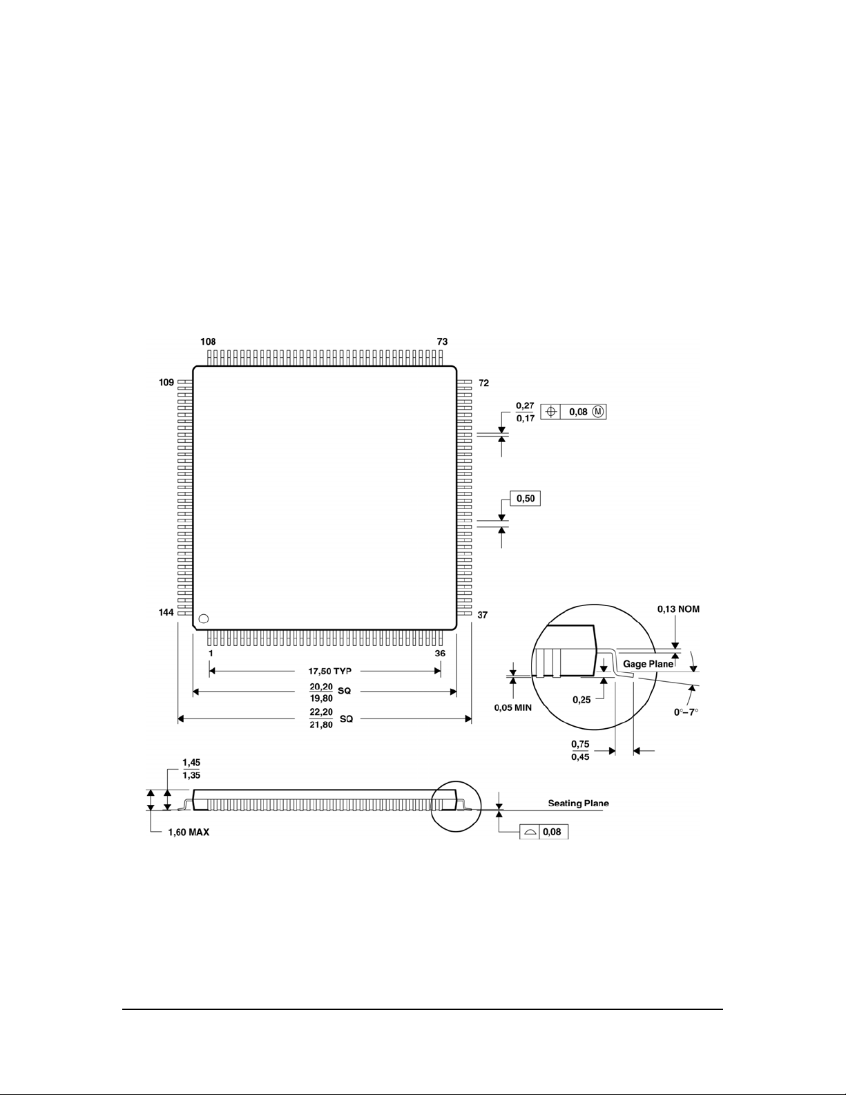
2.2 Physical characteristics and mounting dimensions
2.2.1 CP chip
All dimensions are in millimeters.
MC58000 Electrical Specification – Preliminary 11/13/2003
15
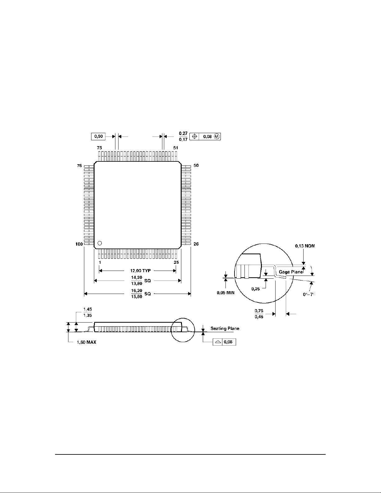
2.2.2 IO chip
All dimensions are in millimeters.
MC58000 Electrical Specification – Preliminary 11/13/2003
16

2.3 Environmental and electrical ratings
d)
s)
a)
a)
-65 °C to 150 °C
-40 °C to 85 °C*
-40 °C to 125 °C*
CP 445 mW
Storage Temperature (T
Operating Temperature: Standard (T
Operating Temperature: Extended (T
Power Dissipation (P
IO 110 mW
Nominal Clock Frequency (F
Supply Voltage limits (V
clk)
cc)
Supply Voltage operating range (V
cc)
40.0 MHz
-0.3V to +4.6V
3.0V to 3.6V
2.4 MC58110 System configuration – Single chip, 1 axis control
The following figure shows the principal control and data paths in an MC58110 system.
CANOpen/CAN 2.0B network
Serial network
CP
Parallel port
40 MHz clock
Host
HostRdy
~HostSlct
HostData0-15
Parallel Communication
PLD/FPGA
~HostRead
~HostWrite
HostIntrpt
HostCmd
2
0
z
c
M
l
o
H
c
k
Home
Index
B
A
Encoder
16 bit data/address bus
Motor type configuration
Serial port configuration
CAN bus configuration
Parallel word input
AxisOut
D
A
C
o
u
p
t
External memoryUser I/O
SPI
AxisIn
Hall A/B/C
t
u
D/A
converter
Positive
Limit
switches
Negative
Analog inputs
PWM output
Motor
Amplifier
The shaded area shows the CPLD/FPGA that must be provided by the designer if parallel
communication is required. A description and the necessary logic (in the form of schematics) of this
device are detailed in the section Parallel FPGA section of this manual.
MC58000 Electrical Specification – Preliminary 11/13/2003
17

The CP chip is a self-contained motion processor. In addition to handling all system functions, the
CP chip contains the profile generator, which calculates velocity, acceleration, and position values for
a trajectory. When an axis is configured for servo motor control, a digital servo filter controls the
motor output signal. When an axis is configured for microstepping motor control, a commutator
controls the motor output signal. In either case, one of three types of output can be generated:
• a Pulse-Width Modulated (PWM) signal output; or
• a DAC-compatible value routed via the data bus to the appropriate D/A converter; or
• a DAC-compatible value routed via the SPI port to the appropriate D/A converter
When an axis is configured for step motor control, the CP chip generates step and direction signals.
Axis position information returns to the motion processor in the form of encoder feedback using
either the incremental encoder input signals, or via the bus as parallel word input.
The MC58110 can co-exist in a CANOpen network as a slave device. It is CAN 2.0B compliant.
2.5 MC58020 System configuration – Two chip, 1 to 4 axis control
The following figure shows the principal control and data paths in an MC58020 system.
Parallel port
40 MHz
clock
A
B
Encoder
Host
HostIntrpt
HostRdy
~HostSlct
HostData0-15
HostCmd
~HostRead
~HostWrite
20MHz clock
Serial network
IO CP
SPI
Index
Home
PWM or S+D output
Motor amplifier
16-bit data bus
Motor type configuration
D/A
converter
Serial port configuration
CAN bus configuration
Parallel word input
D
A
u
o
C
CANOpen/CAN 2.0B network
t
t
u
p
AxisIn
AxisOut
External memory
User I/O
Positive
Limit
switches
Negative
Analog inputs
Hall A/B/C
Other user devices
MC58000 Electrical Specification – Preliminary 11/13/2003
18

The IO chip contains the parallel host interface, the incremental encoder input along with motor
output signals that are configured as PWM or step and direction signals according to the motor type
selected for each axis.
The CP chip contains the profile generator, which calculates velocity, acceleration, and position
values for a trajectory. When an axis is configured for servo motor control, a digital servo filter
controls the motor output signal. When an axis is configured for microstepping motor control, a
commutator controls the motor output signal. In either case, one of three types of output can be
generated:
• a Pulse-Width Modulated (PWM) signal output; or
• a DAC-compatible value routed via the data bus to the appropriate D/A converter; or
• a DAC-compatible value routed via the SPI port to the appropriate D/A converter
When an axis is configured for step motor control, the IO chip generates the step and direction
signals.
Axis position information returns to the motion processor in the form of encoder feedback using
either the incremental encoder input signals, or via the bus as parallel word input.
The MC58020 can co-exist in a CANOpen network as a slave device. It is CAN 2.0B compliant.
2.6 Peripheral device address mapping
Device addresses on the CP chip’s external bus are memory-mapped to the following locations:
Address Device Description
0100h Motor type configuration Contains the configuration data for the per axis motor
0200h Serial port configuration Contains the configuration data (transmission rate,
0400h CAN port configuration Contains the configuration data (baud rate and node
0800h Parallel-word encoder Base address for parallel-word feedback devices
1000h User-defined Base address for user-defined I/O devices
2000h RAM page pointer Page pointer to external memory
4000h Motor-output DACs Base address for motor-output D/A converters
8000h Reserved
type selection
parity, stop bits, etc) for the asynchronous serial port
ID) for the CAN controller
MC58000 Electrical Specification – Preliminary 11/13/2003
19

3 Electrical Characteristics
3.1 DC characteristics
(Vcc and Ta per operating ratings, F
= 40.0 MHz)
clk
Symbol Parameter Minimum Maximum Conditions
Vcc Supply Voltage 3.00 V 3.6 V
Idd Supply Current 135 mA CP
open outputs
33 mA IO
Input Voltages
Vih Logic 1 input voltage 2.0 V Vcc @CP
Vil Logic 0 input voltage 0.8 V @CP
Output Voltages
Voh Logic 1 Output Voltage 2.4 V -2 mA@CP
Vol Logic 0 Output Voltage 0.4 V 8 mA@CP
Other
I
Tri-State output leakage current
out
Iin Input current
I
Input current, CPClk
inclk
-2 µA 2 µA
-25 µA 25 µA
-25 µA 25 µA
Cio Input/Output capacitance 2/3 pF
@CP typical
@CP
0 < V
< Vcc
out
@CP
0 < V
< Vcc
i
0 < Vi < Vcc
Zai Analog input source impedance
E
Differential nonlinearity error.
dnl
Difference between the step width
and the ideal value.
E
Integral nonlinearity error.
inl
Maximum deviation from the best
straight line through the ADC
transfer characteristics, excluding
the quantization error.
3.2 AC characteristics
See timing diagrams, Section 4, for Tn numbers. The symbol “~” indicates active low signal.
Timing Interval Tn Minimum Maximum
Clock Frequency (F
Clock Pulse Width T1 20 nsec 30 nsec
Clock Period (note 3) T2 50 nsec 250 nsec
Encoder Pulse Width T3 150 nsec
Dwell Time Per State T4 75 nsec
) 4 MHz 40 MHz (note 1)
clk
Analog Input
10Ω
-1 ±2 LSB
±2 LSB
MC58000 Electrical Specification – Preliminary 11/13/2003
20

Timing Interval Tn Minimum Maximum
Index Setup and Hold (relative to Quad A
and Quad B low)
~HostSlct Hold Time T6 0 nsec
~HostSlct Setup Time T7 0 nsec
HostCmd Setup Time T8 0 nsec
HostCmd Hold Time T9 0 nsec
Read Data Access Time T10 25 nsec
Read Data Hold Time T11 10 nsec
~HostRead High to HI-Z Time T12 20 nsec
HostRdy Delay Time T13 100 nsec 150 nsec
~HostWrite Pulse Width T14 70 nsec
Write Data Delay Time T15 15 nsec
Write Data Hold Time T16 0 nsec
Read Recovery Time (note 2) T17 60 nsec
Write Recovery Time (note 2) T18 60 nsec
Read Pulse Width T19 70 nsec
External Memory Read Timing
ClockOut low to control valid T20 4 nsec
ClockOut low to address valid T21 8 nsec
Address valid to ~ReadEnable low T22 31 nsec
ClockOut high to ~ReadEnable low T23 5 nsec
Data access time from Address valid T24 40 nsec
Data access time from ~ReadEnable low T25 31 nsec
Data hold time T26 0 nsec
ClockOut low to control inactive T27 5 nsec
Address hold time after ClockOut low T28 2 nsec
ClockOut low to Strobe low T29 5 nsec
ClockOut low to Strobe high T30 6 nsec
W/~R low to R/~W rising delay time T31 5 nsec
External Memory Write Timing
ClockOut high to control valid T32 4 nsec
ClockOut high to address valid T33 10 nsec
Address valid to ~WriteEnable low T34 29 nsec
ClockOut low to ~WriteEnable low T35 6 nsec
Data setup time before ~WriteEnable high T36 33 nsec
Data bus driven from ClockOut low T37 -3 nsec
Data hold time T38 2 nsec
ClockOut high to control inactive T39 5 nsec
Address hold time after ClockOut low T40 -5 nsec
ClockOut low to Strobe low T41 6 nsec
ClockOut low to Strobe high T42 6 nsec
R/~W low to W/~R rising delay time T43 5 nsec
ClockOut high to control valid T44 6 nsec
Peripheral Device Read Timing
Address valid to ~ReadEnable low T22-45 56 nsec
Data access time from Address valid T24-46 65 nsec
Data access time from ~ReadEnable low T25-47 56 nsec
T5 0 nsec
MC58000 Electrical Specification – Preliminary 11/13/2003
21

Timing Interval Tn Minimum Maximum
Peripheral Device Write Timing
Address valid to ~WriteEnable low T34-48 54 nsec
Data setup time before ~WriteEnable high T36-49 58 nsec
Device Ready/ Outputs Initialized T57 1 msec
Note 1 Performance figures and timing information valid at F
information and performance parameters at F
< 40.0 MHz, contact PMD.
clk
= 40.0 MHz only. For timing
clk
Note 2 For 8/16 interface modes only.
Note 3 The clock low/high split has an allowable range of 40-60%.
MC58000 Electrical Specification – Preliminary 11/13/2003
22

4 I/O Timing Diagrams
For the values of Tn, please refer to the table in Section 3.2.
4.1 Clock
MasterClkIn
4.2 Quadrature encoder input
T3
Quad A
Quad B
~Index
4.3 Reset
V
cc
T1 T2
T3
T4 T4
T5
(= ~QuadA * ~QuadB * ~Index)
T1
T5
Index
I/OClk
~RESET
T50
T57
MC58000 Electrical Specification – Preliminary 11/13/2003
23

4.4 Host interface, 8/16 mode
4.4.1 Instruction write, 8/16 mode
T7
~HostSlct
see note
T6
HostCmd
~HostWrite
HostData0-7
HostRdy
Note: If setup and hold times are met, ~HostSlct and HostCmd may be de-asserted at this point.
4.4.2 Data write, 8/16 mode
~HostSlct
T7
T8
T15
T14
T16
T18
T9
see note
T14
T16
Low byteHigh byte
T15
T13
T6
see note
HostCmd
~HostWrite
HostData0-7
HostRdy
T8
see note
T16
T18
T14
T15
T14
High byte
T15
Note: If setup and hold times are met, ~HostSlct and HostCmd may be de-asserted at this
point.
T9
T16
Low byte
T13
MC58000 Electrical Specification – Preliminary 11/13/2003
24

4.4.3 Data read, 8/16 mode
~HostSlct
T7
T6
see note
HostCmd
~HostRead
HostData0-7
High-Z
HostRdy
Note: If setup and hold times are met, ~HostSlct and HostCmd may be de-asserted at this
point.
4.4.4 Status read, 8/16 mode
~HostSlct
T8
T7
T10
T19
High
byte
T11
T12
see note
High-Z
Low byte
T13
T9
High-Z
T6
HostCmd
~HostRead
HostData0-7
T8
T17
T19
T12
High-Z High-Z
T10
High
byte
T11
MC58000 Electrical Specification – Preliminary 11/13/2003
25
Low byte
T9
High-Z

4.5 Host interface, 16/16 mode
4.5.1 Instruction write, 16/16 mode
~HostSlct
HostCmd
T7 T6
~HostWrite
HostData0-15
HostRdy
4.5.2 Data write, 16/16 mode
~HostSlct
HostCmd
T8
T14
T15
T13
T7 T6
T8
T9
T16
T9
~HostWrite
HostData0-15
HostRdy
T14
T15
T13
MC58000 Electrical Specification – Preliminary 11/13/2003
26
T16

4.5.3 Data read, 16/16 mode
~HostSlct
HostCmd
~HostRead
HostData0-15
HostRdy
T7
T8
High-Z
T10
T19
T13
T6
T9
T12
High-Z
T11
4.5.4 Status read, 16/16 mode
~HostSlct
HostCmd
~HostRead
HostData0-15
T7
T8
High-Z
T10
T19
T6
T9
T11
T12
High-Z
MC58000 Electrical Specification – Preliminary 11/13/2003
27

4.6 External memory timing
4.6.1 External memory read
Note: PMD recommends using memory with an access time no greater than 15 nsec.
ClockOut
~RAMSlct
Addr0-Addr15
W/~R
R/~W
~ReadEnable
Data0-Data15
T31
T23
T20
T21
T27
T28
T22
T26
T25
T24
~Strobe
T30T29
MC58000 Electrical Specification – Preliminary 11/13/2003
28

4.6.2 External memory write
ClockOut
~RAMSlct
Addr0-Addr15
R/~W
W/~R
~WriteEnable
Data0-Data15
T33
T44
T32
T43
T34
T35
T37
T39
T40
T38
T36
~Strobe
T42T41
MC58000 Electrical Specification – Preliminary 11/13/2003
29

4.7 Peripheral device timing
4.7.1 Peripheral device read
ClockOut
~PeriphSlct
Addr0-Addr15
W/~R
R/~W
~ReadEnable
Data0-Data15
T31
T23
T20
T21
T27
T28
T45
T26
T47
T46
~Strobe
T30T29
MC58000 Electrical Specification – Preliminary 11/13/2003
30

4.7.2 Peripheral device write
ClockOut
~PeriphSlct
Addr0-Addr15
R/~W
W/~R
~WriteEnable
Data0-Data15
T33
T44
T32
T43
T48
T35
T37
T39
T40
T38
T49
T42T41
~Strobe
MC58000 Electrical Specification – Preliminary 11/13/2003
31

5 Pinouts and Pin Descriptions
5.1 Pinouts for the MC58110
4, 29, 42, 50, 67, 77, 86, 95,
122, 129, 141
133
~Reset
~WriteEnable89
~ReadEnable
93
96 ~Strobe
92
R/~W
W/~R
19
120
Ready
~PeriphSlct
82
87
~RAMSlct
25
SrlXmt
26
SrlRcv
72
CANXmt/SrlEnable
70
CANRcv
3530SPIClock
SPIXmt
23 IOInterr upt
123
MasterClkIn
73 ClockOut
80
Addr0
78
Addr1
74
Addr2
71
Addr3
68
Addr4
64
Addr5
61
Addr6
57
Addr7
53
Addr8
51
Addr9
48
Addr10
45
Addr11
43
Addr12
39
Addr13
34
Addr14
31
Addr15
127
Data0
130
Data1
132
Data2
134
Data3
136
Data4
138
Data5
143
Data6
5
Data7
9
Data8
13
Data9
15
Data10
17
Data11
20
Data12
22
Data13
24
Data14
27
Data15
VCC
CP
GND
AnalogVcc
AnalogRefHigh
AnalogRefLow
AnalogGnd
Analog0
Analog1
Analog2
Analog3
Analog4
Analog5
Analog6
Analog7
PosLim1
NegLim1
AxisOut1
AxisIn1
PWMMag1A
PWMSign1A
PWMMag1B
PWMSign1B
PWMMag1C
PWMSign1C
QuadA1
QuadB1
~Home1
QuadAuxA1
QuadAuxB1
Hall1A
Hall1B
Hall1C
~ParallelEnable 8
~HostInterrupt
Synch
OscFilter1
OscFilter2
Vcc5
Vssf
116
115
114
117
112
113
110
111
107
109
105
108
46
38
32
16
56
54
52
47
44
40
83
79
75
88
81
69~Index1
18
14
37
131
21
11
10
58
12
3, 28, 41, 49, 66, 76, 85, 94, 125,
1, 2, 6, 7, 33, 36, 55, 59, 60, 62,
63, 65, 84, 90, 91, 97, 118, 119,
128, 140
AGND
98, 99, 100, 101,
102, 103, 104, 106
No connection
121, 124, 126, 135, 137, 139,
142, 144
MC58000 Electrical Specification – Preliminary 11/13/2003
32

5.1.1 MC58110 CP chip pin description
Pin Name and number Direction Description
~Reset 133
~WriteEnable 89
~ReadEnable 93
~Strobe 96
R/~W 92
W/~R 19
Ready 120
~PeriphSlct 82
~RAMSlct 87
SrlXmt 25
SrlRcv 26
CANXmt
SrlEnable
CANRcv 70
SPIClock 35
SPIXmt 30
IOInterrupt 23
MasterClkIn 123
ClockOut 73
72
input This is the master reset signal. When brought low, this pin resets the chipset to its
output This signal is the write-enable strobe. When low, this signal indicates that data is
output This signal is the read-enable strobe. When low, this signal indicates that data is
output This signal is low when the data and address are valid during CP
output This signal is high when the CP chip is performing a read, and low when it is
output This signal is the inverse of R/~W; it is high when R/~W is low, and vice versa. For
input Ready can be pulled low to add wait states for external accesses. Ready indicates
output This signal is low when peripheral devices on the data bus are being addressed. If
output This signal is low when external memory is being accessed.
output This pin outputs serial data from the asynchronous serial port.
input This pin inputs serial data to the asynchronous serial port.
output When the CAN host interface is used, this pin transmits serial data to the CAN
output This pin receives serial data from the CAN transceiver.
output This pin is the clock signal used for strobing synchronous serial data to the serial
output This pin transmits synchronous serial data to the serial DAC(s).
input This interrupt signal is used for IO to CP communication. If the parallel
input This is the clock signal for the Motion Processor. It is driven at a nominal
output This signal is the reference output clock. Its frequency is twice the frequency of
CP
initial conditions.
being written to the bus.
being read from the bus.
communications. If the parallel interface is used, this pin should be connected
to the PLD/FPGA IO chip signal
performing a write. If the parallel interface is used, this pin should be connected
to the PLD/FPGA IO chip signal
some decode circuits and devices this is more convenient than
that an external device is prepared for a bus transaction to be completed. If the
device is not ready, it pulls the
one cycle and checks
Ready again.
This signal can be left unconnected if it is not used.
the parallel interface is used, this pin should be connected to the PLD/FPGA
IO chip signal
CPPeriphSlct.
transceiver.
When the multi-drop serial interface is used, this pin sets the serial port enable
line and the CANXmt function is not available. SrlEnable is high during
transmission for the multi-drop protocol and low at all other times.
DAC(s). This signal is only active when SPI data is being transmitted.
interface is used, this pin should be connected to the PLD/FPGA IO chip signal
CPInterrupt.
This signal can be left unconnected if it is not used.
20MHz.
the input clock (which is normally 20MHz) resulting in a nominal output
frequency of 40MHz.
CPStrobe.
CPR/~W.
R/~W.
Ready pin low. The motion processor then waits
MC58000 Electrical Specification – Preliminary 11/13/2003
33

Pin Name and number Direction Description
Addr0
Addr1
Addr2
Addr3
Addr4
Addr5
Addr6
Addr7
Addr8
Addr9
Addr10
Addr11
Addr12
Addr13
Addr14
Addr15
Data0
Data1
Data2
Data3
Data4
Data5
Data6
Data7
Data8
Data9
Data10
Data11
Data12
Data13
Data14
Data15
AnalogVcc 116
AnalogRefHigh 115
AnalogRefLow 114
AnalogGND 117
Analog0
Analog1
Analog2
Analog3
Analog4
Analog5
Analog6
Analog7
80
78
74
71
68
64
61
57
53
51
48
45
43
39
34
31
127
130
132
134
136
138
143
5
9
13
15
17
20
22
24
27
112
113
110
111
107
109
105
108
output Multi-purpose address lines. These pins comprise the CP chip’s external address
bus, used to select devices for communication over the data bus. If the parallel
interface is used, pins
PLD/FPGA IO chip signals
communicate between the CP and IO chips.
Other address pins may be used for DAC output, parallel word input, or userdefined I/O operations. See the User’s Guide for a complete memory map.
bi-directional Multi-purpose data lines. These pins comprise the CP chip’s external data bus,
used for all communications with peripheral devices such as external memory or
DACs. They may also be used for parallel-word input and for user-defined I/O
operations.
If the parallel interface is used, these pins should be connected to the
PLD/FPGA IO chip signals
input Analog input Vcc. This pin should be connected to the analog input supply
voltage, which must be in the range 3.0-3.6 V.
If the analog input circuitry is not used, this pin should be tied to V
input Analog high voltage reference for A/D input. The allowed range is AnalogRefLow
to
AnalogVcc.
If the analog input circuitry is not used, this pin should be tied to V
input Analog low voltage reference for A/D input. The allowed range is AnalogGND to
AnalogRefHigh.
If the analog input circuitry is not used, this pin should be tied to GND.
input Analog input ground. This pin should be connected to the analog input power
supply return.
If the analog input circuitry is not used, this pin should be tied to GND.
input These signals provide general-purpose analog voltage levels which are sampled
by an internal A/D converter. The A/D resolution is 10 bits.
The allowed signal input range is
Any unused pins should be tied to AnalogGND.
If the analog input circuitry is not used, these pins should be tied to GND.
CP
Addr0, Addr1, and Addr15 should be connected to the
CPAddr0, CPAddr1 and CPAddr15. They are used to
CPData0-15.
AnalogRefLow to AnalogRefHigh.
.
cc
.
cc
MC58000 Electrical Specification – Preliminary 11/13/2003
34

Pin Name and number Direction Description
PosLim1 46
NegLim1 38
AxisOut1 32
AxisIn1 16
PWMMag1A
PWMSign1A
PWMMag1B
PWMSign1B
PWMMag1C
PWMSign1C
SPIEnable1 54
Pulse1 56
Direction1 54
AtRest1 52
56
54
52
47
44
40
input This signal provides input from the positive-side (forward) travel limit switch.
On power-up or after reset this signal defaults to active low interpretation, but
the interpretation can be set to active high interpretation using the
SetSignalSense instruction.
If this pin is not used it may be left unconnected.
input This signal provides input from the negative-side (reverse) travel limit switch.
On power-up or after reset this signal defaults to active low interpretation, but
the interpretation can be set to active high interpretation using the
SetSignalSense instruction.
If this pin is not used it may be left unconnected.
output This pin can be programmed to track the state of any bit in the status registers.
If this pin is not used it may be left unconnected.
input This pin is a general-purpose input that can also be used as a breakpoint input.
If this pin is not used it may be left unconnected.
output These pins provide the Pulse Width Modulated signals for each phase of the
motor. The PWM resolution is 10 bits at a frequency of 20.0 KHz or 80kHz,
selectable via the host command
In 2 or 3-phase PWM 50/50 mode, PWMMag1A/1B/1C are the only signals
and encode both the magnitude and direction in the one signal.
In single-phase PWM sign/magnitude mode, PWMMag1A and PWMSign1A are
the PWM magnitude and direction signals respectively.
In 2-phase PWM sign/magnitude mode, PWMMag1A and PWMSign1A are the
PWM magnitude and direction signals for Phase A. PWMMag1B and
PWMMag1B are the PWM magnitude and direction signals for Phase B.
Unused pins should be left unconnected.
Refer to the User’s Guide for more information on PWM encoding schemes.
output This pin provides the enable signal when SPI DAC output is active. The enable
is high when the DAC channel is being written to. At all other times the signal is
low.
SPI output can only be used when the axis being controlled is DC brushed or
when the amplifier expects a single-phase input and it performs brushless motor
commutation. PWM and Step and Direction output is not available when SPI
DAC output is selected.
If this pin is not used it may be left unconnected.
output This pin provides the pulse (step) signal to the motor. A step occurs when the
signal transitions from a high to a low state. This default behavior can be changed
to a low to high state transition using the command
If this pin is not used it may be left unconnected.
output This pin indicates the direction of motion and works in conjunction with the
pulse signal. A high level on this signal indicates a positive direction move and a
low level indicates a negative direction move.
output This signal indicates that the axis is at rest and the step motor can be switched to
low power or standby mode. A high level on this signal indicates the axis is at
rest while a low signal indicates the axis is in motion.
CP
SetPWMFrequency.
SetSignalSense.
MC58000 Electrical Specification – Preliminary 11/13/2003
35

Pin Name and number Direction Description
QuadA1
QuadB1
~Home1 75
QuadAuxA1
QuadAuxB1
~Index1
83
79
88
81
69
input These pins should be connected to the A and B quadrature signals from the
incremental encoder. When the axis is moving in the positive (forward)
direction, signal A leads signal B by 90°.
The theoretical maximum encoder pulse rate is 5.0 MHz. Actual maximum rate
will vary, depending on signal noise.
NOTE: Many encoders require a pull-up resistor on each signal to establish a
proper high signal. Check your encoder’s electrical specification.
If these pins are not used they may be left unconnected.
input This pin provides the home signal, a general-purpose input to the position
capture mechanism. A valid home signal is recognized by the motion processor
when
~Home transitions from high to low.
If this pin is not used it may be left unconnected.
input If index capture is required, the encoder A and B signals connected to QuadA1
and QuadB1 signals must also be connected to QuadAuxA1 and QuadAuxB1.
The index pin should be connected to the index signal from the incremental
encoder. A valid index pulse is recognized by the motion processor when this
signal transitions from high to low.
If these pins are not used they may be left unconnected.
WARNING! There is no internal gating of the index signal with
the encoder A and B inputs. This must be performed externally if
desired. Refer to the Application Notes section at the end of this
manual for an example.
CP
Hall1A
Hall1B
Hall1C
ParallelEnable 8
~HostInterrupt 131
Synch 21
OscFilter1
OscFilter2
18
14
37
11
10
input Hall sensor inputs. These signals encode 6 valid states as follows: A on, A and B
input This signal enables/disables the parallel communication with the host. If this
output When low, this signal causes an interrupt to be sent to the host processor.
input/output This pin is the synchronization signal. In the disabled mode, the pin is
on, B on, B and C on, C on, C and A on. A sensor is defined as being on when
its signal is high. On power-up or after reset these signal defaults to active high
interpretation, but the interpretation can be set to active low interpretation using
the
SetSignalSense instruction.
Note: These signals should only be connected to Hall sensors that are mounted
at a 120° offset. Motors with hall signals 60° apart will not work.
The number of available axes determines which of these signals are valid.
If these pins are not used they may be left unconnected.
signal is tied high, the parallel interface is enabled. If this signal is tied low the
parallel interface is disabled. Contact PMD for more information on parallel
communication.
WARNING! This signal should only be tied high if an external
logic device that implements the parallel communication logic is
included in the design.
configured as an input and is not used. In the master mode, the pin outputs a
synchronization pulse that can be used by slave nodes or other devices to
synchronize with the internal chip cycle of the master node. In the slave mode,
the pin is configured as an input and should be connected to the Synch pin on
the master node. A pulse on the pin synchronizes the internal chip cycle to the
signal provided by the master node.
If this pin is not used it may be left unconnected.
These signals connect to the external oscillator filter circuitry. Section 5.3 shows
the required filter circuitry.
MC58000 Electrical Specification – Preliminary 11/13/2003
36

CP
Pin Name and number Direction Description
V
58
cc5
This signal can optionally be tied to a 5V logic supply, which is required for
reprogramming the chipset firmware.
V
12
ssf
This signal must be tied to pin 28 using a bypass capacitor. A ceramic capacitor
with a value between 0.1µF and 0.01µF should be used.
Vcc
GND
AGND
No connection
4, 29, 42, 50, 67, 77,
86, 95, 122, 129, 141
3, 28, 41, 49, 66, 76,
85, 94, 125, 128, 140
98, 99, 100, 101, 102,
103, 104, 106
1, 2, 6, 7, 33, 36, 55,
CP digital supply voltage. All of these pins must be connected to the supply
voltage. V
must be in the range 3.0 – 3.6 V.
cc
CP digital supply ground. All of these pins must be connected to the digital
power supply return.
These signals must be tied to AnalogGND.
If the analog input circuitry is not used, these pins must be tied to GND.
These signals must be left unconnected.
59, 60, 62, 63, 65, 84,
90, 91, 97, 118, 119,
121, 124, 126, 135,
137, 139, 142, 144
5.1.2 MC58110 CP chip pin assignment for multiple motor types
The MC58110 chip supports outputting PWM motor commands in sign/magnitude and 50/50
modes. For stepping motors it can also output step and direction signals. The CP chip assigns pin
function according to the selected output mode.
If the output mode is set to PWM sign/magnitude, the following pinout should be used.
PWMMag1A
PWMMag1B
PWMSign1A
PWMSign1B
56
52
54
47
output These pins provide the Pulse Width Modulated signal to the motor. In
PWM 50/50 mode, this is the only signal. In PWM sign-magnitude
mode, this is the magnitude signal.
output In PWM sign-magnitude mode, these pins provide the sign (direction) of
the PWM signal to the motor amplifier.
If the output mode is set to PWM 5050, the following pinout should be used.
PWMMag1A
PWMMag1B
PWMMag1C
56
52
44
output These pins provide the Pulse Width Modulated signals for each phase to
the motor. If the number of phases is 2, only phase A and B are valid. If
the number of phases is 3, phases A,B and C are valid. The number of
phases is set using the command
SetNumberPhases.
In PWM 50/50 mode, these are the only signals.
If the output mode is set to Step and Direction, the following pinout should be used.
Pulse1 56
Direction1 54
AtRest1 52
output This pin provides the pulse (step) signal to the motor.
output These pin indicates the direction of motion and works in conjunction
with the pulse signal.
output This signal indicates the axis is at rest and the step motor can be switched
to low power or standby mode.
If the output mode is set to SPI DAC, the following pinout should be used.
SPIEnable1 54
output This pin provides the enable signal when SPI DAC output is active.
MC58000 Electrical Specification – Preliminary 11/13/2003
37

5.2 Pinouts for the MC58420
16, 17, 40, 65, 66, 67, 90
HostCmd
100
81
92
94
77
53
54
52
41
43
50
89
24
91
12
10
99
98
11
97
95
76
74
73
75
38
36
35
32
31
8
5
1
2
3
7
6
HostRdy
~HostRead
~HostWrite
~HostSlct
CPInterrupt
CPR/~W
CPStrobe
CPPeriphSlct
CPAddr0
CPAddr1
CPAddr15
MasterClkIn
CPClock
HostMode0
HostMode1
HostData0
HostData1
HostData2
HostData3
HostData4
HostData5
HostData6
HostData7
HostData8
HostData9
HostData10
HostData11
HostData12
HostData13
HostData14
HostData15
CPData0
CPData1
CPData2
CPData3
CPData4
4, 9, 22, 34, 46, 57, 64, 72, 84, 96
VCC
IO
GND
No connection
27, 55, 56
CPData5
CPData6
CPData7
CPData8
CPData9
CPData10
CPData11
CPData12
CPData13
CPData14
CPData15
PWMMag1A
PWMMag1B
PWMMag1C
PWMMag2A
PWMMag2B
PWMMag2C
PWMMag3A
PWMMag3B
PWMMag3C
PWMMag4A
PWMMag4B
PWMMag4C
PWMSign1
PWMSign2 60
PWMSign3
PWMSign4
QuadA1
QuadB1
~Index1
~Home1
QuadA2
QuadB2
~Index2
~Home2
QuadA3
QuadB3
~Index3
~Home3
QuadA4
QuadB4
~Index4
~Home4
4, 29, 42, 50, 67, 77, 86, 95,
122, 129, 141
133
37
42
39
18
14
71
13
70
15
69
68
21
62
23
85
87
86
20
19
63
79
78
80
61
59
26
47
25
49
82
48
44
93
29
33
51
83
88
30
58
28
45
~Reset
~WriteEnable89
93
~ReadEnable
96 ~Strobe
92
R/~W
19
W/~R
120
Ready
82
~PeriphSlct
87
~RAMSlct
SrlXmt
25
SrlRcv
26
CANXmt/SrlEnable
72
CANRcv
70
3530SPIClock
SPIXmt
IOInterrupt
23
IOClock
123
73 ClockOut
Addr0
80
Addr1
78
Addr2
74
Addr3
71
Addr4
68
Addr5
64
Addr6
61
Addr7
57
Addr8
53
Addr9
51
Addr10
48
Addr11
45
Addr12
43
Addr13
39
Addr14
34
Addr15
31
Data0
127
Data1
130
132
Data2
Data3
134
Data4
136
Data5
138
Data6
143
Data7
5
Data8
9
Data9
13
Data10
15
Data11
17
Data12
20
Data13
22
Data14
24
Data15
27
VCC
CP
GND
AnalogVcc
AnalogRefHigh
AnalogRefLow
AnalogGnd
Analog0
Analog1
Analog2
Analog3
Analog4
Analog5
Analog6
Analog7
PosLim1
PosLim2
PosLim3
PosLim4
NegLim1
NegLim2
NegLim3
NegLim4
AxisOut1
AxisOut2
AxisOut3
AxisOut4
AxisIn1
AxisIn2
AxisIn3
AxisIn4
Hall1A
Hall1B
Hall1C
Hall2A
Hall2B
Hall2C
Hall3A
Hall3B
Hall3C
Hall4A
Hall4B
Hall4C
~HostInterrupt
Synch
OscFilter1
OscFilter2
Vcc5
Vssf
116
115
114
117
112
113
110
111
107
109
105
108
46
59
65
81
38
55
62
69
32
119
88
54
16
8
52
83
18
14
37
6
2
126
47
44
40
79
75
56
131
21
11
10
58
12
3, 28, 41, 49, 66, 76, 85, 94, 125,
128, 140
AGND
98, 99, 100, 101,
102, 103, 104, 106
No connection
1, 7, 33, 36, 60, 63, 84, 90, 91,
97, 118, 121, 124, 135, 137,
139, 142, 144
MC58000 Electrical Specification – Preliminary 11/13/2003
38

5.2.1 MC58020 IO chip pin description
Pin Name and Number Direction Description
HostCmd 81
HostRdy
~HostRead 92
~HostWrite 100
~HostSlct 94
CPInterrupt 77
CPR/~W 53
CPStrobe 54
CPPeriphSlct 52
CPAddr0
CPAddr1
CPAddr15
MasterClkIn 89
CPClock 24
HostMode0
HostMode1 5 91
8
41
43
50
input This signal is asserted high to write a host instruction to the motion
output This signal is used to synchronize communication between the motion
input When ~HostRead is low, a data word is read from the motion processor.
input When ~HostWrite is low, a data word is written to the motion processor.
input When ~HostSlct is low, the host port is selected for reading or writing
output IO chip to CP chip interrupt. It should be connected to CP chip pin 23,
input This signal is high when the CP chip is reading data from the IO chip, and
input This signal goes low when the data and address become valid during
input This signal goes low when a peripheral device on the data bus is being
input These signals are high when the CP chip is communicating with the IO
input This is the master clock signal for the motion processor. It is driven at a
output This signal provides the clock pulse for the CP chip. Its frequency is half
input These two signals determine the host communications mode, as follows:
IO
processor, or to read the status of the
is asserted low to read or write a data word.
processor and the host.
HostRdy (HostReady) will go low indicating host
port busy at the end of a read or write operation according to the
interface mode in use, as follows:
Interface Mode
HostRdy goes
8/16 after the second byte of the instruction word
after the second byte of each data word is transferred
16/16 after the 16-bit instruction word
after each 16-bit data word
HostRdy will go high, indicating that the host port is ready to transmit,
when the last transmission has been processed. All host port
communications must be made with
A typical busy-to-ready cycle is 10 microseconds, but can be substantially
longer, up to 50 microseconds.
operations.
IOInterrupt.
low when it is writing data. It should be connected to CP chip pin 92,
R/~W.
motion processor communication with peripheral devices on the data
bus, such as external memory or a DAC. It should be connected to CP
chip pin 96,
~Strobe.
addressed. It should be connected to CP chip pin 82,
chip (as distinguished from any other device on the data bus). They
should be connected to CP chip pins 80 (
(
Addr15).
nominal 40 MHz
that of
MasterClkIn (pin 89), or 20 MHz nominal. It is connected directly
to the CP chip
HostMode1 HostMode0
IOClock signal (pin 123).
0 0 16/16 parallel (16-bit bus, 16-bit instruction)
0 1 not used
1 0 8/16 parallel (8-bit bus, 16-bit instruction)
1 1 Parallel disabled
HostRdy and HostInterrupt signals. It
low
HostRdy high (ready).
~PeriphSlct.
Addr0), 78 (Addr1), and 31
MC58000 Electrical Specification – Preliminary 11/13/2003
39

Pin Name and Number Direction Description
HostData0
HostData1
HostData2
HostData3
HostData4
HostData5
HostData6
HostData7
HostData8
HostData9
HostData10
HostData11
HostData12
HostData13
HostData14
HostData15
CPData0
CPData1
CPData2
CPData3
CPData4
CPData5
CPData6
CPData7
CPData8
CPData9
CPData10
CPData11
CPData12
CPData13
CPData14
CPData15
PWMMag1A
PWMMag1B
PWMMag1C
PWMSign1A
12
10
99
98
1
11
97
95
76
74
73
75
2
3
7
6
38
36
35
32
31
37
42
39
18
14
71
13
70
15
69
68
21
62
23
61
bi-directional,
tri-state
These signals transmit data between the host and the motion processor
through the parallel port. Transmission is mediated by the control signals
~HostSelect, ~HostWrite, ~HostRead and HostCmd.
In 16-bit mode, all 16 bits are used (
low-order 8 bits of data are used (
HostMode1 signals select the communication mode this port operates in.
bi-directional These signals transmit data between the IO chip and pins Data0-15 of the
CP chip.
output These pins provide the Pulse Width Modulated signals for each phase of
the motor. The PWM resolution is 10 bits at a frequency of 20.0 KHz or
80kHz, selectable via the host command SetPWMFrequency.
These pins control Axis 1.
In 2 or 3-phase PWM 50/50 mode, PWMMag1A/1B/1C are the only
signals and encode both the magnitude and direction in the one signal.
In single-phase PWM sign/magnitude mode, PWMMag1A and
PWMSign1A are the PWM magnitude and direction signals respectively.
In 2-phase PWM sign/magnitude mode, PWMMag1A and PWMSign1A
are the PWM magnitude and direction signals for Phase A. PWMMag1B
and PWMMag1C, “PWMSign1B”, are the PWM magnitude and direction
signals for Phase B.
The number of available axes determines which of these signals are valid.
Unused pins should be left unconnected.
Refer to the User’s Guide for more information on PWM encoding
schemes.
IO
HostData0-15). In 8-bit mode, only the
HostData0-7). The HostMode0 and
MC58000 Electrical Specification – Preliminary 11/13/2003
40

Pin Name and Number Direction Description
PWMMag2A
PWMMag2B
PWMMag2C
PWMSign2A
PWMMag3A
PWMMag3B
PWMMag3C
PWMSign3A
PWMMag4A
PWMMag4B
PWMMag4C
PWMSign4A
85
87
86
60
20
19
63
59
79
78
80
26
output These pins control Axis 2.
In 2 or 3-phase PWM 50/50 mode, PWMMag2A/2B/2C are the only
signals and encode both the magnitude and direction in the one signal.
In single-phase PWM sign/magnitude mode, PWMMag2A and
PWMSign2 are the PWM magnitude and direction signals respectively.
In 2-phase PWM sign/magnitude mode, PWMMag2A and PWMSign2A
are the PWM magnitude and direction signals for Phase A. PWMMag2B
and PWMMag2C, “PWMSign2B”, are the PWM magnitude and direction
signals for Phase B.
The number of available axes determines which of these signals are valid.
Unused or invalid pins should be left unconnected.
output These pins control Axis 3.
In 2 or 3-phase PWM 50/50 mode, PWMMag3A/3B/3C are the only
signals and encode both the magnitude and direction in the one signal.
In single-phase PWM sign/magnitude mode, PWMMag3A and
PWMSign3A are the PWM magnitude and direction signals respectively.
In 2-phase PWM sign/magnitude mode, PWMMag3A and PWMSign3A
are the PWM magnitude and direction signals for Phase A. PWMMag3B
and PWMMag3C, “PWMSign3B”, are the PWM magnitude and direction
signals for Phase B.
The number of available axes determines which of these signals are valid.
Unused or invalid pins should be left unconnected.
output These pins control Axis 4.
In 2 or 3-phase PWM 50/50 mode, PWMMag4A/4B/4C are the only
signals and encode both the magnitude and direction in the one signal.
In single-phase PWM sign/magnitude mode, PWMMag4A and
PWMSign4A are the PWM magnitude and direction signals respectively.
In 2-phase PWM sign/magnitude mode, PWMMag4A and PWMSign4A
are the PWM magnitude and direction signals for Phase A. PWMMag4B
and PWMMag4C, “PWMSign4B”, are the PWM magnitude and direction
signals for Phase B.
The number of available axes determines which of these signals are valid.
Unused or invalid pins should be left unconnected.
IO
MC58000 Electrical Specification – Preliminary 11/13/2003
41

Pin Name and Number Direction Description
SPIEnable1
SPIEnable2
SPIEnable3
SPIEnable4
Pulse1
Pulse2
Pulse3
Pulse4
Direction1
Direction2
Direction3
Direction4
AtRest1
AtRest2
AtRest3
AtRest4
QuadA1
QuadB1
QuadA2
QuadB2
QuadA3
QuadB3
QuadA4
QuadB4
21
85
20
79
21
85
20
79
61
60
59
26
23
86
63
80
47
25
48
44
33
51
30
58
output These pins provide the enable signal when SPI DAC output is active.
Each enable is high when the specific DAC channel is being written to.
At all other times the signals are low.
There is one signal per axis. SPI output can only be used when the axis
being controlled is DC brushed or when the amplifier expects a singlephase input and it performs brushless motor commutation.
The number of available axes determines which of these signals are valid.
Unused or invalid pins should be left unconnected.
output These pins provide the pulse (step) signal to the motor. This signal is
always a square wave, regardless of the pulse rate. A step occurs when
the signal transitions from a high state to a low state. This default
behavior can be changed to a low to high state transition using the
command SetSignalSense.
The number of available axes determines which of these signals are valid.
Invalid axis pins may be left unconnected.
output These pins indicate the direction of motion and work in conjunction with
the pulse signal. A high level on this signal indicates a positive direction
move and a low level indicates a negative direction move.
The number of available axes determines which of these signals are valid.
Invalid axis pins may be left unconnected.
output The AtRest signal indicates the axis is at rest and the step motor can be
switched to low power or standby. A high level on this signal indicates
the axis is at rest. A low signal indicates the axis is in motion.
The number of available axes determines which of these signals are valid.
Invalid axis pins may be left unconnected.
input These pins provide the A and B quadrature signals for the incremental
encoder for each axis. When the axis is moving in the positive (forward)
direction, signal A leads signal B by 90°.
The theoretical maximum encoder pulse rate is 10.2 MHz. Actual
maximum rate will vary, depending on signal noise.
NOTE: Many encoders require a pull-up resistor on each signal to
establish a proper high signal. Check your encoder’s electrical
specification.
The number of available axes determines which of these signals are valid.
IO
~Index1
~Index2
~Index3
~Index4
49
93
83
28
WARNING! If a valid axis pin is not used, its signal should
be tied high.
Invalid axis pins may be left unconnected or connected to ground.
input These pins provide the Index quadrature signals for the incremental
encoders. A valid index pulse is recognized by the chipset when
B are all low.
and
~Index, A,
The number of available axes determines which of these signals are valid.
WARNING! If a valid axis pin is not used, its signal should
be tied high.
Invalid axis pins may be left unconnected or connected to ground.
MC58000 Electrical Specification – Preliminary 11/13/2003
42

Pin Name and Number Direction Description
~Home1
~Home2
~Home3
~Home4
82
29
88
45
input These pins provide the Home signals, general-purpose inputs to the
position-capture mechanism. A valid Home signal is recognized by the
chipset when
not gated by the A and B encoder channels.
The number of available axes determines which of these signals are valid.
WARNING! If a valid axis pin is not used, its signal should
be tied high.
Invalid axis pins may be left unconnected or connected to ground.
Vcc
GND
Not connected
16, 17, 40, 65, 66, 67,
90
4, 9, 22, 34, 46, 57, 64,
72, 84, 96
All of these pins must be connected to the IO chip digital supply voltage,
which should be in the range 3.0 to 3.6 V.
IO chip ground. All of these pins must be connected to the digital power
supply return.
27, 55, 56 These pins must be left unconnected (floating).
IO
~Homen goes low. These signals are similar to ~Index, but are
MC58000 Electrical Specification – Preliminary 11/13/2003
43

5.2.2 MC58020 IO chip pin assignment for multiple motor types
The MC58020 chip supports outputting PWM motor commands in sign/magnitude and 50/50
modes. For stepping motors it can also output step and direction signals. The IO chip assigns pin
function according to the selected output mode.
For axis 1 of the chipset:
If the output mode is set to PWM sign/magnitude, the following pinout should be used.
PWMMag1A
PWMMag1B
PWMSign1A
PWMSign1B
If the output mode is set to PWM 5050, the following pinout should be used.
PWMMag1A
PWMMag1B
PWMMag1C
If the output mode is set to Step and Direction, the following pinout should be used.
Pulse1 21
Direction1 61
AtRest1 23
21
62
61
23
21
62
23
output These pins provide the Pulse Width Modulated signal to the motor. In
PWM 50/50 mode, this is the only signal. In PWM sign-magnitude mode,
this is the magnitude signal.
output In PWM sign-magnitude mode, these pins provide the sign (direction) of
the PWM signal to the motor amplifier.
output These pins provide the Pulse Width Modulated signals for each phase to
the motor. If the number of phases is 2, only phase A and B are valid. If
the number of phases is 3, phases A,B and C are valid. The number of
phases is set using the Motion processor command SetNumberPhases.
In PWM 50/50 mode, these are the only signals.
output This pin provides the pulse (step) signal to the motor.
output These pin indicates the direction of motion and works in conjunction
with the pulse signal.
output This signal indicates the axis is at rest and the step motor can be switched
to low power or standby.
For axis 2 of the chipset:
If the output mode is set to PWM sign/magnitude, the following pinout should be used.
PWMMag2A
PWMMag2B
PWMSign2A
PWMSign2B
85
87
60
86
output These pins provide the Pulse Width Modulated signal to the motor. In
PWM 50/50 mode, this is the only signal. In PWM sign-magnitude mode,
this is the magnitude signal.
output In PWM sign-magnitude mode, these pins provide the sign (direction) of
the PWM signal to the motor amplifier.
If the output mode is set to PWM 5050, the following pinout should be used.
PWMMag2A
PWMMag2B
PWMMag2C
85
87
86
output These pins provide the Pulse Width Modulated signals for each phase to
the motor. If the number of phases is 2, only phase A and B are valid. If
the number of phases is 3, phases A,B and C are valid. The number of
phases is set using the Motion processor command SetNumberPhases.
In PWM 50/50 mode, these are the only signals.
If the output mode is set to Step and Direction, the following pinout should be used.
Pulse2 85
Direction2 60
AtRest2 86
output This pin provides the pulse (step) signal to the motor.
output These pin indicates the direction of motion and works in conjunction
with the pulse signal.
output This signal indicates the axis is at rest and the step motor can be switched
to low power or standby.
MC58000 Electrical Specification – Preliminary 11/13/2003
44

For axis 3 of the chipset:
If the output mode is set to PWM sign/magnitude, the following pinout should be used.
PWMMag3A
PWMMag3B
PWMSign3A
PWMSign3B
20
19
59
63
output These pins provide the Pulse Width Modulated signal to the motor. In
PWM 50/50 mode, this is the only signal. In PWM sign-magnitude mode,
this is the magnitude signal.
output In PWM sign-magnitude mode, these pins provide the sign (direction) of
the PWM signal to the motor amplifier.
If the output mode is set to PWM 5050, the following pinout should be used.
PWMMag3A
PWMMag3B
PWMMag3C
20
19
63
output These pins provide the Pulse Width Modulated signals for each phase to
the motor. If the number of phases is 2, only phase A and B are valid. If
the number of phases is 3, phases A,B and C are valid. The number of
phases is set using the Motion processor command SetNumberPhases.
In PWM 50/50 mode, these are the only signals.
If the output mode is set to Step and Direction, the following pinout should be used.
Pulse3 20
Direction3 59
AtRest3 63
output This pin provides the pulse (step) signal to the motor.
output These pin indicates the direction of motion and works in conjunction
with the pulse signal.
output This signal indicates the axis is at rest and the step motor can be switched
to low power or standby.
For axis 4 of the chipset:
If the output mode is set to PWM sign/magnitude, the following pinout should be used.
PWMMag4A
PWMMag4B
PWMSign4A
PWMSign4B
79
78
26
80
output These pins provide the Pulse Width Modulated signal to the motor. In
PWM 50/50 mode, this is the only signal. In PWM sign-magnitude mode,
this is the magnitude signal.
output In PWM sign-magnitude mode, these pins provide the sign (direction) of
the PWM signal to the motor amplifier.
If the output mode is set to PWM 5050, the following pinout should be used.
PWMMag4A
PWMMag4B
PWMMag4C
79
78
80
output These pins provide the Pulse Width Modulated signals for each phase to
the motor. If the number of phases is 2, only phase A and B are valid. If
the number of phases is 3, phases A,B and C are valid. The number of
phases is set using the Motion processor command SetNumberPhases.
In PWM 50/50 mode, these are the only signals.
If the output mode is set to Step and Direction, the following pinout should be used.
Pulse4 79
Direction4 26
AtRest4 80
output This pin provides the pulse (step) signal to the motor.
output These pin indicates the direction of motion and works in conjunction
with the pulse signal.
output This signal indicates the axis is at rest and the step motor can be switched
to low power or standby.
Any unused pins may be left unconnected (floating).
MC58000 Electrical Specification – Preliminary 11/13/2003
45

5.2.3 MC58020 CP chip pin description
Pin Name and number Direction Description
~Reset 133
~WriteEnable 89
~ReadEnable 93
~Strobe 96
R/~W 92
W/~R 19
Ready 120
~PeriphSlct 82
~RAMSlct 87
SrlXmt 25
SrlRcv 26
CANXmt
SrlEnable
CANRcv 70
SPIClock 35
SPIXmt 30
IOInterrupt 23
IOClock 123
ClockOut 73
72
input This is the master reset signal. When brought low, this pin resets the chipset to its
output This signal is the write-enable strobe. When low, this signal indicates that data is
output This signal is the read-enable strobe. When low, this signal indicates that data is
output This signal is low when the data and address are valid during CP
output This signal is high when the CP chip is performing a read, and low when it is
output This signal is the inverse of R/~W; it is high when R/~W is low, and vice versa. For
input Ready can be pulled low to add wait states for external accesses. Ready indicates
output This signal is low when peripheral devices on the data bus are being addressed. It
output This signal is low when external memory is being accessed.
output This pin outputs serial data from the asynchronous serial port.
input This pin inputs serial data to the asynchronous serial port.
output When the CAN host interface is used, this pin transmits serial data to the CAN
output This pin receives serial data from the CAN transceiver.
output This pin is the clock signal used for strobing synchronous serial data to the serial
output This pin transmits synchronous serial data to the serial DAC(s).
input This interrupt signal is used for IO to CP communication. It should be
input This is the CP chip clock signal. It should be connected to IO chip pin 24,
output This signal is the reference output clock. Its frequency is the same as the
CP
initial conditions.
being written to the bus.
being read from the bus.
communications. It should be connected to IO chip pin 54,
performing a write. It should be connected to IO chip pin 53,
some decode circuits and devices this is more convenient than
that an external device is prepared for a bus transaction to be completed. If the
device is not ready, it pulls the
one cycle and checks
Ready again.
Ready pin low. The motion processor then waits
This signal can be left unconnected if it is not used.
should be connected to IO chip pin 52,
CPPeriphSlct.
transceiver.
When the multi-drop serial interface is used, this pin sets the serial port enable
line and the CANXmt function is not available. SrlEnable is high during
transmission for the multi-drop protocol and low at all other times.
DAC(s). This signal is only active when SPI data is being transmitted.
connected to IO chip pin 77,
CPClock.
CPInterrupt.
MasterClkIn signal to the IO chip, nominally 40MHz.
CPStrobe.
CPR/~W.
R/~W.
MC58000 Electrical Specification – Preliminary 11/13/2003
46

Pin Name and number Direction Description
Addr0
Addr1
Addr2
Addr3
Addr4
Addr5
Addr6
Addr7
Addr8
Addr9
Addr10
Addr11
Addr12
Addr13
Addr14
Addr15
Data0
Data1
Data2
Data3
Data4
Data5
Data6
Data7
Data8
Data9
Data10
Data11
Data12
Data13
Data14
Data15
AnalogVcc 116
AnalogRefHigh 115
AnalogRefLow 114
AnalogGND 117
Analog0
Analog1
Analog2
Analog3
Analog4
Analog5
Analog6
Analog7
80
78
74
71
68
64
61
57
53
51
48
45
43
39
34
31
127
130
132
134
136
138
143
5
9
13
15
17
20
22
24
27
112
113
110
111
107
109
105
108
output Multi-purpose Address lines. These pins comprise the CP chip’s external address
bus, used to select devices for communication over the data bus.
Addr15 are connected to the corresponding CPAddr pins on the IO chip, and
and
are used to communicate between the CP and IO chips.
Other address pins may be used for DAC output, parallel word input, or userdefined I/O operations. See the User’s Guide for a complete memory map.
bi-directional Multi-purpose data lines. These pins comprise the CP chip’s external data bus,
used for all communications with the IO chip and peripheral devices such as
external memory or DACs. They may also be used for parallel-word input and
for user-defined I/O operations.
input Analog input Vcc. This pin should be connected to the analog input supply
voltage, which must be in the range 3.0-3.6 V.
If the analog input circuitry is not used, this pin should be tied to V
input Analog high voltage reference for A/D input. The allowed range is AnalogRefLow
to
AnalogVcc.
If the analog input circuitry is not used, this pin should be tied to V
input Analog low voltage reference for A/D input. The allowed range is AnalogGND to
AnalogRefHigh.
If the analog input circuitry is not used, this pin should be tied to GND.
input Analog input ground. This pin should be connected to the analog input power
supply return.
If the analog input circuitry is not used, this pin should be tied to GND.
input These signals provide general-purpose analog voltage levels which are sampled
by an internal A/D converter. The A/D resolution is 10 bits.
The allowed signal input range is
Any unused pins should be tied to AnalogGND.
If the analog input circuitry is not used, these pins should be tied to GND.
CP
AnalogRefLow to AnalogRefHigh.
Addr0, Addr1,
.
cc
.
cc
MC58000 Electrical Specification – Preliminary 11/13/2003
47

Pin Name and number Direction Description
PosLim1
PosLim2
PosLim3
PosLim4
NegLim1
NegLim2
NegLim3
NegLim4
AxisOut1
AxisOut2
AxisOut3
AxisOut4
AxisIn1
AxisIn2
AxisIn3
AxisIn4
Hall1A
Hall1B
Hall1C
Hall2A
Hall2B
Hall2C
Hall3A
Hall3B
Hall3C
Hall4A
Hall4B
Hall4C
~HostInterrupt 131
Synch 21
OscFilter1
OscFilter2
V
58
cc5
V
12
ssf
Vcc
GND
AGND
46
59
65
81
38
55
62
69
32
119
88
54
16
8
52
83
18
14
37
6
2
126
47
44
40
79
75
56
input These signals provide inputs from the positive-side (forward) travel limit
input These signals provide inputs from the negative-side (reverse) travel limit
output Each of these pins can be conditioned to track the state of any bit in the Status
input These are general-purpose inputs that can also be used as a breakpoint input.
input Hall sensor inputs. Each set (A, B, and C) of signals encodes 6 valid states as
output When low, this signal causes an interrupt to be sent to the host processor.
input/output This pin is the synchronization signal. In the disabled mode, the pin is
11
10
4, 29, 42, 50, 67, 77,
86, 95, 122, 129, 141
3, 28, 41, 49, 66, 76,
85, 94, 125, 128, 140
98, 99, 100, 101, 102,
103, 104, 106
switches. On power-up or after reset these signals default to active low
interpretation, but the interpretation can be set explicitly using the
SetSignalSense instruction.
The number of available axes determines which of these signals are valid.
Invalid or unused pins may be left unconnected.
switches. On power-up or after reset these signals default to active low
interpretation, but the interpretation can be set explicitly using the
SetSignalSense instruction.
The number of available axes determines which of these signals are valid.
Invalid or unused pins may be left unconnected.
registers associated with its axis.
The number of available axes determines which of these signals are valid.
Invalid or unused pins may be left unconnected.
The number of available axes determines which of these signals are valid.
Invalid or unused pins may be left unconnected.
follows: A on, A and B on, B on, B and C on, C on, C and A on. A sensor is
defined as being on when its signal is high.
Note: These signals should only be connected to Hall sensors that are mounted
at a 120° offset. Motors with hall signals 60° apart will not work.
The number of available axes determines which of these signals are valid.
Invalid or unused pins may be left unconnected.
configured as an input and is not used. In the master mode, the pin outputs a
synchronization pulse that can be used by slave nodes or other devices to
synchronize with the internal chip cycle of the master node. In the slave mode,
the pin is configured as an input and should be connected to the Synch pin on
the master node. A pulse on the pin synchronizes the internal chip cycle to the
signal provided by the master node.
If this pin is not used it may be left unconnected.
These signals connect to the external oscillator filter circuitry. Section 5.3 shows
the required filter circuitry.
This signal can optionally be tied to a 5V logic supply, which is required for
reprogramming the chipset firmware.
This signal must be tied to pin 28 using a bypass capacitor. A ceramic capacitor
with a value between 0.1µF and 0.01µF should be used.
CP digital supply voltage. All of these pins must be connected to the supply
voltage. V
CP digital supply ground. All of these pins must be connected to the digital
power supply return.
These signals must be tied to AnalogGND.
If the analog input circuitry is not used, these pins must be tied to GND.
CP
must be in the range 3.0 – 3.6 V.
cc
MC58000 Electrical Specification – Preliminary 11/13/2003
48

Pin Name and number Direction Description
No connection
1, 7, 33, 36, 60, 63, 84,
90, 91, 97, 118, 121,
124, 135, 137, 139,
142, 144
These signals must be left unconnected.
CP
MC58000 Electrical Specification – Preliminary 11/13/2003
49

5.3 External oscillator filter
The following circuit shows the recommended configuration and suggested values for the filter that
must be connected to the OscFilter1 and OscFilter2 pins of the CP chip. The resistor tolerance is
±5% and the capacitor tolerance is ±20%.
C2
.0033uF
R1
24ohm
C1
.15uF
OscFilter1
OscFilter2
MC58000 Electrical Specification – Preliminary 11/13/2003
50
 Loading...