


Performance Motion Devices, Inc.
55 Old Bedford Road
Lincoln, MA 01773
Pilot™ Motion Processor
MC3410 Single Chip
Technical Specifications
for Microstepping Motion Control
Revision 1.5, July 2003

NOTICE
This document contains proprietary and confidential information of Performance Motion Devices,
Inc., and is protected by federal copyright law. The contents of this document may not be disclosed
to third parties, translated, copied, or duplicated in any form, in whole or in part, without the express
written permission of PMD.
The information contained in this document is subject to change without notice. No part of this
document may be reproduced or transmitted in any form, by any means, electronic or mechanical,
for any purpose, without the express written permission of PMD.
Copyright 2000 by Performance Motion Devices, Inc.
Navigator, Pilot and C-Motion are trademarks of Performance Motion Devices, Inc

MC3410 Technical Specifications
iii
Warranty
PMD warrants performance of its products to the specifications applicable at the time of sale in
accordance with PMD's standard warranty. Testing and other quality control techniques are utilized
to the extent PMD deems necessary to support this warranty. Specific testing of all parameters of
each device is not necessarily performed, except those mandated by government requirements.
Performance Motion Devices, Inc. (PMD) reserves the right to make changes to its products or to
discontinue any product or service without notice, and advises customers to obtain the latest version
of relevant information to verify, before placing orders, that information being relied on is current
and complete. All products are sold subject to the terms and conditions of sale supplied at the time
of order acknowledgement, including those pertaining to warranty, patent infringement, and
limitation of liability.
Safety Notice
Certain applications using semiconductor products may involve potential risks of death, personal
injury, or severe property or environmental damage. Products are not designed, authorized, or
warranted to be suitable for use in life support devices or systems or other critical applications.
Inclusion of PMD products in such applications is understood to be fully at the customer's risk.
In order to minimize risks associated with the customer's applications, adequate design and operating
safeguards must be provided by the customer to minimize inherent procedural hazards.
Disclaimer
PMD assumes no liability for applications assistance or customer product design. PMD does not
warrant or represent that any license, either express or implied, is granted under any patent right,
copyright, mask work right, or other intellectual property right of PMD covering or relating to any
combination, machine, or process in which such products or services might be or are used. PMD's
publication of information regarding any third party's products or services does not constitute PMD's
approval, warranty or endorsement thereof.

MC3410 Technical Specifications
iv

MC3410 Technical Specifications
v
Related Documents
Pilot Motion Processor User’s Guide (MC3000UG)
How to set up and use all members of the Pilot Motion Processor family.
Pilot Motion Processor Programmer’s Reference (MC3000PR)
Descriptions of all Pilot Motion Processor commands, with coding syntax and examples, listed
alphabetically for quick reference.
Pilot Motion Processor Technical Specifications
These booklets contain physical and electrical characteristics, timing diagrams, pinouts and pin
descriptions of each:
MC3110, for brushed servo motion control (MC3110TS)
MC3310, for brushless servo motion control (MC3310TS)
MC3410, for microstepping motion control (MC3410TS)
MC3510, for stepper motion control (MC3510TS)
Pilot Motion Processor Developer’s Kit Manual (DK3000M)
How to install and configure the DK3410 developer’s kit PC board.

MC3410 Technical Specifications
vi

MC3410 Technical Specifications
vii
Table of Contents
Warranty...................................................................................................................................................... iii
Safety Notice ................................................................................................................................................iii
Disclaimer.....................................................................................................................................................iii
Related Documents....................................................................................................................................... v
Table of Contents........................................................................................................................................ vii
1 The Pilot Family ........................................................................................................................................ 9
2 Functional Characteristics...................................................................................................................... 11
2.1 Configurations, parameters, and performance.............................................................................. 11
2.2 Physical characteristics and mounting dimensions....................................................................... 13
2.3 Environmental and electrical ratings............................................................................................14
2.4 System configuration.................................................................................................................... 14
2.5 Peripheral device address mapping...............................................................................................15
3 Electrical Characteristics........................................................................................................................ 16
3.1 DC characteristics......................................................................................................................... 16
3.2 AC characteristics......................................................................................................................... 16
4 I/O Timing Diagrams..............................................................................................................................18
4.1 Clock ............................................................................................................................................ 18
4.2 Quadrature encoder input.............................................................................................................18
4.3 Reset............................................................................................................................................. 18
4.4 Host interface, 8/16 mode (requires external logic device).......................................................... 19
4.4.1 Instruction write, 8/16 mode................................................................................................. 19
4.4.2 Data write, 8/16 mode...........................................................................................................19
4.4.3 Data read, 8/16 mode............................................................................................................20
4.4.4 Status read, 8/16 mode..........................................................................................................20
4.5 Host interface, 16/16 mode (requires external logic device) ........................................................ 21
4.5.1 Instruction write, 16/16 mode............................................................................................... 21
4.5.2 Data write, 16/16 mode......................................................................................................... 21
4.5.3 Data read, 16/16 mode.......................................................................................................... 22
4.5.4 Status read, 16/16 mode........................................................................................................ 22
4.6 External memory timing............................................................................................................... 23
4.6.1 External memory read........................................................................................................... 23
4.6.2 External memory write......................................................................................................... 23
4.7 Peripheral device timing............................................................................................................... 24
4.7.1 Peripheral device read........................................................................................................... 24
4.7.2 Peripheral device write.........................................................................................................24
5 Pinouts and Pin Descriptions.................................................................................................................. 25
5.1 Pinouts for MC3410..................................................................................................................... 25
5.2 CP chip pin description table........................................................................................................ 26

MC3410 Technical Specifications
viii
6 Parallel Communication......................................................................................................................... 30
6.1 Host interface pin description table.............................................................................................. 30
6.2 16-bit Host Interface (IOPIL16)................................................................................................... 32
6.3 8-bit Host Interface (IOPIL8)....................................................................................................... 46
7 Application Notes..................................................................................................................................... 62
7.1 Design Tips................................................................................................................................... 62
7.2 RS-232 Serial Interface ................................................................................................................ 64
7.3 RS 422/485 Serial Interface.......................................................................................................... 66
7.4 PWM Motor Interface .................................................................................................................. 68
7.5 12-bit Parallel DAC Interface....................................................................................................... 70
7.6 16-bit Serial DAC Interface.......................................................................................................... 72
7.7 RAM Interface.............................................................................................................................. 74
7.8 User-defined I/O........................................................................................................................... 76
7.9 12-bit A/D Interface...................................................................................................................... 78
7.10 16-bit A/D Input........................................................................................................................... 80
7.11 External Gating Logic Index ........................................................................................................ 82
MC3410 Technical Specifications
9
1 The Pilot Family
MC3110 MC3310 MC3410 MC3510
Number of axes
1 1 1 1
Motor type supported
Brushed servo
Brushless servo Stepping Stepping
Output format
Brushed servo
(single phase)
Commutated (6-
step or sinusoidal)
Microstepping Pulse and Direction
Incremental encoder
input
√ √ √ √
Parallel word device
input
√ √ √ √
Parallel communication
√
1
√1 √1 √1
Serial communication
√ √ √ √
S-curve profiling
√ √ √ √
On-the-fly changes
√ √ √ √
Directional limit
switches
√ √ √ √
Programmable bit output
√ √ √ √
Software-invertable
signals
√ √ √ √
PID servo control
√ √
- -
Feedforward (accel &
vel)
√ √
- -
Derivative sampling time
√ √
- -
Data trace/diagnostics
√ √ √ √
PWM output
√ √ √ -
Pulse & direction output
- - - √
Index & Home signals
√ √ √ √
Motion error detection
√ √
√
(with encoder) √ (with encoder)
Axis settled indicator
√ √
√
(with encoder) √ (with encoder)
DAC-compatible output
√ √ √ -
Position capture
√ √ √ √
Analog input
√ √ √ √
User-defined I/O
√ √ √ √
External RAM support
√ √ √ √
Multi-chip
synchronization
√
(MC3113) √ (MC3313) √ (MC3413)
-
Chip part numbers
MC3110 MC3310 MC3410 MC3510
Developer's Kit p/n's:
DK3110 DK3310 DK3410 DK3510
1
Parallel communication is available via an additional logic device
Introduction
This manual describes the operational characteristics of the MC3410 Motion Processor from PMD.
This device is a member of the MC3000 family of single-chip, single-axis motion processors.

MC3410 Technical Specifications
10
Each device of the MC3000 family is a complete chip-based motion processor providing trajectory
generation and related motion control functions for one axis including servo loop closure or onboard commutation where appropriate. This family of products provides a software-compatible
selection of dedicated motion processors that can handle a large variety of system configurations.
The chip architecture not only makes it ideal for the task of motion control, it allows for similarities
in software commands, so software written for one motor type can be re-used if the motor type is
changed.
Pilot Family Summary
MC3110 – This single-chip, single-axis motion processor outputs motor commands in either
Sign/Magnitude PWM or DAC-compatible format for use with brushed servo motors, or with
brushless servo motors having external commutation.
MC3310 – This single-chip, single-axis motion processor outputs sinusoidally commutated motor
signals appropriate for driving brushless motors. Depending on the motor type, the output is a twophase or three-phase signal in either PWM or DAC-compatible format.
MC3410 – This single-chip, single-axis motion processor outputs microstepping signals for stepping
motors. Two phased signals per axis are generated in either PWM or DAC-compatible format.
MC3510 – This single-chip, single-axis motion processor outputs pulse and direction signals for
stepping motor systems.

MC3410 Technical Specifications
11
2 Functional Characteristics
2.1 Configurations, parameters, and performance
Configuration
Single axis, single chip.
Operating modes
Open loop (motor command is driven from output of trajectory generator and
microstep generator, encoder input used for stall detection)
Communication modes
8/16 parallel (8 bit external parallel bus with 16 bit internal command word size)
16/16 parallel (16 bit external parallel bus with 16 bit internal command word
size)
Point to point asynchronous serial
Multi-drop asynchronous serial
Serial port baud rate range
1,200 baud to 416,667 baud
Position range
-2,147,483,648 to +2,147,483,647 counts
Velocity range
-32,768 to +32,767 counts/sample with a resolution of 1/65,536 counts/sample
Acceleration/ deceleration ranges
-32,768 to +32,767 counts/sample
2
with a resolution of 1/65,536 counts/sample2
Jerk range
0 to ½ counts/sample
3
, with a resolution of 1/4,294,967,296 counts/sample3
Profile modes
S-curve point-to-point (Velocity, acceleration, jerk, and position parameters)
Trapezoidal point-to-point (Velocity, acceleration, deceleration, and position
parameters)
Velocity-contouring (Velocity, acceleration, and deceleration parameters)
Filter modes
Scalable PID + Velocity feedforward + Acceleration feedforward + Bias. Also
includes integration limit, settable derivative sampling time, and output motor
command limiting
Filter parameter resolution
16 bits
Position error tracking
Motion error window (allows axis to be stopped upon exceeding programmable
window)
Tracking window (allows flag to be set if axis exceeds a programmable position
window)
Axis settled (allows flag to be set if axis exceeds a programmable position
window for a programmable amount of time after trajectory motion is compete)
Motor output modes
PWM (80 kHz, 8-bit*)
DAC (16 bits)
Commutation rate
20 kHz
Microstepping waveform
Sinusoidal
Number of microsteps per full step
Programmable 1 to 256
Maximum encoder rate
Incremental (up to 5 million counts/sec)
Parallel-word (up to 160 million counts/sec)
Parallel encoder word size
16 bits
Parallel encoder read rate
20 kHz (reads all axes every 50 µsec)
Cycle loop timing range
153.6 µsec to 32.767 milliseconds
Minimum cycle loop time
153.6 µsec
Limit switches
2 per axis: one for each direction of travel
Position-capture triggers
2 per axis: index and home signals

MC3410 Technical Specifications
12
Other digital signals
1xAxisIn, 1xAxisOut
Software-invertable signals
Index, Home, AxisIn, AxisOut, PositiveLimit, NegativeLimit (all individually
programmable)
Analog input
8 10-bit analog inputs
User defined discrete I/O
256 16-bit wide user defined I/O
RAM/external memory support
65,536 blocks of 32,768 16-bit words per block. Total accessible memory is
2,147,483,648 16 bit words
Trace modes
one-time
continuous
Max. number of trace variables
4
Number of traceable variables
27
Number of host instructions
116
* The MC3410 is also available with 20 kHz, 10-bit PWM output. Please contact PMD for information.
MC3410 Technical Specifications
13
2.2 Physical characteristics and mounting dimensions
All dimensions are in inches (with millimeters in brackets).
Dimension Minimum
(inches)
Maximum
(inches)
D 1.070 1.090
D1 0.934 0.966
D2 1.088 1.112
D3 0.800 nominal
MC3410 Technical Specifications
14
2.3 Environmental and electrical ratings
Storage Temperature (Ts)
-55 °C to 150 °C
Operating Temperature (T
a)
0 °C to 70 °C*
Power Dissipation (P
d)
400 mW
Nominal Clock Frequency (F
clk)
20.0 MHz
Supply Voltage limits (V
cc)
-0.3V to +7.0V
Supply Voltage operating range (V
cc)
4.75V to 5.25V
* An industrial version with an operating range of -40°C to 85°C is also available. Please contact
PMD for more information.
2.4 System configuration
The following figure shows the principal control and data paths in an MC3410 system.
Host
CP
HostData0-15
~HostSlct
Parallel port
Serial Port
System clock
(40 MHz)
HostIntrpt
HostRdy
~HostWrite
HostCmd
~HostRead
Parallel-word input
External memory
User I/O
Serial port configuration
Parallel Communication
PLD/FPGA
2
0
M
H
z
c
l
o
c
k
16 bit data/address bus
AxisOut
Negative
Positive
AxisIn
Hall sensors
(MC3310 only)
Motor
Amplifier
PWM output
DAC output
D/A
converter
A
Home
Index
B
Encoder
Pilot Motion Processor
Limit
switches
The shaded area shows the CPLD/FPGA that must be provided by the designer if parallel
communication is required. A description and the necessary logic (in the form of schematics) of this
device are detailed in section 6 of this manual. The CP chip contains the profile generator, which
calculates velocity, acceleration, and position values for a trajectory; and the commutation unit, which

MC3410 Technical Specifications
15
calculates a motor command for each motor phase. The commutation unit produces one of two
types of output:
• a Pulse-Width Modulated (PWM) signal output; or
• a DAC-compatible value routed via the data bus to the appropriate D/A converter.
Axis position information returns to the motion processor in the form of encoder feedback using
either the incremental encoder input signals, or via the bus as parallel word input.
2.5 Peripheral device address mapping
Device addresses on the CP chip’s data bus are memory-mapped to the following locations:
Address Device Description
0200h Serial port data Contains the configuration data (transmission rate,
parity, stop bits, etc) for the asynchronous serial port
0800h Parallel-word encoder Base address for parallel-word feedback devices
1000h User-defined Base address for user-defined I/O devices
2000h RAM page pointer Page pointer to external memory
4000h Motor-output DACs Base address for motor-output D/A converters
8000h Parallel interface Base address for parallel interface communication
MC3410 Technical Specifications
16
3 Electrical Characteristics
3.1 DC characteristics
(Vcc and Ta per operating ratings, F
clk
= 20.0 MHz)
Symbol Parameter Minimum Maximum Conditions
Vcc Supply Voltage 4.75 V 5.25 V
Idd Supply Current 80 mA open outputs
Input Voltages
Vih Logic 1 input voltage 2.0 V Vcc + 0.3 V
Vil Logic 0 input voltage -0.3 V 0.8 V
V
ihclk
Logic 1 voltage for clock pin
(ClockIn)
3.0 V Vcc + 0.3 V
V
oclk
Logic 0 voltage for clock pin
(ClockIn)
-0.3 V 0.7 V
V
ihreset
Logic 1 voltage for reset pin (reset) 2.2 V Vcc + 0.3 V
Output Voltages
Voh Logic 1 Output Voltage 2.4 V @CP Io = -23 mA
Vol Logic 0 Output Voltage 0.33 V @CP Io = 6 mA
Other
I
out
Tri-State output leakage current
-5 µA 5 µA
@CP
0 < V
out
< Vcc
Iin Input current
-10 µA
10 µA
@CP
0 < V
i
< Vcc
Cio Input/Output capacitance 15 pF @CP typical
Analog Input
Zai Analog input source impedance
9kΩ
E
dnl
Differential nonlinearity error.
Difference between the step width
and the ideal value.
-1 1.5 LSB
E
inl
Integral nonlinearity error.
Maximum deviation from the best
straight line through the ADC
transfer characteristics, excluding
the quantization error.
+/-1.5 LSB
3.2 AC characteristics
See timing diagrams, Section 4, for Tn numbers. The symbol “~” indicates active low signal.
Timing Interval Tn Minimum Maximum
Clock Frequency (F
clk
) > 0 MHz 20 MHz (note 1)
Clock Pulse Width T1 25 nsec
Clock Period (note 2) T2 50 nsec
Encoder Pulse Width T3 150 nsec
Dwell Time Per State T4 75 nsec
~HostSlct Hold Time T6 0 nsec

MC3410 Technical Specifications
17
Timing Interval Tn Minimum Maximum
~HostSlct Setup Time T7 0 nsec
HostCmd Setup Time T8 0 nsec
HostCmd Hold Time T9 0 nsec
Read Data Access Time T10 25 nsec
Read Data Hold Time T11 10 nsec
~HostRead High to HI-Z Time T12 20 nsec
HostRdy Delay Time T13 100 nsec 150 nsec
~HostWrite Pulse Width T14 70 nsec
Write Data Delay Time T15 35 nsec
Write Data Hold Time T16 0 nsec
Read Recovery Time (note 2) T17 60 nsec
Write Recovery Time (note 2) T18 60 nsec
Read Pulse Width T19 70 nsec
Address Setup Delay Time T20 7 nsec
Data Access Time T21 19 nsec
Data Hold Time T22 2 nsec
Address Setup Delay Time T23 7 nsec
Address Setup to WriteEnable High T24 72 nsec
RAMSlct Low to WriteEnable High T25 79 nsec
Address Hold Time T26 17 nsec
WriteEnable Pulse Width T27 39 nsec
Data Setup Time T28 3 nsec
Data Setup before Write High Time T29 42 nsec
Address Setup Delay Time T30 7 nsec
Data Access Time T31 71 nsec
Data Hold Time T32 2 nsec
Address Setup Delay Time T33 7 nsec
Address Setup to WriteEnable High T34 122 nsec
PeriphSlct Low to WriteEnable High T35 129 nsec
Address Hold Time T36 17 nsec
WriteEnable Pulse Width T37 89 nsec
Data Setup Time T38 3 nsec
Data Setup before Write High Time T39 92 nsec
Read to Write Delay Time T40 50 nsec
Reset Low Pulse Width T50
5.0 µsec
RAMSlct Low to Strobe Low T51 1 nsec
Strobe High to RAMSlct High T52 4 nsec
WriteEnable Low to Strobe Low T53 1 nsec
Strobe High to WriteEnable High T54 3 nsec
PeriphSlct Low to Strobe Low T55 1 nsec
Strobe High to PeriphSlct High T56 4 nsec
Note 1 Performance figures and timing information valid at F
clk
= 20.0 MHz only. For timing
information and performance parameters at F
clk
< 20.0 MHz, refer to section 7.1.
Note 2 The clock low/high split has an allowable range of 45-55%.
MC3410 Technical Specifications
18
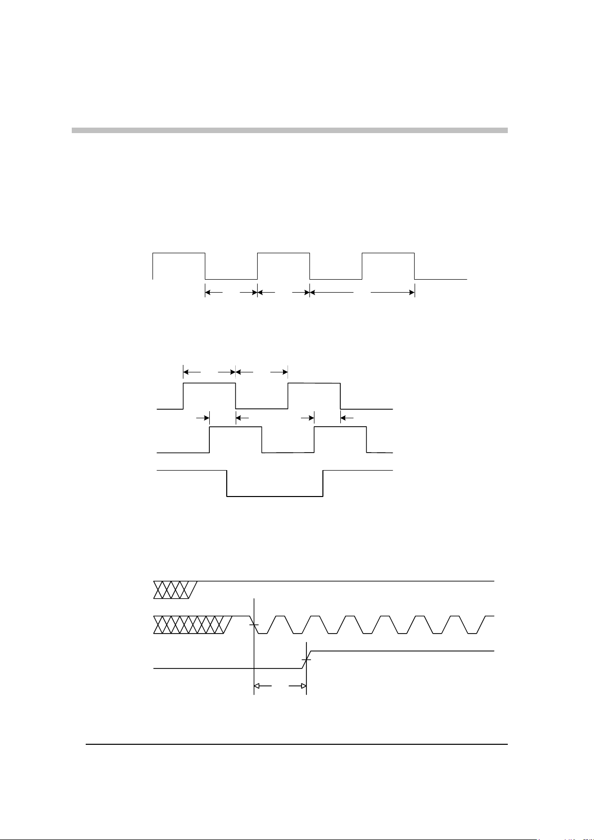
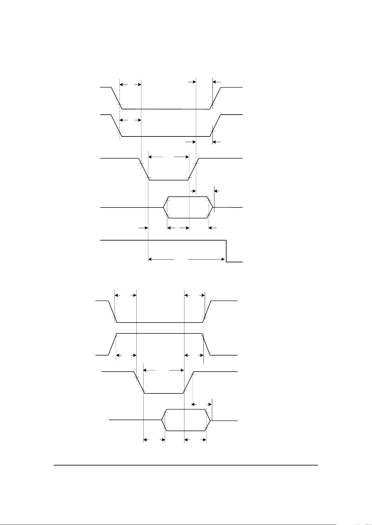
4 I/O Timing Diagrams
For the values of Tn, please refer to the table in Section 3.2.
The host interface timing shown in diagrams 4.4 and 4.5 is only valid when an external logic device is
used to provide a parallel communication interface. Refer to section 6 for more information.
4.1 Clock
4.2 Quadrature encoder input
4.3 Reset
T1 T2
ClockIn
T1
V
cc
ClockIn
~RESET
T50
T3
T3
T4
T4
Quad A
Quad B
~Index
MC3410 Technical Specifications
19
4.4 Host interface, 8/16 mode (requires external logic device)
4.4.1 Instruction write, 8/16 mode
HostData0-7
~HostSlct
HostCmd
HostRdy
~HostWrite
Note: If setup and hold times are met, ~HostSlct and HostCmd may be de-asserted at this point.
T7
T6
see note
T8
T18
T9
T14
T14
see note
T16
T16
T15
T13
T15
Low byteHigh byte
4.4.2 Data write, 8/16 mode
HostData0-7
~HostSlct
HostCmd
HostRdy
~HostWrite
Note: If setup and hold times are met, ~HostSlct and HostCmd may be de-asserted at this
point.
T7
T8
T6
T9
T15
see note
see note
Low byte
T16
T13
T16
T15
High byte
T18
T14
T14
MC3410 Technical Specifications
20
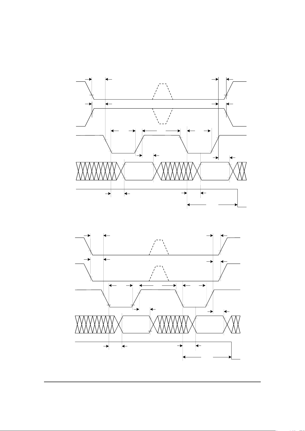
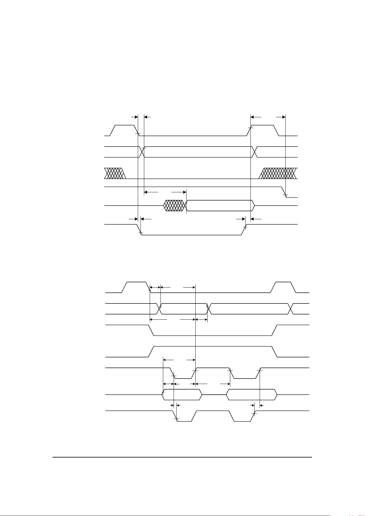
4.4.3 Data read, 8/16 mode
HostData0-7
~HostSlct
T7
T8
T19
T6
T9
T13
T11
HostCmd
HostRdy
~HostRead
T12
T10
High-Z
High-Z
High-Z
High
byte
Low byte
Note: If setup and hold times are met, ~HostSlct and HostCmd may be de-asserted at this
point.
see note
see note
4.4.4 Status read, 8/16 mode
~HostSlct
T7
T8
T17
T6
T9
T11
HostCmd
HostData0-7
~HostRead
T12
T10
High-Z High-Z
High-Z
High
byte
Low byte
T19
MC3410 Technical Specifications
21
4.5 Host interface, 16/16 mode (requires external logic device)
4.5.1 Instruction write, 16/16 mode
T7 T6
T9
T14
T16
T8
T13
T15
~HostSlct
HostCmd
~HostWrite
HostData0-15
HostRdy
4.5.2 Data write, 16/16 mode
T7 T6
T9
T14
T16
T8
T13
T15
~HostSlct
HostCmd
~HostWrite
HostData0-15
HostRdy
MC3410 Technical Specifications
22
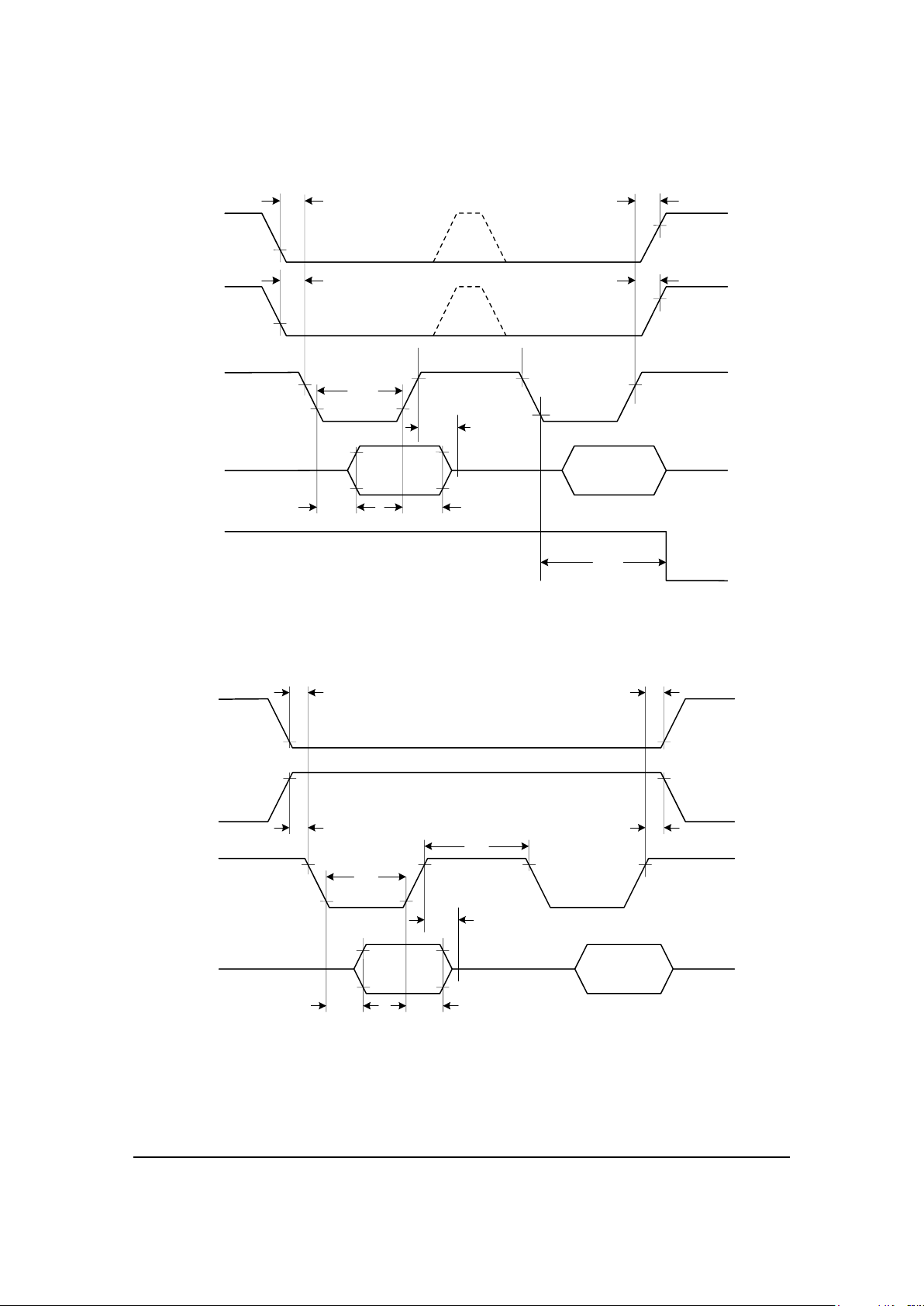
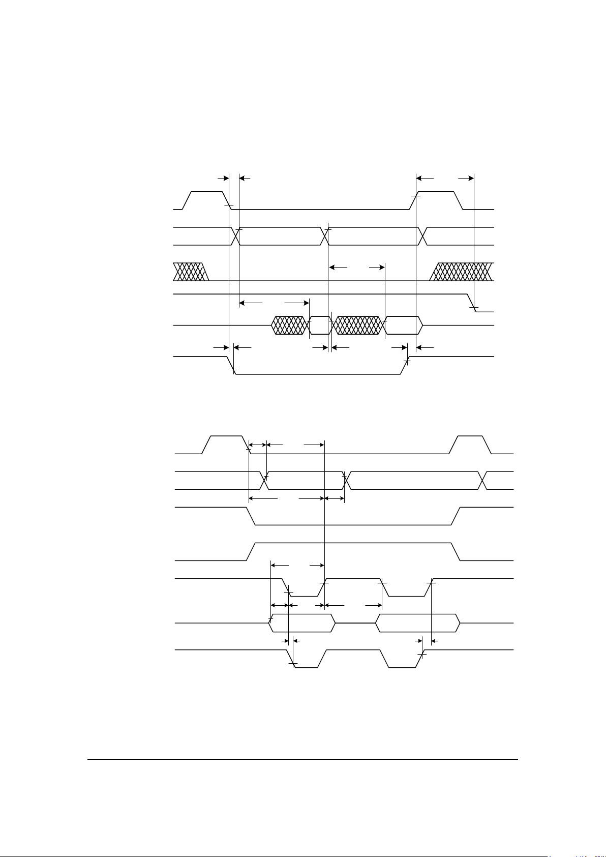
4.5.3 Data read, 16/16 mode
~HostSlct
T7
T8
T13
T11
HostCmd
HostData0-15
HostRdy
~HostRead
T12
T10
High-Z
High-Z
T6
T9
T19
4.5.4 Status read, 16/16 mode
~HostSlct
T7
T8
T11
HostCmd
HostData0-15
~HostRead
T12
T10
High-Z
High-Z
T6
T9
T19
MC3410 Technical Specifications
23
4.6 External memory timing
4.6.1 External memory read
Note: PMD recommends using memory with an access time no greater than 15 nsec.
4.6.2 External memory write
Addr0-Addr15
R/~W
W/~R
~WriteEnbl
Data0-Data15
~RAMSlct
T26
T27
T27
T23
T28
T24
T25
T29
~Strobe
T53 T54
~RAMSlct
Addr0-Addr15
W/~R
~WriteEnbl
Data0-Data15
T21
T20
T40
~Strobe
T52T51
MC3410 Technical Specifications
24
4.7 Peripheral device timing
4.7.1 Peripheral device read
4.7.2 Peripheral device write
Addr0-Addr15
R/~W
W/~R
~WriteEnbl
Data0-Data15
~PeriphSlct
T36
T37
T37
T33
T38
T34
T35
T39
~Strobe
T53 T54
~PeriphSlct
Addr0-Addr15
W/~R
~WriteEnbl
Data0-Data15
T31
T32
T30
T31
T40
~Strobe
T56T55
MC3410 Technical Specifications
25
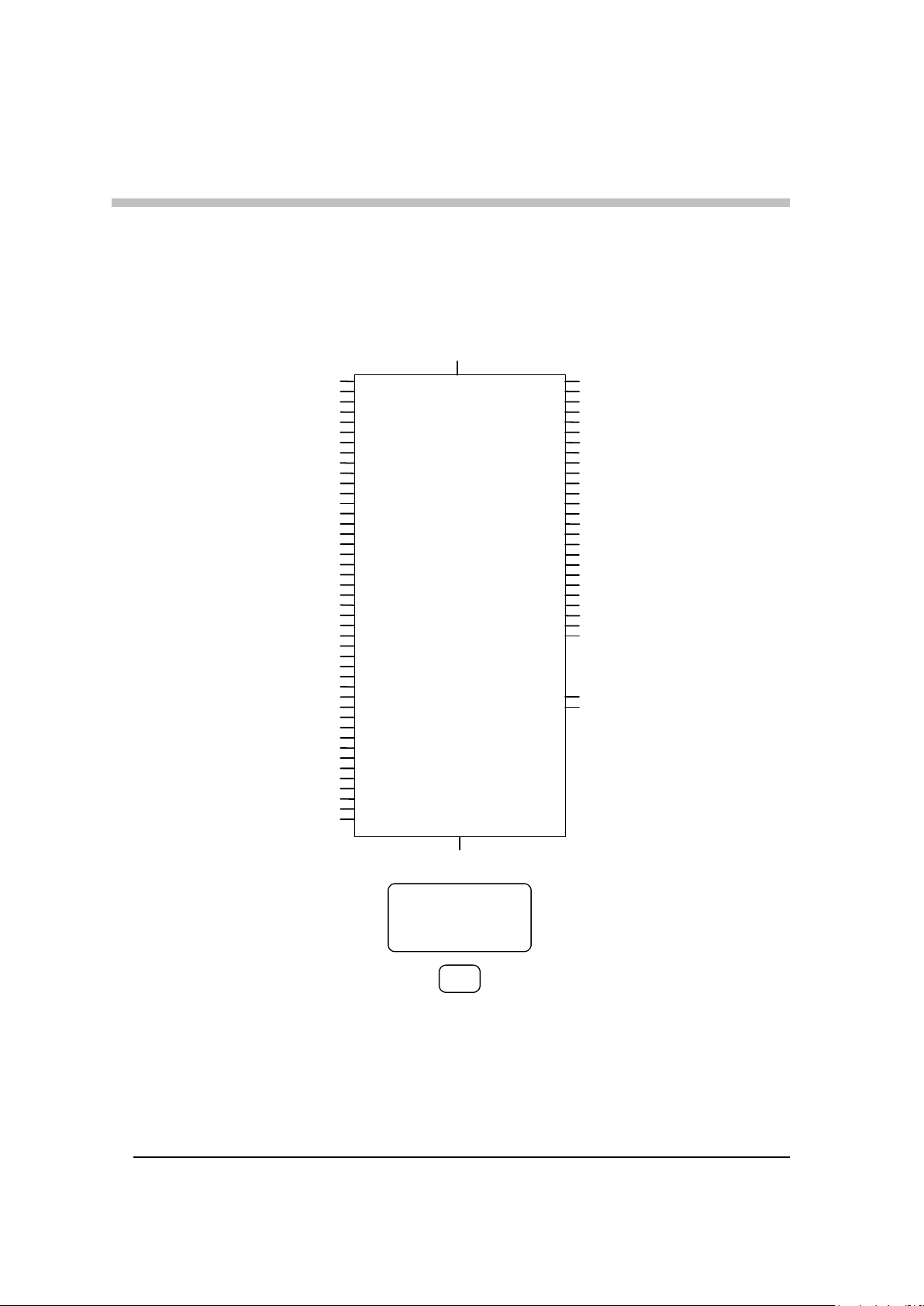
5 Pinouts and Pin Descriptions
5.1 Pinouts for MC3410
CP
~WriteEnbl
~PeriphSlct
GND
3, 8, 14, 20, 29, 37, 46, 56, 59,
61, 71, 92, 104, 113, 120
Unassigned
5, 30-34, 38, 39, 42, 45, 48, 49,
51, 55, 57, 73, 90, 91, 95, 105,
106, 107-109, 131
VCC
2, 7, 13, 21, 35, 36, 40, 47, 50,
52, 60, 62, 66, 93, 103, 121
9
10
11
12
15
16
17
18
19
22
23
24
25
26
27
28
111
112
114
115
116
117
118
119
122
123
124
125
126
127
128
43
44
99
98
58
SrlRcv
SrlXmt
SrlEnable
~HostIntrpt
ClockIn
Data0
Data1
Data2
Data3
Data4
Data5
Data6
Data7
Data8
Data9
Data10
Data11
Data12
Data13
Data14
Data15
Addr1
Addr2
Addr3
Addr4
Addr5
Addr6
Addr7
Addr8
Addr9
Addr10
Addr11
Addr12
Addr13
Addr14
Addr15
4
6
130
129
41
R/~W
~Strobe
~RAMSlct
~Reset
W/~R132
1
63
64
PosLim1
NegLim1
85
86
87
94
72
74
89
75
88
76
83
77
82
AxisOut1
AxisIn1
Analog1
Analog2
Analog3
Analog4
Analog5
Analog6
Analog7
Analog8
AnalogVcc
AnalogRefHigh
AnalogRefLow
AnalogGnd
84
67
68
QuadA1
QuadB1
69
70
100
101
~Index1
~Home1
PWMMag1
PWMMag2
110 Addr0
102PWMMag3
96PWMSign1
97PWMSign2
54
NC/Synch
I/OIntrpt
53
PrlEnable
65
AGND
78-81

MC3410 Technical Specifications
26
5.2 CP chip pin description table
Pin Name and number Direction Description
~WriteEnbl 1
output When low, this signal enables data to be written to the bus.
R/~W 4
output This signal is high when the CP chip is performing a read, and low when it is
performing a write.
~Strobe 6
output This signal is low when the data and address are valid during CP
communications.
~PeriphSlct 130
output This signal is low when peripheral devices on the data bus are being addressed.
~RAMSlct 129
output This signal is low when external memory is being accessed.
~Reset 41
input This is the master reset signal. When brought low, this pin resets the processor to
its initial conditions.
W/~R 132
output This signal is the inverse of R/~W; it is high when R/~W is low, and vice versa. For
some decode circuits, this is more convenient than
R/~W.
SrlRcv 43
input This pin receives serial data from the asynchronous serial port. If serial
communication is not used, this pin should be tied to V
cc
.
SrlXmt 44
output This pin transmits serial data to the asynchronous serial port.
SrlEnable 99
output This pin sets the serial port enable line. SrlEnable is always high for the point-to-
point protocol and is high during transmission for the multi-drop protocol.
~HostIntrpt 98
output When low, this signal causes an interrupt to be sent to the host processor.
I/OIntrpt 53
input This signal interrupts the CP chip when a host I/O transfer is complete. It
should be connected to
CPIntrpt of the parallel interface chip.
If the parallel interface is disabled (see below) this signal can be left unconnected
or tied to V
cc
.
PrlEnable 65
input This signal enables/disables the parallel communication with the host. If this
signal is tied high, the parallel interface is enabled. If this signal is tied low the
parallel interface is disabled. See section 6 of this manual for more information
on parallel communication.
WARNING! This signal should only be tied high if an external
logic device that implements the parallel communication logic
included in the design. This signal is an output during device reset
and as such any connection to GND or V
cc
must be via a series
resistor.
Data0
Data1
Data2
Data3
Data4
Data5
Data6
Data7
Data8
Data9
Data10
Data11
Data12
Data13
Data14
Data15
9
10
11
12
15
16
17
18
19
22
23
24
25
26
27
28
bi-directional Multi-purpose data lines. These pins comprise the CP chip’s external data bus,
used for all communications with peripheral devices such as external memory or
DACs. They may also be used for parallel-word input and for user-defined I/O
operations.

MC3410 Technical Specifications
27
Pin Name and number Direction Description
Addr0
Addr1
Addr2
Addr3
Addr4
Addr5
Addr6
Addr7
Addr8
Addr9
Addr10
Addr11
Addr12
Addr13
Addr14
Addr15
110
111
112
114
115
116
117
118
119
122
123
124
125
126
127
128
output Multi-purpose Address lines. These pins comprise the CP chip’s external address
bus, used to select devices for communication over the data bus.
They may be used for DAC output, parallel word input, or user-defined I/O
operations. See the Pilot Motion Processor User’s Guide for a complete memory map.
ClockIn 58
input This is the clock signal for the Motion Processor. It is driven at a nominal
20MHz.
AnalogVcc 84
input CP chip analog power supply voltage. This pin must be connected to the analog
input supply voltage, which must be in the range 4.5-5.5 V
If the analog input circuitry is not used, this pin must be connected to V
cc
.
AnalogRefHigh 85
input CP chip analog high voltage reference for A/D input. The allowed range is
AnalogRefLow to AnalogVcc.
If the analog input circuitry is not used, this pin must be connected to V
cc
.
AnalogRefLow 86
input CP chip analog low voltage reference for A/D input. The allowed range is
AnalogGND to AnalogRefHigh.
If the analog input circuitry is not used, this pin must be connected to GND.
AnalogGND 87
CP chip analog input ground. This pin must be connected to the analog input
power supply return.
If the analog input circuitry is not used, this pin must be connected to GND.
Analog1
Analog2
Analog3
Analog4
Analog5
Analog6
Analog7
Analog8
74
89
75
88
76
83
77
82
input These signals provide general-purpose analog voltage levels, which are sampled
by an internal A/D converter. The A/D resolution is 10 bits.
The allowed range is
AnalogRefLow to AnalogRefHigh.
Any unused pins should be tied to AnalogGND.
If the analog input circuitry is not used, these pins should be tied to GND.
PWMMag1
PWMMag2
PWMMag3
PWMSign1
PWMSign2
100
101
102
96
97
output These pin provide the Pulse Width Modulated signals for each phase to the
motor. The PWM resolution is 9 bits at a frequency of 20.0 KHz.
In 2 or 3-phase PWM 50/50 mode, PWMMag1/2/3 are the only signals and
encode both the magnitude and direction in the one signal.
In single-phase PWM sign/magnitude mode, PWMMag1 and PWMSign1 are the
PWM magnitude and direction signals respectively.
In 2-phase PWM sign/magnitude mode, PWMMag1 and PWMSign1 are the
PWM magnitude and direction signals for Phase A. PWMMag2 and PWMSign2,
are the PWM magnitude and direction signals for Phase B.
Unused pins may be left unconnected.

MC3410 Technical Specifications
28
Pin Name and number Direction Description
QuadA1
QuadB1
67
68
input These pins provide the A and B quadrature signals for the incremental encoder.
When the axis is moving in the positive (forward) direction, signal A leads signal
B by 90°.
The theoretical maximum encoder pulse rate is 5.1 MHz. Actual maximum rate
will vary, depending on signal noise.
NOTE: Many encoders require a pull-up resistor on each signal to establish a
proper high signal. Check your encoder’s electrical specification.
~Index1 69
input This pin provides the Index signal for the incremental encoder. A valid index
pulse is recognized by the chip when
this signal transitions from high to low.
There is no internal gating of the index signal with the encoder A
and B inputs. This must be performed externally if desired. Refer
to the Application Notes section at the end of this manual for an
example.
~Home1 70
input This pin provides the Home signal, general-purpose inputs to the position-
capture mechanism. A valid Home signal is recognized by the chip when
~Home
goes low.
WARNING! If this pin is not used, its signal should be tied high.
PosLim1
63
input This signal provides input from the positive-side (forward) travel limit switch.
On power-up or
Reset this signal defaults to active low interpretation, but the
interpretation can be set explicitly using the
SetSignalSense instruction.
WARNING! If this pin is not used, its signal should be tied high.
NegLim1 64
input This signal provides input from the negative-side (reverse) travel limit switch. On
power-up or
Reset this signal defaults to active low interpretation, but the
interpretation can be set explicitly using the
SetSignalSense instruction.
WARNING! If this pin is not used, its signal should be tied high.
This signal is an output during device reset and as such any
connection to GND or V
cc
must be via a series resistor.
AxisOut1 94
output This pin can be programmed to track the state of any bit in the Status registers.
If this pin is not used it may be left unconnected.
AxisIn1 72
input This is a general-purpose or programmable input. It can be used as a breakpoint
input, to stop a motion axis, or to cause an Update to occur.
If this pin is not used it may be left unconnected.
NC/Synch 54
input/output On the MC3410 this pin is not used.
On the MC3413 this pin is the synchronization signal. In the disabled mode, the
pin is configured as an input and is not used. In the master mode, the pin
outputs a synchronization pulse that can be used by slave nodes or other devices
to synchronize with the internal chip cycle of the master node. In the slave
mode, the pin is configured as an input and a pulse on the pin synchronizes the
internal chip cycle.
Vcc
2, 7, 13, 21, 35, 36, 40,
47, 50, 52, 60, 66, 62,
93, 103, 121
CP digital supply voltage. All of these pins must be connected to the supply
voltage. V
cc
must be in the range 4.75 - 5.25 V
WARNING! Pin 35 must be tied HIGH with a pull-up resistor. A
nominal value of 22K Ohms is suggested.
GND
3, 8, 14, 20, 29, 37, 46,
56, 59, 61, 71, 92, 104,
113, 120
CP ground. All of these pins must be connected to the power supply return.

MC3410 Technical Specifications
29
Pin Name and number Direction Description
AGND
78-81 These signals must be tied to AnalogGND.
If the analog input circuitry is not used, these pins must be tied to GND.
unassigned
45, 48, 49, 51, 55, 73,
90, 91, 105, 106, 107,
108, 109
These signals may be connected to GND for better noise immunity and reduced
power consumption or they can be left unconnected (floating).
unassigned
5, 30-34, 38, 39, 42,
57, 95, 131
These signals must be left unconnected (floating).

MC3410 Technical Specifications
30
6 Parallel Communication
With the addition of an external logic device, the Pilot motion processor can communicate with a
host processor using a parallel data stream. This offers a higher communication rate than a serial
interface and may be used in configurations where a serial connection is not available or not
convenient. This section details the required logic that must be implemented in the external device
as well as the necessary connections to the CP chip.
The reference design files for the parallel interface chip, in Actel/ViewLogic format, are available
from PMD. There are two versions of the design, one for interfacing with host processors that have
an 8-bit data bus and one for host processors that have a 16-bit data bus. The designs are called
IOPIL8 and IOPIL16 respectively. The interface to the CP chip is essentially identical in both.
The function of the I/O chip is to provide a shared-memory style interface between the host and CP
chip, comprised of four 16-bit wide locations. These are used for transferring commands and data
between the host and Pilot motion processor. The CP chip accesses the command/data registers
using its 16-bit external data bus while the host accesses the registers via a parallel interface with chip
select, read, write and command/data signals. If necessary, the host side interface can be modified
by the designer to match specific requirements of the host processor.
6.1 Host interface pin description table
Pin Name Direction Description
HostCmd
input This signal is asserted high to write a host instruction to the motion processor, or to
read the status of the
HostRdy and HostIntrpt signals. It is asserted low to read or write
a data word.
HostRdy
output This signal is used to synchronize communication between the motion processor
and the host.
HostRdy will go low (indicating host port busy) at the end of a read or
write operation according to the interface mode in use, as follows:
Interface Mode
HostRdy goes low
8/16 after the second byte of the instruction word
after the second byte of each data word is transferred
16/16 after the 16-bit instruction word
after each 16-bit data word
serial n/a
HostRdy will go high, indicating that the host port is ready to transmit, when the last
transmission has been processed. All host port communications must be made
with
HostRdy high (ready).
A typical busy-to-ready cycle is 12.5 microseconds, but can be substantially longer,
up to 100 microseconds.
~HostRead
input When ~HostRead is low, a data word is read from the motion processor.
~HostWrite
input When ~HostWrite is low, a data word is written to the motion processor.
~HostSlct
input When ~HostSlct is low, the host port is selected for reading or writing operations.
CPIntrpt
output I/O chip to CP chip interrupt. This signal sends an interrupt to the CP chip
whenever a host–chipset transmission occurs. It should be connected to CP chip
pin 53,
I/OIntrpt.
CPR/~W
input This signal is high when the I/O chip is reading data from the I/O chip, and low
when it is writing data. It should be connected to CP chip pin 4,
R/W.
CPStrobe
input This signal goes low when the data and address become valid during Motion
processor communication with peripheral devices on the data bus, such as external
memory or a DAC. It should be connected to CP chip pin 6,
Strobe.

MC3410 Technical Specifications
31
Pin Name Direction Description
CPPeriphSlct
input This signal goes low when a peripheral device on the data bus is being addressed. It
should be connected to CP chip pin 130,
PeriphSlct.
CPAddr0
CPAddr1
CPAddr15
input These signals are high when the CP chip is communicating with the I/O chip (as
distinguished from any other device on the data bus). They should be connected to
CP chip pins 110 (
Addr0), 111 (Addr1), and 128 (Addr15).
MasterClkIn
input This is the master clock signal for the motion processor. It is driven at a nominal
40 MHz
CPClk
output This signal provides the clock pulse for the CP chip. Its frequency is half that of
MasterClkIn (pin 89), or 20 MHz nominal. It is connected directly to the CP chip
I/Oclk signal (pin 58).
HostData0
HostData1
HostData2
HostData3
HostData4
HostData5
HostData6
HostData7
HostData8
HostData9
HostData10
HostData11
HostData12
HostData13
HostData14
HostData15
bi-directional,
tri-state
These signals transmit data between the host and the Motion processor through
the parallel port. Transmission is mediated by the control signals
~HostSlct,
~HostWrite, ~HostRead and HostCmd
.
In 16-bit mode, all 16 bits are used (
HostData0-15). In 8-bit mode, only the low-
order 8 bits of data are used (
HostData0-7).
CPData0
CPData1
CPData2
CPData3
CPData4
CPData5
CPData6
CPData7
CPData8
CPData9
CPData10
CPData11
CPData12
CPData13
CPData14
CPData15
bi-directional These signals transmit data between the I/O chip and pins Data0-15 of the CP chip,
via the motion processor data bus.

MC3410 Technical Specifications
32
6.2 16-bit Host Interface (IOPIL16)
This design implements a parallel interface with a host processor utilizing a 16-bit data bus. An
understanding of the underlying operation of the design is only necessary if the designer intends to
make modifications. In most cases this design can be implemented without changes. The following
notes should be read while referencing the schematics. IOPIL16 1 is the top level schematic. The
timing for the host to I/O chip communication can be found in section 4.5 and the timing for the
CP to I/O chip communication can be found in section 4.7.
The description below identifies the key elements of each schematic starting with the host side
signals. The paragraph title identifies the key schematic(s) being described in the text.
IOPIL16 3
The host interface is shown in sheet IOPIL16 3. The incoming data HD[15:0] is latched in the
transparent latches when ~HG1 and ~HG2 go high. This would be the result of a write from the
host to the CP. The latched data HI[15:8] and HI[7:0] go to schematic IOPIL16 1 and IOPIL16 5.
Data from the interface to the host, HO[15:8] and HO[7:0] is enabled onto the host bus, HD[15:0],
by HOES2 and HOES1 respectively. The output latches, which present the data during a host read,
are always transparent because GOUT is connected to VDD. The latched I/O is an I/O option on
the Actel part used and could be omitted in the host interface if a different CPLD or FPGA does not
have this feature.
IOPIL16 1
The control for the host interface starts on IOPIL16 1. HOES1 and HOES2 are the AND of
~HSEL and ~HRD and enable read data onto the host bus, as previously described. HRDY is a
handshaking signal to the host to allow asynchronous communication between the host and the CP.
The host must wait until HRDY is true before attempting to communicate with the CP. This signal
is copied as a bit in the host status register. The host status register may be read at any time to
determine the state of HRDY, or the HRDY output may be used as an interrupt to the host.
~HSEL, ~HRD, ~HWR, and HA0 are the buffered inputs of the host control signals.
HOST INTERFACE/IOPIL16 5
Data from the host HI[15:8] and HI[7:0] is written into REG1 and REG2 on the schematic HOST
INTERFACE by ~EN1 and ~EN2. These registers have a 2 to 1 multiplexed input with both the
host data and the CP data being written to these registers. This is convenient for diagnostic purposes
and is very efficient in the Actel A42MX FPGA's, which are multiplexer based but if the
configuration of the logic device used demands it, separate registers could be used for the host and
CP data. The schematic for this register is shown as DFME8. Only commands and checksums are
written to registers REG1 and REG2 while data is written and read from the set of data registers,
DATREG shown on IOPIL16 5. These 3 data registers buffer data sent to and from the CP,
reducing the number of interrupts the CP must handle. The output from REG1 and REG2,
CIQ[15:8] and CIQ[7:0] go to IOPIL16 5, where they are multiplexed with the other data registers.
The multiplexed result, IQ[15:8] and IQ[7:0], is multiplexed with HST[15:8] and HST[7:0] - the
output of the host status registers REG3 and REG4. As previously mentioned, HRDY becomes
HST15 so it can be read by the host. The rest of the status register is written by the CP to provide
information to the host. HA0 acts as an address bit, and usually is an address bit on the bus. When
the host is writing, HA0 low indicates data and HA0 high indicates a command. When the host is
reading, HAO low indicates data and HA0 high indicates status. Read status is the only transaction

MC3410 Technical Specifications
33
allowed while HRDY is low. During a host write the AND gate (G1:HOST INTERFACE) and two
flops latch the incoming data in the interface latches by driving ~HG1, and ~HG2 low from the
start of the write transaction until the first negative clock transition after the first positive transition
following the start of the write cycle. This tail-biting circuit removes the requirement for hold time
on the data bus.
HICTLA
Most of the control logic for the host interface is shown on schematic HICTLA. The sequencer at
the top generates HCYC one clock interval after the interface has been accessed and the host has
finished the transaction. The nature of the transaction, rd/wr, command/data, and read status is
preserved in the three flops F13, F8, and F9. A host write or a CP write, DSIW, enable REG1 and
REG2 on the HOST INTERFACE schematic discussed previously. A host data write generates
~ENHD1 and ~ENHD2 for the data registers on the DATREG schematic. The logic at the bottom
of the page generates the CP interrupt, the HRDY and the HCMDFL. The HCMDFL is used in the
CP status to indicate a command. DSIW, the CP writing to REG1 and REG2 on the HOST
INTERFACE schematic clears the interrupt and reasserts HRDY. HRDY is de-asserted during all
host transactions except read status, and stays de-asserted until the CP has completed the DSIW
cycle that clears the interrupt and reasserts HRDY. As mentioned previously data transfers to and
from the host use the data registers and do not interrupt the CP. The CP knows the number of data
transfers that must take place after decoding the command. It places this number, 0-3, in the 2 least
significant bits of the host status register, HST[1:0]. These become DPNT[1:0] on this page of the
schematic and enable an interrupt at 0 for a read and 1 or 0 for a write. The CP always leaves theses
bit set to 0 unless setting up a multiple word data transfer. If INTEN is true and LRDST, latched
read status, is false, HCYC will generate an interrupt to the CP. This will also hold HRDY false until
after the CP writes to the interface register, DSIW, thereby generating ~CLRFLGS.
IOPIL16 4
The CP interface is shown in sheet IOPIL16 4. The incoming data DSD[15:0] is latched in the
transparent latches when ~DG1 and ~DG2 go high. This occurs at the completion of a write from
the CP to the I/O chip. The latched data DSI[15:8] and DSI[7:0] go to schematic IOPIL16 1 and
IOPIL16 5. DSI[7:0] also goes to IOPIL16 2. Data from the interface to the CP, DO[15:8] and
DO[7:0] is enabled onto the CP bus, DSD[15:0], by DOE2 and DOE1 respectively. The output
latches, which present the data during a CP read, are always transparent because GOUT is connected
to VDD. The latched I/O in the Actel part contains both input and output latches. The output
latches could be omitted in the CP interface if a different CPLD or FPGA does not have this feature.
The two incoming CP address bits CPA0 and CPA1 are also latched using ~DG3. The 20CK signal
is the clock for the CP. This is a 20 MHz clock derived from a 40 MHz clock input.
IOPIL16 2
The CP control starts on IOPIL16 2. The I/O control is generated from ~CPSTRB, ~CPIS,
CPSEL and R/W. ~DG1, ~DG2, and ~DG3 latch the incoming data and DOE1 and DOE2 outenable the data from this chip to the CP. F2 and F4 tail-bite the write to avoid having to specify hold
times on the data. Flop F1 divides the 40MHz clock down to 20 MHz. A 20 MHz clock could be
used for this interface and the CP.

MC3410 Technical Specifications
34
DSPWA
The CP write control is contained on schematic DSPWA. The CP interface uses page addressing to
save I/O pins. F0, F1 and F2 make up the page register. In addition there are the 2 address bits,
LA0 and LA1. A write to address 0 selects the page register with DSI[2:0] going to the page register
and selecting the page for the successive transfers. A read from address 0 reads the status register on
all pages. Pages 4 and 6 are the only ones implemented in this device. L1 latches the r/w level. The
write decoding generates DSIW which enables writes to the DFME8 registers reg1 and reg2 shown
on the HOST INTERFACE schematic. DSIW also clears the CP interrupt and restores HRDY.
DSWST writes to the host status register also shown on the HOST INTERFACE schematic.
DSWDREG implements writing to the data registers shown on IOPIL16 5 and DATREG. Finally
the logic at the bottom of the page generates CPCYC, a 1-clock interval after the CP cycle is over
that implements the actual writes to the registers. The use of the data bus latches and the post bus
cycle transfers keeps as much of the logic synchronous as possible given two asynchronous devices,
without requiring clocking at several times the bus speed.
DSPRA
The CP read control is contained on schematic DSPRA. The 2 by 16 bit mux selects CP status if the
CP latched address is 0 and IQ[15:0] if the address is not 0. The only significant status bits are bits 15
(indicating the CP is interrupting the host), bits 13 and 14 (both 0 indicating a 16 bit host interface)
and bit 0 (set to 1 during a host command transfer and 0 during data transfer).
HOST INTERFACE
Both the CP and the host use a special mode to transfer data to avoid unnecessary CP interrupts.
This special mode is under the control of the CP and is transparent to the host. When the CP
receives a command from the host it initializes the transfer by setting the number of transfers
expected (0,1,2 or 3) in the 2 LSB's of the host status register, REG3 and REG4 on HOST
INTERFACE. This write (DSWST) also loads these bits into the 2 bit down counter DCNT2 on
IOPIL16 5. Note that a Q8 low, which indicates a host command, asynchronously clears this
register enabling interrupts on schematic HICTLA. If DPNT[1:0] is not 0 and Q8 is high, indicating
a host data transfer, and SINT goes high indicating the end of a host cycle the counter is
decremented. MXAD2 selects address RA from the CP latched address bits if the page register
contains 6, or the counter contents DPNT[1:0] if not. This allows the CP to have direct access to
registers 1, 2, and 3, using addresses 1,2,and 3 on page 6. The host on the other hand can only read
or write to the data register, HA0 low and the counter will auto decrement from 3 down to 0
allowing the host to access the registers on DATREG where REG1=R1 and R2, REG2=R3 and R4,
and REG3=R5 and R6. The writes are enabled by the two decoders DECE2X4, while the reads are
selected by the two 4x8 muxes, MUX1 and MUX2 controlled by the two 2x1 muxes MDS1 and
MDS0. The output data IQ[15:0] goes to HOST INTERFACE schematic below IOPIL16 1 and to
DSPRA below IOPIL16 2. The write data is HI[15:8], HI[7:0] from the host and DSI[15:8] and
DSI[7:0] from the CP.

HRD
HSEL
HOES1
DSPINTR
OUT5
HA0
HRD
HSEL
IN19
IN18
IN17
DSIW
HSTSEL
HSTRD
HSTWR HWR
DSPINT
HO[7:0]
DSPINTR
IN20
HADR0
ST15
DSWST
HG1
HI[15:8]
HO[15:8]
HG2
RDY HRDY
HI[7:0]
HOES2
CIQ[7:0]
CIQ[15:8]
Q8
SINT
ENHD1
ENHD2
IQ[15:8]
IQ[7:0]
DSI[7:0]
DPNT[1:0]
DSI[15:8]
ST0
HSEL
HRD
HINTF
CLK
Y
B
A
AND2B
D PAD
OUTBUF
PAD Y
INBUF
PAD Y
INBUF
PAD Y
INBUF
DRAWN BY:
4
3
2
1
DCBA
A B C D
1
2
3
4
PAD Y
INBUF
D PAD
OUTBUF
Y
B
A
AND2B
CIQ[15:8]
CIQ[7:0]
CLK
DSIW
DSI[15:8]
DSI[7:0]
DSWST
HA0
HCMDFL
HI[15:8]
HI[7:0]
HO[15:8]
HO[7:0]
HST14
HST15
HST[1:0]
IQ[15:8]
IQ[7:0]
Q8
SINT
DSPINTR
ENHD1
ENHD2
HG1
HG2
HRD
HSEL
HWR
(HINTRFA)
HOST INTERFACE
IOPIL16 1
22 OCT 2002 DBS

PP4
PP6
G4
G5
CQ3
CPIS
DSIW
DSWST
DSI[7:0]
CLK
R/W
CPSTRB
DO[15:0]
CSEL0
CPCYC
CPR-W
CS
DOE1
DOE2
F1
IB1
CLKIN
20CK
IS
20CK
CSACC CQ3
F2
LA0
CPSEL
LA1
IN27
IN28
IN26
IN30
CSACC
G1
G2
G3
CKBUF
DG3
G6
CQ1
F4
40CK
CSEL1
LA0
LA1
CPSEL
R/W
CLK
IQ[15:0]
ST0
ST15
DSPWA
DSPRA
STRB
CPIS
CPSTRB
DSWDREG
QN
CLK
D
DF1A
PAD Y
INBUF
D
CLK
Q
DF1
PAD Y
INBUF
PAD Y
INBUF
PAD Y
INBUF
PAD Y
INBUF
A
B
C
Y
NAND3B
YA
CLKINT
D
CLK
Q
DF1
CLK
CPCYC
CPSEL
DSIW
DSI[7:0]
DSWST
LA0
LA1
PNT0
R/W
CPIS
CPSTRB
DG3
DSWDREG
PNT1
PP6
PP4
DSPWA
DO[15:0]
IQ[15:0]
ST0
ST15
LA0
LA1
DSPRA
DRAWN BY:
4
3
2
1
DCBA
A B C D
1
2
3
4
IOPIL16 2
24 OCT 2002 DBS
A
B
C
D
Y
AND4B
A
B
C
D
Y
AND4B
A
B
C
Y
NAND3B
A
B
C
Y
NAND3B
CSACC
A
B
C
D
Y
NAND4B
DG1
DG2
DG3

VDDVDD
HD0
HD1
HD2
HD3
HD4
HD5
HD7
HD8
HD9
HD10
HD11
HD13
HD14
HD15
HG1
HI8
HI9
HI10
HI11
HI12
HI13
HI14
HI15
HI[15:0]
HG2
HG1
HO0
HO1
HO2
HO3
HO5
HO6
HO7
HO4
HO[7:0]
VDD
HOES1 HOES2
HG2
VDD
HO8
HO9
HO10
HO11
HO12
HO14
HO15
HO[15:8]
HO13
VDD
HI1
HI2
HI3
HI4
HI5
HI6
HI7
HI[7:0]
HI0
HD6
HD12
Y
VCC
E
D
GOUT
GIN
PAD
Q
HIGH SLEW
QD
G
Q
BBDLHS
D
G
E
D
GOUT
GIN
PAD
Q
HIGH SLEW
QD
G
Q
BBDLHS
D
G
E
D
GOUT
GIN
PAD
Q
HIGH SLEW
QD
G
Q
BBDLHS
D
G
E
D
GOUT
GIN
PAD
Q
HIGH SLEW
QD
G
Q
BBDLHS
D
G
E
D
GOUT
GIN
PAD
Q
HIGH SLEW
QD
G
Q
BBDLHS
D
G
E
D
GOUT
GIN
PAD
Q
HIGH SLEW
QD
G
Q
BBDLHS
D
G
E
D
GOUT
GIN
PAD
Q
HIGH SLEW
QD
G
Q
BBDLHS
D
G
E
D
GOUT
GIN
PAD
Q
HIGH SLEW
QD
G
Q
BBDLHS
D
G
E
D
GOUT
GIN
PAD
Q
HIGH SLEW
QD
G
Q
BBDLHS
D
G
E
D
GOUT
GIN
PAD
Q
HIGH SLEW
QD
G
Q
BBDLHS
D
G
E
D
GOUT
GIN
PAD
Q
HIGH SLEW
QD
G
Q
BBDLHS
D
G
E
D
GOUT
GIN
PAD
Q
HIGH SLEW
QD
G
Q
BBDLHS
D
G
E
D
GOUT
GIN
PAD
Q
HIGH SLEW
QD
G
Q
BBDLHS
D
G
E
D
GOUT
GIN
PAD
Q
HIGH SLEW
QD
G
Q
BBDLHS
D
G
E
D
GOUT
GIN
PAD
Q
HIGH SLEW
QD
G
Q
BBDLHS
D
G
E
D
GOUT
GIN
PAD
Q
HIGH SLEW
QD
G
Q
BBDLHS
D
G
DRAWN BY:
4
3
2
1
DCBA
A B C D
1
2
3
4
IOPIL16 3
21 OCT 2002 DBS

LA1
DSD0
DSD1
DSD12
DSD13
DSD14
DG2
DG2
DSI3
DSI4
DSI5
DSI6
DSI7
DSI2
DSI1
DSI[7:0]
DO9
DO10
DO11
DO15
DO14
DO13
DO12
DO[15:8]
DO8
DOE2
DOE2
DOE2
DOE2
DOE1
DOE1
DOE1
DOE1
DOE1
CPA0
CPA1
LA0
DO3
DO7
DO6
DO5
DO4
DO[7:0]
DO1
DO2
DO0
DSI8
DSI9
DSI10
DSI15
DSI14
DSI13
DSI[15:8]
DG1
VDD
VDD
VDD VDD VDD
GND
GND
DG3
DG3
CLKOUT20CK
DOE2
DOE2
DOE2
E
D
GOUT
GIN
PAD
Q
HIGH SLEW
QD
G
Q
BBDLHS
D
G
E
D
GOUT
GIN
PAD
Q
HIGH SLEW
QD
G
Q
BBDLHS
D
G
E
D
GOUT
GIN
PAD
Q
HIGH SLEW
QD
G
Q
BBDLHS
D
G
E
D
GOUT
GIN
PAD
Q
HIGH SLEW
QD
G
Q
BBDLHS
D
G
E
D
GOUT
GIN
PAD
Q
HIGH SLEW
QD
G
Q
BBDLHS
D
G
E
D
GOUT
GIN
PAD
Q
HIGH SLEW
QD
G
Q
BBDLHS
D
G
E
D
GOUT
GIN
PAD
Q
HIGH SLEW
QD
G
Q
BBDLHS
D
G
E
D
GOUT
GIN
PAD
Q
HIGH SLEW
QD
G
Q
BBDLHS
D
G
E
D
GOUT
GIN
PAD
Q
HIGH SLEW
QD
G
Q
BBDLHS
D
G
E
D
GOUT
GIN
PAD
Q
HIGH SLEW
QD
G
Q
BBDLHS
D
G
E
D
GOUT
GIN
PAD
Q
HIGH SLEW
QD
G
Q
BBDLHS
D
G
E
D
GOUT
GIN
PAD
Q
HIGH SLEW
QD
G
Q
BBDLHS
D
G
E
D
GOUT
GIN
PAD
Q
HIGH SLEW
QD
G
Q
BBDLHS
D
G
DRAWN BY:
4
3
2
1
DCBA
A B C D
1
2
3
4
E
D
GOUT
GIN
PAD
Q
HIGH SLEW
QD
G
Q
BBDLHS
D
G
E
D
GOUT
GIN
PAD
Q
HIGH SLEW
QD
G
Q
BBDLHS
D
G
E
D
GOUT
GIN
PAD
Q
HIGH SLEW
QD
G
Q
BBDLHS
D
G
E
D
GOUT
GIN
PAD
Q
HIGH SLEW
QD
G
Q
BBDLHS
D
G
E
D
GOUT
GIN
PAD
Q
HIGH SLEW
QD
G
Q
BBDLHS
D
G
D PAD
OUTBUF
Y
VCC
DBS
IOPIL16 4
21 OCT 2002
DOE1
DOE1
DSI0
DSD2
DSD3
DOE1
DOE1
DSD7
DSD6
DSD5
DSD4
DOE2
DOE2
DSD8
DSD9
DSD10
DSD11
DSI11
DOE2
DSI12
DSD15

IQ[7:0]
IQ[15:8]
DSWST
DPINC
Q8
CLK
DSI[1:0]
PP6
DPNT[1:0]
LA[1:0]
LA0
LA1
RA[1:0]
DPINC
DPNT0
DPNT1
Q8
SINT
ENHD1
ENHD2
DSWDREG
END1
END2DOE1
DREG
A
B
Y
OR2A
A
B
Y
OR2A
DRAWN BY:
4
3
2
1
DCBA
A B C D
1
2
3
4
DATA[1:0]
SLOAD
ENABLE
ACLR
CLOCK
Q[1:0]
DCNT2
DATA1_[1:0]
DATA0_[1:0]
RESULT[1:0]
SEL0
MXAD2
A
BCY
AND3
A
B
Y
NAND2B
DBS
IOPIL16 5
22 OCT 2002
PP4
CIQ[7:0]
CIQ[15:8]
HI[7:0]
HI[15:8]
DSI[7:0]
DSI[15:8]
RA[1:0]
LA[1:0]
PP6
END1
END2
CLK
CIQ[15:8]
CIQ[7:0]
CLK
DSI[15:8]
DSI[7:0]
HIH[15:8]
HI[7:0]
IQ[15:8]
IQ[7:0]
LA[1:0]
PP4
PP6
DOE1
RA[1:0]
END1
END2
DATREG

MUX1
REG3
REG4
DSIW
HA0
HRD
HWR
HA0
HG2
CLK
DSWST
DSLA
DSL
DSWST
CLK
DSI[14:8]
REG1
CIQ[7:0]
CIQ[15:8]
BUF1
DSIW
HI[7:0]
DSI[7:0]
BUF2
CLK
HWR
HSEL
G1
DSI[7:2]
HG1
HO[15:8]
HSEL
CLK
HST15
HST[14:8]
HST[15:8]
HST14
ENHD1
ENHD2
SINT
Q8
HST[1:0]
HST[7:0]
HST[7:2]
HST[1:0]
MUX2
HA0
HO[7:0]
CLK
G2
G3
REG2
HI[15:8]
DSI[15:8]
EN1
EN2
VDD
EN1
DSPINTR
HCMDFL
HICTLA
EN2
IQ[15:8]
IQ[7:0]
DATA1_[7:0]
DATA0_[7:0]
RESULT[7:0]
SEL0
MUX2X8
Q[5:0]
DATA[5:0]
CLOCK
ENABLE
REG6
Q[6:0]
DATA[6:0]
CLOCK
ACLR
ENABLE
REG7
DRAWN BY:
4
3
2
1
DCBA
A B C D
1
2
3
4
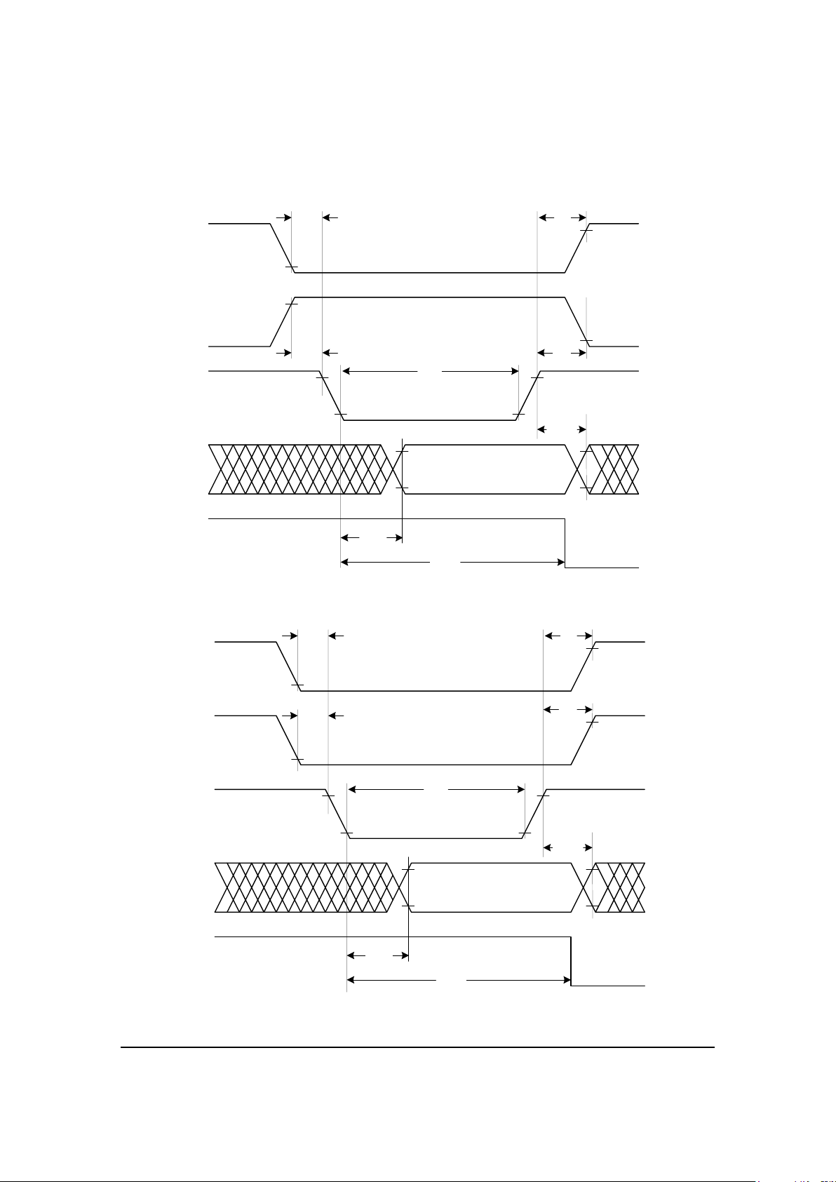
A[7:0]
B[7:0]
CK
Q[7:0]
S
EN1
DFME8
YA
BUF
YA
BUF
Y
B
A
AND2B
DATA1_[7:0]
DATA0_[7:0]
RESULT[7:0]
SEL0
MUX2X8
D
CLK
QN
DF1C
D
CLK
Q
DF1
A
B
Y
NAND2
A
B
Y
NAND2
A[7:0]
B[7:0]
CK
Q[7:0]
S
EN1
DFME8
CK
DSIW
HA0
HCMDFL
HRDY
Q8
SINT
DSPINTR
EN1
EN2
ENHD1
ENHD2
HRD
DPNT[1:0]
HSEL
HWR
HICTLA
HOST INTERFACE
DBS
(HINTRFA)
24 OCT 2002

ENHD1
EN1
EN2
CK
VDD
CK
HCYC
HSEL
DSPINTR
LRDSTQ9
CK
HCYC
HA0
HRD
HSEL
HRD
HWR
HRD
HSEL
CLRFLGS
HWR
HSEL
HWR
F1
F2 F3
GND
HCYC
G2
G1
HSEL
HWR
HA0
HCYC
CK
VDD
F8
INV3
Q8 HCMD
F9
INV4
SHCMD
SLRDST
G7
F7
INV1
HCYC
Q2Q1
Q1
HRDY
F10
G21
F6
F5
HCMDFL
CK
HWR
Q8
CK
LRDST
SINTR
Q8
WREN
RDEN
DPNT[1:0]
DPNT1
DPNT0
INV2
HWR
SHWR
F13
LWR
EBSY
Q1
Q2
HCYC
Q9
HCYC
HCMD
G19
HCCYC
DSIW
DSPINTR
ENHD2
HCYC
DSIW
G10
VDD
HRD
HWR
LWR
CLRFLGS
SINT
INTEN
AY
INV
Y
B
A
AND2A
A
B
Y
NAND2
A
B
C
Y
NAND3B
Y
B
A
NOR2
Y
B
A
NOR2
A
B
C
D
Y
OA4
D
CLK
Q
DF1
D
CLK
Q
DF1
Y
VCC
D0
D1
D2
D3
S0
S1
CLK
CLR
Q
DFM6A
Y
B
A
AND2B
A
B
C
Y
OA1C
CS
J
CLK
K
CLR
Q
JKF2C
AY
INV
CS
J
CLK
K
CLR
Q
JKF2C
AY
INV
A
BCY
AND3B
J
CLK
K
Q
JKF
AY
INV
D
CLK
Q
DF1
B
2
A
2
CC
D
Y
C
NOR4
J
CLK
K
Q
JKF
D
CLK
Q
DF1
A
BCY
AND3
AY
INV
Y
B
A
AND2B
CS
J
CLK
K
CLR
Q
JKF2C
Y
B
A
AND2
A
B
C
Y
OR3C
A
B
Y
NAND2B
A
B
Y
NAND2
DRAWN BY:
4
3
2
1
DCBA
A B C D
1
2
3
4
A
BCY
AND3B
DBS21 OCT 2002
HICTLA

CPCYC1
LR/W
ADW0
CPS
CPS
PP4
CPCYC1
PP4
CPCYC1
CPIS
CPSTRB
CPSEL
LR/W
LA0
LA1
DSWPNT
ADW2
ADW3
DSIW
DSWST
DSI[7:0]
G11
BUF2
BUF3
CPCYC
CPCYC1
GND
Q3
G6
Q2
CLK
Q2
Q3
F4
F5
ADW0
DSI0
DSI1
CLK
DSI2
DSWPNT
R/W LR/W
DG3
L1
DSWDREG
G12
PP6
PP6
PP4
Q3
CPCYC
ADW2
ADW3
DEC2
G2
F1
F2
F0 PNT0
PNT2
PNT1
A
B
C
D
Y
AND4B
Y
VCC
DRAWN BY:
4
3
2
1
DCBA
A B C D
1
2
3
4
A
BCY
AND3
YA
BUF
YA
BUF
A
BCY
AND3B
AY
INV
AY
INV
Y
VCC
D
E
CLK
CLR
Q
DFE3A
D0
D1
D2
D3
S0
S1
CLK
CLR
Q
DFM6A
QGD
DL1B
A
BCY
AND3
A
BCY
AND3A
A
BCY
AND3B
A
B
Y2
Y3
E
Y1
Y0
DECE2X4D
A
B
Y
NAND2
D
E
CLK
Q
DFE1B
D
E
CLK
Q
DFE1B
D
E
CLK
Q
DFE1B
DBS
24 OCT 2002
DSPWA

$ARRAY=12
DO[15:0]
IQ[15:0]
ST0
ST15
CH0
CH15
GND[12:1]
LA0
LA1
IQSEL
CH15,GND,GND,GND[12:1],CH0
Y
GND
YA
BUF
YA
BUF
YA
BUF
DRAWN BY:
4
3
2
1
DCBA
A B C D
1
2
3
4
DATA1_[15:0]
DATA0_[15:0]
RESULT[15:0]
SEL0
MUX2X16
B
Y
A
OR2
DSPRA
DBS24 OCT 2002

Q4 Q7Q6Q5Q3Q2Q1Q0
Q[7:0]
F7F6F5F4F3F2F1F0
B4B0 B1 B2 B3 B5 B6 B7
B[7:0]
A4A0 A1 A2 A3 A5 A7
A[7:0]
A6
S
CK
EN1
DRAWN BY:
4
3
2
1
DCBA
A B C D
1
2
3
4
ABS
E
CLK
Q
DFME1A
ABS
E
CLK
Q
DFME1A
ABS
E
CLK
Q
DFME1A
ABS
E
CLK
Q
DFME1A
ABS
E
CLK
Q
DFME1A
ABS
E
CLK
Q
DFME1A
ABS
E
CLK
Q
DFME1A
ABS
E
CLK
Q
DFME1A
DFME8
DBS19 NOV. 2002

GND
RA1
DSPSEL1
HI[7:0]
DSI[7:0]
HIH[15:8]
DSI[15:8]
EN1R3
EN2R3
DSPSEL2
DSPSEL1
R2[7:0]
EN2R2
EN1R2
DSI[15:8]
CLK
HIH[15:8]
DSI[7:0]
HI[7:0]
HI[7:0]
DSI[7:0]
HIH[15:8]
DSI[15:8]
EN1R1
EN2R1
R1[15:8]
DSPSEL
R2[15:8]
R1[7:0]
MDS1 MDS0
MDS1 MDS0
EN2R1
EN2R2
EN2R3
EN1R1
EN1R2
EN1R3
DSPSELPP6
R2
R3
R4
R5 MUX1
B1
B2
B3
R3[7:0]
R3[15:8]
R6
LA0
LA1
PP4
DOE1
IQ[15:8]
IQ[7:0]
LA[1:0]
DSPSEL2
RA[1:0]
RA0
RA1
END1
END2
DEC1
DEC2
MDS0
RA0
GND
MDS1
DSIR
R1
CLK
CLK
CIQ[7:0]
R1[7:0]
R3[7:0]
R2[7:0]
CIQ[15:8]
R1[15:8]
R3[15:8]
MUX2
R2[15:8]
Y
GND
DRAWN BY:
4
3
2
1
DCBA
A B C D
1
2
3
4
A[7:0]
B[7:0]
CK
Q[7:0]
S
EN1
DFME8
A[7:0]
B[7:0]
CK
Q[7:0]
S
EN1
DFME8
A[7:0]
B[7:0]
CK
Q[7:0]
S
EN1
DFME8
A[7:0]
B[7:0]
CK
Q[7:0]
S
EN1
DFME8
DATA3_[7:0]
DATA2_[7:0]
DATA1_[7:0]
DATA0_[7:0]
RESULT[7:0]
SEL1
SEL0
MUX4X8
YA
BUF
YA
BUF
YA
BUF
A[7:0]
B[7:0]
CK
Q[7:0]
S
EN1
DFME8
DATA0
ENABLE
DATA1
EQ3
EQ2
EQ1
EQ0
DECE2X4
DATA0
ENABLE
DATA1
EQ3
EQ2
EQ1
EQ0
DECE2X4
Y
D
C
B
A
AND4A
A
B
Y
S
MX2
A
B
Y
S
MX2
A[7:0]
B[7:0]
CK
Q[7:0]
S
EN1
DFME8
DATA3_[7:0]
DATA2_[7:0]
DATA1_[7:0]
DATA0_[7:0]
RESULT[7:0]
SEL1
SEL0
MUX4X8
DBS24 OCT 2002
DATREG

MC3410 Technical Specifications
46
6.3 8-bit Host Interface (IOPIL8)
This design implements a parallel interface with a host processor utilizing an 8-bit data bus. An
understanding of the underlying operation of the design is only necessary if the designer intends to
make modifications. In most cases this design can be implemented without changes. The following
notes should be read while referencing the schematics. IOPIL16 1 is the top level schematic. The
timing for the host to I/O chip communication can be found in section 4.4 and the timing for the
CP to I/O chip communication can be found in section 4.7.
The description below identifies the key elements of each schematic starting with the host side
signals. The paragraph title identifies the key schematic(s) being described in the text.
IOPIL8 3
The host interface for IOPIL8 is shown in sheet IOPIL8 3. The incoming data HD[7:0] is latched in
the transparent latches when ~HG1 goes high. This would be a write from the host to the CP. The
latched data HI[7:0] goes to IOPIL8 1 and IOPIL8 5. Data from the interface to the host, HO[7:0]
is enabled onto the host bus, HD[7:0], by HOES1. The output latches, which present the data
during a host read, are always transparent because GOUT is connected to VDD. The latched I/O is
an I/O option on the Actel part used and could be omitted in the host interface if a different CPLD
or FPGA does not have this feature. HD[15:8] are tri-stated outputs because Actel grounds unused
I/O pins and this would interfere with using existing PMD test equipment. These reserved I/O's can
be ommitted in a different implementation with an 8 bit bus.
IOPIL8 1
The control for the host interface starts on IOPIL8 1. HOES1 is the AND of ~HSEL and ~HRD,
and enable read data onto the host bus, as previously described. HRDY is a handshaking signal to
the host to allow asynchronous communication between the host and the CP. The host must wait
until HRDY is true before attempting to communicate with the CP. This signal is copied as a bit in
the host status register. The host status register may be read at any time to determine the state of
HRDY, or the HRDY output may be used as an interrupt to the host. ~HSEL, ~HRD, ~HWR, and
HA0 are the buffered inputs of the host control signals.
HOST INTERFACE/IOPIL8 5
Data from the host HI[7:0] is written into REG1 and REG2 on the schematic HOST INTERFACE
by ~EN1 and ~EN2. All transfers are 16 bits and take two writes or reads on the 8-bit bus. These
registers have a 2 to 1 multiplexed input with both the host data and the CP data being written to this
register.
This is convenient for diagnostic purposes and is very efficient in the Actel A42MX FPGA's, which
are multiplexer based but if the configuration of the logic device used demands it, separate registers
could be used for the host and CP data. The schematic for this register is shown as DFME8. Only
commands and checksums are written to registers REG1 and REG2 while data is written and read
from the set of data registers, DATREG shown on IOPIL8 5. These 3 data registers buffer data sent
to and from the CP, reducing the number of interrupts the CP must handle. The output from REG1
and REG2, CIQ[15:8] and CIQ[7:0] go to IOPIL8 5, where they are multiplexed with the other data
registers. The multiplexed result, IQ[15:8] and IQ[7:0], is multiplexed with HST[15:8] and HST[7:0] the output of the host status registers REG3 and REG4. This four input mux, MUX4X8, also
muxes the 16 bit data onto the 8-bit bus. As previously mentioned HRDY becomes HST15 so it can
be read by the host. The rest of the status register is written by the CP to provide information to the

MC3410 Technical Specifications
47
host. HA0 acts as an address bit, and usually is an address bit on the bus. When the host is writing,
HA0 low indicates data and HA0 high indicates a command. When the host is reading, HAO low
indicates data and HA0 high indicates status. Read status is the only transaction allowed while
HRDY is low. During a host write the AND gate (G1:HOST INTERFACE) and two flops latch the
incoming data in the interface latches by driving ~HG1 low from the start of the write transaction
until the first negative clock transition after the first positive transition following the start of the write
cycle. This tail-biting circuit removes the requirement for hold time on the data bus.
HICTLA
Most of the control logic for the host interface is shown on schematic HICTLA. The sequencer at
the top generates HCYC one clock interval after the interface has been accessed and the host has
finished the transaction. The nature of the transaction, rd/wr, command/data, and read status is
preserved in the three flops F13, F8, and F9. Since 16 bit transfers must take place over an 8 bit bus
two transfers are required. The toggle flop is used to determine whether a cycle is the first or second
of the 2 required. The toggle flop may be initialized to the 0 state, which indicates that this is the
first transfer (high byte), by the CP writing a one to host status bit 15. This status bit is read by the
host as the HRDY bit and is not writable by the CP. In addition flop F12 and the associated gating
determine if the present command transaction is the first or second byte of a command. If the
toggle flop gets into the wrong state due to a missed or aborted transfer the next command will set it
back to the correct state. A host write or a CP write, DSIW, enable REG1 and REG2 on the HOST
INTERFACE schematic discussed previously. A host data write generates ~ENHD1 and
~ENHD2 for the data registers on the DATAREG schematic. For host writes ~EN2, ~EN1,
~ENHD2, and ~ENHD1 are also determined by the state of the toggle flop using HIEN and
LOEN. 1CMD is used in this logic to ensure correct behavior when the command is correcting the
state of the toggle. The logic at the bottom of the page generates the CP interrupt, the HRDY and
the HCMDFL. The HCMDFL is used in the CP status to indicate a command. DSIW, the CP
writing to REG1 and REG2 on the HOST INTERFACE schematic clears the interrupt and reasserts
HRDY. HRDY is de-asserted during all host transactions except read status, and stays de-asserted
until the CP has completed the DSIW cycle that clears the interrupt and reasserts HRDY. As
mentioned previously data transfers to and from the host use the data registers and do not interrupt
the CP. The CP knows the number of data transfers that must take place after decoding the
command. It places this number, 0-3, in the 2 least significant bits of the host status register,
HST[1:0]. These become DPNT[1:0] on this page of the schematic and enable an interrupt at 0 for a
read and 1 or 0 for a write. The CP always leaves these bits at 0 unless setting up a multiple word
data transfer. If INTEN is true and LRDST, latched read status, is false, HCYC will generate an
interrupt to the CP. This will also hold HRDY false until after the CP writes to the interface register,
DSIW, thereby generating ~CLRFLGS.
IOPIL8 4
The CP interface is shown in sheet IOPIL8 4. The incoming data DSD[15:0] is latched in the
transparent latches when ~DG1 and ~DG2 go high. This occurs at the completion of a write from
the CP to the I/O chip. The latched data DSI[15:8] and DSI[7:0] go to schematic IOPIL8 1 and
IOPIL16 5. DSI[7:0] also goes to IOPIL16 2. Data from the interface to the CP, DO[15:8] and
DO[7:0] is enabled onto the CP bus, DSD[15:0], by DOE2 and DOE1 respectively. The output
latches, which present the data during a CP read, are always transparent because GOUT is connected
to VDD. The latched I/O in the Actel part contains both input and output latches. The output
latches could be omitted in the CP interface if a different CPLD or FPGA does not have this feature.
The two incoming CP address bits CPA0 and CPA1 are also latched using ~DG3. The 20CK signal
is the clock for the CP. This is a 20 MHz clock derived from a 40 MHz clock input.

MC3410 Technical Specifications
48
IOPIL8 2
The CP control starts on IOPIL8 2. The I/O control is generated from ~CPSTRB, ~CPIS, CPSEL
and R/W. ~DG1, ~DG2, and ~DG3 latch the incoming data and DOE1 and DOE2 out-enable
the data from this chip to the CP. F2 and F4 tail-bite the write to avoid having to specify hold times
on the data. Flop F1 divides the 40MHz clock down to 20 MHz. A 20 MHz clock could be used for
this interface and the CP.
DSPWA
The CP write control is contained on schematic DSPWA. The CP interface uses page addressing to
save I/O pins. F0, F1 and F2 make up the page register. In addition there are the 2 address bits,
LA0 and LA1. A write to address 0 selects the page register with DSI[2:0] going to the page register
and selecting the page for the successive transfers. A read from address 0 reads the status register on
all pages. Pages 4 and 6 are the only ones implemented in this device. L1 latches the r/w level. The
write decoding generates DSIW which enables writes to the DFME8 registers reg1 and reg2 shown
on the HOST INTERFACE schematic. DSIW also clears the CP interrupt and restores HRDY.
DSWST writes to the host status register also shown on the HOST INTERFACE schematic.
DSWDREG implements writing to the data registers shown on IOPIL8 5 and DATREG. Finally
the logic at the bottom of the page generates CPCYC, a 1-clock interval after the CP cycle is over
that implements the actual writes to the registers. The use of the data bus latches and the post bus
cycle transfers keeps as much of the logic synchronous as possible given two asynchronous devices,
without requiring clocking at several times the bus speed.
DSPRA
The CP read control is contained on schematic DSPRA. The 2 by 16 bit mux selects CP status if the
CP latched address is 0 and IQ[15:0] if the address is not 0. The only significant status bits are bits 15
(indicating the CP is interrupting the host), bit 14 (1 indicating an 8-bit host interface) and bit 0 (set
to 1 during a host command transfer and 0 during data transfer).
HOST INTERFACE
Both the CP and the host use a special mode to transfer data to avoid unnecessary CP interrupts.
This special mode is under the control of the CP and is transparent to the host. When the CP
receives a command from the host it initializes the transfer by setting the number of transfers
expected (0,1,2 or 3) in the 2 LSB's of the host status register, REG3 and REG4 on HOST
INTERFACE. This write (DSWST) also loads these bits into the 2 bit down counter DCNT2 on
IOPIL8 5. Note that a Q8 low, which indicates a host command, asynchronously clears this register
enabling interrupts on schematic HICTLA. If DPNT[1:0] is not 0 and Q8 is high, indicating a host
data transfer, and SINT goes high indicating the end of a host cycle the counter is decremented.
MXAD2 selects address RA from the CP latched address bits if the page register contains 6, or the
counter contents DPNT[1:0] if not. This allows the CP to have direct access to registers 1, 2, and 3,
using address 1,2,and 3 on page 6. The host on the other hand can only read or write to the data
register, HA0 low and the counter will auto decrement from 3 down to 0 allowing the host to access
the registers on DATAREG where REG1=R1 and R2, REG2=R3 and R4, and REG3=R5 and R6.
The writes are enabled by the two decoders DECE2X4 while the reads are selected by the two 4x8
muxes, MUX1 and MUX2 controlled by the two 2x1 muxes MDS1 and MDS0. The output data
IQ[15:0] goes to HOST INTERFACE schematic below IOPIL8 1 and to DSPRA below IOPIL8 2.
The write data is HI[7:0] from the host and DSI[15:8] and DSI[7:0] from the CP. Note that END1

MC3410 Technical Specifications
49
and END2, the write enables, are both high for DSWDREG, while they are high one at a time for
host writes controlled by the toggle flop. SINT enables DPINC only when the toggle is high after
the second transfer.

HRD
HSEL
HOES1
DSPINTR
OUT5
HA0
HRD
HSEL
IN19
IN18
IN17
DSIW
HSTSEL
HSTRD
HSTWR HWR
CLK
DSPINT
HO[7:0]
IN20
HADR0
DSWST
RDY HRDY
HI[7:0]
CIQ[7:0]
CIQ[15:8]
Q8
SINT
ENHD1
ENHD2
IQ[7:0]
DSI[7:0]
DPNT[1:0]
DSI[15:8]
IQ[15:8]
HINTF
DSPINTR
ST0
HG1
ST15
Y
B
A
AND2B
D PAD
OUTBUF
PAD Y
INBUF
PAD Y
INBUF
PAD Y
INBUF
DRAWN BY:
4
3
2
1
DCBA
A B C D
1
2
3
4
PAD Y
INBUF
D PAD
OUTBUF
CIQ[15:8]
CIQ[7:0]
CLK
DSIW
DSI[15:8]
DSI[7:0]
DSWST
HA0
HCMDFL
HI[7:0]
HO[7:0]
HST14
HST15
HST[1:0]
IQ[15:8]
IQ[7:0]
Q8
SINT
DSPINTR
ENHD1
ENHD2
HG1
HRD
HSEL
HWR
(HINTRFA)
HOST INTERFACE
DBS
IOPIL8 1
22 OCT 2002

ST0
CSACC
G4
G5
CQ3
CPIS
STRB
DSI[7:0]
R/W
DO[15:0]
CSEL0
CPR-W
CS
F1
IB1
CLKIN
20CK
20CK
CSACC CQ3
F2
LA0
CPSEL
LA1
IN27
IN28
IN26
IN30
CSACC
G1
G3
CKBUF
DG3
G6
CQ1
F4
40CK
CSEL1
LA0
LA1
CPIS
CPSEL
CPSTRB
R/W
CLK
CPCYC
ST15
IQ[15:0]
DSPRA
G2
IS
DOE1
DOE2
DG1
DG2
DG3
DSWDREG
DSIW
DSWST
PP4
PP6
CPSTRB
CLK
DSPWA
A
B
C
Y
NAND3B
A
B
C
Y
NAND3B
DRAWN BY:
4
3
2
1
DCBA
A B C D
1
2
3
4
QN
CLK
D
DF1A
PAD Y
INBUF
D
CLK
Q
DF1
PAD Y
INBUF
PAD Y
INBUF
PAD Y
INBUF
PAD Y
INBUF
A
B
C
Y
NAND3B
A
B
C
D
Y
AND4B
YA
CLKINT
A
B
C
D
Y
NAND4B
D
CLK
Q
DF1
DO[15:0]
LA0
LA1
ST0
ST15
IQ[15:0]
DSPRA
A
B
C
D
Y
AND4B
CLK
CPCYC
CPSEL
DSI[7:0]
DSWDREG
DSWST
LA0
LA1
PNT0
PNT1
R/W
CPIS
CPSTRB
DG3
DSIW
PP4
PP6
DSPWA
DBS30 OCT 2002
IOPIL8 2

VDD
HD0
HD1
HD2
HD3
HD4
HD5
HD6
HD7
HG1
HI0
HI1
HI2
HI3
HI4
HI5
HI6
HI7
HI[7:0]
HG1
HO0
HO1
HO2
HO3
HO5
HO6
HO7
HO4
HO[7:0]
VDD
HOES1
VDD
HD10
HD11
HD12
HD14
HD15
HD8
HD9
HD13
D
E
PAD
TRIBUFF
D
E
PAD
TRIBUFF
D
E
PAD
TRIBUFF
D
E
PAD
TRIBUFF
D
E
PAD
TRIBUFF
D
E
PAD
TRIBUFF
D
E
PAD
TRIBUFF
D
E
PAD
TRIBUFF
Y
GND
Y
VCC
E
D
GOUT
GIN
PAD
Q
HIGH SLEW
QD
G
Q
BBDLHS
D
G
E
D
GOUT
GIN
PAD
Q
HIGH SLEW
QD
G
Q
BBDLHS
D
G
DRAWN BY:
4
3
2
1
DCBA
A B C D
1
2
3
4
E
D
GOUT
GIN
PAD
Q
HIGH SLEW
QD
G
Q
BBDLHS
D
G
E
D
GOUT
GIN
PAD
Q
HIGH SLEW
QD
G
Q
BBDLHS
D
G
E
D
GOUT
GIN
PAD
Q
HIGH SLEW
QD
G
Q
BBDLHS
D
G
E
D
GOUT
GIN
PAD
Q
HIGH SLEW
QD
G
Q
BBDLHS
D
G
E
D
GOUT
GIN
PAD
Q
HIGH SLEW
QD
G
Q
BBDLHS
D
G
E
D
GOUT
GIN
PAD
Q
HIGH SLEW
QD
G
Q
BBDLHS
D
G
AVOID LOADING 16 BIT BUSSES
IOPIL8 3
HI BYTE TRISTATE TO
24 OCT 2002 DBS

LA1
DSD0
DSD1
DSD2
DSD3
DSD4
DSD5
DSD6
DSD7
DSD8
DSD9
DSD10
DSD11
DSD12
DSD13
DSD14
DSD15
DG2
DG2
DO9
DO10
DO11
DO15
DO14
DO13
DO12
DO[15:8]
DO8
DOE2
DOE2
DOE2
DOE2
DOE2
CPA0
CPA1
LA0
DO3
DO7
DO6
DO5
DO4
DO[7:0]
DO1
DO2
DO0
DSI8
DSI9
DSI10
DSI11
DSI15
DSI14
DSI13
DSI12
DSI[15:8]
DG1
VDD
VDD
VDD VDD VDD
GND
GND
DG3
DG3
CLKOUT20CK
DOE2
DOE2
DOE2
DOE2
DOE2
DSI4
DSI5
DSI6
DSI7
DSI2
DSI1
DSI0
DSI[7:0]
DSI3
DOE1
DOE1
DOE1
DOE1
DOE1
DOE1
DOE1
DOE1
DOE1
E
D
GOUT
GIN
PAD
Q
HIGH SLEW
QD
G
Q
BBDLHS
D
G
E
D
GOUT
GIN
PAD
Q
HIGH SLEW
QD
G
Q
BBDLHS
D
G
E
D
GOUT
GIN
PAD
Q
HIGH SLEW
QD
G
Q
BBDLHS
D
G
E
D
GOUT
GIN
PAD
Q
HIGH SLEW
QD
G
Q
BBDLHS
D
G
E
D
GOUT
GIN
PAD
Q
HIGH SLEW
QD
G
Q
BBDLHS
D
G
E
D
GOUT
GIN
PAD
Q
HIGH SLEW
QD
G
Q
BBDLHS
D
G
E
D
GOUT
GIN
PAD
Q
HIGH SLEW
QD
G
Q
BBDLHS
D
G
E
D
GOUT
GIN
PAD
Q
HIGH SLEW
QD
G
Q
BBDLHS
D
G
E
D
GOUT
GIN
PAD
Q
HIGH SLEW
QD
G
Q
BBDLHS
D
G
E
D
GOUT
GIN
PAD
Q
HIGH SLEW
QD
G
Q
BBDLHS
D
G
E
D
GOUT
GIN
PAD
Q
HIGH SLEW
QD
G
Q
BBDLHS
D
G
E
D
GOUT
GIN
PAD
Q
HIGH SLEW
QD
G
Q
BBDLHS
D
G
E
D
GOUT
GIN
PAD
Q
HIGH SLEW
QD
G
Q
BBDLHS
D
G
E
D
GOUT
GIN
PAD
Q
HIGH SLEW
QD
G
Q
BBDLHS
D
G
DRAWN BY:
4
3
2
1
DCBA
A B C D
1
2
3
4
E
D
GOUT
GIN
PAD
Q
HIGH SLEW
QD
G
Q
BBDLHS
D
G
E
D
GOUT
GIN
PAD
Q
HIGH SLEW
QD
G
Q
BBDLHS
D
G
E
D
GOUT
GIN
PAD
Q
HIGH SLEW
QD
G
Q
BBDLHS
D
G
E
D
GOUT
GIN
PAD
Q
HIGH SLEW
QD
G
Q
BBDLHS
D
G
D PAD
OUTBUF
Y
VCC
DBS22 OCT 2002
IOPIL8 4

PP6
IQ[7:0]
IQ[15:8]
DSWST
DPINC
Q8
CLK
DSI[1:0]
PP6
DPNT[1:0]
LA[1:0]
LA0
LA1
RA[1:0]
LA[1:0]
END1
END2
RA[1:0]
DPINC
DPNT0
DPNT1
Q8
SINT
ENHD1
ENHD2
DSWDREG
END1
END2
DREG
DSI[15:8]
DSI[7:0]
HI[7:0]
CIQ[15:8]
CIQ[7:0]
CLK
DOE1
PP4
A
B
Y
OR2A
A
B
Y
OR2A
DRAWN BY:
4
3
2
1
DCBA
A B C D
1
2
3
4
DATA[1:0]
SLOAD
ENABLE
ACLR
CLOCK
Q[1:0]
DCNT2
DATA1_[1:0]
DATA0_[1:0]
RESULT[1:0]
SEL0
MXAD2
A
BCY
AND3
A
B
Y
NAND2B
CIQ[15:8]
CIQ[7:0]
CLK
DSI[15:8]
DSI[7:0]
HI[7:0]
IQ[15:8]
IQ[7:0]
LA[1:0]
PP4
PP6
DOE1
RA[1:0]
END1
END2
DATREG
DBS22 OCT 2002
IOPIL8 5

REG3
REG4
DSIW
HA0
HRD
HWR
CLK
DSWST
DSLA
EN2
DSL
DSI[15:8]
DSWST
CLK
DSI[14:8]
REG1
CIQ[7:0]
BUF1
BUF2
HWR
HSEL
G1
DSI[7:2]
HG1
RSTOG
HSEL
CLK
DSWST
DSI15
RSTOG
ENHD1
ENHD2
SINT
Q8
HST[1:0]
CLK
REG2
CLK
G2
IQ[7:0]
HO[7:0]
DSIW
DSI[7:0]
HI[7:0]
EN1
HI[7:0]
CIQ[15:8]
VDD
HICTLA
EN1
TOGGLE
EN2
DSPINTR
HCMDFL
HST[7:0]
HST[7:2]
HST[1:0]
IQ[15:8]
HST[15:8]
HST[14:8]
HST14
HST15
HST[15:8]
TOGGLE
HA0
AY
INV
D
CLK
QN
DF1C
Q[5:0]
DATA[5:0]
CLOCK
ENABLE
REG6
Q[6:0]
DATA[6:0]
CLOCK
ACLR
ENABLE
REG7
A
B
Y
NAND2
DRAWN BY:
4
3
2
1
DCBA
A B C D
1
2
3
4
A[7:0]
B[7:0]
CK
Q[7:0]
S
EN1
DFME8
YA
BUF
YA
BUF
Y
B
A
AND2B
A[7:0]
B[7:0]
CK
Q[7:0]
S
EN1
DFME8
D
CLK
Q
DF1
A
B
Y
NAND2
DATA3_[7:0]
DATA2_[7:0]
DATA1_[7:0]
DATA0_[7:0]
RESULT[7:0]
SEL1
SEL0
MUX4X8
CK
DPNT[1:0]
DSIW
HCMDFL
HRDY
Q8
SINT
TOGGLE
DSPINTR
EN1
EN2
ENHD1
ENHD2
HRD
HSEL
HWR
RSTOG
HA0
HICTLA
SELECTS [15:8], HI BYTE FIRST
DBS
TOGGLE LO
24 AUG 2001
(HINTRFA)
HOST INTERFACE

CK
VDD
CK
HCYC
HSEL
HCYC
DSPINTR
DSPINTR
LRDSTQ9
VDD
CK
HCYC
HA0
HRD
HSEL
LOEN
HWR
HRD
HSEL
CLRFLGS
HWR
HSEL
HWR
HWR
HIEN
F1
F2 F3
GND
HCYC
G2
G12
G14
HSEL
HWR
HA0
HCYC
CK
VDD
INV3
Q8 HCMD
SHCMD
G7
F7
HCYC
Q2Q1
Q1
HRDY
F10
G21
F6
F5
F4
HCMDFL
CK
LCMD
CK
HCYC
F12
EN1
EN2
HIEN
HWR
Q8
ENHD2
ENHD1
CK
ENINTR
LRDST
SINTR
CLRFLGS
SINT
INTEN
Q8
WREN
RDEN
DPNT[1:0]
DPNT1
DPNT0
INV2
HWR
SHWR
F13
LWR
EBSY
Q1
Q2
HCYC
Q9
HCYC
HCMD
G19
HCCYC
CK
HCYC
RSTOG
TOGGLE
1CMD
Q8
TOGGLE
1CMD
TOGGLE
1CMD
TOGGLE
1CMD
DSIW
1CMD
HWR
G1
INV1
HRD HRD
DSIW
DSIW
LWR
LOEN
G10
SLRDST
F8
F9
INV4
AY
INV
Y
B
A
AND2A
Y
B
A
AND2A
A
B
Y
NAND2A
A
B
C
D
Y
OA4
D
CLK
Q
DF1
D
CLK
Q
DF1
Y
VCC
D0
D1
D2
D3
S0
S1
CLK
CLR
Q
DFM6A
Y
B
A
AND2B
A
B
C
Y
AOI1
A
B
C
Y
AOI1
AY
INV
A
BCY
AND3B
J
CLK
K
Q
JKF
D
CLK
Q
DF1
B
2
A
2
CC
D
Y
C
NOR4
J
CLK
K
Q
JKF
D
CLK
Q
DF1
D
E
CLK
CLR
Q
DFE3A
D
E
CLK
Q
DFE
B
C
A
Y
NAND3
B
C
A
Y
NAND3
A
BCY
AND3
A
B
C
Y
NAND3B
A
B
Y
NAND2B
A
B
C
Y
OR3C
AY
INV
Y
B
A
AND2B
CS
J
CLK
K
CLR
Q
JKF2C
Y
B
A
AND2
Y
B
A
AND2A
A
B
Y
OR2A
A
BCY
AND3A
DRAWN BY:
4
3
2
1
DCBA
A B C D
1
2
3
4
A
B
C
Y
OA1C
AY
INV
A
BCY
AND3B
CS
J
CLK
K
CLR
Q
JKF2C
CS
J
CLK
K
CLR
Q
JKF2C
AY
INV
TOGGLE LO (1ST BYTE) LD HI, RD HI
HICTLA
22 OCT 2002 DBS

Q3
ADW2
PNT2
PNT1
PNT0
CPCYC1
LR/W
ADW0
CPS
CPS
PP4
CPCYC1
PP4
CPCYC1
CPIS
CPSTRB
CPSEL
LR/W
LA0
LA1
ADW2
ADW3
DSIW
DSWST
CPCYC
DSI[7:0]
G12
BUF2
BUF3
CPCYC
CPCYC1
GND
Q3
G6
Q2
CLK
Q2
Q3
F4
F5
ADW0
DEC2
DSI0
DSI1
CLK
DSI2
F0
F1
F2
R/W LR/W
DG3
L1
G2
PP6
PP4
PP6
ADW3
G11
DSWPNT
DSWPNT
DSWDREG
A
BCY
AND3B
Y
VCC
DRAWN BY:
4
3
2
1
DCBA
A B C D
1
2
3
4
A
BCY
AND3
YA
BUF
YA
BUF
A
BCY
AND3B
AY
INV
AY
INV
Y
VCC
D
E
CLK
CLR
Q
DFE3A
D0
D1
D2
D3
S0
S1
CLK
CLR
Q
DFM6A
A
B
Y2
Y3
E
Y1
Y0
DECE2X4D
D
E
CLK
Q
DFE1B
D
E
CLK
Q
DFE1B
D
E
CLK
Q
DFE1B
QGD
DL1B
A
B
Y
NAND2
A
BCY
AND3A
A
BCY
AND3
A
B
C
D
Y
AND4B
DBS
24 OCT 2002
DSPWA

IQSEL
LA0
LA1
ST0
ST15
CH0
CH15
IQ[15:0]
GND[12:1]
DO[15:0]
VDD
GND
$ARRAY=12
CH15,VDD,GND,GND[12:1],CH0
DATA1_[15:0]
DATA0_[15:0]
RESULT[15:0]
SEL0
MUX2X16
Y
GND
B
Y
A
OR2
YA
BUF
DRAWN BY:
4
3
2
1
DCBA
A B C D
1
2
3
4
YA
BUF
Y
VCC
YA
BUF
DSPRA
DBS30 OCT 2002

Q4 Q7Q6Q5Q3Q2Q1Q0
Q[7:0]
F7F6F5F4F3F2F1F0
B4B0 B1 B2 B3 B5 B6 B7
B[7:0]
A4A0 A1 A2 A3 A5 A7
A[7:0]
A6
CK
EN1
S
DRAWN BY:
4
3
2
1
DCBA
A B C D
1
2
3
4
ABS
E
CLK
Q
DFME1A
ABS
E
CLK
Q
DFME1A
ABS
E
CLK
Q
DFME1A
ABS
E
CLK
Q
DFME1A
ABS
E
CLK
Q
DFME1A
ABS
E
CLK
Q
DFME1A
ABS
E
CLK
Q
DFME1A
ABS
E
CLK
Q
DFME1A
DFME8
DBS19 NOV. 2002

GND
END2
END1
RA1
RA0
RA[1:0]
DSPSEL2
DSPSEL1
HI[7:0]
DSI[7:0]
HI[7:0]
CLK
DSI[15:8]
EN1R3
EN2R3
DSPSEL2
DSPSEL1
R2[7:0]
EN2R2
EN1R2
DSI[15:8]
CLK
HI[7:0]
DSI[7:0]
HI[7:0]
HI[7:0]
DSI[7:0]
HI[7:0]
DSI[15:8]
EN1R1
R1[15:8]
DSPSEL
R2[15:8]
R1[7:0]
MDS1 MDS0
MDS0
LA[1:0]DSPSELPP6
R1
R3
R4
R5 MUX1
MUX2
B1
B2
B3
R3[7:0]
R3[15:8]
R6
LA0
PP4
DOE1
IQ[15:8]
IQ[7:0]
EN1R3
EN1R2
EN1R1
EN2R3
EN2R2
EN2R1
DSIR
DSIR
LA1
RA0
GND
RA1
MDS0
MDS1
R2
EN2R1
CLK
CIQ[7:0]
R1[7:0]
R3[7:0]
R2[7:0]
MDS1
R1[15:8]
R3[15:8]
CIQ[15:8]
R2[15:8]
A
B
Y
S
MX2
DRAWN BY:
4
3
2
1
DCBA
A B C D
1
2
3
4
A[7:0]
B[7:0]
CK
Q[7:0]
S
EN1
DFME8
A[7:0]
B[7:0]
CK
Q[7:0]
S
EN1
DFME8
A[7:0]
B[7:0]
CK
Q[7:0]
S
EN1
DFME8
A[7:0]
B[7:0]
CK
Q[7:0]
S
EN1
DFME8
DATA3_[7:0]
DATA2_[7:0]
DATA1_[7:0]
DATA0_[7:0]
RESULT[7:0]
SEL1
SEL0
MUX4X8
DATA3_[7:0]
DATA2_[7:0]
DATA1_[7:0]
DATA0_[7:0]
RESULT[7:0]
SEL1
SEL0
MUX4X8
YA
BUF
YA
BUF
YA
BUF
A[7:0]
B[7:0]
CK
Q[7:0]
S
EN1
DFME8
DATA0
DATA1
ENABLE
EQ0
EQ1
EQ2
EQ3
DECE2X4
DATA0
DATA1
ENABLE
EQ0
EQ1
EQ2
EQ3
DECE2X4
Y
D
C
B
A
AND4A
Y
GND
A
B
Y
S
MX2
DBS30 OCT 2002
DATREG
A[7:0]
B[7:0]
CK
Q[7:0]
S
EN1
DFME8

MC3410 Technical Specifications
61

MC3410 Technical Specifications
62
7 Application Notes
7.1 Design Tips
The following are recommendations for the design of circuits that utilize a PMD Motion Processor.
Serial Interface
If the serial configuration decode logic is not implemented (see section 7.2) the CP data bus should
be tied high. This places the serial interface in a default configuration of 9600,n,8,1 after power on
or reset.
Controlling PWM output during reset
When the motion processor is in a reset state (when the reset line is held low) or immediately after a
power on, the PWM outputs can be in an unknown state, causing undesirable motor movement. It is
recommended that the enable line of any motor amplifier be held in a disabled state by the host
processor or some logic circuitry until communication to the motion processor is established. This
can be in the form of a delay circuit on the amplifier enable line after power up, or the enable line can
be ANDed with the CP reset line.
Parallel word encoder input
When using parallel word input for motor position, it is useful to also decode this information into
the User I/O space. This allows the current input value to be read using the chip instruction ReadIO
for diagnostic purposes.
Using a non standard system clock frequency
It is often desirable to share a common clock among several components in a design. In the case of
the PMD Motion Processors it is possible to use a clock below the standard value of 20MHz. In this
case all system frequencies will be reduced as a fraction of the input clock verses the standard
20MHz clock. The list below shows the affected system parameters:-
• Serial baud rate
• PWM carrier frequency
• Timing characteristics as shown in section 3.2
• Cycle time
• Commutation rate
For example, if an input clock of 17MHz is used with a serial baud rate of 9600 the following timing
changes will result:-
• Serial baud rate decreases to 9600 bps *17/20 = 8160 bps
• PWM frequency decreases to 20 KHz *17/20 = 17 KHz
• Cycle time increases to 153.6 µsec *20/17 = 180.71 µsec

MC3410 Technical Specifications
63
• Commutation rate decreases to 20KHz *17/20 = 17 KHz

MC3410 Technical Specifications
64
7.2 RS-232 Serial Interface
The interface between the MC3410 chip and an RS-232 serial port is shown in the following figure.
Comments on Schematic
S1 and S2 encode the characteristics of the serial port such as baud rate, number of stop bits, parity,
etc. The CP will read these switches during initialization, but these parameters may also be set or
changed using the
SetSerialPort chipset command. The DB9 connector wired as shown can be
connected directly to the serial port of a PC without requiring a null modem cable.

8
8
7
7
6
6
5
5
4
4
3
3
2
2
1
1
D D
C C
B B
A A
FEMALE DB9 WIRED
AS SHOWN WILL
CONNECT TO A PC
WITHOUT A DUMMY
MODEM.
U2 AND U3 COULD BE IMPLEMENTED IN A PLD
B
RS232 SERIAL INTERFACE
PERFORMANCE MOTION DEVICES
55 OLD BEDFORD RD
LINCOLN, MA 01773
B
10Monday, July 07, 2003
Title
Size Document Number Rev
Date: Sheet
of
VCC
A0
A1
DS0 A2
DS1 A3
DS2 A4
DS3 A5
DS4 A6
DS5 A7
DS6 A8
DS7 A9
DS8 A10
DS9 A11
DS10 A12
DS11 A13
DS12 A14
DS13 A15
DS14
DS15
ISR/W
STRB-
VCC
C1+
C1- V+
C2+ VC2-
SERXMIT TXD
SERRCV RXD
GND
RSCLK
GND
DS[0..15]
A[0..15]
DS4
SW8
SW6
VCC
SW7
DS1
SW6
DS6
SW1
DS7
SW15
SW13
SW13
SW14
SW8
DS5
DS[0..15]
DS10
SW2
DS12
DS8
SW16
SW5
SW16
SW10
SW12
DS14
SW3
SW9
SW15
SW11
DS15
DS9
IS-
DS0
A9
SW9
SW4
DS[0..15]
SW12
SW11
SW1
SW2
DS3
SW14
SW4
R/W
DS13
DS2
SW5
DS11
SW7
VCC
SW10
SW3
STRB-
C5
.1UF
50V
RS1
RSIP9
1
2
3
4
5
6
7
8
9
COM
R1
R2
R3
R4
R5
R6
R7
R8
C3
.1UF
50V
C1
.1UF
50V
RS2
RSIP9
1
2
3
4
5
6
7
8
9
COM
R1
R2
R3
R4
R5
R6
R7
R8
S1
SW DIP-8
1
2
3
4
5
6
7
8
16
15
14
13
12
11
10
9
U3
AD232
1
3
4
5
11
10
12
9
2
6
14
7
13
8
C1+
C1-
C2
C2-
T1IN
T2IN
R1OUT
R2OUT
V+
V-
T1OUT
T2OUT
R1IN
R2IN
U2
NOT
12
J1
CONNECTOR DB9
5
9
4
8
3
7
2
6
1
U2
NOT
12
C4
.1UF
50V
R?
22K
U2
74LS244
2
4
6
8
11
13
15
17
1
19
18
16
14
12
9
7
5
3
1A1
1A2
1A3
1A4
2A1
2A2
2A3
2A4
1G
2G
1Y1
1Y2
1Y3
1Y4
2Y1
2Y2
2Y3
2Y4
C2
.1UF
50V
S2
SW DIP-8
1
2
3
4
5
6
7
8
16
15
14
13
12
11
10
9
U2
NAND4
1
2
3
4
5
U3
74LS244
2
4
6
8
11
13
15
17
1
19
18
16
14
12
9
7
5
3
1A1
1A2
1A3
1A4
2A1
2A2
2A3
2A4
1G
2G
1Y1
1Y2
1Y3
1Y4
2Y1
2Y2
2Y3
2Y4
U1
CP2N11
13
60
14
20
9
10
11
12
15
16
17
18
19
22
23
24
47
110
111
112
114
115
116
117
118
119
122
123
124
125
126
127
128
129
130
4
6
1
25
26
27
28
294659617192104
113
120
21
406293
103
121
58
7
24136
50
56
35
132
63
64
94
100
96
72 98
43
44
53
99
74
89
75
88
76
83
77
82
84
85
86
87
3837
131
67
69
70
68
52
101
102
97
73
90
91
65
54
VCC
VCC
GND
GND
DATA0
DATA1
DATA2
DATA3
DATA4
DATA5
DATA6
DATA7
DATA8
DATA9
DATA10
DATA11
VCC
ADDR0
ADDR1
ADDR2
ADDR3
ADDR4
ADDR5
ADDR6
ADDR7
ADDR8
ADDR9
ADDR10
ADDR11
ADDR12
ADDR13
ADDR14
ADDR15
~RAMSLCT
~PERIPHSLCT
R/~W
~STROBE
~WRITEENBL
DATA12
DATA13
DATA14
DATA15
GND
GND
GND
GND
GND
GND
GND
GND
GND
VCC
VCC
VCC
VCC
VCC
VCC
CLOCKIN
VCC
VCC
~RESET
VCC
VCC
GND
~RS
W/~R
POSLIM1
NEGLIM1
AXISOUT1
PWMMAG1
PWMSIGN1
AXISIN1 ~HOSTINTRPT
SRLRCV
SRLXMT
I/OINTRPT
SRLENABLE
ANALOG1
ANALOG2
ANALOG3
ANALOG4
ANALOG5
ANALOG6
ANALOG7
ANALOG8
ANALOGVCC
ANALOGREFHIGH
ANALOGREFLOW
ANALOGGND
GND
GND
GND
N/C
QUADA1
~INDEX1
~HOME1
QUADB1
VCC
PWMMAG2
PWMMAG3
PWMSIGN2
HALL1A
HALL1B
HALL1C
PRLENABLE
SYNCH

MC3410 Technical Specifications
66
7.3 RS 422/485 Serial Interface
The interface between the MC3410 chip and an RS-422/485 serial port is shown in the following
figure.
Comments on Schematic
Use the included table to determine the jumper setup that matches the chosen configuration. If
using RS485, the last CP must have its jumpers set to RS485 LAST. The DB9 connector wiring is
for example only. The DB9 should be wired according to the specification that accompanies the
connector to which it is attached.
For correct operation, logic should be provided that contains the start up serial configuration for the
motion processor. Refer to the RS232 Serial Interface schematic for an example of the required
logic.
Note that the RS485 interface cannot be used in point to point mode. It can only be used in a multidrop configuration where the chip SrlEnable line is used to control transmit/receive operation of the
serial transceiver.
Chips in a multi-drop environment should not be operated at different baud rates. This will result in
communication problems.

8
8
7
7
6
6
5
5
4
4
3
3
2
2
1
1
D D
C C
B B
A A
TO HOST
RS422
RS485
RS485 LAST
COM TYPE JP1 JP2 JP3 JP4
1-2 1-2 2-3 2-3
2-3 2-3 1-2 1-2
1-2 2-3 1-2 1-2
NOTE:RS422 IS CAPABLE OF FULL DUPLEX AND USES 2 PAIRS.
RS485 IS HALF-DUPLEX ON 1 PAIR AND MAY BE DAISY CHAINED
RS422 HOST AS SHOWN IN THE TABLE.
THE CP USES RS485. A SINGLE CP MAY COMMUNICATE WITH AN
A SINGLE PAIR MAY BE WIRED TO EITHER P1-1,9 OR P1-2,3
FOR RS485.
TERMINATE
TERMINATE
TRANSMITTX-RX +
TX-RX -
RECEIVE
A
RS422/485 Interface
PERFORMANCE MOTION DEVICES
55 OLD BEDFORD RD
LINCOLN, MA 01773
B
11Thursday, April 11, 2002
Title
Size Document Number Rev
Date: Sheet
of
VCC
TX+
TX-
VCC
GND
RX+
RX-
GND
RXT
TXT
R3
4.7K
JP4
JMP3
123
JP1
JMP3
123
R1
120
JP3
JMP3
123
U1
MAX491
5
9
10
12
11
2
4
3
14
7
6
DI
Y
Z
A
B
RO
DE
RE
VCC
GND
GND
+
C1
4.7UF
10V
TANT
C2
.1UF
50V
CER
R2
120
P1
CONNECTOR DB9
RT ANGLE MALE
5
9
4
8
3
7
2
6
1
JP2
JMP3
123
SRLRCV
SRLXMT
SRLENABLE

MC3410 Technical Specifications
68
7.4 PWM Motor Interface
The following schematic shows a typical interface circuit between the MC3410 and an amplifier that
accepts an analog current command and a separate sign bit.
Comments on Schematic
The A3952 from Allegro Microsystems is an integrated H-bridge package with internal current loop
control which provides all TTL and power-level circuitry to form a complete amplifier-on-a-chip.
The only other components needed are capacitors and resistors.
The analog current command input to the amplifier chip is constructed by low pass filtering the
digital magnitude output signal from the chipset. The sign bit is connected directly from the MC3410
chipset to the amplifier.
The amplifier performs the current control by continuously comparing the analog input signal from
the chipset (current command) to the measured current and tuning on or off the H-bridge drivers
accordingly to maintain the actual current close to the desired current.
Some of the resistor and capacitor values for the circuit may need to be adjusted depending on the
particular values for the motor resistance and inductance. In particular the value shown for R7 (.175
Ohm) may change if a maximum current of less than 2 Amps is desired. Other values which may be
adjusted are R1 and C1. These adjust the overall PWM frequency (off-time duration) as well as the
blanking interval. See the Allegro application notes for more information.

5
5
4
4
3
3
2
2
1
1
D D
C C
B B
A A
AXIS1
2 PHASES PER AXIS.
FILTER AND A3952SW REPEATED 2 TIMES
A
2 Phase PWM Sign Magnitude
PERFORMANCE MOTION DEVICES
55 OLD BEDFORD RD
LINCOLN, MA 01773
B
1 0Tuesday, November 19, 2002
Title
Size Document Number Rev
Date: Sheet of
HOME1
SIGN1A
QUADA1
QUADB1
MAG1A
INDX1
GND
VCC
SIGN1A
VBB
MAG1B
GND
GND
MAG1A
VCC
SIGN1B
GND
VCC
MAG1B
SIGN1B
C7
.0047UF
R1
15K
R3
7.5K
1/4W MF
5%
C8
.0047UF
FILTBR
0
0
0
0
DIR
IN
OUTA
OUTB
C6
.1UF
63V
U?
A3952SW
10
8
9
4
5
6
12
11
2
7
3
1
MODE
PHASE
ENABLE
BRAKE
REF
RC
SENSE
OUTA
OUTB
VCC
MV+
GND
R?
22K
+
C5
47UF
63V
R7
0.175
R4
7.5K
1/4W MF
5%
C2
.1UF
U1
CP24N11
13
60
14
20
9
10
11
12
15
16
17
18
19
22
23
24
47
110
111
112
114
115
116
117
118
119
122
123
124
125
126
127
128
129
130
4
6
1
25
26
27
28
294659617192104
113
120
21
406293
103
121
58
7
24136
50
56
35
132
63
64
94
100
96
72 98
43
44
53
99
74
89
75
88
76
83
77
82
84
85
86
87
3837
131
67
69
70
68
52
101
102
97
73
90
91
65
54
VCC
VCC
GND
GND
DATA0
DATA1
DATA2
DATA3
DATA4
DATA5
DATA6
DATA7
DATA8
DATA9
DATA10
DATA11
VCC
ADDR0
ADDR1
ADDR2
ADDR3
ADDR4
ADDR5
ADDR6
ADDR7
ADDR8
ADDR9
ADDR10
ADDR11
ADDR12
ADDR13
ADDR14
ADDR15
~RAMSLCT
~PERIPHSLCT
R/~W
~STROBE
~WRITEENBL
DATA12
DATA13
DATA14
DATA15
GND
GND
GND
GND
GND
GND
GND
GND
GND
VCC
VCC
VCC
VCC
VCC
VCC
CLOCKIN
VCC
VCC
~RESET
VCC
VCC
GND
~RS
W/~R
POSLIM1
NEGLIM1
AXISOUT1
PWMMAG1
PWMSIGN1
AXISIN1 ~HOSTINTRPT
SRLRCV
SRLXMT
I/OINTRPT
SRLENABLE
ANALOG1
ANALOG2
ANALOG3
ANALOG4
ANALOG5
ANALOG6
ANALOG7
ANALOG8
ANALOGVCC
ANALOGREFHIGH
ANALOGREFLOW
ANALOGGND
GND
GND
GND
N/C
QUADA1
~INDEX1
~HOME1
QUADB1
VCC
PWMMAG2
PWMMAG3
PWMSIGN2
HALL1A
HALL1B
HALL1C
PRLENABLE
SYNCH
C1
1200PF
OUT1A-
OUT1B+
OUT1B-
OUT1A+

MC3410 Technical Specifications
70
7.5 12-bit Parallel DAC Interface
The interface between the MC3410 chip and a quad 12 bit DAC is shown in the following figure.
Comments on Schematic
The 12 data bits are written to the DAC addressed by address bits A0 and A1 in quad DAC 1, when
A2 is 0. In this fashion CP address 4000h is used for axis 1, phase A, and 4001h is used for axis 1
phase B.

8
8
7
7
6
6
5
5
4
4
3
3
2
2
1
1
D D
C C
B B
A A
IT IS GENERALLY NOT NECESSARY
PROVIDED FOR VREFH AND VREFL
IF CLEAN SUPPLIES +- 10V ARE
0X4000+ 0,1,2,3.
TO PROVIDE OFFSET ADJUST.
4 DACS @ CP ADR
THE LOGIC WITHIN THE DOTTED LINES
IS EASILY IMPLEMENTED WITHIN A CPLD.
A
2 or 3 Phase 12-bit DAC OUT
PERFORMANCE MOTION DEVICES
55 OLD BEDFORD RD
LINCOLN, MA 01773
B
1 1Tuesday, November 19, 2002
Title
Size Document Number Rev
Date: Sheet of
VCC
DS0
DS1
DS2
DS3
DS4
DS5
DS6
DS7
DS8
DS9
DS10
DS11
DS12
DS13
DS14
DS15
ISSTRB-
WE-
RSCLK
GND
DS[0..15] VREFH
DS13
VREFL
DS7
A0
DACVA2
DS6
GND
DS11
A1
DS12
VSS
GND
DS9
DS8
VDD
DS[4..15]
DS5
DS10
GND
RS-
DACVB1
DACVB2
DS4
CS1-
VCC
DACVA1
DS15
DS14
A14-
A7
A5
A12
A[0..15]
A4
IS-
CS1-
A11
A10
A0
A13
A2
A2
WE-
A6
A1
A14
A15
A9
A3
A8
STRB-
U1
CP24N1
13
60
14
20
9
10
11
12
15
16
17
18
19
22
23
24
47
110
111
112
114
115
116
117
118
119
122
123
124
125
126
127
128
129
130
4
6
1
25
26
27
28
294659617192104
113
120
21
406293
103
121
58
7
24136
50
56
35
132
63
64
94
100
96
72 98
43
44
53
99
74
89
75
88
76
83
77
82
84
85
86
87
3837
131
67
69
70
68
52
101
102
97
73
90
91
65
54
VCC
VCC
GND
GND
DATA0
DATA1
DATA2
DATA3
DATA4
DATA5
DATA6
DATA7
DATA8
DATA9
DATA10
DATA11
VCC
ADDR0
ADDR1
ADDR2
ADDR3
ADDR4
ADDR5
ADDR6
ADDR7
ADDR8
ADDR9
ADDR10
ADDR11
ADDR12
ADDR13
ADDR14
ADDR15
~RAMSLCT
~PERIPHSLCT
R/~W
~STROBE
~WRITEENBL
DATA12
DATA13
DATA14
DATA15
GND
GND
GND
GND
GND
GND
GND
GND
GND
VCC
VCC
VCC
VCC
VCC
VCC
CLOCKIN
VCC
VCC
~RESET
VCC
VCC
GND
~RS
W/~R
POSLIM1
NEGLIM1
AXISOUT1
PWMMAG1
PWMSIGN1
AXISIN1 ~HOSTINTRPT
SRLRCV
SRLXMT
I/OINTRPT
SRLENABLE
ANALOG1
ANALOG2
ANALOG3
ANALOG4
ANALOG5
ANALOG6
ANALOG7
ANALOG8
ANALOGVCC
ANALOGREFHIGH
ANALOGREFLOW
ANALOGGND
GND
GND
GND
N/C
QUADA1
~INDEX1
~HOME1
QUADB1
VCC
PWMMAG2
PWMMAG3
PWMSIGN2
HALL1A
HALL1B
HALL1C
PRLENABLE
SYNCH
R?
22K
U?
OR5
1
2
3
4
5
6
U7
BURR-BROWN 7724,7725
SO or PLCC
24251
5428
8
9
10
11
12
13
14
15
16
17
18
19
20
23
22
21
7
3
2
27
26
6
VLOG
VDD
VREFH
GND
VSS
VREFL
DB0
DB1
DB2
DB3
DB4
DB5
DB6
DB7
DB8
DB9
DB10
DB11
R/W
/CS
A0
A1
/LDAC
VOUTA
VOUTB
VOUTC
VOUTD
/RESET

MC3410 Technical Specifications
72
7.6 16-bit Serial DAC Interface
The following schematic shows an interface circuit between the MC3410 and a dual 16-bit serial
DAC.
Comments on Schematic
The 16 data bits from the CP chip are latched in the two 74H165 shift registers when the CP writes
to address 400x hex, and the address bits A1 and A2 are latched in the 2 DLAT latches and decoded
by the 138 CPU cycle. The fed-back and-or gate latches, the decoded WRF, and the next clock will
clear the 1
st
sequencer flop DFF3. This will disable the WRF latch and the second clock will clear
the second DFF3 flop, forcing DACWRN low, and setting the first flop since WRF will have gone
high. DACWRN low will clear the 74109, SHFTCNTN. The 4 bit counter, 74161, is also parallel
loaded to 0, and the counter is enabled by ENP going high. The counter will not start counting nor
the shift register start shifting until the clock after the DACWRN flop sets since the load overrides
the count enable. When the DACWR flop is set the shift register will start shifting and the counter
will count the shifts. After 15 shifts CNT15 from the counter will go high and the next clock will set
the DACLAT flop and set the SHFTCNTN flop. This will stop the shift after 16 shifts and assert
L1 through L4 depending on the address stored in the latch. The 16th clock also was counted
causing the counter to roll over to 0 and CNT15 to go low. The next clock will therefore clear the
DACLAT flop causing the DAC latch signal L1 through L4 to terminate and the 16 bits of data to be
latched in the addressed DAC. The control logic is now back in its original state waiting for the next
write to the DACs by the CP. SERCK is a 10MHz clock, the 20MHz CP clock divided by 2, since
the AD1866 DACs will not run at 20MHz.

8
8
7
7
6
6
5
5
4
4
3
3
2
2
1
1
D D
C C
B B
A A
AXIS 1 AMP SHOWN TYPICAL OF ALL 4 AXIS
THE MODULE PORTS REPRESENT INPUTS AND OUTPUTS FROM THE CPLD
ALL LOGIC LABELLED U2 MAY BE IMPLEMENTED IN A CPLD
ALL INPUT SIGNALS ARE COMMON TO THE CP.
A
SERIAL DAC OUT
PERFORMANCE MOTION DEVICES
55 OLD BEDFORD RD
LINCOLN, MA 01773
B
1 0Thursday, April 11, 2002
Title
Size Document Number Rev
Date: Sheet of
DACL
SERCK
GND GND
CLK DS0
DS1
DS2
DS3
DS4
A14 A14N DS5
A0 IS- DS6
A1 A0 WRF DS7
A2 R/W LDN
A14 STRBIS- CLKINH
R/W SHTCNTN
STRB-
CLK RSRS-
WRF
DACWRN DS8
DS9
DS10
DS11
DS12
RS- DS13
DS14
DS15 SERD
VCC
SERCK
VCC 5VA
SHFTCNTN
VB1 A1 L1 SDAT
L2
L1 VO1 GND L3
L4 VCC
SDAT
DACL
SERCK
GND DACL
L2 VO2
A2
VB2
WRF
SERCK
GND
VCC 5VA
VB3 +12VA
L3 VO3
VO1
DACV1
L4 VO4
VB4 -12VA
VB1
GND
DS[0..15]
DS[0..15]
GND
LDN
U2
DFF
12
3
QD
CLK
U2A
74109
2
4
3
6
7
51
J
CLK
KQQ
PRCL
U2
74161
3
4
5
6
7
10
2
9
1
14
13
12
11
15
A
B
C
D
ENP
ENT
CLK
LOAD
CLR
QA
QB
QC
QD
RCO
U2
NOT
12
U2
NOT
12
U2
NOT
12
R3
100K
U2
NOR2
1
2
3
U2
74165
10
11
12
13
14
3
4
5
6
2
15
1
9
7
SER
A
B
C
D
E
F
G
H
CLK
INH
SH/LD
QH
QH
U2
AND3
1
2
3
4
U2
OR2
1
2
3
U2
DLAT
12
3
QD
G
U2
138
1
2
3
6
4
5
15
14
13
12
11
10
9
7
A
B
C
G1
G2A
G2B
Y0
Y1
Y2
Y3
Y4
Y5
Y6
Y7
U4
AD1866
2
3
5
6
1
15
7
12 9
4
16
14
13
11
10
8
LL
DL
DR
LR
VL
VS
DGND
AGND VS
CLK
VBL
VOL
NRL
NRR
VOR
VBR
U3
AD1866
2
3
5
6
1
15
7
12 9
4
16
14
13
11
10
8
LL
DL
DR
LR
VL
VS
DGND
AGND VS
CLK
VBL
VOL
NRL
NRR
VOR
VBR
R1
10K
U2
OR2
1
2
3
U2
DLAT
12
3
QD
G
U?
OR5
1
2
3
4
5
6
U2
NOT
12
+
-
U4A
OP497
3
2
1
413
U2
74165
10
11
12
13
14
3
4
5
6
2
15
1
9
7
SER
A
B
C
D
E
F
G
H
CLK
INH
SH/LD
QH
QH
U2A
74LS74
2
3
5
6
41
D
CLK
Q
Q
PRCL
U2
DFF
12
3
QD
CLK
R2
10K
U2
DFF3
12
3
54
QD
CLK
PRCL
U?
NOT
1 2
U2
NAND2
1
2
3
U2
DFF3
12
3
54
QD
CLK
PRCL
U2A
74109
2
4
3
6
7
51
J
CLK
KQQ
PRCL
A14
CLK
RS-
IS-
A0
A1
A2
R/W
STRB-
DACV1
DS[0..15]
L1
L2
L3
L4
SDAT
SERCK

MC3410 Technical Specifications
74
7.7 RAM Interface
The following schematic shows an interface circuit between the MC3410 and external ram.
Comments on Schematic
The CP is capable of directly addressing 32K words of 16-bit memory. It will also use a 16 bit
paging register to address up to 32K word pages. The schematic shows the paging and addressing
for 128KB RAM chips, i.e. 4 pages per RAM chip. The page address decoding is shown for only 6 of
the 16 possible paging bits. The decoding time from W/R and DS- to the memory output must not
exceed 18 ns. for a read with no wait states. The writes provide 25 extra ns access time for W/R and
DS- to reverse the CP data bus.

8
8
7
7
6
6
5
5
4
4
3
3
2
2
1
1
D D
C C
B B
A A
PAGE REGISTER UP TO 16 BITS
NOTE:THE CRITICAL DECODE AND MEMORY
ACCESS TIME IS DURING READ,
THE REQUIRED ACCESS TIME IS
18 NS. FROM DS- LOW.
AS ILLUSTRATED THERE IS ~ 100NS.
TO ACCOMPLISH THE DECODING
FROM PAGE REG WRITE TO
MEMORY READ OR WRITE.
DECODING WILL HAVE TO BE
CAREFULLY DONE ON MEMORIES
WITH A SINGLE CHIP SELECT.
NOTE: POS139 IS A STANDARD 139 WITH INVERTED
OUTPUTS
B
RAM INTERFACE
PERFORMANCE MOTION DEVICES
55 OLD BEDFORD RD
LINCOLN, MA 01773
B
1 0Tuesday, November 19, 2002
Title
Size Document Number Rev
Date: Sheet of
VCC
A0 A0
A1 D0 A1 D8
A2 D1 A2 D9
A3 D2 A3 D10
A4 D3 A4 D11
D0 MPG0 A5 D4 A5 D12
A0 D1 MPG1 A6 D5 A6 D13
A1 D2 CS1 A7 D6 A7 D14
D0 A2 D3 CS2 A8 D7 A8 D15
D1 A3 D4 CS3 A9 A9
D2 A4 D5 CS4 A10 A10
D3 A5 D6 A11 A11
D4 A6 D7 A12 A12
D5 A7 A13 A13
D6 A8 WE- A14 A14
D7 A9 PGR- MPG0 MPG0
D8 A10 CS5 MPG1 MPG1
D9 A11 CS6
D10 A12 CS7 DS- DSD11 A13 GND CS8 CS1 CS1
D12 A14
D13 WE- WED14 W/R W/R
D15 DS- D8
D9
D10
D11
WE- D12
W/R D13
D14
D15
WE-
PGR-
A0 A0
A1 D0 A1 D8
A2 D1 A2 D9
A3 D2 A3 D10
A13 A4 D3 A4 D11
IS- PGR- A5 D4 A5 D12
R/W A6 D5 A6 D13
A7 D6 A7 D14
A8 D7 A8 D15
A9 A9
A10 A10
A11 A11
A12 A12
A13 A13
A14 A14
MPG0 MPG0
MPG1 MPG1
DS- DSCS2 CS2
WE- WE-
W/R W/R
RSCLK
D[0..15]
A[0..14]
D[0..15]
A[0..14]
VCC
GND
ISR/W
U2A
POS139
2
3
1
4
5
6
7
A
B
G
Y0
Y1
Y2
Y3
U2
74LS377
3
4
7
8
13
14
17
18
11
1
2
5
6
9
12
15
16
19
D1
D2
D3
D4
D5
D6
D7
D8
CLK
G
Q1
Q2
Q3
Q4
Q5
Q6
Q7
Q8
U2
74LS377
3
4
7
8
13
14
17
18
11
1
2
5
6
9
12
15
16
19
D1
D2
D3
D4
D5
D6
D7
D8
CLK
G
Q1
Q2
Q3
Q4
Q5
Q6
Q7
Q8
U?
MCM6226
12
11
10
9
8
7
6
5
27
26
23
25
4
28
3
31
2
29
24
22
30
13
14
15
17
18
19
20
21
A0
A1
A2
A3
A4
A5
A6
A7
A8
A9
A10
A11
A12
A13
A14
A15
A16
WE
OE
CE1
CE2
DQ0
DQ1
DQ2
DQ3
DQ4
DQ5
DQ6
DQ7
U?
MCM6226
12
11
10
9
8
7
6
5
27
26
23
25
4
28
3
31
2
29
24
22
30
13
14
15
17
18
19
20
21
A0
A1
A2
A3
A4
A5
A6
A7
A8
A9
A10
A11
A12
A13
A14
A15
A16
WE
OE
CE1
CE2
DQ0
DQ1
DQ2
DQ3
DQ4
DQ5
DQ6
DQ7
R?
22K
U2
NOT
12
U2B
POS139
14
13
15
12
11
10
9
A
B
G
Y0
Y1
Y2
Y3
U?
MCM6226
12
11
10
9
8
7
6
5
27
26
23
25
4
28
3
31
2
29
24
22
30
13
14
15
17
18
19
20
21
A0
A1
A2
A3
A4
A5
A6
A7
A8
A9
A10
A11
A12
A13
A14
A15
A16
WE
OE
CE1
CE2
DQ0
DQ1
DQ2
DQ3
DQ4
DQ5
DQ6
DQ7
U?
CP2N11
13
60
14
20
9
10
11
12
15
16
17
18
19
22
23
24
47
110
111
112
114
115
116
117
118
119
122
123
124
125
126
127
128
129
130
4
6
1
25
26
27
28
294659617192104
113
120
21
406293
103
121
58
7
24136
50
56
35
132
63
64
94
100
96
72 98
43
44
53
99
74
89
75
88
76
83
77
82
84
85
86
87
3837
131
67
69
70
68
52
101
102
97
73
90
91
65
54
VCC
VCC
GND
GND
DATA0
DATA1
DATA2
DATA3
DATA4
DATA5
DATA6
DATA7
DATA8
DATA9
DATA10
DATA11
VCC
ADDR0
ADDR1
ADDR2
ADDR3
ADDR4
ADDR5
ADDR6
ADDR7
ADDR8
ADDR9
ADDR10
ADDR11
ADDR12
ADDR13
ADDR14
ADDR15
~RAMSLCT
~PERIPHSLCT
R/~W
~STROBE
~WRITEENBL
DATA12
DATA13
DATA14
DATA15
GND
GND
GND
GND
GND
GND
GND
GND
GND
VCC
VCC
VCC
VCC
VCC
VCC
CLOCKIN
VCC
VCC
~RESET
VCC
VCC
GND
~RS
W/~R
POSLIM1
NEGLIM1
AXISOUT1
PWMMAG1
PWMSIGN1
AXISIN1 ~HOSTINTRPT
SRLRCV
SRLXMT
I/OINTRPT
SRLENABLE
ANALOG1
ANALOG2
ANALOG3
ANALOG4
ANALOG5
ANALOG6
ANALOG7
ANALOG8
ANALOGVCC
ANALOGREFHIGH
ANALOGREFLOW
ANALOGGND
GND
GND
GND
N/C
QUADA1
~INDEX1
~HOME1
QUADB1
VCC
PWMMAG2
PWMMAG3
PWMSIGN2
HALL1A
HALL1B
HALL1C
PRLENABLE
SYNCH
U2
OR3
1
2
3
4
U?
MCM6226
12
11
10
9
8
7
6
5
27
26
23
25
4
28
3
31
2
29
24
22
30
13
14
15
17
18
19
20
21
A0
A1
A2
A3
A4
A5
A6
A7
A8
A9
A10
A11
A12
A13
A14
A15
A16
WE
OE
CE1
CE2
DQ0
DQ1
DQ2
DQ3
DQ4
DQ5
DQ6
DQ7

MC3410 Technical Specifications
76
7.8 User-defined I/O
The interface between the MC3410 chip and 16 bits of user output and 16 bits of user input is shown
in the following figure.
Comments on Schematic
The schematic implements 1 word of user output registered in the 74LS377’s and 1 word of user
inputs read via the 244’s. The schematic decodes the low 3 bits of the address to 8 possible UIO
addresses UIO0 through UIO7. Registers and buffers are shown for only UIO0, but the
implementation shown may be easily extended. The lower 8 address bits may be decoded to provide
up to 256 user output words and 256 user input words of 16 bits.

8
8
7
7
6
6
5
5
4
4
3
3
2
2
1
1
D D
C C
B B
A A
THE LOGIC LABELED U2 MAY BE IMPLEMENTED IN
A CPLD. THE LOWER 8 ADDRESS BITS, A0-A8, MAY BE
AND 256 USER OUTPUTS.
DECODED TO PROVIDE 256 16 BIT USER INPUTS
USER INPUTS
USER OUTPUTS
D
USER I/O
PERFORMANCE MOTION DEVICES
55 OLD BEDFORD RD
LINCOLN, MA 01773
B
1 0Tuesday, November 19, 2002
Title
Size Document Number Rev
Date: Sheet of
A0 UIO0
A1 UIO1
D0 UO0-0 A2 UIO2
A0 D1 UO0-1 UIO3
A1 D2 UO0-2 UIO4
D0 A2 D3 UO0-3 UIO UIO5
D1 A3 D4 UO0-4 A3 UIO6
D2 A4 D5 UO0-5 A4 UIO7
D3 A5 D6 UO0-6
D4 A6 D7 UO0-7
D5 A7
D6 A8 WED7 A9 UIO0
D8 A10
D9 A11
D10 A12
D11 A13
D12 A14
D13
D14
D15 D8 UO0-8 A12 A12n
D9 UO0-9 UIO
D10 UO0-10 IS-
D11 UO0-11
WE- D12 UO0-12
W/R D13 UO0-13
D14 UO0-14
D15 UO0-15
WE-
UIO0 A12n
UIOn
IS- W/R UI0n
UIO0
D0 UI0-0
D1 UI0-1
D2 UI0-2
D3 UI0-3
D4 UI0-4
D5 UI0-5
D6 UI0-6
D7 UI0-7
D8 UI0-8
D9 UI0-9
D10 UI0-10
D11 UI0-11
D12 UI0-12
RS- D13 UI0-13
D14 UI0-14
CLK D15 UI0-15
UI0n
UI0n
D[0..15]
A[0..14]
GND
VCC
IS-
UI0n
UI0n
U2
OR2
1
2
3
U2
OR3
1
2
3
4
U2
244
2
4
6
8
11
13
15
17
1
19
18
16
14
12
9
7
5
3
1A1
1A2
1A3
1A4
2A1
2A2
2A3
2A4
1G
2G
1Y1
1Y2
1Y3
1Y4
2Y1
2Y2
2Y3
2Y4
U2
138
1
2
3
6
4
5
15
14
13
12
11
10
9
7
A
B
C
G1
G2A
G2B
Y0
Y1
Y2
Y3
Y4
Y5
Y6
Y7
R?
22K
U2
NOT
12
U2
NOR2
1
2
3
U2
74LS377
3
4
7
8
13
14
17
18
11
1
2
5
6
9
12
15
16
19
D1
D2
D3
D4
D5
D6
D7
D8
CLK
G
Q1
Q2
Q3
Q4
Q5
Q6
Q7
Q8
U2
74LS377
3
4
7
8
13
14
17
18
11
1
2
5
6
9
12
15
16
19
D1
D2
D3
D4
D5
D6
D7
D8
CLK
G
Q1
Q2
Q3
Q4
Q5
Q6
Q7
Q8
U2
244
2
4
6
8
11
13
15
17
1
19
18
16
14
12
9
7
5
3
1A1
1A2
1A3
1A4
2A1
2A2
2A3
2A4
1G
2G
1Y1
1Y2
1Y3
1Y4
2Y1
2Y2
2Y3
2Y4
U?
CP2N11
13
60
14
20
9
10
11
12
15
16
17
18
19
22
23
24
47
110
111
112
114
115
116
117
118
119
122
123
124
125
126
127
128
129
130
4
6
1
25
26
27
28
294659617192104
113
120
21
406293
103
121
58
7
24136
50
56
35
132
63
64
94
100
96
72 98
43
44
53
99
74
89
75
88
76
83
77
82
84
85
86
87
3837
131
67
69
70
68
52
101
102
97
73
90
91
65
54
VCC
VCC
GND
GND
DATA0
DATA1
DATA2
DATA3
DATA4
DATA5
DATA6
DATA7
DATA8
DATA9
DATA10
DATA11
VCC
ADDR0
ADDR1
ADDR2
ADDR3
ADDR4
ADDR5
ADDR6
ADDR7
ADDR8
ADDR9
ADDR10
ADDR11
ADDR12
ADDR13
ADDR14
ADDR15
~RAMSLCT
~PERIPHSLCT
R/~W
~STROBE
~WRITEENBL
DATA12
DATA13
DATA14
DATA15
GND
GND
GND
GND
GND
GND
GND
GND
GND
VCC
VCC
VCC
VCC
VCC
VCC
CLOCKIN
VCC
VCC
~RESET
VCC
VCC
GND
~RS
W/~R
POSLIM1
NEGLIM1
AXISOUT1
PWMMAG1
PWMSIGN1
AXISIN1 ~HOSTINTRPT
SRLRCV
SRLXMT
I/OINTRPT
SRLENABLE
ANALOG1
ANALOG2
ANALOG3
ANALOG4
ANALOG5
ANALOG6
ANALOG7
ANALOG8
ANALOGVCC
ANALOGREFHIGH
ANALOGREFLOW
ANALOGGND
GND
GND
GND
N/C
QUADA1
~INDEX1
~HOME1
QUADB1
VCC
PWMMAG2
PWMMAG3
PWMSIGN2
HALL1A
HALL1B
HALL1C
PRLENABLE
SYNCH

MC3410 Technical Specifications
78
7.9 12-bit A/D Interface
The following schematic shows a typical interface circuit between the MC3410 and a quad 12 bit 2’s
complement A/D converter used as a position input device. Any single channel A/D can also be
used provided it meets the interface timing requirements.
Comments on Schematic
The A/D converter samples the 2’s complement digital words. DACRD- is used to perform the
read and is also used to load the counter to FFh. The counter will be reloaded for each read and will
not count significantly between reads. The counter will therefore start counting down after the last
read and will generate the cvt- pulse after 12.75 µsec. The conversions will take approximately 35
µsec, and the data will be available for the next set of reads after 50 µsec. The 12 bit words from the
A/D are extended to 16 bits with the 74LS244.

8
8
7
7
6
6
5
5
4
4
3
3
2
2
1
1
D D
C C
B B
A A
NOTE:FS INPUTS ARE +- 10V
DACRD- WILL LOAD THE COUNTER TO 255.
12.8 USEC. AFTER THE LAST DACRDTHE COUNTER WILL REACH 0 AND START THE
NEXT CONVERSION. THE INPUT WILL
BE CONVERTED IN 35 USEC. READY FOR
THE NEXT READ 50 USEC LATER.
BE IMPLEMENTEDIN A PLD.
NOTE:THE LOGIC LABELED U2 MAY
NOTE:SIGN EXTENTION FOR 2'S COMPLEMENT
A
12 BIT A/D IN
PERFORMANCE MOTION DEVICES
55 OLD BEDFORD RD
LINCOLN, MA 01773
B
1 0Tuesday, November 19, 2002
Title
Size Document Number Rev
Date: Sheet of
VCC
POS1
POS2
POS3
POS4
CVT- DACRD-
DACRD-
A11
-5VA
CVT- ENCNTCLK CLK
DACRD- DACRD-
ENCNT-
DACRD-
DS[0..15]
VCC
A2
DS7
DS4
DS8
DS1
A15
DS5
DS14
A13
A12
DS8
DS5
DS10
A10
DS3
GND
A11
DS3
DS15
STRB-
DS6
DS12
DS0
DS13
VCC AGND
A9
A6
A0
DS10
DS1
A7
A1
DS4
W/R
DS13
DS11
RS-
A14
A3
DS9
GND
DS15
A8
DS0
DS6
DS11
DS7
A5
DS11
GND
DS[0..15]
DS2
CLK
DS14
DS12
A4
DS9
DS2
A[0..15]
CLK
IS-
VCC
GND
U2
74ALS169
3
4
5
6
2
9
1
10
7
14
13
12
11
15
A
B
C
D
CLK
LOAD
U/D
ENT
ENP
QA
QB
QC
QD
RCO
U2
OR4
1
2
3
4
5
U1
CP2N11
13
60
14
20
9
10
11
12
15
16
17
18
19
22
23
24
47
110
111
112
114
115
116
117
118
119
122
123
124
125
126
127
128
129
130
4
6
1
25
26
27
28
294659617192104
113
120
21
406293
103
121
58
7
24136
50
56
35
132
63
64
94
100
96
72 98
43
44
53
99
74
89
75
88
76
83
77
82
84
85
86
87
3837
131
67
69
70
68
52
101
102
97
73
90
91
65
54
VCC
VCC
GND
GND
DATA0
DATA1
DATA2
DATA3
DATA4
DATA5
DATA6
DATA7
DATA8
DATA9
DATA10
DATA11
VCC
ADDR0
ADDR1
ADDR2
ADDR3
ADDR4
ADDR5
ADDR6
ADDR7
ADDR8
ADDR9
ADDR10
ADDR11
ADDR12
ADDR13
ADDR14
ADDR15
~RAMSLCT
~PERIPHSLCT
R/~W
~STROBE
~WRITEENBL
DATA12
DATA13
DATA14
DATA15
GND
GND
GND
GND
GND
GND
GND
GND
GND
VCC
VCC
VCC
VCC
VCC
VCC
CLOCKIN
VCC
VCC
~RESET
VCC
VCC
GND
~RS
W/~R
POSLIM1
NEGLIM1
AXISOUT1
PWMMAG1
PWMSIGN1
AXISIN1 ~HOSTINTRPT
SRLRCV
SRLXMT
I/OINTRPT
SRLENABLE
ANALOG1
ANALOG2
ANALOG3
ANALOG4
ANALOG5
ANALOG6
ANALOG7
ANALOG8
ANALOGVCC
ANALOGREFHIGH
ANALOGREFLOW
ANALOGGND
GND
GND
GND
N/C
QUADA1
~INDEX1
~HOME1
QUADB1
VCC
PWMMAG2
PWMMAG3
PWMSIGN2
HALL1A
HALL1B
HALL1C
PRLENABLE
SYNCH
R?
22K
U2
74ALS169
3
4
5
6
2
9
1
10
7
14
13
12
11
15
A
B
C
D
CLK
LOAD
U/D
ENT
ENP
QA
QB
QC
QD
RCO
U2
NOT
12
U2
DFF2
12
3
4
QD
CLK
CL
U2
NOT
12
U?
AD7874
1
2
27
28
5
6
7
8
24
25
10
11
12
13
15
16
17
18
19
20
21
22
3
9
262314
4
VIN1
VIN2
VIN3
VIN4
CONVST
RD
CS
CLK
REFIN
REFOUT
DB11
DB10
DB9
DB8
DB7
DB6
DB5
DB4
DB3
DB2
DB1
DB0
VDD
VDD
VSS
AGND
DGND
INT
U2
74LS244
2
4
6
8
11
13
15
17
1
19
18
16
14
12
9
7
5
3
1A1
1A2
1A3
1A4
2A1
2A2
2A3
2A4
1G
2G
1Y1
1Y2
1Y3
1Y4
2Y1
2Y2
2Y3
2Y4

MC3410 Technical Specifications
80
7.10 16-bit A/D Input
The interface between the MC3410 chip and a 16 bit A/D converter as a parallel input position
device is shown in the following figure.
Comments on Schematic
The schematic shows a 16 bit A/D used to provide parallel position input to axis 1 and axis 2. The
expansion to the remaining two axes is easily implemented. The 374 registers are required on the
output of the A/D converters to make the 68-nanosecond access time of the CP. The worst-case
timing of the A/D’s specify 83 nanoseconds for data on the bus and 83 nanoseconds from data to
tri-state on the bus. Each time the data is read the 169 counter is set to 703 decimal. This provides a
35.2-microsecond delay before the next conversion. With a 10-microsecond conversion time the
data will be available for the next set of reads after 50 microseconds. The delay is used to provide a
position sample close to the actual position.

8
8
7
7
6
6
5
5
4
4
3
3
2
2
1
1
D D
C C
B B
A A
NOTE:FS INPUTS ARE +- 10V
38.4 USEC. AFTER THE DACRDTHE COUNTER WILL REACH 0 AND START THE
NEXT CONVERSION. THE INPUT WILL
BE CONVERTED IN 10 USEC. READY FOR
THE NEXT READ AFTER 50 USEC.
BE IMPLEMENTEDIN A PLD.
NOTE:THE LOGIC LABELED U2 MAY
DACRD- WILL LOAD THE COUNTER TO 700.
SEE ANALOG DEVICES SPECIFICATIONS FOR
ADITIONAL INFORMATION AND POWER BYPASSING.
A
16 BIT A/D INPUT
PERFORMANCE MOTION DEVICES
55 OLD BEDFORD RD
LINCOLN, MA 01773
B
1 1Tuesday, November 19, 2002
Title
Size Document Number Rev
Date: Sheet of
+5A VCC
A0
A1
DS0 A2
DS1 A3
DS2 A4
DS3 A5 AIN1
DS4 A6
DS5 A7
DS6 A8
DS7 A9
DS8 A10
DS9 A11
DS10 A12
DS11 A13
DS12 A14
DS13 A15 CVTDS14
DS15 GND
ISSTRB- DACRDW/R A11n
DACRD-
GND
A11 A11n AGND
RSCLK
GND
ENCNT-
GND
CLK CLK CLK
DACRD- DACRD- DACRD- CLK
GND GND GND
ENCNT- DACRD-
DS[0..15]
DS[0..15]
VCC VCC VCC
CVT-
A[0..15]
VCC
U2
74ALS169
3
4
5
6
2
9
1
10
7
14
13
12
11
15
A
B
C
D
CLK
LOAD
U/D
ENT
ENP
QA
QB
QC
QD
RCO
U2
OR4
1
2
3
4
5
C1
2.2UF
R2
33.2
U2
374
3
4
7
8
13
14
17
18
1
11
2
5
6
9
12
15
16
19
D0
D1
D2
D3
D4
D5
D6
D7
OC
CLK
Q0
Q1
Q2
Q3
Q4
Q5
Q6
Q7
U1
CP2N11
13
60
14
20
9
10
11
12
15
16
17
18
19
22
23
24
47
110
111
112
114
115
116
117
118
119
122
123
124
125
126
127
128
129
130
4
6
1
25
26
27
28
294659617192104
113
120
21
406293
103
121
58
7
24136
50
56
35
132
63
64
94
100
96
72 98
43
44
53
99
74
89
75
88
76
83
77
82
84
85
86
87
3837
131
67
69
70
68
52
101
102
97
73
90
91
65
54
VCC
VCC
GND
GND
DATA0
DATA1
DATA2
DATA3
DATA4
DATA5
DATA6
DATA7
DATA8
DATA9
DATA10
DATA11
VCC
ADDR0
ADDR1
ADDR2
ADDR3
ADDR4
ADDR5
ADDR6
ADDR7
ADDR8
ADDR9
ADDR10
ADDR11
ADDR12
ADDR13
ADDR14
ADDR15
~RAMSLCT
~PERIPHSLCT
R/~W
~STROBE
~WRITEENBL
DATA12
DATA13
DATA14
DATA15
GND
GND
GND
GND
GND
GND
GND
GND
GND
VCC
VCC
VCC
VCC
VCC
VCC
CLOCKIN
VCC
VCC
~RESET
VCC
VCC
GND
~RS
W/~R
POSLIM1
NEGLIM1
AXISOUT1
PWMMAG1
PWMSIGN1
AXISIN1 ~HOSTINTRPT
SRLRCV
SRLXMT
I/OINTRPT
SRLENABLE
ANALOG1
ANALOG2
ANALOG3
ANALOG4
ANALOG5
ANALOG6
ANALOG7
ANALOG8
ANALOGVCC
ANALOGREFHIGH
ANALOGREFLOW
ANALOGGND
GND
GND
GND
N/C
QUADA1
~INDEX1
~HOME1
QUADB1
VCC
PWMMAG2
PWMMAG3
PWMSIGN2
HALL1A
HALL1B
HALL1C
PRLENABLE
SYNCH
U2
74ALS169
3
4
5
6
2
9
1
10
7
14
13
12
11
15
A
B
C
D
CLK
LOAD
U/D
ENT
ENP
QA
QB
QC
QD
RCO
R1
200
U3
AD976
6
7
8
9
10
11
12
13
15
16
17
18
19
20
21
22
2514 28
27
26
1
3
4
25
24
23
D15
D14
D13
D12
D11
D10
D9
D8
D7
D6
D5
D4
D3
D2
D1
D0
AGND1
AGND2
DGND VCC
VANA
BUSY
VIN
REF
CAP
CS
R/C
BYTE
C1
2.2UF
U2
NOT
12
U2
374
3
4
7
8
13
14
17
18
1
11
2
5
6
9
12
15
16
19
D0
D1
D2
D3
D4
D5
D6
D7
OC
CLK
Q0
Q1
Q2
Q3
Q4
Q5
Q6
Q7
U2
DFF2
12
3
4
QD
CLK
CL
R?
22K
U2
NOT
12
U2
74ALS169
3
4
5
6
2
9
1
10
7
14
13
12
11
15
A
B
C
D
CLK
LOAD
U/D
ENT
ENP
QA
QB
QC
QD
RCO

MC3410 Technical Specifications
82
7.11 External Gating Logic Index
A typical circuit for gating the Index signal with the encoder A & B channels is shown in the
following schematic.
Comments on Schematic
In order for proper operation of the Index signal when used for position capture or phase correction,
the signal must be gated with the A & B encoder channels to ensure that this signal is only active
when all three signals are LOW. The motion processor does not perform this gating internally.

5
5
4
4
3
3
2
2
1
1
D D
C C
B B
A A
A
EXTERNAL GATING LOGIC INDEX
PERFORMANCE MOTION DEVICES
55 OLD BEDFORD RD
LINCOLN, MA 01773
B
1 1Tuesday, November 19, 2002
Title
Size Document Number Rev
Date: Sheet of
QUADA1
GND
VCC
HOME1
INDX1
INDEX1
QUADB1
QUADA1
QUADB1
R?
22K
U3
OR3
1
2
3
4
U1
CP24N11
13
60
14
20
9
10
11
12
15
16
17
18
19
22
23
24
47
110
111
112
114
115
116
117
118
119
122
123
124
125
126
127
128
129
130
4
6
1
25
26
27
28
294659617192104
113
120
21
406293
103
121
58
7
24136
50
56
35
132
63
64
94
100
96
72 98
43
44
53
99
74
89
75
88
76
83
77
82
84
85
86
87
3837
131
67
69
70
68
52
101
102
97
73
90
91
65
54
VCC
VCC
GND
GND
DATA0
DATA1
DATA2
DATA3
DATA4
DATA5
DATA6
DATA7
DATA8
DATA9
DATA10
DATA11
VCC
ADDR0
ADDR1
ADDR2
ADDR3
ADDR4
ADDR5
ADDR6
ADDR7
ADDR8
ADDR9
ADDR10
ADDR11
ADDR12
ADDR13
ADDR14
ADDR15
~RAMSLCT
~PERIPHSLCT
R/~W
~STROBE
~WRITEENBL
DATA12
DATA13
DATA14
DATA15
GND
GND
GND
GND
GND
GND
GND
GND
GND
VCC
VCC
VCC
VCC
VCC
VCC
CLOCKIN
VCC
VCC
~RESET
VCC
VCC
GND
~RS
W/~R
POSLIM1
NEGLIM1
AXISOUT1
PWMMAG1
PWMSIGN1
AXISIN1 ~HOSTINTRPT
SRLRCV
SRLXMT
I/OINTRPT
SRLENABLE
ANALOG1
ANALOG2
ANALOG3
ANALOG4
ANALOG5
ANALOG6
ANALOG7
ANALOG8
ANALOGVCC
ANALOGREFHIGH
ANALOGREFLOW
ANALOGGND
GND
GND
GND
N/C
QUADA1
~INDEX1
~HOME1
QUADB1
VCC
PWMMAG2
PWMMAG3
PWMSIGN2
HALL1A
HALL1B
HALL1C
PRLENABLE
SYNCH
 Loading...