

Page 1

Performance Motion Devices, Inc.
55 Old Bedford Road
Lincoln, MA 01773
Navigator™ Motion Processor
MC2502 Series
Technical Specifications
for Stepping Motion Control
Revision 1.0, July 2003
Page 2

NOTICE
This document contains proprietary and confidential information of Performance Motion Devices,
Inc., and is protected by federal copyright law. The contents of this document may not be disclosed
to third parties, translated, copied or duplicated in any form, in whole or in part, without the express
written permission of PMD.
The information contained in this document is subject to change without notice. No part of this
document may be reproduced or transmitted in any form, by any means, electronic or mechanical,
for any purpose, without the express written permission of PMD.
Copyright 1998, 1999, 2000 by Performance Motion Devices, Inc.
Navigator and C-Motion are trademarks of Performance Motion Devices, Inc
Page 3

MC2502 Technical Specifications
iii
Warranty
PMD warrants performance of its products to the specifications applicable at the time of sale in
accordance with PMD's standard warranty. Testing and other quality control techniques are utilized
to the extent PMD deems necessary to support this warranty. Specific testing of all parameters of
each device is not necessarily performed, except those mandated by government requirements.
Performance Motion Devices, Inc. (PMD) reserves the right to make changes to its products or to
discontinue any product or service without notice, and advises customers to obtain the latest version
of relevant information to verify, before placing orders, that information being relied on is current
and complete. All products are sold subject to the terms and conditions of sale supplied at the time
of order acknowledgement, including those pertaining to warranty, patent infringement, and
limitation of liability.
Safety Notice
Certain applications using semiconductor products may involve potential risks of death, personal
injury, or severe property or environmental damage. Products are not designed, authorized, or
warranted to be suitable for use in life support devices or systems or other critical applications.
Inclusion of PMD products in such applications is understood to be fully at the customer's risk.
In order to minimize risks associated with the customer's applications, adequate design and operating
safeguards must be provided by the customer to minimize inherent procedural hazards.
Disclaimer
PMD assumes no liability for applications assistance or customer product design. PMD does not
warrant or represent that any license, either express or implied, is granted under any patent right,
copyright, mask work right, or other intellectual property right of PMD covering or relating to any
combination, machine, or process in which such products or services might be or are used. PMD's
publication of information regarding any third party's products or services does not constitute PMD's
approval, warranty or endorsement thereof.
Page 4

MC2502 Technical Specifications
iv
Page 5

MC2502 Technical Specifications
v
Related Documents
Navigator Motion Processor User’s Guide (MC2000UG)
How to set up and use all members of the Navigator Motion Processor family.
Navigator Motion Processor Programmer’s Reference (MC2000PR)
Descriptions of all Navigator Motion Processor commands, with coding syntax and examples,
listed alphabetically for quick reference.
Navigator Motion Processor Technical Specifications
Four booklets containing physical and electrical characteristics, timing diagrams, pinouts, and pin
descriptions of each series:
MC2100 Series, for brushed servo motion control (MC2100TS);
MC2300 Series, for brushless servo motion control (MC2300TS);
MC2400 Series, for microstepping motion control (MC2400TS);
MC2500 Series, for stepping motion control (MC2500TS);
MC2502 Series, for stepping motion control (MC2502TS);
MC2800 Series, for brushed servo and brushless servo motion control (MC2800TS).
Navigator Motion Processor Developer’s Kit Manual (DK2000M)
How to install and configure the DK2000 developer’s kit PC board.
Page 6

MC2502 Technical Specifications
vi
Page 7

MC2502 Technical Specifications
vii
Table of Contents
Warranty...................................................................................................................................................... iii
Safety Notice ................................................................................................................................................iii
Disclaimer.....................................................................................................................................................iii
Related Documents ....................................................................................................................................... v
Table of Contents........................................................................................................................................ vii
1 The Navigator Family ............................................................................................................................... 9
2 Functional Characteristics...................................................................................................................... 11
2.1 Configurations, parameters, and performance.............................................................................. 11
2.2 Physical characteristics and mounting dimensions....................................................................... 12
2.2.1 CP chip ................................................................................................................................. 12
2.2.2 I/O chip................................................................................................................................. 13
2.3 Environmental and electrical ratings............................................................................................14
2.4 System configuration.................................................................................................................... 14
2.5 Peripheral device address mapping...............................................................................................15
3 Electrical Characteristics........................................................................................................................ 16
3.1 DC characteristics......................................................................................................................... 16
3.2 AC characteristics......................................................................................................................... 16
4 I/O Timing Diagrams..............................................................................................................................18
4.1 Clock ............................................................................................................................................ 18
4.2 Quadrature encoder input.............................................................................................................18
4.3 Reset............................................................................................................................................. 18
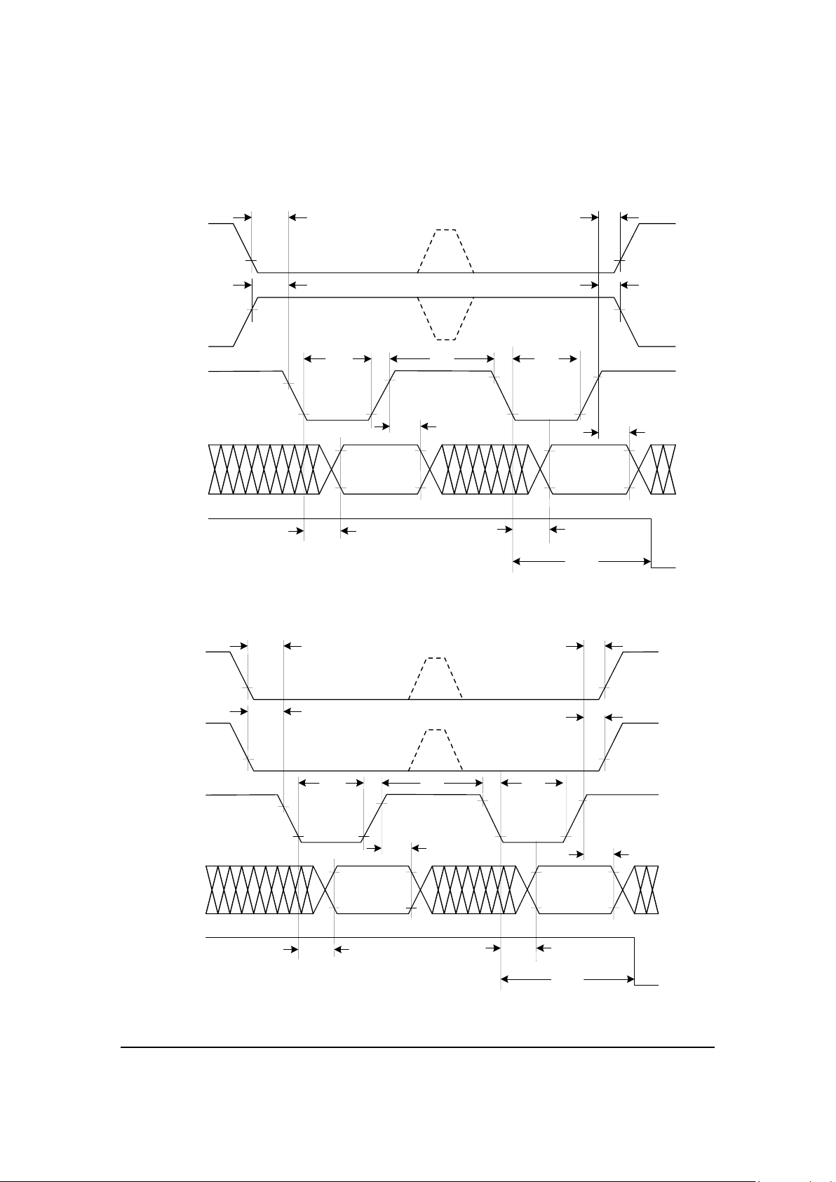
4.4 Host interface, 8/8 mode............................................................................................................... 19
4.4.1 Instruction write, 8/8 mode................................................................................................... 19
4.4.2 Data write, 8/8 mode ............................................................................................................19
4.4.3 Data read, 8/8 mode.............................................................................................................. 20
4.4.4 Status read, 8/8 mode............................................................................................................ 20
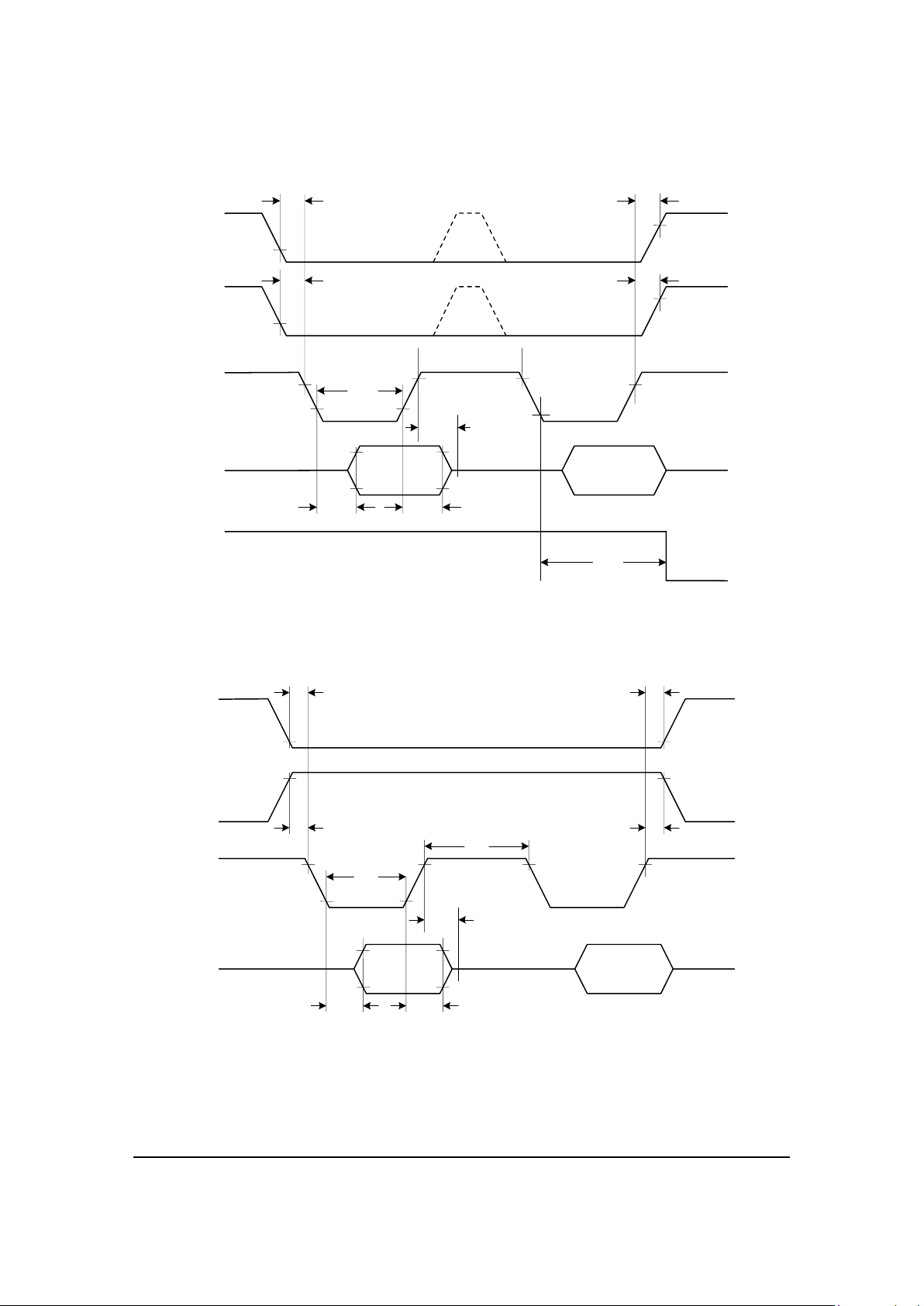
4.5 Host interface, 8/16 mode............................................................................................................. 21
4.5.1 Instruction write, 8/16 mode................................................................................................. 21
4.5.2 Data write, 8/16 mode...........................................................................................................21
4.5.3 Data read, 8/16 mode............................................................................................................22
4.5.4 Status read, 8/16 mode..........................................................................................................22
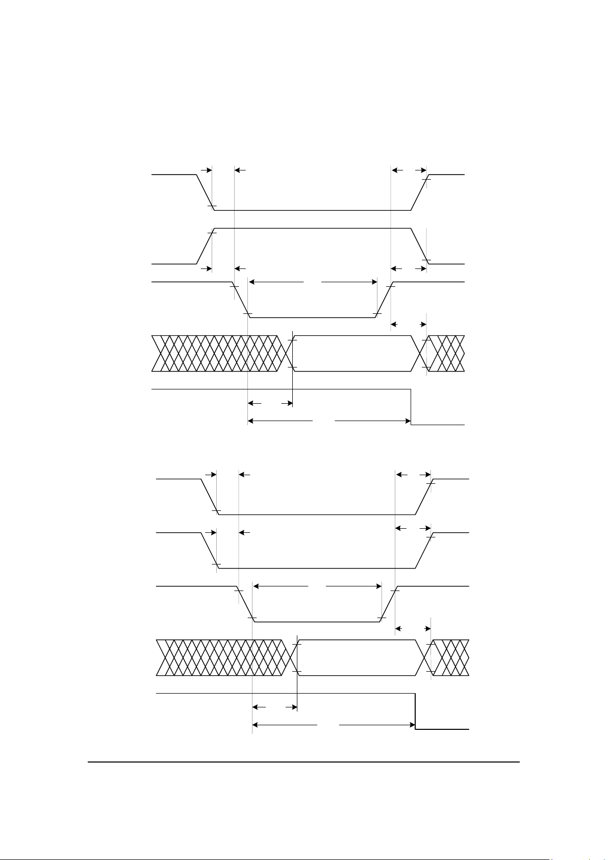
4.6 Host interface, 16/16 mode........................................................................................................... 23
4.6.1 Instruction write, 16/16 mode............................................................................................... 23
4.6.2 Data write, 16/16 mode......................................................................................................... 23
4.6.3 Data read, 16/16 mode.......................................................................................................... 24
4.6.4 Status read, 16/16 mode........................................................................................................ 24
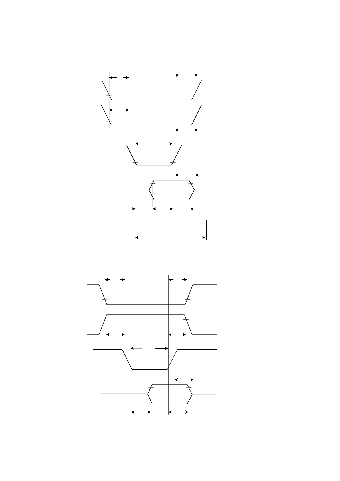
4.7 External memory timing............................................................................................................... 25
4.7.1 External memory read........................................................................................................... 25
4.7.2 External memory write......................................................................................................... 25
4.8 Peripheral device timing............................................................................................................... 26
4.8.1 Peripheral device read........................................................................................................... 26
4.8.2 Peripheral device write.........................................................................................................26
Page 8

MC2502 Technical Specifications
viii
5 Pinouts and Pin Descriptions.................................................................................................................. 27
5.1 Pinouts for MC2542..................................................................................................................... 27
5.2 Pinouts for MC2522..................................................................................................................... 28
5.3 Pinouts for MC2512..................................................................................................................... 29
5.4 Pin description tables.................................................................................................................... 30
5.4.1 I/O chip................................................................................................................................. 30
5.4.2 CP chip ................................................................................................................................. 33
6 Application Notes..................................................................................................................................... 36
6.1 Design Tips................................................................................................................................... 36
6.2 ISA Bus Interface......................................................................................................................... 38
6.3 RS-232 Serial Interface ................................................................................................................ 40
6.4 RS 422/485 Serial Interface.......................................................................................................... 42
6.5 12-bit A/D Interface...................................................................................................................... 44
6.6 16-bit A/D Input........................................................................................................................... 46
6.7 RAM Interface.............................................................................................................................. 48
6.8 User-defined I/O........................................................................................................................... 50
Page 9

MC2502 Technical Specifications
9
1 The Navigator Family
MC2100
Series
MC2300
Series
MC2400
Series
MC2502
Series
MC2800
Series
# of axes
4, 2, or 1 4, 2 or 1 4, 2 or 1 4, 2, or 1 4 or 2
Motor type supported
Brushed servo
Brushless
servo
Stepping Stepping
Brushed servo
+ brushless servo
Output format
Brushed servo
(single phase)
Commutated
(6-step or
sinusoidal)
Microstepping
Pulse and
direction
Brushed servo
(single phase)
+ commutated
(6-step or
sinusoidal)
Incremental encoder
input
√ √ √ √ √
Parallel word device input
√ √ √ √
√
Parallel communication
√ √ √ √
√
Serial communication
√ √ √ √
√
Diagnostic port
√ √ √ √
√
S-curve profiling
√ √ √
-
√
Electronic gearing
√ √ √
-
√
On-the-fly changes
√ √ √ √
√
Directional limit switches
√ √ √ √
√
Programmable bit output
√ √ √ √
√
Software-invertable
signals
√ √ √ √ √
PID servo control
√ √
- -
√
Feedforward (accel & vel)
√ √
- -
√
Derivative sampling time
√ √
- -
√
Data trace/diagnostics
√ √ √ √
√
PWM output
√ √ √
-
√
Motion error detection
√ √
√
(with
encoder)
√
(with
encoder)
√
Axis settled indicator
√ √
√
(with
encoder)
√
(with
encoder)
√
DAC-compatible output
√ √ √
-
√
Pulse & direction output - - -
√
-
Index & Home signals
√ √ √ √
√
Position capture
√ √ √ √
√
Analog input
√ √ √ √
√
User-defined I/O
√ √ √ √
√
External RAM support
√ √ √ √
√
Chipset part numbers
MC2140
(4 axes)
MC2120
(2 axes)
MC2110
(1 axis)
MC2340
(4 axes)
MC2320
(2 axes)
MC2310
(1 axis)
MC2440
(4 axes)
MC2420
(2 axes)
MC2410
(1 axis)
MC2542
(4 axes)
MC2522
(2 axes)
MC2512
(1 axis)
MC2840
(4 axes)
MC2820
(2 axes)
Developer's Kit p/n
DK2100 DK2300 DK2400 DK2502 DK2800
Page 10

MC2502 Technical Specifications
10
Introduction
This manual describes the operational characteristics of the MC2542, MC2522 and MC2512 Motion
Processors from PMD. These devices are members of PMD’s second-generation motion processor
family, which consists of 17 separate products organized into 6 series.
Each of these devices is a complete chip-based motion processor. They provide trajectory
generation and related motion control functions, and high speed pulse and direction outputs.
Together these products provide a software-compatible family of dedicated motion processors that
can handle a large variety of system configurations.
Each of these chips utilize a similar architecture, consisting of a high-speed computation unit, along
with an ASIC (Application Specific Integrated Circuit). The computation unit contains special onboard hardware that makes it well suited for the task of motion control.
Each chipset consists of two PQFP (Plastic Quad Flat Pack) ICs: a 100-pin Input/Output (I/O)
chip, and a 132-pin Command Processor (CP) chip.
Four of the series in the Navigator family are designed for a particular type of motor or control
scheme. The fifth allows the user to control 2 servo motor types (brushed and brushless). Here is a
summary description of each series.
Family Summary
MC2100 Series (MC2140, MC2120, MC2110) – This series outputs motor commands in either
Sign/Magnitude PWM or DAC-compatible format for use with brushed servo motors, or with
brushless servo motors having external commutation.
MC2300 Series (MC2340, MC2320, MC2310) – This series outputs sinusoidally or 6-step
commutated motor signals appropriate for driving brushless motors. Depending on the motor type,
the output is a two-phase or three-phase signal in either PWM or DAC-compatible format.
MC2400 Series (MC2440, MC2420, MC2410) – This series provides microstepping signals for
stepping motors. Two phased signals per axis are generated in either PWM or DAC-compatible
format.
MC2500 Series (MC2540, MC2520, MC2510) – These chipsets provide high-speed pulse and
direction signals for stepping motor systems.
MC2502 Series (MC2542, MC2522, MC2512) – Reduced feature version of the MC2500, these
chipsets provide high-speed pulse and direction signals for stepping motor systems.
MC2800 Series (MC2840, MC2820) – This series outputs sinusoidally or 6-step commutated motor
signals appropriate for driving brushless servo motors as well as PWM or DAC- compatible outputs
for driving brushed servo motors.
Page 11

MC2502 Technical Specifications
11
2 Functional Characteristics
2.1 Configurations, parameters, and performance
Available configurations
4 axes (MC2542), 2 axes (MC2522), or 1 axis (MC2512)
Operating modes
Open loop (pulse generator is driven by trajectory generator output)
Stall detection (pulse generator is driven by trajectory generator output and
encoder feedback is used for stall detection)
Communication modes
8/8 parallel (8 bit external parallel bus with 8 bit internal command word size)
8/16 parallel (8 bit external parallel bus with 16 bit internal command word size)
16/16 parallel (16 bit external parallel bus with 16 bit internal command word
size)
Point to point asynchronous serial
Multidrop asynchronous serial
Serial port baud rate range
1,200 baud to 416,667 baud
Position range
-2,147,483,648 to +2,147,483,647 counts
Velocity range
-32,768 to +32,767 counts/sample with a resolution of 1/65,536 counts/sample
Acceleration/deceleration ranges
-32,768 to +32,767 counts/sample
2
with a resolution of 1/65,536 counts/sample2
Jerk range
0 to ½ counts/sample
3
, with a resolution of 1/4,294,967,296 counts/sample3
Profile modes
Trapezoidal point-to-point (Velocity, acceleration, deceleration, and position
parameters)
Velocity-contouring (Velocity, acceleration, and deceleration parameters)
Maximum pulse rate
1.00 M-pulses/sec
Maximum encoder rate
Incremental (up to 5 Mcounts/sec)
Parallel-word (up to 160 Mcounts/sec)
Parallel encoder word size
16 bits
Parallel encoder read rate
20 kHz (reads all axes every 50 µsec)
Cycle rate timing range
102.4 µsec to 32.767 milliseconds
Minimum cycle time
102.4 µsec per enabled axis
Limit switches
2 per axis: one for each direction of travel
Position-capture triggers
2 per axis: index and home signals
Other digital signals (per axis)
1 AxisIn signal per axis, 1 AxisOut signal per axis
Software-invertable signals
Encoder A, Encoder B, Index, Home, AxisIn, AxisOut, PositiveLimit,
NegativeLimit, Pulse, Direction (all individually programmable per axis)
Analog input
8 10-bit analog inputs
User defined discrete I/O
256 16-bit wide user defined I/O
RAM/external memory support
65,536 blocks of 32,768 16 bit words per block. Total accessible memory is
2,147,483,648 16 bit words
Trace modes
one-time
continuous
Max. number of trace variables
4
Number of traceable variables
20
Number of host instructions
106
Page 12
MC2502 Technical Specifications
12
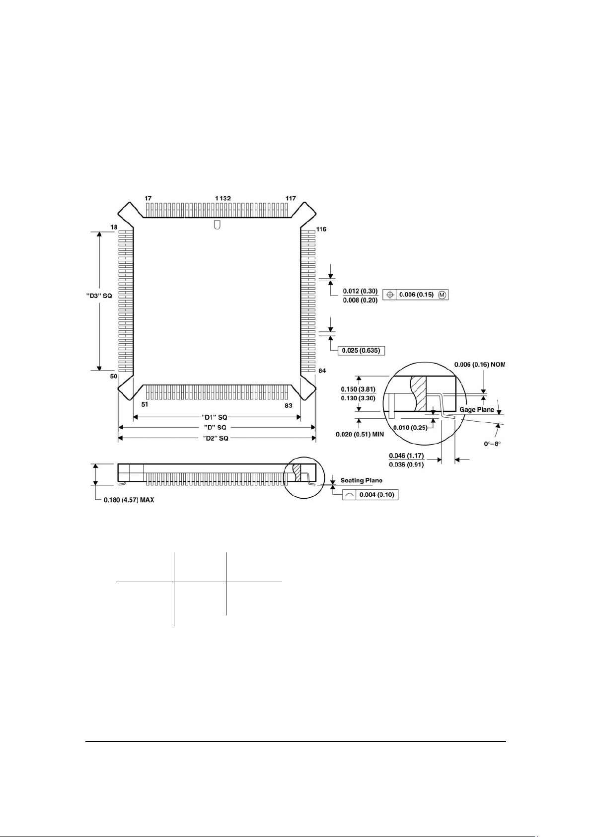
2.2 Physical characteristics and mounting dimensions
2.2.1 CP chip
All dimensions are in inches (with millimeters in brackets).
Dimension Minimum
(inches)
Maximum
(inches)
D 1.070 1.090
D1 0.934 0.966
D2 1.088 1.112
D3 0.800 nominal
Page 13

MC2502 Technical Specifications
13
2.2.2 I/O chip
All dimensions are in millimeters.
Dimension Minimum
(mm)
Nominal
(mm)
Maximum
(mm)
A 3.40
A1 0.25 0.33
A2 2.55 2.80 3.05
b 0.22 0.38
c 0.13 0.23
D 22.95 23.20 23.45
D1 19.90 20.00 20.10
E 16.95 17.20 17.45
E1 13.90 14.00 14.01
e 0.65 BSC
L 0.73 0.88 1.03
ccc 0.10
theta 0° 7°
Page 14
MC2502 Technical Specifications
14
2.3 Environmental and electrical ratings
All ratings and ranges are for both the I/O and CP chips.
Storage Temperature (T
s)
-55 °C to 150 °C
Operating Temperature (T
a)
0 °C to 70 °C*
Power Dissipation (P
d)
600 mW (I/O and CP combined)
Nominal Clock Frequency (F
clk)
40.0 MHz
Supply Voltage Limits (V
cc)
-0.3V to +7.0V
Supply Voltage Operating Range (V
cc)
4.75V to 5.25V
* An industrial version with an operating range of -40°C to 85°C is also available. Please contact
PMD for more information.
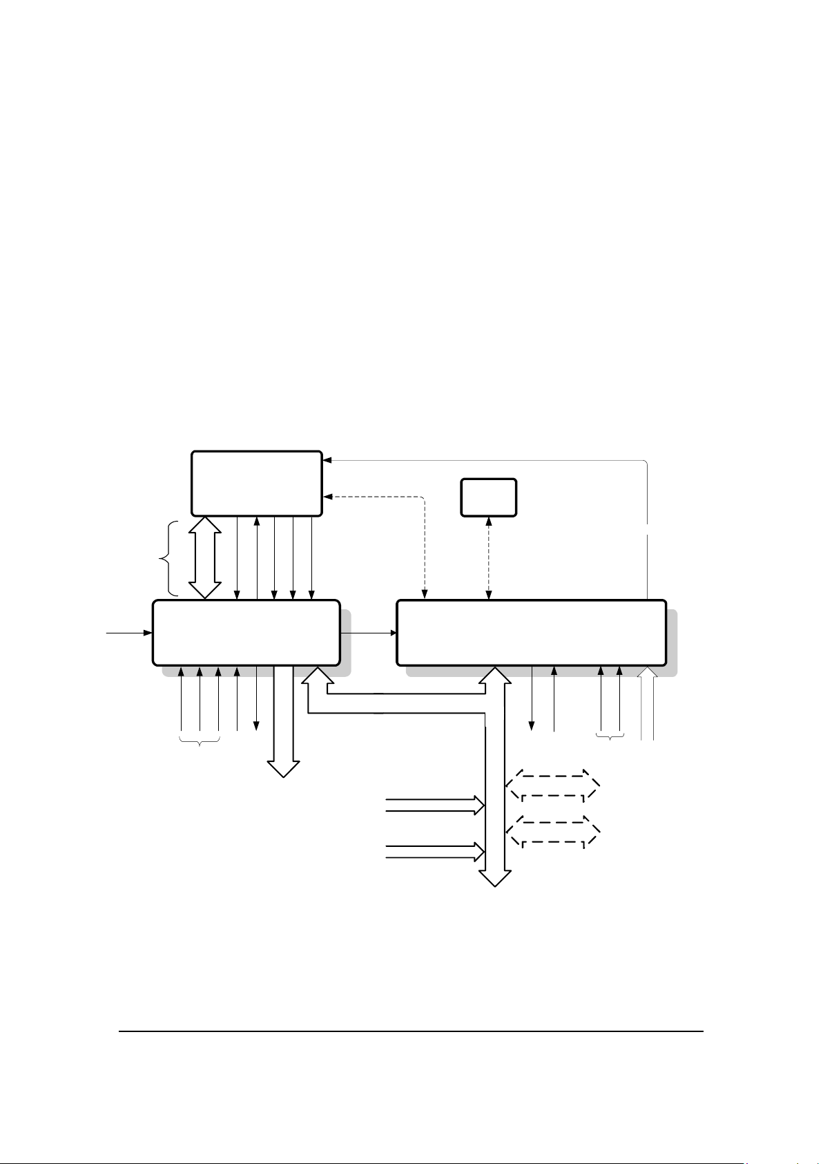
2.4 System configuration
The following figure shows the principal control and data paths in an MC2502 system.
Host
Serial-port
host
I/O CP
HostData0-15
~HostSlct
Parallel port
Serial port
(alternatives)
System clock
(40 MHz)
HostIntrpt
Navigator Motion Processor
20MHz clock
HostRdy
~HostWrite
HostCmd
~HostRead
Navigator Motion Processor
AxisOut
Negative
Positive
AxisIn
Limit
switches
Motor amplifier
A
Home
Index
B
Encoder
Analog inputs
Pulse and Direction
External memory
Other user devices
16-bit data bus
User I/O
Serial port configuration
Parallel word input
AtRest
The CP chip contains the profile generator, which calculates velocity, acceleration, and position
values for a trajectory. The output of the trajectory generator is used to produce pulse and direction
signals that control motor position.
Page 15

MC2502 Technical Specifications
15
Optional axis position information returns to the motion processor through the I/O chip, in the
form of encoder feedback, or through the CP chip, in the form of parallel-word feedback. This
position feedback may be used to detect motor stalling errors.
2.5 Peripheral device address mapping
Device addresses on the CP chip’s data bus are memory-mapped to the following locations:
Address Device Description
0200h Serial port data Contains the configuration data (transmission rate,
parity, stop bits, etc) for the asynchronous serial port
0800h Parallel-word encoder Base address for parallel-word feedback devices
1000h User-defined Base address for user-defined I/O devices
2000h RAM page pointer Page pointer to external memory
4000h Reserved Reserved for future use
8000h I/O chip Base address for I/O chip communications
Page 16

MC2502 Technical Specifications
16
3 Electrical Characteristics
3.1 DC characteristics
(Vcc and Ta per operating ratings, F
clk
= 40.0 MHz)
Symbol Parameter Minimum Maximum Conditions
Vcc Supply Voltage 4.75 V 5.25 V
Idd Supply Current 120 mA open outputs
Input Voltages
Vih Logic 1 input voltage 2.0 V Vcc + 0.3 V
Vil Logic 0 input voltage -0.3 V 0.8 V
V
ihreset
Logic 1 voltage for reset pin (reset) 2.2 V Vcc + 0.3 V
Output Voltages
Voh Logic 1 Output Voltage 2.4 V @CP Io = -23 mA
@I/O I
o
= -6 mA
Vol Logic 0 Output Voltage 0.33 V @CP Io = 6 mA
@I/O I
o
= 6 mA
Other
I
out
Tri-State output leakage current
-5 µA 5 µA
@CP
0 < V
out
< Vcc
Iin Input current
-10 µA
-10 µA
10 µA
-10 µA
@CP
@I/O
0 < V
i
< Vcc
Cio Input/Output capacitance 15 pF
10 pF
@CP typical
@I/O
Analog Input
Zai Analog input source impedance
9kΩ
E
dnl
Differential nonlinearity error.
Difference between the step width
and the ideal value.
-1 1.5 LSB
E
inl
Integral nonlinearity error.
Maximum deviation from the best
straight line through the ADC
transfer characteristics, excluding
the quantization error.
+/-1.5 LSB
3.2 AC characteristics
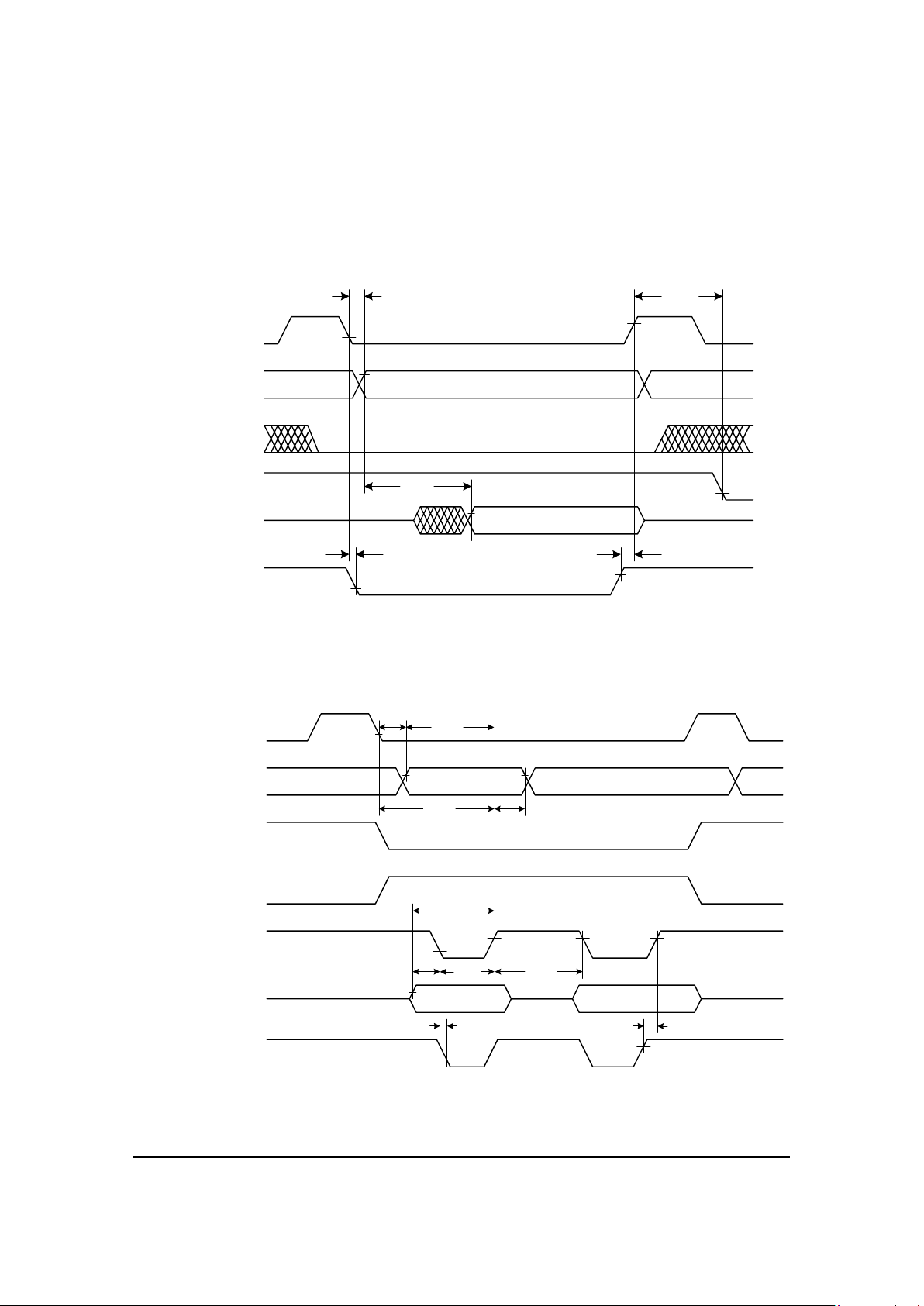
See timing diagrams, section 4, for Tn numbers. The symbol “~” indicates active low signal.
Timing Interval Tn Minimum Maximum
Clock Frequency (F
clk
) > 0 MHz 40 MHz (note 1)
Clock Pulse Width T1 10 nsec
Clock Period (note 3) T2 25 nsec
Encoder Pulse Width T3 150 nsec
Dwell Time Per State T4 75 nsec
Page 17

MC2502 Technical Specifications
17
Timing Interval Tn Minimum Maximum
Index Setup and Hold (relative to Quad
A and Quad B low)
T5 0 nsec
~HostSlct Hold Time T6 0 nsec
~HostSlct Setup Time T7 0 nsec
HostCmd Setup Time T8 0 nsec
HostCmd Hold Time T9 0 nsec
Read Data Access Time T10 25 nsec
Read Data Hold Time T11 10 nsec
~HostRead High to HI-Z Time T12 20 nsec
HostRdy Delay Time T13 100 nsec 150 nsec
~HostWrite Pulse Width T14 70 nsec
Write Data Delay Time T15 25 nsec
Write Data Hold Time T16 0 nsec
Read Recovery Time (note 2) T17 60 nsec
Write Recovery Time (note 2) T18 60 nsec
Read Pulse Width T19 70 nsec
Address Setup Delay Time T20 7 nsec
Data Access Time T21 19 nsec
Data Hold Time T22 2 nsec
Address Setup Delay Time T23 7 nsec
Address Setup to WriteEnable High T24 72 nsec
RAMSlct Low to WriteEnable High T25 79 nsec
Address Hold Time T26 17 nsec
WriteEnable Pulse Width T27 39 nsec
Data Setup Time T28 3 nsec
Data Setup before Write High Time T29 42 nsec
Address Setup Delay Time T30 7 nsec
Data Access Time T31 71 nsec
Data Hold Time T32 2 nsec
Address Setup Delay Time T33 7 nsec
Address Setup to WriteEnable High T34 122 nsec
PeriphSlct Low to WriteEnable High T35 129 nsec
Address Hold Time T36 17 nsec
WriteEnable Pulse Width T37 89 nsec
Data Setup Time T38 3 nsec
Data Setup before Write High Time T39 92 nsec
Read to Write Delay Time T40 50 nsec
Reset Low Pulse Width T50
5.0 µsec
RAMSlct Low to Strobe Low T51 1 nsec
Strobe High to RAMSlct High T52 4 nsec
WriteEnable Low to Strobe Low T53 1 nsec
Strobe High to WriteEnable High T54 3 nsec
PeriphSlct Low to Strobe Low T55 1 nsec
Strobe High to PeriphSlct High T56 4 nsec
Note 1 Performance figures and timing information valid at F
clk
= 40.0 MHz only. For timing
information and performance parameters at F
clk
< 40.0 MHz refer to section 6.1.
Note 2 For 8/8 and 8/16 interface modes only.
Note 3 The clock low/high split has an allowable range of 45-55%.
Page 18

MC2502 Technical Specifications
18
4 I/O Timing Diagrams
For the values of Tn, please refer to the table in Section 3.2.
4.1 Clock
4.2 Quadrature encoder input
4.3 Reset
T1 T2
MasterClkIn
T1
T3
T3
T4
T4
T5
(= ~QuadA * ~QuadB * ~Index)
T5
Index
Quad A
Quad B
~Index
V
cc
I/OClk
~RESET
T50
Page 19
MC2502 Technical Specifications
19
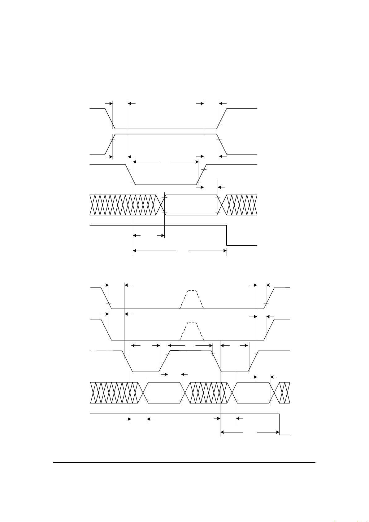
4.4 Host interface, 8/8 mode
4.4.1 Instruction write, 8/8 mode
T13
T15
~HostSlct
HostCmd
~HostWrite
HostData0-7
HostRdy
T14
T16
T8
T9
T7
T6
4.4.2 Data write, 8/8 mode
HostData0-7
~HostSlct
HostCmd
HostRdy
~HostWrite
Note: If setup and hold times are met, ~HostSlct and HostCmd may be de-asserted at this
point.
T7
T8
T18
T6
T9
T15
T14
T13
T16
Low byte
T14
T16
T15
High byte
see note
see note
Page 20
MC2502 Technical Specifications
20
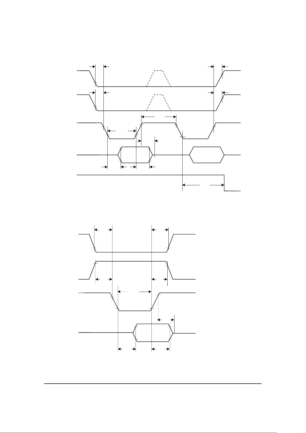
4.4.3 Data read, 8/8 mode
~HostSlct
HostCmd
HostData0-7
HostRdy
~HostRead
Note: If setup and hold times are met, ~HostSlct and HostCmd may be de-asserted at this
point.
T7
T8
T17
T6
T9
T13
see
note
T11
T12
T10
High-Z
High-Z
High-Z
High
byte
Low byte
T19
see
note
4.4.4 Status read, 8/8 mode
~HostSlct
T7
T8
T11
HostCmd
HostData0-7
~HostRead
T12
T10
High-Z
High-Z
T6
T9
T14
Page 21
MC2502 Technical Specifications
21
4.5 Host interface, 8/16 mode
4.5.1 Instruction write, 8/16 mode
HostData0-7
~HostSlct
HostCmd
HostRdy
~HostWrite
Note: If setup and hold times are met, ~HostSlct and HostCmd may be de-asserted at this point.
T7
T6
see note
T8
T18
T9
T14
T14
see note
T16
T16
T15
T13
T15
Low byteHigh byte
4.5.2 Data write, 8/16 mode
HostData0-7
~HostSlct
HostCmd
HostRdy
~HostWrite
Note: If setup and hold times are met, ~HostSlct and HostCmd may be de-asserted at this
point.
T7
T8
T6
T9
T15
see note
see note
Low byte
T16
T13
T16
T15
High byte
T18
T14
T14
Page 22
MC2502 Technical Specifications
22
4.5.3 Data read, 8/16 mode
HostData0-7
~HostSlct
T7
T8
T19
T6
T9
T13
T11
HostCmd
HostRdy
~HostRead
T12
T10
High-Z
High-Z
High-Z
High
byte
Low byte
Note: If setup and hold times are met, ~HostSlct and HostCmd may be de-asserted at this
point.
see note
see note
4.5.4 Status read, 8/16 mode
~HostSlct
T7
T8
T17
T6
T9
T11
HostCmd
HostData0-7
~HostRead
T12
T10
High-Z High-Z
High-Z
High
byte
Low byte
T19
Page 23
MC2502 Technical Specifications
23
4.6 Host interface, 16/16 mode
4.6.1 Instruction write, 16/16 mode
T7 T6
T9
T14
T16
T8
T13
T15
~HostSlct
HostCmd
~HostWrite
HostData0-15
HostRdy
4.6.2 Data write, 16/16 mode
T7 T6
T9
T14
T16
T8
T13
T15
~HostSlct
HostCmd
~HostWrite
HostData0-15
HostRdy
Page 24
MC2502 Technical Specifications
24
4.6.3 Data read, 16/16 mode
~HostSlct
T7
T8
T13
T11
HostCmd
HostData0-15
HostRdy
~HostRead
T12
T10
High-Z
High-Z
T6
T9
T14
4.6.4 Status read, 16/16 mode
~HostSlct
T7
T8
T11
HostCmd
HostData0-15
~HostRead
T12
T10
High-Z
High-Z
T6
T9
T14
Page 25
MC2502 Technical Specifications
25
4.7 External memory timing
4.7.1 External memory read
Note: PMD recommends using memory with an access time no greater than 15 nsec.
4.7.2 External memory write
Addr0-Addr15
R/~W
W/~R
~WriteEnbl
Data0-Data15
~RAMSlct
T26
T27
T27
T23
T28
T24
T25
T29
~Strobe
T53 T54
~RAMSlct
Addr0-Addr15
W/~R
~WriteEnbl
Data0-Data15
T21
T20
T40
~Strobe
T52T51
Page 26

MC2502 Technical Specifications
26
4.8 Peripheral device timing
4.8.1 Peripheral device read
4.8.2 Peripheral device write
Addr0-Addr15
R/~W
W/~R
~WriteEnbl
Data0-Data15
~PeriphSlct
T36
T37
T37
T33
T38
T34
T35
T39
~Strobe
T53 T54
~PeriphSlct
Addr0-Addr15
W/~R
~WriteEnbl
Data0-Data15
T31
T32
T30
T31
T40
~Strobe
T56T55
Page 27

MC2502 Technical Specifications
27
5 Pinouts and Pin Descriptions
5.1 Pinouts for MC2542
I/O
VCC
16, 17, 40, 65, 66, 67, 90
GND
4, 9, 22, 34, 46, 57, 64, 72, 84, 96
Unassigned
19, 27, 55,
56, 62, 78, 87
CP
~WriteEnbl
~PeriphSlct
GND
3, 8, 14, 20, 29, 37, 46, 56, 59,
61, 71, 92, 104, 113, 120
VCC
2, 7, 13, 21, 35, 36, 40, 47, 50,
52, 60, 62, 93, 103, 121
81
8
92
100
94
CPData8
CPData9
CPData10
CPData11
CPData12
CPData13
CPData14
CPData15
HostCmd
~HostRdy
~HostRead
~HostWrite
~HostSlct
12
10
99
98
1
11
97
95
76
74
73
75
2
3
7
6
38
36
35
32
31
37
42
39
HostData0
HostData1
HostData2
HostData3
HostData4
HostData5
HostData6
HostData7
HostData8
HostData9
HostData10
HostData11
HostData12
HostData13
HostData14
HostData15
CPData0
CPData1
CPData2
CPData3
CPData4
CPData5
CPData6
CPData7
18
14
71
13
70
15
69
68
77
53
54
52
41
43
50
89
24
5
91
CPIntrpt
CPR/~W
CPStrobe
CPPeriphSlct
CPAddr0
CPAddr1
CPAddr15
CPClk
MasterClkIn
HostMode0
HostMode1
47
25
49
82
48
44
93
29
33
51
83
88
30
58
28
45
QuadA1
QuadB1
~Index1
~Home1
QuadA2
QuadB2
~Index2
~Home2
QuadA3
QuadB3
~Index3
~Home3
QuadA4
QuadB4
~Index4
~Home4
9
10
11
12
15
16
17
18
19
22
23
24
25
26
27
28
110
111
112
114
115
116
117
118
119
122
123
124
125
126
127
128
43
44
99
98
53
58
SrlRcv
SrlXmt
SrlEnable
~HostIntrpt
I/OIntrpt
I/OClk
Data0
Data1
Data2
Data3
Data4
Data5
Data6
Data7
Data8
Data9
Data10
Data11
Data12
Data13
Data14
Data15
Addr0
Addr1
Addr2
Addr3
Addr4
Addr5
Addr6
Addr7
Addr8
Addr9
Addr10
Addr11
Addr12
Addr13
Addr14
Addr15
4
6
130
129
41
R/~W
~Strobe
~RAMSlct
~Reset
W/~R132
1
63
65
54
49
64
66
55
51
PosLim1
PosLim2
PosLim3
PosLim4
NegLim1
NegLim2
NegLim3
NegLim4
85
86
87
94
95
96
97
72
100
106
67
74
89
75
88
76
83
77
82
AxisOut1
AxisOut2
AxisOut3
AxisOut4
AxisIn1
AxisIn2
AxisIn3
AxisIn4
Analog1
Analog2
Analog3
Analog4
Analog5
Analog6
Analog7
Analog8
AnalogVcc
AnalogRefHigh
AnalogRefLow
AnalogGnd
84
21
85
59
20
61
26
79
Pulse1
Pulse2
Pulse3
Pulse4
Direction1
Direction4
Direction3
Direction2 60
AtRest1
AtRest2
AtRest3
AtRest4
23
86
63
80
Unassigned
5, 30-34, 38, 39, 42, 45, 48, 57,
68-70, 73, 90, 91, 101, 102,
105, 107, 108, 109, 131
AGND
78-81
Page 28

MC2502 Technical Specifications
28
5.2 Pinouts for MC2522
I/O
VCC
16, 17, 40, 65, 66, 67, 90
GND
4, 9, 22, 34, 46, 57, 64, 72, 84, 96
Unassigned
19, 20, 26, 27, 30, 33, 45, 51, 55,
56, 58, 59, 62, 63, 78, 79, 80, 83,
87, 88
CP
~WriteEnbl
~PeriphSlct
GND
3, 8, 14, 20, 29, 37, 46, 56, 59,
61, 71, 92, 104, 113, 120
VCC
2, 7, 13, 21, 35, 36, 40, 47, 50,
52, 60, 62, 93, 103, 121
81
8
92
100
94
CPData8
CPData9
CPData10
CPData11
CPData12
CPData13
CPData14
CPData15
HostCmd
~HostRdy
~HostRead
~HostWrite
~HostSlct
12
10
99
98
1
11
97
95
76
74
73
75
2
3
7
6
38
36
35
32
31
37
42
39
HostData0
HostData1
HostData2
HostData3
HostData4
HostData5
HostData6
HostData7
HostData8
HostData9
HostData10
HostData11
HostData12
HostData13
HostData14
HostData15
CPData0
CPData1
CPData2
CPData3
CPData4
CPData5
CPData6
CPData7
18
14
71
13
70
15
69
68
77
53
54
52
41
43
50
89
24
5
91
CPIntrpt
CPR/~W
CPStrobe
CPPeriphSlct
CPAddr0
CPAddr1
CPAddr15
CPClk
MasterClkIn
HostMode0
HostMode1
47
25
49
82
48
44
93
29
QuadA1
QuadB1
~Index1
~Home1
QuadA2
QuadB2
~Index2
~Home2
9
10
11
12
15
16
17
18
19
22
23
24
25
26
27
28
110
111
112
114
115
116
117
118
119
122
123
124
125
126
127
128
43
44
99
98
53
58
SrlRcv
SrlXmt
SrlEnable
~HostIntrpt
I/OIntrpt
I/OClk
Data0
Data1
Data2
Data3
Data4
Data5
Data6
Data7
Data8
Data9
Data10
Data11
Data12
Data13
Data14
Data15
Addr0
Addr1
Addr2
Addr3
Addr4
Addr5
Addr6
Addr7
Addr8
Addr9
Addr10
Addr11
Addr12
Addr13
Addr14
Addr15
4
6
130
129
41
R/~W
~Strobe
~RAMSlct
~Reset
W/~R132
1
63
65
64
66
PosLim1
PosLim2
NegLim1
NegLim2
85
86
87
94
95
72
100
74
89
75
88
76
83
77
82
AxisOut1
AxisOut2
AxisIn1
AxisIn2
Analog1
Analog2
Analog3
Analog4
Analog5
Analog6
Analog7
Analog8
AnalogVcc
AnalogRefHigh
AnalogRefLow
AnalogGnd
84
21
85
61
Pulse1
Pulse2
Direction1
Direction2 60
AtRest1
AtRest22386
Unassigned
5, 30-34, 38, 39, 42, 45, 48, 49,
51, 54, 55, 57, 67-70, 73, 90,
91, 96, 97, 101, 102, 105, 106-
109, 131
AGND
78-81
Page 29

MC2502 Technical Specifications
29
5.3 Pinouts for MC2512
I/O
VCC
16, 17, 40, 65, 66, 67, 90
CP
~WriteEnbl
~PeriphSlct
GND
3, 8, 14, 20, 29, 37, 46, 56, 59,
61, 71, 92, 104, 113, 120
VCC
2, 7, 13, 21, 35, 36, 40, 47, 50,
52, 60, 62, 93, 103, 121
81
8
92
100
94
CPData8
CPData9
CPData10
CPData11
CPData12
CPData13
CPData14
CPData15
HostCmd
~HostRdy
~HostRead
~HostWrite
~HostSlct
12
10
99
98
1
11
97
95
76
74
73
75
2
3
7
6
38
36
35
32
31
37
42
39
HostData0
HostData1
HostData2
HostData3
HostData4
HostData5
HostData6
HostData7
HostData8
HostData9
HostData10
HostData11
HostData12
HostData13
HostData14
HostData15
CPData0
CPData1
CPData2
CPData3
CPData4
CPData5
CPData6
CPData7
18
14
71
13
70
15
69
68
77
53
54
52
41
43
50
89
24
5
91
CPIntrpt
CPR/~W
CPStrobe
CPPeriphSlct
CPAddr0
CPAddr1
CPAddr15
CPClk
MasterClkIn
HostMode0
HostMode1
47
25
49
82
QuadA1
QuadB1
~Index1
~Home1
9
10
11
12
15
16
17
18
19
22
23
24
25
26
27
28
110
111
112
114
115
116
117
118
119
122
123
124
125
126
127
128
43
44
99
98
53
58
SrlRcv
SrlXmt
SrlEnable
~HostIntrpt
I/OIntrpt
I/OClk
Data0
Data1
Data2
Data3
Data4
Data5
Data6
Data7
Data8
Data9
Data10
Data11
Data12
Data13
Data14
Data15
Addr0
Addr1
Addr2
Addr3
Addr4
Addr5
Addr6
Addr7
Addr8
Addr9
Addr10
Addr11
Addr12
Addr13
Addr14
Addr15
4
6
130
129
41
R/~W
~Strobe
~RAMSlct
~Reset
W/~R132
1
63
64
PosLim1
NegLim1
85
86
87
94
72
74
89
75
88
76
83
77
82
AxisOut1
AxisIn1
Analog1
Analog2
Analog3
Analog4
Analog5
Analog6
Analog7
Analog8
AnalogVcc
AnalogRefHigh
AnalogRefLow
AnalogGnd
84
21
61
Pulse1
Direction1
AtRest1 23
Unassigned
5, 30-34, 38, 39, 42, 45, 48, 49,
51, 54, 55, 57, 65-70, 73, 90,
91, 95-97, 100-102, 105, 106-
109, 131
GND
4, 9, 22, 34, 46, 57, 64, 72, 84, 96
Unassigned
19, 20, 26, 27, 29, 30, 33, 44, 45,
48, 51, 55, 56, 58-60, 62, 63, 78,
79, 80, 83, 85-87, 88, 93
AGND
78-81
Page 30

MC2502 Technical Specifications
30
5.4 Pin description tables
5.4.1 I/O chip
I/O Chip
Pin Name and Number Direction Description
HostCmd 81
Input This signal is asserted high to write a host instruction to the Motion
Processor, or to read the status of the
HostRdy and HostIntrpt signals. It is
asserted low to read or write a data word.
HostRdy
8
Output This signal is used to synchronize communication between the Motion
Processor and the host.
HostRdy will go low (indicating host port busy) at
the end of a read or write operation according to the interface mode in
use, as follows:
Interface Mode
HostRdy goes low
8/8 after the instruction byte is transferred
after the second byte of each data word is transferred
8/16 after the second byte of the instruction word
after the second byte of each data word is transferred
16/16 after the 16-bit instruction word
after each 16-bit data word
serial n/a
HostRdy will go high, indicating that the host port is ready to transmit,
when the last transmission has been processed. All host port
communications must be made with
HostRdy high (ready).
A typical busy-to-ready cycle is 12.5 microseconds.
~HostRead 92
Input When ~HostRead is low, a data word is read from the Motion Processor.
~HostWrite 100
Input When ~HostWrite is low, a data word is written to the Motion Processor.
~HostSlct 94
Input When ~HostSlct is low, the host port is selected for reading or writing
operations.
CPIntrpt 77
Output I/O chip to CP chip interrupt. This signal sends an interrupt to the CP
chip whenever a host–chipset transmission occurs. It should be
connected to CP chip pin 53,
I/OIntrpt.
CPR/~W 53
Input This signal is high when the I/O chip is reading data from the I/O chip,
and low when it is writing data. It should be connected to CP chip pin 4,
R/W.
CPStrobe 54
Input This signal goes low when the data and address become valid during
Motion Processor communication with peripheral devices on the data
bus, such as external memory or a DAC. It should be connected to CP
chip pin 6,
Strobe.
CPPeriphSlct 52
Input This signal goes low when a peripheral device on the data bus is being
addressed. It should be connected to CP chip pin 130,
PeriphSlct.
CPAddr0
CPAddr1
CPAddr15
41
43
50
Input These signals are high when the CP chip is communicating with the I/O
chip (as distinguished from any other device on the data bus). They
should be connected to CP chip pins 110 (
Addr0), 111 (Addr1), and 128
(
Addr15).
MasterClkIn 89
Input This is the master clock signal for the Motion Processor. It is driven at a
nominal 40 MHz
CPClk 24
Output This signal provides the clock pulse for the CP chip. Its frequency is half
that of
MasterClkIn (pin 89), or 20 MHz nominal. It is connected directly to
the CP chip
I/Oclk signal (pin 58).
Page 31

MC2502 Technical Specifications
31
I/O Chip
Pin Name and Number Direction Description
HostMode1
HostMode0
91
5
Input These two signals determine the host communications mode, as follows:
HostMode1 HostMode0
0 0 16/16 parallel (16-bit bus, 16-bit instruction)
0 1 8/8 parallel (8-bit bus, 8-bit instruction)
1 0 8/16 parallel (8-bit bus, 16-bit instruction)
1 1 serial
HostData0
HostData1
HostData2
HostData3
HostData4
HostData5
HostData6
HostData7
HostData8
HostData9
HostData10
HostData11
HostData12
HostData13
HostData14
HostData15
12
10
99
98
1
11
97
95
76
74
73
75
2
3
7
6
Bi-directional,
tri-state
These signals transmit data between the host and the Motion Processor
through the parallel port. Transmission is mediated by the control signals
~HostSlct, ~HostWrite, ~HostRead and HostCmd.
In 16 bit mode, all 16 bits are used (
HostData0-15). In 8 bit mode, only the
low-order 8 bits of data are used (
HostData0-7). The HostMode0 and
HostMode1 signals select the communication mode this port operates in.
CPData0
CPData1
CPData2
CPData3
CPData4
CPData5
CPData6
CPData7
CPData8
CPData9
CPData10
CPData11
CPData12
CPData13
CPData14
CPData15
38
36
35
32
31
37
42
39
18
14
71
13
70
15
69
68
Bi-directional These signals transmit data between the I/O chip and pins Data0-15 of the
CP chip, via the Motion Processor data bus.
Pulse1
Pulse2
Pulse3
Pulse4
21
85
20
79
Output These pins provide the Pulse signal to the motor. This signal is always a
square wave, regardless of the pulse rate. A “step” occurs when the
signal transitions from a high state to a low state. For the MC2542 all 4
pins are valid. For MC2522 only Pulse1 and Pulse2 are valid. For
MC2512 only Pulse1 is valid.
Invalid axis pins may be left unconnected.
Direction1
Direction2
Direction3
Direction4
61
60
59
26
Output These pins indicate the direction of motion and work in conjunction with
the pulse signal. A high level on this signal indicates a positive direction
move and a low level indicates a negative direction move. For MC2542
all 4 pins are valid. For MC2522 only Direction1 and Direction2 are valid.
For MC2512 only Direction1 is valid.
Invalid axis pins may be left unconnected.
Page 32

MC2502 Technical Specifications
32
I/O Chip
Pin Name and Number Direction Description
AtRest1
AtRest2
AtRest3
AtRest4
23
86
63
80
Output The AtRest signal indicates the axis is at rest and the step motor can be
switched to low power or standby. A high level on this signal indicates
the axis is at rest. A low signal indicates the axis is in motion.
For MC2542 all 4 pins are valid. For MC2522 only AtRest1 and AtRest2
are valid. For MC2512 only AtRest1 is valid.
Invalid axis pins may be left unconnected.
QuadA1
QuadB1
QuadA2
QuadB2
QuadA3
QuadB3
QuadA4
QuadB4
47
25
48
44
33
51
30
58
Input These pins provide the A and B quadrature signals for the incremental
encoder for each axis. When the axis is moving in the positive (forward)
direction, signal A leads signal B by 90°.
The theoretical maximum encoder pulse rate is 5.1 MHz. Actual
maximum rate will vary, depending on signal noise.
NOTE: Many encoders require a pull-up resistor on each signal to
establish a proper high signal. Check your encoder’s electrical
specifications.
For MC2542, all 8 pins are valid. For MC2522, only the first four pins
(axes 1 and 2) are valid. For MC2512, only the first two pins (axis 1) are
valid.
WARNING! If a valid axis pin is not used, its signal should
be tied high.
Invalid axis pins may be left unconnected.
~Index1
~Index2
~Index3
~Index4
49
93
83
28
Input These pins provide the Index quadrature signals for the incremental
encoders. A valid index pulse is recognized by the chipset when
~Index, A,
and
B are all low.
For MC2542, all 4 pins are valid. For MC2522, only
~Index1 and ~Index2
are valid. For MC2512, only ~Index1 is valid.
WARNING! If a valid axis pin is not used, its signal should
be tied high.
Invalid axis pins may be left unconnected.
~Home1
~Home2
~Home3
~Home4
82
29
88
45
Input These pins provide the Home signals, general-purpose inputs to the
position-capture mechanism. A valid Home signal is recognized by the
chipset when ~Homen goes low. These signals are similar to ~Index, but are
not gated by the A and B encoder channels.
For MC2142, all 4 pins are valid. For MC2122, only
~Home1 and ~Home2
are valid. For MC2112, only ~Home1 is valid.
WARNING! If a valid axis pin is not used, its signal should
be tied high.
Invalid axis pins may be left unconnected.
Vcc
16, 17, 40, 65, 66, 67,
90
All of these pins must be connected to the I/O chip’s digital supply
voltage, which should be in the range 4.75 to 5.25 V.
GND
4, 9, 22, 34, 46, 57, 64,
72, 84, 96
I/O chip ground. All of these pins must be connected to the digital
power supply return.
unassigned
19, 27, 55, 56, 62, 78,
87
These pins must be left unconnected (floating).
Page 33

MC2502 Technical Specifications
33
5.4.2 CP chip
CP chip
Pin Name and Number Direction Description
~WriteEnbl 1
Output When low, this signal enables data to be written to the bus.
R/~W 4
Output This signal is high when the CP chip is performing a read, and low when it is
performing a write. It should be connected to I/O chip pin 53,
CPR/~W.
~Strobe 6
Output This signal is low when the data and address are valid during CP
communications. It should be connected to I/O chip pin 54,
CPStrobe.
~PeriphSlct 130
Output This signal is low when peripheral devices on the data bus are being addressed. It
should be connected to I/O chip pin 52,
CPPeriphSlct.
~RAMSlct 129
Output This signal is low indicates that external memory is being accessed.
~Reset 41
Input This is the master reset signal. When brought low, this pin resets the chipset to its
initial conditions.
W/~R 132
Output This signal is the inverse of R/~W; it is high when R/~W is low, and vice versa. For
some decode circuits, this is more convenient than
R/~W.
SrlRcv 43
Input This pin receives serial data from the serial transceiver.
NOTE! If this signal is not used, it should be tied high.
SrlXmt 44
Output This pin transmits serial data to the asynchronous serial port.
SrlEnable 99
Output This pin sets the serial port enable line. SrlEnable is always high for the point-to-
point protocol and is high during transmission for the multi-drop protocol.
~HostIntrpt 98
Output When low, this signal causes an interrupt to be sent to the host processor.
I/OIntrpt 53
Input This signal interrupts the CP chip when a host I/O transfer is complete. It
should be connected to I/O chip pin 77,
CPIntrpt.
Data0
Data1
Data2
Data3
Data4
Data5
Data6
Data7
Data8
Data9
Data10
Data11
Data12
Data13
Data14
Data15
9
10
11
12
15
16
17
18
19
22
23
24
25
26
27
28
Bidirectional
Multi-purpose data lines. These pins comprise the CP chip’s external data bus,
used for all communications with the I/O chip and peripheral devices such as
external memory or DACs. They may also be used for parallel-word input and
for user-defined I/O operations.
Page 34

MC2502 Technical Specifications
34
CP chip
Pin Name and Number Direction Description
Addr0
Addr1
Addr2
Addr3
Addr4
Addr5
Addr6
Addr7
Addr8
Addr9
Addr10
Addr11
Addr12
Addr13
Addr14
Addr15
110
111
112
114
115
116
117
118
119
122
123
124
125
126
127
128
Output Multi-purpose Address lines. These pins comprise the CP chip’s external address
bus, used to select devices for communication over the data bus.
Addr0, Addr1,
and
Addr15 are connected to the corresponding CPAddr pins on the I/O chip, and
are used to communicate between the CP and I/O chips.
Other address pins may be used for DAC output, parallel word input, or userdefined I/O operations. See the Navigator Motion Processor User’s Guide for a
complete memory map.
I/OClk 58
Input This is the CP chip clock signal. It should be connected to I/O chip pin 24,
CPClk.
AnalogVcc 84
Input CP chip analog power supply voltage. This pin must be connected to the analog
input supply voltage, which must be in the range 4.5-5.5 V
If the analog input circuitry is not used, this pin must be connected to V
cc
.
AnalogRefHigh 85
Input CP chip analog high voltage reference for A/D input. The allowed range is
AnalogRefLow to AnalogVcc.
If the analog input circuitry is not used, this pin must be connected to V
cc
.
AnalogRefLow 86
Input CP chip analog low voltage reference for A/D input. The allowed range is
AnalogGND to AnalogRefHigh.
If the analog input circuitry is not used, this pin must be connected to GND.
AnalogGND 87
Input CP chip analog input ground. This pin must be connected to the analog input
power supply return.
If the analog input circuitry is not used, this pin must be connected to GND.
Analog1
Analog2
Analog3
Analog4
Analog5
Analog6
Analog7
Analog8
74
89
75
88
76
83
77
82
Input These signals provide general-purpose analog voltage levels, which are sampled
by an internal A/D converter. The A/D resolution is 10 bits.
The allowed range is
AnalogRefLow to AnalogRefHigh.
Any unused pins should be tied to AnalogGND.
If the analog input circuitry is not used, these pins should be tied to GND.
PosLim1
PosLim2
PosLim3
PosLim4
63
65
54
49
Input These signals provide inputs from the positive-side (forward) travel limit
switches. On power-up or
Reset these signals default to active low interpretation,
but the interpretation can be set explicitly using the
SetSignalSense instruction.
For MC2542, all 4 pins are valid. For MC2522, only
PosLim1 and PosLim2 are
valid. For MC2512, only
PosLim1 is valid.
WARNING! If a valid axis pin is not used, its signal must be tied
high. PosLim2 is an output during device reset and as such any
connection to GND or V
cc
must be via a series resistor.
Invalid axis pins may also be left unconnected or connected to GND.
Page 35

MC2502 Technical Specifications
35
CP chip
Pin Name and Number Direction Description
NegLim1
NegLim2
NegLim3
NegLim4
64
66
55
51
Input These signals provide inputs from the negative-side (reverse) travel limit
switches. On power-up or
Reset these signals default to active low interpretation,
but the interpretation can be set explicitly using the
SetSignalSense instruction.
For MC2542, all 4 pins are valid. For MC2522, only
NegLim1 and NegLim2 are
valid. For MC2512, only
NegLim1 is valid.
WARNING! If a valid axis pin is not used, its signal must be tied
high. NegLim1 is an output during device reset and as such any
connection to GND or V
cc
must be via a series resistor.
Invalid axis pins may also be left unconnected or connected to GND.
AxisOut1
AxisOut2
AxisOut3
AxisOut4
94
95
96
97
Output Each of these pins can be conditioned to track the state of any bit in the Status
registers associated with its axis.
For MC2542, all 4 pins are valid. For MC2522, only
AxisOut1 and AxisOut2 are
valid. For MC2512, only
AxisOut1 is valid.
Invalid or unused pins may be left unconnected.
AxisIn1
AxisIn2
AxisIn3
AxisIn4
72
100
106
67
Input These are general-purpose programmable inputs. They may be used as a
breakpoint input, to stop a motion axis, or to cause an UPDATE to occur.
For MC2542, all 4 pins are valid. For MC2522, only
AxisIn1 and AxisIn2 are valid.
For MC2512, only
AxisIn1 is valid.
Invalid or unused pins may be left unconnected or connected to GND.
Vcc
2, 7, 13, 21, 35, 36, 40,
47, 50, 52, 60, 62, 93,
103, 121
CP digital supply voltage. All of these pins must be connected to the supply
voltage. V
cc
must be in the range 4.75 - 5.25 V
WARNING! Pin 35 must be tied HIGH with a pull-up resistor. A
nominal value of 22K Ohms is suggested.
GND
3, 8, 14, 20, 29, 37, 46,
56, 59, 61, 71, 92, 104,
113, 120
CP ground. All of these pins must be connected to the power supply return.
AGND
78-81 These signals must be tied to AnalogGND.
If the analog input circuitry is not used, these pins must be tied to GND.
unassigned
(MC2542)
45, 48, 68, 69, 70, 73,
90, 91, 101, 102, 105,
107, 108, 109
These signals may be connected to GND for better noise immunity and reduced
power consumption or they can be left unconnected (floating).
unassigned
5, 30-34, 38, 39, 42,
57, 131
These signals must be left unconnected (floating).
Page 36

MC2502 Technical Specifications
36
6 Application Notes
6.1 Design Tips
The following are recommendations for the design of circuits that utilize a PMD Motion Processor.
Serial Interface
The serial interface is a convenient interface that can be used before host software has been written
to communicate through the parallel interface. It is recommended that even if the serial interface is
not utilized as a standard communication interface, that the serial receive and transmit signals are
brought to test points so that they may be connected during initial board configuration/debugging.
This is especially important during the prototype phase. The serial receive line should include a pullup resistor to avoid spurious interrupts when it is not connected to a transceiver.
If the serial configuration decode logic is not implemented (see section 6.3) and the serial interface
may be used for debugging as mentioned above, the CP data bus should be tied high. This places the
serial interface in a default configuration of 9600,n,8,1 after power on or reset.
Controlling pulse output during reset
When the motion processor is in a reset state (when the reset line is held low) or immediately after a
power on, the pulse outputs can be in an unknown state, causing undesirable motor movement. It is
recommended that the enable line of any motor amplifier be held in a disabled state by the host
processor or some logic circuitry until communication to the motion processor is established. This
can be in the form of a delay circuit on the amplifier enable line after power up, or the enable line can
be ANDed with the CP reset line.
Parallel word encoder input
When using parallel word input for motor position, it is useful to also decode this information into
the User I/O space. This allows the current input value to be read using the chip instruction ReadIO
for diagnostic purposes.
Using a non standard system clock frequency
It is often desirable to share a common clock among several components in a design. In the case of
the PMD Motion Processors it is possible to use a clock below the standard value of 40MHz. In this
case all system frequencies will be reduced as a fraction of the input clock verses the standard
40MHz clock. The list below shows the affected system parameters:-
• Serial baud rate
• Maximum pulse rate
• Timing characteristics as shown in section 3.2
• Cycle time
Page 37

MC2502 Technical Specifications
37
For example, if an input clock of 34MHz is used with a serial baud rate of 9600 and the step range
(SetStepRange) set to 625KHz the following timing changes will result:-
• Serial baud rate decreases to 9600 bps *34/40 = 8160 bps
• Maximum step rate decreases to 625 KHz *34/40 = 531.25 KHz
• Cycle time per axis increases to 102.4 µsec *40/34 = 120.48 µsec
Page 38

MC2502 Technical Specifications
38
6.2 ISA Bus Interface
A complete, ready-to-use ISA (PC/AT) bus interface circuit has been provided to illustrate Navigator
host interfacing, as well as to make it easier for the customer to build a Navigator development
system.
The interface between the PMD Navigator chipset and the ISA (PC-AT) bus is shown on the
following page.
Comments on Schematic
This interface uses a CPLD and two 74LS245s to buffer the data lines. This interface assumes a base
address is assigned in the address space of A9-A0, 300-400 hex. These addresses are generally
available for prototyping and other system-specific uses without interfering with system assignments.
This interface occupies 16 addresses from XX0 to XXF hex though it does not use all the addresses.
Four select lines are provided allowing the base address to be set from 300 to 3F0 hex for the select
lines SW1-SW4 equal to 0- F respectively. The address assignments used are as follows, where
BADR is the base address, 340 hex for example:
Address use
340h read-write data
342h write command -read status
344h write command -read status
348h write reset [Data = don't care]
The base address (BADR) is decoded in the 74LS688. It is combined with SA1, SA2, and SA3,
(BADR+0,2,4) to form HSELN to select the I/O chip and the 245’s. (BADR+2,4) asserts HCMD.
Two addresses are used to be compatible with the first generation products, which used BADR+2 to
write command and BADR+4 to read status.
B+8 and IOW* generate a reset pulse, -RS, for the CP chip. The reset instruction is OR'd with
RESET on the bus to initialize the PMD chipset when the PC is reset.
Page 39

8
8
7
7
6
6
5
5
4
4
3
3
2
2
1
1
D D
C C
B B
A A
SA0
B+0,2,4
B+8
2,4
ALL COMPONENTS LABELED U2
MAY BE EASILY IMPLEMENTED
IN A CPLD.
SW[4..1] ENCODE BASE ADR.
0X300 THRU 0X3F0. A CLOSED
SWITCH ENCODES 0. THE BASE
ADDRESSES ARE ON 10 HEX
BOUNDARIES.
SW4-SW1 BADR
1 OX310
2 OX320
3 OX330
4 OX340
5 OX350
6 OX360
7 OX370
8 OX380
A OX3A0
B OX3B0
C OX3C0
D OX3D0
E OX3E0
F OX3F0
0 OX300
BE USED TO
INTERRUPT THE
PC. IT CAN BE
READ IN THE
STATUS REG.
BE USED TO
INTERRUPT THE
PC. IT CAN BE
READ IN THE
STATUS REG.
HRDY MAY
HINT- MAY
B
16 BIT ISA INTERFACE (GEN2DB1)
PERFORMANCE MOTION DEVICES
55 OLD BEDFORD RD
LINCOLN, MA 01773
B
00Thursday, April 11, 2002
Title
Size Document Number Rev
Date: Sheet
of
BD15 HD15
IOCS16- BD14 HD14
INT3 BD13 HD13
INT4 BD12 HD12
INT5 BD11 HD11
INT7 BD10 HD10
INT6 BD9 HD9
BD8 HD8
HSELN
BD8 IOR*
BD9
BD10
BD11
BD12
VCC BD13 BD0 HD0
BD14 BD1 HD1
GND BD15 BD2 HD2
BD3 HD3
BD4 HD4
BD5 HD5
BD6 HD6
BD7 HD7
GND
RESET BD7 HSELN
VCC BD6 IOR* HD0 CPINTR-
BD5 HD1 ADR0
BD4 HD2 ADR1
BD3 HD3 ADR15
BD2 HD4 ISBD1 HD5 CPSTRBBD0 HD6 CPR/W
GND HD7 CPINTR-
AEN HD8
HD9 CLK
IOW* SA4 BADRN HD10
IOR* SA5 HD11
SA6 HD12
SA7 HD13
SA8 HD14
SA9 HD15
SA10
SA11 SA11 HCMD
INT2 SA10 VCC HSELN
SA9 SW1 IOW*
INT1 SA8 SW2 IOR*
SA7 SW3 HRDY
INT0 SA6 SW4 VCC
SA5 RS- VCC 40MHz
SA4 VCC
SA3 GND GND
VCC SA2 GND GND
SA1
GND AEN
BADRN
SW1 SA3 SA3N ADR6 HSELN
SW2 SA3
SW3
SW4
BADRN BADR SA1
ADR6
SA2
BADR
SA1
HCMD
GND IOCS16- SA2
BADRN
SA1
SA2 RST
SA3N RSIOW* RESET
BD[0..15]
SA[1..11]
HD[0..15]
D7
D1
D0
D1
D7
RS-
D0
D10
ADR1
D8 D8
D3
D6
D2
D3
D6
D12
D13
CPR/W
D13
D4 D4
ADR15
D14
HINT-
D9 D9
CPSTRB-
D5
D10
D5
D[0..15]
D11 D11
D12
D2
D15
VCC
CLK
D14
GND
GND
ADR0
IS-
D15
GND
VCC
J1
CON AT36
D1
D2
D3
D4
D5
D6
D7
D8
D9
D10
D11
D12
D13
D14
D15
D16
D17
D18
C1
C2
C3
C4
C5
C6
C7
C8
C9
C10
C11
C12
C13
C14
C15
C16
C17
C18
J2
CON AT62
B1
B2
B3
B4
B5
B6
B7
B8
B9
B10
B11
B12
B13
B14
B15
B16
B17
B18
B19
B20
B21
B22
B23
B24
B25
B26
B27
B28
B29
B30
B31
A1
A2
A3
A4
A5
A6
A7
A8
A9
A10
A11
A12
A13
A14
A15
A16
A17
A18
A19
A20
A21
A22
A23
A24
A25
A26
A27
A28
A29
A30
A31
U2
NOR5
1
2
3
4
5
6
U2
TRI
12
3
R?
22K
X1
40MHz
3
1
OUT
ENB
U2
74LS688
2
4
6
8
11
13
15
17
3
5
7
9
12
14
16
18
1
19
P0
P1
P2
P3
P4
P5
P6
P7
Q0
Q1
Q2
Q3
Q4
Q5
Q6
Q7
G
P=Q
U2
OR3
1
2
3
4
S1
SW DIP-4
1
2
3
4
8
7
6
5
T1
1
T
U?
RSIP8
1
2
3
4
5
6
7
8
COM
R1
R2
R3
R4
R5
R6
R7
U3
I/O2N40
47
25
49
48
44
93
12
10
99
98
1
11
97
95
81
94
100
92
8
24
33
51
83
30
58
28
31
37
42
39
18
14
71
13
43
41
77
1617656640
2234465764
72
82
29
88
45
76
74
73
75
2
3
7
6
68
69
15
70
32
35
36
38
67
90
4
9
84
96
50
52
89
54
53
21
62
23
85
87
86
20
19
63
79
78
80
61
60
59
26
5
91
QUADA1
QUADB1
INDEX1
QUADA2
QUADB2
INDEX2
HOSTDATA0
HOSTDATA1
HOSTDATA2
HOSTDATA3
HOSTDATA4
HOSTDATA5
HOSTDATA6
HOSTDATA7
HOSTCMD
~HOSTSLCT
~HOSTWRITE
~HOSTREAD
HOSTRDY
CPCLK
QUADA3
QUADB3
INDEX3
QUADA4
QUADB4
INDEX4
CPDATA4
CPDATA5
CPDATA6
CPDATA7
CPDATA8
CPDATA9
CPDATA10
CPDATA11
CPADDR1
CPADDR0
~CPINTRPT
VCC
VCC
VCC
VCC
VCC
GND
GND
GND
GND
GND
GND
HOME1
HOME2
HOME3
HOME4
HOSTDATA8
HOSTDATA9
HOSTDATA10
HOSTDATA11
HOSTDATA12
HOSTDATA13
HOSTDATA14
HOSTDATA15
CPDATA15
CPDATA14
CPDATA13
CPDATA12
CPDATA3
CPDATA2
CPDATA1
CPDATA0
VCC
VCC
GND
GND
GND
GND
CPADR15
~CPPERIPHSLCT
MASTERCLKIN
~CPSTROBE
CPR/~W
PWM1A
PWM1B
PWM1C
PWM2A
PWM2B
PWM2C
PWM3A
PWM3B
PWM3C
PWM4A
PWM4B
PWM4C
PWMS1A
PWMS2A
PWMS3A
PWMS4A
HOSTMODE0
HOSTMODE1
U2
AND2
1
2
3
U2
OR2
1
2
3
U6
CP2N40
13
60
14
20
9
10
11
12
15
16
17
18
19
22
23
24
47
110
111
112
114
115
116
117
118
119
122
123
124
125
126
127
128
129
130
4
6
1
25
26
27
28
294659617192104
113
120
21
406293
103
121
58
7
2
41
53
36
50
56
35
132
63
65
54
49
64
66
55
51
73
90
91
101
102
105
107
108
109
68
69
70
94
95
96
97
72
100
106
67
98
43
44
45
99
74
89
75
88
76
83
77
82
84
85
86
87
3
8
30
31
34
33
32
38
39
78
79
80
81
37
131
52
VCC
VCC
GND
GND
DATA0
DATA1
DATA2
DATA3
DATA4
DATA5
DATA6
DATA7
DATA8
DATA9
DATA10
DATA11
VCC
ADDR0
ADDR1
ADDR2
ADDR3
ADDR4
ADDR5
ADDR6
ADDR7
ADDR8
ADDR9
ADDR10
ADDR11
ADDR12
ADDR13
ADDR14
ADDR15
~RAMSLCT
~PERIPHSLCT
R/~W
~STROBE
~WRITEENBL
DATA12
DATA13
DATA14
DATA15
GND
GND
GND
GND
GND
GND
GND
GND
GND
VCC
VCC
VCC
VCC
VCC
VCC
I/OCK
VCC
VCC
~RESET
I/OINTRP
VCC
VCC
GND
~RS
W/~R
POSLIM1
POSLIM2
POSLIM3
POSLIM4
NEGLIM1
NEGLIM2
NEGLIM3
NEGLIM4
HALL1A
HALL1B
HALL1C
HALL2A
HALL2B
HALL2C
HALL3A
HALL3B
HALL3C
HALL4A
HALL4B
HALL4C
AXISOUT1
AXISOUT2
AXISOUT3
AXISOUT4
AXISIN1
AXISIN2
AXISIN3
AXISIN4
~HOSTINTRPT
SRLRCV
SRLXMT
SYNCH
SRLENABLE
ANALOG1
ANALOG2
ANALOG3
ANALOG4
ANALOG5
ANALOG6
ANALOG7
ANALOG8
ANALOGVCC
ANALOGREFHIGH
ANALOGREFLOW
ANALOGGND
GND
GND
N/C
N/C
N/C
N/C
N/C
N/C
N/C
N/C
N/C
N/C
N/C
GND
N/C
VCC
U2
NOT
12
U4
74LS245
2
3
4
5
6
7
8
9
19
1
18
17
16
15
14
13
12
11
A1
A2
A3
A4
A5
A6
A7
A8
G
DIR
B1
B2
B3
B4
B5
B6
B7
B8
U2
NOT
12
U5
74LS245
2
3
4
5
6
7
8
9
19
1
18
17
16
15
14
13
12
11
A1
A2
A3
A4
A5
A6
A7
A8
G
DIR
B1
B2
B3
B4
B5
B6
B7
B8
U2
NOR2
1
2
3
Page 40

MC2502 Technical Specifications
40
6.3 RS-232 Serial Interface
The interface between the Navigator chipset and an RS-232 serial port is shown in the following
figure.
Comments on Schematic
S1 and S2 encode the characteristics of the serial port such as baud rate, number of stop bits, parity,
etc. The CP will read these switches during initialization, but these parameters may also be set or
changed using the
SetSerialPort chipset command. The DB9 connector wired as shown can be
connected directly to the serial port of a PC without requiring a null modem cable.
Page 41

8
8
7
7
6
6
5
5
4
4
3
3
2
2
1
1
D D
C C
B B
A A
FEMALE DB9 WIRED
AS SHOWN WILL
CONNECT TO A PC
WITHOUT A DUMMY
MODEM.
U2 AND U3 COULD BE IMPLEMENTED IN A PLD
B
RS232 SERIAL INTERFACE (GEN2DG1)
PERFORMANCE MOTION DEVICES
55 OLD BEDFORD RD
LINCOLN, MA 01773
B
10Thursday, April 11, 2002
Title
Size Document Number Rev
Date: Sheet
of
VCC VCC
SW1
SW2
SW3
A0
SW4
A1
SW5
DS0 A2
SW6
DS1 A3
SW7
DS2 A4
DS3 A5
DS4 A6
DS5 A7 SW1 DS0
DS6 A8 SW2 DS1
DS7 A9 SW3 DS2
DS8 A10 SW4 DS3
DS9 A11 SW5 DS4
DS10 A12 SW6 DS5
DS11 A13 SW7 DS6
DS12 A14
SW8
DS7
DS13 A15
DS14
DS15
ISR/W
STRB-
IS-
A9
R/W
STRB-
VCC
C1+
C1- V+
C2+ VC2-
SERXMIT TXD
SERRCV RXD
GND
RSCLK
GND
DS[0..15]
DS[0..15]
A[0..15]
SW16
SW9
DS[0..15]
DS8
DS15
SW14
DS12
DS9
DS11
SW13
SW10
DS13
SW11
SW15
DS10
DS14
SW12
SW10
SW14
SW9
VCC
SW13
SW12
SW15
SW11
SW8 SW16
C5
.1UF
50V
RS1
RSIP9
1
2
3
4
5
6
7
8
9
COM
R1
R2
R3
R4
R5
R6
R7
R8
C3
.1UF
50V
C1
.1UF
50V
RS2
RSIP9
1
2
3
4
5
6
7
8
9
COM
R1
R2
R3
R4
R5
R6
R7
R8
S1
SW DIP-8
1
2
3
4
5
6
7
8
16
15
14
13
12
11
10
9
U3
AD232
1
3
4
5
11
10
12
9
2
6
14
7
13
8
C1+
C1-
C2
C2-
T1IN
T2IN
R1OUT
R2OUT
V+
V-
T1OUT
T2OUT
R1IN
R2IN
U2
NOT
12
U2
NOT
12
J1
CONNECTOR DB9
5
9
4
8
3
7
2
6
1
C4
.1UF
50V
R?
22K
U2
74LS244
2
4
6
8
11
13
15
17
1
19
18
16
14
12
9
7
5
3
1A1
1A2
1A3
1A4
2A1
2A2
2A3
2A4
1G
2G
1Y1
1Y2
1Y3
1Y4
2Y1
2Y2
2Y3
2Y4
C2
.1UF
50V
S2
SW DIP-8
1
2
3
4
5
6
7
8
16
15
14
13
12
11
10
9
U2
NAND4
1
2
3
4
5
U3
74LS244
2
4
6
8
11
13
15
17
1
19
18
16
14
12
9
7
5
3
1A1
1A2
1A3
1A4
2A1
2A2
2A3
2A4
1G
2G
1Y1
1Y2
1Y3
1Y4
2Y1
2Y2
2Y3
2Y4
U1
CP2N40
13
60
14
20
9
10
11
12
15
16
17
18
19
22
23
24
47
110
111
112
114
115
116
117
118
119
122
123
124
125
126
127
128
129
130
4
6
1
25
26
27
28
294659617192104
113
120
21
406293
103
121
58
7
2
41
53
36
50
56
35
132
63
65
54
49
64
66
55
51
73
90
91
101
102
105
107
108
109
68
69
70
94
95
96
97
72
100
106
67
98
43
44
45
99
74
89
75
88
76
83
77
82
84
85
86
87
3
8
30
31
34
33
32
38
39
78
79
80
81
37
131
52
VCC
VCC
GND
GND
DATA0
DATA1
DATA2
DATA3
DATA4
DATA5
DATA6
DATA7
DATA8
DATA9
DATA10
DATA11
VCC
ADDR0
ADDR1
ADDR2
ADDR3
ADDR4
ADDR5
ADDR6
ADDR7
ADDR8
ADDR9
ADDR10
ADDR11
ADDR12
ADDR13
ADDR14
ADDR15
~RAMSLCT
~PERIPHSLCT
R/~W
~STROBE
~WRITEENBL
DATA12
DATA13
DATA14
DATA15
GND
GND
GND
GND
GND
GND
GND
GND
GND
VCC
VCC
VCC
VCC
VCC
VCC
I/OCK
VCC
VCC
~RESET
I/OINTRP
VCC
VCC
GND
~RS
W/~R
POSLIM1
POSLIM2
POSLIM3
POSLIM4
NEGLIM1
NEGLIM2
NEGLIM3
NEGLIM4
HALL1A
HALL1B
HALL1C
HALL2A
HALL2B
HALL2C
HALL3A
HALL3B
HALL3C
HALL4A
HALL4B
HALL4C
AXISOUT1
AXISOUT2
AXISOUT3
AXISOUT4
AXISIN1
AXISIN2
AXISIN3
AXISIN4
~HOSTINTRPT
SRLRCV
SRLXMT
SYNCH
SRLENABLE
ANALOG1
ANALOG2
ANALOG3
ANALOG4
ANALOG5
ANALOG6
ANALOG7
ANALOG8
ANALOGVCC
ANALOGREFHIGH
ANALOGREFLOW
ANALOGGND
GND
GND
N/C
N/C
N/C
N/C
N/C
N/C
N/C
N/C
N/C
N/C
N/C
GND
N/C
VCC
Page 42

MC2502 Technical Specifications
42
6.4 RS 422/485 Serial Interface
The interface between the Navigator chipset and an RS-422/485 serial port is shown in the following
figure.
Comments on Schematic
Use the included table to determine the jumper setup that matches the chosen configuration. If
using RS485, the last CP must have its jumpers set to RS485 LAST. The DB9 connector wiring is
for example only. The DB9 should be wired according to the specification that accompanies the
connector to which it is attached.
For correct operation, logic should be provided that contains the start up serial configuration for the
chipset. Refer to the RS232 Serial Interface schematic for an example of the required logic.
Note that the RS485 interface cannot be used in point to point mode. It can only be used in a multidrop configuration where the chip SrlEnable line is used to control transmit/receive operation of the
serial transceiver.
Chips in a multi-drop environment should not be operated at different baud rates. This will result in
communication problems.
Page 43

8
8
7
7
6
6
5
5
4
4
3
3
2
2
1
1
D D
C C
B B
A A
TO HOST
RS422
RS485
RS485 LAST
COM TYPE JP1 JP2 JP3 JP4
1-2 1-2 2-3 2-3
2-3 2-3 1-2 1-2
1-2 2-3 1-2 1-2
NOTE:RS422 IS CAPABLE OF FULL DUPLEX AND USES 2 PAIRS.
RS485 IS HALF-DUPLEX ON 1 PAIR AND MAY BE DAISY CHAINED
RS422 HOST AS SHOWN IN THE TABLE.
THE CP USES RS485. A SINGLE CP MAY COMMUNICATE WITH AN
A SINGLE PAIR MAY BE WIRED TO EITHER P1-1,9 OR P1-2,3
FOR RS485.
TERMINATE
TERMINATE
TRANSMITTX-RX +
TX-RX -
RECEIVE
A
RS422/485 Interface (GENDO1)
PERFORMANCE MOTION DEVICES
55 OLD BEDFORD RD
LINCOLN, MA 01773
B
11Thursday, April 11, 2002
Title
Size Document Number Rev
Date: Sheet
of
TX+
TX-
VCC
GND
RX+
RX-
GND
RXT
TXT
VCC
JP4
JMP3
123
JP1
JMP3
123
R1
120
JP3
JMP3
123
R3
4.7K
U1
MAX491
5
9
10
12
11
2
4
3
14
7
6
DI
Y
Z
A
B
RO
DE
RE
VCC
GND
GND
+
C1
4.7UF
10V
TANT
C2
.1UF
50V
CER
R2
120
P1
CONNECTOR DB9
RT ANGLE MALE
5
9
4
8
3
7
2
6
1
JP2
JMP3
123
SRLRCV
SRLXMT
SRLENABLE
Page 44

MC2502 Technical Specifications
44
6.5 12-bit A/D Interface
The following schematic shows a typical interface circuit between the Navigator chipset and a quad
12 bit 2’s complement A/D converter used as a position input device.
Comments on Schematic
The A/D converter samples all 4 axes and sequentially converts and stores the 2’s complement
digital words. The data is read out sequentially, axis 1 to 4. DACRD- is used to perform the read
and is also used to load the counter to FFh. The counter will be reloaded for each read and will not
count significantly between reads. The counter will therefore start counting down after the last read
and will generate the cvt- pulse after 12.75 µsec. The conversions will take approximately 35 µsec,
and the data will be available for the next set of reads after 50 µsec. The 12 bit words from the A/D
are extended to 16 bits with the 74LS244.
Page 45

8
8
7
7
6
6
5
5
4
4
3
3
2
2
1
1
D D
C C
B B
A A
NOTE:FS INPUTS ARE +- 10V
DACRD- WILL LOAD THE COUNTER TO 255.
12.8 USEC. AFTER THE LAST DACRDTHE COUNTER WILL REACH 0 AND START THE
NEXT CONVERSION. ALL 4 CHANNELS WILL
BE CONVERTED IN 35 USEC. READY FOR
THE NEXT SET OF READS 50 USEC LATER.
BE IMPLEMENTEDIN A PLD.
NOTE:THE LOGIC LABELED U2 MAY
NOTE:SIGN EXTENTION FOR 2'S COMPLEMENT
B
12 BIT A/D IN (GEN2DC1)
PERFORMANCE MOTION DEVICES
55 OLD BEFORD RD
LINCOLN, MA 01773
B
10Thursday, April 11, 2002
Title
Size Document Number Rev
Date: Sheet
of
POS1
POS2
POS3
POS4
CVT- DACRD-
DACRD-
A11
-5VA GND
AGND
CVT- ENCNTCLK CLK
DACRD- DACRD-
ENCNT-
CLK
DACRD-
DS[0..15]
DS[0..15]
VCC
DS5
DS15
W/R
A14
DS3
A7
DS0
DS8
DS11
A11
DS11
DS1
DS4
STRB-
A5
A3
A[0..15]
DS9
GND
VCC
DS2
DS1
DS13
DS2
DS13
GND
VCC
A13
A8
DS12
RSCLK
DS0
DS6
GND
A15
DS11
VCC
A10
A9
A0
DS4
DS7
A6
A4
DS12
A1
DS5
DS14
DS10
DS3DS15
DS10
DS8
DS7
A2
DS9
DS14
A12
DS6
IS-
U2
74ALS169
3
4
5
6
2
9
1
10
7
14
13
12
11
15
A
B
C
D
CLK
LOAD
U/D
ENT
ENP
QA
QB
QC
QD
RCO
U2
OR4
1
2
3
4
5
U1
CP2N40
13
60
14
20
9
10
11
12
15
16
17
18
19
22
23
24
47
110
111
112
114
115
116
117
118
119
122
123
124
125
126
127
128
129
130
4
6
1
25
26
27
28
294659617192104
113
120
21
406293
103
121
58
7
2
41
53
36
50
56
35
132
63
65
54
49
64
66
55
51
73
90
91
101
102
105
107
108
109
68
69
70
94
95
96
97
72
100
106
67
98
43
44
45
99
74
89
75
88
76
83
77
82
84
85
86
87
3
8
30
31
34
33
32
38
39
78
79
80
81
37
131
52
VCC
VCC
GND
GND
DATA0
DATA1
DATA2
DATA3
DATA4
DATA5
DATA6
DATA7
DATA8
DATA9
DATA10
DATA11
VCC
ADDR0
ADDR1
ADDR2
ADDR3
ADDR4
ADDR5
ADDR6
ADDR7
ADDR8
ADDR9
ADDR10
ADDR11
ADDR12
ADDR13
ADDR14
ADDR15
~RAMSLCT
~PERIPHSLCT
R/~W
~STROBE
~WRITEENBL
DATA12
DATA13
DATA14
DATA15
GND
GND
GND
GND
GND
GND
GND
GND
GND
VCC
VCC
VCC
VCC
VCC
VCC
I/OCK
VCC
VCC
~RESET
I/OINTRP
VCC
VCC
GND
~RS
W/~R
POSLIM1
POSLIM2
POSLIM3
POSLIM4
NEGLIM1
NEGLIM2
NEGLIM3
NEGLIM4
HALL1A
HALL1B
HALL1C
HALL2A
HALL2B
HALL2C
HALL3A
HALL3B
HALL3C
HALL4A
HALL4B
HALL4C
AXISOUT1
AXISOUT2
AXISOUT3
AXISOUT4
AXISIN1
AXISIN2
AXISIN3
AXISIN4
~HOSTINTRPT
SRLRCV
SRLXMT
SYNCH
SRLENABLE
ANALOG1
ANALOG2
ANALOG3
ANALOG4
ANALOG5
ANALOG6
ANALOG7
ANALOG8
ANALOGVCC
ANALOGREFHIGH
ANALOGREFLOW
ANALOGGND
GND
GND
N/C
N/C
N/C
N/C
N/C
N/C
N/C
N/C
N/C
N/C
N/C
GND
N/C
VCC
R?
22K
U2
74ALS169
3
4
5
6
2
9
1
10
7
14
13
12
11
15
A
B
C
D
CLK
LOAD
U/D
ENT
ENP
QA
QB
QC
QD
RCO
U2
NOT
12
U2
DFF2
12
3
4
QD
CLK
CL
U2
NOT
12
U?
AD7874
1
2
27
28
5
6
7
8
24
25
10
11
12
13
15
16
17
18
19
20
21
22
3
9
262314
4
VIN1
VIN2
VIN3
VIN4
CONVST
RD
CS
CLK
REFIN
REFOUT
DB11
DB10
DB9
DB8
DB7
DB6
DB5
DB4
DB3
DB2
DB1
DB0
VDD
VDD
VSS
AGND
DGND
INT
U2
74LS244
2
4
6
8
11
13
15
17
1
19
18
16
14
12
9
7
5
3
1A1
1A2
1A3
1A4
2A1
2A2
2A3
2A4
1G
2G
1Y1
1Y2
1Y3
1Y4
2Y1
2Y2
2Y3
2Y4
Page 46

MC2502 Technical Specifications
46
6.6 16-bit A/D Input
The interface between the Navigator chipset and 16 bit A/D converters as parallel input position
devices is shown in the following figure.
Comments on Schematic
The schematic shows a 16 bit A/D used to provide parallel position input to axis 1 and axis 2. The
expansion to the remaining two axes is easily implemented. The 374 registers are required on the
output of the A/D converters to make the 68-nanosecond access time of the CP. The worst-case
timing of the A/D’s specify 83 nanoseconds for data on the bus and 83 nanoseconds from data to
tri-state on the bus. Each time the data is read the 169 counter is set to 703 decimal. This provides a
35.2-microsecond delay before the next conversion. With a 10-microsecond conversion time the
data will be available for the next set of reads after 50 microseconds. The delay is used to provide a
position sample close to the actual position.
Page 47

8
8
7
7
6
6
5
5
4
4
3
3
2
2
1
1
D D
C C
B B
A A
NOTE:FS INPUTS ARE +- 10V
38.4 USEC. AFTER THE LAST DACRDTHE COUNTER WILL REACH 0 AND START THE
NEXT CONVERSION. ALL 4 CHANNELS WILL
BE CONVERTED IN 10 USEC. READY FOR
THE NEXT SET OF READS AFTER 50 USEC.
BE IMPLEMENTEDIN A PLD.
NOTE:THE LOGIC LABELED U2 MAY
DACRD- WILL LOAD THE COUNTER TO 700.
NOTE:AXIS 1 AND 2 ARE SHOWN EXPLICITLY.
IDENTICAL FASHION.
AXIS 3 AND 4 MAY BE IMPLEMENTED IN AN
SEE ANALOG DEVICES SPECIFICATIONS FOR
ADITIONAL INFORMATION AND POWER BYPASSING.
B
16 BIT A/D INPUT (GEN2DL1)
PERFORMANCE MOTION DEVICES
55 OLD BEDFORD RD
LINCOLN, MA 01773
B
11Thursday, April 11, 2002
Title
Size Document Number Rev
Date: Sheet
of
VCC
+5A VCC
A0
A1
DS0 A2
DS1 A3
DS2 A4
DS3 A5
AIN1
DS4 A6
DS5 A7
DS6 A8
DS7 A9
DS8 A10
DS9 A11
DS10 A12
DS11 A13
DS12 A14
DS13 A15
CVT-
DS14
DS15 A0 RD1-
GND
IS- A1 RD2-
RD3-
STRB- DACRD- RD4W/R A11n
RD1-
GND
A11 A11n
AGND
+5A
AIN2
CVT-
GND
RS-
RD2-
CLK GND
AGND
GND
ENCNT-
GND
CLK CLK CLK
DACRD- DACRD- DACRD- CLK
GND GND GND
ENCNT- DACRD-
DS[0..15]
DS[0..15]
VCC VCC VCC
CVT-
VCC
A[0..15]
U2
74ALS169
3
4
5
6
2
9
1
10
7
14
13
12
11
15
A
B
C
D
CLK
LOAD
U/D
ENT
ENP
QA
QB
QC
QD
RCO
U2
OR4
1
2
3
4
5
C1
2.2UF
R2
33.2
U2
374
3
4
7
8
13
14
17
18
1
11
2
5
6
9
12
15
16
19
D0
D1
D2
D3
D4
D5
D6
D7
OC
CLK
Q0
Q1
Q2
Q3
Q4
Q5
Q6
Q7
U1
CP2N40
13
60
14
20
9
10
11
12
15
16
17
18
19
22
23
24
47
110
111
112
114
115
116
117
118
119
122
123
124
125
126
127
128
129
130
4
6
1
25
26
27
28
294659617192104
113
120
21
406293
103
121
58
7
2
41
53
36
50
56
35
132
63
65
54
49
64
66
55
51
73
90
91
101
102
105
107
108
109
68
69
70
94
95
96
97
72
100
106
67
98
43
44
45
99
74
89
75
88
76
83
77
82
84
85
86
87
3
8
30
31
34
33
32
38
39
78
79
80
81
37
131
52
VCC
VCC
GND
GND
DATA0
DATA1
DATA2
DATA3
DATA4
DATA5
DATA6
DATA7
DATA8
DATA9
DATA10
DATA11
VCC
ADDR0
ADDR1
ADDR2
ADDR3
ADDR4
ADDR5
ADDR6
ADDR7
ADDR8
ADDR9
ADDR10
ADDR11
ADDR12
ADDR13
ADDR14
ADDR15
~RAMSLCT
~PERIPHSLCT
R/~W
~STROBE
~WRITEENBL
DATA12
DATA13
DATA14
DATA15
GND
GND
GND
GND
GND
GND
GND
GND
GND
VCC
VCC
VCC
VCC
VCC
VCC
I/OCK
VCC
VCC
~RESET
I/OINTRP
VCC
VCC
GND
~RS
W/~R
POSLIM1
POSLIM2
POSLIM3
POSLIM4
NEGLIM1
NEGLIM2
NEGLIM3
NEGLIM4
HALL1A
HALL1B
HALL1C
HALL2A
HALL2B
HALL2C
HALL3A
HALL3B
HALL3C
HALL4A
HALL4B
HALL4C
AXISOUT1
AXISOUT2
AXISOUT3
AXISOUT4
AXISIN1
AXISIN2
AXISIN3
AXISIN4
~HOSTINTRPT
SRLRCV
SRLXMT
SYNCH
SRLENABLE
ANALOG1
ANALOG2
ANALOG3
ANALOG4
ANALOG5
ANALOG6
ANALOG7
ANALOG8
ANALOGVCC
ANALOGREFHIGH
ANALOGREFLOW
ANALOGGND
GND
GND
N/C
N/C
N/C
N/C
N/C
N/C
N/C
N/C
N/C
N/C
N/C
GND
N/C
VCC
U4
AD976
6
7
8
9
10
11
12
13
15
16
17
18
19
20
21
22
2514 28
27
26
1
3
4
25
24
23
D15
D14
D13
D12
D11
D10
D9
D8
D7
D6
D5
D4
D3
D2
D1
D0
AGND1
AGND2
DGND VCC
VANA
BUSY
VIN
REF
CAP
CS
R/C
BYTE
U2
74ALS169
3
4
5
6
2
9
1
10
7
14
13
12
11
15
A
B
C
D
CLK
LOAD
U/D
ENT
ENP
QA
QB
QC
QD
RCO
C1
2.2UF
C1
2.2UF
R4
33.2
R3
200
U2
374
3
4
7
8
13
14
17
18
1
11
2
5
6
9
12
15
16
19
D0
D1
D2
D3
D4
D5
D6
D7
OC
CLK
Q0
Q1
Q2
Q3
Q4
Q5
Q6
Q7
R1
200
U2
374
3
4
7
8
13
14
17
18
1
11
2
5
6
9
12
15
16
19
D0
D1
D2
D3
D4
D5
D6
D7
OC
CLK
Q0
Q1
Q2
Q3
Q4
Q5
Q6
Q7
U2A
139
2
3
1
4
5
6
7
A
B
G
Y0
Y1
Y2
Y3
C1
2.2UF
U3
AD976
6
7
8
9
10
11
12
13
15
16
17
18
19
20
21
22
2514 28
27
26
1
3
4
25
24
23
D15
D14
D13
D12
D11
D10
D9
D8
D7
D6
D5
D4
D3
D2
D1
D0
AGND1
AGND2
DGND VCC
VANA
BUSY
VIN
REF
CAP
CS
R/C
BYTE
U2
NOT
12
U2
DFF2
12
3
4
QD
CLK
CL
U2
374
3
4
7
8
13
14
17
18
1
11
2
5
6
9
12
15
16
19
D0
D1
D2
D3
D4
D5
D6
D7
OC
CLK
Q0
Q1
Q2
Q3
Q4
Q5
Q6
Q7
U2
NOT
12
U2
74ALS169
3
4
5
6
2
9
1
10
7
14
13
12
11
15
A
B
C
D
CLK
LOAD
U/D
ENT
ENP
QA
QB
QC
QD
RCO
R?
22K
Page 48

MC2502 Technical Specifications
48
6.7 RAM Interface
The following schematic shows an interface circuit between the Navigator chipset and external ram.
Comments on Schematic
The CP is capable of directly addressing 32K words of 16-bit memory. It will also use a 16 bit
paging register to address up to 32K word pages. The schematic shows the paging and addressing
for 128KB RAM chips, i.e. 4 pages per RAM chip. The page address decoding is shown for only 6 of
the 16 possible paging bits. The decoding time from W/R and DS- to the memory output must not
exceed 18 ns. for a read with no wait states. The writes provide 25 extra ns access time for W/R and
DS- to reverse the CP data bus.
Page 49
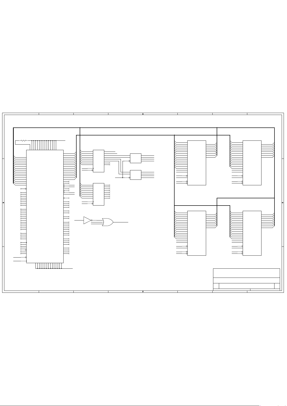
8
8
7
7
6
6
5
5
4
4
3
3
2
2
1
1
D D
C C
B B
A A
PAGE REGISTER UP TO 16 BITS
NOTE:THE CRITICAL DECODE AND MEMORY
ACCESS TIME IS DURING READ,
THE REQUIRED ACCESS TIME IS
18 NS. FROM DS- LOW.
AS ILLUSTRATED THERE IS ~ 100NS.
TO ACCOMPLISH THE DECODING
FROM PAGE REG WRITE TO
MEMORY READ OR WRITE.
DECODING WILL HAVE TO BE
CAREFULLY DONE ON MEMORIES
WITH A SINGLE CHIP SELECT.
NOTE: POS139 IS A STANDARD 139 WITH INVERTED
OUTPUTS
B
RAM INTERFACE (GEN2DF1)
PERFORMANCE MOTION DEVICES
55 OLD BEDFORD RD
LINCOLN, MA 01773
B
10Friday, January 31, 2003
Title
Size Document Number Rev
Date: Sheet
of
A0 A0
A1 D0 A1 D8
A2 D1 A2 D9
A3 D2 A3 D10
A4 D3 A4 D11
D0 MPG0 A5 D4 A5 D12
A0 D1 MPG1 A6 D5 A6 D13
A1 D2 CS1 A7 D6 A7 D14
D0 A2 D3 CS2 A8 D7 A8 D15
D1 A3 D4 CS3 A9 A9
D2 A4 D5 CS4 A10 A10
D3 A5 D6 A11 A11
D4 A6 D7 A12 A12
D5 A7 A13 A13
D6 A8 WE- A14 A14
D7 A9 PGR- MPG0 MPG0
D8 A10 CS5 MPG1 MPG1
D9 A11 CS6
D10 A12 CS7 DS- DSD11 A13 GND CS8 CS1 CS1
D12 A14
D13 WE- WED14 W/R W/R
D15 DS- D8
D9
D10
D11
WE- D12
W/R D13
D14
D15
WE-
PGR-
A0 A0
A1 D0 A1 D8
A2 D1 A2 D9
A3 D2 A3 D10
A13 A4 D3 A4 D11
IS- PGR- A5 D4 A5 D12
R/W A6 D5 A6 D13
A7 D6 A7 D14
A8 D7 A8 D15
A9 A9
A10 A10
A11 A11
A12 A12
A13 A13
A14 A14
MPG0 MPG0
MPG1 MPG1
DS- DSCS2 CS2
WE- WE-
W/R W/R
RSCLK
D[0..15]
A[0..14]
D[0..15]
A[0..14]
VCC
GND
IS-
U2A
POS139
2
3
1
4
5
6
7
A
B
G
Y0
Y1
Y2
Y3
U2
74LS377
3
4
7
8
13
14
17
18
11
1
2
5
6
9
12
15
16
19
D1
D2
D3
D4
D5
D6
D7
D8
CLK
G
Q1
Q2
Q3
Q4
Q5
Q6
Q7
Q8
U2
74LS377
3
4
7
8
13
14
17
18
11
1
2
5
6
9
12
15
16
19
D1
D2
D3
D4
D5
D6
D7
D8
CLK
G
Q1
Q2
Q3
Q4
Q5
Q6
Q7
Q8
U?
MCM6226
12
11
10
9
8
7
6
5
27
26
23
25
4
28
3
31
2
29
24
22
30
13
14
15
17
18
19
20
21
A0
A1
A2
A3
A4
A5
A6
A7
A8
A9
A10
A11
A12
A13
A14
A15
A16
WE
OE
CE1
CE2
DQ0
DQ1
DQ2
DQ3
DQ4
DQ5
DQ6
DQ7
U?
MCM6226
12
11
10
9
8
7
6
5
27
26
23
25
4
28
3
31
2
29
24
22
30
13
14
15
17
18
19
20
21
A0
A1
A2
A3
A4
A5
A6
A7
A8
A9
A10
A11
A12
A13
A14
A15
A16
WE
OE
CE1
CE2
DQ0
DQ1
DQ2
DQ3
DQ4
DQ5
DQ6
DQ7
R?
22K
U2
NOT
12
U2B
POS139
14
13
15
12
11
10
9
A
B
G
Y0
Y1
Y2
Y3
U?
MCM6226
12
11
10
9
8
7
6
5
27
26
23
25
4
28
3
31
2
29
24
22
30
13
14
15
17
18
19
20
21
A0
A1
A2
A3
A4
A5
A6
A7
A8
A9
A10
A11
A12
A13
A14
A15
A16
WE
OE
CE1
CE2
DQ0
DQ1
DQ2
DQ3
DQ4
DQ5
DQ6
DQ7
U?
CP2N40
13
60
14
20
9
10
11
12
15
16
17
18
19
22
23
24
47
110
111
112
114
115
116
117
118
119
122
123
124
125
126
127
128
129
130
4
6
1
25
26
27
28
294659617192104
113
120
21
406293
103
121
58
7
2
41
53
36
50
56
35
132
63
65
54
49
64
66
55
51
73
90
91
101
102
105
107
108
109
68
69
70
94
95
96
97
72
100
106
67
98
43
44
45
99
74
89
75
88
76
83
77
82
84
85
86
87
3
8
30
31
34
33
32
38
39
78
79
80
81
37
131
52
VCC
VCC
GND
GND
DATA0
DATA1
DATA2
DATA3
DATA4
DATA5
DATA6
DATA7
DATA8
DATA9
DATA10
DATA11
VCC
ADDR0
ADDR1
ADDR2
ADDR3
ADDR4
ADDR5
ADDR6
ADDR7
ADDR8
ADDR9
ADDR10
ADDR11
ADDR12
ADDR13
ADDR14
ADDR15
~RAMSLCT
~PERIPHSLCT
R/~W
~STROBE
~WRITEENBL
DATA12
DATA13
DATA14
DATA15
GND
GND
GND
GND
GND
GND
GND
GND
GND
VCC
VCC
VCC
VCC
VCC
VCC
I/OCK
VCC
VCC
~RESET
I/OINTRP
VCC
VCC
GND
~RS
W/~R
POSLIM1
POSLIM2
POSLIM3
POSLIM4
NEGLIM1
NEGLIM2
NEGLIM3
NEGLIM4
HALL1A
HALL1B
HALL1C
HALL2A
HALL2B
HALL2C
HALL3A
HALL3B
HALL3C
HALL4A
HALL4B
HALL4C
AXISOUT1
AXISOUT2
AXISOUT3
AXISOUT4
AXISIN1
AXISIN2
AXISIN3
AXISIN4
~HOSTINTRPT
SRLRCV
SRLXMT
SYNCH
SRLENABLE
ANALOG1
ANALOG2
ANALOG3
ANALOG4
ANALOG5
ANALOG6
ANALOG7
ANALOG8
ANALOGVCC
ANALOGREFHIGH
ANALOGREFLOW
ANALOGGND
GND
GND
N/C
N/C
N/C
N/C
N/C
N/C
N/C
N/C
N/C
N/C
N/C
GND
N/C
VCC
U2
OR3
1
2
3
4
U?
MCM6226
12
11
10
9
8
7
6
5
27
26
23
25
4
28
3
31
2
29
24
22
30
13
14
15
17
18
19
20
21
A0
A1
A2
A3
A4
A5
A6
A7
A8
A9
A10
A11
A12
A13
A14
A15
A16
WE
OE
CE1
CE2
DQ0
DQ1
DQ2
DQ3
DQ4
DQ5
DQ6
DQ7
Page 50

MC2502 Technical Specifications
50
6.8 User-defined I/O
The interface between the Navigator chipset and 16 bits of user output and 16 bits of user input is
shown in the following figure.
Comments on Schematic
The schematic implements 1 word of user output registered in the 74LS377’s and 1 word of user
inputs read via the 244’s. The schematic decodes the low 3 bits of the address to 8 possible UIO
addresses UIO0 through UIO7. Registers and buffers are shown for only UIO0, but the
implementation shown may be easily extended. The lower 8 address bits may be decoded to provide
up to 256 user output words and 256 user input words of 16 bits.
Page 51
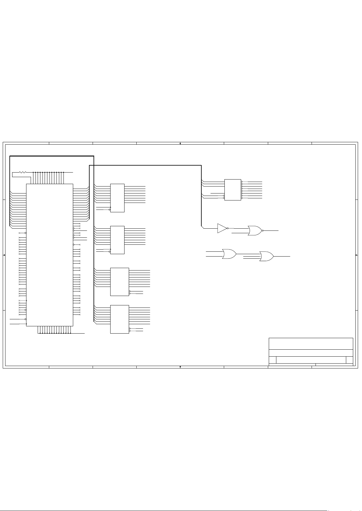
8
8
7
7
6
6
5
5
4
4
3
3
2
2
1
1
D D
C C
B B
A A
THE LOGIC LABELED U2 MAY BE IMPLEMENTED IN
A CPLD. THE LOWER 8 ADDRESS BITS, A0-A8, MAY BE
AND 256 USER OUTPUTS.
DECODED TO PROVIDE 256 16 BIT USER INPUTS
USER INPUTS
USER OUTPUTS
D
USER I/O (GEN2DK1)
PERFORMANCE MOTION DEVICES
55 OLD BEDFORD RD
LINCOLN, MA 01773
B
10Monday, April 22, 2002
Title
Size Document Number Rev
Date: Sheet
of
A0 UIO0
A1 UIO1
D0 UO0-0 A2 UIO2
A0 D1 UO0-1 UIO3
A1 D2 UO0-2 UIO4
D0 A2 D3 UO0-3 UIO UIO5
D1 A3 D4 UO0-4 A3 UIO6
D2 A4 D5 UO0-5 A4 UIO7
D3 A5 D6 UO0-6
D4 A6 D7 UO0-7
D5 A7
D6 A8 WED7 A9 UIO0
D8 A10
D9 A11
D10 A12
D11 A13
D12 A14
D13
D14
D15 D8 UO0-8 A12 A12n
D9 UO0-9 UIO
D10 UO0-10 IS-
D11 UO0-11
WE- D12 UO0-12
W/R D13 UO0-13
D14 UO0-14
D15 UO0-15
WE-
UIO0 A12n
UIOn
IS- W/R UI0n
UIO0
D0 UI0-0
D1 UI0-1
D2 UI0-2
D3 UI0-3
D4 UI0-4
D5 UI0-5
D6 UI0-6
D7 UI0-7
D8 UI0-8
D9 UI0-9
D10 UI0-10
D11 UI0-11
D12 UI0-12
RS- D13 UI0-13
D14 UI0-14
CLK D15 UI0-15
UI0n
UI0n
D[0..15]
A[0..14]
GND
VCC
IS-
UI0n
UI0n
U2
OR2
1
2
3
U2
OR3
1
2
3
4
R?
22K
U2
244
2
4
6
8
11
13
15
17
1
19
18
16
14
12
9
7
5
3
1A1
1A2
1A3
1A4
2A1
2A2
2A3
2A4
1G
2G
1Y1
1Y2
1Y3
1Y4
2Y1
2Y2
2Y3
2Y4
U2
138
1
2
3
6
4
5
15
14
13
12
11
10
9
7
A
B
C
G1
G2A
G2B
Y0
Y1
Y2
Y3
Y4
Y5
Y6
Y7
U2
NOT
12
U2
NOR2
1
2
3
U2
74LS377
3
4
7
8
13
14
17
18
11
1
2
5
6
9
12
15
16
19
D1
D2
D3
D4
D5
D6
D7
D8
CLK
G
Q1
Q2
Q3
Q4
Q5
Q6
Q7
Q8
U2
74LS377
3
4
7
8
13
14
17
18
11
1
2
5
6
9
12
15
16
19
D1
D2
D3
D4
D5
D6
D7
D8
CLK
G
Q1
Q2
Q3
Q4
Q5
Q6
Q7
Q8
U2
244
2
4
6
8
11
13
15
17
1
19
18
16
14
12
9
7
5
3
1A1
1A2
1A3
1A4
2A1
2A2
2A3
2A4
1G
2G
1Y1
1Y2
1Y3
1Y4
2Y1
2Y2
2Y3
2Y4
U?
CP2N40
13
60
14
20
9
10
11
12
15
16
17
18
19
22
23
24
47
110
111
112
114
115
116
117
118
119
122
123
124
125
126
127
128
129
130
4
6
1
25
26
27
28
294659617192104
113
120
21
406293
103
121
58
7
2
41
53
36
50
56
35
132
63
65
54
49
64
66
55
51
73
90
91
101
102
105
107
108
109
68
69
70
94
95
96
97
72
100
106
67
98
43
44
45
99
74
89
75
88
76
83
77
82
84
85
86
87
3
8
30
31
34
33
32
38
39
78
79
80
81
37
131
52
VCC
VCC
GND
GND
DATA0
DATA1
DATA2
DATA3
DATA4
DATA5
DATA6
DATA7
DATA8
DATA9
DATA10
DATA11
VCC
ADDR0
ADDR1
ADDR2
ADDR3
ADDR4
ADDR5
ADDR6
ADDR7
ADDR8
ADDR9
ADDR10
ADDR11
ADDR12
ADDR13
ADDR14
ADDR15
~RAMSLCT
~PERIPHSLCT
R/~W
~STROBE
~WRITEENBL
DATA12
DATA13
DATA14
DATA15
GND
GND
GND
GND
GND
GND
GND
GND
GND
VCC
VCC
VCC
VCC
VCC
VCC
I/OCK
VCC
VCC
~RESET
I/OINTRP
VCC
VCC
GND
~RS
W/~R
POSLIM1
POSLIM2
POSLIM3
POSLIM4
NEGLIM1
NEGLIM2
NEGLIM3
NEGLIM4
HALL1A
HALL1B
HALL1C
HALL2A
HALL2B
HALL2C
HALL3A
HALL3B
HALL3C
HALL4A
HALL4B
HALL4C
AXISOUT1
AXISOUT2
AXISOUT3
AXISOUT4
AXISIN1
AXISIN2
AXISIN3
AXISIN4
~HOSTINTRPT
SRLRCV
SRLXMT
SYNCH
SRLENABLE
ANALOG1
ANALOG2
ANALOG3
ANALOG4
ANALOG5
ANALOG6
ANALOG7
ANALOG8
ANALOGVCC
ANALOGREFHIGH
ANALOGREFLOW
ANALOGGND
GND
GND
N/C
N/C
N/C
N/C
N/C
N/C
N/C
N/C
N/C
N/C
N/C
GND
N/C
VCC
 Loading...