

Page 1
Advanced Step Motor
j
Control Chipset
Features
Advanced control of up to 4 step motors
per chipset
High speed pulse and direction output
S-curve, trapezoidal, velocity contouring,
and electronic gearing trajectory modes
Optional incremental encoder feedback
Software & feature compatible with other
versions of PMD's chipset family
Available in 1, 2, or 4 axis configurations
32-bit position, velocity, acceleration and
erk trajectory profile registers
Pulse and direction output for each axis at
up to 1.5 Mpulses/sec
On-the -fly stall detection
Two travel-limit switches per axis
External motion breakpoint per axis
Intelligent easy-to-use packet-oriented
command protocol
Programmable pulse output modes
Chipset Developer's kit available
MC1451A, MC1451A-E
MC1251A, MC1251A-E
MC1151A, MC1151A-E
General Description
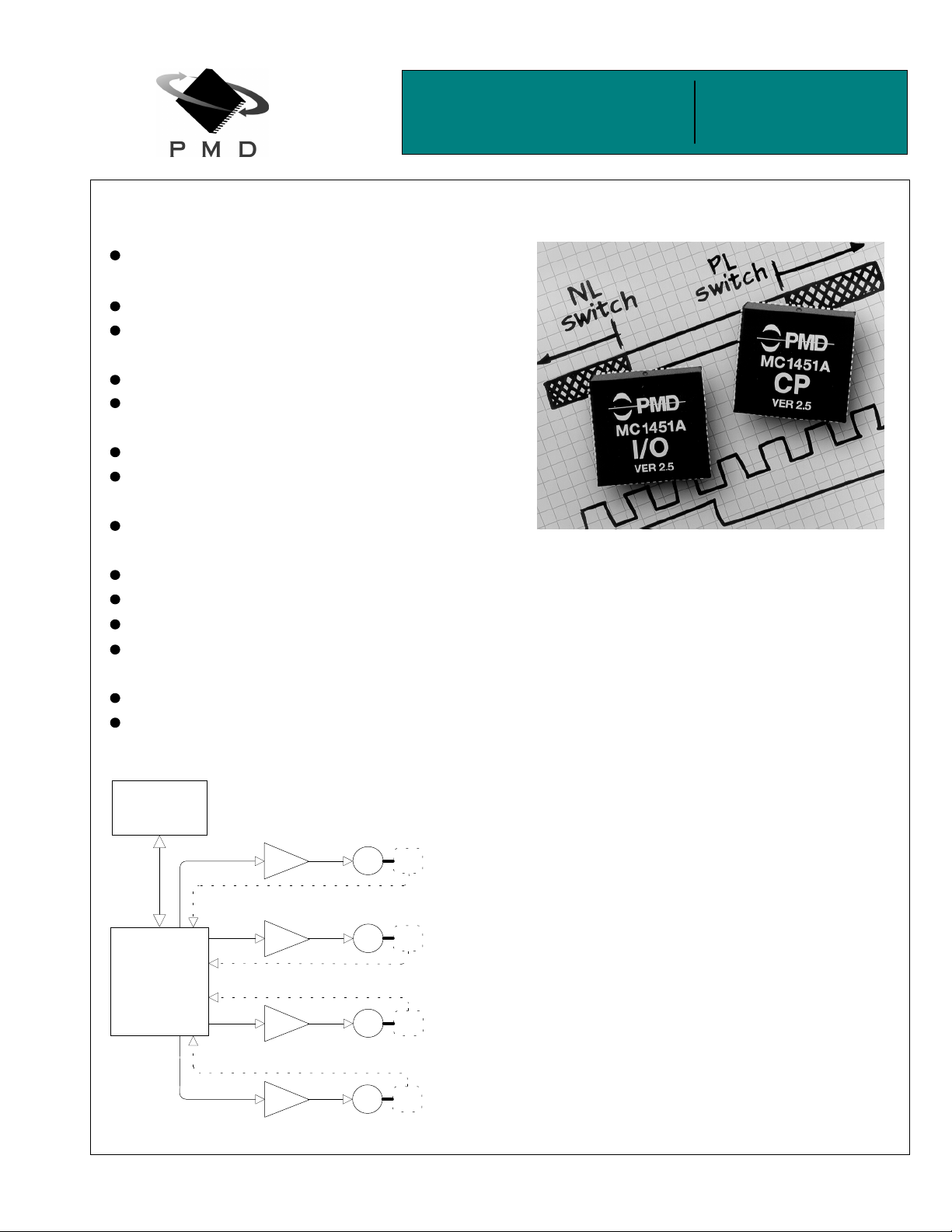
The MC1451A is a dedicated motion processor which functions
as a complete chip-based step motor controller . Packaged in a
2-IC chipset, this device performs trajectory generation and
pulse and direction signal generation for use in a wide variety of
stepper-based systems. The MC1451A provides an optional
third IC which allows incremental encoder signal input for
position verificat i on and on-the-fly stall detection. The MC1451A
is available in a one, a two, and a four-axis configuration.
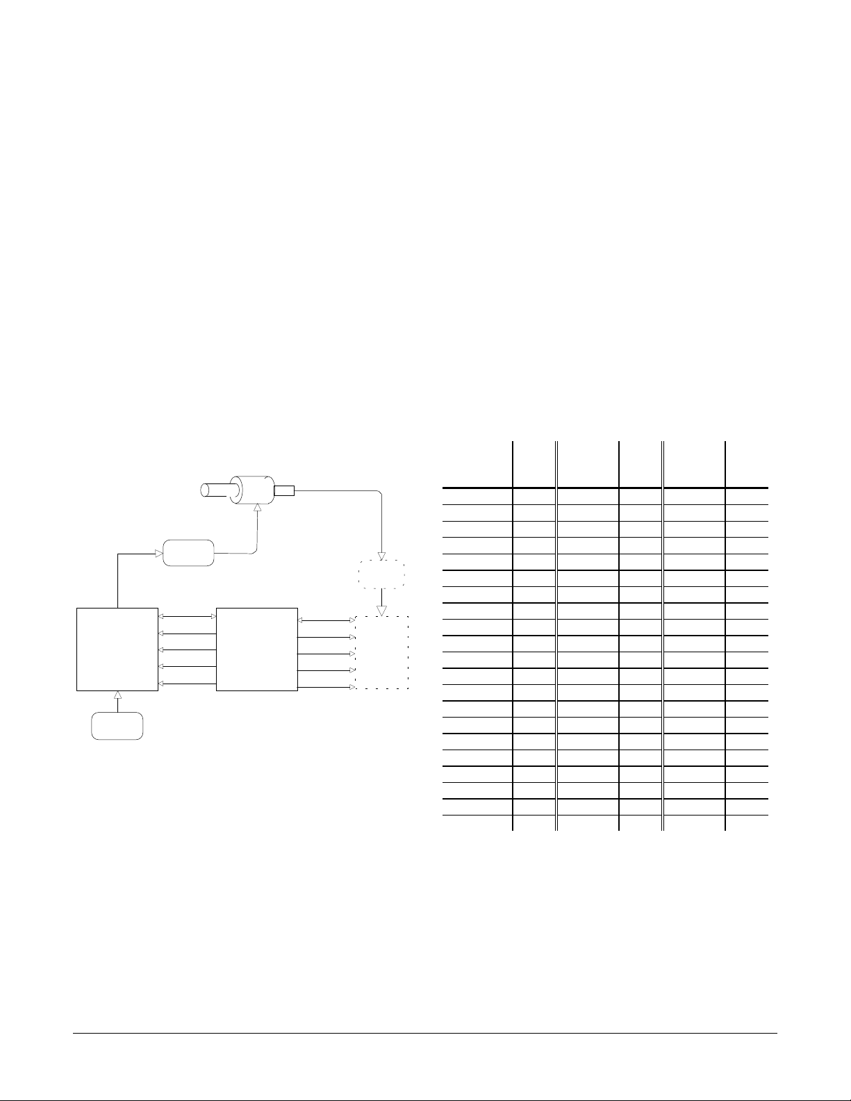
Typical Configuration
Host
Processor
Amp
Amp
MC1451A
(I/O & CP
& ENC)
Amp
Amp
Performance Motion Dev ices, In c. 12 Waltham St. Le xington, M A 02421 te l: 781. 674.98 60 fax: 781.674.9 861
E
M
E
M
(MC1451A, MC1251A
E
M
E
M
Axis 1
Axis 2
only)
Axis 3
(MC1451A only)
Axis 4
(MC1451A only)
The MC1451A is functionally similar to other PMD motion
processors however it is dedicated to the control of step motors,
instead of servo motors. All of these devices provide
sophisticated trajectory generation and synch ronization features
allowing the creation of complex motion sequences.
In addition to pulse and direction circuitry which can output at
up to 1.5 mega pulses per second the chipset provides two limit
switches per axis, a programmabl e external signal b reakpoint
per axis, and an 'At Rest' output signal.
The chipset is controlled by a host processor which interfaces
with the chipset via an 8-bit bi-directional port. Communications
to/from the chi pset consist of packet-oriented messages. A host
interrupt line is provided so tha t t he chipset can signal the host
when special conditions occur such as stall detection.
The chipset is packaged in 2 68-pin PLCC packages. An
optional third 44 pin PLCC chip provides encoder input. All
chips are CMOS and are powered by 5 volts.
Doc. Rev. 12.02, Nov. 1997
www.pmdcorp.com
Page 2

Table of Contents
Product Family Overview.......................................Page 3
Introduction........................................................... Page 3
Family Summary................................................... Page 3
Electrical Characteristics....................................... Page 4
Absolute Maximum Ratings..................................Page 5
Operating Ratings................................................. Page 5
DC Electrical Characteristics................................ Page 5
AC Electrical Characteristics................................Page 5
I/O Timing Diagrams............................................. Page 7
Pinouts....................................................................Page 11
MC1451A.............................................................. Page 11
MC1251A, MC1151A............................................ Page 12
Pin Descriptions.................................................... Page 13
Theory of Operations............................................. Page 17
Trajectory Profile Generation................................ Page 18
S-curve Point to Point....................................... Page 19
Trapezoidal Point to Point.................................Page 20
Velocity Contouring...........................................Page 20
Electronic Gear.................................................Page 21
Trajectory Control................................................. Page 21
Halting The Trajectory......................................Page 21
Motion Complete Status...................................Page 22
Parameter Loading & Updating............................Page 22
Manual Update.................................................Page 22
Breakpoints....................................................... Page 23
External Breakpoints and Homing.................... Page 23
Disabling Automatic Profile Update..................Page 24
Travel Limit Switches............................................ Page 24
Axis Timing........................................................... Page 24
Host Communications .......................................... Page 25
Electrical Interface............................................ Page 25
Packet Format ...................................................Page 25
Packet Checksum.............................................Page 26
Illegal Commands .............................................Page 26
Command Errors...............................................Page 26
Axis Addressing.................................................Page 26
Axis Status............................................................Page 27
Status Word ......................................................Page 27
Miscellaneous Mode Status Word.....................Page 27
Host Interrupts.......................................................Page 28
Pulse & Direction Signal Generation.....................Page 29
Pulse Generation Control...........................................Page 29
At Rest Indicator.........................................................Page 29
Encoder Position Feedback..................................Page 29
Stall Detection............................................................Page 30
Position Error.............................................................Page 30
Recovering From A Motion Error ...............................Page 30
Host Commands .....................................................Page 32
Command Summary.............................................Page 32
Command Reference............................................Page 34
Axis Control.......................................................Page 34
Profile Generation.............................................Page 35
Parameter Update.............................................Page 39
Interrupt Processing..........................................Page 41
Status/Mode......................................................Page 42
Pulse Generation ..............................................Page 43
Encoder.............................................................Page 44
Miscellaneous ...................................................Page 45
Application Notes ...................................................Page 48
ISA bus interfacing................................................Page 48
Performance Motion Devices, Inc. does not assume any responsibility for use of any circuitry described in this manual, nor does it make
any guarantee as to the accuracy of this manual. Performance Motion Devices, Inc. reserves the right to change the circuitry described in
this manual, or the manual itself, at any time.
The components described in this manual are not authorized for use in life-support systems without the express written permission of
Performance Motion Devices, Inc.
2
Page 3

Product Family Overview
MC1401 series MC1231 series MC1241 series MC1451 series
# of axes 4, 2, or 1 2 or 1 2 or 1 4, 2, or 1
Motors Supported DC Servo Brushless Servo Stepper Stepper
Encoder Format Incremental (no dash version)
and Parallel ('-P' version)
Output Format DC servo Sinusoidally
S-curve profiling Yes Yes Yes Yes
Electronic gearing Yes Yes Yes Yes
On-the-fly changes Yes Yes Yes Yes
Limit switches Yes Yes Yes Yes
PID & feedforward Yes Yes - -
PWM output Yes Yes Yes -
DAC-compatible output Yes Yes Yes -
Pulse & direction output ---Yes
Index & Home signal Yes Yes Yes Yes
Chipset p/n's MC1401A, MC1401A-P (4 axes)
MC1201A, MC1201A-P (2 axes)
MC1101A, MC1101A-P (1 axis)
Developer's Kit p/n's: DK1401A, DK1401A-P DK1231A DK1241A DK1451A
* optional using third I.C. ('-E' version)
Incremental Incremental Incremental*
Microstepping Pulse and Direction
commutated
MC1231A (2 axes)
MC1131A (1 axis)
MC1241A (2 axes)
MC1141A (1 axis)
MC1451A, MC1451A-E (4 axes)
MC1251A, MC1251A-E (2 axes)
MC1151A, MC1151A-E (1 axis)
Introduction
This manual describes the operational characteristics of the MC1451A,
MC1251A, MC1151A, MC1451A-E, MC1251A-E, and MC1151A-E
Motion Processors. These devices are members of PMD's 1st
generation motion processor family, which consists of 16 separate
products organized into four groups.
Each of these devices are complete chip-based motion controllers.
They provide trajectory generation and related motion control functions.
Depending on the type of motor controlled they provide servo loop
closure, on-board commutation for brushless motors, and high speed
pulse and direction outputs. Together these products provide a
software-compatible family of dedicated motion processor chips which
can handle a large variety of system configurations.
Each of these chips utilize a similar architecture, consisting of a highspeed DSP (Digital Signal Processor) computation unit , along with an
ASIC (Application Specific Integrated Circuit). The computation unit
contains special on-board hardware such as a multiply instruction that
makes it well suited for the task of motion control.
Along with a similar hardware architecture these chips also share most
software commands, so that software written for one chipset may be reused with another, even though the type of motor may be different.
This manual describes the operation of the MC1451A, MC1251A,
MC1151A, MC1451A-E, MC1251A-E, and MC1151A-E chipsets. For
technical details on other members of PMD's first generation
motion processors see the corresponding product manual.
Family Summary
MC1401 series (MC1401A, MC1201A, MC1101A, MC1401A-P,
MC1201A-P, MC1101A-P)
encoder signals (standard version) or parallel word encoder signals
(-P version) and output a motor command in either PWM or DACcompatible format. These chipsets come in 1, 2 or 4 axis versions
and can be used with DC brushed motors, or brushless motors using
external commutation.
MC1231 series (MC1231A, MC1131A) -
incremental quadrature encoder signals and output sinusoidally
commutated motor signals appropriate for driving brushless motors.
They are available in one or two axis versions. Depending on the
motor type they output two or three phased signals per axis in either
PWM or DAC-compatible format.
MC1241 series (MC1241A, MC1141A)
internal microstepping generation for stepping motors. They are
available in a one or a two-axis version. Two phased signals are
output per axis in either PWM or DAC-compatible format. An
incremental encoder signal can be input to confirm motor position.
MC1451 series (MC1451A, MC1251A, MC1151A, MC1451A-E,
MC1251A-E, MC1151A-E) -
pulse and direction signal output appropriate for driving step motorbased systems. They are available in a one, two, or four-axis version
and are also available with quadrature encoder input.
Each of these chipsets has an associated Chipset Developer's
Kit available for it. For more information contact your PMD
representative.
- These chipsets take in incremental
These chipsets take in
- These chipsets provide
These chipsets provide very high speed
3
Page 4
Electrical Characteristics
Overview
The MC1451A-consists of either two 68 pin PLCC's (standard version),
or these same two I.C.s with an additional 44 pin PLCC for incremental
encoder feedback (-E version). All of these devices are fabricated in
CMOS. The two 68 pin PLCCs are known as the I/O and the CP chips.
The 44-pin PLCC is known as the ENC chip.
The Peripheral Input/Output IC (I/O chip) is responsible for interfacing
to the host processor and for generating the high speed pulse and
direction output. The Command Processor IC (CP chip) is responsible
for all host command, trajectory, and related computations. The ENC
chip is responsible for incremental encoder feedback.
The following figure shows a typical system block diagram, along with
the pin connections between the I/O chip, CP chip, and ENC chip if it is
used.
Motor
(4 axis)
Amplifier
(1-4 axis)
I/O
Host
Processor
Data4-11
I/OAddr0-3
I/OWrite
I/OCntrl0-3
ClkOut
CP
Data4-11
I/OAddr0-3
I/OWrite
I/OCntrl0-3
ClkOut
Use of the ENC chip does not require a special version of the I/O or CP
chips. The CP chip automatically recognizes the presence or absence
of the ENC chip and functions accordingly.
The CP, I/O, and ENC chip (if used) form a complete chipset and
function together as one integrated motion processor. The major
components connected to the chipset are the step & direction
compatible amplifier (4, 2, or 1 axes), the optional encoder feedback
channels (4, 2, or 1 axes), and the host processor.
The chipset's pulse and direction output signals are connected to the
motor amplifier. Using this scheme the direction bit indicates whether
the motor should move in the positive or negative direction, and the
pulse signal indicates the desired motor speed. Pulse and direction
output is compatible with a wide variety of full, half, and microstepping
amplifiers.
Encoder
(1-4 axis)
ENC
Using the -E chipset parts it is possible to input quadrature encoder
feedback to the chipset. The encoder signals consist of the A and B
quadrature signals from the encoder.
The host processor is interfaced via an 8-bit bi-directional bus and
various control signals. Host communication is coordinated by a
ready/busy signal, which indicates when communication is allowed.
Interconnections between the I/O and the CP chip consist of a data bus
(8 bits) and various control and synchronization signals.
Interconnections between the CP and the ENC chip (if used) also
consist of a data bus (10 bits) and various control and synchronization
signals. Many of these signals are common between the I/O, CP, and
the ENC chips although there are no direct connections between just
the ENC and the I/O chip. The following table summarizes the signals
that must be interconnected for the chipset to function properly. For
each listed signal the I/O chip pin on the left side of the table is
connected to the CP chip pin in the middle which is connected to the
ENC chip pin on the right side.
I/O Chip
Signal
Name
I/O
Chip
Pin
CP Chip
Signal
Name
CP
Chip
Pin
ENC Chip
Signal
Name
ENC
Chip
Pin
- - Data2 58 CPData2 22
- - Data3 57 CPData3 19
CPData4 18 Data4 50 CPData4 9
CPData5 5 Data5 49 CPData5 31
CPData6 6 Data6 46 CPData6 41
CPData7 7 Data7 43 CPData7 42
CPData8 8 Data8 40 CPData8 44
CPData9 17 Data8 39 CPData9 1
CPData10 3 Data10 36 CPData10 12
CPData11 1 Data11 35 CPData11 2
CPAddr0 68 I/OAddr0 28 CPAddr0 24
CPAddr1 27 I/OAddr1 9 - CPAddr2 29 I/OAddr2 6 CPAddr2 20
CPAddr3 12 I/OAddr3 5 CPAddr3 23
CPCntr0 20 I/OCntr0 16 CPCntr0 15
CPCntr1 36 I/OCntr1 18 - CPCntr2 22 I/OCntr2 68 - CPCntr3 63 I/OCntr3 67 - CPWrite 2 I/OWrite 15 CPWrite 13
CPClk 46 ClkOut 19 CPClk 7
CPReset 43 Reset 17 - -
For a complete description of all pins see the 'Pin Descriptions'
section of this manual.
Unless specifically noted otherwise, the term 'MC1451' or
'MC1451A' refers to the MC1451A, MC1251A, MC1151A, MC1451AE, MC1251A-E, and MC1151A-E Motion Processors.
4
Page 5

Absolute Maximum Ratings
Operating Ratings
Unless otherwise stated, all electrical specifications are for both
the I/O and CP chips.
Storage Temperature, Ts....................-55 deg. C to +150 deg. C
Supply Voltage, Vcc............................ -0.3 V to +7.0 V
Power Dissipation, Pd......................... 650 mW (I/O and CP
combined)
Operating Temperature, Ta .................0 deg. C to +70 deg. C*
Nominal Clock Frequency, Fclk...........25.0 Mhz
Supply Voltage, Vcc.............................4.75 V to 5.25 V
* Industrial and Military operating ranges also available. Contact your
PMD representative for more information.
DC Electrical Characteristics
(Vcc and Ta per operating ratings, Fclk = 25.0 Mhz)
Symbol Parameter Min. Max. Units Conditions
Vcc Supply Voltage 4.75 5.25 V
Idd Supply Current 100 mA open outputs
Input Voltages
Vih Logic 1 input voltage 2.0 Vcc + 0.3 V
Vil Logic 0 input voltage -0.3 0.8 V
Vihclk Logic 1 voltage for clock pin
(ClkIn)
Vihreset Logic 1 voltage for reset pin
(reset)
Output Voltages
Voh Logic 1 Output Voltage 2.4 V @CP Io = 300 uA
Vol Logic 0 Output Voltage 0.33 V @CP Io = 2 mA
Iout Tri-State output leakage current -20 20 uA 0 < Vout < Vcc
Iin Input current -50 50 uA 0 < Vi < Vcc
Iinclk Input current ClkIn -20 20 uA 0 < Vi < Vcc
3.0 Vcc+0.3 V
4.0 Vcc+0.3 V
@I/O Io = 4 mA
@I/O Io = 4 mA
AC Electrical Characteristics
(see reference timing diagrams)
(Vcc and Ta per operating ratings; Fclk = 25.0 Mhz)
(~ character indicates active low signal)
Timing Interval T# Min. Max. Units
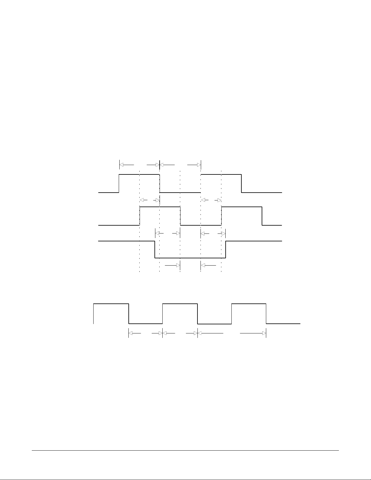
Encoder and Index Pulse Timing
Motor-Phase Pulse Width T1 1.6 uS
Dwell Time Per State T2 0.8 uS
Index Pulse Setup and Hold
(relative to Quad A and Quad B low)
Reset Timing
Stable Power to Reset 0.25 Sec
Reset Low Pulse Width 1.0 uS
Clock Timing
Clock Frequency (Fclk) 6.7 25.6 Mhz
Clock Pulse Width T4 19.5 75 (note 2) nS
Clock Period T5 39 149 (note 2) nS
T3 0 uS
5
Page 6

Timing Interval T# Min. Max. Units
Command Byte Write Timing
~HostSlct Hold Time T6 15 2000 (note 3) nS
~HostSlct Setup Time T7 10 nS
HostCmd Setup Time T8 10 nS
Host Cmd Hold Time T9 25 nS
HostRdy Delay Time T13 70 nS
~HostWrite Pulse Width T14 50 nS
Write Data Setup Time T15 35 nS
Write Data Hold Time T16 30 nS
Data Word Read Timing
~HostSlct Hold Time T6 15 2000 (note 3) nS
~HostSlct Setup Time T7 (read only) - 20 nS
HostCmd Setup Time T8 (read only) - 20 nS
HostCmd Hold Time T9 25 nS
Read Data Access Time T10 50 nS
Read Data Hold Time T11 10 nS
~HostRead high to HI-Z Time T12 50 nS
HostRdy Delay Time T13 70 nS
Read Recovery Time T17 60 nS
Data Word Write Timing
~HostSlct Hold Time T6 15 2000 (note 3) nS
~HostSlct Setup Time T7 10 nS
HostCmd Setup Time T8 10 nS
HostCmd Hold Time T9 25 nS
HostRdy Delay Time T13 70 nS
~HostWrite Pulse Width T14 50 nS
Write Data Setup Time T15 35 nS
Write Data Hold Time T16 30 nS
Write Recovery Time T18 60 nS
note 1 ~HostSlct and HostCmd may optionally be de-asserted if setup and hold times are met.
note 2 Chip-set performance figures and timing information valid at Fclk = 25.0 only. For timing information & performance parameters at Fclk <
25.0 Mhz, call PMD.
note 3 Two micro seconds maximum to release interface before chip set responds to command
note 4 ClkOut from CP is 1/4 frequency of ClkIn (CP chip).
6
Page 7
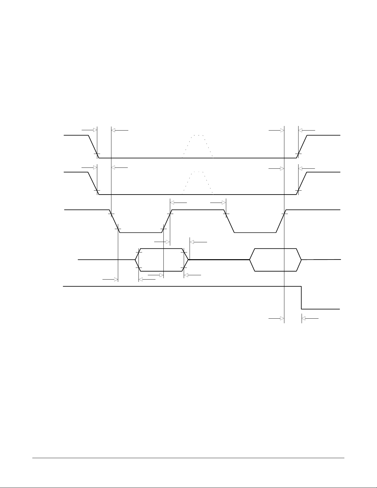
I/O Timing Diagrams
The following diagrams show the MC1451A electrical interface timing. T#' values are listed in the above timing chart.
Quadrature Encoder Input Timing
Quad A
Quad B
~Index
ClkIn
T1
T1
T2 T2
T3
Clock Timing
T3
T4 T4 T5
Index = ~A * ~B * ~IN D
7
Page 8
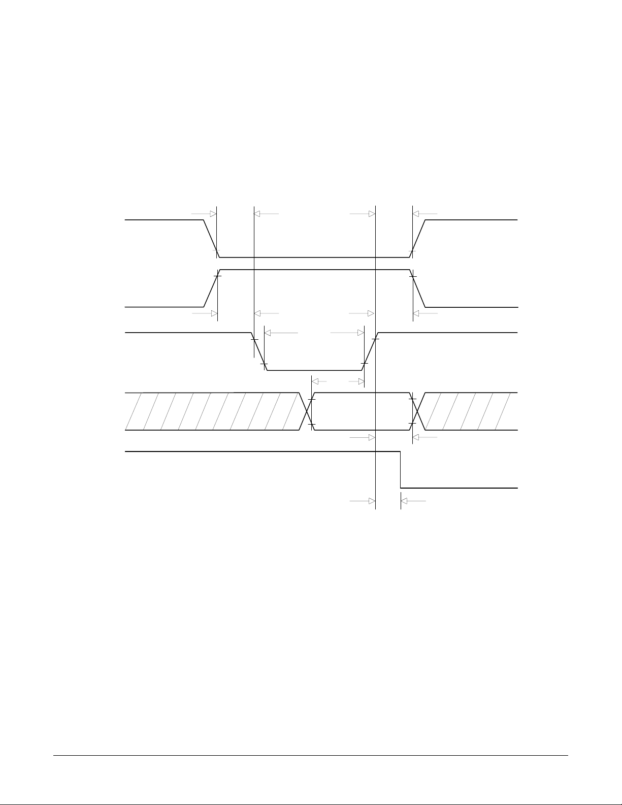
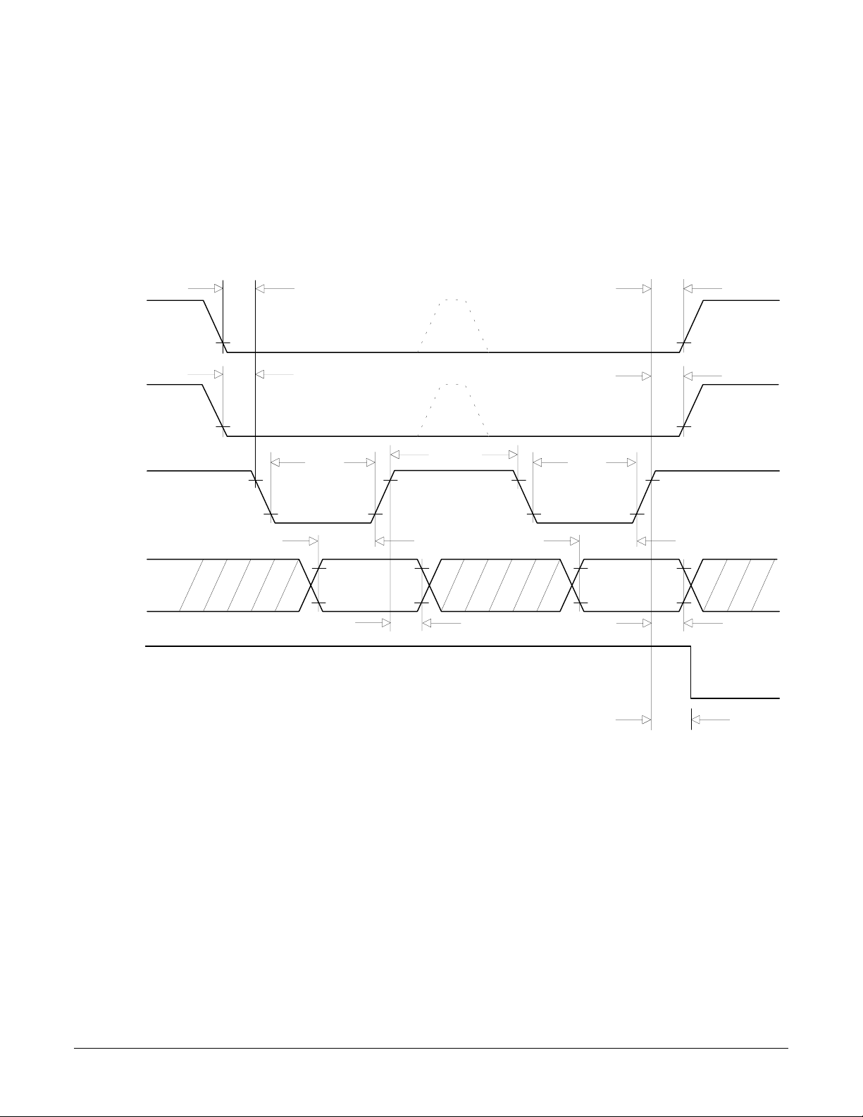
Command Byte Write TIming
~HostSlct
HostCmd
~HostWrite
HostData0-7
HostRdy
T7
T8
T6
T9
T14
T15
T16
T13
8
Page 9
Data Word Read TImi ng
~HostSlct
HostCmd
~HostRead
HostData0-7
HostRdy
T7
T6
Note 1
T8
Note 1
T9
T17
T12
High-Z High-Z High-Z
High
Byte
T10
T11
Low
Byte
T13
9
Page 10
Data Word Write TIming
~HostSlct
HostCmd
~HostWrite
HostData0-7
HostRdy
T7
T8
T14
T15
High
Byte
T16
T18
Note 1
Note 1
T6
T9
T14
T15
Low
Byte
T16
10
T13
Page 11
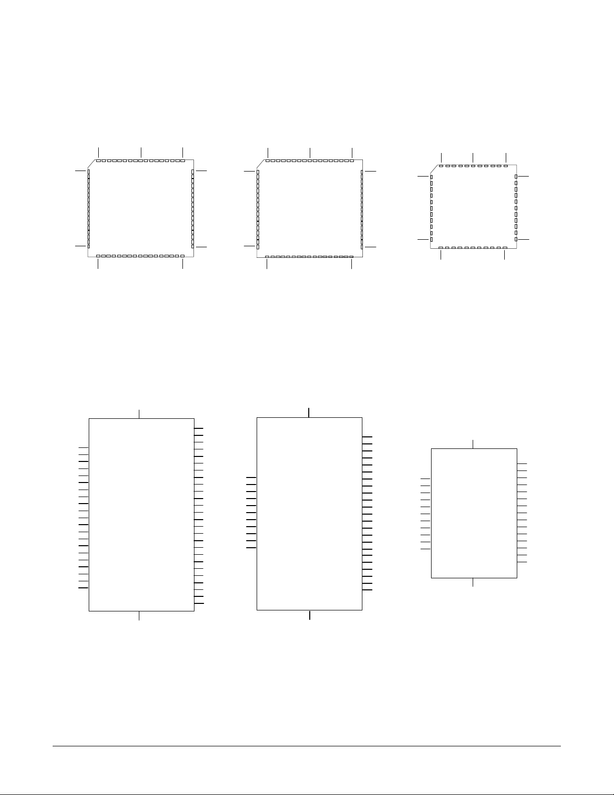
Pinouts
9
10
(Top view)
26
27 43
4, 21, 25, 38, 55
28
Pulse1
42
Dir1
13
Home1
26
Pulse2
30
Dir2
23
Home2
40
Pulse3
35
Dir3
11
Home3
39
Pulse4
34
Dir4
10
Home4
46
CPClk
52
I/OClkIn
45
I/OClkOut
29
CPAddr2
12
CPAddr3
2
CPWrite
20
CPCntrl0
36
CPCntrl1
43
CPReset
1
I/O
VCC
I/O
GND
61
CPCntrl2
CPCntrl3
HostCmd
HostRdy
HostRead
HostWrite
HostSlct
HostIntrpt
HostData0
HostData1
HostData2
HostData3
HostData4
HostData5
HostData6
HostData7
CPData4
CPData5
CPData6
CPData7
CPData8
CPData9
CPData10
CPData11
CPAddr0
CPAddr1
9
60
10
1
CP
(Top view)
44
26
27 43
(Chip Outlines Not Drawn To Scale)
MC1451A & MC1451A-E Pinouts
4, 22, 33
22
63
41
37
51
47
48
44
56
50
61
53
65
67
62
64
60
18
5
6
7
8
17
3
1
68
27
AtRest1
55
AtRest2
54
AtRest3
53
AtRest4
24
ClkIn
19
ClkOut
17
Reset
16
I/OCntrl0
18
I/OCntrl1
68
I/OCntrl2
67
I/OCntrl3
VCC
CP
GND
61
Data2
Data3
Data4
Data5
Data6
Data7
Data8
Data9
Data10
Data11
I/OAddr0
I/OAddr1
I/OAddr2
I/OAddr3
I/OWrite
PosLimit1
PosLimit2
PosLimit3
PosLimit4
NegLimit1
NegLimit2
NegLimit3
NegLimit4
6
60
7
1
40
39
ENC
(Top view)
17
44
18 28
58
57
50
49
46
43
40
39
36
35
28
9
6
5
15
52
45
42
38
51
44
41
37
30
36
17
18
27
28
5
29
7
33
6
3, 14, 16, 25, 35
QuadA1
QuadB1
QuadA2
QuadB2
QuadA3
QuadB3
QuadA4
QuadB4
CPClk
I/OClkIn
I/OClkOut
10, 21, 32, 34, 43
VCC
ENC
GND
CPAddr0
CPAddr2
CPAddr3
CPWrite
CPCntrl0
CPData2
CPData3
CPData4
CPData5
CPData6
CPData7
CPData8
CPData9
CPData10
CPData11
29
24
20
23
13
15
22
19
9
31
41
42
44
1
12
2
14, 15, 32, 49, 54, 66
3, 34
11
Page 12
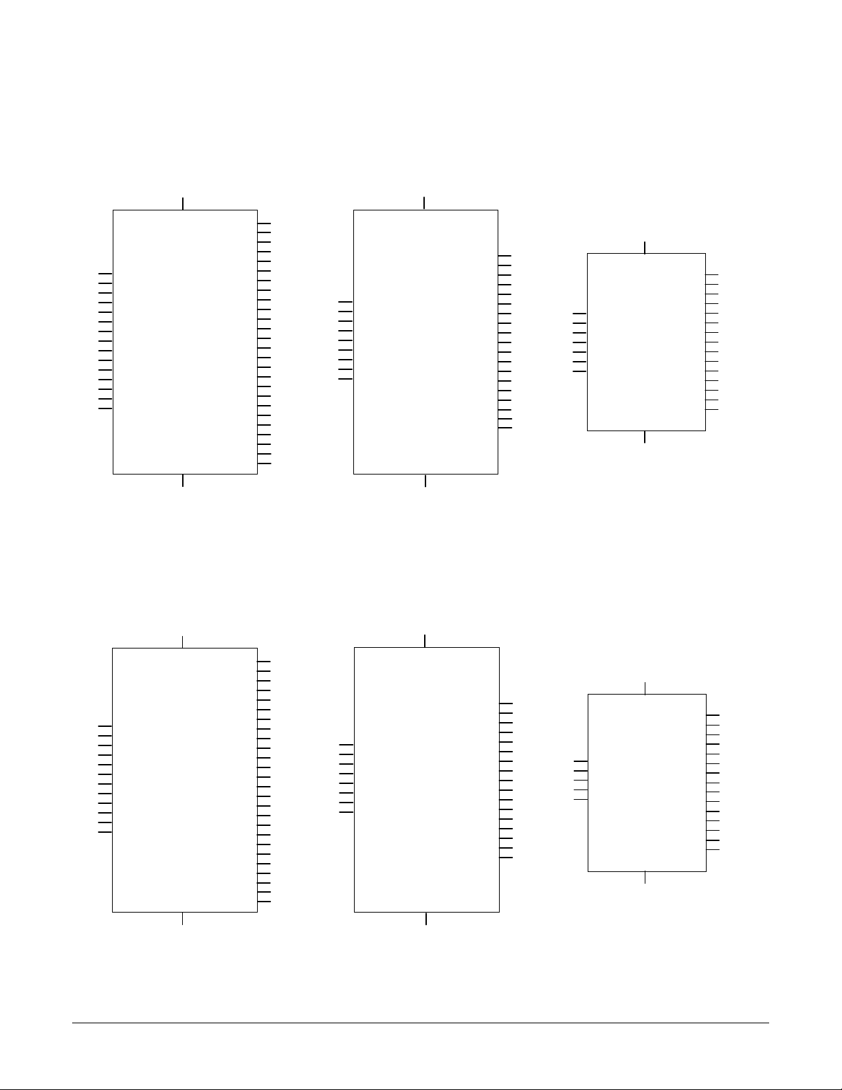
MC1251A & MC1251A-E Pinouts
4, 21, 25, 38, 55
VCC
28
Pulse1
42
Dir1
13
Home1
26
Pulse2
30
Dir2
23
Home2
46
CPClk
52
I/OClkIn
45
I/OClkOut
29
CPAddr2
12
CPAddr3
2
CPWri t e
20
CPCntrl0
36
CPCntrl1
43
CPReset
I/O
GND
14, 15, 32, 49, 54, 66
CPCntrl2
CPCntrl3
HostCmd
HostRdy
HostRead
HostWrite
HostSlct
HostIntrpt
HostData0
HostData1
HostData2
HostData3
HostData4
HostData5
HostData6
HostData7
CPData4
CPData5
CPData6
CPData7
CPData8
CPData9
CPData10
CPData11
CPAddr0
CPAddr1
22
63
41
37
51
47
48
44
50
61
53
65
67
62
64
60
18
5
6
7
8
17
3
1
68
27
AtRest1
56
AtRest2
55
ClkIn
24
ClkOut
19
Reset
17
I/OCntrl0
16
I/OCntrl1
18
I/OCntrl2
68
I/OCntrl3
67
4, 22, 33
VCC
CP
GND
3, 34
Data2
Data3
Data4
Data5
Data6
Data7
Data8
Data9
Data10
Data11
I/OAddr0
I/OAddr1
I/OAddr2
I/OAddr3
I/OWrite
PosLimit1
PosLimit2
NegLimit1
NegLimit2
3, 14, 16, 25, 35
58
57
50
49
46
43
40
39
36
35
28
9
6
5
15
52
45
51
44
QuadA1
30
QuadB1
36
QuadA2
17
QuadB2
18
CPClk
7
I/OClkIn
33
I/OClkOut
6
VCC
ENC
CPData10
CPData11
GND
10, 21, 32, 34, 43
CPAddr0
CPAddr2
CPAddr3
CPWrite
CPCntrl0
CPData2
CPData3
CPData4
CPData5
CPData6
CPData7
CPData8
CPData9
24
20
23
13
15
22
19
9
31
41
42
44
1
12
2
MC1151A & MC1151A-E Pinouts
4, 21, 25, 38 , 55
VCC
28
Pulse1
42
Dir1
13
Home1
46
CPClk
52
I/OClkIn
45
I/OClkOut
29
CPAddr2
12
CPAddr3
2
CPWri t e
20
CPCntrl0
36
CPCntrl1
43
CPReset
I/O
GND
14, 15, 32, 49, 54, 66
CPCntrl2
CPCntrl3
HostCmd
HostRdy
HostRead
HostWrite
HostSlct
HostIntrpt
HostData0
HostData1
HostData2
HostData3
HostData4
HostData5
HostData6
HostData7
CPData4
CPData5
CPData6
CPData7
CPData8
CPData9
CPData10
CPData11
CPAddr0
CPAddr1
22
63
41
37
51
47
48
44
50
61
53
65
67
62
64
60
18
5
6
7
8
17
3
1
68
27
56
AtRest1
24
ClkIn
19
ClkOut
17
Reset
16
I/OCntrl0
18
I/OCntrl1
68
I/OCntrl2
67
I/OCntrl3
4, 22, 33
VCC
CP
GND
3, 34
Data2
Data3
Data4
Data5
Data6
Data7
Data8
Data9
Data10
Data11
I/OAddr0
I/OAddr1
I/OAddr2
I/OAddr3
I/OWrite
PosLimit1
NegLimit1
3, 14, 16, 25, 35
58
57
50
49
46
43
40
39
36
35
28
9
6
5
15
52
51
QuadA1
30
QuadB1
36
CPClk
7
I/OClkIn
33
I/OClkOut
6
VCC
ENC
CPData10
CPData11
GND
10, 21, 32, 34, 43
CPAddr0
CPAddr2
CPAddr3
CPWr ite
CPCntrl0
CPData2
CPData3
CPData4
CPData5
CPData6
CPData7
CPData8
CPData9
24
20
23
13
15
22
19
9
31
41
42
44
1
12
2
12
Page 13

Pin Descriptions
The following tables provide pin descriptions for the MC1401 and MC1401-P series chipsets.
IC Pin Name Pin # Description/Functionality
I/O Chip Pinouts
I/O Pulse1
Pulse2
Pulse3
Pulse4
I/O Dir1
Dir2
Dir3
Dir4
I/O ~Home1
~Home2
~Home3
~Home4
I/O CPClk 46 I/O chip clock (input). This signal is connected directly to the ClkOut pin (CP chip) and
I/O I/OClkIn 52 Phase shifted clock (input). This signal is connected to I/OClkOut (I/O chip), and inputs a
I/O I/OClkOut 45 Phase shifted clock (output). This signal is connected to I/OClkIn (I/O chip), and outputs a
I/O CPAddr0
CPAddr1
CPAddr2
CPAddr3
I/O ~CPWrite 2 I/O chip to CP chip communication write (input). This signal is connected to the ~I/OWrite pin
I/O CPCntrl0
CPCntrl1
CPCntrl2
CPCntrl3
I/O HostCmd 41 Host Port Command (input). This signal is asserted high to write a host command to the chip
I/O HostRdy 37 Host Port Ready/Busy (output). This signal is used to synchronize communication between
28
26
40
39
42
30
35
34
13
23
11
10
68
27
29
12
20
36
22
63
Pulse signal for channels 1-4 (output). This signal is always a square wave, regardless of
pulse rate. Nominal 'step' occurs when signal goes from a high state to a low state.
NOTE: For MC1451A all 4 pins are valid. For MC1251A pins for axes 1 & 2 only are valid.
For MC1151A pins for axis 1 only are valid. Invalid axis pins can be left unconnected.
Direction signal for channels 1-4 (output). This signal indicates the direction of motion, and
works in conjunction with the pulse signal. A high level on this signal indicates a positive
direction move, and a low level indicates a negative direction move.
NOTE: For MC1451A all 4 pins are valid. For MC1251A pins for axes 1 & 2 only are valid.
For MC1151A pins for axis 1 only are valid. Invalid axis pins can be left unconnected.
Home signals for axis 1-4 (input). Each of these signals provide a general purpose input to
the external breakpoint mechanism. Using these signals it is possible to stop, start, or alter
the motion trajectory. See theory of operations for details.
An active home signal is recognized by the chipset as a low state.
NOTE: For MC1451A all 4 pins are valid. For MC1251A pins for axes 1 & 2 only are valid.
For MC1151A pin for axis 1 only is valid. Invalid axis pins can be left unconnected.
provides the clock signal for the I/O chip. The frequency of this signal is 1/4 the user-provided
ClkIn (CP chip) frequency.
phase shifted clock signal.
phase shifted clock signal.
I/O chip to CP chip communication address (input). These 4 signals are connected to the
corresponding I/OAddr0-3 pins (CP chip), and together provide addressing signals to
facilitate CP to I/O chip communication.
(CP chip) and provides a write strobe to facilitate CP to I/O chip communication.
I/O chip to CP chip communication control (mixed). These 4 signals are connected to the
corresponding I/OCntrl0-3 pins (CP chip), and provide control signals to facilitate CP to I/O
chip communication.
set. It is asserted low to read or write a host data word to the chipset
the DSP and the host. HostRdy will go low (indicating host port busy) at the end of a host
command write or after the second byte of a data write or read. HostRdy will go high
(indicating host port ready) when the command or data word has been processed and the
chip set is ready for more I/O operations. All host port communications must be made with
HostRdy high (indicating ready).
Typical busy to ready cycle is 82.5 uSec..
13
Page 14

IC Pin Name Pin # Description/Functionality
I/O ~HostRead 51 Host Port Read data (input). Used to indicate that a data word is being read from the chip set
(low asserts read).
I/O ~HostWrite 47 Host Port Write data (input). Used to indicate that a data word or command is being written to
the chip set (low asserts write).
I/O ~HostSlct 48 Host Port Select (input). Used to select the host port for reading or writing operations (low
assertion selects port). ~HostSlct must remain inactive (high) when the host port is not in use.
I/O ~HostIntrpt 44 Host Interrupt (output). A low assertion on this pin indicates that a host interrupt condition
exists that may require special host action.
I/O HostData0
HostData1
HostData2
HostData3
HostData4
HostData5
HostData6
HostData7
I/O CPData4
CPData5
CPData6
CPData7
CPData8
CPData9
CPData10
CPData11
I/O ~CPReset 43 I/O chip set reset (input). When brought low this pin resets the I/O chip to its initial condition.
I/O Vcc 4, 21, 25, 38, 55 I/O chip supply voltage pin. All of these pins must be connected to the supply voltage. Supply
I/O GND 14, 15, 32, 49, 54,66I/O chip ground pin. All of these pins must be connected to the power supply return.
50
61
53
65
67
62
64
60
18
5
6
7
8
17
3
1
Host Port Data 0-7 (bi-directional, tri-stated). These signals form the 8 bit host data port used
during communication to/from the chip set. This port is controlled by ~HostSlct, ~HostWrite,
~HostRead and HostCmd.
I/O chip to CP chip data port (bi-directional). These 8 bits are connected to the corresponding
Data4-11 pins on the CP chip, and facilitate communication to/from the I/O and CP chips..
Reset should occur no less than 250 mSec after stable power has been provided to the chip
set. This signal should be connected to the ~Reset pin of the CP chip, which in turn should
be connected to the master reset signal.
voltage = 4.75 to 5.25 V
IC Pin Name Pin # Description/Functionality
CP Chip Pinouts
CP AtRest1
AtRest2
AtRest3
AtRest4
CP PosLimit1
PosLimit2
PosLimit3
PosLimit4
56
55
54
53
52
45
42
38
At Rest indicator signals for axes 1-4 (output). A high level on this signal indicates the axis is
at rest. A low signal indicates the axis is in motion.
This signal is useful for driving amplifiers with an input bit to control running and holding
torque.
NOTE: For MC1451A all 4 pins are valid. For MC1251A pins for axes 1 & 2 only are valid.
For MC1151A pin for axis 1 only is valid. Invalid axis pins can be left un connected.
Positive limit switch input for axis 1-4. These signals provide directional limit inputs for the
positive-side travel limit of the axis. Upon powerup these signals default to "active high"
interpretation, but the interpretation can be set explicitly using the SET_LMT_SENSE
command. If not used these signals should be tied low for the default interpretation, or tied
high if the interpretation is reversed.
NOTE: For MC1451A all 4 pins are valid. For MC1251A pins for axes 1 & 2 only are valid.
For MC1151A pin for axis 1 only is valid. Invalid axis pins can be left un connected.
14
Page 15

IC Pin Name Pin # Description/Functionality
CP NegLimit1
NegLimit2
NegLimit3
NegLimit4
CP ClkIn 24 Clock In (input). This pin provides the chip set master clock (Fclk = 25.0 Mhz)
CP ClkOut 19 Clock Out (output). This pin provides a clock output which is 1/4 the ClkIn frequency. This pin
CP ~Reset 17 Master chip set reset (input). When brought low, this pin resets the chip set to its initial
CP I/OCntrl0
I/OCntrl1
I/OCntrl2
I/OCntrl3
CP Data2
Data3
Data4
Data5
Data6
Data7
Data8
Data9
Data10
Data11
CP I/OAddr0
I/OAddr1
I/OAddr2
I/OAddr3
CP I/OWrite 15 Write (output). This pin is connected to CPWrite on the I/O and on the ENC chip. It provides a
CP Vcc 4, 22, 33 CP chip supply voltage pin. All of these pins must be connected to the supply voltage. Supply
CP GND 3, 34 CP chip ground pin. All of these pins must be connected to the power supply return.
51
44
41
37
16
18
68
67
58
57
50
49
46
43
40
39
36
35
28
9
6
5
Negative limit switch input for axis 1-4. These signals provide directional limit inputs for the
negative-side travel limit of the axis. Upon powerup these signals default to "active high"
interpretation, but the interpretation can be set explicitly using the SET_LMT_SENSE
command. If not used these signals should be tied low for the default interpretation, or tied
high if the interpretation is reversed.
NOTE: For MC1451A all 4 pins are valid. For MC1251A pins for axes 1 & 2 only are valid.
For MC1151A pin for axis 1 only is valid. Invalid axis pins can be left un connected.
is connected to the CPClk signals of the I/O chip and ENC chip
condition. Reset should occur no less than 250 mSec after stable power has been provided
to the chip set.
The master reset signal should be connected to this pin as well as the ~CPReset pin of the
I/O chip
I/O and ENC chip to CP chip communication control (mixed). These signals provide various
inter-chip control signals for the I/O and ENC chips. For the I/O chip these four signals are
connected to the corresponding CPCntrl0-3 pins. For the ENC chip only I/OCntrl0 is used
which is connected to the CPCntrl0 pin.
CP to I/O and ENC chip Data4-11. (Bi-directional). These pins are connected to the
corresponding CPData4-11 pins on the I/O chip, and on the corresponding CPData2-11 pins
on the ENC chip. These signals are used to communicate between the CP and the I/O and
ENC chips.
Address0-3 (output). These signals provide various inter-chip address control signals for the
I/O and ENC chips. For the I/O chip these four signals are connected to the corresponding
CPAddr0-3 pins. For the ENC chip only I/OAddr0, I/OAddr2, and I/OAddr3 are used and they
are connected to the corresponding pins on the ENC chip.
control signal to the I/O and ENC chip to facilitate communication between these chips and
the CP chip
voltage = 4.75 to 5,.25 V
15
Page 16

IC Pin Name Pin # Description/Functionality
ENC Chip Pinouts
ENC QuadA1
QuadB1
QuadA2
QuadB2
QuadA3
QuadB3
QuadA4
QuadB4
ENC CPClk 7 ENC chip clock (input). This signal is connected directly to the I/OClkOut pin (CP chip) and
ENC ENCClkIn 33 Phase shifted clock (input). This signal is connected to ENCClkOut (ENC chip), and inputs a
ENC ENCClkOut 6 Phase shifted clock (output). This signal is connected to ENCClkIn (ENC chip), and outputs a
ENC CPAddr0
CPAddr2
CPAddr3
ENC ~CPWrite 13 ENC chip to CP chip communication write (input). This signal is connected to the ~I/OWrite
ENC CPCntrl0 15 ENC chip to CP chip communication control (input). This signal is connected to the I/OCntrl0
ENC CPData2
CPData3
CPData4
CPData5
CPData6
CPData7
CPData8
CPData9
CPData10
CPData11
ENC Vcc 3, 14, 16, 25, 35 ENC chip supply voltage pin. All of these pins must be connected to the supply voltage.
ENC GND 10, 21, 32, 34, 43 ENC chip ground pin. All of these pins must be connected to the power supply return.
30
36
17
18
27
28
5
29
24
20
23
22
19
9
31
41
42
44
1
12
2
Quadrature A, B channels for axis 1 - 4 (input). Each of these 4 pairs of quadrature (A, B)
signals provide the position feedback for an incremental encoder. When the encoder is
moving in the positive, or forward direction, the A signal leads the B signal by 90 degs.
NOTE: Many encoders require a pull-up resistor on each of these signals to establish a
proper high signal (check the encoder electrical specifications)
NOTE: For MC1451A-E all 8 pins are valid. For MC1251A-E pins for axes 1 & 2 only are
valid. For MC1151A-E pins for axis 1 only are valid. Invalid axis pins can be left unconnected.
provides the clock signal for the ENC chip. The frequency of this signal is 1/4 the userprovided ClkIn (CP chip) frequency.
phase shifted clock signal.
phase shifted clock signal.
ENC chip to CP chip communication address (input). These 3 signals are connected to the
corresponding CPAddr0, 2, & 3 pins (CP chip), and together provide addressing signals to
facilitate CP to ENC chip communication.
NOTE: There is no CPAddr1 pin on the ENC chip.
pin (CP chip) and provides a write strobe to facilitate CP to ENC chip communication.
pin (CP chip), and provides control signals to facilitate CP to ENC chip communication.
ENC chip to CP chip data port (bi-directional). These 10 bits are connected to the
corresponding Data2-11 pins on the CP chip, and facilitate communication to/from the ENC
and CP chips.
Supply voltage = 4.75 to 5.25 V
16
Page 17

Theory of Operations
Internal Block Diagram
Home
Input
Motor Output Signals
Step Direction
1/a 1/a1/a
CP Chip
Pulse & Direction
Generator (1-4)
Trajectory profile
generator (1-4)
I/O Chip
System Registers (1-4)
Host I/O controller
185
host interr up tDataControl
Host I/O
The above figure shows an internal block diagram for the MC1451A
and MC1451A-E Motion Processors.
The MC1451-series chipsets consist of two chips, an ASIC (Application
Specific I.C.) called the I/O chip and a DSP (Digital Signal Processor)
called the CP chip. The MC1451-E series chipsets consist of these
same two chips along with an additional ASIC chip called the ENC chip.
The function of the I/O ASIC is to perform host I/O as well as pulse
generation. The function of the CP chip is to perform all motion
computations. The function of the ENC chip is to perform quadrature
position decoding.
The chipset supports up to four axes simultaneously. Each axis
provides programmable trajectory generation including electronic
gearing, trapezoidal point-to-point, s-curve point to point, and a velocity
contouring mode.
The chipset calculates all trajectory information on a cycle-by-cycle
basis. Each cycle results in a new desired pulse rate based on the
trajectory generator mode and the specified trajectory parameters. By
Host command
Miscellaneous Signals
At Rest
1/a
Encoder Inputs
BA
1/a 1/a
Quadrature
decoder
counter (1-4)
ENC
Chip
1/a
PosLimit
Overtrav el I npu t s
feeding the resulting pulse rate to the pulse generating circuitry of the
I/O ASIC at each cycle, continuous and smooth motion is achieved for
all four axes.
The I/O ASIC provides high speed pulse and direction generation
appropriate for interfacing to a wide variety of standard stepper drivers.
Two pulse rate operating modes are provided, one which results in a
pulse rate range of 0 - ~48,000 pulses per second (standard range),
and one which results in a pulse rate range of 0 - ~1,500,000 pulses per
second (high speed range).
The encoder feedback, which is available through the optional ENC
chip, is updated at each chipset cycle. This information can be used by
the host to check that the axis has achieved a desired position.
Additionally, the chipset can use the encoder information to
automatically detect a motor stall condition while a move is ongoing.
The following table summarizes the operational parameters of the
MC1451-series chipsets.
1/a
NegLimit
17
Page 18

MC1451-Series Chipset Operational Parameters
Available configurations: MC1451A 4 axis step and direction motion chipset
MC1251A 2 axis step and direction motion chipset
MC1151A 1 axis step and direction motion chipset
MC1451A-E 4 axis step and direction motion chipset with quadrature input
MC1251A-E 2 axis step and direction motion chipset with quadrature input
MC1151A-E 1 axis step and direction motion chipset with quadrature input
Position Range: -1,073,741,824 to 1,073,741,823 steps
Velocity Range: -16,384 to 16,383 steps/cycle with a resolution of 1/65,536 steps/cycle
Acceleration Range:
Jerk Range: -1/2 to +1/2 steps/cycle, with a resolution of 1/4,294,967,296 steps/cycle
Start velocity range -32,768 to +32,767 steps/cycle with a resolution of 1/65,536 steps/cycle
Trajectory Profile Generator Modes: S-curve (host commands final position, max velocity, max acceleration, and jerk)
Electronic Gear Ratio Range: 32768:1 to 1:32768 (negative and positive direction)
Motor output signals Pulse and direction (1 each per axis)
Max. pulse rate standard speed range: 48.828 Kpulses/sec
Encoder Input Signals: A, B quadrature signals (MC1451A-E, MC1251A-E, MC1151A-E chipsets only)
Maximum Encoder Input Rate: 1.25 MCounts/sec (MC1451A-E, MC1251A-E, MC1151A-E chipsets only)
Encoder Feedback Modes: Manual position read (host queries position) (MC1451A-E, MC1251A-E, MC1151A-E chipsets only)
Stall detection counts/steps ratio
range:
Cycle loop rate: 330 uSec*
# of limit switches per axis 2 (one for each direction of travel)
Per axis hardware control lines Home signal (one per axis)
# of Host commands: 72
S-curve profile: - 1/2 to + 1/2 steps/cycle with a resolution of 1/65,536 steps/cycle
All others: -16,384 to 16,383 steps/cycle with a resolution of 1/65,536 steps/cycle
(used with trapezoidal and velocity profile modes only)
Trapezoidal (host commands final position, max velocity, starting velocity, and acceleration)
Velocity contouring (host commands max velocity, starting velocity, acceleration)
Electronic Gear (Encoder position is used as position command for corresponding axis).
(available only with MC1451A-E, MC1251A-E, MC1151A-E chipsets)
high speed range: 1.5625 Mpulses/sec
Automatic stall detection (stall detected on-the-fly) (MC1451A-E, MC1251A-E, MC1151A-E chipsets only)
1/256 - 127 encoder counts/step (MC1451A-E, MC1251A-E, MC1151A-E chipsets only)
Limit Switch (two per axis)
At rest signal (one per axis, output to amplifier)
.
*exact time is 327.68 uSec, 330 is an approximation
Trajectory Profile Generation
The trajectory profile generator performs calculations to determine the
target position, velocity and acceleration at each calculation cycle.
These calculations are performed taking into account the current profile
mode, as well as the current profile parameters set by the host. Four
trajectory profile modes are supported:
- S-curve point to point
- Trapezoidal point to point
- Velocity contouring
- Electronic Gear
The commands to select these profile modes are
SET_PRFL_S_CRV (to select the s-curve mode), SET_PRFL_TRAP
(to select the trapezoidal mode) SET_PRFL_VEL (to select the
velocity contouring mode) and SET_PRFL_GEAR (to select the
electronic gear mode).
Throughout this manual various command mnemonics will be
shown to clarify chipset usage or provide specific examples. See
the Host Communications section for a description of host
command nomenclature.
18
Page 19

The profile mode may be programmed independently for each axis. For
example axis #1 may be in trapezoidal point to point mode while axis
#2 is in S-curve point to point.
Use the following figure showing a typical S-curve velocity vs. time
graph for reference in reading the next section:
Generally, the axis should be at rest when switching profile modes.
Under certain conditions however, switching into certain profile modes
"on-the-fly" is allowed. See specific profile descriptions for details.
S-curve Point to Point
The following table summarizes the host specified profile parameters
for the S-curve point to point profile mode:
Profile
Parameter
Destination
Position
Maximum
Velocity
Max. Accel.
Jerk
* uses 1/216 scaling. Chipset expects a 32 bit number which
has been scaled by a factor of 65,536 from units of
steps/cycle. For example to specify a velocity of 2.75
steps/cycle 2.75 is multiplied by 65,536 and the result is sent
to the chipset as a 32 bit integer (180,224 dec. or 2c000 hex.).
** uses 1/216 scaling. Chipset expects a 16 bit number which
has been scaled by a factor of 65,536 from units of
steps/cycle2. For example to specify an acceleration of .175
steps/cycle2, .175 is multiplied by 65,536 and the result is
sent to the chipset as a 16 bit integer (11,469 dec. or 2ccd
hex).
Representation & Range Units
signed 32 bits
steps
-1,073,741,824 to 1,073,741,823
unsigned 32 bits* (1/2
16
scaling)
steps/cycle
0 to 1,073,741,823
unsigned 16 bits ** (1/2
16
scaling)
steps/cycle
0 to 32,767
unsigned 32 bits *** (1/2
32
scaling)
steps/cycle
0 to 2,147,483,647
PhaseI.Phase
Phase
II.
III.
Phase
IV.
PhaseV.Phase
VI.
Phase
VII.
S-curve profile
The S-curve profile drives the axis at the specified jerk until the
maximum acceleration is reached. (phase I). it will then drive the axis at
2
jerk = 0 (constant acceleration) through phase II. It will then drive the
axis at the negative of the specified jerk though phase III, such that the
3
axis reaches the specified maximum velocity with acceleration = 0. This
completes the acceleration phase. At the end of the acceleration phase
of the move, the velocity will be constant, and the acceleration will be 0.
At the appropriate time, the profile will then decelerate (phases V, VI
and VII) symmetrically to the acceleration phase such that it arrives at
the destination position with acceleration and velocity = 0.
There are several conditions where the actual velocity graph of an Scurve motion will not contain all of the segments shown in the above
figure. For example, if the max. acceleration is not reached before the
"half-way" point to the max. velocity, then the actual velocity profile will
not contain a phase II or a phase VI segment (they will have a duration
of 0 cycles). Such a profile is shown below:
PhaseI.Phase
III.
Phase
IV.
PhaseV.Phase
VII.
*** uses 1/2
has been scaled by a factor of 4,294,967,296 (2
32
scaling. Chipset expects a 32 bit number which
32)
from units
of steps/cycle3. For example to specify a jerk value of .0075
steps/cycle3, .0075 is multiplied by 4,294,967,296 and the
result is sent to the chipset as a 32 bit integer (32,212,256
dec. or 1eb8520 hex).
S-curve that doesn't reach max. acceleration
Another such condition is if the position is specified such that max.
velocity is not reached. In this case there will be no phase IV, and there
may also be no phase II and VI, depending on where the profile is
"truncated".
While the S-curve profile is in motion, the user is not allowed to
change any of the profile parameters. The axis must be at rest
before a new set of profile parameters can be executed. If
parameters are changed during motion then a 'command error'
19
Page 20

will occur, and all new parameters will be ignored except the
position. See the section of this manual entitled "Command Error"
for more information..
Before switching to the S-curve point to point profile mode, the
axis should be at a complete rest.
When the axis is in the S-curve profile mode, the SET_MAX_ACC
command should be used to load the max. acceleration value. The
alternate acceleration loading command SET_ACC can not be
used.
The following figure shows a velocity profile for a typical point to point
trapezoidal move, along with a more complicated move involving on the
fly changes to the maximum velocity and the destination position.
Vel.
Time
Simple trapezoidal mode motion
Trapezoidal Point to Point
The following table summarizes the host specified profile parameters
for the trapezoidal point to point profile mode:
Profile
Parameter
Destination
Position
Maximum
Velocity
Starting
Velocity
Accel.
In the trapezoidal point to point profile mode the host specifies a
destination position, a maximum velocity, a starting velocity, and an
acceleration. The trajectory is executed by accelerating at the
commanded acceleration, beginning at the starting velocity, to the
maximum velocity where it coasts until decelerating such that the
destination position is reached with the axis at rest (zero velocity). If it is
not possible to reach the maximum velocity (because deceleration must
begin) then the velocity profile will have no "coasting" phase. The
acceleration rate is the same as the deceleration rate.
Representation & Range Units
signed 32 bits
steps
-1,073,741,824 to 1,073,741,823
unsigned 32 bits (1/2
16
scaling)
steps/cycle
0 to 1,073,741,823
unsigned 32 bits, (1/2
16
scaling)
steps/cycle
0 to 1,073,741,823
unsigned 32 bits (1/2
16
scaling)
steps/cycle
0 to1,073,741,823
2
Vel.
change max
velocity
change destination
position
Complex trapezoidal mode motion
change destination
position
Vel.
change max
starting
velocity
Trapezoidal Profile With Non-Zero Starting Velocity
velocity
Velocity Contouring
Time
Time
A new maximum velocity and destination position can be specified
while the axis is in motion. When this occurs the axis will accelerate or
decelerate toward the new destination position while attempting to
satisfy the new maximum velocity condition.
Before switching to the Trapezoidal point to point profile mode,
the axis should be at rest.
When in Trapezoidal point to point profile mode, to change the
acceleration, the axis must come to a complete stop. After this has
occurred, a new acceleration value can be loaded. If the
acceleration parameter is changed during motion then a
'command error' will occur, and all updated parameters will be
ignored except the position. See the section entitled 'Axis Status
for more informaton' on command errors.
The Starting Velocity can not be changed while the axis is in
motion.
The following table summarizes the host specified profile parameters
for the Velocity contouring profile mode:
Profile
Representation & Range Units
Parameter
Maximum
Velocity
Starting
Velocity
Acceleration
unsigned 32 bits (1/2
0 to 1,073,741,823
unsigned 32 bits, (1/2
0 to 1,073,741,823
signed 32 bits* (1/2
16
16
16
scaling)
scaling)
scaling)
-1,073,741,824 to 1,073,741,823
* negative numbers using 1/216 scaling are handled no
differently than positive numbers. For example if an
acceration value of -1.95 steps/cycle2 is desired, -1.95 is
20
steps/cycle
steps/cycle
steps/cycle
2
Page 21

multipled by 65,536 and the result is sent to the chipset (127,795 dec. or fffe0ccd hex).
In this profile mode the host specifies two parameters, the commanded
acceleration, and the maximum velocity. The trajectory is executed by
continuously accelerating the axis at the commanded rate until the max.
velocity is reached, or until a new acceleration command is given.
The maximum velocity value must always be positive. Motion
direction is controlled using the acceleration value. Positive
acceleration values result in positive motion, and negative values
result in negative motion.
There are no restrictions on changing the profile parameters on
the fly. Note that the motion is not bounded by position however.
It is the responsibility of the host to generate acceleration and
max. velocity command values which result in safe motion, within
acceptable position limits.
The following figure shows a typical velocity profile using this mode.
Example Velocity Contouring Mode
Vel.
change
acceler a tion
In this way the output of the pulse and direction generator will precisely
track the input encoder position factored by a programmable gear ratio.
This can be useful in many applications where continuous
synchronization with an external mechanism is important.
The following figure shows the arrangement for encoders and motor
drives in a typical electronic gearing application with the MC1451A
Master
Encoder
MC1451-E
Only one of four axes shown
Pulse &
Direction
Amplifier
Motor
The total number of geared axes supported per chipset is equal to the
number of motor axes. For each motor axes the encoder input for the
same axis is used as the master position command. In addition these
master/slave combinations are fixed, with the encoder for axis 1 driving
the axis 1 pulse and direction generator, and the encoder for axis 2
driving the axis 2 pulse and direction generator.
change
max velocity
change max
velocity and
acceler a tion
There are no restrictions on switching the profile mode to velocity
contouring while the axis is in motion.
The Starting Velocity can not be changed while the axis is in
motion.
Electronic Gear
The following table summarizes the host specified profile parameters
for the electronic gear profile mode:
Profile
Parameter
Gear Ratio
* for example to specify a gear ratio of +1.5 to 1 the value
1.5*65,536 is sent to the chipset (98,304). Alternatively to set
the gear ratio as -11.39 to 1 the value -11.39*65,536 is sent (746,455 dec. or fff49c29 hex.).
In this profile mode, the host specifies one parameter, the gear ratio.
The target position is generated by applying the specified gear ratio to
the encoder position of the same axis, multiplying by the specified gear
ratio and outputting the corresponding number of pulses.
Representation & Range Units
signed 32 bits* (1/2
16
scaling)
-
-1,073,741,824 to +1,073,741,823
Time
There are no restrictions on changing the gear ratio when the axis
is in motion, although care should be taken to select ratios such
that safe motion is maintained.
There are also no restrictions on changing to this profile mode
while the axis is in motion.
Trajectory Control
Normally each of the above trajectory modes will execute the specified
trajectory, within the specified parameter limits, until the profile
conditions are satisfied. For example for the point-to-point profile modes
this means that the profile will move the axis until the final destination
position has been reached, at which point the axis will have a velocity
of zero.
Halting The Trajectory
In some cases however it is necessary to halt the trajectory manually,
for safety reasons, or simply to achieve a particular desired profile. This
can be accomplished using one of two methods; abrupt stop, or smooth
stop.
Abrupt stops are accomplished using the STOP command. This
command instantaneously stops the trajectory generator by setting the
velocity of the axis to zero. This control mode is typically used during an
emergency stop, when no deceleration phase is desired.
Smooth stops are accomplished using the SMOOTH_STOP command.
This command causes the trajectory to decelerate at a rate equal to the
21
Page 22

specified acceleration rate, until a velocity of zero is reached. In
addition the form of the deceleration is symmetric to the acceleration
phase. For example if the profile mode is S-curve, and a
SMOOTH_STOP command is given, the profile will decelerate in a
manner exactly equal and opposite to the acceleration phase.
The STOP command functions in all profile modes; S-curve pointto-point, Trajectory point-to-point, Velocity Contouring, and
Electronic Gear.
Contouring profile modes only. They do not func tion when the
profile mode is set to electronic gearing.
The motion complete and in-motion bits indicate the state of the
trajectory generator, not the actual motor. Even if the trajectory
generator has completed a motion, the actual axis position may or
may not be at rest depending on motor stability, and other system
conditions.
The SMOOTH_STOP functions in S-curve point-to-point,
Trajectory point-to-point, and Velocity Contouring profiling mode.
It does not function in Electronic Gear mode.
Caution should be exercised when using the STOP command due
to the large and abrupt changes in motion that may occur.
Motion Complete Status
To simplify the programming of a complete motion system it is
convenient to have the motion chipset indicate when a particular profile
move has been completed.
This function is provided by two status bits in the chipset's status word
(See the section of this manual entitled "Axis Status " for more
information on the axis status word). These two bits are called the
motion complete bit, and the in-motion bit.
The motion complete bit is controlled interactively by the chipset and
the host. After a motion has completed, the chipset sets the motion
complete bit on. The host may then poll this bit to determine that motion
is complete, or if desired, the host can program the chipset to
automatically signal when the motion is complete (using an interrupt). In
either case once the host has recognized that the motion has been
completed the host clears the motion complete bit, enabling the bit to
indicate the end of motion for the next move.
The following list shows the conditions that will cause the motion
complete bit to occur:
- Profile has reached the destination position (point-to-point
profile modes only)
- Axis trajectory reaches a velocity of zero and the current
velocity command is zero
- SMOOTH_STOP command is given and axis trajectory
reaches a velocity of zero
- STOP command is given
- Limit switch condition occurs
Parameter Loading & Updating
Various profile & motor control parameters must be specified by the
host for an axis to be controlled in the desired manner. To facilitate
precisely synchronized motion, these parameters and related control
commands are loaded into the chip using a double-buffered scheme. In
this scheme, the parameters and action commands being loaded are
not acted upon (copied from the double-buffered to the active registers)
until an update signal is given.
This update signal can consist of either a "manual" update command or
one of several conditional breakpoints. Whichever update method is
used, at the time the update occurs, all of the double buffered registers
and commands will be copied to the active registers. Conversely,
before the update occurs, loading the double-buffered registers or
executing the double buffered commands will have no effect on the
system behavior.
The double buffered registers are listed below.
Register Name Command to set
destination position SET_POS
maximum velocity SET_VEL
acceleration SET_ACC
maximum acceleration SET_MAX_ACC
jerk SET_JERK
ratio SET_RATIO
buffered motor command SET_BUF_MTR_CMD
The double-buffered commands are: STOP, SMOOTH_STOP, and
SYNCH_PRFL.
Manual Update
There are two methods of manually updating the double-buffered
parameters & commands, one for a single axis instantaneous update
and one for a multiple-axis update.
The in-motion bit is similar to the motion complete bit except that it
continuously indicates the status of the axis without interaction with the
host. In addition this bit is used exclusively for polled mode operations.
It can not cause an interrupt to the host to be generated.
The motion complete and the in-motion indicator bits function in
the S-curve point-to-point, Trapezoidal point-to-point, and Velocity
The single axis instantaneous update, which is specified using the
UPDATE command, forces the parameters for the current axis to be
updated at the next cycle.
The multiple axis instantaneous update, which is specified using the
MULTI_UPDATE command, causes multiple axes to be updated
simultaneously. This can be useful when synchronized multi-axis
profiling is desired. This command takes a 1 word argument which
22
Page 23

consists of a bit mask, with 1 bit assigned to each axis. Executing this
command has the same affect as instantaneously switching to each
desired axes, and executing an UPDATE command.
Breakpoints
A breakpoint is a convenient way of programming a profile or other
double-buffered parameter change upon some specific condition. There
are two types of breakpoints, those that have a 32-bit comparitor value
associated with them and those that do not. For those that have the
comparitor, a 32-bit comparitor value is loaded into the breakpoint
compare register first, and then one of the breakpoint conditions is
specified. For those breakpoint modes without associated comparitor
values only the breakpoint condition needs to be specified.
The double-buffered registers and commands will be updated upon
satisfaction of the specified breakpoint condition.
Here is a list of all of the available breakpoint conditions.
Positive
A 32 bit position breakpoint can be specified which will result in
the parameters being updated when the current target position
(the instantaneous desired axis position output from the profile
generator) equals or exceeds the specified breakpoint value. This
breakpoint is set using the SET_POS_BRK command.
Negative
A 32 bit position breakpoint can be specified which will result in
the parameters being updated when the current target position
(the instantaneous desired axis position output from the profile
generator) equals or is less than the specified breakpoint
value.This breakpoint is set using the SET_NEG_BRK command.
Positive
A 32 bit position breakpoint can be specified which will result in
the parameters being updated when the current actual position
(the instantaneous position of the actual axis hardware) equals or
exceeds the specified breakpoint value.This breakpoint is set
using the SET_ACTL_POS_BRK command.
Position Breakpoint
Target
Position Breakpoint
Target
Position Breakpoint
Actual
Motion Complete Breakpoint
A breakpoint can be specified which will result in the parameters
being updated when the previous motion has been completed
(motion complete bit is set). When using this breakpoint no 32 bit
compare value is required.
External Breakpoint
A breakpoint can be specified which will result in the parameters
being updated when the home signal of the corresponding axis
becomes active (low). When using this breakpoint no 32 bit
compare value is required. This breakpoint is useful whenever it is
desired that an external signal starts, stops, or otherwise modifies
the profile movement.
Normally, whenever one of these conditions has been programmed and
the condition occurs, the double-buffered parameters will automatically
be shifted to the active registers. There is a mechanism to disable this
"automatic update upon breakpoint" however. This is discussed in the
next section.
The above breakpoint modes are particularly useful during multi-axis
motion. This is because the next profile commands (set of hostspecified trajectory commands) can be pre-loaded and activated at the
precise position or time required, with no delay incurred to send an
update or load parameters command.
After a breakpoint condition has been satisfied it i s no longer
active. To set up another breakpoint condition, a new one must be
explicitly set by the host.
The double-buffered registers that are shifted to the active
registers do not change upon being shifted, only the active
registers change.
Except for the MULTI_AXIS command, parameter loading and updating
is controlled individually for each axis. In addition each axis has a
separate 32-bit breakpoint register, and can be set to various individual
breakpoint conditions.
External Breakpoints and Homing
Negative
A 32 bit position breakpoint can be specified which will result in
the parameters being updated when the current actual position
(the instantaneous position of the actual axis hardware) equals or
is less than the specified breakpoint value.This breakpoint is set
using the SET_ACTL_NEG_BRK command.
Time Breakpoint
A 32 bit time break point can be specified which will result in the
parameters being updated when the # of cycles executed since
chip set reset (the current chip set time) is equal to the time
breakpoint value.The # of cycles continuously increases until it
rolls over from 232 - 1 back to 0.The time breakpoint is set using
the SET_TIME_BRK command.
Position Breakpoint
Actual
By connecting a home input sensor to the home signal input of the
MC1451-series chipsets it is possible to cause the chipset to halt a
motion at the moment it receives the home signal. This capability
makes it ideal for performing a home sequence. The following host I/O
sequence illustrates this:
GET_HOME ; check to make sure axis not already at
; home. If so, then a 'reverse' move must
; be made to retract axis from home switch.
; This ‘reversing’ sequence is not
; indicated here for simplicity sake
SET_POS 12345 ; load home move parameters
SET_VEL 23456
SET_ACC 345
UPDATE ; start home move
SET_EXT_BRK ; initiate external breakpoint mode
23
Page 24

STOP ; load (but do not update) a stop command
This sequence will start a homing move which will stop as soon as the
axis encounters the home switch.
As is the case for all of the breakpoint modes, the external breakpoint
can not only be use to stop an ongoing move, but to start or otherwise
modify a move as well. This flexibility makes it well suited for
applications such as cut-on-the-fly where externally-initiated motions
are required.
Disabling Automatic Profile Update
Normally, when a breakpoint condition has been satisfied, it causes the
profile and other double-buffered parameters to be automatically
updated. For certain types of profiles however, it may be desirable to
still use the breakpoint mechanism (to allow it to generate a host
interrupt for example), but not to have the profile update.
2) Upon entering an over-travel condition, the trajectory generator
will automatically be halted, so that the motor does not travel
further into the over travel region.
To recover from an over-travel condition the corresponding status bits
in the status word should be reset (see the section of this manual on
axis status for details on resetting status word bits). Once this has been
performed the host can command a trajectory move to bring the axis
out of the over-travel region.
The over-travel detector is 're-armed' when the axis exits the over travel
condition.
Only one over-travel signal can be processed at a time. For
example if the negative over travel switch becomes active, the
corresponding status bits must be cleared, and the axis moved
into the legal travel range before a positive over travel switch will
be recognized.
Whether the profiles are automatically updated or not for a given axis is
controlled by the commands SET_AUTO_UPDATE_ON and
SET_AUTO_UPDATE_OFF. When auto update is set to on, the
breakpoint/profile mechanism behaves as described above. When set
to off, upon a breakpoint condition, no profile update will occur. When in
this mode the only way to update the profile is to use the UPDATE
command or the MULTI_UPDATE command.
Travel Limit Swit ches
The MC1451-series chipsets support motion travel limit switches that
can be used to automatically recognize an "end of travel" condition.
The following figure shows a schematic representation of an axis with
travel-limit switches installed, indicating the "legal" motion area and the
over-travel regions.
negative limit
switch
negative
over-travel
region
There are two primary services that the MC1451A provides in
connection with the over-travel limit switch inputs:
1) The host can be automatically notified that an axis has entered
an over-travel condition, allowing the host to take appropriate
special action to manage the over-travel condition.
Legal travel region
positive limit
switch
positive
over-travel
region
Axis Timing
Each axis of the MC1451-series chipsets receives a "time slice" of the
available computation power of the CP chip. The amount of time
required for the chipset to perform one complete pass of calculations for
all of the axes is known as the chipset cycle time. This chipset cycle
time is important to the host processor because it determines the rate at
which profile trajectories are updated.
The cycle time is the same for all MC1451-series chipsets. The cycle
time value is 330 uSec*. All velocities, accelerations, and jerk values
are related to this cycle time via the various trajectory generator modes
that generate axis motion.
* exact cycle time is 327.68 uSec, 330 is an approximation.
For example, to determine the velocity of a given axis in units of
steps/second, we use the conversion ration 1 sec = 3,030 cycles (3,030
cycles/sec = 1 cycle every 330 uSec). Therefore if the desired
maximum velocity to be provided to the chipset is (for example) 12,345
steps/sec we convert to units of steps/cycle by dividing by 3,030, giving
a value of 4.07425. The value we send to the chipset using the
SET_VEL command (see host command section for details) would be
65,536 times this amount since the velocity parameter uses 1/2
scaling. Therefore we would send a value of 267,010 to the chipset.
As an additional example, to determine the acceleration of a given axis
in units of steps/second2, we again use the conversion ratio 1 sec =
3,030 cycles, however we must take into account the conversion to
cycles2 (not cycles). Therefor e if the desired acceleration to be
provided to the chipset is (for example) 67,890 steps/sec2 we convert
to units of steps/cycle2 by dividing by 3,0302 (or 9,180,900), giving a
value of .00739469. The value we send to the chipset using the
SET_ACC command (or SET_MAX_ACC command if we are in Scurve mode) would be 65,536 times this amount since this parameter
16
24
Page 25

16
uses 1/2
to the chipset.
All MC1451-series chips have the same cycle time (330 uSec),
which is not adjustable by the host.
scaling. Therefore we would send a value of 485 (decimal)
Host Communications
signal is then brought high to end the transfer of the first byte. To
transfer the second (low) byte, ~HostSlct, ~HostRead, and ~HostCmd
are again brought low and the data should be read from the data bus.
Before any command write, data write or data read operations are
performed, the user must check that the HostRdy signal indicates
ready. After a command write, or after the second byte of each
read or write, this signal will go busy. It will return to ready when
the chipset can receive another I/O operation.
Electrical Interface
The MC1451A communicates to the host processor via an 8-bit bidirectional data port. 5* additional signals are used to synchronize
communication operations. The following table gives a brief description
of the control signals used during host communication:
Signal Description
~HostSlct Selects the host port for operations
~HostWrite Writes a byte of data (or a command) to the chip
set. A write operation can only occur when the
ready/busy line indicates ready
~HostRead Reads a byte of data from the chip set. A read
operation can only occur when the ready/busy line
indicates ready
HostCmd Is asserted in combination with the HostWrite signal
when a command is being written to the chip set.
HostRdy Indicates to the host that the host port is available
for operations
*An additional signal, HostIntrpt is provided to the host. This
signal is not used directly in communication operations, and is
discussed in a separate section
Three types of hardware communication operations are possible
between the host processor and the chip set; Command Write, Data
Write and Data Read. Each of these operations transfers information to
or from the chip set, and is coordinated using the 5 control signals listed
above.
For more specific electrical information on the host interface operations,
see the pin descriptions and the timing diagram.
Packet Format
All communications to/from the chip set take the form of packets. A
packet is a sequence of transfers to/from the host resulting in a chip set
action or data transfer. Packets can consist of a command with no data
(Dataless Command), a command with associated data that is written
to the chip set (Write Command) or a command with associated data
that is read from the chip set (Read Command).
All commands with associated data (read or write) have either 1 or 2
words of data. See the host commands section for more information on
the length of specific commands.
If a read or a write command has 2 words of associated data (a 32 bit
quantity) the high word is loaded/read first, and the low word is
loaded/read second.
The following charts show the generic command packet sequence for a
Dataless Command, a Write Command, and a Read Command. The
hardware communication operation described in the previous section to
accomplish each type of transfer is shown in the left column.
Dataless Command
Time --> --> --> -->
A Command Write operation involves the transfer of a single byte
command to the chip set. To perform a write command operation, the
desired command is loaded on the 8 data pins and ~HostSlct and
~HostWrite are brought low, while HostCmd is brought high.
A Data Write operation involves the transfer of two bytes of data (1
word) to the chip set. To transfer the first byte (high byte), the desired
data byte is loaded on the 8 data bits and ~HostSlct, ~HostWrite and
HostCmd are brought low. The HostWrite signal is then brought high to
end the transfer of the first byte. To transfer the second byte (low byte),
the desired data byte is loaded on the 8 data bits and ~HostSlct,
~HostWrite and HostCmd are again brought low.
A Data Read operation involves the transfer of two bytes of data (1
word) from the chip set to the host. To transfer the first (high) byte,
~HostSlct, ~HostRead,and ~HostCmd signals should be brought low,
and the data should be read from the 8 bit data bus. The HostRead
Cmd Write: Cmd byte
Data Write:
Data Read: [pkt checksum]
Write Command
Time --> --> --> -->
Cmd Write: Cmd byte
Data Write: word 1 [word 2]
Data Read: [pkt checksum]
25
Page 26

Read Command
Command Errors
Time --> --> --> ->
Cmd Write: Cmd byte
Data Write:
Data Read: Word 1 [Word 2] [pkt checksum]
[ ] Indicates an optional operation
Packet Checksum
The above charts show that at the end of each packet, a checksum
word is available for reading.
Although host to chip set I/O operations are extremely reliable, for
critical applications the checksum can provide a further reliability
enhancement (particularly in very noisy electrical environments, or
when the communication signals are routed over a media that may
have data losses such as a serial link).
This checksum consists of a 16-bit sum of all previous communications
that have occurred for the associated command. The command byte is
included in the low byte of the 1st checksum word (high byte set to 0).
Data words are added as is to the checksum value.
For example if a SET_VEL command (which takes two 16-bit words of
data) was sent with a data value of fedcba98 (hex), the checksum
would be:
0011 (code for SET_VEL command)
+ fedc (high data word)
+ ba98 (low data word)
---------1b985
check sum = b985 (keep bottom 16 bits only)
If a command, or command sequence is sent to the chipset that is not
valid at a given operating condition of the chipset, but is valid at other
times, this command is said to cause a command error.
When a command error occurs this condition is indicated by the
'command error' bit of the axis status word (See the section of this
manual entitled "Axis Status" for more information on the axis status
word).
The following list indicates the command sequences that result in a
command error:
- Changing and updating the acceleration (SET_ACC, UPDATE)
when in the trapezoidal profile mode and when the axis
trajectory is still in motion.
- Changing and updating either the velocity, max acceleration, or
jerk (SET_VEL or SET_MAX_ACC or SET_JERK, and then
UPDATE) when in the S-curve profiling mode and when the
trajectory is in motion
- Commanding a move in the same direction as a limit switch
condition when in Trapezoidal or S-curve profile mode. For
example if travelling in the positive direction and a limit switch
is encountered, a further move in the positive direction will be
ignored and a command error will be generated.
Once a command error occurs the command error bit is set, and the
illegal profile changes are ignored. If additional parameters are also
changed such as position or any filter values as part of the same
UPDATE command then these parameters will not be rejected at the
time of the UPDATE, and they will become the active values.
Axis Addressing
Reading the checksum is optional. Recovering from an incorrect packet
transfer (bad checksum) will depend on the nature of the packet. Read
and Write operations can always be re-transmitted, while a command
resulting in an action may or may not be re-tried, depending on the
command and the state of the axis.
Illegal Commands
When the MC1451A receives a command that is illegal (see host
command summary for listing of illegal commands), it will signal this
condition by returning a checksum of 0, regardless of the illegal
command value or the value of any subsequent data written to the host
as part of the illegal command sequence.
In this manner the host processor checksum can be used to detect
communication problems as well as an illegal command sequence,
resulting in a simplification of the host processor communication code.
Most chip set commands alter the parameters or the operating state of
one axis at a time. In this way each axis can be controlled separately.
To facilitate efficient communication for these types of commands, the
chip set maintains the concept of a current axis number, which can be
set explicitly by the host. After setting the current axis number,
commands that are addressed to the current axis will automatically
operate on this axis. The current axis number will stay the same until it
is changed by one of the commands that alter the current axis number.
As an illustration of this, the following sequence sets the current axis to
#2, updates some motion parameters, and switches to axis #1, and
alters some other motion parameters.
SET_2 -> sets current axis to #2
SET_POS 02345678 -> loads current axis (#2) dest.
position with value of 2345678
UPDATE -> causes the loaded value to take
effect (axis # 2)
26
Page 27

SET_1 -> sets current axis to #1
SET_ACCEL 00001234 -> loads current axis (#1) with
acceleration value 1234
UPDATE -> causes the loaded value to take
effect (axis # 1)
Bits 0-7 indicate various status flags that can also generate host
interrupts (see next section for details). These flags are set by the
chipset, and must be reset by the host (They will not be cleared by the
chipset).
Axis Status
The MC1451A supports a status word for each axis, which contains
various information about the state of the axis.
The status word is a 16-bit register which can be queried using the
command GET_STATUS. It contains the following information (Bit
encoding is 0 = LSB, 15 = MSB):
Bit # Description
0 Motion complete flag. This bit is set (1) when the axis
trajectory has completed. This flag is only valid for the Scurve and trapezoidal, and velocity contouring profile
modes.
1 Wrap-around condition flag. This bit is set (1) when the axis
has reached the end of its travel range,and has wrapped to
the other end of the travel range. Specifically, when
travelling in a positive direction past the position
+1,073,741,823, the axis will wrap to position 1,073,741,824, and vice-versa.
2 Breakpoint reached flag. This bit is set (1) when one of the
breakpoint conditions has occurred.
3 Index pulse received flag. This bit is set (1) when an index
pulse has been received.
4 Motion error flag. This bit is set (1) when the position error is
exceeded (see filter section for more information). This bit
can only be reset when the axis is no longer in a motion
error condition
5 Positive limit switch flag. This bit is set (1) when the positive
limit switch goes active.
6 Negative limit switch flag. This bit is set (1) when the
negative limit switch goes active.
7 Command error flag. This bit is set (1) when a command
error has occurred.
8 motor on/off status (1 indicates motor is on, 0 indicates
motor is off).
9 axis on/off status (1 indicates on, 0 indicates off).
10 In-motion flag. This bit continuously indicates whether or not
the axis trajectory is in motion. This bit is set (1) when the
axis is in motion, and cleared (0) when the axis trajectory is
not in motion.
11 reserved (may contain 0 or 1)
12,13 current axis # (13 bit = high bit, 12 bit = low bit). Therefore
axis encoding is as follows:
Bit 13 Bit12 Axis
001
012
14,15 reserved (may contain 0 or 1)
Bits 0-7 of the status word operate using a set/reset mechanism.
These flags are set by the chipset, and must be reset by the host.
If they are not reset by the host they will remain active indefinitely.
Miscellaneous Mode Status Word
There is another status word available that indicates the current status
of various mode settings or conditions.
The miscellaneous mode status word is a 16-bit register which can be
queried using the command GET_MODE. It contains the following
information (Bit encoding is 0 = LSB, 15 = MSB):
Bit # Description
0-6 Used internally by chipset. Contains no host-useable
information.
7 Stop on motion error mode flag. This bit indicates the state
of the stop on motion error mode, set by the commands
SET_AUTO_STOP_ON and SET_AUTO_STOP_OFF. A 1
indicates auto stop is on (-E version chipset only).
8 Used internally by chipset. Contains no host-useable
information
9 Pulse Generator Mode. This bit indicates the mode of the
pulse generator, set using the commands
SET_OUTPUT_STNDRD, and SET_OUTPUT_HIGH. A
one (1) indicates the generator is set for high speed output
10 Auto update flag. This bit indicates the state of the auto
update mode, set using the commands
SET_AUTO_UPDATE_ON and
SET_AUTO_UPDATE_OFF. A 1 indicates that auto update
is disabled.
11,12 Trajectory generator mode. This bit indicates the mode of
the trajectory generator, set using the commands
SET_PRFL_S_CRV, SET_PRFL_TRAP, SET_PRFL_VEL,
SET_PRFL_GEAR. The encoding is as follows:
Bit 12 Bit11 Profile Mode
0 0 trapezoidal
0 1 velocity contouring
10s-curve
1 1 electronic gear
13-15 Phase #. These bits indicate the current phase # of the S-
curve profile (only valid if the current profile mode is Scurve). A 0 indicates that the profile has not started yet, and
phases 1-7 indicate the phase #'s corresponding to the
phases described in the S-curve profiling mode. The 3-bit
phase # word is encoded bit 15 MSB, and bit 13 LSB.
Bits 8-10 and 12-13 indicate continuous status information, and do not
need to be reset by the host.
27
Page 28

Host Interrupts
In many situations, during axis motion or at other times, it is useful to
have the chip set signal the host that a special condition has occurred.
This is generally more convenient and efficient than having the host poll
the chip set for various possible conditions. This chip set-initiated signal
is known as a host interrupt.
Several chip set conditions may occur that can result in the generation
of a host interrupt. Whether these conditions in fact interrupt the host is
controllable for each condition and for each axis. The mechanism used
to control each condition is a mask register.
The interrupt conditions correspond to bits 0-7 and 11 of the
status register (the axis event flags), described in the previous
section. These conditions are summarized below:
Motion Complete Occurs when the profile is complete
Wrap-around condition Occurs when the axis position wraps.
Break Point Reached Occurs when a breakpoint condition has
been satisfied.
Position Capture
Received
Motion Error Occurs when the maximum position
Negative Limit Switch Occurs when the negative over-travel
Positive Limit Switch Occurs when the positive over travel
Command Error Occurs when a host communication
When one of these interrupt conditions occur for a particular axis, the
host interrupt line is made active. At this point the host can respond to
the interrupt (although the current I/O operation should be completed),
but it is not required to do so
When the host has completed processing the interrupt, it sends a
command that clears the interrupt conditions for a particular axis, the
RST_INTRPT command.
This command includes a "clearing mask" as an argument, which
allows one interrupt to be cleared at a time.
Bits cleared by the RST_INTRPT command are the exact same bits
as those cleared by non-interrupt commands such as
RST_STATUS and CLR_STATUS. In each case the bits affected are
the status word bits 0-7.
Interrupts occur for a particular axis. If the user is currently
programming parameters on axis #1 and an interrupt occurs on axis #2,
it is the host's responsibility to change axis number to 2 if this is the
appropriate response to an interrupt on that axis. If more than one axis
interrupt condition becomes active at exactly the same time, then the
axis with the lowest number will generate the interrupt first.
Occurs when the encoder index pulse or
home pulse has been captured
error set for a particular axis has been
exceeded
limit switch is active
limit switch is active
sequence causes a command error
condition
The following host commands are used in managing interrupts:
(See Host Command reference for complete information)
SET_INTRPT_MASK Sets the interrupt conditions mask
GET_INTRPT Returns the status of the interrupting axis
(including the interrupting axis #). The
current axis # is not altered by this
command
SET_I Changes the current axis # to the
interrupting axis. This is a 'time saver'
command which performs the dual
operations of getting the interrupting axis
# and switching to that axis in one
command.
RST_INTRPT Clears particular conditions for the
interrupting axis. The current axis # is not
altered by this command.
To facilitate determining the nature of the interrupt, the status register
holds the axis #, allowing the interrupting axis # to be determined.
The following represents a typical sequence of interrupt conditions and
host responses. Assume for the purposes of this example that an axis
(not the current axis) has hit a "hard stop" causing an essentially
instantaneous motion error, as well as a positive limit switch trip. Also
assume that the interrupt mask for this axis was set so that either
motion errors or limit switch trips will cause an interrupt
Event Host action
motion Error & limit switch trip
generates interrupt
interrupting axis status
returned by chipset, current
axis set to interrupting axis.
chipset clears motion error bit
and disables host interrupt line
Because limit switch interrupt
is still active chipset
immediately generates
interrupt for limit switch
interrupting axis status
returned by chipset, current
axis set to interrupting axis.
chipset clears limit switch bit
and disables host interrupt line
At the end of this sequence, all status bits are clear, the interrupt line is
inactive, and no interrupts are pending.
host sends SET_I command
host detects motion error & limit
switch flags are set, recovers from
motion error first.
host sends: RST_INTRPT 00EF,
clearing motion error bit
-
host sends SET_I command
host detects that neg. limit switch
trip flag is set, performs recovery
for limit switch trip.
host sends RST_INTRPT 00DF,
clearing pos. limit switch bit
-
28
Page 29

Note that it is not required to process multiple interrupts separately (as
is shown in the example). It is perfectly valid to process 2 or more
interrupt conditions at the same time, and to then send a RST_INTRPT
command with a mask that clears multiple bits at the same time.
Pulse Generation Control
The rate of pulse output is usually determined by the particular
trajectory profile parameters being requested by the host processor.
The RST_INTRPT and GET_I commands are only effective when
there is an interrupt present. If no interrupt is present than
alternative 'polled-mode' commands such as RST_STATUS or
GET_STATUS should be used.
Pulse & Direction Signal Generation
For each axis two signals are provided which determine the desired
axis position at any given moment. These two signals are the pulse
signal, and the direction signal.
The pulse signal output by the chipset consists of a precisely-controlled
series of individual pulses each of which represents a desired
increment of movement. This signal is always output as a square wave
pulse train (50 % duty cycle regardless of pulse rate).
A step, or pulse, is considered to have occurred when the pulse signal
transitions from a high to a low output value
The direction signal is synchronized with the pulse signal at the
moment each pulse transition occurs. The direction signal is encoded
such that a high value indicates a positive direction pulse, and a low
value indicates a negative direction pulse.
The MC1451-series of chipsets supports two separate pulse rate
modes, known as the standard speed mode, which can output pulses at
up 48.8 KSteps per second, and the high speed mode, which can
output pulses at up to 1.5625 MegaSteps/sec.
In addition to the trajectory profile however there is separate method of
enabling and disabling pulse generation. This method is known as
'motor control' and provides an on/off pulse generator control
mechanism. The command to enable pulse output is MTR_ON and the
command to disable pulse generation is MTR_OFF.
MTR_OFF causes the trajectory generator to immediately discontinue
further pulse generation until a MTR_ON command is given. As long as
the motor is in the off state any further trajectory commands will have
no effect until the motor is turned on.
The current motor status (on or off) can be read back using the axis
status word (bit # 8).
It the motor is turned on by the host (MTR_ON command) the motor will
stay at rest until a new trajectory move is loaded and initiated.
In addition to manually turning the motor output on and off it possible for
the chipset to automatically turn the motor off during a motion. This can
occur if the chipset detects a motion error condition while the auto-stop
feature is enabled. See the section of this manual below entitled "Stall
Detection" for more information.
At Rest Indicator
In addition to the standard pulse and direction output signals the
MC1451-series chipsets provide an additional output for each axis
known as the AtRest signal which indicates when the trajectory
generator is in motion.
For full-step and half-step applications, as well as pulse and direction
applications which will have a maximum velocity of ~ 48 ksteps/sec, the
standard speed range should be used. For applications which require
pulse rates higher than 48 ksteps/sec the high speed range should be
used.
To select the standard speed mode use the command
SET_OUTPUT_STNDRD. To select the high speed mode use the
command SET_OUTPUT_HIGH. Speed range is selectable separately
for each axis.
To read back the current speed range setting, use the GET_MODE
command, bit # 9.
The pulse counter is designed such that a step occurs when the
pulse signal transitions from high to low. Systems that use step
motor amplifiers that interpret a pulse as a low to high transition
should insert an inverter at the pulse signal output from the
MC1451A chipset to insure proper step counting.
This signal can be useful when interfacing with amplifiers that support a
separate torque output level for the stepper during motion as when the
motor is not moving (holding).
This feature is enabled and operational automatically at all times. It
does not need to be initiated by the host processor.
Encoder Position Feedback
The MC1451A-E version of the MC1451A chipset has the capability of
receiving quadrature position data so that the current location of the
motor can be determined.
To receive quadrature information the MC1451A chipset must have the
optional 'ENC' chip installed.
The MC1451A-E supports two encoder signals per axis, the A
quadrature channel and the B quadrature channel. Up to four axes are
supported. For a given chipset the number of encoder channels
supported is equal to the number of pulse and direction channels. For
example the MC1251A-E supports 2 sets of pulse and direction
channels and 2 sets of A, B quadrature signals.
29
Page 30

Each quadrature channel consists of a square wave offset 90 deg. from
the other. Positive motion consists of the A channel leading the B
channel by 90 deg., and negative motion consists of the A channel
lagging the B channel by 90 deg. For each full phase of one channel,
four resolved quadrature counts will occur, resulting in a 4 to 1
resolution enhancement over the basic channel resolution.
rotation
For example if a step motor with a 64 ustep per full step pulse and
directionping amplifier (12,800 total pulses per motor rotation) is used
with an encoder which has 4,000 counts per motor rotation, the ratio
specified in the SET_STEP_RATIO command would be
(4,000/12,800)*256, or 80.
To enhance reliability of the received encoder information the MC1451
provides digital filtering of the quadrature data lines (A and B
quadrature count) as well as the index and home signals.
For all of these signals a valid high or low condition is recognized only
when the input signal has been maintained for 3 clock cycles of 160
nSec each (total required duration of 480 nSec)
Although this digital filtering scheme can increase the overall reliability
of the quadrature data, to achieve the highest possible reliability
additional techniques may be required, such as differential line
drivers/receivers, or analog filtering.
Stall Detection
The MC1451A-E chipset supports two primary operations in connection
with encoder feedback:
- readback of current axis position
- automatic stall detection.
Readback of the current encoder position is accomplished using the
GET_ACTL_POS command. This command allows the user to confirm
that the stepper axis has achieved a particular location. The
GET_ACTL_POS command can be used at any time, whether the axis
is in motion or not.
Automatic stall detection allows the chipset to detect when the step
motor has lost steps during a motion. This typically occurs when the
motor encounters an obstruction, or otherwise exceeds its rated torque
specification.
Automatic stall detection operates continuously once it is initiated. The
current desired position (target position) is compared with the actual
position (from the encoder) and if the difference between these two
values exceeds a specified limit a stall condition is detected.
To initiate automatic stall detection the host must specify the number of
encoder counts per output motor step. This is accomplished using the
command SET_STEP_RATIO. The following equation shows how this
value should be set for various values of encoder count resolution and
output step resolution:
Ratio = (N
counts/Npulses
)*256.
Although the MC1451A-E supports stall detection with encoders that
have a different number of counts then pulses, the ratio provided with
the SET_STEP_RATIO command must be an exact integer. For
example in the above example an encoder with 4,000 counts per
rotation which gives a ratio value of 80 is acceptable however an
encoder with 4,096 which gives a ratio value of 81.92 is not acceptable.
Position Error
The difference between the desired position, also called the target
position, and the actual encoder position is known as the position error,
or the actual position error.
The position error is continuously maintained by the chipset and can be
read by the host at any time. To read the position error the command
GET_ACTL_POS_ERR is used.
To perform the stall detection function the position error is continuously
compared with the maximum allowed position error, which is set using
the command SET_POS_ERR. To read this value back the command
GET_POS_ERR is used. The units of the maximum position error is
encoder counts.
If the maximum position error value is exceeded (stall is detected), then
the axis is said to be in a "motion error" condition. When this occurs the
motion error bit in the axis status word is set, and further pulse
generation may be halted, depending on the state of the automatic
motor shutdown mode (see SET_AUTO_STOP_ON and
SET_AUTO_STOP_OFF host command descriptions).
If the automatic motor stop mode is not set than only the motion error
status bit is set.
Recovering From A Motion Error
To recover from a motion error which results in the pulse output being
halted, the following sequence should be performed:
1) Determine cause of motion error and correct problem (this may
require human intervention).
2) Synchronize the profile generator's target position with the actual
axis location by executing a SYNCH_PRFL command, and then
an UPDATE command
where: Ratio is the ratio value specified to the SET_STEP_RATIO
command
N
is the number of encoder counts per motor
counts
rotation.
N
is the number of output step pulses per motor
pulses
3) Turn pulse generator back on using MTR_ON command.
After the above sequence the axis will be at rest, and the position error
between the target position and the actual encoder position will be set
to zero.
30
Page 31

Resetting the position error is useful not only for motion error recovery
but also when the coordinate system is changed. Several commands
reset the position error to zero. These commands are
SET_ACTL_POS, which sets the actual as well as the target position to
a particular value, ZERO_POS, which sets the actual and target
position to zero, and SYNCH_PRFL, which sets the actual position
equal to the target position. The ZERO_POS and SYNCH_PRFL
commands will not take affect until an UPDATE command is given.
31
Page 32

Command Summary
Command Mnemonic Code
Axis Control
SET_1 01 all axes set by cmd. 1/read no Set current axis # to 1
SET_2 02 all axes set by cmd. 1/read no Set current axis # to 2
SET_3 03 all axes set by cmd. 1/read no Set current axis # to 3
SET_4 04 all axes set by cmd. 1/read no Set current axis # to 4
SET_I 08 all axes interrupting axis 1/read no Set current axis # to the interrupting axis
Profile Generation
SET_PRFL_S_CRV 0b all axes current axis 0 no Set profile mode to S-curve
SET_PRFL_TRAP 09 all axes current axis 0 no Set profile mode to trapezoidal point to point
SET_PRFL_VEL 0a all axes current axis 0 no Set profile mode to velocity-contouring
SET_PRFL_GEAR 0c all axes current axis 0 no Set profile mode to electronic gear
SET_POS 10 all axes current axis 2/write yes Set command position
SET_VEL 11 all axes current axis 2/write yes Set command velocity
SET_ACC 12 all axes current axis 2/write yes Set command acceleration
SET_MAX_ACC 15 all axes current axis 1/write yes Set max acceleration (S-curve profile only)
SET_JERK 13 all axes current axis 2/write yes Set command jerk
SET_RATIO 14 all axes current axis 2/write yes Set command electronic gear ratio
SET_START_VEL 6a all axes current axis 2/write no Set starting velocity
STOP 46 all axes current axis 0 yes Abruptly stop current axis motion
SMOOTH_STOP 4e all axes current axis 0 yes Smoothly stop current axis motion
SYNCH_PRFL 47 all axes current axis 0 yes Set actual pos. equal to target pos. (-E only)
GET_POS 4a all axes current axis 2/read - Get command position
GET_VEL 4b all axes current axis 2/read - Get command velocity
GET_ACC 4c all axes current axis 2/read - Get command acceleration
GET_MAX_ACC 4f all axes current axis 1/read - Get max. acceleration (S-curve profile only)
GET_JERK 58 all axes current axis 2/read - Get command jerk
GET_RATIO 59 all axes current axis 2/read - Get command electronic gear rate
GET_START_VEL 6b all axes current axis 2/read - Get starting velocity
GET_TRGT_POS 1d all axes current axis 2/read - Get current target position
GET_TRGT_VEL 1e all axes current axis 2/read - Get current target velocity
Parameter Update
SET_TIME_BRK 17 all axes current axis 0 no Set breakpoint mode to time
SET_POS_BRK 18 all axes current axis 0 no Set breakpoint mode to pos. target position
SET_NEG_BRK 19 all axes current axis 0 no Set breakpoint mode to neg. target position
SET_ACTL_POS_BRK 1b all axes current axis 0 no Set breakpoint mode to pos. actual position
SET_ACTL_NEG_BRK 1c all axes current axis 0 no Set breakpoint mode to neg. actual position
SET_MTN_CMPLT_BRK 35 all axes current axis 0 no Set breakpoint mode to motion complete
SET_EXT_BRK 5e all axes current axis 0 no Set breakpoint mode to external
SET_BRK_OFF 6d all axes current axis 0 no Set breakpoint mode off
SET_BRK_PNT 16 all axes current axis 2/write no Set breakpoint comparison value
UPDATE 1a all axes current axis 0 - Immediate parameter update
MULTI_UPDATE 5b all axes set by mask 1/write no Multiple axis immediate parameter update
SET_AUTO_UPDATE_ON 5c all axes current axis 0 no Set automatic profile update on
SET_AUTO_UPDATE_OFF 5d all axes current axis 0 no Set automatic profile update off
GET_BRK_PNT 57 all axes current axis 2/read - Get breakpoint comparison value
AvailableonAxes acted on # data words
(hex)
/direction
Double
Buffered
Description
32
Page 33

Command Mnemonic Code
(hex)
Interrupt Processing
SET_INTRPT_MASK 2f all axes current axis 1/write no Set interrupt mask
GET_INTRPT 30 all axes interrupting axis 1/read - Get status of interrupting axis
RST_INTRPT 32 all axes interrupting axis 1/write no Reset interrupting events
GET_INTRPT_MASK 56 all axes current axis 1/read - Get interrupt mask
Status/Mode
CLR_STATUS 33 all axes current axis 0 no Reset status of current axis
RST_STATUS 34 all axes current axis 1/write no Reset events for current axis
GET_STATUS 31 all axes current axis 1/read - Get axis status word
GET_MODE 48 all axes current axis 1/read - Get axis mode word
Pulse Generation
SET_OUTPUT_STNDRD 3c all axes current axis 0 no Set pulse generation mode to standard
SET_OUTPUT_HIGH 3b all axes current axis 0 no Set pulse generation mode to high speed
MTR_ON 43 all axes current axis 0 no Enable pulse generator output
MTR_OFF 42 all axes current axis 0 no Disable pulse generator output
Encoder (-E Version Chipsets Only)
GET_ACTL_POS 37 all axes current axis 2/read - Get current actual axis location
SET_STEP_RATIO 68 all axes current axis 1/write no Set number of encoder counts per step
GET_STEP_RATIO 6f all axes current axis 1/read - Get number of encoder counts per step
SET_AUTO_STOP_ON 45 all axes current axis 0 no Set auto stop on motion error mode on
SET_AUTO_STOP_OFF 44 all axes current axis 0 no Set auto stop on motion error mode off
SET_POS_ERR 29 all axes current axis 1/write no Set maximum position error limit
GET_POS_ERR 55 all axes current axis 1/read - Get maximum position error limit
GET_ACTL_POS_ERR 60 all axes current axis 1/read - Get actual position error
Miscellaneous
SET_ACTL_POS 4d all axes current axis 2/write no Set axis position
SET_LMT_SENSE 66 all axes global 1/write no Set limit switch bit sense
GET_LMT_SWTCH 67 all axes global 1/read - Get state of limit switches
LMTS_ON 70 all axes global 0 no Set limit switch sensing on
LMTS_OFF 71 all axes global 0 no Set limit switch sensing off
GET_HOME 05 all axes global 1/read - Get state of home switches
RESET 39 all axes global 0 no Reset chipset
GET_VRSN 6c all axes global 1/read - Get chipset software version information
GET_TIME 3e all axes global 2/read - Get current chip set time (# cycles)
AvailableonAxes acted on # data words
/direction
Double
Buffered
Description
33
Page 34

Command Reference
Each command consists of a single byte, with a command code value
as described in the "encoding" description for each command. Data is
transmitted to/from the chip set in 16-bit words. All data is encoded
"high to low" i.e. each 16-bit word is encoded high byte first, low byte
second, and two word data values are encoded high word first, low
word second.
Signed data is represented in two’s complement format. In the case of
32-bit quantities, the entire 32-bit number is two's complemented. For
example to transmit the decimal number 1,234,567, which has a
hexadecimal representation of 12d687, the high word is sent first (12
hex) and then the low word is sent (d687 hex). Negative numbers are
treated in the same way. For example to transmit the decimal number
-746,455 , which has a hexadecimal value of fff49c29, then the high
word is transmitted first (fff4 hex.) followed by the low word (9c29 hex.).
Some chipset quantities such as position are provided with ‘unity
scaling’, meaning that the value provided is used by the chipset without
internal scaling.
The following hex code commands are reserved for future use, or are
currently used during manufacturing/test. They return a valid checksum,
although they should not be used during normal chipset operations. The
hex command codes are: 49, 4e
The following hex code commands are illegal, and will return a
checksum of 0. They should not be used during normal chipset
operations. The hex command codes are: 00, 03, 04, 22, 80 through ff
Unless otherwise noted, all numerical values presented in this
command summary are in decimal.
Axis Control
SET_1 Set current axis to #1
Data/direction: 1/read
Encoding: 01 (hex)
Axis acted on: set by command
Available on: all axes
Double buffered: No
Other chipset quantities are scaled by various constants to allow a
more useful operating range. The non-unity scaling constants that are
used by the chipset are either 1/216 or 1/232 .
If 1/216 scaling is used then the chipset expects a number which has
been scaled by a factor of 65,536 from the ‘user’ units. For example to
specify a velocity (SET_VEL command) of 2.75 steps/cycle time, 2.75
is multiplied by 65,536 and the result is sent to the chipset as a 32 bit
integer (180,224 dec. or 2c000 hex.). 1/216 scaling is used with 16 bit
as well as 32 bit quantities. The size of the data word does not affect
how the scaling is performed.
32
If 1/2
scaling is indicated the chipset expects a number which has
been scaled by a factor of 4,294,967,296. For example to specify a
jerk value (SET_JERK command) of .0075 steps/cycle time3, .0075 is
multiplied by 4,294,967,296 and the result is sent to the chipset as a 32
bit integer (32,212,256 dec. or 1eb8520 hex).
All transmissions to/from the chip set are checksummed. The
checksum is a 16-bit quantity that can be read at the end of each
command transmission. The checksum value consists of the 16-bit sum
of all 16-bit transmissions to or from the chip set, including the
command byte which occupies the low byte of the first 16-bit
transmission word. For example if a SET_VEL command (which takes
two 16-bit words of data) was sent with a data value of fedcba98 (hex),
the checksum would be:
0011 (code for SET_VEL command)
+ fedc (high data word)
+ ba98 (low data word)
---------1b985
check sum = b985 (keep bottom 16 bits only)
SET_1 changes the current axis number to 1. All commands that
operate on the current axis will be affected by this command. The
status of axis #1 is returned. See GET_STATUS command for the
status word format.
SET_2 Set current axis to #2
Data/direction: 1/read
Encoding: 02 (hex)
Axis acted on: set by command
Available on: all axes
Double buffered: No
SET_2 changes the current axis number to 2. All commands that
operate on the current axis will be affected by this command. The
status of the axis #2 is returned. See GET_STATUS command for the
status word format.
SET_3 Set current axis to #3
Data/direction: 1/read
Encoding: 03 (hex)
Axis acted on: set by command
Available on: all axes
Double buffered: No
SET_3 changes the current axis number to 3. All commands that
operate on the current axis will be affected by this command. The
status of the axis #3 is returned. See GET_STATUS command for the
status word format.
34
Page 35

SET_4 Set current axis to #4
Data/direction: 1/read
Encoding: 04 (hex)
Axis acted on: set by command
Available on: all axes
Double buffered: No
SET_4 changes the current axis number to 4. All commands that
operate on the current axis will be affected by this command. The
status of the axis #4 is returned. See GET_STATUS command for the
status word format.
SET_I Set current axis to interrupting axis
Data/direction: 1/read
Encoding: 08 (hex)
Axis acted on: interrupting axis
Available on: all axes
Double buffered: No
SET_I changes the current axis number to the interrupting axis, which
is the axis that has caused the host interrupt to become active. All
commands that operate on the current axis will be affected by this
command. The status of the interrupting axis is returned. See
GET_STATUS command for the status word format.
Profile Generation
SET_PRFL_S_CRV Set profile mode to S-curve point to
point
Data/direction: none
Encoding: 0b (hex)
Axis acted on: current axis
Available on: all axes
Double buffered: No
SET_PRFL_S_CRV sets the trajectory profile mode to S-curve point to
point. In this mode, the host specifies the destination position
(SET_POS cmd), the maximum velocity (SET_VEL cmd) the maximum
acceleration (SET_MAX_ACC cmd), and the jerk (SET_JERK cmd).
Once in this mode, the trajectory profile generator will drive the axis to
the destination position at the specified jerk while not exceeding the
maximum velocity and max. acceleration. The axis will stay in this
profile mode until another profile mode is explicitly set.
While in this profile mode, no parameters should be changed
while the axis is in motion.
Before setting the current profile mode to S-curve point to point,
the axis should be completely at rest.
SET_PRFL_TRAP Set profile mode to trapezoidal point to
point
Data/direction: none
Encoding: 09 (hex)
Axis acted on: current axis
Available on: all axes
Double buffered: No
SET_PRFL_TRAP sets the trajectory profile mode to trapezoidal point
to point. In this mode, the host specifies the destination position
(SET_POS cmd), the maximum velocity (SET_VEL cmd), the starting
velocity (SET_START_VEL cmd), and the acceleration (SET_ACC
cmd). Once in this mode, the trajectory profile generator will drive the
axis to the destination position at the specified acceleration while not
exceeding the maximum velocity. Position and velocity may be
changed on the fly when in this profile mode; acceleration and starting
velocity may not. The axis will stay in this profile mode until another
profile mode is explicitly set.
Before setting the current profile mode to trapezoidal point to
point, the axis should be completely at rest.
While in this mode, the acceleration should not be changed until
the axis has come to a stop.
SET_PRFL_VEL Set profile mode to v elocity contouring.
Data/direction: none
Encoding: 0a (hex)
Axis acted on: current axis
Available on: all axes
Double buffered: No
SET_PRFL_VEL sets the trajectory profile mode to velocity contouring.
In this mode the host specifies the command acceleration (SET_ACC
cmd), the starting velocity (SET_START_VEL cmd), and the maximum
velocity (SET_VEL cmd). Once in this mode, the trajectory profile
generator will drive the axis at the specified acceleration while not
exceeding the maximum velocity. The acceleration and the maximum
velocity may be changed on the fly. The starting velocity may not. The
axis will stay in this profile mode until another profile mode is explicitly
set. There are no limitations on changing the profile mode to velocity
contouring while the axis is in motion.
There are no host-specified limits on the position in this mode. It
is the responsibility of the host to specify profile parameters t ha t
maintain the axis within safe position limits.
SET_PRFL_GEAR Set profile mode to electronic gear
Data/direction: none
Encoding: 0c (hex)
Axis acted on: current axis
Available on: all axes
Double buffered: No
35
SET_PRFL_GEAR, sets the trajectory profile mode to electronic gear.
In this mode the host specifies the gear ratio (SET_RATIO cmd). Once
Page 36

in this mode the trajectory profile generator will drive the current axis to
the position specified by the encoder factored by the specified gear
ratio. The gear ratio may be changed on the fly. The axis will stay in this
profile mode until another profile mode is explicitly set.
There are no host-specified limits to axis motion in this mode. It is
the responsibility of the host to specify a gear ratio that maintains
the axis within safe motion limits.
This command is available on the MC1451A-E, MC1251A-E, and
MC1151A-E parts only.
SET_POS Set command position
Data/direction 2/write
Encoding: 10 (hex)
Axis acted on: current axis
Available on: all axes
Double buffered: yes
This command is used when the profile mode is set to trapezoidal
point-to-point or velocity contouring.
SET_MAX_ACC Set maximum acceleration
Data/direction: 1/write
Encoding: 15 (hex)
Axis acted on: current axis
Available on: all axes
Double buffered: yes
SET_MAX_ACC sets the maximum acceleration. The acceleration is
specified as an unsigned 16-bit number with units of steps/cycle
represented using 1/216 scaling. The range is 0 to +1,073,741,823. The
loaded max. acceleration is not utilized until a parameter update occurs.
This command is used when the profile mode is set to S-curve
point to point.
2
SET_POS sets the final position used during the S-curve and
trapezoidal trajectory profile generator modes. The position is specified
as a signed 32-bit number with units of steps. The range is
-1,073,741,824 to 1,073,741,823. The loaded position is not utilized
until a parameter update occurs.
SET_VEL Set command velocity
Data/direction: 2/write
Encoding: 11 (hex)
Axis acted on: current axis
Available on: all axes
Double buffered: yes
SET_VEL sets the maximum velocity magnitude used during the Scurve, trapezoidal, and velocity contouring profile modes. The velocity
is specified as an unsigned 32-bit number with units of steps/cycle. The
data word scaling is 1/216. The range is 0 to +1,073,741,823. The
loaded velocity is not utilized until a parameter update occurs.
SET_ACC Set command acceleration
Data/direction: 2/write
Encoding: 12 (hex)
Axis acted on: current axis
Available on: all axes
Double buffered: yes
SET_ACC sets the command acceleration. When in trapezoidal pointto-point mode, the acceleration is specified as an unsigned 32-bit
number with units of steps/cycle2, represented using 1/216 scaling. The
range is 0 to +1,073,741,823. When in the velocity contouring mode,
the acceleration is specified as a signed 32-bit number with units of
steps/cycle2, represented in 1/216 format.The range is -1,073,741,824
to +1,073,741,823. The loaded acceleration is not utilized until a
parameter update occurs.
SET_JERK Set command jerk
Data written: 2 words
Data read: none
Encoding: 13 (hex)
Axis acted on: current axis
Available on: all axes
Double buffered: yes
SET_JERK sets the command jerk used during the S-curve profile
generation mode. The jerk is specified as an unsigned 32-bit number
with units of steps/cycle3. The scaling is 1/232. The range is 0 to
2,147,483,647. The loaded jerk is not utilized until a parameter update
occurs.
SET_RATIO Set command gear ratio
Data/direction: 2/write
Encoding: 14 (hex)
Axis acted on: current axis
Available on: all axes
Double buffered: yes
SET_RATIO sets the electronic gear ratio used by the trajectory profile
generator. It is used when the profile mode is set to electronic gear. The
gear ratio is specified as a signed 32-bit number with 1/216 scaling. The
range is -1,073,741,824 to +1,073,741,823. The specified ratio value is
defined as the number of steps per encoder count with a positive
number indicating motion in the same direction. For example a value of
+8000 hex (1/2) will result in 1 step in the positive direction for each two
encoder counts in the positive direction, and a value of -FFFE0000 hex
(-2) will result in 2 steps in the negative direction for each encoder
count in the positive direction. The loaded ratio is not utilized until a
parameter update occurs.
36
Page 37

This command is available on the MC1451A-E, MC1251A-E, and
MC1151A-E parts only.
SET_START_VEL Set starting velocity
Data/direction: 2/write
Encoding: 6a (hex)
Axis acted on: current axis
Available on: all axes
Double buffered: no
SET_START_VEL sets the minimum allowed velocity. This command
is used during the trapezoidal and velocity contouring profile modes,
and is useful in conjunction with systems that may be induced to
oscillate if operated at too low a speed. The starting velocity is specified
as an unsigned 32-bit number with units of steps/cycle. The data word
scaling is 1/2
The starting velocity must always be smaller than the maximum
velocity set using the SET_VEL command.
This command is not used with the S-curve and electronic gear
profile modes.
The starting velocity parameter is not double buffered. It takes
affect immediately, not after an UPDATE command.
16.
The range is 0 to +1,073,741,823.
during a trapezoidal profile or a velocity mode profile the deceleration
will be linear, with a value equal to the acceleration parameter.
This command does not func tion when the profile mode is set to
Electronic Gear.
SYNCH_PRFL Set target position equal to the actual
position
Data/direction: none
Encoding: 47 (hex)
Axis acted on: current axis
Available on: all axes
Double buffered: yes
SYNCH_PRFL sets the trajectory profile generator target position (in
steps) equal to the actual axis position (in encoder counts), clearing the
following error. This command is available for all profile types. This
function will not be performed until a parameter update occurs.
The SYNCH_PRFL command does not set the target velocity to
zero. If it is desired that the axis not move after a SYNCH_PRFL
command then a STOP command, in addition to the SYNCH_PRFL
command should be used.
This command is available on the MC1451A-E, MC1251A-E, and
MC1151A-E parts only.
STOP Abruptly stop current axis motion
Data/direction: none
Encoding: 46 (hex)
Axis acted on: current axis
Available on: all axes
Double buffered: yes
STOP, also known as CLR_PRFL in earlier chipset versions, stops the
current axis by setting the target velocity to zero. This fun c tion will not
be performed until a parameter update occurs. After the update occurs
the axis trajectory generator will stop and the motion complete bit will
be set. This command is useful for stopping the axis abruptly.
SMOOTH_STOP Smoothly stop current axis motion
Data/direction: none
Encoding: 4e (hex)
Axis acted on: current axis
Available on: all axes
Double buffered: yes
SMOOTH_STOP stops the current axis by setting the desired velocity
to zero, resulting in a controlled deceleration of the axis eventually to a
velocity of 0. The deceleration profile will mirror the acceleration profile
for the current profile mode. For example if the SMOOTH_STOP
command is given during an s-curve profile the deceleration profile may
have up to three phases, depending on the # of phases during the
acceleration profile, and if the SMOOTH_STOP command is given
GET_POS Get command position
Data/direction: 2/read
Encoding: 4a (hex)
Axis acted on: current axis
Available on: all axes
Double buffered: -
GET_POS returns the destination position set using the SET_POS
command. It returns the double-buffered value (set directly by the host),
which may or may not correspond to the active value, depending on
whether the profile parameters have been updated. The returned
position is a signed 32-bit number with units of steps.
GET_VEL Get command velocity
Data/direction: 2/read
Encoding: 4b (hex)
Axis acted on: current axis
Available on: all axes
Double buffered: -
GET_VEL returns the maximum velocity set using the SET_VEL
command. It returns the double-buffered value (set directly by the host),
which may or may not correspond to the active value, depending on
whether the profile parameters have been updated. The returned
37
Page 38

velocity is an unsigned 32-bit number in 1/216 format with units of
steps/cycle.
GET_ACC Get command acceleration
Data/direction: 2/read
Encoding: 4c (hex)
Axis acted on: current axis
Available on: all axes
Double buffered: -
GET_ACC returns the acceleration value set using the SET_ACC
command. It returns the double-buffered value (set directly by the host),
which may or may not correspond to the active value, depending on
whether the profile parameters have been updated. The returned
position is either an unsigned 32-bit number in 1/216 format with units
of steps/cycle2, or a signed 32 bit number in 1/216 format with units of
steps/cycle2.
This command is used when the profile mode is set to trapezoidal
point-to-point or velocity contouring.
GET_RATIO Get command gear ratio
Data/direction: 2/read
Encoding: 59 (hex)
Axis acted on: current axis
Available on: all axes
Double buffered: -
GET_RATIO returns the gear ratio set using the SET_RATIO
command. It returns the double-buffered value (set directly by the host),
which may or may not correspond to the active value, depending on
whether the profile parameters have been updated. The returned ratio
is a signed 32-bit number in 1/216 format.
This command is available on the MC1451A-E, MC1251A-E, and
MC1151A-E parts only.
GET_START_VEL Get starting velocity
Data/direction: 2/read
Encoding: 6b (hex)
Axis acted on: current axis
Available on: all axes
Double buffered: -
GET_MAX_ACC Get maximum acceleration
Data/direction: 1/read
Encoding: 4f (hex)
Axis acted on: current axis
Available on: all axes
Double buffered: -
GET_MAX_ACC returns the max. acceleration value set using the
SET_MAX_ACC command. It returns the double-buffered value (set
directly by the host), which may or may not correspond to the active
value, depending on whether the profile parameters have been
updated. The returned acceleration is an unsigned 16-bit number in
1/216 format with units of steps/cycle2.
This command is used when the profile mode is set to S-curve
point to point.
GET_JERK Get command jerk
Data/direction: 2/read
Encoding: 58 (hex)
Axis acted on: current axis
Available on: all axes
Double buffered: -
GET_JERK returns the jerk value set using the SET_JERK command.
It returns the double-buffered value (set directly by the host), which may
or may not correspond to the active value, depending on whether the
profile parameters have been updated. The returned jerk is an
unsigned 32-bit number with 1/232 scaling with units of steps/cycle3.
GET_START_VEL returns the starting velocity set using the
SET_START_VEL command. The returned starting velocity is an
unsigned 32-bit number using 1/216 scaling with units of steps/cycle.
GET_TRGT_POS Return target position
Data/direction: 2/read
Encoding: 1d (hex)
Axis acted on: current axis
Available on: all axes
Double buffered: -
GET_TRGT_POS returns the current desired position value being
generated by the trajectory profile generator. This value represents the
target position for the axis at the current cycle time, i.e. the position
being output by the trajectory profile generator at the time of the
command. This command operates for all profile modes. The value
returned is a 32-bit signed number with units of steps. The range is 1,073,741,824 to 1,073,741,823.
GET_TRGT_VEL Return target velocity
Data/direction: 2/read
Encoding: 1e (hex)
Axis acted on: current axis
Available on: all axes
Double buffered: -
GET_TRGT_VEL returns the current desired velocity value being
generated by the trajectory profile generator. This value represents the
target velocity for the axis at the current cycle time, i.e. the velocity
being output by the trajectory profile generator at the time of the
command. This command operates for all profile modes. The value
38
Page 39

returned is a 32 bit signed number with units of steps/cycle,
represented in 1/216 format. The range is -1,073,741,824 to
+1,073,741,823.
Parameter Update
SET_TIME_BRK Set break point mode to time based
Data/direction: none
Encoding: 17 (hex)
Axis acted on: current axis
Available on: all axes
Double buffered: no
SET_TIME_BRK sets the current breakpoint mode to time based. In
this mode the value loaded into the breakpoint register (SET_BRK_PNT
cmd) will represent the number of cycles since chip set power on. After
the SET_TIME_BRK command is executed, at each loop the break
point value will be compared against the current chip set time. If the
values are equal all double-buffered parameters will be loaded in to the
active registers. See GET_TIME cmd for information on the chip set
time. After this breakpoint condition has been satisfied, the breakpoint
mode is reset i.e. no additional breakpoints will occur until a new
breakpoint condition is set.
SET_POS_BRK Set break point mode to positive target
position based
Data/direction: none
Encoding: 18 (hex)
Axis acted on: current axis
Available on: all axes
Double buffered: no
SET_POS_BRK sets the current breakpoint mode to positive target
position based. In this mode the value loaded into the breakpoint
register (SET_BR K_PNT cmd) will represent the axis position in steps.
After the SET_POS_BRK command is executed, at each cycle the
break point value will be compared against the current axis target
position. If the target position has a value equal to or greater than the
breakpoint register then all double-buffered parameters will be loaded in
to the active registers. After this breakpoint condition has been
satisfied, the breakpoint mode is reset i.e. no additional breakpoints will
occur until a new breakpoint condition is set.
SET_NEG_BRK Set break point mode to negative target
position based
Data/direction: none
Encoding: 19 (hex)
Axis acted on: current axis
Available on: all axes
Double buffered: no
After the SET_NEG_BRK command is executed, at each cycle the
break point value will be compared against the current axis target
position. If the target position has a value equal to or less than the
breakpoint register then all double-buffered parameters will be loaded
into the active registers. After this breakpoint condition has been
satisfied, the breakpoint mode is reset i.e. no additional breakpoints will
occur until a new breakpoint condition is set.
SET_ACTL_POS_BRK Set break point mode to positive actual
position based
Data/direction: none
Encoding: 1b (hex)
Axis acted on: current axis
Available on: all axes
Double buffered: no
SET_ACTL_POS_BRK sets the current breakpoint mode to positive
actual position based. In this mode the value loaded into the breakpoint
register (SET_BR K_PNT cmd) will represent the axis position in steps.
After the SET_ACTL_POS_BRK command is executed, at each cycle
the break point value will be compared against the current axis actual
position. If the actual position has a value equal to or greater than the
breakpoint register then all double-buffered parameters will be loaded in
to the active registers. After this breakpoint condition has been
satisfied, the breakpoint mode is reset i.e. no additional breakpoints will
occur until a new breakpoint condition is set..
This command is available on the MC1451A-E, MC1251A-E, and
MC1151A-E parts only.
SET_ACTL_NEG_BRK Set break point mode to negative actual
position based
Data/direction: none
Encoding: 1c (hex)
Axis acted on: current axis
Available on: all axes
Double buffered: no
SET_ACTL_NEG_BRK sets the current breakpoint mode to negative
actual position based. In this mode the value loaded into the breakpoint
register (SET_BR K_PNT cmd) will represent the axis position in steps
After the SET_ACTL_NEG_BRK command is executed, at each cycle
the break point value will be compared against the current axis actual
position. If the actual position has a value equal to or less than the
breakpoint register then all double-buffered parameters will be loaded
into the active registers. After this breakpoint condition has been
satisfied, the breakpoint mode is reset i.e. no additional breakpoints will
occur until a new breakpoint condition is set.
This command is available on the MC1451A-E, MC1251A-E, and
MC1151A-E parts only.
SET_NEG_BRK sets the current breakpoint mode to negative target
position based. In this mode the value loaded into the breakpoint
register (SET_BR K_PNT cmd) will represent the axis position in steps
39
Page 40

SET_MTN_CMPLT_BRK Set break point mode to motion
complete
Data/direction: none
Encoding: 35 (hex)
Axis acted on: current axis
Available on: all axes
Double buffered: no
SET_MTN_CMPLT_BRK sets the current breakpoint mode to motion
complete. In this mode the breakpoint condition is satisfied when the
motion complete bit in the axis status word becomes active (axis motion
is complete). This breakpoint mode is useful for immediately starting a
new profile at the end of the current profile. Once the motion complete
bit becomes active all double-buffered parameters will be loaded in to
the active registers. After this breakpoint condition has been satisfied,
the breakpoint mode is reset i.e. no additional breakpoints will occur
until a new breakpoint condition is set.
No 32-bit compare value is required to be loaded when using this
breakpoint mode.
SET_BRK_PNT Set break point comparison value
Data/direction: 2/write
Encoding: 16 (hex)
Axis acted on: current axis
Available on: all axes
Double buffered: no
SET_BRK_PNT sets the breakpoint comparison value. Its contents are
interpreted based on the type of breakpoint set; time based
(SET_TIME_BRK cmd) or position based (SET_POS_BRK cmd,
SET_NEG_BRK cmd, SET_POS_ACTL_BRK cmd, and
SET_NEG_ACTL_BRK cmd). When set to time-based the loaded value
is compared with the current chip set time at each cycle, and the value
loaded is a 32-bit number with units of cycles. When set to positionbased the loaded value is compared with the current axis target or
actual position at each cycle, and the value loaded is a 32-bit number
with units of steps.
It is the responsibility of the host to ensure that the motion
complete bit is not set when this breakpoint is initiated.
SET_EXT_BRK Set break point mode to external
Data/direction: none
Encoding: 5e (hex)
Axis acted on: current axis
Available on: all axes
Double buffered: no
SET_EXT_BRK sets the current breakpoint mode to external. In this
mode the breakpoint condition is satisfied when the home signal for the
current axis becomes active (goes low). This breakpoint mode is useful
for executing a profile change based on some external signal condition.
Once the home signal becomes active all double-buffered parameters
will be loaded in to the active registers. After this breakpoint condition
has been satisfied, the breakpoint mode is reset i.e. no additional
breakpoints will occur until a new breakpoint condition is set.
No 32-bit compare value is required to be loaded when using this
breakpoint mode.
SET_BRK_OFF Set break point mode off
Data/direction: none
Encoding: 6d (hex)
Axis acted on: current axis
Available on: all axes
Double buffered: no
SET_BRK_OFF sets the breakpoint mode to "off". Any breakpoint
mode that has been set previously (SET_TIME_BRK, SET_POS_BRK,
SET_NEG_BRK, SET_ACTL_POS_BRK or SET_ACTL_NEG_BRK)
and is still active (the breakpoint condition has not occurred), is
disabled with this command. After this command has been executed no
additional breakpoints will occur until a new breakpoint condition is set.
UPDATE Immediately update parameters
Data/direction: none
Encoding: 1a (hex)
Axis acted on: current axis
Available on: all axes
Double buffered: no
UPDATE immediately updates all double buffered parameters.
MULTI_UPDATE Immediately update parameters for
multiple axis
Data/direction: 1/write
Encoding: 5b (hex)
Axis acted on: set by data word
Available on: all axes
Double buffered: no
MULTI_UPDATE immediately updates the double-buffered parameters
for 1 or more axis simultaneously. For each updated axis, the axis
behaves as if a separate UPDATE command had been given for each
axis. The associated data word contains a "positive-sense" bit mask for
each axis. A one (1) in the axis bit position indicates the axis will be
updated. A zero (0) indicates it will not. The following table shows this
bit encoding:
Bit # Axis # updated
01
12
23
34
4-15 unused, must be set to 0
40
Page 41

SET_AUTO_UPDATE_ON Set automatic profile update on
Data/direction: none
Encoding: 5c (hex)
Axis acted on: current
Available on: all axes
Double buffered: no
SET_AUTO_UPDATE_ON sets the automatic profile update
mechanism on. After this command is sent, a satisfied breakpoint
condition will result in all of the double-buffered parameters
automatically being transferred to the active registers. Once set to this
mode, the axis will stay in this mode until explicitly commanded out
using the SET_AUTO_UPDATE_OFF command.
SET_AUTO_UPDATE_OFF Set automatic profile update off
Data/direction: none
Encoding: 5d (hex)
Axis acted on: current
Available on: all axes
Double buffered: no
SET_AUTO_UPDATE_OFF sets the automatic profile update
mechanism off. After this command is sent, a satisfied breakpoint
condition will not result in the double-buffered parameters automatically
being transferred to the active registers. Once set to this mode, the axis
will stay in this mode until explicitly commanded out using the
SET_AUTO_UPDATE_ON command.
When in this mode, the only way that profile parameters can be
updated is through the UPDATE or the MULTI_UPDATE
commands.
Interrupt Processin g
SET_INTRPT_MASK Set host interrupt mask
Data/direction: 1/write
Encoding: 2f (hex)
Axis acted on: current axis
Available on: all axes
Double buffered: no
SET_INTRPT_MASK sets the interrupt mask so that interrupt events
can be individually masked off. When a non-masked interrupt occurs in
any axis, the interrupt signal to the host is activated (HostIntrpt pin on
I/O chip). The host can choose to ignore or respond to the interrupt.
Once an interrupt has been generated, no new interrupts will be
generated until a RST_INTRPT command is given, after which the
interrupt signal to the host will be cleared, and a new interrupt (on any
axis) can be generated. The associated data word is encoded as a field
of bits, with each bit representing a possible interrupting condition. A 1
value in the mask bit will cause the corresponding event to generate an
interrupt, while a 0 will stop the corresponding event from interrupting
the host. The bit encoding is as follows:
Bit # Event
0 Motion complete
1 position wrap-around
2 update breakpoint reached
3 position capture received
4 motion error
5 positive limit switch
6 negative limit switch
7 command error
8-15 not used, must be set to 0
GET_BRK_PNT Get break point comparison value
Data/direction: 2/read
Encoding: 57 (hex)
Axis acted on: current axis
Available on: all axes
Double buffered: no
GET_BRK_PNT returns the breakpoint comparison value set using the
SET_BRK_PNT command. The returned value is a 32-bit number with
units of either cycles or steps (depending on the current breakpoint
mode).
GET_INTRPT Return status of the interrupting axis
Data/direction: 1/read
Encoding: 30 (hex)
Axis acted on: interrupting axis
Available on: all axes
Double buffered: -
GET_INTRPT returns the status of the axis that generated a host
interrupt. The current axis number will not be changed after executing
this command. See GET_STATUS for a definition of the returned status
word. If this command is executed when no interrupt condition is
present, the status of the current axis will be returned.
If this command is executed when no interrupt condition is
present, the command will return the status of the current axis
(same as GET_STATUS command).
41
Page 42

RST_INTRPT Reset interrupting condition events
Data/direction: 1/write
Encoding: 32 (hex)
Axis acted on: interrupting axis
Available on: all axes
Double buffered: no
RST_INTRPT resets (clears) the interrupt condition bits for the axis that
caused a host interrupt by masking the interrupting axis status word
with the specified data word. In addition, the host interrupt signal
(HostIntrpt pin on I/O chip) is de-activated.The data word is encoded as
a field of bits, with each bit representing a possible interrupting
condition. For each status word event bit a 1 value in the specified word
will cause the status bit to remain unchanged, while a 0 will reset the
corresponding event. The bit encoding is as follows:
Bit # Event
0 Motion complete
1 position wrap-around
2 breakpoint reached
3 position capture received
4 motion error
5 positive limit switch
6 negative limit switch
7 command error
8-15 not used, may be set to 0 or 1
If this command is executed when no interrupt condition is
present, the command will have no effect.
GET_INTRPT_MASK Get host interrupt mask
Data/direction: 1/read
Encoding: 56 (hex)
Axis acted on: current axis
Available on: all axes
Double buffered: no
GET_INTRPT_MASK returns the interrupt mask set by the
SET_INTRPT_MASK command. The returned value is a bit-encoded
mask, described in the SET_INTRPT_MASK command.
Status/Mode
CLR_STATUS Clear all event bit conditions
Data/direction: none
Encoding: 33 (hex)
Axis acted on: current axis
Available on: all axes
Double buffered: no
CLR_STATUS resets (clears) all of the event bit conditions for the axis
(bits 0-7 of the status word). The host interrupt line is not affected by
this command. This command is useful for clearing all event bits during
initialization, or during on-line usage if the interrupt line and associated
commands are not being used. For a detailed description of the status
word event bits, see the GET_STATUS command.
This command does not af fect the sta tus of the host int errupt line,
only the status event-bits themselves. To reset the host interrupt
line, a RST_INTRPT command must be sent.
RST_STATUS Reset specific event bit conditions
Data/direction: 1/write
Encoding: 34 (hex)
Axis acted on: current axis
Available on: all axes
Double buffered: no
RST_STATUS resets (clears) the condition event bits for the current
axis, using a data word mask. The data word is encoded as a field of
bits, with each bit representing a possible condition event. For each
status word event bit a 1 value in the specified data word will cause the
status bit to remain unchanged, while a 0 will reset the corresponding
event. The bit encoding is as follows:
Bit # Event
0 Motion complete
1 position wrap-around
2 breakpoint reached
3 position capture received
4 motion error
5 positive limit switch
6 negative limit switch
7 command error
8-15 not used, may be set to 0 or 1
GET_STATUS Get axis status word
Data/direction: 1/read
Encoding: 31 (hex)
Axis acted on: current axis
Available on: all axes
Double buffered: -
GET_STATUS returns the status of the current axis.The bit encoding of
the returned word is as follows:
Bit # Event
0 motion complete (1 indicates complete)
1 position wrap-around (1 indicates wrap)
2 update breakpoint reached (1 indicates reached)
3 position capture received (1 indicates capture has
occurred)
4 motion error (1 indicates motion error)
5 positive limit switch (1 indicates limit switch trip)
6 negative limit switch (1 indicates limit switch trip)
7 command error (1 indicates command error)
8 motor on/off status (1 indicates on)
9 axis on/off status (1 indicates on)
42
Page 43

10 In-motion bit (1 indicates axis is in motion)
11 reserved (may be 0 or 1)
12,13 current axis # (13 bit = high bit, 12 bit = low bit)
14,15 reserved (may be 0 or 1)
Bits 0-7 are set by the chipset, and must be reset by the host
(using CLR_STATUS, RST_STATUS, or RST_INTRPT commands).
Bits 8, 9, 10, 12, and 13 a re continuously mai ntained by the chipset
and are not set or reset by the host.
command does not act gl obally, but on the current axis only. This
allows different pulse ranges to be executed on different axes.
SET_OUTPUT_HIGH Set pulse generator mode to high speed
Data/direction: none
Encoding: 3b (hex)
Axis acted on: current
Available on: all axes
Double buffered: no
GET_MODE Get axis mode word
Data/direction: 1/read
Encoding: 48 (hex)
Axis acted on: current axis
Available on: all axes
Double buffered: -
GET_MODE returns the mode word for the axis.The bit encoding of the
returned word is as follows:
Bit # Event
0-6 Contains no host-useable information.
7 Stop on motion error mode flag. 1 indicates auto
stop is on.
8 Internal use only. Contains no host-useable data
9 Pulse generator mode. 1 indicates high speed
mode, 0 indicates standard mode
10 Auto update flag. 1 indicates auto update is
disabled.
11,12 Trajectory profile mode, encoded as follows:
Bit 12 Bit 11 Profile Mode
0 0 trapezoidal
0 1 velocity contouring
10s-curve
1 1 electronic gear
13-15 Phase # (S-curve profile only). 3-bit word encodes
phase #. Bit 15 is MSB, bit 13 is LSB.
Pulse Generation
SET_OUTPUT_HIGH sets the pulse generator output mode to high
speed. In this mode the maximum pulse rate output by the chipset is
1.5625 megapulses/sec. This command only affects the current axis.
Unlike the output mode control commands for PMD's servo chips
(SET_OUTPUT_PWM cmd, SET_OUTPUT_DAC16 cmd), this
command does not act gl obally, but on the current axis only. This
allows different pulse ranges to be executed on different axes.
MTR_ON Enable pulse generation output
Data/direction: none
Encoding: 43 (hex)
Axis acted on: current axis
Available on: all axes
Double buffered: no
MTR_ON enables pulse generation. When pulse generation is enabled,
pulse rate and direction information is generated by the trajectory
generator and output on the pulse and direction lines. When it is
disabled no pulse generation can occur.
After a MTR_ON command the pulse generator will be inactive
until a trajectory move is made by the host.
MTR_OFF Disable pulse generation output
Data/direction: none
Encoding: 42 (hex)
Axis acted on: current axis
Available on: all axes
Double buffered: no
SET_OUTPUT_STNDRD Set pulse generator mode to standard
Data/direction: none
Encoding: 3c (hex)
Axis acted on: current
Available on: all axes
Double buffered: no
SET_OUTPUT_STNDRD sets the pulse generator output mode to
standard. In this mode the maximum pulse rate output by the chipset is
48.8 kilopulses/sec. This command only affects the current axis.
Unlike the output mode control commands for PMD's servo chips
(SET_OUTPUT_PWM cmd, SET_OUTPUT_DAC16 cmd), this
MTR_OFF disables pulse generation. When pulse generation is
disabled, pulse rate and direction output is immediately terminated. To
re-enabled pulse output the MTR_ON command should be used.
43
Page 44

Encoder (-E Version Chipsets Only)
GET_ACTL_POS Return actual axis position
Data/direction: 2/read
Encoding: 37 (hex)
Axis acted on: current axis
Available on: all axes
Double buffered: -
GET_ACTL_POS returns the current encoder position of the current
axis. The value read is up to date to within a cycle time.The value
returned is a 32 bit signed number with units of encoder counts.
This command is available for the MC1451A-E, MC1251A-E, and
MC1151A-E parts only.
SET_CAPT_INDEX Set position capture trigge r source to
the index signal
Data/direction: none
Encoding: 64 (hex)
Axis acted on: current axis
Available on: all axes
Double buffered: no
SET_CAPT_INDEX sets the high-speed position register trigger source
for the current axis to the index signal. When the index is used as the
trigger source, it is gated by the A and B quadrature signals (see Pin
Descriptions Section of this manual for details).
This command is available for the MC1451A-E, MC1251A-E, and
MC1151A-E parts only.
GET_CAPT Return high speed capture register
Data/direction: 2/read
Encoding: 36 (hex)
Axis acted on: current axis
Available on: all axes
Double buffered: -
GET_CAPT returns the current value of the high-speed position capture
register, as well as resets the capture hardware so that subsequent
positions may be captured. The value returned is a 32 bit signed
number with units of encoder counts.
This command is available for the MC1451A-E, MC1251A-E, and
MC1151A-E parts only.
SET_STEP_RATIO Set number of encoder counts per step
Data/direction: none
Encoding: 68 (hex)
Axis acted on: current axis
Available on: all axes
Double buffered: no
SET_STEP_RATIO sets the ratio of encoder counts to output steps for
the current axis used in conjunction with automatic stall detection. The
specified ratio is a 16-bit unsigned number with a range of 0 to 32,767.
The formula that should be used to set this value is: Ratio =
(N
counts/Nsteps
per motor rotation, and N
rotation (12,800 for a 1.8 degree stepper, 3,200 for a 7.2 degree
stepper). Using this equation the resultant ratio must be an exact
integer.
)*256. Where N
steps
is the number of encoder counts
counts
is the number of output steps per motor
SET_CAPT_HOME Set position capture trigger source to
the home signal
Data/direction: none
Encoding: 65 (hex)
Axis acted on: current axis
Available on: all axes
Double buffered: no
SET_CAPT_HOME sets the high-speed position register trigger source
to the home signal.
This command is available for the MC1451A-E, MC1251A-E, and
MC1151A-E parts only.
This command is available for the MC1451A-E, MC1251A-E, and
MC1151A-E parts only.
GET_STEP_RATIO Get number of encoder counts per step
Data/direction: none
Encoding: 6f (hex)
Axis acted on: current axis
Available on: all axes
Double buffered: -
GET_STEP_RATIO returns the ratio of encoder counts to output steps
set using the SET_STEP_RATIO command. The returned value is a
16-bit unsigned number.
This command is available for the MC1451A-E, MC1251A-E, and
MC1151A-E parts only.
44
Page 45

SET_AUTO_STOP_ON Enable automatic motor shutdown
Data/direction: none
Encoding: 45 (hex)
Axis acted on: current axis
Available on: all axes
Double buffered: no
GET_POS_ERR Get maximum position error
Data/direction: 1/read
Encoding: 55 (hex)
Axis acted on: current axis
Available on: all axes
Double buffered: -
SET_AUTO_STOP_ON enables automatic profile generation shutdown
upon motion error. In this mode profile generation will be disabled
(equivalent to MTR_OFF cmd) when a motion error occurs (see
SET_POS_ERR cmd for more info.). The profile generator can be reenabled using the MTR_ON cmd.
This command is available for the MC1451A-E, MC1251A-E, and
MC1151A-E parts only.
SET_AUTO_STOP_OFF Disables automatic motor shutdown
Data/direction: none
Encoding: 44 (hex)
Axis acted on: current axis
Available on: all axes
Double buffered: no
SET_AUTO_STOP_OFF disables automatic profile generator
shutdown upon motion error. In this mode the profile generator will not
be disabled when a motion error occurs.
This command is available for the MC1451A-E, MC1251A-E, and
MC1151A-E parts only.
SET_POS_ERR Set position error limit
Data/direction: 1/write
Encoding: 29 (hex)
Axis acted on: current axis
Available on: all axes
Double buffered: no
SET_POS_ERR sets the position error limit for the automatic stall
detection facility. The error is specified as an unsigned 16-bit number
with units of encoder counts The range is 0 to 32,767. At each chipset
cycle the magnitude of the position error calculated by the stall detector
is compared with the specified position error limit. If the actual position
error exceeds the specified value, the motion error status bit is set. In
addition, if the axis has been set for automatic motor stop upon motion
error, the axis profile generation will be disabled. The loaded maximum
position error is utilized immediately. No update is required for this
command to take effect.
This command is available for the MC1451A-E, MC1251A-E, and
MC1151A-E parts only.
GET_POS_ERR returns the maximum position error value set using the
SET_POS_ERR command. The returned maximum position error value
is an un signed 16-bit number with units of encoder counts.
This command is available for the MC1451A-E, MC1251A-E, and
MC1151A-E parts only.
GET_ACTL_POS_ERR Return current position error
Data/direction: 1/read
Encoding: 60 (hex)
Axis acted on: current axis
Available on: all axes
Double buffered: -
GET_ACTL_POS_ERR returns the current instantaneous position error
of the axis. The returned value represents the difference between the
actual position and the target position after the target motion, which has
units of steps has been converted into encoder counts using the step
ratio parameters (set using SET_STEP_RATIO command). The
returned value is a signed 16-bit number with units of encoder counts.
The range is -32,768 to +32,767.
This command is available for the MC1451A-E, MC1251A-E, and
MC1151A-E parts only.
Miscellaneous
SET_ACTL_POS Set actual axis position
Data/direction: 2/write
Encoding: 4d (hex)
Axis acted on: current axis
Available on: all axes
Double buffered: no
SET_ACTL_POS sets the current actual position (in encoder counts) as
well as the current target position (in steps) to the specified value. The
desired position is specified as a signed 32 bit number with an allowed
range of -1,073,741,824 to 1,073,741,823.
If the -E chipset is used this command causes the actual position
error to be set to 0.
This command causes the actual position error to be set to 0.
45
The loaded position is utilized immediately. No UPDATE is
required for the command to take effect.
Page 46

SET_LMT_SENSE Set limit switch bit sense
Data/direction: 1/write
Encoding: 66 (hex)
Axis acted on: global (all axes)
Available on: all axes
Double buffered: -
SET_LMT_SENSE sets the interpretation of the limit switch input bits.
This command provides added flexibility in interfacing to various
switch/sensor components. The signal level interpretation for the
positive and negative switch inputs are bit-programmable. A 0 in the
corresponding bit of the sense word indicates that the input will be
active high. A 1 in the sense word indicates that the input will be active
low. The sense word is encoded as follows:
Bit # Description
0 Axis 1 positive limit switch (0 = active high)
1 Axis 1 negative limit switch (0 = active high)
2 Axis 2 positive limit switch (0 = active high)
3 Axis 2 negative limit switch (0 = active high)
4 Axis 3 positive limit switch (0 = active high)
5 Axis 3 negative limit switch (0 = active high)
6 Axis 4 positive limit switch (0 = active high)
7 Axis 4 negative limit switch (0 = active high)
8-15 not used (must set to 0)
The above bits are encoded as shown for the MC1451A. For the
MC251A axis 3 and 4 are not used. For the MC1151A axes 2, 3, and 4
are not used.
The values returned by this command are not affected by the
SET_LMT_SENSE command.
LMTS_ON Set limit switch sensing on
Data/direction: none
Encoding: 70 (hex)
Axis acted on: global (all axes)
Available on: all axes
Double buffered: -
LMTS_ON turns the limit switch sensing mechanism on. LMTS_ON reenables limit switch sensing whenever it has been disabled using the
LMTS_OFF command.
LMTS_OFF Set limit switch sensing off
Data/direction: none
Encoding: 71 (hex)
Axis acted on: global (all axes)
Available on: all axes
Double buffered: -
LMTS_OFF turns the limit switch sensing mechanism off. LMTS_OFF
is used whenever it is desired that limit switch sensing not be active.
This command only disables the automatic setting of the negative
and positive limit switch bits in the status word. It does not affect
the status of these bits if they have already been set, nor does it
affect the GET_LMT_SWTCH command.
GET_LMT_SWTCH Get state of over-travel limit switches
Data/direction: 1/read
Encoding: 67 (hex)
Axis acted on: global (all axes)
Available on: all axes
Double buffered: -
GET_LMT_SWTCH returns the value of the limit switch input signals
for all valid axis. The returned word is encoded as follows:
Bit # Description
0 Axis 1 positive limit switch (1 = high)
1 Axis 1 negative limit switch (1 = high)
2 Axis 2 positive limit switch (1 = high)
3 Axis 2 negative limit switch (1 = high)
4 Axis 3 positive limit switch (1 = high)
5 Axis 3 negative limit switch (1 = high)
6 Axis 4 positive limit switch (1 = high)
7 Axis 4 negative limit switch (1 = high)
8-15 not used (set to 0)
The above bits are encoded as shown for the MC1451A. For the
MC251A axis 3 and 4 are not used. For the MC1151A axes 2, 3, and 4
are not used.
GET_HOME Get state of home signal inputs
Data/direction: 1/read
Encoding: 05 (hex)
Axis acted on: global (all axes)
Available on: all axes
Double buffered: -
GET_HOME returns the value of the home signal inputs for all valid
axes. The returned word is encoded as follows:
Bit # Description
0 Axis 1 home signal (1 = high)
1 Axis 2 home signal (1 = high)
2 Axis 3 home signal (1 = high)
3 Axis 4 home signal (1 = high)
4-15 not used (set to 0)
The above bits are encoded as shown for the MC1451A. For the
MC251A axis 3 and 4 are not used. For the MC1151A axes 2, 3, and 4
are not used.
46
Page 47

RESET Reset chip set
Data/direction: none
Encoding: 39 (hex)
Axis acted on: global (all axes)
Available on: all axes
Double buffered: No
RESET resets the entire chip set. This command performs the same
sequence as a hardware reset. At the end of this operation the chip set
will be in the default or powerup condition, defined as follows:
(version 1.0 software) is 4928, and the returned version code for the
MC1451A (version 2.1 software) is 5c11.
GET_TIME Return current chip set time.
Data/direction: 2/read
Encoding: 3e (hex)
Axis acted on: global (all axes)
Available on: all axes
Double buffered: -
Condition Initial Value
all actual axis positions 0
all capture registers 0
all event conditions cleared
host interrupt (HostIntrpt) signal not active
all interrupt masks 0
all profile modes trapezoidal
all profile parameter values 0
all brkpnt comparison values 0
auto update enabled (on)
capture input mode index
limit switch sensing enabled (on)
Limit switch sense 0 (all active high)
all pulse generator modes standard
all pulse rates 0
current axis number 1
all current actual positions 0
All step ratios 0
all actual position errors 0
all motor status' on
GET_VRSN Return chipset software information
Data/direction: 1read
Encoding: 6c (hex)
Axis acted on: global (all axes)
Available on: all axes
Double buffered: -
GET_TIME returns the current system time, expressed as the number
of cycles since chip set power on.The chip set clock starts at 0 after a
power on or reset and will count indefinitely, wrapping from a value of
4,294,967,296 to 0. The returned value is a 32 bit number with units of
cycles.
GET_VRSN returns various information on the chipset part number and
software version. The encoding is as follows:
Bit # Interpretation
0-2 Minor software version
3-4 Major software version. Major software versions 2
and above indicate 'A' versions parts
5-7 "Dash" version # (no dash = 0, -P = 1
8-10 Part number code 0 = 00 (MC1400-series), 1 = 01
(MC1401-series), 2 = 31 (MC1231-series) , 3 = 41
(MC1451-series), 4 = 51 (MC1451-series)
11-13 # Axes supported (0 = 1)
14-15 Generation # (1)
For example, the returned version code for the MC1401 (version 1.0
software) is 5908 (hex), the returned version code for the MC1201-P
47
Page 48

Application Notes
Interfacing MC1451 to ISA bus.
A complete, ready-to-use ISA (PC/AT) bus interface circuit has been
provided to illustrate MC1451A host interfacing.
The interface between the PMD MC1451A chip set and the ISA (PCAT) Bus is shown on the following page.
Comments on Schematic
This interface uses a 22V10 PAL and a 74LS245 to buffer the data
lines.This interface assumes a base address is assigned in the address
space of A9-A0. 300-400 hex These addresses are generally available
for prototyping and other system-specific uses without interfering with
system assignments. This interface occupies 16 addresses from XX0 to
XXF hex though it does not use all the addresses. Two select lines are
provided allowing the base address to be set to 340,350,370 and 390
hex for the select lines S1,S0 equal to 0,1,2,and 3 respectively.The
address assignments used are as follows, where BADR is the base
address, 340 hex for example:
Address use
340h read-write data
342h write command
344h read status (HostRdy) [D7 only]
348h write reset [Data= don't care]
The base address (BADR) is decoded in ADRDEC. It is nanded with
SA2:SA3, BADR+0, (B+0) to form -HSEL to select the I/O chip. B+0
nanded with IOR* forms -HRD, host read, directly. The 22V10 tail-bites
the write pulse since the setup time is greater than necessary on the
bus some of the bus duration is used to generate data hold time at the
I/O chip. -HWR, host write is set the first clock after B+0 and IOW* is
recognized. The next clock sets TOG and clears -HWR. TOG remains
set holding -HWR clear until IOW* is unasserted on the bus indicating
the end of the bus cycle. B+4 and IOR* out enables HRDY to SD7 so
the status of HRDY may be tested. SD7 is used since the sign bit of a
byte may be easily tested. The rest of the data bits are left floating and
should be ignored. B+8 and IOW* generate a reset pulse which will init
the interface by clearing the two write registers and outputs a reset
pulse, -RS, for the CP chip. The reset instruction is OR'd with RESET
on the bus to initialize the PMD chip set when the PC is reset.
48
Page 49

49
Page 50

NOTES
50
Page 51

Internal Block Diagram
Home
Input
Motor Output Signals
Step Direction
1/a 1/a1/a
Pulse &
Direction
I/O Chip
Host I/O controller
host int e rr uptDataControl
Host I/O
Available Configurations:
Operating Modes:
Position Range:
Velocity Range:
Acceleration Range:
Jerk Range:
Cycle Rate:
Maximum Pulse Rate:
Pulse Output Modes:
Trajectory Profil e Generator Modes:
Electronic Gear Ratio Range:
Max. Incremental Encoder Rate:
# of Limit Switches Per Axis:
Miscellaneous Control Signals
# of Host Commands:
Miscellaneous Signals
1/a
Encoder Inputs
BA
1/a 1/a
CP Chip
Trajectory
profile generator
Quadrature
decoder
counter (1-4)
System Registers (1-4)
ENC
Chip
185
1/a
PosLimit
Overtravel Inputs
Technical Specificatio n s
4 axes with pulse & direc tion output (MC1451A)
2 axes with pulse & direc tion output (MC1251A)
1 axis with pulse & direction output (MC1151A)
4 axes with pulse & direc tion and encoder input (MC1451A-E)
2 axes with pulse & direc tion output and encoder input (MC1251A-E)
1 axis with puls e & direction output and encoder input (MC1151A-E)
Open loop (uses traject ory generator, pulse generator)
Stall detection (uses trajectory generator, pulse generator and encoder feedback for stall detection)
-1,073,741,824 to 1,073,741,823 steps
-16,384 to 16,383 steps/ cycle with a resolution of 1/65,536 steps/cycle
S-curve profile: -1/2 to 1/2 steps/cycle^2 with a resolution of 1/65,536 steps/cycle^2
All other profiles: -16,384 to 16,383 steps/cycle^2 with a resolution of 1/65,536 steps/cycle^2
-1/2 to 1/2 steps/cy cl e^ 3, wit h a resoluti on of 1/4, 294,967,296 st eps/ cycle^3
330uSec/cycle (rate of profile calculations)
1.5625 MPulses/sec
High speed (up to 1.5625 MPulses/s ec)
Standard speed (up to 48.828 Kpulses/sec)
S-curve (host commands final position, maximum velocity, maximum accelerat ion, and jerk)
Trapezoidal (host commands final position, maximum velocity, and acceleration)
Velocity contouring (host commands maximum velocity, acceleration)
Electronic Gear (Encoder posit ion used as position command for stepper axis, -E version chipsets only).
32,768:1 to 1:32,768 (negative and positive direction, -E version chipsets only)
1.25 MCounts/s ec (-E version chipsets only)
2 (one for each direction of travel)
home signal (one per axis, can be programmed t o automatically change profiles on the fly)
At rest signal (one per axis)
Home signal (one per axis)
72
1/a
NegLimit
Ordering
Chipset
Information
p/n: MC1 51A-
Custom chipset versions
4 - 4 axis
2 - 2 axis
E - encoder option
no dash - no encoder
Performance Motion Dev ices, In c. 12 Waltham St. Le xington, M A 02421 te l: 781. 674.98 60 fax: 781.674.9 861
also available. Call PMD
Chipset Developer's Kit
p/n: DK1451A*
*(Supports MC1451A, M C1251A,
MC1151A, MC1451A-E, MC1251A-E,
MC1151A-E
www.pmdcorp.com
 Loading...