

PMD MC1401A, MC1401A-P, MC1101A, MC1101A-P, MC1201A Datasheet
...
Available in 1, 2, or 4 axes configurations
32-bit position, velocity, acceleration and jerk
Choice of S-curve, trapezoidal, or contoured
Electronic gearing
1.0 megacount/sec quadrature incremental encoder
Choice of PWM or DAC motor output signals
with pre-load
Programmable host interrupts
Host
Processor
MC1401A
(I/O & CP)
Axis 1
Axis 2
Axis 3
Axis 4
$GYDQFHG0XOWL$[LV0RWLRQ
Features
Provides trajectory generation and servo loop
closure
registers
Two directional travel-limit switches per axis
velocity profile modes
Programmable loop rate to 100 micro sec
Choice of either PID or PI with velocity feedforward
servo control loops
with index position capture
Parallel encoder and resolver input support
High speed home-signal position capture
"On the fly" control of profile and filter parameters
Programmable torque limit
Easy to use packet-oriented host protocol
&RQWURO&KLSVHW
General Descripti on
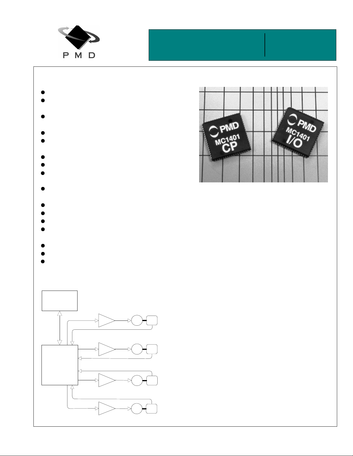
The MC1401A is a 2-IC general purpose motion contr ol chipset
available in one, two, or four axis configurations. It provides
trajectory generation and clo sed-loop digital servo control for a
large variety of servo motors. It uses incremental or absolute
encoder positi on feedback signals, and a DAC or P WM
compatible ou tput drive. Axe s can be progra m m ed either
independently or in synchrony to allow advanced multi-axis
motion such as ci rcular and contin uous-path profiles.
0&$0&$3
0&$0&$3
0&$0&$3
Typical Configuration
Amp
Amp
Amp
Amp
The MC1401A is functionally similar to other members of
PMD's 1st generation chipset family, provid i ng software an d
architectural compatibility with these chipsets. All of these
products support advanced features such as S-curve profile
generation, bi-directional motion-travel limit switches, and
separate hom e and index positio n capture signals.
The chipset is controlled by a host processor which interfaces
with the chipset vi a an 8-bit, bi-directional port. Communications
E
M
M
E
(MC1401A,
MC1201A only)
E
M
(MC1401A only)
E
M
(MC1401A only)
to/from the chi pset consist of pack et-oriented messages. A ho st
interrupt line is provided so that the chipset can signal the host
when special condi tions occur such as enc o der index pulse
received.
Each axis interfaces to either a quadrature encoder with an
optional index pulse, or a parallel-word device such as an
absolute enco der or resolver . For motor a m pl if i er output, PWM
signals are provided, as well as DAC-compatible signals with up
to 16 bits of resolution.
The chipset is packaged in 2 68-pin PLCC pa ck ages. Both
chips utilize CMOS technology and are powered by 5 volts.
Doc. Rev. 6.14, Nov , 1997
Performance Motion Dev ices, In c. 12 Waltham St. Le xington, M A 02421 te l: 781. 674.98 60 fax: 781.674.9 861 www.pmdcorp.com

Table of Contents
Product Family Overview.......................................Page 3
Introduction ............................................................ Page 3
Family Summary..................................................... Page 3
Electrical Characteristics....................................... Page 4
Absolute Maximum Ratings..................................Page 4
Operating Ratings................................................. Page 4
DC Electrical Characteristics................................ Page 5
AC Electrical Characteristics................................Page 5
I/O Timing Diagrams............................................. Page 7
Pinouts....................................................................Page 13
MC1401A. MC1201A............................................ Page 13
MC1101A, MC1401A-P........................................ Page 14
MC1201A-P, MC1101A-P.....................................Page 15
Pin Descriptions.................................................... Page 16
Theory of Operations............................................. Page 20
Trajectory Profile Generation................................ Page 21
S-curve Point to Point....................................... Page 22
Trapezoidal Point to Point.................................Page 23
Velocity Contouring...........................................Page 23
Electronic Gear.................................................Page 24
Trajectory Control................................................. Page 24
Halting The Trajectory......................................Page 24
Motion Complete Status...................................Page 25
Digital Servo Filtering ........................................... Page 25
Motor Limit........................................................Page 26
Motor Bias........................................................ Page 26
Parameter Loading & Updating............................Page 26
Manual Update.................................................Page 27
Breakpoints....................................................... Page 27
External Breakpoints and Homing.................... Page 28
Disabling Automatic Profile Update..................Page 28
Travel Limit Switches............................................ Page 28
Motion Error Detection and Recovery.................. Page 29
Recovering From a Motion Error......................Page 29
Axis Timing........................................................... Page 29
Host Communications .......................................... Page 30
Electrical Interface............................................ Page 30
Packet Format..................................................Page 30
Packet Checksum.............................................Page 31
Illegal Commands .............................................Page 31
Command Errors...............................................Page 31
Axis Addressing....................................................Page 31
Axis Status............................................................Page 32
Status Word ......................................................Page 32
Miscellaneous Mode Status Word.....................Page 32
Host Interrupts.......................................................Page 32
Encoder Position Feedback..................................Page 34
Incremental Encoder Input................................Page 34
Encoder Filtering...............................................Page 34
High Speed Position Capture............................Page 34
Parallel-Word Device Input................................ Page 34
Parallel-Word Device Interfacing.......................Page 35
Motor Outputs.......................................................Page 35
Motor Output Control.........................................Page 35
PWM Output......................................................Page 36
12-Bit DAC Output.............................................Page 36
16-Bit DAC Output.............................................Page 36
Host Commands .....................................................Page 38
Command Summary.............................................Page 38
Command Reference............................................Page 40
Axis Control.......................................................Page 40
Profile Generation.............................................Page 41
Digital Filter.......................................................Page 45
Parameter Update............................................. Page 47
Interrupt Processing..........................................Page 50
Status/Mode......................................................Page 51
Encoder.............................................................Page 52
Motor.................................................................Page 52
Miscellaneous ...................................................Page 54
Application Notes ...................................................Page 58
Interfacing to ISA bus............................................Page 58
Parallel-Word Device Interface .............................Page 60
PWM Motor Interface............................................Page 62
16-Bit Parallel DAC Motor interface......................Page 64
16-Bit Serial DAC Motor Interface.........................Page 66
Performance Motion Devices, Inc. does not assume any responsibility for use of any circuitry described in this manual, nor does it make
any guarantee as to the accuracy of this manual. Performance Motion Devices, Inc. reserves the right to change the circuitry described in
this manual, or the manual itself, at any time.
The components described in this manual are not authorized for use in life-support systems without the express written permission of
Performance Motion Devices, Inc.
2

Product Family Overview
MC1401 series MC1231 series MC1241 series MC1451 series
# of axes 4, 2, or 1 2 or 1 2 or 1 4, 2, or 1
Motors Supported DC Servo Brushless Servo Stepper Stepper
Encoder Format Incremental (no dash version)
and Parallel ('-P' version)
Output Format DC servo Sinusoidally
S-curve profiling Yes Yes Yes Yes
Electronic gearing Yes Yes Yes Yes
On-the-fly changes Yes Yes Yes Yes
Limit switches Yes Yes Yes Yes
PID & feedforward Yes Yes - -
PWM output Yes Yes Yes -
DAC-compatible output Yes Yes Yes -
Pulse & direction output ---Yes
Index & Home signal Yes Yes Yes Yes (-E version)
Chipset p/n's MC1401A, MC1401A-P (4 axes)
MC1201A, MC1201A-P (2 axes)
MC1101A, MC1101A-P (1 axis)
Developer's Kit p/n's: DK1401A, DK1401A-P DK1231A DK1241A DK1451A
Incremental Incremental Incremental (-E version)
Microstepping Pulse and Direction
commutated
MC1231A (2 axes)
MC1131A (1 axis)
MC1241A (2 axes)
MC1141A (1 axis)
MC1451A, MC1451A-E (4 axes)
MC1251A, MC1251A-E (2 axes)
MC1151A, MC1151A-E (1 axis)
Introduction
This manual describes the operational characteristics of the MC1401A,
MC1201A, MC1101A, MC1401A-P, MC1201A-P, and MC1101A-P
Motion Processors. These devices are members of PMD's 1st
generation motion processor family, which consists of 16 separate
products organized into four groups.
Each of these devices are complete chip-based motion controllers.
They provide trajectory generation and related motion control functions.
Depending on the type of motor controlled they provide servo loop
closure, on-board commutation for brushless motors, and high speed
pulse and direction outputs. Together these products provide a
software-compatible family of dedicated motion processor chips which
can handle a large variety of system configurations.
Each of these chips utilize a similar architecture, consisting of a highspeed DSP (Digital Signal Processor) computation unit , along with an
ASIC (Application Specific Integrated Circuit). The computation unit
contains special on-board hardware such as a multiply instruction that
makes it well suited for the task of motion control.
Along with a similar hardware architecture these chips also share most
software commands, so that software written for one chipset may be reused with another, even though the type of motor may be different.
This manual describes the operation of the MC1401A, MC1201A,
MC1101A, MC1401A-P, MC1201A-P, and MC1101A-P chipsets. For
technical details on other members of PMD's first ge neration
motion processors see the corresponding product manual.
Family Summary
MC1401 series (MC1401A, MC1201A, MC1101A, MC1401A-P,
MC1201A-P, MC1101A-P)
encoder signals (standard version) or parallel word encoder signals
(-P version) and output a motor command in either PWM or DACcompatible format. These chipsets come in 1, 2 or 4 axis versions
and can be used with DC brushed motors, or brushless motors using
external commutation.
MC1231 series (MC1231A, MC1131A) -
incremental quadrature encoder signals and output sinusoidally
commutated motor signals appropriate for driving brushless motors.
They are available in one or two axis versions. Depending on the
motor type they output two or three phased signals per axis in either
PWM or DAC-compatible format.
MC1241 series (MC1241A, MC1141A)
internal microstepping generation for stepping motors. They are
available in a one or a two-axis version. Two phased signals are
output per axis in either PWM or DAC-compatible format. An
incremental encoder signal can be input to confirm motor position.
MC1451 series (MC1451A, MC1251A, MC1151A, MC1451A-E,
MC1251A-E, MC1151A-E) -
pulse and direction signal output appropriate for driving step motorbased systems. They are available in a one, two, or four-axis version
and are also available with quadrature encoder input.
Each of these chipsets has an associated Chipset Developer's
Kit available for it. For more information contact your PMD
representative.
- These chipsets take in incremental
These chipsets take in
- These chipsets provide
These chipsets provide very high speed
3
Electrical Characteristics
Overview
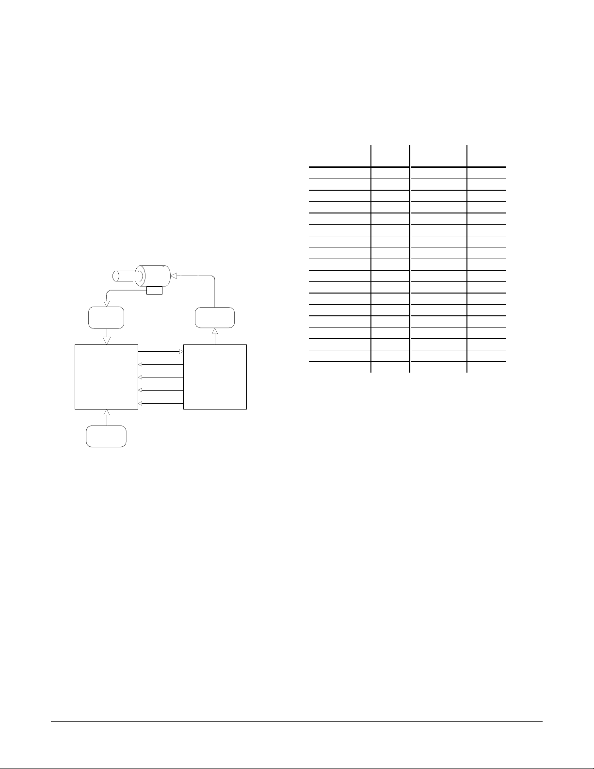
Interconnections between the two chips consist of a data bus and
various control and synchronization signals. The following table
summarizes the signals that must be interconnected for the chipset to
function properly. For each listed signal the I/O chip pin on the left side
of the table is directly connected to the pin to the right.
The MC1401A-consists of two 68 pin PLCC's both fabricated in CMOS.
The Peripheral Input/Output IC (I/O chip) is responsible for interfacing
to the host processor and to the position input encoders. The Command
Processor IC (CP chip) is responsible for all host command, profile and
servo computations, as well as for outputting the PWM and DAC
signals.
The following figure shows a typical system block diagram, along with
the pin connections between the I/O chip and the CP chip.
Motor
(4 axis)
Encoder
(1-4 axis)
I/O
Host
Processor
Data4-11
I/OAddr0-3
I/OWrite
I/OCntrl0-3
ClkOut
Amplifier
(1-4 axis)
CP
I/O Chip Signal
Name
I/O Chip
Pin
CP Chip
Signal Name
CP Chip
Pin
CPData4 18 Data4 50
CPData5 5 Data5 49
CPData6 6 Data6 46
CPData7 7 Data7 43
CPData8 8 Data8 40
CPData9 17 Data8 39
CPData10 3 Data10 36
CPData11 1 Data11 35
CPAddr0 68 I/OAddr0 28
CPAddr1 27 I/OAddr1 9
CPAddr2 29 I/OAddr2 6
CPAddr3 12 I/OAddr3 5
CPCntr0 20 I/OCntr0 16
CPCntr1 36 I/OCntr1 18
CPCntr2 22 I/OCntr2 68
CPCntr3 63 I/OCntr3 67
CPWrite 2 I/OWrite 15
CPClk 46 ClkOut 19
For a complete description of all pins see the 'Pin Descriptions'
section of this manual.
Unless specifically noted otherwise, the term 'MC1401A' refers to
the MC1401A, MC1201A, MC1101A, MC1401A-P, MC1201A-P, and
MC1101A-P Motion Processors.
The CP and I/O chips function together as one integrated motion
processor. The major components connected to the chip set are the
Encoder (4, 2, or 1 axes), the motor amplifier (4, 2, or 1 axes), and the
host processor.
For the standard MC1401A parts (non '-P' parts), the encoder signals
are input to the I/O chip in quadrature format. For the '-P' parts the
encoder information is input directly into the CP chip, via an 8 bit data
bus and various control signals.
The chipset's motor output signals are connected to the motor amplifier.
Two types of output are provided; PWM (pulse width modulation), and
DAC-compatible signals used with an external DAC (digital to analog
converter).
The host processor is interfaced via an 8-bit bi-directional bus and
various control signals. Host communication is coordinated by a
ready/busy signal, which indicates when communication is allowed.
Absolute Maximum Ratings
Unless otherwise stated, all electrical specifications are for both
the I/O and CP chips.
Storage Temperature, Ts.....................-55 deg. C to +150 deg. C
Supply Voltage, Vcc.............................-0.3 V to +7.0 V
Power Dissipation, Pd..........................650 mW (I/O and CP
combined)
Operating Ratings
Operating Temperature, Ta .................0 deg. C to +70 deg. C*
Nominal Clock Frequency, Fclk...........25.0 Mhz
Supply Voltage, Vcc.............................4.75 V to 5.25 V
* Industrial and Military operating ranges also available. Contact your
PMD representative for more information.
4
DC Electrical Characteristics
(Vcc and Ta per operating ratings, Fclk = 25.0 Mhz)
Symbol Parameter Min. Max. Units Conditions
Vcc Supply Voltage 4.75 5.25 V
Idd Supply Current 100 mA open outputs
Input Voltages
Vih Logic 1 input voltage 2.0 Vcc + 0.3 V
Vil Logic 0 input voltage -0.3 0.8 V
Vihclk Logic 1 voltage for clock pin
(ClkIn)
Vihreset Logic 1 voltage for reset pin
(reset)
Output Voltages
Voh Logic 1 Output Voltage 2.4 V @CP Io = 300 uA
Vol Logic 0 Output Voltage 0.33 V @CP Io = 2 mA
Iout Tri-State output leakage current -20 20 uA 0 < Vout < Vcc
Iin Input current -50 50 uA 0 < Vi < Vcc
Iinclk Input current ClkIn -20 20 uA 0 < Vi < Vcc
3.0 Vcc+0.3 V
4.0 Vcc+0.3 V
AC Electrical Characteristics
(see reference timing diagrams)
(Vcc and Ta per operating ratings; Fclk = 25.0 Mhz)
(~ character indicates active low signal)
@I/O Io = 4 mA
@I/O Io = 4 mA
Timing Interval T# Min. Max. Units
Encoder and Index Pulse Timing
Motor-Phase Pulse Width T1 1.6 uS
Dwell Time Per State T2 0.8 uS
Index Pulse Setup and Hold
(relative to Quad A and Quad B low)
Reset Timing
Stable Power to Reset 0.25 Sec
Reset Low Pulse Width 1.0 uS
Clock Timing
Clock Frequency (Fclk) 6.7 25.6 Mhz
Clock Pulse Width T4 19.5 75 (note 2) nS
Clock Period T5 39 149 (note 2) nS
T3 0 uS
5

Timing Interval T# Min. Max. Units
Command Byte Write Timing
~HostSlct Hold Time T6 15 2000 (note 3) nS
~HostSlct Setup Time T7 10 nS
HostCmd Setup Time T8 10 nS
Host Cmd Hold Time T9 25 nS
HostRdy Delay Time T13 70 nS
~HostWrite Pulse Width T14 50 nS
Write Data Setup Time T15 35 nS
Write Data Hold Time T16 30 nS
Data Word Read Timing
~HostSlct Hold Time T6 15 2000 (note 3) nS
~HostSlct Setup Time T7 (read only) - 20 nS
HostCmd Setup Time T8 (read only) - 20 nS
HostCmd Hold Time T9 25 nS
Read Data Access Time T10 50 nS
Read Data Hold Time T11 10 nS
~HostRead high to HI-Z Time T12 50 nS
HostRdy Delay Time T13 70 nS
Read Recovery Time T17 60 nS
Data Word Write Timing
~HostSlct Hold Time T6 15 2000 (note 3) nS
~HostSlct Setup Time T7 10 nS
HostCmd Setup Time T8 10 nS
HostCmd Hold Time T9 25 nS
HostRdy Delay Time T13 70 nS
~HostWrite Pulse Width T14 50 nS
Write Data Setup Time T15 35 nS
Write Data Hold Time T16 30 nS
Write Recovery Time T18 60 nS
DAC Interface Timing
I/OAddr Stable to ~I/OWrite setup time T19 35 nS
~I/OWrite Pulse Width T20 56 95 nS
Data Hold Time After ~I/OWrite T21 17 nS
ClkOut Low to I/OAddr stable T22 10 40 nS
ClkOut Low to ~I/OWrite Low T23 75 92 nS
ClkOut Low to Data Valid T24 92 nS
ClkOut Cycle Time T25 160 typical (note 4) nS
I/OAddr Stable to DACSlct High T26 66 nS
~I/OWrite Low to DACSlct High T27 44.5 nS
PWM Output Timing
PWM Output Frequency 24.5 Khz
Parallel-Word Enc oder Timing (-P versi ons only)
ClkOut Period T28 160 typical (note 4) nS
I/OCtrnl0 Delay Time T29 35 47 nS
Data Setup Time to ClkOut T30 40 nS
I/OAddr Stable to DACSlct High T31 22.0 27.0 uSec
Convert Pulse Width T32 320 nSec
note 1 ~HostSlct and HostCmd may optionally be de-asserted if setup and hold times are met.
note 2 Chip-set performance figures and timing information valid at Fclk = 25.0 only. For timing information & performance parameters at Fclk <
25.0 Mhz, call PMD.
note 3 Two micro seconds maximum to release interface before chip set responds to command
note 4 ClkOut from CP is 1/4 frequency of ClkIn (CP chip).
6
I/O Timing Diagrams
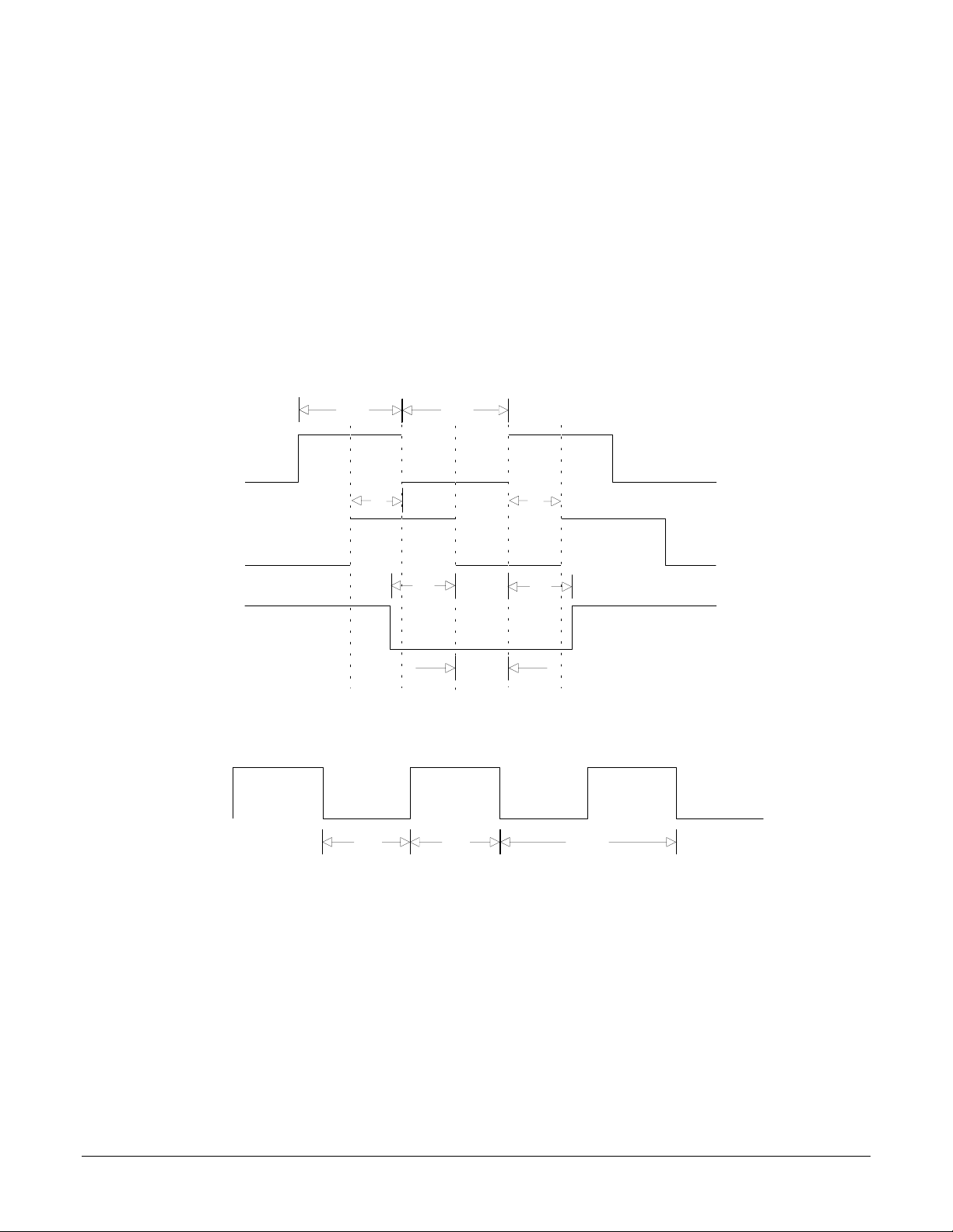
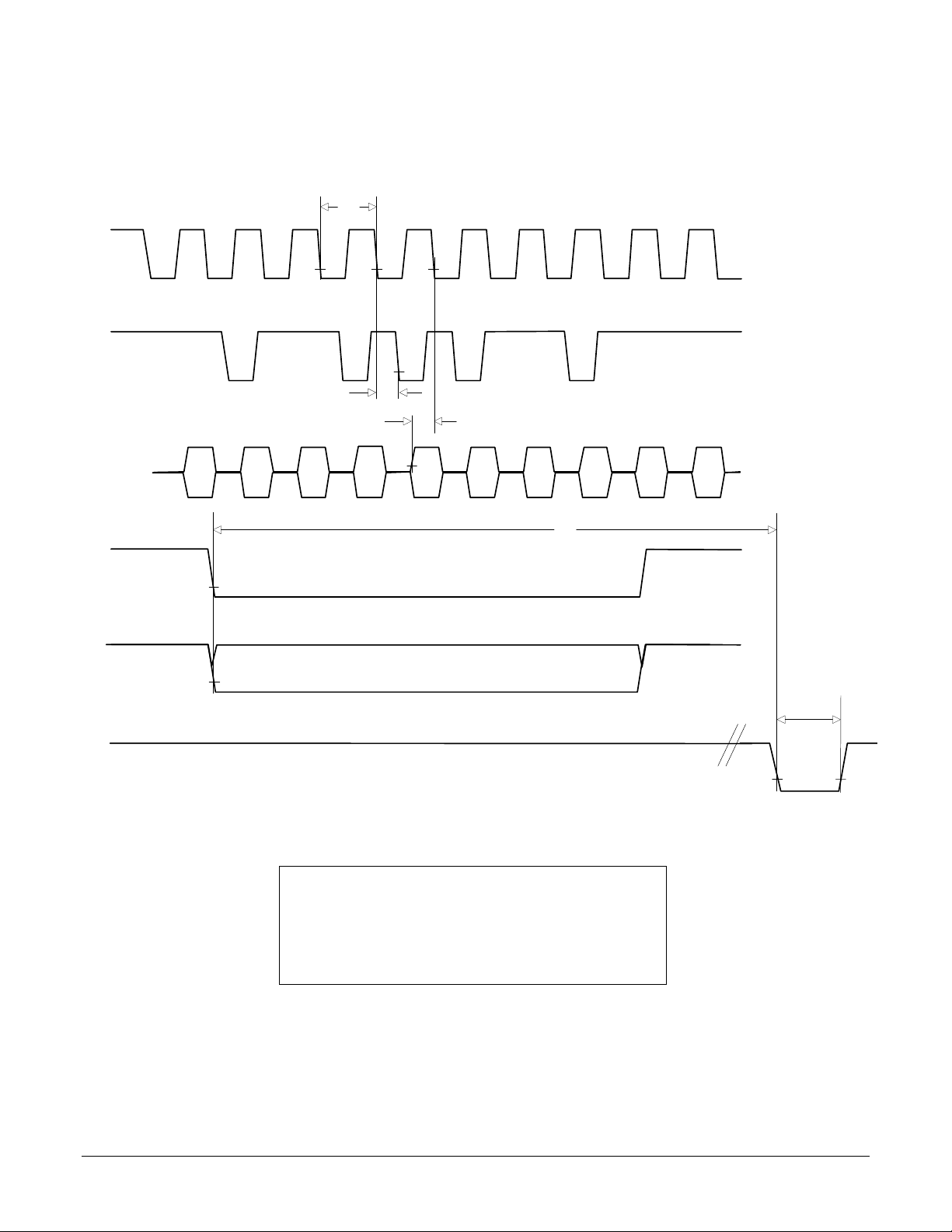
The following diagrams show the MC1401A electrical interface timing. T#' values are listed in the above timing chart.
Quadrature Encoder Input Timing
Quad A
Quad B
~Index
ClkIn
T1
T1
T2 T2
T3
Clock Timing
T3
T4 T4 T5
Index = ~A * ~B * ~IND
7
Command Byte Write TIming
~HostSlct
HostCmd
~HostWrite
HostData0-7
HostRdy
T7
T8
T6
T9
T14
T15
T16
T13
8
Data Word Read TImi ng
~HostSlct
HostCmd
~HostRead
HostData0-7
HostRdy
T7
T6
Note 1
T8
Note 1
T9
T17
T12
High-Z High-Z High-Z
High
Byte
T10
T11
Low
Byte
T13
9
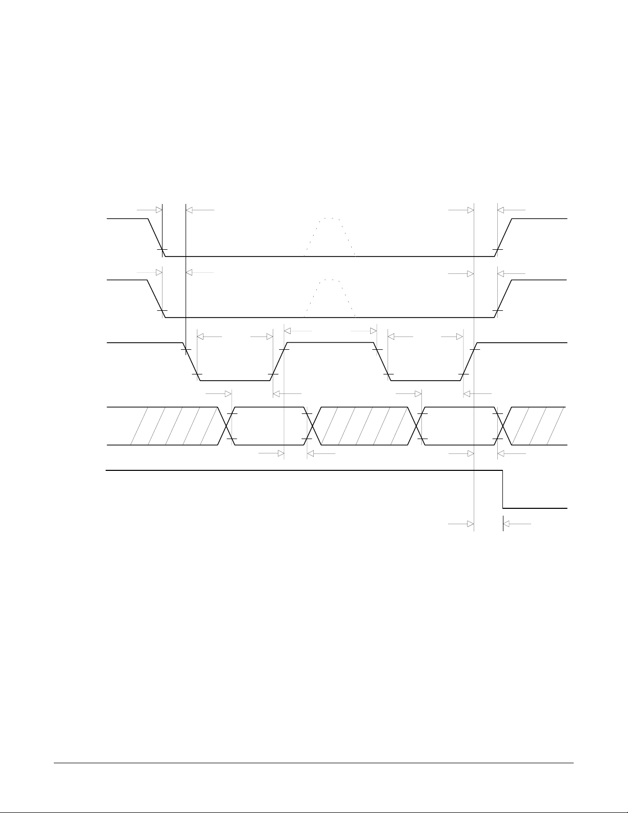
Data Word Write TIming
~HostSlct
HostCmd
~HostWrite
HostData0-7
HostRdy
T7
T8
T14
T15
High
Byte
T16
T18
Note 1
Note 1
T6
T9
T14
T15
Low
Byte
T16
10
T13
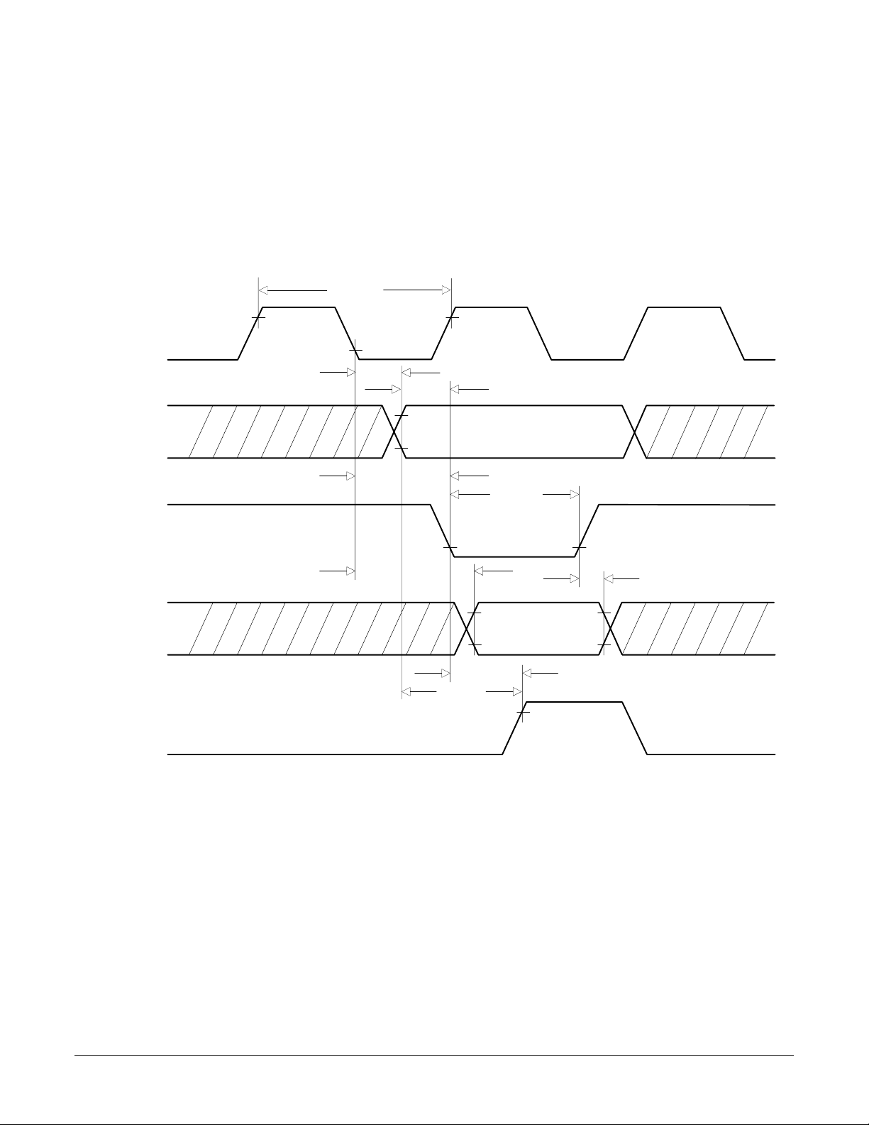
ClkOut
I/OAddr
~I/OWrite
DAC Interface Timing
T25
T22
T19
T23
T20
Data 0-11,
DACAddr0,1
DACSlct
T24
T21
T27
T26
11
ClkOut
Parallel Word Device Read Timing
T28
I/OCntrl0
Data0-11,
DACLow0-3
PosSlct
Dac16Addr0, 1
Convert
12345
T29
T30
T31
T32
6
One data read shown. Axis address read sequence is 1, 2, 4, 3
Legend
1 - Instruct i on Fetch
2 - Instruct i on Fetch
3 - Read the data value
4 - Instruct i on Fetch
5 - Instruct i on Fetch
12
6 - Convert strobe
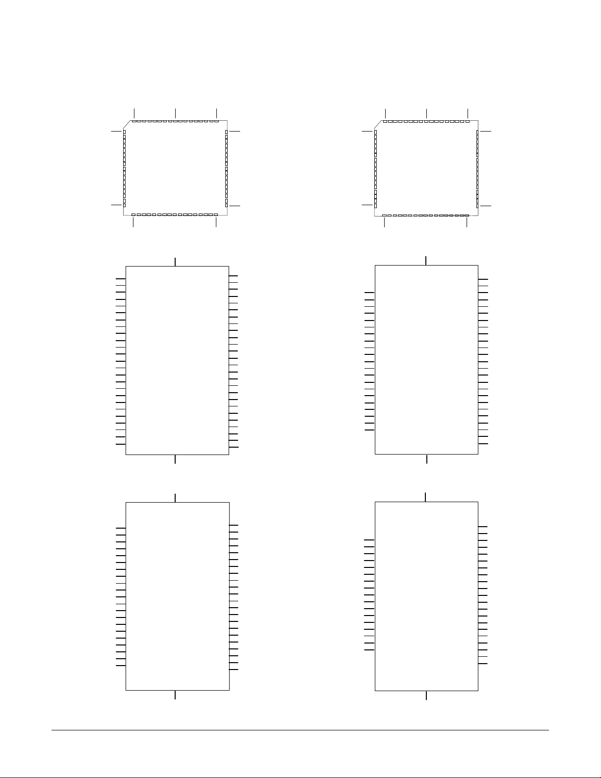
Pinouts
9
10
(Top view)
26
27 43
4, 21, 25, 38, 55
28
QuadA1
42
QuadB1
24
Index1
13
Home1
26
QuadA2
30
QuadB2
9
Index2
23
Home2
40
QuadA3
35
QuadB3
19
Index3
11
Home3
39
QuadA4
34
QuadB4
16
Index4
10
Home4
33
DACSlct
46
CPClk
52
I/OClkIn
45
I/OClkOut
29
CPAddr2
12
CPAddr3
2
CPWrite
20
CPCntrl0
36
CPCntrl1
1
I/O
VCC
I/O
GND
61
CPCntrl2
CPCntrl3
HostCmd
HostRdy
HostRead
HostWrite
HostSlct
HostIntrpt
HostData0
HostData1
HostData2
HostData3
HostData4
HostData5
HostData6
HostData7
CPData4
CPData5
CPData6
CPData7
CPData8
CPData9
CPData10
CPData11
CPAddr0
CPAddr1
60
44
MC1401A Pinouts
22
63
41
37
51
47
48
44
50
61
53
65
67
62
64
60
18
5
6
7
8
17
3
1
68
27
9
10
1
61
60
CP
(Top view)
26
27 43
4, 22, 33
56
55
54
53
30
29
24
19
17
16
18
68
67
64
63
62
61
8
7
2
1
PWMMag1
PWMSign1
PWMMag2
PWMSign2
PWMMag3
PWMSign3
PWMMag4
PWMSign4
DAC16Addr0
DAC16Addr1
ClkIn
ClkOut
Reset
I/OCntrl0
I/OCntrl1
I/OCntrl2
I/OCntrl3
DACLow0
DACLow1
DACLow2
DACLow3
VCC
CP
GND
Data0
Data1
Data2
Data3
Data4
Data5
Data6
Data7
Data8
Data9
Data10
Data11
I/OAddr0
I/OAddr1
I/OAddr2
I/OAddr3
I/OWrite
PosLimit1
PosLimit2
PosLimit3
PosLimit4
NegLimit1
NegLimit2
NegLimit3
NegLimit4
44
60
59
58
57
50
49
46
43
40
39
36
35
28
9
6
5
15
52
45
42
38
51
44
41
37
14, 15, 32, 49, 54, 66
4, 21, 25, 38, 55
VCC
QuadA1
28
QuadB1
42
Index1
24
Home1
13
QuadA2
26
QuadB2
30
Index2
9
Home2
23
DACSlct
33
CPClk
46
I/OClkIn
52
I/OClkOut
45
CPAddr2
29
CPAddr3
12
CPWrite
2
CPCntrl0
20
CPCntrl1
36
CPCntrl2
22
CPCntrl3
63
CPAddr0
68
CPAddr1
27
I/O
GND
14, 15, 32, 49, 54, 66
HostCmd
HostRdy
HostRead
HostWrite
HostSlct
HostIntrpt
HostData0
HostData1
HostData2
HostData3
HostData4
HostData5
HostData6
HostData7
CPData4
CPData5
CPData6
CPData7
CPData8
CPData9
CPData10
CPData11
MC1201A Pinouts
41
37
51
47
48
44
50
61
53
65
67
62
64
60
18
5
6
7
8
17
3
1
PWMMag1
8
PWMSign1
56
PWMMag2
7
PWMSign2
55
DAC16Addr0
30
DAC16Addr1
29
ClkIn
24
ClkOut
19
Reset
17
I/OCntrl0
16
I/OCntrl1
18
I/OCntrl2
68
I/OCntrl3
67
DACLow0
64
DACLow1
63
DACLow2
62
DACLow3
61
3, 34
4, 22, 33
VCC
CP
GND
3, 34
Data0
Data1
Data2
Data3
Data4
Data5
Data6
Data7
Data8
Data9
Data10
Data11
I/OAddr0
I/OAddr1
I/OAddr2
I/OAddr3
I/OWrite
PosLimit1
PosLimit2
NegLimit1
NegLimit2
60
59
58
57
50
49
46
43
40
39
36
35
28
9
6
5
15
52
45
51
44
13
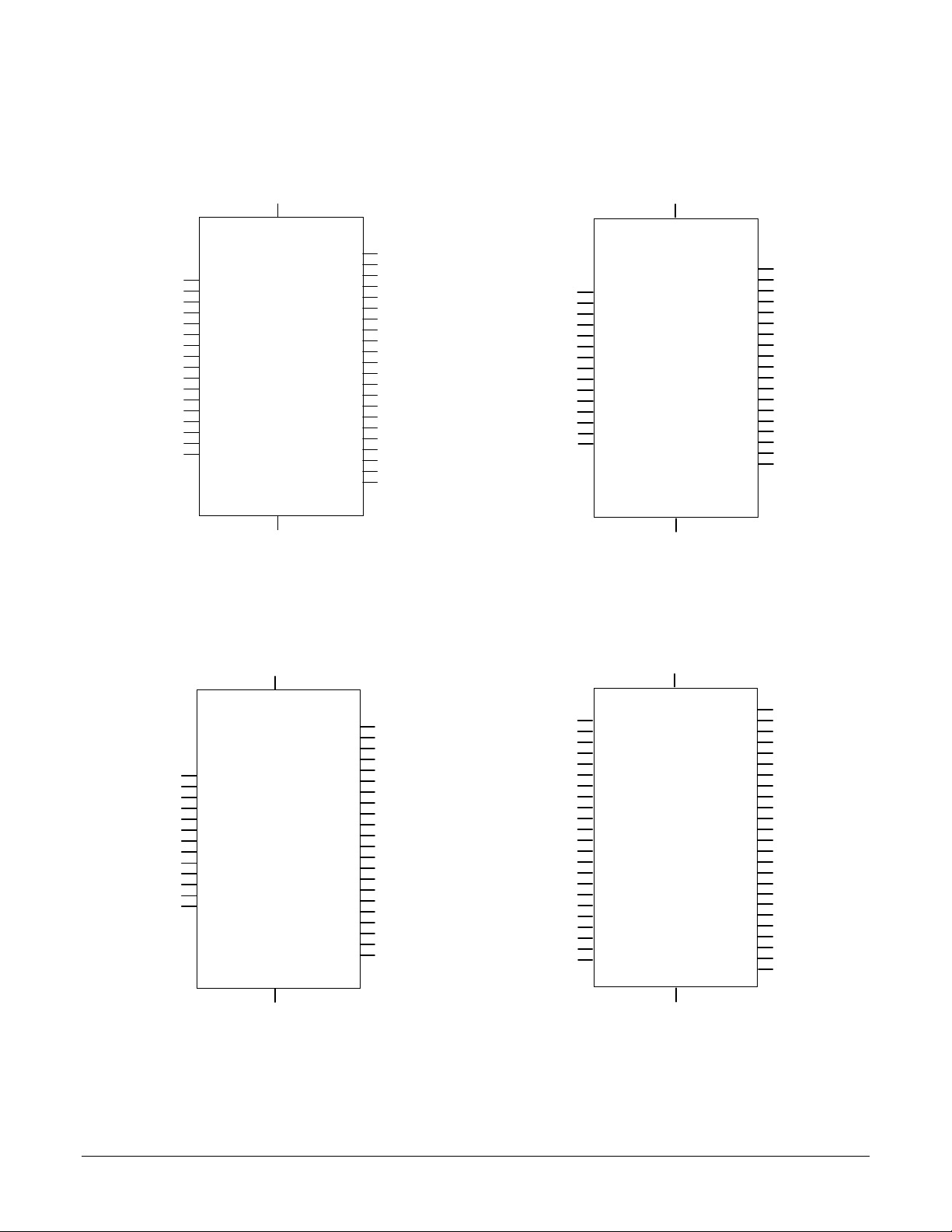
4, 21, 25, 38, 55
MC1101A Pinouts
4, 22, 33
VCC
HostCmd
HostRdy
28
QuadA1
42
QuadB1
24
Index1
13
Home1
33
DACSlct
46
CPClk
52
I/OClkIn
45
I/OClkOut
29
CPAddr2
12
CPAddr3
2
CPWrite
20
CPCntrl0
36
CPCntrl1
22
CPCntrl2
63
CPCntrl3
68
CPAddr0
27
CPAddr1
I/O
GND
14, 15, 32, 49, 54, 66
HostRead
HostWrite
HostSlct
HostIntrpt
HostData0
HostData1
HostData2
HostData3
HostData4
HostData5
HostData6
HostData7
CPData4
CPData5
CPData6
CPData7
CPData8
CPData9
CPData10
CPData11
41
37
51
47
48
44
50
61
53
65
67
62
64
60
18
5
6
7
8
17
3
1
8
56
30
29
24
19
17
16
18
68
67
64
63
62
61
PWMMag1
PWMSign1
DAC16Addr0
DAC16Addr1
ClkIn
ClkOut
Reset
I/OCntrl0
I/OCntrl1
I/OCntrl2
I/OCntrl3
DACLow0
DACLow1
DACLow2
DACLow3
VCC
CP
GND
3, 34
Data0
Data1
Data2
Data3
Data4
Data5
Data6
Data7
Data8
Data9
Data10
Data11
I/OAddr0
I/OAddr1
I/OAddr2
I/OAddr3
I/OWrite
PosLimit1
NegLimit1
60
59
58
57
50
49
46
43
40
39
36
35
28
9
6
5
15
52
51
MC1401A-P Pinouts
4, 21, 25, 38, 55
4, 22, 33
VCC
8
HostCmd
HostRdy
HostRead
HostWrite
DACSlct
33
CPClk
46
I/OClkIn
52
I/OClkOut
45
CPAddr2
29
CPAddr3
12
CPWrite
2
CPCntrl0
20
CPCntrl1
36
CPCntrl2
22
CPCntrl3
63
CPAddr0
68
CPAddr1
27
I/O
GND
14, 15, 32, 49, 54, 66
HostSlct
HostIntrpt
HostData0
HostData1
HostData2
HostData3
HostData4
HostData5
HostData6
HostData7
CPData4
CPData5
CPData6
CPData7
CPData8
CPData9
CPData10
CPData11
41
37
51
47
48
44
50
61
53
65
67
62
64
60
18
5
6
7
8
17
3
1
56
55
54
53
30
29
31
32
24
19
17
16
18
68
67
64
63
62
61
7
2
1
PWMMag1
PWMSign1
PWMMag2
PWMSign2
PWMMag3
PWMSign3
PWMMag4
PWMSign4
DAC16Addr0
DAC16Addr1
PosSlct
Convert
ClkIn
ClkOut
Reset
I/OCntrl0
I/OCntrl1
I/OCntrl2
I/OCntrl3
DACLow0
DACLow1
DACLow2
DACLow3
VCC
CP
GND
3, 34
Data0
Data1
Data2
Data3
Data4
Data5
Data6
Data7
Data8
Data9
Data10
Data11
I/OAddr0
I/OAddr1
I/OAddr2
I/OAddr3
I/OWrite
PosLimit1
PosLimit2
PosLimit3
PosLimit4
NegLimit1
NegLimit2
NegLimit3
NegLimit4
60
59
58
57
50
49
46
43
40
39
36
35
28
9
6
5
15
52
45
42
38
51
44
41
37
14
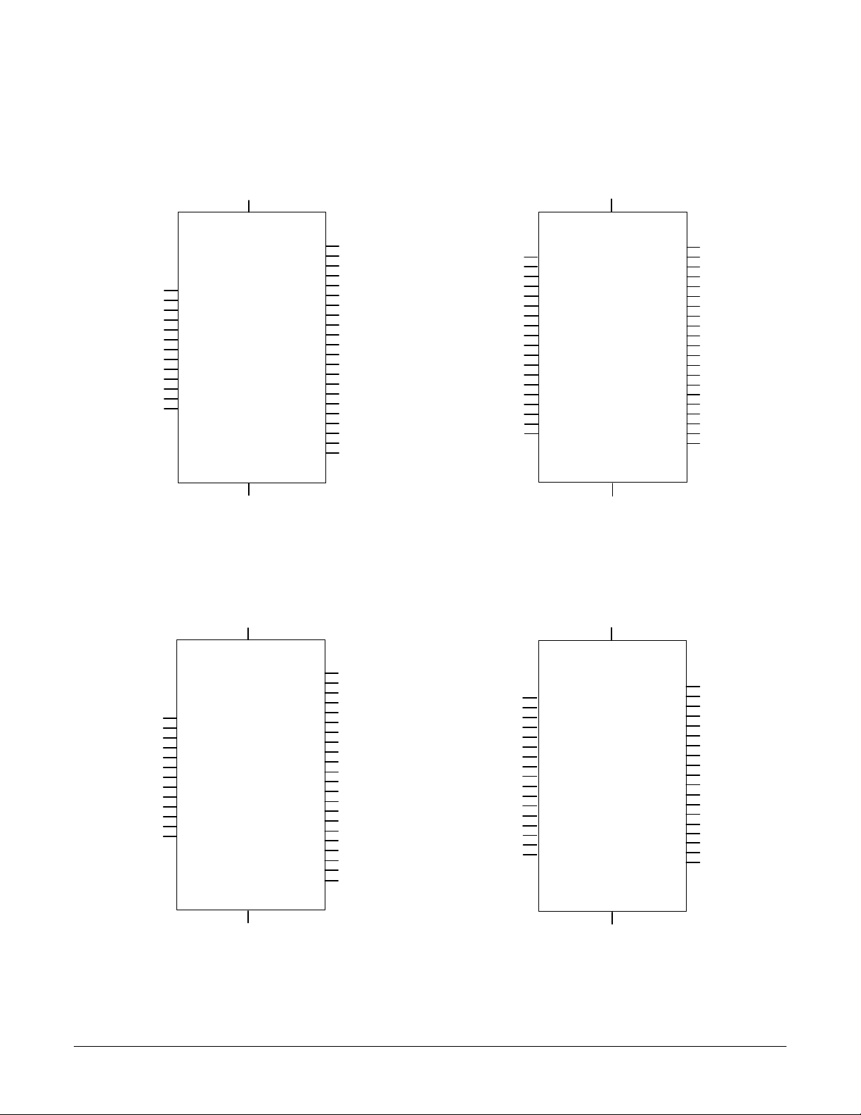
4, 21, 25, 38, 55
MC1201A-P Pinouts
4, 22, 33
VCC
HostCmd
HostRdy
HostRead
HostWrite
DACSlct
33
CPClk
46
I/OClkIn
52
I/OClkOut
45
CPAddr2
29
CPAddr3
12
CPWrite
2
CPCntrl0
20
CPCntrl1
36
CPCntrl2
22
CPCntrl3
63
CPAddr0
68
CPAddr1
27
I/O
GND
14, 15, 32, 49, 54, 66
HostSlct
HostIntrpt
HostData0
HostData1
HostData2
HostData3
HostData4
HostData5
HostData6
HostData7
CPData4
CPData5
CPData6
CPData7
CPData8
CPData9
CPData10
CPData11
41
37
51
47
48
44
50
61
53
65
67
62
64
60
18
5
6
7
8
17
3
1
56
55
30
29
31
32
24
19
17
16
18
68
67
64
63
62
61
8
7
PWMMag1
PWMSign1
PWMMag2
PWMSign2
DAC16Addr0
DAC16Addr1
PosSlct
Convert
ClkIn
ClkOut
Reset
I/OCntrl0
I/OCntrl1
I/OCntrl2
I/OCntrl3
DACLow0
DACLow1
DACLow2
DACLow3
VCC
CP
GND
3, 3 4
Data0
Data1
Data2
Data3
Data4
Data5
Data6
Data7
Data8
Data9
Data10
Data11
I/OAddr0
I/OAddr1
I/OAddr2
I/OAddr3
I/OWri te
PosLimit1
PosLimit2
NegLimit1
NegLimit2
60
59
58
57
50
49
46
43
40
39
36
35
28
9
6
5
15
52
45
51
44
MC1101A-P Pinouts
4, 21, 25, 38, 55
4, 22, 33
VCC
HostCmd
HostRdy
HostRead
HostWrite
DACSlct
33
CPClk
46
I/OClkIn
52
I/OClkOut
45
CPAddr2
29
CPAddr3
12
CPWrite
2
CPCntrl0
20
CPCntrl1
36
CPCntrl2
22
CPCntrl3
63
CPAddr0
68
CPAddr1
27
I/O
GND
14, 15, 32, 49, 54, 66
HostSlct
HostIntrpt
HostData0
HostData1
HostData2
HostData3
HostData4
HostData5
HostData6
HostData7
CPData4
CPData5
CPData6
CPData7
CPData8
CPData9
CPData10
CPData11
41
37
51
47
48
44
50
61
53
65
67
62
64
60
18
5
6
7
8
17
3
1
8
56
30
29
31
32
24
19
17
16
18
68
67
64
63
62
61
PWMMag1
PWMSign1
DAC16Addr0
DAC16Addr1
PosSlct
Convert
ClkIn
ClkOut
Reset
I/OCntrl0
I/OCntrl1
I/OCntrl2
I/OCntrl3
DACLow0
DACLow1
DACLow2
DACLow3
VCC
CP
GND
3, 34
Data0
Data1
Data2
Data3
Data4
Data5
Data6
Data7
Data8
Data9
Data10
Data11
I/OAddr0
I/OAddr1
I/OAddr2
I/OAddr3
I/OWrite
PosLimit1
NegLimit 1
60
59
58
57
50
49
46
43
40
39
36
35
28
9
6
5
15
52
51
15

Pin Descriptions
The following tables provide pin descriptions for the MC1401A and MC1401A-P series chipsets.
IC Pin Name Pin # Description/Functionality
I/O Chip Pinouts
I/O QuadA1
QuadB1
QuadA2
QuadB2
QuadA3
QuadB3
QuadA4
QuadB4
I/O ~Index1
~Index2
~Index3
~Index4
28
42
26
30
40
35
39
34
24
9
19
16
Quadrature A, B channels for axis 1 - 4 (input). Each of these 4 pairs of quadrature (A, B)
signals provide the position feedback for an incremental encoder. When the encoder is
moving in the positive, or forward direction, the A signal leads the B signal by 90 degs. The
quadrature signals must stay in the same state for .8 uSec to register a valid encoder state,
resulting in a maximum theoretical encoder state capture rate of 1.2 Mcounts/sec. Actual
maximum rate will vary depending on signal noise. Typical maximum is 1.0 Mcounts/sec.
NOTE: Many encoders require a pull-up resistor on each of these signals to establish a
proper high signal (check the encoder electrical specifications)
NOTE: For MC1401A all 8 pins are valid. For MC1201A pins for axes 1 & 2 only are valid.
For MC1101A pins for axis 1 only are valid. Invalid axis pins can be left unconnected.
NOTE: Not valid for -P parts.
Index encoder signals for axis 1-4 (input). Each of these 4 signals indicate the index flag
state from the encoder. A valid index pulse is recognized by the chip set when the index flag
transitions low, followed by the corresponding A and B channels of the encoder transitioning
low. The index pulse is recognized at the later of the A or B transitions. If not used this signal
must be tied high.
NOTE: For MC1401A all 4 pins are valid. For MC1201A pins for axes 1 & 2 only are valid.
For MC1101A pin for axis 1 only is valid. Invalid axis pins can be left unconnected.
NOTE: Not valid for -P parts.
I/O ~Home1
~Home2
~Home3
~Home4
I/O DACSlct 33 DAC Select (output). This signal is asserted high to select any of the available DAC output
I/O CPClk 46 I/O chip clock (input). This signal is connected directly to the ClkOut pin (CP chip) and
I/O I/OClkIn 52 Phase shifted clock (input). This signal is connected to I/OClkOut (I/O chip), and inputs a
I/O I/OClkOut 45 Phase shifted clock (output). This signal is connected to I/OClkIn (I/O chip), and outputs a
I/O CPAddr0
CPAddr1
CPAddr2
CPAddr3
13
23
11
10
68
27
29
12
Home signals for axis 1-4 (input). Each of these signals provide a general purpose input to
the hardware position capture mechanism. A valid home signal is recognized by the chipset
when the home flag transitions low. These signals have a similar function as the ~Index
signals, but are not gated by the A and B encoder channels. For valid axis pins, If not used,
this signal must be tied high. See below for valid pin definitions for the MC1401A, MC1201A,
and MC1101A.
NOTE: For MC1401A all 4 pins are valid. For MC1201A pins for axes 1 & 2 only are valid.
For MC1101A pin for axis 1 only is valid. Invalid axis pins can be left unconnected.
NOTE: Not valid for -P parts.
channels. For details on DAC decoding see description of DACAddr0-1 and DAC16Addr0-3
signals.
provides the clock signal for the I/O chip. The frequency of this signal is 1/4 the user-provided
ClkIn (CP chip) frequency.
phase shifted clock signal.
phase shifted clock signal.
I/O chip to CP chip communication address (input). These 4 signals are connected to the
corresponding I/OAddr0-3 pins (CP chip), and together provide addressing signals to
facilitate CP to I/O chip communication.
16

IC Pin Name Pin # Description/Functionality
I/O ~CPWrite 2 I/O chip to CP chip communication write (input). This signal is connected to the ~I/OWrite pin
(CP chip) and provides a write strobe to facilitate CP to I/O chip communication.
I/O CPCntrl0
CPCntrl1
CPCntrl2
CPCntrl3
I/O HostCmd 41 Host Port Command (input). This signal is asserted high to write a host command to the chip
I/O HostRdy 37 Host Port Ready/Busy (output). This signal is used to synchronize communication between
I/O ~HostRead 51 Host Port Read data (input). Used to indicate that a data word is being read from the chip set
I/O ~HostWrite 47 Host Port Write data (input). Used to indicate that a data word or command is being written to
I/O ~HostSlct 48 Host Port Select (input). Used to select the host port for reading or writing operations (low
I/O ~HostIntrpt 44 Host Interrupt (output). A low assertion on this pin indicates that a host interrupt condition
I/O HostData0
HostData1
HostData2
HostData3
HostData4
HostData5
HostData6
HostData7
I/O CPData4
CPData5
CPData6
CPData7
CPData8
CPData9
CPData10
CPData11
I/O Vcc 4, 21, 25, 38, 55 I/O chip supply voltage pin. All of these pins must be connected to the supply voltage. Supply
I/O GND 14, 15, 32, 49, 54,66I/O chip ground pin. All of these pins must be connected to the power supply return.
20
36
22
63
50
61
53
65
67
62
64
60
18
5
6
7
8
17
3
1
I/O chip to CP chip communication control (mixed). These 4 signals are connected to the
corresponding I/OCntrl0-3 pins (CP chip), and provide control signals to facilitate CP to I/O
chip communication.
set. It is asserted low to read or write a host data word to the chipset
the DSP and the host. HostRdy will go low (indicating host port busy) at the end of a host
command write or after the second byte of a data write or read. HostRdy will go high
(indicating host port ready) when the command or data word has been processed and the
chip set is ready for more I/O operations. All host port communications must be made with
HostRdy high (indicating ready).
Typical busy to ready cycle is 100.0 uSec.
(low asserts read).
the chip set (low asserts write).
assertion selects port). ~HostSlct must remain inactive (high) when the host port is not in use.
exists that may require special host action.
Host Port Data 0-7 (bi-directional, tri-stated). These signals form the 8 bit host data port used
during communication to/from the chip set. This port is controlled by ~HostSlct, ~HostWrite,
~HostRead and HostCmd.
I/O chip to CP chip data port (bi-directional). These 8 bits are connected to the corresponding
Data4-11 pins on the CP chip, and facilitate communication to/from the I/O and CP chips..
voltage = 4.75 to 5.25 V
17

IC Pin Name Pin # Description/Functionality
CP Chip Pinouts
CP PWMMag1
PWMMag2
PWMMag3
PWMMag4
CP PWMSign1
PWMSign2
PWMSign3
PWMSign4
CP PosLimit1
PosLimit2
PosLimit3
PosLimit4
CP NegLimit1
NegLimit2
NegLimit3
NegLimit4
CP DAC16Addr0
DAC16Addr13029
8
7
2
1
56
55
54
53
52
45
42
38
51
44
41
37
PWM motor output magnitude signals (output). When the chip set is in PWM output mode
these pins provide the Pulse Width Modulated magnitude signal to the motor amplifier. Each
PWM signal output directly corresponds to the axis # being driven.
PWM motor output sign signals for axis 1-4 (output). When the chip set is in PWM output
mode these pins provide the Pulse Width Modulated sign signal to the motor amplifier for
each axis.
Positive limit switch input for axis 1-4. These signals provide directional limit inputs for the
positive-side travel limit of the axis. Upon powerup these signals default to "active high"
interpretation, but the interpretation can be set explicitly using the SET_LMT_SENSE
command. If not used these signals should be tied low for the default interpretation, or tied
high if the interpretation is reversed.
NOTE: For MC1401A all 4 pins are valid. For MC1201A pins for axes 1 & 2 only are valid.
For MC1101A pin for axis 1 only is valid. Invalid axis pins can be left un connected.
Negative limit switch input for axis 1-4. These signals provide directional limit inputs for the
negative-side travel limit of the axis. Upon powerup these signals default to "active high"
interpretation, but the interpretation can be set explicitly using the SET_LMT_SENSE
command. If not used these signals should be tied low for the default interpretation, or tied
high if the interpretation is reversed.
NOTE: For MC1401A all 4 pins are valid. For MC1201A pins for axes 1 & 2 only are valid.
For MC1101A pin for axis 1 only is valid. Invalid axis pins can be left un connected.
Axis Address used during 16-bit DAC motor command output and parallel-word encoder input
(output). When used to encode the motor DAC address or the parallel word encoder address
these signals are encoded as follows:
Dac16Addr1 Dac16Addr0 Addressed Encoder
Low Low Axis 1
Low High Axis 2
High Low Axis 3
High High Axis 4
To read a parallel position word from an external device, the chipset loads DAC16Addr0-1
with the axis # and PosSlct is asserted low.
To write a valid DAC motor command value DACSlct (I/O chip) and I/OAddr0-3 (CP chip)
must be high, and I/OWrite (CP chip) must be low. The 16 bit DAC data word is organized as
follows: High twelve bits are in Data0-11 (CP chip), and low 4 bits are in DACLow0-3 (CP
chip).
CP ClkIn 24 Clock In (input). This pin provides the chip set master clock (Fclk = 25.0 Mhz)
CP ClkOut 19 Clock Out (output). This pin provides a clock output which is 1/4 the ClkIn frequency. This pin
is connected to CPClk (I/O chip).
CP ~Reset 17 Master chip set reset (input). When brought low, this pin resets the chip set to its initial
condition. Reset should occur no less than 250 mSec after stable power has been provided
to the chip set.
CP I/OCntrl0
I/OCntrl1
I/OCntrl2
I/OCntrl3
16
18
68
67
I/O chip to CP chip communication control (mixed). These signals provide various inter-chip
control signals and are connected to the corresponding CPCntrl0-3 pins on the I/O chip.
18

IC Pin Name Pin # Description/Functionality
CP Data0
Data1
Data2
Data3
Data4
Data5
Data6
Data7
Data8
Data9
Data10
Data11
CP DACLow0
DACLow1
DACLow2
DACLow3
CP I/OAddr0
I/OAddr1
I/OAddr2
I/OAddr3
CP PosSlct 31 Parallel-word position-input device select (output). This pin selects the parallel word device(s)
60
59
58
57
50
49
46
43
40
39
36
35
64
63
62
61
28
9
6
5
Multi-purpose Data0-11. (Bi-directional). These pins have 3 functions:
1) Pins Data4-11 (8 bits total) are connected to the corresponding CPData4-11 pins on the
I/O chip, and are used to communicate between the CP and I/O chips
2) Pins Data0-11 hold the high 12 bits of the DAC output value when the output mode is set
to 16-bit DAC.
3) Pins Data0-11 input the high 12 bits of the parallel-word position data (-P version chipsets
only).
DACLow0-3 (output). These pins hold the lowest 4 bits of the 16 bit DAC output word when
DAC16 motor output mode is selected. In addition they input the low 4 bits of the parallel
word (-P version chip set only).
Multi-purpose Address0-3 (output). These pins are connected to the corresponding CPAddr0-
3 pins on the I/O chip. They have 2 functions; They provide addressing signals to facilitate
communication between the I/O chip and CP chip, and they are used during DAC data
decoding.
for reading.
To read a parallel position word from an external device, the chipset loads DAC16Addr0-1
with the axis # and PosSlct is asserted low.
Note: Only valid for -P parts.
CP Convert 32 Parallel-word conversion start signal (output). This pin provides a signal which momentarily
strobes low at the end of the parallel word read sequence.
This signal is useful for starting A/D converters or for synchronizing external latch hardware
associated with the parallel-word read circuitry
Note: Only valid for -P parts.
CP I/OWrite 15 Multi-purpose write (output). This pin is connected to CPWrite on the I/O chip. It has 2
functions:
1) It provides a control signal to the I/O chip to facilitate communication between the I/O chip
and CP chip.
2) It is used during DAC data decoding.
CP Vcc 4, 22, 33 CP chip supply voltage pin. All of these pins must be connected to the supply voltage. Supply
voltage = 4.75 to 5,.25 V
CP GND 3, 34 CP chip ground pin. All of these pins must be connected to the power supply return.
19
Theory of Operations
Incremental Encoder
Index B A
Home
1/a
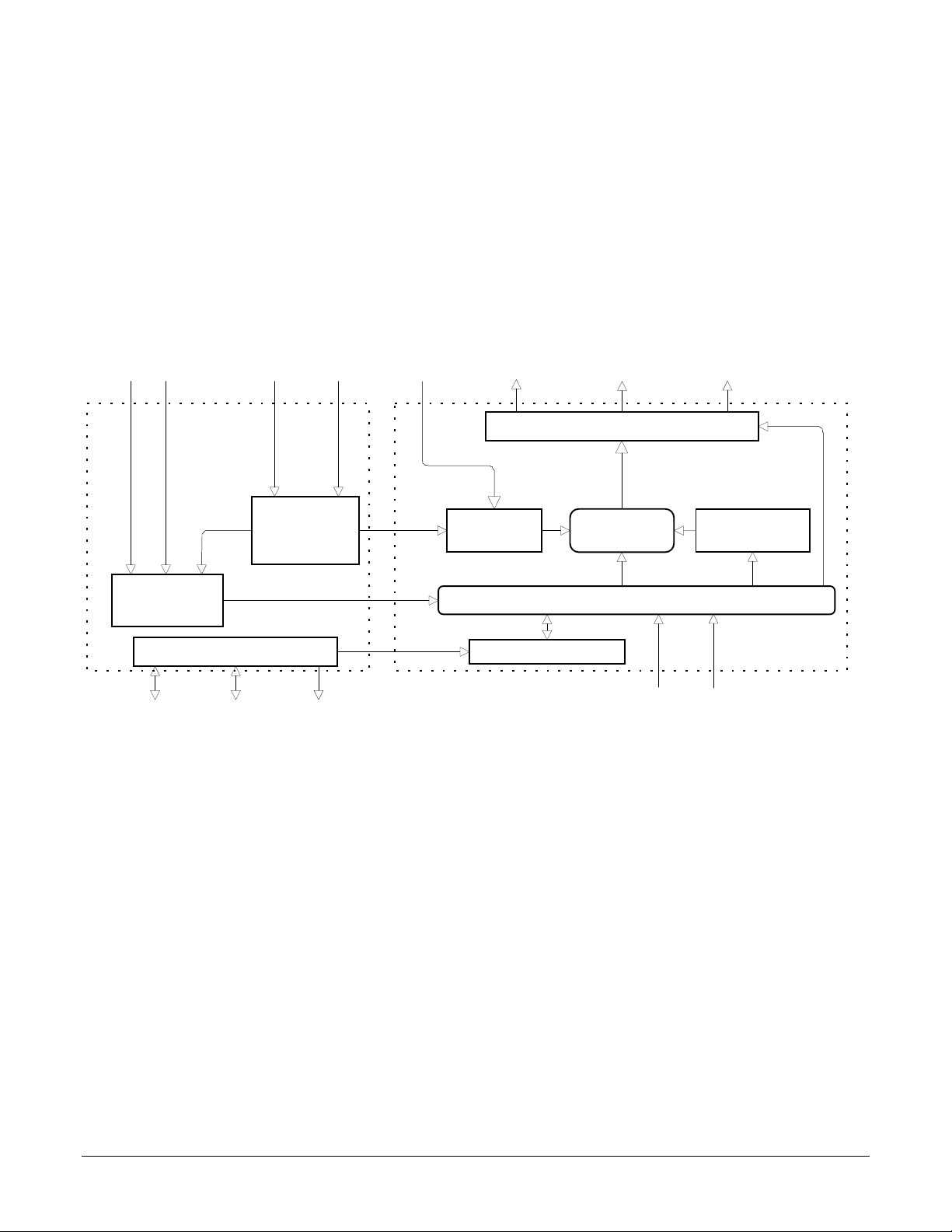
1/a
I/O Chip
Internal Block Diagram
1/a 1/a
Parallel I nput
(-P chipset only)
8 data
2 Control
PWM sign,
mag
1/phase 2
Motor Output
DAC address
DAC data
16
DAC, PWM signal generator (1-4 channels)
CP Chip
Quadrature
decoder
counter (1-4)
Position capture
register (1-4)
Host I/O controller
185
host interr uptDataControl
The above figure shows an internal block diagram for the MC1401A
and MC1401A-P series motion processors.
Each servo axis inputs the actual location of the axis using either
incremental encoder signals or signals from a parallel-word input device
such as an absolute encoder or resolver. If incremental signals are
used then the incoming A, and B quadrature data stream is digitally
filtered, and then passed on to a high speed up/down counter. Using
the parallel-word interface a direct binary-encoded position of up to 16
bits is read by the chipset. Regardless of the encoder input method this
position information is then used to maintain a 32-bit actual axis
position counter.
If incremental feedback is used, then the chipset also supports the
ability to capture the instantaneous position of each axis using an
external trigger signal. The captured value may then later be retrieved
by the host processor.
Position
register (1-4)
Host command
generation and digital servo loop closure. In this mode the motor output
value is controlled by the servo filter. Open loop mode, which is used
for direct motor-control operations only, does not use the output of the
servo filter, and allows the motor output value to be controlled directly
by the host processor.
When closed loop mode operations are used the actual axis position is
combined with the target position generated by the trajectory profile
generator to calculate a position error, which is passed through a PID
filter. The resultant value is then output by the chipset to an external
amplifier using either PWM or DAC signals.
The following table summarizes the operational parameters of the
MC1401-series chipsets.
Digital Servo
filtering (1-4)
System Registers (1-4)
1/a
PosLimit
NegLimit
Trajectory profile
generator (1-4)
1/a
The chipset can be operated in two modes. Closed loop mode, which is
the normal operating mode of the chipset, performs trajectory
20

MC1401-series Chipset Operational Parameters
Available configurations: 4 axes with incremental quadrature encoder input (MC1401A)
2 axes with incremental quadrature input (MC1201A)
1 axis with incremental quadrature input (MC1101A)
4 axes with parallel word encoder input (MC1401A-P)
2 axes with parallel word encoder input (MC1201A-P)
1 axes with parallel word encoder input (MC1101A-P)
Operating modes: Closed loop (motor command is driven from output of servo filter)
Open loop (motor command is driven from user-programmed register)
Position range: -1,073,741,824 to 1,073,741,823 counts
Velocity range: -16,384 to 16,383 counts/sample with a resolution of 1/65,536 counts/sample
Acceleration range:
Jerk range:
Trajectory profile generator modes: S-curve (host commands final position, max velocity, max acceleration, and jerk)
Electronic gear ratio range: 32768:1 to 1:32768 (negative and positive direction)
Filter modes: PID+Vff (standard PID loop plus velocity feedforward plus bias offset)
Filter parameter resolution: 16 bits
Motor output modes: PWM (10 bits resolution @ 24.5 Khz)
Max incremental. encoder rate: Incremental: 1.0 Mcounts/sec Parallel-word: 80.0 Mcounts/sec
Parallel encoder word size: 16 bits (read in 2 byte reads) (-P version parts only)
Parallel encoder read rate: 10 kHz (reads all axes every 100 uSec)
Servo loop rate range: standard, -P parts: 100* uSec minimum, 3,276 mSec max.
Max servo loop rate: standard, -P parts: 100* uSec per enabled axis.
# of limit switches per axis 2 (one for each direction of travel)
# of position capture triggers: 2 (index, home signal)
Capture trigger latency: 160 nSec
# of host commands: 94
S-curve profile: - 1/2 to + 1/2 counts/sample2 with a resolution of 1/65,536 counts/sample
All others: -16,384 to 16,383 counts/sample2 with a resolution of 1/65,536 counts/sample
-1/2 to +1/2 counts/sample3, with a resolution of 1/4,294,967,296 counts/sample
Trapezoidal (host commands final position, max velocity and acceleration)
Velocity contouring (host commands max. velocity, acceleration)
Electronic Gear (Encoder position of one axis is used as position command for another axis). A total of 2
electronic gears are supported (2 encoders and 1 output each). Not available in MC1101A
DAC 16 bits
2.
2
3
* Exact servo loop time is 101.12 uSec, 100 uSec is an approximation
Trajectory Profile Generation
The trajectory profile generator performs calculations to determine the
target position, velocity and acceleration at each servo loop. These
calculations are performed taking into account the current profile mode,
as well as the current profile parameters set by the host. Four trajectory
profile modes are supported:
- S-curve point to point
- Trapezoidal point to point
- Velocity contouring
- Electronic Gear
The commands to select these profile modes are
SET_PRFL_S_CRV (to select the s-curve mode), SET_PRFL_TRAP
(to select the trapezoidal mode) SET_PRFL_VEL (to select the
velocity contouring mode) and SET_PRFL_GEAR (to select the
electronic gear mode).
Throughout this manual various command mnemonics will be
shown to clarify chipset usage or provide specific examples. See
the Host Communications section for a description of host
command nomenclature.
21
 Loading...