

Page 1
Advanced Brushless Moto r
j
Features
Supports 3-phase as well as 2-phase
brushless motors
Performs trajectory generation, servo
loop closure, and commutation
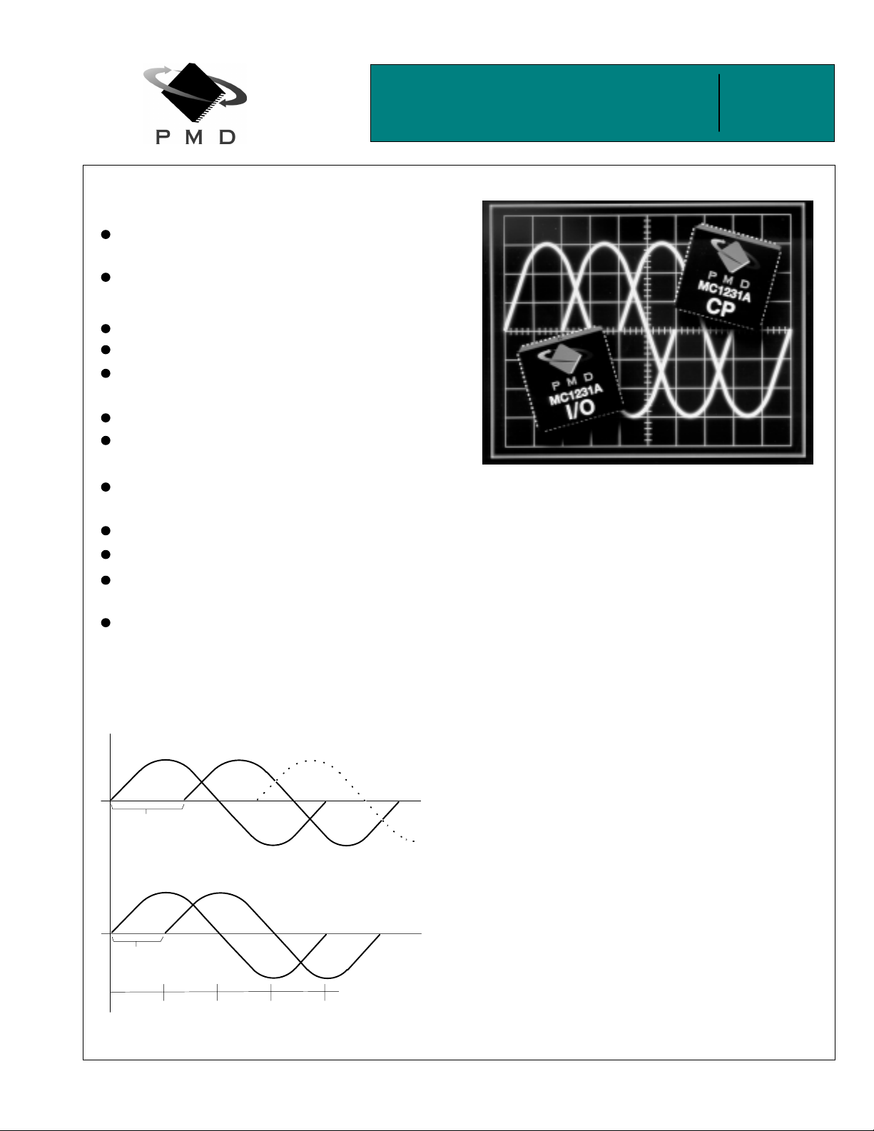
Ultra-smooth sinusoidal commutation
Open or closed loop operation
Software and feature-com pat ible w ith
other 1st generation PMD chipsets
Available in 1 or 2 axis configurations
32-bit position, velocity, acceleration and
erk trajectory profile registers
Choice of S-curve, trapezoidal, or
contoured velocity profile modes
Electronic Gearing
Two travel-limit switches per axis
Choice of PWM or DAC motor output
signals
Easy-to-use packet-oriented command
protocol
Control Chipset
General Description
The MC1231A is a dedicated motion processor which functions
as a complete chi p-based motor controller. Packaged i n a 2-IC
chipset, this device performs trajectory generation, servo loop
closure, and sinusoidal commutation. The chipset inputs
incremental encoder signals and outputs PWM or
DAC-compati b l e mo to r c omm and signals. The MC 1 231A is
available in a one, or a two-axis configuration.
MC1231A
MC1131A
The MC1231A is functionally similar to other members of
Commutation Waveforms
Phase A Phase B Phase C
Phase A Phase B
Performance Motion Dev ices, In c. 12 Waltham St. Le xington, M A 02421 te l: 781. 674.98 60 fax: 781.674.9 861
3-Phase Brushless
2-Phase Brushless
PMD's 1st generation chipset family however it adds the ability
to perform sinusoidal commutation of brushless motors. All of
these devices provide sophisticated motion control capabilities
allowing the creation of comp lex profile sequences with very low
tracking errors.
Both two and three-phase brushless motors are supported by
the MC1231A. Wh en used with two-phase brushless motors
each phase is separated by 90 d egrees. When used with
3-phase brushless motors each phase is separated by 120
degress. The commutation angle is continuously calculated
using the encoder position. User-programmable commutation
parameter s allow a very wide rang e of encoders and motors to
be controlled.
The chipset is controlled by a host processor which interfaces
with the chipse t via an 8-bit, bi-directional port. Commun ic ations
to/from the chi pset consist of pack et-oriented m essages.
The chipset is packaged in 2 68- pin PLCC package s. Both
chips utilize CMOS technology and are powered by 5 volts.
Doc. Rev. 10.05, Nov 1997
www.pmdcorp.com
Page 2

Table of Contents
Product Family Overview.......................................Page 3
Introduction........................................................... Page 3
Family Summary................................................... Page 3
Electrical Characteristics....................................... Page 4
Absolute Maximum Ratings.................................. Page 4
Operating Ratings................................................. Page 4
DC Electrical Characteristics................................ Page 5
AC Electrical Characteristics................................Page 5
I/O Timing Diagrams............................................. Page 7
Pinouts....................................................................Page 12
MC1231A, MC1131A............................................ Page 12
Pin Descriptions.................................................... Page 13
Theory of Operations............................................. Page 17
Operational Parameters.......................................Page 18
Trajectory Profile Generation................................ Page 18
S-curve Point to Point....................................... Page 19
Trapezoidal Point to Point.................................Page 20
Velocity Contouring...........................................Page 20
Electronic Gear................................................. Page 21
Trajectory Control................................................. Page 21
Halting the Trajectory ....................................... Page 21
Motion Complete Status...................................Page 22
Digital Servo Filtering ........................................... Page 22
Motor Bias........................................................ Page 23
Motor Limit........................................................Page 23
Parameter Loading & Updating............................Page 23
Manual Update.................................................Page 24
Breakpoints....................................................... Page 24
External Breakpoints and Homing.................... page 25
Disabling Automatic Profile Update..................Page 25
Travel Limit Switches............................................ Page 25
Motion Error Detection.......................................... Page 26
Recovering From a Motion Error......................Page 26
Servo Loop Control & Timing............................... Page 26
Host Communications .......................................... Page 27
Electrical Interface............................................ Page 27
Packet Format..................................................Page 27
Packet Checksum............................................. Page 28
Illegal Commands............................................. Page 28
Command Errors..............................................Page 28
Axis Addressing................................................ Page 29
Axis Status............................................................ Page 29
Status Word...................................................... Page 29
Miscellaneous Mode Status Word.....................Page 29
Host Interrupts.......................................................Page 30
Encoder Position Feedback..................................Page 31
Encoder FIltering...............................................Page 31
High Speed Position Capture............................Page 31
Index Pulses and Commutation........................Page 31
Motor Outputs.......................................................Page 31
Motor Output Control.........................................Page 32
Sinusoidal Commutation.......................................Page 31
Commutation Waveforms..................................Page 33
Commutation Parameters.................................Page 33
Index Pulse Referencing...................................Page 33
Commutation Error Detection............................Page 34
Phase Initialization............................................Page 34
Phase Initialization Programming......................Page 35
Adjusting The Commutation Angle....................Page 36
Encoder Pre-Scalar...........................................Page 37
Velocity-Based Phase Advance........................Page 37
Phase Info Status Word....................................Page 37
Commutation Command Summary...................Page 38
Motor Output Configuration...............................Page 38
Motor Output Signal Interpretation....................Page 38
DAC16 Decoding...............................................Page 39
PWM Decoding.................................................Page 39
Host Commands .....................................................Page 40
Command Summary.............................................Page 40
Command Reference............................................Page 42
Axis Control.......................................................Page 42
Profile Generation.............................................Page 43
Digital Filter.......................................................Page 46
Parameter Update.............................................Page 49
Interrupt Processing..........................................Page 51
Status/Mode......................................................Page 52
Encoder.............................................................Page 53
Motor.................................................................Page 54
Miscellaneous ...................................................Page 55
Commutation.....................................................Page 57
Application Notes ...................................................Page 62
Interfacing to ISA bus............................................Page 62
PWM Motor Interface............................................Page 64
16-Bit Parallel DAC Motor interface......................Page 66
Performance Motion Devices, Inc. does not assume any responsibility for use of any circuitry described in this manual, nor does it make
any guarantee as to the accuracy of this manual. Performance Motion Devices, Inc. reserves the right to change the circuitry described in
this manual, or the manual itself, at any time.
The components described in this manual are not authorized for use in life-support systems without the express written permission of
Performance Motion Devices, Inc..
2
Page 3

Product Family Overview
MC1401 series MC1231 series MC1241 series MC1451 series
# of axes 4, 2, or 1 2 or 1 2 or 1 4, 2, or 1
Motors Supported DC Servo Brushless Servo Stepper Stepper
Encoder Format Incremental (no dash version)
and Parallel ('-P' version)
Output Format DC servo Sinusoidally
S-curve profiling Yes Yes Yes Yes
Electronic gearing Yes Yes Yes Yes
On-the-fly changes Yes Yes Yes Yes
Limit switches Yes Yes Yes Yes
PID & feedforward Yes Yes - -
PWM output Yes Yes Yes -
DAC-compatible output Yes Yes Yes -
Pulse & direction output ---Yes
Index & Home signal Yes Yes Yes Yes*
Chipset p/n's MC1401A, MC1401A-P (4 axes)
MC1201A, MC1201A-P (2 axes)
MC1101A, MC1101A-P (1 axis)
Developer's Kit p/n's: DK1401A, DK1401A-P DK1231A DK1241A DK1451A
* optional using third I.C. ('-E' version)
Incremental Incremental Incremental*
Microstepping Pulse and Direction
commutated
MC1231A (2 axes)
MC1131A (1 axis)
MC1241A (2 axes)
MC1141A (1 axis)
MC1451A, MC1451A-E (4 axes)
MC1251A, MC1251A-E (2 axes)
MC1151A, MC1151A-E (1 axis)
Introduction
This manual describes the operational characteristics of the MC1231A,
and MC1131A Motion Processors. These devices are members of
PMD's 1st generation motion processor family, which consists of 16
separate products organized into four groups.
Each of these devices are complete chip-based motion controllers.
They provide trajectory generation and related motion control functions.
Depending on the type of motor controlled they provide servo loop
closure, on-board commutation for brushless motors, and high speed
pulse and direction outputs. Together these products provide a
software-compatible family of dedicated motion processor chips which
can handle a large variety of system configurations.
Each of these chips utilize a similar architecture, consisting of a highspeed DSP (Digital Signal Processor) computation unit , along with an
ASIC (Application Specific Integrated Circuit). The computation unit
contains special on-board hardware such as a multiply instruction that
makes it well suited for the task of servo control.
Along with a similar hardware architecture these chips also share most
software commands, so that software written for one chipset may be reused with another, even though the type of motor may be different.
This manual describes the operation of the MC1231A and
MC1131A chipsets. For technical details on other members of
PMD's 1st generation motion processors see the corresponding
product manual.
Family Summary
MC1401 series (MC1401A, MC1201A, MC1101A, MC1401A-P,
MC1201A-P, MC1101A-P)
encoder signals (standard version) or parallel word encoder signals
(-P version) and output a motor command in either PWM or DACcompatible format. These chipsets come in 1, 2 or 4 axis versions
and can be used with DC brushed motors, or brushless motors using
external commutation.
MC1231A series (MC1231A, MC1131A) -
incremental quadrature encoder signals and output sinusoidally
commutated motor signals appropriate for driving brushless motors.
They are available in one or two axis versions. Depending on the
motor type they output two or three phased signals per axis in either
PWM or DAC-compatible format.
MC1241 series (MC1241A, MC1141A)
internal microstepping generation for stepping motors. They are
available in a one or a two-axis version. Two phased signals are
output per axis in either PWM or DAC-compatible format. An
incremental encoder signal can be input to confirm motor position.
MC1451 series (MC1451A, MC1251A, MC1151A, MC1451A-E,
MC1251A-E, MC1151A-E) -
pulse and direction signal output appropriate for driving step motorbased systems. They are available in a one, two, or four-axis version
and are also available with quadrature encoder input.
Each of these chipsets has an associated Chipset Developer's
Kit available for it. For more information contact your PMD
representative.
- These chipsets take in incremental
These chipsets take in
- These chipsets provide
These chipsets provide very high speed
3
Page 4
Electrical Characteristics
Overview
Interconnections between the two chips consist of a data bus and
various control and synchronization signals. The following table
summarizes the signals that must be interconnected for the chipset to
function properly. For each listed signal the I/O chip pin on the left side
of the table is directly connected to the pin to the right.
The MC1231A consists of two 68 pin PLCC's both fabricated in CMOS.
The Peripheral Input/Output IC (I/O chip) is responsible for interfacing
to the host processor and to the position input encoders. The Command
Processor IC (CP chip) is responsible for all host command, trajectory,
servo, and commutation computations, as well as for outputting the
PWM and DAC signals.
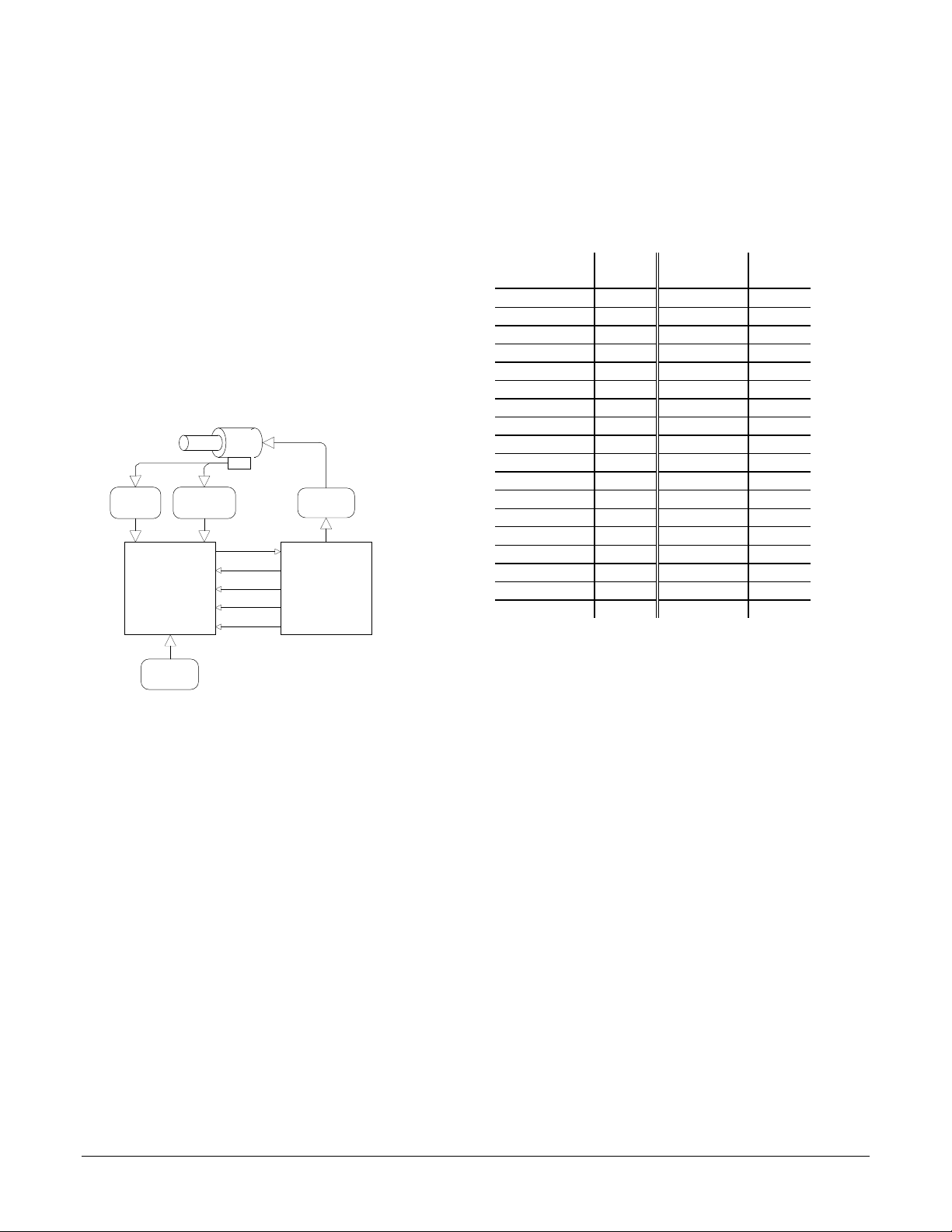
The following figure shows a typical system block diagram, along with
the pin connections between the I/O chip and the CP chip.
Motor
(4 axis)
Encoder
(1-2 axis)
Hall Sensors
I/O
Host
Processor
(1 - 2 axis)
Data4-11
I/OAddr0-3
I/OWrite
I/OCntrl0-3
ClkOut
Amplifier
(1-2 axis)
CP
I/O Chip Signal
Name
I/O Chip
Pin
CP Chip
Signal Name
CP Chip
Pin
CPData4 18 Data4 50
CPData5 5 Data5 49
CPData6 6 Data6 46
CPData7 7 Data7 43
CPData8 8 Data8 40
CPData9 17 Data8 39
CPData10 3 Data10 36
CPData11 1 Data11 35
CPAddr0 68 I/OAddr0 28
CPAddr1 27 I/OAddr1 9
CPAddr2 29 I/OAddr2 6
CPAddr3 12 I/OAddr3 5
CPCntr0 20 I/OCntr0 16
CPCntr1 36 I/OCntr1 18
CPCntr2 22 I/OCntr2 68
CPCntr3 63 I/OCntr3 67
CPWrite 2 I/OWrite 15
CPClk 46 ClkOut 19
For a complete description of all pins see the 'Pin Descriptions'
section of this manual.
The CP and I/O chips function together as one integrated motion
processor. The major components connected to the chip set are the
Encoder (2, or 1 axes), (optionally) the motor Hall-sensors (2 or 1 axes),
the motor amplifier (2, or 1 axes), and the host processor.
The encoder signals are input to the I/O chip in quadrature format. Two
signals encode the position, and an optional index signal contains a
once-per-rotation locating signal.
Hall sensors may be connected to the chipset to provide phase
initialization information, although this is not required. Three Hall sensor
signals are input per axis.
The chipset's motor output signals are connected to the motor amplifier.
Two types of output are provided; PWM (pulse width modulation), and
DAC-compatible signals used with an external DAC (digital to analog
converter). Because the output signals are commutated, more than one
motor output signal will be output per axis. See Theory of Operations
section on sinusoidal motor commutation for details.
The host processor is interfaced via an 8-bit bi-directional bus and
various control signals. Host communication is coordinated by a
ready/busy signal, which indicates when communication is allowed.
Absolute Maximum Ratings
Unless otherwise stated, all electrical specifications are for both
the I/O and CP chips.
Storage Temperature, Ts.....................-55 deg. C to +150 deg. C
Supply Voltage, Vcc.............................-0.3 V to +7.0 V
Power Dissipation, Pd..........................650 mW (I/O and CP
combined)
Operating Ratings
Operating Temperature, Ta .................0 deg. C to +70 deg. C
Nominal Clock Frequency, Fclk...........25.0 Mhz
Supply Voltage, Vcc.............................4.75 V to 5.25 V
* Industrial and Military operating ranges also available. Contact your
PMD representative for more information.
4
Page 5

DC Electrical Characteristics
(Vcc and Ta per operating ratings, Fclk = 25.0 Mhz)
Symbol Parameter Min. Max. Units Conditions
Vcc Supply Voltage 4.75 5.25 V
Idd Supply Current 100 mA open outputs
Input Voltages
Vih Logic 1 input voltage 2.0 Vcc + 0.3 V
Vil Logic 0 input voltage -0.3 0.8 V
Vihclk Logic 1 voltage for clock pin
(ClkIn)
Vihreset Logic 1 voltage for reset pin
(reset)
Output Voltages
Voh Logic 1 Output Voltage 2.4 V @CP Io = 300 uA
Vol Logic 0 Output Voltage 0.33 V @CP Io = 2 mA
Iout Tri-State output leakage current -20 20 uA 0 < Vout < Vcc
Iin Input current -50 50 uA 0 < Vi < Vcc
Iinclk Input current ClkIn -20 20 uA 0 < Vi < Vcc
3.0 Vcc+0.3 V
4.0 Vcc+0.3 V
AC Electrical Characteristics
(see reference timing diagrams)
(Vcc and Ta per operating ratings; Fclk = 25.0 Mhz)
(~ character indicates active low signal)
@I/O Io = 4 mA
@I/O Io = 4 mA
Timing Interval T# Min. Max. Units
Encoder and Index Pulse Timing
Motor-Phase Pulse Width T1 1.6 uS
Dwell Time Per State T2 0.8 uS
Index Pulse Setup and Hold
(relative to Quad A and Quad B low)
Reset Timing
Stable Power to Reset 0.25 Sec
Reset Low Pulse Width 1.0 uS
Clock Timing
Clock Frequency (Fclk) 6.7 25.6 Mhz
Clock Pulse Width T4 19.5 75 (note 2) nS
Clock Period T5 39 149 (note 2) nS
T3 0 uS
5
Page 6

Timing Interval T# Min. Max. Units
Command Byte Write Timing
~HostSlct Hold Time T6 15 2000 (note 3) nS
~HostSlct Setup Time T7 10 nS
HostCmd Setup Time T8 10 nS
Host Cmd Hold Time T9 25 nS
HostRdy Delay Time T13 70 nS
~HostWrite Pulse Width T14 50 nS
Write Data Setup Time T15 35 nS
Write Data Hold Time T16 30 nS
Data Word Read Timing
~HostSlct Hold Time T6 15 2000 (note 3) nS
~HostSlct Setup Time T7 (read only) - 20 nS
HostCmd Setup Time T8 (read only) - 20 nS
HostCmd Hold Time T9 25 nS
Read Data Access Time T10 50 nS
Read Data Hold Time T11 10 nS
~HostRead high to HI-Z Time T12 50 nS
HostRdy Delay Time T13 70 nS
Read Recovery Time T17 60 nS
Data Word Write Timing
~HostSlct Hold Time T6 15 2000 (note 3) nS
~HostSlct Setup Time T7 10 nS
HostCmd Setup Time T8 10 nS
HostCmd Hold Time T9 25 nS
HostRdy Delay Time T13 70 nS
~HostWrite Pulse Width T14 50 nS
Write Data Setup Time T15 35 nS
Write Data Hold Time T16 30 nS
Write Recovery Time T18 60 nS
DAC Interface Timing
I/OAddr Stable to ~I/OWrite setup time T19 35 nS
~I/OWrite Pulse Width T20 56 95 nS
Data Hold Time After ~I/OWrite T21 17 nS
ClkOut Low to I/OAddr stable T22 10 40 nS
ClkOut Low to ~I/OWrite Low T23 75 92 nS
ClkOut Low to Data Valid T24 92 nS
ClkOut Cycle Time T25 160 typical (note 4) nS
I/OAddr Stable to DACSlct High T26 66 nS
~I/OWrite Low to DACSlct High T27 44.5 nS
PWM Output Timing
PWM Output Frequency 24.5 Khz
note 1 ~HostSlct and HostCmd may optionally be de-asserted if setup and hold times are met.
note 2 Chip-set performance figures and timing information valid at Fclk = 25.0 only. For timing information & performance parameters at Fclk <
25.0 Mhz, call PMD.
note 3 Two micro seconds maximum to release interface before chip set responds to command
note 4 ClkOut from CP is 1/4 frequency of ClkIn (CP chip).
6
Page 7
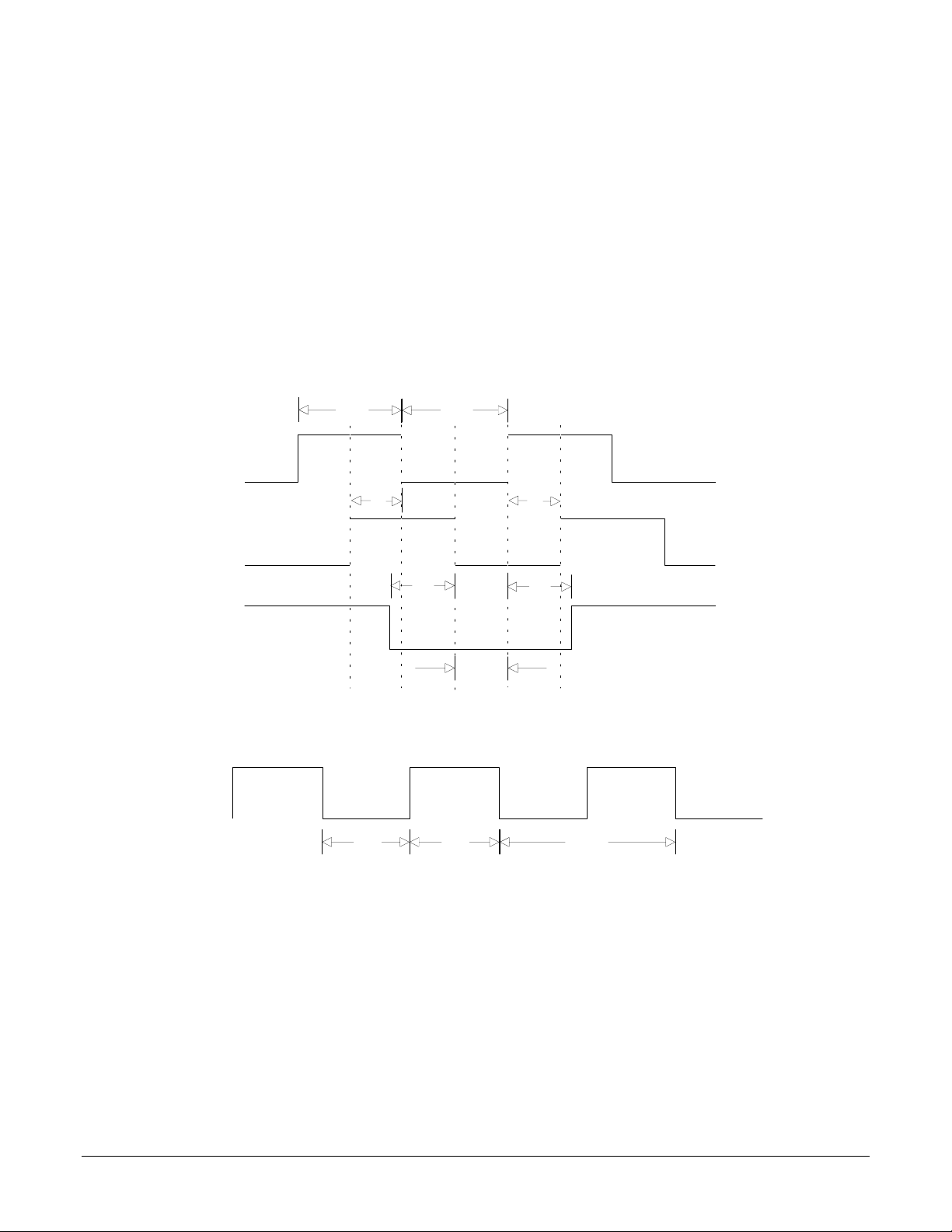
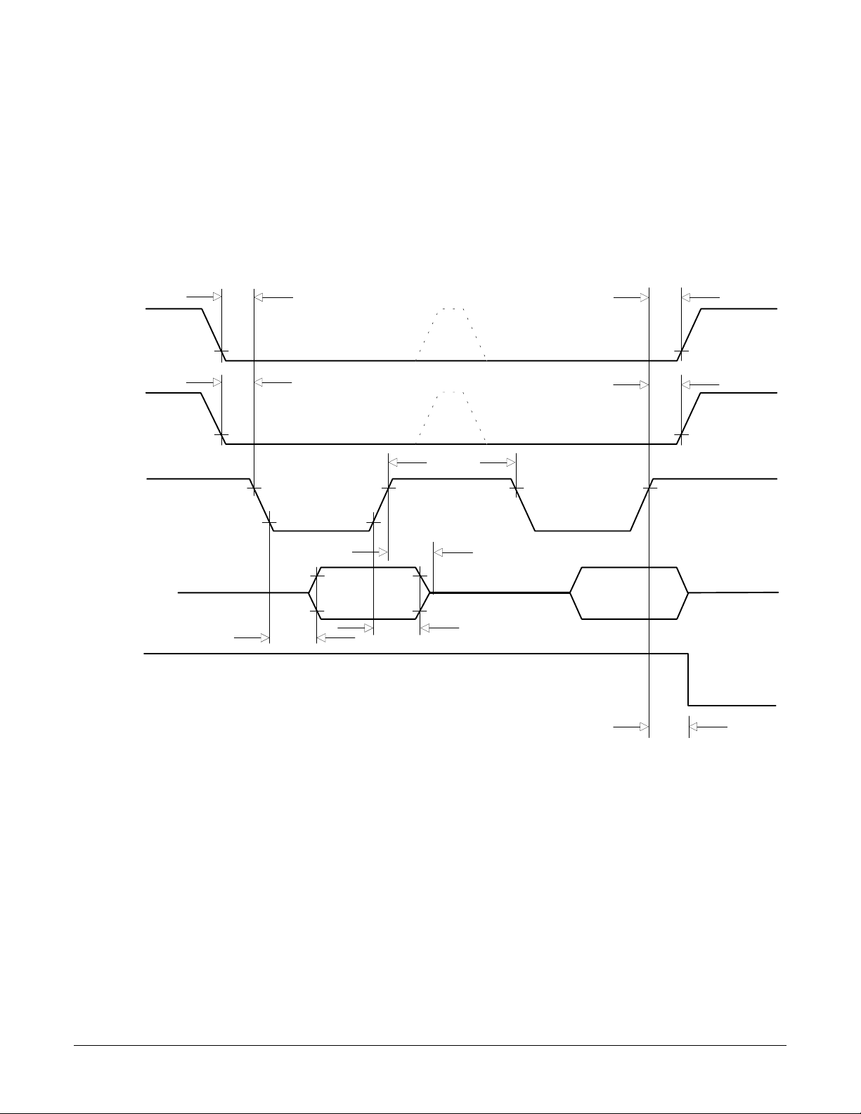
I/O Timing Diagrams
The following diagrams show the MC1231A electrical interface timing. T#' values are listed in the above timing chart.
Quadrature Encoder Input Timing
Quad A
Quad B
~Index
ClkIn
T1
T1
T2 T2
T3
Clock Timing
T3
T4 T4 T5
Index = ~A * ~B * ~IND
7
Page 8
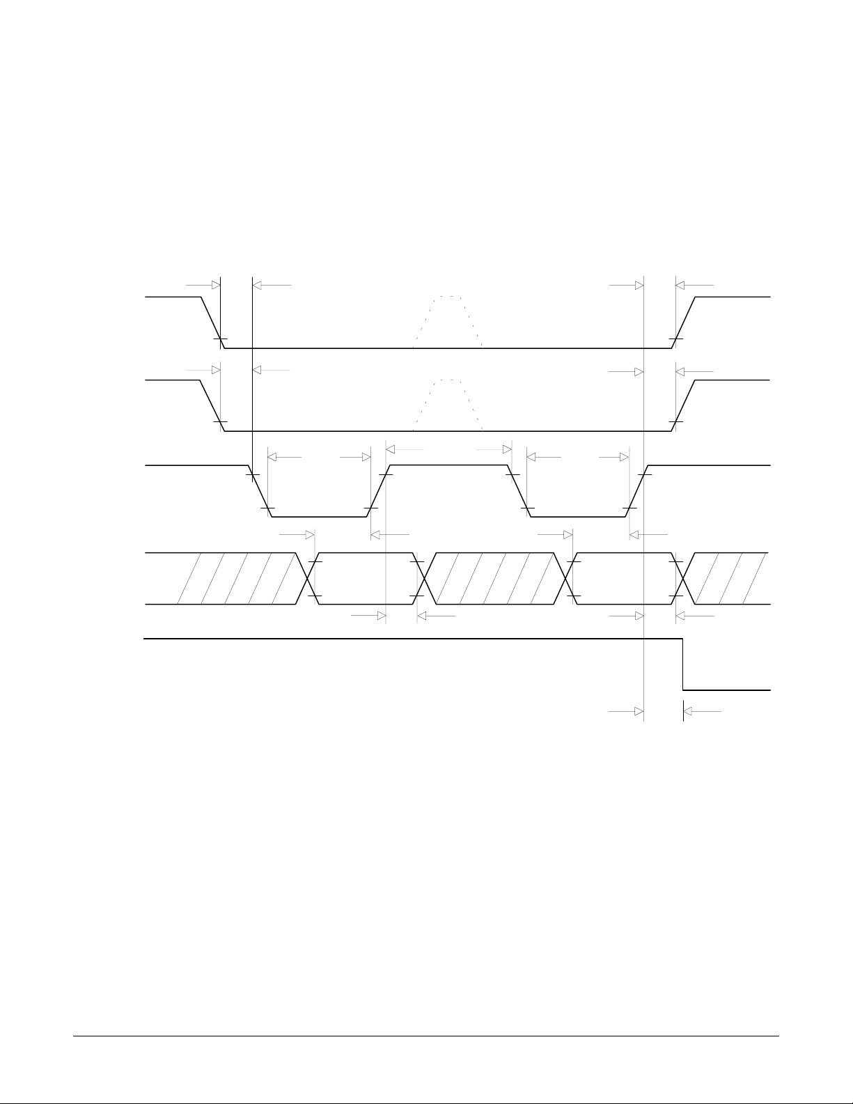
Command Byte Write TIming
~HostSlct
HostCmd
~HostWrite
HostData0-7
HostRdy
T7
T8
T6
T9
T14
T15
T16
T13
8
Page 9
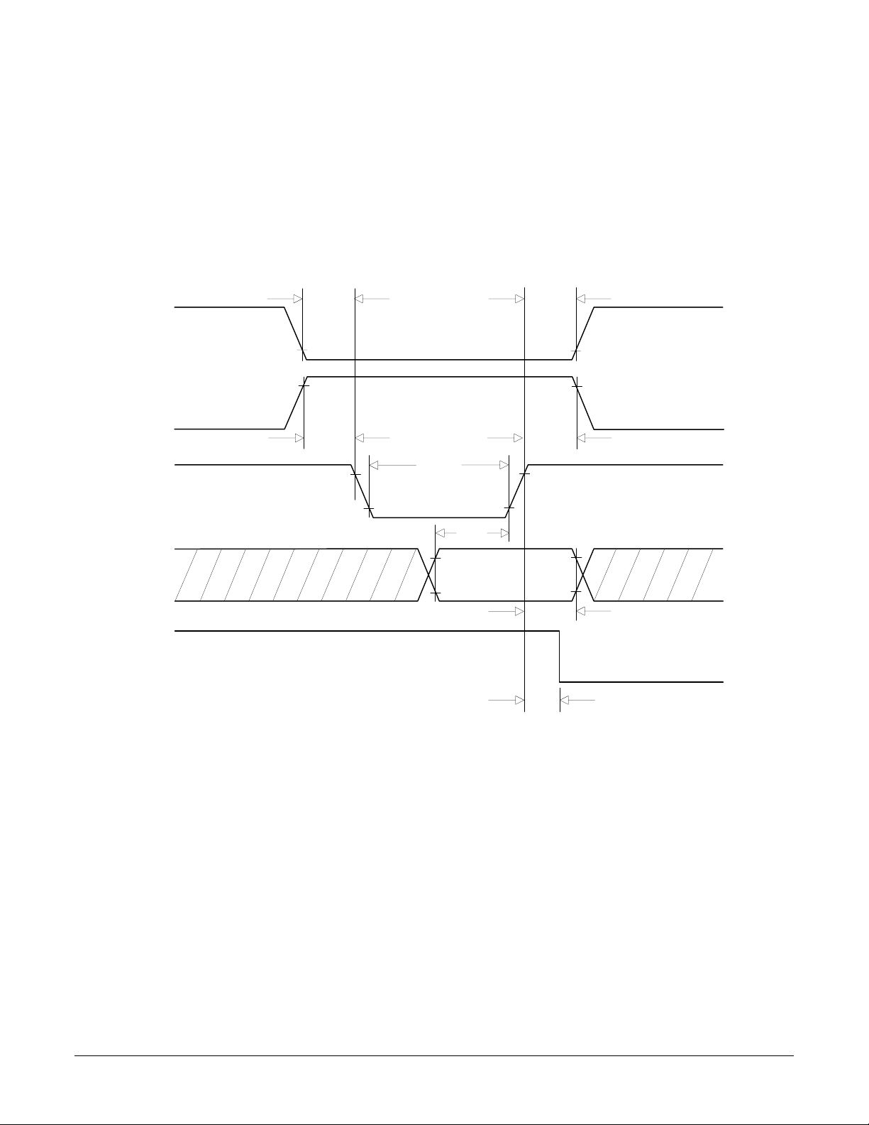
Data Word Read TImi ng
~HostSlct
HostCmd
~HostRead
HostData0-7
HostRdy
T7
T6
Note 1
T8
Note 1
T9
T17
T12
High-Z High-Z High-Z
High
Byte
T10
T11
Low
Byte
T13
9
Page 10
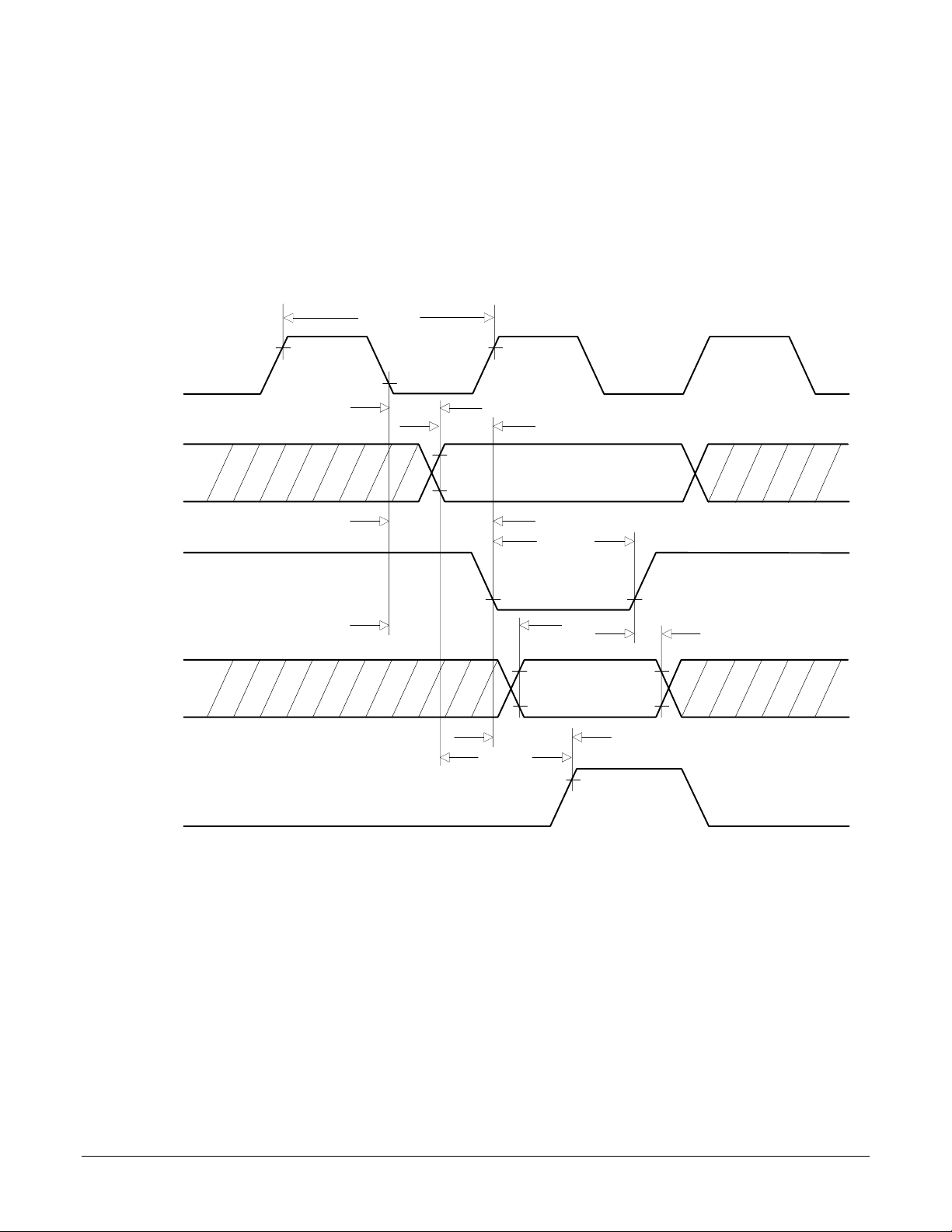
Data Word Write TIming
~HostSlct
HostCmd
~HostWrite
HostData0-7
HostRdy
T7
T8
T14
T15
High
Byte
T16
T18
Note 1
Note 1
T6
T9
T14
T15
Low
Byte
T16
10
T13
Page 11
ClkOut
I/OAddr
~I/OWrite
DAC Interface Timing
T25
T22
T19
T23
T20
Data 0-11,
DACAddr0,1
DACSlct
T24
T21
T27
T26
11
Page 12

Pinouts
9
1
61
9
1
61
10
I/O
(Top view)
26
27 43
60
10
60
CP
(Top view)
44
26
27 43
44
MC1231A Pinouts
4, 21, 25, 38, 55
VCC
QuadA1
28
QuadB1
42
Index1
24
Home1
13
QuadA2
26
QuadB2
30
Index2
9
Home2
23
Hall1A
40
Hall1B
35
Hall1C
19
Hall2A
39
Hall2B
34
Hall2C
16
DACSlct
33
CPClk
46
I/OClkIn
52
I/OClkOut
45
CPAddr2
29
CPAddr3
12
CPWrite
2
CPCntrl0
20
CPCntrl1
36
I/O
GND
CPCntrl2
CPCntrl3
HostCmd
HostRdy
HostRead
HostWrite
HostSlct
HostIntrpt
HostData0
HostData1
HostData2
HostData3
HostData4
HostData5
HostData6
HostData7
CPData4
CPData5
CPData6
CPData7
CPData8
CPData9
CPData10
CPData11
CPAddr0
CPAddr1
22
63
41
37
51
47
48
44
50
61
53
65
67
62
64
60
18
5
6
7
8
17
3
1
68
27
66
65
30
29
24
19
17
16
18
68
67
64
63
62
61
8
7
2
1
PWMMag1
PWMMag2
PWMMag3
PWMMag4
PWMMag5
PWMMag6
DAC16Addr0
DAC16Addr1
ClkIn
ClkOut
Reset
I/OCntrl0
I/OCntrl1
I/OCntrl2
I/OCntrl3
DACLow0
DACLow1
DACLow2
DACLow3
4, 22, 33
VCC
CP
GND
Data0
Data1
Data2
Data3
Data4
Data5
Data6
Data7
Data8
Data9
Data10
Data11
I/OAddr0
I/OAddr1
I/OAddr2
I/OAddr3
I/OWrite
PosLimit1
PosLimit2
NegLimit1
NegLimit2
60
59
58
57
50
49
46
43
40
39
36
35
28
9
6
5
15
52
45
51
44
14, 15, 32, 49, 54, 66
3, 34
MC1131A Pinouts
4, 21, 25, 38, 55
VCC
HostCmd
QuadA1
28
QuadB1
42
Index1
24
Home1
13
Hall1A
40
Hall1B
35
Hall1C
19
DACSlct
33
CPClk
46
I/OClkIn
52
I/OClkOut
45
CPAddr2
29
CPAddr3
12
CPWrite
2
CPCntrl0
20
CPCntrl1
36
CPCntrl2
22
CPCntrl3
63
CPAddr0
68
CPAddr1
27
I/O
GND
14, 15, 32, 49, 54, 66
HostRdy
HostRead
HostWrite
HostSlct
HostIntrpt
HostData0
HostData1
HostData2
HostData3
HostData4
HostData5
HostData6
HostData7
CPData4
CPData5
CPData6
CPData7
CPData8
CPData9
CPData10
CPData11
41
37
51
47
48
44
50
61
53
65
67
62
64
60
18
5
6
7
8
17
3
1
30
29
24
19
17
16
18
68
67
64
63
62
61
8
7
2
PWMMag1
PWMMag2
PWMMag3
DAC16Addr0
DAC16Addr1
ClkIn
ClkOut
Reset
I/OCntrl0
I/OCntrl1
I/OCntrl2
I/OCntrl3
DACLow0
DACLow1
DACLow2
DACLow3
12
4, 22, 33
VCC
CP
GND
3, 34
Data0
Data1
Data2
Data3
Data4
Data5
Data6
Data7
Data8
Data9
Data10
Data11
I/OAddr0
I/OAddr1
I/OAddr2
I/OAddr3
I/OWrite
PosLimit1
NegLimit 1
60
59
58
57
50
49
46
43
40
39
36
35
28
9
6
5
15
52
51
Page 13

Pin Descriptions
The following tables provide pin descriptions for the MC1231-series chipsets.
IC Pin Name Pin # Description/Functionality
I/O Chip Pinouts
I/O QuadA1
QuadB1
QuadA2
QuadB2
I/O ~Index1
~Index2
I/O ~Home1
~Home2
28
42
26
30
24
9
13
23
Quadrature A, B channels for axis 1 - 2 (input). Each of these 2 pairs of quadrature (A, B)
signals provide the position feedback for an incremental encoder. When the encoder is
moving in the positive, or forward direction, the A signal leads the B signal by 90 degs.
NOTE: Many encoders require a pull-up resistor on each of these signals to establish a
proper high signal (check the encoder electrical specifications)
NOTE: For MC1231A all 4 pins are valid. For MC1131A pins for axes 1 only are valid. Invalid
axis pins can be left unconnected
Index encoder signals for axis 1-2 (input). Each of these 2 signals indicate the index flag
state from the encoder. A valid index pulse is recognized by the chip set when the index flag
transitions low, followed by the corresponding A and B channels of the encoder transitioning
low. The index pulse is recognized at the later of the A or B transitions. If not used this signal
must be tied high.
NOTE: For MC1231A both pins are valid. For MC1131A pins for axes 1 only are valid.
Invalid axis pins can be left unconnected.
Home signals for axis 1-2 (input). Each of these signals provide a general purpose input to
the hardware position capture mechanism. A valid home signal is recognized by the chipset
when the home flag transitions low. These signals have a similar function as the ~Index
signals, but are not gated by the A and B encoder channels. For valid axis pins, If not used,
this signal must be tied high. See below for valid pin definitions for the MC1231A and
MC1131A.
NOTE: For MC1231A both pins are valid. For MC1131A pins for axes 1 only are valid.
Invalid axis pins can be left unconnected.
I/O DACSlct 33 DAC Select (output). This signal is asserted high to select any of the available DAC output
channels. For details on DAC decoding see description of DAC16Addr0-1 signals.
I/O CPClk 46 I/O chip clock (input). This signal is connected directly to the ClkOut pin (CP chip) and
provides the clock signal for the I/O chip. The frequency of this signal is 1/4 the user-provided
ClkIn (CP chip) frequency.
I/O I/OClkIn 52 Phase shifted clock (input). This signal must be connected to I/OClkOut (I/O chip), and inputs
a phase shifted clock signal.
I/O I/OClkOut 45 Phase shifted clock (output). This signal must be connected to I/OClkIn (I/O chip), and
outputs a phase shifted clock signal.
I/O CPAddr0
CPAddr1
CPAddr2
CPAddr3
I/O ~CPWrite 2 I/O chip to CP chip communication write (input). This signal is connected to the ~I/OWrite pin
I/O CPCntrl0
CPCntrl1
CPCntrl2
CPCntrl3
I/O HostCmd 41 Host Port Command (input). This signal is asserted high to write a host command to the chip
68
27
29
12
20
36
22
63
I/O chip to CP chip communication address (input). These 4 signals are connected to the
corresponding I/OAddr0-3 pins (CP chip), and together provide addressing signals to
facilitate CP to I/O chip communication.
(CP chip) and provides a write strobe to facilitate CP to I/O chip communication.
I/O chip to CP chip communication control (mixed). These 4 signals are connected to the
corresponding I/OCntrl0-3 pins (CP chip), and provide control signals to facilitate CP to I/O
chip communication.
set. It is asserted low to read or write a host data word to the chipset
13
Page 14

IC Pin Name Pin # Description/Functionality
I/O HostRdy 37 Host Port Ready/Busy (output). This signal is used to synchronize communication between
the DSP and the host. HostRdy will go low (indicating host port busy) at the end of a host
command write or after the second byte of a data write or read. HostRdy will go high
(indicating host port ready) when the command or data word has been processed and the
chip set is ready for more I/O operations. All host port communications must be made with
HostRdy high (indicating ready).
Typical busy to ready cycle is 67.5 uSec, although it can be longer when host port traffic is
high.
I/O ~HostRead 51 Host Port Read data (input). Used to indicate that a data word is being read from the chip set
(low asserts read).
I/O ~HostWrite 47 Host Port Write data (input). Used to indicate that a data word or command is being written to
the chip set (low asserts write).
I/O ~HostSlct 48 Host Port Select (input). Used to select the host port for reading or writing operations (low
assertion selects port). ~HostSlct must remain inactive (high) when the host port is not in use.
I/O ~HostIntrpt 44 Host Interrupt (output). A low assertion on this pin indicates that a host interrupt condition
exists that may require special host action.
I/O HostData0
HostData1
HostData2
HostData3
HostData4
HostData5
HostData6
HostData7
I/O CPData4
CPData5
CPData6
CPData7
CPData8
CPData9
CPData10
CPData11
I/O Hall1A
Hall1B
Hall1C
Hall2A
Hall2B
Hall2C
50
61
53
65
67
62
64
60
18
5
6
7
8
17
3
1
40
35
19
39
34
16
Host Port Data 0-7 (bi-directional, tri-stated). These signals form the 8 bit host data port used
during communication to/from the chip set. This port is controlled by ~HostSlct, ~HostWrite,
~HostRead and HostCmd.
I/O chip to CP chip data port (bi-directional). These 8 bits are connected to the corresponding
Data4-11 pins on the CP chip, and facilitate communication to/from the I/O and CP chips..
Hall Sensor A, B, and C commutation inputs for axis 1 and 2 (input). Each set of the three
signals for one axis (A, B and C) encodes 6 valid signal states as follows: A on, A and B on,
B on, B and C on, C on, C and A on. An on state is defined as a high signal.
NOTE: These signals should only be connected to Hall sensors that are mounted 120-deg
offset from each other. Schemes which provide Hall signals 60-deg apart will not work.
NOTE: For MC1231A all 6 pins are valid. For MC1131A pins for axis 1 only are valid. Invalid
axis pins can be left unconnected.
I/O Vcc 4, 21, 25, 38, 55 I/O chip supply voltage pin. All of these pins must be connected to the supply voltage. Supply
voltage = 4.75 to 5.25 V
I/O GND 14, 15, 32, 49, 54,66I/O chip ground pin. All of these pins must be connected to the power supply return.
14
Page 15

IC Pin Name Pin # Description/Functionality
CP Chip Pinouts
CP PWMMag1
PWMMag2
PWMMag3
PWMMag4
PWMMag5
PWMMag6
CP PosLimit1
PosLimit2
CP NegLimit1
NegLimit2
8
7
2
1
66
65
52
45
51
44
PWM motor output magnitude signals (output). When the chip set is in PWM output mode
these pins provide the Pulse Width Modulated magnitude signal to the motor amplifier.The
PWM signals are output for each motor axis as follows:
3-Phase Brushless 2-Phase Brushless
Signal Axis # Phase Signal Axis # Phase
PWMMag1 1 A PWMMag1 1 A
PWMMag2 1 B PWMMag2 1 B
PWMMag3 1 C PWMMag3 2 A
PWMMag4 2 A PWMMag4 2 B
PWMMag5 2 B
PWMMag6 2 C
NOTE: If using the MC1231A with one axis in 3-phase and the other axis in 2-phase mode, to
avoid pin conflict, axis 1 should be assigned to 2-phase output, and axis 2 to 3-phase
The PWM resolution is 10 bits, frequency = 24.5Kz.
Positive limit switch input for axis 1-2. These signals provide directional limit inputs for the
positive-side travel limit of the axis. Upon powerup these signals default to "active high"
interpretation, but the interpretation can be set explicitly using the SET_LMT_SENSE
command. (See Host Command Section for more info.) If not used these signals should be
tied low for the default interpretation, or tied high if the interpretation is reversed.
NOTE: For MC1231A both pins are valid. For MC1131A pins for axes 1 only are valid. Invalid
axis pins can be left un connected.
Negative limit switch input for axis 1-2. These signals provide directional limit inputs for the
negative-side travel limit of the axis. Upon powerup these signals default to "active high"
interpretation, but the interpretation can be set explicitly using the SET_LMT_SENSE
command. (See Host Command Section for more info.) If not used these signals should be
tied low for the default interpretation, or tied high if the interpretation is reversed.
NOTE: For MC1231A both pins are valid. For MC1131A pins for axis 1 only are valid. Invalid
axis pins can be left un connected.
CP DAC16Addr0
DAC16Addr13029
CP ClkIn 24 Clock In (input). This pin provides the chip set master clock (Fclk = 25.0 Mhz)
Axis Address used during 16-bit DAC motor command output (output). These signals encode
the motor output axis address as shown in the table below (both 3-phase and 2-phase
waveforms)
Dac16Addr1 Dac16Addr0 Addressed Encoder
Low Low Axis 1 phase A
Low High Axis 1 phase B
High Low Axis 2 phase A
High High Axis 2 phase B
Note: When connecting to 3-phase brushless motors only two of the three required phase
outputs are provided in the DAC output mode. The third phase (phase C) is constructed
external to the chipset, usually by the amplifier. See theory of operations for more
information.
To write a valid DAC motor command value DACSlct (I/O chip) and I/OAddr0-3 (CP chip)
must be high, and I/OWrite (CP chip) must be low. The 16 bit DAC data word is organized as
follows: High twelve bits are in Data0-11 (CP chip), and low 4 bits are in DACLow0-3 (CP
chip).
15
Page 16

IC Pin Name Pin # Description/Functionality
CP ClkOut 19 Clock Out (output). This pin provides a clock output which is 1/4 the ClkIn frequency. This pin
is connected to I/OClkin (I/O chip).
CP ~Reset 17 Master chip set reset (input). When brought low, this pin resets the chip set to its initial
condition. Reset should occur no less than 250 mSec after stable power has been provided
to the chip set.
CP I/OCntrl0
I/OCntrl1
I/OCntrl2
I/OCntrl3
CP Data0
Data1
Data2
Data3
Data4
Data5
Data6
Data7
Data8
Data9
Data10
Data11
CP DACLow0
DACLow1
DACLow2
DACLow3
CP I/OAddr0
I/OAddr1
I/OAddr2
I/OAddr3
CP I/OWrite 15 Multi-purpose write (output). This pin is connected to CPWrite on the I/O chip. It has 2
16
18
68
67
60
59
58
57
50
49
46
43
40
39
36
35
64
63
62
61
28
9
6
5
I/O chip to CP chip communication control (mixed). These signals are connected to the
corresponding CPCntrl0-3 pins on the I/O chip, and provide control signals to facilitate CP to
I/O communication.
Multi-purpose Data0-11. (Bi-directional). These pins have 2 functions:
1) Pins Data4-11 (8 bits total) are connected to the corresponding CPData4-11 pins on the
I/O chip, and are used to communicate between the CP and I/O chips
2) Pins Data0-11 hold the high 12 bits of the DAC output value when the output mode is set
to 16-bit DAC.
DACLow0-3 (output). These pins hold the lowest 4 bits of the 16 bit DAC output word when
the output mode is set to 16 bit DAC. These pins, in conjunction with Data0-11 (providing the
high 12 bits) make up the 16-bit DAC output word.
Multi-purpose Address0-3 (output). These pins are connected to the corresponding CPAddr03 pins on the I/O chip. They have 2 functions; They provide addressing signals to facilitate
communication between the I/O chip and CP chip, and they are used during DAC data
decoding. To read a valid DAC value from Data0-Data11 (CP chip), DACSlct (I/O chip) and
I/OAddr0-3 (CP chip) must all be high, and I/OWrite (CP chip) must be low.
functions:
1) It provides a control signal to the I/O chip to facilitate communication between the I/O chip
and CP chip.
2) It is used during DAC data decoding to read a valid DAC value from Data0-Data11 (CP
chip), DACSlct (I/O chip) and I/OAddr0-3 (CP chip) must all be high, and I/OWrite (CP chip)
must be low.
CP Vcc 4, 22, 33 CP chip supply voltage pin. All of these pins must be connected to the supply voltage. Supply
voltage = 4.75 to 5,.25 V
CP GND 3, 34 CP chip ground pin. All of these pins must be connected to the power supply return.
16
Page 17
Theory of Operations
g
Incremental Encoder
Index B A
Home
1/a
1/a
1/a 1/a
Internal Block Diagram
PWM ma
. DAC address
1/phase
DAC, PWM signal generator (6 channels)
Motor Output
2
DAC data
16
I/O Chip
CP Chip
Quadrature
decoder
counter (2)
Index capture
registe r (2)
Host I/O controller
185
host interruptDataControl
The above figure shows an internal block diagram for the MC1231A
motion processor.
Each servo axis inputs the actual location of the axis using incremental
encoder signals. These encoder signals are digitally filtered for
increased reliability and then passed on to a high speed up/down
counter. This counter is used to maintain a 32-bit actual axis position
register.
The chipset can be operated in two modes. Closed loop mode, which is
the normal operating mode of the chipset, performs trajectory
generation, digital servo loop closure, and sinusoidal commutation. In
this mode the motor output value is controlled by the servo filter. Open
loop mode performs commutation only. It allows the motor output value
to be controlled directly by the host processor.
Commutation
Generator (2)
Position
registe r (2)
Digital Servo
filtering (2)
Trajectory profile
generator (2)
System Reg isters (2)
Host command
1/a
PosLimit
1/a
NegLimit
motor encoder. Two or more commutated signals are generated for
each axis, with each signal being shifted either 90 or 120 degrees from
one another, depending on the motor type.
The resultant commutated signals are then output to the amplifier either
as PWM or DAC signals.
To perform continuous digital servoing, the trajectory and servo
calculations are performed at every sample time for all enabled axes.
The commutation is performed 4 times for each sample time.
The following table summarizes the operational parameters of the
MC1231A-series chipsets.
For either operating mode the desired motor output value is then
combined with the current commutation value from an internal
sinusoidal lookup. The commutation angle is determined using the
17
Page 18

MC1231A-Series Chipset Operational Parameters
Available configurations: 2 axes with internal sinusoidal commutation (MC1231A)
1 axes with internal sinusoidal commutation (MC1131A)
Operating Modes: Closed loop (motor command is driven from output of servo filter)
Open loop (motor command is driven from user-programmed register)
Position Range: -1,073,741,824 to 1,073,741,823 counts
Velocity Range: -16,384 to 16,383 counts/sample with a resolution of 1/65,536 counts/sample
Acceleration Range:
Jerk Range:
Trajectory Profile Generator Modes: S-curve (host commands final position, max velocity, max acceleration, and jerk)
Electronic Gear Ratio Range: 32768:1 to 1:32768 (negative and positive direction)
Filter Modes: PID+Velocity feedforward and motor bias
Filter parameter resolution: 16 bits
Commutation Waveform: Sinusoidal
Phase Initialization Methods: Hall-Based
# of sinusoidal lookups: 256 per electrical cycle
range of commutation cycle: 129 to 2,097,088 (using pre-scalar) counts per electrical cycle
Commutation rate: 15 kHz
Phasing Modes: 120 degrees (used with 3-phase brushless motors)
# of PWM Output Phases: 3-phase brushless motors: 3
# of DAC Output Phases: 2 (all motor types)
Max Incremental. Encoder Rate: 1.75 Mcounts/sec
Servo loop rate range: 270 uSec*minimum, 4,423 mSec max.
Max servo loop rate: 270 uSec* per enabled axis.
# of limit switches per axis 2 (one for each direction of travel)
# of position capture triggers: 2 (index, home signal)
Capture trigger latency: 160 nSec
# of Host commands: 116
S-curve profile: - 1/2 to + 1/2 counts/sample2 with a resolution of 1/65,536 counts/sample
All others: -16,384 to 16,383 counts/sample2 with a resolution of 1/65,536 counts/sample
-1/2 to +1/2 counts/sample3, with a resolution of 1/4,294,967,296 counts/sample
Trapezoidal (host commands final position, max velocity and acceleration)
Velocity contouring (host commands max. velocity, acceleration)
Electronic Gear (Encoder position of one axis is used as position command for another axis). A total of 2
electronic gears are supported (2 encoders and 1 output each). Not available in MC1131A
Algorithmic (briefly energize motor coils)
Microstepping (advance motor to known phase position)
Direct set (explicitly set current commutation angle)
90 degrees (used with 2-phase brushless motors)
2-phase brushless motors: 2
2.
2
3
*Exact servo loop time is 271.36 uSec, 270 is an approximation
Trajectory Profile Generation
The trajectory profile generator performs calculations to determine the
target position, velocity and acceleration at each servo loop. These
calculations are performed using the current profile mode and profile
parameters set by the host. Four trajectory profile modes are supported:
- S-curve point to point
- Trapezoidal point to point
- Velocity contouring
- Electronic Gear
The commands to select these profile modes are
SET_PRFL_S_CRV (to select the s-curve mode), SET_PRFL_TRAP
(to select the trapezoidal mode) SET_PRFL_VEL (to select the
velocity contouring mode) and SET_PRFL_GEAR (to select the
electronic gear mod).
Throughout this manual various command mnemonics will be
shown to clarify chipset usage or provide specific examples. See
the Host Communications section for a description of host
command nomenclature.
18
Page 19
The profile mode may be programmed independently for each axis. For
example axis #1 may be in trapezoidal point to point mode while axis
#2 is in S-curve point to point.
Use the following figure showing a typical S-curve velocity vs. time
graph for reference in reading the next section:
Generally, the axis should be at rest when switching profile modes.
Under certain conditions however, switching into certain profile modes
"on-the-fly" is allowed. See specific profile descriptions for details.
S-curve Point to Point
The following table summarizes the host specified profile parameters
for the S-curve point to point profile mode:
Profile
Parameter
Destination
Position
Maximum
Velocity
Max. Accel.
Jerk
* uses 1/216 scaling. Chipset expects a 32 bit number which
has been scaled by a factor of 65,536 from units of
counts/sample time. For example to specify a velocity of 2.75
counts/sample time, 2.75 is multiplied by 65,536 and the
result is sent to the chipset as a 32 bit integer (180,224 dec.
or 2c000 hex.).
** uses 1/216 scaling. Chipset expects a 16 bit number which
has been scaled by a factor of 65,536 from units of
counts/sample time2. For example to specify an acceleration
of .175 counts/sample time2, .175 is multiplied by 65,536 and
the result is sent to the chipset as a 16 bit integer (11,469
dec. or 2ccd hex).
Representation & Range Units
signed 32 bits
counts
-1,073,741,824 to 1,073,741,823
unsigned 32 bits* (1/2
16
scaling)
counts/smpl
0 to 1,073,741,823
unsigned 16 bits ** (1/2
16
scaling)
counts/smpl
0 to 32,767
unsigned 32 bits *** (1/2
32
scaling)
counts/smpl
0 to 2,147,483,647
PhaseI.Phase
Phase
II.
III.
Phase
IV.
PhaseV.Phase
VI.
Phase
VII.
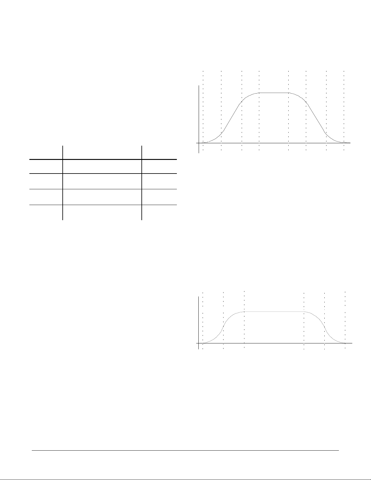
S-curve profile
The S-curve profile drives the axis at the specified jerk until the
maximum acceleration is reached. (phase I). it will then drive the axis at
jerk = 0 (constant acceleration) through phase II. It will then drive the
2
axis at the negative of the specified jerk though phase III, such that the
axis reaches the specified maximum velocity with acceleration = 0. This
3
completes the acceleration phase. At the end of the acceleration phase
of the move, the velocity will be constant, and the acceleration will be 0.
At the appropriate time, the profile will then decelerate (phases V, VI
and VII) symmetrically to the acceleration phase such that it arrives at
the destination position with acceleration and velocity = 0.
There are several conditions where the actual velocity graph of an Scurve motion will not contain all of the segments shown in the above
figure. For example, if the max. acceleration is not reached before the
"half-way" point to the max. velocity, then the actual velocity profile will
not contain a phase II or a phase VI segment (they will have a duration
of 0 servo loops). Such a profile is shown below:
PhaseI.Phase
III.
Phase
IV.
PhaseV.Phase
VII.
*** uses 1/2
has been scaled by a factor of 4,294,967,296 (2
32
scaling. Chipset expects a 32 bit number which
32)
from units
of counts/sample time3. For example to specify a jerk value of
.0075 counts/sample time3, .0075 is multiplied by
4,294,967,296 and the result is sent to the chipset as a 32 bit
integer (32,212,256 dec. or 1eb8520 hex).
S-curve that doesn't reach max. acceleration
Another such condition is if the position is specified such that max.
velocity is not reached. In this case there will be no phase IV, and there
may also be no phase II and VI, depending on where the profile is
"truncated".
While the S-curve profile is in motion, the user is not allowed to
change any of the profile parameters. The axis must be at rest
before a new set of profile parameters can be executed. If
parameters are changed during motion then a 'command error'
19
Page 20
will occur, and all new parameters will be ignored except the
position. See the section of this manual entitled "Command Error"
for more information..
Vel.
Before switching to the S-curve point to point profile mode, the
axis should be at a complete rest.
When the axis is in the S-curve profile mode, the SET_MAX_ACC
command should be used to load the max. acceleration value. The
alternate acceleration loading command SET_ACC can not be
used.
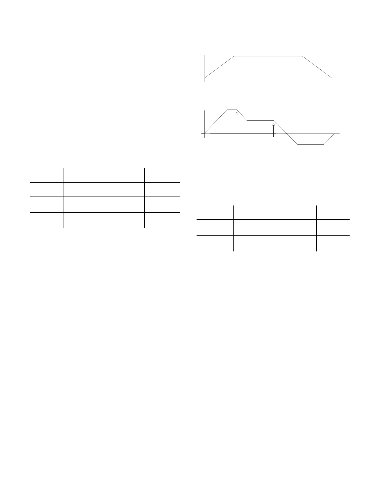
Trapezoidal Point to Point
The following table summarizes the host specified profile parameters
for the trapezoidal point to point profile mode:
Profile
Parameter
Destination
Position
Maximum
Velocity
Accel.
In the trapezoidal point to point profile mode the host specifies a
destination position, a maximum velocity, and an acceleration. The
trajectory is executed by accelerating at the commanded acceleration to
the maximum velocity where it coasts until decelerating such that the
destination position is reached with the axis at rest (zero velocity). If it is
not possible to reach the maximum velocity (because deceleration must
begin) then the velocity profile will have no "coasting" phase. The
acceleration rate is the same as the deceleration rate.
A new maximum velocity and destination position can be specified
while the axis is in motion. When this occurs the axis will accelerate or
decelerate toward the new destination position while attempting to
satisfy the new maximum velocity condition.
When in Trapezoidal point to point profile mode, to change the
acceleration, the axis must come to a complete stop. After this has
occurred, a new acceleration value can be loaded. If the
acceleration parameter is changed during motion then a
'command error' will occur, and all updated parameters will be
ignored except the position. See the section of this manual
entitled "Command Errors" for more information.
Before switching to the Trapezoidal point to point profile mode,
the axis should be at a complete rest.
The following figure shows a velocity profile for a typical point to point
trapezoidal move, along with a more complicated move involving on the
fly changes to the maximum velocity and the destination position.
Representation & Range Units
signed 32 bits
counts
-1,073,741,824 to 1,073,741,823
unsigned 32 bits (1/2
16
scaling)
counts/smpl
0 to 1,073,741,823
unsigned 32 bits (1/2
16
scaling)
counts/smpl
0 to1,073,741,823
2
Simple trapezoidal mode motion
Vel.
change max
velocity
change target
position
Complex trapezoidal mode motion
Velocity Contouring
The following table summarizes the host specified profile parameters
for the Velocity contouring profile mode:
Profile
Parameter
Maximum
Velocity
Acceleration
* negative numbers using 1/216 scaling are handled no
differently than positive numbers. For example if an
acceration value of -1.95 counts/sample time2 is desired, -
1.95 is multipled by 65,536 and the result is sent to the
chipset (-127,795 dec. or fffe0ccd hex).
In this profile mode the host specifies two parameters, the commanded
acceleration, and the maximum velocity. The trajectory is executed by
continuously accelerating the axis at the commanded rate until the max.
velocity is reached, or until a new acceleration command is given.
The maximum velocity value must always be positive. Motion
direction is controlled using the acceleration value. Positive
acceleration values result in positive motion, and negative
acceleration values result in negative motion.
There are no restrictions on changing the prof ile parameters on
the fly. Note that the motion is not bounded by position however.
It is the responsibility of the host to generate acceleration and
max. velocity command values which result in safe motion, within
acceptable position limits.
The following figure shows a typical velocity profile using this mode.
Representation & Range Units
unsigned 32 bits (1/2
16
scaling)
counts/smpl
0 to 1,073,741,823
signed 32 bits* (1/2
16
scaling)
counts/smpl
-1,073,741,824 to 1,073,741,823
Time
Time
2
20
Page 21
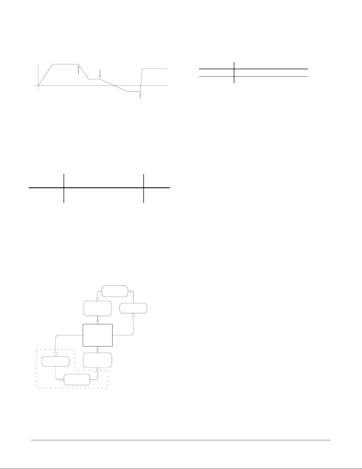
Example Velocity Contouring Mode
Vel.
change
max velocity
change
acceler a tion
change max
velocity and
acceler a tion
There are no restrictions on switching the profile mode to velocity
contouring while the axis is in motion.
In addition, the master /slave axis combinations are fixed. The following
chart shows the allowed master/slave combinations for each chipset:
chipset p/n gear pairs (master -> slave)
MC1231A #2 -> #1
MC1131A not available
Time
Typically the master axis is only used for encoder input. It is possible
however to use the master axis as a normal driven axis by leaving it
enabled, and using one of the three trajectory modes other than
electronic gear for the master axis. The net effect of this will be to run
two servo motors off of the same trajectory profile (although at a
different ratio if so programmed).
Electronic Gear
The following table summarizes the host specified profile parameters
for the electronic gear profile mode:
Profile
Parameter
Gear Ratio
* for example to specify a gear ratio of +1.5 to 1 the value
1.5*65,536 is sent to the chipset (98,304). Alternatively to set
the gear ratio as -11.39 to 1 the value -11.39*65,536 is sent (746,455 dec. or fff49c29 hex.).
In this profile mode, the host specifies one parameter, the gear ratio.
The target position is generated by applying the specified gear ratio to
the current position of another axis, slaving the driven axis to the axis
providing the position input. The following figure shows the
arrangement for encoders and motor drives in a typical electronic
gearing application.
Representation & Range Units
signed 32 bits* (1/2
16
scaling)
-
-1,073,741,824 to +1,073,741,823
Motor
Slave
Encoder
Amplifier
This configuration is shown in the previous diagram as 'optional'
components. Using this configuration the chipset can be made to
perform useful functions such as linear interpolation of two axis.
There are no restrictions on changing the gear ratio when the axis
is in motion, although care should be taken to select ratios such
that safe motion is maintained.
The specified gear ratio (SET_RATIO command) indicates the
number of target counts generated per input encoder count. For
example a gear ratio of 1.5 means 1.5 counts of the slave axis are
generated for every count of the master axis.
There are also no restrictions on changing to this profile mode
while the axes is in motion.
Trajectory Control
Normally each of the above trajectory modes will execute the specified
trajectory, within the specified parameter limits, until the profile
conditions are satisfied. For example for the point-to-point profile modes
this means that the profile will move the axis until the final destination
position has been reached, at which point the axis will have a velocity
of zero.
MC1231A
Amplifier
Motor
Master
Encoder
Optional
Because a geared axis takes up two encoder channels, the total
number of geared axes supported per chipset is 1/2 the total # of axes.
Halting The Trajectory
In some cases however it is necessary to halt the trajectory manually,
for safety reasons, or simply to achieve a particular desired profile. This
can be accomplished using one of two methods; abrupt stop, or smooth
stop.
Abrupt stops are accomplished using the STOP command. This
command instantaneously stops the trajectory generator by setting the
velocity of the axis to zero. This control mode is typically used during an
emergency stop, when no deceleration phase is desired.
Smooth stops are accomplished using the SMOOTH_STOP command.
This command causes the trajectory to decelerate at a rate equal to the
specified acceleration rate, until a velocity of zero is reached. In
addition the form of the deceleration is symmetric to the acceleration
21
Page 22

phase. For example if the profile mode is S-curve, and a
SMOOTH_STOP command is given, the profile will decelerate in a
manner exactly equal and opposite to the acceleration phase.
The STOP command functions in all profile modes; S-curve pointto-point, Trajectory point-to-point, Velocity Contouring, and
Electronic Gear.
The SMOOTH_STOP functions in S-curve point-to-point,
Trajectory point-to-point, and Velocity Contouring profiling mode.
It does not function in Electronic Gear mode.
Caution should be exercised when using the STOP command due
to the large and abrupt changes in motion that may occur.
Motion Complete Status
The motion complete and in-motion bits indicate the state of the
trajectory generator, not the actual motor. Even if the trajectory
generator has completed a motion, the actual axis position may or
may not be at rest depending on servo lag, stability, and other
system conditions.
Digital Servo Filtering
A digital filter is available for use in calculating a motor output signal.
The filter used is a PID (proportional, integral, derivative) filter, along
with a velocity feedforward term and a term to adjust the offset, also
called the DC bias value. This filter type is known as a PID+Vff filter.
This filter uses programmable gain values which can be tuned to
provide excellent control accuracy and stability over a large range of
systems.
To simplify the programming of a complete motion system it is
convenient to have the motion chipset indicate when a particular profile
move has been completed.
This function is provided by two status bits in the chipset's status word
(See the section of this manual entitled "Axis Status " for more
information on the axis status word). These two bits are called the
motion complete bit, and the in-motion bit.
The motion complete bit is controlled interactively by the chipset and
the host. After a motion has completed, the chipset sets the motion
complete bit on. The host may then poll this bit to determine that motion
is complete, or if desired, the host can program the chipset to
automatically signal when the motion is complete (using an interrupt). In
either case once the host has recognized that the motion has been
completed the host clears the motion complete bit, enabling the bit to
indicate the end of motion for the next move.
The following list shows the conditions that will cause the motion
complete bit to occur:
- Profile has reached the destination position (point-to-point
profile modes only)
- Axis trajectory reaches a velocity of zero and the current
velocity command is zero
- SMOOTH_STOP command is given and axis trajectory
reaches a velocity of zero
- STOP command is given
- Limit switch condition occurs
The in-motion bit is similar to the motion complete bit except that it
continuously indicates the status of the axis without interaction with the
host. In addition this bit is used exclusively for polled mode operations.
It can not cause an interrupt to the host to be generated.
The motion complete and the in-motion indicator bits function in
the S-curve point-to-point, Trapezoidal point-to-point, and Velocity
Contouring profile modes only. They do not function when the
profile mode is set to electronic gearing.
The following schematic diagram shows the computational flow for the
PID+Vff digital filter.
Target
Velocity
Proportional Term
P = En * Kp
Bias
Kvff
Target
Position
+
-
Integral Term
I = (S+En)*Ki
S = S+En
Derivative Term
D = (En-E(n-1))*Kd
+
+
+
+
+
Actual Position
From Encoder
In the PID+Vff filter, the host-specified parameters are:
Symbol Name Representation & Range
Kp Proportional Gain unsigned 16 bits (0 to 32767)
Ki Integral Gain unsigned 16 bits (0 to 32767)
Kd Derivative Gain unsigned 16 bits (0 to 32767)
Ilim Integration Limit unsigned 16 bits (0 to 32767)
Kvff Velocity Feedforward
gain
MtrBias DC motor offset signed 16 bits (-32767 to 32767)
The PID+Vff filter is calculated as follows:
Position Errorn = En = TPn - AP
Outputn = En*Kp + (En-E
+ MtrBias
n-1
unsigned 16 bits (0 to 32767)
n
)*Kd + Int(En)*Ki/256 + TrgtVel*Kvff/4
Output
To Motor
22
Page 23

where: En is the position error at sample time n
TPn is the target position at sample time n
APn is the actual position at sample time n
Int(En) is the integration sum at time sample n
TrgtVel is the current desired velocity in counts/sample
MtrBias is the motor bias value
All multiplied error quantities are saturated to fit within a 16 bit number
so that no discontinuities in the output signal occur at values beyond +/-
2 15. The integral term is actually maintained to an accuracy of 24 bits,
but only the top 16 bits are used. This results in a more useful range for
Ki, the integral gain.
The result of this calculation is a 16 bit number. The top 10 bits of this
result become the output value if the motor output mode is PWM (10
bits magnitude), and the entire word is used if the mode is DAC16.
The motor bias value is applied to the filter value at all times when the
chipset is in closed loop mode. If the chipset transitions to open loop
mode (MTR_OFF command is given or a motion error occurs with
automatic motor stop enabled) than the motor bias value will be output
to the motor by itself, until a manual motor command value is given
(SET_MTR_CMD command), at which point this host-provided motor
command value, without modification by the motor bias value, becomes
the active motor command.
The following example illustrates this: If the chipset is in closed loop
mode with a motor bias value of 100, then if a motor off command is
given (MTR_OFF), then the output motor command will be exactly 100.
Thereafter if the host sends a manual motor command of 200 (using the
SET_MTR_CMD command), then the output motor command will be
200. At this instant the chipset is returned to closed loop mode however
(MTR_ON command), the motor bias value will again be added to the
filter output.
Care should be taken when setting a Ki value for the first time. If
the system has already been running and the integration value is
unknown, an abrupt 'jump' may occur when the Ki value is set to a
non-zero value. To avoid this set the I_LM (integration limit) to 0,
set the Ki to the desired value, and then set I_LM to the desired
integration limit value. This will 'clear' all prior integration values,
smoothly enabling the integration function from that point
forward.
Motor Limit
In addition to setting various PID gain values the MC1231A also allows
the maximum value output by the filter to be set. This motor limit value
is set using the command SET_MTR_LMT. It can be read back using
the command GET_MTR_LMT.
The specified motor limit affects the filter output such that if the
magnitude of the filter output value (positive as well as negative)
exceeds the motor limit than the output value is maintained at the motor
limit value. Once the filter output value returns below the specified limit
than normal servo filter values are output
The motor limit is only applied during closed loop servo operations,
when the servo filter controls the motor output value. It does not affect
the output motor value applied during open loop operations
Motor Bias
If the specified motor bias value does not properly compensate for
the offsetting DC load, then after a motion error with automatic
motor stop enabled or after a MTR_OFF command the axis may
move suddenly in one direction or another. It is the responsibility
of the host to select a motor bias value such that safe motion is
maintained.
Parameter Loading & Updating
Various profile & servo parameters must be specified by the host for an
axis to be controlled in the desired manner. To facilitate precisely
synchronized motion, these parameters and related control commands
are loaded into the chip using a double-buffered scheme. In this
scheme, the parameters and action commands being loaded are not
acted upon (copied from the double-buffered to the active registers)
until an update signal is given.
This update signal can consist of either a "manual" update command,
or one of several conditional breakpoints. Whichever update method is
used, at the time the update occurs, all of the double buffered registers
and commands will be copied to the active registers. Conversely,
before the update occurs, loading the double-buffered registers or
executing the double buffered commands will have no effect on the
system behavior.
The double buffered registers are listed below.
When using an axis which has a net force in one direction or the other
(such as a vertical axis which experiences the force of gravity) the
motor bias function of the PID compensation filter may be useful. By
adding a constant bias value to the filter output, the overall position
error of the filter can be reduced by directly compensating for the
constant force.
The motor bias value is set using the command SET_MTR_BIAS. It can
be read back using the command GET_MTR_BIAS.
23
Page 24

Register Name Command to set
destination position SET_POS
maximum velocity SET_VEL
acceleration SET_ACC
maximum acceleration SET_MAX_ACC
jerk SET_JERK
ratio SET_RATIO
Kp SET_KP
Ki SET_KI
Kd SET_KD
Kvff SET_KVFF
Integration limit SET_I_LM
The double-buffered commands are: STOP, SMOOTH_STOP, and
SYNCH_PRFL.
Manual Update
There are two methods of manually updating the double-buffered
parameters, one for a single axis instantaneous update and one for a
multiple-axis update.
The single axis instantaneous update, which is specified using the
UPDATE command, forces the parameters for the current axis to be
updated at the next servo loop.
The multiple axis instantaneous update, which is specified using the
MULTI_UPDATE command, causes multiple axes to be updated
simultaneously. This can be useful when synchronized multi-axis
profiling is desired. This command takes a 1 word argument which
consists of a bit mask, with 1 bit assigned to each axis. Executing this
command has the same affect as instantaneously switching to each
desired axes, and executing an UPDATE command.
generator) equals or exceeds the specified breakpoint value. This
breakpoint is set using the SET_POS_BRK command.
Negative Target Position Breakpoint:.
A 32 bit position breakpoint can be specified which will result in
the parameters being updated when the current target position
(the instantaneous desired axis position output from the profile
generator) equals or is less than the specified breakpoint
value.This breakpoint is set using the SET_NEG_BRK command.
Positive Actual Position Breakpoint
A 32 bit position breakpoint can be specified which will result in
the parameters being updated when the current actual position
(the instantaneous position of the actual axis hardware) equals or
exceeds the specified breakpoint value.This breakpoint is set
using the SET_ACTL_POS_BRK command.
Negative Actual Position Breakpoint:.
A 32 bit position breakpoint can be specified which will result in
the parameters being updated when the current actual position
(the instantaneous position of the actual axis hardware) equals or
is less than the specified breakpoint value.This breakpoint is set
using the SET_ACTL_NEG_BRK command.
Time Breakpoint
A 32 bit time break point can be specified which will result in the
parameters being updated when the # of servo loops executed
since chip set reset (the current chip set time) is equal to the time
breakpoint value.The # of servo loops continuously increases
until it rolls over from 232 - 1 back to 0.The time breakpoint is set
using the SET_TIME_BRK command.
Motion Complete Breakpoint
A breakpoint can be specified which will result in the parameters
being updated when the previous motion has been completed
(motion complete bit is set). When using this breakpoint no 32 bit
compare value is required.
Breakpoints
A breakpoint is a convenient way of programming a profile or filter
change upon some specific condition. There are two types of
breakpoints, those that have a 32-bit comparitor value associated with
them and those that do not. For those that have the comparitor, a 32-bit
comparitor value is loaded into the breakpoint compare register first,
and then one of the breakpoint conditions is specified. For those
breakpoint modes without associated comparitor values only the
breakpoint condition needs to be specified.
The double-buffered registers and commands will be updated upon
satisfaction of the specified breakpoint condition.
Here is a list of all of the available breakpoint conditions.
Positive Target Position Breakpoint
A 32 bit position breakpoint can be specified which will result in
the parameters being updated when the current target position
(the instantaneous desired axis position output from the profile
External Breakpoint
A breakpoint can be specified which will result in the parameters
being updated when the home signal of the corresponding axis
becomes active (low). When using this breakpoint no 32 bit
compare value is required. This breakpoint is useful whenever it is
desired that an external signal starts, stops, or otherwise modifies
the profile movement.
Normally, whenever one of these conditions has been programmed and
the condition occurs, the double-buffered parameters will automatically
be shifted to the active registers. There is a mechanism to disable this
"automatic update upon breakpoint" however. This is discussed in the
next section.
The above breakpoint modes are particularly useful during multi-axis
motion. This is because the next profile commands (set of hostspecified trajectory commands) can be pre-loaded and activated at the
precise position or time required, with no delay incurred to send an
update or load parameters command.
24
Page 25

After a breakpoint condition has bee n satisfied it is no longer
active. To set up another breakpoint condition, a new one must be
explicitly set by the host.
The double-buffered registers that are shifted to the active
registers do not change upon being shifted, only the active
registers change.
Disabling Automatic Profile Update
Normally, when a breakpoint condition has been satisfied, it causes the
profile & filter parameters to be automatically updated. For certain types
of profiles however, it may be desirable to still use the breakpoint
mechanism (to allow it to generate a host interrupt for example), but not
to have the profile update.
Except for the MULTI_AXIS command, parameter loading and updating
is controlled individually for each axis. In addition each axis has a
separate 32-bit breakpoint register, and can be set to various individual
breakpoint conditions.
External Breakpoints and Homing
By connecting a home input sensor to the home signal input of the
MC1231-series chipsets it is possible to cause the chipset to halt a
motion at the moment it receives the home signal. This capability
makes it ideal for performing a home sequence. The following host I/O
sequence illustrates this:
GET_HOME ; check to make sure axis not already at
; home. If so, then a 'reverse' move must
; be made to retract axis from home switch.
; This 'reverse' sequence is not indicated
; here for simplicity sake
SET_CAPT_HOME ; set trigger capture to home signal
CLR_STATUS ; clear status register
GET_CAPT ; clear out any previous captures
SET_POS 12345 ; load home move parameters
SET_VEL 23456
SET_ACC 345
UPDATE ; start home move
SET_EXT_BRK ; initiate external breakpoint mode
SMOOTH_STOP ; load (but do not update) a stop command
This sequence will start a homing move which will come to a smooth
stop as soon as the axis encounters the home switch. In addition the
capture register will be loaded with the exact location of the home
sensor. This register can be used in conjunction with the
GET_ACTL_POS and SET_ACTL_POS commands to set the position
to any desired location. For example if it is desired that the home
sensor be located at a position of 0, then the new position should be set
to the current actual axis position minus the capture position. This is
shown in the sequence below, which should be executed after the axis
has come to a stop.
current_pos = GET_ACTL_POS
capture_pos = GET_CAPT
SET_ACTL_POS (current _pos - capture_pos)
As is the case for all of the breakpoint modes, the external breakpoint
can not only be used to stop an ongoing move, but to start or otherwise
modify a move as well. This flexibility makes it well suited for
applications such as cut-on-the-fly or other externally-initiated motions.
Whether the profiles are automatically updated or not for a given axis is
controlled by the commands SET_AUTO_UPDATE_ON and
SET_AUTO_UPDATE_OFF. When auto update is set to on, the
breakpoint/profile mechanism behaves as described above. When set
to off, upon a breakpoint condition, no profile update will occur. When in
this mode the only way to update the profile is to use the UPDATE
command or the MULTI_UPDATE command.
Travel Limit Swit ches
The MC1231-series chipsets support motion travel limit switches that
can be used to automatically recognize an "end of travel" condition.
The following figure shows a schematic representation of an axis with
travel-limit switches installed, indicating the "legal" motion area and the
over-travel regions.
negative limit
switch
negative
over-travel
region
There are two primary services that the MC1231A provides in
connection with the over-travel limit switch inputs:
1) The host can be automatically notified that an axis has entered
an over-travel condition, allowing the host to take appropriate
special action to manage the over-travel condition.
2) Upon entering an over-travel condition, the trajectory generator
will automatically be halted, so that the motor does not travel
further into the over travel region.
To recover from an over-travel condition the corresponding status bits
in the status word should be reset (see the section of this manual on
axis status for details on resetting status word bits). Once this has been
performed the host can command a trajectory move to bring the axis
out of the over-travel region.
The over-travel detector is 're-armed' when the axis exits the over travel
condition.
Only one over-travel signal can be processed at a time. For
example if the negative over travel switch becomes active, the
corresponding status bits must be cleared, and the axis moved
Legal travel region
positive limit
switch
positive
over-travel
region
25
Page 26

into the legal travel range before a positive over travel switch will
be recognized.
Motion Error Detection and Recovery
Servo Loop Control & Timing
Each of the axes on the MC1231-series chipsets can be individually
enabled or disabled *. Each enabled axis receives a "time slice" of the
available computation power of the CP chip.
Under certain circumstances, the actual axis position may differ from
the target (desired) axis position by an excessive amount. Such an
excessive position error often indicates a potentially dangerous
condition such as motor or encoder failure, or excessive mechanical
friction.
To detect this condition, thereby increasing safety and equipment
longevity, the MC1231A includes a programmable maximum position
error.
The maximum position error is set using the command
SET_POS_ERR, and read back using the command GET_POS_ERR.
To determine whether a motion error has occurred the maximum
position error is continuously compared against the actual position
error. If the maximum position error value is exceeded, then the axis is
said to be in "motion error". When this occurs the motion error bit in the
axis status word is set, and the axis motor may be turned off,
depending on the state of the automatic motor shutdown mode (see
SET_AUTO_STOP_ON and SET_AUTO_STOP_OFF host command
descriptions).
At the moment motion error occurs several events occur
simultaneously. The following list describes these events:
- Motion Error bit of the axis status word is set
- If automatic motor stop is enabled the motor is set off (set to
open loop control mode)
- If the automatic stop is enabled the trajectory generator is
stopped
If the automatic motor stop mode is not set than only the motion error
status bit is set.
* This is true even for the MC1131A, which has only one
axis, although generally disabling the only axis has no utility.
Disabled axes do not use any computing power; thus it is possible to
increase the servo loop rate when less than the supported number of
axes are used.
To set the servo loop rate to a value other than the default value, use
the command SET_SMPL_TIME. The value GET_SMPL_TIME can be
used to read this value back from the chipset.
The formula for determining the minimum loop time (maximum
sampling frequency) for a given number of enabled axis is 135 uSec for
each enabled axis.
The following table summarizes the minimum loop time for the
standard and -P parts.
# Axes
enabled
2 540*
1 270**
The loop time is specified to the chip set as an integer number from 1 to
32,767 with units of 135*** uSec For example to set the standard
MC1231A part for the minimum loop time with two axes enabled, a
value of 4 (4*135 = 540 uSec) would be sent to the chipset using the
SET_SMPL_TIME command.
* actual value = 542.72 uSec, 540 is an approximation
** actual value = 271.36 uSec, 270 is an approximation
*** actual value = 135.68 uSec, 135 is an approximation
Minimum time
Recovering From A Motion Error
To recover from a motion error which results in the motor being turned
off, the following sequence should be performed:
1) Determine cause of motion error and correct problem (this may
require human intervention).
2) Turn motor on using MTR_ON command.
After the above sequence, the axis will be servoing correctly, and the
profile generator will be at rest, ready for another move.
Changing the loop time to increase servo loop rate when axes are
disabled is not required. It is available as an option if greater loop
speed is desired.
The servo loop rate should generally not be changed while axes
are in motion.
It is the responsibility of the host to insure that the servo loop rate
that is commanded can be supported for the # of axes enabled.
Failure to observe the maximums specified in the above table may
result in unexpected axis behavior.
26
Page 27

Host Communications
read or write, this signal will go busy. It will return to ready when
the chipset can receive another I/O operation.
Electrical Interface
The MC1231A communicates to the host processor via an 8-bit bidirectional data port. 5* additional signals are used to synchronize
communication operations. The following table gives a brief description
of the control signals used during host communication:
Signal Description
~HostSlct Selects the host port for operations
~HostWrite Writes a byte of data (or a command) to the chip
set. A write operation can only occur when the
ready/busy line indicates ready
~HostRead Reads a byte of data from the chip set. A read
operation can only occur when the ready/busy line
indicates ready
HostCmd Is asserted in combination with the HostWrite signal
when a command is being written to the chip set.
HostRdy Indicates to the host that the host port is available
for operations
*An additional signal, HostIntrpt is provided to the host. This
signal is not used directly in communication operations, and is
discussed in a separate section
Three types of hardware communication operations are possible
between the host processor and the chip set; Command Write, Data
Write and Data Read. Each of these operations transfers information to
or from the chip set, and is coordinated using the 5 control signals listed
above.
A
Command Write
command to the chip set. To perform a write command operation, the
desired command is loaded on the 8 data pins and ~HostSlct and
~HostWrite are brought low, while HostCmd is brought high.
operation involves the transfer of a single byte
For more specific electrical information on the host interface operations,
see the pin descriptions and the timing diagram.
Packet Format
All communications to/from the chip set take the form of packets. A
packet is a sequence of transfers to/from the host resulting in a chip set
action or data transfer. Packets can consist of a command with no data
(Dataless Command), a command with associated data that is written
to the chip set (Write Command) or a command with associated data
that is read from the chip set (Read Command).
All commands with associated data (read or write) have either 1 or 2
words of data. See the host commands section for more information on
the length of specific commands.
If a read or a write command has 2 words of associated data (a 32 bit
quantity) the high word is loaded/read first, and the low word is
loaded/read second.
The following charts show the generic command packet sequence for a
Dataless Command, a Write Command, and a Read Command. The
hardware communication operation described in the previous section to
accomplish each type of transfer is shown in the left column.
Dataless Command
Time --> --> --> -->
Cmd Write:
Data Write:
Data Read:
Cmd byte
[pkt checksum]
A
Data Write
word) to the chip set. To transfer the first byte (high byte), the desired
data byte is loaded on the 8 data bits and ~HostSlct, ~HostWrite and
HostCmd are brought low. The HostWrite signal is then brought high to
end the transfer of the first byte. To transfer the second byte (low byte),
the desired data byte is loaded on the 8 data bits and ~HostSlct,
~HostWrite and HostCmd are again brought low.
A
Data Read
word) from the chip set to the host. To transfer the first (high) byte,
~HostSlct, ~HostRead,and ~HostCmd signals should be brought low,
and the data should be read from the 8 bit data bus. The HostRead
signal is then brought high to end the transfer of the first byte. To
transfer the second (low) byte, ~HostSlct, ~HostRead, and ~HostCmd
are again brought low and the data should be read from the data bus.
Before any command write, data write or data read operations are
performed, the user must check that the HostRdy signal indicates
ready. After a command write, or after the second byte of each
operation involves the transfer of two bytes of data (1
operation involves the transfer of two bytes of data (1
Write Command
Time --> --> --> -->
Cmd Write:
Data Write:
Data Read:
Time --> --> --> ->
Cmd Write:
Data Write:
Data Read:
Indicates an optional operation
[ ]
27
Cmd byte
word 1 [word 2]
Read Command
Cmd byte
Word 1 [Word 2] [pkt checksum]
[pkt checksum]
Page 28

Packet Checksum
The above charts show that at the end of each packet, a checksum
word is available for reading.
Although host to chip set I/O operations are extremely reliable, for
critical applications the checksum can provide a further reliability
enhancement (particularly in very noisy electrical environments, or
when the communication signals are routed over a media that may
have data losses such as a serial link).
This checksum consists of a 16-bit sum of all previous communications
that have occurred for the associated command. The command byte is
included in the low byte of the 1st checksum word (high byte set to 0).
Data words are added as is to the checksum value.
For example if a SET_VEL command (which takes two 16-bit words of
data) was sent with a data value of fedcba98 (hex), the checksum
would be:
0011 (code for SET_VEL command)
+ fedc (high data word)
+ ba98 (low data word)
---------1b985
check sum = b985 (keep bottom 16 bits only)
The following list indicates the command sequences that result in a
command error:
- Changing and updating the acceleration (SET_ACC, UPDATE)
when in the trapezoidal profile mode and when the axis
trajectory is still in motion.
- Changing and updating either the velocity, max acceleration, or
jerk (SET_VEL or SET_MAX_ACC or SET_JERK, and then
UPDATE) when in the S-curve profiling mode and when the
trajectory is in motion
- Commanding a move in the same direction as a limit switch
condition when in Trapezoidal or S-curve profile mode. For
example if travelling in the positive direction and a limit switch
is encountered, a further move in the positive direction will be
ignored and a command error will be generated.
Once a command error occurs the command error bit is set, and the
illegal profile changes are ignored. If additional parameters are also
changed such as position or any filter values as part of the same
UPDATE command then these parameters will not be rejected at the
time of the UPDATE, and they will become the active values.
Axis Addressing
Reading the checksum is optional. Recovering from an incorrect packet
transfer (bad checksum) will depend on the nature of the packet. Read
and Write operations can always be re-transmitted, while a command
resulting in an action may or may not be re-tried, depending on the
command and the state of the axis.
Illegal Commands
When the MC1231A receives a command that is illegal (see host
command summary for listing of illegal commands), it will signal this
condition by returning a checksum of 0, regardless of the illegal
command value or the value of any subsequent data written to the host
as part of the illegal command sequence.
In this manner the host processor checksum can be used to detect
communication problems as well as an illegal command sequence,
resulting in a simplification of the host processor communication code.
Command Errors
If a command, or command sequence is sent to the chipset that is not
valid at a given operating condition of the chipset, but is valid at other
times, this command is said to cause a command error.
When a command error occurs this condition is indicated by the
'command error' bit of the axis status word (See the section of this
manual entitled "Axis Status" for more information on the axis status
word).
Most chip set commands alter the parameters or the operating state of
one axis at a time. In this way each axis can be controlled separately.
To facilitate efficient communication for these types of commands, the
chip set maintains the concept of a current axis number, which can be
set explicitly by the host. After setting the current axis number,
commands that are addressed to the current axis will automatically
operate on this axis. The current axis number will stay the same until it
is changed by one of the commands that alter the current axis number.
As an illustration of this, the following sequence sets the current axis to
#2, updates some motion parameters, and switches to axis #1, and
alters some other motion parameters.
SET_2
SET_POS 02345678
UPDATE -
SET_1
SET_ACCEL 00001234
UPDATE -
-> sets current axis to #2
-> loads current axis (#2) dest.
position with value of 2345678
> causes the loaded value to take
effect (axis # 2)
-> sets current axis to #1
-> loads current axis (#1) with
acceleration value 1234
> causes the loaded value to take
effect (axis # 1)
28
Page 29

Axis Status
The MC1231A supports a status word for each axis, which contains
various information about the state of the axis.
The status word is a 16-bit register which can be queried using the
command GET_STATUS. It contains the following information (Bit
encoding is 0 = LSB, 15 = MSB):
Bit # Description
0 Motion complete flag. This bit is set (1) when the axis
trajectory has completed. This flag is only valid for the Scurve and trapezoidal, and velocity contouring profile
modes.
1 Wrap-around condition flag. This bit is set (1) when the axis
has reached the end of its travel range,and has wrapped to
the other end of the travel range. Specifically, when
travelling in a positive direction past the position
+1,073,741,823, the axis will wrap to position 1,073,741,824, and vice-versa.
2 Breakpoint reached flag. This bit is set (1) when one of the
breakpoint conditions has occurred.
3 Index pulse received flag. This bit is set (1) when an index
pulse has been received.
4 Motion error flag. This bit is set (1) when the position error is
exceeded (see filter section for more information). This bit
can only be reset when the axis is no longer in a motion
error condition
5 Positive limit switch flag. This bit is set (1) when the positive
limit switch goes active.
6 Negative limit switch flag. This bit is set (1) when the
negative limit switch goes active.
7 Command error flag. This bit is set (1) when a command
error has occurred.
8 motor on/off status (1 indicates motor is on, 0 indicates
motor is off).
9 axis on/off status (1 indicates on, 0 indicates off).
10 In-motion flag. This bit continuously indicates whether or not
the axis trajectory is in motion. This bit is set (1) when the
axis is in motion, and cleared (0) when the axis trajectory is
not in motion.
11 commutation error flag. This bit is set (1) when a
commutation error is detected.
12,13 current axis # (13 bit = high bit, 12 bit = low bit). Therefore
axis encoding is as follows:
Bit 13 Bit12 Axis
001
012
14,15 reserved (may contain 0 or 1)
Bits 8-10 and 12-13 indicate continuous status information, and do not
need to be reset by the host.
Bits 0-7 and bit 11 indicate various status flags that can also generate
host interrupts (see next section for details). These flags are set by the
chipset, and must be reset by the host (They will not be cleared by the
chipset).
Bits 0-7 and 11 of the status word operate using a set/reset
mechanism. These flags are set by the chipset, and must be reset
by the host. If they are not reset by the host they will remain active
indefinitely.
Miscellaneous Mode Status Word
There is another status word available that indicates the current status
of various mode settings or conditions.
The miscellaneous mode status word is a 16-bit register which can be
queried using the command GET_MODE. It contains the following
information (Bit encoding is 0 = LSB, 15 = MSB):
Bit # Description
0-6 Used internally by chipset. Contains no host-useable
information.
7 Stop on motion error mode flag. This bit indicates the state
of the stop on motion error mode, set by the commands
SET_AUTO_STOP_ON and SET_AUTO_STOP_OFF. A 1
indicates auto stop is on.
8-9 Used internally by chipset. Contains no host-useable
information.
10 Auto update flag. This bit indicates the state of the auto
update mode, set using the commands
SET_AUTO_UPDATE_ON and
SET_AUTO_UPDATE_OFF. A 1 indicates that auto update
is disabled.
11,12 Trajectory generator mode. This bit indicates the mode of
the trajectory generator, set using the commands
SET_PRFL_S_CRV, SET_PRFL_TRAP, SET_PRFL_VEL,
SET_PRFL_GEAR. The encoding is as follows:
Bit 12 Bit11 Profile Mode
0 0 trapezoidal
0 1 velocity contouring
10s-curve
1 1 electronic gear
13-15 Phase #. These bits indicate the current phase # of the S-
curve profile (only valid if the current profile mode is Scurve). A 0 indicates that the profile has not started yet, and
phases 1-7 indicate the phase #'s corresponding to the
phases described in the S-curve profiling mode. The 3-bit
phase # word is encoded bit 15 MSB, and bit 13 LSB.
Host Interrupts
In many situations, during axis motion or at other times, it is useful to
have the chip set signal the host that a special condition has occurred.
This is generally more convenient and efficient than having the host poll
the chip set for various possible conditions. This chip set-initiated signal
is known as a host interrupt.
Several chip set conditions may occur that can result in the generation
of a host interrupt. Whether these conditions in fact interrupt the host is
29
Page 30

controllable for each condition and for each axis. The mechanism used
to control each condition is a mask register.
The interrupt conditions correspond to bits 0-7 and 11 of the
status register (the axis event flags), described in the previous
section. These conditions are summarized below:
Motion Complete Occurs when the profile is complete
Wrap-around condition Occurs when the axis position wraps.
Break Point Reached Occurs when a breakpoint condition has
been satisfied.
Position Capture
Received
Motion Error Occurs when the maximum position
Negative Limit Switch Occurs when the negative over-travel
Positive Limit Switch Occurs when the positive over travel
Command Error Occurs when a host communication
When one of these interrupt conditions occur for a particular axis, the
host interrupt line is made active. At this point the host can respond to
the interrupt (although the current I/O operation should be completed),
but it is not required to do so
When the host has completed processing the interrupt, it sends a
command that clears the interrupt conditions for a particular axis, the
RST_INTRPT command.
Occurs when the encoder index pulse or
home pulse has been captured
error set for a particular axis has been
exceeded
limit switch is active
limit switch is active
sequence causes a command error
condition
SET_INTRPT_MASK Sets the interrupt conditions mask
GET_INTRPT Returns the status of the interrupting axis
(including the interrupting axis #). The
current axis # is not altered by this
command
SET_I Changes the current axis # to the
interrupting axis. This is a 'time saver'
command which performs the dual
operations of getting the interrupting axis
# and switching to that axis in one
command.
RST_INTRPT Clears particular conditions for the
interrupting axis. The current axis # is not
altered by this command.
To facilitate determining the nature of the interrupt, the status register
holds the axis #, allowing the interrupting axis # to be determined.
The following represents a typical sequence of interrupt conditions and
host responses. Assume for the purposes of this example that an axis
(not the current axis) has hit a "hard stop" causing an essentially
instantaneous motion error, as well as a positive limit switch trip. Also
assume that the interrupt mask for this axis was set so that either
motion errors or limit switch trips will cause an interrupt
Event Host action
motion Error & limit switch trip
generates interrupt
interrupting axis status
returned by chipset, current
axis set to interrupting axis.
host sends SET_I command
host detects motion error & limit
switch flags are set, recovers from
motion error first.
This command includes a "clearing mask" as an argument, which
allows one interrupt to be cleared at a time.
Bits cleared by the RST_INTRPT command are the exact same bits
as those cleared by non-interrupt commands such as
RST_STATUS and CLR_STATUS. In each case the bits affected are
the status word bits 0-7 and 11.
Interrupts occur for a particular axis. If the user is currently
programming parameters on axis #1 and an interrupt occurs on axis #2,
it is the host's responsibility to change axis number to 2 if this is the
appropriate response to an interrupt on that axis. If more than one axis
interrupt condition becomes active at exactly the same time, then the
axis with the lowest number will generate the interrupt first.
The following host commands are used in managing interrupts:
(See Host Command reference for complete information)
host sends: RST_INTRPT 00EF,
clearing motion error bit
chipset clears motion error bit
and disables host interrupt line
Because limit switch interrupt
is still active chipset
immediately generates
interrupt for limit switch
interrupting axis status
returned by chipset, current
axis set to interrupting axis.
chipset clears limit switch bit
and disables host interrupt line
At the end of this sequence, all status bits are clear, the interrupt line is
inactive, and no interrupts are pending.
Note that it is not required to process multiple interrupts separately (as
is shown in the example). It is perfectly valid to process 2 or more
interrupt conditions at the same time, and to then send a RST_INTRPT
command with a mask that clears multiple bits at the same time.
-
host sends SET_I command
host detects that neg. limit switch
trip flag is set, performs recovery
for limit switch trip.
host sends RST_INTRPT 00DF,
clearing pos. limit switch bit
-
30
Page 31

The RST_INTRPT and GET_I commands are only effective when
there is an interrupt present. If no interrupt is present than
alternative 'polled-mode' commands such as RST_STATUS or
GET_STATUS should be used.
Encoder Position Feedback
The MC1231A-series of chipsets support direct input of incremental
encoder signals. Four position input and control signals are supported:
- A quadrature channel
- B quadrature channel
- Index pulse
- Home signal
The A and B signals are used to continuously maintain the position of
the motor, and the index and home signals are used as trigger inputs to
a high-speed position capture mechanism.
Each quadrature channel consists of a square wave offset 90 deg. from
the other. Positive motion consists of the A channel leading the B
channel by 90 deg., and negative motion consists of the A channel
lagging the B channel by 90 deg. For each full phase of one channel,
four resolved quadrature counts will occur, resulting in a 4 to 1
resolution enhancement over the basic channel resolution.
The index pulse is typically located on the encoder and will be active
once per revolution. The chip set recognizes that an index trigger has
occurred (i.e. when the 32-bit index location is captured) when the
index signal, as well as the A and B signals transition low.
High Speed Position Capture
Each axis of the MC1231A supports a high speed position capture
register that allows the current axis location to be saved using an
external trigger signal. When in incremental encoder mode, The
MC1231A allows either the index signal or the home signal to be used
as the capture trigger. These two input triggers differ however in that
the index signal will cause a position capture when it, as well as the A
and B index signals, transition low, while the home signal will result in a
capture when it alone goes low.
The commands SET_CAPT_INDEX and SET_CAPT_HOME select
which input signal is used.
After an index or home signal has been captured by the MC1231A, the
capture value must be read by the host processor before another
position capture can occur. In addition, if the index signal is being used
as the trigger, the index signal,along with the A and B quadrature
signals, must transition high before another index pulse can be
registered.
The captured position is equal to the axis position at the moment the
trigger pulse was encountered. Note that the capture register is located
in hardware. Its accuracy is therefore not affected by the velocity of the
axis.
Index Pulses And Commutation
In addition to providing one of the two sources for the high speed
position capture the index-signal has an additional function which is to
maintain synchronization during commutation.
The home signal is typically connected to a position reference sensor,
or to any other general purpose synchronizing signal. The home signal
is recognized when it alone transitions low. The state of the A and B
signals does not affect home signal trigger recognition.
Encoder Filtering
To enhance reliability of the received encoder information the MC1231A
provides digital filtering of the quadrature data lines (A and B
quadrature count) as well as the index and home signals.
For all of these signals a valid high or low condition is recognized only
when the condition has been maintained for 3 clock cycles of 160 nSec
each (total required duration of 480 nSec)
For example if a brief spurious noise signal on one of the lines occurs
for 300 nSec, then this noise will be rejected until a valid state change
lasting over 480nSec occurs.
Although this function is optional, if connected, the index signal can
improve the reliability of sinusoidal commutation by eliminating any long
term drift due to lost encoder counts. To utilize this function it is simply
necessary to use an index pulse which occurs once per motor rotation
(rotary motor), or at the same point within the commutation electrical
cycle (linear motor). For more information see the section of this
manual entitled "Sinusoidal Commutation".
Motor Outputs
The MC1231A series of chipsets provides two different motor amplifier
interfaces:
- 10-bit 24.5 Khz PWM interface
- 16-bit DAC output.
The output mode is host-selectable. The selected method affects all
axes (motor output mode is not individually programmable for each
axis). The host commands to select these output modes are
SET_OUTPUT_PWM (to select PWM mode), and
SET_OUTPUT_DAC16 (to select 16 bit DAC mode).
31
Page 32

Motor Output Control
Generator
Actual
F
DAC signal
Commutator
Phase A
command
Phase B
command
Phase C
command
Motor Output
F
The following diagram shows the control flow for the motor command
output by the chipset.
otor command register
(SET_MTR_CMD)
Trajectory
MTR_OF
MTR_ON
Servo filter
(PID or PIVff)
Sinusoidal
PWM or
generator
To
Amp.
GET_MTR_CMD Retrieves the current motor command output
by the chipset. When in closed loop mode
this command will return the current output
value of the servo filter. When in open loop
mode this command will return the value set
using the SET_MTR_CMD command, or
SET_BUF_MTR_CMD after an UPDATE.
GET_BUF_MTR_CMD Retrieves the buffered motor value set using
the SET_BUF_MTR_CMD.
Sinusoidal Commutation
position
The chipset can be run in either closed loop mode, or open loop mode.
In closed loop mode the motor command is determined by the output of
the servo filter, which in turn is determined by the output of the
trajectory generator and the actual axis position. Closed loop mode is
the normal operating mode of the chipset.
Open loop mode allows the motor command to be directly set by the
host. Open loop mode is typically used when one or more axes require
torque control only, or to calibrate the amplifier.
Whether or not the motor command comes from the servo filter (closed
loop mode) or the motor command register (open loop mode), the motor
command is then commutated based on the encoder position and
commutation parameters specified by the host. See the section of this
manual on commutation for more details.
Here is a summary of the motor control commands.
Command Description
MTR_ON Enables closed loop servo control. In this
mode the source of motor command is the
servo filter and the motor command register
has not effect.
MTR_OFF Disables closed loop servo operations. In
this mode the motor command is determined
by the motor command register, which is set
by the host.
SET_MTR_CMD Sets the motor command register, used to
control the motor output value during open
loop operations. For this command to take
effect the motor must be off (MTR_OFF
command).
SET_BUF_MTR_CMD Double buffered version of SET_MTR_CMD.
For this command to take effect the motor
must be off (MTR_OFF command), and an
UPDATE command must be given
In addition to trajectory generation and servo loop closure the
MC1231A chipset provides sinusoidal motor commutation of 3 and 2phase brushless motors.
The following diagram shows an overview of the control flow of the
sinusoidal commutation portion of the MC1231A chipset:
Motor command register
(SET_MTR_CMD)
Target pos. &
vel. (from profile
generator)
Servo filter
(PID or PIVff)
Actual position
MTR_OF
MTR_ON
Actual position
(if encoder-based)
(PWM or DAC16)
To
Amp.
Actual velocity
(for phase
advance)
Actual position
(from encoder)
The commutation portion of the chipset uses as input the motor
command signal from either the servo filter, or the motor command
register (depending on whether the chipset is in closed loop or open
loop mode). This pre-commutated command signal is then multiplied by
commutation values derived from an internal lookup Sin/Cos table.
The commutation angle used in the Sin/Cos lookup is determined by
the position encoder as well as parameters set by the host processor
which relate the specific encoder used to the motor magnetic poles.
Two commutation waveforms are provided, one appropriate for 3-phase
devices with 120 deg. separation between phases (such as brushless
motors), and one appropriate for 2-phase devices with 90 deg.
separation between phases (such as stepper motors).
Other features of the MC1231A chipset are the ability to use Hallsensor inputs for phase initialization, to use an index pulse to maintain
commutation synchronization, to pre-scale the encoder input to support
a wider variety of feedback devices, and to provide velocity-based
phase advance for smoother and more efficient high speed operation.
32
Page 33

Commutation Waveforms
120 Deg
Phase A
Phase B
90 Deg
where:
Counts_per_rot is the # of enc. counts per motor rotation
N_poles is the number of motor poles
The MC1231A supports two commutation waveforms, a 120 degree
offset waveform appropriate for 3-phase brushless motors, and a 90degree offset waveform appropriate for 2-phase brushless motors. To
specify the 3-phase brushless waveform the command SET_PHASE_3
is used, and to set it for 2-phase brushless motors the command
SET_PHASE_2 is used.
Depending on the waveform selected, as well as the motor output mode
selected (PWM or DAC16), either 2 or 3 commutated output signals per
axis will be provided by the chipset. The following chart shows this.
Waveform Motor Output Mode # of Output signals
& Name
3-phase PWM 3 (A, B, C)
3-phase DAC16 2 (A, B)
2-phase PWM 2 (A, B)
2-phase DAC16 2 (A, B)
For specific pin assignments of the PWM and DAC16 motor output
signals see the section of this manual entitled 'Pin Descriptions'.
The diagram below shows the phase A, B, and C commutation signals
for a 3-phase brushless motor, and the phase A and phase B signals
for a 2-phase brushless motor.
Phase A Phase B Phase C
3-Phase Brushless
The command used to set the number of encoder counts per electrical
cycle is SET_PHASE_CNTS. To read back this value use the
command GET_PHASE_CNTS.
The smallest allowed value for the number of counts per electrical
cycle is 129 (decimal).
Index Pulse Referencing
To enhance long term commutation reliability the MC1231A provides
the ability to utilize an index pulse input from the motor encoder as a
reference point during commutation. By using an index pulse during the
phase calculations any long term loss of encoder counts which might
otherwise affect the accuracy of the commutation are automatically
eliminated.
To utilize index pulse referencing the motor encoder chosen must
provide an index pulse signal to the chipset once per rotation. This
index pulse is connected to the chipset using the Index signal of the I/O
chip (see Pin Descriptions section for more information).
Index pulse referencing is recommended for all rotary brushless motors
with quadrature encoders. For linear brushless motors it is generally not
used, although it can be used as long as the index pulses are arranged
so that each pulse occurs at the same phase angle within the
commutation cycle.
2-Phase Brushless
90 180 270 360
Commutation Parameters
To perform sinusoidal commutation it is necessary to specify the # of
encoder counts per electrical cycle. To determine this value the # of
magnetic poles on the motor, along with the number of encoder counts
per motor revolution must be known. Knowing these two quantities the
number of encoder counts per electrical cycle is given by the following
equation:
Counts_per_cycle = 2*Counts_per_rot/N_poles
When using an index pulse the number of encoder counts per electrical
cycle is not required to be an exact integer. In the case that this value is
not an integer, the nearest integer should be chosen. Conversely, if
index pulses are not being used then the number of counts per
electrical cycle must be an exact integer, with no remainder.
For example if a 6-pole brushless motor is to be used with an encoder
without an index pulse than an encoder with 1200 counts per rotation
would be an appropriate choice, but an encoder with 1024 would not
because 1024 can not be divided by 3 evenly.
Index pulse referencing is performed automati cally by the chipset,
regardless of the initialization scheme used (algorithmic, Hallbased, microstepping, or direct set).
33
Page 34

Commutation Error Detection
With an index signal properly installed the chipset will automatically
correct any small losses of encoder counts that may occur.
If the loss of encoder counts becomes excessive however, or if the
index pulse does not arrive at the expected location within the
commutation cycle, a "commutation error" is said to occur.
Commutation errors are caused by a number of circumstances. The
most common are listed below:
- noise on the A or B encoder lines
- noise on the index line
- incorrect setting of # encoder counts per electrical cycle
For each instance that a commutation error occurs phase referencing
will not occur for that index pulse. Depending on the cause of the error
the commutation error may be a one-time event, or may occur
essentially continuously after the first event.
When a commutation error occurs bit # 11 of the status word is set high
(1). This condition can also be used as a source of host interrupts so
the host can be automatically notified of a commutation error. To
recover from a commutation error this bit is cleared by the host,
however depending on the nature of the error it is possible that
commutation errors will continue to be generated.
A commutation error may indicate a serious problem with the
motion system, potentially resulting in unsafe motion. It is the
responsibility of the host to determine and correct the cause of
commutation errors.
SET_PHASE_TIME. To read back this value use the command
GET_PHASE_TIME.
To minimize the impact on the system mechanics this method utilizes a
motor command value set by the host processor to determine the
overall amount of power to "inject" into the motor during phase
initialization Typically, the amount of power to inject should be in the
range of 5 - 25 % of full scale output, but in any case should be at least
3 times the breakaway stiction torque. For best results the initialization
motor command value can be determined experimentally. The
command used to set the motor output level is SET_BUF_MTR_CMD.
To read back this value use the command GET_BUF_MTR_CMD.
To execute the initialization procedure, the host command INIT_PHASE
is used. Upon executing this command, the phasing procedure will
immediately be executed.
Before the phase initialization command is given however
(INIT_PHASE command), the motor must be turned off (MTR_OFF
command), a motor command output must be specified
(SET_BUF_MTR_CMD command), and an initialization duration must
be specified (SET_PHASE_TIME command).
During algorithmic phase initialization the motor may move
suddenly in either direction. Proper safety precautions should be
taken to prevent damage from this movement. In addition, to
provide accurate results motor movement must be unobstructed
in both directions and must not experience excessive stiction.
Hall-Based Phase Initialization
Phase Initialization
After startup the chipset must determine the proper commutation angle
of the motor relative to the encoder position. This information is
determined using a procedure called phase initialization.
The chipset provides four methods to perform phase initialization;
algorithmic, Hall Sensor-based, microstepping, and direct-set.
Algorithmic Phase Initialization
To set the chipset for algorithmic initialization use the command
SET_PHASE_ALGOR
In the algorithmic initialization mode no additional motor sensors
beyond the position encoder are required. To determine the phasing the
chipset performs a sequence which briefly stimulates the motor
windings, and sets the initial phasing using the observed motor
response. From the resulting motion the chipset can automatically
determine the correct motor phasing.
Depending on the size and speed of the motor, the time between the
start of motor phasing and the motor coming to a complete rest (settling
time) will vary. To accommodate these differences the amount of time
to wait for the motor to settle is programmable using the command
To set the chipset for Hall-based initialization use the command
SET_PHASE_HALL
In this mode 3 Hall-Sensor signals are used to initially determine the
motor phasing, and sinusoidal commutation begins automatically after
the motor has moved through one full rotation.
The Hall-Sensor signals are fed back to the chipset through the signals
Hall1A-C (axis #1) and Hall2A-C (axis # 2). Care should be taken to
connect these sensors properly. To read the current status of the hall
sensors use the command GET_HALLS.
The following diagram shows the relationship between the state of the
three Hall sensor inputs for each axis and the commutated motor
outputs. This graph shows the expected Hall sensor states and winding
excitation for forward motion (increasing position).
34
Page 35

3-Phase Brushless
Phase A Phase B Phase C
Hall A
Hall B
Hall C
90 180 270 360
Unlike the algorithmic method, using Hall-based phase initialization no
special motor procedures are required. Initialization is performed using
the command INIT_PHASE, and occurs immediately, without any motor
motion.
To accommodate varying types of Hall sensors, or sensors that contain
inverter circuitry, the signal level/logic interpretation of the Hall sensor
input signals can be set through the host.
The command SET_HALL_SENSE accepts a bit-programmed word
which controls whether the incoming Hall signals are interpreted as
active high, or active low. To read back this Hall interpretation value
use the command GET_HALL_SENSE. For details on the programming
of this control word see the Command Reference section of this
manual.
Hall-based initialization should only be used with a 3-phase
commutation waveform, and with Hall sensors located 120
degrees apart. Hall-sensors located 60 degrees apart should not
be used.
Microstepping Phase Initialization
the index pulse is encountered the phase angle can be set using the
command SET_PHASE.
To operate the motor in microstepping mode the motor must be set on
(MTR_ON command), and a motor output value must be provided
(SET_BUF_MTR_CMD & UPDATE). In addition the # of encoder
counts per electrical cycle should be set to 512.
When in microstepping mode each trajectory 'count' corresponds to
1/256 of a full electrical cycle. For example using a 4-pole motor (2
electrical cycles per motor rotation) a trajectory move of 512 counts will
move the motor 1 full motor rotation.
Special care should be taken when initializing the motor using the
microstepping method. Because the motor is operated 'open-loop' the
resultant coil energization and subsequent rotation may be jerky and
abrupt.
Phase initialization using the microstepping method should only
be used under special circumstances. It is not generally
recommended unless the algorithmic or Hall-based methods can
not be used.
Direct-Set Phase Initialization
If, after power-up the location of the motor phasing is known explicitly
the phase angle can simply be set directly using the SET_PHASE
command.
This typically occurs when sensors such as resolvers are used where
the returned motor position information is absolute in nature (not
incremental) , and can be used to generate a quadrature data stream
as well as be read by the host directly.
Phase Initialization Programming
The following examples show typical host command sequences to
initialize the commutation of a brushless motor for all four initialization
methods.
If the location of the index pulse in relation to the motor rotor and case
is known then it may be advantageous to use an initialization technique
which operates the motor as a microstepper, rotating the motor until the
index pulse is found, and then setting the phase angle explicitly.
This scheme is only appropriate for motors which have the index pulse
in a fixed and repeatable location within the commutation cycle for all of
the motors to be used during manufacturing of the product. Although
this is relatively uncommon, it is typical for motors with optical Hallsensors which use a single disk containing the A, B, index, and Hall
sensor information.
To set the chipset for microstepping operation the command
SET_PHASE_MICRO is used. To restore the chipset for encoderbased commutation the command SET_PHASE_ENC is used. Once
Algorithmic Initialization Sequence
SET_PHASE_CNTS uuuu Set # of encoder counts per electrical
cycle
SET_PHASE_ALGOR Set phase initialization method to
algorithmic
MTR_OFF Turn motor off so it doesn't conflict
with initialization procedure
SET_PHASE_TIME wwww Set algorithmic phase init duration
SET_BUF_MTR_CMD xxxx Set initialization motor command level
INIT_PHASE Perform the initialization
This sequence will cause the motor to immediately begin the
initialization procedure, which will last 'wwww' servo loops long. To
determine if the procedure is completed, the command
35
Page 36

GET_PHASE_INFO can be used. The 'phase initialization not
'Zero' Location
Pulse
Phase Offset
completed' bit will indicate when the procedure is finished. After the
initialization procedure is completed the motor should be enabled
(MTR_ON cmd) if the chipset is to be run in closed loop mode.
Hall-based Initialization Sequence
SET_PHASE_CNTS uuuu Set # of encoder counts per electrical
cycle
SET_HALL_SENSE vvvv Set Hall sensor signal interpretation
SET_PHASE_HALL Set phase initialization method to
Hall-sensor based
INIT_PHASE Perform the initialization
This sequence will cause the chipset to read the Hall sensor signals
and initialize the phasing immediately. The motor will not move as a
result of this sequence, and no delay is required for further motor
operations to be performed.
Microstepping Initialization Sequence
Direct-Set Initialization Sequence
SET_PHASE_CNTS xxxx Set # of encoder counts per electrical
cycle (hex)
SET_PHASE xxxx Set phase angle based on information
from external sensor
This sequence will directly set the phase angle to a value determined
by another sensor. The set value must be between 0 and the # of
encoder counts per electrical cycle.
Adjusting The Commutation Angle
The MC1231A supports the ability to change the motor's commutation
angle directly, both when the motor is stationary and when it is in
motion. Although this is not generally required it can be useful during
testing, or during commutation initialization when the microstepping or
direct-set methods are used.
To change the commutation angle when the motor is stationary use the
command SET_PHASE.
SET_PHASE_CNTS 512 Set # of encoder counts per electrical
cycle to 512 (dec.)
SET_PHASE_MICRO Set chipset for microstepping mode
SET_CAPT_INDEX Set capture mode to index (not
necessary if already so set)
CLR_STATUS Clear axis status
GET_CAPT Clear out any previous captures
MTR_ON Turn motor on (not necessary if
already on)
SET_BUF_MTR_CMD xxxx Set motor command value
SET_POS 560 Set rotation distance a bit more than 1
full motor rotation (assuming 4-pole
motor
SET_VEL yyyy Set velocity
SET_ACC zzzz Set acceleration
UPDATE start the motion
This sequence will cause the motor to make a move of somewhat more
than 1 rotation. After the update the host should poll the status word
(GET_STATUS cmd) until a capture occurs and then immediately send
a SET_PHASE command, followed by a SET_PHASE_OFFSET
command, each loaded with the phase angle required to init. the
phasing.
See the following section of this manual entitled "Adjusting the
commutation angle" for more information on determining the correct
phase set value.
Once the SET_PHASE and SET_PHASE_OFFSET commands have
been sent by the host the chipset should be initialized for normal
commutation operation. This means the phasing mode should be set to
encoder-based (SET_PHASE_ENC cmd.) and the correct # of encoder
counts per electrical cycle should be set (SET_PHASE_CNTS cmd.)
To change the commutation angle while the motor is moving the index
pulse is required, and a different command, SET_PHASE_OFFSET, is
used which only takes effect when an index pulse occurs. The following
description provides some background on this function.
After phase initialization has occurred the correct commutation angle is
stored by the chipset as the offset from the index mark (in encoder
counts) to the phase A maximum output value (commutation 'zero'
location). This 16-bit offset register can be read using the command
GET_PHASE_OFFSET.
The following chart shows the relationship between the phase A
commutation 'zero' location, the index location, and the phase offset
value. For a given motor the index pulse shown in this figure could have
been located anywhere within the phase cycle since it will usually vary
in position from motor to motor. Only motors that have been
mechanically assembled such that the index position is referenced to
the motor windings will have a consistent index position relative to the
commutation zero location.
Phase A
Commutation
Index
90 180 270 360
Wavef o rm
Before phase initialization has occurred the phase offset register will
have a value of ffff (hex). Once phase initialization has occurred and the
motor has been rotated such that at least one index pulse has been
36
Page 37

received, the phase offset value will be stored as a positive number with
a value between 0 and the number of encoder counts per electrical
cycle.
To convert the phase offset value which is in encoder counts to degrees
the following expression can be used:
Velocity-Based Phase Advance
Because of inductance and magnetic field setup delays a lag may exist
between the motor command signals from the chipset and the desired
magnetic field in the motor. This lag can reduce the efficiency and
maximum velocity of the motor.
Offset
where:
The phase offset value can also be changed any number of times while
the motor is in motion, although only relatively small changes should be
made to avoid sudden jumps in the motor motion.
The SET_PHASE_OFFSET and GET_PHASE_OFFSET commands
can only be used when an index pulse from the encoder is
connected. If no index pulse is used the phase offset angle can
not be adjusted or read back by the host
Setting the phase offset value does not change the relative
phasing of phase B and C to phase A These phases are still set at
either 90 or 120 degree offsets from phase A (depending on the
waveform chosen).
Encoder Pre-Scalar
Particularly when used with linear motors, the range in the value of the
# of encoder counts per electrical cycle can vary widely. Typical rotary
motors can have a value between 129 and 32,767. Linear brushless
motors however can have values of 1,000,000 counts per cycle or
higher because they often use high accuracy laser-based encoders.
To accommodate this large range the MC1231A series chips support a
prescalar function which, for the purposes of commutation calculations,
divides the incoming encoder counts by 64. With the prescalar enabled
the max range for the number of encoder counts per electrical cycle is
2,097,088.
To enable the prescalar use the command SET_PRESCALE_ON. To
disable the prescalar use the command SET_PRESCALE_OFF.
The prescalar function should not be enabled or disabled once the
motor has been put in motion.
The prescalar function only affects the commutation of the
chipset. It does not affect the position used during servo filtering,
or requested by the command GET_ACTL_POS.
= 360 * Offset
degrees
Offset
Offset
counts_per_cycle is the # of counts per electrical cycle set
using the SET_PHASE_CNTS command
is the phase offset in degrees
degrees
is the phase offset in encoder counts
counts
/counts_per_cycle
counts
To compensate for this effect the MC1231A chipsets provide the ability
to advance the commutation phase of the motor during rotation so that
the actual magnetic field experienced by the motor more closely
resembles the optimum values.
The phase advance value is determined by a combination of the motor
velocity, and a phase advance gain value specified by the host. The
phase advance value is calculated as follows:
phase_advance = motor_velocity * KPHASE/1000
where: phase_advance is in units of encoder counts
motor_velocity is in units of encoder counts/sample time
KPHASE is the host-specified gain phase advance gain
Phase Info Status Word
A status word is available that indicates the current value of various
phasing-related conditions.
The phase information status word is a 16-bit register which can be
queried using the command GET_PHASE_INFO. It contains the
following information (Bit encoding is 0 = LSB, 15 = MSB):
Bit # Description
0 Phase initialization mode. This bit will be set to 1 if the
initialization mode is hall-based, 0 if the initialization mode
is algorithmic.
1 used internally by chipset (may be 0 or 1)
2 Commutation mode. This bit indicates whether the
commutation mode has been set to microstepping
(SET_PHASE_MICRO cmd) or encoder-based
(SET_PHASE_ENC cmd). A 1 indicates microstepping
mode.
3 Waveform. This bit indicates whether the output waveform
is 3-phase (0) or 2-phase (1)
4-6 Used internally by chipset (may be 0 or 1)
7 Prescalar status. This bit indicates whether the prescalar is
active. A 1 indicates it is active.
8 Phase initialization not completed. This bit indicates that
phase initialization has not been completed yet. A 1
indicates that initialization has not been completed.
9 used internally by chipset may be 0 or 1)
10-15 Unused (set to 0)
37
Page 38

Commutation Command Summary:
Axis #1 Phase C
Mtr #2
Axis #2 phase A
Axis #2 Phase B
MC1231
Axis #1
C=-(A+B)
Axis #2 phase A
d
The following table summarizes the commands that are used in
conjunction with sinusoidal commutation:
Command Function
SET_PHASE_3 Sets the commutation waveform for 3-
phase brushless motors.
SET_PHASE_2 Sets the commutation waveform for 2-
phase brushless motors.
SET_PHASE_HALL Sets the phase initialization mode to
Hall-sensor-based
SET_PHASE_ALGOR Sets the phase initialization mode to
algorithmic.
SET_PHASE_ENC Sets commutation mode to encoder-
based
SET_PHASE_MICRO Sets commutation mode to
microstepping
PRESCALE_ON Sets the encoder prescalar on
PRESCALE_OFF Sets the encoder prescalar off
SET_PHASE_CNTS Sets the # of encoder counts per
commutation electrical cycle.
SET_PHASE_TIME Sets the amount of time to wait during
phase initialization
SET_PHASE Sets the current phase angle
SET_PHASE_OFFSET Sets the phase offset angle
SET_KPHASE Sets the velocity phase advance gain
SET_HALL_SENSE Sets the logic level interpretation for the
Hall sensor inputs
INIT_PHASE Begins the algorithmic phase
initialization procedure.
GET_PHASE_INFO Returns various commutation-related
state information set by the host
GET_PHASE_CNTS Returns the number of encoder counts
per electrical cycle
GET_PHASE_TIME Returns the wait time used during phase
initialization
GET_PHASE_OFFSET Returns the phase offset angle
GET_KPHASE Returns the phase advance gain
GET_HALL_SENSE Returns the logic level interpretation for
the Hall sensor inputs
GET_HALLS Returns the status of the hall sensors
GET_PHASE Returns the current commutation angle.
Brushless Motor ( P WM Mo de) Conn ecti on S cheme
Amplifiers
Axis #1 phase A
Axis #1 Phase B
MC1231
Axis #2 Phase C
Mtr #1
In this configuration the chipset outputs 3 phased PWM magnitude
signals per axis. These signals are then fed directly into 3 half-bridge
type voltage amplifiers.
Below is shown a typical amplifier configuration for a 3-phase brushless
motor using the DAC output mode:
Brush less Motor (DAC Mode) Conne ction S c h eme
Amplifiers
DAC 1A
C=-(A+B)
DAC 1B
DAC 2A
Axis #2
DAC 2B
Axis #1 phase A
Axis #1 Phase B
Axis #1 Phase C
Axis #2 Phase B
Axis #2 Phase C
Mtr #1
Mtr #2
When using DAC output mode the digital word provided by the chipset
must first be converted into a voltage using an external DAC. Two DAC
channels are required per axis. To construct the third phase for a
brushless motor (C phase) the sum of the A and B signals must be
'negated' using C = -(A+B).
This is usually accomplished with an Op-amp circuit. In addition, if
current loop control is desired the three output signals are usually
arranged so that the sum of the currents flowing through the windings of
the motor are zero.
Motor Output Signal Interpretation
Motor Output Configuration
The MC1231A series of chipsets supports two motor output methods,
PWM and DAC (up to 16 bit resolution).
Below is shown a typical amplifier configuration for a 3-phase brushless
motor using the PWM output mode:
The following graph shows the desired output voltage waveform for a
single phase.
+ motor comman
0
- motor command
38
Page 39

The waveform is centered around a value of 0 volts. The magnitude of
the generated waveform is proportional to either the output of the servo
filter or the motor command register (depending on the commutation
mode and motor on/off status).
For example if the chipset is connected to a DAC with output range of 10 Volts to + 10 Volts and the chipset is set to open loop mode with a
motor command value of 32,767 (which is the maximum allowed value)
than as the motor rotates through a full electrical cycle, a sinusoidal
waveform centered at 0 volts will be output with a minimum voltage of 10, and a maximum voltage of +10.
DAC16 Decoding
The digital values output by the chipset to the DAC encode the desired
voltages as a 16-bit digital word. The minimum voltage is output as a
digital word value of 0, a voltage of 0 Volts is output as a digital word of
32,768 (dec.), and the maximum positive voltage is output as a digital
word value of 65,535.
To load each of the four (MC1231A) or two (MC1131A) DACs, the DAC
control pins in combination with the chipset's 16-bit data bus are used.
To load a particular DAC, The DAC address (1 of 4) is output on the
signals DAC16Addr0-1, the 16 bits of DAC data are output on pins
Data0-11 (high 12 bits), as well as DACLow0-3 (low 4 bits), I/OAddr0-3
and DACSlct are high, and I/OWrite is low.
0/1024
(max. neg.
value)
512/1024
(0 value)
1024/1024
(max. po s.
value)
1
0
1
0
1
0
An output pulse width of 0 parts per 1,024 represents the maximum
negative voltage, an output pulse width of 512 per 1,024 (50 %)
represents a voltage of 0, and a pulse width of 1,024 per 1,024
represents the maximum positive voltage.
This PWM scheme has been chosen to allow convenient interfacing to
half bridge type amplifiers by connecting the PWM output to a level
shifter circuit , and using this output to drive the high and low side
drivers of the bridge.
For more information on the DAC signal timing & conditions, see the
Pin Descriptions and timing diagrams section of this manual.
DACs with lower resolution than 16 bits can also be used. To connect
to a DAC with less resolution, the high order bits of the 16-bit data word
should be used. For example, to connect to an 8-bit DAC, bits Data4Data11 should be used. The low order 8 bits are written to by the
chipset, but ignored by the DAC circuitry.
PWM Decoding
The PWM output mode also outputs a sinusoidal desired voltage
waveform for each phase, however the method by which these signals
encode the voltage differ substantially from the DAC16 digital word.
The PWM output mode uses a single signal per output motor phase.
This signal contains a pulse-width encoded representation of the
desired voltage. In this encoding the duty cycle of the waveform
determines the desired voltage. The PWM cycle has a frequency of
24.5 kHz, with a resolution of 10 bits, or 1/1,024.
The following chart shows the encoding.
39
Page 40

Command Summary
Command Mnemonic Code
(hex)
Axis Control
SET_1 01 all axes set by cmd. - 1/read Set current axis # to 1
SET_2 02 all axes set by cmd. - 1/read Set current axis # to 2
SET_I 08 all axes interrupting axis - 1/read Set current axis # to the interrupting axi s
Profile Generation
SET_PRFL_S_CRV 0b all axes current axis no 0 Set pr ofile mode to S-curve
SET_PRFL_TRAP 09 all axes current axis no 0 Set profile mode to trapezoidal point to point
SET_PRFL_VEL 0a all axes current axis no 0 Set pr ofile mode to velocity-contour ing
SET_PRFL_GEAR 0c 1 current axis no 0 Set profile mode to electronic gear
SET_POS 10 all axes current axis yes 2/write Set command position
SET_VEL 11 all axes current axis yes 2/write Set command velocity
SET_ACC 12 all axes current axis yes 2/write Set command acceleration
SET_MAX_ACC 15 all axes current axis yes 1/write Set max acceleration (S-curve profile only)
SET_JERK 13 all axes current axis yes 2/write Set command jerk
SET_RATIO 14 1 current axis yes 2/write Set command electronic gear ratio
STOP/CLR_PRFL 46 all axes current axis yes 0 Abruptly stop current axis trajectory motion
SMOOTH_STOP 4e all axes current axis yes 0 Smoot hly stop current axis traject or y motion
SYNCH_PRFL 47 all axes current axis yes 0 Set target position equal to actual position
GET_POS 4a all axes current axis - 2/read Get command position
GET_VEL 4b all axes current axis - 2/read Get command velocity
GET_ACC 4c all axes current axis - 2/read Get command acceleration
GET_MAX_ACC 4f all axes current axis - 1/read Get max. acceleration ( S -curve profile only)
GET_JERK 58 all axes current axis - 2/read Get command jerk
GET_RATIO 59 1 current axis - 2/read Get command electronic gear rate
GET_TRGT_POS 1d all axes current axis - 2/read Get current target position
GET_TRGT_VEL 1e all axes current axis - 2/read Get current target velocity
Digital Filter
SET_KP 25 all axes current axis yes 1/write Set proportional gain
SET_KD 27 all axes current axis yes 1/write Set derivative gain
SET_KI 26 all axes current axis yes 1/write Set integral gain
SET_KVFF 2b all axes current axis yes 1/write Set feedforward gain
SET_I_LM 28 all axes current axis yes 1/write Set integration limit
SET_MTR_LMT 06 all axes current axis no 1/write Set motor output limit
SET_MTR_BIAS 0f all axes current axis no 1/write Set motor output bias
SET_POS_ERR 29 all axes current axis no 1/write Set maximum position err or l imit
GET_KP 50 all axes current axis - 1/read Get proportional gain
GET_KD 52 all axes current axis - 1/read Get derivative gain
GET_KI 51 all axes current axis - 1/read Get integral gain
GET_KVFF 54 all axes current axis - 1/read Get velocity feedforward gain
GET_I_LM 53 all axes current axis - 1/read Get integration limit
GET_MTR_LMT 07 all axes current axis - 1/read Get motor output limit
GET_MTR_BIAS 2d all axes current axis - 1/read Get motor output bias
GET_POS_ERR 55 all axes current axis - 1/read Get position error
GET_INTGR 2e all axes current axis - 1/read Get integrated position error val ue
GET_ACTL_POS_ERR 60 all axes current axis - 1/read Get actual position error
SET_AUTO_STOP_ON 45 all axes current axis - 0 Set auto stop on motion error mode on
SET_AUTO_STOP_OFF 44 all axes current axis - 0 Set auto stop on motion error mode off
Parameter Update
SET_TIME_BRK 17 all axes current axis no 0 Set breakpoint mode to time
SET_POS_BRK 18 all axes current axis no 0 Set breakpoint mode to pos. target position
SET_NEG_BRK 19 all axes current axis no 0 Set breakpoint mode to neg. target position
SET_ACTL_POS_BRK 1b all axes current axis no 0 Set breakpoint mode to pos. actual position
SET_ACTL_NEG_BRK 1c all axes current axis no 0 Set breakpoint mode to neg. actual position
SET_MTN_CMPLT_BRK 35 all axes current axis no 0 Set breakpoint mode to motion complet e
SET_EXT_BRK 5e all axes current axis no 0 Set breakpoint mode to external
SET_BRK_OFF 6d all axes current axis no 0 Set breakpoint mode off
SET_BRK_PNT 16 all axes current axis no 2/write Set breakpoint comparison value
UPDATE 1a all axes current axis no 0 Immediate parameter update
MULTI_UPDATE 5b all axes set by mask no 1/write Multiple axis immediate parameter update
SET_AUTO_UPDATE _ON 5c all axes current axis no 0 Set automatic profile update on
SET_AUTO_UPDATE _OFF 5d all axes current axis no 0 Set automatic profile update off
GET_BRK_PNT 57 all axes current axis - 2/read Get breakpoint comparison value
AvailableonAxes acted on Double
Buffered
# data words
/direction
Description
40
Page 41

Command Mnemonic Code
( hex)
Interrupt Processing
SET_INTRPT_MASK 2f all axes current axis no 1/write Set interrupt mask
GET_INTRPT 30 all axes interrupting axis - 1/read Get status of interrupting axis
RST_INTRPT 32 all axes interrupting axis no 1/write Reset interrupting events
GET_INTRPT_MASK 56 all axes current axis - 1/read Get interrupt mask
Status/Mode
CLR_STATUS 33 all axes current axis no 0 Reset status of current axis
RST_STATUS 34 all axes current axis no 1/write Reset events for current axis
GET_STATUS 31 all axes current axis - 1/read Get axis status word
GET_MODE 48 all axes current axis - 1/read Get axis mode word
Encoder
SET_CAPT_INDEX 64 all axes current axis no 0 Set index signal as position capture trigger
SET_CAPT_HOME 65 all axes current axis no 0 Set home signal as position capture trigger
GET_CAPT 36 all axes current axis - 2/read Get current axis position capture l ocation
Motor
SET_OUTPUT_PWM 3c all axes global no 0 Set motor output mode to PWM
SET_OUTPUT_DAC16 3b all axes global no 0 Set motor output mode to 16-bit DAC
MTR_ON 43 all axes current axis no 0 Enable motor output
MTR_OFF 42 all axes current axis no 0 Disable motor output
SET_MTR_CMD 62 all axes current axis no 1/write Write direct value to mot or out put
GET_MTR_CMD 3a all axes current axis - 1/read Read motor output command
SET_BUF_MTR_CMD 77 all axes current axis yes 1/write Write double buffered motor command output
GET_OUTPUT_MODE 6e all axes global - 1/read Get current output mode
GET_BUF_MTR_CMD 69 all axes current axis - 1/read Get double buffered motor command value
Miscellaneous
AXIS_ON 41 all axes current axis no 0 Enable axis
AXIS_OFF 40 all axes current axis no 0 Disable axis
SET_ACTL_POS 4d all axes current axis no 2/write Set current actual axis location
GET_ACTL_POS 37 all axes current axis - 2/read Get current actual axis location
SET_LMT_SENSE 66 all axes global no 1/write Set limit switch bit sense
GET_LMT_SWTCH 67 all axes global - 1/read Get state of limit swit ches
LMTS_ON 70 all axes global no 0 Set limit switch sensing on
LMTS_OFF 71 all axes global no 0 Set limit switch sensi ng of f
GET_HOME 05 all axes global - 1/read Get state of home switches
SET_SMPL_TIME 38 all axes global no 1/write Set servo loop sample ti me
GET_SMPL_TIME 61 all axes global - 1/read Get servo loop sample time
RESET 39 all axes global no 0 Reset chipset
GET_VRSN 6c all axes global - 1/read Get chipset software version informati on
GET_TIME 3e all axes global - 2/read Get current chip set time (# servo loops)
Commutation
SET_PHASE_3 73 all axes current axis no 0 Set waveform to 3-phase
SET_PHASE_2 74 all axes current axis no 0 Set waveform to 2-phase
SET_PHASE_HALL 78 all axes current axis no 0 Set phase initialization to Hall - based
SET_PHASE_ALGOR 79 all axes current axis no 0 Set phase initialization to algorithmic
SET_PHASE_ENC 5f all axes current axis no 0 Set commutation mode to encoder-based
SET_PHASE_MICRO 63 all axes current axis no 0 Set commutation mode to microstepping
PRESCALE_ON 0d all axes current axis no 0 Set encoder prescale on
PRESCALE_OFF 0e all axes current axis no 0 Set encoder prescale off
SET_PHASE_CNTS 75 all axes current axis no 1/write Set # of encdr counts per commutation cycle
SET_PHASE_TIME 72 all axes current axis no 1/write Set amount of time to wait after phase init .
SET_PHASE_OFFSET 76 all axes current axis no 1/write Set phase offset val ue
SET_KPHASE 1f all axes current axis no 1/write Set velocity phase advance gain
SET_HALL_SENSE 23 all axes global no 1/write Set Hall-sensor logic level interpretation
SET_PHASE 84 all axes current axis no 1/write Set current commutat ion phase angle
INIT_PHASE 7a all axes current axis no 0 Perform phase initializat i on procedure
GET_PHASE_INFO 7f all axes current axis - 1/read Get commutation flags set by host
GET_PHASE_CNTS 7d all axes current xais - 1/read Get # of encdr counts per commutation cycle
GET_PHASE_TIME 7c all axes current axis - 1/read Get amount of time to wait after phase init
GET_PHASE_OFFSET 7b all axes current axis - 1/read Get phase offset value
GET_KPHASE 20 all axes current axis - 1/read Get velocity phase advance gain
GET_HALL_SENSE 24 all axes global - 1/read Get Hall-sensor logic level inter pr et ation
GET_HALLS 7e all axes global - 1/read Get state of Hall sensors
GET_PHASE 2c all axes current axis - 1/read Get current commutation phase angle
AvailableonAxis acted on Double
Buffered
# data words
/direction
Description
41
Page 42

Command Reference
Each command consists of a single byte, with a command code value
as described in the "encoding" description for each command. Data is
transmitted to/from the chip set in 16-bit words. All data is encoded
"high to low" i.e. each 16-bit word is encoded high byte first, low byte
second, and two word data values are encoded high word first, low
word second.
The following hex code commands are reserved for future use, or are
currently used during manufacturing/test. They return a valid checksum,
although they should not be used during normal chipset operations. The
hex command codes are: 49, 4e
The following hex code commands are illegal, and will return a
checksum of 0. They should not be used during normal chipset
operations. The hex command codes are: 00, 03, 04, 22, 3d, 80, 81, 82,
83, 85 through ff
Signed data is represented in two’s complement format. In the case of
32-bit quantities, the entire 32-bit number is two's complemented. For
example to transmit the decimal number 1,234,567, which has a
hexadecimal representation of 12d687, the high word is sent first (12
hex) and then the low word is sent (d687 hex). Negative numbers are
treated in the same way. For example to transmit the decimal number
-746,455 , which has a hexadecimal value of fff49c29, then the high
word is transmitted first (fff4 hex.) followed by the low word (9c29 hex.).
Some chipset quantities such as position are provided with ‘unity
scaling’, meaning that the value provided is used by the chipset without
internal scaling.
Other chipset quantities are scaled by various constants to allow a
more useful operating range. The non-unity scaling constants that are
used by the chipset are either 1/216 or 1/232 .
If 1/216 scaling is used then the chipset expects a number which has
been scaled by a factor of 65,536 from the ‘user’ units. For example to
specify a velocity (SET_VEL command) of 2.75 counts/sample time,
2.75 is multiplied by 65,536 and the result is sent to the chipset as a 32
bit integer (180,224 dec. or 2c000 hex.). 1/216 scaling is used with 16
bit as well as 32 bit quantities. The size of the data word does not affect
how the scaling is performed.
32
If 1/2
scaling is indicated the chipset expects a number which has
been scaled by a factor of 4,294,967,296. For example to specify a
jerk value (SET_JERK command) of .0075 counts/sample time3, .0075
is multiplied by 4,294,967,296 and the result is sent to the chipset as a
32 bit integer (32,212,256 dec. or 1eb8520 hex).
Unless otherwise noted, all numerical values presented in this
command summary are in decimal.
Axis Control
SET_1 Set current axis to #1
Data/direction: 1/read
Encoding: 01 (hex)
Axis acted on: set by command
Available on: all axes
Double buffered: No
SET_1 changes the current axis number to 1. All commands that
operate on the current axis will be affected by this command. The
status of axis #1 is returned. See GET_STATUS command for the
status word format.
SET_2 Set current axis to #2
Data/direction: 1/read
Encoding: 02 (hex)
Axis acted on: set by command
Available on: all axes
Double buffered: No
SET_2 changes the current axis number to 2. All commands that
operate on the current axis will be affected by this command. The
status of the axis #2 is returned. See GET_STATUS command for the
status word format.
All transmissions to/from the chip set are checksummed. The
checksum is a 16-bit quantity that can be read at the end of each
command transmission. The checksum value consists of the 16-bit sum
of all 16-bit transmissions to or from the chip set, including the
command byte which occupies the low byte of the first 16-bit
transmission word. For example if a SET_VEL command (which takes
two 16-bit words of data) was sent with a data value of fedcba98 (hex),
the checksum would be:
0011 (code for SET_VEL command)
+ fedc (high data word)
+ ba98 (low data word)
---------1b985
check sum = b985 (keep bottom 16 bits only)
SET_I Set current axis to interrupting axis
Data/direction: 1/read
Encoding: 08 (hex)
Axis acted on: interrupting axis
Available on: all axes
Double buffered: No
SET_I changes the current axis number to the interrupting axis, which
is the axis that has caused the host interrupt to become active. All
commands that operate on the current axis will be affected by this
command. The status of the interrupting axis is returned. See
GET_STATUS command for the status word format.
42
Page 43

Profile Generation
SET_PRFL_S_CRV Set profile mode to S-curve point to
point
Data/direction: none
Encoding: 0b (hex)
Axis acted on: current axis
Available on: all axes
Double buffered: No
SET_PRFL_S_CRV sets the trajectory profile mode to S-curve point to
point. In this mode, the host specifies the destination position
(SET_POS cmd), the maximum velocity (SET_VEL cmd) the maximum
acceleration (SET_MAX_ACC cmd), and the jerk (SET_JERK cmd).
Once in this mode, the trajectory profile generator will drive the axis to
the destination position at the specified jerk while not exceeding the
maximum velocity and max. acceleration. The axis will stay in this
profile mode until another profile mode is explicitly set.
While in this profile mode, no parameters should be changed
while the axis is in motion.
Before setting the current profile mode to S-curve point to point,
the axis should be completely at rest.
SET_PRFL_TRAP Set profile mode to tra pezoidal point to
point
Data/direction: none
Encoding: 09 (hex)
Axis acted on: current axis
Available on: all axes
Double buffered: No
SET_PRFL_TRAP sets the trajectory profile mode to trapezoidal point
to point. In this mode, the host specifies the destination position
(SET_POS cmd), the maximum velocity (SET_VEL cmd) and the
acceleration (SET_ACC cmd). Once in this mode, the trajectory profile
generator will drive the axis to the destination position at the specified
acceleration while not exceeding the maximum velocity. Position and
velocity may be changed on the fly when in this profile mode;
acceleration may not. The axis will stay in this profile mode until
another profile mode is explicitly set.
Before setting the current profile mode to trapezoidal point to
point, the axis should be complete ly at rest.
SET_PRFL_VEL Set profile mode to velocity contouring.
Data/direction: none
Encoding: 0a (hex)
Axis acted on: current axis
Available on: all axes
Double buffered: No
SET_PRFL_VEL sets the trajectory profile mode to velocity contouring.
In this mode the host specifies the command acceleration (SET_ACC
cmd), and the maximum velocity (SET_VEL cmd). Once in this mode,
the trajectory profile generator will drive the axis at the specified
acceleration while not exceeding the maximum velocity. The
acceleration and the maximum velocity may be changed on the fly. The
axis will stay in this profile mode until another profile mode is explicitly
set. There are no limitations on changing the profile mode to velocity
contouring while the axis is in motion.
There are no host-specified lim its on the position in this mode. It
is the responsibility of the host to specify profile parameters that
maintain the axis within safe position limits.
SET_PRFL_GEAR Set profile mode to electronic gear
Data/direction: none
Encoding: 0c (hex)
Axis acted on: current axis
Available on: axis #1, #2 (see chart)
Double buffered: No
SET_PRFL_GEAR, sets the trajectory profile mode to electronic gear.
In this mode the host specifies the gear ratio (SET_RATIO cmd). Once
in this mode the trajectory profile generator will drive the current (slave)
axis to the position specified by the master axis factored by the
specified gear ratio. The gear ratio may be changed on the fly. The axis
will stay in this profile mode until another profile mode is explicitly set.
The electronic gear mode is available on the following axis for each
chipset:
chipset p/n gear pairs (master -> slave)
MC1231A #2 -> #1
MC1131A not available
There are no host-specified limits to axis motion in this mode. It is
the responsibility of the host to specify a gear ratio that maintains
the axis within safe motion limits.
While in this mode, the acceleration should not be changed until
the axis has come to a stop.
SET_POS Set command position
Data/direction 2/write
Encoding: 10 (hex)
Axis acted on: current axis
Available on: all axes
Double buffered: yes
SET_POS sets the final position used during the S-curve and
trapezoidal trajectory profile generator modes. The position is specified
as a signed 32-bit number with units of counts. The range is
43
Page 44

-1,073,741,824 to 1,073,741,823. The loaded position is not utilized
until a parameter update occurs.
SET_VEL Set command velocity
Data/direction: 2/write
Encoding: 11 (hex)
Axis acted on: current axis
Available on: all axes
Double buffered: yes
SET_VEL sets the maximum velocity magnitude used during the Scurve, trapezoidal, and velocity contouring profile modes. The velocity
is specified as an unsigned 32-bit number with units of counts/sample.
The data word scaling is 1/216. The range is 0 to +1,073,741,823. The
loaded velocity is not utilized until a parameter update occurs.
SET_ACC Set command acceleration
Data/direction: 2/write
Encoding: 12 (hex)
Axis acted on: current axis
Available on: all axes
Double buffered: yes
SET_ACC sets the command acceleration. When in trapezoidal pointto-point mode, the acceleration is specified as an unsigned 32-bit
number with units of counts/sample2, represented using 1/216 scaling.
The range is 0 to +1,073,741,823. When in the velocity contouring
mode, the acceleration is specified as a signed 32-bit number with units
of counts/sample2, represented in 1/216 format.The range is 1,073,741,824 to +1,073,741,823. The loaded acceleration is not
utilized until a parameter update occurs.
This command is used when the profile mode is set to trapezoidal
point-to-point or velocity contouring.
SET_MAX_ACC Set maximum acceleration
Data/direction: 1/write
Encoding: 15 (hex)
Axis acted on: current axis
Available on: all axes
Double buffered: yes
SET_MAX_ACC sets the maximum acceleration. The acceleration is
specified as an unsigned 16-bit number with units of counts/sample
represented using 1/216 scaling. The range is 0 to +1,073,741,823. The
loaded max. acceleration is not utilized until a parameter update occurs.
2
SET_JERK Set command jerk
Data written: 2 words
Data read: none
Encoding: 13 (hex)
Axis acted on: current axis
Available on: all axes
Double buffered: yes
SET_JERK sets the command jerk used during the S-curve profile
generation mode. The jerk is specified as an unsigned 32-bit number
with units of counts/sample3. The scaling is 1/232. The range is 0 to
2,147,483,647. The loaded jerk is not utilized until a parameter update
occurs.
SET_RATIO Set command gear ratio
Data/direction: 2/write
Encoding: 14 (hex)
Axis acted on: current axis
Available on: axis #1, #2
Double buffered: yes
SET_RATIO sets the electronic gear ratio used by the trajectory profile
generator. It is used when the profile mode is set to electronic gear. The
gear ratio is specified as a signed 32-bit number represented using
1/216 scaling. The range is -1,073,741,824 to +1,073,741,823. The
specified ratio value is defined as the number of counts of the slave
axis per master axis count with a positive number indicating motion in
the same direction. For example a value of +8000 hex (1/2) will result in
1/2 turn in the positive direction of the slave axis for each full turn of the
master axis in the positive direction, and a value of -FFFE0000 hex (-2)
will result in 2 turns in the negative direction of the slave axis for each
full turn of the master axis in the positive direction. The loaded ratio is
not utilized until a parameter update occurs.
STOP/CLR_PRFL Abruptly stop current axis motion
Data/direction: none
Encoding: 46 (hex)
Axis acted on: current axis
Available on: all axes
Double buffered: yes
STOP, also known as CLR_PRFL in earlier chipset versions, stops the
current axis by setting the target velocity to zero. This function will not
be performed until a parameter update occurs. After the update occurs
the axis trajectory generator will stop and the motion complete bit will
be set. This command is useful for stopping the axis abruptly.
This command is used when the profile mode is set to S-curve
point to point.
44
Page 45

SMOOTH_STOP Smoothly stop current axis motion
Data/direction: none
Encoding: 4e (hex)
Axis acted on: current axis
Available on: all axes
Double buffered: yes
GET_VEL Get command velocity
Data/direction: 2/read
Encoding: 4b (hex)
Axis acted on: current axis
Available on: all axes
Double buffered: -
SMOOTH_STOP stops the current axis by setting the desired velocity
to zero, resulting in a controlled deceleration of the axis eventually to a
velocity of 0. The deceleration profile will mirror the accelera tion profile
for the current profile mode. For example if the SMOOTH_STOP
command is given during an s-curve profile the deceleration profile may
have up to three phases, depending on the # of phases during the
acceleration profile, and if the SMOOTH_STOP command is given
during a trapezoidal profile or a velocity mode profile the deceleration
will be linear, with a value equal to the acceleration parameter.
This command does not func tion when the profile mode is set to
Electronic Gear.
SYNCH_PRFL Set target position equal to the actual
position
Data/direction: none
Encoding: 47 (hex)
Axis acted on: current axis
Available on: all axes
Double buffered: yes
SYNCH_PRFL sets the trajectory profile generator target position equal
to the actual axis position, clearing the following error. This command is
available for all profile types. This function will not be performed until a
parameter update occurs.
GET_VEL returns the maximum velocity set using the SET_VEL
command. It returns the double-buffered value (set directly by the host),
which may or may not correspond to the active value, depending on
whether the profile parameters have been updated. The returned
velocity is an unsigned 32-bit number in 1/216 format with units of
counts/sample.
GET_ACC Get command acceleration
Data/direction: 2/read
Encoding: 4c (hex)
Axis acted on: current axis
Available on: all axes
Double buffered: -
GET_ACC returns the acceleration value set using the SET_ACC
command. It returns the double-buffered value (set directly by the host),
which may or may not correspond to the active value, depending on
whether the profile parameters have been updated. The returned
position is either an unsigned 32-bit number in 1/216 format with units
of counts/sample2, or a signed 32 bit number in 1/216 format with units
of counts/sample2.
This command is used when the profile mode is set to trapezoidal
point-to-point or velocity contouring.
The SYNCH_PRFL command does not set the target velocity to
zero. If it is desired that the axis not move after a SYNCH_PRFL
command then a STOP command, in addition to the SYNCH_PRFL
command should be used.
GET_POS Get command position
Data/direction: 2/read
Encoding: 4a (hex)
Axis acted on: current axis
Available on: all axes
Double buffered: -
GET_POS returns the destination position set using the SET_POS
command. It returns the double-buffered value (set directly by the host),
which may or may not correspond to the active value, depending on
whether the profile parameters have been updated. The returned
position is a signed 32-bit number with units of counts.
GET_MAX_ACC Get maximum acceleration
Data/direction: 1/read
Encoding: 4f (hex)
Axis acted on: current axis
Available on: all axes
Double buffered: -
GET_MAX_ACC returns the max. acceleration value set using the
SET_MAX_ACC command. It returns the double-buffered value (set
directly by the host), which may or may not correspond to the active
value, depending on whether the profile parameters have been
updated. The returned value is an unsigned 16-bit number in 1/2
format with units of counts/sample2.
This command is used when the profile mode is set to S-curve
point to point.
16
45
Page 46

GET_JERK Get command jerk
Data/direction: 2/read
Encoding: 58 (hex)
Axis acted on: current axis
Available on: all axes
Double buffered: -
being output by the trajectory profile generator at the time of the
command. This command operates for all profile modes. The value
returned is a 32 bit signed number with units of counts/sample,
represented in 1/216 format. The range is -1,073,741,824 to
+1,073,741,823. This command is useful to monitor the profile being
generated by the chip set, or to verify servo performance.
GET_JERK returns the jerk value set using the SET_JERK command.
It returns the double-buffered value (set directly by the host), which may
or may not correspond to the active value, depending on whether the
profile parameters have been updated. The returned jerk is an
unsigned 32-bit number with 1/232 scaling with units of
counts/sample3.
GET_RATIO Get command gear ratio
Data/direction: 2/read
Encoding: 59 (hex)
Axis acted on: current axis
Available on: all axes
Double buffered: -
GET_RATIO returns the gear ratio set using the SET_RATIO
command. It returns the double-buffered value (set directly by the host),
which may or may not correspond to the active value, depending on
whether the profile parameters have been updated. The returned ratio
is a signed 32-bit number in 1/216 format.
GET_TRGT_POS Return target position
Data/direction: 2/read
Encoding: 1d (hex)
Axis acted on: current axis
Available on: all axes
Double buffered: -
GET_TRGT_POS returns the current desired position value being
generated by the trajectory profile generator. This value represents the
target position for the axis at the current sample time, i.e. the position
being output by the trajectory profile generator at the time of the
command. This command operates for all profile modes. The value
returned is a 32-bit signed number with units of counts. The range is 1,073,741,824 to 1,073,741,823. This command is useful to monitor the
profile being generated by the chip set, or to verify servo performance.
Digital Filter
SET_KP Set proportional ga in
Data/direction: 1/write
Encoding: 25 (hex)
Axis acted on: current axis
Available on: all axes
Double buffered: yes
SET_KP sets the proportional gain for the digital filter. The gain is
specified as an unsigned 16-bit number. The range is 0 to 32,767. The
loaded gain is not utilized until a parameter update occurs.
SET_KD Set derivative gain
Data/direction: 1/write
Encoding: 27 (hex)
Axis acted on: current axis
Available on: all axes
Double buffered: yes
SET_KD sets the derivative gain for the digital filter. The gain is
specified as an unsigned 16-bit number. The range is 0 to 32,767. The
loaded gain is not utilized until a parameter update occurs.
SET_KI Set integral gain
Data/direction: 1/write
Encoding: 26 (hex)
Axis acted on: current axis
Available on: all axes
Double buffered: yes
SET_KI sets the integral gain for the digital filter. The gain is specified
as an unsigned 16-bit number. The range is 0 to 32,767. The loaded
gain is not utilized until a parameter update occurs.
GET_TRGT_VEL Return target velocity
Data/direction: 2/read
Encoding: 1e (hex)
Axis acted on: current axis
Available on: all axes
Double buffered: -
GET_TRGT_VEL returns the current desired velocity value being
generated by the trajectory profile generator. This value represents the
target velocity for the axis at the current sample time, i.e. the velocity
SET_KVFF Set velocity feed forward gain
Data/direction: 1/write
Encoding: 2b (hex)
Axis acted on: current axis
Available on: all axes
Double buffered: yes
SET_KVFF sets the velocity feed forward gain for the digital filter. The
gain is specified as an unsigned 16 bit number. The range is 0 to
32,767. The loaded gain is not utilized until a parameter update occurs.
46
Page 47

SET_I_LM Set integration limit
Data/direction: 1/write
Encoding: 28 (hex)
Axis acted on: current axis
Available on: all axes
Double buffered: yes
SET_POS_ERR Set position error limit
Data/direction: 1/write
Encoding: 29 (hex)
Axis acted on: current axis
Available on: all axes
Double buffered: no
SET_I_LM sets the integration limit for the digital filter. The integration
limit is specified as an unsigned 16-bit number. The range is 0 to
32,767. The loaded integration limit is not utilized until a parameter
update occurs.
SET_MTR_LMT Set motor output limit
Data/direction: 1/write
Encoding: 06 (hex)
Axis acted on: current axis
Available on: all axes
Double buffered: no
SET_MTR_LMT sets the maximum allowed motor command value
output by the servo filter. The motor limit is specified as an unsigned
16-bit number with a range of 0 to 32,767. If the magnitude of the filter
output value (whether positive or negative) exceeds the motor limit than
the output value is maintained at the motor limit value. Once the filter
output value returns below the specified limit than normal servo filter
values are output.
The loaded motor output limit is utilized immediately. No UPDATE
command is required.
The SET_MTR_LMT command only functions during closed loop
operations.
SET_MTR_BIAS Set motor output bias
Data/direction: 1/write
Encoding: 0f (hex)
Axis acted on: current axis
Available on: all axes
Double buffered: no
SET_MTR_BIAS sets the filter DC bias value, used to offset constant
uni-directional forces (typically a vertical axis which is not balanced by a
counter-weight). The specified motor bias value is added directly to the
output of the servo filter. The motor bias is specified as a signed 16-bit
number with a range of -32,767 to 32,767.
The loaded motor bias value is utilized immediately. No UPDATE
command is required.
SET_POS_ERR sets the position error limit for the digital filter. The
error is specified as an unsigned 16-bit number. The range is 0 to
32,767. At each servo loop the magnitude of the position error
calculated by the digital filter is compared with the specified position
error limit. If the actual position error exceeds the specified value, the
motion error interrupt bit is set. In addition, if the axis has been set for
automatic motor stop upon motion error, the axis motor output may be
turned off (all power to motor is turned off). The loaded maximum
position error is utilized immediately.
The value set by this command specifies the limit of the valid
motion error range, but not necessarily the maximum error value.
If the position error limit value is set to less than 32,767 than the
actual position error may exceed the specified limit.
GET_KP Get proportional gain
Data/direction: 1/read
Encoding: 50 (hex)
Axis acted on: current axis
Available on: all axes
Double buffered: -
GET_KP returns the proportional gain set using the SET_KP command.
It returns the double-buffered value (set directly by the host), which may
or may not correspond to the active value, depending on whether the
filter parameters have been updated. The returned gain value is an
unsigned 16-bit number.
GET_KD Get derivative gain
Data/direction: 1/read
Encoding: 52 (hex)
Axis acted on: current axis
Available on: all axes
Double buffered: -
GET_KD returns the derivative gain set using the SET_KD command. It
returns the double-buffered value (set directly by the host), which may
or may not correspond to the active value, depending on whether the
filter parameters have been updated. The returned gain value is an
unsigned 16-bit number.
The SET_MTR_BIAS command functi ons during closed loop
operations, as well as after a transition to open loop before a
SET_MTR_CMD manual motor output command has been given.
Caution should be used when selecting a motor bias value to
avoid uncontrolled axis motion when transitioning to open loop
mode.
47
Page 48

GET_KI Get integral gain
Data/direction: 1/read
Encoding: 51 (hex)
Axis acted on: current axis
Available on: all axes
Double buffered: -
GET_MTR_BIAS Get motor output bias
Data/direction: 1/read
Encoding: 2d (hex)
Axis acted on: current axis
Available on: all axes
Double buffered: -
GET_KI returns the integral gain set using the SET_KI command. It
returns the double-buffered value (set directly by the host), which may
or may not correspond to the active value, depending on whether the
filter parameters have been updated. The returned gain value is an
unsigned 16-bit number.
GET_KVFF Get velocity feedforward gain
Data/direction: 1/read
Encoding: 54 (hex)
Axis acted on: current axis
Available on: all axes
Double buffered: -
GET_KVFF returns the proportional gain set using the SET_KVFF
command. It returns the double-buffered value (set directly by the host),
which may or may not correspond to the active value, depending on
whether the filter parameters have been updated. The returned gain
value is an unsigned 16-bit number.
GET_I_LM Get integration limit
Data/direction: 1/read
Encoding: 53 (hex)
Axis acted on: current axis
Available on: all axes
Double buffered: -
GET_I_LM returns the integration limit value set using the SET_I_LM
command. It returns the double-buffered value (set directly by the host),
which may or may not correspond to the active value, depending on
whether the filter parameters have been updated. The returned
integration limit value is an unsigned 16-bit number.
GET_MTR_LMT Get motor output limit
Data/direction: 1/read
Encoding: 07 (hex)
Axis acted on: current axis
Available on: all axes
Double buffered: -
GET_MTR_LMT returns the maximum allowed motor command value
output by the servo filter set using the SET_MTR_LMT command. The
returned value is an unsigned 16-bit number with a range of 0 to
32,767.
GET_MTR_BIAS returns the filter DC bias value set using the
SET_MTR_BIAS command. The returned value is a signed 16-bit
number with a range of -32767 to 32,767.
GET_POS_ERR Get maximum position error
Data/direction: 1/read
Encoding: 55 (hex)
Axis acted on: current axis
Available on: all axes
Double buffered: -
GET_POS_ERR returns the maximum position error value set using the
SET_POS_ERR command. The returned maximum position error value
is an un signed 16-bit number.
GET_INTGR Return current integrated position error
value
Data/direction: 1/read
Encoding: 2e (hex)
Axis acted on: current axis
Available on: all axes
Double buffered: -
GET_INTGR returns the current integrated position error value
maintained by the digital filter. The value returned represents the top 16
bit word of the 24-bit integration value. The value returned is a 16-bit
signed number. The range is -32,768 to +32,767. This command is
useful to monitor the loading on the axis, since increases or decreases
in the axis load may be reflected in the value of the integration limit.
GET_ACTL_POS_ERR Return current position error
Data/direction: 1/read
Encoding: 60 (hex)
Axis acted on: current axis
Available on: all axes
Double buffered: -
GET_ACTL_POS_ERR returns the current instantaneous position error
of the axis. The returned value represents the difference between the
target position and the actual position (actual position minus target
position), and is a signed 16-bit number. The range is -32,768 to
+32,767. This command is useful to monitor and analyze the tracking
error of the axis.
48
Page 49

SET_AUTO_STOP_ON Enable automatic motor shutdown
Data/direction: none
Encoding: 45 (hex)
Axis acted on: current axis
Available on: all axes
Double buffered: no
SET_AUTO_STOP_ON enables automatic motor shutdown upon
motion error. In this mode the motor will be disabled (equivalent to
MTR_OFF cmd) when a motion error occurs (see SET_POS_ERR
cmd). The motor output can be re-enabled using the MTR_ON cmd.
SET_AUTO_STOP_OFF Disables automatic motor shutdown
Data/direction: none
Encoding: 44 (hex)
Axis acted on: current axis
Available on: all axes
Double buffered: no
SET_AUTO_STOP_OFF disables the automatic motor shutdown upon
motion error mode. In this mode the motor will not be disabled when a
motion error occurs.
Parameter Update
After the SET_POS_BRK command is executed, at each servo loop the
break point value will be compared against the current axis target
position. If the target position has a value equal to or greater than the
breakpoint register then all profile and all filter parameters will be
loaded in to the active registers. After this breakpoint condition has
been satisfied, the breakpoint mode is reset i.e. no additional
breakpoints will occur until a new breakpoint condition is set.
SET_NEG_BRK Set break point mode to negative target
position based
Data/direction: none
Encoding: 19 (hex)
Axis acted on: current axis
Available on: all axes
Double buffered: no
SET_NEG_BRK sets the current breakpoint mode to negative target
position based. In this mode the value loaded into the breakpoint
register (SET_BRK_PNT cmd) will represent the axis position in counts
After the SET_NEG_BRK command is executed, at each servo loop the
break point value will be compared against the current axis target
position. If the target position has a value equal to or less than the
breakpoint register then all profile and all filter parameters will be
loaded into the active registers. After this breakpoint condition has been
satisfied, the breakpoint mode is reset i.e. no additional breakpoints will
occur until a new breakpoint condition is set.
SET_TIME_BRK Set break point mode to time based
Data/direction: none
Encoding: 17 (hex)
Axis acted on: current axis
Available on: all axes
Double buffered: no
SET_TIME_BRK sets the current breakpoint mode to time based. In
this mode the value loaded into the breakpoint register (SET_BRK_PNT
cmd) will represent the number of sample loops since chip set power
on. After the SET_TIME_BRK command is executed, at each servo
loop the break point value will be compared against the current chip set
time. If the values are equal all profile and filter parameters will be
loaded in to the active registers. See GET_TIME cmd for information on
the chip set time. After this breakpoint condition has been satisfied, the
breakpoint mode is reset i.e. no additional breakpoints will occur until a
new breakpoint condition is set.
SET_POS_BRK Set break point mode to positive target
position based
Data/direction: none
Encoding: 18 (hex)
Axis acted on: current axis
Available on: all axes
Double buffered: no
SET_ACTL_POS_BRK Set break point mode to positive actual
position based
Data/direction: none
Encoding: 1b (hex)
Axis acted on: current axis
Available on: all axes
Double buffered: no
SET_ACTL_POS_BRK sets the current breakpoint mode to positive
actual position based. In this mode the value loaded into the breakpoint
register (SET_BRK_PNT cmd) will represent the axis position in counts.
After the SET_ACTL_POS_BRK command is executed, at each servo
loop the break point value will be compared against the current axis
actual position. If the actual position has a value equal to or greater
than the breakpoint register then all profile and all filter parameters will
be loaded in to the active registers. After this breakpoint condition has
been satisfied, the breakpoint mode is reset i.e. no additional
breakpoints will occur until a new breakpoint condition is set..
SET_POS_BRK sets the current breakpoint mode to positive target
position based. In this mode the value loaded into the breakpoint
register (SET_BRK_PNT cmd) will represent the axis position in counts.
49
Page 50

SET_ACTL_NEG_BRK Set break point mode to negative actual
position based
Data/direction: none
Encoding: 1c (hex)
Axis acted on: current axis
Available on: all axes
Double buffered: no
SET_ACTL_NEG_BRK sets the current breakpoint mode to negative
actual position based. In this mode the value loaded into the breakpoint
register (SET_BRK_PNT cmd) will represent the axis position in counts
After the SET_ACTL_NEG_BRK command is executed, at each servo
loop the break point value will be compared against the current axis
actual position. If the actual position has a value equal to or less than
the breakpoint register then all profile and all filter parameters will be
loaded into the active registers. After this breakpoint condition has been
satisfied, the breakpoint mode is reset i.e. no additional breakpoints will
occur until a new breakpoint condition is set.
SET_MTN_CMPLT_BRK Set break point mode to motion
complete
Data/direction: none
Encoding: 35 (hex)
Axis acted on: current axis
Available on: all axes
Double buffered: no
SET_MTN_CMPLT_BRK sets the current breakpoint mode to motion
complete. In this mode the breakpoint condition is satisfied when the
motion complete bit in the axis status word becomes active (axis motion
is complete). This breakpoint mode is useful for immediately starting a
new profile at the end of the current profile. Once the motion complete
bit becomes active all double-buffered profile parameters will be loaded
in to the active registers. After this breakpoint condition has been
satisfied, the breakpoint mode is reset i.e. no additional breakpoints will
occur until a new breakpoint condition is set.
No 32-bit compare value is required to be loaded when using this
breakpoint mode.
parameters will be loaded in to the active registers. After this breakpoint
condition has been satisfied, the breakpoint mode is reset i.e. no
additional breakpoints will occur until a new breakpoint condition is set.
No 32-bit compare value is required to be loaded when using this
breakpoint mode.
SET_BRK_OFF Set break point mode off
Data/direction: none
Encoding: 6d (hex)
Axis acted on: current axis
Available on: all axes
Double buffered: no
SET_BRK_OFF sets the breakpoint mode to "off". Any breakpoint
mode that has been set previously (SET_TIME_BRK, SET_POS_BRK,
SET_NEG_BRK, SET_ACTL_POS_BRK or SET_ACTL_NEG_BRK)
and is still active (the breakpoint condition has not occurred), is
disabled with this command. After this command has been executed no
additional breakpoints will occur until a new breakpoint condition is set.
SET_BRK_PNT Set break point comparison value
Data/direction: 2/write
Encoding: 16 (hex)
Axis acted on: current axis
Available on: all axes
Double buffered: no
SET_BRK_PNT sets the breakpoint comparison value. Its contents are
interpreted based on the type of breakpoint set; time based
(SET_TIME_BRK cmd) or position based (SET_POS_BRK cmd,
SET_NEG_BRK cmd, SET_POS_ACTL_BRK cmd, and
SET_NEG_ACTL_BRK cmd). When set to time-based the loaded value
is compared with the current chip set time at each servo loop, and the
value loaded is a 32-bit number with units of servo loops. When set to
position-based the loaded value is compared with the current axis
target or actual position at each servo loop, and the value loaded is a
32-bit number with units of counts.
It is the responsibility of the host to ensure that the motion
complete bit is not set when this breakpoint is initiated.
SET_EXT_BRK Set break point mode to external
Data/direction: none
Encoding: 5e (hex)
Axis acted on: current axis
Available on: all axes
Double buffered: no
SET_EXT_BRK sets the current breakpoint mode to external. In this
mode the breakpoint condition is satisfied when the home signal for the
current axis becomes active (goes low). This breakpoint mode is useful
for executing a profile change based on some external signal condition.
Once the home signal becomes active all double-buffered profile
UPDATE Immediately update parameters
Data/direction: none
Encoding: 1a (hex)
Axis acted on: current axis
Available on: all axes
Double buffered: no
UPDATE immediately updates all double buffered parameters.
50
Page 51

MULTI_UPDATE Immediately update parameters for
multiple axis
Data/direction: 1/write
Encoding: 5b (hex)
Axis acted on: set by data word
Available on: all axes
Double buffered: no
MULTI_UPDATE immediately updates the profile and filter parameters
for 1 or more axis simultaneously. For each updated axis, the axis
behaves as if a separate UPDATE command had been given for each
axis. The associated data word contains a "positive-sense" bit mask for
each axis. A one (1) in the axis bit position indicates the axis will be
updated. A zero (0) indicates it will not. The following table shows this
bit encoding:
GET_BRK_PNT Get break point comparison value
Data/direction: 2/read
Encoding: 57 (hex)
Axis acted on: current axis
Available on: all axes
Double buffered: no
GET_BRK_PNT returns the breakpoint comparison value set using the
SET_BRK_PNT command. The returned value is a 32-bit number with
units of either servo loops or counts (depending on the current
breakpoint mode).
Interrupt Processin g
Bit # Axis # updated
01
12
2-15 unused, must be set to 0
SET_AUTO_UPDATE_ON Set automatic profile update on
Data/direction: none
Encoding: 5c (hex)
Axis acted on: current
Available on: all axes
Double buffered: no
SET_AUTO_UPDATE_ON sets the automatic profile update
mechanism on. After this command is sent, a satisfied breakpoint
condition will result in all of the double-buffered profile and filter
parameters automatically being transferred to the active registers. Once
set to this mode, the axis will stay in this mode until explicitly
commanded out using the SET_AUTO_UPDATE_OFF command.
SET_AUTO_UPDATE_OFF Set automatic profile update off
Data/direction: none
Encoding: 5d (hex)
Axis acted on: current
Available on: all axes
Double buffered: no
SET_AUTO_UPDATE_OFF sets the automatic profile update
mechanism off. After this command is sent, a satisfied breakpoint
condition will not result in the double-buffered profile and filter
parameters automatically being transferred to the active registers. Once
set to this mode, the axis will stay in this mode until explicitly
commanded out using the SET_AUTO_UPDATE_ON command.
SET_INTRPT_MASK Set host interrupt mask
Data/direction: 1/write
Encoding: 2f (hex)
Axis acted on: current axis
Available on: all axes
Double buffered: no
SET_INTRPT_MASK sets the interrupt mask so that interrupt events
can be individually masked off. When a non-masked interrupt occurs in
any axis, the interrupt signal to the host is activated (HostIntrpt pin on
I/O chip). The host can choose to ignore or respond to the interrupt.
Once an interrupt has been generated, no new interrupts will be
generated until a RST_INTRPT command is given, after which the
interrupt signal to the host will be cleared, and a new interrupt (on any
axis) can be generated. The associated data word is encoded as a field
of bits, with each bit representing a possible interrupting condition. A 1
value in the mask bit will cause the corresponding event to generate an
interrupt, while a 0 will stop the corresponding event from interrupting
the host. The bit encoding is as follows:
Bit # Event
0 Motion complete
1 position wrap-around
2 update breakpoint reached
3 position capture received
4 motion error
5 positive limit switch
6 negative limit switch
7 command error
8-10 not used, must be set to 0
11 commutation error
12-15 not used, may be set to 0 or 1
When in this mode, the only way that profile parameters can be
updated is through the UPDATE or the MULTI_UPDATE
commands.
51
Page 52

GET_INTRPT Return status of the interrupting axis
Data/direction: 1/read
Encoding: 30 (hex)
Axis acted on: interrupting axis
Available on: all axes
Double buffered: -
GET_INTRPT returns the status of the axis that generated a host
interrupt. The current axis number will not be changed after executing
this command. See GET_STATUS for a definition of the returned status
word. If this command is executed when no interrupt condition is
present, the status of the current axis will be returned.
If this command is executed when no interrupt condition is
present, the command will return the status of the current axis
(same as GET_STATUS command).
RST_INTRPT Reset interrupting condition events
Data/direction: 1/write
Encoding: 32 (hex)
Axis acted on: interrupting axis
Available on: all axes
Double buffered: no
RST_INTRPT resets (clears) the interrupt condition bits for the axis that
caused a host interrupt by masking the interrupting axis status word
with the specified data word. In addition, the host interrupt signal
(HostIntrpt pin on I/O chip) is de-activated.The data word is encoded as
a field of bits, with each bit representing a possible interrupting
condition. For each status word event bit a 1 value in the specified word
will cause the status bit to remain unchanged, while a 0 will reset the
corresponding event. The bit encoding is as follows:
Bit # Event
0 Motion complete
1 position wrap-around
2 breakpoint reached
3 position capture received
4 motion error
5 positive limit switch
6 negative limit switch
7 command error
8-10 not used, may be set to 0 or 1
11 commutation error
12-15 not used, may be set to 0
If this command is executed when no interrupt condition is
present, the command will have no effect.
GET_INTRPT_MASK Get host interrupt mask
Data/direction: 1/read
Encoding: 56 (hex)
Axis acted on: current axis
Available on: all axes
Double buffered: no
GET_INTRPT_MASK returns the interrupt mask set by the
SET_INTRPT_MASK command. The returned value is a bit-encoded
mask, described in the SET_INTRPT_MASK command.
Status/Mode
CLR_STATUS Clear all event bit conditions
Data/direction: none
Encoding: 33 (hex)
Axis acted on: current axis
Available on: all axes
Double buffered: no
CLR_STATUS resets (clears) all of the event bit conditions for the axis
(bits 0-7 and 11 of the status word). The host interrupt line is not
affected by this command. This command is useful for clearing all event
bits during initialization, or during on-line usage if the interrupt line and
associated commands are not being used. For a detailed description of
the status word event bits, see the GET_STATUS command.
This command does not af fect the status of the host i nterrupt line,
only the status event-bits themselves. To reset the host interrupt
line, a RST_INTRPT command must be sent.
RST_STATUS Reset specific event bit conditions
Data/direction: 1/write
Encoding: 34 (hex)
Axis acted on: current axis
Available on: all axes
Double buffered: no
RST_STATUS resets (clears) the condition event bits for the current
axis, using a data word mask. The data word is encoded as a field of
bits, with each bit representing a possible condition event. For each
status word event bit a 1 value in the specified data word will cause the
status bit to remain unchanged, while a 0 will reset the corresponding
event. The bit encoding is as follows:
Bit # Event
0 Motion complete
1 position wrap-around
2 breakpoint reached
3 position capture received
4 motion error
5 positive limit switch
6 negative limit switch
7 command error
52
Page 53

8-10 not used, may be set to 0 or 1
11 commutation error
12-15 not used, may be set to 0
GET_STATUS Get axis status word
Data/direction: 1/read
Encoding: 31 (hex)
Axis acted on: current axis
Available on: all axes
Double buffered: -
GET_STATUS returns the status of the current axis.The bit encoding of
the returned word is as follows:
Bit # Event
0 motion complete (1 indicates complete)
1 position wrap-around (1 indicates wrap)
2 update breakpoint reached (1 indicates reached)
3 position capture received (1 indicates capture has
occurred)
4 motion error (1 indicates motion error)
5 positive limit switch (1 indicates limit switch trip)
6 negative limit switch (1 indicates limit switch trip)
7 command error (1 indicates command error)
8 motor on/off status (1 indicates on)
9 axis on/off status (1 indicates on)
10 In-motion bit (1 indicates axis is in motion)
11 commutation error (1 indicates error)
12,13 current axis # (13 bit = high bit, 12 bit = low bit)
14,15 reserved (may be 0 or 1)
Bits 0-7 and 11 are set by the chipset, and must be reset by the
host (using CLR_STATUS, RST_STATUS, or RST_INTRPT
commands). Bits 8, 9, 10, 12, and 13 are continuously maintained
by the chipset and are not set or reset by the host.
11,12 Trajectory profile mode, encoded as follows:
Bit 12 Bit 11 Profile Mode
0 0 trapezoidal
0 1 velocity contouring
10s-curve
1 1 electronic gear
13-15 Phase # (S-curve profile only). 3-bit word encodes
phase #. Bit 15 is MSB, bit 13 is LSB.
Encoder
SET_CAPT_INDEX Set position capture trigger source to
the index signal
Data/direction: none
Encoding: 64 (hex)
Axis acted on: current axis
Available on: all axes
Double buffered: no
SET_CAPT_INDEX sets the high-speed position register trigger source
to the index signal. When the index is used as the trigger source, it is
gated by the A and B quadrature signals (see theory of operations for
details).
SET_CAPT_HOME Set position capture trigger source to
the home signal
Data/direction: none
Encoding: 65 (hex)
Axis acted on: current axis
Available on: all axes
Double buffered: no
SET_CAPT_HOME sets the high-speed position register trigger source
to the home signal.
GET_MODE Get axis mode word
Data/direction: 1/read
Encoding: 48 (hex)
Axis acted on: current axis
Available on: all axes
Double buffered: -
GET_MODE returns the mode word for the axis.The bit encoding of the
returned word is as follows:
Bit # Event
0-6 Contains no host-useable information.
7 Stop on motion error mode flag. 1 indicates auto
stop is on.
8 Internal use only. Contains no host-useable data
9 Contains no host-useable information
10 Auto update flag. 1 indicates auto update is
disabled.
GET_CAPT Return high speed capture register
Data/direction: 2/read
Encoding: 36 (hex)
Axis acted on: current axis
Available on: all axes
Double buffered: -
GET_CAPT returns the current value of the high-speed position capture
register, as well as resets the capture hardware so that subsequent
positions may be captured. The value returned is a 32 bit signed
number with units of counts.
53
Page 54

Motor
SET_OUTPUT_PWM Set motor output mode to PWM
Data/direction: none
Encoding: 3c (hex)
Axis acted on: global (all axes)
Available on: all axes
Double buffered: no
SET_OUTPUT_PWM sets the motor output mode to PWM. PWM mode
outputs the motor output value on 2 output signals (sign and
magnitude) for each enabled axis. This command affects the output
mode for all axes.
SET_MTR_CMD Write direct value to motor output
Data/direction: 1/write
Encoding: 62 (hex)
Axis acted on: current axis
Available on: all axes
Double buffered: no
SET_MTR_CMD loads the motor command register with the specified
value. This register replaces the motor command value from the servo
filter when the motor is shut off (MTR_OFF command). The specified
motor command is a 16-bit signed number with range -32,767 to
+32,767. Regardless of the motor output mode (PWM or DAC16), a
value of -32,767 represents the largest negative direction motor
command, a value of 0 represents no motor (0) output command, and a
value of 32,767 represents the largest positive motor command.
SET_OUTPUT_DAC16 Set motor output mode to 16-bit DAC
Data/direction: none
Encoding: 3b (hex)
Axis acted on: global (all axes)
Available on: all axes
Double buffered: no
SET_OUTPUT_DAC16 sets the motor output mode to 16-bit DAC. This
motor output mode uses a 16-bit data bus, along with various control
signals to load a DAC value for each enabled axis. This command
affects the output mode for all axes.
MTR_ON Enable servo motor output
Data/direction: none
Encoding: 43 (hex)
Axis acted on: current axis
Available on: all axes
Double buffered: no
MTR_ON enables closed loop servo control. When motor output is
enabled, motor output values generated by the digital filter are output to
the selected output hardware circuitry (PWM, DAC12 or DAC16).
MTR_OFF Disable servo motor output
Data/direction: none
Encoding: 42 (hex)
Axis acted on: current axis
Available on: all axes
Double buffered: no
For this command to work properly, the chipset must be in ope n
loop mode (MTR_OFF cmd or after a motion error with automatic
motor stop enabled)
GET_MTR_CMD Read current motor output value
Data/direction: 1/read
Encoding: 3a (hex)
Axis acted on: current axis
Available on: all axes
Double buffered: -
GET_MTR_CMD returns the current motor output command. When the
chipset is in closed loop mode this command returns the output of the
servo filter. When the chipset is in open loop mode this command
returns the contents of the manual output register, set using the
SET_MTR_CMD command.
SET_BUF_MTR_CMD Write double-buffered value to motor
output
Data/direction: 1/write
Encoding: 77 (hex)
Axis acted on: current axis
Available on: 1, 2
Double buffered: yes
SET_BUF_MTR_CMD loads the motor command register with the
specified value. It is identical to the SET_MTR_CMD except that it
requires an UPDATE command for the written value to take effect.
MTR_OFF disables closed loop servo operations. After this command
is executed the motor output is taken from the motor command register,
set using the SET_MTR_CMD command. This register is loaded with a
value of 0 at the moment the motor is disabled. This command can be
used for emergency shutdowns, for calibrating the motor amplifier, or
for running an axis in open loop mode.
GET_OUTPUT_MODE Get current motor output mode
Data/direction: 1/read
Encoding: 6e (hex)
Axis acted on: global (all axes)
Available on: all axes
Double buffered: -
GET_OUTPUT_MODE returns the current motor output mode set using
the SET_OUTPUT_PWM and SET_OUTPUT_DAC16 commands. The
54
Page 55

returned 16 bit word contains the motor output mode. The encoding is
as follows:
Returned Word Value Output Mode
0PWM
1 not used
2DAC16
GET_BUF_MTR_C MD Get double-buffered motor output value
Data/direction: 1/read
Encoding: 69 (hex)
Axis acted on: current axis
Available on: 1, 2
Double buffered: -
SET_ACTL_POS Set actual axis position
Data/direction: 2/write
Encoding: 4d (hex)
Axis acted on: current axis
Available on: all axes
Double buffered: no
SET_ACTL_POS sets the current actual position to the specified value.
In addition, it sets the current target position equal to the specified
actual position minus the current actual position error. In this way the
current actual position error is maintained, allowing the
SET_ACTL_POS command to be used while the axis is moving without
causing the servo axis to jump. The desired actual axis position is
specified as a signed 32 bit number with an allowed range of 1,073,741,824 to 1,073,741,823.
GET_BUF_MTR_CMD returns the value set using the
SET_BUF_MTR_CMD. The returned value is a 16 bit integer.
Miscellaneous
AXIS_ON Enable current axis
Data/direction: none
Encoding: 41 (hex)
Axis acted on: current axis
Available on: all axes
Double buffered: no
AXIS_ON enables the current axis. Axes that are on are serviced
normally. Axes that are off are not serviced, and will not support any
axis features. Axes can be enabled or disabled at any time, although
care should be taken not to disable an axis such that unsafe motion
occurs.
AXIS_OFF Disable current axis
Data/direction: none
Encoding: 40 (hex)
Axis acted on: current axis
Available on: all axes
Double buffered: no
AXIS_OFF disables the current axis. Axis that are on are serviced
normally. Axis that are off are not serviced, and will not support any axis
features. Axes can be enabled or disabled at any time, although care
should be taken not to disable an axis such that unsafe motion occurs.
The loaded position is utilized immediately. No UPDATE is
required for the command to take effect.
GET_ACTL_POS Return actual axis position
Data/direction: 2/read
Encoding: 37 (hex)
Axis acted on: current axis
Available on: all axes
Double buffered: -
GET_ACTL_POS returns the current actual position of the current axis.
The value read is up to date to within a servo sample time.The value
returned is a 32 bit signed number with units of counts.
SET_LMT_SENSE Set limit switch bit sense
Data/direction: 1/write
Encoding: 66 (hex)
Axis acted on: global (all axes)
Available on: all axes
Double buffered: -
SET_LMT_SENSE sets the interpretation of the limit switch input bits.
This command provides added flexibility in interfacing to various
switch/sensor components. The signal level interpretation for the
positive and negative switch inputs are bit-programmable. A 0 in the
corresponding bit of the sense word indicates that the input will be
active high. A 1 in the sense word indicates that the input will be active
low. The sense word is encoded as follows:
Bit # Description
0 Axis 1 positive limit switch (0 = active high)
1 Axis 1 negative limit switch (0 = active high)
2 Axis 2 positive limit switch (0 = active high)
3 Axis 2 negative limit switch (0 = active high)
4-15 not used (must set to 0)
The above bits are encoded as shown for the MC1231A. For the
MC1131A axis 2 is not used.
55
Page 56

GET_LMT_SWTCH Get state of over-travel limit switches
Data/direction: 1/read
Encoding: 67 (hex)
Axis acted on: global (all axes)
Available on: all axes
Double buffered: -
GET_HOME Get state of home signal inputs
Data/direction: 1/read
Encoding: 05 (hex)
Axis acted on: global (all axes)
Available on: all axes
Double buffered: -
GET_LMT_SWTCH returns the value of the limit switch input signals
for all valid axis. The returned word is encoded as follows:
Bit # Description
0 Axis 1 positive limit switch (1 = high)
1 Axis 1 negative limit switch (1 = high)
2 Axis 2 positive limit switch (1 = high)
3 Axis 2 negative limit switch (1 = high)
4-15 not used (set to 0)
The above bits are encoded as shown for the MC1231A. For the
MC1131A Axis 2 will always be set to 0.
The values returned by this command are not affected by the
SET_LMT_SENSE command.
LMTS_ON Set limit switch sensing on
Data/direction: none
Encoding: 70 (hex)
Axis acted on: global (all axes)
Available on: all axes
Double buffered: -
LMTS_ON turns the limit switch sensing mechanism on. This
command is primarily intended for compatibility with the MC1400
chipset, although it can also be used to re-enable limit switch sensing
whenever it has been disabled using the LMTS_OFF command.
LMTS_OFF Set limit switch sensing off
Data/direction: none
Encoding: 71 (hex)
Axis acted on: global (all axes)
Available on: all axes
Double buffered: -
LMTS_OFF turns the limit switch sensing mechanism off. This
command is primarily intended for compatibility with the MC1400
chipset, although it can also be used whenever it is desired that limit
switch sensing not be active.
GET_HOME returns the value of the home signal inputs for all valid
axes. The returned word is encoded as follows:
Bit # Description
Axis 1 home signal (1 = high)
1 Axis 2 home signal (1 = high)
2-15 not used (set to 0)
The above bits are encoded as shown for the MC1231A. For the
MC1131A Axis 2 will always be set to 0.
SET_SMPL_TIME Set serv o loop sample time
Data/direction: 1/write
Encoding: 38 (hex)
Axis acted on: global (all axes)
Available on: all axes
Double buffered: No
SET_SMPL_TIME sets the servo sampling time which is the amount of
time between servo updates. All axes operate at the same sample rate,
and therefore are all affected by this command. The written value
consists of the sample time expressed in units of 135 micro-seconds.
For example a written value of 4 sets the loop time to 540 uSec. The
allowed range is 1 to 32,767, however see theory of operations section
for guidelines on the minimum values that can be used.
GET_SMPL_TIME Get servo loop sample time
Data/direction: 1/read
Encoding: 61 (hex)
Axis acted on: global (all axes)
Available on: all axes
Double buffered: No
GET_SMPL_TIME returns the sample time set using the command
SET_SMPL_TIME. The returned value is a 16 bit unsigned number with
units of 135 uSecs.
This command only disables the automatic setting of the negative
and positive limit switch bits in the status word. It does not affect
the status of these bits if they have already been set, nor does it
affect the GET_LMT_SWTCH command.
56
Page 57

RESET Reset chip set
Data/direction: none
Encoding: 39 (hex)
Axis acted on: global (all axes)
Available on: all axes
Double buffered: No
GET_VRSN Return chipset software information
Data/direction: 1read
Encoding: 6c (hex)
Axis acted on: global (all axes)
Available on: all axes
Double buffered: -
RESET resets the entire chip set. This command performs the same
sequence as a hardware reset. At the end of this operation the chip set
will be in the default or powerup condition, defined as follows:
Condition Initial Value
all actual axis positions 0
all capture registers 0
all event conditions cleared
host interrupt (HostIntrpt) signal not active
all interrupt masks 0
all profile modes trapezoidal
all filter modes PID
all profile parameter values 0
all filter gains 0
all integration limits 32767
all max. position error values 32767
all brkpnt comparison values 0
auto update enabled (on)
all axes status' enabled (on)
all motor status' enabled (on)
all auto stop modes enabled (on)
limit switch sensing enabled (on)
limit switch sense register 0 (all active high)
output mode PWM
all motor output values 0
current axis number 1
sample time 4 - MC1231A
2 - MC1131A
all waveforms 3-phase
all initial phase offsets ffff (hex)
all # counts per comm. cycle 0
all phase init methods algorithmic
all commutation modes encoder-based
all prescalars disabled
all phase advance gains 0
Hall sense register 0 (all active high)
all phase init durations 0
After a reset (software or hardware) the chipset requires at least 2
milliseconds before it can accept another host I/O command
GET_VRSN returns various information on the chipset part number and
software version. The encoding is as follows:
Bit # Interpretation
0-2 minor software version
3-4 major software version. Major software versions 2
and above indicate 'A' versions parts
5-7 "dash" version # (no dash = 0, -P = 1
8-10 part number code 0 = 00 (MC1400-series), 1 = 01
(MC1401-series), 2 = 31 (MC1231-series) , 3 = 41
(MC1241-series), 4 = 51 (MC1451-series)
11-13 # axes supported (0 = 1)
14-15 generation # (1)
For example, the returned version code for the MC1401 (version 1.0
software) is 5908 (hex), the returned version code for the MC1201-P
(version 1.0 software) is 4928, and the returned version code for the
MC1231 (version 1.3 software) is 4a0b
GET_TIME Return current chip set time.
Data/direction: 2/read
Encoding: 3e (hex)
Axis acted on: global (all axes)
Available on: all axes
Double buffered: -
GET_TIME returns the current system time, expressed as the number
of servo loops since chip set power on.The chip set clock starts at 0
after a power on or reset and will count indefinitely, wrapping from a
value of 4,294,967,295 to 0. The returned value is a 32 bit number with
units of sample times.
Commutation
SET_PHASE_3 Set waveform to 3-phase
Data/direction: none
Encoding: 73 (hex)
Axis acted on: global
Available on: all
Double buffered: no
SET_PHASE_3 sets the current commutation waveform to 3-phase
brushless. In this scheme the commutated output signals have a phase
separation of 120 degrees.
57
Page 58

SET_PHASE_2 Set waveform mode to 2-phase
Data/direction: none
Encoding: 74 (hex)
Axis acted on: global
Available on: all
Double buffered: no
SET_PHASE_2 sets the current commutation waveform to 2-phase. In
this scheme the commutated output signals have a phase separation of
90 degrees.
SET_PHASE_HALL Set phase initialization to Hall-based
Data/direction: none
Encoding: 78 (hex)
Axis acted on: current axis
Available on: all
Double buffered: no
SET_PHASE_HALL sets the phase initialization mode to Hall-based. In
this mode the phasing of the motor is initialized immediately after the
host sends an INIT_PHASE command by reading the state of the three
Hall-sensors. Phasing is completed automatically after the motor has
moved through one full rotation.
during phase initialization sequence) , and the # of encoder counts per
electrical cycle (provided by host).
SET_PHASE_MICRO Set commutation mode to microstepping
Data/direction: none
Encoding: 63 (hex)
Axis acted on: current axis
Available on: all
Double buffered: no
SET_PHASE_MICRO sets the commutation mode to microstepping.
This is not the normal operating mode of the MC1231A chipset and
should only be used during phase initialization if the algorithmic or Hallbased methods can not be used.
PRESCALE_ON Set encoder prescalar on
Data/direction: none
Encoding: 0d (hex)
Axis acted on: current axis
Available on: all
Double buffered: no
PRESCALE_ON enables the encoder prescalar function which reduces
the rate of encoder counts used for commutation by a factor of 64.
SET_PHASE_ALGOR Set phase initialization to algorithmic
Data/direction: none
Encoding: 79 (hex)
Axis acted on: current axis
Available on: all
Double buffered: no
SET_PHASE_ALGOR sets the phase initialization mode to algorithmic.
In this mode the phasing of the motor is initialized by applying energy to
the windings and observing the resultant motor motion. Before the
phase initialization routine can be performed the motor must be in open
loop mode (MTR_OFF command). The amount of time that the chipset
waits to initialize the phase after applying energy is set using the
command SET_PHASE_TIME. Before phase initialization occurs the
amount of energy to apply to the motor is set using the command
SET_BUF_MTR_CMD. To actually begin the algorithmic initialization
procedure the command INIT_PHASE is used.
SET_PHASE_ENC Set commutation mode to encoder-
based
Data/direction: none
Encoding: 5f (hex)
Axis acted on: current axis
Available on: all
Double buffered: no
SET_PHASE_ENC sets the commutation mode to encoder-based. This
is the normal operating mode of the MC1231A chipset. In this mode the
commutation angle is determined by the encoder location (maintained
continuously by chipset) , the initial phase offset value (determined
This command does not affect the actual axis position, the servo
filter output, or any other encoder-related functions other than
those used directly for commutation.
This command should only be used when the commuta tion mode
is encoder-based, and when the motor is not in motion.
PRESCALE_OFF Set encoder prescalar off
Data/direction: none
Encoding: 0e (hex)
Axis acted on: current axis
Available on: all
Double buffered: no
PRESCALE_OFF disables the encoder prescalar function which
reduces the rate of encoder counts used for commutation by a factor of
64.
SET_PHASE_CNTS Set number of encoder counts per
commutation cycle
Data/direction: 1/write
Encoding: 75 (hex)
Axis acted on: current axis
Available on: all
Double buffered: no
SET_PHASE_CNTS sets the number of encoder counts per
commutation electrical cycle. The associated data word is an unsigned
16 bit number, with an allowed range of 129 to 32,767.
58
Page 59

The minimum allowed value for this parameter is 129 (decimal).
SET_PHASE_TIME Set amount of time to wait after phase
initialization
Data/direction: 1/write
Encoding: 72 (hex)
Axis acted on: current axis
Available on: all
Double buffered: no
SET_PHASE_TIME sets the amount of time to wait after the
INIT_PHASE command has been given. This command is not used if
the initialization method is Hall-based. The value specified is in units of
sample times. The associated data word is an unsigned 16 bit number,
with an allowed range of 1 to 32,767.
SET_PHASE_OFFSET Set phase offset value
Data/direction: 1/write
Encoding: 76 (hex)
Axis acted on: current axis
Available on: all
Double buffered: no
SET_PHASE_OFFSET sets the phase offset angle used to maintain
proper motor commutation. The value specified is in units of encoder
counts, and represents the offset from the index mark (in encoder
counts) to the phase A maximum output value (cosine of angle 0). The
associated data word is an unsigned 16 bit number, with an allowed
range of 1 to 32,767. This parameter can be changed on the fly if
desired.
This command will not function if index pulses are not used. In
addition this command will not take affect until an index pulse is
received from the motor.
SET_KPHASE Set velocity phase advance gain
Data/direction: 1/write
Encoding: 1f (hex)
Axis acted on: current axis
Available on: all
Double buffered: no
SET_KPHASE sets velocity phase advance gain. The value specified
has an allowed range of 0 to 32,767. This parameter can be changed
on the fly if desired.
SET_HALL_SENSE Set Hall-sensor logic level interpretation
Data/direction: 1/write
Encoding: 23 (hex)
Axis acted on: current axis
Available on: all
Double buffered: no
SET_HALL_SENSE sets the interpretation of the Hall-sensor input bits.
This command provides added flexibility in interfacing to various Hallsensor components. The signal level interpretation is bit-programmable.
A 0 in the corresponding bit of the sense word indicates that the input
will be active high. A 1 in the sense word indicates that the input will be
active low. The sense word is encoded as follows:
Bit # Description
0 Hall Sensor 1A (0 = active high)
1 Hall Sensor 1B (0 = active high)
2 Hall Sensor 1C (0 = active high)
3 Hall Sensor 2A (0 = active high)
4 Hall Sensor 2B (0 = active high)
5 Hall Sensor 2C (0 = active high)
6-15 not used (must set to 0)
The above bits are encoded as shown for the MC1231A. For the
MC1131A axis 2 inputs are not used.
SET_PHASE Set current commutation phase angle
Data/direction: 1/write
Encoding: 84 (hex)
Axis acted on: current axis
Available on: all
Double buffered: -
SET_PHASE sets the current instantaneous commutation angle. It
should generally only be used when the motor is stationary. The value
specified has an allowed range of 0 to the # of encoder counts per
electrical cycle (set using SET_PHASE_CNTS command). The
SET_PHASE command causes the 'phasing not initialized' flag in the
phase info word (GET_PHASE_INFO command) to be set false (0),
indicating phasing has been initialized.
INIT_PHASE Perform phase initialization procedure.
Data/direction: 0
Encoding: 7a (hex)
Axis acted on: current axis
Available on: all
Double buffered: no
INIT_PHASE performs the phase initialization procedure. This
command is used with both initialization methods; Hall-based
(SET_PHASE_HALL command), and algorithmic
(SET_PHASE_ALGOR command). When used with the Hall-based
method this command will not result in any motor motion. When used
with the algorithmic method this command will result in the motor
59
Page 60

rapidly moving a short distance, with the final location being stored after
a delay time set using the SET_PHASE_TIME command.
When used in the algorithmic initialization mode before this
command is given a double-buffered motor command value must
be specified (SET_BUF_MTR_CMD command), an initialization
duration must be specified (SET_PHASE_TIME command), and the
motor must be turned off (MTR_OFF command).
After executing this command the motor may jump suddenly.
Precautions should be taken to avoid damage.
GET_PHASE_INFO Get commutation flags set by host .
Data/direction: 1/read
Encoding: 7f (hex)
Axis acted on: current axis
Available on: all
Double buffered: -
GET_PHASE_INFO returns the state of various commutation-related
flags maintained by the chipset. The returned word is a 16-bit word
encoded as follows:
Bit # Interpretation
0 phase initialization mode (0 = Algorithmic, 1 =
Hall-based)
1 used internally by chipset
2 commutation mode. (1 = microstepping, 0 =
encoder-based)
3 waveform (0 = 3-phase, 1 = 2-phase)
4-6 used internally by chipset
7 prescalar status (0 = off, 1 = on)
8 phasing not initialized flag. (1 = not initialized,
0 = initialized)
9 used internally by chipset
10-15 unused
GET_PHASE_CNTS Get number of encoder counts per
commutation cycle
Data/direction: 1/read
Encoding: 7d (hex)
Axis acted on: current axis
Available on: all
Double buffered: -
GET_PHASE_CNTS returns the number of encoder counts per
commutation electrical cycle set using the SET_PHASE_CNTS
command. The returned value is in units of encoder counts, and is an
unsigned 16 bit number.
GET_PHASE_TIME Get amount of time to wa it after phase
init
Data/direction: 1/read
Encoding: 7c (hex)
Axis acted on: current axis
Available on: all
Double buffered: -
GET_PHASE_TIME returns the amount of time that the chipset will wait
during phase initialization set using the SET_PHASE_TIME command.
The returned word has units of sample times and is an unsigned 16 bit
number.
GET_PHASE_OFFSET Get phase offset value
Data/direction: 1/read
Encoding: 7b (hex)
Axis acted on: current axis
Available on: all
Double buffered: -
GET_PHASE_OFFSET returns the phase offset value determined
using the INIT_PHASE command, or set explicitly using the
SET_PHASE_OFFSET command. A value of ffff (hex) in this register
indicates that phase initialization has not been completed, or that the
first index pulse has not yet been received. The returned value is a 16
bit integer with a range of 0 to 32,767.
GET_KPHASE Get velocity phase advance gain
Data/direction: 1/read
Encoding: 20 (hex)
Axis acted on: current axis
Available on: all
Double buffered: -
GET_KPHASE returns the velocity phase advance gain set using the
SET_KPHASE command. The returned value is a 16-bit integer with a
range of 0 to 32,767.
GET_HALL_SENSE Get the Hall-sensor logic level
interpretation
Data/direction: 1/read
Encoding: 24 (hex)
Axis acted on: current axis
Available on: all
Double buffered: -
GET_HALL_SENSE returns the Hall-sensor logic level interpretation
value. The returned value is a 16-bit integer encoded as described in
the SET_HALL_SENSE command.
60
Page 61

GET_HALLS Get state of Hall sensors
Data/direction: 1/read
Encoding: 7e (hex)
Axis acted on: global
Available on: all
Double buffered: -
GET_HALLS returns the state of the hall sensors input into the chipset.
The returned word is encoded as follows:
Bit # Interpretation
0 Hall sensor 1A (0 = low)
1 Hall sensor 1B (0 = low)
2 Hall sensor 1C (0 = low)
3 Hall sensor 2A (0 = low)
4 Hall sensor 2B (0 = low)
5 Hall sensor 2C (0 = low)
GET_PHASE Get current commutation phase angle
Data/direction: 1/read
Encoding: 2c (hex)
Axis acted on: current axis
Available on: all
Double buffered: -
GET_PHASE returns the current commutation phase angle, expressed
as the # of encoder counts past the max. value of phase A (cosine of
angle 0). The returned value is a 16-bit integer with a range of 0 to
32,767. This command can be useful for diagnostic purposes, as well
as for amplifier calibration.
61
Page 62

Application Notes
Interfacing MC1231A to ISA bus.
A complete, ready-to-use ISA (PC/AT) bus interface circuit has been
provided to illustrate MC1231A host interfacing, as well as to make it
easier for the customer to build an MC1231A-based system.
The interface between the PMD MC1231A chip set and the ISA (PCAT) Bus is shown on the following page.
Comments on Schematic
This interface uses a 22V10 PAL and a 74LS245 to buffer the data
lines.This interface assumes a base address is assigned in the address
space of A9-A0. 300-400 hex These addresses are generally available
for prototyping and other system-specific uses without interfering with
system assignments. This interface occupies 16 addresses from XX0 to
XXF hex though it does not use all the addresses. Two select lines are
provided allowing the base address to be set to 340,350,370 and 390
hex for the select lines S1,S0 equal to 0,1,2,and 3 respectively.The
address assignments used are as follows, where BADR is the base
address, 340 hex for example:
Address use
340h read-write data
342h write command
344h read status (HostRdy) [D7 only]
348h write reset [Data= don't care]
The base address (BADR) is decoded in ADRDEC. It is nanded with
SA2:SA3, BADR+0, (B+0) to form -HSEL to select the I/O chip. B+0
nanded with IOR* forms -HRD, host read, directly. The 22V10 tail-bites
the write pulse since the setup time is greater than necessary on the
bus some of the bus duration is used to generate data hold time at the
I/O chip. -HWR, host write is set the first clock after B+0 and IOW* is
recognized. The next clock sets TOG and clears -HWR. TOG remains
set holding -HWR clear until IOW* is unasserted on the bus indicating
the end of the bus cycle. B+4 and IOR* out enables HRDY to SD7 so
the status of HRDY may be tested. SD7 is used since the sign bit of a
byte may be easily tested. The rest of the data bits are left floating and
should be ignored. B+8 and IOW* generate a reset pulse which will init
the interface by clearing the two write registers and outputs a reset
pulse, -RS, for the CP chip. The reset instruction is OR'd with RESET
on the bus to initialize the PMD chip set when the PC is reset.
62
Page 63

63
Page 64

PWM Motor Interface
The following schematic shows a typical interface circuit between the
MC1231A and an amplifier used in PWM output mode.
The SGSL6234 from SGS-Thompson is an integrated package which
provides 3 half-bridge amplifiers on a single chip. It can drive up to 2
Amps continuous at 52 Volts.
Other integrated 3-phase drivers that are compatible with the PMD
chipset's sinusoidal output are available from other vendors. Call PMD
for details.
64
Page 65

65
Page 66

16-bit Parallel DAC Interface
The Interface between the MC1231A chip set and one or more 16 bit
DACs is shown in the following figure.
Comments on Schematic
The 16 Data bits and 2 address bits from the CP chip are latched in the
two 74FCT841 latches when the CP writes to address F hex, in the
address bits A0:A3. Three 74C373 latches could also be used. If this is
a write to the DAC, DAC SLCT will be asserted during this CP bus cycle.
The assertion of DACSLCT will be latched by the fed-back and-or gate
and the next clock will set the DACWR flop. The second clock will set
the second shift flop which will clear the DACL latch. Since this latch
has been cleared the third clock will clear DACWR providing a two
clock DACWR level. The fourth clock will clear the second shift flop
returning the system to its original state waiting for the next DACSLCT.
The DACWR assertion will enable the decoder causing the DAC
selected by the address bits stored in the transparent latch. The timing
described will produce a two clock write pulse to the DACs. This will be
about 320 nSec using I/OClk.
66
Page 67

67
Page 68

NOTES
68
Page 69

NOTES
69
Page 70

Increment a l E n c od er
Index B A
Home
1/a
1/a
1/a 1/a
Internal Block Diagram
PWM sign DA C address
1/phase
DAC, PWM signal generator (6
Motor Output
2
16
I/O Chip
Quadrature
counter (2)
Index capture
register (2)
Host I/O controller
Available Configurations:
Operating Modes:
Position Range:
Velocity Range:
Acceleration Range:
Jerk Range:
Trajectory Profile Generator Modes:
Electronic Gear Ratio Range:
Digital Filter Modes:
Motor Output Formats:
Commutation Waveform:
# of Output Phases per axis:
Commutation Rate:
Max. Encoder Rate:
Servo Loop Rate Range:
Max. Servo Loop Rate:
# of Limit Switches Per Axis:
Hardware Position Capture Latency:
Hardware Position Capture Triggers:
# of Host Commands:
CP Chip
Commutation
Generator (2)
decoder
Position
register (2)
Digital Servo
filtering (2)
System Registers (2)
Host command
185
host interruptDataControl
1/a
PosLimit
NegLimit
Technical Specifications
2 axes with internal sinusoidal commutation (MC1231A)
1 axis with internal sinusoidal commutation (MC1131A)
Closed Loop (uses trajectory generator, servo loop, and commutation)
Open loop (uses commutation only)
-1,073,741,824 to 1,073,741,823 counts
-16,384 to 16,383 counts/ sample with a resolution of 1/ 65,536 counts/sample
S-curve profile: -1/2 to 1/2 counts/sample^2 with a resolution of 1/65,536 counts/sample^2
All other profiles: -16,384 to 16,383 counts/ sample^2 with a resolution of 1/65,536 counts/sample^2
-1/2 to 1/2 counts/sample^3, with a resolution of 1/4,294,967,296 counts/sample^3
S-curve (host commands final position, maximum velocity, maximum acceleration, and jerk)
Trapezoidal (host commands final position, maximum velocity, and acceleration)
Velocity contouring (host commands maximum velocity, acceleration)
Electronic Gear (Encoder position of one axis is used as position command for another axis).
32768:1 to 1:32768 (negative and positive direction)
PID+Vff (Proportional, Integral, Deri vative + Velocity Feedforward and DC Offset)
PWM (10 bi t s r e s ol u t ion @ 24. 5 Khz)
DAC (16 bits)
Sinusoidal
PWM : 2 for 2-phase motors, 3 for 3-phase motors
DAC16: 2 for both 2-phase and 3-phase motors
15 kHz
1.75 Megacounts/sec.
270 uSec minimum, 4,423 mSec maximum
270 uSec per enabled axis
2 (one for each direct ion of travel)
160 nSec
Index signal (quadrature A and B must be low)
Home signal
116
Trajectory
profile generator
1/a
Ordering
Chipset Chipset Developer's Kit
p/n: MC1 31A
2 - 2 axis
1 - 1 axis
Performance Motion Dev ices, In c. 12 Waltham St. Le xington, M A 02421 te l: 781. 674.98 60 fax: 781.674.9 861
Information
Custom chipset versions
also available. Call P M D
p/n: DK1231A*
*(Supports MC1231A and
MC1131A)
www.pmdcorp.com
 Loading...