RM7000A™ Microprocessor with On-Chip Secondary Cache Data Sheet
Released
RM7000A
RM7000A™ Microprocessor with On-
Chip Secondary Cache
Data Sheet
Proprietary and Confidential
Released
Issue 2, May 2001
Proprietary and Confidential to PMC-Sierra, Inc and for its Customer’s Internal Use
Document ID: PMC-2002227, Issue 2

RM7000A™ Microprocessor with On-Chip Secondary Cache Data Sheet
Released
Legal Information
Copyright
© 2001 PMC-Sierra, Inc.
The information is proprietary and confidential to PMC-Sierra, Inc., and for its customers’ internal use. In
any event, you cannot reproduce any part of this document, in any form, without the express written
consent of PMC-Sierra, Inc.
PMC-2002227 (R2)
Disclaimer
None of the information contained in this document constitutes an express or implied warranty by PMCSierra, Inc. as to the sufficiency, fitness or suitability for a particular purpose of any such information or the
fitness, or suitability for a particular purpose, merchantability, performance, compatibility with other parts
or systems, of an y of t he pr oducts of PMC-Si erra , Inc., or an y port io n ther eof, r efer red to i n this document .
PMC-Sierra, Inc. expressly disclaims all re presentations and war ra nties of any kind rega rdi ng the contents
or use of the information, including, but not limited to, express and implied warranties of accuracy,
completeness, merchantability, fitness for a particular use, or non-infringement.
In no event will PMC-Sierra, Inc. be liable for any direct, indirect, special, incidental or consequential
damages, including, but not limited to, lost profits, lost business or lost data resulting from any use of or
reliance upon the infor ma tion, whether or not PMC-Sierra, Inc . has been a dvised of the possibility of such
damage.
Trademarks
RM7000A and Fast Packet Cache are trademarks of PMC-Sierra, Inc.
Patents
The technology discussed is protected by one or more of the following Patents.
U.S. Patent Numbers
Relevant patent applications and other patents may also exist.
5,953,748, 5,953,748, 5,953,74 8
Contacting PMC-Sierra
PMC-Sierra, Inc.
8555 Baxter Place Burnaby, BC
Canada V5A 4V7
Tel: (604) 415-6000
Fax: (604) 415-6200
Document Information: document@pmc-sierra.com
Corporate Information: info@pmc-sierra.com
Technical Support: apps@pmc-sierra.com
Web Site: http: //www.pmc-sierra.com
Proprietary and Confidential to PMC-Sierra, Inc and for its Customers' Internal Use 2
Document ID: PMC-2002227, Issue 2

Revision History
RM7000A™ Microprocessor with On-Chip Secondary Cache Data Sheet
Released
Issue
No. Issue Date
2 May 2001 3716 K. Murray Changed pin AC13 SysCmd[2] from active
1 January 2001 T. Chapman Applied PMC-Sierra template to exi sting
ECN
Number Originator Details of Change
low to high.
Added industrial values to Recommended
Operating Instructions
Added industrial and commercial values to
Absolute Maximum Ratings
Changed Timer Interrupt Enable/Disable
information in Boot Time Mode Stream
table
Added paragraph to Interrupt Handling
section
Clarification added to System Interface
Parameters
Additional information added to Clock
Parameter table
MPD (QED) FrameMaker document.
In the Pinout Table, changed al l refer enc es
from IP to INT
Section 1, Features, changed High-
performance system interface, 133 MHz
maximum frequency, multiplexed address/
data to 125 MHz.
Changed QED references to PMC-Sierra
or MIPS.
Updated Section 7, Recommended
Operating Condition s and Se cti on 9 Power
Consumption.
Added System Interface Parameter values,
Section 10.3, for 350 MHz and 400 MHz
CPU speeds per data provided by Mark
Scrivener.
Proprietary and Confidential to PMC-Sierra, Inc and for its Customers' Internal Use 3
Document ID: PMC-2002227, Issue 2

RM7000A™ Microprocessor with On-Chip Secondary Cache Data Sheet
Released
Document Conventions
The following conventions are used in this datasheet:
• All signal, pin, and bus names described in the text, such as ExtRqst*, are in boldface
typeface.
• All bit and field names described in the text, such as Interrupt Mask, are in an italic -bold
typeface.
• All instruct ion names, such as MFHI, are in san serif typeface.
Proprietary and Confidential to PMC-Sierra, Inc and for its Customers' Internal Use 4
Document ID: PMC-2002227, Issue 2

RM7000A™ Microprocessor with On-Chip Secondary Cache Data Sheet
Released
Table of Contents
Legal Information ...........................................................................................................................2
Revision History .............................................................................................................................3
Document Conventions .................................................................................................................4
Table of Contents .......................................................................................................................... 5
List of Figures ................................. ...... ....... ...................................... ....... ...... ....... ...... ..................7
List of Tables . ....... ...... ....... ...... ....... ...... ....... ...... ....... ...................................... ....... ...... ..................8
1 Features ......................................... ....................................................................... ..................9
2 Block Diagram ...... ....... ...... ....... ...... ....................................... ...... ....... ...... ....... ...... ....... .........10
3 Description ............................................................................................................................11
4 Hardware Overview ...............................................................................................................12
4.1 CPU Registers .............................................................................................................12
4.2 Superscalar Dispatch ...................................................................................................12
4.3 Pipeline ........................................................................................................................13
4.4 Integer Unit ..................................................................................................................14
4.5 ALU ..............................................................................................................................15
4.6 Integer Multiply/Divide ..................................................................................................15
4.7 Floating-Point Coprocessor ..........................................................................................16
4.8 Floating-Point Unit .......................................................................................................16
4.9 Floating-Point General Register File ............................................................................17
4.10 System Control Coprocessor (CP0) .............................................................................18
4.11 System Control Coprocessor Registers .......................................................................18
4.12 Virtual to Physical Address Mapping ............................................................................19
4.13 Joint TLB ......................................................................................................................20
4.14 Instruction TLB .............................................................................................................21
4.15 Data TLB ......................................................................................................................21
4.16 Cache Memory .............................................................................................................21
4.17 Instruction Cache .........................................................................................................22
4.18 Data Cache ..................................................................................................................22
4.19 Secondary Cache ........................................................................................................24
4.20 Secondary Caching Protocols ......................................................................................24
4.21 Tertiary Cache .............................................................................................................25
4.22 Cache Locking .............................................................................................................26
4.23 Cache Management .....................................................................................................27
4.24 Primary Write Buffer .....................................................................................................27
4.25 System Interface ............. ...................................... ....... ...... ....... ...... ....... ......................27
4.26 System Address/Data Bus .... ....................................... ...... ....... ...... ....... ......................28
4.27 System Command Bus ................................................ ...... ....... ...... .............................28
4.28 Handshake Signals ......................................................................................................29
4.29 System Interface Operation ......................................................................... ....... ...... ...29
Proprietary and Confidential to PMC-Sierra, Inc and for its Customers' Internal Use 5
Document ID: PMC-2002227, Issue 2

RM7000A™ Microprocessor with On-Chip Secondary Cache Data Sheet
Released
4.30 Data Prefetch ...............................................................................................................31
4.31 Enhanced Write Modes ................................................................................................32
4.32 External Requests ........................................................................................................32
4.33 Test/Breakpoint Registers ............................................................................................32
4.34 Performance Counters .................................................................................................33
4.35 Interrupt Handling ........................................................................................................35
4.36 Standby Mode .... ...... ....... ...................................... ....... ...... ....... ...... .............................37
4.37 JTAG Interface .............................................................................................................37
4.38 Boot-Time Options .......................................................................................................37
4.39 Boot-Time Modes .........................................................................................................37
5 Pin Descriptions ....................................................................................................................39
6 Absolute Maximum Ratings1 ................................................................................................43
7 Recommended Operating Conditions ...................................................................................44
8 DC Electrical Characteristics .................................................................................................45
9 Power Consumption ..............................................................................................................46
10 AC Electrical Characteristic s .... ...... ....... ...... ....... ...... ...... ....................................... ....... ...... . ..47
10.1 Capacitive Load Deration .............................................................................................47
10.2 Clock Parameters ........................................................................................................47
10.3 System Interface Parameters ................... ...... ....................................... ...... ....... ...... ...48
10.4 Boot-Time Interface Parameters ..................................................................................48
11 Timing Diagrams ...................................................................................................................49
11.1 Clock Timing ................................................................................................................49
12 Packaging Information ..........................................................................................................50
13 RM7000A Pinout ...................................................................................................................51
14 Ordering Information .............................................................................................................53
Proprietary and Confidential to PMC-Sierra, Inc and for its Customer’s Internal Use 6
Document ID: PMC-2002227, Issue 2

RM7000A™ Microprocessor with On-Chip Secondary Cache Data Sheet
Released
List of Figures
Figure 1 Block Diagram .............................................................................................................10
Figure 2 CP0 Registers .............................................................................................................12
Figure 3 Instruction Issue Paradigm ..........................................................................................13
Figure 4 Pipeline ........................................................................................................................14
Figure 5 CP0 Registers .............................................................................................................19
Figure 6 Kernel Mode Virtual Addressing (32-bit) .....................................................................20
Figure 7 Tertiary Cache Hit and Miss ........................................................................................25
Figure 8 Typical Embedded System Block Diagram .................................................................28
Figure 9 Processor Block Read .................................................................................................30
Figure 10 Processor Block Write ...............................................................................................31
Figure 11 Multiple Outstanding Reads ......................................................................................31
Figure 12 Clock Timing ..............................................................................................................49
Figure 13 Input Timing ...............................................................................................................49
Figure 14 Output Timing ............................................................................................................49
Figure 15 304 TBGA Drawing ...................................................................................................50
Proprietary and Confidential to PMC-Sierra, Inc and for its Customer’s Internal Use 7
Document ID: PMC-2002227, Issue 2

RM7000A™ Microprocessor with On-Chip Secondary Cache Data Sheet
Released
List of Tables
Table 1 Instruction Issue Rules .................................................................................................12
Table 2 Dual Issue Instruction Classes .....................................................................................13
Table 3 ALU Operations ............................................................................................................15
Table 4 Integer Multiply/Divide Operations ................................................................................15
Table 5 Floating Point Latencies and Repeat Rates .................................................................17
Table 6 Cache Attributes ...........................................................................................................26
Table 7 Cache Locking Control .................................................................................................27
Table 8 Penalty Cycles ..............................................................................................................27
Table 9 Watch Control Register ................................................................................................33
Table 10 Performance Counter Control .....................................................................................34
Table 11 Cause Register ...........................................................................................................36
Table 12 Interrupt Control Register ...........................................................................................36
Table 13 IPLLO Register ...........................................................................................................36
Table 14 IPLHI Register ............................................................................................................36
Table 15 Interrupt Vector Spacing .............................................................................................37
Table 16 Boot Time Mode Stream .............................................................................................38
Table 17 System Interface .........................................................................................................39
Table 18 Clock/Control Interface ...............................................................................................40
Table 19 Tertiary Cache Interface .............................................................................................41
Table 20 Interrupt Interface .......................................................................................................42
Table 21 JTAG Interface ...........................................................................................................42
Table 22 Initialization Interface ..................................................................................................42
Proprietary and Confidential to PMC-Sierra, Inc and for its Customer’s Internal Use 8
Document ID: PMC-2002227, Issue 2

1 Features
• Dual issue symmetric superscalar microprocessor with instructio n prefetch optimized for
system level price/performance
• 300, 350, 400 MHz operating frequency
• >600 Dhrystone 2.1 MIPS @ 400 MHz
• High-performance system interface
• 1000 MB per second peak throughput
• 125 MHz max. freq., multiplexed address/data
• Supports two outstanding reads with out-of-order return
• Processor clock multipliers 2, 2.5, 3, 3.5, 4, 4.5, 5, 6, 7, 8, 9
• Integrated primary and secondary caches
• All are 4-way set associative with 32 byte line size
• 16 KB instruction, 16 KB data, 256 KB on-chip secondary
• Per line cache locking in primaries and secondary
• Fast Packet Cache™ increases system efficiency in
networking applications
• Integrated external cache controller (up to 8 MB)
• High-performance floating-point unit — 800 MFLOPS maximum
• Single cycle repeat rate for common single -pr ecision ope ra tions and some double-p recision operations
• Single cycle repeat rate for single-precision combined multiply-add operations
• Two cycle repeat rate for double-precision multiply and double-precision combined
multiply-add operations
RM7000A™ Microprocessor with On-Chip Secondary Cache Data Sheet
Released
• MIPS IV superset instruction set arch itecture
• Data PREFETCH inst ruction allows the processor to overlap cache miss laten cy and
instruction execution
• Single-cycle floating-point multiply-add
• Integrated memory management unit
• Fully associative joint TLB (shared by I and D translations)
• 64/48 dual entries map 128/96 pages
• Variable page size
• Embedded application enhancements
• Specialized DSP integer Multiply-Accumulate instructions, (MAD/MADU) and
three-operand multiply instructio n (MUL)
• I&D Te st/Break-point (Watch) registers for emulation & debug
• Performance counter for system and software tuning & debug
• Fourteen fully prioritized vectored interrupts — 10 external, 2 internal, 2 sof tware
• Fully static CMOS design with dynamic power down logic
• RM5271 pin compatible, 304 pin TBGA package, 31x31 mm
Proprietary and Confidential to PMC-Sierra, Inc and for its Customer’s Internal Use 9
Document ID: PMC-2002227, Issue 2

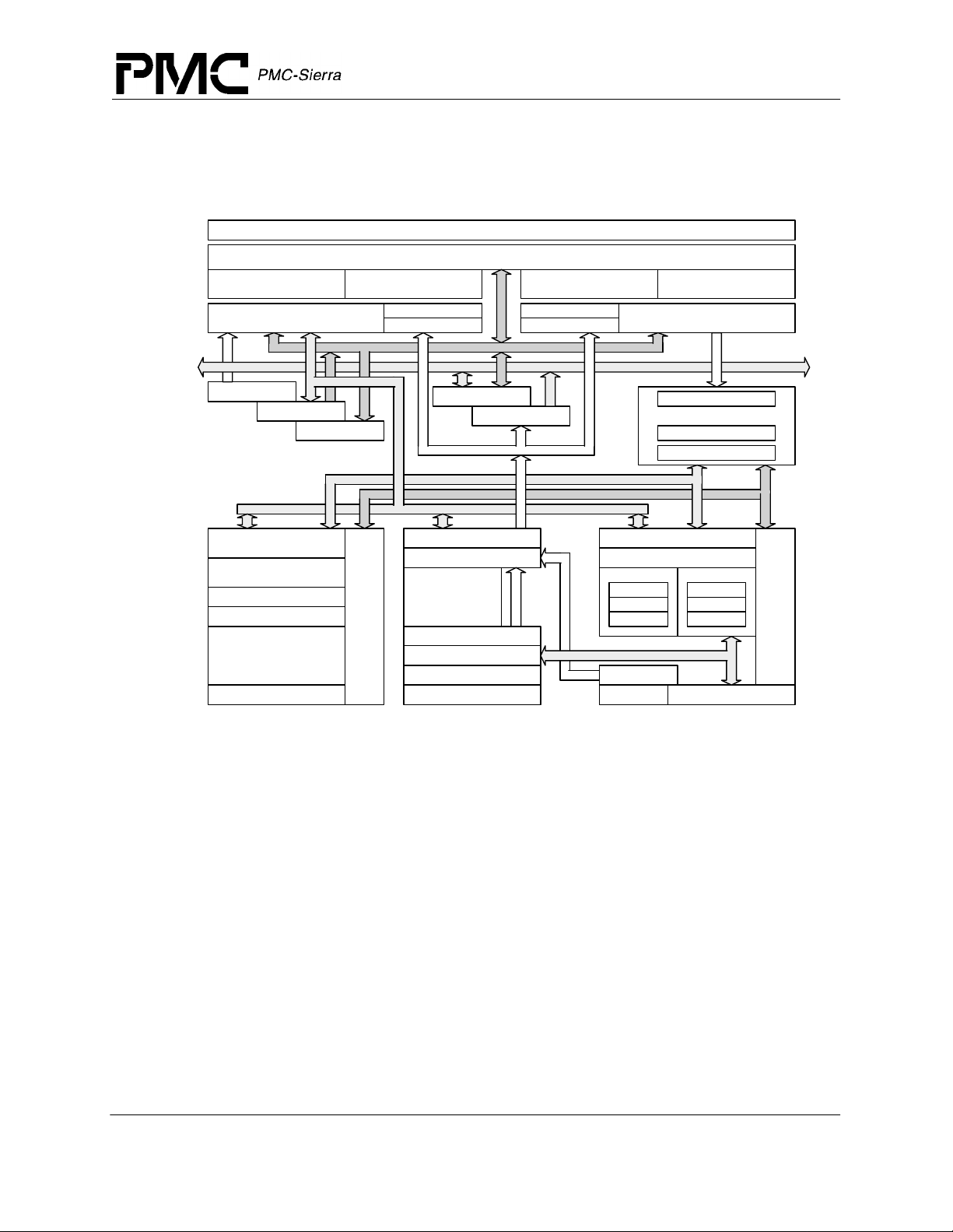
2 Block Diagram
Figure 1 Block Diagram
Secondary Tags
Set A
Primary Data Cache
4-way Set Associative
RM7000A™ Microprocessor with On-Chip Secondary Cache Data Sheet
Released
Extenal Cache Controller
On-chip 256K Byte Secondary Cache, 4-way Set Associative
Secondary Tags
Set B
DTag
DTLB
Secondary Tags
Set C
ITag
ITLB
Secondary Tags
Set D
Primary Instruction Cache
4-way Set Associative
A/D Bus
Pad Bus
Store Buffer
Write Buffer
D Bus
Floating-Point
Load/Align
Floating-Point
Register File
Packer/Unpacker
Comparator
Floating-Point
MultAdd, Add, Sub,
Cvt, Div, Sqrt
Multiplier Array
Read Buffer
Coprocessor 0
System/Memory
Control
PC Incrementer
Floating-Point Control
Branch PC Adder
ITLB Virtual
Program Counter Int Mult, Div, Madd
Pad Buffer
Joint TLB
Address Buffer
IVA
F-Pipe Bus
DVA
Integer Register File
Adder
StAln/Sh
Logicals
FA Bus
DTLB Virtual
PLL/Clocks
Prefetch Buffer
Instruction Dispatch Unit
F Pipe Register
M Pipe Register
M-Pipe Bus
Load Aligner
F PipeM Pipe
Adder
Shifter
Logicals
Integer Control
Proprietary and Confidential to PMC-Sierra, Inc and for its Customer’s Internal Use 10
Document ID: PMC-2002227, Issue 2

3 Description
PMC-Sierra’s RM7000A is a highly integrated symmetric superscalar microprocessor capable of
issuing two instructions each processor cycle. It has two high-performance 64-bit integer units as
well as a high-throughput, fully pipelined 64-bit floating point unit.
The RM7000A integrates 16 KB 4-way set associative instruction and data caches along with an
integrated 256 KB 4-way set associative secondary. The primary data and secondary caches are
write-back and non-blocking. An optional external tertiary cache provides high-performance
capability even in app lications with very large data sets.
The memory management unit contains a 64/48-entry fully associative TLB and a 64-bit system
interface supporting multiple outstanding reads with out-of-order return and hardware prioritized
and vectored interrupts.
The RM7000A ideally suits high-end embedded control applications such as internetworking,
high-performance image manipulati on, high-sp eed print ing, and 3-D vi sualizati on. The RM7000A
is also applicable to the low end workstation market where its balanced integer and floating-point
performance and direct support for a large tertiary cache (up to 8 MB) provide outstanding price/
performance.
RM7000A™ Microprocessor with On-Chip Secondary Cache Data Sheet
Released
Proprietary and Confidential to PMC-Sierra, Inc and for its Customer’s Internal Use 11
Document ID: PMC-2002227, Issue 2

RM7000A™ Microprocessor with On-Chip Secondary Cache Data Sheet
4 Hardware Overview
The RM7000A offers a high-level of integration targeted at high-performance embedded
applications. The key elements of the RM7000A are described throughout this section.
4.1 CPU Registers
The RM7000A CPU contains 32 general purpose registers (GPR), two special purpose registers
for integer multiplication and division, and a program counter; there are no condition code bits.
Figure 2 shows the user visible state.
Figure 2 CP0 Registers
General Purpose Registers
63 0
0630
r1 HI
r2 63 0
• LO
•
•
• 63 0
r29 PC
r30
r31
Released
Multiply/Divide Registers
Program Counter
4.2 Superscalar Dispatch
The RM7000A incorporates a superscalar dispatch unit that allows it to issue up to two
instructions per cycle. For purposes of instruction issue, the RM7000A defines four classes of
instructions: integer, load/store, branches, and floating-point. There are two logical pipelines, the
function, or F, pipeline and the memory, or M, pipeline. Note however that the M pip e ca n exe cut e
integer as well as memory type instru ctions.
Table 1 Instruction Issue Rules
F Pipe M Pipe
one of: one of: integer, branch, floating-point,
integer mul, div
Proprietary and Confidential to PMC-Sierra, Inc and for its Customer’s Internal Use 12
Document ID: PMC-2002227, Issue 2
integer, load/store

RM7000A™ Microprocessor with On-Chip Secondary Cache Data Sheet
Released
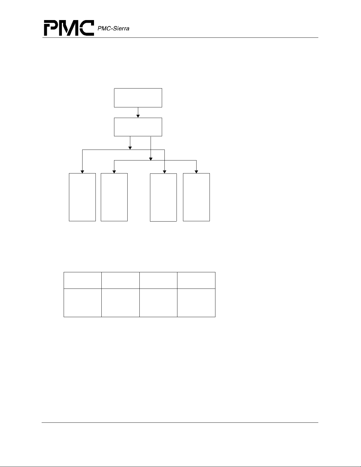
Figure 2 is a simplification of the pipeline section and illustrates the basics of the instruction issue
mechanism.
Figure 3 Instruction Issue Paradigm
Instruction
Cache
Dispatch
Unit
F Pipe IBus
M Pipe IBus
FP
F Pipe
The figure illustrates that one F pipe instruction and one M pipe instruction can be issued
concurrently but that two M pipe or two F pipe instructions cannot be issued. Table 2 specifies
more completely the instructions within each class.
T able 2 Dual Issue Instruction Classes
integer load/store
add, sub, or , xor, sh ift, etc .
4.3 Pipeline
The logical length of both the F an d M pipel ines i s fiv e stages with st ate c ommitti ng in t he reg ister
write, or W, pipe stage. The physical length of the floating-point execution pipeline is actually
seven stag es but this is completely transparent to the user.
FP
M Pipe
lw, sw, ld, sd, ldc1, sdc1, mov, movc, fmov, etc.
Integer
F Pipe
floatingpoint branch
fadd, fsub, fmult, fm add, fdiv, fcmp, fsqrt, etc.
Integer
M Pipe
beq, bne, bCzT, bCzF, j, etc.
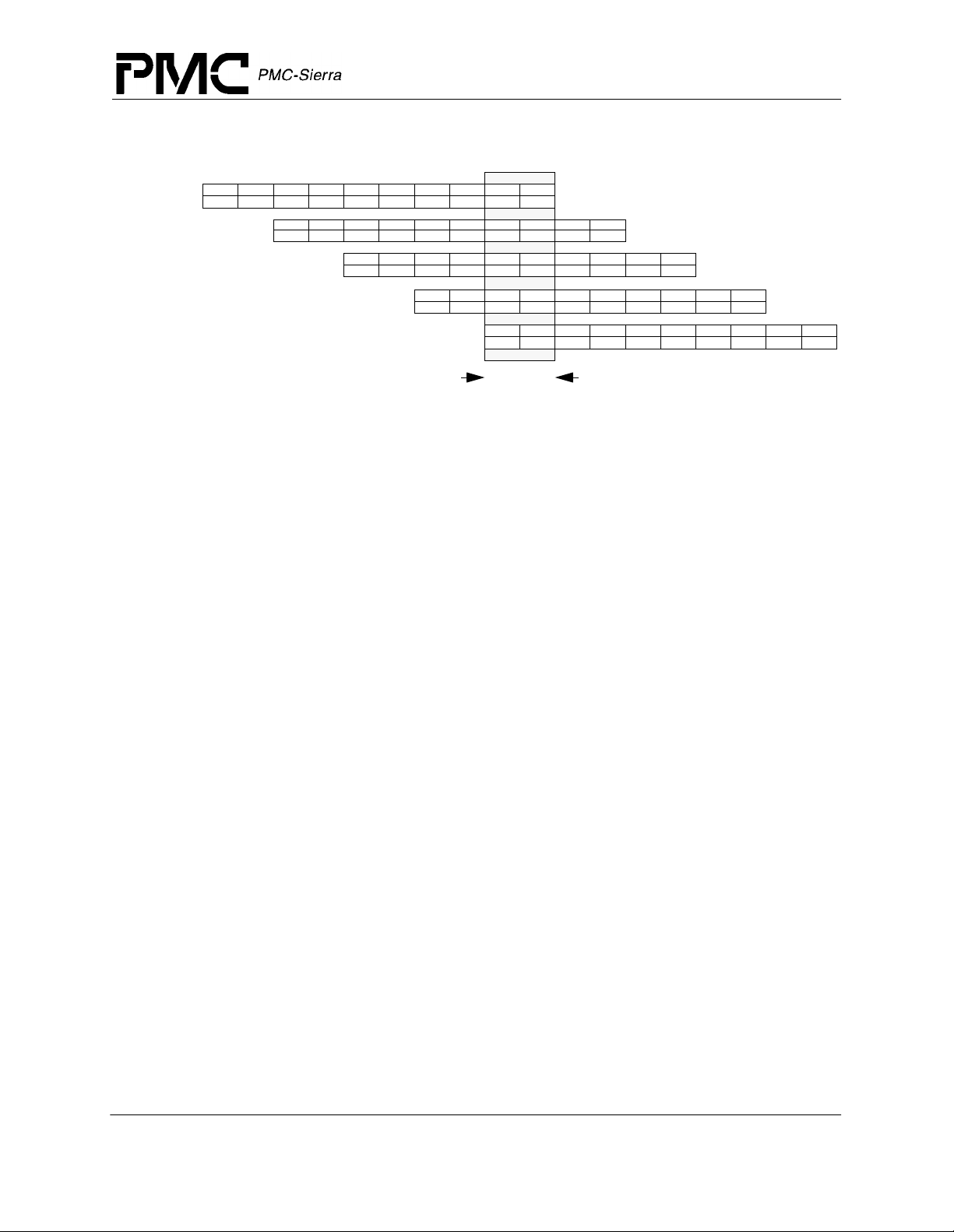
Figure 4 shows instruction execution within the RM7000A when instructions are issuing
simultaneously down both pipelines. As illustrated in the figure, up to ten instructions can be
executing simultaneously. This figure pres ents a somewhat simplistic view of the processors
operation since the out-of-order completion of loads, stores, and long latency floating-point
operations can result in there being even more instructions in process than what is shown.
Proprietary and Confidential to PMC-Sierra, Inc and for its Customer’s Internal Use 13
Document ID: PMC-2002227, Issue 2

Figure 4 Pipeline
RM7000A™ Microprocessor with On-Chip Secondary Cache Data Sheet
Released
I0
I1
I2
I3
I4
I5
I6
I7 2I1I 1R 2R 1A 2A 1D 2D 1W 2W
I8
I9
1I-1R:
2I:
2R:
1A:
1A:
1A-2A:
2A:
2A-2D:
1D:
2W:
2I1I 1R 2R 1A 2A 1D 2D 1W 2W
2I1I 1R 2R 1A 2A 1D 2D 1W 2W
Instruction cache access
Instruction virtual to physical address translation
Register file read, Bypass calculation, Instruction decode, Branch address calculation
Issue or slip decision, Branch decision
Data virtual address calculation
Integer add, logical, shift
Store Align
Data cache access and load align
Data virtual to physical address translation
Register file write
Note that instruction dependencies, resource conflicts, and branches may result in some of the
instruction slots being occupied by
4.4 Integer Unit
The RM7000A implements the MIP S IV Instru ction Set Architect ure. Addit ionally, the RM7000A
includes two implementation specific i nst r u ct ion s not f ound in the baselin e MI PS I V I SA, b ut that
are useful in the embedded market place. These instructions are integer multiply-accumulate
(MAD) and three-operand integer m ultiply (MUL).
2I1I 1R 2R 1A 2A 1D 2D 1W 2W
2I1I 1R 2R 1A 2A 1D 2D 1W 2W
2I1I 1R 2R 1A 2A 1D 2D 1W 2W
2I1I 1R 2R 1A 2A 1D 2D 1W 2W
2I1I 1R 2R 1A 2A 1D 2D 1W 2W
2I1I 1R 2R 1A 2A 1D 2D 1W 2W
2I1I 1R 2R 1A 2A 1D 2D 1W 2W
one cycle
NOPs.
The RM7000A integer unit includes thirty-two general purpose 64-bit registers, the HI/LO result
registers for two-operand integer multiply/divide operations, and the program counter, or PC.
There are two separate execution units, one of which can execute function (F) type instructions
and one which can e xecute memor y (M) type instruc tions. Ref er to Table 1 for the inst ruction issue
rules.
Note that integer multip ly/divide instructions, as well as their corresponding
MFHI and MFLO
instructions, can only be executed in the F type execution unit. Within each execution unit the
operational characteristics are the same as on previous MIPS designs with single cycle ALU
operations (add, sub, logical, shift), one cycle load delay, and an autonomous multiply/divide unit.
Register File
The RM7000A has thirty-two general purpose registers with register location 0 (r0) hard wired to
a zero value. Thes e regist ers are use d for scalar integer operatio ns and addr ess cal culation . In order
to service the two integer execution units, the register file has four read ports and two write ports
and is fully bypassed both within and between the two execution units to minimize operation
latency in the pipeline.
Proprietary and Confidential to PMC-Sierra, Inc and for its Customer’s Internal Use 14
Document ID: PMC-2002227, Issue 2

RM7000A™ Microprocessor with On-Chip Secondary Cache Data Sheet
4.5 ALU
The RM7000A has two complete integer ALUs each consisting of an integer adder/subtractor, a
logic unit, and a shifter. Table 3 shows the functions performed by the ALUs for each execution
unit. Each of these units is optimized to perform all operations in a single processor cycle.
Table 3 ALU Operations
Unit F Pipe M Pipe
Adder add, sub add, sub, data address
Logic logic, moves, zero shifts
(nop)
Shifter non zero shift non zero shift, store
4.6 Integer Multiply/Divide
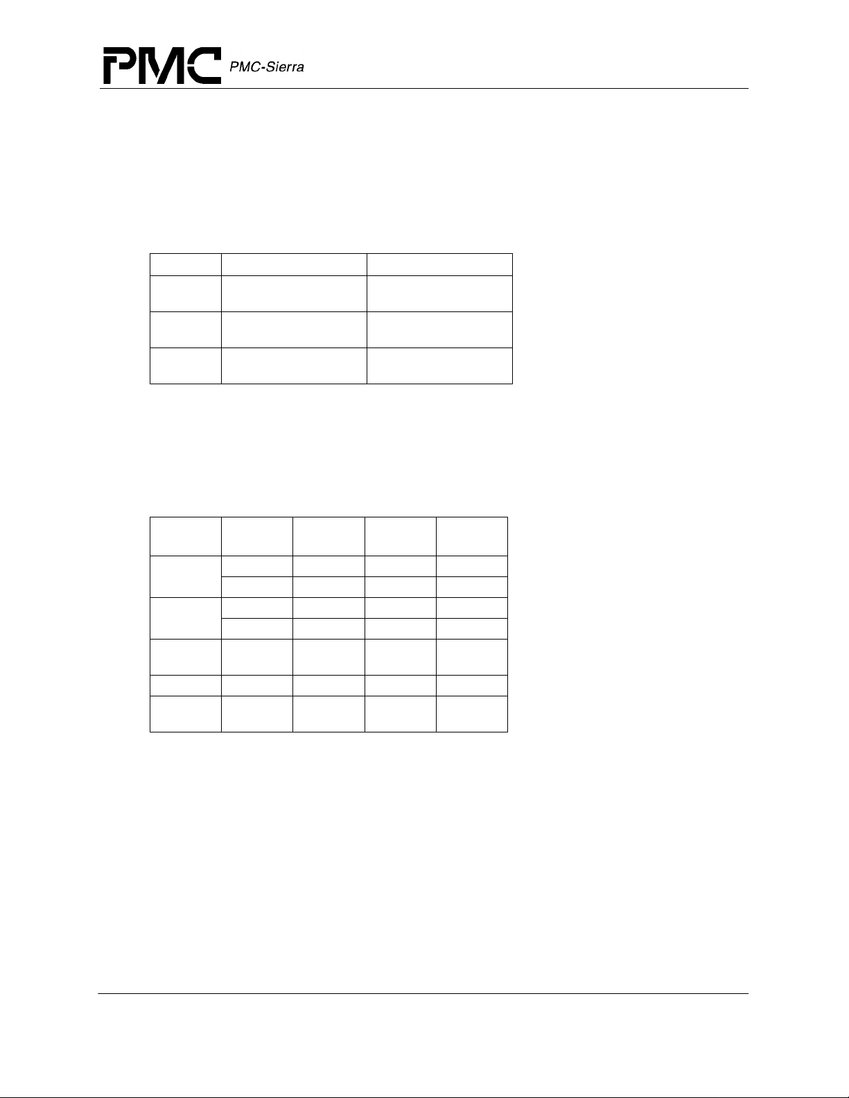
The RM7000A has a single dedicated integer multiply/divide unit optimized for high-speed
multiply and multiply-accumulate operations. The multiply/divide unit resides in the F type
execution unit. Table 4 shows the performance of the multiply/divide unit on each operation.
Released
add
logic, moves, zero shifts
(nop)
align
Table 4 Integer Multiply/Divide Operations
Operand
Opcode
MULT/U, MAD/U
MUL
DMULT, DMUL TU
DIV, DIVD any 36 36 0 DDIV,
DDIVU
Size Latency
16 bit 4 3 0 32 bit 5 4 0 16 bit 4 3 2 32 bit 5 4 3
any 9 8 0
any 68 68 0
Repeat
Rate
Stall
Cycles
The baseline MIPS IV ISA specifies that the results of a multiply or divide operation be placed in
the Hi and Lo registers. These values can then be transferred to the general purpose register file
using the Move-from-Hi and Move-from-Lo (
MFHI/MFLO) instru ctions.
In addition to the baseline MIPS IV integer multiply instructions, the RM7000A also implements
the 3-operand multiply instruction,
MUL. This instruction spec ifies that the multiply re sult go
directly to the integer register file rather than the Lo register. The portion of the multiply that
would have normally gone i nto the Hi re gister i s discard ed. For applicat ions where i t is known tha t
the upper half of the multiply result is not required, using the
necessity of executing an explicit
MFLO instruction.
MUL instruction eliminates the
The multiply-add instructions,
MAD and MADU, multiply two ope rands and add the resulting
product to the current contents of the Hi and Lo registers. The multip ly-accumulate operat ion is
Proprietary and Confidential to PMC-Sierra, Inc and for its Customer’s Internal Use 15
Document ID: PMC-2002227, Issue 2

RM7000A™ Microprocessor with On-Chip Secondary Cache Data Sheet
the core primitive of almost all signal processing algorithms. Therefore, using the RM7000A
eliminates the need for a separate DSP engine in many embedded applications.
4.7 Floating-Point Coprocessor
The RM7000A incorporates a high-performance fully pipelined floating-point coprocessor which
includes a floating-po int register file and autonomous execution units for multiply/a dd/convert and
divide/square root. The floating-point coprocessor is a tightly coupled execution unit, decoding
and executing instructions in parallel with, and in the case of floating-point loads and stores, in
cooperation with the M pipe of the integer unit. The superscalar capabilities of the RM7000A
allow floating-point computation instructions to issue concurrently with integer instructions.
4.8 Floating-Point Unit
The RM7000A floating-point execution unit supports single and double precision arithmetic, as
specified in the IEEE S tanda rd 754. The ex ecution uni t is broken i nto a separa te divide /square ro ot
unit and a pipelined multiply/add unit. Overlap of divide/square root and multiply/add is
supported.
The RM7000A maintains fully precise floating-point exceptions while allowing both overlapped
and pipelined operations. Precise exceptions are extremely important in object-oriented
programming environments and highly desirable for debugging in any environment.
Released
Floating-point operations include:
• add
• subtract
• multiply
• divide
• square root
• reciprocal
• reciprocal square root
• conditional moves
• conversion between fixed-point and floating-point format
• conversion between floating-point formats
• floating-point compare
Table 5 gives the latencies of the floating-point instructions in internal processor cycles.
Proprietary and Confidential to PMC-Sierra, Inc and for its Customer’s Internal Use 16
Document ID: PMC-2002227, Issue 2
 Loading...