


RM7000A™ Microprocessor with On-Chip Secondary Cache Data Sheet
Released
RM7000A
RM7000A™ Microprocessor with On-
Chip Secondary Cache
Data Sheet
Proprietary and Confidential
Released
Issue 2, May 2001
Proprietary and Confidential to PMC-Sierra, Inc and for its Customer’s Internal Use
Document ID: PMC-2002227, Issue 2

RM7000A™ Microprocessor with On-Chip Secondary Cache Data Sheet
Released
Legal Information
Copyright
© 2001 PMC-Sierra, Inc.
The information is proprietary and confidential to PMC-Sierra, Inc., and for its customers’ internal use. In
any event, you cannot reproduce any part of this document, in any form, without the express written
consent of PMC-Sierra, Inc.
PMC-2002227 (R2)
Disclaimer
None of the information contained in this document constitutes an express or implied warranty by PMCSierra, Inc. as to the sufficiency, fitness or suitability for a particular purpose of any such information or the
fitness, or suitability for a particular purpose, merchantability, performance, compatibility with other parts
or systems, of an y of t he pr oducts of PMC-Si erra , Inc., or an y port io n ther eof, r efer red to i n this document .
PMC-Sierra, Inc. expressly disclaims all re presentations and war ra nties of any kind rega rdi ng the contents
or use of the information, including, but not limited to, express and implied warranties of accuracy,
completeness, merchantability, fitness for a particular use, or non-infringement.
In no event will PMC-Sierra, Inc. be liable for any direct, indirect, special, incidental or consequential
damages, including, but not limited to, lost profits, lost business or lost data resulting from any use of or
reliance upon the infor ma tion, whether or not PMC-Sierra, Inc . has been a dvised of the possibility of such
damage.
Trademarks
RM7000A and Fast Packet Cache are trademarks of PMC-Sierra, Inc.
Patents
The technology discussed is protected by one or more of the following Patents.
U.S. Patent Numbers
Relevant patent applications and other patents may also exist.
5,953,748, 5,953,748, 5,953,74 8
Contacting PMC-Sierra
PMC-Sierra, Inc.
8555 Baxter Place Burnaby, BC
Canada V5A 4V7
Tel: (604) 415-6000
Fax: (604) 415-6200
Document Information: document@pmc-sierra.com
Corporate Information: info@pmc-sierra.com
Technical Support: apps@pmc-sierra.com
Web Site: http: //www.pmc-sierra.com
Proprietary and Confidential to PMC-Sierra, Inc and for its Customers' Internal Use 2
Document ID: PMC-2002227, Issue 2
Revision History
RM7000A™ Microprocessor with On-Chip Secondary Cache Data Sheet
Released
Issue
No. Issue Date
2 May 2001 3716 K. Murray Changed pin AC13 SysCmd[2] from active
1 January 2001 T. Chapman Applied PMC-Sierra template to exi sting
ECN
Number Originator Details of Change
low to high.
Added industrial values to Recommended
Operating Instructions
Added industrial and commercial values to
Absolute Maximum Ratings
Changed Timer Interrupt Enable/Disable
information in Boot Time Mode Stream
table
Added paragraph to Interrupt Handling
section
Clarification added to System Interface
Parameters
Additional information added to Clock
Parameter table
MPD (QED) FrameMaker document.
In the Pinout Table, changed al l refer enc es
from IP to INT
Section 1, Features, changed High-
performance system interface, 133 MHz
maximum frequency, multiplexed address/
data to 125 MHz.
Changed QED references to PMC-Sierra
or MIPS.
Updated Section 7, Recommended
Operating Condition s and Se cti on 9 Power
Consumption.
Added System Interface Parameter values,
Section 10.3, for 350 MHz and 400 MHz
CPU speeds per data provided by Mark
Scrivener.
Proprietary and Confidential to PMC-Sierra, Inc and for its Customers' Internal Use 3
Document ID: PMC-2002227, Issue 2

RM7000A™ Microprocessor with On-Chip Secondary Cache Data Sheet
Released
Document Conventions
The following conventions are used in this datasheet:
• All signal, pin, and bus names described in the text, such as ExtRqst*, are in boldface
typeface.
• All bit and field names described in the text, such as Interrupt Mask, are in an italic -bold
typeface.
• All instruct ion names, such as MFHI, are in san serif typeface.
Proprietary and Confidential to PMC-Sierra, Inc and for its Customers' Internal Use 4
Document ID: PMC-2002227, Issue 2

RM7000A™ Microprocessor with On-Chip Secondary Cache Data Sheet
Released
Table of Contents
Legal Information ...........................................................................................................................2
Revision History .............................................................................................................................3
Document Conventions .................................................................................................................4
Table of Contents .......................................................................................................................... 5
List of Figures ................................. ...... ....... ...................................... ....... ...... ....... ...... ..................7
List of Tables . ....... ...... ....... ...... ....... ...... ....... ...... ....... ...................................... ....... ...... ..................8
1 Features ......................................... ....................................................................... ..................9
2 Block Diagram ...... ....... ...... ....... ...... ....................................... ...... ....... ...... ....... ...... ....... .........10
3 Description ............................................................................................................................11
4 Hardware Overview ...............................................................................................................12
4.1 CPU Registers .............................................................................................................12
4.2 Superscalar Dispatch ...................................................................................................12
4.3 Pipeline ........................................................................................................................13
4.4 Integer Unit ..................................................................................................................14
4.5 ALU ..............................................................................................................................15
4.6 Integer Multiply/Divide ..................................................................................................15
4.7 Floating-Point Coprocessor ..........................................................................................16
4.8 Floating-Point Unit .......................................................................................................16
4.9 Floating-Point General Register File ............................................................................17
4.10 System Control Coprocessor (CP0) .............................................................................18
4.11 System Control Coprocessor Registers .......................................................................18
4.12 Virtual to Physical Address Mapping ............................................................................19
4.13 Joint TLB ......................................................................................................................20
4.14 Instruction TLB .............................................................................................................21
4.15 Data TLB ......................................................................................................................21
4.16 Cache Memory .............................................................................................................21
4.17 Instruction Cache .........................................................................................................22
4.18 Data Cache ..................................................................................................................22
4.19 Secondary Cache ........................................................................................................24
4.20 Secondary Caching Protocols ......................................................................................24
4.21 Tertiary Cache .............................................................................................................25
4.22 Cache Locking .............................................................................................................26
4.23 Cache Management .....................................................................................................27
4.24 Primary Write Buffer .....................................................................................................27
4.25 System Interface ............. ...................................... ....... ...... ....... ...... ....... ......................27
4.26 System Address/Data Bus .... ....................................... ...... ....... ...... ....... ......................28
4.27 System Command Bus ................................................ ...... ....... ...... .............................28
4.28 Handshake Signals ......................................................................................................29
4.29 System Interface Operation ......................................................................... ....... ...... ...29
Proprietary and Confidential to PMC-Sierra, Inc and for its Customers' Internal Use 5
Document ID: PMC-2002227, Issue 2

RM7000A™ Microprocessor with On-Chip Secondary Cache Data Sheet
Released
4.30 Data Prefetch ...............................................................................................................31
4.31 Enhanced Write Modes ................................................................................................32
4.32 External Requests ........................................................................................................32
4.33 Test/Breakpoint Registers ............................................................................................32
4.34 Performance Counters .................................................................................................33
4.35 Interrupt Handling ........................................................................................................35
4.36 Standby Mode .... ...... ....... ...................................... ....... ...... ....... ...... .............................37
4.37 JTAG Interface .............................................................................................................37
4.38 Boot-Time Options .......................................................................................................37
4.39 Boot-Time Modes .........................................................................................................37
5 Pin Descriptions ....................................................................................................................39
6 Absolute Maximum Ratings1 ................................................................................................43
7 Recommended Operating Conditions ...................................................................................44
8 DC Electrical Characteristics .................................................................................................45
9 Power Consumption ..............................................................................................................46
10 AC Electrical Characteristic s .... ...... ....... ...... ....... ...... ...... ....................................... ....... ...... . ..47
10.1 Capacitive Load Deration .............................................................................................47
10.2 Clock Parameters ........................................................................................................47
10.3 System Interface Parameters ................... ...... ....................................... ...... ....... ...... ...48
10.4 Boot-Time Interface Parameters ..................................................................................48
11 Timing Diagrams ...................................................................................................................49
11.1 Clock Timing ................................................................................................................49
12 Packaging Information ..........................................................................................................50
13 RM7000A Pinout ...................................................................................................................51
14 Ordering Information .............................................................................................................53
Proprietary and Confidential to PMC-Sierra, Inc and for its Customer’s Internal Use 6
Document ID: PMC-2002227, Issue 2

RM7000A™ Microprocessor with On-Chip Secondary Cache Data Sheet
Released
List of Figures
Figure 1 Block Diagram .............................................................................................................10
Figure 2 CP0 Registers .............................................................................................................12
Figure 3 Instruction Issue Paradigm ..........................................................................................13
Figure 4 Pipeline ........................................................................................................................14
Figure 5 CP0 Registers .............................................................................................................19
Figure 6 Kernel Mode Virtual Addressing (32-bit) .....................................................................20
Figure 7 Tertiary Cache Hit and Miss ........................................................................................25
Figure 8 Typical Embedded System Block Diagram .................................................................28
Figure 9 Processor Block Read .................................................................................................30
Figure 10 Processor Block Write ...............................................................................................31
Figure 11 Multiple Outstanding Reads ......................................................................................31
Figure 12 Clock Timing ..............................................................................................................49
Figure 13 Input Timing ...............................................................................................................49
Figure 14 Output Timing ............................................................................................................49
Figure 15 304 TBGA Drawing ...................................................................................................50
Proprietary and Confidential to PMC-Sierra, Inc and for its Customer’s Internal Use 7
Document ID: PMC-2002227, Issue 2

RM7000A™ Microprocessor with On-Chip Secondary Cache Data Sheet
Released
List of Tables
Table 1 Instruction Issue Rules .................................................................................................12
Table 2 Dual Issue Instruction Classes .....................................................................................13
Table 3 ALU Operations ............................................................................................................15
Table 4 Integer Multiply/Divide Operations ................................................................................15
Table 5 Floating Point Latencies and Repeat Rates .................................................................17
Table 6 Cache Attributes ...........................................................................................................26
Table 7 Cache Locking Control .................................................................................................27
Table 8 Penalty Cycles ..............................................................................................................27
Table 9 Watch Control Register ................................................................................................33
Table 10 Performance Counter Control .....................................................................................34
Table 11 Cause Register ...........................................................................................................36
Table 12 Interrupt Control Register ...........................................................................................36
Table 13 IPLLO Register ...........................................................................................................36
Table 14 IPLHI Register ............................................................................................................36
Table 15 Interrupt Vector Spacing .............................................................................................37
Table 16 Boot Time Mode Stream .............................................................................................38
Table 17 System Interface .........................................................................................................39
Table 18 Clock/Control Interface ...............................................................................................40
Table 19 Tertiary Cache Interface .............................................................................................41
Table 20 Interrupt Interface .......................................................................................................42
Table 21 JTAG Interface ...........................................................................................................42
Table 22 Initialization Interface ..................................................................................................42
Proprietary and Confidential to PMC-Sierra, Inc and for its Customer’s Internal Use 8
Document ID: PMC-2002227, Issue 2

1 Features
• Dual issue symmetric superscalar microprocessor with instructio n prefetch optimized for
system level price/performance
• 300, 350, 400 MHz operating frequency
• >600 Dhrystone 2.1 MIPS @ 400 MHz
• High-performance system interface
• 1000 MB per second peak throughput
• 125 MHz max. freq., multiplexed address/data
• Supports two outstanding reads with out-of-order return
• Processor clock multipliers 2, 2.5, 3, 3.5, 4, 4.5, 5, 6, 7, 8, 9
• Integrated primary and secondary caches
• All are 4-way set associative with 32 byte line size
• 16 KB instruction, 16 KB data, 256 KB on-chip secondary
• Per line cache locking in primaries and secondary
• Fast Packet Cache™ increases system efficiency in
networking applications
• Integrated external cache controller (up to 8 MB)
• High-performance floating-point unit — 800 MFLOPS maximum
• Single cycle repeat rate for common single -pr ecision ope ra tions and some double-p recision operations
• Single cycle repeat rate for single-precision combined multiply-add operations
• Two cycle repeat rate for double-precision multiply and double-precision combined
multiply-add operations
RM7000A™ Microprocessor with On-Chip Secondary Cache Data Sheet
Released
• MIPS IV superset instruction set arch itecture
• Data PREFETCH inst ruction allows the processor to overlap cache miss laten cy and
instruction execution
• Single-cycle floating-point multiply-add
• Integrated memory management unit
• Fully associative joint TLB (shared by I and D translations)
• 64/48 dual entries map 128/96 pages
• Variable page size
• Embedded application enhancements
• Specialized DSP integer Multiply-Accumulate instructions, (MAD/MADU) and
three-operand multiply instructio n (MUL)
• I&D Te st/Break-point (Watch) registers for emulation & debug
• Performance counter for system and software tuning & debug
• Fourteen fully prioritized vectored interrupts — 10 external, 2 internal, 2 sof tware
• Fully static CMOS design with dynamic power down logic
• RM5271 pin compatible, 304 pin TBGA package, 31x31 mm
Proprietary and Confidential to PMC-Sierra, Inc and for its Customer’s Internal Use 9
Document ID: PMC-2002227, Issue 2
2 Block Diagram
Figure 1 Block Diagram
Secondary Tags
Set A
Primary Data Cache
4-way Set Associative
RM7000A™ Microprocessor with On-Chip Secondary Cache Data Sheet
Released
Extenal Cache Controller
On-chip 256K Byte Secondary Cache, 4-way Set Associative
Secondary Tags
Set B
DTag
DTLB
Secondary Tags
Set C
ITag
ITLB
Secondary Tags
Set D
Primary Instruction Cache
4-way Set Associative
A/D Bus
Pad Bus
Store Buffer
Write Buffer
D Bus
Floating-Point
Load/Align
Floating-Point
Register File
Packer/Unpacker
Comparator
Floating-Point
MultAdd, Add, Sub,
Cvt, Div, Sqrt
Multiplier Array
Read Buffer
Coprocessor 0
System/Memory
Control
PC Incrementer
Floating-Point Control
Branch PC Adder
ITLB Virtual
Program Counter Int Mult, Div, Madd
Pad Buffer
Joint TLB
Address Buffer
IVA
F-Pipe Bus
DVA
Integer Register File
Adder
StAln/Sh
Logicals
FA Bus
DTLB Virtual
PLL/Clocks
Prefetch Buffer
Instruction Dispatch Unit
F Pipe Register
M Pipe Register
M-Pipe Bus
Load Aligner
F PipeM Pipe
Adder
Shifter
Logicals
Integer Control
Proprietary and Confidential to PMC-Sierra, Inc and for its Customer’s Internal Use 10
Document ID: PMC-2002227, Issue 2

3 Description
PMC-Sierra’s RM7000A is a highly integrated symmetric superscalar microprocessor capable of
issuing two instructions each processor cycle. It has two high-performance 64-bit integer units as
well as a high-throughput, fully pipelined 64-bit floating point unit.
The RM7000A integrates 16 KB 4-way set associative instruction and data caches along with an
integrated 256 KB 4-way set associative secondary. The primary data and secondary caches are
write-back and non-blocking. An optional external tertiary cache provides high-performance
capability even in app lications with very large data sets.
The memory management unit contains a 64/48-entry fully associative TLB and a 64-bit system
interface supporting multiple outstanding reads with out-of-order return and hardware prioritized
and vectored interrupts.
The RM7000A ideally suits high-end embedded control applications such as internetworking,
high-performance image manipulati on, high-sp eed print ing, and 3-D vi sualizati on. The RM7000A
is also applicable to the low end workstation market where its balanced integer and floating-point
performance and direct support for a large tertiary cache (up to 8 MB) provide outstanding price/
performance.
RM7000A™ Microprocessor with On-Chip Secondary Cache Data Sheet
Released
Proprietary and Confidential to PMC-Sierra, Inc and for its Customer’s Internal Use 11
Document ID: PMC-2002227, Issue 2
RM7000A™ Microprocessor with On-Chip Secondary Cache Data Sheet
4 Hardware Overview
The RM7000A offers a high-level of integration targeted at high-performance embedded
applications. The key elements of the RM7000A are described throughout this section.
4.1 CPU Registers
The RM7000A CPU contains 32 general purpose registers (GPR), two special purpose registers
for integer multiplication and division, and a program counter; there are no condition code bits.
Figure 2 shows the user visible state.
Figure 2 CP0 Registers
General Purpose Registers
63 0
0630
r1 HI
r2 63 0
• LO
•
•
• 63 0
r29 PC
r30
r31
Released
Multiply/Divide Registers
Program Counter
4.2 Superscalar Dispatch
The RM7000A incorporates a superscalar dispatch unit that allows it to issue up to two
instructions per cycle. For purposes of instruction issue, the RM7000A defines four classes of
instructions: integer, load/store, branches, and floating-point. There are two logical pipelines, the
function, or F, pipeline and the memory, or M, pipeline. Note however that the M pip e ca n exe cut e
integer as well as memory type instru ctions.
Table 1 Instruction Issue Rules
F Pipe M Pipe
one of: one of: integer, branch, floating-point,
integer mul, div
Proprietary and Confidential to PMC-Sierra, Inc and for its Customer’s Internal Use 12
Document ID: PMC-2002227, Issue 2
integer, load/store
RM7000A™ Microprocessor with On-Chip Secondary Cache Data Sheet
Released
Figure 2 is a simplification of the pipeline section and illustrates the basics of the instruction issue
mechanism.
Figure 3 Instruction Issue Paradigm
Instruction
Cache
Dispatch
Unit
F Pipe IBus
M Pipe IBus
FP
F Pipe
The figure illustrates that one F pipe instruction and one M pipe instruction can be issued
concurrently but that two M pipe or two F pipe instructions cannot be issued. Table 2 specifies
more completely the instructions within each class.
T able 2 Dual Issue Instruction Classes
integer load/store
add, sub, or , xor, sh ift, etc .
4.3 Pipeline
The logical length of both the F an d M pipel ines i s fiv e stages with st ate c ommitti ng in t he reg ister
write, or W, pipe stage. The physical length of the floating-point execution pipeline is actually
seven stag es but this is completely transparent to the user.
FP
M Pipe
lw, sw, ld, sd, ldc1, sdc1, mov, movc, fmov, etc.
Integer
F Pipe
floatingpoint branch
fadd, fsub, fmult, fm add, fdiv, fcmp, fsqrt, etc.
Integer
M Pipe
beq, bne, bCzT, bCzF, j, etc.
Figure 4 shows instruction execution within the RM7000A when instructions are issuing
simultaneously down both pipelines. As illustrated in the figure, up to ten instructions can be
executing simultaneously. This figure pres ents a somewhat simplistic view of the processors
operation since the out-of-order completion of loads, stores, and long latency floating-point
operations can result in there being even more instructions in process than what is shown.
Proprietary and Confidential to PMC-Sierra, Inc and for its Customer’s Internal Use 13
Document ID: PMC-2002227, Issue 2
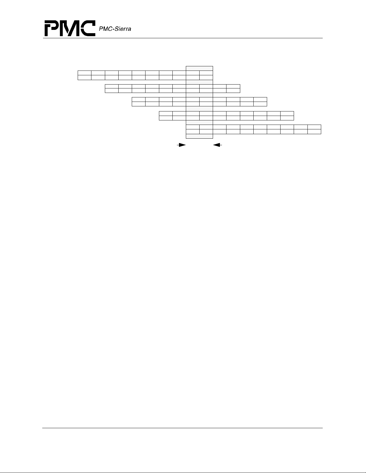
Figure 4 Pipeline
RM7000A™ Microprocessor with On-Chip Secondary Cache Data Sheet
Released
I0
I1
I2
I3
I4
I5
I6
I7 2I1I 1R 2R 1A 2A 1D 2D 1W 2W
I8
I9
1I-1R:
2I:
2R:
1A:
1A:
1A-2A:
2A:
2A-2D:
1D:
2W:
2I1I 1R 2R 1A 2A 1D 2D 1W 2W
2I1I 1R 2R 1A 2A 1D 2D 1W 2W
Instruction cache access
Instruction virtual to physical address translation
Register file read, Bypass calculation, Instruction decode, Branch address calculation
Issue or slip decision, Branch decision
Data virtual address calculation
Integer add, logical, shift
Store Align
Data cache access and load align
Data virtual to physical address translation
Register file write
Note that instruction dependencies, resource conflicts, and branches may result in some of the
instruction slots being occupied by
4.4 Integer Unit
The RM7000A implements the MIP S IV Instru ction Set Architect ure. Addit ionally, the RM7000A
includes two implementation specific i nst r u ct ion s not f ound in the baselin e MI PS I V I SA, b ut that
are useful in the embedded market place. These instructions are integer multiply-accumulate
(MAD) and three-operand integer m ultiply (MUL).
2I1I 1R 2R 1A 2A 1D 2D 1W 2W
2I1I 1R 2R 1A 2A 1D 2D 1W 2W
2I1I 1R 2R 1A 2A 1D 2D 1W 2W
2I1I 1R 2R 1A 2A 1D 2D 1W 2W
2I1I 1R 2R 1A 2A 1D 2D 1W 2W
2I1I 1R 2R 1A 2A 1D 2D 1W 2W
2I1I 1R 2R 1A 2A 1D 2D 1W 2W
one cycle
NOPs.
The RM7000A integer unit includes thirty-two general purpose 64-bit registers, the HI/LO result
registers for two-operand integer multiply/divide operations, and the program counter, or PC.
There are two separate execution units, one of which can execute function (F) type instructions
and one which can e xecute memor y (M) type instruc tions. Ref er to Table 1 for the inst ruction issue
rules.
Note that integer multip ly/divide instructions, as well as their corresponding
MFHI and MFLO
instructions, can only be executed in the F type execution unit. Within each execution unit the
operational characteristics are the same as on previous MIPS designs with single cycle ALU
operations (add, sub, logical, shift), one cycle load delay, and an autonomous multiply/divide unit.
Register File
The RM7000A has thirty-two general purpose registers with register location 0 (r0) hard wired to
a zero value. Thes e regist ers are use d for scalar integer operatio ns and addr ess cal culation . In order
to service the two integer execution units, the register file has four read ports and two write ports
and is fully bypassed both within and between the two execution units to minimize operation
latency in the pipeline.
Proprietary and Confidential to PMC-Sierra, Inc and for its Customer’s Internal Use 14
Document ID: PMC-2002227, Issue 2
RM7000A™ Microprocessor with On-Chip Secondary Cache Data Sheet
4.5 ALU
The RM7000A has two complete integer ALUs each consisting of an integer adder/subtractor, a
logic unit, and a shifter. Table 3 shows the functions performed by the ALUs for each execution
unit. Each of these units is optimized to perform all operations in a single processor cycle.
Table 3 ALU Operations
Unit F Pipe M Pipe
Adder add, sub add, sub, data address
Logic logic, moves, zero shifts
(nop)
Shifter non zero shift non zero shift, store
4.6 Integer Multiply/Divide
The RM7000A has a single dedicated integer multiply/divide unit optimized for high-speed
multiply and multiply-accumulate operations. The multiply/divide unit resides in the F type
execution unit. Table 4 shows the performance of the multiply/divide unit on each operation.
Released
add
logic, moves, zero shifts
(nop)
align
Table 4 Integer Multiply/Divide Operations
Operand
Opcode
MULT/U, MAD/U
MUL
DMULT, DMUL TU
DIV, DIVD any 36 36 0 DDIV,
DDIVU
Size Latency
16 bit 4 3 0 32 bit 5 4 0 16 bit 4 3 2 32 bit 5 4 3
any 9 8 0
any 68 68 0
Repeat
Rate
Stall
Cycles
The baseline MIPS IV ISA specifies that the results of a multiply or divide operation be placed in
the Hi and Lo registers. These values can then be transferred to the general purpose register file
using the Move-from-Hi and Move-from-Lo (
MFHI/MFLO) instru ctions.
In addition to the baseline MIPS IV integer multiply instructions, the RM7000A also implements
the 3-operand multiply instruction,
MUL. This instruction spec ifies that the multiply re sult go
directly to the integer register file rather than the Lo register. The portion of the multiply that
would have normally gone i nto the Hi re gister i s discard ed. For applicat ions where i t is known tha t
the upper half of the multiply result is not required, using the
necessity of executing an explicit
MFLO instruction.
MUL instruction eliminates the
The multiply-add instructions,
MAD and MADU, multiply two ope rands and add the resulting
product to the current contents of the Hi and Lo registers. The multip ly-accumulate operat ion is
Proprietary and Confidential to PMC-Sierra, Inc and for its Customer’s Internal Use 15
Document ID: PMC-2002227, Issue 2

RM7000A™ Microprocessor with On-Chip Secondary Cache Data Sheet
the core primitive of almost all signal processing algorithms. Therefore, using the RM7000A
eliminates the need for a separate DSP engine in many embedded applications.
4.7 Floating-Point Coprocessor
The RM7000A incorporates a high-performance fully pipelined floating-point coprocessor which
includes a floating-po int register file and autonomous execution units for multiply/a dd/convert and
divide/square root. The floating-point coprocessor is a tightly coupled execution unit, decoding
and executing instructions in parallel with, and in the case of floating-point loads and stores, in
cooperation with the M pipe of the integer unit. The superscalar capabilities of the RM7000A
allow floating-point computation instructions to issue concurrently with integer instructions.
4.8 Floating-Point Unit
The RM7000A floating-point execution unit supports single and double precision arithmetic, as
specified in the IEEE S tanda rd 754. The ex ecution uni t is broken i nto a separa te divide /square ro ot
unit and a pipelined multiply/add unit. Overlap of divide/square root and multiply/add is
supported.
The RM7000A maintains fully precise floating-point exceptions while allowing both overlapped
and pipelined operations. Precise exceptions are extremely important in object-oriented
programming environments and highly desirable for debugging in any environment.
Released
Floating-point operations include:
• add
• subtract
• multiply
• divide
• square root
• reciprocal
• reciprocal square root
• conditional moves
• conversion between fixed-point and floating-point format
• conversion between floating-point formats
• floating-point compare
Table 5 gives the latencies of the floating-point instructions in internal processor cycles.
Proprietary and Confidential to PMC-Sierra, Inc and for its Customer’s Internal Use 16
Document ID: PMC-2002227, Issue 2

RM7000A™ Microprocessor with On-Chip Secondary Cache Data Sheet
Table 5 Floating Point Latencies and Repeat Rates
Latency
Operation
fadd 4 1 fsub 4 1 fmult 4/5 1/2 fmadd 4/5 1/2 fmsub 4/5 1/2 fdiv 21/36 19/34 fsqrt 21/36 19/34 frecip 21/36 19/34 frsqrt 38/68 36/66 fcvt.s.d 4 1 fcvt.s.w 6 3 fcvt.s.l 6 3 fcvt.d.s 4 1 fcvt.d.w 4 1 fcvt.d.l 4 1 fcvt.w.s 4 1 fcvt.w.d 4 1 fcvt.l.s 4 1 fcvt.l.d 4 1 fcmp 1 1 fmov, fmovc 1 1 fabs, fneg 1 1
single/double
Repeat Rate
single/double
Released
4.9 Floating-Point General Register File
The floating-point general register file (FGR) is made up of thirty-two 64-bit registers. With the
floating-point load and store double instructions,
take advantage of the 64-bit wide data cache and issue a floating-point coprocessor load or store
doubleword instruction in every cycle.
The floating-point control register file contains two registers; one for determining configuration
and revision information for the coprocessor, and one for control and status information. These
registers are primar ily used f or diagnost ic software , exception handling, st ate savi ng and resto ring,
and control of rounding modes.
To support superscalar operations the FGR has four read ports and two write ports and is fully
bypassed to minimize operation latency in the pipeline. Three of the read ports and one write port
are used to support the combined multiply-add instruction while the fourth read and second write
port allows for concurrent floating-point load or store and conditional move operations.
Proprietary and Confidential to PMC-Sierra, Inc and for its Customer’s Internal Use 17
Document ID: PMC-2002227, Issue 2
LDC1 and SDC1, the floating-point unit can

RM7000A™ Microprocessor with On-Chip Secondary Cache Data Sheet
4.10 System Control Coprocessor (CP0)
The system control coprocessor (CP0) is responsible for the virtual memory sub-system, the
exception control system, and the diagnostics capability of the processor.
For memory management support, the RM7000A CP0 is logically identical to the RM5200
Family. For interrupt exceptions and diagnostics, the RM7000A is a superset of the RM5200
Family, implementing additional features described in the following sections on Interrupts, Test/
Breakpoint registers, and Performance Counters.
The memory management unit co ntrol s the virtu al memory syste m page mapping . It co nsist s of a n
instruction address translation buffer (ITLB) a data address translation buffer (DTLB), a Joint TLB
(JTLB), and coprocessor registers used by the virtual memory mapping sub-system.
4.11 System Control Coprocessor Registers
The RM7000A incorporates all CP0 registers internally. These registers provide the path through
which the virtual memory system’s page mapping is examined and modified, exceptions are
handled, and operatin g modes are controlled (ke rn el vs. user mode, interr upt s e nabled or disabled,
cache features). In addition, the RM7000A includes registers to implement a real-time cycle
counting facility, to aid in cache and system diagnostics, and to assist in data error detection.
Released
T o supp ort the non-bloc king c aches an d enhanced interr upt handl ing capa biliti es of t he RM7000A,
both the data and control register spaces of CP0 are supported. In the data register space, which is
accessed using the
MFC0 and MTC0 instructions, the RM7000A supports the same registers as
found in the RM5200 Family. In the control space, which is accessed by the previously unused
CTC0 and CFC0 instructions, the RM7000A suppor ts f ive ne w r egi st ers. The first thr ee of these
new 32-bit registers support the enhanced interrupt handling capabilities; Interrupt Control,
Interrupt Priority Level Lo (IPLLO), and Interrup t Priority Lev el Hi (IPLHI). These registers are
described further in the section on interrupt handling. Two other registers, Imprecise Error 1 and
Imprecise Error 2, have been added to help diagnose bus errors that occur on non-blocking
memory references.
Figure 5 shows the CP0 registers.
Proprietary and Confidential to PMC-Sierra, Inc and for its Customer’s Internal Use 18
Document ID: PMC-2002227, Issue 2

Figure 5 CP0 Registers
RM7000A™ Microprocessor with On-Chip Secondary Cache Data Sheet
Released
Context
4*
Count
9*
Status
12*
EPC
14*
Watch2
19*
ECC
26*
LLAddr
17*
PageMask
47
0
5*
EntryHi
10*
TLB
(entries protected
from TLBWR)
TagLo
28*
Used for memory
management
EntryLo0
2*
EntryLo1
3*
TagHi
29*
Info
7*
Index
0*
Random
1*
Wired
6*
PRId
15*
Config
16*
* Register number
4.12 Virtual to Physical Address Mapping
The RM7000A provides three modes of virtual addressing:
BadVAddr
8*
Compare
11*
Cause
13*
Watch1
18*
XContext
20*
CacheErr
27*
ErrorEPC
30*
Used for exception
processing
Perf Counter
25*
Perf Ctr Cntrl
22*
Watch Mask
24*
IPLLO
18*
IPLHI
19*
IntControl
20*
Imp Error 1
26*
Imp Error 2
27*
Control Space Registers
• user mode
• kernel mode
• supervisor mode
These modes allow sys tem softwar e to provide a secure environment for us er processe s. Bits in the
CP0 Status registe r det ermine which vi rtual addr essing mode is used. I n user mode, t he RM7000A
provides a single, uniform virtual address space of 256 GB (2 GB in 32-bit mode).
When operating in the kernel mode, four distinct virtual address spaces, totalling 1024 GB (4 GB
in 32-bit mode), are simultaneously available and are differentiated by the high-order bits of the
virtual address.
The RM7000A processor also supports a supervisor mode in which the virtual address space is
256.5 GB (2.5 GB in 32-bit mode), divided into three regions based on the high-order bits of the
virtual address. Figure 6 shows the address space layout for 32-bit operations.
Proprietary and Confidential to PMC-Sierra, Inc and for its Customer’s Internal Use 19
Document ID: PMC-2002227, Issue 2

RM7000A™ Microprocessor with On-Chip Secondary Cache Data Sheet
Figure 6 Kernel Mode Virtual Addressing (32-bit)
0xFFFFFFFF Kernel virtual address space
(kseg3)
0xE0000000 Mapped, 0.5GB
0xDFFFFFFF Supervisor virtual address space
(ksseg)
0xC0000000 Mapped, 0.5GB
0xBFFFFFFF Uncached kernel physical address space
(kseg1)
0xA0000000 Unmapped, 0.5GB
0x9FFFFFFF Cached kernel physical address space
(kseg0)
0x80000000 Unmapped, 0.5GB
Released
0x7FFFFFFF User virtual address space
When the RM7000A is configured for 64-bit addressing, the virtual address space layout is an
upward compatible extension of the 32-bit virtual address space layout.
4.13 Joint TLB
For fast virtual-to-physical address translation, the RM7000A uses a large, fully associative TLB
that maps virtual pages to their corresponding physical addresses. As indicated by its name, the
JTLB is used for b oth inst ruction and data translat ions. The JTLB is or gani zed as pa irs of e ven/od d
entries, and maps a virtual address and address space identifier (ASID) into the large, 64 GB
physical address space. By default, the JTLB is configured as 48 pairs of even/odd entries. The
optional 64 even/odd entry configuration is set at boot time.
Two mechanisms are provided to assist in controlling the amount of mapped space and the
replacement characte ristic s of various memory regi ons. First, the page si ze can be conf igured, on a
per-entry basis, to use page sizes in the range of 4 KB to 16 MB (in 4x multiples). The CP0
PageMask register is loaded wi th the d esired p age size of a ma pping, and that si ze is s tored int o the
TLB, along with the virtual address, when a new entry is written. Thus, operating systems can
create spec ial purpose maps; for example, an entire frame buffer can be m emory mapped using
only one TLB entry.
(kuseg)
Mapped, 2.0GB
The second mechanism controls the replacement algorithm when a TLB miss occurs. The
RM7000A provides a random replacement algorithm to select a TLB entry to be written with a
new mapping. However, the processor also provides a mechanism whereby a system specific
number of mappings can be locked into the TLB, thereby avoiding random replacement. This
Proprietary and Confidential to PMC-Sierra, Inc and for its Customer’s Internal Use 20
Document ID: PMC-2002227, Issue 2

RM7000A™ Microprocessor with On-Chip Secondary Cache Data Sheet
Released
mechanism uses the CP0 Wired register and allows the operating system to guarantee that certain
pages are always mapped for performance reasons and to avoid a deadlock condition. This
mechanism also facilitates the design of real-time systems by allowing deterministic access to
critical software.
The JTLB also contains information that controls the cache coherency protocol for each page.
Specifically, each page has attribute bits to determine whether the coherency algorithm is:
• uncached
• write-back
• write-through with write-allocate
• write-through without write-allocate
• write-back with secondary and tertiary bypass
Note that both of the write-through protocols bypass both the secondary and the tertiary caches
since neither of these caches support writes of less than a complete cache line.
These protocols are used for both code and data on the RM7000A with data using write-back or
write-through depending on the application. The write-through modes support the same efficient
frame buffer handling as the RM5200 Family.
4.14 Instruction TLB
The RM7000A uses a 4-entry instructio n TLB (ITLB). The ITLB offers the followin g advan ta ges ;
• Minimizes contention for the JTLB
• Eliminates the critical path of translating through a large associative array
• Allows instruction address and data address translations to occur in parallel
• Saves power
Each ITLB entry maps a 4 KB page. The ITLB improves performance by allowing instruction
address translation to occur in parallel with data address translation. When a miss occurs on an
instructio n address translation by the ITLB, the least-recently used ITLB entry is filled from the
JTLB. The operation of the ITLB is c ompletely transparent to the user.
4.15 Data TLB
The RM7000A uses a 4-entry data TLB (DTLB) for the same reasons cited above for the ITLB.
Each DTLB entry maps a 4 KB page. The DTLB improves performance by allowing data address
translation to occur in parallel with instruction address translation. When a miss occurs on a data
address translation, the DTLB is filled from the JTLB. The DTLB refill is pseudo-LRU; the least
recently used ent r y of th e least recently used pair of entrie s is filled. The opera ti on of the DTLB is
completely transparent to the user.
4.16 Cache Memory
The RM7000A contains integrated primary instruction and data caches that support single cycle
access, as well as a lar g e un ifie d second ary ca che with a t hree cycle miss pen alt y fro m the pr imary
caches. Each primary cache has a 64-bit read path and a 128-bit write path. Both caches can be
accessed simultaneously. The primary caches provide the integer and floating-point units with an
Proprietary and Confidential to PMC-Sierra, Inc and for its Customer’s Internal Use 21
Document ID: PMC-2002227, Issue 2

aggregate bandwidth of 6.4 GB per second at an internal clock frequency of 400 MHz. During an
instruction or data primary cache refill, the secondary cache can provide a 64-bit datum every
cycle following the initial three cycle latency for a peak bandwidth of 3.6 GB per second. For
applications requi ring eve n higher performan ce, the RM700 0A also ha s a dire ct inte rface t o a lar ge
external te rtiary cache.
4.17 Instruction Cache
The RM7000A has an integrated 16 KB, four- way set assoc iative inst ruction c ache that is virtual ly
indexed and physically tagged. The effective physical index eliminates the potential for virtual
aliases in the cache.
The data array portion of the instruction cache is 64 bits wide and protected by word parity while
the tag array holds a 24-bit physical address, 14 control bits, a valid bit, and a single parity bit.
By accessing 64 bits pe r cy cle , th e instruction cache is a ble to supply two instruction s per cycle to
the superscalar di spatch unit. For s ig nal pr oce ssing, graphics, and ot her numerical code sequences
where a floating-point load or store and a floating-point computation instruction are being issued
together in a loop, the entire bandwidth available from the instruction cache is consumed by
instruction issue. For typical integer code mixes, where instruction dependencies and other
resource constraints restrict the level of parallelism that can be achieved, the extra instruction
cache bandwidth is used to fetch both the taken and non-taken branch paths to minimize the
overall penalty for branches.
RM7000A™ Microprocessor with On-Chip Secondary Cache Data Sheet
Released
A 32-byte (eight instruction) line size is used to maximize the communication efficiency between
the instruction cache and the secondary cache, tertiary cache, or memory system.
The RM7000A supports cache locking on a per line basis. The contents of each line of the cache
can be locked by setting a bit in the Tag RAM. Locking the line prevents its contents from being
overwritten by a subsequent cache miss. Refills occur only into unlocked cache lines. This
mechanism allows the programmer to lock critical code into the cache, thereby g uaranteeing
deterministic behavior for the locked code sequence.
4.18 Data Cache
The RM7000A has an integrated 16 KB, four-way set associative data cache that is virtually
indexed and physically tagged. Line size is 32 bytes (8 words). The effective physical index
eliminates the potential for virtual aliases in the cache.
The data cache is non-blocking; that is, a miss in the data cache does not necessarily stall the
processor pipeline. As long as no instruction is encountered which is dependent on the data
reference which caused the miss, the pipeline continues to advance. Once there are two cache
misses outstanding, the processor stalls if it encounters another load or store instruction.
The data array portion of the data cache is 64 bits wide and protected by byte parity while the tag
array holds a 24-bit physic al addre ss, 3 control bits, a two-bit cac he st at e field, and two parity bits.
The most commonly used wri te policy is writ e-b ack, which means that a st ore to a cache li ne d oes
not immediately cau se memo ry to b e updat ed. This in creas es syst em perf ormance by redu cing bu s
traffic and eliminating the bottleneck of waiting for each store operation to finish before issuing a
subsequent memory operation. Software can, however, select write-through on a per-page basis
Proprietary and Confidential to PMC-Sierra, Inc and for its Customer’s Internal Use 22
Document ID: PMC-2002227, Issue 2

RM7000A™ Microprocessor with On-Chip Secondary Cache Data Sheet
Released
when appropriate, such as for frame buffers. Cache protocols supported for the data cache are as
follows:
1. Uncached Reads to addresses in a memory area identified as uncached do not access the cache. Writes to
such addresses are written directly to main memory witho ut updating the cache.
2. Write-back Loads and instruction fetches first search the cache, reading the next memory hierarchy level
only if the d esired data is not cache resident. On data store operations, the cache is first
searched to determine if the tar get address is cache resid ent. If it is resid ent, the cache con tents
are updated and the cache line is marked for later write-back. If the cache lookup misses, the
target line is first brought into the cache, afterwhich the write is performed as above.
3. Write-through with write allocate Loads and instruction fetches first search the cache, reading from memory only if the desired
data is not cache resident; write-through data is never cached in the secondary or tertiary
caches. On data store operations, the cache is first searched to determine if the target address is
cache resident. If it is resident, the primary cache contents are updated and main memory is
written, leaving the write-back bit of the cache line unchanged; no writes occur to the
secondary or tertia ry cache s. If the cac he lookup misse s, the tar g et line is firs t brought into the
cache, afterwhich the write is performed as above.
4. Write-through without write allocate Loads and instruction fetches first search the cache, reading from memory only if the desired
data is not cache resident; write-through data is never cached in the secondary or tertiary
caches. On data store operations, the cache is first searched to determine if the target address is
cache resident. If it is resident, the cache contents are updated and main memory is written,
leaving the write-back bit of the cache line unchanged; no writes occur to the secondary or
tertiary caches. If the cache lookup misses, only main memory is written.
5. Fast Packet Cache™ (Write-back with secondary and tertiary bypass) Loads and instruction fetches first search the primary cache, reading from memory only if the
desired data is not resident; the secondary and tertiary caches are not searched. On data store
operations, the primary cache is first searched to determine if the target address is resident. If
it is resident, the cache cont ent s ar e updated, and the ca che line marked for la ter write-back. If
the cache lookup misses, the target line is first brought into the cache, afterwhich the write is
performed as above.
Associated with the data cache is the store buffer. When the RM7000A executes a
STORE
instruction, this single-entry buffer is written with the store data while the tag comparison is
performed. If the tag matches, then the data is written into the data cache in the next cycle that the
data cache is not accessed (the next non-load cycle). The store buffer allows the RM7000A to
execute a store every processor cycle and to perform back-to-back stores without penalty. In the
event of a store immediately followed by a load to the same address, a combined merge and cache
write occurs such that no penalty is incurred.
Proprietary and Confidential to PMC-Sierra, Inc and for its Customer’s Internal Use 23
Document ID: PMC-2002227, Issue 2

4.19 Secondary Cache
The RM7000A has an integrated 256 KB, four-way set associative, block write-back secondary
cache. The secondary cache has a 32-byte line size, a 64-bit bus width to match the system
interface and primary cache bus widths, and is protected with doubleword parity. The secondary
cache tag array holds a 20-bit physica l a ddress, 2 control b it s, a th ree bit cache state fi el d, and two
parity bits.
By integrating a seconda ry cache, t he RM7000A is a ble to d ecreas e the l atency of a pri mary cache
miss without significantly increasing the number of pins and the amount of power required by the
processor. From a technology point of view, integrating a secondary cache leverages CMOS
technology by using silicon to build the structures that are most amenable to silicon technology;
building very dense, low power memory arrays rather than large power hungry I/O buffers.
Further benefits of an integrated secondary cache are flexibility in the cache organization and
management policies that are not practical with an external cache. Two previously mentioned
examples are the 4-way associativity and write-back cache protocol.
A third management policy for which integration affords flexibility is cache hierarchy
management. With multiple levels of cache, it is necessary to specify a policy for dealing with
cases where two cache lines at level n of the hierarchy could possibly be sharing an entry in level
n+1 of the hierarchy.
RM7000A™ Microprocessor with On-Chip Secondary Cache Data Sheet
Released
The RM7000A allows entries to be stored in the primary caches that do not necessarily have a
corresponding entry in the secondary; t h e RM7000A does not force th e pr i mari es to be a subset of
the secondary. For example, if primary cache line A is being filled and a cache line already exists
in the secondary for prima ry cac he li ne B at the locat ion whe re pr imary A’s line would reside, then
that secondary entry is replaced by an entry corresponding to primary cache line A and no action
occurs in the primary for cache line B. This operation creates the aforementioned scenario where
the primary cache l ine , whi ch initially had a corresponding secondary entry, no longer has such an
entry. Such a primary line is called an orphan. In general, cache li nes at level n+1 of the hierarc hy
are called parents of level n’s children.
Another RM7000A cache management optimization occurs for the case of a secondary cache line
replacement where the secondary line is dirty and has a corresponding dirty line in the primary. In
this case, since it is permissible to leave the dirty line in the primary, it is not necessary to write the
secondary line back to main memory. Taking this scenario one step further, a final optimization
occurs when the a for emen ti oned dirty primary line is replaced by anot her line and must be wri t ten
back. In this case it is written directly to memory, bypassi ng the secondary cache.
4.20 Secondary Caching Protocols
Unlike the primary dat a cac he, t he secondary cache supports only uncached a nd block write-back.
As noted earlier, cache lines managed with either of the write-through protocols are not placed in
the secondary cache. A new caching attribute, write-back with secondary and tertiary bypass,
allows the secondary, and tertiary caches to be bypassed entirely. When this attribute is selected,
the secondary and tertiary caches are not filled on load misses and are not written on dirty writebacks from the primary cache.
Proprietary and Confidential to PMC-Sierra, Inc and for its Customer’s Internal Use 24
Document ID: PMC-2002227, Issue 2

4.21 Tertiary Cache
The RM7000A has direct support for an external tertiary cache. The tertiary cache is direct
mapped and block writ e-throug h with byt e parity protection for data . The RM7000A t ertiary c ache
operates identical to the secondary cache of the RM527x while supporting additional size
increments to support 4 MB and 8 MB caches.
The tertiary interface uses the SysAD bus for data and tags while providing a separate bus,
TcLine[17:0], for addresses, along with a number of tertiary cache specific control signals.
A tertiary read looks nearly identical to a stand ard processor read except that the tag chip enab le
signal, TcTCE*, is assert ed concurrently with ValidOut* and Release*, initiating a ta g pr obe and
indicating to the external controller that a tertiary cache access is being performed. As a result, the
external co ntroller monitors the te rtiary hit si gnal, TcMatch. If a hit is indicated the controller
aborts the memory read and refrains from acquiring control of the system interface. Along with
TcTCE*, the processor also asserts the tag data enable signal, TcTDE*, which causes the tag
RAMs to latch the SysAD address internally for use as the replacement tag if a cache miss occurs.
On a tertiary miss, a refill is accomplished with a two signal handshake between the data output
enable sign al, TcDOE*, which is deasserted by the controller, and the tag and data write enable
signal, TcCWE* , asserted by the processor. Figure 7 illustrates a tert iary cache hit followed by a
miss.
RM7000A™ Microprocessor with On-Chip Secondary Cache Data Sheet
Released
Figure 7 Tertiary Cache Hit and Miss
Master
SysClock
SysAD
TcLine[17:0]
TcWord[1:0]
TcTCE*
TcMatch
TcDCE*
TcCWE*
TcDOE*
Processor
Addr Data1 Data2
Index
I0
Data0 Addr Data0
I1 I2I0I3 I0 I1 I2 I3 I1
Tertiary (Hit) Tertiary (Miss)
Data3 Data1
Processor
Data0
Index
System
Data1
Other capabilities of the tertiary interface include block write, tag invalidate, and tag probe. For
details of these transactions as well as detailed timing waveforms for all the tertiary cache
transactio ns, refer to the RM7000A Bus Interface Specifi cation. The tertiary cache tag can e asily
be implemented with standard components such as the Motorola MCM69T618.
The RM7000A cache attributes for the instruction, data, internal secondary, and optional external
tertiary cac hes are summarized in Table 6.
Proprietary and Confidential to PMC-Sierra, Inc and for its Customer’s Internal Use 25
Document ID: PMC-2002227, Issue 2

RM7000A™ Microprocessor with On-Chip Secondary Cache Data Sheet
Released
T a ble 6 Cache Attributes
Attribute Instruction Data Secondary Tertiary
Size 16KB 16KB 256KB 512K, 1M, 2M, 4M,
or 8M Associativity 4-way 4-way 4-way direct mapped Replacement
Algorithm. Line size 32 byte 32 byte 32 byte 32 byte Index vAddr
Tag pAddr Write policy n.a. write-back, write-
read policy n.a. non-blocki ng (2
read order critical word first critical word first critical word first critical word first write order NA sequential sequential sequential miss restart
following: Parity per word per byte per doubleword per byte
cyclic cyclic cyclic direct replacement
11..0
35..12
complete line first double (if
vAddr
11..0
pAddr
35..12
through
outstanding)
waiting for data)
pAddr
15..0
pAddr
35..16
block write-back, bypass
non-blocking (data only, 2 outstanding)
n.a. n.a.
pAddr
pAddr
block write-through,
bypass
non-blocking (data
only, 2 outstanding)
22..0
35..19
4.22 Cache Locking
The RM7000A allows critical co de or data fr agments to be locked into the pr imar y and sec ondary
caches. The user has complete control over the locking function. For instruction and data
fragments in the primary caches, locking is accomplished by setting either or both of the cache
lock enable bits and specifying the set in the CP0 ECC register, then executing either a load
instruction for data, or a Fill_I cache operation for instructions.
Only sets A and B within each cache can be locked. Locking within the secondary works
identically to the primaries using a separate secondary lock enable bit and the same set selection
field. As with the primaries, only sets A and B can be locked. Table 7 summarizes the cache
locking capabilities.
Proprietary and Confidential to PMC-Sierra, Inc and for its Customer’s Internal Use 26
Document ID: PMC-2002227, Issue 2

Table 7 Cache Locking Control
Lock
Cache
Primary I ECC[27] ECC[28]=0→A
Primary D ECC[26] ECC[28]=0→A
Secondary ECC[25] ECC[28]=0→A
Enable Set Select Activa t e
ECC[28]=1→B
ECC[28]=1→B
ECC[28]=1→B
4.23 Cache Management
To improve the performance of critical data movement operations in the embedded environment,
the RM7000A significantly improves the speed of operation of certain critical cache management
operations. In particular, the speed of the Hit-Writeback-Invalidate and Hit-Invalidate cache
operations has been improved, in some cases by an order of magnitude, over that of other MIPS
processors. For example, Table 8 compares the RM7000A with the R4000 processor.
RM7000A™ Microprocessor with On-Chip Secondary Cache Data Sheet
Released
Fill_I
Load/Store
Fill_I or
Load/Store
T a ble 8 Penalty Cycles
Operation Condition
Hit-WritebackInvalidate
Hit-Invalidate Miss 0 7
Miss 0 7 Hit-Clean 3 12 Hit-Dirty 3+n 14+n
Hit 2 9
For the Hit-Dirty case of Hit-Writeback-Invalidate in Table 8 above, if the writeback buffer is full
from some previous cache evicti on, then n is the number of cycles req uired to empty th e writeback
buffer. If the buffer is empty then n is zero.
The penalty value in Table 8 is the number of processor cycles beyond the one cycle required to
issue the instruction that is required to implement the operation.
4.24 Primary Write Buffer
Writes to secondary cache or external memory, whether cache miss write-backs or stores to
uncached or write-through addresses, use the integrated primary write buffer. The write buffer
holds up to four 64-bit ad dress an d data pai rs. The entir e buf fer is used for a dat a cac he write-b ack
and allows the processor to proceed in parallel with memory update. For uncached and writethrough stores, the write buffer significantly increases performance by decoupling the SysAD bus
transfers fr om the instruction exec ution stream .
Penalty
RM7000A R4000
4.25 System Interface
The RM7000A provides a high-performance 64-bit system interface which is compatible with the
RM5200 Family. As an enhancement to the SysAD bus interface, the RM70 00A allows half-
Proprietary and Confidential to PMC-Sierra, Inc and for its Customer’s Internal Use 27
Document ID: PMC-2002227, Issue 2

RM7000A™ Microprocessor with On-Chip Secondary Cache Data Sheet
Released
integral clock multipliers, thereby providing greater granularity when selecting pipeline and
system interface frequencies.
The SysAD interf ace cons ists of a 64-bi t Addres s/Da ta bus wit h 8 check bits and a 9-bi t command
bus. In addition, there are ten handshake signals and ten interrupt inputs. The interface is capable
of transferring data between the processor and memory at a peak rate of 1000 MB/sec with a 125
MHz SysClock.
Figure 8 shows a typical embedded system using the RM7000A. This example shows a system
with a bank of DRAMs, an optional tertiary cache, and an interface ASIC which provides DRAM
control as well as an I/O port.
Figure 8 Typical Embedded System Block Diagram
DRAM
72
Latch
72
RM7000A
TcLine, etc.
Tertiary Cache
SysCmd
72
(optional)
4.26 System Address/Data Bus
The 64-bit System Address Data (SysAD) bus is used to transfer addresses and data between the
RM7000A and the rest of the system. It is protected with an 8-bit parity check bus, SysADC[7:0].
The system interface is configurable to allow easy interfacing to me mory and I/O systems of
varying frequenci es. T he da ta rat e and the bus frequency at which the RM7000A transmits data to
the system interface are programmable at boot time via mode control bits. In addition, the rate at
which the processor re ceives dat a is fully con trolled by the externa l device. Ther efore, either a lo w
cost interface requiring no read or write buffering, or a faster, high-performance interface can be
designed to communicate with the RM7000A.
SysAD Bus
72
25
Flash/
Boot
ROM
Address
Control
8
Memory I/O
Controller
x x
PCI Bus
4.27 System Command Bus
The RM7000A interface has a 9-bit System Command bus, SysCmd[8:0]. The command bus
indicates whether the SysAD bus carries address or data information on a per-clock basis. If the
SysAD bus carries address, the SysCmd bus indicates the transaction type (for example, a read or
write). If the SysAD bus carries data, then the SysCmd bus contains information about the data
(for example, this is the last data word transmitted, or the data contains an error). The SysCmd bus
is bidirectional to support both processor requests and external requests to the RM7000A.
Proprietary and Confidential to PMC-Sierra, Inc and for its Customer’s Internal Use 28
Document ID: PMC-2002227, Issue 2

Processor requests are init iate d by the RM7000A a nd res ponded t o by an extern al dev ice. Ext ernal
requests are issued by an external device and require the RM7000A to respond.
The RM7000A supports one- to eight-byte transfers as well as 32-byte block transfers on the
SysAD bus. In the case of a sub-doubleword transfer, the 3 low-order address bits give the byte
address of the transf er, and the SysCmd bus indicates the number of bytes being transferred.
4.28 Handshake Signals
There are ten handshake sign als on th e syste m interf ace . Two of these, RdRdy* and WrRdy*, are
driven by an extern al dev ice to i ndicat e to t he RM700 0A whether it c an acce pt a ne w read or writ e
transaction. The RM7000A sampl es t hese signals before deasserting the ad dre ss on read and write
requests.
ExtRqst* and Release* are used to transfer control of the SysAD and SysCmd buses from the
processor to an external device. When an external device requires control of the bus, it asserts
ExtRqst*. The RM7000A responds by asserting Release* to release the system interfa ce to slave
state.
PRqst* and PAck* are used to transfer control of the SysAD and SysCmd buses from the external
agent to the proces sor. These two pins have been added to the SysAD interface to suppor t multip le
outstanding reads and facilitate non-blocking caches. When the processor needs to reacquire
control of the interface, it asserts PRqst*. The external device responds by asser ti ng PAck* to
return control of the interface to the processor.
RM7000A™ Microprocessor with On-Chip Secondary Cache Data Sheet
Released
RspSwap* is also a new pin and is used by the external agent to indicate to the processor when it
is returning data out of order. For example, when there are two outstanding reads, the external
agent asserts RspSwap* when it is going to re tu rn the data for th e seco nd rea d b efore it r et urns the
data for the fir st rea d. RspSwap * must be a ssert ed by the ext ernal age nt two cycl es ahea d of when
it presents data so that the processor has time to switch to the correct address for writes into the
tertiary cache.
RdType is another new pin on the i nte rfac e that indi cates whethe r a r ead is an inst ructi on rea d o r a
data read. Wh en asserted, the reference is an instru ction read. When deasse rted it is a data read.
RdType is only valid during valid address cycles.
ValidOut* and ValidIn* are used by the RM7000A and the external device respectively to
indicate that there is a valid command or data on the SysAD and SysCmd buses. The RM7000A
asserts ValidOut* when it is driving these buses with a valid command or data, and the external
device drives ValidIn* when it has control of the buses and is driving a valid command or data.
4.29 System Interface Operation
To support non-blocking caches and data prefetch instructions, the RM7000A allows two
outstanding reads. An external device may respond to read requests in whatever order it chooses
by using the response order indicator pin RspSwap*. No more than two read requests are
submitted to the external device. Sup port for multiple outstand ing reads can be ena bled or di sabled
via a boot-time mode bit. Refer to Table 16 for a complete list of mode bits.
The RM7000A can issue read and write requests to an external device, while an external device
can issue null and write requests to the RM7000A.
Proprietary and Confidential to PMC-Sierra, Inc and for its Customer’s Internal Use 29
Document ID: PMC-2002227, Issue 2

RM7000A™ Microprocessor with On-Chip Secondary Cache Data Sheet
Released
For processor reads, the RM7000A asserts ValidOut* and simultaneously drives the address and
read command on the SysAD and SysCmd buses. If the system interface has RdRdy* asserted,
then the processor tristates its drivers and releases the system interface to slave state by asserting
Release*. The external device can then begin sending data to the RM7000A.
Figure 9 shows a processor block read request and the external agent read response for a system
with either no tertiary cache or a transaction where the tertiary is being bypassed.
Figure 9 Processor Block Read
SysClock
SysAD
SysCmd
ValidOut*
ValidIn*
RdRdy*
WrRdy*
Release*
Addr Data0 Data1
Read
NData NData NEOD
NData
Data2
Data3
In Figure 9 the read latency is 4 cycles (ValidOut* to ValidIn*), and the response data pattern is
DDxxDD. Figure 10 shows a processor block write where the processor was programmed with
write-back data rate boot code 2, or DDxxDDxx.
Finally, Figure 11 shows a typical sequence resulting in two outstanding reads both with initial
tertiary cache accesses, as explained in the following sequence.
1. The processor issues a read which misses in the tertiary cache.
2. The external agent takes control of the bus in preparation for returning data to the processor.
3. The proc esso r encount ers another inter nal cache miss and there fore ass erts PRqst* in order to
regain control of the bus.
4. The external agent pulses PAck*, returning control of the bus to the processor.
5. The processor issues a read for the second miss.
6. The second cycle a lso misses in the tertiary.
7. The RspSwap* pin is asserted to denote the out of order response. Not shown in the figure is
the completion of the data transfer for the second miss, or any of the data transfer for the first
miss.
8. The external agent retakes control of the bus and begins returning data (out of order) for the
second miss to the processor
Proprietary and Confidential to PMC-Sierra, Inc and for its Customer’s Internal Use 30
Document ID: PMC-2002227, Issue 2

RM7000A™ Microprocessor with On-Chip Secondary Cache Data Sheet
Figure 10 Processor Block Write
SysClock
Released
SysAD
SysCmd
ValidOut*
ValidIn*
RdRdy*
WrRdy*
Release*
Addr Data0 Data1 Data2 Data3
Write NData NData NData NEOD
Figure 11 Multiple Outstanding Reads
Master
SysClock
SysAD
SysCmd
RspSwap*
ValidOut*
ValidIn*
Processor
Addr
Read
Tertiary(Miss) Tertiary(Miss)
Data0
1
1
Data1 Data1
System
2
Processor
Addr
Read
System
5
Data0
NData
Data1
2
2
NData
2
2
Data0
7
8
Release*
PRqst*
PAck*
TcMatch
1
3
4
6
4.30 Data Prefetch
The RM7000A is the first PMC-Sierra design to support the MIPS IV integer data prefetch
(
PREF) and floating-point data prefetch (PREFX) instructions. These instructions are used by
the compiler or by an assembly language programmer when it is known or suspected that an
upcoming data reference is going to miss in the cache. By appropriately placing a prefetch
instruction, the memory latency can be hidden under the execution of other instructions. In cases
where the execution of a prefetch ins tr uct ion would cause a memory ma nagement or address error
exception the prefetch is treated as a
The “Hint” field of the data prefetch instruction is used to specify the action taken by the
instruction. The ins truction can ope rate normally (tha t is, fetching dat a as if for a load oper ation) or
it can allocate and fill a cache line with zeroes on a primary data cache miss.
Proprietary and Confidential to PMC-Sierra, Inc and for its Customer’s Internal Use 31
Document ID: PMC-2002227, Issue 2
NOP.

RM7000A™ Microprocessor with On-Chip Secondary Cache Data Sheet
4.31 Enhanced Write Modes
The RM7000A implements two enhancements to the original R4000 write mechanism: Write
Reissue and Pipeline Writes. The original R4000 allowed a write on the SysAD bus every four
SysClock cycles. Hence for a non-block write, this meant that two out of every four cycles were
wait states.
Pipelined write mode eliminates these two wait states by allowing the processor to drive a new
write address onto the bus immediately after the previous data cycle. This allows for higher
SysAD bus utilization. However, at high frequencies the processor may drive a subsequent write
onto the bus prior to the time the external agent deasserts WrRdy*, indicating that it can not
accept another write cycle. This can cause the cycle to be aborted.
Write re issue mode is an enhance ment to pipeli ned writ e mode and allo ws the proce ssor to re is sue
aborted wr ite cycles. If WrRdy* is deasserted during the issue phase of a write operation, the
cycle is aborted by the processor and reissue d at a later time.
In write reissue mode, a rate of one write every two bus cycles can be achieved. Pipelined writes
have the same two bus cycle write repeat rate, but can issue one additional write following the
deassertion of WrRdy*.
Released
4.32 External Requests
The RM7000A can respond to certain requests issued by an external device. These requests take
one of two forms: Write requests and Null requests. An external device execut es a write request
when it wishes to update one of the processors writable resources such as the internal interrupt
register. A null request is executed when the external device wishes the processor to reassert
ownership of the proce ssor ex terna l in terf ace. On ce the ex terna l devic e has acquir ed cont rol of t he
processor interface via ExtRqst*, it can execute a null request after completing an independent
transaction between itself and system memory in a system where memory is connected directly to
the SysAD bus. Normally this transaction w ould be a DMA read or write from the I/ O system.
4.33 Test/Breakpoint Registers
To facilitate hardware and software debugging, the RM7000A incorporates a pair of Test/Breakpoint, or Watch registers, called Watch1 and Watch2, Each Watch register can be separately
enabled to watch for a load address, a store address, or an instruction address. All address
comparisons are done on physical addresses. An associated register, Watch Mask, has also been
added so that either or both of the Watch registers can compare against an address range rather
than a specific address. The range granularity is limited to a power of two.
When enabled, a match of either Watch register results in an exception. If the Watch is enabled for
a load or store address then the exception is the Watch exception as defined for the R4000 by
Cause exception code twenty-three. If the Watch is enabled for instruction addresses then a newly
defined Instruction Watch exception is taken and the Cause code is sixteen. The Watch register
which caused the exception is indicated by Cause bits 25:24. Table 9 summarizes a Watch
operation.
Proprietary and Confidential to PMC-Sierra, Inc and for its Customer’s Internal Use 32
Document ID: PMC-2002227, Issue 2

RM7000A™ Microprocessor with On-Chip Secondary Cache Data Sheet
Table 9 Watch Control Register
Register Bit Field/Function
63 62 61 60:36 35:2 1:0
Watch1, 2 Store Load Instr 0 Addr 0
31:2 1 0
Watch Mask Mask Mask
Note that the W1 and W2 bits of the Cause register indicate which Watch register caused a particular Watch exception.
4.34 Performance Counters
To facilitate system tuning, the RM7000A implements a performance counter using two new CP0
registers, PerfCount and PerfControl. The PerfCount register is a 32-bit writable counter which
causes an interrupt when bit 31 is set. The PerfControl register is a 32-bit register containing a 5bit field which sele cts one of twenty-two event types as well as a handful of bits which c ontrol the
overall counting fun ction. Note tha t only one event type can be counte d at a time and that co unting
can occur for user code, kernel code, or both. The event types and control bits are listed in Table
10.
Watch
2
Released
Mask
Watch
1
Proprietary and Confidential to PMC-Sierra, Inc and for its Customer’s Internal Use 33
Document ID: PMC-2002227, Issue 2

RM7000A™ Microprocessor with On-Chip Secondary Cache Data Sheet
Table 10 Performance Counter Control
PerfControl
Field Description
4:0 Event Type
00: Clock cycles 01: Total instructions issued 02: Floating-point instructions issued 03: Integer instructions issued 04: Load instructions issued 05: Store instructions issued 06: Dual issued pairs 07: Branch prefetches 08: External Cache Misses
09: Stall cycles 0A: Secondary cac he misses 0B: Instruction cache misses 0C: Data cache misses 0D: Data TLB misses 0E: Instruction TLB misses 0F: Joint TLB instruction misses 10: Joint TLB data misses 11: Branches taken 12: Branches issued 13: Secondary cache writebacks 14: Primary cache writebacks 15: Dcache miss stall cycles (cycles where both cache miss tokens taken and a third address is
requested)
16: Cache misses
17: FP possible exception cycles
18: Slip Cycles due to multiplier busy
19: Coprocessor 0 slip cycles
1A: Slip cycles doe to pending non-blocking loads
1B: Write buffer full stall cycles
1C: Cache instruction stall cycles
1D: Multiplier stall cycles
1E: Stall cycles due to pending non-blocking loads - stall start of exception
7:5 Reserved (must be zero)
8 Count in Kernel Mode
0: Disable 1: Enable
9 Count in User Mode
0: Disable 1: Enable
10 Count Enable
0: Disable 1: Enable
31:11 Reserved (must be zero)
Released
The performance counter interrupt only occurs when interrupts are enabled in the St atus register,
IE=1, and the Interrupt Mask bit 13 (IM[13]) of the coprocessor 0 interrupt control register is set.
Proprietary and Confidential to PMC-Sierra, Inc and for its Customer’s Internal Use 34
Document ID: PMC-2002227, Issue 2

Since the performance coun ter can be se t up to cou nt clock cycl es, it can be used as eit her a second
timer, or a wat chd og i nterrupt. A watchdog inte rr upt can be used as an aid in debuggi ng sys tem or
software “hangs.” Typically the software is setup to periodically update the count so that no
interrupt occurs. When a hang occurs the interrup t ultimately triggers, thereby bre aking free fr om
the hang-up.
4.35 Interrupt Handling
In order to provide better real time interrupt handling, the RM7000A provides an extended set of
hardware interrupts, each of which can be separately prioritized and separately vectored.
In addition to the standard six external interrupt pins, the RM7000A provides four more interrupt
pins for a total of ten external interrupts.
As described above, the performance counter is also a hardware interrupt source using INT[13].
Historically in the MIPS architecture, interrupt 7 (INT[7]) was used as th e timer interrupt. The
RM7000A provides a separate interrupt, INT[12], for this purpose, thereby releasing INT[7] for
use as a pure external interrupt.
All interrupts (INT[13:0]), the Performance Coun ter, and the Timer , hav e cor re sponding interrupt
mask bits, IM[13..0], and interrupt pending bits, IP[13..0], in the Status, Interrupt Co ntrol, and
Cause registers. The bit assignments for the Interrupt Control and Cause registers are shown in
Table 11 and Table 12. The Status register has not changed from the RM5200 Family and is not
shown.
RM7000A™ Microprocessor with On-Chip Secondary Cache Data Sheet
Released
The IV bit in the Cause register is the global enable bit for the enhanced interrupt features . If this
bit is clear then interrupt operation is compatible with the RM5200 Family.
In the Interrupt Control register, the interrupt vector spacing is controlled by the Spacing field as
described below. The Interrupt Mask field (IM[15:8]) contains the interrupt mask for interrupts
eight through thirteen. IM[15:14] are reserved for future use.
The Timer Enable (TE) bit is used to gate the Timer Interrupt to the Cause Register. If TE is set to
0, the Timer Interrupt is not gated to IP[12]. If TE i s set to 1, the Timer Interrupt is gated to IP[12].
The setting for Mode Bit 11 is used to determine if the Timer Interrupt replaces the external
Interrupt ( Int[5]*) as an input to IP[7] in the Cause Register. If Mode Bit 11 is set to 1, the Timer
Interrupt is gated to IP[7].
In order to utilize both the external Interrupt (Int[5]*) and the internal Timer Interrupt, Mode Bit
11 must be set to 0, and TE must be set to 1. In this case, the Timer Interrupt will utilize IP[12], and
Int[5]* will utilize IP[7]. Please also reference the logic diagram for interrupt signals in the
RM7000 User Manual.
The Interrupt Control register uses IM13 to enable the Performance Counter Control.
Priority of the interrupts is set via two new coprocessor 0 registers called Interrupt Priority Level
Lo (IPLLO) and Interrupt Priority Level Hi (IPLHI).
Proprietary and Confidential to PMC-Sierra, Inc and for its Customer’s Internal Use 35
Document ID: PMC-2002227, Issue 2

RM7000A™ Microprocessor with On-Chip Secondary Cache Data Sheet
Released
Table 11 Cause Register
31 30 29,28 27 26 25 24 23..8 7 6..2 0,1
BD 0 CE 0 W2 W1 IV IP[15..0] 0 EXC 0
Table 12 Interrupt Control Register
31..16 15..8 7 6..5 4..0
0 IM[15..8] TE 0 Spacing
Table 13 IPLLO Register
31..28 27..24 23..20 19..16 15..12 11..8 7..4 3..0
IPL7 IPL6 IPL5 IPL4 IPL3 IPL2 IPL1 IPL0
Table 14 IPLHI Register
31..28 27..24 23..20 19..16 15..12 11..8 7..4 3..0
0 0 IPL13 IPL12 IPL11 IPL10 IPL9 IPL8
In the IPLLO and IPLHI registers, each interrupt is represented by a four-bit field, thereby
allowing each interru pt to be programmed with a priority level from 0 to 13 inclusive. The
priorities can be set in any manner, including having all the priorities set exa ctly t he same. Pr iorit y
0 is the highest level and priority 15 the lowest. The format of the priority level registers is shown
in T abl e 13 and Table 14 above. The priority lev el reg isters are l ocated in the copr ocessor 0 control
register space.
In addition to programmable priority levels, the RM7000A also permits the spacing between
interrupt vectors to be programmed. For example, the minimum spacing between two adjacent
vectors is 0x20 while the maximum is 0x200. This programma bility all ows the use r to either set up
the vectors as jumps to the actu al inte rrupt routin es or, if interrupt latency is paramount, to include
the entire interrupt routine at one vector. Table 15 illustrates the complete set of vector spacing
selections along with the coding as required in the Interrupt Con trol register bits 4:0.
In general, the acti ve interrupt priority, combined with the spacing setting, generates a vect or offse t
which is then added to the interrupt base address of 0x200 to generate the interrupt exception
offset. This offset is then added to the exception base to produce the final interrupt vector address.
Proprietary and Confidential to PMC-Sierra, Inc and for its Customer’s Internal Use 36
Document ID: PMC-2002227, Issue 2

Table 15 Interrupt Vector Spacing
ICR[4..0] Spacing
0x0 0x000 0x1 0x020 0x2 0x040 0x4 0x080 0x8 0x100
0x10 0x200
others reserved
4.36 Standby Mode
The RM7000A provides a means to reduce the amount of power consumed by the internal core
when the CPU is not performing any useful operations. This state is known as Standby Mode.
RM7000A™ Microprocessor with On-Chip Secondary Cache Data Sheet
Released
Executing the
WAIT instruction enables interrupts and causes the processor to enter Standby
Mode. If the SysAD bus is currently idle when the WAIT instruction comp letes the W pipe stage,
the internal processor clock stops, thereby freezing the pipeline. The phase lock loop, or PLL,
internal timer/counter, and the "wake up" input pins: INT[9.0]*, NMI*, ExtReq*, Reset*, and
ColdReset* continue to operate in their normal fashion.
If the SysAD bus is not idle when the
WAIT is treated as a NOP until the bus operation is completed. Once the processor is in Standby,
any interrupt, including the internally generated timer interrupt, causes the processor to exit
Standby and resume operation where it left off. The
idle loop of the operating system or real time executive.
4.37 JTAG Interface
The RM7000A interface supports JTAG boundary scan in conformance with IEEE 1149.1. The
JTAG interface is useful for checking the integrity of the processor’s pin connections.
4.38 Boot-Time Options
The RM7000A operating modes are initialized at power-up by the boot-time mode control
interface. The serial boot-time mode control interface operates at a very low frequency (SysClock
divided by 256), allowin g the init iali zatio n infor mat ion to be kept i n a low cos t EPROM or syst em
interface AS IC.
4.39 Boot-Time Modes
WAIT i nstruction completes th e W pipe stage, then the
WAIT instruction is typically ins erted in the
The boot-time serial mode stream is defined in Table 16. Bit 0 is presented to the processor as the
first bit in the stream whe n VccOK is de-asserted. Bit 255 is the last bit transferred.
Proprietary and Confidential to PMC-Sierra, Inc and for its Customer’s Internal Use 37
Document ID: PMC-2002227, Issue 2

RM7000A™ Microprocessor with On-Chip Secondary Cache Data Sheet
Table 16 Boot Time Mode Stream
Mode bit Description Mode bit Description
0 reserved (must be zero) 17:16 System configuration identifiers - software
visible in processor Config[21..20] register
4:1 Write-back data rate
0: DDDD 1: DDxDDx 2: DDxxDDxx 3: DxDxDxDx 4: DDxxxDDxxx 5: DDxxxxDDxxxx 6: DxxDxxDxxDxx 7: DDxxxxxxDDxxxxxx 8: DxxxDxxxDxxxDxxx 9-15: reserved
7:5 SysClock to Pclock Multiplier
Mode bit 20 = 0 / Mode bit 20 = 1
0: Multiply by 2/x 1: Multiply by 3/x 2: Multiply by 4/x 3: Multiply by 5/2.5 4: Multiply by 6/x 5: Multiply by 7/3.5 6: Multiply by 8/x 7: Multiply by 9/4.5
8 Specifies byte ordering. Logically ORed
with BigEndian input signal.
0: Little endian 1: Big endian
10:9 Non-Block Write C ontrol
00: R4000 compatible non-block writes 01: reserved 10: pipelined non-block writes 11: non-block write re-issue
11 Timer Interrupt Enable/Disable
0: External Int[5]* gated to IP[7] 1: Internal timer Interrupt gated to IP[7]
12 Enable the external tertiary cache
0: Disable 1: Enable
14:13 Output driver strength - 100% = fastest
00: 67% strength 01: 50% strength 10: 100% strength 11: 83% strength
15 External Tertiary cache RAM type:
0: Dual-cycle deselect (DCD) 1: Single-cycle deselect (SCD)
19:18 Reserved: Must be zero
20 Pclock to SysClock multipliers.
0: Integer multipliers (2,3,4,5,6,7,8,9) 1: Half integer multipliers (2.5,3.5,4.5)
23:21 Reserved: Must be zero
24 JTLB Size.
0: 48 dual-entry 1: 64 dual-entry
25 On-chip secondary cache control.
0: Disable 1: Enable
26 Enable two outstanding reads with out-of-
order return
0: Disable 1: Enable
255:27 Reserved: Must be zero
Released
Proprietary and Confidential to PMC-Sierra, Inc and for its Customer’s Internal Use 38
Document ID: PMC-2002227, Issue 2

5 Pin Descriptions
The following is a list of control, data, clock, tertiary cache, interrupt, and miscellaneous pins of
the RM7000A.
Table 17 System Interface
Pin Name Type Description
ExtRqst* Input External request
Release* Output Release interface
RdRdy* Input Read Ready
WrRd y* Input Write Ready
ValidIn* Input Valid Input
ValidOut* Output Valid output
PRqst* Output Processor Req uest
PAck* Input Processor Acknowledge
RspSwap* Input Response Swap
RdType Output Read Type
RM7000A™ Microprocessor with On-Chip Secondary Cache Data Sheet
Released
Signals that the system interface is submitting an external request.
Signals that the processor is releasing the system interface to slave state
Signals that an external agent can now accept a processor read.
Signals that an external agent can now accept a processor write request.
Signals that an external agent is now drivin g a valid address or data on
the SysAD bus and a valid command or data identifier on the SysCmd
bus.
Signals that the pro ce ss or is n ow d r iv ing a v ali d add res s or dat a o n the
SysAD bus and a valid comm and or data iden tifi er on the Sy sCm d bus .
When asserted this signa l requ es ts tha t cont rol of the sy st em interfa ce
be returned to the processor. This is enabled by Mode Bit 26.
When asserted, in response to PRqst*, this signal indicates to the
processor that it has been granted control of the system interface.
RspSwap* is used by th e ex ternal agent to signal the proces sor wh en it
is about to return a memory reference out of order; i.e., of two
outstanding memory references, the data for the second reference is
being returned ahead of t he data for th e first refere nce. In ord er that the
processor will have time to sw itch the ad dress to the terti ary cache, this
signal must be a ss erte d a mi nim um o f two cycles prior t o t he data itself
being presented. Note that this signal works as a toggle; i.e., for each
cycle that it is held asserted the order of return is reversed. By default,
anytime the processor issues a second read it is assumed that the
reads will be returned in order; i.e., no action is required if the reads are
indeed returned in order. This is enabled by Mode Bit 26.
During the address cycle of a read request, RdType indicates whether
the read request is an instruction read or a data read.
Proprietary and Confidential to PMC-Sierra, Inc and for its Customer’s Internal Use 39
Document ID: PMC-2002227, Issue 2

RM7000A™ Microprocessor with On-Chip Secondary Cache Data Sheet
Pin Name Type Description
SysAD(63:0) Input/Output System address/data bus
A 64-bit address and data bus for communication between the processor and an external agent.
SysADC(7:0) Input/Output System address/data check bus
An 8-bit bus contain ing pari ty che ck bi ts for the SysAD bus durin g da ta cycles.
SysCmd(8:0) Input/Output System command/data identifier bus
A 9-bit bus for command and data identifier transmission between the
processor and an external agent.
SysCmdP Input/Output System Command/Data Identifier Bus Parity
For the RM7000A, unused on input and zero on output.
Table 18 Clock/Control Interface
Pin Name Type Description
SysClock Input System clock
Master clock input used as the system interface reference clock. All
output timings are relative to this input clock. Pipeline operation
frequency is derived by multiplying this clock up by the factor selected
during boot initialization
VccP Input Vcc for PLL
Quiet VccInt for the internal phase locked loop. Must be connected to
VccInt through a filt er circuit .
VssP Input Vss for PLL
Quiet Vss for the internal phase locked loop. Must be connected to VssInt through a filt er circuit .
Released
Proprietary and Confidential to PMC-Sierra, Inc and for its Customer’s Internal Use 40
Document ID: PMC-2002227, Issue 2

RM7000A™ Microprocessor with On-Chip Secondary Cache Data Sheet
Table 19 Tertiary Cache Interface
Pin Name Type Description
TcCLR* Output Tertiary Cache Block Clear
Requests that all vali d bits be cleared in the Tag RAMs. Many RAM s
may not support a block cle ar the refo r e the block clea r cap abi li ty is not
required for the cache to operate.
TcCWE*(1:0) Output Tertiary Cache Write Enable
Asserted to cause a write to the cache. Two identical signals are
provided to balance the c apa ci tiv e lo ad relative to the remaining c ac he
interface signals.
TcDCE*(1:0) Output Tertiary Cache Data RAM Chip Enable
When asserted this signal causes the data RAMs to read out their
contents. Two identical signals are provided to balance the capacitive
load relative to the remaining cache interface signals
TcDOE* Input Terti ary Cache Da ta RA M Output Enab le
When asserted this signal causes the data RAMs to drive data onto
their I/O pins. This signal is monitored by the processor to determine
when to drive the data RAM write enable in a tertiary cache miss refill
sequence. TcLine(17:0) Output Tertiary Cache Line Index TcMatch Input Tertiary Cache Tag Match
This signal is asserted by the cache Tag RAMs when a match occurs
between the value on its da ta inputs and the co ntents of the addre ssed
location in the RAM. TcTCE* Output Tertiary Cache Tag RAM Chip Enable
When asserted this signal will cause eith er a probe or a write of the Tag
RAMs depending on the state of the Tag RAMs write enable signal.
This signal is monitored by the external agent and indicates to it that a
tertiary cache access is occurring. TcTDE* Output Tertiary Cache Tag RAM Data Enable
When asserted this signal causes the value on the data inputs of the
Tag RAM to be latched into the RAM. If a refill o f the RAM is n ecessar y,
this latched value will be written into the Tag RAM array. Latching the
Tag allows a shared address/data bus to be used without incurring a
penalty to re-present the Tag during the refill sequence. TcTOE* Output Tertiary Cache Tag RAM Output Enable
When asserted t his signal causes the Tag RAMs to d rive dat a onto th eir
I/O pins. TcWord(1:0) Input/Output Tertiary Cache Double Word Index
Driven by the processor on cache hits and by the external agent on
cache miss refills. TcValid Input/Output Tertiary Cache Valid
This signal is driven by the processor as appropriate to make a cache
line valid or invalid. On Tag read operations the Tag RAM will drive this
signal to indicate the line state.
Released
Proprietary and Confidential to PMC-Sierra, Inc and for its Customer’s Internal Use 41
Document ID: PMC-2002227, Issue 2

RM7000A™ Microprocessor with On-Chip Secondary Cache Data Sheet
Table 20 Interrupt Interface
Pin Name Type Description
Int*(9:0) Input Interrupt
Ten general processor interrupts, bit-wise ORed with bits 9:0 of the
interrupt register. NMI* Input Non-maskable interrupt
Non-maskable interrupt, O Red with bit 15 of the interrupt registe r (bit 6
in R5000 compatibility mode).
Table 21 JTAG Interface
Pin Name Type Description
JTDI Input JTAG data in
JTAG serial data in. JTCK Input JTAG clock input
JTAG serial clock input. JTDO Output JTAG data out
JTAG serial data out. JTMS Input JTAG command
JTAG command signal, signals that the incoming serial data is
command data.
Released
Table 22 Initialization Interface
Pin Name Type Description
BigEndian Input Big Endian / Little Endian Control
Allows the system to change the processor addressing mode without
rewriting the mode ROM. VccOK Input Vcc is OK
When asserted, this signal indicates to the RM7000A that the VccInt
power supply has been above the recommended value for more than
100 milliseconds and will remain stable. The assertion of VccOK
initiates the reading of the boot-time mode control serial stream. ColdReset* Input Cold Reset
This signal must be asserted for a power on reset or a cold reset.
ColdReset must be de-asserted synchronously with SysClock. Reset* Input Reset
This signal must be asserted for any reset sequence. It may be
asserted synchronously or asynchronously for a cold reset, or
synchronously to initiate a warm reset. Reset must be de-asserted
synchronously with SysClock. ModeClock Output Boot Mode Clock
Serial boot-mode data clock output at the system clock frequency
divided by two hundred and fifty six. ModeIn Input Boot Mode Data In
Serial boot-mode data input.
Proprietary and Confidential to PMC-Sierra, Inc and for its Customer’s Internal Use 42
Document ID: PMC-2002227, Issue 2

RM7000A™ Microprocessor with On-Chip Secondary Cache Data Sheet
Released
6 Absolute Maximum Ratings
Symbol Rating Limits Unit
V
TERM
T
CASE
T
STG
I
IN
I
OUT
Notes
1. Stresses greater than those listed under ABSOLUTE MAXIMUM RATINGS may cause per-
manent damage to the device. This is a stress rating only and functional operation of the
device at these or any other conditions above those indicated in the operational sections of
this specification is not implied. Exposure to absolute maximum rating conditions for
extended p eriods may affect reliability.
2. V
minimum = -2.0 V for pulse width less than 15 ns. VIN should not exceed 3.9 Volts.
IN
3. When V
4. Not more than one output should be shorted at a time. Duration of the short should not
exceed 30 seconds.
Terminal Voltage with respect to VSS
Operating Temperature
Commercial
Industrial
Storage Temperature –55 to +125 °C DC Input Current
DC Output Current
< 0V or VIN > VccIO
IN
3
4
1
2
to +3.9
–0.5
0 to +85 –40 to +85
±20 mA
±20 mA
V
°C
°C
Proprietary and Confidential to PMC-Sierra, Inc and for its Customer’s Internal Use 43
Document ID: PMC-2002227, Issue 2

RM7000A™ Microprocessor with On-Chip Secondary Cache Data Sheet
7 Recommended Operating Conditions
Grade CPU Speed Temperature Vss VccInt VccIO VccP
Commercial 300 - 350 MHz 0°C to +85°C
(Case)
400 MHz 0°C to +70°C
(Case)
Industrial 350MHz -40°C to +85°C
(Case)
Notes
1. VccIO should not exceed VccInt by greater than 2.0 V during the power-up sequence.
2. Applying a logic high state to any I/O pin before VccInt becomes stable is not recommended.
3. As specified in IEEE 1149.1 (JTAG), the JTMS pin must be held high during reset to avoid
entering JTAG test mode. Refer to the RM7000A Family Users Manual, Appendix E.
4. VccP must be connected to VccInt through a p assive fil ter cir cuit. See RM70 00 Famil y User’s
Manual for recommended circuit.
0V 1.65V ± 50 mV 3.3 V ± 150 mV or
0V 1.8V ± 50 mV 3.3 V ± 150 mV or
0V 1.65 ± 50 mV 3.3 V ± 150 mV or
2.5 V ± 200 mV
2.5 V ± 200 mV
2.5 V ± 200 mV
Released
1.65V ± 50 mV
1.8V ± 50 mV
1.65V ± 50 mV
Proprietary and Confidential to PMC-Sierra, Inc and for its Customer’s Internal Use 44
Document ID: PMC-2002227, Issue 2

RM7000A™ Microprocessor with On-Chip Secondary Cache Data Sheet
8 DC Electrical Characteristics
(VccIO = 3.15V - 3.45V)
Parameter Minimum Maximum Conditions
V
OL
V
OH
V
OL
V
OH
V
IL
V
IH
I
IN
(V
IO = 2.3V - 2.7V)
cc
VccIO - 0.2V
2.4V
-0.3V 0.8V
2.0V VccIO + 0.3V
Parameter Minimum Maximum Conditions
V
OL
V
OH
V
OL
V
OH
V
OL
V
OH
V
IL
V
IH
I
IN
2.1V
2.0
1.7
-0.3V 0.7V
1.7V VccIO + 0.3V
0.2V |I
0.4V |I
±15 µA
±15 µA
0.2V |I
0.4V |I
0.7V |I
±15 µA
±15 µA
OUT
OUT
VIN = 0
= VccIO
V
IN
OUT
OUT
OUT
VIN = 0
= VccIO
V
IN
Released
|= 100 µA
| = 2 mA
|= 100 µA
| = 1 mA
| = 2 mA
Proprietary and Confidential to PMC-Sierra, Inc and for its Customer’s Internal Use 45
Document ID: PMC-2002227, Issue 2

RM7000A™ Microprocessor with On-Chip Secondary Cache Data Sheet
9 Power Consumption
Parameter Conditions
standby 255 300 370 VccInt Power
(mWatts)
active
Notes
1. Worst case s upply vo ltage (maxim um VccInt ) with wo rst ca se tempe rature ( maximu m TCase).
2. Dhrystone 2.1 instruction mix.
3. I/O supply power is application dependant, but typically <20% of VccInt.
Maximum with no FPU operation
Maximum worst case instruction
mix
CPU Speed
300 MHz 350 MHz 400 MHz
1
Max
2
2350 2750 3200 2500 3000 4000
Max
1
Max
Released
1
Proprietary and Confidential to PMC-Sierra, Inc and for its Customer’s Internal Use 46
Document ID: PMC-2002227, Issue 2

RM7000A™ Microprocessor with On-Chip Secondary Cache Data Sheet
10 AC Electrical Characteristics
10.1 Capacitive Load Deration
Parameter Symbol Min Max Units
Load Derate C
10.2 Clock Parameters
Parameter Symbol
SysClock High t SysClock Low t SysClock
Frequency
SysClock Period t
Clock Jitter for SysClock
SysClock Rise Time
SysClock Fall Time
ModeClock Period
JTAG Clock Period
Note: Operation of the RM7000A is only guaranteed with the Phase Lock Loop Enabled.
SCHigh
SCLow
SCP
t
JitterIn
t
SCRise
t
SCFall
t
ModeCKP
t
JTAGCKP
LD
CPU Speed
Test
Conditions
Transition ≤ 5ns 3 3 3 ns
Transition ≤ 5ns 3 3 3 ns
300 MHz 350 MHz 400 MHz
Min Max Min Max Min Max
33.3 100 33.3 117 33.13 125 MHz
Released
2 ns/25pF
Units
10 30 8.5 30 8 30 ns
±150 ±150 ±150 ps
222ns
222ns
256 256 256 t
444t
SCP
SCP
Proprietary and Confidential to PMC-Sierra, Inc and for its Customer’s Internal Use 47
Document ID: PMC-2002227, Issue 2

RM7000A™ Microprocessor with On-Chip Secondary Cache Data Sheet
10.3 System Interface Parameters
Parameter1Symbol Test Conditions
mode14..13 = 10
Data Output
Data Setup
Data Hold
4
2,3
t
4
t
t
DO
DS
DH
6
(fastest)
mode14..13 = 01
(slowest)
t
= see above table
rise
t
= see above table
fall
Notes
1. Timings are measured from 0.425 x VccIO of clock to 0.425 x VccIO of signal for 3.3V I/O.
Timings are measured from 0.48 x VccIO of clock to 0.48 x VccIO of signal for 2.5V I/O.
2. Capacitive load for all maximum output timings is 50 pF. Minimum output timings are for
theoretical no load conditions - unt ested.
3. Data Output timing applies to all signal pins whether tristate I/O or output only.
4. Setup and Hold parameters apply to all signal pins whether tristate I/O or input only.
5. Only mode 14:13 = 10 is tested and guaranteed.
6. Data shown is for 3.3 V I/O. For 2.5 V I/O derate all times by .5 nS.
5,6
5,6
CPU Speed
300 MHz 350 MHz 400 MHz
Min Max Min Max Min Max
1.0 4.5 1.0 4.5 1.0 4.5 ns
1.0 5.5 1.0 5.5 1.0 5.5 ns
2.5 2.5 2.5 ns
1.0 1.0 1.0 ns
Released
Units
10.4 Boot-Time Interface Parameters
Parameter Symbol Min
Mode Data Setup t Mode Data Hold t
DS
DH
4 SysClock cycles 0 SysClock cycles
Max
Units
Proprietary and Confidential to PMC-Sierra, Inc and for its Customer’s Internal Use 48
Document ID: PMC-2002227, Issue 2

11 Timing Diagrams
11.1 Clock Timing
Figure 12 Clock Timing
SysClock
System Interface Timing (SysAD, SysCmd, ValidIn*, ValidOut*, etc.)
Figure 13 Input Timing
SysClock
RM7000A™ Microprocessor with On-Chip Secondary Cache Data Sheet
Released
t
t
High
t
Rise
t
Fall
Low
±t
JitterIn
Data
Figure 14 Output Timing
SysClock
Data
t
DS
t
DOmin
Data
t
DH
t
DOmax
DataData
Proprietary and Confidential to PMC-Sierra, Inc and for its Customer’s Internal Use 49
Document ID: PMC-2002227, Issue 2

RM7000A™ Microprocessor with On-Chip Secondary Cache Data Sheet
12 Packaging Information
Figure 15 304 TBGA Drawing
1.27 mm
1.27 mm
O
O
A1 ball
corner
ink mark
D
TOP VIEW
Released
23 22 21 20 19 18 17 16 15 14 13 12 11 10 9 8 7 6 5 4 3 2 1
E
E1, N
e
DETAIL B
D1, M
e
BOTTOM VIEW
A
B
C
D
E
F
G
H
J
K
L
M
N
P
R
T
U
V
W
Y
AA
AB
AC
SIDE VIEW
A
A2
DETAIL A
f
P
DETAIL B
A1
aaa
DETAIL A
Body Size: 31.0 x 31.0 mm Package
Symbol Mi n Nominal Max Note
A 1.45 1.55 1.65 Overall Thickness A1 0.60 0.65 0.70 Ball Height A2 0.85 0.90 0.95 Body Thickness
D, E 30.80 31.00 31.20 Body Size
D1, E1 27.94 Ball Footprint
M,N 23 x 23 Ball Matrix
M1 4 Number of Rows Deep
b 0.65 0.75 0.85 Ball Diameter
e 1.27 Ball Pitch
aaa 0.15 Coplanarity bbb 0.15 Parallel
f 0.30 0.35 0.40 Seating Plan Clearance
P 0.25 Encapsulation Height
Theta JC 0.3 Deg. C/Watt Theta JA 13 Deg. C/Watt @ 0 cfm air flow.
Note: All dimensions in mi llimeters unless otherwise indicated.
b
Proprietary and Confidential to PMC-Sierra, Inc and for its Customer’s Internal Use 50
Document ID: PMC-2002227, Issue 2

RM7000A™ Microprocessor with On-Chip Secondary Cache Data Sheet
Released
13 RM7000A Pinout
Pin Function Pin Function Pin Function Pin Function
A1 VccIO A2 VssIO A3 VssIO A4 TcLine[11] A5 Do not conne ct A6 VsslO A7 Do Not Connect A8 VsslO A9 SysAD[32] A10 SysADC[1] A11 Do Not Connect A12 VsslO A13 Vcclnt A14 Vcclnt A15 SysAD[63] A16 VsslO A17 SysAD[61] A18 VsslO A19 Do Not Connect A20 TcLine[4] A21 VsslO A22 VsslO A23 VcclO B1 Vsslnt B2 VcclO B3 Vsslnt B4 VsslO B5 TcLine[10] B6 SysAD[35} B7 SysAD[34] B8 Vcclnt B9 SysAD[33] B10 SysADC[5] B11 SysADC[0] B12 Do Not Connect B13 SysADC[7] B14 SysADC[6] B15 Do Not Connect B16 SysAD[30] B17 SysAD[29] B18 SysAD[28] B19 TcLine[5] B20 VsslO B21 Vsslnt B22 VcclO B23 VsslO C1 VsslO C2 Vsslnt C3 VcclO C4 VcclO C5 Do Not Connect C6 TcLine[9] C7 SysAD[3] C8 SysAD[2] C9 Vcclnt C10 SysAD[0] C11 SysADC[4] C12 Vcclnt C13 SysADC[3] C14 SysADC[2] C15 SysAD[62] C16 Vcclnt C17 SysAD[60] C18 TcLine[6] C19 Do Not Connect C20 VcclO C21 VcclO C22 Vsslnt C23 VsslO D1 TcLine[13] D2 VsslO D3 VcclO D4 VcclO D5 VcclO D6 VcclO D7 TcLine[8] D8 Vcclnt D9 VcclO D10 SysAD[1] D11 Vcclnt D12 VcclO D13 Vcclnt D14 SysAD[31] D15 VcclO D16 Vcclnt D17 TcLine[7] D18 VcclO D19 VcclO D20 VcclO D21 VcclO D22 VsslO D23 Do Not Connect E1 Vcclnt E2 TcLine[14] E3 TcLine[12] E4 VcclO E20 VcclO E21 Do Not Connect E22 Do Not Connect E23 TcLine[1] F1 VsslO F2 TcLine[16] F3 TcLine[15] F4 VcclO F20 VcclO F21 TcLine[3] F22 TcLine[0] F23 VsslO G1SysAD[36] G2SysAD[4] G3TcLine[17] G4Vcclnt G20 TcLine[2] G21 Vcclnt G22 SysAD[59] G23 SysAD[58] H1 VsslO H2 SysAD[37] H3 SysAD[5] H4 Do Not Connect H20 Vcclnt H21 SysAD[27] H22 SysAD[26] H23 VsslO J1 SysAD[7] J2 SysAD[6] J3 Vcclnt J4 VcclO J20 VcclO J21 Vccint J22 SysAD[57] J23 SysAD[56] K1 SysAD[40] K2 SysAD[8] K3 SysAD[39] K4 SysAD[38] K20 SysAD[25] K21 SysAD[24] K22 SysAD[55] K23 SysAD[23] L1 SysAD[10] L2 SysAD[41] L3 SysAD[9] L4 Vcclnt L20 Vcclnt L21 SysAD[54] L22 SysAD[22] L23 SysAD[53] M1 VsslO M2 SysAD[11] M3 SysAD[42] M4 VcclO M20 VcclO M21 SysAD[52] M22 SysAD[21] M23 VsslO
Proprietary and Confidential to PMC-Sierra, Inc and for its Customer’s Internal Use 51
Document ID: PMC-2002227, Issue 2

RM7000A™ Microprocessor with On-Chip Secondary Cache Data Sheet
Released
Pin Function Pin Function Pin Function Pin Function
N1 SysAD[43] N2 Vcclnt N3 SysAD[12] N4 SysAD[44] N20 SysAD[19] N21 SysAD[51] N22 Vcclnt N23 SysAD[20] P1 SysAD[13] P2 SysAD[45] P3 SysAD[14] P4 Vcclnt P20 Vcclnt P21 SysAD[49] P22 SysAD[18] P23 SysAD[50] R1 SysAD[46] R2 SysAD[15] R3 SysAD[47] R4 VcclO R20 VcclO R21 SysAD[16] R22 SysAD[48] R23 SysAD[17] T1VsslO T2RspSwap* T3PRqst* T4Vcclnt T20 ExtRqst* T21 VccOK T22 BigEndlan T23 VsslO U1PAck* U2Vcclnt U3ModeClock U4JTCK U20 Vcclnt U21 NMI* U22 Reset* U23 ColdReset* V1VsslO V2JTDO V3JTMS V4VcclO V20 VcclO V21 INT[9]* V22 Vcclnt V23 VsslO W1 JTDI W2 VcclO W3 Do Not Connect W4 VcclO W20VcclO W21INT[6]* W22INT[8]* W23Vcclnt Y1 Do Not Connect Y2 VsslO Y3 VcclO Y4 VcclO Y5 VcclO Y6 VcclO Y7 RdRdy* Y8 Release* Y9 VcclO Y10 TcWord[0] Y11 Vcclnt Y12 VcclO Y13 SysCmd[5] Y14 Vcclnt Y15 VcclO Y16 Vcclnt Y17 INT[2]* Y18 VcclO Y19 VcclO Y20 VcclO Y21 VcclO Y22 VsslO Y23 INT[7]* AA1 VsslO AA2 Vsslnt AA3 VcclO AA4 VcclO AA5 Do Not Connect AA6 TcMatch AA7 ValidOut* AA8 SysClock AA9 Vcclnt AA10 Do Not Connect AA11 Do Not Connect AA12 SysCmd[0] AA13 SysCmd[4] AA14 SysCmd[8] AA15 TcTCE* AA16 TcValid AA17 Vcclnt AA18 INT[3]* AA19 Do Not Connect AA20 VcclO AA21 VcclO AA22 Vsslnt AA23 VsslO AB1 VsslO AB2 VcclO AB3 Vsslnt AB4 VsslO AB5 Modeln AB6 Validin* AB7 VccP AB8 Vcclnt AB9 Vcclnt AB10 TcCWE[0]* AB11 TcDCE[0]* AB12 SysCmd[1] AB13 SysCmd[3] AB14 SysCmd[7] AB15 TcClr* AB16 TcTDE* AB17 TcDOE* AB18 INT[0]* AB19 INT[4]* AB20 VsslO AB21 Vsslnt AB22 VcclO AB23 Vsslnt AC1 VcclO AC2 Vsslnt AC3 VsslO AC4 RdType AC5 WrRdy* AC6 VsslO AC7 VssP AC8 VsslO AC9 TcWord[1] AC10 TcCWE[1]* AC11 TcDCE[1]* AC12 VsslO AC13 SysCmd[2] AC14 SysCmd[6] AC15 SysCmdP AC16 VsslO AC17 TcTOE* AC18 VsslO AC19 INT[1]* AC20 INT[5]* AC21 VsslO AC22 VsslO AC23 VcclO
Proprietary and Confidential to PMC-Sierra, Inc and for its Customer’s Internal Use 52
Document ID: PMC-2002227, Issue 2

RM7000A™ Microprocessor with On-Chip Secondary Cache Data Sheet
14 Ordering Information
RM7000A -123 T I
Valid Combinations
RM7000A-300T
RM7000A-350T
RM7000A-400T
RM7000A-350TI
Released
Temperature Grade:
(blank) = commercial
I = Industrial
Package Type:
T = TBGA
Device Maximum Speed
Device Type
A = 0.18 micron process geometry
Proprietary and Confidential to PMC-Sierra, Inc and for its Customer’s Internal Use 53
Document ID: PMC-2002227, Issue 2
 Loading...