

Datasheet RM7000-200S, RM7000-200T, RM7000-225S, RM7000-250S, RM7000-250T Datasheet (PMC)
...Page 1

RM7000™ Microprocessor with On-Chip Secondary Cache Datasheet
Released
RM7000
RM7000™ Microprocessor with On-Chip
Secondary Cache
Datasheet
Proprietary and Confidential
Issue 1, January 2001
Proprietary and Confidential to PMC-Sierra, Inc and for its Customer’s Internal Use
Document ID: PMC-2002175, Issue 1
Page 2

RM7000™ Microprocessor with On-Chip Secondary Cache Datasheet
Released
Legal Information
Copyright
© 2001 PMC-Sierra, Inc.
The information is proprietary and confidential to PMC-Sierra, Inc., and for its customers’ internal
use. In any event, you cannot reproduce any part of this document, in any form, without the
express written consent of PMC-Sierra, Inc.
PMC-2002175 (R1)
Disclaimer
None of the information co ntained in this document co nst it ut es an express or implied warran ty by
PMC-Sierr a, Inc. as to the sufficiency, fitness or suitability for a particular pu r pose of any such
information or the fitness, or suitability for a particular purpose, merchantability, performance,
compatibility with other parts or systems, of any of the products of PMC-Sierra, Inc., or any
portion thereof, referred to in this document. PMC-Sierra, Inc. expressly disclaims all
representations and warranties of any kind regarding the contents or use of the information,
including, but not limited to, express and implied warranties of accuracy, completeness,
merchantability, fitness for a particular use, or non-infringement.
In no event will PMC-Sierra, Inc. be liable for any direct, indirect, special, incidental or
consequential damages, including, but not limited to, lost profits, lost business or lost data
resulting from any use of or reliance upon the information, whether or not PMC-Sierra, Inc. has
been advised of the possibility of such damage.
Trademarks
RM7000 and Fast Packet Cache are trademarks of PMC-Sierra, Inc.
Contacting PMC-Sierra
PMC-Sierra, Inc.
105-8555 Baxter Place Burnaby, BC
Canada V5A 4V7
Tel: (604) 415-6000
Fax: (604) 415-6200
Document Information: document@pmc-sierra.com
Corporate Information: info@pmc-sierra.com
Technical Support: apps@pmc-sierra.com
Web Site: http: //www.pmc-sierra.com
Proprietary and Confidential to PMC-Sierra, Inc and for its Customer’s Internal Use 2
Document ID: PMC-2002175, Issue 1
Page 3
Revision History
RM7000™ Microprocessor with On-Chip Secondary Cache Datasheet
Released
Issue
No. Issue Date
1 January 2001 3618 T. Chapman Applied PMC-Sierra template to exi sting
ECN
Number Originator Details of Change
MPD (QED) FrameMaker document.
Changed IP register bits to INT.
Updated Notes 1 and 5 of the System
Interface Parameters table.
Proprietary and Confidential to PMC-Sierra, Inc and for its Customer’s Internal Use 3
Document ID: PMC-2002175, Issue 1
Page 4

RM7000™ Microprocessor with On-Chip Secondary Cache Datasheet
Document Conventions
The following conventions are used in this datasheet:
• All signal, pin, and b us names descri bed i n the t ext, s uch as ExtRqst*, are in boldf ace
typeface.
• All bit and field names described in the text, such as Interrupt Mask, are in an italic -
bold typeface.
• All instruct ion names, such as MFHI, are in san serif typeface.
Released
Proprietary and Confidential to PMC-Sierra, Inc and for its Customer’s Internal Use 4
Document ID: PMC-2002175, Issue 1
Page 5

RM7000™ Microprocessor with On-Chip Secondary Cache Datasheet
Released
Table of Contents
Legal Information ...........................................................................................................................2
Revision History .............................................................................................................................3
Document Conventions .................................................................................................................4
Table of Contents ..........................................................................................................................5
List of Figures ....................................... ....... ...... ....... ...... ...... ....... ..................................................7
List of Tables ............................................................................................ .....................................8
1 Features ......................................... ....................................................................... ..................9
2 Block Diagram ...... ....... ...... ....... ...... .......................................................................................10
3 Description ............................................................................................................................11
4 Hardware Overview ...............................................................................................................12
4.1 CPU Registers .............................................................................................................12
4.2 Superscalar Dispatch ...................................................................................................12
4.3 Pipeline ........................................................................................................................13
4.4 Integer Unit ..................................................................................................................14
4.5 ALU ..............................................................................................................................15
4.6 Integer Multiply/Divide ..................................................................................................15
4.7 Floating-Point Coprocessor ..........................................................................................16
4.8 Floating-Point Unit .......................................................................................................16
4.9 Floating-Point General Register File ............................................................................16
4.10 System Control Coprocessor (CP0) .............................................................................17
4.11 System Control Coprocessor Registers .......................................................................18
4.12 Virtual to Physical Address Mapping ............................................................................19
4.13 Joint TLB ......................................................................................................................20
4.14 Instruction TLB .............................................................................................................20
4.15 Data TLB ......................................................................................................................20
4.16 Cache Memory .............................................................................................................21
4.17 Instruction Cache .........................................................................................................21
4.18 Data Cache ..................................................................................................................21
4.19 Secondary Cache ........................................................................................................23
4.20 Secondary Caching Protocols ......................................................................................24
4.21 Tertiary Cache .............................................................................................................24
4.22 Cache Locking .............................................................................................................26
4.23 Cache Management .....................................................................................................26
4.24 Primary Write Buffer .....................................................................................................27
4.25 System Interface ................... ....... ...... ....... ...................................................................27
4.26 System Address/Data Bus ........... ...... ....... ...... ....................................... ...... ....... ...... ...28
4.27 System Command Bus ................................................ ...... ....... ...... .............................28
4.28 Handshake Signals ......................................................................................................28
4.29 System Interface Operation ......................................................................... ....... ...... ...29
Proprietary and Confidential to PMC-Sierra, Inc and for its Customer’s Internal Use 5
Document ID: PMC-2002175, Issue 1
Page 6

RM7000™ Microprocessor with On-Chip Secondary Cache Datasheet
Released
4.30 Data Prefetch ...............................................................................................................31
4.31 Enhanced Write Modes ................................................................................................32
4.32 External Requests ........................................................................................................32
4.33 Test/Breakpoint Registers ............................................................................................32
4.34 Performance Counters .................................................................................................33
4.35 Interrupt Handling ........................................................................................................35
4.36 Standby Mode .... ...... ....... ...... ....... ...... ....... ...... ....................................... ...... ....... ...... ...37
4.37 JTAG Interface .............................................................................................................37
4.38 Boot-Time Options .......................................................................................................37
4.39 Boot-Time Modes .........................................................................................................37
5 Pin Descriptions ....................................................................................................................39
6 Absolute Maximum Ratings1 ................................................................................................43
7 Recommended Operating Conditions ...................................................................................44
8 DC Electrical Characteristics .................................................................................................45
9 Power Consumption ..............................................................................................................46
10 AC Electrical Characteristic s .......... ....................................... ...... ....... ...... ....... ...... ....... ...... . ..47
10.1 Capacitive Load Deration .............................................................................................47
10.2 Clock Parameters ........................................................................................................47
10.3 System Interface Parameters ................... ...... .............................................................48
10.4 Boot-Time Interface Parameters ..................................................................................48
11 Timing Diagrams ...................................................................................................................49
11.1 Clock Timing ................................................................................................................49
12 Packaging Information ..........................................................................................................50
13 RM7000 Pinout .....................................................................................................................51
14 Ordering Information .............................................................................................................53
Proprietary and Confidential to PMC-Sierra, Inc and for its Customer’s Internal Use 6
Document ID: PMC-2002175, Issue 1
Page 7

RM7000A™ Microprocessor with On-Chip Secondary Cache Datasheet
Released
List of Figures
Figure 1 Block Diagram ..........................................................................................................10
Figure 2 CP0 Registers ...........................................................................................................12
Figure 3 Instruction Issue Paradigm .......................................................................................13
Figure 4 Pipeline 1...................................................................................................................4
Figure 5 CP0 Registers ...........................................................................................................18
Figure 6 Kernel Mode Virtual Addressing (32-bit mode) .........................................................19
Figure 7 Tertiary Cache Hit and Miss .....................................................................................25
Figure 8 Typical Embedded System Block Diagram ...............................................................28
Figure 9 Processor Block Read ..............................................................................................30
Figure 10 Processor Block Write ..............................................................................................31
Figure 11 Multiple Outstanding Reads ......................................................................................31
Figure 12 Clock Timing .............................................................................................................49
Figure 13 Input Timing ..............................................................................................................49
Figure 14 Output Timing ...........................................................................................................49
Proprietary and Confidential to PMC-Sierra, Inc and for its Customer’s Internal Use 7
Document ID: PMC-2002175, Issue 1
Page 8

RM7000A™ Microprocessor with On-Chip Secondary Cache Datasheet
Released
List of Tables
Table 1 Instruction Issue Rules ...............................................................................................12
Table 2 Dual Issue Instruction Classes ...................................................................................13
Table 3 ALU Operations .........................................................................................................15
Table 4 Integer Multiply/Divide Operations ..............................................................................15
Table 5 Floating Point Latencies and Repeat Rates ...............................................................17
Table 6 Cache Attributes .........................................................................................................26
Table 7 Cache Locking Control ...............................................................................................26
Table 8 Penalty Cycles ............................................................................................................27
Table 9 Watch Control Register ...............................................................................................33
Table 10 Performance Counter Control .....................................................................................34
Table 11 Cause Register ...........................................................................................................36
Table 12 Interrupt Control Register ...........................................................................................36
Table 13 IPLLO Register ...........................................................................................................36
Table 14 IPLHI Register ............................................................................................................36
Table 15 Interrupt Vector Spacing .............................................................................................37
Table 16 Boot Time Mode Stream .............................................................................................38
Table 17 System interface Pins .................................................................................................39
Table 18 Clock/control interface Pins ........................................................................................40
Table 19 Tertiary cache interfacePins .......................................................................................41
Table 20 Interrupt Interface Pins ...............................................................................................42
Table 21 JTAG Interface Pins ....................................................................................................42
Table 22 Initialization Interface Pins ..........................................................................................42
Proprietary and Confidential to PMC-Sierra, Inc and for its Customer’s Internal Use 8
Document ID: PMC-2002175, Issue 1
Page 9

1 Features
• Dual Issue symmetric superscalar microprocessor with instruction prefetch opti mized for
system level price/performance
• 200, 250, 266, 300 MHz operating frequency
• >500 Dhrystone 2.1 MIPS @ 300 MHz
• High-performance system interface
• 1000 MB per second peak throughput
• 125 MHz max. freq., multiplexed address/data
• Supports two outstanding reads with out-of-order return
• Processor clock multipliers 2, 2.5, 3, 3.5, 4, 4.5, 5, 6, 7, 8, 9
• Integrated pri mary and secondary cac hes — all are 4-way set associative with 32 byte line size
• 16 KB instruction, 16 KB data, 256 KB on-chip secondary
• Per line cache locking in primaries and secondary
• Fast Packet Cache™ increases system efficiency in
networking applications
• Integrated external cache controller (up to 8 MB)
• High-performance floating-point unit — 600 MFLOPS maximum
• Single cycle repeat rate for common single -pr ecision ope ra tions and some double-p recision operations
• Single cycle repeat rate for single-precision combined multiply-add operations
• Two cycle repeat rate for double-precision multiply and double-precision combined
multiply-add operations
RM7000™ Microprocessor with On-Chip Secondary Cache Datasheet
Released
• MIPS IV Superset Instruction Set Architecture
• Data
PREFETCH instruction allows the proce ssor to overlap cache miss latency and
instruction execution
• Single-cycle floating-point multiply-add
• Integrated memory management unit
• Fully associative joint TLB (shared by I and D translations)
• 64/48 dual entries map 128/96 pages
• Variable page size
• Embedded application enhancements
• Specialized DSP integer Multiply-Accumulate instructions, (
operand multiply instruction (
MUL)
• I&D Test/Break-point (Watch) registers for emulation & debug
• Performance counter for system and software tuning & debug
• Fourteen fully prioritiz ed vectored i nterrupts - 10 external, 2 internal, 2 software
• Fully static CMOS design with dynamic power down logic
• RM5271 pin compatible, 304 pin TBGA package, 31x31 mm
MAD/MADU) and three-
Proprietary and Confidential to PMC-Sierra, Inc and for its Customer’s Internal Use 9
Document ID: PMC-2002175, Issue 1
Page 10
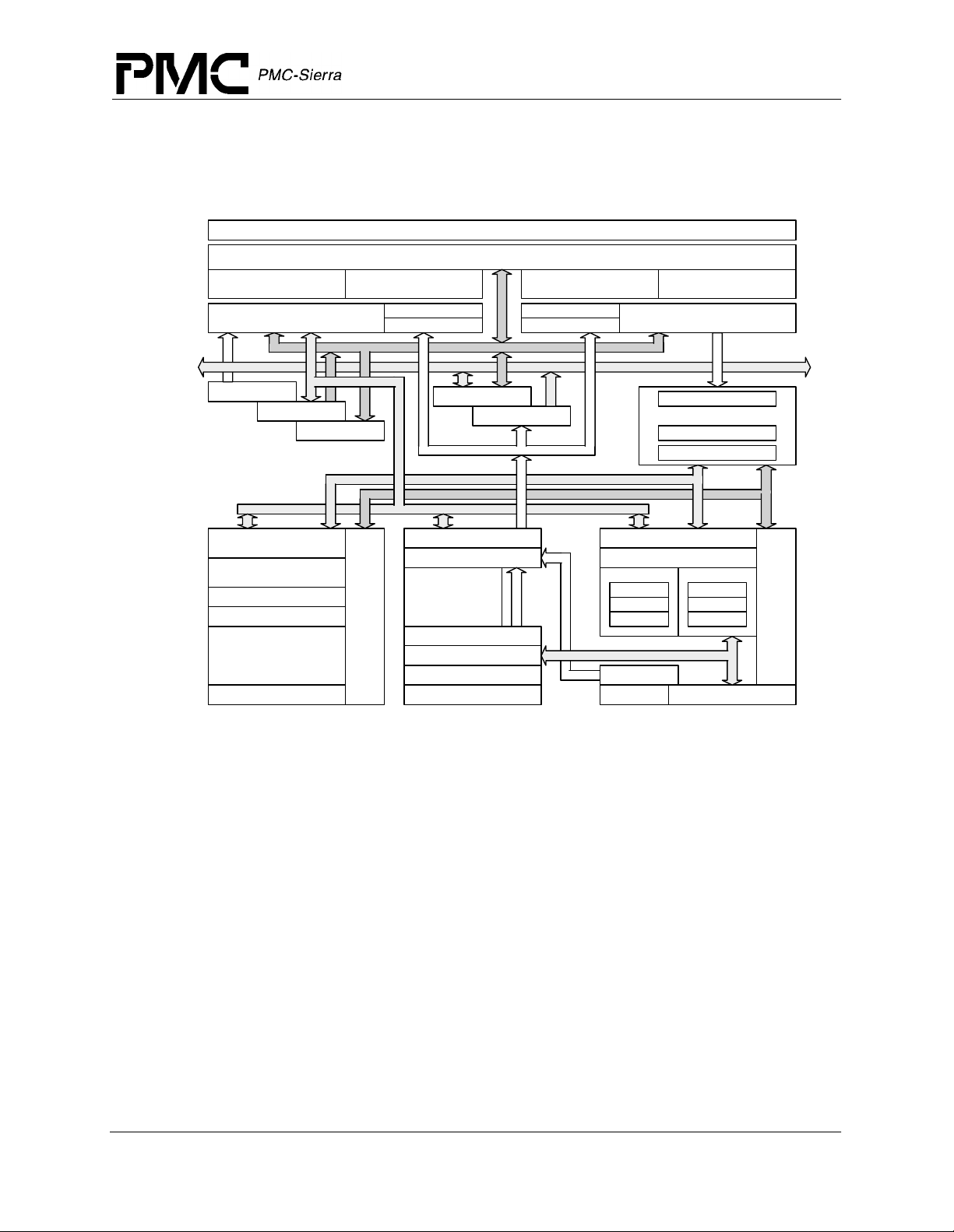
2 Block Diagram
Figure 1 Block Diagram
Secondary Tags
Set A
Primary Data Cache
4-way Set Associative
RM7000™ Microprocessor with On-Chip Secondary Cache Datasheet
Released
Extenal Cache Controller
On-chip 256K Byte Secondary Cache, 4-way Set Associative
Secondary Tags
Set B
DTag
DTLB
Secondary Tags
Set C
ITag
ITLB
Secondary Tags
Set D
Primary Instruction Cache
4-way Set Associative
A/D Bus
Pad Bus
Store Buffer
Write Buffer
D Bus
Floating-Point
Load/Align
Floating-Point
Register File
Packer/Unpacker
Comparator
Floating-Point
MultAdd, Add, Sub,
Cvt, Div, Sqrt
Multiplier Array
Read Buffer
Coprocessor 0
System/Memory
Control
PC Incrementer
Floating-Point Control
Branch PC Adder
ITLB Virtual
Program Counter Int Mult, Div, Madd
Pad Buffer
Joint TLB
Address Buffer
IVA
F-Pipe Bus
DVA
Integer Register File
Adder
StAln/Sh
Logicals
FA Bus
DTLB Virtual
PLL/Clocks
Prefetch Buffer
Instruction Dispatch Unit
F Pipe Register
M Pipe Register
M-Pipe Bus
Load Aligner
F PipeM Pipe
Adder
Shifter
Logicals
Integer Control
Proprietary and Confidential to PMC-Sierra, Inc and for its Customer’s Internal Use 10
Document ID: PMC-2002175, Issue 1
Page 11

3 Description
PMC-Sierra’s RM7000 is a highly integrated symmetric superscalar microprocessor capable of
issuing two instructions each processor cycle. It has two high-performance 64-bit integer units as
well as a high-throughput, f ully pi peline d 64-bit float ing point unit. To keep its mul tiple executi on
units running efficiently, the RM7000 integrates not only 16 KB 4-way set associative instruction
and data caches but backs them up with an integrated 256 KB 4-way set associative secondary as
well. For maximum effici ency, the data an d secondary cache s are write-back an d non-blocking. An
optional external tertiary cache provides high-performance capability even in applications having
very large data sets.
A RM5200 Family compatible, operating system friendlymemory management unit with a 64/48entry fully associative TLB and a high-performance 64-bit system interface supporting multiple
outstanding reads with out-of-order return and hardware prioritized and vectored interrupts round
out the main features of the processor.
The RM7000 is ideally suited for high-end embedded control applications such as
internetworking, high-performance image manipulation, high-speed printing, and 3-D
visualization. The RM7000 is also applicable to the low end workstation market where its
balanced integer and fl oati ng-poi nt per formanc e and di rect suppor t for a large tertiar y cache (up t o
8 MB) provide outstanding price/performance.
RM7000™ Microprocessor with On-Chip Secondary Cache Datasheet
Released
Proprietary and Confidential to PMC-Sierra, Inc and for its Customer’s Internal Use 11
Document ID: PMC-2002175, Issue 1
Page 12
RM7000™ Microprocessor with On-Chip Secondary Cache Datasheet
4 Hardware Overview
The RM7000 offers a high-level of integration targeted at high-performance embedded
applications. The key elements of the RM7000 are briefly described below.
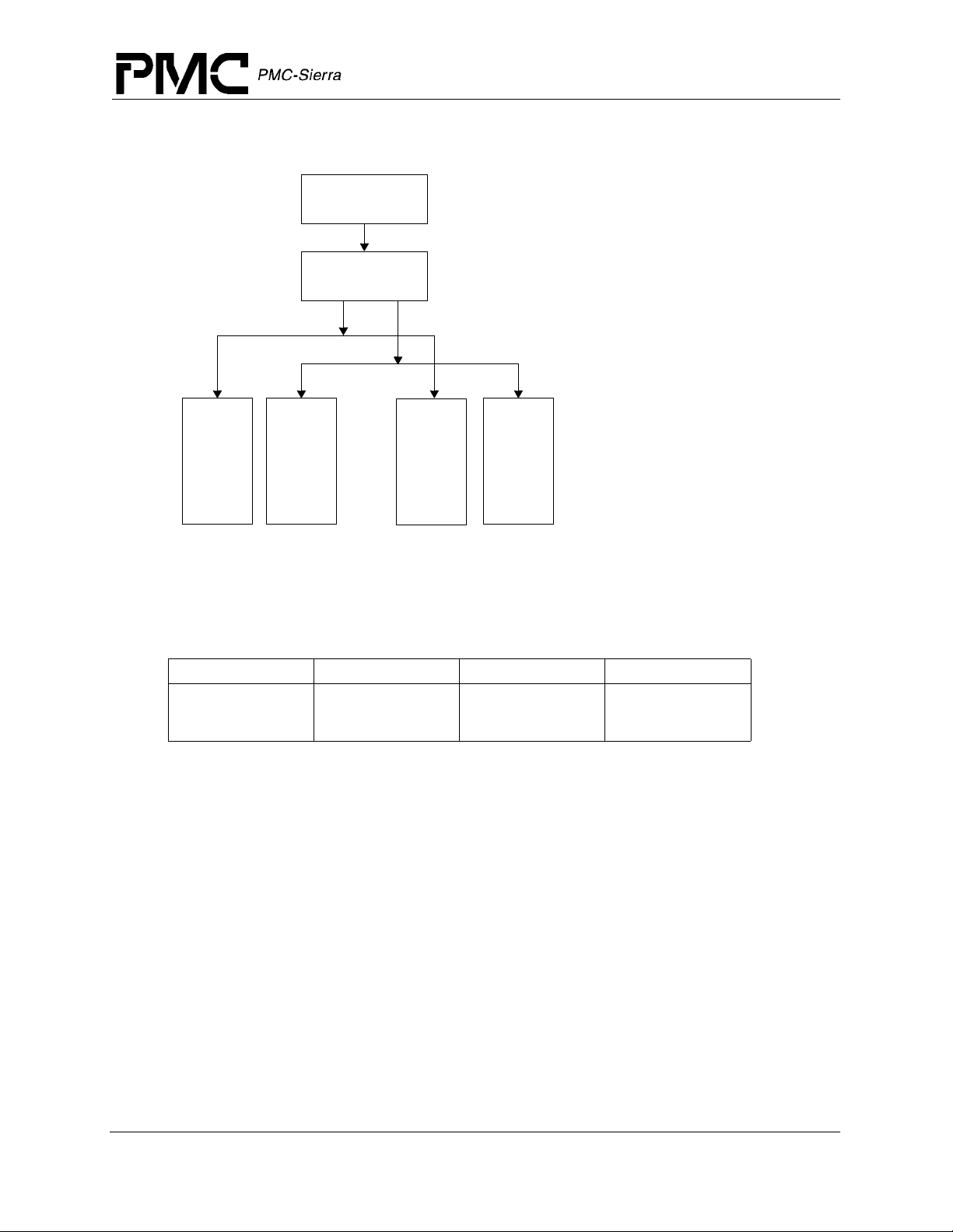
4.1 CPU Registers
Like all MIPS ISA processors, the RM7000 CPU has a simple, clean user visible state consisting
of 32 general pu rpo se registers (GPR), two special purpose r egi sters for integer mul ti pl ic ati on and
division, and a program counter; there are no condition code bits. Figure 2 shows the user visible
state.
Figure 2 CP0 Registers
General Purpose Registers
63 0
0630
r1 HI
r2 63 0
• LO
•
•
• 63 0
r29 PC
r30
r31
Released
Multiply/Divide Registers
Program Counter
4.2 Superscalar Dispatch
The RM7000 has an efficient symmetric superscalar dispatch unit which allows it to issue up to
two instructions per cycle. For purposes of instruction issue, the RM7000 defines four classes of
instructions: integer, load/store, branches, and floating-point. There are two logical pipelines, the
function, or F, p ipe li ne and the memory, or M, pipeline. Note however that the M pip e ca n execute
integer as well as memory type instruc tions.
Table 1 Instruction Issue Rules
F Pipe M Pipe
one of: one of: integer, branch, floating-point,
integer mul, div
Figure 3 is a simplification of the pipeline section and illustrates the basics of the instruction issue
mechanism.
Proprietary and Confidential to PMC-Sierra, Inc and for its Customer’s Internal Use 12
Document ID: PMC-2002175, Issue 1
integer, load/store
Page 13
RM7000™ Microprocessor with On-Chip Secondary Cache Datasheet
Figure 3 Instruction Issue Paradigm
Instruction
Cache
Dispatch
Unit
F Pipe IBus
M Pipe IBus
Released
FP
F Pipe
The figure illustrates that one F pipe instruction and one M pipe instruction can be issued
concurrently but that two M pipe or two F pipe instructions cannot be issued. Table 2 specifies
more completely the instructions within each class.
T able 2 Dual Issue Instruction Classes
integer load/store floating-point branch
add, sub, or , xor , shift, etc.
The symmetric superscalar capability of the RM7000, in combination with its low latency integer
execution units and high-throughput fully pipelined floating-point execution unit, provides
unparalleled price/performance in computational intensive embedded applications.
4.3 Pipeline
The logical length of both the F an d M pipel ines i s fiv e stages with st ate c ommitti ng in t he reg ister
write, or W, pipe stage. The physical length of the floating-point execution pipeline is actually
seven stag es but this is co mpletely transparent t o the user.
FP
M Pipe
lw, sw, ld, sd, ldc1, sdc1, mov, movc, fmov, etc.
Integer
F Pipe
Integer
M Pipe
fadd, fsub, fmult, fmadd, fdiv, fcmp, fsqrt, etc.
beq, bne, bCzT, bCzF, j, etc.
Figure 4 shows instruction execution within the RM7000 when instructions are issuing
simultaneously down both pipelines. As illustrated in the figure, up to ten instructions can be
executing simultaneou sly. This figure presents a somewhat simplistic view of the processors
operation however since the out-of-order completion of loads, stores, and long latency floatingpoint operations can res ult in there be ing even more instructions in process than what is shown.
Proprietary and Confidential to PMC-Sierra, Inc and for its Customer’s Internal Use 13
Document ID: PMC-2002175, Issue 1
Page 14
Figure 4 Pipeline
RM7000™ Microprocessor with On-Chip Secondary Cache Datasheet
Released
I0
I1
I2
I3
I4
I5 2I1I 1R 2R 1A 2A 1D 2D 1W 2W
I6
I7 2I1I 1R 2R 1A 2A 1D 2D 1W 2W
I8
I9 2I1I 1R 2R 1A 2A 1D 2D 1W 2W
1I-1R:
2I:
2R:
1A:
1A:
1A-2A:
2A:
2A-2D:
1D:
2W:
2I1I 1R 2R 1A 2A 1D 2D 1W 2W
2I1I 1R 2R 1A 2A 1D 2D 1W 2W
Instruction cache access
Instruction virtual to physical address translation
Register file read, Bypass calculation, Instruction decode, Branch address calculation
Issue or slip decision, Branch decision
Data virtual address calculation
Integer add, logical, shift
Store Align
Data cache access and load align
Data virtual to physical address translation
Register file write
Note that instruction dependencies, resource conflicts, and branches result in some of the
instruction slots being occupied by
4.4 Integer Unit
Like the RM5200 Fcamily, the RM7000 implements the MIPS IV Instruction Set Architecture,
and is therefore fully upward compatible with applications that run on processors such as the
R4650 and R4700 that implement the earlier generation MIPS III Instruction Set Architecture.
Additionally, the RM7000 includes two implementation specific instructions not found in the
baseline MIPS IV ISA, but that are useful in the embedded market place. Described in detail in a
later sectio n, these instructions are integer multiply-accumulate and three-operand integer
multiply.
2I1I 1R 2R 1A 2A 1D 2D 1W 2W
2I1I 1R 2R 1A 2A 1D 2D 1W 2W
2I1I 1R 2R 1A 2A 1D 2D 1W 2W
2I1I 1R 2R 1A 2A 1D 2D 1W 2W
2I1I 1R 2R 1A 2A 1D 2D 1W 2W
one cycle
NOPs.
The RM7000 integer unit includes thirty-two general purpose 64-bit registers, the HI/LO result
registers for the two-operand integer multiply/divide operations, and the program counter, or PC.
There are two separate execution units, one of which can execute function, or F, type instructions
and one which can execute memory, or M, type instructions. See above for a description of the
instruction types and the issue rules. As a special case, integer multiply/divide instructions as well
as their corresponding
MFHI and MFLO instructions can only be executed in the F type
execution unit. Within each execution unit the operational characteristics are the same as on
previous MIPS designs with single cycle ALU operations (add, sub, logical, shift), one cycle load
delay, and an autonomous multiply/divide unit.
Register File
The RM7000 has thirty-two general purpose registers with register location 0 (r0) hard wired to a
zero value. These registers are used for scalar integer operations and address calculation. In order
to service the two integer execution units, the register file has four read ports and two write ports
and is fully bypassed both within and between the two execution units to minimize operation
latency in the pipeline.
Proprietary and Confidential to PMC-Sierra, Inc and for its Customer’s Internal Use 14
Document ID: PMC-2002175, Issue 1
Page 15
RM7000™ Microprocessor with On-Chip Secondary Cache Datasheet
4.5 ALU
The RM7000 has two complete integer ALUs each consisting of an integer adder/subtractor, a
logic unit, and a shifter. Table 3 shows the functions performed by the ALUs for each execution
unit. Each of these units is optimized to perform all operations in a single processor cycle.
Table 3 ALU Operations
Unit F Pipe M Pipe
Adder add, sub add, sub, data address
Logic l ogic, moves, zero shifts
(nop)
Shifter non zero shift non zero shift, store align
4.6 Integer Multiply/Divide
The RM7000 has a si ngle dedi cated i nteger mul tiply/d ivide un it opti mized for high-sp eed multi ply
and multiply-accumulate operations. The multiply/divide unit resi des in the F type execution uni t.
Table 4 shows the performance of the multiply/divide unit on each operation.
Released
add
logic, moves, zero shifts
(nop)
Table 4 Integer Multiply/Divide Operations
Operand
Opcode
MULT/U, MAD/U
MUL16 bit432
DMULT, DMUL TU
DIV, DIVD any 36 36 0 DDIV,
DDIVU
Size Latency
16 bit 4 3 0 32 bit 5 4 0
32 bit 5 4 3 any980
any 68 68 0
Repeat
Rate
Stall
Cycles
The baseline MIPS IV ISA specifies that the results of a multiply or divide operation be placed in
the Hi and Lo registers. These values can then be transferred to the general purpose register file
using the Move-from-Hi and Move-from-Lo (
MFHI/MFLO) instructions.
In addition to the baselin e MIPS IV integer multip ly instructi ons, the RM7000 also imple ments the
3-operand multipl y instr uction, MUL. This instruction sp ecifies that t he mult iply res ult go d irectly
to the integer register file rather than the Lo register. The portion of the multiply that would have
normally gone into the Hi register is discarded. For applications where it is known that the upper
half of the multiply result is not required, using the
executing an explicit
MFLO instruction.
MUL instruction eliminates t he necessity of
Also included in the RM7000 are the multiply-add instructions
MAD/MADU. This instruction
multiplies two operands and adds the resulting product to the current contents of the Hi and Lo
registers. The multiply-accumulate operation is the core primitive of almost all signal processing
Proprietary and Confidential to PMC-Sierra, Inc and for its Customer’s Internal Use 15
Document ID: PMC-2002175, Issue 1
Page 16

RM7000™ Microprocessor with On-Chip Secondary Cache Datasheet
algorithms allowing the RM7000 to eliminate the need for a separate DSP engine in many
embedded applications.
By pipelining the multipl y- acc umulate function and dynamica ll y determining the size of the input
operands, the RM7000 is able to maximize throughput while still using an area efficient
implementation.
4.7 Floating-Point Coprocessor
The RM7000 incorporates a high-performance fully pipelined floating-point coprocessor which
includes a floating-po int register file and autonomous execution units for multiply/a dd/convert and
divide/square root . The f loati ng-poi nt cop roc essor is a tight ly coup le d co-e xecuti on unit , d ecodin g
and executing instructions in parallel with, and in the case of floating-point loads and stores, in
cooperation with the M pipe of the int eger unit. As described earlier, the superscalar capabilities of
the RM7000 allow floating-point computation instructions to issue concurrently with integer
instructions.
4.8 Floating-Point Unit
The RM7000 floating-point execution unit supports single and double precision arithmetic, as
specified in the IEEE S tanda rd 754. The ex ecution uni t is broken i nto a separa te divide /square ro ot
unit and a pipelined multiply/add unit. Overlap of divide/square root and multiply/add is
supported.
Released
The RM7000 maintains fully precise floating-point exceptions while allowing both overlapped
and pipelined operations. Precise exceptions are extremely important in object-oriented
programming environments and highly desirable for debugging in any environment.
The floating-point unit’s operation set includes floating-point add, subtract, multiply, multiply-
add, divide, square roo t, recipr ocal, rec iprocal squa re root, c ondition al moves, conversio n between
fixed-point and floating-point format, conversion between floating-point formats, and floatingpoint compare. Table 5 gives the latencies of the floating-point instructions in internal processor
cycles.
4.9 Floating-Point General Register File
The floating-point general register file, FGR, is made up of thirty-two 64-bit registers. With the
floating-point load and store double instructions,
take advantage of the 64-bit wide data cache and issue a floating-point coprocessor load or store
doubleword instruction in every cycle.
The floating-point control register file contains two registers; one for determining configuration
and revision information for the coprocessor and one for control and status information. These
registers are primar ily used f or diagnost ic software , exception handling, st ate savi ng and resto ring,
and control of rounding modes.
LDC1 and SDC1, the floating-point unit can
Proprietary and Confidential to PMC-Sierra, Inc and for its Customer’s Internal Use 16
Document ID: PMC-2002175, Issue 1
Page 17
RM7000™ Microprocessor with On-Chip Secondary Cache Datasheet
Table 5 Floating Point Latencies and Repeat Rates
Latency
Operation
fadd 4 1 fsub 4 1 fmult 4/5 1/2 fmadd 4/5 1/2 fmsub 4/5 1/2 fdiv 21/36 19/34 fsqrt 21/36 19/34 frecip 21/36 19/34 frsqrt 38/68 36/66 fcvt.s.d 4 1 fcvt.s.w 6 3 fcvt.s.l 6 3 fcvt.d.s 4 1 fcvt.d.w 4 1 fcvt.d.l 4 1 fcvt.w.s 4 1 fcvt.w.d 4 1 fcvt.l.s 4 1 fcvt.l.d 4 1 fcmp 1 1 fmov, fmovc 1 1 fabs, fneg 1 1
Single/double
Repeat Rate
Single/double
Released
To support superscalar operations, the FGR has four read ports and two write ports, and is fully
bypassed to minimize operation latency in the pipeline. Three of the read ports and one write port
are used to support the combined multiply-add instruction while the fourth read and second write
port allows a concurrent floating-point load or store and conditional moves.
4.10 System Control Coprocessor (CP0)
The system control copr ocessor (CP0) in the MIPS architecture is responsible for the virtual
memory sub-system, th e exception control sys tem, and the diagnost i cs capability of the p roc ess or.
In the MIPS architecture, the system control coprocessor (and thus the kernel s oftware) is
implementation dependent. For memory management, the RM7000 CP0 is logically identical to
that of the RM5200 Family and R5000. For interrupt ex ceptions and diagnosti cs, the RM7000 is a
superset of the RM5200 Family and R5000 implementi ng addition al feature s described later in the
sections on Interrupts, the Test/Breakpoint facility, and the Performance Counter facility.
The memory management unit co ntrol s the virtu al memory syste m page mapping . It co nsist s of a n
instructio n address translation bu ffer (ITLB), a data address translation b uffer (DTLB), a Joint
TLB (JTLB), and coprocessor registers used by the virtual memory mapping sub-system.
Proprietary and Confidential to PMC-Sierra, Inc and for its Customer’s Internal Use 17
Document ID: PMC-2002175, Issue 1
Page 18

RM7000™ Microprocessor with On-Chip Secondary Cache Datasheet
4.11 System Control Coprocessor Registers
The RM7000 incorporates all system control coprocessor (CP0) registers internally. These
registers provide the path through which the virtual memory system’s page mapping is examined
and modified, exceptions are handled, and operating modes are controlled (kernel vs. user mode,
interrupts enabled or disabled, cache features). In addition, the RM7000 includes registers to
implement a real-time cyc le cou nting facility, to aid in cache and system diagnostics, and to assist
in data error detection.
To support the non-blocking caches and enhanced interrupt handling capabilities of the RM7000,
both the data and c ont rol r egi st er spaces of CP0 are supported by the RM7000. In the da ta register
space, that is the space accessed using the
the same registers a s found in the RM5200, R4000 a nd R5000 famil ies. In t he contro l space, t hat is
the space accessed by th e previously unu sed
five new registers. The first three of these new 32-bit registers support the enhanced interrupt
handling capabilities and are the Interrupt Control, Interrupt Priority Level Lo (IPLLO), and
Interrupt Priority Level Hi (IPLHI) registers. These registers are described further in the section on
interrupt handling. The other two registers, Imprecise Error 1 and Imprecise Error 2, have been
added to help diagnose bus errors which occur on non-blocking memory references.
MFC0 and MTC0 instructions, the RM7000 supports
CTC0 and CFC0 instru ctions, the RM70 00 supports
Released
Figure 5 shows the CP0 registers.
Figure 5 CP0 Registers
47
TLB
(entries protected
from TLB WR)
TagLo
28*
Used for memory
management
LLAddr
17*
0
TagHi
29*
Info
7*
Index
0*
Random
1*
Wired
6*
PRId
15*
Config
16*
* Register number
Status
12*
EPC
14*
Watch2
19*
ECC
26*
Cause
13*
Watch1
18*
XContext
20*
CacheErr
27*
ErrorEPC
30*
Used for exception
processing
Watch Mask
24*
Proprietary and Confidential to PMC-Sierra, Inc and for its Customer’s Internal Use 18
Document ID: PMC-2002175, Issue 1
Page 19

RM7000™ Microprocessor with On-Chip Secondary Cache Datasheet
4.12 Virtual to Physical Address Mapping
The RM7000 provides three modes of virtual addressing:
• user mode
• supervisor mode
• kernel mode
This mechanism is avai lable to system software to provide a secure envi ronment for user
processes. Bits in the CP0 Status register determine which virtual addressing mode is used. In the
user mode, the RM7000 provides a single, uniform virtual address space of 256 GB (2 GB in 32bit mode).
When operating in the kernel mode, four distinct virtual address spaces, totalling 1024 GB (4 GB
in 32-bit mode), are simultaneously available and are differentiated by the high-order bits of the
virtual address.
The RM7000 processor also supports a supervisor mode in which the virtual address space is
256.5 GB (2.5 GB in 32-bit mode), divided into three regions based on the high-order bits of the
virtual address. Figure 6 shows the address space layout for 32-bit operation.
Released
Figure 6 Kernel Mode Virtual Addressing (32-bit mode)
0xFFFFFFFF Kernel virtual address space
(kseg3)
0xE0000000 Mapped, 0.5GB
0xDFFFFFFF Supervisor virtual address space
(ksseg)
0xC0000000 Mapped, 0.5GB
0xBFFFFFFF Uncached kernel physical address space
(kseg1)
0xA0000000 Unmapped, 0.5GB
0x9FFFFFFF Cached kernel physical address space
(kseg0)
0x80000000 Unmapped, 0.5GB
0x7FFFFFFF User virtual address space
(kuseg)
Mapped, 2.0GB
When the RM7000 is configured for 64-bit addressing, the virtual address space layout is an
upward compatible extension of the 32-bit virtual address space layout.
Proprietary and Confidential to PMC-Sierra, Inc and for its Customer’s Internal Use 19
Document ID: PMC-2002175, Issue 1
Page 20

4.13 Joint TLB
For fast virtual-to-physical address translation, the RM7000 uses a large, fully associative TLB
that maps virtual pages to their corresponding physical addresses. As indicated by its name, the
joint TLB (JTLB) is used for both instruction and data translations. The JTLB is organized as pairs
of even/odd entries, and maps a virtual address and address space identifier into the large, 64 GB
physical address spa ce. By default, the JTLB is co nfi gur ed a s 48 pai rs of even/odd entries. The 64
even/odd entry optional configuration is set at boot time.
Two mechanisms are provided to assist in controlling the amount of mapped space, and the
replacement characte ristic s of various memory regi ons. First, the page si ze can be conf igured, on a
per-entry basi s, to use page sizes in the range of 4 KB to 16 MB (in 4X multip les). A CP0 regist er,
PageMask, is loaded with the desired page size of a mapping, and that size is stored into the TLB
along with the virtual address when a new entry is written. Thus, operating systems can create
special purpose maps; for example, a typical frame buffer can be memory mapped using only one
TLB entry.
The second mechanism controls the replacement algorithm when a TLB miss occurs. The
RM7000 provides a random replacement algorithm to select a TLB entry to be written with a new
mapping; however , the pr ocessor als o provides a mech anism whereby a sys tem specifi c number of
mappings can be locked into the TLB, thereby avoiding random replacement. This mechanism
allows the operating s ystem to guarantee that certain pages are always mapped for performance
reasons and for deadlock avoidance. This mechanism also facilitates the design of real-time
systems by allowing deterministic access to critical software.
RM7000™ Microprocessor with On-Chip Secondary Cache Datasheet
Released
The JTLB also contains information that controls the cache coherency protocol for each page.
Specifically, each page has attribute bits to determine whether the coherency algorithm is:
uncached, write-back, write-through with write-allocate, write-through without write-allocate,
write-back with secondary and tertiary bypass. Note that both of the write-through protocols
bypass both the secondary and the tertiary caches since neither of these caches support writes of
less than a complete cache line.
These protocols are used for both code and data on the RM7000 with data using write-back or
write-through depending on the application. The write-through modes support the same efficient
frame buffer handling as the RM5200 Family, R4700, and R5000.
4.14 Instruction TLB
The RM7000 uses a 4-entry instruction TLB (ITLB) to minimize contention for the JTLB, to
eliminate the critical path of translating through a large associative array, and to save power. Each
ITLB entry maps a 4 KB page. The ITLB improves performance by allowing instruction address
translation to occur in parallel with data address translation. When a miss occurs on an instruction
address translation by the ITLB, the least-recently used ITLB entry is filled from the JTLB. The
operation of the ITLB is completely transparent to the user.
4.15 Data TLB
The RM7000 uses a 4-entry data TLB (DTLB) for the same reasons cited above for the ITLB.
Each DTLB entry maps a 4 KB page. The DTLB improves performance by allowing data address
translation to occur in parallel with instruction address translation. When a miss occurs on a data
Proprietary and Confidential to PMC-Sierra, Inc and for its Customer’s Internal Use 20
Document ID: PMC-2002175, Issue 1
Page 21

address translation by the DTLB, the DTLB is filled from the JTLB. The DTLB refill is pseudoLRU: the least recently used entry of the least recently used pair of entries is filled. The operation
of the DTLB is completely transparent to the user.
4.16 Cache Memory
In order to keep the RM7000’s super sc alar pipeline full a nd operating eff ic ie n tl y, the RM7000 has
integrated primary instruction and data caches with single cycle access as well as a large unified
secondary cache with a three cycle miss penalty from the primaries. Each primary cache has a 64bit read path, a 128-bit write path, and both caches can be accessed simultaneously. The primary
caches provide the integer and floating-point units with an aggregate bandwidth of 4.8 GB per
second at an internal clock frequency of 300 MHz. During an instruction or data primary cache
refill, the secondary ca che can provide a 64-bit datum ever y cycl e fo ll owing the initial three cyc le
latency for a peak bandwidth of 2.4 GB per second. For applications requiring even higher
performance, the RM7000 also has a direct interface to a large external tertiary cache.
4.17 Instruction Cache
The RM7000 has an integ rated 16 KB, four -way s et associ ative i nstruct ion cache and, eve n though
instruction address translation is done in parallel with the cache access, the combination of 4-way
set associativity and 16 KB size results in a cache which is virtually indexed and physically
tagged. Since the ef fectiv e physical i ndex elimina tes the poten tial for vi rtual ali ases in the cache, it
is possible that some operating system code can be simplified vis-a-vis the RM5200 Family,
R5000 and R4000 class processors.
RM7000™ Microprocessor with On-Chip Secondary Cache Datasheet
Released
The data array portion of the instruction cache is 64 bits wide and protected by word parity while
the tag array holds a 24-bit physical address, 14 housekeeping bits, a valid bit, and a single bit of
parity protection.
By accessing 64 bits pe r cy cle , th e instruction cache is a ble to supply two instruction s per cycle to
the superscalar di spatch unit. For s ig nal pr oce ssing, graphics, and ot her numerical code sequences
where a floating-point load or store and a floating-point computation instruction are being issued
together in a loop, the entire bandwidth available from the instruction cache will be consumed by
instruction issue. For typical integer code mixes, where instruction dependencies and other
resource co nstraints restrict the achievable parallelism, the extra instruction ca che bandwidth is
used to fetch both the taken and non-taken branch paths to minimize the overall penalty for
branches.
A 32-byte (eight instruction) line size is used to maximize the communication efficiency between
the instruction cache and the secondary cache, tertiary cache, or memory system.
The RM7000 is the first MIPS RISC microprocessor to support cache locking on a per line basis.
The contents of each line of the cache can be locked by setting a bit in the Tag. Locking the line
prevents its contents from being overwritten by a subsequent cache miss. Refill will occur only
into unlocked cache lines. This mechanism allows the programmer to lock critical code into the
cache thereby guaranteeing deterministic behavior for the locked code sequence.
4.18 Data Cache
The RM7000 has an integrated 16 KB, four-way set associative data cache, and even though data
address translation is done in parallel with the cache access, the combination of 4-way set
Proprietary and Confidential to PMC-Sierra, Inc and for its Customer’s Internal Use 21
Document ID: PMC-2002175, Issue 1
Page 22

RM7000™ Microprocessor with On-Chip Secondary Cache Datasheet
Released
associativity and 16 KB size resul ts in a cache wh ic h is physi ca ll y inde xed and physic al ly tagged.
Since the effective physical index eliminates the potential for virtual aliases in the cache, it is
possible that some operating system code can be simplified vis-a-vis the RM5200 Family, R5000
and R4000 class processors.
The data cache is non-blocking; that is, a miss in the data cache will not necessarily stall the
processor pipeline. As long as no instruction is encountered which is dependent on the data
reference which caused the miss, the pipeline will continue to advance. Once there are two cache
misses outstanding, the processor will stall if it encounters another load or store instruction.
A 32-byte (eight word) line size is used to maximize the communication efficiency between the
data cache and the secondary cache, tertiary cache, or memory system.
The data array portion of the data cache is 64 bits wide and protected by byte parity while the tag
array holds a 24-bit physical address, three housekeeping bits, a two bit cache state field, and has
two bits of parity protection.
The normal write policy is write-back, which means that a store to a cache line does not
immediately cause memory to be updated. This increases system performance by reducing bus
traffic and eliminating the bottleneck of waiting for each store operation to finish before issuing a
subsequent memory operation. Software can, however, select write-through on a per-page basis
when appropriate, such as for frame buffers. Cache protocols supported for the data cache are:
1. Uncached Reads to addresses in a memory area identified as uncached will not access the cache. Writes
to such addresses will be written directly to main m emory without updating the cache.
2. Write-back Loads and instruction f etches will first search th e cache, read ing the next memory hierarchy
level only if the desired data is not cache resident. On data store operations, the ca che is first
searched to determine if the tar get address is cache resid ent. If it is resid ent, the cache con tents
will be updated, and the cache l ine marked for lat er write-bac k. If the cache lookup misses , the
target line is first brought into the cache and then the write is performed as above.
3. Write-through with write allocate Loads and in struction fetches will first search the cache, reading from memory only if the
desired data is not cache resident; write-through data is never cached in the secondary or
tertiary caches. On data store operations, the cache is first searched to determine if the target
address is cache re siden t. If it i s resi dent, t he prima ry cache conten ts wil l be updat ed and mai n
memory will also be written leaving the write-back bit of the cache line unchanged; no writes
will occur into the secondary or tertiary. If the cache lookup misses, the target line is first
brought into the cache and then the write is performed as above.
4. Write-through without write allocate Loads and in struction fetches will first search the cache, reading from memory only if the
desired data is not cache resident; write-through data is never cached in the secondary or
tertiary caches. On data store operations, the cache is first searched to determine if the target
address is cache resid ent. If it is reside nt, the cach e contents will be updat ed and main memo ry
will also be written leaving the write-back bit of the cache line unchanged; no writes will
Proprietary and Confidential to PMC-Sierra, Inc and for its Customer’s Internal Use 22
Document ID: PMC-2002175, Issue 1
Page 23

RM7000™ Microprocessor with On-Chip Secondary Cache Datasheet
occur into the secondary or tertiary. If the cache lookup misses, then only main memory is
written.
5. Fast Packet Cache™ (Write-back with secondary and tertiary bypass) Loads and instruction fetches first search the primary cache, reading from memory only if the
desired data is not resident; the secondary and tertiary are not searched. On data store
operations, the primary cache is first searched to determine if the target address is resident. If
it is resident, the cache cont ent s ar e updated, and the ca che line marked for la ter write-back. If
the cache lookup misses, the target line is first brought into the cache and then the write is
performed as above.
Released
Associated with the Data Cache is the store buffer. When the RM7000 executes a
instruction, this single-entry buff er gets written with the store data while the tag comparison is
performed. If the tag mat ches, then the data is writ ten into th e Data Cache in the next cycl e that the
Data Cache is not accessed (the next non-load cycle). The store buffer allows the RM7000 to
execute a store every processor cycle and to perform back-to-back stores without penalty. In the
event of a store immediately followed by a load to the same address, a combined merge and cache
write will occur such that no penalty is incurred.
4.19 Secondary Cache
The RM7000 has an integrated 256 KB, four-way set associative, block write-back secondary
cache. The secondary has the same line size as the primaries, 32 bytes, is logically 64-bits wide
matching the system interface and prima ry widths, and is prot ec ted with doubleword parity. The
secondary tag array holds a 20-bit physical address, two housekeeping bits, a three bit cache state
field, and two parity bits.
By integrating a secondary cache, the RM7000 is able to dramatically decrease the latency of a
primary cache miss without dramatically increasing the number of pins and the amount of power
required by the processor. From a technology point of view, integrating a secondary cache
maximally leverages CMOS semi conductor technolog y by usi ng silicon t o build th e struct ures that
are most amenable to silicon technology; silicon is being used to build very dense, low power
memory arrays rather than large power hungry I/O buffers.
Further benefits of an integrated secondary are flexibility in the cache organization and
management policies that are not practical with an external cache. Two previously mentioned
examples are the 4-way associativity and write-back cache protocol.
STORE
A third management policy for which integration affords flexibility is cache hierarchy
management. With multiple levels of cache, it is necessary to specify a policy for dealing with
cases where two cache lines at level n of the hierarchy would, if possible, be sharing an entry in
level n+1 of the hierarchy. The policy followed by the RM7000 is motivated by the desire to get
maximum cache utility and results in the RM7000 allowing entries in the primaries which do not
necessarily have a corre spondi ng entry in the sec ondary; the RM7000 does not force the pri maries
to be a subset of the secondary. For example, if primary cache line A is being filled and a cache
line already exists in th e seconda ry for pri mar y cache li ne B at the loca tion wher e primar y A’s line
would reside then that secondary entry will be replaced by an entry corresponding to primary
cache line A and no actio n will occur in the primary fo r cache lin e B. This operat ion will cr eate the
aforementioned scenario where the primary cache line which initially had a corresponding
Proprietary and Confidential to PMC-Sierra, Inc and for its Customer’s Internal Use 23
Document ID: PMC-2002175, Issue 1
Page 24

RM7000™ Microprocessor with On-Chip Secondary Cache Datasheet
secondary entry will no longer have such an entry. Such a primary line is called an orphan. In
general, cache lines at level n+1 of the hierarchy are called parents of level n’s children.
Another RM7000 cache management optimization occurs for the case of a secondary cache line
replacement where the secondary line is dirty and has a corresponding dirty line in the primary. In
this case, since it is permissible to leave the dirty line in the primary, it is not necessary to write the
secondary line back to main memory. Taking this scenario one step further, a final optimization
occurs when the a for emen ti oned dirty primary line is replaced by anot her line and must be wri t ten
back, in this case, it will be written directly to memory bypassing the secondary cache.
4.20 Secondary Caching Protocols
Unlike the primary dat a cac he, t he secondary cache supports only uncached a nd block write-back.
As noted earlier, cache lines managed with ei th er of the write- thr oug h protocols will not be placed
in the secondary cache. A new caching attribute, write-back with secondary and tertiary bypass,
allows the secondary, and the tertiary if present, to be bypassed entirely. When this attribute is
selected, the secondary and tertiary will not be filled on load misses and will not be written on
dirty write-backs from the primary.
4.21 Tertiary Cache
Released
Like the RM5270, RM5271 and R5000, the RM7000 has direct support for an external cache. In
the case of the RM527x chips this is a secondary cache whereas for the RM7000 this cache
becomes a level-3, or tertiary cache. The tertiary cache is direct mapped and block write-through
with byte parity pro tection for da ta. The RM7000 t ertiary operates identic al to the secondar y of the
RM527x and R5000 while supporting additional size increments to 4M and 8M byte caches.
The tertiary interface uses the SysAD bus for data and tags while providing a separate bus,
TcLine, for addresses, and a handful of tertiary specific control signals (for the complete set, see
Pin Listing).
A tertiary read looks nearly identical to a standard processor r ead except that the tag chip enable
signal, TcTCE*, is assert ed concurrently with ValidOut* and Release*, initiating a ta g pr obe an d
indicating to the external controller that a tertiary cache access is being performed. As a result, the
external contro ll er monitors the te rt ia ry hit signal, TcMatch, and if a hit is indicated the controller
will abort the memory read and will refrain from acquiring control of the system interface. Along
with TcTCE*, the processor also assert s the tag data ena ble si gnal, TcTDE*, which causes the tag
RAMs to latch the SysAD address internally for use as the replacement tag if a cache miss occurs.
On a tertiary miss, a refill is accomplished with a two signal handshake between the data output
enable sign al, TcDOE*, which is deasserted by the controller and the tag and data write enable
signal, TcCWE*, which is asserted by the processor. Figure 7 illustrates a tertiary cache hit
followed by a miss.
Proprietary and Confidential to PMC-Sierra, Inc and for its Customer’s Internal Use 24
Document ID: PMC-2002175, Issue 1
Page 25

RM7000™ Microprocessor with On-Chip Secondary Cache Datasheet
Figure 7 Tertiary Cache Hit and Miss
Released
Master
SysClock
SysAD
TcLine[17:0]
TcWord[1:0]
TcTCE*
TcMatch
TcDCE*
TcCWE*
TcDOE*
Processor
Addr Data1 Data2
Index
I0
Data0 Addr Data0
I1 I2I0I3 I0 I1 I2 I3 I1
Tertiary(Hit) Tertiary(Miss)
Data3 Data1
Processor
Data0
Index
System
Data1
Other capabilities of the tertiary interface include block write, tag invalidate, and tag probe. For
details of these transactions as well as detailed timing waveforms for all the tertiary transactions,
see the R5000 or RM7000 Bus Interface Specifications. The tertiary cache tag can easily be
implemented with standard components such as the Motorola MCM69T618.
The RM7000 cache attributes for the instruction, data, internal secondary, and optional external
tertiary cac hes are summarized in Table 6.
Proprietary and Confidential to PMC-Sierra, Inc and for its Customer’s Internal Use 25
Document ID: PMC-2002175, Issue 1
Page 26

RM7000™ Microprocessor with On-Chip Secondary Cache Datasheet
Released
T a ble 6 Cache Attributes
Attribute Instruction Data Secondary Tertiary
Size 16KB 16KB 256KB 512K, 1M, 2M, 4M,
or 8M Associativity 4-way 4-way 4-way direct mapped Replacement
Algorithm. Line size 32 byte 32 byte 32 byte 32 byte Index vAddr
Tag pAddr Write policy n.a. write-back, write-
read policy n.a. non-blocking (2
read order critical word first critical word first critical word first critical word first write order NA sequential sequential sequential miss restart
following: Parity per word per byte per doubleword per byte
cyclic cyclic cyclic direct replacement
11..0
35..12
complete line first double (if
vAddr
11..0
pAddr
35..12
through
outstanding)
waiting for data)
pAddr
15..0
pAddr
35..16
block write-back, bypass
non-blocking (data only, 2 outstanding)
n.a. n.a.
pAddr
pAddr
block write-through,
bypass
non-blocking (data
only, 2 outstanding)
22..0
35..19
4.22 Cache Locking
The RM7000 allows critical code or data fragments to be locked into the primary and secondary
caches. The user has complete cont ro l ove r what lock ing is performed with cache line granularity.
For instruction and data fragments in the primaries, locking is accomplish ed by setting either or
both of the cache loc k enable bits i n the CP0 ECC r egister, specifying the set via a field in th e CP0
ECC register, and then executing either a load instruction or a Fill_I cache operation for data or
instructions respectively. Only two sets are lockable within each cache: set A and set B. Locking
within the secondary works identically to the primaries using a s eparate secon dary lock ena ble bit
and the same set selectio n field. As with the primaries, only two sets are loc kable: sets A and B.
Table 7 summarizes the cache locking capabilities.
Table 7 Cache Locking Control
Cache Lock Enable Set Select Activate
Primary I ECC[27] ECC[28]=0→A
Primary D ECC[26] ECC[28]=0→A
Secondary ECC[25] ECC[28]=0→A
4.23 Cache Management
ECC[28]=1→B
ECC[28]=1→B
ECC[28]=1→B
Fill_I
Load/Store
Fill_I or
Load/Store
To improve the performance of critical data movement operations in the embedded environment,
the RM7000 significantly improves the speed of operation of certain critical cache management
Proprietary and Confidential to PMC-Sierra, Inc and for its Customer’s Internal Use 26
Document ID: PMC-2002175, Issue 1
Page 27
RM7000™ Microprocessor with On-Chip Secondary Cache Datasheet
Released
operations vis-a-vis the R5000 and R4000 families. In particular, the speed of the Hit-WritebackInvalidate and Hit-Invalidate cache operations has been improved in some cases by an order of
magnitude over that of the earlier families. Table 8 compares the RM7000 with the R4000 and
R5000 processors.
T a ble 8 Penalty Cycles
Penalty
Operation Condition
Hit-WritebackInvalidate
Hit-Invalidate Miss 0 7
Miss 0 7 Hit-Clean 3 12 Hit-Dirty 3+n 14+n
Hit 2 9
RM7000 R4000/R5000
For the Hit-Dirty case of Hit-Writeback-Invalidate, if the writeback buffer is full from some
previous cache eviction then n is the number of cycles required to empty the writeback buffer. If
the buffer is empty then n is zero.
The penalty value is the number of processor cycles beyond the one cycle required to issue the
instruction that is required to implement the operation.
4.24 Primary Write Buffer
Writes to secondary cache or external memory, whether cache miss write-backs or stores to
uncached or write-through addresses, use the integrated primary write buffer. The write buffer
holds up to four 64-bit ad dress an d data pai rs. The entir e buf fer is used for a dat a cac he write-b ack
and allows the processor to proceed in parallel with memory update. For uncached and writethrough stores, the write buffer significantly increases performance by decoupling the SysAD bus
transfers fr om the instruction execution stream.
4.25 System Interface
The RM7000 provides a high-performance 64-bit system interface which is compatible with the
RM5200 Family and R5000. Unlike the R4000 and R5000 family processors which provide only
an integral multiplication factor between SysClock and the pipeline clock, the RM7000 also
allows half-integral multipliers, thereby providing greater granularity in the designers choice of
pipeline and system interface frequencies.
The interface consist s of a 64- bi t Addr ess/Data bus with 8 check bit s a nd a 9-bit command bus. In
addition, there are ten handsha ke signals and ten int errupt inputs. The in terface has a simple timing
specification and is capable of transferring data between the processor and memory at a peak rate
of 1000 MB/sec with a 125 MHz SysClock.
Figure 8 shows a typic al embedded system using th e RM7000. This example shows a sys te m wit h
a bank of DRAMs, an optional tertiary cache, and an interface ASIC which provides DRAM
control as well as an I/O port.
Proprietary and Confidential to PMC-Sierra, Inc and for its Customer’s Internal Use 27
Document ID: PMC-2002175, Issue 1
Page 28

RM7000™ Microprocessor with On-Chip Secondary Cache Datasheet
Figure 8 Typical Embedded System Block Diagram
Flash/
Boot
ROM
RM7000
DRAM
Latch
SysCmd
72
72
72
SysAD Bus
72
25
Address
Control
8
Memory I/O
Controller
Released
x x
PCI Bus
TcLine, etc.
Tertiary Cache
(optional)
4.26 System Address/Data Bus
The 64-bit System Address Data (SysAD) bus is used to transfer addresses and data between the
RM7000 and the rest of the system. It is protected with an 8-bit parity check bus, SysADC.
The system interface is configurable to allow ea sy interfacing to memory and I/O systems of
varying frequencies. The data rate and the bus frequency at which the RM7000 transmits data to
the system interface are programmable via boot time mode control bits. Also, the rate at which the
processor receives data is fully controlled by the external device. Therefore, either a low cost
interface requiring no read or write buffering or a faster, high-performance interface can be
designed to communicate wi th the RM7 000. Again, th e syste m designer h as the fl exibility to make
these price/performance trade-offs.
4.27 System Command Bus
The RM7000 interface has a 9-bit System Command (SysCmd) bus. The command bus indicates
whether the SysAD bus carries an address or data. If the SysAD bus carries an address, then the
SysCmd bus also indicates what t ype of transaction is to t ake place (for example, a rea d or wri te) .
If the SysAD bus carries data, then the SysCmd bus also gives information about the data (for
example, this is the last data word transmitted, or the data contains an error). The SysCmd bus is
bidirectional to support both processor requests and external requests to the RM7000. Processor
requests are initia ted by the RM7000 a nd responded to by an exter nal device . External r equests ar e
issued by an external device and require the RM7000 to respond.
The RM7000 supports one to eight byte and 32 -by te block transfer s on the SysAD bus. In t he case
of a sub-doubleword trans fer, the 3 low-order address bits give the byte address of the transfer, and
the SysCmd bus indicates the number of bytes being transferred.
4.28 Handshake Signals
There are ten handshake sign als on th e syste m interf ace . Two of these, RdRdy* and WrRdy*, are
used by an external device to indicate to the RM7000 whether it can accept a new read or write
Proprietary and Confidential to PMC-Sierra, Inc and for its Customer’s Internal Use 28
Document ID: PMC-2002175, Issue 1
Page 29

RM7000™ Microprocessor with On-Chip Secondary Cache Datasheet
Released
transaction. The RM7000 samples these signals before deasserting the address on read and write
requests.
ExtRqst* and Release* are used to transfer control of the SysAD and SysCmd buses from the
processor to an external device. When an external device needs to control the interface, it asserts
ExtRqst*. The RM7000 responds by asserting Release* to release the system interface to slave
state.
PRqst* and PAck* are used to transfer cont rol of the SysAD and SysCmd buses from the external
agent to the processor. These two pins are new to the interface relative to the RM52x, R4000 and
R5000 families and have been adde d to support multiple o uts tanding reads and ultimat el y th e nonblocking caches. When the proc ess o r nee ds to reac qui re control of the interface , it ass er ts PRqst*.
The external device responds by asserting PAck* to return control of the interface to the processor.
RspSwap* is also a new pin and is used by the external agent to tell the processor when it is
returning data out of order; i.e., when there are two outstanding reads, the external agent asserts
RspSwap* when it is going to return the data for the second read before it returns the data for the
first read. RspSwap* must be asserted by the external agent two cycles ahead of when it presen ts
data so that the pr ocesso r has t ime t o switc h to the cor rect a ddress for wri tes i nto the te rtia ry cach e.
RdType is the last new pin on the interface. RdType indicates whet her a read is an instr uction read
or a data read. When ass erted the refer ence i s an ins truct ion re ad, when deass erte d it is a da ta rea d.
RdType is only valid during valid address cycles.
ValidOut* and ValidIn* are used by the RM7000 and the external device respective ly t o indi ca te
that there is a valid command or data on the SysAD and SysCmd buses. The RM7000 asserts
ValidOut* when it is driving these buses with a valid command or data, and the external device
drives ValidIn* when it has control of the buses and is driving a valid command or data.
4.29 System Interface Operation
Unlike the R4000 and R5000 processor families, to support the non-blocking caches and data
Prefetch instructions, the RM7000 allows two outstanding reads. An external device may respond
to read requests in what eve r order it cho oses by us ing the respon se or der in dicat or pin RspSwap*.
No more than two read requests will be submitted to the external device. Other than support for
two outstanding reads, operation of the system interface is identical to that of the RM5270,
RM5271 and R5000. Support f or mu lt ipl e o uts tanding reads can be e nabl ed or disabled via a boot time mode bit.
The RM7000 can issue read and wri te r eque sts to an external device, whil e an ext er nal devi ce can
issue null and write requests to the RM7000.
For processor reads, the RM7000 asserts ValidOut* and simultaneously drives the address and
read command on the SysAD and SysCmd buses. If the system interface has RdRdy* asserted,
then the processor tristates its drivers and releases the system interface to slave state by asserting
Release*. The external device can then begin sending data to the RM7000.
Figure 9 shows a processor block read request and the external agent read response for a system
with either no tertiary cache or a transaction where the tertiary is being bypassed.
Proprietary and Confidential to PMC-Sierra, Inc and for its Customer’s Internal Use 29
Document ID: PMC-2002175, Issue 1
Page 30

RM7000™ Microprocessor with On-Chip Secondary Cache Datasheet
Figure 9 Processor Block Read
SysClock
Released
SysAD
SysCmd
ValidOut*
ValidIn*
RdRdy*
WrRdy*
Release*
Addr Data0 Data1
Read
NData NData NEOD
NData
Data2
Data3
The read latency is four cycles (ValidOut* to ValidIn*), and the response data pattern is
DDxxDD. Figure 10 shows a processor block write where the processor was programmed with
write-back data rate boot code 2, or DDxxDDxx.
Finally, Figure 11 shows a typical sequence resulting in two outstanding reads both with initial
tertiary cache accesses, as explained in the following sequence.
1. The processor issues a read which misses in the tertiary cache.
2. The external agent ta kes control of the bus in preparation for returnin g data to the p rocessor.
3. The processor encounters anot her int ernal cache miss and the refor e asser ts PRqst* in ord er to
regain control of the bus.
4. The external agent pulses PAck*, returning control of the bus to the processor.
5. The processor issues a read for the second miss.
6. The second cycle also misses in the tertiary.
7. The RspSwap* pin is asserted to denote the out of order response. Not shown in the figure is
the completion of the data transfer for the second miss, or any of the data tra nsfer for the first
miss.
8. The external agent retakes control of the bus and begins returning data (out of order) for the
second miss to the processor.
Proprietary and Confidential to PMC-Sierra, Inc and for its Customer’s Internal Use 30
Document ID: PMC-2002175, Issue 1
Page 31

RM7000™ Microprocessor with On-Chip Secondary Cache Datasheet
Figure 10 Processor Block Write
SysClock
Released
SysAD
SysCmd
ValidOut*
ValidIn*
RdRdy*
WrRdy*
Release*
Addr Data0 Data1 Data2 Data3
Write NData NData NData NEOD
Figure 11 Multiple Outstanding Reads
Master
SysClock
SysAD
SysCmd
RspSwap*
ValidOut*
ValidIn*
Processor
Addr
Read
Tertiary(Miss) Tertiary(Miss)
Data0
1
1
Data1 Data1
System
2
Processor
Addr
Read
System
5
Data0
NData
Data1
2
2
NData
2
2
Data0
7
8
Release*
PRqst*
PAck*
TcMatch
1
3
4
6
4.30 Data Prefetch
The RM7000 is the first PMC-Sier ra des ign t o suppor t the MIPS IV i nteger data pref etch ( PREF)
and floating-point data prefetch (
compiler or by an as sembly lang uage progr ammer when it is known or suspec ted that an upcomin g
data reference is going to miss in the cache. By appropriately placing a prefetch instruction, the
memory latency can be hidden under the execution of other instructions. If the execution of a
prefetch instruct io n would cause a memory management or address error exception the prefetch is
treated as a
Proprietary and Confidential to PMC-Sierra, Inc and for its Customer’s Internal Use 31
Document ID: PMC-2002175, Issue 1
NOP.
PREFX) instructions. These instructions are used by the
Page 32

RM7000™ Microprocessor with On-Chip Secondary Cache Datasheet
The “Hint” field of the data prefetch instruction is used to specify the action taken by the
instruction. The ins truction can ope rate normally (tha t is, fetching dat a as if for a load oper ation) or
it can allocate and fill a cache line with zeroes on a primary data cache miss.
4.31 Enhanced Write Modes
Like previous MIPS processor des igns, the RM7000 imple ments two enha ncements to th e original
R4000 write mechanism: Write Reissue and Pipeline Writes. In write reissue mode, a write rate of
one write every two bus cycles can be achieved. A write issues if WrRdy* is asserted two cycles
earlier and is still asserted during the issue cycle. If it is not still asserted then the last write will
reissue. Pipelined writes have the same two bus cycle write repeat rate, but can issue one
additional write following the deassertion of WrRdy*.
4.32 External Requests
The RM7000 can respon d to certa in r equest s iss ued by an exte rnal dev ice. Th ese r equest s ta ke one
of two forms: Write requests and Null requests. An external device executes a write request when it
wishes to update one of the processors writable resources such as the internal interrupt register. A
null request is e xec uted whe n the exter nal de vi ce wish es th e proc ess or to reass ert ownershi p of the
processor externa l int erfac e. Typically a null request will be e xec uted af ter an extern al devi ce , that
has acquired control of the processor interface via ExtRqst*, has completed an independent
transaction between itself and system memory in a system where memory is connected directly to
the SysAD bus. Normally this transaction would be a DMA read or write fro m the I/O system.
Released
4.33 Test/Breakpoint Registers
To increase both observability and controllability of the processor thereby easing hardware and
software debugging, a pair of Test/Break-point, or Watch, registers, Watch1 and Watch2, have
been added to the RM7000. Each Watch register can be separately enabled to watch for a load
address, a store address, or an instruction address. All address comparisons are done on physical
addresses. An associated register, Watch Mask, has also been added so that either or both of the
Watch registers can compare against an address range rather than a specific address. The range
granularity is limited to a power of two.
When enabled, a match of either W atch register results in an exception. If the Watch is enabled for
a load or store address then the exception is the Watch exception as defined for the R4000 with
Cause exception code twenty-three. If the Watch is enabled for instruction addresses then a newly
defined Instruction Watch exception is taken and the Cause code is sixteen. The Watch register
which caused the exception is indicated by Cause bits 25..24. Table 9 summarizes a Watch
operation.
Proprietary and Confidential to PMC-Sierra, Inc and for its Customer’s Internal Use 32
Document ID: PMC-2002175, Issue 1
Page 33
RM7000™ Microprocessor with On-Chip Secondary Cache Datasheet
Table 9 Watch Control Register
Register Bit Field/Function
63 62 61 60:36 35:2 1:0
Watch1, 2 Store Load Instr 0 Addr 0
31:2 1 0
Watch Mask Mask Mask
4.34 Performance Counters
Like the Test/Break-point capability described above, the Performance Counter feature has been
added to improve the observability and controllability of the processor thereby easing system
debug and, especially in the case of the performance counters, easing system tuning.
The Performance Counter feature is implemented using two new CP0 registers, PerfCount and
PerfControl. The Per fCount regis ter is a 32-bit writable counter whi ch causes an in terrupt when bit
31 is set. The PerfControl register is a 32-bit register containing a five bit field which selects one
of twenty-two event ty pes as wel l as a handf ul of bi ts which control the overal l co unt ing function.
Note that only one event type can be counted at a time and that counting can occur for user code,
kernel code, or both. The event types and control bits are listed in Table 10.
Watch
2
Released
Mask Watch 1
Proprietary and Confidential to PMC-Sierra, Inc and for its Customer’s Internal Use 33
Document ID: PMC-2002175, Issue 1
Page 34

RM7000™ Microprocessor with On-Chip Secondary Cache Datasheet
Table 10 Performance Counter Control
PerfControl
Field Description
4..0 Event Type 00: Clock cycles
01: Total instructions issued 02: Floating-point instructions issued 03: Integer instruc tions issued 04: Load instructions issued 05: Store instruct i ons issued 06: Dual issued pair s 07: Branch prefetches 08: External Cache Misses 09: Stall cycles 0A: Secondary cache m is se s 0B: Instruction cache misses 0C: Data cache misses 0D: Data TLB misses 0E: Instruction TLB misses 0F: Joint TL B in stru ct i on m i ss es 10: Joint TLB data misses 11: Branches taken 12: Branches issu ed 13: Secondary ca che writebacks 14: Primary cache writebacks 15: Dcache miss st al l cyc le s ( cycles where both cache miss tokens taken and a third
address is requested)
16: Cache misses
17: FP possible except i on cycles
18: Slip Cycles due to multiplier busy
19: Coprocesso r 0 sli p cycles
1A: Slip cycles doe to pendi ng n on- blocking loads
1B: Write buffer full stall cycles
1C: Cache instruction stall cycles
1D: Multiplier stall cycles
1E: Stall cycles due to pending non-blocking loads - stall start of exception
7..5 Reserved (must be zero) 8 Count in Kernel Mode
0: Disable 1: Enable
9 Count in User Mode
0: Disable 1: Enable
10 Count Enable
0: Disable 1: Enable
31..11 Reserved (must be zero)
Released
The performance counter interrupt will only occur when interrupts are enabled in the Status
register , IE=1, and Interrupt Mask bit 13 (IM[13]) of the coproc essor 0 inter rupt control re gister is
not set.
Proprietary and Confidential to PMC-Sierra, Inc and for its Customer’s Internal Use 34
Document ID: PMC-2002175, Issue 1
Page 35

Since the performance counter can be set up to count clock cycles, it can be used as either a) a
second timer or b) a watchdog interrupt. A watchdog interrupt can be used as an aid in debugging
system or software “hangs.” Typicall y the softwa re is setup to periodi cally updat e the count so that
no interrupt will occur. When a hang occurs the interrupt ultimately triggers thereby breaking free
from the hang-up.
4.35 Interrupt Handling
In order to provide better real time interrupt handling, the RM7000 provides an extended set of
hardware interrupts each of which can be separately prioritized and separately vectored.
In addition to the six external interrupt pins available on the R4000 and R5000 family processors,
the RM7000 provides four more interrupt pins for a total of ten external interrupts.
As described above, the performance counter is also a hardware interrupt source, INT[13]. Also,
whereas the R4000 and R5000 family processors map the timer interrupt onto INT[7], the
RM7000 provides a separate interrupt, INT[12], for this purpose freeing INT[7] for use as a pure
external in terrupt.
All of these interrupts, INT[13..0], the Performance Counter, and the Timer, have corresponding
interrupt mask bits, IM[13..0], and interrupt pending bits, IP[13..0], in the Status, Interrupt
Control, and Cause registers. The bit a ss ignments for the I nte rr upt Control and Cause regi sters are
shown in T a ble 1 1 and Table 12. The Status r egister has n ot changed f rom the RM520 0 Family and
R5000, and is not shown.
RM7000™ Microprocessor with On-Chip Secondary Cache Datasheet
Released
The IV bit in the Cause register is the global enable bit for the enhanced interrupt features. If this
bit is clear then interrupt operation is compatible with the RM5200 Family and R5000. Although
not related to the inter rupt mecha nism, note that the W1 and W2 bits indi cate which Watch register
caused a particular Watch exception.
In the Interrupt Control register, the interrupt vector spacing is controlled by the Spacing field as
described below. The Interrupt Mask field (IM[15..8]) contains the interrupt mask for interrupts
eight through thirteen. IM[15..14] are reserved for future use. The Timer Exclusive (TE) bit if set
moves the Timer interrupt to INT[12]. If clear, the Timer interrupt will be or’ed into INT[7] as on
the R5000.
The Interrupt Control register uses IM13 to enable the Performance Counter Control.
Priority of the interrupts is set via two new coprocessor 0 registers called Interrupt Priority Level
Lo (IPLLO) and Interrupt Priority Level Hi (IPLHI).
Proprietary and Confidential to PMC-Sierra, Inc and for its Customer’s Internal Use 35
Document ID: PMC-2002175, Issue 1
Page 36

RM7000™ Microprocessor with On-Chip Secondary Cache Datasheet
Released
Table 11 Cause Register
31 30 29,28 27 26 25 24 23..8 7 6..2 0,1
BD 0 CE 0 W2 W1 IV IP[15..0] 0 EXC 0
Table 12 Interrupt Control Register
31..16 15..8 7 6..5 4..0
0 IM[15..8] TE 0 Spacing
Table 13 IPLLO Register
31..28 27..24 23..20 19..16 15..12 11..8 7..4 3..0
IPL7 IPL6 IPL5 IPL4 IPL3 IPL2 IPL1 IPL0
Table 14 IPLHI Register
31..28 27..24 23..20 19..16 15..12 11..8 7..4 3..0
0 0 IPL13 IPL12 IPL11 IPL10 IPL9 IPL8
These two registers contain a four-bit field corresponding to each interrupt thereby allowing each
interrupt to be programmed with a priority level from 0 to 13 inclusive. The priorities can be set in
any manner including having all the priorities set exactly the same. Priority 0 is the highest level
and priority 15 the lowest. The f ormat o f the pr iori ty le vel r egist ers i s sho wn in Table 13 and Table
14 above. The priority level registers are located in the coprocessor 0 control register space. For
further details about the control space see the section describing coprocessor 0.
In addition to programmable priority levels, the RM7000 also permits the spacing between
interrupt vectors to be programmed. For example, the minimum spacing between two adjacent
vectors is 0x20 while the maximum is 0x200. This programma bility all ows the use r to either set up
the vectors as jumps to the actu al inte rrupt routin es or, if interrupt latency is paramount, to include
the entire interrupt routine at the vector. Table 15 illustrates the complete set of vector spacing
selections along with the coding as required in the Interrupt Con trol register bits 4:0.
In general, the ac ti ve i nt errupt priority combin ed wi th the spacing settin g generates a vector offset
which is then added to the interrupt base address of 0x200 to generate the interrupt exception
offset. This offset is then added to the exception base to produce the final interrupt vector address.
Proprietary and Confidential to PMC-Sierra, Inc and for its Customer’s Internal Use 36
Document ID: PMC-2002175, Issue 1
Page 37

Table 15 Interrupt Vector Spacing
ICR[4..0] Spacing
0x0 0x000 0x1 0x020 0x2 0x040 0x4 0x080 0x8 0x100 0x10 0x200 others reserved
4.36 Standby Mode
The RM7000 provides a means to reduce the amount of power consumed by the internal core
when the CPU would not otherwise be performing any useful operations. This state is known as
Standby Mode.
RM7000™ Microprocessor with On-Chip Secondary Cache Datasheet
Released
Executing the
WAIT instruction enables interrupts and enters Standby Mode. When the WAIT
instructio n completes the W pipe stage, if the SysAD bus i s currently id le, the internal processor
clocks will stop thereb y freez ing the pipeli ne. The phase l ock loop, or PLL, inter nal ti mer/co unter,
and the “wake up” input pins: INT[9:0]*, NMI*, ExtReq*, Reset*, and ColdReset* continue to
operate in their normal fas hion. I f the SysAD bus is not idl e when the WAIT instruction completes
the W pipe stage, then the
WAIT is treated as a NOP. Once the processor is in Standby, any
interrupt, including the internally generated ti mer interrup t, will cause the processor to exit
Standby and resume operation where it left off. The
idle loop of the operating system or real time executive.
4.37 JTAG Interface
The RM7000 interface supports JTAG boundary scan in conformance with IEEE 1149.1. The
JTAG interface is especia lly helpful fo r checking th e integrity of the processor’s pin connections.
4.38 Boot-Time Options
Fundamental operational modes for the processor are initialized by the boot-time mode control
interface. The boot-time mode control interface is a serial interface operating at a very low
frequency (SysClock divided by 256). The low frequency operation allows the initialization
information to be kept in a low cost EPROM; alternatively the twenty or so bits could be generated
by the system interface ASIC.
Immediately after the VccOK signal is asserted, the processor reads a serial bit stream of 256 bits
to initialize all the fundamental operational modes. ModeClock runs continuously from the
assertion of VccOK.
WAIT instruction is typically inserted in the
4.39 Boot-Time Modes
The boot-time serial mode stream is defined in Table 16. Bit 0 is the bit presented to t he processor
when
VccOK is de-asserted; bit 255 is the last.
Proprietary and Confidential to PMC-Sierra, Inc and for its Customer’s Internal Use 37
Document ID: PMC-2002175, Issue 1
Page 38

RM7000™ Microprocessor with On-Chip Secondary Cache Datasheet
Released
Table 16 Boot Time Mode Stream
Mode bit Description Mode bit Description
0 reserved (must be zero) 17..16 System configuration identifiers - software visible
in processor Config[21..20] register
4..1 Write-back data rate 0: DDDD
1: DDxDDx 2: DDxxDDxx 3: DxDxDxDx 4: DDxxxDDxxx 5: DDxxxxDDxxxx 6: DxxDxxDxxDxx 7: DDxxxxxxDDxxxxxx 8: DxxxDxxxDxxxDxxx 9-15: reserved
7..5 SysClock to Pclock Multiplier
Mode bit 20 = 0 / Mode bit 20 = 1
0: Multiply by 2/x 1: Multiply by 3/x 2: Multiply by 4/x 3: Multiply by 5/2.5 4: Multiply by 6/x 5: Multiply by 7/3.5 6: Multiply by 8/x 7: Multiply by 9/4.5
8 Specifies byte ordering. Logically ORed with
BigEndian input signal.
0: Little endian 1: Big endian
10..9 Non-Block Write Control 00: R4000 compatible non-block writes
01: reserved 10: pipelined non-block writes 11: non-block write re-issue
11 Timer Interrupt Enable/Disable
0: Enable the timer interrupt on IP[5] 1: Disable the timer interrupt on IP[5]
12 Enable the external tertiary cache
0: Disable 1: Enable
14..13 Output driver strength - 100% = fastest 00: 67% strength
01: 50% strength 10: 100% strength 11: 83% strength
15 External Tert iary cache RA M type:
0: Dual-cycle deselect (DCD) 1: Single-cycle deselect (SCD)
19..18 Reserved: Must be zero
20 Pclock to SysClock multipliers.
0: Integer multipliers (2,3,4,5,6,7,8,9) 1: Half integer multipliers (2.5,3.5,4.5)
23..21 Reserved: Must be zero
24 JTLB Size.
0: 48 dual-entry 1: 64 dual-entry
25 On-chip secondary cache control.
0: Disable 1: Enable
26 Enable two outstanding reads with out-of-order
return
0: Disable 1: Enable
255..27 Reserved: Must be zero
Proprietary and Confidential to PMC-Sierra, Inc and for its Customer’s Internal Use 38
Document ID: PMC-2002175, Issue 1
Page 39

5 Pin Descriptions
The following is a list of control, data, clock, tertiary cache, interrupt, and miscellaneous pins of
the RM7000.
Table 17 System interface Pins
Pin Name Type Description
ExtRqst* Input External request
Release* Output Release interface
RdRdy* Input Read Ready
WrRd y* Input Write Ready
ValidIn* Input Valid Input
ValidOut* Output Valid output
PRqst* Output Processor Request
PAck* Input Processor Acknowledge
RspSwap* Input Response Swap
RdType Output Read Type
SysAD(63:0) Input/Output System address/data bus
RM7000™ Microprocessor with On-Chip Secondary Cache Datasheet
Released
Signals that the system interface is submitting an external request.
Signals that the processor is releas ing the system interface to slave state
Signals that an external agent can now accept a processor read.
Signals that an external agent can now accept a processor write request.
Signals that an external agent is now drivin g a valid address or data on
the SysAD bus and a valid command or data identifier on the SysCmd
bus.
Signals that the pro ce ss or is n ow d r iv ing a v ali d add res s or dat a o n the
SysAD bus and a valid comm and or data iden tifi er on the Sy sCm d bus .
When asserted this signa l requ es ts tha t cont rol of the sy st em interfa ce
be returned to the processor. This is enabled by Mode Bit 26.
When asserted, in response to PRqst*, this signal indicates to the
processor that it has been granted control of the system interface.
RspSwap* is used by th e ex ternal agent to signal the proces sor wh en it
is about to return a memory reference out of order; i.e., of two
outstanding memory references, the data for the second reference is
being returned ahead of t he data for th e first refere nce. In ord er that the
processor will have time to sw itch the ad dress to the terti ary cache, this
signal must be a ss erte d a mi nim um o f two cycles prior t o t he data itself
being presented. Note that this signal works as a toggle; i.e., for each
cycle that it is held asserted the order of return is reversed. By default,
anytime the processor issues a second read it is assumed that the
reads will be returned in order; i.e., no action is required if the reads are
indeed returned in order. This is enabled by Mode Bit 26.
During the address cycle of a read request, RdType indicates whether
the read request is an instruction read or a data read.
A 64-bit address and data bus for communication between the processor and an external agent.
Proprietary and Confidential to PMC-Sierra, Inc and for its Customer’s Internal Use 39
Document ID: PMC-2002175, Issue 1
Page 40

RM7000™ Microprocessor with On-Chip Secondary Cache Datasheet
Pin Name Type Description
SysADC(7:0) Input/Output System address/data check bus
An 8-bit bus contain ing pari ty che ck bi ts for the SysAD bus durin g da ta cycles.
SysCmd(8:0) Input/Output System command/data identifier bus
A 9-bit bus for command and data identifier transmission between the
processor and an external agent.
SysCmdP Input/Output System Command/Data Identifier Bus Parity
For the RM7000, unused on input and zero on output.
Table 18 Clock/control interface Pins
Pin Name Type Description
SysClock Input System clock
Master clock input used as the system interface reference clock. All
output timings are relative to this input clock. Pipeline operation
frequency is derived by multiplying this clock up by the factor selected
during boot initialization
VccP Input Vcc for PLL
Quiet VccInt for the internal phase locked loop. Must be connected to
VccInt through a filter circuit.
VssP Input Vss for PLL
Quiet Vss for the internal phase locked loop. Must be connected to VssInt through a filter circuit.
Released
Proprietary and Confidential to PMC-Sierra, Inc and for its Customer’s Internal Use 40
Document ID: PMC-2002175, Issue 1
Page 41

RM7000™ Microprocessor with On-Chip Secondary Cache Datasheet
Table 19 Te rtiary cache interfacePins
Pin Name Type Description
TcCLR* Output Terti ary Cac he Block C lea r
Requests that all valid bits be cleared in the Tag RAMs. Many RAM’s
may not support a block cle ar the refo r e the block clea r cap abi li ty is not
required for the cache to operate.
TcCWE*(1:0) Output Tertiary Cache Write Enable
Asserted to cause a write to the cache. Two identical signals are
provided to balance the c apa ci tiv e lo ad relative to the remaining c ac he
interface signals.
TcDCE*(1:0) Output Tertiary Cache Data RAM Chip Enable
When asserted this signal causes the data RAM’s to read out their
contents. Two identical signals are provided to balance the capacitive
load relative to the remaining cache interface signals
TcDOE* Input Tertiary Cache Da ta RAM Out put Enab le
When asserted this signal causes the data RAM’s to drive data onto
their I/O pins. This signal is monitored by the processor to determine
when to drive the data RAM write enable in a tertiary cache miss refill
sequence. TcLine(17:0) Output Tertiary Cache Line Index TcMatch Input Tertiary Cache Tag Match
This signal is asserted by the cache Tag RAM’s when a match occurs
between the value on its da ta inputs and the co ntents of the addre ssed
location in the RAM. TcTCE* Output Te rtiary Cache Tag RAM Chip Enable
When asserted this signal will cause eith er a probe or a write of the Tag
RAM’s depending on the state of the Tag RAM’s write ena ble sign al.
This signal is monitored by the external agent and indicates to it that a
tertiary cache access is occurring. TcTDE* Output Tertiary Cache Tag RAM Data Enable
When asserted this signal causes the value on the data inputs of the
Tag RAM to be latched into the RAM. If a re fill o f the RAM is nec essar y,
this latched value will be written into the Tag RAM array. Latching the
Tag allows a shared address/data bus to be used without incurring a
penalty to re-present the Tag during the refill sequence. TcTOE* Output Tertiary Cache Tag RAM Output Enable
When asserted this signal causes the Tag RAM’s to drive data onto
their I/O pins. TcWord(1:0) Input/Output Tertiary Cache Double Word Index
Driven by the processor on cache hits and by the external agent on
cache miss refills. TcValid Input/Output Tertiary Cache Valid
This signal is driven by the processor as appropriate to make a cache
line valid or invalid. On Tag read operations the Tag RAM will drive this
signal to indicate the line state.
Released
Proprietary and Confidential to PMC-Sierra, Inc and for its Customer’s Internal Use 41
Document ID: PMC-2002175, Issue 1
Page 42

RM7000™ Microprocessor with On-Chip Secondary Cache Datasheet
Table 20 Interrupt Interface Pins
Pin Name Type Description
Int*(9:0) Input Interrupt
Ten general processor interrupts, bit-wise ORed with bits 9:0 of the
interrupt register. NMI* Input Non-maskable interrupt
Non-maskable interrupt, O Red with bit 15 of the interrupt registe r (bit 6
in R5000 compatibility mode).
Table 21 JT A G Interfa ce Pins
Pin Name Type Description
JTDI Input JTAG data in
JTAG serial data in. JTCK Input JTAG clock input
JTAG serial clock input. JTDO Output JTAG data out
JTAG serial data out. JTMS Input JTAG command
JTAG command signal, signals that the incoming serial data is
command data.
Released
Table 22 Initialization Interface Pins
Pin Name Type Description
BigEndian Input Big Endian / Little Endian Control
Allows the system to change the processor addressing mode without
rewriting the mode ROM. VccOK Input Vcc is OK
When asserted, this signal indicates to the RM7000 that the 2.5V
power supply has been above 2.25V for more than 100 milliseconds
and will remain stable. The assertion of VccOK initiates the reading of
the boot-time mode control serial stream. ColdReset* Input Cold Reset
This signal must be asserted for a power on reset or a cold reset.
ColdReset must be de-asserted synchronously with SysClock. Reset* Input Reset
This signal must be asserted for any reset sequence. It may be
asserted synchronously or asynchronously for a cold reset, or
synchronously to initiate a warm reset. Reset must be de-asserted
synchronously with SysClock. ModeClock Output Boot Mode Clock
Serial boot-mode data clock output at the system clock frequency
divided by two hundred and fifty six. ModeIn Input Boot Mode Data In
Serial boot-mode data input.
Proprietary and Confidential to PMC-Sierra, Inc and for its Customer’s Internal Use 42
Document ID: PMC-2002175, Issue 1
Page 43
RM7000™ Microprocessor with On-Chip Secondary Cache Datasheet
Released
6 Absolute Maximum Ratings
Symbol Rating Limits Unit
V
TERM
T
CASE
T
STG
I
IN
I
OUT
Notes
1. Stresses greater than those listed under ABSOLUTE MAXIMUM RATINGS may cause per-
manent damage to the device. This is a stress rating only and functional operation of the
device at these or any other conditions above those indicated in the operational sections of
this specification is not implied. Exposure to absolute maximum rating conditions for
extended p eriods may affect reliability.
2. V
minimum = -2.0 V for pulse width less than 15 ns. VIN should not exceed 3.9 Volts.
IN
3. When V
4. Not more than one output should be shorted at a time. Duration of the short should not
exceed 30 seconds.
Terminal Voltage with respect to VSS Operating Temperature 0 to +85 °C Storage Temperature –55 to +125 °C
DC Input Current
DC Output Current
< 0V or VIN > VccIO
IN
3
4
1
2
to +3.9
–0.5
±20 mA
±20 mA
V
Proprietary and Confidential to PMC-Sierra, Inc and for its Customer’s Internal Use 43
Document ID: PMC-2002175, Issue 1
Page 44
RM7000™ Microprocessor with On-Chip Secondary Cache Datasheet
7 Recommended Operating Conditions
CPU Speed Temperature Vss VccInt VccIO VccP
200 - 250 MHz 0°C to +85°C
(Case)
266 MHz 0°C to +85°C
(Case)
300 MHz 0°C to +70°C
(Case)
Notes
1. VCC I/O should not exceed VccInt by greater than 1.2 V during the power-up sequence.
2. Applying a logic high state to any I/O pin before VccInt becomes stable is not recommended.
3. As specified in IEEE 1149.1 (JTAG), the JTMS pin must be held high during reset to avoid
entering JTAG test mode. Refer to the RM7000 Family Users Manual, Appendix E.
4. VccP must be connected t o VccIn t through a p assive filte r circui t. See RM7000 Fa mily Use r’s
Manual for recommended circuit.
0V 2.5V ± 5% 3.3V ± 5% 2.5V ± 5%
0V 2.5V ± 3% 3.3V ± 5% 2.5V ± 3%
0V 2.6V ± .05V 3.3V ± 5% 2.6V ± .05V
Released
Proprietary and Confidential to PMC-Sierra, Inc and for its Customer’s Internal Use 44
Document ID: PMC-2002175, Issue 1
Page 45

RM7000™ Microprocessor with On-Chip Secondary Cache Datasheet
8 DC Electrical Characteristics
Released
V
OL
V
OH
V
OL
V
OH
V
IL
V
IH
I
IN
Parameter
Minimum Maximum
0.2V |I
VccIO - 0.2V
0.4V |I
2.4V
-0.3V 0.8V
2.0V VccIO + 0.3V
±15 µA
±15 µA
Conditions
|= 100 µA
OUT
| = 2 mA
OUT
VIN = 0
= VccIO
V
IN
Proprietary and Confidential to PMC-Sierra, Inc and for its Customer’s Internal Use 45
Document ID: PMC-2002175, Issue 1
Page 46

RM7000™ Microprocessor with On-Chip Secondary Cache Datasheet
9 Power Consumption
Parameter Conditions
VccInt Power (mWatt s)
Notes
1. Typical integer instruction mix and cache miss rates with worst case supply voltage.
2. Worst case instruction mix with worst case supply voltage.
standb No SysAD bus activity 500 1000 1500 2000 active R4000 write proto col with no FPU
operation (integer instructions
only)
Write re-issue or pipelined writes with superscalar (Integer and floating point instructions)
Released
CPU Clock Speed
200 MHz 250 MHz 266 MHz 300 MHz
Max
1
Typ
2200 4400 2700 5400 2800 5600 3800 7600
2550 5100 3150 6300 3300 6600 4250 8500
Typ
Max
1
Typ
Max
1
Typ
Max
1
3. I/O supply power is application dependant, but typically <10% of VccInt.
Proprietary and Confidential to PMC-Sierra, Inc and for its Customer’s Internal Use 46
Document ID: PMC-2002175, Issue 1
Page 47

RM7000™ Microprocessor with On-Chip Secondary Cache Datasheet
10 AC Electrical Characteristics
10.1 Capacitive Load Deration
Parameter Symbol Min Max Units
Load Derate C
10.2 Clock Parameters
Parameter Symbol
SysClock High t SysClock Low t SysClock
Frequency
SysClock Period t
Clock Jitter for SysClock
SysClock Rise Time
SysClock Fall Time
ModeClock Period
JTAG Clock Period
Note: Operation of the RM7000 is only guaranteed with the Phase Lock Loop Enabled.
7
LD
SCHigh
SCLow
SCP
t
JitterIn
t
SCRise
t
SCFall
t
ModeCKP
t
JTAGCKP
CPU Speed
T est
Conditions
Transition ≤ 5ns3333ns
Transition ≤ 5ns3333ns
200 MHz 250 MHz 266 MHz 300 MHz
Min Max Min Max Min Max Min Max
25 100 25 125 33.3 105 33.3 120 MHz
4444t
Released
2 ns/25pF
Units
40 40 30 30 ns
±200 ±150 ±150 ±150 ps
2222ns
2222ns
256 256 256 256 t
SCP
SCP
Proprietary and Confidential to PMC-Sierra, Inc and for its Customer’s Internal Use 47
Document ID: PMC-2002175, Issue 1
Page 48

RM7000™ Microprocessor with On-Chip Secondary Cache Datasheet
10.3 System Interface Parameters
Parameter1Symbol Test Conditions
2,3
t
Data Output
Data Setup
Data Hold
DO
4
t
DS
4
t
DH
Notes
1. Timings are measured from 0.425 x VccIO of clock to 0.425 x VccIO of signal for 3.3V I/O.
2. Capacitive load for all output timings is 50 pF.
mode14..13 = 10 (fastes t) 1.0 5.0 1.0 5.0 1.0 4.5 1.0 4.5 ns
mode14..13 = 11 1.0 5.5 1.0 5.5 1.0 5.0 1.0 4.5 ns
mode14..13 = 00 1.0 6.0 1.0 6.0 1.0 5.0 1.0 5.0 ns
mode14..13 = 01
(slowest)
t
= see above table
rise
= see above table
t
fall
Released
CPU Speed
200 MHz 250 MHz 266 MHz 300 MHz
Min Max Min Max Min Max Min Max
1.0 7.0 1.0 6.5 1.0 6.0 1.0 5.5 ns
2.5 2.5 2.5 2.5 ns
1.0 1.0 1.0 1.0 ns
Units
3. Data Output timing applies to all signal pins whether tristate I/O or output only.
4. Setup and Hold parameters apply to all signal pins whether tristate I/O or input only.
5. Only mode 14:13 = 10 is tested and guaranteed.
10.4 Boot-Time Interface Parameters
Parameter
Mode Data Setup
Mode Data Hold t
7
Symbol
t
DS
DH
Test Conditions Min
Max
4 SysClock cycles
0 SysClock cycles
Units
Proprietary and Confidential to PMC-Sierra, Inc and for its Customer’s Internal Use 48
Document ID: PMC-2002175, Issue 1
Page 49

11 Timing Diagrams
11.1 Clock Timing
Figure 12 Clock Timing
SysClock
System Interface Timing (SysAD, SysCmd, ValidIn*, ValidOut*, etc.)
Figure 13 Input Timing
SysClock
RM7000™ Microprocessor with On-Chip Secondary Cache Datasheet
Released
t
t
High
t
Rise
t
Fall
Low
±t
JitterIn
Data
Figure 14 Output Timing
SysClock
Data
t
DS
t
DOmin
Data
t
DH
t
DOmax
DataData
Proprietary and Confidential to PMC-Sierra, Inc and for its Customer’s Internal Use 49
Document ID: PMC-2002175, Issue 1
Page 50
RM7000™ Microprocessor with On-Chip Secondary Cache Datasheet
12 Packaging Information
304 TBGA Drawing
1.27 mm
1.27 mm
O
O
A1 ball
corner
ink mark
D
TOP VIEW
Released
23 22 21 20 19 18 17 16 15 14 13 12 11 10 9 8 7 6 5 4 3 2 1
E
E1, N
e
DETAIL B
D1, M
e
BOTTOM VIEW
A
B
C
D
E
F
G
H
J
K
L
M
N
P
R
T
U
V
W
Y
AA
AB
AC
SIDE VIEW
A
A2
DETAIL A
f
P
b
DETAIL B
A1
aaa
DETAIL A
Body Size: 31.0 x 31.0 mm Package
Symbol Min Nominal Max Note
A 1.45 1.55 1.65 Overall Thickness A1 0.60 0.65 0.70 Ball Height A2 0.85 0.90 0.95 Body Thickness D, E 30.80 31.00 31.20 Body Size D1, E1 27.94 Ball Footprint M,N 23 x 23 Ball Matrix M1 4 Number of Rows Deep b 0.65 0.75 0.85 Ball Diameter e 1.27 Ball Pitch aaa 0.15 Coplanarity bbb 0.15 Parallel f 0.30 0.35 0.40 Seating Plan Clearance P 0.25 Encapsulation Height Theta JC 0.3 Deg. C/Watt Theta JA 13 Deg. C/Watt @ 0 cfm air flow. Note: All dimensions in mi llim et er s unless otherwise indicat ed.
Proprietary and Confidential to PMC-Sierra, Inc and for its Customer’s Internal Use 50
Document ID: PMC-2002175, Issue 1
Page 51
13 RM7000 Pinout
Pin Function Pin Function Pin Function Pin Function
A1 VccIO A2 VssIO A3 VssIO A4 TcLine[11] A5 Do not connect A6 VsslO A7 Do Not Connect A8 VsslO A9 SysAD[32] A10 SysADC[1] A11 Do Not Connect A12 VsslO A13 Vcclnt A14 Vcclnt A15 SysAD[63] A16 VsslO A17 SysAD[61] A18 VsslO A19 Do Not Connect A20 TcLine[4] A21 VsslO A22 VsslO A23 VcclO B1 Vsslnt B2 VcclO B3 Vsslnt B4 VsslO B5 TcLine[10] B6 SysAD[35} B7 SysAD[34] B8 Vcclnt B9 SysAD[33] B10 SysADC[5] B11 SysADC[0] B12 Do Not Connect B13 SysADC[7] B14 SysADC[6] B15 Do Not Connect B16 SysAD[30] B17 SysAD[29] B18 SysAD[28] B19 TcLine[5] B20 VsslO B21 Vsslnt B22 VcclO B23 VsslO C1 VsslO C2 Vsslnt C3 VcclO C4 VcclO C5 Do Not Connect C6 TcLine[9] C7 SysAD[3] C8 SysAD[2] C9 Vcclnt C10 SysAD[0] C11 SysADC[4] C12 Vcclnt C13 SysADC[3] C14 SysADC[2] C15 SysAD[62] C16 Vcclnt C17 SysAD[60] C18 TcLine[6] C19 Do Not Connect C20 VcclO C21 VcclO C22 Vsslnt C23 VsslO D1 TcLine[13] D2 VsslO D3 VcclO D4 VcclO D5 VcclO D6 VcclO D7 TcLine[8] D8 Vcclnt D9 VcclO D10 SysAD[1] D11 Vcclnt D12 VcclO D13 Vcclnt D14 SysAD[31] D15 VcclO D16 Vcclnt D17 TcLine[7] D18 VcclO D19 VcclO D20 VcclO D21 VcclO D22 VsslO D23 Do Not Connect E1 Vcclnt E2 TcLine[14] E3 TcLine[12] E4 VcclO E20 VcclO E21 Do Not Connect E22 Do Not Connect E23 TcLine[1] F1 VsslO F2 TcLine[16] F3 TcLine[15] F4 VcclO F20 VcclO F21 TcLine[3] F22 TcLine[0] F23 VsslO G1SysAD[36] G2SysAD[4] G3TcLine[17] G4Vcclnt G20 TcLine[2] G21 Vcclnt G22 SysAD[59] G23 SysAD[58] H1 VsslO H2 SysAD[37] H3 SysAD[5] H4 Do Not Connect H20 Vcclnt H21 SysAD[27] H22 SysAD[26] H23 VsslO J1 SysAD[7] J2 SysAD[6] J3 Vcclnt J4 VcclO J20 VcclO J21 Vccint J22 SysAD[57] J23 SysAD[56] K1 SysAD[40] K2 SysAD[8] K3 SysAD[39] K4 SysAD[38] K20 SysAD[25] K21 SysAD[24] K22 SysAD[55] K23 SysAD[23] L1 SysAD[10] L2 SysAD[41] L3 SysAD[9] L4 Vcclnt L20 Vcclnt L21 SysAD[54] L22 SysAD[22] L23 SysAD[53] M1 VsslO M2 SysAD[11] M3 SysAD[42] M4 VcclO
RM7000™ Microprocessor with On-Chip Secondary Cache Datasheet
Released
Proprietary and Confidential to PMC-Sierra, Inc and for its Customer’s Internal Use 51
Document ID: PMC-2002175, Issue 1
Page 52

RM7000™ Microprocessor with On-Chip Secondary Cache Datasheet
Pin Function Pin Function Pin Function Pin Function
M20 VcclO M21 SysAD[52] M22 SysAD[21] M23 VsslO N1 SysAD[43] N2 Vcclnt N3 SysAD[12] N4 SysAD[44] N20 SysAD[19] N21 SysAD[51] N22 Vcclnt N23 SysAD[20] P1 SysAD[13] P2 SysAD[45] P3 SysAD[14] P4 Vcclnt P20 Vcclnt P21 SysAD[49] P22 SysAD[18] P23 SysAD[50] R1 SysAD[46] R2 SysAD[15] R3 SysAD[47] R4 VcclO R20 VcclO R21 SysAD[16] R22 SysAD[48] R23 SysAD[17] T1VsslO T2RspSwap* T3PRqst* T4Vcclnt T20 ExtRqst* T21 VccOK T22 BigEndlan T23 VsslO U1PAck* U2Vcclnt U3ModeClock U4JTCK U20 Vcclnt U21 NMI* U22 Reset* U23 ColdReset* V1VsslO V2JTDO V3JTMS V4VcclO V20 VcclO V21 INT[9]* V22 Vcclnt V23 VsslO W1 JTDI W2 VcclO W3 Do Not Connect W4 VcclO W20VcclO W21INT[6]* W22INT[8]* W23Vcclnt Y1 Do Not Connect Y2 VsslO Y3 VcclO Y4 VcclO Y5 VcclO Y6 VcclO Y7 RdRdy* Y8 Release* Y9 VcclO Y10 TcWord[0] Y11 Vcclnt Y12 VcclO Y13 SysCmd[5] Y14 Vcclnt Y15 VcclO Y16 Vcclnt Y17 INT[2]* Y18 VcclO Y19 VcclO Y20 VcclO Y21 VcclO Y22 VsslO Y23 INT[7]* AA1 VsslO AA2 Vsslnt AA3 VcclO AA4 VcclO AA5 Do Not Connect AA6 TcMatch AA7 ValidOut* AA8 SysClock AA9 Vcclnt AA10 Do Not Connect AA11 Do Not Connect AA12 SysCmd[0] AA13 SysCmd[4] AA14 SysCmd[8] AA15 TcTCE* AA16 TcValid AA17 Vcclnt AA18 INT[3]* AA19 Do Not Connect AA20 VcclO AA21 VcclO AA22 Vsslnt AA23 VsslO AB1 VsslO AB2 VcclO AB3 Vsslnt AB4 VsslO AB5 Modeln AB6 Validin* AB7 VccP AB8 Vcclnt AB9 Vcclnt AB10 TcCWE[0]* AB11 TcDCE[0]* AB12 SysCmd[1] AB13 SysCmd[3] AB14 SysCmd[7] AB15 TcClr* AB16 TcTDE* AB17 TcDOE* AB18 INT[0]* AB19 INT[4]* AB20 VsslO AB21 Vsslnt AB22 VcclO AB23 Vsslnt AC1 VcclO AC2 Vsslnt AC3 VsslO AC4 RdType AC5 WrRdy* AC6 VsslO AC7 VssP AC8 VsslO AC9 TcWord[1] AC10 TcCWE[1]* AC11 TcDCE[1]* AC12 VsslO AC13 SysCmd[2]* AC14 SysCmd[6] AC15 SysCmdP AC16 VsslO AC17 TcTOE* AC18 VsslO AC19 INT[1]* AC20 INT[5]* AC21 VsslO AC22 VsslO AC23 VcclO
Released
Proprietary and Confidential to PMC-Sierra, Inc and for its Customer’s Internal Use 52
Document ID: PMC-2002175, Issue 1
Page 53

RM7000™ Microprocessor with On-Chip Secondary Cache Datasheet
14 Ordering Information
RM7000 -123 T I
Valid Combinations
RM7000-200T
RM7000-250T
RM7000-266T
RM7000-300T
Released
Temperature Grade:
(blank) = commercial
I = Industrial
Package Type:
T = TBGA
S = SBGA
Device Maximum Speed
Device Type
Legacy Devices Recommended Conversions
RM7000-200S RM7000-200T
RM7000-225S RM7000-250T
RM7000-250S RM7000-250T
RM7000-263S RM7000-266T
RM7000-300S RM7000-300T
Proprietary and Confidential to PMC-Sierra, Inc and for its Customer’s Internal Use 53
Document ID: PMC-2002175, Issue 1
Page 54

RM7000™ Microprocessor with On-Chip Secondary Cache Datasheet
Released
Proprietary and Confidential to PMC-Sierra, Inc and for its Customer’s Internal Use 54
Document ID: PMC-2002175, Issue 1
 Loading...