Proprietary and Confidential to PMC-Sierra, Inc and for its Customer’s Internal Use
Document ID: PMC-2002165, Issue 1
RM5231™ Microprocessor with 32-Bit System Bus Data Sheet
Released
RM5231
RM5231™ Microprocessor with 32-Bit
System Bus
Data Sheet
Proprietary and Confidential
Issue 1, March 2001

RM5231™ Microprocessor with 32-Bit System Bus Data Sheet
Released
Proprietary and Confidential to PMC-Sierra, Inc and for its Customer’s Internal Use 2
Document ID: PMC-2002165, Issue 1
Legal Information
Copyright
© 2001 PMC-Sierra, Inc.
The information is proprietary and confidential to PMC-Sierra, Inc., and for its customers’ internal use. In
any event, you cannot reproduce any part of this document, in any form, without the express written
consent of PMC-Sierra, Inc.
PMC-2002165 (R1)
Disclaimer
None of the information contained in this document constitutes an express or implied warranty by PMCSierra, Inc. as to the sufficiency, fitness or suitability for a particular purpose of any such information or the
fitness, or suitability for a particular purpose, merchantability, performance, compatibility with other parts
or systems, of an y of the pr oducts of PMC-Si erra , Inc., or an y port ion t hereof , r eferre d to i n thi s docu ment .
PMC-Sierra, Inc. expres sly disclaims all re pr esentations and warra nti es of any kind regardi ng the contents
or use of the information, including, but not limited to, express and implied warranties of accuracy,
completeness, merchantability, fitness for a particular use, or non-infringement.
In no event will PMC-Sierra, Inc. be liable for any direct, indirect, special, incidental or consequential
damages, including, but not limited to, lost profits, lost business or lost data resulting from any use of or
reliance upon the infor mati on, whether or not PMC-Sierra, Inc. has been a dvised of the possibility of s uch
damage.
Trademarks
RM5231 is a trademark of PMC-Sierra, Inc.
Contacting PMC-Sierra
PMC-Sierra, Inc.
105-8555 Baxter Place Burnaby, BC
Canada V5A 4V7
Tel: (604) 415-6000
Fax: (604) 415-6200
Document Information: document@pmc-sierra.com
Corporate Information: info@pmc-sierra.com
Technical Support: apps@pmc-sierra.com
Web Site: http://www.pmc-sierra.com

RM5231™ Microprocessor with 32-Bit System Bus Data Sheet
Released
Proprietary and Confidential to PMC-Sierra, Inc and for its Customer’s Internal Use 3
Document ID: PMC-2002165, Issue 1
Revision History
Issue
No. Issue Date
ECN
Number Originator Details of Change
1 March 2001 3287 T. Chapman Applied PMC-Sierra template to existi ng
MPD (QED) FrameMaker document.
Revised Section 3.14, 3.19, 3.22, 3.25,
3.26, 3.27, 3.30, 3.32, 5, 6, 9.3, 9.4, and
the Packaging Information diagram.

RM5231™ Microprocessor with 32-Bit System Bus Data Sheet
Released
Proprietary and Confidential to PMC-Sierra, Inc and for its Customer’s Internal Use 4
Document ID: PMC-2002165, Issue 1
Document Conventions
The following conventions are used in this datasheet:
• All signal, pin, and bus names described in the text, such as ExtRqst*, are in boldface
typeface.
• All bit and f i eld names described in the text, such as Interrupt Mask, are in an italic-bold
typeface.
• All instruction names, such as MFHI, are in san serif typeface.

RM5231™ Microprocessor with 32-Bit System Bus Data Sheet
Released
Proprietary and Confidential to PMC-Sierra, Inc and for its Customer’s Internal Use 5
Document ID: PMC-2002165, Issue 1
Table of Contents
Legal Information ...........................................................................................................................2
Revision History .............................................................................................................................3
Document Conventions .................................................................................................................4
Table of Contents ..........................................................................................................................5
List of Figures ....................................... ....... ...... ....... ...... ...... ....... ...... ....... .....................................7
List of Tables .............. ....... ............................................. ...... .........................................................8
1 Features ......................................... ....................................................................... ..................9
2 Block Diagram ...... ....... ...... ....... ...... ....... ...... ............................................. ....... ......................10
3 Hardware Overview ...............................................................................................................11
3.1 Superscalar Dispatch ...................................................................................................11
3.2 CPU Registers .............................................................................................................11
3.3 Pipeline ........................................................................................................................11
3.4 Integer Unit ..................................................................................................................12
3.5 Register File .................................................................................................................12
3.6 ALU ..............................................................................................................................12
3.7 Integer Multiply/Divide ..................................................................................................12
3.8 Floating-Point Co-Processor ........................................................................................13
3.9 Floating-Point Unit .......................................................................................................13
3.10 Floating-Point General Register File ............................................................................15
3.11 System Control Co-processor (CP0) ............................................................................15
3.12 System Control Co-Processor Registers .....................................................................15
3.13 Virtual to Physical Address Mapping ............................................................................16
3.14 Joint TLB ......................................................................................................................17
3.15 Instruction TLB .............................................................................................................18
3.16 Data TLB ......................................................................................................................18
3.17 Cache Memory .............................................................................................................18
3.18 Instruction Cache .........................................................................................................18
3.19 Data Cache ..................................................................................................................19
3.20 Write Buffer ..................................................................................................................20
3.21 System Interface ................... ....... ...... ....... ...... ...... .............................................. ...... ...21
3.22 System Address/Data Bus ........... ...... ....... ...... ...... ....... ................................................21
3.23 System Command Bus ................................................ ...... ....... ...... ....... ...... ................21
3.24 Handshake Signals ......................................................................................................22
3.25 Non-overlapping System Interface ...............................................................................22
3.26 Enhanced Write Modes ................................................................................................23
3.27 External Requests ........................................................................................................24
3.28 Interrupt Handling ........................................................................................................24
3.29 Standby Mode ........................................................................................ ......................24
3.30 JTAG Interface .............................................................................................................24

RM5231™ Microprocessor with 32-Bit System Bus Data Sheet
Released
Proprietary and Confidential to PMC-Sierra, Inc and for its Customer’s Internal Use 6
Document ID: PMC-2002165, Issue 1
3.31 Boot-Time Options .......................................................................................................24
3.32 Boot-Time Modes .........................................................................................................25
4 Pin Descriptions ....................................................................................................................26
5 Absolute Maximum Ratings ..................................................................................................29
6 Recommended Operating Conditions ...................................................................................30
7 DC Electrical Characteristics .................................................................................................31
8 Power Consumption ..............................................................................................................32
9 AC Electrical Characteristics ....................... ....... ...................................................................33
9.1 Capacitive Load Deration .............................................................................................33
9.2 Clock Parameters ........................................................................................................33
9.3 System Interface Parameters ............. ....... ...... ...... ....... ...... ....... ...................................34
9.4 Boot-Time Interface Parameters ..................................................................................34
10 Timing Diagrams ...................................................................................................................35
10.1 System Interface Timing ....................................... ....... ...... ....... ...... ....... ...... ....... ...... ...35
11 Packaging Information ..........................................................................................................36
12 RM5231 128-pin PQFP Package Pinout ...............................................................................38
13 Ordering Information .............................................................................................................39

RM5231™ Microprocessor with 32-Bit System Bus Data Sheet
Released
Proprietary and Confidential to PMC-Sierra, Inc and for its Customer’s Internal Use 7
Document ID: PMC-2002165, Issue 1
List of Figures
Figure 1 Block Diagram .............................................................................................................10
Figure 2 CPU Registers .............................................................................................................11
Figure 3 Pipeline ........................................................................................................................12
Figure 4 CP0 Registers .............................................................................................................16
Figure 5 Kernel Mode Virtual Addressing ..................................................................................17
Figure 6 Typical Embedded System Block Diagram ................................................................21
Figure 7 Processor Block Read .................................................................................................23
Figure 8 Processor Block Write .................................................................................................23
Figure 9 Clock Timing ................................................................................................................35
Figure 10 Input Timing ...............................................................................................................35
Figure 11 Output Timing ............................................................................................................35

RM5231™ Microprocessor with 32-Bit System Bus Data Sheet
Released
Proprietary and Confidential to PMC-Sierra, Inc and for its Customer’s Internal Use 8
Document ID: PMC-2002165, Issue 1
List of Tables
Table 1 Integer Multiply/Divide Operations ................................................................................13
Table 2 Floating-Point Instruction Cycles ..................................................................................14
Table 3 Cache Attributes ...........................................................................................................20
Table 4 Boot-Time Mode Bit Stream .........................................................................................25
Table 5 System Interface ...........................................................................................................26
Table 6 Clock/Control Interface .................................................................................................27
Table 7 Interrupt Interface .........................................................................................................27
Table 8 JTAG Interface .............................................................................................................27
Table 9 Initialization Interface ....................................................................................................28
Table 10 Power Supply .............................................................................................................28

Proprietary and Confidential to PMC-Sierra, Inc and for its Customer’s Internal Use 9
Document ID: PMC-2002165, Issue 1
RM5231™ Microprocessor with 32-bit System Bus Data Sheet
Released
1 Features
• Dual Issue superscalar microprocessor
• 150, 200, & 250 MHz operating frequencies
• 300 Dhrystone2.1 MIPS
• System interface optimized for embedded applications
• 32-bit system interface lowers total system cost
• High-performance write protocols maximize uncached write bandwidth
• Processor clock multipliers: 2, 2.5, 3, 3.5, 4, 4.5, 5, 6, 7, 8, 9
• 2.5 V core with 3.3 V IOs
• IEEE 1149.1 JTAG boundary scan
• Integrated on-chip caches
• 32 KB instruction and 32 KB data — 2 way set associative
• Per set locking
• Virtually indexed, physically tagged
• Write-back and write-through on a per page basis
• Pipeline restart on first doubleword for data cache misses
• Integrated memory management unit
• Fully associative joint TLB (shared by I and D translations)
• 48 dual entries map 96 pages
• Variable page size (4 KB to 16 MB in 4x increments)
• High-performance floating-point unit — up to 500 MFLOPS
• Single cycle repeat rate for common single-precision operations and some double precision operations
• Two cycle repeat rate for double-precision multiply and double precision combined
multiply-add operations
• Single cycle repeat rate for single-precision combined multiply-add operation
• MIPS IV instruction set
• Floating point multiply-add instruction increases performance in signal processing
and graphics applications
• Conditional moves to reduce branch frequency
• Index addr ess modes (r egister + regi ster)
• Embedded application enhancements
• Specialized DSP integer Multiply-Accumulate instructions and 3-operand multiply
instruction
• I and D cache locking by set
• Optional dedicated exception vector for interrupts
• Fully static 0.25 micron CMOS design with power down logic
• Standby reduced power mode with
WAIT instruction
• 2.5 V core with 3.3 V I/O
• 128-pin Power-Quad 4 (QFP) package

Proprietary and Confidential to PMC-Sierra, Inc and for its Customer’s Internal Use 10
Document ID: PMC-2002165, Issue 1
RM5231™ Microprocessor with 32-bit System Bus Data Sheet
Released
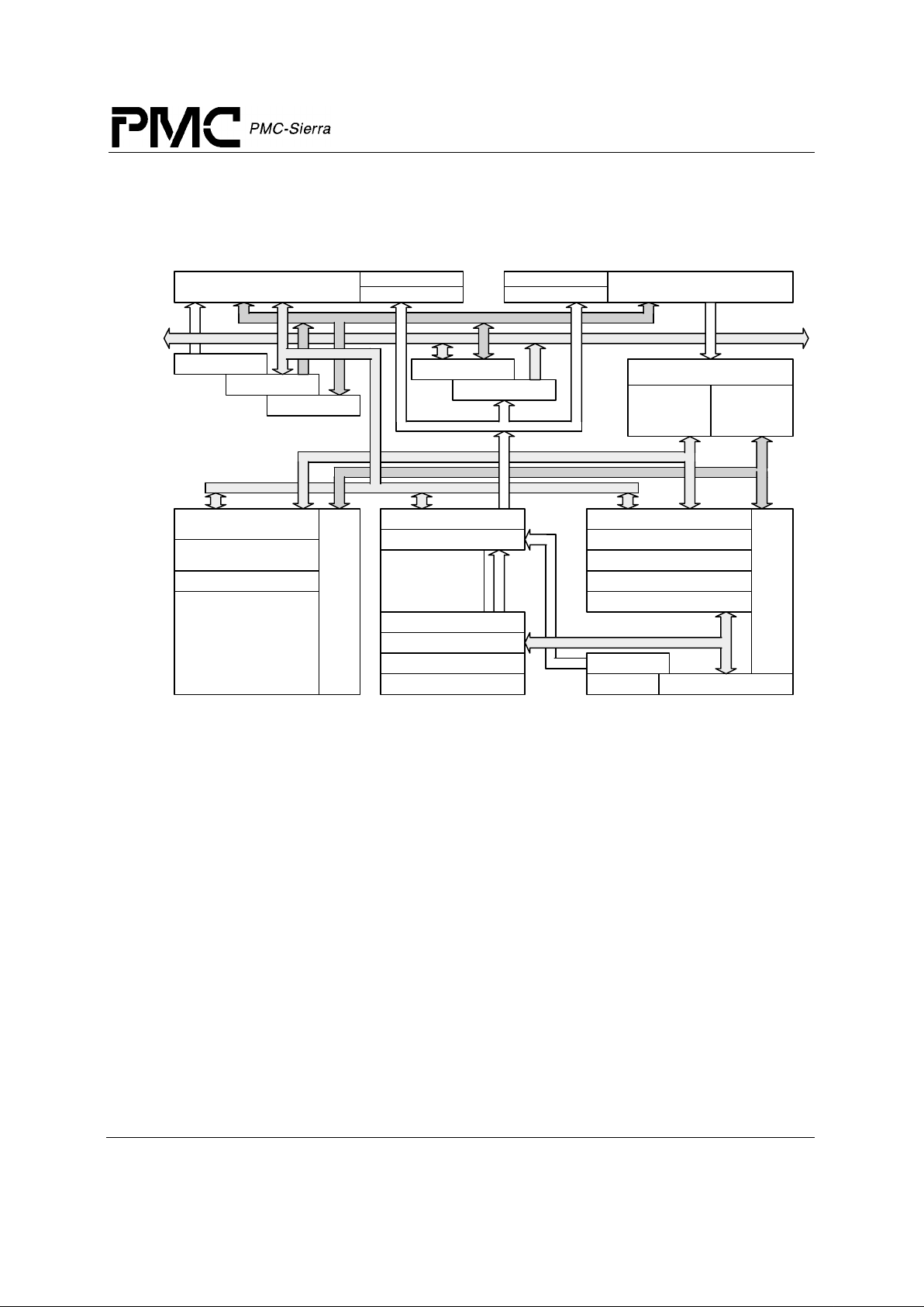
2 Block Diagram
Figure 1 Block Diagram
Integer Address/Adder
Instruction Dispatch Unit
Primary Data Cache
2-way Set Associative
Primary Instruction Cache
2-way Set Associative
DTag
DTLB
ITag
ITLB
FP
Instruction
Register
Integer
Instruction
Register
Store Buffer
Write Buffer
Read Buffer
Pad Buffer
Address Buffer
Load Aligner
Integer Register File
DTLB Virtual
PLL/Clocks
Floating-Point
Load/Align
Floating-Point
Register File
Packer/Unpacker
Floating-Point
MultAdd, Add, Sub,
Cvt, Div, Sqrt
Joint TLB
Coprocessor 0
System/Memory
Control
PC Incrementer
Branch PC Adder
ITLB Virtual
Program Counter Int Mult, Div, Madd
Floating-Point Control
Integer Control
DVA
IVA
Pad Bus
D Bus
FP Bus
Integer Bus
FA Bus
A/D Bus
Shifter/Store Aligner
Logic Unit

Proprietary and Confidential to PMC-Sierra, Inc and for its Customer’s Internal Use 11
Document ID: PMC-2002165, Issue 1
RM5231™ Microprocessor with 32-bit System Bus Data Sheet
Released
3 Hardware Overview
The RM5231 offers a high-level of integration targeted at high-performance embedded
applications. The key elements of the RM5231 are briefly described in this section.
3.1 Superscalar Dispatch
The RM5231 has an asymmetric superscalar dispatch unit which allows it to issue an integer
instruction and a floating-point computation instruction simultaneously. Integer instructions
include ALU, branch, load/store, and floating-point load/store, while floating-point computation
instructions include floating-point add, subtract, combined multiply-add, converts, etc. In
combination with its high- throug hput ful ly pipel ined fl oatin g-poin t exe cutio n unit, the supersc alar
capability of the RM5231 provides unparalleled price/performance in computationally intensive
embedded applications.
3.2 CPU Registers
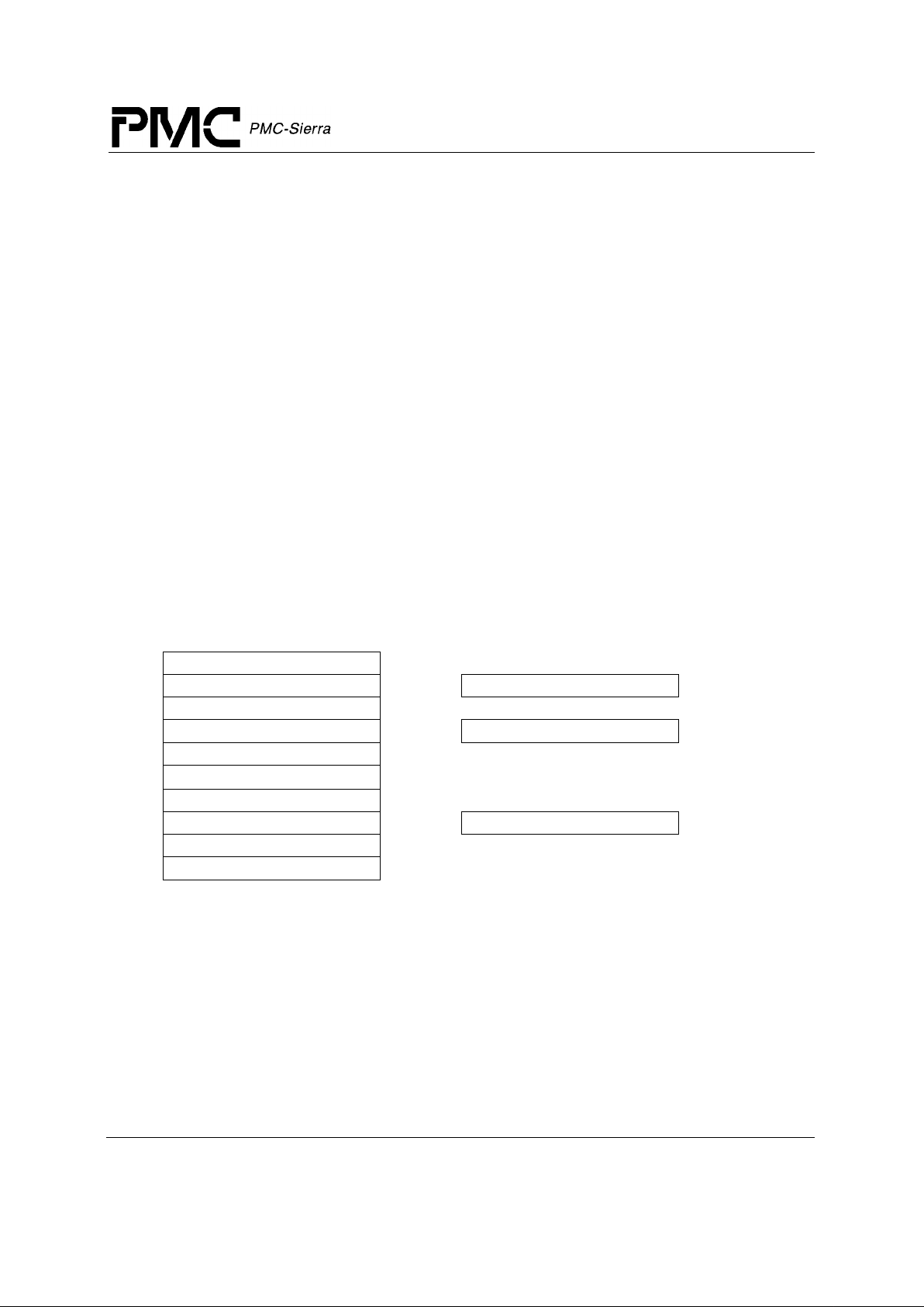
The RM5231 CPU has a user-visible state consisting of 32 general purpose registers, two special
purpose registers for integ er multi plica tion and di vision , a pr ogram c ounter, and no condi tion c ode
bits. Figure 2 shows the user visible state.
Figure 2 CPU Registers
3.3 Pipeline
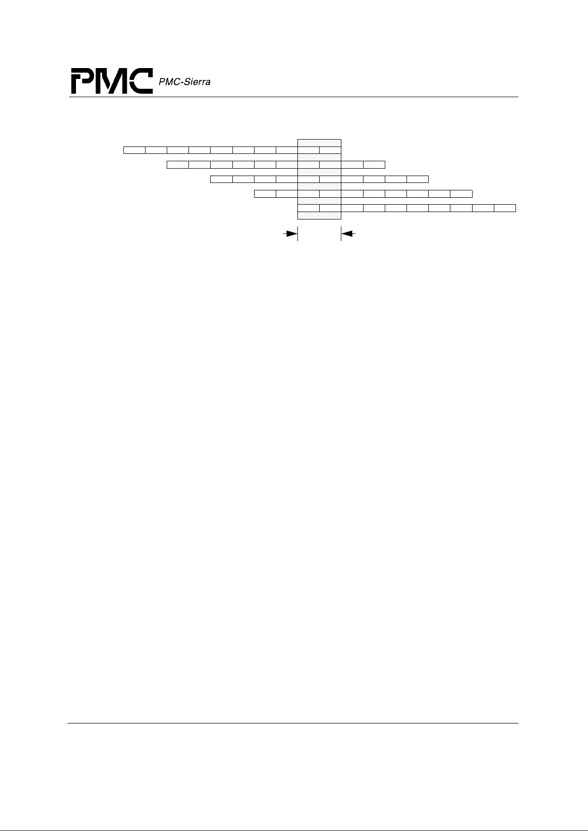
For integer operations, loads, stores, and other non-floating-point operations, the RM5231 uses a
5-stage pipeline. In addit ion to t he int eger p ipeli ne, the RM5231 us es an ex tended 7 -stag e pipel ine
for floating-point operations.
Figure 3 shows the RM5231 integer pipeline. As illustrated in the figure, up to five integer
instructions can be executing simultaneously.
General Purpose Registers
63 0
Multiply/Divide Registers
0 63 0
r1 HI
r2 63 0
• LO
•
•
Program Counter
• 63 0
r29 PC
r30
r31

Proprietary and Confidential to PMC-Sierra, Inc and for its Customer’s Internal Use 12
Document ID: PMC-2002165, Issue 1
RM5231™ Microprocessor with 32-bit System Bus Data Sheet
Released
Figure 3 Pipeline
3.4 Integer Unit
The RM5231 integer unit includes thirty-two general purpose 64-bit registers, a load/store
architecture with single cycle ALU operations (add, sub, logical, shift) and an autonomous
multiply/divide unit. A dditional register resou rces include: the HI/LO result regist ers for the two operand integer multiply /divide operations, and the program co unter (PC).
The RM5231 implements the MIPS IV Instruction Set Architecture, and is therefore fully upward
compatible with applications that run on processo rs implementing the earlier generation MIPS IIII instruct ion sets.
3.5 Register File
The RM5231 has thirty-two general purpose registers with register location 0 (r0) hard wired to a
zero value. These registers are used for scalar integer operations and address calculation. The
register file has two read ports and one write port and is fully bypassed to minimize operation
latency in the pipeline.
3.6 ALU
The RM5231 ALU consists of an integer adder/subtractor, a logic unit, and a shifter. The adder
performs address calculations in addition to arithmetic operations. The logic unit performs all
logical and zero shif t d ata moves . The shift er per forms s hifts and st ore align ment op erat ions. Eac h
of these units is optimized to perform all operations in a single processor cycl e.
3.7 Integer Multiply/Divide
The RM5231 has a dedicated integer multiply/divide unit optimized for high-speed multiply and
multiply-accumulate operations. Table 1 shows the performance of the multiply/divide unit on
each operation.
I0
I1
I2
I3
I4
2I1I 1R 2R 1A 2A 1D 2D 1W 2W
2I1I 1R 2R 1A 2A 1D 2D 1W 2W
2I1I 1R 2R 1A 2A 1D 2D 1W 2W
2I1I 1R 2R 1A 2A 1D 2D 1W 2W
2I1I 1R 2R 1A 2A 1D 2D 1W 2W
one cycle
1I-1R:
2I:
2A-2D:
2R:
1A-2A:
1A:
1A:
1D:
2A:
2W:
Instruction cache access
Instruction virtual to physical address translation
Register file read, Bypass calculation, Instruction decode, Branch address calculation
Issue or slip decision, Branch decision
Integer add, logical, shift
Data virtual address calculation
Data virtual to physical address translation
Store Align
Register file write
Data cache access and load align
 Loading...