
PM8620
NSE-20G
NSE-20G™ Standard Product Data Sheet
Preliminary
20G Narrowband Switch Element
Data Sheet
Preliminary
Issue 3: May, 2001
Proprietary and Confidential to PMC-Sierra, Inc., and for its Customers’ Internal Use
Document ID: PMC-2000170, Issue 3

NSE-20G™ Standard Product Data Sheet
Preliminary
Legal Information
Copyright
© 2001 PMC-Sierra, Inc.
The information is proprietary and confidential to PMC-Sierra, Inc., and for its customers’
internal use. In any event, you cannot reproduce any part of this document, in any form, without
the express written consent of PMC-Sierra, Inc.
PMC-2000170 (P3)
Disclaimer
None of the information contained in this document constitutes an express or implied warranty by
PMC-Sierra, Inc. as to the sufficiency, fitness or suitability for a particular purpose of any such
information or the fitness, or suitability for a particular purpose, merchantability, performance,
compatibility with other parts or systems, of any of the products of PMC-Sierra, Inc., or any
portion thereof, referred to in this document. PMC-Sierra, Inc. expressly disclaims all
representations and warranties of any kind regarding the contents or use of the information,
including, but not limited to, express and implied warranties of accuracy, completeness,
merchantability, fitness for a particular use, or non-infringement.
In no event will PMC-Sierra, Inc. be liable for any direct, indirect, special, incidental or
consequential damages, including, but not limited to, lost profits, lost business or lost data
resulting from any use of or reliance upon the information, whether or not PMC-Sierra, Inc. has
been advised of the possibility of such damage.
Trademarks
S/UNI is a registered trademark of PMC-Sierra, Inc. and NSE-20G, SBS, CHESS, TEMUX-84,
AAL1gator-32, FREEDM-336, SPECTRA, and SBI are trademarks of PMC-Sierra, Inc.
Proprietary and Confidential to PMC-Sierra, Inc., and for its Customers’ Internal Use 1
Document ID: PMC-2000170, Issue 3

Contacting PMC-Sierra
PMC-Sierra
8555 Baxter Place Burnaby, BC
Canada V5A 4V7
Tel: (604) 415-6000
Fax: (604) 415-6200
Document Information: document@pmc-sierra.com
Corporate Information: info@pmc-sierra.com
Technical Support: apps@pmc-sierra.com
Web Si te: http://www.pmc-sierra.com
NSE-20G™ Standard Product Data Sheet
Preliminary
Proprietary and Confidential to PMC-Sierra, Inc., and for its Customers’ Internal Use 2
Document ID: PMC-2000170, Issue 3

NSE-20G™ Standard Product Data Sheet
Preliminary
Table of Contents
1 Features..................................................................................................................... 11
2 Applications ...............................................................................................................12
3 References ................................................................................................................13
4 Application Examples ................................................................................................ 14
5 Block Diagram ...........................................................................................................17
6 Description.................................................................................................................19
7 Pin Diagram ...............................................................................................................20
8 Pin Description........................................................................................................... 24
8.1 Pin Description Table ........................................................................................24
8.2 Analog Power Filtering Recommendations.......................................................41
9 Functional Description ...............................................................................................43
9.1 LVDS Overview .................................................................................................43
9.1.1 LVDS Receiver (RXLV) ........................................................................44
9.1.2 LVDS Transmitter (TXLV).....................................................................44
9.1.3 LVDS Transmit Reference (TXREF) ....................................................44
9.1.4 Data Recovery Unit (DRU)...................................................................44
9.1.5 Parallel to Serial Converter (PISO) ......................................................45
9.1.6 Clock Synthesis Unit (CSU) .................................................................45
9.2 Receive 8B/10B Frame Aligner (R8TD) ............................................................ 45
9.2.1 FIFO Buffer...........................................................................................45
9.3 Transmit 8B/10B Encoder (T8TE).....................................................................45
9.3.1 SBI336S 8B/10B Character Encoding .................................................46
9.3.2 Serial TelecomBus 8B/10B Character Encoding.................................. 47
9.3.3 Serial SBI336S and TelecomBus Alignment ........................................ 49
9.3.4 Character Alignment Block ...................................................................49
9.3.5 Frame Alignment ..................................................................................50
9.3.6 SBI336S Multiframe Alignment ............................................................52
9.4 DS0 Cross Bar switch (DCB) ............................................................................ 52
9.5 Clock Synthesis and Transmit Reference Digital Wrapper (CSTR)..................53
9.6 Fabric Latency................................................................................................... 53
9.7 JTAG Support....................................................................................................53
9.8 Microprocessor Interface ..................................................................................53
9.9 In-band Link Controller (ILC).............................................................................54
Proprietary and Confidential to PMC-Sierra, Inc., and for its Customers’ Internal Use 3
Document ID: PMC-2000170, Issue 3

NSE-20G™ Standard Product Data Sheet
Preliminary
9.9.1 In-Band Signaling Channel Fixed Overhead........................................55
9.10 Microprocessor Interface ..................................................................................56
10 Normal Mode Register Description............................................................................60
11 Test Features Description........................................................................................131
11.1 Master Test and Test Configuration Registers ................................................131
11.2 JTAG Test Port ................................................................................................134
11.2.1 Boundary Scan Cells.......................................................................... 138
12 Operation .................................................................................................................140
12.1 Software Default Settings ...............................................................................140
12.1.1 Setting the T8TE Time-slot Configuration #1 Register....................... 140
12.1.2 Setting the T8TE Time-slot Configuration #2 Register....................... 140
12.1.3 Configuring the NSE-20G to Use Fewer Links ..................................140
12.1.4 PCB Design Notes .............................................................................142
12.2 “C1” Synchronization.......................................................................................142
12.3 Synchronized Control Setting Changes .......................................................... 143
12.3.1 SBS/NSE-20G Systems with DS0 and CAS switching ......................143
12.3.2 SBS/NSE-20G Systems switching DS0s without CAS ......................145
12.3.3 SBS/NSE-20G Non-DS0 Level Switching with SBI336 Devices .......147
12.4 NSE-20G CPU Interaction with the Switching Cycle When Using the ILC .....148
12.5 Controlling frame alignment in the receive port. .............................................149
12.6 DS0 Cross-Bar Switch (DCB) Operation ........................................................150
12.6.1 Configuring the DCB using Port Transfer Mode.................................150
12.6.2 Configuring the DCB using Word Transfer Mode...............................151
12.6.3 Reading Configurations...................................................................... 152
12.6.4 DCB Online to Offline Memory Page Copy........................................152
12.7 TelecomBus Mode Operation.......................................................................... 153
12.8 SBI column Mode Operation...........................................................................153
12.9 SBI DS0 Mode Operation ...............................................................................154
12.10 SBI DS0 with CAS Mode Operation................................................................154
12.11 ILC Operation.................................................................................................. 155
12.12 ILC CPU Operations .......................................................................................156
12.12.1 Accessing the Transmit Message FIFO .............................................156
12.12.2 Accessing the Receive Message FIFO ..............................................156
12.12.3 Handling the Transmit Header ...........................................................160
12.12.4 Handling the Receive Header ............................................................ 160
Proprietary and Confidential to PMC-Sierra, Inc., and for its Customers’ Internal Use 4
Document ID: PMC-2000170, Issue 3

NSE-20G™ Standard Product Data Sheet
Preliminary
12.12.5 Handling Interrupts .............................................................................160
12.12.6 Bypass Function.................................................................................160
12.13 Switch Setting Algorithm .................................................................................162
12.13.1 Problem Description ...........................................................................162
12.13.2 Naïve Algorithm .................................................................................. 163
12.13.3 Bi-partite graphs ................................................................................. 165
12.13.4 Unicast ...............................................................................................166
12.13.5 Experimental Results .........................................................................168
12.13.6 Multicast .............................................................................................168
12.14 JTAG Support..................................................................................................169
12.14.1 TAP Controller ....................................................................................170
12.14.2 States..................................................................................................170
12.14.3 Instructions .........................................................................................171
13 Functional Timing.....................................................................................................173
13.1 Receive Interface Timing ................................................................................173
13.2 Transmit Interface Timing................................................................................174
14 Absolute Maximum Ratings ..................................................................................... 176
15 D.C. Characteristics.................................................................................................177
16 Microprocessor Interface Timing Characteristics ....................................................179
17 A.C. Timing Characteristics .....................................................................................182
17.1 Input Timing.....................................................................................................182
1.1 Reset Timing ...................................................................................................183
17.2 Serial SBI Bus Interface ..................................................................................184
17.3 JTAG Port Interface.........................................................................................184
18 Ordering and Thermal Information ..........................................................................186
18.1 Packaging Information ....................................................................................186
18.2 Thermal Information ........................................................................................186
19 Mechanical Information ........................................................................................... 188
Notes ...............................................................................................................................189
Proprietary and Confidential to PMC-Sierra, Inc., and for its Customers’ Internal Use 5
Document ID: PMC-2000170, Issue 3

NSE-20G™ Standard Product Data Sheet
Preliminary
List of Registers
Register 000H: NSE-20G Master Reset............................................................................61
Register 001H: NSE-20G Individual Channel Reset ......................................................... 62
Register 002H: NSE-20G Master JTAG ID .......................................................................63
Register 003H: SBS Page select – Page 0 ....................................................................... 64
Register 004H: SBS Page select – Page 1 ....................................................................... 65
Register 005H: NSE-20G Master Interrupt Source ...........................................................66
Register 006H: NSE-20G Master ILC Interrupt Source ....................................................68
Register 007H: NSE-20G Master R8TD Interrupt Source................................................. 69
Register 008H: NSE-20G Master T8TE Interrupt Source .................................................70
Register 009H: NSE-20G Master Clock Monitor ...............................................................71
Register 00AH: NSE-20G DCB CMP select......................................................................72
Register 00BH: NSE-20G Interrupt Enable Register ........................................................73
Register 00CH: NSE-20G Subsystem Interrupt Enable Register ..................................... 74
Register 00DH: NSE-20G R8TD TIP Rgister .................................................................... 75
Register 00EH: SBS User Bit 0 ......................................................................................... 76
Register 00FH: SBS User Bit 1 .........................................................................................77
Register 010H: SBS User Bit 2 .........................................................................................78
Register 011H: NSE-20G FREE User Register.................................................................79
Register 012H: Correct R8TD_RX_C1 Pulse Monitor ......................................................80
Register 013H: Unexpected R8TD_RX_C1 Interrupt........................................................ 81
Register 014H: Missing R8TD_RX_C1 Interrupt............................................................... 82
Register 015H: Unexpected R8TD_RX_C1 Interrupt Enable ...........................................83
Register 016H: Missing R8TD_RX_C1 Interrupt Enable ..................................................84
Register 020H, 024H: CSTR #1 – 2 Control* ....................................................................85
Register 021H, 025H: CSTR #1 – 2* Interrupt Enable and CSU Lock Status .................. 86
Register 022H, 026H: CSTR #1 – 2 Interrupt Indication ...................................................87
Register 040H: DCB Configuration port 31-30 Register (NSE-20G 20G only) .................88
Register 041H: DCB Configuration port 29-24 Register (NSE-20G 20G only) .................89
Register 042H: DCB Configuration port 23-18 Register (NSE-20G 20G only) .................90
Register 043H: DCB Configuration port 17-12 Register ...................................................91
Register 044H: DCB Configuration port 11-6 Register......................................................92
Register 045H: DCB Configuration port 5-0 Register .......................................................93
Register 046H: DCB Configuration Output Register .........................................................94
Proprietary and Confidential to PMC-Sierra, Inc., and for its Customers’ Internal Use 6
Document ID: PMC-2000170, Issue 3

NSE-20G™ Standard Product Data Sheet
Preliminary
Register 047H: DCB Access Mode Register .....................................................................95
Register 048H: DCB C1 delay (RC1DLY) Register...........................................................97
Register 04AH: DCB Frame size Register ........................................................................98
Register 04CH: DCB Configuration Register ....................................................................99
Register 04DH: DCB Interrupt status Register................................................................102
Register 100H + N*20H: R8TD Control and Status.........................................................103
Register 101H + N*20H, R8TD Interrupt Status..............................................................105
Register 102H + N*20H, R8TD Line Code Violation Count ............................................107
Register 103H + N*20H, RXLV and DRU Control ...........................................................108
Register 108H + N*20H, T8TE Control and Status ......................................................... 110
Register 109H + N*20H, T8TE Interrupt Status .............................................................. 112
Register 10AH + N*20H: T8TE Time-slot Configuration #1 ............................................ 113
Register 10BH + N*20H: T8TE Time-slot Configuration #2 ............................................ 114
Register 10CH + N*20H, T8TE Test Pattern ................................................................... 115
Register 10DH + N*20H, TXLV and PISO Control .......................................................... 116
Register 110H + N*20H, ILC Transmit FIFO Data........................................................... 117
Register 111h + N*20H, ILC Transmit Control Register ................................................. 118
Register 112h + N*20H, ILC Transmit Misc.Status and FIFO Synch Register................ 119
Register 113h + N*20H, ILC Receive FIFO Data Register.............................................. 121
Register 114h + N*20H, ILC Receive Control Register...................................................122
Register 115h + N*20H, ILC Receive Auxiliary, Status and FIFO Synch Register..........123
Register 116h + N*20H, ILC Interrupt Enable and Control Register ............................... 127
Register 117h + N*20H: ILC Interrupt Reason Register.................................................. 130
Register 800H: NSE-20G Master Test ............................................................................132
Proprietary and Confidential to PMC-Sierra, Inc., and for its Customers’ Internal Use 7
Document ID: PMC-2000170, Issue 3

NSE-20G™ Standard Product Data Sheet
Preliminary
List of Figures
Figure 1 An OC-48 T1/E1 ADM (Individually Drop/Add any T1/E1 in STS-48) ..............14
Figure 2 An OC-48 T1/E1 ADM (Drop/Add up to STS-48 at STS-1 Granularity)............14
Figure 3 Any-Service-Any-Port TDM Access Solution ....................................................15
Figure 4 Any-Service-Any-Port DS0-Granularity PHY Card ...........................................16
Figure 5 NSE-20G Block Diagram Showing TSBs..........................................................17
Figure 6 NSE-20G UBGA-480 Ball Diagram (Bottom-View)........................................... 20
Figure 7 Analog Power Filter Circuit................................................................................42
Figure 8 Generic LVDS Link Block Diagram ...................................................................43
Figure 9 Character Alignment State Machine .................................................................50
Figure 10 Frame Alignment State Machine.....................................................................51
Figure 11 In-Band Signaling Channel Message Format ................................................. 55
Figure 12 In-Band Signaling Channel Header Format ....................................................55
Figure 13 Input Observation Cell (IN_CELL) ................................................................138
Figure 14 Output Cell (OUT_CELL) ..............................................................................139
Figure 15 Bidirectional Cell (IO_CELL) .........................................................................139
Figure 16 Layout of Output Enable and Bidirectional Cells...........................................139
Figure 17 Shutting down a link ...................................................................................... 141
Figure 18 “C1” Synchronization Control........................................................................143
Figure 19 TEMUX-84™/SBS/NSE/SBS/AAL1GATOR-32™ system DS0
Switching with CAS .......................................................................................144
Figure 20 CAS Multiframe timing ..................................................................................145
Figure 21 Switch Timing DSOs with CAS .....................................................................145
Figure 22 TEMUX-84/SBS/NSE/SBS/FREEDM-336 system DS0 Switching no
CAS...............................................................................................................146
Figure 23 Switch Timing - DSOs without CAS ..............................................................147
Figure 24 Non DS0 Switch Timing ................................................................................148
Figure 25 Architecture of the RAM Input Interface........................................................150
Figure 26 C1 Position in the First Row..........................................................................155
Figure 27 Transport Overhead Affected by ILC ............................................................161
Figure 28 Example Graph .............................................................................................164
Figure 29 Time Space Time Switching in one NSE-20G and four Single-Ported
SBSs .............................................................................................................164
Figure 30 Example Graph .............................................................................................166
Figure 31 Example Problem..........................................................................................167
Proprietary and Confidential to PMC-Sierra, Inc., and for its Customers’ Internal Use 8
Document ID: PMC-2000170, Issue 3

NSE-20G™ Standard Product Data Sheet
Preliminary
Figure 32 Merged Graph ...............................................................................................167
Figure 33 Relabeled Graph ...........................................................................................168
Figure 34 Boundary Scan Architecture .........................................................................169
Figure 35 TAP Controller Finite State Machine.............................................................170
Figure 36 Receive Interface Timing ..............................................................................173
Figure 37 Transmit Interface Timing .............................................................................174
Figure 38 CMP Timing ..................................................................................................175
Figure 39 Microprocessor Interface Read Timing .........................................................179
Figure 40 Microprocessor Interface Write Timing .........................................................181
Figure 41 NSE-20G Input Timing ..................................................................................182
Figure 42 RSTB Timing.................................................................................................183
Figure 43 JTAG Port Interface Timing...........................................................................185
Proprietary and Confidential to PMC-Sierra, Inc., and for its Customers’ Internal Use 9
Document ID: PMC-2000170, Issue 3

NSE-20G™ Standard Product Data Sheet
Preliminary
List of Tables
Table 1 Analog Power Filters ..........................................................................................42
Table 2 SBI336S Character Encoding ............................................................................46
Table 3 Serial TelecomBus Character Encoding ............................................................48
Table 4 Switching Control RAM layout............................................................................53
Table 5 In-band Message Header Fields ........................................................................55
Table 6 NSE-20G Register Map......................................................................................56
Table 7 TX FIFO Message Level ..................................................................................120
Table 8 RX FIFO Message Level ..................................................................................125
Table 9 RXFIFO Threshold Values ...............................................................................128
Table 10 RXFIFO Timeout Delay .................................................................................. 128
Table 11 Test Mode Register Memory Map .................................................................. 131
Table 12 Instruction Register (Length - 3 bits) ..............................................................134
Table 13 Identification Register.....................................................................................134
Table 14 Boundary Scan Register ................................................................................135
Table 15 Absolute Maximum Ratings............................................................................176
Table 16 D.C Characteristics ........................................................................................177
Table 17 Microprocessor Interface Read Access .........................................................179
Table 18 Microprocessor Interface Write Access..........................................................181
Table 19 NSE-20G Input Timing ( Figure 41 ) ..............................................................182
Table 20 RSTB Timing ( Figure 42 ) .............................................................................183
Table 21 Serial SBI Bus Interface ................................................................................. 184
Table 22 JTAG Port Interface ( Figure 43 ) ................................................................... 184
Proprietary and Confidential to PMC-Sierra, Inc., and for its Customers’ Internal Use 10
Document ID: PMC-2000170, Issue 3

1 Features
The Narrowband Switch Element 20G (NSE-20G):
• Implements a Scaleable Bandwidth Interconnect (SBI™) DS0 granularity Space switch.
• Implements a SONET/SDH VT1.5/VT2/TU11/TU12 granularity Space switch for the serial
777.6 MHz LVDS TelecomBus.
• With the allied SBS or SBS-lite device, implements a DS0 granularity Memory-Space-
Memory switch.
• Supports 32 STS-12 equivalent serial ports via 777.6 MHz, 8B/10B encoded LVDS links
(each port can be either Serial TelecomBus or Serial SBI336S)
• When configured for SBI mode, switches DS0 or N*DS0 for all T1 and E1 tributaries and
aggregate columns for switching T1, E1, TVT1.5, TVT2, DS3 and E3 tributaries.
• When configured for the serial 777.6 MHz TelecomBus interface, switches any SONET/SDH
virtual tributary or tributary unit up to STS-1.
NSE-20G™ Standard Product Data Sheet
Preliminary
• Supports switching of arbitrary non-standard octet aggregates.
• Supports unicast, multicast, and broadcast for all switching modes.
• Provides 20 Gbit/s (258,048 DS0s, 10,752 T1s/VT1.5s, 8,064 E1s/VT2s, 384 DS3s/E3s)
switching.
• Works with SBS devices that support up to four 19.44 MHz SBI buses or one 77.76 MHz
SBI336 bus that communicates with PMC-Sierra’s SBI device family. Alternatively, the SBS
and SBS-lite devices support up to four 19.44 MHz STS-3 TelecomBuses or one 77.76 MHz
STS-12 TelecomBus for connection with PMC-Sierra’s SPECTRA™ family of devices.
• Can be combined in applications with PMC-Sierra’s CHESS™ Set devices (PM5374 TSE
and PM5307 TBS).
• Supports a microprocessor interface which is used to configure/control the NSE, to make
DS0-granularity switch settings.
• Supports clean error checked 8 Mbit/s full-duplex, in-band communications channels from
the NSE’s attached microprocessor to the attached microprocessors of each of the 32 attached
SBS336S devices. This channel is used to initialize and control the SBSs, or other such
devices, and to implement call-establishment set-up changes.
• Supports JTAG for all non-LVDS signals.
• Requires dual power supplies at 1.8 V and 3.3 V.
• Packaged as a 480 ball UBGA.
• In conjunction with the SBS or SBS-lite, supports “1+1” and “1:N” fabric redundancy.
Proprietary and Confidential to PMC-Sierra, Inc., and for its Customers’ Internal Use 11
Document ID: PMC-2000170, Issue 3

2 Applications
The PM8620 Narrowband Switch Element (NSE) supports a variety of flexible Layer 1 and Layer
2 architectures in combination with the following PMC-Sierra devices:
• PM8610 SBS and PM8611 SBS-lite (SBI Serializer and Memory switching stage)
• SBI bus devices (PM8315 TEMUX™/PM5365 TEMAP, FREEDM™ devices, S/UNI®-IMA
devices, AAL1gator™ devices, and other future devices)
• CHESS chip set devices (PM5374 TSE, PM5307 TBS, PM5315 SPECTRA™-2488, and
PM7390 S/UNI®-MACH48)
These architectures include:
• T1/E1 SONET Add/Drop Multiplexers (ADMs)
• TDM ASAP applications
• PHY cards with DS0 (and above) level switching
NSE-20G™ Standard Product Data Sheet
Preliminary
• PSTN replacement switching cores, as part of any-service-any-port applications
• Voice Gateways
Proprietary and Confidential to PMC-Sierra, Inc., and for its Customers’ Internal Use 12
Document ID: PMC-2000170, Issue 3

3 References
1. ANSI - T1.105-1995, “Synchronous Optical Network (SONET) – Basic Description
including Multiplex Structure, Rates, and Formats”, 1995.
2. Telcordia - SONET Transport Systems: Common Generic Criteria, GR-253-CORE, Issue 2,
Revision 2, January 1999.
3. ITU, Recommendation G.707 - "Digital Transmission Systems – Terminal equipments -
General", March 1996.
4. IEEE 802.3, “Carrier SeNSE-20G Multiple Access with Collision Detection (CSMA/CD)
Access Method and Physical Layer Specifications”, Section 36.2, 1998.
5. A.X. Widmer and P.A. Franaszek, “A DC-Balanced, Partitioned-Block, 8B/10B Transmission
Code,” IBM Journal of Research and Development, Vol. 27, No 5, September 1983, pp 440-
451.
NSE-20G™ Standard Product Data Sheet
Preliminary
6. U.S. Patent No. 4,486,739, P.A. Franaszek and A.X. Widmer, “Byte Oriented DC Balanced
(0,4) 8B/10B Partitioned Block Transmission Code,” December 4, 1984.
7. IEEE Std 1596.3-1996, “IEEE Standard for Low-voltage Differential Signals (LVDS) for
Scalable Coherent Interface (SCI)”, Approved March 21, 1996
8. L.R. Ford, D.R. Fulkerson, “Flows in Networks'', Maximum Cardinality Matchings in
Bipartite Graphs.
Proprietary and Confidential to PMC-Sierra, Inc., and for its Customers’ Internal Use 13
Document ID: PMC-2000170, Issue 3
4 Application Examples
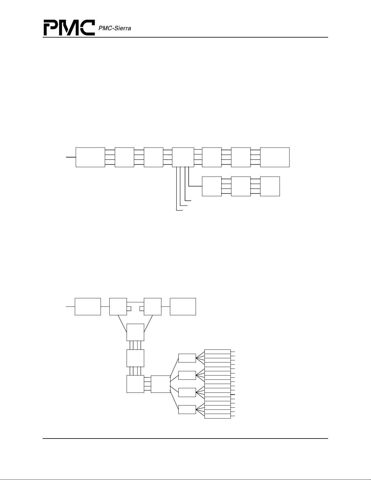
Figure 1 illustrates an OC-48 SONET Ring Add/Drop Multiplexer. The PM5363 TUPP-622
devices align all paths to transport frames in preparation for VT1.5/VT2 granularity switching.
The PM8610 SBI336 Bus Serializer (SBS™) and PM8620 Narrowband Switching Element 20G
(NSE-20G™) devices support VT1.5/VT2 and above switching. The Add and Drop buses are
provided by the SBSs that are not in the SONET Ring path. In this case, they connect to T1 and
E1 mapper ports.
Figure 1 An OC-48 T1/E1 ADM (Individually Drop/Add any T1/E1 in STS-48)
NSE-20G™ Standard Product Data Sheet
Preliminary
SPECTRA-
2488
4 X
TUPP-
622
4 X
SBS
NSE20G
4 X
SBS
SBS
**
42 required to terminate
4 X
TUPP-
622
4 X
TEMAP
-84
SPECTRA-
2488
4 X
OCTAL
-LIU **
links for all 4 TEMAPS
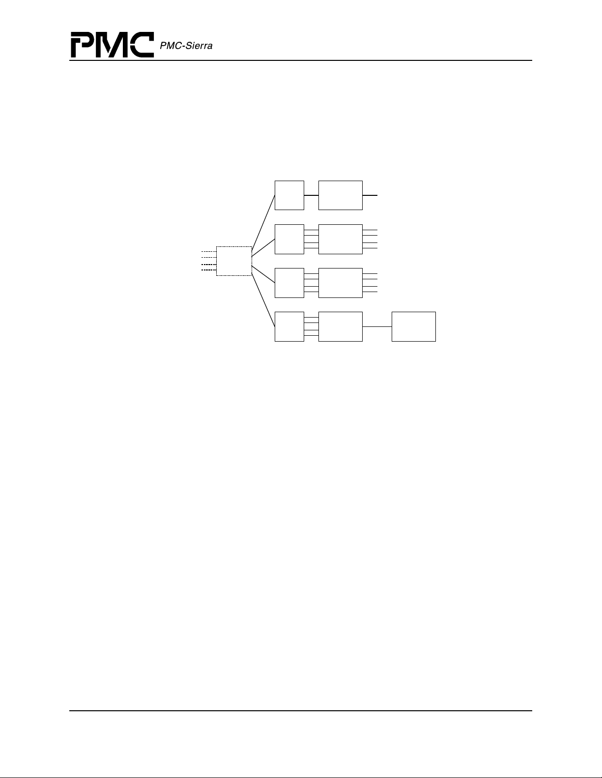
Figure 2 illustrates another OC-48 SONET Ring ADM. In this application, the network of three
PM5310 TelecomBus Serializers (TBSs) from PMC-Sierra’s CHESS™ chip set add, drop, and
groom traffic at STS-1 granularities. The four TUPP-622 devices align any dropped STS-1s
(paths to transport frames). The virtual tributary (VT) or tributary unit (TU) switching solution is
provided by the SBS-NSE-20G-SBS network below the TUPP-622s. Four SBSs support up to an
STS-48 amount of add/drop traffic.
Figure 2 An OC-48 T1/E1 ADM (Drop/Add up to STS-48 at STS-1 Granularity)
SPECTA-
2488
TBS TBS
SPECTA-
2488
TBS
4 X
TUPP-
622
4 X
SBS
SBS
SBS
NSE20G
SBS
SBS
SBI device
SBI device
SBI device
SBI device
SBI device
SBI device
SBI device
SBI device
SBI device
SBI device
SBI device
SBI device
SBI device
SBI device
SBI device
SBI device
Proprietary and Confidential to PMC-Sierra, Inc., and for its Customers’ Internal Use 14
Document ID: PMC-2000170, Issue 3
NSE-20G™ Standard Product Data Sheet
Preliminary
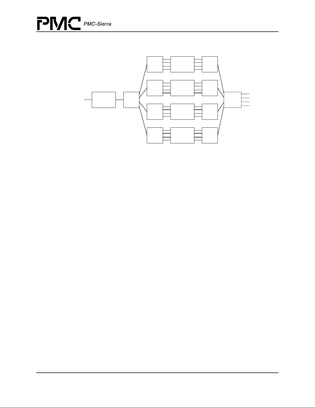
Figure 3 illustrates the organization of the access line size card(s) from a SONET Any Service
Any Port (ASAP) product. All traffic from the NSE-20G to the SBI link layer devices is pathaligned. See Figure 4 for a description of the PHY line cards compatible with the system in
Figure 3.
Figure 3 Any-Service-Any-Port TDM Access Solution
FREEDM-
336
4 X
IMA-84
12 X
AAL1gator-
32
4 X
TEMUX-84
H-MVIP
Any-PHY
(Packet)
Any-PHY
(Cell)
Any-PHY
(Cell)
Processors
DSP
NSE20G
SBS-
lite
SBS
SBS
SBS
T1/E1/DS0/N*DS0 Layer 2 Processing
Figure 4 shows the organization of a SONET PHY card compatible with Figure 3. As shown, both
Figure 3 and Figure 4 have NSE-20Gs, but only one instance of this device is required to connect
all the SBSs. A likely packaging of this combined system would place the NSE-20G (and a
standby NSE-20G) on separate fabric cards. In Figure 4, four PM8315 TEMUXs align paths to
transport frames. Note: Figure 3 assumes this alignment.
Proprietary and Confidential to PMC-Sierra, Inc., and for its Customers’ Internal Use 15
Document ID: PMC-2000170, Issue 3
NSE-20G™ Standard Product Data Sheet
Figure 4 Any-Service-Any-Port DS0-Granularity PHY Card
Preliminary
4 X
TEMUX-84
4 X
TEMUX-84
4 X
TEMUX-84
4 X
TEMUX-84
SPECTRA-
2488
TBS
TBS
TBS
TBS
TBS
SONET/T1/E1 Termination - VT/TU/DS0 Switching
SBS
SBS
NSE20G
SBS
SBS
Proprietary and Confidential to PMC-Sierra, Inc., and for its Customers’ Internal Use 16
Document ID: PMC-2000170, Issue 3
5 Block Diagram
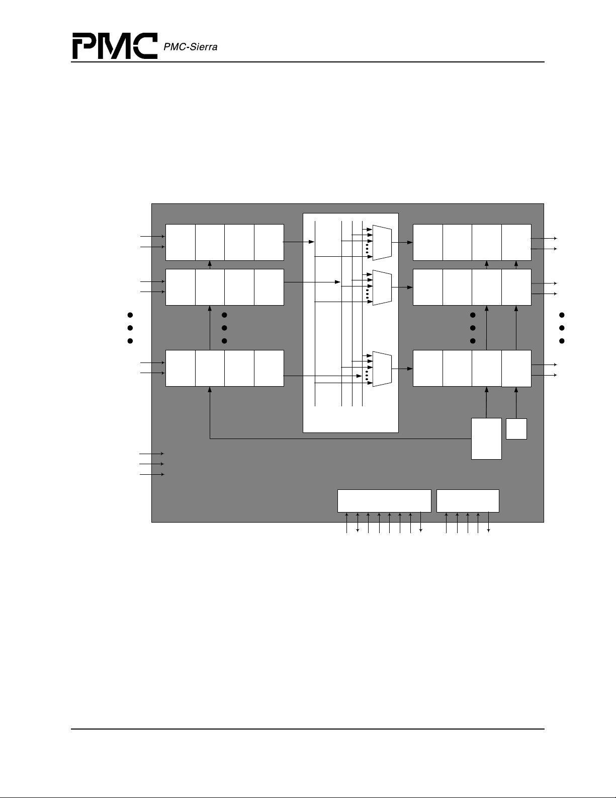
The NSE-20G is organized as a DS0 granularity space switch. The NSE-20G may also be
organized (with respect to STS-12 boundaries in TelecomBus mode) as a self aligning
VT1.5/VT2 granularity space switch. Refer to Figure 5.
Figure 5 NSE-20G Block Diagram Showing TSBs
NSE-20G™ Standard Product Data Sheet
Preliminary
RP[0]
RN[0]
RP[1]
RN[1]
RP[31]
RN[31]
RC1FP
CMP
SYSCLK
LVDS
Receiver
(RXLV)
LVDS
Receiver
(RXLV)
LVDS
Receiver
(RXLV)
Data
Recovery
Unit
(DRU)
Data
Recovery
Unit
(DRU)
Data
Recovery
Unit
(DRU)
Receive
8B/10B
Decoder
(R8TD)
Receive
8B/10B
Decoder
(R8TD)
Receive
8B/10B
Decoder
(R8TD)
1/2
In-Band
Link
Controller
(ILC)
1/2
In-Band
Link
Controller
(ILC)
1/2
In-Band
Link
Controller
(ILC)
DS0 Crossbar Switch
(DCB)
Microprocessor Interface
1/2
In-Band
Link
Controller
(ILC)
1/2
In-Band
Link
Controller
(ILC)
1/2
In-Band
Link
Controller
(ILC)
Transmit
8B/10B
Encoder
(T8TE)
Transmit
8B/10B
Encoder
(T8TE)
Transmit
8B/10B
Encoder
(T8TE)
JTAG
Transmit
Serializer
(PISO)
Transmit
Serializer
(PISO)
Transmit
Serializer
(PISO)
Clock
Synthesis
Units (2)
LVDS
Transmitt
er
(TXLV)
LVDS
Transmitt
er
(TXLV)
LVDS
Transmitt
er
(TXLV)
Tx
Ref
TP[0]
TN[0]
TP[1]
TN[1]
TP[31]
TN[31]
CSB
RSTB
A[11:0]
D[31:0]
ALE
RDB
WRB
INTB
TRSTB
TDI
TCK
TMS
TDO
The R8TD block, in combination with the RXLV and DRU receive, decode and align incoming
SBI336/STS-12-equivalent LVDS links. Outputs are provided to the primary switching flow, and
to the in-band signaling channel. These provide all analog and digital functions to terminate a
full-duplex 777.6 MHz serial SBI336S or 777.6 MHz serial TelecomBus on LVDS.
A 32 x 32 DS0 Crossbar Switch (DCB) stage switches data and control signals between the 32
ports. The switching instructions are stored in two pages of RAM configured as offline and online
allowing the user to modify the offline page.
Proprietary and Confidential to PMC-Sierra, Inc., and for its Customers’ Internal Use 17
Document ID: PMC-2000170, Issue 3

NSE-20G™ Standard Product Data Sheet
Preliminary
The T8TE block, in combination with the PISO and TXLV perform 8B/10B coding and emits the
LVDS bit streams. These provide all analog and digital functions to launch a full-duplex 777.6
MHz serial SBI336S bus or 777.6 MHz serial TelecomBus on LVDS.
The microprocessor bus interface and in-band signaling units (ILC) provide a clean (error
checked) channel between the NSE-20G and SBSs. This can be used to send messages between
the NSE-20G microprocessor-and the SBS microprocessors in a user defined format.
Proprietary and Confidential to PMC-Sierra, Inc., and for its Customers’ Internal Use 18
Document ID: PMC-2000170, Issue 3

6 Description
The PM8620 NSE-20G is a monolithic CMOS integrated circuit packaged in a 480 ball UBGA
that performs DS0 and above granularity space switching on 32 SBI336 streams carried as serial
SBI336S in 8B/10B coding over LVDS at 777.6 Mbit/s. The NSE-20G also performs VT1.5/VT2
and above granularity switching on 32 STS-12/STM-4 SONET/SDH streams, carried as Serial
TelecomBus signals in 8B/10B coding over LVDS at 777.6 Mbit/s.
The NSE-20G is typically used with up to 32 PM8610 SBS or PM8611 SBS-lite devices to
provide Memory-Space-Memory switching systems. As each SBS supports either four SBI buses
at 19.44 MHz or one SBI336 bus at 77.76 MHz, the overall system supports any mixture of SBI
and SBI336 byte serial buses, ranging from 128 19.44 MHz SBI buses to 32 SBI336 77.76 MHz
buses that do not exceed an aggregate bandwidth of STS-384, or about 20 Gbit/s. In TelecomBus
mode, the SBS devices support the same range of flexibility for 128 19.44 MHz and 32 77.76
MHz TelecomBuses at VT1.5/VT2 granularity
Central to the NSE-20G is a 32 x 32 cross bar switch. At every clock cycle, the cross bar
switches a byte of data with control signals from each input port to an output port. The byte of
data may be a DS0 channel from a T1/E1 or may be one byte of a column comprising a T1, E1,
DS3, E3, VT1.5, VT2 or STS-1.
NSE-20G™ Standard Product Data Sheet
Preliminary
In order for switching to take place all input and output streams must be synchronized. This is
done via the RC1FP input signal. When switching T1s, E1s, VTs and other higher order units only
SBI336 multiframe alignment is required. The same applies for TelecomBus mode where only
frame alignment is required.
An in-band control link over the serial LVDS interface allows the NSE-20G to communicate with
the microprocessors attached to the SBS, SBS-lite or other serial SBI336S devices. The effective
bandwidth of each inband link to each device is 8 Mbit/s. The inband link provides error
detection on 32-byte user messages and some near realtime control signals between devices.
Using the near realtime control signals, the NSE-20G is able to synchronize page switching,
indicate switchover between working or protected links, and exchange three user defined signals
(software) and 8 Auxilliary signals (software). The user and auxilliary signals can be used to
indicates interrupts or initiate handshaking between the end point microprocessors. The message
format is left to the user of the devices. The only constraint is that each message is a maximum of
32 bytes long.
Proprietary and Confidential to PMC-Sierra, Inc., and for its Customers’ Internal Use 19
Document ID: PMC-2000170, Issue 3
NSE-20G™ Standard Product Data Sheet
7 Pin Diagram
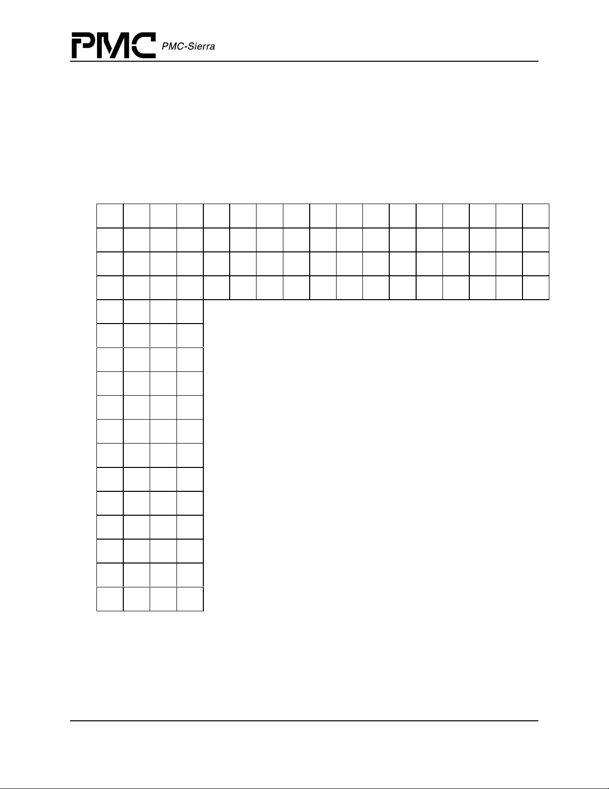
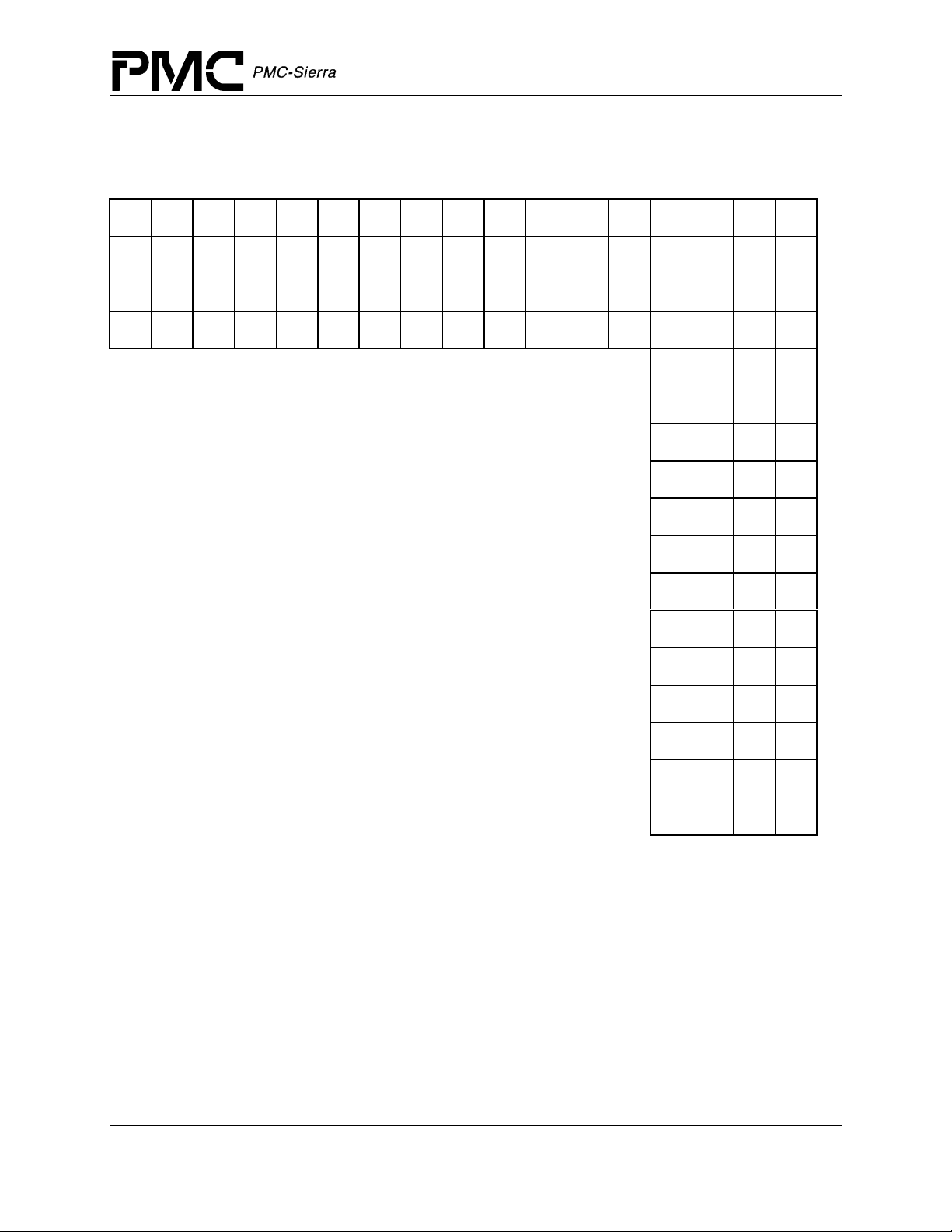
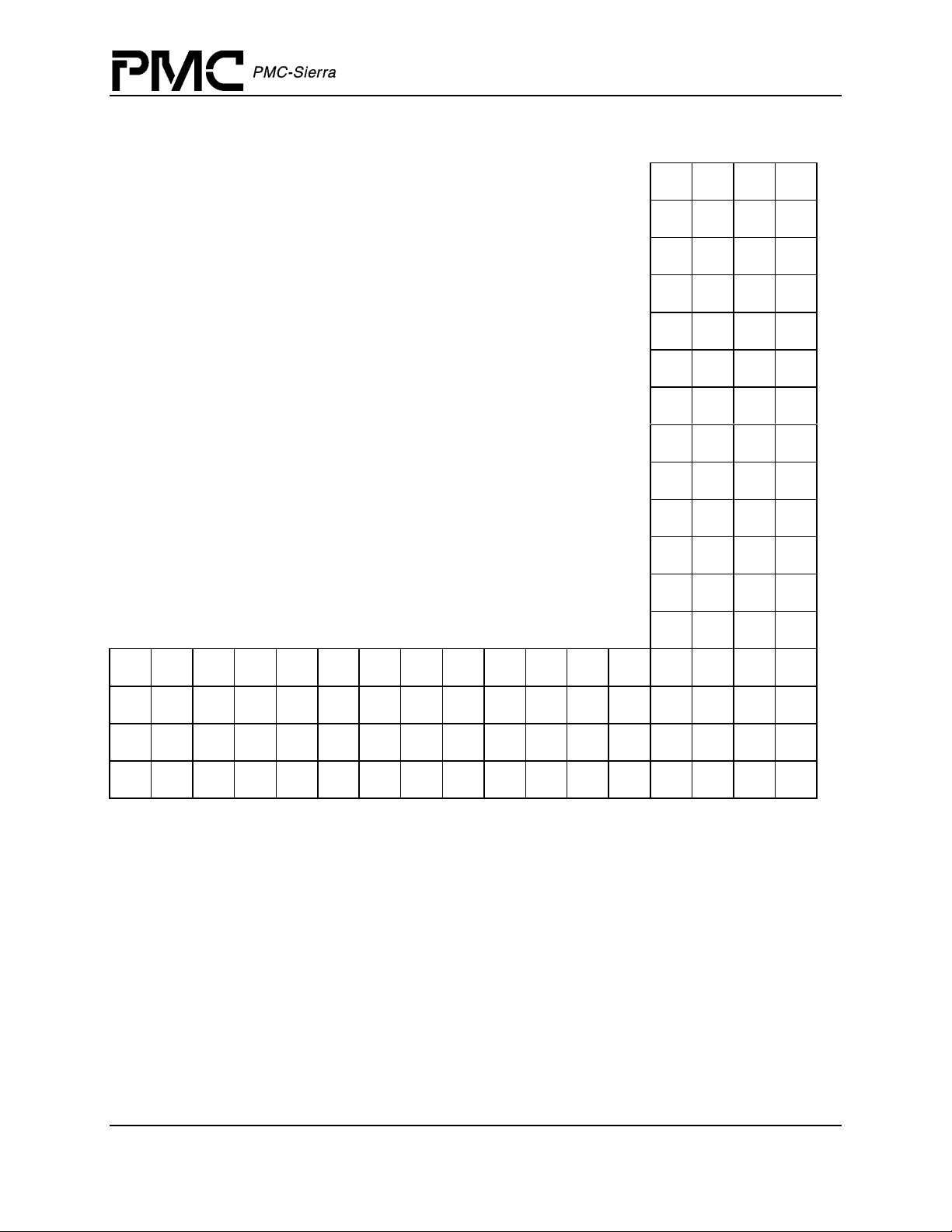
The NSE-20G packaged in a 35 mm x 35 mm 480 ball UBGA.
Figure 6 NSE-20G UBGA-480 Ball Diagram (Bottom-View)
34 33 32 31 30 29 28 27 26 25 24 23 22 21 20 19 18
Preliminary
A VSS VSS VSS VSS VDDO VSS NC VSS NC VSS
B VSS AVDH VDDO VDDO VDDO VDDI NC NC NC VDDI
C VSS AVDH AVDH VDDO VDDI
D VSS AVDH AVDH AVDH VDDO
E RESK1 RES1 RN[32] RP[32]
F VSS RN[31] RP[31] AVDL1
Reserved
NC NC VDDI NC
Reserved
VDDI VDDO NC NC
Upper Left
G RN[30] RP[30] RN[29] RP[29]
H VSS TP[32] TN[32] AVDH
J TP[31] TN[31] TP[30] TN[30]
K VSS TP[29] TN[29] VDDI
L RN[28] RP[28] RN[27] RP[27]
M VSS RN[26] RP[26] AVDH
N VDDI AVDL2 RN[25] RP[25]
Reserved
Reserved Reserved Reserved Reserved Reserved Reserved
Reserved
Reserved
Reserved
VSS
VDDI
VDDO
VSS
Reserved Reserved Reserved Reserved
Reserved Reserved Reserved
Reserved
VSS VDDI
VDDO VDDI
RSTB
VDDI
P VSS TP[28] TN[28] VDDI
R TP[27] TN[27] TP[26] TN[26]
T TP[25] TN[25] AVDL4 AVDL3
U RN[24] RP[24] AVDL5 CSU_A
VDH
Proprietary and Confidential to PMC-Sierra, Inc., and for its Customers’ Internal Use 20
Document ID: PMC-2000170, Issue 3
NSE-20G™ Standard Product Data Sheet
Preliminary
1716151413121110987654321
NC SYSCLK NC VSS NC VSS NC VSS
NC NC NC TCK TMS NC VDDI
Reserved
NC VDDI NC VDDI TDI TDO NC
NC RC1FP VDDI TRSTB VDDI VDDO VDDI CMP
Reserved] Reserved Reserved Reserved Reserved
Upper Right
Reserved
Reserved Reserved Reserved Reserved
Reserved
VSS
VDDO
Reserved
VSS NC VSS VSS VSS VSS A
Reserved Reserved
NC VDDO VDDO VDDO VSS B
VDDI VDDO VDDO AVDH VSS C
NC VDDO AVDH AVDH VSS D
AVDH ATB0[1] AVDH AVDH E
ATB1[1] TN[1] TP[1] VSS F
TN[3] TP[3] TN[2] TP[2] G
AVDH VDDI NC VSS H
RP[1] RN[1] TN[4] TP[4] J
VDDI RP[2] RN[2] VSS K
VDDI AVDL14 RP[3] RN[3] L
AVDH RP[4] RN[4] VSS M
TN[6] TP[6] TN[5] TP[5] N
VDDI TN[7] TP[7] VSS P
RP[5] RN[5] TN[8] TP[8] R
AVDH VDDI AVDL13 VSS T
RP[7] RN[7] RP[6] RN[6] U
Proprietary and Confidential to PMC-Sierra, Inc., and for its Customers’ Internal Use 21
Document ID: PMC-2000170, Issue 3

V RN[22] RP[22] RN[23] RP[23]
W VSS AVDL6 VDDI AVDH
Y TP[24] TN[24] RN[21] RP[21]
NSE-20G™ Standard Product Data Sheet
Preliminary
AA VSS TP[23] TN[23] VDDI
Lower Left
AB TP[21] TN[21] TP[22] TN[22]
AC VSS RN[20] RP[20] AVDH
AD RN[19] RP[19] AVDL7 VDDI
AE VSS RN[18] RP[18] VDDI
AF TP[20] TN[20] RN[17] RP[17]
AG VSS NC VDDI AVDH
AH TP[18] TN[18] TP[19] TN[19]
AJ VSS TP[17] TN[17] ATB1[2]
AK AVDH AVDH ATB0[2] AVDH
AL VSS AVDH AVDH VDDO ALE NC VDDI VDDO A[6] A[2] VDDI VDDO D[27] VDDI NC NC VDDI
AM VSS AVDH VDDO VDDO CSB RDB VDDI A[9] A[5] A[3] D[31] D[29] VDDI D[25] VDDI D[21] D[20]
AN VSS VDDO VDDO VDDO INTB WRB NC A[10] A[7] A[4] A[0] D[30] D[28] D[26] NC D[22] D[19]
AP VSS VSS VSS VSS NC VSS A[11] VSS A[8] VSS A[1] VSS NC VSS D[24] D[23] D[18]
34 33 32 31 30 29 28 27 26 25 24 23 22 21 20 19 18
Proprietary and Confidential to PMC-Sierra, Inc., and for its Customers’ Internal Use 22
Document ID: PMC-2000170, Issue 3
NSE-20G™ Standard Product Data Sheet
Preliminary
CSU_A
AVDL12 RP[8] RN[8] V
VDH
AVDL10 AVDL11 TN[9] TP[9] W
TN[10] TP[10] TN[11] TP[11] Y
Lower Right
VDDI TN[12] TP[12] VSS AA
RP[9] RN[9] AVDL9 VDDI AB
AVDH RP[10] RN[10] VSS AC
RP[11] RN[11] RP[12] RN[12] AD
VDDI TN[13] TP[13] VSS AE
TP[14] TN[14] TN[15] TP[15] AF
AVDH TN[16] TP[16] VSS AG
RP[13] RN[13] RP[14] RN[14] AH
AVDL8 RP[15] RN[15] VSS AJ
RP[16] RN[16] RES2 RESK2 AK
D[17] VDDO D[13] D[11] D[8] VDDO D[5] D[3] D[0] VDDO NC NC VDDO AVDH AVDH AVDH VSS AL
VDDI D[15] VDDI D[10] D[9] D[7] NC D[2] D[1] NC NC NC NC VDDO AVDH AVDH VSS AM
D[16] D[14] D[12] NC VDDI D[6] D[4] VDDI NC NC NC NC VDDO VDDO VDDO AVDH VSS AN
NC VSS VDDI VSS VDDI VSS NC VSS NC VSS NC VSS VDDO VSS VSS VSS VSS AP
1716151413121110987654321
Proprietary and Confidential to PMC-Sierra, Inc., and for its Customers’ Internal Use 23
Document ID: PMC-2000170, Issue 3

8 Pin Description
8.1 Pin Description Table
Pad Name Type Pin No. Function
LVDS Ports (128 Balls)
RP[1]
RN[1]
RP[2]
RN[2]
RP[3]
RN[3]
RP[4]
RN[4]
RP[5]
RN[5]
RP[6]
RN[6]
RP[7]
RN[7]
RP[8]
RN[8]
RP[9]
RN[9]
RP[10]
RN[10]
RP[11]
RN[11]
RP[12]
RN[12]
RP[13]
RN[13]
RP[14]
RN[14]
RP[15]
RN[15]
RP[16]
RN[16]
RP[17]
RN[17]
Analog
LVDS Input
J4
J3
K3
K2
L2
L1
M3
M2
R4
R3
U2
U1
U4
U3
V2
V1
AB4
AB3
AC3
AC2
AD4
AD3
AD2
AD1
AH4
AH3
AH2
AH1
AJ3
AJ2
AK4
AK3
AF31
AF32
NSE-20G™ Standard Product Data Sheet
Preliminary
Receive Serial Data. The differential receive serial data
links (RP[31:0]/RN[31:0]) carry the receive SBI336S or
SONET/SDH STS-12 frame data from upstream sources
in bit serial format. Each differential pair RP[X]/RN[X]
carries a constituent SBI336 or STS-12 stream. Data on
RP[X]/RN[X] is encoded in an 8B/10B format extended
from IEEE Std. 802.3. The 8B/10B character bit ‘a’ is
transmitted first and the bit ‘j’ is transmitted last. All
RP[X]/RN[X] differential pairs must be frequency locked
and phase aligned (within a certain tolerance) to each
other. RP[31:0]/RN[31:0] are nominally 777.6 Mbit/s data
streams.
Any unused, but available inputs should be tied low
using a 10 K resistor.
Proprietary and Confidential to PMC-Sierra, Inc., and for its Customers’ Internal Use 24
Document ID: PMC-2000170, Issue 3

Pad Name Type Pin No. Function
RP[18]
RN[18]
RP[19]
RN[19]
RP[20]
RN[20]
RP[21]
RN[21]
RP[22]
RN[22]
RP[23]
RN[23]
RP[24]
RN[24]
RP[25]
RN[25]
RP[26]
RN[26]
RP[27]
RN[27]
RP[28]
RN[28]
RP[29]
RN[29]
RP[30]
RN[30]
RP[31]
RN[31]
RP[32]
RN[32]
Analog
LVDS Input
AE32
AE33
AD33
AD34
AC32
AC33
Y31
Y32
V33
V34
V31
V32
U33
U34
N31
N32
M32
M33
L31
L32
L33
L34
G31
G32
G33
G34
F32
F33
E31
E32
NSE-20G™ Standard Product Data Sheet
Preliminary
Proprietary and Confidential to PMC-Sierra, Inc., and for its Customers’ Internal Use 25
Document ID: PMC-2000170, Issue 3

Pad Name Type Pin No. Function
TP[1]
TN[1]
TP[2]
TN[2]
TP[3]
TN[3]
TP[4]
TN[4]
TP[5]
TN[5]
TP[6]
TN[6]
TP[7]
TN[7]
TP[8]
TN[8]
TP[9]
TN[9]
TP[10]
TN[10]
TP[11]
TN[11]
TP[12]
TN[12]
TP[13]
TN[13]
TP[14]
TN[14]
Analog
LVDS
Output
F2
F3
G1
G2
G3
G4
J1
J2
N1
N2
N3
N4
P2
P3
R1
R2
W1
W2
Y3
Y4
Y1
Y2
AA2
AA3
AE2
AE3
AF4
AF3
Transmit Serial Data. The differential transmit working
serial data links (TP[31:0]/TN[31:0]) carry the transmit
SBI336S or SONET/SDH STS-12 frame data to a
downstream sinks in bit serial format. Each differential
pair carries a constituent STS-12 stream. Data on
TP[X]/TN[X] is encoded in an 8B/10B format extended
from IEEE Std. 802.3. The 8B/10B character bit ‘a’ is
transmitted first and the bit ‘j’ is transmitted last. All
TP[X]/TN[X] differential pairs are frequency locked and
phase aligned (within a certain tolerance) to each other.
TP[31:0]/TN[31:0] are nominally 777.6 Mbit/s data
streams.
NSE-20G™ Standard Product Data Sheet
Preliminary
Proprietary and Confidential to PMC-Sierra, Inc., and for its Customers’ Internal Use 26
Document ID: PMC-2000170, Issue 3

Pad Name Type Pin No. Function
TP[15]
TN[15]
TP[16]
TN[16]
TP[17]
TN[17]
TP[18]
TN[18]
TP[19]
TN[19]
TP[20]
TN[20]
TP[21]
TN[21]
TP[22]
TN[22]
TP[23]
TN[23]
TP[24]
TN[24]
TP[25]
TN[25]
TP[26]
TN[26]
TP[27]
TN[27]
TP[28]
TN[28]
TP[29]
TN[29]
TP[30]
TN[30]
TP[31]
TN[31]
TP[32]
TN[32]
NSE-20G Control and Clocking (5 Balls)
SYSCLK Input A16
Analog
LVDS
Output
AF1
AF2
AG2
AG3
AJ33
AJ32
AH34
AH33
AH32
AH31
AF34
AF33
AB34
AB33
AB32
AB31
AA33
AA32
Y34
Y33
T34
T33
R32
R31
R34
R33
P33
P32
K33
K32
J32
J31
J34
J33
H33
H32
System Clock. The system clock signal (SYSCLK) is the
master clock for the NSE-20G device. SYSCLK must be
a 77.76 MHz clock, with a nominal 50% duty cycle.
CMP and RC1FP are sampled on the rising edge of
SYSCLK.
NSE-20G™ Standard Product Data Sheet
Preliminary
Proprietary and Confidential to PMC-Sierra, Inc., and for its Customers’ Internal Use 27
Document ID: PMC-2000170, Issue 3

NSE-20G™ Standard Product Data Sheet
Pad Name Type Pin No. Function
RC1FP Input D16
Reserved Output C17 Reserved pin, must be left floating
CMP Input D10
RSTB Input B18
Receive Serial Interface Frame Pulse. The receive
serial interface frame pulse signal (RC1FP) provides
system timing for the receive serial interface. RC1FP is
supplied in common to all devices in a system containing
one or more NSE-20G devices. In TelecomBus mode
RC1FP is set high once every 4 frames, in SBI mode
without any DS0 switching, or when switching DS0s
(WITHOUT CAS) RC1FP is also set high once every 4
frames, or multiple thereof. When in SBI mode switching
DS0s WITH CAS RC1FP indicates signaling multiframe
alignment by pulsing once every 48 frames or multiples
thereof.
A software configurable delay from RC1FP is used to
indicate that the C1 multiframe boundary 8B/10B
characters have been delivered on all the receive serial
data links (RP[32:1]/RN[32:1]) and are ready for
processing by the time-space-time switching elements.
RC1FP is sampled on the rising edge of SYSCLK.
Connection Memory Page. The connection memory
page select signal (CMP) controls the selection of the
connection memory page in the NSE. When CMP is set
high, connection memory page 1 is selected. When CMP
is set low, connection memory page 0 is selected.
Changes to the connection memory page selection are
synchronized to the boundary of the next C1FP frame or
multiframe depending on the mode:
4-Frame SBI/SBI336 mode:
CMP is sampled at the C1 byte position of the incoming
bus on the first frame of the four-frame multiframe.
Changes to the connection memory page selection are
synchronized to the frame boundary (A1 byte position) of
the next four-frame multiframe.
48-Frame SBI/SBI336 mode:
CMP is sampled at the C1 byte position of the incoming
bus on the first frame of the 48-frame multiframe.
Changes to the connection memory page selection are
synchronized to the frame boundary (A1 byte position) of
the next 48-frame multiframe.
TelecomBus mode:
CMP is sampled at the C1 byte position of every frame
on the incoming bus. Changes to the connection memory
pate selection are synchronized to the frame boundary
(A1 byte position) of the next frame.
CMP is sampled on the rising edge of SYSCLK at the
RC1FP frame position.
Reset Enable Bar. The active low reset signal (RSTB)
provides an asynchronous reset for the NSE. RSTB is a
Schmitt triggered input with an integral pull-up resistor
Preliminary
Proprietary and Confidential to PMC-Sierra, Inc., and for its Customers’ Internal Use 28
Document ID: PMC-2000170, Issue 3

Pad Name Type Pin No. Function
Microprocessor Interface (49 Balls)
CSB Input AM30
RDB Input AM29
WRB Input AN29
Chip Select Bar. The active low chip select signal (CSB)
controls microprocessor access to registers in the NSE20G device. CSB is set low during NSE-20G
Microprocessor Interface Port register accesses. CSB is
set high to disable microprocessor accesses.
If CSB is not required (i.e. register accesses controlled
using RDB and WRB signals only), CSB should be
connected to an inverted version of the RSTB input.
Read Enable Bar. The active low read enable bar signal
(RDB) controls microprocessor read accesses to
registers in the NSE-20G device. RDB is set low and
CSB is also set low during NSE-20G Microprocessor
Interface Port register read accesses. The NSE-20G
drives the D[31:0] bus with the contents of the addressed
register while RDB and CSB are low.
Write Enable Bar. The active low write enable bar signal
(WRB) controls microprocessor write accesses to
registers in the NSE-20G device. WRB is set low and
CSB is also set low during NSE-20G Microprocessor
Interface Port register write accesses. The contents of
D[31:0] are clocked into the addressed register on the
rising edge of WRB while CSB is low.
NSE-20G™ Standard Product Data Sheet
Preliminary
Proprietary and Confidential to PMC-Sierra, Inc., and for its Customers’ Internal Use 29
Document ID: PMC-2000170, Issue 3
 Loading...