


PM8610
SBS Telecom Standard Product Data Sheet
Preliminary
SBI Bus Serializer (SBS)
Telecom Standard Product
Data Sheet
Preliminary
Issue 3: May, 2001
Proprietary and Confidential to PMC-Sierra, Inc., and for its Customers’ Internal Use
Document ID: PMC-2000168, Issue 3

SBS Telecom Standard Product Data Sheet
Preliminary
Legal Information
Copyright
© 2001 PMC-Sierra, Inc.
The information is proprietary and confidential to PMC-Sierra, Inc., and for its customers’
internal use. In any event, you cannot reproduce any part of this document, in any form, without
the express written consent of PMC-Sierra, Inc.
PMC-2000168, (A3)
Disclaimer
None of the information contained in this document constitutes an express or implied warranty by
PMC-Sierra, Inc. as to the sufficiency, fitness or suitability for a particular purpose of any such
information or the fitness, or suitability for a particular purpose, merchantability, performance,
compatibility with other parts or systems, of any of the products of PMC-Sierra, Inc., or any
portion thereof, referred to in this document. PMC-Sierra, Inc. expressly disclaims all
representations and warranties of any kind regarding the contents or use of the information,
including, but not limited to, express and implied warranties of accuracy, completeness,
merchantability, fitness for a particular use, or non-infringement.
In no event will PMC-Sierra, Inc. be liable for any direct, indirect, special, incidental or
consequential damages, including, but not limited to, lost profits, lost business or lost data
resulting from any use of or reliance upon the information, whether or not PMC-Sierra, Inc. has
been advised of the possibility of such damage.
Trademarks
SBI, SPECTRA, TEMUX, AAL1gator, and FREEDM are trademarks of PMC-Sierra, Inc.
Proprietary and Confidential to PMC-Sierra, Inc., and for its Customers’ Internal Use 2
Document ID: PMC-2000168, Issue 3

Contacting PMC-Sierra
PMC-Sierra
8555 Baxter Place Burnaby, BC
Canada V5A 4V7
Tel: (604) 415-6000
Fax: (604) 415-6200
Document Information: document@pmc-sierra.com
Corporate Information: info@pmc-sierra.com
Technical Support: apps@pmc-sierra.com
Web Si te: http://www.pmc-sierra.com
SBS Telecom Standard Product Data Sheet
Preliminary
Proprietary and Confidential to PMC-Sierra, Inc., and for its Customers’ Internal Use 3
Document ID: PMC-2000168, Issue 3

SBS Telecom Standard Product Data Sheet
Preliminary
Table of Contents
1 Features..................................................................................................................... 17
2 Applications ...............................................................................................................19
3 References ................................................................................................................20
4 Application Examples ................................................................................................ 21
5 Block Diagram ...........................................................................................................23
6 Loopback Configurations...........................................................................................25
7 Description.................................................................................................................26
8 Pin Diagram ...............................................................................................................28
9 Pin Description........................................................................................................... 29
10 Functional Description ...............................................................................................54
10.1 SBI Bus Data Formats ......................................................................................54
10.1.1 SBI Multiplexing Structure ....................................................................54
10.1.2 SBI Timing Master Modes ....................................................................56
10.1.3 SBI Link Rate Information ....................................................................57
10.1.4 Alarms ..................................................................................................58
10.1.5 T1 Tributary Mapping ...........................................................................59
10.1.6 E1 Tributary Mapping ...........................................................................62
10.1.7 DS3 Tributary Mapping.........................................................................65
10.1.8 E3 Tributary Mapping ...........................................................................66
10.1.9 Transparent VT1.5/TU11 Mapping ....................................................... 67
10.1.10 Transparent VT2/TU12 Mapping ..........................................................69
10.1.11 Fractional Rate Tributary Mapping .......................................................71
10.1.12 SBI336 Bus Format..............................................................................71
10.1.13 SBI336 Multiplexing Structure..............................................................72
10.2 Incoming SBI336 Timing Adapter......................................................................72
10.3 CAS Expanders................................................................................................. 73
10.4 Memory Switch Units ........................................................................................73
10.4.1 Data Buffer ...........................................................................................73
10.4.2 Connection Memory .............................................................................74
10.5 CAS Merging.....................................................................................................74
10.6 Incoming SBI336 Tributary Translator...............................................................74
10.7 PRBS Processors .............................................................................................75
10.7.1 PRBS Generator ..................................................................................75
Proprietary and Confidential to PMC-Sierra, Inc., and for its Customers’ Internal Use 4
Document ID: PMC-2000168, Issue 3

SBS Telecom Standard Product Data Sheet
Preliminary
10.7.2 PRBS Detector ..................................................................................... 75
10.8 Transmit 8B/10B Encoders ...............................................................................75
10.8.1 SBI336S 8B/10B Character Encoding .................................................75
10.8.2 Serial TelecomBus 8B/10B Character Encoding..................................77
10.9 Transmit Serializer ............................................................................................79
10.10 LVDS Transmitters ............................................................................................79
10.11 Clock Synthesis Unit .........................................................................................79
10.12 Transmit Reference Generator .........................................................................79
10.13 LVDS Receivers ................................................................................................ 79
10.14 Data Recovery Units .........................................................................................79
10.15 Receive 8B/10B Decoders................................................................................80
10.15.1 FIFO Buffer........................................................................................... 80
10.15.2 Serial SBI336S and TelecomBus Alignment ........................................ 80
10.15.3 Character Alignment Block...................................................................80
10.15.4 Frame Alignment ..................................................................................81
10.15.5 SBI336S Multiframe Alignment ............................................................82
10.16 Outgoing SBI336S Tributary Translator ............................................................ 83
10.16.1 Outgoing SBI336S Translation............................................................83
10.17 Outgoing SBI336 Timing Adapter......................................................................83
10.18 In-band Link Controller......................................................................................84
10.18.1 In-Band Signaling Channel Fixed Overhead........................................85
10.19 Microprocessor Interface ..................................................................................86
11 Normal Mode Register Description............................................................................91
12 Test Features Description........................................................................................278
12.1 Master Test and Test Configuration Registers ................................................ 278
12.2 JTAG Test Port ................................................................................................280
12.2.1 Boundary Scan Cells.......................................................................... 289
13 Operation .................................................................................................................292
13.1 “C1” Synchronization.......................................................................................292
13.2 Synchronized Control Setting Changes .......................................................... 293
13.2.1 SBS/NSE Systems with DS0 and CAS switching ..............................293
13.2.2 SBS/NSE Systems switching DS0s without CAS .............................. 295
13.2.3 SBS/NSE Non-DS0 Level Switching with SBI336 Devices................297
13.3 Switch Setting Algorithm .................................................................................297
13.3.1 Problem Description...........................................................................298
Proprietary and Confidential to PMC-Sierra, Inc., and for its Customers’ Internal Use 5
Document ID: PMC-2000168, Issue 3

SBS Telecom Standard Product Data Sheet
Preliminary
13.3.2 Naïve Algorithm ..................................................................................298
13.3.3 Bi-partite graphs .................................................................................301
13.3.4 Unicast ...............................................................................................301
13.3.5 Experimental Results .........................................................................303
13.3.6 Multicast .............................................................................................303
13.4 JTAG Support..................................................................................................304
13.4.1 TAP Controller .................................................................................... 306
13.4.2 States..................................................................................................307
13.4.3 Instructions ......................................................................................... 308
14 Functional Timing.....................................................................................................309
14.1 Incoming SBI336 Bus Functional Timing ........................................................ 309
14.2 Incoming SBI Bus Functional Timing .............................................................. 310
14.3 Incoming 77 MHz TelecomBus Functional Timing.......................................... 311
14.4 Incoming 19 MHz TelecomBus Functional Timing..........................................312
14.5 Transmit Serial LVDS Functional Timing ........................................................312
14.6 Transmit TelecomBus Functional Timing ........................................................314
14.7 Transmit SBI336 Bus Functional Timing.........................................................314
14.8 Receive TelecomBus Functional Timing .........................................................315
14.9 Receive SBI336 Functional Timing .................................................................316
14.10 Receive Serial LVDS Functional Timing .........................................................317
14.11 Outgoing 77.76 MHz TelecomBus Functional Timing.....................................318
14.12 Outgoing 19.44 MHz TelecomBus Functional Timing.....................................319
14.13 Outgoing SBI336 Functional Timing ...............................................................319
14.14 Outgoing SBI Bus Functional Timing ..............................................................320
15 Absolute Maximum Ratings ..................................................................................... 321
16 D. C. Characteristics................................................................................................322
17 Microprocessor Interface Timing Characteristics ....................................................324
18 A.C. timing Characteristics ......................................................................................327
18.1 SBS Incoming Bus Timing ..............................................................................327
18.2 SBS Receive Bus Timing ................................................................................328
18.3 SBS Outgoing Bus Timing ..............................................................................331
18.4 SBS Outgoing Bus Collision Avoidance Timing ..............................................332
18.5 SBS Transmit Bus Timing ...............................................................................333
18.6 JTAG Port Interface.........................................................................................335
19 Ordering and Thermal Information ..........................................................................336
Proprietary and Confidential to PMC-Sierra, Inc., and for its Customers’ Internal Use 6
Document ID: PMC-2000168, Issue 3

SBS Telecom Standard Product Data Sheet
Preliminary
19.1 Packaging Information ....................................................................................336
19.2 Thermal Information ........................................................................................336
20 Mechanical Information ........................................................................................... 337
Notes ...............................................................................................................................338
Proprietary and Confidential to PMC-Sierra, Inc., and for its Customers’ Internal Use 7
Document ID: PMC-2000168, Issue 3

SBS Telecom Standard Product Data Sheet
Preliminary
List of Registers
Register 000H: SBS Master Reset....................................................................................92
Register 001H: SBS Master Configuration........................................................................93
Register 002H: SBS Version/Part Number........................................................................ 96
Register 003H: SBS Part Number/Manufacturer ID..........................................................97
Register 004H: SBS Master Bypass Register ................................................................... 98
Register 005H: SBS Master SPE Control #1 ..................................................................100
Register 006H: SBS Master SPE Control #2 ..................................................................101
Register 007H: SBS Receive Synchronization Delay .....................................................102
Register 008H: SBS In-Bank Link User Bits....................................................................103
Register 009H: SBS Receive Configuration....................................................................104
Register 00AH: SBS Transmit Configuration ..................................................................106
Register 00BH: SBS Transmit J1 Configuration..............................................................108
Register 00CH: SBS Transmit V1 Configuration.............................................................109
Register 00DH: SBS Transmit H1-H2 Pointer Value....................................................... 110
Register 00EH: SBS Transmit Alternate H1-H2 Pointer Value........................................ 111
Register 00FH: SBS Transmit H1-H2 Pointer Selection .................................................112
Register 010H: SBS Master Interrupt Source .................................................................113
Register 011H: SBS Interrupt Register............................................................................ 116
Register 012H: SBS Interrupt Enable Register ............................................................... 118
Register 013H: SBS Loopback Configuration .................................................................120
Register 014H: SBS Master Signal Monitor #1, Accumulation Trigger ........................... 121
Register 015H: SBS Master Signal Monitor #2 ...............................................................123
Register 016H: SBS Master Interrupt Enable .................................................................125
Register 017H: SBS Free User Register......................................................................... 128
Register 020H: ISTA Incoming Parity Configuration .......................................................129
Register 021H: ISTA Incoming Parity Status ...................................................................131
Register 022H: ISTA TelecomBus Configuration.............................................................132
Register 028H: IMSU Configuration ................................................................................ 133
Register 029H: IMSU Interrupt Status and Memory Page Update Register ...................134
Register 02AH: IMSU Indirect Time Switch Address.......................................................135
Register 02BH: IMSU Indirect Time Switch Data ............................................................ 137
Register 030H: ICASM CAS Enable Indirect Access Address Register .........................138
Register 031H: ICASM CAS Enable Indirect Access Control Register ...........................139
Proprietary and Confidential to PMC-Sierra, Inc., and for its Customers’ Internal Use 8
Document ID: PMC-2000168, Issue 3

SBS Telecom Standard Product Data Sheet
Preliminary
Register 032H: ICASM CAS Enable Indirect Access Data Register ...............................140
Register 038H: ISTT Tributary Translator Control RAM Indirect Access Address
Register ..................................................................................................................141
Register 039H: ISTT Tributary Translator Control RAM Indirect Access Control
Register ..................................................................................................................142
Register 03AH: ISTT Tributary Translator Control RAM Indirect Access Data
Register ..................................................................................................................143
Register 040H: OSTT Tributary Translator Control RAM Indirect Access Address
Register ..................................................................................................................144
Register 041H: OSTT Tributary Translator Control RAM Indirect Access Control
Register ..................................................................................................................145
Register 042H: OSTT Tributary Translator Control RAM Indirect Access Data
Register ..................................................................................................................146
Register 048H: OMSU Configuration ..............................................................................147
Register 049H: OMSU Interrupt Status and Memory Page Update Register .................148
Register 04AH: OMSU Indirect Time Switch Address.....................................................149
Register 04BH: OMSU Indirect Time Switch Data ..........................................................151
Register 050H: OCASM CAS Enable Indirect Access Address Register........................152
Register 051H: OCASM CAS Enable Indirect Access Control Register ......................... 153
Register 052H: OCASM CAS Enable Indirect Access Data Register ............................. 154
Register 060H: OSTA Outgoing Configuration and Parity..............................................155
Register 061H: OSTA Outgoing J1 Configuration ........................................................... 157
Register 062H: OSTA Outgoing V1 Configuration ..........................................................158
Register 063H: OSTA H1-H2 Pointer Value ....................................................................159
Register 064H: OSTA Alternate H1-H2 Pointer Value .....................................................160
Register 065H: OSTA H1-H2 Pointer Selection ..............................................................161
Register 066H: OSTA Tributary Output Enable Indirect Access Address Register .........162
Register 067H: OSTA Tributary Output Enable Indirect Access Control Register ..........163
Register 068H: OSTA Tributary Output Enable Indirect Access Data Register ..............164
Register 070h: WPP Indirect Address .............................................................................165
Register 071h: WPP Indirect Data................................................................................... 167
Register 071h (IADDR = 0h): WPP Monitor STS-1 path Configuration ..........................168
Register 071h (IADDR = 1h): WPP Monitor PRBS[22:7] Accumulator ...........................170
Register 071h (IADDR = 2h): WPP Monitor PRBS[6:0] Accumulator .............................171
Register 071h (IADDR = 4h): WPP Monitor Error count .................................................172
Register 071h (IADDR = 8h): WPP Generator STS-1 path Configuration ......................173
Register 071h (IADDR = 9h): WPP Generator PRBS[22:7] Accumulator ....................... 175
Proprietary and Confidential to PMC-Sierra, Inc., and for its Customers’ Internal Use 9
Document ID: PMC-2000168, Issue 3

SBS Telecom Standard Product Data Sheet
Preliminary
Register 071h (IADDR = Ah): WPP Generator PRBS[6:0] Accumulator.........................176
Register 072h: WPP Generator Payload Configuration .................................................. 177
Register 073h: WPP Monitor Payload Configuration ......................................................179
Register 074h: WPP Monitor Byte Error Interrupt Status................................................181
Register 075h: WPP Monitor Byte Error Interrupt Enable...............................................182
Register 079h: WPP Monitor Synchronization Interrupt Status.......................................183
Register 07Ah: WPP Monitor Synchronization Interrupt Enable .....................................184
Register 07Bh: WPP Monitor Synchronization State ......................................................185
Register 07Ch: WPP Performance Counters Transfer Trigger ....................................... 186
Register 080h: PPP Indirect Address ..............................................................................187
Register 081h: PPP Indirect Data.................................................................................... 189
Register 081h (IADDR = 0h): PPP Monitor STS-1 path Configuration ...........................190
Register 081h (IADDR = 1h): PPP Monitor PRBS[22:7] Accumulator ............................192
Register 081h (IADDR = 2h): PPP Monitor PRBS[6:0] Accumulator ..............................193
Register 081h (IADDR = 4h): PPP Monitor Error count ..................................................194
Register 081h (IADDR = 8h): PPP Generator STS-1 path Configuration .......................195
Register 081h (IADDR = 9h): PPP Generator PRBS[22:7] Accumulator ........................197
Register 081h (IADDR = Ah): PPP Generator PRBS[6:0] Accumulator..........................198
Register 082h: PPP Generator Payload Configuration ...................................................199
Register 083h: PPP Monitor Payload Configuration .......................................................201
Register 084h: PPP Monitor Byte Error Interrupt Status.................................................203
Register 085h: PPP Monitor Byte Error Interrupt Enable................................................204
Register 089h: PPP Monitor Synchronization Interrupt Status........................................205
Register 08Ah: PPP Monitor Synchronization Interrupt Enable ......................................206
Register 08Bh: PPP Monitor Synchronization State........................................................207
Register 08Ch: PPP Performance Counters Transfer Trigger ........................................208
Register 090H: WILC Transmit FIFO Data High .............................................................209
Register 091H: WILC Transmit FIFO Data Low ..............................................................210
Register 093H: WILC Transmit Control Register ............................................................211
Register 095H: WILC Transmit Status and FIFO Synch Register...................................212
Register 096H: WILC Receive FIFO Data High ..............................................................214
Register 097H: WILC Receive FIFO Data Low ...............................................................215
Register 099H: WILC Receive FIFO Control Register ....................................................216
Register 09AH: WILC Receive Auxiliary Register ........................................................... 217
Register 09BH: WILC Receive Status and FIFO Synch Register ...................................218
Proprietary and Confidential to PMC-Sierra, Inc., and for its Customers’ Internal Use 10
Document ID: PMC-2000168, Issue 3

SBS Telecom Standard Product Data Sheet
Preliminary
Register 09DH: WILC Interrupt Enable and Control Register. ........................................222
Register 09FH: WILC Interrupt Reason Register ............................................................224
Register 0A0H: PILC Transmit FIFO Data High .............................................................. 225
Register 0A1H: PILC Transmit FIFO Data Low...............................................................226
Register 0A3H: PILC Transmit Control Register ............................................................. 227
Register 0A5H: PILC Transmit Status and FIFO Synch Register ...................................228
Register 0A6H: PILC Receive FIFO Data High............................................................... 230
Register 0A7H: PILC Receive FIFO Data Low................................................................231
Register 0A9H: PILC Receive FIFO Control Register..................................................... 232
Register 0AAH: PILC Receive Auxiliary Register............................................................233
Register 0ABH: PILC Receive Status and FIFO Synch Register....................................234
Register 0ADH: PILC Interrupt Enable and Control Register.......................................... 238
Register 0AFH: PILC Interrupt Reason Register ............................................................240
Register 0B0H: TW8E Control and Status ...................................................................... 241
Register 0B1H: TW8E Interrupt Status............................................................................243
Register 0B2H: TW8E Time-slot Configuration #1 ..........................................................244
Register 0B3H: TW8E Time-slot Configuration #2 ..........................................................245
Register 0B4H: TW8E Test Pattern ................................................................................. 246
Register 0B5H: TW8E Analog Control ............................................................................247
Register 0B8H: TP8E Control and Status .......................................................................248
Register 0B9H: TP8E Interrupt Status.............................................................................250
Register 0BAH: TP8E Time-slot Configuration #1 .......................................................... 251
Register 0BBH: TP8E Time-slot Configuration #2 .......................................................... 252
Register 0BCH: TP8E Test Pattern .................................................................................253
Register 0BDH: TP8E Analog Control.............................................................................254
Register 0C0H: RW8D Control and Status......................................................................255
Register 0C1H: RW8D Interrupt Status...........................................................................258
Register 0C2H: RW8D LCV Count..................................................................................260
Register 0C3H: RW8D Analog Control............................................................................261
Register 0C8H: RP8D Control and Status.......................................................................262
Register 0C9H: RP8D Interrupt Status............................................................................265
Register 0CAH: RP8D LCV Count ..................................................................................267
Register 0CBH: RP8D Analog Control ............................................................................268
Register 0D0H: CSTR Control ........................................................................................269
Register 0D1H: CSTR Configuration and Status ............................................................270
Proprietary and Confidential to PMC-Sierra, Inc., and for its Customers’ Internal Use 11
Document ID: PMC-2000168, Issue 3

SBS Telecom Standard Product Data Sheet
Preliminary
Register 0D2H: CSTR Interrupt Status............................................................................271
Register 0E0H: REFDLL Configuration ...........................................................................272
Register 0E3H: REFDLL Control Status..........................................................................273
Register 0E8H: SYSDLL Configuration...........................................................................275
Register 0EBH: SYSDLL Control Status .........................................................................276
Register 100H: Master Test.............................................................................................279
Proprietary and Confidential to PMC-Sierra, Inc., and for its Customers’ Internal Use 12
Document ID: PMC-2000168, Issue 3

SBS Telecom Standard Product Data Sheet
Preliminary
List of Figures
Figure 1 OC-48 T1/E1 ADM (Individually Drop/Add any T1/E1 in STS-48)....................21
Figure 2 OC-48 T1/E1 ADM (Drop/Add up to STS-48 at STS-1 Granularity) .................21
Figure 3 Any-Service-Any-Port NxDS0 TDM Access Solution........................................22
Figure 4 Any-Service-Any-Port T1/E1 Channelized PHY Card ......................................22
Figure 5 Quad 19 MHz SBI Bus/TelecomBus SBS Block Diagram ................................23
Figure 6 77 MHz SBI Bus/TelecomBus SBS Block Diagram ..........................................24
Figure 7 Loopback Block Diagram .................................................................................. 25
Figure 8 Pin Diagram ...................................................................................................... 28
Figure 9 Character Alignment State Machine .................................................................81
Figure 10 Frame Alignment State Machine.....................................................................82
Figure 11 In-Band Signaling Channel Message Format ................................................. 85
Figure 12 In-Band Signaling Channel Header Format ....................................................85
Figure 13 Input Observation Cell (IN_CELL) ................................................................289
Figure 14 Output Cell (OUT_CELL) ..............................................................................290
Figure 15 Bidirectional Cell (IO_CELL) .........................................................................290
Figure 16 Layout of Output Enable and Bidirectional Cells...........................................291
Figure 17 “C1” Synchronization Control........................................................................293
Figure 18 TEMUX™-84/SBS/NSE/SBS/AAL1gator™-32 System DS0 Switching
with CAS .......................................................................................................294
Figure 19 CAS Multiframe timing ..................................................................................295
Figure 20 Switch Timing DSOs with CAS .....................................................................295
Figure 21 TEMUX-84/SBS/NSE/SBS/FREEDM-336 System DS0 Switching No
CAS...............................................................................................................296
Figure 22 Switch Timing - DSOs without CAS ..............................................................296
Figure 23 Non DS0 Switch Timing ................................................................................297
Figure 24 Example Graph .............................................................................................299
Figure 25 Time:Space:Time Switching in one NSE-20G and four Single-Ported
SBSs .............................................................................................................300
Figure 26 Example Graph .............................................................................................301
Figure 27 Example Problem..........................................................................................302
Figure 28 Merged Graph ...............................................................................................302
Figure 29 Relabeled Graph ...........................................................................................303
Figure 30 Boundary Scan Architecture .........................................................................305
Figure 31 TAP Controller Finite State Machine.............................................................306
Proprietary and Confidential to PMC-Sierra, Inc., and for its Customers’ Internal Use 13
Document ID: PMC-2000168, Issue 3

SBS Telecom Standard Product Data Sheet
Preliminary
Figure 32 Incoming SBI336 Functional Timing .............................................................309
Figure 33 Incoming SBI Functional Timing ...................................................................310
Figure 34 Incoming 77 MHz TelecomBus Functional Timing .......................................312
Figure 35 Incoming 19 MHz TelecomBus Functional Timing .......................................312
Figure 36 Incoming TelecomBus to LVDS Functional Timing ......................................313
Figure 37 Incoming SBI Bus to LVDS Timing with DS0 Switching ...............................313
Figure 38 Transmit TelecomBus Functional Timing......................................................314
Figure 39 Transmit SBI336 Functional Timing Diagram ...............................................315
Figure 40 Receive TelecomBus Functional Timing.......................................................315
Figure 41 Receive SBI336 Functional Timing ............................................................... 316
Figure 42 Receive LVDS Link Timing ...........................................................................317
Figure 43 Outgoing Synchronization Timing .................................................................318
Figure 44 Outgoing 77.76 MHz TelecomBus Functional Timing ..................................318
Figure 45 Outgoing 19.44 MHz TelecomBus Functional Timing ..................................319
Figure 46 Outgoing SBI336 Functional Timing .............................................................320
Figure 47 Outgoing SBI Bus Functional Timing ............................................................320
Figure 48 Microprocessor Interface Read Timing .........................................................324
Figure 49 Microprocessor Interface Write Timing .........................................................326
Figure 50 SBS Incoming Timing....................................................................................328
Figure 51 SBS Receive Timing ..................................................................................... 330
Figure 52 SBS Outgoing Timing....................................................................................332
Figure 53 SBS Outgoing Bus Collision Avoidance Timing............................................333
Figure 54 SBS Transmit Timing ....................................................................................334
Figure 55 JTAG Port Interface Timing...........................................................................335
Figure 56 352 Pin UBGA 27 mm x 27 mm Body...........................................................337
Proprietary and Confidential to PMC-Sierra, Inc., and for its Customers’ Internal Use 14
Document ID: PMC-2000168, Issue 3

SBS Telecom Standard Product Data Sheet
Preliminary
List of Tables
Table 1 Structure for Carrying Multiplexed Links ............................................................55
Table 2 T1/TVT1.5 Tributary Column Numbering ...........................................................55
Table 3 E1/TVT2 Tributary Column Numbering .............................................................. 56
Table 4 T1/E1 Link Rate Information...............................................................................57
Table 5 T1/E1 Clock Rate Encoding ...............................................................................57
Table 6 DS3/E3 Link Rate Information............................................................................58
Table 7 DS3/E3 Clock Rate Encoding ............................................................................58
Table 8 T1 Framing Format.............................................................................................60
Table 9 T1 Channel Associated Signaling bits................................................................61
Table 10 E1 Framing Format ..........................................................................................63
Table 11 E1 Channel Associated Signaling bits .............................................................64
Table 12 DS3 Framing Format........................................................................................65
Table 13 DS3 Block Format ............................................................................................65
Table 14 DS3 Multi-frame Stuffing Format......................................................................66
Table 15 E3 Framing Format ..........................................................................................66
Table 16 E3 Frame Stuffing Format ................................................................................67
Table 17 Transparent VT1.5/TU11 Format .....................................................................68
Table 18 Transparent VT2/TU12 Format ........................................................................69
Table 19 Fractional Rate Format.....................................................................................71
Table 20 Structure for Carrying Multiplexed Links in SBI336..........................................72
Table 21 SBI336S Character Encoding ..........................................................................76
Table 22 Serial TelecomBus Character Encoding ..........................................................77
Table 23 In-band Message Header Fields ......................................................................85
Table 24 Test Mode Register Memory Map .................................................................. 278
Table 25 Instruction Register (Length - 3 bits) ..............................................................280
Table 26 Identification Register.....................................................................................281
Table 27 Boundary Scan Register ................................................................................282
Table 28 Absolute Maximum Ratings............................................................................321
Table 29 D.C Characteristics ........................................................................................322
Table 30 Microprocessor Interface Read Access (Figure 48).......................................324
Table 31 Microprocessor Interface Write Access (Figure 49) .......................................326
Table 32 SBS Incoming Timing (Figure 50) ..................................................................327
Table 33 SBS Receive Timing (Figure 51)....................................................................328
Proprietary and Confidential to PMC-Sierra, Inc., and for its Customers’ Internal Use 15
Document ID: PMC-2000168, Issue 3

SBS Telecom Standard Product Data Sheet
Preliminary
Table 34 SBS Outgoing Timing with 77.76 MHz SREFCLK (Figure 52) ......................331
Table 35 SBS Outgoing Timing with 19.44 MHz SREFCLK (Figure 52) ......................331
Table 36 SBS Outgoing Bus Collision Avoidance Timing (Figure 53) ..........................332
Table 37 SBS Transmit Timing (Figure 54)...................................................................333
Table 38 JTAG Port Interface (Figure 55) .....................................................................335
Proprietary and Confidential to PMC-Sierra, Inc., and for its Customers’ Internal Use 16
Document ID: PMC-2000168, Issue 3

1 Features
• The PM8610 SBI336 Bus Serializer (SBS) is a:
° Scalable Bandwidth Interconnect (SBI) converter and Time Division Multiplexer (TDM)
SBI switch.
° Quad byte-wide 19.44 MHz SBI bus to 777.6 MHz serial SBI336S converter.
° Byte-wide 77.76 MHz SBI336 bus to 777.6 MHz serial SBI336S converter.
° DS0, NxDS0, T1, E1, TVT1.5, TVT2, DS3 and E3 granular quad SBI to serial SBI336S
switch. Supports subrate link switching with the restriction that subrate links must be
symmetric in both the transmit and receive directions.
° DS0, NxDS0, T1, E1, TVT1.5, TVT2, DS3 and E3 granular SBI336 to serial SBI336S
switch. Supports subrate link switching with the restriction that subrate links must be
symmetric in both the transmit and receive directions.
Note: The byte-wide 77.76 MHz SBI336 bus interface can be used instead of the serial
SBI336S interface. All converter and switch capabilities can be used with the byte-wide
SBI interface.
SBS Telecom Standard Product Data Sheet
Preliminary
° VT channelized TelecomBus to TelecomBus converter and TDM switch. This requires
the telecombus J1 byte to be in a fixed location corresponding to a value of 0 or 522 that
is immediately following the C1 octets.
° Quad byte-wide 19.44 MHz TelecomBus to serial 777.6 MHz TelecomBus converter.
° Byte-wide 77.76 MHz TelecomBus to serial 777.6 MHz TelecomBus converter.
° VT1.5, VT2, STS-1 quad 19.44 MHz TelecomBus to serial TelecomBus switch.
° VT1.5, VT2, STS-1 77.76 MHz TelecomBus to serial TelecomBus switch.
Note: The byte-wide 77.76 MHz TelecomBus interface can be used instead of the serial
TelecomBus interface. All converter and switch capabilities can be used with the bytewide TelecomBus interface.
• Can be used with the Narrowband Switch Elements, NSE-20G to implement a DS0
granularity SBI Memory:Space:Memory switch scalable to 20 Gbit/s and the NSE-8G to
implement a switch scalable to 8 Gbit/s. In TelecomBus mode, can implement a 20 Gbit/s
VT1.5/VT2 granularity Memory:Space:Memory switch.
• Integrates two independent DS0 granularity Memory Switches. One switch is placed
between the incoming 77.76 MHz byte wide SBI336 bus (or quad multiplexed 19.44 MHz
SBI buses) and the transmit working and protect Serial SBI336S link (or the 77.76 MHz byte
wide transmit SBI336 bus). The transmit working and protect links transmit the same data.
The other switch is placed between the receive working or protect Serial SBI336S link (or the
77.76 MHz byte wide receive SBI336 bus) and the outgoing 77.76 MHz byte wide SBI336
bus (or quad multiplexed 19.44 MHz SBI buses).
• Provides 125 µS nominal latency in DS0 mode. Channel Associated Signaling (CAS) latency
through the SBS in DS0 mode is two T1 multiframes (6 mS) or two E1 multiframes (4 mS).
• Provides less than 16 µS nominal latency in TelecomBus mode or SBI mode without DS0
level switching.
Proprietary and Confidential to PMC-Sierra, Inc., and for its Customers’ Internal Use 17
Document ID: PMC-2000168, Issue 3

SBS Telecom Standard Product Data Sheet
Preliminary
• Permits any receive or incoming byte from an input port to be mapped to any outgoing or
transmit byte, respectively, on the associated output port through the Memory switch.
• Supports redundant working and protect serial SBI336S links in support of a redundant
Memory:Space:Memory switch with the NSE.
• Encodes and decodes byte wide SBI and SBI336 bus control signals for all SBI supported
link types and clock modes for transport over the serial SBI336S interface.
• Encodes data from the incoming SBI bus or TelecomBus stream to a working and protect
777.6 Mbit/s LVDS serial links with 8B/10B-based encoding.
• Decodes data from a working and protect 777.6 MHz LVDS serial links with 8B/10B-based
encoding to the outgoing SBI bus or TelecomBus stream.
• In SBI mode, switches Channel Associated Signaling bits (CAS) with all DS0 data.
• Uses 8B/10B-based line coding protocol on the serial links to provide transition density
guarantee and DC balance and to offer a greater control character vocabulary than the
standard 8B/10B protocol.
• Provides optional pseudo-random bit sequence (PRBS) generation for each outgoing LVDS
serial data link for off-line link verification. PRBS can be inserted with STS-1 granularity.
• Provides PRBS detection for each incoming LVDS serial link for off-line link verification.
PRBS is verified with STS-1 granularity.
• Provides pins to coordinate updating of the connection map of the time-slot interchange
blocks in the local device, peer SBS devices and companion NSE switch device.
• Can communicate with the NSE switch device over an in-band communications channel in
the LVDS links. This channel includes mechanisms for central control and configuration.
• Derives all internal timing from a single 77.76 MHz system clock and a system frame pulse.
• Implemented in 1.8 V/3.3 V 0.18 µm CMOS and packaged in a 352 ball 27 mm x 27 mm
UBGA package.
• Consumes low power at 1.4 W.
Proprietary and Confidential to PMC-Sierra, Inc., and for its Customers’ Internal Use 18
Document ID: PMC-2000168, Issue 3

2 Applications
• T1/E1 SONET/SDH Cross-connects
• T1/E1 SONET/SDH Add-Drop Multiplexers
• OC-48 Multiservice Access Multiplexers
• Channelized OC-12/OC-48 Any Service Any Port Switches
• Serial Backplane Board Interconnect
• Shelf to Shelf Cabled Serial Interconnect
• Voice Gateways
SBS Telecom Standard Product Data Sheet
Preliminary
Proprietary and Confidential to PMC-Sierra, Inc., and for its Customers’ Internal Use 19
Document ID: PMC-2000168, Issue 3

3 References
1. IEEE 802.3, “Carrier Sense Multiple Access with Collision Detection (CSMA/CD) Access
Method and Physical Layer Specifications”, Section 36.2, 1998.
2. A.X. Widmer and P.A. Franaszek, “A DC-Balanced, Partitioned-Block, 8B/10B Transmission
Code,” IBM Journal of Research and Development, Vol. 27, No 5, September 1983, pp 440-
451.
3. U.S. Patent No. 4,486,739, P.A. Franaszek and A.X. Widmer, “Byte Oriented DC Balanced
(0,4) 8B/10B Partitioned Block Transmission Code,” December 4, 1984.
4. Telcordia - SONET Transport Systems: Common Generic Criteria, GR-253-CORE, Issue 2,
Revision 2, January 1999.
5. ITU, Recommendation G.707 - "Digital Transmission Systems – Terminal equipments General", March 1996.
SBS Telecom Standard Product Data Sheet
Preliminary
6. ITU, Rec Recommendation O.151 – “Error Performance Measuring Equipment Operating at
the Primary Rate and Above", October 1992.
Proprietary and Confidential to PMC-Sierra, Inc., and for its Customers’ Internal Use 20
Document ID: PMC-2000168, Issue 3
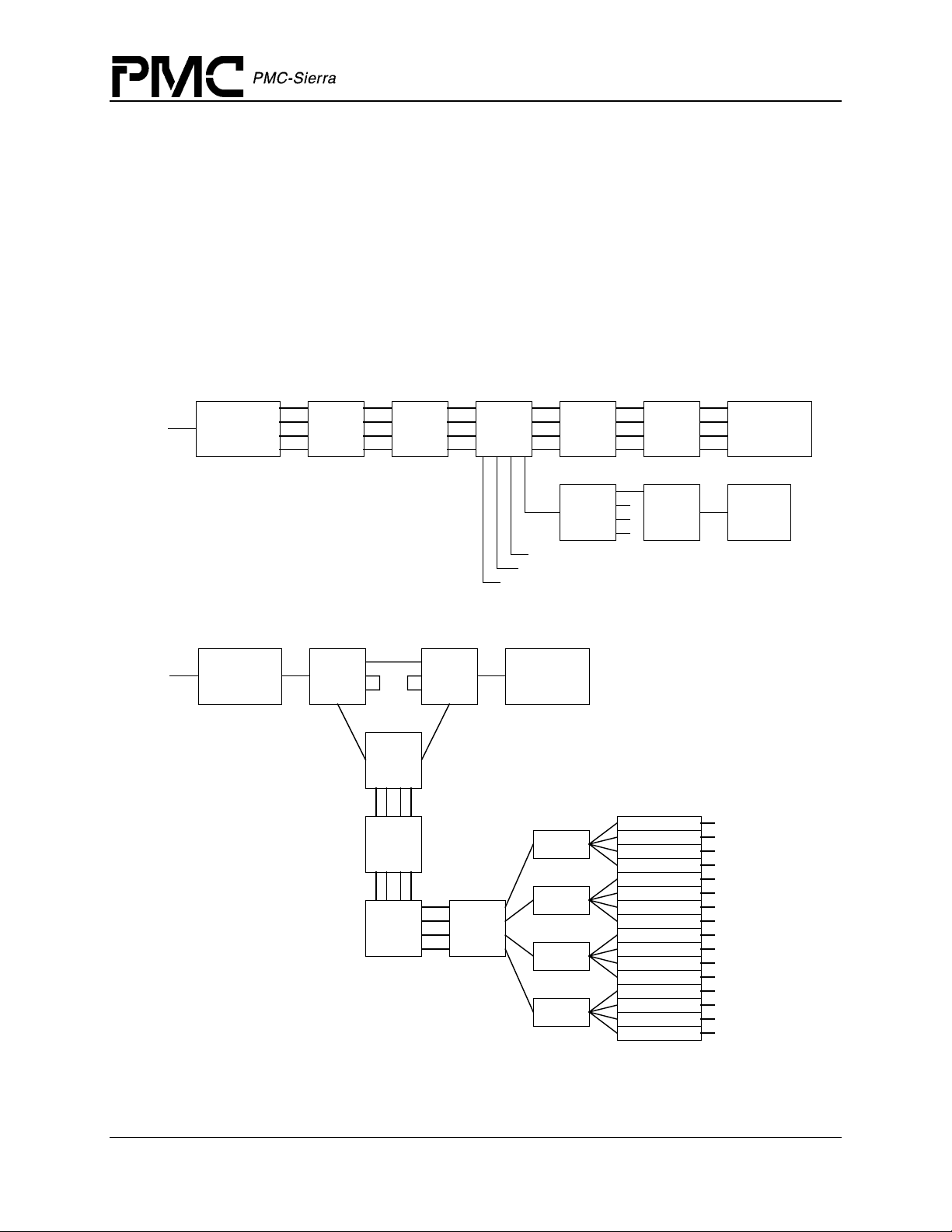
4 Application Examples
Figure 1 and Figure 2 show a PM8610 SBI336 Bus Serializer (SBS) connected to a TelecomBus
to implement a T1 or E1 Add/Drop function. When connected to a TelecomBus, the SBS and the
PM8620 or PM8621 Narrowband Switching Element (NSE) implements a T1/E1
Memory:Space:Memory switch. The SBS requires all path pointer justifications to be translated
into tributary pointer movements so that J1 is fixed to the location following C1 or H3. In both
examples, J1 alignment is performed with the TUPP-622. Switching within the SBS and NSE is
done using Transparent Virtual Tributary, TVT, mapping across the serial SBI336S LVDS links.
Figure 1 OC-48 T1/E1 ADM (Individually Drop/Add any T1/E1 in STS-48)
SBS Telecom Standard Product Data Sheet
Preliminary
SPECTRA-
2488
4 X
TUPP-
622
4 X
SBS
NSE
4 X
SBS
SBS
4 X
TUPP-
622
1 X
TEMAP
-84
Figure 2 OC-48 T1/E1 ADM (Drop/Add up to STS-48 at STS-1 Granularity)
SPECTRA-
2488
TBS TBS
TBS
4 X
TUPP-
622
4 X
SBS
NSE
SPECTRA-
2488
SBS
SBS
SBS
SBS
TEMUX84
TEMUX84
TEMUX84
TEMUX84
TEMUX84
TEMUX84
TEMUX84
TEMUX84
TEMUX84
TEMUX84
TEMUX84
TEMUX84
TEMUX84
TEMUX84
TEMUX84
TEMUX84
SPECTRA-
2488
11 X
OCTLIU
Proprietary and Confidential to PMC-Sierra, Inc., and for its Customers’ Internal Use 21
Document ID: PMC-2000168, Issue 3
SBS Telecom Standard Product Data Sheet
Preliminary
Figure 3 and Figure 4 show examples of the SBS used to implement high density T1/E1
Channelized Physical Interface cards and NxDS0 Multiservice access cards using SBS and NSE
devices. DS0, NxDS0, T1, E1, Transparent VTs, E3, DS3 and sub-rate links can be switched
between the Physical Layer and Layer 2 devices using SBS and NSE devices.
Figure 3 Any-Service-Any-Port NxDS0 TDM Access Solution
SBS
SBS
NSE
SBS
SBS
FREEDM-
336
4 X
IMA-84
12 X
AAL1gator-
32
11 X
OCTLIU
Serial
Clock and
Data
Figure 4 Any-Service-Any-Port T1/E1 Channelized PHY Card
TBS
4 X
TEMUX-84
SBS
Any-PHY
(Packet)
Any-PHY
(Cell)
Any-PHY
(Cell)
Processors
DSP
SPECTRA-
2488
TBS
TBS
TBS
TBS
4 X
TEMUX-84
4 X
TEMUX-84
4 X
TEMUX-84
SBS
NSE
SBS
SBS
Proprietary and Confidential to PMC-Sierra, Inc., and for its Customers’ Internal Use 22
Document ID: PMC-2000168, Issue 3
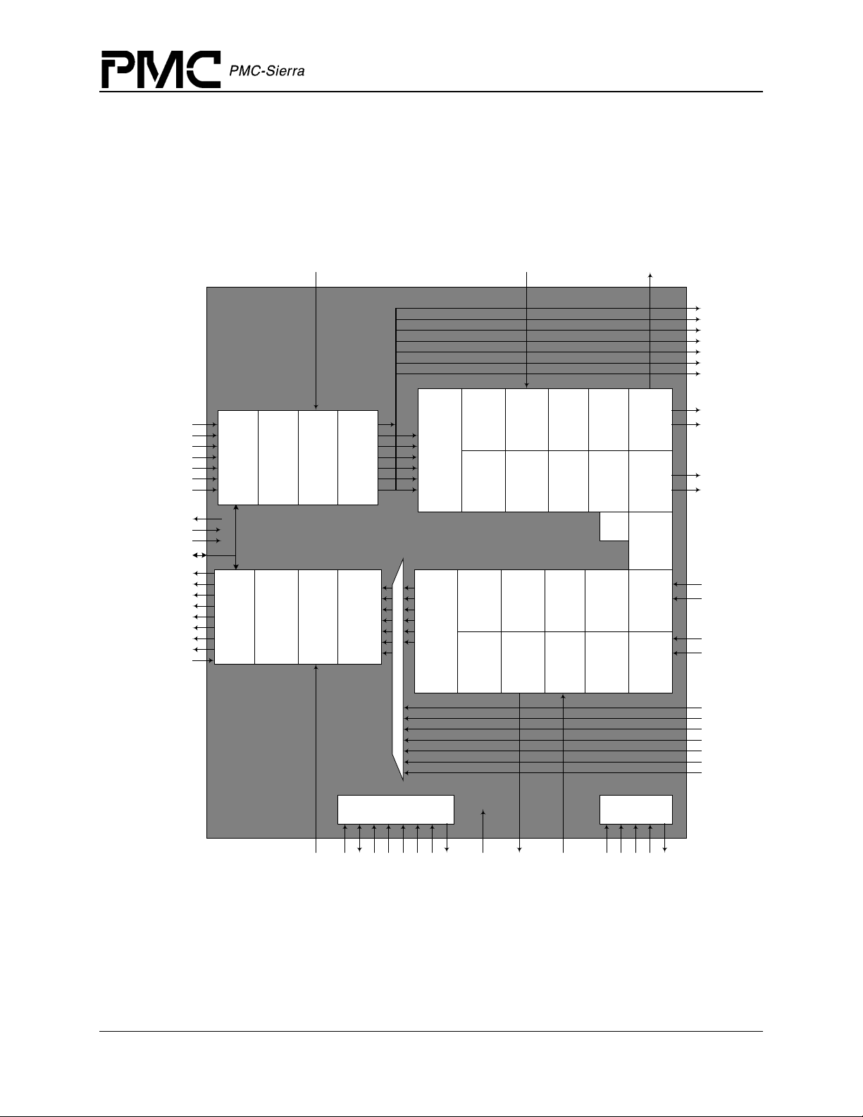
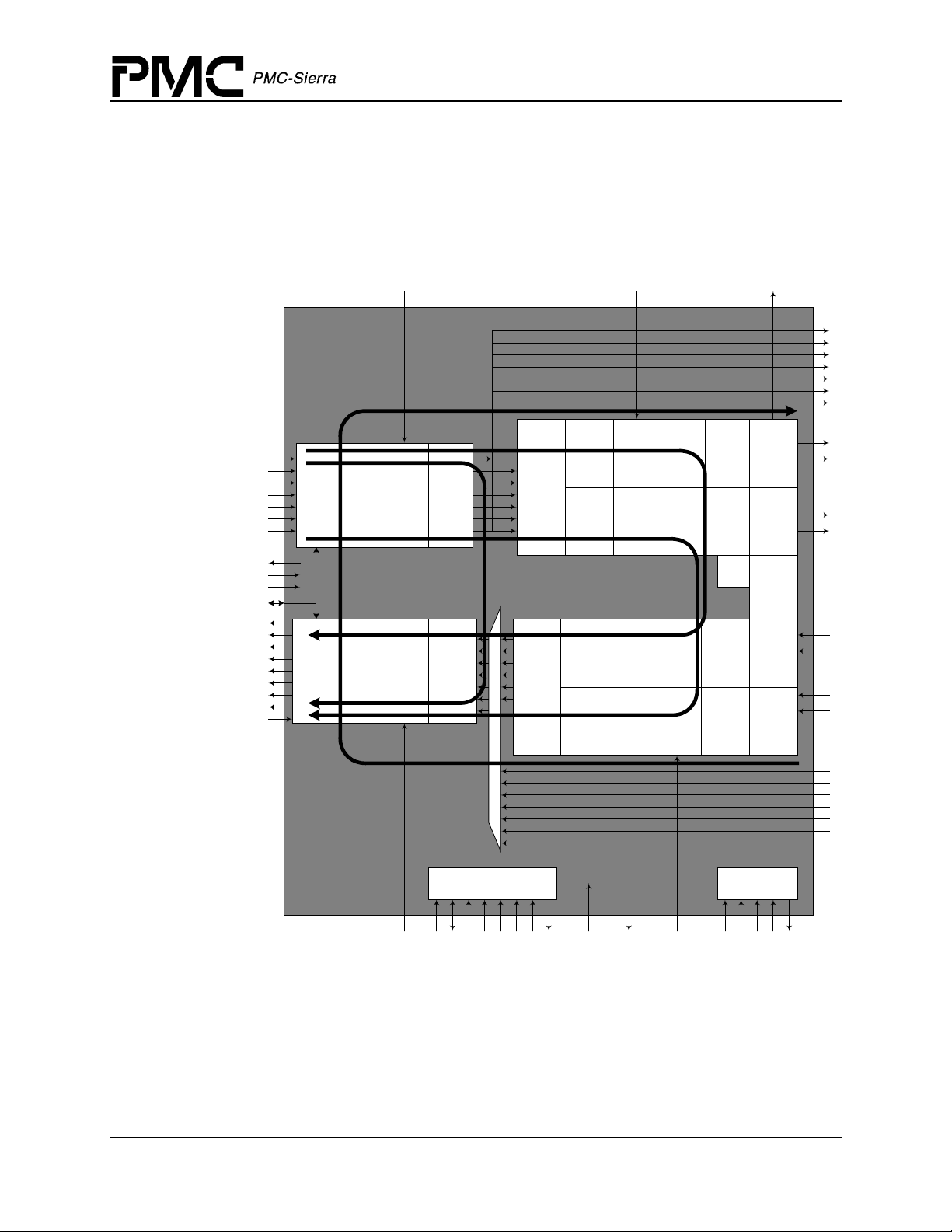
5 Block Diagram
Figure 5 Quad 19 MHz SBI Bus/TelecomBus SBS Block Diagram
SBS Telecom Standard Product Data Sheet
Preliminary
IDATA[4:1][7:0]
IDP[4:1]
IPL[4:1]
IV5[4:1]
IC1FP[4:1]
ITPL[4:1]
ITAIS[4:1]
SREFCLK19
SREFCLK
SYSCLK
JUST_REQ[4:1]
ODATA[4:1][7:0]
ODP[4:1]
OPL[4:1]
OV5[4:1]
OC1FP[4:1]
OTPL[4:1]
OTAIS[4:1]
OACTIVE[4:1]
ODETECT[4:1]
Incoming
SBI336
Timing
Adaptor
(ISTA)
Outgoing
SBI336
Timing
Adaptor
(OSTA)
Incoming
CAS
Expand
(ICASE)
Outgoing
CAS
Merge
(OCASM)
ICMP
Incoming
Memory
Switch
Unit
(IMSU)
Outgoing
Memory
Switch
Unit
(OMSU)
Incoming
CAS
Merge
(ICASM)
Outgoing
CAS
Expand
(OCASE)
Incoming
SBI
Tributary
Translator
(ISTT)
Outgoing
SBI
Tributary
Translator
(OSTT)
1/2
Working
PRBS
Processor
(WPP)
1/2
Protect
PRBS
Processor
(PPP)
1/2
Working
PRBS
Processor
(WPP)
1/2
Protect
PRBS
Processor
(PPP)
1/2
Working
In-Band
Link
Controller
(WILC)
1/2
Protect
In-Band
Link
Controller
(PILC)
1/2
Working
In-Band
Link
Controller
(WILC)
1/2
Protect
In-Band
Link
Controller
(PILC)
IUSER
Transmit
Transmit
Working
Working
8B/10B
Serializer
Encoder
(TWPS)
(TW8E)
Transmit
Transmit
Protect
Protect
8B/10B
Serializer
Encoder
Receive
Working
8B/10B
Decoder
(RW8D)
Receive
Protect
8B/10B
Decoder
(RP8D)
(TP8E)
(TPPS)
Tx
Ref
Working
Data
Recovery
Unit
(WDRU)
Protect
Data
Recovery
Unit
(PDRU)
TC1FP
Transmit
Working
LVDS
Interface
(TWLV)
Transmit
Protect
LVDS
Interface
(TPLV)
Clock
Synthesis
Unit
Receive
Working
LVDS
Interface
(RWLV)
Receive
Protect
LVDS
Interface
(RPLV)
TDATA[7:0]
TDP
TPL
TV5
TJUST_REQ
TTPL
TTAIS
TPWRK
TNWRK
TPPROT
TNPROT
RPWRK
RNWRK
RPPROT
RNPROT
RDATA[7: 0]
RDP
RPL
RV5
RJUST_REQ
RTPL
RTAIS
Microprocessor Interface
A[8:0]
OCMP
D[15:0]
CSB
RSTB
ALE
RDB
WRB
INTB
RWSEL
OUSER
RC1FP
JTAG
TDI
TCK
TMS
TRSTB
TDO
Proprietary and Confidential to PMC-Sierra, Inc., and for its Customers’ Internal Use 23
Document ID: PMC-2000168, Issue 3
SBS Telecom Standard Product Data Sheet
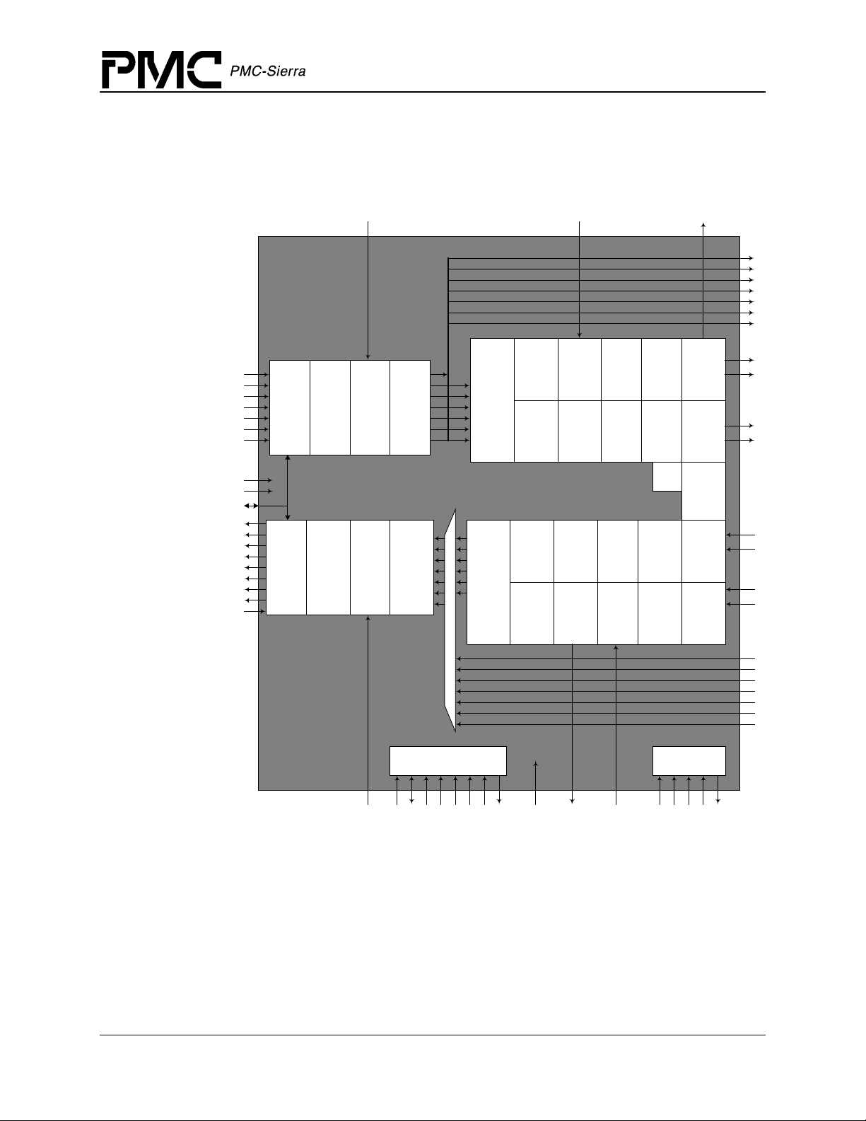
Figure 6 77 MHz SBI Bus/TelecomBus SBS Block Diagram
Preliminary
IDATA[1][7:0]
IDP[1]
IPL[1]
IV5[1]
IC1FP[1]
ITPL[1]
ITAIS[1]
SREFCLK
SYSCLK
JUST_REQ[1]
ODATA[1][7:0]
ODP[1]
OPL[1]
OV5[1]
OC1FP[1]
OTPL[1]
OTAIS[1]
OACTIVE[1]
ODETECT[1]
Incoming
SBI336
Timing
Adaptor
(ISTA)
Outgoing
SBI336
Timing
Adaptor
(OSTA)
Incoming
CAS
Expand
(ICASE)
Outgoing
CAS
Merge
(OCASM)
ICMP
Incoming
Memory
Switch
Unit
(IMSU)
Outgoing
Memory
Switch
Unit
(OMSU)
Incoming
CAS
Merge
(ICASM)
Outgoing
CAS
Expand
(OCASE)
Incoming
SBI
Tributary
Translator
(ISTT)
Outgoing
SBI
Tributary
Translator
(OSTT)
1/2
Working
PRBS
Processor
(WPP)
1/2
Protect
PRBS
Processor
(PPP)
1/2
Working
PRBS
Processor
(WPP)
1/2
Protect
PRBS
Processor
(PPP)
1/2
Working
In-Band
Link
Controller
(WILC)
1/2
Protect
In-Band
Link
Controller
(PILC)
1/2
Working
In-Band
Link
Controller
(WILC)
1/2
Protect
In-Band
Link
Controller
(PILC)
IUSER
Transmit
Transmit
Working
Working
8B/10B
Serializer
Encoder
(TWPS)
(TW8E)
Transmit
Transmit
Protect
Protect
8B/10B
Serializer
Encoder
Receive
Working
8B/10B
Decoder
(RW8D)
Receive
Protect
8B/10B
Decoder
(RP8D)
(TP8E)
(TPPS)
Tx
Ref
Working
Data
Recovery
Unit
(WDRU)
Protect
Data
Recovery
Unit
(PDRU)
TC1FP
Transmit
Working
LVDS
Interface
(TWLV)
Transmit
Protect
LVDS
Interface
(TPLV)
Clock
Synthesis
Unit
Receive
Working
LVDS
Interface
(RWLV)
Receive
Protect
LVDS
Interface
(RPLV)
TDATA[7:0]
TDP
TPL
TV5
TJUST_REQ
TTPL
TTAIS
TPWRK
TNWRK
TPPROT
TNPROT
RPWRK
RNWRK
RPPROT
RNPROT
RDATA[7: 0]
RDP
RPL
RV5
RJUST_REQ
RTPL
RTAIS
Microprocessor Interface
A[8:0]
OCMP
CSB
RSTB
D[15:0]
ALE
RDB
WRB
INTB
RWSEL
OUSER
RC1FP
JTAG
TDI
TCK
TMS
TRSTB
TDO
Proprietary and Confidential to PMC-Sierra, Inc., and for its Customers’ Internal Use 24
Document ID: PMC-2000168, Issue 3
6 Loopback Configurations
Figure 7 Loopback Block Diagram
SBS Telecom Standard Product Data Sheet
Preliminary
IDATA[4:1][7:0]
IDP[4:1]
IPL[4:1]
IV5[4:1]
IC1FP[4:1]
ITPL[4:1]
ITAIS[4:1]
SREFCLK19
SREFCLK
SYSCLK
JUST_REQ[4:1]
ODATA[4:1][7:0]
ODP[4:1]
OPL[4:1]
OV5[4:1]
OC1FP[4:1]
OTPL[4:1]
OTAIS[4:1]
OACTIVE[4:1]
ODETECT[4:1]
Incoming
SBI336
Timing
Adaptor
(ISTA)
Outgoing
SBI336
Timing
Adaptor
(OSTA)
Incoming
CAS
Expand
(ICASE)
Outgoing
CAS
Merge
(OCASM)
ICMP
Incoming
Memory
Switch
Unit
(IMSU)
Outgoing
Memory
Switch
Unit
(OMSU)
Incoming
CAS
Merge
(ICASM)
Outgoing
CAS
Expand
(OCASE)
Incoming
SBI
Tributary
Translator
(ISTT)
Outgoing
SBI
Tributary
Translator
(OSTT)
1/2
Working
PRBS
Processor
(WPP)
1/2
Protect
PRBS
Processor
(PPP)
1/2
Working
PRBS
Processor
(WPP)
1/2
Protect
PRBS
Processor
(PPP)
1/2
Working
In-Band
Link
Controller
(WILC)
1/2
Protect
In-Band
Link
Controller
(PILC)
1/2
Working
In-Band
Link
Controller
(WILC)
1/2
Protect
In-Band
Link
Controller
(PILC)
IUSER
Transmit
Transmit
Working
Working
8B/10B
Serializer
Encoder
(TWPS)
(TW8E)
Transmit
Transmit
Protect
Protect
8B/10B
Serializer
Encoder
Receive
Working
8B/10B
Decoder
(RW8D)
Receive
Protect
8B/10B
Decoder
(RP8D)
(TP8E)
(TPPS)
Tx
Ref
Working
Data
Recovery
Unit
(WDRU)
Protect
Data
Recovery
Unit
(PDRU)
TC1FP
Transmit
Working
LVDS
Interface
(TWLV)
Transmit
Protect
LVDS
Interface
(TPLV)
Clock
Synthesis
Unit
Receive
Working
LVDS
Interface
(RWLV)
Receive
Protect
LVDS
Interface
(RPLV)
TDATA[7:0]
TDP
TPL
TV5
TJUST_REQ
TTPL
TTAIS
TPWRK
TNWRK
TPPROT
TNPROT
RPWRK
RNWRK
RPPROT
RNPROT
RDATA[7: 0]
RDP
RPL
RV5
RJUST_REQ
RTPL
RTAIS
Microprocessor Interface
A[8:0]
OCMP
CSB
RSTB
D[15:0]
ALE
RDB
WRB
INTB
RWSEL
OUSER
RC1FP
JTAG
TDI
TCK
TMS
TRSTB
TDO
Proprietary and Confidential to PMC-Sierra, Inc., and for its Customers’ Internal Use 25
Document ID: PMC-2000168, Issue 3

7 Description
The PM8610 SBI336 Bus Serializer (SBS) is a monolithic integrated circuit that implements
conversion between a byte-serial 19.44 MHz SBI bus or 77.76 MHz SBI336 bus and a redundant
777.6 Mbit/s bit-serial 8B/10B-base SBI336S bus.
In TelecomBus mode, the SBS implements conversion between any 19.44 MHz TelecomBus or
77.76 MHz TelecomBus format and a redundant 777.6 Mbit/s bit-serial 8B/10B-base serial
TelecomBus format. In line with the bus conversion is a DS0 granular switch allowing any input
DS0 to be output on any output DS0. The redundant 777.6 Mbit/s serial interfaces can be disabled
and a byte-wide SBI336 bus can be enabled in its place with all the DS0 level switching
capabilities.
The SBS can be used to connect and switch high density T1/E1 framer devices supporting an SBI
bus with link layer devices supporting an SBI bus over a serial backplane. Placing a PM8620 or
PM8621 Narrowband Switch Element (NSE) between the framer and link layer devices allows up
to 20 Gbit/s NxDS0 switches to be constructed.
SBS Telecom Standard Product Data Sheet
Preliminary
In the ingress direction, the SBS connects an incoming SBI stream to a pair of redundant serial
SBI336S LVDS links through a DS0 memory switch. The incoming SBI bus can be either a
single 77.76 MHz SBI bus (SBI336) or four 19.44 MHz SBI buses (SBI). In TelecomBus mode
an incoming 77.76 MHz TelecomBus or four 19.44 MHz TelecomBuses that have the J1 path
fixed and all high order pointer justifications converted to tributary pointer justifications can be
switched through a VT granular switch to a pair of redundant serial LVDS TelecomBus format
links. The incoming data is encoded into an extended set of 8B/10B characters and transferred
onto two redundant 777.6 Mbit/s serial LVDS links. SBI or TelecomBus frame boundaries,
pointer justification events and master timing controls are marked by 8B/10B control characters.
Incoming SPEs may be optionally overwritten with the locally generated X
23
+ X18 + 1 pseudorandom bit sequence (PRBS) pattern for diagnosis of downstream equipment. The PRBS
processor is configurable to handle any combination of SPEs and can be inserted independently
into either of the redundant LVDS links. A DS0 memory switch provides arbitrary mapping of
streams on the incoming SBI bus stream(s) to the working and protect LVDS links. In
TelecomBus mode, a VT1.5/VT2 memory switch provides arbitrary mapping of tributaries on the
incoming TelecomBus stream(s) to the working and protect LVDS links. Multi-cast is supported.
In the egress direction, the SBS connects two independent 777.6 Mbit/s serial LVDS links to an
outgoing SBI Bus. Each link contains a constituent SBI336S stream. Bytes on the links are
carried as 8B/10B characters. The SBS decodes the characters into data and control signals for a
single 77.76 MHz SBI336 bus or four 19.44 MHz SBI buses. Alternatively the SBS decodes two
independent 777.6 Mbit/s TelecomBus formatted serial LVDS links characters into a single 77.76
MHz or quad 19.44 MHz TelecomBuses. A PRBS processor is provided to monitor the decoded
payload for the X
23
+ X18 + 1 pattern in each SPE. The PRBS processor is configurable to handle
any combination of SPEs in the serial LVDS link. Data on the outgoing SBI bus stream(s) may
be sourced from either of the LVDS links.
An In-band signaling link over the serial LVDS links allows this device to be controlled by a
companion switching device, a Narrowband Switching Element, PM8620 NSE-20G. This link can
be used as communication link between a central processor and the local microprocessor.
Proprietary and Confidential to PMC-Sierra, Inc., and for its Customers’ Internal Use 26
Document ID: PMC-2000168, Issue 3

SBS Telecom Standard Product Data Sheet
Preliminary
Three loopbacks are provided on the SBS. The outgoing-to-incoming loopback allows data
entering the SBS on the receive interface to be looped back from the output of the OCASM to the
input of the ICASE and then returned to the transmit interface. The transmit 8B/10B-to-receive
8B/10B loopback allows data entering on the incoming bus to be looped back from the output of
the TW8E and TP8E to the input of the RW8D and RP8D, respectively. Only the data looped
back on the active link (working or protect) will make it back to the outgoing bus. The transmit
to receive loopback allows data entering on the incoming bus to be looped back from the output
of the ICASM to the input of the OCASE and then returned to the outgoing bus.
Proprietary and Confidential to PMC-Sierra, Inc., and for its Customers’ Internal Use 27
Document ID: PMC-2000168, Issue 3

SBS Telecom Standard Product Data Sheet
Preliminary
8 Pin Diagram
The SBS is packaged in a 352-pin UBGA package having a body size of 27 mm by 27 mm and a
ball pitch of 1 mm.
Figure 8 Pin Diagram
2625242322212019181716151413121110987654321
VSS VSS TC1FP NC NC TDATA[7]ODATA[1
A
VSS DVDDO VSS
B
VSS VSS DVDDO NC NC NC TDATA[5]ODATA[1
C
VSS VSS AVDH DVDDO TJ UST_
D
VSS NC AVDH NC NC
E
RESK RES NC NC IDATA[1][3]IDATA[1][5]NC ITPL[1]
F
VSS NC NC NC IDATA[1][6]IDP[1] IV5[ 1] IPL[1]
G
TNPROT TPPROT NC NC DVDDO IC1FP[1] ITAIS[1]
H
VSS NC NC AVDH NC DVDDI ODATA[2
J
TPWRK TNWRK NC NC NC ODATA[2
K
VSS NC NC NC
L
RPWRK RNWRK ATB0 ATB1 OPL[2] OC1FP[ 2]TDO NC
M
RPPROT RNPROT NC AVDL DVDDO INTB NC VSS
N
AVDL AVDL NC
P
ITPL[4] ITAIS[4] AVDL IV5[4] ODATA[3
R
VSS IPL[4] IC1FP[4] AVDH
T
IDATA[4]
IDATA[4][
[6]
U
V
W
Y
AA
AB
AC
AD
AE
AF
7]
VSS IDATA[4][3]IDATA[4][4]IDATA[4][
ITAIS[2] IDATA[4][0]IDATA[4][2]IDATA[4][
VSS IC1FP[2] ITPL[2] AVDH
WRB RDB DVDDI ALE A[2] A[1] JUST_R
VSS CSB AVDH DVDDO NC A[3] NC IDATA[3][
VSS VSS AVDH DVDDO RSTB
VSS VSS DVDDO RWSEL ODET EC
VSS DVDDO VSS OACTIV
VSS VSS RC1FP
TDATA[0]TDATA[2]TDATA[4
CSU_AV
DH
DVDDI IDP[4] NC ODP[3]
5]
1]
E[4]
OC1FP[4
]
]
TDATA[1]TDATA[3]TDATA[6]DVDDO TPL OACTIV
REQ
JUST_R
EQ[4]
OV5[4] NC D[14 ] ODATA[4
T[4]
OTAIS[4] ODP[4] D[15] NC ODAT A[4
OPL[4] NC DVDDI
TTPL TTAIS ODATA[1
][1]
ODP[1]
ODATA[1
][2]
][0]
OTPL[4] DVDDO NC
ODATA[4
][5]
ODATA[
ODATA[1
][3]
1][5]
NC
TDP TV5 DVDDI ODATA[1
NC NC OT AIS[1] OTPL[1] NC
ODETEC
T[1]
E[1]
VSS VSS OPL[1] R JUST_
][7]
NC OV5[1] OC 1FP[1]RDATA[3]RDATA[6]RV5 O TPL[2] ICMP OD ETEC
][6]
ODATA[1
NC DVDDO RDATA[0]RDATA[5]RPL NC DVDDO N C SYSCL K NC DVDDO NC IDAT A[1][1]NC
][4]
352 UBGA
BOTTOM VIEW
ODATA[4
][6]
NC ODATA[
][7]
ODATA[4
][4]
][1]
NC D[13] D[10] VSS VSS IDP[2]
ODATA[4
][3]
IUSER2 DVDDO NC
ODATA[
4][2]
D[12] D[9] IPL[2] IDATA[2][6]IDATA[2][1]D[7] ITPL[3] IDP[3] D[4] IDATA[3][3]D[1] A[6] DVDDO VSS A[5]
4][0]
NC D[11] NC IV5[2] IDATA[2][7]IDATA[2][3]IDATA[2][0]DVDDI IC1FP[3] IDATA[3][7]IDATA[3][6]IDATA[3][2]D[0] VSS DVDDO VSS
REQ
RDATA[1]RDATA[4]RDATA[7
D[8] ITAIS[3] DVDDO D[5]
IDATA[2][
4]
IDATA[2][5]IDATA[2][
RDATA[2]NC RDP RTAIS NC DVDDI JUST_R
RTPL OTAIS[2] OCMP
]
T[2]
D[2] A[7] DVDDO NC A[4] DVDDI
IDATA[3][
4]
NC IV5[3] IPL[3] D[6]
2]
EQ[2]
OACTIV
SREFCL
E[2]
K19
SREFCLKNC DVDDO VSS IDATA[1][
ODATA[2
][4]
TRSTB TMS TCK VSS
][2]
ODATA[3
][7]
DVDDO OTPL[3] O PL[3] OACTIV
NC OC1FP[3]OV5[3] NC
IDATA[3][
1]
D[3] A[8] VSS VSS
IDATA[3][
5]
NC VSS VSS
VSS DVDDO VSS
0]
IDATA[1][2]IDATA[1][4]IDATA[1][
][2]
ODATA[2
][6]
ODATA[3
][0]
ODATA[3
][5]
A[0]
7]
ODATA[2
][0]
ODATA[2
][1]
][3]
ODATA[2
ODATA[2
][5]
][7]
ODP[2] OV5[2]
ODETEC
TDI
T[3]
ODATA[3
ODATA[3
][3]
][1]
ODATA[3
ODATA[3
][6]
][4]
E[3]
OTAIS[3]
JUST_R
EQ[1]
OUSER2
EQ[3]
0]
A
B
C
D
E
F
G
H
J
K
L
M
N
P
R
T
U
V
W
Y
AA
AB
AC
AD
AE
AF
2625242322212019181716151413121110987654321
Proprietary and Confidential to PMC-Sierra, Inc., and for its Customers’ Internal Use 28
Document ID: PMC-2000168, Issue 3

9 Pin Description
Pin Name Type Pin No. Function
Receive Serial Data Interface (5 Signals)
RPWRK
RNWRK
RPPROT
RNPROT
Analog
LVDS
Input
Analog
LVDS
Input
M26
M25
N26
N25
SBS Telecom Standard Product Data Sheet
Preliminary
Receive Working Serial Data. In SBI336 mode, the differential
receive working serial data link (RPWRK/RNWRK) carries the
receive 77.76 MHz SBI336 data from an upstream working source,
in bit serial format, SBI336S.
In TelecomBus mode, RPWRK/RNWRK carries the receive 77.76
MHz TelecomBus from an upstream working source, in bit serial
format.
Data on RPWRK/RNWRK is encoded in an 8B/10B format
extended from IEEE Std. 802.3. The 8B/10B character bit ‘a’ is
expected first and the bit ‘j’ is expected last.
RPWRK/RNWRK are nominally 777.6 Mbit/s data streams.
Receive Protect Serial Data. In SBI336 mode, the differential
receive protect serial data link (RPPROT/RNPROT) carries the
receive 77.76 MHz SBI336 data from an upstream protect source,
in bit serial format, SBI336S.
In TelecomBus mode, RPPROT/RNPROT carries the receive
77.76 MHz TelecomBus from an upstream protection source, in bit
serial format.
Data on RPPROT/RNPROT is encoded in an 8B/10B format
extended from IEEE Std. 802.3. The 8B/10B character bit ‘a’ is
expected first and the bit ‘j’ is expected last.
RPPROT/RNPROT are nominally 777.6 Mbit/s data streams.
Proprietary and Confidential to PMC-Sierra, Inc., and for its Customers’ Internal Use 29
Document ID: PMC-2000168, Issue 3

Pin Name Type Pin No. Function
RC1FP Input AF24
Receive SBI336 Interface (14 Signals)
RDATA[7]
RDATA[6]
RDATA[5]
RDATA[4]
RDATA[3]
RDATA[2]
RDATA[1]
RDATA[0]
RDP Input A8
Input B9
C10
D11
B10
C11
A10
B11
D12
Receive Serial Frame Pulse. The receive serial SBI336S frame
pulse signal (RC1FP) provides system timing of the receive serial
interface. When using the receive parallel interface, this signal
indicates the first C1 byte on the bus.
Using the Receive Serial Interface:
When using the receive serial interface, RC1FP is set high once
every multiframe (4 frames for SBI without CAS, 48 frames for SBI
with CAS, and 4 frames for TelecomBus), or multiple thereof. The
RC1FP_DLY[13:0] bits (register 007H) are used to align the C1
frame boundary 8B/10B character on the receive serial interface
(RPWRK/RNWRK and RPPROT/RNPROT) with RC1FP.
Using the Receive Parallel Interface:
In SBI mode, this signal also indicates multiframe alignment which
occurs every 4 frames, therefore this signal is pulsed every fourth
C1 octet to produce a 2KHz multiframe signal. The frame pulse
does not need to be repeated every 2KHz as the SBS will flywheel
in its absence.
When using the SBI bus in synchronous mode the RC1FP signal
can be used to indicate T1 and E1 multiframe alignment by pulsing
on 48 SBI frame boundaries. This must be done if CAS is to be
switched along with the data.
In TelecomBus mode, this signal may also be pulsed to indicate
the J1 byte position and the byte following J1. The J1 byte position
must be locked to an offset of either 0 or 522. The byte following
J1 is used to indicate multiframe alignment and should only pulse
once every 4 frames marking the frame with the V1s.
RC1FP is sampled on the rising edge of SYSCLK.
Receive Data (RDATA[7:0]). This is the receive SBI336 data bus
when configured for SBI336 byte-wide interface instead of the
Serial SBI336S interface. When in TelecomBus mode this is the
data bus for 77.76 MHz TelecomBus. The receive data bus is a
time division multiplexed bus which transports tributaries by
assigning them to fixed octets within the SBI or TelecomBus
structure.
In SBI336 mode, multiple devices can drive this bus at uniquely
assigned tributary columns within the SBI336 bus structure.
RDATA[7:0] is sampled on the rising edge of SYSCLK.
RDATA[7:0] have integral pull-up resistors.
Receive Data Parity (RDP). This is the receive data bus parity
when configured for the Receive byte-wide interface. This signal
carries the even or odd parity for the receive bus signals. In SBI336
mode, the parity calculation encompasses the RDATA[7:0], RPL
and RV5 signals. In TelecomBus mode, the parity calculation
encompasses the RDATA[7:0] and optionally the RC1FP and RPL
signals.
Multiple devices can drive this signal at uniquely assigned tributary
columns within the fixed structure. This parity signal is intended to
detect multiple sources in the column assignment.
RDP is sampled on the rising edge of SYSCLK.
RDP has an integral pull-up resistor.
SBS Telecom Standard Product Data Sheet
Preliminary
Proprietary and Confidential to PMC-Sierra, Inc., and for its Customers’ Internal Use 30
Document ID: PMC-2000168, Issue 3
Pin Name Type Pin No. Function
RPL Input D10
RV5 Input C9
Receive Payload (RPL). This receive SBI336 data bus payload
signal indicates valid tributary payload data when configured for the
receive SBI336 byte-wide interface. In TelecomBus mode this
signal indicates valid path payload.
In SBI336 mode:
This active high signal indicates valid data within the SBI336
structure. This signal is high during all octets making up a tributary
which includes all octets shaded grey in the framing format tables.
This signal goes high during the V3 or H3 octet within a tributary to
accommodate negative timing adjustments between the tributary
rate and the fixed SBI336 bus structure. This signal goes low
during the octet following the V3 or H3 octet within a tributary to
accommodate positive timing adjustments between the tributary
rate and the fixed SBI336 bus structure. For fractional rate links
this signal indicates that the current octet is carrying valid data
when high.
Multiple SBI336 devices can drive this signal at uniquely assigned
tributary columns within the SBI336 bus structure.
In TelecomBus mode:
This signal distinguishes between transport overhead bytes and
synchronous payload bytes. RPL is set high to mark each payload
byte on RDATA[7:0] and is set low to mark each transport
overhead byte on RDATA[7:0].
RPL is sampled on the rising edge of SYSCLK.
RPL has an integral pull-up resistor.
Receive Payload Indicator (RV5). This is the receive payload
indicator that locates the floating payload on the SBI336 or
TelecomBus when configured for the receive byte-wide interface.
In SBI336 mode:
This active high signal locates the position of the floating payloads
for each tributary within the SBI336 structure. Timing differences
between the port timing and the SBI336 bus timing are indicated by
adjustments of this payload indicator relative to the fixed SBI336
structure. All movements indicated by this signal must be
accompanied by appropriate adjustments in the RPL signal.
Multiple devices can drive this signal at uniquely assigned tributary
columns within the SBI336 structure.
In TelecomBus mode:
This signal identifies tributary payload frame boundaries on the
receive parallel data bus. RV5 is set high to mark the V5 bytes on
the bus.
RV5 is sampled on the rising edge of SYSCLK.
RV5 has an integral pull-up resistor.
SBS Telecom Standard Product Data Sheet
Preliminary
Proprietary and Confidential to PMC-Sierra, Inc., and for its Customers’ Internal Use 31
Document ID: PMC-2000168, Issue 3

Pin Name Type Pin No. Function
RTPL Input B8
RTAIS Input A7
RJUST_REQ Input A11
RJUST_REQ
(continued)
Receive Tributary Payload (RTPL). This signal indicates valid
tributary payload data when configured for the receive byte-wide
TelecomBus interface.
RTPL is set high during valid VC11 and VC12 bytes. RTPL is set
low for all transport overhead bytes, high order path overhead
bytes, fixed stuff column bytes and tributary transport overhead
bytes (V1,V2,V3,V4).
RTPL is ignored when configured for SBI336 mode.
RTPL is sampled on the rising edge of SYSCLK.
RTPL has an integral pull-up resistor.
Receive Tributary AIS Indicator (RTAIS). This signal indicates
tributaries in low order path AIS state when configured for the
receive byte-wide TelecomBus interface.
RTAIS is set high when the tributary on the receive bus is in AIS
state and is set low when the tributary is out of AIS state.
RTAIS is ignored when configured for SBI336 mode.
RTAIS is sampled on the rising edge of SYSCLK.
RTAIS has an integral pull-up resistor.
Receive Justification Request (RJUST_REQ). This is the receive
side justification request when configured for SBI336 byte-wide
interface instead of the Serial SBI336S interface and when
connecting to a PHY device. This signal is not used when
connecting to a SBI336 link layer device nor when in TelecomBus
mode.
The SBI336 Bus Justification Request signal, RJUST_REQ, is
used to speed up, slow down or maintain the minimal rate of a
slave timed SBI device.
This active high signal indicates negative timing adjustments on the
SBI336 bus when asserted high during the V3 or H3 octet,
depending on the tributary type. In response to this the slave timed
SBI336 device should send an extra byte in the V3 or H3 octet of
the next frame along with a valid payload signal indicating a
negative justification.
This signal indicates positive timing adjustments on the SBI336 bus
when asserted high during the octet following the V3 or H3 octet,
depending on the tributary type. The slave timed SBI336 device
should respond to this by not sending an octet during the V3 or H3
octet of the next frame along with a valid payload signal indicating
a positive justification.
For fractional rate links this signal is asserted high during any
available information byte to indicate to the slave timed SBI336
device that the timing master device is able to accept another byte
of data. For every byte that this signal is asserted high the slave
device is expected to send a valid byte of data.
All timing adjustments from the slave timed device in response to
the justification request must still set the payload and payload
indicators appropriately for timing adjustments.
RJUST_REQ is sampled on the rising edge of SYSCLK.
RJUST_REQ has an integral pull-up resistor.
SBS Telecom Standard Product Data Sheet
Preliminary
Proprietary and Confidential to PMC-Sierra, Inc., and for its Customers’ Internal Use 32
Document ID: PMC-2000168, Issue 3

Pin Name Type Pin No. Function
Outgoing SBI Bus (68 Signals)
OC1FP[4]
OC1FP[3]
OC1FP[2]
OC1FP[1]
Output
AF23
W3
M3
C12
Outgoing C1 Frame Pulse (OC1FP[4:1]). This signal indicates
the first C1 octet on the outgoing SBI or TelecomBus.
In SBI/SBI336 mode:
This signal also indicates multiframe alignment which occurs every
4 frames, therefore this signal is pulsed every fourth C1 octet to
produce a 2KHz multiframe signal.
When using the SBI bus in synchronous mode the OC1FP signal
indicates T1 and E1 signaling multiframe alignment by pulsing on
48 SBI frame boundaries. This must be done if CAS is to be
switched along with the data.
For both 19.44 MHz SBI and 77.76 MHz SBI336 buses, only
OC1FP[1] will indicate the C1 byte position and OC1FP[4:2] are
held low.
In TelecomBus mode:
This signal may also be pulsed to indicate the J1 byte position and
the byte following J1. The J1 byte position is locked to an offset of
either 0 or 522. The byte following J1 is used to indicate
multiframe alignment and is only pulsed once every 4 frames
marking the frame with the V1s.
For a 77.76 MHz TelecomBus, only OC1FP[1] is used and
OC1FP[4:2] are held low. For a 19.44 MHz TelecomBus,
OC1FP[4:1] are all generated with the same C1 frame alignment.
OC1FP[4:1] is updated on the rising edge of SREFCLK.
SBS Telecom Standard Product Data Sheet
Preliminary
Proprietary and Confidential to PMC-Sierra, Inc., and for its Customers’ Internal Use 33
Document ID: PMC-2000168, Issue 3

Pin Name Type Pin No. Function
ODATA[4][7]
ODATA[4][6]
ODATA[4][5]
ODATA[4][4]
ODATA[4][3]
ODATA[4][2]
ODATA[4][1]
ODATA[4][0]
ODATA[3][7]
ODATA[3][6]
ODATA[3][5]
ODATA[3][4]
ODATA[3][3]
ODATA[3][2]
ODATA[3][1]
ODATA[3][0]
Tristate
Output
AD18
AC17
AF19
AE18
AF18
AC16
AE17
AD16
T4
U2
T3
U1
T2
R4
T1
R3
Outgoing Data (ODATA[4:1][7:0]). The Outgoing Data buses,
ODATA[4:1][7:0], are separate time division multiplexed buses
which transport tributaries by assigning them to fixed octets within
the SBI or TelecomBus structure.
In 19.44 MHz SBI mode, The SBS can drive this bus at uniquely
assigned tributary columns within the SBI bus structure.
ODATA[1][7:0] can be either a 19.44 MHz SBI or TelecomBus
when combined with ODATA[4:2][7:0] or can be used as a
standalone 77.76 MHz SBI336 or TelecomBus.
ODATA[4:2][7:0] are held tri-state when configured for 77.76 MHz
operation.
ODATA[4:1][7:0] are updated on the rising edge of SREFCLK.
SBS Telecom Standard Product Data Sheet
Preliminary
ODATA[2][7]
ODATA[2][6]
ODATA[2][5]
ODATA[2][4]
ODATA[2][3]
ODATA[2][2]
ODATA[2][1]
ODATA[2][0]
ODATA[1][7]
ODATA[1][6]
ODATA[1][5]
ODATA[1][4]
ODATA[1][3]
ODATA[1][2]
ODATA[1][1]
ODATA[1][0]
ODP[4]
ODP[3]
ODP[2]
ODP[1]
Tristate
Output
K1
L3
K2
L4
J1
K3
J2
H1
A15
C15
A16
D15
A17
B19
A20
C19
AE21
U3
L2
B20
Outgoing Bus Data Parity (ODP[4:1]). The outgoing data parity
signals carry the even or odd parity for the corresponding outgoing
buses. In SBI/SBI336 modes, the parity calculation for ODP[x]
encompasses the ODATA[x][7:0], OPL[x] and OV5[x] signals. In
TelecomBus mode, the parity calculation encompasses the
ODATA[x][7:0] and optionally the OC1FP[x] and OPL[x] signals.
In 19.44 MHz SBI mode, The SBS can drive this bus at uniquely
assigned tributary columns within the SBI bus structure. This parity
signal is intended to detect conflicts in the tributary assignment.
ODP[1] can be part of either a 19.44 MHz SBI or TelecomBus
when combined with ODP[4:2] or can be used as part of a
standalone 77.76 MHz SBI336 or TelecomBus.
ODP[4:2] are held tri-state when configured for 77.76 MHz
operation.
ODP is updated on the rising edge of SREFCLK.
Proprietary and Confidential to PMC-Sierra, Inc., and for its Customers’ Internal Use 34
Document ID: PMC-2000168, Issue 3

Pin Name Type Pin No. Function
OPL[4]
OPL[3]
OPL[2]
OPL[1]
OPL[4]
OPL[3]
OPL[2]
OPL[1]
(continued)
Tristate
Output
AF22
V2
M4
A12
Outgoing Bus Payload (OPL[4:1]). The outgoing payload signal,
OPL[x], indicates valid tributary data within each of the
corresponding SBI buses. In TelecomBus mode, this signal
indicates valid path payload.
In SBI/SBI336 mode:
This active high signal is asserted during all octets making up a
tributary which includes all octets shaded grey in the framing
format tables. This signal goes high during the V3 or H3 octet
within a tributary to accommodate negative timing adjustments
between the tributary rate and the fixed SBI bus structure. This
signal goes low during the octet after the V3 or H3 octet within a
tributary to accommodate positive timing adjustments between the
tributary rate and the fixed SBI bus structure. For fractional rate
links this signal indicates that the current octet is carrying valid data
when high.
In 19.44 MHz SBI mode, the SBS can drive this signal at uniquely
assigned tributary columns within the SBI bus structure.
In locked TVT mode, this signal must be driven in the same
manner as for floating TVTs.
In TelecomBus mode:
This signal distinguishes between transport overhead bytes and
synchronous payload bytes. OPL[x] is set high to mark each
payload byte on ODATA[x][7:0] and is set low to mark each
transport overhead byte.
OPL[1] can be part of either a 19.44 MHz SBI or TelecomBus when
combined with OPL[4:2] or can be used as part of a standalone
77.76 MHz SBI336 or TelecomBus.
OPL[4:2] are held tri-state when configured for 77.76 MHz
operation.
OPL[x] is updated on the rising edge of SREFCLK.
SBS Telecom Standard Product Data Sheet
Preliminary
Proprietary and Confidential to PMC-Sierra, Inc., and for its Customers’ Internal Use 35
Document ID: PMC-2000168, Issue 3

Pin Name Type Pin No. Function
OV5[4]
OV5[3]
OV5[2]
OV5[1]
JUST_REQ[4]
JUST_REQ[3]
JUST_REQ[2]
JUST_REQ[1]
Tristate
Output
Bidir AC21
AD21
W2
L1
C13
AA2
A4
Y2
Outgoing Bus Payload Indicator (OV5[4:1]). The active high
signal, OV5[x], locates the position of the floating payload for each
tributary within each of the corresponding outgoing SBI/SBI336 or
TelecomBuses.
In SBI/SBI336 mode:
This active high signal locates the position of the floating payloads
for each tributary within the SBS/SBI336 structure. Timing
differences between the port timing and the bus timing are
indicated by adjustments of this payload indicator relative to the
fixed bus structure. All movements indicated by this signal must be
accompanied by appropriate adjustments in the OPL[x] signal.
In 19.44 MHz SBI mode, the SBS can drive this signal at uniquely
assigned tributary columns within the SBI bus structure.
In locked TVT mode or fractional rate link mode this signal may be
driven but must be ignored by the receiving device.
In TelecomBus mode:
This signal identifies tributary payload frame boundaries on the
corresponding outgoing data bus. OV5[x] is set high to mark the
V5 bytes on the bus.
OV5[1] can be part of either a 19.44 MHz SBI or TelecomBus when
combined with OV5[4:2] or can be used as part of a standalone
77.76 MHz SBI336 or TelecomBus.
OV5[4:2] are held tri-state when configured for 77.76 MHz
operation.
OV5[x] is updated on the rising edge of SREFCLK.
Shared Bus Justification Request (JUST_REQ[4:1]). The SBI
Bus Justification Request signal, JUST_REQ[x], is used to speed
up, slow down or maintain the minimal rate of a slave timed SBI
device.
When the SBS is configured to be connected to a physical layer
device, JUST_REQ[4:1] is an input. In SBI mode, JUST_REQ[4:1]
is aligned to OC1FP[1] and the Outgoing bus. In SBI336 mode,
JUST_REQ[1] is aligned to the IC1FP[1] and Incoming Bus.
When the SBS is configured to be connected to a link layer device,
JUST_REQ[4:1] is an output. In SBI mode, JUST_REQ[4:1] is
aligned to IC1FP[1] and the Incoming bus. In SBI336 mode,
JUST_REQ[1] is aligned to OC1FP[1] and the Outgoing bus.
This active high signal, JUST_REQ[x], indicates negative timing
adjustments on the corresponding SBI bus when asserted high
during the V3 or H3 octet, depending on the tributary type. In
response to this the slave timed SBI device should send an extra
byte in the V3 or H3 octet of the next frame along with a valid
payload signal indicating a negative justification.
This signal indicates positive timing adjustments on the
corresponding SBI bus when asserted high during the octet
following the V3 or H3 octet, depending on the tributary type. The
slave timed SBI device should respond to this by not sending an
octet during the V3 or H3 octet of the next frame along with a valid
payload signal indicating a positive justification.
SBS Telecom Standard Product Data Sheet
Preliminary
Proprietary and Confidential to PMC-Sierra, Inc., and for its Customers’ Internal Use 36
Document ID: PMC-2000168, Issue 3

Pin Name Type Pin No. Function
JUST_REQ[4]
JUST_REQ[3]
JUST_REQ[2]
JUST_REQ[1]
(continued)
OACTIVE[4]
OACTIVE[3]
OACTIVE[2]
OACTIVE[1]
ODETECT[4]
ODETECT[3]
ODETECT[2]
ODETECT[1]
OTPL[4]
OTPL[3]
OTPL[2]
OTPL[1]
Output AE23
V1
B5
D16
Input AD22
R2
C6
B17
Tristate
Output
AC20
V3
C8
B13
For fractional rate links this signal is asserted high during any
available information byte to indicate to the slave timed SBI device
that the timing master device is able to accept another byte of data.
For every byte that this signal is asserted high the slave device is
expected to send a valid byte of data.
All timing adjustments from the slave timed device in response to
the justification request must still set the payload and payload
indicators appropriately for timing adjustments.
JUST_REQ[1] can be part of either a 19.44 MHz SBI bus when
combined with JUST_REQ[4:2] or can be used as part of a
standalone 77.76 MHz SBI336 bus.
JUST_REQ[4:1] is configured as an input in TelecomBus mode
and is ignored.
JUST_REQ[4:1] is asserted and sampled on the rising edge of
SREFCLK.
Outgoing Bus Active Indicator (OACTIVE[4:1]). The active high
Outgoing SBI Bus Active Indicator signal, OACTIVE[x], is asserted
high during all octets when driving data and control signals,
ODATA[x][7:0], ODP[x], OPL[x] and OV5[x], onto the bus.
All other SBI devices driving the bus listen to this signal to detect
multiple sources driving the bus which can occur due to
configuration problems.
OACTIVE[4:1] is only valid when the SBS is configured for a 19.44
MHz SBI bus. In all other modes, OACTIVE[4:1] is held low.
OACTIVE[x] is updated on the rising edge of SREFCLK.
Outgoing Bus Active Detector (ODETECT[4:1]). This input
listens to the OR of all other SBI device ACTIVE signals.
When another device is driving OACTIVE[x] high and this device
detects ODETECT[x] is high from that other device it signals a
collision and tristates the bus to minimize or eliminate contention.
Tristating is only done with the 19.44 MHz SBI buses.
The AND of OACTIVE[x] and ODETECT[x] is sampled on the rising
edge of SREFCLK to indicate that a collision occurred and can be
used to indicate contention to management procedures.
ODETECT[4:1] is only valid when the SBS is configured for a 19.44
MHz SBI bus. In all other modes, ODETECT[4:1] is ignored.
ODETECT[4:1] have integral pull-up resistors.
Outgoing Tributary Payload (OTPL[4:1]). This signal is used to
indicate tributary payload when configured for TelecomBus and is
held low when configured for SBI or SBI336 buses.
OTPL[x] is set high during valid VC11 and VC12 bytes of the
corresponding Outgoing bus. OTPL[x] is set low for all transport
overhead bytes, high order path overhead bytes, fixed stuff column
bytes and tributary transport overhead bytes (V1,V2,V3,V4).
OTPL[1] can be part of either a 19.44 MHz TelecomBus when
combined with OTPL[4:2] or can be used as part of a standalone
77.76 MHz TelecomBus.
OTPL[4:2] are held tri-state when configured for 77.76 MHz
operation.
OTPL[x] is updated on the rising edge of SREFCLK.
SBS Telecom Standard Product Data Sheet
Preliminary
Proprietary and Confidential to PMC-Sierra, Inc., and for its Customers’ Internal Use 37
Document ID: PMC-2000168, Issue 3

Pin Name Type Pin No. Function
OTAIS[4]
OTAIS[3]
OTAIS[2]
OTAIS[1]
Incoming SBI Bus (56 Signals)
IC1FP[4]
IC1FP[3]
IC1FP[2]
IC1FP[1]
IC1FP[4]
IC1FP[3]
IC1FP[2]
IC1FP[1]
(continued)
Tristate
Output
Input
AE22
Y1
B7
B14
T24
AE8
Y25
H3
Outgoing Tributary Alarm Indication Signal (OTAIS[4:1]). This
signal indicates tributaries in low order path AIS state for the
corresponding Outgoing TelecomBus and is held low when
configured for SBI or SBI336 buses.
OTAIS[x] is set high when the tributary on the corresponding
Outgoing bus is in AIS state and is set low when the tributary is out
of AIS state.
OTAIS[1] can be part of either a 19.44 MHz TelecomBus when
combined with OTAIS[4:2] or can be used as part of a standalone
77.76 MHz TelecomBus.
OTAIS[4:2] are held tri-state when configured for 77.76 MHz
operation.
OTAIS[x] is updated on the rising edge of SREFCLK.
Incoming C1 Frame Pulse (IC1FP[4:1]). This signal indicates the
first C1 octet on the incoming SBI or TelecomBus.
In SBI/SBI336 mode:
This signal also indicates multiframe alignment which occurs every
4 frames, therefore this signal is pulsed every fourth C1 octet to
produce a 2KHz multiframe signal. The frame pulse does not need
to be repeated every 2KHz as the SBS will flywheel in its absence.
When using the SBI bus in synchronous mode the IC1FP signal
can be used to indicate T1 and E1 multiframe alignment by pulsing
on 48 SBI frame boundaries. This must be done if CAS is to be
switched along with the data.
For both 19.44 MHz SBI and 77.76 MHz SBI336 buses, only
IC1FP[1] is used and IC1FP[4:2] are ignored.
In TelecomBus mode:
This signal may also be pulsed to indicate the J1 byte position and
the byte following J1. The J1 byte position must be locked to an
offset of either 0 or 522. The byte following J1 is used to indicate
multiframe alignment and should only pulse once every 4 frames
marking the frame with the V1s.
IC1FP[1] can be part of either a 19.44 MHz TelecomBus when
combined with IC1FP[4:2] or can be used as part of a standalone
77.76 MHz TelecomBus. When using a 19.44 MHz TelecomBus,
all 4 C1 positions must be aligned and the four signals, IC1FP[4:1],
are logically OR’ed together internally.
IC1FP[4:1] is sampled on the rising edge of SREFCLK.
IC1FP[4:2] have integral pull-up resistors.
SBS Telecom Standard Product Data Sheet
Preliminary
Proprietary and Confidential to PMC-Sierra, Inc., and for its Customers’ Internal Use 38
Document ID: PMC-2000168, Issue 3

Pin Name Type Pin No. Function
IDATA[4][7]
IDATA[4][6]
IDATA[4][5]
IDATA[4][4]
IDATA[4][3]
IDATA[4][2]
IDATA[4][1]
IDATA[4][0]
IDATA[3][7]
IDATA[3][6]
IDATA[3][5]
IDATA[3][4]
IDATA[3][3]
IDATA[3][2]
IDATA[3][1]
IDATA[3][0]
Input
U25
U26
V23
V24
V25
W24
W23
W25
AE7
AE6
AF5
AC7
AD6
AE5
Y4
AB1
Incoming Bus Data (IDATA[4:1][7:0]). The Incoming data buses,
IDATA[4:1][7:0], are separate time division multiplexed buses
which transports tributaries by assigning them to fixed octets within
the SBI or TelecomBus structure.
Multiple SBI/SBI336 devices can drive this bus at uniquely
assigned tributary columns within the SBI/SBI336 bus structure.
IDATA[1][7:0] can be either a 19.44 MHz SBI or TelecomBus when
combined with IDATA[4:2][7:0] or can be used as a standalone
77.76 MHz SBI336 or TelecomBus.
IDATA[4:1][7:0] is sampled on the rising edge of SREFCLK.
IDATA[4:2][7:0] have integral pull-up resistors.
SBS Telecom Standard Product Data Sheet
Preliminary
IDATA[2][7]
IDATA[2][6]
IDATA[2][5]
IDATA[2][4]
IDATA[2][3]
IDATA[2][2]
IDATA[2][1]
IDATA[2][0]
IDATA[1][7]
IDATA[1][6]
IDATA[1][5]
IDATA[1][4]
IDATA[1][3]
IDATA[1][2]
IDATA[1][1]
IDATA[1][0]
IDP[4]
IDP[3]
IDP[2]
IDP[1]
AE12
AD12
AF11
AC12
AE11
AF10
AD11
AE10
E1
G4
F3
E2
F4
E3
D2
C1
Input U23
AD8
AF12
G3
Incoming Bus Data Parity (IDP[4:1]). The Incoming data parity
signals carry the even or odd parity for the corresponding Incoming
buses. In SBI/SBI336 modes, the parity calculation encompasses
the IDATA[x][7:0], IPL[x] and IV5[x] signals. In TelecomBus mode,
the parity calculation encompasses the IDATA[x][7:0] and
optionally the IC1FP[x] and IPL[x] signals.
Multiple SBI/SBI336 devices can drive this signal at uniquely
assigned tributary columns within the SBI/SBI336 bus structure.
This parity signal is intended to detect multiple sources in the
column assignment.
IDP[1] can be part of either a 19.44 MHz SBI or TelecomBus when
combined with IDP[4:2] or can be used as part of a standalone
77.76 MHz SBI336 or TelecomBus.
IDP[x] is sampled on the rising edge of SREFCLK.
IDP[4:2] have integral pull-up resistors.
Proprietary and Confidential to PMC-Sierra, Inc., and for its Customers’ Internal Use 39
Document ID: PMC-2000168, Issue 3

Pin Name Type Pin No. Function
IPL[4]
IPL[3]
IPL[2]
IPL[1]
Input
T25
AF7
AD13
G1
Incoming Bus Payload (IPL[4:1]). The Incoming Payload signal,
IPL[4:1], indicates valid tributary data within each of the
corresponding SBI buses. In TelecomBus mode, this signal
indicates valid path payload.
In SBI/SBI336 mode:
This active high signal is asserted during all octets making up a
tributary which includes all octets shaded grey in the framing
format tables. This signal goes high during the V3 or H3 octet
within a tributary to accommodate negative timing adjustments
between the tributary rate and the fixed SBI/SBI336 structure. This
signal goes low during the octet following the V3 or H3 octet within
a tributary to accommodate positive timing adjustments between
the tributary rate and the fixed SBI/SBI336 structure. For fractional
rate links this signal indicates that the current octet is carrying valid
data when high.
Multiple SBI/SBI336 devices can drive this signal at uniquely
assigned tributary columns within the SBI/SBI336 structure.
For locked TVTs, this signal must be driven in the same manner as
for floating TVTs.
In TelecomBus mode:
This signal distinguishes between transport overhead bytes and
the synchronous payload bytes. IPL[x] is set high to mark each
payload byte on IDATA[x][7:0] and is set low to mark each
transport overhead byte..
IPL[1] can be part of either a 19.44 MHz SBI or TelecomBus when
combined with IPL[4:2] or can be used as part of a standalone
77.76 MHz SBI336 or TelecomBus.
IPL[x] is sampled on the rising edge of SREFCLK.
IPL[4:2] have integral pull-up resistors.
SBS Telecom Standard Product Data Sheet
Preliminary
Proprietary and Confidential to PMC-Sierra, Inc., and for its Customers’ Internal Use 40
Document ID: PMC-2000168, Issue 3

Pin Name Type Pin No. Function
IV5[4]
IV5[3]
IV5[2]
IV5[1]
ITPL[4]
ITPL[3]
ITPL[2]
ITPL[1]
ITAIS[4]
ITAIS[3]
ITAIS[2]
ITAIS[1]
Input
Input R26
Input
R23
AF8
AE13
G2
AD9
Y24
F1
R25
AC10
W26
H2
Incoming Bus Payload Indicator (IV5[4:1]). This signal locates
the position of the floating payload for each tributary within each of
the incoming SBI/SBI336 or TelecomBuses.
In SBI/SBI336 mode:
This active high signal locates the position of the floating payloads
for each tributary within the SBI/SBI336 structure. Timing
differences between the port timing and the bus timing are
indicated by adjustments of this payload indicator relative to the
fixed bus structure. All movements indicated by this signal must be
accompanied by appropriate adjustments in the IPL[x] signal.
Multiple SBI/SBI336 devices can drive this signal at uniquely
assigned tributary columns within the SBI/SBI336 structure.
For locked TVTs, this signal must either be driven in the same
manner as for floating TVTs or held low.
In TelecomBus mode:
This signal identifies tributary payload frame boundaries on the
corresponding incoming data bus. IV5[x] is set high to mark the V5
bytes on the bus.
IV5[1] can be part of either a 19.44 MHz SBI or TelecomBus when
combined with IV5[4:2] or can be used as part of a standalone
77.76 MHz SBI336 or TelecomBus.
IV5[x] is sampled on the rising edge of SREFCLK.
IV5[4:2] have integral pull-up resistors.
Incoming Tributary Payload (ITPL[4:1]). This signal is used to
indicate tributary payload when configured for TelecomBus and is
unused when configured for SBI or SBI336 buses.
ITPL[x] is set high during valid VC11 and VC12 bytes of the
corresponding Incoming bus. ITPL[x] is set low for all transport
overhead bytes, high order path overhead bytes, fixed stuff column
bytes and tributary transport overhead bytes (V1,V2,V3,V4).
ITPL[1] can be part of either a 19.44 MHz TelecomBus when
combined with ITPL[4:2] or can be used as part of a standalone
77.76 MHz TelecomBus.
ITPL[x] is sampled on the rising edge of SREFCLK.
ITPL[4:2] have integral pull-up resistors.
Incoming Tributary Alarm Indication Signal (ITAIS[4:1]). This
signal indicates tributaries in low order path AIS state for the
corresponding Incoming TelecomBus and is unused when
configured for SBI or SBI336 buses.
ITAIS[x] is set high when the tributary on the corresponding
Incoming bus is in AIS state and is set low when the tributary is out
of AIS state.
ITAIS[1] can be part of either a 19.44 MHz TelecomBus when
combined with ITAIS[4:2] or can be used as part of a standalone
77.76 MHz TelecomBus.
ITAIS[x] is sampled on the rising edge of SREFCLK.
ITAIS[4:2] have integral pull-up resistors.
SBS Telecom Standard Product Data Sheet
Preliminary
Proprietary and Confidential to PMC-Sierra, Inc., and for its Customers’ Internal Use 41
Document ID: PMC-2000168, Issue 3

Pin Name Type Pin No. Function
Transmit Serial Data Interface (4 Signals)
TPWRK
TNWRK
TPPROT
TNPROT
Transmit SBI336 Interface (15 Signals)
TC1FP Output A24
Analog
LVDS
Output
Analog
LVDS
Output
K26
K25
H25
H26
Transmit Working Serial Data. In SBI336 mode, the differential
transmit working serial data link (TPWRK/TNWRK) carries a
transmit 77.76 MHz SBI336 data stream to a downstream working
sink, in bit serial format, SBI336S.
In TelecomBus mode, TPWRK/TNWRK carries the transmit 77.76
MHz TelecomBus data stream to a downstream working sink, in bit
serial format.
Data on TPWRK/TNWRK is encoded in an 8B/10B format
extended from IEEE Std. 802.3. The 8B/10B character bit ‘a’ is
transmitted first and the bit ‘j’ is transmitted last.
TPWRK/TNWRK are nominally 777.6 Mbit/s data streams.
Transmit Protect Serial Data. In SBI336 mode, the differential
transmit protect serial data link (TPPROT/TNPROT) carries a
transmit 77.76 MHz SBI336 data stream to a downstream protect
sink, in bit serial format, SBI336S.
In TelecomBus mode, TPPROT/TNPROT carries the transmit
77.76 MHz TelecomBus data stream to a downstream protection
sink, in bit serial format.
Data on TPPROT/TNPROT is encoded in an 8B/10B format
extended from IEEE Std. 802.3. The 8B/10B character bit ‘a’ is
transmitted first and the bit ‘j’ is transmitted last.
TPPROT/TNPROT are nominally 777.6 Mbit/s data streams.
Transmit Serial SBI Frame Pulse. The transmit serial SBI frame
pulse signal (TC1FP) provides system timing of the transmit serial
interface. When using the transmit parallel interface, this signal
indicated the first C1 octet on the transmit SBI336 or TelecomBus.
Using the Transmit Serial Interface:
TC1FP is set high to indicate that the C1 frame boundary 8B/10B
character has been serialized out on the transmit working serial
data link (TPWRK/TNWRK) and the transmit protection serial data
link (TPPROT/ TNPROT). TC1FP is output every 4 frame for SBI
mode without CAS and for TelecomBus mode. TC1FP is output
every 48 frames for SBI mode with CAS.
Using the Transmit Parallel Interface:
In SBI/SBI336 mode, this signal also indicates multiframe
alignment which occurs every 4 frames, therefore this signal is
pulsed every fourth C1 octet to produce a 2KHz multiframe signal.
When using the SBI bus in synchronous mode the TC1FP signal
indicates T1 and E1 signaling multiframe alignment by pulsing on
48 SBI frame boundaries. This must be done if CAS is to be
switched along with the data.
In TelecomBus mode, this signal may also be pulsed to indicate
the J1 byte position and the byte following J1. The J1 byte position
is locked to an offset of either 0 or 522. The byte following J1 is
used to indicate multiframe alignment and is only pulsed once
every 4 frames marking the frame with the V1s.
TC1FP is updated on the rising edge of SYSCLK.
SBS Telecom Standard Product Data Sheet
Preliminary
Proprietary and Confidential to PMC-Sierra, Inc., and for its Customers’ Internal Use 42
Document ID: PMC-2000168, Issue 3

Pin Name Type Pin No. Function
TDATA[7]
TDATA[6]
TDATA[5]
TDATA[4]
TDATA[3]
TDATA[2]
TDATA[1]
TDATA[0]
TDP Output C18
TPL Output D17
Output
A21
D19
C20
B21
D20
B22
D21
B23
Transmit Data (TDATA[7:0]). This is the transmit data bus when
configured for the Transmit byte-wide interface. The transmit data
bus is a time division multiplexed bus which transports tributaries
by assigning them to fixed octets within the 77.76 MHz SBI336 or
TelecomBus structure.
TDATA[7:0] is updated on the rising edge of SYSCLK.
Transmit Data Parity (TDP). This is the transmit data bus parity
when configured for the Transmit byte-wide interface. This signal
carries the even or odd parity for the transmit bus signals. In
SBI336 mode, the parity calculation encompasses the TDATA[7:0],
TPL and TV5 signals. In TelecomBus mode, the parity calculation
encompasses the TDATA[7:0] and optionally the TC1FP and TPL
signals.
TDP is updated on the rising edge of SYSCLK.
Transmit Payload (TPL). The transmit SBI336 data bus payload
signal indicates valid tributary payload data when configured for the
transmit SBI336 byte-wide interface. In TelecomBus mode this
signal indicates valid path payload.
In SBI336 mode:
This active high signal indicates valid data within the SBI336
structure. This signal is high during all octets making up a tributary
which includes all octets shaded grey in the framing format tables.
This signal goes high during the V3 or H3 octet within a tributary to
accommodate negative timing adjustments between the tributary
rate and the fixed SBI336 structure. This signal goes low during the
octet following the V3 or H3 octet within a tributary to
accommodate positive timing adjustments between the tributary
rate and the fixed SBI336 structure. For fractional rate links this
signal indicates that the current octet is carrying valid data when
high.
In TelecomBus mode:
This signal distinguishes between transport overhead bytes and
synchronous payload bytes. TPL is set high to mark each payload
byte on TDATA[7:0] and is set low to mark each transport
overhead byte on TDATA[7:0].
TPL is updated on the rising edge of SYSCLK.
SBS Telecom Standard Product Data Sheet
Preliminary
Proprietary and Confidential to PMC-Sierra, Inc., and for its Customers’ Internal Use 43
Document ID: PMC-2000168, Issue 3

Pin Name Type Pin No. Function
TV5 Output C17
TTPL Output A19
TTAIS Output A18
Transmit Payload Indicator (TV5). The transmit payload indicator
(TV5) locates the floating payload on the SBI336 or TelecomBus
when configured for the transmit byte-wide interface.
In SBI336 mode:
This active high signal locates the position of the floating payloads
for each tributary within the SBI336 structure. Timing differences
between the port timing and the SBI336 bus timing are indicated by
adjustments of this payload indicator relative to the fixed SBI336
structure. All movements indicated by this signal must be
accompanied by appropriate adjustments in the TPL signal.
In TelecomBus mode:
This signal identifies tributary payload frame boundaries on the
transmit parallel data bus. TV5 is set high to mark the V5 bytes on
the bus.
TV5 is updated on the rising edge of SYSCLK.
Transmit Tributary Payload (TTPL). This signal indicates valid
tributary payload data when configured for transmit byte-wide
TelecomBus interface.
TTPL is set high during valid VC11 and VC12 bytes. TTPL is set
low for all transport overhead bytes, high order path overhead
bytes, fixes stuff column bytes and tributary transport overhead
bytes (V1,V2,V3,V4).
TTPL is held low in SBI336 mode.
TTPL is updated on the rising edge of SYSCLK.
Transmit Tributary AIS Indicator (TAIS). This signal indicates
tributaries in low order path AIS state when configured for the
transmit byte-wide TelecomBus interface.
TTAIS is set high when the tributary on the transmit bus is in AIS
state and is set low when the tributary is out of AIS state.
TTAIS is held low in SBI336 mode
TTAIS is updated on the rising edge of SYSCLK.
SBS Telecom Standard Product Data Sheet
Preliminary
Proprietary and Confidential to PMC-Sierra, Inc., and for its Customers’ Internal Use 44
Document ID: PMC-2000168, Issue 3

Pin Name Type Pin No. Function
TJUST_REQ Output D22
TJUST_REQ
(continued)
Microprocessor Interface (30 Signals)
CSB Input AB25
RDB Input AA25
WRB Input AA26
Transmit Justification Request (TJUST_REQ). This is the
transmit side justification request when configured for SBI336 bytewide interface instead of the Serial SBI336S interface and when
connecting to a link layer device. This signal is held low when
connecting to a SBI336 physical layer device or when in
TelecomBus mode.
The SBI336 Bus Justification Request signal, TJUST_REQ, is used
to speed up, slow down or maintain the minimal rate of a slave
timed SBI336 device.
This active high signal indicates negative timing adjustments on the
SBI336 bus when asserted high during the V3 or H3 octet,
depending on the tributary type. In response to this the slave timed
SBI336 device should send an extra byte in the V3 or H3 octet of
the next receive frame along with a valid payload signal indicating
a negative justification.
This signal indicates positive timing adjustments on the SBI336 bus
when asserted high during the octet following the V3 or H3 octet,
depending on the tributary type. The slave timed SBI336 device
should respond to this by not sending an octet during the V3 or H3
octet of the next receive frame along with a valid payload signal
indicating a positive justification.
For fractional rate links this signal is asserted high during any
available information byte to indicate to the slave timed SBI336
device that the timing master device is able to accept another byte
of data. For every byte that this signal is asserted high the slave
device is expected to send a valid byte of data.
All timing adjustments from the slave timed device in response to
the justification request must still set the payload and payload
indicators appropriately for timing adjustments.
TJUST_REQ is updated on the rising edge of SYSCLK.
Chip Select Bar. The active low chip select signal (CSB) controls
microprocessor access to registers in the SBS device. CSB is set
low during SBS Microprocessor Interface Port register accesses.
CSB is set high to disable microprocessor accesses.
If CSB is not required (i.e. register accesses controlled using RDB
and WRB signals only), CSB should be connected to an inverted
version of the RSTB input.
Read Enable Bar. The active low read enable bar signal (RDB)
controls microprocessor read accesses to registers in the SBS
device. RDB is set low and CSB is also set low during SBS
Microprocessor Interface Port register read accesses. The SBS
drives the D[15:0] bus with the contents of the addressed register
while RDB and CSB are low.
Write Enable Bar. The active low write enable bar signal (WRB)
controls microprocessor write accesses to registers in the SBS
device. WRB is set low and CSB is also set low during SBS
Microprocessor Interface Port register write accesses. The
contents of D[15:0] are clocked into the addressed register on the
rising edge of WRB while CSB is low.
SBS Telecom Standard Product Data Sheet
Preliminary
Proprietary and Confidential to PMC-Sierra, Inc., and for its Customers’ Internal Use 45
Document ID: PMC-2000168, Issue 3

Pin Name Type Pin No. Function
D[15]
D[14]
D[13]
D[12]
D[11]
D[10]
D[9]
D[8]
D[7]
D[6]
D[5]
D[4]
D[3]
D[2]
D[1]
D[0]
A[8]/TRS
A[7]
A[6]
A[5]
A[4]
A[3]
A[2]
A[1]
A[0]
ALE Input AA23
INTB
General Function (9 Signals)
SYSCLK Input D6
SREFCLK19 Output B4
I/O
Input AF3
Open
Drain
Output
AE20
AD19
AF16
AD15
AE15
AF15
AD14
AC11
AD10
AF6
AC8
AD7
AF4
AC6
AD5
AE4
AC5
AD4
AD1
AC2
AB3
AA4
AA3
Y3
N3
Microprocessor Data Bus. The bi-directional data bus, D[15:0] is
used during SBS Microprocessor Interface Port register reads and
write accesses. D[15] is the most significant bit of the data words
and D[0] is the least significant bit.
Microprocessor Address Bus. The microprocessor address bus
(A[8:0]) selects specific Microprocessor Interface Port registers
during SBS register accesses.
A[8] is also the Test Register Select (TRS) address pin and selects
between normal and test mode register accesses. TRS is set high
during test mode register accesses, and is set low during normal
mode register accesses.
Address Latch Enable. The address latch enable signal (ALE) is
active high and latches the address bus (A[11:0]) when it is set low.
The internal address latches are transparent when ALE is set high.
ALE allows the SBS to interface to a multiplexed address/data bus.
ALE has an integral pull up resistor.
Interrupt Request Bar. The active low interrupt enable signal
(INTB) output goes low when an SBS interrupt source is active and
that source is unmasked. INTB returns high when the interrupt is
acknowledged via an appropriate register access. INTB is an open
drain output.
SBI System Clock. The 77 MHz SBI reference clock signal,
SYSCLK, is the master clock for the SBS device. SYSCLK is a
77.76 MHz clock, with a nominal 50% duty cycle. RC1FP,
RDATA[7:0], RDP, RPL, RV5, RTPL, RTAIS and RJUST_REQ are
sampled on the rising edge of SYSCLK. TC1FP, TDATA[7:0],
TDP, TPL, TV5, TTPL, TAIS and TJUST_REQ are updated on the
rising edge of SYSCLK.
19.44 MHz SBI Reference Clock. The19.44 MHz SBI reference
clock signal, SREFCLK19, is a reference for 19.44 MHz SBI bus
and TelecomBus interfaces. SREFCLK19 is a 19.44 MHz clock,
with a nominal 50% duty cycle and is generated from the 77.76
MHz SYSCLK.
When the incoming and outgoing buses are running at 19.44 MHz,
this signal should be tied to SREFCLK.
SBS Telecom Standard Product Data Sheet
Preliminary
Proprietary and Confidential to PMC-Sierra, Inc., and for its Customers’ Internal Use 46
Document ID: PMC-2000168, Issue 3
Pin Name Type Pin No. Function
SREFCLK Input C5
ICMP Input C7
SBI Reference Clock. The SBI reference clock, SREFCLK, is a
reference for the incoming and outgoing SBI bus and TelecomBus
interfaces. SREFCLK is either a 77.76 MHz clock with a nominal
50% duty cycle or a 19.44 MHz clock with a nominal 50% duty
cycle. IC1FP, IDATA[4:1][7:0], IDP[4:1], IPL[4:1], IV5[4:1],
ITPL[4:1], ITAIS[4:1] and JUST_REQ[4:1] are sampled on the
rising edge of SREFCLK. OC1FP, ODATA[4:1][7:0], ODP[4:1],
OPL[4:1], OV5[4:1], OTPL[4:1], OTAIS[4:1] and JUST_REQ[4:1]
are updated on the rising edge of SYSCLK.
When the incoming and outgoing buses are running at 77.76 MHz,
this signal should be tied to SYSCLK.
When the incoming and outgoing buses are running at 19.44 MHz,
this signal should be tied to SREFCLK19.
Incoming Connection Memory Page. The incoming connection
memory page select signal, ICMP, controls the selection of the
connection memory page in the Incoming Memory Switch Unit,
IMSU. When ICMP is set high, connection memory page 1 is
selected. When ICMP is set low, connection memory page 0 is
selected.
The byte location during which ICMP is sampled is dependant on
the mode of operation.
4-Frame SBI/SBI336 mode:
ICMP is sampled at the C1 byte position of the incoming bus on the
first frame of the 4-frame multiframe (marked by IC1FP[1]).
Changes to the connection memory page selection is synchronized
to the frame boundary (A1 byte position) of the next four frame
multiframe.
48-Frame SBI/SBI336 mode:
ICMP is sampled at the C1 byte position of the incoming bus on the
first frame of the 48-frame multiframe (marked by IC1FP[1]).
Changes to the connection memory page selection is synchronized
to the frame boundary (A1 byte position) of the next 48-frame
multiframe.
TelecomBus mode:
ICMP is sampled at the C1 byte position of every frame on the
incoming bus (marked by IC1FP[4:1]). Changes to the connection
memory page selection are synchronized to the frame boundary
(A1 byte position) of the next frame.
CMP is sampled on the rising edge of SREFCLK.
SBS Telecom Standard Product Data Sheet
Preliminary
Proprietary and Confidential to PMC-Sierra, Inc., and for its Customers’ Internal Use 47
Document ID: PMC-2000168, Issue 3

Pin Name Type Pin No. Function
OCMP Input B6
RWSEL Input AD23
IUSER2 Input AC15
OUSER2 Output AA1
Outgoing Connection Memory Page. The outgoing connection
memory page select signal, OCMP, controls the selection of the
connection memory page in the Outgoing Memory Switch Unit,
OMSU. When OCMP is set high, connection memory page 1 is
selected. When OCMP is set low, connection memory page 0 is
selected.
The byte location during which OCMP is sampled is dependant on
the mode of operation.
4-Frame SBI/SBI336 mode:
OCMP is sampled at the C1 byte position of the receive bus on the
first frame of the 4-frame multiframe (marked by RC1FP).
Changes to the connection memory page selection is synchronized
to the frame boundary (A1 byte position) of the next four frame
multiframe.
48-Frame SBI/SBI336 mode:
OCMP is sampled at the C1 byte position of the receive bus on the
first frame of the 48-frame multiframe (marked by RC1FP).
Changes to the connection memory page selection is synchronized
to the frame boundary (A1 byte position) of the next 48-frame
multiframe.
TelecomBus mode:
OCMP is sampled at the C1 byte position of every frame on the
receive bus (marked by RC1FP). Changes to the connection
memory page selection are synchronized to the frame boundary
(A1 byte position) of the next frame.
OCMP is sampled on the rising edge of SYSCLK.
Receive Working Serial Data Select. The receive working serial
data select signal, RWSEL, selects between sourcing outgoing
data, ODATA[4:1][7:0], from the receive working serial data link,
RPWRK/RNWRK, or the receive protect serial data link,
RPPROT/RNPROT. When RWSEL is set high, the working serial
bus is selected. When RWSEL is set low, the protect serial bus is
selected. RWSEL is sampled at the C1 byte location as defined by
the receive serial interface frame pulse signal, RC1FP. Changes
to the selection of the working and protect serial streams are
synchronized to the SBI frame boundary of the next frame.
RWSEL is sampled on the rising edge of SYSCLK.
Input In-band Link User Signal. The input in-band link user
signal, IUSER2, provides external control over one of the bits in the
in-band link. The USER[2] bit in the header of the in-band
signaling channel of both the working and protection serial links will
reflect the state of this input.
IUSER2 an asynchronous signal and is internally synchronized to
SYSCLK.
Output In-Band Link User Signal. The output in-band link user
signal, OUSER2, reflects the state of the USER[2] bit in the header
of the in-band signaling channel of either the working or the
protection serial link, whichever is active.
OUSER2 is an asynchronous output.
SBS Telecom Standard Product Data Sheet
Preliminary
Proprietary and Confidential to PMC-Sierra, Inc., and for its Customers’ Internal Use 48
Document ID: PMC-2000168, Issue 3

Pin Name Type Pin No. Function
RSTB Input AC22
JTAG Interface (5 Signals)
TCK Input P2
TMS Input P3
TDI Input R1
TDO Tristate M2
TRSTB Input P4
Analog Reference Resistors (2 Signals)
RES Analog F25
RESK Analog F26
Analog Test Bus (2 Signals)
ATB0 Analog M24
Reset Enable Bar. The active low reset signal, RSTB, provides an
asynchronous SBS reset. RSTB is a Schmitt triggered input with
an integral pull-up resistor.
Test Clock. The JTAG test clock signal, TCK, provides timing for
test operations that are carried out using the IEEE P1149.1 test
access port.
Test Mode Select. The JTAG test mode select signal, TMS,
controls the test operations that are carried out using the IEEE
P1149.1 test access port. TMS is sampled on the rising edge of
TCK. TMS has an integral pull-up resistor.
Test Data Input. The JTAG test data input signal, TDI, carries test
data into the SBS via the IEEE P1149.1 test access port. TDI is
sampled on the rising edge of TCK. TDI has an integral pull-up
resistor.
Test Data Output. The JTAG test data output signal, TDO, carries
test data out of the SBS via the IEEE P1149.1 test access port.
TDO is updated on the falling edge of TCK. TDO is a tri-state
output which is inactive except when scanning of data is in
progress.
Test Reset Bar. The active low JTAG test reset signal, TRSTB,
provides an asynchronous SBS test access port reset via the IEEE
P1149.1 test access port. TRSTB is a Schmitt triggered input with
an integral pull-up resistor.
Note that when TRSTB is not being used, it must be connected to
the RSTB input.
Reference Resistor Connection (RES). An off-chip 3.16kΩ ±1%
resistor is connected between this positive resistor reference pin
and a Kelvin ground pin, RESK. An on-chip negative feedback path
will force the 0.8 V VREF onto RES, therefore forcing 252uA of
current to flow through the resistor.
Reference Resistor Connection (RESK). An off-chip 3.16 kΩ
±1% resistor is connected between the positive resistor reference
pin, RESK, and this Kelvin ground pin. An on-chip negative
feedback path will force the 0.8 VREF onto RESK, therefore forcing
252 uA of current to flow through the resistor.
Analog test pin (ATB0). This pin is used for PMC validation and
testing.
SBS Telecom Standard Product Data Sheet
Preliminary
ATB1 Analog M23
Proprietary and Confidential to PMC-Sierra, Inc., and for its Customers’ Internal Use 49
Document ID: PMC-2000168, Issue 3
Analog test pin (ATB1). This pin is used for PMC validation and
testing.

Pin Name Type Pin No. Function
Analog High Voltage Power (8 Signals)
CSU_AVDH Power P23
AVDH[6]
AVDH[5]
AVDH[4]
AVDH[3]
AVDH[2]
AVDH[1]
AVDH[0]
Analog Low Voltage Power (4 Signals)
AVDL[3]
AVDL[2]
AVDL[1]
AVDL[0]
Digital Core Power (8 Signals)
DVDDI[7]
DVDDI[6]
DVDDI[5]
DVDDI[4]
DVDDI[3]
DVDDI[2]
DVDDI[1]
DVDDI[0]
Digital I/O Power (22 Signals)
DVDDO[21]
DVDDO[20]
DVDDO[19]
DVDDO[18]
DVDDO[17]
DVDDO[16]
DVDDO[15]
DVDDO[14]
DVDDO[13]
DVDDO[12]
DVDDO[11]
DVDDO[10]
DVDDO[9]
DVDDO[8]
DVDDO[7]
DVDDO[6]
DVDDO[5]
DVDDO[4]
DVDDO[3]
DVDDO[2]
DVDDO[1]
DVDDO[0]
Power
Power
Power U24
Power
Y23
T23
J23
D24
E24
AB24
AC24
N23
P25
P26
R24
AA24
AF20
AE9
AC1
J3
A5
C16
AB23
D23
C24
B25
D18
D13
D8
D4
C3
B2
H4
N4
V4
AC4
AD3
AE2
AC9
AC14
AC19
AC23
AD24
AE25
CSU Analog Power (CSU_AVDH). This pin should be connected
to a well-decoupled +3.3V DC supply.
Analog Power (AVDH[6:0]). These pins should be connected to a
well-decoupled +3.3 V DC supply.
Analog Power (AVDL[3:0]). This pin should be connected to a
well-decoupled +1.8V DC supply. Each AVDL pin requires
individual filtering.
Digital Core Power (DVDDI[7:0]). The digital core power pins
should be connected to a well-decoupled +1.8 V DC supply.
Digital I/O Power (DVDDO[21:0]). The digital I/O power pins
should be connected to a well-decoupled +3.3 V DC supply.
SBS Telecom Standard Product Data Sheet
Preliminary
Proprietary and Confidential to PMC-Sierra, Inc., and for its Customers’ Internal Use 50
Document ID: PMC-2000168, Issue 3

Pin Name Type Pin No. Function
Ground (40 Signals)
VSS[39]
VSS[38]
VSS[37]
VSS[36]
VSS[35]
VSS[34]
VSS[33]
VSS[32]
VSS[31]
VSS[30]
VSS[29]
VSS[28]
VSS[27]
VSS[26]
VSS[25]
VSS[24]
VSS[23]
VSS[22]
VSS[21]
VSS[20]
VSS[19]
VSS[18]
VSS[17]
VSS[16]
VSS[15]
VSS[14]
VSS[13]
VSS[12]
VSS[11]
VSS[10]
VSS[9]
VSS[8]
VSS[7]
VSS[6]
VSS[5]
VSS[4]
VSS[3]
VSS[2]
VSS[1]
VSS[0]
Ground
Ground J26
A26
B26
C25
A25
B24
A14
A13
B3
A2
A1
B1
C2
N1
P1
AD2
AE1
AF1
AF2
AE3
AF13
AF14
AE24
AF25
AF26
AE26
AD25
AD26
AC25
AC26
AB26
Y26
V26
T26
L26
G26
E26
D26
D25
C26
Ground (VSS[39:0]). The ground pins, VSS[39:0], should be
connected to GND.
SBS Telecom Standard Product Data Sheet
Preliminary
Proprietary and Confidential to PMC-Sierra, Inc., and for its Customers’ Internal Use 51
Document ID: PMC-2000168, Issue 3

Pin Name Type Pin No. Function
No Connect (60 signals)
NC[59:25]
No
Connect
A23
A22
A9
A6
A3
B18
B16
B15
B12
C23
C22
C21
C14
C4
D14
D9
D7
D5
D3
D1
E25
E23
E4
F24
F23
F2
G25
G24
G23
H24
H23
J25
J24
J4
K24
The No Connect pins must be left floating.
SBS Telecom Standard Product Data Sheet
Preliminary
Proprietary and Confidential to PMC-Sierra, Inc., and for its Customers’ Internal Use 52
Document ID: PMC-2000168, Issue 3

SBS Telecom Standard Product Data Sheet
Preliminary
Pin Name Type Pin No. Function
NC[24:0]
Notes on Pin Description:
1. All SBS inputs and bi-directionals except the LVDS links present minimum capacitive loading and
operate at TTL (Vdd reference) logic levels.
2. Inputs RSTB, ALE, TMS, TDI and TRSTB have internal pull-up resistors.
3. All SBS outputs have 8 mA drive capability.
4. The DVDDI and AVDL power pins are not internally connected to each other. Failure to connect these
pins externally may cause malfunction or damage to the SBS.
5. The AVDH, CSU_AVDH and DVDDO power pins are not internally connected to each other. Failure to
connect these pins externally may cause malfunction or damage to the SBS.
6. The DVDDI, DVDDO, AVDH, CSU_AVDH and AVDL power pins all share a common ground.
7. To prevent damage to the SBS and to ensure proper operation, power must be applied simultaneously
to all 3.3 V power pins followed by power to all the 1.8 V power pins followed by input pins driven by
signals.
8. To prevent damage to the SBS, power must first be removed from input pins. Then power may be
removed from all the 1.8 V power supply pins. Only then, should power be simultaneously removed
from all the 3.3 V power pins.
No
Connect
K23
K4
L25
L24
L23
M1
N24
N2
P24
U4
W4
W1
AB4
AB2
AC18
AC13
AC3
AD20
AD17
AE19
AE16
AE14
AF21
AF17
AF9
Proprietary and Confidential to PMC-Sierra, Inc., and for its Customers’ Internal Use 53
Document ID: PMC-2000168, Issue 3

10 Functional Description
10.1 SBI Bus Data Formats
The 19.44 MHz Scalable Bandwidth Interconnect (SBI™) bus is a multi-point to multi-point bus.
Since each SBS SBI interface handles the full SBI bus capacity, it will be more common for a
single SBS to talk to multiple devices over the SBI bus, but there is nothing in the SBS that
would prevent the SBS from sharing an SBI bus with other SBI devices.
10.1.1 SBI Multiplexing Structure
The SBI structure uses a locked SONET/SDH structure fixing the position of the TU-3 relative to
the STS-3/STM-1. The SBI is also of fixed frequency and alignment as determined by the
reference clock (SREFCLK19) and frame indicator signal (IC1FP). Frequency deviations are
compensated by adjusting the location of the T1/E1/DS3/E3/TVT1.5/TVT2 channels using
floating tributaries as determined by the V5 indicator and payload signals (IV5[x] and IPL[x]).
TVTs also allow for synchronous operation where SONET/SDH tributary pointers are carried
within the SBI structure in place of the V5 indicator and payload signals (IV5[x] and IPL[x]).
Fractional links use as many bytes as required within a given synchronous payload envelope
(SPE) using the payload signals to indicate bytes carrying valid data.
SBS Telecom Standard Product Data Sheet
Preliminary
Table 1 shows the bus structure for carrying T1, E1, TVT1.5, TVT2, DS3, E3 and Fractional
tributaries in a SDH STM-1 like format. Up to 84 T1s, 63 E1s, 84 TVT1.5s, 63 TVT2s, 3 DS3s,
3 E3s or 3 Fractional rate links are carried within the octets labeled SPE1, SPE2 and SPE3 in
columns 16-270. All other octets are unused and are of fixed position. The frame signal (IC1FP)
occurs during the octet labeled C1 in Row 1 column 7.
The multiplexed links are separated into three SPEs: SPE1, SPE2 and SPE3. Each envelope
carries up to 28 T1s, 21 E1, 28 TVT1.5s, 21 TVT2s, a DS3, an E3 or a Fractional link. SPE1
carries the T1s numbered 1,1 through 1,28, E1s numbered 1,1 through 1,21, DS3 number 1,1, E3
number 1,1 or Fractional link 1,1. SPE2 carries T1s numbered 2,1 through 2,28, E1s numbered
2,1 through 2,21, DS3 number 2,1, E3 number 2,1 or Fractional link 2,1. SPE3 carries T1s
numbered 3,1 through 3,28, E1s numbered 3,1 through 3,21, DS3 number 3,1, E3 number 3,1 or
Fractional link 3,1. TVT1.5s are numbered the same as T1 tributaries and TVT2s are numbered
the same as E1 tributaries.
Proprietary and Confidential to PMC-Sierra, Inc., and for its Customers’ Internal Use 54
Document ID: PMC-2000168, Issue 3

SBS Telecom Standard Product Data Sheet
Preliminary
Table 1 Structure for Carrying Multiplexed Links
SBI Column
1 6 7 8 15 16 17 18 19 268 269 270
Row 1
-
-
2
- - - - - SPE1 SPE2 SPE3 SPE1 SPE1 SPE2 SPE3
9
-C1-
•••
---
•••
- SPE1 SPE2 SPE3 SPE1
•••
- SPE1 SPE2 SPE3 SPE1
•••
SPE1 SPE2 SPE3
•••
SPE1 SPE2 SPE3
•••
1 233 56667 909090
SPE Column
The mapping for each link type are rigidly defined. However, the mix of links transported across
the bus at any one time is flexible. Each SPE, comprising 85 columns numbered 6 through 90,
operates independently allowing a mix of T1s, E1s, TVT1.5s, TVT2s, DS3s, E3s or Fractional
links. For example, SPE1 could transport a single DS3, SPE2 could transport a single E3 and
SPE3 could transport either 28 T1s or 21 E1s. Each SPE is restricted to carrying a single tributary
type. SBI columns 16-18 are unused for T1, E1, TVT1.5 and TVT2 tributaries.
Tributary Numbering
The tributary numbering convention for T1 and E1 uses the SPE number followed by the
tributary number within that SPE. These are numbered sequentially. Table 2 and Table 3 show the
T1 and E1 column numbering and relates the tributary number to the SPE column numbers and
overall SBI column structure. Numbering for DS3 or E3 follows the same naming convention
even though there is only one DS3 or E3 per SPE. TVT1.5s and TVT2s follow the same
numbering conventions as T1 and E1 tributaries respectively. SBI columns 16-18 are unused for
T1, E1, TVT1.5 and TVT2 tributaries.
Table 2 T1/TVT1.5 Tributary Column Numbering
T1# SPE1 Column SPE2 Column SPE3 Column SBI Column
1,1 7,35,63 19,103,187
2,1 7,35,63 20,104,188
3,1 7,35,63 21,105,189
1,2 8,36,64 22,106,190
2,2 8,36,64 23,107,191
•••
1,28 34,62,90 100,184,268
2,28 34,62,90 101,185,269
3,28 34,62,90 102,186,270
Proprietary and Confidential to PMC-Sierra, Inc., and for its Customers’ Internal Use 55
Document ID: PMC-2000168, Issue 3

Table 3 E1/TVT2 Tributary Column Numbering
E1# SPE1 Column SPE2 Column SPE3 Column SBI Column
1,1 7,28,49,70 19,82,145,208
2,1 7,28,49,70 20,83,146,209
3,1 7,28,49,70 21,84,147,210
1,2 8,29,50,71 22,85,148,211
2,2 8,29,50,71 23,86,149,212
•••
1,21 27,48,69,90 79,142,205,268
2,21 27,48,69,90 80,143,206,269
3,21 27,48,69,90 81,144,207,270
10.1.2 SBI Timing Master Modes
The SBI is a synchronous bus that is timed to a reference 19.44 MHz clock and a 2 KHz frame
pulse (8 KHz is easily derived from the 2 KHz and 19.44 MHz clock). All sources and sinks of
data on this bus are timed to the reference clock and frame pulse.
SBS Telecom Standard Product Data Sheet
Preliminary
The data format on the data bus allows for compensating between clock differences on the PHY,
SBI and Link Layer devices. This is achieved by floating data structures within the SBI format.
Timing is communicated across the SBI bus by floating data structures within the bus. Payload
indicator signals in the SBI control the position of the floating data structure and, therefore, the
timing. When sources are running faster than the SBI, the floating payload structure is advanced
by an octet be passing an extra octet in the V3 octet locations (H3 octet for DS3 and E3
mappings). When the source is slower than the SBI, the floating payload is retarded by leaving
the octet after the V3 or H3 octet unused. Both these rate adjustments are indicated by the SBI
control signals.
On the Drop Bus, all timing is sourced from the PHY and is passed onto the Link Layer device by
the arrival rate of data over the SBI.
On the Add Bus, timing can be controlled by either the PHY or the Link Layer device by
controlling the payload and by making justification requests. When the Link Layer device is the
timing master the PHY device gets its transmit timing information from the arrival rate of data
across the SBI. When the PHY device is the timing master it signals the Link Layer device to
speed up or slow down with justification request signals. The PHY timing master indicates a
speedup request to the Link Layer by asserting the justification request signal high during the V3
or H3 octet. When this is detected by the Link Layer it will advance the channel by inserting data
in the next V3 or H3 octet as described above. The PHY timing master indicates a slowdown
request to the Link Layer by asserting the justification request signal high during the octet after
the V3 or H3 octet. When detected by the Link Layer it will retard the channel by leaving the
octet following the next V3 or H3 octet unused. Both advance and retard rate adjustments take
place in the frame or multi-frame following the justification request.
Proprietary and Confidential to PMC-Sierra, Inc., and for its Customers’ Internal Use 56
Document ID: PMC-2000168, Issue 3

The SBI bus supports a synchronous SBI mode for T1 and E1 links. In this mode, the DS0s or
timeslots within the T1 or E1 tributaries are fixed to the locations shown in the T1 and E1
mappings. Effectively synchronous mode locks the V5 in the octet following the V1 octet and
does not allow the tributaries to float relative to SREFCLK19.
10.1.3 SBI Link Rate Information
The SBI bus provides a method for carrying link rate information. This is optional on a per
channel basis. Two methods are specified, one for T1 and E1 channels and the second for DS3
and E3 channels. Link rate information is not available for TVTs. These methods use the
reference 19.44 MHz SBI clock and the IC1FP frame synchronization signal to measure channel
clock ticks and clock phase for transport across the bus.
The T1 and E1 method allows for a count of the number of T1 or E1 rising clock edges between
two IC1FP frame pulses. This count is encoded in ClkRate[1:0] to indicate that the nominal
number of clocks, one more than nominal or one less than nominal should be generated during
the IC1FP period. This method also counts the number of 19.44 MHz clock rising edges after
sampling IC1FP high to the next rising edge of the T1 or E1 clock, giving the ability to control
the phase of the generated clock. The link rate information passed across the SBI bus via the V4
octet and is shown in Table 4. Table 5 shows the encoding of the clock count, ClkRate[1:0],
passed in the link rate octet.
SBS Telecom Standard Product Data Sheet
Preliminary
Table 4 T1/E1 Link Rate Information
C1FP
REFCLK
T1/E1 CLK
Clock Count
Link Rate Octet Bit # 7 6 5:4 3:0
T1/E1 Format ALM 0 ClkRate[1:0] Phase[3:0]
Table 5 T1/E1 Clock Rate Encoding
ClkRate[1:0] T1 Clocks / 2KHz E1 Clocks / 2 KHz
“00” – Nominal 772 1024
“01” – Fast 773 1025
“1x” – Slow 771 1023
•••
•••
•••
Phase
Proprietary and Confidential to PMC-Sierra, Inc., and for its Customers’ Internal Use 57
Document ID: PMC-2000168, Issue 3
SBS Telecom Standard Product Data Sheet
Preliminary
The DS3 and E3 method for transferring link rate information across the SBI passes the encoded
count of DS3/E3 clocks between C1FP pulses in the same method used for T1/E1 tributaries, but
does not pass any phase information. The other difference from T1/E1 link rate is that
ClkRate[1:0] indicates whether the nominal number of clocks are generated or if four fewer or
four extra clocks are generated during the C1FP period. The format of the DS3/E3 link rate octet
is shown in Table 6. This is passed across the SBI via the Linkrate octet which follows the H3
octet in the column, see Table 12 and Table 15. Table 7 shows the encoding of the clock count,
ClkRate[1:0], passed in the link rate octet.
Table 6 DS3/E3 Link Rate Information
Link Rate Octet Bit # 7 6 5:4 3:0
DS3/E3 Format ALM 0 ClkRate[1:0] Unused
Table 7 DS3/E3 Clock Rate Encoding
ClkRate[1:0] DS3 Clocks / 2KHz E3 Clocks / 2 KHz
“00” – Nominal 22368 17184
“01” – Fast 22372 17188
“1x” – Slow 22364 17180
10.1.4 Alarms
A method is provided for transferring alarm conditions across the SBI bus. This is optional on a
per tributary basis and is valid for T1, E1, DS3, E3 tributaries but not valid for transparent VTs or
Fractional links.
Table 4 and Table 6 show the alarm indication bit (ALM) as bit 7 of the Link Rate Octet. Devices
that do not support alarm indications should set this bit to 0. When not enabled, the value of this
bit must be ignored by the receiving device.
The presence of an alarm condition is indicated by the ALM bit set high in the Link Rate Octet.
The absence of an alarm condition is indicated by the ALM bit set low in the Link Rate Octet.
The ALM bit is transparent to the SBS.
Proprietary and Confidential to PMC-Sierra, Inc., and for its Customers’ Internal Use 58
Document ID: PMC-2000168, Issue 3

10.1.5 T1 Tributary Mapping
Table 8 shows the format for mapping 84 T1s within the SPE octets. The DS0s and framing bits
within each T1 are easily located within this mapping for channelized T1 applications. It is
acceptable for the framing bit to not carry a valid framing bit on the Add Bus since the Physical
Layer device will provide this information. Unframed T1s use the exact same format for mapping
84 T1s into the SBI except that the T1 tributaries need not align with the frame bit and DS0
locations. The V1,V2 and V4 octets are not used to carry T1 data and are either reserved or used
for control across the interface. When enabled, the V4 octet is the Link Rate octet of Tables 1 and
3. It carries alarm and clock phase information across the SBI bus. The V1 and V2 octets are
unused and should be ignored by devices listening to the SBI bus. The V5 and R octets do not
carry any information and are fixed to a zero value. The V3 octet carries a T1 data octet but only
during rate adjustments as indicated by the V5 indicator signals, IV5 and OV5, and payload
signals, IPL and OPL. The PPSSSSFR octets carry channel associated signaling (CAS) bits and
the T1 framing overhead. The DS0 octets are the 24 DS0 channels making up the T1 link.
The V1,V2,V3 and V4 octets are fixed to the locations shown. All the other octets, shown shaded
for T1#1,1, float within the allocated columns maintaining the same order and moving a
maximum of one octet per 2 KHz multi-frame. The position of the floating T1 is identified via the
V5 Indicator signals, IV5 and OV5, which locate the V5 octet. When the T1 tributary rate is faster
than the SBI nominal T1 tributary rate, the T1 tributary is shifted ahead by one octet which is
compensated by sending an extra octet in the V3 location. When the T1 tributary rate is slower
than the nominal SBI tributary rate the T1 tributary is shifted by one octet which is compensated
by inserting a stuff octet in the octet immediately following the V3 octet and delaying the octet
that was originally in that position.
SBS Telecom Standard Product Data Sheet
Preliminary
Proprietary and Confidential to PMC-Sierra, Inc., and for its Customers’ Internal Use 59
Document ID: PMC-2000168, Issue 3

SBS Telecom Standard Product Data Sheet
Preliminary
Table 8 T1 Framing Format
COL # T1#1,1 T1#2,1-3,28 T1#1,1 T1#2,1-3,28 T1#1,1 T1#2,1-3,28
ROW # 1-18 19 20-102 103 104-186 187 188-270
1
2
3
4
5
6
7
8
9
1
2
3
4
5
6
7
8
9
1
2
3
4
5
6
7
8
9
1
2
3
4
5
6
7
8
Unused V1 V1 V5 - PPSSSSFR -
Unused DS0#1 - DS0#2 - DS0#3 -
Unused DS0#4 - DS0#5 - DS0#6 -
Unused DS0#7 - DS0#8 - DS0#9 -
Unused DS0#10 - DS0#11 - DS0#12 -
Unused DS0#13 - DS0#14 - DS0#15 -
Unused DS0#16 - DS0#17 - DS0#18 -
Unused DS0#19 - DS0#20 - DS0#21 -
Unused DS0#22 - DS0#23 - DS0#24 -
Unused V2 V2 R - PPSSSSFR -
Unused DS0#1 - DS0#2 - DS0#3 -
Unused DS0#4 - DS0#5 - DS0#6 -
Unused DS0#7 - DS0#8 - DS0#9 -
Unused DS0#10 - DS0#11 - DS0#12 -
Unused DS0#13 - DS0#14 - DS0#15 -
Unused DS0#16 - DS0#17 - DS0#18 -
Unused DS0#19 - DS0#20 - DS0#21 -
Unused DS0#22 - DS0#23 - DS0#24 -
Unused V3 V3 R - PPSSSSFR -
Unused DS0#1 - DS0#2 - DS0#3 -
Unused DS0#4 - DS0#5 - DS0#6 -
Unused DS0#7 - DS0#8 - DS0#9 -
Unused DS0#10 - DS0#11 - DS0#12 -
Unused DS0#13 - DS0#14 - DS0#15 -
Unused DS0#16 - DS0#17 - DS0#18 -
Unused DS0#19 - DS0#20 - DS0#21 -
Unused DS0#22 - DS0#23 - DS0#24 -
Unused V4 V4 R - PPSSSSFR -
Unused DS0#1 - DS0#2 - DS0#3 -
Unused DS0#4 - DS0#5 - DS0#6 -
Unused DS0#7 - DS0#8 - DS0#9 -
Unused DS0#10 - DS0#11 - DS0#12 -
Unused DS0#13 - DS0#14 - DS0#15 -
Unused DS0#16 - DS0#17 - DS0#18 -
Unused DS0#19 - DS0#20 - DS0#21 -
Proprietary and Confidential to PMC-Sierra, Inc., and for its Customers’ Internal Use 60
Document ID: PMC-2000168, Issue 3

SBS Telecom Standard Product Data Sheet
Preliminary
COL # T1#1,1 T1#2,1-3,28 T1#1,1 T1#2,1-3,28 T1#1,1 T1#2,1-3,28
ROW # 1-18 19 20-102 103 104-186 187 188-270
9
Unused DS0#22 - DS0#23 - DS0#24 -
The P1P0S1S2S3S4FR octet carries T1 framing in the F bit and channel associated signaling in the
and S1S2S3S4bits. CAS is optional. The R bit is reserved and is set to 0. The P1P0bits are used
P
1P0
to indicate the phase of the channel associated signaling and the S
1S2S3S4
bits are the channel
associated signaling bits for the 24 DS0 channels in the T1. Table 9 shows the channel associated
signaling bit mapping and how the phase bits locate the sixteen state CAS mapping as well as T1
frame alignment for super frame and extended superframe formats. When using four state CAS
then the signaling bits are A1-A24, B1-B24, A1-B24, B1-B24 in place of are A1-A24, B1-B24,
C1-C24, D1-D24. When using 2 state CAS there are only A1-A24 signaling bits.
Table 9 T1 Channel Associated Signaling bits
SF ESF
S
1
A1 A2 A3 A4 F1 M1 00
A5 A6 A7 A8 S1 C1 00
A9 A10 A11 A12 F2 M2 00
A13 A14 A15 A16 S2 F1 00
A17 A18 A19 A20 F3 M3 00
A21 A22 A23 A24 S3 C2 00
B1 B2 B3 B4 F4 M4 01
B5 B6 B7 B8 S4 F2 01
B9 B10 B11 B12 F5 M5 01
B13 B14 B15 B16 S5 C3 01
B17 B18 B19 B20 F6 M6 01
B21 B22 B23 B24 S6 F3 01
C1 C2 C3 C4 F1 M7 10
C5 C6 C7 C8 S1 C4 10
C9 C10 C11 C12 F2 M8 10
C13 C14 C15 C16 S2 F4 10
C17 C18 C19 C20 F3 M9 10
C21 C22 C23 C24 S3 C5 10
D1 D2 D3 D4 F4 M10 11
D5 D6 D7 D8 S4 F5 11
D9 D10 D11 D12 F5 M11 11
D13 D14 D15 D16 S5 C6 11
D17 D18 D19 D20 F6 M12 11
D21 D22 D23 D24 S6 F6 11
S
2
S
3
S
4
FF P1 P
0
Proprietary and Confidential to PMC-Sierra, Inc., and for its Customers’ Internal Use 61
Document ID: PMC-2000168, Issue 3

T1 tributary asynchronous timing is compensated via the V3 octet as described in section 10.1.2.
T1 tributary link rate adjustments are optionally passed across the SBI via the V4 octet as
described in section 10.1.3. T1 tributary alarm conditions are optionally passed across the SBI
bus via the link rate octet in the V4 location as described in Section 10.1.3 and 10.1.4.
The SBI bus allows for a synchronous T1 mode of operation. In this mode the T1 tributary
mapping is fixed to that shown in Table 8 and rate justifications are not possible using the V3
octet. The clock rate information within the link rate octet in the V4 location is not used in
synchronous mode.
10.1.6 E1 Tributary Mapping
Table 10 shows the format for mapping 63 E1s within the SPE octets. The timeslots and framing
bits within each E1 are easily located within this mapping for channelized E1 applications. It is
acceptable for the framing bits to not carry valid framing information on the Add Bus since the
physical layer device will provide this information. Unframed E1s use the exact same format for
mapping 63 E1s into the SBI except that the E1 tributaries need not align with the timeslot
locations associated with channelized E1 applications. The V1,V2 and V4 octets are not used to
carry E1 data and are either reserved used for control information across the interface. When
enabled, the V4 octet carries clock phase information across the SBI. The V1 and V2 octets are
unused and should be ignored by devices listening to the SBI bus. The V5 and R octets do not
carry any information and are fixed to a zero value. The V3 octet carries an E1 data octet but
only during rate adjustments as indicated by the V5 indicator signals, IV5 and OV5, and payload
signals, IPL and OPL. The PP octets carry channel associated signaling phase information and E1
frame alignment. TS#0 through TS#31 make up the E1 channel.
SBS Telecom Standard Product Data Sheet
Preliminary
The V1,V2,V3 and V4 octets are fixed to the locations shown. All the other octets, shown shaded
for E1#1,1, float within the allocated columns maintaining the same order and moving a
maximum of one octet per 2 KHz multi-frame. The position of the floating E1 is identified via
the V5 Indicator signals, IV5 and OV5, which locate the V5 octet. When the E1 tributary rate is
faster than the E1 tributary nominal rate, the E1 tributary is shifted ahead by one octet which is
compensated by sending an extra octet in the V3 location. When the E1 tributary rate is slower
than the nominal rate the E1 tributary is shifted by one octet which is compensated by inserting a
stuff octet in the octet immediately following the V3 octet and delaying the octet that was
originally in that position.
Proprietary and Confidential to PMC-Sierra, Inc., and for its Customers’ Internal Use 62
Document ID: PMC-2000168, Issue 3
Table 10 E1 Framing Format
SBS Telecom Standard Product Data Sheet
Preliminary
COL # E1#1,1
#2,1-
E1#1,1
#2,1-
E1#1,1
#2,1-
E1#1,1
#2,1-
ROW # 1-18 19 20-81 82 83-144 145 146-207 208 209-270
1
2
3
4
5
6
7
8
9
1
2
3
4
5
6
7
8
9
1
2
3
4
5
6
7
8
9
1
2
3
4
5
6
7
8
Unused V1 V1 V5 - PP - TS#0 -
Unused TS#1 - TS#2 - TS#3 - TS#4 -
Unused TS#5 - TS#6 - TS#7 - TS#8 -
Unused TS#9 - TS#10 - TS#11 - TS#12 -
Unused TS#13 - TS#14 - TS#15 - TS#16 -
Unused TS#17 - TS#18 - TS#19 - TS#20 -
Unused TS#21 - TS#22 - TS#23 - TS#24 -
Unused TS#25 - TS#26 - TS#27 - TS#28 -
Unused TS#29 - TS#30 - TS#31 - R -
Unused V2 V2 R - PP - TS#0 -
Unused TS#1 - TS#2 - TS#3 - TS#4 -
Unused TS#5 - TS#6 - TS#7 - TS#8 -
Unused TS#9 - TS#10 - TS#11 - TS#12 -
Unused TS#13 - TS#14 - TS#15 - TS#16 -
Unused TS#17 - TS#18 - TS#19 - TS#20 -
Unused TS#21 - TS#22 - TS#23 - TS#24 -
Unused TS#25 - TS#26 - TS#27 - TS#28 -
Unused TS#29 - TS#30 - TS#31 - R -
Unused V3 V3 R - PP - TS#0 -
Unused TS#1 - TS#2 - TS#3 - TS#4 -
Unused TS#5 - TS#6 - TS#7 - TS#8 -
Unused TS#9 - TS#10 - TS#11 - TS#12 -
Unused TS#13 - TS#14 - TS#15 - TS#16 -
Unused TS#17 - TS#18 - TS#19 - TS#20 -
Unused TS#21 - TS#22 - TS#23 - TS#24 -
Unused TS#25 - TS#26 - TS#27 - TS#28 -
Unused TS#29 - TS#30 - TS#31 - R -
Unused V4 V4 R - PP - TS#0 -
Unused TS#1 - TS#2 - TS#3 - TS#4 -
Unused TS#5 - TS#6 - TS#7 - TS#8 -
Unused TS#9 - TS#10 - TS#11 - TS#12 -
Unused TS#13 - TS#14 - TS#15 - TS#16 -
Unused TS#17 - TS#18 - TS#19 - TS#20 -
Unused TS#21 - TS#22 - TS#23 - TS#24 -
Unused TS#25 - TS#26 - TS#27 - TS#28 -
Proprietary and Confidential to PMC-Sierra, Inc., and for its Customers’ Internal Use 63
Document ID: PMC-2000168, Issue 3

SBS Telecom Standard Product Data Sheet
Preliminary
COL # E1#1,1 #2,1- E1#1,1 #2,1- E1#1,1 #2,1- E1#1,1 #2,1-
ROW # 1-18 19 20-81 82 83-144 145 146-207 208 209-270
9
Unused TS#29 - TS#30 - TS#31 - R -
When using CAS TS#16 carries the ABCD signaling bits and the timeslots 17 through 31 are
renumbered 16 through 30. The PP octet is 0h for all frames except for the frame which carries
the CAS for timeslots 15/30 at which time the PP octet is C0h. The first octet of the CAS multiframe, RRRRRRRR, is reserved and should be ignored by the receiver when CAS signaling is
enabled. Table 11 shows the format of timeslot 16 when carrying channel associated signaling.
Table 11 E1 Channel Associated Signaling bits
TS#16[7:4] TS#16[3:0] PP
RRRR RRRR 00
ABCD1 ABCD16 00
ABCD2 ABCD17 00
ABCD3 ABCD18 00
ABCD4 ABCD19 00
ABCD5 ABCD20 00
ABCD6 ABCD21 00
ABCD7 ABCD22 00
ABCD8 ABCD23 00
ABCD9 ABCD24 00
ABCD10 ABCD25 00
ABCD11 ABCD26 00
ABCD12 ABCD27 00
ABCD13 ABCD28 00
ABCD14 ABCD29 00
ABCD15 ABCD30 C0
E1 tributary asynchronous timing is compensated via the V3 octet as described in section 10.1.2.
E1 tributary link rate adjustments are optionally passed across the SBI via the V4 octet as
described in section 10.1.3. E1 tributary alarm conditions are optionally passed across the SBI
bus via the link rate octet in the V4 location as described in Sections 10.1.3 and 10.1.4.
The SBI bus allows for a synchronous E1 mode of operation. In this mode, the E1 tributary
mapping is fixed to that shown in Table 10 and rate justifications are not possible using the V3
octet. The clock rate information within the link rate octet in the V4 location is not used in
synchronous mode.
Proprietary and Confidential to PMC-Sierra, Inc., and for its Customers’ Internal Use 64
Document ID: PMC-2000168, Issue 3

10.1.7 DS3 Tributary Mapping
Table 12 shows a DS3 tributary mapped within the first synchronous payload envelope, SPE1.
The V5 indicator pulse identifies the V5 octet. The DS3 framing format does not follow an 8KHz
frame period so the floating DS3 multi-frame located by the V5 indicator, shown in heavy border
grey region in Table 12, will jump around relative to the H1 frame on every pass. In fact the V5
indicator will often be asserted twice per H1 frame, as is shown by the second V5 octet in Table
12. The V5 indicator and payload signals indicate negative and positive rate adjustments which
are carried out by either putting a data byte in the H3 octet or leaving empty the octet after the H3
octet.
Table 12 DS3 Framing Format
SBS Telecom Standard Product Data Sheet
Preliminary
ROW
1
2
3
4
5
6
7
8
9
SPE COL #
SBI COL#
1,4,7,10 13 16
Unused H1 V5 DS3 DS3 DS3 DS3
Unused H2 DS3 DS3 DS3 DS3 DS3
Unused H3 DS3 DS3 DS3 DS3 DS3
Unused Linkrate DS3 DS3 DS3 DS3 DS3
Unused Unused DS3 DS3 DS3 DS3 DS3
Unused Unused DS3 DS3 DS3 DS3 DS3
Unused Unused DS3 DS3 DS3 DS3 DS3
Unused Unused DS3 DS3 V5 DS3 DS3
Unused Unused DS3 DS3 DS3 DS3 DS3
DS3
1
DS3
2-56
•••
•••
••••••
DS3
57
184
DS3
58-84
•••
•••
••••••
DS3
Col 85
268
Because the DS3 tributary rate is less than the rate of the grey region, padding octets are
interleaved with the DS3 tributary to make up the difference in rate. Interleaved with every DS3
multi-frame are 35 stuff octets, one of which is the V5 octet. These 35 stuff octets are spread
evenly across seven DS3 subframes. Each DS3 subframe is eight blocks of 85 bits. The 85 bits
making up a DS3 block are padded out to be 11 octets. Table 13 shows the DS3 block 11 octet
format where R indicates a stuff bit, F indicates a DS3 framing bit and I indicates DS3
information bits. Table 14 shows the DS3 multi-frame format that is packed into the grey region
of Table 12. In this table V5 indicates the V5 octet which is also a stuff octet, R indicates a stuff
octet and B indicates the 11 octet DS3 block. Each row in Table 14 is a DS3 multi-frame. The
DS3 multi-frame stuffing format is identical for 5 multi-frames and then an extra stuff octet after
the V5 octet is added every sixth frame.
Table 13 DS3 Block Format
Octet #1 234567891011
Data RRRFIIII 8*I 8*I 8*I 8*I 8*I 8*I 8*I 8*I 8*I 8*I
Proprietary and Confidential to PMC-Sierra, Inc., and for its Customers’ Internal Use 65
Document ID: PMC-2000168, Issue 3

Table 14 DS3 Multi-frame Stuffing Format
V5 4*R 8*B 5*R 8*B 5*R 8*B 5*R 8*B 5*R 8*B 5*R 8*B 5*R 8*B
V5 4*R 8*B 5*R 8*B 5*R 8*B 5*R 8*B 5*R 8*B 5*R 8*B 5*R 8*B
V5 4*R 8*B 5*R 8*B 5*R 8*B 5*R 8*B 5*R 8*B 5*R 8*B 5*R 8*B
V5 4*R 8*B 5*R 8*B 5*R 8*B 5*R 8*B 5*R 8*B 5*R 8*B 5*R 8*B
V5 4*R 8*B 5*R 8*B 5*R 8*B 5*R 8*B 5*R 8*B 5*R 8*B 5*R 8*B
V5 5*R 8*B 5*R 8*B 5*R 8*B 5*R 8*B 5*R 8*B 5*R 8*B 5*R 8*B
DS3 asynchronous timing is compensated via the H3 octet as described in section 10.1.2. DS3
link rate adjustments are optionally passed across the SBI via the Linkrate octet as described in
section 10.1.3. DS3 alarm conditions are optionally passed across the SBI bus via the Linkrate
octet as described in section 10.1.3 and 10.1.4.
10.1.8 E3 Tributary Mapping
Table 15 shows a E3 tributary mapped within the first synchronous payload envelope SPE1. The
V5 indicator pulse identifies the V5 octet. The E3 framing format does not follow an 8KHz frame
period so the floating frame located by the V5 indicator and shown in grey in Table 15, will jump
around relative to the H1 frame on every pass. In fact the V5 indicator will be asserted two or
three times per H1 frame, as is shown by the second and third V5 octet in Table 15. The V5
indicator and payload signals indicate negative and positive rate adjustments which are carried
out by either putting a data byte in the H3 octet or leaving empty the octet after the H3 octet.
SBS Telecom Standard Product Data Sheet
Preliminary
Table 15 E3 Framing Format
SPE
COL #
E3
1
E3
2-18
E3
19
E3
20-38E339
E3
40-84E385
SBI
COL#
ROW
13 16
•••
•••
••••••
70
•••
•••
••••••
130
•••
•••
••••••
268
1,4,7,10
1 Unused H1 V5 E3 E3 E3 E3 E3 E3
2 Unused H2 E3 E3 E3 E3 E3 E3 E3
3 Unused H3 E3 E3 E3 E3 E3 E3 E3
4 Unused Linkrate E3 E3 V5 E3 E3 E3 E3
5 Unused Unused E3 E3 E3 E3 E3 E3 E3
6 Unused Unused E3 E3 E3 E3 E3 E3 E3
7 Unused Unused E3 E3 E3 E3 V5 E3 E3
8 Unused Unused E3 E3 E3 E3 E3 E3 E3
9 Unused Unused E3 E3 E3 E3 E3 E3 E3
Proprietary and Confidential to PMC-Sierra, Inc., and for its Customers’ Internal Use 66
Document ID: PMC-2000168, Issue 3

SBS Telecom Standard Product Data Sheet
Preliminary
Because the E3 tributary rate is less than the rate of the grey region, padding octets are
interleaved with the E3 tributary to make up the difference in rate. Interleaved with every E3
frame is an alternating pattern of 81 and 82 stuff octets, one of which is the V5 octet. These 81 or
82 stuff octets are spread evenly across the E3 frame. Each E3 subframe is 48 octet which is
further broken into 4 equal blocks of 12 octets each. Table 16 shows the alternating E3 frame
stuffing format that is packed into the grey region of Table 15. Note that there are 6 stuff octets
after the V5 octet in one frame and 5 stuff octets after the V5 octet in the next frame. In this table
V5 indicates the V5 octet which is also a stuff octet, R indicates a stuff octet, D indicates an E3
data octet, FAS indicates the first byte of the 10 bit E3 Frame Alignment Signal.
Table 16 E3 Frame Stuffing Format
V5 6*R FAS 11*D 5*R 12*D 5*R 12*D 5*R 12*D
5*R FAS 11*D 5*R 12*D 5*R 12*D 5*R 12*D
5*R FAS 11*D 5*R 12*D 5*R 12*D 5*R 12*D
5*R FAS 11*D 5*R 12*D 5*R 12*D 5*R 12*D
V5 5*R FAS 11*D 5*R 12*D 5*R 12*D 5*R 12*D
5*R FAS 11*D 5*R 12*D 5*R 12*D 5*R 12*D
5*R FAS 11*D 5*R 12*D 5*R 12*D 5*R 12*D
5*R FAS 11*D 5*R 12*D 5*R 12*D 5*R 12*D
E3 asynchronous timing is compensated via the H3 octet as described in Section 10.1.2. E3 link
rate adjustments are optionally passed across the SBI via the Linkrate octet as described in
section 10.1.3. E3 alarm conditions are optionally passed across the SBI bus via the Linkrate octet
as described in section 10.1.3 and 10.1.4.
10.1.9 Transparent VT1.5/TU11 Mapping
VT1.5 and TU11 virtual tributaries, TVT1.5s, are transported across the SBI bus in a similar
manner to the T1 tributary mapping. Table 17 shows the transparent structure where “I” is used to
indicate information bytes. There are two options when carrying virtual tributaries on the SBI
bus, the primary difference being how the floating V5 payload is located.
The first option is locked TVT mode which carries the entire VT1.5/TU11 virtual tributary
indicated by the shaded region in Table 17. Locked is used to indicate that the location of the
V1,V2 pointer is locked. The virtual tributary must have a valid V1,V2 pointer to locate the V5
payload. In this mode the V5 indicator and payload signals, IV5, OV5, IPL and OPL, may be
generated but must be ignored by the receiving device. In locked mode timing is always sourced
by the transmitting side, therefore justification requests are not used and the JUST_REQ signal is
ignored. Other than the V1 and V2 octets which must carry valid pointers, all octets can carry
data in any format. The location of the V1,V2,V3 and V4 octets is fixed to the locations shown in
Table 17.
Proprietary and Confidential to PMC-Sierra, Inc., and for its Customers’ Internal Use 67
Document ID: PMC-2000168, Issue 3
SBS Telecom Standard Product Data Sheet
Preliminary
The second option is floating TVT mode which carries the payload comprised of the V5 and I
octets within the shaded region of Table 17. In this mode the V1,V2 pointers are still in a fixed
location and may be valid but are ignored by the receiving device. The V5 indicator and payload
signals, IV5, OV5, IPL and OPL, must be valid and are used to locate the floating payload. The
justification request signal can be used to control the timing on the add bus. The V3 octets are
used to accommodate justification requests. The location of the V1,V2,V3 and V4 octets is fixed
to the locations shown in Table 17.
Table 17 Transparent VT1.5/TU11 Format
COL # VT1.5#1,1 #2,1-3,28 VT1.5#1,1 #2,1-3,28 VT1.5#1,1 #2,1-3,28
ROW #
1 Unused V1 V1 V5 - I -
2 Unused I - I - I -
3 Unused I - I - I -
4 Unused I - I - I -
5 Unused I - I - I -
6 Unused I - I - I -
7 Unused I - I - I -
8 Unused I - I - I -
9 Unused I - I - I -
1 Unused V2 V2 I - I -
2 Unused I - I - I -
3 Unused I - I - I -
4 Unused I - I - I -
5 Unused I - I - I -
6 Unused I - I - I -
7 Unused I - I - I -
8 Unused I - I - I -
9 Unused I - I - I -
1 Unused V3 V3 I - I -
2 Unused I - I - I -
3 Unused I - I - I -
4 Unused I - I - I -
5 Unused I - I - I -
6 Unused I - I - I -
7 Unused I - I - I -
8 Unused I - I - I -
9 Unused I - I - I -
1 Unused V4 V4 I - I -
2 Unused I - I - I -
3 Unused I - I - I -
1-18 19 20-102 103 104-186 187 188-270
Proprietary and Confidential to PMC-Sierra, Inc., and for its Customers’ Internal Use 68
Document ID: PMC-2000168, Issue 3
COL # VT1.5#1,1 #2,1-3,28 VT1.5#1,1 #2,1-3,28 VT1.5#1,1 #2,1-3,28
ROW #
4 Unused I - I - I -
5 Unused I - I - I -
6 Unused I - I - I -
7 Unused I - I - I -
8 Unused I - I - I -
9 Unused I - I - I -
1-18 19 20-102 103 104-186 187 188-270
10.1.10 Transparent VT2/TU12 Mapping
VT2 and TU12 virtual tributaries, TVT2s, are transported across the SBI bus in a similar manner
to the E1 tributary mapping. Table 18 shows the transparent structure where “I” is used to
indicate information bytes. There are two options when carrying virtual tributaries on the SBI
bus, the primary difference being how the floating V5 payload is located.
The first option is locked TVT mode, which carries the entire VT2/TU12 virtual tributary
indicated by the shaded region in Table 18. Locked is used to indicate that the location of the
V1,V2 pointer is locked. The virtual tributary must have a valid V1,V2 pointer to locate the V5
payload. In this mode the V5 indicator and payload signals, IV5, OV5, IPL and OPL, are
optionally generated but must be ignored by the receiving device. In locked mode timing is
always sourced by the transmitting side, therefore justification requests are not used and the
JUST_REQ signal is ignored. Other than the V1 and V2 octets which are carrying valid pointers,
all octets can carry data in any format. The location of the V1,V2,V3 and V4 octets is fixed to the
locations shown in Table 18.
SBS Telecom Standard Product Data Sheet
Preliminary
The second option is floating TVT mode, which carries the payload comprised of the V5 and I
octets within the shaded region of Table 18. In this mode the V1,V2 pointers are still in a fixed
location and may be valid but are ignored by the receiving device. The V5 indicator and payload
signals, IV5, OV5, IPL and OPL, must be valid and are used to locate the floating payload. The
justification request signal can be used to control the timing on the add bus. The V3 octet is used
to accommodate justification requests. The location of the V1,V2,V3 and V4 octets is fixed to the
locations shown in Table 18.
Table 18 Transparent VT2/TU12 Format
COL # E1#1,1
ROW #
1 Unuse
2
3 Unuse
4 Unuse
5
6 Unuse
7 Unuse
1-18 19 20-81 82 83-144 145 146-207 208 209-270
Unuse
Unuse
#2,1-
V1 V1 V5 - I - I -
I - I - I - I -
I - I - I - I -
I - I - I - I -
I - I - I - I -
I - I - I - I -
I - I - I - I -
E1#1,1
#2,1-
E1#1,1
#2,1-
E1#1,1
#2,1-
Proprietary and Confidential to PMC-Sierra, Inc., and for its Customers’ Internal Use 69
Document ID: PMC-2000168, Issue 3

SBS Telecom Standard Product Data Sheet
Preliminary
COL # E1#1,1
ROW #
8 Unuse
9 Unuse
1
2 Unuse
3 Unuse
4
5 Unuse
6 Unuse
7
8 Unuse
9 Unuse
1
2 Unuse
3 Unuse
4
5 Unuse
6 Unuse
7
8 Unuse
9 Unuse
1
2 Unuse
3 Unuse
4
5 Unuse
6 Unuse
7
8 Unuse
9 Unuse
1-18 19 20-81 82 83-144 145 146-207 208 209-270
Unuse
Unuse
Unuse
Unuse
Unuse
Unuse
Unuse
Unuse
Unuse
#2,1-
I - I - I - I -
I - I - I - I -
V2 V2 I - I - I -
I - I - I - I -
I - I - I - I -
I - I - I - I -
I - I - I - I -
I - I - I - I -
I - I - I - I -
I - I - I - I -
I - I - I - I -
V3 V3 I - I - I -
I - I - I - I -
I - I - I - I -
I - I - I - I -
I - I - I - I -
I - I - I - I -
I - I - I - I -
I - I - I - I -
I - I - I - I -
V4 V4 I - I - I -
I - I - I - I -
I - I - I - I -
I - I - I - I -
I - I - I - I -
I - I - I - I -
I - I - I - I -
I - I - I - I -
I - I - I - I -
E1#1,1
#2,1-
E1#1,1
#2,1-
E1#1,1
#2,1-
Proprietary and Confidential to PMC-Sierra, Inc., and for its Customers’ Internal Use 70
Document ID: PMC-2000168, Issue 3
10.1.11 Fractional Rate Tributary Mapping
The Fractional Rate SBI mapping is intended for support of data services over fractional DS3 or
similar links. A fractional rate link is mapped into any SPE octet as defined in Table 1. Table 19
shows all the available information (I) octets useable for carrying a Fractional rate link mapped to
a single SPE. There are no V1 to V5 bytes nor frame alignment signals in a fractional rate link.
The Add bus and Drop bus payload signals, IPL and OPL, indicate when a fractional rate
information byte contains valid data or is empty. The fractional rate link Add bus can have the
timing master be either the PHY or the Link Layer device. When the PHY is the timing master the
JUST_REQ signal from the PHY communicates the transmit rate to the Link Layer device. The
JUST_REQ signal is asserted during any of the available fractional rate link octets to indicate that
the PHY can accept another byte of data. For every byte that is marked with the JUST_REQ
signal the Link Layer device should respond with a valid byte to the PHY within a short time. The
PHY accepts data from the Link Layer device whenever it sees valid data as indicated by the IPL
or OPL signal, whether it is timing master or slave.
Table 19 Fractional Rate Format
SBS Telecom Standard Product Data Sheet
Preliminary
SPE
COL #
SBI COL#
ROW
1 Unused I I I
2 Unused I I I
3 Unused I I I
4 Unused I I I
5 Unused I I I
6 Unused I I I
7 Unused I I I
8 Unused I I I
9 Unused I I I
1,4,7,10,13 16
Fractional1Fractional
10.1.12 SBI336 Bus Format
The 77.76 MHz SBI336 bus is exactly four interleaved 19.44 MHz SBI buses. There are some
slight differences between the two formats to accommodate the increased clock rate. The
differences are:
The JUST_REQ signal is referenced to the Drop bus C1FP alignment rather than the common
Add/Drop C1FP alignment of the SBI bus. This aids 77.76 MHz bus timing by allowing buffering
and retiming logic to be put between SBI336 devices. This change also aids construction of larger
SBI cross connect systems using smaller buffers between devices by controlling the C1 frame
alignment independently in each direction.
2-84
•••
Fractional
Col 85
268
Proprietary and Confidential to PMC-Sierra, Inc., and for its Customers’ Internal Use 71
Document ID: PMC-2000168, Issue 3

10.1.13 SBI336 Multiplexing Structure
Table 20 Structure for Carrying Multiplexed Links in SBI336
SBI Column
1 24 25 26 60 61 62 63 64 65 66 67 68 1078 1079 1080
Row1
-
-C1-
•••
-
---
•••
2
1,SPE1 2,SPE1 3,SPE1 4,SPE1 1,SPE2 2,SPE2 3,SPE2 4,SPE2
-
•••
1,SPE1 2,SPE1 3,SPE1 4,SPE1 1,SPE2 2,SPE2 3,SPE2 4,SPE2
-
•••
SBS Telecom Standard Product Data Sheet
Preliminary
2,SPE3 3,SPE3 4,SPE3
•••
2,SPE3 3,SPE3 4,SPE3
•••
-----
9
1,SPE1 2,SPE1 3,SPE1 4,SPE1 1,SPE2 2,SPE2 3,SPE2 4,SPE2
1233566666666 909090
SPE Column
Table 20 shows how 12 SPEs are multiplexed into a 77.76 MHz SBI336 bus. The structure is
exactly the same as byte interleaving four 19.44 MHz SBI buses. 1,SPE1 identifies SPE1 from
the first SBI equivalent bus, 2,SPE1 identifies SPE1 from the second SBI equivalent bus, and so
on. All tributary mapping formats are exactly the same as for the 19.44 MHz SBI bus with the
only difference that there are four times the number of tributaries. Tributary numbering appends
the equivalent SBI number to the original SBI numbering. For example, the first T1 in a SBI bus
would be numbered T1 #1,1 whereas the first T1 in a SBI336 bus would be numbered T1 #1,1,1.
Likewise the second T1 in a SBI bus would be T1 #2,1 whereas the second T1 in a SBI336 bus
would be T1 #2,1,1.
10.2 Incoming SBI336 Timing Adapter
The Incoming SBI336 Timing Adapter, ISTA, provides a multiplexing function of four incoming
19.44 MHz SBI or TelecomBuses into a 77.76 MHz SBI336 or TelecomBus. This involves simple
column muxing of the four incoming SBI or TelecomBuses. The timing adapter block also
provides a transparent mode when the incoming interface is already in SBI336 or 77.76 MHz
TelecomBus format.
When the SBS is connected to an 19.44 MHz SBI physical layer device, the justification request
signal, JUST_REQ, is an input to the SBS and is aligned to the outgoing bus. This block realigns the justification request signal from the outgoing frame alignment, marked by OC1FP, to
the internal incoming SBI336 frame alignment. When the SBS is connected to a 19.44 MHz SBI
link layer device or any 77.76 MHz SBI336 device, no re-alignment of the justification request is
required by this block.
2,SPE3 3,SPE3 4,SPE3
•••
Proprietary and Confidential to PMC-Sierra, Inc., and for its Customers’ Internal Use 72
Document ID: PMC-2000168, Issue 3

10.3 CAS Expanders
The Channel Associated Signaling Expander blocks, ICASE and OCASE, pull the CAS
information from the SBI336 formatted bus on a tributary basis so that it can be switched through
the memory switch with the DS0 data. For tributaries enabled for DS0 switching the Channel
Associated Signaling bits (CAS bits) are double buffered on a signaling multiframe boundary and
repeated along side the tributary data for the duration of the multiframe. This function is enabled
on a per tributary basis and can be used for T1 and E1 tributaries simultaneously across SBI
SPEs. This block adds one T1 multiframe (24 frames) or one E1 multiframe (16 frames) of
latency to the CAS bits.
10.4 Memory Switch Units
The Memory Switch Unit blocks, IMSU and OMSU, provide DS0 or column switching of the
SBI336 or 77.76 MHz TelecomBus. Any input byte (or column) can be switched to any output
byte (or column). Four bits of Channel Associated Signaling (CAS) and three or four bits of
control information are switched along with the data byte. In SBI336 mode, the control signals
are PL, V5 and JUST_REQ. In TelecomBus mode, the control signals are PL, TPL, V5 and
TAIS.
SBS Telecom Standard Product Data Sheet
Preliminary
In DS0 switch mode, the data entering the MSU is stored in two alternating pages of memory.
Each page contains one complete frame (9720 bytes) of data. One of these alternating pages is
currently filling while the other is currently full. Data exiting the MSU is extracted from the
currently full page. As a consequence, the MSU imposes a nominal switching latency of 1
frame (125us). The selection of bytes to fill each output port requires a switching connection
memory. Control is required for each of the 9720 bytes in the output SBI336 frame. Complete
specification of an output byte requires 14 bits to specify which of the 9720 input bytes to use.
Dual copies of this control memory are required to provide hitless frame boundary switchover.
In column switch mode, the same switching principle described above is used, but less memory is
required. Data entering the MSU is stored in two alternating pages of memory. Each page
contains one row (1080 bytes) of data. In this mode, the nominal latency is 1 row if a frame (<15
us). The switching connection memory for the output port requires control for each of the 1080
columns in the frame. Complete specification of an output column requires 11 bits to specify
which of the 1080 input columns to use. Dual copies of this control memory are required to
provide hitless frame boundary switchover.
Each MSU can be independently bypassed for reduced latency or debugging purposes.
10.4.1 Data Buffer
The Data Buffer block contains a double buffer structure for each frame consisting of a data byte,
4-bits of Channel Associated Signaling information and 4 bits of control information necessary
for identifying valid data and timing.
Proprietary and Confidential to PMC-Sierra, Inc., and for its Customers’ Internal Use 73
Document ID: PMC-2000168, Issue 3

10.4.2 Connection Memory
The Connection Memory sub-block contains two pages of mapping configuration, page 0 and
page 1. One page is designated the active page and the other the stand-by page. Selection
between which page is to be active and which is to be stand-by is controlled by the ICMP signal
(for the IMSU) and OCMP signal (for the OMSU). The Connection Memory sub-block samples
the value on the ICMP signal at the C1 byte position as defined by the incoming frame pulse
signal, IC1FP. The Connection Memory sub-block samples the value on the OCMP signal at the
C1 byte position as defined by the receive serial interface frame pulse signal, RC1FP. Swaps
between the active/standby status of the two pages are synchronized to the first A1 byte of the
next frame or multiframe. This arrangement allows all devices in a cross-connect system to be
updated in a coordinated fashion. Consequently, DS0 streams or tributaries not being assigned
new positions are unaffected by page swaps.
The CMP input signals can be overridden by register configuration or by the SBI336S inband link
channel.
10.5 CAS Merging
SBS Telecom Standard Product Data Sheet
Preliminary
The Channel Associated Signaling Merge blocks, ICASM and OCASM, insert the CAS signaling
information into the SBI bus on a tributary basis. CAS signaling channels within the SBI bus are
constructed out of the available CAS bits for T1 and E1 SBI tributaries that are enabled for CAS
signaling. The resulting CAS signaling channel replaces the octets of the SBI bus where the new
CAS signaling is to be inserted. This block adds one T1 multiframe (24 frames) or one E1
multiframe (16 frames) of latency to the CAS bits.
10.6 Incoming SBI336 Tributary Translator
The Incoming SBI336 Tributary Translator block, ISTT, translates all SBI336 timing and
Channel Associated Signaling information for all tributaries into SBI336S format. The output
from this block is a 77.76 MHz SBI336 stream with all tributaries and control signals encoded
into an internal format that closely resembles the serial SBI336S format.
This block translates all tributary types into a form that is easy for the 8B/10B encoder to handle
in a more generic form. A control RAM keeps the current configuration for each of the incoming
SBI bus tributaries so that it can perform the translation function.
Common to all tributaries is identification of the first C1 byte. There are unique mappings of the
8B/10B codes for the supported SBI and SBI336 bus link types: Asynchronous T1/E1,
Synchronous (locked) T1/E1, Transparent VT1.5/VT2, DS3/E3 and Fractional rate links. Much of
the identification and mapping of a link into serial SBI format is based on the C1 frame pulse and
a tributaries location relative to that C1 pulse. In addition to the C1FP identification this block
identifies multiframe alignment, valid payload, pointer movements for floating tributaries and
timing control for encoding into the 8B/10B serial SBI format.
This block is transparent in TelecomBus mode.
Proprietary and Confidential to PMC-Sierra, Inc., and for its Customers’ Internal Use 74
Document ID: PMC-2000168, Issue 3

10.7 PRBS Processors
The Working and Protection PRBS Processor blocks, WPP and PPP, provides in-service and offline PRBS generation and detection for diagnostics of the equipment downstream of the two
LVDS links. Each PRBS Processor has the capacity to source and monitor PRBS data for the
associated Working or Protection Serial SBI336S stream with a granularity of unchannelized SBI
SPEs of TelecomBus STS-1s.
10.7.1 PRBS Generator
The PRBS generator sub-block optionally overwrites the data originating from the incoming data
streams, IDATA[4:1][7:0]. When enabled, the PRBS generator sub-block inserts synchronous
payload envelope, SPE bytes into the serial transmit links. The inserted data is derived from an
internal linear feedback shift register (LFSR) with a polynomial of X
10.7.2 PRBS Detector
The PRBS detector sub-block monitors the synchronous payload envelope, SPE, bytes in the
incoming data stream. The incoming data is compared against the expected value derived from
an internal linear feedback shift register (LFSR) with a polynomial of X
incoming data fails to match the expected value for three consecutive bytes, the PRBS detector
sub-block will enter out-of-synchronization (OOS) state. The LFSR will be re-initialized using
the incoming data bytes. The new LFSR seed is confirmed by comparison with subsequent
incoming data bytes. The PRBS detector sub-block will exit the OOS state when the incoming
data matches the LFSR output for three consecutive bytes. The PRBS detector sub-block will
remain in the OOS state and re-load the LFSR if confirmation failed. The PRBS sub-block
counts PRBS byte errors and optionally generates interrupts when it enters and exits the OOS
state.
SBS Telecom Standard Product Data Sheet
Preliminary
23
+ X18 + 1.
23
+ X18 + 1. If the
10.8 Transmit 8B/10B Encoders
The Transmit 8B/10B Encoder blocks, TW8E and TP8E, construct an 8B/10B character stream
from an incoming translated SBI336 bus or TelecomBus carrying an STS-12/STM-4 equivalent
stream.
In SBI mode, these blocks encode the SBI336S stream as shown in Table 21. When configured
for Synchronous mode for DS0 switching, the 8B/10B encoder transmits CAS signaling
multiframe alignment across the SBI336S interface by generating a C1FP character every 48
frame times. When not configured for DS0 switching the C1FP character is sent every 4 frames.
10.8.1 SBI336S 8B/10B Character Encoding
Table 21 shows the mapping of SBI336S bus control bytes and signals into 8B/10B control
characters. The linkrate octet in location V4, V1 and V2, the in-band programming channel, the
V3 octet when it contains data are all carried as data. Justification requests for master timing are
carried in the V5 character so there are three V5 characters used, nominal, negative timing
adjustment request, positive timing adjustment request.
Proprietary and Confidential to PMC-Sierra, Inc., and for its Customers’ Internal Use 75
Document ID: PMC-2000168, Issue 3

Table 21 SBI336S Character Encoding
SBS Telecom Standard Product Data Sheet
Preliminary
Code Group
Name
Common to All Link Types
K28.5 001111 1010 110000 0101 IC1FP=’b1
K23.7- 111010 1000 - Overhead Bytes (columns 1-60 or 1-72
Asynchronous T1/E1 Links
K27.7- 110110 1000 - V5 byte, no justification request
K28.7- 001111 1000 - V5 byte, negative justification request
K29.7- 101110 1000 - V5 byte, positive justification request
Synchronous T1/E1 Links
K27.7- 110110 1000 - V5 byte
Asynchronous DS3/E3 Links
K27.7- 110110 1000 - V5 byte, no justification request
K28.7- 001111 1000 - V5 byte, negative justification request*
K29.7- 101110 1000 - V5 byte, positive justification request*
Fractional Rate Links
K28.7- 001111 1000 - V5 byte, send one extra byte request**
K29.7- 101110 1000 - V5 byte, send one less byte request**
Floating Transparent Virtual Tributaries
K27.7- 110110 1000 -
K27.7+ - 001001 0111 V5 byte
K28.7- 001111 1000 -
K28.7+ - 110000 0111 V5 byte
K29.7- 101110 1000 - V5 byte
Curr. RDabcdei fghj
Curr. RD+
abcdei fghj
Encoded Signals
Description
C1FP frame and multiframe alignment
except for C1 and in-band programming
channel), V3 or H3 byte except during
negative justification, byte after V3 or H3
byte during positive justification, unused
bytes in fraction rate links
V5 byte
IV5=1,
IDATA[0,4] = ERDI[1:0] = ‘b00, IDATA[5] =
REI = ‘b0
IV5=1,
IDATA[0,4] = ERDI[1:0] = ‘b00, IDATA[5] =
REI = ‘b1
V5 byte
IV5=1,
IDATA[0,4] = ERDI[1:0] = ‘b01, IDATA[5] =
REI = ‘b0
IV5=1,
IDATA[0,4] = ERDI[1:0] = ‘b01, IDATA[5] =
REI = ‘b1
IV5=1,
IDATA[0,4] = ERDI[1:0] = ‘b10, IDATA[5] =
REI = ‘b0
Proprietary and Confidential to PMC-Sierra, Inc., and for its Customers’ Internal Use 76
Document ID: PMC-2000168, Issue 3

SBS Telecom Standard Product Data Sheet
Preliminary
Code Group
Name
K29.7+ - 010001 0111
K30.7- 011110 1000 - V5 byte
K30.7+ - 100001 0111 V5 byte
Notes
1. Note there can be multiple V5s per SBI frame when in DS3 or E3 mode but only one justification can
occur per SBI frame. Positive and negative justification request through V5 required by the SBI336S
interface should be limited to one per frame.
2. Note fractional rate links are symmetric in the transmit and receive direction over SBI336S. When using
clock slave mode with a fractional rate link the clock master makes single byte adjustments to the
slaves rate once per frame.
Curr. RDabcdei fghj
Curr. RD+
abcdei fghj
Encoded Signals
Description
V5 byte
IV5=1,
IDATA[0,4] = ERDI[1:0] = ‘b10, IDATA[5] =
REI = ‘b1
IV5=1,
IDATA[0,4] = ERDI[1:0] = ‘b11, IDATA[5] =
REI = ‘b0
IV5=1,
IDATA[0,4] = ERDI[1:0] = ‘b11, IDATA[5] =
REI = ‘b1
10.8.2 Serial TelecomBus 8B/10B Character Encoding
Table 22 shows the mapping of TelecomBus control bytes and signals into 8B/10B control
characters. When the TelecomBus control signals conflict each other, the 8B/10B control
characters are generated according to the sequence of the table, with the characters at the top of
the table taking precedence over those lower in the table.
Table 22 Serial TelecomBus Character Encoding
Code Group
Name
High Order Path Termination (HPT) Mode
K28.5 001111 1010 110000 0101 IC1FP=’b1
K28.0- 001111 0100 - IPL=’b0
K28.0+ - 110000 1011 IPL=’b0
K28.6 001111 0110 110000 1001
Low Order Path Termination (LPT) Mode
K28.4+ - 110000 1101 ITAIS=’b1
Curr. RDabcdei fghj
Curr. RD+
abcdei fghj
Encoded Signals
Description
IPL=’b0
C1FP frame and multiframe alignment
High-order path H3 byte position, no
negative justification event.
High-order path PSO byte position, positive
justification event.
IC1FP=’b1,
IPL=’b1
High-order path frame alignment (J1).
Proprietary and Confidential to PMC-Sierra, Inc., and for its Customers’ Internal Use 77
Document ID: PMC-2000168, Issue 3

SBS Telecom Standard Product Data Sheet
Preliminary
Code Group
Name
K27.7- 110110 1000 - IV5=’b1,
K27.7+ - 001001 0111 IV5=’b1,
K28.7- 001111 1000 - IV5=’b1,
K28.7+ - 110000 0111 IV5=’b1,
K29.7- 101110 1000 - IV5=’b1,
K29.7+ - 010001 0111
K30.7- 011110 1000 -
K30.7+ - 100001 0111
K23.7- 111010 1000 000101 0111 ITPL=’b0
Curr. RDabcdei fghj
Curr. RD+
abcdei fghj
Encoded Signals
Description
Low-order path AIS.
IDATA[0,4] = ERDI[1:0] = ‘b00, IDATA[5] =
REI = ‘b0
Low order path frame alignment. ERDI
and REI are encoded in the V5 byte.
IDATA[0,4] = ERDI[1:0] = ‘b00, IDATA[5] =
REI = ‘b1
Low order path frame alignment. ERDI
and REI are encoded in the V5 byte.
IDATA[0,4] = ERDI[1:0] = ‘b01, IDATA[5] =
REI = ‘b0
Low order path frame alignment. ERDI
and REI are encoded in the V5 byte.
IDATA[0,4] = ERDI[1:0] = ‘b01, IDATA[5] =
REI = ‘b1
Low order path frame alignment. ERDI
and REI are encoded in the V5 byte.
IDATA[0,4] = ERDI[1:0] = ‘b10, IDATA[5] =
REI = ‘b0
Low order path frame alignment. ERDI
and REI are encoded in the V5 byte.
IV5=’b1,
IDATA[0,4] = ERDI[1:0] = ‘b10, IDATA[5] =
REI = ‘b1
Low order path frame alignment. ERDI
and REI are encoded in the V5 byte.
IV5=’b1,
IDATA[0,4] = ERDI[1:0] = ‘b11, IDATA[5] =
REI = ‘b0
Low order path frame alignment. ERDI
and REI are encoded in the V5 byte.
IV5=’b1,
IDATA[0,4] = ERDI[1:0] = ‘b11, IDATA[5] =
REI = ‘b1
Low order path frame alignment. ERDI
and REI are encoded in the V5 byte.
Non low-order path payload bytes.
Proprietary and Confidential to PMC-Sierra, Inc., and for its Customers’ Internal Use 78
Document ID: PMC-2000168, Issue 3

10.9 Transmit Serializer
The Transmit Serializer blocks, TWPS and TPPS, convert 8B/10B characters to bit-serial format.
The Transmit Working Serializer, TWPS, generates a serial stream for the working transmit
LVDS link, TPWRK/TNWRK. The Transmit Protect Serializer, TPPS, generates a serial stream
for the protect transmit LVDS link, TPPROT/TNPROT.
10.10 LVDS Transmitters
The LVDS Transmitters, TWLV and TPLV, convert 8B/10B encoded digital bit-serial streams to
LVDS signaling levels. The Transmit Working LVDS Interface, TWLV, drives the working
transmit LVDS links, TPWRK/TNWRK. The Transmit Protect LVDS Interface block, TPLV,
drives the protect transmit LVDS link, TPPROT/TNPROT.
10.11 Clock Synthesis Unit
The Clock Synthesis Unit, CSU, block generates the 777.6 MHz clock for the transmit and
receive LVDS links.
SBS Telecom Standard Product Data Sheet
Preliminary
10.12 Transmit Reference Generator
The Transmit Voltage Reference Generator block generates bias voltages and currents for the
LVDS Transmitters.
10.13 LVDS Receivers
The LVDS Receivers, RWLV and RPLV, convert LVDS signaling levels to 8B/10B encoded
digital bit-serial. The Receive Working LVDS Interface block, RWLV, connects to the working
receive LVDS links, RPWRK/RNWRK. The Receive Protect LVDS Interface block, RPLV,
connects to the protect receive LVDS link RPPROT/RNPROT.
10.14 Data Recovery Units
The Data Recovery Units, WDRU and PDRU, monitor the receive LVDS link for transitions to
determine the extent of bit cycles on the link. It then adjusts its internal timing to sample the link
in the middle of the data “eye”. WDRU retrieves data from the working receive LVDS link,
RPWRK/RNWRK. PDRU processes the protect receive LVDS link, RPPROT/RNPROT.
The DRU block also converts the serial stream into 10-bit words. The words are constructed
from ten consecutive received bits without regard to 8B/10B character boundaries.
Proprietary and Confidential to PMC-Sierra, Inc., and for its Customers’ Internal Use 79
Document ID: PMC-2000168, Issue 3

10.15 Receive 8B/10B Decoders
The Receive 8B/10B serial SBI336S Bus decoders, RW8D and RP8D, frame to the receive
stream to find 8B/10B character boundaries. It also contains a FIFO to bridge between the timing
domain of the receive LVDS links and the system clock timing domain. The RW8D block
performs framing and elastic store functions on data retrieved from the working receive LVDS
link, RPWRK/RNWRK. The RP8D block processes data on the protect receive LVDS link,
RPPROT/RNPROT.
10.15.1 FIFO Buffer
The FIFO buffer sub-block provides isolation between the timing domain of the associated
receive LVDS link and that of the system clock, SYSCLK. The FIFO also provides a retiming
function to allow individual links in a multi-SBS system to have varying interconnect delay. This
eases timing distribution and synchronization in large systems. Data with arbitrary alignment to
8B/10B characters are written into a 10-bit by 24-word deep FIFO at the link clock rate. Data is
read from the FIFO at every SYSCLK cycle.
10.15.2 Serial SBI336S and TelecomBus Alignment
SBS Telecom Standard Product Data Sheet
Preliminary
The alignment functionality preformed by each receiver can be broken down into two parts,
character alignment and frame alignment. Character alignment finds the 8B/10B character
boundary in the arbitrarily aligned incoming data. Frame alignment finds SBI336S or
TelecomBus frame and multiframe boundaries within the Serial link.
The character and frame alignment are expected to be robust enough for operation over a cabled
interconnect.
10.15.3 Character Alignment Block
Character alignment locates character boundaries in the incoming 8B/10B data stream. The
character alignment algorithm may be in one of two states, in-character-alignment state and outof-character-alignment state. The two states of the character alignment algorithm is shown in
Figure 9.
When the character alignment state machine is in the out-of-character-alignment state, it
maintains the current alignment, while searching for a C1FP character. If it finds the C1FP
character it will re-align to the C1FP character and move to the in-character-alignment state. The
C1FP character is found by searching for the 8B/10B C1FP character, K28.5+ or K28.5-,
simultaneously in ten possible bit locations. While in the in-character-alignment state, the state
machine monitors LCVs. If 5 or more LCVs are detected within a 15 character window the
character alignment state machine transitions to out-of-character-alignment state. The special
characters listed in Table 21 and Table 22 are ignored for LCV purposes. Upon return to incharacter-alignment state the LCV count is cleared.
Proprietary and Confidential to PMC-Sierra, Inc., and for its Customers’ Internal Use 80
Document ID: PMC-2000168, Issue 3

Figure 9 Character Alignment State Machine
5-in-15 LCVs
SBS Telecom Standard Product Data Sheet
Preliminary
out-of-
character-
alignment
10.15.4 Frame Alignment
Frame alignment locates SBI or TelecomBus frame and multiframe boundaries in the incoming
8B/10B data stream. The frame alignment state machine may be in one of two states, in-framealignment state and out-of-frame-alignment state. Each SBI336S frame is 125uS in duration.
In SBI mode: Encoded over the SBI336S frame alignment is SBI336S multiframe alignment
which is every four SBI336S frames or 500uS. When carrying DS0 traffic in synchronous mode,
signaling multiframe alignment is also necessary and is also encoded over SBI336S alignment.
Signaling multiframe alignment is every 24 frames for T1 links and every 16 frames for E1 links,
therefore signaling multiframe alignment covering both T1 and E1 multiframe alignment is every
48 SBI336S frames or 6ms. Therefore C1FP characters are sent every four or every 48 frames.
in-
character-
alignment
Found C1FP Character
In TelecomBus mode: Encoded over the serial link is the tributary multiframe alignment which is
every 4 frames or 500uS. Multiframe alignment is required so that a downstream device can
extract the T1 or E1 data from the tributary. The multiframe information is preserved by only
sending out C1FP characters every four frames.
Proprietary and Confidential to PMC-Sierra, Inc., and for its Customers’ Internal Use 81
Document ID: PMC-2000168, Issue 3

SBS Telecom Standard Product Data Sheet
Preliminary
The frame alignment state machine establishes frame alignment over the link and is based on the
frame and not the multiframe alignments. When the frame alignment state machine is in the outof-frame-alignment state, it maintains the current alignment, while searching for a C1FP
character. When it finds the C1FP character the state machine transitions to the in-framealignment state. While in the in-frame-alignment state the state machine monitors out-of-place
C1FP characters. Out-of-place C1FP characters are identified by maintaining a frame counter
based on the C1FP character. The counter is initialized by the C1FP character when in the out-ofcharacter-alignment state, and is unaffected in the in-character-alignment state. If 3 consecutive
C1FPs have been found that do not agree with the expected location as defined by the frame
counter, the state will change to out-of-frame-alignment state.
The frame alignment state machine is also sensitive to character alignment. When the character
alignment state machine is in the out-of-character-alignment state, the frame alignment state
machine is forced out-of-alignment, and is held in that state until the character alignment state
machine transitions to the in-character alignment state.
Figure 10 Frame Alignment State Machine
3 consecutive out-of-place
C1FPs or
out-of-character alignment
out-offrame-
alignment
Found C1FP and
not (out-of-character alignment)
10.15.5 SBI336S Multiframe Alignment
SBI336S multiframe alignment is communicated across the link by controlling the frequency of
the C1FP character. The most frequent transmission of the C1FP character is every four SBI336S
frame times. This is the SBI336S multiframe and is used when there are no synchronous
tributaries requiring signalling multiframe alignment on the SBI336S bus. When there are
synchronous tributaries on the SBI336S bus the C1FP character is transmitted every 48 frame
times. This is the CAS signaling multiframe and is the lowest common multiple of the 24 frame
T1 multiframe and the 16 frame E1 multiframe.
in-frame-
alignment
Proprietary and Confidential to PMC-Sierra, Inc., and for its Customers’ Internal Use 82
Document ID: PMC-2000168, Issue 3

SBS Telecom Standard Product Data Sheet
The SBI336S multiframe and signaling multiframe alignment is based a free running multiframe
counter that is reset with each C1FP character received. Under normal operating conditions each
received C1FP character will coincide with the free running multiframe counter. SBI336S
multiframe alignment is always required, SBI336S signaling multiframe alignment is optional
and only required when synchronous tributaries are supported with DS0 level switching.
10.16 Outgoing SBI336S Tributary Translator
The Outgoing SBI Tributary Translator block, OSTT, processes all timing information and
Channel Associated Signaling information for the tributaries on the outgoing SBI Bus or buses.
Input to this block is a 77 MHz SBI stream with all tributaries encoded in an internal format that
closely resembles the serial SBI format.
This block is transparent in TelecomBus mode.
10.16.1 Outgoing SBI336S Translation
This block translates the generic internal SBI format to the external SBI format. A control RAM
keeps the current configuration of the outgoing SBI bus(es) and the tributaries carried so that it
can perform the translation function.
Preliminary
Common to all tributaries is identification of the first C1 byte. There are unique mappings of the
8B/10B codes for the supported SBI bus link types: Asynchronous T1/E1, Synchronous (locked)
T1/E1, Transparent VT1.5/VT2, DS3/E3 and Fractional rate links. Much of the identification and
mapping of a link from serial SBI format is based on the OC1FP frame pulse and a tributaries
location relative to that C1 reference. In addition to the OC1FP identification this block identifies
multiframe alignment, valid payload, pointer movements for floating tributaries and timing
control for decoding from the 8B/10B serial SBI format.
10.17 Outgoing SBI336 Timing Adapter
The Outgoing SBI336 Timing Adapter, OSTA, provides a demultiplexing from a 77.76 MHz
SBI336 or TelecomBus to four outgoing 19.44 MHz SBI or TelecomBuses. The outgoing timing
adapter block also provides a transparent mode when the outgoing interface is already in 77.76
MHz SBI336 or TelecomBus format.
When the SBS is connected to a 19.44 MHz SBI link layer device the justification request signal,
JUST_REQ, is an output from the SBS and is aligned to the incoming bus. This block re-aligns
the internal justification request signal from the internal outgoing SBI336 frame alignment to the
incoming SBI frame alignment, marked by IC1FP. When the SBS is connected to a 19.44 MHz
SBI physical layer device or any 77.76 MHz SBI336 device, no re-alignment of the justification
request is required by this block.
Proprietary and Confidential to PMC-Sierra, Inc., and for its Customers’ Internal Use 83
Document ID: PMC-2000168, Issue 3

10.18 In-band Link Controller
In order to permit centralized control of distributed NSE/SBS fabrics from the NSE
microprocessor interface (for applications in which NSEs are located on fabric cards, and SBSs
are located on multiple line cards), an in-band signaling channel is provided between the NSE and
the SBS over the Serial interface. Each NSE can control up to 32 SBSs which are attached by the
LVDS links. The NSE-SBS in-band channel is full duplex, but the NSE has active control of the
link.
The SBS contains two independent In-Band Link Controllers. One ILC is connected to the
Working Transmit Serial LVDS Link and the other is connected to the Protection Transmit Serial
LVDS Link.
The in-band channel is carried in the first 36 columns of four rows of the SBI or TelecomBus
structure, rows 3, 6, 7 and 8. The overall in-band channel capacity is thus 36*4*64kb/s =
9.216Mb/s. Each 36 bytes per row allocated to the in-band signaling channel is its own in-band
message between the end points. Four bytes of each 36 byte inband message are reserved for endto-end control information and error protection, leaving 8.192Mb/s available for user data transfer
between the end points.
SBS Telecom Standard Product Data Sheet
Preliminary
The data transferred between the end points has no fixed format, effectively providing a clear
channel for packet transfer between the attached microprocessors at each of the LVDS link
terminating devices. Using the microprocessor interface, the user is able to send and receive any
packet up to 32 bytes in length. The first two bytes of each 36 byte message contains a header and
the last two bytes of the message is a CRC-16 which detects errors in the message.
This in-band channel is expected to be used almost entirely to carry out switching control changes
in the SBSs. To configure a DS0 in an SBS device most often requires a local microprocessor to
write to one memory location consisting of a 16-bit address and a 16-bit data. Using this as a
baseline and assuming an efficient use of the in-band channel bandwidth we can set a maximum
of (32bytes/row * 4 rows/frame * 8000 frames/sec / 4 bytes/write) 256,000 DS0 configurations
per second.
Considering that configuring a T1 when switching DS0s requires 27 DS0 writes indicates that the
in-band signaling channel bandwidth sets maximum limit of over 9000 T1 configurations per
second. In real life these limits will not be achieved but this shows that the in-band link should
not be the bottleneck. In TelecomBus mode this same configuration will require only 3 writes per
T1 link.
In N+1 protected architectures it is likely that full configuration of a port card will be necessary
during the switchover. This would require the entire connection memory be reconfigured.
Assuming connections for overhead bytes are also reconfigured, the fastest that a complete
reconfiguration can take place is 9720 register writes which equates to (9720 writes * 4
bytes/write / (32 bytes/row * 4 rows/frame * 8000 frames/second)) 38 milliseconds. It is also
possible that the spare card could hold all the connection configurations for all the port cards it is
protecting locally, for even faster switch over.
Proprietary and Confidential to PMC-Sierra, Inc., and for its Customers’ Internal Use 84
Document ID: PMC-2000168, Issue 3

SBS Telecom Standard Product Data Sheet
10.18.1 In-Band Signaling Channel Fixed Overhead
The In-Band Link Controller block generates and terminates two bytes of fixed header and a
CRC-16 per every 36 byte in-band message. The two byte header provides control and status
between devices at the ends of the LVDS link. The CRC-16 is calculated over the entire 34 byte
in-band message and provides the terminating end the ability to detect errors in the in-band
message. The format of the in-band message and header bytes is shown in Figure 11 and Figure
12.
Figure 11 In-Band Signaling Channel Message Format
1 byte 1 byte 32 bytes 2 bytes
Header1 Header2 Free Format Information CRC-16
Figure 12 In-Band Signaling Channel Header Format
Header1
Bit 7 Bit 6 Bit 5 Bit4 Bit3 Bit2 Bit1 Bit 0
Valid Link[1:0] Page[1:0] User[2:0]
Preliminary
Header2
Bit 7 Bit 6 Bit 5 Bit4 Bit3 Bit2 Bit1 Bit 0
Aux[7:0]
Table 23 In-band Message Header Fields
Field Name Received by SBS Transmitted by SBS
Valid Message slot contains a valid
message(1) or is empty(0). If empty
this message will not be put into Rx
Message FIFO (other header
information processed as usual)
Link[1:0]#
Page[1:0]# Each bit indicates which configuration
User[2:0]#
Each bit indicates which Link to use,
working(0) or Protect(1). Other
algorithms are possible in indicate
Working or Protect over these 2 bits.
page to use, page (1) or page (0) for
the corresponding MSU. Page[1]
controls the IMSU configuration page
and Page[0] controls the OMSU
configuration page.
User defined bits which may be read
through the microprocessor interface.
User[2] is also output from the SBS on
the OUSER2 pin.
Message slot contains a valid
message(1) or is empty(0). The
header and CRC bytes are
transmitted regardless of the state of
this bit.
Each bit shows current Link in use,
working(0) or Protect(1). Other
algorithms are possible in indicate
Working or Protect over these 2 bits.
These bits are transmitted
immediately.
Each bit shows current control page in
use, page (1) or page (0) for the
corresponding MSU. Page[1]
indicates the IMSU configuration page
and Page[0] indicates the OMSU
configuration page
Only transmitted from the beginning of
the first message of the frame
User defined bits. User[2] is sourced
from the IUSER2 input to the SBS.
User[1:0] are sourced from an internal
register.
Proprietary and Confidential to PMC-Sierra, Inc., and for its Customers’ Internal Use 85
Document ID: PMC-2000168, Issue 3

Aux[7:0]# User defined auxiliary register
indication.
#Change in these bits (received side) will not be processed if the received message CRC-16
indicates an error.
Interrupts can be generated when CRC errors are detected or the USER or LINK bits change
state. There is no inherent flow control provided by the In-Band Link Controller. The attached
microprocessor is able to provide flow control via interrupts when the in-band message fifo
overflows and via the USER bits in the header.
As each message arrives, the CRC-16 and valid bit is checked; if the valid bit is not set the
message is discarded, if it fails the CRC check it is flagged as being in error and an interrupt is
generated if enabled. If the CRC-16 is OK, regardless of the valid bit, the Page Link, User and
Aux bits are passed on immediately. If the fifo erroneously overflows, an interrupt is generated.
10.19 Microprocessor Interface
SBS Telecom Standard Product Data Sheet
Preliminary
Transmitted immediately.
User defined auxiliary register
indication.
Transmitted immediately.
The Microprocessor Interface block provides normal and test mode registers, and logic required
to connect to the microprocessor interface. The normal mode registers are required for normal
operation, and test mode registers are used to enhance testability of the SBS.
Address Register
000H SBS Master Reset
001H SBS Master Configuration
002H SBS Revision/Part Number
003H SBS Part Number/Manufacturer ID
004H SBS Master Bypass
005H SBS Master SPE Control #1
006H SBS Master SPE Control #2
007H SBS Receive Synchronization Delay
008H SBS In-Band Link User Bits
009H SBS Receive Configuration
00AH SBS Transmit Configuration
00BH SBS Transmit J1 Configuration
00CH SBS Transmit V1 Configuration
00DH SBS Transmit H1-H2 Pointer Value
00EH SBS Transmit Alternate H1-H2 Pointer Value
00FH SBS Transmit H1-H2 Pointer Selection
010H SBS Master Interrupt Source
011H SBS Interrupt Register
012H SBS Interrupt Enable Register
013H SBS Loopback Configuration
Proprietary and Confidential to PMC-Sierra, Inc., and for its Customers’ Internal Use 86
Document ID: PMC-2000168, Issue 3

SBS Telecom Standard Product Data Sheet
Address Register
014H SBS Master Clock Monitor #1, Accumulation Trigger
015H SBS Master Clock Monitor #2
016H SBS Master Interrupt Enable Register
017H SBS Free User Register
020H ISTA Incoming Parity Configuration
021H ISTA Incoming Parity Status
022H ISTA TelecomBus Configuration
023H ISTA Reserved
024H – 027H Reserved
028H IMSU Configuration
029H IMSU Interrupt Status and Memory Page Update
02AH IMSU Indirect Time Switch Address
02BH IMSU Indirect Time Switch Data
02CH – 02FH Reserved
030H ICASM CAS Enable Indirect Address
031H ICASM CAS Enable Indirect Control
032H ICASM CAS Enable Indirect Data
033H ICASM Reserved
034H – 037H Reserved
038H ISTT Control RAM Indirect Access Address Register
039H ISTT Control RAM Indirect Access Control Register
03AH ISTT Control RAM Indirect Access Data Register
03BH Reserved
03CH – 03FH Reserved
040H OSTT Control RAM Indirect Access Address Register
041H OSTT Control RAM Indirect Access Control Register
042H OSTT Control RAM Indirect Access Data Register
043H Reserved
044H – 047H Reserved
048H OMSU Configuration
049H OMSU Interrupt Status and Memory Page Update
04AH OMSU Indirect Time Switch Address
04BH OMSU Indirect Time Switch Data
04CH – 04FH Reserved
050H OCASM Indirect Address
051H OCASM Indirect Control
052H OCASM Indirect Data
053H OCASM Reserved
054H – 05FH Reserved
060H OSTA Outgoing Configuration and Parity
Preliminary
Proprietary and Confidential to PMC-Sierra, Inc., and for its Customers’ Internal Use 87
Document ID: PMC-2000168, Issue 3

SBS Telecom Standard Product Data Sheet
Address Register
061H OSTA Outgoing J1 Configuration
062H OSTA Outgoing V1 Configuration
063H OSTA H1-H2 Pointer Value
064H OSTA Alternate H1-H2 Pointer Value
065H OSTA H1-H2 Pointer Selection
066H OSTA Output Enable Indirect Access Address
067H OSTA Output Enable Indirect Access Control
068H OSTA Output Enable Indirect Access Data
069H – 06FH OSTA Reserved
070H WPP Indirect Address
071H WPP Indirect Data
072H WPP Generator Payload Configuration
073H WPP Monitor Payload Configuration
074H WPP Monitor Byte Error Interrupt Status
075H WPP Monitor Byte Error Interrupt Enable
076H Reserved
077H Reserved
078H Reserved
079H WPP Monitor Synchronization Interrupt Status
07AH WPP Monitor Synchronization Interrupt Enable
07BH WPP Monitor Synchronization State
07CH WPP Performance Counters Transfer Trigger
07DH – 07FH WPP Reserved
080H PPP Indirect Address
081H PPP Indirect Data
082H PPP Generator Payload Configuration
083H PPP Monitor Payload Configuration
084H PPP Monitor Byte Error Interrupt Status
085H PPP Monitor Byte Error Interrupt Enable
086H Reserved
087H Reserved
088H Reserved
089H PPP Monitor Synchronization Interrupt Status
08AH PPP Monitor Synchronization Interrupt Enable
08BH PPP Monitor Synchronization State
08CH PPP Performance Counters Transfer Trigger
08DH – 08FH PPP Reserved
090H WILC Transmit Message FIFO Data High
091H WILC Transmit Message FIFO Data Low
092H WILC Reserved
Preliminary
Proprietary and Confidential to PMC-Sierra, Inc., and for its Customers’ Internal Use 88
Document ID: PMC-2000168, Issue 3

SBS Telecom Standard Product Data Sheet
Address Register
093H WILC Transmit Control
094H WILC Reserved
095H WILC Transmit Status and FIFO Synch
096H WILC Receive Message FIFO Data High
097H WILC Receive Message FIFO Data Low
098H WILC Reserved
099H WILC Receive Control
09AH WILC Receive Auxiliary
09BH WILC Receive Status and FIFO Synch
09CH WILC Reserved
09DH WILC Interrupt Enable and Control
09EH WILC Reserved
09FH WILC Interrupt Reason
0A0H PILC Transmit Message FIFO Data High
0A1H PILC Transmit Message FIFO Data Low
0A2H PILC Reserved
0A3H PILC Transmit Control
0A4H PILC Reserved
0A5H PILC Transmit Status and FIFO Synch
0A6H PILC Receive Message FIFO Data High
0A7H PILC Receive Message FIFO Data Low
0A8H PILC Reserved
0A9H PILC Receive Control
0AAH PILC Receive Auxiliary
0ABH PILC Receive Status and FIFO Synch
0ACH PILC Reserved
0ADH PILC Interrupt Enable and Control
0AEH PILC Reserved
0AFH PILC Interrupt Reason
0B0H TW8E Control and Status
0B1H TW8E Interrupt Status
0B2H TW8E Time-slot Configuration #1
0B3H TW8E Time-slot Configuration #2
0B4H TW8E Test Pattern
0B5H TW8E Analog Control
0B6H – 0B7H TW8E Reserved
0B8H TP8E Control and Status
0B9H TP8E Interrupt Status
0BAH TP8E Time-slot Configuration #1
0BBH TP8E Time-slot Configuration #2
Preliminary
Proprietary and Confidential to PMC-Sierra, Inc., and for its Customers’ Internal Use 89
Document ID: PMC-2000168, Issue 3

Address Register
0BCH TP8E Test Pattern
0BDH TP8E Analog Control
0BEH – 0BFH TP8E Reserved
0C0H RW8D Control and Status
0C1H RW8D Interrupt Status
0C2H RW8D Line Code Violation Count
0C3H RW8D Analog Control #1
0C4H – 0C7H RW8D Reserved
0C8H RP8D Control and Status
0C9H RP8D Interrupt Status
0CAH RP8D Line Code Violation Count
0CBH RP8D Analog Control
0CCH – 0CFH RP8D Reserved
0D0H CSTR Control
0D1H CSTR Interrupt Enable and Status
0D2H CSTR Interrupt Indication
0D3H CSTR Reserved
0D4H – 0DFH Reserved
0E0H REFDLL Configuration
0E1H REFDLL Reserved
0E2H REFDLL Reserved
0E3H REFDLL Control Status
0E4H – 0E7H Reserved
0E8H SYSDLL Configuration
0E9H SYSDLL Reserved
0EAH SYSDLL Reserved
0EBH SYSDLL Control Status
0ECH – 0FFH Reserved
100H SBS Master Test
101H – 1FFH Reserved for Test
Note
1. For all register accesses, CSB must be set low.
SBS Telecom Standard Product Data Sheet
Preliminary
Proprietary and Confidential to PMC-Sierra, Inc., and for its Customers’ Internal Use 90
Document ID: PMC-2000168, Issue 3

SBS Telecom Standard Product Data Sheet
11 Normal Mode Register Description
Normal mode registers are used to configure and monitor the operation of the SBS. Normal
mode registers (as opposed to test mode registers) are selected when A[8] is set low.
Notes on Normal Mode Register Bits:
1. Writing values into unused register bits has no effect. However, to ensure software
compatibility with future, feature-enhanced versions of this product, unused register bits must
be written with logic zero. Reading back unused bits can produce either a logic one or a logic
zero; hence, unused register bits should be masked off by software when read.
2. All configuration bits that can be written into can also be read back. This allows the
processor controlling the TSB to determine the programming state of the block.
3. Writeable normal mode register bits are cleared to logic zero upon reset unless otherwise
noted.
4. Writing into read-only normal mode register bit locations does not affect SBS operation
unless otherwise noted.
Preliminary
Proprietary and Confidential to PMC-Sierra, Inc., and for its Customers’ Internal Use 91
Document ID: PMC-2000168, Issue 3

SBS Telecom Standard Product Data Sheet
Register 000H: SBS Master Reset
Bit Type Function Default
Bit 15 Unused 0
Bit 14 Unused 0
Bit 13 Unused 0
Bit 12 Unused 0
Bit 11 Unused 0
Bit 10 Unused 0
Bit 9 Unused 0
Bit 8 Unused 0
Bit 7 Unused 0
Bit 6 Unused 0
Bit 5 R/W Reserved 0
Bit 4 R/W Reserved 0
Bit 3 R/W Reserved 0
Bit 2 R/W Reserved 0
Bit 1 R/W ARESET 0
Bit 0 R/W DRESET 0
Preliminary
Reserved
These bits must be set low for proper operation of the SBS.
ARESET
The analogue reset bit (ARESET) allows the analogue circuitry in the SBS to be reset and
disabled under software control. When the ARESET bit is set high, all SBS analogue
circuitry is held in reset and disabled. This bit is not self-clearing. Therefore, it must be set
low to bring the affected circuitry out of reset and enable it. Holding SBS in analogue reset
state places it into a low power, disabled mode. A hardware reset clears the ARESET bit, thus
negating the analogue software reset.
DRESET
The digital reset bit (DRESET) allows the digital circuitry in the SBS to be reset under
software control. When the DRESET bit is set high, all SBS digital circuitry is held in reset
with the exception of this register. This bit is not self-clearing. Therefore, it must be set low
to bring the affected circuitry out of reset. Holding SBS in digital reset state places it into a
low power, digital stand-by mode. A hardware reset clears the DRESET bit, thus negating the
digital software reset.
Proprietary and Confidential to PMC-Sierra, Inc., and for its Customers’ Internal Use 92
Document ID: PMC-2000168, Issue 3

SBS Telecom Standard Product Data Sheet
Register 001H: SBS Master Configuration
Bit Type Function Default
Bit 15 Unused 0
Bit 14 R/W ICMP_SRC[1] 0
Bit 13 R/W ICMP_SRC[0] 0
Bit 12 R/W ICMP_VAL 0
Bit 11 Unused 0
Bit 10 R/W OCMP_SRC[1] 0
Bit 9 R/W OCMP_SRC[0] 0
Bit 8 R/W OCMP_VAL 0
Bit 7 R/W RWSEL_SRC 0
Bit 6 R/W RWSEL_VAL 1
Bit 5 R/W PARALLEL_MODE 0
Bit 4 R/W COLUMN_MODE 0
Bit 3 R/W PHY_SBI 1
Bit 2 R/W MF_48 0
Bit 1 R/W TELECOM_BUS 0
Bit 0 R/W 19M_BUS 0
Preliminary
ICMP_SRC[1:0]
The ICMP_SRC[1:0] bits select the source for the incoming connection memory page
information.
ICMP_SRC[1:0] Source
00 ICMP_VAL register bit
01 ICMP input pin
10 PAGE bit from the active ILC (as determined by the
RWSEL_VAL bit or RWSEL input)
11 Reserved
ICMP_VAL
The ICMP_VAL bit controls the selection of the connection memory page in each Incoming
Memory Switch Unit, IMSU. When ICMP_VAL is a logic one, connection memory page 1 is
selected. When ICMP_VAL is a logic zero, connection memory page 0 is selected.
ICMP_VAL is sampled at the C1 byte position as defined by the incoming frame pulse signal
(IC1FP). Changes to the connection memory page selection are synchronized to the frame
boundary of the next frame (in TelecomBus mode), 4 frame multiframe (in SBI mode without
CAS), or 48 frame multiframe (in SBI mode with CAS). This bit is only used when
ICMP_SRC[1:0] = ‘b00.
Proprietary and Confidential to PMC-Sierra, Inc., and for its Customers’ Internal Use 93
Document ID: PMC-2000168, Issue 3

SBS Telecom Standard Product Data Sheet
Preliminary
OCMP_SRC[1:0]
The OCMP_SRC[1:0] bits select the source for the outgoing connection memory page
information.
OCMP_SRC[1:0] Source
00 OCMP_VAL register bit
01 OCMP input pin
10 PAGE bit from the active ILC (as determined by the
RWSEL_VAL bit or RWSEL input)
11 Reserved
OCMP_VAL
The OCMP_VAL bit controls the selection of the connection memory page in each Outgoing
Memory Switch Unit, OMSU. When OCMP_VAL is a logic one, connection memory page 1
is selected. When OCMP_VAL is a logic zero, connection memory page 0 is selected.
OCMP_VAL is sampled at the C1 byte position as defined by the receive frame pulse signal
(RC1FP). Changes to the connection memory page selection are synchronized to the frame
boundary of the next frame (in TelecomBus mode), 4 frame multiframe (in SBI mode without
CAS), or 48 frame multiframe (in SBI mode with CAS). This bit is only used when
OCMP_SRC[1:0] = ‘b00.
RWSEL_SRC
The RWSEL_SRC bit selects the source for the selection of which link, the working or the
protect, is active. When RWSEL_SRC is a logic zero, the RWSEL_VAL register bit is used
as the source for selecting the active link. When RWSEL_SRC is a logic one, the RWSEL
input is used as the source for selecting the active link.
RWSEL_VAL
The RWSEL_VAL bit selects between the receive working and protect links when the
RWSEL_SRC is a logic zero. When RWSEL_VAL is a logic one, the working link is
selected and the SBS listens to the data from the RPWRK and RNWRK inputs. When
RWSEL_VAL is a logic zero, the protect link is selected and the SBS listens to the data from
the RPPROT and RNPROT inputs. This bit has no effect when the RWSEL_SRC bit is a
logic one or when the parallel interface is used (PARALLEL_MODE = ‘b1).
PARALLEL_MODE
The PARALLEL_MODE bit selects between the parallel bus or the serial LVDS links on the
transmit and receive interfaces. When PARALLEL_MODE is set to a logic one, parallel
mode is enabled. When PARALLEL_MODE is set to a logic zero, the serial LVDS mode is
enabled.
Proprietary and Confidential to PMC-Sierra, Inc., and for its Customers’ Internal Use 94
Document ID: PMC-2000168, Issue 3

SBS Telecom Standard Product Data Sheet
Preliminary
COLUMN_MODE
The COLUMN_MODE bit selects between column switching and DS0 switching. When
COLUMN_MODE is set to a logic one, column switching is enabled and the SBS is
configured to switch columns within the SBI336 or TelecomBus. When COLUMN_MODE
is set to a logic zero, DS0 switching is enabled and the SBS is configured to switch DS0’s
within the SBI336 bus. DS0 switching is not permitted in TelecomBus mode.
PHY_SBI
The PHY_SBI bit configures the direction of the JUST_REQ[4:1] input/output signals on the
incoming and outgoing buses. When PHY_SBI is set to a logic one, the SBS is configured to
be connected to a PHY device and the JUST_REQ[4:1] signal is an input. When PHY_SBI is
set to a logic zero, the SBS is configured to be connected to a Link layer device and the
JUST_REQ[4:1] signal is an output.
MF_48
The MF_48 bit selects between 4 frame multiframe mode or 48 frame multiframe mode on
the SBI336 bus. When MF_48 is a logic one, 48 frame mode is selected. IC1FP is expected
once every 48 frames and OC1FP is output every 48 frames, indicating CAS signaling
multiframe alignment. When MF_48 is a logic zero, 4 frame mode is selected. IC1FP is
expected once every 4 frames and OC1FP is output every 4 frames. This bit has no effect
when in TelecomBus mode (TELECOM_BUS = ‘b1).
TELECOM_BUS
The TELECOM_BUS bit selects between TelecomBus and SBI bus modes on the incoming
and outgoing buses. When TELECOM_BUS is set to a logic one, TelecomBus mode is
selected and all frame pulses must mark C1J1V1 positions. When TELECOM_BUS is set to
a logic zero, SBI bus mode is selected and the all frame pulses only mark the C1 position.
19M_BUS
The 19M_BUS bit selects between 19 MHz and 77 MHz mode on the incoming and outgoing
buses. When 19M_BUS is set to a logic zero, 19 MHz mode is selected and 4 separate 19
MHz buses are used. When 19M_BUS is set to a logic one, 77 MHz mode is selected and a
single 77 MHz bus is used.
Proprietary and Confidential to PMC-Sierra, Inc., and for its Customers’ Internal Use 95
Document ID: PMC-2000168, Issue 3

SBS Telecom Standard Product Data Sheet
Register 002H: SBS Version/Part Number
Bit Type Function Default
Bit 15 R VERSION[3] 0
Bit 14 R VERSION[2] 0
Bit 13 R VERSION[1] 0
Bit 12 R VERSION[0] 0
Bit 11 R PART_NUMBER[15] 1
Bit 10 R PART_NUMBER[14] 0
Bit 9 R PART_NUMBER[13] 0
Bit 8 R PART_NUMBER[12] 0
Bit 7 R PART_NUMBER[11] 0
Bit 6 R PART_NUMBER[10] 1
Bit 5 R PART_NUMBER[9] 1
Bit 4 R PART_NUMBER[8] 0
Bit 3 R PART_NUMBER[7] 0
Bit 2 R PART_NUMBER[6] 0
Bit 1 R PART_NUMBER[5] 0
Bit 0 R PART_NUMBER[4] 1
Preliminary
VERSION[3:0]
The VERSION[3:0] bits report the binary revision number of the SBS silicon.
PART_NUMBER[15:4]
The PART NUMBER[15:4] bits represent the 12 most significant bits of the part number of
the SBS device.
Proprietary and Confidential to PMC-Sierra, Inc., and for its Customers’ Internal Use 96
Document ID: PMC-2000168, Issue 3

SBS Telecom Standard Product Data Sheet
Register 003H: SBS Part Number/Manufacturer ID
Bit Type Function Default
Bit 15 R PART_NUMBER[3] 0
Bit 14 R PART_NUMBER[2] 0
Bit 13 R PART_NUMBER[1] 0
Bit 12 R PART_NUMBER[0] 0
Bit 11 R MANUFACTURER_ID[10] 0
Bit 10 R MANUFACTURER_ID[9] 0
Bit 9 R MANUFACTURER_ID[8] 0
Bit 8 R MANUFACTURER_ID[7] 0
Bit 7 R MANUFACTURER_ID[6] 1
Bit 6 R MANUFACTURER_ID[5] 1
Bit 5 R MANUFACTURER_ID[4] 0
Bit 4 R MANUFACTURER_ID[3] 0
Bit 3 R MANUFACTURER_ID[2] 1
Bit 2 R MANUFACTURER_ID[1] 1
Bit 1 R MANUFACTURER_ID[0] 0
Bit 0 R JID 1
Preliminary
PART_NUMBER[3:0]
The PART NUMBER[3:0] bits represent the 4 least significant bits of the part number of the
SBS device.
MANUFACTURER_ID[10:0]
The MANUFACTURER ID[10:0] bits represent the 11 bit manufacturer’s code assigned to
PMC-Sierra, Inc. for inclusion in the JTAG Boundary Scan Identification Code. For more
information on JTAG Boundary Scan, refer to Section 12.
JID
The JID bit is bit 0 in the JTAG identification code.
Proprietary and Confidential to PMC-Sierra, Inc., and for its Customers’ Internal Use 97
Document ID: PMC-2000168, Issue 3

SBS Telecom Standard Product Data Sheet
Register 004H: SBS Master Bypass Register
Bit Type Function Default
Bit 15 Unused 0
Bit 14 Unused 0
Bit 13 Unused 0
Bit 12 Unused 0
Bit 11 Unused 0
Bit 10 Unused 0
Bit 9 Unused 0
Bit 8 Unused 0
Bit 7 Unused 0
Bit 6 Unused 0
Bit 5 R/W IMSU_BYPASS 0
Bit 4 R/W ICASE_BYPASS 0
Bit 3 R/W ICASM_BYPASS 0
Bit 2 R/W OMSU_BYPASS 0
Bit 1 R/W OCASE_BYPASS 0
Bit 0 R/W OCASM_BYPASS 0
Preliminary
IMSU_BYPASS
The IMSU_BYPASS bit is used to bypass the functionality of the IMSU block. When
IMSU_BYPASS is a logic one, the incoming memory switch is bypassed and the incoming
data bus is passed to the transmit data bus unmodified. This eliminates the one frame delay
through the IMSU and places the IMSU in a low power mode. When IMSU_BYPASS is a
logic zero, the IMSU is not bypassed and must be configured.
ICASE_BYPASS
The ICASE_BYPASS bit is used to bypass the functionality of the ICASE block. When
ICASE_BYPASS is a logic one, the incoming CAS extractor is bypassed and the CAS bits
are not extracted from the SBI336 bus. This places the ICASE block in a low power mode.
When ICASE_BYPASS is a logic zero, the ICASE is not bypassed and the CAS bits are
extracted from the SBI336 bus.
ICASM_BYPASS
The ICASM_BYPASS bit is used to bypass the functionality of the ICASM block. When
ICASM_BYPASS is a logic one, the incoming CAS merge block is bypassed and the CAS
bits are not inserted into the SBI336 bus. This places the ICASM block in a low power
mode. When ICASM_BYPASS is a logic zero, the ICASM is not bypassed and the CAS bits
are inserted into the SBI336 bus.
Proprietary and Confidential to PMC-Sierra, Inc., and for its Customers’ Internal Use 98
Document ID: PMC-2000168, Issue 3

SBS Telecom Standard Product Data Sheet
Preliminary
OMSU_BYPASS
The OMSU_BYPASS bit is used to bypass the functionality of the OMSU block. When
OMUS_BYPASS is a logic one, the outgoing memory switch is bypassed and the receive
data bus is passed to the outgoing data bus unmodified. This eliminates the one frame delay
through the OMSU and places the OMSU in a low power mode. When OMSU_BYPASS is a
logic zero, the OMSU is not bypassed and must be configured.
OCASE_BYPASS
The OCASE_BYPASS bit is used to bypass the functionality of the OCASE block. When
OCASE_BYPASS is a logic one, the transmit CAS extractor is bypassed and the CAS bits are
not extracted from the SBI336 bus. This places the OCASE block in a low power mode.
When OCASE_BYPASS is a logic zero, the OCASE is not bypassed and the CAS bits are
extracted from the SBI336 bus.
OCASM_BYPASS
The OCASM_BYPASS bit is used to bypass the functionality of the OCASM block. When
OCASM_BYPASS is a logic one, the transmit CAS merge block is bypassed and the CAS
bits are not inserted into the SBI336 bus. This places the OCASM block in a low power
mode. When OCASM_BYPASS is a logic zero, the OCASM is not bypassed and the CAS
bits are inserted into the SBI336 bus.
Proprietary and Confidential to PMC-Sierra, Inc., and for its Customers’ Internal Use 99
Document ID: PMC-2000168, Issue 3

SBS Telecom Standard Product Data Sheet
Register 005H: SBS Master SPE Control #1
Bit Type Function Default
Bit 15 Unused 0
Bit 14 Unused 0
Bit 13 Unused 0
Bit 12 Unused 0
Bit 11 Unused 0
Bit 10 Unused 0
Bit 9 Unused 0
Bit 8 Unused 0
Bit 7 R/W SBI4_SPE3_TYP[1] 0
Bit 6 R/W SBI4_SPE3_TYP[0] 0
Bit 5 R/W SBI3_SPE3_TYP[1] 0
Bit 4 R/W SBI3_SPE3_TYP[0] 0
Bit 3 R/W SBI2_SPE3_TYP[1] 0
Bit 2 R/W SBI2_SPE3_TYP[0] 0
Bit 1 R/W SBI1_SPE3_TYP[1] 0
Bit 0 R/W SBI1_SPE3_TYP[0] 0
Preliminary
Proprietary and Confidential to PMC-Sierra, Inc., and for its Customers’ Internal Use 100
Document ID: PMC-2000168, Issue 3
 Loading...