


DATA SHEET
PMC-1990445 ISSUE 5 FRAME ENGINE AND DATA LINK MANAGER 84P672
PM7384 FREEDM-84P672
PM7384
FREEDM™-84P672
FRAME ENGINE AND DATALINK
MANAGER 84P672
DATA SHEET
PROPRIETARY AND CONFIDENTIAL
ISSUE 5: AUGUST 2001
PROPRIETARY AND CONFIDENTIAL TO PMC-SIERRA, INC., AND FOR ITS CUSTOMERS’ INTERNAL USE

DATA SHEET
PMC-1990445 ISSUE 5 FRAME ENGINE AND DATA LINK MANAGER 84P672
PM7384 FREEDM-84P672
REVISION HISTORY
Issue No. Issue
Details of Change
Date
Issue 1 April 10,
Document created.
1999
Issue 2 July 7,
Document reissue.
1999
Issue 3 January,
Document reissue.
2000
Issue 4 July, 2000 Document reissue. Minor corrections and changes
to some DC and AC timing parameters.
Issue 5 August,
2001
Patent information added. Change bars reflect
issue 4.
PROPRIETARY AND CONFIDENTIAL TO PMC-SIERRA, INC., AND FOR ITS CUSTOMERS’ INTERNAL USE i

DATA SHEET
PMC-1990445 ISSUE 5 FRAME ENGINE AND DATA LINK MANAGER 84P672
PM7384 FREEDM-84P672
CONTENTS
1 FEATURES...............................................................................................1
2 APPLICATIONS........................................................................................3
3 REFERENCES .........................................................................................4
4 APPLICATION EXAMPLES......................................................................5
5 BLOCK DIAGRAM....................................................................................6
6 DESCRIPTION .........................................................................................7
7 PIN DIAGRAM ..........................................................................................9
8 PIN DESCRIPTION ................................................................................10
9 FUNCTIONAL DESCRIPTION ...............................................................33
9.1 SCALEABLE BANDWIDTH INTERCONNECT (SBI) INTERFACE
.....................................................................................................33
9.2 HIGH-LEVEL DATA LINK CONTROL (HDLC) PROTOCOL.........34
9.3 SBI EXTRACTER AND PISO.......................................................35
9.4 RECEIVE CHANNEL ASSIGNER ................................................35
9.4.1 LINE INTERFACE..........................................................37
9.4.2 PRIORITY ENCODER...................................................38
9.4.3 CHANNEL ASSIGNER ..................................................38
9.4.4 LOOPBACK CONTROLLER .........................................38
9.5 RECEIVE HDLC PROCESSOR / PARTIAL PACKET BUFFER...38
9.5.1 HDLC PROCESSOR .....................................................39
9.5.2 PARTIAL PACKET BUFFER PROCESSOR..................39
9.6 RECEIVE DMA CONTROLLER ...................................................41
9.6.1 DATA STRUCTURES ....................................................42
PROPRIETARY AND CONFIDENTIAL TO PMC-SIERRA, INC., AND FOR ITS CUSTOMERS’ INTERNAL USE ii

DATA SHEET
PMC-1990445 ISSUE 5 FRAME ENGINE AND DATA LINK MANAGER 84P672
PM7384 FREEDM-84P672
9.6.2 DMA TRANSACTION CONTROLLER...........................52
9.6.3 WRITE DATA PIPELINE/MUX.......................................52
9.6.4 DESCRIPTOR INFORMATION CACHE........................52
9.6.5 FREE QUEUE CACHE..................................................53
9.7 PCI CONTROLLER......................................................................53
9.7.1 MASTER MACHINE ......................................................54
9.7.2 MASTER LOCAL BUS INTERFACE..............................56
9.7.3 TARGET MACHINE.......................................................57
9.7.4 CBI BUS INTERFACE ...................................................59
9.7.5 ERROR / BUS CONTROL .............................................59
9.8 TRANSMIT DMA CONTROLLER.................................................59
9.8.1 DATA STRUCTURES ....................................................60
9.8.2 TASK PRIORITIES ........................................................72
9.8.3 DMA TRANSACTION CONTROLLER...........................72
9.8.4 READ DATA PIPELINE..................................................72
9.8.5 DESCRIPTOR INFORMATION CACHE........................72
9.8.6 FREE QUEUE CACHE..................................................73
9.9 TRANSMIT HDLC CONTROLLER / PARTIAL PACKET BUFFER73
9.9.1 TRANSMIT HDLC PROCESSOR..................................73
9.9.2 TRANSMIT PARTIAL PACKET BUFFER PROCESSOR74
9.10 TRANSMIT CHANNEL ASSIGNER .............................................76
9.10.1 LINE INTERFACE..........................................................78
9.10.2 PRIORITY ENCODER...................................................79
9.10.3 CHANNEL ASSIGNER ..................................................79
PROPRIETARY AND CONFIDENTIAL TO PMC-SIERRA, INC., AND FOR ITS CUSTOMERS’ INTERNAL USE iii

DATA SHEET
PMC-1990445 ISSUE 5 FRAME ENGINE AND DATA LINK MANAGER 84P672
PM7384 FREEDM-84P672
9.11 SBI INSERTER AND SIPO ..........................................................79
9.12 PERFORMANCE MONITOR .......................................................80
9.13 JTAG TEST ACCESS PORT INTERFACE...................................80
9.14 PCI HOST INTERFACE ...............................................................80
10 NORMAL MODE REGISTER DESCRIPTION........................................87
10.1 PCI HOST ACCESSIBLE REGISTERS .......................................87
11 PCI CONFIGURATION REGISTER DESCRIPTION ............................284
11.1 PCI CONFIGURATION REGISTERS.........................................284
12 TEST FEATURES DESCRIPTION .......................................................295
12.1 TEST MODE REGISTERS ........................................................295
12.2 JTAG TEST PORT .....................................................................297
12.2.1 IDENTIFICATION REGISTER .....................................297
12.2.2 BOUNDARY SCAN REGISTER ..................................298
13 OPERATIONS ......................................................................................314
13.1 JTAG SUPPORT........................................................................314
14 FUNCTIONAL TIMING .........................................................................321
14.1 SBI DROP BUS INTERFACE TIMING .......................................321
14.2 SBI ADD BUS INTERFACE TIMING..........................................322
14.3 RECEIVE LINK TIMING.............................................................322
14.4 TRANSMIT LINK TIMING ..........................................................323
14.5 PCI INTERFACE........................................................................323
15 ABSOLUTE MAXIMUM RATINGS........................................................333
16 D.C. CHARACTERISTICS....................................................................334
17 FREEDM-84P672 TIMING CHARACTERISTICS.................................336
PROPRIETARY AND CONFIDENTIAL TO PMC-SIERRA, INC., AND FOR ITS CUSTOMERS’ INTERNAL USE iv

DATA SHEET
PMC-1990445 ISSUE 5 FRAME ENGINE AND DATA LINK MANAGER 84P672
PM7384 FREEDM-84P672
18 ORDERING AND THERMAL INFORMATION ......................................344
19 MECHANICAL INFORMATION.............................................................345
PROPRIETARY AND CONFIDENTIAL TO PMC-SIERRA, INC., AND FOR ITS CUSTOMERS’ INTERNAL USE v

DATA SHEET
PMC-1990445 ISSUE 5 FRAME ENGINE AND DATA LINK MANAGER 84P672
PM7384 FREEDM-84P672
LIST OF FIGURES
FIGURE 1 – HDLC FRAME...............................................................................34
FIGURE 2 – CRC GENERATOR.......................................................................35
FIGURE 3 – PARTIAL PACKET BUFFER STRUCTURE ..................................40
FIGURE 4 – RECEIVE PACKET DESCRIPTOR...............................................42
FIGURE 5 – RECEIVE PACKET DESCRIPTOR TABLE...................................45
FIGURE 6 – RPDRF AND RPDRR QUEUES ...................................................48
FIGURE 7 – RPDRR QUEUE OPERATION......................................................50
FIGURE 8 – RECEIVE CHANNEL DESCRIPTOR REFERENCE TABLE.........51
FIGURE 9 – GPIC ADDRESS MAP ..................................................................58
FIGURE 10 – TRANSMIT DESCRIPTOR .........................................................60
FIGURE 11 – TRANSMIT DESCRIPTOR TABLE .............................................64
FIGURE 12 – TDRR AND TDRF QUEUES .......................................................66
FIGURE 13 – TRANSMIT CHANNEL DESCRIPTOR REFERENCE TABLE ....68
FIGURE 14 – TD LINKING................................................................................71
FIGURE 15 – PARTIAL PACKET BUFFER STRUCTURE ................................75
FIGURE 16 – INPUT OBSERVATION CELL (IN_CELL) ................................. 311
FIGURE 17 – OUTPUT CELL (OUT_CELL) ...................................................312
FIGURE 18 – BI-DIRECTIONAL CELL (IO_CELL) .........................................312
FIGURE 19 – LAYOUT OF OUTPUT ENABLE AND BI-DIRECTIONAL CELLS
..............................................................................................................313
FIGURE 20 – BOUNDARY SCAN ARCHITECTURE ......................................315
FIGURE 21 – TAP CONTROLLER FINITE STATE MACHINE........................317
FIGURE 22 – T1/E1 DROP BUS FUNCTIONAL TIMING................................321
PROPRIETARY AND CONFIDENTIAL TO PMC-SIERRA, INC., AND FOR ITS CUSTOMERS’ INTERNAL USE vi

DATA SHEET
PMC-1990445 ISSUE 5 FRAME ENGINE AND DATA LINK MANAGER 84P672
PM7384 FREEDM-84P672
FIGURE 23 – DS3 DROP BUS FUNCTIONAL TIMING ..................................321
FIGURE 24 – DS3 ADD BUS ADJUSTMENT REQUEST FUNCTIONAL TIMING
..............................................................................................................322
FIGURE 25 – RECEIVE LINK TIMING............................................................323
FIGURE 26 – TRANSMIT LINK TIMING .........................................................323
FIGURE 27 – PCI READ CYCLE ....................................................................325
FIGURE 28 – PCI WRITE CYCLE ..................................................................326
FIGURE 29 – PCI TARGET DISCONNECT ....................................................327
FIGURE 30 – PCI TARGET ABORT................................................................328
FIGURE 31 – PCI BUS REQUEST CYCLE ....................................................328
FIGURE 32 – PCI INITIATOR ABORT TERMINATION ...................................329
FIGURE 33 – PCI EXCLUSIVE LOCK CYCLE ...............................................330
FIGURE 34 – PCI FAST BACK TO BACK.......................................................332
FIGURE 35 – SBI FRAME PULSE TIMING ....................................................337
FIGURE 36 – SBI DROP BUS TIMING...........................................................338
FIGURE 37 – SBI ADD BUS TIMING..............................................................339
FIGURE 38 – SBI ADD BUS COLLISION AVOIDANCE TIMING ....................339
FIGURE 39 – RECEIVE DATA TIMING...........................................................340
FIGURE 40 – TRANSMIT DATA TIMING ........................................................340
FIGURE 41 – PCI INTERFACE TIMING .........................................................342
FIGURE 42 – JTAG PORT INTERFACE TIMING............................................343
FIGURE 43 – 352 PIN ENHANCED BALL GRID ARRAY (SBGA) ..................345
PROPRIETARY AND CONFIDENTIAL TO PMC-SIERRA, INC., AND FOR ITS CUSTOMERS’ INTERNAL USE vii

DATA SHEET
PMC-1990445 ISSUE 5 FRAME ENGINE AND DATA LINK MANAGER 84P672
PM7384 FREEDM-84P672
LIST OF TABLES
TABLE 1 – SBI INTERFACE SIGNALS (30) .....................................................10
TABLE 2 – CLOCK/DATA INTERFACE SIGNALS (15) .....................................16
TABLE 3 – PCI HOST INTERFACE SIGNALS (52) ..........................................18
TABLE 4 – MISCELLANEOUS INTERFACE SIGNALS (160)...........................27
TABLE 5 – PRODUCTION TEST INTERFACE SIGNALS (31) .........................28
TABLE 6 – POWER AND GROUND SIGNALS (64) .........................................30
TABLE 7 – SBI SPE/TRIBUTARY TO RCAS LINK MAPPING ..........................36
TABLE 8 – RECEIVE PACKET DESCRIPTOR FIELDS....................................43
TABLE 9 – RPDRR QUEUE ELEMENT............................................................49
TABLE 10 – RECEIVE CHANNEL DESCRIPTOR REFERENCE TABLE FIELDS
................................................................................................................51
TABLE 11 – TRANSMIT DESCRIPTOR FIELDS ..............................................61
TABLE 12 – TRANSMIT DESCRIPTOR REFERENCE.....................................67
TABLE 13 – TRANSMIT CHANNEL DESCRIPTOR REFERENCE TABLE
FIELDS ...................................................................................................69
TABLE 14 – SBI SPE/TRIBUTARY TO TCAS LINK MAPPING.........................77
TABLE 15 – NORMAL MODE PCI HOST ACCESSIBLE REGISTER MEMORY
MAP ........................................................................................................81
TABLE 16 – PCI CONFIGURATION REGISTER MEMORY MAP.....................85
TABLE 17 – SPE TYPE CONFIGURATION.................................................... 118
TABLE 18 – FASTCLK FREQUENCY SELECTION........................................ 119
TABLE 19 – SPE TYPE CONFIGURATION....................................................121
TABLE 20 – FASTCLK FREQUENCY SELECTION........................................121
TABLE 21 – BIG ENDIAN FORMAT................................................................123
PROPRIETARY AND CONFIDENTIAL TO PMC-SIERRA, INC., AND FOR ITS CUSTOMERS’ INTERNAL USE viii

DATA SHEET
PMC-1990445 ISSUE 5 FRAME ENGINE AND DATA LINK MANAGER 84P672
PM7384 FREEDM-84P672
TABLE 22 – LITTLE ENDIAN FORMAT ..........................................................123
TABLE 23 – SBI MODE SPE1 CONFIGURATION..........................................132
TABLE 24 – SBI MODE SPE2 CONFIGURATION..........................................136
TABLE 25 – SBI MODE SPE3 CONFIGURATION..........................................140
TABLE 26 – CRC[1:0] SETTINGS...................................................................150
TABLE 27 – RPQ_RDYN[2:0] SETTINGS ......................................................161
TABLE 28 – RPQ_LFN[1:0] SETTINGS..........................................................162
TABLE 29 – RPQ_SFN[1:0] SETTINGS .........................................................162
TABLE 30 – TDQ_RDYN[2:0] SETTINGS.......................................................196
TABLE 31 – TDQ_FRN[1:0] SETTINGS .........................................................196
TABLE 32 – CRC[1:0] SETTINGS...................................................................224
TABLE 33 – FLAG[2:0] SETTINGS .................................................................230
TABLE 34 – LEVEL[3:0]/TRANS SETTINGS ..................................................232
TABLE 35 – SBI MODE SPE1 CONFIGURATION..........................................248
TABLE 36 – SBI MODE SPE2 CONFIGURATION..........................................252
TABLE 37 – SBI MODE SPE3 CONFIGURATION..........................................256
TABLE 38 – TRIB_TYP ENCODING...............................................................276
TABLE 39 – TRIB_TYP ENCODING...............................................................283
TABLE 40 – TEST MODE REGISTER MEMORY MAP ..................................296
TABLE 41 – INSTRUCTION REGISTER ........................................................297
TABLE 42 – BOUNDARY SCAN CHAIN .........................................................298
TABLE 43 – FREEDM-84P672 ABSOLUTE MAXIMUM RATINGS.................333
TABLE 44 – FREEDM-84P672 D.C. CHARACTERISTICS.............................334
TABLE 45 – CLOCKS AND SBI FRAME PULSE (FIGURE 35) ......................336
PROPRIETARY AND CONFIDENTIAL TO PMC-SIERRA, INC., AND FOR ITS CUSTOMERS’ INTERNAL USE ix

DATA SHEET
PMC-1990445 ISSUE 5 FRAME ENGINE AND DATA LINK MANAGER 84P672
PM7384 FREEDM-84P672
TABLE 46 – SBI DROP BUS (FIGURE 36).....................................................337
TABLE 47 – SBI ADD BUS (FIGURE 37 TO FIGURE 38)...............................338
TABLE 48 – CLOCK/DATA INPUT (FIGURE 39).............................................340
TABLE 49 – CLOCK/DATA OUTPUT (FIGURE 40).........................................340
TABLE 50 – PCI INTERFACE (FIGURE 41) ...................................................341
TABLE 51 – JTAG PORT INTERFACE (FIGURE 42)......................................342
TABLE 52 – FREEDM-84P672 ORDERING INFORMATION..........................344
TABLE 53 – FREEDM-84P672 THERMAL INFORMATION ............................344
PROPRIETARY AND CONFIDENTIAL TO PMC-SIERRA, INC., AND FOR ITS CUSTOMERS’ INTERNAL USE x

DATA SHEET
PMC-1990445 ISSUE 5 FRAME ENGINE AND DATA LINK MANAGER 84P672
PM7384 FREEDM-84P672
1 FEATURES
· Single-chip multi-channel HDLC controller with a 66 MHz, 32 bit Peripheral
Component Interconnect (PCI) Revision 2.1 bus for configuration, monitoring
and transfer of packet data, with an on-chip DMA controller with scatter/
gather capabilities.
· Supports up to 672 bi-directional HDLC channels assigned to a maximum of
84 channelised or unchannelised links conveyed via a Scaleable Bandwidth
Interconnect (SBI) interface.
· Data on the SBI interface is divided into 3 Synchronous Payload Envelopes
(SPEs). Each SPE can be configured independently to carry data for either
28 T1/J1 links, 21 E1 links, or 1 unchannelised DS-3 link.
· Links in a SPE can be configured individually to operate in a clear channel
mode, in which case all framing bit locations are assumed to be carrying
HDLC data.
· Links in an SPE can be configured individually to operate in channelised
mode, in which case, the number of time-slots assigned to an HDLC channel
is programmable from 1 to 24 (for T1/J1 links) and from 1 to 31 (for E1 links).
· Supports three bi-directional HDLC channels each assigned to an
unchannelised link with arbitrary rate link of up to 51.84 MHz when SYSCLK
is running at 45 MHz. Each link may be configured individually to replace one
of the SPEs conveyed on the SBI interface.
· For each channel, the HDLC receiver supports programmable flag sequence
detection, bit de-stuffing and frame check sequence validation. The receiver
supports the validation of both CRC-CCITT and CRC-32 frame check
sequences.
· For each channel, the receiver checks for packet abort sequences, octet
aligned packet length and for minimum and maximum packet length. The
receiver supports filtering of packets that are larger than a user specified
maximum value.
· Alternatively, for each channel, the receiver supports a transparent mode
where each octet is transferred transparently to host memory. For
channelised links, the octets are aligned with the receive time-slots.
· For each channel, time-slots are selectable to be in 56 kbits/s format or 64
kbits/s clear channel format.
PROPRIETARY AND CONFIDENTIAL TO PMC-SIERRA, INC., AND FOR ITS CUSTOMERS’ INTERNAL USE 1

DATA SHEET
PMC-1990445 ISSUE 5 FRAME ENGINE AND DATA LINK MANAGER 84P672
PM7384 FREEDM-84P672
· For each channel, the HDLC transmitter supports programmable flag
sequence generation, bit stuffing and frame check sequence generation. The
transmitter supports the generation of both CRC-CCITT and CRC-32 frame
check sequences. The transmitter also aborts packets under the direction of
the host or automatically when the channel underflows.
· Supports two levels of non-preemptive packet priority on each transmit
channel. Low priority packets will not begin transmission until all high priority
packets are transmitted.
· Alternatively, for each channel, the transmitter supports a transparent mode
where each octet is inserted transparently from host memory. For
channelised links, the octets are aligned with the transmit time-slots.
· Provides 32 Kbytes of on-chip memory for partial packet buffering in both the
transmit and receive directions. This memory may be configured to support a
variety of different channel configurations from a single channel with 32
Kbytes of buffering to 672 channels, each with a minimum of 48 bytes of
buffering.
· Supports PCI burst sizes of up to 256 bytes for transfers of packet data.
· Provides a standard 5 signal P1149.1 JTAG test port for boundary scan board
test purposes.
· Supports 3.3 Volt PCI signaling environment.
· Supports 3.3 Volt I/O on non-PCI signals.
· Low power 2.5 Volt 0.25 mm CMOS technology.
· 352 pin enhanced ball grid array (SBGA) package.
PROPRIETARY AND CONFIDENTIAL TO PMC-SIERRA, INC., AND FOR ITS CUSTOMERS’ INTERNAL USE 2

DATA SHEET
PMC-1990445 ISSUE 5 FRAME ENGINE AND DATA LINK MANAGER 84P672
PM7384 FREEDM-84P672
2 APPLICATIONS
· IETF PPP interfaces for routers
· Frame Relay interfaces for ATM or Frame Relay switches and multiplexers
· FUNI or Frame Relay service inter-working interfaces for ATM switches and
multiplexers.
· Internet/Intranet access equipment.
· Packet-based DSLAM equipment.
· Packet over SONET.
· PPP over SONET.
PROPRIETARY AND CONFIDENTIAL TO PMC-SIERRA, INC., AND FOR ITS CUSTOMERS’ INTERNAL USE 3

DATA SHEET
PMC-1990445 ISSUE 5 FRAME ENGINE AND DATA LINK MANAGER 84P672
PM7384 FREEDM-84P672
3 REFERENCES
1. International Organization for Standardization, ISO Standard 3309-1993,
"Information Technology – Telecommunications and information exchange
between systems – High-level data link control (HDLC) procedures – Frame
structure", December 1993.
2. RFC-1662 – "PPP in HDLC-like Framing" Internet Engineering Task Force,
July 1994.
3. PCI Special Interest Group, PCI Local Bus Specification, June 1, 1995,
Version 2.1.
4. PMC-981125 – “High Density T1/E1 Framer with Integrated VT/TU Mapper
and M13 Multiplexer (TEMUX) Data Sheet”, PMC-Sierra Inc.
PROPRIETARY AND CONFIDENTIAL TO PMC-SIERRA, INC., AND FOR ITS CUSTOMERS’ INTERNAL USE 4
DATA SHEET
PMC-1990445 ISSUE 5 FRAME ENGINE AND DATA LINK MANAGER 84P672
PM7384 FREEDM-84P672
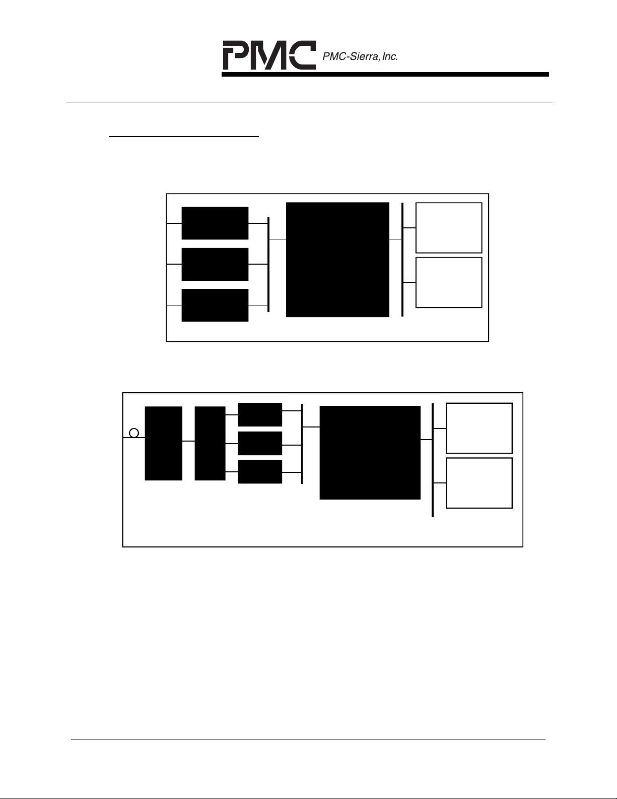
4 APPLICATION EXAMPLES
28xT1
21xE1
DS3
PM8315
TEMUX
PM8315
TEMUX
PM8315
TEMUX
PM7384
FREEDM-84P672
SBI
Bus
Packet
Memory
PCI
Controller /
Bus Arbiter
PCI
Bus
OC-3
5
5
1
-
2
4
A
3
R
5
T
M
C
P
E
P
S
2
6
3
5
M
P
S
U
L
P
P
P
U
T
PM8315
TEMUX
PM8315
TEMUX
PM8315
TEMUX
PM7384
FREEDM-84P672
SBI
Bus
Packet
Memory
PCI
Controller /
Bus Arbiter
PCI
Bus
PROPRIETARY AND CONFIDENTIAL TO PMC-SIERRA, INC., AND FOR ITS CUSTOMERS’ INTERNAL USE 5
DATA SHEET
PMC-1990445 ISSUE 5 FRAME ENGINE AND DATA LINK MANAGER 84P672
PM7384 FREEDM-84P672
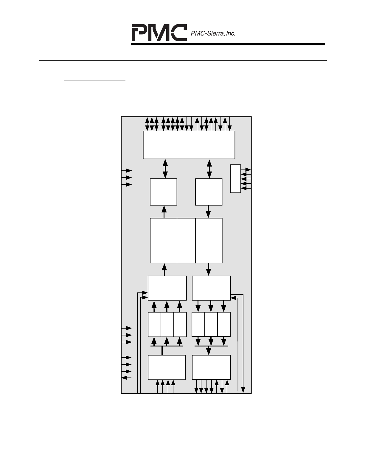
5 BLOCK DIAGRAM
]
RSTB
SYSCLK
PMCTEST
0
:
]
B
3
0
[
E
:
B
1
M
3
E
[
R
A
B
/
D
A
R
A
C
F
P
e
v
i
A
e
M
c
e
D
R
B
L
B
E
B
B
Y
D
R
T
r
e
l
l
o
r
t
n
o
C
L
P
S
Y
E
V
O
D
S
E
T
R
D
I
S
D
I
r
e
l
l
I
o
r
C
t
P
n
o
C
)
2
7
6
C
A
M
R
(
B
B
B
B
K
R
T
Q
C
R
N
E
E
O
L
R
G
P
)
2
7
6
C
I
P
G
(
t
i
m
A
s
M
n
a
D
r
T
O
B
K
K
B
T
N
L
L
R
N
E
I
C
C
I
I
I
R
E
S
r
e
l
l
o
r
t
n
o
C
6
6
C
C
C
P
P
P
M
t
r
TDO
o
TDI
P
)
2
7
6
C
A
M
T
(
TCK
G
A
TMS
T
TRS TB
J
SPE1_EN
SPE2_EN
SPE3_EN
REFCLK
FASTCLK
C1FP
C1FPOUT
l
a
i
t
r
C
r
L
a
D
P
/
H
r
e
o
v
i
s
s
e
c
e
c
e
o
R
r
P
e
v
i
e
c
e
R
O
S
I
P
I
B
S
e
)
e
f
c
2
f
u
B
t
e
k
c
a
P
l
e
n
n
a
h
C
O
S
I
P
I
B
S
I
B
S
r
n
7
o
a
6
t
i
L
m
n
r
D
o
o
f
H
r
M
R
e
(
P
)
2
r
7
e
6
n
g
S
i
s
A
s
C
A
R
(
O
S
I
P
I
B
S
t
c
a
r
t
x
E
l
a
i
t
C
r
r
L
)
e
a
f
2
)
N
O
M
P
(
f
D
P
7
u
/
H
6
B
t
r
i
L
t
o
e
D
m
s
k
s
s
H
c
n
e
T
a
(
a
c
r
P
o
r
T
P
)
t
l
r
2
i
e
e
7
m
n
n
6
s
n
g
S
i
n
a
s
A
a
h
s
r
C
C
T
A
T
(
O
O
P
I
S
I
B
S
O
P
P
I
I
S
S
I
I
B
B
S
S
t
r
I
e
B
s
S
n
I
]
0
0
:
:
2
2
[
[
K
D
L
R
C
R
PROPRIETARY AND CONFIDENTIAL TO PMC-SIERRA, INC., AND FOR ITS CUSTOMERS’ INTERNAL USE 6
L
5
P
0
:
P
V
D
7
D
D
[
D
A
T
A
D
D
]
L
5
P
0
:
7
[
A
T
A
D
A
Q
P
V
D
E
A
A
A
R
_
T
S
U
J
A
]
]
E
V
I
T
C
A
A
]
0
0
0
:
:
:
1
2
2
[
[
[
T
K
D
L
T
C
C
E
T
T
E
D
A
]
]

DATA SHEET
PMC-1990445 ISSUE 5 FRAME ENGINE AND DATA LINK MANAGER 84P672
PM7384 FREEDM-84P672
6 DESCRIPTION
The PM7384 FREEDM-84P672 Frame Engine and Datalink Manager device is a
monolithic integrated circuit that implements HDLC processing, and PCI Bus
memory management functions for a maximum of 672 bi-directional channels.
The FREEDM-84P672 may be configured to support channelised T1/J1/E1 or
unchannelised DS-3 traffic on up to 84 links conveyed via a Scaleable Bandwidth
Interconnect (SBI) interface. The SBI interface transports data in three
Synchronous Payload Envelopes (SPEs), each of which may be configured
independently to carry either 28 T1/J1 links, 21 E1 links or a single DS-3 link.
For channelised T1/J1/E1 links, the FREEDM-84P672 allows up to 672 bidirectional HDLC channels to be assigned to individual time-slots within each
independently timed T1/J1 or E1 link. The channel assignment supports the
concatenation of time-slots (N x DS0) up to a maximum of 24 concatenated timeslots for a T1/J1 link and 31 concatenated time-slots for an E1 link. Time-slots
assigned to any particular channel need not be contiguous within a T1/J1 or E1
link. Unchannelised DS-3 links are assigned to a single HDLC channel.
Additionally, links may be configured independently to operate in an unframed or
“clear channel” mode, in which the bit periods which are normally reserved for
framing information in fact carry HDLC data. In unframed mode, links operate as
unchannelised (i.e. the entire link is assigned to a single HDLC channel)
regardless of link rate.
The FREEDM-84P672 supports mixing of channelised T1/J1/E1 and
unchannelised or unframed links. The total number of channels in each direction
is limited to 672. The maximum possible data rate over all links is 134.208 Mbps
(which occurs with three DS-3 links running in unframed mode).
The FREEDM-84P672 supports three independently timed bidirectional clock/
data links, each carrying a single unchannellised HDLC stream. The links can be
of arbitrary frame format and can operate at up to 51.84 MHz provided SYSCLK
is running at 45 MHz. When activated, each link replaces one of the SPEs
conveyed on the SBI interface. (The maximum possible data rate when all three
clock/data links are activated is 156 Mbps.)
In the receive direction, the FREEDM-84P672 performs channel assignment and
packet extraction and validation. For each provisioned HDLC channel, the
FREEDM-84P672 delineates the packet boundaries using flag sequence
detection, and performs bit de-stuffing. Sharing of opening and closing flags, as
well as sharing of zeros between flags are supported. The resulting packet data
is placed into the internal 32 Kbyte partial packet buffer RAM. The partial packet
PROPRIETARY AND CONFIDENTIAL TO PMC-SIERRA, INC., AND FOR ITS CUSTOMERS’ INTERNAL USE 7

DATA SHEET
PMC-1990445 ISSUE 5 FRAME ENGINE AND DATA LINK MANAGER 84P672
PM7384 FREEDM-84P672
buffer acts as a logical FIFO for each of the assigned channels. Partial packets
are DMA'd out of the RAM, across the PCI bus and into host packet memory.
The FREEDM-84P672 validates the frame check sequence for each packet, and
verifies that the packet is an integral number of octets in length and is within a
programmable minimum and maximum length. The receive packet status is
updated before linking the packet into a receive ready queue. The FREEDM84P672 alerts the PCI Host that there are packets in a receive ready queue by,
optionally, asserting an interrupt on the PCI bus.
Alternatively, in the receive direction, the FREEDM-84P672 supports a
transparent operating mode. For each provisioned transparent channel, the
FREEDM-84P672 directly transfers the received octets into host memory
verbatim. If the transparent channel is assigned to a channelised link, then the
octets are aligned to the received time-slots.
In the transmit direction, the PCI Host provides packets to transmit using a
transmit ready queue. For each provisioned HDLC channel, the FREEDM84P672 DMA's partial packets across the PCI bus and into the transmit partial
packet buffer. The partial packets are read out of the packet buffer by the
FREEDM-84P672 and a frame check sequence is optionally calculated and
inserted at the end of each packet. Bit stuffing is performed before being
assigned to a particular link. The flag sequence is automatically inserted when
there is no packet data for a particular channel. Sequential packets are
optionally separated by two flags (an opening flag and a closing flag) or a single
flag (combined opening and closing flag). Zeros between flags are not shared.
PCI bus latency may cause one or more channels to underflow, in which case,
the packets are aborted, and the host is notified. For normal traffic, an abort
sequence is generated, followed by inter-frame time fill characters (flags or allones bytes) until a new packet is sourced from the PCI host. No attempt is made
to automatically re-transmit an aborted packet.
Alternatively, in the transmit direction, the FREEDM-84P672 supports a
transparent operating mode. For each provisioned transparent channel, the
FREEDM-84P672 directly inserts the transmitted octets from host memory. If the
transparent channel is assigned to a channelised link, then the octets are aligned
to the transmitted time-slots. If a channel underflows due to excessive PCI bus
latency, an abort sequence is generated, followed by inter-frame time fill
characters (flags or all-ones bytes) to indicate idle channel. Data resumes
immediately when the FREEDM-84P672 receives new data from the host.
The FREEDM-84P672 is configured, controlled and monitored using the PCI bus
interface. The PCI bus supports 3.3 Volt signaling. The FREEDM-84P672 is
implemented in low power 2.5 Volt 0.25 mm CMOS technology. All non-PCI
FREEDM-84P672 I/O pins are 3.3 volt tolerant. The FREEDM-84P672 is
packaged in a 352 pin enhanced ball grid array (SBGA) package.
PROPRIETARY AND CONFIDENTIAL TO PMC-SIERRA, INC., AND FOR ITS CUSTOMERS’ INTERNAL USE 8

DATA SHEET
PMC-1990445 ISSUE 5 FRAME ENGINE AND DATA LINK MANAGER 84P672
PM7384 FREEDM-84P672
7 PIN DIAGRAM
The FREEDM-84P672 is manufactured in a 352 pin enhanced ball grid array
package.
2625242322212019181716151413121110987654321
VSS VSS N.C. N.C. N.C. VDD2V5 N.C. N.C. N.C. N.C. N.C. N.C. VSS VSS N.C. N.C. N.C. N.C. N.C. N.C. VDD2V5 N.C. N.C. N.C. VSS VSS
A
ADATA
DDATA
[7]
ADATA
N.C.
DDATA
TDAT[1] N.C.
TA[12]/
TWRB N.C. TA[10] TA[8] TA[6] VSS VDD3V3 VSS
TRS
DDATA
VDD3V3
[4]
ADATA
[6]
DDATA
[7]
DDATA
N.C. DDP N.C. VDD3V3 N.C. APL TCLK[2]
[1]
DDATA
ADATA
[4]
DDATA
[5]
ADATA
[6]
N.C. ADP N.C. VDD3V3 VSS DPL
[2]
[1]
ADATA
DDATA
[3]
[2]
[0]
ADATA
ADATA
VDD2V5
[5]
[3]
VDD3V3 N.C. N.C. VSS
C1FP_OUT
TCLK[1] TD[0] SPE2_EN
C1FP DV5 VSS VDD3V3 VSS
AACTIVE N.C. VSS VSS
[0]
VSS VDD3V3 VSS N.C. N.C. N.C. N.C. N.C. N.C. N.C. N.C. N.C. N.C. VDD2V5 N.C. N.C. N.C.
B
N.C. VSS VDD3V3 N.C. N.C. N.C. N.C. N.C. N.C. N.C. N.C. N.C. N.C. N.C. N.C. N.C. N.C. N.C. TRDB N.C. N.C. N.C. N.C. VDD3V3 VSS N.C.
C
N.C. N.C. N.C. VDD3V3 N.C. N.C. N.C. N.C. VDD3V3 N.C. N.C. N.C. VDD3V3 N.C. N.C. N.C. N.C. VDD3V3 TA[11] TA[9] TA[7] N.C. VDD3V3 N.C. TA[5] N.C.
D
N.C. N.C. N.C. N.C. N.C. RSTB TA[4] N.C.
E
N.C. N.C. N.C. N.C. N.C. N.C. TA[2] N.C.
F
PCICLKO N.C. VDD2V5 N.C. TA[3] N.C. TA[1] TA[0]
G
REQB N.C. PCIINTB N.C. VDD2V5 N.C. N.C. N.C.
H
AD[29] AD[31] PCICLK VDD3V3 VDD3V3 N.C. N.C. N.C.
J
AD[25] AD[27] AD[30] GNTB N.C. N.C. N.C. N.C.
K
N.C. AD[24] AD[26] AD[28] N.C. N.C. N.C. SYSCLK
L
AD[23] N.C. IDSEL CBEB[3] N.C. N.C. N.C. N.C.
M
VSS VDD2V5 AD[21] AD[22]
N
VSS AD[20] AD[19] VDD3V3 VDD2V5 RCLK[2] N.C. VSS
P
AD[18] AD[17] AD[16] FRAMEB RD[0] RD[1] RCLK[1] RD[2]
R
CBEB[2] IRDYB DEVSELB LOCKB N.C. N.C. N.C. RCLK[0]
T
TRDYB STOPB SERRB AD[15] TCK N.C. N.C. N.C.
U
PERRB PAR AD[14] VDD3V3 VDD3V3 TDI TRSTB N.C.
V
CBEB[1] AD[13] AD[11] AD[9] SPE3_EN N.C. TDO TMS
W
AD[12] AD[10] AD[8] AD[6] TD[1] VDD2V5 SPE1_EN FASTCLK
Y
VDD2V5 CBEB[0] AD[5] AD[2]
AA
AD[7] AD[4] AD[1] N.C. AV5 REFCLK TD[2] TCLK[0]
AB
TDAT
[15]
TDAT
VDD3V3
[14]
TDAT
N.C. N.C. N.C. TDAT[6] TDAT[4] TDAT[3]
[13]
TDAT
TDAT
N.C.
[12]
[10]
AD[3] AD[0] N.C. VDD3V3 N.C. N.C. N.C.
AC
N.C. VSS VDD3V3 N.C. N.C. N.C. N.C.
AD
VSS VDD3V3 VSS M66EN
AE
VSS VSS N.C. N.C. N.C. VDD2V5 N.C. N.C. TDAT[9] N.C. N.C. TDAT[5] VSS VSS
AF
PMCTEST
BOTTOM VIEW
TDAT
N.C. TDAT[7] N.C. VDD3V3
[11]
TDAT[8] N.C. N.C. VDD2V5 N.C. TDAT[2] TDAT[0]
AJUST_REQ
ADETECT
[0]
ADETECT
[1]
2625242322212019181716151413121110987654321
A
B
C
D
E
F
G
H
J
K
L
M
N
P
R
T
U
V
W
Y
AA
AB
AC
AD
AE
AF
PROPRIETARY AND CONFIDENTIAL TO PMC-SIERRA, INC., AND FOR ITS CUSTOMERS’ INTERNAL USE 9

DATA SHEET
PMC-1990445 ISSUE 5 FRAME ENGINE AND DATA LINK MANAGER 84P672
PM7384 FREEDM-84P672
8 PIN DESCRIPTION
Table 1 – SBI Interface Signals (30)
Pin Name Type Pin
Function
No.
REFCLK Input AB3 The SBI reference clock signal (REFCLK)
provides reference timing for the SBI ADD and
DROP busses.
REFCLK is nominally a 50% duty cycle clock
of frequency 19.44 MHz ±50ppm.
FASTCLK Input Y1 The high-speed reference clock signal
(FASTCLK) is used by the FREEDM-84P672
to generate an internal clock for use when
processing DS-3 links.
FASTCLK is nominally a 50% duty cycle,
±50ppm clock having one of the following
frequencies: 51.84 MHz, 44.928 MHz or
66 MHz.
C1FP Input AE5 The C1 octet frame pulse signal (C1FP)
provides frame synchronisation for devices
connected via an SBI interface. C1FP must
be asserted for 1 REFCLK cycle every 500 µs
or multiples thereof (i.e. every 9720 n
REFCLK cycles, where n is a positive integer).
All devices interconnected via an SBI
interface must be synchronised to a C1FP
signal from a single source.
C1FP is sampled on the rising edge of
REFCLK.
Note – If the SBI bus is being operated in
synchronous mode [Ref. 4], C1FP must be
asserted for 1 REFCLK cycle every 6 ms or
multiples thereof.
PROPRIETARY AND CONFIDENTIAL TO PMC-SIERRA, INC., AND FOR ITS CUSTOMERS’ INTERNAL USE 10

DATA SHEET
PMC-1990445 ISSUE 5 FRAME ENGINE AND DATA LINK MANAGER 84P672
Pin Name Type Pin
Function
PM7384 FREEDM-84P672
No.
C1FPOUT Output AA4 The C1 octet frame pulse output signal
(C1FPOUT) may be used to provide frame
synchronisation for devices interconnected via
an SBI interface. C1FPOUT is asserted for 1
REFCLK cycle every 500 µs (i.e. every 9720
REFCLK cycles). If C1FPOUT is used for
synchronisation, it must be connected to the
C1FP inputs of all the devices connected to
the SBI interface.
C1FPOUT is updated on the rising edge of
REFCLK.
Note – The C1FPOUT pulse generated by
FREEDM-84P672 is not suitable for use in
systems in which the SBI bus is operated in
synchronous mode [Ref. 4].
DDATA[0]
DDATA[1]
DDATA[2]
DDATA[3]
DDATA[4]
DDATA[5]
DDATA[6]
DDATA[7]
Input AE6
AC8
AD8
AE8
AC10
AE9
AF9
AE10
The SBI DROP bus data signals (DDATA[7:0])
contain the time division multiplexed receive
data from the up to 84 independently timed
links. Data from each link is transported as a
tributary within the SBI TDM bus structure.
Multiple PHY devices can drive the SBI DROP
bus at uniquely assigned tributary column
positions.
DDATA[7:0] are sampled on the rising edge of
REFCLK.
DDP Input AC6 The SBI DROP bus parity signal (DDP)
carries the even or odd parity for the DROP
bus signals. The parity calculation
encompasses the DDATA[7:0], DPL and DV5
signals.
Multiple PHY devices can drive DDP at
uniquely assigned tributary column positions.
This parity signal is intended to detect
accidental PHY source clashes in the column
assignment.
DDP is sampled on the rising edge of
REFCLK.
PROPRIETARY AND CONFIDENTIAL TO PMC-SIERRA, INC., AND FOR ITS CUSTOMERS’ INTERNAL USE 11

DATA SHEET
PMC-1990445 ISSUE 5 FRAME ENGINE AND DATA LINK MANAGER 84P672
Pin Name Type Pin
Function
PM7384 FREEDM-84P672
No.
DPL Input AD1 The SBI DROP bus payload signal (DPL)
indicates valid data within the SBI TDM bus
structure. This signal is asserted during all
octets making up a tributary. This signal may
be asserted during the V3 or H3 octet within a
tributary to accommodate negative timing
adjustments between the tributary rate and
the fixed TDM bus structure. This signal may
be deasserted during the octet following the
V3 or H3 octet within a tributary to
accommodate positive timing adjustments
between the tributary rate and the fixed TDMBUS structure.
Multiple PHY devices can drive DPL at
uniquely assigned tributary column positions.
DPL is sampled on the rising edge of
REFCLK.
DV5 Input AE4 The SBI DROP bus payload indicator signal
(DV5) locates the position of the floating
payloads for each tributary within the SBI
TDM bus structure. Timing differences
between the port timing and the TDM bus
timing are indicated by adjustments of this
payload indicator relative to the fixed TDM bus
structure.
Multiple PHY devices can drive DV5 at
uniquely assigned tributary column positions.
All movements indicated by this signal must
be accompanied by appropriate adjustments
in the DPL signal.
DV5 is sampled on the rising edge of
REFCLK.
PROPRIETARY AND CONFIDENTIAL TO PMC-SIERRA, INC., AND FOR ITS CUSTOMERS’ INTERNAL USE 12

DATA SHEET
PMC-1990445 ISSUE 5 FRAME ENGINE AND DATA LINK MANAGER 84P672
Pin Name Type Pin
Function
PM7384 FREEDM-84P672
No.
ADATA[0]
ADATA[1]
ADATA[2]
ADATA[3]
ADATA[4]
ADATA[5]
ADATA[6]
ADATA[7]
Tristat
e
Output
AF5
AD7
AE7
AF7
AD9
AF8
AD10
AC11
The SBI ADD bus data signals (ADATA[7:0])
contain the time division multiplexed transmit
data from the up to 84 independently timed
links. Data from each link is transported as a
tributary within the SBI TDM bus structure.
Multiple link layer devices can drive the SBI
ADD bus at uniquely assigned tributary
column positions. ADATA[7:0] are tristated
when the FREEDM-84P672 is not outputting
data on a particular tributary column.
ADATA[7:0] are updated on the rising edge of
REFCLK.
ADP Tristat
e
Output
AD5 The SBI ADD bus parity signal (ADP) carries
the even or odd parity for the ADD bus
signals. The parity calculation encompasses
the ADATA[7:0], APL and AV5 signals.
Multiple link layer devices can drive this signal
at uniquely assigned tributary column
positions. ADP is tristated when the
FREEDM-84P672 is not outputting data on a
particular tributary column. This parity signal
is intended to detect accidental link layer
source clashes in the column assignment.
ADP is updated on the rising edge of
REFCLK.
PROPRIETARY AND CONFIDENTIAL TO PMC-SIERRA, INC., AND FOR ITS CUSTOMERS’ INTERNAL USE 13

DATA SHEET
PMC-1990445 ISSUE 5 FRAME ENGINE AND DATA LINK MANAGER 84P672
Pin Name Type Pin
Function
PM7384 FREEDM-84P672
No.
APL Tristat
e
Output
AC2 The SBI ADD bus payload signal (APL)
indicates valid data within the SBI TDM bus
structure. This signal is asserted during all
octets making up a tributary. This signal may
be asserted during the V3 or H3 octet within a
tributary to accommodate negative timing
adjustments between the tributary rate and
the fixed TDM bus structure. This signal may
be deasserted during the octet following the
V3 or H3 octet within a tributary to
accommodate positive timing adjustments
between the tributary rate and the fixed TDMBUS structure.
Multiple link layer devices can drive this signal
at uniquely assigned tributary column
positions. APL is tristated when the
FREEDM-84P672 is not outputting data on a
particular tributary column.
AV5 Tristat
e
output
APL is updated on the rising edge of
REFCLK.
AB4 The SBI ADD bus payload indicator signal
(AV5) locates the position of the floating
payloads for each tributary within the SBI
TDM bus structure. Timing differences
between the port timing and the TDM bus
timing are indicated by adjustments of this
payload indicator relative to the fixed TDM bus
structure.
Multiple link layer devices can drive this signal
at uniquely assigned tributary column
positions. APL is tristated when the
FREEDM-84P672 is not outputting data on a
particular tributary column. All movements
indicated by this signal are accompanied by
appropriate adjustments in the APL signal.
AV5 is updated on the rising edge of
REFCLK.
PROPRIETARY AND CONFIDENTIAL TO PMC-SIERRA, INC., AND FOR ITS CUSTOMERS’ INTERNAL USE 14

DATA SHEET
PMC-1990445 ISSUE 5 FRAME ENGINE AND DATA LINK MANAGER 84P672
Pin Name Type Pin
Function
PM7384 FREEDM-84P672
No.
AJUST_REQ Input AC12 The SBI ADD bus justification request signal
(AJUST_REQ) is used to speed up or slow
down the output data rate of the FREEDM84P672.
Negative timing adjustments are requested by
asserting AJUST_REQ during the V3 or H3
octet, depending on the tributary type. In
response to this the FREEDM-84P672 will
send an extra byte in the V3 or H3 octet of the
next frame along with a valid APL indicating a
negative justification.
Positive timing adjustments are requested by
asserting AJUST_REQ during the octet
following the V3 or H3 octet, depending on the
tributary type. FREEDM-84P672 will respond
to this by not sending an octet during the octet
following the V3 or H3 octet of the next frame
and deasserting APL to indicate a positive
justification.
AJUST_REQ is sampled on the rising edge of
REFCLK.
AACTIVE Output AF4 The SBI ADD bus active indicator signal
(AACTIVE) is asserted whenever FREEDM84P672 is driving the SBI ADD bus signals,
ADATA[7:0], ADP, APL and AV5.
All other Link Layer devices driving the SBI
ADD bus should listen to this signal (to detect
multiple sources accidentaly driving the bus)
and should cease driving the bus whenever a
conflict is detected.
AACTIVE is updated on the rising edge of
REFCLK.
PROPRIETARY AND CONFIDENTIAL TO PMC-SIERRA, INC., AND FOR ITS CUSTOMERS’ INTERNAL USE 15

DATA SHEET
PMC-1990445 ISSUE 5 FRAME ENGINE AND DATA LINK MANAGER 84P672
Pin Name Type Pin
Function
PM7384 FREEDM-84P672
No.
ADETECT[0]
ADETECT[1]
Input AD12
AF12
The SBI ADD bus conflict detection signals
(ADETECT[1:0]) may be connected to the
AACTIVE outputs of other link layer devices
sharing the SBI ADD bus. FREEDM-84P672
will immediately tristate the SBI ADD bus
signals ADATA[7:0], ADP, APL and AV5 if
either of ADETECT[1] and ADETECT[0] is
asserted.
ADETECT[1:0] are asynchronous inputs.
Table 2 – Clock/Data Interface Signals (15)
Pin Name Type Pin
Function
No.
RCLK[0]
RCLK[1]
RCLK[2]
RD[0]
RD[1]
RD[2]
Input T1
R2
P3
Input R4
R3
R1
The receive line clock signals (RCLK[2:0])
contain the recovered line clock for the 3
independently timed links. RCLK[n] must be
externally gapped during the bits or time-slots
that are not part of the transmission format
payload (i.e. not part of the HDLC packet).
RCLK[2:0] is nominally a 50% duty cycle clock
between 0 and 51.84 MHz.
The RCLK[n] inputs are invalid and should be
tied low when their associated link is not
configured for operation (i.e. SPEn_EN input
is high).
The receive data signals (RD[2:0]) contain the
recovered line data for the 3 independently
timed links. RD[2:0] contain HDLC packet
data. For certain transmission formats,
RD[2:0] may contain place holder bits or timeslots. RCLK[n] must be externally gapped
during the place holder positions in the RD[n]
stream. The FREEDM-84P672 supports a
maximum data rate of 51.84 Mbit/s on each
link. RD[2:0] are sampled on the rising edge
of the corresponding RCLK[2:0].
PROPRIETARY AND CONFIDENTIAL TO PMC-SIERRA, INC., AND FOR ITS CUSTOMERS’ INTERNAL USE 16

DATA SHEET
PMC-1990445 ISSUE 5 FRAME ENGINE AND DATA LINK MANAGER 84P672
Pin Name Type Pin
Function
PM7384 FREEDM-84P672
No.
TCLK[0]
TCLK[1]
TCLK[2]
Input AB1
AA3
AC1
The transmit line clock signals (TCLK[2:0])
contain the transmit clocks for the 3
independently timed links. TCLK[n] must be
externally gapped during the bits or time-slots
that are not part of the transmission format
payload (i.e. not part of the HDLC packet).
TCLK[2:0] is nominally a 50% duty cycle clock
between 0 and 51.84 MHz.
The TCLK[n] inputs are invalid and should be
tied low when their associated link is not
configured for operation (i.e. SPEn_EN input
is high).
TD[0]
TD[1]
TD[2]
Output AA2
Y4
AB2
The transmit data signals (TD[2:0]) contain
the transmit data for the 3 independently
timed links. TD[2:0] contain HDLC packet
data. For certain transmission formats,
TD[2:0] may contain place holder bits or timeslots. TCLK[n] must be externally gapped
during the place holder positions in the TD[n]
stream. The FREEDM-84P672 supports a
maximum data rate of 51.84 Mbit/s on each
link.
TD[2:0] are updated on the falling edge of the
corresponding TCLK[2:0] clock.
SPE1_EN
SPE2_EN
SPE3_EN
Input Y2
AA1
W4
The Synchronous Payload Envelope Enable
signals (SPEn_EN) configure the operation of
the clock/data inputs and the SBI Interface.
When SPEn_EN is low, the corresponding
Synchronous Payload Envelope conveyed on
the SBI interface is unused and the
corresponding independently timed link
(signals RCLK[n-1], RD[n-1], TCLK[n-1] and
TD[n-1]) is enabled. When SPEn_EN is high,
the corresponding Synchronous Payload
Envelope conveyed on the SBI interface is
enabled and the corresponding independently
timed link is disabled.
SPEn_EN are asynchronous inputs.
PROPRIETARY AND CONFIDENTIAL TO PMC-SIERRA, INC., AND FOR ITS CUSTOMERS’ INTERNAL USE 17

DATA SHEET
PMC-1990445 ISSUE 5 FRAME ENGINE AND DATA LINK MANAGER 84P672
PM7384 FREEDM-84P672
Table 3 – PCI Host Interface Signals (52)
Pin Name Type Pin
Function
No.
PCICLK Input J24 The PCI clock signal (PCICLK) provides timing
for PCI bus accesses. PCICLK is a nominally
50% duty cycle, 25 to 66 MHz clock.
PCICLKO Output G26 The PCI clock output signal (PCICLKO) is a
buffered version of the PCICLK. PCICLKO may
be used to derive the SYSCLK input.
C/BEB[0]
C/BEB[1]
C/BEB[2]
C/BEB[3]
I/O AA25
W26
T26
M23
The PCI bus command and byte enable bus
(C/BEB[3:0]) contains the bus command or the
byte valid indications. During the first clock
cycle of a transaction, C/BEB[3:0] contains the
bus command code. For subsequent clock
cycles, C/BEB[3:0] identifies which bytes on the
AD[31:0] bus carry valid data. C/BEB[3] is
associated with byte 3 (AD[31:24]) while
C/BEB[0] is associated with byte 0 (AD[7:0]).
When C/BEB[n] is set high, the associated byte
is invalid. When C/BEB[n] is set low, the
associated byte is valid.
When the FREEDM-84P672 is the initiator,
C/BEB[3:0] is an output bus.
When the FREEDM-84P672 is the target,
C/BEB[3:0] is an input bus.
When the FREEDM-84P672 is not involved in
the current transaction, C/BEB[3:0] is tristated.
As an output bus, C/BEB[3:0] is updated on the
rising edge of PCICLK. As an input bus,
C/BEB[3:0] is sampled on the rising edge of
PCICLK.
PROPRIETARY AND CONFIDENTIAL TO PMC-SIERRA, INC., AND FOR ITS CUSTOMERS’ INTERNAL USE 18

DATA SHEET
PMC-1990445 ISSUE 5 FRAME ENGINE AND DATA LINK MANAGER 84P672
Pin Name Type Pin
Function
PM7384 FREEDM-84P672
No.
AD[0]
AD[1]
AD[2]
AD[3]
AD[4]
AD[5]
AD[6]
AD[7]
AD[8]
AD[9]
AD[10]
AD[11]
AD[12]
AD[13]
AD[14]
AD[15]
AD[16]
AD[17]
AD[18]
AD[19]
AD[20]
AD[21]
AD[22]
AD[23]
AD[24]
AD[25]
AD[26]
AD[27]
AD[28]
AD[29]
AD[30]
AD[31]
I/O AC25
AB24
AA23
AC26
AB25
AA24
Y23
AB26
Y24
W23
Y25
W24
Y26
W25
V24
U23
R24
R25
R26
P24
P25
N24
N23
M26
L25
K26
L24
K25
L23
J26
K24
The PCI address and data bus (AD[31:0])
carries the PCI bus multiplexed address and
data. During the first clock cycle of a
transaction, AD[31:0] contains a physical byte
address. During subsequent clock cycles of a
transaction, AD[31:0] contains data.
A transaction is defined as an address phase
followed by one or more data phases. When
Little-Endian byte formatting is selected,
AD[31:24] contain the most significant byte of a
DWORD while AD[7:0] contain the least
significant byte. When Big-Endian byte
formatting is selected. AD[7:0] contain the most
significant byte of a DWORD while AD[31:24]
contain the least significant byte. When the
FREEDM-84P672 is the initiator, AD[31:0] is an
output bus during the first (address) phase of a
transaction. For write transactions, AD[31:0]
remains an output bus for the data phases of
the transaction. For read transactions, AD[31:0]
is an input bus during the data phases.
When the FREEDM-84P672 is the target,
AD[31:0] is an input bus during the first
(address) phase of a transaction. For write
transactions, AD[31:0] remains an input bus
during the data phases of the transaction. For
read transactions, AD[31:0] is an output bus
during the data phases.
When the FREEDM-84P672 is not involved in
the current transaction, AD[31:0] is tristated.
J25
As an output bus, AD[31:0] is updated on the
rising edge of PCICLK. As an input bus,
AD[31:0] is sampled on the rising edge of
PCICLK.
PROPRIETARY AND CONFIDENTIAL TO PMC-SIERRA, INC., AND FOR ITS CUSTOMERS’ INTERNAL USE 19

DATA SHEET
PMC-1990445 ISSUE 5 FRAME ENGINE AND DATA LINK MANAGER 84P672
Pin Name Type Pin
Function
PM7384 FREEDM-84P672
No.
PAR I/O V25 The parity signal (PAR) indicates the parity of
the AD[31:0] and C/BEB[3:0] buses. Even
parity is calculated over all 36 signals in the
buses regardless of whether any or all the bytes
on the AD[31:0] are valid. PAR always reports
the parity of the previous PCICLK cycle. Parity
errors detected by the FREEDM-84P672 are
indicated on output PERRB and in the
FREEDM-84P672 Interrupt Status register.
When the FREEDM-84P672 is the initiator, PAR
is an output for writes and an input for reads.
When the FREEDM-84P672 is the target, PAR
is an input for writes and an output for reads.
When the FREEDM-84P672 is not involved in
the current transaction, PAR is tristated.
As an output signal, PAR is updated on the
rising edge of PCICLK. As an input signal, PAR
is sampled on the rising edge of PCICLK.
FRAMEB I/O R23 The active low cycle frame signal (FRAMEB)
identifies a transaction cycle. When FRAMEB
transitions low, the start of a bus transaction is
indicated. FRAMEB remains low to define the
duration of the cycle. When FRAMEB
transitions high, the last data phase of the
current transaction is indicated.
When the FREEDM-84P672 is the initiator,
FRAMEB is an output.
When the FREEDM-84P672 is the target,
FRAMEB is an input.
When the FREEDM-84P672 is not involved in
the current transaction, FRAMEB is tristated.
As an output signal, FRAMEB is updated on the
rising edge of PCICLK. As an input signal,
FRAMEB is sampled on the rising edge of
PCICLK.
PROPRIETARY AND CONFIDENTIAL TO PMC-SIERRA, INC., AND FOR ITS CUSTOMERS’ INTERNAL USE 20

DATA SHEET
PMC-1990445 ISSUE 5 FRAME ENGINE AND DATA LINK MANAGER 84P672
Pin Name Type Pin
Function
PM7384 FREEDM-84P672
No.
TRDYB I/O U26 The active low target ready signal (TRDYB)
indicates when the target is ready to start or
continue with a transaction. TRDYB works in
conjunction with IRDYB to complete transaction
data phases. During a transaction in progress,
TRDYB is set high to indicate that the target
cannot complete the current data phase and to
force a wait state. TRDYB is set low to indicate
that the target can complete the current data
phase. The data phase is completed when
TRDYB is set low and the initiator ready signal
(IRDYB) is also set low.
When the FREEDM-84P672 is the initiator,
TRDYB is an input.
When the FREEDM-84P672 is the target,
TRDYB is an output. During accesses to
FREEDM-84P672 registers, TRDYB is set high
to extend data phases over multiple PCICLK
cycles.
When the FREEDM-84P672 is not involved in
the current transaction, TRDYB is tristated.
As an output signal, TRDYB is updated on the
rising edge of PCICLK. As an input signal,
TRDYB is sampled on the rising edge of
PCICLK.
PROPRIETARY AND CONFIDENTIAL TO PMC-SIERRA, INC., AND FOR ITS CUSTOMERS’ INTERNAL USE 21

DATA SHEET
PMC-1990445 ISSUE 5 FRAME ENGINE AND DATA LINK MANAGER 84P672
Pin Name Type Pin
Function
PM7384 FREEDM-84P672
No.
IRDYB I/O T25 The active low initiator ready (IRDYB) signal is
used to indicate whether the initiator is ready to
start or continue with a transaction. IRDYB
works in conjunction with TRDYB to complete
transaction data phases. When IRDYB is set
high and a transaction is in progress, the
initiator is indicating it cannot complete the
current data phase and is forcing a wait state.
When IRDYB is set low and a transaction is in
progress, the initiator is indicating it has
completed the current data phase. The data
phase is completed when IRDYB is set low and
the target ready signal (IRDYB) is also set low.
When the FREEDM-84P672 is the initiator,
IRDYB is an output.
When the FREEDM-84P672 is the target,
IRDYB is an input.
When the FREEDM-84P672 is not involved in
the current transaction, IRDYB is tristated.
IRDYB is updated on the rising edge of PCICLK
or sampled on the rising edge of PCICLK
depending on whether it is an output or an
input.
PROPRIETARY AND CONFIDENTIAL TO PMC-SIERRA, INC., AND FOR ITS CUSTOMERS’ INTERNAL USE 22

DATA SHEET
PMC-1990445 ISSUE 5 FRAME ENGINE AND DATA LINK MANAGER 84P672
Pin Name Type Pin
Function
PM7384 FREEDM-84P672
No.
STOPB I/O U25 The active low stop signal (STOPB) requests
the initiator to stop the current bus transaction.
When STOPB is set high by a target, the
initiator continues with the transaction. When
STOPB is set low, the initiator will stop the
current transaction.
When the FREEDM-84P672 is the initiator,
STOPB is an input. When STOPB is sampled
low, the FREEDM-84P672 will terminate the
current transaction in the next PCICLK cycle.
When the FREEDM-84P672 is the target,
STOPB is an output. The FREEDM-84P672
only issues transaction stop requests when
responding to reads and writes to configuration
space (disconnecting after 1 DWORD
transferred) or if an initiator introduces wait
states during a transaction.
When the FREEDM-84P672 is not involved in
the current transaction, STOPB is tristated.
STOPB is updated on the rising edge of
PCICLK or sampled on the rising edge of
PCICLK depending on whether it is an output or
an input.
IDSEL Input M24 The initialization device select signal (IDSEL)
enables read and write access to the PCI
configuration registers. When IDSEL is set high
during the address phase of a transaction and
the C/BEB[3:0] code indicates a register read or
write, the FREEDM-84P672 performs a PCI
configuration register transaction and asserts
the DEVSELB signal in the next PCICLK period.
IDSEL is sampled on the rising edge of
PCICLK.
PROPRIETARY AND CONFIDENTIAL TO PMC-SIERRA, INC., AND FOR ITS CUSTOMERS’ INTERNAL USE 23

DATA SHEET
PMC-1990445 ISSUE 5 FRAME ENGINE AND DATA LINK MANAGER 84P672
Pin Name Type Pin
Function
PM7384 FREEDM-84P672
No.
DEVSELB I/O T24 The active low device select signal (DEVSELB)
indicates that a target claims the current bus
transaction. During the address phase of a
transaction, all targets decode the address on
the AD[31:0] bus. When a target, recognizes
the address as its own, it sets DEVSELB low to
indicate to the initiator that the address is valid.
If no target claims the address in six bus clock
cycles, the initiator assumes that the target
does not exist or cannot respond and aborts the
transaction.
When the FREEDM-84P672 is the initiator,
DEVSELB is an input. If no target responds to
an address in six PCICLK cycles, the FREEDM84P672 will abort the current transaction and
alerts the PCI Host via an interrupt.
When the FREEDM-84P672 is the target,
DEVSELB is an output. DELSELB is set low
when the address on AD[31:0] is recognised.
When the FREEDM-84P672 is not involved in
the current transaction, DEVSELB is tristated.
FREEDM-84P672 is updated on the rising edge
of PCICLK or sampled on the rising edge of
PCICLK depending on whether it is an output or
an input.
LOCKB Input T23 The active low bus lock signal (LOCKB) locks a
target device. When LOCKB and FRAME are
set low, and the FREEDM-84P672 is the target,
an initiator is locking the FREEDM-84P672 as
an "owned" target. Under these circumstances,
the FREEDM-84P672 will reject all transaction
with other initiators. The FREEDM-84P672 will
continue to reject other initiators until its owner
releases the lock by forcing both FRAMEB and
LOCKB high. As a initiator, the FREEDM84P672 will never lock a target.
LOCKB is sampled using the rising edge of
PCICLK.
PROPRIETARY AND CONFIDENTIAL TO PMC-SIERRA, INC., AND FOR ITS CUSTOMERS’ INTERNAL USE 24

DATA SHEET
PMC-1990445 ISSUE 5 FRAME ENGINE AND DATA LINK MANAGER 84P672
Pin Name Type Pin
Function
PM7384 FREEDM-84P672
No.
REQB Tristate
Output
H26 The active low PCI bus request signal (REQB)
requests an external arbiter for control of the
PCI bus. REQB is set low when the FREEDM84P672 desires access to the host memory.
REQB is set high when access is not desired.
REQB is updated on the rising edge of PCICLK.
GNTB Input K23 The active low PCI bus grant signal (GNTB)
indicates the granting of control over the PCI in
response to a bus request via the REQB output.
When GNTB is set high, the FREEDM-84P672
does not have control over the PCI bus. When
GNTB is set low, the external arbiter has
granted the FREEDM-84P672 control over the
PCI bus. However, the FREEDM-84P672 will
not proceed until the FRAMEB signal is
sampled high, indicating no current transactions
are in progress.
PCIINTB OD
Output
GNTB is sampled on the rising edge of PCICLK.
H24 The active low PCI interrupt signal (PCIINTB) is
set low when a FREEDM-84P672 interrupt
source is active, and that source is unmasked.
The FREEDM-84P672 may be enabled to
report many alarms or events via interrupts.
PCIINTB returns high when the interrupt is
acknowledged via an appropriate register
access.
PCIINTB is an open drain output and is
asynchronous to PCICLK.
PROPRIETARY AND CONFIDENTIAL TO PMC-SIERRA, INC., AND FOR ITS CUSTOMERS’ INTERNAL USE 25

DATA SHEET
PMC-1990445 ISSUE 5 FRAME ENGINE AND DATA LINK MANAGER 84P672
Pin Name Type Pin
Function
PM7384 FREEDM-84P672
No.
PERRB I/O V26 The active low parity error signal (PERRB)
indicates a parity error over the AD[31:0] and
C/BEB[3:0] buses. Parity error is signalled
when even parity calculations do not match the
PAR signal. PERRB is set low at the cycle
immediately following an offending PAR cycle.
PERRB is set high when no parity error is
detected.
PERRB is enabled by setting the PERREN bit in
the Control/Status register in the PCI
Configuration registers space. Regardless of
the setting of PERREN, parity errors are always
reported by the PERR bit in the Control/Status
register in the PCI Configuration registers
space.
PERRB is updated on the rising edge of
PCICLK.
SERRB OD
Output
U24 The active low system error signal (SERRB)
indicates an address parity error. Address parity
errors are detected when the even parity
calculations during the address phase do not
match the PAR signal. When the FREEDM84P672 detects a system error, SERRB is set
low for one PCICLK period.
SERRB is enabled by setting the SERREN bit in
the Control/Status register in the PCI
Configuration registers space. Regardless of
the setting of SERREN, parity errors are always
reported by the SERR bit in the Control/Status
register in the PCI Configuration registers
space.
SERRB is an open drain output and is updated
on the rising edge of PCICLK.
M66EN Input AE23 The active high 66 MHz mode enable signal
(M66EN) reflects the speed of operation of the
PCI bus. M66EN should be set high for 66 MHz
operation on the PCI bus. M66EN should be
set low for 33 MHz operation on the PCI bus.
PROPRIETARY AND CONFIDENTIAL TO PMC-SIERRA, INC., AND FOR ITS CUSTOMERS’ INTERNAL USE 26

DATA SHEET
PMC-1990445 ISSUE 5 FRAME ENGINE AND DATA LINK MANAGER 84P672
PM7384 FREEDM-84P672
Table 4 – Miscellaneous Interface Signals (160)
Pin Name Type Pin
Function
No.
SYSCLK Input L1 The system clock (SYSCLK) provides timing for
the core logic. SYSCLK is nominally a 50% duty
cycle clock of frequency 45 MHz ±50ppm.
RSTB Input E3 The active low reset signal (RSTB) signal
provides an asynchronous FREEDM-84P672
reset. RSTB is an asynchronous input. When
RSTB is set low, all FREEDM-84P672 registers
are forced to their default states. In addition, all
SBI and PCI output pins are forced tristate and
will remain tristated until RSTB is set high.
PMCTEST Input AE22 The PMC production test enable signal
(PMCTEST) places the FREEDM-84P672 is test
mode. When PMCTEST is set high, production
test vectors can be executed to verify
manufacturing via the test mode interface signals
TA[11:0], TA[12]/TRS, TRDB, TWRB and
TDAT[15:0]. PMCTEST must be tied low for
normal operation.
TCK Input U4 The test clock signal (TCK) provides timing for
test operations that can be carried out using the
IEEE P1149.1 test access port. TMS and TDI are
sampled on the rising edge of TCK. TDO is
updated on the falling edge of TCK.
TMS Input W1 The test mode select signal (TMS) controls the
test operations that can be carried out using the
IEEE P1149.1 test access port. TMS is sampled
on the rising edge of TCK. TMS has an integral
pull up resistor.
TDI Input V3 The test data input signal (TDI) carries test data
into the FREEDM-84P672 via the IEEE P1149.1
test access port. TDI is sampled on the rising
edge of TCK.
TDI has an integral pull up resistor.
PROPRIETARY AND CONFIDENTIAL TO PMC-SIERRA, INC., AND FOR ITS CUSTOMERS’ INTERNAL USE 27

DATA SHEET
PMC-1990445 ISSUE 5 FRAME ENGINE AND DATA LINK MANAGER 84P672
Pin Name Type Pin
Function
PM7384 FREEDM-84P672
No.
TDO Tristate
Output
W2 The test data output signal (TDO) carries test
data out of the FREEDM-84P672 via the IEEE
P1149.1 test access port. TDO is updated on the
falling edge of TCK. TDO is a tristate output
which is inactive except when scanning of data is
in progress.
TRSTB Input V2 The active low test reset signal (TRSTB) provides
an asynchronous FREEDM-84P672 test access
port reset via the IEEE P1149.1 test access port.
TRSTB is an asynchronous input with an integral
pull up resistor.
Note that when TRSTB is not being used, it must
be connected to the RSTB input.
NC1-152 Open These pins must be left unconnected.
Table 5 – Production Test Interface Signals (31)
Pin Name Type Pin
Function
No.
TA[0]
TA[1]
TA[2]
TA[3]
TA[4]
TA[5]
TA[6]
TA[7]
TA[8]
TA[9]
TA[10]
TA[11]
Input G1
G2
F2
G4
E2
D2
B4
D6
B5
D7
B6
D8
The test mode address bus (TA[11:0]) selects
specific registers during production test
(PMCTEST set high) read and write accesses.
In normal operation (PMCTEST set low), these
signals should be grounded.
TA[12]/TRS Input B9 The test register select signal (TA[12]/TRS)
selects between normal and test mode register
accesses during production test (PMCTEST set
high). TRS is set high to select test registers
and is set low to select normal registers. In
normal operation (PMCTEST set low), this
signal should be grounded.
PROPRIETARY AND CONFIDENTIAL TO PMC-SIERRA, INC., AND FOR ITS CUSTOMERS’ INTERNAL USE 28

DATA SHEET
PMC-1990445 ISSUE 5 FRAME ENGINE AND DATA LINK MANAGER 84P672
Pin Name Type Pin
Function
PM7384 FREEDM-84P672
No.
TRDB Input C8 The test mode read enable signal (TRDB) is set
low during FREEDM-84P672 register read
accesses during production test (PMCTEST set
high). The FREEDM-84P672 drives the test
data bus (TDAT[15:0]) with the contents of the
addressed register while TRDB is low. In
normal operation (PMCTEST set low), this
signal should be tied to logic 1.
TWRB Input B8 The test mode write enable signal (TWRB) is
set low during FREEDM-84P672 register write
accesses during production test (PMCTEST set
high). The contents of the test data bus
(TDAT[15:0]) are clocked into the addressed
register on the rising edge of TWRB. In normal
operation (PMCTEST set low), this signal should
be tied to logic 1.
TDAT[0]
TDAT[1]
TDAT[2]
TDAT[3]
TDAT[4]
TDAT[5]
TDAT[6]
TDAT[7]
TDAT[8]
TDAT[9]
TDAT[10]
TDAT[11]
TDAT[12]
TDAT[13]
TDAT[14]
TDAT[15]
I/O AE11
AF11
AE12
AD13
AD14
AF15
The bi-directional test mode data bus
(TDAT[15:0]) carries data read from or written to
FREEDM-84P672 registers during production
test (PMCTEST set high). In normal operation
(PMCTEST set low), these signals should be left
unconnected.
AD15
AC15
AE17
AF18
AE18
AC17
AE19
AD19
AC19
AE21
PROPRIETARY AND CONFIDENTIAL TO PMC-SIERRA, INC., AND FOR ITS CUSTOMERS’ INTERNAL USE 29

DATA SHEET
PMC-1990445 ISSUE 5 FRAME ENGINE AND DATA LINK MANAGER 84P672
PM7384 FREEDM-84P672
Table 6 – Power and Ground Signals (64)
Pin Name Type Pin
Function
No.
VDD3V3[1]
VDD3V3[2]
VDD3V3[3]
VDD3V3[4]
VDD3V3[5]
VDD3V3[6]
VDD3V3[7]
VDD3V3[8]
VDD3V3[9]
VDD3V3[10]
VDD3V3[11]
VDD3V3[12]
VDD3V3[13]
VDD3V3[14]
VDD3V3[15]
VDD3V3[16]
VDD3V3[17]
VDD3V3[18]
VDD3V3[19]
VDD3V3[20]
VDD3V3[21]
VDD3V3[22]
VDD3V3[23]
VDD3V3[24]
Power B25
C3
C24
D4
D9
D14
D18
D23
J4
N4
P23
J23
V4
V23
AC4
AC9
AC13
AC18
AC23
AD3
AE2
AE25
B2
AD24
The VDD3V3[24:1] DC power pins should be
connected to a well decoupled +3.3 V DC
supply. These power pins provide DC current
to the I/O pads.
VDD2V5[1]
VDD2V5[2]
VDD2V5[3]
VDD2V5[4]
VDD2V5[5]
VDD2V5[6]
VDD2V5[7]
VDD2V5[8]
VDD2V5[9]
VDD2V5[10]
VDD2V5[11]
VDD2V5[12]
PROPRIETARY AND CONFIDENTIAL TO PMC-SIERRA, INC., AND FOR ITS CUSTOMERS’ INTERNAL USE 30
Power H4
P4
Y3
AF6
AE14
AF21
AA26
N25
G24
A21
B13
A6
The VDD2V5[12:1] DC power pins should be
connected to a well decoupled +2.5 V DC
supply. These power pins provide DC current
to the digital core.

DATA SHEET
PMC-1990445 ISSUE 5 FRAME ENGINE AND DATA LINK MANAGER 84P672
Pin Name Type Pin
Function
PM7384 FREEDM-84P672
No.
VSS[1]
VSS[2]
VSS[3]
VSS[4]
VSS[5]
VSS[6]
VSS[7]
VSS[8]
VSS[9]
VSS[10]
VSS[11]
VSS[12]
VSS[13]
VSS[14]
VSS[15]
VSS[16]
VSS[17]
VSS[18]
VSS[19]
VSS[20]
VSS[21]
VSS[22]
VSS[23]
VSS[24]
VSS[25]
VSS[26]
VSS[27]
VSS[28]
Ground A1
A2
A13
A14
A25
A26
B1
B3
B24
B26
C2
C25
N1
N26
P1
P26
AD2
AD25
AE1
AE3
AE24
AE26
AF1
AF2
AF13
AF14
AF25
AF26
The VSS[28:1] DC ground pins should be
connected to ground. They provide a ground
reference for the 3.3 V rail. They also provide
a ground reference for the 2.5 V rail.
Notes on Pin Description:
1. All FREEDM-84P672 non-PCI inputs and bi-directionals present minimum
capacitive loading and are 3.3 Volt tolerant. PCI signals conform to the 3.3
Volt signaling environment.
2. All FREEDM-84P672 non-PCI outputs and bi-directionals have 8 mA drive
capability, except the TDO output which has 4 mA drive capability.
3. All FREEDM-84P672 outputs can be tristated under control of the IEEE
P1149.1 test access port, even those which do not tristate under normal
operation. All non-PCI outputs and bi-directionals are 3.3 V tolerant when
tristated.
PROPRIETARY AND CONFIDENTIAL TO PMC-SIERRA, INC., AND FOR ITS CUSTOMERS’ INTERNAL USE 31

DATA SHEET
PMC-1990445 ISSUE 5 FRAME ENGINE AND DATA LINK MANAGER 84P672
PM7384 FREEDM-84P672
4. All non-PCI inputs are Schmitt triggered. Inputs TMS, TDI and TRSTB have
internal pull-up resistors.
5. Power to the VDD3V3 pins should be applied before power to the VDD2V5
pins is applied. Similarly, power to the VDD2V5 pins should be removed
before power to the VDD3V3 pins is removed.
PROPRIETARY AND CONFIDENTIAL TO PMC-SIERRA, INC., AND FOR ITS CUSTOMERS’ INTERNAL USE 32

DATA SHEET
PMC-1990445 ISSUE 5 FRAME ENGINE AND DATA LINK MANAGER 84P672
PM7384 FREEDM-84P672
9 FUNCTIONAL DESCRIPTION
9.1 Scaleable Bandwidth Interconnect (SBI) Interface
The Scaleable Bandwidth Interconnect is a synchronous, time-division
multiplexed bus designed to transfer, in a pin-efficient manner, data belonging to
a number of independently timed links of varying bandwidth. The bus is timed to
a reference 19.44MHz clock and a 2kHz or 166.7Hz frame pulse. All sources and
sinks of data on the bus are timed to the reference clock and frame pulse.
Timing is communicated across the Scaleable Bandwidth Interconnect by floating
data structures. Payload indicator signals in the SBI control the position of the
floating data structure and therefore the timing. When sources are running faster
than the SBI the floating payload structure is advanced by an octet be passing
an extra octet in the V3 octet locations (H3 octet for DS3 mappings). When the
source is slower than the SBI the floating payload is retarded by leaving the octet
after the V3 or H3 octet unused. Both these rate adjustments are indicated by
the SBI control signals.
An SBI interface consists of a DROP BUS and an ADD BUS. On the DROP BUS
all timing is sourced from the PHY and is passed onto the FREEDM-84P672 by
the arrival rate of data over the SBI. On the ADD BUS timing can be controlled
by either the PHY or the FREEDM-84P672. When the FREEDM-84P672 is the
timing master the PHY device determines its transmit timing information from the
arrival rate of data across the SBI. When the PHY device is the timing master it
signals the FREEDM-84P672 to speed up or slow down with justification request
signals. The PHY timing master indicates a speedup request to the Link Layer
by asserting the justification request signal high during the V3 or H3 octet. When
this is detected by the FREEDM-84P672 it will advance the channel by inserting
data in the next V3 or H3 octet as described above. The PHY timing master
indicates a slowdown request to the FREEDM-84P672 by asserting the
justification request signal high during the octet after the V3 or H3 octet. The
FREEDM-84P672 responds by leaving the octet following the next V3 or H3
octet unused. Both advance and retard rate adjustments take place in the frame
or multi-frame following the justification request.
The SBI multiplexing structure is modeled on the SONET/SDH standards. The
SONET/SDH virtual tributary structure is used to carry T1/J1 and E1 links.
Unchannelized DS3 payloads follow a byte synchronous structure modeled on
the SONET/SDH format.
The SBI structure uses a locked SONET/SDH structure fixing the position of the
TUG-3/TU-3 relative to the STS-3/STM-1 transport frame. The SBI is also of
fixed frequency and alignment as determined by the reference clock (REFCLK)
PROPRIETARY AND CONFIDENTIAL TO PMC-SIERRA, INC., AND FOR ITS CUSTOMERS’ INTERNAL USE 33

DATA SHEET
PMC-1990445 ISSUE 5 FRAME ENGINE AND DATA LINK MANAGER 84P672
PM7384 FREEDM-84P672
and frame indicator signal (C1FP). Frequency deviations are compensated by
adjusting the location of the T1/J1/E1/DS3 channels using floating tributaries as
determined by the V5 indicator and payload signals (DV5, AV5, DPL and APL).
The multiplexed links are separated into three Synchronous Payload Envelopes.
Each envelope may be configured independently to carry up to 28 T1/J1s, 21
E1s or a DS3.
9.2 High-Level Data Link Control (HDLC) Protocol
Figure 1 shows a diagram of the synchronous HDLC protocol supported by the
FREEDM-84P672 device. The incoming stream is examined for flag bytes
(0111111 0 bit pattern) which delineate the opening and closing of the HDLC
packet. The packet is bit de-stuffed which discards a "0" bit which directly
follows five contiguous "1" bits. The resulting HDLC packet size must be a
multiple of an octet (8 bits) and within the expected minimum and maximum
packet length limits. The minimum packet length is that of a packet containing
two information bytes (address and control) and FCS bytes. For packets with
CRC-CCITT as FCS, the minimum packet length is four bytes while those with
CRC-32 as FCS, the minimum length is six bytes. An HDLC packet is aborted
when seven contiguous "1" bits (with no inserted "0" bits) are received. At least
one flag byte must exist between HDLC packets for delineation. Contiguous flag
bytes, or all ones bytes between packets are used as an "inter-frame time fill".
Adjacent flag bytes may share zeros.
Figure 1 – HDLC Frame
Flag Information FCS Flag
HDLC Packet
The CRC algorithm for the frame checking sequence (FCS) field is either a
CRC-CCITT or CRC-32 function. Figure 2 shows a CRC encoder block diagram
using the generating polynomial g(X) = 1 + g1X + g2X2 +…+ g
CRC-CCITT FCS is two bytes in size and has a generating polynomial g(X) = 1 +
X5 + X12 + X16. The CRC-32 FCS is four bytes in size and has a generating
polynomial g(X) = 1 + X + X
2
+ X4 + X5 + X7 + X8 + X10 + X11 + X12 + X16 + X22
+ X23 + X26 + X32. The first FCS bit received is the residue of the highest term.
PROPRIETARY AND CONFIDENTIAL TO PMC-SIERRA, INC., AND FOR ITS CUSTOMERS’ INTERNAL USE 34
n-1
Flag
n-1
X
+ Xn. The

DATA SHEET
PMC-1990445 ISSUE 5 FRAME ENGINE AND DATA LINK MANAGER 84P672
PM7384 FREEDM-84P672
Figure 2 – CRC Generator
g
1
D
0
LSB MSB
D
1
g
2
D
2
Parity Check Digits
g
n-1
D
n-1
Message
9.3 SBI Extracter and PISO
The SBI receive circuitry consists of an SBI Extract block and three SBI Parallel
to Serial Converter (SBI PISO) blocks. The SBI Extract block receives data from
the SBI DROP BUS and converts it to an internal parallel bus format. The
received data is then converted to serial bit streams by the PISO blocks. Each
PISO block processes one of the three Synchronous Payload Envelopes (SPEs)
conveyed on the SBI DROP BUS.
The SBI Extract block may be configured to enable or disable reception of
individual triburaries within the SBI DROP bus. Individual triburaries may also be
configured to operate in framed or unframed mode.
Each PISO block inputs data related to one SPE from the internal parallel bus
and generates either 28 serial data streams at T1/J1 rate, 21 streams at E1 rate
or a single stream at DS-3 rate. These serial streams are then processed by the
Receive Channel Assigner block.
9.4 Receive Channel Assigner
The Receive Channel Assigner block (RCAS672) processes up to 84 serial links.
When receiving data from the SBI PISO blocks, links may be configured to
support channelised T1/J1/E1 traffic, unchannelised DS-3 traffic or unframed
traffic at T1/J1, E1 or DS-3 rates. When receiving data from the RCLK/RD
inputs, links 0, 1 and 2 support unchannelised data at arbitary rates up to 51.84
Mbps.
Each link is independent and has its own associated clock. For each link, the
RCAS672 performs a serial to parallel conversion to form data bytes. The data
bytes are multiplexed, in byte serial format, for delivery to the Receive HDLC
Processor / Partial Packet Buffer block (RHDL672) at SYSCLK rate. In the event
PROPRIETARY AND CONFIDENTIAL TO PMC-SIERRA, INC., AND FOR ITS CUSTOMERS’ INTERNAL USE 35

DATA SHEET
PMC-1990445 ISSUE 5 FRAME ENGINE AND DATA LINK MANAGER 84P672
PM7384 FREEDM-84P672
where multiple streams have accumulated a byte of data, multiplexing is
performed on a fixed priority basis with link #0 having the highest priority and link
#83 the lowest.
The 84 RCAS links have a fixed relationship to the SPE and tributary numbers
on the SBI DROP BUS as shown in the following table.
Table 7 – SBI SPE/Tributary to RCAS Link Mapping
SBI
SPE
No.
SBI
Trib.
No.
RCAS
Link
No.
SBI
SPE
No.
SBI
Trib.
No.
RCAS
Link
No.
SBI
SPE
No.
SBI
Trib.
No.
RCAS
Link
No.
1 1 0 2 1 1 3 1 2
1 2 3 2 2 4 3 2 5
1 3 6 2 3 7 3 3 8
1 4 9 2 4 10 3 4 11
1 5 12 2 5 13 3 5 14
1 6 15 2 6 16 3 6 17
1 7 18 2 7 19 3 7 20
1 8 21 2 8 22 3 8 23
1 9 24 2 9 25 3 9 26
1 10 27 2 10 28 3 10 29
1 11 30 2 11 31 3 11 32
1 12 33 2 12 34 3 12 35
1 13 36 2 13 37 3 13 38
1 14 39 2 14 40 3 14 41
1 15 42 2 15 43 3 15 44
1 16 45 2 16 46 3 16 47
1 17 48 2 17 49 3 17 50
1 18 51 2 18 52 3 18 53
1 19 54 2 19 55 3 19 56
1 20 57 2 20 58 3 20 59
1 21 60 2 21 61 3 21 62
1 22 63 2 22 64 3 22 65
PROPRIETARY AND CONFIDENTIAL TO PMC-SIERRA, INC., AND FOR ITS CUSTOMERS’ INTERNAL USE 36

DATA SHEET
PMC-1990445 ISSUE 5 FRAME ENGINE AND DATA LINK MANAGER 84P672
SBI
SPE
No.
SBI
Trib.
No.
RCAS
Link
No.
SBI
SPE
No.
SBI
Trib.
No.
RCAS
Link
No.
SBI
SPE
No.
PM7384 FREEDM-84P672
SBI
Trib.
No.
RCAS
Link
No.
1 23 66 2 23 67 3 23 68
1 24 69 2 24 70 3 24 71
1 25 72 2 25 73 3 25 74
1 26 75 2 26 76 3 26 77
1 27 78 2 27 79 3 27 80
1 28 81 2 28 82 3 28 83
Links containing a T1/J1 or an E1 stream may be channelised. Data at each
time-slot may be independently assigned to a different channel. The RCAS672
performs a table lookup to associate the link and time-slot identity with a
channel. The position of T1/J1 and E1 framing bits/bytes is identified by frame
pulse signals generated by the SBI PISO blocks. Links containing a DS-3
stream are unchannelised, i.e. all data on the link belongs to one channel. The
RCAS672 performs a table lookup using only the link number to determine the
associated channel, as time-slots are non-existent in unchannelised links. Links
may additionally be configured to operate in an unframed “clear channel” mode,
in which all bit positions, including those normally reserved for framing
information, are assumed to be carrying HDLC data. Links so configured
operate as unchannelised regardless of link rate and the RCAS672 performs a
table lookup using only the link number to determine the associated channel.
9.4.1 Line Interface
There are 84 line interface blocks in the RCAS672. Each line interface block
contains a bit counter, an 8-bit shift register and a holding register that, together,
perform serial to parallel conversion. Whenever the holding register is updated,
a request for service is sent to the priority encoder block. When acknowledged
by the priority encoder, the line interface responds with the data residing in the
holding register.
To support channelised links, each line interface block contains a time-slot
counter. The time-slot counter is incremented each time the holding register is
updated and is reset on detection of a frame pulse from the SBI PISO blocks.
For unchannelised or unframed links, the time-slot counter is held reset.
PROPRIETARY AND CONFIDENTIAL TO PMC-SIERRA, INC., AND FOR ITS CUSTOMERS’ INTERNAL USE 37

DATA SHEET
PMC-1990445 ISSUE 5 FRAME ENGINE AND DATA LINK MANAGER 84P672
PM7384 FREEDM-84P672
9.4.2 Priority Encoder
The priority encoder monitors the line interfaces for requests and synchronises
them to the SYSCLK timing domain. Requests are serviced on a fixed priority
scheme where highest to lowest priority is assigned from the line interface
attached to link 0 to that attached to link 83. Thus, simultaneous requests from
link ‘m’ will be serviced ahead of link ‘n’, if m < n. When there are no pending
requests, the priority encoder generates an idle cycle. In addition, once every
fourth SYSCLK cycle, the priority encoder inserts a null cycle where no requests
are serviced. This cycle is used by the channel assigner downstream for host
microprocessor accesses to the provisioning RAMs.
9.4.3 Channel Assigner
The channel assigner block determines the channel number of the data byte
currently being processed. The block contains a 2688 word channel provision
RAM. The address of the RAM is constructed from concatenating the link
number and the time-slot number of the current data byte. The fields of each
RAM word include the channel number and a time-slot enable flag. The time-slot
enable flag labels the current time-slot as belonging to the channel indicted by
the channel number field.
9.4.4 Loopback Controller
The loopback controller block implements the channel based diagnostic
loopback function. Every valid data byte belonging to a channel with diagnostic
loopback enabled from the Transmit HDLC Processor / Partial Packet Buffer
block (THDL672) is written into a 256 word FIFO. The loopback controller
monitors for an idle time-slot or a time-slot carrying a channel with diagnostic
loopback enabled. If either conditions hold, the current data byte is replaced by
data retrieved from the loopback data FIFO.
9.5 Receive HDLC Processor / Partial Packet Buffer
The Receive HDLC Processor / Partial Packet Buffer block (RHDL672)
processes up to 672 synchronous transmission HDLC data streams. Each
channel can be individually configured to perform flag sequence detection, bit
de-stuffing and CRC-CCITT or CRC-32 verification. The packet data is written
into the partial packet buffer. At the end of a frame, packet status including CRC
error, octet alignment error and maximum length violation are also loaded into
the partial packet buffer. Alternatively, a channel can be provisioned as
transparent, in which case, the HDLC data stream is passed to the partial packet
buffer processor verbatim.
PROPRIETARY AND CONFIDENTIAL TO PMC-SIERRA, INC., AND FOR ITS CUSTOMERS’ INTERNAL USE 38

DATA SHEET
PMC-1990445 ISSUE 5 FRAME ENGINE AND DATA LINK MANAGER 84P672
PM7384 FREEDM-84P672
There is a natural precedence in the alarms detectable on a receive packet.
Once a packet exceeds the programmable maximum packet length, no further
processing is performed on it. Thus, octet alignment detection, FCS verification
and abort recognition are squelched on packets with a maximum length violation.
An abort indication squelches octet alignment detection, minimum packet length
violations, and FCS verification. In addition, FCS verification is only performed
on packets that do not have octet alignment errors, in order to allow the
RHDL672 to perform CRC calculations on a byte-basis.
The partial packet buffer is an 32 Kbyte RAM that is divided into 16-byte blocks.
Each block has an associated pointer which points to another block. A logical
FIFO is created for each provisioned channel by programming the block pointers
to form a circular linked list. A channel FIFO can be assigned a minimum of 3
blocks (48 bytes) and a maximum of 2048 blocks (32 Kbytes). The depth of the
channel FIFOs are monitored in a round-robin fashion. Requests are made to
the Receive DMA Controller block (RMAC672) to transfer, to the PCI host
memory, data in channel FIFOs with depths exceeding their associated
threshold.
9.5.1 HDLC Processor
The HDLC processor is a time-slice state machine which can process up to 672
independent channels. The state vector and provisioning information for each
channel is stored in a RAM. Whenever new channel data arrives, the
appropriate state vector is read from the RAM, processed and written back to the
RAM. The HDLC state-machine can be configured to perform flag delineation,
bit de-stuffing, CRC verification and length monitoring. The resulting HDLC data
and status information is passed to the partial packet buffer processor to be
stored in the appropriate channel FIFO buffer.
The configuration of the HDLC processor is accessed using indirect channel
read and write operations. When an indirect operation is performed, the
information is accessed from RAM during a null clock cycle generated by the
upstream Receive Channel Assigner block (RCAS672). Writing new provisioning
data to a channel resets the channel's entire state vector.
9.5.2 Partial Packet Buffer Processor
The partial packet buffer processor controls the 32 Kbyte partial packet RAM
which is divided into 16 byte blocks. A block pointer RAM is used to chain the
partial packet blocks into circular channel FIFO buffers. Thus, non-contiguous
sections of the RAM can be allocated in the partial packet buffer RAM to create a
channel FIFO. System software is responsible for the assignment of blocks to
individual channel FIFOs. Figure 3 shows an example of three blocks (blocks 1,
3, and 200) linked together to form a 48 byte channel FIFO.
PROPRIETARY AND CONFIDENTIAL TO PMC-SIERRA, INC., AND FOR ITS CUSTOMERS’ INTERNAL USE 39

DATA SHEET
PMC-1990445 ISSUE 5 FRAME ENGINE AND DATA LINK MANAGER 84P672
PM7384 FREEDM-84P672
The partial packet buffer processor is divided into three sections: writer, reader
and roamer. The writer is a time-sliced state machine which writes the HDLC
data and status information from the HDLC processor into a channel FIFO in the
packet buffer RAM. The reader transfers channel FIFO data from the packet
buffer RAM to the downstream Receive DMA Controller block (RMAC672). The
roamer is a time-sliced state machine which tracks channel FIFO buffer depths
and signals the reader to service a particular channel. If a buffer over-run
occurs, the writer ends the current packet from the HDLC processor in the
channel FIFO with an over-run flag and ignores the rest of the packet.
Figure 3 – Partial Packet Buffer Structure
Block 0
Partial Packet
Buffer RAM
16 bytes
Block 0
Block
Pointer RAM
XX
Block 1
Block 2
Block 3
Block 2047
16 bytes
16 bytes
16 bytes
16 bytes
16 bytes
Block 1
Block 2
Block 3
Block 200Block 200
Block 2047
0x03
XX
0xC8
0x01
XX
The FIFO algorithm of the partial packet buffer processor is based on a
programmable per-channel transfer size. Instead of tracking the number of full
blocks in a channel FIFO, the processor tracks the number of transactions.
Whenever the partial packet writer fills a transfer-sized number of blocks or
writes an end-of-packet flag to the channel FIFO, a transaction is created.
Whenever the partial packet reader transmits a transfer-size number of blocks or
an end-of-packet flag to the RMAC672 block, a transaction is deleted. Thus,
small packets less than the transfer size will be naturally transferred to the
PROPRIETARY AND CONFIDENTIAL TO PMC-SIERRA, INC., AND FOR ITS CUSTOMERS’ INTERNAL USE 40

DATA SHEET
PMC-1990445 ISSUE 5 FRAME ENGINE AND DATA LINK MANAGER 84P672
PM7384 FREEDM-84P672
RMAC672 block without having to precisely track the number of full blocks in the
channel FIFO.
The partial packet roamer performs the transaction accounting for all channel
FIFOs. The roamer increments the transaction count when the writer signals a
new transaction and sets a per-channel flag to indicate a non-zero transaction
count. The roamer searches the flags in a round-robin fashion to decide for
which channel FIFO to request transfer by the RMAC672 block. The roamer
informs the partial packet reader of the channel to process. The reader transfers
the data to the RMAC672 until the channel transfer size is reached or an end of
packet is detected. The reader then informs the roamer that a transaction is
consumed. The roamer updates its transaction count and clears the non-zero
transaction count flag if required. The roamer then services the next channel
with its transaction flag set high.
The writer and reader determine empty and full FIFO conditions using flags.
Each block in the partial packet buffer has an associated flag. The writer sets
the flag after the block is written and the reader clears the flag after the block is
read. The flags are initialized (cleared) when the block pointers are written using
indirect block writes. The writer declares a channel FIFO overrun whenever the
writer tries to store data to a block with a set flag. In order to support optional
removal of the FCS from the packet data, the writer does not declare a block as
filled (set the block flag nor increment the transaction count) until the first double
word of the next block in channel FIFO is filled. If the end of a packet resides in
the first double word, the writer declares both blocks as full at the same time.
When the reader finishes processing a transaction, it examines the first double
word of the next block for the end-of-packet flag. If the first double word of the
next block contains only FCS bytes, the reader would, optionally, process next
transaction (end-of-packet) and consume the block, as it contains information not
transferred to the RMAC672 block.
9.6 Receive DMA Controller
The Receive DMA Controller block (RMAC672) is a DMA controller which stores
received packet data in host computer memory. The RMAC672 is not directly
connected to the host memory PCI bus. Memory accesses are serviced by a
downstream PCI controller block (GPIC). The RMAC672 and the host exchange
information using receive packet descriptors (RPDs). The descriptor contains
the size and location of buffers in host memory and the packet status information
associated with the data in each buffer. RPDs are transferred from the
RMAC672 to the host and vice versa using descriptor reference queues. The
RMAC672 maintains all the pointers for the operation of the queues. The
RMAC672 provides two receive packet descriptor reference (RPDR) free queues
to support small and large buffers. The RMAC672 acquires free buffers by
reading RPDRs from the free queues. After a packet is received, the RMAC672
PROPRIETARY AND CONFIDENTIAL TO PMC-SIERRA, INC., AND FOR ITS CUSTOMERS’ INTERNAL USE 41

DATA SHEET
PMC-1990445 ISSUE 5 FRAME ENGINE AND DATA LINK MANAGER 84P672
PM7384 FREEDM-84P672
places the associated RPDR onto a RPDR ready queue. To minimize host bus
accesses, the RMAC672 maintains a descriptor reference table to store current
DMA information. This table contains separate DMA information entries for up to
672 receive channels.
9.6.1 Data Structures
For packet data, the RMAC672 communicates with the host using Receive
Packet Descriptors (RPD), Receive Packet Descriptor References (RPDR), the
Receive Packet Descriptor Reference Ready (RPDRR) queue and the Receive
Packet Descriptor Reference Small and Large Buffer Free (RPDRF) queues.
The RMAC672 copies packet data to data buffers in host memory. The RPD,
RPDR, RPDRR queue, and Small and Large RPDRF queues are data structures
which are used to transfer host memory data buffer information. All five data
structures are manipulated by both the RMAC672 and the host computer. The
RPD holds the data buffer size, data buffer address, and packet status
information. The RPDR is a pointer which is used to index into a table of RPDs.
The RPDRR queue and RPDRF queues allow the RMAC672 and the host to
pass RPDRs back and forth. These data structures are described in more detail
in the following sections.
Receive Packet Descriptor
The Receive Packet Descriptors (RPDs) pass buffer and packet information
between the RMAC672 and the host. Both the RMAC672 and the host read and
write information in the RPDs. The host writes RPD fields which describe the
size and address of data buffers in host memory. The RMAC672 writes RPD
fields which provide number of bytes used in each data buffer, RPD link
information, and the status of the received packet. RPDs are stored in host
memory in a Receive Packet Descriptor Table which is described in a later
section. The Receive Packet Descriptor structure is shown in Figure 4.
Figure 4 – Receive Packet Descriptor
0 Bit 31
Data Buffer Start Address [31:0]
CE
Reserved (7)
Reserved (6)
Bytes In Bu ffer [15 :0]
RCC[9:0] Res (1)
Reserved (16)
Status [5:0 ]
Off set[1:0]
Next RPD Pointer [14:0]
Receive Buffer Size [15:0]
PROPRIETARY AND CONFIDENTIAL TO PMC-SIERRA, INC., AND FOR ITS CUSTOMERS’ INTERNAL USE 42

DATA SHEET
PMC-1990445 ISSUE 5 FRAME ENGINE AND DATA LINK MANAGER 84P672
PM7384 FREEDM-84P672
Table 8 – Receive Packet Descriptor Fields
Field
Description
Data Buffer Start
Address[31:0]
The Data Buffer Start Address[31:0] bits point to the data
buffer in host memory. This field is expected to be
configured by the Host during initialisation.
The Data Buffer Start Address field is valid in all RPDs.
CE The Chain End (CE) bit indicates the end of a linked list of
RPDs. When CE is set to logic one, the current RPD is
the last RPD of a linked list of RPDs. When CE is set to
logic zero, the current RPD is not the last RPD of a linked
list.
The CE bit is valid for all RPDs written by the RMAC672
to the Receive Ready Queue. When a packet requires
only one RPD, the CE bit is set to logic one. The CE bit is
ignored for all RPDs read by the RMAC672 from the
Receive Free Queues, each of which is assumed to point
to only one buffer, i.e. not a chain.
Offset[1:0] The Offset[1:0] bits indicate the byte offset of the data
packet from the start of the buffer. If this value is nonzero, there will be ‘dummy’ (i.e. undefined) bytes at the
start of the data buffer prior to the packet data proper.
For a linked list of RPDs, only the first RPD's Offset field
is valid. All other RPD Offset fields of the linked list are
set to 0.
Status [5:0] The Status[5:0] bits indicate the status of the received
packet.
Status[0] Rx buffer overrun
Status[1] Packet exceeds max. allowed size
Status[2] CRC error
Status[3] Packet Length not an exact no. of bytes
Status[4] HDLC abort detected
Status[5] Unused (set to 0)
For a linked list of RPDs, only the last RPD's Status field
is valid. All other RPD Status fields of the linked list are
invalid and should be ignored. When a packet requires
only one RPD, the Status field is valid.
PROPRIETARY AND CONFIDENTIAL TO PMC-SIERRA, INC., AND FOR ITS CUSTOMERS’ INTERNAL USE 43

DATA SHEET
PMC-1990445 ISSUE 5 FRAME ENGINE AND DATA LINK MANAGER 84P672
PM7384 FREEDM-84P672
Field Description
Bytes in Buffer
[15:0]
The Bytes in Buffer[15:0] bits indicate the number of bytes
actually used in the current RPD's data buffer to store
packet data. The count excludes the 'dummy' bytes
inserted as a result of a non-zero Offset field. A count
greater than 32767 bytes indicates a packet that is
shorter than the expected length of the FCS field.
The Bytes in Buffer field is invalid when Status[0] or
Status[4] is asserted .
Next RPD Pointer
[14:0]
The Next RPD Pointer[14:0] bits store a RPDR which
enables the RMAC672 to support linked lists of RPDs.
This field, which is only valid when CE is equal to logic
zero, contains the RPDR to the next RPD in a linked list.
The RMAC672 links RPDs when more than one buffer is
needed to store a packet.
The Next RPD Pointer is not valid for the last RPD in a
linked list (when CE=1). When a packet requires only one
RPD, the Next RPD Pointer field is not valid.
RCC[9:0] The Receive Channel Code (RCC[9:0]) bits are used by
the RMAC672 to associate a RPD with a channel.
For a linked list of RPDs, all the RPDs’ RCC[9:0] fields
are valid. i.e. all contain the same channel value.
Receive Buffer Size
[15:0]
The Receive Buffer Size[15:0] bits indicate the size in
bytes of the current RPD's data buffer. This field is
expected to be configured by the Host during initialisation.
The Receive Buffer Size must be a non-zero integer
multiple of sixteen and less than or equal to 32752.
The Receive Buffer Size field is valid in all RPDs.
The Receive Buffer Size and Data Buffer Start Address fields are written only by
the host. The RMAC672 reads these fields to determine where to store packet
data. All other fields are written only by the RMAC672.
Receive Packet Descriptor Table
The Receive Packet Descriptor Table resides in host memory and stores all the
RPDs. The RPD Table can contain a maximum of 32768 RPDs. The base of
the RPD table is user programmable using the Rx Packet Descriptor Table Base
(RPDTB) register. The table is indexed by a Receive Packet Descriptor
Reference (RPDR) which is a 15-bit pointer defining the offset of a RPD from the
PROPRIETARY AND CONFIDENTIAL TO PMC-SIERRA, INC., AND FOR ITS CUSTOMERS’ INTERNAL USE 44

DATA SHEET
PMC-1990445 ISSUE 5 FRAME ENGINE AND DATA LINK MANAGER 84P672
PM7384 FREEDM-84P672
table base. Thus, as shown in the following diagram, a RPD can be located by
adding the RPDR to the Rx Packet Descriptor Table Base register.
Figure 5 – Receive Packet Descriptor Table
RPDTB[31:4] = Rx Packet Descriptor Table Base register
RPDR[14:0] = Receive Packet Descriptor Reference
RPD_ADDR[31:0] = Receive Packet Descriptor Address
Bit 31 Bit 0
RPDTB[31:4]
0000
+
RPDR[14:0]
0000
RPDTB
RPD_ADDR
RPD 32768
RPD 1
RPD 2
=
RPD_ADDR[31:0]
Bit 0Bit 31
Dword 0
Dword 1
Dword 2
Dword 3
Dword 0
Dword 3
Dword 0
Dword 3
The Receive Packet Descriptor Table resides in host memory. The Rx Packet
Descriptor Table Base register resides in the RMAC672; this register is initialised
PROPRIETARY AND CONFIDENTIAL TO PMC-SIERRA, INC., AND FOR ITS CUSTOMERS’ INTERNAL USE 45

DATA SHEET
PMC-1990445 ISSUE 5 FRAME ENGINE AND DATA LINK MANAGER 84P672
PM7384 FREEDM-84P672
by the host. The RPDRs reside in host memory and are accessed using receive
packet queues which are described in the next section.
Receive Packet Queues
Receive Packet Queues are used to transfer RPDRs between the host and the
RMAC672. There are three queues: a RPDR Large Buffer Free Queue
(RPDRLFQ), a RPDR Small Buffer Free Queue (RPDRSFQ) and a RPDR Ready
Queue (RPDRRQ). The free queues contain RPDRs referencing RPDs that
define free buffers. The ready queue contains RPDRs referencing RPDs that
define buffers ready for host processing. The RMAC672 pulls RPDRs from the
free queues when it needs free data buffers. The RMAC672 places an RPDR
onto the ready queue after it has filled the buffers with data from each complete
packet. The host removes RPDRs from the ready queue to process the data
buffers. The host places the RPDRs back onto the free queues after it finishes
reading the data from the buffers.
When starting to process a packet, the RMAC672 uses a small buffer RPD to
store the first buffer of packet data. If the packet data requires more than one
buffer, the RMAC672 uses large buffer RPDs to store the remainder of the
packet. The RMAC672 links together all the RPDs required to store the packet
and returns the RPDR associated with the first RPD onto the ready queue.
All receive packet queues reside in host memory and are defined by the Rx
Queue Base (RQB) register and index registers which reside in the RMAC672.
The Rx Queue Base is the base address for the receive packet queues. Each
packet queue has four index registers which define the start and end of the
queue and the read and write locations of the queue. Each index register is 16
bits in length and defines an offset from the Rx Queue Base. Thus, as shown in
the Figure 6, the host address of a RPDR is calculated by adding the index
register to the Rx Queue Base register. The host initializes the Rx Queue Base
register and all the index registers. When an entity (either the RMAC672 or the
host) removes elements from a queue, the entity updates the read pointer for
that queue. When an entity (either the RMAC672 or the host) places elements
onto a queue, the entity updates the write pointer for that queue.
The read index for each queue points to the last valid RPDR read while the write
index points to where the next RPDR can be written. The start index points to the
first valid location within the queue; an RPDR can be written to this location.
However, the end index points to a location that is beyond a queue; an RPDR
can not be written to this location. Note however, the start index of one queue
can be set to the end index of another queue. A queue is empty when the read
index is one less than the write index; a queue is also empty if the read index is
one less than the end index and the write index equals the start index. A queue is
PROPRIETARY AND CONFIDENTIAL TO PMC-SIERRA, INC., AND FOR ITS CUSTOMERS’ INTERNAL USE 46

DATA SHEET
PMC-1990445 ISSUE 5 FRAME ENGINE AND DATA LINK MANAGER 84P672
PM7384 FREEDM-84P672
full when the read index is equal to the write index. Figure 6 shows the RPDR
reference queues.
PROPRIETARY AND CONFIDENTIAL TO PMC-SIERRA, INC., AND FOR ITS CUSTOMERS’ INTERNAL USE 47

DATA SHEET
PMC-1990445 ISSUE 5 FRAME ENGINE AND DATA LINK MANAGER 84P672
PM7384 FREEDM-84P672
Figure 6 – RPDRF and RPDRR Queues
Receive Packet Descriptor (RPD) Reference Queues
Base Address:
RQB [31:2] = Rx Q ueue Base register
Index Registers:
Large Buffer Free Queue:
RPDRLFQS[15:0] = RPDR Large Free Queue Start register
RPDR LFQW [15:0] = RPDR L arge Free Queue W rite register
RPDR LFQR [15:0] = R PDR Large F ree Queu e Read register
RPDRLFQE[15:0] = RPD R Large Free Queue End register
Ready Queue:
RPDRRQS[15:0] = RPDR Ready Queue Start register
RPDRRQW[15:0] = RPDR Ready Queue Write register
RPDRRQR[15:0] = RPDR Ready Queue Read register
RPDRRQE[15:0] = RPDR Ready Queue End register
Small Buffer Free Queue:
RPDRSFQS[15:0] = RPDR Small Free Queue Start register
RPDR SFQW [15:0] = RPDR S mall Free Queue W rite register
RPDRSFQR[15:0] = RPDR Small Free Queue Read register
RPDR SFQE[1 5:0] = RPD R Sm all Free Queue En d register
Base Address
+ Index Register
------------------------Host Address
+
RQB[31:2]
Index[15 :0]
AD[31:0]
00
00
Rx Packet Descriptor Reference Queue Memory Map
RPDRRQS
RPDRRQ R
RPDRRQW
RPDRRQE
RPDRLFQS
RPDRLFQR
RPDRLFQW
RPDRLFQE
RPDRSFQS
RPDRSFQR
Bit 31
Status + RPDR
Status + RPDR
Status + RPDR
Status + RPDR
Status + RPDR
Status + RPDR
RPDR
RPDR
RPDR
RPDR
RPDR
RPDR
RPDR
RPDR
RPDR
Bit 0
RQB
Host Memory
RPD Reference Queues
256KB
RPDRSFQW
RPDRSFQE
RPDR
RPDR
RPDR
PROPRIETARY AND CONFIDENTIAL TO PMC-SIERRA, INC., AND FOR ITS CUSTOMERS’ INTERNAL USE 48
Valid RPDR

DATA SHEET
PMC-1990445 ISSUE 5 FRAME ENGINE AND DATA LINK MANAGER 84P672
PM7384 FREEDM-84P672
Note that the maximum value to which an end pointer may be set is FFFF hex,
resulting in a maximum offset from the queue base address of (4*(FFFF-1)) =
3FFF8 hex. An end pointer must not be set to 0 hex in an attempt to include
offset 3FFFC hex in a queue.
As shown in Figure 6, the ready queue elements have a status field as well as an
RPDR field. The RMAC672 fills in the status field to mark whether a packet was
successfully received or not. The host reads the status field. The ready queue
element is shown in Table 9 below along with the definition of the status bits.
If the RMAC672 requires a buffer of a particular size (i.e. small or large) and no
RPDR is available in the corresponding free queue, a RPDR from the other free
queue is substituted. The host may, therefore, force the RMAC672 to store
received data in buffers of only one size by setting one of the free queues to zero
length, i.e. by setting the start and end index registers of one of the queues to
equal values. If the RMAC672 requires a buffer and neither free queue contains
RPDRs, an RPQ_ERRI interrupt is generated.
Table 9 – RPDRR Queue Element
Bit 16 Bit 0
STATUS[1:0] RPDR[14:0]
Field Description
STATUS[1:0] The encoding for the status field is as follows:
00 – Successful reception of packet.
01 – Unsuccessful reception of packet.
10 – Unprovisioned partial packet.
11 – Partial packet returned due to RAWMAX
limit being reached.
RPDR[14:0] The RPDR[14:0] field defines the offset of the first
RPD in a linked chain of RPDs, each pointing to a
buffer containing the received data.
As described previously, the RMAC672 links RPDs together if more than one
buffer is needed for a packet. The RMAC672 links additional buffer RPDs to the
end of the chain as required until the entire packet is copied to host memory
(provided that the host has not disabled use of both the small and large free
queues by setting one of them to length zero). After storing the packet data, the
RMAC672 places the STATUS+RPDR for the first RPD onto the ready queue.
Only the RPDR associated with the first RPD is placed onto the ready queue. All
other required RPDs are linked to the first RPD as shown in Figure 7.
PROPRIETARY AND CONFIDENTIAL TO PMC-SIERRA, INC., AND FOR ITS CUSTOMERS’ INTERNAL USE 49

DATA SHEET
PMC-1990445 ISSUE 5 FRAME ENGINE AND DATA LINK MANAGER 84P672
PM7384 FREEDM-84P672
Although a STATUS+RPDR only totals to 17 bits, each queue entry is a dword,
i.e. 32 bits. When the RMAC672 block writes a STATUS+RPDR to the ready
queue, it sets the remaining 7 bits in the third byte to zero and the fourth byte is
unmodified.
Figure 7 – RPDRR Queue Operation
Rx Packet Descriptor Reference Ready Queue
RPDRRQ_START_ADDR
RPDRRQ_READ_ADDR
RPDRRQ_WRITE_ADDR
STATUS+RPDR
STATUS+RPDR
STATUS+RPDR
Bit 0 Bit 31
RPD - 16 bytes
RPD - 16 bytes
buffer
-packet M
buffer
-packet N
RPD - 16 bytes
RPD - 16 bytes
RPD - 16 bytes
RPDRRQ_END_ADDR
buffer
-start of
packet O
buffer
-middle of
packet O
buffer
-end of
packet O
Receive Channel Descriptor Reference Table
On a per-channel basis, the RMAC672 caches information such as the current
DMA information in a Receive Channel Descriptor Reference (RCDR) Table.
The RMAC672 can process 672 channels and stores three dwords of
information per channel. This information is cached internally in order to
PROPRIETARY AND CONFIDENTIAL TO PMC-SIERRA, INC., AND FOR ITS CUSTOMERS’ INTERNAL USE 50

DATA SHEET
PMC-1990445 ISSUE 5 FRAME ENGINE AND DATA LINK MANAGER 84P672
PM7384 FREEDM-84P672
decrease the number of host bus accesses required to process each data
packet. The structure of the RCDR table is shown in Figure 8.
Figure 8 – Receive Channel Descriptor Reference Table
Bit 0 Bit 31
RCC 0
RCC 1
Buffer Size[14:0]
DMA Current Address[31:0]
Bytes Avail. in Buffer[14:0]
Buffer Size[14:0]
DMA Current Address[31:0]
RBC[1:0]
Res
V
RBC[1:0]
Res
V
RPD Pointer[14:0] Bytes Avail. in Buffer[14:0]
Start RPD Pointer[14:0]
RPD Pointer[14:0]
Start RPD Pointer[14:0]
RCC 671
Bytes Avail. in Buffer[14:0]
Buffer Size[14:0]
DMA Current Address[31:0]
RBC[1:0]
Res
V
RPD Pointer[14:0]
Start RPD Pointer[14:0]
Table 10 – Receive Channel Descriptor Reference Table Fields
Field Description
Bytes Available in
Buffer[15:0]
This field is used to keep track of the number of bytes
available in the current data buffer. The RMAC672
initialises the Bytes Available in Buffer to the Receive
Buffer Size minus the offset at the head of the buffer.
The field is decremented each time a byte is written into
the buffer.
RBC[1:0] This field is used to keep track of the number of buffers
used when storing ‘raw’ (i.e. non packet delimited) data.
The RMAC672 initialises the RBC field to the value of
the RAWMAX[1:0] field in the RMAC Control Register.
The field is decremented each time a buffer is filled with
data. If the field reaches zero, the chain of RPDs is
placed on the ready queue and a new chain started.
RPD Pointer[14:0] This field contains the pointer to the current RPD.
PROPRIETARY AND CONFIDENTIAL TO PMC-SIERRA, INC., AND FOR ITS CUSTOMERS’ INTERNAL USE 51

DATA SHEET
PMC-1990445 ISSUE 5 FRAME ENGINE AND DATA LINK MANAGER 84P672
PM7384 FREEDM-84P672
Field Description
Buffer Size[14:0] This field contains the size in bytes of the buffer
currently being written to.
V This bit (Valid) indicates whether a packet is currently
being received on the DMA channel. When the V bit is
set to 1, the other fields in the RCDR table entry for the
DMA channel contain valid information.
Start RPD
Pointer[14:0]
DMA Current
Address[31:0]
This field contains the pointer to the first RPD for the
packet being received.
The DMA Current Address [31:0] bits holds the host
address of the next dword in the current buffer. The
RMAC672 increments this field on each access to the
buffer.
9.6.2 DMA Transaction Controller
The DMA Transaction Controller coordinates the reception of data packets from
the Receive Packet Interface and their subsequent storage in host memory. A
packet may be received over a number of separate transactions, interleaved with
transactions belonging to other DMA channels. As well as sending the received
data to host memory, the DMA Transaction Controller initiates data transactions
of its own for the purposes of maintaining the data structures (queues,
descriptors, etc.) in host memory.
9.6.3 Write Data Pipeline/Mux
The Write Data Pipeline/Mux performs two functions. First, it pipelines receive
data between the RHDL672 block and the GPIC block, inserting enough delay to
enable the DMA Transaction Controller to generate appropriate control signals at
the GPIC interface. Second, it provides a multiplexor to the data out lines on the
GPIC interface, allowing the DMA Transaction Controller to output data relating
to the transactions the controller itself initiates.
9.6.4 Descriptor Information Cache
The Descriptor Information Cache provides the storage for the Receive Channel
Descriptor Reference (RCDR) Table described above (Figure 8).
PROPRIETARY AND CONFIDENTIAL TO PMC-SIERRA, INC., AND FOR ITS CUSTOMERS’ INTERNAL USE 52

DATA SHEET
PMC-1990445 ISSUE 5 FRAME ENGINE AND DATA LINK MANAGER 84P672
PM7384 FREEDM-84P672
9.6.5 Free Queue Cache
The Free Queue Cache block implements the 6 element RPDR Small Buffer
Free Queue cache and the 6 element RPDR Large Buffer Free Queue cache.
These caches are used to store free small buffer and large buffer RPDRs.
Caching RPDRs reduces the number of host bus accesses that the RMAC672
makes.
Each cache is managed independently. The elements of the cache are
consumed one at a time as they are needed by the RMAC672. The RPDR small
buffer cache is reloaded when it is empty and the RMAC672 requires a new
small buffer RPDR. The large buffer RPDR cache is reloaded when it is empty
and the RMAC672 requires a new large buffer RPDR. When reloading either of
the caches, the appropriate cache controller will read up to six new elements.
The cache controller may read fewer than six elements if there are fewer than six
new elements available, or the read pointer index is within six elements of the
end of the free queue. If the read pointer is near the end of the free queue, the
cache controller reads only to the end of the queue and does not start reading
from the top of the queue until the next time a reload is required. To do so would
require two host memory transactions and would be of no benefit.
9.7 PCI Controller
The General-Purpose Peripheral Component Interconnect Controller block
(GPIC) provides a 32-bit Master and Target interface core which contains all the
required control functions for full Peripheral Component Interconnect (PCI) Bus
Revision 2.1 compliance. Communications between the PCI bus and other
FREEDM-84P672 blocks can be made through either an internal
asynchronous16-bit bus or through one of two synchronous FIFO interfaces.
One of the FIFO interfaces is dedicated to servicing the Receive DMA Controller
block (RMAC672) and the other to the Transmit DMA Controller block
(TMAC672).
The GPIC supports a 32-bit PCI bus operating at up to 66 MHz and bridges
between the timing domain of the DMA controllers (SYSCLK) and the timing
domain of the PCI bus (PCICLK). The GPIC is backwards compatible and will
operate at 33 MHz when connected to a 33 MHz PCI bus. By itself, the GPIC
does not generate any PCI bus accesses. All transactions on the bus are
initiated by another PCI bus master or by the core device. The GPIC transforms
each access to and from the PCI bus to the intended target or initiator in the core
device. Except for the configuration space registers and parity
generating/checking, the GPIC performs no operations on the data.
The GPIC is made up of four sections: master state machine, a target state
machine, internal microprocessor bus interface and error/bus controller. The
PROPRIETARY AND CONFIDENTIAL TO PMC-SIERRA, INC., AND FOR ITS CUSTOMERS’ INTERNAL USE 53

DATA SHEET
PMC-1990445 ISSUE 5 FRAME ENGINE AND DATA LINK MANAGER 84P672
PM7384 FREEDM-84P672
target and master blocks operate independent of each other. The error/bus
control block monitors the control signals from the target and master blocks to
determine the state of the PCI I/O pads. This block also generates and/or
checks parity for all data going to or coming from the PCI bus. The internal
microprocessor bus interface block contains configuration and status registers
together with the production test logic for the GPIC block.
9.7.1 Master Machine
The GPIC master machine translates requests from the RMAC672 and
TMAC672 block interfaces into PCI bus transactions. The GPIC initiates four
types of PCI cycles: memory read (burst or single), memory read multiple,
memory read line and memory write (burst or single). The number of data
transfers in any cycle is controlled by the DMA controllers. The maximum burst
size is determined by the particular data path. A read cycle to the RMAC672 is
restricted to a maximum burst size of 8 dwords and a write cycle is limited to a
maximum of 64. The TMAC672 interface has a limit of 64 dwords on a read
cycle and 8 on a write cycle.
In response to a DMA controller requesting a cycle, the GPIC must arbitrate for
control of the PCI bus. In the event that the RMAC672 and TMAC672 request
service simultaneously, the GPIC66 processes the RMAC672 DMA operation
first.
When an external PCI bus arbitrator issues a Grant in response to the Request
from the GPIC, the master state machine monitors the PCI bus to insure that the
previous master has completed its transaction and has released the bus before
beginning the cycle. Once the GPIC has control of the bus, it will assert the
FRAME signal and drive the bus with the address and command. The value for
the address is provided by the selected DMA controller. After the initial data
transfer, the GPIC tracks the address for all remaining transfers in the burst
internally in case the GPIC is disconnected by the target and must retry the
transaction.
The target of the GPIC master burst cycle has the option of stopping or
disconnecting the burst at any point. In the event of a target disconnect the
GPIC will terminate the present cycle and release the PCI bus. If the GPIC is
asserting the REQUEST line at the time of the disconnect, it will remove the
REQUEST for two PCI clock cycles then reassert it. When the PCI bus arbitrator
returns the GRANT, the GPIC will restart the burst access at the next address
and continue until the burst is completed or repeat the sequence if the target
disconnects again.
During burst reads, the GPIC accepts the data without inserting any wait states.
Data is written directly into the read FIFO where the RMAC672 or TMAC672 can
PROPRIETARY AND CONFIDENTIAL TO PMC-SIERRA, INC., AND FOR ITS CUSTOMERS’ INTERNAL USE 54

DATA SHEET
PMC-1990445 ISSUE 5 FRAME ENGINE AND DATA LINK MANAGER 84P672
PM7384 FREEDM-84P672
remove it at its own rate. During burst writes, the GPIC will output the data
without inserting any wait states, but may terminate the transaction early if the
local master fails to fill the write FIFO with data before the GPIC requires it. (If a
write transaction is terminated early due to data starvation, the GPIC will
automatically initiate a further transaction to write the remaining data when it
becomes available.)
Normally, the GPIC will begin requesting the PCI bus for a write transaction
shortly after data starts to be loaded into the write FIFO by the RMAC672 or
TMAC672. The RMAC672, however, is not required to supply a transaction
length when writing packet data and in addition, may insert pauses during the
transfer. In the case of packet data writes by the RMAC672, the GPIC will hold
off requesting the PCI bus until the write FIFO has filled up with a number of
dwords equal to a programmable threshold. If the FIFO empties without
reaching the end of the transition, the GPIC will terminate the current transaction
and restart a new transaction to transfer any remaining data when the RMAC672
signals an end of transaction. Beginning the PCI transaction before all the data
is in the write FIFO allows the GPIC to reduce the impact of the bus latency on
the core device.
Each master PCI cycle generated by the GPIC can be terminated in three ways:
Completion, Timeout or Master Abort. The normal mode of operation of the GPIC
is to terminate after transferring all the data from the master FIFO selected. As
noted above this may involve multiple PCI accesses because of the inability of
the target to accept the full burst or data starvation during writes. After the
completion of the burst transfer the GPIC will release the bus unless another
FIFO is requesting service, in which case if the GRANT is asserted the GPIC will
insert one idle cycle on the bus and then start a new transfer.
The maximum duration of the a master burst cycle is controlled by the value set
in the LATENCY TIMER register in the GPIC Configuration Register block. This
value is set by the host on boot and is loaded into a counter in the GPIC master
state at the start of each access. If the counter reaches zero and the GRANT
signal has been removed the GPIC will release the bus regardless of whether it
has completed the present burst cycle. This type of termination is referred to as
a Master Time-out. In the case of a Master Time-out the GPIC will remove the
REQUEST signal for two PCI clocks and then reassert it to complete the burst
cycle.
If no target responds to the address placed on the bus by the GPIC after 4 PCI
clocks the GPIC will terminate the cycle and flag the cycle in the PCI Command/
Status Configuration Register as a Master Abort. If the Stop on Error enable
(SOE_E) bit is set in the GPIC Command Register, the GPIC will not process any
more requests until the error condition is cleared. If the SOE_E is not set, the
GPIC will discard the REQUEST and indicate to the local master that the cycle is
PROPRIETARY AND CONFIDENTIAL TO PMC-SIERRA, INC., AND FOR ITS CUSTOMERS’ INTERNAL USE 55

DATA SHEET
PMC-1990445 ISSUE 5 FRAME ENGINE AND DATA LINK MANAGER 84P672
PM7384 FREEDM-84P672
complete. This action will result in any write data being lost and any read data
being erroneous.
9.7.2 Master Local Bus Interface
The master local bus is a 32 bit data bus which connects the local master device
to the GPIC. The GPIC contains two local master interface blocks, with one
supporting the RMAC672 and the other the TMAC672. Each local master
interface has been optimised to support the traffic pattern generated by the
RMAC672 or the TMAC672 and are not interchangeable.
The data path between the GPIC and local master device provides a mechanism
to segregate the system timing domain of the core from the PCI bus. Transfers
on each of the RMAC672 and TMAC672 interfaces are timed to its own system
clock. The DMA controllers isolated from all aspects of the PCI bus protocol, and
instead “sees” a simple synchronous protocol. Read or write cycles on the local
master bus will initiate a request for service to the GPIC which will then transfer
the data via the PCI bus.
The GPIC maximises data throughput between the PCI bus and the local device
by paralleling local bus data transfers with PCI access latency. The GPIC allows
either DMA controller to write data independent of each other and independent of
PCI bus control. The GPIC temporarily buffers the data from each DMA
controller while it is arbitrating for control of the PCI bus. After completion of a
write transfer, the DMA controller is then released to perform other tasks. The
GPIC can buffer only a single transaction from each DMA controller.
Read accesses on the local bus are optimised by allowing the DMA controllers
access to the data from the PCI bus as soon as the first data becomes available.
After the initial synchronisation and PCI bus latency data is transferred at the
slower of PCI bus rate or the core logic SYSCLK rate. Once a read transaction
is started, the DMA controller is held waiting for the ready signal while the GPIC
is arbitrating for the PCI bus.
All data is passed between the GPIC and the DMA controllers in little Endian
format and, in the default mode of operation, the GPIC expects all data on the
PCI bus to also be in little Endian format. The GPIC provides a selection bit in
the internal Control register which allows the Endian format of the PCI bus data
to be changed. If enabled, the GPIC will swizzle all packet data on the PCI bus
(but not descriptor references and the contents of descriptors). The swizzling is
performed according to the “byte address invariance” rule, i.e. the only change to
the data is the mirror-imaging of byte lanes.
The interface for the RMAC672 provides for byte addressability of write
transactions whereas the interface for the TMAC672 provides for byte
PROPRIETARY AND CONFIDENTIAL TO PMC-SIERRA, INC., AND FOR ITS CUSTOMERS’ INTERNAL USE 56

DATA SHEET
PMC-1990445 ISSUE 5 FRAME ENGINE AND DATA LINK MANAGER 84P672
PM7384 FREEDM-84P672
addressability of read transactions. Other transactions must be dword aligned.
For byte-addressable transactions, the data transferred between the local device
and the GPIC need not be dword aligned with the data as it is presented on the
PCI bus. The GPIC will perform any byte-realignment required. In order to
complete a transfer involving byte re-alignment, the GPIC may need to add an
extra burst cycle to the PCI transaction.
9.7.3 Target Machine
The GPIC target machine performs all the required functions of a stand alone
PCI target device. The target block performs three main functions. The first is
the target state machine which controls the protocol of PCI target accesses to
the GPIC. The second function is to provide all PCI Configuration registers.
Last, the target block provides a Target Interface to the CBI registers in the other
FREEDM-84P672 blocks.
The GPIC tracks the PCI bus and decodes all addresses and commands placed
on the bus to determine whether to respond to the access. The GPIC responds
to the following types of PCI bus commands only: Configuration read and write,
memory read and write, memory-read-multiple and memory-read-line which are
aliased to memory read and memory-write-and-invalidate which is aliased to
memory write. The GPIC will ignore any access that falls within the address
range but has any other command type.
After accepting a target access as a medium speed device, the FREEDM84P672 inserts one wait state for a configuration read/write and five wait states
for other command types before completing the transaction by asserting TRDYB.
Burst accesses to the GPIC are accepted provided they are of linear type. If a
master makes a memory access to the GPIC with the lower two address bits set
to any value but "00" (linear burst type) the GPIC ignores the cycle. Burst
accesses of any length are accepted, but the FREEDM-84P672 will disconnect if
the master inserts any wait states during the transaction. The FREEDM-84P672
will also disconnect on every read and write access to configuration space after
transferring one Dword of data.
Figure 9 illustrates the GPIC address space.
PROPRIETARY AND CONFIDENTIAL TO PMC-SIERRA, INC., AND FOR ITS CUSTOMERS’ INTERNAL USE 57

DATA SHEET
PMC-1990445 ISSUE 5 FRAME ENGINE AND DATA LINK MANAGER 84P672
PM7384 FREEDM-84P672
Figure 9 – GPIC Address Map
PCI ADDRESS MAP
0B
CBI Registers
Base Address
CBI Registers
4GB
8KB
The GPIC responds with medium timing to master accesses. (i.e. DEVSELB is
asserted 2 PCICLK cycles after FRAMEB asserted). The GPIC inserts five wait
states on reads to the internal CBI register space (six wait states for the 2nd and
subsequent dwords of a burst read). The target machine will only terminate an
access with a Retry if the target is locked and another master tries to access the
GPIC. The GPIC will terminate any access to a non-burst area with a
Disconnect and always with data transferred. The target does not support
delayed transactions. The GPIC will perform a Target-Abort termination only in
the case of an address parity error in an address that the GPIC claims.
PROPRIETARY AND CONFIDENTIAL TO PMC-SIERRA, INC., AND FOR ITS CUSTOMERS’ INTERNAL USE 58

DATA SHEET
PMC-1990445 ISSUE 5 FRAME ENGINE AND DATA LINK MANAGER 84P672
PM7384 FREEDM-84P672
9.7.4 CBI Bus Interface
The CBI bus interface provides access to the CBI address space of the
FREEDM-84P672 blocks. The CBI address space is set by the associated BAR
in the PCI Configuration registers.
Write transfers to the CBI space always write all 32 bits provided that at least
one byte enable is asserted. A write command with all byte enables negated will
be ignored. Read transfers always return the 32 bits regardless of the status of
the byte enables, as long as at least one byte enable is asserted. A read
command with all byte enables negated will be ignored.
9.7.5 Error / Bus Control
The Error/Bus Control block monitors signals from both the Target block and
Master Block to determine the direction of the PCI bus pads and to generate or
check parity. After reset, the GPIC sets all bi-directional PCI bus pads to inputs
and monitors the bus for accesses. The Error/Bus control unit remains in this
state unless either the Master requests the PCI bus or the Target responds to a
PCI Master Access. The Error/Bus control unit decodes the state of each state
machine to determine the direction of each PCI bus signal.
All PCI bus devices are required to check and generate even parity across
AD[31:0] and C/BEB[3:0] signals. The GPIC generates parity on Master address
and write data phases; the target generates parity on read data phases. The
GPIC is required to check parity on all PCI bus phases even if it is not
participating in the cycle. But, the GPIC will report parity errors only if the GPIC
is involved in the PCI cycle or if the GPIC detects an address parity error or data
parity is detected in a PCI special cycle. The GPIC updates the PCI
Configuration Status register for all detected error conditions.
9.8 Transmit DMA Controller
The Transmit DMA Controller block (TMAC672) is a DMA controller which
retrieves packet data from host computer memory for transmission. The minimum
packet data length is two bytes. The TMAC672 communicates with the host
computer bus through the master interface connected to PCI Controller block
(GPIC) which translates host bus specific signals from the host to the master
interface format. The TMAC672 uses the master interface whenever it wishes to
initiate a host bus read or write; in this case, the TMAC672 is the initiator and the
host memory is the target.
The TMAC672 and the host exchange information using transmit descriptors
(TDs). The descriptor contains the size and location of buffers in host memory
PROPRIETARY AND CONFIDENTIAL TO PMC-SIERRA, INC., AND FOR ITS CUSTOMERS’ INTERNAL USE 59

DATA SHEET
PMC-1990445 ISSUE 5 FRAME ENGINE AND DATA LINK MANAGER 84P672
PM7384 FREEDM-84P672
and the packet status information associated with the data in each buffer. TDs
are transferred from the TMAC672 to the host and vice versa using descriptor
reference queues. The TMAC672 maintains all the pointers for the operation of
the queues. The TMAC672 acquires buffers with data ready for transmission by
reading TDRs from a TDR ready queue. After a packet has been transmitted,
the TMAC672 places the associated TDR onto a TDR free queue.
To minimise host bus accesses, the TMAC672 maintains a descriptor reference
table to store current DMA information. This table contains separate DMA
information entries for up to 672 transmit channels. The TMAC672 also
performs per-channel sorting of packets received in the TDR ready queue to
eliminate head-of-line blocking.
9.8.1 Data Structures
The TMAC672 communicates with the host using Transmit Descriptors (TD),
Transmit Descriptor References (TDR), the Transmit Data Reference Ready
(TDRR) queue and the Transmit Data Reference Free (TDRF) queue.
The TMAC672 reads packet data from data buffers in host memory. The TD,
TDR, TDRR queue, and TDRF queue are data structures which are used to
transfer host memory data buffer information. All four data structures are
manipulated by both the TMAC672 and the host computer. The TD holds the
data buffer size, data buffer address, and other packet information. The TDR is
a pointer which is used to index into a table of TDs. The TDRR queue and TDRF
queue allow the TMAC672 and the host to pass TDRs back and forth. These
data structures are described in more detail in the following sections.
Transmit Descriptor
The Transmit Descriptors (TDs) pass buffer and packet information between the
TMAC672 and the host. Both the TMAC672 and the host read and write
information in the TDs. TDs are stored in host memory in a Transmit Descriptor
Table. The Transmit Descriptor structure is shown in Figure 10.
Figure 10 – Transmit Descriptor
Bit 31 0
Data Bu ffer S tart Addres s [31:0 ]
IOCABT
Bytes In B uffer [1 5:0]
P
CE
Res (2)
TCC[9:0]
VM
PROPRIETARY AND CONFIDENTIAL TO PMC-SIERRA, INC., AND FOR ITS CUSTOMERS’ INTERNAL USE 60
TMAC Next TD Pointer[14:0]
Reserved (16)
Host Next TD P ointer[14 :0]
Transmit Buffer Size[15:0]

DATA SHEET
PMC-1990445 ISSUE 5 FRAME ENGINE AND DATA LINK MANAGER 84P672
PM7384 FREEDM-84P672
Table 11 – Transmit Descriptor Fields
Field Description
Data Buffer Start
Address [31:0]
The Data Buffer Start Address[31:0] bits point to the
data buffer in host memory.
The Data Buffer Start Address field is valid in all TDs
Bytes In Buffer [15:0] The Bytes In Buffer[15:0] field is used by the host to
indicate the total number of bytes to be transmitted in
the current TD. Zero length buffers are illegal.
P The Priority bit is set by the host to indicate the
priority of the associated packet in a two level quality
of service scheme. Packets with its P bit set high are
queued in the high priority queue in the TMAC672.
Packets with the P bit set low are queued in the low
priority queue. Packets in the low priority queue will
not begin transmission until the high priority queue is
empty.
ABT The Abort (ABT) bit is used by the host to abort the
transmission of a packet. When ABT is set to logic 1,
the packet will be aborted after all the data in the
buffer has been transmitted. If ABT is set to logic 1 in
the current TD, the M bit must be set low and the CE
bit must be set to high.
IOC The Interrupt On Complete (IOC) bit is used by the
host to instruct the TMAC672 to interrupt the host
when the current TD's data buffer has been read.
When IOC is logic 1, the TMAC672 asserts the IOCI
interrupt when the data buffer has been read.
Additionally, the Free Queue FIFO will be flushed. If
IOC is logic zero, the TMAC672 will not generate an
interrupt and the Free Queue FIFO will operate
normally.
PROPRIETARY AND CONFIDENTIAL TO PMC-SIERRA, INC., AND FOR ITS CUSTOMERS’ INTERNAL USE 61

DATA SHEET
PMC-1990445 ISSUE 5 FRAME ENGINE AND DATA LINK MANAGER 84P672
PM7384 FREEDM-84P672
Field Description
CE The Chain End (CE) bit is used by the host to indicate
the end of a linked list of TDs presented to the
TMAC672. The linked list can contain one or more
packets as delineated by the M bit (see above).
When CE is set to logic 1, the current TD is the last
TD of a linked list of TDs. When CE is set to logic 0,
the current TD is not the last TD of a linked list.
When the current TD is not the last of the linked list,
the Host Next TD Pointer[14:0] field is valid,
otherwise the field is not valid.
Note: When CE is set to logic 1, the only valid value
for M is logic 0.
Note: When presenting raw (i.e. unpacketised) data
for transmission, the host should code the M and CE
bits as for a single packet chain, i.e. M=1, CE=0 for
all TDs except the last in the chain and M=0, CE=1
for the last TD in the chain.
TCC[9:0] The Transmit Channel Code (TCC[9:0]) bits are used
by the host to associate a channel with a TD pointed
to by a TDR.
All TCC[9:0] fields in a linked list of TDs must be set
to the same value.
V The V bit is used to indicate that the TMAC Next TD
Pointer field is valid. When set to logic 1, the TMAC
Next TD Pointer[14:0] field is valid. When V is set to
logic 0, the TMAC Next TD Pointer[14:0] field is
invalid. The V bit is used by the host to reclaim data
buffers in the event that data presented to the
TMAC672 is returned to the host due to a channel
becoming unprovisioned. The V bit is expected to be
initialised to logic 0 by the host.
PROPRIETARY AND CONFIDENTIAL TO PMC-SIERRA, INC., AND FOR ITS CUSTOMERS’ INTERNAL USE 62

DATA SHEET
PMC-1990445 ISSUE 5 FRAME ENGINE AND DATA LINK MANAGER 84P672
PM7384 FREEDM-84P672
Field Description
TMAC Next TD Pointer
[14:0]
The TMAC Next TD Pointer[14:0] bits are used to
store TDRs which permits the TMAC672 to create
linked lists of TDs passed to it via the TDRR queue.
The TDs are linked with other TDs belonging to the
same channel and same priority level. In the case
that data presented to the TMAC672 is returned to
the host due to a channel becoming unprovisioned, a
TDR pointing to the start of the per-channel linked list
of TDs is placed on the TDRF queue. It is the
responsibility of the host to follow the TMAC672 and
host links in order to recover all the buffers.
M The More (M) bit is used by the host to support
packets that require multiple TDs. If M is set to
logic 1, the current TD is just one of several TDs for
the current packet. If M is set to logic 0, this TD
either describes the entire packet (in the single TD
packet case) or describes the end of a packet (in the
multiple TD packet case).
Note: When M is set to logic 1, the only valid value
for CE is logic 0.
Host Next TD Pointer
[14:0]
The Host Next TD Pointer[14:0] bits are used to store
TDRs which permits the host to support linked lists of
TDs. As described above, linked lists of TDs are
terminated by setting the CE bit to logic 1. Linked
lists of TDs are used by the host to pass multiple TD
packets or multiple packets associated with the same
channel and priority level to the TMAC672.
Transmit Buffer Size
[15:0]
The Transmit Buffer Size[15:0] field is used to
indicate the size in bytes of the current TD's data
buffer. (N.B. The TMAC672 does not make use of
this field.)
Transmit Descriptor Table
The Transmit Descriptor Table, which resides in host memory, contains all of the
Transmit Descriptors referenced by the TMAC672. To access a TD, the
TMAC672 takes a TDR from a TDRR queue or from the TCDR table and adds
16 times its value (because each TD is 16 bytes in size) to the Transmit
Descriptor Table Base (TDTB) pointer to form the actual address of the TD in
host memory. Each TD must reside in the Transmit Descriptor Table. The
PROPRIETARY AND CONFIDENTIAL TO PMC-SIERRA, INC., AND FOR ITS CUSTOMERS’ INTERNAL USE 63

DATA SHEET
PMC-1990445 ISSUE 5 FRAME ENGINE AND DATA LINK MANAGER 84P672
PM7384 FREEDM-84P672
Transmit Descriptor Table can contain a maximum of 32768 TDs. The base of
the Transmit Descriptor Table is user programmable using the TMAC Tx
Descriptor Table Base register. Thus, as shown below, each TD can be located
using a Transmit Descriptor Reference (TDR) combined with the TMAC Tx
Descriptor Table Base register.
Figure 11 – Transmit Descriptor Table
TDTB[31:4] = Tx Descriptor Table Base register
TDR[14:0] = Transmit Descriptor Reference
TD_ADDR[31:0] = Transmit Descriptor Address
Bit 31 Bit 0
TDTB[31:4]
0000
+
TDR[14:0]
0000
TDTB
TD_ADDR
TD1
TD2
TD 32768
=
TD_ADDR[31:0]
Bit 0Bit 31
Dword 0
Dword 1
Dword 2
Dword 3
Dword 0
Dword 3
Dword 0
Dword 3
PROPRIETARY AND CONFIDENTIAL TO PMC-SIERRA, INC., AND FOR ITS CUSTOMERS’ INTERNAL USE 64

DATA SHEET
PMC-1990445 ISSUE 5 FRAME ENGINE AND DATA LINK MANAGER 84P672
PM7384 FREEDM-84P672
Transmit Queues
Pointers to the transmit descriptors (TDs) containing packet(s) ready for
transmission are passed from the host to the TMAC672 using the Transmit
Descriptor Reference Ready (TDRR) queue, which resides in host memory.
Pointers to transmit descriptor structures whose buffers have been read by the
TMAC672 are passed from the TMAC672 to the host using the Transmit
Descriptor Reference Free (TDRF) queue, which also resides in host memory.
The TMAC672 contains a Free Queue cache which can store up to six TDRs. If
caching is enabled, free TDRs are written into the TDRF queue six at a time, to
reduce the number of host memory accesses. The Free Queue cache is flushed
to the TDRF queue if the Interrupt On Completion (IOC) bit is set in the TD,
which sends the corresponding TDR directly to the TDRF queue. The Free
Queue cache is also flushed to the TDRF queue if the FQFLUSH register bit is
set high. The FQFLUSH register bit is self clearing.
The queues, shown in Figure 12 are defined by a common base pointer residing
in the Transmit Queue Base register and eight offset pointers, four per queue.
For each queue, two pointers define the start and the end of the queue, and two
pointers keep track of the current read and write locations within the queue. The
read pointer for each queue points to the offset of the last valid TDR read, and
the write pointer points to the offset where next TDR can be written. The end of
a queue is not a valid location for a TDR to be read or written. A queue is empty
when the read pointer is one less than the write pointer or if the read pointer is
one less than the end pointer and the write pointer equals the start pointer. A
queue is full when the read pointer is equal to the write pointer. Each queue
element is 32 bits in size, but only the least significant 18 bits are valid. The 18
least significant bits consist of a 15-bit TDR and three status bits for the TD
pointed at by this TDR. The status bits are used by the TMAC672 to inform the
host of the success or failure of transmission (see Table 12). When the
TMAC672 writes TDRs to the TDRF queue, it sets bits [23:18] of the queue
element to 0 and leaves bits [31:24] unaltered. Once a TDR is placed on the
TDRF queue, the FREEDM-84P672 will make no further accesses to the TD nor
the associated buffer.
Note that the maximum value to which an end pointer may be set is FFFF hex,
resulting in a maximum offset from the queue base address of (4*(FFFF-1)) =
3FFF8 hex. An end pointer must not be set to 0 hex in an attempt to include
offset 3FFFC hex in a queue.
PROPRIETARY AND CONFIDENTIAL TO PMC-SIERRA, INC., AND FOR ITS CUSTOMERS’ INTERNAL USE 65

r
r
r
A
DATA SHEET
PMC-1990445 ISSUE 5 FRAME ENGINE AND DATA LINK MANAGER 84P672
PM7384 FREEDM-84P672
Figure 12 – TDRR and TDRF Queues
Transmit Descriptor Referance Queues
Base Address:
TQB[31:2] = Tx Queue Base register
Index Registers:
Ready:
TDRRQS[15:0] = TDR Ready Queue Start registe
TDRRQW[15:0] = TDR Ready Queue Write registe
TDRRQR[15:0] = TDR Ready Queue Read register
TDRRQE[15:0] = TDR Ready Queue End registe
Free:
TDRFQS[15:0] = TDR Free Queue Start register
TDRFQW[15:0] = TDR Free Queue Write register
TDRFQR[15:0] = TDR Free Queue Read register
TDRFQE[15:0] = TDR Free Queue End register
Base Address
+ Index Register
------------------------PCI Address
TQB[31:2]
+
Index[15:0]
D[31:0]
00
00
Tx Descriptor Reference Queue Memory Map
TDR FQS
TDR FQR
TDR FQW
TDR FQE
TDRRQS
TDRRQR
TDRRQW
TDRRQE
Status + TDR
Status + TDR
Status + TDR
Status + TDR
Status + TDR
Status + TDR
TDR
TDR
TDR
TDR
TDR
TDR
Bit 0Bit 31
PCI Host Memory
TQB
TDR Reference Queues
Valid TDR
256KB
PROPRIETARY AND CONFIDENTIAL TO PMC-SIERRA, INC., AND FOR ITS CUSTOMERS’ INTERNAL USE 66

DATA SHEET
PMC-1990445 ISSUE 5 FRAME ENGINE AND DATA LINK MANAGER 84P672
PM7384 FREEDM-84P672
Table 12 – Transmit Descriptor Reference
Bit 17 Bit 0
STATUS[2:0] TDR[14:0]
Field Description
Status[2:0] The TMAC672 fills in the Status field to indicate to the
host the results of processing the TD. The encoding is:
Status[1:0] Description
00 Last or only buffer of packet, buffer read.
01 Buffer of partial packet, buffer read.
10 Unprovisioned channel, buffer not read.
11 Malformed packet (e.g. Bytes In Buffer field
set to 0), buffer not read.
Status[2] Description
0 No underflow detected.
1 Underflow detected.
TDR[14:0] The TDR[14:0] field contains the offset of the TD
returned.
If a TDR is returned to the host with the status field set to “10” (unprovisioned
channel), the TDR may point to a binary tree of TDs and buffers (as indicated by
the CE and V bits in the TDs). It is the responsibility of the host to traverse the
tree to reclaim all the buffers. If a TDR is returned to the host with the status
field set to any other value, the TDR will only point to one TD and buffer
regardless of the values of V and CE in that TD.
The underflow status bit (Status[2]) is normally attached to the TDR belonging to
a packet experiencing underflow. For long packets spanning multiple buffers,
underflow is reported only once at the first available TDR of that channel. All
subsequent TDRs of that packet will be returned normally without the underflow
status. In rare cases, due to internal buffering by the FREEDM-84P672, a
packet may experience underflow at the very end of a packet, just as the TDR is
being returned to the TDR free queue. The underflow status will then be
reported in the first TDR of the immediate next packet of that channel. Because
of the uncertainty with the reporting of underflows between the current verse the
subsequent packet, the underflow status should only be used to gather
performance statistics on channels and not for initiating packet specific
responses such as retransmission.
PROPRIETARY AND CONFIDENTIAL TO PMC-SIERRA, INC., AND FOR ITS CUSTOMERS’ INTERNAL USE 67

DATA SHEET
PMC-1990445 ISSUE 5 FRAME ENGINE AND DATA LINK MANAGER 84P672
PM7384 FREEDM-84P672
Transmit Channel Descriptor Reference Table
The TMAC672 maintains a Transmit Channel Descriptor Reference (TCDR)
table in which is stored certain information relating to DMA activity on each
channel together with TD pointers which are used by the TMAC672 to sort
packet chains supplied by the host into per-channel linked lists (see below). The
caching of DMA-related information reduces the number of host bus accesses
required to process each data packet, while the sorting into per-channel linked
lists eliminates head of line blocking. Each channel is provided with two entries
in the TCDR table, one for high priority packets (Pri 1) and one for low priority
packets (Pri 0). The structure of the TCDR table is shown in Figure 13 below.
Figure 13 – Transmit Channel Descriptor Reference Table
Bit 0
TCC 0, Pri 0
TCC 1, Pri 0
Bit 33
Res
Res
Res
Res
Res
Res
Reserved (12)
PiP
U
Last TD Pointer [14:0]
Reserved (12)
PiP
U
Last TD Pointer [14:0]
IOCAbrt
NA
Bytes to Tx [15:0]
DMA Current Address[31:0]
IOCAbrt
NA
Bytes to Tx [15:0]
DMA Current Address[31:0]
DAMCE
Current TD Pointer [14:0]
Res
Res
Host TD Pointer [14:0]
V
Next TD Pointer [14:0]
DAMCE
Current TD Pointer [14:0]
Host TD Pointer [14:0]
V
Next TD Pointer [14:0]
IOCAbrt
TCC 671, Pri 1
PROPRIETARY AND CONFIDENTIAL TO PMC-SIERRA, INC., AND FOR ITS CUSTOMERS’ INTERNAL USE 68
Reserved (12)
Res
Res
PiP
U
Res
Bytes to Tx [15:0]
Last TD Pointer [14:0]
NA
DMA Current Address[31:0]
DAMCE
Current TD Pointer [14:0]
Res
Host TD Pointer [14:0]
V
Next TD Pointer [14:0]

DATA SHEET
PMC-1990445 ISSUE 5 FRAME ENGINE AND DATA LINK MANAGER 84P672
PM7384 FREEDM-84P672
Table 13 – Transmit Channel Descriptor Reference Table Fields
Field Description
NA Indicates that a ‘null abort’ is to be sent to the
downstream block when it next requests data on this
channel. The NA bit is set if a mal-formed TD is
encountered while searching down a host chain.
ABRT A copy of the ABRT bit in the TD currently being read.
IOC A copy of the IOC bit in the TD currently being read.
M A copy of the M bit in the TD currently being read.
CE A copy of the CE bit in the TD currently being read.
A Indicates if this channel is active (i.e. provisioned). If
the channel is active, the A bit is set to logic 1. If the
channel is inactive, the A bit is set to logic 0.
D Indicates whether the linked list of packets for this
channel is empty or not. If the D bit is set to logic 1,
the list is not empty and the current TD pointer field is
valid (i.e., it points to a valid TD). If the D bit is set to
logic 0, the list is empty and the current TD pointer field
is invalid.
Current TD Pointer
Offset to the TD currently being read. (See Figure 14)
[14:0]
Bytes To Tx[15:0] The Bytes to Tx[15:0] bits are used to indicate the total
number of bytes that remain to be read in the current
buffer. Each access to the data buffer decrements this
value. A value of zero in this field indicates the buffer
has been completely read.
Host TD Pointer [14:0] A copy of the Host Next TD Pointer field of the TD
currently being read, i.e. a pointer to the next TD in the
chain currently being read. (See Figure 14)
DMA Current
Address[31:0]
The DMA Current Address [31:0] bits hold the address
of the next dword in the current buffer. This field is
incremented on each access to the buffer.
U Indicates that an underflow has occurred on this
channel. This bit is set in response to an underflow
indication for the downstream THDL672 block and is
cleared when a TDR is written to the TDR Free Queue
(or to the free queue cache).
PROPRIETARY AND CONFIDENTIAL TO PMC-SIERRA, INC., AND FOR ITS CUSTOMERS’ INTERNAL USE 69

DATA SHEET
PMC-1990445 ISSUE 5 FRAME ENGINE AND DATA LINK MANAGER 84P672
PM7384 FREEDM-84P672
Field Description
PiP The Packet Transfer in Progress bit indicates that a
packet is currently being transmitted on this channel at
this priority level.
Last TD Pointer [14:0] Offset to the head of the last host-linked chain of TDs
to be read. (See Figure 14)
V Indicates if the linked list of packets for this channel
contains more than one host-linked chain (See Figure
14). If the V bit is set to logic 1, the list contains more
than one chain and the next and last TD pointer fields
are valid. If the V bit is set to logic 0, the list is either
empty or contains only one host-linked chain and the
next and last TD pointer fields are invalid.
Next TD Pointer [14:0] Offset to the head of the next host-linked chain of TDs
to be read. (See Figure 14)
Transmit Descriptor Linking
As described above, the TCDR table contains pointers which the TMAC672 uses
to construct linked lists of data packets to be transmitted. After the host places a
new TDR in the TDR Ready queue, the TMAC672 retrieves the TDR and links it
to the TD pointed at by the Last TD Pointer field. The TMAC672 may create up
to 1,344 linked lists, viz. a high-priority list and a low-priority list for each DMA
channel. Whenever a new data packet is requested by the downstream block,
the TMAC672 picks a packet from the high-priority linked list unless it is empty, in
which case, a packet from the low-priority linked list is used.
PROPRIETARY AND CONFIDENTIAL TO PMC-SIERRA, INC., AND FOR ITS CUSTOMERS’ INTERNAL USE 70

DATA SHEET
PMC-1990445 ISSUE 5 FRAME ENGINE AND DATA LINK MANAGER 84P672
PM7384 FREEDM-84P672
Figure 14 – TD Linking
TD TD
P3
V=1
M=1
CE=0
TMAC Link
Data
Host Li nk
TD
P3
M=0
CE=1
Data
P4
V=0
M=0
CE=1
Curr.
TDR
TDR
TDR
Last
Next
TCDR Table
Host
TDR
TD
Host Link
TD
P1
P1
V=1
M=1
CE=0
M=1
CE=0
TMAC Link
Data
Data
Host Link
TD
P1
M=0
CE=0
Data
Host Link
TD
P2
M=0
CE=1
Data
The host links the TDs vertically while the TMAC672 links TDs horizontally.
Figure 14 shows the TDs for packets P1 and P2 linked by the host before the
TDR is placed on the TDRR queue, as are the TDs for packet P3 and P4.
Packet P3 is linked to packet P1 by the TMAC672, as is packet P4 linked to
PROPRIETARY AND CONFIDENTIAL TO PMC-SIERRA, INC., AND FOR ITS CUSTOMERS’ INTERNAL USE 71

DATA SHEET
PMC-1990445 ISSUE 5 FRAME ENGINE AND DATA LINK MANAGER 84P672
PM7384 FREEDM-84P672
packet P3. The TMAC672 indicates valid horizontal links by setting the V bit to
logic 1.
9.8.2 Task Priorities
The TMAC672 must perform a number of tasks concurrently in order to maintain
a steady flow of data through the system. The main tasks of the TMAC672 are
managing the Ready Queue (i.e. removing chains of data packets from the
queue and attaching them to the appropriate per-channel linked list) and
servicing requests for data from the Transmit Packet Interface. The priority of
service for each of the tasks is fixed by the TMAC672 as follows:
· Top priority is given to servicing ‘expedited’ read requests from the Transmit
HDLC Processor / Partial Packet Buffer block (THDL672).
· Second priority is given to removing chains of data packets from the TDRR
queue and attaching them to the appropriate per-channel linked list.
· Third priority is given to servicing non-expedited read requests from the
THDL672.
9.8.3 DMA Transaction Controller
The DMA Transaction Controller coordinates the processing of requests from the
THDL672 with the reading of data stored in host memory. The reading of a data
packet may require a number of separate host memory transactions, interleaved
with transactions of other DMA channels. As well as reading data from the Host
Master Interface, the DMA Transaction Controller initiates read and write
transactions to the PCI Controller block (GPIC) for the purposes of maintaining
the data structures (queues, descriptors, etc.) in host memory.
9.8.4 Read Data Pipeline
The Read Data Pipeline inserts delay in the data stream between the GPIC
interface and the THDL672 interface to enable the DMA Transaction Controller to
generate appropriate control signals at the Transmit Packet Interface.
9.8.5 Descriptor Information Cache
The Descriptor Information Cache provides the storage for the Transmit Channel
Descriptor Reference (TCDR) Table.
PROPRIETARY AND CONFIDENTIAL TO PMC-SIERRA, INC., AND FOR ITS CUSTOMERS’ INTERNAL USE 72

DATA SHEET
PMC-1990445 ISSUE 5 FRAME ENGINE AND DATA LINK MANAGER 84P672
PM7384 FREEDM-84P672
9.8.6 Free Queue Cache
The Free Queue Cache block implements the 6 element TDR Free Queue
cache. Caching TDRs reduces the number of host bus accesses that the
TMAC672 makes.
TDRs are written to the cache one at a time as they are released by the
TMAC672. The cache is then flushed to host memory when it becomes full,
when a TD with the IOC bit set high is released, when the FQFLUSH register bit
is set high or when a TD is released as the result of unprovisioning a channel.
The cache controller may also flush the cache when it contains fewer than six
elements or if the pointer index is within six elements of the end of the free
queue. When the write pointer is near the end of the free queue, the cache
controller writes only to the end of the queue and does not start writing from the
top of the queue until the next time a flush is required. To do so would require
two host memory transactions and would be of no benefit.
9.9 Transmit HDLC Controller / Partial Packet Buffer
The Transmit HDLC Controller / Partial Packet Buffer block (THDL672) contains
a partial packet buffer for PCI latency control and a transmit HDLC controller.
Packet data retrieved from the PCI host memory by the Transmit DMA Controller
block (TMAC672) is stored in channel specific FIFOs residing in the partial
packet buffer. When the amount of data in a FIFO reaches a programmable
threshold, the HDLC controller is enabled to initiate transmission. The HDLC
controller performs flag generation, bit stuffing and, optionally, frame check
sequence (FCS) insertion. The FCS is software selectable to be CRC-CCITT or
CRC-32. The minimum packet size, excluding FCS, is two bytes. A single byte
payload is illegal. The HDLC controller delivers data to the Transmit Channel
Assigner block (TCAS672) on demand. A packet in progress is aborted if an
under-run occurs. The THDL672 is programmable to operate in transparent
mode where packet data retrieved from the PCI host is transmitted verbatim.
9.9.1 Transmit HDLC Processor
The HDLC processor is a time-slice state machine which can process up to 672
independent channels. The state vector and provisioning information for each
channel is stored in a RAM. Whenever the TCAS672 requests data, the
appropriate state vector is read from the RAM, processed and finally written back
to the RAM. The HDLC state-machine can be configured to perform flag
insertion, bit stuffing and CRC generation. The HDLC processor requests data
from the partial packet processor whenever a request for channel data arrives.
However, the HDLC processor does not start transmitting a packet until the entire
packet is stored in the channel FIFO or until the FIFO free space is less than the
PROPRIETARY AND CONFIDENTIAL TO PMC-SIERRA, INC., AND FOR ITS CUSTOMERS’ INTERNAL USE 73

DATA SHEET
PMC-1990445 ISSUE 5 FRAME ENGINE AND DATA LINK MANAGER 84P672
PM7384 FREEDM-84P672
software programmable limit. If a channel FIFO under-runs, the HDLC processor
aborts the packet.
The configuration of the HDLC processor is accessed using indirect channel
read and write operations. When an indirect operation is performed, the
information is accessed from RAM during a null clock cycle inserted by the
TCAS672 block. Writing new provisioning data to a channel resets the channels
entire state vector.
9.9.2 Transmit Partial Packet Buffer Processor
The partial packet buffer processor controls the 32 Kbyte partial packet RAM
which is divided into 16 byte blocks. A block pointer RAM is used to chain the
partial packet blocks into circular channel FIFO buffers. Thus, non-contiguous
sections of RAM can be allocated in the partial packet buffer RAM to create a
channel FIFO. Figure 15 shows an example of three blocks (blocks 1, 3, and
200) linked together to form a 48 byte channel FIFO. The three pointer values
would be written sequentially using indirect block write accesses. When a
channel is provisioned with this FIFO, the state machine can be initialised to
point to any one of the three blocks.
The partial packet buffer processor is divided into three sections: reader, writer
and roamer. The roamer is a time-sliced state machine which tracks each
channel's FIFO buffer free space and signals the writer to service a particular
channel. The writer requests data from the TMAC672 block and transfers packet
data from the TMAC672 to the associated channel FIFO. The reader is a timesliced state machine which transfers the HDLC information from a channel FIFO
to the HDLC processor when the HDLC processor requests it. If a buffer underrun occurs for a channel, the reader informs the HDLC processor and purges the
rest of the packet.
PROPRIETARY AND CONFIDENTIAL TO PMC-SIERRA, INC., AND FOR ITS CUSTOMERS’ INTERNAL USE 74

DATA SHEET
PMC-1990445 ISSUE 5 FRAME ENGINE AND DATA LINK MANAGER 84P672
PM7384 FREEDM-84P672
Figure 15 – Partial Packet Buffer Structure
Block 0
Block 1
Block 2
Block 3
Partial Packet
Buffer RAM
16 bytes
16 bytes
16 bytes
16 bytes
Block 0
Block 1
Block 2
Block 3
Block
Pointer RAM
XX
0x03
XX
0xC8
0x01
XX
Block 2047
16 bytes
16 bytes
Block 200Block 200
Block 2047
The writer and reader determine empty and full FIFO conditions using flags.
Each block in the partial packet buffer has an associated flag. The writer sets
the flag after the block is written and the reader clears the flag after the block is
read. The flags are initialized (cleared) when the block pointers are written using
indirect block writes. The reader declares a channel FIFO under-run whenever it
tries to read data from a block without a set flag.
The FIFO algorithm of the partial packet buffer processor is based on perchannel software programmable transfer size and free space trigger level.
Instead of tracking the number of full blocks in a channel FIFO, the processor
tracks the number of empty blocks, called free space, as well as the number of
end of packets stored in the FIFO. Recording the number of empty blocks
instead of the number of full blocks reduces the amount of information the
roamer must store in its state RAM.
The partial packet roamer records the FIFO free space and end-of-packet count
for all channel FIFOs. When the reader signals that a block has been read, the
roamer increments the FIFO free space and sets a per-channel request flag if
PROPRIETARY AND CONFIDENTIAL TO PMC-SIERRA, INC., AND FOR ITS CUSTOMERS’ INTERNAL USE 75

DATA SHEET
PMC-1990445 ISSUE 5 FRAME ENGINE AND DATA LINK MANAGER 84P672
PM7384 FREEDM-84P672
the free space is greater than the limit set by XFER[3:0]. The roamer also
decrements the end-of-packet count when the reader signals that it has passed
an end of a packet to the HDLC processor. If the HDLC is transmitting a packet
and the FIFO free space is greater than the free space trigger level and there are
no complete packets within the FIFO (end-of-packet count equal to zero), a perchannel starving flag is set. The roamer searches the starving flags in a roundrobin fashion to decide which channel FIFO should make expedited data
requests to the TMAC672 block. If no starving flags are set, the roamer
searches the request flags in a round-robin fashion to decide which channel
FIFO should make regular data requests to the TMAC672 block. The roamer
informs the partial packet writer of the channel FIFO to process, the FIFO free
space and the type of request it should make. The writer sends a request for
data to the TMAC672 block and writes the response data to the channel FIFO
setting block full flags. The writer reports back to the roamer the number of
blocks and end-of-packets transferred. The maximum amount of data
transferred during one request is limited by a software programmable limit.
The configuration of the HDLC processor is accessed using indirect channel
read and write operations as well as indirect block read and write operations.
When an indirect operation is performed, the information is accessed from RAM
during a null clock cycle identified by the TCAS672 block. Writing new
provisioning data to a channel resets the entire state vector.
9.10 Transmit Channel Assigner
The Transmit Channel Assigner block (TCAS672) processes up to 672 channels.
Data for all channels is sourced from a single byte-serial stream from the
Transmit HDLC Controller / Partial Packet Buffer block (THDL672). The
TCAS672 demultiplexes the data and assigns each byte to any one of 84 links.
When sending data to the SBI SIPO blocks, each link may be configured to
support channelised T1/J1/E1 traffic, unchannelised DS-3 traffic or unframed
traffic at T1/J1, E1 or DS-3 rates. When sending data to the TD outputs, links 0,
1 and 2 support unchannelised data at arbitary rates up to 51.84 Mbps. Each
link is independent and has its own associated clock.
The 84 TCAS links have a fixed relationship to the SPE and tributary numbers on
the SBI ADD BUS as shown in the following table.
PROPRIETARY AND CONFIDENTIAL TO PMC-SIERRA, INC., AND FOR ITS CUSTOMERS’ INTERNAL USE 76

DATA SHEET
PMC-1990445 ISSUE 5 FRAME ENGINE AND DATA LINK MANAGER 84P672
PM7384 FREEDM-84P672
Table 14 – SBI SPE/Tributary to TCAS Link Mapping
SBI
SPE
No.
SBI
Trib.
No.
TCAS
Link
No.
SBI
SPE
No.
SBI
Trib.
No.
TCAS
Link
No.
SBI
SPE
No.
SBI
Trib.
No.
TCAS
Link
No.
1 1 0 2 1 1 3 1 2
1 2 3 2 2 4 3 2 5
1 3 6 2 3 7 3 3 8
1 4 9 2 4 10 3 4 11
1 5 12 2 5 13 3 5 14
1 6 15 2 6 16 3 6 17
1 7 18 2 7 19 3 7 20
1 8 21 2 8 22 3 8 23
1 9 24 2 9 25 3 9 26
1 10 27 2 10 28 3 10 29
1 11 30 2 11 31 3 11 32
1 12 33 2 12 34 3 12 35
1 13 36 2 13 37 3 13 38
1 14 39 2 14 40 3 14 41
1 15 42 2 15 43 3 15 44
1 16 45 2 16 46 3 16 47
1 17 48 2 17 49 3 17 50
1 18 51 2 18 52 3 18 53
1 19 54 2 19 55 3 19 56
1 20 57 2 20 58 3 20 59
1 21 60 2 21 61 3 21 62
1 22 63 2 22 64 3 22 65
1 23 66 2 23 67 3 23 68
1 24 69 2 24 70 3 24 71
1 25 72 2 25 73 3 25 74
1 26 75 2 26 76 3 26 77
1 27 78 2 27 79 3 27 80
PROPRIETARY AND CONFIDENTIAL TO PMC-SIERRA, INC., AND FOR ITS CUSTOMERS’ INTERNAL USE 77

DATA SHEET
PMC-1990445 ISSUE 5 FRAME ENGINE AND DATA LINK MANAGER 84P672
SBI
SPE
No.
SBI
Trib.
No.
TCAS
Link
No.
SBI
SPE
No.
SBI
Trib.
No.
TCAS
Link
No.
SBI
SPE
No.
PM7384 FREEDM-84P672
SBI
Trib.
No.
TCAS
Link
No.
1 28 81 2 28 82 3 28 83
As shown in the table above, TCAS links 0, 1, and 2 are mapped to tributary 1 of
SPEs 1, 2 and 3 respectively. These links may be configured to operate at DS-3
rate. (They may also be configured to output data to the TD outputs at rates up
to 51.84 Mbps.) For each of these high-speed links, the TCAS672 provides a six
byte FIFO. For the remaining links (TCAS links 3 to 83, mapped to links 2 to 28
of each SPE), the TCAS672 provides a single byte holding register. The
TCAS672 performs parallel to serial conversion to form bit-serial streams which
are passed to the SBI SIPO blocks. In the event where multiple links are in need
of data, TCAS672 requests data from upstream blocks on a fixed priority basis
with link 0 having the highest priority and link 83 the lowest.
Links containing a T1/J1 or an E1 stream may be channelised. Data at each
time-slot may be independently assigned to be sourced from a different channel.
The position of T1/J1 and E1 framing bits/bytes is identified by frame pulse
signals generated by the SBI SIPO blocks. With knowledge of the transmit link
and time-slot identity, the TCAS672 performs a table look-up to identify the
channel from which a data byte is to be sourced.
Links containing a DS-3 stream are unchannelised, in which case, all data bytes
on the link belong to one channel. The TCAS672 performs a table look-up to
identify the channel to which a data byte belongs using only the outgoing link
identity, as no time-slots are associated with unchannelised links. Links may
additionally be configured to operate in an unframed “clear channel” mode, in
which case the FREEDM-84P672 will output HDLC data in all bit positions,
including those normally reserved for framing information. Links so configured
operate as unchannelised regardless of link rate and the TCAS672 performs a
table lookup using only the link number to determine the associated channel.
9.10.1 Line Interface
There are 84 line interface blocks in the TCAS672. Each line interface block
contains a bit counter, an 8-bit shift register and a holding register that, together,
perform parallel to serial conversion. Whenever the shift register is updated, a
request for service is sent to the priority encoder block. When acknowledged by
the priority encoder, the line interface responds by writing the data into the
holding register.
To support channelised links, each line interface block contains a time-slot
counter. The time-slot counter is incremented each time the shift register is
PROPRIETARY AND CONFIDENTIAL TO PMC-SIERRA, INC., AND FOR ITS CUSTOMERS’ INTERNAL USE 78

DATA SHEET
PMC-1990445 ISSUE 5 FRAME ENGINE AND DATA LINK MANAGER 84P672
PM7384 FREEDM-84P672
updated and is reset on detection of a frame pulse from the SBI SIPO blocks.
For unchannelised or unframed links, the time-slot counter is held reset.
9.10.2 Priority Encoder
The priority encoder monitors the line interfaces for requests and synchronises
them to the SYSCLK timing domain. Requests are serviced on a fixed priority
scheme where highest to lowest priority is assigned from the line interface
attached to link 0 to that attached to link 83. Thus, simultaneous requests from
link ‘m’ will be serviced ahead of link ‘n’, if m < n. The priority encoder selects
the request from the link with the highest priority for service. When there are no
pending requests, the priority encoder generates an idle cycle. In addition, once
every fourth SYSCLK cycle, the priority encoder inserts a null cycle where no
requests are serviced. This cycle is used by the channel assigner upstream for
CBI accesses to the channel provision RAM.
9.10.3 Channel Assigner
The channel assigner block determines the channel number of the request
currently being processed. The block contains a 2688 word channel provision
RAM. The address of the RAM is constructed from concatenating the link
number and the time-slot number of the highest priority requester. The fields of
each RAM word include the channel number and a time-slot enable flag. The
time-slot enable flag labels the current time-slot as belonging to the channel
indicted by the channel number field. For time-slots that are enabled, the
channel assigner issues a request to the THDL672 block which responds with
packet data within one byte period of the transmit stream.
9.11 SBI Inserter and SIPO
The SBI transmit circuitry consists of an SBI Insert block and three SBI Serial to
Parallel Converter (SBI SIPO) blocks. Each SIPO block processes data for one
of the three Synchronous Payload Envelopes (SPEs) conveyed on the SBI ADD
BUS. It receives serial data on either 28 links running at T1/J1 rate, 21 links at
E1 rate or a single link at DS-3 rate and converts it to an internal parallel bus
format. The SBI Insert block receives data from the SIPO blocks in the internal
format and transmits it on the SBI ADD BUS.
The SIPO blocks generate the serial clocks for the TCAS672 and thus are able
to control the rate at which data is transmitted on to the SBI. The SBI Insert
block can command the SIPO blocks to speed up or slow down these clocks in
response to justfication requests received on the SBI interface. The SBI Insert
block also contains FIFO circuitry to compensate for short term variations in the
PROPRIETARY AND CONFIDENTIAL TO PMC-SIERRA, INC., AND FOR ITS CUSTOMERS’ INTERNAL USE 79

DATA SHEET
PMC-1990445 ISSUE 5 FRAME ENGINE AND DATA LINK MANAGER 84P672
PM7384 FREEDM-84P672
rate at which data is output by the TCAS672 and the rate at which it is
transmitted on the SBI ADD BUS.
The SBI Insert block may be configured to enable or disable transmission of
individual triburaries on to the SBI ADD bus. Individual triburaries may also be
configured to operate in framed or unframed mode.
9.12 Performance Monitor
The Performance Monitor block (PMON) contains four counters. The first two
accumulate receive partial packet buffer FIFO overrun events and transmit partial
packet buffer FIFO underflow events, respectively. The remaining two counters
are software programmable to accumulate a variety of events, such as receive
packet count, FCS error counts, etc. All counters saturate upon reaching
maximum value. The accumulation logic consists of a counter and holding
register pair. The counter is incremented when the associated event is detected.
Writing to the FREEDM-84P672 Master Clock / Frame Pulse Activity Monitor and
Accumulation Trigger register transfer the count to the corresponding holding
register and clear the counter. The contents of the holding register is accessible
via the PCI interface.
9.13 JTAG Test Access Port Interface
The JTAG Test Access Port block provides JTAG support for boundary scan. The
standard JTAG EXTEST, SAMPLE, BYPASS, IDCODE and STCTEST instructions
are supported. The FREEDM-84P672 identification code is 073840CD
hexadecimal.
9.14 PCI Host Interface
The FREEDM-84P672 supports two different normal mode register types as
defined below:
1. PCI Host Accessible registers (PA) – these registers can be accessed
through the PCI Host interface.
2. PCI Configuration registers (PC) – these register can only be accessed
through the PCI Host interface during a PCI configuration cycle.
The PCI registers are addressable on dword boundaries only. The PCI offset
shown in the table below must be combined with a base address to form the PCI
Interface address. The base address can be found in the FREEDM-84P672
Memory Base Address register in the PCI Configuration memory space.
PROPRIETARY AND CONFIDENTIAL TO PMC-SIERRA, INC., AND FOR ITS CUSTOMERS’ INTERNAL USE 80

DATA SHEET
PMC-1990445 ISSUE 5 FRAME ENGINE AND DATA LINK MANAGER 84P672
PM7384 FREEDM-84P672
Table 15 – Normal Mode PCI Host Accessible Register Memory Map
PCI Offset Register
0x000 FREEDM-84P672 Master Reset
0x004 FREEDM-84P672 Master Interrupt Enable
0x008 FREEDM-84P672 Master Interrupt Status
0x00C FREEDM-84P672 Master Clock / Frame Pulse Activity Monitor
and Accumulation Trigger
0x010 Reserved
0x014 FREEDM-84P672 Master Line Loopback
0x018 – 0x020 Reserved
0x024 FREEDM-84P672 Master Performance Monitor Control
0x028 FREEDM-84P672 Master SBI Interrupt Enable
0x02C FREEDM-84P672 Master SBI Interrupt Status
0x030 FREEDM-84P672 Master Tributary Loopback #1
0x034 FREEDM-84P672 Master Tributary Loopback #2
0x038 FREEDM-84P672 Master Tributary Loopback #3
0x03C FREEDM-84P672 Master Tributary Loopback #4
0x040 FREEDM-84P672 Master Tributary Loopback #5
0x044 FREEDM-84P672 Master Tributary Loopback #6
0x048 FREEDM-84P672 SBI DROP BUS Master Configuration
0x04C FREEDM-84P672 SBI ADD BUS Master Configuration
0x050 – 0x07C Reserved
0x080 GPIC Control
0x084 – 0x0FC GPIC Reserved
0x100 RCAS Indirect Channel and Time-slot Select
0x104 RCAS Indirect Channel Data
0x108 RCAS Reserved
0x10C RCAS Channel Disable
0x110 – 0x13C RCAS Reserved
0x140 RCAS SBI SPE1 Configuration Register #1
PROPRIETARY AND CONFIDENTIAL TO PMC-SIERRA, INC., AND FOR ITS CUSTOMERS’ INTERNAL USE 81

DATA SHEET
PMC-1990445 ISSUE 5 FRAME ENGINE AND DATA LINK MANAGER 84P672
PM7384 FREEDM-84P672
PCI Offset Register
0x144 RCAS SBI SPE1 Configuration Register #2
0x148 RCAS SBI SPE2 Configuration Register #1
0x14C RCAS SBI SPE2 Configuration Register #2
0x150 RCAS SBI SPE3 Configuration Register #1
0x154 RCAS SBI SPE3 Configuration Register #2
0x158 – 0x17C RCAS Reserved
0x180 – 0x188 RCAS Link #0 to #2 Configuration
0x18C - 0x1FC RCAS Reserved
0x200 RHDL Indirect Channel Select
0x204 RHDL Indirect Channel Data Register #1
0x208 RHDL Indirect Channel Data Register #2
0x20C RHDL Reserved
0x210 RHDL Indirect Block Select
0x214 RHDL Indirect Block Data Register
0x218 - 0x21C RHDL Reserved
0x220 RHDL Configuration
0x224 RHDL Maximum Packet Length
0x228 - 0x23C RHDL Reserved
0x240 - 0x27C Reserved
0x280 RMAC Control
0x284 RMAC Indirect Channel Provisioning
0x288 RMAC Packet Descriptor Table Base LSW
0x28C RMAC Packet Descriptor Table Base MSW
0x290 RMAC Queue Base LSW
0x294 RMAC Queue Base MSW
0x298 RMAC Packet Descriptor Reference Large Buffer Free Queue
Start
0x29C RMAC Packet Descriptor Reference Large Buffer Free Queue
Write
PROPRIETARY AND CONFIDENTIAL TO PMC-SIERRA, INC., AND FOR ITS CUSTOMERS’ INTERNAL USE 82

DATA SHEET
PMC-1990445 ISSUE 5 FRAME ENGINE AND DATA LINK MANAGER 84P672
PM7384 FREEDM-84P672
PCI Offset Register
0x2A0 RMAC Packet Descriptor Reference Large Buffer Free Queue
Read
0x2A4 RMAC Packet Descriptor Reference Large Buffer Free Queue
End
0x2A8 RMAC Packet Descriptor Reference Small Buffer Free Queue
Start
0x2AC RMAC Packet Descriptor Reference Small Buffer Free Queue
Write
0x2B0 RMAC Packet Descriptor Reference Small Buffer Free Queue
Read
0x2B4 RMAC Packet Descriptor Reference Small Buffer Free Queue
End
0x2B8 RMAC Packet Descriptor Reference Ready Queue Start
0x2BC RMAC Packet Descriptor Reference Ready Queue Write
0x2C0 RMAC Packet Descriptor Reference Ready Queue Read
0x2C4 RMAC Packet Descriptor Reference Ready Queue End
0x2C8 - 0x2FC RMAC Reserved
0x300 TMAC Control
0x304 TMAC Indirect Channel Provisioning
0x308 TMAC Descriptor Table Base LSW
0x30C TMAC Descriptor Table Base MSW
0x310 TMAC Queue Base LSW
0x314 TMAC Queue Base MSW
0x318 TMAC Descriptor Reference Free Queue Start
0x31C TMAC Descriptor Reference Free Queue Write
0x320 TMAC Descriptor Reference Free Queue Read
0x324 TMAC Descriptor Reference Free Queue End
0x328 TMAC Descriptor Reference Ready Queue Start
0x32C TMAC Descriptor Reference Ready Queue Write
0x330 TMAC Descriptor Reference Ready Queue Read
0x334 TMAC Descriptor Reference Ready Queue End
PROPRIETARY AND CONFIDENTIAL TO PMC-SIERRA, INC., AND FOR ITS CUSTOMERS’ INTERNAL USE 83

DATA SHEET
PMC-1990445 ISSUE 5 FRAME ENGINE AND DATA LINK MANAGER 84P672
PM7384 FREEDM-84P672
PCI Offset Register
0x338 - 0x37C TMAC Reserved
0x380 THDL Indirect Channel Select
0x384 THDL Indirect Channel Data #1
0x388 THDL Indirect Channel Data #2
0x38C THDL Indirect Channel Data #3
0x390 - 0x39C THDL Reserved
0x3A0 THDL Indirect Block Select
0x3A4 THDL Indirect Block Data
0x3A8 - 0x3AC THDL Reserved
0x3B0 THDL Configuration
0x3B4 - 0x3BC THDL Reserved
0x3C0 - 0x3FC Reserved
0x400 TCAS Indirect Channel and Time-slot Select
0x404 TCAS Indirect Channel Data
0x408 TCAS Reserved
0x40C TCAS Idle Time-slot Fill Data
0x410 TCAS Channel Disable
0x414 - 0x43C TCAS Reserved
0x440 TCAS SBI SPE1 Configuration Register #1
0x444 TCAS SBI SPE1 Configuration Register #2
0x448 TCAS SBI SPE2 Configuration Register #1
0x44C TCAS SBI SPE2 Configuration Register #2
0x450 TCAS SBI SPE3 Configuration Register #1
0x454 TCAS SBI SPE3 Configuration Register #2
0x458 - 0x47C TCAS Reserved
0x480 - 0x488 TCAS Link #0 to #2 Configuration
0x48C - 0x4FC TCAS Reserved
0x500 PMON Status
0x504 PMON Receive FIFO Overflow Count
PROPRIETARY AND CONFIDENTIAL TO PMC-SIERRA, INC., AND FOR ITS CUSTOMERS’ INTERNAL USE 84

DATA SHEET
PMC-1990445 ISSUE 5 FRAME ENGINE AND DATA LINK MANAGER 84P672
PM7384 FREEDM-84P672
PCI Offset Register
0x508 PMON Transmit FIFO Underflow Count
0x50C PMON Configurable Count #1
0x510 PMON Configurable Count #2
0x514 - 0x51C PMON Reserved
0x520 - 0x5BC Reserved
0x5C0 SBI EXTRACT Control
0x5C4 - 0x5C8 SBI EXTRACT Reserved
0x5CC SBI EXTRACT Tributary RAM Indirect Access Address
0x5D0 SBI EXTRACT Tributary RAM Indirect Access Control
0x5D4 SBI EXTRACT Reserved
0x5D8 SBI EXTRACT Tributary RAM Indirect Access Data
0x5DC SBI EXTRACT Parity Error Interrupt Reason
0x5E0 - 0x5FC SBI EXTRACT Reserved
0x600 - 0x67C Reserved
0x680 SBI INSERT Control
0x684 - 0x688 SBI INSERT Reserved
0x68C SBI INSERT Tributary RAM Indirect Access Address
0x690 SBI INSERT Tributary RAM Indirect Access Control
0x694 SBI INSERT Reserved
0x698 SBI INSERT Tributary RAM Indirect Access Data
0x69C - 0x6FC SBI INSERT Reserved
0x700 - 0x7FC Reserved
The following PCI configuration registers are implemented by the PCI Interface.
These registers can only be accessed when the PCI Interface is a target and a
configuration cycle is in progress as indicated using the IDSEL input.
Table 16 – PCI Configuration Register Memory Map
PCI Offset Register
0x00 Vendor Identification/Device Identification
PROPRIETARY AND CONFIDENTIAL TO PMC-SIERRA, INC., AND FOR ITS CUSTOMERS’ INTERNAL USE 85

DATA SHEET
PMC-1990445 ISSUE 5 FRAME ENGINE AND DATA LINK MANAGER 84P672
PM7384 FREEDM-84P672
PCI Offset Register
0x04 Command/Status
0x08 Revision Identifier/Class Code
0x0C Cache Line Size/Latency Timer/Header Type/BIST
0x10 CBI Memory Base Address Register
0x14 - 0x24 Unused Base Address Register
0x28 - 0x38 Reserved
0x3C Interrupt Line/Interrupt Pin/MIN_GNT/MAX_LAT
PROPRIETARY AND CONFIDENTIAL TO PMC-SIERRA, INC., AND FOR ITS CUSTOMERS’ INTERNAL USE 86

DATA SHEET
PMC-1990445 ISSUE 5 FRAME ENGINE AND DATA LINK MANAGER 84P672
PM7384 FREEDM-84P672
10 NORMAL MODE REGISTER DESCRIPTION
Normal mode registers are used to configure and monitor the operation of the
FREEDM-84P672.
Notes on Normal Mode Register Bits:
1. Writing values into unused register bits has no effect. However, to ensure
software compatibility with future, feature-enhanced versions of the product,
unused register bits must be written with logic zero. Reading back unused
bits can produce either a logic one or a logic zero; hence, unused register bits
should be masked off by software when read.
2. Except where noted, all configuration bits that can be written into can also be
read back. This allows the processor controlling the FREEDM-84P672 to
determine the programming state of the block.
3. Writable normal mode register bits are cleared to logic zero upon reset unless
otherwise noted.
4. Writing into read-only normal mode register bit locations does not affect
FREEDM-84P672 operation unless otherwise noted.
5. Certain register bits are reserved. These bits are associated with megacell
functions that are unused in this application. To ensure that the FREEDM84P672 operates as intended, reserved register bits must only be written with
their default values. Similarly, writing to reserved registers should be
avoided.
10.1 PCI Host Accessible Registers
PCI host accessible registers can be accessed by the PCI host. For each
register description below, the hexadecimal register number indicates the PCI
offset from the base address in the FREEDM-84P672 CBI Register Base
Address Register when accesses are made using the PCI Host Port.
Note
These registers are not byte addressable. Writing to any one of these registers
modifies all the bits in the register. Byte selection using byte enable signals
(CBEB[3:0]) are not implemented. However, when all four byte enables are
negated, no access is made to the register.
PROPRIETARY AND CONFIDENTIAL TO PMC-SIERRA, INC., AND FOR ITS CUSTOMERS’ INTERNAL USE 87

DATA SHEET
PMC-1990445 ISSUE 5 FRAME ENGINE AND DATA LINK MANAGER 84P672
PM7384 FREEDM-84P672
Register 0x000 : FREEDM-84P672 Master Reset
Bit Type Function Default
Bit 31
Unused XXXXH
to
Bit 16
Bit 15 R/W Reset 0
Bit 14
Unused XXXXH
to
Bit 0
This register provides software reset capability.
Note
This register is not byte addressable. Writing to this register modifies all the bits
in the register. Byte selection using byte enable signals (CBEB[3:0]) are not
implemented. However, when all four byte enables are negated, no access is
made to this register.
RESET:
The RESET bit allows the FREEDM-84P672 to be reset under software
control. If the RESET bit is a logic one, the entire FREEDM-84P672 except
the PCI Interface is held in reset. This bit is not self-clearing. Therefore, a
logic zero must be written to bring the FREEDM-84P672 out of reset. Holding
the FREEDM-84P672 in a reset state places it into a low power, stand-by
mode. A hardware reset clears the RESET bit, thus negating the software
reset.
Note
Unlike the hardware reset input (RSTB), RESET does not force the FREEDM84P672's PCI pins tristate. RESET causes all registers to be set to their default
values.
PROPRIETARY AND CONFIDENTIAL TO PMC-SIERRA, INC., AND FOR ITS CUSTOMERS’ INTERNAL USE 88

DATA SHEET
PMC-1990445 ISSUE 5 FRAME ENGINE AND DATA LINK MANAGER 84P672
PM7384 FREEDM-84P672
Register 0x004 : FREEDM-84P672 Master Interrupt Enable
Bit Type Function Default
Bit 31
Unused XXXXH
to
Bit 16
Bit 15 R/W TFUDRE 0
Bit 14 R/W IOCE 0
Bit 13 R/W TDFQEE 0
Bit 12 R/W TDQRDYE 0
Bit 11 R/W TDQFE 0
Bit 10 R/W RPDRQEE 0
Bit 9 R/W RPDFQEE 0
Bit 8 R/W RPQRDYE 0
Bit 7 R/W RPQLFE 0
Bit 6 R/W RPQSFE 0
Bit 5 R/W RFOVRE 0
Bit 4 R/W RPFEE 0
Bit 3 R/W RABRTE 0
Bit 2 R/W RFCSEE 0
Bit 1 R/W PERRE 0
Bit 0 R/W SERRE 0
This register provides interrupt enables for various events detected or initiated by
the FREEDM-84P672.
Note
This register is not byte addressable. Writing to this register modifies all the bits
in the register. Byte selection using byte enable signals (CBEB[3:0]) are not
implemented. However, when all four byte enables are negated, no access is
made to this register.
PROPRIETARY AND CONFIDENTIAL TO PMC-SIERRA, INC., AND FOR ITS CUSTOMERS’ INTERNAL USE 89
 Loading...