

Page 1

查询PM7383供应商
RELEASED
DATASHEET
PMC-2010336 ISSUE 1 FRAME ENGINE AND DATA LINK MANAGER 32A256
PM7383 FREEDM-32A256
PM7383
FREEDM™-32A256
FRAME ENGINE AND DATALINK
MANAGER 32A256
DATASHEET
PROPRIETARY AND CONFIDENTIAL
RELEASED
ISSUE 2: AUGUST 2001
PMC-Sierra, Inc. 105 - 8555 Baxter Place Burnaby, BC Canada V5A 4V7 604 .415.6000
Page 2

RELEASED
DATASHEET
PMC-2010336 ISSUE 1 FRAME ENGINE AND DATA LINK MANAGER 32A256
PM7383 FREEDM-32A256
CONTENTS
1 FEATURES...............................................................................................1
2 APPLICATIONS........................................................................................4
3 REFERENCES .........................................................................................5
4 BLOCK DIAGRAM....................................................................................6
5 DESCRIPTION .........................................................................................7
6 PIN DIAGRAM ........................................................................................ 11
7 PIN DESCRIPTION ................................................................................12
8 FUNCTIONAL DESCRIPTION................................................................44
8.1 HIGH SPEED MULTI-VENDOR INTEGRATION PROTOCOL
(H-MVIP) ......................................................................................44
8.2 HIGH-LEVEL DATA LINK CONTROL (HDLC) PROTOCOL.........44
8.3 RECEIVE CHANNEL ASSIGNER ................................................45
8.3.1 Line Interface Translator (LIT) .......................................47
8.3.2 Line Interface .................................................................48
8.3.3 Priority Encoder .............................................................48
8.3.4 Channel Assigner ..........................................................49
8.3.5 Loopback Controller.......................................................49
8.4 RECEIVE HDLC PROCESSOR / PARTIAL PACKET BUFFER...49
8.4.1 HDLC Processor............................................................50
8.4.2 Partial Packet Buffer Processor.....................................50
8.5 RECEIVE ANY-PHY INTERFACE................................................52
8.5.1 FIFO Storage and Control..............................................53
PROPRIETARY AND CONFIDENTIAL i
Page 3

RELEASED
DATASHEET
PMC-2010336 ISSUE 1 FRAME ENGINE AND DATA LINK MANAGER 32A256
PM7383 FREEDM-32A256
8.5.2 Polling Control and Management...................................54
8.6 TRANSMIT ANY-PHY INTERFACE .............................................54
8.6.1 FIFO Storage and Control..............................................54
8.6.2 Polling Control and Management...................................56
8.7 TRANSMIT HDLC CONTROLLER / PARTIAL PACKET BUFFER57
8.7.1 Transmit HDLC Processor .............................................57
8.7.2 Transmit Partial Packet Buffer Processor ......................58
8.8 TRANSMIT CHANNEL ASSIGNER..............................................60
8.8.1 Line Interface Translator (LIT) .......................................62
8.8.2 Line Interface .................................................................63
8.8.3 Priority Encoder .............................................................63
8.8.4 Channel Assigner ..........................................................64
8.9 PERFORMANCE MONITOR .......................................................64
8.10 JTAG TEST ACCESS PORT INTERFACE...................................64
8.11 MICROPROCESSOR INTERFACE .............................................64
9 NORMAL MODE REGISTER DESCRIPTION ........................................68
9.1 MICROPROCESSOR ACCESSIBLE REGISTERS .....................68
10 TEST FEATURES DESCRIPTION .......................................................159
10.1 TEST MODE REGISTERS.........................................................159
10.2 JTAG TEST PORT .....................................................................160
10.2.1 Identification Register ..................................................161
10.2.2 Boundary Scan Register..............................................161
11 OPERATIONS.......................................................................................180
11.1 TOCTL CONNECTIONS ............................................................180
PROPRIETARY AND CONFIDENTIAL ii
Page 4

RELEASED
DATASHEET
PMC-2010336 ISSUE 1 FRAME ENGINE AND DATA LINK MANAGER 32A256
PM7383 FREEDM-32A256
11.2 JTAG SUPPORT ........................................................................180
12 FUNCTIONAL TIMING..........................................................................187
12.1 RECEIVE H-MVIP LINK TIMING ...............................................187
12.2 TRANSMIT H-MVIP LINK TIMING.............................................188
12.3 RECEIVE NON H-MVIP LINK TIMING.......................................190
12.4 TRANSMIT NON H-MVIP LINK TIMING ....................................191
12.5 RECEIVE APPI TIMING.............................................................193
12.6 TRANSMIT APPI TIMING ..........................................................197
12.7 BERT INTERFACE.....................................................................200
13 ABSOLUTE MAXIMUM RATINGS........................................................202
14 D.C. CHARACTERISTICS....................................................................203
15 FREEDM-32A256 TIMING CHARACTERISTICS.................................206
16 ORDERING AND THERMAL INFORMATION ......................................220
17 MECHANICAL INFORMATION.............................................................221
PROPRIETARY AND CONFIDENTIAL iii
Page 5

RELEASED
DATASHEET
PMC-2010336 ISSUE 1 FRAME ENGINE AND DATA LINK MANAGER 32A256
PM7383 FREEDM-32A256
LIST OF FIGURES
FIGURE 1 – H-MVIP PROTOCOL.....................................................................44
FIGURE 2 – HDLC FRAME...............................................................................45
FIGURE 3 – CRC GENERATOR.......................................................................45
FIGURE 4 – PARTIAL PACKET BUFFER STRUCTURE ..................................51
FIGURE 5 – PARTIAL PACKET BUFFER STRUCTURE ..................................58
FIGURE 6 – INPUT OBSERVATION CELL (IN_CELL) ...................................176
FIGURE 7 – OUTPUT CELL (OUT_CELL)......................................................177
FIGURE 8 – BI-DIRECTIONAL CELL (IO_CELL)............................................178
FIGURE 9 – LAYOUT OF OUTPUT ENABLE AND BI-DIRECTIONAL CELLS179
FIGURE 10 – BOUNDARY SCAN ARCHITECTURE ......................................181
FIGURE 11 – TAP CONTROLLER FINITE STATE MACHINE.........................183
FIGURE 12 – RECEIVE 8.192 MBPS H-MVIP LINK TIMING .........................187
FIGURE 13 – RECEIVE 2.048 MBPS H-MVIP LINK TIMING .........................188
FIGURE 14 – TRANSMIT 8.192 MBPS H-MVIP LINK TIMING.......................189
FIGURE 15 – TRANSMIT 2.048 MBPS H-MVIP LINK TIMING.......................189
FIGURE 16 – UNCHANNELISED RECEIVE LINK TIMING ............................190
FIGURE 17 – CHANNELISED T1/J1 RECEIVE LINK TIMING........................191
FIGURE 18 – CHANNELISED E1 RECEIVE LINK TIMING ............................191
FIGURE 19 – UNCHANNELISED TRANSMIT LINK TIMING..........................192
FIGURE 20 – CHANNELISED T1/J1 TRANSMIT LINK TIMING .....................192
FIGURE 21 – CHANNELISED E1 TRANSMIT LINK TIMING..........................193
FIGURE 22 – RECEIVE APPI TIMING (NORMAL TRANSFER) .....................193
PROPRIETARY AND CONFIDENTIAL iv
Page 6

RELEASED
DATASHEET
PMC-2010336 ISSUE 1 FRAME ENGINE AND DATA LINK MANAGER 32A256
PM7383 FREEDM-32A256
FIGURE 23 – RECEIVE APPI TIMING (AUTO DESELECTION) ....................195
FIGURE 24 – RECEIVE APPI TIMING (OPTIMAL RESELECTION)...............196
FIGURE 25 – RECEIVE APPI TIMING (BOUNDARY CONDITION) ...............196
FIGURE 26 – TRANSMIT APPI TIMING (NORMAL TRANSFER)...................197
FIGURE 27 – TRANSMIT APPI TIMING (SPECIAL CONDITIONS)................198
FIGURE 28 – TRANSMIT APPI TIMING (POLLING).......................................199
FIGURE 29 – RECEIVE BERT PORT TIMING................................................200
FIGURE 30 – TRANSMIT BERT PORT TIMING .............................................201
FIGURE 31 – RECEIVE DATA & FRAME PULSE TIMING (2.048 MBPS H-MVIP
MODE) ..................................................................................................208
FIGURE 32 – RECEIVE DATA & FRAME PULSE TIMING (8.192 MBPS H-MVIP
MODE) ..................................................................................................208
FIGURE 33 – RECEIVE DATA TIMING (NON H-MVIP MODE).......................209
FIGURE 34 – BERT INPUT TIMING ...............................................................209
FIGURE 35 – TRANSMIT DATA & FRAME PULSE TIMING (2.048 MBPS H-
MVIP MODE) ........................................................................................211
FIGURE 36 – TRANSMIT DATA & FRAME PULSE TIMING (8.192 MBPS H-
MVIP MODE) ........................................................................................212
FIGURE 37 – TRANSMIT DATA TIMING (NON H-MVIP MODE) ....................212
FIGURE 38 – BERT OUTPUT TIMING ...........................................................213
FIGURE 39 – RECEIVE ANY-PHY PACKET INTERFACE TIMING.................214
FIGURE 40 – TRANSMIT ANY-PHY PACKET INTERFACE TIMING ..............215
FIGURE 41 – MICROPROCESSOR READ ACCESS TIMING .......................216
FIGURE 42 – MICROPROCESSOR WRITE ACCESS TIMING......................218
FIGURE 43 – JTAG PORT INTERFACE TIMING............................................219
FIGURE 44 – 329 PIN PLASTIC BALL GRID ARRAY (PBGA)........................221
PROPRIETARY AND CONFIDENTIAL v
Page 7

RELEASED
DATASHEET
PMC-2010336 ISSUE 1 FRAME ENGINE AND DATA LINK MANAGER 32A256
PM7383 FREEDM-32A256
LIST OF TABLES
TABLE 1 – LINE SIDE INTERFACE SIGNALS (154) ........................................12
TABLE 2 – ANY-PHY PACKET INTERFACE SIGNALS (70) .............................23
TABLE 3 – MICROPROCESSOR INTERFACE SIGNALS (31).........................35
TABLE 4 – MISCELLANEOUS INTERFACE SIGNALS (9) ...............................37
TABLE 5 – PRODUCTION TEST INTERFACE SIGNALS (0 - MULTIPLEXED)39
TABLE 6 – POWER AND GROUND SIGNALS (65)..........................................40
TABLE 7 – TRANSMIT POLLING......................................................................56
TABLE 8 – NORMAL MODE MICROPROCESSOR ACCESSIBLE REGISTERS
................................................................................................................65
TABLE 9 – RECEIVE LINKS #0 TO #2 CONFIGURATION .............................101
TABLE 10 – RECEIVE LINKS #3 TO #31 CONFIGURATION .........................102
TABLE 11 – CRC[1:0] SETTINGS ...................................................................109
TABLE 12 – CRC[1:0] SETTINGS...................................................................120
TABLE 13 – FLAG[2:0] SETTINGS .................................................................125
TABLE 14 – LEVEL[3:0]/TRANS SETTINGS ..................................................127
TABLE 15 – TRANSMIT LINKS #0 TO #2 CONFIGURATION ........................143
TABLE 16 – TRANSMIT LINKS #3 TO #31 CONFIGURATION.......................144
TABLE 17 – TEST MODE REGISTER MEMORY MAP...................................160
TABLE 18 – INSTRUCTION REGISTER.........................................................161
TABLE 19 – BOUNDARY SCAN CHAIN .........................................................162
TABLE 20 – FREEDM–TOCTL CONNECTIONS ............................................180
TABLE 21 – FREEDM-32A256 ABSOLUTE MAXIMUM RATINGS .................202
TABLE 22 – FREEDM-32A256 D.C. CHARACTERISTICS.............................203
PROPRIETARY AND CONFIDENTIAL vi
Page 8

RELEASED
DATASHEET
PMC-2010336 ISSUE 1 FRAME ENGINE AND DATA LINK MANAGER 32A256
PM7383 FREEDM-32A256
TABLE 23 – FREEDM-32A256 LINK INPUT (FIGURE 31 TO FIGURE 34) ....206
TABLE 24 – FREEDM-32A256 LINK OUTPUT (FIGURE 35 TO FIGURE 38) 209
TABLE 25 – ANY-PHY PACKET INTERFACE (FIGURE 39 TO FIGURE 40) ..213
TABLE 26 – MICROPROCESSOR INTERFACE READ ACCESS (FIGURE 41)
..............................................................................................................215
TABLE 27 – MICROPROCESSOR INTERFACE WRITE ACCESS (FIGURE 42)
..............................................................................................................217
TABLE 28 – JTAG PORT INTERFACE (FIGURE 43)......................................218
TABLE 29 – FREEDM-32A256 ORDERING INFORMATION..........................220
TABLE 30 – FREEDM-32A256 THERMAL INFORMATION ............................220
PROPRIETARY AND CONFIDENTIAL vii
Page 9

RELEASED
DATASHEET
PMC-2010336 ISSUE 1 FRAME ENGINE AND DATA LINK MANAGER 32A256
PM7383 FREEDM-32A256
1 FEATURES
· Single-chip multi-channel HDLC controller with a 50 MHz, 16 bit “Any-PHY”
Packet Interface (APPI) for transfer of packet data using an external
controller.
· Supports up to 256 bi-directional HDLC channels assigned to a maximum of
32 H-MVIP digital telephony buses at 2.048 Mbps per link. The links are
grouped into 4 logical groups of 8 links. A common clock and a type 0 frame
pulse is shared among links in each logical group. The number of time-slots
assigned to an HDLC channel is programmable from 1 to 32.
· Supports up to 256 bi-directional HDLC channels assigned to a maximum of 8
H-MVIP digital telephony buses at 8.192 Mbps per link. The links share a
common clock and a type 0 frame pulse. The number of time-slots assigned
to an HDLC channel is programmable from 1 to 128.
· Supports up to 256 bi-directional HDLC channels assigned to a maximum of
32 channelised T1/J1 or E1 links. The number of time-slots assigned to an
HDLC channel is programmable from 1 to 24 (for T1/J1) and from 1 to 31 (for
E1).
· Supports up to 32 bi-directional HDLC channels each assigned to an
unchannelised arbitrary rate link, subject to a maximum aggregate link clock
rate of 64 MHz in each direction. Channels assigned to links 0 to 2 support a
clock rate of up to 51.84 MHz. Channels assigned to links 3 to 31 support a
clock rate of up to 10 MHz.
· Supports three bi-directional HDLC channels each assigned to an
unchannelised arbitrary rate link of up to 51.84 MHz when SYSCLK is running
at 45 MHz.
· Supports a mix of up to 32 channelised, unchannelised and H-MVIP links,
subject to the constraint of a maximum of 256 channels and a maximum
aggregate link clock rate of 64 MHz in each direction.
· Links configured for channelised T1/J1/E1 or unchannelised operation
support the gapped-clock method for determining time-slots which is
backwards compatible with the FREEDM-8 and FREEDM-32 devices.
· For each channel, the HDLC receiver supports programmable flag sequence
detection, bit de-stuffing and frame check sequence validation. The receiver
PROPRIETARY AND CONFIDENTIAL 1
Page 10

RELEASED
DATASHEET
PMC-2010336 ISSUE 1 FRAME ENGINE AND DATA LINK MANAGER 32A256
PM7383 FREEDM-32A256
supports the validation of both CRC-CCITT and CRC-32 frame check
sequences.
· For each channel, the receiver checks for packet abort sequences, octet
aligned packet length and for minimum and maximum packet length. The
receiver supports filtering of packets that are larger than a user specified
maximum value.
· Alternatively, for each channel, the receiver supports a transparent mode
where each octet is transferred transparently on the receive APPI. For
channelised links, the octets are aligned with the receive time-slots.
· For each channel, time-slots are selectable to be in 56 kbits/s format or 64
kbits/s clear channel format.
· For each channel, the HDLC transmitter supports programmable flag
sequence generation, bit stuffing and frame check sequence generation. The
transmitter supports the generation of both CRC-CCITT and CRC-32 frame
check sequences. The transmitter also aborts packets under the direction of
the external controller or automatically when the channel underflows.
· Alternatively, for each channel, the transmitter supports a transparent mode
where each octet is inserted transparently from the transmit APPI. For
channelised links, the octets are aligned with the transmit time-slots.
· Supports per-channel configurable APPI burst sizes of up to 256 bytes for
transfers of packet data.Provides 32 Kbytes of on-chip memory for partial
packet buffering in both the transmit and the receive directions. This memory
may be configured to support a variety of different channel configurations
from a single channel with 32 Kbytes of buffering to 256 channels, each with a
minimum of 48 bytes of buffering.
· Provides a 16 bit microprocessor interface for configuration and status
monitoring.
· Provides a standard 5 signal P1149.1 JTAG test port for boundary scan board
test purposes.
· Supports 5 Volt tolerant I/O (except APPI).
· Low power 2.5 Volt 0.25 mm CMOS technology.
PROPRIETARY AND CONFIDENTIAL 2
Page 11

RELEASED
DATASHEET
PMC-2010336 ISSUE 1 FRAME ENGINE AND DATA LINK MANAGER 32A256
PM7383 FREEDM-32A256
· 329 pin plastic ball grid array (PBGA) package.
PROPRIETARY AND CONFIDENTIAL 3
Page 12

RELEASED
DATASHEET
PMC-2010336 ISSUE 1 FRAME ENGINE AND DATA LINK MANAGER 32A256
PM7383 FREEDM-32A256
2 APPLICATIONS
· IETF PPP interfaces for routers
· TDM switches
· Frame Relay interfaces for ATM or Frame Relay switches and multiplexers
· FUNI or Frame Relay service inter-working interfaces for ATM switches and
multiplexers.
· Internet/Intranet access equipment.
· Packet-based DSLAM equipment.
· Packet over SONET.
PROPRIETARY AND CONFIDENTIAL 4
Page 13

RELEASED
DATASHEET
PMC-2010336 ISSUE 1 FRAME ENGINE AND DATA LINK MANAGER 32A256
PM7383 FREEDM-32A256
3 REFERENCES
1. International Organization for Standardization, ISO Standard 3309-1993,
"Information Technology - Telecommunications and information exchange between
systems - High-level data link control (HDLC) procedures - Frame structure",
December 1993.
2. RFC-1662 – “PPP in HDLC-like Framing" Internet Engineering Task Force, July
1994.
3. GO-MVIP, “MVIP-90 Standard”, October 1994, release 1.1.
4. GO-MVIP, “H-MVIP Standard”, January 1997, release 1.1a.
PROPRIETARY AND CONFIDENTIAL 5
Page 14
RELEASED
DATASHEET
PMC-2010336 ISSUE 1 FRAME ENGINE AND DATA LINK MANAGER 32A256
PM7383 FREEDM-32A256
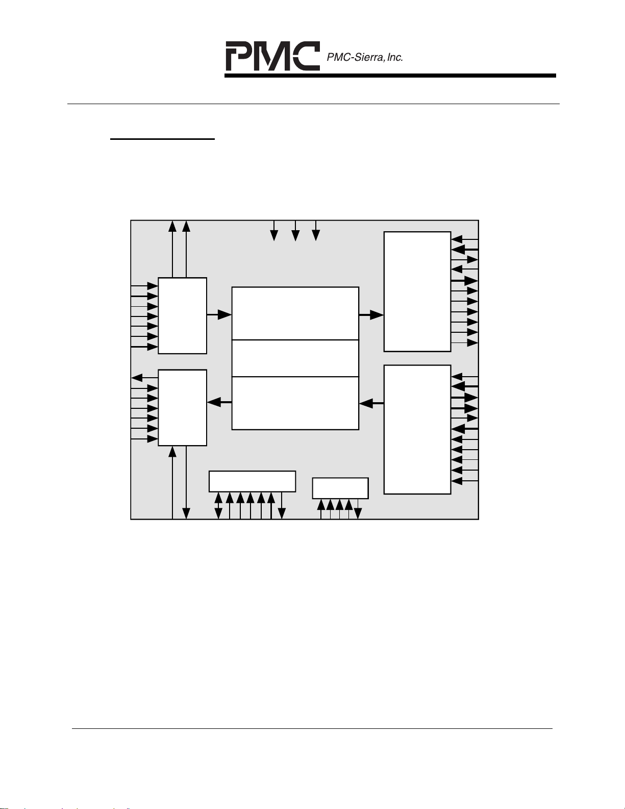
4 BLOCK DIAGRAM
RD[31:0]
RCLK[31:0]
RFPB[3:0]
RMVCK[3:0]
RMV8DC
RMV8FPC
RFP8B
TD[31:0 ]
TCLK[31:0]
TFPB[3:0]
TMVCK[3:0]
TMV8DC
TMV8FPC
TFP8 B
RBCLK
RBD
Receive
Channel
Assigner
(RCAS256)
Transmit
Channel
Assigner
(TCAS256)
Transmit HDLC Processor/
Microprocessor
Interface
PMCTEST
SYSCLK
RSTB
Receive HDLC Processor/
Partial Packet Buffer
(RHDL256)
Performance Monitor
(PMON)
Partial Packet Buffer
(THDL256)
JTAG Port
Receive
Any-PHY
Packet
Interface
(RAPI256)
Transmit
Any-PHY
Packet
Interface
(TAPI256)
RXCLK
RXADDR[2:0]
RPA
RENB
RXDATA[15:0]
RXPRTY
RSX
REOP
RMOD
RERR
RVAL
TXCLK
TXADD R[12:0]
TPA1[2:0]
TPA2[2:0]
TRDY
TXDATA[15:0]
TXPRTY
TSX
TEOP
TMOD
TERR
TBCLK
TBD
D[15:0]
TRSTB
INTB
RDB
WRB
CSB
ALE
A[11:2]
PROPRIETARY AND CONFIDENTIAL 6
TCK
TMS
TDI
TDO
Page 15

RELEASED
DATASHEET
PMC-2010336 ISSUE 1 FRAME ENGINE AND DATA LINK MANAGER 32A256
PM7383 FREEDM-32A256
5 DESCRIPTION
The PM7383 FREEDM-32A256 Frame Engine and Datalink Manager device is a
monolithic integrated circuit that implements HDLC processing for a maximum of
256 bi-directional channels.
The FREEDM-32A256 may be configured to support H-MVIP, channelised
T1/J1/E1 or unchannelised traffic across 32 physical links.
The FREEDM-32A256 may be configured to interface with H-MVIP digital
telephony buses at 2.048 Mbps. For 2.048 Mbps H-MVIP links, the FREEDM32A256 allows up to 256 bi-directional HDLC channels to be assigned to
individual time-slots within a maximum of 32 H-MVIP links. The channel
assignment supports the concatenation of time-slots (N x DS0) up to a maximum
of 32 concatenated time-slots for each 2.048 Mbps H-MVIP link. Time-slots
assigned to any particular channel need not be contiguous within the H-MVIP
link. When configured for 2.048 Mbps H-MVIP operation, the FREEDM-32A256
partitions the 32 physical links into 4 logical groups of 8 links. Links 0 through 7, 8
through 15, 16 through 23 and 24 through 31 make up the 4 logical groups.
Links in each logical group share a common clock and a common type 0 frame
pulse in each direction.
The FREEDM-32A256 may be configured to interface with H-MVIP digital
telephony buses at 8.192 Mbps. For 8.192 Mbps H-MVIP links, the FREEDM32A256 allows up to 256 bi-directional HDLC channels to be assigned to
individual time-slots within a maximum of 8 H-MVIP links. The channel
assignment supports the concatenation of time-slots (N x DS0) up to a maximum
of 128 concatenated time-slots for each 8.192 H-MVIP link. Time-slots assigned
to any particular channel need not be contiguous within the H-MVIP link. When
configured for 8.192 Mbps H-MVIP operation, the FREEDM-32A256 partitions
the 32 physical links into 8 logical groups of 4 links. Only the first link, which
must be located at physical links numbered 4m (0£m£7), of each logical group
can be configured for 8.192 Mbps operation. The remaining 3 physical links in
the logical group (numbered 4m+1, 4m+2 and 4m+3) are unused. All links
configured for 8.192 Mbps H-MVIP operation will share a common type 0 frame
pulse, a common frame pulse clock and a common data clock.
For channelised T1/J1/E1 links, the FREEDM-32A256 allows up to 256 bidirectional HDLC channels to be assigned to individual time-slots within a
maximum of 32 independently timed T1/J1 or E1 links. The gapped clock
method to determine time-slot positions as per the FREEDM-8 and FREEDM-32
devices is retained. The channel assignment supports the concatenation of time-
PROPRIETARY AND CONFIDENTIAL 7
Page 16

RELEASED
DATASHEET
PMC-2010336 ISSUE 1 FRAME ENGINE AND DATA LINK MANAGER 32A256
PM7383 FREEDM-32A256
slots (N x DS0) up to a maximum of 24 concatenated time-slots for a T1/J1 link
and 31 concatenated time-slots for an E1 link. Time-slots assigned to any
particular channel need not be contiguous within the T1/J1 or E1 link.
For unchannelised links, the FREEDM-32A256 processes up to 32 bi-directional
HDLC channels within 32 independently timed links. The links can be of arbitrary
frame format. When limited to three unchannelised links, each link can be rated
at up to 51.84 MHz provided SYSCLK is running at 45 MHz. For lower rate
unchannelised links, the FREEDM-32A256 processes up to 32 links each rated
at up to 10 MHz. In this case, the aggregate clock rate of all the links is limited to
64 MHz.
The FREEDM-32A256 supports mixing of up to 32 channelised T1/J1/E1,
unchannelised and H-MVIP links. The total number of channels in each direction
is limited to 256. The aggregate instantaneous clock rate over all 32 possible
links is limited to 64 MHz.
The FREEDM-32A256 provides a low latency “Any-PHY” packet interface (APPI)
to allow an external controller direct access into the 32 Kbyte partial packet
buffers. Up to seven FREEDM-32A256 devices may share a single APPI. For
each of the transmit and receive APPI, the external controller is the master of
each FREEDM-32A256 device sharing the APPI from the point of view of device
selection. The external controller is also the master for channel selection in the
transmit direction. In the receive direction, however, each FREEDM-32A256
device retains control over selection of its respective channels. The transmit and
receive APPI is made up of three groups of functional signals – polling, selection
and data transfer. The polling signals are used by the external controller to
interrogate the status of the transmit and receive 32 Kbyte partial packet buffers.
The selection signals are used by the external controller to select a FREEDM32A256 device, or a channel within a FREEDM-32A256 device, for data transfer.
The data transfer signals provide a means of transferring data across the APPI
between the external controller and a FREEDM-32A256 device.
In the receive direction, polling and selection are done at the device level.
Polling is not decoupled from selection, as the receive address pins serve as
both a device poll address and to select a FREEDM-32A256 device. In response
to a positive poll, the external controller may select that FREEDM-32A256 device
for data transfer. Once selected, the FREEDM-32A256 prepends an in-band
channel address to each partial packet transfer across the receive APPI to
associate the data with a channel. A FREEDM-32A256 must not be selected
after a negative poll response.
PROPRIETARY AND CONFIDENTIAL 8
Page 17

RELEASED
DATASHEET
PMC-2010336 ISSUE 1 FRAME ENGINE AND DATA LINK MANAGER 32A256
PM7383 FREEDM-32A256
In the transmit direction, polling is done at the channel level. Polling is
completely decoupled from selection. To increase the polling bandwidth, up to
two channels may be polled simultaneously. The polling engine in the external
controller runs independently of other activity on the transmit APPI. In response
to a positive poll, the external controller may commence partial packet data
transfer across the transmit APPI for the successfully polled channel of a
FREEDM-32A256 device. The external controller must prepend an in-band
channel address to each partial packet transfer across the transmit APPI to
associate the data with a channel.
In the receive direction, the FREEDM-32A256 performs channel assignment and
packet extraction and validation. For each provisioned HDLC channel, the
FREEDM-32A256 delineates the packet boundaries using flag sequence
detection, and performs bit de-stuffing. Sharing of opening and closing flags, as
well as sharing of zeros between flags are supported. The resulting packet data
is placed into the internal 32 Kbyte partial packet buffer RAM. The partial packet
buffer acts as a logical FIFO for each of the assigned channels. An external
controller transfers partial packets out of the RAM, across the receive APPI bus,
into host packet memory. The FREEDM-32A256 validates the frame check
sequence for each packet, and verifies that the packet is an integral number of
octets in length and is within a programmable minimum and maximum lengths.
Receive APPI bus latency may cause one or more channels to overflow, in which
case, the packets are aborted. The FREEDM-32A256 reports the status of each
packet on the receive APPI at the end of each packet transfer.
Alternatively, in the receive direction, the FREEDM-32A256 supports a
transparent operating mode. For each provisioned transparent channel, the
FREEDM-32A256 directly transfers the received octets onto the receive APPI
verbatim. If the transparent channel is assigned to a channelised link, then the
octets are aligned to the received time-slots.
In the transmit direction, an external controller provides packets to transmit using
the transmit APPI. For each provisioned HDLC channel, an external controller
transfers partial packets, across the transmit APPI, into the internal 32 Kbyte
transmit partial packet buffer. The partial packets are read out of the partial
packet buffer by the FREEDM-32A256 and a frame check sequence is optionally
calculated and inserted at the end of each packet. Bit stuffing is performed
before being assigned to a particular link. The flag or idle sequence is
automatically inserted when there is no packet data for a particular channel.
Sequential packets are optionally separated by a single flag (combined opening
and closing flag) or up to 128 flags. Zeros between flags are not shared in the
transmit direction although, as stated previously, they are accepted in the receive
direction. Transmit APPI bus latency may cause one or more channels to
PROPRIETARY AND CONFIDENTIAL 9
Page 18

RELEASED
DATASHEET
PMC-2010336 ISSUE 1 FRAME ENGINE AND DATA LINK MANAGER 32A256
PM7383 FREEDM-32A256
underflow, in which case, the packets are aborted. The FREEDM-32A256
generates an interrupt to notify the host of aborted packets. For normal traffic, an
abort sequence is generated, followed by inter-frame time fill characters (flags or
all-ones bytes) until a new packet is sourced on the transmit APPI. The
FREEDM-32A256 will not attempt to re-transmit aborted packets.
Alternatively, in the transmit direction, the FREEDM-32A256 supports a
transparent operating mode. For each provisioned transparent channel, the
FREEDM-32A256 directly inserts the transmitted octets provided on the transmit
APPI. If the transparent channel is assigned to a channelised link, then the
octets are aligned to the transmitted time-slots. If a channel underflows due to
excessive transmit APPI bus latency, an abort sequence is generated, followed
by inter-frame time fill characters (flags or all-ones bytes) to indicate idle channel.
Data resumes immediately when the FREEDM-32A256 receives new data on the
transmit APPI.
The FREEDM-32A256 is configured, controlled and monitored using the
microprocessor interface. The FREEDM-32A256 is implemented in low power2.5
Volt 0.25 mm CMOS technology. All FREEDM-32A256 I/O except those
belonging to the APPI are 5 volt tolerant. The APPI I/O are 3.3 volt tolerant. The
FREEDM-32A256 is packaged in a 329 pin plastic ball grid array (PBGA)
package.
PROPRIETARY AND CONFIDENTIAL 10
Page 19

RELEASED
DATASHEET
PM7383 FREEDM-32A256
PMC-2010336 ISSUE 1 FRAME ENGINE AND DATA LINK MANAGER 32A256
6 PIN DIAGRAM
The FREEDM-32A256 is manufactured in a 329 pin plastic ball grid array
package.
2322212019181716151413121110987654321
RMVCK[2] RD[16] RCLK[17] RCLK[19] RD[21] RD[22] RD[23] RD[24] RCLK[25] RCLK[27] RCLK[29] VDD2V5 RDB A[10] A[6] A[3] D[13] D[11] D[9] D[6] D[2] D[0] TPA2[2]
A
RFPB[2] RCLK[16] RD[18] RD[20] VDD2V5 RCLK[22] RFPB[3] RCLK[24] RCLK[26] RD[28] RD[30] RCLK[31] INTB A[11] A[8] A[4] D[15] D[12] VDD2V5 D[7] D[3] TPA2[0] TPA2[1]
B
RD[15] RSTB RCLK[15] RCLK[18] RCLK[20] RCLK[21] RMVCK[3] RD[25] RD[27] RCLK[28] RCLK[30] RD[31] CSB ALE A[9] A[5] A[2] D[10] D[8] D[4] D[1] N.C. TPA1[1]
C
RCLK[13] RD[13] RCLK[14] RD[17] RD[19] VDD3V3 RCLK[23] VSS RD[26] VDD3V3 RD[29] VSS WRB VDD3V3 A[7] VSS D[14] VDD3V3 D[5] TPA1[2] TPA1[0]
D
RD[12] VDD2V5 RCLK[12] RD[14]
E
RD[11] RCLK[10] RCLK[11] VSS VSS
F
RD[10] RD[9] RCLK[8] RCLK[9]
G
RD[8] RMVCK[1] RFPB[1] VDD3V3 VDD3V3
H
RCLK[7] RCLK[6] RD[6] RD[7]
J
SYSCLK RCLK[5] RD[5] VSS VSS VSS VSS VSS VSS VSS
K
RD[4] RD[3] RCLK[3] RCLK[4] VSS VSS VSS VSS VSS TXPRTY
L
VDD2V5 RCLK[2] RD[2] VDD3V3 VSS VSS VSS VSS VSS VDD3V3
M
RCLK[0] RD[1] RCLK[1] RD[0] VSS VSS VSS VSS VSS
N
RMV8FPC RFPB[0] RMVCK[0] VSS VSS VSS VSS VSS VSS VSS TEOP TMOD TERR
P
RBD RMV8DC RFP8B RBCLK RPA TRDY RVAL RENB
R
TCK TMS TRSTB VDD3V3 VDD3V3 REOP RMOD RERR
T
TFP8B TDO TDI TMV8DC
U
TFPB[0] TMV8FPC TMVCK[0] VSS VSS
V
TD[0] VDD2V5 TCLK[0] TD[2]
W
TCLK[1] TD[1] TCLK[2] TD[4] TMVCK[1] VDD3V3 TD[12] VSS TCLK[15] VDD3V3 TCLK[17] VSS TD[22] VDD3V3 TD[24] VSS TCLK[27] VDD3V3 TBD
Y
TCLK[3] TD[3] TCLK[6] TFPB[1] TD[9] TD[10] TD[13] TCLK[14] TMVCK[2] TD[17] TCLK[18] TD[20] TCLK[20] TCLK[22] TFPB[3] TD[25] TCLK[26] TCLK[29] TCLK[30] TBCLK
AA
TD[5] TCLK[4] TCLK[7] TCLK[8] VDD2V5 TD[11] TCLK[12] TD[14] TFPB[2] TCLK[16] TD[19] TCLK[19] TD[21] TD[23] TMVCK[3] TCLK[25] TD[27] TCLK[28] VDD2V5 TD[31] PMCTEST
AB
TCLK[5] TD[6] TD[7] TD[8] TCLK[9] TCLK[10] TCLK[11] TCLK[13] TD[15] TD[16] TD[18] VDD2V5 TCLK[21] TCLK[23] TCLK[24] TD[26] TD[28] TD[29] TD[30] TCLK[31]
AC
BOTTOM VIEW
TXADDR
[12]
TXADDR
TXDATA
[13]
TXDATA
RXDATA
[14]
RXDATA
RXADDR
TXADDR
TXADDR
VDD2V5
[9]
TXADDR
TXADDR
[7]
TXADDR
TXADDR
[3]
[1]
TXDATA
TXCLK
[15]
TXDATA
TXDATA
[11]
TXDATA
TXDATA
[8]
TXDATA
TXDATA
[6]
TXDATA
TXDATA
[5]
TXDATA
TXDATA
[0]
[2]
RXDATA
RXPRTY
RXDATA
RXDATA
[10]
RXDATA
VDD2V5
[6]
[8]
RXDATA
[1]
[5]
RXDATA
RXDATA
[2]
RXADDR
RXADDR
RXCLK
[0]
2322212019181716151413121110987654321
[10]
[5]
[2]
[12]
[9]
[7]
[4]
[3]
[15]
[12]
RSX
[4]
[2]
TXADDR
[11]
TXADDR
[8]
TXADDR
[6]
TXADDR
[4]
TXADDR
[0]
TXDATA
[14]
TXDATA
[10]
TSX
VDD2V5
TXDATA
[1]
RXDATA
[13]
RXDATA
[11]
RXDATA
[9]
RXDATA
[7]
RXDATA
[3]
RXDATA
[1]
RXDATA
[0]
A
B
C
D
E
F
G
H
J
K
L
M
N
P
R
T
U
V
W
Y
AA
AB
AC
PROPRIETARY AND CONFIDENTIAL 11
Page 20

RELEASED
DATASHEET
PMC-2010336 ISSUE 1 FRAME ENGINE AND DATA LINK MANAGER 32A256
PM7383 FREEDM-32A256
7 PIN DESCRIPTION
Table 1 – Line Side Interface Signals (154)
Pin Name Type Pin
Function
No.
RCLK[0]
RCLK[1]
RCLK[2]
RCLK[3]
RCLK[4]
RCLK[5]
RCLK[6]
RCLK[7]
RCLK[8]
RCLK[9]
RCLK[10]
RCLK[11]
RCLK[12]
RCLK[13]
RCLK[14]
RCLK[15]
RCLK[16]
RCLK[17]
RCLK[18]
RCLK[19]
RCLK[20]
RCLK[21]
RCLK[22]
RCLK[23]
RCLK[24]
RCLK[25]
RCLK[26]
RCLK[27]
RCLK[28]
RCLK[29]
RCLK[30]
RCLK[31]
Input N23
N21
M22
L21
L20
K22
J22
J23
G21
G20
F22
F21
E21
D23
D21
C21
B22
A21
C20
A20
C19
C18
B18
D17
B16
A15
B15
A14
C14
A13
C13
B12
The receive line clock signals (RCLK[31:0])
contain the recovered line clock for the 32
independently timed links. Processing of
the receive links are on a priority basis, in
descending order from RCLK[0] to
RCLK[31]. Therefore, the highest rate link
should be connected to RCLK[0] and the
lowest to RCLK[31].
For channelised T1/J1 or E1 links, RCLK[n]
must be gapped during the framing bit (for
T1/J1 interfaces) or during time-slot 0 (for
E1 interfaces) of the RD[n] stream. The
FREEDM-32A256 uses the gapping
information to determine the time-slot
alignment in the receive stream.
RCLK[31:0] is nominally a 50% duty cycle
clock of frequency 1.544 MHz for T1/J1 links
and 2.048 MHz for E1 links.
For unchannelised links, RCLK[n] must be
externally gapped during the bits or timeslots that are not part of the transmission
format payload (i.e. not part of the HDLC
packet). RCLK[2:0] is nominally a 50% duty
cycle clock between 0 and 51.84 MHz.
RCLK[31:3] is nominally a 50% duty cycle
clock between 0 and 10 MHz.
The RCLK[n] inputs are invalid and should
be forced to a low state when their
associated link is configured for operation in
H-MVIP mode.
PROPRIETARY AND CONFIDENTIAL 12
Page 21

RELEASED
DATASHEET
PMC-2010336 ISSUE 1 FRAME ENGINE AND DATA LINK MANAGER 32A256
Pin Name Type Pin
Function
PM7383 FREEDM-32A256
No.
RD[0]
RD[1]
RD[2]
RD[3]
RD[4]
RD[5]
RD[6]
RD[7]
RD[8]
RD[9]
RD[10]
RD[11]
RD[12]
RD[13]
RD[14]
RD[15]
RD[16]
RD[17]
RD[18]
RD[19]
RD[20]
RD[21]
RD[22]
RD[23]
RD[24]
RD[25]
RD[26]
RD[27]
RD[28]
RD[29]
RD[30]
RD[31]
Input N20
N22
M21
L22
L23
K21
J21
J20
H23
G22
G23
F23
E23
D22
E20
C23
A22
D20
B21
D19
B20
A19
A18
A17
A16
C16
D15
C15
B14
D13
B13
C12
The receive data signals (RD[31:0]) contain
the recovered line data for the 32
independently timed links in normal mode
(PMCTEST set low). Processing of the
receive links is on a priority basis, in
descending order from RD[0] to RD[31].
Therefore, the highest rate link should be
connected to RD[0] and the lowest to
RD[31].
For H-MVIP links, RD[n] contains 32/128
time-slots, depending on the H-MVIP data
rate configured (2.048 or 8.192 Mbps).
When configured for 2.048 Mbps H-MVIP
operation, RD[31:24], RD[23:16], RD[15:8]
and RD[7:0] are sampled on every 2
nd
rising
edge of RMVCK[3], RMVCK[2], RMVCK[1]
and RMVCK[0] respectively (at the ¾ point
of the bit interval). When configured for
8.192 Mbps H-MVIP operation, RD[4m]
(0£m£7) are sampled on every 2nd rising
edge of RMV8DC (at the ¾ point of the bit
interval).
For channelised links, RD[n] contains the 24
(T1/J1) or 31 (E1) time-slots that comprise
the channelised link. RCLK[n] must be
gapped during the T1/J1 framing bit position
or the E1 frame alignment signal (time-slot
0). The FREEDM-32A256 uses the location
of the gap to determine the channel
alignment on RD[n]. RD[31:0] are sampled
on the rising edge of the corresponding
RCLK[31:0].
For unchannelised links, RD[n] contains the
HDLC packet data. For certain transmission
formats, RD[n] may contain place holder bits
or time-slots. RCLK[n] must be externally
gapped during the place holder positions in
the RD[n] stream. The FREEDM-32A256
supports a maximum data rate of 10 Mbit/s
PROPRIETARY AND CONFIDENTIAL 13
Page 22

RELEASED
DATASHEET
PMC-2010336 ISSUE 1 FRAME ENGINE AND DATA LINK MANAGER 32A256
Pin Name Type Pin
Function
PM7383 FREEDM-32A256
No.
on an individual RD[31:3] link and a
maximum data rate of 51.84 Mbit/s on
RD[2:0]. RD[31:0] are sampled on the rising
edge of the corresponding RCLK[31:0].
RMVCK[0]
RMVCK[1]
RMVCK[2]
RMVCK[3]
Input P21
H22
A23
C17
The receive MVIP data clock signals
(RMVCK[3:0]) provide the receive data clock
for the 32 links when configured to operate
in 2.048 Mbps H-MVIP mode.
When configured for 2.048 Mbps H-MVIP
operation, the 32 links are partitioned into 4
groups of 8, and each group of 8 links share
a common data clock. RMVCK[0],
RMVCK[1], RMVCK[2] and RMVCK[3]
sample the data on links RD[7:0], RD[15:8],
RD[23:16] and RD[31:24] respectively.
Each RMVCK[n] is nominally a 50% duty
cycle clock with a frequency of 4.096 MHz.
RMVCK[n] is ignored and should be tied low
when no physical link within the associated
logical group of 8 links is configured for
operation in 2.048 Mbps H-MVIP mode.
PROPRIETARY AND CONFIDENTIAL 14
Page 23

RELEASED
DATASHEET
PMC-2010336 ISSUE 1 FRAME ENGINE AND DATA LINK MANAGER 32A256
Pin Name Type Pin
Function
PM7383 FREEDM-32A256
No.
RFPB[0]
RFPB[1]
RFPB[2]
RFPB[3]
Input P22
H21
B23
B17
The receive frame pulse signals (RFPB[3:0])
reference the beginning of each frame for
the 32 links when configured for operation in
2.048 Mbps H-MVIP mode.
When configured for 2.048 Mbps H-MVIP
operation, the 32 links are partitioned into 4
groups of 8, and each group of 8 links share
a common frame pulse. RFPB[0], RFPB[1],
RFPB[2] and RFPB[3] reference the
beginning of a frame on links RD[7:0],
RD[15:8], RD[23:16] and RD[31:24]
respectively.
When configured for operation in 2.048
Mbps H-MVIP mode, RFPB[n] is sampled
on the falling edge of RMVCK[n].
Otherwise, RFPB[n] is ignored and should
be tied low.
RFP8B Input R21 The receive frame pulse for 8.192 Mbps H-
MVIP signal (RFP8B) references the
beginning of each frame for links configured
for operation in 8.192 Mbps H-MVIP mode.
RFP8B references the beginning of a frame
for any link configured for 8.192 Mbps HMVIP operation. Only links RD[4m] (0£m£7)
may be configured for 8.192 Mbps H-MVIP
operation.
When one or more links are configured for
8.192 Mbps H-MVIP operation, RFP8B is
sampled on the falling edge of RMV8FPC.
When no links are configured for 8.192
Mbps H-MVIP operation, RFP8B is ignored
and should be tied low.
PROPRIETARY AND CONFIDENTIAL 15
Page 24

RELEASED
DATASHEET
PMC-2010336 ISSUE 1 FRAME ENGINE AND DATA LINK MANAGER 32A256
Pin Name Type Pin
Function
PM7383 FREEDM-32A256
No.
RMV8FPC Input P23 The receive 8.192 Mbps H-MVIP frame
pulse clock signal (RMV8FPC) provides the
receive frame pulse clock for links
configured for operation in 8.192 Mbps HMVIP mode.
RMV8FPC is used to sample RFP8B.
RMV8FPC is nominally a 50% duty cycle,
clock with a frequency of 4.096 MHz. The
falling edge of RMV8FPC must be aligned
with the falling edge of RMV8DC with no
more than ±10 ns skew.
RMV8FPC is ignored and should be tied low
when no physical links are configured for
operation in 8.192 Mbps H-MVIP mode.
RMV8DC Input R22 The receive 8.192 Mbps H-MVIP data clock
signal (RMV8DC) provides the receive data
clock for links configured to operate in 8.192
Mbps H-MVIP mode.
RMV8DC is used to sample data on RD[4m]
(0£m£7) when link 4m is configured for
8.192 Mbps H-MVIP operation. RMV8DC is
nominally a 50% duty cycle clock with a
frequency of 16.384 MHz.
RMV8DC is ignored and should be tied low
when no physical links are configured for
operation in 8.192 Mbps H-MVIP mode.
RBD Tristate
Output
R23 The receive BERT data signal (RBD)
contains the receive bit error rate test data.
RBD reports the data on the selected one of
the receive data signals (RD[31:0]) and is
updated on the falling edge of RBCLK.
RBD may be tristated by setting the RBEN
bit in the FREEDM-32A256 Master BERT
Control register low. BERT is not supported
for H-MVIP links.
PROPRIETARY AND CONFIDENTIAL 16
Page 25

RELEASED
DATASHEET
PMC-2010336 ISSUE 1 FRAME ENGINE AND DATA LINK MANAGER 32A256
Pin Name Type Pin
Function
PM7383 FREEDM-32A256
No.
RBCLK Tristate
Output
R20 The receive BERT clock signal (RBCLK)
contains the receive bit error rate test clock.
RBCLK is a buffered version of the selected
one of the receive clock signals
(RCLK[31:0]). RBCLK may be tristated by
setting the RBEN bit in the FREEDM32A256 Master BERT Control register low.
BERT is not supported for H-MVIP links.
PROPRIETARY AND CONFIDENTIAL 17
Page 26

RELEASED
DATASHEET
PMC-2010336 ISSUE 1 FRAME ENGINE AND DATA LINK MANAGER 32A256
Pin Name Type Pin
Function
PM7383 FREEDM-32A256
No.
TCLK[0]
TCLK[1]
TCLK[2]
TCLK[3]
TCLK[4]
TCLK[5]
TCLK[6]
TCLK[7]
TCLK[8]
TCLK[9]
TCLK[10]
TCLK[11]
TCLK[12]
TCLK[13]
TCLK[14]
TCLK[15]
TCLK[16]
TCLK[17]
TCLK[18]
TCLK[19]
TCLK[20]
TCLK[21]
TCLK[22]
TCLK[23]
TCLK[24]
TCLK[25]
TCLK[26]
TCLK[27]
TCLK[28]
TCLK[29]
TCLK[30]
TCLK[31]
Input W21
Y23
Y21
AA23
AB22
AC23
AA21
AB21
AB20
AC19
AC18
AC17
AB17
AC16
AA16
Y15
AB14
Y13
AA13
AB12
AA11
AC11
AA10
AC10
AC9
AB8
AA7
Y7
The transmit line clock signals (TCLK[31:0])
contain the transmit clocks for the 32
independently timed links. Processing of
the transmit links is on a priority basis, in
descending order from TCLK[0] to
TCLK[31]. Therefore, the highest rate link
should be connected to TCLK[0] and the
lowest to TCLK[31].
For channelised T1/J1 or E1 links, TCLK[n]
must be gapped during the framing bit (for
T1/J1 interfaces) or during time-slot 0 (for
E1 interfaces) of the TD[n] stream. The
FREEDM-32A256 uses the gapping
information to determine the time-slot
alignment in the transmit stream.
For unchannelised links, TCLK[n] must be
externally gapped during the bits or timeslots that are not part of the transmission
format payload (i.e. not part of the HDLC
packet).
TCLK[2:0] is nominally a 50% duty cycle
clock between 0 and 51.84 MHz.
TCLK[31:3] is nominally a 50% duty cycle
clock between 0 and 10 MHz. Typical
values for TCLK[31:0] include 1.544 MHz
(for T1/J1 links) and 2.048 MHz (for E1
links).
AB6
AA6
AA5
AC4
The TCLK[n] inputs are invalid and should
be tied low when their associated link is
configured for operation in H-MVIP mode.
PROPRIETARY AND CONFIDENTIAL 18
Page 27

RELEASED
DATASHEET
PMC-2010336 ISSUE 1 FRAME ENGINE AND DATA LINK MANAGER 32A256
Pin Name Type Pin
Function
PM7383 FREEDM-32A256
No.
TD[0]
TD[1]
TD[2]
TD[3]
TD[4]
TD[5]
TD[6]
TD[7]
TD[8]
TD[9]
TD[10]
TD[11]
TD[12]
TD[13]
TD[14]
TD[15]
TD[16]
TD[17]
TD[18]
TD[19]
TD[20]
TD[21]
TD[22]
TD[23]
TD[24]
TD[25]
TD[26]
TD[27]
TD[28]
TD[29]
TD[30]
TD[31]
Output
W23
Y22
W20
AA22
Y20
AB23
AC22
AC21
AC20
AA19
AA18
AB18
Y17
AA17
AB16
AC15
AC14
AA14
AC13
AB13
AA12
AB11
Y11
AB10
Y9
AA8
AC8
AB7
AC7
AC6
AC5
AB4
The transmit data signals (TD[31:0]) contain
the transmit data for the 32 independently
timed links in normal mode (PMCTEST set
low). Processing of the transmit links is on
a priority basis, in descending order from
TD[0] to TD[31]. Therefore, the highest rate
link should be connected to TD[0] and the
lowest to TD[31].
For H-MVIP links, TD[n] contain 32/128
time-slots, depending on the H-MVIP data
rate configured (2.048 or 8.192 Mbps).
When configured for 2.048 Mbps H-MVIP
operation, TD[31:24], TD[23:16], TD[15:8]
and TD[7:0] are updated on every 2
nd
falling
edge of TMVCK[3], TMVCK[2], TMVCK[1]
and TMVCK[0] respectively. When
configured for 8.192 Mbps H-MVIP
operation, TD[4m] (0£m£7) are updated on
every 2nd falling edge of TMV8DC.
For channelised links, TD[n] contains the 24
(T1/J1) or 31 (E1) time-slots that comprise
the channelised link. TCLK[n] must be
gapped during the T1/J1 framing bit position
or during the E1 frame alignment signal
(time-slot 0). The FREEDM-32A256 uses
the location of the gap to determine the
channel alignment on TD[n]. TD[31:0] are
updated on the falling edge of the
corresponding TCLK[31:0].
For unchannelised links, TD[n] contains the
HDLC packet data. For certain transmission
formats, TD[n] may contain place holder bits
or time-slots. TCLK[n] must be externally
gapped during the place holder positions in
the TD[n] stream. The FREEDM-32A256
supports a maximum data rate of 10 Mbit/s
on an individual TD[31:3] link and a
maximum data rate of 51.84 Mbit/s on
TD[2:0].
PROPRIETARY AND CONFIDENTIAL 19
Page 28

RELEASED
DATASHEET
PMC-2010336 ISSUE 1 FRAME ENGINE AND DATA LINK MANAGER 32A256
Pin Name Type Pin
Function
PM7383 FREEDM-32A256
No.
TD[31:0] are updated on the falling edge of
the corresponding TCLK[31:0] clock.
TMVCK[0]
TMVCK[1]
TMVCK[2]
TMVCK[3]
Input V21
Y19
AA15
AB9
The transmit MVIP data clock signals
(TMVCK[3:0]) provide the transmit data
clocks for the 32 links when configured to
operate in 2.048 Mbps H-MVIP mode.
When configured for 2.048 Mbps H-MVIP
operation, the 32 links are partitioned into 4
groups of 8, and each group of 8 links share
a common clock. TMVCK[0], TMVCK[1],
TMVCK[2] and TMVCK[3] update the data
on links TD[7:0], TD[15:8], TD[23:16] and
TD[31:24] respectively. Each TMVCK[n] is
nominally a 50% duty cycle clock with a
frequency of 4.096 MHz.
TFPB[0]
TFPB[1]
TFPB[2]
TFPB[3]
Input V23
AA20
AB15
AA9
TMVCK[n] is unused and should be tied low
when no physical links within the associated
group of 8 logical links is configured for
operation in 2.048 Mbps H-MVIP mode.
The transmit frame pulse signals
(TFPB[3:0]) reference the beginning of each
frame when configured for operation in
2.048 Mbps H-MVIP mode.
When configured for 2.048 Mbps H-MVIP
operation, the 32 links are partitioned into 4
groups of 8, and each group of 8 links share
a common frame pulse. TFPB[0], TFPB[1],
TFPB[2] and TFPB[3] reference the
beginning of a frame on links TD[7:0],
TD[15:8], TD[23:16] and TD[31:24]
respectively.
When configured for operation in 2.048
Mbps H-MVIP mode, TFPB[n] is sampled on
the falling edge of TMVCK[n]. Otherwise,
TFPB[n] is ignored and should be tied low.
PROPRIETARY AND CONFIDENTIAL 20
Page 29

RELEASED
DATASHEET
PMC-2010336 ISSUE 1 FRAME ENGINE AND DATA LINK MANAGER 32A256
Pin Name Type Pin
Function
PM7383 FREEDM-32A256
No.
TFP8B Input U23 The transmit frame pulse for 8.192 Mbps H-
MVIP signal (TFP8B) references the
beginning of each frame for links configured
to operate in 8.192 Mbps H-MVIP mode.
TFP8B references the beginning of a frame
for any link configured for 8.192 Mbps HMVIP operation. Only links 4m (0£m£7)
may be configured for 8.192 Mbps H-MVIP
operation.
When one or more links are configured for
8.192 Mbps H-MVIP operation, TFP8B is
sampled on the falling edge of TMV8FPC.
When no links are configured for 8.192
Mbps H-MVIP operation, TFPB[n] is ignored
and should be tied low.
TMV8FPC Input V22 The transmit 8.192 Mbps H-MVIP frame
pulse clock signal (TMV8FPC) provides the
transmit frame pulse clock for links
configured for operation in 8.192 Mbps HMVIP mode.
TMV8FPC is used to sample TFP8B.
TMV8FPC is nominally a 50% duty cycle,
clock with a frequency of 4.096 MHz. The
falling edge of TMV8FPC must be aligned
with the falling edge of TMV8DC with no
more than ±10 ns skew.
TMV8FPC[n] is ignored and should be tied
low when no physical links are configured
for operation in 8.192 Mbps H-MVIP mode.
PROPRIETARY AND CONFIDENTIAL 21
Page 30

RELEASED
DATASHEET
PMC-2010336 ISSUE 1 FRAME ENGINE AND DATA LINK MANAGER 32A256
Pin Name Type Pin
Function
PM7383 FREEDM-32A256
No.
TMV8DC Input U20 The transmit 8.192 Mbps H-MVIP data clock
signal (TMV8DC) provides the transmit data
clock for links configured to operate in 8.192
Mbps H-MVIP mode.
TMV8DC is used to update data on TD[4m]
(0£m£7) when link 4m is configured for
8.192 Mbps H-MVIP operation. TMV8DC is
nominally a 50% duty cycle clock with a
frequency of 16.384 MHz.
TMV8DC is unused and should be tied low
when no physical links are configured for
operation in 8.192 Mbps H-MVIP mode.
TBD Input Y5 The transmit BERT data signal (TBD)
contains the transmit bit error rate test data.
When the TBERTEN bit in the BERT Control
register is set high, the data on TBD is
transmitted on the selected one of the
transmit data signals (TD[31:0]). TBD is
sampled on the rising edge of TBCLK.
BERT is not supported for H-MVIP links.
TBCLK Tristate
Output
AA4 The transmit BERT clock signal (TBCLK)
contains the transmit bit error rate test clock.
TBCLK is a buffered version of the selected
one of the transmit clock signals
(TCLK[31:0]). TBCLK may be tristated by
setting the TBEN bit in the FREEDM32A256 Master BERT Control register low.
BERT is not supported for H-MVIP links.
PROPRIETARY AND CONFIDENTIAL 22
Page 31

RELEASED
DATASHEET
PMC-2010336 ISSUE 1 FRAME ENGINE AND DATA LINK MANAGER 32A256
PM7383 FREEDM-32A256
Table 2 – Any-PHY Packet Interface Signals (70)
Pin Name Type Pin
Function
No.
TXCLK Input H2 The transmit clock signal (TXCLK) provides
timing for the transmit Any-PHY packet
interface. TXCLK is a nominally 50% duty
cycle, 25 to 50 MHz clock.
TXADDR[0]
TXADDR[1]
TXADDR[2]
TXADDR[3]
TXADDR[4]
TXADDR[5]
TXADDR[6]
TXADDR[7]
TXADDR[10]
TXADDR[11]
TXADDR[12]
Input H1
G3
G2
G4
G1
F2
F1
F3
D2
D1
E4
The transmit address signals (TXADDR[12:0])
provide a channel address for polling a transmit
channel FIFO. The 8 least significant bits
provide the channel number (0 to 255) while the
3 most significant bits select one of seven
possible FREEDM-32A256 devices sharing a
single external controller. (One address is
reserved as a null address.) The Tx APPI of
each FREEDM-32A256 device is identified by
the base address in the TAPI256 Control
register.
The TXADDR[12:0] signals are sampled on the
rising edge of TXCLK.
Note that TXADDR[9:8] have been removed
from the FREEDM-32A256 device. Pin
numbering of TXADDR[7:0] and
TXADDR[12:10] has been maintained to allow
software compatibility with the FREEDM32A672 device.
PROPRIETARY AND CONFIDENTIAL 23
Page 32

RELEASED
DATASHEET
PMC-2010336 ISSUE 1 FRAME ENGINE AND DATA LINK MANAGER 32A256
Pin Name Type Pin
Function
PM7383 FREEDM-32A256
No.
TPA1[0]
TPA1[1]
TPA1[2]
TPA2[0]
TPA2[1]
TPA2[2]
Tristate
Output
D3
C1
D4
B2
B1
A1
The transmit packet available signals (TPA1[2:0]
and TPA2[2:0]) reflects the status of a poll of
two transmit channel FIFOs. TPA1[2:0] returns
the polled results for channel address ‘n’
provided on TXADDR[12:0] and TPA2[2:0]
returns the polled results for channel address
‘n+1’. TPAn[2] reports packet underrun events
and TPAn[1:0] report the fill state of the transmit
channel FIFO. TPAn[2] is set high when one or
more packets has underrun on the channel and
a further data transfer has occurred since it was
last polled. When TPAn[2] is set low, no packet
has underrun on the channel since the last poll.
TPAn[1:0] are coded as follows:
TPAn[1:0] = “11” => Starving
TPAn[1:0] = “10” => (Reserved)
TPAn[1:0] = “01” => Space
TPAn[1:0] = “00” => Full
A “Starving” polled response indicates that the
polled transmit channel FIFO is at risk of
underflowing and should be supplied with data
as soon as possible. A “Space” polled response
indicates that the polled transmit channel FIFO
can accept XFER[3:0] plus one blocks (16 bytes
per block) of data. A “Full” polled response
indicates that the polled transmit channel FIFO
cannot accept XFER[3:0] plus one blocks of
data. (XFER[3:0] is a per-channel
programmable value – see description of
register 0x38C.)
It is the responsibility of the external controller to
prevent channel underflow conditions by
adequately polling each channel before data
transfer.
TPAn[2:0] are tristate during reset and when a
device address other than the FREEDM32A256’s base address is provided on
TXADDR[12:10].
PROPRIETARY AND CONFIDENTIAL 24
Page 33

RELEASED
DATASHEET
PMC-2010336 ISSUE 1 FRAME ENGINE AND DATA LINK MANAGER 32A256
Pin Name Type Pin
Function
PM7383 FREEDM-32A256
No.
TPAn[2:0] are updated on the rising edge of
TXCLK.
TRDY Tristate
Output
R3 The transmit ready signal (TRDY) indicates the
ability of the transmit Any-PHY packet interface
(APPI) to accept data. When TRDY is set low,
the transmit APPI is unable to accept further
data. When TRDY is set high, data provided on
the transmit APPI will be accepted by the
FREEDM-32A256 device.
TRDY is asserted one TXCLK cycle after TSX is
sampled high. TRDY is asserted by the
FREEDM-32A256 device which was selected by
the in-band channel address on TXDATA[15:0]
when TSX was sampled high. If TRDY is driven
low, the external controller must hold the data
on TXDATA[15:0] until TRDY is driven high.
TRDY may be driven low for 0 or more TXCLK
cycles before it is driven high. TRDY is always
driven tristate the TXCLK cycle after it is driven
high.
TRDY is tristate during reset.
TRDY is updated on the rising edge of TXCLK.
It is recommended that TRDY be connected
externally to a weak pull-up, e.g. 10 kW.
PROPRIETARY AND CONFIDENTIAL 25
Page 34

RELEASED
DATASHEET
PMC-2010336 ISSUE 1 FRAME ENGINE AND DATA LINK MANAGER 32A256
Pin Name Type Pin
Function
PM7383 FREEDM-32A256
No.
TXDATA[0]
TXDATA[1]
TXDATA[2]
TXDATA[3]
TXDATA[4]
TXDATA[5]
TXDATA[6]
TXDATA[7]
TXDATA[8]
TXDATA[9]
TXDATA[10]
TXDATA[11]
TXDATA[12]
TXDATA[13]
TXDATA[14]
TXDATA[15]
Input N4
N1
N3
N2
M2
M3
L3
L2
K3
K2
K1
J3
J2
J4
J1
H3
The transmit data signals (TXDATA[15:0])
contain the transmit Any-PHY packet interface
(APPI) data provided by the external controller.
Data must be presented in big endian order, i.e.
the byte in TXDATA[15:8] is transmitted by the
FREEDM-32A256 before the byte in
TXDATA[7:0].
The first word of each data transfer contains an
address to identify the device and channel
associated with the data being transferred. This
prepended address must be qualified with the
TSX signal. The 8 least significant bits provide
the channel number (0 to 255) while the 3 most
significant bits select one of seven possible
FREEDM-32A256 devices sharing a single
external controller. (One address is reserved as
a null address.) The FREEDM-32A256 will not
respond to channel addresses outside the range
0 to 255, nor to device addresses other than the
base address stored in the TAPI256 Control
register.
The second and any subsequent words of each
data transfer contain packet data.
The TXDATA[15:0] signals are sampled on the
rising edge of TXCLK.
TXPRTY Input L4 The transmit parity signal (TXPRTY) reflects the
odd parity calculated over the TXDATA[15:0]
signals. TXPRTY is only valid when
TXDATA[15:0] are valid.
TXPRTY is sampled on the rising edge of
TXCLK.
PROPRIETARY AND CONFIDENTIAL 26
Page 35

RELEASED
DATASHEET
PMC-2010336 ISSUE 1 FRAME ENGINE AND DATA LINK MANAGER 32A256
Pin Name Type Pin
Function
PM7383 FREEDM-32A256
No.
TSX Input L1 The transmit start of transfer signal (TSX)
denotes the start of data transfer on the transmit
APPI. When the TSX signal is sampled high,
the sampled word on the TXDATA[15:0] signals
contain the device and channel address
associated with the data to follow. When the
TSX signal is sampled low, the sampled word
on the TXDATA[15:0] signals do not contain a
device/channel address.
The TSX signal is sampled on the rising edge of
TXCLK.
TEOP Input P3 The transmit end of packet signal (TEOP)
denotes the end of a packet. TEOP is only valid
during data transfer. When TEOP is sampled
high, the data on TXDATA[15:0] is the last word
of a packet. When TEOP is sampled low, the
data on TXDATA[15:0] is not the last word of a
packet.
TEOP is sampled on the rising edge of TXCLK.
TMOD Input P2 The transmit word modulo signal (TMOD)
indicates the size of the current word on
TXDATA[15:0]. TMOD is only valid when TEOP
is sampled high. When TMOD is sampled high
and TEOP is sampled high, only the
TXDATA[15:8] signals contain valid data and the
TXDATA[7:0] signals are invalid. When TMOD
is sampled low and TEOP is sampled high, the
complete word on TXDATA[15:0] contains valid
data. TMOD must be set low when TEOP is set
low.
TMOD is sampled on the rising edge of TXCLK.
PROPRIETARY AND CONFIDENTIAL 27
Page 36

RELEASED
DATASHEET
PMC-2010336 ISSUE 1 FRAME ENGINE AND DATA LINK MANAGER 32A256
Pin Name Type Pin
Function
PM7383 FREEDM-32A256
No.
TERR Input P1 The transmit error signal (TERR) indicates that
the current packet is errored and should be
aborted. TERR is only valid when TEOP is
sampled high. When TERR is sampled high
and TEOP is sampled high, the current packet is
errored and the FREEDM-32A256 will respond
accordingly. When TERR is sampled low and
TEOP is sampled high, the current packet is not
errored. TERR must be set low when TEOP is
set low.
TERR is sampled on the rising edge of TXCLK.
RXCLK Input AC2 The receive clock signal (RXCLK) provides
timing for the receive Any-PHY packet interface
(APPI). RXCLK is a nominally 50% duty cycle,
25 to 50 MHz clock.
RXADDR[0]
RXADDR[1]
RXADDR[2]
Input AC3
Y4
AB2
The receive address signals (RXADDR[2:0])
serve two functions – device polling and device
selection. When polling, the RXADDR[2:0]
signals provide an address for polling a
FREEDM-32A256 device for receive data
available in any one of its 256 channels. Polling
results are returned on the RPA tristate output.
During selection, the address on the
RXADDR[2:0] signals is qualified with the RENB
signal to select a FREEDM-32A256 device
enabling it to output data on the receive APPI.
Note that up to seven FREEDM-32A256
devices may share a single external controller
(one address is reserved as a null address).
The Rx APPI of each FREEDM-32A256 device
is identified by the base address in the RAPI256
Control register.
The RXADDR[2:0] signals are sampled on the
rising edge of RXCLK.
PROPRIETARY AND CONFIDENTIAL 28
Page 37

RELEASED
DATASHEET
PMC-2010336 ISSUE 1 FRAME ENGINE AND DATA LINK MANAGER 32A256
Pin Name Type Pin
Function
PM7383 FREEDM-32A256
No.
RPA Tristate
Output
R4 The receive packet available signal (RPA)
reflects the status of a poll on the receive APPI
of a FREEDM-32A256 device. When RPA is set
high, the polled FREEDM-32A256 device has
XFER[3:0] plus one blocks (16 bytes per block)
of data to transfer, or alternatively, a smaller
amount of data which includes an end of packet.
When RPA is set low, the polled FREEDM32A256 device does not have data ready to
transfer. (XFER[3:0] is a per-channel
programmable value – see description of
register 0x208.)
A FREEDM-32A256 device must not be
selected for receive data transfer unless it has
been polled and responded that it has data
ready to transfer.
When the RXADDR[2:0] inputs match the base
address in the RAPI256 Control register, that
FREEDM-32A256 device drives RPA one
RXCLK cycle after sampling RXADDR[2:0].
RPA is tristate during reset and when a device
address other than the FREEDM-32A256’s base
address is provided on RXADDR[2:0].
RPA is updated on the rising edge of RXCLK.
PROPRIETARY AND CONFIDENTIAL 29
Page 38

RELEASED
DATASHEET
PMC-2010336 ISSUE 1 FRAME ENGINE AND DATA LINK MANAGER 32A256
Pin Name Type Pin
Function
PM7383 FREEDM-32A256
No.
RENB Input R1 The receive enable signal (RENB) qualifies the
RXADDR[2:0] signals for selection of a
FREEDM-32A256 device. When RENB is
sampled high and then low in consecutive
RXCLK cycles, the address on RXADDR[2:0]
during the cycle when RENB is sampled high
selects a FREEDM-32A256 device enabling it to
output data on the receive APPI. The Rx APPI
of each FREEDM-32A256 device is identified by
the base address in the RAPI256 Control
register.
The polling function of the RXADDR[2:0] and
RPA signals operates regardless of the state of
RENB.
RENB may also be used to throttle the
FREEDM-32A256 during data transfer on the
Rx APPI. When the FREEDM-32A256 samples
RENB high during data transfer, the FREEDM32A256 will pause the data transfer and tri-state
the receive APPI outputs (except RPA) until
RENB is returned low. Since the Any-PHY bus
specification does not support deselection
during data transfers, the address on the
RXADDR[2:0] inputs during the cycle before
RENB is returned low must either re-select the
same FREEDM-32A256 device or be a null
address.
To commence data transfer, RENB must be
sampled low following device selection.
It is the responsibility of the external controller to
prevent overflow by providing each FREEDM32A256 device on an Any-PHY point to multipoint bus sufficient bandwidth through selection.
RENB is sampled on the rising edge of RXCLK.
PROPRIETARY AND CONFIDENTIAL 30
Page 39

RELEASED
DATASHEET
PMC-2010336 ISSUE 1 FRAME ENGINE AND DATA LINK MANAGER 32A256
Pin Name Type Pin
Function
PM7383 FREEDM-32A256
No.
RXDATA[0]
RXDATA[1]
RXDATA[2]
RXDATA[3]
RXDATA[4]
RXDATA[5]
RXDATA[6]
RXDATA[7]
RXDATA[8]
RXDATA[9]
RXDATA[10]
RXDATA[11]
RXDATA[12]
RXDATA[13]
RXDATA[14]
RXDATA[15]
Tristate
Output
AC1
AB1
AA3
AA1
AA2
Y3
W4
Y1
W3
W1
V3
V1
V2
U1
U4
U2
The receive data signals (RXDATA[15:0])
contain the receive Any-PHY packet interface
(APPI) data output by the FREEDM-32A256
when selected. Data is presented in big endian
format, i.e. the byte in RXDATA[15:8] was
received by the FREEDM-32A256 before the
byte in RXDATA[7:0].
The first word of each data transfer (when RSX
is high) contains an address to identify the
device and channel associated with the data
being transferred. The 8 least significant bits
(RXDATA[7:0]) contain the channel number (0 to
255) and the 3 most significant bits
(RXDATA[15:13]) contain the device base
address. The second and any subsequent
words of each data transfer contain valid data.
The FREEDM-32A256 may be programmed to
overwrite RXDATA[7:0] of the final word of each
packet transfer (REOP is high) with the status of
packet reception when that packet is errored
(RERR is high). This status information is bit
mapped as follows:
RXDATA[0]=’1’ => channel FIFO overrun.
RXDATA[1]=’1’ => max. packet length violation.
RXDATA[2]=’1’ => FCS error.
RXDATA[3]=’1’ => non-octet aligned.
RXDATA[4]=’1’ => HDLC packet abort.
RXDATA[7:5]=”Xh” => Reserved.
The RXDATA[15:0] signals are tristate when the
FREEDM-32A256 device is not selected via the
RENB signal.
The RXDATA[15:0] signals are updated on the
rising edge of RXCLK.
PROPRIETARY AND CONFIDENTIAL 31
Page 40

RELEASED
DATASHEET
PMC-2010336 ISSUE 1 FRAME ENGINE AND DATA LINK MANAGER 32A256
Pin Name Type Pin
Function
PM7383 FREEDM-32A256
No.
RXPRTY Tristate
Output
U3 The receive parity signal (RXPRTY) reflects the
odd parity calculated over the RXDATA[15:0]
signals. RXPRTY is driven/tristate at the same
time as RXDATA[15:0].
RXPRTY is updated on the rising edge of
RXCLK.
RSX Tristate
Output
Y2 The receive start of transfer signal (RSX)
denotes the start of data transfer on the receive
APPI. When the RSX signal is set high, the 3
most significant bits on the RXDATA[15:0]
signals contain the FREEDM-32A256 device
address and the 10 least significant bits on the
RXDATA[15:0] signals contain the channel
address associated with the data to follow. Valid
device addresses are in the range 0 through 7
(with one address reserved as a null address)
and valid channel addresses are in the range 0
through 255. When the RSX signal is sampled
low, the word on the RXDATA[15:0] signals does
not contain a device and channel address.
RSX is tristate when the FREEDM-32A256
device is not selected via the RENB signal.
RSX is updated on the rising edge of RXCLK.
It is recommended that RSX be connected
externally to a weak pull-down, e.g. 10 kW.
REOP Tristate
Output
T3 The receive end of packet signal (REOP)
denotes the end of a packet. REOP is only valid
during data transfer. When REOP is set high,
RXDATA[15:0] contains the last data byte of a
packet. When REOP is set low, RXDATA[15:0]
does not contain the last data byte of a packet.
REOP is tristate when the FREEDM-32A256
device is not selected via the RENB signal.
REOP is updated on the rising edge of RXCLK.
PROPRIETARY AND CONFIDENTIAL 32
Page 41

RELEASED
DATASHEET
PMC-2010336 ISSUE 1 FRAME ENGINE AND DATA LINK MANAGER 32A256
Pin Name Type Pin
Function
PM7383 FREEDM-32A256
No.
RMOD Tristate
Output
T2 The receive word modulo signal (RMOD)
indicates the size of the current word on
RXDATA[15:0]. When RDAT[15:0] does not
contain the last byte of a packet (REOP set
low), RMOD is set low. When RMOD is set high
and REOP is set high, RXDATA[15:8] contains
the last data byte of a packet. When RMOD is
set low and REOP is set high, RXDATA[7:0]
contains the last byte of the packet, or
optionally, the error status byte. The behavior of
RMOD relates only to packet data and is
unaffected when the FREEDM-32A256 device is
programmed to overwrite RXDATA[7:0] with
status information when errored packets are
received.
RERR Tristate
T1 The receive error signal (RERR) indicates that
Output
RMOD is tristate when the FREEDM-32A256
device is not selected via the RENB signal.
RMOD is updated on the rising edge of RXCLK.
the current packet is errored and should be
discarded. When RDAT[15:0] does not contain
the last byte of a packet (REOP set low), RERR
is set low. When RERR is set high and REOP is
set high, the current packet is errored. When
RERR is set low and REOP is set high, the
current packet is not errored.
The FREEDM-32A256 may be programmed to
overwrite RXDATA[7:0] of the final word of each
packet transfer (REOP set high) with the status
of packet reception when that packet is errored
(RERR is high).
RERR is tristated when the FREEDM-32A256
device is not selected via the RENB signal.
RERR is updated on the rising edge of RXCLK.
PROPRIETARY AND CONFIDENTIAL 33
Page 42

RELEASED
DATASHEET
PMC-2010336 ISSUE 1 FRAME ENGINE AND DATA LINK MANAGER 32A256
Pin Name Type Pin
Function
PM7383 FREEDM-32A256
No.
RVAL Tristate
Output
R2 The receive data valid (RVAL) is asserted when
packet data is being output on RXDATA[15:0]. It
is deasserted whenever the FREEDM-32A256
device is selected, but not outputting packet
data on RXDATA[15:0]. (E.g., when RSX is high
and address/channel prepend is being output on
RXDATA[15:0], RVAL is deasserted.)
RVAL is tristated when the FREEDM-32A256
device is not selected via the RENB signal.
RVAL is updated on the rising edge of RXCLK.
PROPRIETARY AND CONFIDENTIAL 34
Page 43

RELEASED
DATASHEET
PMC-2010336 ISSUE 1 FRAME ENGINE AND DATA LINK MANAGER 32A256
PM7383 FREEDM-32A256
Table 3 – Microprocessor Interface Signals (31)
Pin Name Type Pin
Function
No.
D[0]
D[1]
D[2]
D[3]
D[4]
D[5]
D[6]
D[7]
D[8]
D[9]
D[10]
D[11]
D[12]
D[13]
D[14]
D[15]
I/O A2
C3
A3
B3
C4
D5
A4
The bi-directional data signals (D[15:0]) provide
a data bus to allow the FREEDM-32A256 device
to interface to an external micro-processor.
Both read and write transactions are supported.
The microprocessor interface is used to
configure and monitor the FREEDM-32A256
device.
B4
C5
A5
C6
A6
B6
A7
D7
B7
A[2]
A[3]
A[4]
A[5]
A[6]
A[7]
A[8]
A[9]
A[10]
A[11]
Input C7
A8
B8
C8
A9
D9
B9
C9
A10
B10
The address signals (A[11:2]) provide an
address bus to allow the FREEDM-32A256
device to interface to an external micro-
processor. All microprocessor accessible
registers are dword aligned.
ALE Input C10 The address latch enable signal (ALE) latches
the A[11:2] signals during the address phase of
a bus transaction. When ALE is set high, the
address latches are transparent. When ALE is
set low, the address latches hold the address
provided on A[11:2].
ALE has an integral pull-up resistor.
PROPRIETARY AND CONFIDENTIAL 35
Page 44

RELEASED
DATASHEET
PMC-2010336 ISSUE 1 FRAME ENGINE AND DATA LINK MANAGER 32A256
Pin Name Type Pin
Function
PM7383 FREEDM-32A256
No.
WRB Input D11 The write strobe signal (WRB) qualifies write
accesses to the FREEDM-32A256 device.
When CSB is set low, the D[15:0] bus contents
are clocked into the addressed register on the
rising edge of WRB.
RDB Input A11 The read strobe signal (RDB) qualifies read
accesses to the FREEDM-32A256 device.
When CSB is set low, the FREEDM-32A256
device drives the D[15:0] bus with the contents
of the addressed register on the falling edge of
RDB.
CSB Input C11 The chip select signal (CSB) qualifies read/write
accesses to the FREEDM-32A256 device. The
CSB signal must be set low during read and
write accesses. When CSB is set high, the
microprocessor interface signals are ignored by
the FREEDM-32A256 device.
INTB Open-
B11 The interrupt signal (INTB) indicates that an
Drain
Output
If CSB is not required (register accesses
controlled only by WRB and RDB) then CSB
should be connected to an inverted version of
the RSTB signal.
interrupt source is active and unmasked. When
INTB is set low, the FREEDM-32A256 device
has an active interrupt that is unmasked. When
INTB is tristate, no interrupts are active, or an
active interrupt is masked. Please refer to the
register description section of this document for
possible interrupt sources and masking.
It is the responsibility of the external
microprocessor to read the status registers in
the FREEDM-32A256 device to determine the
exact cause of the interrupt.
INTB is an open drain output.
PROPRIETARY AND CONFIDENTIAL 36
Page 45

RELEASED
DATASHEET
PMC-2010336 ISSUE 1 FRAME ENGINE AND DATA LINK MANAGER 32A256
PM7383 FREEDM-32A256
Table 4 – Miscellaneous Interface Signals (9)
Pin Name Type Pin
Function
No.
SYSCLK Input K23 The system clock (SYSCLK) provides timing for
the core logic. SYSCLK is nominally a 50% duty
cycle, 25 to 45 MHz clock.
RSTB Input C22 The active low reset signal (RSTB) signal
provides an asynchronous FREEDM-32A256
reset. RSTB is an asynchronous input. When
RSTB is set low, all FREEDM-32A256 registers
are forced to their default states. In addition,
TD[31:0] are forced high and all APPI output pins
are forced tristate and will remain high or tristated,
respectively, until RSTB is set high.
PMCTEST Input AB3 The PMC production test enable signal
(PMCTEST) places the FREEDM-32A256 is test
mode. When PMCTEST is set high, production
test vectors can be executed to verify
manufacturing via the test mode interface signals
TA[11:0], TA[12]/TRS, TRDB, TWRB and
TDAT[15:0]. PMCTEST must be tied low for
normal operation.
TCK Input T23 The test clock signal (TCK) provides timing for
test operations that can be carried out using the
IEEE P1149.1 test access port. TMS and TDI are
sampled on the rising edge of TCK. TDO is
updated on the falling edge of TCK.
TMS Input T22 The test mode select signal (TMS) controls the
test operations that can be carried out using the
IEEE P1149.1 test access port. TMS is sampled
on the rising edge of TCK. TMS has an integral
pull up resistor.
TDI Input U21 The test data input signal (TDI) carries test data
into the FREEDM-32A256 via the IEEE P1149.1
test access port. TDI is sampled on the rising
edge of TCK.
TDI has an integral pull up resistor.
PROPRIETARY AND CONFIDENTIAL 37
Page 46

RELEASED
DATASHEET
PMC-2010336 ISSUE 1 FRAME ENGINE AND DATA LINK MANAGER 32A256
Pin Name Type Pin
Function
PM7383 FREEDM-32A256
No.
TDO Tristate
Output
U22 The test data output signal (TDO) carries test
data out of the FREEDM-32A256 via the IEEE
P1149.1 test access port. TDO is updated on the
falling edge of TCK. TDO is a tristate output
which is inactive except when scanning of data is
in progress.
TRSTB Input T21 The active low test reset signal (TRSTB) provides
an asynchronous FREEDM-32A256 test access
port reset via the IEEE P1149.1 test access port.
TRSTB is an asynchronous input with an integral
pull up resistor.
Note that when TRSTB is not being used, it must
be connected to the RSTB input.
NC Open C2 This pin must be left unconnected.
PROPRIETARY AND CONFIDENTIAL 38
Page 47

RELEASED
DATASHEET
PMC-2010336 ISSUE 1 FRAME ENGINE AND DATA LINK MANAGER 32A256
PM7383 FREEDM-32A256
Table 5 – Production Test Interface Signals (0 - Multiplexed)
Pin Name Type Pin
Function
No.
TA[0]
TA[1]
TA[2]
TA[3]
TA[4]
TA[5]
TA[6]
TA[7]
TA[8]
TA[9]
TA[10]
TA[11]
Input G23
F23
E23
D22
E20
C23
A22
D20
B21
D19
B20
A19
The test mode address bus (TA[11:0]) selects
specific registers during production test
(PMCTEST set high) read and write accesses.
TA[11:0] replace RD[21:10] when PMCTEST is
set high.
TA[12]/
TRS
Input A16 The test register select signal (TA[12]/TRS)
selects between normal and test mode register
accesses during production test (PMCTEST set
high). TRS is set high to select test registers and
is set low to select normal registers. TA[12]/TRS
replaces RD[24] when PMCTEST is set high.
TRDB Input A18 The test mode read enable signal (TRDB) is set
low during FREEDM-32A256 register read
accesses during production test (PMCTEST set
high). The FREEDM-32A256 drives the test data
bus (TDAT[15:0]) with the contents of the
addressed register while TRDB is low. TRDB
replaces RD[22] when PMCTEST is set high.
TWRB Input A17 The test mode write enable signal (TWRB) is set
low during FREEDM-32A256 register write
accesses during production test (PMCTEST set
high). The contents of the test data bus
(TDAT[15:0]) are clocked into the addressed
register on the rising edge of TWRB. TWRB
replaces RD[23] when PMCTEST is set high.
PROPRIETARY AND CONFIDENTIAL 39
Page 48

RELEASED
DATASHEET
PMC-2010336 ISSUE 1 FRAME ENGINE AND DATA LINK MANAGER 32A256
Pin Name Type Pin
Function
PM7383 FREEDM-32A256
No.
TDAT[0]
TDAT[1]
TDAT[2]
TDAT[3]
TDAT[4]
TDAT[5]
TDAT[6]
TDAT[7]
TDAT[8]
TDAT[9]
TDAT[10]
TDAT[11]
TDAT[12]
TDAT[13]
TDAT[14]
TDAT[15]
I/O AC14
AA14
AC13
AB13
AA12
AB11
Y11
AB10
Y9
AA8
AC8
AB7
AC7
AC6
AC5
AB4
The bi-directional test mode data bus
(TDAT[15:0]) carries data read from or written to
FREEDM-32A256 registers during production
test. TDAT[15:0] replace TD[31:16] when
PMCTEST is set high.
Table 6 – Power and Ground Signals (65)
Pin Name Type Pin
Function
No.
VDD3V3[1]
VDD3V3[2]
VDD3V3[3]
VDD3V3[4]
VDD3V3[5]
VDD3V3[6]
VDD3V3[7]
VDD3V3[8]
VDD3V3[9]
VDD3V3[10]
VDD3V3[11]
VDD3V3[12]
VDD3V3[13]
VDD3V3[14]
Power D6
D10
D14
D18
H4
H20
M4
M20
T4
T20
Y6
Y10
Y14
Y18
The VDD3V3[14:1] DC power pins should be
connected to a well decoupled +3.3 V DC
supply. These power pins provide DC
current to the I/O pads.
PROPRIETARY AND CONFIDENTIAL 40
Page 49

RELEASED
DATASHEET
PMC-2010336 ISSUE 1 FRAME ENGINE AND DATA LINK MANAGER 32A256
Pin Name Type Pin
Function
PM7383 FREEDM-32A256
No.
VDD2V5[1]
VDD2V5[2]
VDD2V5[3]
VDD2V5[4]
VDD2V5[5]
VDD2V5[6]
VDD2V5[7]
VDD2V5[8]
VDD2V5[9]
VDD2V5[10]
VDD2V5[11]
VDD2V5[12]
VSS[1]
VSS[2]
VSS[3]
VSS[4]
VSS[5]
VSS[6]
VSS[7]
VSS[8]
VSS[9]
VSS[10]
VSS[11]
VSS[12]
VSS[13]
VSS[14]
Power E2
M1
W2
AB5
AC12
AB19
W22
M23
E22
B19
A12
B5
Ground D8
D12
D16
F4
F20
K4
K20
P4
P20
V4
V20
Y8
Y12
Y16
The VDD2V5[12:1] DC power pins should be
connected to a well decoupled +2.5 V DC
supply. These power pins provide DC
current to the digital core.
The VSS[14:1] DC ground pins should be
connected to ground. They provide a ground
reference for the 3.3 V rail. They also
provide a ground reference for the 2.5 V rail.
PROPRIETARY AND CONFIDENTIAL 41
Page 50

RELEASED
DATASHEET
PMC-2010336 ISSUE 1 FRAME ENGINE AND DATA LINK MANAGER 32A256
Pin Name Type Pin
Function
PM7383 FREEDM-32A256
No.
VSS[15]
VSS[16]
VSS[17]
VSS[18]
VSS[19]
VSS[20]
VSS[21]
VSS[22]
VSS[23]
VSS[24]
VSS[25]
VSS[26]
VSS[27]
VSS[28]
VSS[29]
VSS[30]
VSS[31]
VSS[32]
VSS[33]
VSS[34]
VSS[35]
VSS[36]
VSS[37]
VSS[38]
VSS[39]
K10
K11
K12
K13
The VSS[39:15] DC ground pins should be
connected to ground. They provide
improved thermal properties for the 329
PBGA package.
K14
L10
L11
L12
L13
L14
M10
M11
M12
M13
M14
N10
N11
N12
N13
N14
P10
P11
P12
P13
P14
Notes on Pin Description:
1. All FREEDM-32A256 inputs and bi-directionals present minimum capacitive
loading and, with the exception of the Any-PHY interface, are 5V tolerant.
(The Any-PHY interface is 3.3V tolerant.)
2. All FREEDM-32A256 digital outputs and bi-directionals have 4 mA drive
capability except the RBCLK, TBCLK, RBD, D[15:0] and INTB outputs which
have 8 mA drive capability and the Any-PHY outputs (TPAn[2:0], TRDY, RPA,
RSX, REOP, RXDATA[15:0], RXPRTY, RMOD and RERR) which also have 8
mA drive capability.
PROPRIETARY AND CONFIDENTIAL 42
Page 51

RELEASED
DATASHEET
PMC-2010336 ISSUE 1 FRAME ENGINE AND DATA LINK MANAGER 32A256
PM7383 FREEDM-32A256
3. All FREEDM-32A256 outputs can be tristated under control of the IEEE
P1149.1 test access port, even those which do not tristate under normal
operation. All outputs and bi-directionals with the exception of the Any-PHY
interface are 5 V tolerant when tristated. (The Any-PHY interface is 3.3V
tolerant.)
4. All inputs with the exception of the Any-PHY and microprocessor interfaces
are Schmitt triggered. Inputs ALE, TMS, TDI and TRSTB have internal pullup resistors.
5. Power to the VDD3V3 pins should be applied before power to the VDD2V5
pins is applied. Similarly, power to the VDD2V5 pins should be removed
before power to the VDD3V3 pins is removed.
PROPRIETARY AND CONFIDENTIAL 43
Page 52

RELEASED
DATASHEET
PMC-2010336 ISSUE 1 FRAME ENGINE AND DATA LINK MANAGER 32A256
PM7383 FREEDM-32A256
8 FUNCTIONAL DESCRIPTION
8.1 High Speed Multi-Vendor Integration Protocol (H-MVIP)
H-MVIP defines a synchronous, time division multiplexed (TDM) bus of Nx64
Kbps constant bit rate (CBR) data streams. Each 64 Kbps data stream (timeslot) carries an 8-bit byte of HDLC traffic, as described in the following section,
and is characterised by 8 KHz framing. H-MVIP supports higher bandwidth
applications on existing telephony networks by fitting more time-slots into a 125
ms frame. The FREEDM-32A256 supports H-MVIP data rates of 2.048 Mbps and
8.192 Mbps with 32 or 128 time-slots per frame and associated clocking
frequencies of 4.096 and 16.384 MHz respectively. Figure 1 shows a diagram of
the H-MVIP protocol supported by the FREEDM-32A256 device.
Figure 1 – H-MVIP Protocol
Data Clock
(4, 16 M Hz)
Fram e Pulse Clock
(4 MHz )
Frame Pulse
(8 KHz )
Serial D ata
B7
TS 31/127
B8 B1 B2 B8
TS 0
8.2 High-Level Data Link Control (HDLC) Protocol
Figure 2 shows a diagram of the synchronous HDLC protocol supported by the
FREEDM-32A256 device. The incoming stream is examined for flag bytes
(01111110 bit pa tt ern) which d elineate the opening and closing of the HDLC
packet. The packet is bit de-stuffed which discards a "0" bit which directly follows
five contiguous "1" bits. The resulting HDLC packet size must be a multiple of an
octet (8 bits) and within the expected minimum and maximum packet length
limits. The minimum packet length is that of a packet containing two information
bytes (address and control) and FCS bytes. For packets with CRC-CCITT as
125 us
B1
B2 B8B7
TS 1
TS 31/127
PROPRIETARY AND CONFIDENTIAL 44
Page 53
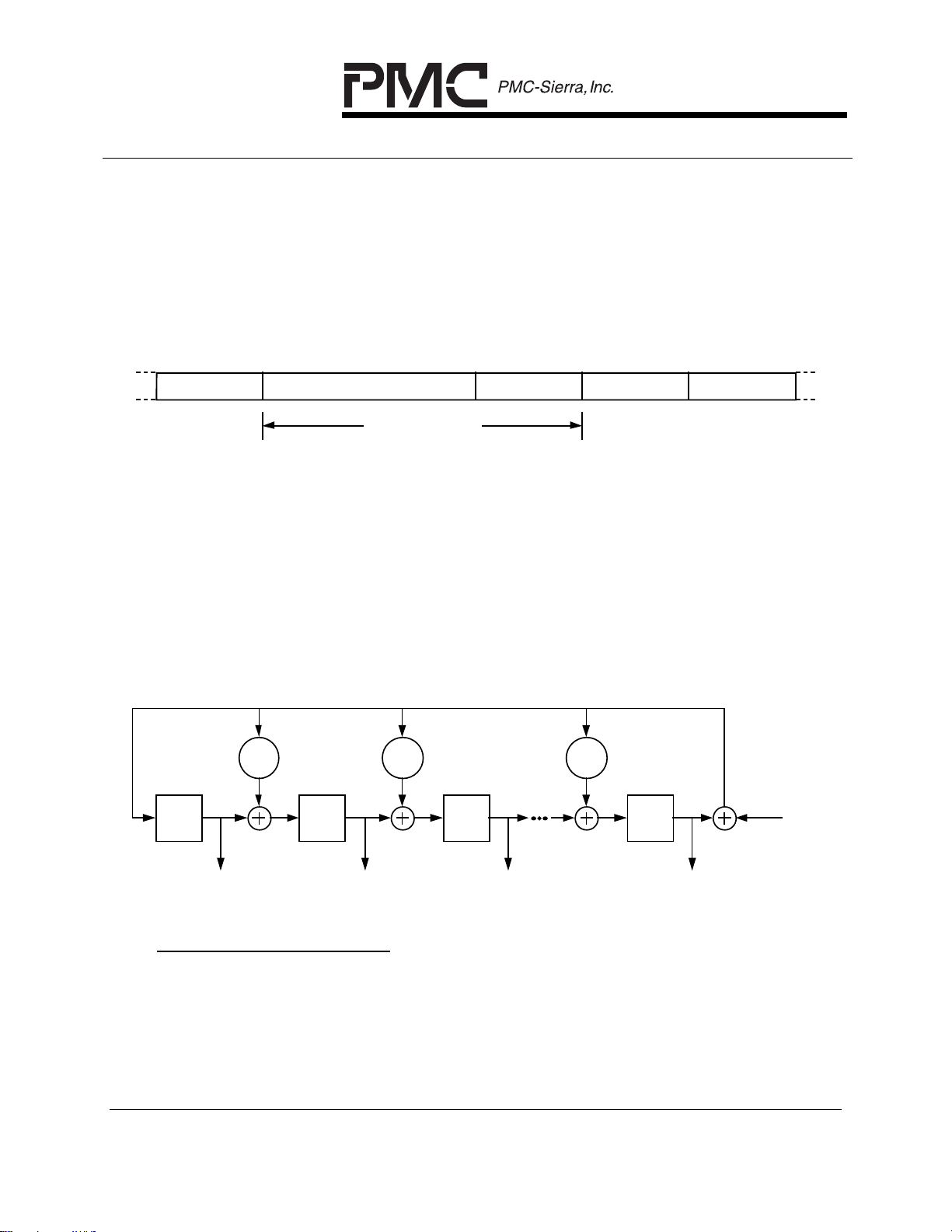
RELEASED
DATASHEET
PMC-2010336 ISSUE 1 FRAME ENGINE AND DATA LINK MANAGER 32A256
PM7383 FREEDM-32A256
FCS, the minimum packet length is four bytes while those with CRC-32 as FCS,
the minimum length is six bytes. An HDLC packet is aborted when seven
contiguous "1" bits (with no inserted "0" bits) are received. At least one flag byte
must exist between HDLC packets for delineation. Contiguous flag bytes, or all
ones bytes between packets are used as an "inter-frame time fill". Adjacent flag
bytes may share zeros.
Figure 2 – HDLC Frame
Flag Information FCS Flag
HDLC Packet
Flag
The CRC algorithm for the frame checking sequence (FCS) field is either a
CRC-CCITT or CRC-32 function. Figure 3 shows a CRC encoder block diagram
using the generating polynomial g(X) = 1 + g1X + g2X2 +…+ g
n-1
n-1
X
+ Xn. The
CRC-CCITT FCS is two bytes in size and has a generating polynomial g(X) = 1 +
X5 + X12 + X16. The CRC-32 FCS is four bytes in size and has a generating
polynomial g(X) = 1 + X + X2 + X4 + X5 + X7 + X8 + X10 + X11 + X12 + X16 + X22
+ X23 + X26 + X32. The first FCS bit received is the residue of the highest term.
Figure 3 – CRC Generator
g
1
D
0
LSB MSB
D
1
8.3 Receive Channel Assigner
The Receive Channel Assigner block (RCAS256) processes up to 32 serial links.
Links may be configured to support 2.048 or 8.192 Mbps H-MVIP traffic, to
support T1/J1/E1 channelised traffic or to support unchannelised traffic. When
configured to support 2.048 Mbps H-MVIP traffic, each group of 8 links share a
clock and frame pulse. All links configured for 8.192 Mbps H-MVIP traffic share a
g
2
D
2
Parity Check Digits
g
n-1
D
n-1
Message
PROPRIETARY AND CONFIDENTIAL 45
Page 54

RELEASED
DATASHEET
PMC-2010336 ISSUE 1 FRAME ENGINE AND DATA LINK MANAGER 32A256
PM7383 FREEDM-32A256
common clock and frame pulse. For T1/J1/E1 channelised traffic or for
unchannelised traffic, each link is independent and has its own associated clock.
For each link, the RCAS256 performs a serial to parallel conversion to form data
bytes. The data bytes are multiplexed, in byte serial format, for delivery to the
Receive HDLC Processor / Partial Packet Buffer block (RHDL256) at SYSCLK
rate. In the event where multiple streams have accumulated a byte of data,
multiplexing is performed on a fixed priority basis with link #0 having the highest
priority and link #31 the lowest.
From the point of view of the RCAS256, links configured for H-MVIP traffic
behave identically to links configured for T1/J1/E1 channelised or unchannelised
traffic in the back end, only differing on the link side as described herein. First,
the number of time-slots in each frame is programmable to be 32 or 128 and has
an associated data clock frequency that is double the data rate. This provides
more bandwidth per link for applications requiring higher data densities on a
single link. Second, H-MVIP links reference the start of each frame with a frame
pulse, thereby avoiding having to gap the link clock during the framing bits/bytes
of each frame. The frame pulse is provided by an H-MVIP bus master and
ensures that all agents sharing the H-MVIP bus remain synchronized. When
configured for operation in 2.048 Mbps mode, the frame pulse is sampled using
the same clock which samples the data. When configured for operation in 8.192
Mbps H-MVIP mode, the frame pulse is sampled using a separate frame pulse
clock provided by an H-MVIP bus master. The frame pulse clock has a
synchronous timing relationship to the data clock. Third, not all links are
independent. When configured for operation in 2.048 Mbps H-MVIP mode, each
group of 8 links share a clock and a frame pulse. Links 0 through 7, 8 through
15, 16 through 23 and 24 through 31 each share a clock and a frame pulse. Not
all 8 links within each group need to be configured for operation in 2.048 Mbps
H-MVIP mode. However, any link within each logical group of 8 which is
configured for 2.048 Mbps H-MVIP operation will share the same clock and frame
pulse. When configured for operation in 8.192 Mbps H-MVIP mode, links 4m
(0£m£7) share a frame pulse, a data clock and a frame pulse clock. Again, not
all eight 4m (0£m£7) links need to be configured for operation in 8.192 Mbps
H-MVIP mode, however, any link which is configured for 8.192 Mbps H-MVIP
operation will share the same frame pulse, data clock and frame pulse clock. If
link 4m is configured for 8.192 Mbps H-MVIP operation, then data transferred on
that link is “spread” over links 4m, 4m+1, 4m+2 and 4m+3 from a channel
assigner point of view. Accordingly, when link 4m is configured for operation in
8.192 Mbps H-MVIP mode, links 4m+1, 4m+2 and 4m+3 must also be configured
for operation in 8.192 Mbps H-MVIP mode. In the back end, the RCAS256
extracts and processes the time-slots in the same way as channelised T1/J1/E1
traffic.
PROPRIETARY AND CONFIDENTIAL 46
Page 55

RELEASED
DATASHEET
PMC-2010336 ISSUE 1 FRAME ENGINE AND DATA LINK MANAGER 32A256
PM7383 FREEDM-32A256
Links containing a T1/J1 or an E1 stream may be channelised. Data at each
time-slot may be independently assigned to a different channel. The RCAS256
performs a table lookup to associate the link and time-slot identity with a channel.
T1/J1 and E1 framing bits/bytes are identified by observing the gap in the link
clock which is squelched during the framing bits/bytes. For unchannelised links,
clock rates are limited to 51.84 MHz for links #0 to #2 and limited to 10 MHz for
the remaining links. All data on each link belongs to one channel. For the case
of a mixture of channelised, unchannelised and H-MVIP links, the total
instantaneous link rate over all the links is limited to 64 MHz. The RCAS256
performs a table lookup using only the link number to determine the associated
channel, as time-slots are non-existent in unchannelised links.
The RCAS256 provides diagnostic loopback that is selectable on a per channel
basis. The RCAS256 does not support diagnostic loopback for links configured
as H-MVIP. When a channel is in diagnostic loopback, stream data on the
received links originally destined for that channel is ignored. Transmit data of
that channel is substituted in its place.
8.3.1 Line Interface Translator (LIT)
The LIT block translates the information on the 32 physical links into a suitable
format for interpretation by the Line Interface block. The LIT block performs three
functions: data translation, clock translation and frame pulse generation.
When link 4m (0£m£7) is configured for operation in 8.192 Mbps H-MVIP mode,
the LIT block translates the 128 time-slots on link 4m to the Line Interface block
across links 4m, 4m+1, 4m+2 and 4m+3. The LIT block provides time-slots 0
through 31, 32 through 63, 64 through 95 and 96 through 127 to the Line
Interface block on links 4m, 4m+1, 4m+2 and 4m+3 respectively. When link 4m
is configured for operation in 8.192 Mbps H-MVIP mode, data cannot be received
on inputs RD[4m+3:4m+1]. However, links 4m+1, 4m+2 and 4m+3 must be
programmed in the RCAS256 Link Configuration register for 8.192 Mbps H-MVIP
operation. When links are configured for operation in 2.048 Mbps H-MVIP mode,
channelised T1/J1/E1 mode or unchannelised mode, the LIT block does not
perform any translation on the link data.
When a link is configured for operation in H-MVIP mode, the LIT block divides the
appropriate clock (RMVCK[n] for 2.048 Mbps H-MVIP and RMV8DC for 8.192
Mbps H-MVIP) by two and provides this divided down clock to the Line Interface
block. When a link is configured for operation in channelised T1/J1/E1 or
unchannelised mode, the LIT block does not perform any translation on the link
clock.
PROPRIETARY AND CONFIDENTIAL 47
Page 56

RELEASED
DATASHEET
PMC-2010336 ISSUE 1 FRAME ENGINE AND DATA LINK MANAGER 32A256
PM7383 FREEDM-32A256
When a link is configured for operation in H-MVIP mode, the LIT block samples
the appropriate frame pulse (RFPB[n] for 2.048 Mbps H-MVIP and RFP8B for
8.192 Mbps H-MVIP) and presents the sampled frame pulse to the Line Interface
block. When a link is configured for operation in channelised T1/J1/E1 or
unchannelised mode, the gapped clock is passed to the LIT block unmodified.
8.3.2 Line Interface
There are 32 identical line interface blocks in the RCAS256. Each line interface
block contains 2 sub-blocks; one supporting channelised T1/J1/E1 streams and
the other H-MVIP streams. Based on configuration, only one of the sub-blocks
are active at one time; the other is held reset. Each sub-block contains a bit
counter, an 8-bit shift register and a holding register. Each sub-block performs
serial to parallel conversion. Whenever the holding register is updated, a request
for service is sent to the priority encoder block. When acknowledged by the
priority encoder, the line interface would respond with the data residing in the
holding register in the active sub-block.
To support H-MVIP links, each line interface block contains a time-slot counter.
The time-slot counter is incremented each time the holding register is updated.
When a frame pulse occurs, the time-slot counter is initialised to indicate that the
next bit is the most significant bit of the first time-slot.
To support non H-MVIP channelised links, each line interface block contains a
time-slot counter and a clock activity monitor. The time-slot counter is
incremented each time the holding register is updated. The clock activity monitor
is a counter that increments at the system clock (SYSCLK) rate and is cleared by
a rising edge of the receive clock (RCLK[n]). A framing bit (T1/J1) or a framing
byte (E1) is detected when the counter reaches a programmable threshold, in
which case, the bit and time-slot counters are initialised to indicate that the next
bit is the most significant bit of the first time-slot. For unchannelised links, the
time-slot counter and the clock activity monitor are held reset.
8.3.3 Priority Encoder
The priority encoder monitors the line interfaces for requests and synchronises
them to the SYSCLK timing domain. Requests are serviced on a fixed priority
scheme where highest to lowest priority is assigned from the line interface
attached to RD[0] to that attached to RD[31]. Thus, simultaneous requests from
RD[m] will be serviced ahead of RD[n], if m < n. When there are no pending
requests, the priority encoder generates an idle cycle. In addition, once every
fourth SYSCLK cycle, the priority encoder inserts a null cycle where no requests
PROPRIETARY AND CONFIDENTIAL 48
Page 57

RELEASED
DATASHEET
PMC-2010336 ISSUE 1 FRAME ENGINE AND DATA LINK MANAGER 32A256
PM7383 FREEDM-32A256
are serviced. This cycle is used by the channel assigner downstream for host
microprocessor accesses to the provisioning RAMs.
8.3.4 Channel Assigner
The channel assigner block determines the channel number of the data byte
currently being processed. The block contains a 1024 word channel provision
RAM. The address of the RAM is constructed from concatenating the link
number and the time-slot number of the current data byte. The fields of each
RAM word include the channel number and a time-slot enable flag. The time-slot
enable flag labels the current time-slot as belonging to the channel indicted by
the channel number field.
8.3.5 Loopback Controller
The loopback controller block implements the channel based diagnostic loopback
function. Every valid data byte belonging to a channel with diagnostic loopback
enabled from the Transmit HDLC Processor / Partial Packet Buffer block
(THDL256) is written into a 64 word FIFO. The loopback controller monitors for
an idle time-slot or a time-slot carrying a channel with diagnostic loopback
enabled. If either conditions hold, the current data byte is replaced by data
retrieved from the loopback data FIFO.
8.4 Receive HDLC Processor / Partial Packet Buffer
The Receive HDLC Processor / Partial Packet Buffer block (RHDL256)
processes up to 256 synchronous transmission HDLC data streams. Each
channel can be individually configured to perform flag sequence detection, bit destuffing and CRC-CCITT or CRC-32 verification. The packet data is written into
the partial packet buffer. At the end of a frame, packet status including CRC
error, octet alignment error and maximum length violation are also loaded into the
partial packet buffer. Alternatively, a channel can be provisioned as transparent,
in which case, the HDLC data stream is passed to the partial packet buffer
processor verbatim.
There is a natural precedence in the alarms detectable on a receive packet.
Once a packet exceeds the programmable maximum packet length, no further
processing is performed on it. Thus, octet alignment detection, FCS verification
and abort recognition are squelched on packets with a maximum length violation.
An abort indication squelches octet alignment detection, minimum packet length
violations, and FCS verification. In addition, FCS verification is only performed
PROPRIETARY AND CONFIDENTIAL 49
Page 58

RELEASED
DATASHEET
PMC-2010336 ISSUE 1 FRAME ENGINE AND DATA LINK MANAGER 32A256
PM7383 FREEDM-32A256
on packets that do not have octet alignment errors, in order to allow the
RHDL256 to perform CRC calculations on a byte-basis.
The partial packet buffer is a 32 Kbyte RAM that is divided into 16-byte blocks.
Each block has an associated pointer which points to another block. A logical
FIFO is created for each provisioned channel by programming the block pointers
to form a circular linked list. A channel FIFO can be assigned a minimum of 3
blocks (48 bytes) and a maximum of 2048 blocks (32 Kbytes). The depth of the
channel FIFOs are monitored in a round-robin fashion. Requests are made to
the Receive Any-PHY Interface block (RAPI256) to transfer, on the Rx APPI, data
in channel FIFOs with depths exceeding their associated threshold.
8.4.1 HDLC Processor
The HDLC processor is a time-slice state machine which can process up to 256
independent channels. The state vector and provisioning information for each
channel is stored in a RAM. Whenever new channel data arrives, the
appropriate state vector is read from the RAM, processed and written back to the
RAM. The HDLC state-machine can be configured to perform flag delineation, bit
de-stuffing, CRC verification and length monitoring. The resulting HDLC data
and status information is passed to the partial packet buffer processor to be
stored in the appropriate channel FIFO buffer.
The configuration of the HDLC processor is accessed using indirect channel read
and write operations. When an indirect operation is performed, the information is
accessed from RAM during a null clock cycle generated by the upstream Receive
Channel Assigner block (RCAS256). Writing new provisioning data to a channel
resets the channel's entire state vector.
8.4.2 Partial Packet Buffer Processor
The partial packet buffer processor controls the 32 Kbyte partial packet RAM
which is divided into 16 byte blocks. A block pointer RAM is used to chain the
partial packet blocks into circular channel FIFO buffers. Thus, non-contiguous
sections of the RAM can be allocated in the partial packet buffer RAM to create a
channel FIFO. System software is responsible for the assignment of blocks to
individual channel FIFOs. Figure 4 shows an example of three blocks (blocks 1,
3, and 200) linked together to form a 48 byte channel FIFO.
PROPRIETARY AND CONFIDENTIAL 50
Page 59

RELEASED
DATASHEET
PMC-2010336 ISSUE 1 FRAME ENGINE AND DATA LINK MANAGER 32A256
PM7383 FREEDM-32A256
Figure 4 – Partial Packet Buffer Structure
Block 0
Block 1
Block 2
Block 3
Partial Packet
Buffer RAM
16 bytes
16 bytes
16 bytes
16 bytes
Block 0
Block 1
Block 2
Block 3
Block
Pointer RAM
XX
0x03
XX
0xC8
0x01
XX
Block 2047
16 bytes
16 bytes
Block 200Block 200
Block 2047
The partial packet buffer processor is divided into three sections: writer, reader
and roamer. The writer is a time-sliced state machine which writes the HDLC
data and status information from the HDLC processor into a channel FIFO in the
packet buffer RAM. The reader transfers channel FIFO data from the packet
buffer RAM to the downstream Receive Any-PHY Interface block (RAPI256).
The roamer is a time-sliced state machine which tracks channel FIFO buffer
depths and signals the reader to service a particular channel. If a buffer over-run
occurs, the writer ends the current packet from the HDLC processor in the
channel FIFO with an overrun flag and ignores the rest of the packet.
The FIFO algorithm of the partial packet buffer processor is based on a
programmable per-channel transfer size. Instead of tracking the number of full
blocks in a channel FIFO, the processor tracks the number of transactions.
Whenever the partial packet writer fills a transfer-sized number of blocks or writes
an end-of-packet flag to the channel FIFO, a transaction is created. Whenever
the partial packet reader transmits a transfer-size number of blocks or an end-of-
PROPRIETARY AND CONFIDENTIAL 51
Page 60

RELEASED
DATASHEET
PMC-2010336 ISSUE 1 FRAME ENGINE AND DATA LINK MANAGER 32A256
PM7383 FREEDM-32A256
packet flag to the RAPI256 block, a transaction is deleted. Thus, small packets
less than the transfer size will be naturally transferred to the RAPI256 block
without having to precisely track the number of full blocks in the channel FIFO.
The partial packet roamer performs the transaction accounting for all channel
FIFOs. The roamer increments the transaction count when the writer signals a
new transaction and sets a per-channel flag to indicate a non-zero transaction
count. The roamer searches the flags in a round-robin fashion to decide for
which channel FIFO to request transfer by the RAPI256 block. The roamer
informs the partial packet reader of the channel to process. The reader transfers
the data to the RAPI256 until the channel transfer size is reached or an end of
packet is detected. The reader then informs the roamer that a transaction is
consumed. The roamer updates its transaction count and clears the non-zero
transaction count flag if required. The roamer then services the next channel
with its transaction flag set high.
The writer and reader determine empty and full FIFO conditions using flags.
Each block in the partial packet buffer has an associated flag. The writer sets the
flag after the block is written and the reader clears the flag after the block is read.
The flags are initialized (cleared) when the block pointers are written using
indirect block writes. The writer declares a channel FIFO overrun whenever the
writer tries to store data to a block with a set flag. In order to support optional
removal of the FCS from the packet data, the writer does not declare a block as
filled (set the block flag nor increment the transaction count) until the first double
word of the next block in channel FIFO is filled. If the end of a packet resides in
the first double word, the writer declares both blocks as full at the same time.
When the reader finishes processing a transaction, it examines the first double
word of the next block for the end-of-packet flag. If the first double word of the
next block contains only FCS bytes, the reader would, optionally, process next
transaction (end-of-packet) and consume the block, as it contains information not
transferred to the RAPI256 block.
8.5 Receive Any-PHY Interface
The Receive Any-PHY Interface (RAPI256) provides a low latency path for
transferring data out of the partial packet buffer in the RHDL256 and onto the
Receive Any-PHY Packet Interface (Rx APPI). The RAPI256 contains a FIFO
block for latency control as well as to segregate the APPI timing domain from the
SYSCLK timing domain. The RAPI256 contains the necessary logic to manage
and respond to device polling from an upper layer device. The RAPI256 also
provides the upper layer device with status information on a per packet basis.
PROPRIETARY AND CONFIDENTIAL 52
Page 61

RELEASED
DATASHEET
PMC-2010336 ISSUE 1 FRAME ENGINE AND DATA LINK MANAGER 32A256
PM7383 FREEDM-32A256
8.5.1 FIFO Storage and Control
The FIFO block temporarily stores channel data during transfer across the Rx
APPI. RAPI256 burst data transfers are transaction based – a write burst data
transfer must be complete before any data will be read, and all data must be
completely read from the FIFO before any further data will be written into the
FIFO. To support full Rx APPI bus rate, a double buffer scheme is used. While
data is being read from one FIFO onto the Rx APPI, data can be written into the
other FIFO. Because the bandwidth on the writer side of the FIFOs is higher
than that on the reader side, the RAPI256 can maintain continuous full bandwidth
transfer over the Rx APPI.
A maximum of 256 bytes can be stored in one of the two FIFOs for any given
burst transfer. A separate storage element samples the 10 bit channel ID to
associate the data in that FIFO with a specific HDLC channel. This channel ID is
prepended in-band as the first word of every burst data transfer across the Rx
APPI. (The maximum length of a burst data transfer on the Rx APPI is therefore
129 words, including prepend.) The 3 most significant bits of the prepended
word of every burst data tansfer across the Rx APPI identify the FREEDM32A256 device associated with the transfer and reflect the value of the base
address programmed in the RAPI256 Control register.
The writer controller provides a means for writing data into the FIFOs. The writer
controller indicates that it can accept data when there is at least one completely
empty FIFO. In response, a complete burst transfer of data, up to a maximum of
256 bytes, is written into that empty FIFO. (The transfer is sourced by the
upstream RHDL256 block which selects from those channels with data available
using its round-robin algorithm.) The writer controller then informs the reader
controller that data is available in that FIFO. The writer controller now switches
to the other FIFO and repeats the process. When both FIFOs are full, the writer
throttles the upstream RHDL256 block to prevent of any further data writes into
the FIFOs.
The reader controller provides a means of reading data out of the FIFOs onto the
Rx APPI. When selected to do so, and the writer controller has indicated that at
least one FIFO is full, the reader controller will read the data out of the FIFOs in
the order in which they were filled. To prevent from overloading the Rx APPI with
several small bursts of data, the RAPI256 automatically deselects after every
burst transfer. This provides time for the upper layer device to detect an end of
packet indication and possibly reselect a different FREEDM-32A256 device
without having to store the extra word or two which may have been output onto
the Rx APPI during the time it took for deselection.
PROPRIETARY AND CONFIDENTIAL 53
Page 62

RELEASED
DATASHEET
PMC-2010336 ISSUE 1 FRAME ENGINE AND DATA LINK MANAGER 32A256
PM7383 FREEDM-32A256
The RAPI256 provides packet status information on the Rx APPI at the end of
every packet transfer. The RAPI256 asserts RERR at the end of packet
reception (REOP high) to indicate that the packet is in error. The RAPI256 may
be programmed to overwrite RXDATA[7:0] of the final word of each packet
transfer (REOP is high) with the status of packet reception when that packet is
errored (RERR is high). Overwriting of status information is enabled by setting
the STATEN bit in the RAPI Control register.
8.5.2 Polling Control and Management
The RAPI256 only responds to device polls which match the base address
programmed in the RAPI256 Control register. A positive poll response indicates
that at least one of the two FIFOs has a complete XFER[3:0] plus one blocks of
data, or an end of packet, and is ready to be selected to transfer this data across
the Rx APPI.
8.6 Transmit Any-PHY Interface
The Transmit Any-PHY Interface (TAPI256) provides a low latency path for
transferring data from the Transmit Any-PHY Packet Interface (Tx APPI) into the
partial packet buffer in the THDL256. The TAPI256 contains a FIFO block for
latency control as well as to segregate the APPI timing domain from the SYSCLK
timing domain. The TAPI256 contains the necessary logic to manage and respond
to channel polling from an upper layer device.
8.6.1 FIFO Storage and Control
The FIFO block temporarily stores channel data during transfer across the Tx
APPI. TAPI256 burst data transfers are transaction based on the writer side of
the FIFO – all data must be completely read from the FIFO before any further
data will be written into the FIFO. To support as close as possible to full Tx APPI
bus rate, a double buffer is used. While data is being read from the one FIFO,
data can be written into the other FIFO. Because the bandwidth on the reader
side of the FIFOs is higher than that on the writer side, the TAPI256 will not incur
any bandwidth reduction to maximum burst data transfers through its FIFOs.
The upper layer device cannot interrupt data transfers on the Tx APPI. However,
the FREEDM-32A256 may throttle the upper layer device if both FIFOs in the
TAPI256 are full. When the FIFOs in the TAPI256 cannot accept data, the
TAPI256 deasserts the TRDY output to the upper layer device connected to the
Tx APPI. In this instance, the upper layer device must halt data transfer until the
TRDY output is returned high. The upper layer device connected to the Tx APPI
PROPRIETARY AND CONFIDENTIAL 54
Page 63

RELEASED
DATASHEET
PMC-2010336 ISSUE 1 FRAME ENGINE AND DATA LINK MANAGER 32A256
PM7383 FREEDM-32A256
must sample the TRDY output high before continuing to burst data across the Tx
APPI.
A maximum of 256 bytes may be stored in one of the two FIFOs for any given
burst transfer. The first word of each burst transfer contains a prepended
address field. (The maximum length of a burst transfer on the Tx APPI is
therefore 129 words, including prepend.) A separate storage element samples
the 10 least significant bits of the prepended channel address to associate the
data with a specific channel. The 3 most significant bits must match the base
address programmed into the TAPI256 Control register for the TAPI256 to
respond to the data transaction on the Tx APPI.
The writer controller provides a means for writing data from the Tx APPI into the
FIFOs. The writer controller can accept data when there is at least one
completely empty FIFO. When a data transfer begins and there are no empty
FIFOs, the writer controller catches the data provided on the Tx APPI and
throttles the upper layer device. The writer controller will continue to throttle the
upper layer device until at least one FIFO is completely empty and can accept a
maximum burst transfer of data.
The whisper controller provides the channel address of the data being written
into the FIFO. As soon as the first word of data has been written into the FIFO,
the whisper controller provides the channel information for that data to the
downstream THDL256 block. The whisper controller will wait for
acknowledgement and the reader controller is then requested to read the data
from the FIFO. Once the reader controller has commenced the data transfer, the
whisper controller will provide the channel information for the other FIFO. The
whisper controller alternates between the two FIFOs in the order in which data is
written into them.
The reader controller provides a means of reading data out of the FIFOs. When
the writer controller indicates that data has been completely written into one of
the two FIFOs, the reader controller is permitted to read that data. The reader
controller will then wait for a request for data from the THDL256 block. When
requested to transfer data, the reader controller will completely read all the data
out of the FIFO before indicating to the writer controller that more data may be
written into the FIFO. Because the reader controller reads data out of the FIFOs
in the order in which they were filled, the THDL256 block will request data for
channels in the order in which they were whispered. The reader controller
manages the read and write FIFO pointers to allow simultaneous reading and
writing of data to/from the double buffer FIFO.
PROPRIETARY AND CONFIDENTIAL 55
Page 64

RELEASED
DATASHEET
PMC-2010336 ISSUE 1 FRAME ENGINE AND DATA LINK MANAGER 32A256
PM7383 FREEDM-32A256
8.6.2 Polling Control and Management
The TAPI256 only responds to poll addresses which are in the range
programmed in the base address field in the TAPI256 Control register. The
TAPI256 uses the 3 most significant bits of the poll address for device recognition
and the 10 least significant bits of the poll address for identification of a channel.
The TAPI256 provides three poll results for every poll address according to Table
7. The TPAn[0] bit indicates whether or not space exists in the channel FIFO for
data and the TPAn[1] bit indicates whether or not that polled channel FIFO is at
risk of underflowing and should be provided data soon. The TPAn[2] bit indicates
that an underflow event has occurred on that channel FIFO.
Table 7 – Transmit Polling
Poll
Address
TPA1[0]
(Full/Space)
TPA1[1]
(Space/Starving)
TPA1[2]
(Underflow)
TPA2[0]
(Full/Space)
TPA2[1]
(Space/Starving)
TPA2[2]
(Underflow)
Channel 0 Channel 0 Channel 0 Channel 0 Channel 1 Channel 1 Channel 1
Channel 1 Channel 1 Channel 1 Channel 1 Channel 2 Channel 2 Channel 2
Channel 2 Channel 2 Channel 2 Channel 2 Channel 3 Channel 3 Channel 3
Channel 3 Channel 3 Channel 3 Channel 3 Channel 4 Channel 4 Channel 4
Channel 4 Channel 4 Channel 4 Channel 4 Channel 5 Channel 5 Channel 5
Channel 5 Channel 5 Channel 5 Channel 5 Channel 6 Channel 6 Channel 6
Channel 6 Channel 6 Channel 6 Channel 6 Channel 7 Channel 7 Channel 7
Channel 7 Channel 7 Channel 7 Channel 7 Channel 8 Channel 8 Channel 8
Channel 8 Channel 8 Channel 8 Channel 8 Channel 9 Channel 9 Channel 9
·
·
·
Channel
255
·
·
·
Channel
255
·
·
·
Channel
255
·
·
·
Channel
255
·
·
·
·
·
·
Channel 0 Channel 0 Channel 0
·
·
·
The TAPI256 maintains a mirror image of the status of each channel FIFO in the
partial packet buffer. The THDL256 continuously reports the status of the 256
channel FIFOs to the TAPI256 and the TAPI256 updates the mirror image
accordingly. The THDL256 also signals to the TAPI256 whenever an underflow
event has occurred on a channel FIFO. At the beginning of every data transfer
across the Tx APPI, the TAPI256 sets the mirror image status of the channel to
“full”. Only the TAPI256 can cause the status to be set to “full” and only the
THDL256 can cause the status to be set to “space” or “starving”. Only the
THDL256 can cause the status to be set to “underflow” and only the TAPI256 can
clear the “underflow” status when that channel FIFO is polled. In the event that
PROPRIETARY AND CONFIDENTIAL 56
Page 65

RELEASED
DATASHEET
PMC-2010336 ISSUE 1 FRAME ENGINE AND DATA LINK MANAGER 32A256
PM7383 FREEDM-32A256
both the TAPI256 and the THDL256 try to change the mirror image status of a
particular channel simultaneously, the TAPI256 takes precedence, except for the
“underflow” status, where the THDL256 takes precedence.
8.7 Transmit HDLC Controller / Partial Packet Buffer
The Transmit HDLC Controller / Partial Packet Buffer block (THDL256) contains
a partial packet buffer for Tx APPI latency control and a transmit HDLC controller.
The THDL256 also contains logic to monitor the full/empty status of each channel
FIFO and push this status onto the polling interface signals.
The THDL256 requests data from the TAPI256 in response to control information
from the TAPI256 indicating the channel for which data is available and ready to
be transferred. Packet data received from the TAPI256 is stored in channel
specific FIFOs residing in the partial packet buffer. When the amount of data in a
FIFO reaches a programmable threshold, the HDLC controller is enabled to
initiate transmission. The HDLC controller performs flag generation, bit stuffing
and, optionally, frame check sequence (FCS) insertion. The FCS is software
selectable to be CRC-CCITT or CRC-32. The minimum packet size, excluding
FCS, is two bytes. A single byte payload is illegal. The HDLC controller delivers
data to the Transmit Channel Assigner block (TCAS256) on demand. A packet in
progress is aborted if an under-run occurs. The THDL256 is programmable to
operate in transparent mode where packet data retrieved from the TAPI256 is
transmitted verbatim.
8.7.1 Transmit HDLC Processor
The HDLC processor is a time-slice state machine which can process up to 256
independent channels. The state vector and provisioning information for each
channel is stored in a RAM. Whenever the TCAS256 requests data, the
appropriate state vector is read from the RAM, processed and finally written back
to the RAM. The HDLC state-machine can be configured to perform flag
insertion, bit stuffing and CRC generation. The HDLC processor requests data
from the partial packet processor whenever a request for channel data arrives.
However, the HDLC processor does not start transmitting a packet until the entire
packet is stored in the channel FIFO or until the FIFO free space is less than the
software programmable limit. If a channel FIFO under-runs, the HDLC processor
aborts the packet, generates a microprocessor interrupt and signals the
underflow to the transmit Any-PHY interface.
The configuration of the HDLC processor is accessed using indirect channel read
and write operations. When an indirect operation is performed, the information is
PROPRIETARY AND CONFIDENTIAL 57
Page 66

RELEASED
DATASHEET
PMC-2010336 ISSUE 1 FRAME ENGINE AND DATA LINK MANAGER 32A256
PM7383 FREEDM-32A256
accessed from RAM during a null clock cycle inserted by the TCAS256 block.
Writing new provisioning data to a channel resets the channels entire state
vector.
8.7.2 Transmit Partial Packet Buffer Processor
The partial packet buffer processor controls the 32 Kbyte partial packet RAM
which is divided into 16 byte blocks. A block pointer RAM is used to chain the
partial packet blocks into circular channel FIFO buffers. Thus, non-contiguous
sections of RAM can be allocated in the partial packet buffer RAM to create a
channel FIFO. Figure 5 shows an example of three blocks (blocks 1, 3, and 200)
linked together to form a 48 byte channel FIFO. The three pointer values would
be written sequentially using indirect block write accesses. When a channel is
provisioned within this FIFO, the state machine can be initialized to point to any
one of the three blocks.
Figure 5 – Partial Packet Buffer Structure
Block 0
Block 1
Block 2
Block 3
Block 2047
Partial Packet
Buffer RAM
16 bytes
16 bytes
16 bytes
16 bytes
16 bytes
16 bytes
Block 0
Block 1
Block 2
Block 3
Block 200Block 200
Block 2047
Block
Pointer RAM
XX
0x03
XX
0xC8
0x01
XX
PROPRIETARY AND CONFIDENTIAL 58
Page 67

RELEASED
DATASHEET
PMC-2010336 ISSUE 1 FRAME ENGINE AND DATA LINK MANAGER 32A256
PM7383 FREEDM-32A256
The partial packet buffer processor is divided into three sections: reader, writer
and roamer. The roamer is a time-sliced state machine which tracks each
channel’s FIFO buffer free space and signals the writer to service a particular
channel. The writer requests data from the TAPI256 block and transfers packet
data from the TAPI256 to the associated channel FIFO. The reader is a timesliced state machine which transfers the HDLC information from a channel FIFO
to the HDLC processor in response to a request from the HDLC processor. If a
buffer under-run occurs for a channel, the reader informs the HDLC processor
and purges the rest of the packet. If a buffer overflow occurs for a channel, the
THDL256 disables the channel as if it were unprovisioned and does not transmit
any further data until that channel is reprovisioned. In both cases, an interrupt is
generated and the cause of the interrupt may be read via the interrupt status
register using the microprocessor interface.
The writer and reader determine empty and full FIFO conditions using flags.
Each block in the partial packet buffer has an associated flag. The writer sets the
flag after the block is written and the reader clears the flag after the block is read.
The flags are initialized (cleared) when the block pointers are written using
indirect block writes. The reader declares a channel FIFO under-run whenever it
tries to read data from a block without a set flag.
The FIFO algorithm of the partial packet buffer processor is based on perchannel software programmable transfer size and free space trigger level.
Instead of tracking the number of full blocks in a channel FIFO, the processor
tracks the number of empty blocks, called free space, as well as the number of
end of packets stored in the FIFO. Recording the number of empty blocks
instead of the number of full blocks reduces the amount of information the
roamer must store in its state RAM.
The partial packet roamer records the FIFO free space and end-of-packet count
for all channel FIFOs. When the reader signals that a block has been read, the
roamer increments the FIFO free space and sets a per-channel request flag if the
free space is greater than the limit set by XFER[3:0]. The roamer pushes this
status information to the TAPI256 to indicate that it can accept at least XFER[3:0]
blocks of data. The roamer also decrements the end-of-packet count when the
reader signals that it has passed an end of a packet to the HDLC processor. If
the HDLC processor is transmitting a packet and the FIFO free space is greater
than the free space trigger level and there are no complete packets within the
FIFO (end-of-packet count equal to zero), a per-channel starving flag is set. The
roamer searches the starving flags in a round-robin fashion to decide which
channel FIFOs are at risk of underflowing and pushes this status information to
the TAPI256. The roamer listens to control information from the TAPI256 to
decide which channel FIFO requests data from the TAPI256 block. The roamer
PROPRIETARY AND CONFIDENTIAL 59
Page 68

RELEASED
DATASHEET
PMC-2010336 ISSUE 1 FRAME ENGINE AND DATA LINK MANAGER 32A256
PM7383 FREEDM-32A256
informs the partial packet writer of the channel FIFO to process and the FIFO
free space. The writer sends a request for data to the TAPI256 block and writes
the response data to the channel FIFO setting block full flags. The writer reports
back to the roamer the number of blocks and end-of-packets transferred. The
maximum amount of data transferred during one request is limited by a software
programmable limit.
The roamer round-robins between all channel FIFOs and pushes the status to
the TAPI256 block. The status consists of two pieces of information: (1) is there
space in the channel FIFO for at least one XFER[3:0] of data, and (2) is this
channel FIFO at risk of underflowing. Where a channel FIFO is at risk of
underflowing, the THDL256 pushes a starving status for that channel FIFO to the
TAPI256 at the earliest possible opportunity.
The configuration of the HDLC processor is accessed using indirect channel read
and write operations as well as indirect block read and write operations. When
an indirect operation is performed, the information is accessed from RAM during
a null clock cycle identified by the TCAS256 block. Writing new provisioning data
to a channel resets the entire state vector.
8.8 Transmit Channel Assigner
The Transmit Channel Assigner block (TCAS256) processes up to 256 channels.
Data for all channels is sourced from a single byte-serial stream from the
Transmit HDLC Controller / Partial Packet Buffer block (THDL256). The
TCAS256 demultiplexes the data and assigns each byte to any one of 32 links.
Each link may be configured to support 2.048 or 8.192 H-MVIP traffic, to support
T1/J1/E1 channelised traffic or to support unchannelised traffic. When
configured to support H-MVIP traffic, each group of 8 links share a clock and
frame pulse, otherwise each link is independent and has its own associated
clock. For each high-speed link (TD[2:0]), the TCAS provides a six byte FIFO.
For the remaining links (TD[31:3]), the TCAS provides a single byte holding
register. The TCAS256 also performs parallel to serial conversion to form a bitserial stream. In the event where multiple links are in need of data, TCAS256
requests data from upstream blocks on a fixed priority basis with link TD[0]
having the highest priority and link TD[31] the lowest.
From the point of view of the TCAS256, links configured for H-MVIP traffic
behave identically to links configured for T1/J1/E1 channelised or unchannelised
traffic in the back end, only differing on the link side as described herein. First,
the number of time-slots in each frame is programmable to be 32 or 128 and has
an associated data clock frequency that is double the data rate. This provides
PROPRIETARY AND CONFIDENTIAL 60
Page 69

RELEASED
DATASHEET
PMC-2010336 ISSUE 1 FRAME ENGINE AND DATA LINK MANAGER 32A256
PM7383 FREEDM-32A256
more bandwidth per link for applications requiring higher data densities on a
single link. Data at each time-slot may be independently assigned to be sourced
from a different channel. Second, H-MVIP links reference the start of each frame
with a frame pulse, thereby avoiding having to gap the link clock during the
framing bits/bytes of each frame. The frame pulse is provided by an H-MVIP bus
master and ensures that all agents sharing the H-MVIP bus remain synchronized.
When configured for operation in 2.048 Mbps H-MVIP mode, the frame pulse is
sampled using the same clock which samples the data. When configured for
operation in 8.192 Mbps H-MVIP mode, the frame pulse is sampled using a
separate frame pulse clock provided by an H-MVIP bus master. The frame pulse
clock has a synchronous timing relationship to the data clock. Third, not all links
are independent. When configured for operation in 2.048 Mbps H-MVIP mode,
each group of 8 links share a clock and a frame pulse. Links 0 through 7, 8
through 15, 16 through 23 and 24 through 31 each share a clock and a frame
pulse. Not all 8 links within each group need to be configured for operation in
2.048 Mbps H-MVIP mode. However, any link within each logical group of 8
which is configured for 2.048 Mbps H-MVIP operation will share the same clock
and frame pulse. When configured for operation in 8.192 Mbps H-MVIP mode,
links 4m (0£m£7) share a frame pulse, a data clock and a frame pulse clock.
Again, not all eight 4m (0£m£7) links need to be configured for operation in 8.192
Mbps H-MVIP mode, however, any link which is configured for 8.192 Mbps HMVIP operation will share the same frame pulse, data clock and frame pulse
clock. If link 4m is configured for 8.192 Mbps H-MVIP operation, then data
transferred on that link is “spread” over links 4m, 4m+1 4m+2 and 4m+3 from a
channel assigner point of view. Accordingly, when link 4m is configured for
operation in 8.192 Mbps H-MVIP mode, links 4m+1, 4m+2 and 4m+3 must also
be configured for operation in 8.192 Mbps H-MVIP mode. In the back end, the
TCAS256 extracts and processes the time-slots identically to channelised
T1/J1/E1 traffic.
Links containing a T1/J1 or an E1 stream may be channelised. Data at each
time-slot may be independently assigned to be sourced from a different channel.
The link clock is only active during time-slots 1 to 24 of a T1/J1 stream and is
inactive during the frame bit. Similarly, the clock is only active during time-slots 1
to 31 of an E1 stream and is inactive during the FAS and NFAS framing bytes.
The most significant bit of time-slot 1 of a channelised link is identified by noting
the absence of the clock and its re-activation. With knowledge of the transmit
link and time-slot identity, the TCAS256 performs a table look-up to identify the
channel from which a data byte is to be sourced.
Links may also be unchannelised. Then, all data bytes on that link belong to one
channel. The TCAS256 performs a table look-up to identify the channel to which
PROPRIETARY AND CONFIDENTIAL 61
Page 70

RELEASED
DATASHEET
PMC-2010336 ISSUE 1 FRAME ENGINE AND DATA LINK MANAGER 32A256
PM7383 FREEDM-32A256
a data byte belongs using only the outgoing link identity, as no time-slots are
associated with unchannelised links. Link clocks are no longer limited to T1/J1 or
E1 rates and may range up to a maximum clock rate of 51.84 MHz for TCLK[2:0]
and 10 MHz for TCLK[31:3]. The link clock is only active during bit times
containing data to be transmitted and inactive during bits that are to be ignored
by the downstream devices, such as framing and overhead bits. For the case of
three unchannelised links, the maximum link rate is 51.84 MHz. For the case of
more numerous unchannelised links or a mixture of channelised, unchannelised
and H-MVIP links, the total instantaneous link rate over all the links is limited to
64 MHz.
8.8.1 Line Interface Translator (LIT)
The LIT block translates the information between the 32 physical links and the
Line Interface block. The LIT block performs three functions: data translation,
clock translation and frame pulse generation.
When link 4m (0£m£7) is configured for operation in 8.192 Mbps H-MVIP mode,
the LIT block translates the data arriving from the Line Interface block on links
4m, 4m+1, 4m+2 and 4m+3 onto the 128 time-slot link 4m. The LIT block
translates data arriving from the Line Interface block on link 4m, 4m+1, 4m+2 and
4m+3 onto time-slots 0 through 31, 32 through 63, 64 through 95 and 96 through
127 respectively. When link 4m is configured for operation in 8.192 Mbps HMVIP mode, outputs TD[4m+3:4m+1] are driven with constant ones. However,
links 4m+1, 4m+2 and 4m+3 must be programmed in the TCAS256 Link
Configuration register for 8.192 Mbps H-MVIP operation. When links are
configured for operation in 2.048 Mbps H-MVIP mode, channelised T1/J1/E1
mode or unchannelised mode, the LIT block does not perform any translation on
the link data.
When a link is configured for operation in H-MVIP mode, the LIT block divides the
appropriate clock (TMVCK[n] for 2.048 Mbps H-MVIP and TMV8DC for 8.192
Mbps H-MVIP) by two and provides this divided down clock to the Line Interface
block. When a link is configured for operation in channelised T1/J1/E1 or
unchannelised mode, the LIT block does not perform any translation on the link
clock.
When a link is configured for operation in H-MVIP mode, the LIT block samples
the appropriate frame pulse (TFPB[n] for 2.048 Mbps H-MVIP and TFP8B for
8.192 Mbps H-MVIP) and presents the sampled frame pulse to the Line Interface
block. When a link is configured for operation in channelised T1/J1/E1 or
unchannelised mode, the gapped clock is passed to the LIT block unmodified.
PROPRIETARY AND CONFIDENTIAL 62
Page 71

RELEASED
DATASHEET
PMC-2010336 ISSUE 1 FRAME ENGINE AND DATA LINK MANAGER 32A256
PM7383 FREEDM-32A256
8.8.2 Line Interface
There are 32 identical line interface blocks in the TCAS256. Each line interface
block contains 2 sub-blocks; one supporting channelised T1/J1/E1 streams and
the other H-MVIP streams. Based on configuration, only one of the sub-blocks
are active at one time; the other is held reset. Each sub-block contains a bit
counter, an 8-bit shift register and a holding register. Each sub-block performs
parallel to serial conversion. Whenever the shift register is updated, a request for
service is sent to the priority encoder block. When acknowledged by the priority
encoder, the line interface would respond by writing the data into the holding
register in the active sub-block.
To support H-MVIP links, each line interface block contains a time-slot counter.
The time-slot counter is incremented each time the holding register is updated.
When a frame pulse occurs, the time-slot counter is cleared to indicate that the
next byte belongs to the first time-slot.
To support non H-MVIP channelised links, each line interface block contains a
time-slot counter and a clock activity monitor. The time-slot counter is
incremented each time the shift register is updated. The clock activity monitor is
a counter that increments at the system clock (SYSCLK) rate and is cleared by a
rising edge of the transmit clock (TCLK[n]). A framing bit (T1/J1) or a framing
byte (E1) is detected when the counter reaches a programmable threshold, at
which point, the bit and time-slot counters are initialised to indicate that the next
bit sampled is the most significant bit of the first time-slot. For unchannelised
links, the time-slot counter and the clock activity monitor are held reset.
8.8.3 Priority Encoder
The priority encoder monitors the line interfaces for requests and synchronises
them to the SYSCLK timing domain. Requests are serviced on a fixed priority
scheme where highest to lowest priority is assigned from line interface TD[0] to
line interface TD[31]. Thus, simultaneous requests from line interface TD[m] will
be serviced ahead of line interface TD[n], if m < n. The priority encoder selects
the request from the link with the highest priority for service. When there are no
pending requests, the priority encoder generates an idle cycle. In addition, once
every fourth SYSCLK cycle, the priority encoder inserts a null cycle where no
requests are serviced. This cycle is used by the channel assigner downstream
for CBI accesses to the channel provision RAM.
PROPRIETARY AND CONFIDENTIAL 63
Page 72

RELEASED
DATASHEET
PMC-2010336 ISSUE 1 FRAME ENGINE AND DATA LINK MANAGER 32A256
PM7383 FREEDM-32A256
8.8.4 Channel Assigner
The channel assigner block determines the channel number of the request
currently being processed. The block contains a 1024 word channel provision
RAM. The address of the RAM is constructed from concatenating the link
number and the time-slot number of the highest priority requester. The fields of
each RAM word include the channel number and a time-slot enable flag. The
time-slot enable flag labels the current time-slot as belonging to the channel
indicted by the channel number field. For time-slots that are enabled, the
channel assigner issues a request to the THDL256 block which responds with
packet data within one byte period of the transmit stream.
8.9 Performance Monitor
The Performance Monitor block (PMON) contains four counters. The first two
accumulate receive partial packet buffer FIFO overrun events and transmit partial
packet buffer FIFO underflow events, respectively. The remaining two counters
are software programmable to accumulate a variety of events, such as receive
packet count, FCS error counts, etc. All counters saturate upon reaching
maximum value. The accumulation logic consists of a counter and holding
register pair. The counter is incremented when the associated event is detected.
Writing to the FREEDM-32A256 Master Clock / BERT Activity Monitor and
Accumulation Trigger register transfer the count to the corresponding holding
register and clear the counter. The contents of the holding register is accessible
via the microprocessor interface.
8.10 JTAG Test Access Port Interface
The JTAG Test Access Port block provides JTAG support for boundary scan. The
standard JTAG EXTEST, SAMPLE, BYPASS, IDCODE and STCTEST instructions
are supported. The FREEDM-32A256 identification code is 073830CD
hexadecimal.
8.11 Microprocessor Interface
The FREEDM-32A256 supports microprocessor access to an internal register
space for configuring and monitoring the device. All registers are 16 bits wide but
are DWORD aligned in the microprocessor memory map. The registers are
described below:
PROPRIETARY AND CONFIDENTIAL 64
Page 73

RELEASED
DATASHEET
PMC-2010336 ISSUE 1 FRAME ENGINE AND DATA LINK MANAGER 32A256
PM7383 FREEDM-32A256
Table 8 – Normal Mode Microprocessor Accessible Registers
Address Register
0x000 FREEDM-32A256 Master Reset
0x004 FREEDM-32A256 Master Interrupt Enable
0x008 FREEDM-32A256 Master Interrupt Status
0x00C FREEDM-32A256 Master Clock / Frame Pulse / BERT
Activity Monitor and Accumulation Trigger
0x010 FREEDM-32A256 Master Link Activity Monitor
0x014 FREEDM-32A256 Master Line Loopback #1
0x018 FREEDM-32A256 Master Line Loopback #2
0x01C FREEDM-32A256 Reserved
0x020 FREEDM-32A256 Master BERT Control
0x024 FREEDM-32A256 Master Performance Monitor Control
0x028 – 0x0FC Reserved
0x100 RCAS Indirect Channel and Time-slot Select
0x104 RCAS Indirect Channel Data
0x108 RCAS Framing Bit Threshold
0x10C RCAS Channel Disable
0x110 – 0x17C RCAS Reserved
0x180 – 0x1FC RCAS Link #0 through #31 Configuration
0x200 RHDL Indirect Channel Select
0x204 RHDL Indirect Channel Data Register #1
0x208 RHDL Indirect Channel Data Register #2
0x20C RHDL Reserved
0x210 RHDL Indirect Block Select
0x214 RHDL Indirect Block Data Register
0x218 – 0x21C RHDL Reserved
0x220 RHDL Configuration
0x224 RHDL Maximum Packet Length
PROPRIETARY AND CONFIDENTIAL 65
Page 74

RELEASED
DATASHEET
PMC-2010336 ISSUE 1 FRAME ENGINE AND DATA LINK MANAGER 32A256
PM7383 FREEDM-32A256
Address Register
0x228 – 0x23C RHDL Reserved
0x240 – 0x37C Reserved
0x380 THDL Indirect Channel Select
0x384 THDL Indirect Channel Data #1
0x388 THDL Indirect Channel Data #2
0x38C THDL Indirect Channel Data #3
0x390 – 0x39C THDL Reserved
0x3A0 THDL Indirect Block Select
0x3A4 THDL Indirect Block Data
0x3A8 – 0x3AC THDL Reserved
0x3B0 THDL Configuration
0x3B4 – 0x3BC THDL Reserved
0x3C0 – 0x3FC Reserved
0x400 TCAS Indirect Channel and Time-slot Select
0x404 TCAS Indirect Channel Data
0x408 TCAS Framing Bit Threshold
0x40C TCAS Idle Time-slot Fill Data
0x410 TCAS Channel Disable
0x414 – 0x47C TCAS Reserved
0x480 – 0x4FC TCAS Link #0 through #31 Configuration
0x500 PMON Status
0x504 PMON Receive FIFO Overflow Count
0x508 PMON Transmit FIFO Underflow Count
0x50C PMON Configurable Count #1
0x510 PMON Configurable Count #2
0x514 – 0x51C PMON Reserved
0x520 – 0x57C Reserved
PROPRIETARY AND CONFIDENTIAL 66
Page 75

RELEASED
DATASHEET
PMC-2010336 ISSUE 1 FRAME ENGINE AND DATA LINK MANAGER 32A256
PM7383 FREEDM-32A256
Address Register
0x580 RAPI Control
0x584 – 0x5BC RAPI Reserved
0x5C0 – 0x5FC Reserved
0x600 TAPI Control
0x604 TAPI Indirect Channel Provisioning
0x608 TAPI Indirect Channel Data Register
0x60C – 0x63C TAPI Reserved
0x640 – 0x7FC Reserved
PROPRIETARY AND CONFIDENTIAL 67
Page 76

RELEASED
DATASHEET
PMC-2010336 ISSUE 1 FRAME ENGINE AND DATA LINK MANAGER 32A256
PM7383 FREEDM-32A256
9 NORMAL MODE REGISTER DESCRIPTION
Normal mode registers are used to configure and monitor the operation of the
FREEDM-32A256.
Notes on Normal Mode Register Bits:
1. Writing values into unused register bits has no effect. However, to ensure software
compatibility with future, feature-enhanced versions of the product, unused register
bits must be written with logic zero. Reading back unused bits can produce either a
logic one or a logic zero; hence, unused register bits should be masked off by
software when read.
2. Except where noted, all configuration bits that can be written into can also be read
back. This allows the processor controlling the FREEDM-32A256 to determine the
programming state of the block.
3. Writable normal mode register bits are cleared to logic zero upon reset unless
otherwise noted.
4. Writing into read-only normal mode register bit locations does not affect FREEDM32A256 operation unless otherwise noted.
5. Certain register bits are reserved. These bits are associated with megacell functions
that are unused in this application. To ensure that the FREEDM-32A256 operates
as intended, reserved register bits must only be written with their default values.
Similarly, writing to reserved registers should be avoided.
9.1 Microprocessor Accessible Registers
Microprocessor accessible registers can be accessed by the external
microprocessor. For each register description below, the hexadecimal register
number indicates the address in the FREEDM-32A256 when accesses are made
using the external microprocessor.
Note
These registers are not byte addressable. Writing to any one of these registers
modifies all 16 bits in the register.
PROPRIETARY AND CONFIDENTIAL 68
Page 77

RELEASED
DATASHEET
PMC-2010336 ISSUE 1 FRAME ENGINE AND DATA LINK MANAGER 32A256
PM7383 FREEDM-32A256
Register 0x000 : FREEDM-32A256 Master Reset
Bit Type Function Default
Bit 15 R/W Reset 0
Bit 14
Unused XH
to
Bit 12
Bit 11 R TYPE[3] 0
Bit 10 R TYPE[2] 0
Bit 9 R TYPE[1] 1
Bit 8 R TYPE[0] 1
Bit 7 R ID[7] 0
Bit 6 R ID[7] 0
Bit 5 R ID[5] 0
Bit 4 R ID[4] 0
Bit 3 R ID[3] 0
Bit 2 R ID[2] 0
Bit 1 R ID[1] 1
Bit 0 R ID[0] 0
This register provides software reset capability and device ID information.
RESET:
The RESET bit allows the FREEDM-32A256 to be reset under software
control. If the RESET bit is a logic one, the entire FREEDM-32A256, except
the microprocessor interface, is held in reset. This bit is not self-clearing.
Therefore, a logic zero must be written to bring the FREEDM-32A256 out of
reset. Holding the FREEDM-32A256 in a reset state places it into a low
power, stand-by mode. A hardware reset clears the RESET bit, thus negating
the software reset.
PROPRIETARY AND CONFIDENTIAL 69
Page 78

RELEASED
DATASHEET
PMC-2010336 ISSUE 1 FRAME ENGINE AND DATA LINK MANAGER 32A256
PM7383 FREEDM-32A256
Note
Like the hardware reset input (RSTB), RESET forces the FREEDM-32A256’s
transmit link data pins (TD[31:0]) high and the APPI outputs tristate.
TYPE[3:0]:
The Device Type bits (TYPE[3:0]) allow software to identify the device as the
FREEDM-32A256 member of the FREEDM family of products.
ID[7:0]:
The Device ID bits (ID[7:0]) allow software to identify the version level of the
FREEDM-32A256.
PROPRIETARY AND CONFIDENTIAL 70
Page 79

RELEASED
DATASHEET
PMC-2010336 ISSUE 1 FRAME ENGINE AND DATA LINK MANAGER 32A256
PM7383 FREEDM-32A256
Register 0x004 : FREEDM-32A256 Master Interrupt Enable
Bit Type Function Default
Bit 15 R/W TFUDRE 0
Bit 14 R/W TFOVRE 0
Bit 13 R/W TUNPVE 0
Bit 12 R/W TPRTYE 0
Bit 11
Unused XXH
to
Bit 6
Bit 5 R/W RFOVRE 0
Bit 4 R/W RPFEE 0
Bit 3 R/W RABRTE 0
Bit 2 R/W RFCSEE 0
Bit 1 Unused X
Bit 0 Unused X
This register provides interrupt enables for various events detected or initiated by
the FREEDM-32A256.
RFCSEE:
The receive frame check sequence error interrupt enable bit (RFCSEE)
enables receive FCS error interrupts to the microprocessor. When RFCSEE
is set high, a mismatch between the received FCS code and the computed
CRC residue will cause an interrupt to be generated on the INTB output.
Interrupts are masked when RFCSEE is set low. However, the RFCSEI bit
remains valid when interrupts are disabled and may be polled to detect
receive FCS error events.
RABRTE:
The receive abort interrupt enable bit (RABRTE) enables receive HDLC abort
interrupts to the microprocessor. When RABRTE is set high, receipt of an
abort code (at least 7 contiguous 1’s) will cause an interrupt to be generated
on the INTB output. Interrupts are masked when RABRTE is set low.
PROPRIETARY AND CONFIDENTIAL 71
Page 80

RELEASED
DATASHEET
PMC-2010336 ISSUE 1 FRAME ENGINE AND DATA LINK MANAGER 32A256
PM7383 FREEDM-32A256
However, the RABRTI bit remains valid when interrupts are disabled and may
be polled to detect receive abort events.
RPFEE:
The receive packet format error interrupt enable bit (RPFEE) enables receive
packet format error interrupts to the microprocessor. When RPFEE is set
high, receipt of a packet that is longer than the maximum specified in the
RHDL Maximum Packet Length register, or a packet that is shorter than 32
bits (CRC-CCITT) or 48 bits (CRC-32), or a packet that is not octet aligned
will cause an interrupt to be generated on the INTB output. Interrupts are
masked when RPFEE is set low. However, the RPFEI bit remains valid when
interrupts are disabled and may be polled to detect receive packet format
error events.
RFOVRE:
The receive FIFO overrun error interrupt enable bit (RFOVRE) enables
receive FIFO overrun error interrupts to the microprocessor. When RFOVRE
is set high, attempts to write data into the logical FIFO of a channel when it is
already full will cause an interrupt to be generated on the INTB output.
Interrupts are masked when RFOVRE is set low. However, the RFOVRI bit
remains valid when interrupts are disabled and may be polled to detect
receive FIFO overrun events.
TPRTYE:
The transmit parity error interrupt enable bit (TPRTYE) enables parity errors
on the transmit APPI to generate interrupts to the microprocessor. When
TPRTYE is set high, detection of a parity error on the transmit APPI will cause
an interrupt to be generated on the INTB output. Interrupts are masked when
TPRTYE is set low. However, the TPRTYI bit remains valid when interrupts
are disabled and may be polled to detect parity error events.
TUNPVE:
The transmit unprovisioned error interrupt enable bit (TUNPVE) enables
attempted transmissions to unprovisioned channels to generate interrupts to
the microprocessor. When TUNPVE is set high, attempts to write data to an
unprovisioned channel will cause an interrupt to be generated on the INTB
output. Interrupts are masked when TUNPVE is set low. However, the
TUNPVI bit remains valid when interrupts are disabled and may be polled to
detect attempted transmissions to unprovisioned channel events.
PROPRIETARY AND CONFIDENTIAL 72
Page 81

RELEASED
DATASHEET
PMC-2010336 ISSUE 1 FRAME ENGINE AND DATA LINK MANAGER 32A256
PM7383 FREEDM-32A256
TFOVRE:
The transmit FIFO overflow error interrupt enable bit (TFOVRE) enables
transmit FIFO overflow error interrupts to the microprocessor. When
TFOVRE is set high, attempts to write data to the logical FIFO when it is
already full will cause an interrupt to be generated on the INTB output.
Interrupts are masked when TFOVRE is set low. However, the TFOVRI bit
remains valid when interrupts are disabled and may be polled to detect
transmit FIFO overflow events.
TFUDRE:
The transmit FIFO underflow error interrupt enable bit (TFUDRE) enables
transmit FIFO underflow error interrupts to the microprocessor. When
TFUDRE is set high, attempts to read data from the logical FIFO when it is
already empty will cause an interrupt to be generated on the INTB output.
Interrupts are masked when TFUDRE is set low. However, the TFUDRI bit
remains valid when interrupts are disabled and may be polled to detect
transmit FIFO underflow events.
PROPRIETARY AND CONFIDENTIAL 73
Page 82

RELEASED
DATASHEET
PMC-2010336 ISSUE 1 FRAME ENGINE AND DATA LINK MANAGER 32A256
PM7383 FREEDM-32A256
Register 0x008 : FREEDM-32A256 Master Interrupt Status
Bit Type Function Default
Bit 15 R TFUDRI X
Bit 14 R TFOVRI X
Bit 13 R TUNPVI X
Bit 12 R TPRTYI X
Bit 11
Unused XXH
to
Bit 6
Bit 5 R RFOVRI X
Bit 4 R RPFEI X
Bit 3 R RABRTI X
Bit 2 R RFCSEI X
Bit 1 Unused X
Bit 0 Unused X
This register reports the interrupt status for various events detected or initiated by
the FREEDM-32A256. Reading this registers acknowledges and clears the
interrupts.
RFCSEI:
The receive frame check sequence error interrupt status bit (RFCSEI) reports
receive FCS error interrupts to the microprocessor. RFCSEI is set high when
a mismatch between the received FCS code and the computed CRC residue
is detected. RFCSEI remains valid when interrupts are disabled and may be
polled to detect receive FCS error events.
RABRTI:
The receive abort interrupt status bit (RABRTI) reports receive HDLC abort
interrupts to the microprocessor. RABRTI is set high upon receipt of an abort
code (at least 7 contiguous 1’s). RABRTI remains valid when interrupts are
disabled and may be polled to detect receive abort events.
PROPRIETARY AND CONFIDENTIAL 74
Page 83

RELEASED
DATASHEET
PMC-2010336 ISSUE 1 FRAME ENGINE AND DATA LINK MANAGER 32A256
PM7383 FREEDM-32A256
RPFEI:
The receive packet format error interrupt status bit (RPFEI) reports receive
packet format error interrupts to the microprocessor. RPFEI is set high upon
receipt of a packet that is longer than the maximum programmed length, of a
packet that is shorter than 32 bits (CRC-CCITT) or 48 bits (CRC-32), or of a
packet that is not octet aligned. RPFEI remains valid when interrupts are
disabled and may be polled to detect receive packet format error events.
RFOVRI:
The receive FIFO overrun error interrupt status bit (RFOVRI) reports receive
FIFO overrun error interrupts to the microprocessor. RFOVRI is set high on
attempts to write data into the logical FIFO of a channel when it is already full.
RFOVRI remains valid when interrupts are disabled and may be polled to
detect receive FIFO overrun events.
TPRTYI:
The transmit parity error interrupt status bit (TPRTYI) reports the detection of
a parity on the transmit APPI. TPRTYI is set high upon detection of a parity
error. TPRTYI remains valid when interrupts are disabled and may be polled
to detect parity errors.
TUNPVI:
The transmit unprovisioned error interrupt status bit (TUNPVI) reports an
attempted data transmission to an unprovisioned channel FIFO. TUNPVI is
set high upon attempts to write data to an unprovisioned channel FIFO.
TUNPVI remains valid when interrupts are disabled and may be polled to
detect an attempt to write data to an unprovisioned channel FIFO.
TFOVRI:
The transmit FIFO overflow error interrupt status bit (TFOVRI) reports
transmit FIFO overflow error interrupts to the microprocessor. TFOVRI is set
high upon attempts to write data to the logical FIFO when it is already full.
TFOVRI remains valid when interrupts are disabled and may be polled to
detect transmit FIFO overflow events. (Note – Transmit FIFO overflows will
not occur if channels are properly polled on the Transmit APPI before
transferring data.)
TFUDRI:
The transmit FIFO underflow error interrupt status bit (TFUDRI) reports
transmit FIFO underflow error interrupts to the microprocessor. TFUDRI is set
PROPRIETARY AND CONFIDENTIAL 75
Page 84

RELEASED
DATASHEET
PMC-2010336 ISSUE 1 FRAME ENGINE AND DATA LINK MANAGER 32A256
PM7383 FREEDM-32A256
high upon attempts to read data from the logical FIFO when it is already
empty. TFUDRI remains valid when interrupts are disabled and may be
polled to detect transmit FIFO underflow events.
PROPRIETARY AND CONFIDENTIAL 76
Page 85

RELEASED
DATASHEET
PMC-2010336 ISSUE 1 FRAME ENGINE AND DATA LINK MANAGER 32A256
PM7383 FREEDM-32A256
Register 0x00C : FREEDM-32A256 Master Clock / Frame Pulse / BERT
Activity Monitor and Accumulation Trigger
Bit Type Function Default
Bit 15
Unused XH
to
Bit 14
Bit 13 R TXCLKA X
Bit 12 R RXCLKA X
Bit 11 R TFPA[3] X
Bit 10 R TFPA[2] X
Bit 9 R TFPA[1] X
Bit 8 R TFPA[0] X
Bit 7 R RFPA[3] X
Bit 6 R RFPA[2] X
Bit 5 R RFPA[1] X
Bit 4 R RFPA[0] X
Bit 3 R TFP8A X
Bit 2 R RFP8A X
Bit 1 R TBDA X
Bit 0 R SYSCLKA X
This register provides activity monitoring on the FREEDM-32A256 system clock,
Any-PHY clocks, H-MVIP frame pulse and BERT port inputs. When a monitored
input makes a transition, the corresponding register bit is set high. The bit will
remain high until this register is read, at which point, all the bits in this register are
cleared. A lack of transitions is indicated by the corresponding register bit
reading low. This register should be read periodically to detect for stuck at
conditions.
Writing to this register delimits the accumulation intervals in the PMON
accumulation registers. Counts accumulated in those registers are transferred to
holding registers where they can be read. The counters themselves are then
PROPRIETARY AND CONFIDENTIAL 77
Page 86

RELEASED
DATASHEET
PMC-2010336 ISSUE 1 FRAME ENGINE AND DATA LINK MANAGER 32A256
PM7383 FREEDM-32A256
cleared to begin accumulating events for a new accumulation interval. The bits in
this register are not affected by write accesses.
SYSCLKA:
The system clock active bit (SYSCLKA) monitors for low to high transitions on
the SYSCLK input. SYSCLKA is set high on a rising edge of SYSCLK, and is
set low when this register is read.
TBDA:
The transmit BERT data active bit (TBDA) monitors for low to high transitions
on the TBD input. TBDA is set high on a rising edge of TDB, and is set low
when this register is read.
RFP8A:
The receive 8.192 Mbps H-MVIP frame pulse activity bit (RFP8A) monitors for
low to high transitions on the RFP8B input. RFP8A is set high when RFP8B
has been sampled low and sampled high by falling edges of the RMV8FPC,
and is set low when this register is read.
TFP8A:
The transmit 8.192 Mbps H-MVIP frame pulse activity bit (TFP8A) monitors
for low to high transitions on the TFP8B input. TFP8A is set high when
TFP8B has been sampled low and sampled high by falling edges of the
TMV8FPC, and is set low when this register is read.
RFPA[3:0]:
The receive frame pulse activity bits (RFPA[3:0]) monitor for low to high
transitions on the RFPB[3:0] inputs. RFPA[n] is set high when RFPB[n] has
been sampled low and sampled high by falling edges of the corresponding
RMVCK[n], and is set low when this register is read.
TFPA[3:0]:
The transmit frame pulse activity bits (TFPA[3:0]) monitor for low to high
transitions on the TFPB[3:0] inputs. TFPA[n] is set high when TFPB[n] has
been sampled low and sampled high by falling edges of the corresponding
TMVCK[n], and is set low when this register is read.
RXCLKA / TXCLKA:
The Any-PHY clock active bits (RXCLKA, TXCLKA) monitor for low to high
transitions on the RXCLK and TXCLK inputs respectively. RXCLKA and
PROPRIETARY AND CONFIDENTIAL 78
Page 87

RELEASED
DATASHEET
PMC-2010336 ISSUE 1 FRAME ENGINE AND DATA LINK MANAGER 32A256
PM7383 FREEDM-32A256
TXCLKA are set high on a rising edge of the corresponding clock, and are set
low when this register is read.
PROPRIETARY AND CONFIDENTIAL 79
Page 88

RELEASED
DATASHEET
PMC-2010336 ISSUE 1 FRAME ENGINE AND DATA LINK MANAGER 32A256
PM7383 FREEDM-32A256
Register 0x010 : FREEDM-32A256 Master Link Activity Monitor
Bit Type Function Default
Bit 15 R TLGA[7] X
Bit 14 R TLGA[6] X
Bit 13 R TLGA[5] X
Bit 12 R TLGA[4] X
Bit 11 R TLGA[3] X
Bit 10 R TLGA[2] X
Bit 9 R TLGA[1] X
Bit 8 R TLGA[0] X
Bit 7 R RLGA[7] X
Bit 6 R RLGA[6] X
Bit 5 R RLGA[5] X
Bit 4 R RLGA[4] X
Bit 3 R RLGA[3] X
Bit 2 R RLGA[2] X
Bit 1 R RLGA[1] X
Bit 0 R RLGA[0] X
This register provides activity monitoring on FREEDM-32A256 receive and
transmit link inputs. When a monitored input makes a low to high transition, the
corresponding register bit is set high. The bit will remain high until this register is
read, at which point, all the bits in this register are cleared. A lack of transitions is
indicated by the corresponding register bit reading low. This register should be
read periodically to detect for stuck at conditions.
RLGA[0]:
The receive link group #0 active bit (RLGA[0]) monitors for transitions on the
RD[3:0] and RCLK[3:0]/RMVCK[0]/RMV8DC inputs. RLGA[0] is set high
when either:
1. Each of RD[3:0] has been sampled low and sampled high by rising
edges of the corresponding RCLK[3:0] inputs, or
PROPRIETARY AND CONFIDENTIAL 80
Page 89

RELEASED
DATASHEET
PMC-2010336 ISSUE 1 FRAME ENGINE AND DATA LINK MANAGER 32A256
PM7383 FREEDM-32A256
2. Each of RD[3:0] has been sampled low and sampled high by rising
edges of the RMVCK[0] input, or
3. RD[0] has been sampled low and sampled high by rising edges of the
RMV8DC input.
RLGA[0] is set low when this register is read.
RLGA[1]:
The receive link group #1 active bit (RLGA[1]) monitors for transitions on the
RD[7:4] and RCLK[7:4]/RMVCK[0]/RMV8DC inputs. RLGA[1] is set high
when either:
1. Each of RD[7:4] has been sampled low and sampled high by rising
edges of the corresponding RCLK[7:4] inputs, or
2. Each of RD[7:4] has been sampled low and sampled high by rising
edges of the RMVCK[0] input, or
3. RD[4] has been sampled low and sampled high by rising edges of the
RMV8DC input.
RLGA[1] is set low when this register is read.
RLGA[2]:
The receive link group #2 active bit (RLGA[2]) monitors for transitions on the
RD[11:8] and RCLK[11:8]/RMVCK[1]/RMV8DC inputs. RLGA[2] is set high
when either:
1. Each of RD[11:8] has been sampled low and sampled high by rising
edges of the corresponding RCLK[11:8] inputs, or
2. Each of RD[11:8] has been sampled low and sampled high by rising
edges of the RMVCK[1] input, or
3. RD[8] has been sampled low and sampled high by rising edges of the
RMV8DC input.
RLGA[2] is set low when this register is read.
RLGA[3]:
The receive link group #3 active bit (RLGA[3]) monitors for transitions on the
RD[15:12] and RCLK[15:12]/RMVCK[1]/RMV8DC inputs. RLGA[3] is set high
when either:
1. Each of RD[15:12] has been sampled low and sampled high by rising
edges of the corresponding RCLK[15:12] inputs, or
2. Each of RD[15:12] has been sampled low and sampled high by rising
edges of the RMVCK[1] input, or
3. RD[12] has been sampled low and sampled high by rising edges of the
RMV8DC input.
RLGA[3] is set low when this register is read.
PROPRIETARY AND CONFIDENTIAL 81
Page 90

RELEASED
DATASHEET
PMC-2010336 ISSUE 1 FRAME ENGINE AND DATA LINK MANAGER 32A256
PM7383 FREEDM-32A256
RLGA[4]:
The receive link group #4 active bit (RLGA[4]) monitors for transitions on the
RD[19:16] and RCLK[19:16]/RMVCK[2]/RMV8DC inputs. RLGA[4] is set high
when either:
1. Each of RD[19:16] has been sampled low and sampled high by rising
edges of the corresponding RCLK[19:16] inputs, or
2. Each of RD[19:16] has been sampled low and sampled high by rising
edges of the RMVCK[2] input, or
3. RD[16] has been sampled low and sampled high by rising edges of the
RMV8DC input.
RLGA[4] is set low when this register is read.
RLGA[5]:
The receive link group #5 active bit (RLGA[5]) monitors for transitions on the
RD[23:20] and RCLK[23:20]/RMVCK[2]/RMV8DC inputs. RLGA[5] is set high
when either:
1. Each of RD[23:20] has been sampled low and sampled high by rising
edges of the corresponding RCLK[23:20] inputs, or
2. Each of RD[23:20] has been sampled low and sampled high by rising
edges of the RMVCK[2] input, or
3. RD[20] has been sampled low and sampled high by rising edges of the
RMV8DC input.
RLGA[5] is set low when this register is read.
RLGA[6]:
The receive link group #6 active bit (RLGA[6]) monitors for transitions on the
RD[27:24] and RCLK[27:24]/RMVCK[3]/RMV8DC inputs. RLGA[6] is set high
when either:
1. Each of RD[27:24] has been sampled low and sampled high by rising
edges of the corresponding RCLK[27:24] inputs, or
2. Each of RD[27:24] has been sampled low and sampled high by rising
edges of the RMVCK[3] input, or
3. RD[24] has been sampled low and sampled high by rising edges of the
RMV8DC input.
RLGA[6] is set low when this register is read.
RLGA[7]:
The receive link group #7 active bit (RLGA[7]) monitors for transitions on the
RD[31:28] and RCLK[31:28]/RMVCK[3]/RMV8DC inputs. RLGA[7] is set high
when either:
PROPRIETARY AND CONFIDENTIAL 82
Page 91

RELEASED
DATASHEET
PMC-2010336 ISSUE 1 FRAME ENGINE AND DATA LINK MANAGER 32A256
PM7383 FREEDM-32A256
1. Each of RD[31:28] has been sampled low and sampled high by rising
edges of the corresponding RCLK[31:28] inputs, or
2. Each of RD[31:28] has been sampled low and sampled high by rising
edges of the RMVCK[3] input, or
3. RD[28] has been sampled low and sampled high by rising edges of the
RMV8DC input.
RLGA[7] is set low when this register is read.
TLGA[0]:
The transmit link group #0 active bit (TLGA[0]) monitors for low to high
transitions on the TCLK[3:0] & TMVCK[0] inputs. TLGA[0] is set high when
either:
1. Rising edges have been observed on all four TCLK[3:0] inputs, or
2. A rising edge has been observed on the TMVCK[0] input.
TLGA[0] is set low when this register is read.
TLGA[1]:
The transmit link group #1 active bit (TLGA[1]) monitors for low to high
transitions on the TCLK[7:4] & TMVCK[1] inputs. TLGA[1] is set high when
either:
1. Rising edges have been observed on all four TCLK[7:4] inputs, or
2. A rising edge has been observed on the TMVCK[1] input.
TLGA[1] is set low when this register is read.
TLGA[2]:
The transmit link group #2 active bit (TLGA[2]) monitors for low to high
transitions on the TCLK[11:8] & TMVCK[2] inputs. TLGA[2] is set high when
either:
1. Rising edges have been observed on all four TCLK[11:8] inputs, or
2. A rising edge has been observed on the TMVCK[2] input.
TLGA[2] is set low when this register is read.
TLGA[3]:
The transmit link group #3 active bit (TLGA[3]) monitors for low to high
transitions on the TCLK[15:12] & TMVCK[3] inputs. TLGA[3] is set high when
either:
1. Rising edges have been observed on all four TCLK[15:12] inputs, or
2. A rising edge has been observed on the TMVCK[3] input.
TLGA[3] is set low when this register is read.
PROPRIETARY AND CONFIDENTIAL 83
Page 92

RELEASED
DATASHEET
PMC-2010336 ISSUE 1 FRAME ENGINE AND DATA LINK MANAGER 32A256
PM7383 FREEDM-32A256
TLGA[4]:
The transmit link group #4 active bit (TLGA[4]) monitors for low to high
transitions on the TCLK[19:16] inputs. TLGA[4] is set high when rising edges
have been observed on all four TCLK[19:16] inputs, and is set low when this
register is read.
TLGA[5]:
The transmit link group #5 active bit (TLGA[5]) monitors for low to high
transitions on the TCLK[23:20] inputs. TLGA[5] is set high when rising edges
have been observed on all four TCLK[23:20] inputs, and is set low when this
register is read.
TLGA[6]:
The transmit link group #6 active bit (TLGA[6]) monitors for low to high
transitions on the TCLK[27:24] inputs. TLGA[6] is set high when rising edges
have been observed on all four TCLK[27:24] inputs, and is set low when this
register is read.
TLGA[7]:
The transmit link group #7 active bit (TLGA[7]) monitors for low to high
transitions on the TCLK[31:28] & TMV8DC inputs. TLGA[7] is set high when
either:
1. Rising edges have been observed on all four TCLK[31:28] inputs, or
2. A rising edge has been observed on the TMV8DC input.
TLGA[7] is set low when this register is read.
PROPRIETARY AND CONFIDENTIAL 84
Page 93

RELEASED
DATASHEET
PMC-2010336 ISSUE 1 FRAME ENGINE AND DATA LINK MANAGER 32A256
PM7383 FREEDM-32A256
Register 0x014 : FREEDM-32A256 Master Line Loopback #1
Bit Type Function Default
Bit 15 R/W LLBEN[15] 0
Bit 14 R/W LLBEN[14] 0
Bit 13 R/W LLBEN[13] 0
Bit 12 R/W LLBEN[12] 0
Bit 11 R/W LLBEN[11] 0
Bit 10 R/W LLBEN[10] 0
Bit 9 R/W LLBEN[9] 0
Bit 8 R/W LLBEN[8] 0
Bit 7 R/W LLBEN[7] 0
Bit 6 R/W LLBEN[6] 0
Bit 5 R/W LLBEN[5] 0
Bit 4 R/W LLBEN[4] 0
Bit 3 R/W LLBEN[3] 0
Bit 2 R/W LLBEN[2] 0
Bit 1 R/W LLBEN[1] 0
Bit 0 R/W LLBEN[0] 0
This register controls line loopback for links #0 to #15.
LLBEN[15:0]:
The line loopback enable bits (LLBEN[15:0]) controls line loopback for
links #15 to #0. When links #0 through #15 are configured for channelised
T1/J1/E1 or unchannelised traffic and LLBEN[n] is set high, the data on RD[n]
is passed verbatim to TD[n] which is then updated on the falling edge of
RCLK[n]. TCLK[n] is ignored. When LLBEN[n] is set low, TD[n] is processed
normally. Line loopback is not supported for H-MVIP traffic.
PROPRIETARY AND CONFIDENTIAL 85
Page 94

RELEASED
DATASHEET
PMC-2010336 ISSUE 1 FRAME ENGINE AND DATA LINK MANAGER 32A256
PM7383 FREEDM-32A256
Register 0x018 : FREEDM-32A256 Master Line Loopback #2
Bit Type Function Default
Bit 15 R/W LLBEN[31] 0
Bit 14 R/W LLBEN[30] 0
Bit 13 R/W LLBEN[29] 0
Bit 12 R/W LLBEN[28] 0
Bit 11 R/W LLBEN[27] 0
Bit 10 R/W LLBEN[26] 0
Bit 9 R/W LLBEN[25] 0
Bit 8 R/W LLBEN[24] 0
Bit 7 R/W LLBEN[23] 0
Bit 6 R/W LLBEN[22] 0
Bit 5 R/W LLBEN[21] 0
Bit 4 R/W LLBEN[20] 0
Bit 3 R/W LLBEN[19] 0
Bit 2 R/W LLBEN[18] 0
Bit 1 R/W LLBEN[17] 0
Bit 0 R/W LLBEN[16] 0
This register controls line loopback for links #16 to #31.
LLBEN[31:16]:
The line loopback enable bits (LLBEN[31:16]) controls line loopback for
links #31 to #16. When links #16 through #31 are configured for channelised
T1/J1/E1 or unchannelised traffic and LLBEN[n] is set high, the data on RD[n]
is passed verbatim to TD[n] which is then updated on the falling edge of
RCLK[n]. TCLK[n] is ignored. When LLBEN[n] is set low, TD[n] is processed
normally. Line loopback is not supported for H-MVIP traffic.
PROPRIETARY AND CONFIDENTIAL 86
Page 95

RELEASED
DATASHEET
PMC-2010336 ISSUE 1 FRAME ENGINE AND DATA LINK MANAGER 32A256
PM7383 FREEDM-32A256
Register 0x01C : FREEDM-32A256 Reserved
Bit Type Function Default
Bit 15
Unused XXXXH
to
Bit 1
Bit 0 R/W Reserved 0
Reserved:
The reserved bit must be set low for correct operation of the FREEDM32A256 device.
PROPRIETARY AND CONFIDENTIAL 87
Page 96

RELEASED
DATASHEET
PMC-2010336 ISSUE 1 FRAME ENGINE AND DATA LINK MANAGER 32A256
PM7383 FREEDM-32A256
Register 0x020 : FREEDM-32A256 Master BERT Control
Bit Type Function Default
Bit 15 R/W TBEN 0
Bit 14 Unused X
Bit 13 Unused X
Bit 12 R/W TBSEL[4] 0
Bit 11 R/W TBSEL[3] 0
Bit 10 R/W TBSEL[2] 0
Bit 9 R/W TBSEL[1] 0
Bit 8 R/W TBSEL[0] 0
Bit 7 R/W RBEN 0
Bit 6 Unused X
Bit 5 Unused X
Bit 4 R/W RBSEL[4] 0
Bit 3 R/W RBSEL[3] 0
Bit 2 R/W RBSEL[2] 0
Bit 1 R/W RBSEL[1] 0
Bit 0 R/W RBSEL[0] 0
This register controls the bit error rate testing of the receive and transmit links.
Bit error rate testing is not supported for links configured for H-MVIP traffic.
RBSEL[4:0]:
The receive bit error rates testing link select bits (RBSEL[4:0]) controls the
source of data on the RBD and RBCLK outputs when receive bit error rate
testing is enabled (RBEN set high). RBSEL[4:0] is a binary number that
selects a receive link configured for non H-MVIP traffic (RD[31:0]/RCLK[31:0])
to be the source of data for RBD and RBCLK outputs. RBSEL[4:0] is ignored
when RBEN is set low. RBSEL[4:0] cannot select a link configured for HMVIP traffic.
PROPRIETARY AND CONFIDENTIAL 88
Page 97

RELEASED
DATASHEET
PMC-2010336 ISSUE 1 FRAME ENGINE AND DATA LINK MANAGER 32A256
PM7383 FREEDM-32A256
RBEN:
The receive bit error rates testing link enable bit (RBEN) controls the receive
bit error rate testing port. When RBEN is set high, RBSEL[4:0] is a binary
number that selects a receive link configured for non H-MVIP traffic
(RD[31:0]/RCLK[31:0]) to be the source of data for RBD and RBCLK outputs.
When RBEN is set low, RBD and RBCLK are held tristated.
TBSEL[4:0]:
The transmit bit error rates testing link select bits (TBSEL[4:0]) controls the
over-writing of transmit data on TD[31:0] by data on TBD when transmit bit
error rate testing is enabled (TBEN set high) and the selected link is not in
line loopback (LLBEN[n] set low). TBSEL[4:0] is a binary number that selects
a transmit link configured for non H-MVIP traffic (TD[31:0]/TCLK[31:0]) to
carry the data on TBD. The TBCLK output is a buffered version of the
selected one of TCLK[31:0]. TBSEL[4:0] is ignored when TBEN is set low.
TBSEL[4:0] cannot select a link configured for H-MVIP traffic.
TBEN:
The transmit bit error rates testing link enable bit (TBEN) controls the transmit
bit error rate testing port. When TBEN is set high and the associated link in
not in line loopback (LLBEN set low), TBSEL[4:0] is a binary number that
selects a transmit link data configured for non H-MVIP traffic (TD[31:0]) to
carry the data on TBD and selects a transmit link clock (TCLK[31:0]) as the
source of TBCLK. When TBEN is set low, all transmit links are processed
normally and TBCLK is held tristated.
PROPRIETARY AND CONFIDENTIAL 89
Page 98

RELEASED
DATASHEET
PMC-2010336 ISSUE 1 FRAME ENGINE AND DATA LINK MANAGER 32A256
PM7383 FREEDM-32A256
Register 0x024 : FREEDM-32A256 Master Performance Monitor Control
Bit Type Function Default
Bit 15 Unused X
Bit 14 R/W TP2EN 0
Bit 13 R/W TABRT2EN 0
Bit 12 R/W RP2EN 0
Bit 11 R/W RLENE2EN 0
Bit 10 R/W RABRT2EN 0
Bit 9 R/W RFCSE2EN 0
Bit 8 R/W RSPE2EN 0
Bit 7 Unused X
Bit 6 R/W TP1EN 0
Bit 5 R/W TABRT1EN 0
Bit 4 R/W RP1EN 0
Bit 3 R/W RLENE1EN 0
Bit 2 R/W RABRT1EN 0
Bit 1 R/W RFCSE1EN 0
Bit 0 R/W RSPE1EN 0
This register configures the events that are accumulated in the two configurable
performance monitor counters in the PMON block.
RSPE1EN:
The receive small packet error accumulate enable bit (RSPE1EN) enables
counting of minimum packet size violation events. When RSPE1EN is set
high, receipt of a packet that is shorter than 32 bits (CRC-CCITT, Unspecified
CRC or no CRC) or 48 bits (CRC-32) will cause the PMON Configurable
Accumulator #1 register to increment. Small packet errors are ignored when
RSPE1EN is set low.
PROPRIETARY AND CONFIDENTIAL 90
Page 99

RELEASED
DATASHEET
PMC-2010336 ISSUE 1 FRAME ENGINE AND DATA LINK MANAGER 32A256
PM7383 FREEDM-32A256
RFCSE1EN:
The receive frame check sequence error accumulate enable bit (RFCSE1EN)
enables counting of receive FCS error events. When RFCSE1EN is set high,
a mismatch between the received FCS code and the computed CRC residue
will cause the PMON Configurable Accumulator #1 register to increment.
Receive frame check sequence errors are ignored when RFCSE1EN is set
low.
RABRT1EN:
The receive abort accumulate enable bit (RABRT1EN) enables counting of
receive HDLC abort events. When RABRT1EN is set high, receipt of an abort
code (at least 7 contiguous 1’s) will cause the PMON Configurable
Accumulator #1 register to increment. Receive aborts are ignored when
RABRT1EN is set low.
RLENE1EN:
The receive packet length error accumulate enable bit (RLENE1EN) enables
counting of receive packet length error events. When RLENE1EN is set high,
receipt of a packet that is longer than the programmable maximum or of a
packet that in not octet aligned will cause the PMON Configurable
Accumulator #1 register to increment. (Receipt of a packet that is both too
long and not octet aligned results in only one increment.) Receive packet
length errors are ignored when RLENE1EN is set low.
RP1EN:
The receive packet enable bit (RP1EN) enables counting of receive error-free
packets. When RP1EN is set high, receipt of an error-free packet will cause
the PMON Configurable Accumulator #1 register to increment. Receive errorfree packets are ignored when RP1EN is set low.
TABRT1EN:
The transmit abort accumulate enable bit (TABRT1EN) enables counting of
transmit HDLC abort events. When TABRT1EN is set high, insertion of an
abort in the outgoing stream will cause the PMON Configurable Accumulator
#1 register to increment. Transmit aborts are ignored when TABRT1EN is set
low.
TP1EN:
The transmit packet enable bit (TP1EN) enables counting of transmit
error-free packets. When TP1EN is set high, transmission of an error-free
PROPRIETARY AND CONFIDENTIAL 91
Page 100

RELEASED
DATASHEET
PMC-2010336 ISSUE 1 FRAME ENGINE AND DATA LINK MANAGER 32A256
PM7383 FREEDM-32A256
packet will cause the PMON Configurable Accumulator #1 register to
increment. Transmit error-free packets are ignored when TP1EN is set low.
RSPE2EN:
The receive small packet error accumulate enable bit (RSPE2EN) enables
counting of minimum packet size violation events. When RSPE2EN is set
high, receipt of a packet that is shorter than 32 bits (CRC-CCITT, Unspecified
CRC or no CRC) or 48 bits (CRC-32) will cause the PMON Configurable
Accumulator #2 register to increment. Small packet errors are ignored when
RSPE2EN is set low.
RFCSE2EN:
The receive frame check sequence error accumulate enable bit (RFCSE2EN)
enables counting of receive FCS error events. When RFCSE2EN is set high,
a mismatch between the received FCS code and the computed CRC residue
will cause the PMON Configurable Accumulator #2 register to increment.
Receive frame check sequence errors are ignored when RFCSE2EN is set
low.
RABRT2EN:
The receive abort accumulate enable bit (RABRT2EN) enables counting of
receive HDLC abort events. When RABRT2EN is set high, receipt of an abort
code (at least 7 contiguous 2’s) will cause the PMON Configurable
Accumulator #2 register to increment. Receive aborts are ignored when
RABRT2EN is set low.
RLENE2EN:
The receive packet length error accumulate enable bit (RLENE2EN) enables
counting of receive packet length error events. When RLENE2EN is set high,
receipt of a packet that is longer than the programmable maximum or of a
packet that in not octet aligned will cause the PMON Configurable
Accumulator #2 register to increment. (Receipt of a packet that is both too
long and not octet aligned results in only one increment.) Receive packet
length errors are ignored when RLENE2EN is set low.
RP2EN:
The receive packet enable bit (RP2EN) enables counting of receive error-free
packets. When RP2EN is set high, receipt of an error-free packet will cause
the PMON Configurable Accumulator #2 register to increment. Receive errorfree packets are ignored when RP2EN is set low.
PROPRIETARY AND CONFIDENTIAL 92
 Loading...