

RELEASED
X
DATA SHEET
PMC-1980582 ISSUE 5 OCTAL SERIAL LINK MULTIPLEXER
PM7351 S/UNI-VORTEX
PM7351
TM
S/UNI
-
VORTE
S/UNI-VORTEX
OCTAL SERIAL LINK MULTIPLEXER
DATA SHEET
RELEASED
ISSUE 5: MARCH 2000
PROPRIETARY AND CONFIDENTIAL TO PMC-SIERRA, INC., AND FOR ITS CUSTOMERS’ INTERNAL USE
RELEASED
DATA SHEET
PMC-1980582 ISSUE 5 OCTAL SERIAL LINK MULTIPLEXER
PM7351 S/UNI-VORTEX
REVISION HISTORY
Issue No. Issue Date Details of Change
Issue 5 March 2000 Changes marked with side bars.
Incorporated errata items and updated data sheet
for Production Release.
Updated A.C. Timing Characteristics
tH
RCLK
and tH
TCLK
.
and V
IN
ODM
Issue 4 January
2000
Updated D.C. Characteristics R
Changes marked with side bars.
Matches functionality of PM7351 Rev B
Issue 3 June 1999 Changed the confidentiality notices for the
document’s public release.
Issue 2 April 1999 Changes in all areas from Issue 1.
Matches functionality of product
PM7351-BI, Rev A
Issue 1 May ,1998 Preliminary Document
in.
PROPRIETARY AND CONFIDENTIAL TO PMC-SIERRA, INC., AND FOR ITS CUSTOMERS’ INTERNAL USE

RELEASED
DATA SHEET
PMC-1980582 ISSUE 5 OCTAL SERIAL LINK MULTIPLEXER
PM7351 S/UNI-VORTEX
CONTENTS
1 FEATURES .............................................................................................. 1
2 APPLICATIONS ....................................................................................... 3
3 REFERENCES......................................................................................... 4
4 APPLICATION EXAMPLES ..................................................................... 5
5 BLOCK DIAGRAM ................................................................................... 9
6 DESCRIPTION ...................................................................................... 10
7 PIN DIAGRAM ....................................................................................... 12
8 PIN DESCRIPTION................................................................................ 13
9 FUNCTIONAL DESCRIPTION............................................................... 29
9.1 CELL INTERFACE ...................................................................... 29
9.2 HIGH-SPEED SERIAL INTERFACES......................................... 34
9.3 CELL BUFFERING AND FLOW CONTROL ............................... 43
9.4 TIMING REFERENCE INSERTION AND RECOVERY ............... 46
9.5 JTAG TEST ACCESS PORT....................................................... 47
9.6 MICROPROCESSOR INTERFACE ............................................ 47
9.7 INTERNAL REGISTERS............................................................. 51
9.8 REGISTER MEMORY MAP ........................................................ 51
10 NORMAL MODE REGISTER DESCRIPTION ....................................... 55
11 TEST FEATURES DESCRIPTION .......................................................117
11.1 RAM BUILT-IN-SELF-TEST ...................................................... 120
11.2 JTAG TEST PORT .................................................................... 122
12 OPERATION ........................................................................................ 127
PROPRIETARY AND CONFIDENTIAL TO PMC-SIERRA, INC., AND FOR ITS CUSTOMERS’ INTERNAL USE i

RELEASED
DATA SHEET
PMC-1980582 ISSUE 5 OCTAL SERIAL LINK MULTIPLEXER
PM7351 S/UNI-VORTEX
12.1 DETERMINING THE VALUE FOR FREADY[5:0]...................... 127
12.2 INTERACTION BETWEEN BUS AND LVDS CONFIGURATIONS
.................................................................................................. 130
12.3 MINIMUM PROGRAMMING ..................................................... 134
12.4 JTAG SUPPORT ....................................................................... 135
12.5 MICROPROCESSOR INBAND COMMUNICATION ................. 141
13 FUNCTIONAL TIMING......................................................................... 144
14 ABSOLUTE MAXIMUM RATINGS....................................................... 147
15 D.C. CHARACTERISTICS................................................................... 148
16 MICROPROCESSOR INTERFACE TIMING CHARACTERISTICS..... 152
17 A.C. TIMING CHARACTERISTICS...................................................... 156
18 ORDERING AND THERMAL INFORMATION...................................... 162
19 MECHANICAL INFORMATION ............................................................ 163
PROPRIETARY AND CONFIDENTIAL TO PMC-SIERRA, INC., AND FOR ITS CUSTOMERS’ INTERNAL USE ii

RELEASED
DATA SHEET
PMC-1980582 ISSUE 5 OCTAL SERIAL LINK MULTIPLEXER
PM7351 S/UNI-VORTEX
LIST OF REGISTERS
REGISTER 0X000: MASTER RESET AND IDENTITY / LOAD PERFORMANCE
METERS ................................................................................................ 56
REGISTER 0X001: MASTER CONFIGURATION ............................................ 57
REGISTER 0X002: RECEIVE SERIAL INTERRUPT STATUS......................... 59
REGISTER 0X003: TRANSMIT SERIAL INTERRUPT STATUS ...................... 60
REGISTER 0X004: MISCELLANEOUS INTERRUPT STATUSES................... 61
REGISTER 0X005: CONTROL CHANNEL BASE ADDRESS .......................... 63
REGISTER 0X006: CONTROL CHANNEL BASE ADDRESS MSB ................. 64
REGISTER 0X007: CLOCK MONITOR............................................................ 65
REGISTER 0X008: DOWNSTREAM CELL INTERFACE CONFIGURATION .. 67
REGISTER 0X00A: DOWNSTREAM CELL INTERFACE INTERRUPT ENABLE
............................................................................................................... 69
REGISTER 0X00B: DOWNSTREAM CELL INTERFACE INTERRUPT STATUS
............................................................................................................... 70
REGISTER 0X00C: UPSTREAM CELL INTERFACE CONFIGURATION AND
INTERRUPT STATUS............................................................................ 71
REGISTER 0X010: MICROPROCESSOR CELL BUFFER INTERRUPT
CONTROL AND STATUS....................................................................... 73
REGISTER 0X011: MICROPROCESSOR INSERT FIFO CONTROL.............. 75
REGISTER 0X012: MICROPROCESSOR EXTRACT FIFO CONTROL .......... 77
REGISTER 0X013: MICROPROCESSOR INSERT FIFO READY................... 79
REGISTER 0X014: MICROPROCESSOR EXTRACT FIFO READY ............... 80
REGISTER 0X015: INSERT CRC-32 ACCUMULATOR (LSB) ......................... 81
REGISTER 0X016: INSERT CRC-32 ACCUMULATOR (2ND BYTE) .............. 81
PROPRIETARY AND CONFIDENTIAL TO PMC-SIERRA, INC., AND FOR ITS CUSTOMERS’ INTERNAL USE iii

RELEASED
DATA SHEET
PMC-1980582 ISSUE 5 OCTAL SERIAL LINK MULTIPLEXER
PM7351 S/UNI-VORTEX
REGISTER 0X017: INSERT CRC-32 ACCUMULATOR (3RD BYTE) .............. 82
REGISTER 0X018: INSERT CRC-32 ACCUMULATOR (MSB) ........................ 82
REGISTER 0X019: EXTRACT CRC-32 ACCUMULATOR (LSB) ..................... 83
REGISTER 0X01A: EXTRACT CRC-32 ACCUMULATOR (2ND BYTE) .......... 83
REGISTER 0X1B: EXTRACT CRC-32 ACCUMULATOR (3RD BYTE) ............ 84
REGISTER 0X01C: EXTRACT CRC-32 ACCUMULATOR (MSB).................... 84
REGISTER 0X01D: MICROPROCESSOR CELL BUFFER DATA ................... 85
REGISTERS 0X080, 0X0A0, 0X0C0, 0X0E0, 0X100, 0X120, 0X140, 0X160:
RECEIVE HIGH SPEED SERIAL CONFIGURATION............................ 86
REGISTERS 0X081, 0X0A1, 0X0C1, 0X0E1, 0X101, 0X121, 0X141, 0X161:
RECEIVE HIGH-SPEED SERIAL CELL FILTERING
CONFIGURATION/STATUS................................................................... 88
REGISTERS 0X082, 0X0A2, 0X0C2, 0X0E2, 0X102, 0X122, 0X142, 0X162:
RECEIVE HIGH-SPEED SERIAL INTERRUPT ENABLES ................... 90
REGISTERS 0X083, 0X0A3, 0X0C3, 0X0E3, 0X103, 0X123, 0X143, 0X163:
RECEIVE HIGH-SPEED SERIAL INTERRUPT STATUS ...................... 92
REGISTER 0X084, 0X0A4, 0X0C4, 0X0E4, 0X104, 0X124, 0X144, 0X164:
RECEIVE HIGH-SPEED SERIAL HCS ERROR COUNT ...................... 94
REGISTERS 0X085, 0X0A5, 0X0C5, 0X0E5, 0X105, 0X125, 0X145, 0X165:
RECEIVE HIGH-SPEED SERIAL CELL COUNTER (LSB).................... 95
REGISTERS 0X086, 0X0A6, 0X0C6, 0X0E6, 0X106, 0X126, 0X146, 0X166:
RECEIVE HIGH-SPEED SERIAL CELL COUNTER .............................. 95
REGISTERS 0X087, 0X0A7, 0X0C7, 0X0E7, 0X107, 0X127, 0X147, 0X167:
RECEIVE HIGH-SPEED SERIAL CELL COUNTER (MSB)................... 96
REGISTERS 0X088, 0X0A8, 0X0C8, 0X0E8, 0X108, 0X128, 0X148, 0X168:
RECEIVE HIGH-SPEED SERIAL FIFO OVERFLOW............................ 97
REGISTERS 0X089, 0X0A9, 0X0C9, 0X0E9, 0X109, 0X129, 0X149, 0X169:
UPSTREAM ROUND ROBIN WEIGHT ................................................. 98
PROPRIETARY AND CONFIDENTIAL TO PMC-SIERRA, INC., AND FOR ITS CUSTOMERS’ INTERNAL USE iv

RELEASED
DATA SHEET
PMC-1980582 ISSUE 5 OCTAL SERIAL LINK MULTIPLEXER
PM7351 S/UNI-VORTEX
REGISTERS 0X08A, 0X0AA, 0X0CA, 0X0EA, 0X10A, 0X12A, 0X14A, 0X16A:
LOGICAL CHANNEL BASE ADDRESS................................................. 99
REGISTER 0X08B, 0X0AB, 0X0CB, 0X0EB, 0X10B, 0X12B, 0X14B, 0X16B:
LOGICAL CHANNEL ADDRESS RANGE / LOGICAL CHANNEL BASE
ADDRESS MSB................................................................................... 100
REGISTERS 0X08C, 0X0AC, 0X0CC, 0X0EC, 0X10C, 0X12C, 0X14C, 0X16C:
DOWNSTREAM LOGICAL CHANNEL FIFO CONTROL..................... 101
REGISTER 0X08D, 0X0AD, 0X0CD, 0X0ED, 0X10D, 0X12D, 0X14D, 0X16D:
DOWNSTREAM LOGICAL CHANNEL FIFO INTERRUPT STATUS... 102
REGISTERS 0X08F, 0X0AF, 0X0CF, 0X0EF, 0X10F, 0X12F, 0X14F, 0X16F:
DOWNSTREAM LOGICAL CHANNEL FIFO READY LEVEL.............. 103
REGISTERS 0X090, 0X0B0, 0X0D0, 0X0F0, 0X110, 0X130, 0X150, 0X170:
TRANSMIT HIGH-SPEED SERIAL CONFIGURATION ....................... 104
REGISTERS 0X091, 0X0B1, 0X0D1, 0X0F1, 0X111, 0X131, 0X151, 0X171:
TRANSMIT HIGH-SPEED SERIAL CELL COUNT STATUS................ 106
REGISTERS 0X092, 0X0B2, 0X0D2, 0X0F2, 0X112, 0X132, 0X152, 0X172:
TRANSMIT HIGH-SPEED SERIAL CELL COUNTER (LSB) ............... 107
REGISTERS 0X093, 0X0B3, 0X0D3, 0X0F3, 0X113, 0X133, 0X153, 0X173:
TRANSMIT HIGH-SPEED SERIAL CELL COUNTER ......................... 107
REGISTER 0X094, 0X0B4, 0X0D4, 0X0F4, 0X114, 0X134, 0X154, 0X174:
TRANSMIT HIGH-SPEED SERIAL CELL COUNTER (MSB) .............. 108
REGISTERS 0X095, 0X0B5, 0X0D5, 0X0F5, 0X115, 0X135, 0X155, 0X175:
SERIAL LINK MAINTENANCE ............................................................ 109
REGISTERS 0X097, 0X0B7, 0X0D7, 0X0F7, 0X117, 0X137, 0X157, 0X177:
TRANSMIT BIT ORIENTED CODE ...................................................... 111
REGISTERS 0X098, 0X0B8, 0X0D8, 0X0F8, 0X118, 0X138, 0X158, 0X178: BIT
ORIENTED CODE RECEIVER ENABLE..............................................112
REGISTER 0X099, 0X0B9, 0X0D9, 0X0F9, 0X119, 0X139, 0X159, 0X179:
RECEIVE BIT ORIENTED CODE STATUS ..........................................113
REGISTERS 0X09C, 0X0BC, 0X0DC, 0X0FC, 0X11C, 0X13C, 0X15C, 0X17C:
UPSTREAM LINK FIFO CONTROL .....................................................114
PROPRIETARY AND CONFIDENTIAL TO PMC-SIERRA, INC., AND FOR ITS CUSTOMERS’ INTERNAL USE v

RELEASED
DATA SHEET
PMC-1980582 ISSUE 5 OCTAL SERIAL LINK MULTIPLEXER
PM7351 S/UNI-VORTEX
REGISTER 0X200: MASTER TEST................................................................118
REGISTER 0X201: MASTER TEST CONTROL .............................................119
PROPRIETARY AND CONFIDENTIAL TO PMC-SIERRA, INC., AND FOR ITS CUSTOMERS’ INTERNAL USE vi

RELEASED
DATA SHEET
PMC-1980582 ISSUE 5 OCTAL SERIAL LINK MULTIPLEXER
PM7351 S/UNI-VORTEX
LIST OF FIGURES
FIG. 1 TYPICAL TARGET APPLICATION ........................................................... 5
FIG. 2 THREE STAGE MULTIPLEX ARCHITECTURE....................................... 7
FIG. 3 SCI-PHY/ANY-PHY CELL FORMAT....................................................... 32
FIG. 4 HIGH-SPEED SERIAL LINK DATA STRUCTURE ................................. 34
FIG. 5 LOOPBACKS ......................................................................................... 38
FIG. 6: CELL DELINEATION STATE DIAGRAM............................................... 42
FIG. 7 MICROPROCESSOR CELL FORMAT................................................... 50
FIG. 8 BOUNDARY SCAN ARCHITECTURE ................................................. 136
FIG. 9 TAP CONTROLLER FINITE STATE MACHINE ................................... 138
FIG. 10 UPSTREAM SCI-PHY INTERFACE TIMING ..................................... 144
FIG. 11 UPSTREAM ANY-PHY INTERFACE TIMING..................................... 145
FIG. 12 DOWNSTREAM ANY-PHY INTERFACE POLLING TIMING ............. 146
FIG. 13 DOWNSTREAM ANY-PHY INTERFACE TRANSFER TIMING.......... 146
FIG. 14 MICROPROCESSOR INTERFACE READ TIMING ........................... 153
FIG. 15 MICROPROCESSOR INTERFACE WRITE TIMING ......................... 155
FIG. 16 RSTB TIMING .................................................................................... 156
FIG. 17 RECEIVE SCI-PHY/ANY-PHY INTERFACE TIMING......................... 157
FIG. 18 TRANSMIT SCI-PHY INTERFACE TIMING....................................... 158
FIG. 19 JTAG PORT INTERFACE TIMING ..................................................... 160
PROPRIETARY AND CONFIDENTIAL TO PMC-SIERRA, INC., AND FOR ITS CUSTOMERS’ INTERNAL USE vii

RELEASED
DATA SHEET
PMC-1980582 ISSUE 5 OCTAL SERIAL LINK MULTIPLEXER
PM7351 S/UNI-VORTEX
LIST OF TABLES
TABLE 1 SCI-PHY AND ANY-PHY COMPARISON .......................................... 33
TABLE 2 PREPENDED FIELDS....................................................................... 34
TABLE 3 : ASSIGNED BIT ORIENTED CODES .............................................. 41
TABLE 4: BOUNDARY SCAN REGISTER ..................................................... 123
TABLE 5 FROM NEAR-END DOWNSTREAM BUS TO FAR-END UPSTREAM
BUS 131
PROPRIETARY AND CONFIDENTIAL TO PMC-SIERRA, INC., AND FOR ITS CUSTOMERS’ INTERNAL USE viii

RELEASED
DATA SHEET
PMC-1980582 ISSUE 5 OCTAL SERIAL LINK MULTIPLEXER
PM7351 S/UNI-VORTEX
1 FEATURES
• Integrated analog/digital device that interfaces a high speed parallel bus to 8
bidirectional data streams, each transported over a high speed Low Voltage
Differential Signal (LVDS) serial link.
• Works with its sister device, the S/UNI-DUPLEX, to satisfy a full set of system
level requirements for backplane interconnect:
• Transports user data by providing the inter-card data-path.
• Inter-processor communication by providing an integrated inter-card
control channel.
• Exchanges flow control information (back-pressure) to prevent data
loss.
• Provides embedded command and control signals across the
backplane: system reset, error indications, protection switching
commands, etc.
• Clock/timing distribution (system clocks as well as reference clocks
such as 8 kHz timing references).
• Fault detection, redundancy, protection switching, and
inserting/removing cards while the system is running (hot swap).
• Each S/UNI-VORTEX Interfaces to 8 S/UNI-DUPLEX devices (via the LVDS
links) to create a point-to-multipoint serial backplane architecture.
• Up to 16 S/UNI-VORTEX devices (interfacing to a maximum of 128 S/UNIDUPLEXs) can reside on a single system bus.
• In the LVDS receive direction: accepts cell streams from the 8 LVDS links,
multiplexing them into a single cell stream which is presented to the system
bus as a single Utopia L2 compatible PHY.
• In the LVDS transmit direction: receives cell streams from the bus master,
and routes the cells to the appropriate serial link.
• Cell read/write to the 8 LVDS links is available via the microprocessor port.
Provides optional hardware assisted CRC32 calculation across cells to create
an embedded inter-processor communication channel across the LVDS links.
• Optionally routes the embedded control channels from the 8 link's to/ from the
system bus.
PROPRIETARY AND CONFIDENTIAL TO PMC-SIERRA, INC., AND FOR ITS CUSTOMERS’ INTERNAL USE 1

RELEASED
DATA SHEET
PMC-1980582 ISSUE 5 OCTAL SERIAL LINK MULTIPLEXER
PM7351 S/UNI-VORTEX
• Under software control, the 8 LVDS links can be individually marked active or
standby. This is used by the far end S/UNI-DUPLEXs to implement 1:1
protected systems.
• Error monitoring and cell counting on all links.
• Requires no external memories.
• Low power 3.3V CMOS technology.
• Standard 5 pin P1149 JTAG port.
• 304 ball SBGA, 31mm x 31mm.
PROPRIETARY AND CONFIDENTIAL TO PMC-SIERRA, INC., AND FOR ITS CUSTOMERS’ INTERNAL USE 2

RELEASED
DATA SHEET
PMC-1980582 ISSUE 5 OCTAL SERIAL LINK MULTIPLEXER
PM7351 S/UNI-VORTEX
2 APPLICATIONS
• Single shelf or multi-shelf Digital Subscriber Loop Access Multiplexer
(DSLAM).
• ATM, frame relay, IP switch.
• Multiservice access multiplexer.
• Universal Mobile Telecommunication System (UMTS) wireless base stations.
• UMTS wireless base station controllers.
• Multi-shelf access concentrators.
PROPRIETARY AND CONFIDENTIAL TO PMC-SIERRA, INC., AND FOR ITS CUSTOMERS’ INTERNAL USE 3

RELEASED
DATA SHEET
PMC-1980582 ISSUE 5 OCTAL SERIAL LINK MULTIPLEXER
PM7351 S/UNI-VORTEX
3 REFERENCES
• PMC-Sierra; “Saturn Compatible Interface For ATM PHY Layer And ATM
Layer Devices, Level 2”; PMC-940212; Dec. 8, 1995
• PMC-Sierra; “Saturn Interface Specification And Interoperability Framework
For Packet And Cell Transfer Between Physical Layer And Link Layer
Devices”, PMC-980902, Draft
• ATM Forum, “Universal Test & Operations PHY Interface for ATM (UTOPIA),
Level 2”, Version 1.0, af-phy-0039.000, June 1995
• ITU-T Recommendation I.432.1, “B-ISDN user-network interface – Physical
layer specification: General characteristics”, 08/96
• American National Standard for Telecommunications, “Network and Customer
Installation Interfaces – Asymmetric Digital Subscriber Line (ADSL) Metallic
Interface”, ANSI T1.413-1998, November, 1998
PROPRIETARY AND CONFIDENTIAL TO PMC-SIERRA, INC., AND FOR ITS CUSTOMERS’ INTERNAL USE 4
RELEASED
DATA SHEET
PMC-1980582 ISSUE 5 OCTAL SERIAL LINK MULTIPLEXER
PM7351 S/UNI-VORTEX
4 APPLICATION EXAMPLES
When designing communication equipment such as access switches,
multiplexers, wireless base stations, and base station controllers the equipment
architect is faced with a common problem: how do I efficiently connect a large
number of lower speed ports to a small number of high speed ports? Typically, a
number of line-side ports (analog modems, xDSL modems ATM PHYs, or RF
modems) are terminated on each line card. Numerous line cards are then
slotted into one or more shelves and backplane traces or inter-shelf cables are
used to connect the line cards to a centralized (often 1:1 protected) common
card, hereafter referred to as the core card. The core card normally includes one
or more high speed WAN up-link ports that transport traffic to and from a high
speed broadband network.
A block diagram of a 1:1 redundant system is shown in Fig. 1.
Fig. 1 Typical Target Application
Modem
or PHY
Modem
or PHY
Modem
or PHY
Modem
or PHY
Modem
or PHY
Modem
or PHY
Line Card #1
S/UNI-
DUPLEX
Line Card #N
S/UNI-
DUPLEX
S/UNI-
VORTEX
WAN Card
S/UNI-
VORTEX
WAN Card
Policing
OA&M
Policing
OA&M
Buffering
Discard
Scheduling
Buffering
Discard
Scheduling
OA&M
OA&M
WAN
up-link
WAN
up-link
In this type of equipment the majority (perhaps all) user traffic goes from WAN
port to line port, or from line port to WAN port. Although the individual ports on
the line cards are often relatively low speed interfaces such as T1, E1, or xDSL,
there may be many ports per line card and many line cards per system, resulting
in hundreds or even thousands of lines terminating on a single WAN up-link. In
the upstream direction (from line card to WAN up-link), the equipment must have
capacity to buffer and intelligently manage bursts of upstream traffic
simultaneously from numerous line cards.
PROPRIETARY AND CONFIDENTIAL TO PMC-SIERRA, INC., AND FOR ITS CUSTOMERS’ INTERNAL USE 5

RELEASED
DATA SHEET
PMC-1980582 ISSUE 5 OCTAL SERIAL LINK MULTIPLEXER
PM7351 S/UNI-VORTEX
In the downstream direction the equipment must handle a similar issue, the “big
pipe feeding little pipe” problem. When a large burst of traffic destined for a
single line port is received at the high speed WAN port it must be buffered and
managed as it queues up waiting for the much lower speed line port to clear.
The line cards are always the most numerous cards in this type of equipment.
An individual line card, even if it terminates a few dozen low speed ports, does
not generate or receive enough traffic to justify putting complex buffering and
traffic management devices on it. The ideal architecture has low cost “dumb”
line cards and a feature rich, “smart” core card. In order to enhance fault
tolerance, the architecture should also inherently support 1:1 protection using a
redundant core card and WAN up-link without significantly increasing line card
complexity.
A system architecture that keeps buffering and traffic management off the line
card will typically exhibit the following features:
1. Connection setup is simpler both in terms of programming and during
execution because there is minimal or no requirement for line card
intervention during the connection setup process.
2. In-service feature upgrades are simpler because feature complexity is
limited to the common equipment.
3. Component costs are reduced, while system reliability increases due
to reduced component count.
In this type of architecture there are often three stages of signal concentration or
multiplexing, as shown in Fig. 2.
PROPRIETARY AND CONFIDENTIAL TO PMC-SIERRA, INC., AND FOR ITS CUSTOMERS’ INTERNAL USE 6
RELEASED
DATA SHEET
PMC-1980582 ISSUE 5 OCTAL SERIAL LINK MULTIPLEXER
PM7351 S/UNI-VORTEX
Fig. 2 Three Stage Multiplex Architecture
Modem
Modem
Modem
Modem
Modem
Modem
Modem
Modem
Modem
Line Card #1
S/UNI-
DUPLEX
Line Card #2
S/UNI-
DUPLEX
Line Card #N
S/UNI-
DUPLEX
Stage 1 Stage 2 Stage 3
S/UNI-
VORTEX
S/UNI-
VORTEX
Policing
OA&M
Buffering
Discard
Scheduling
OA&M
WAN Card
WAN
up-link
The first stage resides on the line card and spans only those ports physically
terminated by that card. Since it is confined to a single card, this first stage of
multiplexing readily lends itself to a simple parallel bus based multiplex topology.
The second stage of concentration occurs between the core card(s) and the line
cards, including line cards that are on a separate shelf. This second stage is
best served by a redundant serial point-to-point technology. The third stage of
multiplexing is optional and resides on the core card. This third stage is used in
systems with a large number of line cards that require several S/UNI-VORTEX
devices to terminate the second stage of aggregation. Since the third stage of
aggregation is confined to the core card, it lends itself readily to a parallel bus
implementation. This three stage approach is implemented directly by the
S/UNI-VORTEX and its sister device, the S/UNI-DUPLEX.
The S/UNI-DUPLEX acts as the line card’s bus master. It implements the first
stage of multiplexing by routing traffic from the PHYs and transmitting the traffic
simultaneously over two high speed (up to 200 Mbps) serial 4-wire LVDS links.
One serial link attaches to the active core card, the other to the standby core
PROPRIETARY AND CONFIDENTIAL TO PMC-SIERRA, INC., AND FOR ITS CUSTOMERS’ INTERNAL USE 7

RELEASED
DATA SHEET
PMC-1980582 ISSUE 5 OCTAL SERIAL LINK MULTIPLEXER
PM7351 S/UNI-VORTEX
card.1 In the downstream direction the S/UNI-DUPLEX demultiplexes traffic from
the active core card’s LVDS serial link and routes this traffic to the appropriate
PHYs. If the active core card (or its LVDS link) should fail, protection switching
commands embedded in the spare LVDS link will direct the S/UNI-DUPLEX to
start receiving its traffic from this spare link.
The S/UNI-VORTEX resides on the core card and terminates up to 8 LVDS links
connected to 8 S/UNI-DUPLEX devices. The S/UNI-VORTEX implements the
second stage of multiplexing. More than one S/UNI-VORTEX will be required if
more than 8 links are required – as will be the case for a system with more than
8 line cards. The S/UNI-VORTEX device(s) share a high speed parallel bus with
the core card’s traffic management and OA&M layers, as implemented by
devices such as PMC-Sierra’s S/UNI-APEX and the S/UNI-ATLAS. This is the
third stage of multiplexing.
1
A single core card implementation is also supported, of course.
PROPRIETARY AND CONFIDENTIAL TO PMC-SIERRA, INC., AND FOR ITS CUSTOMERS’ INTERNAL USE 8
RELEASED
DATA SHEET
PMC-1980582 ISSUE 5 OCTAL SERIAL LINK MULTIPLEXER
PM7351 S/UNI-VORTEX
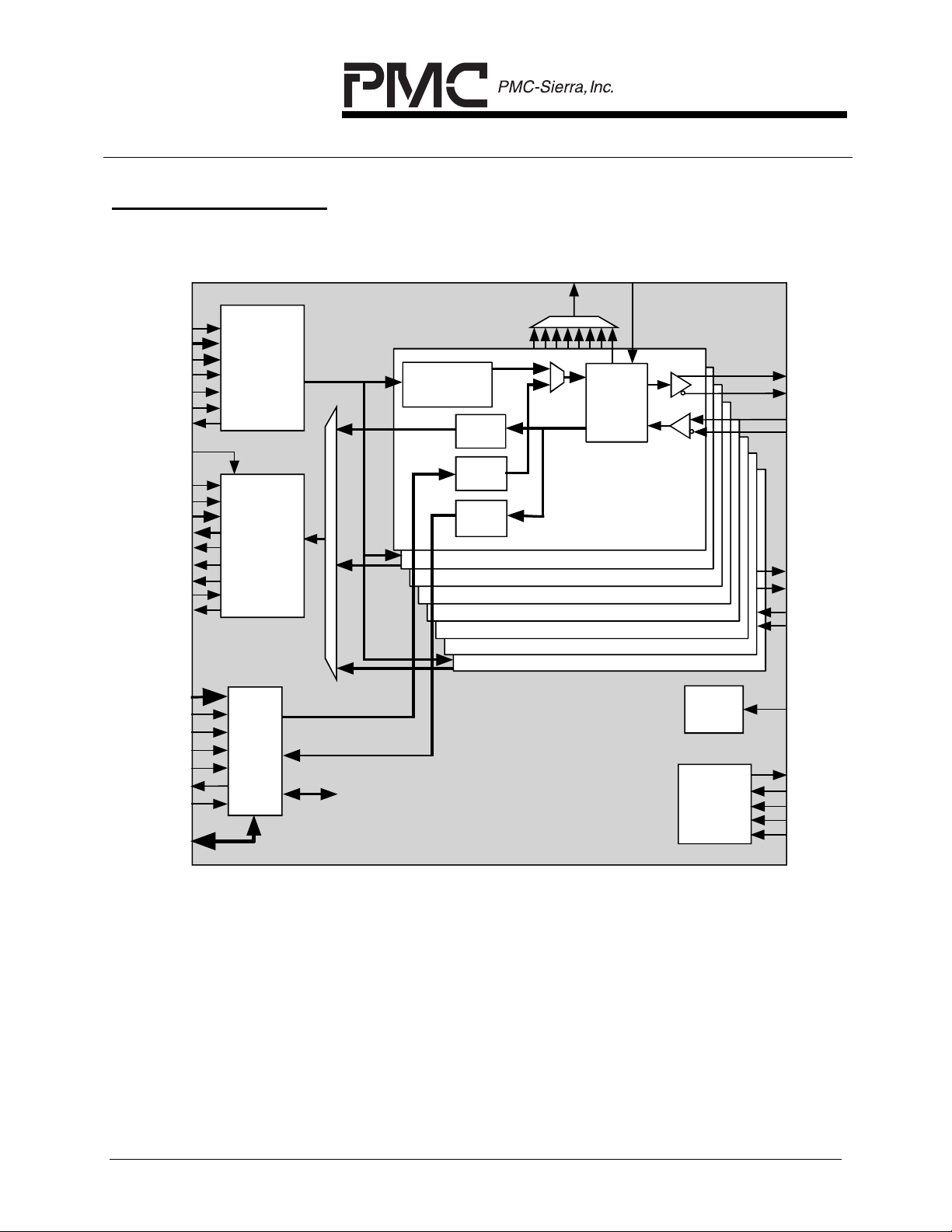
5 BLOCK DIAGRAM
TENB
TADR[11:0]
TDAT[15:0]
TPRTY
TSX
TCLK
TPA
VADR[4:0]
RANYPHY
RENB
RADR[4:0]
RDAT[15:0]
RPRTY
RSOP
RSX
RCLK
RPA
A[9:0]
RDB
WRB
CSB
ALE
INTB
RSTB
D[7:0]
Any-PHY
Transm it
Slave
SCI-PHY/
Any-PHY
Receive
Slave
Micro-
Processor
Inte rfac e
to all
blocks
.
.
.
33 Cell
per-PHY
buffer
6 Cell
FIFO
2 Cell
FIFO
4 Cell
FIFO
K
8
X
R
Cell
Processor
K
8
X
T
TXD0 +
TXD0 -
RXD0+
RXD0-
.
.
.
TXD7+
TXD7-
RXD7+
RXD7-
Clock
Synthesis
JTAG
Test Access
Port
REFCLK
TDO
TDI
TCK
TMS
TRS TB
PROPRIETARY AND CONFIDENTIAL TO PMC-SIERRA, INC., AND FOR ITS CUSTOMERS’ INTERNAL USE 9

RELEASED
DATA SHEET
PMC-1980582 ISSUE 5 OCTAL SERIAL LINK MULTIPLEXER
PM7351 S/UNI-VORTEX
6 DESCRIPTION
The PM7351 S/UNI-VORTEX is a monolithic integrated circuit typically used with
its sister device, the S/UNI-DUPLEX, to implement a point-to-point serial
backplane interconnect architecture.
Up to sixteen S/UNI-VORTEX devices can reside on a common cell processing
card along side a traffic management device. The traffic management device
exchanges cells with the S/UNI-VORTEX via 16-bit SCI-PHY or Any-PHY
interfaces. Flow control is effected across this interface via cell available signals
generated by the S/UNI-VORTEX. In the downstream direction, the availability
of a buffer for each logical channel can be polled by the traffic management
device. In the upstream direction, an indication is provided whether there is one
or more cells queued in the S/UNI-VORTEX for transfer.
Each S/UNI-VORTEX can be connected to eight line cards via 100 to 200 Mb/s
serial links. Each upstream link has its own queue. If a queue becomes nearly
full, a flow control indication is sent downstream. In the downstream direction,
each logical channel has a dedicated cell buffer to avoid head of line blocking.
The serialization of cells from the cell buffers is throttled by flow control
information sent from the line card via the upstream high-speed link.
A microprocessor port provides access to internal configuration and monitoring
registers. The port may also be used to insert and extract cells in support of a
control channel.
LVDS INTERFACES, BOTH DIRECTIONS
• 8 independent 4-wire LVDS serial transceivers each operating at up to 200
Mbps across PCB or backplane traces, or across up to 10 meters of 4-wire
twisted pair cabling for inter-shelf communications.
• Usable bandwidth (excludes system overhead) of 186 Mbps per direction per
LVDS link.
• Full integrated LVDS clock synthesis and recovery. No external analog
components are required.
LVDS RECEIVE DIRECTION
• Weighted round robin multiplex of cell streams from the 8 LVDS links into a
single cell stream which is transferred to the parallel bus under control of the
bus master.
PROPRIETARY AND CONFIDENTIAL TO PMC-SIERRA, INC., AND FOR ITS CUSTOMERS’ INTERNAL USE 10

RELEASED
DATA SHEET
PMC-1980582 ISSUE 5 OCTAL SERIAL LINK MULTIPLEXER
PM7351 S/UNI-VORTEX
• LVDS link and S/UNI-VORTEX identifiers are added to each cell (along with
the PHY identifier already added by S/UNI-DUPLEX) for use by ATM layer to
identify the cell source.
• Back-pressure sent to far end to prevent overflow of receiver FIFO.
LVDS TRANSMIT DIRECTION
• Per PHY and microprocessor port back-pressure used on each of the 8 links
to prevent overflow of downstream buffers.
• Device polling: provides Utopia-like TCA status for 264 PHYs (includes 8
control channels) based on back-pressure from the LVDS links.
• Cell transfer: Bus master adds a PHY address to each cell via a 12 bit
identifier. S/UNI-Vortex decodes and accepts cells for its links based on
software configured base addresses.
PARALLEL BUS INTERFACE:
• Both directions: 16 bit wide, 50 MHz max clock rate, bus slave.
• Cells transferred to the bus: Utopia L2 compatible with optional expanded
length cells. Appears as single PHY, with a cell prepend identifying the
source PHY ID of each cell. Alternatively, Utopia L2 compliance is supported
by placing the PHY ID inside the UDF/HEC fields of a standard ATM cell.
• Cells received from the bus: The Any-PHY bus is similar to Utopia L2 but with
optional expanded length cells and expanded addressing capabilities. The
S/UNI-VORTEX appears to the bus master as a 264 port multi-PHY device (8
links, each with 32 PHYs & communication channel). PHY address is added
as cell prepend or optionally in HEC/UDF field when standard length cells are
desired.
MICROPROCESSOR INTERFACE
• 8 bit data bus, 8 bit address bus.
• Provides read/write access to all configuration and status registers.
• Provides CRC32 calculation and cell transfer registers to support an
embedded microprocessor to microprocessor communication channel
over the LVDS link.
PROPRIETARY AND CONFIDENTIAL TO PMC-SIERRA, INC., AND FOR ITS CUSTOMERS’ INTERNAL USE 11
RELEASED
DATA SHEET
PMC-1980582 ISSUE 5 OCTAL SERIAL LINK MULTIPLEXER
PM7351 S/UNI-VORTEX
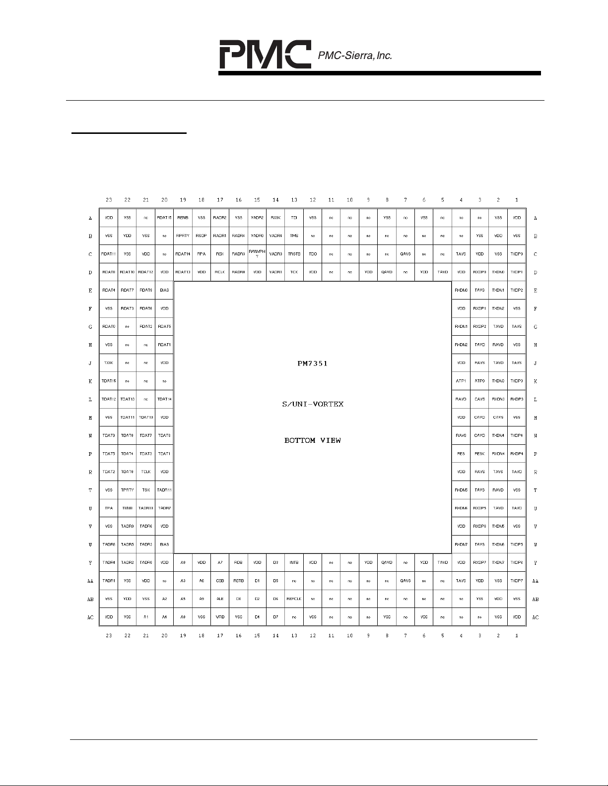
7 PIN DIAGRAM
The S/UNI-VORTEX is packaged in a 304-ball enhanced ball grid array (BGA)
package having a body size of 31 mm by 31 mm and a ball pitch of 1.27 mm.
PROPRIETARY AND CONFIDENTIAL TO PMC-SIERRA, INC., AND FOR ITS CUSTOMERS’ INTERNAL USE 12
RELEASED
DATA SHEET
PMC-1980582 ISSUE 5 OCTAL SERIAL LINK MULTIPLEXER
PM7351 S/UNI-VORTEX
8 PIN DESCRIPTION
Ball
Name
RXD0+
RXD0RXD1+
RXD1RXD2+
RXD2RXD3+
RXD3RXD4+
RXD4RXD5+
RXD5RXD6+
RXD6RXD7+
RXD7-
TXD0+
TXD0TXD1+
TXD1TXD2+
TXD2TXD3+
TXD3TXD4+
TXD4TXD5+
TXD5TXD6+
TXD6TXD7+
TXD7-
Type
Diff.
LVDS
Input
Diff.
LVDS
Output
Ball
No. Function
High Speed LVDS Links
D3
E4
F3
G4
G3
H4
L1
L2
P1
P2
U3
T4
The high-speed receive data (RXD0+/- - RXD7+/-)
inputs present NRZ data from a serial backplane.
These are truly differential inputs offering superior
common-mode noise rejection. They have sufficient
sensitivity and common-mode range to support LVDS
signals.
These inputs are high-impedance. An external
resistor must be connected between the two pins of a
signal pair to terminate the transmission line. D.C. or
A.C. coupling may be used depending on the
application.
V3
U4
Y3
W4
C1
D2
D1
E2
E1
F2
K1
K2
N1
N2
The transmit differential data (TXD0+/- -TXD7+/-)
outputs present NRZ encoded data to a serial
backplane. These outputs are open drain current
sinks which interface directly with twisted-pair cabling
or board interconnect. D.C. or A.C. coupling may be
used depending on the application.
As current sinks, these outputs must see a 100Ω
reflected impedance between the pins in a signal pair
to produce correct LVDS signal levels.
W1
V2
Y1
W2
AA1
Y2
PROPRIETARY AND CONFIDENTIAL TO PMC-SIERRA, INC., AND FOR ITS CUSTOMERS’ INTERNAL USE 13

RELEASED
DATA SHEET
PMC-1980582 ISSUE 5 OCTAL SERIAL LINK MULTIPLEXER
PM7351 S/UNI-VORTEX
Ball
Name
Type
Ball
No. Function
REFCLK Input AB13 The reference clock input (REFCLK) must provide a
jitter-free reference clock. It is used as the reference
clock by both clock recovery and clock synthesis
circuits. Any jitter below 1 MHz is transferred directly
to the TXDn+/- outputs. The high speed serial
interface bit rate is eight times the REFCLK frequency.
RES
RESK
Analog P4
P3
A 4.75kΩ ±1% resistor must be connected between
these two balls to achieve the correct LVDS output
signal levels.
ATP0
ATP1
Analog K3K4The Analog Test Points (ATP) are provided for
production test purposes. In mission mode they are
high impedance and should be connected to ground.
TX8K Input J23 The transmit 8 kHz timing reference (TX8K) input
allows a traceable signal to be transmitted to the far
end of the high-speed serial links via TXD0+/- through
TXD7+/-. A rising edge on TX8K is encoded in the
next cell transmitted.
Although TX8K is targeted at a typical need of
transporting an 8 kHz signal, its frequency is not
constrained to 8 kHz. Any frequency less than the cell
rate is permissible.
RX8K Output A14 The receive 8 kHz timing reference (RX8K) output
presents the timing extracted from one of the receive
high-speed serial links.
The rising edge of RX8K is accurate to the nearest
byte boundary of the high-speed serial link; therefore,
a small amount of jitter is present. At a link rate of
155.52 Mb/s, the jitter is 63ns peak-to-peak.
Pulses on RX8K are always 16 high-speed serial link
bit periods wide (two REFCLK periods).
PROPRIETARY AND CONFIDENTIAL TO PMC-SIERRA, INC., AND FOR ITS CUSTOMERS’ INTERNAL USE 14
RELEASED
DATA SHEET
PMC-1980582 ISSUE 5 OCTAL SERIAL LINK MULTIPLEXER
PM7351 S/UNI-VORTEX
Ball
Name
Type
Ball
No. Function
Upstream (Receive) Bus
RANYPHY Input C15 The Receive Any-PHY configuration input determines
the protocol of the upstream cell interface.
If RANYPHY is logic low, the interface complies to the
SCI-PHY specification. As such, all outputs have a
single cycle latency.
If RANYPHY is logic high, the interface complies to
the Any-PHY specification. Relative to SCI-PHY, all
outputs have an additional cycle of latency.
RANYPHY is an asynchronous input and is expected
to be held static.
RCLK Input D17 The Receive FIFO clock (RCLK) is used to read words
from the S/UNI-VORTEX upstream cell buffer. RCLK
must cycle at a 52 MHz or lower instantaneous rate.
RSOP, RPA, RPRTY and RDAT[15:0] are updated on
the rising edge of RCLK. RENB and RADR[4:0] are
sampled on the rising edge of RCLK.
RPA Output C18 The RPA signal indicates whether at least one cell is
queued for transfer.
Upon sampling a RADR[4:0] value that equals the
value on VADR[4:0], the S/UNI-VORTEX drives the
RPA with the cell availability status immediately if
RANYPHY is logic low. If RANYPHY is logic high,
RPA has an additional cycle of latency. RPA will be a
one if at least one entire cell is available.
RPA is high-impedance when not polled.
RPA is updated on the rising edge of RCLK.
PROPRIETARY AND CONFIDENTIAL TO PMC-SIERRA, INC., AND FOR ITS CUSTOMERS’ INTERNAL USE 15
RELEASED
DATA SHEET
PMC-1980582 ISSUE 5 OCTAL SERIAL LINK MULTIPLEXER
PM7351 S/UNI-VORTEX
Ball
Name
Type
Ball
No. Function
RENB Input A19 The active low read enable (RENB) output is used to
initiate the transfer of cells from the S/UNI-VORTEX to
a traffic management device.
When RENB is sampled low and the S/UNI-VORTEX
has been selected, a word is output on bus
RDAT[15:0]. Selection occurs when RENB is last
sampled high if the RADR[4:0] value equals the state
of VADR[4:0]. RENB must be low for between 27 and
29 cycles to transfer an entire cell depending on
whether the cell contains prepended words or the
H5/UDF word.
If RANYPHY is logic low, valid data is driven
immediately upon sampling RENB low. If RANYPHY
is logic high, the RSX, RSOP, RDAT[15:0] and RPRTY
outputs have an additional cycle of latency.
It is permissible to pause a cell transfer by deasserting
RENB high. If RANYPHY is logic low, the S/UNIVORTEX’s address must be presented on RADR[4:0]
the last cycle RENB is high to reselect the device. If
RANYPHY is logic high, the cell transfer resumes
unconditionally when RENB is asserted low again. In
either case, a cell transfer must be completed before
another device on the bus is selected.
The Any-PHY protocol supports autonomous
deselection. If RANYPHY is logic high, the outputs
become high impedance after the last word of a cell is
transferred until the S/UNI-VORTEX is reselected. If
RANYPHY is logic low, a subsequent cell is
transferred (provided one is available) if RENB is held
low beyond the end of a cell.
When RENB is sampled high or the S/UNI-VORTEX
is not selected, no read is performed and outputs
RDAT[15:0], RPRTY, RSX and RSOP become high
impedance.
The RENB input is sampled on the rising edge of
RCLK.
PROPRIETARY AND CONFIDENTIAL TO PMC-SIERRA, INC., AND FOR ITS CUSTOMERS’ INTERNAL USE 16

RELEASED
DATA SHEET
PMC-1980582 ISSUE 5 OCTAL SERIAL LINK MULTIPLEXER
PM7351 S/UNI-VORTEX
Ball
Name
RADR[4]
RADR[3]
RADR[2]
RADR[1]
RADR[0]
VADR[4]
VADR[3]
VADR[2]
VADR[1]
VADR[0]
Ball
Type
No. Function
Input B16
C16
A17
B17
D16
Input B14
C14
A15
D14
B15
The RADR[4:0] signals are used to address up to
sixteen S/UNI-VORTEX devices for the purposes of
polling and selection for cell transfer.
When a RADR[4:0] value is sampled that equals the
state of VADR[4:0], the RPA output is driven to
indicate whether a cell is available for transfer. If
RANYPHY is logic high, RPA has an additional cycle
of latency.
If the RADR[4:0] value equals the state of VADR[4:0]
when the RENB is last sampled high, the S/UNIVORTEX will initiate a cell transfer. If RANYPHY is
logic low, the device must be reselected to resume a
cell transferred that has been halted by deasserting
RENB high.
The RADR[4:0] bus is sampled on the rising edge of
RCLK.
The device identification address (VADR[4:0]) inputs
are the most-significant bits of the upstream polling
address space which this S/UNI-VORTEX occupies.
When the VADR[4:0] inputs match the value sampled
on RADR[4:0] inputs, the S/UNI-VORTEX drives RPA
to indicate the existence of queued cells. Otherwise,
RPA is high impedance.
VADR[4:0] are expected to be held static.
PROPRIETARY AND CONFIDENTIAL TO PMC-SIERRA, INC., AND FOR ITS CUSTOMERS’ INTERNAL USE 17

RELEASED
DATA SHEET
PMC-1980582 ISSUE 5 OCTAL SERIAL LINK MULTIPLEXER
PM7351 S/UNI-VORTEX
Ball
Name
Type
Ball
No. Function
RSOP Output B18 The Receive Start of Packet (RSOP) marks either the
first or second word of the cell on the RDAT[15:0] bus.
When RSOP is high and RANYPHY is low, the first
word of the cell structure is present on the RDAT[15:0]
stream. When RSOP and RANYPHY are both high,
the second word of the cell structure is present on the
RDAT[15:0] stream.
RSOP is updated on the rising edge of RCLK and
considered valid only when the S/UNI-VORTEX
device was selected after the polling process and the
RENB signal is sampled low. If RANYPHY is logic low
RSOP is driven immediately upon sampling RENB
low, but it has an additional cycle latency when
RANYPHY is logic high. RSOP becomes high
impedance upon sampling RENB high or if the S/UNIVORTEX device is not selected for transfer.
When RANYPHY is high, autonomous deselection
occurs after the last word of a cell resulting in setting
RSOP high-impedance until reselection.
RSX Output C17 The Receive Start of Transfer (RSX) is only active
when the RANYPHY input is logic high. When
RANYPHY is logic low, RSX is low during cell
transfers or high-impedance otherwise.
RSX marks the start of the cell on the RDAT[15:0]
bus. When RSX is high, the first word of the cell
structure is present on the RDAT[15:0] stream.
RSX is updated on the rising edge of RCLK and
considered valid only when the RENB signal was
sampled low in the previous cycle and the S/UNIVORTEX device was selected after the polling
process. RSX becomes high impedance (with a cycle
latency) upon sampling RENB high or if the S/UNIVORTEX device is not selected for transfer.
When RANYPHY is high, autonomous deselection
occurs after the last word of a cell resulting in setting
RSX high-impedance until reselection.
PROPRIETARY AND CONFIDENTIAL TO PMC-SIERRA, INC., AND FOR ITS CUSTOMERS’ INTERNAL USE 18
RELEASED
DATA SHEET
PMC-1980582 ISSUE 5 OCTAL SERIAL LINK MULTIPLEXER
PM7351 S/UNI-VORTEX
Ball
Name
RDAT[15]
RDAT[14]
RDAT[13]
RDAT[12]
RDAT[11]
RDAT[10]
RDAT[9]
RDAT[8]
RDAT[7]
RDAT[6]
RDAT[5]
RDAT[4]
RDAT[3]
RDAT[2]
RDAT[1]
RDAT[0]
Type
Output A20
Ball
No. Function
The receive cell data bus (RDAT[15:0]) carries the
C19
D19
D21
C23
D22
E21
D23
E22
F21
G20
E23
F22
G21
H20
G23
ATM cell words that have been read from the S/UNI-
VORTEX internal cell buffers.
The RDAT[15:0] bus is updated on the rising edge of
RCLK and considered valid only when the S/UNI-
VORTEX device was selected after the polling
process and the RENB signal is sampled low. If
RANYPHY is logic low RDAT[15:0] is driven
immediately upon sampling RENB low, but it has an
additional cycle latency when RANYPHY is logic high.
RDAT[15:0] becomes high impedance upon sampling
RENB high or if the S/UNI-VORTEX device is not
selected for transfer.
When RANYPHY is high, autonomous deselection
occurs after the last word of a cell resulting in setting
RDAT[15:0] high-impedance until reselection.
RPRTY Output B19 The Receive Parity (RPRTY) signal completes the
parity (programmable for odd or even parity) of the
RDAT[15:0] bus.
The RPRTY signal is updated on the rising edge of
RCLK and is considered valid only when the S/UNI-
VORTEX device was selected after the polling
process and the RENB signal is sampled low. If
RANYPHY is logic low RPRTY is driven immediately
upon sampling RENB low, but it has an additional
cycle latency when RANYPHY is logic high. RPRTY
becomes high impedance upon sampling RENB high
or if the S/UNI-VORTEX device is not selected for
transfer.
When RANYPHY is high, autonomous deselection
occurs after the last word of a cell resulting in setting
RPRTY high-impedance until reselection.
PROPRIETARY AND CONFIDENTIAL TO PMC-SIERRA, INC., AND FOR ITS CUSTOMERS’ INTERNAL USE 19
RELEASED
DATA SHEET
PMC-1980582 ISSUE 5 OCTAL SERIAL LINK MULTIPLEXER
PM7351 S/UNI-VORTEX
Ball
Name
Type
Ball
No. Function
Downstream (Transmit) Bus
TCLK Input R21 The transmit FIFO clock (TCLK) is used to transfer
cells from a traffic scheduler device to the internal
downstream cell buffers. TCLK must cycle at a 52
MHz or lower instantaneous rate. TSX, TENB,
TADR[11:0], TPRTY and TDAT[15:0] are sampled on
the rising edge of TCLK. TPA is updated on the rising
edge of TCLK.
TPA Output U23 The S/UNI-VORTEX indicates the availability of space
in the FIFO associated with a logical channel when
polled using the TADR[11:0] signals. The S/UNI-
VORTEX will drive the TPA signal to the appropriate
value during the second clock cycle following that in
which a particular logical channel is addressed. When
high, TPA indicates that the corresponding buffer
segment is empty and a complete cell may be written.
The buffer status for the particular logical channel
involved in the transfer is updated immediately upon
sampling the first word of the cell when the
INADDUDF bit of the Downstream Cell Interface
Configuration register is logic 0. When the
INADDUDF bit is logic 1, the buffer status is stale until
nine cycles after the cell transfer is completed;
therefore, the master should refrain from polling that
logical channel in the interim.
TPA becomes high impedance when an address not
matching the address space set by the Control
Channel Base Address, Logical Channel Base
Address and Logical Channel Address Range /
Logical Channel Base Address MSB registers is
sampled from the TADR[11:3] inputs.
TPA is updated on the rising edge of TCLK.
PROPRIETARY AND CONFIDENTIAL TO PMC-SIERRA, INC., AND FOR ITS CUSTOMERS’ INTERNAL USE 20

RELEASED
DATA SHEET
PMC-1980582 ISSUE 5 OCTAL SERIAL LINK MULTIPLEXER
PM7351 S/UNI-VORTEX
Ball
Name
Type
Ball
No. Function
TENB Input U22 The active low write enable (TENB) signal is used to
indicate cell transfers to the internal cell buffers. The
segment of the buffer associated with a particular
logical channel is determined by the inband address in
the prepended cell bytes.
TENB is ignored if TSX is high. Upon the completion
of a cell transfer, TENB may be held low because a
cell transfer is only initiated by assertion of TSX.
TENB must be low for 26 to 28 (depending on the
inclusion of optional words) cycles to transfer an entire
cell. TENB may be deasserted high at any time to
pause a cell transfer.
TENB is updated on the rising edge of TCLK.
TADR[11]
TADR[10]
TADR[9]
TADR[8]
TADR[7]
TADR[6]
TADR[5]
TADR[4]
TADR[3]
TADR[2]
TADR[1]
TADR[0]
Input T20
U21
V22
W23
U20
V21
W22
Y23
W21
Y22
AA23
Y21
The TADR[11:0] signals are used to address logical
channels for the purposes of polling.
Upon sampling a TADR[11:3] value within one of the
address ranges set by the Control Channel Base
Address, Logical Channel Base Address and Logical
Channel Address Range / Logical Channel Base
Address MSB registers, TPA will be driven to indicate
the availability of the buffer segment addressed by
TADR[4:0]. When TADR[11:3] does not match a
programmed address range, TPA becomes high
impedance.
The TADR[11:0] bus is sampled on the rising edge of
TCLK.
TSX Input T21 The transmit start of cell (TSX) indication signal marks
the start of cell on the TDAT[15:0] data bus. When
TSX is high, the first word of the cell structure is
present on the TDAT[15:0] stream. TSX must be
asserted for each cell. An interrupt may be generated
if TSX is high during any word other than the expected
first word of the cell structure.
TSX is sampled on the rising edge of TCLK.
PROPRIETARY AND CONFIDENTIAL TO PMC-SIERRA, INC., AND FOR ITS CUSTOMERS’ INTERNAL USE 21

RELEASED
DATA SHEET
PMC-1980582 ISSUE 5 OCTAL SERIAL LINK MULTIPLEXER
PM7351 S/UNI-VORTEX
Ball
Name
TDAT[15]
TDAT[14]
TDAT[13]
TDAT[12]
TDAT[11]
TDAT[10]
TDAT[9]
TDAT[8]
TDAT[7]
TDAT[6]
TDAT[5]
TDAT[4]
TDAT[3]
TDAT[2]
TDAT[1]
TDAT[0]
Type
Input K23
Ball
No. Function
The transmit cell data bus (TDAT[15:0]) carries the
L20
L22
L23
M22
M21
N23
N22
ATM cell octets that are transferred to the internal cell
buffer.
The TDAT[15:0] bus is sampled on the rising edge of
TCLK and is considered valid only when the TENB
signal is asserted low or the TSX signal is asserted
high.
N21
N20
P23
P22
P21
R23
P20
R22
TPRTY Input T22 The transmit parity (TPRTY) signal completes the
parity (programmable for odd or even parity) of the
TDAT[15:0] bus.
A parity error is indicated by a status bit and a
maskable interrupt.
The TPRTY signal is sampled on the rising edge of
TCLK and is considered valid only when the TENB
signal is asserted or the TSX signal is asserted high.
Microprocessor Bus
CSB Input AA17 The active-low chip select (CSB) signal is low during
S/UNI-VORTEX register accesses.
If CSB is not required (i.e., registers accesses are
controlled using the RDB and WRB signals only), CSB
must be connected to an inverted version of the RSTB
input.
RDB Input Y16 The active-low read enable (RDB) signal is low during
S/UNI-VORTEX register read accesses. The S/UNIVORTEX drives the D[7:0] bus with the contents of
the addressed register while RDB and CSB are low.
PROPRIETARY AND CONFIDENTIAL TO PMC-SIERRA, INC., AND FOR ITS CUSTOMERS’ INTERNAL USE 22

RELEASED
DATA SHEET
PMC-1980582 ISSUE 5 OCTAL SERIAL LINK MULTIPLEXER
PM7351 S/UNI-VORTEX
Ball
Name
Type
Ball
No. Function
WRB Input AC17 The active-low write strobe (WRB) signal is low during
S/UNI-VORTEX register write accesses. The D[7:0]
bus contents are clocked into the addressed register
on the rising WRB edge while CSB is low.
D[7]
D[6]
D[5]
D[4]
D[3]
D[2]
D[1]
D[0]
A[9]/TRS
A[8]
A[7]
A[6]
A[5]
A[4]
A[3]
A[2]
A[1]
A[0]
I/O AC14
AB14
AA14
AC15
Y14
AB15
AA15
AB16
Input AB18
AC19
Y17
AA18
AB19
AC20
AA19
AB20
AC21
Y19
The bi-directional data bus D[7:0] is used during
S/UNI-VORTEX register read and write accesses.
The address bus A[9:0] selects specific registers
during S/UNI-VORTEX register accesses.
The test register select (TRS) signal selects between
normal and test mode register accesses. TRS is high
during test mode register accesses, and is low during
normal mode register accesses.
RSTB Input AA16 The active-low reset (RSTB) signal provides an
asynchronous S/UNI-VORTEX reset. RSTB is a
Schmitt triggered input with an integral pull-up resistor.
ALE Input AB17 The address latch enable (ALE) is active-high and
latches the address bus A[9:0] when low. When ALE
is high, the internal address latches are transparent.
It allows the S/UNI-VORTEX to interface to a
multiplexed address/data bus. ALE has an integral
pull-up resistor.
INTB OD
Output
Y13 The active-low interrupt (INTB) signal goes low when
a S/UNI-VORTEX interrupt source is active and that
source is unmasked. The S/UNI-VORTEX may be
enabled to report many alarms or events via
interrupts. INTB becomes high impedance when the
interrupt is acknowledged via an appropriate register
access. INTB is an open drain output.
JTAG Boundary Scan Port
PROPRIETARY AND CONFIDENTIAL TO PMC-SIERRA, INC., AND FOR ITS CUSTOMERS’ INTERNAL USE 23

RELEASED
DATA SHEET
PMC-1980582 ISSUE 5 OCTAL SERIAL LINK MULTIPLEXER
PM7351 S/UNI-VORTEX
Ball
Name
Type
Ball
No. Function
TCK Input D13 The test clock (TCK) signal provides timing for test
operations that are carried out using the IEEE
P1149.1 test access port. TCK has an integral pull-up
resistor.
TMS Input B13 The test mode select (TMS) signal controls the test
operations that are carried out using the IEEE
P1149.1 test access port. TMS is sampled on the
rising edge of TCK. TMS has an integral pull-up
resistor.
TDI Input A13 The test data input (TDI) signal carries test data into
the S/UNI-VORTEX via the IEEE P1149.1 test access
port. TDI is sampled on the rising edge of TCK. TDI
has an integral pull-up resistor.
TDO Tristate C12 The test data output (TDO) signal carries test data out
of the S/UNI-VORTEX via the IEEE P1149.1 test
access port. TDO is updated on the falling edge of
TCK. TDO is a tristate output which is inactive except
when scanning of data is in progress.
TRSTB Input C13 The active-low test reset (TRSTB) signal provides an
asynchronous S/UNI-VORTEX test access port reset
via the IEEE P1149.1 test access port. TRSTB is a
Schmitt triggered input with an integral pull-up resistor.
Note that when not being used, TRSTB must be
connected to the RSTB input.
Power and Ground
BIAS Power E20
W20
When tied to +5V, the BIAS inputs are used to bias
the wells in the input and I/O pads so that the pads
can tolerate 5V on their inputs without forward biasing
internal ESD protection devices. When tied to +3.3V,
the inputs and bi-directional inputs will only tolerate
3.3V level inputs.
PROPRIETARY AND CONFIDENTIAL TO PMC-SIERRA, INC., AND FOR ITS CUSTOMERS’ INTERNAL USE 24

RELEASED
DATA SHEET
PMC-1980582 ISSUE 5 OCTAL SERIAL LINK MULTIPLEXER
PM7351 S/UNI-VORTEX
Ball
Name
Type
Ball
No. Function
VDD Power A1
B2
C3
D4
F4
J4
M4
R4
V4
AC1
AB2
AA3
Y4
Y6
Y9
Y12
Y15
Y18
AC23
AB22
AA21
Y20
V20
R20
M20
J20
F20
A23
B22
C21
D20
D18
D15
D12
D9
D6
The pad ring power (VDD) pins should be connected
to a well-decoupled +3.3 V DC supply.
PROPRIETARY AND CONFIDENTIAL TO PMC-SIERRA, INC., AND FOR ITS CUSTOMERS’ INTERNAL USE 25

RELEASED
DATA SHEET
PMC-1980582 ISSUE 5 OCTAL SERIAL LINK MULTIPLEXER
PM7351 S/UNI-VORTEX
Ball
Name
Type
Ball
No. Function
VSS Ground B1
C2
F1
H1
M1
T1
V1
AA2
AB1
AC2
AB3
AC6
AC8
AC12
AC16
AC18
AC22
AB21
AB23
AA22
V23
T23
M23
H23
F23
B23
C22
B21
A22
A18
A16
A12
A8
A6
A2
B3
The pad ring ground (VSS) pins should be connected
to GND.
QAVD1
QAVD0
QAVS1
QAVS0
PROPRIETARY AND CONFIDENTIAL TO PMC-SIERRA, INC., AND FOR ITS CUSTOMERS’ INTERNAL USE 26
Analog
PowerY8D8
Analog
AA7C7Quiet Analog Ground (QAVS1, QAVS0). QAVS1 and
Power
Quiet Analog Power (QAVD1, QAVD0). QAVD1 and
QAVD0 should be connected to analog +3.3 V.
QAVS0 should be connected to analog GND.

RELEASED
DATA SHEET
PMC-1980582 ISSUE 5 OCTAL SERIAL LINK MULTIPLEXER
PM7351 S/UNI-VORTEX
Ball
Name
Type
CAVD Analog
PowerM3N3
CAVS Analog
GroundL3M2
RAVD Analog
PowerH2L4
RAVS Analog
GroundJ3N4
TAVD Analog
PowerD5G2
Ball
No. Function
The power (CAVD) pins for the analog clock synthesis
unit. These pins should be connected to analog
+3.3V.
The ground (CAVS) pins for the analog clock
synthesis unit. These pins should be connected to
analog GND.
The power (RAVD) pins for the LVDS receivers.
These pins should be connected to analog +3.3V.
T2
The ground (RAVS) pins for the LVDS receivers.
These pins should be connected to analog GND.
R3
The power (TAVD) pins for the LVDS transmitters.
These pins should be connected to analog +3.3V.
H3
J2
R1
U1
U2
Y5
TAVS Analog
GroundC4E3
The ground (TAVS) pins for the LVDS transmitters.
These pins should be connected to analog GND.
G1
J1
R2
T3
W3
AA4
Notes on Pin Description:
1. All S/UNI-VORTEX inputs and bi-directionals present minimum capacitive
loading and operate at TTL logic levels, except RXD0+/- through RXD7+/-.
2. Inputs RSTB, ALE, RANYPHY, TMS, TDI, TCK and TRSTB have internal
pull-up resistors. To improve noise immunity, in designs where these
inputs are no-connects it is still recommend that they be tied to VDD.
3. The recommended power supply sequencing is as follows:
PROPRIETARY AND CONFIDENTIAL TO PMC-SIERRA, INC., AND FOR ITS CUSTOMERS’ INTERNAL USE 27

RELEASED
DATA SHEET
PMC-1980582 ISSUE 5 OCTAL SERIAL LINK MULTIPLEXER
PM7351 S/UNI-VORTEX
3.1 During power-up, the voltage on the BIAS pins must be kept equal to or
greater than the voltage on the VDD pins, to avoid damage to the device.
3.2 The VDD power must be applied before input pins are driven or the input
current per pin be limited to less than the maximum DC input current
specification. (20 mA)
3.3 Analog power supplies (QAVD, CAVD, RAVD, TAVD) must have their
current per pin limited to the maximum latch-up current specification
(100 mA). In operation, the differential voltage measured between AVD
supplies and VDD must be less than 0.5 V. The relative power
sequencing of the multiple AVD power supplies is not important.
3.4 Power down the device in the reverse sequence.
PROPRIETARY AND CONFIDENTIAL TO PMC-SIERRA, INC., AND FOR ITS CUSTOMERS’ INTERNAL USE 28

RELEASED
DATA SHEET
PMC-1980582 ISSUE 5 OCTAL SERIAL LINK MULTIPLEXER
PM7351 S/UNI-VORTEX
9 FUNCTIONAL DESCRIPTION
First, a brief note on terminology. Throughout this document the use of the term
“downstream” implies data read in from the parallel bus (or microprocessor port)
and sent out the LVDS links. However, since the S/UNI-VORTEX is a slave
device and bus direction (transmit or receive) is normally defined with respect to
the bus master, the downstream bus is called the Transmit bus. Conversely,
“upstream” is used to describe the data path from the LVDS to the parallel bus,
which is called the Receive bus.
9.1 Cell Interface
Cell transfer from the S/UNI-VORTEX (bus slave) to a traffic management device
(bus master) in the upstream direction is configurable as either SCI-PHY or AnyPHY. SCI-PHY is very similar to UTOPIA, but it supports the appended bytes
used by the S/UNI-VORTEX for carrying PHY address information. If the option
to place PHY addressing information in the H5/UDF field is enabled, the SCIPHY bus is compatible to a 16 bit Utopia Level 2. Any-PHY defines inband
selection and polling techniques to support a large number of logical channels,
where SCI-PHY is limited to 32 and UTOPIA is limited to 31.
The downstream interface only provides an Any-PHY bus slave interface. While
the downstream cell transfer mechanism is compatible with existing SCI-PHY
devices (or UTOPIA devices supporting extended cells), the channel status
polling is a new extension.
16-bit wide busses plus parity are supported; 8 bit wide is not supported.
9.1.1 Downstream
Conceptually, the Any-PHY protocol can be divided into two processes: polling
and cell transfer.
Polling in the downstream direction is used by the bus master – typically a traffic
buffering and management device – to determine when a buffered data cell can
be safely sent to a downstream PHY. The S/UNI-VORTEX provides an
independent cell buffer for each logical downstream channel on each LVDS link.
In total there are 256 data path cell buffers (maximum 32 channels per LVDS link
times 8 links) plus 8 microprocessor communication channel buffers (one per
link). This arrangement ensures there is no head of line blocking while
eliminating the risk of buffer overflow.
The traffic manager need only poll those logical channels for which it has
downstream cells queued. A cell transfer can be initiated after a polled logical
PROPRIETARY AND CONFIDENTIAL TO PMC-SIERRA, INC., AND FOR ITS CUSTOMERS’ INTERNAL USE 29

RELEASED
DATA SHEET
PMC-1980582 ISSUE 5 OCTAL SERIAL LINK MULTIPLEXER
PM7351 S/UNI-VORTEX
channel asserts the TPA output. Each channel’s cell buffer availability status (i.e.
the status that will be driven onto the TPA output when the channel is polled) is
deasserted when the first byte of a cell is written into the buffer. It is re-asserted
only after the number of bytes programmed by the associated Downstream
Logical Channel FIFO Ready Level register have been serialized onto a highspeed link. Determining what value to set the FIFO ready level is discussed in
Section 12.1.
Polling is performed using the TADR[11:0] bus, which supports a 4096 logical
channel address space. Up to 32 logical channels associated with each highspeed link can be mapped to anywhere within this address space with a
granularity of eight locations through the Logical Channel Base Address
registers. To provide an optimal address map regardless of the number logical
channels per high-speed link, each high-speed link can be programmed to use 8,
16, 24 or 32 address locations through the Logical Channel Address Range
registers. The eight control channels of each S/UNI-VORTEX are mapped to
eight contiguous address locations starting at the address set by the Control
Channel Base Address register. The control channels are associated with the
addresses numerical, i.e. the control channel for TXD0+/- belongs to the lowest
order address and TXD7+/- belongs to the highest order address.
With respect to cell transfers, the Any-PHY port appears like a single PHY entity.
No out of band addressing is required. Instead, the first word of the transferred
cell identifies the destination logical channel. The format of the cell data
structure is illustrated in Fig. 3. As programmed through register bits, a User
Prepend word may be prepended to a basic ATM cell to support applications
where context information is carried inband. By default, only the logical channel
index (Word 0) is prepended.
The cell will be transferred to a S/UNI-VORTEX if the ADDR[11:0] (ADDR[13:12]
is unused in the downstream direction.) field value matches the logical channel
mapping programmed through the Control Channel Base Address, Logical
Channel Base Address and Logical Channel Address Range / Logical Channel
Base Address MSB registers.
Normally, ADDR[11:0] is contained within Word 0 of the Any-PHY data structure,
but can be mapped to the H5/UDF fields. The H5/UDF (User Defined Field) and
User Prepend fields can be handled in four ways:
1. They are excluded from the Any-PHY data structure.
2. They exist in the Any-PHY data structure, but are not passed across the
high-speed serial interfaces. The contents are ignored.
3. They are passed transparently across the high-speed serial interfaces.
PROPRIETARY AND CONFIDENTIAL TO PMC-SIERRA, INC., AND FOR ITS CUSTOMERS’ INTERNAL USE 30

RELEASED
DATA SHEET
PMC-1980582 ISSUE 5 OCTAL SERIAL LINK MULTIPLEXER
PM7351 S/UNI-VORTEX
4. The H5/UDF fields contain the ADDR[11:0] value and are used to route
transferred cells. In this case Word 0 is not used and should not
generated by the bus master.
The treatment of the H5/UDF field, the address prepend(word 0), and their
corresponding fields on the LVDS link are independent of that of the User
Prepend. See Section 12.2 Interaction Between Bus and LVDS Configurations
on page 130 for further details.
Although the ability to carry the inband address in the H5/UDF fields is provided
for compatibility with devices that cannot generate an address prepend, there are
two constraints that must be respected in this configuration:
1. Recall that in the default case (i.e. Word 0 provides the address) the
logical channel participating in a cell transfer will deassert TPA upon the
first word of the cell transfer. However, when the H5/UDF provides the
address, the channel’s TPA status will not return deasserted until nine
TCLK periods after the last word of the cell transfer is complete. This
implies that once a cell transfer to a channel has begun that channel
should not be polled again until at least nine bus cycles after the transfer
is complete.
2. Once the cell transfer is started, the TENB input must remain low until
after the H5/UDF word has been transferred. After that, it is permissible
for TENB to toggle high to momentarily halt the cell transfer.
Be aware that the Any-PHY data structures are transported transparently. There
are no constraints on the contents. Therefore, data streams other than ATM
cells can be transferred across the Any-PHY interface; only the bus timing and
protocols need be respected.
PROPRIETARY AND CONFIDENTIAL TO PMC-SIERRA, INC., AND FOR ITS CUSTOMERS’ INTERNAL USE 31

RELEASED
DATA SHEET
PMC-1980582 ISSUE 5 OCTAL SERIAL LINK MULTIPLEXER
PM7351 S/UNI-VORTEX
Fig. 3 SCI-PHY/Any-PHY Cell
Bit 15 Bit 0
Bit 8 Bit 7
Word 0
(optional)
Word 1
(optional)
Word 2
Word 3
Word 4
(optional)
Word 5
Word 6
Word 28
Reserved
PAYLOAD1 PAYLOAD2
PAYLOAD3 PAYLOAD4
PAYLOAD47 PAYLOAD48
ADDR[13:0]
User Prepend
H1
H3 H4
1
H5
H2
UDF
1
Format
Note 1: Optionally, the H5/UDF fields can be overwritten by ADDR[13:0].
9.1.2 Upstream
In the upstream direction, each S/UNI-VORTEX appears as a single SCI-PHY or
Any-PHY slave. The traffic from each high-speed serial link (RXD0+/- through
RXD7+/) is queued independently to support per logical channel flow control
without head of line blocking. Weighted round robin servicing determines the
order of cells presented on RDAT[15:0]. Weights are strictly linear. For
example, compared to a link with a weight of one, a LVDS link with a weight of
four will on average have four times the number of opportunities to place a cell
from its receive buffer onto the upstream bus. Each high speed serial link can be
assigned a weight between 1 and 4. When the state of the RADR[4:0] inputs
equals the state of the VADR[4:0] pins, the RPA output indicates whether there is
at least one cell available for transfer from any link.
PROPRIETARY AND CONFIDENTIAL TO PMC-SIERRA, INC., AND FOR ITS CUSTOMERS’ INTERNAL USE 32

RELEASED
DATA SHEET
PMC-1980582 ISSUE 5 OCTAL SERIAL LINK MULTIPLEXER
PM7351 S/UNI-VORTEX
To support current and future devices, the interface is configurable as either an
Any-PHY or SCI-PHY interface. Table 1 summarizes the distinctions between
the two protocols.
Table 1 SCI-PHY and Any-PHY Comparison
Attribute SCI-PHY Any-PHY
Latency RDAT[15:0], RPRTY, RSOP and
RSX are driven or become high
impedance immediately upon
sampling RENB low or high,
respectively. RPA is driven
immediately upon sampling a
RADR[4:0] value that matches
VADR[4:0].
RSX Undefined. It is low when not high
impedance.
RSOP High coincident with the first word
of the cell data structure.
Paused
transfers
Autonomous
deselection
Permitted by deasserting RENB
high, but the S/UNI-VORTEX’s
address must be presented on
RADR[4:0] the last cycle RENB is
high.
Not supported. A subsequent cell
is output (provided one is available)
if RENB is held low beyond the end
of a cell.
RDAT[15:0], RPRTY, RSOP and
RSX are driven or become high
impedance on the RCLK rising
edge following the one that
samples RENB low or high,
respectively. RPA is driven on the
RCLK rising edge following the one
that samples a RADR[4:0] value
that matches VADR[4:0].
High coincident with the first word
of the cell data structure.
High coincident with the second
word of the cell data structure.
Permitted by deasserting RENB
high. The cell transfer resumes
unconditionally when RENB is
asserted low again.
The outputs become high
impedance after the last word of a
cell is transferred until the S/UNIVORTEX is reselected.
The cell format is the same as the downstream interface (Fig. 3). No address
map manipulation is performed in the upstream direction; ADDR[13:0] field
encoding has a fixed relationship to the physical ports. ADDR[13:9] will always
equal the VADR[4:0] input pins’ state. ADDR[8:6] corresponds to the index of the
high speed serial link (RXD0+/- through RXD7+/-) over which the cell was
received. ADDR[5:0] presents the logical channel index that had been encoded
in the cell received on the high-speed serial link. An encoding of “111110” in
ADDR[5:0] indicates the cell is a control channel cell.
PROPRIETARY AND CONFIDENTIAL TO PMC-SIERRA, INC., AND FOR ITS CUSTOMERS’ INTERNAL USE 33

RELEASED
DATA SHEET
PMC-1980582 ISSUE 5 OCTAL SERIAL LINK MULTIPLEXER
PM7351 S/UNI-VORTEX
9.2 High-Speed Serial Interfaces
The S/UNI-VORTEX provides backplane interconnection via 100 to 200 Mb/s
serial links. All data destined to and coming from the line cards are concentrated
on these high-speed links. The transceivers support UTP-5 cable lengths up to
10m. To avoid clock skew issues, no clock is transmitted and the receivers
recover a local clock from the incoming data.
The serial links typically carry ATM cells with prepended bytes. The cell format is
illustrated in Fig. 4. The S/UNI-VORTEX appends the first four bytes and the
Header Check Sequence (HCS) byte in the downstream direction and strips
them off and parses them in the upstream direction. The remainder of the bytes
in the data structure is transferred transparently. The bytes are serialized most
significant bit first.
The bit stream is a simple concatenation of the extended cells. Cell rate
decoupling is accomplished through introduction of stuff cells.
The transmitter inserts a correct CRC-8 that protects both the ATM cell header
and prepended bytes in the HCS byte. The receiver uses the HCS byte for
delineation. Failure to establish cell alignment results in a loss of cell delineation
(LCD) alarm. The entire bit stream is scrambled with a x43 + 1 self-synchronous
scrambler.
Table 2 summarizes the contents of the system prepended bytes.
Fig. 4 High-Speed Serial Link Data Structure
Byte 0123
System
Prepend
N bytes, where N = 0 or 2
User
Prepend
4+N
User Header
4 to 6 bytes
H
ATM Payload
C
S
ATM Payload
48 bytes
Table 2 Prepended Fields
Byte Bits Mnemonic Description
0
1
7:0
7:0
CA[15:8]
CA[7:0]
The CA[15:0] bits carry logical channel
flow control information in the upstream
direction. To support 32 logical channels,
the status for each logical channel is sent
every other cell; the CASEL indicates
PROPRIETARY AND CONFIDENTIAL TO PMC-SIERRA, INC., AND FOR ITS CUSTOMERS’ INTERNAL USE 34

RELEASED
DATA SHEET
PMC-1980582 ISSUE 5 OCTAL SERIAL LINK MULTIPLEXER
PM7351 S/UNI-VORTEX
Byte Bits Mnemonic Description
which half is represented. If CASEL is
logic 0, CA[15:0] corresponds to those
logical channels with UTOPIA addresses 0
through 15. If CASEL is logic 1, CA[15:0]
corresponds to those logical channels with
UTOPIA addresses 16 through 31.
In the downstream direction, CA[0] is the
only relevant bit and it flow controls the
aggregate. A logic 0 indicates the far end
can accept no more cells, and the S/UNIDUPLEX will immediately start sending idle
cells. If this bit is a logic 1, the S/UNIDUPLEX is free to send all queued traffic.
To allow inter-operability with a device that
may be flow controlled on a logical channel
basic, CA[15:1] are set to the same state
as CA[0].
In the event of an errored header (as
detected by an incorrect HCS), the CA bits
will be assumed to be all zero. This
ensures cells are not transmitted for which
there is no buffer space.
2 7 CASEL The state of the CA select bit determines
which half of the modems the CA[15:0] bits
correspond to. CASEL toggles with each
cell transmitted.
2 6 UPCA The UPCA bit carries flow control
information for the microprocessor control
channel. If this bit is one, control channel
cells may be transferred.
In the event of an errored header, the
UPCA bit will be assumed to be zero. This
ensures cells are not transmitted for which
there is no buffer space.
2 5:0 PHYID The PHY identifier determines to which
PHY a cell is destined in the downstream
direction and from which PHY it came in
the upstream direction. It also indicates
whether the cell is a stuff or control
channel cell. The field is encoded as
PROPRIETARY AND CONFIDENTIAL TO PMC-SIERRA, INC., AND FOR ITS CUSTOMERS’ INTERNAL USE 35

RELEASED
DATA SHEET
PMC-1980582 ISSUE 5 OCTAL SERIAL LINK MULTIPLEXER
PM7351 S/UNI-VORTEX
Byte Bits Mnemonic Description
follows:
“111111” – St uff ce ll provided for cell rate
decoupling. The payload carries no useful
data and the cell shall be discarded.
“111110” – Co ntrol c hannel cell. On the
transmit serial link, PHYID shall equal this
value for all cells inserted via the
Microprocessor Cell Buffer and for all cells
received from the Any-PHY interface
whose inband address matches that
programmed by the Control Channel Base
Address register. All cells received on the
serial link with this encoding will be routed
to the local microprocessor if the
ROUTECC register bit is a logic 1.
Otherwise, the cells are routed to the SCIPHY/Any-PHY interface.
“100000” to “111101” – Reserved
“000000” to “011111” – Logica l channel
index for PHY device.
3 7 BOC The Bit Oriented Code (BOC) bit position
carries a repeating 16 pattern that encodes
one of 63 possible code words used for
remote control and status reporting. Three
codes are predefined to represent a
remote defect, a loopback activate request
and a loopback deactivate request. The
remaining codes are either reserved or
user defined. The receiver ensures the
pattern is the same for 8 of 10 (default) or
4 of 5 repetitions before validating a new
code word.
Refer to the Bit Oriented Codes section for
more details.
3 6 ACTIVE The link active bit indicates which of the
redundant links is currently chosen. The
S/UNI-DUPLEX will switch to the link which
contains a one in this location for at least 3
consecutive cells. The line card
microprocessor can override this selection.
PROPRIETARY AND CONFIDENTIAL TO PMC-SIERRA, INC., AND FOR ITS CUSTOMERS’ INTERNAL USE 36

RELEASED
DATA SHEET
PMC-1980582 ISSUE 5 OCTAL SERIAL LINK MULTIPLEXER
PM7351 S/UNI-VORTEX
Byte Bits Mnemonic Description
The transmitted ACTIVE bit is set by the
per-link ACTIVE register bits. To confirm
which link is active, the received ACTIVE
bit will be a one if the associated link is
selected by the S/UNI-DUPLEX.
In the event of an errored header or out of
cell delineation state, the previous ACTIVE
value is retained.
3 5:0 TREF[5:0] The timing reference encodes an 8 kHz
signal inband that is independent of the
serial bit rate.
The TREF[5:0] binary value represents the
number of high-speed link bytes after this
one at which the timing reference is
inferred. An all ones value indicates no
timing mark is associated with this cell.
The transmitter outputs are internally terminated current mode drivers. Correct
termination at the receiver is required to provide the correct signal levels..
The internal transmit clock is synthesized from a 12.5 MHz to 25 MHz clock. The
resulting data bit rate is eight times the frequency of the REFCLK input. All jitter
below 1 MHz on REFCLK is passed unattenuated to the TXDn+/- outputs. The
design of the loop filter and PLL is optimized for minimum intrinsic jitter. With a
jitter free reference input and a low noise board layout, the intrinsic jitter is
typically less than 0.01 UI RMS and 0.10 UI peak-to-peak when measured using
a band pass filter with 12 kHz and 1.3 MHz cutoff frequencies.
The eight truly differential receivers are capable of handling signal swings down
to 100mV. A wide common mode range makes them compatible with LVDS
signals. External termination resisters must be provided to match the cable
impedance.
The receivers monitor for loss of signal (LOS) on the links. LOS is declared
upon 2048 bit periods (13.2 µs at 155.52 Mb/s) without a signal transition in the
scrambled data. As a consequence, a status bit is set, a maskable interrupt is
asserted and the RDI codeword is sent repetitively in the BOC bit in the
corresponding downstream link. The LOS indication is cleared when a signal
transition has occurred in each of 16 consecutive intervals of 16 bit periods each.
Clock recovery is performed by a digital phase locked loop (DPLL). The
implementation is robust against operating condition variations and power supply
PROPRIETARY AND CONFIDENTIAL TO PMC-SIERRA, INC., AND FOR ITS CUSTOMERS’ INTERNAL USE 37

RELEASED
DATA SHEET
PMC-1980582 ISSUE 5 OCTAL SERIAL LINK MULTIPLEXER
PM7351 S/UNI-VORTEX
noise. The receive link is constrained to be within 100 ppm of eight times the
REFCLK frequency.
As shown in Fig. 5, two datapath loopbacks are provided on each LVDS link to
aid in fault isolation and continuity verification. The metallic loopback routes
receive data to the transmitter. The diagnostic loopback replaces the receive
data with the transmit data. The two loopbacks can be enabled individually or
simultaneously on the same link, and each link can be looped back
independently of the other seven.
Fig. 5 Loopbacks
TENB
TADR[11:0]
TDAT[15:0]
TPRTY
TSX
TCLK
TPA
VADR[4:0]
RANYPHY
RENB
RADR[4:0]
RDAT[15:0]
RPRTY
RSOP
RSX
RCLK
RPA
A[9:0]
RDB
WRB
CSB
ALE
INTB
RSTB
D[7:0]
Any-PHY
Transmit
Slave
SCI-PHY/
Any-PHY
Receive
Slave
Micro-
Processor
Inte rfac e
Diagnostic Loopback
33 Cell
per-PHY
buffer
6 Cell
FIFO
4 Cell
FIFO
4 Cell
FIFO
.
.
.
to all
blocks
K
8
X
R
Cell
Processor
K
8
X
T
Metallic
Loopback
TXD0 +
TXD0 -
RXD0+
RXD0-
.
.
.
TXD7+
TXD7-
RXD7+
RXD7-
Clock
Synthesis
JTAG
Test Access
Port
REFCLK
TDO
TDI
TCK
TMS
TRS TB
PROPRIETARY AND CONFIDENTIAL TO PMC-SIERRA, INC., AND FOR ITS CUSTOMERS’ INTERNAL USE 38

RELEASED
DATA SHEET
PMC-1980582 ISSUE 5 OCTAL SERIAL LINK MULTIPLEXER
PM7351 S/UNI-VORTEX
A diagnostic loopback is effected if the DLB bit of the Serial Link Maintenance
register is set to logic 1. The transmit data and clock are inserted into the
receive datapath downstream of the clock recovery.
The metallic loopback can be effected in one of three ways: after the receipt of a
loopback activate bit-oriented code (as described on page 39), when the MLB bit
of the Serial Link Maintenance register is set to logic 1, or when the RSTB input
is asserted low. The loopback occurs at the LVDS transceiver after the
conversion to digital but before clock recovery . The looped back data may be
slightly distorted by the data slicing (conversion from differential to single-ended)
and the re-buffering that occurs.
Metallic loopback is terminated if a loopback deactivate bit oriented code is
received and validated, provided the MLB bit of the Serial Link Maintenance
register is logic 0.
9.2.1 Link Integrity Monitoring
Although the serial link bit error rate can be inferred from the accumulated
Header Check Sequence (HCS) errors, the option exists to perform error
monitoring over the entire bit stream.
When the feature is enabled the second User Prepend byte transmitted shall be
overwritten by the CRC-8 syndrome for the preceding cell. The encoding is valid
for all cells, including stuff cells. The CRC-8 polynomial is x8 + x2 + x + 1. The
receiver shall raise a maskable interrupt and optionally increment the HCS error
count. Simultaneous HCS and cell CRC-8 errors result in a single increment.
9.2.2 Bit Oriented Codes
Bit Oriented Codes (BOCs) are carried in the BOC bit position in the System
Prepend. The 63 possible codes can be used to carry predefined or user
defined signaling.
Bit oriented codes are transmitted as a repeating 16-bit sequence consisting of 8
ones, a zero, 6 code bits, and a trailing zero (111111110xxxxxx0). The code to be
transmitted is programmed by writing the Transmit Bit Oriented Code register.
The autonomously generated Remote Defect Indication (RDI) code, which is
generated upon a loss-of-signal or loss-of-cell-delineation, takes precedence
over the programmed code. RDI insertion can be disabled via the RDIDIS bit of
the Serial Link Maintenance register. RDI can be inserted manually by setting
the Transmit Bit Oriented Code register to all zeros.
The receiver can be enabled to declare a received code valid if it has been
observed for 8 out of 10 times or for 4 out of 5 times, as specified by the AVC bit
PROPRIETARY AND CONFIDENTIAL TO PMC-SIERRA, INC., AND FOR ITS CUSTOMERS’ INTERNAL USE 39

RELEASED
DATA SHEET
PMC-1980582 ISSUE 5 OCTAL SERIAL LINK MULTIPLEXER
PM7351 S/UNI-VORTEX
in the Bit Oriented Code Receiver Enable register. Unless fast declaration is
necessary, it is recommended that the AVC bit be set to logic 0 to improve bit
error tolerance. Valid BOC are indicated through the Receive Bit Oriented Code
Status register. The BOC bits are set to all ones (111111) if n o valid c ode has
been detected. A maskable interrupt is generated to signal when a detected
code has been validated, or optionally, when a valid code goes away (i.e. the
BOC bits go to all ones).
When the receiver is out of cell delineation (OCD) and the Receive Bit Oriented
Code Status register will produce all ones (111111).
The valid codes are provided in Table 3. The Reserved codes anticipate future
enhanced feature set devices and should not be used. The User Defined codes
may be used without restriction. Regardless of definition, all 63 codes may be
validated and read by the microprocessor.
Note that processing of the metalic loopback activate code is handled as a
special case. The RXDn+/- data is looped back onto TXDn+/- at the end of the
reception of the loopback activate code rather than when the code is first
validated. For loopback to be initiated the loopback activate code must be first
validated (received 8 out of 10 times) and then invalidated, typical by reception of
another code. The loopback is not enable upon initial validation of the loopback
activate code because the looped back signal, which still contains the original
loopback activate command, would cause the far-end receiver to go into metallic
loopback as well, thereby forming an undesirable closed loop condition! The
loopback is cleared immediately upon the validation of the loopback deactivate
code, assuming the MLB register bit is logic 0.
To produce a loopback at the far end, program the Transmit Bit Oriented Code
register with the loopback activate code for at least 1 ms and then revert to an
another (typically idle) code. Upon termination of the loopback activate code, the
data transmitted on TXDn+/- is expected to be received verbatim on the RXDn+/inputs. When transmitting a loopback activate code, it is recommended the
RDIDIS register bit be set to logic 1, or else a loss-of-signal or loss-of-celldelineation event, would cause a premature loopback due to a pre-emptive
Remote Defect Indication (RDI) code being sent.
The remote reset activate and deactivate code words are supported by the
S/UNI-DUPLEX (PM7350) device. The S/UNI-VORTEX can send the reset
activate code to cause the S/UNI-DUPLEX device to assert its active low RSTOB
output. The deactivate code causes deassertion of RSTOB. See the S/UNIDUPLEX datasheet for details.
The Remote Defect Indication (RDI) is sent whenever Loss of Signal (LOS) or
Loss of Cell Delineation (LCD) is declared. This code word takes precedence
over all others.
PROPRIETARY AND CONFIDENTIAL TO PMC-SIERRA, INC., AND FOR ITS CUSTOMERS’ INTERNAL USE 40

RELEASED
DATA SHEET
PMC-1980582 ISSUE 5 OCTAL SERIAL LINK MULTIPLEXER
PM7351 S/UNI-VORTEX
Table 3 : Assigned Bit Oriented Codes
Function Codeword (left bit
transmitted first)
Remote Defe ct Indication (RDI) 11111111 00000000
Loopback activate 11111111 01000000
Loopback deactivate 11111111 00100000
Remote reset activate 11111111 01100000
Remote reset deactivate 11111111 00010000
Reserved 11111111 01010000
. . . . . .
Reserved 11111111 00000100
User Def ined 11111111 01000100
. . . . . .
User Def ined 11111111 00111110
Idle Code 11111111 01111110
9.2.3 Cell Delineation Process
The S/UNI-VORTEX performs HCS cell delineation, payload descrambling, idle
cell filtering and header error detection to recover valid cells from the receive
high-speed links. These functions are performed in the spirit of ITU-T
Recommendation I.432.1, but support 9 to 13 byte cell headers.
Cell delineation is the process of framing to cell boundaries using the header
check sequence (HCS) field found in the cell header. The HCS is a CRC-8 (x8 +
2
+ x + 1) calculation over all octets of the cell header. In accordance with ITU-
x
T Recommendation I.432.1, the coset polynomial x
(modulo 2) to the received HCS octet before comparison with the calculated
result. When performing delineation, correct HCS calculations are assumed to
indicate cell boundaries.
The cell delineation circuitry performs a sequential bit-by-bit hunt for a correct
HCS sequence. This state is referred to as the HUNT state. When a correct
HCS is found, a particular cell boundary is assumed and the PRESYNC state is
entered. This state verifies that the previously detected HCS pattern was not a
false indication. If the HCS pattern was a false indication then an incorrect HCS
should be received within the next DELTA cells and the delineation state
machine falls back to the HUNT state. If an incorrect HCS is not found in this
6
+ x4 + x2 + 1 is added
PROPRIETARY AND CONFIDENTIAL TO PMC-SIERRA, INC., AND FOR ITS CUSTOMERS’ INTERNAL USE 41

RELEASED
DATA SHEET
PMC-1980582 ISSUE 5 OCTAL SERIAL LINK MULTIPLEXER
PM7351 S/UNI-VORTEX
PRESYNC period then a transition to the SYNC state is made, cell delineation is
declared and all non-idle cells with a correct HCS are passed on. In the SYNC
state synchronization is not relinquished until ALPHA consecutive incorrect HCS
patterns are found. In such an event a transition is made back to the HUNT
state. The state diagram of the cell delineation process is shown in Fig. 6.
Fig. 6: Cell delineation State Diagram
correct HCS
(bit by bit)
HUNT
Incorrect HCS
(cell by cell)
PRESYNC
ALPHA
consecutive
incorrect HCS's
(cell by cell)
SYNC
The values of ALPHA and DELTA determine the robustness of the delineation
method. ALPHA determines the robustness against false misalignments due to
bit errors. DELTA determines the robustness against false delineation in the
synchronization process. ALPHA is chosen to be 7 and DELTA is chosen to be
6.
The loss of cell delineation (LCD) alarm is declared after 1318 consecutive cell
periods (4.0 ms at 155.52Mb/s) in the HUNT or PRESYNC states. The LCD
alarm is cleared after 1318 consecutive cells in the SYNC state.
All cells with an incorrect HCS octet are filtered out and counted. Header
correction is not performed.
9.2.4 Protection Switching Protocol
DELTA
consecutive
correct HCS's
(cell by cell)
The S/UNI-VORTEX and its sister device, the S/UNI-DUPLEX inherently support
system architectures requiring fault tolerance and 1:1 redundancy of the
system’s common equipment. In point-to-point backplane architectures such as
these, the 1:1 protection also includes the associated LVDS links connecting the
PROPRIETARY AND CONFIDENTIAL TO PMC-SIERRA, INC., AND FOR ITS CUSTOMERS’ INTERNAL USE 42

RELEASED
DATA SHEET
PMC-1980582 ISSUE 5 OCTAL SERIAL LINK MULTIPLEXER
PM7351 S/UNI-VORTEX
common equipment to the line cards. The S/UNI-VORTEX and S/UNI-DUPLEX,
perform clock recovery, cell delineation, and header error monitoring for all
receive high-speed serial links simultaneously. The maintained error counts and
alarm status indications may be used by the control system to determine the
state and viability of each high speed serial link.
In these architectures, the S/UNI-DUPLEX will be connected to two S/UNIVORTEXs, one on the active common card and one on the spare common card .
Upon a failure of the active card, the spare card becomes the conduit for traffic.
The S/UNI-VORTEX facilitates link selection upon start-up as well as switching
between links upon failure conditions.
Typically a centralized resource or cooperating distributed microprocessor
subsystems will determine which common card is to be considered active for
each downstream S/UNI-DUPLEX. The key to link selection lies in how the
“ACTIVE” bit is handled by the S/UNI-VORTEX and S/UNI-DUPLEX. The control
system uses the ACTIVE bit within each of the 8 Serial Link Maintenance
registers to independently set the state of each link’s ACTIVE status. The
current state of the link’s ACTIVE bit is sent downstream once per transmitted
cell. The ACTIVE status is debounced and acted upon by the S/UNI-DUPLEX.
The S/UNI-DUPLEX will only accept data traffic from one of its two LVDS links,
and normally it is the link marked ACTIVE that is considered to be the working
link. However, the S/UNI-DUPLEX can override this using local control. Thus,
although the S/UNI-VORTEX may indicate the ACTIVE and spare links, it is
actually the S/UNI-DUPLEX that must effect the protection switching. See the
S/UNI-DUPLEX data sheet for additional details.
The S/UNI-DUPLEX returns an ACTIVE bit status to indicate which link it has
chosen as active. This reflected ACTIVE bit does not have a direct affect on the
S/UNI-VORTEX, but its status is debounced (must remain the same for 3
received cells) and then stored by the S/UNI-VORTEX in the Receive HighSpeed Serial Cell Filtering Configuration/Status register. The reflected status can
be used by the local control system to confirm receipt of the ACTIVE status by
the S/UNI-DUPLEX.
9.3 Cell Buffering and Flow Control
The possibility of congestion is inherent in an access multiplexer. In the
downstream direction, the WAN link can generate a burst of cells for a particular
modem at a rate far exceeding the modem’s bandwidth capacity. Therefore,
feedback to the traffic scheduler is required to cause it to buffer and smooth cell
bursts to prevent downstream buffer overflow. In the upstream direction, the
subscribed aggregate bandwidth can exceed that accommodated by the WAN
PROPRIETARY AND CONFIDENTIAL TO PMC-SIERRA, INC., AND FOR ITS CUSTOMERS’ INTERNAL USE 43

RELEASED
DATA SHEET
PMC-1980582 ISSUE 5 OCTAL SERIAL LINK MULTIPLEXER
PM7351 S/UNI-VORTEX
uplink. Flow control is required to ensure fair access to the up-link, to minimize
cell loss and to minimize the impact of greedy users on others.
By its very nature, the upstream and downstream flow control implemented by
the S/UNI-VORTEX can only be explained in the context of an overall system,
including the role played by the eight S/UNI-DUPLEX devices connected to the
S/UNI-VORTEX. Therefore, the reader is referred to a companion document
provided by PMC-Sierra titled S/UNI-VORTEX & S/UNI-DUPLEX TECHNICAL
OVERVIEW. The document number is PMC-981025 and it can be obtained by
one of the various means described on the last page of this document.
For the remainder of this data sheet we will focus on describing cell buffering and
flow control as it is implemented by the S/UNI-VORTEX.
9.3.1 Downstream Traffic Flow Control
The S/UNI-VORTEX has 33 one cell deep buffers for each of the 8 downstream
LVDS links. In the Section 9.1.1 on Page 29 we describe how the S/UNIVORTEX responds to bus polling and asserts the TPA signal when another cell
can safely be written into one of these downstream cell buffers. Now we will
describe how, on a per link basis, the S/UNI-VORTEX schedules cells out of
these 33 cell buffers and transmits them on their LVDS link. We describe an
individual link here, but the reader is reminded that there is no scheduling
interaction or interdependence among the 8 LVDS links – each has its own 33
cell buffer and each has its own scheduler.
Downstream scheduling only occurs when the previous cell has been fully
transmitted over the downstream link. In other words, once a cell (data or stuff
cell) has been scheduled the entire cell is sent before another cell can be
scheduled. When there is no buffered data in any of the 33 buffers the S/UNIVORTEX generates a stuff cell and sends it on the link. A stuff cell meets all the
requirements of a standard data cell, including valid system overhead
information, but stuff cells are discarded by the far-end receiver.
When there are one or more non-empty buffers, the S/UNI-VORTEX must
decide which of the far-end channels (up to 32 PHYs and the microprocessor
port) should have its buffered cell scheduled onto the downstream link. This
decision consists of two steps: first any channel that is presenting a far-end
buffer full status (described below) is eliminated from this scheduling round. If all
far-end channels have full buffers a stuff cell is generated automatically.
Otherwise, a simple round robin algorithm is used among the remaining eligible
channels to share the downstream link fairly and schedule the next cell to be
sent.
PROPRIETARY AND CONFIDENTIAL TO PMC-SIERRA, INC., AND FOR ITS CUSTOMERS’ INTERNAL USE 44

RELEASED
DATA SHEET
PMC-1980582 ISSUE 5 OCTAL SERIAL LINK MULTIPLEXER
PM7351 S/UNI-VORTEX
As shown in Table 2, each cell transmitted over each of the eight upstream LVDS
upstream links contains 16 bits of information that convey the far-end cell buffer
status (full or not full) for 16 of the maximum 32 active PHYs supported on each
link. After two cells are received on the upstream link the downstream buffer
status of all 32 far-end PHYs has been updated. A separate overhead bit per cell
conveys the buffer status of the far-end microprocessor port.
Hence, at any given instant the S/UNI-VORTEX is using information that is either
one or two cells out of date. The far-end device (typically the S/UNI-DUPLEX) is
therefore required to have enough per PHY buffer space to accommodate the
slight delay in conveying the “buffer full” information to the S/UNI-VORTEX. The
S/UNI-VORTEX uses the full or not full information to determine which channels
should be involved in the current round of scheduling, as discussed above.
9.3.2 Upstream Traffic Flow Control
The upstream traffic flow control within the S/UNI-VORTEX allows for some
system engineering flexibility. When the system is engineered such that
maximum aggregate burst upstream bandwidth is less than or equal to the link
and device bandwidth at each stage of concentration, congestion will not occur
prior to upstream traffic queuing in the TM device1. In this case, upstream traffic
flow control is unnecessary and will not be utilized within the S/UNI-DUPLEX or
S/UNI-VORTEX devices.
However, when a system is engineered such that upstream burst bandwidth
capacity can exceed the link and bus bandwidth, then depending on the over
subscription employed, misbehaving users, and traffic burst scenarios,
congestion at the upstream S/UNI-VORTEX buffers can occur. To ensure that
these buffers do not overflow, upstream traffic flow control is implemented by the
S/UNI-VORTEX and S/UNI-DUPLEX.
Far-end scheduling of the up to 32 upstream PHY channels and the
microprocessor channel onto the upstream LVDS link is discussed in the S/UNIDUPLEX Data Sheet. This section discusses how upstream flow control is
implemented to prevent overflow of the S/UNI-VORTEX’s upstream FIFOs.
Unlike the downstream direction, the upstream direction does not require per
channel buffering or per channel buffer status indication. In the S/UNI-VORTEX,
each of the 8 upstream LVDS serial links is provided with a simple six cell FIFO.
The SCI-PHY/Any-PHY bus slave state machine services the 8 FIFOs with a
weighted round-robin algorithm and presents the data to the upstream bus
1
Upstream queues could congest due to restricted up-link capacity, in which case appropriate congestion
management algorithms within the TM device should be invoked.
PROPRIETARY AND CONFIDENTIAL TO PMC-SIERRA, INC., AND FOR ITS CUSTOMERS’ INTERNAL USE 45

RELEASED
DATA SHEET
PMC-1980582 ISSUE 5 OCTAL SERIAL LINK MULTIPLEXER
PM7351 S/UNI-VORTEX
master as a single cell stream. Scheduling from the S/UNI-VORTEX onto the
upstream bus is described more fully in Section 9.1.2 on Page 32.
In aggregate, the 8 upstream links can burst data into the S/UNI-VORTEX at up
to 1.6 Gbps, which is twice the maximum bandwidth of the upstream bus.
Further, the bus master may be servicing several S/UNI-VORTEX devices at
once or be otherwise restricted in the maximum sustained bandwidth it is able to
receive from the S/UNI-VORTEX. Therefore, the potential to overflow one or
more of the 6 cell upstream FIFOs is a real possibility.
When any upstream FIFO has less than three empty cell buffers, it deasserts the
cell available (CA[0]) bit sent in the system overhead of the corresponding
downstream LVDS link (see Table 2). It is the responsibility of the far end device
(typically a S/UNI-DUPLEX) to start sending stuff cells immediately upon
indication that the S/UNI-VORTEX can accept no more traffic. By setting the full
mark at 3 cells the S/UNI-VORTEX allows for up to two additional cells can be
accepted after the cell available bit is deasserted. This accommodates far-end
latency in reaction to the CA[0] indication.
9.4 Timing Reference Insertion and Recovery
The high-speed LVDS links are capable of transporting a timing reference in both
directions, independent of the LVDS bit rate. As shown in Table 2, every cell
transmitted over the LVDS contains a timing reference field called TREF[5:0].
Although the timing reference is targeted at a typical need of transporting an 8
kHz signal, its frequency is not constrained to 8 kHz. Any frequency less than
the cell rate is permissible.
In the transmit direction, rising edges on the TX8K input are encoded in the cells
transmitted on all eight serial links. For each of the 8 LVDS links, the rising edge
of TX8K causes an internal counter to be initialized to the cell length minus 1.
The counter decrements with each subsequent byte transmitted until the fourth
byte of the next extended cell, at which point the state of the counter is written
into the outgoing TREF[5:0] field. If no rising edge on TX8K has occurred,
TREF[5:0] is set to all ones.
In the receive direction the S/UNI-VORTEX is typically receiving cells from a
S/UNI-DUPLEX device, which implements the same TX8K process described
above. As determined by the value of the RX8KSEL[2:0] bits in the Master
Configuration register, the timing signal received over one of the eight LVDS links
is recreated on RX8K.
The S/UNI-VORTEX monitors the TREF[5:0] field on the selected upstream
LVDS link and initializes an internal counter to the value of TREF[5:0] each time
the field is received. The counter decrements with each subsequent byte
PROPRIETARY AND CONFIDENTIAL TO PMC-SIERRA, INC., AND FOR ITS CUSTOMERS’ INTERNAL USE 46

RELEASED
DATA SHEET
PMC-1980582 ISSUE 5 OCTAL SERIAL LINK MULTIPLEXER
PM7351 S/UNI-VORTEX
received. When the count becomes zero, a rising edge is generated on RX8K.
If the value of TREF[5:0] is all ones, RX8K remains low. RX8K is left asserted
for two high speed (REFCLK) reference clock periods, and then it is deasserted.
The recovered timing event is generated one cell period later than the inserted
timing with a resolution of one byte. Because of the limited resolution, some
jitter is present. At a link rate of 155.52 Mb/s, 63ns of peak-to-peak jitter will
occur on RX8K. An external local high-Q phase locked loop (PLL) can be used
to remove the jitter.
9.5 JTAG Test Access Port
The JTAG Test Access Port block provides JTAG support for boundary scan.
The standard JTAG EXTEST, SAMPLE, BYPASS, IDCODE and STCTEST
instructions are supported. The S/UNI-VORTEX identification code is 173510CD
hexadecimal.
9.6 Microprocessor Interface
The microprocessor interface is provided for device configuration, control and
monitoring by an external microprocessor. Normal mode registers and test mode
registers can be accessed through this port. Test mode registers are used to
enhance the testability of the S/UNI-VORTEX.
The interface has an 8-bit wide data bus. Multiplexed address and data
operation is supported.
9.6.1 Inband Communication Channel
To provide flexibility, two mechanisms are being provided for the transport of a
control channel. Control channel cells can be inserted and extracted either via
the microprocessor interface or via an external device transferring control
channel cells across the SCI-PHY/Any-PHY interfaces.
The control channel cell insertion and extraction capabilities provide a simple
unacknowledged (but flow controlled) cell relay capability. For a fully robust
control channel implementation, it is assumed the local microprocessor and the
remote entity are running a reliable communications protocol.
9.6.2 Insertion and Extraction Via the SCI-PHY/Any-PHY Interfaces
Control channel cells inserted via the downstream Any-PHY interface are treated
in the same manner as normal data traffic with respect to flow control, buffering,
and cell format.. The transmitting of control cells across the high-speed serial
PROPRIETARY AND CONFIDENTIAL TO PMC-SIERRA, INC., AND FOR ITS CUSTOMERS’ INTERNAL USE 47

RELEASED
DATA SHEET
PMC-1980582 ISSUE 5 OCTAL SERIAL LINK MULTIPLEXER
PM7351 S/UNI-VORTEX
link is throttled by the UPCA bit in the upstream cell prepends. The UPCA bit
reflects the buffer availability on the line card.
In the downstream direction, the control channels for the eight links are provided
with a polling address range set by the Control Channel Base Address register.
As discussed in Section 9.1.1, the TPA status for each control channel can be
discovered by presenting a TADR[11:0] value in the specified range. A
transferred control channel cell is accepted when the ADDR[11:0] field in the cell
structure corresponds to one of the eight addresses specified by the Control
Channel Base Address register.
In the upstream direction, control channel cells are given no special treatment
when they are directed to the upstream SCI-PHY/Any-PHY bus. The traffic
management device can identify them by an encoding of “111110 ” in the
ADDR[5:0] field in the cell prepend or H5.UDF field.
9.6.3 Insertion and Extraction Via the Micro-Processor Interface
Control cells can be inserted and extracted through the parallel microprocessor
interface.
9.6.3.1 Writing Cells
The S/UNI-VORTEX contains a two cell buffer per high-speed link for the
insertion of a cell by the microprocessor onto the high-speed serial links.
Optional CRC-32 calculation over the last 48 bytes of the cell relieves the
microprocessor of this task. The CRC-32 generator polynomial is consistent with
AAL5:
G(x) = x32 + x26 + x23 + x22 + x16 + x12 + x11 + x10 + x8 + x7 +x5 + x4 +x2 + x + 1
All cells written by the microprocessor will have binary 111110 encode d in th e
PHYID[5:0] field within the cell prepend bytes. This distinction between user
cells and control cells provides a clear channel for both types of cells. The
microprocessor cell format is illustrated in Fig. 7. The 8-bit cell data structure is
fixed at 60 bytes long regardless of how the SCI-PHY/Any-PHY bus and LVDS
link are configured. The microprocessor must transfer all bytes of the cell,
including the unused ones. The unused bytes are included in the received cell
when it is made available to the far-end microprocessor, but the value of the
bytes is undefined.
Bytes marked with an asterisk in Fig. 7 must be included in cells written into the
cell transfer register, but they will only be sent across the LVDS if the
corresponding Transmit High-Speed Serial Configuration register and the far-
PROPRIETARY AND CONFIDENTIAL TO PMC-SIERRA, INC., AND FOR ITS CUSTOMERS’ INTERNAL USE 48

RELEASED
DATA SHEET
PMC-1980582 ISSUE 5 OCTAL SERIAL LINK MULTIPLEXER
PM7351 S/UNI-VORTEX
end’s corresponding Receive High-Speed Serial Configuration register have
1
been programmed to include them
.
Other than what has already been mentioned, there are no constraints on the
contents of cells written by the microprocessor. They are transported across the
LVDS link transparently. Specifically, although the standard ATM header bytes
H1-H5 are shown in Fig. 7 there is no restriction on the values they can contain.
See the Operation section for details on the cell write protocol.
1
Obviously the near and far end must configure their corresponding High-Speed Serial Configuration
registers such that the high speed link format is the same at both transmitter and receiver or the receiver
will always be out of frame.
PROPRIETARY AND CONFIDENTIAL TO PMC-SIERRA, INC., AND FOR ITS CUSTOMERS’ INTERNAL USE 49

RELEASED
DATA SHEET
PMC-1980582 ISSUE 5 OCTAL SERIAL LINK MULTIPLEXER
PM7351 S/UNI-VORTEX
Fig. 7 Microprocessor Cell Format
Byte 0
Byte 1
Byte 2
Byte 3
Byte 4
Byte 5
Byte 6
Byte 7
Byte 8
Byte 9
Bit 7
Unused
Unused
User Prepend
User Prepend
H1
H2
H3
H4
*
H5
*
UDF
Bit 0
*
*
Byte 10
Byte 11
Byte 12
Byte 59
Unused
Unused
PAYLOAD1
PAYLOAD48
*Depending on the serial link programming, these fields
may be undefined or not transmitted.
PROPRIETARY AND CONFIDENTIAL TO PMC-SIERRA, INC., AND FOR ITS CUSTOMERS’ INTERNAL USE 50

RELEASED
DATA SHEET
PMC-1980582 ISSUE 5 OCTAL SERIAL LINK MULTIPLEXER
PM7351 S/UNI-VORTEX
9.6.3.2 Reading Cells
By default, control cells are not terminated by the Microprocessor Cell Buffer, but
instead routed to the SCI-PHY/Any-PHY interface along with all other cells.
Control cells that are routed to the SCI-PHY/Any-PHY bus will be stripped or
padded (if required) to match the cell format of the bus.
The redirection of control cells must be enabled by the ROUTECC register bit in
the Master Configuration register. If ROUTECC is a logic 1, all cells received on
the high-speed serial link with binary 111110 in the PHYI D[5:0] prepend field will
be routed to the Microprocessor Cell Buffer. The buffer has a capacity of four
cells dedicated to each high-speed link. The control channel is flow controlled to
avoid cell loss.
A maskable interrupt status bit is set upon the receipt of a cell. The format of
received cell when it is read from the Microprocessor Cell Buffer Data register is
shown in Fig. 7. Unused bytes have undefined value. The value of the optional
bytes depends on the configuration of the corresponding LVDS link and the
source of the cell. Control cells that come from the far-end SCI-PHY/Any-PHY
bus will have their optional fields defined only if both the SCI-PHY/Any-PHY bus
and the LVDS link have been configured to carry them. Control cells that come
from the far-end microprocessor port have their optional fields defined (i.e. equal
to the value originally written by the far-end microprocessor) only if the LVDS link
has been configured to carry them. This is discussed further in the Operations
section.
See the Operation section for details on the cell read protocol.
9.7 Internal Registers
The microprocessor interface provides access to normal and test mode registers.
The normal mode registers are required for mission mode operation, and test
mode registers are used to enhance the testability of the S/UNI-VORTEX. The
register set is accessed as follows:
9.8 Register Memory Map
Address Register
0x000 Master Reset and Identity / Load Performance Meters
0x001 Master Configuration
0x002 Receive Serial Interrupt Status
0x003 Transmit Serial Interrupt Status
0x004 Miscellaneous Interrupt Statuses
PROPRIETARY AND CONFIDENTIAL TO PMC-SIERRA, INC., AND FOR ITS CUSTOMERS’ INTERNAL USE 51

RELEASED
DATA SHEET
PMC-1980582 ISSUE 5 OCTAL SERIAL LINK MULTIPLEXER
PM7351 S/UNI-VORTEX
0x005 Control Channel Base Address
0x006 Control Channel Base Address MSB
0x007 Clock Monitor
0x008 Downstream Cell Interface Configuration
0x009 Reserved
0x00A Downstream Cell Interface Interrupt Enable
0x00B Downstream Cell Interface Interrupt Status
0x00C Upstream Cell Interface Configuration and Interrupt Status
0x00D –
Reserved
0x00F
0x010 Microprocessor Cell Buffer Interrupt Control and Status
0x011 Microprocessor Insert FIFO Control
0x012 Microprocessor Extract FIFO Control
0x013 Microprocessor Insert FIFO Ready
0x014 Microprocessor Extract FIFO Ready
0x015 Insert CRC-32 Accumulator (LSB)
0x016 Insert CRC-32 Accumulator (2nd byte)
0x017 Insert CRC-32 Accumulator (3rd byte)
0x018 Insert CRC-32 Accumulator (MSB)
0x019 Extract CRC-32 Accumulator (LSB)
0x01A Extract CRC-32 Accumulator (2nd byte)
0x01B Extract CRC-32 Accumulator (3rd byte)
0x01C Extract CRC-32 Accumulator (MSB)
0x01D Microprocessor Cell Buffer Data
0x01E –
Reserved
0x07F
0x080 –
Registers associated with RXD0+/- and TXD0+/0x09F
0x0A0 –
Registers associated with RXD1+/- and TXD1+/0x0BF
0x0C0 –
Registers associated with RXD2+/- and TXD2+/0x0DF
0x0E0 –
Registers associated with RXD3+/- and TXD3+/0x0FF
0x100 –
Registers associated with RXD4+/- and TXD4+/0x11F
0x120 –
Registers associated with RXD5+/- and TXD5+/0x13F
0x140 –
Registers associated with RXD6+/- and TXD6+/0x15F
0x160 –
Registers associated with RXD7+/- and TXD7+/0x17F
PROPRIETARY AND CONFIDENTIAL TO PMC-SIERRA, INC., AND FOR ITS CUSTOMERS’ INTERNAL USE 52

RELEASED
DATA SHEET
PMC-1980582 ISSUE 5 OCTAL SERIAL LINK MULTIPLEXER
PM7351 S/UNI-VORTEX
0x180 –
Reserved
0x1FF
0x200 –
Reserved for test registers.
0x3FF
9.8.1 Per-Link Registers
Each pair of serial links (RXDn+/- and TXDn+/-) has a identical bank of registers.
These registers are located within the address space by a base address and
offset according to the following formula:
register address = 0x080 + 0x20*(link index) + offset
where the link index = 0..7
Address
Offset
0x000 Receive High-Speed Serial Configuration
0x001 Receive High-Speed Serial Cell Filtering Configuration/Status
0x002 Receive High-Speed Serial Interrupt Enables
0x003 Receive High-Speed Serial Interrupt Status
0x004 Receive High-Speed Serial HCS Error Count
0x005 Receive High-Speed Serial Cell Counter (LSB)
0x006 Receive High-Speed Serial Cell Counter
0x007 Receive High-Speed Serial Cell Counter (MSB)
0x008 Receive High-Speed Serial FIFO Overflow
0x009 Upstream Round Robin Weight
0x00A Logical Channel Base Address
0x00B Logical Channel Address Range / Logical Channel Base Address
MSB
0x00C Downstream Logical Channel FIFO Control
0x00D Downstream Logical Channel FIFO Interrupt Status
0x00E Reserved
0x00F Downstream Logical Channel FIFO Ready Level
0x010 Transmit High-Speed Serial Configuration
0x011 Transmit High-Speed Serial Cell Count Status
0x012 Transmit High-Speed Serial Cell Counter (LSB)
0x013 Transmit High-Speed Serial Cell Counter
0x014 Transmit High-Speed Serial Cell Counter (MSB)
0x015 Serial Link Maintenance
0x016 Reserved
0x017 Transmit Bit Oriented Code
0x018 Bit Oriented Code Receiver Enable
Register
PROPRIETARY AND CONFIDENTIAL TO PMC-SIERRA, INC., AND FOR ITS CUSTOMERS’ INTERNAL USE 53

RELEASED
DATA SHEET
PMC-1980582 ISSUE 5 OCTAL SERIAL LINK MULTIPLEXER
PM7351 S/UNI-VORTEX
0x019 Receive Bit Oriented Code Status
0x01A –
Reserved
0x01B
0x01C Upstream Link FIFO Control
0x01D –
Reserved
0x01F
For all register accesses, CSB must be low.
PROPRIETARY AND CONFIDENTIAL TO PMC-SIERRA, INC., AND FOR ITS CUSTOMERS’ INTERNAL USE 54

RELEASED
DATA SHEET
PMC-1980582 ISSUE 5 OCTAL SERIAL LINK MULTIPLEXER
PM7351 S/UNI-VORTEX
10 NORMAL MODE REGISTER DESCRIPTION
Normal mode registers are used to configure and monitor the operation of the
S/UNI-DUPLEX. Normal mode registers (as opposed to test mode registers) are
selected when TRS (A[8]) is low.
Notes on Normal Mode Register Bits:
1. Writing values into unused register bits has no effect. However, to ensure
software compatibility with future, feature-enhanced versions of the product,
unused register bits must be written with logic zero. Reading back unused bits
can produce either a logic one or a logic zero; hence, unused register bits should
be masked off by software when read.
2. All configuration bits that can be written into can also be read back. This allows
the processor controlling the S/UNI-VORTEX to determine the programming
state of the block.
3. Writeable normal mode register bits are cleared to logic zero upon reset unless
otherwise noted.
4. Writing into read-only normal mode register bit locations does not affect S/UNIVORTEX operation unless otherwise noted.
5. Certain register bits are reserved. These bits are associated with megacell
functions that are unused in this application. To ensure that the S/UNI-VORTEX
operates as intended, reserved register bits must only be written with logic zero.
Similarly, writing to reserved registers should be avoided.
PROPRIETARY AND CONFIDENTIAL TO PMC-SIERRA, INC., AND FOR ITS CUSTOMERS’ INTERNAL USE 55

RELEASED
DATA SHEET
PMC-1980582 ISSUE 5 OCTAL SERIAL LINK MULTIPLEXER
PM7351 S/UNI-VORTEX
Register 0x000: Master Reset and Identity / Load Performance Meters
Bit Type Function Default
Bit 7 R/W RESET 0
Bit 6 R TYPE[2] 0
Bit 5 R TYPE[1] 1
Bit 4 R TYPE[0] 0
Bit 3 R ID[3] 0
Bit 2 R ID[2] 0
Bit 1 R ID[1] 0
Bit 0 R ID[0] 1
This register allows the revision number of the S/UNI-VORTEX to be read by
software permitting graceful migration to newer, feature-enhanced versions of
the S/UNI-VORTEX.
In addition, writing to this register simultaneously loads all the performance meter
registers in the S/UNI-VORTEX.
ID[3:0]:
The ID bits can be read to provide a binary S/UNI-VORTEX revision number.
TYPE[2:0]:
The TYPE bits can be read to distinguish the S/UNI-VORTEX from the other
members of the S/UNI family of devices.
RESET:
The RESET bit allows the S/UNI-VORTEX to be reset under software control.
If the RESET bit is a logic one, the entire S/UNI-VORTEX is held in reset.
This bit is not self-clearing. Therefore, a logic zero must be written to bring
the S/UNI-VORTEX out of reset. Holding the S/UNI-VORTEX in a reset state
places it into a low power, stand-by mode. A hardware reset clears the
RESET bit, thus negating the software reset. Otherwise, the effect of a
software reset is equivalent to that of a hardware reset with the exception that
the Master Test Register (0x200) is not reset by a software reset. Register
0x200 should be written after a software reset to ensure it is in a known state.
PROPRIETARY AND CONFIDENTIAL TO PMC-SIERRA, INC., AND FOR ITS CUSTOMERS’ INTERNAL USE 56

RELEASED
DATA SHEET
PMC-1980582 ISSUE 5 OCTAL SERIAL LINK MULTIPLEXER
PM7351 S/UNI-VORTEX
Register 0x001: Master Configuration
Bit Type Function Default
Bit 7 R/W Reserved 0
Bit 6 Unused X
Bit 5 R/W MINTE 0
Bit 4 R/W TPAEN 0
Bit 3 R/W ROUTECC 0
Bit 2 R/W RX8KSEL[2] 0
Bit 1 R/W RX8KSEL[1] 0
Bit 0 R/W RX8KSEL[0] 0
RX8KSEL[2:0]:
The RX8KSEL select (RX8KSEL[2:0]) bits determine the high-speed serial
link from which RX8K is derived. RX8K is extracted from the RXDn+/- serial
link whose index equals the binary RX8KSEL value.
ROUTECC:
The ROUTECC bit determines how the upstream control channel cells are
handled. If ROUTECC is logic 0, the control channel cells are presented on
the RDAT[15:0] cell bus. If ROUTECC is logic 1, the control channel cells are
directed to the microprocessor port through a four cell FIFO.
TPAEN:
The TPA Enable (TPAEN) bit determines whether the TPA output is driven in
response to polling. If TPAEN is logic 0, TPA is unconditionally high
impedance. If TPAEN is logic 1, TPA drives upon the sampling of a
TADR[11:0] value that lies in the range of addresses specified by the Control
Channel Base Address, Logical Channel Base Address and Logical Channel
Address Range registers. TPAEN should only be set to logic 1 after the
aforementioned registers have been initialized.
MINTE:
The Master Interrupt Enable allows internal interrupt statuses to be
propagated to the interrupt output. If MINTE is logic 1, INTB will be asserted
low upon the assertion of an interrupt status bit whose individual enable is
set. If MINTE is logic 0, INTB is unconditionally high-impedance.
PROPRIETARY AND CONFIDENTIAL TO PMC-SIERRA, INC., AND FOR ITS CUSTOMERS’ INTERNAL USE 57

RELEASED
DATA SHEET
PMC-1980582 ISSUE 5 OCTAL SERIAL LINK MULTIPLEXER
PM7351 S/UNI-VORTEX
Reserved:
The Reserved bit should be set be logic 0 for correct operation.
PROPRIETARY AND CONFIDENTIAL TO PMC-SIERRA, INC., AND FOR ITS CUSTOMERS’ INTERNAL USE 58

RELEASED
DATA SHEET
PMC-1980582 ISSUE 5 OCTAL SERIAL LINK MULTIPLEXER
PM7351 S/UNI-VORTEX
Register 0x002: Receive Serial Interrupt Status
Bit Type Function Default
Bit 7 R RXI[7] X
Bit 6 R RXI[6] X
Bit 5 R RXI[5] X
Bit 4 R RXI[4] X
Bit 3 R RXI[3] X
Bit 2 R RXI[2] X
Bit 1 R RXI[1] X
Bit 0 R RXI[0] X
RXI[7:0]:
This register indicates whether there is a pending interrupt for a particular
serial link. RXI[n] is associated with RXDn+/-. If RXI[n] is logic 1, at least one
interrupt status bit within the associated Receive High-Speed Serial Interrupt
Status, Receive High-Speed Serial FIFO Overflow or Receive Bit Oriented
Code Status registers that has its corresponding enable set is a logic 1.
These bits are not self-clearing; they are only cleared to logic 0 by reading the
associated Receive High-Speed Serial Interrupt Status, Receive High-Speed
Serial FIFO Overflow or Receive Bit Oriented Code Status registers.
PROPRIETARY AND CONFIDENTIAL TO PMC-SIERRA, INC., AND FOR ITS CUSTOMERS’ INTERNAL USE 59

RELEASED
DATA SHEET
PMC-1980582 ISSUE 5 OCTAL SERIAL LINK MULTIPLEXER
PM7351 S/UNI-VORTEX
Register 0x003: Transmit Serial Interrupt Status
Bit Type Function Default
Bit 7 R TXI[7] X
Bit 6 R TXI[6] X
Bit 5 R TXI[5] X
Bit 4 R TXI[4] X
Bit 3 R TXI[3] X
Bit 2 R TXI[2] X
Bit 1 R TXI[1] X
Bit 0 R TXI[0] X
TXI[7:0]:
This register indicates whether there is a pending interrupt for a particular
serial link. TXI[n] is associated with TXDn+/-. If TXI[n] is logic 1, at least one
interrupt status bit within the associated Transmit High-Speed Serial Cell
Count Status or Downstream Logical Channel FIFO Interrupt Status registers
that has its corresponding enable set is a logic 1.
These bits are not self-clearing; they are only cleared to logic 0 by reading the
associated Transmit High-Speed Serial Cell Count Status or Downstream
Logical Channel FIFO Interrupt Status registers.
PROPRIETARY AND CONFIDENTIAL TO PMC-SIERRA, INC., AND FOR ITS CUSTOMERS’ INTERNAL USE 60

RELEASED
DATA SHEET
PMC-1980582 ISSUE 5 OCTAL SERIAL LINK MULTIPLEXER
PM7351 S/UNI-VORTEX
Register 0x004: Miscellaneous Interrupt Statuses
Bit Type Function Default
Bit 7 Unused X
Bit 6 Unused X
Bit 5 Unused X
Bit 4 Unused X
Bit 3 R ROOLI X
Bit 2 R UPCBI X
Bit 1 R UCIFI X
Bit 0 R DCIFI X
DCIFI:
This bit indicates whether there is a pending interrupt for the Downstream
Cell Interface. If DCIFI is logic 1, at least one interrupt status bit within the
Downstream Cell Interface Interrupt Status register that has its corresponding
enable set is a logic 1.
This bit is not self-clearing; it is only cleared to logic 0 by reading the
Downstream Cell Interface Interrupt Status register.
UCIFI:
This bit indicates whether there is a pending interrupt for the Upstream Cell
Interface. If UCIFI is logic 1, the interrupt status bit in the Upstream Cell
Interface Configuration And Interrupt Status register has its corresponding
enable set and is a logic 1.
This bit is not self-clearing; it is only cleared to logic 0 by reading the
Upstream Cell Interface Configuration and Interrupt Status register.
UPCBI:
This bit indicates whether there is a pending interrupt for the Microprocessor
Cell Buffer. If UPCBI is logic 1, at least one interrupt status bit within the
Microprocessor Cell Buffer Interrupt Control and Status register that has its
corresponding enable set is a logic 1.
This bit is not self-clearing; it is only cleared to logic 0 by reading the
Microprocessor Cell Interrupt Status register.
PROPRIETARY AND CONFIDENTIAL TO PMC-SIERRA, INC., AND FOR ITS CUSTOMERS’ INTERNAL USE 61

RELEASED
DATA SHEET
PMC-1980582 ISSUE 5 OCTAL SERIAL LINK MULTIPLEXER
PM7351 S/UNI-VORTEX
ROOLI:
The Reference Out of Lock interrupt (ROOLI) status is a logic 1 if the ROOLV
bit of the Clock Monitor register has changed state since the last time this
register was read. The ROOLI bit is reset when this register is read.
PROPRIETARY AND CONFIDENTIAL TO PMC-SIERRA, INC., AND FOR ITS CUSTOMERS’ INTERNAL USE 62

RELEASED
DATA SHEET
PMC-1980582 ISSUE 5 OCTAL SERIAL LINK MULTIPLEXER
PM7351 S/UNI-VORTEX
Register 0x005: Control Channel Base Address
Bit Type Function Default
Bit 7 R/W CCBA[10] 0
Bit 6 R/W CCBA[9] 0
Bit 5 R/W CCBA[8] 0
Bit 4 R/W CCBA[7] 0
Bit 3 R/W CCBA[6] 0
Bit 2 R/W CCBA[5] 0
Bit 1 R/W CCBA[4] 0
Bit 0 R/W CCBA[3] 0
CCBA[10:3]
This register in conjunction with the CCBA[11] bit of the Control Channel
Base Address MSB register determines the location of the control channels
for the S/UNI-VORTEX within the available address space for the purposes of
polling and transfer selection. This register is only relevant to the
downstream direction; no address remapping is done in the upstream.
The value of CCBA[11:3]*8 is subtracted from the TADR[11:0] input value
sampled. If the difference is less than 8, TPA will drive the buffer availability
status (provided the TPAEN register bit is logic 1) of the control channel
whose link index (the ‘n’ in TXDn+/- and RXDn+/-) matches the difference.
The value of CCBA[11:3]*8 is subtracted from the ADDR[11:0] value encoded
in the cell structures (see Fig. 3) received on TDAT[15:0]. If the difference is
less than 8, the cell shall be written to the control channel buffer whose link
index matches the difference.
PROPRIETARY AND CONFIDENTIAL TO PMC-SIERRA, INC., AND FOR ITS CUSTOMERS’ INTERNAL USE 63

RELEASED
DATA SHEET
PMC-1980582 ISSUE 5 OCTAL SERIAL LINK MULTIPLEXER
PM7351 S/UNI-VORTEX
Register 0x006: Control Channel Base Address MSB
Bit Type Function Default
Bit 7 Unused X
Bit 6 Unused X
Bit 5 Unused X
Bit 4 Unused X
Bit 3 Unused X
Bit 2 Unused X
Bit 1 Unused X
Bit 0 R/W CCBA[11] 0
CCBA[11]
This is the most significant bit of the Control Channel Base Address.
PROPRIETARY AND CONFIDENTIAL TO PMC-SIERRA, INC., AND FOR ITS CUSTOMERS’ INTERNAL USE 64

RELEASED
DATA SHEET
PMC-1980582 ISSUE 5 OCTAL SERIAL LINK MULTIPLEXER
PM7351 S/UNI-VORTEX
Register 0x007: Clock Monitor
Bit Type Function Default
Bit 7 Unused X
Bit 6 Unused X
Bit 5 Unused X
Bit 4 R/W ROOLE 0
Bit 3 R ROOLV X
Bit 2 R REFCLKA X
Bit 1 R RCLKA X
Bit 0 R TCLKA X
This register provides activity monitoring of the S/UNI-VORTEX clocks. When a
monitored clock signal makes a low to high transition, the corresponding register
bit is set high. The bit will remain high until this register is read, at which point,
all the bits in this register are cleared. A lack of transitions is indicated by the
corresponding register bit reading low. This register should be read at periodic
intervals to detect clock failures.
The register also reports the state of the clock synthesis unit that generates the
internal clocks.
TCLKA:
The TCLK active (TCLKA) bit monitors for low to high transitions on the TCLK
transmit FIFO clock input. TCLKA is set high on a rising edge of TCLK, and
is set low when this register is read.
RCLKA:
The RCLK active (RCLKA) bit monitors for low to high transitions on the
RCLK receive FIFO clock input. RCLKA is set high on a rising edge of RCLK,
and is set low when this register is read.
REFCLKA:
The REFCLK active (REFCLKA) bit monitors for low to high transitions on the
REFCLK reference clock input. REFCLKA is set high on a rising edge of
REFCLK, and is set low when this register is read.
PROPRIETARY AND CONFIDENTIAL TO PMC-SIERRA, INC., AND FOR ITS CUSTOMERS’ INTERNAL USE 65

RELEASED
DATA SHEET
PMC-1980582 ISSUE 5 OCTAL SERIAL LINK MULTIPLEXER
PM7351 S/UNI-VORTEX
ROOLV:
The reference out of lock status indicates the clock synthesis phase locked
loop is unable to lock to the reference on REFCLK. ROOLV is a logic one if
the synthesized clock frequency is not within 488 ppm of eight times the
REFCLK frequency.
ROOLE:
The ROOLE bit is an interrupt enable for the transmit reference out of lock
status. When ROOLE and the Master Interrupt Enable bit of the Master
Configuration register are set to logic one, and the INTB output is asserted
low when the ROOLV bit changes state.
PROPRIETARY AND CONFIDENTIAL TO PMC-SIERRA, INC., AND FOR ITS CUSTOMERS’ INTERNAL USE 66

RELEASED
DATA SHEET
PMC-1980582 ISSUE 5 OCTAL SERIAL LINK MULTIPLEXER
PM7351 S/UNI-VORTEX
Register 0x008: Downstream Cell Interface Configuration
Bit Type Function Default
Bit 7 R/W H5UDF 1
Bit 6 Unused X
Bit 5 Unused X
Bit 4 R/W INADDUDF 0
Bit 3 R/W Reserved 0
Bit 2 R/W PREPEND 0
Bit 1 Unused X
Bit 0 R/W PTYP 0
PTYP:
The Parity Type (PTYP) bit selects even or odd parity for input TPRTY. When
set to logic 1, TPRTY is the even parity bit for TDAT[15:0]. When set to logic
0, TPRTY is the odd parity bit for TDAT[15:0].
PREPEND:
The PREPEND bit determines whether a word is prepended to each cell.
When PREPEND is logic 1, the optional “Word 1” illustrated in Fig. 3 (p. 34)
is included in the data structure expected on TDAT[15:0].
Reserved:
The Reserved bit should be set be logic 0 for correct operation.
INADDUDF:
The INADDUDF (inband addressing in UDF byte) bit re-locates the inband
address. When this bit is set, the logical channel address for in band
selection is located in the twelve lower bits of the H5 and UDF bytes and
there is no extended address word in front of the prepend word. The H5UDF
bit must also be set (its default value) if this bit is set or the interface will not
function correctly.
Although the ability to carry the inband address in the H5/UDF fields is
provided for compatibility with devices that cannot generate a prepend, there
are a couple of constraints that must be respected in this configuration:
PROPRIETARY AND CONFIDENTIAL TO PMC-SIERRA, INC., AND FOR ITS CUSTOMERS’ INTERNAL USE 67

RELEASED
DATA SHEET
PMC-1980582 ISSUE 5 OCTAL SERIAL LINK MULTIPLEXER
PM7351 S/UNI-VORTEX
1. The logical channel participating in a cell transfer cannot be polled until
nine TCLK periods after the cell transfer is complete.
2. Once the cell transfer is started, the TENB input must remain low until
after the H5/UDF word has been transferred. After that, it is permissible
for TENB to toggle high to momentarily halt the cell transfer.
H5UDF:
The H5UDF bit determines whether or not the H5/UDF octets are included in
cells transferred over the interface. When H5UDF is logic 1 (default), the H5
and UDF octets are included, i.e. the optional “Word 4” illustrated in Fig. 3 (p.
32) is included in the data structure expected on TDAT[15:0].
PROPRIETARY AND CONFIDENTIAL TO PMC-SIERRA, INC., AND FOR ITS CUSTOMERS’ INTERNAL USE 68

RELEASED
DATA SHEET
PMC-1980582 ISSUE 5 OCTAL SERIAL LINK MULTIPLEXER
PM7351 S/UNI-VORTEX
Register 0x00A: Downstream Cell Interface Interrupt Enable
Bit Type Function Default
Bit 7 Unused X
Bit 6 Unused X
Bit 5 Unused X
Bit 4 Unused X
Bit 3 Unused X
Bit 2 R/W Reserved 0
Bit 1 R/W CELLXFERRE 0
Bit 0 R/W PARERRE 0
The Master Interrupt Enable bit of the Master Configuration register must also be
logic 1 for these enables to take effect.
CELLXFERRE:
The Cell Transfer Error Interrupt Enable (CELLXFERRE) register bit is the
interrupt enable for invalid start of cell. When a start of cell occurs when not
expected, INTB is asserted low if this bit is set to logic 1. No external
interrupt is generated if this bit is set to zero (Even if the interrupt is not
enabled, it is always reported in the Downstream Cell Interface Interrupt
Status register).
PARERRE:
The Parity Error Interrupt Enable (PARRERRE) register bit is the interrupt
enable for invalid parity over the TDAT[15:0] data bus. When a parity error
occurs over the TDAT[15:0] data bus, an external interrupt is generated if this
bit is set to one. No external interrupt is generated if this bit is set to zero
(Even if the interrupt is not enabled, it is always reported in the Downstream
Cell Interface Interrupt Status register).
Reserved:
This bit must be logic 0 for correct operation.
PROPRIETARY AND CONFIDENTIAL TO PMC-SIERRA, INC., AND FOR ITS CUSTOMERS’ INTERNAL USE 69

RELEASED
DATA SHEET
PMC-1980582 ISSUE 5 OCTAL SERIAL LINK MULTIPLEXER
PM7351 S/UNI-VORTEX
Register 0x00B: Downstream Cell Interface Interrupt Status
Bit Type Function Default
Bit 7 Unused X
Bit 6 Unused X
Bit 5 Unused X
Bit 4 Unused X
Bit 3 Unused X
Bit 2 Unused X
Bit 1 R CELLXFERRI X
Bit 0 R PARERRI X
CELLXFERRI:
The Cell Transfer Error Interrupt Status (CELLXFERRI) read only register bit
reports the current status of the interrupt for invalid start of cell. When TSX is
asserted when not expected, an interrupt is generated. The interrupt is reset
when this register is read.
The same event that asserts this bit may also result in a corrupted cell being
transmitted on a high-speed serial link.
PARERRI:
The Parity Error Interrupt Status (PARERRI) read only register bit reports the
current status of the interrupt for invalid parity over the input data bus. When
a parity error occurs over the TDAT[15:0] data bus, an interrupt is generated.
The interrupt is reset when this register is read.
PROPRIETARY AND CONFIDENTIAL TO PMC-SIERRA, INC., AND FOR ITS CUSTOMERS’ INTERNAL USE 70

RELEASED
DATA SHEET
PMC-1980582 ISSUE 5 OCTAL SERIAL LINK MULTIPLEXER
PM7351 S/UNI-VORTEX
Register 0x00C: Upstream Cell Interface Configuration and Interrupt Status
Bit Type Function Default
Bit 7 R CELLXFERRI X
Bit 6 R/W CELLXFERRE 0
Bit 5 Unused X
Bit 4 R/W INADDUDF 0
Bit 3 R/W H5UDF 1
Bit 2 R/W Reserved 0
Bit 1 R/W PREPEND 0
Bit 0 R/W PTYP 0
PTYP:
The Parity Type (PTYP) bit selects even or odd parity for the RPRTY output.
When set to logic 1, RPRTY completes even parity bit for RDAT[15:0]. When
set to logic 0, RPRTY completes odd parity bits for RDAT[15:0].
PREPEND:
The PREPEND bit determines whether a word is prepended to each cell.
When PREPEND is logic 1, the optional “Word 1” illustrated in Fig. 3 (p. 34)
is included in the data structure presented on RDAT[15:0].
Reserved:
This bit must be logic 0 for correct operation.
H5UDF:
The H5UDF bit determines whether or not the H5/UDF octets are included in
cells transferred over the interface. When H5UDF is logic 1 (default), the H5
and UDF octets are included, i.e. the optional “Word 4” illustrated in Fig. 3 (p.
32) is included in the data structure presented on RDAT[15:0].
INADDUDF:
The INADDUDF (inband addressing in UDF byte) bit re-locates the inband
address. When this bit is set, the logical channel address for in band
selection is located in the fourteen lower bits of the H5 and UDF bytes and
there is no extended address word in front of the prepend word. This bit
supercedes the H5UDF bit, in that it forces the inclusion of “Word 4”. This bit
has no effect if the RANYPHY input is logic 1.
PROPRIETARY AND CONFIDENTIAL TO PMC-SIERRA, INC., AND FOR ITS CUSTOMERS’ INTERNAL USE 71

RELEASED
DATA SHEET
PMC-1980582 ISSUE 5 OCTAL SERIAL LINK MULTIPLEXER
PM7351 S/UNI-VORTEX
CELLXFERRE:
The Cell Transfer Error Interrupt Enable (CELLXFERRE) bit allows the
generation of an interrupt on an invalid selection by an external master
device. This occurs when a cell transfer is attempted, but the VORTEX has
indicated no cell is available by returning RPA low when polled. When
CELLXFERRE is set to logic 1, the INTB output is asserted low when the
CELLXFERRI bit is logic 1.
CELLXFERRI:
The CELLXFERRI bit provides a status of the Cell Transfer Error Interrupt.
This interrupt status is asserted when an external master device selects the
Upstream Cell Interface (i.e. RADR[4:0] value equals the state of VADR[4:0]
when RENB is last sampled high) for a transfer without a cell being available.
This bit does not indicate the case where RENB is held low beyond the end
of a cell transfer, when there is not a second cell to transfer. This bit is reset
immediately after a read to this register.
PROPRIETARY AND CONFIDENTIAL TO PMC-SIERRA, INC., AND FOR ITS CUSTOMERS’ INTERNAL USE 72

RELEASED
DATA SHEET
PMC-1980582 ISSUE 5 OCTAL SERIAL LINK MULTIPLEXER
PM7351 S/UNI-VORTEX
Register 0x010: Microprocessor Cell Buffer Interrupt Control and Status
Bit Type Function Default
Bit 7 R EXTCRCERRI X
Bit 6 R EXTRDYI X
Bit 5 R INSOVRI X
Bit 4 R INSRDYI X
Bit 3 R/W EXTCRCERRE 0
Bit 2 R/W EXTRDYE 0
Bit 1 R/W INSOVRE 0
Bit 0 R/W INSRDYE 0
The Master Interrupt Enable bit of the Master Configuration register must also be
logic 1 for the interrupt enables to take effect.
INSRDYE:
The INSRDYE bit allows the generation of an interrupt when an Insert FIFO
becomes available. When INSRDYE is set to logic 1, the INTB output is
asserted low when the INSRDYI bit is logic 1.
INSOVRE:
The INSOVRE bit controls the generation of an interrupt upon an overflow of
an insert buffer. When INSOVRE is set to logic 1, the INTB output is
asserted low when the INSOVRI bit is logic 1.
EXTRDYE:
The EXTRDYE bit allows the generation of an interrupt when an Extract FIFO
becomes ready. When EXTRDYE is set to logic 1, the INTB output is
asserted low when the EXTRDYI bit is logic 1.
EXTCRCERRE:
The EXTCRCERRE bit controls the generation of the interrupt upon a CRC32 error. When EXCRCERRE is set to logic 1, the INTB output is asserted
low when the EXTCRCERRI bit is logic 1.
INSRDYI:
The INSRDYI bit provides a status of the Insert FIFOs Ready Interrupt. This
bit is set to logic 1 when one of the Insert FIFOs becomes ready to accept a
PROPRIETARY AND CONFIDENTIAL TO PMC-SIERRA, INC., AND FOR ITS CUSTOMERS’ INTERNAL USE 73

RELEASED
DATA SHEET
PMC-1980582 ISSUE 5 OCTAL SERIAL LINK MULTIPLEXER
PM7351 S/UNI-VORTEX
cell (i.e. a cell is transferred from a full FIFO) or upon the completion of a cell
write if at least one more cell can be written. The ready status of a specific
FIFO is indicated by a logic 1 at the corresponding bit of the Microprocessor
Insert FIFO Ready register. The INSRDYI bit is reset immediately after a
read to this register.
INSOVRI:
The INSOVRI bit indicates the status of the write access to a Microprocessor
Insert FIFO. This bit is set to logic 1 when a write access has being
attempted to a full Microprocessor Insert FIFO and the data has been
discarded. This bit is reset immediately after a read to this register.
EXTRDYI:
The EXTRDYI bit provides a status of the Microprocessor Extract FIFOs
Ready Interrupt. This bit is set to logic 1 when one of the Microprocessor
Extract FIFOs becomes ready for a cell read (i.e. upon reception of the only
cell in the FIFO) or upon the completion of a cell read if there is at least one
more cell to be read from the FIFO. Ready status of a specific FIFO is
indicated by a logic 1 at the corresponding bit of the Microprocessor Extract
FIFO Ready register. The EXTRDYI bit is reset immediately after a read to
this register.
EXTCRCERRI:
The EXTCRCERRI bit indicates the CRC-32 status of a cell read from an
Extract FIFO. When the EXTCRCCHK bit is set to logic 1, the EXTCRCERRI
bit is updated when the last byte of a cell is read by the microprocessor. It is
set to logic 1 if the value of the Extract CRC Accumulator register differs from
the expected CRC-32 remainder polynomial. Otherwise, it is set to logic 0.
This bit is also reset immediately after a read to this register.
PROPRIETARY AND CONFIDENTIAL TO PMC-SIERRA, INC., AND FOR ITS CUSTOMERS’ INTERNAL USE 74

RELEASED
DATA SHEET
PMC-1980582 ISSUE 5 OCTAL SERIAL LINK MULTIPLEXER
PM7351 S/UNI-VORTEX
Register 0x011: Microprocessor Insert FIFO Control
Bit Type Function Default
Bit 7 Unused X
Bit 6 Unused X
Bit 5 R/W INSCRCEND 0
Bit 4 R/W INSCRCPR 1
Bit 3 W INSRST X
Bit 2 R/W INSFSEL[2] 0
Bit 1 R/W INSFSEL[1] 0
Bit 0 R/W INSFSEL[0] 0
INSFSEL[2:0]:
The INSFSEL[2:0] bits are used to select the one of eight Microprocessor
Insert FIFOs for a cell write operation. The Insert FIFO has to be selected
prior to starting a cell transfer. The value of INSFSEL[2:0] corresponds to the
index of the serial link (i.e. the ‘n’ in TXDn+/-) on which the cell will be
presented. The Microprocessor Insert FIFO has to be selected prior to
starting the cell transfer. Due to synchronization delays, a read of the
Microprocessor Cell Buffer Data register should not be initiated until two
REFCLK periods after completion of the write of these bits.
INSRST:
The INSRST bit allows the microprocessor to abort a cell write to the
Microprocessor Insert FIFO. If INSRST is set to a logic 1 when previously
logic 0, the insert write pointer is reset without completing the transaction.
Setting INSRST after the last write (i.e. at the beginning of the next cell) has
no effect. To abort a cell, the microprocessor must have written at least the
first byte of the cell but less than 56 bytes.
INSRST is not readable.
This bit is cleared on every write to Microprocessor Cell Data register.
INSCRCPR:
The INSCRCPR bit is used to force the value of the Insert CRC-32
accumulation register to its preset value. If INSCRCPR is set to logic 1, the
Insert CRC-32 accumulation register is kept to its preset value. If INSCRCPR
is set to logic 0, CRC-32 calculations are performed on inserted cells. CRC-
PROPRIETARY AND CONFIDENTIAL TO PMC-SIERRA, INC., AND FOR ITS CUSTOMERS’ INTERNAL USE 75

RELEASED
DATA SHEET
PMC-1980582 ISSUE 5 OCTAL SERIAL LINK MULTIPLEXER
PM7351 S/UNI-VORTEX
32 calculations are performed on the cell payload bytes being written to the
Microprocessor Cell Data register.
Due to synchronization delays, a write of the Microprocessor Cell Buffer Data
register should not be initiated until two REFCLK periods after completion of
the write of this bit.
INSCRCEND:
The INSCRCEND bit is used to indicate that the following inserted cell is the
last one of the CPCS-PDU. Setting this bit to logic 1 will cause the last four
bytes of the cell transferred from the microprocessor to be replaced by the
value of the ones complement of the Insert CRC-32 Accumulation register.
PROPRIETARY AND CONFIDENTIAL TO PMC-SIERRA, INC., AND FOR ITS CUSTOMERS’ INTERNAL USE 76

RELEASED
DATA SHEET
PMC-1980582 ISSUE 5 OCTAL SERIAL LINK MULTIPLEXER
PM7351 S/UNI-VORTEX
Register 0x012: Microprocessor Extract FIFO Control
Bit Type Function Default
Bit 7 Unused X
Bit 6 Unused X
Bit 5 R/W EXTCRCCHK 0
Bit 4 R/W EXTCRCPR 1
Bit 3 W EXTABRT X
Bit 2 R/W EXTFSEL[2] 0
Bit 1 R/W EXTFSEL[1] 0
Bit 0 R/W EXTFSEL[0] 0
EXTFSEL[2:0]:
The EXTFSEL [2:0] bits are used to select the one of eight Microprocessor
Extract FIFOs for a cell read operation. The value of EXTFSEL[2:0]
corresponds to the index of the serial link (i.e. the ‘n’ in RXDn+/-) on which
the cell was received. The Microprocessor Extract FIFO has to be selected
prior to starting the cell transfer. Due to synchronization delays, a read of the
Microprocessor Cell Buffer Data register should not be initiated until two
REFCLK periods after completion of the write of these bits.
EXTABRT:
The EXTABRT bit allows the microprocessor to discard a cell without reading
the remaining contents. If EXTABRT is set to a logic 1 when previously logic
0, the extract pointer is reset, effectively discarding the remaining contents of
the cell. Setting EXTABRT after the last read (i.e. at the beginning of the next
cell) has no effect. To abort a cell, the microprocessor must have read at
least the first word of the cell but no more than 56 bytes.
Due to synchronization delays, no cell extraction operation should be initiated
until two REFCLK periods after completion of the write of this bit.
EXTABRT is not readable.
It is cleared on every read from normal mode Microprocessor Cell Data
register.
PROPRIETARY AND CONFIDENTIAL TO PMC-SIERRA, INC., AND FOR ITS CUSTOMERS’ INTERNAL USE 77

RELEASED
DATA SHEET
PMC-1980582 ISSUE 5 OCTAL SERIAL LINK MULTIPLEXER
PM7351 S/UNI-VORTEX
EXTCRCPR:
The EXTCRCPR bit is used to force the value of the Extract CRC-32
accumulation register to its preset value. If EXTCRCPR is set to logic 1, the
Insert CRC-32 accumulation register is kept to its preset value. If
EXTCRCPR is set to logic 0, CRC-32 verification is performed on extracted
cells. The CRC-32 calculations are performed on the bytes being read from
the location of the Microprocessor Cell Data register corresponding to the
payload of extract cells.
Due to synchronization delays, a read of the Microprocessor Cell Buffer Data
register should not be initiated until two REFCLK periods after completion of
the write of this bit.
EXTCRCCHK:
The EXTCRCCHK bit is used to enable the CRC-32 field check. Setting this
bit to logic 1 will cause the S/UNI-VORTEX to verify if the value of the Extract
CRC-32 Accumulation register is equal to the expected CRC-32 remainder
polynomial at the end of a cell read access by the microprocessor. If
EXTCRCCHK is logic 1, the EXTCRCERRI bit will be set to logic 1 if the
CRC-32 is incorrect.
PROPRIETARY AND CONFIDENTIAL TO PMC-SIERRA, INC., AND FOR ITS CUSTOMERS’ INTERNAL USE 78

RELEASED
DATA SHEET
PMC-1980582 ISSUE 5 OCTAL SERIAL LINK MULTIPLEXER
PM7351 S/UNI-VORTEX
Register 0x013: Microprocessor Insert FIFO Ready
Bit Type Function Default
Bit 7 R INSRDY[7] X
Bit 6 R INSRDY[6] X
Bit 5 R INSRDY[5] X
Bit 4 R INSRDY[4] X
Bit 3 R INSRDY[3] X
Bit 2 R INSRDY[2] X
Bit 1 R INSRDY[1] X
Bit 0 R INSRDY[0] X
INSRDY[7:0]:
The INSRDY[7:0] bits provide the ready status of the Microprocessor Insert
FIFOs. A logic 1 in a INSRDY[7:0] bit indicates that the corresponding
Microprocessor Insert FIFO is ready to accept a cell. The bit index
corresponds to the serial link index.
Note that the INSRDY bit for the FIFO currently being written will always
return a logic 0.
PROPRIETARY AND CONFIDENTIAL TO PMC-SIERRA, INC., AND FOR ITS CUSTOMERS’ INTERNAL USE 79

RELEASED
DATA SHEET
PMC-1980582 ISSUE 5 OCTAL SERIAL LINK MULTIPLEXER
PM7351 S/UNI-VORTEX
Register 0x014: Microprocessor Extract FIFO Ready
Bit Type Function Default
Bit 7 R EXTRDY[7] X
Bit 6 R EXTRDY[6] X
Bit 5 R EXTRDY[5] X
Bit 4 R EXTRDY[4] X
Bit 3 R EXTRDY[3] X
Bit 2 R EXTRDY[2] X
Bit 1 R EXTRDY[1] X
Bit 0 R EXTRDY[0] X
EXTRDY[7:0]:
The EXTRDY[7:0] bits provide the ready status of the Microprocessor Extract
FIFOs. A logic 1 in a EXTRDY[7:0] bit indicates that the corresponding
Microprocessor Extract FIFO has at least one cell available for reading. The
bit index corresponds to the serial link index.
Note that the EXTRDY bit for the FIFO currently being read will always return
a logic 0.
PROPRIETARY AND CONFIDENTIAL TO PMC-SIERRA, INC., AND FOR ITS CUSTOMERS’ INTERNAL USE 80

RELEASED
DATA SHEET
PMC-1980582 ISSUE 5 OCTAL SERIAL LINK MULTIPLEXER
PM7351 S/UNI-VORTEX
Register 0x015: Insert CRC-32 Accumulator (LSB)
Bit Type Function Default
Bit 7 R/W INSCRCACC[7] 1
Bit 6 R/W INSCRCACC[6] 1
Bit 5 R/W INSCRCACC[5] 1
Bit 4 R/W INSCRCACC[4] 1
Bit 3 R/W INSCRCACC[3] 1
Bit 2 R/W INSCRCACC[2] 1
Bit 1 R/W INSCRCACC[1] 1
Bit 0 R/W INSCRCACC[0] 1
Register 0x016: Insert CRC-32 Accumulator (2nd byte)
Bit Type Function Default
Bit 7 R/W INSCRCACC[15] 1
Bit 6 R/W INSCRCACC[14] 1
Bit 5 R/W INSCRCACC[13] 1
Bit 4 R/W INSCRCACC[12] 1
Bit 3 R/W INSCRCACC[11] 1
Bit 2 R/W INSCRCACC[10] 1
Bit 1 R/W INSCRCACC[9] 1
Bit 0 R/W INSCRCACC[8] 1
PROPRIETARY AND CONFIDENTIAL TO PMC-SIERRA, INC., AND FOR ITS CUSTOMERS’ INTERNAL USE 81

RELEASED
DATA SHEET
PMC-1980582 ISSUE 5 OCTAL SERIAL LINK MULTIPLEXER
PM7351 S/UNI-VORTEX
Register 0x017: Insert CRC-32 Accumulator (3rd byte)
Bit Type Function Default
Bit 7 R/W INSCRCACC[23] 1
Bit 6 R/W INSCRCACC[22] 1
Bit 5 R/W INSCRCACC[21] 1
Bit 4 R/W INSCRCACC[20] 1
Bit 3 R/W INSCRCACC[19] 1
Bit 2 R/W INSCRCACC[18] 1
Bit 1 R/W INSCRCACC[17] 1
Bit 0 R/W INSCRCACC[16] 1
Register 0x018: Insert CRC-32 Accumulator (MSB)
Bit Type Function Default
Bit 7 R/W INSCRCACC[31] 1
Bit 6 R/W INSCRCACC[30] 1
Bit 5 R/W INSCRCACC[29] 1
Bit 4 R/W INSCRCACC[28] 1
Bit 3 R/W INSCRCACC[27] 1
Bit 2 R/W INSCRCACC[26] 1
Bit 1 R/W INSCRCACC[25] 1
Bit 0 R/W INSCRCACC[24] 1
INSCRCACC[31:0]:
The four registers of INSCRCACC[31:0] allows the microprocessor to read or
write the contents of the Insert CRC Accumulator register. This register
accumulates the CRC-32 value over the data being written to a
Microprocessor Insert FIFO.
The rising edge of WRB for two successive write accesses to these registers
must separated by at least three REFCLK periods.
PROPRIETARY AND CONFIDENTIAL TO PMC-SIERRA, INC., AND FOR ITS CUSTOMERS’ INTERNAL USE 82

RELEASED
DATA SHEET
PMC-1980582 ISSUE 5 OCTAL SERIAL LINK MULTIPLEXER
PM7351 S/UNI-VORTEX
Register 0x019: Extract CRC-32 Accumulator (LSB)
Bit Type Function Default
Bit 7 R/W EXTCRCACC[7] 1
Bit 6 R/W EXTCRCACC[6] 1
Bit 5 R/W EXTCRCACC[5] 1
Bit 4 R/W EXTCRCACC[4] 1
Bit 3 R/W EXTCRCACC[3] 1
Bit 2 R/W EXTCRCACC[2] 1
Bit 1 R/W EXTCRCACC[1] 1
Bit 0 R/W EXTCRCACC[0] 1
Register 0x01A: Extract CRC-32 Accumulator (2nd byte)
Bit Type Function Default
Bit 7 R/W EXTCRCACC[15] 1
Bit 6 R/W EXTCRCACC[14] 1
Bit 5 R/W EXTCRCACC[13] 1
Bit 4 R/W EXTCRCACC[12] 1
Bit 3 R/W EXTCRCACC[11] 1
Bit 2 R/W EXTCRCACC[10] 1
Bit 1 R/W EXTCRCACC[9] 1
Bit 0 R/W EXTCRCACC[8] 1
PROPRIETARY AND CONFIDENTIAL TO PMC-SIERRA, INC., AND FOR ITS CUSTOMERS’ INTERNAL USE 83

RELEASED
DATA SHEET
PMC-1980582 ISSUE 5 OCTAL SERIAL LINK MULTIPLEXER
PM7351 S/UNI-VORTEX
Register 0x1B: Extract CRC-32 Accumulator (3rd byte)
Bit Type Function Default
Bit 7 R/W EXTCRCACC[23] 1
Bit 6 R/W EXTCRCACC[22] 1
Bit 5 R/W EXTCRCACC[21] 1
Bit 4 R/W EXTCRCACC[20] 1
Bit 3 R/W EXTCRCACC[19] 1
Bit 2 R/W EXTCRCACC[18] 1
Bit 1 R/W EXTCRCACC[17] 1
Bit 0 R/W EXTCRCACC[16] 1
Register 0x01C: Extract CRC-32 Accumulator (MSB)
Bit Type Function Default
Bit 7 R/W EXTCRCACC[31] 1
Bit 6 R/W EXTCRCACC[30] 1
Bit 5 R/W EXTCRCACC[29] 1
Bit 4 R/W EXTCRCACC[28] 1
Bit 3 R/W EXTCRCACC[27] 1
Bit 2 R/W EXTCRCACC[26] 1
Bit 1 R/W EXTCRCACC[25] 1
Bit 0 R/W EXTCRCACC[24] 1
EXTCRCACC[31:0]:
The four registers of EXTCRCACC[31:0] allows the microprocessor to read or
write the contents of the Insert CRC Accumulator register. The Extract CRC32 Accumulator Register accumulates the CRC-32 value of the data being
read from a Microprocessor Extract FIFO.
The rising edge of WRB for two successive write accesses to these registers
must separated by at least three REFCLK periods.
PROPRIETARY AND CONFIDENTIAL TO PMC-SIERRA, INC., AND FOR ITS CUSTOMERS’ INTERNAL USE 84

RELEASED
DATA SHEET
PMC-1980582 ISSUE 5 OCTAL SERIAL LINK MULTIPLEXER
PM7351 S/UNI-VORTEX
Register 0x01D: Microprocessor Cell Buffer Data
Bit Type Function Default
Bit 7 R/W MCDAT[7] X
Bit 6 R/W MCDAT[6] X
Bit 5 R/W MCDAT[5] X
Bit 4 R/W MCDAT[4] X
Bit 3 R/W MCDAT[3] X
Bit 2 R/W MCDAT[2] X
Bit 1 R/W MCDAT[1] X
Bit 0 R/W MCDAT[0] X
MCDAT[7:0]:
The MCDAT[7:0] is used to write to the selected Microprocessor Insert FIFO
or read from the selected Microprocessor Extract FIFO by the
microprocessor.
When inserting cells, the Microprocessor Insert FIFO Ready register may be
polled to determine which FIFO is ready to receive a cell. Alternately, an
interrupt may be generated by setting the Microprocessor Insert FIFO
Interrupt Enable Register bit accordingly. Selection of the Microprocessor
Insert FIFO is done by writing the INSFSEL[2:0] bits of the Microprocessor
Insert FIFO Control Register. A cell is transferred to a Microprocessor Insert
FIFO by performing successive write accesses to the Microprocessor Cell
Data register. The rising edge of WRB for two successive write accesses to
this register must separated by at least three REFCLK periods.
When extracting cells, the Microprocessor Extract FIFO Ready register may
be polled to determine which FIFO has a cell available to be read.
Alternately, an interrupt may be generated by setting the Microprocessor
Extract FIFO Interrupt Enable Register bit accordingly. Selection of the
Microprocessor Extract FIFO is done by writing the EXTFSEL[2:0] bits of the
Extract FIFO Control Register. A cell is transferred from an Extract FIFO by
performing successive read accesses to the Microprocessor Cell Data
register. The falling edge of RDB for two successive read accesses to this
register must separated by at least three REFCLK periods.
PROPRIETARY AND CONFIDENTIAL TO PMC-SIERRA, INC., AND FOR ITS CUSTOMERS’ INTERNAL USE 85

RELEASED
DATA SHEET
PMC-1980582 ISSUE 5 OCTAL SERIAL LINK MULTIPLEXER
PM7351 S/UNI-VORTEX
Registers 0x080, 0x0A0, 0x0C0, 0x0E0, 0x100, 0x120, 0x140, 0x160:
Receive High Speed Serial Configuration
Bit Type Function Default
Bit 7 R/W DDSCR 0
Bit 6 R/W HDSCR 1
Bit 5 Unused X
Bit 4 R/W CNTCELLERR 0
Bit 3 R/W CELLCRC 0
Bit 2 R/W PREPEND 0
Bit 1 R/W USRHDR[1] 1
Bit 0 R/W USRHDR[0] 0
These registers configure, on a per-link basis, the format of the cells expected on
the eight RXDn+/- serial links.
USRHDR[1:0]:
The USRHDR[1:0] bits determine the length of the expected User Header
field of the received cells.
USRHDR[1:0] Bytes in User Header
00 4
01 5
10 6
11 Reserved
PREPEND:
The PREPEND bit determines if the User Prepend field is expected to exist in
the received cells. If PREPEND is logic 1, a two byte User Prepend is
expected to follow the System Prepend field.
CELLCRC:
The CELLCRC bit determines whether the entire high speed serial data
structure is expected to be protected by a CRC-8 code word. The PREPEND
bit must be logic 1 for this bit to have effect. If CELLCRC and PREPEND are
logic 1, the second User Prepend byte is expected to contain the CRC-8
PROPRIETARY AND CONFIDENTIAL TO PMC-SIERRA, INC., AND FOR ITS CUSTOMERS’ INTERNAL USE 86

RELEASED
DATA SHEET
PMC-1980582 ISSUE 5 OCTAL SERIAL LINK MULTIPLEXER
PM7351 S/UNI-VORTEX
syndrome for the preceding cell. A non-zero remainder shall result in a
maskable interrupt and, if enabled by the CNTCELLERR bit, a cell error count
increment. If CELLCRC is logic 0, the contents of the second User Prepend
byte are not examined.
CNTCELLERR:
The CNTCELLERR bit allows the redefinition of the Receive High-Speed
Serial HCS Error Count register to include the number of cell CRC-8 errors.
If CNTCELLERR and CELLCRC are logic 1, each non-zero remainder for the
CRC-8 protecting the entire cell or non-zero remainder HCS results in an
increment. (Simultaneous cell CRC-8 and HCS errors result in a single
increment.) If either CNTCELLERR or CELLCRC is logic 0, the count
represents the number of HCS errors.
DDSCR and HDSCR:
The Disable Descramble (DDSCR) and Header Descramble enable (HDSCR)
bits control the descrambling of the cell by the x43 + 1 self-synchronous
descrambler. When DDSCR is a logic one, cell header and payload
descrambling is disabled. When DDSCR is a logic zero, payload
descrambling is enabled and cell header descrambling is determined by
HDSCR. HDSCR enables descrambling of the System Prepend, User
Prepend, User Header, and HCS byte collectively. The operation of the
DDSCR and HDSCR bits is summarized below:
DDSCR HDSCR Operation
1 X Cell payload and header descrambling is
disabled. THIS CONFIGURATION SHOULD
ONLY BE USED FOR DIAGNOSTIC
PURPOSES.
0 0 Cell payload is descrambled. Cell header is
left unscrambled. THIS CONFIGURATION
SHOULD ONLY BE USED FOR
DIAGNOSTIC PURPOSES.
0 1 Cell payload and header are both
descrambled.
PROPRIETARY AND CONFIDENTIAL TO PMC-SIERRA, INC., AND FOR ITS CUSTOMERS’ INTERNAL USE 87

RELEASED
DATA SHEET
PMC-1980582 ISSUE 5 OCTAL SERIAL LINK MULTIPLEXER
PM7351 S/UNI-VORTEX
Registers 0x081, 0x0A1, 0x0C1, 0x0E1, 0x101, 0x121, 0x141, 0x161:
Receive High-Speed Serial Cell Filtering Configuration/Status
Bit Type Function Default
Bit 7 R/W Unused X
Bit 6 R/W HCSPASS 0
Bit 5 R/W Reserved 0
Bit 4 R OCDV X
Bit 3 Unused X
Bit 2 R ACTV X
Bit 1 R LCDV X
Bit 0 R LOSV X
These registers provide the status of each individual RXDn+/- serial link.
LOSV:
The LOSV gives the Loss of Signal state. LOSV becomes logic 1 upon 2048
bit periods (13.2 µs at 155.52 Mb/s) without a signal transition in the
scrambled data. LOSV becomes logic 0 when a signal transition has
occurred in each of 16 consecutive intervals of 16 bit periods each.
LCDV:
The LCDV bit gives the Loss of Cell Delineation state. When LCDV is logic 1,
an out of cell delineation (OCD) defect has persisted for 1318 cells. LCDV
becomes logic 0 when cell delineation has been maintained for 1318 cells.
ACTV:
The ACTV bit provides the debounced state of the ACTIVE bit in the cell
prepend. ACTV reflects the state of the ACTIVE bit when it has been the
same for three consecutive valid cells.
OCDV:
The OCDV bit indicates the cell delineation state. When OCDV is logic 1, the
cell delineation state machine is in the 'HUNT' or 'PRESYNC' states and is
hunting for the cell boundaries. When OCDV is logic 0, the cell delineation
state machine is in the 'SYNC' state and cells are passed through the receive
FIFO.
PROPRIETARY AND CONFIDENTIAL TO PMC-SIERRA, INC., AND FOR ITS CUSTOMERS’ INTERNAL USE 88

RELEASED
DATA SHEET
PMC-1980582 ISSUE 5 OCTAL SERIAL LINK MULTIPLEXER
PM7351 S/UNI-VORTEX
HCSPASS:
The HCSPASS bit controls the dropping of cells based on the detection of a
HCS error. When HCSPASS is logic 0, cells containing a HCS error are
dropped. When HCSPASS is logic 1, cells are passed to the FIFO interface
regardless of errors detected in the HCS. Additionally, the HCS verification
finite state machine never exits the ‘SYNC’ state, and hence will never lose
cell delineation. This bit is provided for diagnostic purposes only.
Regardless of the programming of this bit, cells are always dropped while the
cell delineation state machine is in the 'HUNT' or 'PRESYNC' states.
Reserved:
This bit must be logic 0 for correct operation.
PROPRIETARY AND CONFIDENTIAL TO PMC-SIERRA, INC., AND FOR ITS CUSTOMERS’ INTERNAL USE 89

RELEASED
DATA SHEET
PMC-1980582 ISSUE 5 OCTAL SERIAL LINK MULTIPLEXER
PM7351 S/UNI-VORTEX
Registers 0x082, 0x0A2, 0x0C2, 0x0E2, 0x102, 0x122, 0x142, 0x162:
Receive High-Speed Serial Interrupt Enables
Bit Type Function Default
Bit 7 Unused X
Bit 6 R/W HCSE 0
Bit 5 R/W XFERE 0
Bit 4 R/W OCDE 0
Bit 3 R/W CELLERRE 0
Bit 2 R/W ACTE 0
Bit 1 R/W LCDE 0
Bit 0 R/W LOSE 0
These registers allow changes in the Receive High-Speed Serial Cell Filtering
Configuration/Status register bits, HCS errors and counter transfers to cause
assertion low the INTB output.
The Master Interrupt Enable bit of the Master Configuration register must also be
logic 1 for the interrupt enables to take effect.
LOSE:
The LOSE bit enables the generation of an interrupt upon a change in the
Loss of Signal state. When LOSE is set to logic 1, the interrupt is enabled.
LCDE:
The LCDE bit enables the generation of an interrupt due to a change in the
LCD (Loss of Cell Delineation) state. When LCDE is set to logic 1, the
interrupt is enabled.
ACTE:
The ACTE bit enables the generation of an interrupt due to a change in the
ACTV register bit. When ACTE is set to logic 1, the interrupt is enabled.
CELLERRE:
The CELLERRE bit enables the generation of an interrupt due to a non-zero
remainder of the CRC-8 protecting the entire cell. When CELLERRE and
CELLCRC are set to logic 1, the interrupt is enabled.
PROPRIETARY AND CONFIDENTIAL TO PMC-SIERRA, INC., AND FOR ITS CUSTOMERS’ INTERNAL USE 90
 Loading...