

RELEASED
D
M
DATA SHEET
PMC-1980581 ISSUE 5 DUAL SERIAL LINK PHY MULTIPLEXER
PM7350 S/UNI-DUPLEX
PM7350
T
S/UNI
-
UPLEX
S/UNI-DUPLEX
DUAL SERIAL LINK, PHY MULTIPLEXER
DATA SHEET
RELEASED
ISSUE 5: APRIL 2000
PROPRIETARY AND CONFIDENTIAL TO PMC-SIERRA, INC., AND FOR ITS CUSTOMERS’ INTERNAL USE
RELEASED
DATA SHEET
PMC-1980581 ISSUE 5 DUAL SERIAL LINK PHY MULTIPLEXER
PM7350 S/UNI-DUPLEX
REVISION HISTORY
Issue No. Issue Date Originator Details of Change
Issue 5 April 2000 Phil Walston Updated analog parameters,
I
, thermal info and corrected
DDOP
register description typos.
Release to production.
Issue 4 February
2000
Phil Walston Updated to incorporate Revision
B changes outinled in previous
Errata. Change bars highlight
specific changes.
Issue 3 June 1999 James
Lamothe
Changed confidentiality notices
for document’s public release.
Issue 2 May, 1999 Jeff Brown Extensive updates throughout
Issue 1 May, 1998 Jeff Brown First release
PROPRIETARY AND CONFIDENTIAL TO PMC-SIERRA, INC., AND FOR ITS CUSTOMERS’ INTERNAL USE

RELEASED
DATA SHEET
PMC-1980581 ISSUE 5 DUAL SERIAL LINK PHY MULTIPLEXER
PM7350 S/UNI-DUPLEX
CONTENTS
1 FEATURES .............................................................................................. 1
2 APPLICATIONS ....................................................................................... 3
3 REFERENCES......................................................................................... 4
4 APPLICATION EXAMPLES ..................................................................... 5
5 BLOCK DIAGRAM ..................................................................................11
6 DESCRIPTION ...................................................................................... 12
7 PIN DIAGRAM ....................................................................................... 14
8 PIN DESCRIPTION................................................................................ 15
9 FUNCTIONAL DESCRIPTION............................................................... 45
9.1 PARALLEL BUS INTERFACE ..................................................... 45
9.2 CLOCKED SERIAL DATA INTERFACE ...................................... 57
9.3 HIGH-SPEED SERIAL INTERFACE ........................................... 61
9.4 CELL BUFFERING AND FLOW CONTROL ............................... 71
9.5 TIMING REFERENCE INSERTION AND RECOVERY ............... 75
9.6 JTAG TEST ACCESS PORT....................................................... 76
9.7 MICROPROCESSOR INTERFACE ............................................ 76
9.8 INTERNAL REGISTERS ............................................................. 80
9.9 REGISTER MEMORY MAP ........................................................ 80
10 NORMAL MODE REGISTER DESCRIPTION ....................................... 84
11 TEST FEATURES DESCRIPTION ...................................................... 170
11.1 RAM BUILT-IN-SELF-TEST ...................................................... 173
11.2 JTAG TEST PORT .................................................................... 177
PROPRIETARY AND CONFIDENTIAL TO PMC-SIERRA, INC., AND FOR ITS CUSTOMERS’ INTERNAL USE i

RELEASED
DATA SHEET
PMC-1980581 ISSUE 5 DUAL SERIAL LINK PHY MULTIPLEXER
PM7350 S/UNI-DUPLEX
12 OPERATION ........................................................................................ 182
12.1 MICROPROCESSOR INBAND COMMUNICATION ................. 182
12.2 INTERACTION BETWEEN BUS AND LVDS CONFIGURATIONS
.................................................................................................. 184
12.3 MAXIMUM CELL BIT RATE ...................................................... 193
12.4 MINIMUM PROGRAMMING ..................................................... 194
12.5 JTAG SUPPORT ....................................................................... 196
13 FUNCTIONAL TIMING......................................................................... 203
13.1 SCI-PHY/ANY-PHY INTERFACE .............................................. 203
13.2 CLOCKED SERIAL DATA INTERFACE .................................... 208
14 ABSOLUTE MAXIMUM RATINGS....................................................... 210
15 D.C. CHARACTERISTICS ....................................................................211
16 MICROPROCESSOR INTERFACE TIMING CHARACTERISTICS..... 215
17 A.C. TIMING CHARACTERISTICS...................................................... 219
18 ORDERING AND THERMAL INFORMATION...................................... 226
19 MECHANICAL INFORMATION............................................................ 227
PROPRIETARY AND CONFIDENTIAL TO PMC-SIERRA, INC., AND FOR ITS CUSTOMERS’ INTERNAL USE ii

RELEASED
DATA SHEET
PMC-1980581 ISSUE 5 DUAL SERIAL LINK PHY MULTIPLEXER
PM7350 S/UNI-DUPLEX
LIST OF REGISTERS
REGISTER 0X00: MASTER RESET AND IDENTITY / LOAD PERFORMANCE
METERS ................................................................................................ 85
REGISTER 0X01: MASTER CONFIGURATION .............................................. 86
REGISTER 0X02: MASTER INTERRUPT STATUS ......................................... 88
REGISTER 0X03: MISCELLANEOUS INTERRUPT STATUS ......................... 90
REGISTER 0X04: CLOCK MONITOR.............................................................. 92
REGISTER 0X05: SERIAL LINKS MAINTENANCE......................................... 94
REGISTER 0X06: EXTENDED ADDRESS MATCH (LSB)............................... 96
REGISTER 0X07: EXTENDED ADDRESS MATCH (MSB).............................. 97
REGISTER 0X08: EXTENDED ADDRESS MASK (LSB) ................................. 98
REGISTER 0X09: EXTENDED ADDRESS MASK (MSB) ................................ 99
REGISTER 0X0A: OUTPUT ADDRESS MATCH ........................................... 100
REGISTER 0X0B: CONFIGURATION PINS STATUS.................................... 101
REGISTER 0X0C: SCI-PHY/ANY-PHY INPUT CONFIGURATION 1 ............. 103
REGISTER 0X0D: SCI-PHY/ANY-PHY INPUT CONFIGURATION 2 ............. 105
REGISTER 0X0E: SCI-PHY/ANY-PHY INPUT INTERRUPT ENABLES ........ 107
REGISTER 0X0F: SCI-PHY/ANY-PHY INPUT INTERRUPT STATUS ........... 108
REGISTER 0X10: INPUT CELL AVAILABLE ENABLE (LSB)......................... 109
REGISTER 0X11: INPUT CELL AVAILABLE ENABLE (2ND) ........................ 109
REGISTER 0X12: INPUT CELL AVAILABLE ENABLE (3RD) .........................110
REGISTER 0X13: INPUT CELL AVAILABLE ENABLE (MSB).........................110
REGISTER 0X14: SCI-PHY/ANY-PHY OUTPUT CONFIGURATION..............112
REGISTER 0X15: SCI-PHY/ANY-PHY OUTPUT POLLING RANGE ..............115
PROPRIETARY AND CONFIDENTIAL TO PMC-SIERRA, INC., AND FOR ITS CUSTOMERS’ INTERNAL USE iii

RELEASED
DATA SHEET
PMC-1980581 ISSUE 5 DUAL SERIAL LINK PHY MULTIPLEXER
PM7350 S/UNI-DUPLEX
REGISTERS 0X18, 0X1A: RXD1, RXD2 BIT ORIENTED CODE RECEIVER
ENABLE................................................................................................116
REGISTER 0X19, 0X1B: RXD1, RXD2 RECEIVE BIT ORIENTED CODE
STATUS ................................................................................................117
REGISTERS 0X1D, 0X1F: TXD1, TXD2 TRANSMIT BIT ORIENTED CODE.118
REGISTER 0X20: MICROPROCESSOR CELL BUFFER INTERRUPT..........119
REGISTER 0X21: MICROPROCESSOR INSERT FIFO CONTROL.............. 121
REGISTER 0X22: MICROPROCESSOR EXTRACT FIFO CONTROL.......... 122
REGISTER 0X23: MICROPROCESSOR INSERT FIFO READY................... 124
REGISTER 0X24: MICROPROCESSOR EXTRACT FIFO READY ............... 125
REGISTER 0X25: INSERT CRC-32 ACCUMULATOR (LSB)......................... 126
REGISTER 0X26: INSERT CRC-32 ACCUMULATOR (2ND)......................... 126
REGISTER 0X27: INSERT CRC-32 ACCUMULATOR (3RD)......................... 126
REGISTER 0X28: INSERT CRC-32 ACCUMULATOR (MSB)........................ 127
REGISTER 0X29: EXTRACT CRC-32 ACCUMULATOR (LSB) ..................... 128
REGISTER 0X2A: EXTRACT CRC-32 ACCUMULATOR (2ND) .................... 128
REGISTER 0X2B: EXTRACT CRC-32 ACCUMULATOR (3RD) .................... 128
REGISTER 0X2C: EXTRACT CRC-32 ACCUMULATOR (MSB).................... 129
REGISTER 0X2D: MICROPROCESSOR CELL DATA................................... 130
REGISTER 0X30: RXD1 EXTRACT FIFO CONTROL ................................... 131
REGISTER 0X31: RXD1 EXTRACT FIFO INTERRUPT STATUS.................. 132
REGISTER 0X34: RXD2 EXTRACT FIFO CONTROL ................................... 133
REGISTER 0X35: RXD2 EXTRACT FIFO INTERRUPT STATUS.................. 134
REGISTER 0X3C: RECEIVE LOGICAL CHANNEL FIFO CONTROL............ 135
PROPRIETARY AND CONFIDENTIAL TO PMC-SIERRA, INC., AND FOR ITS CUSTOMERS’ INTERNAL USE iv

RELEASED
DATA SHEET
PMC-1980581 ISSUE 5 DUAL SERIAL LINK PHY MULTIPLEXER
PM7350 S/UNI-DUPLEX
REGISTER 0X3D:RECEIVE LOGICAL CHANNEL FIFO INTERRUPT STATUS
............................................................................................................. 137
REGISTERS 0X40, 0X50: RXD1, RXD2 HIGH-SPEED SERIAL
CONFIGURATION ............................................................................... 138
REGISTERS 0X41, 0X51: RXD1, RXD2 HIGH-SPEED SERIAL CELL
FILTERING CONFIGURATION/STATUS ............................................. 140
REGISTERS 0X42, 0X52: RXD1, RXD2 HIGH-SPEED SERIAL INTERRUPT
ENABLES ............................................................................................ 142
REGISTERS 0X43,0X53: RXD1, RXD2 HIGH-SPEED SERIAL INTERRUPT
STATUS ............................................................................................... 144
REGISTERS 0X44, 0X54: RXD1, RXD2 HIGH-SPEED SERIAL HCS ERROR
COUNT ................................................................................................ 146
REGISTERS 0X45, 0X55: RXD1, RXD2 HIGH-SPEED SERIAL CELL
COUNTER (LSB) ................................................................................. 147
REGISTERS 0X46, 0X56: RXD1, RXD2 HIGH-SPEED SERIAL CELL
COUNTER ........................................................................................... 147
REGISTERS 0X47, 0X57: RXD1, RXD2 HIGH-SPEED SERIAL CELL
COUNTER (MSB) ................................................................................ 148
REGISTER 0X5C: TRANSMIT LOGICAL CHANNEL FIFO CONTROL ......... 149
REGISTER 0X5D: TRANSMIT LOGICAL CHANNEL FIFO INTERRUPT STATUS150
REGISTER 0X5E: TRANSMIT LOGICAL CHANNEL FIFO DEPTH............... 151
REGISTER 0X60: TRANSMIT HIGH-SPEED SERIAL CONFIGURATION .... 152
REGISTER 0X61: TRANSMIT HIGH-SPEED SERIAL CELL COUNT STATUS
............................................................................................................. 154
REGISTER 0X62: TRANSMIT HIGH-SPEED SERIAL CELL COUNTER (LSB)
............................................................................................................. 155
REGISTER 0X63: TRANSMIT HIGH-SPEED SERIAL CELL COUNTER ...... 155
REGISTER 0X64: TRANSMIT HIGH-SPEED SERIAL CELL COUNTER (MSB)
............................................................................................................. 156
PROPRIETARY AND CONFIDENTIAL TO PMC-SIERRA, INC., AND FOR ITS CUSTOMERS’ INTERNAL USE v

RELEASED
DATA SHEET
PMC-1980581 ISSUE 5 DUAL SERIAL LINK PHY MULTIPLEXER
PM7350 S/UNI-DUPLEX
REGISTER 0X68: RECEIVE SERIAL INDIRECT CHANNEL SELECT .......... 157
REGISTER 0X69: RECEIVE SERIAL INDIRECT CHANNEL CONFIGURATION
............................................................................................................. 159
REGISTER 0X6A: RECEIVE SERIAL INDIRECT CHANNEL INTERRUPT
ENABLES ............................................................................................ 161
REGISTER 0X6B: RECEIVE SERIAL INDIRECT CHANNEL INTERRUPT AND
STATUS ............................................................................................... 162
REGISTER 0X6C: RECEIVE SERIAL INDIRECT CHANNEL HCS ERROR
COUNT ................................................................................................ 164
REGISTER 0X6D: RECEIVE SERIAL LCD COUNT THRESHOLD ............... 165
REGISTER 0X70: TRANSMIT SERIAL INDIRECT CHANNEL SELECT ....... 166
REGISTER 0X71:TRANSMIT SERIAL INDIRECT CHANNEL DATA ............. 167
REGISTER 0X74:TRANSMIT SERIAL ALIGNMENT CONTROL ................... 169
REGISTER 0X80: MASTER TEST................................................................. 171
REGISTER 0X83: MISCELLANEOUS TEST ................................................. 172
PROPRIETARY AND CONFIDENTIAL TO PMC-SIERRA, INC., AND FOR ITS CUSTOMERS’ INTERNAL USE vi

RELEASED
DATA SHEET
PMC-1980581 ISSUE 5 DUAL SERIAL LINK PHY MULTIPLEXER
PM7350 S/UNI-DUPLEX
LIST OF FIGURES
FIG. 1 TYPICAL TARGET APPLICATION ........................................................... 5
FIG. 2 THREE STAGE MULTIPLEX ARCHITECTURE....................................... 7
FIG. 3 CLOCK AND DATA PHY INTERFACE ..................................................... 8
FIG. 4 S/UNI-DUPLEX TO S/UNI-DUPLEX APPLICATIONS............................ 10
FIG. 5 S/UNI-DUPLEX TO S/UNI-DUPLEX PROTECTION SWITCHING ........ 10
FIG. 6 EIGHT BIT SCI-PHY/UTOPIA/ANY-PHY CELL FORMAT...................... 56
FIG. 7 SIXTEEN BIT SCI-PHY/UTOPIA/UTOPIA CELL FORMAT.................... 57
FIG. 8 CELL DELINEATION STATE DIAGRAM................................................ 59
FIG. 9 HIGH-SPEED SERIAL LINK DATA STRUCTURE ................................. 62
FIG. 10 DATAPATH LOOPBACK ...................................................................... 66
FIG. 11 MICROPROCESSOR CELL FORMAT ................................................. 79
FIG. 12 INPUT OBSERVATION CELL (IN_CELL) .......................................... 179
FIG. 13 OUTPUT CELL (OUT_CELL)............................................................. 180
FIG. 14 BIDIRECTIONAL CELL (IO_CELL).................................................... 180
FIG. 15 LAYOUT OF OUTPUT ENABLE AND BIDIRECTIONAL CELLS ....... 181
FIG. 16 BOUNDARY SCAN ARCHITECTURE ............................................... 197
FIG. 17 TAP CONTROLLER FINITE STATE MACHINE ................................. 199
FIG. 18 SCI-PHY INTERFACE, INPUT BUS SLAVE TRANSFER TIMING..... 203
FIG. 19 SCI-PHY INTERFACE, INPUT BUS MASTER TRANSFER TIMING. 204
FIG. 20 ANY-PHY INTERFACE, INPUT BUS SLAVE TRANSFER TIMING.... 205
FIG. 21 SCI-PHY INTERFACE, OUTPUT BUS SLAVE TRANSFER TIMING. 206
FIG. 22 SCI-PHY INTERFACE, OUTPUT BUS MASTER TRANSFER TIMING
207
PROPRIETARY AND CONFIDENTIAL TO PMC-SIERRA, INC., AND FOR ITS CUSTOMERS’ INTERNAL USE vii

RELEASED
DATA SHEET
PMC-1980581 ISSUE 5 DUAL SERIAL LINK PHY MULTIPLEXER
PM7350 S/UNI-DUPLEX
FIG. 23 ANY-PHY INTERFACE, OUTPUT BUS SLAVE TRANSFER TIMING 208
FIG. 24 CLOCKED SERIAL DATA TRANSMIT INTERFACE .......................... 208
FIG. 25 CLOCKED SERIAL DATA TRANSMIT INTERFACE, 1 BIT GAP...... 209
FIG. 26 CLOCKED SERIAL DATA TRANSMIT INTERFACE, 8 BIT GAP....... 209
FIG. 27 CLOCKED SERIAL DATA RECEIVE INTERFACE............................. 209
FIG. 28: MICROPROCESSOR INTERFACE READ TIMING.......................... 216
FIG. 29: MICROPROCESSOR INTERFACE WRITE TIMING ........................ 218
FIG. 30: RSTB TIMING ................................................................................... 219
FIG. 31: INGRESS SCI-PHY/ANY-PHY INTERFACE TIMING........................ 220
FIG. 32: EGRESS SCI-PHY/ANY-PHY INTERFACE TIMING......................... 221
FIG. 33: CLOCKED SERIAL DATA INTERFACE ............................................ 222
FIG. 34: JTAG PORT INTERFACE TIMING.................................................... 224
PROPRIETARY AND CONFIDENTIAL TO PMC-SIERRA, INC., AND FOR ITS CUSTOMERS’ INTERNAL USE viii

RELEASED
DATA SHEET
PMC-1980581 ISSUE 5 DUAL SERIAL LINK PHY MULTIPLEXER
PM7350 S/UNI-DUPLEX
LIST OF TABLES
TABLE 1 SIGNAL NAME CROSS-REFERENCE ............................................. 46
TABLE 2 EIGHT BIT SCI-PHY/UTOPIA BUS MASTER, INPUT
CONFIGURATION............................................................................................ 48
TABLE 3 SIXTEEN BIT SCI-PHY/UTOPIA BUS MASTER, INPUT
CONFIGURATION............................................................................................ 48
TABLE 4 EIGHT BIT SCI-PHY/UTOPIA BUS MASTER, OUTPUT
CONFIGURATION............................................................................................ 49
TABLE 5 SIXTEEN BIT SCI-PHY/UTOPIA BUS MASTER, OUTPUT
CONFIGURATION............................................................................................ 49
TABLE 6 EIGHT BIT SCI-PHY/UTOPIA BUS SLAVE, INPUT CONFIGURATION
50
TABLE 7 SIXTEEN BIT SCI-PHY/UTOPIA BUS SLAVE, INPUT
CONFIGURATION............................................................................................ 50
TABLE 8 EIGHT BIT SCI-PHY/UTOPIA BUS SLAVE, OUTPUT
CONFIGURATION............................................................................................ 51
TABLE 9 SIXTEEN BIT SCI-PHY/UTOPIA BUS SLAVE, OUTPUT
CONFIGURATION............................................................................................ 52
TABLE 10 SCI-PHY/UTOPIA AND ANY-PHY COMPARISON, INGRESS
DIRECTION ...................................................................................................... 53
TABLE 11 EIGHT BIT ANY-PHY BUS SLAVE, INPUT CONFIGURATION....... 53
TABLE 12 SIXTEEN BIT ANY-PHY BUS SLAVE, INPUT CONFIGURATION .. 54
TABLE 13 SCI-PHY/UTOPIA AND ANY-PHY COMPARISON, EGRESS
DIRECTION ...................................................................................................... 54
TABLE 14 EIGHT BIT ANY-PHY BUS SLAVE, OUTPUT CONFIGURATION... 55
TABLE 15 SIXTEEN BIT SCI-PHY/UTOPIA BUS SLAVE, OUTPUT
CONFIGURATION............................................................................................ 55
TABLE 16 PREPENDED FIELDS..................................................................... 62
PROPRIETARY AND CONFIDENTIAL TO PMC-SIERRA, INC., AND FOR ITS CUSTOMERS’ INTERNAL USE ix

RELEASED
DATA SHEET
PMC-1980581 ISSUE 5 DUAL SERIAL LINK PHY MULTIPLEXER
PM7350 S/UNI-DUPLEX
TABLE 17 ASSIGNED BIT ORIENTED CODES .............................................. 69
TABLE 18: BOUNDARY SCAN REGISTER ................................................... 177
TABLE 19 LVDS LINK 59 BYTE CELL CONFIGURATIONS .......................... 188
TABLE 20 LVDS LINK 58 BYTE CELL CONFIGURATIONS .......................... 188
TABLE 21 LVDS LINK 57 BYTE CELL CONFIGURATIONS .......................... 190
TABLE 22 LVDS LINK 61 BYTE CELL CONFIGURATIONS .......................... 192
TABLE 23 LVDS LINK 59 BYTE CELL CONFIGURATIONS WITH CRC ....... 192
PROPRIETARY AND CONFIDENTIAL TO PMC-SIERRA, INC., AND FOR ITS CUSTOMERS’ INTERNAL USE x

RELEASED
DATA SHEET
PMC-1980581 ISSUE 5 DUAL SERIAL LINK PHY MULTIPLEXER
PM7350 S/UNI-DUPLEX
1 FEATURES
• Integrated analog/digital device that interfaces a high-speed parallel bus to a
high speed Low Voltage Differential Signal (LVDS) serial link with optional 1:1
protection.
• For framers or modems without Utopia bus interfaces the S/UNI-DUPLEX
provides cell delineation (I.432) across 16 clock and data (bit serial)
interfaces.
• Fault detection, redundancy, protection switching, and inserting/removing
cards while the system is running (hot swap).
• Interface to other S/UNI-DUPLEX or S/UNI-VORTEX, to satisfy a full set of
system level requirements for backplane interconnect:
• Transports user data by providing the inter-card data-path.
• Inter-processor communication by providing an integrated inter-card
control channel.
• Exchanges flow control information (back-pressure) to prevent data
loss.
• Provides embedded command and control signals across the
backplane: system reset, error indications, protection switching
commands, etc.
• Clock/timing distribution (system clocks as well as reference clocks
such as 8 kHz timing references).
• When used as a parallel bus slave device, can be configured to share the
bus with other S/UNI-DUPLEX bus slave devices.
• Can interface to another S/UNI-DUPLEX device (via a single LVDS link) to
create a simple point-to-point "Utopia bus extension" capability.
• Can interface to two S/UNI-DUPLEX devices to create a 1:1 protected bus
extension.
• Interworks with PM7351 S/UNI-VORTEX devices to implement a point-tomultipoint serial backplane architecture, with optional 1:1 protection of the
common card.
• In the LVDS receive direction: selects traffic from the LVDS link marked active
and demultiplexes the individual cell streams to the appropriate PHY device.
PROPRIETARY AND CONFIDENTIAL TO PMC-SIERRA, INC., AND FOR ITS CUSTOMERS’ INTERNAL USE 1

RELEASED
DATA SHEET
PMC-1980581 ISSUE 5 DUAL SERIAL LINK PHY MULTIPLEXER
PM7350 S/UNI-DUPLEX
• Cell read/write to both LVDS links available through the processor port.
Provides optional hardware assisted CRC32 calculation across cells to
support an embedded inter-processor communication channel across the
LVDS links.
• Requires no external memories.
• Standard 5 pin P1149.1 JTAG test port.
• Low-power, 3.3V CMOS technology.
• 160-pin high-performance plastic ball grid array (PBGA) package.
PROPRIETARY AND CONFIDENTIAL TO PMC-SIERRA, INC., AND FOR ITS CUSTOMERS’ INTERNAL USE 2

RELEASED
DATA SHEET
PMC-1980581 ISSUE 5 DUAL SERIAL LINK PHY MULTIPLEXER
PM7350 S/UNI-DUPLEX
2 APPLICATIONS
• Single shelf or multi-shelf Digital Subscriber Loop Access Multiplexer
(DSLAM).
• ATM, frame relay, IP switch.
• Multiservice access multiplexer.
• Universal Mobile Telecommunication System (UMTS) wireless base stations.
• 16 channel cell delineation (I.432 transmission convergence processing).
PROPRIETARY AND CONFIDENTIAL TO PMC-SIERRA, INC., AND FOR ITS CUSTOMERS’ INTERNAL USE 3

RELEASED
DATA SHEET
PMC-1980581 ISSUE 5 DUAL SERIAL LINK PHY MULTIPLEXER
PM7350 S/UNI-DUPLEX
3 REFERENCES
• PMC-Sierra; “Saturn Compatible Interface For ATM PHY Layer And ATM
Layer Devices, Level 2”; PMC-940212; Dec. 8, 1995
• ATM Forum, “Universal Test & Operations PHY Interface for ATM (UTOPIA),
Level 2”, Version 1.0, af-phy-0039.000, June 1995
• PMC-Sierra; “Saturn Interface Specification And Interoperability Framework
For Packet And Cell Transfer Between Physical Layer And Link Layer
Devices”, PMC-980902, Draft
• Draft American National Standard for Telecommunications T1.413 Issue 2,
“Network and Customer Installation Interfaces - Asymmetric Digital
Subscriber Line (ADSL) Metallic Interface”, ANSI T1.413-1998, November
1998
• ITU-T Recommendation I.432.1, “B-ISDN user-network interface – Physical
layer specification: General characteristics”, 08/96
PROPRIETARY AND CONFIDENTIAL TO PMC-SIERRA, INC., AND FOR ITS CUSTOMERS’ INTERNAL USE 4
RELEASED
DATA SHEET
PMC-1980581 ISSUE 5 DUAL SERIAL LINK PHY MULTIPLEXER
PM7350 S/UNI-DUPLEX
4 APPLICATION EXAMPLES
When designing communication equipment such as access switches,
multiplexers, wireless base stations, and base station controllers the equipment
architect is faced with a common problem: how to efficiently connect a large
number of lower speed ports to a small number of high speed ports? Typically, a
number of line-side ports (analog modems, xDSL modems ATM PHYs, or RF
modems) are terminated on each line card. Numerous line cards are then
slotted into one or more shelves and backplane traces or inter-shelf cables are
used to connect the line cards to a centralized (often 1:1 protected) common
card, hereafter referred to as the core card. The core card normally includes one
or more high speed WAN up-link ports that transport traffic to and from a high
speed broadband network.
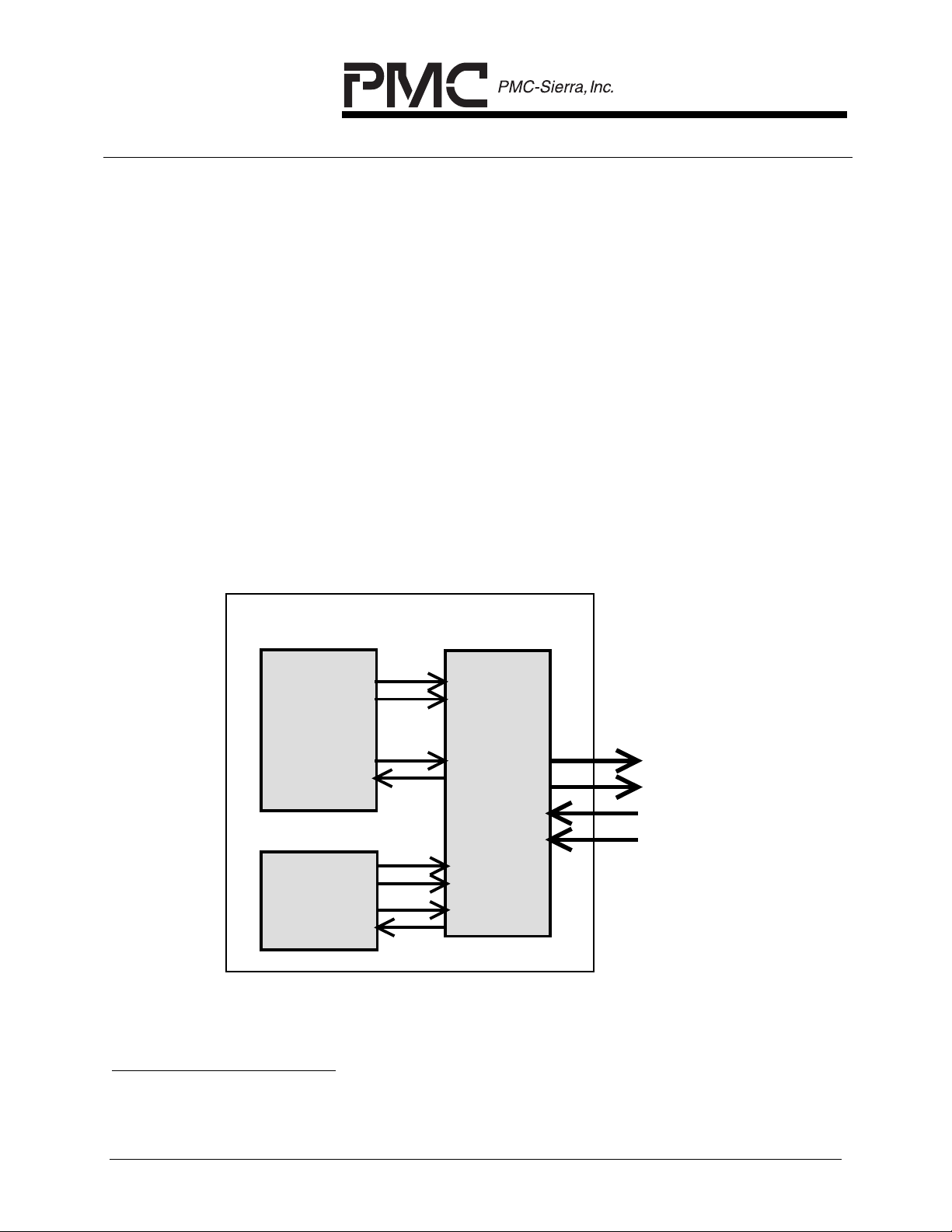
A block diagram of a 1:1 redundant system is shown in Fig. 1.
Fig. 1 Typical Target Application
Modem
or PHY
Modem
or PHY
Modem
or PHY
Modem
or PHY
Modem
or PHY
Modem
or PHY
Line Card #1
S/UNI-
DUPLEX
Line Card #N
S/UNI-
DUPLEX
S/UNI-
VORTEX
WAN Card
S/UNI-
VORTEX
WAN Card
Policing
OA&M
Policing
OA&M
Buffering
Discard
Scheduling
Buffering
Discard
Scheduling
OA&M
OA&M
WAN
up-link
WAN
up-link
In this type of equipment the majority (perhaps all) user traffic goes from WAN
port to line port, or from line port to WAN port. Although the individual ports on
the line cards are often relatively low speed interfaces such as T1, E1, or xDSL,
there may be many ports per line card and many line cards per system, resulting
in hundreds or even thousands of lines terminating on a single WAN up-link. In
the upstream direction (from line card to WAN up-link), the equipment must have
capacity to buffer and intelligently manage bursts of upstream traffic
simultaneously from numerous line cards.
PROPRIETARY AND CONFIDENTIAL TO PMC-SIERRA, INC., AND FOR ITS CUSTOMERS’ INTERNAL USE 5

RELEASED
DATA SHEET
PMC-1980581 ISSUE 5 DUAL SERIAL LINK PHY MULTIPLEXER
PM7350 S/UNI-DUPLEX
In the downstream direction the equipment must handle a similar issue, the “big
pipe feeding little pipe” problem. When a large burst of traffic destined for a
single line port is received at the high speed WAN port it must be buffered and
managed as it queues up waiting for the much lower speed line port to clear.
The line cards are always the most numerous cards in this type of equipment.
An individual line card, even if it terminates a few dozen low speed ports, does
not generate or receive enough traffic to justify putting complex buffering and
traffic management devices on it. The ideal architecture has low cost “dumb”
line cards and a feature rich, “smart” core card. In order to enhance fault
tolerance, the architecture should also inherently support 1:1 protection using a
redundant core card and WAN up-link without significantly increasing line card
complexity.
A system architecture that keeps buffering and traffic management off the line
card with typically exhibit the following features:
1. Connection setup is simpler both in terms of programming and during
execution because there is minimal or no requirement for line
intervention during the connection setup process.
2. In-service feature upgrades are simpler because feature complexity is
limited to the common equipment.
3. Component costs are reduced, while system reliability increases due
to reduced component count.
In this type of architecture there are often three stages of signal concentration or
multiplexing, as shown in Fig 2.
PROPRIETARY AND CONFIDENTIAL TO PMC-SIERRA, INC., AND FOR ITS CUSTOMERS’ INTERNAL USE 6
RELEASED
DATA SHEET
PMC-1980581 ISSUE 5 DUAL SERIAL LINK PHY MULTIPLEXER
PM7350 S/UNI-DUPLEX
Fig. 2 Three Stage Multiplex Architecture
Modem
Modem
Modem
Modem
Modem
Modem
Modem
Modem
Modem
Line Card #1
S/UNI-
DUPLEX
Line Card #2
S/UNI-
DUPLEX
Line Card #N
S/UNI-
DUPLEX
S/UNI-
VORTEX
S/UNI-
VORTEX
Policing
OA&M
Buffering
Discard
Scheduling
OA&M
WAN Card
WAN
up-link
The first stage resides on the line card and spans only those ports physically
terminated by that card. Since it is confined to a single card, this first stage of
multiplexing readily lends itself to the simple parallel bus based multiplex
topology implemented by the S/UNI-DUPLEX. The second stage of
concentration occurs between the core card(s) and the line cards, including line
cards that are on a separate shelf. This second stage is best served by a
redundant serial point-to-point technology. The third stage of multiplexing is
optional and resides on the core card. This third stage is used in systems with a
large number of line cards that require several devices to terminate the second
stage of aggregation. Since the third stage of aggregation is confined to the core
card, it lends itself readily to a parallel bus implementation. This three stage
approach is implemented directly by the S/UNI-DUPLEX and its sister device, the
S/UNI-VORTEX.
The S/UNI-DUPLEX acts as the line card’s bus master. It implements the first
stage of multiplexing by routing traffic from the PHYs and transmitting the traffic
simultaneously over two high speed (200 Mbps) serial 4-wire LVDS links. One
serial link attaches to the active core card, the other to the standby core card. In
the downstream direction the S/UNI-DUPLEX demultiplexes traffic from the
active core card’s LVDS serial link and routes this traffic to the appropriate PHYs.
If the active core card (or its LVDS link) should fail, protection switching
commands embedded in the spare LVDS link will direct the S/UNI-DUPLEX to
start receiving its traffic from this spare link.
PROPRIETARY AND CONFIDENTIAL TO PMC-SIERRA, INC., AND FOR ITS CUSTOMERS’ INTERNAL USE 7
RELEASED
DATA SHEET
PMC-1980581 ISSUE 5 DUAL SERIAL LINK PHY MULTIPLEXER
PM7350 S/UNI-DUPLEX
The S/UNI-VORTEX resides on the core card and terminates up to 8 LVDS links
connected to 8 S/UNI-DUPLEX devices. The S/UNI-VORTEX implements the
second stage of multiplexing. More than one S/UNI-VORTEX will be required if
more than 8 links are required – as will be the case for a system with more than
8 line cards. The S/UNI-VORTEX device(s) share a high speed parallel bus with
the core card’s traffic management and OA&M layers, as implemented by
devices such as PMC-Sierra’s S/UNI-APEX and the S/UNI-ATLAS.
Some applications use framer or modem devices without integrated I.432
processing1 normally support a clock and data interface, and rely on external
circuitry to detect and generate ATM cell framing and overhead. To support
these applications, the S/UNI-DUPLEX provides a clock and data mode2. In this
mode, the input/output pins that normally interface to the Utopia bus are
configured to support up to 16 clock and data serial interfaces. This type of line
card is shown in Fig. 3. The I.432 processing is transparent to the far end
device, which implies that a single S/UNI-VORTEX can simultaneously interface
to line cards that implement the Utopia bus and to line cards that use clock and
data interfaces.
Fig. 3 Clock and Data PHY Interface
Line Card
Rx Clock
Rx Data
Modem #1
Tx Clock
Tx Data
S/UNI-
DUPLEX
4-wire
LVDS
Modem #16
Some PHY devices provide a 3-line interface consisting of clock, data, and
overhead indication. For these PHYs external circuitry can be used to adapt to
the S/UNI-DUPLEX’s 2-line interface.
1
Cell delineation, payload scrambling-descrambling, idle cell generation/discard, etc..
2
Either Utopia mode or clock and data mode can be selected, but not both at once.
PROPRIETARY AND CONFIDENTIAL TO PMC-SIERRA, INC., AND FOR ITS CUSTOMERS’ INTERNAL USE 8

RELEASED
DATA SHEET
PMC-1980581 ISSUE 5 DUAL SERIAL LINK PHY MULTIPLEXER
PM7350 S/UNI-DUPLEX
In the clock and data receive direction the S/UNI-DUPLEX performs bit level ATM
cell delineation function. In the transmit direction the S/UNI-DUPLEX can
operate in either bit or frame aligned mode. In frame mode (also called byte
aligned mode) the two wire transmit interface continuously monitors for gaps in
the transmit clock to determine where the frame or byte alignment should occur.
The circuitry assumes that when a gap in the transmit clock is detected this is
either the framing bit position (e.g. the DS-1 framing bit) or an overhead byte
(e.g. ADSL modem). In either case the next clock period after the gap is
assumed to represent the byte alignment position.
In the multiplexer application discussed previously the S/UNI-DUPLEX’s LVDS
interfaces are connected to one or two S/UNI-VORTEX devices. It is also
possible to interface S/UNI-DUPLEX to S/UNI-DUPLEX via the LVDS link. Since
the S/UNI-DUPLEX bus interface can be configured in several ways (clock and
data, 8/16 bits bus master, 8/16 bit bus slave) there are various applications
where two S/UNI-DUPLEX devices can be used “back-to-back” in order to
perform one or more of the following functions:
1. Interfacing a bus master device to another bus master.
2. Interfacing a bus slave device to another bus slave.
3. Converting between 8 bit and 16 bit buses.
4. Off card or off shelf bus extension.
5. Cell delineation (I.432 processing).
6. Protection switching.
Examples of these types of configurations are shown in Fig. 4 and Fig. 5.
PROPRIETARY AND CONFIDENTIAL TO PMC-SIERRA, INC., AND FOR ITS CUSTOMERS’ INTERNAL USE 9
RELEASED
DATA SHEET
PMC-1980581 ISSUE 5 DUAL SERIAL LINK PHY MULTIPLEXER
PM7350 S/UNI-DUPLEX
Fig. 4 S/UNI-DUPLEX to S/UNI-DUPLEX Applications
Bus
master
8 bit bus
S/UNI-
DUPLEX
LVDS
S/UNI-
DUPLEX
16 bit bus
Example of on-card bus conversion:
8 bit bus master to 16 bit bus master
Bus
master
S/UNI-
DUPLEX
LVDS
S/UNI-
DUPLEX
Example of basic bus extension between cards
Framer #1
LVDS
DUPLEX
Framer #2
S/UNI-
DUPLEX
...
S/UNI-
Bus
master
Bus
slave
Bus
master
Framer # 16
Clock + data
8/16 bit bus
Example of on-card I.432 processing
Fig. 5 S/UNI-DUPLEX to S/UNI-DUPLEX Protection Switching
Bus
master
Bus
master
S/UNI-
DUPLEX
S/UNI-
DUPLEX
S/UNI-
DUPLEX
S/UNI-
DUPLEX
Bus
slave
Bus
slave
Example of protection switching between cards
PROPRIETARY AND CONFIDENTIAL TO PMC-SIERRA, INC., AND FOR ITS CUSTOMERS’ INTERNAL USE 10
RELEASED
DATA SHEET
PMC-1980581 ISSUE 5 DUAL SERIAL LINK PHY MULTIPLEXER
PM7350 S/UNI-DUPLEX
5 BLOCK DIAGRAM
Although separated to improve clarity, many signals in the following diagram
share physical package pins. The use of the SCI-PHY/Any-PHY interfaces and
the clocked serial data interfaces is mutually exclusive.
B
K
O
K
K
L
8
SCIANY
OBUS8
OANYPHY
OMASTER
OENB
OADDR[4:0]
OAVALID
ODAT[15:0]
OPRTY
OSOC
OSX
OFCLK
OCA
LTXD[15:0]
LTXC[15:0]
LRXD[15:0]
LRXC[15:0]
IBU S8
IAN YP HY
IMAS TE R
IEN B
IADDR[4:0]
IAV AL ID
IDAT[15 :0]
IPR TY
ISOC
ISX
IFC LK
ICA
A[7:0]
RDB
WRB
CSB
ALE
IN TB
RSTB
D[7:0]
SCI-PHY
Transmit
Master/
Receive
Slave
Elastic
Store
SCI-PHY
Receive
Master/
Transmit
Slave
Micro-
Processor
Interface
Time-Sliced
ATM
Transmission
Convergence
2 Cell
Buffer
4 Cell
FIFO
to all
blocks
per-PHY
buffers
per-PHY
buffers
T
S
R
Cell
Processor
X
C
R
R
Clock
Synthesis
JTAG
Test Access
Port
8
X
T
RXD1+
RXD1-
TXD1+
TXD1-
RXD2+
RXD2-
TXD2+
TXD2-
REFCLK
TDO
TDI
TCK
TMS
TRS TB
PROPRIETARY AND CONFIDENTIAL TO PMC-SIERRA, INC., AND FOR ITS CUSTOMERS’ INTERNAL USE 11

RELEASED
DATA SHEET
PMC-1980581 ISSUE 5 DUAL SERIAL LINK PHY MULTIPLEXER
PM7350 S/UNI-DUPLEX
6 DESCRIPTION
The PM7350 S/UNI-DUPLEX is a monolithic integrated circuit typically used with
its sister device, the S/UNI-VORTEX, to implement a point-to-point serial
backplane interconnect architecture. The primary role of the S/UNI-DUPLEX is
to interface to up to 32 devices (typically framers or PHYs) and transfer 52-56
byte data cells in serial format to/from a backplane. Devices interface to the
S/UNI-DUPLEX via an 8 or 16-bit SCI-PHY/Utopia/Any-PHY bus, or optionally
via a 16 port clock and data interface.
Each S/UNI-DUPLEX can connect to two 100 to 200 Mb/s Low Voltage
Differential Signal (LVDS) serial links. A microprocessor port provides access to
internal configuration and monitoring registers. The microprocessor port may
also be used to insert and extract cells in support of an embedded
microprocessor communication channel.
BUS INTERFACE:
One of four modes can be selected:
• 8 or 16 bit, Utopia L2 bus master operating at up to 33 MHz bus clock
frequency. Also supports PMC-Sierra’s SCI-PHY bus standard which is
compatible with Utopia L2 but allows extended length cells and supports
an additional bus address signal in order to support 32 PHY devices
rather than Utopia’s 31. See Table 1 for a comparison of these bus
standards.
• 16 port, 4 pin clocked serial data interface (Tx, TxClk, Rx, RxClk), with
integrated I.432 ATM cell delineation operating at up to 52 MHz serial
clock frequency.
• 8 or 16 bit, SCI-PHY/Utopia bus slave operating at up to 52 MHz bus
clock frequency. The slave input port presents itself as 32 addressable
logical channels. The slave output port appears as a single addressable
channel carrying the multiplexed traffic from up to 32 logical channels
where each cell’s channel number can optionally be embedded in the H5
header field (Utopia bus mode) or indicated in a cell prepend (SCI-PHY
bus mode).
• 8 or 16 bit, Any-PHY bus slave (bus protocol compatible with the PM7351
S/UNI-VORTEX) operating at up to 52 MHz bus clock frequency. The
slave input port presents itself as 32 addressable logical channels. The
slave output port appears as a single addressable channel carrying the
multiplexed traffic from up to 32 logical channels. In both directions each
cell’s logical channel number is indicated in a cell prepend.
PROPRIETARY AND CONFIDENTIAL TO PMC-SIERRA, INC., AND FOR ITS CUSTOMERS’ INTERNAL USE 12

RELEASED
DATA SHEET
PMC-1980581 ISSUE 5 DUAL SERIAL LINK PHY MULTIPLEXER
PM7350 S/UNI-DUPLEX
LVDS INTERFACES (both directions):
• Dual 4-wire LVDS serial transceivers each operating at 100 to 200 Mbps
across PCB or backplane traces, or across up to 10 meters of 4-wire
twisted pair cabling for inter-shelf communications.
• Full integrated LVDS clock synthesis and recovery. No external analog
components are required.
• Usable bandwidth (excludes system overhead) of 186 Mbps.
LVDS TRANSMIT DIRECTION
• Simple round robin multiplex of up to 32 PHYs (or 16 clock and data
interfaces) plus the microprocessor port’s cell transfer buffer.
• Multiplexed cell stream broadcast to both LVDS simultaneously.
• 6 bit port ID prepended to each cell for use by ATM layer to identify cell
source (1 of 32 PHYs or processor).
• Back-pressure provided by far end (active link only) to prevent overflow of
far end receiver.
LVDS RECEIVE DIRECTION
• Cells received from the active LVDS link are forwarded to the appropriate
PHY, bit serial interface, or the microprocessor port as specified by a 6 bit
port ID added to each cell at the far end device.
• The LVDS link marked as "spare" is monitored for errors, PHY cells are
discarded, microprocessor port cells are accepted.
• Individual PHY and microprocessor FIFO back-pressure indications are
sent to the far end to prevent FIFO overflows. Per stream back-pressure
prevents head-of-line blocking.
MICROPROCESSOR INTERFACE
• 8 bit data bus, 8 bit address bus.
• Provides read/write access to all configuration and status registers.
• Provides CRC32 calculation and cell transfer registers to support an
embedded microprocessor to microprocessor communication channel
over the LVDS link.
PROPRIETARY AND CONFIDENTIAL TO PMC-SIERRA, INC., AND FOR ITS CUSTOMERS’ INTERNAL USE 13
RELEASED
PM7350 S/UNI-DUPLEX
DATA SHEET
PMC-1980581 ISSUE 5 DUAL SERIAL LINK PHY MULTIPLEXER
7 PIN DIAGRAM
The S/UNI-DUPLEX is packaged in a 160-pin plastic ball grid array (PBGA)
package having a body size of 15 mm by 15 mm and a ball pitch of 1.00 mm.
1413121110987654321
A
B
C
D
E
F
RXD1+ RXD1- RES TAVD GND GND
G
TXD1+ TXD1- TAVS RESK GND GND ISX LTXC[6]
H
RXD2+ RXD2- RAVS RAVD
J
TXD2+ TXD2- TAVS TAVD VSS
K
TRSTB TDI A[2] RSTB A[6] RDB BIAS
TX8K TCK TMS A[0] A[4] A[5] ALE INTB
D[7] VDD VSS A[1] VSS A[7] VSS SCIANY
D[4] D[6] D[5] A[3] VDD WRB CSB VSS
VDD RX8K V SS RCLK
D[0] D[2] D[1] D[3]
IMASTER
LTXD[15]
IAVALID
LTXC[15]
IBUS8
LTXD[14]
IADDR[4]
LRXD[15]
IADDR[3]
LRXC[15]
VSS
VDD
IADDR[2]
LTXC[14]
IADDR[1]
LRXD[14]
IENB
LRXD[13]
IADDR[0]
LRXC[14]
VSS
IDAT[7]
LRXC[11]
IFCLK
LTXC[9]
IDAT[3]
LTXD[8]
ODAT[15]
LRXC[10]
ICA
LRXC[13]
VDD
VSS
IDAT[11]
LRXC[12]
IDAT[8]
LRXD[11]
VDD
IDAT[1]
LTXD[7]
IDAT[2]
LTXC[8]
VSS
ODAT[14]
LRXD[9]
RSTOB
IPRTY
LTXD[13]
IDAT[14]
LTXD[12]
IDAT[12]
LRXD[12]
VDD
IDAT[6]
LTXD[10]
VSS
ISOC
LTXD[6]
OPRTY
LRXD[10]
ODAT[13]
LRXC[9]
IDAT[15]
LTXC[13]
IDAT[13]
LTXC[12]
IDAT[10]
LTXD[11]
IDAT[9]
LTXC[11]
IDAT[5]
LTXC[10]
IDAT[4]
LTXD[9]
IDAT[0]
LTXC[7]
IANYPHY
LTXD[5]
VDD
ATP0 ATP1 CAVS CAVD
L
QAVS QAVD VDD
M
VSS V DD
N
P
TDO REFCLK
Unused
LTXD[0]
OMASTER
LTXD[1]
VSS
OADDR[0]
LRXC[0]
OADDR[1]
LRXD[0]
OADDR[3]
LTXC[1]
OADDR[2]
LTXC[0]
VSS
VDD VSS
OAVALID
LRXD[1]
OADDR[4]
LRXC[1]
OENB
LRXD[2]
OSOC
LRXD[3]
VSS VDD VSS
OCA LRXC[ 2]
OSX LRXC[3]
ODAT[1]
LRXC[4]
ODAT[0]
LTXC[2]
ODAT[2]
LRXD[4]
ODAT[3]
LRXD[5]
VDD VSS
ODAT[4]
LRXC[6]
OANYPHY
LTXD[2]
OFCLK
LRXC[5]
VDD
ODAT[5]
LRXD[6]
ODAT[6]
LRXC[7]
OBUS8
LTXD[4]
ODAT[12]
ODAT[9]
LTXC[5]
LTXC[4]
VDD
VSS
ODAT[11]
LRXD[8]
VSS
ODAT[8]
LTXC[3]
ODAT[7]
LRXD[7]
VDD
ODAT[10]
LRXC[8]
Unused
LTXD[3]
BOTTOM VIEW
PROPRIETARY AND CONFIDENTIAL TO PMC-SIERRA, INC., AND FOR ITS CUSTOMERS’ INTERNAL USE 14
RELEASED
DATA SHEET
PMC-1980581 ISSUE 5 DUAL SERIAL LINK PHY MULTIPLEXER
PM7350 S/UNI-DUPLEX
8 PIN DESCRIPTION
Ball
Name
RXD1+
RXD1RXD2+
RXD2-
TXD1+
TXD1TXD2+
TXD2-
Type
Diff.
LVDS
Input
Diff.
LVDS
Output
Ball
No. Function
High Speed LVDS Links
G14
G13
J14
J13
The high-speed receive data (RXD1+/-, RXD2+/-)
inputs present NRZ data from a serial backplane.
Two pairs are provided for redundancy. The active
link may be chosen by the local microprocessor or
determined by a simple handshake.
RXD1+/- and RXD2+/- are truly differential inputs
offering superior common-mode noise rejection.
They have sufficient sensitivity and common-mode
range to support LVDS signals.
H14
H13
K14
K13
The transmit differential data (TXD1+/-, TXD2+/-)
outputs present NRZ encoded data to a serial
backplane. These outputs are open drain current
sinks which interface directly with twisted-pair
cabling or board interconnect. Edge rates are
controlled to minimize radiated emissions.
Both differential links carry identical traffic except
the exact phase relationship is not guaranteed.
REFCLK Input P12 The reference clock input (REFCLK) must provide a
jitter-free reference clock. It is used as the
reference clock by both clock recovery and clock
synthesis circuits. Any jitter below 1 MHz is
transferred directly to the TXD1+/- and TXD2+/outputs. The high-speed serial interface bit rate is
eight times the REFCLK frequency.
RES
RESK
Analog G12
H11
A 4.75k
Ω ±1% resistor must be connected between
these two pins to achieve the correct LVDS output
signal levels.
ATP0
ATP1
Analog L14
L13
The Analog Test Points (ATP) are provided for
production test purposes. In mission mode they
are high impedance and should be connected to
ground.
PROPRIETARY AND CONFIDENTIAL TO PMC-SIERRA, INC., AND FOR ITS CUSTOMERS’ INTERNAL USE 15
RELEASED
DATA SHEET
PMC-1980581 ISSUE 5 DUAL SERIAL LINK PHY MULTIPLEXER
PM7350 S/UNI-DUPLEX
Ball
Name
Type
Ball
No. Function
High Speed LVDS Links
TX8K Input B14 The transmit 8 kHz timing reference (TX8K) input
allows a traceable signal to be transmitted to the far
end of the high-speed serial links via TXD1+/- and
TXD2+/-. A rising edge on TX8K is encoded in the
next cell transmitted.
Although TX8K is targeted at a typical need of
transporting an 8 kHz signal, its frequency is not
constrained to 8 kHz. Any frequency less than the
cell rate is permissible.
RX8K Output E13 The receive 8 kHz timing reference (RX8K) output
presents the timing extracted from one of the
receive high-speed serial links, RXD1+/- or
RXD2+/-.
The rising edge of RX8K is accurate to the nearest
byte boundary of the high-speed serial link;
therefore, a small amount of jitter is present. At a
link rate of 155.52 Mb/s, the jitter is 63ns peak-topeak.
Pulses on RX8K are always 16 high-speed serial
link bit periods wide (two REFCLK periods).
RCLK Output E11 The Recovered Clock (RCLK) output presents the
byte clock for the active receive high-speed serial
link. The RCLK frequency shall be 0.125 of the
RXD1+/- or RXD2+/- bit rate.
Due to the digital clock recovery technique
employed, jitter is introduced as 12.8 ns phase
steps. If the active link is changed, RCLK can not
be guaranteed to be glitch free. Because of these
two factors, RCLK must be cleaned up by a PLL
before it is suitable for use as a timing reference.
Clocked Data Serial Interface
PROPRIETARY AND CONFIDENTIAL TO PMC-SIERRA, INC., AND FOR ITS CUSTOMERS’ INTERNAL USE 16

RELEASED
DATA SHEET
PMC-1980581 ISSUE 5 DUAL SERIAL LINK PHY MULTIPLEXER
PM7350 S/UNI-DUPLEX
Ball
Name
Type
Ball
No. Function
High Speed LVDS Links
SCIANY Input C7 The SCI-PHY/Any-PHY Interface (SCIANY) input
selects the type of PHY device interface. If
SCIANY is a logic high, the S/UNI-DUPLEX will be
configured to communicate to the PHY devices via
a shared SCI-PHY Level 2, Utopia L2, or Any-PHY
cell bus. If SCIANY is a logic low, each PHY device
has a dedicated clocked bit serial interface.
The two types of interfaces share common package
pins. Failure to present the correct logic level on
this signal for the application may result in damage
to the S/UNI-DUPLEX or the PHY devices.
When SCIANY is logic high, LTXD[3] and LTXD[0]
become inputs and need to be tied to VDD or VSS
through a pull up or a pull down.
LRXD[15]
LRXD[14]
LRXD[13]
LRXD[12]
LRXD[11]
LRXD[10]
LRXD[9]
LRXD[8]
LRXD[7]
LRXD[6]
LRXD[5]
LRXD[4]
LRXD[3]
LRXD[2]
LRXD[1]
LRXD[0]
Input
(SCIANY=
0)
D6
A4
B4
D2
E3
J2
K3
L2
P2
M4
N6
L6
L7
P9
M9
L10
The low-speed receive data (LRXD[15:0]) inputs
provide data from individual modem channels. The
data streams must carry contiguous ATM cells with
valid HCS (Header Check Sequence) bytes.
LRXD[n] can be clocked either by the rising or
falling edge of the corresponding LRXC[n] input,
depending on the value of the LRXCINV bit of the
Master Configuration register. By default, the rising
edge is used.
These inputs are only active if the SCIANY input is
a logic low.
PROPRIETARY AND CONFIDENTIAL TO PMC-SIERRA, INC., AND FOR ITS CUSTOMERS’ INTERNAL USE 17
RELEASED
DATA SHEET
PMC-1980581 ISSUE 5 DUAL SERIAL LINK PHY MULTIPLEXER
PM7350 S/UNI-DUPLEX
Ball
Name
LRXC[15]
LRXC[14]
LRXC[13]
LRXC[12]
LRXC[11]
LRXC[10]
LRXC[9]
LRXC[8]
LRXC[7]
LRXC[6]
LRXC[5]
LRXC[4]
LRXC[3]
LRXC[2]
LRXC[1]
LRXC[0]
LTXD[15]
LTXD[14]
LTXD[13]
LTXD[12]
LTXD[11]
LTXD[10]
LTXD[9]
LTXD[8]
LTXD[7]
LTXD[6]
LTXD[5]
LTXD[4]
LTXD[3]
LTXD[2]
LTXD[1]
LTXD[0]
Type
Input
(SCIANY
= 0)
Output A6
Ball
No. Function
High Speed LVDS Links
A5
C4
A3
D3
E4
J4
K2
M1
N4
L5
N5
N7
P8
N8
N9
The low-speed receive clock (LRXC[15:0]) inputs
provide timing for the receive links. Each LRXC
signal is independent of the others.
Each signal in LRXD[15:0] is sampled either on the
rising or the falling edge of the corresponding
LRXC[15:0] clock, depending the value of the
LRXCINV bit of the Master Configuration register.
By default, the rising edge is used.
The active edge on each LRXC must only occur
during those bit periods containing ATM cell data. It
must be suppressed during bit periods containing
transmission overhead. These inputs are only
active if the SCIANY input is a logic low.
Maximum clock rate is 50 MHz.
P11
The low-speed transmit data signals (LTXD[15:0])
C6
B2
C2
D1
F2
G1
G4
G3
H2
J1
P4
N1
M5
M11
N12
carry the outgoing link data in bit serial format.
Each LTXD signal is independent of the other
signals. The most significant bit of each data byte is
transmitted first.
Each signal in LTXD[15:0] can be updated either on
the rising or falling edge of the corresponding
LTXC[15:0] clock, depending the value of the
LTXCINV bit of the Master Configuration register.
By default, the rising edge is used.
These outputs are only active if the SCIANY input is
a logic low.
When SCIANY is logic high, LTXD[3] and LTXD[0]
become inputs and need to be tied to VDD or VSS
through a pull up or a pull down.
PROPRIETARY AND CONFIDENTIAL TO PMC-SIERRA, INC., AND FOR ITS CUSTOMERS’ INTERNAL USE 18

RELEASED
DATA SHEET
PMC-1980581 ISSUE 5 DUAL SERIAL LINK PHY MULTIPLEXER
PM7350 S/UNI-DUPLEX
Ball
Name
LTXC[15]
LTXC[14]
LTXC[13]
LTXC[12]
LTXC[11]
LTXC[10]
LTXC[9]
LTXC[8]
LTXC[7]
LTXC[6]
LTXC[5]
LTXC[4]
LTXC[3]
LTXC[2]
LTXC[1]
LTXC[0]
Type
Input
(SCIANY
= 0)
Input Parallel Bus – (SCIANY is logic high)
Ball
No. Function
High Speed LVDS Links
B6
D5
B1
C1
E1
F1
F4
H3
H1
H4
L3
M3
N2
The low-speed transmit clock (LTXC[15:0]) inputs
provide timing for the transmit links. Each LTXC
signal is independent of the others.
Each signal in LTXD[15:0] is updated either on the
rising or the falling edge of the corresponding
LTXC[15:0] clock, depending on the value of the
LTXCINV bit of the Master Configuration register.
By default, the rising edge is used.
As an option, clock gaps can be recognized to
force byte alignment to the transmission overhead.
These outputs are only active if the SCIANY input is
a logic low.
P7
M10
Maximum clock rate is 50 MHz.
N10
IANYPHY Input J1 The Input Port Any-PHY configuration (IANYPHY)
input determines the protocol of the SCI-PHY/AnyPHY input port interface. IANYPHY is only active if
the SCIANY input is a logic high.
If IANYPHY is logic low, the interface complies to
the SCI-PHY/Utopia specification.
If IANYPHY is logic high, the interface complies to
the Any-PHY specification. The Any-PHY protocol
is supported only when the input port cell interface
is configured as a bus slave (IMASTER input must
be set to logic 0 if IANYPHY is high).
IANYPHY is an asynchronous input and is
expected to be held static.
PROPRIETARY AND CONFIDENTIAL TO PMC-SIERRA, INC., AND FOR ITS CUSTOMERS’ INTERNAL USE 19

RELEASED
DATA SHEET
PMC-1980581 ISSUE 5 DUAL SERIAL LINK PHY MULTIPLEXER
PM7350 S/UNI-DUPLEX
Ball
Name
Type
Ball
No. Function
High Speed LVDS Links
IMASTER Input A6 The input port master select (IMASTER) pin
determines the direction of the input port cell
interface control signals.
If IMASTER is low, the input port of the S/UNIDUPLEX is a bus slave and complies with the SCIPHY/Utopia or Any-PHY transmit protocol
depending of the state of the IANYPHY input. The
IADDR[4:0], IAVALID, IENB signals are inputs. The
ICA signal is an output.
If IMASTER is high, the input port of the S/UNIDUPLEX is a bus master and complies with the
SCI-PHY/Utopia receive protocol (IANYPHY must
be set to low if IMASTER is high). The IADDR[4:0],
IAVALID, IENB signals are outputs. The ICA signal
is an input.
This input is only active if the SCIANY input is a
logic high.
IBUS8 Input C6 The input port bus width select (IBUS8) selects the
interface bus width. When IBUS8 is high, only
IDAT[7:0] are expected to present valid data and
IDAT[15:8] are ignored. When IBUS8 is low, all
IDAT[15:0] inputs are used.
This input is only active if the SCIANY input is a
logic high.
IFCLK Input F4 The input FIFO clock (IFCLK) is used to read words
into the S/UNI-DUPLEX upstream cell buffer.
IFCLK must cycle at a 52 MHz or lower
instantaneous rate. All SCI-PHY/Any-PHY input
port timing is relative to the rising edge of IFCLK.
This input is only active if the SCIANY input is a
logic high.
PROPRIETARY AND CONFIDENTIAL TO PMC-SIERRA, INC., AND FOR ITS CUSTOMERS’ INTERNAL USE 20

RELEASED
DATA SHEET
PMC-1980581 ISSUE 5 DUAL SERIAL LINK PHY MULTIPLEXER
PM7350 S/UNI-DUPLEX
Ball
Name
Type
Ball
No. Function
High Speed LVDS Links
ISOC Input H2 This input is only active in SCI-PHY/Utopia bus
slave or bus master modes (SCIANY = 1,
ANYPHY= 0).
The Input Start of Cell (ISOC) marks the start of the
cell on the IDAT[15:0] bus. When ISOC is high, the
first word of the cell structure is present on the
IDAT[15:0] stream. It is not necessary for ISOC to
be asserted for each cell, unless inband addressing
is being used. An interrupt may be generated if
ISOC is high during any word other than the first
word of the cell structure.
ISOC is sampled on the rising edge of IFCLK. If
IMASTER is high, ISOC is considered valid only
when the IENB signal was low in the previous cycle.
If IMASTER is low, ISOC is considered valid
coincident with IENB assertion.
ISX Input H4 The Transmit Start Of Cell (ISX) indication signal is
only active in Any-PHY bus slave mode (when
IANYPHY=1 and IMASTER=0). ISX marks the start
of cell on the IDAT[15:0] data bus. When ISX is
high, the first word of the cell structure is present on
the IDAT[15:0] stream. ISX must be asserted for
each cell. An interrupt may be generated if ISX is
high during any word other than the expected first
word of the cell structure.
This input is only active if the SCIANY input is a
logic high.
PROPRIETARY AND CONFIDENTIAL TO PMC-SIERRA, INC., AND FOR ITS CUSTOMERS’ INTERNAL USE 21

RELEASED
DATA SHEET
PMC-1980581 ISSUE 5 DUAL SERIAL LINK PHY MULTIPLEXER
PM7350 S/UNI-DUPLEX
Ball
Name
IDAT[15]
IDAT[14]
IDAT[13]
IDAT[12]
IDAT[11]
IDAT[10]
IDAT[9]
IDAT[8]
IDAT[7]
IDAT[6]
IDAT[5]
IDAT[4]
IDAT[3]
IDAT[2]
IDAT[1]
IDAT[0]
Type
Input
(SCIANY
= 1)
Ball
No. Function
High Speed LVDS Links
B1
C2
C1
D2
D3
D1
E1
E3
E4
F2
F1
G1
G4
H3
G3
H1
The Input Data bus (IDAT[15:0]) carries the ATM
cell words that are written to the upstream cell
buffer. Only IDAT[7:0] are used if the IBUS8 input
is high.
IDAT[15:0] is sampled on the rising edge of IFCLK.
As a SCI-PHY/Utopia bus master (IMASTER=1,
IANYPHY=0) the IDAT[15:0] bus is considered valid
only when the IENB signal was low in the previous
cycle.
As a bus slave (IMASTER = 0) the IDAT[15:0] bus
is considered valid when the IENB signal is
asserted low or the ISX signal is asserted high. As
an Any-PHY bus slave (IMASTER = 0,
IANYPHY=1) IDAT[15:0] bus is not considered valid
when autonomous deselection occurs after the last
word of a cell.
These inputs are only active if the SCIANY input is
a logic high.
IPRTY Input B2 The Input Parity (IPRTY) signal completes the
parity (programmable for odd or even parity) of the
IDAT[15:0] bus when IBUS8 is low and the
IDAT[7:0] bus when IBUS8 is high. A maskable
interrupt and a status bit are generated upon a
parity error; no other actions are taken.
The IPRTY signal is sampled on the rising edge of
IFCLK. As a SCI-PHY/Utopia bus master
(IMASTER=1, IANYPHY=0) IPRTY is considered
valid only when the IENB signal was low in the
previous cycle.
As a bus slave (IMASTER=0) IPRTY is considered
valid coincident with IENB being asserted low or
ISX being asserted high. As an Any-PHY bus slave
(IMASTER = 0, IANYPHY = 1) IPRTY is not
considered valid when autonomous deselection
occurs after the last word of a cell.
This input is only active if the SCIANY input is a
logic high.
PROPRIETARY AND CONFIDENTIAL TO PMC-SIERRA, INC., AND FOR ITS CUSTOMERS’ INTERNAL USE 22

RELEASED
DATA SHEET
PMC-1980581 ISSUE 5 DUAL SERIAL LINK PHY MULTIPLEXER
PM7350 S/UNI-DUPLEX
Ball
Name
Type
Ball
No. Function
High Speed LVDS Links
ICA I/O A3 The Input Cell Available (ICA) signal provides cell-
level flow control. ICA’s direction depends on the
state of the IMASTER input.
As a SCI-PHY/Utopia bus master (IMASTER = 1,
IANYPHY = 0) the S/UNI-DUPLEX polls up to 32
PHYs using the PHY address signals IADDR[4:0].
A PHY device being addressed by IADDR[4:0] is
expected to indicate whether or not it has a
complete cell available for transfer by driving ICA
during the clock cycle following that in which it is
addressed. When a cell transfer is in progress, the
S/UNI-DUPLEX will not poll the PHY device which
is sending the cell so PHY devices need not
support the cell availability indication during cell
transfer. The selection of a particular PHY device
from which to transfer a cell is indicated by the state
of IADDR[4:0] during the last cycle IENB is high.
As a bus slave (IMASTER = 0) the S/UNI-DUPLEX
indicates the ability to accept additional cells via the
ICA output. When IAVALID is sampled high in SCIPHY or low in Any-PHY configuration, ICA is
asserted if the cell FIFO for the logical channel
addressed by IADDR[4:0] has at least one empty
cell buffer. If the FIFO is full, ICA is deasserted. If a
cell transfer is in progress that will fill a logical
channel FIFO, ICA will also be deasserted. When
IAVALID is sampled low in SCI-PHY or high in AnyPHY configuration, ICA becomes high impedance.
ICA is delayed by an additional clock cycle in AnyPHY configuration. The buffer status for the
particular logical channel involved is stale for a
maximum of 16 cycles after the start of the cell
transfer when using a 8 bit bus or 12 cycles when
using a 16 bit bus. Therefore, the master should
refrain from polling that logical channel in the
interim.
PROPRIETARY AND CONFIDENTIAL TO PMC-SIERRA, INC., AND FOR ITS CUSTOMERS’ INTERNAL USE 23

RELEASED
DATA SHEET
PMC-1980581 ISSUE 5 DUAL SERIAL LINK PHY MULTIPLEXER
PM7350 S/UNI-DUPLEX
Ball
Name
ICA
(Cont’d)
Type
Ball
No. Function
High Speed LVDS Links
As a bus slave (IMASTER = 0) the S/UNI-DUPLEX
can also be configured to respond to a subset of
the IADDRESS[4:0] address range. In this case,
ICA will remain high-impedance when the logical
channel addressed by IADDR[4:0] is outside the
address range specified by ICAEN[31:0] of the
Input Cell Available Enable registers.
ICA is sampled or updated on the rising edge of
IFCLK.
This signal is only active if the SCIANY input is a
logic high.
PROPRIETARY AND CONFIDENTIAL TO PMC-SIERRA, INC., AND FOR ITS CUSTOMERS’ INTERNAL USE 24

RELEASED
DATA SHEET
PMC-1980581 ISSUE 5 DUAL SERIAL LINK PHY MULTIPLEXER
PM7350 S/UNI-DUPLEX
Ball
Name
Type
Ball
No. Function
High Speed LVDS Links
IENB I/O B4 The active low input port enable (IENB) signal is
used to initiate the reading of cells from a PHY
device into the upstream cell buffer.
As a SCI-PHY/Utopia bus master (IMASTER = 1,
IANYPHY = 0) the S/UNI-DUPLEX asserts IENB to
transfer a cell from one of up to 32 PHY devices.
The source PHY is selected by the IADDR[4:0]
signals. A valid word is expected on the IDAT[15:0]
bus at the second rising edge of IFCLK after the
enable is asserted.
As a bus slave (IMASTER = 0) IENB is an input
and a IDAT[15:0] word is accepted coincident with
IENB being sampled low.
As an Any-PHY bus slave (IMASTER = 0,
IANYPHY = 1) IENB is ignored if ISX is high and
may be held low upon the completion of a cell
transfer, since a cell transfer is only initiated by
assertion of ISX.
IENB may be deasserted high at any time to pause
a cell transfer.IENB is sampled or updated on the
rising edge of IFCLK.
The Any-PHY protocol supports autonomous
deselection. As an Any-PHY slave the inputs
become high impedance after the last word of a cell
is transferred until the S/UNI-DUPLEX is reselected
(via ISX) even if IENB is left asserted. As a SCIPHY/Utopia slave ISX is not defined, so a
subsequent cell is transferred (provided one is
available) if IENB is held low beyond the end of a
cell.
This signal is only active if the SCIANY input is a
logic high.
PROPRIETARY AND CONFIDENTIAL TO PMC-SIERRA, INC., AND FOR ITS CUSTOMERS’ INTERNAL USE 25

RELEASED
DATA SHEET
PMC-1980581 ISSUE 5 DUAL SERIAL LINK PHY MULTIPLEXER
PM7350 S/UNI-DUPLEX
Ball
Name
IADDR[4]
IADDR[3]
IADDR[2]
IADDR[1]
IADDR[0]
Type
I/O D6
Ball
No. Function
High Speed LVDS Links
As a SCI-PHY/Utopia bus master (IMASTER = 1,
A5
D5
A4
C4
IANYPHY = 0) the IADDR[4:0] signals are outputs
used to address up to 32 PHY devices for the
purposes of polling and selection for cell transfer.
When conducting polling, in order to avoid bus
contention, the S/UNI-DUPLEX inserts gap cycles
during which IADDR[4:0] is set to 0x1F and
IAVALID is logic 0. When this occurs, no PHY
device should drive ICA during the following clock
cycle. Polling is performed in incrementing
sequential order. The PHY device selected for
transfer is based on the IADDR[4:0] value present
during the last cycle IENB was high.
As a SCI-PHY/Utopia bus slave (IMASTER = 0,
IANYPHY = 0) IADDR[4:0] are inputs. During
polling when IAVALID is sampled high in SCI-PHY
or low in Any-PHY configuration, the S/UNI-
DUPLEX will drive ICA with the cell buffer
availability status of the logical channel indexed by
IADDR[4:0] on the next IFCLK cycle. The logical
channel selected for a cell transfer is determined by
the IADDR[4:0] value presented when IENB was
last sampled high. Cell transfer is initiated with the
ISOC input being asserted.
As an Any-PHY bus slave (IMASTER = 0, IANYPHY
= 1) IADDR[4:0] are inputs used only for polling. Cell
transfer is initiated with inband addressing (prepend
Word 0 contains the address) and the ISX input.
Polling occurs when IAVALID is sampled low and the
S/UNI-DUPLEX drives ICA with the cell buffer
availability status of the logical channel indexed by
IADDR[4:0]. There is a one IFCLK cycle gap
between IAVALID sampled low and ICA.
PROPRIETARY AND CONFIDENTIAL TO PMC-SIERRA, INC., AND FOR ITS CUSTOMERS’ INTERNAL USE 26

RELEASED
DATA SHEET
PMC-1980581 ISSUE 5 DUAL SERIAL LINK PHY MULTIPLEXER
PM7350 S/UNI-DUPLEX
Ball
Name
Type
Ball
No. Function
High Speed LVDS Links
IADDR[4]
IADDR[3]
IADDR[2]
IADDR[1]
IADDR[0]
(Cont’d)
As a bus slave device (either SCI-PHY or Any-
PHY), the S/UNI-DUPLEX can be configured to be
restricted to a subset of the logical channel address
range. In this case, device polling or selection will
occur when the logical channel addressed by
IADDR[4:0] is inside the address range specified by
ICAEN[31:0] of the Input Cell Available Enable
registers.
The IADDR[4:0] bus is updated or sampled on the
rising edge of IFCLK.
These signals are only active if the SCIANY input is
a logic high.
IAVALID I/O B6 The Input Port Address Valid (IAVALID) pin
indicates that the IADDR[4:0] bus is asserting a
valid PHY address for polling purposes.
As a SCI-PHY/Utopia bus master (IMASTER = 1,
IANYPHY = 0) IAVALIV is an output. When IAVALID
is deasserted, the IADDR[4:0] bus is set to 0x1F as
defined by the Utopia L2 bus standard. therefore
use of IAVALID is not necessary when less than 32
PHY devices are being polled.
As a bus slave (IMASTER = 0) IAVALID is an input
used to control the ICA output. IAVALID is active
highin SCI-PHY/Utopia mode (IANYPHY = 0) and
active low in Any-PHY mode (IANYPHY = 1). The
ICA output is only driven when IAVALID is sampled
active. If IAVALID is sampled inactive, ICA becomes
high impedance. The S/UNI-DUPLEX supports
polling in contiguous cycles if IAVALID is held
active.
ICA is delayed by an additional IFCLK
cycle.IAVALID is sampled or updated on the rising
edge of IFCLK.
This signal is only active if the SCIANY input is a
logic high.
Parallel Bus - Output
PROPRIETARY AND CONFIDENTIAL TO PMC-SIERRA, INC., AND FOR ITS CUSTOMERS’ INTERNAL USE 27

RELEASED
DATA SHEET
PMC-1980581 ISSUE 5 DUAL SERIAL LINK PHY MULTIPLEXER
PM7350 S/UNI-DUPLEX
Ball
Name
Type
Ball
No. Function
High Speed LVDS Links
OANYPHY Input M5 The Output Port Any-PHY configuration
(OANYPHY) input determines the protocol of the
SCI-PHY/Any-PHY output port interface.
OANYPHY is only active if the SCIANY input is a
logic high.
If OANYPHY is logic low, the interface complies to
the SCI-PHY/Utopia specification.
If OANYPHY is logic high, the interface complies to
the Any-PHY specification. The Any-PHY protocol
is supported only when the output port cell interface
is configured as a bus slave (IMASTER input must
be set to logic low if OANYPHY is high).
OANYPHY is an asynchronous input and is
expected to be held static.
OMASTER Input M11 The Output Port Master select (OMASTER) pin
determines the direction of the output port cell
interface control signals.
If OMASTER is high the OANYPHY must be low.
The output port of the S/UNI-DUPLEX is a bus
master that complies with the SCI-PHY/Utopia
transmit protocol. The OADDR[4:0], OAVALID,
OENB signals are outputs and the OCA signal is an
input.
If OMASTER is low, the output port of the S/UNI-
DUPLEX is a bus slave and complies with the SCI-
PHY/Utopia or the Any-PHY receive protocol
depending on the state of the OANYPHY input.
The OADDR[4:0], OAVALID, OENB signals are
inputs. The OCA signal is an output.
This input is only active if the SCIANY input is a
logic high.
PROPRIETARY AND CONFIDENTIAL TO PMC-SIERRA, INC., AND FOR ITS CUSTOMERS’ INTERNAL USE 28

RELEASED
DATA SHEET
PMC-1980581 ISSUE 5 DUAL SERIAL LINK PHY MULTIPLEXER
PM7350 S/UNI-DUPLEX
Ball
Name
Type
Ball
No. Function
High Speed LVDS Links
OBUS8 Input P4 The output port bus width select (OBUS8) selects
the output port interface bus width.
When OBUS8 is high, only ODAT[7:0] present valid
data and ODAT[15:8] are held low. When OBUS8
is low, all ODAT[15:0] outputs are used.
This input is only active if the SCIANY input is a
logic high.
OFCLK Input N5 The output port FIFO clock (OFCLK) is used to
transfer cells from the internal downstream cell
buffer to the PHY devices. OFCLK must cycle at a
52 MHz or lower instantaneous rate, but a high
enough rate to avoid a FIFO overflow. All SCI-
PHY/Any-PHY output port timing is relative to the
rising edge of OFCLK.
This input is only active if the SCIANY input is a
logic high.
PROPRIETARY AND CONFIDENTIAL TO PMC-SIERRA, INC., AND FOR ITS CUSTOMERS’ INTERNAL USE 29

RELEASED
DATA SHEET
PMC-1980581 ISSUE 5 DUAL SERIAL LINK PHY MULTIPLEXER
PM7350 S/UNI-DUPLEX
Ball
Name
Type
Ball
No. Function
High Speed LVDS Links
OSOC Output L7 In all bus modes, OSOC is updated on the rising
edge of OFCLK. When not presenting valid data,
OSOC is high impedance.
In SCI-PHY/Utopia bus slave mode (OMASTER =
0, OANYPHY = 0) the output port start of cell
(OSOC) indication signal marks the first word of the
cell transfer on the ODAT[15:0] data bus. OSOC is
driven immediately upon sampling OENB low if the
previous polling cycle resulted in this device being
selected (see the OCA description below).
In Any-PHY bus slave mode (OMASTER = 0,
OANYPHY = 1) the output port start of cell (OSOC)
indication signal marks the second word of the cell
transfer on the ODAT[15:0] data bus. OSOC is
driven after one OFCLK cycle delay upon sampling
OENB low if the previous polling cycle resulted in
this device being selected (see the OCA description
below). Autonomous deselection occurs after the
last word of a cell resulting in setting OSOC high-
impedance until reselection.
In SCI-PHY/Utopia bus master mode (OMASTER
= 1, OANYPHY = 0) the output port start of cell
(OSOC) indication signal marks the first word of the
cell transfer on the ODAT[15:0] data bus. OSOC is
valid coincident with OENB assertion..
When OANYPHY is high, autonomous deselection
occurs after the last word of a cell resulting in
setting OSOC high-impedance until reselection.
This output is only active if the SCIANY input is a
logic high.
PROPRIETARY AND CONFIDENTIAL TO PMC-SIERRA, INC., AND FOR ITS CUSTOMERS’ INTERNAL USE 30

RELEASED
DATA SHEET
PMC-1980581 ISSUE 5 DUAL SERIAL LINK PHY MULTIPLEXER
PM7350 S/UNI-DUPLEX
Ball
Name
Type
Ball
No. Function
High Speed LVDS Links
OSX Output P8 The Output Start of Transfer (OSX) is only active in
Any-PHY bus slave mode (OANYPHY = 1
OMASTER = 0). When OANYPHY is logic low,
OSX is held low during cell transfer or high-
impedance otherwise.
OSX marks the start of the cell on the ODAT[15:0]
bus. When OSX is high, the first word of the cell
structure is present on the ODAT[15:0] stream.
OSX is updated on the rising edge of OFCLK and
considered valid only when the OENB signal was
sampled low in the previous cycle and the S/UNI-
VORTEX device was selected after the polling
process. OSX becomes high impedance (with a
cycle latency) upon sampling OENB high or if the
S/UNI-VORTEX device is not selected for transfer.
When OANYPHY is high, autonomous deselection
occurs after the last word of a cell resulting in
setting OSX high-impedance until reselection.
This input is only active if the SCIANY input is a
logic high.
PROPRIETARY AND CONFIDENTIAL TO PMC-SIERRA, INC., AND FOR ITS CUSTOMERS’ INTERNAL USE 31

RELEASED
DATA SHEET
PMC-1980581 ISSUE 5 DUAL SERIAL LINK PHY MULTIPLEXER
PM7350 S/UNI-DUPLEX
Ball
Name
ODAT[15]
ODAT[14]
ODAT[13]
ODAT[12]
ODAT[11]
ODAT[10]
ODAT[9]
ODAT[8]
ODAT[7]
ODAT[6]
ODAT[5]
ODAT[4]
ODAT[3]
ODAT[2]
ODAT[1]
ODAT[0]
Type
Output
(SCIANY
= 1)
Ball
No. Function
High Speed LVDS Links
J4
K3
K2
L3
L2
M1
M3
N2
P2
N4
M4
L5
N6
L6
N7
P7
The output port cell data bus (ODAT[15:0]) carries
the ATM cell octets that are transferred to the PHY
devices. Only ODAT[7:0] are used if OBUS8 is
high.
The ODAT[15:0] bus is updated on the rising edge
of OFCLK.
As a SCI-PHY/Utopia bus master (OMASTER = 1,
OANYPHY = 0), the ODAT[15:0] bus is considered
valid coincident with OENB assertion.
As a bus slave (OMASTER = 0), the ODAT[15:0]
bus is considered valid only when the S/UNIVORTEX device was selected after the polling
process and the OENB signal is sampled low. As an
SCI-PHY/Utopia bus slave (OMASTER = 0,
OANYPHY = 0) ODAT[15:0] is driven immediately
upon sampling OENB low it has an additional
OFCLK cycle latency. When not presenting valid
data, the ODAT[15:0] bus is high impedance.
Autonomous deselection occurs after the last word
of a cell resulting in setting ODAT[15:0] highimpedance until reselection.
These outputs are only active if the SCIANY input is
a logic high.
PROPRIETARY AND CONFIDENTIAL TO PMC-SIERRA, INC., AND FOR ITS CUSTOMERS’ INTERNAL USE 32

RELEASED
DATA SHEET
PMC-1980581 ISSUE 5 DUAL SERIAL LINK PHY MULTIPLEXER
PM7350 S/UNI-DUPLEX
Ball
Name
Type
Ball
No. Function
High Speed LVDS Links
OPRTY Output J2 The output port parity (OPRTY) signal completes
the parity (programmable for odd or even parity) of
the ODAT[15:0] bus when OBUS8 is low and the
ODAT[7:0] bus when OBUS8 is high.
The OPRTY signal is updated on the rising edge of
OFCLK.
As a SCI-PHY/Utopia bus master (OMASTER = 1,
OANYPHY = 0) OPRTY is considered valid
coincident with OENB assertion.
As a bus slave (OMASTER = 0) the OPRTY bus is
considered valid only when the S/UNI-VORTEX
device was selected after the polling process and
the OENB signal is sampled low. As an SCIPHY/Utopia bus slave (OMASTER = 0, OANYPHY
= 0) OPRTY is driven immediately upon sampling
OENB low, but as an Any-PHY bus slave
(OMASTER = 0, OANYPHY = 1) it has an
additional cycle latency when OANYPHY is logic
high. When not presenting valid data, OPRTY is
high impedance.
As an Any-PHY bus slave autonomous deselection
occurs after the last word of a cell resulting in
setting OPRTY high-impedance until reselection.
This output is only active if the SCIANY input is a
logic high.
PROPRIETARY AND CONFIDENTIAL TO PMC-SIERRA, INC., AND FOR ITS CUSTOMERS’ INTERNAL USE 33

RELEASED
DATA SHEET
PMC-1980581 ISSUE 5 DUAL SERIAL LINK PHY MULTIPLEXER
PM7350 S/UNI-DUPLEX
Ball
Name
Type
Ball
No. Function
High Speed LVDS Links
OCA I/O N8 The Output Cell Available (OCA) signal provides
cell-level flow control. OCA’s direction depends on
the state of the OMASTER input.
As a SCI-PHY/Utopia bus master (OMASTER = 1,
OANYPHY = 0) the S/UNI-DUPLEX polls up to 32
PHYs using the PHY address signals OADDR[4:0].
A PHY device being addressed by OADDR[4:0] is
expected to indicate whether or not it can accept a
cell by driving the OCA during the clock cycle
following that in which it is addressed. When a cell
transfer is in progress, the S/UNI-DUPLEX will not
poll the PHY device which is receiving the cell so
PHY devices need not support the cell availability
indication during cell transfer. The selection of a
particular PHY device to which a cell will be written
is indicated by the state of OADDR[4:0] during the
last cycle OENB was high.
As a bus slave (OMASTER = 0) the S/UNIDUPLEX indicates the existence of at least one
complete cell within its buffers when polled. The
S/UNI-DUPLEX round-robins between the logical
channel cell FIFOs to autonomously select cells, so
the interface appears as a single PHY slave.
When OAVALID is sampled high in SCI-PHY or low
in Any-PHY configuration and the sampled
OADDR[4:0] matches the OAD[4:0] bits in the
Output Address Match register, OCA is asserted if
at least one cell is available for transfer. If all
logical channel FIFOs are empty, OCA is
deasserted. If a cell transfer is in progress that will
read the last available cell, OCA will also be
deasserted. When OAVALID is sampled low, OCA
becomes high impedance. OCA is delayed by an
additional clock cycle in Any-PHY configuration.
OCA is sampled or updated on the rising edge of
OFCLK.
This signal is only active if the SCIANY input is a
logic high.
PROPRIETARY AND CONFIDENTIAL TO PMC-SIERRA, INC., AND FOR ITS CUSTOMERS’ INTERNAL USE 34

RELEASED
DATA SHEET
PMC-1980581 ISSUE 5 DUAL SERIAL LINK PHY MULTIPLEXER
PM7350 S/UNI-DUPLEX
Ball
Name
Type
Ball
No. Function
High Speed LVDS Links
OENB I/O P9 The active low output port enable (OENB) signal is
used to enact cell transfers from the output port.
OENB’s direction depends on the state of the
OMASTER input.
As a SCI-PHY/Utopia bus master (OMASTER = 1,
OANYPHY = 0) OENB is an output and a valid
word is output on the ODAT[15:0] bus coincidentally
with the assertion of OENB. The state of
OADDR[4:0] during the last cycle OENB was high
selects the PHY to which the cell is destined. Once
asserted low, OENB will remain low until the cell
transfer is complete.
As a bus slave (OMASTER = 0) OENB is an input.
When OENB is sampled low and the S/UNIDUPLEX has been selected, a word is output on
bus ODAT[15:0]. Selection occurs when OENB is
last sampled high if the OADDR[4:0] value equals
the state of the OAD[4:0] bits in the Output Address
Match register and OAVALID is sampled is its
asserted state. OENB must be low for the duration
of the cell transfer. As a SCI-PHY/Utopia slave valid
data is driven immediately upon sampling OENB
low. As a Any-PHY slave the OSX, OSOP,
ODAT[15:0] and OPRTY outputs have an additional
cycle of latency.
It is permissible to pause a cell transfer by
deasserting OENB high. As a SCI-PHY/Utopia
slave the S/UNI-DUPLEX’s must be reselected
before the cell transfer can resume. As a Any-PHY
slave the cell transfer resumes unconditionally
when OENB is asserted low again. In either case, a
cell transfer must be completed before another
device on the bus is selected.
The Any-PHY protocol supports autonomous
deselection. As an Any-PHY slave the outputs
become high impedance after the last word of a cell
is transferred until the S/UNI-DUPLEX is reselected
(via OSX) even if OENB is left asserted. As a SCIPHY/Utopia slave OSX is not defined, so a
subsequent cell is transferred (provided one is
available) if OENB is held low beyond the end of a
PROPRIETARY AND CONFIDENTIAL TO PMC-SIERRA, INC., AND FOR ITS CUSTOMERS’ INTERNAL USE 35
cell.

RELEASED
DATA SHEET
PMC-1980581 ISSUE 5 DUAL SERIAL LINK PHY MULTIPLEXER
PM7350 S/UNI-DUPLEX
Ball
Name
Type
Ball
No. Function
High Speed LVDS Links
OENB I/O (Continued)
When OENB is sampled high or the S/UNIDUPLEX is not selected, no read is performed and
outputs ODAT[15:0], OPRTY, OSX and OSOC
become high impedance.
OENB is sampled or updated on the rising edge of
OFCLK.
This signal is only active if the SCIANY input is a
logic high.
PROPRIETARY AND CONFIDENTIAL TO PMC-SIERRA, INC., AND FOR ITS CUSTOMERS’ INTERNAL USE 36

RELEASED
DATA SHEET
PMC-1980581 ISSUE 5 DUAL SERIAL LINK PHY MULTIPLEXER
PM7350 S/UNI-DUPLEX
Ball
Name
OADDR[4]
OADDR[3]
OADDR[2]
OADDR[1]
OADDR[0]
Type
I/O N9
Ball
No. Function
High Speed LVDS Links
As a SCI-PHY/Utopia bus master (OMASTER = 1,
M10
N10
L10
P11
0ANYPHY = 0) the OADDR[4:0] signals are used to
address up to 32 PHY devices for the purposes of
polling and selection for cell transfer. When
conducting polling, in order to avoid bus contention,
the S/UNI-DUPLEX inserts gap cycles during which
the OADDR[4:0] bus is set to 0x1F and OAVALID is
logic 0. When this occurs, no PHY device should
drive OCA during the following clock cycle. The
polling order is based on the existence of cells in
the downstream cell buffer. The PHY device
selected for transfer is based on the OADDR[4:0]
value present during the last cycle OENB is high.
As a bus slave the OADDR[4:0] signals are inputs.
When OAVALID is sampled high in SCI-PHY/Utopia
or low in Any-PHY configuration and the sampled
OADDR[4:0] matches the OAD[4:0] bits in the
Output Address Match register, OCA is asserted if
at least one cell is available for transfer. OCA is
delayed by an additional OFCLK cycle in Any-PHY
configuration. If the OADDR[4:0] value equals the
state of the OAD[4:0] bits in the Output Address
Match register when the OENB is last sampled
high, the S/UNI-DUPLEX will initiate a cell transfer.
As a SCI-PHY/Utopia bus slave (OMASTER = 0,
OANYPHY = 0) the device must be reselected to
resume a cell transferred that has been halted by
deasserting OENB high.
The OADDR[4:0] bus is sampled or updated on the
rising edge of OFCLK.
These signals are only active if the SCIANY input is
a logic high.
PROPRIETARY AND CONFIDENTIAL TO PMC-SIERRA, INC., AND FOR ITS CUSTOMERS’ INTERNAL USE 37

RELEASED
DATA SHEET
PMC-1980581 ISSUE 5 DUAL SERIAL LINK PHY MULTIPLEXER
PM7350 S/UNI-DUPLEX
Ball
Name
Type
Ball
No. Function
High Speed LVDS Links
OAVALID I/O M9 The Output Address Valid (OAVALID) pin indicates
that the OADDR[4:0] bus is asserting a valid PHY
address for polling purposes.
As a SCI-PHY/Utopia bus master (OMASTER = 1,
OANYPHY = 0) OAVALID is an output. When this
signal is deasserted, the OADDR[4:0] bus is also
set to 0x1Fas defined by the Utopia L2 bus
standard. Therefore. Use of OAVALID is not
necessary when less than 32 PHY devices are
being polled.
As a bus slave (OMASTER = 0) OAVALID is an
input used to control the OCA output. The OCA
output is only driven when OAVALID is asserted
(sampled high in SCI-PHY/Utopia or sample low in
Any-PHY configuration) and the sampled
OADDR[4:0] value matches the OAD[4:0] bits in the
Output Address Match register. If OAVALID is
deasserted (sampled low in SCI-PHY/Utopia) or
high in Any-PHY configuration) OCA becomes high
impedance. The S/UNI-DUPLEX supports polling
in contiguous cycles if OAVALID is held high.
OCA is delayed by an additional OFCLK cycle in
Any-PHY bus configuration.
OAVALID is sampled or updated on the rising edge
of OFCLK.
This signal is only active if the SCIANY input is a
logic high.
Microprocessor Bus
CSB Input D8 The active-low chip select (CSB) signal is low
during S/UNI-DUPLEX register accesses.
Note that when not being used, CSB must be tied
high. If CSB is not required (i.e., registers
accesses are controlled using the RDB and WRB
signals only), CSB must be connected to an
inverted version of the RSTB input.
PROPRIETARY AND CONFIDENTIAL TO PMC-SIERRA, INC., AND FOR ITS CUSTOMERS’ INTERNAL USE 38

RELEASED
DATA SHEET
PMC-1980581 ISSUE 5 DUAL SERIAL LINK PHY MULTIPLEXER
PM7350 S/UNI-DUPLEX
Ball
Name
Type
Ball
No. Function
High Speed LVDS Links
RDB Input A8 The active-low read enable (RDB) signal is low
during S/UNI-DUPLEX register read accesses. The
S/UNI-DUPLEX drives the D[7:0] bus with the
contents of the addressed register while RDB and
CSB are low.
WRB Input D9 The active-low write strobe (WRB) signal is low
during S/UNI-DUPLEX register write accesses.
The D[7:0] bus contents are clocked into the
addressed register on the rising WRB edge while
CSB is low.
D[7]
D[6]
D[5]
D[4]
D[3]
D[2]
D[1]
D[0]
I/O C14
D13
D12
D14
F11
F13
F12
F14
The bi-directional data bus D[7:0] is used during
S/UNI-DUPLEX register read and write accesses.
A[7]/TRS
A[6]
A[5]
A[4]
A[3]
A[2]
A[1]
A[0]
Input C9
A9
B9
B10
D11
A11
C11
B11
The address bus A[7:0] selects specific registers
during S/UNI-DUPLEX register accesses.
The test register select (TRS) signal selects
between normal and test mode register accesses.
TRS is high during test mode register accesses,
and is low during normal mode register accesses.
RSTB Input A10 The active-low reset (RSTB) signal provides an
asynchronous S/UNI-DUPLEX reset. RSTB is a
Schmitt triggered input with an integral pull-up
resistor.
ALE Input B8 The address latch enable (ALE) is active-high and
latches the address bus A[5:0] when low. When
ALE is high, the internal address latches are
transparent. It allows the S/UNI-DUPLEX to
interface to a multiplexed address/data bus. ALE
has an integral pull-up resistor.
PROPRIETARY AND CONFIDENTIAL TO PMC-SIERRA, INC., AND FOR ITS CUSTOMERS’ INTERNAL USE 39

RELEASED
DATA SHEET
PMC-1980581 ISSUE 5 DUAL SERIAL LINK PHY MULTIPLEXER
PM7350 S/UNI-DUPLEX
Ball
Name
Type
Ball
No. Function
High Speed LVDS Links
INTB OD
Output
B7 The active-low interrupt (INTB) signal goes low
when a S/UNI-DUPLEX interrupt source is active
and that source is unmasked. The S/UNI-DUPLEX
may be enabled to report many alarms or events
via interrupts. INTB is tristated when the interrupt is
acknowledged via an appropriate register access.
INTB is an open drain output.
RSTOB OD
Output
The active low Reset Output pin may be used to
A2
reset other devices. RSTOB is asserted low when
RSTB is low, the RESETO bit of the Master
Configuration register is set or if a “remote reset
activate” bit oriented code has been validated for the
active link. The “remote reset deactivate” code sets
RSTOB to high impedance unless the RESETO bit is
set.
JTAG Boundary Scan Port
TCK Input B13 The test clock (TCK) signal provides timing for test
operations that are carried out using the IEEE
P1149.1 test access port.
TMS Input B12 The test mode select (TMS) signal controls the test
operations that are carried out using the IEEE
P1149.1 test access port. TMS is sampled on the
rising edge of TCK. TMS has an integral pull-up
resistor.
TDI Input A12 The test data input (TDI) signal carries test data
into the S/UNI-DUPLEX via the IEEE P1149.1 test
access port. TDI is sampled on the rising edge of
TCK. TDI has an integral pull-up resistor.
TDO Tristate P13 The test data output (TDO) signal carries test data
out of the S/UNI-DUPLEX via the IEEE P1149.1
test access port. TDO is updated on the falling
edge of TCK. TDO is a tristate output which is
inactive except when scanning of data is in
progress.
PROPRIETARY AND CONFIDENTIAL TO PMC-SIERRA, INC., AND FOR ITS CUSTOMERS’ INTERNAL USE 40

RELEASED
DATA SHEET
PMC-1980581 ISSUE 5 DUAL SERIAL LINK PHY MULTIPLEXER
PM7350 S/UNI-DUPLEX
Ball
Name
Type
Ball
No. Function
High Speed LVDS Links
TRSTB Input A13 The active-low test reset (TRSTB) signal provides
an asynchronous S/UNI-DUPLEX test access port
reset via the IEEE P1149.1 test access port.
TRSTB is a Schmitt triggered input with an integral
pull-up resistor.
Note that when not being used, TRSTB must be
connected to the RSTB input.
Power and Ground
BIAS Power A7 When tied to +5V, the BIAS input is used to bias
the wells in the input and I/O pads so that the pads
can tolerate 5V on their inputs without forward
biasing internal ESD protection devices. When
tied to +3.3V, the inputs and bi-directional inputs will
only tolerate 3.3V level inputs.
VDD Power B3
C5
The digital power (VDD) pins should be connected
to a well-decoupled +3.3 V DC supply.
C13
D10
E2
E14
F3
K1
L1
L4
L9
M7
M12
N3
N13
P6
PROPRIETARY AND CONFIDENTIAL TO PMC-SIERRA, INC., AND FOR ITS CUSTOMERS’ INTERNAL USE 41

RELEASED
DATA SHEET
PMC-1980581 ISSUE 5 DUAL SERIAL LINK PHY MULTIPLEXER
PM7350 S/UNI-DUPLEX
Ball
Name
Type
Ball
No. Function
VSS Ground B5
C3
C8
C10
C12
D4
D7
E12
G2
J3
K4
L8
M2
M6
M8
N11
N14
P3
P5
P10
High Speed LVDS Links
The digital ground (VSS) pins should be connected
to GND.
QAVD Analog
Power
QAVS Analog
Ground
CAVD Analog
Power
CAVS Analog
Ground
M13 Quiet Analog Power (QAVD). QAVD should be
connected to analog +3.3 V. It should be electrically
isolated (as much as possible) from the other
power connections.
M14 Quiet Analog Ground (QAVS). QAVS should be
connected to analog GND. It should be electrically
isolated (as much as possible) from the other
ground connections.
L11 The power (CAVD) pin for the analog clock
synthesis unit. This pin should be connected to
analog +3.3V. It should be electrically isolated (as
much as possible) from the other power
connections.
L12 The ground (CAVS) pin for the analog clock
synthesis unit. This pin should be connected to
analog GND. It should be electrically isolated (as
much as possible) from the other ground
connections.
PROPRIETARY AND CONFIDENTIAL TO PMC-SIERRA, INC., AND FOR ITS CUSTOMERS’ INTERNAL USE 42

RELEASED
DATA SHEET
PMC-1980581 ISSUE 5 DUAL SERIAL LINK PHY MULTIPLEXER
PM7350 S/UNI-DUPLEX
Ball
Name
Type
RAVD Analog
Power
RAVS Analog
Ground
TAVD Analog
Power
TAVS Analog
Ground
Ball
No. Function
High Speed LVDS Links
J11 The power (RAVD) pin for the LVDS receivers. This
pin should be connected to analog +3.3V. It should
be electrically isolated (as much as possible) from
the other power connections.
J12 The ground (RAVS) pin for the LVDS receivers.
This pin should be connected to analog GND. It
should be electrically isolated (as much as
possible) from the other ground connections.
G11
K11
The power (TAVD) pins for the LVDS transmitters.
These pins should be connected to analog +3.3V.
These should be electrically isolated (as much as
possible) from the other power connections.
H12
K12
The ground (TAVS) pins for the LVDS transmitters.
These pins should be connected to analog GND.
These should be electrically isolated (as much as
possible) from the other ground connections.
GND Thermal
Vias
G7
G8
H7
H8
The Thermal Vias (GND) are used to improve
thermal conductance of the device package. They
should be connected to the PCB ground plane. The
GND pins are not electrically connected to the other
ground pins of the package.
Notes on Pin Description:
1. All S/UNI-DUPLEX inputs and bi-directionals present minimum capacitive loading
and operate at TTL logic levels, except RXD1+/- and RXD2+/-.
2. Inputs RSTB, ALE, TMS, TDI and TRSTB have internal pull-up resistors.
3. The recommended power supply sequencing is as follows:
1. 3.1 During power-up, the voltage on the BIAS pin must be kept equal to
or greater than the voltage on the VDD pins, to avoid damage to the
device.
2. 3.2 The VDD power must be applied before input pins are driven or the
input current per pin be limited to less than the maximum DC input current
specification (20 mA).
PROPRIETARY AND CONFIDENTIAL TO PMC-SIERRA, INC., AND FOR ITS CUSTOMERS’ INTERNAL USE 43

RELEASED
DATA SHEET
PMC-1980581 ISSUE 5 DUAL SERIAL LINK PHY MULTIPLEXER
PM7350 S/UNI-DUPLEX
3. 3.3 Analog power supplies (QAVD, CAVD, RAVD, TAVD) must be
applied after VDD have been applied or they must be current limited to the
maximum latch-up current specification (100 mA). In operation, the
differential voltage measured between AVD supplies and VDD must be
less than 0.5 V. The relative power sequencing of the multiple AVD power
supplies is not important.
4. 3.4 Power down the device in the reverse sequence.
PROPRIETARY AND CONFIDENTIAL TO PMC-SIERRA, INC., AND FOR ITS CUSTOMERS’ INTERNAL USE 44

RELEASED
DATA SHEET
PMC-1980581 ISSUE 5 DUAL SERIAL LINK PHY MULTIPLEXER
PM7350 S/UNI-DUPLEX
9 FUNCTIONAL DESCRIPTION
The S/UNI-DUPLEX supports two distinct methods of interconnection to
modems, PHYs and other ATM devices: via a parallel bus interface or via 16
clocked serial data interface. In either case the primary function of the S/UNIDUPLEX is to transfer cells between the external devices and the high speed
LVDS serial links. At far end of the LVDS link another S/UNI-DUPLEX device or
a S/UNI-VORTEX device must be connected. See the PMC-Sierra Data Sheet
for the PM7351 S/UNI-VORTEX for details on that device.
In the LVDS transmit direction, cells are read from the external devices and
multiplexed onto the LVDS link. Flow control, alarm, PHY identification, and
other control information is added to each cell to ensure a managed link is
maintained.
In the LVDS receive direction, system overhead is stripped off each cell before it
is sent to the appropriate device on the parallel bus or over the clocked serial
data interfaces. In bus slave mode, the PHY ID is left in the cell, typically for
use by an ATM layer device such as PMC-Sierra’s S/UNI-ATLAS so that the cell
source can be determined. In bus master mode, or in clocked serial interface
mode the PHY ID is stripped off and used to direct the cell to the appropriate
Utopia slave device or to the appropriate clocked serial interface.
For a discussion of overall system architecture issues, the reader is referred to a
companion document provided by PMC-Sierra titled
DUPLEX TECHNICAL OVERVIEW. The document number is PMC-981025 and
it can be obtained by one of the various means described on the last page of this
document.
The remainder of this section focuses on the interfaces and functionality of a
single S/UNI-DUPLEX device, although the reader should also view things in the
context of the attached far-end device (either a S/UNI-DUPLEX or a S/UNIVORTEX).
9.1 Parallel Bus Interface
The S/UNI-DUPLEX’s parallel interface. is selected when the SCIANY input is
tied high. This interface supports three types of bus: Utopia Level 2, SCI-PHY
Level 2, and Any-PHY.
Table 1 provides the correspondence between the S/UNI-DUPLEX pin names
and the Utopia Level 2, SCI-PHY Level 2 and Any-PHY signals. The Any-PHY
bus format is enabled when the IANYPHY and OANYPHY inputs are tied high,
SCI-PHY or Utopia is selected when the inputs are tied low. Input and output
S/UNI-VORTEX & S/UNI-
PROPRIETARY AND CONFIDENTIAL TO PMC-SIERRA, INC., AND FOR ITS CUSTOMERS’ INTERNAL USE 45

RELEASED
DATA SHEET
PMC-1980581 ISSUE 5 DUAL SERIAL LINK PHY MULTIPLEXER
PM7350 S/UNI-DUPLEX
bus formats need not be the same. When configured as a SCI-PHY or Utopia
Level 2 interface the S/UNI-DUPLEX can be either a bus master or bus slave, as
determined by the IMASTER and OMASTER inputs. When configured as an
Any-PHY interface, the S/UNI-DUPLEX can only be a bus slave. 8 and 16 bit
wide interfaces are supported in all configurations, and are determined by the
IBUS8 and OBUS8 inputs.
Table 1 Signal Name Cross-Reference
S/UNI-
DUPLEX
PIN Name
IFCLK TxClk RxClk TFCLK RFCLK TCLK
IENB TxEnb* RxEnb* TWRENB RWRENB TENB
IADDR[4:0] TxAddr[4:0] RxAddr[4:0] TADDR[4:0] RADDR[4:0] TADR[4:0]
IAVALID n/a n/a TAVALID RAVALID TADR[5]
IDAT[15:0] TxData[15:0] RxData[15:0] TDAT[15:0] RDAT[15:0] TDAT[15:0]
IPRTY TxPrty RxPrty TPRTY RPRTY TPRTY
ICA TxClav RxClav TCA RCA TPA
ISOC TxSOC RxSOC TSOC RSOC TSOP
ISX n/a n/a n/a n/a TSX
OFCLK RxClk TxClk RFCLK TFCLK RCLK
OENB RxEnb* TxEnb* RWRENB TWRENB RENB
OADDR[4:0] RxAddr[4:0] TxAddr[4:0] RADDR[4:0] TADDR[4:0] RADR[4:0]
OAVALID n/a n/a RAVALID TAVALID RADR[5]
ODAT[15:0] RxData[15:0] TxData[15:0] RDAT[15:0] TDAT[15:0] RDAT[15:0]
UTOPIA
Level 2
Bus Slave
UTOPIA
Level 2
Bus Master
SCI-PHY
Level 2
Bus Slave
SCI-PHY
Level 2
Bus Master
Any-PHY Bus
Slave
OPRTY RxPrty TxPrty RPRTY TPRTY RPRTY
OCA RxClav TxClav RCA TCA RPA
OSOC RxSOC TxSOC RSOC TSOC RSOP
OSX n/a n/a n/a n/a RSX
Utopia and SCI-PHY are electrically compatible, the only difference is that Utopia
does not support the use of the optional OAVALID and IAVALID pins. Therefore,
whether the input and output buses are Utopia or SCI-PHY is determined by the
inclusion or exclusion of optional words in the cell format that is transferred
across the bus. The cell formats supported are presented in Fig. 6 and Fig. 7. As
programmed through register bits, bytes may be prepended to a basic ATM cell
to support applications where user defined context information is carried inband.
Also, inclusion of the H5 and H5/UDF fields (8 bit and 16 bit modes respectively)
is optional under most configurations. For bus slave configurations, the PHY
PROPRIETARY AND CONFIDENTIAL TO PMC-SIERRA, INC., AND FOR ITS CUSTOMERS’ INTERNAL USE 46

RELEASED
DATA SHEET
PMC-1980581 ISSUE 5 DUAL SERIAL LINK PHY MULTIPLEXER
PM7350 S/UNI-DUPLEX
identifier and an inband address can be included in an additional prepend word
or in the H5/UDF fields, as discussed below. By default, none of the optional
words are prepended, and the H5 or H5/UDF field is included.
Be aware that cells are transported transparently across the LVDS links. There
are no constraints on the contents. Therefore, data streams other than ATM
cells can be transferred across the parallel bus interface interface; only the bus
timing and bus protocols need be respected.
It is also important to note that the treatment of the H5/UDF field, the address
prepend (Word 0), and the optional User Prepend on the input and output buses
are independent from how their corresponding fields on the LVDS link are
configured. See Section 12.2 for further details.
9.1.1 SCI-PHY or Utopia Bus Master
The SCI-PHY/Utopia bus master format is enabled when the IANYPHY and
OANYPHY inputs are tied low and the IMASTER and OMASTER inputs are tied
high. The SCI-PHY/Utopia bus master interface supports up to 32 PHY entities
provided the IAVALID and OAVALID signals are used; otherwise, 31 are
supported. The interface is fully Utopia Level 2 compliant when IAVALID and
OAVALID are not used. It is assumed the PHY devices perform all Transmission
Convergence (TC) functions including cell delineation, cell rate decoupling,
payload scrambling, HCS insertion and cell filtering upon header errors.
In the ingress direction (cells are transferred from the input bus to the LVDS link),
the S/UNI-DUPLEX uses round robin polling to provide equal access to all PHY
devices. As directed by flow control information on the LVDS link (and optionally
through S/UNI-DUPLEX configuration), any PHY device may temporarily be
removed from the polling sequence. Data transfers are cell based, that is, an
entire cell is transferred from one PHY device before another is selected. Polling
occurs concurrently with cell transfers to ensure maximum throughput.
The SCI-PHY/Any-PHY Input Configuration 1 register (0x0C) determines the cell
format of the input bus. Unlike the Any-PHY bus mode, a SCI-PHY/Utopia bus
master does not require and hence does not support embedded PHY ID. The
cell length options for the 8 bit bus (shown in Fig. 6) are described in Table 2. 16
bit bus options (shown in Fig. 7) are described in Table 3.
PROPRIETARY AND CONFIDENTIAL TO PMC-SIERRA, INC., AND FOR ITS CUSTOMERS’ INTERNAL USE 47

RELEASED
DATA SHEET
PMC-1980581 ISSUE 5 DUAL SERIAL LINK PHY MULTIPLEXER
PM7350 S/UNI-DUPLEX
Table 2 Eight Bit SCI-PHY/Utopia Bus Master, Input Configuration
Byte Register 0x0C
#
0127
H5UDF PRELEN Notes
bytes
52 N N N N 0 00 Short cell, no H5 byte
53 N N N Y 1 00
Default, Utopia compatible
53 N Y N N 0 01 1 user byte then H1-H4
54 N Y N Y 1 01 1 user byte then H1-H5
54 N Y Y N 0 10 2 user bytes then H1-H4.
55 N Y Y Y 1 10 2 user bytes then H1-H5.
Table 3 Sixteen Bit SCI-PHY/Utopia Bus Master, Input Configuration
Word Register 0x0C
#
014
H5UDF PRELEN Notes
bytes
52 N N N 0 00 Short cell, no H5/UDF field
54 N N Y 1 00
Default, Utopia compatible
54 N Y N 0 01 1 user word then H1-H4
56 N Y Y 1 01 1 user word, H1-H4, then H5/UDF
In the egress direction (cells are transferred from the LVDS link to the output
bus.), only those PHY devices are polled for which there is a cell in the internal
cell buffer. The cell buffer is organized as 32 FIFOs, each associated with a
single PHY device. This arrangement prevents head-of-line blocking. As per the
ingress interface, transfers are cell based and polling is concurrent with cell
transfers.
The SCI-PHY/Any-PHY Output Configuration register (0x14) determines the cell
format of the output bus. A SCI-PHY/Utopia bus master neither requires nor
supports embedded PHY ID. The cell length options for the 8 bit bus (shown in
Fig. 6) are described in Table 4. 16 bit bus options (shown in Fig. 7) are
described in Table 5.
PROPRIETARY AND CONFIDENTIAL TO PMC-SIERRA, INC., AND FOR ITS CUSTOMERS’ INTERNAL USE 48

RELEASED
DATA SHEET
PMC-1980581 ISSUE 5 DUAL SERIAL LINK PHY MULTIPLEXER
PM7350 S/UNI-DUPLEX
Table 4 Eight Bit SCI-PHY/Utopia Bus Master, Output Configuration
Byte Register 0x14
#
bytes
0127
INADD
UDFH5UDF
PRE
LEN
Notes
52 N N N N X 0 00 Short cell, no PHY ID is generated
53 N N N Y X 1 00
Default setting. Utopia compatible,
standard 53 byte cell, no PHY ID
53 N Y N N X 0 01 1 user byte, H1-H4, no PHY ID
54 N Y N Y X 1 01 1 user byte, H1-H5, no PHY ID
54 N Y Y N X 0 10 2 user bytes, H1-H4, no PHY ID
55 N Y Y Y X 1 10 2 user bytes, H1-H5, no PHY ID
Table 5 Sixteen Bit SCI-PHY/Utopia Bus Master, Output Configuration
Word Register 0x14
#
bytes
014
INADD
UDF
H5
UDF
PRE
LEN
Notes
52 N N N X 0 00 Short cell, no PHY ID
54 N N Y X 1 00
Default, Utopia compatible, no PHY ID
54 N Y N X 0 01 2 user bytes, H1-H4, no PHY ID
56 N Y Y X 1 01 2 user bytes, H1-H4, H5/UDF, no PHY ID
9.1.2 SCI-PHY or Utopia Bus Slave
The SCI-PHY/Utopia bus slave format is enabled when the IANYPHY,
OANYPHY, IMASTER, and OMASTER inputs are all tied low.
In the ingress direction (cells are transferred from the parallel bus input port to
the LVDS links), the port presents itself as 32 PHY entities but is fully Utopia
Level 2 compatible when 31 or fewer PHYs are active and IAVALID is tied high.
Cells read from the bus are queued in a dedicated FIFO for each virtual PHY
(hereafter referred to as a logical channel). The ability of the FIFOs to accept
additional cells is discovered through polling using the IADDR[4:0] and IAVALID
inputs. Upon IAVALID being sampled high the ICA output is asserted if the cell
FIFO for the logical channel addressed by IADDR[4:0] has at least one empty
cell buffer. If the FIFO is full, ICA is deasserted. If a cell transfer is in progress
that will fill a logical channel FIFO, ICA will also be deasserted. If IAVALID is
sampled low (in SCI-PHY mode) ICA becomes high impedance.
When operating as a SCI-PHY/Utopia interface, a cell transfer is effected by the
assertion low of IENB. The logical channel FIFO to which the cell is written is
selected by the IADDR[4:0] value sampled when IENB was last sampled high.
PROPRIETARY AND CONFIDENTIAL TO PMC-SIERRA, INC., AND FOR ITS CUSTOMERS’ INTERNAL USE 49

RELEASED
DATA SHEET
PMC-1980581 ISSUE 5 DUAL SERIAL LINK PHY MULTIPLEXER
PM7350 S/UNI-DUPLEX
The SCI-PHY/Any-PHY Input Configuration 1 register (0x0C) determines the cell
format of the input bus. A SCI-PHY/Utopia input bus slave neither requires nor
supports embedded PHY ID. The cell length options for the 8 bit bus (shown in
Fig. 6) are described in Table 6. 16 bit bus options (shown in Fig. 7) are
described in Table 7. Note that these options are identical to the SCIPHY/Utopia input bus master configuration.
Table 6 Eight Bit SCI-PHY/Utopia Bus Slave, Input Configuration
Byte Register 0x0C
#
0127
H5UDF PRELEN Notes
bytes
52 N N N N 0 00 H1-H4, no H5 byte
53 N N N Y 1 00
Default, Utopia compatible
53 N Y N N 0 01 1 user byte then H1-H4
54 N Y N Y 1 01 1 user byte then H1-H5
54 N Y Y N 0 10 2 user bytes then H1-H4
55 N Y Y Y 1 10 2 user bytes then H1-H5
Table 7 Sixteen Bit SCI-PHY/Utopia Bus Slave, Input Configuration
Word Register 0x0C
#
014
H5UDF PRELEN Notes
bytes
52 N N N 0 00 H1-H4, no H5/UDF field
54 N N Y 1 00
Default, Utopia compatible
54 N Y N 0 01 1 user word then H1-H4
56 N Y Y 1 01 1 user word, H1-H4, then H5/UDF
In the egress direction (cells are transferred from the LVDS to the output port),
the port appears as a single addressable SCI-PHY/Utopia Level 2 slave. The
cells received on the high-speed serial link are queued in FIFOs dedicated to
each logical channel. The corresponding PHY ID of each cell is encoded in
system prepend bytes sent over the LVDS link. The S/UNI-DUPLEX
autonomously multiplexes the traffic from up to 32 logical channels and presents
it as a single cell stream on the output bus. If at least one cell is present in any
of the FIFOs, OCA will drive high when the device is polled.
Polling occurs when OAVALID is sampled high and the sampled OADDR[4:0]
matches the OAD[4:0] bits in the Output Address Match register. Utopia L2
compatibility is achieved if OAVALID is tied high and OAD[4:0] is not all ones.
PROPRIETARY AND CONFIDENTIAL TO PMC-SIERRA, INC., AND FOR ITS CUSTOMERS’ INTERNAL USE 50

RELEASED
DATA SHEET
PMC-1980581 ISSUE 5 DUAL SERIAL LINK PHY MULTIPLEXER
PM7350 S/UNI-DUPLEX
A cell transfer will be enacted if the OADDR[4:0] value equals the state of the
OAD[4:0] bits in the Output Address Match register when the OENB is last
sampled high.
In SCI-PHY bus mode a word is prepended to the transferred ATM cell to identify
the cell’s source (i.e. a logical channel number). To retain Utopia Level 2
compatibility, the word identifying the logical channel can be placed in the
H5/UDF field. The three most significant bits of the channel number in the 8-bit
format and the 11 most significant bits of the prepend in the 16-bit format are
derived from the contents of the Extended Address Match registers, which
default to all zeros.
The SCI-PHY/Any-PHY Output Configuration register (0x14) determines the cell
format on the output bus. The cell length options for the 8 bit bus (shown in Fig.
6) are described in Table 8. 16 bit bus options (shown in Fig. 7) are described in
Table 9.
Table 8 Eight Bit SCI-PHY/Utopia Bus Slave, Output Configuration
Byte Register 0x14
#
bytes
0127
INADD
UDFH5UDF
PRE
LEN
Notes
52 N N N N 0 0 00 H1-H4 only, no PHY ID is generated
53 N N N Y 0 1 00
Default setting. Utopia
compatible, standard 53 byte cell,
no PHY ID
53 N Y N N 0 0 01 1 user byte, H1-H4, no PHY ID
54 N Y N Y 0 1 01 1 user byte, H1-H5, no PHY ID
54 N Y Y N 0 0 10 2 user bytes, H1-H4, no PHY ID
55 N Y Y Y 0 1 10 2 user bytes, H1-H5, no PHY ID
53 N N N Y 1 X 00
Most common setting when Utopia
compatibility is desired. Standard
53 byte cell, PHY ID embedded in
H5.
54 N Y N Y 1 X 01 1 user byte, H1-H4, PHY ID in H5
55 N Y Y Y 1 X 10 2 user bytes, H1-H4, PHY ID in H5
PROPRIETARY AND CONFIDENTIAL TO PMC-SIERRA, INC., AND FOR ITS CUSTOMERS’ INTERNAL USE 51

RELEASED
DATA SHEET
PMC-1980581 ISSUE 5 DUAL SERIAL LINK PHY MULTIPLEXER
PM7350 S/UNI-DUPLEX
Table 9 Sixteen Bit SCI-PHY/Utopia Bus Slave, Output Configuration
Word Register 0x14
#
bytes
014
INADD
UDF
H5
UDF
PRE
LEN
Notes
52 N N N 0 0 00 H1-H4 only, no PHY ID
54 N N Y 0 1 00
Default, Utopia compatible, no PHY ID
54 N Y N 0 0 01 2 user bytes, H1-H4, no PHY ID
56 N Y Y 0 1 01 2 user bytes, H1-H4, H5/UDF, no PHY ID
54 N N Y 1 X 00
Most common setting when Utopia
compatibility is desired. Standard 54
byte cell, PHY ID embedded in H5/UDF.
56 N Y Y 1 X 01 2 user bytes, H1-H4, PHY ID in H5/UDF
9.1.3 Any-PHY Slave
The Any-PHY bus slave format is enabled when the IANYPHY and OANYPHY
inputs are high, and IMASTER, and OMASTER inputs are all tied low.
In the ingress direction (cells are transferred from the parallel bus input port to
the LVDS links), the port presents itself as 32 PHY entities. Cells read from the
bus are queued in a dedicated FIFO for each logical channel. As in the SCI-PHY
bus mode, the ability of the FIFOs to accept additional cells is discovered
through polling using the IADDR[4:0] and IAVALID inputs. Upon IAVALID being
sampled low (note this is opposite to SCI-PHY mode) the ICA output is asserted
if the cell FIFO for the logical channel addressed by IADDR[4:0] has at least one
empty cell buffer. If the FIFO is full, ICA is deasserted. If a cell transfer is in
progress that will fill a logical channel FIFO, ICA will also be deasserted. If
IAVALID is sampled high ICA becomes high impedance. ICA is delayed by one
bus cycle (i.e. one IFCLK cycle) in the Any-PHY bus configuration.
In Any-PHY mode cell transfer is initiated using inband selection. The first word
of the cell, coincident with the assertion of the ISX signal, is used for logical
channel selection. Cells are accepted by the S/UNI-DUPLEX if the value in the
Extended Address field of Word 0 agrees with the Extended Address Match
registers over the range of bits specified by the Extended Address Mask
registers.
Table 10 summarizes the distinctions between the SCI-PHY/Utopia and Any-PHY
protocols in the ingress direction.
PROPRIETARY AND CONFIDENTIAL TO PMC-SIERRA, INC., AND FOR ITS CUSTOMERS’ INTERNAL USE 52

RELEASED
DATA SHEET
PMC-1980581 ISSUE 5 DUAL SERIAL LINK PHY MULTIPLEXER
PM7350 S/UNI-DUPLEX
Table 10 SCI-PHY/Utopia and Any-PHY Comparison, Ingress Direction
Attribute SCI-PHY Any-PHY
Latency ICA is driven high or low immediately
upon sampling IAVALID high and
becomes high impedance
immediately upon sampling IAVALID
low.
Logical
Channel
Selection
ISX Unused. High coincident with the first word of
ISOC High coincident with the first word of
Autonomous
deselection
Logical channel is selected by
IADDR[4:0] when IENB was last
sampled high.
the cell data structure.
Not supported. A subsequent cell is
input (provided space is available) if
IENB is held low beyond the end of a
cell.
ICA is driven or becomes high
impedance on the IFCLK rising edge
following the one that samples a
IAVALID low or high respectively.
An extra word (Word 0) is prepended
to the cell coincident with the assertion
of the ISX signal. Word 0 is used for
logical channel selection
the cell data structure.
Unused in the S/UNI-DUPLEX.
Supported. Subsequent writes are
ignored if IENB is held low until ISX
input is asserted.
The SCI-PHY/Any-PHY Input Configuration 1 register (0x0C) determines the cell
format of the input bus. An Any-PHY input bus slave requires the embedded
PHY ID to be present in Byte 0 or Word 0. The cell format options for the 8 bit
bus (shown in Fig. 6) are described in Table 11. 16 bit bus options (shown in Fig.
7) are described in Table 12.
Table 11 Eight Bit Any-PHY Bus Slave, Input Configuration
Byte Register 0x0C
#
0127
H5UDF PRELEN Notes
bytes
53 Y N N N 0 00 PHY ID byte, then H1-H4, no H5 byte
54 Y N N Y 1 00
Default setting. PHY ID, then H1-H5
54 Y Y N N 0 01 PHY ID, 1 user byte then H1-H4
55 Y Y N Y 1 01 PHY ID, 1 user byte then H1-H5
55 Y Y Y N 0 10 PHY ID, 2 user bytes then H1-H4
55 Y Y Y Y 1 10 PHY ID, 2 user bytes then H1-H5
PROPRIETARY AND CONFIDENTIAL TO PMC-SIERRA, INC., AND FOR ITS CUSTOMERS’ INTERNAL USE 53

RELEASED
DATA SHEET
PMC-1980581 ISSUE 5 DUAL SERIAL LINK PHY MULTIPLEXER
PM7350 S/UNI-DUPLEX
Table 12 Sixteen Bit Any-PHY Bus Slave, Input Configuration
Word Register 0x0C
#
014
H5UDF PRELEN Notes
bytes
54 Y N N 0 00 PHY ID word, then H1-H4, no H5/UDF field
56 Y N Y 1 00
Default, PHY ID, H1-H4, then H5/UDF
56 Y Y N 0 01 PHY ID, user word, then H1-H4, no H5/UDF
58 Y Y Y 1 01 PHY ID, user word, H1-H4, then H5/UDF
In the egress direction (cells are transferred from the LVDS to the output port),
the port appears as a single addressable Any-PHY slave. The S/UNI-DUPLEX
autonomously multiplexes the traffic from up to 32 logical channels and presents
it as a single cell stream on the output bus. If at least one cell is present in any
of the FIFOs, OCA will drive high when the device is polled. OCA is delayed by
an additional clock cycle (one OFCLK) in the Any-PHY configuration.
Polling occurs when OAVALID is sampled low and the sampled OADDR[4:0]
matches the OAD[4:0] bits in the Output Address Match register.
A cell transfer will be enacted if the OADDR[4:0] value equals the state of the
OAD[4:0] bits in the Output Address Match register when the OENB is last
sampled high. A word prepended to the transferred ATM cell identifies the logical
channel. The three most significant bits of the prepend in the 8-bit format and
the 11 most significant bits of the prepend in the 16-bit format are derived from
the contents of the Extended Address Match registers, which default to all zeros.
Table 13 summarizes the distinctions between the two protocols in the egress
direction.
Table 13 SCI-PHY/Utopia and Any-PHY Comparison, Egress Direction
Attribute SCI-PHY/Utopia Any-PHY
Latency ODAT[15:0], OPRTY and OSOC are
driven or become high impedance
immediately upon sampling OENB
low or high, respectively. OCA is
driven immediately upon sampling a
OADDR[4:0] value that matches the
contents of the Output Address
Match register.
0DAT[15:0], 0PRTY, 0SOC and OSX
are driven or become high impedance
on the OFCLK rising edge following the
one that samples OENB low or high,
respectively. OCA is driven on the
OFCLK rising edge following the one
that samples a OADDR[4:0] value that
matches the content of the Output
Address Match register.
OSX Undefined. It is low when not high
impedance.
PROPRIETARY AND CONFIDENTIAL TO PMC-SIERRA, INC., AND FOR ITS CUSTOMERS’ INTERNAL USE 54
High coincident with the first word of
the cell data structure.

RELEASED
DATA SHEET
PMC-1980581 ISSUE 5 DUAL SERIAL LINK PHY MULTIPLEXER
PM7350 S/UNI-DUPLEX
OSOC High coincident with the first word of
the cell data structure.
Paused
transfers
Autonomous
deselection
Permitted by deasserting OENB
high, but the S/UNI-DUPLEX the
address presented on OADDR[4:0]
must match the content of the Output
Address Match register the last cycle
OENB is high to reselect the device.
Not supported. A subsequent cell is
output (provided one is available) if
OENB is held low beyond the end of
a cell.
High coincident with the second word
of the cell data structure.
Permitted by deasserting OENB high.
The cell transfer resumes
unconditionally when OENB is asserted
low again.
The outputs become high impedance
after the last word of a cell is
transferred until the S/UNI-DUPLEX is
reselected.
The SCI-PHY/Any-PHY Output Configuration register (0x14) determines the cell
format on the output bus. Byte 0 or Word 0 will always contain the channel ID.
The cell length options for the 8 bit bus (shown in Fig. 6) are described in Table
14. 16 bit bus options (shown in Fig. 1) are described in Table 15.
Table 14 Eight Bit Any-PHY Bus Slave, Output Configuration
Byte Register 0x14
#
bytes
0127
INADD
UDFH5UDF
PRE
LEN
Notes
53 N N N N X 0 00 PHY ID in byte 0, then H1-H4
54 N N N Y X 1 00
Default setting. PHY ID , then H1H5
54 N Y N N X 0 01 PHY ID, 1 user byte, then H1-H4
55 N Y N Y X 1 01 PHY ID, 1 user byte, then H1-H5
55 N Y Y N X 0 10 PHY ID, 2 user bytes, then H1-H4
56 N Y Y Y X 1 10 PHY ID, 2 user bytes, then H1-H5
Table 15 Sixteen Bit SCI-PHY/Utopia Bus Slave, Output Configuration
Word Register 0x14
#
bytes
014
INADD
UDF
H5
UDF
PRE
LEN
Notes
54 N N N X 0 00 PHY ID in word 0, then H1-H4
56 N N Y X 1 00
Default setting. PHY ID , H1-H4, then
H5/UDF
56 N Y N X 0 01 PHY ID , 2 user bytes, H1-H4
58 N Y Y X 1 01 PHY ID , 2 user bytes, H1-H4, H5/UDF
PROPRIETARY AND CONFIDENTIAL TO PMC-SIERRA, INC., AND FOR ITS CUSTOMERS’ INTERNAL USE 55

RELEASED
DATA SHEET
PMC-1980581 ISSUE 5 DUAL SERIAL LINK PHY MULTIPLEXER
PM7350 S/UNI-DUPLEX
Fig. 6 Eight Bit SCI-PHY/Utopia/Any-PHY Cell Format
Word 0
(optional)
Word 1
(optional)
Word 2
(optional)
Word 3
Word 4
Word 5
Word 6
Word 7
(optional)
Word 8
Bit 7
Extended
Address
User Prepend
User Prepend
PAYLOAD1
Bit 4 Bit 5
PHYID[4:0]
H1
H2
H3
H4
1
H5
Bit 0
Word 55
PAYLOAD48
Note 1: Optionally, the H5 field can be overwritten
by the Extended Address and PHYID[4:0].
PROPRIETARY AND CONFIDENTIAL TO PMC-SIERRA, INC., AND FOR ITS CUSTOMERS’ INTERNAL USE 56

RELEASED
DATA SHEET
PMC-1980581 ISSUE 5 DUAL SERIAL LINK PHY MULTIPLEXER
PM7350 S/UNI-DUPLEX
Fig. 7 Sixteen Bit SCI-PHY/Utopia/Utopia Cell Format
Word 0
(optional)
Word 1
(optional)
Word 2
Word 3
Word 4
(optional)
Word 5
Word 6
Word 28
Bit 15 Bit 0
Bit 5
Extended
Address
Bit 4
PHYID[4:0]
User Prepend
H1
H2
H3 H4
H5
1
UDF
1
PAYLOAD1 PAYLOAD2
PAYLOAD3 PAYLOAD4
PAYLOAD47 PAYLOAD48
Note 1: Optionally, the H5/UDF fields can be overwritten by the
Extended Address and PHYID[4:0].
9.2 Clocked Serial Data Interface
In some systems the PHY devices to which the S/UNI-DUPLEX is to interface
may not contain an integrated Transmission Convergence function even though
the low level protocol being transported over that interface is I.432 compliant
ATM cells. For these types of devices (typically framers or modems) the S/UNIDUPLEX provides up to 16 bi-directional clocked serial data interfaces with fully
integrated, I.432 compliant, Transmission Convergence (TC) functions to allow
cell structured bit streams to be exchanged with the modems. The modems
perform all Physical Media Dependent (PMD) functions so that the bit streams
contain only contiguous ATM cells. The S/UNI-DUPLEX requires that the clock is
gapped during PMD overhead bit locations.
PROPRIETARY AND CONFIDENTIAL TO PMC-SIERRA, INC., AND FOR ITS CUSTOMERS’ INTERNAL USE 57

RELEASED
DATA SHEET
PMC-1980581 ISSUE 5 DUAL SERIAL LINK PHY MULTIPLEXER
PM7350 S/UNI-DUPLEX
9.2.1 Upstream Functions
In the upstream direction (input from the modems), the S/UNI-DUPLEX provides
2 inputs (clock and data) per channel and implements HCS cell delineation,
payload descrambling, idle cell filtering and header error detection to recover
valid ATM cells. These functions are performed in accordance with ITU-T
Recommendation I.432.1.
When configuring the S/UNI-DUPLEX in clocked serial data mode the user must
modify the Transmit Logical Channel FIFO Depth register (0x5E) accordingly.
See the register descriptions for details.
Cell delineation is the process of framing to ATM cell boundaries using the
header check sequence (HCS) field found in the ATM cell header. The HCS is a
8
CRC-8 (x
+ x2 + x + 1) calculation over the first 4 octets of the ATM cell header.
In accordance with ITU-T Recommendation I.432.1, the coset polynomial
6
+ x4 + x2 + 1 is added (modulo 2) to the received HCS octet before
x
comparison with the calculated result. When performing delineation, correct
HCS calculations are assumed to indicate cell boundaries. The cell delineation
circuitry performs a sequential bit-by-bit hunt for a correct HCS sequence. This
state is referred to as the HUNT state. When a correct HCS is found, a particular
cell boundary is assumed and the PRESYNC state is entered. This state verifies
that the previously detected HCS pattern was not a false indication. If the HCS
pattern was a false indication then an incorrect HCS should be received within
the next DELTA cells and the delineation state machine falls back to the HUNT
state. If an incorrect HCS is not found in this PRESYNC period then a transition
to the SYNC state is made, cell delineation is declared and all non-idle cells with
a correct HCS are passed on. In the SYNC state synchronization is not
relinquished until ALPHA consecutive incorrect HCS patterns are found. In such
an event a transition is made back to the HUNT state. The state diagram of the
cell delineation process is shown in Fig. 8.
PROPRIETARY AND CONFIDENTIAL TO PMC-SIERRA, INC., AND FOR ITS CUSTOMERS’ INTERNAL USE 58

RELEASED
DATA SHEET
PMC-1980581 ISSUE 5 DUAL SERIAL LINK PHY MULTIPLEXER
PM7350 S/UNI-DUPLEX
Fig. 8 Cell delineation State Diagram
correct HCS
(bit by bit)
HUNT
Incorrect HCS
(cell by cell)
ALPHA
consecutive
incorrect HCS's
(cell by cell)
SYNC
PRESYNC
DELTA
consecutive
correct HCS's
(cell by cell)
The values of ALPHA and DELTA determine the robustness of the delineation
method. ALPHA determines the robustness against false misalignments due to
bit errors. DELTA determines the robustness against false delineation in the
synchronization process. ALPHA is chosen to be 7 and DELTA is chosen to be
6.
The loss of cell delineation (LCD) alarm is declared after a programmable
threshold of incorrect cells occurs while in the HUNT state. The threshold is set
by the Receive Serial LCD Count Threshold register. The threshold has a default
value of 104 which translates to 73 ms at 600 kbs.All idle cells are filtered out
and not passed to the high-speed interface. They are identified as cells
containing all zeros VPI, and VCI fields and a one in the CLP bit. Optionally,
unassigned cells (like idle cells except CLP is a zero) may also be filtered.
All cells with an incorrect HCS octet are filtered out. Header correction is not
implemented.
As an option configured in Receive Serial Indirect Channel Configuration register
(0x69), the ATM Transmission Convergence functions can be disabled to provide
a clear channel capability. In this case, the serial data is segmented into 53 byte
packets independent of the contents, and then transported across the highspeed LVDS links.
PROPRIETARY AND CONFIDENTIAL TO PMC-SIERRA, INC., AND FOR ITS CUSTOMERS’ INTERNAL USE 59

RELEASED
DATA SHEET
PMC-1980581 ISSUE 5 DUAL SERIAL LINK PHY MULTIPLEXER
PM7350 S/UNI-DUPLEX
9.2.2 Downstream Functions
In the downstream direction (toward the modems), the S/UNI-DUPLEX uses one
clock input and one data output per channel to produce valid ATM cell streams
with correct HCS octets and inserted idle cells to adapt to the clock generated by
the modem.
Each modem provides its own clock, which may be asynchronous to all others.
The S/UNI-DUPLEX responds to the active edge of each transmit clock by
generating a single bit. Idle cells are automatically generated and interleaved
with the cells available from the high-speed serial interface to match the
channel’s bit rate as driven by the clock input.
When it needs to insert transmission overhead (such as framing bits) into the
data stream provided by the S/UNI-DUPLEX, the modem is expected to gap the
downstream clock provided to the S/UNI-DUPLEX so that no data bits are output
during the overhead bit period(s).
Optionally, the S/UNI-DUPLEX can be programmed (using register 0x74) to
optionally force octet alignment of the data to overhead by monitoring the clock
gaps. To support dynamically adaptable modem rate without external
intervention, the system automatically adapts to frequency changes on
LTXC[15:0]. When byte alignment is enabled, the clock gap period is monitored
on each LTXC[15:0] input. If the gap period is greater than the minimum
detectable period, the most significant bit of the data octet is output during the
gap period, allowing the receiving modem to receive it on the first clock active
edge after the gap.
The S/UNI-DUPLEX can detect clock gaps of eight clock periods over the
permitted LTXC[15:0] clock line frequency range. The frequency range over
which one bit framing gap can be detected changes linearly with the speed of the
high-speed links. When operating the LVDS interface at 200 Mb/s (REFCLK
frequency set to 25 MHz), the S/UNI-DUPLEX will detect one bit clock gap for a
line frequency range of 200 kHz to 8 MHz. At the minimum frequency of 100
Mb/s (REFCLK frequency of 12.5 MHz) the line frequency range at which one bit
framing gap can be detected is 100 kHz to 4 MHz.
As an option (see Transmit Serial Indirect Channel Data register 0x71) the
transmitted data stream can be provided clear channel by disabling HCS
generation and payload scrambling. It is the responsibility of the traffic
generation entity at the other end of the LVDS link to send traffic at a sufficient
rate to keep the internal FIFOs from emptying, else the clear channel data will be
interrupted by an automatically generated ATM idle cell pattern.
PROPRIETARY AND CONFIDENTIAL TO PMC-SIERRA, INC., AND FOR ITS CUSTOMERS’ INTERNAL USE 60

RELEASED
DATA SHEET
PMC-1980581 ISSUE 5 DUAL SERIAL LINK PHY MULTIPLEXER
PM7350 S/UNI-DUPLEX
9.3 High-Speed Serial Interface
The S/UNI-DUPLEX provides backplane interconnection via 100 to 200 Mb/s
serial links. All data destined to and coming from the core cell processing card
are concentrated on these high-speed links. The transceivers support UTP-5
cable lengths up to 10m. To avoid clock skew issues, no clock is transmitted and
the receivers recover a local clock from the incoming data.
Two bi-directional LVDS links are provided for redundancy; each link is intended
to be routed to different core cards. Both LVDS transmitters carry identical traffic
except for internally generated overhead. Both links are frequency locked to the
single input reference clock although their phase is not guaranteed to match. At
the LVDS receivers clock recovery and cell delineation are always active for both
receivers to allow a quick switch to the redundant core card with minimal cell
loss.
The serial links carry ATM cells with prepended bytes. The cell format is
illustrated in Fig. 9 and discussed in Section 12.2). The S/UNI-DUPLEX
appends the first four bytes and the Header Check Sequence (HCS) byte in the
upstream direction and strips them off and parses them in the downstream
direction. The remainder of the bytes in the data structure are transferred
transparently. The bytes are serialized most significant bit first. The bit stream is
a simple concatenation of the extended cells. Cell rate decoupling is
accomplished through introduction of stuff cells.
The transmitter inserts a correct CRC-8 that protects both the ATM cell header
and prepended bytes in the HCS byte. Cells with an errored HCS are counted
and then discarded. The receiver also uses the HCS byte for determining cell
delineation. Failure to establish cell alignment results in a loss of cell delineation
(LCD) alarm. The entire bit stream is scrambled with a x
43
+ 1 self-synchronous
scrambler.Table 16 summarizes the contents of the system prepended bytes.
PROPRIETARY AND CONFIDENTIAL TO PMC-SIERRA, INC., AND FOR ITS CUSTOMERS’ INTERNAL USE 61

RELEASED
A
A
DATA SHEET
PMC-1980581 ISSUE 5 DUAL SERIAL LINK PHY MULTIPLEXER
PM7350 S/UNI-DUPLEX
Fig. 9 High-Speed Serial Link Data Structure
Byte 0123
System
Prepend
N bytes,where N = 0 or 2
Table 16 Prepended Fields
Byte Bits Mnemonic Description
0
1
7:0
7:0
User
Prepend
CA[15:8]
CA[7:0]
4+N
User Header
4 to 6 bytes
The CA[15:0] bits carry per-PHY flow
control information in the upstream
direction. To support 32 PHYs, the status
for each PHY is sent every other cell; the
CASEL indicates which half is represented.
If CASEL is logic 0, CA[15:0] corresponds
to those PHYs with addresses 0 through
15. If CASEL is logic 1, CA[15:0]
corresponds to those PHYs with
addresses 16 through 31.
H
C
S
TM Payload
48 bytes
TM Payload
In the downstream direction, CA[15:0]
communicates congestion of the upstream
entity. The encoding is identical to the
upstream direction. A logic 0 indicates the
far end can accept no more cells for a
specific logical channel. A logic 1 indicates
the S/UNI-DUPLEX is free to send queued
traffic for that logical channel immediately.
In the event of an errored header (as
detected by an incorrect HCS), the CA bits
will be assumed to be all zero. This
ensures cells are not transmitted for which
there is no buffer space.
2 7 CASEL The state of the CA select bit determines
which half of the PHY devices the CA[15:0]
bits correspond to. CASEL toggles with
each cell transmitted.
PROPRIETARY AND CONFIDENTIAL TO PMC-SIERRA, INC., AND FOR ITS CUSTOMERS’ INTERNAL USE 62

RELEASED
DATA SHEET
PMC-1980581 ISSUE 5 DUAL SERIAL LINK PHY MULTIPLEXER
PM7350 S/UNI-DUPLEX
Byte Bits Mnemonic Description
2 6 UPCA The UPCA bit carries flow control
information for the microprocessor control
channel. If this bit is one, control channel
cells may be transferred.
In the event of an errored header, the
UPCA bit will be assumed to be zero. This
ensures cells are not transmitted for which
there is no buffer space.
2 5:0 PHYID The PHY identifier determines to which
PHY a cell is destined in the downstream
direction and from which PHY it came in
the upstream direction. It also indicates
whether the cell is a stuff or control
channel cell. The field is encoded as
follows:
“111111” – Stuff cell p rovided for cell rate
decoupling. The payload carries no useful
data and the cell shall be discarded.
“111110 ” – Control channel cell. On the
transmit serial link, PHYID shall equal this
value for all cells inserted via the
Microprocessor Cell Buffer. All cells
received on the serial link with this
encoding will be routed to the local
microprocessor.
“100000” to “111101” – Reserved
“000000” to “011111” – Logical c hannel
index for the PHY devices.
3 7 BOC The Bit Oriented Code (BOC) bit position
carries a repeating 16 pattern that encodes
one of 63 possible code words used for
remote control and status reporting. Five
codes are predefined to represent a
remote defect, a loopback activate
request, a loopback deactivate request, a
reset activate request and a reset
deactivate request. The remaining codes
are either reserved or user defined. The
receiver ensures the pattern is the same
for 10 (default) or 5 repetitions before
PROPRIETARY AND CONFIDENTIAL TO PMC-SIERRA, INC., AND FOR ITS CUSTOMERS’ INTERNAL USE 63

RELEASED
DATA SHEET
PMC-1980581 ISSUE 5 DUAL SERIAL LINK PHY MULTIPLEXER
PM7350 S/UNI-DUPLEX
Byte Bits Mnemonic Description
validating a new code word.
Refer to the 9.3.1 section for more details.
3 6 ACTIVE The link active bit indicates which of the
redundant links is currently chosen. The
S/UNI-DUPLEX will switch to the link which
contains a one in this location for at least 3
consecutive cells. The local
microprocessor can override this selection.
If both links present a one in this location,
the selection remains unchanged. To
confirm which link is active, the transmitted
ACTIVE bit will be a one if the associated
receive link is selected.
In the event of an errored header, the
previous ACTIVE value is retained.
3 5:0 TREF[5:0] The timing reference encodes an 8 kHz
signal inband that is independent of the
serial bit rate.
The TREF[5:0] binary value represents the
number of high-speed link bytes after this
one at which the timing reference is
inferred. An all ones value indicates no
timing mark is associated with this cell.
The transmitter outputs are internally terminated current mode drivers. Correct
termination is at the receiver required to provide appropriated signal levels.
The internal transmit clock is synthesized from a 12.5 MHz to 25 MHz clock. The
resulting data bit rate is eight times the frequency of the REFCLK input. All jitter
below 1 MHz on REFCLK is passed unattenuated to the TXD1+/- and TXD2+/outputs. The design of the loop filter and PLL is optimized for minimum intrinsic
jitter. With a jitter free reference input and a low noise board layout, the intrinsic
jitter is typically less than 0.01 UI RMS and 0.10 UI peak-to-peak when
measured using a band pass filter with 12 kHz and 1.3 MHz cutoff frequencies.
The two truly differential receivers are capable of handling signal swings down to
100mV. A wide common mode range makes them compatible with LVDS
signals. External termination resisters must be provided to match the cable
impedance.
PROPRIETARY AND CONFIDENTIAL TO PMC-SIERRA, INC., AND FOR ITS CUSTOMERS’ INTERNAL USE 64

RELEASED
DATA SHEET
PMC-1980581 ISSUE 5 DUAL SERIAL LINK PHY MULTIPLEXER
PM7350 S/UNI-DUPLEX
The receivers monitor for loss of signal (LOS) on the links. LOS is declared
upon 2048 bit periods (13.2
µs at 155.52 Mb/s) without a signal transition in the
scrambled data. As a consequence, a status bit is set, a maskable interrupt is
asserted and the RDI (Remote Defect Indication) codeword is sent repetitively in
the BOC bit in the corresponding downstream link. The LOS indication is
cleared when a signal transition has occurred in each of 16 consecutive intervals
of 16 bit periods each.
Clock recovery is performed by a digital phase locked loop (DPLL). The
implementation is robust against operating condition variations and power supply
noise. The receive link is constrained to be within 100 ppm of eight times the
REFCLK frequency.
As shown in Fig. 10, two datapath loopbacks are provided on each LVDS link to
aid in fault isolation and continuity verification. The metallic loopback routes
high-speed serial receive data to the transmitter. The diagnostic loopback
replaces the downstream data with the upstream data. The loopbacks can be
enabled individually or simultaneously, and each link can be looped back
independently of the other.
PROPRIETARY AND CONFIDENTIAL TO PMC-SIERRA, INC., AND FOR ITS CUSTOMERS’ INTERNAL USE 65

RELEASED
DATA SHEET
PMC-1980581 ISSUE 5 DUAL SERIAL LINK PHY MULTIPLEXER
PM7350 S/UNI-DUPLEX
Fig. 10 Datapath Loopback
B
K
O
K
K
L
8
SCIANY
OBUS8
OANYPHY
OMASTER
OENB
OADDR[4:0]
OAVALID
ODAT[15:0]
OPRTY
OSOC
OSX
OFCLK
OCA
LTXD[15:0]
LTXC[15:0]
LRXD[15:0]
LRXC[15:0]
IBU S8
IAN YP HY
IMASTER
IEN B
IADDR[4:0]
IAVALID
IDA T[1 5:0 ]
IPR TY
ISO C
ISX
IFC LK
ICA
A[8:0]
RDB
WRB
CSB
ALE
INTB
RSTB
D[7:0]
SCI-PHY
Transmit
Master/
Receive
Slave
Elastic
Store
SCI-PHY
Receive
Master/
Transmit
Slave
Micro-
Processor
Interface
Time-Sliced
ATM
Transmission
Convergence
2 Cell
Buffer
4 Cell
FIFO
to all
blocks
per-PHY
buffers
per-PHY
buffers
T
S
R
Cell
Processor
X
C
R
R
Clock
Synthesis
JTAG
Test Access
Port
8
X
T
RXD1+
RXD1-
TXD1+
TXD1-
RXD2+
RXD2-
TXD2+
TXD2-
REFCLK
TDO
TDI
TCK
TMS
TRS TB
A diagnostic loopback is effected if the DLB bit of the Serial Links Maintenance
register (0x05) corresponding to the active high-speed serial link is set to logic 1
(DLB1 or DLB2 depending if data is being received from the RXD1+/- or RXD2+/inputs). The upstream data and clock are inserted into the downstream datapath
PROPRIETARY AND CONFIDENTIAL TO PMC-SIERRA, INC., AND FOR ITS CUSTOMERS’ INTERNAL USE 66

RELEASED
DATA SHEET
PMC-1980581 ISSUE 5 DUAL SERIAL LINK PHY MULTIPLEXER
PM7350 S/UNI-DUPLEX
after clock recovery. Setting the DLB bit corresponding to the inactive link has no
effect.
The metallic loopback is set independently on each high-speed serial link. It can
be effected in one of three ways: after the receipt of the loopback activate code
on the corresponding RXD1+/- or RXD2+/- inputs (as described in Section 9.3.2)
when the corresponding MLB1 or MLB2 bit of the Serial Link Maintenance
register is set to logic 1 or when the reset (RSTB) input is asserted low. The
loopback occurs at the LVDS transceiver after the conversion to digital but before
clock recovery. The looped back data may be slightly distorted by the data
slicing (differential to single-ended) and re-buffering that occurs.
Metallic loopback is terminated if a loopback deactivate bit oriented code is
received and validated, provided the corresponding MLB1 or MLB2 bit of the
Serial Links Maintenance register to logic 0.
9.3.1 Link Integrity Monitoring
Although the serial link bit error rate can be inferred from the accumulated
Header Check Sequence (HCS) errors, the option exists to perform error
monitoring over the entire bit stream.
When the feature is enabled the second User Prepend byte transmitted shall be
overwritten by the CRC-8 syndrome for the preceding cell. The encoding is valid
for all cells, including stuff cells. The CRC-8 polynomial is x
receiver shall raise a maskable interrupt and optionally increment the HCS error
count. Simultaneous HCS and cell CRC-8 errors result in a single increment.
9.3.2 Bit Oriented Codes
Bit Oriented Codes (BOCs) are carried in the BOC bit position in the System
Prepend. The 63 possible codes can be used to carry predefined or user
defined signaling.
Bit oriented codes are transmitted as a repeating 16-bit sequence consisting of 8
ones, a zero, 6 code bits, and a trailing zero (111111110xxxxxx0). The code to be
transmitted is set independently on the two LVDS links, and is programmed by
writing the TXD1 Bit Oriented Code and TXD2 Bit Oriented Code registers. The
autonomously generated Remote Defect Indication (RDI) code, which is
generated upon a loss-of-signal or loss-of-cell-delineation, takes precedence
over the programmed code. RDI insertion can be disabled via the RDIDIS bit of
the Serial Links Maintenance register. RDI can be inserted manually on a highspeed serial link by setting the corresponding TXD1 Bit Oriented Code or TXD2
Bit Oriented Code register to all zeros.
8
+ x2 + x + 1. The
PROPRIETARY AND CONFIDENTIAL TO PMC-SIERRA, INC., AND FOR ITS CUSTOMERS’ INTERNAL USE 67

RELEASED
DATA SHEET
PMC-1980581 ISSUE 5 DUAL SERIAL LINK PHY MULTIPLEXER
PM7350 S/UNI-DUPLEX
The receiver can be enabled to declare a received code valid if it has been
observed for 8 out of 10 times or for 4 out of 5 times, as specified by the AVC bit
in the Bit Oriented Code Receiver Enable register. Unless fast declaration is
necessary, it is recommended that the AVC bit be set to logic 0 to improve bit
error tolerance. Valid BOC are indicated through the RXD1 Bit Oriented Code
Status and RXD2 Bit Oriented Code Status registers. The BOC bits are set to all
ones (111111) if no valid c ode has been detected. A maskable interrupt is
generated to signal when a detected code has been validated, or optionally,
when a valid code goes away (i.e. the BOC bits go to all ones).
When the receiver is out of cell delineation (OCD), the BOC detection is disabled
and the corresponding RXD1 or RXD2 Bit Oriented Code Status register will
produce all ones (111111). .
The valid codes are provided in Table 17. The Reserved codes anticipate future
enhanced feature set devices and should not be used. The User Defined codes
may be used without restriction. Regardless of definition, all 63 codes may be
validated and read by a microprocessor. Only four codes result in autonomous
action: loopback activate, loopback deactivate, reset output activate and reset
output deactivate.
Note that processing of the metallic loopback activate code is handled as a
special case. The RXD1+/-, RXD2+/- data is looped back onto TXD1+/-,
TXD2+/- respectively at the end of the reception of the loopback activate code on
the corresponding high-speed serial link rather than when the code is first
validated. For the loopback to be enabled the loopback code must be first
validated (received 8 out of 10 times at least once) and then invalidated, typically
by reception of another code. The loopback is not enable upon initial validation
of the loopback activate code because the looped back signal, which still
contains the original loopback activate command, would cause the far-end
receiver to go into metallic loopback, thereby forming an undesirable closed loop
condition! The loopback is cleared immediately upon the validation of the
loopback deactivate code, assuming the corresponding MLB register bit of the
Serial Links Maintenance register is logic 0.
To produce a loopback at the far end, program the desired TXD1 Bit Oriented
Code or TXD2 Bit Oriented Code register with the loopback activate code for at
least 1 ms and then revert to another (typically idle) code. Upon termination of
the loopback activate code, the data transmitted on TXD1+/- or TXD2+/- is
expected to be received verbatim on the RXD1+/- or RXD2+/- inputs. When
transmitting a loopback activate code on a high-speed serial link, it is
recommended the corresponding RDIDIS1 or RDIDIS2 register bit be set to logic
1, or else a loss-of-signal or loss-of-cell-delineation event would cause a
premature loopback due to a pre-emptive Remote Defect Indication (RDI) code
being sent.
PROPRIETARY AND CONFIDENTIAL TO PMC-SIERRA, INC., AND FOR ITS CUSTOMERS’ INTERNAL USE 68

RELEASED
DATA SHEET
PMC-1980581 ISSUE 5 DUAL SERIAL LINK PHY MULTIPLEXER
PM7350 S/UNI-DUPLEX
The remote reset activate and remote reset deactivate code words are used to
control the RSTOB output. If the remote reset activate code is validated, the
RSTOB output is asserted low. If the remote reset deactivate code is validated
the RSTOB output becomes high impedance. RSTOB can also be controlled
through the RESETO bit in the Master Configuration register.
The Remote Defect Indication (RDI) is sent whenever Loss of Signal (LOS) or
Loss of Cell Delineation (LCD) is declared. This code word takes precedence
over all others.
Table 17 Assigned Bit Oriented Codes
Function Codeword (left bit
transmitted first)
Rem ote De fect Indication (RDI) 11111111 00000000
Loopback activate 11111111 01000000
Loopback deactivate 11111111 00100000
Rem ote re set ac tiva te 11111111 01100000
Remote reset deactivate 11111111 00010000
Reserved 11111111 01010000
. . . . . .
Reserved 11111111 00000100
User Def ined 11111111 01000100
. . . . . .
User Def ined 11111111 00 111110
Idle Code 11111111 0111111 0
9.3.3 Cell Delineation Process
The S/UNI-DUPLEX performs HCS cell delineation, payload descrambling, idle
cell filtering and header error detection to recover valid cells from the receive
high-speed links. These functions are performed with a similar algorithm as for
the upstream Clocked Serial Data interface described in Section 9.2.1 but
support 9 to 13 byte cell headers.
The loss of cell delineation (LCD) alarm is declared after 1318 consecutive cell
periods (4.0 ms at 155.52Mb/s) in the HUNT or PRESYNC states. The LCD
alarm is cleared after 1318 consecutive cells in the SYNC state.
PROPRIETARY AND CONFIDENTIAL TO PMC-SIERRA, INC., AND FOR ITS CUSTOMERS’ INTERNAL USE 69

RELEASED
DATA SHEET
PMC-1980581 ISSUE 5 DUAL SERIAL LINK PHY MULTIPLEXER
PM7350 S/UNI-DUPLEX
9.3.4 Protection Switching Protocol
The S/UNI-DUPLEX and its sister device, the S/UNI-VORTEX inherently support
system architectures requiring fault tolerance and 1:1 redundancy of the
system’s common equipment. In point-to-point backplane architectures such as
these, the 1:1 protection also includes the associated LVDS links connecting the
common equipment to the line cards. The S/UNI-VORTEX and S/UNI-DUPLEX
perform clock recovery, cell delineation, and header error monitoring for all
receive high-speed serial links simultaneously. The maintained error counts and
alarm status indications may be used by the control system to determine the
state and viability of each LVDS link. See the S/UNI-VORTEX data sheet for
additional details.
In these architectures, each S/UNI-DUPLEX will be connected to two S/UNIVORTEXs (see Fig. 1) or to two S/UNI-DUPLEXs (see Fig. 5). Upon a failure of
the active card, the spare card becomes the conduit for traffic. The S/UNIVORTEX and S/UNI-DUPLEX facilitate link selection upon start-up as well as
switching between links upon failure conditions.
Typically a centralized resource or cooperating distributed microprocessor
subsystems will determine which common card is to be considered active for
each downstream S/UNI-DUPLEX and sets the active indication accordingly.
The current state of the link’s active bit is sent downstream once per transmitted
cell. The active status is debounced and acted upon by the far-end S/UNIDUPLEX.
The S/UNI-DUPLEX will only accept data traffic from one of its two LVDS links,
and normally it is the link marked active that is considered the working link
(although this can be overridden locally as discussed below). Thus, although the
far-end S/UNI-VORTEX or S/UNI-DUPLEX may indicate the desired active and
spare links, it is actually the local S/UNI-DUPLEX that must enforce the
protection switching. The link switching mechanism preserves cell integrity on
the high-speed serial link that becomes active. In other words, switching occurs
between cells.
At reset Link 1 is marked as the active link. It is also important to note that a
Loss of Signal (LOS) on the active LVDS link does not automatically affect the
value of the ACTIVE bit. The ACTIVE bit value prior to the LOS condition is
maintained unless the other link’s active indication is asserted (after debouncing)
or until a local override (described below) or device reset is invoked. The value of
the extracted ACTIVE bit is forced to logic 0 when the corresponding link is in
Loss of Cell Delineation (LCD ) state.
If the S/UNI-DUPLEX is auto-selecting its active link status (Master Configuration
register 0x01, RXAUTOSEL = 1) the active bit transmitted on the two LVDS links
PROPRIETARY AND CONFIDENTIAL TO PMC-SIERRA, INC., AND FOR ITS CUSTOMERS’ INTERNAL USE 70

RELEASED
DATA SHEET
PMC-1980581 ISSUE 5 DUAL SERIAL LINK PHY MULTIPLEXER
PM7350 S/UNI-DUPLEX
will indicate which link is currently chosen as active. This reflected ACTIVE bit
may not have a direct affect on the far end S/UNI-VORTEX or S/UNI-DUPLEX,
but its status is typically debounced (must remain the same for 3 received cells)
and then stored by the far end device. The reflected status is normally
monitored by the control system to determine when protection switching has
been completed. The S/UNI-DUPLEX stores its LVDS active indication in the
ACTIVE bit in Master Configuration register (0x01).
The S/UNI-DUPLEX can override active link selection in the receive direction or
force link selection in the transmit direction (this applies to the S/UNI-DUPLEX to
S/UNI-DUPLEX type configuration) using the Master Configuration register
(0x01). If the S/UNI-DUPLEX is forcing its ACTIVE link status (Master
Configuration register 0x01, RXAUTOSEL = 0) the active receive link and the
transmitted ACTIVE bit on the two LVDS links will reflect the status of the Master
Configuration register ACTIVE bit. If ACTIVE is 0 then LVDS link 1 receiver will
be active and link 1 transmitter will indicate it is active, while LVDS link 2
transmitter will indicate it is inactive. If the ACTIVE bit is 0 the opposite
indications will occur.
9.4 Cell Buffering and Flow Control
The possibility of congestion is inherent in an access multiplexer. In the
downstream direction, the WAN link can generate a burst of cells for a particular
PHY device at a rate far exceeding the modem’s bandwidth capacity. Therefore,
feedback to the core card is required to cause it to buffer and smooth cell bursts
to prevent downstream buffer overflow. In the upstream direction, the subscribed
aggregate bandwidth can exceed that accommodated by the WAN uplink. Flow
control is required to ensure fair access to the uplink, to minimize cell loss and to
minimize the impact of greedy users on others.
9.4.1 LVDS Receive Traffic Flow Control
In the LVDS receive direction the primary task of the S/UNI-DUPLEX is to accept
cells from the active high speed link, inspect the PHYID field to determine the
destination of the cell, and then route the cell to the appropriate parallel bus PHY,
clocked serial data interface, or to the microprocessor port. Because the LVDS
link typically supports a much higher transfer bandwidth than the external
devices, rate decoupling and flow control are implemented. Flow control
signaling is implemented using in-band system overhead appended to each cell
sent over the LVDS link (see Table 16).
On the currently active link user cells (those destined to the parallel bus or
clocked serial data interfaces) and inter-processor communication channel cells
(those destined to the microprocessor port) are processed. On the inactive link
only inter-processor communication cells (hereafter called control cells) are
PROPRIETARY AND CONFIDENTIAL TO PMC-SIERRA, INC., AND FOR ITS CUSTOMERS’ INTERNAL USE 71

RELEASED
DATA SHEET
PMC-1980581 ISSUE 5 DUAL SERIAL LINK PHY MULTIPLEXER
PM7350 S/UNI-DUPLEX
processed – user cells are discarded. Both links discard stuff cells after
extracting the system overhead. The active link uses all fields of the system
overhead on each cell. The inactive link monitors the PHYID (only to identify
control channel cells), the ACTIVE, BOC, and TREF fields. Both links monitor for
loss of signal and loss of cell delineation conditions. Cells received with an
incorrect Header Check Sequence (HCS) (due to bit errors during transmission)
are counted and discarded. The system overhead fields of errored cells are
ignored.
User and control channel cells received from the high-speed serial link are
temporarily stored in a shallow buffer partitioned into a separate FIFO for each
logical channel. As discussed below, cells are read out of this buffer under the
control of the parallel bus, the clocked serial data, or the microprocessor
interface. The buffer is logically partitioned into a FIFO for each logical channel.
Each FIFO has an associated flow control bit (CA for user cells, UPCA for the
control channels) embedded within the prepended bytes in the upstream highspeed serial link.
The 34 (32 PHYs + 2 control channels) channel FIFOs are four cells deep.
When a FIFO contains less than two cells, the corresponding flow control bit is
set to allow cell transmission. Upon the beginning of the write of a cell which will
place the second cell in the FIFO, the flow control bit becomes a zero until only
one cell remains in the FIFO. The far end device (either another S/UNI-DUPLEX
or a S/UNI-VORTEX) will only resume sending cells to that PHY or control
channel when its flow control bit has been set to a one. Since the flow control bit
is encoded into the next upstream cell (either a user data cell or a filler cell) there
will be some latency between the setting and clearing of the flow control bit and
the corresponding action by the far-end device. However, since the far-end
buffer is four cells deep no overflow condition will occur.
The process of reading cells out of the per channel FIFOs and placing them on
the parallel bus is flow controlled by the bus polling protocol, as discussed in
Section 9.1. When operating with the clocked serial data interface, cells are read
from the FIFO at a rate determined by the transmit clock provided to the S/UNIDUPLEX by the modem. If the FIFO contains less than one complete cell when
the previous cell has been serialized then an idle cell will be emitted. Idle cell
generation has no impact of the channel’s FIFO.
See Section 9.7.1 for a description of how the two control channel interfaces are
presented to the microprocessor port.
9.4.2 LVDS Transmit Traffic Flow Control
In the LVDS transmit direction, the primary task of the S/UNI-DUPLEX is accept
cells from the parallel bus, clocked serial interfaces, or microprocessor port
PROPRIETARY AND CONFIDENTIAL TO PMC-SIERRA, INC., AND FOR ITS CUSTOMERS’ INTERNAL USE 72

RELEASED
DATA SHEET
PMC-1980581 ISSUE 5 DUAL SERIAL LINK PHY MULTIPLEXER
PM7350 S/UNI-DUPLEX
control channel, add system overhead to the cell (including the PHY ID), and
then transmit the cell over both high speed links simultaneously. Per PHY rate
decoupling and flow control are implemented to ensure head-of-line blocking and
far-end buffer overflow never occur. Flow control signaling is implemented using
in-band system overhead appended to each cell sent over the LVDS link (see
Table 16).
The transmitted cell is identical on both links except for the ACTIVE field, the
BOC bit and UPCA status field. Stuff cells are automatically generated and sent
over the high speed link if there is no user data cell or control channel cell to
send or if the far-end is indicating that it has no room in any of its per channel
buffers.
It is important to note that the S/UNI-DUPLEX only acts on the CA and
UPCA status fields of the active LVDS receive link. The inactive link’s flow
control information is ignored. This should be taken into account when
designing 1:1 protected systems, especially with respect to the behavior of
the standby common card data path and the embedded control channel.
Rate decoupling between the external PHYs and the LVDS link occurs via the
per channel buffers. Specifically, independent internal processes determine how
the buffers are filled and how they are scheduled onto the LVDS link.
When the S/UNI-DUPLEX is configured as a parallel bus master the 32 PHY
devices are polled in a round robin fashion. When a polled external PHY
indicates that it has a cell available the cell is transferred into a shallow FIFO.
Each PHY has its own FIFO. If the per-channel flow control asserted by the farend prevents cells from being transferred from a buffer to the LVDS transmit link,
the buffer may fill to capacity, at which time the S/UNI-DUPLEX will remove that
external PHY from the polling sequence until buffer space becomes available.
Under congestion the S/UNI-DUPLEX does not discard cells, although the
external PHY device may have to.
When the S/UNI-DUPLEX is configured as a parallel bus slave the PHY devices
are polled by the bus master and the S/UNI-DUPLEX provides the appropriate
FIFO status indication, as described in Section 9.1.2 and Section 9.1.3. If the
per-channel flow control asserted by the far-end prevents cells from being
transferred from a buffer to the LVDS transmit link, the buffer may fill to capacity,
at which time the S/UNI-DUPLEX will deassert the buffer available status for that
PHY when it is polled. Under congestion the S/UNI-DUPLEX does not discard
cells, although the external bus master may have to.
When the S/UNI-DUPLEX is configured for clocked serial data interfaces, cells
from the maximum 16 PHYs are buffered in 16 dedicated logical channel FIFOs.
They should be programmed in the Transmit Logical Channel FIFO Depth
PROPRIETARY AND CONFIDENTIAL TO PMC-SIERRA, INC., AND FOR ITS CUSTOMERS’ INTERNAL USE 73

RELEASED
DATA SHEET
PMC-1980581 ISSUE 5 DUAL SERIAL LINK PHY MULTIPLEXER
PM7350 S/UNI-DUPLEX
register (0x5E) to be four cells deep as per the I.432 specification. If flow control
asserted by the far-end device prevents cells from a particular serial data
interface from being read, the corresponding FIFO will begin to fill. In general,
proper system engineering should ensure that the far-end is able to keep up, but
should flow control continue to be asserted by the far-end an overflow condition
could occur. Overflow results in an optional interrupt being raised, an error
status register being set, and subsequently received cells being discarded until
FIFO space is available.
Regardless of whether configured a bus master, bus slave, or clocked serial data
device, the S/UNI-DUPLEX monitors the per-channel FIFOs and performs round
robin scheduling of cells onto the transmit LVDS links. The control channel FIFO
is given equal priority to the PHYs.
The device attached to the far-end of the LVDS link is typically a S/UNI-VORTEX
(see Fig. 1) or a S/UNI-DUPLEX (see Fig. 4 and Fig. 5). Although the S/UNIDUPLEX only implements one form of transmit flow control, to help understand
the end-to-end flow control we will discuss the two situations separately.
Case #1: the far-end device is a S/UNI-VORTEX
The S/UNI-VORTEX is a parallel bus slave with a single receive buffer for each
of its eight LVDS links. It uses a weighted round robin polling of these buffers
and schedules the received cells onto the parallel bus under the control of the
bus master. The S/UNI-VORTEX’s eight LVDS links running at 200 Mb/s can
provide aggregate traffic bursts that exceed the capacity of a 800 Mb/s parallel
bus. Also, link polling weights may be set such that one or more links receive
relatively less of the aggregate bus bandwidth. Therefore, it is quite likely that
congestion will sometimes occur at the S/UNI-VORTEX’s LVDS receive buffers.
Since all traffic received on the eight LVDS links is heading to the S/UNIVORTEX’s parallel bus there was no need to partition this FIFO into individual
channels. Therefore the S/UNI-VORTEX implements flow control on each of its
LVDS links in a binary fashion – all 32 logical channels are enabled or all
channels are disabled. The S/UNI-VORTEX may or may not treat the
microprocessor control channel independently from the user channels depending
on how it is configured. If it is programmed to route control channel cells out
over the parallel bus then the control channel flow control is identical to the 32
user channels. If the control channel is being routed to the microprocessor port
then the control channel flow control is independent from the user channels.
When the S/UNI-VORTEX’s LVDS receiver cell buffer becomes congested the
S/UNI-VORTEX will immediately clear the CA bits and possibly the UPCA fields
in Table 16 in the cells sent on the downstream LVDS link. When the S/UNI-
PROPRIETARY AND CONFIDENTIAL TO PMC-SIERRA, INC., AND FOR ITS CUSTOMERS’ INTERNAL USE 74

RELEASED
DATA SHEET
PMC-1980581 ISSUE 5 DUAL SERIAL LINK PHY MULTIPLEXER
PM7350 S/UNI-DUPLEX
DUPLEX sees that all far-end channels are congested it will immediately start
sending stuff cells on the upstream serial link (unless it has control channel cells
to send and that channel is not marked as congested). With the worst case
alignment between upstream and downstream links, the S/UNI-DUPLEX may
transmit up to two cells after the cell available deassertion was first registered by
the far-end S/UNI-VORTEX. The FIFO threshold on the S/UNI-VORTEX
accounts for this latency, buffer overflow cannot occur.
Once the far-end S/UNI-VORTEX has a chance to clear cells from its receiver
buffer it will reassert the cell available bit on all channels. Refer to the S/UNIVORTEX Data Sheet for further information.
Case #2: the far-end device is a S/UNI-DUPLEX
Unlike the S/UNI-VORTEX, the far-end’s S/UNI-DUPLEX’s LVDS receive buffer
is divided into 32 FIFOS, so it always individually indicates the status of the 32
user channels. This also applies to the control channel – its status in
independent of the status of the user channels.
When the near-end S/UNI-DUPLEX sees that a PHY or control channel is
congested it will take that channel out of the round robin scheduling used to
transfer cells from the buffers to the transmit LVDS link. If none of the remaining
channels have cells to send, or if all channels are experiencing congestion, then
the S/UNI-DUPLEX will automatically broadcast a stuff cell on the two upstream
serial links.
With worst case alignment between upstream and downstream links, the S/UNIDUPLEX may transmit up to two cells to a channel after the cell available
deassertion for that channel was first registered by the far-end S/UNI-DUPLEX.
Since the FIFO threshold on the S/UNI-DUPLEX accounts for this latency, buffer
overflow cannot occur on the active link.
Once the far-end S/UNI-DUPLEX has a chance to clear cells from the congested
receive buffer it will reassert the cell available bit on the affected channel.
9.5 Timing Reference Insertion and Recovery
The high-speed serial links are capable of transporting a timing reference
independent of the bit rate. The timing signal received on the active RXD1+/- or
RXD2+/- inputs is presented on RX8K. Rising edges of TX8K input are encoded
in the TXD1+/- and TXD2+/- cells.
Although the timing reference is targeted at a typical need of transporting an 8
kHz signal, its frequency is not constrained to 8 kHz. Any frequency less than
the cell rate is permissible.
PROPRIETARY AND CONFIDENTIAL TO PMC-SIERRA, INC., AND FOR ITS CUSTOMERS’ INTERNAL USE 75

RELEASED
DATA SHEET
PMC-1980581 ISSUE 5 DUAL SERIAL LINK PHY MULTIPLEXER
PM7350 S/UNI-DUPLEX
The rising edge of TX8K initializes an internal counter to the number of bytes in
the high-speed serial cell minus one. The counter decrements with each byte
transmitted. Upon the fourth byte of the next extended cell, the state of the
counter is encoded in the TREF[5:0] field. If no rising edge on TX8K has
occurred, TREF[5:0] is set to all ones.
In the receive direction, two independent counters are initialized to the value of
TREF[5:0] extracted from RXD1+/- or RXD2+/-. The counters decrement with
each byte received on its respective high-speed serial link. When the count
becomes zero, a rising edge is generated on an internal reference signal
associated to this counter. If the value of TREF[5:0] is all ones, the signal
remains low. The internal reference signal of the high-speed serial link that is
declared active is output on RX8K.
If the same functionality is implemented at the far end of the serial link, it can be
seen that the recovered timing event is generated one cell period later than the
inserted timing with a resolution of one byte. Because of the limited edge
encoding resolution, some jitter is present. At a link rate of 155.52 Mb/s, 63ns of
peak-to-peak jitter will occur on RX8K. A local high-Q phase locked loop (PLL)
can be used to remove the jitter.
In systems where 1:1 protection is used the timing reference output on TX8K will
change sources if the link marked active changes. Even though the S/UNIDUPLEX maintains the edges being sent on both links, and even if the far end
sources are synchronized, there is no guarantee that an arbitrary phase hit will
not occur during protection switching.
In general the LVDS links will run error free, but if errors do occur the S/UNIDUPLEX discards a cell that arrive with an HCS error. Hence it is possible that a
transmission error could corrupt the cell carrying a clock edge indication in
TREF[5:0]. This would result in that edge being lost (i.e. there would be no
corresponding output on TX8K).
9.6 JTAG Test Access Port
The JTAG Test Access Port block provides JTAG support for boundary scan.
The standard JTAG EXTEST, SAMPLE, BYPASS, IDCODE and STCTEST
instructions are supported. The S/UNI-DUPLEX identification code is 173500CD
hexadecimal.
9.7 Microprocessor Interface
The microprocessor interface is provided for device configuration and status
monitoring by an external microprocessor. Normal mode registers and test mode
PROPRIETARY AND CONFIDENTIAL TO PMC-SIERRA, INC., AND FOR ITS CUSTOMERS’ INTERNAL USE 76

RELEASED
DATA SHEET
PMC-1980581 ISSUE 5 DUAL SERIAL LINK PHY MULTIPLEXER
PM7350 S/UNI-DUPLEX
registers can be accessed through this port. Test mode registers are used to
enhance the testability of the S/UNI-DUPLEX.
The interface has a 8-bit wide data bus. Multiplexed address and data operation
is supported.
9.7.1 Inband Communication
A cell insertion and extraction capability provides a simple unacknowledged cell
relay capability. For a fully robust control channel implementation, it is assumed
the local microprocessor and the remote entity are running a reliable
communications protocol.
In the upstream direction, identical copies of each control channel cell are
broadcast on both the active and spare high-speed serial links. If the user wishes
to implement two independent control channels (active/inactive or link 1/link 2)
then the contents of the cell will have to indicate the cell’s destination link. In the
downstream direction, each high-speed serial link has a dedicated receive queue
for the control channel cells.
The control channel is treated as a virtual PHY device. In the upstream
direction, it is scheduled with the same priority as the other logical channels.
Flow control with the receiving device (either a S/UNI-VORTEX or a S/UNIDUPLEX) is based on the cell available bit (UPCA, see Table 16) of the highspeed serial link marked as active. In the downstream direction, control channel
cells are queued in a four cell FIFO for each high-speed serial link. If either FIFO
contains two or more cells, the cell available bit returned upstream on the
corresponding high-speed link is deasserted to prevent cell loss when the
microprocessor cell reads fail to keep pace with the incoming control channel
cells.
9.7.2 Writing Cells
The S/UNI-DUPLEX contains a two cell buffer for the insertion of a cell by the
microprocessor into the high-speed serial interface. Optional CRC-32 calculation
over the last 48 bytes of the cell relieves the microprocessor of this task. The
CRC-32 generator polynomial is consistent with AAL5:
5. G(x) = x
+ 1
All cells written by the microprocessor will have binary 111110 enc oded in the
PHYID[5:0] field within the cell prepend bytes. This distinction between user
cells and control cells provides a clear channel for both types of cells.
32
+ x26 + x23 + x22 + x16 + x12 + x11 + x10 + x8 + x7 + x5 + x4 + x2 + x
PROPRIETARY AND CONFIDENTIAL TO PMC-SIERRA, INC., AND FOR ITS CUSTOMERS’ INTERNAL USE 77

RELEASED
DATA SHEET
PMC-1980581 ISSUE 5 DUAL SERIAL LINK PHY MULTIPLEXER
PM7350 S/UNI-DUPLEX
The microprocessor cell format is illustrated in Fig. 11. The 8-bit cell data
structure is fixed at 60 bytes long regardless of how the SCI-PHY/Utopia/AnyPHY bus (or the Clocked Serial Data interface) and LVDS link are configured.
The microprocessor must transfer all bytes of the cell, including the unused
ones. The unused bytes are included in the received cell when it is made
available to the far-end microprocessor, but the value of the bytes is undefined.
This 60 bytes cell format is used to retain interface compatibility with the PM7326
S/UNI-APEX device, and to align the header and data fields on 32 bit
boundaries.
Bytes marked with an asterisk in Fig. 11 must be included in cells written into the
cell transfer register, but they will only be sent across the LVDS if the
corresponding Transmit High-Speed Serial Configuration register (0x60) and the
far-end’s corresponding Receive High-Speed Serial Configuration register have
been programmed to include them. See Section 12.2 for details.
Other than what has already been mentioned, there are no constraints on the
contents of cells written by the microprocessor. They are transported across the
LVDS link transparently. Specifically, although the standard ATM header bytes
H1-H5 are shown in Fig. 11 there is no restriction on the values they can contain.
See Section 12.1.1 for details on the cell write protocol.
PROPRIETARY AND CONFIDENTIAL TO PMC-SIERRA, INC., AND FOR ITS CUSTOMERS’ INTERNAL USE 78

RELEASED
DATA SHEET
PMC-1980581 ISSUE 5 DUAL SERIAL LINK PHY MULTIPLEXER
PM7350 S/UNI-DUPLEX
Fig. 11 Microprocessor Cell Format
Byte 0
Byte 1
Byte 2
Byte 3
Byte 4
Byte 5
Byte 6
Byte 7
Byte 8
Byte 9
Bit 7
Unused
Unused
User Prepend
User Prepend
H1
H2
H3
H4
*
H5
*
UDF
Bit 0
*
*
Byte 10
Byte 11
Byte 12
Byte 59
Unused
Unused
PAYLOAD1
PAYLOAD48
*Depending on the serial link programming, these fields
may be undefined or not transmitted.
PROPRIETARY AND CONFIDENTIAL TO PMC-SIERRA, INC., AND FOR ITS CUSTOMERS’ INTERNAL USE 79

RELEASED
DATA SHEET
PMC-1980581 ISSUE 5 DUAL SERIAL LINK PHY MULTIPLEXER
PM7350 S/UNI-DUPLEX
9.7.3 Reading Cells
The microprocessor cell buffer has a capacity of four cells. The UPCA bit
returned on the upstream high-speed serial link will be set to logic 0 when the
buffer contains more than two cells. This shall prevent overflow of the local
buffer if the indication is responded to within two cell slots.
Maskable interrupt status bits are generated upon the receipt of the first cell,
upon detection of a CRC-32 error and upon a buffer overflow. If a buffer
overflow occurs (this would indicate an operation failure due to the far-end
device not respecting the UPCA bit status), entire cells are lost (the new
incoming cells would be lost).
The format of received cell when it is read from the Microprocessor Cell Buffer
Data register is shown in Fig. 11. Unused bytes have undefined value. The
value of the bytes marked with an asterisk depends on the configuration of the
corresponding LVDS link and the source of the cell. This is discussed further in
the Operations section.
See Section 12.1.2 for details on the cell read protocol.
9.8 Internal Registers
The microprocessor interface provides access to normal and test mode registers.
The normal mode registers are required for mission mode operation, and test
mode registers are used to enhance the testability of the S/UNI-DUPLEX. The
register set is accessed as follows:
9.9 Register Memory Map
Address Register
0x00 Master Reset and Identity / Load Performance Meters
0x01 Master Configuration
0x02 Master Interrupt Status
0x03 Miscellaneous Interrupt Statuses
0x04 Clock Monitor
0x05 Serial Links Maintenance
0x06 Extended Address Match (LSB)
0x07 Extended Address Match (MSB)
0x08 Extended Address Mask (LSB)
0x09 Extended Address Mask (MSB)
0x0A Output Address Match
0x0B Configuration Pins Status
PROPRIETARY AND CONFIDENTIAL TO PMC-SIERRA, INC., AND FOR ITS CUSTOMERS’ INTERNAL USE 80

RELEASED
DATA SHEET
PMC-1980581 ISSUE 5 DUAL SERIAL LINK PHY MULTIPLEXER
PM7350 S/UNI-DUPLEX
0x0C SCI-PHY/Any-PHY Input Configuration 1
0x0D SCI-PHY/Any-PHY Input Configuration 2
0x0E SCI-PHY/Any-PHY Input Interrupt Enables
0x0F SCI-PHY/Any-PHY Input Interrupt Status
0x10 Input Cell Available Enable (LSB)
0x11 Input Cell Available Enable (2nd)
0x12 Input Cell Available Enable (3rd)
0x13 Input Cell Available Enable (MSB)
0x14 SCI-PHY/Any-PHY Output Configuration
0x15 SCI-PHY/Any-PHY Output Polling Range
0X16 –
Reserved
0x17
0x18 RXD1 Bit Oriented Code Enable
0x19 RXD1 Bit Oriented Code Status
0x1A RXD2 Bit Oriented Code Enable
0x1B RXD2 Bit Oriented Code Status
0x1C Reserved
0x1D TXD1 Bit Oriented Code
0x1E Reserved
0x1F TXD2 Bit Oriented Code
0x20 Microprocessor Cell Buffer Interrupt
0x21 Microprocessor Insert FIFO Control
0x22 Microprocessor Extract FIFO Control
0x23 Microprocessor Insert FIFO Ready
0x24 Microprocessor Extract FIFO Ready
0x25 Insert CRC-32 Accumulator (LSB)
0x26 Insert CRC-32 Accumulator (2nd byte)
0x27 Insert CRC-32 Accumulator (3rd byte)
0x28 Insert CRC-32 Accumulator (MSB)
0x29 Extract CRC-32 Accumulator (LSB)
0x2A Extract CRC-32 Accumulator (2nd byte)
0x2B Extract CRC-32 Accumulator (3rd byte)
0x2C Extract CRC-32 Accumulator (MSB)
0x2D Microprocessor Cell Buffer Data
0x2E –
Reserved
0x2F
0x30 RXD1 Extract FIFO Control
0x31 RXD1 Extract FIFO Interrupt Status
0x32 –
Reserved
0x33
0x34 RXD2 Extract FIFO Control
0x35 RXD2 Extract FIFO Interrupt Status
PROPRIETARY AND CONFIDENTIAL TO PMC-SIERRA, INC., AND FOR ITS CUSTOMERS’ INTERNAL USE 81

RELEASED
DATA SHEET
PMC-1980581 ISSUE 5 DUAL SERIAL LINK PHY MULTIPLEXER
PM7350 S/UNI-DUPLEX
0x36 –
Reserved
0x3B
0x3C Receive Logical Channel FIFO Control
0x3D Receive Logical Channel FIFO Interrupt Status
0x3E –
Reserved
0x3F
0x40 RXD1 High-Speed Serial Configuration
0x41 RXD1 High-Speed Serial Cell Filtering Configuration/Status
0x42 RXD1 High-Speed Serial Interrupt Enables
0x43 RXD1 High-Speed Serial Interrupt Status
0x44 RXD1 High-Speed Serial HCS Error Count
0x45 RXD1 High-Speed Serial Cell Counter (LSB)
0x46 RXD1 High-Speed Serial Cell Counter
0x47 RXD1 High-Speed Serial Cell Counter (MSB)
0x48 -
Reserved
0x4F
0x50 RXD2 High-Speed Serial Configuration
0x51 RXD2 High-Speed Serial Cell Filtering Configuration/Status
0x52 RXD2 High-Speed Serial Interrupt Enables
0x53 RXD2 High-Speed Serial Interrupt Status
0x54 RXD2 High-Speed Serial HCS Error Count
0x55 RXD2 High-Speed Serial Cell Counter (LSB)
0x56 RXD2 High-Speed Serial Cell Counter
0x57 RXD2 High-Speed Serial Cell Counter (MSB)
0x58 –
Reserved
0x5B
0x5C Transmit Logical Channel FIFO Control
0x5D Transmit Logical Channel FIFO Interrupt Status
0x5E Transmit Logical Channel FIFO Depth
0x5F Reserved
0x60 Transmit High-Speed Serial Configuration
0x61 Transmit High-Speed Serial Cell Count Status
0x62 Transmit High-Speed Serial Cell Counter (LSB)
0x63 Transmit High-Speed Serial Cell Counter
0x64 Transmit High-Speed Serial Cell Counter (MSB)
0x65 –
Reserved
0x67
0x68 Receive Serial Indirect Channel Select
0x69 Receive Serial Indirect Channel Configuration
0x6A Receive Serial Indirect Channel Interrupt Enables
0x6B Receive Serial Indirect Channel Interrupt and Status
0x6C Receive Serial Indirect Channel HCS Error Count
0x6D Receive Serial LCD Count Threshold
PROPRIETARY AND CONFIDENTIAL TO PMC-SIERRA, INC., AND FOR ITS CUSTOMERS’ INTERNAL USE 82

RELEASED
DATA SHEET
PMC-1980581 ISSUE 5 DUAL SERIAL LINK PHY MULTIPLEXER
PM7350 S/UNI-DUPLEX
0x6E –
Reserved
0x6F
0x70 Transmit Serial Indirect Channel Select
0x71 Transmit Serial Indirect Channel Data
0x72 –
Reserved
0x73
0x74 Transmit Serial Alignment Control
0x75 –
Reserved
0x7F
0x80 –
Reserved for test registers
0xFF
For all register accesses, CSB must be low.
PROPRIETARY AND CONFIDENTIAL TO PMC-SIERRA, INC., AND FOR ITS CUSTOMERS’ INTERNAL USE 83

RELEASED
DATA SHEET
PMC-1980581 ISSUE 5 DUAL SERIAL LINK PHY MULTIPLEXER
PM7350 S/UNI-DUPLEX
10 NORMAL MODE REGISTER DESCRIPTION
Normal mode registers are used to configure and monitor the operation of the
S/UNI-DUPLEX. Normal mode registers (as opposed to test mode registers) are
selected when TRS (A[8]) is low.
Notes on Normal Mode Register Bits:
1. Writing values into unused register bits has no effect. However, to ensure
software compatibility with future, feature-enhanced versions of the product,
unused register bits must be written with logic zero. Reading back unused bits
can produce either a logic one or a logic zero; hence, unused register bits should
be masked off by software when read.
2. All configuration bits that can be written into can also be read back. This allows
the processor controlling the S/UNI-DUPLEX to determine the programming
state of the block.
3. Writeable normal mode register bits are cleared to logic zero upon reset unless
otherwise noted.
4. Writing into read-only normal mode register bit locations does not affect S/UNIDUPLEX operation unless otherwise noted.
5. Certain register bits are reserved. These bits are associated with megacell
functions that are unused in this application. To ensure that the S/UNI-DUPLEX
operates as intended, reserved register bits must only be written with logic zero.
Similarly, writing to reserved registers should be avoided.
PROPRIETARY AND CONFIDENTIAL TO PMC-SIERRA, INC., AND FOR ITS CUSTOMERS’ INTERNAL USE 84

RELEASED
DATA SHEET
PMC-1980581 ISSUE 5 DUAL SERIAL LINK PHY MULTIPLEXER
PM7350 S/UNI-DUPLEX
Register 0x00: Master Reset and Identity / Load Performance Meters
Bit Type Function Default
Bit 7 R/W RESET 0
Bit 6 R TYPE[2] 0
Bit 5 R TYPE[1] 0
Bit 4 R TYPE[0] 1
Bit 3 R ID[3] 0
Bit 2 R ID[2] 0
Bit 1 R ID[1] 0
Bit 0 R ID[0] 1
This register allows the revision number of the S/UNI-DUPLEX to be read by
software permitting graceful migration to newer, feature-enhanced versions of
the S/UNI-DUPLEX.
In addition, writing to this register simultaneously loads all the performance meter
registers in the S/UNI-DUPLEX.
ID[3:0]:
The ID bits can be read to provide a binary S/UNI-DUPLEX revision number.
TYPE[2:0]:
The TYPE bits can be read to distinguish the S/UNI-DUPLEX from the other
members of the S/UNI family of devices.
RESET:
The RESET bit allows the S/UNI-DUPLEX to be reset under software control.
If the RESET bit is a logic one, the entire S/UNI-DUPLEX is held in reset.
This bit is not self-clearing. Therefore, a logic zero must be written to bring
the S/UNI-DUPLEX out of reset. Holding the S/UNI-DUPLEX in a reset state
places it into a low power, stand-by mode. A hardware reset clears the
RESET bit, thus negating the software reset. Otherwise, the effect of a
software reset is equivalent to that of a hardware reset.
PROPRIETARY AND CONFIDENTIAL TO PMC-SIERRA, INC., AND FOR ITS CUSTOMERS’ INTERNAL USE 85

RELEASED
DATA SHEET
PMC-1980581 ISSUE 5 DUAL SERIAL LINK PHY MULTIPLEXER
PM7350 S/UNI-DUPLEX
Register 0x01: Master Configuration
Bit Type Function Default
Bit 7 R/W Reserved 0
Bit 6 R/W Reserved 0
Bit 5 R/W LTXCINV 0
Bit 4 R/W LRXCINV 0
Bit 3 R/W RESETO 0
Bit 2 R/W MINTE 0
Bit 1 R/W RXAUTOSEL 1
Bit 0 R/W ACTIVE 0
ACTIVE:
The ACTIVE bit reports and allows the selection of the active high-speed
serial link. If ACTIVE is logic 0, the cell data and RX8K timing reference are
extracted from the RXD1+/- serial link. If ACTIVE is logic 1, the cell data and
RX8K timing reference are extracted from the RXD2+/- serial link.
The value read reflects the link actually selected. It is either the value written
if RXAUTOSEL is logic 0, or the selection based on the system prepend
otherwise.
The active high-speed serial link can be determined automatically depending
on the value of the RXAUTOSEL bit. If RXAUTOSEL is set to logic 0, the
microprocessor selects the active high-speed link by writing to the ACTIVE
bit. Writing to the ACTIVE bit has no effect if the RXAUTOSEL is logic 1.
RXAUTOSEL:
The RXAUTOSEL bit controls the automatic selection of the active highspeed serial link. If RXAUTOSEL is logic 1, the DUPLEX switches the active
link based on the status information extracted from both links.
.
MINTE:
The Master Interrupt Enable allows internal interrupt statuses to be
propagated to the interrupt output. If MINTE is logic 1, INTB will be asserted
low upon the assertion of an interrupt status bit whose individual enable is
set. If MINTE is logic 0, INTB is unconditionally high-impedance.
PROPRIETARY AND CONFIDENTIAL TO PMC-SIERRA, INC., AND FOR ITS CUSTOMERS’ INTERNAL USE 86

RELEASED
DATA SHEET
PMC-1980581 ISSUE 5 DUAL SERIAL LINK PHY MULTIPLEXER
PM7350 S/UNI-DUPLEX
RESETO:
The RESETO bit controls the state of the RSTOB output. Setting RESETO to
logic 1 causes the active low RSTOB output to be asserted. Setting RESETO
to logic 0 causes the RSTOB output to go back to high impedance. RSTOB
can also be controlled through bit oriented code received on the active highspeed link.
LRXCINV:
The LRXCINV bit determines the edge of the clock used to sample the
LRXD[15:0] bus. When the LRXCINV bit is set to logic 1, each line of the
LRXD[15:0] bus is sampled on the falling edge of the clock signal input on the
corresponding LRXC[15:0] line. When the LRXCINV bit is set to logic 0, each
line of the LRXD[15:0] bus is sampled on the rising edge of the clock signal
input on the corresponding LRXC[15:0] line.
LTXCINV:
The LTXCINV bit determines the edge of the clock used to output the
LTXD[15:0] bus. When the LTXCINV bit is set to logic 1, each line of the
LTXD[15:0] bus is output on the falling edge of the clock signal input on the
corresponding LTXC[15:0] line. When the LTXCINV bit is set to logic 0, each
line of the LTXD[15:0] bus is output on the rising edge of the clock signal
input on the corresponding LTXC[15:0] line.
Reserved:
These bits must be logic 0 for correct operation.
PROPRIETARY AND CONFIDENTIAL TO PMC-SIERRA, INC., AND FOR ITS CUSTOMERS’ INTERNAL USE 87

RELEASED
DATA SHEET
PMC-1980581 ISSUE 5 DUAL SERIAL LINK PHY MULTIPLEXER
PM7350 S/UNI-DUPLEX
Register 0x02: Master Interrupt Status
Bit Type Function Default
Bit 7 R UPCIFI X
Bit 6 R OCIF X
Bit 5 R ICIF X
Bit 4 R TFI X
Bit 3 R RFI X
Bit 2 R TXI X
Bit 1 R RX2I X
Bit 0 R RX1I X
RX1I, RX2I:
This register indicates whether there is a pending interrupt for a particular
high-speed serial link receiver. RX1I is associated with RXD1+/-. and RX2I is
associated with RXD2+/-. If RX1I or RX2I is logic 1, at least one interrupt
status bit within the RXD1 or RXD2 High-Speed Serial Interrupt Status
register that has its corresponding enable set is a logic 1.
These bits are not self-clearing; they are only cleared to logic 0 by reading the
RXD1 or RXD2 High-Speed Serial Interrupt Status register.
TXI:
This register indicates whether there is a pending interrupt for the high-speed
serial link transmitter. If TXI is logic 1, the interrupt status bit in the Transmit
High-Speed Serial Cell Count Status register has its corresponding enable set
and is a logic 1.
This bit is not self-clearing; it is only cleared to logic 0 by reading the Transmit
High-Speed Serial Cell Count Status register.
RFI:
This register indicates whether there is a pending interrupt for the Receive
Logical Channel FIFO. IF RFI is logic 1, the interrupt status bit in the Receive
Logical Channel FIFO Interrupt Status register has its corresponding enable
set and is a logic 1.
This bit is not self-clearing; it is only cleared to logic 0 by reading the Receive
Logical Channel FIFO Interrupt register.
PROPRIETARY AND CONFIDENTIAL TO PMC-SIERRA, INC., AND FOR ITS CUSTOMERS’ INTERNAL USE 88
 Loading...