PMC-Sierra,Inc.
g
g
(
(
gy
y
g
g
g
)
(
)
g
g
y
q
(
)
(
Dual Serial Link, PHY Multiplexer
PM7350
S/UNI-DUPLEX
FEATURES
•Integrated analog/digital device that
interfaces a UT OPI A L2 bus to a serial
backplane with optional 1:1 protection
high speed Low Voltage
usin
Differential Si
• For framers or modems without
UTOPIA bus interfaces: optionally
provides cell del ineati on
16 clock and data
interfaces.
• Interworks with PM7351
S/UNI-VORTEX devices to implement
a point-to-multipoint serial backplane
architecture, with optional 1:1
protection of the common card.
• Interfaces to another S/UNI-DUPLEX
device (via a single LVDS link) to
create a simple point-to- point “UTOPIA
bus extension” capability.
• Interfaces to two S/UNI-DUPLEX
devices to create a 1:1 protected bus
extension.
•Requires no external memory devices.
• Low power 3.3V CMOS technolo
• Standard 5 pin P1149 JTAG port.
nal (LVDS) serial links.
I.432) across
bit serial)
.
• 160 ball PB G A, 15mm x 15mm.
• In the LVD S receive direction: selects
traffic from the LVDS link marked
active and demultiplexes the individual
cell streams to the appropriate PHY
device.
• In the LVDS transmit direction: accepts
52-56 b
te cell streams from up to 32
UTOPIA L2 compatible PHY devices,
multiplexin
carried over two hi
into a single cell stream
h speed LVDS
serial interfaces.
• Cell read/write to both LVDS links
available throu
h the processor port.
Provides optional hardware assisted
CRC32 calculation across cells to
support an embedded inter-processor
communication channel across the
LVDS links.
PHY/FRAMER INTERFACES
One of three modes can be selected:
• 8/16 bit, 33 MHz UTOPIA L2 bus
master (also supports expanded length
.
cells
• 8/16 bit, 52 MHz ex ten de d U TO PIA L2
bus slave
S/UNI-VORTEX
compatible with PM7351
.
• 16 port, 4 pin clocked serial data
interface (Tx & Rx), with integrated
I.432 ATM cell delineation.
LVDS INTERFACES
• Dual 4 wire LVDS serial transceivers
each operatin
at up to 200 Mb/s.
• Operates across PCB or backplane
traces, or across up to 10 meters of 4
wire twisted pair cablin
for inter-shelf
communications.
•Fully integrated LVDS clock synthesis
and recover
components are re
• Usable bandwidth
overhead
. No external analog
uired.
excludes system
of 186 Mb/s.
LVDS TRANSMIT DIRECTION
• Simple round-robin multiplex of up to
32 PHYs
plus the microprocessor port’s cell
transfer buffer.
• Multiplexed cell stream broadcast to
both LVDS simultaneously.
or 16 clock/data interfaces)
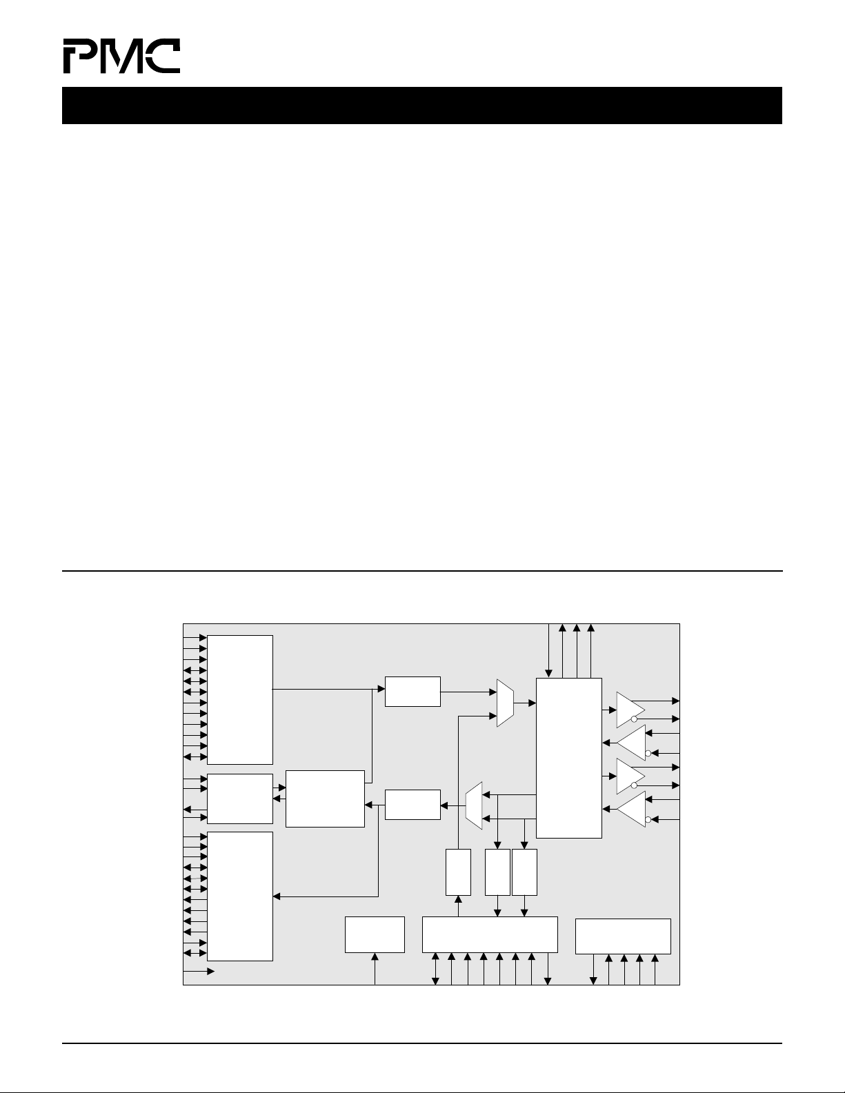
BLOCK DIAGRAM
IBUS8
IANYPHY
IMASTER
IENB
IADDR[4:0]
IAVALID
IDAT[15:0]
IPRTY
ISOC
ISX
IFCLK
ICA
LRXD[15:0]
LRXC[15:0]
LTXD[15:0]
LTXC[15:0]
OBUS8
OANYPHY
OMASTER
OENB
OADDR[4:0]
OAVALID
ODAT[15:0]
OPRTY
OSOC
OSX
OFCLK
OCA
SCIANY
SCI-PHY
Receive
Master/
Transmit
Slave
Elastic Store
SCI-PHY
Transmit
Master/
Receive Slave
Time-Sliced ATM
Transmission
Convergence
Synthesis
Clock
Per-PHY
Buffers
Per-PHY
Buffers
Cell Processor
FIFO
4 Cell
FIFO
4 Cell
2 Cell
Buffer
Microprocessor Interface
TX8K
RX8K
RCLK
RSTOB
JTAG Test Access
Port
TXD1+
TXD1-
RXD1+
RXD1-
TXD2+
TXD2-
RXD2+
RXD2-
PMC-990147 (P2)
TDI
ALE
CSB
RDB
RSTB
INTB
A[8:0]
REFCLK
PROPRIETARY AND CONFIDENTIAL TO PMC-SIERRA, INC. AND FOR ITS CUSTOMERS’ INTERNAL USE
D[7:0]
WRB
TDO
TMS
TCK
TRSTB
1999 PMC-Sierra, Inc.

Dual Serial Link, PHY MultiplexerDual Serial Link, PHY Multiplexer
y
(
y
(
g
(
PM7350 S/UNI-DUPLEX
• 6 bit port ID prepended to each cell for
ATM layer to identify cell source
use b
• Individual PHY and microprocessor
1 of 32 PHYs or processor).
• Back-pressure provided b
far end
active link only) to prevent overflow of
far end receiver.
• Cells received from the active LVDS
LVDS RECEIVE DIRECTION
• The LVDS l ink marked as "spare" i s
monitored for errors, PHY cells are
discarded, microprocessor port cells
are accepted.
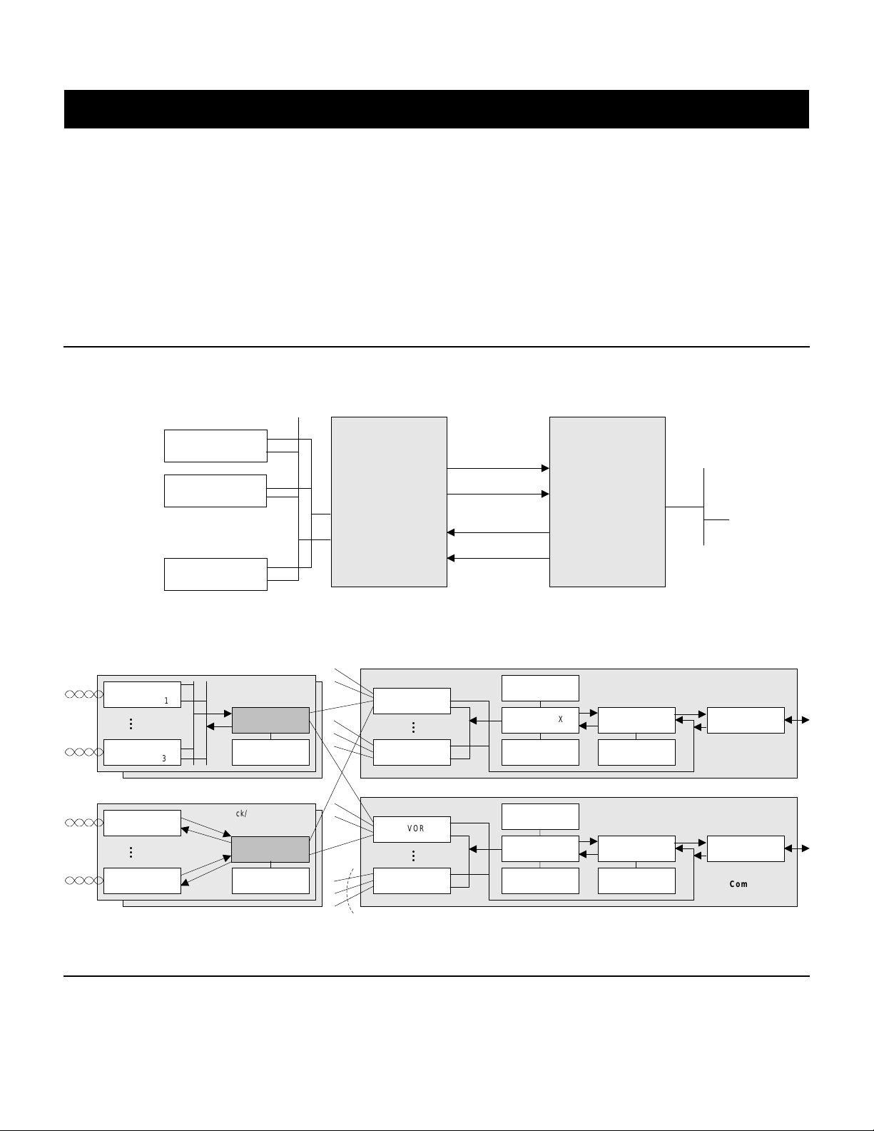
TYPICAL APPLICATIONS
INTER-SHELF UTOPIA BUS EXTENSION
modem #1
modem #2
FIFO back-pressure indications are
sent to the far end to prevent FIFO
overflows. Per stream backpressure
prevents head-of-line blockin
.
link are forwarded to the appropriate
PHY, bit serial interface, or the
microprocessor port as specified by a
6 bit port ID added to each cell at the
far end device.
4 Wire
UTOPIA
Bus Master
PM7350
S/UNI-DUPLEX
LVDS
APPLICATIONS
•Single shelf or multi-shelf Digital
Subscriber Loop Access Multiplexer
DSLAM).
• ATM/frame/IP switch or multiservice
access multi plexer.
• UMTS wireless base station and base
station controller.
Bus Slave or
Bus Master
PM7350
S/UNI-DUPLEX
modem #N
MULTI-SHELF 1024 LINE ATM DSLAM
xDSL PHY
xDSL PHY
modem
modem
1
32
1
16
UTOPIA Line Cards
S/UNI-DUPLEX
processor
Clock/Data Line Cards
S/UNI-DUPLEX
processor
S/UNI-VORTEX
S/UNI-VORTEX
S/UNI-VORTEX
S/UNI-VORTEX
8 Links per S/UNI-VORTEX
processor
S/UNI-APEX
RAM RAM
processor
S/UNI-APEX S/UNI-ATLAS S/UNI-PLUS
RAM RAM
S/UNI-ATLAS S/UNI-PLUS
Common Card,
working
Common Card,
spare
Head Office:
PMC-Sierra, Inc.
#105 - 8555 Baxter Place
Burnaby, B.C. V5A 4V7
Canada
Tel: 604.415.6000
Fax: 604.415.6200
PROPRIETARY AND CONFIDENTIAL TO PMC-SIERRA, INC. AND FOR ITS CUSTOMERS’ INTERNAL USE
To order documentation,
send email to:
document@pmc-sierra.com
or contact the head office,
Attn: Document Coordinator
All product documentation is available
on our web site at:
http://www.pmc-sierra.com
For corporate information,
send email to:
info@pmc-sierra.com
PMC-990147 (P2)
1999 PMC-Sierra, Inc.
 Loading...