


Released
Datasheet
PMC-Sierra, Inc.
PMC-980616 Issue 3 5 Gbit/s ATM Switch Fabric Element
PM73488 QSE
PM73488
QSE
5 Gbit/s ATM Switch Fabric Element
DATASHEET
Released
Issue 3: June 1999
Long Form Data Sheet

Released
Datasheet
PMC-Sierra, Inc.
PM73488 QSE
PMC-980616 Issue 3 5 Gbit/s ATM Switch Fabric Element
AAL1gator, AAL1gator2, Evil Twin Switching, QRT, QSE, and SATURN are trademarks of PMC-Sierra, Inc.
AMCC is a registered trademar k of Applied MicroCircuits Corporation.
i960 is a registered trademark of Intel Corporation.
National Semiconducto r is a registered trademark of National Semiconductor Corporat ion.
Vitesse is a trademark of Vitesse S emiconductor Corporation.
All other brand or product names are trademarks
of their res p ec t iv e com pan ies or org an iz at ions.
U.S. Patents 5,557,607, 5,57 0,348, and 5,583 ,861
Copyright © 1999 PMC-Sierra, Inc.
All Rights Reserved
Released
Datasheet
PMC-Sierra, Inc.
PM73488 QSE
PMC-980616 Issue 3 5 Gbit/s ATM Switch Fabric Element
Public Revision History
Issue Number Issue Date Details of Change
Issue 1 March 1998 Creati on of Document
Issue 2 October 1998 Fixed all known typos/errors (e.g. wrong pin-
out:
RAM_ADD(16) and RAM_PARITY swapped).
Issue 3 June 1999 Production Release Version
© 1999
PMC-Sierra, Inc.
105-8555 Baxter Place
Burnaby BC Canada V5A 4V7
Phone: 604.415.6000 FAX: 604.415.6200

Released
Datasheet
PMC-Sierra, Inc.
PMC-980616 Issue 3 5 Gbit/s ATM Switch Fabric Element
PM73488 QSE
Table of Contents
Description . . . . . . . . . . . . . . . . . . . . . . . . . . . . . . . . . . . . . . . . . . . . . . . . . . . . . . . . . . . . . . . . . . . . . . . . . . . . . 13
Features. . . . . . . . . . . . . . . . . . . . . . . . . . . . . . . . . . . . . . . . . . . . . . . . . . . . . . . . . . . . . . . . . . . . . . . . . . . . . . . . 14
Switching Algorithm . . . . . . . . . . . . . . . . . . . . . . . . . . . . . . . . . . . . . . . . . . . . . . . . . . . . . . . . . . . . . . . . . . 14
Multicast Support . . . . . . . . . . . . . . . . . . . . . . . . . . . . . . . . . . . . . . . . . . . . . . . . . . . . . . . . . . . . . . . . . . . . 14
Diagnostic/Robustness Features . . . . . . . . . . . . . . . . . . . . . . . . . . . . . . . . . . . . . . . . . . . . . . . . . . . . . . . . . 14
I/O Features . . . . . . . . . . . . . . . . . . . . . . . . . . . . . . . . . . . . . . . . . . . . . . . . . . . . . . . . . . . . . . . . . . . . . . . . . 14
Physical Characteristics. . . . . . . . . . . . . . . . . . . . . . . . . . . . . . . . . . . . . . . . . . . . . . . . . . . . . . . . . . . . . . . . 14
1 How the QSE Fits into Your System . . . . . . . . . . . . . . . . . . . . . . . . . . . . . . . . . . . . . . . . . . . . . . . . . . . . . . . . . . . 16
1.1 QSE System Overview . . . . . . . . . . . . . . . . . . . . . . . . . . . . . . . . . . . . . . . . . . . . . . . . . . . . . . . . . . . . . . . . 16
1.2 32 x 32 Switch Application (5 Gbps) . . . . . . . . . . . . . . . . . . . . . . . . . . . . . . . . . . . . . . . . . . . . . . . . . . . . . 17
1.3 64 x 64 Switch Application (10 Gbps) . . . . . . . . . . . . . . . . . . . . . . . . . . . . . . . . . . . . . . . . . . . . . . . . . . . . 17
1.4 5 Gbps to 20 Gbps Application Example - Seamless Growth. . . . . . . . . . . . . . . . . . . . . . . . . . . . . . . . . . . 18
1.5 5 Gbps to 160 Gbps Application Example – LAN-to-WAN. . . . . . . . . . . . . . . . . . . . . . . . . . . . . . . . . . . . 20
2 Theory of Operation. . . . . . . . . . . . . . . . . . . . . . . . . . . . . . . . . . . . . . . . . . . . . . . . . . . . . . . . . . . . . . . . . . . . . . . . 25
2.1 Phase Aligners . . . . . . . . . . . . . . . . . . . . . . . . . . . . . . . . . . . . . . . . . . . . . . . . . . . . . . . . . . . . . . . . . . . . . . . 26
2.2 Data Drivers. . . . . . . . . . . . . . . . . . . . . . . . . . . . . . . . . . . . . . . . . . . . . . . . . . . . . . . . . . . . . . . . . . . . . . . . . 26
2.3 Unicast Routing and Distribution . . . . . . . . . . . . . . . . . . . . . . . . . . . . . . . . . . . . . . . . . . . . . . . . . . . . . . . . 26
2.4 Multicast Cell Flow . . . . . . . . . . . . . . . . . . . . . . . . . . . . . . . . . . . . . . . . . . . . . . . . . . . . . . . . . . . . . . . . . . . 27
2.4.1 Multicast Queue Engine . . . . . . . . . . . . . . . . . . . . . . . . . . . . . . . . . . . . . . . . . . . . . . . . . . . . . . . . . . 28
2.4.2 Multicast Dequeue Engine. . . . . . . . . . . . . . . . . . . . . . . . . . . . . . . . . . . . . . . . . . . . . . . . . . . . . . . . . 28
2.5 Arbiter . . . . . . . . . . . . . . . . . . . . . . . . . . . . . . . . . . . . . . . . . . . . . . . . . . . . . . . . . . . . . . . . . . . . . . . . . . . . . 30
2.6 BP_ACK Drivers. . . . . . . . . . . . . . . . . . . . . . . . . . . . . . . . . . . . . . . . . . . . . . . . . . . . . . . . . . . . . . . . . . . . . 31
2.7 Interdevic e Interconnectability . . . . . . . . . . . . . . . . . . . . . . . . . . . . . . . . . . . . . . . . . . . . . . . . . . . . . . . . . . 31
2.8 Network Topologies and the Speedup Factor (SF) . . . . . . . . . . . . . . . . . . . . . . . . . . . . . . . . . . . . . . . . . . . 31
2.8.1 Network Philosophy . . . . . . . . . . . . . . . . . . . . . . . . . . . . . . . . . . . . . . . . . . . . . . . . . . . . . . . . . . . . . 32
2.8.2 Network Definition . . . . . . . . . . . . . . . . . . . . . . . . . . . . . . . . . . . . . . . . . . . . . . . . . . . . . . . . . . . . . . 34
2.8.3 Speedup Factor (SF) . . . . . . . . . . . . . . . . . . . . . . . . . . . . . . . . . . . . . . . . . . . . . . . . . . . . . . . . . . . . . 36
3 External Port Descriptions . . . . . . . . . . . . . . . . . . . . . . . . . . . . . . . . . . . . . . . . . . . . . . . . . . . . . . . . . . . . . . . . . . . 39
3.1 Switch Fabric Port and Interface Description . . . . . . . . . . . . . . . . . . . . . . . . . . . . . . . . . . . . . . . . . . . . . . . 39
3.1.1 SE_SOC Encodings. . . . . . . . . . . . . . . . . . . . . . . . . . . . . . . . . . . . . . . . . . . . . . . . . . . . . . . . . . . . . . 39
3.1.2 Data Cell Format . . . . . . . . . . . . . . . . . . . . . . . . . . . . . . . . . . . . . . . . . . . . . . . . . . . . . . . . . . . . . . . . 40
3.1.3 BP_ACK Encodings . . . . . . . . . . . . . . . . . . . . . . . . . . . . . . . . . . . . . . . . . . . . . . . . . . . . . . . . . . . . . 42
3.2 Data Acknowledge. . . . . . . . . . . . . . . . . . . . . . . . . . . . . . . . . . . . . . . . . . . . . . . . . . . . . . . . . . . . . . . . . . . . 43
3.3 Microprocessor Interface. . . . . . . . . . . . . . . . . . . . . . . . . . . . . . . . . . . . . . . . . . . . . . . . . . . . . . . . . . . . . . . 44
3.4 Multicast SRAM Interface. . . . . . . . . . . . . . . . . . . . . . . . . . . . . . . . . . . . . . . . . . . . . . . . . . . . . . . . . . . . . . 44
3.5 Clocks and Timing Signals . . . . . . . . . . . . . . . . . . . . . . . . . . . . . . . . . . . . . . . . . . . . . . . . . . . . . . . . . . . . . 44
3.6 CTRL_IN. . . . . . . . . . . . . . . . . . . . . . . . . . . . . . . . . . . . . . . . . . . . . . . . . . . . . . . . . . . . . . . . . . . . . . . . . . . 44
3.7 STAT_OUT . . . . . . . . . . . . . . . . . . . . . . . . . . . . . . . . . . . . . . . . . . . . . . . . . . . . . . . . . . . . . . . . . . . . . . . . . 45
Long Form Data Sheet
3.8 Fabric Switch-Over . . . . . . . . . . . . . . . . . . . . . . . . . . . . . . . . . . . . . . . . . . . . . . . . . . . . . . . . . . . . . . . . . . . 45

Released
Datasheet
PMC-Sierra, Inc.
PMC-980616 Issue 3 5 Gbit/s ATM Switch Fabric Element
3.9 Cell Timing/Latency . . . . . . . . . . . . . . . . . . . . . . . . . . . . . . . . . . . . . . . . . . . . . . . . . . . . . . . . . . . . . . . . . . 46
4 QSE Feature Descriptions . . . . . . . . . . . . . . . . . . . . . . . . . . . . . . . . . . . . . . . . . . . . . . . . . . . . . . . . . . . . . . . . . . . 47
4.1 Distribution Algorithm . . . . . . . . . . . . . . . . . . . . . . . . . . . . . . . . . . . . . . . . . . . . . . . . . . . . . . . . . . . . . . . . 47
4.2 Cell Start Offset Logic. . . . . . . . . . . . . . . . . . . . . . . . . . . . . . . . . . . . . . . . . . . . . . . . . . . . . . . . . . . . . . . . . 47
4.2.1 Relation Between External CELL_START and Local CELL_START . . . . . . . . . . . . . . . . . . . . . . 47
4.2.2 Relation Between Local CELL_START and Data Out of the QSE . . . . . . . . . . . . . . . . . . . . . . . . . 48
4.3 General Description of Phase Aligners . . . . . . . . . . . . . . . . . . . . . . . . . . . . . . . . . . . . . . . . . . . . . . . . . . . . 48
4.4 Multicast Backpressure Control. . . . . . . . . . . . . . . . . . . . . . . . . . . . . . . . . . . . . . . . . . . . . . . . . . . . . . . . . . 49
4.5 Multilevel Reset. . . . . . . . . . . . . . . . . . . . . . . . . . . . . . . . . . . . . . . . . . . . . . . . . . . . . . . . . . . . . . . . . . . . . . 49
5 Fault Specification . . . . . . . . . . . . . . . . . . . . . . . . . . . . . . . . . . . . . . . . . . . . . . . . . . . . . . . . . . . . . . . . . . . . . . . . . 51
5. 1 Purpose . . . . . . . . . . . . . . . . . . . . . . . . . . . . . . . . . . . . . . . . . . . . . . . . . . . . . . . . . . . . . . . . . . . . . . . . . . . . 51
5. 2 Basic Data and BP/ACK Flow . . . . . . . . . . . . . . . . . . . . . . . . . . . . . . . . . . . . . . . . . . . . . . . . . . . . . . . . . . 51
5. 3 Fault Detection Mechanisms . . . . . . . . . . . . . . . . . . . . . . . . . . . . . . . . . . . . . . . . . . . . . . . . . . . . . . . . . . . 52
5. 4 Interface Behavior. . . . . . . . . . . . . . . . . . . . . . . . . . . . . . . . . . . . . . . . . . . . . . . . . . . . . . . . . . . . . . . . . . . . 52
5. 5 IRT-to-Switch Fabric Interface. . . . . . . . . . . . . . . . . . . . . . . . . . . . . . . . . . . . . . . . . . . . . . . . . . . . . . . . . . 53
5. 6 QSE Interface, Receive Data Direction . . . . . . . . . . . . . . . . . . . . . . . . . . . . . . . . . . . . . . . . . . . . . . . . . . . 53
5. 7 QSE Interface, Transmit Data Direction. . . . . . . . . . . . . . . . . . . . . . . . . . . . . . . . . . . . . . . . . . . . . . . . . . . 54
5. 8 Switch Fabric-to-ORT Interface . . . . . . . . . . . . . . . . . . . . . . . . . . . . . . . . . . . . . . . . . . . . . . . . . . . . . . . . . 55
5. 9 Types of Failures and Their Manifestation. . . . . . . . . . . . . . . . . . . . . . . . . . . . . . . . . . . . . . . . . . . . . . . . . 56
6 Signal Descriptions . . . . . . . . . . . . . . . . . . . . . . . . . . . . . . . . . . . . . . . . . . . . . . . . . . . . . . . . . . . . . . . . . . . . . . . . 58
6.1 Package Diagram . . . . . . . . . . . . . . . . . . . . . . . . . . . . . . . . . . . . . . . . . . . . . . . . . . . . . . . . . . . . . . . . . . . . . 58
6.2 Signal Locations (Signal Name to Ball) . . . . . . . . . . . . . . . . . . . . . . . . . . . . . . . . . . . . . . . . . . . . . . . . . . . 60
6.3 Signal Locations (Ball to Signal Name) . . . . . . . . . . . . . . . . . . . . . . . . . . . . . . . . . . . . . . . . . . . . . . . . . . . 65
6.4 Pin Descriptions. . . . . . . . . . . . . . . . . . . . . . . . . . . . . . . . . . . . . . . . . . . . . . . . . . . . . . . . . . . . . . . . . . . . . . 70
6.4.1 Processor Interface Signals . . . . . . . . . . . . . . . . . . . . . . . . . . . . . . . . . . . . . . . . . . . . . . . . . . . . . . . . 72
6.4.2 Multicast RAM Interface Signals . . . . . . . . . . . . . . . . . . . . . . . . . . . . . . . . . . . . . . . . . . . . . . . . . . . 72
6.4.3 QSE Interface Signals . . . . . . . . . . . . . . . . . . . . . . . . . . . . . . . . . . . . . . . . . . . . . . . . . . . . . . . . . . . . 74
6.4.4 Boundary Scan Signals . . . . . . . . . . . . . . . . . . . . . . . . . . . . . . . . . . . . . . . . . . . . . . . . . . . . . . . . . . . 79
6.4.5 Miscellaneous Signals . . . . . . . . . . . . . . . . . . . . . . . . . . . . . . . . . . . . . . . . . . . . . . . . . . . . . . . . . . . . 81
6.4.6 Total Pin Count . . . . . . . . . . . . . . . . . . . . . . . . . . . . . . . . . . . . . . . . . . . . . . . . . . . . . . . . . . . . . . . . . 83
7 Physical Characteristics . . . . . . . . . . . . . . . . . . . . . . . . . . . . . . . . . . . . . . . . . . . . . . . . . . . . . . . . . . . . . . . . . . . . . 84
8 Timing Diagrams . . . . . . . . . . . . . . . . . . . . . . . . . . . . . . . . . . . . . . . . . . . . . . . . . . . . . . . . . . . . . . . . . . . . . . . . . . 86
8.1 Microprocessor Timing . . . . . . . . . . . . . . . . . . . . . . . . . . . . . . . . . . . . . . . . . . . . . . . . . . . . . . . . . . . . . . . . 86
8.2 RAM Timing . . . . . . . . . . . . . . . . . . . . . . . . . . . . . . . . . . . . . . . . . . . . . . . . . . . . . . . . . . . . . . . . . . . . . . . . 87
8.3 QSE Interface Timing . . . . . . . . . . . . . . . . . . . . . . . . . . . . . . . . . . . . . . . . . . . . . . . . . . . . . . . . . . . . . . . . . 88
8.4 Miscellaneous Timing . . . . . . . . . . . . . . . . . . . . . . . . . . . . . . . . . . . . . . . . . . . . . . . . . . . . . . . . . . . . . . . . . 89
9 Microprocessor Ports . . . . . . . . . . . . . . . . . . . . . . . . . . . . . . . . . . . . . . . . . . . . . . . . . . . . . . . . . . . . . . . . . . . . . . . 92
9.1 Microprocessor Ports Summary. . . . . . . . . . . . . . . . . . . . . . . . . . . . . . . . . . . . . . . . . . . . . . . . . . . . . . . . . . 92
9.2 Note on Error Detection and Reporting . . . . . . . . . . . . . . . . . . . . . . . . . . . . . . . . . . . . . . . . . . . . . . . . . . . 94
9.3 Microprocessor Ports Bit Definitions . . . . . . . . . . . . . . . . . . . . . . . . . . . . . . . . . . . . . . . . . . . . . . . . . . . . . 94
9.3.1 REVISION. . . . . . . . . . . . . . . . . . . . . . . . . . . . . . . . . . . . . . . . . . . . . . . . . . . . . . . . . . . . . . . . . . . . . 95
Long Form Data Sheet
9.3.2 CHIP_MODE . . . . . . . . . . . . . . . . . . . . . . . . . . . . . . . . . . . . . . . . . . . . . . . . . . . . . . . . . . . . . . . . . . 95
PM73488 QSE

Released
Datasheet
PMC-Sierra, Inc.
PMC-980616 Issue 3 5 Gbit/s ATM Switch Fabric Element
9.3.3 MULTICAST_GROUP_INDEX_REGISTER . . . . . . . . . . . . . . . . . . . . . . . . . . . . . . . . . . . . . . . . . 96
9.3.4 MULTICAST_GROUP_VECTOR_REGISTER . . . . . . . . . . . . . . . . . . . . . . . . . . . . . . . . . . . . . . . 96
9.3.5 MULTICAST_GROUP_OP . . . . . . . . . . . . . . . . . . . . . . . . . . . . . . . . . . . . . . . . . . . . . . . . . . . . . . . 97
9.3.6 UC/MC_FAIRNESS_REGISTER . . . . . . . . . . . . . . . . . . . . . . . . . . . . . . . . . . . . . . . . . . . . . . . . . . 97
9.3.7 EXTENDED_CHIP_MODE . . . . . . . . . . . . . . . . . . . . . . . . . . . . . . . . . . . . . . . . . . . . . . . . . . . . . . . 97
9.3.8 MULTICAST_GROUP_INDEX_MSB . . . . . . . . . . . . . . . . . . . . . . . . . . . . . . . . . . . . . . . . . . . . . . 98
9.3.9 INPUT_PORT_ENABLE . . . . . . . . . . . . . . . . . . . . . . . . . . . . . . . . . . . . . . . . . . . . . . . . . . . . . . . . . 98
9.3.10 OUTPUT_PORT_ENABLE . . . . . . . . . . . . . . . . . . . . . . . . . . . . . . . . . . . . . . . . . . . . . . . . . . . . . . 99
9.3.11 INPUT_MARKE D_CE LL S _COUNT . . . . . . . . . . . . . . . . . . . . . . . . . . . . . . . . . . . . . . . . . . . . . . 99
9.3.12 OUTPUT_MARKED_CELLS_COUNT . . . . . . . . . . . . . . . . . . . . . . . . . . . . . . . . . . . . . . . . . . . . 99
9.3.13 PARITY_ERROR_PRESENT . . . . . . . . . . . . . . . . . . . . . . . . . . . . . . . . . . . . . . . . . . . . . . . . . . . 100
9.3.14 PARITY_ERROR_LATCH . . . . . . . . . . . . . . . . . . . . . . . . . . . . . . . . . . . . . . . . . . . . . . . . . . . . . 100
9.3.15 PARITY_ERROR_INT_MASK . . . . . . . . . . . . . . . . . . . . . . . . . . . . . . . . . . . . . . . . . . . . . . . . . . 100
9.3.16 SE_INPUT_PORT_FAIL_PRESENT . . . . . . . . . . . . . . . . . . . . . . . . . . . . . . . . . . . . . . . . . . . . . 101
9.3.17 SE_INPUT_PORT_FAIL_LATCH . . . . . . . . . . . . . . . . . . . . . . . . . . . . . . . . . . . . . . . . . . . . . . . 102
9.3.18 BP_ACK_FAIL_PRESENT . . . . . . . . . . . . . . . . . . . . . . . . . . . . . . . . . . . . . . . . . . . . . . . . . . . . . 102
9.3.19 BP_ACK_FAIL_LATCH . . . . . . . . . . . . . . . . . . . . . . . . . . . . . . . . . . . . . . . . . . . . . . . . . . . . . . . 102
9.3.20 BP_REMOTE_FAIL_PRESENT . . . . . . . . . . . . . . . . . . . . . . . . . . . . . . . . . . . . . . . . . . . . . . . . . 103
9.3.21 BP_REMOTE_FAIL_LATCH . . . . . . . . . . . . . . . . . . . . . . . . . . . . . . . . . . . . . . . . . . . . . . . . . . . 103
9.3.22 CONTROL_REGISTER . . . . . . . . . . . . . . . . . . . . . . . . . . . . . . . . . . . . . . . . . . . . . . . . . . . . . . . . 103
9.3.23 INTERRUPT_STATUS_REGISTER. . . . . . . . . . . . . . . . . . . . . . . . . . . . . . . . . . . . . . . . . . . . . . 105
9.3.24 MULTICAST_AGGREGATE_OUTPUT_AND_INPUT_MODES . . . . . . . . . . . . . . . . . . . . . . 105
9.3.25 UNICAST_AGGREGATE_OUTPUT_MODE . . . . . . . . . . . . . . . . . . . . . . . . . . . . . . . . . . . . . . 106
9.3.26 SWITCH_FABRIC_ROW . . . . . . . . . . . . . . . . . . . . . . . . . . . . . . . . . . . . . . . . . . . . . . . . . . . . . . 107
9.3.27 SWITCH_FABRIC_COLUMN . . . . . . . . . . . . . . . . . . . . . . . . . . . . . . . . . . . . . . . . . . . . . . . . . . 108
9.3.28 CELL_START_OFFSET . . . . . . . . . . . . . . . . . . . . . . . . . . . . . . . . . . . . . . . . . . . . . . . . . . . . . . . 109
9.3.29 BP_CONTROL_REGISTER . . . . . . . . . . . . . . . . . . . . . . . . . . . . . . . . . . . . . . . . . . . . . . . . . . . . 109
9.3.30 ACK_PAYLOAD . . . . . . . . . . . . . . . . . . . . . . . . . . . . . . . . . . . . . . . . . . . . . . . . . . . . . . . . . . . . . 109
9.3.31 GANG_DEAD_ACK_PAYLOAD. . . . . . . . . . . . . . . . . . . . . . . . . . . . . . . . . . . . . . . . . . . . . . . . 110
9.3.32 EXTENDED_SWITCH_MODE. . . . . . . . . . . . . . . . . . . . . . . . . . . . . . . . . . . . . . . . . . . . . . . . . . 110
10 JTAG . . . . . . . . . . . . . . . . . . . . . . . . . . . . . . . . . . . . . . . . . . . . . . . . . . . . . . . . . . . . . . . . . . . . . . . . . . . . . . . . . 111
10.1 JTAG Support . . . . . . . . . . . . . . . . . . . . . . . . . . . . . . . . . . . . . . . . . . . . . . . . . . . . . . . . . . . . . . . . . . . . . 111
10.2 TAP Controller . . . . . . . . . . . . . . . . . . . . . . . . . . . . . . . . . . . . . . . . . . . . . . . . . . . . . . . . . . . . . . . . . . . . 112
10.2.1 Test-Logic-Reset: . . . . . . . . . . . . . . . . . . . . . . . . . . . . . . . . . . . . . . . . . . . . . . . . . . . . . . . . . . . . . 113
10.2.2 Run-Test-Idle: . . . . . . . . . . . . . . . . . . . . . . . . . . . . . . . . . . . . . . . . . . . . . . . . . . . . . . . . . . . . . . . . 114
10.2.3 Capture-DR:. . . . . . . . . . . . . . . . . . . . . . . . . . . . . . . . . . . . . . . . . . . . . . . . . . . . . . . . . . . . . . . . . . 114
10.2.4 Shift-DR: . . . . . . . . . . . . . . . . . . . . . . . . . . . . . . . . . . . . . . . . . . . . . . . . . . . . . . . . . . . . . . . . . . . . 114
10.2.5 Update-DR: . . . . . . . . . . . . . . . . . . . . . . . . . . . . . . . . . . . . . . . . . . . . . . . . . . . . . . . . . . . . . . . . . . 114
10.2.6 Capture-IR: . . . . . . . . . . . . . . . . . . . . . . . . . . . . . . . . . . . . . . . . . . . . . . . . . . . . . . . . . . . . . . . . . . 114
10.2.7 Shift-IR: . . . . . . . . . . . . . . . . . . . . . . . . . . . . . . . . . . . . . . . . . . . . . . . . . . . . . . . . . . . . . . . . . . . . . 114
10.2.8 Update-IR: . . . . . . . . . . . . . . . . . . . . . . . . . . . . . . . . . . . . . . . . . . . . . . . . . . . . . . . . . . . . . . . . . . . 114
Long Form Data Sheet
10.3 Boundary Scan Instructions. . . . . . . . . . . . . . . . . . . . . . . . . . . . . . . . . . . . . . . . . . . . . . . . . . . . . . . . . . . 114
PM73488 QSE

Released
Datasheet
PMC-Sierra, Inc.
PMC-980616 Issue 3 5 Gbit/s ATM Switch Fabric Element
10.3.1 BYPASS . . . . . . . . . . . . . . . . . . . . . . . . . . . . . . . . . . . . . . . . . . . . . . . . . . . . . . . . . . . . . . . . . . . . 114
10.3.2 EXTEST . . . . . . . . . . . . . . . . . . . . . . . . . . . . . . . . . . . . . . . . . . . . . . . . . . . . . . . . . . . . . . . . . . . . 114
10.3.3 SAMPLE . . . . . . . . . . . . . . . . . . . . . . . . . . . . . . . . . . . . . . . . . . . . . . . . . . . . . . . . . . . . . . . . . . . . 115
10.3.4 IDCODE . . . . . . . . . . . . . . . . . . . . . . . . . . . . . . . . . . . . . . . . . . . . . . . . . . . . . . . . . . . . . . . . . . . . 115
10.3.5 STCTEST . . . . . . . . . . . . . . . . . . . . . . . . . . . . . . . . . . . . . . . . . . . . . . . . . . . . . . . . . . . . . . . . . . . 115
10.4 Boundary Scan Pin Order . . . . . . . . . . . . . . . . . . . . . . . . . . . . . . . . . . . . . . . . . . . . . . . . . . . . . . . . . . . . 115
PM73488 QSE
Long Form Data Sheet

Released
Datasheet
PMC-Sierra, Inc.
PMC-980616 Issue 3 5 Gbit/s ATM Switch Fabric Element
PM73488 QSE
List of Figures
Figure 1. QSE In te rface Block D ia gr am . . . . . . . . . . . . . . . . . . . . . . . . . . . . . . . . . . . . . . . . . . . . . . . . . 12
Figure 2. QSE S yst em O v er v iew . . . . . . . . . . . . . . . . . . . . . . . . . . . . . . . . . . . . . . . . . . . . . . . . . . . . . . . 13
Figure 3. 32 x 32 S w it ch A p pl ica ti on ( 5 G bps ) . . . . . . . . . . . . . . . . . . . . . . . . . . . . . . . . . . . . . . . . . . . . 14
Figure 4. 64 x 64 S w it ch A p pl ica ti on ( 10 G b p s ) . . . . . . . . . . . . . . . . . . . . . . . . . . . . . . . . . . . . . . . . . . . 14
Figure 5. 5 Gbps ATM S w itc h U s in g 8 QR Ts, an d 1 QSE . . . . . . . . . . . . . . . . . . . . . . . . . . . . . . . . . . . . 15
Figure 6. 10 Gbp s A T M Sw i tch U s i ng 1 6 QRTs , an d 2 Q SEs . . . . . . . . . . . . . . . . . . . . . . . . . . . . . . . . . 15
Figure 7. 20 Gbp s A T M Sw i tch U s i ng 3 2 QRTs , an d 4 Q SEs . . . . . . . . . . . . . . . . . . . . . . . . . . . . . . . . . 16
Figure 8. 5 Gbps to 160 G b ps S wi tc he s M od el ed Using O nl y Tw o Ca rd s . . . . . . . . . . . . . . . . . . . . . . . . 17
Figure 9. 5 Gbps ATM S w itc h . . . . . . . . . . . . . . . . . . . . . . . . . . . . . . . . . . . . . . . . . . . . . . . . . . . . . . . . . 18
Figure 10 . 10 Gbp s A T M Sw it ch . . . . . . . . . . . . . . . . . . . . . . . . . . . . . . . . . . . . . . . . . . . . . . . . . . . . . . . 19
Figure 11 . 15 Gbp s A T M Sw it ch . . . . . . . . . . . . . . . . . . . . . . . . . . . . . . . . . . . . . . . . . . . . . . . . . . . . . . . 20
Figure 12 . 20 Gbp s A T M Sw it ch . . . . . . . . . . . . . . . . . . . . . . . . . . . . . . . . . . . . . . . . . . . . . . . . . . . . . . . 21
Figure 13 . Basic Q S E F l ow . . . . . . . . . . . . . . . . . . . . . . . . . . . . . . . . . . . . . . . . . . . . . . . . . . . . . . . . . . . 22
Figure 14 . Routing B it s Ro ta ti on f o r Un icast Traf fi c, G an g M o d e o f F our . . . . . . . . . . . . . . . . . . . . . . . 24
Figure 15. Examp le of Mult ic as t Cell Hand l in g i n the QSE . . . . . . . . . . . . . . . . . . . . . . . . . . . . . . . . . . . 27
Figure 16 . Ideal Di s trib u ted N et w or k . . . . . . . . . . . . . . . . . . . . . . . . . . . . . . . . . . . . . . . . . . . . . . . . . . . 29
Figure 17 . More Realistic D ist r ib ut ed N etw o r k . . . . . . . . . . . . . . . . . . . . . . . . . . . . . . . . . . . . . . . . . . . . 29
Figure 18. “Large” Distri bu t ed N etw o r k (Wi ll n ot W o rk W ell with B an y an Alone ) . . . . . . . . . . . . . . . . 30
Figure 19 . High-Le ve l Q R T/QSE Sy s tem . . . . . . . . . . . . . . . . . . . . . . . . . . . . . . . . . . . . . . . . . . . . . . . . 30
Figure 20 . (3) x 1 - 5 Gbp s Sy s te m . . . . . . . . . . . . . . . . . . . . . . . . . . . . . . . . . . . . . . . . . . . . . . . . . . . . . 31
Figure 21 . (5) x 4 - 20 G b p s Sy s tem . . . . . . . . . . . . . . . . . . . . . . . . . . . . . . . . . . . . . . . . . . . . . . . . . . . . 31
Figure 22 . (1,3) x 1 - 10 G b ps System . . . . . . . . . . . . . . . . . . . . . . . . . . . . . . . . . . . . . . . . . . . . . . . . . . . 32
Figure 23 . Random iz er ( w ith Evil Twi n S witching A l gor it hm) . . . . . . . . . . . . . . . . . . . . . . . . . . . . . . . . 33
Figure 24 . Networ k Ne ed s to be Ru n F aster than th e Lin e Rate . . . . . . . . . . . . . . . . . . . . . . . . . . . . . . . . 33
Figure 25 . Definit io n of t he S pe ed up Factor . . . . . . . . . . . . . . . . . . . . . . . . . . . . . . . . . . . . . . . . . . . . . . 34
Figure 26 . How to U se t he SF to Select Fa vo r ab le N etw o r ks . . . . . . . . . . . . . . . . . . . . . . . . . . . . . . . . . . 3 4
Figure 27 . SE_SOC Encodin g s . . . . . . . . . . . . . . . . . . . . . . . . . . . . . . . . . . . . . . . . . . . . . . . . . . . . . . . . 36
Figure 28 . Expanded SE_SO C En codings . . . . . . . . . . . . . . . . . . . . . . . . . . . . . . . . . . . . . . . . . . . . . . . . 36
Figure 29 . BP_AC K En co di ng s . . . . . . . . . . . . . . . . . . . . . . . . . . . . . . . . . . . . . . . . . . . . . . . . . . . . . . . . 39
Figure 30 . QSE Cel l- Lev el Timing . . . . . . . . . . . . . . . . . . . . . . . . . . . . . . . . . . . . . . . . . . . . . . . . . . . . . 44
Figure 31 . QSE Sw it ch La ten cy . . . . . . . . . . . . . . . . . . . . . . . . . . . . . . . . . . . . . . . . . . . . . . . . . . . . . . . . 45
Figure 32 . Basic F or war d an d Backwar d Da ta P ath . . . . . . . . . . . . . . . . . . . . . . . . . . . . . . . . . . . . . . . . . 46
Figure 33. Basic Dat a Path (SE_D_ OUT/IN and SE_SOC_OUT /IN in Forward Path, B P_ACK_OUT /IN in
Backwar d Pa th ) . . . . . . . . . . . . . . . . . . . . . . . . . . . . . . . . . . . . . . . . . . . . . . . . . . . . . . . . . . . . . . . . . . . . . 48
Figure 34 . 596-Bal l E nh an ced Plast ic BG A P h y sical Dimen s io n s D iagram (T op v ie w ) . . . . . . . . . . . . . 55
Figure 35 . 596-Bal l E nh an ced Plast ic BG A P h y sical Dimen s io n s D iagram (B o tt om vi ew ) . . . . . . . . . . . 56
Figure 36 . QSE Pi no u t B lo ck D ia gram . . . . . . . . . . . . . . . . . . . . . . . . . . . . . . . . . . . . . . . . . . . . . . . . . . 68
Long Form Data Sheet
Figure 37 . Micropr o cess o r Ti min g . . . . . . . . . . . . . . . . . . . . . . . . . . . . . . . . . . . . . . . . . . . . . . . . . . . . . 83

Released
Datasheet
PMC-Sierra, Inc.
PMC-980616 Issue 3 5 Gbit/s ATM Switch Fabric Element
Figure 38 . RAM In ter f ac e . . . . . . . . . . . . . . . . . . . . . . . . . . . . . . . . . . . . . . . . . . . . . . . . . . . . . . . . . . . . 84
Figure 39 . QSE Bit -L ev e l Timing . . . . . . . . . . . . . . . . . . . . . . . . . . . . . . . . . . . . . . . . . . . . . . . . . . . . . . 85
Figure 40 . Reset Timing . . . . . . . . . . . . . . . . . . . . . . . . . . . . . . . . . . . . . . . . . . . . . . . . . . . . . . . . . . . . . 86
Figure 41 . JTAG Ti min g . . . . . . . . . . . . . . . . . . . . . . . . . . . . . . . . . . . . . . . . . . . . . . . . . . . . . . . . . . . . . 87
Figure 42 . Boundar y S ca n A rch itecture . . . . . . . . . . . . . . . . . . . . . . . . . . . . . . . . . . . . . . . . . . . . . . . . . 108
Figure 43 . TAP Con t ro ll er Fin it e S t at e M achine . . . . . . . . . . . . . . . . . . . . . . . . . . . . . . . . . . . . . . . . . . 110
PM73488 QSE
Long Form Data Sheet

Released
Datasheet
PMC-Sierra, Inc.
PMC-980616 Issue 3 5 Gbit/s ATM Switch Fabric Element
PM73488 QSE
List of Tables
Table 1. BP_CO NT R O L_ RE G ISTER; Thr esh ol d Co n trol B its for Each Set of 3 2 B uff er s . . . . . . . . . . . 25
Table 2. Spee dup F ac to r (1 - Stag e Netwo rks ) . . . . . . . . . . . . . . . . . . . . . . . . . . . . . . . . . . . . . . . . . . . . . 35
Table 3. Spee dup F ac to r (3 - Stag e Netwo rks ) . . . . . . . . . . . . . . . . . . . . . . . . . . . . . . . . . . . . . . . . . . . . . 35
Table 5. Regu lar C el l Fo r m at . . . . . . . . . . . . . . . . . . . . . . . . . . . . . . . . . . . . . . . . . . . . . . . . . . . . . . . . . 37
Table 6. PM73 48 8 M od e I d le Cell Form a t . . . . . . . . . . . . . . . . . . . . . . . . . . . . . . . . . . . . . . . . . . . . . . . 38
Table 7. Infor mat io n Bit Enc odin g . . . . . . . . . . . . . . . . . . . . . . . . . . . . . . . . . . . . . . . . . . . . . . . . . . . . . 40
Table 8. Data Lat en c ie s . . . . . . . . . . . . . . . . . . . . . . . . . . . . . . . . . . . . . . . . . . . . . . . . . . . . . . . . . . . . . 43
Table 9. Fail ure C o nd it io n s , I RT -t o S witch Fab ri c In ter f ace . . . . . . . . . . . . . . . . . . . . . . . . . . . . . . . . . . 50
Table 10. Failur e C on d iti o ns, QSE R ece iv e I n ter f ace . . . . . . . . . . . . . . . . . . . . . . . . . . . . . . . . . . . . . . . 51
Table 11. Failur e C on d iti o ns, QSE Tran s mi t I n te rf ac e . . . . . . . . . . . . . . . . . . . . . . . . . . . . . . . . . . . . . . 52
Table 12. Failur e C on d iti o ns, Switc h Fabric-to- OR T In te rface . . . . . . . . . . . . . . . . . . . . . . . . . . . . . . . . 53
Table 13. Faults . . . . . . . . . . . . . . . . . . . . . . . . . . . . . . . . . . . . . . . . . . . . . . . . . . . . . . . . . . . . . . . . . . . . 53
Table 14. Signal Lo cations (Signal N am e t o B al l) . . . . . . . . . . . . . . . . . . . . . . . . . . . . . . . . . . . . . . . . . 57
Table 15. Signal Lo cations (B al l t o S ig na l N a m e) . . . . . . . . . . . . . . . . . . . . . . . . . . . . . . . . . . . . . . . . . 62
Table 16. Process o r Inte rf a ce S i gn al s ( 21 Signal Pin s ) . . . . . . . . . . . . . . . . . . . . . . . . . . . . . . . . . . . . . . 69
Table 17. Multicas t R A M Inter face S i gn al s (3 9 S i gn al Pin s ) . . . . . . . . . . . . . . . . . . . . . . . . . . . . . . . . . . 69
Table 18. QSE In te rf ac e S i gnals (364 S ignal Pins ) . . . . . . . . . . . . . . . . . . . . . . . . . . . . . . . . . . . . . . . . . 71
Table 19. Bounda ry Scan Sig na ls ( 8 Sig n al Pins) . . . . . . . . . . . . . . . . . . . . . . . . . . . . . . . . . . . . . . . . . . 76
Table 20. Miscell an eo us S ignals (8 S ignal Pin s) . . . . . . . . . . . . . . . . . . . . . . . . . . . . . . . . . . . . . . . . . . . 78
Table 21. Pin Al lo cat io ns . . . . . . . . . . . . . . . . . . . . . . . . . . . . . . . . . . . . . . . . . . . . . . . . . . . . . . . . . . . . 80
Table 22. Absolut e M aximum R ati ng s . . . . . . . . . . . . . . . . . . . . . . . . . . . . . . . . . . . . . . . . . . . . . . . . . . . 81
Table 23. Recommended O p er at in g Co nd i tio n s . . . . . . . . . . . . . . . . . . . . . . . . . . . . . . . . . . . . . . . . . . . . 81
Table 24. DC Ope ra ti ng C on d iti o ns . . . . . . . . . . . . . . . . . . . . . . . . . . . . . . . . . . . . . . . . . . . . . . . . . . . . . 81
Table 25. Capaci tan ce . . . . . . . . . . . . . . . . . . . . . . . . . . . . . . . . . . . . . . . . . . . . . . . . . . . . . . . . . . . . . . 82
Table 26. Estima ted Package Th er m a l C h ar act er is t ics . . . . . . . . . . . . . . . . . . . . . . . . . . . . . . . . . . . . . . . 82
Table 27. Microp ro ce s sor T im i ng . . . . . . . . . . . . . . . . . . . . . . . . . . . . . . . . . . . . . . . . . . . . . . . . . . . . . . 83
Table 28. RAM In te rf ac e Timing . . . . . . . . . . . . . . . . . . . . . . . . . . . . . . . . . . . . . . . . . . . . . . . . . . . . . . 84
Table 29. CTRL_IN, STAT_ O UT , T E ST_ M OD E an d D EBUG Tim in g . . . . . . . . . . . . . . . . . . . . . . . . . 86
Table 30. Valid W i nd o w Timing . . . . . . . . . . . . . . . . . . . . . . . . . . . . . . . . . . . . . . . . . . . . . . . . . . . . . . . 87
Table 31. Microp ro ce s sor Po r ts S u m mary . . . . . . . . . . . . . . . . . . . . . . . . . . . . . . . . . . . . . . . . . . . . . . . 89
Table 32. Bounda ry Scan Pin o rder . . . . . . . . . . . . . . . . . . . . . . . . . . . . . . . . . . . . . . . . . . . . . . . . . . . . 112
Table 33. Standar d A b brev iations . . . . . . . . . . . . . . . . . . . . . . . . . . . . . . . . . . . . . . . . . . . . . . . . . . . . 129
Table 34. Orderi ng I n fo r mat io n . . . . . . . . . . . . . . . . . . . . . . . . . . . . . . . . . . . . . . . . . . . . . . . . . . . . . . . 132
Long Form Data Sheet

Released
Datasheet
PMC-Sierra, Inc.
PMC-980616 Issue 3 5 Gbit/s ATM Switch Fabric Element
WAC- 488-B
PM73488 QSE
Product Overview
DESCRIPTION
The PM73488 (QSE) is an advanced communications device that enables the implementation of high performance
switching syst ems. The QSE is a 32 × 32 cell based switch element, with a total sustainable bandwidth of 5 Gb/s .
(The peak, or raw, bandwidth is much more than that: about 8 Gb/s). The QSE is designed to be used with other
QSE’s as part of a larger switch fabric. Various QSE combinations allow fabrics with theoretical peak capacities
ranging from 5 Gb/s (one QSE) to 160 Gb/s. The QSE is not ATM specific; however, should the QSE be used for
switching ATM cells, the QSE cell size is large enough to allow efficient direct mapping between QSE Cells and
ATM cells.
Multistage QSE Fabrics (Delta-Reverse Delt a c onfiguration) have rich connectivity with multi ple paths betwee n each
source/dest ination pair. A QSE fabric performs cut-through unicast swi tching and uses Randomization and Evil-Twin
algorithms to fully utilize these multiple paths and avoid the build up of internal hot spots. Randomiza tion, in combination with multiple routing paths allows graceful degradation of QSE Fabric performance if internal links fail. To
detect failed links, the QSE maintains and checks liveness patterns on input and output ports in hardware, and
automatically routes around ports if they die.
QSE data ports are 6 bits wide including a 4-bit wide 66 MHz data path, a one-bit wide start-of-cell indication, and a
one-bit wide acknowledgment signal. Each port contains "Phase Aligners" to recover the clock for that port, thus
removing the need to synchronize all data to a singl e global clock.
When switching unicast traffic in a multistage fabric (one to three stages), the first nibble of the cell will come out of
the last QSE st age before the last nibble o f that cell enters the first stage. The cell thereby traverses the en tire fabric in
one cell time. If the cell sucessfully makes it to its destination, the ("egress") device accepting the cell from the last
stage QSE has the opportunity to send a four bit "Ack Information Packet" back to source indicating what it did with
this cell ; at its simplest, the egress device can send back one pattern to indicate that the cell was accepted and another
to indicate that the cell was dropped due to, say, buffer overflow.
It is also possible that the cell was dropped inside the QSE fabric due to say a collision with another cell. The QSE
classifies lost cells as due to one of three causes (collision, all possible outputs dead, or parity errors) and will
generate an "Ack Information Packet" back to the source to communicate this event. In each QSE, the 4 bit pattern in
the information packet can be independently software configured for each of the three cases. Note that since each
QSE can be separately programmed, the patterns can even be setup so that the source knows where the cell was
dropped.
The information provided by the "Ack Information Packets" can be used by the device injecting cells into the first
QSE stage to decide how to handle the cells; at its simplest, the device can resend cells that did not get through (a
more sophisticated algorithm might also take into account where the cell was lost and the behavior of the evil twin
algorithm to decide when to resend the cell; for example if the cell was dropped due to output congestion it might
make sense to back off on cells to that output).
For unicast traffic, part of switch bandwidth will be used to resend cells that did not make it through the first time
around. This implies that sustained throughput is less than peak switching capacity. The amount of bandwidth
required for resending cells and the effect of resending on latency and "Cell Delay Variation (CDV)" has been extensively studied with analytical models of the fabric. These results have then been cross checked with results from
simulating software models of the fabric. This data is crucial for designing fabrics that can efficiently support
Long Form Data Sheet
13

Released
Datasheet
PMC-Sierra, Inc.
PMC-980616 Issue 3 5 Gbit/s ATM Switch Fabric Element
guaranteed "Quality of Service (QOS)" requirements. The recommended QSE fabric configurations for high quality
switching takes these results into account; for example the 3 stage 160 Gb/s sustained throughput fabric has a peak
capacity of 256 Gb/s (60% mar gin).
The QSE fabric is store-and-forward for multicast traffic. Cell replication is performed in an optimal tree based
manner where replication is done as far downstream as possible and each QSE contains cell buffers to buffer
multicast cells. A multipriority backpres sure feedback is us ed to control the flow of multicast cells through the fabric.
PM73488 QSE
FEATURES
Switching A l go rithm
• Supports blocking resolution in the swi tch fabric.
• Guarantees a lower bound on switch performance using a patented randomization algorithm called Evil
Twin Switching.
• Determines routes using specified bits in the header (self-routing switch fabric) for unicast traffic.
• Determines out put groupings using a lookup tabl e for m ulticast traffic.
• Allows output ports to be combined in groups of 1, 2, 4, 8, 16, or 32 for unicast traffic.
• Allows output ports to be combined in groups of 1, 2, or 4 for multicast traffic.
Multicast Support
• Supports opt imal tree-based multicast replication in the switch fabric.
• Supports 512 internal multicast groups, expandable to 256K with external SRAM.
• Provides 64 internal cell buffers for multicast cells.
Diagnostic/Robustness Features
• Checks the header p arity.
• Counts tagge d cells.
• Checks for connectivity and stuck-at faults on all switch fabric interconnects.
I/O Features
• Provides 32 switch fabric interfaces with integrated phase aligner clock recovery ci rcuitry.
• Provides a Start-Of-Cell (SOC) output per four switch element interfaces.
• Provides an external 8-bit Synchronous SRAM (SSRAM) interface for multicast grou p expansion.
• Provides a demultiplexed address/data CPU interface.
• Provides an IEEE 1149.1 (JTAG) boundary scan test bus.
Physical Characteristics
• 3.3 V supply volta ge.
• 5 V tolerant inpu ts.
• 596-p i n En h an c ed P la s ti c B al l G r id Arr a y (EP B G A ) pa ck age.
• Operates from a single 66 MHz clock.
Long Form Data Sheet
14
Released
Datasheet
PMC-Sierra, Inc.
PM73488 QSE
PMC-980616 Issue 3 5 Gbit/s ATM Switch Fabric Element
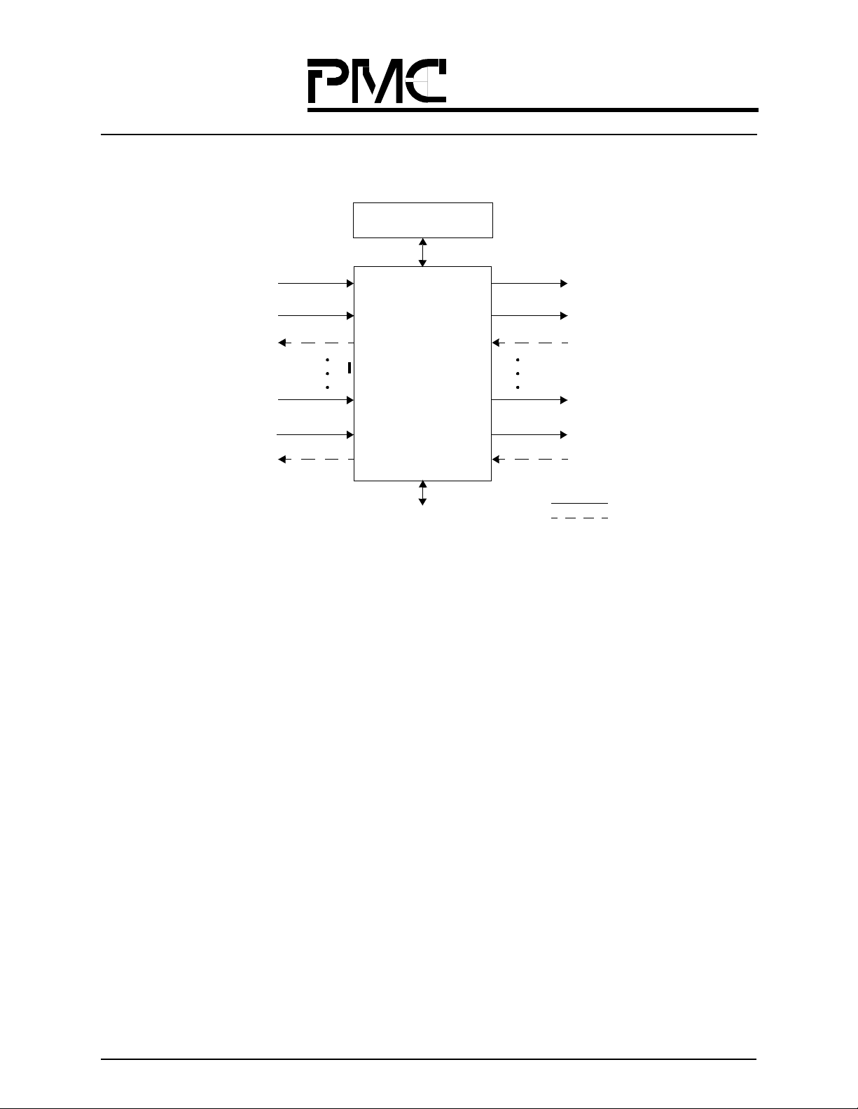
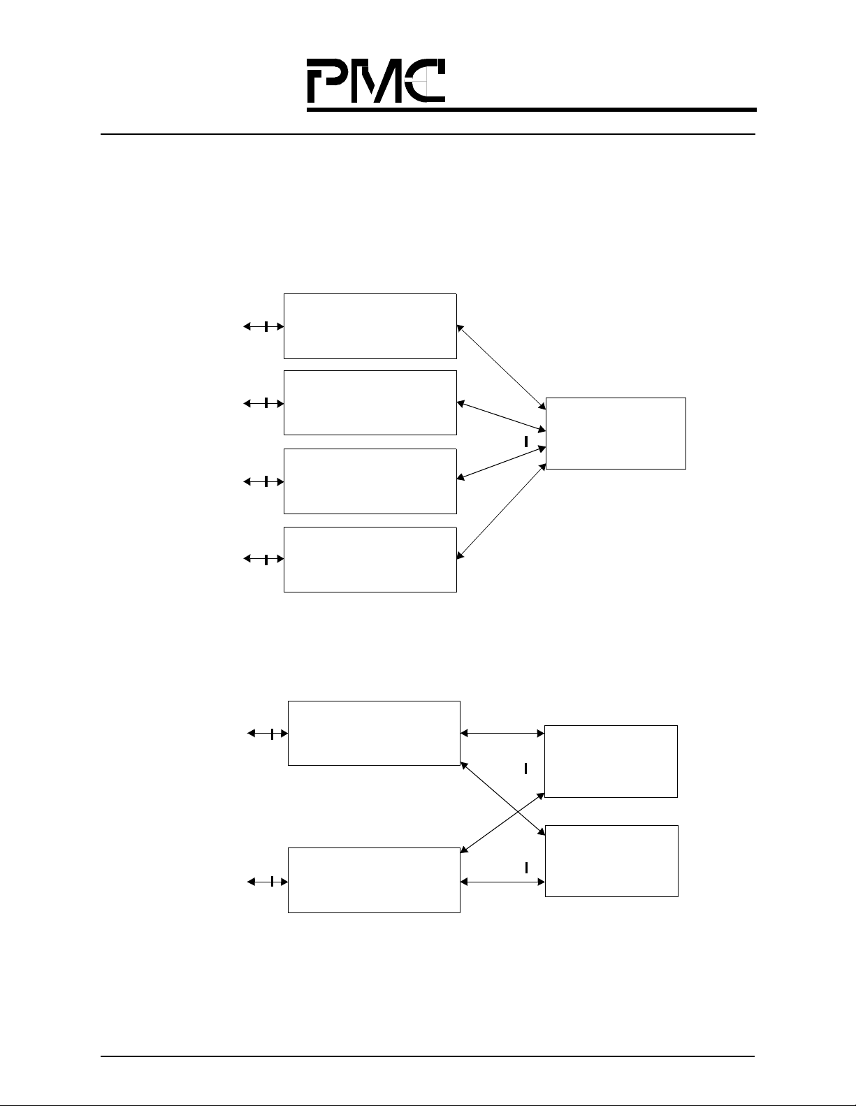
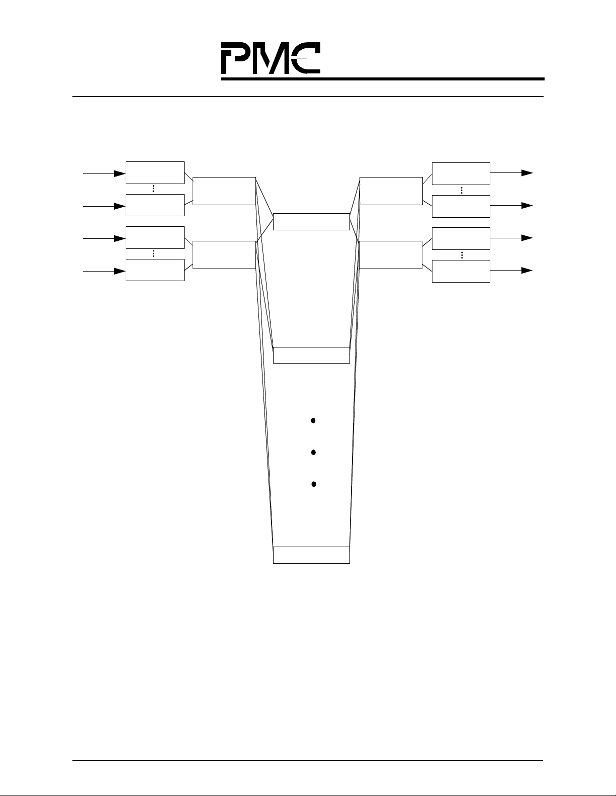
Figure 1 shows a QSE system block diagram.
Multicast SSRAM
(Optional)
SE_SOC_IN(0)
Data from QRTs or QSEs
Input Ports 0
NACK to QRTs or QSEs
SE_SOC_IN(31)
Data from QRTs or QSEs
Input Ports 31
NACK to QRTs or QSEs
QSE
PM73488
Host Interface
Figure 1. QSE Interface Block Di a gram
SE_SOC_OUT(0)
Data to QRTs or QSEs
Output Ports 0:3
NACK from QRTs or QSEs
SE_SOC_OUT(7)
Data to QRTs or QSEs
Output Ports 28:31
NACK from QRTs or QSEs
Key:
Control or Data Signals
Acknowledgment Signal
Long Form Data Sheet
15
Released
Datasheet
PMC-Sierra, Inc.
PM73488 QSE
PMC-980616 Issue 3 5 Gbit/s ATM Switch Fabric Element
1 HOW THE QSE FITS INTO YOUR SYSTEM
The QSE, together with the QRT, supports a wide range of high-performance ATM switching systems. These systems range in size from 5 Gbps to 160 Gbps. The systems can be developed to provide scalability with linear cost.
Another key feature of the QSE/QRT architecture is that it is exceptionally fault-tolerant, both in the switch fabric
and the UTOPIA interface.
This section contains a quick overvi ew of the QSE and several example applications:
• a 5 Gbps switch using PM73487s and a PM73488,
• a 10 Gbps switch using PM73487s and PM73488s,
• a switch architecture using PM73487s and PM73488s that scales from 5 Gbps to 20 Gbps,
• a switch architecture using PM73487s and PM73488s that scales from 5 Gpbs to 160 Gbps
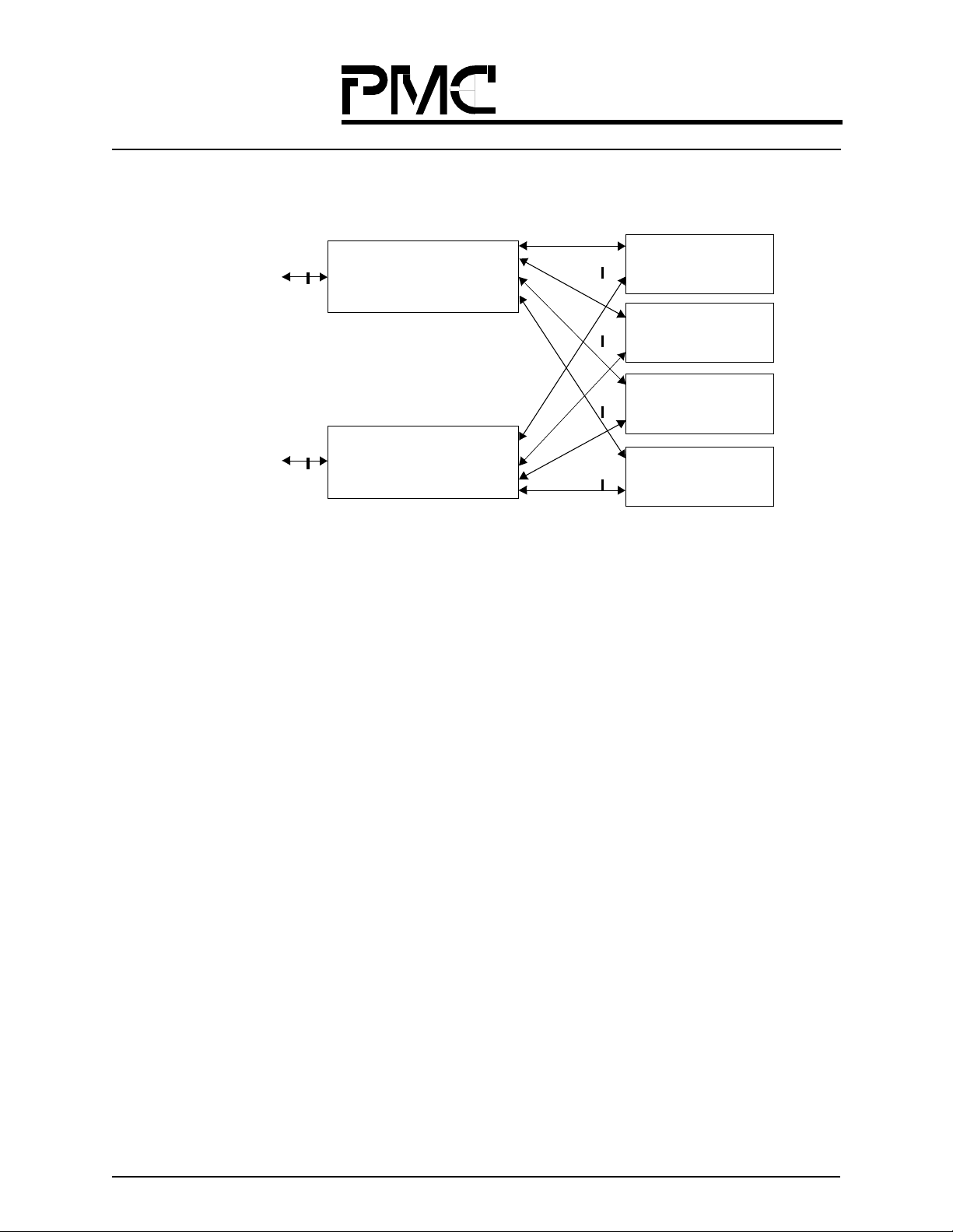
1.1 QSE System Overview
The QSE is switch element, combinations of which allows switch fabric implementations that span from 5 Gbps to
160 Gbps. The bandwidth of a singl e QSE is 5Gbps of sustainable bandwidth; the raw, or peak, bandwidth is 8Gbps.
(Thus the QSE has an in-buil t sp ee d-up factor of 8/5 = 1.6.)
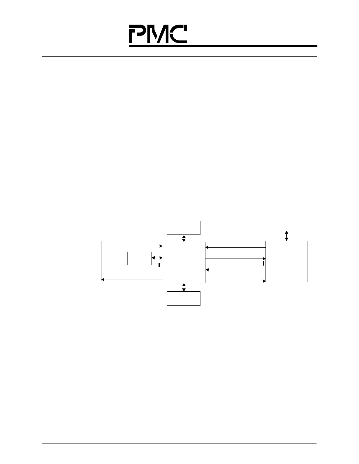
The QSE has 32 input ports and 32 output ports. Each port is a 66 MHz 6-bit interface, out of which 4 are data and 2
are control. Each port can be connected to another QSE or QRT. Figure 2 shows a QSE connected to a QRT.
Physical and/or
Adaptation Layers
Receive UTOPI A Level 2
Interface
Control
SSRAM
Transmit UTOPIA Level 2
Interface
Figure 2. QSE System Overview
Input Cell
SDRAM
QRT
(PM73487)
Output Cell
SDRAM
Receive Feedback
Receive Nibble Data
Transmit Nibble Data
Transmit Feedback
Multicast
SRAM
QSE
(PM73488)
Long Form Data Sheet
16
Released
Datasheet
PMC-Sierra, Inc.
PM73488 QSE
PMC-980616 Issue 3 5 Gbit/s ATM Switch Fabric Element
1.2 32 x 32 Switch Application (5 Gbps)
Figure 3 shows a basic 32 × 32 switch application (5 Gbps) using one QSE and eight QRTs.
622 Mbps
Aggregate
Receive UTOPIA
Level 2
622 Mbps
Aggregate
QRT #1
(PM73487)
Receive Input
QRT #8
(PM73487)
Receive Input
QRT #1
(PM73487)
×
4
QSE
4
×
(PM73488)
4
Transmit Output
×
×
4
QRT #8
(PM73487)
Transmit Output
622 Mbps
Aggregate
Transmit UTOPIA
Level 2
622 Mbps
Aggregate
Figure 3. 32 x 32 Switch Ap p lic ati on (5 G bps )
1.3 64 x 64 Switch Application (10 Gbps)
Figure 4 shows a 64 × 64 switch application (10 Gbps) using 6 QSEs and 16 QRTs. This application uses QSEs in a
3-stage fabric. This sized system can be implemented in a single 19 inch rack.
622 Mbps
Aggregate
Receive
UTOPIA
Level 2
622 Mbps
Aggregate
QRT #1
(PM73487)
Receive Input
QRT #8
(PM73487)
Receive Input
×
4
QSE
(PM73488)
× 16
QSE
(PM73488)
× 16
QSE
(PM73488)
4
×
QRT #1
(PM73487)
Transmit Output
QRT #8
(PM73487)
Transmit Output
622 Mbps
Aggregate
Transmit
UTOPIA
Level 2
622 Mbps
Aggregate
622 Mbps
Aggregate
Receive
UTOPIA
Level 2
622 Mbps
Aggregate
QRT #9
(PM73487)
Receive Input
QRT #16
(PM73487)
Receive Input
(PM73488)
4
×
QSE
Figure 4. 6 4 x 6 4 S witc h A pp lic at ion (1 0 G bp s)
Long Form Data Sheet
× 16
QSE
(PM73488)
× 16
QSE
(PM73488)
×
4
QRT #9
(PM73487)
Transmit Output
QRT #16
(PM73487)
Transmit Output
622 Mbps
Aggregate
Transmit
UTOPIA
Level 2
622 Mbps
Aggregate
17
Released
Datasheet
PMC-Sierra, Inc.
PM73488 QSE
PMC-980616 Issue 3 5 Gbit/s ATM Switch Fabric Element
1.4 5 Gbps to 20 Gbps Application Example - Seamless Growth
Figure 5 illustrates the modularity of the QSE and QRT architecture. A 5 Gbps system can immediately be created (as
shown in Figure 5), then be upgraded to 10 Gbps (as shown in Figure 6), or 20 Gbps (as shown in Figure 7 on page
19) with the QSE and the QRT. Since systems composed of the QSEs and QRTs are based on a single-stage switch
fabric, the per-port cost for each system will remain the same.
Eight
155 Mbps
Interfaces
Eight
155 Mbps
Interfaces
Eight
155 Mbps
Interfaces
Eight
155 Mbps
Interfaces
Port Card
• Two QRTs (PM73487s)
Port Card
• Two QRTs (PM73487s)
Switch Card
• One QSE (PM73488s)
Port Card
• Two QRTs (PM73487s)
Port Card
• Two QRTs (PM73487s)
Figure 5 . 5 Gbp s A TM Sw itc h Us in g 8 Q RTs, and 1 Q S E
Eight
155 Mbps
Interfaces
Eight
155 Mbps
Interfaces
Long Form Data Sheet
Figure 6. 10 Gb ps A TM Switch U sing 16 Q R Ts, a n d 2 Q S Es
• Two QRTs (PM73487s)
• Two QRTs (PM73487s)
Port Card 1
Port Card 8
Switch Card
•
• One QSE (PM73488)
•
•
Switch Card
• One QSE (PM73488)
18
Released
Datasheet
PMC-Sierra, Inc.
PM73488 QSE
PMC-980616 Issue 3 5 Gbit/s ATM Switch Fabric Element
Eight
155 Mbp s
Interface s
Eight
155 Mbp s
Interface s
Port Card 1
• Two QRTs (PM73487s)
•
Switch Card
• One QSE (PM73488)
Switch Card
• One QSE (PM73488)
•
•
Port Card 16
• Two QRTs (PM73487s)
Figure 7. 20 Gb ps A TM Switch U sing 32 Q R Ts, a n d 4 Q S Es
Switch Card
• One QSE (PM73488)
Switch Card
• One QSE (PM73488)
Long Form Data Sheet
19
Released
Datasheet
PMC-Sierra, Inc.
PMC-980616 Issue 3 5 Gbit/s ATM Switch Fabric Element
1.5 5 Gbps to 160 Gbps Application Example – LAN-to-WAN
A powerful application of the QRT and QSE devices is the creation of modules that can be used in a range of
switches with only the interconnection changing between different sizes. ATM switches from 5 Gbps to 160 Gbps
can be realized with only two unique cards. A port card has one QRT, and a switch card has two QSEs. The switch
fabri c consist s of thr ee stages, each wi th 32 QSEs (o r 1 6switch cards). To plan fo r future scalability, the middle stage
must be built-in upfront. This is a one- time cost. Then, in order to scale in 5 Gbps increments , one switch card and its
accompanying eight port cards should be added. Finer bandwidth scaling is possible by populating the additional
switch card with port cards as needed (in increments of 622 Mbps). With this switch fabric topology, scaling is possible up to 160 Gbps. Once the initial middle stage cost has been incurred, the per-port cost for 5 Gbps through
160 Gbps systems remains cons tant
PM73488 QSE
Port Card - One QRT
One UT O P I A
Level 2 Interfac e
QRT
(PM73487)
Figure 8 . 5 Gbp s to 16 0 Gb p s Sw itc h es M odeled Using O n ly Two C ar ds
Switch Card - Two QSEs
x32
x32
QSE
(PM73488)
QSE
(PM73488)
x32
x32
Long Form Data Sheet
20
Released
Datasheet
PMC-Sierra, Inc.
PM73488 QSE
PMC-980616 Issue 3 5 Gbit/s ATM Switch Fabric Element
622 Mbps
622 Mbps
Port Card #1
Rx Input
Port Card #8
Rx Input
Switch Card #17
Stage 1 Q SE
x2
Switch Card #1
Switch Card #2
Switch Card #17
Stage 3 QSE
x2
Port Card #1
Tx Output
Port Card #8
Tx Output
622 Mbps
622 Mbps
Switch Card #16
Figure 9 . 5 Gbp s A TM Sw itc h
Figure 9 shows a 5 Gbps ATM switch using 8 port cards (8 QRTs) and 17 switch cards (34 QSEs). The middle stage
is composed of 16 switch c ards. The 5 Gbps bandwith is achie ved by adding switch card #17 (whi ch is depicted using
two boxes: one stage 1 QSE and one stage 3 QSE), and eight port cards (each of which is depicted using two boxes:
one for the Rx input side, and one for the Tx output side). Lines between stage 1 and stage 2, and stage 2 and stage 3
switch cards represent two set s of w ires, one to each of the QSEs in the middle s t age switch ca rds.
Long Form Data Sheet
21
Released
Datasheet
PMC-Sierra, Inc.
PM73488 QSE
PMC-980616 Issue 3 5 Gbit/s ATM Switch Fabric Element
Figure 10 shows a 10 Gbps ATM s witch using 16 port cards (16 QRTs) and 18 switch cards (36 QSEs). Here, another
switch card and eig ht port cards have been added to the 5 Gbps switch depicted in Figure 9.
622 Mbps
622 Mbps
622 Mbps
622 Mbps
Port Card #1
Rx Input
Port Card #8
Rx Input
Port Card #9
Rx Input
Port Card #16
Rx Input
Switch Card #17
Stage 1 QSE
x2
Switch Card #18
Stage 1 QSE
x2
Switch Card #1
Switch Card #2
Switch Card #17
Stage 3 QSE
x2
Switch Card #18
Stage 3 Q SE
x2
Port Card #1
Tx Output
Port Card #8
Tx Output
Port Card #9
Tx Output
Port Card #16
Tx Output
622 Mbps
622 Mbps
622 Mbps
622 Mbps
Figure 10. 10 Gbps ATM Switch
Long Form Data Sheet
Switch Card #16
22
Released
Datasheet
PMC-Sierra, Inc.
PM73488 QSE
PMC-980616 Issue 3 5 Gbit/s ATM Switch Fabric Element
Figure 11 shows a 15 Gbps ATM switch using 24 port cards (24 QRTs) and 19 switch cards (38 QSEs).Here, once
again, another s witch card and eight port cards hav e bee n adde d
622 Mbp s
622 Mbp s
622 Mbp s
622 Mbp s
622 Mbps
622 Mbps
Port Card #1
Rx Input
Port Card #8
Rx Input
Port Card #9
Rx Input
Port Card #16
Rx Input
Port Card #17
Rx Input
Port Card #24
Rx Input
Switch Card #17
Stage 1 Q SE
x2
Switch Card #18
Stage 1 Q SE
Switch Card #19
Stage 1 QSE
x2
x2
Switch Card #1
Switch Card #2
Switch Card #17
Stage 3 Q SE
x2
Switch Card #18
Stage 3 QSE
x2
Switch Card #19
Stage 3 Q SE
x2
Port Card #1
Tx Output
Port Card #8
Tx Output
Port Card #9
Tx Output
Port Card #16
Tx Output
Port Card #17
Tx Output
Port Card #24
Tx Output
622 Mbps
622 Mbps
622 Mbps
622 Mbps
622 Mbps
622 Mbps
Figure 11. 15 Gbps ATM Switch
Long Form Data Sheet
Switch Card #16
23
Released
Datasheet
PMC-Sierra, Inc.
PM73488 QSE
PMC-980616 Issue 3 5 Gbit/s ATM Switch Fabric Element
Figure 12 shows a 20 Gbps ATM switch composed of 32 port cards (32 QRTs) and 20 switch cards (40 QSEs). By
adding additional sets of a switch card and eight port cards in the same manner, this system c an scale up to 160 Gbps.
622 Mbps
622 Mbps
622 Mbps
622 Mbps
622 Mbps
622 Mbps
622 Mbps
622 Mbps
Port Card #1
Rx Input
Port Card #8
Rx Input
Port Card #9
Rx Input
Port Card #16
Rx Input
Port Card #17
Rx Input
Port Card #24
Rx Input
Port Card #25
Rx Input
Port Card #32
Rx Input
Switch Card #17
Stage 1 QSE
x2
Switch Card #18
Stage 1 QSE
x2
Switch Card #19
Stage 1 Q SE
x2
Switch Card #20
Stage 1 Q SE
x2
Switch Card #1
Switch Card #2
Switch Card #17
Stage 3 QSE
x2
Switch Card #18
Stage 3 Q SE
x2
Switch Card #19
Stage 3 QSE
x2
Switch Ca rd #20
Stage 3 Q SE
x2
Port Card #1
Tx Output
Port Card #8
Tx Output
Port Card #9
Tx Output
Port Card #16
Tx Output
Port Card #17
Tx Output
Port Card #24
Tx Output
Port Card #25
Tx Output
Port Card #32
Tx Output
622 Mbps
622 Mbps
622 Mbps
622 Mbps
622 Mbps
622 Mbp s
622 Mbps
622 Mbps
Figure 12. 20 Gbps ATM Switch
Long Form Data Sheet
Switch Card #16
24

Released
Datasheet
PMC-Sierra, Inc.
PM73488 QSE
PMC-980616 Issue 3 5 Gbit/s ATM Switch Fabric Element
2 THEORY OF OPERATION
Multiple PM73488 QSEs can be combined to build a scalable switch fabric. The QSE switches data in the form of
118 nibble cells. The QSE has 32-input ports and 32 output ports, each containing a nibble-wide data interface, an
SOC signal, and a backp r es s ure/data-acknowledge signal.
Groups of 1, 2, 4, 8, 16, or 32 ports can be internally configured to act as a singl e a ggregate port (also called gang) for
unicast traffic. For multicast traffic, inputs and outputs can be grouped together in groups of 1, 2, or 4 ports. The input
multicast grouping mode, output multicast grouping mode, and the unicast grouping modes do not need to be the
same. Also, the QSE can be configured as a single 32 input × 32 output switch
The cell flow through the QSE has two separate data paths; one path for unicast cells and another path for multicast
cells. Unicast cells are routed from one end of the switch fabric to the other end in a single cell time. In other words,
no unicast cells are ever stored in the switch fabric. Unicast cells are stored only at the ingress and egress of the
switch fabric. Multicast cells are routed in a store-and-forward manner. Each QSE can store up to 64 multicast cells.
The QRT used as an interface to a switch fabric constructed with QSEs allows the construction of an ATM switc h up
to 160 Gbps.
A diagram of the QSE cell flow is shown in Figure 13. The unicast cell flow contains a routing stage that uses routing
information from the cell header to determine the output group. The multicast cell flow contains an interface to an
external SSRAM that contains the Multicast Port Vector (MPV) information for routing cells to multiple output
groups.
Forward Cell Flow
Backpressu r e / Ac k F lo w
Miscel laneous Signals
Phase Aligners
and
Receive SE_D_IN
and SE_SOC_IN
BP_ACK
Drivers
External SSRAM
Multicast
Path
Data
Driver s
Arbiter
Phase Aligners
and Rece iv e
BP_ACK_IN
Unicast Routing and
Distribution Path
Figure 13. Basic QSE Flow
Long Form Data Sheet
25

Released
Datasheet
PMC-Sierra, Inc.
PMC-980616 Issue 3 5 Gbit/s ATM Switch Fabric Element
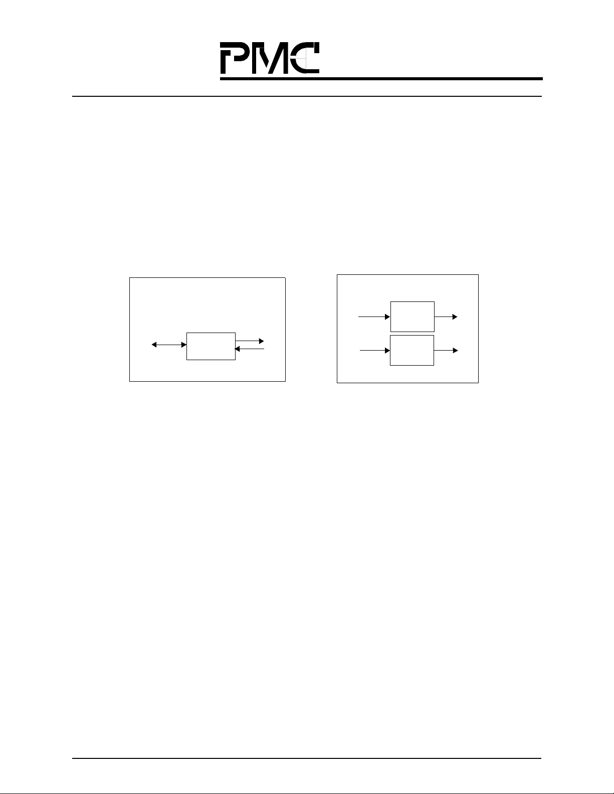
2.1 Phase Aligners
Phase aligners aid in constructing large systems. Clock information is recovered from the data sent to each QSE
switch fabric port. Phase aligners are used on the BP_ACK_IN(31:0), SE_SOC_IN(31:0), and SE_D_IN(31:0, 3:0)
signal lines. Since there is no setup or hold time requirements on these signals, the overall clock distribution scheme
within the system can be simplified. Howev er, overall system jitter and skew between signals on the s ame switch fabric data port must still be managed.
2.2 Data Drivers
Another aid to constructing large systems is an elastic store at each QSE input data port. The data elastic store allows
data arriving from different ports to be offset by up to a maxi mu m of e ight clock cycles. The internally generated and
software programmable local CELL_START signal marks the end of an 8-clock-period window within which the
SOC marker on each of the SE_SOC_IN(31:0) lines must arrive.
2.3 Unicast Routing and Distribution
Each of the 32 nibble-wide inputs is connected to an output by a crossbar. This crossbar is transparently controlled by
the cell’s routing tag, which specifies the input-to-output connection. In the event of a conflict for an output port,
higher priority cells are given preference over lower priority cells. There are three unicast cell priorities: high,
medium, and low.
PM73488 QSE
The gang of 32, also known as distribution mode, is a special unicast routing mode in which incoming unicast cells
are routed to outputs us ing PMC’s patented congestion-minimization (Evil Twi n Swi tching) algorithm. In this mode,
no routing information is used from the cell’s routing tag.
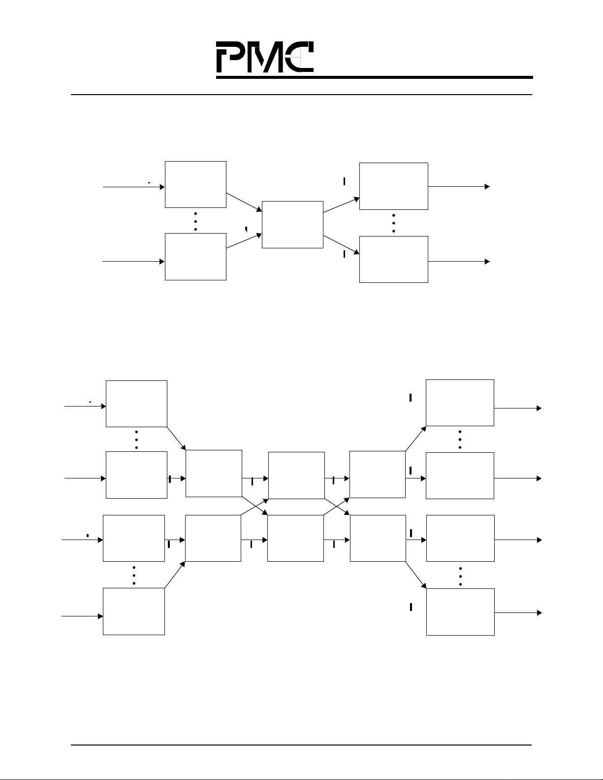
Depending on the gang mode, the QSE will need a number of routing bits to determine the output gang of a unicast
cell. For ex am ple, in gang mode of four, there are eigh t output gangs, thus three routing bits are required for selecting
the QSE. However, in distribution mode no routing bits are needed. The routing bits are taken from the head of the
routing tag and are then shifted back in at the tail (which preserves header parity). This allows the next set of routing
bits to be al ways accessible at the sam e spot in the tag, nam ely the head. The cell routing tag is broken int o eight nibbles, namely TAG_0 through TAG_7.
Figure 14 on page 27 shows the tag rotation for gang mode of four (three routing bits are used by the QSE from
TAG_0 and then shifted back in at the tail of TAG_7). TAG_0 is broken up and part of it ended up at the end of
TAG_7 (shown by the white area in Figure 14 on page 27). As a result, all the other tags (TAG_1 through TAG_7)
also get broken up and shifted (as shown by the light and dark gra y areas of Figure 14 on page 27).
Long Form Data Sheet
26
Released
Datasheet
PMC-Sierra, Inc.
PMC-980616 Issue 3 5 Gbit/s ATM Switch Fabric Element
PM73488 QSE
32
10
TAG_0
TAG_1
TAG_2
TAG_3
TAG_4
TAG_5
TAG_6
TAG_7
Figure 14. Routing Bits Rotation for Unicast Traffic, Gang Mode of Four
2.4 Multicast Cell Flow
There are 64 internal cell buffers for multicast traffic. These buffers are shared among three multicast priorities: high,
medium, and low. These 64 buffers are grouped into two sets of 32-cell buffers each. One set is dedicated to ports 0
to 15, the other set to ports 16 to 32.
Bit Mapping
32
TAG_0
TAG_1
TAG_2
TAG_3
TAG_4
TAG_5
TAG_6
TAG_7
10
A multicast queue engine dynamically allocates the cell buffers to incoming multicast cells. Each cell is buffered
until it can be sent out on all output ports to which it should be routed. These output ports are designated by a Multicast Group Vect or (MGV) that is associated with a Multicast Group Index (MGI) carried by each multicast cell. Each
QSE holds multicast MGVs in an MGV RAM. The QSE has internal RAM to support up to 128 MGVs. This support
can be extended up to 256K MGVs by using an external MGV RAM.
Each multicast cell cont ains the RAM address of the MGV it is supposed to use. When a multicast cell is receive d , its
MGV is fetched from RAM and copied to the MULTICAST_QUEUE_COMPLETION register. The
MULTICAST_QUEUE_COMPLETION register tracks to which QSE ports the cell needs to be sent before its cell
buffer can be cleared. In a multistage QSE fabric, each multicast cell will look up MGVs at each QSE. The MGV’s
sequence determines which output ports will finally receive the cell . T he MGV str ucture allows software to create an
optimal distribution tree for each multicast cell.
Multicast operation can be bes t understood by considering the QSE multicast path as two separate engine s; the multicast queue engine and the multicast dequeue engine. The multicast queue engine queues cells into the multicast cell
buffers (of which there are 64), and issues backpressure on the BP_ACK_OUT(31:0) lines. The multicast dequeue
engine selects and dequeues cells from the buffers for output ports as guided by the backpressure received on the
BP_ACK_IN(31:0) lines.
Long Form Data Sheet
27
Released
Datasheet
PMC-Sierra, Inc.
PMC-980616 Issue 3 5 Gbit/s ATM Switch Fabric Element
2.4.1 Multicast Queue Engine
The multicast queue engine associates input ports with cell buffers, computes backpressure for the input ports, and
stores incoming cells into the buffers. In doing so, it guarantees:
• No input port will have more than three cells pending in the QSE — this can be changed to allow four
pending cell s by setting the “Allow 4 Bits Per Port” bi t (bit 1) in the BP CONTROL register.
• No input port will have more than two high-priority cells pending.
• The sum of low- and medium-priority cells pending from any single input port will be less than 2.
In addition, the queue engine allows buffers to be reserved for high-priority cells or high/medium-priority cells. This
is controlled by bits 2 and 3 of the BP_CONTROL_REGISTER (refer to section 9.3.29
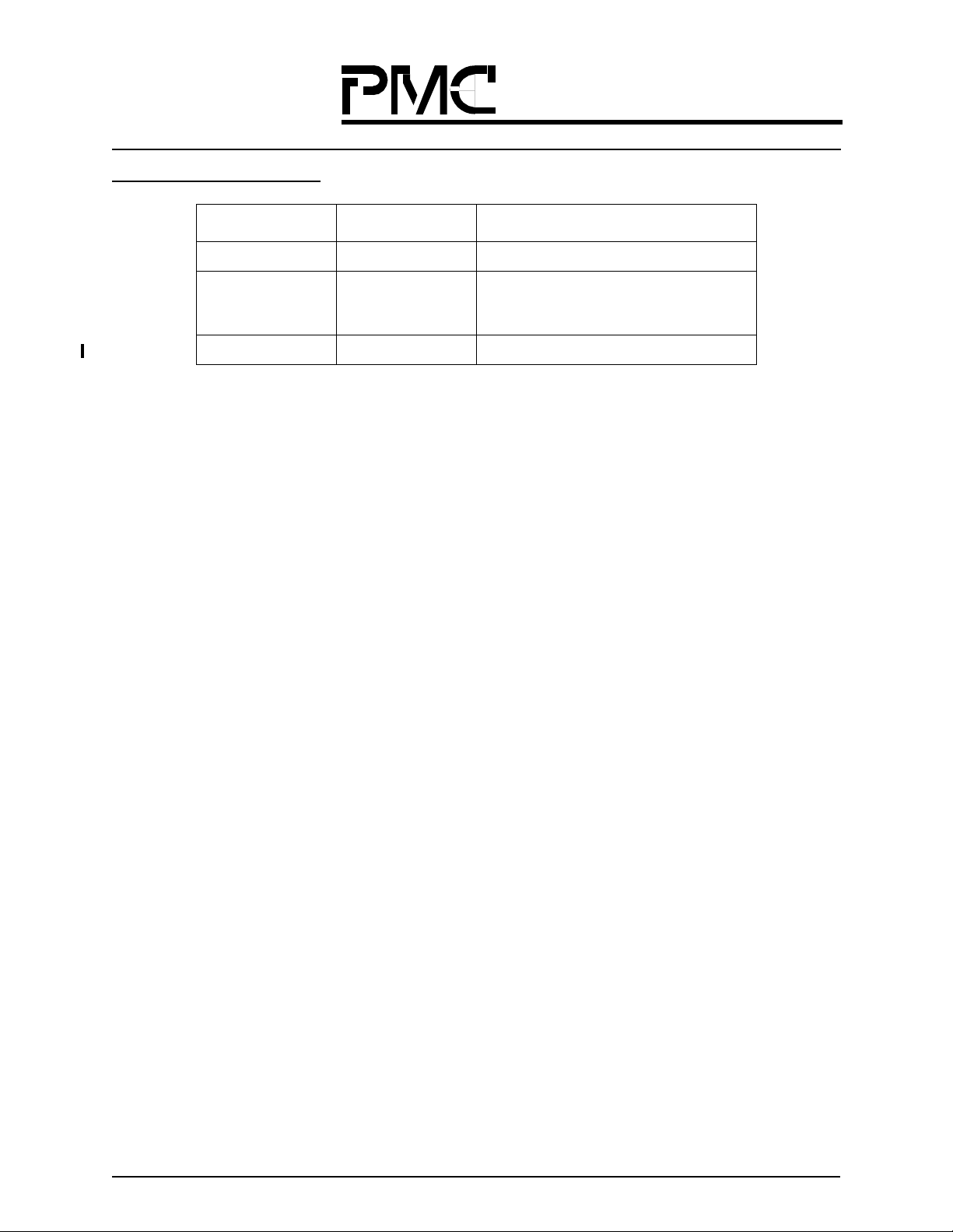
“BP_CONTROL_REGISTER” on page109). The four possible combinations for these two bits are listed in Table 1.
The multicast queue engine will compute backpressur e fo r the preceding QSE/QRT to ensure the constraints listed in
Table 1 are sati sfied. The same reservation policy applies to both sets of 32 buffers.
T able 1. BP_CONTROL_REGISTER; Threshold Control Bits for Each Set of 32 Buffers
Bit 3 Bit 2 Description
PM73488 QSE
00 • Four buffers are res erv ed for high-priority cells.
• Four buffers are reserved for high- or me diu m -priority c ell s.
• All other buffers can be used by any cell.
0 1 • Four buffers are res erv ed for high-priority cells.
• All other buffers can be used by any cell.
1 0 • Eight buffers are re served for high- or m edium-prior ity cells.
• All other buffers can be used by any cell.
1 1 • All buffers can be used by any cell.
After t he MGV ad dress f or th e cell e n ters t he Q S E , th e MGV a s so ciate d w it h t hat ce ll i s f e tched a nd lo aded in to the
QUEUE_COMPLETION_REGISTER (an internal register) as soon as possible.
2.4.2 Multicast Dequeue Engine
In each cell time, the multicast dequeue engine selects one multicast cell for each of the 32 output ports. In effect, all
multicast cells wanting to go to a particular output port arbitrate among themselves to select the most appropriate
port. Arbitration occurs independently for all 32 ports. The cells winning the internal multicast arbitration then compete w i th th e inc oming u nicast cells f o r a ccess to th e out p ut p or t s . Mu ltica s t ar b it r ation w inne rs ar e chos en to s a tisfy
the following cond itions in this sequence:
• Obey backpress ure from the down stream QSE or QRT. Only cells with the allowed priori ties will take part
in arbitration.
• Higher prio r ity cells win over lower priority cells.
• Cells th at came in ea r lier win ov e r ce lls that came in la te r (if th e y h av e th e sa me prior i ty ) .
• If multiple cells have the same priority and came in s imultaneously, cells from a random input gang group
will be selected.
• If multiple cells have the same priority, came in simultaneous ly, and belong to the same input gang group,
the cell with the lowest port number will be selected.
• Ties are broken randomly.
Long Form Data Sheet
28

Released
Datasheet
PMC-Sierra, Inc.
PMC-980616 Issue 3 5 Gbit/s ATM Switch Fabric Element
This arbitration occurs among all cells in the cell buffers and occurs for all 32 ports. In effect, arbitration occurs for
output ports in sequence, starting with cells arbitrating for port 0, then for port 1, and continuing on until port 31
(even though the actual implementation uses a parallel algorithm).
Multic ast cells t hat h ave w on t his a rbitra tion then comp ete w ith un icas t cell s fo r acces s to t he ou tput ports . In this
contention, the cell with the highest priority wins and ties are broken randomly according to the programmable ratio
set in the UC/MC_FAI RNESS_REGISTER (refer to section 9.3.6 “UC/MC_FAIRNESS_REGISTER” on page 97).
All these operations are optimized so that, in the absence of congestion, it is possible for a multicast cell to leave the
QSE in the cell time immediately after it arrived.
As mentioned before, the queue completion register (32-bit vector) indicates the outputs to which each multicast cell
needs to go. As a cell goes out on its desired outputs, the appropriate bi ts in the queue completion regis ter are cleared.
When all bits in the queue completion register have been cleared, the cell is deleted from the internal buffers and the
buffer is reused for new incoming traffic.
PM73488 QSE
Long Form Data Sheet
29
Released
Datasheet
PMC-Sierra, Inc.
PM73488 QSE
PMC-980616 Issue 3 5 Gbit/s ATM Switch Fabric Element
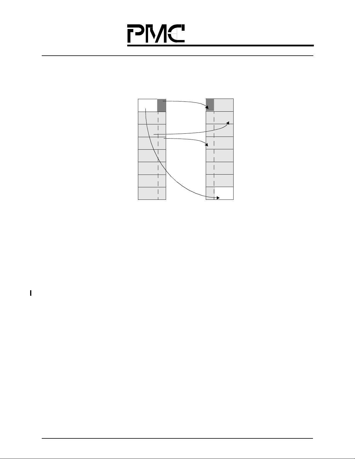
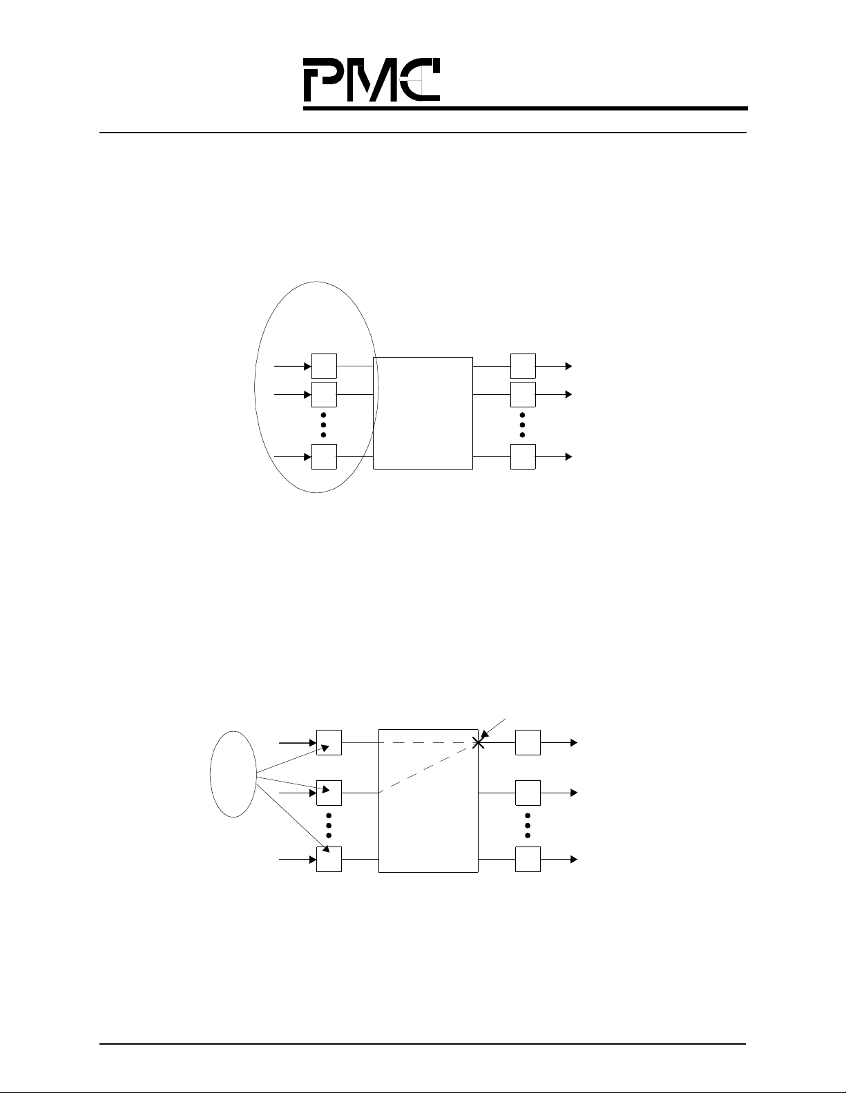
Figure 15 shows an example of a high-priority cell preempting a cell in the multicast queue, and the resulting bit settings in the MULTICAST_QUEUE_COMPLETION_REGISTER (an internal register). (For the sake of simplicity,
only 8 of the 32 outputs, and eight bits of the MGV_REGISTER (refer to section 9.3.4
“MULTICAST_GROUP_VECTOR_REGISTER” on page 96) and
MULTICAST_GROUP_COMPLETION_REGISTER (an internal register) are shown.)
Multicast Group Vector (MGV)
(Specifies where cells should be sent.)
MULTICAST_QUEUE_COMPLETION_REGISTER
(Recor ds if the c ells arrived at the destinations
indicated in the
MULTICAST_GROUP_VECTOR_REGISTER.)
0
0
0
1
0
0
1
0
0
7
This bi t is not set since a hig her priority
cell was output on Output(3 ), preempting
the cell in the multicast qu eue.
High-Priority
Cell
CELL_H
Multicast Queue
CELL_M
0
0
0
1
1
0
1
0
7
0
Output(0)
Output(1)
Output(2)
CELL_M
Output(3)
CELL_H
Output(4)
Output(5)
CELL_M
Output(6)
Output(7)
Figure 15. E x amp le of M ultica s t C ell H an dl ing in th e Q SE
2.5 Arbiter
The arbiter selects between unicast cells and multicast ce lls contending for the same output port. Higher priority ce lls
are given preference over lower priority cells. If a multicast cell and unicast cell have the same priority, one cell is
randomly chosen. The random choice can be biased in favor of either unicast cells or multicast cells at different
points in the switch fabric by using the UC/MC_FAIRNESS_REGISTER (refer to section 9.3.6 “UC/
MC_FAIRNESS_REGISTER” on page 97). In general, unicast cells should be favored at later stages in the switch
fabric. Favoring unicast cells is necessary in multiple-stage switch fabrics since unicast cells are routed in a cutthrough fashion and multicast cells are routed in a store-and-forward fashion. As such, a unicast cell becomes more
“valuable” as it proceeds further in the switc h fabric, since it did so at the expense of other cells.
Long Form Data Sheet
30

Released
Datasheet
PMC-Sierra, Inc.
PMC-980616 Issue 3 5 Gbit/s ATM Switch Fabric Element
For example, co nsider a congested 3-stage switch fabric w h ere unic ast cells and multicast cells of equal priorities collide at each stage in the fabric, without any biasing. A unicast ce ll must make it from ingress to egress in one cell time
and the chances of doing so would be a little more than (1/2)
50% chance of advancing to the next stage in the switch fabric.
2.6 BP_ACK Drivers
The BP_ACK_OUT(31:0) lines are used to send information from a QSE to upstream QSEs or QRTs. Thes e lines are
used to send two types of information:
• Backpressure information (for unicast cells).
• Transmit acknowledge information (for multicast cells).
Backpressure information is sent for multicast cells. This information indicates to an upstream QRT or QSE if the
QSE c an acc ep t a not her mu ltic ast ce ll i n t he nex t ce ll time . Ba ckpr ess ure in form atio n als o i ndica te s w hat mul tic ast
cell priorities the QSE can accept.
Cell transmit acknowledge information is sent for unicast cells. This information signals whether or not the unicast
cell transmitted in the current cell time made it to its destination QRT. If the cell makes it to the destination QRT, an
Acknowledgment (ACK) is se nt. If the cell has been dropped in the swi tch fabric, informati on is se nt back indicating
if the cell was dropped internally Mid Switch Negative Acknowledgment (MNACK) or at the output of the switch
fabric Output Negative Acknowledgment (ONACK). The MNACK and ONACK is used by the QRT to determine
when to retry sending the given cell.
3
= 12.5%. However, each multicast cell would have a
PM73488 QSE
2.7 Interdevice Interconnectability
All input and output ports can be c onfigured in groups of four to directly connect to either QRT devices or other QSE
devices. This allows considerable flexibility in the switch fabric types and sizes that can be constructed using the
entire PMC chip set.
2.8 Network Topologies and the Speed up Fa ctor (SF)
For many switch fabric architectures using the QSE, a single metric called the Speedup Factor (SF) allows comparison of different network topologies, which is independen t of tr affic load and type. The SF also al lows for predictions
about the network performance.
Before describing the SF metric, we will briefly discuss the network philosophy and the different network topolo gies.
Long Form Data Sheet
31
Released
Datasheet
PMC-Sierra, Inc.
PM73488 QSE
PMC-980616 Issue 3 5 Gbit/s ATM Switch Fabric Element
2.8.1 Network Philosophy
Given current technology, to scale through 160 Gbps, a network must be distributed and use buffers at the network
inputs and outputs. In an id eal world, crossbar s of any arbitrary size could be built to provide connectivity for the net-
work inputs and outputs. Additionally, there would be a central “brain”, or global arbiter, to control the input buffers
and schedule cells optimally for routing in the network, as shown in Figure 16.
Global
Arbiter
“Perfect
Crossbar”
Input
Buffers
Figure 16 . Id ea l D is trib u te d Ne tw or k
Output
Buffers
Unfortunately, given real con st r aints, it is not possible to have a global arbiter wired to each input that has knowledge
of all cells in the system, and can quickly make optimal decisions about routing. Thus, each input must make decisions using knowledge local to its buffers. This results in the possibility of collisions at the network outputs, even
though it is a “perfect” crossbar, as shown in Figur e 17.
Output
Collision
Local
Arbiters
“Perfect
Crossb ar”
Input
Buffers
Long Form Data Sheet
Figure 17. More Realistic Distributed Network
Output
Buffers
32

Released
Datasheet
PMC-Sierra, Inc.
PM73488 QSE
PMC-980616 Issue 3 5 Gbit/s ATM Switch Fabric Element
Replacing the idealized crossbar with a buildable, traditional Banyan network increase s the possibil ity of internal network collisions, as shown in Figure 18. Given a particular Banyan network, one can always find a large class of traffic patterns that will cause many internal collisions. For large Banyan networks, the collision problem is greatly
increased.
Internal
Collisions
Local
Arbiters
Banyan
Input
Buffers
Figure 18. “Large” Distributed Network (Will not Work Well with Banyan Alone)
Output
Collision
Output
Buffers
To reduce internal collisions in the traffic-dependent Banyan networks, the QRT/QSE network adds a distribution/
randomizing network (shown in Figure 19) that uses a patented intelligent configuration algorithm, known as Evil
Twin Sw itch in g. The algor ith m (des cri bed in section 2.8.3 “Speedup Factor (SF)” on page 36) allows lower-bound-
ing the network performance, independent of traffic patterns.
Internal
Collisions
Local
Arbiters
Input
Buffers
Figure 19. High-Level QRT/QSE System
Long Form Data Sheet
Intelligent
Configuration
Algorithm
Banyan
and
Randomizer
Output
Buffers
33

Released
Datasheet
PMC-Sierra, Inc.
PM73488 QSE
PMC-980616 Issue 3 5 Gbit/s ATM Switch Fabric Element
To overcome the inefficiencies caused by collision in the network, the fabric must be run at a rate greater than line
rate. The speedup factor is the minimum rate necessary to guarantee that the network is no longer the system bottleneck. Note that in this case, the network efficiently moves data from the input to the output buffers, and the switch
performs similar to a purely output buffered switch.
2.8.2 Network Definition
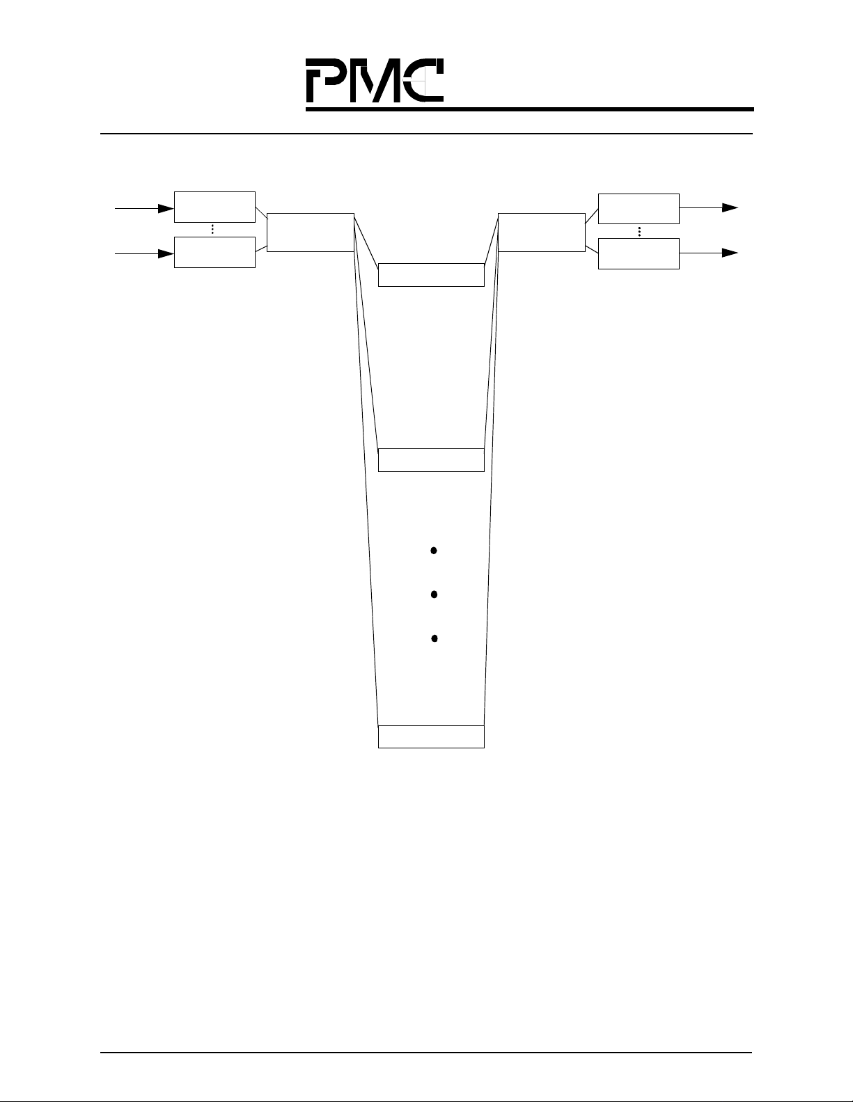
A large range of switch fabrics can be described as follows: with the following notation: “p” refers to the number of
fabric planes, and “x,” “y,” and “z” refer to the routing tag size necessary to make routing decisions in the Banyan
section of the net wo rk to route cells to the correct out put port. This is summarized as follows:
(z)xp — 1-stage network
(y,z)xp — 3-stage network
Hence, the (3) × 1 network shown in Figure 20 refers to a single switch stage, and three routing bits are required to
select from one of the eight output port groupings. (Recall that the QSE has 32 output ports that can be configured in
groups of 1, 2, 4, 8, 16, or 32. In Figure 20, they are configured in groups of four. The input and output buffers provided by the QRT have four input ports and four output ports to the switch fabric, and are logically broken into the
input half of the QRT (IRT) and output half of the QRT (ORT) for convenience.
x4
x4
ORT
622 Mbp s
UTOPIA
622 Mbps
UTOPIA
IRT
x 4
x 4
Figure 20. (3) x 1 - 5 G bps Sys te m
QSE
The (5) × 4 network sh own in Figure 21 is an example of a network with four parall el planes. It demonstrates t he flexibility allowed because the QRT has four input and output ports. In this case, randomization is performed in the IRT .
622 Mbps
UTOPIA
IRT
Randomizer
Figure 21. (5) x 4 - 20 Gbps System
x 4
x 1
QSE
x 1
x 4
ORT
622 Mbps
UTOPIA
Long Form Data Sheet
34

Released
Datasheet
PMC-Sierra, Inc.
PM73488 QSE
PMC-980616 Issue 3 5 Gbit/s ATM Switch Fabric Element
In Figure 22, the first stage of QSEs is configured to provide the required randomization, and the next two switch
stages route the cells to the final port destination. The second QSE stage needs only t o make an “up” or “down” deci-
sion requirin g a singl e routing bi t, while the third QSE sta ge needs to s elec t between ei ght QRTs , requiri ng three rou ting bits.
622 Mbps
UTOPIA
IRT
x 4
x 4
Randomizer
x16 x 16
QSE
QSE
x 16 x 16
Figure 22. (1,3) x 1 - 10 Gbps System
QSE
QSE
QSE
QSE
x 4
x 4
ORT
622 Mbps
UTOPIA
Long Form Data Sheet
35

Released
Datasheet
PMC-Sierra, Inc.
PM73488 QSE
PMC-980616 Issue 3 5 Gbit/s ATM Switch Fabric Element
2.8.3 Speedup Factor (SF)
If the traffic pattern presented to a particular Banyan network results in many internal collision, a shuffling pattern
exists that has been proven to result in few internal collisions. Although a purely random reshuffling results in good
behavior, we can lower-bound network performance by using randomization along with the Evil Twin Switching
algorithm as shown in Figure 23. This algorithm is as follows: randomly choose a configuration, route data, choose
the dual or Evil Twin Switching configuration, route data, and repeat. This algorithm minimizes the number of internal collisions. In 3-stage networks, the first stage of the QSEs provide this functionality.
ONACK
Output
Buffers
Randomly
Choose
Configuration
Send Data
Choose the
Dual or
Evil Twin
Switching
Configuration
Send Data
MNACK
Local
Arbiters
Input
Buffers
Figure 2 3. Ran do m iz er (w ith E vil Twin S w itc hin g A lgorithm)
Intelligent
Configuration
Algorithm
and
Randomizer
Banyan
Even with a perfect crossbar for a network, there are still output collisions, and despite the Evil Twin Switc h ing algorithm, there are still internal collisions (albeit fewer). Thus, multiple routing attempts must be made per cell to yield
full throu ghput. This can be a ccomplished by running the switch fabric at a faster clock rate than the buffer ing logic.
Local
Arbiters
Input
Buffers
Long Form Data Sheet
Figure 24. Network Needs to be Run Faster than the Line Rate
Output
Buffers
36

Released
Datasheet
PMC-Sierra, Inc.
PM73488 QSE
PMC-980616 Issue 3 5 Gbit/s ATM Switch Fabric Element
The chance for inter nal collisions increases as the networ k load increases, and the exact behavi or varies with network
topology. An example of this behavior is shown in Figure 25 and the SF is inferred from the limiting case where the
network is fully loaded.
1
PA = Probability
of cell accept ance
PA
01
Figure 25. Definition of the Speedup Factor
Network To pol og y
Load
Limiting case,
where t he Lo ad = 1,
SF = 1/P
A
Given this notion of SF, “how much faster is fast enough?” Theoretic al models and simulations can answer that question. Given that the switch fabric can be run at a certain clock rate relative to th e buffe ring logic, we can know which
networks to choose to prevent the network from becoming a bot tleneck.
2.0
Speedup
Factor
(SF)
1.0
622 Mbps
Networ k S ize
Figure 26 . H o w to Use th e SF to S ele ct Fa v orab le Ne two rk s
160 Gbps
Fabric Rate
Table 2, Table 3 show all of the 1-, 3-stage network topologies requiring an SF of less than 1.6, which is the maximum speedup allowed by the actual implementation.
Long Form Data Sheet
37

Released
Datasheet
PMC-Sierra, Inc.
PMC-980616 Issue 3 5 Gbit/s ATM Switch Fabric Element
Table 2. Speedup Factor (1-Stage Networks)
PM73488 QSE
Network
(3) × 1 5 1.22 1
(4) × 2 10 1.36 2
(5) × 4 20 1.57 4
Table 3. Speedup Factor (3-Stage Networks)
Network
(1,3) × 110 1.28 6
(1,4) × 220 1.41 12
(2,3) × 120 1.32 12
(2,4) × 240 1.46 24
(3,3) × 140 1.39 24
(3,4) × 280 1.53 48
(4,3) × 180 1.49 48
Size
(Gbps)
Size
(Gbps)
Speedup Factor
(SF)
Speedup Factor
(SF)
Number
of QSEs
Number
of QSEs
Long Form Data Sheet
38

Released
Datasheet
PMC-Sierra, Inc.
PMC-980616 Issue 3 5 Gbit/s ATM Switch Fabric Element
PM73488 QSE
3 EXTERNAL PORT DESCRIP TIONS
3.1 Switch Fabric Port and Interface Description
Each port is a 6-bit interface consisting of:
• a nibble-wide data interface (SE_D_IN and SE_D_OUT),
• an SOC signal (SE_SOC_IN and SE_SOC_OUT), and
• a backpressure/data acknowledge signal (BP_ACK_IN and BP_ACK_OUT).
3.1.1 SE_SOC Encodings
The SE_SOC encodings (SE_SOC_IN(31:0), SE_SOC_OUT(7:0)) provide guaranteed transitions and SOC encodings.
The SE_SOC signals carry a repeating four “0s” and four “1s” pattern to guarantee transitions required by the phase
aligner. The SOC signal on data lines associated with an SE_SOC line is indicated by a break in this repeating pattern. The SOC is a single “1” followed by five “0s”. Figure 27 shows the guaranteed transitions. Figure 28 provides
an expanded view of the signal transitions and the first nibble after the SOC pulse (nibble #0) corresponds to nibble
“0” in Table 5 on page 40.
SE_CLK
SE_SOC
Magnified SE_CLK
SE_DATA
Magnified SE_SOC
Four 1s Four 0s Five 0s Four 1s Four 0s Four 1s Four 0s
Start Of Cell Pulse
Figure 27. SE_SOC Encodings
Tsesu Tseho Tsesu
#115. #116 #117 #0 #1
Four 1s Four 0s One Five 0s Four 1s
Start Of Cell Pulse
Figure 28. Expanded SE_SOC Encodings
Long Form Data Sheet
39

Released
Datasheet
PMC-Sierra, Inc.
PM73488 QSE
PMC-980616 Issue 3 5 Gbit/s ATM Switch Fabric Element
3.1.2 Data Cell Format
The regular cell format is shown in Table 5.
Table 5. Regular Cell Format
Nibble Symbol Definition Comment
0 PRES(1:0),
MC,
SP
1 SP(1:0),
PRIORITY(1:0)
2 TAG_0 Routing ta g 0 or
3 TAG_1 Routing ta g 1 or
4 TAG_2 Routing ta g 2 or MULTICAST_GROUP_INDEX(7:4).
5 TAG_3 Routing ta g 3 or MULTICAST_GROUP_INDEX(3:0).
Pres = 10
MC = 1
SP Spare bit.
SP(1:0) Spare bits.
Priori ty = 11
MULTICAST_G ROUP_INDEX( 15: 12) . Ref er to section
9.3.3 “MULTICAST_GROUP_INDEX_REGISTER” on
page 96.
MULTICAST_GROUP_INDEX(11: 8). R efer to sect ion
9.3.3 “MULTICAST_GROUP_INDEX_REGISTER” on
page 96.
Refer to se c tion 9. 3.3
“MULTICAST_GROUP_INDEX_REGISTER ” on
page 96.
Refer to se c tion 9. 3.3
“MULTICAST_GROUP_INDEX_REGISTER ” on
page 96.
: Cell present.
b
01
: Cell not present (See Table 6 on page 41).
b
00
: Cell ass um e d to be no t pr es ent (failu re).
b
11
: Cell ass um e d to be no t pr es ent (failu re).
b
: Multicast Cell.
b
: High-priority cel l.
b
10
: Medium-priority cell.
b
01
: Low-priority cell.
b
00
: Undefined. Cell discarded by QSE.
b
The spare bit is not interpreted
or used by the QSE.
Priority for the switching fabric.
The QRT should be configured
never to gene rate priority 00
cells, since they are di scarded
by the QSE.
The spare bit s are not
inte rp re te d or used by the QSE.
Interpretation of TAG_5:0
depends on whether or not the
cell is a multicast cell.
b
6 TAG_4 Routing ta g 4 or
MULTICAST_GROUP_INDEX(23:20).
7 TAG_5 Routing ta g 5 or
MULTICAST_G ROUP_INDEX( 19: 16) . Ref er to section
9.3.8 “MULTICAST_GROUP_INDEX_MSB” on
page 98.
Long Form Data Sheet
8 TAG_6 Routing ta g 6.
Currently, QSE supports only
256K multica st group vectors,
i.e. it only uses multicast group
index(17: 0). Therefore, bits
23:20 are ig nored.
Currently, QSE supports only
256K multica st group vectors,
i.e. it only uses multicast group
index(17: 0). Therefore, bits
(19:18) ar e ignored.
40

Released
Datasheet
PMC-Sierra, Inc.
PM73488 QSE
PMC-980616 Issue 3 5 Gbit/s ATM Switch Fabric Element
T able 5. Regular Cell Format (Continue d)
Nibble Symbol Definition Comment
9 TAG_7 Routing ta g 7.
10 OUTCHAN_3 Interpreted as OUTCHAN(15:12) by a QRT. Not used by the QSE.
11 SP(1:0),
MB,
PARITY
12 OUTCHAN_2 Interpreted as OUTCHAN(11:8) by a QRT. Not used by the QSE.
13 OUTCHAN_1 Interpreted as OUTCHAN(7:4) by a QRT. Not used by the QSE.
14 OUTCHAN_0 Interpreted as OUTCHAN(3:0) by a QRT. Not used by the QSE.
15 VCI_3 Inter p re t e d as Vi rtual Cha nnel Ide nt ifier (VC I)(15 :1 2 ) by
16 VCI_2 Interpreted as VCI(11:8) by a QR T. Not used by the QSE.
17 VCI_1 Interpreted as VCI(7:4) by a QRT. Not used by the QSE.
18 VCI_0 Interpreted as VCI(3:0) by a QRT. Not used by the QSE.
19 PTI(2:0)/CLP Interpr eted as the Payl oad Type Indica tor (PTI) and Cel l
SP(1:0) Spare bits.
MB Mark bit: Cells that are present and have this bit
set are cou nted by the
INPUT_MARKED_CELL_COUNT (refer to
section 9. 3.11
“INPUT_MARKED_CELLS_COUNT” on
page 99) and
OUTPUT_MARKED_CELL_COUNT (refer to
section 9. 3.12
“OUTPUT_MARKED_CELLS_COUNT” on
page 99) counters .
P Should be od d parity over nibbles 0 to 11.
Not used by the QSE.
a QRT.
Not used by the QSE.
Loss Priority (CLP) fields from the cell by a PM73487A.
20 SEQ_1 Interpreted as SEQ(7:4) by a QRT. Not used by t he Q S E.
21 SEQ_0 Interpreted as SEQ(3:0) by a QRT. Not used by t he Q S E.
22-117 Payload In terpreted as 48 bytes of ATM cell payload by a QRT. Not used by t he Q S E.
The idle cell format is shown in Table 6. The idle cell format is chosen to make the interface robust to both stuck-at
faults, as well as bridging faults on the data li nes.
Table 6. PM73488 Mode Idle Cell Format
Nibble Symbol Definition Comment
0 Pres(3:0) Pres = 0100
1 IDLE_0 IDLE_0 = 0000
2 IDLE_1 IDLE_1 = 1000
: Cell not present.
b
: All 0.
b
: Marching 1 pattern, which protects
b
against bridging faults.
Long Form Data Sheet
41

Released
Datasheet
PMC-Sierra, Inc.
PM73488 QSE
PMC-980616 Issue 3 5 Gbit/s ATM Switch Fabric Element
T able 6. PM73488 Mode Idle Cell Format (Continue d)
Nibble Symbol Definition Comment
3 IDLE_2 IDLE_2 = 0100b: Marching 1 pattern, which protects
against bridging faults.
4 IDLE_3 IDLE_3 = 0010
5 IDLE_4 IDLE_4 = 0001
6 IDLE_5 IDLE_5 = 0000
7 IDLE_6 IDLE_6 = 0000
8-15 Reserved (QSE currently outp uts 0000
16-117 Unused (QSE curre ntly outputs 0000
: Marching 1 pattern, which protects
b
against bridging faults.
: Marching 1 pattern, which protects
b
against bridging faults.
:
b
.
b
.)
b
.)
b
3.1.3 BP_ACK Encodings
The BP_ACK encodings (BP_ACK_IN and BP_ACK_OUT) guarantee transitions, and BP and ACK encodings are
shown in Figure 29.
The BP_ACK signal is used to signal backpressure/cell acknowledgment to the previous stage. To ensure the transi-
tions required by the phase aligner, this line carries a repeating four “0s” and four “1s” pattern. The actual information is transferred by a break in this pattern (shown by BP_ACK signaling in Figure 29). The pattern break is
identified by a bit inversion (Inversion 1) on the line, followed by a mode, and two data bits, followed by a second
inversion (Inversion2) of the expected bit, if the previous pattern ha d continued. This is followed by the last two bits.
After these information bits, the repeating pattern restarts with four “0s”.
SE_CLK
BP_ACK Base Pattern
BP_ACK Signaling
Four 1s Four 0s Four 1s Four 0s
Inversion 1
Figure 29. BP_ACK Encodings
Long Form Data Sheet
Mode
Data3
Data2
Four 0s Four 1s
Data0
Data1
Inversion 2
42

Released
Datasheet
PMC-Sierra, Inc.
PMC-980616 Issue 3 5 Gbit/s ATM Switch Fabric Element
The information bits encoding is described in Table 7.
T able 7. Information Bit Encoding
Mode Data 3 Data 2 Data 1 Data 0 Description
PM73488 QSE
01 = Backpressure
on high-priority
multic as t cell.
1 0 0 0 0 Unassigned.
1 0 1 0 0 Signals MNACK.
1 1 0 0 0 Signals ONACK.
1 1 1 0 0 Signals ACK.
3.2 Data Acknowledge
The data acknowledge signals (BP_ACK_IN and BP_ACK_OUT) are used to indicate if, at the current cell time, a
cell was successfully transmitted or not. Data acknowledge is a single line per port that returns from a cell’s destination in the reverse direction from the data flow. If the cell is being blocked by the switch, this information is generated directly by the QSE. If the cell is not being blocked by the switch, this information is forwarded from the next
switch stage.
The data acknowledge signal provides the following information to the QRT:
• The cell was successfully received by the QRT at the cell destination (ACK).
• The cell was not accepted by the QRT at the cell destination (does not hap pen by design in the PM73487).
• The cell was blocked by the switc h at the output of the switch fabric (refer to section 9.3.30
“ACK_PAYLOAD” on page 109).
• The cell was blocke d internal to the switch fabric (refer to secti on 9.3.30 “ACK_PAYLOAD” on page 109).
• The cell was detected as a parity error cell by a QSE (refer to section 9.3.30 “ACK_PAYLOAD” on
page 109).
• The cell was headed to a gang of which all ports are dead (refer to section 9.3.31
“GANG_DEAD_ACK_PAYLOAD” on page 110).
Thus, direct information is provided to the QRT on a per-cell basis and on a per-VC basis.
1 = Backpressure
on medium-priority
multic as t cell.
1 = Backpress ure
on low-priority
multic as t cell.
0 Backpressure information.
This signal is present each cell time
regardless of whether a cell was
transmi tted or not (on that link).
This sig na l is withhe ld if an y pro b lem
is detected on the input port.
The QSE behavior to suppo rt the above scenario is as follows:
• If the cell was a parity errored cell, and the QSE is configured to check parity in the CHIP_MODE register
(refer to the field labeled “PARITY_CHECK” on page 95), then the parity acknowledge in the
ACK_PAYLOAD register is sent (the default is ONACK).
• If the cell is dropped due to congestion at an output of the QSE, th en Ack Pay load for cells dropped due to
congestion in the ACK_PAYLOAD register is sent (bits3:0). Refer to bits 3:0 in section 9.3.31
“GANG_DEAD_ACK_PAYLOAD” on page 110.
Long Form Data Sheet
43

Released
Datasheet
PMC-Sierra, Inc.
PMC-980616 Issue 3 5 Gbit/s ATM Switch Fabric Element
• If the cell was blocke d at an output of the QSE because the entire gang is disabled (the default is ACK), then
the cell is to be cleared when all ports to a QRT are known to be unavailable.
• If the cell was successfully routed through the QSE, the return path is set up to route the data-acknowledge
signal back from the next switch stage.
For multicast traffic, the BP_ACK_IN and BP_ACK_OUT signals also serve as a backpressure signal, indicating at
each cell time, the multicast cell priority the QSE can accept on the followi ng ce ll time on a given port.
3.3 Microprocessor Interface
The QSE has a non-multiplexed, asynchronous, general-purpose microprocessor interface (PIF) through which the
internal registers can be accessed. The external SSRAM is also indirectly accessed through this same interface.
3.4 Multicast SRAM Interface
The QSE supports 128 internal multicast group s, and is expandable up to 256K through an exte rnal SSRAM.
3.5 Clock s a nd Ti m i ng Sig nals
The QSE is driven from a single clock s ource up to a maximum clock rate of 66 MHz.
PM73488 QSE
To indicate th e SOC, there is one SE_SOC_IN signal per input port. There is one SE_SOC_OUT signal per group of
four outp ut s .
Cells must arrive at the input ports within an eight clock-cycle window. A CELL_START is used as a reference for
an internal cell start signal to determine the eight clock-cycle window in which the SOC signal on the SE_SOC_IN
lines are valid. The internal cell start signal delay from the external CELL_START signal is programmed in the
CELL_START_OFFSET (refer to section 9.3.28 “CELL_START_OFFSET” on page 109).
3.6 CTRL_IN
CTRL_IN is a one bit input port. Its function depends on the value of the
CHIP_MODE register. When this bit is “0”, CTRL_IN directly sets the value of the internal “No Data Out” control bit.
What this internal bit does is explained later. When this bit is “1”, CTRL_IN expects a data packet which sets the value of
both, the internal “/No Data Out” and the “/No Data In” registers.
The format for the data pac ket is described below:
Data on this line has to be clocked out by its source at one-eighth the QSE clock rate. CTRL_IN is normally “0”. A
valid data packet starts with a “0” -> “1” transition on the line (implying that the first “bit” of the data packet is “1”).
A valid data packet starts with “100
data packet are not “100
back to back. At least 4 zero bits must be present between any two data packets.
A valid data packet is therefore: “100b
value of “/No Data Out”.
”, the data packet is ignored (i.e. the next 8 bits are ignored). Data packets may not arrive
b
” followed by 2 control bits and 6 bits which are ignored. If the first 3 bits of a
b
XXXXXXb”. b0 is the desired value of “/No Data In” and b1 is the de si r ed
0b1
“ENA BLE_S TAT_P INS” (b it 7) bit in the
If the internal “/No Data In” bit is asserted the QSE will continously apply back pressure on all inputs and all priorities. If the internal “/No Data Out” bit is asserted the QSE will behave as if all its outputs are receiving backpressure
on all priorities.
Long Form Data Sheet
44

Released
Datasheet
PMC-Sierra, Inc.
PMC-980616 Issue 3 5 Gbit/s ATM Switch Fabric Element
3.7 STAT_OUT
This is a bidirectional port whose function depends on the value of the
CHIP_MODE register. When this bit is “0”, STAT_OUT is configured as an input port and directly sets the value of the
“No Data In” internal register (see CTRL_IN description above for what this internal register does). When this bit
(ENABLE_STAT_PINS) is “1”, STAT_OUT is configured as an output and periodically outputs an information packet
which indicates whether the internal multicast buffers are empty.
STAT_OUT is normally “0” and the information packet generated on the STAT_OUT pin is 5 bits long and is
clocked out using the QSE clock. The pattern starts with a “1” and the 5 bits are “10b
starts it a ll. If b
value , th e n it m eans th at th e multic as t buffer s are not empty. N o te that thi s pa ck et repr es e n ts th e i nstan tane ous status
of the multicast buff er s. Therefore, if a mult icast cell is entering or exiting the chip at just about the time the packet is
being output, then the information in the packet must be interpreted with caution. However such delicate race conditions are not a proble m in practice. (See “Fabric Switch-Over” on page 45.)
3.8 Fabric Switch-Over
The reason /NO_DATA_IN, /NO_DATA_OUT and STAT_OUT exist is to support hitless fabric switch-over. This
means that we wish to detour traffic to a back-up fabric and take the current fabric d own for repairs, al l without losi ng
a single cell. This can be accomplished in several different ways. We suggest a possible scheme below. Our scheme
only uses the /NO_DATA_IN and STAT_OUT features . Othe r sc hemes may also use the /NO_DATA_OUT feature.
is “000”, then it means that all the multicast buffers are empty. If b0b1b2 is any other three-bit
0b1b2
“ENABLE_STAT_PINS” (bit 7) bit in the
” including the “1” that
0b1b2
PM73488 QSE
There are two fabrics, A and B. Each fabric has two kinds of inputs: data_in and bp_ack_in. Assum e that these inputs
are duplicated to both fabrics. Each fabric also has two kinds of outputs: data_out and bpack_out. Assume that there
are muxes that can choose outputs either from fabric A or from fabric B. At any point in time, all muxes must select
A, or all muxes must select B, i.e. all muxes must switch in lock-step. Initially, we are using fabric A, and B is the
back-up. Thus all muxes are set to choose A. At the end of the process, we want to be using fabric B, with A being the
back-up. During the process, no cell must get lost, and there should be no ordering viol ations.
• Assert /NO_DATA_IN on both A and B. For unicas t, the result is that both A and B wil l reject cells and
return nacks. For multicast , the result is that both A and B will assert full back-pressure. Of course, only the
nacks and back-pressure fro m A will reach the ingress QRTs, beca u se the muxes are set to cho o se A.
• Effectively, the QRT will not be able to deliver even a single cell. All unicast cells will be attempted, but
they will bounce back with nacks. Multicast cells can’t even be attempted because of full back-pressure.
• Wait for STAT_OUT to go to "000" on all QSEs on both fabrics. This indicates that all multicast cells that
were in transit in the fabrics have drained out. Of cour se, only the cells from A will reach the e gr ess QRTs,
because the muxes ar e set to choose A.
• At a cell time boundary, switch all muxes to ch oose B.
• Now deassert / NO_DATA_IN on bot h A and B. Cells will s t art flo wing t hroug h B, and A can be taken down
safely for maintenance/repair.
Long Form Data Sheet
45

Released
Datasheet
PMC-Sierra, Inc.
PMC-980616 Issue 3 5 Gbit/s ATM Switch Fabric Element
3.9 Cell Timing/Latency
The data latency thro ugh each QSE depends on the distrib uti on mode. The maximum data l atenc y is listed in T able 8.
Table 8. Data Latencies
Aggregate Mode Latency
1 13 clock cycles
2, 4, 8, 16, 32 10 clock cycles
The data acknowledge through each QSE is a maximum of five clock cycles.
PM73488 QSE
Long Form Data Sheet
46

Released
Datasheet
PMC-Sierra, Inc.
PM73488 QSE
PMC-980616 Issue 3 5 Gbit/s ATM Switch Fabric Element
4 QSE FEATURE DESCRIPTIONS
4.1 Distribution Algorithm
The QSE has an algorithm that allows unicast cells to take advantage of multiple paths in multistage switch fabrics.
This algorithm is run simultaneously by all QSEs in a system. Since the position (row and column) of each QSE is
known (refer to section 9.3.26 “SWITCH_FABRIC_ROW” on page 107 and to section 9.3.27
“SWITCH_FABRIC_COLUMN” on page 108), and they all receive a synchronizing strobe (CELL_24_START),
each QS E ca n d eter min e ex actl y w hat t he o the r QS Es ar e do in g. Thi s e nab les t he Q SEs to act g loba lly to mini mize
cell con gestion in the switch fabric.
4.2 Cell Start Offset Logic
Each QSE needs to be informed when the window occurs during which the SE_SOC_IN is valid for the input ports.
Generally, since this window can vary from one QSE to another in the fabric, it is made software programmable by
setting the CELL_STA RT_OFFS ET regist er (refer to section 9.3.28 “CELL_START_OFFSET” on page 109). The
significance of this register is as follows: The QSE generates an internal signal calle d "Local CELL_START " , which
is simply a delayed version of external CELL_START input, where the delay is the number of clock cycles given in
the CELL_START_OFFSET register. The valid window for accepting SE_SOC_IN is the 8-clock-cycle interval
immediately preceding the pulse of local CELL_START signal. (For a detailed timing diagram, see “Relation
Between Exte rnal CELL_START and Local CEL L_START” on page 47.)
4.2.1 Relation Between External CELL_START and Local CELL_START
Figure 30 shows the relationship between the external CELL_START signal and the local CELL_START signal,
which is used internally by the QSE. The signal offset is programmable through the microprocessor interface (refer to
section 9.3.28 “CELL_START_OFFSET” on page 109) to allow for easy system synchronizatio n.
CSTART DelayCSTART Delay
CST High
Delta
Delta
SE_CLK
External CELL_START
Local CELL_START
SOC Pulses
Clock CycleClock Cycle
Tseau Tesu
SOC Pulses Derived from the SE_SOC_IN Signals
Figure 30. QS E C ell-Lev el Ti m i ng
CST Low
Valid SOC Pulses
Valid SOC Pulses
8 Clock Cycles
8 Clock Cycles
The QSE performs cut-through routing wherever possible and requires the SOC to be synchronized across all input
ports. For greater flexibility, the QSE allows cells starting within a window of eight clock pulses to be considered
valid. The end of the 8-clock-cycle window is also indicated by the local CELL_START signal.
Long Form Data Sheet
47

Released
Datasheet
PMC-Sierra, Inc.
PM73488 QSE
PMC-980616 Issue 3 5 Gbit/s ATM Switch Fabric Element
4.2.2 Relation Between Local CELL_START and Data Out of the QSE
The QSE switch latency from the local CELL_START s ignal to the first nibbl e depends on the gang mode, as shown
in Figure 31. The switch latency is 8 clocks from the local CELL_START signal for all unicast gang modes, except
for unicast ga ng mode = 0, in whic h case the switch latency is 11 clocks..
SE_CLK
Local CELL_START
SOC Pulses
Gang Mode not = 1
SE_D_OUT
SE_SOC_OUT
Gang Mode = 1
SE_D_OUT(1)
SE_SOC_OUT(1)
End of 8 CLK Valid Window
#115. #116. #117. #0 #1 #2 #3
#115. #116. #117. #0
Figure 31. QSE Switch Latency
The CELL_24_START signal is used as a strobe to synchronize the internal state machines of all QSEs and QRTs in
the system. When it occurs, the CELL_24_START signal must be coincident with the CELL_START signal and
th
should occur every 4N
cell time. (The signal is called CELL_24_START for legacy reasons that are no longer rele-
vant.)
4.3 General Description of Phase Aligners
The phase aligners recover a clock from the data in the QSE-to-QSE, QRT-to-QSE, and QSE-to-QRT interfaces as
shown in Figure 32 on page 49. The forward cell path consists of five signals, SE_D(3:0) and SE_SOC, while the
backward path consi s ts of one signal, BP_ACK.
In the forward cell path, the phase aligners lock to the SE_SOC_IN signal that has guaranteed signal transitions. The
recovered clock is then used to sample the other signals, SE_D_IN(3:0).
In the backward path, the phase aligners lock to the BP_ACK_IN signal that has guaranteed signal transitions.
Long Form Data Sheet
48

Released
Datasheet
PMC-Sierra, Inc.
PM73488 QSE
PMC-980616 Issue 3 5 Gbit/s ATM Switch Fabric Element
QRT-to-QSE Interface QSE-to-QRT Interface
QRT
(IRT Portion)
A
QRT
(IRT Portion)
B
QSE
(Switching
Matrix)
QSE-to-QSE Interface
Figure 32. Basic Forward and Backward Data Path
QSE
(Switching
Matrix)
Forward Cell Flow
Backward BP/ACK Flow
QRT
(ORT Portion)
A
QRT
(ORT Portion)
B
4.4 Multicast Backpressure Control
As described in s ec tion 2.4.1 “Multi ca st Queue Engine” on page 28, the multicast queue engine computes m ultiprior-
ity backpressure (high, medium, or low) based on the following factors:
• Total buffer usage.
• Buffer usage on an individual port.
The buffer use constraints described therein guarantee against one port flooding the QSE and choking other ports (by
the per-port buffer limits) or heavy traffic from cells of a lower priority level choking cells of higher priorities (by
allowing buffers to be reserved for high- and medium-priority cel ls ) .
The QSE is tolerant of the QRT and other QSEs on its input ignoring the backpressure it applies. Depending on the
situatio n, ce lls that arrive in violation of r ec ommended backpressure may be dropped or may be accepte d and treated
as normal cells. This is fault behavior since, during normal operation, neither the QSE nor the QRT will ever violate
backpressure applied by a downstream QSE.
4.5 Multilevel Reset
When the RESET pin is as serted, the QSE is in total reset. Access is not permitted to any registe r ; and all QSE- dr iven
Long Form Data Sheet
signals, excep t f o r RAM_CLK, are static at either 0 or 1.
49

Released
Datasheet
PMC-Sierra, Inc.
PMC-980616 Issue 3 5 Gbit/s ATM Switch Fabric Element
When the CHIP_HARDWARE_RESET bit in the CHIP_MODE register (refer to section 9.3.2 “CHIP_MODE” on
page 95) is enabled, all registers can be read from and written to, but do not attempt to access the multicast port vec-
tors in the multicast RAM. The rest of the device is in full reset.
When the CHIP_HARDWARE_RESET bit in the CHIP_MODE register (refer to section 9.3.2 “CHIP_MODE” on
page 95) is disabled, but the SW_RESET bit in the CONTROL_REGISTER (refer to section 9.3.22
“CONTROL_REGISTER” on page 103) is enabled, the processor has fast access to the multicast RAM. This mode
allows the multicast port vectors to be set up quickly at initialization. In normal device operation, the microprocessor
has a sing l e m u lt ic ast RAM access ev er y 11 8 cl ocks.
PM73488 QSE
Long Form Data Sheet
50

Released
Datasheet
PMC-Sierra, Inc.
PM73488 QSE
PMC-980616 Issue 3 5 Gbit/s ATM Switch Fabric Element
5. FAULT SPECIFICATION
5. 1. Purp ose
The purpose of this cha pter is to provide syst em des igners with the high- level failure behavior of the system. It documents the algorithm s used, as well as the QRT- and QSE-specific behaviors required.
5. 2. Basic Da ta and BP /AC K Flow
The basic data path throu gh the QRT and QSE is shown in Figure 33. In this example, data enters the switch through
a UTOPIA interface at the IRT porti on on the QRT and is queued in the IRT. Then, cells are played out to the switch
fabric (which consists of one or more stages of QSEs), and finally enters the ORT portion of the QRT where it is
queued. Cells are then played out of the switch through a UTOPIA interface. Failures within the switch fabric are
looked for, excluding the UTOPIA interfaces.
QRT-to-QSE Interface
QRT
(IRT Portion)
A
QRT
(IRT Portion)
B
Figure 33 . Basic D ata P a th (SE_ D _OU T/ IN an d SE_ SOC _ O UT/IN in F or w ar d Pa th , B P_ AC K_ OU T/IN i n
a
b
c
d
(Switching
c
Matrix)
d
a
b
e
QSE
f
e
f
QSE-to-QSE Interface
Backward Path)
QSE-to-QRT Interface
c
d
(Switching
c
Matrix)
d
e
QSE
f
e
f
Forward Cell Path
Backward BP/ACK Path
QRT
g
(ORT Porti on)
h
A
QRT
(ORT Portion)
g
h
B
It is important to decide at the beginning what level of fault diagnosis, recovery, and additional functionality is
desired. The goal is to be robust to:
• Any stuck-at fault,
• Any bridging fault within a port, and
• Possible card re moval.
In particular, the system should not be totally disabled by any of the above, although it may operate at a reduced per-
Long Form Data Sheet
formance. In addit ion, any of the previous failu res should be locatable. The system will not necessarily be robu st to:
51

Released
Datasheet
PMC-Sierra, Inc.
PMC-980616 Issue 3 5 Gbit/s ATM Switch Fabric Element
• All dribbling errors,
• Any bridging fault between ports, and
• Complex partial failures.
As much as possible, the following secondary goals will be taken into account in the algorithms implemented.
• Quick and responsive in failure detection,
• Localize the problem, and minimize the effect of the problem,
• Avoid throughput collapse,
• Identify and locate the problem,
• Possibly do strong manufacturing test,
• On line diagnostics, and
• Automatically detect when a failure resolves itself.
5. 3. Fault Dete ctio n Me chani sms
Several mechanisms are built into the QSE and the QRT to facilitate online detection and location of faults within a
system. These involve:
PM73488 QSE
• Special coding and guaranteed transitions on the BP_ACK line. If this is not detected, the condition is
flagged, and no data is sent out on the port.
• Special coding and guaranteed transitions on the SE_SOC line. If this is not detected, the port is flagged as
failed, and all data from the port is discarded.
• Cell present bei ng ma rked by two bits, Nibble 0 is 10xx for cell present or 01xx for cell absent (11xx and
00xx are considered errors, the port is flagged as failed, and all data from the port is discarded).
• Idle cell is coded by five nibbles, (01xx, 0000,1000, 0100, 0010, 0001). This pattern verifies no line has a
stuck-at or bridging fault.
• Closed loop port behavior ensures no data is sent to a bad port . If a port is flagged as failed, then no BP
signal is sent back on the BP_ACK line. This in turn will be detected by the transmitting QS E, and will be
flagged. In addi tion, no data will be sent to that port while the condition exists.
• Nibbles 1 through 12 of the ce ll header are parity protec ted. For unicast data, in the QRT, a pa rity errored
cell is dropped, but an ACK is still issued. In the QSE, an ONACK is issued for parity errored cells. This
results in th e unicas t ONACKed cell be ing ret ransmit te d if the pa rity er ror did not occu r in the l ast sta ge. For
multicast data, parity errored cell s ar e dropped by both the QRT and QSE.
• Marked cell co unt. All input and outpu t ports have a 4-bit cell counter. Any cell that goes by with a marked
cell cou nt bit set increme n ts this count. (Note that unicast traffic has to be ACKed to increment the count.)
Modulo 16 ar ithmetic c an be perform ed on t hese counts to det er mine if there was any une xpe cted cell l oss or
generation.
• Whenever a port is tag ged dead due to BP _ACK failu re, the re needs to be two conse cutive good in stances to
make the port alive again.
5. 4. Interface Behavior
In Figure 33 on page 51, the various interfaces of interest are labeled a, b, c, d, e, f, g, and h respectively.
Long Form Data Sheet
52

Released
Datasheet
PMC-Sierra, Inc.
PMC-980616 Issue 3 5 Gbit/s ATM Switch Fabric Element
5. 5. IRT-to-Switc h Fab ric Inte rface
An IRT interface consists of a and b in Figure 33 on page 51. Where a refers to each of the four SE_SOC_OUT and
SE_D_OUT(3:0) data ports , a nd b refers to the corresponding BP_ACK_IN signals in the QRT.
The failure conditions detected by the IRT on b, and the acti o ns tak en ar e su m marize d in Ta bl e 9 .
T able 9. Failure Conditions, IRT-to Switch Fabric Interface
PM73488 QSE
Fault Detected on
Cannot lock to special coding and
guaranteed transitions on
BP_ACK_IN.
No BP received on BP_ACK_IN
line.
No ACK, MNACK, or ONACK
received, although unicast cell
sent out.
5. 6. QSE Inter face, Receiv e Data Di rectio n
A QSE Receive in terface cons ists of c and d in F igure 33 on page 51. Where c refers to each of the four SE_SOC_IN
and SE_D_IN(3:0) data ports, and d r efers to the corresponding BP_ACK_OUT signals in the QSE.
b
Idle cells sent out on data interface a.
Inter n al ly to the IRT , ce lls that wou l d
have gone out are MNACKed, and no
multic a st cells ar e gen e ra te d for the por t.
BP_ACK_FAIL signaled to the
microprocessor.
Idle cells sent out on data interface a.
Inter n al ly to the IRT , ce lls that wou l d
have gone out are MNACKed, and no
multic a st cells ar e gen e ra te d for the por t.
BP_REMOTE_FAIL sign aled to the
microprocessor.
Cell transmitted treated as sent.
ACK_LIVE_FAIL signaled to the
microprocessor.
Action Taken Comment
Port treated as dead. Problem is most
likely with the BP_ACK_IN line.
Port treated as dead. Problem is with
the forward data flow, and the QSE is
signa lin g th is ba ck to the IRT.
Long Form Data Sheet
53

Released
Datasheet
PMC-Sierra, Inc.
PM73488 QSE
PMC-980616 Issue 3 5 Gbit/s ATM Switch Fabric Element
The failure conditions detected by the ORT on c, and the actions taken are summarized in Table 10.
T able 10. Failure Conditions, QSE Receive In terface
Fault Detected on
Cannot lock to special coding
and guaranteed transitions on
SE_SOC_IN.
Invalid cell present coding on
SE_D_IN(3:0).
Bad idle cell coding on
SE_D_IN(3:0).
Parity fail. ONACK sent out on d for unicast data.
c
No BP sent out on d. All data discarded.
SE_INPU T_PO R T_FAIL signaled to the
micropr ocessor.
No BP sent out on d. All data discarded.
SE_INPU T_PO R T_FAIL signaled to the
micropr ocessor.
No BP sent out on d. All data discarded.
SE_INPU T_PO R T_FAIL signaled to the
micropr ocessor.
Multicast data dropped.
PARITY_FA IL signaled to the
micropr ocessor.
Action Taken Comment
Withholding BP on d signals to the
previous stage that the port should not
be used.
Most likely due to unconnected input
lines that are pulled up or down.
Withholding BP on d signals to the
previous stage that the port should not
be used.
Withholding BP on d signals to the
previous stage that the port should not
be used.
QSE does not necessarily have time to
drop cell by the time it has detected a
parity error.
5. 7. QSE Inter fac e, Tran smi t Data Di rectio n
A QSE Transmit interface consists of e and f in Figure 33 on page 51. Where e refers to each of the 32
SE_SOC_OUT and SE_D_OUT(3:0) data ports, and f refers to the corresponding BP_ACK_IN signals in the QSE.
Long Form Data Sheet
54

Released
Datasheet
PMC-Sierra, Inc.
PMC-980616 Issue 3 5 Gbit/s ATM Switch Fabric Element
The failure conditions detected by the QSE on f, and t h e actions taken are summ arized in Ta b l e 11.
T able 11. Failure Condit ions, QSE Transmit Interface
PM73488 QSE
Fault Detected on
Cannot lock to special coding and
guaranteed transitions on
BP_ACK_IN.
No BP received on BP_ACK_IN
line.
No ACK, MNACK, or ONACK
received on BP_ACK_IN line.
5. 8. Switch Fabri c-to-ORT Interfac e
An ORT interface consists of g and h in Figure 33 on page 51. Where g refers to each of the four SE_SOC_IN and
SE_D_IN(3:0) data ports, and h refers to the corresponding BP_ACK_OUT signals in the QRT.
f
Idle cells sent ou t o n da ta in te rface e.
Data routed around port if possible.
Multicast data is dropped if all pos sible port
choices ar e dead or off.
Unicast data is optionally dropped if all possib le
port choices are dead or off.
BP_ACK_FAIL signaled to the microprocessor.
Idle cells sent ou t o n da ta in te rface e.
Data routed around port if possible.
Multicast data is dropped if all pos sible port
choices ar e dead or off.
Unicast data is optionally dropped if all possib le
port choices are dead or off.
BP_REMOTE_FAIL signaled to the
microprocessor.
No action tak en. This contingency is not
Action Taken Comment
Port treated as dead. Problem
is most likely with the
BP_ACK line.
Port treated as dead. Problem
is with the forward data flow.
monitored in the QSE.
Long Form Data Sheet
55

Released
Datasheet
PMC-Sierra, Inc.
PM73488 QSE
PMC-980616 Issue 3 5 Gbit/s ATM Switch Fabric Element
The failure conditions detected by the ORT on g, and the actions taken are summariz ed in Table 12.
T able 12. Failure Conditions, Switch Fabric-to-ORT Interface
Fault Detected on
Cannot lock to special coding
and guaranteed transitions on
SE_SOC_IN.
Invalid cell present coding on
SE_D_IN(3:0).
Bad idle cell coding on
SE_D_IN(3:0).
Pari ty f a il. ACK sent out on h.
g
No BP sent out on h. All data discarded.
SE_INPU T_PO R T_FAIL signaled to the
micropr ocessor.
No BP sent out on h. All data discarded.
SE_INPU T_PO R T_FAIL signaled to the
micropr ocessor.
No BP sent out on h. All data discarded.
SE_INPU T_PO R T_FAIL signaled to the
micropr ocessor.
Parit y errored cell dropped.
TX_PARITY_FAIL signaled to the
microprocessor.
Action Taken Comment
Withholding BP on h signals to the
previous stage that the port should not
be used.
Most likely due to unconnected input
lines that are pulled up or down.
Withholding BP on h signals to the
previous stage that the port should not
be used.
Withholding BP on h signals to the
previous stage that the port should not
be used.
ACK already sent by the time the QRT
has dete cted a pari ty error. No te tha t in
this case we have ACKed a cell that was
dropped.
5. 9. Types of Failures and Their Manifestation
Possible faults, the effects and how they affect the network are shown in Table 13.
T able 13. Faults
Fault Manifestation Effect on Network
Wire Connection
Data line from SE_D(3:0) stuck at 0
or 1.
SE_SOC line stuck at 0 or 1. Loss of lock on special
BP_ACK line stuck at 0 or 1. Loss of lock on special
Bridging fault within a port. Inva li d id le c el l , w it h s om e
QRT and QSE Port Failures
No SE_SOC_OUT generation. Loss of lo ck on spec ial
Invali d idle cel l, wi th some
10/01 fail and parity error.
coding on SE_SOC_IN.
coding on BP_ACK_IN.
10/01 fail and parity error.
coding on SE_SOC_IN.
Long Form Data Sheet
Port shut down on receipt of first bad idle cell
until condition is fixed, as port failure is sent back
to source of data by the lack of BP indication.
Port shut down until condition is fixed, as port
failure i s sent back to source of data by the lack of
BP indication.
Port shut dow n until the con dition is fixed.
Port shut down on receipt of first bad idle cell
until condition is fixed, as port failure is sent back
to source of data by the lack of BP indication.
Port shut down until condition is fixed, as port
failure i s sent back to source of data by the lack of
BP indication.
56

Released
Datasheet
PMC-Sierra, Inc.
PMC-980616 Issue 3 5 Gbit/s ATM Switch Fabric Element
T able 13. Faults
Fault Manifestation Effect on Network
PM73488 QSE
No/Invali d data generated. 10/ 01 Fail, or parity error,
invalid idle cell.
No BP_ACK_OUT generation. Loss of lock on special
coding on BP_ACK_IN.
QSE Chip Failures
Multicast handling. Cell los s or generation. Detection possible using marked cell count.
MC Cell pool buffer. Parity error in header or
cell.
Partial cell buffers. Parit y error in header and
cell.
Multicast and Unicast selection
networks.
Arbiter. Cell los t. Detection possi ble using marked cell count.
Cell gets out on wrong
port, cell duplicated, cell
lost.
Port shut down on receipt of first bad idle cell
until condition is fixed, as port failure is sent back
to source of data by the lack of BP indication.
Port shut dow n until the con dition is fixed.
Only detection in header, not in payload.
Parity error.
Cell to wrong por t may be notic ed by re cei ving Q RT,
if that VC is not active. cell duplication and cell loss
detecti on possible using marked cell count.
Long Form Data Sheet
57

Released
Datasheet
PMC-Sierra, Inc.
PM73488 QSE
PMC-980616 Issue 3 5 Gbit/s ATM Switch Fabric Element
6 SIGNAL DESCRIPTIONS
6.1 Package Diagram
A 596-pin Enhanced Plastic Ball Grid Array (EPBGA), shown in Figure 34 (part 1 and part 2), is used for the
QSE.The packag e me as u rements ar e sh o w n in millimet ers .
Measurements are
40.00 ± 0.20
30.00 M AX.
shown in millimeters.
Not drawn to scale.
PM73488-PI
1.14 ±0.125
0.86 ±0.15
NOTES:
1. “L2A0962” is the LSI part num ber .
2. “L_____B” is the w afer batch c ode.
3. “Lyyww” is the as sem bly date code.
4. Dimensions are for referen ce.
5. Controlling d imens ion: mi llimeter.
6. // = Parallelism toler ance.
2.98 Max.
Long Form Data Sheet
Figure 34. 596-Ball Enhanced Plastic BGA Physical Dimensions Diagram (Top view)
QSE
L2A0962
L_______B
Lyyww
30.00 MAX.
40.00 ± 0 . 2 0
0.60 ±0.1
0.25
// C
C
0.10
58

Released
Datasheet
PMC-Sierra, Inc.
PM73488 QSE
PMC-980616 Issue 3 5 Gbit/s ATM Switch Fabric Element
Measurements are shown in
40.00 ±0.20
36.83
1.27
1.27
0.75 ±0.15
millimeters. Not drawn to scale.
30
29
28
27
26
25
24
23
22
21
20
19
18
36.83
40.00 ±0.20
17
16
15
14
13
12
11
10
9
9
8
7
6
5
4
3
2
1
NOTES:
1. Controlling dimension: millimeter.
2. PCB material: high temperature glass/epoxy resin cloth (that is, driclad, MCL-679, or equivalent).
Solder resist: photoimagab le ( that is, vac rel 8130 , DSR 3241, PSR 4000 , or eq uival ent).
3. If you need a m easu rement no t shown in this fi gure, conta ct PMC .
0.30
0.10
Figure 35. 596-Ball Enhanced Plastic BGA Physical Dimensions Diagram (Bottom view)
Long Form Data Sheet
ABCDEFGHJKLMNPRTUVWYAAABACADAEAFAGAHAJAK
S
CCA B
S
S S
59

Released
Datasheet
PMC-Sierra, Inc.
PM73488 QSE
PMC-980616 Issue 3 5 Gbit/s ATM Switch Fabric Element
6.2 Signal Locations (Signal Name to Ball)
Table 14. Signal Locations (Signal Name to Ball)
Signal Name Ball Signal Name Ball Signal Name Ball Signal Name Ball
BP_ACK_IN(0) L29 SE_D_IN11(1) B7 SE_D_OUT16(2) AE24 GND R3
BP_ACK_IN(1) K30 SE_D_IN11(2) C9 SE_D_OUT16(3) AG26 GND T3
BP_ACK_IN(2) G30 SE_D_IN11(3) D10 SE_D_OUT17(0) AJ28 GND V1
BP_ACK_IN(3) N27 SE_D_IN12(0) A4 SE_D_OUT17(1) AE22 GND AA2
BP_ACK_IN(4) J29 SE_D_IN12(1) C8 SE_D_OUT17(2) AH27 GND W4
BP_ACK_IN(5) M28 SE_D_IN12(2) D9 SE_D_OUT17(3) AF23 GND AF1
BP_ACK_IN(6) H30 SE_D_IN12(3) A3 SE_D_OUT18(0) AK28 GND AD3
BP_ACK_IN(7) L27 SE_D_IN13(0) B5 SE_D_OUT18(1) AH25 GND AJ2
BP_ACK_IN(8) M26 SE_D_IN13(1) F10 SE_D_OUT18(2) AJ26 GND AG4
BP_ACK_IN(9) H29 SE_D_IN13(2) B4 SE_D_OUT18(3) AE21 GND AE6
BP_ACK_IN(10) K28 SE_D_IN13(3) F9 SE_D_OUT19(0) AF21 GND AF3
BP_ACK_IN(11) F30 SE_D_IN14(0) E8 SE_D_OUT19(1) AF22 GND AH5
BP_ACK_IN(12) N25 SE_D_IN14(1) B3 SE_D_OUT19(2) AH23 GND AK5
BP_ACK_IN(13) M25 SE_D_IN14(2) D7 SE_D_OUT19(3) AJ27 GND AH7
BP_ACK_IN(14) J28 SE_D_IN14(3) F7 SE_D_OUT20(0) AF20 GND AJ10
BP_ACK_IN(15) L26 SE_D_IN15(0) D6 SE_D_OUT20(1) AK27 GND AG12
BP_ACK_IN(16) D30 SE_D_IN15(1) E7 SE_D_OUT20(2) AJ24 GND AK13
BP_ACK_IN(17) G29 SE_D_IN15(2) E6 SE_D_OUT20(3) AG22 GND AH15
BP_ACK_IN(18) J27 SE_D_IN15(3) D5 SE_D_OUT21(0) AK25 GND AH16
BP_ACK_IN(19) K27 SE_D_IN16(0) F3 SE_D_OUT21(1) AE18 GND AK18
BP_ACK_IN(20) K26 SE_D_IN16(1) C1 SE_D_OUT21(2) AE19 GND AJ21
BP_ACK_IN(21) J26 SE_D_IN16(2) D2 SE_D_OUT21(3) AH22 GND AG19
BP_ACK_IN(22) H28 SE_D_IN16(3) H3 SE_D_OUT22(0) AG20 GND AK26
BP_ACK_IN(23) D29 SE_D_IN17(0) K5 SE_D_OUT22(1) AF19 GND AH24
BP_ACK_IN(24) C30 SE_D_IN17(1) K4 SE_D_OUT22(2) AJ23 GND AH26
BP_ACK_IN(25) F28 SE_D_IN17(2) J4 SE_D_OUT22(3) AH21 GND AJ29
BP_ACK_IN(26) E29 SE_D_IN17(3) G2 SE_D_OUT23(0) AG18 GND AG27
BP_ACK_IN(27) K25 SE_D_IN18(0) L5 SE_D_OUT23(1) AJ22 GND AE25
BP_ACK_IN(28) C29 SE_D_IN18(1) J3 SE_D_OUT23(2) AH19 GND AF28
BP_ACK_IN(29) J25 SE_D_IN18(2) M6 SE_D_OUT23(3) AK23 GND AF30
BP_ACK_IN(30) D28 SE_D_IN18(3) N6 SE_D_OUT24(0) AE17 GND AD28
BP_ACK_IN(31) H26 SE_D_IN19(0) K3 SE_D_OUT24(1) AH18 GND AA29
BP_ACK_OUT(0) AB5 SE_D_IN19(1) H2 SE_D_OUT24(2) AJ20 GND W27
BP_ACK_OUT(1) AF2 SE_D_IN19(2) M5 SE_D_OUT24(3) AK21 GND V30
Long Form Data Sheet
BP_ACK_OUT(2) AA6 SE_D_IN19(3) L4 SE_D_OUT25(0) AK20 GND T28
60

Released
Datasheet
PMC-Sierra, Inc.
PM73488 QSE
PMC-980616 Issue 3 5 Gbit/s ATM Switch Fabric Element
T able 14. Signal Locations (Signal Name to Ball) (Continued)
Signal Name Ball Signal Name Ball Signal Name Ball Signal Name Ball
BP_ACK_OUT(3) AG2 SE_D_IN20(0) M3 SE_D_OUT25(1) AJ19 GND R28
BP_ACK_OUT(4) AB6 SE_D_IN20(1) J2 SE_D_OUT25(2) AE16 GND N30
BP_ACK_OUT(5) AE3 SE_D_IN20(2) N4 SE_D_OUT25(3) AF18 GND K29
BP_ACK_OUT(6) AC5 SE_D_IN20(3) G1 SE_D_OUT26(0) AG17 GND M27
BP_ACK_OUT(7) AH2 SE_D_IN21(0) L2 SE_D_OUT26(1) AF16 GND E30
BP_ACK_OUT(8) AD4 SE_D_IN21(1) N3 SE_D_OUT26(2) AJ18 GND G28
BP_ACK_OUT(9) AD6 SE_D_IN21(2) P6 SE_D_OUT26(3) AF17 GND E28
BP_ACK_OUT(10) AG3 SE_D_IN21(3) N5 SE_D_OUT27(0) AK19 GND B29
BP_ACK_OUT(11) AE4 SE_D_IN22(0) M2 SE_D_OUT27(1) AK17 GND D27
BP_ACK_OUT(12) AD5 SE_D_IN22(1) L1 SE_D_OUT27(2) AH17 GND F25
BP_ACK_OUT(13) AE5 SE_D_IN22(2) P5 SE_D_OUT27(3) AG16 GND C26
BP_ACK_OUT(14) AF4 SE_D_IN22(3) N2 SE_D_OUT28(0) AG15 GND A26
BP_ACK_OUT(15) AJ1 SE_D_IN23(0) P4 SE_D_OUT28(1)) AK15 GND C24
BP_ACK_OUT(16) AK2 SE_D_IN23(1) R4 SE_D_OUT28(2) AK14 GND B21
BP_ACK_OUT(17) AG5 SE_D_IN23(2) P3 SE_D_OUT28(3) AK16 GND D19
BP_ACK_OUT(18) AF6 SE_D_IN23(3) P1 SE_D_OUT29(0) AH14 GND A18
BP_ACK_OUT(19) AF7 SE_D_IN24(0) R2 SE_D_OUT29(1) AJ13 GND C16
BP_ACK_OUT(20) AG6 SE_D_IN24(1) T2 SE_D_OUT29(2) AF15 GND C15
BP_ACK_OUT(21) AH4 SE_D_IN24(2) R1 SE_D_OUT29(3) AK12 GND A13
BP_ACK_OUT(22) AE7 SE_D_IN24(3) U1 SE_D_OUT30(0) AF14 GND B10
BP_ACK_OUT(23) AG7 SE_D_IN25(0) T4 SE_D_OUT30(1) AE15 GND D12
BP_ACK_OUT(24) AJ3 SE_D_IN25(1) W1 SE_D_OUT30(2) AG14 GND A5
BP_ACK_OUT(25) AF8 SE_D_IN25(2) T5 SE_D_OUT30(3) AK11 GND C7
BP_ACK_OUT(26) AH6 SE_D_IN25(3) V2 SE_D_OUT31(0) AK10 GND C5
BP_ACK_OUT(27) AE9 SE_D_IN26(0) Y1 SE_D_OUT31(1) AJ12 GND Y20
BP_ACK_OUT(28) AJ4 SE_D_IN26(1) U4 SE_D_OUT31(2) AH13 GND W19
BP_ACK_OUT(29) AE10 SE_D_IN26(2) T6 SE_D_OUT31(3) AE14 GND U19
BP_ACK_OUT(30) AJ5 SE_D_IN26(3) U5 /OE D3 GND P19
BP_ACK_OUT(31) AF9 SE_D_IN27(0) V3 RESET AF13 GND M19
CELL_24_START C2 SE_D_IN27(1) W2 SE_SOC_IN(0) B22 GND L20
CELL_START J6 SE_D_IN27(2) AA1 SE_SOC_IN(1) C18 GND W17
RAM_ADD(17) AH1 SE_D_IN27(3) V5 SE_SOC_IN(2) A20 GND U17
RAM_ADD(18) AF12 SE_D_IN28(0) Y2 SE_SOC_IN(3) D16 GND P17
/IDDTN G5 SE_D_IN28(1) W3 SE_SOC_IN(4) B15 GND M17
STAT_OUT K6 SE_D_IN28(2) AC1 SE_SOC_IN(5) A12 GND W14
CTRL_IN E2 SE_D_IN28(3) AD1 SE_SOC_IN(6) D14 GND U14
Long Form Data Sheet
61

Released
Datasheet
PMC-Sierra, Inc.
PM73488 QSE
PMC-980616 Issue 3 5 Gbit/s ATM Switch Fabric Element
T able 14. Signal Locations (Signal Name to Ball) (Continued)
Signal Name Ball Signal Name Ball Signal Name Ball Signal Name Ball
/ACK AJ11 SE_D_IN29(0) AB2 SE_SOC_IN(7) B12 GND P14
ADD(0) AK3 SE_D_IN29(1) AA3 SE_SOC_IN(8) C12 GND M14
ADD(1) AG9 SE_D_IN29(2) Y4 SE_SOC_IN(9) C10 GND Y11
ADD(2) AH8 SE_D_IN29(3) V6 SE_SOC_IN(10) E11 GND W12
ADD(3) AK4 SE_D_IN30(0) AC2 SE_SOC_IN(11) E10 GND U12
ADD(4) AF10 SE_D_IN30(1) Y5 SE_SOC_IN(12) E9 GND P12
ADD(5) AG10 SE_D_IN30(2) AE1 SE_SOC_IN(13) C6 GND M12
ADD(6) AH9 SE_D_IN30(3) AD2 SE_SOC_IN(14) C4 GND L11
ADD(7) AJ7 SE_D_IN31(0) AA4 SE_SOC_IN(15) A2 GND W21
/CS AK7 SE_D_IN31(1) AA5 SE_SOC_IN(16) J5 GND AA12
DATA(0) AK6 SE_D_IN31(2) AG1 SE_SOC_IN(17) D1 GND M10
DATA(1) AF11 SE_D_IN31(3) AC3 SE_SOC_IN(18) F1 GND K19
DATA(2) AJ8 SE_D_OUT00(0) P26 SE_SOC_IN(19) H1 GND P10
DATA(3) AE12 SE_D_OUT00(1) L30 SE_SOC_IN(20) K1 GND U10
DATA(4) AE13 SE_D_OUT00(2) M29 SE_SOC_IN(21) R6 GND W10
DATA(5) AG11 SE_D_OUT00(3) R25 SE_SOC_IN(22) R5 GND K12
DATA(6) AH10 SE_D_OUT01(0) R27 SE_SOC_IN(23) M1 GND K14
DATA(7) AJ9 SE_D_OUT01(1) P27 SE_SOC_IN(24) T1 GND AA14
/INTR AG13 SE_D_OUT01(2) R26 SE_SOC_IN(25) U3 GND K17
/RD AK8 SE_D_OUT01(3) N29 SE_SOC_IN(26) U6 GND AA17
/WR AH12 SE_D_OUT02(0) R29 SE_SOC_IN(27) V4 GND AA19
/PLL_BYPASS P25 SE_D_OUT02(1) M30 SE_SOC_IN(28) W5 GND M21
PLL_VDD AJ30 SE_D_OUT02(2) P30 SE_SOC_IN(29) W6 GND P21
PLL_VSS AF27 SE_D_OUT02(3) P28 SE_SOC_IN(30) AB3 GND U21
not used H5 SE_D_OUT03(0) T30 SE_SOC_IN(31) AB4 V
/SCAN_EN G6 SE_D_OUT03(1) U30 SE_SOC_OUT0 N26 V
/SCAN_TRST E4 SE_D_OUT03(2) R30 SE_SOC_OUT1 T27 V
SCAN_TCK G4 SE_D_OUT03(3) T29 SE_SOC_OUT2 AC30 V
SCAN_TDI B1 SE_D_OUT04(0) U28 SE_SOC_OUT3 AB27 V
SCAN_TDO F5 SE_D_OUT04(1) V29 SE_SOC_OUT4 AG25 V
SCAN_TMS F4 SE_D_OUT04(2) T26 SE_SOC_OUT5 AG21 V
SE_CLK_BYPASS AF25 SE_D_OUT04(3) W30 SE_SOC_OUT6 AK24 V
SE_CLK AJ16 SE_D_OUT05(0) U26 SE_SOC_OUT7 AJ15 V
SE_D_IN00(0) E19 SE_D_OUT05(1) T25 RAM_ADD(0) G26 V
SE_D_IN00(1) D20 SE_D_OUT05(2) U27 RAM_ADD(1) G27 V
SE_D_IN00(2) A23 SE_D_OUT05(3) Y30 RAM_ADD(2) G25 V
Long Form Data Sheet
A1
DD
C3
DD
E5
DD
F2
DD
H4
DD
J1
DD
L3
DD
P2
DD
U2
DD
AB1
DD
Y3
DD
AE2
DD
62

Released
Datasheet
PMC-Sierra, Inc.
PM73488 QSE
PMC-980616 Issue 3 5 Gbit/s ATM Switch Fabric Element
T able 14. Signal Locations (Signal Name to Ball) (Continued)
Signal Name Ball Signal Name Ball Signal Name Ball Signal Name Ball
SE_D_IN00(3) C19 SE_D_OUT06(0) AA30 RAM_ADD(3) E27 VDD AC4
SE_D_IN01(0) D18 SE_D_OUT06(1) W29 RAM_ADD(4) F27 V
SE_D_IN01(1) A24 SE_D_OUT06(2) V28 RAM_ADD(5) F26 V
SE_D_IN01(2) A21 SE_D_OUT06(3) U25 RAM_ADD(6) B30 V
SE_D_IN01(3) B20 SE_D_OUT07(0) W28 RAM_ADD(7) A29 V
SE_D_IN02(0) F17 SE_D_OUT07(1) Y29 RAM_ADD(8) E25 V
SE_D_IN02(1) E18 SE_D_OUT07(2) V27 RAM_ADD(9) D25 V
SE_D_IN02(2) F16 SE_D_OUT07(3) V26 RAM_ADD(10) D26 V
SE_D_IN02(3) B19 SE_D_ O UT08(0) AA28 RAM_ADD(11) F24 V
SE_D_IN03(0) E17 SE_D_OUT08(1) AB29 RAM_ADD(12) D24 V
SE_D_IN03(1) B18 SE_D_OUT 08(2) W26 RAM_ADD(13) E24 V
SE_D_IN03(2) E16 SE_D_OUT08(3) AD30 RAM_ADD(14) E23 V
SE_D_IN03(3) D17 SE_D_OUT09(0) AC29 RAM_ADD(15) C27 V
SE_D_IN04(0) C17 SE_D_OUT09(1) W25 RAM_CLK B23 V
SE_D_IN04(1) A17 SE_D_OUT09(2) V25 RAM_DATA(0) F22 V
SE_D_IN04(2) A19 SE_D_OUT09(3) Y27 RAM_DATA(1) B28 V
SE_D_IN04(3) B16 SE_D_OUT10(0) AB28 RAM_DATA(2) F21 V
SE_D_IN05(0) A16 SE_D_OUT10(1) AD29 RAM_DATA(3) B26 V
SE_D_IN05(1) A14 SE_D_OUT10(2) AE30 RAM_DATA(4) C25 V
SE_D_IN05(2) A15 SE_D_OUT10(3) Y26 RAM_DATA(5) A28 V
SE_D_IN05(3) D15 SE_D_OUT11(0) AC28 RAM_DATA(6) B27 V
SE_D_IN06(0) E15 SE_D_OUT11(1) AG30 RAM_DATA(7) C23 V
SE_D_IN06(1) B13 SE_D_OUT11(2) AA26 RAM_DATA(8) E22 V
SE_D_IN06(2) C14 SE_D_OUT11(3) AA27 RAM_DATA(9) E21 V
SE_D_IN06(3) A11 SE_D_OUT12(0) AA25 RAM_DATA(10) D21 V
SE_D_IN07(0) F15 SE_D_OUT12(1) AF29 RAM_DATA(11) D22 V
SE_D_IN07(1) E14 SE_D_OUT12(2) AB26 RAM_DATA(12) B24 V
SE_D_IN07(2) F14 SE_D_OUT12(3) AH30 RAM_DATA(13) A27 V
SE_D_IN07(3) C13 SE_D_OUT13(0) AC26 RAM_DATA(14) E20 V
SE_D_IN08(0) A10 SE_D_OUT13(1) AE28 RAM_DATA(15 ) C22 V
SE_D_IN08(1) E13 SE_D_OUT13(2) AB25 /RAM_OE C21 V
SE_D_IN08(2) D13 SE_D_OUT13(3) AG29 /RAM_WR A25 V
SE_D_IN08(3) B11 SE_D_OUT14(0) AG28 /TEST_MODE N28 V
SE_D_IN09(0) A8 SE_D_OUT14(1) AD25 GND B2 V
SE_D_IN09(1) A7 SE_D_OUT14(2) AD27 GND D4 V
SE_D_IN09(2) E12 SE_D_OUT14(3) AH29 GND F6 V
Long Form Data Sheet
AK1
DD
AH3
DD
AF5
DD
AJ6
DD
AG8
DD
AK9
DD
AH11
DD
AJ14
DD
AJ17
DD
AK22
DD
AH20
DD
AJ25
DD
AG23
DD
AK30
DD
AH28
DD
AF26
DD
AE29
DD
AC27
DD
AB30
DD
Y28
DD
U29
DD
P29
DD
J30
DD
L28
DD
F29
DD
H27
DD
A30
DD
C28
DD
E26
DD
B25
DD
D23
DD
A22
DD
C20
DD
B17
DD
B14
DD
63

Released
Datasheet
PMC-Sierra, Inc.
PM73488 QSE
PMC-980616 Issue 3 5 Gbit/s ATM Switch Fabric Element
T able 14. Signal Locations (Signal Name to Ball) (Continued)
Signal Name Ball Signal Name Ball Signal Name Ball Signal Name Ball
SE_D_IN09(3) B9 SE_D_OUT15(0) AK29 GND E3 VDD A9
SE_D_IN10(0) D11 SE_D_OUT15(1) AE26 GND E1 V
SE_D_IN10(1) F13 SE_D_OUT15(2) AD26 GND G3 V
SE_D_IN10(2) F12 SE_D_OUT15(3) AE27 GND K2 V
SE_D_IN10(3) B8 SE_D_OUT16(0) AF24 GND M4 RAM_ADD(16) F19
SE_D_IN11(0) A6 SE_D_OUT16(1) AG24 GND N1 RAM_PARITY F18
C11
DD
B6
DD
D8
DD
Long Form Data Sheet
64

Released
Datasheet
PMC-Sierra, Inc.
PM73488 QSE
PMC-980616 Issue 3 5 Gbit/s ATM Switch Fabric Element
6.3 Signal Locations (Ball to Signal Name)
Table 15. Signal Locations (Ball to Signal Name)
Ball Signal Name Ball Signal Name Ball Signal Name) all Signal Name
A1 VDD F1 SE_SOC_IN18 T3 GND AF5 VDD
A2 SE_SOC_IN15 F2 V
A3 SE_D_IN12(3) F3 SE_D_IN 16(0) T5 SE_D_IN 25(2) AF7 BP_ACK_OU T(19)
A4 SE_D_IN12(0) F4 SCAN_TMS T6 SE_D_IN26(2) AF8 BP_ACK_OUT(25)
A5 GND F5 SCAN_TDO T25 SE_D_OUT05(1) AF9 BP_ACK_OUT(31)
A6 SE_D_IN11(0) F6 GND T26 SE_D_OUT04(2) AF10 ADD(4)
A7 SE_D_IN09(1) F7 SE_D_IN14(3) T27 SE_SOC_OUT1 AF11 DATA(1)
A8 SE_D_IN09(0) F9 SE_D_IN13(3) T28 GND AF12 RAM_ADD(18)
A9 V
A10 SE_D_IN08(0) F 12 SE_D_IN10(2) T30 SE_D_OUT03(0) AF14 SE_D_OUT30(0)
A11 SE_D_IN06(3) F 13 SE_D_IN10(1) U1 SE_D_IN24(3) AF15 SE_D_OUT29(2)
A12 SE_SOC_IN05 F14 SE_D_IN07(2) U2 V
A13 GND F15 SE_D_IN07(0) U3 SE_SOC_IN25 AF17 SE_D_OUT26(3)
A14 SE_D_IN05(1) F 16 SE_D_IN02(2) U4 SE_D_IN26(1) AF18 SE_D_OUT25(3)
A15 SE_D_IN05(2) F 17 SE_D_IN02(0) U5 SE_D_IN26(3) AF19 SE_D_OUT22(1)
A16 SE_D_IN05(0) F18 RAM_PARITY U6 SE_SOC_IN26 AF20 SE_D_OUT20(0)
A17 SE_D_IN04(1) F19 RAM_ADD(16) U10 GND AF21 SE_D_OUT19(0)
A18 GND F21 RAM_DATA(2) U12 GND AF22 SE_D_OUT19(1)
A19 SE_D_IN04(2) F22 RAM_DATA(0) U14 GND AF23 SE_D_OUT17(3)
A20 SE_SOC_IN02 F24 RAM_ADD(11) U17 GND AF24 SE_D_OUT16(0)
A21 SE_D_IN01(2) F25 GND U19 GND AF25 SE_CLK_BYPASS
A22 V
A23 SE_D_IN00(2) F27 RAM_ADD(4) U25 SE_D_OUT06(3) AF27 PLL_VSS
A24 SE_D_IN01(1) F28 BP_ACK_IN(25) U26 SE_D_OUT05(0) AF28 GND
A25 /RAM_WR F29 V
A26 GND F30 BP_ACK_IN(11) U28 SE_D_OUT04(0) AF30 GND
A27 RAM_DATA(13) G1 SE_D_IN20(3) U29 V
A28 RAM_DATA(5) G2 SE_D_IN17(3) U30 SE_D_OUT03(1) AG2 BP_ACK_OUT(3)
A29 RAM_ADD(7) G3 GND V1 GND AG3 BP_ACK_OUT(10)
A30 V
B1 SCAN_TDI G5 /IDDTN V3 SE_D_IN27(0) AG5 BP_ACK_OUT(17)
B2 GND G6 /SCAN_EN V4 SE_SOC_IN27 AG6 BP_ACK_OUT(20)
B3 SE_D_IN14(1) G25 RAM_ADD(2) V5 SE_D_IN27(3) AG7 BP_ACK_OUT(23)
B4 SE_D_IN13(2) G26 RAM_ADD(0) V6 SE_D_IN29(3) AG8 V
Long Form Data Sheet
B5 SE_D_IN13(0) G27 RAM_ADD(1) V25 SE_D_OUT09(2) AG9 ADD(1)
F10 SE_D_IN13(1) T29 SE_D_OUT03(3) AF13 RESET
DD
F26 RAM_ADD(5) U21 GND AF26 VDD
DD
G4 SCAN_TCK V2 SE_D_IN25(3) AG4 GND
DD
T4 SE_D_IN25(0) AF6 BP_ACK_OUT(18)
DD
AF16 SE_D_OUT26(1)
DD
U27 SE_D_OUT05(2) AF29 SE_D_OUT12(1)
DD
AG1 SE_D_IN31(2)
DD
DD
65

Released
Datasheet
PMC-Sierra, Inc.
PM73488 QSE
PMC-980616 Issue 3 5 Gbit/s ATM Switch Fabric Element
Table 15. Signal Locations (Ball to Signal Name) (Continued)
Ball Signal Name Ball Signal Name Ball Signal Name) all Signal Name
B6 VDD G28 GND V26 SE_D_OUT07(3) AG10 ADD(5)
B7 SE_D_IN11(1) G29 BP_ACK_IN(17) V27 SE_D_OUT07(2) AG11 DATA(5)
B8 SE_D_IN10(3) G30 BP_ACK_IN(2) V28 SE_D_OUT06(2) AG12 GND
B9 SE_D_IN09(3) H1 SE_SOC_IN19 V29 SE_D_OUT04(1) AG13 /INTR
B10 GND H2 SE_D_IN19(1) V30 GND AG14 SE_D_OUT30(2)
B11 SE_D_IN08(3) H3 SE_D_IN16(3) W1 SE_D_IN25(1) AG15 SE_D_OUT28(0)
B12 SE_SO C_IN07 H4 V
B13 SE_D_IN06(1) H5 not used W3 SE_D_IN28(1) AG17 SE_D_OUT26(0)
B14 V
B15 SE_SO C_IN04 H27 V
B16 SE_D_IN04(3) H28 BP_ACK_IN(22) W6 SE_SOC_IN29 AG20 SE_D_OUT22(0)
B17 V
B18 SE_D_IN03(1) H30 BP_ACK_IN(6) W12 GND AG22 SE_D_OUT20(3)
B19 SE_D_IN02(3) J1 V
B20 SE_D_IN01(3) J2 SE_D_IN20(1) W17 GND AG24 SE_D_OUT16(1)
B21 GND J3 SE_D_IN18(1) W19 GND AG25 SE_SOC_OUT4
B22 SE_SOC_IN00 J4 SE_D_IN17(2) W21 GND AG26 SE_D_OUT16(3)
B23 RAM_CLK J5 SE_SOC_IN16 W25 SE_D_OUT09(1) AG27 GND
B24 RAM_DATA(12) J6 CELL_START W26 SE_D_OUT08(2) AG28 SE_D_OUT14(0)
B25 V
B26 RAM_DATA(3) J26 BP_ACK_IN(21) W28 SE_D_OUT07(0) AG30 SE_D_OUT11(1)
B27 RAM_DATA(6) J27 BP_ACK_IN(18) W29 SE_D_OUT06(1) AH1 RAM_ADD(17)
B28 RAM_DATA(1) J28 BP_ACK_IN(14) W30 SE_D_OUT04(3) AH2 BP_ACK_OUT(7)
B29 GND J29 BP_ACK_IN(4) Y1 SE_D_IN26(0) AH3 V
B30 RAM_ADD(6) J30 V
C1 SE_D_IN16(1) K1 SE_SOC_IN20 Y3 V
C2 CELL_24_START K2 GND Y4 SE_D_IN29(2) AH6 BP_ACK_OUT(26)
C3 V
C4 SE_SOC_IN14 K4 SE_D_IN17(1) Y11 GND AH8 ADD(2)
C5 GND K5 SE_D_IN17(0) Y20 GND AH9 ADD(6)
C6 SE_SOC_IN13 K6 STAT_OUT Y26 SE_D_OUT10(3) AH10 DATA(6)
C7 GND K12 GND Y27 SE_D_OUT09(3) AH11 V
C8 SE_D_IN12(1) K14 GND Y28 V
C9 SE_D_IN11(2) K17 GND Y29 SE_D_OUT07(1) AH13 SE_D_OUT31(2)
C10 SE_SOC_IN09 K19 GND Y30 SE_D_OUT05(3) AH14 SE_D_OUT29(0)
C11 V
Long Form Data Sheet
H26 BP_ACK_IN(31) W4 GND AG18 SE_D_OUT23(0)
DD
H29 BP_ACK_IN(9) W10 GND AG21 SE_SOC_OUT5
DD
J25 BP_ACK_IN(29) W27 GND AG29 SE_D_OUT13(3)
DD
K3 SE_D_IN19(0) Y5 SE_D_IN30(1) AH7 GND
DD
K25 BP_ACK_IN(27) AA1 SE_D_IN27(2) AH15 GND
DD
W2 SE_D_IN27(1) AG16 SE_D_OUT27(3)
DD
W5 SE_SOC_IN28 AG19 GND
DD
W14 GND AG23 VDD
DD
DD
Y2 SE_D_IN28(0) AH4 BP_ACK_OUT(21)
DD
AH5 GND
DD
DD
AH12 /WR
DD
66

Released
Datasheet
PMC-Sierra, Inc.
PM73488 QSE
PMC-980616 Issue 3 5 Gbit/s ATM Switch Fabric Element
Table 15. Signal Locations (Ball to Signal Name) (Continued)
Ball Signal Name Ball Signal Name Ball Signal Name) all Signal Name
C12 SE_SOC_IN08 K26 BP_ACK_IN(20) AA2 GND AH16 GND
C13 SE_D_IN07(3) K27 BP_ACK_IN(19) AA3 SE_D_IN29(1) AH17 SE_D_OUT27(2)
C14 SE_D_IN06(2) K28 BP_ACK_IN(10) AA4 SE_D_IN31(0) AH18 SE_D_OUT24(1)
C15 GND K29 GND AA5 SE_D_IN31(1) AH19 SE_D_OUT23(2)
C16 GND K30 BP_ACK_IN(1) AA6 BP_ACK_OUT(2) AH20 V
C17 SE_D_IN04(0) L1 SE_D_IN22(1) AA12 GND AH21 SE_D_OUT22(3)
C18 SE_SOC_IN01 L2 SE_D_IN21(0) AA14 GND AH22 SE_D_OUT21(3)
C19 SE_D_IN00(3) L3 V
C20 V
C21 /RAM_OE L5 SE_D_IN18(0) AA25 SE_D_OUT12(0) AH25 SE_D_OUT18(1)
C22 RAM_DATA(15) L11 GND AA26 SE_D_OUT11(2) AH26 GND
C23 RAM_DATA(7) L20 GND AA27 SE_D_OUT11(3) AH27 SE_D_OUT17(2)
C24 GND L26 BP_ACK_IN(15) AA28 SE_D_OUT08(0) AH28 V
C25 RAM_DATA(4) L27 BP_ACK_IN(7) AA29 GND AH29 SE_D_OUT14(3)
C26 GND L28 V
C27 RAM_ADD(15) L29 BP_ACK_IN(0) AB1 V
C28 V
C29 BP_ACK_IN(28) M1 SE_SOC_IN23 AB3 SE_SOC_IN30 AJ3 BP_ACK_OUT(24)
C30 BP_ACK_IN(24) M2 SE_D_IN22(0) AB4 SE_SOC_IN31 AJ4 BP_ACK_OUT(28)
D1 SE_SOC_IN17 M3 SE_D_IN20(0) AB5 BP_ACK_OUT(0) AJ5 BP_ACK_OUT(30)
D2 SE_D_IN16(2) M4 GND AB6 BP_ACK_OUT(4) AJ6 V
D3 /OE M5 SE_D_IN19(2) AB25 SE_D_OUT13(2) AJ7 ADD(7)
D4 GND M6 SE_D_IN18(2) AB26 SE_D_OUT12(2) AJ8 DATA(2)
D5 SE_D_IN15(3) M10 GND AB27 SE_SOC_OUT3 AJ9 DATA(7)
D6 SE_D_IN15(0) M12 GND AB28 SE_D_OUT10(0) AJ10 GND
D7 SE_D_IN14(2) M14 GND AB29 SE_D_OUT08(1) AJ11 /ACK
D8 V
D9 SE_D_IN12(2) M19 GND AC1 SE_D_IN28(2) AJ13 SE_D_OUT29(1)
D10 SE_D_IN11(3) M21 GND AC2 SE_D_IN30(0) AJ14 V
D11 SE_D_IN10(0) M25 BP_ACK_IN(13) AC3 SE_D_IN31(3) AJ15 SE_SOC_OUT7
D12 GND M26 BP_ACK_IN(8) AC4 V
D13 SE_D_IN08(2) M27 GND AC5 BP_ACK_OUT(6) AJ17 V
D14 SE_SOC_IN06 M28 BP_ACK_IN(5) AC26 SE_D_OUT13(0) AJ18 SE_D_OUT26(2)
D15 SE_D_IN05(3) M29 SE_D_OUT00(2) AC27 V
D16 SE_SOC_IN03 M30 SE_D_OUT02(1) AC28 SE_D_OUT11(0) AJ20 SE_D_OUT24(2)
D17 SE_D_IN03(3) N1 GND AC29 SE_D_OUT09(0) AJ21 GND
Long Form Data Sheet
L4 SE_D_IN19(3) AA19 GND AH24 GND
DD
L30 SE_D_OUT00(1) AB2 SE_D_IN29(0) AJ2 GND
DD
M17 GND AB30 VDD AJ12 SE_D_OUT31(1)
DD
AA17 GND AH23 SE_D_OUT19(2)
DD
AA30 SE_D_OUT06(0) AH30 SE_D_OUT12(3)
DD
AJ1 BP_ACK_OUT(15)
DD
AJ16 SE_CLK
DD
AJ19 SE_D_OUT25(1)
DD
DD
DD
DD
DD
DD
67

Released
Datasheet
PMC-Sierra, Inc.
PM73488 QSE
PMC-980616 Issue 3 5 Gbit/s ATM Switch Fabric Element
Table 15. Signal Locations (Ball to Signal Name) (Continued)
Ball Signal Name Ball Signal Name Ball Signal Name) all Signal Name
D18 SE_D_IN01(0) N2 SE_D_IN 22(3) AC30 SE_SOC_OUT 2 AJ22 SE_D_OUT23(1)
D19 GND N3 SE_D_IN21(1) AD1 SE_D_IN28(3) AJ23 SE_D_OUT22(2)
D20 SE_D_IN00(1) N4 SE_D_IN 20(2) AD2 SE_D_IN30(3) AJ24 SE_D_OUT20(2)
D21 RAM_DATA(10) N5 SE_D_IN21(3) AD3 GND AJ25 V
D22 RAM_DATA(11) N6 SE_D_IN18(3) AD4 BP_ACK_OUT(8) AJ26 SE_D_OUT18(2)
D23 V
D24 RAM_ADD(12) N26 SE_SOC_OUT0 AD6 BP_ACK_OUT(9) AJ28 SE_D_OUT17(0)
D25 RAM_ADD(9) N27 BP_ACK_IN(3) AD25 SE_D_OUT14(1) AJ29 GND
D26 RAM_ADD(10) N28 /TEST_MODE AD26 SE_D_OUT15(2) AJ30 PLL_VDD
D27 GND N29 SE_D_OUT01(3) AD27 SE_D_OUT14(2) AK1 V
D28 BP_ACK_IN(30) N30 GND AD28 GND AK2 BP_ACK_OUT(16)
D29 BP_ACK_IN(23) P1 SE_D_IN23(3) AD29 SE_D_OUT10(1) AK3 ADD(0)
D30 BP_ACK_IN(16) P2 V
E1 GND P3 SE_D_IN23(2) AE1 SE_D_IN30(2) AK5 GND
E2 CTRL_IN P4 SE_D_IN23(0) AE2 V
E3 GND P5 SE_D_IN22(2) AE3 BP_ACK_OUT(5) AK7 /CS
E4 /SCAN_TRST P6 SE_D_IN21(2) AE4 BP_ACK_OUT(11) AK8 /RD
E5 V
E6 SE_D_IN15(2) P12 GND AE6 GND AK10 SE_D_OUT31(0)
E7 SE_D_IN15(1) P14 GND AE7 BP_ACK_OUT(22) AK11 SE_D_OUT30(3)
E8 SE_D_IN14(0) P17 GND AE9 BP_ACK_OUT(27) AK12 SE_D_OUT29(3)
E9 SE_SOC_IN12 P19 GND AE10 BP_ACK_OUT(29) AK13 GND
E10 SE_SOC_IN11 P21 GND AE12 DATA(3) AK14 SE_D_OUT28(2)
E11 SE_SOC_IN10 P25 /PLL_BYPASS AE13 DATA(4) AK15 SE_D_OUT28(1)
E12 SE_D_IN09(2) P26 SE_D_OUT00(0) AE14 SE_D_OUT31(3) AK16 SE_D_OUT28(3)
E13 SE_D_IN08(1) P27 SE_D_OUT01(1) AE15 SE_D_OUT30(1) AK17 SE_D_OUT27(1)
E14 SE_D_IN07(1) P28 SE_D_OUT02(3) AE16 SE_D_OUT25(2) AK18 GND
E15 SE_D_IN06(0) P29 V
E16 SE_D_IN03(2) P30 SE_D_OUT02(2) AE18 SE_D_OUT21(1) AK20 SE_D_OUT25(0)
E17 SE_D_IN03(0) R1 SE_D_IN24(2) AE19 SE_D_OUT21(2) AK21 SE_D_OUT24(3)
E18 SE_D_IN02(1) R2 SE_D_IN24(0) AE21 SE_D_OUT18(3) AK22 V
E19 SE_D_IN00(0) R3 GND AE22 SE_D_OUT17(1) AK23 SE_D_OUT23(3)
E20 RAM_DATA(14) R4 SE_D_IN23(1) AE24 SE_D_OUT16(2) AK24 SE_SOC_OUT6
E21 RAM_DATA(9) R5 SE_SOC_IN22 AE25 GND AK25 SE_D_OUT21(0)
E22 RAM_DATA(8) R6 SE_SOC_IN21 AE26 SE_D_OUT15(1) AK26 GND
E23 RAM_ADD(14) R25 SE_D_OUT00(3) AE27 SE_D_OUT15(3) AK27 SE_D_OUT20(1)
Long Form Data Sheet
N25 BP_ACK_IN(12) AD5 BP_ACK_OUT(12) AJ27 SE_D_OUT19(3)
DD
AD30 SE_D_OUT08(3) AK4 ADD(3)
DD
AK6 DATA(0)
DD
P10 GND AE5 BP_ACK_OUT(13) AK9 VDD
DD
AE17 SE_D_OUT24(0) AK19 SE_D_OUT27(0)
DD
DD
DD
DD
68

Released
Datasheet
PMC-Sierra, Inc.
PM73488 QSE
PMC-980616 Issue 3 5 Gbit/s ATM Switch Fabric Element
Table 15. Signal Locations (Ball to Signal Name) (Continued)
Ball Signal Name Ball Signal Name Ball Signal Name) all Signal Name
E24 RAM_ADD(13) R26 SE_D_OUT01(2) AE28 SE_D_OUT13(1) AK28 SE_D_OUT18(0)
E25 RAM_ADD(8) R27 SE_D_OUT01(0) AE29 V
E26 V
E27 RAM_ADD(3) R29 SE_D_OUT02(0) AF1 GND
E28 GND R30 SE_D_OUT03(2) AF2 BP_ACK_OUT(1)
E29 BP_ACK_IN(26) T1 SE_SOC_IN24 AF3 GND
E30 GND T2 SE_D_IN24(1) AF4 BP_ACK_OUT(14)
R28 GND AE30 SE_D_OUT10(2) AK30 V
DD
AK29 SE_D_OUT15(0)
DD
DD
Long Form Data Sheet
69

Released
Datasheet
PMC-Sierra, Inc.
PMC-980616 Issue 3 5 Gbit/s ATM Switch Fabric Element
6.4 Pin Descriptions
All inputs except SE_CLK are 5V tolerant. All bidirectional signals are 5 V tolerant. Other outputs are not 5 V tolerant. All pins ha ve pull-ups except /IDDTN.
All inputs have Schmitt triggers, except the SCAN_TDI, SCAN_TMS, /SCAN_TRST, /SCAN_EN, /TEST_MODE,
/PLL_BYPASS, DATA[7:0] (which is a bi-di) and RAM_DATA[15:0] (which is also a bi-di).
For outputs, the driv e streng th li sted in the “Type” column ( in Table 16 on page 72 t hrough Table 20 on page 81) is in
milliamperes. (For example, Out 5 is and output with a drive strength of 5mA.) All switch fabric interface outputs,
namely SE_SOC_OUT, SE_D_OUT and BP_ACK_OUT, should be series terminated if the trace is more than four
inches long. (Use the series termination resistor as close as poss ible to the QSE. If the characteristic impedance of the
board trace is R ohms, then use a series termination of (R-11) ohms for SE_SOC_OUT, and (R-17) ohms for
SE_D_OUT and BP_ACK_OUT .)
PM73488 QSE
Long Form Data Sheet
70

Released
Datasheet
PMC-Sierra, Inc.
PM73488 QSE
PMC-980616 Issue 3 5 Gbit/s ATM Switch Fabric Element
Figure 36 shows the signal groupings for the QSE.
SE_CLK_BYPASS
CELL_24_START
BP_ACK_OUT(0)
Input Ports Output Ports
SE_D_IN(31,3:0)
BP_ACK_OUT(31)
Boundary Scan
Interface
SE_CLK
/PLL_BYPASS
CELL_START
CTRL_IN
STAT_OUT
SE_SOC_IN(0)
SE_D_IN(0,3:0)
QSE
PM73488
SE_SOC_IN(31)
SCAN_TCK
SCAN_TDI
SCAN_TDO
SCAN_TMS
/SCAN_TRST
/SCAN_EN
RESET
/OE
ADD(7:0)
DATA(7:0)
/CS
/RD
/WR
/ACK
/INTR
SE_SOC_OUT(0) (Shar ed
between ports 0-3)
SE_D_OUT(0,3:0)
BP_ACK_IN(0)
SE_SOC_OUT(7) (Shared
between ports 28-31)
SE_D_OUT(31,3:0)
BP_ACK_IN(31)
RAM_ADDR(18:0)
RAM_DATA(15:0)
RAM_PARITY
RAM_CLK
/RAM_OE
/RAM_WR
Processor Interface
SRAM Interface
/TEST_MODE
/IDDTN
Figure 36. QSE Pinout Block Diagram
Long Form Data Sheet
71

Released
Datasheet
PMC-Sierra, Inc.
PM73488 QSE
PMC-980616 Issue 3 5 Gbit/s ATM Switch Fabric Element
6.4.1 Processor Interface Signals
T able 16. Processor Interface Signals (21 Signal Pins)
Signal Name
ADD(7:0) AJ7, AH9, AG10,
DATA(7:0) AJ9, AH10,
/CS AK7 1 In Chip Select is an active low signal that selects the device
/RD AK8 1 In Read is an active low signal that sele cts a read cycle.
/WR AH12 1 In Write is an active low signal that selects a write cycle.
/ACK AJ11 1 Out 5 Acknowledge is an active low signal that indicates the
/INTR AG13 1 Out 5 Interrupt indicates an interrupt is present.
Ball
#
AF10, AK4, AH8,
AG9, AK3
AG11, AE13,
AE12, AJ8, AF11,
AK6
# of
Pins
Type Description
8InAddress Bits 7to 0 are part of the 8-bit pro cessor address
bus.
8Bi 3Data Bits 7 to 0 are part of the 8-bit processor data bus.
for processor access.
process or cycle is fin ished.
6.4.2 Multicast RAM Interface Signals
T able 17. Multicast RAM Interface Signals (39 Signal Pins)
Signal Name
RAM_ADD(18:0) AF12, AH1, F18,
RAM_DATA(15:0) C22, E20, A27,
RAM_PARITY F19 1 Bi 3 Parity for the RAM Data bit s. Generated and checked by
RAM_CLK B23 1 Out 8 RAM Clock.
Long Form Data Sheet
Ball
#
C27, E23, E24,
D24, F24, D26,
D25, E25, A29,
B30, F26, F27,
E27, G25, G27,
G26
B24, D22, D21,
E21, E22, C23,
B27, A28, C25,
B26, F21, B28,
F22
# of
Pins
Type Description
19 Out 5 RAM Address Bits 18 to 0 are part of th e 19- b it S R A M
address bus.
16 Bi 3 RAM Data Bits 15 to 0 are part of the 16-bit SRAM data
bus.
the QSE.
72

Released
Datasheet
PMC-Sierra, Inc.
PMC-980616 Issue 3 5 Gbit/s ATM Switch Fabric Element
6.4.2 Multicast RAM Interface Signals
T able 17. Multicast RAM Interface Signals (39 Signal Pins)
PM73488 QSE
Signal Name
/RAM_OE C21 1 Out 5 RAM Output Enable enables all SRAM output signals.
/RAM_WR A25 1 Out 5 RAM Write Enable strobes data into external SRAM.
NOTE: The external RAM /CE and /ADSC signals are expected to be tied low and the external RAM /ADSP and /ADV signals
are expec ted to be tied high.
Ball
#
# of
Pins
Type Description
Long Form Data Sheet
73

Released
Datasheet
PMC-Sierra, Inc.
PM73488 QSE
PMC-980616 Issue 3 5 Gbit/s ATM Switch Fabric Element
6.4.3 QSE Interface Signals
T able 18. QSE Interface Signals (364 Signal Pi ns)
Signal Name
CELL_START J6 1 In The rising ed ge of Cell Start indicates to the QSE it should
CELL_24_START C2 1 In Cell 24 Start indicates the start of the 4N
CTRL_IN
(or /No_ D a ta_Out)
Ball
#
E2 1 In Control In is used to feed in an information packet to the
# of
Pins
Type Description
stop looking for the SE_SOC_IN(31:0) on t he input ports.
The signal must have the following characteristics: The
rising edge should come every 118 clock s exactly. Al so, it
must be hi gh for at l east one clock an d l ow f or at le ast e ight
clocks during eac h 118-cycle period. Thus, Cell Start must
be high for x clocks and low for (118-x) clocks, where
1
≤x≤110.
should be dr iven high every 4 N
assertions, and should match CELL_START when driven
high. Here , N can be any integer ≥ 1, as long as it is the
same for all the QSE and QRT devices in the fabric. It is
called CELL_24_START because N used to be 6 (so 4N
used to be 24) in some leg acy sys tems, but th at is no l ong er
relevan t.
QSE. This information packet can be used to tell the QSE
not to accept any incoming cells (which is called a “/No
Data In” comm and) and/or t ell it not to send any cells to
the next st age (which is called a “/No Data Out”
command).
th
CELL_START
th
cell ti me. It
Long Form Data Sheet
There is a software confi gurable mode which splits the
“/No Data In” and “/No Data Out” functionality and
assigns them to separate pins. If this mode is turned on,
then the CTR L _IN pin performs the “/N o Data Out”
functio nality. (The com plementary function of “/No Data
In” is per formed by the STAT_O U T pin; see below. ) That
is, whenever CTRL_IN is pulled low, the QSE will not
send any cel ls to the next stage.
After Reset, the abov e mode is on by default; that is, the
CTRL_IN pin is configured as “/No Data Out”.
74

Released
Datasheet
PMC-Sierra, Inc.
PMC-980616 Issue 3 5 Gbit/s ATM Switch Fabric Element
Table 18. QSE Interface Signals (364 Signal Pins) (Continued)
PM73488 QSE
Signal Name
STAT_OUT
(or /No_Data_In)
SE_SOC_IN(31:0) AB4, AB3, W6, W5,
D1, J 5, A2 , C4 , C 6 , E 9,
Ball
#
K6 1 Bi 3 On this pin, the QSE periodically puts out an information
V4, U6, U3, T1, M1,
R5, R6, K1, H1, F1,
E10, E11, C10, C12 ,
B12, D14, A12, B15,
D16, A20, C18, B22
# of
Pins
Type Description
packet which indicates if all multi cast buffers are em pty or
not.
There is a software confi gurable mode in which the
STAT_OUT pin ceases to be an outpu t pin, and instea d
turns into an input pin that perfor ms “/No Data In”
functio nality. (The com plementary funcion of “/No D ata
Out” is performed by the CTRL_IN pi n; see above). Th at
is, whenever STAT_OUT is pulled low, the QSE will not
accept any incoming cell.
After Reset, the abov e mode is on by default; that is, the
STAT_OUT pin is configured as “/No Data In”.
32 In Receive Cell Start indicates the start of a cell time. This
signal precedes the fi rst nibble of a cell by one clock .
Long Form Data Sheet
75

Released
Datasheet
PMC-Sierra, Inc.
PM73488 QSE
PMC-980616 Issue 3 5 Gbit/s ATM Switch Fabric Element
Table 18. QSE Interface Signals (364 Signal Pins) (Continued)
Signal Name
SE_D_IN(31:0, 3:0) (As follows) 128 In SE_D_In Ports 31-0, Bits 3 to 0 are the nibble-wide data
SE_D_IN31(3:0) AC3, AG1, AA5, AA4 4 In
SE_D_IN30(3:0) AD2, AE1, Y5, AC2 4 In
SE_D_IN29(3:0) V6, Y4, AA3, AB2 4 In
SE_D_IN28(3:0) AD1, AC1, W3, Y2 4 In
SE_D_IN27(3:0) V5, AA1, W2, V3 4 In
SE_D_IN26(3:0) U5, T6, U4, Y1 4 In
SE_D_IN25(3:0) V2, T5, W1, T4 4 In
SE_D_IN24(3:0) U1, R1, T2, R2 4 In
SE_D_IN23(3:0) P1, P3, R4, P4 4 In
SE_D_IN22(3:0) N2, P5, L1, M2 4 In
SE_D_IN21(3:0) N5, P6, N3, L2 4 In
SE_D_IN20(3:0) G1, N4, J2, M3 4 In
SE_D_IN19(3:0) L4, M5, H2, K3 4 In
SE_D_IN18(3:0) N6, M6, J3, L5 4 In
SE_D_IN17(3:0) G2, J4, K4, K5 4 In
SE_D_IN16(3:0) H3, D2, C1, F3 4 In
SE_D_IN15(3:0) D5, E6, E7, D6 4 In
SE_D_IN14(3:0) F7, D7, B3, E8 4 In
SE_D_IN13(3:0) F9, B4, F10, B5 4 In
SE_D_IN12(3:0) A3, D9, C8, A4 4 In
SE_D_IN11(3:0) D10, C9, B7, A6 4 In
SE_D_IN10(3:0) B8, F12, F13, D11 4 In
SE_D_IN09(3:0) B9, E12, A7, A8 4 In
SE_D_IN08(3:0) B11, D13, E13, A10 4 In
SE_D_IN07(3:0) C13, F14, E14, F15 4 In
SE_D_IN06(3:0) A11, C14, B13, E15 4 In
SE_D_IN05(3:0) D15, A15, A14, A16 4 In
SE_D_IN04(3:0) B16, A19, A17, C17 4 In
SE_D_IN03(3:0) D17, E16, B18, E17 4 In
SE_D_IN02(3:0) B19, F16, E18, F17 4 In
SE_D_IN01(3:0) B20, A21, A24, D18 4 In
SE_D_IN00(3:0) C19, A23, D2 0, E19 4 In
Ball
#
# of
Pins
Type Description
path.
Long Form Data Sheet
76

Released
Datasheet
PMC-Sierra, Inc.
PMC-980616 Issue 3 5 Gbit/s ATM Switch Fabric Element
Table 18. QSE Interface Signals (364 Signal Pins) (Continued)
PM73488 QSE
Signal Name
BP_ACK_OUT(31 :0) AF9, AJ5, AE10, AJ4,
AE9, AH6, AF8, AJ3,
AG7, AE7, AH4, AG6,
AF7, AF6, AG5, AK2,
AJ1, AF4, AE5, AD5,
AE4, AG3, AD6, AD4,
AH2, AC5, AE3, AB6,
AG2, AA6, AF2, AB5
SE_SOC_OUT(7:0) AJ15, AK24, AG21,
Ball
#
AG25, AB27, AC30,
T27, N26
# of
Pins
Type Description
32 Out 5 Acknowl edge Outputs 31 to 0 a ssert an acknowledge
toward the previous QSE or QRT for unic ast cells. It also
carrie s backpressur e information for multicast cells.
8Out 8Transm i t C ell Star t indicates th e start of a cel l time. This
signal precedes the fi rst nibble of a cell by one clock .
Long Form Data Sheet
77

Released
Datasheet
PMC-Sierra, Inc.
PM73488 QSE
PMC-980616 Issue 3 5 Gbit/s ATM Switch Fabric Element
Table 18. QSE Interface Signals (364 Signal Pins) (Continued)
Signal Name
SE_D_OUT(31 :0, 3:0) (As follows) 128 Out 5 S E _D_Ou t Ports 31-0, Bit s 3 t o 0 are 32 nibble-wide
SE_D_OUT31(3:0) AE14, AH13, AJ12,
SE_D_OUT30(3:0) AK11, AG14, AE15,
SE_D_OUT29(3:0) AK12, AF15, AJ13,
SE_D_OUT28(3:0) AK16, AK14, AK15,
SE_D_OUT27(3:0) AG16, AH17, AK17,
SE_D_OUT26(3:0) AF17, AJ18, AF16,
SE_D_OUT25(3:0) AF18, AE16 , AJ19,
SE_D_OUT24(3:0) AK21, AJ20, AH18,
SE_D_OUT23(3:0) AK23, AH19, AJ22,
SE_D_OUT22(3:0) AH21, AJ23, AF19,
SE_D_OUT21(3:0) AH22, AE19, AE18,
SE_D_OUT20(3:0) AG22, AJ24, AK27,
SE_D_OUT19(3:0) AJ27, AH23, AF22,
SE_D_OUT18(3:0) AE21, AJ26, AH25,
SE_D_OUT17(3:0) AF23, AH27, AE22,
SE_D_OUT16(3:0) AG26, AE24, AG24,
Ball
#
AK10
AF14
AH14
AG15
AK19
AG17
AK20
AE17
AG18
AG20
AK25
AF20
AF21
AK28
AJ28
AF24
# of
Pins
Type Description
4Out 5
4Out 5
4Out 5
4Out 5
4Out 5
4Out 5
4Out 5
4Out 5
4Out 5
4Out 5
4Out 5
4Out 5
4Out 5
4Out 5
4Out 5
4Out 5
output ports.
Long Form Data Sheet
78

Released
Datasheet
PMC-Sierra, Inc.
PM73488 QSE
PMC-980616 Issue 3 5 Gbit/s ATM Switch Fabric Element
Table 18. QSE Interface Signals (364 Signal Pins) (Continued)
Signal Name
SE_D_OUT15(3:0) AE27, AD26, AE26,
SE_D_OUT14(3:0) AH29, AD27, AD25,
SE_D_OUT13(3:0) AG29, AB25, AE28,
SE_D_OUT12(3:0) AH30, AB26, AF29,
SE_D_OUT11(3:0) AA27, AA26, AG30,
SE_D_OUT10(3:0) Y26, AE30, AD29,
SE_D_OUT09(3:0) Y27, V25, W25, AC29 4 Out 5
SE_D_OUT08(3:0) AD30, W26, AB29,
SE_D_OUT07(3:0) V26, V27, Y29, W28 4 Out 5
SE_D_OUT06(3:0) U25, V28, W 29, AA30 4 Out 5
SE_D_OUT05(3:0) Y30, U27, T25, U26 4 Out 5
SE_D_OUT04(3:0) W30, T26, V29, U28 4 Out 5
SE_D_OUT03(3:0) T29, R30, U30, T30 4 Out 5
SE_D_OUT02(3:0) P28, P30, M30, R29 4 Out 5
SE_D_OUT01(3:0) N29, R26, P27, R27 4 Out 5
SE_D_OUT00(3:0) R25, M29, L30, P26 4 Out 5
BP_ACK_IN(31: 0) H26, D28, J25, C29,
Ball
#
AK29
AG28
AC26
AA25
AC28
AB28
AA28
K25, E29, F28, C30,
D29, H28, J26, K26,
K27, J27, G29, D30,
L26, J28, M25, N25,
F30, K28, H29, M26,
L27, H30, M28, J29,
N27, G30, K30, L29
# of
Pins
Type Description
4Out 5
4Out 5
4Out 5
4Out 5
4Out 5
4Out 5
4Out 5
32 In Acknowledge Inputs 31 to 0 receive an acknowledge from
the previous QSE or QRT for unicast cells. It also carries
backpres sure information for multicast cells.
6.4.4 Boundary Scan Signals Table 19. Boundary Scan Signals (8 Signal Pins)
Signal Name
SCAN_TCK G4 1 In Scan Test Clock is an independent clock u sed to drive the
Long Form Data Sheet
Ball
#
Pin # Type Description
interna l boundary scan test logic.
(Normal operation = V
through a pull-up resistor.)
DD
79

Released
Datasheet
PMC-Sierra, Inc.
PM73488 QSE
PMC-980616 Issue 3 5 Gbit/s ATM Switch Fabric Element
Table 19. Boundary Scan Signals (8 Signal Pins) (Continued)
Signal Name
SCAN_TDI B1 1 In Scan Test Data Input is the serial input for boundary scan
SCAN_TDO F5 1 Out 6 Scan Test Data Output is the serial outpu t for boundary
SCAN_TMS F4 1 In Scan Test Mode Select controls the operation of the
/SCAN_TRST E4 1 In Scan Test Reset is used t o r eset t he i nt ernal bo unda ry sca n
/SCAN_EN G6 1 In Scan Test Enable is used to enable the internal scan test
/TEST_MODE N28 1 In Test mode.
Ball
#
Pin # Type Description
test data and instruction bits.
(Normal operation = V
scan test data.
interna l boundary scan test logic.
(Normal operation = V
test logic.
(Normal operation = V
logic.
(Normal operation = V
(Normal operation = V
through a pull-up resistor.)
DD
through a pull-up resistor.)
DD
through a pull-up resistor.)
DD
through a pull-up resistor.)
DD
through a pull-up resistor.)
DD
Long Form Data Sheet
80

Released
Datasheet
PMC-Sierra, Inc.
PM73488 QSE
PMC-980616 Issue 3 5 Gbit/s ATM Switch Fabric Element
6.4.5 Miscellaneous Signals
Table 20. Miscellaneous Signals (8 Signal Pins )
Signal Name
SE_CLK AJ16 1 In QSE Clock is the main QSE clock.
SE_CLK_BYPASS AF25 1 In QSE Bypass Clock is the clock u sed when the Phase
/OE D3 1 In Output En able is an act ive low signal that enables the
RESET AF13 1 In Reset is an active h ig h signal us ed to ini tia li ze or re-
/PLL_BYPASS P25 1 In Bypass PLL, and use clock from SE_CLK_BYPASS for
PLL_VDD AJ30 1 In PLL power. Connect to V
PLL_VSS AF27 1 In PLL ground. Connect to GND.
/IDDTN G5 1 In Global output disable.
VDD D8, B6, C11, A9 ,
Ball
#
B14, B17, C20,
A22, D23, B25,
E26, C 2 8, A30,
H27, F29, L28,
J30, P29, U29,
Y28, AB30,
AC27, AE29,
AF26, AH28,
AK30, AG23,
AJ25, AH20,
AK22, AJ17,
AJ14, AH11,
AK9, AG8, AJ6,
AF5, AH3, AK1,
AC4, AE2, Y3,
AB1, U2, P2, L3 ,
J1, H4, F2, E5,
C3, A1,
Pin # Type Description
Locked Loop (P LL) is bypassed.
drivers on device outputs.
initiali ze the device. SE_CLK m ust be present for the
reset to take effe c t .
the QSE instead of SE_CLK.
(Normal operation = V
(Normal operation = GND.)
52 In Supply voltage 3.3 V ± 10%.
through a pull-up resistor.)
DD
.
DD
Long Form Data Sheet
81

Released
Datasheet
PMC-Sierra, Inc.
PM73488 QSE
PMC-980616 Issue 3 5 Gbit/s ATM Switch Fabric Element
Table 20. Miscellaneous Signals (8 Signal Pins )
Signal Name
VSS N1, M4, K2, G3,
Ball
#
E1, E3, F6, D4,
B2, U21, P21,
M21, AA19,
AA17, K17,
AA14, K14, K12,
W10, U10, P10,
K19, M10,
AA12, W21,
L11, M12, P12,
U12, W12, Y11,
M14, P14, U14,
W14, M17, P17,
U17, W17, L20,
M19, P19, U19,
W19, Y20, C5,
C7, A5, D12,
B10, A13, C15,
C16, A18, D19,
B21, C24, A26,
C26, F25, D27,
B29, E28, G28,
E30, M27, K29,
N30, R28, T28,
V30, W27,
AA29, AD28,
AF30, AF28,
AE25, AG27,
AJ29, AH26,
AH24, AK26,
AG19, AJ21,
AK18, AH16,
AH15, AK13,
AG12, AJ10,
AH7, AK5, AH5,
AF3, AE6, AG4,
AJ2, AD3, AF1,
W4, AA2, V1,
T3, R3
Pin # Type Description
104 In Ground.
Long Form Data Sheet
82

Released
Datasheet
PMC-Sierra, Inc.
PMC-980616 Issue 3 5 Gbit/s ATM Switch Fabric Element
6.4.6 Total Pin Count
Table 21. Pin Allocations
Signal Name Pi n # Type Description
Total processor interface si gnals 21
Total multicast RAM signals 39
Total QS E interface signals 364
Total boundary scan signals 8
Total miscellaneous signals 8
Total signal pins 440
V
52 In Supply volt age 3.3 V ± 10%.
DD
GND 104 In Ground.
Total pins 596
PM73488 QSE
Long Form Data Sheet
83

Released
Datasheet
PMC-Sierra, Inc.
PM73488 QSE
PMC-980616 Issue 3 5 Gbit/s ATM Switch Fabric Element
7 PHYSICAL CHARACTERISTICS
T able 22. Absolute Maximum Ratings
Symbol Parameter Conditions Min Max Unit
V
Supply voltage W ith respect to GND -0.3 3.9 V
DD
I
OUT
T
STG
T
J
t
R
t
F
DC output cu rrent , per pin All outp uts -12 12 mA
Storage t em perature -65 125 °C
Junction operating temperature -40 125 °C
Input rise time 10 ns
Input fall time 10 ns
ESD tolerance 1kV
Latch-up current 80 mA
T able 23. Recommended Operating Conditions
Symbol Parameter Conditions Min Typ Max Unit
V
Supply voltage 3.0 3.3 3.6 V
DD
V
T
Input volta ge VSS - 0.5 V
I
Ambient operating temperature See note about junction
A
VDD + 0.3 V
DD
-40 25 85 °C
operati ng temperatur e
after Table 26 on page 85.
t
t
Input rise time 1.5 2 ns
R
Input fall time 1.5 2 ns
F
.
T able 24. DC Operating Conditions
Symbol Parameter Conditions Min Typ Max Unit
V
V
V
V
I
TYP
High-level TTL i nput voltage 5 V tolerant inputs 2.2 VDD 5.5 V
IH
Low-level TTL input voltage GND-0.3 0.0 0.8 V
IL
High-level TTL output voltage |I
OH
| ≤ Specified DC drive
OH
2.4 V
curr en t (i n Signal D es c riptio n s
section)
Low-level TTL output voltage |I
OL
| ≤ Specified DC drive
OL
curr en t (i n Signal D es c riptio n s
section)
Typical ope rating curr ent 66 MHz clock rat e 900 mA
0.4 V
Long Form Data Sheet
84

Released
Datasheet
PMC-Sierra, Inc.
PM73488 QSE
PMC-980616 Issue 3 5 Gbit/s ATM Switch Fabric Element
Table 25. Capacitance
Symbol Parameter Conditions Min Max Unit
C
IN
C
OUT
C
LOAD
NOTES:
Symbol Parameter Condition Typ Unit
θ
JC
θ
JA
θ
JA
θ
JA
θ
JA
Input capacitance 1.5 6 pF
Output capacitance 1.5 6 pF
Load capac itance To meet timing on any out put signal 30 pF
• Capacitance measured at 25
• Sample tested only.
Junction-to-Case thermal resistance 2.5 °C/Watt
Junction-to-Ambient thermal resistance Still air 12.0 °C/Watt
Junction -to-Ambient thermal resistance 200 lfpm 10.2 °C/Wat t
Junction -to-Ambient thermal resistance 400 lfpm 9.4 °C/Watt
Junction -to-Ambient thermal resistance 600 lfpm 8.9 °C/Watt
o
C.
Table 26. Estimated Package Thermal Characteristics
NOTE: The junct ion temperature must be kept below 125°C while the device is operating.
Long Form Data Sheet
85

Released
Datasheet
PMC-Sierra, Inc.
PM73488 QSE
PMC-980616 Issue 3 5 Gbit/s ATM Switch Fabric Element
8 TIMING DIAGRAMS
All signal names are described in section 6.4 “Pin Descriptions” starting on page 70 . Unless otherwise indicated, all
output t im ing delays as su me a capacitive loading of 30 pF and tha t the interna l PLL is enab led. The use of the interna l
PLL is controlled through the /PLL_BYPASS signal. It is recommended that the internal PLL remains enabled
8.1 Microprocessor Timing
A mic ropro ce ssor cy cle star ts whe n t he chip se lect (/C S) and eith er re ad (/ RD ) o r wr ite (/W R) are ass ert ed. Dur ing
read cy cles, th e Q SE asser t s /A C K t o i n di cate data on th e d ata bus is val id , an d d u r in g w r it e c y cles th e Q SE asse rts /
ACK to indicate the write has finished and data can be removed from the bus. The microprocessor can terminate the
current cycle at anytime. As shown in Figure 37, the QSE stops driving the data bus and deasserts the /ACK control
line when the cycle terminates. The current cycle terminates when the chip select is deasserted, or when both read and
write are deass erted . A new cy cle can start onc e the /ACK has bee n deass erted . If the cy cle was termin ated pr ematurely before the /ACK was asserted, then a new microprocessor cycle can start after one clock cycle.
NOTE: Asserting both read and write lines together while the chip select is asserted (/RD = 0, /WR = 0, and /
CS = 0) will cause the d evice to operate in an undefined manner.
SE_CLK
/CS
/RD
/WR
/ACK
DATA(7:0)
ADD(7:0)
Twcy
Tvdk
Tqk
Thc Tqk
Thc
Thc Tvd Thd
Tvk
Tvk Thc
Tqd
Tva
Tva Tha Tva Tha
Figure 37. Microprocessor Timing
T a ble 27. Microprocessor Timing
Thc
Thc
Symbol Parameter Conditions Min Max Unit
Tvk /ACK valid after /CS, /RD, or /
Long Form Data Sheet
Tqk SE_CLK-to-output delay /ACK 1 10 ns
WR, whichever is low last
/ACK 2 118 SE_CLK
cycles
86

Released
Datasheet
PMC-Sierra, Inc.
PM73488 QSE
PMC-980616 Issue 3 5 Gbit/s ATM Switch Fabric Element
Table 27. Microprocessor Timing (Continued)
Symbol Parameter Conditions Min Max Unit
Tqd SE_CLK-to-output delay DATA(7:0) 1 13.5 ns
Tvdk Data valid prior to /ACK
assertion
Tvd Data valid after /CS or /WR,
whichever is low last
Tva Address valid after /CS, /RD, or
/WR, whichever is low last
Tha Address hold afte r /A CK
assert ion
Thd Data hold after /ACK assertion
for write cycle
Thc Hold time after /CS, /RD, or /
WR, whichever is high first
Twcy Wait time between two
consecut ive cycles
DATA(7:0) SE_CLK
cycle - 10.3
DATA(7:0) 1 SE_CLK
ADD(7:0) 1 SE_CLK
ADD(7:0) 0 ns
DATA(7:0) 0 ns
/ACK, DATA(7:0) 1.2 ns
/CS, /RD, /WR 1 SE_CLK
ns
cycle
cycles
cycles
8.2 RAM Timing
The RAM interface is a synchronous interface, with respect to the RAM_CLK. Each read or write operation lasts for
at least two clock cycles because of the internal 32-bit data bus. Recall that the RAM_DATA bus is covered by one
bit of parity, named RAM_PARITY; this parity bit signal follows the same timing constraints and timing guarantees
as the rest of the data bus.
SE_CLK
RAM_CLK
/RAM_WR
/RAM_OE
Tqa Tqa
RAM_ADD
RAM_DATA
Tck
Tsd Thd
Tq
Tq
Tq
Figure 38. R A M In te rfa ce
Table 28. RAM Interface Timing
Symbol Parameter Conditions Min Max Unit
Tck SE_CLK to RAM_CLK RAM_CLK 0.5 2.5 ns
Long Form Data Sheet
87

Released
Datasheet
PMC-Sierra, Inc.
PM73488 QSE
PMC-980616 Issue 3 5 Gbit/s ATM Switch Fabric Element
T able 28. RAM Interface Timing (Continued)
Symbol Parameter Conditions Min Max Unit
Tq RAM_CLK-to-outpu t delay /RAM_WR, /RAM_OE,
RAM_DATA
Tsd RAM_CLK setup time RAM_DATA 5.2 ns
Thd RAM_CLK hold time RAM_DATA 0 ns
Tqa RAM_CLK-to-output delay RAM_ADD 1.5 10 ns
1.5 9 ns
8.3 QSE Interface Timing
Figure 39 shows the bit-level timing for the QSE.
Tctsu
SE_CLK
SE_D_IN(31:0, 3:0), BP_ACK_IN(31:0)
SE_D_OUT(31:0,3:0), BP_ACK_OUT(31:0)
CELL_START, CELL_24_START
SE_SOC_OUT(7:0)
Figure 39. QSE Bit-L evel Ti m i ng
Symbol Parameter Signals Min Max Unit
Fseclk Frequency of SE_CLK SE_CLK 35
Tctsu Control signal setup CELL_START, CELL_24_START 8.0 ns
Tctho Control signal hold CELL_START, CELL_24_START 0 ns
Tseq Output delay from SE_CLK SE_D_OUT (15 pF),
BP_ACK_OUT(31:0),
SE_SOC_OUT(7:0)
Output delay skew * SE_D_OUT(0,3:0) and SE_SOC_OUT
SE_D_OUT(1,3: 0) and SE_SOC_OUT
SE_D_OUT(2,3: 0) and SE_SOC_OUT
SE_D_OUT(3,3: 0) and SE_SOC_OUT
Tseho
Tseq
Tseq
b
Tsesu FseclkFseclk
Tctho
a
16ns
66 MHz
1.9 ns
Input del ay skew * SE_D_IN(0,3:0) and SE_SOC_I N (0)
SE_D_IN(1,3:0) and SE_SOC_IN(1)
SE_D_IN(2,3:0) and SE_SOC_IN(2)
SE_D_IN(3,3:0) and SE_SOC_IN(3)
* When the phase aligners are turned on, Tsesu and Tseho are no longer defined. However, the maximum input and output
Long Form Data Sheet
skew and jitter on these signals wit h respect to the SE_SOC_IN is constrained to specification listed in t his table.
3.5 ns
88

Released
Datasheet
PMC-Sierra, Inc.
PMC-980616 Issue 3 5 Gbit/s ATM Switch Fabric Element
a. For the phase aligners to lock.
b. In real applications the output skew will be lower than 1.9ns. The reason for this is as follows. When all
pins are equally loaded, SE_SOC_OUT is fast er than all the SE_D_OUTs by (upto ) 1.9ns. However, in real
applications SE_SOC_OUT will have fan-out of four, and hence will be loaded four times as much as the
other pins. This will slow down SE_SOC_OUT and hence lower the output skew.
8.4 Miscellaneous Timing
Timing for the CTRL_IN, STAT_OUT, TEST_MODE, IDDTN and DEBUG(1:0) signals is shown in Table 29.
Ta ble 29. CTRL_IN, STAT_OUT, TEST_MODE and DEBUG Timing
Symbol Parameter Signals Min Max Unit
Tdasu Control signal setup STAT_OUT (when it behaves as i/p) 4 ns
Tdasu Control signal setup CTRL_IN 4 ns
Tdaho Control signal setup TEST_MODE 10 ns
Tdah o C on trol si gnal se tup I D D TN 10 ns
PM73488 QSE
Tdaho Control signal hold STAT_OUT (when it behaves as i/p) 0 ns
Tdaho Control signal hold CTRL_IN 0 ns
Tdaho Control signal hold TEST_MODE 10 ns
Tdaho Control signal hold IDDTN 10 ns
Tdaq Outpu t delay from SE_CLK STAT_OUT (when it behaves as o/p) 1 10 ns
Tdeq Output de lay from SE_CL K DEBUG(1,0 ), 1.5 14 ns
Figure 40 shows the reset pin (RESET) timing. The RESET signal must be asserted for a minimum time (Tres) to be
properly processed internal to the QSE. The QSE remains in reset while RESET is asserted, and starts performing
normally afte r Trstproc.
SE_CLK
TresTres
RESET
CELL_START(i)
Figure 40. Reset Timing
TrstprocTrstproc
Symbol Parameter Signals Min Max Unit
Tres Reset assertion time RESET 10 SE_CLK periods
Long Form Data Sheet
Trstproc Rese t processing time RESET 2 3 SE_CLK periods
89

Released
Datasheet
PMC-Sierra, Inc.
PM73488 QSE
PMC-980616 Issue 3 5 Gbit/s ATM Switch Fabric Element
NOTE: RESET assertion a nd dea ssertion is asynchrono us to the clock.
Timing information for the SOC, BP, and ACK is given in Table 30.
T able 30. Valid Window Timing
Symbol Parameter Min Max Unit
Vsoc SOC valid
window
Vbprec Valid
window
when BP is
accepted by
QSE
Vbpgen Valid
window
when BP is
generate d by
QSE
Vack Valid
window
when ACK is
accepted by
QSE
Local_CELL_START - 8 Local_CELL_START SE_CLK periods
SE_SOC_OUT + 0 Local_CELL_START + 60 SE_CLK periods
Local_CELL_START + 15
(But in early BP mode:
Local CELL_START + 0
See “BP_CONTROL_REGI STER”
on page 109)
SE_SOC_OUT + 0 (Next cell time’s)
Local_CELL_START + 35
(But in early BP mode:
Local_CELL_START + 15
See“BP_CONTROL_ REGISTER”
Local_CELL_START - 8
on page 109)
SE_CLK periods
SE_CLK periods
Figure 41 shows the timing for the JTAG port. The /SCAN_TRST signal is asynchronous to SCAN_TCK.
SCAN_TRST(i)
TjresTjres
SCAN_TCK(i)
SCAN_TMS(i)
SCAN_TDI(i)
SCAN_TDO(o)
Symbol Parameter Signals Min Max Unit
Long Form Data Sheet
Tch SCAN_TCK high 40 ns
SCAN_TCK frequency 10 MHz
TchTch
Tqj Tqj
Tjsu
Tjsu
Figure 41. JT A G Tim ing
Tjh
Tjh TclTcl
90

Released
Datasheet
PMC-Sierra, Inc.
PMC-980616 Issue 3 5 Gbit/s ATM Switch Fabric Element
Symbol Parameter Signals Min Max Unit
Tcl SCAN_TCK low 40 ns
Tjh SCAN_TCK hold time SCAN_TMS, SCAN_TDI 20 ns
Tjsu SCAN_TCK setup time SCAN_TMS, SCAN_TDI 20 ns
Tjres /SCAN_TRST low 40 ns
Tqj SCAN_TCK- to-output delay
/SCAN_TRST-to-output delay
SCAN_TDO 20 ns
PM73488 QSE
Long Form Data Sheet
91

Released
Datasheet
PMC-Sierra, Inc.
PMC-980616 Issue 3 5 Gbit/s ATM Switch Fabric Element
PM73488 QSE
9 MICROPROCESSOR PORTS
9.1 Microprocessor Ports Summary
NOTES:
• All re ad/wr it e po r t bi ts marke d “N ot us e d ” m u s t be w r itten with the value 0 to main tain so f tw a r e compatibility with future versions.
• All port bits marked “Reserved” should not be written. Software modifications to these locations after
setup may cause incorrect operation.
• For 16-bit registers at addresses X and (X+1), bit 15 is addr ess X bit 7 and bit 0 is address (X+1) bit 0.
• For 32-bit registers at addresses X to (X+3), bit 31 is address X bit 7 and bit 0 is address ( X+3) bit 0. For
example, the INPUT_PORT_ENABLE register.
• For 128-bit registers at addresses X to (X+F
(X+F
) bits 3 to 0. For example, the INPUT_MARKED_CELLS_COUNT register.
h
• Registers marked with a “
t” should only be modified while the chip is in software reset.
), nibble 31 is address X bits 7 to 4 and nibble 0 is address
h
Table 31. Microprocessor Ports Summary
Address
(in Hex)
0 REVISION R Contains the device revision number (namely,
1 CHIP_MODE R/Wt Assorted chip-configuration bits.
2-3 MULTICAST_GROUP_INDEX R/W Multicas t group to be modified or read.
4-7 MULTICAST_GROUP_VECTOR R/W Set of destinations compri sing the multicast group.
8 MULTICAST_GROUP_OP R/W Operation to be performed.
9-A UC/MC_FAIRNESS_REGISTER R/W Unicast/Multi cast behavior for cells of the same
B EXTENDED_CHIP_MODE R/Wt Extended chip mode
C MULTICAST_GROUP_INDEX _MSB R/W Highest byte of Multi cas t group to be modif ied or read.
D-F RESERVED —
10-13 INPUT_PORT_ENABLE R/W Enable input ports and associated interrupts.
14-17 OUTPUT_PORT_ENABLE R/W Enable output ports and associated interrupts.
18-27 INPUT_MARKED_CELLS_COUNT R Count of marked cells arri vi ng at inputs.
28-37 OUTPUT_MARKED_CELLS_COUNT R Count of marked cells leaving at outputs.
Name Read or Write Description
Chip Control/Status Registers
priority.
Port Control/Status Registers
01
).
h
38-3B PARIT Y_ERR OR _ PR E S E N T R Parit y err or status on in pu t s du ring the la st cell time.
3C-3F PARITY_ERROR_LATCH R Indicates if any parity errors have occurred since the
last read.
Long Form Data Sheet
40-43 PARITY_ERROR_INT_MASK R/W Enables/di sables inte rrupt due to parity error.
92

Released
Datasheet
PMC-Sierra, Inc.
PM73488 QSE
PMC-980616 Issue 3 5 Gbit/s ATM Switch Fabric Element
T able 31. Microprocessor Ports Summary (Continued)
Address
(in Hex)
44-47 SE_INPUT_PORT_FAIL_PRESENT R Indicates absence of special pattern on SOC or invalid
48-4B SE_INPUT_PORT_FAIL_LATCH R Indicates if an SE_INPUT_PORT_FAIL has occurred
4C-4F BP_ACK_FAIL_PRESENT R Indicates absence of special coding on BP_ACK_IN
50-53 BP_ACK_FAIL_LATCH R Indicates if a BP_ACK_FAIL has occur red since the
54-57 BP_REMOTE_FAIL_PRESENT R Indicates absence of back pressure on BP_ACK_IN
58-5B BP_R EMOT E _ FAIL_ LATC H R Ind i c a t e s if a BP_REMO T E_FAIL condi tion ha s
5C-7F RESERVED —
80 CONTROL_REGISTER R/Wt Various switch parameters.
81 INTERRUPT_STATUS_REGISTER R Identifies if an interrupt condition is present.
82 MULTICAST_AGGREGATE_OUTPU
T_MODE
Name Read or Write Description
cell pre sent code on data lines or inv alid idle cell code
on data lin es during the l ast cell time.
since the last read.
line on out put ports during the last cell time.
last read.
line on out put ports during the last cell time.
occurred since the last read.
Switch Control/Status Registers
R/Wt Aggregate mode for multicast cells.
83 UNICAST_AGGREGATE_OUTPUT_
MODE
84 SWITCH_FABRIC_ROW R/Wt Row number in switch fabric.
85 SWITCH_FABRIC_COLUMN R/Wt Column number in switch fabric.
86 CELL_START_OFFSET R/Wt Offset between internal and external CELL_STA RT
87 BP_CONTROL_REGISTER R/Wt Control backpressure functionality.
88 ACK_PAYLOAD R/W Payload for ACK packet when ACK needs to be
89 GANG_DEAD_ACK R/W Payload for ACK packet when ACK needs to be
8A EXTENDED_SWITCH_MODE Rt Extended switch control register.
8B-EF RESERVED —
R/Wt Aggregate mode for unicast cells.
signals.
generat ed by the QSE for parity fail an d regular
congestion.
generated by the QSE because the entire g ang is dead.
Long Form Data Sheet
93

Released
Datasheet
PMC-Sierra, Inc.
PMC-980616 Issue 3 5 Gbit/s ATM Switch Fabric Element
9.2 Note on Error Detection and Reporting
The QSE detects six classes of errors and each error in every class is report ed using two bits:
• Error_present: There is an error at the present moment
• Error_ lat ch ed: The re was an er ror some time in the p as t, betwe en now an d the la st ti me t his r egi ste r was read .
Of these two bits, errors latched in the Error_latched registers can be further used to generate interrupts to the microprocessor.
The six de tected classes of errors fall into tw o categor ies:
Category 1: Errors that can be associated with an input or output port.
Errors in this category are only detected if the corre sponding port is enabled .
• Input port failed: This means that one of the SOC_IN or DATA_IN wires is stuck or glitchy. The
error_present register is at address 44-47, and the error_latched regi st er is at address 48-4B. You can stop
checking for this er ror by turning off the appropriate input ports using the register at addres s 10-13.
• BpAck failed: This means that one of the BPACK_IN wires is stuck or gl itchy. The error_present register is
at address 4C-4F, and the error_latched register is at ad dress 50-53. So you can stop checking for this error
by turning off the appropriate output port using the register at address 14-17.
• Remote failure : This means that the downstream QSE did not s ent a BP packet on some BPACK_IN wire
during some cel l-tim e. By impl icati on, it means that on e of the SOC_OUT o r DATA_OUT wires is stuc k or
glitchy (to which the downstream QSE responds by withholding the BP packet). The error_present register
is at address 54-57, and the error_latched register is at address 58-5B. You can st op che cking for this error
by turning off the appropriate output port using the register at address 14-17.
• Parity error in a cell. The error_present register is at address 38-3B, and the error_latched register is at
address 3C-3F. You can stop checking for this error by turning off the appropriate inp ut ports using the
register at address 10-13. A separate set of registers at a ddress 40-43 allow you to disable interrupts due to
this error. You can als o globally disable all parity checks on input ports using the CHIP_MODE register (bit
6).
Each of the above four classes of errors has a "summary" bit in the interrupt status register (ISR) at address 81. The
summ ary bi t for a cla ss is set if any ena bled e rror is latch ed in th at cl ass. A n actu al int erru pt to th e micro pro cesso r
(due to these classes of errors) will be generated if any of the four summary bits in the ISR are set and if the global
interrupt mask is enabled.
PM73488 QSE
Category 2: Errors in this category are globa l to the entire chip.
• CSTART is out of lock. The erro r_pres ent regist er is at address 80 (bi t 7), and the error _la tched re gist er is at
address 8A (bit 0). You ca n turn off the interr upt fr om this error u sing t he regi ster at a ddres s 80 (bi t 6). If t his
error is causing an interrupt, this is indi cated by bit 4 of the ISR (address 81).
• Parity error in external MC connection RAM. There is no error_present register. The error_latched register
is at address B(bit 6). You can turn off the parity check usin g the register at address B(bit 4) and you can
disable interrupts due to this error us ing address B(bit 5). This error will cause an interrupt if it has been
latched and if interrupts from this error have not been disabled using the register at address B (bit 5).
9.3 Microprocessor Ports Bit Definitions
NOTE : T h e bits re s e t to
0
unless otherwise indicated.
b
Long Form Data Sheet
94

Released
Datasheet
PMC-Sierra, Inc.
PM73488 QSE
PMC-980616 Issue 3 5 Gbit/s ATM Switch Fabric Element
9.3.1 REVISION
This register contains the device revision number.
Address: 0
h
Type: Read Only
Format: Refer to the following table .
Field (Bits) Description
REVISION
(7:0)
9.3.2 CHIP_MODE
Address: 1
h
Type: Read/Write
Format: Refer to the following table .
Field (Bits) Description
ENABLE_STAT_PINS
(7)
PARITY_CHECK
(6)
/NO_DATA_OUT
(5)
/NO_DATA_IN
(4)
Revision number of the QSE device. Revision numbers start at 0.
1 En able St atOut an d C trlIn pi n funct ional ity
0 StatOut behaves like No Data In, and Ctrl In behaves like No Data Out.
1 Parity checks on cell header disabled.
0 Normal operati on.
Current value at the /NO_DATA_OUT pin.
Current val ue at the /NO_ D ATA_IN pin.
MULTICAST_MODE
(3)
CHIP_HARDWARE_RESET
(2)
SWITCH_MODE
(1)
Reserved
(1:0)
1 External RAM present.
0 No external RAM.
1 Writing a one to this bit will put the chip is in hardware reset (except the
0 Writing a zero to this bit will take the chip out of hardware reset.
Upon pin-re se t, th is bi t co mes u p as a on e. A z ero m ust be exp li citl y wr it te n to
1 Double switch m o de.
0 Single switch mode.
Write with a 0 to maintain future software compatibility.
Long Form Data Sheet
process or interface, which remains untouched).
this bit before the chip can function normally.
95

Released
Datasheet
PMC-Sierra, Inc.
PM73488 QSE
PMC-980616 Issue 3 5 Gbit/s ATM Switch Fabric Element
9.3.3 MULTICAST_GROUP_INDEX_REGISTER
Address: 2-3
h
Type: Read/Write
Format: Refer to the following table .
Field (Bits) Description
MC_ADD
(15:0)
Multicast group index to be used by MULTICAST_GROUP_OP (refer to
section “9.3.5 MULTICAST_GROUP_OP” on page 97). This regis te r ha s
bits 15 to 0 of the i ndex. The MULTICAST_GROUP _IND EX _MSB register
has the rem a in ing.
9.3.4 MULTICAST_GROUP_VECTOR_REGISTER
Address: 4-7
h
Type: Read/Write
Format: Refer to the following table .
Field (Bits) Description
MC_GROUP
(31:0)
Multicast Group Vector (M G V ) data to be used by
MULTICAST_GROUP_OP (refer to section “9 .3.5
MULTICAST_GROUP_OP” on page 97).
Address 45
correspo nds to the lowest register bit.
Depending on the multicast gang mode, only certain bits are active, and the
acti ve bit s are as follows:
Gang 1 mask FFFFFFFF
Gang 2 mask 0F0F0F0F
Gang 4 mask 03030303
1 Enables the tran smi ssi on of a cel l on t he mult icas t gr oup corres pond in g to
the active bit number.
0 Disables the transm ission of a cell on the multicast group corre sponding
to the act ive bit number.
bit 7 corresponds to the hi ghest register bit, and 42h bit 0
h
h
h
h
Long Form Data Sheet
96

Released
Datasheet
PMC-Sierra, Inc.
PM73488 QSE
PMC-980616 Issue 3 5 Gbit/s ATM Switch Fabric Element
9.3.5 MULTICAST_GROUP_OP
Address: 8
h
Type: Read/Write
Format: Refer to the following table .
Field (Bits) Description
Not used
(7:2)
INC_BIT
(1)
OPERATION_BIT
(0)
Write with a 0 to maintain future software compatibility.
Incr ement Bit.
1 Autoincrement MULTICAST_GROUP_INDEX_REGISTER (refer to
section “9 .3.3 MULTI CAST_GROUP_INDEX _REGISTER” on pa ge 96)
after each operation.
0 Leave MULTICAST_GROUP_INDEX_REGISTER unchanged.
Operation Bit.
1 Enables the write of MULTICAST_GROUP_VECTOR_REGISTER to
the multicast group vector equal to the address referenced by
MULTICAST_GROUP_INDEX_REGISTER.
0 Enables the read of MULTICAST_GROUP_ VECTOR_REGI STER from
the multicast group vector equal to the address referenced by
MULTICAST_GROUP_INDEX_REGISTER.
9.3.6 UC/MC_FAIRNESS_REGISTER
Address: 9-A
h
Type: Read/Write
Format: Refer to the following table .
Field (Bits) Description
UPPER PORTS
(15:8)
LOWER PORTS
(7:0)
Suppose a UC cell and an MC cell of the same priority a re contending for the
same output port, where t he output port number is between 31 and 16. If x bits
are set, then the UC cell h as an x/8 probabi lity of winning over the MC cell.
For example, if (any) 4 of the 8 bits are set, then a tie is broken randomly with
a 50-50 chance of either one winning. If none of the bits are set, then MC
always wins, and if all the bits are set then UC always wins.
This register rese ts to 3A
Same as above, except this register controls output ports between 15 and 0.
Anoth e r di fferen c e is tha t th is reg ister rese ts to A3
.
h
.
h
9.3.7 EXTENDED_CHIP_MODE
Address: B
h
Type: Read/Write
Long Form Data Sheet
97

Released
Datasheet
PMC-Sierra, Inc.
PM73488 QSE
PMC-980616 Issue 3 5 Gbit/s ATM Switch Fabric Element
Format: Refer to the following table .
Field (Bits) Description
Not used
(7)
RAM_PARITY_ERR_SENSED
(6)
RAM_PARITY_INT_ENABLE
(5)
RAM_PARITY_ENABLE
(4)
Not used
(3:1)
SHORT_TAG_ENABLE 1: Rotate only 5 nibbles of the routing tag.
Write with a 0 to maintain future software compatibility.
1: A parity error was sensed in the external multicast RAM
0: No parity error was sensed or parity is not enable d
1: Enable interrupt on External Multicast Vector RAM parity error
0: No interrupt on RAM parity error
1: Enable parity checking for the external multicast vector RAM
0: Disable parity checking for the external multicast vector RAM
Write with a 0 to maintain future software compatibility.
0: Rotate all 8 nibbles of the routing tag.
When the QSE receives a uni cast cell, it looks at the initial portion of the
cell’s routing tag, and interprets it to be the d estinatio n gang of the cell .
Befor e se n ding the ce ll out on tha t de s tin a tion, the QS E cyc li ca lly shift s th e
routing ta g leftwards. The purpose of this shift is to move new bits into the
initial portion of th e routing tag, thus making the routing tag su itable for u se
by the next- stage QSE. The amount of the rotation is equal to (5 - UC output
gang mode) bits. (For a discussion on UC output gang mode, see section
“9.3.25 UNICAST_AGGREGATE_OUTPUT_MODE” on page 106.)
If SHORT_TA G _EN A B LE is set to 1, th en only 5 n ibbles are rotated. H ence,
the last 3 nibbles are left untouched, and they could potentially be used by the
traffic m anager to send diagnostic inf ormation. The QRT currently does not
*NOT* use these 3 nibbles for anything. Therefore, when the Q S E is used in
conjunction with the QRT, there is no adva ntage to short tags, and the
SHORT_TAG_ENABLE bit may remain at the reset-default value o f 0.
9.3.8 MULTICAST_GROUP_INDEX_MSB
Address: C
h
Type: Read/Write
Format: Refer to the following table .
Field (Bits) Description
MGI_MSB
(1:0)
Bits 17 and 16 of the m ulticast group index. Use al ong with the
MULTICAST_GROUP_INDEX_REGISTER
9.3.9 INPUT_PORT_ENABLE
Long Form Data Sheet
Address: 10-13
h
98

Released
Datasheet
PMC-Sierra, Inc.
PM73488 QSE
PMC-980616 Issue 3 5 Gbit/s ATM Switch Fabric Element
Type: Read/Write
Format: Refer to the following table .
Field (Bits) Description
x:
Bit
(31:0)
1 Enable input port x.
0 D is ab l e in pu t port x and interrupts due to
SE_INPUT_PORT_FAIL_PRESENT (r efer to secti o n “9 .3 .1 6
SE_INPUT_PORT_FAIL_PRESENT” on page 101).
9.3.10 OUTPUT_PORT_ENABLE
Address: 14-17
h
Type: Read/Write
Format: Refer to the following table .
Field (Bits) Description
Bit
x:
(31:0)
1 Enable output port x.
0 D isabl e ou t p u t po r t x and interr u pt s due to BP_AC K _ F A IL_PRESE N T
(refer to section “9.3.18 BP_ACK _FA IL_PRESENT” on page 102) and
BP_REMOTE_FAIL_PRESENT (refer to section “9.3.20
BP_REMOTE_FAIL _PRESENT” on page 103).
9.3.11 INPUT_MARKED_CELLS_COUNT
Address: 18-27
h
Type: Read only
Format: Refer to the following table .
Field (Bits) Description
Nibble 31 - Nibble 0 Nibble
x:
Number of cells mod 16 on input port
All marked cells that en ter on that por t w ill be counte d, even if they are
discarde d later on due to other reaso ns (e.g. multi cast cell wi th parity errored
header, or a multicast cell sent in violation of back-pressure.)
9.3.12 OUTPUT_MARKED_CELLS_COUNT
Address: 28-37
h
Type: Read only
x that had Tag( 9,1) set to 1.
Long Form Data Sheet
99

Released
Datasheet
PMC-Sierra, Inc.
PM73488 QSE
PMC-980616 Issue 3 5 Gbit/s ATM Switch Fabric Element
Format: Refer to the following table .
Field (Bits) Description
Nibble 31 - Nibble 0 Nibble
Number of cells mod 16 on output port
9.3.13 PARITY_ERROR_PRESENT
Address: 38-3B
h
Type: Read only
Format: Refer to the following table .
Field (Bits) Description
Indicat es if a parity error was present on the input port data lines during the
(31:0)
last cell time.
Bit x:
1 Error detected on input port x.
0 No error on inpu t port x.
9.3.14 PARITY_ERROR_LATCH
Address: 3C-3F
h
Type: Read only
Format: Refer to the following table .
x:
x that had Tag(9,1) set to 1.
Field (Bits) Description
Indicat es if a parity error occurred on an input port since the last time this
(31:0)
register was read.
Bit
1 Error detected on input port x.
0 No error on inpu t port x.
Res et to 0 on read.
9.3.15 PARITY_ERROR_INT_MASK
Address: 40-43
h
Type: Read/Write
Format: Refer to the following table .
Field (Bits) Description
Bit
Long Form Data Sheet
(31:0)
1 Enable inte rrupt due to par ity condition latched for input port x.
0 Disable int errupt due to parity condition latched for input port x.
x:
x:
100

Released
Datasheet
PMC-Sierra, Inc.
PMC-980616 Issue 3 5 Gbit/s ATM Switch Fabric Element
9.3.16 SE_INPUT_PORT_FAIL_PRESENT
Address: 44-47
Type: Read only
Format: Refer to the following table .
Field (Bits) Description
(31:0)
h
Bit x:
1 Indicates that one or more of the followi ng condition s w e re true for input
port
x during the last cell time:
- Special pattern on S E_ SO C _I N is ab se nt.
- Presence of an invalid cell present code.
- Presence of an inva lid idle cell code.
0 Normal.
PM73488 QSE
Long Form Data Sheet
101

Released
Datasheet
PMC-Sierra, Inc.
PM73488 QSE
PMC-980616 Issue 3 5 Gbit/s ATM Switch Fabric Element
9.3.17 SE_INPUT_PORT_FAIL_ LATCH
Address: 48-4B
h
Type: Read only
Format: Refer to the following table .
Field (Bits) Description
x:
Bit
(31:0)
1 An SE_INPUT_PORT_FAIL_PRESENT (refer to sectio n “9 .3.16
SE_INPUT_PORT_FAIL_PRESENT” on page 101) has occurred on
input por t x since the last time this register was read.
0Normal.
Res et to 0 on read.
9.3.18 BP_ACK_FAIL_PRESENT
Address: 4C-4F
h
Type: Read only
Format: Refer to the following table .
Field (Bits) Description
(31:0)
9.3.19 BP_ACK_FAIL_LATCH
Address: 50-53
h
Type: Read only
Format: Refer to the following table .
Field (Bits) Description
(31:0)
Bit
x:
1 Indicates absence of special pattern on the BP_ACK line for output x.
0Normal
x:
Bit
1 A BP_ACK_FAIL_PRESENT has occurred on output x since the last
time this register was read.
0Normal.
Res et to 0 on read.
Long Form Data Sheet
102
 Loading...