


Released
Datasheet
PMC-Sierra, Inc.
PMC-980618 Issue 3 622 Mbps ATM Traffic Management Device
PM73487 QRT
PM73487
QRT
622 Mbps ATM Traffic Management
Device
DATASHEET
Released
Issue 3: JUN 1999
Long Form Data Sheet

Released
Datasheet
PMC-Sierra, Inc.
PM73487 QRT
PMC-980618 Issue 3 622 Mbps ATM Traffic Management Device
AAL1gator, AAL1gator2, Evil Twin Switching, QRT, QSE, and SATURN are trademarks of PMC-Sierra, Inc.
AMCC is a registered trademark of Applied MicroCircuits Corporation.
i960 is a registered trademark of Intel Corporation.
National Semiconductor is a registered trademark of National Semiconductor Corporation.
is a trademark of PMC-Sierra, Inc.
Vitesse is a trademark of Vitesse Semiconductor Corporation.
All other brand or product names are trademarks
of their respective companies or organizations.
U.S. Patents 5,557,607, 5,570,348, and 5,583,861
Copyright © 1998 PMC-Sierra, Inc.
All Rights Reserved

Released
Datasheet
PMC-Sierra, Inc.
PM73487 QRT
PMC-980618 Issue 3 622 Mbps ATM Traffic Management Device
Public Revision History
Issue Number Issue Date Details of Change
Issue 1 March 1998 Creation of Document
Issue 2 October 1998 This data sheet includes: regi sters added in B
version of devi ce:
RX_QUEUE_ENGINE_TEST - bits 26:16
TX_QUEUE_ENGINE_TEST - bits 22:15
QUEUE_ENGINE_CONDITION_PRES_BIT
S
QUEUE_ENGINE_CONDITION_LATCH_B
ITS
QUEUE_ENGINE_INT_MASK
RX_LOWER16_SCG_CONFIG
RX_LOWER16_SCG_STATE
RX_LOWER32_SCG_CONFIG
RX_LOWER32_SCG_STATE
RX_LOWER48_SCG_CONFIG
RX_LOWER48_SCG_STATE
TX_LOWER4_SCG_CONFIG
TX_LOWER4_SCG_STATE
TX_LOWER8_SCG_CONFIG
TX_LOWER8_SCG_STATE
TX_LOWER12_SCG_CONFIG
TX_LOWER12_SCG_STATE
Updated RX_SERV IC E_ T AB LE
Issue 3 June 1999 Production Release Version
© 1999
PMC-Sierra, Inc.
105-8555 Baxter Place
Burnaby BC Canada V5A 4V7
Phone: 604.415.6000 FAX: 604.415.6200
In any event, no part of this document may be reproduced in any form without the express written consent of PMC-Sierra, Inc.

Released
Datasheet
PMC-Sierra, Inc.
PMC-980618 Issue 3 622 Mbps ATM Traffic Management Device
PM73487 QRT
Long Form Data Sheet

Released
Datasheet
PMC-Sierra, Inc.
PM73487 QRT
PMC-980618 Issue 3 622 Mbps ATM Traffic Management Device
Table of Contents
1 System Applications . . . . . . . . . . . . . . . . . . . . . . . . . . . . . . . . . . . . . . . . . . . . . . . . . . . . . . . . . . . . . . . . . . . . . . . . . 4
1.1 QRT System Overview. . . . . . . . . . . . . . . . . . . . . . . . . . . . . . . . . . . . . . . . . . . . . . . . . . . . . . . . . . . . . . . . . . 4
1.2 622 Mbps Switch Configuration. . . . . . . . . . . . . . . . . . . . . . . . . . . . . . . . . . . . . . . . . . . . . . . . . . . . . . . . . . . 5
1.3 32 x 32 Switch Application (5 Gbps). . . . . . . . . . . . . . . . . . . . . . . . . . . . . . . . . . . . . . . . . . . . . . . . . . . . . . . 6
1.4 64 x 64 Switch Application (10 Gbps). . . . . . . . . . . . . . . . . . . . . . . . . . . . . . . . . . . . . . . . . . . . . . . . . . . . . . 6
1.5 5 Gbps to 20 Gbps Application Example - Seamless Growth . . . . . . . . . . . . . . . . . . . . . . . . . . . . . . . . . . . . 7
1.6 5 Gbps to 160 Gbps Application Example – LAN-to-WAN . . . . . . . . . . . . . . . . . . . . . . . . . . . . . . . . . . . . . 9
2 Theory of Operations . . . . . . . . . . . . . . . . . . . . . . . . . . . . . . . . . . . . . . . . . . . . . . . . . . . . . . . . . . . . . . . . . . . . . . . 14
2.1 Overview. . . . . . . . . . . . . . . . . . . . . . . . . . . . . . . . . . . . . . . . . . . . . . . . . . . . . . . . . . . . . . . . . . . . . . . . . . . . 14
2.2 Interface Descriptions. . . . . . . . . . . . . . . . . . . . . . . . . . . . . . . . . . . . . . . . . . . . . . . . . . . . . . . . . . . . . . . . . . 14
2.2.1 Switch Fabric Interface. . . . . . . . . . . . . . . . . . . . . . . . . . . . . . . . . . . . . . . . . . . . . . . . . . . . . . . . . . . . 14
2.2.2 Phase Aligners . . . . . . . . . . . . . . . . . . . . . . . . . . . . . . . . . . . . . . . . . . . . . . . . . . . . . . . . . . . . . . . . . . 15
2.2.3 UTOPIA Interface . . . . . . . . . . . . . . . . . . . . . . . . . . . . . . . . . . . . . . . . . . . . . . . . . . . . . . . . . . . . . . . 15
2.2.4 Cell Buffer SDRAM Interface . . . . . . . . . . . . . . . . . . . . . . . . . . . . . . . . . . . . . . . . . . . . . . . . . . . . . . 15
2.2.5 Channel RAM (CH_RAM) Interface. . . . . . . . . . . . . . . . . . . . . . . . . . . . . . . . . . . . . . . . . . . . . . . . . 15
2.2.6 Address Lookup RAM (AL_RAM) Interface . . . . . . . . . . . . . . . . . . . . . . . . . . . . . . . . . . . . . . . . . . 15
2.2.7 AB_RAM Interface . . . . . . . . . . . . . . . . . . . . . . . . . . . . . . . . . . . . . . . . . . . . . . . . . . . . . . . . . . . . . . 15
2.2.8 Host Processor Interface. . . . . . . . . . . . . . . . . . . . . . . . . . . . . . . . . . . . . . . . . . . . . . . . . . . . . . . . . . . 15
2.2.9 SE_SOC Encodings . . . . . . . . . . . . . . . . . . . . . . . . . . . . . . . . . . . . . . . . . . . . . . . . . . . . . . . . . . . . . . 16
2.2.10 BP_ACK Encodings. . . . . . . . . . . . . . . . . . . . . . . . . . . . . . . . . . . . . . . . . . . . . . . . . . . . . . . . . . . . . 16
2.2.11 Relation Between External CELL_START and Local CELL_START. . . . . . . . . . . . . . . . . . . . . . 17
2.3 Cell Flow Overview . . . . . . . . . . . . . . . . . . . . . . . . . . . . . . . . . . . . . . . . . . . . . . . . . . . . . . . . . . . . . . . . . . . 18
2.4 UTOPIA Operation. . . . . . . . . . . . . . . . . . . . . . . . . . . . . . . . . . . . . . . . . . . . . . . . . . . . . . . . . . . . . . . . . . . . 19
2.4.1 General . . . . . . . . . . . . . . . . . . . . . . . . . . . . . . . . . . . . . . . . . . . . . . . . . . . . . . . . . . . . . . . . . . . . . . . . 19
2.4.2 UTOPIA Interface . . . . . . . . . . . . . . . . . . . . . . . . . . . . . . . . . . . . . . . . . . . . . . . . . . . . . . . . . . . . . . . 19
2.5 Receiver Operation . . . . . . . . . . . . . . . . . . . . . . . . . . . . . . . . . . . . . . . . . . . . . . . . . . . . . . . . . . . . . . . . . . . . 25
2.5.1 Receive Channel Lookup . . . . . . . . . . . . . . . . . . . . . . . . . . . . . . . . . . . . . . . . . . . . . . . . . . . . . . . . . . 25
2.5.2 Receive VC (Channel) Queuing. . . . . . . . . . . . . . . . . . . . . . . . . . . . . . . . . . . . . . . . . . . . . . . . . . . . . 27
2.5.3 Receive Channel Ring . . . . . . . . . . . . . . . . . . . . . . . . . . . . . . . . . . . . . . . . . . . . . . . . . . . . . . . . . . . . 28
2.5.4 Receive Congestion Management . . . . . . . . . . . . . . . . . . . . . . . . . . . . . . . . . . . . . . . . . . . . . . . . . . . 29
2.5.5 Receive Queue Service Algorithm. . . . . . . . . . . . . . . . . . . . . . . . . . . . . . . . . . . . . . . . . . . . . . . . . . . 31
2.5.6 Receive Sequencing Algorithm . . . . . . . . . . . . . . . . . . . . . . . . . . . . . . . . . . . . . . . . . . . . . . . . . . . . . 34
2.6 Transmitter Operation. . . . . . . . . . . . . . . . . . . . . . . . . . . . . . . . . . . . . . . . . . . . . . . . . . . . . . . . . . . . . . . . . . 35
2.6.1 Transmit Queuing. . . . . . . . . . . . . . . . . . . . . . . . . . . . . . . . . . . . . . . . . . . . . . . . . . . . . . . . . . . . . . . . 35
2.6.2 Transmit Congestion Management. . . . . . . . . . . . . . . . . . . . . . . . . . . . . . . . . . . . . . . . . . . . . . . . . . . 35
2.6.3 Transmit Queue Service Algorithm . . . . . . . . . . . . . . . . . . . . . . . . . . . . . . . . . . . . . . . . . . . . . . . . . . 36
2.6.4 Transmit Resequencing Algorithm. . . . . . . . . . . . . . . . . . . . . . . . . . . . . . . . . . . . . . . . . . . . . . . . . . . 39
2.6.5 Transmit Recovery Algorithm . . . . . . . . . . . . . . . . . . . . . . . . . . . . . . . . . . . . . . . . . . . . . . . . . . . . . . 40
2.6.6 Transmit Multicast Cell Background Process . . . . . . . . . . . . . . . . . . . . . . . . . . . . . . . . . . . . . . . . . . 40
2.6.7 Transmit Multicast Congestion Management. . . . . . . . . . . . . . . . . . . . . . . . . . . . . . . . . . . . . . . . . . . 42
2.7 System Diagram of Internal QRT Blocks and External RAM . . . . . . . . . . . . . . . . . . . . . . . . . . . . . . . . . . . 43
3 Fault Tolerance . . . . . . . . . . . . . . . . . . . . . . . . . . . . . . . . . . . . . . . . . . . . . . . . . . . . . . . . . . . . . . . . . . . . . . . . . . . . 44
viii

Released
Datasheet
PMC-Sierra, Inc.
PM73487 QRT
PMC-980618 Issue 3 622 Mbps ATM Traffic Management Device
3.1 The Data Path . . . . . . . . . . . . . . . . . . . . . . . . . . . . . . . . . . . . . . . . . . . . . . . . . . . . . . . . . . . . . . . . . . . . . . . . 44
3.1.1 UTOPIA Interface . . . . . . . . . . . . . . . . . . . . . . . . . . . . . . . . . . . . . . . . . . . . . . . . . . . . . . . . . . . . . . . 44
3.1.2 Switch Fabric Interface. . . . . . . . . . . . . . . . . . . . . . . . . . . . . . . . . . . . . . . . . . . . . . . . . . . . . . . . . . . . 45
3.2 Fault Detection and Isolation . . . . . . . . . . . . . . . . . . . . . . . . . . . . . . . . . . . . . . . . . . . . . . . . . . . . . . . . . . . . 45
3.2.1 Memory Parity Checking . . . . . . . . . . . . . . . . . . . . . . . . . . . . . . . . . . . . . . . . . . . . . . . . . . . . . . . . . . 45
3.2.2 UTOPIA Interface Fault Detection and Recovery Mechanisms . . . . . . . . . . . . . . . . . . . . . . . . . . . . 45
3.2.3 Switch Fabric Fault Detection and Recovery Mechanisms . . . . . . . . . . . . . . . . . . . . . . . . . . . . . . . . 47
3.2.4 Tables of Switch Fabric Interface Failure Behaviors. . . . . . . . . . . . . . . . . . . . . . . . . . . . . . . . . . . . . 50
4 Pin Descriptions . . . . . . . . . . . . . . . . . . . . . . . . . . . . . . . . . . . . . . . . . . . . . . . . . . . . . . . . . . . . . . . . . . . . . . . . . . . 55
4.1 Package Diagram . . . . . . . . . . . . . . . . . . . . . . . . . . . . . . . . . . . . . . . . . . . . . . . . . . . . . . . . . . . . . . . . . . . . . 55
4.2 Signal Locations . . . . . . . . . . . . . . . . . . . . . . . . . . . . . . . . . . . . . . . . . . . . . . . . . . . . . . . . . . . . . . . . . . . . . . 57
4.3 Signal Descriptions (372 Signal Pins) . . . . . . . . . . . . . . . . . . . . . . . . . . . . . . . . . . . . . . . . . . . . . . . . . . . . . 63
4.3.1 Processor Interface Signals. . . . . . . . . . . . . . . . . . . . . . . . . . . . . . . . . . . . . . . . . . . . . . . . . . . . . . . . . 64
4.3.2 Statistics Interface Signal . . . . . . . . . . . . . . . . . . . . . . . . . . . . . . . . . . . . . . . . . . . . . . . . . . . . . . . . . . 64
4.3.3 Switch Element Interface Signals. . . . . . . . . . . . . . . . . . . . . . . . . . . . . . . . . . . . . . . . . . . . . . . . . . . . 65
4.3.4 CH_RAM Interface Signals . . . . . . . . . . . . . . . . . . . . . . . . . . . . . . . . . . . . . . . . . . . . . . . . . . . . . . . . 66
4.3.5 AL_RAM Interface Signals . . . . . . . . . . . . . . . . . . . . . . . . . . . . . . . . . . . . . . . . . . . . . . . . . . . . . . . . 67
4.3.6 ABR_RAM Interface Signals. . . . . . . . . . . . . . . . . . . . . . . . . . . . . . . . . . . . . . . . . . . . . . . . . . . . . . . 68
4.3.7 Receive Cell Buffer DRAMs . . . . . . . . . . . . . . . . . . . . . . . . . . . . . . . . . . . . . . . . . . . . . . . . . . . . . . . 69
4.3.8 Transmit Cell Buffer DRAMs . . . . . . . . . . . . . . . . . . . . . . . . . . . . . . . . . . . . . . . . . . . . . . . . . . . . . . 70
4.3.9 UTOPIA ATM Layer Interface Signals . . . . . . . . . . . . . . . . . . . . . . . . . . . . . . . . . . . . . . . . . . . . . . . 72
4.3.10 Boundary Scan Signals. . . . . . . . . . . . . . . . . . . . . . . . . . . . . . . . . . . . . . . . . . . . . . . . . . . . . . . . . . . 73
4.3.11 Miscellaneous Signals . . . . . . . . . . . . . . . . . . . . . . . . . . . . . . . . . . . . . . . . . . . . . . . . . . . . . . . . . . . 74
5 Physical Characteristics . . . . . . . . . . . . . . . . . . . . . . . . . . . . . . . . . . . . . . . . . . . . . . . . . . . . . . . . . . . . . . . . . . . . . 75
6 Timing Diagrams . . . . . . . . . . . . . . . . . . . . . . . . . . . . . . . . . . . . . . . . . . . . . . . . . . . . . . . . . . . . . . . . . . . . . . . . . . 77
6.1 UTOPIA Timing. . . . . . . . . . . . . . . . . . . . . . . . . . . . . . . . . . . . . . . . . . . . . . . . . . . . . . . . . . . . . . . . . . . . . . 77
6.2 DRAM External Memory Timing . . . . . . . . . . . . . . . . . . . . . . . . . . . . . . . . . . . . . . . . . . . . . . . . . . . . . . . . 79
6.3 SRAM Timings. . . . . . . . . . . . . . . . . . . . . . . . . . . . . . . . . . . . . . . . . . . . . . . . . . . . . . . . . . . . . . . . . . . . . . . 83
6.4 QRT-QSE Interface Timing . . . . . . . . . . . . . . . . . . . . . . . . . . . . . . . . . . . . . . . . . . . . . . . . . . . . . . . . . . . . . 90
6.4.1 Switch Fabric Cell Formats . . . . . . . . . . . . . . . . . . . . . . . . . . . . . . . . . . . . . . . . . . . . . . . . . . . . . . . . 91
6.5 Processor Interface Timing. . . . . . . . . . . . . . . . . . . . . . . . . . . . . . . . . . . . . . . . . . . . . . . . . . . . . . . . . . . . . . 93
6.6 Miscellaneous Timing. . . . . . . . . . . . . . . . . . . . . . . . . . . . . . . . . . . . . . . . . . . . . . . . . . . . . . . . . . . . . . . . . . 96
7 Microprocessor Ports . . . . . . . . . . . . . . . . . . . . . . . . . . . . . . . . . . . . . . . . . . . . . . . . . . . . . . . . . . . . . . . . . . . . . . . 98
7.1 Microprocessor Ports Summary . . . . . . . . . . . . . . . . . . . . . . . . . . . . . . . . . . . . . . . . . . . . . . . . . . . . . . . . . . 98
7.2 Microprocessor Ports Bit Definitions . . . . . . . . . . . . . . . . . . . . . . . . . . . . . . . . . . . . . . . . . . . . . . . . . . . . . 101
7.2.1 REVISION . . . . . . . . . . . . . . . . . . . . . . . . . . . . . . . . . . . . . . . . . . . . . . . . . . . . . . . . . . . . . . . . . . . . 101
7.2.2 RESET . . . . . . . . . . . . . . . . . . . . . . . . . . . . . . . . . . . . . . . . . . . . . . . . . . . . . . . . . . . . . . . . . . . . . . . 101
7.2.3 TEST_CONFIG . . . . . . . . . . . . . . . . . . . . . . . . . . . . . . . . . . . . . . . . . . . . . . . . . . . . . . . . . . . . . . . . 102
7.2.4 SRAM_CONFIG . . . . . . . . . . . . . . . . . . . . . . . . . . . . . . . . . . . . . . . . . . . . . . . . . . . . . . . . . . . . . . . 104
7.2.5 SWITCH_CONFIG . . . . . . . . . . . . . . . . . . . . . . . . . . . . . . . . . . . . . . . . . . . . . . . . . . . . . . . . . . . . . 106
7.2.6 RAM BIST RESULT . . . . . . . . . . . . . . . . . . . . . . . . . . . . . . . . . . . . . . . . . . . . . . . . . . . . . . . . . . . . 108
7.2.7 MARKED_CELLS_COUNT. . . . . . . . . . . . . . . . . . . . . . . . . . . . . . . . . . . . . . . . . . . . . . . . . . . . . . 1 1 0
7.2.8 CONDITION_PRES_BITS . . . . . . . . . . . . . . . . . . . . . . . . . . . . . . . . . . . . . . . . . . . . . . . . . . . . . . . 111
7.2.9 CONDITION_LATCH_BITS . . . . . . . . . . . . . . . . . . . . . . . . . . . . . . . . . . . . . . . . . . . . . . . . . . . . . 113
ix

Released
Datasheet
PMC-Sierra, Inc.
PM73487 QRT
PMC-980618 Issue 3 622 Mbps ATM Traffic Management Device
7.2.10 INTR_MASK . . . . . . . . . . . . . . . . . . . . . . . . . . . . . . . . . . . . . . . . . . . . . . . . . . . . . . . . . . . . . . . . . 115
7.2.11 UTOPIA_CONFIG. . . . . . . . . . . . . . . . . . . . . . . . . . . . . . . . . . . . . . . . . . . . . . . . . . . . . . . . . . . . . 117
7.2.12 UT_PRIORITY. . . . . . . . . . . . . . . . . . . . . . . . . . . . . . . . . . . . . . . . . . . . . . . . . . . . . . . . . . . . . . . . 119
7.2.13 UT_ENABLE. . . . . . . . . . . . . . . . . . . . . . . . . . . . . . . . . . . . . . . . . . . . . . . . . . . . . . . . . . . . . . . . . 120
7.2.14 TX_UT_STAT . . . . . . . . . . . . . . . . . . . . . . . . . . . . . . . . . . . . . . . . . . . . . . . . . . . . . . . . . . . . . . . . 121
7.2.15 TX_UT_WD_ALIVE. . . . . . . . . . . . . . . . . . . . . . . . . . . . . . . . . . . . . . . . . . . . . . . . . . . . . . . . . . . 121
7.2.16 RX_CELL_START_ALIGN (Internal Structure) . . . . . . . . . . . . . . . . . . . . . . . . . . . . . . . . . . . . . 122
7.2.17 RX_QUEUE_ENGINE_TEST. . . . . . . . . . . . . . . . . . . . . . . . . . . . . . . . . . . . . . . . . . . . . . . . . . . . 123
7.2.18 TX_QUEUE_ENGINE_TEST. . . . . . . . . . . . . . . . . . . . . . . . . . . . . . . . . . . . . . . . . . . . . . . . . . . . 128
7. 2. 19 QUEUE ENGINE CONDITION_PRES_BITS . . . . . . . . . . . . . . . . . . . . . . . . . . . . . . . . . . . . . . 132
7. 2. 20 QUEUE_ENGINE_CONDITION_LATCH_BITS . . . . . . . . . . . . . . . . . . . . . . . . . . . . . . . . . . . 135
7. 2. 21 QUEUE_ENGINE_INT_MASK . . . . . . . . . . . . . . . . . . . . . . . . . . . . . . . . . . . . . . . . . . . . . . . . . 138
7.2.22 RX_DIR_CONFIG. . . . . . . . . . . . . . . . . . . . . . . . . . . . . . . . . . . . . . . . . . . . . . . . . . . . . . . . . . . . . 140
7.2.23 RX_DIR_STATE (Internal Structure) . . . . . . . . . . . . . . . . . . . . . . . . . . . . . . . . . . . . . . . . . . . . . . 140
7.2.24 TX_DIR_CONFIG. . . . . . . . . . . . . . . . . . . . . . . . . . . . . . . . . . . . . . . . . . . . . . . . . . . . . . . . . . . . . 141
7.2.25 TX_DIR_STATE (Internal Structure) . . . . . . . . . . . . . . . . . . . . . . . . . . . . . . . . . . . . . . . . . . . . . . 141
7.2.26 RX_SENT_CELLS . . . . . . . . . . . . . . . . . . . . . . . . . . . . . . . . . . . . . . . . . . . . . . . . . . . . . . . . . . . . 142
7.2.27 RX_DROPPED_CELLS . . . . . . . . . . . . . . . . . . . . . . . . . . . . . . . . . . . . . . . . . . . . . . . . . . . . . . . . 142
7.2.28 TX_SENT_CELLS. . . . . . . . . . . . . . . . . . . . . . . . . . . . . . . . . . . . . . . . . . . . . . . . . . . . . . . . . . . . . 142
7.2.29 TX_DROPPED_CELLS . . . . . . . . . . . . . . . . . . . . . . . . . . . . . . . . . . . . . . . . . . . . . . . . . . . . . . . . 143
7. 2. 30 RX_LOWER16_SCG_CONFIG . . . . . . . . . . . . . . . . . . . . . . . . . . . . . . . . . . . . . . . . . . . . . . . . . 144
7. 2. 31 RX_LOWER16_SCG_STATE (Internal State). . . . . . . . . . . . . . . . . . . . . . . . . . . . . . . . . . . . . . 144
7. 2. 32 RX_LOWER32_SCG_CONFIG . . . . . . . . . . . . . . . . . . . . . . . . . . . . . . . . . . . . . . . . . . . . . . . . . 145
7. 2. 33 RX_LOWER32_SCG_STATE (Internal State). . . . . . . . . . . . . . . . . . . . . . . . . . . . . . . . . . . . . . 145
7. 2. 34 RX_LOWER48_SCG_CONFIG . . . . . . . . . . . . . . . . . . . . . . . . . . . . . . . . . . . . . . . . . . . . . . . . . 146
7. 2. 35 RX_LOWER48_SCG_STATE (Internal State). . . . . . . . . . . . . . . . . . . . . . . . . . . . . . . . . . . . . . 146
7. 2. 36 TX_LOWER4_SCG_CONFIG . . . . . . . . . . . . . . . . . . . . . . . . . . . . . . . . . . . . . . . . . . . . . . . . . . 147
7. 2. 37 TX_LOWER4_SCG_STATE (Internal State). . . . . . . . . . . . . . . . . . . . . . . . . . . . . . . . . . . . . . . 147
7. 2. 38 TX_LOWER8_SCG_CONFIG . . . . . . . . . . . . . . . . . . . . . . . . . . . . . . . . . . . . . . . . . . . . . . . . . . 148
7. 2. 39 TX_LOWER8_SCG_STATE (Internal State). . . . . . . . . . . . . . . . . . . . . . . . . . . . . . . . . . . . . . . 148
7. 2. 40 TX_LOWER12_SCG_CONFIG . . . . . . . . . . . . . . . . . . . . . . . . . . . . . . . . . . . . . . . . . . . . . . . . . 149
7. 2. 41 TX_LOWER12_SCG_STATE (Internal State). . . . . . . . . . . . . . . . . . . . . . . . . . . . . . . . . . . . . . 149
8 Internal RAM Memory Map. . . . . . . . . . . . . . . . . . . . . . . . . . . . . . . . . . . . . . . . . . . . . . . . . . . . . . . . . . . . . . . . . 150
8.1 Internal RAM Summary . . . . . . . . . . . . . . . . . . . . . . . . . . . . . . . . . . . . . . . . . . . . . . . . . . . . . . . . . . . . . . . 150
8.2 Transmit Service Class RAM (TSC_RAM) Summary. . . . . . . . . . . . . . . . . . . . . . . . . . . . . . . . . . . . . . . . 151
8.2.1 Transmit Service Class Queue (TX SCQ) Control Block . . . . . . . . . . . . . . . . . . . . . . . . . . . . . . . . 152
8.3 Receive Service Class RAM (RSC_RAM) Summary . . . . . . . . . . . . . . . . . . . . . . . . . . . . . . . . . . . . . . . . 155
8.3.1 Receive Service Class (RX SC) Control Block . . . . . . . . . . . . . . . . . . . . . . . . . . . . . . . . . . . . . . . . 156
8.4 Virtual Output Control RAM (VO_RAM) Summary. . . . . . . . . . . . . . . . . . . . . . . . . . . . . . . . . . . . . . . . . 159
8.4.1 Transmit VO Control Block. . . . . . . . . . . . . . . . . . . . . . . . . . . . . . . . . . . . . . . . . . . . . . . . . . . . . . . 160
8.4.2 Transmit SC Control Block . . . . . . . . . . . . . . . . . . . . . . . . . . . . . . . . . . . . . . . . . . . . . . . . . . . . . . . 163
8.4.3 Transmit Multicast SC Control Block Summary . . . . . . . . . . . . . . . . . . . . . . . . . . . . . . . . . . . . . . . 164
8.5 Receive Switch Fabric Control RAM (RSF_CONTROL) Summary. . . . . . . . . . . . . . . . . . . . . . . . . . . . . 167
8.5.1 RX_RSF_CONFIG (Internal Structure). . . . . . . . . . . . . . . . . . . . . . . . . . . . . . . . . . . . . . . . . . . . . . 1 6 7
x

Released
Datasheet
PMC-Sierra, Inc.
PM73487 QRT
PMC-980618 Issue 3 622 Mbps ATM Traffic Management Device
8.5.2 RX_RSF_TAG (Internal Structure) . . . . . . . . . . . . . . . . . . . . . . . . . . . . . . . . . . . . . . . . . . . . . . . . . 168
8.5.3 RX_RSF_NEW_VPI_VCI (Internal Structure). . . . . . . . . . . . . . . . . . . . . . . . . . . . . . . . . . . . . . . . 168
8.5.4 RX_RSF_SN_CHAN (Internal Structure) . . . . . . . . . . . . . . . . . . . . . . . . . . . . . . . . . . . . . . . . . . . . 168
8.5.5 RX_RSF_ER_CELL_PTR (Internal Structure). . . . . . . . . . . . . . . . . . . . . . . . . . . . . . . . . . . . . . . . 169
8.6 Transmit Switch Fabric Control RAM (TSF_CONTROL_RAM) Summary . . . . . . . . . . . . . . . . . . . . . . 169
8.6.1 TX_TSF_SN_CHAN (Internal Structure) . . . . . . . . . . . . . . . . . . . . . . . . . . . . . . . . . . . . . . . . . . . . 169
8.7 Test Access to the Receive UTOPIA RAM (RU_RAM). . . . . . . . . . . . . . . . . . . . . . . . . . . . . . . . . . . . . . 170
8.8 Test Access to the Transmit UTOPIA RAM (TU_RAM) . . . . . . . . . . . . . . . . . . . . . . . . . . . . . . . . . . . . . 171
8.9 Test Access to Receive Switch Element RAM (RS_RAM). . . . . . . . . . . . . . . . . . . . . . . . . . . . . . . . . . . . 172
8.10 Test Access to Transmit Swith Element RAM (TS_RAM) . . . . . . . . . . . . . . . . . . . . . . . . . . . . . . . . . . . 173
9 External RAM Memory Map . . . . . . . . . . . . . . . . . . . . . . . . . . . . . . . . . . . . . . . . . . . . . . . . . . . . . . . . . . . . . . . . 173
9.1 External RAM Summary . . . . . . . . . . . . . . . . . . . . . . . . . . . . . . . . . . . . . . . . . . . . . . . . . . . . . . . . . . . . . . 173
9.2 Address Lookup RAM (AL_RAM) . . . . . . . . . . . . . . . . . . . . . . . . . . . . . . . . . . . . . . . . . . . . . . . . . . . . . . 174
9.2.1 VI_VPI_TABLE. . . . . . . . . . . . . . . . . . . . . . . . . . . . . . . . . . . . . . . . . . . . . . . . . . . . . . . . . . . . . . . . 175
9.2.2 VCI_TABLE. . . . . . . . . . . . . . . . . . . . . . . . . . . . . . . . . . . . . . . . . . . . . . . . . . . . . . . . . . . . . . . . . . . 176
9.2.3 Multicast Cell Instance Control Block (Internal Structure) . . . . . . . . . . . . . . . . . . . . . . . . . . . . . . . 177
9.2.4 RX_NEXT_CELL (Internal Structure) . . . . . . . . . . . . . . . . . . . . . . . . . . . . . . . . . . . . . . . . . . . . . . 179
9.2.5 Transmit Cell Buffer Control Block (Internal Structure). . . . . . . . . . . . . . . . . . . . . . . . . . . . . . . . . 180
9.2.6 Service Order Control Block (Internal Structure) . . . . . . . . . . . . . . . . . . . . . . . . . . . . . . . . . . . . . . 181
9.3 Channel RAM (CH_RAM). . . . . . . . . . . . . . . . . . . . . . . . . . . . . . . . . . . . . . . . . . . . . . . . . . . . . . . . . . . . . 183
9.3.1 Channel Control Block. . . . . . . . . . . . . . . . . . . . . . . . . . . . . . . . . . . . . . . . . . . . . . . . . . . . . . . . . . . 183
9.3.2 Multicast Control Block . . . . . . . . . . . . . . . . . . . . . . . . . . . . . . . . . . . . . . . . . . . . . . . . . . . . . . . . . . 194
9.4 ABR_RAM. . . . . . . . . . . . . . . . . . . . . . . . . . . . . . . . . . . . . . . . . . . . . . . . . . . . . . . . . . . . . . . . . . . . . . . . . 196
9.4.1 Receive Channel Queue Block. . . . . . . . . . . . . . . . . . . . . . . . . . . . . . . . . . . . . . . . . . . . . . . . . . . . . 196
9.4.2 Receive Channel Statistics Block. . . . . . . . . . . . . . . . . . . . . . . . . . . . . . . . . . . . . . . . . . . . . . . . . . . 197
9.5 SDRAM/SGRAM Interface Description . . . . . . . . . . . . . . . . . . . . . . . . . . . . . . . . . . . . . . . . . . . . . . . . . . 197
9.5.1 RX_DRAM_REGISTER . . . . . . . . . . . . . . . . . . . . . . . . . . . . . . . . . . . . . . . . . . . . . . . . . . . . . . . . . 199
9.5.2 TX_DRAM_REGISTER . . . . . . . . . . . . . . . . . . . . . . . . . . . . . . . . . . . . . . . . . . . . . . . . . . . . . . . . . 201
9.5.3 Receive Cell Buffer SDRAM/SGRAM Summary (Internal Structure) . . . . . . . . . . . . . . . . . . . . . . 202
9.5.4 Transmit Cell Buffer SDRAM/SGRAM Summary (Internal Structure) . . . . . . . . . . . . . . . . . . . . . 203
10 JTAG. . . . . . . . . . . . . . . . . . . . . . . . . . . . . . . . . . . . . . . . . . . . . . . . . . . . . . . . . . . . . . . . . . . . . . . . . . . . . . . . . . 204
11 Application Notes . . . . . . . . . . . . . . . . . . . . . . . . . . . . . . . . . . . . . . . . . . . . . . . . . . . . . . . . . . . . . . . . . . . . . . . . 226
11.1 Connecting QRTs to QSEs Using Gigabit Ethernet Transceivers . . . . . . . . . . . . . . . . . . . . . . . . . . . . . . 226
11.2 Connecting to Standard Serializer/Deserializer Chipsets. . . . . . . . . . . . . . . . . . . . . . . . . . . . . . . . . . . . . 227
11.3 Connecting the QRT to the S/UNI-ATLAS PM7324. . . . . . . . . . . . . . . . . . . . . . . . . . . . . . . . . . . . . . . . 229
11.4 Relationships Among Various Clock Domains . . . . . . . . . . . . . . . . . . . . . . . . . . . . . . . . . . . . . . . . . . . . 229
11.4.1 Relationship Among the SYSCLK, SE_CLK, and the Switch Speed-Up Factor . . . . . . . . . . . . . 230
11.4.2 The Phase Aligner SE_CLK Frequency Constraint. . . . . . . . . . . . . . . . . . . . . . . . . . . . . . . . . . . . 230
11.4.3 The SYSCLK DRAM Refresh Constraint . . . . . . . . . . . . . . . . . . . . . . . . . . . . . . . . . . . . . . . . . . . 230
11.4.4 Relationship Between ATM_CLK and SYSCLK . . . . . . . . . . . . . . . . . . . . . . . . . . . . . . . . . . . . . 231
11.4.5 Relationship Between the PCLK and the SYSCLK. . . . . . . . . . . . . . . . . . . . . . . . . . . . . . . . . . . . 231
xi

Released
Datasheet
PMC-Sierra, Inc.
PM73487 QRT
PMC-980618 Issue 3 622 Mbps ATM Traffic Management Device
List of Figures
Figure 1. QRT System Block Diagram . . . . . . . . . . . . . . . . . . . . . . . . . . . . . . . . . . . . . . . . . . . . . . . . . . . . . . . . . . . . 3
Figure 2. QRT System Overview. . . . . . . . . . . . . . . . . . . . . . . . . . . . . . . . . . . . . . . . . . . . . . . . . . . . . . . . . . . . . . . . . 5
Figure 3. 622 Mbps Switch Configuration. . . . . . . . . . . . . . . . . . . . . . . . . . . . . . . . . . . . . . . . . . . . . . . . . . . . . . . . . . 5
Figure 4. 32 x 32 Switch Application (5 Gbps). . . . . . . . . . . . . . . . . . . . . . . . . . . . . . . . . . . . . . . . . . . . . . . . . . . . . . 6
Figure 5. 64 x 64 Switch Application (10 Gbps). . . . . . . . . . . . . . . . . . . . . . . . . . . . . . . . . . . . . . . . . . . . . . . . . . . . . 6
Figure 6. 5 Gbps ATM Switch Using 16 Dual S/UNIs, 8 QRTs, and 1 QSE . . . . . . . . . . . . . . . . . . . . . . . . . . . . . . . 7
Figure 7. 10 Gbps ATM Switch Using 32 Dual S/UNIs, 16 QRTs, and 2 QSEs . . . . . . . . . . . . . . . . . . . . . . . . . . . . 7
Figure 8. 20 Gbps ATM Switch Using 64 Dual S/UNIs, 32 QRTs, and 4 QSEs . . . . . . . . . . . . . . . . . . . . . . . . . . . . 8
Figure 9. 5 Gbps to 160 Gbps Switches Modeled Using Only Two Cards . . . . . . . . . . . . . . . . . . . . . . . . . . . . . . . . . 9
Figure 10. 5 Gbps ATM Switch. . . . . . . . . . . . . . . . . . . . . . . . . . . . . . . . . . . . . . . . . . . . . . . . . . . . . . . . . . . . . . . . . 10
Figure 11. 1 0 Gbps ATM Switch. . . . . . . . . . . . . . . . . . . . . . . . . . . . . . . . . . . . . . . . . . . . . . . . . . . . . . . . . . . . . . . . 11
Figure 12. 1 5 Gbps ATM Switch. . . . . . . . . . . . . . . . . . . . . . . . . . . . . . . . . . . . . . . . . . . . . . . . . . . . . . . . . . . . . . . . 12
Figure 13. 2 0 Gbps ATM Switch. . . . . . . . . . . . . . . . . . . . . . . . . . . . . . . . . . . . . . . . . . . . . . . . . . . . . . . . . . . . . . . . 13
Figure 14. QRT System Overview. . . . . . . . . . . . . . . . . . . . . . . . . . . . . . . . . . . . . . . . . . . . . . . . . . . . . . . . . . . . . . . 14
Figure 15. SE_SOC Encodings . . . . . . . . . . . . . . . . . . . . . . . . . . . . . . . . . . . . . . . . . . . . . . . . . . . . . . . . . . . . . . . . . 16
Figure 16. BP_ACK Encodings. . . . . . . . . . . . . . . . . . . . . . . . . . . . . . . . . . . . . . . . . . . . . . . . . . . . . . . . . . . . . . . . . 16
Figure 17. QRT Cell-Level Timing . . . . . . . . . . . . . . . . . . . . . . . . . . . . . . . . . . . . . . . . . . . . . . . . . . . . . . . . . . . . . . 17
Figure 18. QRT Data Flow Diagram . . . . . . . . . . . . . . . . . . . . . . . . . . . . . . . . . . . . . . . . . . . . . . . . . . . . . . . . . . . . . 19
Figure 19. Receive UTOPIA Operation. . . . . . . . . . . . . . . . . . . . . . . . . . . . . . . . . . . . . . . . . . . . . . . . . . . . . . . . . . . 20
Figure 20. Transmit UTOPIA Operation . . . . . . . . . . . . . . . . . . . . . . . . . . . . . . . . . . . . . . . . . . . . . . . . . . . . . . . . . . 20
Figure 21. Receive Standard Single Cell Available Polling . . . . . . . . . . . . . . . . . . . . . . . . . . . . . . . . . . . . . . . . . . . 21
Figure 22. Transmit Standard Single Cell Available Polling. . . . . . . . . . . . . . . . . . . . . . . . . . . . . . . . . . . . . . . . . . . 21
Figure 23. Receive UTOPIA Multiplexed Status Polling (MSP), Including Cell Transfer. . . . . . . . . . . . . . . . . . . . 22
Figure 24. Transmit UTOPIA 50 MHz Multiplexed Status Polling (MSP), Including Cell Transfer . . . . . . . . . . . . 22
Figure 25. VCC Channel Lookup . . . . . . . . . . . . . . . . . . . . . . . . . . . . . . . . . . . . . . . . . . . . . . . . . . . . . . . . . . . . . . . 25
Figure 26. VPC Channel Lookup. . . . . . . . . . . . . . . . . . . . . . . . . . . . . . . . . . . . . . . . . . . . . . . . . . . . . . . . . . . . . . . . 26
Figure 27. Channel Linked List . . . . . . . . . . . . . . . . . . . . . . . . . . . . . . . . . . . . . . . . . . . . . . . . . . . . . . . . . . . . . . . . . 27
Figure 28. Channel Linked List – a New Cell Arrives . . . . . . . . . . . . . . . . . . . . . . . . . . . . . . . . . . . . . . . . . . . . . . . 27
Figure 29. Channel Linked List – a Cell Is Sent to the Fabric. . . . . . . . . . . . . . . . . . . . . . . . . . . . . . . . . . . . . . . . . . 27
Figure 30. Receive Channel Ring . . . . . . . . . . . . . . . . . . . . . . . . . . . . . . . . . . . . . . . . . . . . . . . . . . . . . . . . . . . . . . . 28
Figure 31. Receive Channel Ring after Channel_A Becomes Run-Limited. . . . . . . . . . . . . . . . . . . . . . . . . . . . . . . 28
Figure 32. Receive Channel Ring after Channel_B is Served But It is Not Run-Limited. . . . . . . . . . . . . . . . . . . . . 29
Figure 33. Receive Channel Ring After Channel_A Gets Cell Through Fabric and is Added to Ring. . . . . . . . . . . 29
Figure 34. Receive Congestion Limits. . . . . . . . . . . . . . . . . . . . . . . . . . . . . . . . . . . . . . . . . . . . . . . . . . . . . . . . . . . . 29
Figure 35. EPD/PTD Operation. . . . . . . . . . . . . . . . . . . . . . . . . . . . . . . . . . . . . . . . . . . . . . . . . . . . . . . . . . . . . . . . . 30
Figure 36. EPD/PTD with CLP Operation. . . . . . . . . . . . . . . . . . . . . . . . . . . . . . . . . . . . . . . . . . . . . . . . . . . . . . . . . 30
Figure 37. EFCI Operation. . . . . . . . . . . . . . . . . . . . . . . . . . . . . . . . . . . . . . . . . . . . . . . . . . . . . . . . . . . . . . . . . . . . . 31
Figure 38. Steps to Send a Cell to the Fabric. . . . . . . . . . . . . . . . . . . . . . . . . . . . . . . . . . . . . . . . . . . . . . . . . . . . . . . 31
Figure 39. Receive Service Class (SC) Map. . . . . . . . . . . . . . . . . . . . . . . . . . . . . . . . . . . . . . . . . . . . . . . . . . . . . . . 33
Figure 40. Transmit Per-SCQ Linked List. . . . . . . . . . . . . . . . . . . . . . . . . . . . . . . . . . . . . . . . . . . . . . . . . . . . . . . . . 35
Figure 41. Transmit Maximum and Congested Threshold Checks . . . . . . . . . . . . . . . . . . . . . . . . . . . . . . . . . . . . . . 36
Figure 42. Transmit Service Class (SC) Map (Per VO) . . . . . . . . . . . . . . . . . . . . . . . . . . . . . . . . . . . . . . . . . . . . . . 38
xii

Released
Datasheet
PMC-Sierra, Inc.
PM73487 QRT
PMC-980618 Issue 3 622 Mbps ATM Traffic Management Device
Figure 43. Cell Playout Steps. . . . . . . . . . . . . . . . . . . . . . . . . . . . . . . . . . . . . . . . . . . . . . . . . . . . . . . . . . . . . . . . . . . 39
Figure 44. Transmit Resequencing Operation . . . . . . . . . . . . . . . . . . . . . . . . . . . . . . . . . . . . . . . . . . . . . . . . . . . . . . 39
Figure 45. Multicast Background Process. . . . . . . . . . . . . . . . . . . . . . . . . . . . . . . . . . . . . . . . . . . . . . . . . . . . . . . . . 40
Figure 46. Multicast Pointer FIFO Operation . . . . . . . . . . . . . . . . . . . . . . . . . . . . . . . . . . . . . . . . . . . . . . . . . . . . . . 41
Figure 47. System Diagram of Internal QRT Blocks and External RAM. . . . . . . . . . . . . . . . . . . . . . . . . . . . . . . . . 43
Figure 48. Basic Data Path Through the Switch . . . . . . . . . . . . . . . . . . . . . . . . . . . . . . . . . . . . . . . . . . . . . . . . . . . . 44
Figure 49. 5 03-Pin EPBGA Top and Side Views (Part 1 of 2) . . . . . . . . . . . . . . . . . . . . . . . . . . . . . . . . . . . . . . . . . 55
Figure 49. 5 03-Pin EPBGA Bottom View (Part 2 of 2) . . . . . . . . . . . . . . . . . . . . . . . . . . . . . . . . . . . . . . . . . . . . . . 56
Figure 50. Receive UTOPIA 50 MHz Timing. . . . . . . . . . . . . . . . . . . . . . . . . . . . . . . . . . . . . . . . . . . . . . . . . . . . . . 77
Figure 51. Transmit UTOPIA 50 MHz Timing . . . . . . . . . . . . . . . . . . . . . . . . . . . . . . . . . . . . . . . . . . . . . . . . . . . . . 78
Figure 52. Receive DRAM External Memory 100 MHz Read Timing. . . . . . . . . . . . . . . . . . . . . . . . . . . . . . . . . . . 79
Figure 53. Receive DRAM External Memory 100 MHz Write Timing . . . . . . . . . . . . . . . . . . . . . . . . . . . . . . . . . . 80
Figure 54. Transmit DRAM External Memory 100 MHz Read Timing . . . . . . . . . . . . . . . . . . . . . . . . . . . . . . . . . . 81
Figure 55. Transmit DRAM External Memory 100 MHz Write Timing . . . . . . . . . . . . . . . . . . . . . . . . . . . . . . . . . 82
Figure 56. Address Lookup RAM Read Timing . . . . . . . . . . . . . . . . . . . . . . . . . . . . . . . . . . . . . . . . . . . . . . . . . . . . 83
Figure 57. Address Lookup RAM Write Timing. . . . . . . . . . . . . . . . . . . . . . . . . . . . . . . . . . . . . . . . . . . . . . . . . . . . 84
Figure 58. Channel RAM Read Timing. . . . . . . . . . . . . . . . . . . . . . . . . . . . . . . . . . . . . . . . . . . . . . . . . . . . . . . . . . . 85
Figure 59. Channel RAM Write Timing . . . . . . . . . . . . . . . . . . . . . . . . . . . . . . . . . . . . . . . . . . . . . . . . . . . . . . . . . . 86
Figure 60. AB RAM Read Timing. . . . . . . . . . . . . . . . . . . . . . . . . . . . . . . . . . . . . . . . . . . . . . . . . . . . . . . . . . . . . . . 87
Figure 61. AB RAM Write Timing . . . . . . . . . . . . . . . . . . . . . . . . . . . . . . . . . . . . . . . . . . . . . . . . . . . . . . . . . . . . . . 88
Figure 62. QRT Bit-Level Timing . . . . . . . . . . . . . . . . . . . . . . . . . . . . . . . . . . . . . . . . . . . . . . . . . . . . . . . . . . . . . . . 90
Figure 63. Microprocessor Read Timing . . . . . . . . . . . . . . . . . . . . . . . . . . . . . . . . . . . . . . . . . . . . . . . . . . . . . . . . . . 93
Figure 65. Reset Timing. . . . . . . . . . . . . . . . . . . . . . . . . . . . . . . . . . . . . . . . . . . . . . . . . . . . . . . . . . . . . . . . . . . . . . . 96
Figure 66. JTAG Timing . . . . . . . . . . . . . . . . . . . . . . . . . . . . . . . . . . . . . . . . . . . . . . . . . . . . . . . . . . . . . . . . . . . . . . 97
Figure 67. Transmit Service Class RAM (TSC_RAM) Memory Map . . . . . . . . . . . . . . . . . . . . . . . . . . . . . . . . . . 151
Figure 68. Receive Service Class RAM (RSC_RAM) Memory Map. . . . . . . . . . . . . . . . . . . . . . . . . . . . . . . . . . . 155
Figure 69. Virtual Output Control RAM (VO_RAM) Memory Map . . . . . . . . . . . . . . . . . . . . . . . . . . . . . . . . . . . 159
Figure 70. Boundary Scan Architecture. . . . . . . . . . . . . . . . . . . . . . . . . . . . . . . . . . . . . . . . . . . . . . . . . . . . . . . . . . 204
Figure 71. TAP Controller Finite State Machine. . . . . . . . . . . . . . . . . . . . . . . . . . . . . . . . . . . . . . . . . . . . . . . . . . . 206
Figure 72. Connecting the QRT to Gigabit Ethernet Transceivers . . . . . . . . . . . . . . . . . . . . . . . . . . . . . . . . . . . . . 227
Figure 73. Connecting the QRT to the RCMP-800 . . . . . . . . . . . . . . . . . . . . . . . . . . . . . . . . . . . . . . . . . . . . . . . . . 229
xiii

Released
Datasheet
PMC-Sierra, Inc.
PM73487 QRT
PMC-980618 Issue 3 622 Mbps ATM Traffic Management Device
List of Tables
Table 1. Backpressure and Acknowledgment Encodings . . . . . . . . . . . . . . . . . . . . . . . . . . . . . . . . . . . . . . . . . . . . 17
Table 2. Failure Conditions, IRT-to-Switch Fabric Interface . . . . . . . . . . . . . . . . . . . . . . . . . . . . . . . . . . . . . . . . . . 50
Table 3. Failure Conditions, QSE Receive Interface. . . . . . . . . . . . . . . . . . . . . . . . . . . . . . . . . . . . . . . . . . . . . . . . . 51
Table 4. Failure Conditions, QSE Transmit Interface . . . . . . . . . . . . . . . . . . . . . . . . . . . . . . . . . . . . . . . . . . . . . . . . 52
Table 5. Failure Conditions, Switch Fabric-to-ORT Interface . . . . . . . . . . . . . . . . . . . . . . . . . . . . . . . . . . . . . . . . 52
Table 6. Faults and Effects on the Network . . . . . . . . . . . . . . . . . . . . . . . . . . . . . . . . . . . . . . . . . . . . . . . . . . . . . . . 53
Table 7. Signal Locations . . . . . . . . . . . . . . . . . . . . . . . . . . . . . . . . . . . . . . . . . . . . . . . . . . . . . . . . . . . . . . . . . . . . . 57
Table 8. Processor Interface Signals (38 Pins) . . . . . . . . . . . . . . . . . . . . . . . . . . . . . . . . . . . . . . . . . . . . . . . . . . . . . 64
Table 9. Statistics Interface Signal (1 Pin) . . . . . . . . . . . . . . . . . . . . . . . . . . . . . . . . . . . . . . . . . . . . . . . . . . . . . . . . 64
Table 10. Switch Element Interface Signals (47 Pins) . . . . . . . . . . . . . . . . . . . . . . . . . . . . . . . . . . . . . . . . . . . . . . . 65
Table 11. CH_ RAM Interface Signals (58 Pins) . . . . . . . . . . . . . . . . . . . . . . . . . . . . . . . . . . . . . . . . . . . . . . . . . . . 66
Table 12. Address Lookup RAM Interface Signals (42 Pins) . . . . . . . . . . . . . . . . . . . . . . . . . . . . . . . . . . . . . . . . . 67
Table 13. ABR_R AM Interface Signals (22 Pins) . . . . . . . . . . . . . . . . . . . . . . . . . . . . . . . . . . . . . . . . . . . . . . . . . . 68
Table 14. Receive Cell Buffer RAM Interface Signals (49 Pins) . . . . . . . . . . . . . . . . . . . . . . . . . . . . . . . . . . . . . . 69
Table 15. Transmit Cell Buffers RAM Interface Signals (48 Pins) . . . . . . . . . . . . . . . . . . . . . . . . . . . . . . . . . . . . . 70
Table 16. Transmit UTOPIA ATM Layer Interface Signals (29 Pins) . . . . . . . . . . . . . . . . . . . . . . . . . . . . . . . . . . 72
Table 17. Receive UTOPIA ATM Layer Interface Signals (27 Pins) . . . . . . . . . . . . . . . . . . . . . . . . . . . . . . . . . . . 72
Table 18. Test Signals (8 Signal Pins). . . . . . . . . . . . . . . . . . . . . . . . . . . . . . . . . . . . . . . . . . . . . . . . . . . . . . . . . . . . 73
Table 19. Mis cellaneous Signals (3 Signal Pins) . . . . . . . . . . . . . . . . . . . . . . . . . . . . . . . . . . . . . . . . . . . . . . . . . . . 74
Table 20. Estimated Package Thermal Characteristics . . . . . . . . . . . . . . . . . . . . . . . . . . . . . . . . . . . . . . . . . . . . . . . 76
Table 21. QRT-QSE Interface Cell Format. . . . . . . . . . . . . . . . . . . . . . . . . . . . . . . . . . . . . . . . . . . . . . . . . . . . . . . . 91
Table 22. QRT-QSE Interface Idle Cell Format . . . . . . . . . . . . . . . . . . . . . . . . . . . . . . . . . . . . . . . . . . . . . . . . . . . . 92
Table 23. Microprocessor Ports Summary . . . . . . . . . . . . . . . . . . . . . . . . . . . . . . . . . . . . . . . . . . . . . . . . . . . . . . . . 98
Table 24. Various ways to configure UTOPIA interface. . . . . . . . . . . . . . . . . . . . . . . . . . . . . . . . . . . . . . . . . . . . . 117
Table 25. Internal RAM Summary . . . . . . . . . . . . . . . . . . . . . . . . . . . . . . . . . . . . . . . . . . . . . . . . . . . . . . . . . . . . . 150
Table 26. Transmit Service Class Queue (TX SCQ) Control Block Summary. . . . . . . . . . . . . . . . . . . . . . . . . . . . 152
Table 27. Receive Service Class (RX SC) Control Block Summary. . . . . . . . . . . . . . . . . . . . . . . . . . . . . . . . . . . . 15 6
Table 28. Transmit VO Control Block Summary . . . . . . . . . . . . . . . . . . . . . . . . . . . . . . . . . . . . . . . . . . . . . . . . . . 160
Table 29. Transmit SC Control Block Summary. . . . . . . . . . . . . . . . . . . . . . . . . . . . . . . . . . . . . . . . . . . . . . . . . . . 163
Table 30. Transmit Multicast SC Control Block Summary. . . . . . . . . . . . . . . . . . . . . . . . . . . . . . . . . . . . . . . . . . . 164
Table 31. Receive Switch Fabric Control RAM (RSF_CONTROL) Summary . . . . . . . . . . . . . . . . . . . . . . . . . . . 167
Table 32. Receive UTOPIA Cell Buffers Summary . . . . . . . . . . . . . . . . . . . . . . . . . . . . . . . . . . . . . . . . . . . . . . . . 170
Table 33. Transmit UTOPIA Cell Buffers Summary . . . . . . . . . . . . . . . . . . . . . . . . . . . . . . . . . . . . . . . . . . . . . . . 171
Table 34. Address Lookup RAM (AL_RAM) Summary . . . . . . . . . . . . . . . . . . . . . . . . . . . . . . . . . . . . . . . . . . . . 174
Table 35. Determining the NUM_VPI Value . . . . . . . . . . . . . . . . . . . . . . . . . . . . . . . . . . . . . . . . . . . . . . . . . . . . . 175
Table 36. VI_VPI_TABLE Entry if VPC_ENTRY = 1 . . . . . . . . . . . . . . . . . . . . . . . . . . . . . . . . . . . . . . . . . . . . . 175
Table 37. VI_VPI_TABLE Entry if VPC_ENTRY = 0 . . . . . . . . . . . . . . . . . . . . . . . . . . . . . . . . . . . . . . . . . . . . . 175
Table 38. Service Order Control Block Summary. . . . . . . . . . . . . . . . . . . . . . . . . . . . . . . . . . . . . . . . . . . . . . . . . . 181
Table 39. Channel RAM (CH_RAM) Summary . . . . . . . . . . . . . . . . . . . . . . . . . . . . . . . . . . . . . . . . . . . . . . . . . . . 183
Table 40. Channel Control Block Summary . . . . . . . . . . . . . . . . . . . . . . . . . . . . . . . . . . . . . . . . . . . . . . . . . . . . . . 183
Table 41. Multicas t Control Block Summary . . . . . . . . . . . . . . . . . . . . . . . . . . . . . . . . . . . . . . . . . . . . . . . . . . . . . 194
Table 42. AB_RAM Summary . . . . . . . . . . . . . . . . . . . . . . . . . . . . . . . . . . . . . . . . . . . . . . . . . . . . . . . . . . . . . . . . 196
xiv

Released
Datasheet
PMC-Sierra, Inc.
PM73487 QRT
PMC-980618 Issue 3 622 Mbps ATM Traffic Management Device
Table 43. Receive Channel Queue Block Summary . . . . . . . . . . . . . . . . . . . . . . . . . . . . . . . . . . . . . . . . . . . . . . . . 196
Table 44. Receive Channel Queue Block Summary . . . . . . . . . . . . . . . . . . . . . . . . . . . . . . . . . . . . . . . . . . . . . . . . 197
Table 45. Receive Cell Buffers SDRAM/SGRAM Summary. . . . . . . . . . . . . . . . . . . . . . . . . . . . . . . . . . . . . . . . . 202
Table 46. Transmit Cell Buffers SDRAM/SGRAM Summary . . . . . . . . . . . . . . . . . . . . . . . . . . . . . . . . . . . . . . . . 203
Table 47. Boundary Scan Pin Order . . . . . . . . . . . . . . . . . . . . . . . . . . . . . . . . . . . . . . . . . . . . . . . . . . . . . . . . . . . . 208
Table 48. Prefixes and Associated Functions . . . . . . . . . . . . . . . . . . . . . . . . . . . . . . . . . . . . . . . . . . . . . . . . . . . . . 232
Table 49. QRT RAM Selection . . . . . . . . . . . . . . . . . . . . . . . . . . . . . . . . . . . . . . . . . . . . . . . . . . . . . . . . . . . . . . . . 237
Table 50. Ordering Information. . . . . . . . . . . . . . . . . . . . . . . . . . . . . . . . . . . . . . . . . . . . . . . . . . . . . . . . . . . . . . . . 238
xv

Released
Datasheet
PMC-Sierra, Inc.
PMC-980618 Issue 3 622 Mbps ATM Traffic Management Device
PM73487 QRT
Product Overview
The PM73487 622 Mbps ATM Traffic Management Device (QRT) is an advanced communications device capable of supporting very large, high-performance ATM switching systems. The
rich feature set of the QRT enables systems to offer many sophisticated network services. The
QRT provides 622 Mbps UTOPIA (Level 1 or Level 2) access to switch fabrics composed of
PM73488 5 Gbps ATM Switch Fabric Elements (QSEs). Together, these device s can be used to
build architectures with capacities from 622 Mbps to 160 Gbps. The QRT can also act as a standalone 622 Mbps switch.
The QRT/QSE architecture virtually eliminates hea d-of-line blocking by m eans of the QRT’s perVirtual Channel (VC) receive queues and congestion feedback from the QSE switch fabric. The
distributed architecture acts as an output-buffered switch by incorporating Evil Twin Switching
(a congestion-reducing routing algorithm in the switch fabric) and a speed-up factor in the switch
fabric (running the fabric faster than the line rate).
The QRT uses per-VC receive queues, 64 receive Service Classes (SCs), and 16 transmit SCs per
each of the 31 Virtual Outputs (VOs) to enable flexible multi-priority scheduling algorithms. The
scheduler can be used to ensure Quality-of-Service (QoS) guarantees for Constant Bit Rate
(CBR), Variable Bit Rate (VBR), and Unspecified Bit Rate (UBR) VCs. The QRT also provides
five separate congestion thresholds, each with hysteresis, that selectively control AAL5 Early
Packet Discard (EPD) and/or Cell Loss Priority (CLP)-based cell dropping for UBR support.
Additional highlights of the QRT include full Virtual Path Indicator (VPI)/Virtual Channel Indicator (VCI) header translation, separate input and output ce ll buffers (up to 64K each), Virtual
Path (VP)/VC switching, and support for up to 16K VCs on both the receive and transmit sides.
PMC-Sierra also offers the QRT Device Control Package, which is a software package that harnesses the QRT’s rich feature set and shortens system development times.
FEATURES
QUEUING ALGO R ITHMS
Receive
• Maintains 64 weighted, bandwidth-controlled SCs with per-VC queues.
• Provides round-robin servicing of queues within each SC.
• Provides per-channel (VP or VC), per-SC, and per-direction congested and maximum
queue depth limits.
• Provides up to 64K cell buffers.
Transmit
• Provides 31 VOs.
• Maintains 16 SCs for each VO with per-VC accounting.
1

Released
Datasheet
PMC-Sierra, Inc.
PMC-980618 Issue 3 622 Mbps ATM Traffic Management Device
PM73487 QRT
• Provides per-channel (VP or VC), per-SC Queue (SCQ), per-SC, per-VO, and perdirection congested and maximum queue depth limits.
• Provides up to 64K cell buffers.
CONGESTION MANAGEMENT ALGORITHMS
• Supports EPD and Partial Packet Discard (PPD) for UBR traffic, and as a backup for ABR
traffic.
• Supports CLP-based cell discard and Explicit Forward Congestion Indicator (EFCI) cell
marking.
• Supports three congestion limits (as well as EPD, CLP, and EFCI, and/or backpressure)
for logical multicast on the transmit side.
SWITCHING
• Supports VC and VP switching.
• Supports up to 16K VCs.
ADDRESS MAPPING
• Supports all 12 VP and 16 VC bits through use of a double, indirect lookup table.
• Performs header translation at both the input (receive) and output (transmit) directions.
Input header translation is used to pass the output queue channel number through the
switch.
MULTICAST
• Supports logical multicast with a superior queue-clearing algorithm.
DIAGNOSTIC/ROBUSTNESS FEATURES
• Checks the header parity.
• Counts tagged cells.
• Runs error checks continually on all fabric lines.
• Checks liveness of control signal lines at both switch fabric and UTOPIA interfaces,
working around partial fabric failures.
• Checks Static Random Access Memory (SRAM) and Dynamic Random Access Memory
(DRAM) parity.
STATISTICS FEATURES
• In the receive direction, counts cells transmitted and dropped.
• In the transmit direction, counts cells transmitted and dropped on a per-VC basis.
I/O FEATURES
• Provides four switch element interfaces with phase aligners. The phase aligners allow for
external serialization of the data stream enabling systems to be built that support device
separation of up to 10 meters.
• Provides a UTOPIA Level 2 Multi-PHY (MPHY) 16-bit, 50 MHz interface.
• Provides a 2-level priority servicing algorithm for high and low bandwidth UTOPIA PHY
layer devices.
• Provides a multiplexed address/data CPU interface.
2
Released
Datasheet
PMC-Sierra, Inc.
PM73487 QRT
PMC-980618 Issue 3 622 Mbps ATM Traffic Management Device
• Provides two 100 MHz, 32-bit, synchronous DRAM cell buffer interfaces.
• Provides three 100 MHz, synchronous SRAM control interfaces.
• Provides a JTAG boundary scan interface.
COMPATIBILITY FEATURES
• Compatible with the ATM Forum 3.0, 3.1, and 4.0 specifications.
• Compatible with the ATM Forum UTOPIA Level 1 and Level 2 specifications.
• Compatible with the PM73488 ATM QSE.
PHYSICAL CHARACTERISTICS
• 3.3 V supply voltage.
• 5 V tolerant inputs on the microprocessor and UTOPIA interfaces.
• Available in a 503-pin Enhanced Plastic Ball Grid Array (EPBGA) package.
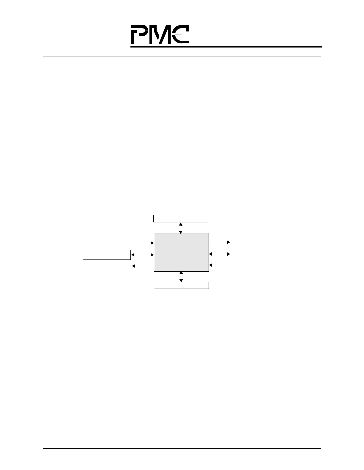
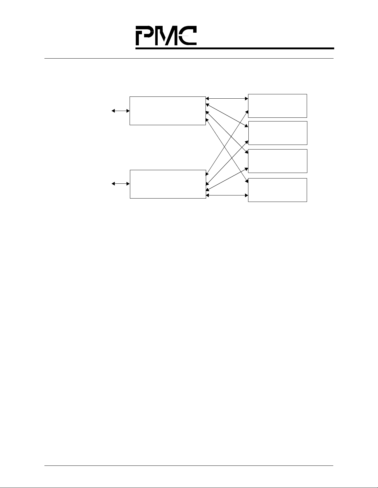
BLOCK DIAGRAM
Figure 1 shows a QRT system block diagram.
Receive Cell SDRAM
Receive UTOPIA
Control SSRAM
Transmit UTOPIA
Figure 1. QRT Sys tem Block Diagram
622 Mbps ATM
Traffic Mgt Device
Transmit Cell SDRAM
(QRT)
PM73487
To Switch Fabr ic
Host Interface
From Switch Fabric
3

Released
Datasheet
PMC-Sierra, Inc.
PMC-980618 Issue 3 622 Mbps ATM Traffic Management Device
PM73487 QRT
1 SYSTEM APPLICATIONS
The QRT, together with the QSE, support a wide range of high-performance ATM switching systems. These systems range in size from 622 Mbps to 160 Gbps. The systems can be developed
such that this scalability is provided with linear cost. Another key feature of the QRT/QSE architecture is that it is exceptionally fault-tolerant, both in the switch fabric and the UTOPIA interface.
This section contains a quick overview of the QRT and several example applications:
• a stand-alone 622 Mbps switch using a single QRT,
• a 5 Gbps switch using QRTs and a QSE,
• a 10 Gbps switch using QRTs and QSEs,
• a switch architecture using QRTs and QSEs that scales from 5 Gbps to 20 Gbps,
• a switch architecture using QRTs and QSEs that scales from 5Gbps to 160 Gbps
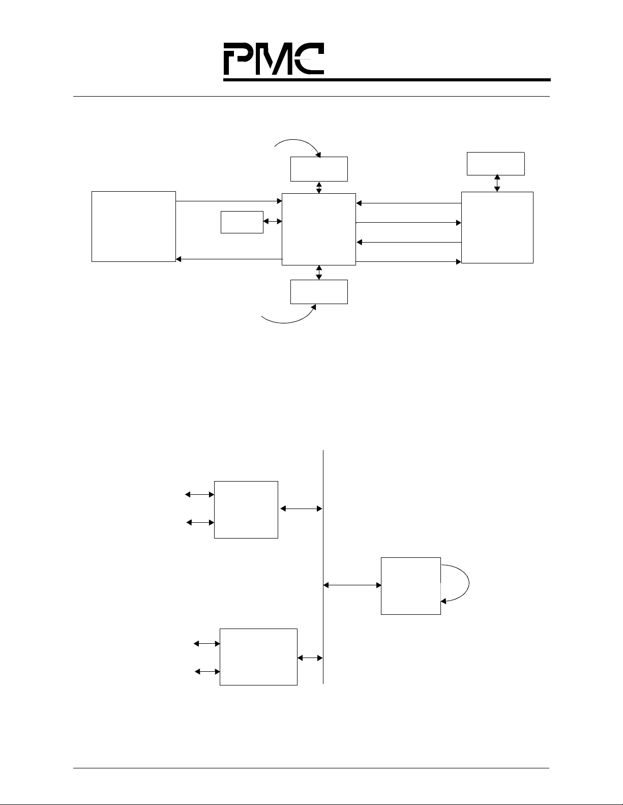
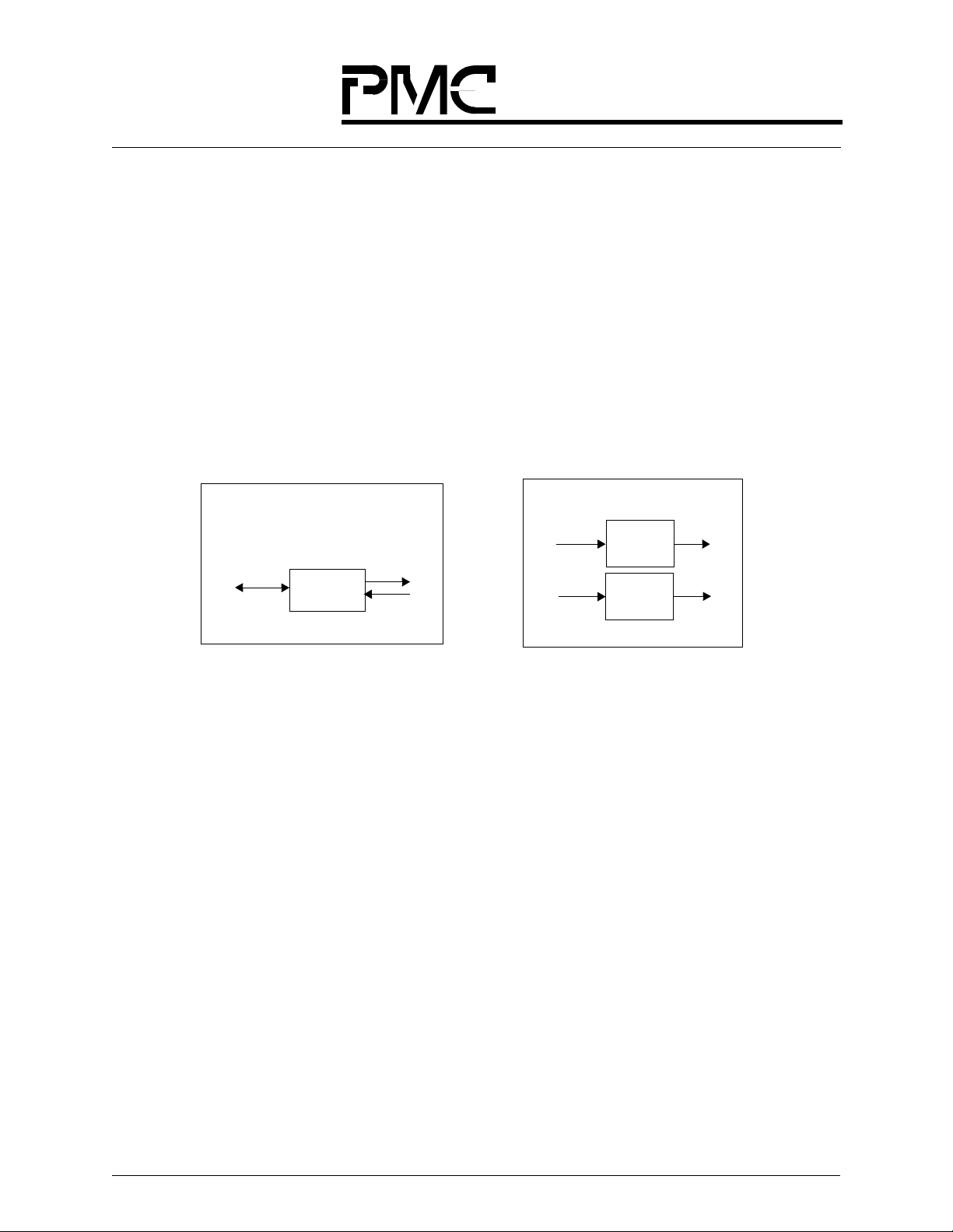
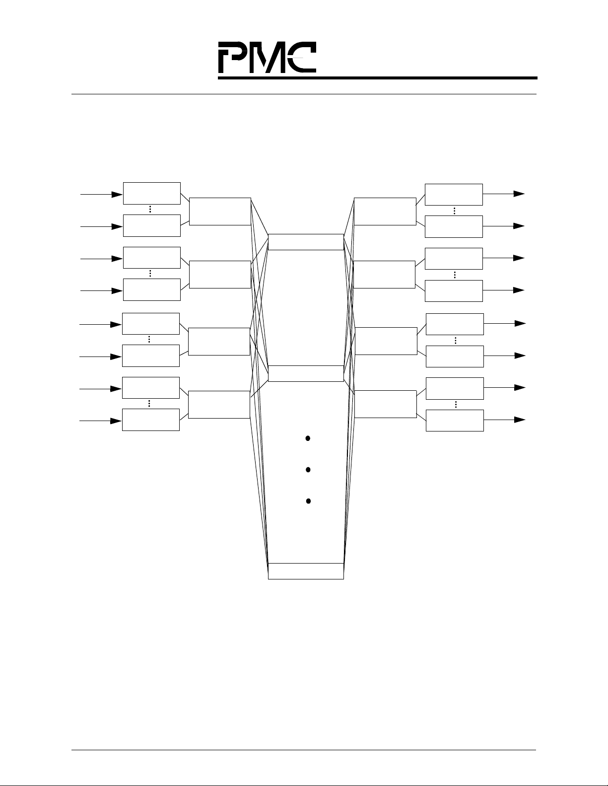
1.1 QRT System Overview
The QRT provides 622 Mbps of input and output buffered a ccess to switch fabrics composed of
QSEs (32 x 32 PM73488s). In addition, the QRT supports a stand-alone, purely output-buffered
622 Mbps switch mode. Head-of-line blocking, commonly associated with input buffers, is virtually eliminated via per-VC receive queues, three types of per-cell switch fabric feedback, and perVC cell selection algorithms. The QRT also provides eight separate congestion thresholds, each
with hysteresis, that selectively control AAL5 Early Packet Discard (EPD)/Packet Tail Discard
(PTD), CLP-based cell dropping, and/or EFCI marking. Eight separate maximum thresholds are
also supported. Additional highlights of the QRT include full VPI/VCI header translation, separate input and output cell buffers (up to 64K each), Virtual Path Connection (VPC)/Virtual Channel Connection (VCC) connections, and up to 16K VCs. The QRT provides a bidirectional
connection between a UTOPIA Level 2 interface and 4-nibble wide, 66 MHz switch fabric interfaces, as shown in Figure 2 on page 5. A significant switch speed-up factor, up to 1.6 times the
line rate, is used to support full throughput for many switch fabric configurations.
4
Released
Datasheet
PMC-Sierra, Inc.
PM73487 QRT
PMC-980618 Issue 3 622 Mbps ATM Traffic Management Device
Cells are stored in pe r-VC que ues on
the input and respond to per-cell
Receive UTOPIA Level 2
Physical and/or
ATM Layers
Transmit UTOPIA Level
Cells are stored in per-
priority queues on the output
with per-VC accountin g
Interface
Control
SSRAM
2 Interface
Input Cell
SDRAM
QRT
(PM73487)
Output Cell
SDRAM
Receive
Receive Nibble Data
Transmit Nibble Data
Transmit Feedback
Multicast
SRAM
QSE
(PM73488)
Figure 2. QR T Syste m Over view
1.2 622 Mbps Switch Configuration
The QRT can be used in a stand-alone application that supports ATM switching up to 622 Mbps,
as shown in Figure 3. The four switch fabric interfaces are looped back to the QRT, allowing the
UTOPIA interface to be fully used. In this application, the QRT operates as an output buffered
switch..
2M
2M
155M
155M
UTOPIA Level 2 Multi-PHY Interface
1
AAL1 SAR
Processor
• • •
8
(PM73121)
1
S/UNI-QUAD
(PM5349)
4
Figure 3. 622 Mbps Switch Configurat ion
QRT
(PM73487)
5
Released
Datasheet
PMC-Sierra, Inc.
PM73487 QRT
PMC-980618 Issue 3 622 Mbps ATM Traffic Management Device
1.3 32 x 32 Switch Application (5 Gbps)
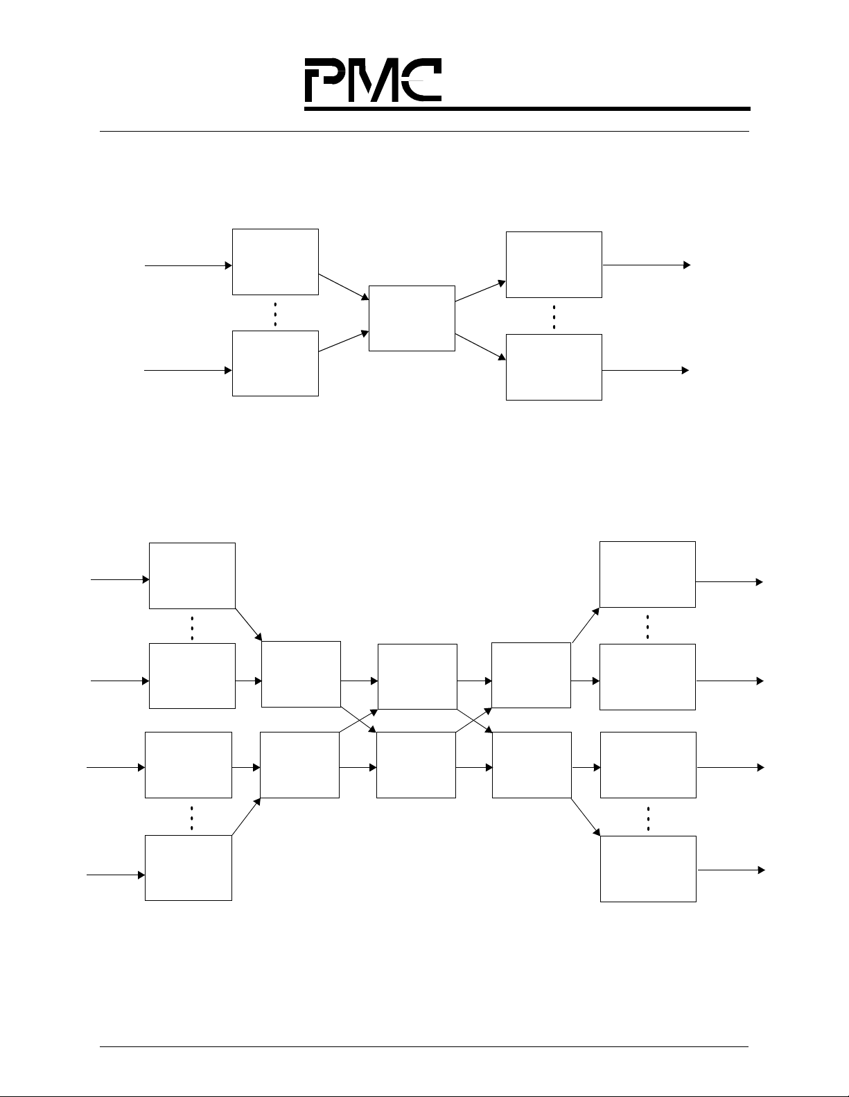
Figure 4 shows a basic 32 × 32 switch application (5 Gbps) using eight QRTs and one QSE.
622 Mbps
Aggregate
Receive UTOPIA
Level 2
622 Mbps
Aggregate
QRT #1
(PM73487)
Receive Input
QRT #8
(PM73487)
Receive Input
QRT #1
(PM73487)
×
4
QSE
4
×
(PM73488)
4
Transmit Output
×
×
4
QRT #8
(PM73487)
Transmit Output
622 Mbps
Aggregate
Transmit UTOPIA
Level 2
622 Mbps
Aggregate
Figure 4. 32 x 32 Swit ch App lic atio n (5 Gbps )
1.4 64 x 64 Switch Application (10 Gbps)
Figure 5 shows a 64 × 64 switch application (10 Gbps) using 16 QRTs and 6 QSEs. This applica-
tion uses QSEs in a 3-stage fabric. This sized system can be implemented in a single 19-inch rack.
622 Mbps
Aggregate
Receive
UTOPIA
Level 2
622 Mbps
Aggregate
QRT #1
(PM73487)
Receive Input
QRT #8
(PM73487)
Receive Input
×
4
QSE
(PM73488)
× 16
QSE
(PM73488)
× 16
QSE
(PM73488)
4
×
QRT #1
(PM73487)
Transmit Output
QRT #8
(PM73487)
Transmit Output
622 Mbps
Aggregate
Transmit
UTOPIA
Level 2
622 Mbps
Aggregate
622 Mbps
Aggregate
Receive
UTOPIA
Level 2
622 Mbps
Aggregate
QRT #9
(PM73487)
Receive Input
QRT #16
(PM73487)
Receive Input
(PM73488)
4
×
QSE
× 16
QSE
(PM73488)
× 16
Figure 5. 64 x 64 Switch Application (10 Gbps)
6
QSE
(PM73488)
×
4
QRT #9
(PM73487)
Transmit Output
QRT #16
(PM73487)
Transmit Output
622 Mbps
Aggregate
Transmit
UTOPIA
Level 2
622 Mbps
Aggregate
Released
Datasheet
PMC-Sierra, Inc.
PM73487 QRT
PMC-980618 Issue 3 622 Mbps ATM Traffic Management Device
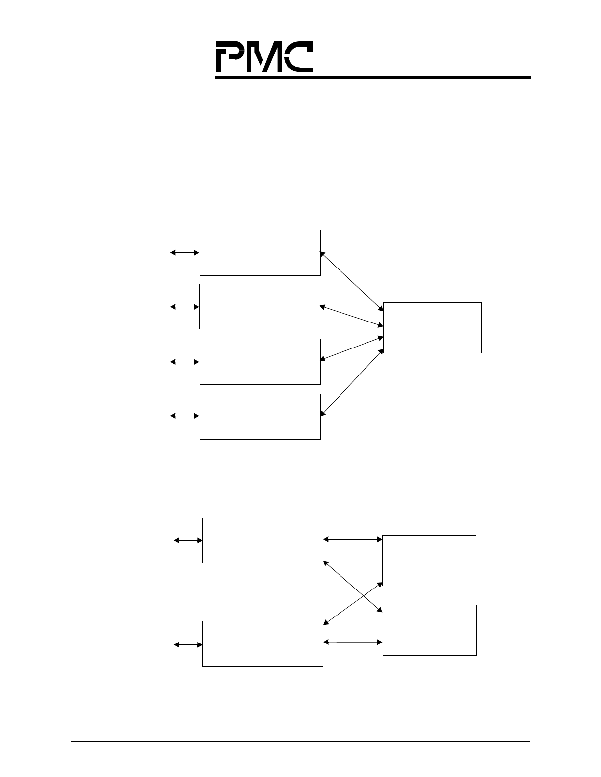
1.5 5 Gbps to 20 Gbps Application Example - Seamless Growth
This section illustrates the modularity of the QRT (PM73487) and QSE (PM73488) architecture.
A 5 Gbps system can immediately be created (as shown in Figure 6 on page 7), and then be
upgraded to 10 Gbps (as shown in Figure 7 on page 7), or 20 Gbps (as shown in Figure 8 on page
8). Since all these systems are based on a single-stage switch fabric, the per-port cost for each sys-
tem will remain the same.
Eight
155 Mbps
Interfaces
Eight
155 Mbps
Interfaces
Eight
155 Mbps
Interfaces
Eight
155 Mbps
Interfaces
• Two QRTs (PM73487s)
• Two QRTs (PM73487s)
• Two QRTs (PM73487s)
• Two QRTs (PM73487s)
Port Card
Port Card
Switch Card
• One QSE (PM73488)
Port Card
Port Card
Figure 6. 5 Gbps ATM Switch Using 16 Dual S/UN Is, 8 QR Ts, and 1 QSE
Eight
155 Mbps
Interfaces
• Two QRTs (PM73487s)
Port Card 1
•
Switch Card
• One QSE (PM73488)
•
•
Eight
155 Mbps
Interfaces
• Two QRTs (PM73487s)
Figure 7. 10 Gbps ATM Switch Using 32 Dual S /UNIs , 16 QRTs, an d 2 QSEs
Port Card 8
7
Switch Card
• One QSE (PM73488)
Released
Datasheet
PMC-Sierra, Inc.
PM73487 QRT
PMC-980618 Issue 3 622 Mbps ATM Traffic Management Device
Eight
155 Mbps
Interfaces
Port Card 1
• Two QRTs (PM73487s)
•
Switch Card
• One QSE (PM73488)
Switch Card
• One QSE (PM73488)
•
•
Eight
155 Mbps
Interfaces
• Two QRTs (PM73487s)
Figure 8. 20 Gbps ATM Switch Using 64 Dual S /UNIs , 32 QRTs, an d 4 QSEs
Port Card 16
Switch Card
• One QSE (PM73488)
Switch Card
• One QSE (PM73488)
8
Released
Datasheet
PMC-Sierra, Inc.
PM73487 QRT
PMC-980618 Issue 3 622 Mbps ATM Traffic Management Device
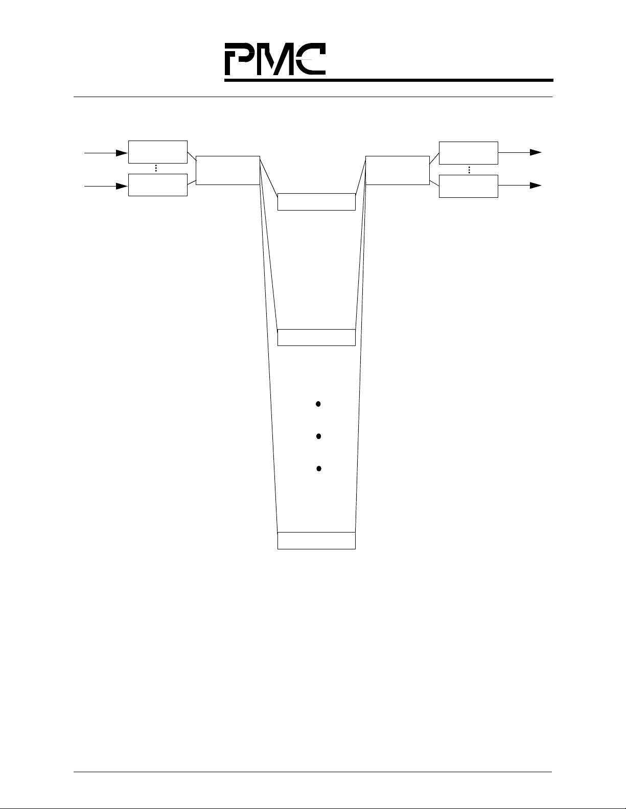
1.6 5 Gbps to 160 Gbps Application Example – LAN-to-WAN
A powerful application of the QRT and the QSE devices is the creation of modules that can be
used in a range of switches with only the interconnection changing between different sizes. ATM
switches from 5 Gbps to 160 Gbps can be realized with only two unique cards. A port card has
one QRT, and a switch card has two QSEs. The switch fabric consists of three stages, each with
32 QSEs (or 16 switch cards). To plan for future scalability, the middle stage must be built-in
upfront. This is a one-time cost. Then, in order to scale in 5 Gbps increments, one switch card and
its accompanying eight port cards should be added. Finer bandwidth scaling is possible by populating the additional switch card with port cards as needed (in increments of 622 Mbps). With this
switch fabric topology, scaling is possible up to 160 Gbps. Once the initial middle stage cost has
been incurred, the per-port cost for 5 Gbps through 160 Gbps systems remains almost constant
Port Card - One QRT
One UTOPIA
Level 2 Interface
QRT
(PM73487
Figure 9. 5 Gbps to 160 Gbp s Swi tches Mod eled Using On ly Two Cards
Switch Card - Two QSEs
x32
x32
QSE
(PM73488
QSE
(PM73488
x32
x32
9
Released
Datasheet
PMC-Sierra, Inc.
PM73487 QRT
PMC-980618 Issue 3 622 Mbps ATM Traffic Management Device
622 Mbps
622 Mbps
Port Card #1
Rx Input
Port Card #8
Rx Input
Switch Card #17
Stage 1 QSE
x2
Switch Card #1
Switch Card #2
Switch Card #17
Stage 3 QSE
x2
Port Card #1
Tx Output
Port Card #8
Tx Output
622 Mbps
622 Mbps
Switch Card #16
Figure 10. 5 Gbps ATM Switch
Figure 10 shows a 5 Gbps ATM switch using 8 port cards (8 QRTs) and 17 switch cards (34
QSEs). The middle stage is composed of 16 switch cards. The 5 Gbps bandwith is achieved by
adding switch card #17 (which is depicted using two boxes: one stage 1 Q SE and one stage 3
QSE), and eight port cards (each of which is depicted using two boxes: one for the Rx input side,
and one for the Tx output side). Lines between stage 1 and stage 2, and stage 2 and stage 3 switch
cards represent two sets of wires, one to each of the QSEs in the middle stage switch cards.
10
Released
Datasheet
PMC-Sierra, Inc.
PM73487 QRT
PMC-980618 Issue 3 622 Mbps ATM Traffic Management Device
.Figure 11 shows a 10 Gbps ATM switch using 16 port cards (16 QRTs) and 18 switch cards (36
QSEs). Here, another switch card and eight port cards have been added to the 5 Gbps switch
depicted in Figure 10.
622 Mbps
622 Mbps
622 Mbps
622 Mbps
Port Card #1
Rx Input
Port Card #8
Rx Input
Port Card #9
Rx Input
Port Card #16
Rx Input
Switch Card #17
Stage 1 QSE
x2
Switch Card #18
Stage 1 QSE
x2
Switch Card #1
Switch Card #2
Switch Card #17
Stage 3 QSE
x2
Switch Card #18
Stage 3 QSE
x2
Port Card #1
Tx Output
Port Card #8
Tx Output
Port Card #9
Tx Output
Port Card #16
Tx Output
622 Mbps
622 Mbps
622 Mbps
622 Mbps
Switch Card #16
Figure 11. 10 Gbps ATM Switch
11
Released
Datasheet
PMC-Sierra, Inc.
PM73487 QRT
PMC-980618 Issue 3 622 Mbps ATM Traffic Management Device
Figure 12 shows a 15 Gbps ATM switch using 24 port cards (24 QRTs) and 19 switch cards (38
QSEs).Here, once again, another switch card and eight port cards have been added
622 Mbps
622 Mbps
622 Mbps
622 Mbps
622 Mbps
622 Mbps
Port Card #1
Rx Input
Port Card #8
Rx Input
Port Card #9
Rx Input
Port Card #16
Rx Input
Port Card #17
Rx Input
Port Card #24
Rx Input
Switch Card #17
Stage 1 QSE
x2
Switch Card #18
Stage 1 QSE
Switch Card #19
Stage 1 QSE
x2
x2
Switch Card #1
Switch Card #2
Switch Card #17
Stage 3 QSE
x2
Switch Card #18
Stage 3 QSE
x2
Switch Card #19
Stage 3 QSE
x2
Port Card #1
Tx Output
Port Card #8
Tx Output
Port Card #9
Tx Output
Port Card #16
Tx Output
Port Card #17
Tx Output
Port Card #24
Tx Output
622 Mbps
622 Mbps
622 Mbps
622 Mbps
622 Mbps
622 Mbps
Switch Card #16
Figure 12. 15 Gbps ATM Switch
12
Released
Datasheet
PMC-Sierra, Inc.
PM73487 QRT
PMC-980618 Issue 3 622 Mbps ATM Traffic Management Device
Figure 13 shows a 20 Gbps ATM switch composed of 32 port cards (32 QRTs) and 20 switch
cards (40 QSEs). By adding additional sets of a switch card and eight port cards in the same manner, this system can scale up to 160 Gbps. .
622 Mbps
622 Mbps
622 Mbps
622 Mbps
622 Mbps
622 Mbps
622 Mbps
622 Mbps
Port Card #1
Rx Input
Port Card #8
Rx Input
Port Card #9
Rx Input
Port Card #16
Rx Input
Port Card #17
Rx Input
Port Card #24
Rx Input
Port Card #25
Rx Input
Port Card #32
Rx Input
Switch Card #17
Stage 1 QSE
x2
Switch Card #18
Stage 1 QSE
x2
Switch Card #19
Stage 1 QSE
x2
Switch Card #20
Stage 1 QSE
x2
Switch Card #1
Switch Card #2
Switch Card #17
Stage 3 QSE
x2
Switch Card #18
Stage 3 QSE
x2
Switch Card #19
Stage 3 QSE
x2
Switch Card #20
Stage 3 QSE
x2
Port Card #1
Tx Output
Port Card #8
Tx Output
Port Card #9
Tx Output
Port Card #16
Tx Output
Port Card #17
Tx Output
Port Card #24
Tx Output
Port Card #25
Tx Output
Port Card #32
Tx Output
622 Mbps
622 Mbps
622 Mbps
622 Mbps
622 Mbps
622 Mbps
622 Mbps
622 Mbps
Switch Card #16
Figure 13. 20 Gbps ATM Switch
.
13
Released
Datasheet
PMC-Sierra, Inc.
PM73487 QRT
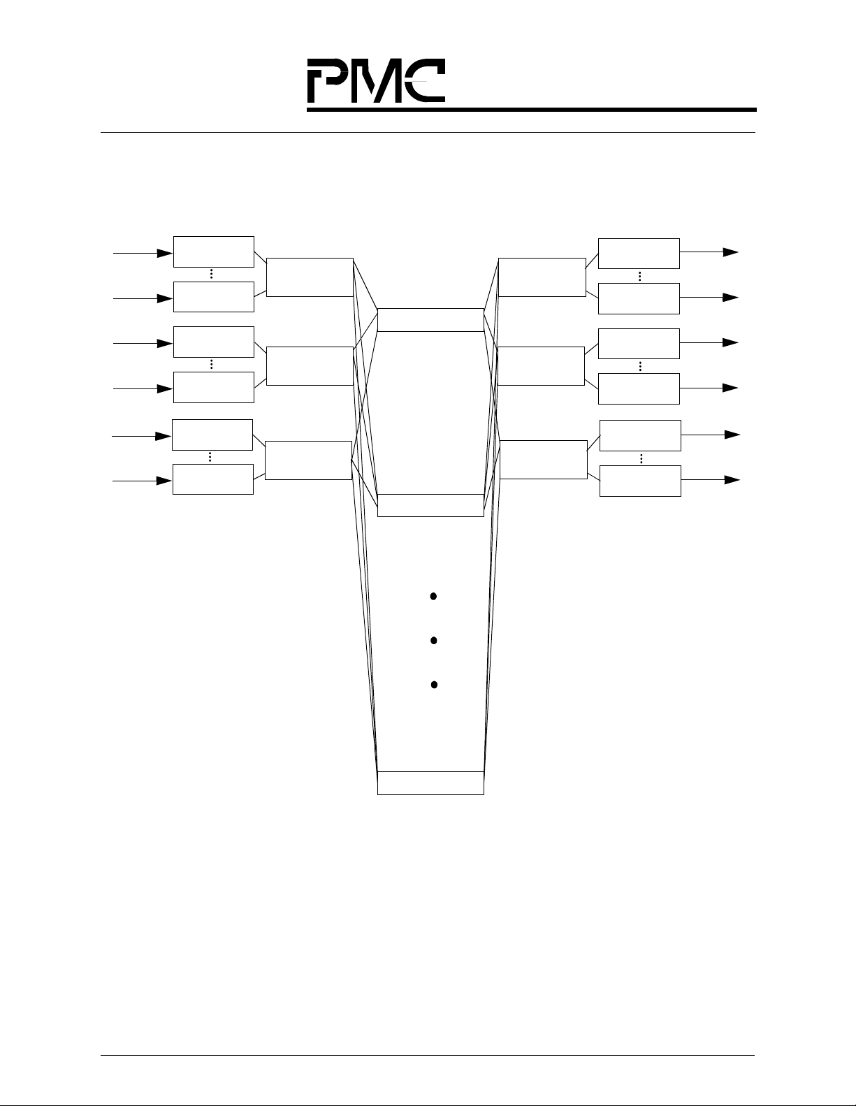
PMC-980618 Issue 3 622 Mbps ATM Traffic Management Device
2 THEORY OF OPERATIONS
2.1 Overview
The QRT is a 622 Mbps, full duplex, intelligent routing table which, when used with a switch fabric composed of either SE or QSE devices, can implement ATM switches from 622 Mbps to 160
Gbps. The QRT supports a 16-bit UTOPIA Level 2 interface for ease of connection to PHY or
AAL layer devices. Four nibble-wide data interfaces connect the QRT to the switch interface.
External DRAM memory devices provide receive and transmit cell buffering, and external SRAM
devices provide control data for the QRT. This section explains the algorithms for the data flow.
Figure 14 shows an overview of the QRT system.
Receive Cell
SDRAM
Receive UTOPIA
Level 2 Interface
Transmit UTOPIA
Level 2 Interface
Control SSRAM
QRT
(PM73487)
Transmit Cell
SDRAM
Figure 14. QRT Sys tem Overview
To QSE
Host Interface
From QSE
2.2 Interface Descriptions
2.2.1 Switch Fabric Interface
The QRT switch fabric interface consists of four groups of signals from both the ingress (receive
side) and the egress (transmit side). Each group consists of a Start-Of-Cell (SE_SOC_OUT) signal, a nibble-wide data bus, and a backpressure acknowledgment (BP_ACK_IN) signal. The
Start-Of-Cell (SE_SOC_OUT) signal is transmitted at the ingress at the same time as the beginning of a cell. SE_SOC_OUT on the ingress is common to all four groups. The BP_ACK_OUT
signal flows from the egress through the switch fabric, in the direction opposite the data, and indicates whether a cell has successfully passed through the switch fabric. Other signals associated
with the switch fabric interface are the switch element clock (SE_CLK) and RX_CELL_START.
To support the highest possible throughput for various switch fabric configurations, a clock
speed-up factor of 1.6 is used. That is, the switch fabric is run at a rate that is effectively 1.6 times
faster than the line rate.
14

Released
Datasheet
PMC-Sierra, Inc.
PMC-980618 Issue 3 622 Mbps ATM Traffic Management Device
2.2.2 Phase Aligners
PM73487 QRT
Phase aligners are used to allow for extended device separation. The technique used is a clock
recovery mechanism that requires only the switch fabric to be frequency synchronous. A master
clock is distributed to all devices associated with the switch fabric, and the phase of the clock at
each interface is dynamically adjusted to account for skew introduced to the signals. The phase
aligner circuitry for each interface responds to the cell start and feedback signals, which contain a
high number of transitions to ensure accurate phase adjustment of the clock for data and signal
sampling.
2.2.3 UT OPIA Interface
The QRT’s UTOPIA interface implements the ATM Forum standardized 16-bit, Level 2 configuration, which supports up to 31 Virtual Outputs (VOs) via five address bits. Up to 31 PHY or
AAL layer devices with 16-bit UTOPIA Level 2 functionality can be connected to this interface,
providing full duplex throughputs of 675 Mbps.
2.2.4 Cell Buffer SDRAM Interface
The QRT supports two Synchronous DRAM (SDRAM or SGRAM) interfaces providing up to
64K of cell buffering in both the receive and transmit directions. Each interface consists of a 32bit data bus, a 9-bit address bus, two chip select signals, and associated control signals. The frequency of these interfaces is 100 MHz. Both Synchronous Graphic RAM (SGRAM) and SDRAM
devices are supported. Clocking for these two interfaces is provided through the device.
2.2.5 Channel RAM (CH_RAM) Interface
The QRT supports up to 16K channels through a Synchronous SRAM (SSRAM) interfac e. The
interface consists of a 32-bit data bus, a 16-bit address bus, and associated control signals. The
frequency of this interface is 100 MHz. Clocking for this interface is provided through the device.
2.2.6 Address Lookup RAM (AL_RAM) Interface
The QRT has data structures in the AL_RAM, including VPI/VCI address translation. The interface consists of a 6-bit data bus, a 17-bit address bus, and associated control signals. The frequency of this interface is 100 MHz. Clocking for this interface is provided through the device.
2.2.7 AB_RAM Interface
The QRT stores the per VC head / tail pointers and sent / dropped counters for the receive direction in the AB_RAM. Each interface consists of a 17-bit multiplexed address/data bus and associated control signals. The frequency of this interface is 100 MHz.
2.2.8 Host Processor Interface
The QRT host processor interface allows connection of a microprocessor through a multiplexed
32-bit address/data bus. The suggested microprocessor for this interface is the Intel i960®. The
microprocessor has direct access to all of the QRT control registers.
15
Released
Datasheet
PMC-Sierra, Inc.
PM73487 QRT
PMC-980618 Issue 3 622 Mbps ATM Traffic Management Device
2.2.9 SE_SOC Encodings
The SE_SOC and BP_ACK signals have guaranteed transitions and special encodings, whic h ar e
defined in this section and in “BP_ACK Encodings” which follows. The SE_SOC_IN and
SE_SOC_OUT signals have guaranteed transitions and SOC encodings as shown in Figure 15.
The SE_SOC signals carry a repeating pattern of four zeros and four ones to guarantee transitions
required by the phase aligner. The “Start-Of-Cell” on the data line s associated with an SE_SOC
line is indicated by a change in this pattern. For a valid SE_SOC, the change in pattern is followed
by reset of the background pattern such that it is followed by four zeros and four ones. The first
nibble (PRES) of the header is coincident with SE_SOC (change in pattern).
SE_CLK
SE_SOC_OUT
Magnified CLK
Magnified Data
Magnified SE_SOC_OUT
4 ones. 4 zeros 4 ones 4 zeros 4 ones 4 zeros. 4 ones 4 zeros. 5 zeros 4 ones 4 zeros.
Tsesu TsesuTseho
PRES.
4 ones 4 zeros 1 one. 5 zeros
Figure 15. SE_SOC Encodings
2.2.10 BP_ACK Encodings
Figure 16 shows the BP_ACK encodings.
Mode
Inversion1
clk
BP_ACK Base Pattern
BP_ACK Signaling
Figure 16. BP_ACK Encodings
Data2
Data1
Data0
Inversion2
Code Ext 0
4 ones 4 zeros
4 zeros 4 ones
The BP_ACK_IN and BP_ACK_OUT signals have guaranteed transitions, and BP and ACK
encodings. The BP_ACK signal is used to signal backpressure/cell acknowledgment to the fabric
(QSE) at the egress and receive backpressure/cell acknowledgment at the ingress from the fabric
(QSE).
To ensure the transitions required by the phase aligner, the BP_ACK signal carries a repeating
four zeros, four ones pattern. The actual information is transferred through encoded 7-bit packets
that start with a change in this background pattern. The change (an inversion) on the line is followed by a mode bit, followed by two bits of coded message, and a second inversion (inverse of
the first inversion). If it is an acknowledgment packet, this is followed by two bits of code exten-
16
Released
Datasheet
PMC-Sierra, Inc.
PM73487 QRT
PMC-980618 Issue 3 622 Mbps ATM Traffic Management Device
sion (these bits are for future use and currently are required to be “00”). In the case of a backpressure packet, the next bit is the backpressure bit on for low priority multicast cells, followed by one
code extension bit.
The background is reset to four zeros and four ones after transmission of each packet.
The QRT and QSE allow back-to-back acknowledgment and backpressure packets. In the case of
back-to-back acknowledgment and backpressure packets, the receiving device may see an
inverted bit (a “1”) followed by the rest of the packet instead of a reset background pattern.
One backpressure packet and either one or none acknowledgment packet are expected to be
received during a cell time. The receipt of multiple acknowledgment or backpressure packet s is a
failure condition.
Table 1 describes the backpressure and acknowledgment encodings.
Ta ble 1. Backpressure and Acknowledgment Encodings
Mode Data 2 Data 1 Data 0
0 1 = Backpressure
on high priority
multicast cell.
10000Signals no response. Treated as acknowl-
10100Signals Mid-switch Negative ACKnowl-
11000Signals Output Negative ACKnowledg-
11100Signals ACKnowledgment (ACK).
1 = Backpressure
on medium priority multicast cell.
1 = Backpressure
on low priority
multicast cell.
Code
Ext 0
0 Backpressure information.
This signal is present each cell time,
regardless of whether a cell was transmitted or not (on that link).
This signal is withheld if any problem is
detected on the input port.
edgment.
edgment (MNACK).
ment (ONACK).
Description
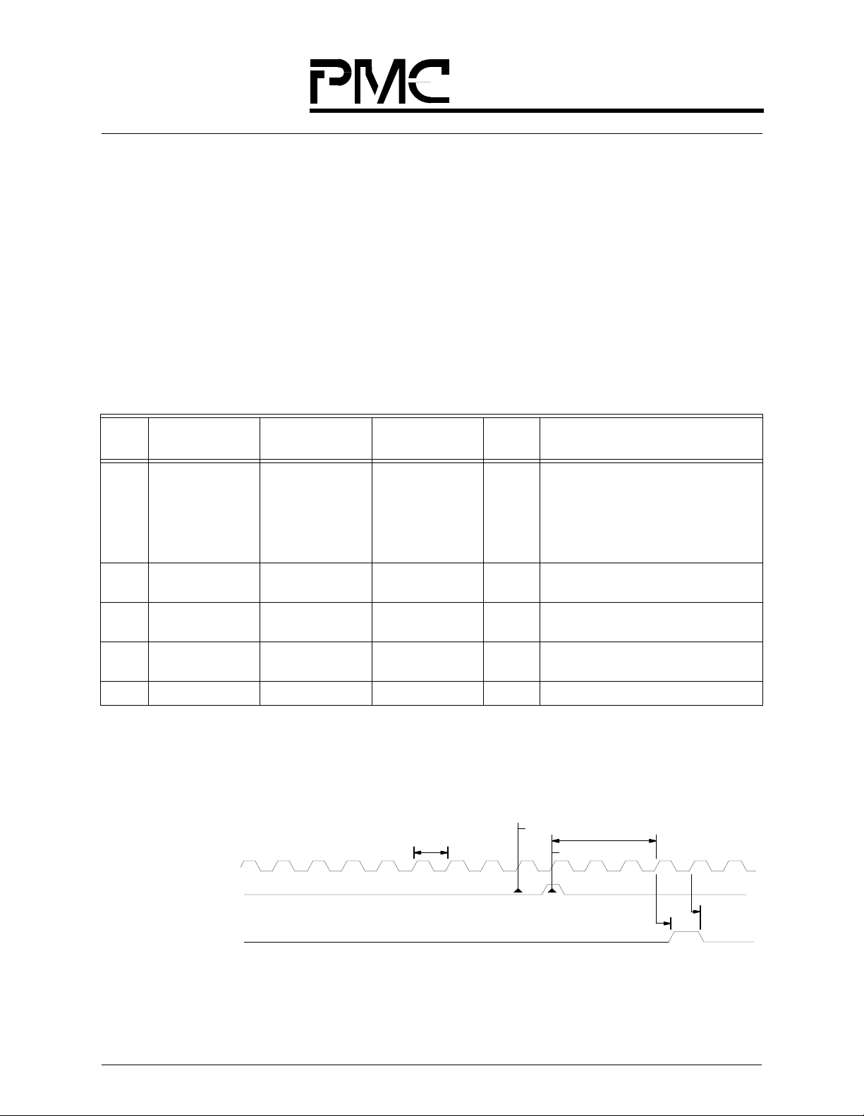
2.2.11 Relation Between External CELL_START and Local CELL_START
Figure 17 shows the relationship between external RX_CELL_START and local CELL_START
signals.
SE_CLK
External RX_CELL_START
Local CELL_START
Clock CycleClock Cycle
RX_CELL_START Low
RX_CELL_START High
CELL_START DelayCELL_START Delay
Delta
Delta
Figure 17. QRT Cell -Level Timin g
17

Released
Datasheet
PMC-Sierra, Inc.
PMC-980618 Issue 3 622 Mbps ATM Traffic Management Device
PM73487 QRT
Delay between the external RX_CELL_START and local CELL_START is programmable
through the RX_CELL_START_ALIGN register (refer to “RX_CELL_START_ALIGN (Inter-
nal Structure)” on page 122).
The local CELL_START impacts the start of cell transmission to the fabric. It also determines the
period within a cell time during which the BP_ACK_IN(3:0) at ingress is valid. As such, the programmable CELL_START delay allows the flexibility to synchronize the QRTs and QSEs in a
system.
2.3 Cell Flow Overview
The QRT functions as a 622 Mbps port for an ATM switch fabric composed of either the SE or
QSE devices. The QRT transfers cells between a UTOPIA Level 2 interface and a switch fa bric
interface. The device supports header tra nslation and congestion management. The basic flow of
cells through the QRT is as follows (see Figure 18 on page 19):
1. A cell enters the QRT on the receive side from the UTOPIA interface and the channel number is looked
up.
2. The cell is then either dropped or transferred to the receive cell buffer DRAM and queued in the r eceive
queue controller depending on six congestion management checks (both maximum and congested
thresholds for the device, Service Class Group (SCG), SC, and connection).
3. When an available cell time occurs, four cells are selected by the receive-side scheduler, which reads
the cells from the receive cell buffer DRAM and transmits them from the QRT into the switch fabric.
4. Once a cell is received from the switch fabric on the transmit side, it is again either dropped or transferred to the transmit cell buffer DRAM and queued in the transmit queue controller, depending on ten
congestion management checks (both maximum and congested thresholds for the device, VO, SC, Service Class Group (SCG),Service Class Queue (SCQ), and connection).
5. When the cell is selected for transmission by the transmit-side scheduler, it is removed from the transmit cell buffer DRAM and processed by the transmit multicast/header mapper fo r corresponding header
translation and distribution.
18

Released
Datasheet
PMC-Sierra, Inc.
PM73487 QRT
PMC-980618 Issue 3 622 Mbps ATM Traffic Management Device
6. The cell then is sent to the UTOPIA interface and exits the QRT on the transmit side.
Receive SDRAM
Cell Buffer
Receive UTOPIA
Level 2 Interface
Receive UTOPIA
Cell Buffer
Receive SDRAM
Controller
Data to QSE
Feedback from QSE
Feedback to QSE
Data from QSE
Control
SSRAM
Transmit UTOPIA
Level 2 Interface
Receive Channel
Lookup
SSRAM
Controller
Transmit Multicast
Background
Transmit UTOPIA
Cell Buffer
Receive Switch
Cell Buffer
Receive Queue
Controller
Transmit Queue
Controller
Transmit Switch
Cell Buffer
Transmit SDRAM
Controller
Transmit SDRAM
Cell Buffer
Figure 18. QRT Data Flow Diagr am
2.4 UTOPIA Operation
2.4.1 General
Cells received from the UTOPIA interface are first processed by the receive channel lookup block
and then queued for transmission within the receive queue controller. The cell waits in the rec eive
cell buffer DRAM for instruction from the receive queue controller to proceed to the switch fabric
interface.
2.4.2 UTOPIA Interface
The QRT interfaces directly to a UTOPIA interface device without needing an external FIFO. The
receive side UTOPIA has a 4-cell internal FIFO, and the transmit side contains another 4-cell
internal FIFO. The QRT UTOPIA interface is 16 bits wide and operates at frequencies up to 50
MHz. It provides the following modes:
• UTOPIA Level 1 single-PHY interface
• UTOPIA Level 2 multi-PHY interface
19

Released
Datasheet
PMC-Sierra, Inc.
PM73487 QRT
PMC-980618 Issue 3 622 Mbps ATM Traffic Management Device
2.4.2.1 UTOPIA Level 2 Polling
The UTOPIA interface offers three modes of polling, as per the UTOPIA Level 2 specification:
• Standard single cell available polling
• Multiplexed Status Polling (MSP) using four cell available signals
• Direct status indication using four cell available signals
These polling modes allow the QRT to communicate with many different PHY devices. Figure 19
shows the QRT polling PHY devices in a receive UTOPIA operation.
QRT polls PHYs to determine if they have cells.
Serial In
PHY
Device
Serial In
PHY
Device
Serial In
PHY
Device
Data
Address
Cell Available
QRT
(PM73487)
To Switch Fabric
Figure 19. Receive UTOPIA Operation
Figure 20 shows the QRT polling PHY devices in a transmit UTOPIA operation.
Serial Out
PHY
Device
Serial Out
PHY
Device
Cell Available
Serial Out
PHY
Device
Figure 20. Tr ansmit UTOPIA Opera tion
QRT polls PHYs to determin e if the y can accep t cells.
Data
Address
QRT
(PM73487)
From Switch Fabric
20

Released
Datasheet
PMC-Sierra, Inc.
PM73487 QRT
PMC-980618 Issue 3 622 Mbps ATM Traffic Management Device
2.4.2.1.1 Standard Single Cell Available Polling
In the standard single cell available polling mode, one cell available response occurs eve ry two
clocks. Figure 21 shows the receive standard single cell available polling.
1 2 3 4 5 6 7 8 9101112131415161718192021222324252627282930
ATM_CLK
RATM_DATA(15:0)
RATM_ADD(4:0)
hh ph pppppppp ppppppppppppppp
01 1F 1F 1F00 01 1F 1F02 03 04 051F 1F 1F06 07 1F 00
/RATM_READ_EN
RATM_CLAV(3:0)
1 010 10 110
RATM_SOC
Figure 21. Receive Standard Single Ce ll Availab le P olling
Figure 22 shows the transmit standard single cell available polling.
1 2 3 4 5 6 7 8 9101112131415161718192021222324252627282930
ATM_CLK
TATM_DATA(15:0)
TATM_ADD(4:0)
/TATM_WRITE_EN
TATM_CLAV(3:0)
TATM_SOC
TATM_PARITY
04 1F 1F 1F00 01 1F 1F02 03 04 051F 1F 1F06 07 1F 01
010101 1
Figure 22. Transmit Standard Single Cell A vaila ble Pol lin g
hp pp pppppppp ppppppppppppp
hh
0100
h
1F
21

Released
Datasheet
PMC-Sierra, Inc.
PM73487 QRT
PMC-980618 Issue 3 622 Mbps ATM Traffic Management Device
2.4.2.1.2 Multiplexed Status Polling (MSP) Using Four Cell Available Signals
With MSP using four cell available signals, up to four cell available responses occur every two
clocks. The advantage offered by the MSP mode is the improved response time for PHY service
selection. With this method, it is possible to poll 31 devices in a single cell time. PHY devices,
however, must comply with this optional part of the UTOPIA Level 2 specification. A standard
PHY device can be configured to use this mode even though it does not support it directly. To
effect this, up to eight PHY devices can be configured with the addresses 0, 4, 8, 12, 16, 20, 24,
and 28. Figure 23 shows the receive UTOPIA 50 MHz MSP, including cell transfer.
1 2 3 4 5 6 7 8 9 101112131415161718192021222324252627282930
ATM_CLK
RATM_DATA(15:0)
RATM_ADD(4:0)
hh ph pppppppp ppppppppppppppp
02 1F 1F 1F00 04 1F 1F08 0C 10 141F 1F 1F18 1C 1F 00
/RATM_READ_EN
RATM_CLAV(3:0)
30308 0 3
RATM_SOC
Figure 23. Receive UTOPIA Multiplexed St atus Po lli ng ( MSP), Incl udi ng C el l Trans fer
Figure 24 shows the transmit UTOPIA 50 MHz MSP including cell transfer.
1 2 3 4 5 6 7 8 9 101112 1314 1516 17181920 2122 2324 2526 27282930
ATM_CLK
TATM_DATA(15:0)
TATM_ADD(4:0)
/TATM_WRITE_EN
00 1F 1F 1F00 04 1F 1F08 0C 10 141F 1F 1F18 1C 1F 01
hp pp pppppppp ppppppppppppp
hh
h
1F
TATM_CLAV(3:0)
0F0F08 F
0
TATM_SOC
TATM_PARITY
Figure 24. Transmit UTOPIA 50 MHz Multipl exed Status Po lli ng ( MSP ), Incl uding C el l Trans fer
22

Released
Datasheet
PMC-Sierra, Inc.
PMC-980618 Issue 3 622 Mbps ATM Traffic Management Device
2.4.2.1.3 Direct Status Indication Using Four Cell Available Signals
PM73487 QRT
When configuring the device, setting the MSP mode bit implicitly turns on direct status indication, since it is a subset of the implemented MSP method.
2.4.2.2 Priority Encoding and TDM Table
The Transmit UTOPIA selects PHY devices for service based upon:
• the assigned UT PRIORITY for the PHY(refer to “UT_PRIORITY” on page 119).
• the configuration of the TDM (Time Division Multiplex) table
• per VO presence of the cells in the QEngine
• cell available assertions received from the PHYs.
The use of priority servicing is beneficial when using multi-phy configurations and the UTOPIA
bandwidth is nearly fully subscribed.
2.4.2.2.1 Basic 2 Level Priority Algorithm
When TDM is disabled (refer to section 7.2.10 UTOPIA_CONFIG) a PHY device is assigned
either a high or low UTOPIA priority based of the bandwidth of the PHY device. Within a priority
level (high or low), further control over the service algorithm can be implemented by assigning
the lowest numbered PHY addresses to the highest bandwidth PHYs. The general algorithm for
deciding which PHY to service is as follows:
1. The High priority encoder has highest service priority. From the high priority PHYs, the lowest address
PHY that has indicated it can accept a cell (and for which a cell is present in the QEngine) is selected. If
no high priority PHY is selected, then the low priority set is considered next.
2. The Low priority encoder has the next highest service priority. The lowest address PHY that has indicated it can accept a cell (and for which a cell is present in the QEngine) is selected. If no low priority
PHY is selected then the cell time is wasted unless the Watchd og is configured for operation, in which
case the stale priority set is considered next. The Watchdog is only available on the Transmit side.
3. The Transmit Stale priority encoder has the lowest priority and is created for the PHY devices that the
Watchdog deems stale. The lowest address PHY that has been detected dead or "stale" by the WatchDog (and for which a cell is present in the Qengine) is se lected. The cell is played out on the interface in
order to relieve VO queue depth congestion. The Watc hdog plays the role of maki ng a best effo rt delivery, even though the PHY is considered dead.
Caveat: Service selection is performed each cell time with the CLAV information gathered from
the previous cell time. This is particularly important, when the standard polling method is used
and not all phy's can be polled in a single cell time. In this mode, UTOPIA Priorities have relative
meaning within 4 address groups of 8 (0to7, 8to15, 16to24 and 25to31). For example a high priority phy of address=1 will compete for service with a low pr iority phy of address=7, but will not
compete for service against a low priority phy of address=10 since they are in different groups. It
is conceivable that a low priority phy can receive as much service as a high priority phy. This
could be the case if the phy at address=10 is the only phy in its address gr oup. It will get the
entire cell time bandwidth simply because there are no other phys to compete with.
23

Released
Datasheet
PMC-Sierra, Inc.
PMC-980618 Issue 3 622 Mbps ATM Traffic Management Device
PM73487 QRT
This problem does not exist in MSP mode since all CLAV information is gathered in one cell
time.
2.4.2.2.2 TDM and the Basic 2 Level Priority Algorithm
When TDM is enabled, (refer to section 7.2.10 UTOPIA_CONFIG and to section 7.2.12
UT_ENABLE for configuring the TDM Pool) another level is added on top of the Basic 2 Level
Priority Algorithm. The TDM table has primary service priority if the UTOPIA interface is configured to use the TDM feature. Each cell time, the TDM pointer is advanced through the TDM
Pool in a round-robin fashion. When a PHY is pointed to and a cell is present in the QEngine for
the PHY, it will be selected. If a PHY is selected and a cell is NOT present in the QEngine for the
PHY, the selection process is deferred to the Basic 2 Leve l Priority Algorit hm so that the ce ll time
is not wasted. The TDM table is most useful when configurations require uniformally distributed
bandwidths, such as 4xOC3 configurations. In the event that the TDM bit is not set in the
UTOPIA_CONFIG then the servicing algorithm reduces to the Basic 2 level Priority encoding
scheme consisting of 1, 2 and 3 above.
The Receive side of the QRT operates in the sam e fas hion as the Tra nsmit side with the exce ption
of the Stale Priority level since there is no Watchdog present in the Receive side.
The UTOPIA Level 2 specification is not designed to support oversubscription due to its lack of
multi-priority cell presence indications. The QRT interface assumes this is the case in order to
operate correctly.
2.4.2.3 Independently Configurable Interfaces
The receive and transmit sides of the UTOPIA interface are independently configurable for either
single-PHY OC-12 or multi-PHY operation. The RX_OC_12C_MODE, TX_OC_12C_MODE,
and UTOPIA_2 bits (refer to section 7.2.11 “UTOPIA_CONFIG” starting on page 117) configure
the device for such operation. This allows versatility in the types of PHY environments that can
be supported (for example, environments that contain high-speed, single-PHY devices can be
supported, as well as environments in which the QRT must perform single-chip, multi-PHY to
high-speed, single-PHY muxing operations). This versatility is particularl y helpful when inte rfacing to the PMC-Sierra, Inc. PM7322 RCMP-800 Operations, Administration, and Maintenance
(OAM) processor, since the output of that device has an interface similar to a single-PHY SATURN interface.
2.4.2.4 Output Channel Number Insertion
The transmit side of the UTOPIA can be configured to insert the QRT output channel identifier in
the HEC/UDF field of outgoing cells. The output channel identifier is a value used by the QRT
transmit portion to identify cells of a particular cell stream as they come in from the fabric. Insertion is configured by means of setting the UTOPIA_CONFIG(7) register. If the configuration bit
is set to 0, the UTOPIA inserts a value of FFFFh in the HEC/UDF field. The transmit UTOPIA
does not calculate the HEC for outgoing cells.
24

Released
Datasheet
PMC-Sierra, Inc.
PMC-980618 Issue 3 622 Mbps ATM Traffic Management Device
2.5 Receiver Operation
2.5.1 Receive Channel Lookup
PM73487 QRT
The receive channel lookup uses two tables: VI_VPI_TABLE (refer to “VI_VPI_TABLE” on
page 175) and VCI_TABLE (refer to “VCI_TABLE” on page 176) to generate a channel number
for an incoming cell. The channel number in turn is used to access the Channel Control Block
(CCB), in the connection table. The CCB contains the configuration and state for the connection.
Figure 25 shows the method used to generate the channel number for VCCs: the Virtual Input
(VI) number and the VPI bits are used to index into a VI_VPI_TABLE of up to 4K entries per VI.
Each entry contains the base address of a block in the VCI_TABLE for that VP and the size of
that block. A VCI_TABLE entry contains a channel number for that VCC. On the other hand, if
channel is a VPC, its VI_VPI_TABLE contains the channel number directly (see Figure 26).
The number of active VC bits can be modified during operation of the QRT by creating a new
VCI_TABLE and then changing the VC_BASE and VCI_BITS (refer to “VCI_BITS” on page
176) values to point to the new table in one write. This is possible since the BLOCK_OFFSET
(refer to “BLOCK_OFFSET” on page 176) is just a pointer to the VCI_TABLE, and the
VCI_TABLE holds no state information. Thus, when the first connection arrives, the eventual
size of the VCI block can be initially guessed. Later, if the guess proves to be too low and the
table grows too big, there is no penalty: a new VCI_TABLE can be created on-the-fly.
This method of determining the CCB allows a flexible and wide range of active VPI and VCI bits
without requiring an expensive Content-Addressable Memory (CAM) or causing fragmentation
of the CCBs.
BLOCK_OFFSET,
VCI_BITS
VPI
VI_VPI_TABLE
Figure 25. VCC Channel Lookup
Channel Numbe r
VCI
VCI_TABLE (one table per VP)
Channel Control
Block (CCB)
Connection Table
25

Released
Datasheet
PMC-Sierra, Inc.
PM73487 QRT
PMC-980618 Issue 3 622 Mbps ATM Traffic Management Device
Figure 26 shows the mapping for VPCs.
Channel
Number
Channel Control
Block (CCB)
VI_VPI_TABL
Connection Table
Figure 26. VPC Channel Lookup
26

Released
Datasheet
PMC-Sierra, Inc.
PM73487 QRT
PMC-980618 Issue 3 622 Mbps ATM Traffic Management Device
2.5.2 Receive VC (Channel) Queuing
Receive cells are enqueued on a per-VC (channel) basis. This means that there are up to 16K
queues. Singly-linked lists are used to queue the cells. The head pointers, the tail pointers, and the
linked lists are all in external RAM.
Figure 27, Figure 28, and Figure 29 show the operation of the channel linked list structure.
Channel
Channel
Head
Tail
Per-VC Linked List
Head
Tail
Per-VC Linked List
Figure 27. Cha nnel Linked List
Link
Link
Link
Link
Link
Link
Link
Channel
Figure 28. C han nel Lin ked L ist – a Ne w Cel l A rri ves
Per-VC Linked List
Head
Tail
Link
Link
Link
Figure 29. Channel Linked List – a Ce ll Is Se nt to th e Fa br ic
27

Released
Datasheet
PMC-Sierra, Inc.
PM73487 QRT
PMC-980618 Issue 3 622 Mbps ATM Traffic Management Device
2.5.3 Receive Channel Ring
The list of channels eligible to send a cell to the fabric are kept in per-SC rings. The ring is kept in
external memory and pointers to the previous and current channels for each SC are kept in internal memory. A channel number is entered into the ring when the first cell for that channel arrives.
While cells for that channel are present in the queuing system, the channel can be removed from
the ring by the dequeue process (if the channel is run-limited because of the resequencing algorithm as explained in “Receive Sequencing Algorithm” on page 34) and sometimes re-added to
the ring by the process that updates the data structures with the results of the last cell time.
Figure 30, Figure 31, Figure 32, and Figure 33 on page 29 show the operation of the receive channel ring.
Service Class (SC)
Service Class (SC)
Figure 31. Receive Channel Ring after Chann el_A B ecome s Run- Limi ted
Current Channe l
Previous
Current Channel
Previous
Channel_A
Channel_E
Channel_D
Figure 30. R ecei ve C hannel Ri ng
Channel_E
Channel_D
Channel_B
Channel_C
Channel_B
Channel_C
28

Released
Datasheet
PMC-Sierra, Inc.
PM73487 QRT
PMC-980618 Issue 3 622 Mbps ATM Traffic Management Device
Service Class ( S C)
Current Channel
Previous
Channel_E
Channel_D
Channel_B
Channel_C
Figure 32. Receive Channel Ring after Cha nnel _B is S erved But It is N ot Run -Limit ed
Channel_B
Service Class (SC)
Current Channe l
Previous
Channel_E
Channel_C
Channel_D
Channel_A
Figure 33. Receive Channel Ring A fter Ch anne l_A Gets Cel l T hr ough Fab ric and is Ad ded to Ri ng
2.5.4 Receive Congestion Management
The receive queue controller maintains current, congested, and maximum queue depth counts of
cells on a per-VC, per-SC, and per-device basis. Three congestion management algorithms are
available for use on a per-channel basis. In each channel’s RX_CH_CONFIG word (refer to
section 9.3.1.1 “RX_CH_CONFIG” starting on page 184) there are bits that enabl e EPD, CLP-
based discard, and EFCI. These may be used in combination. In addition, PTD is supported as a
mode of the EPD operation.
Per Channel
Per Device (DIR)
Figure 34. Recei ve Congestion Limi ts
Per Service
Class (SC)
•
29

Released
Datasheet
PMC-Sierra, Inc.
PM73487 QRT
PMC-980618 Issue 3 622 Mbps ATM Traffic Management Device
A congestion hysteresis bit is kept for each threshold. This bit is set whenever the queue depth
exceeds the congestion limit for that threshold. This bit remains asserted until the queue depth
falls below one-half of the congestion threshold.
Figure 35 illustrates the operation of EPD/PTD.
Tail drop this frame
Maximum Threshold
Drop these frames
•
Queue
Depth
Congested Threshold
Congested Queue Depth ÷ 2
•
•
•
•
•
•
Always send the last ce ll of each
Time
Cells are arriving at a rate gre ater than the
rate at which they are being p layed out.
• = End-Of-Frame (EOF) cell
Figure 35. E PD/P TD Operati on
Figure 36 shows the operation of EPD in combination with CLP-based dropping.
Tail drop this frame
Maximum Threshold
Drop these frames
Queue
Depth
Congested Threshold
•
•
•
•
•
Congested Queue Depth ÷ 2
Figure 36. EPD/PTD with CLP Operation
•
•
30
Always send the last ce ll of each
Time
Cells are arriving at a rate gre ater than the
rate at which they are being p layed out.
• = End-Of-Frame (EOF) cell
= Cell Loss Prior ity (CL P)

Released
Datasheet
PMC-Sierra, Inc.
PM73487 QRT
PMC-980618 Issue 3 622 Mbps ATM Traffic Management Device
Figure 37 shows the operation of EFCI.
EFCI Codepoints Set
Queue
Depth
Congestion Thresh old
Congestion Threshold ÷ 2
Time
From Here
To Here
Time
Figure 37. EFCI Operation
The congestion limits are kept in an exponential form. The interpretation of the limits is the same
for all measurements, except the device limit. F or the other me asurements, t he value of “0” c auses
the measurement to always find congestion. The value of “1” may not be used. The value of F
causes congestion to be found for the limit when the queue depth is 31744. This allows a 15-bit
value to be used to store the state of each measurement except the device measurement, which has
a 16-bit value.
2.5.5 Receive Queue Service Algorithm
Each switch fabric cell time, the receive queue controller select s up to four cells for transmission
to the switch fabric. The controller supports per-channel (per-VC) queues with 64 SCs. The controller addresses the following issues: QoS, Cell Delay Variation (CDV) minimization, Minimum
Cell Rate (MCR) guarantees, and fairness maximization. The flexibility of the controller ensures
that VCs receive their expected bandwidth in a timely fashion depending upon their traffic
requirements.
Run Queue Service Algorithm to
determine Service Class (SC)
Read from ring to
determine channel
Find pointer to cell from
channel linked lis t
h
Fetch cell
Send cell to fabric
Figure 38. Steps to Send a Cell to t he Fabr ic
31
Update structures with
results of transmis sion

Released
Datasheet
PMC-Sierra, Inc.
PMC-980618 Issue 3 622 Mbps ATM Traffic Management Device
PM73487 QRT
The controller has a scheduler that selects cells to be plac ed in pipelined, “ping-pong” buffers.
Once a cell is selected, it is placed in one of these buffers. Each of the four outputs to the switch
fabric has two buffers: while a cell in buffer A is being transmitted, another cell is selected and
placed into buffer B. On the subsequent switch fabric cell time, the buffers are “ping-ponged”,
and the cell in buffer B is sent. Meanwhile, another cell is selected for buffer A.
An exception to this process is when the controller receives a negative acknowledgment (NACK)
for transmission of a cell. There are two cases: the NACK is an MNACK, indicating cell transmission failed due to collision in the middle of the network, or else the NACK is an ONACK,
indicating cell transmission failed due to collision at an output of the network. In the former case,
the cell’s switch fabric priority (assigned during VC setup) is compared with that of the c ell (if
any) in the other ping-pong buffer. Call the first cell X, and the second cell Y. If the priority of cell
X is greater than or equal to that of cell Y, the buffers are not ping-ponged, and cell X will be
resent next time. If the priority of cell X is less than that of cell Y, cell X remains in its buffer, and
the buffers are ping-ponged as usual, with cell Y being sent next. In the latter case, the cell is
requeued at the head of its VC ’s queue . Thus, the cell will be retransmit ted, but a t a later time tha n
if the cell was MNACKed.
The switch fabric has been specially designed to minimize the possibility of consecutive collisions at the same place in the middle of the network, and thus a cell’s transmission that failed in
that manner stands a good probability of being successful in an immediately subsequent transmission attempt. Collisions at an output of the network are more likely to be recurring for a period of
time, and thus the next transmission attempt is delayed.
The scheduler that places cells in the ping-pong buffers operates as follows: The SCs are arranged
in a tabular fashion as seen in Figure 39. An SC is designated for either unicast or multicast traffic. Additionally, an SC is designated as either strict priority SC1, strict priority SC2, or General
Purpose (GP). Associated with each SC is a weight of either 1, 4, 16, or 64. This information is
32

Released
Datasheet
PMC-Sierra, Inc.
PM73487 QRT
PMC-980618 Issue 3 622 Mbps ATM Traffic Management Device
used by the controller to decide which SC to service. Following this decision, the selected SC’s
VCs are serviced in a round-robin manner. The selected VC then transmits the first cell in its
queue.
Strict Priority SC1
Strict Priority SC2
Timeslot-Bas ed Pr i or ity
General Purpose (GP)
Weighted Ro un d-
Robin SCs
Unicast Traffic
Q
0
Q
4
S
Q
Q
12
Q
16
Q
20
Q
24
Q
28
Q2Q
Q
1
Q6Q
Q
5
S
0
1
Q10Q
Q
8
9
Q14Q
Q
13
Q18Q
Q
17
Q22Q
Q
21
Q26Q
Q
25
Q30Q
Q
29
3
7
••
11
15
19
23
27
31
Multicast Traffic
Q
32
Q
36
Q
40
Q
44
Q
48
Q
52
Q
56
Q
60
Q34Q
Q
33
Q38Q
Q
37
S
125S126
Q42Q
Q
41
Q46Q
Q
45
Q50Q
Q
49
Q54Q
Q
53
Q58Q
Q
57
Q62Q
Q
61
VC
1
within an SC
VC
VC
35
39
43
Round-Robin among VCs
47
51
55
59
63
2
VC
3
4
Figure 39. Receive Service Class (SC) Map
The general algorithm for deciding which SC to service is as follows (certain multicast SCs may
be ineligible for selection in particular modes or operating conditions; these will be described
after the numbered list that follows):
1. Strict priority SC 1 has primary service priority. If there is an SC1 with a cell, it will be selected. The
SC1 service classes are serviced in a weighted round-robin manner, alternating between unicast and
multicast classes (Q
pointed at an SC for up to w cell selections, where w is the SC’s weight. If no cells are available in an
SC, the round-robin pointer is advanced. Thus, the most time-critical VCs should be placed in an SC1
service class. The pointer for the SC1 service classes is separate from the pointer to the SC2 and GP service classes.
0, Q32, Q1, Q33, Q2, Q34, Q3, Q35, Q0, ...). The SC1 round-robin pointer will remain
2. Strict priority SC2 has secondary service priority. It is treated in the same fashion as SC1, except it has
its own independent round-robin pointer and the weighted round-robin order is: Q
Q
38, Q7, Q39, Q4, ....
4, Q36, Q5, Q37, Q6,
3. If no cell exists in the strict priority classes, then the controller accesses the timeslot-based priority tabl e
in a round-robin manner. Each entry of this table contains a GP SC number. If the SC pointed to by the
active entry has cells, that SC is selected. The active entry is incremented to the next timeslot each time
the timeslot table is accessed. The table has 127 entries and wraps around. This servicing mechanism
provides the MCR guarantee on a per-SC basis. The number of times an SC is placed in the timeslot
table can be used to determine its MCR.
4. If no cell exists in the strict priority classes, and no cell exists in the SC pointed to by the active entry of
the timeslot-based priority table, then the GP SCs are serviced in a weighted round-robin manner similar to the SC1 and SC2 classes (Q
8, Q40, Q9, Q41, Q10, Q42, Q11, Q43, Q12, Q44, ..., Q31, Q63, Q8, ...).
Again this has a separate round-robin pointer than that kept for the SC1 and SC2 service classes.
33

Released
Datasheet
PMC-Sierra, Inc.
PMC-980618 Issue 3 622 Mbps ATM Traffic Management Device
PM73487 QRT
Certain multicast SCs may be ineligible for selection due to the aggregate mode and the backpressure from the switch fabric. The QRT can be set to a multicast aggregate mode of either 1 or 4. In
aggregate mode of 1, each of the switch fabric outputs of the QRT are treated as distinct outputs.
Multicast connections must be specifically assigned to an SC in the corresponding column of
multicast SCs (there are 32 multicast SCs, with four columns of eight classes each), since all the
cells of a multicast VC must use the same output. In this mode, only one column (eight) of the
multicast SCs will be eligible for selection (for example, service classes Q32, Q36, Q40, Q44, Q48,
Q52, Q56, and Q60 correspond to port 0 and service classes Q33, Q37, Q41, Q45, Q49, Q53, Q57, and Q61
correspond to port 1). The other three columns of SCs (total of 24 SCs) will be ineligible. In
aggregate mode of 4, the four outputs are treated as one logical output, and thus all multicast SCs
may be selected for any of the four outputs.
Additional SCs may be ineligible due to backpressure from the switch fabric. There are three
types of backpressure: high, medium and low. High backpressure renders the eight SC1 and SC2
multicast SCs ineligible (Q32 to Q39). Medium backpressure renders the first eight GP SCs ineligi-
ble (Q40 to Q47, two rows of four). Low backpressure renders the last 16 GP SCs ineligible (Q48 to
Q63, four rows of four).
The receive queue controller scheduler provides the following benefits:
• QoS - the strict priority scheme between SC1, SC2, and GP SCs, and the weighted roundrobin algorithms allow satisfaction of QoS guarantees.
• CDV minimization - the treatment of the strict priority SCs ensure cells within these SCs
get timely service.
• MCR guarantee - the timeslot table ensures all SCs will receive a minimum amount of
servicing (clearly, the aggregate bandwidth given to the SC1 and SC2 VCs affects the
remaining bandwidth to be divided between the GP SCs).
• Fairness maximization - how SCs (1, 4, 16, or 64) are weighted allows different SCs to
support different bandwidth requirements (for example, high bandwidth SCs are assigned
64 and are serviced 64 times as often as low bandwidth SCs, which are assigned 1).
2.5.6 Receive Sequencing Algorithm
One of the service guarantees ATM offers is the FIFO delivery of cells. Since the QRT can send
multiple cells from a channel simultaneously across the fabric, and not all of those cells will get
through on the first try, the QRT must support an algorithm to make sure the cells can be put back
into order. The algorithm it supports is a classic window algorithm where only N cells are allowed
to be outstanding without acknowledgment. In the QRT, N is either 1 or 2. This limits the data
rate of an individual connection to approximately 155 Mbps. The cells are sequence numbered
and reordered at the transmit side.
This algorithm is implemented by removing the channel from the ring of eligible channels whenever two cells are outstanding. The channel is then called run-limited. It also removes the channel
from the ring if the last cell present has been sent to the switch fabric. The channel is then called
cell-limited. In the former case, it will remain off the ring until the fabric transmission results for
34

Released
Datasheet
PMC-Sierra, Inc.
PMC-980618 Issue 3 622 Mbps ATM Traffic Management Device
PM73487 QRT
a run-completing cell are known. For N = 1, every cell completes a run. For N = 2, the cell with
the modulo lower Sequence Number (SN) is the run-completing cell. At that time it will be added
back onto the ring if there are more cells to send or if that cell was ONACKed, in which case that
cell can be resent.
The pointers for these cells are stored in two locations in the CCB. When starting from no cells in
the fabric, the first cell sent is always in POINTER0 and the second cell is always in POINTER1.
For multicast and unicast cells, use N = 2. The N = 1 setting is available for use, but has lower
utility than the N = 2 setting for virtually all situations.
2.6 Transmitter Operation
2.6.1 Transmit Queuing
Transmit cells are enqueued on a per-SC, per-VO basis. As there are 31 VOs, and 16 SCs per
VOs, there are a total of 496 queues. Singly linked lists are used to queue the c ells. The head and
tail pointers are in internal RAM and the linked lists are in external RAM. Figure 40 shows an
example transmit per-SCQ linked list.
Per-SCQ Linked List
Channel
VO,
2.6.2 Transmit Congestion Management
Head
Tail
Figure 40. Tr ansmit Per -SCQ Linked List
Link
Link
Link
A cell received from the switch fabric interface is queued by the transmit queue controller if it
passes ten buffer threshold checks: both maximum and congested thresholds for the device, VO,
SC, queue, and channel as shown in Figure 41 on page 36. The cell waits in the transmit cell
buffer DRAM until the transmit queue controller selects it for transmit multicast/header mapping.
The cell then exits the device through the UTOPIA interface.
A congestion hysteresis bit is kept for each threshold. This bit is set whenever the queue depth
exceeds the congestion limit for that threshold. This bit remains asserted until the queue depth
falls below one-half of the congestion threshold.
The congestion limits are kept in an exponential form. The interpretation of the limits is the same
for all measurements except the device limit. For the other measurements, the value of 0 causes
the measurement to always find congestion. The value of 1 may not be used. The value of F
35
h

Released
Datasheet
PMC-Sierra, Inc.
PM73487 QRT
PMC-980618 Issue 3 622 Mbps ATM Traffic Management Device
causes congestion to be found for the limit when the queue depth is 31744. This allows a 15-bit
value to be used to store the state of each measurement except the device measurement, which has
a 1-bit value.
Per Channel
Per Virtual
Output (VO)
Per Device
Per Service
Class (SC)
•
Per Queue
31 Virtual
Outputs (VOs)
16 Service
Classes (SCs)
Figure 41. Transmit Maximum and Congested Thresh old Ch ecks
Three congestion management algorithms are available for use on a per-channel basis. In ea ch
channel’s TX_CH_CONFIG word (refer to section 9.3.1.7 “TX_CH_CONFIG” starting on
page 189) are bits that enable EPD, CLP-based discard, and EFCI. These may be used in combi-
nation. In addition, Packet Tail Discard (PTD) is supported as a mode of the EPD ope ration. Fig-
ure 35 on page 30 illustrates the operation of EPD/PTD. Figure 36 on page 30 illustrates the
operation of EPD/PTD with CLP.
As described in “Transmit Resequencing Algorithm” on page 39, there is an interaction between
EPD and the resequencing algorithm. Refer to that section for a complete description.
2.6.3 Transmit Queue Service Algorithm
The transmit queue controller supports 16 SCs for each of its 31 VOs (the per-VO structure is
shown in Figure 42 on page 38). As with the receive queue controller, the transmit queue controller addresses the following key issues: QoS, CDV minimization, MCR guarantee, fairness maximization, and output isolation.
36

Released
Datasheet
PMC-Sierra, Inc.
PMC-980618 Issue 3 622 Mbps ATM Traffic Management Device
PM73487 QRT
The VO for which a cell is to be sent is determined first by doing a bit-wise AND of two vectors:
one vector indicates the presence of a cell for a VO, and the other vector indicates the willingness
of a VO to accept a cell. Of the matching VOs, the lowest numbered VO of high priority is
selected if possible; otherwise, the lowest numbered VO is selected.
Once the VO is known, the controller has a scheduler that selects a cell to be transmitted to the
UTOPIA interface. The scheduler operates as follows: The SCs are arranged in a tabular fashion
as seen in Figure 42 on page 38. An SC is designated for either unicast or multicast traffic. Additionally, an SC is designated as either strict priority SC1, strict priority SC2, or GP. Associated
with each SC is a weight of either 1, 4, 16, or 64. This information is used by the controller to
decide which SC to service. Following this decision, the selected SC’s cells are serviced in a
FIFO manner.
The general algorithm for deciding which SC to service is similar to that used by the receive
queue controller, and is as follows:
1. Strict priority SC 1 has primary service priority. If there is an SC1 service class with a cell, it will be
selected. The SC1 service classes are serviced in a weighted round-robin manner, alternating between
unicast and multicast classes (Q
for up to w cell selections, where w is the SC’s weight. If no cells are available in an SC, the round-rob in
pointer is advanced. Thus, the most time-critical VCs should be placed in an SC1 service class.
2. Strict priority SC2 has secondary service priority. It is treated in the same fashion as SC1, except it has
its own independent round-robin pointer, and alternates: Q
3. If no cell exists in the strict priority classes, then the controller accesses the timeslot-based priority tabl e
in a round-robin manner. Each entry of this table contains a GP SC number. If the SC pointed to by the
active entry has cells, that SC is selected. The active entry is incremented to the next timeslot each time
the timeslot table is accessed. The table has 127 entries and wraps around. This servicing mechanism
provides the MCR guarantee on a per-SC basis. The number of times an SC is placed in the timeslot
table can be used to determine its MCR.
4. If no cell exists in the strict priority classes, and no cell exists in the SC pointed to by the active entry of
the timeslot-based priority table, then the GP SCs are serviced in a weighted round-robin manner simi-
0, Q8, Q0, ...). The SC1 round-robin pointer will remain pointed at an SC
1, Q9, Q1, ....
37

Released
Datasheet
PMC-Sierra, Inc.
PM73487 QRT
PMC-980618 Issue 3 622 Mbps ATM Traffic Management Device
lar to the SC1 and SC2 classes (Q
Unicast Traffic
Q
Strict Priority SC1
Strict Priority SC2
Timeslot-Bas ed Pr i or ity
General Purpose
Weighted Ro un d-
Robin SCs
0
Q
1
S
0
Q
Q
Q
Q
Q
Q
S
1
2
3
4
5
6
7
2, Q10, Q3, Q41, Q11, ..., Q7, Q15, Q2, ...).
Multicast Traffic
Q
8
Q
••
Q
10
Q
11
Q
12
Q
13
Q
14
Q
15
9
S
125S126
VC
Cells are FIFO-Queued
within an SC
Figure 42. Transmit Service Class (SC) Map ( Per VO)
The transmit queue controller scheduler provides the following benefits:
• QoS - the strict priority scheme among SC1, SC2, and GP SCs, and the weighted roundrobin algorithms allows satisfaction of QoS guarantees.
• CDV minimization - the treatment of the strict priority SCs ensure that cells within these
SCs get timely service.
• MCR guarantee - the timeslot table ensures all SCs will receive a minimum amount of
servicing (clearly, the aggregate bandwidth given to the SC1 and SC2 VCs affects the
remaining bandwidth to be divided between the GP SCs).
• Fairness maximization - the weights of the SCs (1, 4, 16, or 64) allow different SCs to
support different bandwidth requirements (for example, high bandwidth SCs are assigned
64 and are serviced 64 times as often as low bandwidth SCs, which are assigned 1).
• Output isolation - the cells of channels destined for different VOs are kept in separate data
structures. This helps isolate the effects of congestion on one VO from causing congestion
on another VO.
38

Released
Datasheet
PMC-Sierra, Inc.
PM73487 QRT
PMC-980618 Issue 3 622 Mbps ATM Traffic Management Device
Figure 43 illustrates the steps that are taken when playing out a cell.
Determine VO
Run Queue S er vic e A lgorithm to
determine the Service C lass ( SC)
Fetch cell
Figure 43. Cel l Playout Ste ps
Read OUTCHAN
from cell buffer
Find pointer to cell
from linked list
Play out cell and
update channel s tate
2.6.4 Transmit Resequencing Algorithm
To guarantee the FIFO delivery of cells, the QRT supports an algorithm to make sure the cells can
be put back into order. The algorithm it supports is a classic window algorithm where only N cells
are allowed to be outstanding without acknowledgment. In the QRT, N is either 1 or 2. This limits
the data rate of an individual connection to approximately 155 Mbps. The transmit end reorders
the cells according to their SN.
The resequencing of one algorithm ignores the incoming SN and ac cepts all cells as if their SN
were correct. This can be used for multicast cells as the QSE delivers them in FIFO order.
The resequencing of two algorithms inspects an incoming cell to determine if it has the expected
SN, e. If it does, the cell is immediately processed. If it has SN e+1, then it is stored to await the
run-completing cell (that is, the cell with the original expected SN, e). If it has neither SN e, nor
SN e+1, a recovery algorithm is started which gets the channel back into sequence. This is
described in “Transmit Recovery Algorithm” on page 40.
Cell ONACKed
Cells arrive at receive UTO PIA
Cells are numbered a nd sen t
across the fabric
Cells are sent from transmit UTOPIA
Figure 44. Transmit Resequencing Operatio n
3
4
5
46
The resequencing of two algorithms interacts with EPD. When a cell is missing, the algorithm
cannot determine if the missing cell is an End-Of-Frame (EOF) cell. It is then necessary to defer
the choice of whether or not to send both cells until the run-completing cell is received. The
39

Released
Datasheet
PMC-Sierra, Inc.
PM73487 QRT
PMC-980618 Issue 3 622 Mbps ATM Traffic Management Device
choice of whether or not to send or drop one or mor e of the ce lls is affe cted by the EOF infor mation, because one frame that is being dropped may end, and another frame that is not to be
dropped may start.
2.6.5 Transmit Recovery Algorithm
No recovery algorithm is needed for the resequencing of one algorithm since the SN is ignored.
For resequencing of two algorithms, when a cell with SN s is received, and s is ne ither equal to
the expected cell number e, nor equal to e+1, then the cell is dropped. The new expected SN (for
the next cell) is set at s + 1. The next time two consecutive cells are receiv ed in ascending SN
order, the channel will have recovered its sequence. Using this algorithm, some legitimate cells
may be dropped while recovering. For example, if the next two cells are legitimate, but are
received in descending SN order, they will both be dropped.
2.6.6 Transmit Multicast Cell Background Process
The transmit multicast background process traverses the linked list for that channel and prepares a
list of pointers to cells and pointers to headers for multicast cells. This allows the dequeue process
to replicate the cell with new headers to each entry in the linked list. This is necessary because
multicast cells are bound to different destinations and need different headers.
Figure 45 shows the replication process that occurs, according to how the fields in the MC_LIST
word are set.
Multicast cell is available in the in put FIFO.
Look up the NEXT_MC_HE ADER_ PTR en try in the
TX_CHANNEL_TABLE pointed to by the OU T_C HAN.
1
Make an entry for the cell in the output FIFO for that
SC on the indicated VO. Incre ment the MC_C OUNT
state bit. Check REPLICATE_ CELL bit.
1
Look up the
NEXT_MC_ADD in the
multicast control block.
0
Move the head poin ter in
the input FIFO and clear
ENQ_PEND state bit.
1 0
Figure 45. Mu lti cast Ba ckgroun d P rocess
40

Released
Datasheet
PMC-Sierra, Inc.
PM73487 QRT
PMC-980618 Issue 3 622 Mbps ATM Traffic Management Device
Figure 46 shows the operation of the multicast pointer FIFOs. When a multicast cell arrives, it is
immediately stored to RAM. The pointer to that cell buffer and the OUTCHAN for that c ell are
put onto one of eight input FIFOs. There is one FIFO per input multicast SC. A background
pointer replication process which runs at the UTOPIA rate copies pointers from the input FIFOs
to the output FIFOs. It does so by traversing the linked list for that OUTCHAN and copying the
pointer to the cell buffer to the output FIFO for that SC on the proper VO.
The background process dynamically identifies if any of the output FIFOs are full. If any become
full, the process record s which VOs are full for that SC and ceases tr ansferring cell s for that SC.
Transfers still are free to occur for other SCs. Once the dequeue process serves a cell instance
from that SC on the bottlenecked VO, the background process is free to continue to do replications for that SC.
The background process runs at exactly the same rate as the UTOPIA interface. This allows it to
transmit multicast cells at the full rat e out of the interfa ce, even if ea ch multica st cell is only going
to one destination on this QRT.
Eight Per-SC Input Pointer FIFOs
Cell Pointer,
Channel #
Cell
SDRAM
Channel RAM
Linked List
Background
Pointer
Replication
Process
Cell Pointer
31 × 8 Per-SC, Per-VO Output
Pointer FIFOs
Header
Cell
•
•
•
= Cell header translatio n flow
= Cell pointer control flow
= Cell payload flow
Figure 46. Multicast Pointer FIFO Operat ion
41

Released
Datasheet
PMC-Sierra, Inc.
PMC-980618 Issue 3 622 Mbps ATM Traffic Management Device
2.6.7 Transmit Multicast Congestion Management
PM73487 QRT
The transmit multicast can have congestion management applied to it. Three of the five congestion measurements apply: the device, the SC, and the channe l. The VO and the S C queue limi ts do
not apply to multicast cells as they do not make sense. This is because only one copy of the cell is
kept in the DRAM, regardless of the number of destinations to which the cell is headed. Those
counts contain only the number of unicast cells present.
The QRT can be configured to either generate or not generate backpressure on a per-SC basis. If
no backpressure is desired, configure TX_EXP_MAX_SC_QD (refer to
“TX_EXP_MAX_SC_QD” on page 163) to one-half of the input pointer FIFO depth for that
AL_RAM_CONFIG (refer to “AL_RAM_CONFIG” on pa ge 105). This will drop all cells at a
depth deeper than this, preventing backpressure from reaching back into the switch fabric. The
setting of this is a system-level decision. Preventing backpressure prevents a failure or congestion
on one card from affecting the performance of the fabric as a whole. On the other hand, using the
backpressure allows more multicast cells to be passed without the fear of dropping in the egress
QRT.
The high priority backpressure bit is derived from the near-fullness of queues 8 and 9. The
medium priority backpressure bit is derived from the near-fullness of queue 10 and 11. The low
priority backpressure bit is derived from the OR of the near-fullness of queues 12 to 15.
EPD, CLP-based dropping, and EFCI are all valid for multicast cells and are configured in the
TX_CH_CONFIG word (refer to section 9.3.1.7 “TX_CH_CONFIG” starting on page 189) using
the same bits as for unicast connections.
42

Released
Datasheet
PMC-Sierra, Inc.
PM73487 QRT
PMC-980618 Issue 3 622 Mbps ATM Traffic Management Device
2.7 System Diagram of Internal QRT Blocks and External RAM
Figure 47 shows a system diagram of the internal QRT blocks and the external RAM.
50 MHz 100 MHz 66 MHz
Receive UTOPIA
Microprocessor
AL RAM
CH RAM
RU RAM
Microprocess or
Interface
AL RAM
Control
CH RAM
Control
RSC RAM
UTOPIA
Loopback
VO RAM
TSC RAM
RX DRAM
Cell Buffer
Receive
DRAM
Control
ABR RAM
ABR RAM
Queue
Engine
Control
RS RAM
RSF RAM
TSF RAM
To QSE
BP/Ack from QSE
BP/Ack to QSE
Transmit UTOPIA
TU RAM
TX DRAM
Control
TX DRAM
Cell Buffer
MC RAM
TS RAM
50 MHz 100 MHz 66 MHz
Figure 47. System Diagram of Internal QRT Bl ocks and Exter nal RAM
43
From QSE

Released
Datasheet
PMC-Sierra, Inc.
PM73487 QRT
PMC-980618 Issue 3 622 Mbps ATM Traffic Management Device
3 FAULT TOLERANCE
3.1 The Data Path
Figure 48 shows the basic data path through the switch. The SE_D_OUT/IN and SE_SOC_OUT/
IN signals are used in the forward path, and the BP_ACK_OUT/IN signals are used in the backward path. Data enters the switch via the ingress or receive side UTOPIA interfac e a nd is queued
at the Input half of the QRT (the IRT). The receive queue controller selects cells that are then
played out to the switch fabric, which consists of one or more stages of QSEs. The cell finally
enters the egress QRT where it is queued again at the Output half of the QRT (the ORT). The
transmit queue controller selects a cell which is then played out of the switch via the egress or
transmit side UTOPIA interface.
UTOPIA Interface
QRT
(IRT Portion)
A
QRT
(IRT Portion)
B
a
b
a
b
3.1.1 UTOPIA Interface
QRT/QSE
Interface
c
d
(Switching
Matrix)
c
d
Figure 48. Basic Data Path Through the Switch
e
QSE
f
e
f
QSE/QSE Interface
c
QSE
d
(Switching
Matrix)
c
d
e
f
e
f
QSE/QRT
Interface
(ORT Portion)
g
h
g
(ORT Portion)
h
Forward Cell Path
Backward BP/ACK Path
UTOPIA
Interface
QRT
A
QRT
B
The QRT UTOPIA interface is compatible with the UTOPIA Level 1 specif ication revision 2.01
and the UTOPIA Level 2 specification in 16-bit mode with cell-level handshaking. An external
ATM clock must be provided to this interface with a frequency between 15 MHz and 50 MHz.
The lower bound is determined by the ATM_CLK failure detection circuitry. The receive and
transmit sides of the interface are independently configurable to operate in either single OC-12 or
multi-PHY fashion. The interface also provides several options in polling methods, so bandwidth,
servicing fairness, and response time are optimized for any given PHY layer device arrangement.
44

Released
Datasheet
PMC-Sierra, Inc.
PMC-980618 Issue 3 622 Mbps ATM Traffic Management Device
3.1.2 Switch Fabric Interface
PM73487 QRT
The switch fabric interface of the QRT has four nibble-wide, 50 or 66 MHz interfaces with backpressure to interface to QSEs (PM73488s). The device can avoid head-of-line blocking by receiving two forms of negative acknowledgment from the switch fabric. One form of negative
acknowledgment indicates congestion that is likely to be resolved on the next cell time. This is
termed a Mid-switch NACK (or Medium Negative ACKnowledgment - MNACK). When the
QRT receives an MNACK, it resends the same cell. The other form of negative ac knowledgment
indicates congestion that is not likely to be resolved on the next cell time. This is termed Output
Negative ACKnowledgment (ONACK). When the QRT receives an ONA CK, it skips to another
channel and sends a cell from that different channel.
3.2 Fault Detection and Isolation
The data transfers internally between the various RAMs and between the QRT and the QSE are
checked by the following mechanisms:
• Memory parity checking
• UTOPIA interface fault detection and recovery mechanisms
• Switch fabric fault detection and recovery mechanisms
3.2.1 Memory Parity Checking
The receive and transmit buffer SDRAMs are checked by multibit parity.
All external SRAMs have parity checking. The parity conditions are checked. There are
two kinds of flags (sticky and non-sticky) set for each of these parity error conditions. The
sticky error bits are set by the error and are cleared by the processor. The corresponding
non-sticky bits are used for debugging purposes.
3.2.2 UTOPIA Interface Fault Detection and Recovery Mechanisms
The QRT uses several mechanisms to ensure cell integrity through the UTOPIA interface and to
expediently detect, isolate, and rectify fault conditions.
3.2.2.1 Header Error Check (HEC)
The receive or ingress UTOPIA interface can be configured to perform a HEC calculation
using the CHK_HEC bit in the UTOPIA_CONFIG register (refer to section 7.2.11
“UTOPIA_CONFIG” starting on page 117). When a HEC failure is detected and checking
is enabled, an interrupt is signaled at the processor interface and the cell is dropped at the
UTOPIA interface. Some Segmentation And Reassembly (SAR) and Physical layer
(PHY) devices do not produce the correct HEC or use the HEC for other purposes. To
connect the QRT to these devices, clear the CHK_HEC bit.
3.2.2.2 Start Of Cell (SOC) Recovery
The receive UTOPIA interface is flexible when dealing with the SOC signal sent from the
PHY layer device to the QRT. The QRT can accept a delay of up to four ATM clock
cycles in the aligned SOC and data signals after assertion of the Receive UTOPIA ATM
45

Released
Datasheet
PMC-Sierra, Inc.
PMC-980618 Issue 3 622 Mbps ATM Traffic Management Device
PM73487 QRT
Layer Enable signal (/RATM_READ_EN). The SOC signal can arrive anywhere within
this window and the data will be accepted. Customers will find this feature useful if glue
logic is used for special PHY layer device adaptations. If, however, the SOC signal arrives
after the four-cycle window, the QRT will dump the cell and enter recovery mode. Recovery mode is implemented for both single and multi-PHY configurations and provides
robustness to the QRT in the event of a late SOC resulting from a reset PHY or a double
SOC resulting from renegade PHY devices. The recove ry mode performs precession in
the ATM cell cycles that follow. This is necessary to bring a PHY device back into synchronization for slotted cell-level handshaking. SOC recovery performs the same functions for stuck-at faults in the SOC signal. When an SOC failure is detected, an interrupt is
signaled at the processor interface.
3.2.2.3 Transmit Watchdog
The QRT transmit or egress UTOPIA interface has a function called the “watchdog”. The
watchdog exists to protect the QRT VO queues from overflow if a PHY sink goes offline
or stops requesting cells. The watchdog can be configured in the UT OPIA_CONFIG register in the processor interface (refer to “WD_TIME” on page 118). The watchdog can be
turned off or set to tolerate either OC-3-, DS1-, or DS0-level outputs. The watchdog operates by observing the liveliness of the Transmit UTOPIA ATM Layer Cell Available signals (TATM_CLAV(3:0)). If the QRT determines a PHY device has stopped accepting
cells, the cells intended for that PHY device are playe d out. Other wise, if the PH Y device
can accept these cells and the TATM_CLAV(3:0) signal dormancy is due to a stuck-at
fault, normal UTOPIA signaling at the lowest priority occurs wheneve r spare bandwidth is
available.
3.2.2.4 Transmit Parity
The transmit UTOPIA interface performs UTOPIA Level 2 odd parity calculation over the
Transmit UTOPIA ATM Layer Data signals (TATM_DATA(15:0)) for the PHY devices
to use in error checking.
3.2.2.5 ATM Clock Failure Detection
The UTOPIA interface contains an ATM clock failure detection circuit. The detection circuit samples the ATM clock with the high-frequency system clock a nd determines if the
ATM clock possess signal changes. If the clock failure detection circuit is tripped, an
interrupt is signaled at the processor interface.
3.2.2.6 Receive Cell Available Signal Stuck at 1
When a PHY interface device’s ce ll available signal is stuck at 1, the receive UTOPI A
Level 2 interface limits the PHY to approximately one-half the receive side QRT bandwidth. This condition can result from a floating cell available line and should be avoided
by designing pull-down resistors for the cell available lines. In the transmit direction, this
is not such an issue, because the cell service is dependent on the presence of a cell bound
for that PHY device. However, this condition should be minimized in the transmit direction also.
46

Released
Datasheet
PMC-Sierra, Inc.
PMC-980618 Issue 3 622 Mbps ATM Traffic Management Device
3.2.2.7 Highest Bandwidth Device Support in UTOPIA Level 2 Mode
PM73487 QRT
The QRT UTOPIA Level-2 50 MHz interface was not designed to operate with any device
possessing a bandwidth greater than that of an OC-3. For higher bandwidth requirements,
the user must use the single-PHY UTOPIA Level-1 mode of operation.
3.2.3 Switch Fabric Fault Detection and Recovery Mechanisms
The QRT uses several mechanisms to ensure cell integrity through the switch fabric and to expediently detect, isolate, and rectify fault conditions.
3.2.3.1 SOC Coding
SOC Coding — A special background pattern “0000111100001...” is generated on the
SOC at the ingress QRT and is propagated by the QSE. This background pattern is
checked at the egress QRT. If this pattern is inconsistent or missing, the forward ce ll path
is declared bad and the SE_INPUT_PORT_FAIL interrupt (refer to
“SE_INPUT_PORT_FAIL” on page 112) is asserted.
3.2.3.2 SOC Inversions
The SOC is indicated by an inversion of the background pattern. Also, the pattern is reset
so a valid SOC will always be followed by “000011110000...”. This pattern reset is
checked by the egress QRT, and if it is inconsistent, the forward path is declared bad and
the SE_INPUT_PORT_FAIL interrupt (refer to “SE_INPUT_PORT_FAIL” on page 112)
is asserted.
3.2.3.3 Redundant Cell Present Coding
The first nibble of each valid cell has a predete rmined format. This format is checked as
the cell is received at the egress QRT. If the format is inconsistent, the forward cell path is
declared bad and the SE_INPUT_PORT_FAIL interrupt (refer to
“SE_INPUT_PORT_FAIL” on page 112) is asserted. This also increases the robustness of
the cell presence detection, preventing an all-1s input from creating cells.
3.2.3.4 Idle Cell Pattern Checking
An idle cell at the ingress QR T has a predet er mined form at. Thi s patt ern is c hecke d at the
egress QRT when the idle cell is rece ived. If the format is inconsistent, the f orward cell
path is declared bad and the SE_INPUT_PORT_FAIL interrupt (refer to
“SE_INPUT_PORT_FAIL” on page 112) is asserted.
3.2.3.5 Dropping Cells with Bad Header Parity
Odd parity is generated over the first 12 nibbles of every valid cell. The parity bit is
embedded in the twelfth nibble. Parity checking can be disabled by asserting the
PARITY_FAIL_DIS bit (refer to “PARITY_FAIL_DIS” on page 107). When parity
checking is enabled, cells with bad parity are dropped and a failure is reported to the
microprocessor via the TX_PARITY_FAIL flag (refer to “TX_PARITY_FAIL” on
page 111).
47

Released
Datasheet
PMC-Sierra, Inc.
PMC-980618 Issue 3 622 Mbps ATM Traffic Management Device
3.2.3.6 Forced Bad Parity
PM73487 QRT
The header parity detection logic can be checked by clearing the P bit in the
RX_CH_TAG word (refer to “RX_CH_TAG ” on page 185). This forces bad parity (even
parity) to be created.
3.2.3.7 Marked Cell Counting
The Mark Bit (MB) in the RX_CH_TAG word (refer to “RX_CH_TAG” on page 185) is
set and it is sent between the QRT and QSE. If ACK or NO_RESP feedback is received,
the RX_MARKED_CELLS counters count enabled cells (modulo 16) at the ingress QRT.
The TX_MARKED_CELLS counters count marked cells (modulo 16) that are received at
the egress QRT. The RX_MARKED_CELLS and TX_MARKED_CELLS counters (refer
to “MARKED _CELLS_COUNT” on page 110) help identify subtle failures in the fabric
and can be used to create strong diagnostic routines. These counters are separate for all
four switch fabric interfaces in each of the transmit and receive directions.
3.2.3.8 Remote Data Path Failure Indication
When a cell path is determined to be bad, the egress QRT indicates a remote failure by
violating the syntax of the BP_ACK_OUT signal. This is an indication to the ingress QRT
that a fabric fault in the forward cell path has been detected. Also, an
SE_INPUT_PORT_FAIL interrupt (refer to “SE_INPUT_PORT_FAIL” on page 112) is
flagged to the microprocessor. The cell being received at this time is discarded. This is
detected as a BP_REMOTE_FAIL (refer to “BP_REMOTE_FAIL” on page 112) by the
QRT or QSE on the other end of the link. Withholding backpressure from the ingress QRT
prompts it to send only idle cells on the forward cell path until it recognizes a valid backpressure pattern again.
3.2.3.9 Unacknowledged Cell Detection
If no acknowledgment is received for a cell, the ACK_LIVE_FAIL interrupt (refer to
“ACK_LIVE_FAIL” on page 111) is asserted. This is an indication of a problem in the
end-to-end path through the switch fabric.
3.2.3.10 Switch Fabric Loopbac k
The internal loopback feature also helps detect and isolate fabric faults. When dribbling
errors or other faults are detected, internal loopback can help isolate the fault.
3.2.3.11 Fabric Clock Failure Detection
The switch fabric interface contains a clock failure detection circuit. The detection circuit
samples the fabric clock with the high-frequency system clock and determines whether or
not it possess signal changes. If the clock failure detection circuit is tripped, an interrupt is
signaled at the processor interface.
3.2.3.12 Liveness of Backpressu re Signal
The backpressure signal is checked for a “10” pattern at the start of the backpressure signal. For each of the QSEs, the QRT has a Backpressure (BP) liveness indication bit called
BP_ACK_FAIL (refer to “BP_ACK_FAIL” on page 112). There are two bits per QSE
48

Released
Datasheet
PMC-Sierra, Inc.
PMC-980618 Issue 3 622 Mbps ATM Traffic Management Device
PM73487 QRT
port called ACK_LIVE_FAIL and BP_REMOTE_FAIL (refer to “ACK_LIVE_FAIL”
and to “BP_REMOTE_FAIL” on page 112) that check the ACK response from the switch
fabric and the liveness of the data line. The liveness signal alone will not determine that a
QSE is faulty.
3.2.3.13 BP_ACK_IN Pattern Chec ki ng
Backpressure and acknowledgment are transmitted from the egress QRT to the ingress
QRT in packets on the BP_ACK_OUT line. The format of the packets is as follows:
A background pattern “0000111100001. . .”
Generated by the QRT at egress and propagated by the QSE. This pattern is
checked at the ingress QRT.
First Inversion (of the background pattern)
Indicates the beginning of the packet.
Mode
Indicates the nature of the packet (that is, acknowledge or backpressure).
Data1
Indicates the Most Significant Bit (MSB) of data.
Data0
Indicates the Least Significant Bit (LSB) of data for acknowledgment - The second
bit of data for backpressure.
Second Inversion
Verify the first inversion was not a glitch and the fabric is not stuck.
Code Ext1
The LSB of the backpressure data; otherwise, it must be “0” for acknowledgment
to be accepted as valid.
Code Ext0
Must be “0” to be accepted as valid. This is reserved for future use.
If any part of the coding is missing or inconsistent, the BP/ACK path is indicated as bad
by asserting the BP_ACK_FAIL interrupt (refer to “BP_ACK_FAIL” on page 112).
3.2.3.14 BP_ACK Inversion Checking
The first inversion and the second inversion in the packet are separ ated by three bits to
ensure a fabric fault, such as stuck at “1” or “0”, or a glitch will not result in a false packet.
If the second inversion is not consistent (inverse) with the first inversion, a bad path is
indicated by asserting the BP_ACK_FAIL interrupt (refer to “BP_ACK_FAIL” on
page 112).
When the BP/ACK path is determined to be bad, the ingress QRT withholds issuing valid
cells and instead transmits idle cells until the fabric recovers from the fault.
49

Released
Datasheet
PMC-Sierra, Inc.
PM73487 QRT
PMC-980618 Issue 3 622 Mbps ATM Traffic Management Device
3.2.3.15 BP_ACK Remote Failure Detection
A missing or corrupted (bad second inversion) backpressure packet is reported to the
microprocessor by the BP_REMOTE_FAIL flag (refer to “BP_REMOTE_FAIL” on
page 112). The BP_REMOTE_FAIL flag is an indication of a broken cell path at the
ingress QRT. A missing or corrupted acknowledgment packet is reported to the microprocessor by the ACK_LIVE_FAIL (refer to “ACK_LIVE_FAIL” on page 111).
3.2.3.16 Detection Hysteresis
If the fault detected is the result of a missing or bad background pattern, it takes the QRT a
minimum of 8 and a maximum of 12 switch fabric clocks to recover after the pattern has
been restored. If a backpressure packet is withheld or detected as bad during a cell time
because of built-in hysteresis, it takes two valid backpressure packets in successive cell
times for the QRT to recover. If an acknowledgment packet is detected as bad, it takes one
cell time for the QRT to recover.
3.2.4 Tables of Switch Fabric Interface Failure Behaviors
3.2.4.1 IRT-to-Switch Fabric Interface
In Figure 48 on page 44, the IRT interface consists of a and b. In the figure, a refers to each of the
four SE_SOC_OUT and SE_D_OUT#(3:0) data ports, while b refers to the corresponding
BP_ACK_IN signals in the QRT. Table 2 summarizes the failure conditions detected by the IRT
on b and the actions taken.
Table 2. Failure Conditions, IRT-to-Switch Fabric Interface
Fault Detected On
Cannot lock to special coding and
guaranteed transitions on
BP_ACK_IN.
No backpressure received on
BP_ACK_IN.
b
Idle cells are sent out on data interface a.
Internally to the IRT, cells that would have gone
out are ACKed if all ports are failing; else they are
ONACKed. No multicast cells are generated for
the port. BP_ACK_FAIL (refer to
“BP_ACK_FAIL” on page 112) signaled to the
microprocessor.
Idle cells are sent out on data interface a. Inter-
nally to the IRT, cells that would have gone out
are ACKed if all ports fail; else they are
ONACKed. No multicast cells are generated for
the port. BP_REMOTE_FAIL (refer to
“BP_REMOTE_FAIL” on page 112) signaled to
the microprocessor.
Action Taken Comment
Port treated as dead. Probl em is
probably with the BP_ACK_IN
line.
Port treated as dead. Probl em is
with the forward data flow, and the
QSE is signaling this back to the
IRT.
No ACK, MNACK, or ONACK
received, although unicast cell is sent
out.
Cell that was transmitted is treated as sent.
ACK_LIVE_FAIL (refer to “ACK_LIVE_FAIL”
on page 111) signaled to the microprocessor.
50

Released
Datasheet
PMC-Sierra, Inc.
PM73487 QRT
PMC-980618 Issue 3 622 Mbps ATM Traffic Management Device
3.2.4.2 QSE Interface, Receive Data Direction
In Figure 48 on page 44, a QSE receive interface consists of c and d. In the figure, c refers to each
of the four SE_SOC_IN and SE_D_IN#(3:0) data ports, while d refers to the corresponding
BP_ACK_OUT signals in the QSE.
Table 3 summarizes the failure conditions detected by the ORT on c and the actions taken.
Table 3. Failure Conditions, QSE Receive Interface
Fault Detected On
Cannot lock to special coding and
guaranteed transitio ns on
SE_SOC_IN.
Invalid cell present coding on
SE_D_IN#(3:0).
Bad idle cell coding on
SE_D_IN#(3:0).
Parity fail. ONACK sent out on d for unicast data. Mul-
c
No backpressure sent out on d. All data discarded. SE_INPUT_PORT_FAIL (refer to
“SE_INPUT_PORT_F AIL” on page 112)
signaled to the microprocessor.
No backpressure sent out on d. All data dis-
carded. SE_INPUT_PORT_FAIL signaled to
the microprocessor.
No backpressure sent out on d. All data discarded. SE_INPUT_PORT_FAIL signaled to
the microprocessor.
ticast data dropped. PARITY_ERROR (refer
to the QSE Long Form Data Sheet) sign al ed
to the microprocessor.
Action Taken Comment
Withholding ba ckpressure on d signals to
the previous stage that the port should not
be used.
Probably due to unconnected input lines
that are pulled up or down.
Withholding ba ckpressure on d signals to
the previous stage that the port should not
be used.
Withholding ba ckpressure on d signals to
the previous stage that the port should not
be used.
The QSE does not nece ssarily have time to
drop the cell by the time it has detected a
parity error.
51

Released
Datasheet
PMC-Sierra, Inc.
PM73487 QRT
PMC-980618 Issue 3 622 Mbps ATM Traffic Management Device
3.2.4.3 QSE Interface, Transmit Data Direction
In Figure 48 on page 44, a QSE transmit interface con sists of e and f. In the figure, e refers to each
of the 32 SE_SOC_OUT and SE_D_OUT#(3:0) data ports, while f refers to the corresponding
BP_ACK_IN signals in the QSE. Table 4 summarizes the failure c onditions detected by the QSE
on f and the actions taken.
Table 4. Failure Conditions, QSE Transmit Interface
Fault Detected On
Cannot lock to special coding and
guaranteed transitions on
BP_ACK_IN.
No backpressure received on
BP_ACK_IN.
No ACK, MNACK, or ONACK
received, although the cell sent out is
not currently monitored in the QSE.
f
Idle cells sent out on data interface e. If po s s i ble,
data routed around port. Multicast data is
dropped if all possible port choices are dead or
off. Unicast data is optionally dropped if all possible port choices are dead or off.
BP_ACK_FAIL (refer to “BP_ACK_FAIL” on
page 112) signaled to the microprocessor.
Idle cells sent out on data interface e. If po s s i ble,
data routed around port. Multicast data is
dropped if all possible port choices are dead or
off. Unicast data is optionally dropped if all possible port choices are dead or off.
BP_REMOTE_FAIL (refer to
“BP_REMOTE_F AIL” on page112) signaled to
the microprocessor.
No action taken. Lack of ACK, MNACK, or
Action Taken Comment
Port treated as dead. Problem is
probably with the BP_ACK_IN
line.
Port treated as dead. Problem is
with the forward data flow.
ONACK is not monitored by the
QSE.
3.2.4.4 Switch Fabric-to-ORT Interface
In Figure 48 on page 44, an ORT interface consists of g and h. In the figure, g refers to each of the
four SE_SOC_IN and SE_D_IN#(3:0) data ports, while h refers to the corresponding
BP_ACK_OUT signals in the QRT. Table 5 summarizes the failure conditions detected by the
ORT on g and the actions taken.
Table 5. Failure Conditions, Switch Fabric-to-ORT Interface
Fault Detected On
Cannot lock to special coding and
guaranteed transitions on
SE_SOC_IN.
Invalid cell present coding on
SE_D_IN#(3:0).
Bad idle cell coding on
SE_D_IN#(3:0).
g
Action Taken Comment
No backpressure sent out on h. All data discarded. SE_INPUT_PORT_FAIL (refer to
“SE_INPUT_PORT_ FA IL” on page 112)
signaled to the microprocessor.
No backpressure sent out on h. All data dis-
carded. SE_INPUT_PORT_FAIL signaled
to the microprocessor.
No backpressure sent out on h. All data discarded. SE_INPUT_PORT_FAIL signaled
to the microprocessor.
52
Withholding backpressure on h signals to
the previous stage that the p ort shou ld no t
be used.
Probably due to unconnected input lines
that are pulled up or down. Withholding
backpressure on h signals to the previous
stage that the port should not be used.
Withholding backpressure on h signals to
the previous stage that the p ort shou ld no t
be used.

Released
Datasheet
PMC-Sierra, Inc.
PM73487 QRT
PMC-980618 Issue 3 622 Mbps ATM Traffic Management Device
Table 5. Failure Conditions, Switch Fabric-to-ORT Interface (Continued)
Fault Detected On
Parity fail. ACK sent out on h. Parity errored cell
g
dropped. TX_PARITY_FAIL (refer to
“TX_PARITY_FAIL” on page 111) sig-
naled to the microprocessor.
Action Taken Comment
ACK already sent by the time the QRT
has detected a parity error. In this case, a
cell that was dropped was ACKed.
3.2.4.5 Types of Failures and Their Manifestations
Table 6 shows possible faults, their effects, and how they affect the network.
Table 6. Faults and Effects on the Network
Fault Manifestation Effect on Network
Wire
Connection
Data line from SE_D_IN#(3:0) stuck at
0 or 1.
Invalid idle cell, cells with
missing Cell Present and
parity error.
Port shut down ( interrupt generated and backpressure withheld)
on receipt of first 2 consecutive
bad idle cells until condition is
fixed, as port failure is sent to the
source of data by lac k of bac kpr essure indication. If only one bad
idel cell received, due to the
round-trip delay between the QRT
and the QSE, the source could
send another (user) cell, causing
the destination (QRT) to come out
of the shut down state. This means
the raw interrupt at QRT
(SE_INPUT_PORT_FAIL) will
be asserted and deasserted. The
lateched interrupt
(SE_INPUT_PORT_FAIL_LATC
H) will still be asserted.
SE_SOC_IN(3:0) line stuck at 0 or 1. Loss-of-lock on special cod-
ing on SE_SOC_IN(3:0).
BP_ACK_IN(3:0) line stuck at 0 or 1. Loss-of-lock on special cod-
ing on BP_ACK_IN(3:0).
Bridging fault within a port. Invalid idle cell with some
10/01 fail or parity error.
53
Port shut down until condition is
fixed, as port failure is sent to the
source of data by lac k of bac kpr essure indication.
Port shut down until condition is
fixed.
Port shut down on receipt of first
bad idle cell until condition is
fixed, as port failure is sent to the
source of data by lac k of bac kpr essure indication.

Released
Datasheet
PMC-Sierra, Inc.
PM73487 QRT
PMC-980618 Issue 3 622 Mbps ATM Traffic Management Device
Table 6. Faults and Effects on the Network (Continued)
Fault Manifestation Effect on Network
QRT and QSE
Port Failures
QSE Chip Failures
No SE_SOC_OUT generation. Loss-of-lock on special cod-
ing on SE_SOC_IN(3:0).
Port shut down until condition is
fixed, as port failure is sent to the
source of data by lac k of bac kpr essure indication.
No data or invalid data generated. Invalid idle cell with some
10/01 fail or parity error.
Port shut down on receipt of first
bad idle cell until condition is
fixed, as port failure is sent to the
source of data by lac k of bac kpr essure indication.
No BP_ACK_OUT(3:0) generation. Loss-of-lock on special cod-
ing on BP_ACK_IN(3:0).
Port shut down until condition is
fixed.
Multicast handli ng. Cell loss or genera tion. Detection possible using marked
cell count.
Multicast cell pool buffer. Parity error in header or cell. Detection only in header; not in
payload.
Partial cell buffers. Parity error in header and
Parity error.
cell.
Multicast and unicast selection networks.
Cell gets out on wrong port,
cell duplicated, or cell lo st.
Cell to wrong port may be noticed
by receiving QRT, if that VC is
not active. Cell duplication and
cell loss detection possible using
marked cell count.
Arbiter. Cell lost. Detection possible using marked
cell count.
54

Released
Datasheet
PMC-Sierra, Inc.
PMC-Sierra, Inc.PMC-Sierra, Inc.PMC-Sierra, Inc.
PM73487 QRT
PMC-980618 Issue 3 622 Mbps ATM Traffic Management Device
4 PIN DESCRIPTIONS
4.1 Package Diagram
Figure 49 (parts 1 and 2) shows the 503-pin Enhanced Plastic Ball Grid Array (EPBGA) package
used for the QRT. The package measurements are shown in millimeters.
40.00 ± 0.20
26.00 MAX.
QRT
PM73487-PI
L2A0961
L_______B
Lyyww
Measurements a re
shown in millimeters.
Not drawn to scale.
26.00 MAX.
40.00 ± 0.20
1.14 ±0.125
0.86 ±0.15
NOTES:
1. “L_______B” is the w afer batch c ode.
2. “Lyyww” is the as sembly date co de.
3. Dimensions are for reference.
4. Controlling d imens ion: mi llim eter.
5. // = Parallelism to lerance.
6. If you need a meas ureme nt not sho wn in th is figure, co ntact PMC -Sierr a.
2.98 Max.
Figure 49. 503-Pin EPBGA Top and S ide Vi ews (P ar t 1 of 2)
55
0.60 ±0.10
C
0.25
0.10
// C

Released
Datasheet
PMC-Sierra, Inc.
PM73487 QRT
PMC-980618 Issue 3 622 Mbps ATM Traffic Management Device
Measurements are shown i n
40.00 ± 0.20
35.56
0.75 ± 0.15
millimeters. Not draw n to sca le.
1.27
AJ
AH
AG
AF
AE
AD
AC
AB
AA
Y
W
V
U
T
40.00 ± 0.20
35.56
R
P
N
M
L
K
J
H
G
F
E
D
C
B
A
25
2.8 ± 0.
×
45
NOTES:
1. Controlling dimension: millimeter.
S
2. = Regardles s of featur e size .
3. PCB material: high temperature glass/epoxy resin cloth (that is, driclad, MCL-679, or equivalent).
Solder resist: photoima gable ( that is, vacr el 8130, D SR32 41, PSR40 00, o r equival ent).
4. If you need a measurement not shown in this figure, contact PMC-Sierra.
1234567891011121314151617181920212223242526272829
Figure 49. 503-Pin EPBGA Bottom View (Part 2 of 2)
56
0.30
0.10
S
S
A B
S
C
S
C

Released
Datasheet
PMC-Sierra, Inc.
PM73487 QRT
PMC-980618 Issue 3 622 Mbps ATM Traffic Management Device
4.2 Signal Locations
Table 7. Signal Locations
Ball Signal Name Ball Signal Name Ball Signal Name Ball Signal Name Ball Signal Name
A1 (KEY) B1 VSS C1 VDD D1 VSS E1 VSS
A2 VSS B2 VDD C2 ABR_RAM_AD(4)D2 ABR_RAM_AD(7)E2 ABR_RAM_AD(
12)
A3 VDD B3 JTAG_TDO C3 /RESET D3 ABR_RAM_AD(2)E3 ABR_RAM_AD(
6)
A4 VSS B4 JTAG_TDI C4 /JTAG_RESET D4 /TEST_MODE E4 ABR_RAM_AD(
0)
A5 VDD B5 JTAG_TCK C5 JTAG_TMS D5 /OE E5 VDD
A6 /CS B6 /INTR C6 PCLK D6 STATS_STRB E6 VSS
A7 VSS B7 ADDRDATA(30)C7 /ADS D7 /READY E7 /SCAN_EN
A8 VSS B8 ADDRDATA(31)C8 ADDRDATA(28)D8 ADDRDATA(27)E8 W_/RD
A9 VSS B9 ADDRDATA(20)C9 ADDRDATA(21)D9 ADDRDATA(29)E9 ADDRDATA(24
)
A10 VDD B10 ADDRDATA(22)C10 ADDRDATA(25)D10 ADDRDATA(23)E10 ADDRDATA(26
)
A11 VDD B11 ADDRDATA(12)C11 ADDRDATA(19)D11 ADDRDATA(15)E11 ADDRDATA(17
)
A12 VSS B12 ADDRDATA(11)C12 ADDRDATA(14)D12 ADDRDATA(10)E12 ADDRDATA(18
)
A13 ADDRDATA(6) B13 ADDRDATA(8) C13 ADDRDATA(9) D13 ADDRDATA(13)E13 ADDRDATA(16
)
A14 VDD B14 ADDRDATA(5) C14 ADDRDATA(7) D14 ADDRDATA(3) E14 ADDRDATA(2)
A15 VSS B15 ADDRDATA(1) C15 ADDRDATA(4) D15 RATM_DATA(15)E15 ADDRDATA(0)
A16 VDD B16 SYS_CLK C16 RATM_DATA(9)D16 RATM_DATA(6)E16 RATM_DATA(2
)
A17 RATM_DATA(14)B17 RATM_DATA(13)C17 RATM_DATA(12)D17 RATM_DATA(10)E17 RATM_DATA(1
)
A18 VSS B18 RATM_DATA(11)C18 RATM_DATA(4)D18 RATM_DATA(5)E18 RATM_DATA(3
)
A19 VDD B19 RATM_DATA(7)C19 RATM_ADD(4) D19 RATM_ADDR(0)E19 RATM_CLAV(2
)
A20 VDD B20 RATM_DATA(8)C20 /
D20 RATM_CLAV(0)E20 RATM_ADD(1)
RATM_READ_
EN
A21 VSS B21 RATM_ADD(2) C21 RATM_ADD(3) D21 RATM_SOC E21 RX_DRAM_DA
TA(30)
A22 VSS B22 RATM_DATA(0)C22 RATM_CLAV(3)D22 RX_DRAM_DA
TA(29)
E22 RX_DRAM_DA
TA(25)
57

Released
Datasheet
PMC-Sierra, Inc.
PM73487 QRT
PMC-980618 Issue 3 622 Mbps ATM Traffic Management Device
Table 7. Signal Locations (Continued)
Ball Signal Name Ball Signal Name Ball Signal Name Ball Signal Name Ball Signal Name
A23 VSS B23 RX_DRAM_DA
TA(31)
A24 RATM_CLAV(1)B24 RX_DRAM_DA
TA(28)
A25 VSS B25 RX_DRAM_DA
TA(27)
A26 VSS B26 RX_DRAM_DA
TA(22)
A27 VDD B27 RX_DRAM_DA
TA(19)
A28 VSS B28 RX_DRAM_DA
TA(12)
C23 RX_DRAM_DA
TA(26)
C24 RX_DRAM_DA
TA(24)
C25 RX_DRAM_DA
TA(21)
C26 RX_DRAM_DA
TA(17)
C27 RX_DRAM_DA
TA(14)
C28 RX_DRAM_DA
TA(10)
D23 RX_DRAM_DA
TA(23)
D24 RX_DRAM_DA
TA(20)
D25 RX_DRAM_DA
E23 RX_DRAM_DA
TA(16)
E24 RX_DRAM_DA
TA(18)
E25 VDD
TA(15)
D26 VSS E26 RX_DRAM_DA
TA(11)
D27 RX_DRAM_DA
TA(8)
D28 RX_DRAM_DA
TA(7)
E27 RX_DRAM_DA
TA(9)
E28 RX_DRAM_DA
TA(5)
A29 VDD B29 VSS C29 VDD D29 VSS E29 VSS
58

Released
Datasheet
PMC-Sierra, Inc.
PM73487 QRT
PMC-980618 Issue 3 622 Mbps ATM Traffic Management Device
Table 7. Signal Locations (Continued)
Ball Signal Name Ball Signal Name Ball Signal Name Ball Signal Name Ball Signal Name
F1 /
ABR_RAM_WE
F2 ABR_RAM_AD(
13)
F3 ABR_RAM_AD(9)K27 /
K25 RX_DRAM_AD
D(6)
K26 RX_DRAM_AD
D(2)
RX_DRAM_RA
P1 VDD U25 SE_SOC_IN(0) AA1VSS
P2 CH_RAM_DAT
A(0)
P3 CH_RAM_ADD
(9)
U26 BP_ACK_OUT(1)AA2CH_RAM_DAT
A(18)
U27 BP_ACK_OUT(3)AA3CH_RAM_DAT
A(19)
S
F4 ABR_RAM_AD(5)K28 RX_DRAM_AD
D(0)
F5 ABR_RAM_AD(3)K29 VDD P5 CH_RAM_ADD
F25 RX_DRAM_DA
L1 VDD P25 SE_D_OUT0(3) V1 VSS AA25SE_D_IN0(2)
P4 CH_RAM_ADD
(6)
(2)
U28 BP_ACK_IN(1) AA4CH_RAM_DAT
A(27)
U29 BP_ACK_IN(2) AA5CH_RAM_DAT
A(22)
TA(6)
F26 RX_DRAM_DA
TA(3)
F27 RX_DRAM_DA
TA(1)
F28 RX_DRAM_AD
D(7)
L2 CH_RAM_ADD
(7)
P26 SE_D_OUT1(1) V2 CH_RAM_DAT
A(10)
L3 /CH_RAM_WE1 P27 SE_D_OUT1(0) V3 CH_RAM_DAT
A(13)
L4 /
CH_RAM_ADS
P28 SE_D_OUT1(2) V4 CH_RAM_DAT
A(9)
AA26SE_CLK
AA27SE_D_IN3(1)
AA28SE_D_IN3(2)
C
F29 RX_DRAM_DA
TA(2)
L5 /ABR_RAM_OE P29 VDD V5 CH_RAM_DAT
A(16)
AA29VSS
G1 VSS L11 VSS R1 VSS V25 SE_SOC_IN(1) AB1 VSS
G2 ABR_RAM_AD(
16)
G3 ABR_RAM_AD(
11)
G4 ABR_RAM_AD(8)L17 VSS R4 CH_RAM_ADD
G5 ABR_RAM_AD(1)L19 VSS R5 CH_RAM_ADD
G25 RX_DRAM_DA
TA(13)
G26 RX_DRAM_DA
TA(4)
G27 RX_DRAM_DA
TA(0)
G28 RX_DRAM_AD
D(5)
G29 VSS L29 VDD R19 VSS W5 CH_RAM_PARI
L13 VSS R2 CH_RAM_DAT
A(4)
L15 VSS R3 CH_RAM_ADD
(16)
V26 SE_SOC_IN(3) AB2 CH_RAM_DAT
A(29)
V27 ATM_CLK AB3 CH_RAM_DAT
A(26)
V28 BP_ACK_OUT(0)AB4 CH_RAM_DAT
(15)
A(25)
V29 VDD AB5 CH_RAM_DAT
(17)
A(31)
L25 DRAM_CKE R11 VSS W1 VDD AB25TX_DRAM_DA
TA(31)
L26 SE_D_OUT3(3) R13 VSS W2 CH_RAM_DAT
AB26SE_D_IN0(3)
A(11)
L27 SE_SOC_OUT W3 CH_RAM_DAT
AB27SE_D_IN1(3)
A(17)
L28 SE_D_OUT3(0) R17 VSS W4 CH_RAM_DAT
AB28SE_D_IN1(0)
A(14)
AB29VSS
TY0
H1 VSS M1 VSS R25 SE_D_OUT0(1) W11VSS AC1 VSS
59

Released
Datasheet
PMC-Sierra, Inc.
PM73487 QRT
PMC-980618 Issue 3 622 Mbps ATM Traffic Management Device
Table 7. Signal Locations (Continued)
Ball Signal Name Ball Signal Name Ball Signal Name Ball Signal Name Ball Signal Name
H2 CH_RAM_ADD
(0)
H3 /
ABR_RAM_AD
M2 CH_RAM_ADD
(11)
M3 CH_RAM_ADD
(4)
R26 SE_D_OUT0(0) W13VSS AC2 CH_RAM_DAT
R27 BP_ACK_IN(3) W15VSS AC3 CH_RAM_DAT
V
H4 ABR_RAM_AD(
14)
H5 ABR_RAM_AD(
10)
H25 /
RX_DRAM_CS(
1)
H26 RX_DRAM_AD
D(4)
H27 /
RX_DRAM_WE
H28 /
RX_DRAM_CS(
M4 CH_RAM_ADD
R28 SE_D_OUT0(2) W17VSS AC4 /ALRAM_ADSC
(5)
M5 CH_RAM_ADD
R29 VSS W19VSS AC5 ALRAM_ADD(4
(3)
M25 /
T1 VDD W25SE_D_IN2(0) AC25TX_DRAM_DA
RX_DRAM_CA
S
M26 SE_D_OUT2(2) T2 CH_RAM_DAT
A(6)
M27 SE_D_OUT2(0) T3 CH_RAM_DAT
A(3)
M28 SE_D_OUT3(1) T4 CH_RAM_DAT
A(2)
0)
H29 VSS M29 VSS T5 CH_RAM_DAT
A(1)
J1 VSS N1 CH_RAM_ADD
T25 SE_SOC_IN(2) Y1 VDD AD1ALRAM_CLK
(14)
J2 /CH_RAM_OE N2 CH_RAM_ADD
T26 PROC_MON Y2 CH_RAM_DAT
(13)
J3 /CH_RAM_WE0 N3 CH_RAM_ADD
T27 BP_ACK_OUT(2)Y3 CH_RAM_DAT
(12)
J4 /
ABR_RAM_AD
N4 CH_RAM_ADD
(10)
T28 BP_ACK_IN(0) Y4 CH_RAM_DAT
SP
J5 ABR_RAM_AD(
15)
J25 RX_DRAM_AD
D(1)
J26 RX_DRAM_AD
D(8)
J27 RX_DRAM_AD
D(3)
N5 CH_RAM_ADD
T29 VSS Y5 CH_RAM_DAT
(1)
N11 VSS U1 CH_RAM_DAT
A(5)
N13 VSS U2 CH_RAM_DAT
A(7)
N15 VSS U3 CH_RAM_DAT
A(8)
J28 RX_DRAM_CLKN17 VSS U4 CH_RAM_DAT
A(12)
J29 VSS N19 VSS U5 CH_RAM_DAT
A(15)
K1 VDD N25 RX_DRAM_BA U11 VSS
A(28)
A(30)
)
TA(22)
W26SE_D_IN2(3) AC26TX_DRAM_DA
TA(27)
W27SE_D_IN3(3) AC27TX_DRAM_DA
TA(30)
W28RX_CELL_STARTAC28SE_D_IN0(1)
W29VDD AC29VDD
AD2ALRAMADD18
A(20)
N
AD3CH_RAM_PARI
A(23)
TY1
AD4ALRAMADD17
A(21)
N
AD5VSS
A(24)
Y25 SE_D_IN2(2) AD25VSS
Y26 SE_D_IN1(2) AD26TX_DRAM_DA
TA(26)
Y27 SE_D_IN2(1) AD27TX_DRAM_DA
TA(28)
Y28 SE_D_IN3(0) AD28SE_D_IN0(0)
Y29 VDD AD29SE_D_IN1(1)
60

Released
Datasheet
PMC-Sierra, Inc.
PM73487 QRT
PMC-980618 Issue 3 622 Mbps ATM Traffic Management Device
Table 7. Signal Locations (Continued)
Ball Signal Name Ball Signal Name Ball Signal Name Ball Signal Name Ball Signal Name
K2 CH_RAM_ADD
N26 SE_D_OUT3(2) U13 VSS
(8)
K3 CH_RAM_CLK N27 SE_D_OUT2(3) U15 VSS
K4 ABR_RAM_CLKN28 SE_D_OUT1(3) U17 VSS
K5 CH_RAM_ADD
N29 SE_D_OUT2(1) U19 VSS
17N
61

Released
Datasheet
PMC-Sierra, Inc.
PM73487 QRT
PMC-980618 Issue 3 622 Mbps ATM Traffic Management Device
Table 7. Signal Locations (Continued)
Ball Signal Name Ball Signal Name Ball Signal Name Ball Signal Name Ball Signal Name
AE1 VSS AF1 VSS AG1VDD AH1VSS AJ1 VDD
AE2 /ALRAM_OE AF2 /ALRAM_WE AG2ALRAM_ADD(1)AH2VSS AJ2 VSS
AE3 ALRAM_ADD(0)AF3 ALRAM_ADD(2)AG3ALRAM_ADD(6)AH3VDD AJ3 VDD
AE4 ALRAM_ADD(5)AF4 ALRAM_ADD(3)AG4ALRAM_ADD(10)AH4ALRAM_ADD(12)AJ4 VSS
AE5 VDD AF5 ALRAM_ADD(7)AG5ALRAM_ADD(11)AH5ALRAM_ADD(15)AJ5 VDD
AE6 ALRAM_ADD(8)AF6 ALRAM_ADD(13)AG6ALRAM_ADD(16)AH6ALRAM_DATA
(0)
AE7 ALRAM_ADD(9)AF7 ALRAM_ADD(14)AG7ALRAM_ADD(17)AH7ALRAM_DATA
AJ6 ALRAM_DATA
(5)
AJ7 VSS
(1)
AE8 ALRAM_ADD(18)AF8 ALRAM_DATA
(3)
AE9 ALRAM_DATA
(2)
AE10ALRAM_DATA
(11)
AE11ALRAM_DATA
(9)
AF9 ALRAM_DATA
(8)
AF10ALRAM_DATA
(6)
AF11ALRAM_DATA
(12)
AG8ALRAM_DATA
(7)
AG9ALRAM_DATA
(14)
AG10ALRAM_DATA
(10)
AG11ALRAM_DATA
(16)
AH8ALRAM_DATA
AJ8 VSS
(4)
AH9ALRAM_DATA
AJ9 VSS
(15)
AH10ALRAM_DATA
AJ10VDD
(13)
AH11TATM_CLAV(3)AJ11VDD
AE12TATM_SOC AF12TATM_CLAV(0)AG12TATM_CLAV(1)AH12TATM_DATA(0)AJ12VSS
AE13TATM_PARITY AF13TATM_DATA(1)AG13TATM_DATA(3)AH13TATM_DATA(5)AJ13TATM_DATA(6
)
AE14/
AF14TATM_CLAV(2)AG14TATM_DATA(2)AH14TATM_DATA(4)AJ14VDD
TATM_WRITE_
EN
AE15TATM_DATA(9)AF15TATM_DATA(8)AG15TATM_DATA(7)AH15TATM_DATA(10)AJ15VSS
AE16TATM_DATA(11)AF16TATM_DATA(13)AG16TATM_DATA(12)AH16TATM_DATA(14)AJ16VDD
AE17TX_DRAM_AD
D(0)
AE18TX_DRAM_AD
D(1)
AE19/
TX_DRAM_WE
AE20TX_DRAM_DA
TA(0)
AF17TX_DRAM_BA AG17TATM_ADD(3) AH17TATM_DATA(15)AJ17TATM_ADD(1)
AF18TATM_ADD(2) AG18TATM_ADD(0) AH18TX_DRAM_CLKAJ18VSS
AF19/
TX_DRAM_CA
S
AF20TX_DRAM_AD
D(7)
AG19/
TX_DRAM_RA
S
AG20TX_DRAM_AD
D(3)
62
AH19TATM_ADD(4) AJ19VDD
AH20TX_DRAM_AD
AJ20VDD
D(5)

Released
Datasheet
PMC-Sierra, Inc.
PM73487 QRT
PMC-980618 Issue 3 622 Mbps ATM Traffic Management Device
Table 7. Signal Locations (Continued)
Ball Signal Name Ball Signal Name Ball Signal Name Ball Signal Name Ball Signal Name
AE21TX_DRAM_AD
D(6)
AE22TX_DRAM_DA
TA(4)
AE23TX_DRAM_DA
TA(18)
AE24TX_DRAM_DA
TA(11)
AE25VDD AF25TX_DRAM_DA
AE26TX_DRAM_DA
TA(20)
AE27TX_DRAM_DA
TA(25)
AE28TX_DRAM_DA
TA(29)
AE29VSS AF29VSS AG29VSS AH29VDD AJ29VDD
AF21TX_DRAM_DA
TA(2)
AF22/
TX_DRAM_CS(
0)
AF23TX_DRAM_DA
TA(9)
AF24TX_DRAM_DA
TA(8)
TA(16)
AF26TX_DRAM_DA
TA(17)
AF27TX_DRAM_DA
TA(23)
AF28TX_DRAM_DA
TA(24)
AG21TX_DRAM_AD
D(8)
AG22TX_DRAM_AD
D(4)
AG23TX_DRAM_DA
TA(5)
AG24TX_DRAM_DA
TA(6)
AG25TX_DRAM_DA
TA(14)
AG26TX_DRAM_DA
TA(13)
AG27TX_DRAM_DA
TA(19)
AG28TX_DRAM_DA
TA(21)
AH21TX_DRAM_DD(2)AJ21VSS
AH22TX_DRAM_DA
TA(3)
AH23/
TX_DRAM_CS(
1)
AH24TX_DRAM_DA
TA(1)
AH25TX_DRAM_DA
TA(10)
AH26TX_DRAM_DA
TA(12)
AH27TX_DRAM_DA
TA(15)
AH28VSS AJ28VSS
AJ22VSS
AJ23VSS
AJ24TX_DRAM_DA
TA(7)
AJ25VSS
AJ26VSS
AJ27VDD
4.3 Signal Descriptions (372 Signal Pins)
All inputs and Bidirectional inputs have internal pull up circuit except for /OE input. /OE has an
internal pull down circuit.
All 5V tolerant/ LVTTL inputs have a Schmitt Trigger Hysteresis circuit.
All CMOS inputs are not 5V tolerant.
63

Released
Datasheet
PMC-Sierra, Inc.
PM73487 QRT
PMC-980618 Issue 3 622 Mbps ATM Traffic Management Device
4.3.1 Processor Interface Signals
Table 8. Processor Interface Signals (38 Pins)
Signal Name Ball Type
Drive/
Input Level
Slew
Rate
Description
PCLK C6 In CMOS Processor Clock
ADDRDATA(31:0) B8 , B7 , D9 , C8, D8,
E10, C10, E9, D10,
B10, C9, B9, C11,
Bidir 5 ma/ 5 V or
LV TTL
Mod-
erate
(Mod)
Address/Data Bits 31 to 0 are part of the
32-bit processor address/data bus.
E12, E11, E13, D11,
C12, D13, B11, B12,
D12, C13, B13, C14,
A13, B14, C15, D1 4,
E14, B15, E15
/ADS C7 I n 5 V o r L V
TTL
W_/RD E8 In 5 V or LV
TTL
Address/Data Status is an active low signal that indicates an address state.
Write_/Read is an active high signal that
selects a write cycle when it is high.
/READY D7 O u t 5 ma Mod Ready is an active low signal that indi-
cates the processor cycle is finished.
When this signal is deasserted, it is driv en
high, then tristated.
/CS A6 In 5 V o r L V
TTL
Chip Select is an active low signal that
selects the device for processor access.
/INTR B 6 Out 5 m a Mo d Interrupt is an active low signal that indi-
cates an interrupt is present.
4.3.2 Statistics Interface Signal
Table 9. Statistics Interface Signal (1 Pin)
Signal Name Ball Type
Drive/
Input Level
STATS_STRB D 6 Out 8 m a Mod STATS_STRB is an active high signal that indicates a fixed
Slew
Rate
Description
position in the cell time in the SYS_CLK domain. This can be
used to trigger external circuitry.
64

Released
Datasheet
PMC-Sierra, Inc.
PM73487 QRT
PMC-980618 Issue 3 622 Mbps ATM Traffic Management Device
4.3.3 Switch Element Interface Signals
Table 10. Switch Element Interface Signals (47 Pins)
Signal Name Ball Type
Drive/
Input Level
Slew
Rate
Description
SE_CLK AA26 In CMOS Switch Element Clock is the 50 MHz or
66 M Hz clock for nibble transfer.
RX_CELL_START W28 In 5 V o r L V
TTL
Receive Cell Start indicates the SOC time in
the receive direction. It should be driven high
every cell time (118 SE_CLKs).
BP_ACK_IN(3:0) R27, U29 ,
U28, T28
In 5 V or LV
TTL
Backpressure Input 3 down t o 0. It carries the
cell acknowledge and backpressure from the
switch fabric.
SE_SOC_OUT L27 O u t 8 ma Mod Switch Fabric Start Of Cell Out indicates the
SOC for all four SE_D_OUT signals. This signal precedes the first nibble of cell by one
clock. For cells leaving the QRT and entering
the switch fabric, this signal indicates th e SOC.
SE_D_OUT0(3:0) P 2 5, R 2 8,
R25, R26
SE_D_OUT1(3:0) N28, P 28,
Out 5 ma Mod Switch Element Data Out Ports 3 down to 0
Bits 3 down to 0 are four nibble-wide pathways
Out 5 ma Mod
that carry the cell to the QSEs (PM734 88).
P26, P27
SE_D_OUT2(3:0) N2 7 , M2 6 ,
Out 5 ma Mod
N29, M27
SE_D_OUT3(3:0) L26, N 26,
Out 5 ma Mod
M28, L28
BP_ACK_OUT(3:0) U27 , T 2 7 ,
U26, V28
Out 8 ma Mod Backpressure Output 3 down to 0 asserts mul-
tipriority backpressure and cell acknowledge
toward the switch fabric.
SE_SOC_IN(3:0) V26, T 25,
V25, U25
In 5 V or LV
TTL
Switch Fabric Start of Cell 3 to 0 indicates the
SOC time in the transmit direction for the four
incoming SE_D_IN3, SE_D_IN2, SE_D_IN1
and SE_D_IN0, respectively.
SE_D_IN0(3:0) AB26, AA25,
AC28, AD28
SE_D_IN1(3:0) AB27 , Y 2 6,
AD29, AB28
SE_D_IN2(3:0) W26 , Y2 5,
Y27, W25
SE_D_IN3(3:0) W27, AA28,
AA27, Y28
In 5 V or LV
TTL
In 5 V or LV
TTL
In 5 V or LV
TTL
In 5 V or LV
TTL
65
Switch Element Data In Ports 3 to 0 Bits 3
down to 0 are part of the nibble-wide, 50 MHz
data pathway that carries the cell from the
switch fabric.

Released
Datasheet
PMC-Sierra, Inc.
PM73487 QRT
PMC-980618 Issue 3 622 Mbps ATM Traffic Management Device
4.3.4 CH_RAM Interface Signals
Table 11. CH_ RAM Interface Signals (58 Pins)
Signal Name Ball Type
CH_RAM_ADD(17:0) R5, R 3 , R 4 , N 1 , N2, N 3 ,
M2, N4, P3, K2, L2, P4,
M4, M3, M5, P5, N5, H2
CH_RAM_DATA(31:0) A B 5 , AC3 , A B 2 , A C 2 ,
AA4, AB3, AB4, Y5, Y3,
AA5, Y4, Y2, AA3, AA2,
Drive/
Input Level
Out 5 ma Mod CH_ RAM Address Bits 17 to 0
Bidir 5 ma /C MO S Mod CH_RAM Data Bits 31 to 0 are
Slew
Rate
Description
are part of the 18-bit SRAM
address bus.
part of the 32-bit SRAM data
bus.
W3, V5, U5, W4, V3, U4,
W2, V2, V4, U3, U2, T2,
U1, R2, T3, T4, T5, P2
CH_RAM_PARITY0 W5 Bidir 5 ma/CM O S Mod Odd parity bit for
CH_RAM_DATA(15:0).
CH_RAM_PARITY1 AD3 Bid i r 5 ma / CMO S Mod Odd parity bit for
CH_RAM_DATA(31:16).
CH_RAM_CLK K3 Out 8 ma Fast CH_RAM Clock provides the
clock to the CH_RAM.This
signal should be terminated
with a series resistor before
connecting to the RAM modules
CH_RAM_ADD17N K 5 O u t 5 m a Mod CH_RAM Not Address Bit 17
reverses bit 17 of
CH_RAM_ADD(17:0).
/CH_RAM_OE J2 Out 8 ma Fast CH_RAM Output Enable is an
active low signal that enabl es
the SRAM to drive the
CH_RAM_DATA(31:0),
CH_RAM_PARITY0, and
CH_RAM_PARITY1.This
signal should be terminated
with a series resistor before
connecting to the RAM modules
/CH_RAM_WE0 J3 Ou t 5 m a Mod CH_RAM Write Enable 0 is an
active low signal that strobes
CH_RAM_DATA(15:0) and
CH_RAM_PARITY0 into an
external SRAM.
/CH_RAM_WE1 L 3 Out 5 ma Mod CH_RAM Write Enable 1 is an
active low signal that strobes
CH_RAM_DATA(31:16) and
CH_RAM_PARITY1 into an
external SRAM.
66

Released
Datasheet
PMC-Sierra, Inc.
PM73487 QRT
PMC-980618 Issue 3 622 Mbps ATM Traffic Management Device
Table 11. CH_ RAM Interface Signals (58 Pins) (Continued)
Signal Name Ball Type
Drive/
Input Level
Slew
Rate
Description
/CH_RAM_ADSC L4 Out 5 ma Mod CH_RAM Synchronous
Address Status Controller is an
active low signal that causes
new addresses to be registered
within the external SSRAM.
4.3.5 AL_RAM Interface Signals
Table 12. Address Lookup RAM Interface Signals (42 Pins)
Signal Name Ball Type
ALRAM_ADD(18:0) AE8, A G 7, A G 6 , AH5 ,
Out 5 ma Mod AL RAM Address Bits 18 to 0 are
Drive/
Input Level
AF7, AF6, AH4, AG5,
AG4, AE7, A E6, A F5,
AG3, AE4, A C5, A F4,
AF3, AG2, AE3
ALRAM_DATA(16:0) AG11, AH9, AG9,
Bidir 5 ma/CMOS Mod AL RAM Data Bits 15 to 0 are part
AH10, AF11, AE10,
AG10, AE11, AF9,
AG8, AF10, AJ6, AH8,
AF8, AE9, AH7, AH6
ALRAM_CLK A D 1 Out 8 ma Fa st AL RAM Clock provides the clock
ALRAMADD17N AD4 Ou t 5 ma Mod AL RAM Not Address 17 reverses
Slew
Rate
Description
part of the 19-bit SRAM address
bus.
of the 16-bit SRAM data bus.
Bit 16 is for parity.
to the ALRAM. This signal should
be terminated with a series resistor
before connecting to the RAM
modules
bit 17 of ALRAM_ADD(18:0).
ALRAMADD18N AD2 Ou t 5 ma Mod AL RAM Not Address 18 reverses
bit 18 of ALRAM_ADD(18:0).
/ALRAM_OE AE2 Out 8 ma Fast AL RAM Output Enable is an
active low signal that enables the
SRAM to drive
AL_RAM_DATA(16:0).This signal should be terminated with a
series resistor before connecting to
the RAM modules
/ALRAM_WE AF2 Out 5 ma Mod AL RAM Write Enable is an active
low signal that strobes data into an
external SRAM.
/ALRAM_ADSC AC 4 O u t 5 ma Mod AL RAM Synchronous Address
Status Controll er is an active low
signal that causes new addresses
to be registered within the external
SSRAM.
67

Released
Datasheet
PMC-Sierra, Inc.
PM73487 QRT
PMC-980618 Issue 3 622 Mbps ATM Traffic Management Device
4.3.6 ABR_RAM Interface Signals
Table 13. ABR_RAM Interface Signals (22 Pins)
Signal Name Ball Type
ABR _ RA M _ A D ( 16 : 0 ) G2, J5, H4, F2, E2,
G3, H5, F3, G4,
Drive/
Input Level
Bidir 5 ma/CMOS Mod ABR RAM Address Data Bits 16 to 0 form the
Slew
Rate
Description
time division multiplexed address data bus.
D2, E3, F4, C2,
F5, D3, G5, E4
ABR_RAM_CLK K 4 O u t 8 m a Fast ABR RAM Clock provid e s the clock to th e AB
RAM.This signal should be terminated with a
series resistor before connecting to the RAM
modules
/ABR_RAM_ADSP J4 Out 5 m a M od ABR RAM Address Data Selection def i n e s the
type of information on the address/data bus
(ADDRDATA(31:0)).
/ABR_RAM_OE L5 Out 8 m a Fast ABR_RAM Output Enable is a n activ e lo w sig -
nal that enables the RAM to drive
ABR_RAM_AD(16:0).This signal should be
terminated with a series resistor before connecting to the RAM modules
/ABR_RAM_ADV H 3 O u t 5 ma Mo d ABR_RAM Advance is an active low signal
that signals the external SSRAM to advance
its address.
/ABR_RAM_WE F1 O ut 5 m a Mod ABR RAM Write Enable is an active low signal
that enables a write into the ABR_RAM.
68

Released
Datasheet
PMC-Sierra, Inc.
PM73487 QRT
PMC-980618 Issue 3 622 Mbps ATM Traffic Management Device
4.3.7 Receive Cell Buffer DRAMs
Table 14. Receive Cell Buffer RAM Interface Signals (49 Pins)
Signal Name Ball Type
RX_DRAM_ADD(8:0) J26, F28, K25, G28,
H26, J27, K26, J25,
K28
Drive/
Input Level
Out 5 ma Mod RX DRAM Address Bits 8 to 0 are
Slew
Rate
Description
part of the 9-bit SRAM ad dress bus.
Note that TX_DRAM_ADD(8)
must be connected to the AutoPrecharge pin.If DRAM_TYPE = 1
(refer to “RX_DRAM_TYPE” on
page 104) then connect
RX_DRAM_ADD(8) to the DRAM
autoprecharge pi n, w h ic h s ho ul d be
bit 10 of the DRAM address bus
RX_DRAM_DATA(31:0) B23, E21, D22, B24,
B25, C23, E22, C24,
D23, B26, C25, D24,
Bidir 5 ma/CMOS Mod R eceive DRAM Data Bits 31 to 0
are part of the 32-bit SRAM data
bus.
B27, E24, C26, E23,
D25, C27, G25, B28,
E26, C28, E27, D27,
D28, F25, E28, G26,
F26, F29, F27, G27
RX_DRAM_CLK J 2 8 Out 8 m a Fas t Receive DRAM Clock provides the
clock to the SDRAM.This signal
should be terminated with a series
resistor before connecting to the
RAM modules
DRAM_CKE L25 Out 5 ma M o d DRAM Clock Enable provides a
clock enable signal for RX_DRAM
and TX_DRAM
/RX_DRAM_CS(1:0) H25, H28 Out 5 ma Mod Receive DRAM Chip Select Bits 1 to
0 enable the SDRAMs. If
DRAM_TYPE = 1 (refer to
“RX_DRAM_TYPE” on page 104),
these are RX_DRAM_ADD(9:8).
RX_DRAM_BA N25 Out 5 m a Mod R eceive DRAM Bank Address
defines the bank to which the operation is addressed.
/RX_DRAM_RAS K27 Out 5 ma Mod Receive DRAM Row Address Strobe
is an active low signal that writes in
the row address.
/RX_DRAM_CAS M25 O u t 5 ma M o d Receive DRAM Column Address
Strobe is an active low signal that
writes in the column address.
/RX_DRAM_WE H 2 7 Out 5 ma M o d Receive DRAM Write Ena bl e is an
active low signal that enables a
write into the synchronous DRAM.
NOTE: DQM (I/O mask enables) pins to the SGRAM need to be tied to logic 0.
69

Released
Datasheet
PMC-Sierra, Inc.
PM73487 QRT
PMC-980618 Issue 3 622 Mbps ATM Traffic Management Device
4.3.8 Transmit Cell Buffer DRAMs
Table 15. Transmit Cell Buffers RAM Interface Signals (48 Pins)
Signal Name Ball Type
TX_DRAM_ADD(8:0) AG 2 1 , A F 2 0, A E 2 1 ,
AH20, AG22, AG20,
AH21, AE18, AE17
TX_DRAM_DATA(31:0) AB25, AC27, AE28,
AD27, AC26, AD26,
AE27, AF28, AF27,
AC25, AG28, AE26,
AG27, AE23, AF26,
AF25, AH27, AG25,
AG26, AH26, AE24,
AH25, AF23, AF24,
AJ24, AG24, AG23,
AE22, AH22, AF21,
AH24, AE20
Drive/
Input Level
Slew
Rate
Description
Out 5 ma Mod Transmit DRAM Address Bits 8
to 0 are part of the 9-bit DRAM
address bus. Note that
TX_DRAM_ADD(8) must be
connected to the AutoPrecharge
pin. If DRAM_TYPE = 1 (refer
to “RX_DRAM_TYPE” on
page 104) then connect
TX_DRAM_ADD(8) to the
DRAM autoprecharg e pin,
which should be bit 10 of the
DRAM address bus.
Bidir 5 ma/CMOS Mod Transmit DRAM Data Bits 31
to 0 are part of the 32-bi t
DRAM data bus.
TX_DRAM_CLK AH1 8 O u t 8 ma Fa s t Transmit DRAM Clock pro-
vides the clock to the
SDRAM.Thi s signal should be
terminated with a series resistor
before connecting to the RAM
modules
/TX_DRAM_CS(1:0) AH2 3 , A F 2 2 Ou t 5 m a Mod Transmit DRAM Chip Select
Bits 1 and 0 select the S DRAM
devices. If DRAM_TYPE = 1
(refer to “RX_DRAM_TYPE”
on page 104), then these are
TX_DRAM_ADD(9:8).
TX_DRAM_BA AF17 Out 5 ma Mod Transmit DRAM Bank Address
defines the bank to which the
operation is addressed.
/TX_DRAM_RAS AG1 9 Ou t 5 m a Mod Transmit DRAM Row Address
Strobe is an active low signal
that writes in the row address.
/TX_DRAM_CAS AF1 9 Ou t 5 ma Mo d Transmit DRAM Column
Address Strobe is an active low
signal that writes in the column
address.
70

Released
Datasheet
PMC-Sierra, Inc.
PM73487 QRT
PMC-980618 Issue 3 622 Mbps ATM Traffic Management Device
Table 15. Transmit Cell Buffers RAM Interface Signals (48 Pins) (Continued)
Signal Name Ball Type
Drive/
Input Level
Slew
Rate
Description
/TX_DRAM_WE AE1 9 Out 5 ma Mo d Transmit DRAM Write Enable
is an active low signal that
enables a write into the synchronous DRAM.
NOTE: DQM (I/O mask enables) pins to the SGRAM or SDRAM need to be tied to logic 0.
71

Released
Datasheet
PMC-Sierra, Inc.
PM73487 QRT
PMC-980618 Issue 3 622 Mbps ATM Traffic Management Device
4.3.9 UTOPIA ATM Layer Interface Signals
4.3.9.1 Transmit UTOPIA ATM Layer Interface Signals
Table 16. Transmit UTOPIA ATM Layer Interface Signals (29 Pins)
Signal Name Ball Type
Drive/Input
Level
Slew
Rate
Description
ATM_CLK V27 In CMOS UTOPIA ATM Layer Clock provides
timing information for both the transmit
and receive UTOPIA interfaces.
TATM_ADD(4:0) A H19, AG17, AF18,
AJ17, AG18
TATM_DATA(15:0) AH17, AH16, AF16,
AG16, AE16, AH15,
AE15, AF15, AG15, AJ13,
AH13, AH14, AG13,
Out 12 ma Mod Transmit UTOPIA ATM Layer Address
Bits 4 to 0.
Out 12 ma Mod Transmit UTOPIA ATM Layer Data
Bits 15 to 0 are part of the 16-bit UTOPIA transmit data bus that carries data
toward the PHY layer device.
AG14, AF13, AH12
TATM_CLAV(3:0) AH11, AF14, AG12, AF12 In 5 V or
LV TTL
Transmit UTOPIA ATM Layer Cell
Available Bits 3 to 0 are active high sig-
nals that indicate the selected PHY
layer devices may accept ano ther cell.
TATM_SOC AE12 Out 12 ma Mod Transmit UTOPIA ATM Layer Start-
Of-Cell marks the start of a cell.
/TATM_WRITE_EN AE14 Out 12 ma Mod Transmit UTOPIA ATM Layer Write
Enable enables the write of a cell byte.
TATM_PARITY AE13 Out 12 ma Mod Transmit UTOPIA ATM Layer Odd
Parity bit over TATM_DATA(15:0).
4.3.9.2 Receive UTOPIA ATM Layer Interface Signals
Table 17. Receive UTOPIA ATM Layer Interface Signals (27 Pins)
Signal Name Ball Type
RATM_ADD(4:0) C 1 9 , C 2 1 , B 2 1 , E 2 0 ,
Out 12 ma Mod Receive UTOPIA ATM Layer Address
Drive/
Input Level
D19
RATM_DATA(15:0) D15, A17, B17, C17,
B18, D17, C16, B20,
In 5V or LV
TTL
B19, D16, D18, C18,
E18, E16, E17, B22
RATM_SOC D21 In 5V or L V
TTL
RATM_CLAV(3:0) C22, E19, A24, D20 In 5V or LV
TTL
/RATM_READ_EN C20 Out 1 2 m a M od Receive UT OPIA ATM Layer Read
Slew
Rate
Description
Bits 4 to 0
Receive UTOPIA ATM Layer Data Bits
15 to 0 are part of the 16-bit UTOPIA
receive data bus that carries data from
the PHY layer device.
Receive UTOPIA ATM Layer Start-Of Cell marks the start of a cell.
Receive UTOPIA ATM Layer Cell
Available Bits 0 to 3 indicate the
selected PHY layer devices have
another cell.
Enable causes a read from the F IFO i n
the PHY layer device.
72

Released
Datasheet
PMC-Sierra, Inc.
PM73487 QRT
PMC-980618 Issue 3 622 Mbps ATM Traffic Management Device
4.3.10 Boundary Scan Signals
Table 18. Test Signals (8 Signal Pins)
Signal Name Ball Type
Drive/Input
Level
Slew
Rate
Description
/JTAG_RESET C4 In CMOS JTAG Reset is an active low, true asynchronous reset to the
JTAG controller.
JTAG_TCK B5 In CMOS Scan Test Clock is an independent clock used to dri ve the inter-
nal boundary scan test logic. Connect this signal to VDD
through a pull-up resistor.
JTAG_TDI B4 In CMOS Scan Test Data Input is the serial input for boundary scan test
data and instruction bits. Connect this sign al to VDD throu gh a
pull-up resistor.
JTAG_TDO B3 Out 4 ma M o d Scan Test Data Output is the serial output for boundary scan
test data.
JTAG_TMS C5 In CMOS Scan Test Mode Select cont rols the operation of the boundary
scan test logic. Connect this signal to VDD through a pull-up
resistor.
/TEST_MODE D4 In CMOS This is a manufacturing test mode bit for manufacturing test. It
MUST be pulled up for functional mode on the board.
/SCAN_EN E7 In CMOS Scan Test Enable is used to enable the internal scan test logic.
Connect this signal to VDD through a pull-up resistor.
PROC_MON T26 Out N/A N/A Process Monitor is used for manufacturing test. It is connected
to a NAND tree that may be used for VIL/VIH testing.
73

Released
Datasheet
PMC-Sierra, Inc.
PM73487 QRT
PMC-980618 Issue 3 622 Mbps ATM Traffic Management Device
4.3.11 Miscellaneous Signals
Table 19. Miscellaneous Signals (3 Signal Pins)
Signal Name Ball Type
Drive
/Input Level
Slew Description
SYSCLK B16 In C MOS System Clock provides a high speed clock
input for the state machine and the memory interfaces.
/OE D5 I n CMOS Output Enable is an active low signal that
enables all the output s of the device. Setting it high will tri-state all o utputs except
PROCMON and disable all input pull up
resistors for in-circuit IDD tests.
/RESET C 3 I n 5 V or L V T T L Reset is an active low si gnal used to ini-
tialize or re-initialize the device.
SE_CLK must be present for the reset to
take effect.
VDD A3, A5, A10, A11, A14,
In N/A Supply voltage 3.3 ± 5% V.
A16, A19, A20, A27,
A29, B2, C1, C29, K1,
K29, L1, L29, P1, P29,
T1, V29, W1, W29, Y1,
Y29, AC29, AE5, AG1,
AH3, AH29, AJ1, AJ3,
AJ5, AJ10, AJ11, AJ14,
AJ16, AJ19, AJ20, AJ27,
AJ29, E5, E25, AE25
VSS A2, A4, A7, A8, A9,
A12, A15, A18, A21,
A22, A23, A25, A26,
A28, B1, B29, D1, D26,
D29, E1, E6, E29, G1,
G29, H1, H29, J1, J29,
L11, L13, L15, L17, L19,
M1, M29, N11, N13,
N15, N17, N19, R1, R11,
R13, R17, R19, R29,
T29, U11, U13, U15,
U17, U19, V1, W11,
W13, W15, W17, W19,
AA1, AA29, AB1, AB29,
AC1, AD5, AD25, AE1,
AE29, AF1, AF29,
AG29, AH1, AH2 , AH28,
AJ2, AJ4, AJ7, AJ8, AJ 9,
AJ12, AJ15, AJ18, AJ21,
AJ22, AJ23, AJ25, AJ26,
AJ28
In N/A Ground.
74

Released
Datasheet
PMC-Sierra, Inc.
PM73487 QRT
PMC-980618 Issue 3 622 Mbps ATM Traffic Management Device
5 PHYSICAL CHARACTERISTICS
Symbol Parameter Conditions Min Max Unit
V
DD
I
OUT
T
STG
t
R
t
F
Supply voltage With respect to GND -0.3 3.9 V
DC output curre nt, per pin -12 12 mA
Storage temperature -65 125 °C
Input rise time 10 ns
Input fall time 10 ns
.
Symbol Parameter Conditions Min Max Unit
V
DD
V
O
T
A
Supply voltage 3.14 3.46 V
Output voltage 0 V
DD
Operating temperature -40 85 °C
.
Symbol Parameter Conditions Min Typ Max Unit
V
IHT
High-level TTL input voltage All 5V tolerant /LVTTL inputs 2.15 V
DD
5.5V V
V
V
IHC
V
IL
V
OH
V
OL
I
TYP
NOTES: • V
• Typical values are T
High-level CMOS input volt-
All CMOS inputs 2.0 V
age
Low-level input voltage All 5V tolerant /LVTTL and
CMOS inputs
CMOS high-level ou tp ut voltage
IOH = - Specified DC Drive
current (in Pin Description
section) assuming t he UTOPIA
interface d ri ver s ar e no t s im ultaneously loaded at 12 ma
CMOS low-level output voltage
IOL = Specified DC Drive
current(in Pin Description
section) assuming t he UTOPIA
interface d ri ver s ar e no t
simultaneously loaded at 12
ma
Typical operating current, out put unloaded
SE_CLK = 50 MHz SYS_CLK=
100 MHZ
ATM_CLK = 66 MHZ
= 3.3V ± 10%, TA = -40°C to 85°C for industrial use.
CC
= 25°C and VCC = 3.3 V.
A
DD
VSS -
00.8V
0.3
2.4 V
600 900 mA
V
DD
+ 0.3
DD
0.4 V
V
V
75

Released
Datasheet
PMC-Sierra, Inc.
PM73487 QRT
PMC-980618 Issue 3 622 Mbps ATM Traffic Management Device
Symbol Parameter Conditions Min Max Unit
C
C
C
IN
OUT
LOAD
Input capacitance 6 pF
Output capacitance 6 pF
Load capacitance To meet timing on any signal. 30 pF
NOTES: • Capacitance measured at 2 5°C.
• Sample tested only.
Table 20. Estimated Package Thermal Characteristics
Symbol Parameter Condition Typical Unit
θ
JC
θ
JA
θ
JA
θ
JA
θ
JA
Junction to Case thermal resistance 3.3 °C/Watt
Junction to Ambient thermal resistance Still air 14. 9 °C/Watt
Junction to Ambient thermal resistance 200 lfpm 12. 6 °C/Watt
Junction to Ambient thermal resistance 400 lfpm 11. 8 °C/Watt
Junction to Ambient thermal resistance 600 lfpm 11. 2 °C/Watt
NOTE:
• The junction temperature must be kept below 125°C while the device is operating.
76

Released
Datasheet
PMC-Sierra, Inc.
PM73487 QRT
PMC-980618 Issue 3 622 Mbps ATM Traffic Management Device
6 TIMING DIAGRAMS
All pin names are described in section 4 “Pin Descriptions” starting on page 55. Unless otherwise
indicated, all output timing delays assume a capacitive loading of 30 pF
6.1 UTOPIA Timing
Figure 50 shows the receive UTOPIA 50 MHz timing (the RATM_ADD and RATM_CLAV values are shown in hexadecimal).
ATM_CLK
RATM_DATA(15:0)
RATM_ADD(4:0)
/RATM_READ_EN
RATM_CLAV(3:0)
RATM_SOC
1 2 3 4 5 6 7 8 9 10 11 12
Trdath
Trdatasu
hh phpppp
TraddQ
01 1F 1F 1F00 01
TrenQ
Trclavh
Trclavsu
101010
Trsocsu
p
Figure 50. Receive UTOPIA 50 MHz Timing
Symbol Parameter Signals Min Max Unit
ATM_CLK frequency ATM_CLK 55 MHz
ATM_CLK duty cycle ATM_CLK 40 60 %
TraddQ Clock-to-output valid time RATM_ADD(4:0) 3.4 10.5 ns
Trclavsu Input setup time RATM_CLAV(3:0) 4 ns
Trclavh Input hold time RATM_CLAV(3:0) 1 ns
TrenQ Clock-to-output valid time /RATM_READ_EN 3.5 9.5 ns
Trsocsu Input setup time RATM_SOC 4 ns
Trdatasu Input setup time RATM_DATA(15:0) 4 ns
Trdath Input hold time RATM_DATA(15:0) 1 ns
77

Released
Datasheet
PMC-Sierra, Inc.
PM73487 QRT
PMC-980618 Issue 3 622 Mbps ATM Traffic Management Device
Figure 51 shows the transmit UTOPIA 50 MHz timing.
1 2 3 4 5 6 7 8 9
ATM_CLK
TATM_DATA(15:0)
TATM_ADD(4:0)
/TATM_WRITE_EN
TATM_CLAV(3:0)
TATM_SOC
TATM_PARITY
hh p
TtaddQ
04 1F 1F 1F00 01 1F02 03
TtwenQ
010101
TtsocQ
TtparQ
hp ppp
Ttclavh
Ttclavsu
TtdataQ
00
Figure 51. T ransmit U TOPIA 50 MHz Timing
Symbol Parameter Signals Min Max Unit
ATM_CLK frequency ATM_CLK 55 MHz
TtaddQ Clock-to-output valid time TATM_ADD(4:0) 3.4 12 ns
Ttclavsu Input setup time TATM_CLAV(3:0) 2 ns
TtwenQ Clock-to-output valid time /TATM_WRITE_EN 3.3 9.5 ns
TtsocQ Clock-to-output valid time TATM_SOC 3.3 9.5 ns
TtdataQ Clock-to-output valid time TATM_DATA(15:0) 3.3 12 ns
Ttclavh Input hold time TATM_CLAV(3:0) 2 ns
TtparQ Clock-to-output valid time TATM_PARITY 3.8 11 ns
78

Released
Datasheet
PMC-Sierra, Inc.
PM73487 QRT
PMC-980618 Issue 3 622 Mbps ATM Traffic Management Device
6.2 DRAM External Memory Timing
NOTE: All inputs are the minimum required. All outputs are the minimum expected. All inputs and outputs
are assume to have a 30 pf capacitive loading. The RX_DRAM_CLK and TX_DRAM_CLK are
assume to have a 22 ohm series terminated resister connected to a combined capacitive load of 36
pf.
Figure 52 shows the receive DRAM external memory 100 MHz read timing.
Tch
Tch
Tcl
Tcl
Tckh
Tcksu
Tbasu
Tcash
Tbah
Trds
VALID DATA
Trdh
Tcassu
RX_DRAM_CLK
DRAM_CKE
/RX_DRAM_CS(1:0)
/RX_DRAM_RAS
/RX_DRAM_CAS
RX_DRAM_ADD(8:0)
/RX_DRAM_WE
RX_DRAM_DATA(31:0)
RX_DRAM_BA
TcycTcyc
Tcssu
Trassu
Twesu
Tcsh
Trash
Taddrh
Taddrsu
ROW COLUMN
Tweh
Figure 52. Receive DRAM External Memory 100 MHz Read Timing
Symbol Parameter Signals Min Max Unit
Tcyc Clock period RX_DRAM_CLK 10 ns
Tch Clock high period RX_DRAM_CLK 3 ns
Tcl Clock low period RX_DRAM_CLK 3 ns
Taddrsu Address setup time RX_DRAM_ADD(8:0) 2.7 ns
Tbasu Bank addr ess setup time RX_DRAM_BA 2.9 ns
Taddrh Address hold time RX_DRAM_ADD(8:0) 1.3 ns
Tbah Bank address hold time RX_DRAM_BA 1.5 ns
Tckh Enable hold time * DRAM_CKE ns
Tcksu Enable setup time * DRAM_CKE ns
Trassu RAS setup time /RX_DRAM_RAS 3.1 ns
Trash RAS hold time /RX_DRAM_RAS 1.5 ns
Tcassu CAS setup time /RX_DRAM_CAS 3.2 ns
Tcash CAS hold time /RX_DRAM_CAS 1.5 ns
Tcssu Chip select setup time /RX_DRAM_CS(1:0) 2.4 ns
Tcsh Chip select hold time /RX_DRAM_CS(1:0) 2.2 ns
Trdh Required hold time required (read data) RX_DRAM_DATA(31:0) 2.7 ns
79

Released
123456 78
Datasheet
PMC-Sierra, Inc.
PM73487 QRT
PMC-980618 Issue 3 622 Mbps ATM Traffic Management Device
Symbol Parameter Signals Min Max Unit
Twesu Write enable setup time /RX_DRAM_WE 2.8 ns
Tweh Write enable hold time /RX_DRAM_WE 1.5 ns
Trds Required setup time (read data) RX_DRAM_DATA(31:0) 0 ns
Figure 53 shows the receive DRAM external memory 100 MHz write timing.
Tch
Taddrh
Tch
Tcl
Tcl
Tckh
Tcksu
Tcassu
Twesu
Tbasu
Tcash
Tweh
Tdh
Tdsu
VALID DATA VALID DATA VALID DATA
Tbah
RX_DRAM_CLK
DRAM_CKE
/RX_DRAM_CS(1:0)
/RX_DRAM_RAS
/RX_DRAM_CAS
RX_DRAM_ADD(8:0)
/RX_DRAM_WE
RX_DRAM_DATA(31:0)
RX_DRAM_BA
TcycTcyc
Tcssu
Trassu
Taddrsu
Tcsh
Trash
ROW COLUMN
Figure 53. Receive DRAM External Memor y 10 0 MHz Write Tim ing
Symbol Parameter Signals Min Max Unit
Tcyc Clock period RX_DRAM_CLK 10 ns
Tch Clock high period RX_DRAM_CLK 3 ns
Tcl Clock low period RX_DRAM_CLK 3 ns
Taddrsu Address setup time RX_DRAM_ADD(8:0) 2.7 ns
Taddrh Address hold time RX_DRAM_ADD(8:0) 1.3 ns
Tbasu Bank addr ess setup time RX_DRAM_BA 2.9 ns
Tbah Bank address hold time RX_DRAM_BA 1.5 ns
Tckh Clock enable hold time * DRAM_CKE * ns
Tcksu Clock enable setup time * DRAM_CKE * ns
Trassu RAS setup time /RX_DRAM_RAS 3.1 ns
Trash RAS hold time /RX_DRAM_RAS 1.5 ns
Tcassu CAS setup time /RX_DRAM_CAS 3.2 ns
Tcash CAS hold time /RX_DRAM_CAS 1.5 ns
Tcssu Chip select setup time /RX_DRAM_CS(1:0) 2.4 ns
Tcsh Chip select hold time /RX_DRAM_CS(1:0) 2.2 ns
80

Released
Datasheet
PMC-Sierra, Inc.
PM73487 QRT
PMC-980618 Issue 3 622 Mbps ATM Traffic Management Device
Symbol Parameter Signals Min Max Unit
Twesu Write enable setup time /RX_DRAM_WE 2.8 ns
Tweh Write enable setup time /RX_DRAM_WE 1.5 ns
Tdsu (Write) Data valid before clock RX_DRAM_DATA(31:0) 2.4 ns
Tdh (Write) Data valid after clock RX_DRAM_DATA(31:0) 1 ns
* The DRAM_CKE is a functionally static signal. Software should ensure that the DRAM_CKE
is set at least 1 microsecond before desserting the SW_RESET bit.
Figure 54 shows the transmit DRAM external memory 100 MHz read timing.
TX_DRAM_CLK
DRAM_CKE
/TX_DRAM_CS(1:0)
/TX_DRAM_RAS
/TX_DRAM_CAS
TX_DRAM_ADD(8:0)
/TX_DRAM_WE
TX_DRAM_DATA(31:0)
TX_DRAM_BA
1 2 3 4 5 6 7 8
TcycTcyc
Tcsh
Tcssu
Trash
Trassu
Taddrh
Taddrsu
ROW COLUMN
Tweh
Twesu
TX DRAM READ CYCLE
Tch
Tch
Tcl
Tcl
Tbasu
Tcksu
Tcash
Tcassu
Tbah
Tckh
Trds
VALID DATA
Trdh
Figure 54. Transmit DRAM External Memory 100 MH z Read T imin g
Symbol Parameter Signals Min Max Unit
Tcyc Clock period TX_DRAM_CLK 10 ns
Tch Clock high per iod TX_DRAM_CLK 3 ns
Tcl Clock low period TX_DRAM_CLK 3 ns
Taddrsu Address setup time TX_DRAM_ADD(8:0) 3.1 ns
Taddrh Address hold time TX_DRAM_ADD(8:0) 1.3 ns
Tbasu Bank addr ess setup time TX_DRAM_BA 2.8 ns
Tbah Bank address hold time TX_DRAM_BA 1.5 ns
Tckh Clock enable hold time DRAM_CKE * ns
81

Released
12345678
Datasheet
PMC-Sierra, Inc.
PM73487 QRT
PMC-980618 Issue 3 622 Mbps ATM Traffic Management Device
Symbol Parameter Signals Min Max Unit
Tcksu Clock enable setup time DRAM_CKE * ns
Trassu RAS setup time /TX_DRAM_RAS 3.3 ns
Trash RAS hold time /TX_DRAM_RAS 1.5 ns
Tcassu CAS setup time /TX_DRAM_CAS 3.3 ns
Tcash CAS hold time /TX_DRAM_CAS 1.5 ns
Tcssu Chip select setup time /TX_DRAM_CS(1:0) 2.7 ns
Tcsh Chips select hold time /TX_DRAM_CS(1:0) 1.5 ns
Trdh (Read) Data Valid required after clock TX_DRAM_DATA(31:0) 2 ns
Twesu Write enable setup time /TX_DRAM_WE 2.9 ns
Tweh Write enable hold time /TX_DRAM_W E 1.5 ns
Trds (Read) Data valid required before clock TX_DRAM_DATA(31:0) 0 ns
Figure 55 shows the transmit DRAM external memory 100 MHz write timing.
Tch
Tch
Tcl
Tcl
Tckh
Tcksu
Tdsu
Tbasu
Tcash
Tdh
Tbah
Tcassu
VALID DATA VALID DATA VALID DATA VALID DATA
Tcsh
Trash
Taddrsu
TcycTcyc
Taddrh
Tweh
TX_DRAM_CLK
DRAM_CKE
/TX_DRAM_CS(1:0)
/TX_DRAM_RAS
/TX_DRAM_CAS
TX_DRAM_ADD(8:0)
/TX_DRAM_WE
TX_DRAM_DATA(31:0)
TX_DRAM_BA
Tcssu
Trassu
ROW COLUMN
Twesu
Figure 55. Transmit DRAM External Memory 100 MHz Wr ite Ti ming
Symbol Parameter Signals Min Max Unit
Tcyc TX_DRAM_CLK period TX_DRAM_CLK 10 ns
Tch TX_DRAM_CLK high period TX_DRAM_CLK 3 ns
Tcl TX_DRAM_CLK low period TX_DRAM_CLK 3 ns
Taddrsu Address setup time TX_DRAM_ADD(8:0) 3.1 ns
Taddrh Address hold time TX_DRAM_ADD(8:0) 1.3 ns
Tbasu Bank addr ess setup time TX_DRAM_BA 2.8 ns
Tbah Bank address hold time TX_DRAM_BA 1.5 ns
82

Released
Datasheet
PMC-Sierra, Inc.
PM73487 QRT
PMC-980618 Issue 3 622 Mbps ATM Traffic Management Device
Symbol Parameter Signals Min Max Unit
Tckh CLK enable hold time DRAM_CKE * ns
Tcksu CLK enable setup time DRAM_CKE * ns
Trassu RAS setup time /TX_DRAM_RAS 3.3 ns
Trash RAS hold time /TX_DRAM_RAS 1.5 ns
Tcassu CAS setup time /TX_DRAM_CAS 3.3 ns
Tcash CAS hold time /TX_DRAM_CAS 1.5 ns
Tcssu Chip select setup time /TX_DRAM_CS(1:0) 2.7 ns
Tcsh Chip select hold time /TX_DRAM_CS(1:0) 1.5 ns
Twesu Write enable setup time /TX_DRAM_WE 2.9 ns
Tweh Write enable hold time /TX_DRAM_WE 1.5 ns
Tdsu (Write) Data valid before clock TX_DRAM_DATA(31:0) 2.2 ns
Tdh (Write) Data Valid after clock TX_DRAM_DATA(31:0) 1.5 ns
* The DRAM_CKE is a functionally static signal. Software should ensure that the DRAM_CKE
is set at least 1 microsecond before desserting the SW_RESET bit.
6.3 SRAM Timings
All inputs and outputs are assume to have a 30 pf capacitive loading. The ALRAM_CLK,
ABRAM_CLK and CHRAM_CLK are assume to have a 22 ohm series terminated resister
connected to a combined capacitive load of 36 pf.
Figure 56 shows the AL RAM read timing.
ALRAM READ CYCLE
Toesu Toeh
Trds
VALID DATA
Trdh
ALRAM_CLK
/ALRAM_ADSC
/ALRAM_OE
ALRAM_ADD(18:0)
ALRAMADD17N
ALRAMADD18N
/ALRAM_WE
ALRAM_DATA(16:0)
1 2 3 4 5
TcycTcyc Tch TclTch Tcl
Tadss
Tadrsu
Tadrsu
Tadrsu
Twesu
Tadh
Tadrh
Tadh
Tadrh
Tweh
Figure 56. Address Lookup RAM Read Timing
83

Released
Datasheet
PMC-Sierra, Inc.
PM73487 QRT
PMC-980618 Issue 3 622 Mbps ATM Traffic Management Device
Symbol Parameter Signals Min Max Units
Tcyc Clock period ALRAM_CLK 10 ns
Tch Clock high period ALRAM_CLK 3 ns
Tcl Clock low period ALRAM_CLK 3 ns
Tadrsu Address setup time ALRAM_ADD(18:0),
ALRAMADD17N,
ALRAMADD18N
Tadrh Address hold time ALRAM_ADD(18:0),
ALRAMADD17N,
ALRAMADD18N
Toesu Output enable setup time /ALRAM_OE 3.5 n s
Toeh Output enable hold time /ALRAM_OE -1 ns
2.7 ns
1.5 ns
Tadss Address strobe setup time /ALRAM_ADS C 2.8 ns
Tadh Add ress strobe hold time /ALRAM_ADSC 1.5 ns
Trds (Read) Data valid required before clock ALRAM_DATA(16:0) 3.8 ns
Trdh (Read) Data valid required after clock ALRAM_DATA(16:0) 1.5 ns
Twesu Write enable setup time /ALRAM_WE 2.9 ns
Tweh Write enable hold time /ALRAM_WE 1.2 ns
Figure 57 shows the AL RAM write timing.
ALRAM WRITE CYCLE
ALRAM_CLK
ALRAM_ADSC
/ALRAM_OE
ALRAM_ADD(18:0)
ALRAMADD17N
ALRAMADD18N
ALRAM_WE
ALRAM_DATA(16:0)
1 2 3 4 5
TcycTcyc Tch TclTch Tcl
Tadss
Toesu
Tadrsu
Tadrsu
Tadrsu
Twesu
Tds Tdh
Tadh
Toeh
Tadrh
Tadrh
Tadrh
Tweh
VALID DATA
Figure 57. A ddress Lookup RA M Write Timing
84

Released
Datasheet
PMC-Sierra, Inc.
PM73487 QRT
PMC-980618 Issue 3 622 Mbps ATM Traffic Management Device
Symbol Parameter Signals Min Max Units
Tcyc Clock period ALRAM_CLK 10 ns
Tch Clock high period ALRAM_CLK 3 ns
Tcl Clock low period ALRAM_CLK 3 ns
Tadrsu Address setup time ALRAM_ADD(18:0),
ALRAMADD17N,
ALRAMADD18N
Tadrh Address hold time ALRAM_ADD(18:0),
ALRAMADD17N,
ALRAMADD18N
Toesu Output enable setup time /ALRAM_OE 3.5 n s
Toeh Output enable hold time /ALRAM_OE -1 ns
2.7 ns
1.5 ns
Tadss Address strobe setup time /ALRAM_ADS C 2.8 ns
Tadh Add ress strobe hold time /ALRAM_ADSC 1.5 ns
Tds (Write) Data valid before clock ALRAM_DATA(16:0) 2.6 ns
Tdh (Write) Data valid after clock ALRAM_DATA(16:0) 1.5 n s
Twesu Write enable setup time /ALRAM_WE 2.9 ns
Tweh Write enable hold time /ALRAM_WE 1.2 ns
Figure 58 shows the channel RAM read timing.
CHRAM READ CYCLE
Toesu Toeh
Trdh
Trds
VALID DATA
Trdh
Trds
Trdh
Trds
CH_RAM_CLK
/CH_RAM_ADSC
/CH_RAM_OE
CH_RAM_ADD(17:0)
CH_RAM_ADD17N
/CH_RAM_WE
CH_RAM_DATA(31:0)
CH_RAM_PARITY0
CH_RAM_PARITY1
1 2 3 4 5
Tadss
Tas Tah
Tas Tah
Twesu
TcycTcyc Tch TclTch Tcl
Tadh
Tweh
Figure 58. Channel RAM Read Timing
85

Released
Datasheet
PMC-Sierra, Inc.
PM73487 QRT
PMC-980618 Issue 3 622 Mbps ATM Traffic Management Device
Symbol Parameter Signals Min Max Units
Tcyc Cloc k period CH_RAM_CL K 10 ns
Tch Clock high period CH_RAM_CLK 3 ns
Tcl Clock low period CH_RAM_CLK 3 ns
Tas Address setup time CH_RAM_ADD(17:0),
CH_RAM_ADD17N
Tah Address hold time CH_RAM_ADD(17:0),
CH_RAM_ADD17N
Toesu Output enable setup time /CH_RAM_OE 3.5 ns
Toeh Output enable hold time /CH_RAM_OE -1 ns
Tadss Address strobe setup time /CH_RAM_ADSC 3.2 ns
Tadh Address strobe hold time /CH_RAM_ADSC 1 ns
Trds (Read) Data valid required before clock CH_RAM_DATA(31:0) 4.7 ns
Trdh (Read) Data valid required after clock CH_RAM_DATA(31:0) 1 ns
Twesu Write enable setup time /CH_RAM_WE 3.3 ns
Tweh Write enable hold time /CH_RAM_WE 1 ns
3.1 ns
1ns
Figure 59 shows the channel RAM write timing.
1 2 3 4 5
CH_RAM_CLK
/CH_RAM_ADSC
/CH_RAM_OE
CH_RAM_ADD(17:0)
CH_RAM_ADD17N
/CH_RAM_WE
CH_RAM_DATA(31:0)
CH_RAM_PARITY0
CH_RAM_PARITY1
Tadss
Toesu
Tas Tah
Tas Tah
Twesu
Tds Tdh
VALID DATA
Tds Tdh
Tds Tdh
Figure 59. C hannel RAM Write Timing
TcycTcyc Tch TclTch Tcl
Tadh
Toeh
Tweh
CHRAM WRITE CYCLE
86

Released
Datasheet
PMC-Sierra, Inc.
PM73487 QRT
PMC-980618 Issue 3 622 Mbps ATM Traffic Management Device
Symbol Parameter Signals Min Max Units
Tcyc Cloc k period CH_RAM_CL K 10 ns
Tch Clock high period CH_RAM_CLK 3 ns
Tcl Clock low period CH_RAM_CLK 3 ns
Tas Address setup time CH_RAM_ADD(17:0),
CH_RAM_ADD17N
Tah Address hold time CH_RAM_ADD(17:0),
CH_RAM_ADD17N
Toesu Output enable setup time /CH_RAM_OE 3.5 ns
Toeh Output enable hold time /CH_RAM_OE -1 ns
Tadss Address strobe setup time /CH_RAM_ADSC 3.2 ns
Tadh Address strobe hold time /CH_RAM_ADSC 1 ns
Tds (Write) Data valid before clock CH_RAM_DATA 2.5 n s
Tdh (Write) Data valid after clock CH_RAM_DATA 1 ns
Twesu Write enable setup time /CH_RAM_WE 3.3 ns
Tweh Write enable hold time /CH_RAM_WE 1 ns
3.1 ns
0.8 ns
Figure 60 shows the AB RAM read timing.
1 2 3 4 5
ABR_RAM_CLK
Tadsph
Tadrh
Address Data 1 Data 2
Tweh
Figure 60. AB RA M Read Timing
/ABR_RAM_ADSP
/ABR_RAM_OE
ABR_RAM_AD(16:0)
/ABR_RAM_WE
/ABR_RAM_ADV
Tadspsu
Tadrsu
Twesu
ABRAM READ CYCLE
TcycTcyc Tch TclTch Tcl
Toesu Toeh
Trds Trdh
Tadvnh
Tadvnsu
87

Released
Datasheet
PMC-Sierra, Inc.
PM73487 QRT
PMC-980618 Issue 3 622 Mbps ATM Traffic Management Device
Symbol Parameter Signals Min Max Units
Tcyc Clock period AB_RAM_CLK 10 ns
Tch Clock high period AB_RAM_CLK 3 ns
Tcl Clock low period AB_RAM_CLK 3 ns
Tadrsu (Read) Required data valid before clock
Adress setup time
AB_RAM_AD(16:0) 2.6 ns
Tadrh (Read) Required data valid after clock
AB_RAM_AD(16:0) 1 ns
Address hold time
Trds (Read) Required data valid before clock AB_RAM_AD(16:0) 3.5
Trdh (Read) Required data valid after clock AB_RAM_AD(16:0) 1
Twesu Write enable setup time /AB_RAM_WE 3.5 ns
Tweh Write enable hold time /AB_RAM_WE 1 ns
Tadspsu Address status processor setup time / AB_RAM_ADSP 3.3 ns
Tadsph Address status processor hold time /AB_RAM_ADSP 1 ns
Tadvnsu Address advance setup time /AB_RAM_ADV 3.4 ns
Tadvnh Address advance hold time /AB_RAM_ADV 1 n s
Toesu Output enable setup time /AB_RAM_OE 1.4 ns
Toeh Output enable hold time /AB_RAM_OE -1 ns
Figure 61 shows the AB RAM write timing.
1 2 3 4 5
ABR_RAM_CLK
ABRAM WRITE CYCLE
Tch TclTcycTcyc Tch Tcl
/ABR_RAM_ADSP
/ABR_RAM_OE
ABR_RAM_AD(16:0)
/ABR_RAM_WE
/ABR_RAM_ADV
Tadspsu
Tadrsu
Tadsph
Tadrh
Tadrsu
Address Data 1
Twesu
Figure 61. AB RAM Write Timing
88
Tadrh
Tweh
 Loading...