


PM7347
T
TM
S/UNI
JE
-
S/UNI®-JET Data Sheet
Released
S/UNI®-JET
SATURN® USER NETWORK INTERFACE
for J2/E3/T3
Data Sheet
Released
Issue 3: June 2001
Proprietary and Confidential to PMC-Sierra, Inc., and for its Customers’ Internal Use
Document ID: PMC-1990267, Issue 3

S/UNI®-JET Data Sheet
Released
Legal Information
Copyright
© 2001 PMC-Sierra, Inc.
The information is proprietary and confidential to PMC-Sierra, Inc., and for its customers’
internal use. In any event, you cannot reproduce any part of this document, in any form, without
the express written consent of PMC-Sierra, Inc.
PMC-1990267 (R3)
Disclaimer
None of the information contained in this document constitutes an express or implied warranty by
PMC-Sierra, Inc. as to the sufficiency, fitness or suitability for a particular purpose of any such
information or the fitness, or suitability for a particular purpose, merchantability, performance,
compatibility with other parts or systems, of any of the products of PMC-Sierra, Inc., or any
portion thereof, referred to in this document. PMC-Sierra, Inc. expressly disclaims all
representations and warranties of any kind regarding the contents or use of the information,
including, but not limited to, express and implied warranties of accuracy, completeness,
merchantability, fitness for a particular use, or non-infringement.
In no event will PMC-Sierra, Inc. be liable for any direct, indirect, special, incidental or
consequential damages, including, but not limited to, lost profits, lost business or lost data
resulting from any use of or reliance upon the information, whether or not PMC-Sierra, Inc. has
been advised of the possibility of such damage.
Trademarks
S/UNI and SATURN are registerd trademarks of PMC-Sierra, Inc. SCI-PHY is a trademark of
PMC-Sierra, Inc.
Proprietary and Confidential to PMC-Sierra, Inc., and for its Customers’ Internal Use 2
Document ID: PMC-1990267, Issue 3

Contacting PMC-Sierra
PMC-Sierra
8555 Baxter Place Burnaby, BC
Canada V5A 4V7
Tel: (604) 415-6000
Fax: (604) 415-6200
Document Information: document@pmc-sierra.com
Corporate Information: info@pmc-sierra.com
Technical Support: apps@pmc-sierra.com
Web Si te: http://www.pmc-sierra.com
S/UNI®-JET Data Sheet
Released
Proprietary and Confidential to PMC-Sierra, Inc., and for its Customers’ Internal Use 3
Document ID: PMC-1990267, Issue 3

S/UNI®-JET Data Sheet
Released
Revision History
Issue No. Issue Date Details of Change
3 June 2001 Included Application examples, Description, and Functional Description,
Functional Timing, Microprocessor Timing, and A.C. Timing sections.
Completed Normal Mode Register and Operation sections.
Changed all read-only “Reserved” bits to “Unused”.
Changed IDDOP values.
Changed Thermal “Case” temperature to “Ambient”, Section 11.
Divided Pin Diagram into quadrants for readability.
2 March 2000 Preliminary label removed.
S/UNI-JET errata added.
1 April 1999 Document created.
Proprietary and Confidential to PMC-Sierra, Inc., and for its Customers’ Internal Use 4
Document ID: PMC-1990267, Issue 3

S/UNI®-JET Data Sheet
Table of Contents
1 Features..................................................................................................................... 17
2 Applications ...............................................................................................................21
3 References ................................................................................................................22
4 Definitions ..................................................................................................................24
5 Application Examples ................................................................................................ 26
6 Block Diagram ...........................................................................................................28
7 Description.................................................................................................................29
8 Pin Diagram ...............................................................................................................32
9 Pin Description........................................................................................................... 34
10 Functional Description ...............................................................................................54
10.1 DS3 Framer.......................................................................................................54
10.2 E3 Framer ......................................................................................................... 56
Released
10.3 J2 Framer..........................................................................................................58
10.3.1 J2 Frame Find Algorithms ....................................................................59
10.4 RBOC Bit-Oriented Code Detector ...................................................................62
10.5 RDLC PMDL Receiver ......................................................................................62
10.6 PMON Performance Monitor Accumulator........................................................ 63
10.7 SPLR PLCP Layer Receiver .............................................................................63
10.8 ATMF ATM Cell Delineator................................................................................64
10.9 PRGD Pseudo-Random Sequence Generator/Detector .................................. 65
10.10 RXCP-50 Receive Cell Processor ....................................................................66
10.11 RXFF Receive FIFO..........................................................................................68
10.12 CPPM Cell and PLCP Performance Monitor .................................................... 69
10.13 DS3 Transmitter ................................................................................................69
10.14 E3 Transmitter...................................................................................................70
10.15 J2 Transmitter ...................................................................................................71
10.16 XBOC Bit Oriented Code Generator .................................................................72
10.17 TDPR PMDL Transmitter ..................................................................................72
10.18 SPLT SMDS PLCP Layer Transmitter ..............................................................73
10.19 TXCP-50 Transmit Cell Processor .................................................................... 74
10.20 TXFF Transmit FIFO .........................................................................................74
10.21 TTB Trail Trace Buffer ....................................................................................... 75
10.22 JTAG Test Access Port......................................................................................75
Proprietary and Confidential to PMC-Sierra, Inc., and for its Customers’ Internal Use 5
Document ID: PMC-1990267, Issue 3

S/UNI®-JET Data Sheet
10.23 Microprocessor Interface ..................................................................................76
11 Normal Mode Register Description............................................................................81
12 Test Features Description........................................................................................249
12.1 Test Mode 0 Details.........................................................................................251
12.2 JTAG Test Port ................................................................................................255
13 Operation .................................................................................................................259
13.1 Software Initialization Sequence.....................................................................259
13.2 Register Settings for Basic Configurations .....................................................260
13.3 PLCP Frame Formats .....................................................................................261
13.3.1 PLCP Path Overhead Octet Processing ............................................264
13.4 DS3 Frame Format .........................................................................................267
13.5 G.751 E3 Frame Format .................................................................................269
13.6 G.832 E3 Frame Format .................................................................................270
13.7 J2 Frame Format ............................................................................................271
Released
13.8 S/UNI-JET Cell Data Structure........................................................................273
13.9 Resetting the RXFF and TXFF FIFOs ............................................................277
13.10 Servicing Interrupts .........................................................................................277
13.11 Using the Performance Monitoring Features .................................................. 277
13.12 Using the Internal PMDL Transmitter..............................................................278
13.12.1 Interrupt Driven Mode......................................................................... 279
13.12.2 TDPR Interrupt Routine......................................................................280
13.13 Using the Internal Data Link Receiver ............................................................281
13.14 PRGD Pattern Generation ..............................................................................285
13.14.1 Generating and detecting repetitive patterns .....................................286
13.14.2 Common Test Patterns....................................................................... 286
13.15 JTAG Support.................................................................................................. 288
13.15.1 TAP Controller ....................................................................................289
14 Functional Timing.....................................................................................................295
15 Absolute Maximum Ratings ..................................................................................... 319
16 D.C. Characteristics.................................................................................................320
17 Microprocessor Interface Timing Characteristics ....................................................322
18 A.C. Timing Characteristics .....................................................................................325
19 Ordering and Thermal Information ..........................................................................339
20 Mechanical Information ........................................................................................... 340
Notes ...............................................................................................................................341
Proprietary and Confidential to PMC-Sierra, Inc., and for its Customers’ Internal Use 6
Document ID: PMC-1990267, Issue 3

S/UNI®-JET Data Sheet
Released
Proprietary and Confidential to PMC-Sierra, Inc., and for its Customers’ Internal Use 7
Document ID: PMC-1990267, Issue 3

S/UNI®-JET Data Sheet
List of Registers
Register 300H: S/UNI-JET Configuration 1.......................................................................82
Register 301H: S/UNI-JET Configuration 2.......................................................................85
Register 302H: S/UNI-JET Transmit Configuration ...........................................................87
Register 303H: S/UNI-JET Receive Configuration............................................................89
Register 304H: S/UNI-JET Data Link and FERF/RAI Control ...........................................91
Register 305H: S/UNI-JET Interrupt Status.......................................................................95
Register 006H: S/UNI-JET Identification, Master Reset, and Global Monitor
Update ...................................................................................................................... 96
Register 307H: S/UNI-JET Clock Activity Monitor and Interrupt Identification ..................97
Register 308H: SPLR Configuration..................................................................................98
Register 309H: SPLR Interrupt Enable ...........................................................................100
Register 30AH: SPLR Interrupt Status ............................................................................102
Released
Register 30BH: SPLR Status...........................................................................................104
Register 30CH: SPLT Configuration................................................................................ 106
Register 30DH: SPLT Control..........................................................................................109
Register 30EH: SPLT Diagnostics and G1 Octet ............................................................ 111
Register 30FH: SPLT F1 Octet........................................................................................ 113
Register 310H: Change of PMON Performance Meters .................................................114
Register 311H: PMON Interrupt Enable/Status ............................................................... 115
Register 314H: PMON LCV Event Count LSB ................................................................ 116
Register 315H: PMON LCV Event Count MSB ............................................................... 116
Register 316H: PMON Framing Bit Error Event Count LSB ...........................................117
317H: PMON Framing Bit Error Event Count MSB ......................................................... 117
Register 318H: PMON Excessive Zero Count LSB ........................................................ 118
Register 319H: PMON Excessive Zero Count MSB ....................................................... 118
Register 31AH: PMON Parity Error Event Count LSB ....................................................119
Register 31BH: PMON Parity Error Event Count MSB ...................................................119
Register 31CH: PMON Path Parity Error Event Count LSB............................................ 120
Register 31DH: PMON Path Parity Error Event Count MSB........................................... 120
Register 31EH: PMON FEBE/J2-EXZS Event Count LSB..............................................121
Register 31FH: PMON FEBE/J2-EXZS Event Count MSB.............................................121
Register 321H: CPPM Change of CPPM Performance Meters ......................................122
Register 322H: CPPM B1 Error Count LSB ....................................................................123
Register 323H: CPPM B1 Error Count MSB ...................................................................123
Proprietary and Confidential to PMC-Sierra, Inc., and for its Customers’ Internal Use 8
Document ID: PMC-1990267, Issue 3

S/UNI®-JET Data Sheet
Register 324H: CPPM Framing Error Event Count LSB .................................................124
Register 325H: CPPM Framing Error Event Count MSB ................................................124
Register 326H: CPPM FEBE Count LSB ........................................................................125
Register 327H: CPPM FEBE Count MSB .......................................................................125
Register 330H: DS3 FRMR Configuration.......................................................................126
Register 331H: DS3 FRMR Interrupt Enable (ACE=0) ...................................................128
Register 331H: DS3 FRMR Additional Configuration Register .......................................130
Register 332H: DS3 FRMR Interrupt Status....................................................................133
Register 333H: DS3 FRMR Status ..................................................................................135
Register 334H: DS3 TRAN Configuration .......................................................................137
Register 335H: DS3 TRAN Diagnostic............................................................................139
Register 338H: E3 FRMR Framing Options ....................................................................141
Register 339H: E3 FRMR Maintenance Options ............................................................143
Register 33AH: E3 FRMR Framing Interrupt Enable ......................................................145
Released
Register 33BH: E3 FRMR Framing Interrupt Indication and Status................................146
Register 33CH: E3 FRMR Maintenance Event Interrupt Enable .................................... 148
Register 33DH: E3 FRMR Maintenance Event Interrupt Indication ................................ 150
Register 33EH: E3 FRMR Maintenance Event Status ....................................................152
Register 340H: E3 TRAN Framing Options.....................................................................154
Register 341H: E3 TRAN Status and Diagnostic Options...............................................155
Register 342H: E3 TRAN BIP-8 Error Mask....................................................................157
Register 343H: E3 TRAN Maintenance and Adaptation Options ....................................158
Register 344H: J2-FRMR Configuration..........................................................................160
Register 345H: J2-FRMR Status ..................................................................................... 162
Register 346H: J2-FRMR Alarm Interrupt Enable ...........................................................163
Register 347H: J2-FRMR Alarm Interrupt Status ............................................................165
Register 348H: J2-FRMR Error/Xbit Interrupt Enable ..................................................... 167
Register 349H: J2-FRMR Error/Xbit Interrupt Status ...................................................... 169
Register 34CH: J2-TRAN Configuration..........................................................................171
Register 34DH: J2-TRAN Diagnostic ..............................................................................172
Register 34EH: J2-TRAN TS97 Signaling.......................................................................173
Register 34FH: J2-TRAN TS98 Signaling .......................................................................174
Register 350H: RDLC Configuration ...............................................................................175
Register 351H: RDLC Interrupt Control...........................................................................177
Register 352H: RDLC Status........................................................................................... 178
Proprietary and Confidential to PMC-Sierra, Inc., and for its Customers’ Internal Use 9
Document ID: PMC-1990267, Issue 3

S/UNI®-JET Data Sheet
Register 353H: RDLC Data .............................................................................................180
Register 354H: RDLC Primary Address Match ...............................................................181
Register 355H: RDLC Secondary Address Match ..........................................................182
Register 358H: TDPR Configuration ...............................................................................183
Register 359H: TDPR Upper Transmit Threshold...........................................................185
Register 35AH: TDPR Lower Interrupt Threshold...........................................................186
Register 35BH: TDPR Interrupt Enable...........................................................................187
Register 35CH: TDPR Interrupt Status/UDR Clear ......................................................... 188
Register 35DH: TDPR Transmit Data.............................................................................. 190
Register 360H: RXCP-50 Configuration 1.......................................................................191
Register 361H: RXCP-50 Configuration 2.......................................................................193
Register 362H: RXCP-50 FIFO/UTOPIA Control & Configuration ..................................195
Register 363H: RXCP-50 Interrupt Enables and Counter Status.................................... 197
Register 364H: RXCP-50 Status/Interrupt Status............................................................199
Released
Register 365H: RXCP-50 LCD Count Threshold (MSB) .................................................201
Register 366H: RXCP-50 LCD Count Threshold (LSB) ..................................................201
Register 367H: RXCP-50 Idle Cell Header Pattern......................................................... 203
Register 368H: RXCP-50 Idle Cell Header Mask............................................................ 204
Register 369H: RXCP-50 Corrected HCS Error Count ...................................................205
Register 36AH: RXCP-50 Uncorrected HCS Error Count...............................................206
Register 36BH: RXCP-50 Receive Cell Counter (LSB) ..................................................207
Register 36CH: RXCP-50 Receive Cell Counter ............................................................207
Register 36DH: RXCP-50 Receive Cell Counter (MSB) .................................................208
Register 36EH: RXCP-50 Idle Cell Counter (LSB).......................................................... 209
Register 36FH: RXCP-50 Idle Cell Counter ....................................................................209
Register 370H: RXCP-50 Idle Cell Counter (MSB) .........................................................210
Register 380H: TXCP-50 Configuration 1 ....................................................................... 211
Register 381H: TXCP-50 Configuration 2 ....................................................................... 213
Register 382H: TXCP-50 Cell Count Status....................................................................215
Register 383H: TXCP-50 Interrupt Enable/Status...........................................................216
Register 384H: TXCP-50 Idle Cell Header Control .........................................................218
Register 385H: TXCP-50 Idle Cell Payload Control........................................................219
Register 386H: TXCP-50 Transmit Cell Count (LSB)......................................................220
Register 387H: TXCP-50 Transmit Cell Count ................................................................220
Register 388H: TXCP-50 Transmit Cell Count (MSB).....................................................221
Proprietary and Confidential to PMC-Sierra, Inc., and for its Customers’ Internal Use 10
Document ID: PMC-1990267, Issue 3

S/UNI®-JET Data Sheet
Register 390H: TTB Control ............................................................................................222
Register 391H: TTB Trail Trace Identifier Status .............................................................224
Register 392H: TTB Indirect Address..............................................................................225
Register 393H: TTB Indirect Data ...................................................................................226
Register 394H: TTB Expected Payload Type Label........................................................227
Register 395H: TTB Payload Type Label Control/Status ................................................228
Register 398H: RBOC Configuration/Interrupt Enable .................................................... 230
Register 399H: RBOC Interrupt Status............................................................................231
Register 39AH: XBOC Code ...........................................................................................232
Register 39BH: S/UNI-JET Miscellaneous ...................................................................... 233
Register 39CH: S/UNI-JET FRMR LOF Status. ..............................................................235
Register 3A0H: PRGD Control ........................................................................................237
Register 3A1H: PRGD Interrupt Enable/Status............................................................... 239
Register 3A2H: PRGD Length.........................................................................................241
Released
Register 3A3H: PRGD Tap ..............................................................................................242
Register 3A4H: PRGD Error Insertion Register ..............................................................243
Register 3A8H: Pattern Insertion #1................................................................................244
Register 3A9H: Pattern Insertion #2................................................................................244
Register 3AAH: Pattern Insertion #3 ............................................................................... 245
Register 3ABH: Pattern Insertion #4 ............................................................................... 245
Register 3ACH: PRGD Pattern Detector #1.................................................................... 246
Register 3ADH: PRGD Pattern Detector #2.................................................................... 246
Register 3AEH: PRGD Pattern Detector #3 ....................................................................247
Register 3AFH: PRGD Pattern Detector #4 ....................................................................247
Register 40CH: S/UNI-JET Identification Register .......................................................... 248
Proprietary and Confidential to PMC-Sierra, Inc., and for its Customers’ Internal Use 11
Document ID: PMC-1990267, Issue 3

S/UNI®-JET Data Sheet
List of Figures
Figure 1 S/UNI-JET Operating as an ATM PHY in an ATM Switch ................................26
Figure 2 S/UNI-JET Operating as a Framer Device in Frame Relay Equipment............27
Figure 3 Block Diagram ...................................................................................................28
Figure 4 Framing algorithm (CRC_REFR = 0) ................................................................60
Figure 5 Framing Algorithm (CRC_REFR = 1)................................................................61
Figure 6 Cell delineation State Diagram .........................................................................65
Figure 7 HCS Verification State Diagram........................................................................68
Figure 8 DS3 PLCP Frame Format...............................................................................262
Figure 9 DS1 PLCP Frame Format...............................................................................262
Figure 10 G.751 E3 PLCP Frame Format..................................................................... 263
Figure 11 E1 PLCP Frame Format................................................................................264
Figure 12 DS3 Frame Structure ....................................................................................267
Released
Figure 13 G.751 E3 Frame Structure............................................................................269
Figure 14 G.832 E3 Frame Structure............................................................................270
Figure 15 J2 Frame Structure .......................................................................................272
Figure 16 16-bit Wide, 26-byte Word Structure............................................................. 273
Figure 17 16-bit Wide, 27-byte Word Structure............................................................. 274
Figure 18 8-bit Wide, 52-byte Word Structure............................................................... 275
Figure 19 8-bit Wide, 53-byte Word Structure............................................................... 276
Figure 20 Typical Data Frame.......................................................................................284
Figure 21 Example Multi-Packet Operational Sequence ..............................................284
Figure 22 PRGD Pattern Generator ..............................................................................285
Figure 23 Boundary Scan Architecture .........................................................................288
Figure 24 TAP Controller Finite State Machine.............................................................290
Figure 25 Input Observation Cell (IN_CELL) ................................................................293
Figure 26 Output Cell (OUT_CELL) ..............................................................................293
Figure 27 Bi-directional Cell (IO_CELL) ........................................................................ 294
Figure 28 Layout of Output Enable and Bi-directional Cells .........................................294
Figure 29 Receive DS1 Stream.....................................................................................295
Figure 30 Receive E1 Stream .......................................................................................295
Figure 31 Receive Bipolar DS3 Stream ........................................................................296
Figure 32 Receive Unipolar DS3 Stream ......................................................................296
Figure 33 Receive Bipolar E3 Stream ........................................................................... 296
Proprietary and Confidential to PMC-Sierra, Inc., and for its Customers’ Internal Use 12
Document ID: PMC-1990267, Issue 3

S/UNI®-JET Data Sheet
Figure 34 Receive Unipolar E3 Stream.........................................................................297
Figure 35 Receive Bipolar J2 Stream ...........................................................................297
Figure 36 Receive Unipolar J2 Stream .........................................................................298
Figure 37 Generic Receive Stream ...............................................................................298
Figure 38 Receive DS3 Overhead ................................................................................299
Figure 39 Receive G.832 E3 Overhead ........................................................................300
Figure 40 Receive G.751 E3 Overhead ........................................................................300
Figure 41 Receive J2 Overhead....................................................................................301
Figure 42 Receive PLCP Overhead .............................................................................. 301
Figure 43 Transmit DS1 Stream....................................................................................302
Figure 44 Transmit E1 Stream ......................................................................................302
Figure 45 Transmit Bipolar DS3 Stream .......................................................................303
Figure 46 Transmit Unipolar DS3 Stream .....................................................................303
Figure 47 Transmit Bipolar E3 Stream .......................................................................... 304
Released
Figure 48 Transmit Unipolar E3 Stream........................................................................304
Figure 49 Transmit Bipolar J2 Stream ..........................................................................305
Figure 50 Transmit Unipolar J2 Stream ........................................................................305
Figure 51 Generic Transmit Stream ..............................................................................306
Figure 52 Transmit DS3 Overhead ...............................................................................307
Figure 53 Transmit G.832 E3 Overhead .......................................................................308
Figure 54 Transmit G.751 E3 Overhead .......................................................................309
Figure 55 Transmit J2 Overhead...................................................................................309
Figure 56 Transmit PLCP Overhead .............................................................................310
Figure 57 Framer Mode DS3 Transmit Input Stream .................................................... 311
Figure 58 Framer Mode DS3 Transmit Input Stream With TGAPCLK.......................... 311
Figure 59 Framer Mode DS3 Receive Output Stream ..................................................311
Figure 60 Framer Mode DS3 Receive Output Stream with RGAPCLK ........................ 312
Figure 61 Framer Mode G.751 E3 Transmit Input Stream ...........................................312
Figure 62 Framer Mode G.751 E3 Transmit Input Stream With TGAPCLK .................312
Figure 63 Framer Mode G.751 E3 Receive Output Stream.......................................... 313
Figure 64 Framer Mode G.751 E3 Receive Output Stream with RGAPCLK ................313
Figure 65 Framer Mode G.832 E3 Transmit Input Stream ...........................................314
Figure 66 Framer Mode G.832 E3 Transmit Input Stream With TGAPCLK .................314
Figure 67 Framer Mode G.832 E3 Receive Output Stream.......................................... 314
Figure 68 Framer Mode G.832 E3 Receive Output Stream with RGAPCLK ................314
Proprietary and Confidential to PMC-Sierra, Inc., and for its Customers’ Internal Use 13
Document ID: PMC-1990267, Issue 3

S/UNI®-JET Data Sheet
Figure 69 Framer Mode J2 Transmit Input Stream .......................................................315
Figure 70 Framer Mode J2 Transmit Input Stream With TGAPCLK.............................315
Figure 71 Framer Mode J2 Receive Output Stream .....................................................316
Figure 72 Framer Mode J2 Receive Output Stream with RGAPCLK ...........................316
Figure 73 Multi-PHY Polling and Addressing Transmit Cell Interface...........................317
Figure 74 Multi-PHY Polling and Addressing Receive Cell Interface............................ 318
Figure 75 Microprocessor Interface Read Timing .........................................................322
Figure 76 Microprocessor Interface Write Timing .........................................................324
Figure 77 RSTB Timing.................................................................................................325
Figure 78 Transmit ATM Cell Interface Timing .............................................................326
Figure 79 Receive ATM Cell Interface Timing ..............................................................328
Figure 80 Transmit Interface Timing .............................................................................330
Figure 81 Receive Interface Timing ..............................................................................335
Figure 82 JTAG Port Interface Timing...........................................................................337
Released
Proprietary and Confidential to PMC-Sierra, Inc., and for its Customers’ Internal Use 14
Document ID: PMC-1990267, Issue 3

S/UNI®-JET Data Sheet
List of Tables
Table 1 Supported Operating Formats............................................................................17
Table 2 Transmission System Sublayer Processing Acceptance and Output ................29
Table 3 Summary of Receive Detection Features ..........................................................29
Table 4 Multiframe Format .............................................................................................. 58
Table 5 C1 Octet Pattern.................................................................................................74
Table 6 Register Memory Map ........................................................................................ 76
Table 7 STATSEL[2:0] Options .......................................................................................86
Table 8 TFRM[1:0] Transmit Frame Structure Configurations ........................................88
Table 9 LOF[1:0] Integration Period Configuration .........................................................90
Table 10 RFRM[1:0] Receive Frame Structure Configurations ......................................90
Table 11 SPLR FORM[1:0] Configurations .....................................................................99
Table 12 PLCP LOF Declaration/Removal Times.........................................................104
Released
Table 13 SPLT FORM[1:0] Configurations ...................................................................107
Table 14 DS3 FRMR EXZS/LCV Count Configurations................................................131
Table 15 DS3 FRMR AIS Configurations ...................................................................... 132
Table 16 E3 FRMR FORMAT[1:0] Configurations ........................................................141
Table 17 E3 TRAN FORMAT[1:0] Configurations.........................................................154
Table 18 J2 FRMR LOS Threshold Configurations.......................................................161
Table 19 RDLC PBS[2:0] Data Status...........................................................................178
Table 20 RXCP-50 HCS Filtering Configurations .........................................................193
Table 21 RXCP-50 Cell Delineation Algorithm Base ....................................................193
Table 22 RXCP-50 LCD Integration Periods.................................................................201
Table 23 TXCP-50 FIFO Depth Configurations ............................................................213
Table 24 TTB Payload Type Match Configurations ......................................................227
Table 25 PRGD Pattern Detector Register Configuration............................................. 237
Table 26 PRGD Generated Bit Error Rate Configurations............................................243
Table 27 Test Mode Register Memory Map .................................................................. 249
Table 28 Test Mode 0 Input Read Address Locations.................................................251
Table 29 Test Mode 0 Output Write Address Locations ...............................................253
Table 30 Instruction Register ........................................................................................255
Table 31 Identification Register.....................................................................................256
Table 32 Boundary Scan Register ................................................................................256
Table 33 Register Settings for Basic Configurations.....................................................260
Proprietary and Confidential to PMC-Sierra, Inc., and for its Customers’ Internal Use 15
Document ID: PMC-1990267, Issue 3

S/UNI®-JET Data Sheet
Table 34 PLCP Overhead Processing ..........................................................................264
Table 35 PLCP Path Overhead Identifier Codes ..........................................................266
Table 36 DS3 PLCP Trailer Length...............................................................................266
Table 37 E3 PLCP Trailer Length .................................................................................267
Table 38 DS3 Frame Overhead Operation ...................................................................268
Table 39 G.751 E3 Frame Overhead Operation ...........................................................269
Table 40 G.832 E3 Frame Overhead Operation ...........................................................270
Table 41 J2 Frame Overhead Operation.......................................................................272
Table 42 Pseudo Random Pattern Generation (PS bit = 0)..........................................286
Table 43 Repetitive Pattern Generation (PS bit = 1)..................................................... 287
Table 44 DS3 Receive Overhead Bits...........................................................................299
Table 45 DS3 Transmit Overhead Bits.........................................................................307
Table 46 Absolute Maximum Ratings............................................................................319
Table 47 DC Characteristics .........................................................................................320
Released
Table 48 Microprocessor Interface Read Access (Figure 75).......................................322
Table 49 Microprocessor Interface Write Access (Figure 76) .......................................323
Table 50 RSTB Timing (Figure 77) ...............................................................................325
Table 51 Transmit ATM Cell Interface Timing (Figure 78) ............................................325
Table 52 Receive ATM Cell Interface Timing (Figure 79) .............................................327
Table 53 Transmit Interface Timing (Figure 80) ............................................................329
Table 54 Receive Interface Timing (Figure 81) .............................................................334
Table 55 JTAG Port Interface (Refer to Figure 82) .......................................................336
Table 56 Packaging Information....................................................................................339
Table 57 Thermal Information ....................................................................................... 339
Proprietary and Confidential to PMC-Sierra, Inc., and for its Customers’ Internal Use 16
Document ID: PMC-1990267, Issue 3

1 Features
The S/UNI®-JET is a single chip Asynchronous Transfer Mode (ATM) User Network Interface
(UNI) operating at 44.736 Mbit/s, 34.368 Mbit/s, and 6.312 Mbit/s that:
• Conforms to AF-Physical (PHY)-0054.000, AF-PHY-0034.000 and AF-PHY-0029.000.
• Implements ATM Direct Cell Mapping into DS1, DS3, E1, E3, and J2 transmission systems
according to ITU-T Recommendation G.804.
• Provides a UTOPIA Level 2 compatible ATM-PHY Interface.
• Implements the Physical Layer Convergence Protocol (PLCP) for DS1 and DS3 transmission
systems according to the ATM Forum User Network Interface Specification and ANSI TATSY-000773, TA-TSY-000772, and E1 and E3 transmission systems according to the ETSI
300-269 and ETSI 300-270.
• Supports Switched Multi-megabit Data Service (SMDS) and ATM mappings into various rate
transmission systems as shown in Table 1:
S/UNI®-JET Data Sheet
Released
Table 1 Supported Operating Formats
Rate Format Framer Only SMDS PLCP
Mapping
T3
(44.736 Mbit/s)
E3
(34.368 Mbit/s)
J2
(6.312 Mbit/s)
E1
(2.048 Mbit/s)
T1
(1.544 Mbit/s)
Arbitrary Cell Rate
(up to 52 Mbit/s)
C-bit Parity YES YES YES
M23 YES YES YES
G.751 YES YES YES
G.832 YES n/a YES
G.704 & NTT YES n/a YES
CRC-4 external YES YES
PCM30 external YES YES
ESF external YES YES
SF external YES YES
bypass n/a YES
• Implements the ATM physical layer for Broadband ISDN according to ITU-T
Recommendation I.432.
• Provides on-chip DS3, E3 (G.751 and G.832), and J2 framers.
• Is configurable for sole DS3, E3, or J2 Framer use.
ATM Direct
Mapping
Note: When configured to operate as a DS3, E3, or J2 Framer, gapped transmit and receive clocks
can be optionally generated for interface to devices which only need access to payload data bits.
• Provides support for an arbitrary rate external transmission system interface up to a maximum
rate of 52 Mbit/s, which enables the S/UNI-JET to be used as an ATM cell delineator.
Proprietary and Confidential to PMC-Sierra, Inc., and for its Customers’ Internal Use 17
Document ID: PMC-1990267, Issue 3

S/UNI®-JET Data Sheet
Released
• Uses the PMC-Sierra™ PM4351 COMET, PM4341 T1XC and PM6341 E1XC T1 and E1
framer/line interface chips for DS1 and E1 applications.
• Provides programmable pseudo-random test pattern generation, detection, and analysis
features.
• Provides integral transmit and receive HDLC controller with 128-byte FIFO depth.
• Provides performance monitoring counters suitable for accumulation periods of up to 1
second.
• Provides an 8-bit microprocessor interface for configuration, control and status monitoring.
• Provides a standard 5 signal P1149.1 JTAG test port for boundary scan board test purposes.
• Uses low power 3.3V CMOS technology with 5V tolerant inputs.
• Is available in a 256-pin SBGA package (27mm x 27mm).
The receiver section of the S/UNI-JET:
• Provides frame synchronization for the M23 or C-bit parity DS3 applications and alarm
detection. Also:
° Accumulates line code violations, framing errors, parity errors, path parity errors and
FEBE events.
° Detects far end alarm channel codes.
° Provides an integral HDLC receiver to terminate the path maintenance data link.
• Provides frame synchronization for the G.751 or G.832 E3 applications and alarm detection.
Also:
° Accumulates line code violations, framing errors, parity errors, and FEBE events.
° Detects the Trail Trace in G.832, the Trail Trace is detected.
° Provides an integral HDLC receiver is provided to terminate either the Network
Requirement or the General Purpose data link.
• Provides frame synchronization for G.704 and NTT 6.312 Mbit/s J2 applications and alarm
detection. Also:
° Accumulates line code violations, framing errors, and CRC parity errors.
° Provides an integral HDLC receiver to terminate the data link.
• Provides frame synchronization, cell delineation and extraction for DS3, G.751 E3, G.832 E3,
and G.704 and NTT J2 ATM direct-mapped formats.
• Provides PLCP frame synchronization, path overhead extraction, and cell extraction for DS1
PLCP, DS3 PLCP, E1 PLCP, and G.751 E3 PLCP formatted streams.
• Provides a 50 MHz 8-bit wide or 16-bit wide Utopia FIFO buffer in the receive path with
parity support, and multi-PHY (Level 2) control signals.
• Provides ATM framing using cell delineation. Note: ATM cell delineation may optionally be
disabled to allow passing of all cell bytes regardless of cell delineation status.
Proprietary and Confidential to PMC-Sierra, Inc., and for its Customers’ Internal Use 18
Document ID: PMC-1990267, Issue 3

S/UNI®-JET Data Sheet
Released
• Provides cell descrambling, header check sequence (HCS) error detection, idle cell filtering,
header descrambling (for use with PPP packets), and accumulates the number of received idle
cells, the number of received cells written to the FIFO, and the number of HCS errors.
• Provides a four cell FIFO for rate decoupling between the line, and a higher layer processing
entity. FIFO latency may be reduced by changing the number of operational cell FIFOs.
• Provides a receive HDLC controller with a 128-byte FIFO to accumulate data link
information.
• Provides detection of yellow alarm and loss of frame (LOF), and accumulates BIP-8 errors,
framing errors and FEBE events.
32
• Provides programmable pseudo-random test-sequence detection (up to 2
-1 bit length
patterns conforming to ITU-T O.151 standards) and analysis features.
The transmitter section of the S/UNI-JET:
• Provides frame insertion for the M23 or C-bit parity DS3 applications, alarm insertion, and
diagnostic features. Also:
° Optionally inserts far end alarm channel codes.
° Provides an integral HDLC transmitter is provided to insert the path maintenance data
link.
• Provides frame insertion for the G.751 or G.832 E3 applications, alarm insertion, and
diagnostic features. Also:
° Inserts the Trail Trace for G.832
° Provides an integral HDLC transmitter to insert either the Network Requirement or the
General Purpose data link.
• Provides frame insertion for G.704 6.312 Mbit/s J2 applications, alarm insertion, and
diagnostic features, and also an integral HDLC transmitter to insert the path maintenance data
link.
• Provides frame insertion and path overhead insertion for DS1, DS3, E1 or E3 based PLCP
formats, and also alarm insertion and diagnostic features.
• Provides a 50 MHz 8-bit wide or 16-bit wide Utopia FIFO buffer in the transmit path with
parity support and multi-PHY (Level 2) control signals.
• Provides optional ATM cell scrambling, header scrambling (for use with PPP packets), HCS
generation/insertion, programmable idle cell insertion, diagnostics features and accumulates
transmitted cells read from the FIFO.
• Provides a four cell FIFO for rate decoupling between the line and a higher layer processing
entity. FIFO latency may be reduced by changing the number of operational cells in the FIFO.
• Provides a transmit HDLC controller with a 128-byte FIFO.
• Provides an 8 kHz reference input for locking the transmit PLCP frame rate to an externally
applied frame reference.
Proprietary and Confidential to PMC-Sierra, Inc., and for its Customers’ Internal Use 19
Document ID: PMC-1990267, Issue 3

S/UNI®-JET Data Sheet
Released
• Provides programmable pseudo-random test sequence generation (up to 232-1 bit length
sequences conforming to ITU-T O.151 standards). Diagnostic abilities include single bit error
insertion or error insertion at bit error rates ranging from 10-1 to 10-7.
The bypass and loopback features of the S/UNI-JET:
• Allow bypassing of the DS3, E3, and J2 framers to enable transmission system sublayer
processing by an external device.
• Allow bypassing of the PLCP and ATM functions to enable use of the S/UNI-JET as a DS3,
E3, or J2 framer.
• Provide diagnostic loopbacks, line loopbacks, and payload loopbacks.
Proprietary and Confidential to PMC-Sierra, Inc., and for its Customers’ Internal Use 20
Document ID: PMC-1990267, Issue 3

2 Applications
• ATM or SMDS Switches, Multiplexers, and Routers
• SONET/SDH Mux E3/DS3 Tributary Interfaces
• PDH Mux J2/E3/DS3 Line Interfaces
• DS3/E3/J2 Digital Cross Connect Interfaces
• DS3/E3/J2 PPP Internet Access Interfaces
• DS3/E3/J2 Frame Relay Interfaces
• DSLAM Uplinks
S/UNI®-JET Data Sheet
Released
Proprietary and Confidential to PMC-Sierra, Inc., and for its Customers’ Internal Use 21
Document ID: PMC-1990267, Issue 3

3 References
• ANSI T1.627 - 1993, "Broadband ISDN - ATM Layer Functionality and Specification".
• ANSI T1.107a - 1990, "Digital Hierarchy - Supplement to Formats Specifications (DS3
Format Applications)".
• ANSI T1.107 - 1995, "Digital Hierarchy - Formats Specifications".
• ANSI T1.646 - 1995, "Broadband ISDN - Physical Layer Specification for User-Network
Interfaces Including DS1/ATM".
• ATM Forum - ATM User-Network Interface Specification, V3.1, October, 1995.
• ATM Forum - “UTOPIA, An ATM PHY Interface Specification, Level 2, Version 1”, June,
1995.
• ATM Forum, af-PHY-0034.000, "E3 (34,368 kbps) Physical Layer Interface", August, 1995.
• ATM Forum, af-PHY-0054.000, "DS3 Physical Layer Interface Specification", January, 1996.
• ATM Forum, af-PHY-0029.000, "6,312 Kbps UNI Specification, Version 1.0", June 1995.
S/UNI®-JET Data Sheet
Released
• Bell Communications Research, TA-TSY-000773 - “Local Access System Generic
Requirements, Objectives, and Interface in Support of Switched Multi-megabit Data Service”
Issue 2, March 1990 and Supplement 1, December 1990.
• ETS 300 269 Draft Standard T/NA(91)17 - “Metropolitan Area Network Physical Layer
Convergence Procedure for 2.048 Mbit/s”, April 1994.
• ETS 300 270 Draft Standard T/NA(91)18 - “Metropolitan Area Network Physical Layer
Convergence Procedure for 34.368 Mbit/s”, April 1994.
• ITU-T Recommendation O.151 - "Error Performance Measuring Equipment Operating at the
Primary Rate and Above", October, 1992.
• ITU-T Recommendation I.432 - "B-ISDN User-Network Interface - Physical Layer
Specification", 1993
• ITU-T Recommendation G.703 - "Physical/Electrical Characteristics of Hierarchical Digital
Interfaces", 1991.
• ITU-T Recommendation G.704 - "General Aspects of Digital Transmission Systems;
Terminal Equipment - Synchronous Frame Structures Used At 1544, 6312, 2048, 8488 and 44
736 kbit/s Hierarchical Levels", July, 1995.
• ITU-T Recommendation G.751 - CCITT Blue Book Fasc. III.4, "Digital Multiplex Equipment
Operating at the Third Order Bit Rate of 34,368 kbit/s and the Fourth Order Bit Rate of
139,264 kbit/s and Using Positive Justification", 1988.
• ITU-T Draft Recommendation G.775 - "Loss of Signal (LOS) and Alarm Indication Signal
(AIS) Defect Detection and Clearance Criteria", October 1993.
• ITU-T Recommendation G.804 - "ATM Cell Mapping into Plesiochronous Digital Hierarchy
(PDH)", 1993.
Proprietary and Confidential to PMC-Sierra, Inc., and for its Customers’ Internal Use 22
Document ID: PMC-1990267, Issue 3

S/UNI®-JET Data Sheet
Released
• ITU-T Recommendation G.832 - "Transport of SDH Elements on PDH Networks: Frame and
Multiplexing Structures", 1993.
• ITU-T Recommendation Q.921 - "ISDN User-Network Interface - Data Link Layer
Specification", March, 1993.
• NTT Technical Reference, "NTT Technical Reference for High-Speed Digital Leased Circuit
Services", 1991.
Proprietary and Confidential to PMC-Sierra, Inc., and for its Customers’ Internal Use 23
Document ID: PMC-1990267, Issue 3

4 Definitions
The following table defines the abbreviations for the S/UNI-JET.
AIC Application Identification Channel
AIS Alarm Indication Signal
ATM Asynchronous Transfer Mode
BIP Bit Interleaved Parity
CMOS Complementary Metal Oxide Semiconductor
COFA Change of Frame Alignment
CPERR Path Parity Error
CRC Cyclic Redundancy Check
DSLAM DSL Access Multiplexer
DS1 Digital Signal Level 1
DS3 Digital Signal Level 3
EXZS Excess Zeros
F-bit Framing Bit
FAS Framing Alignment Signal
FEAC Far-End Alarm Control
FEBE Far-End Block Error
FERF Far End Receive Failure
FERR Framing Bit Error
FIFO First-In First-Out
HCS Header Check Sequence
HDLC High-level Data Link Control
ISDN Integrated Services Digital network
ITU International Telecommunications Union
JTAG Joint Test Action Group
LCD Loss of Cell Delineation
LCV Line Code Violation
LOF Loss of Frame
LOS Loss of Signal
NRZ Non Return to Zero
OOF Out of Frame
PERR Parity Error
PHY Physical Layer
PLCP Physical Layer Convergence Procedure
PMDL Path Maintenance Data Link
PMON Performance Monitor
POS Packet Over SONET
PPP Point-to-Point Protocol
S/UNI®-JET Data Sheet
Released
Proprietary and Confidential to PMC-Sierra, Inc., and for its Customers’ Internal Use 24
Document ID: PMC-1990267, Issue 3

RAI Receive Alarm Indication
RBOC Bit Oriented Code Detector
RDLC Data Link Receiver
RED Receive Error Detection
SBGA Super Ball Grid Array
SCI-PHY
TM
SATURN® Compatible Interface Specification for PHY and ATM
layer devices
SMDS Switched Multi-Megabit Data Service
SONET Synchronous Optical Network
TAP Test Access Port
TSB Telecom System Block
TTB Trail Trace Buffer
S/UNI®-JET Data Sheet
Released
Proprietary and Confidential to PMC-Sierra, Inc., and for its Customers’ Internal Use 25
Document ID: PMC-1990267, Issue 3
5 Application Examples
The S/UNI-JET is configurable as:
• An ATM device
• A J2/E3/T3 framer
• A cell processor
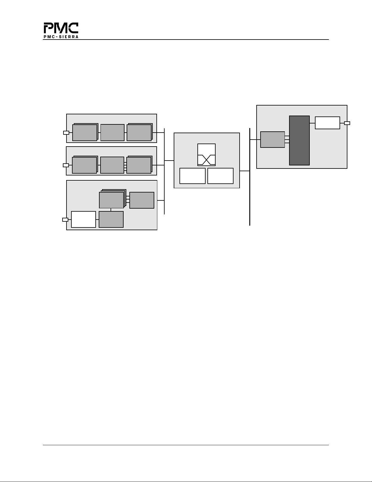
As an ATM-PHY layer device, the S/UNI-JET connects on the line side to one J2/E3/T3 line
interface unit and on the system side, it interfaces with an ATM layer device, such as the PM7322
RCMP-800, over an 8- or 16-bit wide UTOPIA Level 2 interface. Refer to Figure 1.
Figure 1 S/UNI-JET Operating as an ATM PHY in an ATM Switch
T1/E1 Line Card
PM4314
QDSX
J2/E3/T3 Line Card
J2/E3/T3
LIU
PM7344
S/UNI-MPH
PM7347
S/UNI-JET
S/UNI®-JET Data Sheet
Released
OC-12 Line Card
UTOPIA Bus
ATM Switch Core
Switch
Fabric
PM7322
RCMP-800
UTOPIA Bus
Egress
Device
PM5355
S/UNI-622
OC-3 Line Cards
PM5346
S/UNI-LITE
PM7348
S/UNI-
DUAL
PM5347
S/UNI-PLUS
PMD
As a J2/E3/T3 framer, the S/UNI-JET can be used in router, frame relay switch, and multiplexer
applications. Refer to Figure 2.
Proprietary and Confidential to PMC-Sierra, Inc., and for its Customers’ Internal Use 26
Document ID: PMC-1990267, Issue 3
S/UNI®-JET Data Sheet
Figure 2 S/UNI-JET Operating as a Framer Device in Frame Relay Equipment
Released
Access Side
Unchannelized J2/E3/T3 Card
8 Port Channelized T1 Card
PM4314
QDSX
PM4314
QDSX
28 Port Unchannelized T1 Card (M13)
DS-3
LIU
PM4388
TOCTL
4 Port Channelized E1 Card
PM6344
EQUAD
PM4388
TOCTL
PM8313
D3MX
FREEDM-8
FREEDM-8
PM7366
PM7366
PM7364
FREEDM-
IP Switch/Router Core
Switch
Fabric
Processor
Packet
Memory
PCI Bus
32
PCI Bus
PM7366
FREEDM-8
PM7347
S/UNI-
JET
In an unchannelized J2/E3/T3 line card, the S/UNI-JET directly connects to one PM7366
FREEDM-8 HDLC controller. Each FREEDM-8 can process two high-speed links such as T3 and
E3, or can process up to eight lower speed links such as J2. The S/UNI-JET gaps all the overhead
bits so that only the payload data is passed to and from FREEDM-8. On the line side, the S/UNIJET is connected to one J2/E3/T3 line interface unit. On the system side, the S/UNI-JET
interfaces with a data link device over a serial bit interface.
Uplink Side
J2/E3/T3
LIU
Proprietary and Confidential to PMC-Sierra, Inc., and for its Customers’ Internal Use 27
Document ID: PMC-1990267, Issue 3
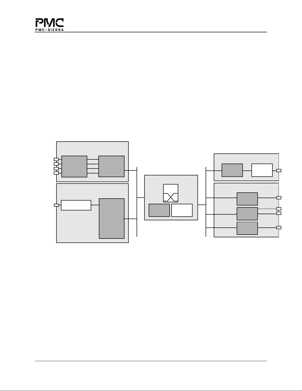
6 Block Diagram
Figure 3 Block Diagram
S/UNI®-JET Data Sheet
Released
TPOHFP/TFPO/TMFPO/TGAPCLK/TCELL
TIOHM/TFPI/TMFPI
TPOS/TDATO
TNEG/TOHM
TCLK
RCLK
RPOS/RDATI
RNEG/RLCV/ROHM
RBOC
Rx
FEAC
XBOC
Tx
FEAC
Line
Encode
Line
Decode
RDLC
HDLC
TDPR
Tx
HDLC
J2, E3, or DS3
Transmit Framer
J2, E3, or DS3
Receive Framer
Rx
Monitor
TRAN
FRMR
PMON
Perfor.
TOHINS
Tx O/H
Access
TOH
TOHCLK
TOHFP
Rx O/H
Access
ROH
1/2 TTB
Tx Trail
Buffer
ROHCLK
1/2 TTB
Rx Trail
Buffer
ROHFP
TPOH/TDATI
TPOHINS
TICLK
SPLT
Transmit ATM and
PLCP Framer
ATMF/ SPLR
Receive ATM
and PLCP Framer
TPOHCLK
LCD/RDATO
RPOH/ROVRHD
REF8KI
PLCP/cell
Performance
Monitor
FRMSTAT
PRGD BER Tester
CPPM
TDO
TXCP_50
Tx Cell
Processor
RXCP_50
Rx Cell
Processor
TCK
TDI
IEEE P1149.1
JTAG Test
Access Port
Tx 4 Cell
Rx 4 Cell
Microprocessor
D[7.0]
A[10.0]
TRSTB
TMS
TXFF
FIFO
RXFF
FIFO
Interface
ALE
CSB
DTCA
TDAT[15.0]
TPRTY
TSOC
TCA
TADR[2.0]
TENB
TFCLK
System
I/F
RDB
INTB
WRB
RSTB
PHY_ADR[2.0]
ATM8
RFCLK
RENB
RADR[2.0]
RCA
RSOC
RPRTY
RDAT[15.0]
DRCA
RPOHCLK/RSCLK/RGAPCLK
REF8KO/RPOHFP/RFPO/RMFPO
Proprietary and Confidential to PMC-Sierra, Inc., and for its Customers’ Internal Use 28
Document ID: PMC-1990267, Issue 3

7 Description
The PM7346 S/UNI-JET is an ATM physical layer processor with integrated DS3, E3, and J2
framers. It supports PLCP sublayer DS1, DS3, E1, and E3 processing and ATM cell delineation.
The S/UNI-JET contains:
• An Integral DS3 framer that provides DS3 framing and error accumulation in accordance
with ANSI T1.107, and T1.107a.
• An Integral E3 framer that provide E3 framing in accordance with ITU-T Recommendations
G.832 and G.751.
• An Integral J2 framer that provide J2 framing in accordance with ITU-T Recommendation
G.704 and I.432.
When configured for various transmission system sublayer processing, the S/UNI-JET accepts
and outputs the appropriate type of bipolar and unipolar signals as described in Table 2:
S/UNI®-JET Data Sheet
Released
Table 2 Transmission System Sublayer Processing Acceptance and Output
Transmission System
Sublayer Processing
DS3 Accepts and outputs both digital B3ZS-encoded bipolar and unipolar
E3 Accepts and outputs both HDB3-encoded bipolar and unipolar signals
J2 Accepts and outputs both B8ZS-encoded bipolar and unipolar signals
DS1, or E1 Accepts and outputs outputs unipolar signals with appropriate clock and
Other transmission systems Provides a generic interface for physical sublayer processing.
Acceptance and Output
signals compatible with M23 and C-bit parity applications.
compatible with G.751 and G.832 applications.
compliant with G.704 and NTT 6.312 Mbit/s applications.
frame pulse signals for physical sublayer processing.
In the DS3 receive direction, the S/UNI-JET frames to DS3 signals with a maximum average
reframe time of 1.5 ms and detects line code violations (LCV), loss of signal (LOS), framing bit
errors, parity errors, path parity errors, alarm indication signals (AIS), far end receive failure
(FERF), and idle code. The DS3 overhead bits are extracted and presented on serial outputs.
When in C-bit parity mode, the Path Maintenance Data Link (PMDL) and the Far End Alarm and
Control (FEAC) channels are extracted. HDLC receivers are provided for PMDL support. Valid
bit-oriented codes in the FEAC channels are also detected and are available through the
microprocessor port.
Table 3 Summary of Receive Detection Features
Transmission System
Sublayer Processing
DS3 Receive
E3 Receive LCV, LOS, framing bit errors, AIS, and RAI
Proprietary and Confidential to PMC-Sierra, Inc., and for its Customers’ Internal Use 29
Document ID: PMC-1990267, Issue 3
Transmit or
Receive
Detected Features
LCV, LOS, framing bit errors, parity errors, path parity
errors, AIS, FERF, and idle code

S/UNI®-JET Data Sheet
Released
Transmission System
Sublayer Processing
J2 Receive
Transmit or
Receive
Detected Features
LCV, LOS, LOF, framing bit errors, physical layer AIS,
payload AIS, CRC-5 errors, Remote End Alarm, and RAI
In the E3 receive direction, the S/UNI-JET frames to G.751 and G.832 E3 signals with a
maximum average reframe times of 135 µs for G.751 frames and 250 µs for G.832 frames. LCVs,
LOS, framing bit errors, AIS, and remote alarm indication (RAI) are detected. Further, when
processing G.832 formatted data, parity errors, far end receive failure, and far end block errors are
also detected; and the Trail Trace message can be extracted and made available through the
microprocessor port. HDLC receivers are provided for either the G.832 Network Requirement or
the G.832 General Purpose Data Link support.
In the J2 receive direction, the S/UNI-JET frames to G.704 6.312 MHz signals with a maximum
average reframe time of 5.07 ms. An alternate framing algorithm that uses the CRC-5 bits to rule
out 99.9% of all static mimic framing patterns is available with a maximum average reframe time
of 10.22 ms when operating with a 10
4
-
bit error rate. The alternate framing algorithm can be
selected by the CRC_REFR bit in the J2-FRMR Configuration Register. LCV, LOS, loss of frame
(LOF), framing bit errors, physical layer AIS, payload AIS, CRC-5 errors, Remote End Alarm,
and RAI are detected. HDLC receivers are provided for Data Link support.
Error event accumulation is also provided by the S/UNI-JET. Framing bit errors, LCV, parity
errors, path parity errors, and far end block errors (FEBE) are accumulated, when appropriate, in
saturating counters for DS3, E3, and J2 frames. LOF detection for DS3, E3, and J2 is provided as
recommended by ITU-T G.783 with integration times of 1ms, 2ms, and 3ms.
In the DS3 transmit direction, the S/UNI-JET inserts DS3 framing, X and P bits. When enabled
for C-bit parity operation, bit-oriented code transmitters and HDLC transmitters are provided for
the insertion of FEAC channels and the PMDL in the appropriate overhead bits. AIS can be
inserted by using internal register bits and other status signals such as the idle signal can be
inserted when enabled by internal register bits. When M23 operation is selected, the C-bit Parity
ID bit (the first C-bit of the first M sub-frame) is forced to toggle so that downstream equipment
will not confuse an M23-formatted stream with stuck-at 1 C-bits for C-bit parity application.
In the E3 transmit direction, the S/UNI-JET inserts E3 framing in either G.832 or G.751 format.
When enabled for G.832 operation, an HDLC transmitter is provided so that the Network
Requirement or General Purpose Data Link is inserted into the appropriate overhead bits. The
AIS and other status signals can be inserted by internal register bits.
In the J2 transmit direction, the S/UNI-JET inserts J2 6.312 Mbit/s G.704 framing. HDLC
transmitters are provided the Data Links are inserted. CRC-5 check bits are calculated and
inserted into the J2 multiframe. External pins are provided so that any of the overhead bits within
the J2 frame can be overwritten.
The S/UNI-JET also supports diagnostic options that allow it to insert, when appropriate, the
transmit framing format, parity or path parity errors, F-bit framing errors, M-bit framing errors,
invalid X or P-bits, LCV, all-zeros, AIS, RAIs, and Remote End Alarms.
Proprietary and Confidential to PMC-Sierra, Inc., and for its Customers’ Internal Use 30
Document ID: PMC-1990267, Issue 3

S/UNI®-JET Data Sheet
Released
The S/UNI-JET provides cell delineation for ATM cells using the PLCP framing format, or by
using the header check sequence octet in the ATM cell header as specified by ITU-T
Recommendation I.432. DS1, DS3, E1, and E3-based PLCP frame formats can be processed.
Non-PLCP-based cell delineation is done with either bit, nibble, or byte-wide search algorithms
depending on the line interface used. An interface consistent with the generic physical interface
defined by ITU-T Recommendation I.432 is provided for arbitrary rates up to 52 Mbit/s. This
interface is used for PHY layer support for transmission systems that do not have an associated
PLCP sublayer, or to provide an efficient means of directly mapping ATM cells to existing
transmission system formats (such as DS3 and DS1).
In the PLCP receive direction, framing, path overhead extraction, and cell extraction is provided.
BIP-8 error events, frame octet error events, and FEBE events are accumulated.
In the PLCP transmit direction, the S/UNI-JET provides overhead insertion using inputs or
internal registers, DS3 nibble and E3 byte stuffing, automatic BIP-8 octet generation and
insertion, and automatic FEBE insertion. Diagnostic features for BIP-8 error, framing error and
FEBE insertion are also supported.
In the cell receive path, idle cells may be dropped according to a programmable filter. By default,
incoming cells with single bit HCS errors are corrected and written to the FIFO buffer.
Optionally, cells can be dropped upon detection of a HCS error. Cell delineation may optionally
be disabled to allow all cells to pass, regardless of cell delineation status. The ATM cell payloads
are optionally descrambled. ATM cell headers may optionally be descrambled (for use with PPP
packets). Assigned cells containing no detectable HCS errors are written to a FIFO buffer. Cell
data is read from the FIFO using a synchronous 50 MHz 8-bit wide or 16-bit wide SCI-PHY
TM
and Utopia Level 2-compatible interface. Cell data parity is also provided. Counts of error-free
assigned cells, and cells containing HCS errors are accumulated independently for performance
monitoring purposes.
In the cell transmit path, cell data is written to a FIFO buffer using a synchronous 50 MHz 8-bit
wide or 16-bit wide SCI-PHY
TM
compatible interface. Cell data parity is also examined for errors.
Idle cells are automatically inserted when the FIFO contains less than one full cell. HCS
generation, cell payload scrambling, and cell header scrambling (for use with PPP packets) are
optionally provided. Counts of transmitted cells are accumulated for performance monitoring
purposes.
Both receive and transmit cell FIFOs provide buffering for four cells. The FIFOs provide the rate
matching interface between the higher layer ATM entity and the S/UNI-JET.
The S/UNI-JET is configured, controlled, and monitored by a generic 8-bit microprocessor bus
through which all internal registers are accessed. All sources of interrupts can be identified,
acknowledged, or masked with this interface.
The S/UNI-JET requires a software initialization sequence in order to guarantee proper device
operation and long term reliability. Please refer to Section 13.1 of this document for the details on
how to program this sequence.
Proprietary and Confidential to PMC-Sierra, Inc., and for its Customers’ Internal Use 31
Document ID: PMC-1990267, Issue 3

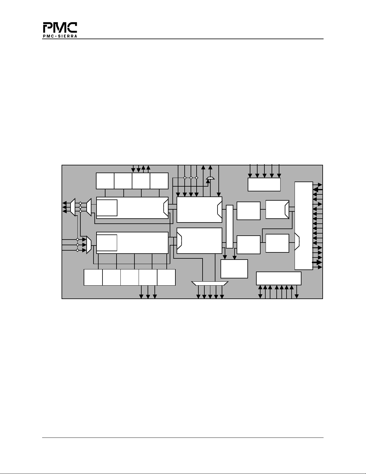
8 Pin Diagram
The S/UNI-JET is packaged in a 256-pin SBGA package with a body size of 27 mm by 27 mm
and a pin pitch of 1.27 mm.
Quadrant A11/A20 to K11/K20
20 19 18 17 16 15 14 13 12 11
A VSS VSS VSS TDATI[10] TDATI[14] D[1] D[5] VSS A[3] A[7] A
B VSS VDD VDD TDATI[9] TDATI[13] D[0] D[4] A[0] A[2] A[6] B
C VSS VDD VDD TDATI[7] TDATI[11] TDATI[15] D[2] D[6] A[1] A[5] C
D TDAT[3] TDAT[4] TDAT[6] NC TDAT[8] TDAT[12] VDD D[3] D[7] A[4] D
E TFCLK TDAT[0] TDAT[2] TDAT[5] E
F TADR[0] TADR[1] TADR[2] TDAT[1] F
G TSOC TPRTY VDD VDD G
H BIAS TCA TENB VDD H
S/UNI®-JET Data Sheet
Released
Bottom View
(Top Left)
J VSS NC NC DTCA J
K VSS NC PHY_ADR[2] VDD
20 19 18 17 16 15 14 13 12 11
K
Quadrant A1/A10 to K1/K10
1098765 4 32 1
A VSS VSS ALE INTB TRSTB TOHM/
B A[9] A[10] WRB TDO TCK TCLK NC VDD VDD VSS B
C A[8] CSB RSTB TMS TPOS/
D VDD RDB TDI VDD
E NC VSS VSS VSS E
FVSSVSSNCNCF
GVDDNCVSSVSSG
Bottom View
TDATO
RPOS/
RDATI
TNEG
RLCV/
RNEG/
ROHM
NC BIAS NC NC VSS D
(Top Right)
H VSS TOH TOHCLK VSS H
J TOHINS TOHFP ROH ROHFP J
K
RCLK VSS VSS VSS A
NC VDD VDD VSS C
ROHCLK VSS VSS NC K
109 876 5 4 32 1
Proprietary and Confidential to PMC-Sierra, Inc., and for its Customers’ Internal Use 32
Document ID: PMC-1990267, Issue 3

S/UNI®-JET Data Sheet
W
W
Released
Quadrant L11/L20 to Y11/Y20
20 19 18 17 16 15 14 13 12 11
L PHY_ADR[1] PHY_ADR[0] ATMB DRCA L
MNC NC NC RSOC M
N VSS RCA RENB RADR[1] N
P RFCLK RADR[2] RADR[0] VDD P
R VDD VDD RPRTY RDAT[13] R
T RDAT[15] RDAT[14] RDAT[12] RDAT[9]
U RDAT[11] RDAT[10] RDAT[8] BIAS RDAT[6] RDAT[2] VDD TPOHCLK REF8KO/
V VSS VDD VDD RDAT[7] RDAT[3] TICLK TPOHINS
W VSS VDD VDD RDAT[5] RDAT[1]
Y VSS VSS VSS RDAT[4] RDAT[0] TDATI/
20 19 18 17 16 15 14 13 12 11
TIOHM/
TFPI/
TMFPI
TPOH
Bottom View
(Bottom Left)
RPOH/
ROVRHD
TPOHFP/
TFPO/
TMFPO/
TGAPCLK/
TCELL
LCD/
RDATO
RPOHCLK/
RSCLK/
RGAPCLK
VSS VSS VSS Y
RPOHFP/
VDD U
RFPO/
RMFPO
VSS NC V
VSS VSS
Quadrant L1/L10 to Y1/Y10
10987 6 543 21
T
L VDD NC NC VSS L
Bottom View
M VSS NC NC VSS M
(Bottom Right)
N NC NC NC VSS N
P VDD VSS NC NC P
R NC NC NC VSS R
T
UNCVSSNCVDDNCNCBIASNC NCFRMSTATU
VNCVSSNCNCVSSNCNCVDDVDDVSSV
W NC VSS VSS NC VSS VSS NC VDD VDD VSS
Y NC NC VSS NC NC VSS NC VSS VSS VSS Y
109876543 21
NC REF8KI NC NC T
Proprietary and Confidential to PMC-Sierra, Inc., and for its Customers’ Internal Use 33
Document ID: PMC-1990267, Issue 3

9 Pin Description
S/UNI®-JET Data Sheet
Released
Pin Name Type Pin
No.
TPOS
TDATO
TNEG
TOHM
Output C6 The Transmit Digital Positive Pulse (TPOS) contains the
Output A5 The Transmit Digital Negative Pulse (TNEG) contains the
Function
positive pulses transmitted on the B3ZS-encoded DS3,
HDB3-encoded E3, or B8ZS-encoded J2 transmission
system when the dual-rail output format is selected.
The Transmit Data (TDATO) contains the transmit data
stream when the single-rail (unipolar) output format is
enabled or when a non-DS3/E3/J2 based transmission
system is selected.
The TPOS/TDATO pin function selection is controlled by
the TFRM[1:0] and the TUNI bits in the S/UNI-JET
Transmit Configuration Register. Output signal polarity
control is provided by the TPOSINV bit in the S/UNI-JET
Transmit Configuration Register.
Both TPOS and TDATO are updated on the falling edge
of TCLK by default, and may be configured for update on
the rising edge of TCLK through the TCLKINV bit in the
S/UNI-JET Transmit Configuration Register. Also, both
TPOS and TDATO can be updated on the rising edge of
TICLK, enabled by the TICLK bit in the S/UNI-JET
Transmit Configuration Register.
negative pulses transmitted on the B3ZS-encoded DS3,
HDB3-encoded E3, or B8ZS-encoded J2 transmission
system when the dual-rail NRZ output format is selected.
The Transmit Overhead Mask (TOHM) indicates the
position of overhead bits (non-payload bits) in the
transmission system stream aligned with TDATO. TOHM
indicates the location of the M-frame boundary for DS3,
the position of the frame boundary for E3, and the
position of the multi-frame boundary for J2 when the
single-rail (unipolar) NRZ input format is enabled.
When a PLCP formatted signal is transmitted, TOHM is
set to logic one once per transmission frame, and
indicates the DS1 or E1 frame alignment.
When a non-PLCP, non-DS3, non-E3, or non-J2 based
signal is transmitted, TOHM is a delayed version of the
TIOHM input, and indicates the position of each
overhead bit in the transmission frame. TOHM is updated
on the falling edge of TCLK.
The TNEG/TOHM pin function selection is controlled by
the TFRM[1:0] and the TUNI bits in the S/UNI-JET
Transmit Configuration Register. Output signal polarity
control is provided by the TNEGINV bit in the S/UNI-JET
Transmit Configuration Register.
Proprietary and Confidential to PMC-Sierra, Inc., and for its Customers’ Internal Use 34
Document ID: PMC-1990267, Issue 3

S/UNI®-JET Data Sheet
Released
Pin Name Type Pin
Function
No.
By default, both TNEG and TOHM are updated on the
falling edge of TCLK and can be enabled for update on
the rising edge of TCLK. This sampling is controlled by
the TCLKINV bit in the S/UNI-JET Transmit
Configuration Register. Also, both TNEG and TOHM can
be updated on the rising edge of TICLK, enabled by the
TICLK bit in the S/UNI-JET Transmit Configuration
Register.
TCLK Output B5 The Transmit Output Clock (TCLK) provides the transmit
direction timing. TCLK is a buffered version of TICLK and
can be enabled to update the TPOS/TDATO and
TNEG/TOHM outputs on its rising or falling edge.
RPOS
RDATI
Input D6 The Receive Digital Positive Pulse (RPOS) contains the
positive pulses received on the B3ZS-encoded DS3, the
HDB3-encoded E3, or the B8ZS-encoded J2
transmission system when the dual-rail NRZ input format
is selected.
The Receive Data (RDATI) contains the data stream
when the single-rail (unipolar) NRZ input format is
enabled or when a non-DS3/E3/J2 based transmission
system is being processed (for example, RDATI may
contain a DS1 or E1 stream).
The RPOS/RDATI pin function selection is controlled by
the RFRM[1:0] bits in the S/UNI-JET Configuration
Register and by the UNI bits in the DS3 FRMR, the E3
FRMR, or the J2 FRMR Configuration Register.
Both RPOS and RDATI are sampled on the rising edge
of RCLK by default, and may be enabled to be sampled
on the falling edge of RCLK. This sampling is controlled
by the RCLKINV bit in the S/UNI-JET Receive
Configuration Register.
Note: Signal polarity control is provided by the RPOSINV
bit in the S/UNI-JET Receive Configuration Register.
Proprietary and Confidential to PMC-Sierra, Inc., and for its Customers’ Internal Use 35
Document ID: PMC-1990267, Issue 3

S/UNI®-JET Data Sheet
Released
Pin Name Type Pin
Function
No.
RNEG
RLCV
ROHM
RCLK Input A4
TOHINS Input J4 The Transmit DS3/E3/J2 Overhead Insertion (TOHINS)
Input C5
The Receive Digital Negative Pulse (RNEG) contains the
negative pulses received on the B3ZS encoded DS3, the
HDB3-encoded E3, or the B8ZS-encoded J2
transmission system when the dual-rail NRZ input format
is selected.
The Receive LCV (RLCV) contains LCV indications when
the single-rail (unipolar) NRZ input format is enabled for
DS3, E3, or J2 applications. Each LCV is represented by
an RCLK period-wide pulse.
When a DS1 or E1 PLCP or ATM direct-mapped signal is
received, Receive Overhead Mask (ROHM) is pulsed
once per transmission frame, and indicates the DS1 or
E1 frame alignment relative to the RDATI data stream.
When an alternate frame-based signal is received,
ROHM indicates the position of each overhead bit in the
transmission frame.
The RNEG/RLCV/ROHM pin function selection is
controlled by the RFRM[1:0] bits in the S/UNI-JET
Receive Configuration Register, the UNI bits in the DS3
FRMR, E3 FRMR, or J2 FRMR Configuration Register,
and the PLCPEN and EXT bits in the SPLR
Configuration Register.
RNEG, RLCV, and ROHM are sampled on the rising
edge of RCLK by default, and may be enabled to be
sampled on the falling edge of RCLK. This sampling is
controlled by the RCLKINV bit in the S/UNI-JET Receive
Configuration Register.
Note: Signal polarity control is provided by the RNEGINV
bit in the S/UNI-JET Receive Configuration Register.
The Receive Clock (RCLK) provides the receive direction
timing. RCLK is the externally recovered transmission
system baud rate clock that samples the RPOS/RDATI
and RNEG/RLCV/ROHM inputs on its rising or falling
edge.
controls the insertion of the DS3, E3, or J2 overhead bits
from the TOH input.
When TOHINS is high, the associated overhead bit in the
TOH stream is inserted in the transmitted DS3, E3, or J2
frame. When TOHINS is low, the DS3, E3, or J2
overhead bit is generated and inserted internally.
TOHINS is sampled on the rising edge of TOHCLK. If
TOHINS is a logic one, the TOH input has precedence
over the internal datalink transmitter, or any internal
register bit setting.
Proprietary and Confidential to PMC-Sierra, Inc., and for its Customers’ Internal Use 36
Document ID: PMC-1990267, Issue 3

S/UNI®-JET Data Sheet
Released
Pin Name Type Pin
No.
TOH Input H3
TOHFP Output J3
TOHCLK Output H2
REF8KI Input T3
Function
When configured for DS3 operation, Transmit DS3/E3/J2
Overhead Data (TOH) contains the overhead bits (C, F,
X, P, and M) that may be inserted in the transmit DS3
stream.
When configured for G.832 E3 operation, TOH contains
the overhead bytes (FA1, FA2, EM mask, TR, MA, NR,
and GC) that may be inserted in the transmit G.832 E3
stream.
When configured for G.751 E3 operation, TOH contains
the overhead bits (RAI, National Use, Stuff Indication,
and Stuff Opportunity) that may be inserted in the
transmit G.751 E3 stream.
When configured for J2 operation, TOH contains the
overhead bits (TS97, TS98, Framing, X
that may be inserted in the transmit J2 stream.
If TOHINS is a logic one, the TOH input has precedence
over the internal datalink transmitter, or any other internal
register bit setting. TOH is sampled on the rising edge of
TOHCLK.
The Transmit DS3/E3/J2 Overhead Frame Position
(TOHFP) is used to align the individual overhead bits in
the transmit overhead data stream, TOH, to the DS3 Mframe or the E3 frame.
For DS3, TOHFP is high during the X1 overhead bit
position in the TOH stream. For G.832 E3, TOHFP is
high during the first bit of the FA1 byte. For G.751 E3,
TOHFP is high during the RAI overhead bit position in
the TOH stream. For J2, TOHFP is high during the first
bit of timeslot 97 in the first frame of a 4-frame
multiframe).
TOHFP is updated on the falling edge of TOHCLK.
The Transmit DS3/E3/J2 Overhead Clock (TOHCLK) is
active when a DS3, E3, or J2 stream is being processed.
TOHCLK is
MHz clock for G.832 E3, a 1.074 MHz clock for G.751
E3, and a gapped 6.312 MHz clock with an average
frequency of 168 kHz for J2.
TOHFP is updated on the falling edge of TOHCLK. TOH,
and TOHINS are sampled on the rising edge of
TOHCLK.
The PLCP frame rate is locked to an external 8 kHz
reference applied on Reference 8 kHz Input (REF8KI).
An internal phase-frequency detector compares the
transmit PLCP frame rate with the externally applied 8
kHz reference and adjusts the PLCP frame rate.
The REF8KI input must transition high once every 125 µs
for correct operation. The REF8KI input is treated as an
asynchronous signal and must be “glitch-free”. If the
LOOPT register bit is logic one, the PLCP frame rate is
locked to the RPOHFP signal instead of the REF8KI
input.
nominally a 526 kHz clock for DS3, a 1.072
1-3
, A, M, E
1-5
)
Proprietary and Confidential to PMC-Sierra, Inc., and for its Customers’ Internal Use 37
Document ID: PMC-1990267, Issue 3

S/UNI®-JET Data Sheet
Released
Pin Name Type Pin
No.
TPOHINS Input V14
TPOH
TDATI
Input Y15 The Transmit PLCP Overhead Data (TPOH) valid when
Function
The Transmit Path Overhead Insertion (TPOHINS)
controls the insertion of PLCP overhead octets on the
TPOH input. When TPOHINS is logic one, the
associated overhead bit in the TPOH stream is inserted
in the transmit PLCP frame. When TPOHINS is logic
zero, the PLCP path overhead bit is generated and
inserted internally.
TPOHINS is sampled on the rising edge of TPOHCLK.
Note: When operating in G.751 E3 PLCP mode, bits 8, 7,
and 6 of the C1 octet should not be manipulated.
the FRMRONLY bit in the S/UNI-JET Configuration 1
Register is logic zero. TPOH contains the PLCP path
overhead octets (Zn, F1, B1, G1, M1, M2, and C1) which
may be inserted in the transmit PLCP frame. The octet
data on TPOH is shifted in order from the most
significant bit (bit 1) to the least significant bit (bit 8).
TPOH is sampled on the rising edge of TPOHCLK.
The Framer Transmit Data (TDATI) contains the serial
data to be transmitted when the S/UNI-JET is configured
as a DS3, E3, or J2 framer device for non-ATM
applications by setting the FRMRONLY bit in the S/UNIJET Configuration 1 Register.
TDATI is sampled on the rising edge of TICLK if the
TXGAPEN register bit in the S/UNI-JET Configuration 2
Register is logic zero. If TXGAPEN is logic one, then
TDATI is sampled on the falling edge of TGAPCLK.
Proprietary and Confidential to PMC-Sierra, Inc., and for its Customers’ Internal Use 38
Document ID: PMC-1990267, Issue 3

S/UNI®-JET Data Sheet
Released
Pin Name Type Pin
No.
TPOHFP
TFPO
TMFPO
TGAPCLK
Output W14
Function
The Transmit Path Overhead Frame Position (TPOHFP)
is valid when the FRMRONLY bit in the S/UNI-JET
Configuration 1 Register is logic zero. The TPOHFP
output locates the individual PLCP path overhead bits in
the transmit overhead data stream, TPOH. TPOHFP is
logic one while bit 1 (the most significant bit) of the path
user channel octet (F1) is present in the TPOH stream.
TPOHFP is updated on the falling edge of TPOHCLK.
The Framer Transmit Frame Pulse/Multi-frame Pulse
Reference (TFPO/TMFPO) is valid when the S/UNI-JET
is configured as a DS3, E3, or J2 framer for non-ATM
applications by setting the FRMRONLY bit in the S/UNIJET Configuration 1 Register to logic one and the
TXGAPEN bit in the S/UNI-JET Configuration Register to
logic zero.
TFPO pulses high for 1 out of every 85 clock cycles
when configured for DS3, giving a free-running mark for
all overhead bits in the frame. TFPO pulses high for 1 out
of every 1536 clock cycles when configured for G.751
E3, giving a free-running reference G.751 indication.
TFPO pulses high for 1 out of every 4296 clock cycles
when configured for G.832 E3, giving a free-running
reference G.832 frame indication. TFPO pulses high for
1 out of every 789 clock cycles when configured for J2,
giving a free-running reference frame indication.
TMFPO pulses high for 1 out of every 4760 clock cycles
when configured for DS3, giving a free-running reference
M-frame indication. TMFPO pulses high for 1 out of
every 3156 clock cycles when configured for J2, giving a
free-running reference multi-frame indication. TMFPO
behaves the same as TFPO for E3 applications.
TFPO and TMFPO are updated on the rising edge of
TICLK or RCLK if loop-timed.
The Framer Gapped Transmit Clock (TGAPCLK) is valid
when the S/UNI-JET is configured as a DS3, E3, or J2
framer for non-ATM applications by setting the
FRMRONLY bit in the S/UNI-JET Configuration 1
Register and the TXGAPEN bit in the S/UNI-JET
Configuration 2 Register.
TGAPCLK is derived from the transmit reference clock
TICLK or from the receive clock if loop-timed. The
overhead bit (gapped) positions are generated internal to
the device. TGAPCLK is held high during the overhead
bit positions. This clock is useful for interfacing to devices
which source payload data only.
TGAPCLK is used to sample TDATI.
Proprietary and Confidential to PMC-Sierra, Inc., and for its Customers’ Internal Use 39
Document ID: PMC-1990267, Issue 3

S/UNI®-JET Data Sheet
Released
Pin Name Type Pin
Function
No.
TCELL
TPOHCLK Output U13 The Transmit PLCP Overhead Clock (TPOHCLK) is
TIOHM
TFPI
TMFPI
Input W15 The Transmit Input Overhead Mask (TIOHM) is valid only
The Transmit Cell Indication (TCELL) is valid when the
TCELL bit in the S/UNI-JET Miscellaneous Register is
set.
TCELL pulses once for every cell (idle or assigned)
transmitted. TCELL is updated using timing derived from
the transmit input clock (TICLK), and is active for a
minimum of 8 TICLK periods (or 8 RCLK periods if looptimed).
active when PLCP processing is enabled. TPOHCLK is
nominally a 26.7 kHz clock for a DS1 PLCP frame, a 768
kHz clock for a DS3 PLCP frame, a 33.7 kHz clock for an
E1 based PLCP frame, and a 576 kHz clock for an G.751
E3 based PLCP frame.
TPOHFP is updated on the falling edge of TPOHCLK.
TPOH and TPOHINS are sampled on the rising edge of
TPOHCLK.
if the FRMRONLY bit in the S/UNI-JET Configuration 1
Register is logic zero. TIOHM indicates the position of
overhead bits when not configured for DS1, DS3, E1, E3,
or J2 transmission system streams. TIOHM is delayed
internally to produce the TOHM output.
When configured for operation over a DS1, a DS3, an
E1, an E3, or a J2 transmission system sublayer, TIOHM
is not required, and should be set to logic zero. When
configured for other transmission systems, TIOHM is set
to logic one for each overhead bit position. TIOHM is set
to logic zero if the transmission system does not contain
overhead bits.
TIOHM is sampled on the rising edge of TICLK.
The Framer Transmit Frame Pulse/Multiframe Pulse
(TFPI/TMFPI) is valid when the S/UNI-JET is configured
as a DS3, E3, or J2 framer for non-ATM applications by
setting the FRMRONLY bit in the S/UNI-JET
Configuration 1 Register to logic one.
TFPI indicates the position of all overhead bits in each
DS3 M-subframe, the first bit in each G.751 E3 or G.832
E3 frame, or the first framing bit in each J2 frame. TFPI
is not required to pulse at every frame boundary in E3 or
J2 modes.
TMFPI indicates the position of the first bit in each DS3
M-frame, the first bit in each E3 frame, or the first framing
bit in each J2 multiframe. TMFPI is not required to pulse
at every multiframe boundary.
TFPI/TMFPI is sampled on the rising edge of TICLK.
Proprietary and Confidential to PMC-Sierra, Inc., and for its Customers’ Internal Use 40
Document ID: PMC-1990267, Issue 3

S/UNI®-JET Data Sheet
Released
Pin Name Type Pin
No.
TICLK Input V15
ROHFP Output J1
ROH Output J2
ROHCLK Output K4
Function
The Transmit Input Clock (TICLK) provides the transmit
direction timing. TICLK is the externally generated
transmission system baud rate clock. It is internally
buffered to produce the transmit clock output, TCLK, and
can be enabled to update the TPOS/TDATO and
TNEG/TOHM outputs on the TICLK rising edge. The
TICLK maximum frequency is 52 MHz.
The Receive DS3/E3/J2 Overhead Frame Position
(ROHFP) locates the individual overhead bits in the
received overhead data stream, ROH.
ROHFP is high during the X1 overhead bit position in the
ROH stream when processing a DS3 stream. ROHFP is
high during the first bit of the FA1 byte when processing
a G.832 E3 stream. ROHFP is high during the RAI
overhead bit position when processing a G.751 E3
stream. ROHFP is high during the first bit in Timeslot 97
in the first frame of the 4-frame multiframe when
processing a J2 stream.
ROHFP is updated on the falling edge of ROHCLK.
The Receive DS3/E3/J2 Overhead Data (ROH) contains
the overhead bits (C, F, X, P, and M) extracted from the
received DS3 stream. It also contains the overhead bytes
(FA1, FA2, EM, TR, MA, NR, and GC) extracted from the
received G.832 E3 stream, the overhead bits (RAI,
National Use, Stuff Indication, and Stuff Opportunity)
extracted from the received G.751 E3 stream, and the
overhead bits (Framing, X
the received J2 stream.
ROH is updated on the falling edge of ROHCLK.
The Receive DS3/E3/J2 Overhead Clock (ROHCLK) is
active when a DS3, E3, or J2 stream is being processed.
ROHCLK is nominally a 526 kHz clock when processing
DS3, a 1.072 MHz clock when processing G.832 E3, a
1.074 MHz clock when processing G.751 E3, and a
gapped 6.312 MHz clock with an average frequency of
168 kHz for J2.
ROH and ROHFP are updated on the falling edge of
ROHCLK.
1-3
, A, M, E
) extracted from
1-5
Proprietary and Confidential to PMC-Sierra, Inc., and for its Customers’ Internal Use 41
Document ID: PMC-1990267, Issue 3

S/UNI®-JET Data Sheet
Released
Pin Name Type Pin
No.
REF8KO
RPOHFP
RFPO
RMFPO
RPOH
ROVRHD
Output U12
Output V13 The Receive PLCP Overhead Data (RPOH) contains the
Function
The Reference 8kHz Output (REF8KO) is an 8kHz
reference derived from the receive clock (RCLK). A freerunning divide-down counter is used to generate
REF8KO so it will not “glitch” on reframe actions.
REF8KO will pulse high for approximately one RCLK
cycle every 125 µs. REF8KO should be treated as a
“glitch-free” asynchronous signal.
The Receive PLCP Overhead Frame Position (RPOHFP)
locates the individual PLCP path overhead bits in the
receive overhead data stream, RPOH. RPOHFP is logic
one while bit 1 (the most significant bit) of the path user
channel octet (F1) is present in the RPOH stream.
RPOHFP is updated on the falling edge of RPOHCLK.
RPOHFP is available when the PLCPEN register bit is
logic one in the SPLR Configuration Register.
The Framer Receive Frame Pulse/Multi-frame Pulse
(RFPO/RMFPO) is valid when the S/UNI-JET is
configured to be in framer only mode. The 8KREFO bit
must be set to logic zero in the S/UNI-JET Configuration
Register.
RFPO is aligned to RDATO and indicates the position of
the first bit in each DS3 M-subframe, the first bit in each
G.751 E3 or G.832 E3 frame, or the first framing bit in
each J2 frame
RMFPO is aligned to RDATO and indicates the position
of the first bit in each DS3 M-frame, the first bit in each
G.751 or G.832 E3 multiframe, or the first framing bit in
each J2 multiframe.
RFPO/RMFPO is updated on either the falling or rising
edge of RSCLK depending on the setting of the RSCLKR
bit in the S/UNI-JET Receive Configuration Register.
PLCP path overhead octets (Zn, F1, B1, G1, M1, M2,
and C1) extracted from the received PLCP frame when
the PLCP layer is in-frame. When the PLCP layer is in
the LOF state, RPOH is forced to all ones. The octet data
on RPOH is shifted out in order from the most significant
bit (bit 1) to the least significant bit (bit 8).
RPOH is updated on the falling edge of RPOHCLK.
The Framer Receive Overhead Indication (ROVRHD) is
valid when the S/UNI-JET is configured as a DS3, E3, or
J2 framer for non-ATM applications by setting the
FRMRONLY bit in the S/UNI-JET Configuration 1
Register. ROVRHD will be high whenever the data on
RDATO corresponds to an overhead bit position.
ROVRHD is updated on the either the falling or rising
edge of RSCLK depending on the setting of the RSCLKR
bit in the S/UNI-JET Receive Configuration Register.
Proprietary and Confidential to PMC-Sierra, Inc., and for its Customers’ Internal Use 42
Document ID: PMC-1990267, Issue 3

S/UNI®-JET Data Sheet
Released
Pin Name Type Pin
Function
No.
RPOHCLK
RSCLK
RGAPCLK
LCD
RDATO
FRMSTAT Output U1
ATM8 Input L18 The ATM Interface Bus Width Selection (ATM8) input pin
Output W13
Output Y14
The Receive PLCP Overhead Clock (RPOHCLK) is
active when PLCP processing is enabled. The frequency
of this signal depends on the selected PLCP format.
RPOHCLK is nominally a 26.7 kHz clock for a DS1 PLCP
frame, a 768 kHz clock for a DS3 PLCP frame, a 33.7
kHz clock for an E1 based PLCP frame, or a 576 kHz
clock for a G.751 E3 based PLCP frame.
RPOHFP and RPOH are updated on the falling edge of
RPOHCLK.
The Framer Recovered Clock (RSCLK) is valid when the
S/UNI-JET is configured as a DS3, E3, or J2 framer for
non-ATM applications by setting the FRMRONLY bit in
the S/UNI-JET Configuration Register.
RSCLK is the recovered clock and timing reference for
RDATO, RFPO/RMFPO, and ROVRHD.
The Framer Recovered Gapped Clock (RGAPCLK) is
valid when the S/UNI-JET is configured as a DS3, E3, or
J2 framer for non-ATM applications by setting the
FRMRONLY bit in the S/UNI-JET Configuration 1
Register and the RXGAPEN bit in the S/UNI-JET
Configuration 2 Register.
RGAPCLK is the recovered clock and timing reference
for RDATO. RGAPCLK is held high for bit positions
which correspond to overhead.
The Loss of Cell Delineation (LCD) is an active high
signal which is asserted while the ATM cell processor
has detected a Loss of Cell Delineation defect. The
FRMRONLY bit in the S/UNI-JET Configuration 1
Register must be set to logic zero for LCD to be valid.
The Framer Receive Data (RDATO) is valid when the
S/UNI-JET is configured as a DS3, E3, or J2 framer for
non-ATM applications by setting the FRMRONLY bit in
the S/UNI-JET Configuration 1 Register.
RDATO is the received data aligned to RFPO/RMFPO
and ROVRHD. RDATO is updated on the active edge (as
set by the RSCLKR register bit) of RSCLK or RGAPCLK.
Framer Status (FRMSTAT) is an active high signal that
can be configured to show when one of the J2, E3, DS3,
or PLCP framers have detected certain conditions. The
FRMSTAT output can be programmed via the
STATSEL[2:0] bits in the S/UNI-JET Configuration 2
Register to indicate: E3/DS3 LOF or J2 extended LOF,
E3/DS3 OOF or J2 LOF, PLCP LOF, PLCP OOF, AIS,
LOS, and DS3 Idle. FRMSTAT should be treated as a
“glitch-free” asynchronous signal.
determines whether the S/UNI-JET works with a 8-bit
wide interface (RDAT[7:0] and TDAT[7:0]) or a 16-bit
wide interface (RDAT[15:0] and TDAT[15:0]).
If ATM8 is set to logic one, then the 8-bit wide interface is
chosen. If ATM8 is set to logic zero, then the 16-bit wide
interface is chosen.
Proprietary and Confidential to PMC-Sierra, Inc., and for its Customers’ Internal Use 43
Document ID: PMC-1990267, Issue 3

S/UNI®-JET Data Sheet
Released
Pin Name Type Pin
Function
No.
TDAT[15]
TDAT[14]
TDAT[13]
TDAT[12]
TDAT[11]
TDAT[10]
TDAT[9]
TDAT[8]
TDAT[7]
TDAT[6]
TDAT[5]
TDAT[4]
TDAT[3]
TDAT[2]
TDAT[1]
TDAT[0]
TPRTY Input G19 The Transmit Bus Parity (TPRTY) signal indicates the
TSOC Input G20 The Transmit Start of Cell (TSOC) signal marks the start
TENB Input H18 The Transmit Multi-PHY Write Enable (TENB) signal is
Input
C15
A16
B16
D15
C16
A17
B17
D16
C17
D18
E17
D19
D20
E18
F17
E19
The Transmit Cell Data Bus (TDAT[15:0]) carries the
ATM cell octets that are written to the transmit FIFO.
TDAT[15:0] is sampled on the rising edge of TFCLK and
is considered valid only when TENB is simultaneously
asserted and the S/UNI-JET has been selected via the
TADR[2:0] inputs.
The S/UNI-JET can be configured to operate with an 8bit wide or 16-bit wide ATM data interface via the ATM8
input pin. When configured for the 8-bit wide interface,
TDAT[15:8] are not used and should be tied to ground.
parity of the TDAT[15:0] or TDAT[7:0] bus. If configured
for the 8-bit bus (via the ATM8 input pin), then parity is
calculated over TDAT[7:0]. If configured for the 16-bit
bus, then parity is calculated over TDAT[15:0].
A parity error is indicated by a status bit and a maskable
interrupt. Cells with parity errors are inserted in the
transmit stream, so the TPRTY input may be unused.
Odd or even parity selection is made using the TPTYP
register bit.
TPRTY is sampled on the rising edge of TFCLK and is
considered valid only when TENB is simultaneously
asserted and the S/UNI-JET has been selected via the
TADR[2:0] inputs.
of cell on the TDAT bus. When TSOC is high, the first
word of the cell structure is present on the TDAT bus.
It is not necessary for TSOC to be present for each cell.
An interrupt may be generated if TSOC is high during
any word other than the first word of the cell structure.
TSOC is sampled on the rising edge of TFCLK and is
considered valid only when TENB is simultaneously
asserted and the S/UNI-JET has been selected via the
TADR[2:0] inputs.
an active low input which is used along with the
TADR[2:0] inputs to initiate writes to the transmit FIFO.
When sampled low using the rising edge of TFCLK, the
word on the TDAT bus is written into the transmit FIFO
selected by the TADR[2:0] address bus. When sampled
high using the rising edge of TFCLK, no write is
performed, but the TADR[2:0] address is latched to
identify the transmit FIFO to be accessed.
A complete 53-octet cell must be written to the transmit
FIFO before it is inserted into the transmit stream. Idle
cells are inserted when a complete cell is not available.
Proprietary and Confidential to PMC-Sierra, Inc., and for its Customers’ Internal Use 44
Document ID: PMC-1990267, Issue 3

S/UNI®-JET Data Sheet
Released
Pin Name Type Pin
Function
No.
TADR[2]
TADR[1]
TADR[0]
TCA Output H19 The Transmit Multi-PHY Cell Available (TCA) signal
TFCLK Input E20
Input
F18
F19
F20
The Transmit Address (TADR[2:0]) bus is used for
device selection and device polling in accordance with
the Utopia Level 2 standard.
When TADR[2:0] is set to the same value as the
PHY_ADR[2:0] inputs than the transmit interface of this
S/UNI-JET is either being selected or polled.
Note: The null-PHY address 7H is an invalid address and
cannot be used to select the S/UNI-JET.
TADR[2:0] is sampled on the rising edge of TFCLK.
indicates when a cell is available in the transmit FIFO for
the device selected by TADR[2:0].
When high, TCA indicates that the corresponding
transmit FIFO is not full and a complete cell may be
written. When TCA goes low, it can be configured to
indicate either that the corresponding transmit FIFO is
near full or that the corresponding transmit FIFO is full.
TCA will transition low on the rising edge of TFCLK
which samples Payload byte 43 (TCALEVEL0=0) or 47
(TCALEVEL0=1) for the 8-bit interface (ATM8=1), or the
rising edge of TFCLK which samples Payload word 19
(TCALEVEL0=0) or 23 (TCALEVEL0=1) for the 16-bit
interface (ATM8=0) if the device being polled is the same
as the selected device.
To reduce FIFO latency, the FIFO depth at which TCA
indicates "full" can be set to one, two, three, or four cells.
Note: Regardless of what fill level TCA is set to indicate
"full" at, the transmit cell processor can store four
complete cells.
TCA is tri-stated when either the null-PHY address (7H)
or an address not matching the address space set by
PHY_ADR[2:0] is latched (by TFCLK) from the
TADR[2:0] inputs.
The polarity of TCA (with respect the the description
above) is inverted when the TCAINV register bit is set to
logic one.
The Transmit FIFO Write Clock (TFCLK) is used to write
ATM cells to the four-cell transmit FIFOs. TFCLK cycles
at a 52 MHz or lower instantaneous rate.
Proprietary and Confidential to PMC-Sierra, Inc., and for its Customers’ Internal Use 45
Document ID: PMC-1990267, Issue 3

S/UNI®-JET Data Sheet
Released
Pin Name Type Pin
No.
DTCA Output J17
RDAT[15]
RDAT[14]
RDAT[13]
RDAT[12]
RDAT[11]
RDAT[10]
RDAT[9]
RDAT[8]
RDAT[7]
RDAT[6]
RDAT[5]
RDAT[4]
RDAT[3]
RDAT[2]
RDAT[1]
RDAT[0]
Output T20
T19
R17
T18
U20
U19
T17
U18
V17
U16
W17
Y17
V16
U15
W16
Y16
Function
The Direct Access Transmit Cell Available (DTCA) output
signals indicate when a cell is available in the transmit
FIFO.
When high, DTCA indicates that the corresponding
transmit FIFO is not full and a complete cell may be
written. DTCA can be configured to indicate either that
the corresponding transmit FIFO is near full and can
accept no more than four writes or that the
corresponding transmit FIFO is full. DTCA will thus
transition low on the rising edge of TFCLK which
samples Payload byte 43 (TCALEVEL0=0) or 47
(TCALEVEL0=1) for the 8-bit interface (ATM8=1), or the
rising edge of TFCLK which samples Payload word 19
(TCALEVEL0=0) or 23 (TCALEVEL0=1) for the 16-bit
interface (ATM8=0).
To reduce FIFO latency, the FIFO depth at which DTCA
indicates "full" can be set to one, two, three or four cells.
Note: Regardless of what fill level DTCA is set to indicate
"full" at, the transmit cell processor can store four
complete cells.
The polarity of DTCA (with respect to the description
above) is inverted when the TCAINV register bit is set to
logic one.
The DTCA outputs can be used to support Utopia Direct
Access mode.
The Receive Cell Data Bus (RDAT[15:0]) bus carries the
ATM cell octets that are read from the receive ATM FIFO
selected by RADR[2:0]. RDAT[15:0] is tri-stated when
RENB is high. RDAT[15:0] is updated on the rising edge
of RFCLK.
The S/UNI-JET can be configured to operate with an 8bit wide or 16-bit wide ATM data interface via the ATM8
input pin. RDAT[15:8] will remain tri-stated if ATM8 is set
to logic one.
RDAT[15:0] is tri-stated when either the null-PHY
address (7H) or an address not matching the address
space set by PHY_ADR[2:0] is latched from the
RADR[2:0] inputs when RENB is high.
Proprietary and Confidential to PMC-Sierra, Inc., and for its Customers’ Internal Use 46
Document ID: PMC-1990267, Issue 3

S/UNI®-JET Data Sheet
Released
Pin Name Type Pin
Function
No.
RPRTY Output R18
RSOC Output M17 The Receive Start of Cell (RSOC) signal marks the start
RENB Input N18
RADR[2]
RADR[1]
RADR[0]
Input P19
N17
P18
The Receive Parity (RPRTY) signal indicates the parity
of the RDAT bus.
The S/UNI-JET can be configured to operate with an 8bit wide or 16-bit wide ATM data interface via the ATM8
input pin. In the 8-bit mode, RPRTY reflects the parity of
RDAT[7:0]. In the 16-bit mode, RPRTY reflects the parity
of RDAT[15:0].
Odd or even parity selection is made using the RXPTYP
register bit.
RPRTY is tri-stated when either the null-PHY address
(7H) or an address not matching the address space set
by PHY_ADR[2:0] is latched from the RADR[2:0] inputs
when RENB is high.
of cell on the RDAT bus. RSOC marks the start of the
cell on the RDAT bus.
RSOC is tri-stated when either the null-PHY address
(7H) or an address not matching the address space set
by PHY_ADR[2:0] is latched from the RADR[2:0] inputs
when RENB is high.
The Receive Multi-PHY Read Enable (RENB) signal is
used to initiate reads from the receive FIFO.
When sampled low using the rising edge of RFCLK, a
byte is read (if one is available) from the receive FIFO
selected by the RADR[2:0] address bus and output on
the RDAT bus. When sampled high using the rising edge
of RFCLK, no read is performed and RDAT[15:0],
RPRTY, and RSOC are tri-stated, and the address on
RADR[2:0] is latched to select the device or port for the
next ATM FIFO access.
RENB must operate in conjunction with RFCLK to
access the FIFOs at a high enough rate to prevent FIFO
overflows. The ATM layer device may de-assert RENB at
anytime it is unable to accept another byte.
The Receive Address (RADR[2:0])] bus is used for
device selection and device polling in accordance with
the Utopia Level 2 standard. When RADR[2:0] is set to
the same value as the PHY_ADR[2:0] inputs than the
receive interface of this S/UNI-JET is either being
selected or polled.
Note: The null PHY address 7H is an invalid address and
cannot be used to select the S/UNI-JET.
RADR[2:0] is sampled on the rising edge of TFCLK.
Proprietary and Confidential to PMC-Sierra, Inc., and for its Customers’ Internal Use 47
Document ID: PMC-1990267, Issue 3

S/UNI®-JET Data Sheet
Released
Pin Name Type Pin
Function
No.
RCA Output N19
RFCLK Input P20
DRCA Output L17 The Direct Access Receive Cell Available (DRCA) output
PHY_ADR[2]
PHY_ADR[1]
PHY_ADR[0]
CSB Input C9 The Active low Chip Select (CSB) signal must be low to
Input K18
L20
L19
The Receive Multi-PHY Cell Available (RCA) signal
indicates when a cell is available in the receive FIFO for
the device selected by RADR[2:0].
RCA can be configured to be de-asserted when either
zero or four bytes remain in the selected/addressed
FIFO. RCA will thus transition low on the rising edge of
RFCLK after Payload byte 48 (RCALEVEL0=1) or 43
(RCALEVEL0=0) is output for the 8-bit interface
(ATM8=1), or after Payload word 24 (RCALEVEL0=1) or
19 (RCALEVEL0=0) is output for the 16-bit interface
(ATM8=0) if the PHY being polled is the same as the
selected device.
RCA is tri-stated when either the null-PHY address (7H)
or an address not matching the address space set by
PHY_ADR[2:0] is latched (by RFCLK) from the
RADR[2:0] inputs.
The polarity of RCA (with respect to the description
above) is inverted when the RCAINV register bit is set to
logic one.
The Receive FIFO Read Clock (RFCLK) signal is used
to read ATM cells from the receive FIFOs. RFCLK must
cycle at a 52 MHz or lower instantaneous rate, but at a
high enough rate to avoid FIFO overflows.
signals indicate when a cell is available in the receive
FIFO.
DRCA can be configured to be de-asserted when either
zero or four bytes remain in the FIFO. DRCA will thus
transition low on the rising edge of RFCLK after Payload
byte 48 (RCALEVEL0=1) or 43 (RCALEVEL0=0) is
output for the 8-bit interface (ATM8=1), or after Payload
word 24 (RCALEVEL0=1) or 19 (RCALEVEL0=0) is
output for the 16-bit interface (ATM8=0).
The DRCA outputs can be used to support Utopia Direct
Access mode.
The Device Identification Address (PHY_ADR[2:0])
inputs represent the address space which this S/UNI-JET
occupies.
When the PHY_ADR[2:0] inputs match the TADR[2:0] or
RADR[2:0] inputs, then this S/UNI-JET is selected for
transmit or receive ATM access.
Note: The null-PHY address 7H is an invalid address and
will not select the S/UNI-JET. The S/UNI-JET can be
used directly in applications requiring 7 or fewer ports.
Applications requiring more than 7 ports may require
external decoding of the Utopia address to avoid bus
contention.
enable S/UNI-JET register accesses. If CSB is not used,
(RDB and WRB determine register reads and writes)
then it should be tied to an inverted version of RSTB.
Proprietary and Confidential to PMC-Sierra, Inc., and for its Customers’ Internal Use 48
Document ID: PMC-1990267, Issue 3

S/UNI®-JET Data Sheet
Released
Pin Name Type Pin
Function
No.
WRB Input B8
RDB Input D9 The Active low Read Enable (RDB) signal is pulsed low
D[7]
D[6]
D[5]
D[4]
D[3]
D[2]
D[1]
D[0]
A[10]
A[9]
A[8]
A[7]
A[6]
A[5]
A[4]
A[3]
A[2]
A[1]
A[0]
RSTB Input C8 The Active low Reset (RSTB) signal is set low to
ALE Input A8 The Address Latch Enable (ALE) is active-high and
INTB Output A7 The Active low Open-Drain Interrupt (INTB) signal goes
TCK Input B6
TMS Input C7 The Test Mode Select (TMS) signal controls the test
TDI Input D8 The Test Data Input (TDI) signal carries test data into the
I/O D12
C13
A14
B14
D13
C14
A15
B15
Input B9
B10
C10
A11
B11
C11
D11
A12
B12
C12
B13
The Active low Write Strobe (WRB) signal is pulsed low
to enable a S/UNI-JET register write access. The D[7:0]
bus is clocked into the addressed register on the rising
edge of WRB while CSB is low.
to enable a S/UNI-JET register read access. The S/UNIJET drives the D[7:0] bus with the contents of the
addressed register while RDB and CSB are both low.
The Bi-directional Data Bus (D[7:0]) is used during
S/UNI-JET register read and write accesses.
The Address Bus (A[10:0]) selects specific registers
during S/UNI-JET register accesses.
asynchronously reset the S/UNI-JET. RSTB is a Schmitttrigger input with an integral pull-up resistor.
latches the address bus A[10:0] when low. When ALE is
high, the internal address latches are transparent. It
allows the S/UNI-JET to interface to a multiplexed
address/data bus. ALE has an integral pull-up resistor.
low when an unmasked interrupt event is detected on
any of the internal interrupt sources. Note: The INTB will
remain low until all active, unmasked interrupt sources
are acknowledged at their source.
The Test Clock (TCK) signal provides timing for test
operations that can be carried out using the IEEE
P1149.1 test access port.
operations that can be carried out using the IEEE
P1149.1 test access port. TMS is sampled on the rising
edge of TCK. TMS has an integral pull up resistor.
S/UNI-JET via the IEEE P1149.1 test access port. TDI is
sampled on the rising edge of TCK. TDI has an integral
pull up resistor.
Proprietary and Confidential to PMC-Sierra, Inc., and for its Customers’ Internal Use 49
Document ID: PMC-1990267, Issue 3

S/UNI®-JET Data Sheet
Released
Pin Name Type Pin
Function
No.
TDO Output B7
TRSTB Input A6 The Active low Test Reset (TRSTB) signal provides an
BIAS Input
VDD[1]
VDD[2]
VDD[3]
VDD[4]
VDD[5]
VDD[6]
VDD[7]
VDD[8]
VDD[9]
VDD[10]
VDD[11]
VDD[12]
VDD[13]
VDD[14]
VDD[15]
VDD[16]
VDD[17]
VDD[18]
VDD[19]
VDD[20]
VDD[21]
VDD[22]
VDD[23]
VDD[24]
VDD[25]
VDD[26]
VDD[27]
VDD[28]
VDD[29]
VDD[30]
VDD[31]
VDD[32]
Power
H20
U17
D4
U4
B2
B3
B18
B19
C2
C3
C18
C19
D7
D10
D14
G4
G17
G18
H17
K17
L4
P4
P17
R19
R20
U7
U11
U14
V2
V3
V18
V19
W2
W3
W18
W19
The Test Data Output (TDO) signal carries test data out
of the S/UNI-JET via the IEEE P1149.1 test access port.
TDO is updated on the falling edge of TCK. TDO is a tristate output which is inactive except when scanning of
data is in progress.
asynchronous S/UNI-JET test access port reset via the
IEEE P1149.1 test access port. TRSTB is a Schmitt
triggered input with an integral pull up resistor. TRSTB
must be asserted during the power up sequence.
Note: If not used, TRSTB must be connected to the
RSTB input.
When tied to +5V, the +5V Bias (BIAS) input is used to
bias the wells in the input and I/O pads so that the pads
can tolerate 5V on their inputs without forward biasing
internal ESD protection devices. When tied to VDD, the
inputs and bi-directional inputs will only tolerate input
levels up to VDD.
The DC Power pins should be connected to a welldecoupled +3.3V DC supply.
Proprietary and Confidential to PMC-Sierra, Inc., and for its Customers’ Internal Use 50
Document ID: PMC-1990267, Issue 3

S/UNI®-JET Data Sheet
Released
Pin Name Type Pin
No.
VSS[1]
VSS[2]
VSS[3]
VSS[4]
VSS[5]
VSS[6]
VSS[7]
VSS[8]
VSS[9]
VSS[10]
VSS[11]
VSS[12]
VSS[13]
VSS[14]
VSS[15]
VSS[16]
VSS[17]
VSS[18]
VSS[19]
VSS[20]
VSS[21]
VSS[22]
VSS[23]
VSS[24]
VSS[25]
VSS[26]
VSS[27]
VSS[28]
VSS[29]
VSS[30]
VSS[31]
VSS[32]
VSS[33]
VSS[34]
VSS[35]
VSS[36]
VSS[37]
VSS[38]
VSS[39]
VSS[40]
VSS[41]
VSS[42]
VSS[43]
VSS[44]
VSS[45]
VSS[46]
VSS[47]
VSS[48]
VSS[49]
Ground
A1
A2
A3
A9
A10
A13
A18
A19
A20
B1
B20
C1
C20
D1
E1
E2
E3
F3
F4
G1
G2
H1
H4
J20
K2
K3
K20
L1
M1
M4
N1
N20
P3
R1
U9
V1
V6
V9
V12
V20
W1
W5
W6
W8
W9
W11
W12
W20
Y1
Function
The DC Ground pins should be connected to GND.
Proprietary and Confidential to PMC-Sierra, Inc., and for its Customers’ Internal Use 51
Document ID: PMC-1990267, Issue 3

S/UNI®-JET Data Sheet
Released
Pin Name Type Pin
No.
VSS[50]
VSS[51]
VSS[52]
VSS[53]
VSS[54]
VSS[55]
VSS[56]
VSS[57]
VSS[58]
VSS[59]
NC[1]
NC[2]
NC[3]
NC[4]
NC[5]
NC[6]
NC[7]
NC[8]
NC[9]
NC[10]
NC[11]
NC[12]
NC[13]
NC[14]
NC[15]
NC[16]
NC[17]
NC[18]
NC[19]
NC[20]
NC[21]
NC[22]
NC[23]
NC[24]
NC[25]
NC[26]
NC[27]
NC[28]
NC[29]
NC[30]
NC[31]
NC[32]
NC[33]
NC[34]
NC[35]
NC[36]
NC[37]
NC[38]
NC[39]
NC[40]
NC[41]
NC[42]
NC[43]
NC[44]
Ground
No Connect B4
Y2
Y3
Y5
Y8
Y11
Y12
Y13
Y18
Y19
Y20
C4
D2
D3
D5
D17
E4
F1
F2
G3
J18
J19
K1
K19
L2
L3
M2
M3
M18
M19
M20
N2
N3
N4
P1
P2
R2
R3
R4
T1
T2
T4
U2
U3
U5
U6
U8
U10
V4
V5
V7
V8
V10
V11
Function
The DC Ground pins should be connected to GND.
These pins are No-Connects
Proprietary and Confidential to PMC-Sierra, Inc., and for its Customers’ Internal Use 52
Document ID: PMC-1990267, Issue 3

S/UNI®-JET Data Sheet
Released
Pin Name Type Pin
Function
No.
NC[45]
NC[46]
NC[47]
NC[48]
NC[49]
NC[50]
NC[51]
NC[52]
Notes
1. All S/UNI-JET inputs and bi-directionals present minimum capacitive loading and operate at TTL logic
levels.
2. All S/UNI-JET outputs and bi-directionals have at least 3 mA drive capability. The data bus outputs,
D[7:0], have 3 mA drive capability. The FIFO interface outputs, RDAT[15:0], RPRTY, RCA, DRCA,
RSOC, TCA, and DTCA, have 12 mA drive capability. The outputs TCLK, TPOS/TDATO, TNEG/TOHM,
TPOHFP/TFPO/TMFPO/TGAPCLK, LCD/RDATO, RPOH/ROVRHD, RPOHCLK/RSCLK/RGAPCLK,
and REF8KO/RPOHFP/RFPO/RMFPO have 6 mA drive capability. All other outputs have 3 mA drive
capability.
3. Inputs RSTB, ALE, TMS, TDI, and TRSTB have internal pull-up resistors.
4. RSTB, TRSTB, TMS, TDI, TCK, REF8KI, TFCLK, RFCLK, TICLK, and RCLK are schmitt trigger input
pads.
5. The VSS [59:1] ground pins are not internally connected together. Failure to connect these pins
externally may cause malfunction or damage the S/UNI-JET.
6. The VDD[32:1] power pins are not internally connected together. Failure to connect these pins
externally may cause malfunction or damage the device. These power supply connections must all be
used and must all connect to a common +3.3 V or ground rail, as appropriate.
7. During power-up and power-down, the voltage on the BIAS pin must be kept equal to or greater than
the voltage on the VDD [32:1] pins, to avoid damage to the device.
No Connect
W4
W7
W10
Y4
Y6
Y7
Y9
Y10
These pins are No-Connects
Proprietary and Confidential to PMC-Sierra, Inc., and for its Customers’ Internal Use 53
Document ID: PMC-1990267, Issue 3

10 Functional Description
The S/UNI-JET contains the following blocks:
• DS3, E3, J2 Framer
• DS3, E3, J2 Transmitter
• RBOC Bit oriented code detector and XBOC Bit oriented code detector
• RDLC PMDL receiver and TDPR PMDL transmitter
• PMON Performance monitor and CPPM Cell and PLCP performance monitor
• SPLR PLCP layer receiver and SPLT SMDS PLCP Layer Transmitter
• ATMF ATM cell delineator
• PRGD Pseudo-random sequence generator/detector
• RXCP Receive cell processor and TXCP Transmit cell processor
• RXFF Receive FIFO and TXFF Transmit FIFO
S/UNI®-JET Data Sheet
Released
• TTB Trail trace buffer
• JTAG Test access port
10.1 DS3 Framer
The DS3 Framer (T3-FRMR) Block integrates the circuitry required for decoding a
B3ZS-encoded signal and framing to the resulting DS3 bit stream. This block is directly
compatible with the M23 and C-bit parity DS3 applications.
The T3-FRMR decodes a B3ZS-encoded signal and provides indications of LCV (LCV). The
B3ZS decoding algorithm and the LCV definition can be independently chosen through software.
A LOS defect is also detected for B3ZS encoded streams. LOS is declared when inputs RPOS and
RNEG contain zeros for 175 consecutive RCLK cycles. LOS is removed when the ones density
on RPOS and/or RNEG is greater than 33% for 175 ±1 RCLK cycles.
The framing algorithm simultaneously examines five F-bit candidates. When at least one
discrepancy has occurred in each candidate, the algorithm examines the next set of five. When a
single F-bit candidate remains in a set, the first bit in the supposed M-subframe is examined for
the M-frame alignment signal such as, the M-bits, M1, M2, and M3 are following the 010 pattern.
If the M-bits are correct for three consecutive M-frames while no discrepancies have occurred in
the F-bit, framing is declared and out-of-frame (OOF) is removed. During the examination of the
M-bits, the X-bits and P-bits are ignored. The algorithm gives a maximum average reframe time
of 1.5 ms.
Proprietary and Confidential to PMC-Sierra, Inc., and for its Customers’ Internal Use 54
Document ID: PMC-1990267, Issue 3

S/UNI®-JET Data Sheet
Released
While the T3-FRMR is synchronized to the DS3 M-frame, the F-bit and M-bit positions in the
DS3 stream are examined. An OOF defect is detected when three F-bit errors out of eight or 16
consecutive F-bits are observed (as selected by the M3O8 bit in the DS3 FRMR Configuration
Register), or when one or more M-bit errors are detected in three out of four consecutive Mframes. The M-bit error criteria for OOF can be disabled by the MBDIS bit in the DS3 Framer
Configuration Register. The three out of eight consecutive F-bits OOF ratio provides more robust
operation, in the presence of a high bit error rate, than the three out of 16 consecutive F-bits ratio.
Either OOF criteria allows an OOF defect to be detected quickly when the M-subframe alignment
patterns or, optionally, when the M-frame alignment pattern is lost.
Also while in-frame, LCV, M-bit or F-bit framing bit errors, and P-bit parity errors are indicated.
When C-bit parity mode is enabled, both C-bit parity errors and FEBEs are indicated. These error
indications, as well as the LCV and excessive zeros indication, are accumulated over one second
intervals with the Performance Monitor (PMON). Note: The framer is an off-line framer,
indicating both OOF and COFA events. Even if an OOF is indicated, the framer will continue
indicating performance monitoring information based on the previous frame alignment.
Three DS3 maintenance signals (a RED alarm condition, the AIS, and the idle signal) are detected
by the T3-FRMR. The maintenance detection algorithm uses a simple integrator with a 1:1 slope
that is based on the occurrence of "valid" M-frame intervals. For the RED alarm, an M-frame is
said to be a "valid" interval if it contains a RED defect, defined as an occurrence of an OOF or
LOS event during that M-frame. For AIS and IDLE, an M-frame interval is "valid" if it contains
AIS or IDLE, defined as the occurrence of less than 15 discrepancies in the expected signal
pattern (1010.. for AIS, 1100.. for IDLE) while valid frame alignment is maintained. This
-3
discrepancy threshold ensures the detection algorithms operate in the presence of a 10
bit error
rate. For AIS, the expected pattern may be selected to be: the framed "1010" signal; the framed
arbitrary DS3 signal and the C-bits all zero; the framed "1010" signal and the C-bits all zero; the
framed all-ones signal (with overhead bits ignored); or the unframed all-ones signal (with
overhead bits equal to ones).
Each "valid" M-frame causes an associated integration counter to increment; "invalid" M-frames
cause a decrement. With the "slow" detection option, RED, AIS, or IDLE are declared when the
respective counter saturates at 127, which results in a detection time of 13.5 ms. With the "fast"
detection option, RED, AIS, or IDLE are declared when the respective counter saturates at 21,
which results in a detection time of 2.23 ms, that is, 1.5 times the maximum average reframe
time. RED, AIS, or IDLE are removed when the respective counter decrements to zero. DS3 LOF
detection is provided as recommended by ITU-T G.783 with programmable integration periods of
1 ms, 2 ms, or 3 ms. While integrating up to assert LOF, the counter will integrate up when the
framer asserts an OOF condition and integrates down when the framer de-asserts the OOF
condition. Once an LOF is asserted, the framer must not assert OOF for the entire integration
period before LOF is de-asserted.
Proprietary and Confidential to PMC-Sierra, Inc., and for its Customers’ Internal Use 55
Document ID: PMC-1990267, Issue 3

S/UNI®-JET Data Sheet
Released
Valid X-bits are extracted by the T3-FRMR to provide indication of far end receive failure
(FERF). A FERF defect is detected if the extracted X-bits are equal and are logic zero
(X1=X2=0); the defect is removed if the extracted X-bits are equal and are logic one (X1=X2=1).
If the X-bits are not equal, the FERF status remains in its previous state. The extracted FERF
status is buffered for two M-frames before being reported within the DS3 FRMR Status Register.
This buffer ensures a better than 99.99% chance of freezing the FERF status on a correct value
during the occurrence of an OOF.
When the C-bit parity application is enabled, both the FEAC channel and the PMDL are
extracted. Codes in the FEAC channel are detected by the Bit Oriented Code Detector (RBOC).
HDLC messages in the PMDL are received by the Data Link Receiver (RDLC).
The T3-FRMR can be enabled to automatically assert the RAI indication in the outgoing transmit
stream upon detection of any combination of LOS, OOF or RED, or AIS. The T3-FRMR can also
be enabled to automatically insert C-bit Parity FEBE upon detection of receive C-bit parity error.
The T3-FRMR extracts the entire DS3 overhead (56 bits per M-frame) using the ROH output,
along with the ROHCLK, and ROHFP outputs.
The T3-FRMR may be configured to generate interrupts on error events or status changes. All
sources of interrupts can be masked or acknowledged via internal registers. Internal registers are
also used to configure the T3-FRMR. Access to these registers is via a generic microprocessor
bus.
10.2 E3 Framer
The E3 Framer (E3-FRMR) Block integrates circuitry required for decoding an HDB3-encoded
signal and framing to the resulting E3 bit stream. The E3-FRMR is directly compatible with the
G.751 and G.832 E3 applications.
The E3-FRMR searches for frame alignment in the incoming serial stream based on either the
G.751 or G.832 formats. For the G.751 format, the E3-FRMR expects to see the selected framing
pattern error-free for three consecutive frames before declaring INFRAME. For the G.832 format,
the E3-FRMR expects to see the selected framing pattern error-free for two consecutive frames
before declaring INFRAME. Once the frame alignment is established, the incoming data is
continuously monitored for framing bit errors and byte interleaved parity errors (in G.832 format).
While in-frame, the E3-FRMR also extracts various overhead bytes and processes them according
to the framing format selected:
In G.832 E3 format, the E3-FRMR extracts:
• The Trail Trace bytes and outputs them as a serial stream for further processing by the Trail
Trace Buffer (TTB) block.
• The FERF bit and indicates an alarm when the FERF bit is a logic one for three or five
consecutive frames. The FERF indication is removed when the FERF bit is a logic zero for
three or five consecutive frames.
• The FEBE bit and outputs it for accumulation in PMON.
Proprietary and Confidential to PMC-Sierra, Inc., and for its Customers’ Internal Use 56
Document ID: PMC-1990267, Issue 3

S/UNI®-JET Data Sheet
Released
• The Payload Type bits and buffers them so that they can be read by the microprocessor.
• The Timing Marker bit and asserts the Timing Marker indication when the value of the
extracted bit has been in the same state for three or five consecutive frames.
• The Network Operator byte and presents it as a serial stream for further processing by the
RDLC block when the RNETOP bit in the S/UNI-JET Data Link and FERF Control Register
is logic one. The byte is also brought out on the ROH[x] output with an associated clock on
ROHCLK[x]. All eight bits of the Network Operator byte are extracted and presented on the
overhead output and, optionally, presented to the RDLC.
• The General Purpose Communication Channel byte and presents it to the RDLC when the
RNETOP bit in the S/UNI-JET Data Link and FERF Control Register is logic zero The byte
is also brought out on the ROH[x] output with an associated clock on ROHCLK[x].
In G.751 E3 mode, the E3-FRMR extracts:
• The RAI bit (bit 11 of the frame) and indicates a Remote Alarm when the RAI bit is a logic
one for three or five consecutive frames. Similarly, the Remote Alarm is removed when the
RAI bit is logic zero for three or five consecutive frames.
• The National Use reserved bit (bit 12 of the frame) and presents it as a serial stream for
further processing in the RDLC when the RNETOP bit in the S/UNI-JET Data Link and
FERF Control Register is logic zero. The bit is also brought out on the ROH[x] output with
an associated clock on ROHCLK[x]. Optionally, an interrupt can be generated when the
National Use bit changes state.
Further, while in-frame, the E3-FRMR indicates the position of all the overhead bits in the
incoming digital stream to the ATMF/SPLR block. For G.751 mode, the tributary justification bits
can be optionally identified as either overhead or payload for payload mappings that take
advantage of the full bandwidth.
The E3-FRMR declares OOF alignment if the framing pattern is in error for four consecutive
frames. The E3-FRMR is an "off-line" framer, where all frame alignment indications, all
overhead bit indications, and all overhead bit processing continue based on the previous
alignment. Once the framer has determined the new frame alignment, the OOF indication is
removed and a COFA indication is declared if the new alignment differs from the previous
alignment.
The E3-FRMR detects the presence of AIS in the incoming data stream when less than eight zeros
in a frame are detected while the framer is OOF in G.832 mode, or when less than five zeros in a
frame are detected while OOF in G.751 mode. This algorithm provides a probability of detecting
AIS in the presence of a 10
-3
BER as 92.9% in G.832 and 98.0% in G.751.
LOS is declared when no marks have been received for 32 consecutive bit periods. LOS deasserted after 32 bit periods during which there is no sequence of four consecutive zeros.
Proprietary and Confidential to PMC-Sierra, Inc., and for its Customers’ Internal Use 57
Document ID: PMC-1990267, Issue 3

E3 LOF detection is provided as recommended by ITU-T G.783 with programmable integration
periods of 1 ms, 2 ms, or 3 ms. While integrating up to assert LOF, the counter will integrate up
when the framer asserts an OOF condition and integrates down when the framer de-asserts the
OOF condition. Once an LOF is asserted, the framer must not assert OOF for the entire
integration period before LOF is de-asserted.
The E3-FRMR can also be enabled to automatically assert the RAI/FERF indication in the
outgoing transmit stream upon detection of any combination of LOS, OOF or AIS. The
E3-FRMR can also be enabled to automatically insert G.832 FEBE upon detection of receive
BIP-8 errors.
10.3 J2 Framer
The J2-FRMR integrates circuitry to decode a unipolar or B8ZS encoded signal and frame to the
resulting 6312 kbps J2 bit stream. Having found frame, the J2-FRMR extracts a variety of
overhead and datalink information from the J2 bit stream.
The J2 format consists of 789-bit frames, each 125 µs long, consisting of 96 bytes of payload, 2
reserved bytes, and five F-bits. The frames are grouped into 4-frame multiframes. The multiframe
format is described in Table 4.
S/UNI®-JET Data Sheet
Released
Table 4 Multiframe Format
Bit#1-8 .. 761-768 769-776 777-784 785 786 787 788 789
1 TS1[1:8] .. TS96[1:8] TS97[1:8] TS98[1:8] 1 1 0 0 m
2 TS1[1:8] .. TS96[1:8] TS97[1:8] TS98[1:8] 1 0 1 0 0
3 TS1[1:8] .. TS96[1:8] TS97[1:8] TS98[1:8] x1 x2 x3 a m
4 TS1[1:8] .. TS96[1:8] TS97[1:8] TS98[1:8] e1 e2 e3 e4 e5
Notes
1. TS1 . TS96 are the byte interleaved payloads.
8. TS97, TS98 are reserved channels for signaling.
9. The Frame Alignment Signal is represented as binary ones and zeroes.
10. m is a 4-kHz datalink.
11. x1, x2, and x3 are spare bits, usually logic one.
12. a is the remote LOF alarm bit, active high.
13. e1.e5 represent the CRC-5 check sequence. The entire 3156-bit multiframe, including the CRC-5
check sequence, should have a remainder of 0 when divided by x5 + x4 + x2 + 1.
Proprietary and Confidential to PMC-Sierra, Inc., and for its Customers’ Internal Use 58
Document ID: PMC-1990267, Issue 3

S/UNI®-JET Data Sheet
Released
The J2-FRMR frames to a J2 signal with an average reframe time of 5.07 ms. An alternate
framing algorithm that uses the CRC-5 check to detect static mimic patterns is
also available.
Once in frame, the J2-FRMR provides indications of frame and multiframe boundaries, and
marks overhead bits, x-bits, m-bits, and reserved channels (TS97 and TS98). Indications of LOS,
bipolar violations, excessive zeroes, change of frame alignment, framing errors, and CRC errors
are provided, and may be accumulated by the PMON (with the exception of change of frame
alignment). Maskable interrupts are available to alert the microprocessor to the occurrence of any
of these events. In addition to marking x-bit values, J2-FRMR provides microprocessor access to
the x-bits, and will optionally generate an interrupt when any of the x-bits change state. The mbits and the associated clock are can either be extracted through the RDLC or through the
ROH[x] and ROHCLK[x] output pins of the S/UNI-JET . The m-bits are also presented to the
RBOC for detection of any generic bit-oriented codes.
The J2-FRMR detects status signals such as Physical AIS, Payload AIS, RAI in m-bits, and
Remote LOF (a-bit). It also optionally generates an interrupt when any of these status signals
change.
J2 LOS is declared when no marks have been received for one of 15, 31, 63, or 255 consecutive
bit periods. J2 LOS is cleared when either 15, 31, 63, or 255 consecutive bit periods have passed
without detection of excessive zeros (meaning eight or more consecutive zeros) as required by
ITU-T G.775.
J2 LOF is declared when seven or more consecutive multiframes with errored framing patterns
are received. The J2 LOF is cleared when three or more consecutive multiframes with correct
framing patterns are received. Also available are framing algorithms that take into account the
CRC calculation.
These framing algorithms are described in the following section.
J2 Physical Layer AIS is declared when two or less zeros are detected in a sequence of 3156 bits.
It is cleared when three or more zeros is detected in a sequence of 3156 bits as required by ITU-T
G.775.
J2 Payload AIS is detected when the incoming J2 payload has two or less zeros in a sequence of
3072 bits. It is cleared when three or more zeros are detected in a sequence of 3072 bits.
Note: The J2-FRMR may be forced to re-frame by microprocessor control. Similarly, the
microprocessor may disable the J2-FRMR from reframing due to framing bit errors.
You can configure the J2-FRMR and mask or acknowledge all sources of interrupts through the
internal registers. These internal registers are accessed from a generic microprocessor bus.
10.3.1 J2 Frame Find Algorithms
The J2-FRMR searches for frame alignment using one of two algorithms, as selected by the
CRC_REFR bit in the J2-FRMR Configuration Register.
Proprietary and Confidential to PMC-Sierra, Inc., and for its Customers’ Internal Use 59
Document ID: PMC-1990267, Issue 3

S/UNI®-JET Data Sheet
Released
When the CRC_REFR bit is set to logic zero, the J2-FRMR uses only the frame alignment
sequence to find frame, searching for three consecutive correct frame alignment sequences. The
frame find block searches for the entire 9-bit sequence (spread over two multiframes) at the same
time, greatly reducing the time required to find frame alignment. The framing process with CRCREFR cleared is illustrated in Figure 4.
Figure 4 Framing algorithm (CRC_REFR = 0)
Reset
or
Out of Frame
Fail
Slip 1 bit
Framing
Pattern
Matched
Mark multifram e alignm ent
Confirm Framing Pattern
in next multiframe
Else
Pass
Fail
Confirm Framing Pattern
in nex t m ultifram e
Pass
Declare in-frame
Using this algorithm, the J2-FRMR will on average find frame in 5.07 ms when starting the
4
search in the worst possible position, given a 10
-
error rate and no static mimic patterns.
When the CRC_REFR bit is set to logic one, in addition to requiring three consecutive correct
framing patterns, the J2-FRMR requires that the first two CRC-5 checks be correct, or a reframe
is initiated. To speed up the process, the CRC-5 and frame alignment checks are run concurrently,
as illustrated in Figure 5.
Proprietary and Confidential to PMC-Sierra, Inc., and for its Customers’ Internal Use 60
Document ID: PMC-1990267, Issue 3

Figure 5 Framing Algorithm (CRC_REFR = 1)
S/UNI®-JET Data Sheet
Released
Reset
or
Out of Frame
Fail
Fail
Fail
Fail
Slip 1 bit
Framing
Pattern
Matched
Mark multifram e alignm ent
Confirm Framing Pattern
in next m ultiframe
Pass
Check CRC-5 Sequence
Pass
Confirm Framing Pattern
in next m ultiframe
Pass
Check CRC-5 Sequence
Else
Pass
Declare in-frame
Using this algorithm, the J2-FRMR will find frame in 10.22 ms, on average when starting the
search in the worst possible position, given a 10
-4
error rate and no static mimic patterns. The
algorithm will reject 99.90% of mimic patterns. Further protection against mimic patterns is
available by monitoring the rate of CRC-5 errors.
Once frame alignment is found, the block sets the LOF indication low, indicates a change of
frame alignment (if it occurred). The block declares LOF alignment if 7 consecutive FASs have
3
-
been received in error. In the presence of a random 10
bit error rate the frame loss criteria
provides a mean time to falsely lose frame alignment of 1.65 years. The Frame Find Block can be
forced to initiate a frame search at any time when the REFRAME bit in the J2-FRMR
configuration. Conversely, when the FLOCK bit is set to logic one, the J2-FRMR will never
declare LOF or search for a new frame alignment due to excess framing bit errors.
Proprietary and Confidential to PMC-Sierra, Inc., and for its Customers’ Internal Use 61
Document ID: PMC-1990267, Issue 3

J2 extended LOF detection is provided as recommended by ITU-T G.783 with programmable
integration periods of 1 ms, 2 ms, or 3 ms. While integrating up to assert LOF, the counter will
integrate up when the framer asserts an OOF condition and integrates down when the framer deasserts the OOF condition. Once an LOF is asserted, the framer must not assert OOF for the
entire integration period before LOF is de-asserted.
10.4 RBOC Bit-Oriented Code Detector
Note: The Bit-Oriented Code Detector is only used in DS3 C-bit Parity or J2 mode.
The Bit-Oriented Code Detector (RBOC) Block detects the presence of 63 of the 64 possible bitoriented codes (BOCs) contained in the DS3 C-bit parity far-end alarm and control (FEAC)
channel or in the J2 datalink signal stream. The 64
sequence and is ignored.
BOCs are received on the FEAC channel as 16-bit sequences each consisting of eight ones, a
zero, six code bits, and a trailing zero ("111111110xxxxxx0"). BOCs are validated when repeated
at least 10 times. The RBOC can be enabled to declare a code valid if it has been observed for
eight out of 10 times or for four out of five times, as specified by the AVC bit in the RBOC
Configuration/Interrupt Enable Register. The RBOC declares that the code is removed if two code
sequences containing code values that are different from the detected code are received in a
moving window of 10 code periods.
S/UNI®-JET Data Sheet
Released
th
code ("111111") is similar to the HDLC flag
Valid BOCs are indicated through the RBOC Interrupt Status Register. The BOC bits are set to
all-ones ("111111") when no valid code is detected. The RBOC can be programmed to generate
an interrupt when a detected code has been validated and when the code is removed.
10.5 RDLC PMDL Receiver
The RDLC is a microprocessor peripheral used to receive LAPD/HDLC frames on any serial
HDLC bit stream that provides data and clock information such as the DS3 C-bit parity Path
Maintenance Data Link, the E3 G.832 Network Requirement byte or the General Purpose data
link (selectable using the RNETOP bit in the S/UNI-JET Data Link and FERF/RAI Control
Register), the E3 G.751 Network Use bit, or the J2 m-bit Data Link.
The RDLC detects the change from flag characters to the first byte of data, removes stuffed zeros
on the incoming data stream, receives packet data, and calculates the CRC-CCITT frame check
sequence (FCS).
In the address matching mode, only those packets whose first data byte matches one of two
programmable bytes or the universal address (all ones) are stored in the FIFO. The two least
significant bits of the address comparison can be masked for LAPD SAPI matching.
Received data is placed into a 128-level FIFO buffer. An interrupt is generated when a
programmable number of bytes are stored in the FIFO buffer. Other sources of interrupt are
detection of the terminating flag sequence, abort sequence, or FIFO buffer overrun.
Proprietary and Confidential to PMC-Sierra, Inc., and for its Customers’ Internal Use 62
Document ID: PMC-1990267, Issue 3

The Status Register contains bits that indicate the overrun or empty FIFO status, the interrupt
status, and the occurrence of first flag or end of message bytes written into the FIFO. The Status
Register also indicates the abort, flag, and end-of-message status of the data just read from the
FIFO. On end of message, the Status Register indicates the FCS status and if the packet contained
a non-integer number of bytes.
10.6 PMON Performance Monitor Accumulator
The PMON Block interfaces directly with either the DS3 Framer (T3-FRMR) to accumulate LCV
events, parity error (PERR) events, path parity error (CPERR) events, FEBE events, excess zeros
(EXZS), and framing bit error (FERR) events using the saturating counters:
• The E3 Framer (E3-FRMR) to accumulate LCV, PERR (in G.832 mode), FEBE and FERR
events, or
• The J2 Framer (J2-FRMR) to accumulate LCVs, CRC errors (in the PERR counter), Framing
bit errors (FERR), and excess zeros (EXZS).
The PMON stops accumulating error signals from the E3, DS3, or J2 Framers once frame
synchronization is lost.
S/UNI®-JET Data Sheet
Released
When an accumulation interval is signaled by a write to the PMON Register address space or a
write to the S/UNI-JET Identification, Master Reset, and Global Monitor Update Register, the
PMON transfers the current counter values into microprocessor-accessible holding registers and
resets the counters to begin collecting error events for the next interval. The counters are reset in
such a manner that error events occurring during the reset period are not missed.
When counter data is transferred into the holding registers, an interrupt will be generated if it has
been enabled. If the holding registers have not been read since the last interrupt, an overrun status
bit is set. Also provided is a register to indicate changes in the PMON counters since the last
accumulation interval.
10.7 SPLR PLCP Layer Receiver
The PLCP Layer Receiver (SPLR) Block integrates circuitry to support DS1, DS3, E1, and G.751
E3 PLCP frame processing. The SPLR provides framing for PLCP based transmission formats.
The SPLR frames to DS1, DS3, E1, and G.751 E3 based PLCP frames with maximum average
reframe times of 635 µs, 22 µs, 483 µs, and 32 µs respectively. Framing is declared (OOF is
removed) upon finding two valid, consecutive sets of framing (A1 and A2) octets and two valid
and sequential path overhead identifier (POHID) octets. While framed, the A1, A2, and POHID
octets are examined. OOF is declared when an error is detected in both the A1 and A2 octets or
when two consecutive POHID octets are found in error. LOF is declared when an OOF state
persists for more than 25 ms, 1 ms, 20 ms, or 1 ms for DS1, DS3, E1, or G.751 E3 PLCP formats
respectively. If the OOF events are intermittent, the LOF counter is decremented at a rate 1/12
(DS3 PLCP), 1/10 (E1, DS1 PLCP) or 1/9(G.751 E3 PLCP) of the incrementing rate. LOF is thus
removed when an in-frame state persists for more than 250 ms for a DS1 signal, 12 ms for a DS3
signal, 200 ms for an E1 signal, or 9 ms for a G.751 E3 signal. When LOF is declared, PLCP
reframe is initiated.
Proprietary and Confidential to PMC-Sierra, Inc., and for its Customers’ Internal Use 63
Document ID: PMC-1990267, Issue 3

When in frame, the SPLR extracts the path overhead octets and outputs them bit serially on
output RPOH, along with the RPOHCLK and RPOHFP outputs. Framing octet errors and path
overhead identifier octet errors are indicated as frame errors. Bit interleaved parity errors and
FEBEs are indicated. The yellow signal bit is extracted and accumulated to indicate yellow
alarms. Yellow alarms are declared when 10 consecutive yellow signal bits are set to logic one. It
is removed when 10 consecutive received yellow signal bits are set to logic zero. The C1 octet is
examined to maintain nibble alignment with the incoming transmission system sublayer bit
stream.
10.8 ATMF ATM Cell Delineator
The ATM Cell Delineator (ATMF) Block integrates circuitry to support HCS-based cell
delineation for non-PLCP based transmission formats. The ATMF block accepts a bit serial cell
stream from an upstream transmission system sublayer entity (such as the T3-FRMR, E3-FRMR,
or J2-FRMR Block) and performs cell delineation to locate the cell boundaries. For PLCP
applications, ATM cell positions are fixed relative to the PLCP frame, but the ATMF still
performs cell delineation to locate the cell boundaries.
Cell delineation is the process of framing to ATM cell boundaries using the HCS field found in
the ATM cell header. The HCS is a CRC-8 calculation over the first four octets of the ATM cell
header. When performing delineation, correct HCS calculations are assumed to indicate cell
boundaries.
S/UNI®-JET Data Sheet
Released
The ATMF performs a sequential bit-by-bit, a nibble-by-nibble (DS-3 direct mapped), or a byteby-byte (J2 and E3 direct-mapped) hunt for a correct HCS sequence. This state is referred to as
the HUNT state. When receiving a bit serial cell stream from an upstream transmission-system
sublayer entity, the bit, nibble, or byte boundaries are determined from the location of the
overhead.
When a correct HCS is found, the ATMF locks on the particular cell boundary and assumes the
PRESYNC state. This state verifies that the previously detected HCS pattern was not a false
indication. If the HCS pattern was a false indication then an incorrect HCS should be received
within the next DELTA cells. At that point a transition back to the HUNT state is executed. If an
incorrect HCS is not found in this PRESYNC period then a transition to the SYNC state is made.
In this state synchronization is not relinquished until ALPHA consecutive incorrect HCS patterns
are found. In such an event a transition is made back to the HUNT state. The state diagram of the
cell delineation process is shown in Figure 6.
Proprietary and Confidential to PMC-Sierra, Inc., and for its Customers’ Internal Use 64
Document ID: PMC-1990267, Issue 3

Figure 6 Cell delineation State Diagram
S/UNI®-JET Data Sheet
Released
Correct HCS
(bit by bit)
HUNT
Incorrect HCS
(cell by cell)
ALPHA consecutive
incorrect HCS's
(cell by cell)
SYNC
PRESYNC
DELTA consecutive
correct HCS's
(cell by cell)
The values of ALPHA and DELTA determine the robustness of the delineation method. ALPHA
determines the robustness against false misalignments due to bit errors. DELTA determines the
robustness against false delineation in the synchronization process. ALPHA is chosen to be 7 and
DELTA is chosen to be 6 as recommended in ITU-T Recommendation I.432. These values result
in a maximum average time to frame of 127 µs for a DS3 stream carrying ATM cells directly
mapped into the DS3 information payload.
LCD is detected by counting the number of incorrect cells while in the HUNT state. The counter
value is stored in the RXCP-50 LCD Count Threshold Register. The threshold has a default value
of 360 which results in:
• A DS3 application detection time of 3.5 ms.
• An E3 G.832 application detection time of 4.5 ms.
• An E3 G.751 application detection time of 5.0 ms.
• A J2 application time of 24.8ms, an E1 application detection time of 77 ms.
• A DS1 application detection time of 100 ms.
If the counter value is set to zero, the LCD output signal is asserted for every incorrect cell.
10.9 PRGD Pseudo-Random Sequence Generator/Detector
The Pseudo-Random Sequence Generator/Detector (PRGD) block is a software programmable
test pattern generator, receiver, and analyzer. Two types of test patterns (pseudo-random and
repetitive) conform to ITU-T O.151.
Proprietary and Confidential to PMC-Sierra, Inc., and for its Customers’ Internal Use 65
Document ID: PMC-1990267, Issue 3

S/UNI®-JET Data Sheet
Released
The PRGD can be programmed to generate any pseudo-random pattern with length up to 232-1
bits or any user programmable bit pattern from 1 to 32 bits in length. The PRGD can also insert
single bit errors or a bit error rate between 10-1 to 10-7.
The PRGD can be programmed to check for the presence of the generated pseudo-random
pattern. The PRGD can perform an auto-synchronization to the expected pattern, and generate
interrupts on detection and loss of the specified pattern. The PRGD can accumulate the total
number of bits received and the total number of bit errors in two saturating 32-bit counters. The
counters accumulate over an interval defined by writes to the S/UNI-JET Identification/Master
Reset, and Global Monitor Update Register (006H) or by writes to any PRGD accumulation
register. When an accumulation is forced by either method, then the holding registers are updated,
and the counters reset to begin accumulating for the next interval. The counters are reset in such a
way that no events are missed. The data is then available in the holding registers until the next
accumulation. In addition to the two counters, a record of the 32 bits received immediately prior
to the accumulation is available.
The PRGD may also be programmed to check for repetitive sequences. When configured to
detect a pattern of length N bits, the PRGD will load N bits from the detected stream, and
determine whether the received pattern repeats itself every N subsequent bits. Should it fail to
find such a pattern, it will continue loading and checking until it finds a repetitive pattern. All the
features (error counting, auto-synchronization, etc.) available for pseudo-random sequences are
also available for repetitive sequences. Whenever a PRGD accumulation is forced, the PRGD
stores a snapshot of the 32 bits received immediately prior to the accumulation. This snapshot
may be examined in order to determine the exact nature of the repetitive pattern received by
PRGD.
The pseudo-random or repetitive pattern can be inserted/extracted in the PLCP payload (if PLCP
framing is enabled) or in the DS3, E3, J2, or Arbitrary framing format payload (if PLCP framing
is disabled). It cannot be inserted into the ATM cell payload.
10.10 RXCP-50 Receive Cell Processor
The Receive Cell Processor (RXCP-50) Block integrates circuitry to support:
• Scrambled or unscrambled cell payloads.
• Scrambled or unscrambled cell headers.
• HCS verification.
• Idle cell filtering.
• Performance monitoring.
The RXCP-50 operates upon a delineated cell stream. For PLCP based transmissions systems,
cell delineation is performed by the SPLR. For non-PLCP based transmission systems, cell
delineation is performed by the ATMF. Framing status indications from these blocks ensure that
cells are not written to the RXFF while the SPLR is in the LOF state, or cells are not written to
the RXFF while the ATMF is in the HUNT or PRESYNC states.
Proprietary and Confidential to PMC-Sierra, Inc., and for its Customers’ Internal Use 66
Document ID: PMC-1990267, Issue 3

S/UNI®-JET Data Sheet
Released
The RXCP-50 descrambles the cell payload field using the self synchronizing descrambler with a
polynomial of x
43
+ 1. The header portion of the cells can optionally be descrambled also. Note:
Cell payload scrambling is enabled by default in the S/UNI-JET as required by ITU-T
Recommendation I.432, but may be disabled to ensure backwards compatibility with older
equipment.
The HCS is a CRC-8 calculation over the first four octets of the ATM cell header. The RXCP-50
8
verifies the received HCS using the accumulation polynomial, x
+ x2 + x + 1. The coset
polynomial x6 + x4 + x2 + 1 is added (modulo 2) to the received HCS octet before comparison
with the calculated result as required by the ATM Forum UNI specification, and ITU-T
Recommendation I.432.
The RXCP-50 can be programmed to drop all cells containing an HCS error or to filter cells
based on the HCS and the cell header. Filtering according to a particular HCS and the GFC, PTI,
and CLP bits of the ATM cell header is programmable through the RXCP-50 Registers. Note: The
VCI and VPI bits must be all logic zero. More precisely, filtering is performed when filtering is
enabled or when HCS errors are found when HCS checking is enabled. Otherwise, all cells are
passed on regardless of any error conditions. Cells can be blocked if the HCS pattern is invalid or
if the filtering 'Match Pattern' and 'Match Mask' Registers are programmed with a certain
blocking pattern. ATM Idle cells are filtered by default. For ATM cells, null or idle cells are
identified by the standardized header pattern of 'H00, 'H00, 'H00 and 'H01 in the first four octets
followed by the valid HCS octet.
While the cell delineation state machine is in the SYNC state, the HCS verification circuit
implements the state machine shown in Figure 7.
Proprietary and Confidential to PMC-Sierra, Inc., and for its Customers’ Internal Use 67
Document ID: PMC-1990267, Issue 3

Figure 7 HCS Verification State Diagram
ATM DELINEATION
SYNC STATE
No Errors
Detected
(Pass Cell)
CORRECTION
MODE
Apparen t Multi-Bit Error
(Drop Cell)
Single Bit Error
(Correct error
and pass cell)
DETECTION
MODE
S/UNI®-JET Data Sheet
Released
ALPHA
consecutive
incorrect HCS's
(To HUNT state)
Drop Cell
DELTA
consecutive
correct HCS's
(From PRESYNC
state)
(M = 1, 2, 4, or 8) consecutive cells
In normal operation, the HCS verification state machine remains in the 'Correction' state.
Incoming cells containing no HCS errors are passed to the receive FIFO. Incoming single-bit
errors are corrected, and the resulting cell is passed to the FIFO. Upon detection of a single-bit
error or a multi-bit error, the state machine transitions to the 'Detection' state.
A programmable hysteresis is provided when dropping cells based on HCS errors. When a cell
with an HCS error is detected, the RXCP-50 can be programmed to continue to discard cells until
m (where m = 1, 2, 4, 8) cells are received with a correct HCS. The mth cell is not discarded (see
Figure 7). Note: The dropping of cells due to HCS errors only occurs while the ATMF is in the
SYNC state.
Cell delineation can optionally be disabled, allowing the RXCP-50 to pass all data bytes it
receives.
10.11 RXFF Receive FIFO
No Errors Detected in M
(Pass Last Cell)
The Receive FIFO (RXFF) provides FIFO management and the S/UNI-JET receive cell interface.
The receive FIFO contains four cells. The FIFO provides the cell rate decoupling function
between the transmission system physical layer and the ATM layer.
The general management functions of the RXFF are:
Proprietary and Confidential to PMC-Sierra, Inc., and for its Customers’ Internal Use 68
Document ID: PMC-1990267, Issue 3

• Filling the receive FIFO.
• Indicating when the receive FIFO contains cells.
• Maintaining the receive FIFO read and write pointers.
• Detecting FIFO overrun and underrun conditions.
The FIFO interface is “UTOPIA Level 2"-compliant. It accepts a read clock (RFCLK) and read
enable signal (RENB). The receive FIFO output bus (RDAT[15:0]) is tri-stated when RENB is
logic one or if the PHY device address (RADR[4:0]) selected does not match this device's
address. The interface indicates the start of a cell (RSOC) and the receive cell available status
(RCA and DRCA[4:1]) when data is read from the receive FIFO (using the rising edges of
RFCLK). The RCA (and DRCA[x]) status changes from available to unavailable when the FIFO
is either empty (RCALEVEL0=1) or near empty (RCALEVEL0 is logic zero).
The interface also indicates FIFO overruns via a maskable interrupt and register bits. Read
accesses while RCA (or DRCA[x]) is a logic zero will output invalid data.
10.12 CPPM Cell and PLCP Performance Monitor
S/UNI®-JET Data Sheet
Released
The Cell and PLCP Performance Monitor (CPPM) Block interfaces directly to the SPLR to
accumulate bit interleaved parity error events, framing octet error events, and FEBE events in
saturating counters. When the PLCP framer (SPLR) declares LOF, the following are not counted:
bit interleaved parity error events, framing octet error events, FEBE events, HCS error events.
When an accumulation interval is signaled by a write to the CPPM register address space or to the
S/UNI-JET Identification, Master Reset, and Global Monitor Update Register, the CPPM
transfers the current counter values into holding registers and resets the counters to begin
accumulating error events for the next interval. The counters are reset in such a manner that error
events occurring during the reset period are not missed.
10.13 DS3 Transmitter
The DS3 Transmitter (T3-TRAN) Block integrates circuitry required to insert the overhead bits
into a DS3 bit stream and produce a B3ZS-encoded signal. The T3-TRAN is directly compatible
with the M23 and C-bit parity DS3 formats.
Status signals such as far end receive failure (FERF), the AIS, and the idle signal can be inserted
when their transmission is enabled by internal register bits. FERF can also be automatically
inserted on detection of any combination of LOS, OOF or RED, or AIS by the T3-FRMR.
A valid pair of P-bits is automatically calculated and inserted by the T3-TRAN. When C-bit
parity mode is selected, the path parity bits, and FEBE indications are automatically inserted.
When enabled for C-bit parity operation, the FEAC channel is sourced by the XBOC bit-oriented
code transmitter. The PMDLmessages are sourced by the TDPR data link transmitter. These
overhead signals can also be overwritten by using the TOH[x] and TOHINS[x] inputs.
Proprietary and Confidential to PMC-Sierra, Inc., and for its Customers’ Internal Use 69
Document ID: PMC-1990267, Issue 3

When enabled for M23 operation, the C-bits are forced to logic one with the exception of the Cbit Parity ID bit (first C-bit of the first M-subframe), which is forced to toggle every M-frame.
The T3-TRAN supports diagnostic modes in which it inserts parity or path parity errors, F-bit
framing errors, M-bit framing errors, invalid X or P-bits, LCV, or all-zeros.
User control of each of the overhead bits in the DS3 frame is provided. Overhead bits may be
inserted on a bit-by-bit basis from a user supplied data stream. An overhead clock (at 526 kHz)
and a DS3 overhead alignment output are provided to allow for control of the user provided
stream.
10.14 E3 Transmitter
The E3 Transmitter (E3-TRAN) Block integrates circuitry required to insert the overhead bits into
an E3 bit stream and produce an HDB3-encoded signal. The E3-TRAN is directly compatible
with the G.751 and G.832 framing formats.
The E3-TRAN generates the frame alignment signal and inserts it into the incoming serial stream
based on either the G.751 or G.832 formats and an alignment pulse applied to it by the SPLT
block. All overhead and status bits in each frame format can be individually controlled by register
bits or by the transmit overhead stream. While in certain framing format modes, the E3-TRAN
generates various overhead bytes according to the following format or mode.
S/UNI®-JET Data Sheet
Released
In G.832 E3 format, the E3-TRAN:
• Inserts the BIP-8 byte calculated over the preceding frame.
• Inserts the Trail Trace bytes through the Trail Trace Buffer (TTB) block.
• Inserts the FERF bit via a register bit or, optionally, when the E3-FRMR declares OOF, or
when the loss of cell delineation (LCD) defect is declared.
• Inserts the FEBE bit, which is set to logic one when one or more BIP-8 errors are detected by
the receive framer. If there are no BIP-8 errors indicated by the E3-FRMR, the E3-TRAN sets
the FEBE bit to logic zero.
• Inserts the Payload Type bits based on the register value set by the microprocessor.
• Inserts the Tributary Unit multiframe indicator bits either via the TOH overhead stream or by
register bit values set by the microprocessor.
• Inserts the Timing Marker bit via a register bit.
• Inserts the Network Operator (NR) byte from the TDPR block when the TNETOP bit in the
S/UNI-JET Data Link and FERF Control Register is logic one; otherwise, the NR byte is set
to all ones. The NR byte can be overwritten by using the TOH[x] and TOHINS[x] input pins.
All eight bits of the Network Operator byte are available for use as a datalink.
• Inserts the General Purpose Communication Channel (GC) byte from the TDPR block when
the TNETOP bit in the S/UNI-JET Data Link and FERF Control Register is logic zero;
otherwise, the byte is set to all ones. The GC byte can be overwritten by using the TOH[x]
and TOHINS[x] input pins.
Proprietary and Confidential to PMC-Sierra, Inc., and for its Customers’ Internal Use 70
Document ID: PMC-1990267, Issue 3

In G.751 E3 mode, the E3-TRAN :
• Inserts the RAI bit (bit 11 of the frame) either via a register bit or, optionally, when the
E3-FRMR declares OOF.
• Inserts the National Use reserved bit (bit 12 of the frame) either as a fixed value through a
register bit or from the TDPR block as configured by the TNETOP bit in the S/UNI-JET Data
Link and FERF Control Register and the NATUSE bit in the E3 TRAN Configuration
Register.
• Optionally identifies the tributary justification bits and stuff opportunity bits as either
overhead or payload to SPLT for payload mappings that take advantage of the full bandwidth.
Further, the E3-TRAN can provide insertion of bit errors in the framing pattern or in the parity
bits, and insertion of single LCV for diagnostic purposes. Most of the overhead bits can be
overwritten by using the TOH[x] and TOHINS[x] input pins.
10.15 J2 Transmitter
The J2 Transmitter (J2-TRAN) Block integrates circuitry required to insert the overhead bits into
an J2 bit stream and produce a B8ZS-encoded signal. The J2-TRAN is directly compatible with
the framing format specified in G.704 and NTT Technical Reference for High-Speed Digital
Leased Circuit Services.
S/UNI®-JET Data Sheet
Released
The J2-TRAN generates the frame alignment signal and inserts it into the incoming serial stream.
All overhead and status bits in each frame format can be individually controlled by either register
bits or by the transmit overhead stream.
The J2-TRAN inserts:
• The CRC-5 bits calculated over the preceding multiframe.
• The x-bits through microprocessor programmable register bits.
• The a-bit through a microprocessor programmable register bit.
• The m-bit data link through the TDPR block.
• Payload AIS or physical layer AIS through microprocessor programmable register bits.
• RAI over the m-bits, overwriting HDLC frames, by using the XBOC block or through
automatic activation upon detection of certain remote alarm conditions.
The J2-TRAN allows overwriting of any of the overhead bits by using the TOH[x], TOHINS[x],
TOHFP[x], and TOHCLK[x] overhead signals. Further, the J2-TRAN can provide insertion of
single bit errors in the framing pattern or in the CRC-5 bits, and insertion of single LCV for
diagnostic purposes.
Proprietary and Confidential to PMC-Sierra, Inc., and for its Customers’ Internal Use 71
Document ID: PMC-1990267, Issue 3

10.16 XBOC Bit Oriented Code Generator
The Bit Oriented Code Generator (XBOC) Block transmits 63 of the possible 64 bit oriented
codes (BOC) in the C-bit parity FEAC channel. A BOC is a 16-bit sequence consisting of eight
ones, a zero, six code bits, and a trailing zero (111111110xxxxxx0) which is repeated as long as
the code is not 111111.
The code to be transmitted is programmed by writing the XBOC Code Register. The 64th code
(111111) is similar to the HDLC idle sequence and is used to disable the transmission of any bit
oriented codes. When transmission is disabled, the FEAC channel is set to all ones.
10.17 TDPR PMDL Transmitter
The Path Maintenance Data Link Transmitter (TDPR) provides a serial data link for the C-bit
parity PMDLin DS3, the serial Network Operator byte or the General Purpose datalink in G.832
E3, the National Use bit datalink in G.751 E3, or the m-bit datalink in J2. The TDPR is used
under microprocessor control to transmit HDLC data frames. It performs all of the data
serialization, CRC generation, zero-bit stuffing, as well as flag, and abort sequence insertion.
Upon completion of the message, a CRC-CCITT FCS can be appended, followed by flags. If the
TDPR transmit data FIFO underflows, an abort sequence is automatically transmitted.
S/UNI®-JET Data Sheet
Released
When enabled, the TDPR continuously transmits flags (01111110) until data is ready to be
transmitted. Data bytes to be transmitted are written into the TDPR Transmit Data Register. The
TDPR automatically begins transmission of data once at least one complete packet is written into
its FIFO. All complete packets of data will be transmitted if no error condition occurs. After the
last data byte of a packet, the CRC FCS (if CRC insertion has been enabled) and a flag, or just a
flag (if CRC insertion has not been enabled) is transmitted. The TDPR then returns to the
transmission of flag characters until the next packet is available for transmission. The TDPR will
also force transmission of the FIFO data once the FIFO depth has surpassed the programmable
upper limit threshold.
Transmission commences regardless of whether or not a packet has been completely written into
the FIFO. The user must be careful to avoid overfilling the FIFO. Underruns can only occur if the
packet length is greater than the programmed upper limit threshold because, in such a case,
transmission will begin before a complete packet is stored in the FIFO.
An interrupt can be generated once the FIFO depth has fallen below a user-configured lower
threshold as an indicator for the user to write more data. Interrupts can also be generated if the
FIFO underflows while transmitting a packet when the FIFO is full, or if the FIFO is overrun.
If there are more than five consecutive ones in the raw transmit data or in the CRC data, a zero is
stuffed into the serial data output. This prevents the unintentional transmission of flag or abort
sequences.
Proprietary and Confidential to PMC-Sierra, Inc., and for its Customers’ Internal Use 72
Document ID: PMC-1990267, Issue 3

Abort sequences (01111111 sequence where the 0 is transmitted first) can be continuously
transmitted at any time by setting a control bit. During packet transmission, an underrun situation
can occur if data is not written to the TDPR Transmit Data Register before the previous byte has
been depleted. In this case, an abort sequence is transmitted, and the controlling processor is
notified by the UDR register bit. An abort sequence will also be transmitted if the user overflows
the FIFO with a packet of length greater than 128 bytes. Overflows where other complete packets
are still stored in the FIFO will not generate an abort. Only the packet which caused the overflow
is corrupted and an interrupt is generated to the user by the OVR register bit. The other packets
remain unaffected.
When the TDPR is disabled, a logic one (Idle) is inserted in the PMDL.
10.18 SPLT SMDS PLCP Layer Transmitter
The SMDS PLCP Layer Transmitter (SPLT ) Block integrates circuitry to support DS1, DS3, E1,
and G.751 E3 based PLCP frame insertion.
The SPLT automatically inserts the framing (A1, A2) and path overhead identification (POHID)
octets and provides registers or automatic generation of the F1, B1, G1, M2, M1, and C1 octets.
S/UNI®-JET Data Sheet
Released
Registers are provided for the path user channel octet (F1) and the path status octet (G1). The bit
interleaved parity octet (B1) and the FEBE subfield are automatically inserted.
The DQDB management information octets, M1 and M2 are generated. The type 0 and type 1
patterns described in TA-TSY-000772 are automatically inserted. The type 1 page counter may be
reset using a register bit in the SPLT Configuration Register. Note: This feature is not required for
the ATM Forum compliant DS3 UNI. For this application, the M1 and M2 octets must be set to
all zeros.
The PLCP transmit frame C1 cycle/stuff counter octet and the transmit stuffing pattern can be
referenced to the REF8KI input pin. Alternately, a fixed stuffing pattern may be inserted into the
C1 cycle/stuff counter octet. A looped timing operating mode is provided where the transmit
PLCP timing is derived from the received timing. In this mode, the C1 stuffing is generated based
on the received stuffing pattern as determined by the SPLR block. When DS1 or E1 PLCP format
is enabled, the pattern 00H is inserted.
When DS3 PLCP format is enabled, the C1 octet indicates the phase of the 375 µs nibble stuffing
opportunity cycle. During frame one of the three frame cycle, the pattern FFH is inserted in the
C1 octet, indicating a 13 nibble trailer length. During frame two, the pattern 00H is inserted,
indicating a 14 nibble trailer length. During frame three, the pattern 66H or 99H is inserted,
indicating a 13 or 14 nibble trailer length respectively.
When configured for G.751 E3 PLCP frame format, the C1 octet is used to indicate the number of
octets stuffed in the trailer. The Table 5 shows the C1 octet pattern for each of the possible octet
stuff lengths:
Proprietary and Confidential to PMC-Sierra, Inc., and for its Customers’ Internal Use 73
Document ID: PMC-1990267, Issue 3

Table 5 C1 Octet Pattern
Stuff Length C1(Hex)
17 3B
18 4F
19 75
20 9D
21 A7
The SPLT block generates a stuff length pattern of 18, 19, or 20 octets determined by the phase
alignment of the start of the G.751 E3 frame and the start of the E3 PLCP frame. The REF8KI
input is provisioned to loop time the PLCP transmit frame to an externally applied 8 kHz
reference.
The Zn, growth octets are set to 00H. The Zn octets may be inserted from an external device via
the path overhead stream input, TPOH.
10.19 TXCP-50 Transmit Cell Processor
S/UNI®-JET Data Sheet
Released
The Transmit Cell Processor (TXCP-50) Block integrates circuitry to support ATM cell payload
scrambling, header check sequence (HCS) generation, and idle/unassigned cell generation.
The TXCP-50 scrambles the cell payload field using the self synchronizing scrambler with
43
polynomial x
+ 1. The header portion of the cells may also be scrambled. Note: Cell payload
scrambling may be disabled in the S/UNI-JET, although it is required by ITU-T Recommendation
I.432. The ATM Forum DS3 UNI specification requires that cell payloads are scrambled for the
DS3 physical layer interface. However, to ensure backwards compatibility with older equipment,
the payload scrambling may be disabled.
The HCS is generated using the polynomial, x
1 is added (modulo 2) to the calculated HCS octet as required by the ATM Forum UNI
specification, and ITU-T Recommendation I.432. The resultant octet optionally overwrites the
HCS octet in the transmit cell. When the transmit FIFO is empty, the TXCP-50 inserts
idle/unassigned cells. The idle/unassigned cell header is fully programmable using five internal
registers. Similarly, the 48-octet information field is programmed with an 8-bit repeating pattern
using an internal register.
10.20 TXFF Transmit FIFO
The Transmit FIFO (TXFF) provides FIFO management and the S/UNI-JET transmit cell
interface. The transmit FIFO contains four cells. The FIFO depth may be programmed to four,
three, two, or one cells. The FIFO provides the cell rate decoupling function between the
transmission system physical layer and the ATM layer.
8
+ x2 + x + 1. The coset polynomial x6 + x4 + x2 +
The general management functions of the TXFF include:
• Emptying cells from the transmit FIFO.
• Indicating when the transmit FIFO is full.
Proprietary and Confidential to PMC-Sierra, Inc., and for its Customers’ Internal Use 74
Document ID: PMC-1990267, Issue 3

• Maintaining the transmit FIFO read and write pointers.
• Detecting a FIFO overrun condition.
The FIFO interface is “UTOPIA Level 2” compliant and accepts a write clock (TFCLK), a write
enable signal (TENB), the start of a cell (TSOC) indication, and the parity bit (TPRTY), and the
ATM device address (TADR[4:0]) when data is written to the transmit FIFO (using the rising
edges of TFCLK). The interface provides the transmit cell available status (TCA and
DTCA[4:1]), which can transition from "available" to "unavailable" when the transmit FIFO is
near full (when TCALEVEL0 is logic zero) or when the FIFO is full (when TCALEVEL0 is logic
one) and can accept no more writes. To reduce FIFO latency, the FIFO depth at which TCA and
DTCA[x] indicates "full" can be set to one, two, three, or four cells by the FIFODP[1:0] bits of
TXCP-50 Configuration 2 Register. If the programmed depth is less than four, more than one cell
may be written after TCA or DTCA[x] is asserted as the TXCP-50 still allows four cells to be
stored in its FIFO. This interface also indicates FIFO overruns via a maskable interrupt and
register bit, but write accesses while TCA or DTCA[x] is logic zero are not processed. The TXFF
automatically transmits idle cells until a full cell is available to be transmitted.
10.21 TTB Trail Trace Buffer
S/UNI®-JET Data Sheet
Released
The Trail Trace Buffer (TTB) extracts and sources the trail trace message carried in the TR byte
of the G.832 E3 stream. The message is used by the OS to prevent delivery of traffic from the
wrong source and is 16 bytes in length.
The 16-byte message is framed by the PTI Multiframe Alignment Signal (TMFAS = 'b10000000
00000000). One bit of the TMFAS is placed in the most significant bit of each message byte. In
the receive direction, the trail trace message is extracted from the serial overhead stream output
by the E3-FRMR. The extracted message is stored in the internal RAM for review by an external
microprocessor. By default, the TTB will write the byte of a 16-byte message with its most
significant bit set high to the first location in the RAM. The extracted trail trace message is
checked for consistency between consecutive multiframes. A message received unchanged three
or five times (programmable) is accepted for comparison with the copy previously written into
the internal RAM by the external microprocessor. Alarms are raised to indicate reception of
unstable and mismatched messages. In the transmit direction, the TTB sources the trail trace
message from the internal RAM for insertion into the TR byte by the E3-TRAN.
The TTB also extracts the Payload Type label carried in the MA byte of the G.832 E3 stream. The
label is used to ensure that the adaptation function at the trail termination sink is compatible with
the adaptation function at the trail termination source. The Payload Type label is check for
consistency between consecutive multiframes. A Payload Type label received unchanged for five
frames is accepted for comparison with the copy previously written into the TTB by the external
microprocessor. Alarms are raised to indicate reception of unstable and mismatched Payload Type
label bits.
10.22 JTAG Test Access Port
The JTAG Test Access Port block provides JTAG support for boundary scan. The standard JTAG
EXTEST, SAMPLE, BYPASS, IDCODE, and STCTEST instructions are supported.
Proprietary and Confidential to PMC-Sierra, Inc., and for its Customers’ Internal Use 75
Document ID: PMC-1990267, Issue 3

The S/UNI-JET identification code is 073460CD hexadecimal.
10.23 Microprocessor Interface
The microprocessor interface block provides normal and test mode registers, and the logic
required to connect to the microprocessor interface. Normal mode registers are required for
normal operation. Test mode registers are used to enhance the testability of the S/UNI-JET.
With the exception of the S/UNI-JET Identification Register, all register descriptions can be
found in the S/UNI-JET datasheet (PMC-1990267).
The register set is accessed as described in Table 6.
Table 6 Register Memory Map
Address Register
000H-2FFH Reserved
300H S/UNI-JET Configuration 1
301H S/UNI-JET Configuration 2
302H S/UNI-JET Transmit Configuration
303H S/UNI-JET Receive Configuration
304H S/UNI-JET Data Link and FERF/RAI Control
305H S/UNI-JET Interrupt Status
006H S/UNI-JET Identification, Master Reset, and Global Monitor Update
306H S/UNI-JET Reserved
307H S/UNI-JET Clock Activity Monitor and Interrupt Identification
308H SPLR Configuration
309H SPLR Interrupt Enable
30AH SPLR Interrupt Status
30BH SPLR Status
30CH SPLT Configuration
30DH SPLT Control
30EH SPLT Diagnostics and G1 Octet
30FH SPLT F1 Octet
310H PMON Change of PMON Performance Meters
311H PMON Interrupt Enable/Status
312H-313H PMON Reserved
314H PMON LCV Event Count LSB
315H PMON LCV Event Count MSB
316H PMON Framing Bit Error Event Count LSB
317H PMON Framing Bit Error Event Count MSB
318H PMON Excessive Zeros Count LSB
319H PMON Excessive Zeros Count MSB
S/UNI®-JET Data Sheet
Released
Proprietary and Confidential to PMC-Sierra, Inc., and for its Customers’ Internal Use 76
Document ID: PMC-1990267, Issue 3

Address Register
31AH PMON Parity Error Event Count LSB
31BH PMON Parity Error Event Count MSB
31CH PMON Path Parity Error Event Count LSB
31DH PMON Path Parity Error Event Count MSB
31EH PMON FEBE/J2-EXZS Event Count LSB
31FH PMON FEBE/J2-EXZS Event Count MSB
320H CPPM Reserved
321H CPPM Change of CPPM Performance Meter
322H CPPM BIP Error Count LSB
323H CPPM BIP Error Count MSB
324H CPPM PLCP Framing Error Event Count LSB
325H CPPM PLCP Framing Error Event Count MSB
326H CPPM PLCP FEBE Count LSB
327H CPPM PLCP FEBE Count MSB
328H-32FH CPPM Reserved
330H DS3 FRMR Configuration
331H DS3 FRMR Interrupt Enable
332H DS3 FRMR Interrupt Status
333H DS3 FRMR Status
334H DS3 TRAN Configuration
335H DS3 TRAN Diagnostics
336H-337H DS3 TRAN Reserved
338H E3 FRMR Framing Options
339H E3 FRMR Maintenance Options
33AH E3 FRMR Framing Interrupt Enable
33BH E3 FRMR Framing Interrupt Indication and Status
33CH E3 FRMR Maintenance Event Interrupt Enable
33DH E3 FRMR Maintenance Event Interrupt Indication
33EH E3 FRMR Maintenance Event Status
33FH E3 FRMR Reserved
340H E3 TRAN Framing Options
341H E3 TRAN Status and Diagnostic Options
342H E3 TRAN BIP-8 Error Mask
343H E3 TRAN Maintenance and Adaptation Options
344H J2 FRMR Configuration
345H J2 FRMR Status
346H J2 FRMR Alarm Interrupt Enable
347H J2 FRMR Alarm Interrupt Status
348H J2 FRMR Error/X-bit Interrupt Enable
S/UNI®-JET Data Sheet
Released
Proprietary and Confidential to PMC-Sierra, Inc., and for its Customers’ Internal Use 77
Document ID: PMC-1990267, Issue 3

Address Register
349H J2 FRMR Error/X-bit Interrupt Status
34AH-34BH J2 FRMR Reserved
34CH J2 TRAN Configuration
34DH J2 TRAN Diagnostics
34EH J2 TRAN TS97 Signaling
34FH J2 TRAN TS98 Signaling
350H RDLC Configuration
351H RDLC Interrupt Control
352H RDLC Status
353H RDLC Data
354H RDLC Primary Address Match
355H RDLC Secondary Address Match
356H RDLC Reserved
357H RDLC Reserved
358H TDPR Configuration
359H TDPR Upper Transmit Threshold
35AH TDPR Lower Interrupt Threshold
35BH TDPR Interrupt Enable
35CH TDPR Interrupt Status/UDR Clear
35DH TDPR Transmit Data
35EH-35FH TDPR Reserved
360H RXCP-50 Configuration 1
361H RXCP-50 Configuration 2
362H RXCP-50 FIFO/UTOPIA Control & Config
363H RXCP-50 Interrupt Enables and Counter Status
364H RXCP-50 Status/Interrupt Status
365H RXCP-50 LCD Count Threshold (MSB)
366H RXCP-50 LCD Count Threshold (LSB)
367H RXCP-50 Idle Cell Header Pattern
368H RXCP-50 Idle Cell Header Mask
369H RXCP-50 Corrected HCS Error Count
36AH RXCP-50 Uncorrected HCS Error Count
36BH RXCP-50 Received Cell Count LSB
36CH RXCP-50 Received Cell Count
36DH RXCP-50 Received Cell Count MSB
36EH RXCP-50 Idle Cell Count LSB
36FH RXCP-50 Idle Cell Count
370H RXCP-50 Idle Cell Count MSB
371H-37FH RXCP-50 Reserved
S/UNI®-JET Data Sheet
Released
Proprietary and Confidential to PMC-Sierra, Inc., and for its Customers’ Internal Use 78
Document ID: PMC-1990267, Issue 3

Address Register
380H TXCP-50 Configuration 1
381H TXCP-50 Configuration 2
382H TXCP-50 Transmit Cell Status
383H TXCP-50 Interrupt Enable/Status
384H TXCP-50 Idle Cell Header Control
385H TXCP-50 Idle Cell Payload Control
386H TXCP-50 Transmit Cell Counter LSB
387H TXCP-50 Transmit Cell Counter
388H TXCP-50 Transmit Cell Counter MSB
389H-38FH TXCP-50 Reserved
390H TTB Control Register
391H TTB Trail Trace Identifier Status
392H TTB Indirect Address Register
393H TTB Indirect Data Register
394H TTB Expected Payload Type Label Register
395H TTB Payload Type Label Control/Status
396H-397H TTB Reserved
398H RBOC Configuration/Interrupt Enable
399H RBOC Status
39AH XBOC Code
39BH S/UNI-JET Misc.
39CH S/UNI-JET FRMR LOF Status.
3A0H PRGD Control
3A1H PRGD Interrupt Enable/Status
3A2H PRGD Length
3A3H PRGD Tap
3A4H PRGD Error Insertion
3A5H-3A7H PRGD Reserved
3A8H PRGD Pattern Insertion Register #1
3A9H PRGD Pattern Insertion Register #2
3AAH PRGD Pattern Insertion Register #3
3ABH PRGD Pattern Insertion Register #4
3ACH PRGD Pattern Detector Register #1
3ADH PRGD Pattern Detector Register #2
3AEH PRGD Pattern Detector Register #3
3AFH PRGD Pattern Detector Register #4
3B0H-3FFH S/UNI-JET Reserved
400H S/UNI-JET Master Test Register
401H-40BH Reserved for S/UNI-JET Test
S/UNI®-JET Data Sheet
Released
Proprietary and Confidential to PMC-Sierra, Inc., and for its Customers’ Internal Use 79
Document ID: PMC-1990267, Issue 3

S/UNI®-JET Data Sheet
Released
Address Register
40CH S/UNI-JET Identification Register
40DH - 7FFH Reserved for S/UNI-JET Test
Notes
1. For all register accesses, CSB must be low.
2. Writing any value to any of the PMON(314H to 31FH), RXCP-50(369H to 370H) or TXCP-50(386H to
388H) counter holding registers will latch the current count value to the holding registers. To ensure that
the transfer was completed a wait function must be performed via software as indicated by the specific
count registers being latched. Each of the above mentioned registers have a specified clock cycle
completion requirement that is stated in the specific count registers description. For example the LCV
PMON count of registers 314H and 315H specifies that it takes three RCLK cycles to complete a
transfer of the current count value to the count holding registers. Other registers may specify a different
clock cycle requirement for the three different operational modes of the JET: DS3, E3 and J2.
Proprietary and Confidential to PMC-Sierra, Inc., and for its Customers’ Internal Use 80
Document ID: PMC-1990267, Issue 3

11 Normal Mode Register Description
Normal mode registers are used to configure and monitor the operation of the S/UNI-JET .
Normal mode registers (as opposed to test mode registers) are selected when A[10] is low.
Notes on Normal Mode Register Bits:
• Writing values into unused register bits has no effect. However, to ensure software
compatibility with future, feature-enhanced versions of the product, unused register bits must
be written with logic zero. Reading back unused bits can produce either a logic one or a logic
zero; hence, unused register bits should be masked off by software when read.
• All configuration bits that can be written into can also be read back. This allows the processor
controlling the S/UNI-JET to determine the programming state of the block.
• Writable normal mode register bits are cleared to logic zero upon reset unless otherwise
noted.
• Writing into read-only normal mode register bit locations does not affect S/UNI-JET
operation unless otherwise noted.
S/UNI®-JET Data Sheet
Released
• Certain register bits are reserved. These bits are associated with megacell functions that are
unused in this application. To ensure that the S/UNI-JET operates as intended, reserved
register bits must only be written with the suggested logic levels. Similarly, writing to
reserved registers should be avoided.
• The S/UNI-JET requires a software initialization sequence in order to guarantee proper
device operation and long term reliability. Please refer to Section 13.1 of this document for
the details on how to program this sequence.
Proprietary and Confidential to PMC-Sierra, Inc., and for its Customers’ Internal Use 81
Document ID: PMC-1990267, Issue 3

S/UNI®-JET Data Sheet
Register 300H: S/UNI-JET Configuration 1
Bit Type Function Default
Bit 7 R/W 8KREFO 1
Bit 6 R/W DS27_53 1
Bit 5 R/W TOCTA 0
Bit 4 R/W FRMRONLY 0
Bit 3 R/W LOOPT 0
Bit 2 R/W LLOOP 0
Bit 1 R/W DLOOP 0
Bit 0 R/W PLOOP 0
PLOOP
The PLOOP bit controls the DS3, E3, or J2 payload loopback. When a logic zero is written to
PLOOP, DS3, E3, or J2 payload loopback is disabled. When a logic one is written to PLOOP,
the DS3, E3, or J2 overhead bits are regenerated and inserted into the received DS3, E3, or J2
stream and the resulting stream is transmitted. Setting the PLOOP bit disables the effect of
the TICLK bit in the S/UNI-JET Transmit Configuration Register, thereby forcing flowthrough timing. The TFRM[1:0] and RFRM[1:0] bits in the S/UNI-JET Transmit
Configuration and Receive Configuration Registers, respectively, must be set to the same
value for PLOOP to work properly.
Released
DLOOP
The DLOOP bit controls the diagnostic loopback. When a logic zero is written to DLOOP,
diagnostic loopback is disabled. When a logic one is written to DLOOP, the transmit data
stream is looped in the receive direction. The TFRM[1:0] and RFRM[1:0] bits in the S/UNIJET Transmit Configuration and Receive Configuration Registers, respectively, must be set to
the same value for DLOOP to work properly. The DLOOP should not be set to a logic one
when either the PLOOP, LLOOP, or LOOPT bit is a logic one. When in DS3, E3, or J2
modes, the TUNI register bit in the S/UNI-JET Transmit Configuration Register should be set
to the same value as the UNI bit in the DS3, E3, or J2 FRMR Registers.
LLOOP
The LLOOP bit controls the line loopback. When a logic zero is written to LLOOP, line
loopback is disabled. When a logic one is written to LLOOP, the stream received on
RPOS/RDATI and RNEG/RLCV/ROHM is looped to the TPOS/TDATO and TNEG/TOHM
outputs. Note: The TPOS, TNEG, and TCLK outputs are referenced to RCLK when LLOOP
is logic one.
Proprietary and Confidential to PMC-Sierra, Inc., and for its Customers’ Internal Use 82
Document ID: PMC-1990267, Issue 3

S/UNI®-JET Data Sheet
LOOPT
The LOOPT bit selects the transmit timing source. When a logic one is written to LOOPT, the
transmitter is loop-timed to the receiver. When loop timing is enabled, the receive clock
(RCLK) is used as the transmit timing source. The transmit nibble stuffing is derived from the
nibble stuffing in the receive PLCP frame (for DS3 or E3 PLCP frame transmission). The
FIXSTUFF bit must be set to logic zero if the LOOPT bit is set to logic one. When a logic
zero is written to LOOPT, the transmit clock (TICLK) is used as the transmit timing source.
The nibble stuffing is derived from the REF8KI input, or is fixed internally as determined by
the FIXSTUFF bit in the SPLT Configuration Register (for DS3 or E3 PLCP frame
transmission only). Setting the LOOPT bit disables the effect of the TICLK and TXREF bits
in the S/UNI-JET Transmit Configuration and S/UNI-JET Configuration 2 Registers
respectively, thereby forcing flow-through timing.
FRMRONLY
The FRMRONLY bit controls whether the S/UNI-JET is operating solely as a DS3, E3, or J2
framer/transmitter. If FRMRONLY is set to logic one, the PLCP, and ATM blocks are
disabled and the RDATO, REF8KO/RFPO/RMFPO, RSCLK, ROVRHD, TFPO/TMFPO,
TFPI/TMFPI, and TDATI I/O pins are enabled. The ATM interface inputs are ignored and the
outputs are tri-stated. If FRMRONLY is set to logic zero, the PLCP and ATM blocks are
enabled and the LCD, RPOH, RPOHCLK, RPOHFP, TPOH, TIOHM, and TPOHFP I/O pins
are enabled and the ATM interface inputs and outputs are enabled.
Released
TOCTA
The TOCTA bit enables octet-alignment or nibble-alignment of the transmit cell stream to the
transmission overhead when the arbitrary transmission format is chosen (TFRM[1:0] = 11
binary and SPLT Configuration register bit EXT = 1). This bit has no effect when DS3, G.751
E3, G.832 E3, J2, T1, or E1 formats are selected since octet or nibble alignment is specified
for these formats. When the arbitrary transmission format is chosen and TOCTA is set to logic
one, the ATM cell nibbles or octets are aligned to the arbitrary transmission format overhead
boundaries (as set by the TIOHM input). Nibble alignment is chosen if the FORM[1:0] bits in
the SPLT Configuration are set to 00. Byte alignment is chosen if these FORM[1:0] bits are
set to any other value. The number of TICLK periods between transmission format overhead
bit positions must be divisible by four (for nibble alignment) or eight (for byte alignment).
When TOCTA is set to logic zero, no octet alignment is performed , and there is no restriction
on the number of TICLK periods between transmission format overhead bit positions.
Proprietary and Confidential to PMC-Sierra, Inc., and for its Customers’ Internal Use 83
Document ID: PMC-1990267, Issue 3

S/UNI®-JET Data Sheet
DS27_53
The DS27_53 bit is used to select between the long data structure (27-byte words in 16-bit
mode and 53-byte words in 8-bit mode) and the short data structure (26-byte words in 16-bit
mode and 52-byte words in 8-bit mode) on the ATM interface. When DS27_53 is set to logic
one, the RXCP-50 and TXCP-50 blocks are configured to operate with the long data
structure; when DS27_53 is set to logic zero, the RXCP-50 and TXCP-50 are configured to
operate with the short data structure.
8KREFO
The 8KREFO bit is used, in conjunction with the PLCPEN bit in the SPLR Configuration
Register to select the function of the REF8KO/RPOHFP/RFPO/RMFPO[x] output pin. When
PLCPEN is logic one, the RPOHFP function will be selected and 8KREFO has no effect.
(Note: RPOHFP is inherently an 8kHz reference). If PLCPEN is logic zero and if 8KREFO
becomes logic one, then an 8 kHz reference will be derived from the RCLK[x] signal and
output on REF8KO. If 8KREFO and PLCPEN are both logic zero, then the RXMFPO
register bit in the S/UNI-JET Configuration 2 Register will select either the RFPO or RMFPO
function.
Released
Proprietary and Confidential to PMC-Sierra, Inc., and for its Customers’ Internal Use 84
Document ID: PMC-1990267, Issue 3

S/UNI®-JET Data Sheet
Register 301H: S/UNI-JET Configuration 2
Bit Type Function Default
Bit 7 R/W STATSEL[2] 0
Bit 6 R/W STATSEL[1] 0
Bit 5 R/W STATSEL[0] 0
Bit 4 R/W TXMFPI 0
Bit 3 R/W TXGAPEN 0
Bit 2 R/W RXGAPEN 0
Bit 1 R/W TXMFPO 0
Bit 0 R/W RXMFPO 0
RXMFPO
The RXMFPO bit controls which of the outputs RMFPO or RFPO is valid. If RXMFPO is a
logic one, then RMFPO will be available. If RXMFPO is a logic zero, then RFPO will be
available. This bit is effective only if the FRMRONLY bit in the S/UNI-JET Configuration 1
Register is a logic one.
Released
TXMFPO
The TXMFPO bit controls which of the outputs TMFPO[4:1] or TFPO[4:1] is valid. If
TXMFPO is a logic one, then TMFPO[4:1] will be available. If TXMFPO is a logic zero,
then TFPO[4:1] will be available. This bit is effective only if the FRMRONLY bit in the
S/UNI-JET Configuration 1 Register is a logic one. The TXGAPEN bit takes precedence over
the TXMFPO bit.
RXGAPEN
The RXGAPEN bit configures the S/UNI-JET to enable the RGAPCLK[x] outputs. When
RXGAPEN is a logic one, then the RGAPCLK[x] output is enabled. When RXGAPEN is a
logic zero, then the RSCLK[x] output is enabled. The FRMRONLY register bit must be a
logic one for RXGAPEN to have effect.
TXGAPEN
The TXGAPEN bit configures the S/UNI-JET to enable the TGAPCLK[x] outputs. When
TXGAPEN is a logic one, the TGAPCLK[x] output is enabled. When TXGAPEN is a logic
zero, then either the TFPO[x] or TMFPO[x] output is enabled, depending on the setting of the
TXMFPO register bit. The FRMRONLY register bit must be a logic one for TXGAPEN to
have effect.
Proprietary and Confidential to PMC-Sierra, Inc., and for its Customers’ Internal Use 85
Document ID: PMC-1990267, Issue 3

TXMFPI
The TXMFPI bit controls which of the inputs TMFPI or TFPI is valid. If TXMFPI is a logic
one, then TMFPI will be expected. If TXMFPI is a logic zero, then TFPI will be expected.
This bit is effective only if the FRMRONLY bit in the S/UNI-JET Configuration 1 Register
is a logic one.
STATSEL[2:0]
The STATSEL[2:0] bits are used to select the function of the FRMSTAT output. The selection
is shown in Table 7:
Table 7 STATSEL[2:0] Options
STATSEL[2:0] FRMSTAT output pin indication function
000 E3/DS3 LOF or J2 extended LOF (integration periods are selected by the
001 PLCP LOF
010 E3/DS3 OOF or J2 LOF
011 PLCP OOF
100 AIS
101 LOS
110 DS3 Idle
111 Reserved
S/UNI®-JET Data Sheet
Released
LOFINT[1:0] register bits in the S/UNI-JET Receive Configuration Register)
Proprietary and Confidential to PMC-Sierra, Inc., and for its Customers’ Internal Use 86
Document ID: PMC-1990267, Issue 3

S/UNI®-JET Data Sheet
Register 302H: S/UNI-JET Transmit Configuration
Bit Type Function Default
Bit 7 R/W TFRM[1] 0
Bit 6 R/W TFRM[0] 0
Bit 5 R/W TXREF 0
Bit 4 R/W TICLK 0
Bit 3 R/W TUNI 0
Bit 2 R/W TCLKINV 0
Bit 1 R/W TPOSINV 0
Bit 0 R/W TNEGINV 0
TNEGINV
The TNEGINV bit provides polarity control for outputs TNEG/TOHM. When a logic zero is
written to TNEGINV, the TNEG/TOHM output is not inverted. When a logic one is written to
TNEGINV, the TNEG/TOHM output is inverted. The TNEGINV bit setting does not affect
the loopback data in diagnostic loopback.
Released
TPOSINV
The TPOSINV bit provides polarity control for outputs TPOS/TDATO. When a logic zero is
written to TPOSINV, the TPOS/TDATO output is not inverted. When a logic one is written to
TPOSINV, the TPOS/TDATO output is inverted. The TPOSINV bit setting does not affect the
loopback data in diagnostic loopback.
TCLKINV
The TCLKINV bit provides polarity control for output TCLK. When a logic zero is written to
TCLKINV, TCLK is not inverted and outputs TPOS/TDATO and TNEG/TOHM are updated
on the falling edge of TCLK. When a logic one is written to TCLKINV, TCLK is inverted
and outputs TPOS/TDATO and TNEG/TOHM are updated on the rising edge of TCLK.
TUNI
The TUNI bit enables the S/UNI-JET to transmit unipolar or bipolar DS3, E3, or J2 data
streams. When a logic one is written to TUNI, the S/UNI-JET transmits unipolar DS3, E3, or
J2 data on TDATO. When TUNI is logic one, the TOHM output indicates the start of the DS3
M-Frame (the X1 bit), the start of the E3 frame (bit 1 of the frame), or the first framing bit of
the J2 multiframe. When a logic zero is written to TUNI, the S/UNI-JET transmits B3ZSencoded DS3 data, HDB3-encoded E3 data, or B8ZS-encoded J2 data on TPOS and TNEG.
The TUNI bit has no effect if TFRM[1:0] is set to 11 binary as the output data is
automatically configured for unipolar format.
Proprietary and Confidential to PMC-Sierra, Inc., and for its Customers’ Internal Use 87
Document ID: PMC-1990267, Issue 3

S/UNI®-JET Data Sheet
TICLK
The TICLK bit selects the transmit clock used to update the TPOS/TDATO and
TNEG/TOHM outputs. When a logic zero is written to TICLK, the buffered version of the
input transmit clock, TCLK, is used to update TPOS/TDATO and TNEG/TOHM on the edge
selected by the TCLKINV bit. When a logic one is written to TICLK, TPOS/TDATO and
TNEG/TOHM are updated on the rising edge of TICLK, eliminating the flow-through TCLK
signal. The TICLK bit has no effect if the LOOPT, LLOOP, or PLOOP bit is a logic one.
TXREF
The TXREF register bit determines if TICLK[1] and TIOHM/TFPI/TMFPI[1] should be used
as the reference transmit clock and overhead/frame pulse, respectively, instead of TICLK and
TIOHM/TFPI/TMFPI. If TXREF is set to a logic one, then TICLK[1] and
TIOHM/TFPI/TMFPI[1] will be used as the reference transmit clock and overhead/frame
pulse, respectively. If TXREF is set to a logic zero, then TICLK and TIOHM/TFPI/TMFPI
will be used as the reference transmit clock and overhead/frame pulse, respectively, for
quadrant X. If loop-timing is enabled (LOOPT = 1), the TXREF bit has no effect on the
corresponding quadrant. Note: When TXREF is set to logic one, the unused TICLK and
TIOHM/TFPI/TMFPI should be tied to power or ground, not left floating.
Released
TFRM[1:0]
The TFRM[1:0] bits determine the frame structure of the transmitted signal. Refer to Table 8:
Table 8 TFRM[1:0] Transmit Frame Structure Configurations
TFRM[1:0] Transmit Frame Structure
00 DS3 (C-bit parity or M23 depending on the setting of the CBIT bit in the DS3
TRAN Configuration Register)
01 E3 (G.751 or G.832 depending on the setting of the FORMAT[1:0] bits in the
E3 TRAN Framing Options Register)
10 J2 (G.704 and NTT compliant framing format)
11
DS1/E1/Arbitrary framing format - If the EXT bit in the SPLT Configuration
Register is a logic zero, then DS1 or E1 direct-mapped or PLCP framing is
selected (via the PLCPEN and FORM[1:0] bits in the SPLT Configuration
Register) and TIOHM should be tied low. If EXT is a logic one, then the
arbitrary framing format is selected and overhead positions are indicated by
the TIOHM input pin.
Proprietary and Confidential to PMC-Sierra, Inc., and for its Customers’ Internal Use 88
Document ID: PMC-1990267, Issue 3

S/UNI®-JET Data Sheet
Register 303H: S/UNI-JET Receive Configuration
Bit Type Function Default
Bit 7 R/W RFRM[1] 0
Bit 6 R/W RFRM[0] 0
Bit 5 R/W LOFINT[1] 0
Bit 4 R/W LOFINT[0] 0
Bit 3 R/W RSCLKR 0
Bit 2 R/W RCLKINV 0
Bit 1 R/W RPOSINV 0
Bit 0 R/W RNEGINV 0
RNEGINV
The RNEGINV bit provides polarity control for input RNEG/RLCV/ROHM. When a logic
zero is written to RNEGINV, the input RNEG/RLCV/ROHM is not inverted. When a logic
one is written to RNEGINV, the input RNEG/RLCV/ROHM is inverted. The RNEGINV bit
setting does not affect the loopback data in diagnostic loopback.
Released
RPOSINV
The RPOSINV bit provides polarity control for input RPOS/RDATI. When a logic zero is
written to RPOSINV , the input RPOS/RDATI is not inverted. When a logic one is written to
RPOSINV , the input RPOS/RDATI is inverted. The RPOSINV bit setting does not affect the
loopback data in diagnostic loopback.
RCLKINV
The RCLKINV bit provides polarity control for input RCLK. When a logic zero is written to
RCLKINV, RCLK is not inverted and inputs RPOS/RDATI and RNEG/RLCV/ROHM are
sampled on the rising edge of RCLK. When a logic one is written to RCLKINV, RCLK is
inverted and inputs RPOS/RDATI and RNEG/RLCV/ROHM are sampled on the falling edge
of RCLK.
RSCLKR
The RSCLKR bit is in effect only when the FRMRONLY bit in the S/UNI-JET Configuration
1 Register is set to logic one. When RSCLKR is a logic one, the RDATO, RFPO/RMFPO,
and ROVRHD outputs are updated on the rising edge of RSCLK. When RSCLKR is a logic
zero, the RDATO, RFPO/RMFPO, and ROVRHD outputs are updated on the falling edge of
RSCLK. If the RXGAPEN bit is a logic one, then RSCLKR affects RGAPCLK in the same
manner as it affects RSCLK.
Proprietary and Confidential to PMC-Sierra, Inc., and for its Customers’ Internal Use 89
Document ID: PMC-1990267, Issue 3

LOFINT[1:0]
The LOFINT[1:0] bits determine the integration period used for asserting and de-asserting E3
and DS3 LOF or J2 extended LOF on the FRMLOF register bit of the S/UNI-JET FRMR
LOF Status Register (x9CH) and on the FRMSTAT[4:1] output pins (if this function is
enabled by the STATSEL[2:0] register bits of the S/UNI-JET Configuration 2 Register). The
integration times are selected as shown in Table 9:
Table 9 LOF[1:0] Integration Period Configuration
LOFINT[1:0] Integration Period
00 3 ms
01 2 ms
10 1 ms
11 Reserved
RFRM[1:0]
S/UNI®-JET Data Sheet
Released
The RFRM[1:0] bits determine the expected frame structure of the received signal. Refer to
Table 10:
Table 10 RFRM[1:0] Receive Frame Structure Configurations
RFRM[1:0] Expected Receive Frame Structure
00
01
10 J2 (G.704 and NTT compliant framing format)
11
DS3 (C-bit parity or M23 depending on the setting of the CBE bit in the DS3 FRMR
Configuration Register)
E3 (G.751 or G.832 depending on the setting of the FORMAT[1:0] bits in the E3
FRMR Framing Options Register)
DS1/E1/Arbitrary framing format (When EXT in the SPLR Configuration Register is
a logic zero, then DS1 or E1 direct-mapped or PLCP framing is selected (via the
PLCPEN and FORM[1:0] bits in the SPLR Configuration Register) and the frame
alignment is indicated by the ROHM[x] input pin. When EXT is a logic one, then the
arbitrary framing format is selected and overhead bit positions are indicated by the
ROHM[x] input pin.)
Proprietary and Confidential to PMC-Sierra, Inc., and for its Customers’ Internal Use 90
Document ID: PMC-1990267, Issue 3

S/UNI®-JET Data Sheet
Register 304H: S/UNI-JET Data Link and FERF/RAI Control
Bit Type Function Default
Bit 7 R/W LCDEN 1
Bit 6 R/W AISEN 1
Bit 5 R/W RBLEN 1
Bit 4 R/W OOFEN 1
Bit 3 R/W LOSEN 1
Bit 2 R/W TNETOP 0
Bit 1 R/W RNETOP 0
Bit 0 R/W DLINV 0
DLINV
The DLINV bit provides polarity control for the DS3 C-bit Parity PMDL, which is located in
the three C-bits of M-subframe 5. When a logic one is written to DLINV, the PMDL is
inverted before being processed. The rationale behind this bit is to safe-guard the S/UNI-JET
in case the inversion is required in the future. Currently, the ANSI standard T1.107 specifies
that the C-bits, which carry the PMDL, be set to all-zeros while the AIS maintenance signal is
transmitted. The data link is obviously inactive during AIS transmission, and ideally the
HDLC idle sequence (all ones) should be transmitted. By inverting the data link, the all-zeros
C-bit pattern becomes an idle sequence and the data link is terminated gracefully.
Released
RNETOP
The RNETOP bit enables the Network Operator Byte (NR) extracted from the G.832 E3
stream to be terminated by the internal HDLC receiver, RDLC. When RNETOP is logic one,
the NR byte is extracted from the G.832 stream and terminated by RDLC. When RNETOP is
logic zero, the GC byte is extracted from the G.832 stream and terminated by RDLC. Both the
NR byte and the GC byte are extracted and output on the ROH pin for external processing.
TNETOP
The TNETOP bit enables the Network Operator Byte (NR) inserted in the G.832 E3 stream to
be sourced by the internal HDLC transmitter, TDPR. When TNETOP is logic one, the NR
byte is inserted into the G.832 stream through the TDPR block; the GC byte of the G.832 E3
stream is sourced by through the TOH and TOHINS pins. If TOH and TOHINS are not
active, then an all-ones signal will be inserted into the GC byte. When TNETOP is logic zero,
the GC byte is inserted into the G.832 stream through the TDPR block; the NR byte of the
G.832 E3 stream is sourced by the TOH and TOHINS pins. If TOH and TOHINS are not
active, then an all-ones signal will be inserted into the NR byte.
Proprietary and Confidential to PMC-Sierra, Inc., and for its Customers’ Internal Use 91
Document ID: PMC-1990267, Issue 3

S/UNI®-JET Data Sheet
For G.751 E3 streams, the National Use bit is sourced by the TDPR block if TNETOP and the
NATUSE bit (from the E3 TRAN Configuration Register 341H) are both logic zero. If either
TNETOP or NATUSE is logic one, the National Use bit will be sourced from the NATUSE
register bit in Register 341H.
If the S/UNI-JET is configured for DS3 or J2 operation, TNETOP has no effect. The DS3 Cbit Parity and J2 datalink is inserted into the DS3 or J2 stream through the internal HDLC
transmitter TDPR.
The TOH and TOHINS input pins can be used to overwrite the values of these overhead bits
in the transmit stream.
LOSEN
The LOSEN bit enables the receive LOS indication to automatically generate a FERF
indication in the transmit stream. This bit operates regardless of framer selected (DS3, E3, or
J2). When LOSEN is logic one, assertion of the LOS indication by the framer causes a FERF
(RAI in G.751 or J2 mode) to be transmitted by TRAN for the duration of the LOS assertion.
When LOSEN is logic zero, assertion of the LOS indication does not cause transmission of a
FERF/RAI.
Released
Note: For the RAI to be automatically transmitted when in J2 format, the FEAC[5:0] bits in
the XBOC Code Register must all be set to logic one. If the XBOC FEAC code is to be
transmitted in J2 mode, LOSEN, OOFEN, AISEN, and LCDEN should all be set to logic
zero.
OOFEN
The OOFEN bit enables the receive OOF indication to automatically generate a FERF
indication (RAI in G.751 or J2 mode) in the transmit stream. This bit operates when the E3 or
J2 framer is selected or when the DS3 framer is selected and the RBLEN bit is logic zero.
When OOFEN is logic one, assertion of the OOF indication by the framer causes a
FERF/RAI to be transmitted by TRAN for the duration of the OOF assertion. When OOFEN
is logic zero, assertion of the OOF indication does not cause transmission of a FERF/RAI.
Note: For the RAI to be automatically transmitted when in J2 format, the FEAC[5:0] bits in
the XBOC Code Register must all be set to logic one. If the XBOC FEAC code is to be
transmitted in J2 mode, LOSEN, OOFEN, AISEN, and LCDEN should all be set to logic
zero.
Proprietary and Confidential to PMC-Sierra, Inc., and for its Customers’ Internal Use 92
Document ID: PMC-1990267, Issue 3

S/UNI®-JET Data Sheet
RBLEN
The RBLEN bit enables: the receive RED alarm (persistent OOF) indication to automatically
generate a FERF indication in the DS3 transmit stream, or a BIP8 error detection in the E3
G.832 Framer to generate a FEBE indication in the E3 G.832 transmit stream, or an LOF to
generate a RLOF indication (A-bit) in the J2 transmit stream. When the E3 G.751 framer is
selected, this bit has no effect.
When RBLEN is logic one, TFRM[1:0] is 00 binary, and RFRM[1:0] is 00 binary, assertion
of the RED indication by the framer causes a FERF to be transmitted by DS3_TRAN for the
duration of the RED assertion. Also, for DS3 frame format, the OOFEN bit is internally
forced to logic zero when RBLEN is logic one. When RBLEN is logic zero, assertion of the
RED indication does not cause transmission of a FERF.
When RBLEN is logic one, TFRM[1:0] is 01 binary, and RFRM[1:0] is 01 binary, any BIP8
error indication by the E3 G.832 framer causes a FEBE to be generated by the E3 G.832
TRAN. When RBLEN is logic zero, BIP8 errors detected by the E3 framer do not cause
FEBEs to be generated by the E3_TRAN.
Released
When RBLEN is logic one, TFRM[1:0] is 10 binary, and RFRM[1:0] is 10 binary, any LOF
error indication by the J2 framer causes the RLOF bit (also known as the A bit) to be set in
the J2 transmit stream. When RBLEN is logic zero, LOF errors detected by the J2 framer do
not cause the RLOF bit to be set in the transmit stream.
AISEN
The AISEN bit enables the RAI signal to automatically generate a FERF indication (RAI in
G.751 or J2 mode) in the transmit stream. This bit operates regardless of framer selected
(DS3, E3, or J2). When AISEN is logic one, assertion of the AIS indication (physical AIS for
J2) by the framer causes a FERF/RAI to be transmitted by TRAN for the duration of the AIS
assertion. When AISEN is logic zero, assertion of the AIS indication does not cause
transmission of a FERF/RAI.
Note: For the RAI to be automatically transmitted when in J2 format, the FEAC[5:0] bits in
the XBOC Code Register must all be set to logic one. If the XBOC FEAC code is to be
transmitted in J2 mode, LOSEN, OOFEN, AISEN, and LCDEN should all be set to logic
zero.
Proprietary and Confidential to PMC-Sierra, Inc., and for its Customers’ Internal Use 93
Document ID: PMC-1990267, Issue 3

S/UNI®-JET Data Sheet
LCDEN
The LCDEN bit enables the receive-out-of-cell-delineation indication to automatically
generate a FERF indication (RAI in G.751 or J2 mode) in the transmit stream. This bit
operates regardless of framer selected (DS3, E3, or J2) but only in ATM mode. When
LCDEN is logic one, assertion of the LCD indication by the receive FIFO causes a
FERF/RAI to be transmitted by the transmitter for the duration of the LCD assertion. When
LCDEN is logic zero, assertion of the LCD indication does not cause transmission of a
FERF/RAI. Note: For the RAI to be automatically transmitted when in J2 format, the
FEAC[5:0] bits in the XBOC Code Register must all be set to logic one. If the XBOC FEAC
code is to be transmitted in J2 mode, LOSEN, OOFEN, AISEN, and LCDEN should all be set
to logic zero.
Released
Proprietary and Confidential to PMC-Sierra, Inc., and for its Customers’ Internal Use 94
Document ID: PMC-1990267, Issue 3

S/UNI®-JET Data Sheet
Released
Register 305H: S/UNI-JET Interrupt Status
Bit Type Function Default
Bit 7 R SPLRI/TTBI X
Bit 6 R TXCP50I X
Bit 5 R RXCP50I X
Bit 4 R RBOCI/PRGDI X
Bit 3 R FRMRI/LOFI X
Bit 2 R PMONI X
Bit 1 R TDPRI X
Bit 0 R RDLCI X
SPLRI/TTBI, TXCP50I, RXCP50I, RBOCI/PRGDI, FRMRI/LOFI, PMONI, TDPRI, RDLCI
These bits are interrupt status indicators that identify the block that is the source of a pending
interrupt. The SPLRI/TTBI bit will be logic one if either the SPLR or the TTB block has
produced the interrupt. The RBOCI/PRGDI bit will be logic one if either the RBOC or PRGD
block has produced the interrupt. The FRMRI/LOFI will be logic one if either the FRMR (J2,
E3, or T3 - whichever one is enabled) or the E3, T3, or J2 Extended LOF signal (FRMLOFI
from Register x9CH) is the source of the interrupt. This register is typically used by interrupt
service routines to determine the source of a S/UNI-JET interrupt.
Proprietary and Confidential to PMC-Sierra, Inc., and for its Customers’ Internal Use 95
Document ID: PMC-1990267, Issue 3

S/UNI®-JET Data Sheet
Released
Register 006H: S/UNI-JET Identification, Master Reset, and Global Monitor Update
Bit Type Function Default
Bit 7 R/W RESET 0
Bit 6 R TYPE[3] 1
Bit 5 R TYPE[2] 0
Bit 4 R TYPE[1] 0
Bit 3 R TYPE[0] 0
Bit 2 R Unused X
Bit 1 R ID[1] 1
Bit 0 R ID[0] 0
This register is used for global performance monitor updates, global software resets, and for
device identification. Writing any value except 80H into this register initiates latching of all
performance monitor counts in the PMON, RXCP-50, and TXCP-50 blocks in all four quadrants
of the S/UNI-JET. The TIP register bit is used to signal when the latching is complete.
The CPPM Counter Registers are not latched by writing to Register 006H. Counters in the CPPM
can only be updated by writing to CPPM register addresses (322H – 32FH).
ID[1:0]
The ID[1:0] bits allows software to identify the version level of the S/UNI-JET.
TYPE[3:0]
The TYPE[3:0] bits allow software to identify this device as the S/UNI-JET member of the
S/UNI family of products.
RESET
The RESET bit allows software to asynchronously reset the S/UNI-JET. The software reset is
equivalent to setting the RSTB input pin low, except that the S/UNI-JET Master Test Register
is not affected. When a logic one is written to RESET, the S/UNI-JET is reset. When a logic
zero is written to RESET, the reset is removed. The RESET bit must be explicitly set and
cleared by writing the corresponding logic value to this register.
Proprietary and Confidential to PMC-Sierra, Inc., and for its Customers’ Internal Use 96
Document ID: PMC-1990267, Issue 3

S/UNI®-JET Data Sheet
Register 307H: S/UNI-JET Clock Activity Monitor and Interrupt Identification
Bit Type Function Default
Bit 7 R INT X
Bit 6 R Unused X
Bit 5 R Unused X
Bit 4 R Unused X
Bit 3 R RCLKA X
Bit 2 R TICLKA X
Bit 1 R TFCLKA X
Bit 0 R RFCLKA X
RFCLKA
The RFCLKA bit monitors for low-to-high transitions on the RFCLK input. RFCLKA is set
low when this register is read and is set high on a rising edge of RFCLK.
Released
TFCLKA
The TFCLKA bit monitors for low-to-high transitions on the TFCLK input. TFCLKA is set
low when this register is read and is set high on a rising edge of TFCLK.
TICLKA
The TICLKA bit monitors for low-to-high transitions on the TICLK input. TICLKA is set
low when this register is read and is set high on a rising edge of TICLK.
RCLKA
The RCLKA bit monitors for low-to-high transitions on the RCLK input. RCLKA is set low
when this register is read and is set high on a rising edge of RCLK.
INT
When the INT bit is set to logic one, the S/UN-JET has generated the interrupt. The particular
block(s) the device that generated the interrupt can be identified by reading the S/UNI-JET
Interrupt Status Register. When the INT bit is set to logic zero, then the device has not
generated an interrupt. Note: The INT bit is valid only in register address 307H.
Proprietary and Confidential to PMC-Sierra, Inc., and for its Customers’ Internal Use 97
Document ID: PMC-1990267, Issue 3

S/UNI®-JET Data Sheet
Register 308H: SPLR Configuration
Bit Type Function Default
Bit 7 R/W FORM[1] 0
Bit 6 R/W FORM[0] 0
Bit 5 R/W Reserved 0
Bit 4 R/W Reserved 0
Bit 3 R/W REFRAME 0
Bit 2 R/W PLCPEN 0
Bit 1 Unused X
Bit 0 R/W EXT 0
EXT
The EXT bit disables the internal transmission system sublayer timeslot counter from
identifying DS1, DS3, E1, J2, E3 G.751, or E3 G.832 overhead bits. The EXT bit allows
transmission formats that are unsupported by the internal timeslot counter to be supported
using the ROHM[x] input. When a logic zero is written to EXT, input transmission system
overhead (for DS1, DS3, E1, J2, E3 G.751, and E3 G.832 formats) is indicated using the
internal timeslot counter. This counter is synchronized to the transmission system frame
alignment using the ROHM[x] (for DS1 or E1 ATM direct-mapped formats), or by the
integral framer block (for the DS3, J2, E3 G.751, or E3 G.832 formats).
Released
When a logic one is written to EXT, indications on ROHM identify each transmission system
overhead bit.
PLCPEN
The PLCPEN bit enables PLCP framing. When a logic one is written to PLCPEN, PLCP
framing is enabled. The PLCP format is specified by the FORM[1:0] bits in this register.
When a logic zero is written to PLCPEN, PLCP related functions in the SPLR block are
disabled. PLCPEN must be programmed to logic zero for E3 G.832, J2, and arbitrary framing
formats.
REFRAME
The REFRAME bit is used to trigger reframing. When a logic one is written to REFRAME,
the S/UNI-JET is forced out of PLCP frame and a new search for frame alignment is initiated.
Note: Only a logic zero to logic one transition of the REFRAME bit triggers reframing;
multiple write operations are required to ensure such a transition.
Reserved
All Reserved bits must be set to logic zero for proper operation.
Proprietary and Confidential to PMC-Sierra, Inc., and for its Customers’ Internal Use 98
Document ID: PMC-1990267, Issue 3

FORM[1:0]
The FORM[1:0] bits select the PLCP frame format as shown below. These bits must be set to
“11” if E1 direct mapped mode is being used (PLCPEN=0 and EXT=1). Refer to Table 11.
Table 11 SPLR FORM[1:0] Configurations
FORM[1] FORM[0] PLCP Framing Format
00 DS3
0 1 E3 G.751
10 DS1
11 E1
S/UNI®-JET Data Sheet
Released
Proprietary and Confidential to PMC-Sierra, Inc., and for its Customers’ Internal Use 99
Document ID: PMC-1990267, Issue 3

S/UNI®-JET Data Sheet
Register 309H: SPLR Interrupt Enable
Bit Type Function Default
Bit 7 Unused X
Bit 6 R/W FEBEE 0
Bit 5 R/W COLSSE 0
Bit 4 R/W BIPEE 0
Bit 3 R/W FEE 0
Bit 2 R/W YELE 0
Bit 1 R/W LOFE 0
Bit 0 R/W OOFE 0
OOFE
The OOFE bit enables interrupt generation when a PLCP OOF defect is declared or removed.
The interrupt is enabled when a logic one is written.
Released
LOFE
The LOFE bit enables interrupt generation when a PLCP LOF defect is declared or removed.
The interrupt is enabled when a logic one is written.
YELE
The YELE bit enables interrupt generation when a PLCP yellow alarm defect is declared or
removed. The interrupt is enabled when a logic one is written.
FEE
The FEE bit enables interrupt generation when the S/UNI-JET detects a PLCP framing octet
error. The interrupt is enabled when a logic one is written.
BIPEE
The BIPEE bit enables interrupt generation when the S/UNI-JET detects a PLCP bit
interleaved parity error. The interrupt is enabled when a logic one is written.
COLSSE
The COLSSE bit enables interrupt generation when the S/UNI-JET detects a change of PLCP
link status. The interrupt is enabled when a logic one is written.
Proprietary and Confidential to PMC-Sierra, Inc., and for its Customers’ Internal Use 100
Document ID: PMC-1990267, Issue 3
 Loading...