


PM7345 S/UNI-PDH
DATA SHEET
PMC-931011 ISSUE 6 SATURN USER-NETWORK INTERFACE
PROPRIETARY AND CONFIDENTIAL TO PMC-SIERRA, INC., AND FOR ITS CUSTOMERS’ INTERNAL USE
PM7345
TM
P
DH
S/
UNI-
S/UNI-PDH
SATURN USER-NETWORK INTERFACE FOR ATM PLESIOCHRONOUS
DIGITAL HIERARCHY DATACOM
DATA SHEET
ISSUE 6: JUNE 1998

PM7345 S/UNI-PDH
DATA SHEET
PMC-931011 ISSUE 6 SATURN USER-NETWORK INTERFACE
PROPRIETARY AND CONFIDENTIAL TO PMC-SIERRA, INC., AND FOR ITS CUSTOMERS’ INTERNAL USE
PUBLIC REVISION HISTORY
Issue
No.
Issue
Date
Details of Change
6 June
1998
Data Sheet Reformatted — No
Change in Technical Content.
Generated R6 data sheet from
PMC-930818, R9

PM7345 S/UNI-PDH
DATA SHEET
PMC-931011 ISSUE 6 SATURN USER-NETWORK INTERFACE
PROPRIETARY AND CONFIDENTIAL TO PMC-SIERRA, INC., AND FOR ITS CUSTOMERS’ INTERNAL USE
i
CONTENTS
1 FEATURES...............................................................................................1
2 APPLICATIONS........................................................................................4
3 REFERENCES.........................................................................................4
4 APPLICATION EXAMPLES......................................................................6
5 BLOCK DIAGRAM....................................................................................9
6 DESCRIPTION.......................................................................................12
7 PIN DIAGRAM........................................................................................15
8 PIN DESCRIPTION................................................................................17
9 FUNCTIONAL DESCRIPTION...............................................................41
9.1 DS3 FRAMER..............................................................................41
9.2 E3 FRAMER ................................................................................43
9.3 PMON PERFORMANCE MONITOR ACCUMULATOR................45
9.4 RBOC BIT-ORIENTED CODE DETECTOR.................................45
9.5 RFDL FACILITY DATA LINK RECEIVER.....................................46
9.6 SPLR PLCP LAYER RECEIVER .................................................47
9.7 ATMF ATM CELL DELINEATOR ..................................................47
9.8 RXCP RECEIVE CELL PROCESSOR ........................................49
9.9 RXFF RECEIVE FIFO..................................................................51
9.10 CPPM CELL AND PLCP PERFORMANCE MONITOR...............52
9.11 DS3 TRANSMITTER....................................................................52
9.12 E3 TRANSMITTER......................................................................53
9.13 XBOC BIT ORIENTED CODE GENERATOR ..............................55

PM7345 S/UNI-PDH
DATA SHEET
PMC-931011 ISSUE 6 SATURN USER-NETWORK INTERFACE
PROPRIETARY AND CONFIDENTIAL TO PMC-SIERRA, INC., AND FOR ITS CUSTOMERS’ INTERNAL USE
ii
9.14 XFDL FACILITY DATA LINK TRANSMITTER...............................55
9.15 SPLT SMDS PLCP LAYER TRANSMITTER................................56
9.16 TXCP TRANSMIT CELL PROCESSOR ......................................57
9.17 TXFF TRANSMIT FIFO................................................................57
9.18 TTB TRAIL TRACE BUFFER.......................................................59
9.19 MICROPROCESSOR INTERFACE .............................................59
9.20 NORMAL MODE REGISTER MEMORY MAP.............................60
10 NORMAL MODE REGISTER DESCRIPTION........................................63
10.1 BASIC OPERATING MODES ....................................................215
11 TEST FEATURES DESCRIPTION .......................................................217
11.1 TEST MODE 0...........................................................................221
12 OPERATION.........................................................................................225
12.1 PLCP FRAME FORMATS..........................................................225
12.2 PLCP PATH OVERHEAD OCTET PROCESSING.....................227
12.3 G.832 E3 FRAME FORMAT.......................................................231
12.4 G.832 E3 PATH OVERHEAD OCTET PROCESSING...............231
12.5 S/UNI-PDH CELL DATA STRUCTURE ......................................233
12.6 USING THE PERFORMANCE MONITORING FEATURES.......234
12.7 USING THE INTERNAL DATA LINK TRANSMITTER ................235
12.8 USING THE INTERNAL DATA LINK RECEIVER .......................236
12.9 SILICON SYSTEMS 78P7200 IMPLEMENTATION...................238
13 FUNCTIONAL TIMING .........................................................................241
14 ABSOLUTE MAXIMUM RATINGS........................................................262

PM7345 S/UNI-PDH
DATA SHEET
PMC-931011 ISSUE 6 SATURN USER-NETWORK INTERFACE
PROPRIETARY AND CONFIDENTIAL TO PMC-SIERRA, INC., AND FOR ITS CUSTOMERS’ INTERNAL USE
iii
15 D.C. CHARACTERISTICS ....................................................................263
16 MICROPROCESSOR INTERFACE TIMING CHARACTERISTICS......266
17 S/UNI-PDH TIMING CHARA CTERISTICS...........................................271
18 ORDERING AND THERMAL INFORMATION ......................................288
19 MECHANICAL INFORMATION .............................................................289
19.1 84 PIN PLASTIC LEADED CHIP CARRIER (Q SUFFIX):.........289
19.2 100 PIN PLASTIC QUAD FLAT PACK (R SUFFIX):...................290

PM7345 S/UNI-PDH
DATA SHEET
PMC-931011 ISSUE 6 SATURN USER-NETWORK INTERFACE
PROPRIETARY AND CONFIDENTIAL TO PMC-SIERRA, INC., AND FOR ITS CUSTOMERS’ INTERNAL USE
iv
LIST OF REGISTERS
REGISTER 00H: S/UNI-PDH CONFIGURATION..............................................64
REGISTER 01H: S/UNI-PDH INTERRUPT ENABLE.......................................67
REGISTER 02H: S/UNI-PDH INTERRUPT STATUS........................................68
REGISTER 03H: S/UNI-PDH CONTROL.........................................................69
REGISTER 04H: S/UNI-PDH IDENTIFICATION AND MASTER RESET.........71
REGISTER 05H: S/UNI-PDH DATA LINK AND FERF CONTROL.....................72
REGISTER 06H: RBOC CONFIGURATION/INTERRUPT ENABLE .................75
REGISTER 07H: RBOC INTERRUPT STATUS.................................................76
REGISTER 08H: DS3 FRMR CONFIGURATION.............................................77
REGISTER 09H: DS3 FRMR INTERRUPT ENABLE (ACE=0) ........................79
REGISTER 09H: DS3 FRMR ADDITIONAL CONFIGURATION REGISTER
(ACE=1)..................................................................................................81
REGISTER 0AH: DS3 FRMR INTERRUPT STATUS........................................84
REGISTER 0BH: DS3 FRMR STATUS.............................................................86
REGISTER 0CH: RFDL CONFIGURATION ......................................................88
REGISTER 0DH: RFDL ENABLE/STATUS .......................................................89
REGISTER 0EH: RFDL STATUS.......................................................................90
REGISTER 0FH: RFDL RECEIVE DATA...........................................................92
REGISTER 10H: S/UNI-PDH CHANGE OF PMON PERFORMANCE METERS
................................................................................................................93
REGISTER 11H: PMON INTERRUPT ENABLE/STATUS ................................94
REGISTER 14H: PMON LINE CODE VIOLATION EVENT COUNT LSB.........95
REGISTER 15H: PMON LINE CODE VIOLATION EVENT COUNT MSB........96

PM7345 S/UNI-PDH
DATA SHEET
PMC-931011 ISSUE 6 SATURN USER-NETWORK INTERFACE
PROPRIETARY AND CONFIDENTIAL TO PMC-SIERRA, INC., AND FOR ITS CUSTOMERS’ INTERNAL USE
v
REGISTER 16H: PMON FRAMING BIT ERROR EVENT COUNT LSB...........97
REGISTER 17H: PMON FRAMING BIT ERROR EVENT COUNT MSB..........98
REGISTER 18H: PMON SUMMED EXCESSIVE ZERO DETECT AND
INCOMING ERROR COUNT LSB..........................................................99
REGISTER 19H: PMON SUMMED EXCESSIVE ZERO DETECT AND
INCOMING ERROR COUNT MSB.......................................................100
REGISTER 1AH: PMON PARITY ERROR EVENT COUNT LSB...................101
REGISTER 1BH: PMON PARITY ERROR EVENT COUNT MSB..................102
REGISTER 1CH: PMON PATH PARITY ERROR EVENT COUNT LSB.........103
REGISTER 1DH: PMON PATH PARITY ERROR EVENT COUNT MSB........104
REGISTER 1EH: PMON FEBE EVENT COUNT LSB ....................................105
REGISTER 1FH: PMON FEBE EVENT COUNT MSB...................................106
REGISTER 20H: DS3 TRAN CONFIGURATION............................................107
REGISTER 21H: DS3 TRAN DIAGNOSTIC...................................................109
REGISTER 24H: XFDL CONFIGURATION.....................................................111
REGISTER 25H: XFDL INTERRUPT STATUS................................................113
REGISTER 26H: XFDL TRANSMIT DATA.......................................................114
REGISTER 27H: XBOC CODE.......................................................................115
REGISTER 28H: SPLR CONFIGURATION....................................................116
REGISTER 29H: SPLR INTERRUPT ENABLE..............................................118
REGISTER 2AH: SPLR INTERRUPT STATUS ..............................................119
REGISTER 2BH: SPLR STATUS....................................................................121
REGISTER 2CH: SPLT CONFIGURATION....................................................123
REGISTER 2DH: SPLT CONTROL................................................................126

PM7345 S/UNI-PDH
DATA SHEET
PMC-931011 ISSUE 6 SATURN USER-NETWORK INTERFACE
PROPRIETARY AND CONFIDENTIAL TO PMC-SIERRA, INC., AND FOR ITS CUSTOMERS’ INTERNAL USE
vi
REGISTER 2EH: SPLT DIAGNOSTICS AND G1 OCTET..............................128
REGISTER 2FH: SPLT F1 OCTET.................................................................130
REGISTER 30H: CPPM LOSS OF CLOCK METERS....................................131
REGISTER 31H: CPPM CHANGE OF CPPM PERFORMANCE METERS...132
REGISTER 32H: CPPM B1 ERROR COUNT LSB.........................................133
REGISTER 33H: CPPM B1 ERROR COUNT MSB........................................134
REGISTER 34H: CPPM FRAMING ERROR EVENT COUNT LSB................135
REGISTER 35H: CPPM FRAMING ERROR EVENT COUNT MSB................136
REGISTER 36H: CPPM FEBE COUNT LSB .................................................137
REGISTER 37H: CPPM FEBE COUNT MSB ................................................138
REGISTER 38H: CPPM HCS ERROR COUNT LSB .....................................139
REGISTER 39H: CPPM HCS ERROR COUNT MSB ....................................140
REGISTER 3AH: CPPM IDLE/UNASSIGNED CELL COUNT LSB................142
REGISTER 3BH: CPPM IDLE/UNASSIGNED CELL COUNT MSB...............143
REGISTER 3CH: CPPM RECEIVE CELL COUNT LSB.................................144
REGISTER 3DH: CPPM RECEIVE CELL COUNT MSB................................145
REGISTER 3EH: CPPM TRANSMIT CELL COUNT LSB..............................146
REGISTER 3FH: CPPM TRANSMIT CELL COUNT MSB..............................147
REGISTER 40H: RXCP CONTROL................................................................148
REGISTER 41H: RXCP FRAMING CONTROL...............................................150
REGISTER 42H: RXCP INTERRUPT ENABLE/STATUS ................................152
REGISTER 43H: RXCP IDLE/UNASSIGNED CELL PATTERN: H1 OCTET...154
REGISTER 44H: RXCP IDLE/UNASSIGNED CELL PATTERN: H2 OCTET...155

PM7345 S/UNI-PDH
DATA SHEET
PMC-931011 ISSUE 6 SATURN USER-NETWORK INTERFACE
PROPRIETARY AND CONFIDENTIAL TO PMC-SIERRA, INC., AND FOR ITS CUSTOMERS’ INTERNAL USE
vii
REGISTER 45H: RXCP IDLE/UNASSIGNED CELL PATTERN: H3 OCTET...156
REGISTER 46H: RXCP IDLE/UNASSIGNED CELL PATTERN: H4 OCTET...157
REGISTER 47H: RXCP IDLE/UNASSIGNED CELL MASK: H1 OCTET ........158
REGISTER 48H: RXCP IDLE/UNASSIGNED CELL MASK: H2 OCTET ........159
REGISTER 49H: RXCP IDLE/UNASSIGNED CELL MASK: H3 OCTET ........160
REGISTER 4AH: RXCP IDLE/UNASSIGNED CELL MASK: H4 OCTET........161
REGISTER 4BH: RXCP USER-PROGRAMMABLE MATCH PATTERN: H1
OCTET .................................................................................................162
REGISTER 4CH: RXCP USER-PROGRAMMABLE MATCH PATTERN: H2
OCTET .................................................................................................163
REGISTER 4DH: RXCP USER-PROGRAMMABLE MATCH PATTERN: H3
OCTET .................................................................................................164
REGISTER 4EH: RXCP USER-PROGRAMMABLE MATCH PATTERN: H4
OCTET .................................................................................................165
REGISTER 4FH: RXCP USER-PROGRAMMABLE MATCH MASK: H1 OCTET
..............................................................................................................166
REGISTER 50H: RXCP USER-PROGRAMMABLE MATCH MASK: H2 OCTET
..............................................................................................................167
REGISTER 51H: RXCP USER-PROGRAMMABLE MATCH MASK 2: H3 OCTET
..............................................................................................................168
REGISTER 52H: RXCP USER-PROGRAMMABLE MATCH MASK 2: H4 OCTET
..............................................................................................................169
REGISTER 53H: RXCP HCS CONTROL/STATUS..........................................170
REGISTER 54H: RXCP LCD COUNT THRESHOLD......................................171
REGISTER 58H: TXCP CONTROL................................................................172
REGISTER 59H: TXCP INTERRUPT ENABLE/STATUS AND CONTROL.....174
REGISTER 5AH: TXCP IDLE/UNASSIGNED CELL PATTERN: H1 OCTET..176

PM7345 S/UNI-PDH
DATA SHEET
PMC-931011 ISSUE 6 SATURN USER-NETWORK INTERFACE
PROPRIETARY AND CONFIDENTIAL TO PMC-SIERRA, INC., AND FOR ITS CUSTOMERS’ INTERNAL USE
viii
REGISTER 5BH: TXCP IDLE/UNASSIGNED CELL PATTERN: H2 OCTET..177
REGISTER 5CH: TXCP IDLE/UNASSIGNED CELL PATTERN: H3 OCTET..178
REGISTER 5DH: TXCP IDLE/UNASSIGNED CELL PATTERN: H4 OCTET..179
REGISTER 5EH: TXCP IDLE/UNASSIGNED CELL PATTERN: H5 OCTET..180
REGISTER 5FH: TXCP IDLE/UNASSIGNED CELL PAYLOAD......................181
REGISTER 60H: E3 FRMR FRAMING OPTIONS .........................................182
REGISTER 61H: E3 FRMR MAINTENANCE OPTIONS................................184
REGISTER 62H: E3 FRMR FRAMING INTERRUPT ENABLE......................186
REGISTER 63H: E3 FRMR FRAMING INTERRUPT INDICATION AND STATUS
..............................................................................................................188
REGISTER 64H: E3 FRMR MAINTENANCE EVENT INTERRUPT ENABLE190
REGISTER 65H: E3 FRMR MAINTENANCE EVENT INTERRUPT INDICATION
..............................................................................................................192
REGISTER 66H: E3 FRMR MAINTENANCE EVENT STATUS......................194
REGISTER 68H: E3 TRAN FRAMING OPTIONS...........................................196
REGISTER 69H: E3 TRAN STATUS AND DIAGNOSTIC OPTIONS...............198
REGISTER 6AH: E3 TRAN BIP-8 ERROR MASK ..........................................200
REGISTER 6BH: E3 TRAN MAINTENANCE AND ADAPTATION OPTIONS.201
REGISTER 6CH: TTB CONTROL...................................................................203
REGISTER 6DH: TTB TRAIL TRA CE IDENTIFIER STA TUS...........................205
REGISTER 6EH: TTB INDIRECT ADDRESS..................................................207
REGISTER 6FH: TTB INDIRECT DATA...........................................................208
REGISTER 70H: TTB EXPECTED PAYLOAD TYPE LABEL...........................209
REGISTER 71H: TTB PAYLOAD TYPE LABEL CONTROL/STATUS: .............211

PM7345 S/UNI-PDH
DATA SHEET
PMC-931011 ISSUE 6 SATURN USER-NETWORK INTERFACE
PROPRIETARY AND CONFIDENTIAL TO PMC-SIERRA, INC., AND FOR ITS CUSTOMERS’ INTERNAL USE
ix
REGISTER 74H: SYNC FIFO PA RITY CONTROL/STATUS:...........................213
ADDRESS 80H MASTER TEST......................................................................220

PM7345 S/UNI-PDH
DATA SHEET
PMC-931011 ISSUE 6 SATURN USER-NETWORK INTERFACE
PROPRIETARY AND CONFIDENTIAL TO PMC-SIERRA, INC., AND FOR ITS CUSTOMERS’ INTERNAL USE
x
LIST OF FIGURES
FIGURE 1 - DS3 AND E3 USER NETWORK INTERFACE ...............................7
FIGURE 2 - DS1 AND E1 USER NETWORK INTERFACE ...............................8
FIGURE 3 - CELL DELINEATION STATE DIAGRAM.......................................48
FIGURE 4 - HCS VERIFICATION STATE DIAGRAM .......................................51
FIGURE 5 - DS3 PLCP FRAME FORMAT.....................................................225
FIGURE 6 - DS1 PLCP FRAME FORMAT.....................................................226
FIGURE 7 - G.751 E3 PLCP FRAME FORMAT.............................................226
FIGURE 8 - E1 PLCP FRAME FORMAT .......................................................227
FIGURE 9 - G.832 E3 FRAME STRUCTURE................................................231
FIGURE 10- CELL DATA STRUCTURE..........................................................233
FIGURE 11- TYPICAL DATA FRAME..............................................................238
FIGURE 12- SSI 78P7200 CONFIGURATION................................................239
FIGURE 13- RECEIVE DS1 STREAM............................................................241
FIGURE 14- RECEIVE E1 PLCP STREAM....................................................241
FIGURE 15- RECEIVE E1 ATM DIRECT-MAPPED STREAM ........................242
FIGURE 16- RECEIVE BIPOLAR DS3 STREAM...........................................242
FIGURE 17- RECEIVE UNIPOLAR DS3 STREAM ........................................243
FIGURE 18- RECEIVE BIPOLAR E3 STREAM..............................................243
FIGURE 19- RECEIVE UNIPOLAR E3 STREAM...........................................244
FIGURE 20- RECEIVE DS3 OVERHEAD.......................................................244
FIGURE 21- RECEIVE G.832 E3 OVERHEAD...............................................245
FIGURE 22- RECEIVE G.751 E3 OVERHEAD...............................................246

PM7345 S/UNI-PDH
DATA SHEET
PMC-931011 ISSUE 6 SATURN USER-NETWORK INTERFACE
PROPRIETARY AND CONFIDENTIAL TO PMC-SIERRA, INC., AND FOR ITS CUSTOMERS’ INTERNAL USE
xi
FIGURE 23- RECEIVE PLCP OVERHEAD ....................................................247
FIGURE 24- TRANSMIT DS1 STREAM .........................................................248
FIGURE 25- TRANSMIT E1 STREAM............................................................248
FIGURE 26- TRANSMIT BIPOLAR DS3 STREAM.........................................249
FIGURE 27- TRANSMIT UNIPOLAR DS3 STREAM......................................249
FIGURE 28- TRANSMIT BIPOLAR E3 STREAM ...........................................250
FIGURE 29- TRANSMIT UNIPOLAR E3 STREAM.........................................250
FIGURE 30- TRANSMIT DS3 OVERHEAD ....................................................251
FIGURE 31- TRANSMIT G.832 E3 OVERHEAD............................................252
FIGURE 32- TRANSMIT G.751 E3 OVERHEAD............................................253
FIGURE 33- TRANSMIT PLCP OVERHEAD..................................................254
FIGURE 34- GENERIC TRANSMIT STREAM................................................255
FIGURE 35- RECEIVE FIFO INTERFACE (84-PIN PLCC AND 100-PIN PQFP
WITH SYFIFOB=1)..........................................................................................256
FIGURE 36- TRANSMIT FIFO INTERFACE (84-PIN PLCC AND 100-PIN PQFP
WITH SYFIFOB=1)..........................................................................................257
FIGURE 37- RECEIVE SYNCHRONOUS FIFO (100-PIN PQFP WITH
SYFIFOB=0, TSEN=0)....................................................................................258
FIGURE 38- RECEIVE SYNCHRONOUS FIFO (100-PIN PQFP WITH
SYFIFOB=0, TSEN=1)....................................................................................259
FIGURE 39- TRANSMIT SYNCHRONOUS FIFO (100-PIN PQFP WITH
SYFIFOB=0)....................................................................................................260
FIGURE 40- RECEIVE FIFO BYPASS INTERFACE.......................................260
FIGURE 41- TRANSMIT FIFO BYPASS INTERFACE ....................................261
FIGURE 42- MICROPROCESSOR READ ACCESS TIMING.........................267
FIGURE 43- MICROPROCESSOR WRITE ACCESS TIMING .......................269

PM7345 S/UNI-PDH
DATA SHEET
PMC-931011 ISSUE 6 SATURN USER-NETWORK INTERFACE
PROPRIETARY AND CONFIDENTIAL TO PMC-SIERRA, INC., AND FOR ITS CUSTOMERS’ INTERNAL USE
xii
FIGURE 44- TRANSMIT FIFO TIMING...........................................................272
FIGURE 45- RECEIVE FIFO TIMING .............................................................274
FIGURE 46- TRANSMIT FIFO TIMING...........................................................276
FIGURE 47- RECEIVE FIFO TIMING .............................................................278
FIGURE 48- TRANSMIT SYSTEM SIDE - FIFO BYPASS..............................279
FIGURE 49- RECEIVE SYSTEM SIDE - FIFO BYPASS ................................280
FIGURE 50- INPUT TIMING ...........................................................................282
FIGURE 51- INPUT TIMING – CONT’D..........................................................283
FIGURE 52- OUTPUT TIMING .......................................................................284
FIGURE 53- OUTPUT TIMING - CONT’D.......................................................285
FIGURE 54- OVERHEAD OUTPUT TIMING ..................................................286
PM7345 S/UNI-PDH
DATA SHEET
PMC-931011 ISSUE 6 SATURN USER-NETWORK INTERFACE
PROPRIETARY AND CONFIDENTIAL TO PMC-SIERRA, INC., AND FOR ITS CUSTOMERS’ INTERNAL USE
1
1
FEATURES
• Implements the ATM Direct Cell Mapping into DS1, DS3, E1, E3 transmission
systems according to ITU-T Draft Recommendation G.804.
• Implements the Physical Layer Convergence Protocol (PLCP) for DS1 and DS3
transmission systems according to the ATM Forum User Network Interface
Specification and ANSI TA-TSY-000773, TA-TSY-000772, and E1 and E3
transmission systems according to the ETSI Draft Standards T/NA(91)17, and
T/NA(91)18.
• Implements the ATM physical layer for Broadband ISDN according to ITU-T
Recommendation I.432.
• Provides on-chip DS3 and E3 (G.751 and G.832) framers.
• Directly interfaces to available E3/DS3 line interface units.
• Uses the PMC-Sierra PM4341 T1XC, PM6341 E1XC, and PM4351 COMET
framer/line interface chips for DS1 and E1 applications.
• Provides support for an arbitrary rate external transmission system interface up to
a maximum rate of 52 Mbit/s.
• Support is provided for SMDS and ATM mappings into various rate transmission
systems as defined below, as well as supporting the evolving mappings defined in
G.804:
Rate Format
SMDS PLCP
mapping
ATM Direct
mapping
SMDS PLCP
mapping
ATM Direct
mapping
45 MHz C-bit
M23
√
√
√
√
√√
34 MHz G.751
G.832
√√
√
√
2 MHz CRC-4
PCM30
√
√
√
√
Evolving
through G.804
√
1.5 MHz ESF
SF
√
√
√
√
√
• Provides an 8-bit microprocessor interface for configuration, control and status
monitoring.
• Low power CMOS technology.

PM7345 S/UNI-PDH
DATA SHEET
PMC-931011 ISSUE 6 SATURN USER-NETWORK INTERFACE
PROPRIETARY AND CONFIDENTIAL TO PMC-SIERRA, INC., AND FOR ITS CUSTOMERS’ INTERNAL USE
2
• Available in a high density 100-pin PQFP package, or in an 84-pin PLCC package
which is pin-compatible with the PMC-Sierra PM7321 PLPP standard product.
The receiver section:
• Provides frame synchronization for the M23 or C-bit parity DS3 applications,
alarm detection, and accumulates line code violations, framing errors, parity
errors, path parity errors and FEBE events. In addition, far end alarm channel
codes are detected, and an integral HDLC receiver is provided to terminate the
path maintenance data link.
• Provides frame synchronization for the G.751 or G.832 E3 applications, alarm
detection, and accumulates line code violations, framing errors, parity errors, and
FEBE events. In addition, in G.832, the Trail Trace is detected, and an integral
HDLC receiver is provided to terminate either the Network Requirement or the
General Purpose data link.
• Provides frame synchronization, path overhead extraction, and cell extraction for
DS1 PLCP, DS3 PLCP, E1 PLCP, G.751 E3 PLCP formats, or G.832 formatted
streams.
• Provides detection of yellow alarm and loss of frame (LOF), and accumulates
BIP-8 errors, framing errors and FEBE events.
• Provides ATM framing using cell delineation.
• Provides cell descrambling, header check sequence (HCS) error detection,
idle/unassigned cell filtering, and accumulates the number of received
idle/unassigned cells, the number of received cells written to the FIFO, and the
number of HCS errors.
• Provides a four cell FIFO for rate decoupling between the line, and a higher layer
processing entity. This FIFO may be bypassed to minimize the delay through the
device when processing PLCP frames.
• Provides an asynchronous 8-bit wide FIFO interface for accessing received cell
data bytes (available in either 84-pin PLCC or 100-pin PQFP packages).
• Provides a synchronous 8-bit wide FIFO with receive byte parity generation and
compatible timing with current “UTOPIA” specifications for single PHY and multiPHY interfaces (available only in the 100-pin PQFP package).

PM7345 S/UNI-PDH
DATA SHEET
PMC-931011 ISSUE 6 SATURN USER-NETWORK INTERFACE
PROPRIETARY AND CONFIDENTIAL TO PMC-SIERRA, INC., AND FOR ITS CUSTOMERS’ INTERNAL USE
3
The transmitter section:
• Provides frame insertion for the M23 or C-bit parity DS3 applications, alarm
insertion, and diagnostic features. In addition, far end alarm channel codes may
be inserted, and an integral HDLC transmitter is provided to insert the path
maintenance data link.
• Provides frame insertion for the G.751 or G.832 E3 applications, alarm insertion,
and diagnostic features. In addition, for G.832, the Trail Trace is inserted, and an
integral HDLC transmitter is provided to insert either the Network Requirement or
the General Purpose data link.
• Provides frame insertion and path overhead insertion for DS1, DS3, E1 or E3
based PLCP formats. In addition, alarm insertion, and diagnostic features are
provided.
• Provides an optional 8 kHz reference input for locking the transmit PLCP frame
rate to an externally applied frame reference.
• Provides optional ATM cell scrambling, HCS generation/insertion, programmable
idle/unassigned cell insertion, diagnostics features and accumulates transmitted
cells read from the FIFO.
• Provides a four cell FIFO for rate decoupling between the line, and a higher layer
processing entity. This FIFO may be bypassed to minimize the delay through the
device when processing PCLP frames.
• Provides an asynchronous 8-bit wide FIFO interface for accessing transmit cell
data bytes (available in either 84-pin PLCC or 100-pin PQFP packages).
• Provides a synchronous 8-bit wide FIFO with transmit byte parity checking and
compatible timing with current “UTOPIA” specifications for single PHY and multiPHY interfaces (available only in the 100-pin PQFP package).
Bypass and Loopback features:
• Allows bypassing of the DS3 or E3 framer to enable transmission system sublayer
processing by an external device (for example, the PM4341 DS1 Framer/LIU may
be used for DS1-based services, and the PM6341 E1 Framer/LIU may be used
for E1-based services).
• Provides for DS3 or E3 diagnostic loopback, DS3 or E3 line loopback, DS3 or E3
payload loopback, and ATM cell loopback.

PM7345 S/UNI-PDH
DATA SHEET
PMC-931011 ISSUE 6 SATURN USER-NETWORK INTERFACE
PROPRIETARY AND CONFIDENTIAL TO PMC-SIERRA, INC., AND FOR ITS CUSTOMERS’ INTERNAL USE
4
2
APPLICATIONS
• ATM or SMDS Routers, Bridges, Switches, and Adapter Cards
• DQDB Access Units
• ATM and SMDS test equipment
3
REFERENCES
• American National Standard for Telecommunications, ANSI T1.107-1995 - “Digital
Hierarchy - Formats Specification s ”.
• Bell Communications Research, TA-TSY-000773 - “Local Access System Generic
Requirements, Objectives, and Interface in Support of Switched Multi-megabit
Data Service” Issue 2, March 1990 and Supplement 1, December 1990.
• ITU-T, Recommendation I.432 - “B-ISDN User-Network Interface - Physical Layer
Specification”, 1993.
• ITU-T Recommendation G.704 – “General Aspects of Digital Transmission
Systems; Terminal Equipments – Synchronous Frame Structures Used At 1544,
6312, 2048, 8488 and 44 736 kbit/s Hierarchical Levels”, July, 1995.
• ITU-T Blue Book, Recommendation G.751, - “Digital Multiplex Equipments
Operating at the Third Order Bit Rate of 34368 kbit/s and the Fourth Order Bit
Rate of 139264 kbit/s and using Positive Justification”, Vol. III, Fascicle III.4, 1988.
• ITU-T Recommendation G.804 - “ATM Cell Mapping into Plesiochronous Digital
Hierarchy (PDH)”, 1993.
• ITU-T Recommendation G.832 - “Transport of SDH Elements on PDH Networks:
Frame and Multiplexing Structures”, 1993.
• ETSI 300 269 “Metropolitan Area Network Physical Layer Convergence
Procedure for 2.048 Mbit/s”, April 1994.
• ETSI 300 270 “Metropolitan Area Network Physical Layer Convergence
Procedure for 34.368 Mbit/s”, April 1994.
• IEEE, Std 802.6-1990 - “Distributed Queue Dual Bus Subnetwork of a
Metropolitan Area Network”.

PM7345 S/UNI-PDH
DATA SHEET
PMC-931011 ISSUE 6 SATURN USER-NETWORK INTERFACE
PROPRIETARY AND CONFIDENTIAL TO PMC-SIERRA, INC., AND FOR ITS CUSTOMERS’ INTERNAL USE
5
• ATM Forum, V3.1, October, 1995 - “ATM User-Network Interface Specification”.
• ATM Forum, 94-0406R5, E3 (34,368 kpbs) Physical Layer Interface”, Dec. 21,
1994.
• ATM Forum, 95-1207R1, “DS3 Physical Layer Interface Specification”, December,
1995.
• ATM Forum, Level 1, V2.00 - February 1994 - “An ATM PHY Data path Interface”.

PM7345 S/UNI-PDH
DATA SHEET
PMC-931011 ISSUE 6 SATURN USER-NETWORK INTERFACE
PROPRIETARY AND CONFIDENTIAL TO PMC-SIERRA, INC., AND FOR ITS CUSTOMERS’ INTERNAL USE
6
4
APPLICATION EXAMPLES
The PM7345 S/UNI-PDH is used to implement ATM user network interfaces (UNI)
and network node interfaces (NNI). An example of a DS3/E3 User Network Interface
(figure 1) and a DS1/E1 User Network Interface (figure 2) illustrate the interconnect
between the S/UNI-PDH and system elements required to implement a complete
ATM physical layer interface.
In figure 1, the DS3/E3 line interface function is provided by a commercially
available DS3/E3 Line Interface Unit (LIU) product available from Silicon Systems.
The DS3/E3 framing function, along with all PLCP processing, and ATM
transmission convergence sublayer processing are performed by the S/UNI-PDH.
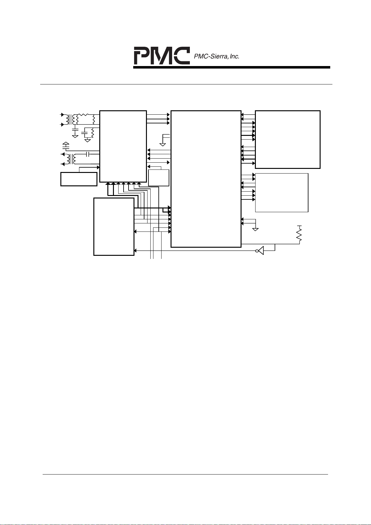
In figure 2, the DS1 LIU and framing functions are provided by the PM4341 T1
Transceiver (T1XC) product available from PMC-Sierra. The E1 LIU and framing
functions are provided by the PM6341 E1 Transceiver (E1XC) product, also
available from PMC-Sierra. The combination of these transceiver devices with the
S/UNI-PDH allows both PLCP-formatted DS1/E1 signals, and ITU-T G.804
compliant DS1/E1 signals to be processed. The G.804 specification defines ATM
direct cell mappings for a variety of transmission formats, including the 1.544 Mbit/s
DS1, and the 2.048 Mbit/s E1 formats.
The optional PLCP and DS3/E3 Overhead Processors illustrated are expected to be
implemented using programmable logic devices. For further S/UNI-PDH application
information, please refer to document number PMC-930410, "The ATM Physical
Layer".
PM7345 S/UNI-PDH
DATA SHEET
PMC-931011 ISSUE 6 SATURN USER-NETWORK INTERFACE
PROPRIETARY AND CONFIDENTIAL TO PMC-SIERRA, INC., AND FOR ITS CUSTOMERS’ INTERNAL USE
7
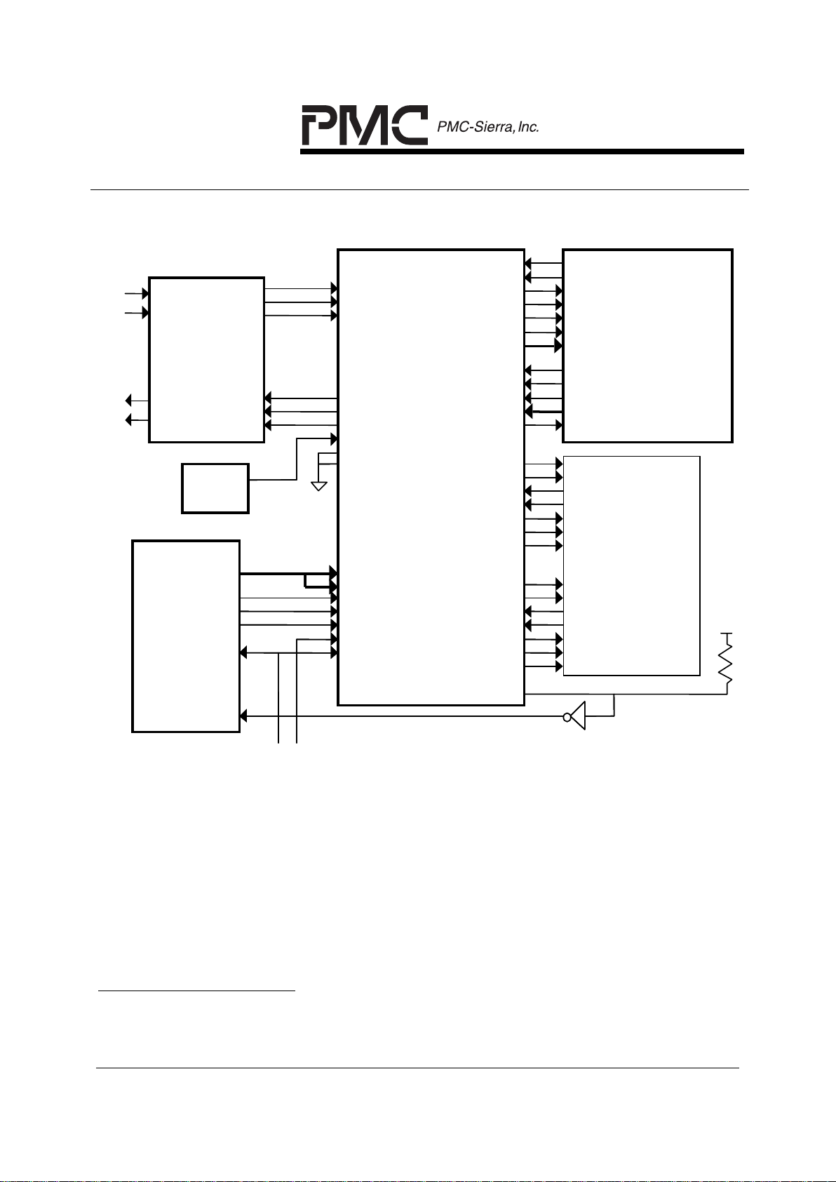
Figure 1 - DS3 and E3 User Network Interface
Optional
DS3/E3/PLCP
Overhead
Processor
( eg. tester
application)
PM7345
S/UNI-PDH
SATURN
User-Network
Interface for
PDH
ATM/SMDS
Adaptation
Layer
Processor
(eg. SAR or
policing
functions)
SSI
78P7200
E3/DS3
LIU
RPOS
RNEG
RCLK
TPOS
TNEG
TCLK
RPOS/RDAT
RNEG/ROHM
RCLK
TPOS/TDAT
TNEG/TOHM
TCLK
TICLK
TIOHM
C13/CADD
TCELL
RCELL
A[7:0]
D[7:0]
ALE
RDB
WRB
CSB
RSTB
RRDENB
FRDB/RFCLK
RSOC
REOH
REOC
FRDATA[7:0]
RFIFOE/RCA
TWRENB
FWRB/TFCLK
TSOC
FWDATA[7:0]
TFIFOFB/TCA
TPOHCLK
TPOHFP
TPOHINS
TPOH
RPOHCLK
RPOHFP
RPOH
TOHCLK
TOHFP
TOHINS
TOH
ROHCLK
ROHFP
ROH
INTB
AD[15:0]
ALE
RDB
WRB
RESB
INT
From Master
reset circuitry
From chip select
decode circuitry
+5V
OSC
44.736 MHz
LINE
IN
INTERFACE
LINE
OUT
INTERFACE
AD[15:0]
ALE
RDB
WRB
RESB
INT
From Master
reset circuitry
From chip select
decode circuitry
OSC
44.736 MHz
or
34.368 MHz
RX
CELL
INTERFACE
TX
CELL
INTERFACE
Intel/
Motorola
Single Chip
µP
Layout information for the SSI 78P7200 E3/DS3 LIU is found in the OPERATION
section of this document. Please refer to it as an example of the E3 and DS3
configuration used by PMC-Sierra.
1
1
Please contact Silicon Systems at (714) 573-6200 for detailed application information concerning the
78P7200 E3/DS3 LIU.
PM7345 S/UNI-PDH
DATA SHEET
PMC-931011 ISSUE 6 SATURN USER-NETWORK INTERFACE
PROPRIETARY AND CONFIDENTIAL TO PMC-SIERRA, INC., AND FOR ITS CUSTOMERS’ INTERNAL USE
8
Figure 2 - DS1 and E1 User Network Interface
RAS
REF
RRC
TC
TAP
TAN
XCLK
BRPCM
BRFPO
RCLKO
BTPCM
BTFP
BTCLK
TCLKO
TCLKI
PM4341A/PM6341
T1XC/E1XC
DS1 or E1
Transceiver
PM7345
S/UNI-PDH
SATURN
User-Network
Interface for
PDH
RPOS/RDAT
RNEG/ROHM
RCLK
TIOHM
C13/CADD
TPOS/TDAT
TNEG/TOHM
TCLK
TICLK
TCELL
RCELL
A[7:0]
D[7:0]
ALE
RDB
WRB
CSB
RSTB
AD[15:0]
ALE
RDB
WRB
RESB
INT
From Master
reset circuitry
From chip select
decode circuitry
+5V
A[7:0]
D[7:0]
ALE
RDB
WRB
CSB
RSTB
AD[15:0]
ALE
RDB
WRB
RESB
INT
OSC
37.056 MHz (DS1)
49.152 MHz (E1)
RX
CELL
INTERFACE
TX
CELL
INTERFACE
Optional
PLCP
Overhead
Processor
( eg. tester
application )
Intel/
Motorola
Single Chip
µP
ATM/SMDS
Adaptation
Layer
Processor
(eg. SAR or
policing
functions)
RRDENB
FRDB/RFCLK
RSOC
REOH
REOC
FRDATA[7:0]
RFIFOE/RCA
TWRENB
FWRB/TFCLK
TSOC
FWDATA[7:0]
TFIFOFB/TCA
TPOHCLK
TPOHFP
TPOHINS
TPOH
RPOHCLK
RPOHFP
RPOH
TOHCLK
TOHFP
TOHINS
TOH
ROHCLK
ROHFP
ROH
INTB
DS1
1.544 MHz
E1
2.048 MHz
PM7345 S/UNI-PDH
DATA SHEET
PMC-931011 ISSUE 6 SATURN USER-NETWORK INTERFACE
PROPRIETARY AND CONFIDENTIAL TO PMC-SIERRA, INC., AND FOR ITS CUSTOMERS’ INTERNAL USE
9
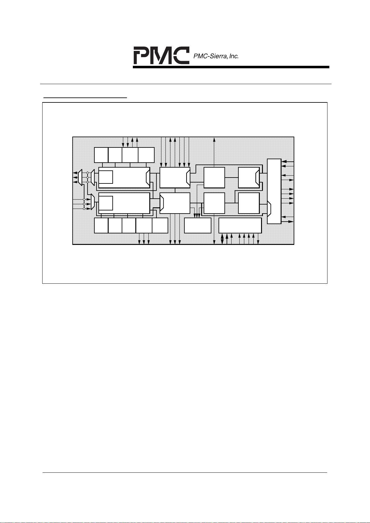
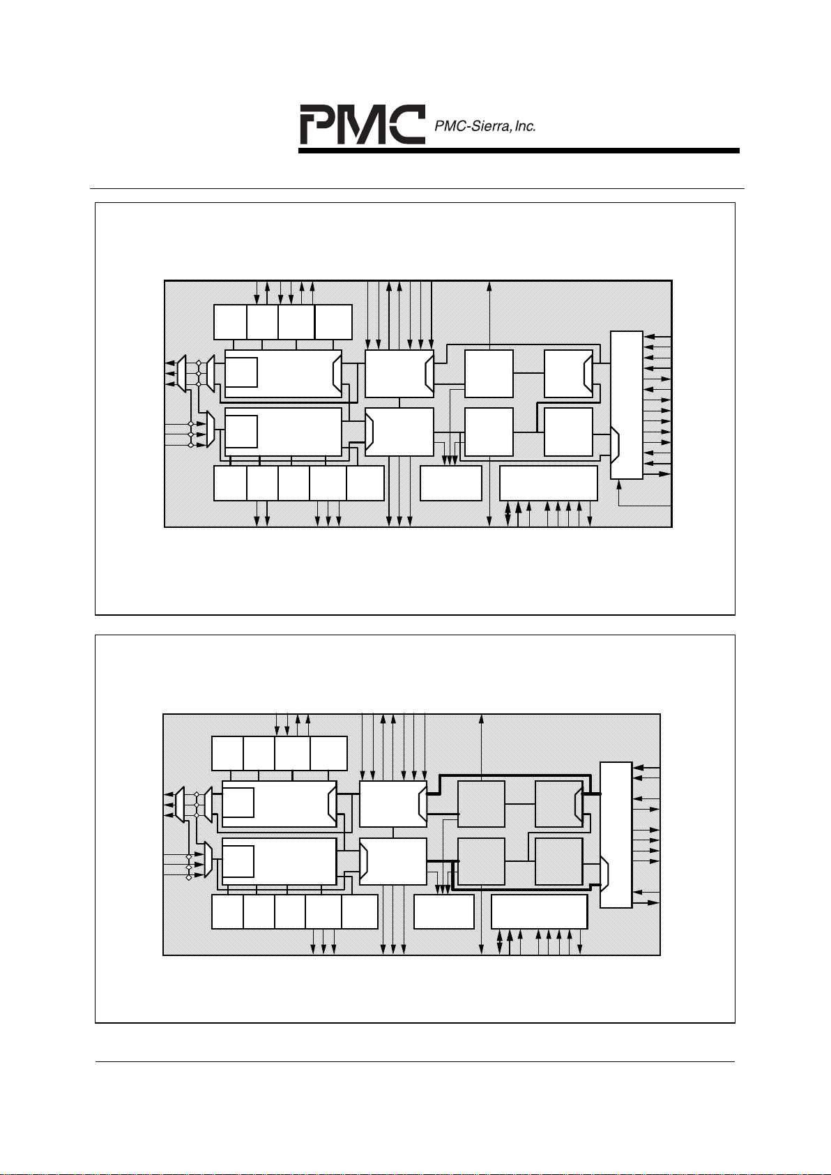
5
BLOCK DIAGRAM
TPOS/TDAT
RNEG/ROHM
RPOS/RDAT
TCLK
TNEG/TOHM
RCLK
TXFF
Tx
4 Cell
FIFO
RXFF
Rx
4 Cell
FIFO
System
I/F
SPLT
Transmit ATM
and PLCP
Framer
FWDATA[7:0]
TSOC
FWRB
FRDATA[7:0]
RSOC
D[7:0]
A[7:0]
ALE
CSB
RDB
WRB
RSTB
INTB
Microprocessor
I/F
Rx
O/H
Access
Tx
O/H
Access
TOHINS
ROH
TOHCLK
ROHFP
RPOH
TPOH
TPOHINS
RPOHCLK
ROHCLK
TOH
TRAN
DS3 or E3
Transmit
Framer
FRMR
DS3 or E3
Receive
Framer
TOHFP
C13/CADD/8KREFRPOHFP
TFIFOFB/FWCLK
TICLK
TIOHM
TXCP
Tx
Cell
Processor
RXCP
Rx
Cell
Processor
REOH/LOF
REOC/OOF
Line
Encode
Line
Decode
TCELL
RCELL
CPPM
PLCP/cell
Perf. Monitor
ATMF/SPLR
Receive
ATM and
PCLP Framer
XFDL
Tx
HDLC
XBOC
Tx
FEAC
RFDL
Rx
HDLC
RBOC
Rx
FEAC
TPOHCLK
TPOHFP
PMON
Perf.
Monitor
1/2 TTB
Rx Trail
Buffer
1/2 TTB
Tx Trail
Buffer
RFIFOE/FRCLK
FRDB
Normal Operating Mode (84-pin PLCC Async FIFO interface shown)
PM7345 S/UNI-PDH
DATA SHEET
PMC-931011 ISSUE 6 SATURN USER-NETWORK INTERFACE
PROPRIETARY AND CONFIDENTIAL TO PMC-SIERRA, INC., AND FOR ITS CUSTOMERS’ INTERNAL USE
10
TXFF
Tx
4 Cell
FIFO
RXFF
Rx
4 Cell
FIFO
System
I/F
SPLT
Transmit ATM
and PLCP
Framer
FWDATA[7:0]
TSOC
TFCLK
FRDATA[7:0]
RSOC
D[7:0]
A[7:0]
ALE
CSB
RDB
WRB
RSTB
INTB
Microprocessor
I/F
Rx
O/H
Access
Tx
O/H
Access
TOHINS
ROH
TOHCLK
ROHFP
RPOH
TPOH
TPOHINS
RPOHCLK
ROHCLK
TOH
TRAN
DS3 or E3
Transmit
Framer
FRMR
DS3 or E3
Receive
Framer
TOHFP
C13/CADD/8KREFRPOHFP
TCA
TICLK
TIOHM
TXCP
Tx
Cell
Processor
RXCP
Rx
Cell
Processor
REOH
REOC
TPOS/TDAT
Line
Encode
RNEG/ROHM
Line
Decode
RPOS/RDAT
TCLK
TNEG/TOHM
RCLK
TCELL
RCELL
CPPM
PLCP/cell
Perf. Monitor
ATMF/SPLR
Receive
ATM and
PCLP Framer
XFDL
Tx
HDLC
XBOC
Tx
FEAC
RFDL
Rx
HDLC
RBOC
Rx
FEAC
TPOHCLK
TPOHFP
PMON
Perf.
Monitor
1/2 TTB
Rx Trail
Buffer
1/2 TTB
Tx Trail
Buffer
TDLSIG
TDLCLK
TSEN
TWRENB
TXPRTY
RCA
RXPRTY
RRDENB
RFCLK
RDLSIG
RDLCLK
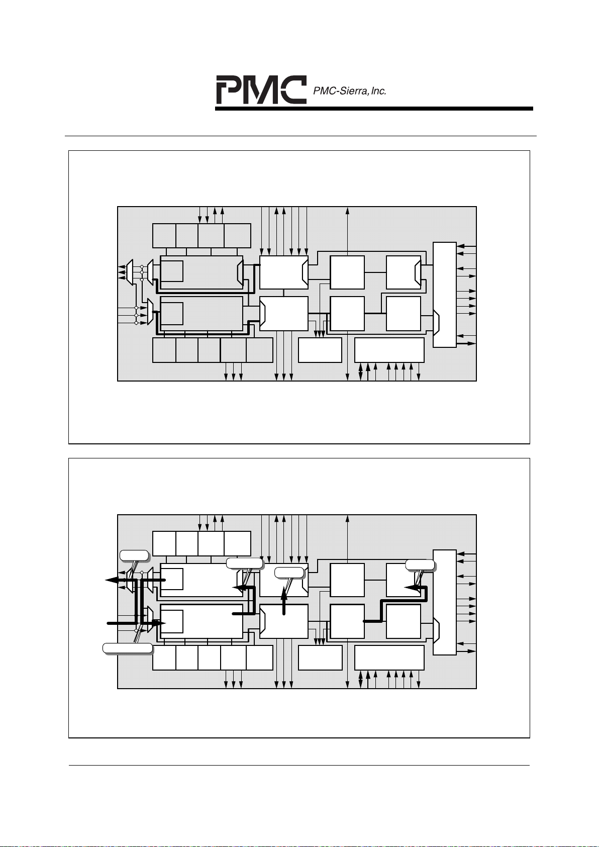
Normal Operating Mode (100-pin PQFP Sync FIFO interface shown)
TPOS/TDAT
RNEG/ROHM
RPOS/RDAT
TCLK
TNEG/TOHM
RCLK
TXFF
Tx
4 Cell
FIFO
RXFF
Rx
4 Cell
FIFO
System
I/F
SPLT
Transmit ATM
and PLCP
Framer
FWDATA[7:0]
TSOC
FWRB
FRDATA[7:0]
RSOC
D[7:0]
A[7:0]
ALE
CSB
RDB
WRB
RSTB
INTB
Microprocessor
I/F
Rx
O/H
Access
Tx
O/H
Access
TOHINS
ROH
TOHCLK
ROHFP
RPOH
TPOH
TPOHINS
RPOHCLK
ROHCLK
TOH
TRAN
DS3 or E3
Transmit
Framer
FRMR
DS3 or E3
Receive
Framer
TOHFP
C13/CADD/8KREFRPOHFP
TFIFOFB/FWCLK
TICLK
TIOHM
TXCP
Tx
Cell
Processor
RXCP
Rx
Cell
Processor
REOH/LOF
REOC/OOF
Line
Encode
Line
Decode
TCELL
RCELL
CPPM
PLCP/cell
Perf. Monitor
ATMF/SPLR
Receive
ATM and
PCLP Framer
XFDL
Tx
HDLC
XBOC
Tx
FEAC
RFDL
Rx
HDLC
RBOC
Rx
FEAC
TPOHCLK
TPOHFP
PMON
Perf.
Monitor
1/2 TTB
Rx Trail
Buffer
1/2 TTB
Tx Trail
Buffer
RFIFOE/FRCLK
FRDB
With FIFO Bypass Enabled
PM7345 S/UNI-PDH
DATA SHEET
PMC-931011 ISSUE 6 SATURN USER-NETWORK INTERFACE
PROPRIETARY AND CONFIDENTIAL TO PMC-SIERRA, INC., AND FOR ITS CUSTOMERS’ INTERNAL USE
11
TPOS/TDAT
RNEG/ROHM
RPOS/RDAT
TCLK
TNEG/TOHM
RCLK
TXFF
Tx
4 Cell
FIFO
RXFF
Rx
4 Cell
FIFO
System
I/F
SPLT
Transmit ATM
and PLCP
Framer
FWDATA[7:0]
TSOC
FWRB
FRDATA[7:0]
RSOC
D[7:0]
A[7:0]
ALE
CSB
RDB
WRB
RSTB
INTB
Microprocessor
I/F
Rx
O/H
Access
Tx
O/H
Access
TOHINS
ROH
TOHCLK
ROHFP
RPOH
TPOH
TPOHINS
RPOHCLK
ROHCLK
TOH
TRAN
DS3 or E3
Transmit
Framer
FRMR
DS3 or E3
Receive
Framer
TOHFP
C13/CADD/8KREFRPOHFP
TFIFOFB/FWCLK
TICLK
TIOHM
TXCP
Tx
Cell
Processor
RXCP
Rx
Cell
Processor
REOH/LOF
REOC/OOF
Line
Encode
Line
Decode
TCELL
RCELL
CPPM
PLCP/cell
Perf. Monitor
ATMF/SPLR
Receive
ATM and
PCLP Framer
XFDL
Tx
HDLC
XBOC
Tx
FEAC
RFDL
Rx
HDLC
RBOC
Rx
FEAC
TPOHCLK
TPOHFP
PMON
Perf.
Monitor
1/2 TTB
Rx Trail
Buffer
1/2 TTB
Tx Trail
Buffer
RFIFOE/FRCLK
FRDB
With DS3/E3 Framer Bypassed
TPOS/TDAT
RNEG/ROHM
RPOS/RDAT
TCLK
TNEG/TOHM
RCLK
TXFF
Tx
4 Cell
FIFO
RXFF
Rx
4 Cell
FIFO
System
I/F
SPLT
Transmit ATM
and PLCP
Framer
FWDATA[7:0]
TSOC
FWRB
FRDATA[7:0]
RSOC
D[7:0]
A[7:0]
ALE
CSB
RDB
WRB
RSTB
INTB
Microprocessor
I/F
Rx
O/H
Access
Tx
O/H
Access
TOHINS
ROH
TOHCLK
ROHFP
RPOH
TPOH
TPOHINS
RPOHCLK
ROHCLK
TOH
TRAN
DS3 or E3
Transmit
Framer
FRMR
DS3 or E3
Receive
Framer
TOHFP
C13/CADD/8KREFRPOHFP
TFIFOFB/FWCLK
TICLK
TIOHM
TXCP
Tx
Cell
Processor
RXCP
Rx
Cell
Processor
REOH/LOF
REOC/OOF
Line
Encode
Line
Decode
TCELL
RCELL
CPPM
PLCP/cell
Perf. Monitor
ATMF/SPLR
Receive
ATM and
PCLP Framer
XFDL
Tx
HDLC
XBOC
Tx
FEAC
RFDL
Rx
HDLC
RBOC
Rx
FEAC
TPOHCLK
TPOHFP
PMON
Perf.
Monitor
1/2 TTB
Rx Trail
Buffer
1/2 TTB
Tx Trail
Buffer
RFIFOE/FRCLK
FRDB
LINE
PAYLOAD
TIMING
CELL
DIAGNOSTIC
Loopback Modes

PM7345 S/UNI-PDH
DATA SHEET
PMC-931011 ISSUE 6 SATURN USER-NETWORK INTERFACE
PROPRIETARY AND CONFIDENTIAL TO PMC-SIERRA, INC., AND FOR ITS CUSTOMERS’ INTERNAL USE
12
6
DESCRIPTION
The PM7345 S/UNI-PDH is an ATM physical layer processor with integrated DS3
and E3 framing. PLCP sublayer DS1, DS3, E1, and E3 processing is supported as
is ATM cell delineation.
The S/UNI-PDH contains an integral DS3 framer, which provides DS3 framing and
error accumulation in accordance with ANSI specifications, and an integral E3
framer, which provides E3 framing in accordance with ITU-T Recommendations
G.832 and G.751. When configured for DS3 transmission system sublayer
processing, the S/UNI-PDH accepts and outputs either a B3ZS-encoded bipolar or a
unipolar signal compatible with M23 and C-bit parity applications. When configured
for E3 transmission system sublayer processing, the S/UNI-PDH accepts and
outputs either a HDB3-encoded bipolar or a unipolar signal compatible with G.751
and G.832 applications. When configured for DS1, or E1 transmission system
sublayer processing, the S/UNI-PDH accepts and outputs a unipolar signal with
appropriate clock and frame pulse signals for physical sublayer processing. When
configured for other transmission systems, the S/UNI-PDH provides a generic
interface for physical sublayer processing.
In the DS3 receive direction, the S/UNI-PDH frames to a DS3 signal with a
maximum average reframe time of 1.5 ms and detects line code violations, loss of
signal, framing bit errors, parity errors, path parity errors, AIS, far end receive failure
and idle code. The DS3 overhead bits are extracted and presented on a serial
output. When in C-bit parity mode, the Path Maintenance Data Link and the Far End
Alarm and Control (FEAC) channel are extracted. An HDLC receiver is provided for
Path Maintenance Data Link support. In addition, valid bit-oriented codes in the
FEAC channel are detected and are available through the microprocessor port.
In the E3 receive direction, the S/UNI-PDH frames to either a G.751 or G.832 E3
signal with a maximum average reframe time of 0.5 ms and detects line code
violations, loss of signal, framing bit errors, AIS, and remote alarm indication.
Further, when processing G.832 formatted data, parity errors, far end receive failure,
and far end block errors are also detected; and the Trail Trace message is extracted
and made available through the microprocessor port. An HDLC receiver is provided
for either the G.832 Network Requirement or the G.832 General Purpose Data Link
support.
Error event accumulation is also provided by the S/UNI-PDH. Framing bit errors,
line code violations, parity errors, path parity errors and far end block errors are
accumulated in saturating counters.

PM7345 S/UNI-PDH
DATA SHEET
PMC-931011 ISSUE 6 SATURN USER-NETWORK INTERFACE
PROPRIETARY AND CONFIDENTIAL TO PMC-SIERRA, INC., AND FOR ITS CUSTOMERS’ INTERNAL USE
13
In the DS3 transmit direction, the S/UNI-PDH inserts DS3 framing, X and P bits.
When enabled for C-bit parity operation, a bit-oriented code transmitter and an
HDLC transmitter are provided for insertion of the FEAC channel and the Path
Maintenance Data Link into the appropriate overhead bits. The Alarm Indication
Signal can be inserted when enabled by an external input or using an internal
register bit; other status signals such as the idle signal can be inserted when
enabled by an internal register bit. When M23 operation is selected, the C-bit Parity
ID bit (the first C-bit of the first M sub-frame) is forced to toggle so that downstream
equipment will not confuse an M23-formatted stream with stuck-at 1 C-bits for C-bit
Parity application.
In the E3 transmit direction, the S/UNI-PDH inserts E3 framing in either G.832 or
G.751 format. When enabled for G.832 operation, an HDLC transmitter is provided
for insertion of either the Network Requirement or General Purpose Data Link into
the appropriate overhead bits. The Alarm Indication Signal and other status signals
can be inserted by internal register bits.
The S/UNI-PDH also supports diagnostic modes in which it inserts parity or path
parity errors, F-bit framing errors, M-bit framing errors, invalid X or P-bits, line code
violations, or all-zeros.
The S/UNI-PDH provides cell delineation for ATM cells using the PLCP framing
format, or by using the header check sequence octet in the ATM cell header as
specified by ITU-T Recommendation I.432. DS1, DS3, E1 and E3 based PLCP
frame formats can be processed. An interface consistent with the generic physical
interface defined by ITU-T Recommendation I.432 is provided for arbitrary rates up
to 52 Mbit/s. This interface is used to provide physical layer support for
transmission systems that do not have an associated PLCP sublayer, or to provide
an efficient means of directly mapping ATM cells to existing transmission system
formats (such as DS3 and DS1).
In the PLCP receive direction, framing, path overhead extraction and cell extraction
is provided. BIP-8 error events, frame octet error events and far end block error
events are accumulated.
In the PLCP transmit direction, the S/UNI-PDH provides overhead insertion using
inputs or internal registers, DS3 nibble and E3 byte stuffing, automatic BIP-8 octet
generation and insertion and automatic far end block error insertion. Diagnostic
features for BIP-8 error, framing error and far end block error insertion are also
supported.
In the cell receive path, idle/unassigned cells may be dropped according to a
programmable filter. By default, incoming cells with single bit HCS errors are
corrected and written to the FIFO buffer. Optionally, cells can be dropped upon

PM7345 S/UNI-PDH
DATA SHEET
PMC-931011 ISSUE 6 SATURN USER-NETWORK INTERFACE
PROPRIETARY AND CONFIDENTIAL TO PMC-SIERRA, INC., AND FOR ITS CUSTOMERS’ INTERNAL USE
14
detection of a HCS error. The ATM cell payloads are optionally descrambled.
Assigned cells containing no detectable HCS errors are written to a FIFO buffer.
Cells are read from the FIFO using an asynchronous 8-bit wide datapath interface or
a synchronous 9-bit wide datapath, depending upon the packaging option selected.
Counts of error-free assigned cells, and cells containing HCS errors are
accumulated independently for performance monitoring purposes.
In the cell transmit path, cells are written to a FIFO buffer using an asynchronous 8bit wide datapath interface or a synchronous 9-bit wide datapath interface,
depending upon the packaging option selected. Idle/unassigned cells are
automatically inserted when the FIFO contains less than one full cell. HCS
generation, and cell payload scrambling are optionally provided.
Both receive and transmit cell FIFOs provide buffering for four cells. The FIFOs
provide the rate matching interface between the higher layer ATM entity and the
S/UNI-PDH.
The S/UNI-PDH is configured, controlled and monitored via a generic 8-bit
microprocessor bus through which all internal registers are accessed. All sources of
interrupts can be identified, acknowledged, or masked via this interface.
PM7345 S/UNI-PDH
DATA SHEET
PMC-931011 ISSUE 6 SATURN USER-NETWORK INTERFACE
PROPRIETARY AND CONFIDENTIAL TO PMC-SIERRA, INC., AND FOR ITS CUSTOMERS’ INTERNAL USE
15
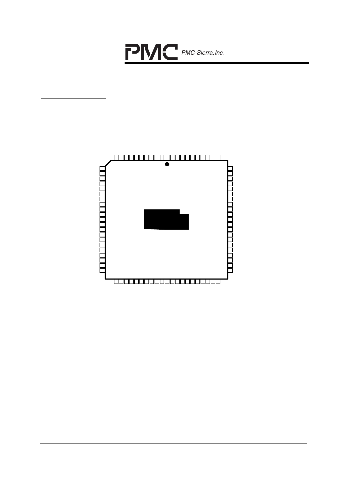
7
PIN DIAGRAM
The S/UNI-PDH is available in an 84-pin PLCC.
S/
UNI-
PM7345
FWDATA[4]
FWDATA[5]
ROHFP
ROHCLK
ROH
RNEG/ROHM
RPOS/RDAT
RCLK
INTB
RSTB
CSB
VDDO
VSSO
RPOHCLK
FWRB
FWDATA[7]
RPOH
RPOHFP
FWDATA[6]
RDB
WRB
55
54
57
56
74
73
72
71
70
69
68
67
66
65
64
63
62
61
60
59
58
33 34 52434241403938373635 5150494847464544 53
FWDATA[0]
RSOC
FWDATA[3]
FWDATA[2]
FWDATA[1]
FRDB
FRDATA[7]
FRDATA[6]
FRDATA[5]
FRDATA[4]
VDDO
VSSI
VDDI
FRDATA[3]
FRDATA[2]
FRDATA[1]
FRDATA[0]
REOC/OOF
REOH/LOF
RFIFOE/FRCLK
ALE
A[0]
A[1]
A[2]
A[3]
D[0]
D[1]
D[2]
D[3]
VDDO
VSSI
VDDI
VSSO
D[4]
D[5]
D[6]
D[7]
A[4]
A[5]
A[6]
A[7]
31
29
30
13
14
15
16
17
18
19
20
21
22
23
24
25
26
27
28
32
12
757612345678977787980818283841011
NC
TIOHM
TICLK
C13/CADD/8KREF
TCLK
TPOS/TDAT
TNEG/TOHM
TOHCLK
TOHFP
VDDO
VSSO
TOHINS
TOH
TPOHCLK
TPOHFP
TPOHINS
TPOH
TCELL
TFIFOFB/FWCLK
TSOC
RCELL
VSSO
PDH
TM
PM7345 S/UNI-PDH
DATA SHEET
PMC-931011 ISSUE 6 SATURN USER-NETWORK INTERFACE
PROPRIETARY AND CONFIDENTIAL TO PMC-SIERRA, INC., AND FOR ITS CUSTOMERS’ INTERNAL USE
16
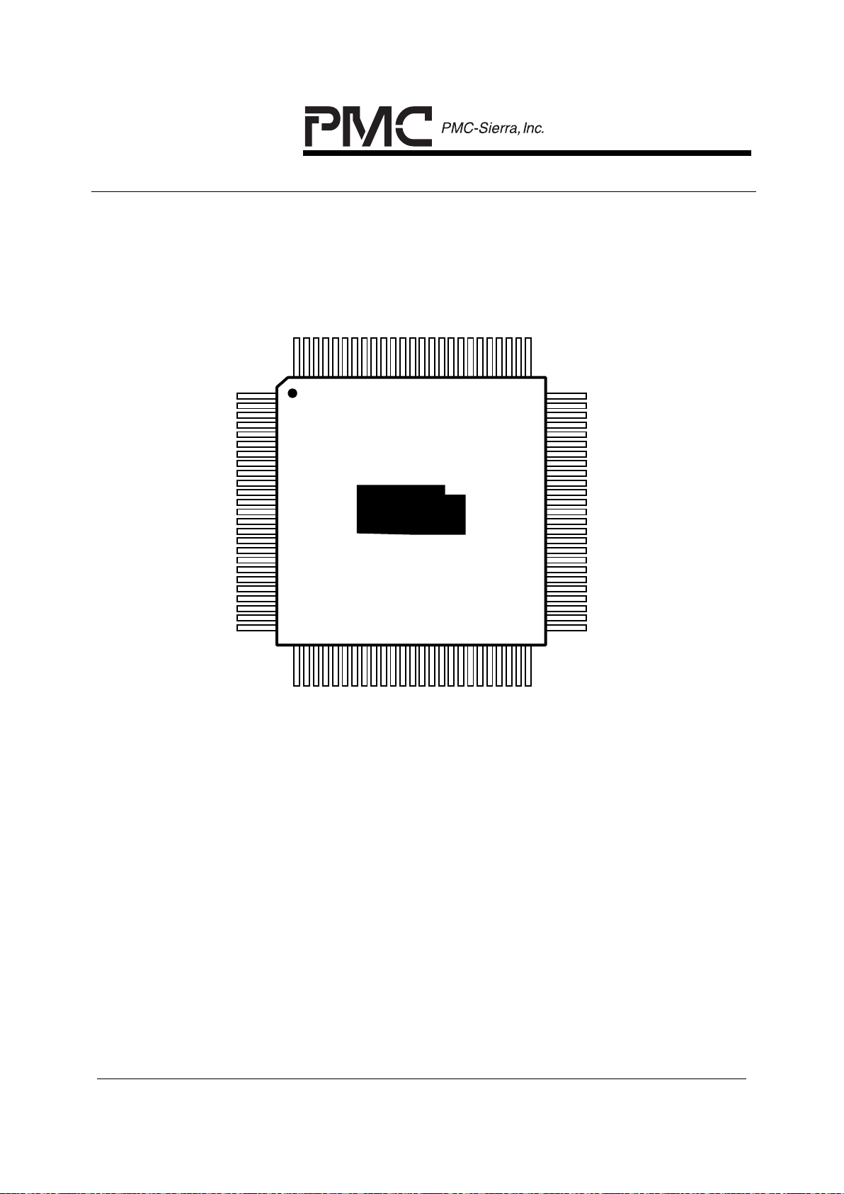
The S/UNI-PDH is also available in a 100-pin PQFP having a body size of 14x14mm
and a pin pitch of 0.5mm.
NC
VDDI
ALE
A[0]
A[1]
A[2]
A[3]
D[0]
D[1]
D[2]
D[3]
VDDO
VSSI
PIN 1
PIN 100
PIN 25
PIN 26
PIN 50
PIN 51
PIN 75
PIN 76
VSSO
NC
TDLSIG
PM7345
VDDI
VSSO
D[4]
D[5]
D[6]
D[7]
A[4]
A[5]
A[6]
A[7]
NC
TIOHM
TICLK
C13/CADD/8KREF
TCLK
TPOS/TDAT
TNEG/TOHM
TOHCLK
TOHFP
VDDO
TDLCLK
VSSO
TOHINS
TOH
TPOHCLK
TPOHFP
TPOHINS
TPOH
TCELL
TFIFOFB/TCA/FWCLK
TSOC
RCELL
SYFIFOB
LCD
FWRDATA[3]
FWRDATA[2]
FWRDATA[1]
FWRDATA[0]
RRDENB
FRDB/RFCLK
FRDATA[7]
FRDATA[6]
FRDATA[5]
FRDATA[4]
VDDO
VSSO
RXPRTY
VSSI
VDDI
FRDATA[3]
FRDATA[2]
FRDATA[1]
FRDATA[0]
RSOC
REOC/OOF
REOH/LOF
RFIFOE/RCA/FRCLK
TSEN
VDDO
RDB
WRB
CSB
RSTB
INTB
RCLK
RPOS/RDAT
RNEG/ROHM
ROH
ROHCLK
ROHFP
RDLSIG
TXPRTY
VSSO
RPOH
RPOHCLK
RPOHFP
TWRENB
FWRB/TFCLK
FWRDATA[7]
FWRDATA[6]
FWRDATA[5]
FWRDATA[4]
VSSI
RDLCLK
Index
TM
PDH
S/
UNI-

PM7345 S/UNI-PDH
DATA SHEET
PMC-931011 ISSUE 6 SATURN USER-NETWORK INTERFACE
PROPRIETARY AND CONFIDENTIAL TO PMC-SIERRA, INC., AND FOR ITS CUSTOMERS’ INTERNAL USE
17
8
PIN DESCRIPTION
Pin Pin No.
Name Type QFP PLCC Function
RCLK Input 95 6
Receive Clock (RCLK). RCLK provides the
receive direction timing. RCLK is the externally
recovered transmission system baud rate clock that
samples the RPOS/RDAT and RNEG/ROHM inputs
on its rising or falling edge. The RCLK maximum
frequency is 52 MHz.
RPOS/
RDAT
Input 94 5
Receive Positive Pulse (RPOS). RPOS contains
the positive pulses received on the B3ZS-encoded
DS3, or the HDB3-encoded E3, transmission
system when the dual-rail NRZ input format is
selected. RPOS contains the entire stream when
the single-rail (unipolar) NRZ input format is
enabled. The dual-rail/single-rail selection is
controlled by the UNI bit in the DS3 FRMR or the E3
FRMR Configuration Registers.
Receive Data (RDAT). RDAT contains the received
transmission system stream when a non-DS3/E3
based transmission system is being processed (for
example RDAT may contain a DS1 or E1 stream).
The RPOS/RDAT pin function selection is controlled
by the FRMRBP bit in the S/UNI-PDH Configuration
Register. Both RPOS and RDAT are sampled on
the rising edge of RCLK by default, and may be
enabled to be sampled on the falling edge of RCLK.
This sampling is controlled by the RCLKINV bit in
the S/UNI-PDH Control Register. In addition, signal
polarity control is provided by the RPNINV bit in the
S/UNI-PDH Control Register.

PM7345 S/UNI-PDH
DATA SHEET
PMC-931011 ISSUE 6 SATURN USER-NETWORK INTERFACE
PROPRIETARY AND CONFIDENTIAL TO PMC-SIERRA, INC., AND FOR ITS CUSTOMERS’ INTERNAL USE
18
RNEG/
ROHM
Input 93 4
Receive Negative Pulse (RNEG). RNEG contains
the negative pulses received on the B3ZS encoded
DS3, or the HDB3-encoded E3, transmission
system when the dual-rail NRZ input format is
selected. RNEG contains line code violation
indications when the single-rail (unipolar) NRZ input
format is enabled. Each line code violation is
represented by an RCLK period-wide pulse. The
dual-rail/single-rail selection is controlled by the UNI
bit in the DS3 FRMR or E3 FRMR Configuration
Registers.
Receive Overhead Mask (ROHM). ROHM
indicates the position of overhead bits in the nonDS3/E3 based transmission system stream, RDAT.
When a PLCP formatted signal is received, ROHM
is pulsed once per transmission frame, and
indicates the DS1 or E1 frame alignment. When a
non-PLCP based signal is received, ROHM
indicates the position of each overhead bit in the
transmission frame.
The RNEG/ROHM pin function selection is
controlled by the FRMRBP bit in the S/UNI-PDH
Configuration Register. Both RNEG and ROHM are
sampled on the rising edge of RCLK by default, and
may be enabled to be sampled on the falling edge
of RCLK. This sampling is controlled by the
RCLKINV bit in the S/UNI-PDH Control Register. In
addition, signal polarity control is provided by the
RPNINV bit in the S/UNI-PDH Control Register.
ROHCLK Output 91 2
Receive DS3/E3 Overhead Clock (ROHCLK).
ROHCLK is active when a DS3 or E3 stream is
being processed. ROHCLK is nominally a 526 kHz
clock when processing DS3, is nominally a 1.072
MHz clock when processing G.832 E3, and is
nominally a 1.074 MHz clock when processing
G.751 E3. ROH, and ROHFP are updated on the
falling edge of ROHCLK.

PM7345 S/UNI-PDH
DATA SHEET
PMC-931011 ISSUE 6 SATURN USER-NETWORK INTERFACE
PROPRIETARY AND CONFIDENTIAL TO PMC-SIERRA, INC., AND FOR ITS CUSTOMERS’ INTERNAL USE
19
ROH Output 92 3
Receive DS3/E3 Overhead Data (ROH). ROH
contains the overhead bits (C, F, X, P, and M)
extracted from the received DS3 stream; ROH
contains the overhead bytes (FA1, FA2, EM, TR,
MA, NR, and GC) extracted from the received
G.832 E3 stream; ROH contains the overhead bits
(RAI, National Use, Stuff Indication, and Stuff
Opportunity) extracted from the received G.751 E3
stream. ROH is updated on the falling edge of
ROHCLK.
ROHFP Output 90 1
Receive DS3/E3 Overhead Frame Position
(ROHFP). ROHFP locates the individual overhead
bits in the received overhead data stream, ROH.
ROHFP is high during the X1 overhead bit position
in the ROH stream when processing a DS3 stream.
ROHFP is high during the first bit of the FA1 byte
when processing a G.832 E3 stream. ROHFP is
high during the RAI overhead bit position when
processing a G.751 E3 stream. ROHFP is updated
on the falling edge of ROHCLK.
RPOHCLK Output 83 81
Receive PLCP Overhead Clock (RPOHCLK).
RPOHCLK is active when PLCP processing is
enabled. The frequency of this signal depends on
the selected PLCP format. RPOHCLK is nominally
a 26.7 kHz clock for a DS1 PLCP frame, a 768 kHz
clock for a DS3 PLCP frame, a 33.7 kHz clock for an
E1 based PLCP frame, or a 576 kHz clock for a
G.751 E3 based PLCP frame. RPOHFP and RPOH
are updated on the falling edge of RPOHCLK.
RPOH Output 84 82
Receive PLCP Overhead Data (RPOH). RPOH
contains the PLCP path overhead octets (Zn, F1,
B1, G1, M1, M2, and C1) extracted from the
received PLCP frame when the PLCP layer is inframe. When the PLCP layer is in the loss of frame
state, RPOH is forced to all ones. The octet data on
RPOH is shifted out in order from the most
significant bit (bit 1) to the least significant bit (bit 8).
RPOH is updated on the falling edge of RPOHCLK.

PM7345 S/UNI-PDH
DATA SHEET
PMC-931011 ISSUE 6 SATURN USER-NETWORK INTERFACE
PROPRIETARY AND CONFIDENTIAL TO PMC-SIERRA, INC., AND FOR ITS CUSTOMERS’ INTERNAL USE
20
RPOHFP Output 82 80
Receive PLCP Overhead Frame Position
(RPOHFP). RPOHFP locates the individual PLCP
path overhead bits in the receive overhead data
stream, RPOH. RPOHFP is logic 1 while bit 1 (the
most significant bit) of the path user channel octet
(F1)is present in the RPOH stream. RPOHFP is
updated on the falling edge of RPOHCLK.
RDLSIG Output 89 n/a
Receive Data Link Signal (RDLSIG). In DS3
mode, RDLSIG contains the Path Maintenance
Data Link signal from the received C-bit Parity DS3
stream. RDLSIG is not affected by the RNETOP bit
in the S/UNI-PDH Data Link and FERF Control
register while in DS3 mode. In E3 G.832 mode,
RDLSIG contains the NR or GC data link signal, as
selected by the RNETOP bit, from the received E3
G.832 stream. In E3 G.751 mode, RDLSIG
contains the National Use bit from the received
G.751 E3 stream if the RNETOP bit is logic one.
RDLSIG is updated on the falling edge of RDLCLK.
RDLCLK Output 88 n/a
Receive Data Link Clock (RDLCLK). RDLCLK is
active when a DS3 or E3 G.832 stream is being
processed. With an E3 G.751 stream, the RNETOP
bit in the S/UNI-PDH Data Link and FERF Control
register must be set to logic one for RDLCLK to be
active.
RCELL Output 49 53
Receive Cell Indication (RCELL). RCELL pulses
once for every cell received. RCELL is updated
using timing derived from the receive input clock
(RCLK) and is active for a minimum of 8 RCLK
periods. RCELL is forced to logic 0 when in the
FIFO bypass mode.

PM7345 S/UNI-PDH
DATA SHEET
PMC-931011 ISSUE 6 SATURN USER-NETWORK INTERFACE
PROPRIETARY AND CONFIDENTIAL TO PMC-SIERRA, INC., AND FOR ITS CUSTOMERS’ INTERNAL USE
21
LCD Output 50 n/a
Loss of Cell Delineation (LCD). The LCD signal
indicates when cell delineation cannot be found.
LCD transitions to logic 1 when an out of cell
delineation (OCD) defect has persisted past a
selected threshold. Once asserted, OCD remains
logic 1 until no OCD defect has been detected past
the selected threshold. The OCD defect state is
entered when the cell delineation state machine is
not in the SYNC state (please refer to the
Functional Description section for an explanation of
the cell delineation state machine). The LCD
indication is available for register access and can be
enabled to generate a microprocessor interrupt.
FRDB/
RFCLK
Input 69 70
FIFO Read (FRDB). FRDB reads cell octets from
the receive FIFO. The data is enabled on the
FRDATA[7:0] outputs on the falling edge of FRDB.
RSOC, REOH, and REOC are updated on the rising
edge of FRDB. Note that when the receive FIFO is
bypassed, FRDB should be logic 1 to minimize the
S/UNI-PDH power consumption.
Read FIFO Clock (RFCLK). RFCLK is used to
read bytes from the synchronous FIFO interface.
This interface is only available in the 100-pin PQFP
package when the synchronous FIFO interface is
enabled (SYFIFOB tied to logic 0). RFCLK must
cycle at a 25 MHz or lower instantaneous rate, but
at a high enough rate to avoid FIFO overflow.
RRDENB is sampled using the rising edge of
RFCLK. RSOC, RCA, RXPRTY, and FRDATA[7:0]
are all updated on the rising edge of RFCLK.

PM7345 S/UNI-PDH
DATA SHEET
PMC-931011 ISSUE 6 SATURN USER-NETWORK INTERFACE
PROPRIETARY AND CONFIDENTIAL TO PMC-SIERRA, INC., AND FOR ITS CUSTOMERS’ INTERNAL USE
22
RRDENB Input 70 n/a
Receive FIFO Read Enable (RRDENB). This
active low enable signal is used to initiate reads
from the synchronous receive FIFO interface (when
SYFIFOB is tied to logic 0). RRDENB sampled (on
the rising edge of RFCLK) at logic 0 indicates that
RSOC and FRDATA[7:0] will be sampled by the ATM
layer at the end of the current RFCLK cycle (on the
next rising edge of RFCLK). When RRDENB is
sampled at logic 1, no read is performed. RRDENB
must be used in conjunction with RFCLK to access
the FIFO at a high enough instantaneous rate as to
avoid FIFO overflow. The RRDENB signal is only
available in the 100-pin PQFP package. RRDENB
contains an integral pull-down resistor.

PM7345 S/UNI-PDH
DATA SHEET
PMC-931011 ISSUE 6 SATURN USER-NETWORK INTERFACE
PROPRIETARY AND CONFIDENTIAL TO PMC-SIERRA, INC., AND FOR ITS CUSTOMERS’ INTERNAL USE
23
RFIFOE/
RCA/
FRCLK
Output 52 54
Receive FIFO Empty (RFIFOE). RFIFOE indicates
the receive FIFO status. RFIFOE is logic 1 when
the cell-based FIFO is empty and logic 0 when the
FIFO contains at least 1 cell. RFIFOE timing is
applicable when using the asynchronous FIFO
interface in the S/UNI-PDH (either in the 84-pin
PLCC or when SYFIFOB is tied to logic 1 in the
100-pin package). Note that with the asynchronous
FIFO interface RFIFOE transitions from empty to full
(logic 1 to logic 0) on write cell boundaries with
timing derived from the RCLK input. RFIFOE
transitions from full to empty (logic 0 to logic 1) on
read cell boundaries on the rising edge of FRDB.
RFIFOE should be treated by the ATM layer as a
purely asynchronous signal.
Receive Cell Available (RCA). RCA is available in
the 100-pin PQFP package when SYFIFOB is tied
to logic 0. When the synchronous FIFO interface is
used, RCA is an active high signal and is logic 1
when the cell-based FIFO contains at least 1 cell
and is logic 0 when the cell-based FIFO is empty.
RCA can be enabled to transition low when the
FIFO is empty (default) or when the FIFO is 4 bytes
away from being empty (almost empty), as
controlled by the REMPTY4 register bit. RCA
transitions on rising edges of the RFCLK.
Receive Cell Clock (FRCLK). FRCLK is derived
from RCLK when the receive FIFO is bypassed (the
FIFOBP bit in the S/UNI-PDH Configuration
Register is logic 1). FRDATA[7:0], LOF, OOF, and
RSOC are updated on the falling edge of FRCLK.

PM7345 S/UNI-PDH
DATA SHEET
PMC-931011 ISSUE 6 SATURN USER-NETWORK INTERFACE
PROPRIETARY AND CONFIDENTIAL TO PMC-SIERRA, INC., AND FOR ITS CUSTOMERS’ INTERNAL USE
24
RSOC Tristate 55 57
Receive Start of Cell (RSOC). RSOC indicates
the start of a 53 octet cell. It is asserted when the
first octet is read from the receive FIFO. RSOC is
tristateable in the 100-pin PQFP package when
TSEN is logic 1. It is forced tristate while FRDB is
high and the receive FIFO is not bypassed (when
SYFIFOB is logic 1), or while RRDENB is sampled
high by the rising edge of RFCLK (when SYFIFOB
is logic 0). The RSOC logic va lue is driven on the
pin while FRDB is low (asynchronous FIFO
interface) or while RRDENB is sampled logic 0
(synchronous interface). RSOC is updated on the
rising edge of FRDB or RFCLK. When the receive
FIFO is bypassed, RSOC is updated on the falling
edge of FRCLK.
REOH/
LOF
Tristate 53 55
Receive End of Header (REOH). REOH is
asserted when the fifth octet of the 53 octet cell is
read from the receive FIFO. REOH is tristatable in
the 100-pin PQFP package when TSEN is logic 1. It
is forced tristate while FRDB is high and the receive
FIFO is not bypassed (when SYFIFOB is logic 1), or
while RRDENB is sampled high by the rising edge
of RFCLK (when SYFIFOB is logic 0). The REOH
logic value is driven on the pin while FRDB is low
(asynchronous FIFO interface) or while RRDENB is
sampled logic 0 (synchronous interface). REOH is
updated on the rising edge of FRDB or RFCLK.
PLCP Loss of Frame (LOF). LOF is asserted
while the PLCP receiver is in a loss of frame state.
LOF may be used to indicate the valid/invalid status
of the FRDATA[7:0] octets to a higher layer
processing entity while the receive FIFO is
bypassed. LOF is updated on the falling edge of
FRCLK.
The REOH/LOF pin function selection is controlled
by the FIFOBP bit in the S/UNI-PDH Configuration
Register.

PM7345 S/UNI-PDH
DATA SHEET
PMC-931011 ISSUE 6 SATURN USER-NETWORK INTERFACE
PROPRIETARY AND CONFIDENTIAL TO PMC-SIERRA, INC., AND FOR ITS CUSTOMERS’ INTERNAL USE
25
REOC/
OOF
Tristate 54 56
Receive End of Cell (REOC). REOC is asserted
when the 53rd octet of the 53 octet cell is being
read from the receive FIFO. RSOC is tristatable in
the 100-pin PQFP package when TSEN is logic 1. It
is forced tristate while FRDB is high and the receive
FIFO is not bypassed (when SYFIFOB is logic 1), or
while RRDENB is sampled high by the rising edge
of RFCLK (when SYFIFOB is logic 0). The RSOC
logic value is driven on the pin while FRDB is low
(asynchronous FIFO interface) or while RRDENB is
sampled logic 0 (synchronous interface). REOC is
updated on the rising edge of FRDB or RFCLK.
PLCP Out of Frame (OOF). OOF is asserted while
the PLCP receiver is in an out of frame state. OOF
may be used to indicate the valid/invalid status of
the FRDATA[7:0] octets to a higher layer processing
entity while the receive FIFO is bypassed. OOF is
updated on the falling edge of FRCLK.
The REOC/OOF pin function selection is controlled
by the FIFOBP bit in the S/UNI-PDH Configuration
Register.
FRDATA[7]
FRDATA[6]
FRDATA[5]
FRDATA[4]
FRDATA[3]
FRDATA[2]
FRDATA[1]
FRDATA[0]
Tristate
Tristate
Tristate
Tristate
Tristate
Tristate
Tristate
Tristate
68
67
66
65
59
58
57
56
69
68
67
66
61
60
59
58
Receive FIFO Data (FRDATA[7:0]). FRDATA[7:0]
contains the cell octet that is read from the receive
FIFO. The FRDATA[7:0] bus is tristatable in the 100pin PQFP package when TSEN is logic 1.
FRDATA[7:0] is forced tristate while FRDB is high
and the receive FIFO is not bypassed (when
SYFIFOB is logic 1), or while RRDENB is sampled
high by the rising edge of RFCLK (when SYFIFOB
is logic 0). The octet read from the receive FIFO is
driven on the FRDATA[7:0] bus while FRDB is low
(asynchronous FIFO interface) or while RRDENB is
sampled logic 0 (synchronous interface).
FRDATA[7:0] is updated on the falling edge of
FRCLK when the receive FIFO is bypassed.

PM7345 S/UNI-PDH
DATA SHEET
PMC-931011 ISSUE 6 SATURN USER-NETWORK INTERFACE
PROPRIETARY AND CONFIDENTIAL TO PMC-SIERRA, INC., AND FOR ITS CUSTOMERS’ INTERNAL USE
26
RXPRTY Tristate 62 n/a
Receive FIFO Read Data Parity (RXPRTY).
RXPRTY is only available in the 100-pin PQFP
package. RXPRTY indicates the parity of the byte
on FRDATA[7:0]. Even or Odd parity is computed
over the FRDATA[7:0] bus, depending upon the
REVEN register bit setting. If REVEN is logic 1,
even parity is calculated; if REVEN is logic 0, odd
parity is calculated. By default, RXPRTY indicates
odd parity. RXPRTY is tristatable when TSEN is
logic 1. RXPRTY is forced tristate while FRDB is
high (when SYFIFOB is logic 1), or while RRDENB
is sampled high by the rising edge of RFCLK (when
SYFIFOB is logic 0). The parity value is driven on
RXPRTY while FRDB is low (asynchronous FIFO
interface) or while RRDENB is sampled logic 0
(synchronous interface).
TSEN Input 51 n/a
Tristate Bus E nable (TSEN). TSEN controls the
tristatability of the FRDATA[7:0], RXPRTY, REOH,
REOC and RSOC pins in the 100-pin PQFP
package. When TSEN is logic 1, the FRDATA[7:0]
bus, RXPRTY, REOH, REOC and RSOC can be
tristated by either the FRDB signal or the sampled
RRDENB signal (depending upon the interface
selected by SYFIFOB). When TSEN is logic 0, the
FRDATA[7:0] bus, RXPRTY, REOH, REOC and
RSOC are always active and forced to digital logic
values. TSEN contains an integral pull-up resistor.

PM7345 S/UNI-PDH
DATA SHEET
PMC-931011 ISSUE 6 SATURN USER-NETWORK INTERFACE
PROPRIETARY AND CONFIDENTIAL TO PMC-SIERRA, INC., AND FOR ITS CUSTOMERS’ INTERNAL USE
27
FWRB/
TFCLK
Input 80 79
FIFO Write (FWRB). FWRB writes cell octets to the
transmit FIFO. The data present on the
FWDATA[7:0] bus is written into the transmit FIFO
on the rising edge of FWRB. TSOC is sampled on
the falling edge of FWRB.
Transmit FIFO Write Clock (TFCLK). TFCLK is
used to write bytes into the synchronous transmit
FIFO interface. This interface is only available in the
100-pin PQFP package when the synchronous
FIFO interface is enabled (SYFIFOB tied to logic 0).
TFCLK must cycle at a 25 MHz or lower
instantaneous r ate. TWRENB, TSOC, TXPR TY, and
FWDATA[7:0] are all sampled on the rising edge of
TFCLK. TCA is updated on the rising edge of
TFCLK.
TWRENB Input 81 n/a
Transmit FIFO Write Enable (TWRENB). This
active low enable signal is used to initiate writes into
the transmit FIFO. TWRENB is sampled on the
rising edge of TFCLK. When TWRENB is sampled
as a logic 0, the byte sampled on the FWDATA[7:0]
bus is written to the transmit FIFO. When TWRENB
is sampled as a logic 1, no write is performed. A
complete 53 byte cell must be written to the FIFO
before it is inserted into the transmission layer.
Idle/Unassigned cells are inserted when a complete
cell is not available. The TWRENB signal is only
available in the 100-pin PQFP package when
SYFIFOB is tied to logic 0. TWRENB contains an
integral pull-down resistor.
TCELL Output 46 50
Transmit Cell Indication (TCELL). TCELL pulses
once for every cell transmitted. TCELL is updated
using timing derived from the transmit input clock
(TICLK) and is active for a minimum of 8 TICLK
periods. TCELL is forced to logic 0 when in the
FIFO bypass mode.

PM7345 S/UNI-PDH
DATA SHEET
PMC-931011 ISSUE 6 SATURN USER-NETWORK INTERFACE
PROPRIETARY AND CONFIDENTIAL TO PMC-SIERRA, INC., AND FOR ITS CUSTOMERS’ INTERNAL USE
28
TFIFOFB/ Output 47 51
Transmit FIFO Not Full (TFIFOFB). TFIFOFB
indicates the transmit FIFO status. The depth of the
transmit FIFO is controlled using the TXCP Control
register. When TFIFOFB is logic 1, the transmit
FIFO is not full and cells can be written into the
transmit FIFO. TFIFOFB timing is applicable when
using the asynchronous FIFO interface in the
S/UNI-PDH (either in the 84-pin PLCC or when
SYFIFOB is tied to logic 1 in the 100-pin package).
Note that with the asynchronous FIFO interface
TFIFOFB transitions from empty to full/almost full
(logic 1 to logic 0) on the rising edge of FWRB.
TFIFOFB transitions from full to empty (logic 0 to
logic 1) on read cell boundaries with timing derived
from the TICLK input. TFIFOFB should be treated
by the ATM layer as a purely asynchronous signal.
TFIFOFB can also programmed to indicate full or
almost-full through the TFULL4 register bit. When
TFULL4 is logic 1, TFIFOFB transitions from empty
to almost full, indicating that the transmit FIFO can
accept no more than four writes before overflowing.
When TFULL4 is logic 0 (default), TIFIFOB
transitions from empty to full, indicating that the
transmit FIFO can accept no more writes before
overflowing.
(cont.)

PM7345 S/UNI-PDH
DATA SHEET
PMC-931011 ISSUE 6 SATURN USER-NETWORK INTERFACE
PROPRIETARY AND CONFIDENTIAL TO PMC-SIERRA, INC., AND FOR ITS CUSTOMERS’ INTERNAL USE
29
TCA/
FWCLK
Output 47 51
Transmit Cell Available (TCA). TCA is available in
the 100-pin PQFP package when SYFIFOB is tied
to logic 0. When the synchronous FIFO interface is
used, TCA is an active high signal and is logic 1
when the cell-based transmit FIFO is not full and a
complete cell may be written in. TCA can be
enabled to transition low when the FIFO is 4 writes
away from being full (almost full) or when the FIFO
is full (default), as controlled by the TFULL4 register
bit. To reduce FIFO latency, the FIFO depth at
which TCA indicates "full" can be set to one, two,
three or four cells by the FIFODP[1:0] bits of TXCP
Control register. If the programmed depth is less
than four, more than one cell may be written after
TCA is asserted. TCA transitions on rising edges of
the TFCLK.
Transmit Cell Clock (FWCLK). FWCLK is derived
from the transmit source clock (TICLK, or RCLK as
determined by the timing mode selected) when the
transmit FIFO is bypassed (the FIFOBP bit in the
S/UNI-PDH Configuration Register is logic 1).
FWDATA[7:0], and TSOC are sampled on the rising
edge of FWCLK.
TSOC Input 48 52
Transmit Start of Cell (TSOC). TSOC identifies
the start of a cell on FWDATA[7:0]. When TSOC is
logic 1, the octet on FWDATA[7:0] is expected to be
the first octet of a 53 octet cell. It is not necessary
for TSOC to be present each cell; an internal cell
counter flywheels based on the last occurrence of
TSOC. TSOC is sampled on the falling edge of
FWRB (in the asynchronous FIFO interface), or
TSOC is sampled on the rising edge of TFCLK (in
the synchronous FIFO interface).
TSOC is sampled on the rising edge of FWCLK
when the transmit FIFO is bypassed.

PM7345 S/UNI-PDH
DATA SHEET
PMC-931011 ISSUE 6 SATURN USER-NETWORK INTERFACE
PROPRIETARY AND CONFIDENTIAL TO PMC-SIERRA, INC., AND FOR ITS CUSTOMERS’ INTERNAL USE
30
FWDATA[7]
FWDATA[6]
FWDATA[5]
FWDATA[4]
FWDATA[3]
FWDATA[2]
FWDATA[1]
FWDATA[0]
Input
Input
Input
Input
Input
Input
Input
Input
79
78
77
76
74
73
72
71
78
77
76
75
74
73
72
71
Transmit FIFO Data (FWDATA[7:0]). FWDATA[7:0]
contains the cell octet that is written to the transmit
FIFO. In the asynchronous FIFO interface (in the
84-pin PLCC package or in the 100-pin PQFP
package when SYFIFOB is tied to logic 1),
FWDATA[7:0] is sampled on the rising edge of
FWRB. In the synchronous FIFO interface (i.e. 100pin package with SYFIFOB tied to logic 0),
FWDATA[7:0] is sampled on the rising edge of
TFCLK when TWRENB is logic 0.
FWDATA[7:0] is sampled on the rising edge of
FWCLK when the transmit FIFO is bypassed.
TXPRTY Input 86 n/a
Transmit FIFO Write Data Parity (TXPRTY).
TXPRTY is only available in the 100-pin PQFP
package. TXPRTY indicates the parity of the byte
input on the FWDATA[7:0] bus. Even or Odd parity
is computed over the FWDATA[7:0] bus, depending
upon the TEVEN register bit setting, and compared
to the value input on TXPRTY. If TEVEN is logic 1,
even parity is calculated and compared; if TEVEN is
logic 0, odd parity is calculated. By default,
TXPRTY is expected to indicate odd parity. When
using the synchronous FIFO (when SYFIFOB is tied
to logic 0), TXPRTY is sampled on the rising edge
of TFCLK when TWRENB is asserted. When using
the asynchronous FIFO (when SYFIFOB is tied to
logic 1), TXPRTY is sampled on the rising edge of
FWRB. If the computed parity does not match the
value on TXPRTY, a parity error is flagged and an
interrupt generated, if enable. TXPRTY contains an
integral pull-up resistor.
TICLK Input 28 35
Transmit Input Clock (TICLK). TICLK provides the
transmit direction timing. TICLK is the externally
generated transmission system baud rate clock; it is
internally buffered to produce the transmit clock
output, TCLK, and can be enabled to update the
TPOS/TDAT and TNEG/TOHM outputs on the
TICLK rising edge. The TICLK maximum frequency
is 52 MHz.

PM7345 S/UNI-PDH
DATA SHEET
PMC-931011 ISSUE 6 SATURN USER-NETWORK INTERFACE
PROPRIETARY AND CONFIDENTIAL TO PMC-SIERRA, INC., AND FOR ITS CUSTOMERS’ INTERNAL USE
31
TIOHM Input 27 34
Transmit Input Overhead Mask (TIOHM). TIOHM
indicates the position of overhead bits in the
transmission system stream, TDAT. TIOHM is
delayed internally to produce the TOHM output.
When configured for operation over a DS1, a DS3,
an E1, or an E3 transmission system sublayer,
TIOHM is not required, and should be set to logic 0.
When configured for other transmission systems,
TIOHM is set to logic 1 for each overhead bit
position. TIOHM is set to logic 0 if the transmission
system contains no overhead bits. TIOHM is
sampled on the rising edge of TICLK.
TCLK Output 30 37
Transmit Output Clock (TCLK). TCLK provides
the transmit direction timing. TCLK is a buffered
version of TICLK and can be enabled to update the
TPOS/TDAT and TNEG/TOHM outputs on its rising
or falling edge.

PM7345 S/UNI-PDH
DATA SHEET
PMC-931011 ISSUE 6 SATURN USER-NETWORK INTERFACE
PROPRIETARY AND CONFIDENTIAL TO PMC-SIERRA, INC., AND FOR ITS CUSTOMERS’ INTERNAL USE
32
TPOS/
TDAT
Output 31 38
Transmit Positive Pulse (TPOS). TPOS contains
the positive pulses transmitted on the B3ZSencoded DS3, or HDB3-encoded E3, transmission
system when the dual-rail NRZ output format is
selected. TPOS contains the entire stream when
the single-rail (unipolar) NRZ input format is
enabled. The dual-rail/single-rail selection is
controlled by the TUNI bit in the S/UNI-PDH Control
Register.
Transmit Data (TDAT). TDAT contains the transmit
transmission system stream when a non-DS3/E3
based transmission system is processed (for
example TDAT may contain a DS1 or E1 stream).
The TPOS/TDAT pin function selection is controlled
by the FRMRBP bit in the S/UNI-PDH Configuration
Register. Both TPOS and TDAT are updated on the
falling edge of TCLK by default, and may be
enabled to be updated on the rising edge of TCLK.
This sampling is controlled by the TCLKINV bit in
the S/UNI-PDH Control Register. In addition, output
signal polarity control is provided by the TPNINV bit
in the S/UNI-PDH Control Register. Finally, both
TPOS and TDAT can be updated on the rising edge
of TICLK, enabled by the TICLK bit in the S/UNIPDH Control Register.

PM7345 S/UNI-PDH
DATA SHEET
PMC-931011 ISSUE 6 SATURN USER-NETWORK INTERFACE
PROPRIETARY AND CONFIDENTIAL TO PMC-SIERRA, INC., AND FOR ITS CUSTOMERS’ INTERNAL USE
33
TNEG/
TOHM
Output 32 39
Transmit Negative Pulse (TNEG). TNEG contains
the negative pulses transmitted on the B3ZSencoded DS3, or HDB3-encoded E3, transmission
system when the dual-rail NRZ output format is
selected. TNEG indicates the location of the Mframe boundary for DS3, and indicates the position
of the frame boundary for E3, when the single-rail
(unipolar) NRZ input format is enabled. The dualrail/single-rail selection is controlled by the TUNI bit
in the S/UNI-PDH Control Register.
Transmit Overhead Mask (TOHM). TOHM
indicates the position of overhead bits (non-payload
bits) in the transmit transmission system stream,
TDAT. When an internally masked signal is
transmitted (the EXT bit in the SPLT is cleared),
TOHM indicates the frame alignment bit positions
based on the internal time slot counter
synchronized by a TIOHM pulse. When an
externally masked signal is transmitted (the EXT bit
in the SPLT is set), TOHM is a delayed version of
the TIOHM input, and indicates the position of each
overhead bit in the transmission frame.
The TNEG/TOHM pin function selection is controlled
by the FRMRBP bit in the S/UNI-PDH Configuration
Register. Both TNEG and TOHM are updated on
the falling edge of TCLK by default and may be
enabled to be updated on the rising edge of TCLK.
This is controlled by the TCLKINV bit in the S/UNIPDH Control Register. In addition, output signal
polarity control is provided by the TPNINV bit in the
S/UNI-PDH Control Register. Finally, both TNEG
and TOHM can be updated on the rising edge of
TICLK, enabled by the TICLK bit in the S/UNI-PDH
Control Register.

PM7345 S/UNI-PDH
DATA SHEET
PMC-931011 ISSUE 6 SATURN USER-NETWORK INTERFACE
PROPRIETARY AND CONFIDENTIAL TO PMC-SIERRA, INC., AND FOR ITS CUSTOMERS’ INTERNAL USE
34
TOHCLK Output 33 40
Transmit Overhead Clock (TOHCLK). TOHCLK is
active when a DS3 or E3 stream is being
processed. TOHCLK is nominally a 526 kHz clock
for DS3, is nominally a 1.072 MHz clock for G.832
E3, and is nominally a 1.074 MHz clock for G.751
E3. TOHFP is updated on the falling edge of
TOHCLK. TOH, and TOHINS are sampled on the
rising edge of TOHCLK.
TOH Input 41 45
Transmit DS3/E3 Overhead Data (TOH). TOH
contains the overhead bits (C, F, X, P, and M) that
may be inserted in the transmit DS3 stream; TOH
contains the overhead bytes (FA1, FA2, EM mask,
TR, MA, NR, and GC) that may be inserted in the
transmit G.832 E3 stream; TOH contains the
overhead bits (RAI, National Use, Stuff Indication,
and Stuff Opportunity) that may be inserted in the
transmit G.751 E3 stream. TOH is sampled on the
rising edge of TOHCLK.
TOHFP Output 34 41
Transmit DS3/E3 Overhead Frame Position
(TOHFP). TOHFP is used to align the individual
overhead bits in the transmit overhead data stream,
TOH, to the DS3 M-frame or the E3 frame. For
DS3, TOHFP is high during the X1 overhead bit
position in the TOH stream. For G.832 E3, TOHFP
is high during the first bit of the FA1 byte. For G.751
E3, TOHFP is high during the RAI overhead bit
position in the TOH stream. TOHFP is updated on
the falling edge of TOHCLK.
TOHINS Input 39 44
Transmit DS3/E3 Overhead Insertion (TOHINS).
TOHINS controls the insertion of the DS3 or E3
overhead bits from the TOH input. When TOHINS is
high, the associated overhead bit in the TOH stream
is inserted in the transmitted DS3 or E3 frame.
When TOHINS is low, the DS3 or E3 overhead bit is
generated and inserted internally. TOHINS is
sampled on the rising edge of TOHCLK.

PM7345 S/UNI-PDH
DATA SHEET
PMC-931011 ISSUE 6 SATURN USER-NETWORK INTERFACE
PROPRIETARY AND CONFIDENTIAL TO PMC-SIERRA, INC., AND FOR ITS CUSTOMERS’ INTERNAL USE
35
TDLSIG Input 35 n/a
Transmit Data Link Signal (TDLSIG). In DS3
mode, TDLSIG contains the Path Maintenance Data
Link signal that may be inserted in the C-bit Parity
DS3 stream if the TNETOP bit in the S/UNI-PDH
Data Link Control register is set to logic one. In E3
G.832 mode, TDLSIG contains the NR or GC data
link signal, as selected by the TNETOP bit, that may
be inserted in the transmit G.832 E3 stream. In E3
G.751 mode, TDLSIG contains the National Use bit
that may be inserted in the G.751 E3 stream if the
TNETOP bit is set to logic one. TDLSIG is sampled
on the rising edge of TDLCLK. TDLSIG contains an
integral pull-up resistor.
TDLCLK Output 36 n/a
Transmit Data Link Clock (TDLCLK). TDLCLK is
active when a DS3 or E3 G.751 stream is being
processed, if the TNETOP bit in the S/UNI-PDH
Data Link Control register is set to logic one.
TDLCLK is active when an E3 G.832 stream is
being processed, independent of the TNETOP bit.
TPOHCLK Output 42 46
Transmit PLCP Overhead Clock (TPOHCLK).
TPOHCLK is active when PLCP processing is
enabled. TPOHCLK is nominally a 26.7 kHz clock
for a DS1 PLCP frame, a 768 kHz clock for a DS3
PLCP frame, a 33.7 kHz clock for an E1 based
PLCP frame, and a 576 kHz clock for an G.751 E3
based PLCP frame. TPOHFP is updated on the
falling edge of TPOHCLK. TPOH, and TPOHINS
are sampled on the rising edge of TPOHCLK.
TPOH Input 45 49
Transmit PLCP Overhead Data (TPOH). TPOH
contains the PLCP path overhead octets (Zn, F1,
B1, G1, M1, M2, and C1) which may be inserted in
the transmit PLCP frame. The octet data on TPOH
is shifted in order from the most significant bit (bit 1)
to the least significant bit (bit 8).TPOH is sampled
on the rising edge of TPOHCLK.

PM7345 S/UNI-PDH
DATA SHEET
PMC-931011 ISSUE 6 SATURN USER-NETWORK INTERFACE
PROPRIETARY AND CONFIDENTIAL TO PMC-SIERRA, INC., AND FOR ITS CUSTOMERS’ INTERNAL USE
36
TPOHFP Output 43 47
Transmit Path Overhead Frame Position
(TPOHFP). The TPOHFP output locates the
individual PLCP path overhead bits in the transmit
overhead data stream, TPOH. TPOHFP is logic 1
while bit 1 (the most significant bit) of the path user
channel octet (F1) is present in the TPOH stream.
TPOHFP is updated on the falling edge of
TPOHCLK.
TPOHINS Input 44 48
Transmit Path Overhead Insertion (TPOHINS).
TPOHINS controls the insertion of PLCP overhead
octets on the TPOH input. When TPOHINS is logic
1, the associated overhead bit in the TPOH stream
is inserted in the transmit PLCP frame. When
TPOHINS is logic 0, the PLCP path overhead bit is
generated and inserted internally. TPOHINS is
sampled on the rising edge of TPOHCLK.
Note, when operating in G.751 E3 PLCP mode, bits
8, 7 and 6 of the C1 octet should not be
manipulated.

PM7345 S/UNI-PDH
DATA SHEET
PMC-931011 ISSUE 6 SATURN USER-NETWORK INTERFACE
PROPRIETARY AND CONFIDENTIAL TO PMC-SIERRA, INC., AND FOR ITS CUSTOMERS’ INTERNAL USE
37
C13/CADD
8KREF
Input 29 36
Transmit Stuff Control (C13/CADD). C13/CADD
controls stuffing when configured for DS3 or G.751
E3 PLCP frame formats and when the 8KREF bit in
the S/UNI-PDH Control Register is set to logic 0.
When DS3 PLCP format is enabled, C13/CADD
determines whether to use a 13 or 14 nibble trailer
at the next stuff opportunity. When logic 0, a 14
nibble trailer is used. When logic 1, a 13 nibble
trailer is used.
When G.751 E3 PLCP format is enabled,
C13/CADD determines whether to add or subtract
one octet from the internally generated octet stuff
pattern at the next stuff opportunity. When logic 0,
one octet is subtracted from the next 18, 19, or 20
octet trailer. When logic 1, one octet is added to the
next 18, 19, or 20 octet trailer.
C13/CADD is internally synchronized and thus can
be asynchronous.
8 kHz Reference Input (8KREF). The PLCP frame
rate can be locked to an external 8 kHz reference
applied on this input when the 8KREF bit in the
S/UNI-PDH Control Register is set to logic 1. An
internal phase-frequency detector compares the
transmit PLCP frame rate with the externally applied
8 kHz reference and adjusts the PLCP frame rate
by taking control over the inter nal C13/CADD signal.
The 8KREF input must transition high once every
125 µs for correct operation. The 8KREF input is
treated as an asynchronous signal and must be
“glitch-free”. The minimum high or low period of the
8KREF pin is 20 ns. Only the rising edge is used.
SYFIFOB Input 40 n/a
Synchronous FIFO Enable (SYFIFOB). This
active low signal selects between the synchronous
and asynchronous FIFO interfaces on the system
side. This signal is available only in the 100-pin
PQFP package and must be tied to VSS to enable
the synchronous FIFO interface. SYFIFOB is not
available in the 84-pin PLCC package and is pulled
to logic 1 internally by an integral pull-up resistor,
thus selecting the asynchronous FIFO interface.

PM7345 S/UNI-PDH
DATA SHEET
PMC-931011 ISSUE 6 SATURN USER-NETWORK INTERFACE
PROPRIETARY AND CONFIDENTIAL TO PMC-SIERRA, INC., AND FOR ITS CUSTOMERS’ INTERNAL USE
38
INTB Output 96 7
Interrupt (INTB). The active low interrupt is
activated when an unmasked interrupt is detected
on any of the internal interrupt sources. The INTB
signal is removed when the interrupt is
acknowledged by reading the associated interrupt
status register. The INTB output is open drain.
CSB Input 98 9
Chip Select (CSB). The active low chip select is
low to enable S/UNI-PDH register accesses. If CSB
is not required (i.e., register accesses are controlled
using the RDB and WRB signals only), CSB must
be connected to an inverted version of the RSTB
input.
D[7]
D[6]
D[5]
D[4]
D[3]
D[2]
D[1]
D[0]
I/O
I/O
I/O
I/O
I/O
I/O
I/O
I/O
20
19
18
17
10
9
8
7
28
27
26
25
20
19
18
17
Bidirectional Data Bus (D[7:0]). D[7:0] is used
during S/UNI-PDH read and write accesses.
RDB Input 100 11
Read Enable (RDB). The active low read enable is
pulsed low to enable a S/UNI-PDH register read
access. The S/UNI-PDH drives the D[7:0] bus with
the contents of the addressed register while RDB
and CSB are both low.
WRB Input 99 10
Write Strobe (WRB). The active low write strobe is
pulsed low to enable a S/UNI-PDH register write
access. The D[7:0] bus contents are clocked into
the addressed normal mode register on the rising
edge of WRB while CSB is low.
ALE Input 2 12
Address Latch Enable (ALE). The address latch
enable latches the address bus, A[7:0], when logic
0. When ALE is logic 1, the address latches are
transparent. ALE contains an integral pullup
resistor.
RSTB Input 97 8
Reset (RSTB). The active low schmitt triggered
reset asynchronously resets the S/UNI-PDH. RSTB
contains an integral pullup resistor. A minimum
assertion inter val of 100 nsec is recommended.

PM7345 S/UNI-PDH
DATA SHEET
PMC-931011 ISSUE 6 SATURN USER-NETWORK INTERFACE
PROPRIETARY AND CONFIDENTIAL TO PMC-SIERRA, INC., AND FOR ITS CUSTOMERS’ INTERNAL USE
39
A[7]
A[6]
A[5]
A[4]
A[3]
A[2]
A[1]
A[0]
Input
Input
Input
Input
Input
Input
Input
Input
24
23
22
21
6
5
4
3
32
31
30
29
16
15
14
13
Address Bus (A[7:0]). The address bus (A[7:0)
selects specific registers during accesses.
VDDO[0]
VDDO[1]
VDDO[2]
VDDO[3]
Power
Power
Power
Power
11
37
64
87
21
42
65
84
Pad Ring Power (VDDO[3:0]). These pins must be
connected to a common, well decoupled +5 VDC
supply together with the VDDI[2:0] pins. Care must
be taken to avoid coupling noise induced on the
VDDO pins into the VDDI pins.
VDDI[0]
VDDI[1]
VDDI[2]
Power
Power
Power
14
15
60
23
n/a
62
Core Power (VDDI[2:0]). These pins must be
connected to a common, well decoupled +5 VDC
supply together with the VDDO[3:0] pins.
VSSO[0]
VSSO[1]
VSSO[2]
VSSO[3]
VSSO[4]
Ground
Ground
Ground
Ground
Ground
16
38
63
85
75
24
43
64
83
n/a
Pad Ring Ground (VSSO[4:0]). These pins must
be connected to a common ground together with
the VSSI[2:0] pins. Care must be taken to avoid
coupling noise induced on the VSSO pins into the
VSSI pins.
VSSI[0]
VSSI[1]
VSSI[2]
Ground
Ground
Ground
12
13
61
22
n/a
63
Core Ground (VSSI[2:0]). These pins must be
connected to a common ground together with the
VSSO[4:0] pins.
Notes on Pin Description:
1. Most S/UNI-PDH inputs and bidirectionals present minimum capacitive loading
and operate at TTL logic levels. The high speed inputs, RCLK, RPOS/RDAT,
RNEG/ROHM, TICLK, C13/CADD, and TIOHM inputs operate at CMOS logic
levels. The ALE, RSTB, TSEN, TDLSIG, TXPRTY, and SYFIFOB inputs have
pullups. The RRDENB and TWRENB inputs have integral pull-down resistors.
RSTB uses a schmitt trigger input.
2. The TCLK, TPOS/TDAT, TNEG/TOHM, RSOC, REOH, REOC, RFIFOE,
TFIFOFB outputs, and the FRDATA[7:0] and RXPRTY tristate outputs have non
slew-rate limited 2 mA drive capability. The D[7:0] bidirectionals and INTB have
4 mA slew-rate limited drive capability. All other S/UNI-PDH digital outputs have
2 mA slew-rate limited drive capability.

PM7345 S/UNI-PDH
DATA SHEET
PMC-931011 ISSUE 6 SATURN USER-NETWORK INTERFACE
PROPRIETARY AND CONFIDENTIAL TO PMC-SIERRA, INC., AND FOR ITS CUSTOMERS’ INTERNAL USE
40
3. The VSSO and VSSI ground pins are not internally connected together. Failure
to connect these pins externally may cause malfunction or damage the
S/UNI-PDH.
4. The VDDO and VDDI power pins are not internally connected together. Failure
to connect these pins externally may cause malfunction or damage the
S/UNI-PDH.

PM7345 S/UNI-PDH
DATA SHEET
PMC-931011 ISSUE 6 SATURN USER-NETWORK INTERFACE
PROPRIETARY AND CONFIDENTIAL TO PMC-SIERRA, INC., AND FOR ITS CUSTOMERS’ INTERNAL USE
41
9
FUNCTIONAL DESCRIPTION
9.1 DS3 Framer
The DS3 Framer (T3-FRMR) Block integrates circuitry required for decoding a
B3ZS-encoded signal and framing to the resulting DS3 bit stream. The T3-FRMR is
directly compatible with the M23 and C-bit parity DS3 applications.
The T3-FRMR decodes a B3ZS-encoded signal and provides indications of line
code violations. The B3ZS decoding algorithm and the LCV definition can be
independently chosen through software. A loss of signal (LOS) defect is also
detected for B3ZS encoded streams. LOS is declared when inputs RPOS and
RNEG contain zeros for 175 consecutive RCLK cycles. LOS is removed when the
ones density on RPOS and/or RNEG is greater than 33% for 175 ±1 RCLK cycles.
The framing algorithm examines five F-bit candidates simultaneously. When at least
one discrepancy has occurred in each candidate, the algorithm examines the next
set of five candidates. When a single F-bit candidate remains in a set, the first bit in
the supposed M-subframe is examined for the M-frame alignment signal (i.e., the Mbits, M1, M2, and M3 are following the 010 pattern). Framing is declared, and outof-frame is removed, if the M-bits are correct for three consecutive M-frames while
no discrepancies have occurred in the F-bits. During the examination of the M-bits,
the X-bits and P-bits are ignored. The algorithm gives a maximum average reframe
time of 1.5 ms.
While the T3-FRMR is synchronized to the DS3 M-frame, the F-bit and M-bit
positions in the DS3 stream are examined. An out-of-frame defect is detected when
3 F-bit errors out of 8 or 16 consecutive F-bits are observed (as selected by the
M3O8 bit in the DS3 FRMR Configuration Register), or when one or more M-bit
errors are detected in 3 out of 4 consecutive M-frames. The M-bit error criteria for
OOF can be disabled by the MBDIS bit in the DS3 Framer Configuration register.
The 3 out of 8 consecutive F-bits out-of-frame ratio provides more robust operation,
in the presence of a high bit error rate, than the 3 out of 16 consecutive F-bits ratio.
Either out-of-frame criteria allows an out-of-frame defect to be detected quickly
when the M-subframe alignment patterns or, optionally, when the M-frame alignment
pattern is lost.
Also while in-frame, line code violations, M-bit or F-bit framing bit errors, and P-bit
parity errors are indicated. When C-bit parity mode is enabled, both C-bit parity
errors and far end block errors are indicated. These error indications, as well as the
line code violation and excessive zeros indication, are accumulated over 1 second
intervals with the Performance Monitor (PMON). Note that the framer is an off-line

PM7345 S/UNI-PDH
DATA SHEET
PMC-931011 ISSUE 6 SATURN USER-NETWORK INTERFACE
PROPRIETARY AND CONFIDENTIAL TO PMC-SIERRA, INC., AND FOR ITS CUSTOMERS’ INTERNAL USE
42
framer, indicating both OOF and COFA events. Even if an OOF is indicated, the
framer will continue indicating performance monitoring information based on the
previous frame alignment.
Three DS3 maintenance signals (a RED alarm condition, the alarm indication signal,
and the idle signal) are detected by the T3-FRMR. The maintenance detection
algorithm employs a simple integrator with a 1:1 slope that is based on the
occurrence of "valid" M-frame intervals. For the RED alarm, an M-frame is said to
be a "valid" interval if it contains a RED defect, defined as an occurrence of an OOF
or LOS event during that M-frame. For AIS and IDLE, an M-frame interval is "valid"
if it contains AIS or IDLE, defined as the occurrence of less than 15 discrepancies in
the expected signal pattern (1010... for AIS, 1100... for IDLE) while valid frame
alignment is maintained. This discrepancy threshold ensures the detection
algorithms operate in the presence of a 10-3 bit error rate. For AIS, the expected
pattern may be selected to be: the framed "1010" signal; the framed arbitrary DS3
signal and the C-bits all zero; the framed "1010" signal and the C-bits all zero; the
framed all-ones signal (with overhead bits ignored); or the unframed all-ones signal
(with overhead bits equal to ones). Each "valid" M-frame causes an associated
integration counter to increment; "invalid" M-frames cause a decrement. With the
"slow" detection option, RED, AIS, or IDLE are declared when the respective
counter saturates at 127, which results in a detection time of 13.5 ms. With the
"fast" detection option, RED, AIS, or IDLE are declared when the respective counter
saturates at 21, which results in a detection time of 2.23 ms (i.e., 1.5 times the
maximum average reframe time). RED, AIS, or IDLE are removed when the
respective counter decrements to 0.
Valid X-bits are extracted by the T3-FRMR to provide indication of far end receive
failure (FERF). A FERF defect is detected if the extracted X-bits are equal and are
logic 0 (X1=X2=0); the defect is removed if the extracted X-bits are equal and are
logic 1 (X1=X2=1). If the X-bits are not equal, the FERF status remains in its
previous state. The extracted FERF status is buffered for 2 M-frames before being
reported within the DS3 FRMR Status register. This buffer ensures a better than
99.99% chance of freezing the FERF status on a correct value during the
occurrence of an out of frame.
When the C-bit parity application is enabled, both the far end alarm and control
(FEAC) channel and the path maintenance data link are extracted. Codes in the
FEAC channel are detected by the Bit Oriented Code Detector (RBOC). HDLC
messages in the Path Maintenance Data Link are received by the Data Link
Receiver (RFDL) and brought out to the RDLSIG output with an associated clock on
RDLCLK. RDLSIG and RDLCLK are available only in the 100-pin PQFP package.
The T3-FRMR can be enabled to automatically assert the RAI indication in the
outgoing transmit stream upon detection of any combination of LOS, OOF or RED,

PM7345 S/UNI-PDH
DATA SHEET
PMC-931011 ISSUE 6 SATURN USER-NETWORK INTERFACE
PROPRIETARY AND CONFIDENTIAL TO PMC-SIERRA, INC., AND FOR ITS CUSTOMERS’ INTERNAL USE
43
or AIS. When C-Bit parity is selected, the T3-FRMR automatically inserts C-Bit
parity FEBE upon detection of receive C-Bit parity error.
The T3-FRMR extracts the entire DS3 overhead (56 bits per M-frame) using the
ROH output, along with the ROHCLK, and ROHFP outputs.
The T3-FRMR may be configured to generate interrupts on error events or status
changes. All sources of interrupts can be masked or acknowledged via internal
registers. Internal registers are also used to configure the T3-FRMR. Access to
these registers is via a generic microprocessor bus.
9.2 E3 Framer
The E3 Framer (E3-FRMR) Block integrates circuitry required for decoding an
HDB3-encoded signal and framing to the resulting E3 bit stream. The E3-FRMR is
directly compatible with the G.751 and G.832 E3 applications.
The E3-FRMR searches for frame alignment in the incoming serial stream based on
either the G.751 or G.832 formats. Regardless of format selected, the E3-FRMR
expects to see the selected framing pattern error-free for three consecutive frames
before declaring INFRAME. Once the frame alignment is established, the incoming
data is continuously monitored for framing bit errors and byte interleaved parity
errors (in G.832 format).
While in-frame, the E3-FRMR also extracts various overhead bytes and processes
them according to the framing format selected:
• in G.832 E3 format, the E3-FRMR extracts:
- the Trail Trace bytes and outputs them as a serial stream for further
processing by the Trail Trace Buffer (TTB) block;
- the FERF bit and indicates an alarm when the FERF bit is a logic 1 for 3 or 5
consecutive frames. The FERF indication is removed when the FERF bit is a
logic 0 for 3 or 5 consecutive frames;
- the FEBE bit and outputs it for accumulation in PMON;
- the Payload Type bits and buffers them so that they can be read by the
microprocessor;
- the Timing Marker bit and asserts the Timing Marker indication when the value
of the extracted bit has been in the same state for 3 or 5 consecutive frames;

PM7345 S/UNI-PDH
DATA SHEET
PMC-931011 ISSUE 6 SATURN USER-NETWORK INTERFACE
PROPRIETARY AND CONFIDENTIAL TO PMC-SIERRA, INC., AND FOR ITS CUSTOMERS’ INTERNAL USE
44
- the Network Operator byte and presents it as a serial stream for further
processing by the RFDL block when the RNETOP bit in the S/UNI-PDH Data
Link and FERF Control register is logic 1; otherwise, the byte is brought out on
the RDLSIG output with an associated clock on RDLCLK. RDLSIG and
RDLCLK are available only in the 100-pin PQFP package. When not
configured for Tandem Connection Maintenance, all 8 bits of the Network
Operator byte are extracted and presented on the overhead output and,
optionally, presented to the RFDL. When configured for Tandem Connection,
the first four bits of the byte identify the incoming error count (IEC) and are
accumulated in the PMON. The last four bits of the byte are output on the
overhead stream and, optionally, presented to the RFDL. However, it is not
envisioned that the Tandem Connection Maintenance mode will be used in
S/UNI-PDH applications;
- the General Purpose Communication Channel byte and presents it to the
RFDL when the RNETOP bit in the S/UNI-PDH Data Link and FERF Control
register is logic 0; otherwise, the byte is brought out on the RDLSIG output
with an associated clock on RDLCLK. RDLSIG and RDLCLK are available
only in the 100-pin PQFP package.
• in G.751 E3 mode, the E3-FRMR extracts:
- the Remote Alarm Indication bit (bit 11 of the frame) and indicates a Remote
Alarm when the RAI bit is a logic 1 for 3 or 5 consecutive frames. Similarly,
the Remote Alarm is removed when the RAI bit is logic 0 for 3 or 5
consecutive frames;
- the National Use reserved bit (bit 12 of the frame) and presents it as a serial
stream for further processing in the RFDL when the RNETOP bit in the S/UNIPDH Data Link and FERF Control register is logic 0; otherwise, the bit is
brought out on the RDLSIG output with an associated clock on RDLCLK.
RDLSIG and RDLCLK are available only in the 100-pin PQFP package.
Optionally, an interrupt can be generated when the National Use bit changes
state.
Further, while in-frame, the E3-FRMR indicates the position of all the overhead bits
in the incoming digital stream to the ATMF/SPLR block. For G.751 mode, the
tributary justification bits can optionally be identified as either overhead or payload
for payload mappings that take advantage of the full bandwidth.
The E3-FRMR declares a loss of frame alignment if the framing pattern is in error for
four consecutive frames. The E3-FRMR is an "off-line" framer, where all frame
alignment indications, all overhead bit indications, and all overhead bit processing
continue based on the previous alignment. Once the framer has determined the
new frame alignment, the out-of-frame indication is removed and a COFA indication
is declared if the new alignment differs from the previous alignment.

PM7345 S/UNI-PDH
DATA SHEET
PMC-931011 ISSUE 6 SATURN USER-NETWORK INTERFACE
PROPRIETARY AND CONFIDENTIAL TO PMC-SIERRA, INC., AND FOR ITS CUSTOMERS’ INTERNAL USE
45
The E3-FRMR detects the presence of AIS in the incoming data stream when less
than 8 zeros in a frame are detected while the framer is OOF in G.832 mode, or
when less than 5 zeros in a frame are detected while OOF in G.751 mode. This
algorithm provides a probability of detecting AIS in the presence of a 10-3 BER as
92.9% in G.832 and 98.0% in G.751.
Loss of signal is LOS is declared when no marks have been received for 32
consecutive bit periods. Loss of signal is deasserted after 32 bit periods during
which there is no sequence of four consecutive zeros.
The E3-FRMR can also be enabled to automatically assert the RAI/FERF indication
in the outgoing transmit stream upon detection of any combination of LOS, OOF or
AIS. The E3-FRMR can also be enabled to automatically insert G.832 FEBE upon
detection of receive BIP-8 errors.
9.3 PMON Performance Monitor Accumulator
The Performance Monitor (PMON) Block interfaces directly with either the DS3
Framer (T3-FRMR) to accumulate line code violation (LCV) events, parity error
(PERR) events, path parity error (CPERR) events, far end block error (FEBE) events,
and framing bit error (FERR) events using saturating counters; or the E3-FRMR to
accumulate LCV, PERR (in G.832 mode), FEBE, FERR, and incoming error counts
(IEC) in G.832 Tandem Connection mode. Due to the off-line nature of the DS3 or
E3 Framers, PMON continues to accumulate performance meters even while the
T3-FRMR or the E3-FRMR has declared OOF.
When an accumulation interval is signalled by a write to the PMON register address
space or a write to the CPPM register address space, the PMON transfers the
current counter values into microprocessor accessible holding registers and resets
the counters to begin accumulating error events for the next interval. The counters
are reset in such a manner that error events occurring during the reset period are
not missed.
When counter data is transferred into the holding registers, an interrupt is
generated, providing the interrupt is enabled. If the holding registers have not been
read since the last interrupt, an overrun status bit is set. In addition, a register is
provided to indicate changes in the PMON counters since the last accumulation
interval.
9.4 RBOC Bit-Oriented Code Detector
Bit-Oriented Code Detector is only use in T3 C-bit Parity mode.

PM7345 S/UNI-PDH
DATA SHEET
PMC-931011 ISSUE 6 SATURN USER-NETWORK INTERFACE
PROPRIETARY AND CONFIDENTIAL TO PMC-SIERRA, INC., AND FOR ITS CUSTOMERS’ INTERNAL USE
46
The Bit-Oriented Code Detector (RBOC) Block detects the presence of 63 of the 64
possible bit-oriented codes (BOCs) contained in the C-bit parity far-end alarm and
control (FEAC) channel. The 64th code ("111111") is similar to the HDLC flag
sequence and is ignored.
Bit-oriented codes (BOCs) are received on the FEAC channel as 16-bit sequences
each consisting of 8 ones, a zero, 6 code bits, and a trailing zero
("111111110xxxxxx0"). BOCs are validated when repeated at least 10 times. The
RBOC can be enabled to declare a code va lid if it has been obser ved for 8 out of 10
times or for 4 out of 5 times, as specified by the AVC bit in the RBOC
Configuration/Interrupt Enable Register. The RBOC declares that the code is
removed if two code sequences containing code values different from the detected
code are received in a moving window of ten code periods.
Valid BOCs are indicated through the RBOC Interrupt Status Register. The BOC
bits are set to all ones ("111111") when no valid code is detected. The RBOC can
be programmed to generate an interrupt when a detected code has been validated
and when the code is removed.
9.5 RFDL Facility Data Link Receiver
The Facility Data Link Receiver (RFDL) Block is a microprocessor peripheral used to
receive LAPD/HDLC frames on the DS3 C-bit parity Path Maintenance Data Link, on
the E3 G.832 Network Requirement byte or the General Purpose data link
(selectable using the RNETOP bit in the S/UNI-PDH Data Link and FERF Control
register), or on the G.751 Network Use bit.
The RFDL detects the change from flag characters to the first byte of data, removes
stuffed zeros on the incoming data stream, receives frame data, and calculates the
CRC-CCITT frame check sequence (FCS).
Received data is placed into a 4-byte FIFO buffer. The RFDL Status Register
contains bits which indicate overrun, end of message, flag detected, and buffered
data available.
On end of message, the RFDL Status Register also indicates the FCS status and
the number of valid bits in the final data byte. Interrupts are generated when one,
two or three (programmable count) bytes are stored in the FIFO buffer. Interrupts
are also generated when the terminating flag sequence, abort sequence, or FIFO
buffer overrun are detected.

PM7345 S/UNI-PDH
DATA SHEET
PMC-931011 ISSUE 6 SATURN USER-NETWORK INTERFACE
PROPRIETARY AND CONFIDENTIAL TO PMC-SIERRA, INC., AND FOR ITS CUSTOMERS’ INTERNAL USE
47
9.6 SPLR PLCP Layer Receiver
The PLCP Layer Receiver (SPLR) Block integrates circuitry to support DS1, DS3,
E1, and G.751 E3 PLCP frame processing. The SPLR provides framing for PLCP
based transmission formats.
The SPLR frames to a DS1, DS3, E1, and G.751 E3 based PLCP frames with
maximum average reframe times of 635 µs, 22 µs, 483 µs, and 32 µs respectively.
Framing is declared (out of frame is removed) upon finding 2 valid, consecutive sets
of framing (A1 and A2) octets and 2 valid and sequential path overhead identifier
(POHID) octets. While framed, the A1, A2, and POHID octets are examined. OOF
is declared when an error is detected in both the A1 and A2 octets or when 2
consecutive POHID octets are found in error. LOF is declared when an OOF state
persists for more than 25 ms, 1 ms, 20 ms, or 1 ms for DS1, DS3, E1, or G.751 E3
PLCP formats respectively. When OOF is cleared, the LOF counter is decremented
at a rate 1/12 (DS3 PLCP), 1/10 (E1, DS1 PLCP) or 1/9(G.751 E3 PLCP) of the
incrementing rate. LOF is thus removed when an in-frame state persists for more
than 250 ms for a DS1 signal, 12 ms for a DS3 signal, 200 ms for an E1 signal, or 9
ms for a G.751 E3 signal. When LOF is declared, PLCP reframe is initiated.
When in frame, the SPLR extracts the path overhead octets and outputs them bit
serially on output RPOH, along with the RPOHCLK and RPOHFP outputs. Framing
octet errors and path overhead identifier octet errors are indicated as frame errors.
Bit interleaved parity errors and far end block errors are indicated. The yellow signal
bit is extracted and accumulated to indicate yellow alarms. Yellow alarm is declared
when 10 consecutive yellow signal bits are set to logical 1; it is removed when 10
consecutive received yellow signal bits are set to logical 0. The C1 octet is
examined to maintain nibble alignment with the incoming transmission system
sublayer bit stream.
9.7 ATMF ATM Cell Delineator
The ATM Cell Delineator (ATMF) Block integrates circuitry to support HCS-based
cell delineation for non-PLCP based transmission formats. The ATMF block accepts
a bit serial cell stream from an upstream transmission system sublayer entity (such
as the T3-FRMR or E3-FRMR Block) and converts the stream into a byte serial
format. Cell delineation is used to locate to the cell boundaries.
Cell delineation is the process of framing to ATM cell boundaries using the header
check sequence (HCS) field found in the ATM cell header. The HCS is a CRC-8
calculation over the first 4 octets of the ATM cell header. When performing
delineation, correct HCS calculations are assumed to indicate cell boundaries.
PM7345 S/UNI-PDH
DATA SHEET
PMC-931011 ISSUE 6 SATURN USER-NETWORK INTERFACE
PROPRIETARY AND CONFIDENTIAL TO PMC-SIERRA, INC., AND FOR ITS CUSTOMERS’ INTERNAL USE
48
The ATMF performs a sequential bit by bit hunt for a correct HCS sequence. This
state is referred to as the HUNT state. When a correct HCS is found, the ATMF
locks on the particular cell boundary and assumes the PRESYNC state. This state
verifies that the previously detected HCS pattern was not a false indication. If the
HCS pattern was a false indication then an incorrect HCS should be received within
the next DELTA cells. At that point a transition back to the HUNT sta t e is executed.
If an incorrect HCS is not found in this PRESYNC period then a transition to the
SYNC state is made. In this state synchronization is not relinquished until ALPHA
consecutive incorrect HCS patterns are found. In such an event a transition is made
back to the HUNT state. The state diagram of the cell delineation process is shown
in figure 3.
Figure 3 - Cell delineation State Diagram
HUNT
PRESYNC
SYNC
correct HCS
(bit by bit)
DELTA
consecutive
correct HCS's
(cell by cell)
Incorrect HCS
(cell by cell)
ALPHA
consecutive
incorrect HCS's
(cell by cell)
The values of ALPHA and DELTA determine the robustness of the delineation
method. ALPHA determines the robustness against false misalignments due to bit
errors. DELTA determines the robustness against false delineation in the
synchronization process. ALPHA is chosen to be 7 and DELTA is chosen to be 6 as
recommended in ITU-T Recommendation I.432. These values result in a maximum
average time to frame of 500 µs for a DS3 stream carrying ATM cells directly
mapped into the DS3 information payload.
Loss of cell delineation (LCD) is detected by counting the number of incorrect cells
while in the HUNT state. The counter value is stored in the RXCP LCD Count
Threshold register. The threshold has a default value of 360 which results in an E3
G.832 application detection time of 4.5 ms, and E3 G.751 application detection time

PM7345 S/UNI-PDH
DATA SHEET
PMC-931011 ISSUE 6 SATURN USER-NETWORK INTERFACE
PROPRIETARY AND CONFIDENTIAL TO PMC-SIERRA, INC., AND FOR ITS CUSTOMERS’ INTERNAL USE
49
of 5.0 ms, an E1 application detection time of 77 ms, a DS3 application detection
time of 3.5 ms, and a DS1 application detection time of 100 ms. If the counter value
is set to zero, the LCD output signal is asserted for every incorrect cell.
9.8 RXCP Receive Cell Processor
The Receive Cell Processor (RXCP) Block integrates circuitry to support cell
payload descrambling, header check sequence (HCS) verification and
idle/unassigned cell filtering.
The RXCP operates upon a delineated cell stream. For PLCP based transmissions
systems, cell delineation is performed by the SPLR. For non-PLCP based
transmission systems, cell delineation is performed by the ATMF. Framing status
indications from these blocks ensure that cells are not written to the RXFF while the
SPLR is in the loss of frame state, or cells are not written to the RXFF while the
ATMF is in the HUNT or PRESYNC states.
The RXCP descrambles the cell payload field using the self synchronizing
descrambler with a polynomial of x43 + 1. The header portion of the cells is not
descrambled. Note that cell payload scrambling is optional in the S/UNI-PDH, yet is
required by ITU-T Recommendation I.432. The ATM Forum DS3 UNI specification
requires that cell payloads are unscrambled for the DS3 physical layer interface
(however, discussions are ongoing to make scrambling a requirement in the future).
The HCS is a CRC-8 calculation over the first 4 octets of the ATM cell header. The
RXCP verifies the received HCS using the accumulation polynomial, x8 + x2 + x + 1.
The coset polynomial x6 + x4 + x2 + 1 is added (modulo 2) to the received HCS octet
before comparison with the calculated result as required by the ATM Forum UNI
specification, and ITU-T Recommendation I.432.
The RXCP can be programmed to drop all cells containing an HCS error or to filter
cells based on the HCS and/or the 4 octet cell header. Filtering according to a
particular HCS and/or 4 octet header pattern is programmable through the RXCP
configuration/control registers. More precisely, filtering is performed when filtering is
enabled or when HCS errors are found when HCS checking is enabled. Otherwise,
all cells are passed on regardless of any error conditions. Cells are blocked if the
HCS pattern is invalid or if the filtering 'Match Pattern' and 'Match Mask' registers
are programmed with a certain blocking pattern. Idle cells are not automatically
filtered. If they are required to be filtered, then that filtering criterion (i.e. the Null cell
pattern) must be programmed through the IDLE/Unassigned Cell Pattern and Mask
registers. For direct mapped or PLCP mapped ATM cells, Null cells (Idle cells) are
identified by the standardized header pattern of 'H00, 'H00, 'H00 and 'H01 in the first
4 octets followed by the valid HCS octet. When operating in a DQDB system the

PM7345 S/UNI-PDH
DATA SHEET
PMC-931011 ISSUE 6 SATURN USER-NETWORK INTERFACE
PROPRIETARY AND CONFIDENTIAL TO PMC-SIERRA, INC., AND FOR ITS CUSTOMERS’ INTERNAL USE
50
PLCP 'Null cell' (Idle cell) slots are identified by the standardized header pattern of
'B0xxxxxx, 'H00, 'H00, 'H00 in the first 4 octets followed by the valid HCS octet. The
7 “don’t care” x bits of the first byte of the header are handled by leaving these bits
cleared in the appropriate header Idle/Unassigned Cell Mask register.
While the cell delineation state machine is in the SYNC state, the HCS verification
circuit implements the state machine shown in "Figure 4 HCS Verification State
Diagram."
In normal operation, the HCS verification state machine remains in the 'Correction'
state. Incoming cells containing no HCS errors are passed to the receive FIFO.
Incoming single-bit errors are corrected, and the resulting cell is passed to the FIFO.
Upon detection of a single-bit error or a multi-bit error, the state machine transitions
to the 'Detection' state.
A programmable hysteresis is provided when dropping cells based on HCS errors.
When a cell with an HCS error is detected, the RXCP can be programmed to
continue to discard cells until m (where m = 1, 2, 4, 8) cells are received with correct
HCS. The value of m is selected by writing the DETHYST[1:0] bits located in the
RXCP Framing control register (0x41H). The mth cell is not discarded (see figure
4). Note that the dropping of cells due to HCS errors only occurs while the ATMF is
in the SYNC state (for non-PLCP based transmission systems), or while the SPLR is
in the in-frame state (for PLCP based transmission systems).

PM7345 S/UNI-PDH
DATA SHEET
PMC-931011 ISSUE 6 SATURN USER-NETWORK INTERFACE
PROPRIETARY AND CONFIDENTIAL TO PMC-SIERRA, INC., AND FOR ITS CUSTOMERS’ INTERNAL USE
51
Figure 4 - HCS Verification State Diagram
Detection
ATM DELINEATION
SYNC
STATE
Correction
No HCS Errors Detected in M
Consecutive Cells
(M'th Cell Accepted)
HCS Multi-bit Error Detected
(Cell discarded)
Cell
Discarded
Cell
Accepted
ALPHA
consecutive
incorrect HCS's
(To HUNT state)
DELTA
consecutive
correct HCS's
(From PRESYNC
state)
HCS Single-bit
Error Detected
(Error corrected
& cell accepted)
9.9 RXFF Receive FIFO
The Receive FIFO (RXFF) provides FIFO management and the S/UNI-PDH receive
cell interface. The receive FIFO contains four cells. The FIFO provides the cell rate
decoupling function between the transmission system physical layer and the ATM
layer.
In general, the management functions include filling the receive FIFO, indicating
when the receive FIFO contains cells, maintaining the receive FIFO read and write
pointers, and detecting FIFO overrun and underrun conditions.
When using the asynchronous FIFO interface (in the 84-pin PLCC, or in the 100-pin
PQFP when SYFIFOB is tied high), the FIFO is automatically reset upon detection
of an overrun or underrun condition. Up to four cells may be lost during the FIFO
reset operation. FIFO overruns and underruns are indicated via a maskable
interrupt and register bits. This asynchronous interface also indicates the FIFO
status (RFIFOE), the start of cell (RSOC), the end of the cell header (REOH), and
the end of the cell (REOC) when data is read from the receive FIFO using FRDB.
The FIFO status changes from empty to full on write cell boundaries with timing

PM7345 S/UNI-PDH
DATA SHEET
PMC-931011 ISSUE 6 SATURN USER-NETWORK INTERFACE
PROPRIETARY AND CONFIDENTIAL TO PMC-SIERRA, INC., AND FOR ITS CUSTOMERS’ INTERNAL USE
52
derived from the receive line clock (RCLK). The FIFO status changes from full to
empty (or almost empty, when REMPTY4 is logic 1) on read cell boundaries with
timing aligned to the FIFO read clock (FRDB).
The synchronous FIFO interface is provided in the 100-pin PQFP package when
SYFIFOB is tied to logic 0. This interface is “UTOPIA” compliant and accepts a read
clock (RFCLK) and read enable signal (RRDENB). The receive FIFO output bus
(FRDATA[7:0]) can be tristated when RRDENB is logic 1 if enabled by the TSEN
pin. The interface indicates the start of a cell (RSOC), the end of the cell header
(REOH), the end of the cell (REOC), and the receive cell available status (RCA)
when data is read from the receive FIFO (using the rising edges of RFCLK while
RRDENB is logic 0). The RCA status changes from available to unavailable when
the FIFO is 4 byte reads away from being empty (or when the FIFO is empty, when
REMPTY4 is logic 0). This interface also indicates FIFO overruns and underruns
via a maskable interrupt and register bits, but, unlike the asynchronous interface,
further read accesses while RCA is logic 0 are ignored (i.e., the FIFO is not reset on
FIFO underrun). The FIFO is still reset on FIFO overrun, causing up to 4 cells to be
lost.
9.10 CPPM Cell and PLCP Performance Monitor
The Cell and PLCP Performance Monitor (CPPM) Block interfaces directly with the
RXCP, SPLR, and TXCP to accumulate bit interleaved parity error events, framing
octet error events, far end block error events, header check sequence error events,
the number of received unassigned/idle cells, the number of received assigned cells,
and the number of transmitted assigned cells in saturating counters. When the
PLCP framer (SPLR) declares loss of frame or when the ATM cell delineator (ATMF)
declares out of delineation, bit interleaved parity error events, framing octet error
events, far end block error events, header check sequence error events are not
counted.
When an accumulation interval is signalled by a write to the PMON register address
space or a write to the CPPM register address space, the CPPM transfers the
current counter values into holding registers and resets the counters to begin
accumulating error events for the next interval. The counters are reset in such a
manner that error events occurring during the reset period are not missed.
9.11 DS3 T ransmitter
The DS3 Transmitter (T3-TRAN) Block integrates circuitry required to insert the
overhead bits into a DS3 bit stream and produce a B3ZS-encoded signal. The
T3-TRAN is directly compatible with the M23 and C-bit parity DS3 formats.

PM7345 S/UNI-PDH
DATA SHEET
PMC-931011 ISSUE 6 SATURN USER-NETWORK INTERFACE
PROPRIETARY AND CONFIDENTIAL TO PMC-SIERRA, INC., AND FOR ITS CUSTOMERS’ INTERNAL USE
53
Status signals such as far end receive failure (FERF), the alarm indication signal,
and the idle signal can be inserted when their transmission is enabled by internal
register bits. FERF can also be automatically inserted on detection of any
combination of LOS, OOF or RED, or AIS by the T3-FRMR.
A valid pair of P-bits is automatically calculated and inserted by the T3-TRAN.
When C-bit parity mode is selected, the path parity bits, and far end block error
(FEBE) indications are automatically inserted.
When enabled for C-bit parity operation, the FEAC channel is sourced by the XBOC
bit-oriented code transmitter. The TNETOP bit in the S/UNI-PDH Data Link and
FERF Control register controls the source of the path maintenance data link. If
TNETOP is logic 0, the path maintenance data link messages are sourced by the
XFDL data link transmitter. If TNETOP is a logic 1, the path maintenance data link
messages are sourced from the TDLSIG input pin with an associated clock on
TDLCLK. TDLSIG and TDLCLK are only available in the 100-pin PQFP package.
When enabled for M23 operation, the C-bits are forced to logic 1 with the exception
of the C-bit Parity ID bit (first C-bit of the first M-subframe), which is forced to toggle
every M-frame.
The T3-TRAN supports diagnostic modes in which it inserts parity or path parity
errors, F-bit framing errors, M-bit framing errors, invalid X or P-bits, line code
violations, or all-zeros.
User control of each of the overhead bits in the DS3 frame is provided. Overhead
bits may be inserted on a bit-by-bit basis from a user supplied data stream. An
overhead clock (at 526 kHz) and a DS3 overhead alignment output are provided to
allow for control of the user provided stream.
9.12 E3 T ransmitter
The E3 Transmitter (E3-TRAN) Block integrates circuitry required to insert the
overhead bits into an E3 bit stream and produce an HDB3-encoded signal. The
E3-TRAN is directly compatible with the G.751 and G.832 framing formats.
The E3-TRAN generates the frame alignment signal and inserts it into the incoming
serial stream based on either the G.751 or G.832 formats and an alignment pulse
applied to it by the SPLT block. All overhead and status bits in each frame format
can be individually controlled by register bits or by the transmit overhead stream.
While in certain framing format modes, the E3-TRAN generates various overhead
bytes according to the following:
• in G.832 E3 format, the E3-TRAN:

PM7345 S/UNI-PDH
DATA SHEET
PMC-931011 ISSUE 6 SATURN USER-NETWORK INTERFACE
PROPRIETARY AND CONFIDENTIAL TO PMC-SIERRA, INC., AND FOR ITS CUSTOMERS’ INTERNAL USE
54
- inserts the BIP-8 byte calculated over the preceding frame;
- inserts the Trail Trace bytes through the Trail Trace Buffer (TTB) block;
- inserts the FERF bit via a register bit or, optionally, when the E3-FRMR
declares OOF, or when the loss of cell delineation (LCD) defect is declared;
- inserts the FEBE bit, which is set to logic 1 when one or more BIP-8 errors are
detected by the receive framer. If there are no BIP-8 errors indicated by the
E3-FRMR, the E3-TRAN sets the FEBE bit to logic 0;
- inserts the Payload Type bits based on the register value set by the
microprocessor;
- inserts the Tributary Unit multiframe indicator bits either via the TOH overhead
stream or by register bit values set by the microprocessor;
- inserts the Timing Marker bit via a register bit;
- inserts the Network Operator byte from the XFDL block when the TNETOP bit
in the S/UNI-PDH Data Link and FERF Control register is logic 1; otherwise,
the byte is sourced by the overhead stream on TDLSIG with an associated
clock on TDLCLK. TDLSIG and TDLCLK are only available in the 100-pin
PQFP package. The Network Operator byte can be split into two nibbles: the
upper nibble supporting the IEC for Tandem Connection operation , the lower
nibble supporting a half rate datalink. The IEC bits are encoded as zero.
S/UNI-PDH applications are not expected to require Tandem Connection;
therefore, all 8 bits of the Network Operator byte are available for the datalink;
- inserts the General Purpose Communication Channel byte from the XFDL
block when the TNETOP bit in the S/UNI-PDH Data Link and FERF Control
register is logic 0; otherwise, the byte is sourced by the overhead stream on
TDLSIG with an associated clock on TDLCLK. TDLSIG and TDLCLK are only
available in the 100-pin PQFP package.
• in G.751 E3 mode, the E3-TRAN :
- inserts the Remote Alarm Indication bit (bit 11 of the frame) either via a
register bit or, optionally, when the E3-FRMR declares OOF;
- inserts the National Use reserved bit (bit 12 of the frame) either as a fixed
value through a register bit or from the XFDL block when the TNETOP bit in
the S/UNI-PDH Data Link and FERF Control register is logic 0; otherwise, the
bit is sourced by the overhead stream on TDLSIG with an associated clock on
TDLCLK. TDLSIG and TDLCLK are only available in the 100-pin PQFP
package.
- optionally identifies the tributary justification bits and stuff opportunity bits as
either overhead or payload to SPLT for payload mappings that take advantage
of the full bandwidth.
Further, the E3-TRAN can provide insertion of bit errors in the framing pattern or in
the parity bits, and insertion of single line code violations for diagnostic purposes.

PM7345 S/UNI-PDH
DATA SHEET
PMC-931011 ISSUE 6 SATURN USER-NETWORK INTERFACE
PROPRIETARY AND CONFIDENTIAL TO PMC-SIERRA, INC., AND FOR ITS CUSTOMERS’ INTERNAL USE
55
9.13 XBOC Bit Oriented Code Generator
The Bit Oriented Code Generator (XBOC) Block transmits 63 of the possible 64 bit
oriented codes (BOC) in the C-bit parity Far End Alarm and Control (FEAC) channel.
A BOC is a 16-bit sequence consisting of 8 ones, a zero, 6 code bits, and a trailing
zero (111111110xxxxxx0) which is repeated as long as the code is not 111111. The
code to be transmitted is programmed by writing the XBOC Code Register. The
64th code (111111) is similar to the HDLC idle sequence and is used to disable the
transmission of any bit oriented codes. When transmission is disabled, the FEAC
channel is set to all ones.
9.14 XFDL Facility Data Link Transmitter
The Facility Data Link Transmitter (XFDL) provides a serial data link for the C-bit
parity path maintenance data link in DS3, the serial Network Operator byte or the
General Purpose datalink in G.832 E3, or the National Use bit datalink in G.751
E3. The XFDL is used under microprocessor control to transmit HDLC data
frames. It performs all of the data serialization, CRC generation, zero-bit stuffing,
as well as flag, and abort sequence insertion. Upon completion of the message,
a CRC-CCITT frame check sequence (FCS) is appended, followed by flags. If
the XFDL Transmit Data register underflows, an abort sequence is automatically
transmitted.
When enabled, the XFDL continuously transmits flags (01111110). Data bytes to
be transmitted are written into the XFDL Transmit Data Register. After the
parallel-to-serial conversion of each data byte, an interrupt is generated to signal
the microprocessor to write the next byte. After the last data frame byte, the FCS
(if CRC insertion has been enabled), or a flag (if CRC insertion has not been
enabled) is transmitted. The XFDL then returns to the transmission of flag
sequences.
If there are more than five consecutive ones in the raw transmit data or in the
CRC data, a zero is stuffed into the serial data outp ut. This prevents the
unintentional transmission of flag or abort sequences.
Abort characters can be continuously transmitted at any time by setting a control
bit. During transmission, an underrun situation can occur if data is not written to
the XFDL Transmit Data register before the previous byte has been depleted. In
this case, an abort sequence is transmitted, and the controlling processor is
notified via the UDR signal.
When the XFDL is disabled, a logical 1 is inserted in the path maintenance data
link.

PM7345 S/UNI-PDH
DATA SHEET
PMC-931011 ISSUE 6 SATURN USER-NETWORK INTERFACE
PROPRIETARY AND CONFIDENTIAL TO PMC-SIERRA, INC., AND FOR ITS CUSTOMERS’ INTERNAL USE
56
9.15 SPLT SMDS PLCP Layer Transmitter
The SMDS PLCP Layer Transmitter (SPLT ) Block integrates circuitry to support
DS1, DS3, E1, and G.751 E3 based PLCP frame insertion.
The SPLT automatically inserts the framing (A1, A2) and path overhead
identification (POHID) octets and provides registers or automatic generation of the
F1, B1, G1, M2, M1 and C1 octets.
Registers are provided for the path user channel octet (F1) and the path status octet
(G1). The bit interleaved parity octet (B1) and the FEBE subfield are automatically
inserted.
The DQDB management information octets, M1 and M2 are generated. The type 0
and type 1 patterns described in TA-TSY-000772 are automatically inserted. The
type 1 page counter may be reset using a register bit in the SPLT Configuration
register. Note that this feature is not required for the ATM Forum compliant DS3
UNI. For this application, the M1 and M2 octets must be set to all zeros.
The cycle/stuff counter octet, C1, may be controlled using the C13/CADD input, or a
fixed stuffing pattern may be inserted. A looped timing operating mode is provided
where the transmit PLCP timing is derived from the received timing. In this mode,
the C1 stuffing is generated based on the received stuffing pattern as determined by
the SPLR block. When DS1 or E1 PLCP format is enabled, the pattern 00H is
inserted.
When DS3 PLCP format is enabled, the C1 octet indicates the phase of the 375 µs
nibble stuffing opportunity cycle. During frame one of the three frame cycle, the
pattern FFH is inserted in the C1 octet, indicating a 13 nibble trailer length. During
frame two, the pattern 00H is inserted, indicating a 14 nibble trailer length. During
frame three, the pattern 66H or 99H is inserted, indicating a 13 or 14 nibble trailer
length respectively. The nibble trailer is set to the binary value 1100.
When configured for G.751 E3 PLCP frame format, the C1 octet is used to indicate
the number of octets stuffed in the trailer. The following table shows the C1 octet
pattern for each of the possible octet stuff lengths:
Stuff Length C1(Hex)
17 3B
18 4F
19 75
20 9D
21 A7

PM7345 S/UNI-PDH
DATA SHEET
PMC-931011 ISSUE 6 SATURN USER-NETWORK INTERFACE
PROPRIETARY AND CONFIDENTIAL TO PMC-SIERRA, INC., AND FOR ITS CUSTOMERS’ INTERNAL USE
57
The SPLT block generates a stuff length pattern of 18, 19 or 20 octets determined
by the phase alignment of the start of the G.751 E3 frame and the start of the E3
PLCP frame. The stuff length may be incremented or decremented by one
depending on the value of the C13/CADD input.
The C13/CADD input can be provisioned to loop time the PLCP transmit frame to an
externally applied 8 kHz reference.
The Zn, growth octets are set to 00H. The Zn octets may be inserted from an
external device via the path overhead stream input, TPOH.
9.16 TXCP Transmit Cell Processor
The Transmit Cell Processor (TXCP) Block integrates circuitry to support ATM cell
payload scrambling, header check sequence (HCS) generation, and idle/unassigned
cell generation.
The TXCP scrambles the cell payload field using the self synchronizing scrambler
with polynomial x43 + 1. The header portion of the cells is not scrambled. Note that
cell payload scrambling is optional in the S/UNI-PDH, and is required by ITU-T
Recommendation I.432. The ATM Forum DS3 UNI specification requires that cell
payloads are unscrambled for the DS3 physical layer interface (however discussions
are ongoing to make scrambling a requirement in the future).
The HCS is generated using the polynomial, x8 + x2 + x + 1. The coset polynomial
x6 + x4 + x2 + 1 is added (modulo 2) to the calculated HCS octet as required by the
ATM Forum UNI specification, and ITU-T Recommendation I.432. The resultant
octet optionally overwrites the HCS octet in the transmit cell. When the transmit
FIFO is empty, the TXCP inserts idle/unassigned cells. The idle/unassigned cell
header is fully programmable using five internal registers. Similarly, the 48 octet
information field is programmed with an 8 bit repeating pattern using an internal
register.
9.17 TXFF Transmit FIFO
The Transmit FIFO (TXFF) provides FIFO management and the S/UNI-PDH
transmit cell interface. The transmit FIFO contains four cells. The FIFO depth may
be programmed to four, three, two, or one cells. The FIFO provides the cell rate
decoupling function between the transmission system physical layer and the ATM
layer.

PM7345 S/UNI-PDH
DATA SHEET
PMC-931011 ISSUE 6 SATURN USER-NETWORK INTERFACE
PROPRIETARY AND CONFIDENTIAL TO PMC-SIERRA, INC., AND FOR ITS CUSTOMERS’ INTERNAL USE
58
In general, the management functions include emptying cells from the transmit
FIFO, indicating when the transmit FIFO is full, maintaining the transmit FIFO read
and write pointers and detecting a FIFO overrun condition.
When using the asynchronous FIFO interface (in the 84-pin PLCC, or in the 100-pin
PQFP when SYFIFOB is tied high), the FIFO is automatically reset upon detection
of an overrun or underrun condition. Up to four cells may be lost during the FIFO
reset operation. FIFO overruns are indicated via a maskable interrupt and a register
bit. This asynchronous interface also expects a start of cell indication (TSOC) when
the first octet of a 53 octet cell is written into the transmit FIFO. The transmit FIFO
write pointer is reset to octet 1 of the 53 octet cell when TSOC is sampled high.
During normal operation, TSOC should coincide with octet 1; however, if TSOC is
sampled high during any other octet, the current cell write is aborted, and the FIFO
write pointer is reset to octet 1 of the current cell. A TSOC out of sync event occurs
when TSOC is sampled low during octet 1 of the 53 octet cell, or when TSOC is
sampled high during any octet except octet 1. TSOC out of sync events are
indicated via a maskable interrupt and a register bit. The asynchronous interface
provides an external device with the indication of the full/empty transmit FIFO status
(TFIFOFB). By default, the FIFO full indication is asserted when the FIFO is full and
can accept no more writes (optionally, the full indication can be selected to indicate
when the FIFO is almost full and no more than four writes can be accepted). The
FIFO status changes from full to empty on read cell boundaries with timing derived
from the transmit line clock (TICLK). The FIFO status changes from empty to full on
write cell boundaries with timing aligned to the FIFO write clock (FWRB).
The synchronous FIFO interface is provided in the 100-pin PQFP package when
SYFIFOB is tied to logic 0. This interface is “UTOPIA” compliant and accepts a
write clock (TFCLK) and write enable signal (TWRENB), and the start of a cell
(TSOC) indication when data is written to the transmit FIFO (using the rising edges
of TFCLK). The interface provides the transmit cell available status (TCA) which
can transition from available to unavailable when the transmit FIFO is near full and
can accept no more than 4 more writes (when TFULL4 is logic 1) or when the FIFO
is full and can accept no more writes (default). To reduce FIFO latency, the FIFO
depth at which TCA indicates "full" can be set to one, two, three or four cells by the
FIFODP[1:0] bits of TXCP Control register. If the programmed depth is less than
four, more than one cell may be written after TCA is asserted. This interface also
indicates FIFO overruns and underruns via a maskable interrupt and register bits,
but, unlike the asynchronous interface, further write accesses while TCA is logic 0
are ignored (i.e., the FIFO is not reset on FIFO overrun). Neither is the FIFO reset
on FIFO underrun; the TXFF automatically transmits idle/unassigned cells until a full
cell is available to be transmitted.

PM7345 S/UNI-PDH
DATA SHEET
PMC-931011 ISSUE 6 SATURN USER-NETWORK INTERFACE
PROPRIETARY AND CONFIDENTIAL TO PMC-SIERRA, INC., AND FOR ITS CUSTOMERS’ INTERNAL USE
59
9.18 TTB T rail T race Buffer
The Trail Trace Buffer (TTB) extracts and sources the trail trace message carried in
the TR byte of the G.832 E3 stream. The message is used by the OS to prevent
delivery of traffic from the wrong source and is 16 bytes in length. The 16-byte
message is framed by the PTI Multiframe Alignment Signal (TMFAS = 'b10000000
00000000). One bit of the TMFAS is placed in the most significant bit of each
message byte. In the receive direction, the trail trace message is extracted from the
serial overhead stream output by the E3-FRMR. The extracted message is stored in
the internal RAM for review by an external microprocessor. By default, the TTB will
write the byte of a 16-byte message with its most significant bit set high to the first
location in the RAM. The extracted trail trace message is checked for consistency
between consecutive multiframes. A message received unchanged three or five
times (programmable) is accepted for comparison with the copy previously written
into the internal RAM by the external microprocessor. Alarms are raised to indicate
reception of unstable and mismatched messages. In the transmit direction, the TTB
sources the trail trace message from the internal RAM for insertion into the TR byte
by the E3-TRAN.
The TTB also extracts the Payload Type label carried in the MA byte of the G.832 E3
stream. The label is used to ensure that the adaptation function at the trail
termination sink is compatible with the adaptation function at the trail termination
source. The Payload Type label is check for consistency between consecutive
multiframes. A Payload Type label received unchanged for five frames is accepted
for comparison with the copy previously written into the TTB by the external
microprocessor. Alarms are raised to indicate reception of unstable and
mismatched Payload Type label bits.
9.19 Microprocessor Interface
The Microprocessor Interface (MPIF) Block serves as the physical interface between
the microprocessor and the internal blocks. The MPIF Block provides functions such
as data bus buffering and address decoding. The MPIF Block allows for device level
configuration of each block of the S/UNI-PDH device.

PM7345 S/UNI-PDH
DATA SHEET
PMC-931011 ISSUE 6 SATURN USER-NETWORK INTERFACE
PROPRIETARY AND CONFIDENTIAL TO PMC-SIERRA, INC., AND FOR ITS CUSTOMERS’ INTERNAL USE
60
9.20 Normal Mode Register Memory Map
Address Register
00H S/UNI-PDH Configuration
01H S/UNI-PDH Interrupt Enable
02H S/UNI-PDH Interrupt Status
03H S/UNI-PDH Control
04H S/UNI-PDH Identification and Master Reset
05H S/UNI-PDH Data Link Control
06H RBOC Configuration/Interrupt Enable
07H RBOC Interrupt Status
08H DS3 FRMR Configuration
09H DS3 FRMR Interrupt Enable
0AH DS3 FRMR Interrupt Status
0BH DS3 FRMR Status
0CH RFDL Configuration
0DH RFDL Enable/Status
0EH RFDL Status
0FH RFDL Data
10H PMON Change of PMON Performance Meters
11H PMON Interrupt Enable/Status
12H-13H Reserved
14H PMON Line Code Violation Event Count LSB
15H PMON Line Code Violation Event Count MSB
16H PMON Framing Bit Error Event Count LSB
17H PMON Framing Bit Error Event Count MSB
18H PMON Summed Excessive Zero Detect Count LSB
19H PMON Summed Excessive Zero Detect Count MSB
1AH PMON Parity Error Event Count LSB
1BH PMON Parity Error Event Count MSB
1CH PMON Path Parity Error Event Count LSB
1DH PMON Path Parity Error Event Count MSB
1EH PMON FEBE Event Count LSB
1FH PMON FEBE Event Count MSB
20H DS3 TRAN Configuration
21H DS3 TRAN Diagnostics
22H-23H Reserved
24H XFDL Configuration
25H XFDL Interrupt Status
26H XFDL Transmit Data

PM7345 S/UNI-PDH
DATA SHEET
PMC-931011 ISSUE 6 SATURN USER-NETWORK INTERFACE
PROPRIETARY AND CONFIDENTIAL TO PMC-SIERRA, INC., AND FOR ITS CUSTOMERS’ INTERNAL USE
61
27H XBOC Code
28H SPLR Configuration
29H SPLR Interrupt Enable
2AH SPLR Interrupt Status
2BH SPLR Status
2CH SPLT Configuration
2DH SPLT Control
2EH SPLT Diagnostics and G1 Octet
2FH SPLT F1 Octet
30H CPPM Loss of Clock Meters
31H CPPM Change of CPPM Performance Meter
32H CPPM B1 Error Count LSB
33H CPPM B1 Error Count MSB
34H CPPM Framing Error Event Count LSB
35H CPPM Framing Error Event Count MSB
36H CPPM FEBE Count LSB
37H CPPM FEBE Count MSB
38H CPPM HCS Error Count LSB
39H CPPM HCS Error Count MSB
3AH CPPM Idle/Unassigned Cell Count LSB
3BH CPPM Idle/Unassigned Cell Count MSB
3CH CPPM Receive Cell Count LSB
3DH CPPM Receive Cell Count MSB
3EH CPPM Transmit Cell Count LSB
3FH CPPM Transmit Cell Count MSB
40H RXCP Control
41H RXCP Framing Control
42H RXCP Interrupt Enable/Status
43H RXCP Idle/Unassigned Cell Pattern: H1 octet
44H RXCP Idle/Unassigned Cell Pattern: H2 octet
45H RXCP Idle/Unassigned Cell Pattern: H3 octet
46H RXCP Idle/Unassigned Cell Pattern: H4 octet
47H RXCP Idle/Unassigned Cell Mask: H1 octet
48H RXCP Idle/Unassigned Cell Mask: H2 octet
49H RXCP Idle/Unassigned Cell Mask: H3 octet
4AH RXCP Idle/Unassigned Cell Mask: H4 octet
4BH RXCP User-Programmable Cell Pattern: H1 octet
4CH RXCP User-Programmable Cell Pa ttern: H2 octet
4DH RXCP User-Programmable Cell Pa ttern: H3 octet
4EH RXCP User-Programmable Cell Pattern: H4 octet
4FH RXCP User-Programmable Cell Mask: H1 octet

PM7345 S/UNI-PDH
DATA SHEET
PMC-931011 ISSUE 6 SATURN USER-NETWORK INTERFACE
PROPRIETARY AND CONFIDENTIAL TO PMC-SIERRA, INC., AND FOR ITS CUSTOMERS’ INTERNAL USE
62
50H RXCP User-Programmable Cell Mask: H2 octet
51H RXCP User-Programmable Cell Mask: H3 octet
52H RXCP User-Programmable Cell Mask: H4 octet
53H RXCP HCS Control/Status
54H RXCP LCD Count Threshold
55H-57H Reserved
58H TXCP Control
59H TXCP Interrupt Enable/Status
5AH TXCP Idle/Unassigned Cell Pattern: H1 octet
5BH TXCP Idle/Unassigned Cell Pattern: H2 octet
5CH TXCP Idle/Unassigned Cell Pattern: H3 octet
5DH TXCP Idle/Unassigned Cell Pattern: H4 octet
5EH TXCP Idle/Unassigned Cell Pattern: H5 octet
5FH TXCP Idle/Unassigned Cell Payload
60H E3 FRMR Framing Options
61H E3 FRMR Maintenance Options
62H E3 FRMR Framing Interrupt Enable
63H E3 FRMR Framing Interrupt Indication and Status
64H E3 FRMR Maintenance Event Interrupt Enable
65H E3 FRMR Maintenance Event Interrupt Indication
66H E3 FRMR Maintenance Event Status
67H Reserved
68H E3 TRAN Framing Options
69H E3 TRAN Status and Diagnostic Options
6AH E3 TRAN BIP-8 Error Mask
6BH E3 TRAN Maintenance and Adaptation Options
6CH TTB Control Register
6DH TTB T rail Trace Identifier Status
6EH TTB Indirect Address Register
6FH TTB Indirect Data Register
70H TTB Expected Payload Type Label Register
71H TTB Payload Type Label Control/Status
72H Reserved
73H Reserved
74H Sync FIFO Parity Control/Status
75H-7FH Reserved
80H-FFH
Reserved For Test Mode Registers
For all register accesses, CSB must be low.

PM7345 S/UNI-PDH
DATA SHEET
PMC-931011 ISSUE 6 SATURN USER-NETWORK INTERFACE
PROPRIETARY AND CONFIDENTIAL TO PMC-SIERRA, INC., AND FOR ITS CUSTOMERS’ INTERNAL USE
63
10
NORMAL MODE REGISTER DESCRIPTION
Normal mode registers are used to configure and monitor the operation of the
S/UNI-PDH. Normal mode registers (as opposed to test mode registers) are
selected when TRS (A[7]) is low.
Notes on Normal Mode Register Bits:
1. Writing values into unused register bits has no effect. However, to ensure
software compatibility with future, feature-enhanced versions of the product,
unused register bits must be written with logic 0. Reading back unused bits can
produce either a logic 1 or a logic 0; hence unused register bits should be
masked off by software when read.
2. All configuration bits that can be written into can also be read back. This allows
the processor controlling the S/UNI-PDH to determine the programming state of
the block.
3. Writeable normal mode register bits are cleared to logic 0 upon reset unless
otherwise noted.
4. Writing into read-only normal mode register bit locations does not affect
S/UNI-PDH operation unless otherwise noted.

PM7345 S/UNI-PDH
DATA SHEET
PMC-931011 ISSUE 6 SATURN USER-NETWORK INTERFACE
PROPRIETARY AND CONFIDENTIAL TO PMC-SIERRA, INC., AND FOR ITS CUSTOMERS’ INTERNAL USE
64
Register 00H: S/UNI-PDH Configuration
Bit Type Function Default
Bit 7 R/W LLB 0
Bit 6 R/W E3ENBL 0
Bit 5 R/W FIFOBP 0
Bit 4 R/W LOOPT 0
Bit 3 R/W FRMRBP 0
Bit 2 R/W DLB 0
Bit 1 R/W PLB 0
Bit 0 R/W CLB 0
CLB:
The CLB bit controls the cell loopback. When a logic 0 is written to CLB, cell
loopback is disabled. When a logic 1 is written to CLB, cell loopback is enabled.
While cell loopback is enabled, cells received by the S/UNI-PDH are written into
the transmit FIFO. These cells also continue to be written to the receive FIFO.
This bit must be used in conjunction with the LOOPT bit, otherwise transmit FIFO
overflow may occur.
PLB:
The PLB bit controls the DS3 (or E3, if E3ENBL is logic 1) payload loopback.
When a logic 0 is written to PLB, DS3 (or E3, if enabled) payload loopback is
disabled. When a logic 1 is written to PLB, the DS3 (or E3, if enabled) overhead
bits are regenerated and inserted into the received DS3 (or E3) stream and the
resulting stream is transmitted. Setting the PLB bit disables the effect of the
TICLK bit in the S/UNI-PDH Control register, thereby forcing flow-through timing.
DLB:
The DLB bit controls the diagnostic loopback. When a logic 0 is written to DLB,
diagnostic loopback is disabled. When a logic 1 is written to DLB, the transmit
data stream is looped in the receive direction. Depending on the S/UNI-PDH
configuration, the loopback includes the DS3 or E3 framer (FRMR), the PLCP
framer (SPLR), or the ATM Cell Delineator (ATMF). The DLB should not be set to
a logic 1 when either the CLB, PLB or LLB bit is a logic 1. The DLB mode is not
available when the S/UNI-PDH is used for E1 ATM direct-mapped applications.
FRMRBP:
The FRMRBP bit controls the bypassing of the internal DS3 or E3 framer. When
a logic 0 is written to FRMRBP, the DS3 or E3 framer is activated, as selected by
the E3ENBL bit. The S/UNI-PDH then receives and transmits an appropriately

PM7345 S/UNI-PDH
DATA SHEET
PMC-931011 ISSUE 6 SATURN USER-NETWORK INTERFACE
PROPRIETARY AND CONFIDENTIAL TO PMC-SIERRA, INC., AND FOR ITS CUSTOMERS’ INTERNAL USE
65
formatted stream. When a logic 1 is written to FRMRBP, the DS3 or E3
transceiver is held reset, and the S/UNI-PDH receives and transmits a nonDS3/E3 formatted stream (for example a DS1 or E1 stream). When using
diagnostic loopback in framer bypass mode, received cell errors may result if the
E3 framer is enabled. Ensure that when FRMRBP is asserted that E3ENBL (in
this register) is not asserted.
LOOPT:
The LOOPT bit selects the transmit timing source. When a logic 1 is written to
LOOPT, the transmitter is loop-timed to the receiver. When loop timing is
enabled, the receive clock (RCLK) is used as the transmit timing source. The
transmit nibble stuffing is derived from the nibble stuffing in the receive PLCP
frame (for DS3 or E3 PLCP frame transmission). The FIXSTUFF bit must be set
to logic 0 if the LOOPT bit is set to logic 1. When a logic 0 is written to LOOPT,
the transmit clock (TICLK) is used as the transmit timing source. The nibble
stuffing is derived from the C13/CADD input, or is fixed internally (as determined
by the FIXSTUFF bit in the SPLT Configuration Register (for DS3 or E3 PLCP
frame transmission only). Setting the LOOPT bit disables the effect of the TICLK
bit in the S/UNI-PDH Control register, thereby forcing flow-through timing. The
LOOPT mode is not available when the S/UNI-PDH is used for E1 ATM directmapped applications. When the S/UNI-PDH is operating in DS-3 mode (E3ENBL
=0) AND loop timing is enabled (LOOPT =1) then the FORMAT[0:1] bits in
register 68H must both be programmed as logic 0. Otherwise cell corruption will
occur.
FIFOBP:
The FIFOBP bit controls the bypassing of the receive and transmit FIFOs. When
a logic 1 is written to FIFOBP, the receive and transmit FIFOs are bypassed,
thereby minimizing the latency through the S/UNI-PDH. Note that the FIFOs may
be bypassed only when PLCP formatted transmission frames (DS3, DS1, G.751
E3, or E1) are processed. When a logic 0 is written to FIFOBP, the receive and
transmit FIFOs operate normally, and both PLCP based and non-PLCP based
transmission frames may be processed
E3ENBL:
The E3ENBL bit controls which of the two transceivers is used for the
transmission system sublayer. When a logic 1 is written to E3ENBL, the
T3-FRMR and T3-TRAN are held reset and the E3-FRMR and E3-TRAN are
enabled to source and sink G.751 or G.832 formatted E3 streams. When a logic
0 is written to E3ENBL, the E3-FRMR and E3-TRAN are held reset and the
T3-FRMR and T3-TRAN are enable to source and sink DS3 formatted streams.

PM7345 S/UNI-PDH
DATA SHEET
PMC-931011 ISSUE 6 SATURN USER-NETWORK INTERFACE
PROPRIETARY AND CONFIDENTIAL TO PMC-SIERRA, INC., AND FOR ITS CUSTOMERS’ INTERNAL USE
66
LLB:
The LLB bit controls the line loopback. When a logic 0 is written to LLB, line
loopback is disabled. When a logic 1 is written to LLB, the stream received on
RPOS/RDAT and RNEG/ROHM is looped to the TPOS/TDAT and TNEG/TOHM
outputs. Note that the TPOS and TNEG outputs are timed to RCLK when LLB is
logic 1. The LLB mode is not available when the S/UNI-PDH is used for E1 ATM
direct-mapped applications.

PM7345 S/UNI-PDH
DATA SHEET
PMC-931011 ISSUE 6 SATURN USER-NETWORK INTERFACE
PROPRIETARY AND CONFIDENTIAL TO PMC-SIERRA, INC., AND FOR ITS CUSTOMERS’ INTERNAL USE
67
Register 01H: S/UNI-PDH Interrupt Enable
Bit Type Function Default
Bit 7 R/W SPLRE 0
Bit 6 R/W TXCPE 0
Bit 5 R/W RXCPE 0
Bit 4 R/W RBOCE 0
Bit 3 R/W FRMRE 0
Bit 2 R/W PMONE 0
Bit 1 R/W XFDLE 0
Bit 0 R/W RFDLE 0
SPLRE, TXCPE, RXCPE, RBOCE, FRMRE, PMONE, XFDLE, RFDLE:
These bits are block interrupt enables. When a logic 0 is written to any of these
bits, interrupts from the associated block are disabled, and are not reported on
INTB. When a logic 1 is written to any of these bits, interrupts from the
associated block are enabled, and may be reported on INTB. Note that interrupt
enable registers are also contained in each block. The block level interrupt
enable register, along with the bit corresponding to that block in this register must
be written to enable interrupt generation.

PM7345 S/UNI-PDH
DATA SHEET
PMC-931011 ISSUE 6 SATURN USER-NETWORK INTERFACE
PROPRIETARY AND CONFIDENTIAL TO PMC-SIERRA, INC., AND FOR ITS CUSTOMERS’ INTERNAL USE
68
Register 02H: S/UNI-PDH Interrupt Status
Bit Type Function Default
Bit 7 R SPLRI X
Bit 6 R TXCPI X
Bit 5 R RXCPI X
Bit 4 R RBOCI X
Bit 3 R FRMRI X
Bit 2 R PMONI X
Bit 1 R XFDLI X
Bit 0 R RFDLI X
SPLRI, TXCPI, RXCPI, RBOCI, FRMRI, PMONI, XFDLI, RFDLI:
These bits are interrupt status indicators. These bits identify the block that is the
source of a pending interrupt. This register is typically used by interr upt service
routines to determine the source of a S/UNI-PDH interrupt.

PM7345 S/UNI-PDH
DATA SHEET
PMC-931011 ISSUE 6 SATURN USER-NETWORK INTERFACE
PROPRIETARY AND CONFIDENTIAL TO PMC-SIERRA, INC., AND FOR ITS CUSTOMERS’ INTERNAL USE
69
Register 03H: S/UNI-PDH Control
Bit Type Function Default
Bit 7 R/W TICLK 0
Bit 6 R/W 8KREF 0
Bit 5 R/W DLINV 0
Bit 4 R/W RCLKINV 0
Bit 3 R/W RPNINV 0
Bit 2 R/W TUNI 0
Bit 1 R/W TCLKINV 0
Bit 0 R/W TPNINV 0
TPNINV:
The TPNINV bit provides polarity control for outputs TPOS/TDAT and
TNEG/TOHM. When a logic 0 is written to TPNINV, the outputs are not inverted.
When a logic 1 is written to TPNINV, the outputs are inverted. The TPNINV bit
setting does not affect the loopback data in diagnostic loopback.
TCLKINV:
The TCLKINV bit provides polarity control for output TCLK. When a logic 0 is
written to TCLKINV, TCLK is not inverted and outputs TPOS/TDAT and
TNEG/TOHM are updated on the falling edge of TCLK. When a logic 1 is written
to TCLKINV, TCLK is inverted and outputs TPOS/TDAT and TNEG/TOHM are
updated on the rising edge of TCLK.
TUNI:
The TUNI bit enables the S/UNI-PDH to transmit unipolar or bipolar DS3 or E3
data streams. When a logic 1 is written to TUNI, the S/UNI-PDH transmits
unipolar DS3 or E3 data on TPOS/TDAT. When TUNI is logic 1, the TNEG/TOHP
output indicates the start of the DS3 M-Frame (the X1 bit) or the start of the E3
frame (bit 1 of the frame). When a logic 0 is written to TUNI, the S/UNI-PDH
transmits B3ZS-encoded DS3 data or HDB3-encoded E3 data on TPOS/TDAT
and TNEG/TOH M.
RPNINV:
The RPNINV bit provides polarity control for inputs RPOS/RDAT and
RNEG/ROHM. When a logic 0 is written to RPNINV, the inputs are not inverted.
When a logic 1 is written to RPNINV, the inputs are inverted. The RPNINV bit
setting does not affect the loopback data in diagnostic loopback.

PM7345 S/UNI-PDH
DATA SHEET
PMC-931011 ISSUE 6 SATURN USER-NETWORK INTERFACE
PROPRIETARY AND CONFIDENTIAL TO PMC-SIERRA, INC., AND FOR ITS CUSTOMERS’ INTERNAL USE
70
RCLKINV:
The RCLKINV bit provides polarity control for input RCLK. When a logic 0 is
written to RCLKINV, RCLK is not inverted and inputs RPOS/RDAT and
RNEG/ROHM are sampled on the rising edge of RCLK. When a logic 1 is written
to RCLKINV, RCLK is inverted and inputs RPOS/RDAT and RNEG/ROHM are
sampled on the falling edge of RCLK.
DLINV:
The DLINV bit provides polarity control for the DS3 C-bit Parity path maintenance
data link which is located in the 3 C-bits of M-subframe 5. When a logic 1 is
written to DLINV, the path maintenance data link is inverted before being
processed. The rationale behind this bit is as follows: currently ANSI standard
T1.107 specifies that the C-bits (which carry the path maintenance data link) be
set to all zeros while the AIS maintenance signal is transmitted. The data link is
obviously inactive during AIS transmission, and ideally the HDLC idle sequence
(all ones) should be transmitted. By inverting the data link, the all zeros C-bit
pattern becomes an idle sequence and the data link is terminated gracefully.
Although this inversion is currently not specified in ANSI T1.107a, this bit is
provided to safe-guard the S/UNI-PDH in case the inversion is required in the
future.
8KREF:
The 8KREF bit selects the use of an 8 kHz PLCP frame reference signal. When
the 8KREF bit is logic 1, an internal phase-frequency detector compares the
transmit PLCP frame rate with the externally applied 8 kHz reference on the
C13/CADD/8KREF input and adjusts the PLCP frame rate by taking control over
the internal C13/CADD signal passed into the SPLT. When the 8KREF bit is logic
0, the C13/CADD input to the SPLT behaves normally and provides direct control
of the SPLT stuffing.
If the LOOPT register bit is a logic 1 and the 8KREF bit is a logic 1, the RPOHFP
output is used as the 8 kHz PLCP frame refe rence.
TICLK:
The TICLK bit selects the transmit clock used to update the TPOS/TDAT and
TNEG/TOHM outputs. When a logic 0 is written to TICLK, the buffered version of
the input transmit clock, TCLK, is used to update TPOS/TDAT and TNEG/TOHM
on the edge selected by the TCLKINV bit. When a logic 1 is written to TICLK,
TPOS/TDAT and TNEG/TOHM are updated on the rising edge of TICLK,
eliminating the flow-through TCLK signal. The TICLK bit has no effect if the
LOOPT, LLB or PLB bit is a logic 1.

PM7345 S/UNI-PDH
DATA SHEET
PMC-931011 ISSUE 6 SATURN USER-NETWORK INTERFACE
PROPRIETARY AND CONFIDENTIAL TO PMC-SIERRA, INC., AND FOR ITS CUSTOMERS’ INTERNAL USE
71
Register 04H: S/UNI-PDH Identification and Master Reset
Bit Type Function Default
Bit 7 R/W RESET 0
Bit 6 R TYPE[2] 0
Bit 5 R TYPE[1] 1
Bit 4 R TYPE[0] 0
Bit 3 R ID[3] 0
Bit 2 R ID[2] 0
Bit 1 R ID[1] 0
Bit 0 R ID[0] 1
RESET:
The RESET bit allows software to asynchronously reset the S/UNI-PDH. The
software reset is equivalent to setting the RSTB input pin low. When a logic 1 is
written to RESET, the S/UNI-PDH is reset. When a logic 0 is written to RESET,
the reset is removed. The RESET bit must be explicitly set and cleared by writing
the corresponding logic value to this register.
TYPE[2:0]:
The TYPE[2:0] bits allow software to identify this device as the S/UNI-PDH
member of the S/UNI family of products. In its 84-pin PLCC package option, the
S/UNI-PDH is pin compatible with the PM7321 PLPP device. The TYPE[2:0] bits
can also be used to distinguish between the two devices. Note that versions of
the PLPP exist that do not provide ID bits in the Master Reset register. This
register should be written with the value 5EH and immediately read to determine
the TYPE and ID; the PLPP will not return 21H.
ID[3:0]:
The ID[3:0] bits allows software to identify the version level of the S/UNI-PDH.
This is the second version and returns ’b0001 when read.

PM7345 S/UNI-PDH
DATA SHEET
PMC-931011 ISSUE 6 SATURN USER-NETWORK INTERFACE
PROPRIETARY AND CONFIDENTIAL TO PMC-SIERRA, INC., AND FOR ITS CUSTOMERS’ INTERNAL USE
72
Register 05H: S/UNI-PDH Data Link and FERF Control
Bit Type Function Default
Bit 7 R/W LCDEN 0
Bit 6 R/W AISEN 0
Bit 5 R/W REDEN 0
Bit 4 R/W OOFEN 0
Bit 3 R/W LOSEN 0
Bit 2 R/W TNETOP 0
Bit 1 R/W HCSCNTSEL 0
Bit 0 R/W RNETOP 0
RNETOP:
The RNETOP bit enables the Network Operator Byte (NR) extracted from the
G.832 E3 stream to be terminated by the internal HDLC receiver, RFDL. When
RNETOP is logic 1, the NR byte is extracted from the G.832 stream and
terminated by RFDL; the GC byte of the G.832 E3 stream is extracted and output
on the RDLSIG pin for further processing externally. When RNETOP is logic 0,
the GC byte is extracted from the G.832 stream and terminated by RFDL; the NR
byte of the G.832 E3 stream is extracted and output on the RDLSIG pin for
further processing externally.
For a G.751 E3 stream, National Use bit is presented on the RDLSIG pin if
RNETOP is a logic 1. If RNETOP is a logic 0, the National Use bit is terminated
internally by RFDL.
HCSCNTSEL:
The HCSCNTSEL bit determines the type of error accumulated by the CPPM
HCS Error Count registers. If HCSCNTSEL is a logic 1, all correctable single bit
header errors while the receive cell processor is in correction mode are
accumulated. If HCSCNTSEL is a logic 0, uncorrectable header errors are
accumulated. These include single bit errors while the receive cell processor is
in detection mode.
TNETOP:
The TNETOP bit enables the Network Operator Byte (NR) inserted in the G.832
E3 stream to be sourced by the internal HDLC transmitter, XFDL. When
TNETOP is logic 1, the NR byte is inserted into the G.832 stream through the
XFDL block; the GC byte of the G.832 E3 stream is sourced by the TDLSIG pin.
When TNETOP is logic 0, the GC byte is inserted into the G.832 stream through

PM7345 S/UNI-PDH
DATA SHEET
PMC-931011 ISSUE 6 SATURN USER-NETWORK INTERFACE
PROPRIETARY AND CONFIDENTIAL TO PMC-SIERRA, INC., AND FOR ITS CUSTOMERS’ INTERNAL USE
73
the XFDL block; the NR byte of the G.832 E3 stream is sourced by the TDLSIG
pin.
For G.751 streams, the National Use bit is sourced by the TDLSIG pin if TNETOP
is logic 1. If TNETOP is logic 0, the National Use bit is sourced through the
XFDL block.
If the S/UNI-PDH is configured for DS3 C-bit Parity operation, TNETOP
determines the source of the Path Maintenance Datalink. When TNETOP is logic
1, the datalink inserted into the DS3 stream is sourced by the TDLSIG pin. When
TNETOP is logic 0, the datalink is inserted into the DS3 stream through XFDL.
LOSEN:
The LOSEN bit enables the receive loss of signal indication to automatically
generate a FERF indication in the transmit stream. This bit operates regardless
of framer selected (DS3 or E3). When LOSEN is logic 1, assertion of the LOS
indication by the framer causes a FERF (RAI in G.751 mode) to be transmitted
by TRAN for the duration of the LOS assertion. When LOSEN is logic 0,
assertion of the LOS indication does not cause transmission of a FERF.
OOFEN:
The OOFEN bit enables the receive out of frame indication to automatically
generate a FERF indication (RAI in G.751 mode) in the transmit stream. This bit
operates when the E3 framer is selected or when the DS3 framer is selected and
the REDEN bit is logic 0. When OOFEN is logic 1, assertion of the OOF
indication by the framer causes a FERF to be transmitted by TRAN for the
duration of the OOF assertion. When OOFEN is logic 0, assertion of the OOF
indication does not cause transmission of a FERF.
REDEN:
The REDEN bit enables the receive RED alarm (persistent out of frame)
indication to automatically generate a FERF indication in the transmit stream.
This bit operates only when the DS3 framer is selected; when the E3 framer is
selected, this bit has no effect. When REDEN is logic 1, assertion of the RED
indication by the framer causes a FERF to be transmitted by TRAN for the
duration of the RED assertion. The OOFEN bit is internally forced to logic 0
when REDEN is logic 1. When REDEN is logic 0, assertion of the RED
indication does not cause transmission of a FERF.
AISEN:
The AISEN bit enables the receive alarm indication signal to automatically

PM7345 S/UNI-PDH
DATA SHEET
PMC-931011 ISSUE 6 SATURN USER-NETWORK INTERFACE
PROPRIETARY AND CONFIDENTIAL TO PMC-SIERRA, INC., AND FOR ITS CUSTOMERS’ INTERNAL USE
74
generate a FERF indication (RAI in G.751 mode) in the transmit stream. This bit
operates regardless of framer selected (DS3 or E3). When AISEN is logic 1,
assertion of the AIS indication by the framer causes a FERF to be transmitted by
TRAN for the duration of the AIS assertion. When AISEN is logic 0, asser tion of
the AIS indication does not cause transmission of a FERF.
LCDEN:
The LCDEN bit enables the receive out of cell delineation indication to
automatically generate a FERF indication (RAI in G.751 mode) in the transmit
stream. This bit operates regardless of framer selected (DS3 or E3) but only in
ATM mode. When LCDEN is logic 1, assertion of the LCD indication by the
receive FIFO causes a FERF to be transmitted by the transmitter for the duration
of the LCD assertion. When LCDEN is logic 0, assertion of the LCD indication
does not cause transmission of a FERF.

PM7345 S/UNI-PDH
DATA SHEET
PMC-931011 ISSUE 6 SATURN USER-NETWORK INTERFACE
PROPRIETARY AND CONFIDENTIAL TO PMC-SIERRA, INC., AND FOR ITS CUSTOMERS’ INTERNAL USE
75
Register 06H: RBOC Configuration/Interrupt Enable
Bit Type Function Default
Bit 7 Unused X
Bit 6 Unused X
Bit 5 Unused X
Bit 4 Unused X
Bit 3 Unused X
Bit 2 R/W IDLE 0
Bit 1 R/W AVC 0
Bit 0 R/W FEACE 0
FEACE:
The FEACE bit enables the generation of an interrupt when a valid far end alarm
and control (FEAC) code is detected. When a logic 1 is written to FEACE, the
interrupt generation is enabled.
AVC:
The AVC bit position selects the validation criterion used in determining a valid
FEAC code. When a logic 0 is written to AVC, a FEAC code is validated when 8
out of the last 10 received codes are identical. The FEAC code is removed when
2 out of the last 10 received code do not match the validated code.
When a logic 1 is written to AVC, a FEAC code is validated when 4 out of the last
5 received codes are identical. The FEAC code is removed when a single
received FEACs does not match the validated code.
IDLE:
The IDLE bit enables the generation of an interrupt when a validated FEAC is
removed. When a logic 1 is written to IDLE, the interrupt generation is enabled.

PM7345 S/UNI-PDH
DATA SHEET
PMC-931011 ISSUE 6 SATURN USER-NETWORK INTERFACE
PROPRIETARY AND CONFIDENTIAL TO PMC-SIERRA, INC., AND FOR ITS CUSTOMERS’ INTERNAL USE
76
Register 07H: RBOC Interrupt Status
Bit Type Function Default
Bit 7 R IDLI X
Bit 6 R FEACI X
Bit 5 R FEAC[5] X
Bit 4 R FEAC[4] X
Bit 3 R FEAC[3] X
Bit 2 R FEAC[2] X
Bit 1 R FEAC[1] X
Bit 0 R FEAC[0] X
FEAC[5:0]:
The FEAC[5:0] bits contain the received far end alarm and control channel
codes. The FEAC[5:0] bits are set to all ones ("111111") when no code has
been validated.
FEACI:
The FEACI bit is set to logic 1 when a new FEAC code is validated. The FEAC
code value is contained in the FEAC[5:0] bits. The FEACI bit position is set to
logic 0 when this register is read.
IDLI:
The IDLI bit is set to logic 1 when a validated FEAC code is removed. The
FEAC[5:0] bits are set to all ones when the code is removed. The IDLI bit
position is set to logic 0 when this register is read.

PM7345 S/UNI-PDH
DATA SHEET
PMC-931011 ISSUE 6 SATURN USER-NETWORK INTERFACE
PROPRIETARY AND CONFIDENTIAL TO PMC-SIERRA, INC., AND FOR ITS CUSTOMERS’ INTERNAL USE
77
Register 08H: DS3 FRMR Configuration
Bit Type Function Default
Bit 7 R/W AISPAT 1
Bit 6 R/W FDET 0
Bit 5 R/W MBDIS 0
Bit 4 R/W M3O8 0
Bit 3 R/W UNI 0
Bit 2 R/W REFR 0
Bit 1 R/W AISC 0
Bit 0 R/W CBE 0
CBE:
The CBE bit enables the DS3 C-bit parity application. When a logic 1 is written
to CBE, C-bit parity mode is enabled. When a logic 0 is written to CBE, the DS3
M23 format is selected. While the C-bit parity application is enabled, C-bit parity
error events, far end block errors are accumulated.
AISC:
The AISC bit controls the algorithm used to detect the alarm indication signal
(AIS). When a logic 1 is written to AISC, the algorithm checks that a framed DS3
signal with all C-bits set to logic 0 is observed for a period of time before
declaring AIS. The payload contents are checked to the pattern selected by the
AISPAT bit. When a logic 0 is written to AISC, the AIS detection algorithm is
determined solely by the settings of AISPAT and AISONES register bits (see bit
mapping table in the Additional Configuration Register description).
REFR:
The REFR bit initiates a DS3 reframe. When a logic 1 is written to REFR, the
S/UNI-PDH is forced out-of-frame, and a new search for frame alignment is
initiated. Note that only a low to high transition of the REFR bit triggers
reframing; multiple write operations are required to ensure such a transition.
UNI:
The UNI bit configures the S/UNI-PDH to accept either dual-rail or single-rail
receive DS3 streams. When a logic 1 is written to UNI, the S/UNI-PDH accepts a
single-rail DS3 stream on RPOS/RDAT. The S/UNI-PDH accumulates line code
violations on the RNEG/ROHM input. When a logic 0 is written to UNI, the
S/UNI-PDH accepts B3ZS-encoded dual-rail data on RPOS/RDAT and
RNEG/ROHM.

PM7345 S/UNI-PDH
DATA SHEET
PMC-931011 ISSUE 6 SATURN USER-NETWORK INTERFACE
PROPRIETARY AND CONFIDENTIAL TO PMC-SIERRA, INC., AND FOR ITS CUSTOMERS’ INTERNAL USE
78
M3O8:
The M3O8 bit controls the DS3 out of frame decision criteria. When a logic 1 is
written to M3O8, DS3 out of frame is declared when 3 of 8 framing bits (F-bits)
are in error. When a logic 0 is written to M3O8, the 3 of 16 framing bits in error
criteria is used, as recommended in ANSI T1.107
MBDIS:
The MBDIS bit disables the use of M-bit errors as a criteria for losing frame
alignment. When MBDIS is set to logic 1, M-bit errors are disabled from causing
an OOF; the loss of frame criteria is based solely on the number of F-bit errors
selected by the M3O8 bit. When MBDIS is set to logic 0, errors in either M-bits or
F-bits are enabled to cause an OOF. When MBDIS is logic 0, an OOF can occur
when one or more M-bit errors occur in 3 out of 4 consecutive M-frames, or when
the F-bit error ratio selected by the M3O8 bit is exceeded.
FDET:
The FDET bit selects the fast detection timing for AIS, IDLE and RED. When
FDET is set to logic 1, the AIS, IDLE, and RED detection time is 2.23 ms; when
FDET is set to logic 0, the detection time is 13.5 ms.
AISPAT:
The AISPAT bit controls the pattern used to detect the alarm indication signal
(AIS). When a logic 1 is written to AISPAT, the AIS detection algorithm checks
that a framed DS3 signal containing the repeating pattern 1010... is present. The
C-bits are checked for the value specified by the AISC bit setting. When a logic 0
is written to AISPAT, the AIS detection algorithm is determined solely by the
settings of AISC and AISONES register bits (see bit mapping table in the
Additional Configuration Register description).

PM7345 S/UNI-PDH
DATA SHEET
PMC-931011 ISSUE 6 SATURN USER-NETWORK INTERFACE
PROPRIETARY AND CONFIDENTIAL TO PMC-SIERRA, INC., AND FOR ITS CUSTOMERS’ INTERNAL USE
79
Register 09H: DS3 FRMR Interrupt Enable (ACE=0)
Bit Type Function Default
Bit 7 R/W COFAE 0
Bit 6 R/W REDE 0
Bit 5 R/W CBITE 0
Bit 4 R/W FERFE 0
Bit 3 R/W IDLE 0
Bit 2 R/W AISE 0
Bit 1 R/W OOFE 0
Bit 0 R/W LOSE 0
LOSE:
The LOSE bit enables interrupt generation when a DS3 loss of signal defect is
declared or removed. The interrupt is enabled when a logic 1 is written.
OOFE:
The OOFE bit enables interrupt generation when a DS3 out of frame defect is
declared or removed. The interrupt is enabled when a logic 1 is written.
AISE:
The AISE bit enables interrupt generation when the DS3 AIS maintenance signal
is detected or removed. The interrupt is enabled when a logic 1 is written.
IDLE:
The IDLE bit enables interrupt generation when the DS3 IDLE maintenance
signal is detected or removed. The interrupt is enabled when a logic 1 is written.
FERFE:
The FERFE bit enables interrupt generation when a DS3 far end receive failure
defect is declared or removed. The interrupt is enabled when a logic 1 is written.
CBITE:
The CBITE bit enables interrupt generation when the S/UNI-PDH detects a
change of state in the DS3 application identification channel. The interrupt is
enabled when a logic 1 is written.
REDE:
The REDE bit enables an interrupt to be generated when a change of state of
the DS3 RED indication occurs. The DS3 RED indication is visible in the REDV

PM7345 S/UNI-PDH
DATA SHEET
PMC-931011 ISSUE 6 SATURN USER-NETWORK INTERFACE
PROPRIETARY AND CONFIDENTIAL TO PMC-SIERRA, INC., AND FOR ITS CUSTOMERS’ INTERNAL USE
80
bit location of the DS3 FRMR Status register. When REDE is set to logic 1, the
interrupt output, INTB, is set low when the state of the RED indication changes.
COFAE:
The COFAE bit enables interrupt generation when the S/UNI-PDH detects a DS3
change of frame alignment. The interrupt is enabled when a logic 1 is written.

PM7345 S/UNI-PDH
DATA SHEET
PMC-931011 ISSUE 6 SATURN USER-NETWORK INTERFACE
PROPRIETARY AND CONFIDENTIAL TO PMC-SIERRA, INC., AND FOR ITS CUSTOMERS’ INTERNAL USE
81
Register 09H: DS3 FRMR Additional Configuration Register (ACE=1)
Bit Type Function Default
Bit 7 Unused X
Bit 6 Unused X
Bit 5 R/W AISONES 0
Bit 4 R/W BPVO 0
Bit 3 R/W EXZSO 0
Bit 2 R/W EXZDET 0
Bit 1 R/W SALGO 0
Bit 0 R/W DALGO 0
DALGO:
The DALGO bit determines the criteria used to decode a valid B3ZS signature.
When DALGO is set to logic 1, a valid B3ZS signature is declared and 3 zeros
substituted whenever a zero followed by a bipolar violation of the opposite
polarity to the last observed BPV is seen. When the DALGO bit is set to logic 0,
a valid B3ZS signature is declared and the 3 zeros are substituted whenever a
zero followed by a bipolar violation is observed.
SALGO:
The SALGO bit determines the criteria used to establish a valid B3ZS signature
used to map BPVs to line code violation indications. Any BPV that is not part of
a valid B3ZS signature is indicated as an LCV. When the SALGO bit is set to
logic 1, a valid B3ZS signature is declared whenever a zero followed by a bipolar
violation is observed. When SALGO is set to logic 0, a valid B3ZS signature is
declared whenever a zero followed by a bipolar violation of the opposite polarity
to the last observed BPV is seen.
EXZDET:
The EXZDET bit determines the type of zero occurrences to be included in the
LCV indication. When EXZDET is set to logic 1, the occurrence of an excessive
zero generates a single pulse indication that is used to indicate an LCV. When
EXZDET is set to logic 0, every occurrence of 3 consecutive zeros generates a
pulse indication that is used to indicate an LCV. For example, if a sequence of 15
consecutive zeros were received, with EXZDET=1 only a single LCV would be
indicated for this string of excessive zeros; with EXZDET=0, five LCVs would be
indicated for this string (i.e. one LCV for every 3 consecutive zeros).
EXZSO:
The EXZSO bit enables only summed zero occurrences to be accumulated in the

PM7345 S/UNI-PDH
DATA SHEET
PMC-931011 ISSUE 6 SATURN USER-NETWORK INTERFACE
PROPRIETARY AND CONFIDENTIAL TO PMC-SIERRA, INC., AND FOR ITS CUSTOMERS’ INTERNAL USE
82
PMON EXZS Count Registers. When EXZSO is set to logic 1, any excessive
zeros occurrences over an 85 bit period increments the PMON EXZS counter by
one. When EXZSO is set to logic 0, summed LCVs are accumulated in the
PMON EXZS Count Registers. A summed LCV is defined as the occurrence of
either BPVs not part of a valid B3ZS signature or 3 consecutive zeros (or
excessive zeros if EXZDET=1) occurring over an 85 bit period; each summed
LCV occurrence increment the PMON EXZS counter by one.
BPVO:
The BPVO bit enables only bipolar violations to indicate line code violations and
be accumulated in the PMON LCV Count Registers. When BPVO is set to logic
1, only BPVs not part of a valid B3ZS signature generate an LCV indication and
increment the PMON LCV counter. When BPVO is set to logic 0, both BPVs not
part of a valid B3ZS signature, and either 3 consecutive zeros or excessive zeros
generate an LCV indication and increment the PMON LCV counter.
AISONES:
The AISONES bit controls the pattern used to detect the alarm indication signal
(AIS) when both AISPAT and AISC bits in DS3 FRMR Configuration register
(08H) are logic 0; if either AISPAT or AISC are logic 1, the AISONES bit is
ignored. When a logic 0 is written to AISONES, the algorithm checks that a
framed all-ones payload pattern (1111...) signal is observed for a per iod of time
before declaring AIS. Only the payload bits are observed to follow an all-ones
pattern, the overhead bits (X, P, M, F, C) are ignored. When a logic 1 is written to
AISONES, the algorithm checks that an unframed all-ones pattern (1111...)
signal is observed for a period of time before declaring AIS. In this case all the
bits, including the overhead, are observed to follow an all-ones pattern. The valid
combinations of AISPAT, AISC, and AISONES bits are summarized below:

PM7345 S/UNI-PDH
DATA SHEET
PMC-931011 ISSUE 6 SATURN USER-NETWORK INTERFACE
PROPRIETARY AND CONFIDENTIAL TO PMC-SIERRA, INC., AND FOR ITS CUSTOMERS’ INTERNAL USE
83
AISPAT AISC AISONES AIS Detected
1 0 X Framed DS3 stream containing
repeating 1010… pattern; overhead
bits ignored.
0 1 X Framed DS3 stream containing C-bits
all logic 0; payload bits ignored.
1 1 X Framed DS3 stream containing
repeating 1010… pattern in the
payload, C-bits all logic 0, and X-Bits
=1. This can be detected by setting
both AISPAT and AISC high and
declaring AIS only when AISV=1 and
FERFV=0 (Register 0BH)
0 0 0 Framed DS3 stream containing all-
ones payload pattern; overhead bits
ignored.
0 0 1 Unframed all-ones DS3 stream.

PM7345 S/UNI-PDH
DATA SHEET
PMC-931011 ISSUE 6 SATURN USER-NETWORK INTERFACE
PROPRIETARY AND CONFIDENTIAL TO PMC-SIERRA, INC., AND FOR ITS CUSTOMERS’ INTERNAL USE
84
Register 0AH: DS3 FRMR Interrupt Status
Bit Type Function Default
Bit 7 R COFAI X
Bit 6 R REDI X
Bit 5 R CBITI X
Bit 4 R FERFI X
Bit 3 R IDLI X
Bit 2 R AISI X
Bit 1 R OOFI X
Bit 0 R LOSI X
LOSI:
The LOSI bit is set to logic 1 when a loss of signal defect is detected or removed.
The LOSI bit position is set to logic 0 when this register is read.
OOFI:
The OOFI bit is set to logic 1 when an out of frame defect is detected or
removed. The OOFI bit position is set to logic 0 when this register is read.
AISI:
The AISI bit is set to logic 1 when the DS3 AIS maintenance signal is detected or
removed. The AISI bit position is set to logic 0 when this register is read.
IDLI:
The IDLI bit is set to logic 1 when the DS3 IDLE maintenance signal is detected
or removed. The IDLI bit position is set to logic 0 when this register is read.
FERFI:
The FERFI bit is set to logic 1 when a FERF defect is detected or removed. The
FERFI bit position is set to logic 0 when this register is read.
CBITI:
The CBITI bit is set to logic 1 when a change of state is detected in the DS3
application identification channel. The CBITI bit position is set to logic 0 when
this register is read.
REDI:
The REDI bit indicates that a change of state of the DS3 RED indication has
occurred. The DS3 RED indication is visible in the REDV bit location of the DS3

PM7345 S/UNI-PDH
DATA SHEET
PMC-931011 ISSUE 6 SATURN USER-NETWORK INTERFACE
PROPRIETARY AND CONFIDENTIAL TO PMC-SIERRA, INC., AND FOR ITS CUSTOMERS’ INTERNAL USE
85
FRMR Status register. When the REDI bit is a logic 1, a change in the RED state
has occurred. When the REDI bit is logic 0, no change in the RED state has
occurred.
COFAI:
The COFAI bit is set to logic 1 when a change of frame alignment is detected. A
COFA is generated when a new DS3 frame alignment is determined that differs
from the last known frame alignment. The COFAI bit position is set to logic 0
when this register is read.

PM7345 S/UNI-PDH
DATA SHEET
PMC-931011 ISSUE 6 SATURN USER-NETWORK INTERFACE
PROPRIETARY AND CONFIDENTIAL TO PMC-SIERRA, INC., AND FOR ITS CUSTOMERS’ INTERNAL USE
86
Register 0BH: DS3 FRMR Status
Bit Type Function Default
Bit 7 R/W ACE 0
Bit 6 R REDV X
Bit 5 R CBITV X
Bit 4 R FERFV X
Bit 3 R IDLV X
Bit 2 R AISV X
Bit 1 R OOFV X
Bit 0 R LOSV X
LOSV:
The LOSV bit indicates the current loss of signal defect state. LOSV is a logic 1
when a sequence of 175 zeros is detected on the B3ZS encoded DS3 receive
stream. LOSV is a logic 0 when a signal with a ones density greater than 33%
for 175 ± 1 bit periods is detected.
OOFV:
The OOFV bit indicates the current DS3 out of frame defect state. When the
S/UNI-PDH has lost frame alignment and is searching for the new alignment,
OOFV is set to logic 1. When the S/UNI-PDH has found frame alignment, the
OOFV bit is set to logic 0.
AISV:
The AISV bit indicates the alarm indication signal state. When the S/UNI-PDH
detects the AIS maintenance signal, AISV is set to logic 1.
IDLV:
The IDLV bit indicates the IDLE signal state. When the S/UNI-PDH detects the
IDLE maintenance signal, IDLV is set to logic 1.
FERFV:
The FERFV bit indicates the current far end receive failure defect state. When
the S/UNI-PDH detects an M-frame with the X1 and X2 bits both set to zero,
FERFV is set to logic 1. When the S/UNI-PDH detects an M-frame with the X1
and X2 bits both set to one, FERFV is set to logic 0.
CBITV:
The CBITV bit indicates the application identification channel (AIC) state. CBITV
 Loading...