


PRELIMINARY
INVERSE MULTIPLEXING OVER ATM
DATA SHEET
PMC-2001723 ISSUE 3 INVERSE MULTIPLEXING OVER ATM
PM7340 S/UNI-IMA-8
PM7340
S/UNI-IMA-8
S/UNI INVERSE MULTIPLEXING FOR
ATM, 8 LINKS
DATA SHEET
PROPRIETARY AND CONFIDENTIAL
PRELIMINARY
ISSUE 3: FEBUARY, 2001
PROPRIETARY AND CONFIDENTIAL TO PMC-SIERRA, INC., AND FOR ITS CUSTOMERS’ INTERNAL USE i

PRELIMINARY
INVERSE MULTIPLEXING OVER ATM
DATA SHEET
PMC-2001723 ISSUE 3 INVERSE MULTIPLEXING OVER ATM
PM7340 S/UNI-IMA-8
CONTENTS
1 DEFINITIONS .......................................................................................... 1
2 FEATURES .............................................................................................. 3
3 APPLICATIONS ....................................................................................... 8
4 REFERENCES......................................................................................... 9
5 APPLICATION EXAMPLES ................................................................... 10
5.1 MULTI-SERVICE ACCESS – IADS, ACCESS CONCENTRATORS
.................................................................................................... 10
5.2 REMOTE DSLAM WAN UPLINK................................................. 10
6 BLOCK DIAGRAM ................................................................................. 12
7 DESCRIPTION....................................................................................... 13
8 PIN DIAGRAM ....................................................................................... 15
9 PIN DESCRIPTION................................................................................ 16
9.1 RECEIVE SLAVE ATM INTERFACE (UTOPIA L2 MODE) (26
SIGNALS).................................................................................... 18
9.2 TRANSMIT SLAVE INTERFACE (ANY-PHY MODE) (30 SIGNALS)21
9.3 TRANSMIT SLAVE INTERFACE (UTOPIA L2 MODE) (26
SIGNALS).................................................................................... 24
9.4 MICROPROCESSOR INTERFACE (31 SIGNALS)..................... 26
9.5 SDRAM I/F (35 SIGNALS) .......................................................... 28
9.6 CLK/DATA (33 SIGNALS)............................................................ 31
9.7 GENERAL (5 SIGNALS) ............................................................. 35
9.8 JTAG & SCAN INTERFACE (7 SIGNALS) .................................. 37
PROPRIETARY AND CONFIDENTIAL TO PMC-SIERRA, INC., AND FOR ITS CUSTOMERS’ INTERNAL USE ii

PRELIMINARY
INVERSE MULTIPLEXING OVER ATM
DATA SHEET
PMC-2001723 ISSUE 3 INVERSE MULTIPLEXING OVER ATM
PM7340 S/UNI-IMA-8
9.9 POWER (120 SIGNALS)............................................................. 38
10 FUNCTIONAL DESCRIPTION............................................................... 41
10.1 ANY-PHY/UTOPIA INTERFACE.................................................. 41
10.1.1 TRANSMIT ANY-PHY/UTOPIA SLAVE (TXAPS).............. 41
10.1.2 RECEIVE ANY-PHY/UTOPIA SLAVE (RXAPS)................ 44
10.1.3 SUMMARY OF ANY-PHY/UTOPIA MODES..................... 49
10.1.4 ANY-PHY/UTOPIA LOOPBACK ....................................... 50
10.2 IMA SUB-LAYER ......................................................................... 50
10.2.1 OVERVIEW ...................................................................... 50
10.2.2 IDCC SCHEDULER.......................................................... 51
10.2.3 TRANSMIT IMA PROCESSOR (TIMA) ............................ 52
10.2.4 RECEIVE IMA DATA PROCESSOR (RDAT) .................... 56
10.2.5 LINK/GROUP STATE MACHINES ................................... 69
10.2.6 SUPPORT OF IMA TEST PATTERN PROCEDURE ........ 80
10.2.7 SUPPORT OF SYMMETRIC/ASYMMETRIC OPERATION
MODES .......................................................................... 80
10.2.8 SUPPORT OF DIFFERENT IMA VERSIONS................... 80
10.2.9 SDRAM INTERFACE........................................................ 81
10.3 LINK FIFOS................................................................................. 84
10.4 TC LAYER................................................................................... 85
10.4.1 TX TC LAYER (TTTC) ...................................................... 85
10.4.2 RX TC LAYER (RTTC)...................................................... 85
10.5 LINE SIDE PHYSICAL LAYER.................................................... 87
PROPRIETARY AND CONFIDENTIAL TO PMC-SIERRA, INC., AND FOR ITS CUSTOMERS’ INTERNAL USE iii

PRELIMINARY
INVERSE MULTIPLEXING OVER ATM
DATA SHEET
PMC-2001723 ISSUE 3 INVERSE MULTIPLEXING OVER ATM
PM7340 S/UNI-IMA-8
10.5.1 TX CLOCK/DATA (TCAS)................................................. 87
10.5.2 RX CLOCK/DATA (RCAS) ................................................ 88
10.6 MICROPROCESSOR INTERFACE ............................................ 89
10.6.1 MAPPING AND LINK IDENTIFICATION........................... 89
10.6.2 INTERRUPT DRIVEN ERROR/STATUS REPORTING .... 90
10.6.3 REGISTERS..................................................................... 91
11 NORMAL MODE REGISTER DESCRIPTION ....................................... 97
11.1 GLOBAL AND INTERRUPT REGISTERS................................... 98
11.2 MASTER INTERRUPT INTERFACE......................................... 102
11.3 UTOPIA INTERFACE REGISTERS ...........................................111
11.4 SDRAM CONFIGURATION AND DIAGNOSTIC ACCESS ........118
11.5 TC LAYER REGISTERS ........................................................... 125
11.6 LINE CLOCK/DATA INTERFACE.............................................. 135
11.7 RIPP REGISTERS .................................................................... 149
11.8 RDAT REGISTERS ................................................................... 215
11.9 TIMA REGISTERS .................................................................... 241
11.10 TX IDCC REGISTERS .............................................................. 252
11.11 RX IDCC REGISTERS.............................................................. 254
12 OPERATION ........................................................................................ 258
12.1 HARDWARE CONFIGURATION............................................... 258
12.2 START-UP................................................................................. 258
12.3 CONFIGURING THE S/UNI-IMA-8............................................ 259
PROPRIETARY AND CONFIDENTIAL TO PMC-SIERRA, INC., AND FOR ITS CUSTOMERS’ INTERNAL USE iv

PRELIMINARY
INVERSE MULTIPLEXING OVER ATM
DATA SHEET
PMC-2001723 ISSUE 3 INVERSE MULTIPLEXING OVER ATM
PM7340 S/UNI-IMA-8
12.3.1 CONFIGURING CLOCK/DATA INTERFACE.................. 259
12.3.2 CONFIGURING TC LAYER OPTIONS........................... 261
12.3.3 UTOPIA INTERFACE CONFIGURATION....................... 261
12.4 IMA_LAYER CONFIGURATION................................................ 262
12.4.1 INDIRECT ACCESS TO INTERNAL MEMORY TABLES 262
12.4.2 CONFIGURING LINKS FOR TRANSMISSION
CONVERGENCE OPERATIONS ................................. 263
12.4.3 CONFIGURING FOR IMA OPERATIONS ...................... 264
12.5 IMA OPERATIONS .................................................................... 267
12.5.1 ISSUING A RIPP COMMAND......................................... 268
12.5.2 SUMMARY OF RIPP COMMANDS................................ 269
12.5.3 ADDING A GROUP......................................................... 275
12.5.4 DELETING A GROUP..................................................... 276
12.5.5 RESTART GROUP ......................................................... 276
12.5.6 INHIBIT GROUP/NOT INHIBIT GROUP......................... 277
12.5.7 ADDING A LINK OR LINKS TO AN EXISTING GROUP
(START LASR) ............................................................. 277
12.5.8 REPORTING LINK DEFECTS IN THE ICP CELL .......... 278
12.5.9 FAULTING/INHIBITING LINKS...................................... 278
12.5.10 CHANGE TRL .............................................................. 278
12.5.11 DELETING A LINK FROM A GROUP........................... 279
12.5.12 TEST PATTERN PROCEDURES................................. 279
12.5.13 IMA EVENTS................................................................ 279
PROPRIETARY AND CONFIDENTIAL TO PMC-SIERRA, INC., AND FOR ITS CUSTOMERS’ INTERNAL USE v

PRELIMINARY
INVERSE MULTIPLEXING OVER ATM
DATA SHEET
PMC-2001723 ISSUE 3 INVERSE MULTIPLEXING OVER ATM
PM7340 S/UNI-IMA-8
12.5.14 END-TO-END CHANNEL COMMUNICATION ............. 280
12.6 DIAGNOSTIC FEATURES ........................................................ 280
12.6.1 ICP CELL TRACE........................................................... 280
12.6.2 SDRAM DIAGNOSTIC ACCESS.................................... 281
12.7 IMA PERFORMANCE PARAMETERS AND FAILURE ALARMS
SUPPORT................................................................................. 282
13 FUNCTIONAL TIMING......................................................................... 286
13.1 RECEIVE LINK INPUT TIMING................................................. 286
13.2 TRANSMIT LINK OUTPUT TIMING.......................................... 287
13.3 ANY-PHY/UTOPIA L2 INTERFACES ........................................ 290
13.3.1 UTOPIA L2 TRANSMIT SLAVE INTERFACE ................. 290
13.3.2 ANY-PHY TRANSMIT SLAVE INTERFACE.................... 291
13.3.3 UTOPIA L2 MULTI-PHY RECEIVE SLAVE INTERFACE 292
13.3.4 UTOPIA L2 SINGLE-PHY RECEIVE SLAVE INTERFACE
..................................................................................... 293
13.3.5 ANY-PHY RECEIVE SLAVE INTERFACE ...................... 294
13.4 SDRAM INTERFACE ................................................................ 294
14 ABSOLUTE MAXIMUM RATINGS ....................................................... 299
15 D. C. CHARACTERISTICS .................................................................. 300
16 A.C. TIMING CHARACTERISTICS...................................................... 303
16.1 MICROPROCESSOR INTERFACE TIMING CHARACTERISTICS
.................................................................................................. 303
16.2 SYNCHRONOUS I/O TIMING................................................... 307
16.3 JTAG TIMING.............................................................................311
PROPRIETARY AND CONFIDENTIAL TO PMC-SIERRA, INC., AND FOR ITS CUSTOMERS’ INTERNAL USE vi

PRELIMINARY
INVERSE MULTIPLEXING OVER ATM
DATA SHEET
PMC-2001723 ISSUE 3 INVERSE MULTIPLEXING OVER ATM
PM7340 S/UNI-IMA-8
17 ORDERING AND THERMAL INFORMATION...................................... 313
18 MECHANICAL INFORMATION ............................................................ 314
PROPRIETARY AND CONFIDENTIAL TO PMC-SIERRA, INC., AND FOR ITS CUSTOMERS’ INTERNAL USE vii

PRELIMINARY
INVERSE MULTIPLEXING OVER ATM
DATA SHEET
PMC-2001723 ISSUE 3 INVERSE MULTIPLEXING OVER ATM
PM7340 S/UNI-IMA-8
LIST OF FIGURES
FIGURE 1 - MULTI-SERVICE ACCESS – IADS AND ACCESS
CONCENTRATORS. ......................................................................... 10
FIGURE 2 -S/UNI-IMA-8 IN A REMOTE DSLAM WAN UPLINK APPLICATION.11
FIGURE 3 - S/UNI-IMA-8 BLOCK DIAGRAM.................................................. 12
FIGURE 4 - S/UNI-IMA PRELIMINARY PINOUT (BOTTOM VIEW) ............... 15
FIGURE 5 - 16-BIT TRANSMIT CELL TRANSFER FORMAT ......................... 43
FIGURE 6 - 8-BIT TRANSMIT CELL TRANSFER FORMAT ........................... 44
FIGURE 7 - 16-BIT RECEIVE CELL TRANSFER FORMAT ........................... 47
FIGURE 8 - 8-BIT RECEIVE CELL TRANSFER FORMAT ............................. 48
FIGURE 9 - INVERSE MULTIPLEXING.......................................................... 51
FIGURE 10- IFSM STATE MACHINE .............................................................. 58
FIGURE 11 - STUFF EVENT WITH ERRORED ICP (ADVANCED INDICATION)
60
FIGURE 12- INVALID STUFF SEQUENCE (ADVANCED INDICATION) ......... 60
FIGURE 13- ERRORED/INVALID ICP CELLS IN PROXIMITY TO A STUFF
EVENT............................................................................................... 61
FIGURE 14- SNAPSHOT OF DCB BUFFERS................................................. 62
FIGURE 15- SNAPSHOT OF DCB BUFFERS AFTER ADDITION OF LINK WITH
SMALLER TRANSPORT DELAY....................................................... 63
FIGURE 16- SNAPSHOT OF DCB BUFFERS WHEN TRYING TO ADD LINK
WITH LARGER TRANSPORT DELAY............................................... 64
FIGURE 17- SNAPSHOT OF DCB BUFFERS AFTER DELAY ADJUSTMENT 65
PROPRIETARY AND CONFIDENTIAL TO PMC-SIERRA, INC., AND FOR ITS CUSTOMERS’ INTERNAL USE viii

PRELIMINARY
INVERSE MULTIPLEXING OVER ATM
DATA SHEET
PMC-2001723 ISSUE 3 INVERSE MULTIPLEXING OVER ATM
PM7340 S/UNI-IMA-8
FIGURE 18- SNAPSHOT OF DCB BUFFERS AFTER DELETION OF LINKS
FROM GROUP .................................................................................. 66
FIGURE 19- IMA ERROR/MAINTENANCE STATE DIAGRAM........................ 67
FIGURE 20- CELL STORAGE MAP................................................................. 82
FIGURE 21- 2 MBYTE ..................................................................................... 83
FIGURE 22- 8 MBYTE ..................................................................................... 83
FIGURE 23- CELL DELINEATION STATE DIAGRAM...................................... 86
FIGURE 24-BURST RAM FORMAT............................................................... 121
FIGURE 25- UNCHANNELIZED RECEIVE LINK TIMING ............................. 286
FIGURE 26- CHANNELIZED T1 RECEIVE LINK TIMING ............................. 287
FIGURE 27- CHANNELIZED E1 RECEIVE LINK TIMING ............................. 287
FIGURE 28- UNCHANNELIZED TRANSMIT LINK TIMING........................... 288
FIGURE 29- CHANNELIZED T1 TRANSMIT LINK TIMING W/ CLOCK GAPPED
LOW ................................................................................................ 288
FIGURE 30- CHANNELIZED T1 TRANSMIT LINK TIMING W/ CLOCK GAPPED
HIGH................................................................................................ 289
FIGURE 31- CHANNELIZED E1 TRANSMIT LINK TIMING W/ CLOCK GAPPED
LOW ................................................................................................ 289
FIGURE 32- CHANNELIZED E1 TRANSMIT LINK TIMING W/ CLOCK GAPPED
HOW................................................................................................ 289
FIGURE 33- UTOPIA L2 TRANSMIT SLAVE ................................................. 291
FIGURE 34- ANY-PHY TRANSMIT SLAVE.................................................... 292
FIGURE 35- UTOPIA L2 MULTI-PHY RECEIVE SLAVE................................ 293
FIGURE 36- UTOPIA L2 SINGLE-PHY RECEIVE SLAVE ............................. 293
FIGURE 37- ANY-PHY RECEIVE SLAVE ...................................................... 294
PROPRIETARY AND CONFIDENTIAL TO PMC-SIERRA, INC., AND FOR ITS CUSTOMERS’ INTERNAL USE ix

PRELIMINARY
INVERSE MULTIPLEXING OVER ATM
DATA SHEET
PMC-2001723 ISSUE 3 INVERSE MULTIPLEXING OVER ATM
PM7340 S/UNI-IMA-8
FIGURE 38- SDRAM READ TIMING ............................................................. 295
FIGURE 39- SDRAM WRITE TIMING............................................................ 296
FIGURE 40- SDRAM REFRESH.................................................................... 297
FIGURE 41- POWER UP AND INITIALIZATION SEQUENCE....................... 298
FIGURE 42- MICROPROCESSOR INTERFACE READ TIMING .................. 304
FIGURE 43- MICROPROCESSOR INTERFACE WRITE TIMING................. 306
FIGURE 44- RSTB TIMING............................................................................ 307
FIGURE 45- SYNCHRONOUS I/O TIMING ................................................... 307
FIGURE 46- JTAG PORT INTERFACE TIMING ............................................ 312
PROPRIETARY AND CONFIDENTIAL TO PMC-SIERRA, INC., AND FOR ITS CUSTOMERS’ INTERNAL USE x

PRELIMINARY
INVERSE MULTIPLEXING OVER ATM
DATA SHEET
PMC-2001723 ISSUE 3 INVERSE MULTIPLEXING OVER ATM
PM7340 S/UNI-IMA-8
LIST OF TABLES
TABLE 1 REVISION HISTORY......................................................................... 2
TABLE 2 TERMINOLOGY ............................................................................... 1
TABLE 3 UTOPIA L2 AND ANY-PHY COMPARISON.................................... 45
TABLE 4 PM COMMAND DESCRIPTION.................................................... 70
TABLE 5 REGISTER MEMORY MAP............................................................ 91
TABLE 6 CONFIGURATION MEMORY ADDRESS SPACE ........................ 150
TABLE 7 CONTEXT MEMORY ADDRESS SPACE..................................... 151
TABLE 8 RIPP GROUP CONFIGURATION RECORD STRUCTURE ........ 152
TABLE 9 RX PHYSICAL LINK TABLE ....................................................... 159
TABLE 10 RIPP TX LINK CONFIGURATION RECORD STRUCTURE....... 160
TABLE 11 RIPP RX LINK CONFIGURATION RECORD STRUCTURE ....... 162
TABLE 12 RIPP GROUP CONTEXT RECORD STRUCTURE ..................... 163
TABLE 13 RIPP TX LINK CONTEXT RECORD STRUCTURE..................... 175
TABLE 14 RIPP RX LINK CONTEXT RECORD STRUCTURE .................... 178
TABLE 15 COMMAND REGISTER ENCODING .......................................... 195
TABLE 16 COMMAND DATA REGISTER ARRAY FORMAT ........................ 203
TABLE 17 GROUP ERROR/STATUS BIT MAPPING ................................... 204
TABLE 18 LINK EVENT INTERRUPT BIT MAPPING................................... 207
TABLE 19 LINK STATUS BIT MAPPING ...................................................... 209
TABLE 20 RECEIVE ICP CELL BUFFER STRUCTURE .............................. 213
TABLE 21 RDAT LINK STATISTICS RECORD (IMA) ................................... 219
PROPRIETARY AND CONFIDENTIAL TO PMC-SIERRA, INC., AND FOR ITS CUSTOMERS’ INTERNAL USE xi

PRELIMINARY
INVERSE MULTIPLEXING OVER ATM
DATA SHEET
PMC-2001723 ISSUE 3 INVERSE MULTIPLEXING OVER ATM
PM7340 S/UNI-IMA-8
TABLE 22 RDAT LINK STATISTICS RECORD (TC)..................................... 220
TABLE 23 RDAT IMA GROUP STATISTICS RECORD................................. 221
TABLE 24 RDAT TC GROUP STATISTICS RECORD.................................. 222
TABLE 25 RDAT VALIDATION RECORD ..................................................... 222
TABLE 26 RDAT LINK CONTEXT RECORD ................................................ 225
TABLE 27 RECEIVE ICP CELL BUFFER STRUCTURE .............................. 230
TABLE 28 RDAT IMA GROUP CONTEXT RECORD.................................... 232
TABLE 29 RDAT TC CONTEXT RECORD ................................................... 233
TABLE 30 RECEIVE ATM CONGESTION COUNT REGISTER ................... 233
TABLE 31 TRANSMIT IMA GROUP CONTEXT RECORD........................... 244
TABLE 32 TRANSMIT GROUP CONFIGURATION TABLE RECORD ........... 247
TABLE 33 TRANSMIT LID TO PHYSICAL LINK MAPPING TABLE ............. 248
TABLE 34 TIMA PHYSICAL LINK CONTEXT RECORD............................... 248
TABLE 35 260
TABLE 36 IMA PERFORMANCE PARAMETER SUPPORT......................... 282
TABLE 37 IMA FAILURE ALARM SUPPORT ............................................... 284
TABLE 38 ABSOLUTE MAXIMUM RATINGS ............................................... 299
TABLE 39 D.C. CHARACTERISTICS........................................................... 300
TABLE 40 MICROPROCESSOR INTERFACE READ ACCESS................... 303
TABLE 41 MICROPROCESSOR INTERFACE WRITE ACCESS ................. 305
TABLE 42 RTSB TIMING.............................................................................. 306
TABLE 43 SYSCLK AND REFCLK TIMING.................................................. 307
PROPRIETARY AND CONFIDENTIAL TO PMC-SIERRA, INC., AND FOR ITS CUSTOMERS’ INTERNAL USE xii

PRELIMINARY
INVERSE MULTIPLEXING OVER ATM
DATA SHEET
PMC-2001723 ISSUE 3 INVERSE MULTIPLEXING OVER ATM
PM7340 S/UNI-IMA-8
TABLE 44 CELL BUFFER SDRAM INTERFACE.......................................... 307
TABLE 45 ANY-PHY/UTOPIA TRANSMIT INTERFACE ............................... 308
TABLE 46 ANY-PHY/UTOPIA RECEIVE INTERFACE ................................. 308
TABLE 47 SERIAL LINK INPUT.................................................................... 309
TABLE 48 SERIAL LINK OUTPUT................................................................ 310
TABLE 49 JTAG PORT INTERFACE .............................................................311
TABLE 50 ORDERING AND THERMAL INFORMATION.............................. 313
TABLE 51 THERMAL INFORMATION - THETA JA VS. AIRFLOW............... 313
PROPRIETARY AND CONFIDENTIAL TO PMC-SIERRA, INC., AND FOR ITS CUSTOMERS’ INTERNAL USE xiii

PRELIMINARY
INVERSE MULTIPLEXING OVER ATM
DATA SHEET
PMC-2001723 ISSUE 3 INVERSE MULTIPLEXING OVER ATM
PM7340 S/UNI-IMA-8
LIST OF REGISTERS
REGISTER 0X000: GLOBAL RESET............................................................... 98
REGISTER 0X002: GLOBAL CONFIGURATION ............................................. 99
REGISTER 0X004: JTAG ID (MSB)................................................................ 101
REGISTER 0X006: JTAG ID (LSB)................................................................. 101
REGISTER 0X008: MASTER INTERRUPT REGISTER................................. 102
REGISTER 0X00A: MISCELLANEOUS INTERRUPT REGISTER................. 104
REGISTER 0X00C: TC INTERRUPT FIFO .................................................... 106
REGISTER 0X010: MASTER INTERRUPT ENABLE REGISTER ................. 108
REGISTER 0X012: MISCELLANEOUS INTERRUPT ENABLE REGISTER .. 109
REGISTER 0X014: TC INTERRUPT ENABLE REGISTER.............................110
REGISTER 0X020: TRANSMIT ANY-PHY/UTOPIA CELL AVAILABLE ENABLE
111
REGISTER 0X022: RECEIVE UTOPIA CELL AVAILABLE ENABLE...............112
REGISTER 0X024: RECEIVE ANY-PHY/UTOPIA CONFIG REG (RXAPS_CFG)
113
REGISTER 0X026: TRANSMIT ANY-PHY/UTOPIA CONFIG REG (TXAPS_CFG)115
REGISTER 0X028: TRANSMIT ANY-PHY ADDRESS CONFIG REGISTER
(TXAPS_ADD_CFG) ........................................................................117
REGISTER 0X040: SDRAM CONFIGURATION .............................................118
REGISTER 0X042 SDRAM DIAGNOSTICS....................................................119
REGISTER 0X044: SDRAM DIAG BURST RAM INDIRECT ACCESS .......... 120
REGISTER 0X046: SDRAM DIAG INDIRECT BURST RAM DATA LSB ........ 121
PROPRIETARY AND CONFIDENTIAL TO PMC-SIERRA, INC., AND FOR ITS CUSTOMERS’ INTERNAL USE xiv

PRELIMINARY
INVERSE MULTIPLEXING OVER ATM
DATA SHEET
PMC-2001723 ISSUE 3 INVERSE MULTIPLEXING OVER ATM
PM7340 S/UNI-IMA-8
REGISTER 0X048: SDRAM DIAG INDIRECT BURST RAM DATA MSB ....... 121
REGISTER 0X04A: SDRAM DIAG WRITE CMD 1 ........................................ 123
REGISTER 0X04C: SDRAM DIAG WRITE CMD 2 ........................................ 123
REGISTER 0X04E: SDRAM DIAG READ CMD 1.......................................... 124
REGISTER 0X050: SDRAM DIAG READ CMD 2 .......................................... 124
REGISTER 0X060: TTTC INDIRECT STATUS............................................... 125
REGISTER 0X062: TTTC INDIRECT LINK DATA REGISTER #1 .................. 126
REGISTER 0X070: RTTC INDIRECT LINK STATUS ..................................... 127
REGISTER 0X072: RTTC INDIRECT LINK DATA REGISTER #1.................. 129
REGISTER 0X074: RTTC INDIRECT LINK DATA REGISTER #2.................. 132
REGISTER 0X076: RTTC INDIRECT LINK DATA REGISTER #3.................. 134
REGISTER 0X078: LCD COUNT THRESHOLD ............................................ 135
REGISTER 0X100: RCAS INDIRECT LINK AND TIME-SLOT SELECT ........ 135
REGISTER 0X102: RCAS INDIRECT LINK DATA ......................................... 137
REGISTER 0X104: RCAS FRAMING BIT THRESHOLD ............................... 139
REGISTER 0X106: RCAS LINK DISABLE ..................................................... 140
REGISTER 0X140- 0X14E: RCAS LINK #0 TO LINK #7 CONFIGURATION. 141
REGISTER 0X180: TCAS INDIRECT LINK AND TIME-SLOT SELECT......... 142
REGISTER 0X182: TCAS INDIRECT CHANNEL DATA................................. 144
REGISTER 0X184: FRAMING BIT THRESHOLD .......................................... 145
REGISTER 0X186: TCAS IDLE TIME-SLOT FILL DATA................................ 146
REGISTER 0X188: TCAS CHANNEL DISABLE REGISTER ......................... 147
PROPRIETARY AND CONFIDENTIAL TO PMC-SIERRA, INC., AND FOR ITS CUSTOMERS’ INTERNAL USE xv

PRELIMINARY
INVERSE MULTIPLEXING OVER ATM
DATA SHEET
PMC-2001723 ISSUE 3 INVERSE MULTIPLEXING OVER ATM
PM7340 S/UNI-IMA-8
REGISTER 0X1C0 – 0X1CE: TCAS LINK #0 TO LINK #7 CONFIGURATION148
REGISTER 0X200:RIPP CONTROL .............................................................. 149
REGISTER 0X202:RIPP INDIRECT MEMORY ACCESS CONTROL ............ 150
REGISTER 0X204 – 0X206:RIPP INDIRECT MEMORY DATA REGISTER
ARRAY............................................................................................. 152
REGISTER 0X20C: RIPP TIMER TICK CONFIGURATION REGISTER ........ 185
REGISTER 0X20E: GROUP TIMEOUT REGISTER # 1 ................................ 186
REGISTER 0X210: GROUP TIMEOUT REGISTER # 2................................. 187
REGISTER 0X212: TX LINK TIMEOUT REGISTER ...................................... 188
REGISTER 0X214: RX LINK TIMEOUT REGISTER...................................... 189
REGISTER 0X216: RIPP INTERRUPT STATUS REGISTER......................... 190
REGISTER 0X218:RIPP GROUP INTERRUPT ENABLE REGISTER........... 191
REGISTER 0X21A:RIPP TX LINK INTERRUPT ENABLE REGISTER .......... 192
REGISTER 0X21C:RIPP RX LINK INTERRUPT ENABLE REGISTER.......... 193
REGISTER 0X220-22C: RIPP COMMAND REGISTER ................................. 194
REGISTER 0X22E: COMMAND READ DATA CONTROL REGISTER........... 198
REGISTER 0X230: ICP CELL FORWARDING STATUS REGISTER............. 199
REGISTER 0X232: ICP CELL FORWARDING CONTROL REGISTER ......... 200
REGISTER 0X240- 0X29E:RIPP COMMAND DATA REGISTER ARRAY ...... 201
REGISTER 0X2C0- 0X2FE: FORWARDING ICP CELL BUFFER.................. 212
REGISTER 0X300: RDAT INDIRECT MEMORY COMMAND ........................ 215
REGISTER 0X302: RDAT INDIRECT MEMORY ADDRESS.......................... 217
REGISTER 0X304: RDAT INDIRECT MEMORY DATA LSB .......................... 218
PROPRIETARY AND CONFIDENTIAL TO PMC-SIERRA, INC., AND FOR ITS CUSTOMERS’ INTERNAL USE xvi

PRELIMINARY
INVERSE MULTIPLEXING OVER ATM
DATA SHEET
PMC-2001723 ISSUE 3 INVERSE MULTIPLEXING OVER ATM
PM7340 S/UNI-IMA-8
REGISTER 0X306: RDAT INDIRECT MEMORY DATA MSB ......................... 219
REGISTER 0X308: RDAT CONFIGURATION ................................................ 234
REGISTER 0X30A: RECEIVE ATM CONGESTION STATUS ........................ 236
REGISTER 0X30E: RECEIVE TC OVERRUN STATUS................................. 237
REGISTER 0X310: RDAT MASTER INTERRUPT STATUS........................... 238
REGISTER 0X312: RECEIVE ATM CONGESTION INTERRUPT ENABLE... 239
REGISTER 0X316: RDAT MASTER INTERRUPT ENABLE .......................... 240
REGISTER 0X320: TIMA INDIRECT MEMORY COMMAND ......................... 241
REGISTER 0X322: TIMA INDIRECT MEMORY ADDRESS........................... 242
REGISTER 0X324: TIMA INDIRECT MEMORY DATA LSB............................ 243
REGISTER 0X326: TIMA INDIRECT MEMORY DATA MSB........................... 244
REGISTER 0X328 TX LINK FIFO OVERFLOW STATUS .............................. 251
REGISTER 0X336 INTERRUPT ENABLE...................................................... 252
REGISTER 0X340: TXIDCC INDIRECT LINK ACCESS................................. 252
REGISTER 0X342: TXIDCC INDIRECT LINK DATA REGISTER 1 ................ 254
REGISTER 0X350: RXIDCC INDIRECT LINK ACCESS ................................ 254
REGISTER 0X352: RXIDCC INDIRECT LINK DATA REGISTER 1................ 256
REGISTER 0X366: DLL CONTROL STATUS................................................. 257
PROPRIETARY AND CONFIDENTIAL TO PMC-SIERRA, INC., AND FOR ITS CUSTOMERS’ INTERNAL USE xvii

PRELIMINARY
INVERSE MULTIPLEXING OVER ATM
DATA SHEET
PMC-2001723 ISSUE 3 INVERSE MULTIPLEXING OVER ATM
PM7340 S/UNI-IMA-8
1 DEFINITIONS
Table 2 Terminology
Term Definition
Any-PHY Interoperable version of UTOPIA and UTOPIA L2, with
inband addressing.
ATM Asynchronous Transfer Mode
CDV Cell Delay Variation
CTC Common Transmit Clock
DLL Delay Locked Loop
ECBI Enhanced Common Bus Interface (asynchronous
register bus and interface)
FIFO First-In-First-Out
Framed Framing information available – may be channelized or
unchannelized.
HEC Header Error Check
HCS Header Check Sequence
ICP IMA Control Protocol Cell
IDCC IMA Data Cell Clock
IDCR IMA Data Cell Rate
IFSN IMA Frame Sequence Number
IMA Inverse Multiplexing for ATM
ITC Independent Transmit Clock
LCD Loss of Cell Delineation
LID Link ID
LSI Link Stuff Indication
MIB Management Information Base
MCFD Multi-Channel Cell Based FIFO
OAM Operation, Administration and Maintenance
PROPRIETARY AND CONFIDENTIAL TO PMC-SIERRA, INC., AND FOR ITS CUSTOMERS’ INTERNAL USE 1

PRELIMINARY
INVERSE MULTIPLEXING OVER ATM
DATA SHEET
PMC-2001723 ISSUE 3 INVERSE MULTIPLEXING OVER ATM
PM7340 S/UNI-IMA-8
OCD Out of Cell Delineation
PISO Parallel in Serial Out
PM Plane Management
RCAS Receive Channel Assigner
RDAT RX IMA Data Processor
RIPP RX IMA Protocol Processor
RMTS RX Master TX Slave
SIPO Serial in Parallel Out
SPE Synchronous Payload Envelope
TC Transmission Convergence
TCAS Transmit Channel Assigner
TDM Time Division Multiplexing
TRL Timing Reference Link
TRLCR TRL Cell Rate
TSB Telecom Systems Block
TC Transmission Convergence
TIMA TX IMA Processor
Unframed No framing information available
UTOPIA Universal Test & Operations PHY Interface for ATM
PROPRIETARY AND CONFIDENTIAL TO PMC-SIERRA, INC., AND FOR ITS CUSTOMERS’ INTERNAL USE 2

PRELIMINARY
INVERSE MULTIPLEXING OVER ATM
DATA SHEET
PMC-2001723 ISSUE 3 INVERSE MULTIPLEXING OVER ATM
PM7340 S/UNI-IMA-8
2 FEATURES
The PM7340 S/UNI-IMA-8 is a monolithic integrated circuit that implements the
Inverse Multiplexing for ATM (IMA 1.1) protocol with backward compatibility to
IMA 1.0 and the Transmission Convergence (TC) layer function. The S/UNIIMA-8 supports 8 T1, E1 or unchannelized links where each link is dynamically
configurable to support either IMA 1.1, backward compatible IMA 1.0, ATM over
T1/E1, ATM over fractional T1/E1 or ATM HEC cell delination for unchannelized
links Unchannelized links may be used to support applications such as ADSL.
Standards Supported
• ATM Forum Inverse Multiplexing for ATM Specification Version 1.1, March
1999
• ATM Forum Inverse Multiplexing for ATM Specification Version 1.0 – supports
the method of reporting Rx cell information as in Appendix C.8 of the ATM
Forum Inverse Multiplexing for ATM Specification Version 1.1 for symmetrical
configurations with M=128.
• I.432-1 B-ISDN user network interface – Physical Layer specification: General
characteristics
• I.432-3 B-ISDN user network interface – Physical Layer specification: 1544
kbps and 2048 kbps operation
• ATM on Fractional E1/T1, af-phy-0130.00 October, 1999
IMA Features
• IMA 1.1 protocol including group and link state machines implemented by on-
chip hardware.
• Supports up to 4 simultaneous IMA groups.
• Each IMA group can support any number of supported links.
• Each link can be programmed for either IMA processing or cell delineation.
• Supports all IMA Group Symmetry modes:
• Symmetrical configuration with symmetrical operation
PROPRIETARY AND CONFIDENTIAL TO PMC-SIERRA, INC., AND FOR ITS CUSTOMERS’ INTERNAL USE 3

PRELIMINARY
INVERSE MULTIPLEXING OVER ATM
DATA SHEET
PMC-2001723 ISSUE 3 INVERSE MULTIPLEXING OVER ATM
PM7340 S/UNI-IMA-8
• Symmetrical configuration with asymmetrical operation.
• Asymmetrical configuration with asymmetrical operation.
• Performs IMA differential delay calculation and synchronization.
• Provides programmable limit on allowable differential delay and minimum
number of links per group.
• Supports up to 279 ms (for T1 links) and 226 ms (for E1 links) link-differential
delay between links in an IMA group.
• Performs ICP and stuff-cell insertion and removal.
• Supports both Common Transmit Clock (CTC) and Independent Transmit
Clock (ITC) transmit ICP stuffing modes.
• Supports IMA frame length (M) equal to 32, 64, 128, or 256.
• Optionally supports the IMA 1.0 method of reporting Rx cell information as
defined in appendix C.8 of the ATM Forum Inverse Multiplexing for ATM
Specification Version 1.1 for symmetrical configurations with M=128.
• Provides IMA layer statistic counts and alarms for support of IMA
Performance and Failure Alarm Monitoring and MIB support.
• Provides per link counters for statistics and performance monitoring:
• ICP Violations
• OIF anomalies
• Rx Link stuff events
• Tx Link stuff events
• User cells
• Filler cells
• Provides per group counters for statistics and performance monitoring:
• User cells received
PROPRIETARY AND CONFIDENTIAL TO PMC-SIERRA, INC., AND FOR ITS CUSTOMERS’ INTERNAL USE 4

PRELIMINARY
INVERSE MULTIPLEXING OVER ATM
DATA SHEET
PMC-2001723 ISSUE 3 INVERSE MULTIPLEXING OVER ATM
PM7340 S/UNI-IMA-8
• Filler cells received
• User cells transmitted
• Filler cells transmitted
TC Features
• Performs cell delineation on all links.
• Performs receive cell Header Error Check (HEC) checking and transmit cell
HEC generation.
• Optionally supports receive cell payload unscrambling and transmit cell
payload scrambling.
• Provides TC layer statistics counts and alarms for MIB support.
Interface Support
• Supports 8 individual serial T1, E1 or unchannelized links via a 2-pin clock
and data interface.
• Supports ATM over fractional T1/E1 by providing the capability to select any
DS0 timeslots that are active in a link.
• Serial link interface supports both independent transmit clock (ITC) and
common transmit clock (CTC) options.
• Interfaces to a 1M x 16 SDRAM for 279 msec of T1, 226 msec of E1
differential delay tolerance through a 16-bit SDRAM interface.
• Provides a 16-bit microprocessor bus interface for configuration and Link and
Unit Management.
• ATM receive interface supports 8- and 16-bit UTOPIA L2 or Any-PHY cell
interfaces at clock rates up to 52 MHz.
• Any-PHY receive slave appears as a single device. The PHY-ID of each cell is
identified in the in-band address.
• UTOPIA L2 receive slave appears as a 31 port multi-PHY.
PROPRIETARY AND CONFIDENTIAL TO PMC-SIERRA, INC., AND FOR ITS CUSTOMERS’ INTERNAL USE 5

PRELIMINARY
INVERSE MULTIPLEXING OVER ATM
DATA SHEET
PMC-2001723 ISSUE 3 INVERSE MULTIPLEXING OVER ATM
PM7340 S/UNI-IMA-8
• UTOPIA L2 receive slave can also appear as a single port with the logical port
provided as a prepend or in the HEC/UDF field.
• ATM transmit interface supports 8- and 16-bit UTOPIA L2 and Any-PHY cell
interfaces at clock rates up to 52 MHz.
• Each link configured for cell delineation or each IMA group appears as a PHY
port on the Any-PHY and UTOPIA L2 bus.
• Any-PHY transmit slave appears as an 8-port multi-PHY. The PHY-ID of each
cell is identified in the in-band address.
• UTOPIA L2 transmit slave appears as an 8-port multi-PHY.
• Seamlessly interconnects to PMC-Sierra’s PM7326 S/UNI-APEX ATM/Packet
Traffic Manager and Switch and PM7324 S/UNI-ATLAS ATM layer device.
Loopback and Diagnostic Features
• Supports UTOPIA L2/Any-PHY Loopback (global loopback– where all cells
received on the UTOPIA L2 / Any-PHY interface are looped back out)
• Supports Line Side Loopback (global loopback– where all data received on
the line side is looped back out)
• Supports the capability to trace ICP cells for any group
Software
• The S/UNI-IMA device driver, written in ANSI C, provides a well-defined
Application Programming Interface (API) for use by application software. Low
level utility functions are also provided for diagnostics and debugging
purposes. Software wrappers are used for RTOS-related functions making the
S/UNI-IMA device driver portable to any Real Time Operating System (RTOS)
and hardware environment. The S/UNI-IMA device driver is compatible
across the S/UNI-IMA family of devices.
Packaging
• Implemented in low power, 0.18 micron, 1.8V CMOS technology with TTL
compatible inputs and outputs.
PROPRIETARY AND CONFIDENTIAL TO PMC-SIERRA, INC., AND FOR ITS CUSTOMERS’ INTERNAL USE 6

PRELIMINARY
INVERSE MULTIPLEXING OVER ATM
DATA SHEET
PMC-2001723 ISSUE 3 INVERSE MULTIPLEXING OVER ATM
PM7340 S/UNI-IMA-8
• Provides a standard 5-pin P1149 JTAG port.
• 324 ball PBGA, 23mm x 23mm
PROPRIETARY AND CONFIDENTIAL TO PMC-SIERRA, INC., AND FOR ITS CUSTOMERS’ INTERNAL USE 7

PRELIMINARY
INVERSE MULTIPLEXING OVER ATM
DATA SHEET
PMC-2001723 ISSUE 3 INVERSE MULTIPLEXING OVER ATM
PM7340 S/UNI-IMA-8
3 APPLICATIONS
• Digital Subscriber Line Access Multiplexers (DSLAMs)
• Access Concentrators
• Integrated Access Devices (IAD)
• Wireless Base Transceiver Stations
PROPRIETARY AND CONFIDENTIAL TO PMC-SIERRA, INC., AND FOR ITS CUSTOMERS’ INTERNAL USE 8

PRELIMINARY
INVERSE MULTIPLEXING OVER ATM
DATA SHEET
PMC-2001723 ISSUE 3 INVERSE MULTIPLEXING OVER ATM
PM7340 S/UNI-IMA-8
4 REFERENCES
• AF-PHY-0086.001 “Inverse Multiplexing for ATM (IMA) Specification Version
1.1”, March 1999
• I.432-1 B-ISDN User Network Interface – Physical Layer specification:
General characteristics
• I.432-3 B-ISDN User Network Interface – Physical Layer specification: 1544
kbps and 2048 kbps operation
• G.804 “ATM Cell Mapping into Plesiochronous Digital Hierarchy (PDH)”
• AF-PHY-0016.000 “ATM Forum DS1 Physical Layer Specification”
• AF-PHY-0064.000 “ATM Forum E1 Physical Interface”
• ATM Forum, UTOPIA, an ATM-PHY Layer Specification, Level 2, V. 1.0,
Foster City, CA USA, June 1995.
PROPRIETARY AND CONFIDENTIAL TO PMC-SIERRA, INC., AND FOR ITS CUSTOMERS’ INTERNAL USE 9
PRELIMINARY
INVERSE MULTIPLEXING OVER ATM
DATA SHEET
PMC-2001723 ISSUE 3 INVERSE MULTIPLEXING OVER ATM
PM7340 S/UNI-IMA-8
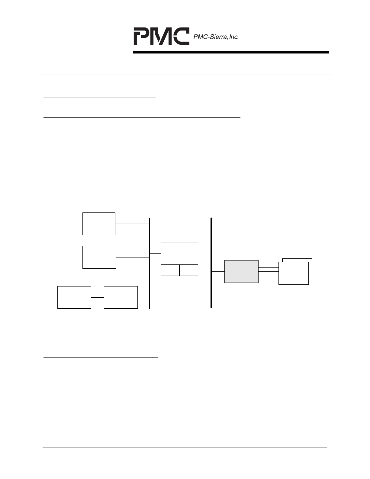
5 APPLICATION EXAMPLES
5.1 Multi-Service Access – IADs, Access Concentrators
Multi-Service access equipment such as Integrated Access Devices (IADs) and
Access Concentrators consolidate voice, data, Internet, and video wide-area
network services over ATM unifying the functions of many different types of
equipment including CSUs, DSUs, multiplexers and FRADs. Figure 1 illustrates
an example of a multi-service access box using IMA over multiple T1/E1 lines for
WAN access.
Figure 1 - Multi-Service Access – IADs and Access Concentrators.
AAL1
PM73124
AAL1gator-4
AAL2
PM73140
MECA-4A
Frame Relay over AAL5
PM7366
FREEDM-8
IWF/AAL5
SAR
UTOPIA L2 /
Any-PHY
On the lineside, the S/UNI-IMA-8 interfaces seamlessly to standard devices such
as the PM4354 COMET-QUAD T1/E1 Framer plus LIU.
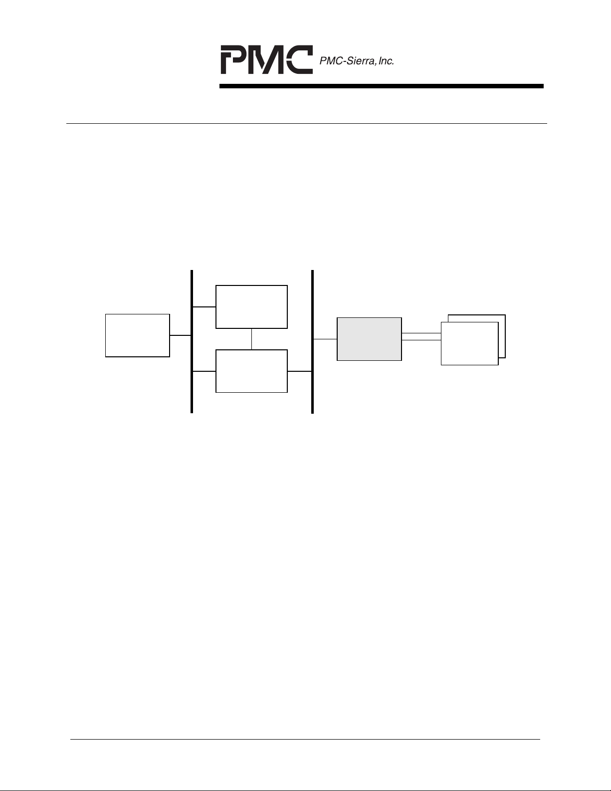
5.2 Remote DSLAM WAN Uplink
IMA is ideally suited for remote DSLAM applications for several reasons. Firstly,
remote DSLAMs are physically located at remote sites of which many are served
by T1 or E1 lines. Secondly, the benefits of ATM have resulted in its almost
exclusive use in DSLAMs. Coupled with ATM, DSLAMs enable service providers
to utilize the bandwidth of the T1/E1 infrastructure for delivering integrated
services such as high-speed Internet access and real-time voice and video. ATM
over T1/E1 is a suitable DSLAM WAN uplink technology and IMA, due to its
PM7326
S/UNI-APEX
PM7324
S/UNI-ATLAS
UTOPIA L2
PM7340
S/UNI-IMA-8
Clock/Data
PM4354
COMET-
QUAD x 2
PROPRIETARY AND CONFIDENTIAL TO PMC-SIERRA, INC., AND FOR ITS CUSTOMERS’ INTERNAL USE 10
PRELIMINARY
INVERSE MULTIPLEXING OVER ATM
DATA SHEET
PMC-2001723 ISSUE 3 INVERSE MULTIPLEXING OVER ATM
PM7340 S/UNI-IMA-8
benefits of higher bandwidth, statistical gain and fault tolerance, is even more
suitable.
Figure 2 illustrates an example of the S/UNI-IMA-8 in a remote DSLAM WAN
uplink application.
Figure 2 -S/UNI-IMA-8 in a Remote DSLAM WAN Uplink Application.
UTOPIA L2 /
Any-PHY
PM7326
S/UNI-APEX
UTOPIA L2
Clock/Data
PM7351
S/UNI-VORTEX
PM7324
S/UNI-ATLAS
PM7340
S/UNI-IMA-8
PM4354
COMET-
QUAD x 2
PROPRIETARY AND CONFIDENTIAL TO PMC-SIERRA, INC., AND FOR ITS CUSTOMERS’ INTERNAL USE 11
PRELIMINARY
INVERSE MULTIPLEXING OVER ATM
DATA SHEET
PMC-2001723 ISSUE 3 INVERSE MULTIPLEXING OVER ATM
PM7340 S/UNI-IMA-8
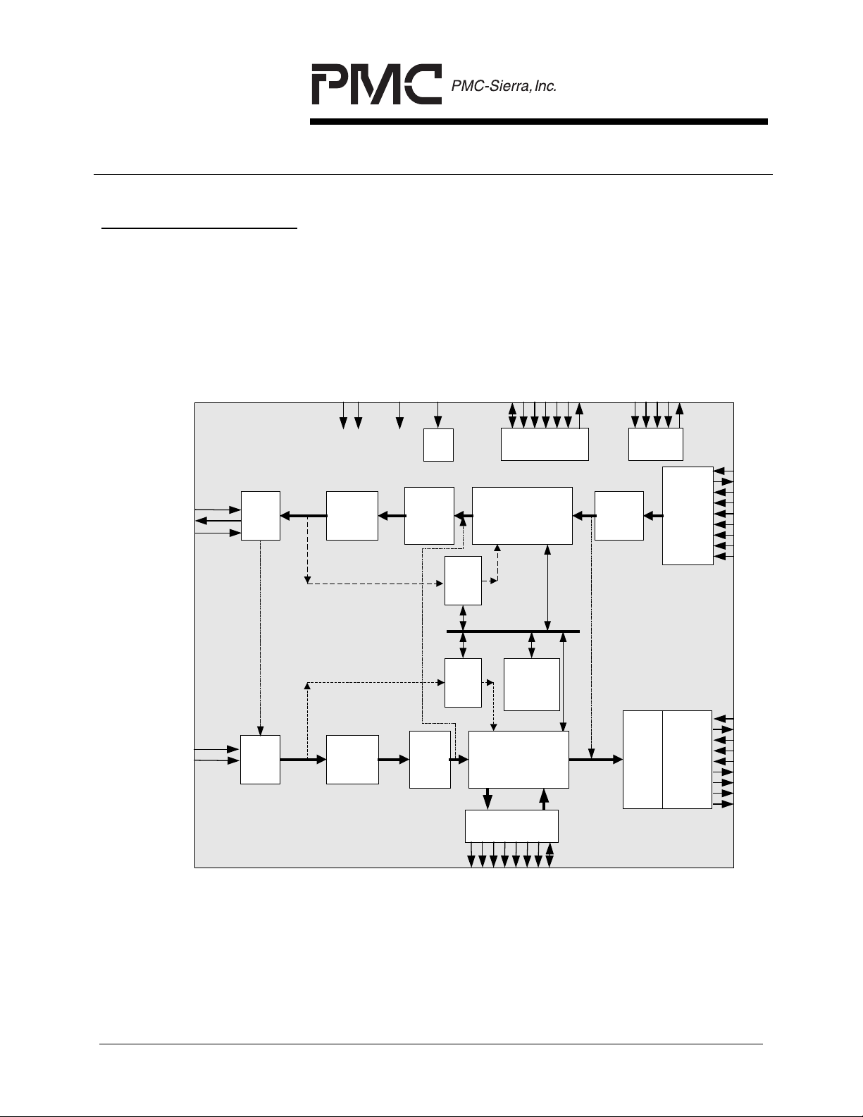
6 BLOCK DIAGRAM
IMA-8 Block Diagram
Figure 3 - S/UNI-IMA-8 Block Diagram
TSCLK[7:0]
TSDATA[7:0]
CTSCLK
RSCLK[7:0]
RSDATA[7:0]
TCAS
RCAS
RSTB
OE
TC Layer
(TTTC-8)
TC Layer
(RTTC-8)
REFCLK
8-chan
x 7 cell
FIFO
(MCFD)
8-chan
FIFO
x 2
cell
DLL
SYSCLK
Tx IMA Processor
IDCC
Internal Bus
IDCC
Rx IMA Data Processor
Cell Writer Ce ll Reader
Memory Interface
D[15:0]
A[10:1]
ALE
WRB
RDB
CSB
INTB
MicroProcess I/F JTAG
8-chan
(TIMA)
Rx IMA
Protocol
Processor
(RIPP)
(RDAT)
(MEMI)
x 3 cell
FIFO
chan
4 cell
FIFO
TCK
8
TMS
TDI
TRSTB
TDO
Any-
PHY/
UTOPIA
Tx Slave
(TXAPS)
Any-
PHY/
UTOPIA
Rx Slave
(RXAPS)
Tx Slave
ATM I/F
TCLK
TPA
TENB
TADR[6:0]
TCSB
TSOP
TSX
TDAT[15:0]
TPRTY
Rx Slave
ATM I/F
RCLK
RPA
RENB
RADR[4:0]
RCSB
RSOP
RSX
RDAT[15:0]
RPRTY
CBCSB
CBRASB
CBCASB
PROPRIETARY AND CONFIDENTIAL TO PMC-SIERRA, INC., AND FOR ITS CUSTOMERS’ INTERNAL USE 12
CBWEB
CBA[11:0]
CBBS[1:0]
CBDQM
CBDQ[15:0]

PRELIMINARY
INVERSE MULTIPLEXING OVER ATM
DATA SHEET
PMC-2001723 ISSUE 3 INVERSE MULTIPLEXING OVER ATM
PM7340 S/UNI-IMA-8
7 DESCRIPTION
The PM7340 S/UNI-IMA-8 is a monolithic integrated circuit that implements the
Inverse Multiplexing for ATM (IMA 1.1) protocol with backward compatibility to
IMA 1.0 and the Transmission Convergence (TC) layer function.
IMA is a protocol designed to combine the transport bandwidth of multiple links
into a single logical link. The logical link is called a group. The S/UNI-IMA-8 can
support up to 4 independent groups with each group capable of supporting from
1 to 8 links. All links within an IMA group must be at the same nominal rate,
however the link rates within a group can be different across groups. The S/UNIIMA-8 can be programmed on a per link basis for cell delination or IMA.
The S/UNI-IMA-8 supports 8 T1, E1 or unchannelized links where each link is
dynamically configurable to support either IMA 1.1, backward compatible IMA
1.0, ATM over T1/E1, ATM over fractional T1/E1 or ATM HEC cell delination for
unchannelized links. Unchannelized links may be used to support applications
such as ADSL.
The S/UNI-IMA-8 supports a clock and data interface where eight 2-pin serial
clock and data interfaces are provided. Each clock and data interface can be
configured to simultaneously support combinations of either T1, E1, or
unchannelized links. Unchannelized links may be used to support applications
such as ADSL. Additionally, for cell delineation only, ATM over fractional T1/E1 is
supported by allowing individual DS0 timeslots to be configured as active or
inactive.
In the transmit direction, the S/UNI-IMA-8 accepts cells from the AnyPHY/UTOPIA interface. As per the IMA specification, the cells, destined for a
group, are distributed in a round-robin fashion to the links within the group,
adding IMA Control Protocol (ICP) cells, filler cells, and stuff cells as needed. The
ICP cells convey state information to the far end and are used to format an IMA
Frame. The IMA Frame is used as a mechanism to synchronize the links at the
far end. Cell rate decoupling is performed at the IMA sub-layer via filler cells.
Filler cells are used instead of physical layer cells for cell rate decoupling, thus a
continuous stream of cells is sent to the TC layer. The stuff cells are used to
maintain synchronization between links in a group by absorbing the rate
differential that exists when links are running at slightly different rates.
The data from the IMA sub-layer is passed on to the TC layer. In the TC layer, the
HEC is calculated and inserted into the cell headers; optional scrambling of the
PROPRIETARY AND CONFIDENTIAL TO PMC-SIERRA, INC., AND FOR ITS CUSTOMERS’ INTERNAL USE 13

PRELIMINARY
INVERSE MULTIPLEXING OVER ATM
DATA SHEET
PMC-2001723 ISSUE 3 INVERSE MULTIPLEXING OVER ATM
PM7340 S/UNI-IMA-8
payload is performed. The cell stream is then mapped into a T1 or E1 payload
with zeros inserted for the framing and overhead bits or bytes. If using an
unchannelized clock and data interface, the data is not mapped into the T1/E1
payload but instead is transmitted one bit for each provided clock pulse.
The links are then transmitted via the serial interfaces. The clock is provided from
each serial clock pin. An optional common-clock mode is provided to enable all
links to run from the same clock. If using an unchannelized clock and data
interface, the data is received one bit for each provided clock pulse.
On the receive side, data is received from the clock/data interface. The timeslots
are mapped to logical channels called links. The TC layer searches for cell
delineation as per the procedures outlined in ITU-T Recommendation I.432.1.
Once cell delineation is obtained, the payload is optionally descrambled and the
cells are passed to the IMA sub-layer. The TC layer provides counts of errored
headers as well as OCD and LCD error interrupts.
The receive IMA sublayer performs IMA-frame delineation and stuff-cell removal.
Based upon the ICP cell information, the S/UNI-IMA-8 determines the differential
delay between the links within a group and applies the link and group state
machine logic to coordinate the activation and deactivation of groups and links
with the far end. As cells are received, they are stored in an external FIFO
structure. This structure is based upon the IMA frame boundaries and the IMA
frame sequence number. When links or groups are determined to be active by
the link and group state machines, the data is played out to the AnyPHY/UTOPIA interface at a constant rate to mimic the existence of a single
higher bandwidth physical link.
Once a group of links is established, links can be dynamically added or deleted
from the group. Under management control, the S/UNI-IMA-8 will perform all
necessary steps to add or delete links from previously established groups.
In order to aid with diagnostics, a line side loopback and a UTOPIA side loopback
are provided. Also, an ICP cell trace feature is provided. When the ICP cell trace
has been enabled for a group, the S/UNI-IMA-8 will place those ICP cells where
a SCCI field change is detected into a buffer that is accessible to the
microprocessor.
PROPRIETARY AND CONFIDENTIAL TO PMC-SIERRA, INC., AND FOR ITS CUSTOMERS’ INTERNAL USE 14

PRELIMINARY
INVERSE MULTIPLEXING OVER ATM
DATA SHEET
PMC-2001723 ISSUE 3 INVERSE MULTIPLEXING OVER ATM
PM7340 S/UNI-IMA-8
8 PIN DIAGRAM
The S/UNI-IMA-8 is packaged in a 324-pin PBGA package that has a body size
of 23mm by 23mm and a ball pitch of 1mm.
Figure 4 - S/UNI-IMA Preliminary Pinout (Bottom View)
PROPRIETARY AND CONFIDENTIAL TO PMC-SIERRA, INC., AND FOR ITS CUSTOMERS’ INTERNAL USE 15

PRELIMINARY
INVERSE MULTIPLEXING OVER ATM
DATA SHEET
PMC-2001723 ISSUE 3 INVERSE MULTIPLEXING OVER ATM
PM7340 S/UNI-IMA-8
9 PIN DESCRIPTION
Receive Slave ATM Interface (Any-PHY mode) (28 Signals)
Pin Name Type Pin
Function
No.
RCLK Input T21 The Receive Clock (RCLK) signal is used to
transfer data blocks from the S/UNI-IMA-8 across
the receive Any-PHY interface.
The RPA, RSOP, RSX, RDAT[15:0], and RPRTY
outputs are updated on the rising edge of RCLK.
The RENB, RADR[4:0], and RCSB inputs are
sampled on the rising edge of RCLK.
The RCLK input must cycle at a 52 MHz or lower
instantaneous rate.
RPA Tristate
Output
AB22 The Receive Packet Available (RPA) is an active
high signal that indicates whether at least one cell is
queued for transfer.
The S/UNI-IMA-8 device drives the RPA with the cell
availability status two RCLK cycles after RADR[4:0]
matches the S/UNI IMA’s device address. The RPA
output is high-impedance at all other times.
The RPA output is updated on the rising edge of
RCLK.
RENB Input W20 The Receive Enable Bar (RENB) is an active low
signal used to initiate the transfer of cells from the
S/UNI-IMA-8 to an ATM layer component, such as a
traffic management device.
The RENB input is sampled on the rising edge of
RCLK.
PROPRIETARY AND CONFIDENTIAL TO PMC-SIERRA, INC., AND FOR ITS CUSTOMERS’ INTERNAL USE 16

PRELIMINARY
INVERSE MULTIPLEXING OVER ATM
DATA SHEET
PMC-2001723 ISSUE 3 INVERSE MULTIPLEXING OVER ATM
PM7340 S/UNI-IMA-8
Pin Name Type Pin
Function
No.
RADR[4]
RADR[3]
RADR[2]
RADR[1]
RADR[0]
Input AA22
Y21
V20
Y22
W22
The Receive Address (RADR[4:0]) signals are
used to address the S/UNI-IMA-8 device for the
purposes of polling and selection for cell transfer.
The RADR[4:0] signals are valid only when the
RCSB signal is sampled active in the following
RCLK cycle.
The RADR[4:0] input bus is sampled on the rising
edge of RCLK.
RCSB Input U21 The Receive Chip Select (RCSB) is an active low
signal that is used to select the S/UNI-IMA-8 receive
interface. When the RCSB is sampled low, it
indicates that the RADR[4:0] sampled at the
previous clock is a valid address. If the RCSB is
sampled high, the device is not selected and the
RADR[4:0] sampled on the previous cycle is not a
valid address and is ignored. When sufficient
address space is provided by RADR[4:0] for all
devices on the bus, this signal may be tied low.
The RCSB input is sampled on the rising edge of
RCLK.
RSOP Output V19 The Receive Start of Packet (RSOP) is an active
high signal that marks the start of the cell on the
RDAT[15:0] bus. When RSOP is active, the first
word of the cell is present on the RDAT[15:0] bus.
The RSOP output is updated on the rising edge of
RCLK.
RSX Output T20 The Receive Start of Transfer (RSX) signal is an
active high signal that marks the first cycle of a data
block transfer on the RDAT[15:0] bus. When the
RSX signal is active, the coinciding data on the
RDAT[15:0] bus represents the in-band PHY
address.
The RSX output is updated on the rising edge of
RCLK.
PROPRIETARY AND CONFIDENTIAL TO PMC-SIERRA, INC., AND FOR ITS CUSTOMERS’ INTERNAL USE 17

PRELIMINARY
INVERSE MULTIPLEXING OVER ATM
DATA SHEET
PMC-2001723 ISSUE 3 INVERSE MULTIPLEXING OVER ATM
PM7340 S/UNI-IMA-8
Pin Name Type Pin
Function
No.
RDAT[15]
RDAT[14]
RDAT[13]
RDAT[12]
RDAT[11]
RDAT[10]
RDAT[9]
RDAT[8]
RDAT[7]
RDAT[6]
RDAT[5]
RDAT[4]
RDAT[3]
RDAT[2]
RDAT[1]
RDAT[0]
Output U22
T22
U19
R20
R22
T19
R19
P20
P21
P22
P19
N20
N21
N22
N19
M20
The Receive Cell Data (RDAT[15:0]) signals carry
the ATM cell words that have been read from the
S/UNI-IMA-8 internal cell buffers. When this
interface is operating in 8-bit mode, the data is
carried on RDAT[7:0].
The RDAT[15:0] output bus is updated on the rising
edge of RCLK.
RPRTY Output M22 The Receive Parity (RPRTY) signal provides the
parity (programmable for odd or even parity) of the
RDAT[15:0] bus. When the interface is operating in
8-bit mode, the parity is calculated over RDAT[7:0]
The RPRTY output is updated on the rising edge of
RCLK.
9.1 Receive Slave ATM Interface (UTOPIA L2 mode) (26 Signals)
Pin Name Type Pin
Function
No.
RCLK Input T21 The Receive Clock (RCLK) signal is used to
transfer data blocks from the S/UNI-IMA-8 across
the receive UTOPIA L2 interface.
The RCA, RSOC, RDAT[15:0], and RPRTY outputs
are updated on the rising edge of RCLK. The RENB
and RADR[4:0] inputs are sampled on the rising
edge of RCLK.
The RCLK input must cycle at a 52 MHz or lower
instantaneous rate.
PROPRIETARY AND CONFIDENTIAL TO PMC-SIERRA, INC., AND FOR ITS CUSTOMERS’ INTERNAL USE 18

PRELIMINARY
INVERSE MULTIPLEXING OVER ATM
DATA SHEET
PMC-2001723 ISSUE 3 INVERSE MULTIPLEXING OVER ATM
PM7340 S/UNI-IMA-8
Pin Name Type Pin
Function
No.
RCA Tristate
Output
AB22 The Receive Cell Available (RCA) is an active high
signal that, when polled using the RADR[4:0]
signals, indicates if at least one cell is queued for
transfer on the selected logical channel FIFO .
The S/UNI-IMA-8 device drives RCA with the cell
availability status for the polled port one RCLK cycle
after a valid RADR[4:0] address is sampled. The
RCA output is high-impedance at all other times.
The RCA output is updated on the rising edge of
RCLK.
RENB Input W20 The Receive Enable Bar (RENB) is an active low
signal used to initiate the transfer of cells from the
S/UNI-IMA-8 to an ATM-layer component, such as a
traffic management device.
The RENB input is sampled on the rising edge of
RCLK.
RADR[4]
RADR[3]
RADR[2]
RADR[1]
RADR[0]
Input AA22
Y21
V20
Y22
W22
The Receive Address (RADR[4:0]) signals are
used to address the S/UNI-IMA-8 device for the
purposes of polling and selecting for cell transfer.
The RADR[4:0] input bus is sampled on the rising
edge of RCLK.
RSOC Output V19 The Receive Start of Cell (RSOC) is an active high
signal that marks the first word of the cell on the
RDAT[15:0] bus.
The RSOC output is updated on the rising edge of
RCLK.
PROPRIETARY AND CONFIDENTIAL TO PMC-SIERRA, INC., AND FOR ITS CUSTOMERS’ INTERNAL USE 19

PRELIMINARY
INVERSE MULTIPLEXING OVER ATM
DATA SHEET
PMC-2001723 ISSUE 3 INVERSE MULTIPLEXING OVER ATM
PM7340 S/UNI-IMA-8
Pin Name Type Pin
Function
No.
RDAT[15]
RDAT[14]
RDAT[13]
RDAT[12]
RDAT[11]
RDAT[10]
RDAT[9]
RDAT[8]
RDAT[7]
RDAT[6]
RDAT[5]
RDAT[4]
RDAT[3]
RDAT[2]
RDAT[1]
RDAT[0]
Output U22
T22
U19
R20
R22
T19
R19
P20
P21
P22
P19
N20
N21
N22
N19
M20
The Receive Cell Data (RDAT[15:0]) signals carry
the ATM cell words that have been read from the
S/UNI-IMA-8 internal cell buffers. When this
interface is operating in 8-bit mode, the data is
carried on RDAT[7:0].
The RDAT[15:0] output bus is updated on the rising
edge of RCLK.
RPRTY Output M22 The Receive Parity (RPRTY) signal provides the
parity (programmable for odd or even parity) of the
RDAT[15:0] bus. When the interface is operating in
8-bit mode, the parity is calculated over RDAT[7:0]
The RPRTY output is updated on the rising edge of
RCLK.
PROPRIETARY AND CONFIDENTIAL TO PMC-SIERRA, INC., AND FOR ITS CUSTOMERS’ INTERNAL USE 20

PRELIMINARY
INVERSE MULTIPLEXING OVER ATM
DATA SHEET
PMC-2001723 ISSUE 3 INVERSE MULTIPLEXING OVER ATM
PM7340 S/UNI-IMA-8
9.2 Transmit Slave Interface (ANY-PHY mode) (30 Signals)
Pin Name Type Pin
Function
No.
TCLK Input E19 The Transmit Clock (TCLK) signal is used to
transfer cells across the ANY-PHY interface to the
internal downstream cell buffers.
The TPA output is updated on the rising edge of
TCLK.
The TENB. TSX, TSOP, TDAT[15:0], TPRTY,
TADR[6:0], and TCSB inputs are sampled on the
rising edge of TCLK.
The TCLK input must cycle at a 52 MHz or lower
instantaneous rate.
TPA Tristate
Output
L22 The Transmit Packet Available (TPA) is an active
high signal that indicates the availability of space in
the selected logical channel FIFO when polled using
the TADR[6:0] signals.
The S/UNI-IMA-8 device drives TPA with the cell
availability status of the polled port two TCLK cycles
after TADR[6:0] matches the S/UNI IMA’s device
address. The TPA output is high-impedance at all
other times.
The TPA output is updated on the rising edge of
TCLK.
TENB Input L20 The Transmit enable bar (TENB) is an active low
signal that is used to indicate cell transfers to the
internal cell buffers.
The TENB input is sampled on the rising edge of
TCLK.
PROPRIETARY AND CONFIDENTIAL TO PMC-SIERRA, INC., AND FOR ITS CUSTOMERS’ INTERNAL USE 21

PRELIMINARY
INVERSE MULTIPLEXING OVER ATM
DATA SHEET
PMC-2001723 ISSUE 3 INVERSE MULTIPLEXING OVER ATM
PM7340 S/UNI-IMA-8
Pin Name Type Pin
Function
No.
TADR[6]
TADR[5]
TADR[4]
TADR[3]
TADR[2]
TADR[1]
TADR[0]
Input K19
K22
K21
K20
J19
J22
J21
The Transmit Address (TADR[6:0]) signals are
used to address logical channels for the purpose of
polling and device selection. The TADR[6:0] signals
are valid only when the TCSB signal is sampled
active in the following TCLK cycle.
The TADR[6:0] input bus is sampled on the rising
edge of TCLK.
TCSB Input J20 The Transmit Chip Select (TCSB) is an active low
signal that is used to select the S/UNI-IMA-8
transmit interface. When the TCSB is sampled low, it
indicates that the TADR[6:0] sampled at the
previous clock is a valid address. If the TCSB is
sampled high, the device is not selected and the
TADR[6:0] sampled on the previous cycle is not a
valid address and is ignored. When sufficient
address space is provided by TADR[6:0] for all
devices on the bus, this signal may be tied low.
The TCSB is asserted low one cycle after a valid
address is present on the TADR[6:0] signals.
The TCSB input is sampled on the rising edge of
TCLK.
TSOP Input H19 The Transmit Start of Packet (TSOP) is an active
high signal that marks the start of the cell on the
TDAT[15:0] bus. When TSOP is active, the first word
of the cell is present on the TDAT[15:0] bus.
The TSOP output is sampled on the rising edge of
TCLK.
TSX Input H22 The Transmit Start of Transfer (TSX) signal is an
active high signal that marks the first cycle of a datablock transfer on the TDAT[15:0] bus. When the
TSX signal is active, the coinciding data on the
TDAT[15:0] bus represents the in-band PHY
address.
The TSX output is sampled on the rising edge of
RCLK.
PROPRIETARY AND CONFIDENTIAL TO PMC-SIERRA, INC., AND FOR ITS CUSTOMERS’ INTERNAL USE 22

PRELIMINARY
INVERSE MULTIPLEXING OVER ATM
DATA SHEET
PMC-2001723 ISSUE 3 INVERSE MULTIPLEXING OVER ATM
PM7340 S/UNI-IMA-8
Pin Name Type Pin
Function
No.
TDAT[15]
TDAT[14]
TDAT[13]
TDAT[12]
TDAT[11]
TDAT[10]
TDAT[9]
TDAT[8]
TDAT[7]
TDAT[6]
TDAT[5]
TDAT[4]
TDAT[3]
TDAT[2]
TDAT[1]
TDAT[0]
Input H21
H20
F19
G22
G21
F22
G20
F21
E22
C20
E21
C22
E20
D21
C21
B22
The Transmit Cell Data (TDAT[15:0]) signals carry
the ATM cell octets that are transferred to the
internal cell buffer. When this interface is operating
in 8-bit mode, only TDAT[7:0] is used.
The TDAT[15:0] input bus is sampled on the rising
edge of TCLK.
TPRTY Input D20 The Transmit Parity (TPRTY) signal provides the
parity (programmable for odd or even parity) of the
TDAT[15:0] bus. The TPRTY signal is considered
valid only when valid data and inband address are
transferring as indicated by the TENB signal
asserted low or the TSX signal asserted high. When
this interface is operating in 8-bit mode, this signal
provides the parity of TDAT[7:0].
A parity error is indicated by a status bit and a
maskable interrupt.
The TPRTY input signal is sampled on the rising
edge of TCLK.
PROPRIETARY AND CONFIDENTIAL TO PMC-SIERRA, INC., AND FOR ITS CUSTOMERS’ INTERNAL USE 23

PRELIMINARY
INVERSE MULTIPLEXING OVER ATM
DATA SHEET
PMC-2001723 ISSUE 3 INVERSE MULTIPLEXING OVER ATM
PM7340 S/UNI-IMA-8
9.3 Transmit Slave Interface (UTOPIA L2 mode) (26 Signals)
Pin Name Type Pin
Function
No.
TCLK Input E19 The Transmit Clock (TCLK) signal is used to
transfer cells across the ANY-PHY interface to the
internal downstream cell buffers.
The TCA output is updated on the rising edge of
TCLK.
The TENB, TSOC, TDAT[15:0], TPRTY, TADR[4:0]
inputs are sampled on the rising edge of TCLK.
The TCLK input must cycle at a 52 MHz or lower
instantaneous rate.
TCA Tristate
Output
L22 The Transmit Cell Available (TCA) is an active high
signal that indicates the availability of space in the
selected logical channel FIFO when polled using the
TADR[4:0] signals.
The S/UNI-IMA-8 drives TCS with the cell space
availability status for the polled port one TCLK cycle
after a valid TADR[4:0] address is sampled.
The TCA output is high-impedance when not polled.
The TCA output is updated on the rising edge of
TCLK.
TENB Input L20 The Transmit enable bar (TENB) is an active low
signal that is used to indicate cell transfers to the
internal cell buffers.
The TENB input is sampled on the rising edge of
TCLK.
TADR[4]
TADR[3]
TADR[2]
TADR[1]
TADR[0]
PROPRIETARY AND CONFIDENTIAL TO PMC-SIERRA, INC., AND FOR ITS CUSTOMERS’ INTERNAL USE 24
Input K21
K20
J19
J22
J21
The Transmit Address (TADR[4:0]) signals are
used to address logical channels for the purposes of
polling and device selection.
The TADR[4:0] input bus is sampled on the rising
edge of TCLK.

PRELIMINARY
INVERSE MULTIPLEXING OVER ATM
DATA SHEET
PMC-2001723 ISSUE 3 INVERSE MULTIPLEXING OVER ATM
PM7340 S/UNI-IMA-8
Pin Name Type Pin
Function
No.
TSOC Input H19 The Transmit Start of Cell (TSOC) is an active high
signal that marks the first word of the cell on the
TDAT[15:0] bus.
The TSOC input is sampled on the rising edge of
TCLK.
TDAT[15]
TDAT[14]
TDAT[13]
TDAT[12]
TDAT[11]
TDAT[10]
TDAT[9]
TDAT[8]
TDAT[7]
TDAT[6]
TDAT[5]
TDAT[4]
TDAT[3]
TDAT[2]
TDAT[1]
TDAT[0]
Input H21
H20
F19
G22
G21
F22
G20
F21
E22
C20
E21
C22
E20
D21
C21
B22
The Transmit Cell Data (TDAT[15:0]) signals carry
the ATM cell octets that are transferred to the
internal cell buffer. The TDAT[15:0] signals are
considered valid only when the TENB signal is
asserted low. When this interface is operating in 8bit mode, only TDAT[7:0] is used.
The TDAT[15:0] input bus is sampled on the rising
edge of TCLK.
TPRTY Input D20 The Transmit Parity (TPRTY) signal provides the
parity (programmable for odd or even parity) of the
TDAT[15:0] bus. The TPRTY signal is valid only
when valid data is transferring as indicated by the
TENB signal asserted low. When this interface is
operating in 8-bit mode, this signal provides the
parity of TDAT[7:0].
A parity error is indicated by a status bit and a
maskable interrupt.
The TPRTY input signal is sampled on the rising
edge of TCLK.
PROPRIETARY AND CONFIDENTIAL TO PMC-SIERRA, INC., AND FOR ITS CUSTOMERS’ INTERNAL USE 25

PRELIMINARY
INVERSE MULTIPLEXING OVER ATM
DATA SHEET
PMC-2001723 ISSUE 3 INVERSE MULTIPLEXING OVER ATM
PM7340 S/UNI-IMA-8
9.4 Microprocessor Interface (31 Signals)
Pin Name Type Pin
No.
D[15]
D[14]
D[13]
D[12]
D[11]
D[10]
D[9]
D[8]
D[7]
D[6]
D[5]
D[4]
D[3]
D[2]
D[1]
D[0]
A[10]
A[9]
A[8]
A[7]
A[6]
A[5]
A[4]
A[3]
A[2]
A[1]
I/O B18
B17
D18
C16
A17
B16
C15
D17
A16
B15
A15
B14
A14
D14
C13
B13
Input A13
D13
C12
B12
D12
A11
B11
D10
A10
B10
Function
The Micro Data (D[15:0]) signals provide a data bus
to allow the S/UNI-IMA-8 device to interface to an
external microprocessor. Both read and write
transactions are supported. The microprocessor
interface is used to configure and monitor the S/UNIIMA-8 device.
The Micro Address (A[10:1]) signals provide an
address bus to allow the S/UNI-IMA-8 device to
interface to an external microprocessor.
The A[10:1] indicate a word address. The S/UNIIMA-8 microprocessor interface is not byte
addressable.
The A[10:1] input signals are sampled while the ALE
is asserted high.
ALE Input C10 The Address Latch Enable (ALE) is an active high
signal that latches the A[10:1] signals during the
address phase of a bus transaction. When ALE is set
high, the address latches are transparent. When ALE
is set low, the address latches hold the address
provided on A[10:1].
The ALE input has an internal pull-up resistor.
PROPRIETARY AND CONFIDENTIAL TO PMC-SIERRA, INC., AND FOR ITS CUSTOMERS’ INTERNAL USE 26

PRELIMINARY
INVERSE MULTIPLEXING OVER ATM
DATA SHEET
PMC-2001723 ISSUE 3 INVERSE MULTIPLEXING OVER ATM
PM7340 S/UNI-IMA-8
Pin Name Type Pin
Function
No.
WRB Input D9 The Write Strobe Bar (WRB) is an active low signal
that qualifies write accesses to the S/UNI-IMA-8
device. When the CSB is set low, the D[15:0] bus
contents are clocked into the addressed register on
the rising edge of WRB.
RDB Input A9 The Read Strobe Bar (RDB) is an active low signal
that qualifies read accesses to the S/UNI-IMA-8
device. When the CSB is set low, the S/UNI-IMA-8
device drives the D[15:0] bus with the contents of the
addressed register on the falling edge of RDB.
CSB Input B9 The Chip Select Bar (CSB) is an active low signal
that qualifies read/write accesses to the S/UNI-IMA-8
device. The CSB signal must be set low during read
and write accesses. When the CSB is set high, the
microprocessor-interface signals are ignored by the
S/UNI-IMA-8 device.
If the CSB is not required (register accesses are
controlled only by WRB and RDB), then it should be
connected to an inverted version of the RSTB signal.
INTB Open-
Drain
Output
C9 The Interrupt Bar (INTB) is an active low signal
indicating that an enabled bit in the Master Interrupt
Register was set. When INTB is set low, the interrupt
is active and enabled. When INTB is tristate, there is
no interrupt pending or it is disabled.
INTB is an open drain output and should be pulled
high externally with a fast resistor.
PROPRIETARY AND CONFIDENTIAL TO PMC-SIERRA, INC., AND FOR ITS CUSTOMERS’ INTERNAL USE 27

PRELIMINARY
INVERSE MULTIPLEXING OVER ATM
DATA SHEET
PMC-2001723 ISSUE 3 INVERSE MULTIPLEXING OVER ATM
PM7340 S/UNI-IMA-8
9.5 SDRAM I/F (35 Signals)
Pin Name Type Pin
Function
No.
CBCSB Output AB6 The Cell Buffer SDRAM Chip Select Bar (CBCSB)
is an active low signal used to control the SDRAM.
CBCSB, CBRASB, CBCASB, and CBWEB define
the command being sent to the SDRAM.
The CBCSB output is updated on the rising edge of
SYSCLK.
CBRASB Output AB7 The Cell Buffer SDRAM Row Address Strobe Bar
(CBRASB) is an active low signal used to control the
SDRAM.
CBCSB, CBRASB, CBCASB, and CBWEB define
the command being sent to the SDRAM.
The CBRASB output is updated on the rising edge
of SYSCLK.
CBCASB Output W6 The Cell Buffer SDRAM Column Address Strobe
Bar (CBCASB) is an active low signal used to
control the SDRAM.
CBCSB, CBRASB, CBCASB, and CBWEB define
the command being sent to the SDRAM.
The CBCASB output is updated on the rising edge
of SYSCLK.
CBWEB Output Y8 The Cell Buffer SDRAM Write Enable Bar
(CBWEB) is an active low signal used to control the
SDRAM.
CBCSB, CBRASB, CBCASB, and CBWEB define
the command being sent to the SDRAM.
The CBWEB output is updated on the rising edge of
SYSCLK.
PROPRIETARY AND CONFIDENTIAL TO PMC-SIERRA, INC., AND FOR ITS CUSTOMERS’ INTERNAL USE 28

PRELIMINARY
INVERSE MULTIPLEXING OVER ATM
DATA SHEET
PMC-2001723 ISSUE 3 INVERSE MULTIPLEXING OVER ATM
PM7340 S/UNI-IMA-8
Pin Name Type Pin
No.
CBA[11]
CBA[10]
Output AA8
W7
CBA[9]
CBA[8]
CBA[7]
CBA[6]
CBA[5]
CBA[4]
CBA[3]
CBA[2]
CBA[1]
CBA[0]
CBBS[1]
CBBS[0]
Output W12
AA9
AB9
W9
Y10
AA10
AB10
W10
AB11
W11
AA12
Y9
Function
The Cell Buffer SDRAM Address (CBA[11:0])
signals identify the row address (CBA[11:0]) and
column address (CBA[7:0]) for the locations
accessed.
The CBA[11:0] output is updated on the rising edge
of SYSCLK.
The Cell Buffer SDRAM Bank Select (CBBS[1:0])
signals determine which bank of a dual/quad bank
Cell Buffer SDRAM chip is active. CBBS is
generated along with the row address when
CBRASB is asserted low.
The CBBS[1:0] outputs are updated on the rising
edge of SYSCLK.
CBDQM Output Y12 The Cell Buffer SDRAM Input/Output Data Mask
(CBDQM) signal is held high until the SDRAM
initialization is complete and then set low for normal
operation.
The CBDQM output is updated on the rising edge of
SYSCLK.
PROPRIETARY AND CONFIDENTIAL TO PMC-SIERRA, INC., AND FOR ITS CUSTOMERS’ INTERNAL USE 29

PRELIMINARY
INVERSE MULTIPLEXING OVER ATM
DATA SHEET
PMC-2001723 ISSUE 3 INVERSE MULTIPLEXING OVER ATM
PM7340 S/UNI-IMA-8
Pin Name Type Pin
No.
CBDQ[15]
CBDQ[14]
CBDQ[13]
CBDQ[12]
CBDQ[11]
CBDQ[10]
CBDQ[9]
CBDQ[8]
CBDQ[7]
CBDQ[6]
CBDQ[5]
CBDQ[4]
CBDQ[3]
CBDQ[2]
CBDQ[1]
CBDQ[0]
I/O W13
AB13
AA13
Y13
W14
AB14
AA14
W15
AA15
Y15
AB16
AA16
Y16
W18
AA17
AB18
Function
The Cell Buffer SDRAM Data (CBDQ[15:0]) signals
interface directly with the Cell Buffer SDRAM data
ports.
The CBDQ[15:0] bi-directional signals are sampled
and updated/tristated on the rising edge of SYSCLK.
PROPRIETARY AND CONFIDENTIAL TO PMC-SIERRA, INC., AND FOR ITS CUSTOMERS’ INTERNAL USE 30

PRELIMINARY
INVERSE MULTIPLEXING OVER ATM
DATA SHEET
PMC-2001723 ISSUE 3 INVERSE MULTIPLEXING OVER ATM
PM7340 S/UNI-IMA-8
9.6 Clk/Data (33 signals)
Pin Name Type Pin No. Function
TSCLK[7]
TSCLK[6]
TSCLK[5]
TSCLK[4]
TSCLK[3]
TSCLK[2]
TSCLK[1]
TSCLK[0]
Input F2
D3
G3
G2
G1
F4
H1
H3
The Transmit Serial Clock (TSCLK[7:0]) signals
contain the transmit clocks for the 8
independently timed links. The TSDATA[7:0]
signals are updated on the falling edge of the
corresponding TSCLK[7:0] clock.
For channelized T1 or E1 links, TSCLK[n] must
be gapped during the framing bit (for T1
interfaces) or during time-slot 0 (for E1
interfaces) of the TSDATA[n] stream. The S/UNIIMA-8 uses the gapping information to determine
the time-slot alignment in the transmit stream.
For unchannelized links, TSCLK[n] must be
externally gapped during the bits or time-slots
that are not part of the transmission format
payload (i.e., not part of the ATM Cell).
The TSCLK[7:0] input signal is nominally a 50%
duty cycle clock of 1.544 MHz for T1 links and
2.048 MHz for E1 links.
The TSCLK[7:0] may operate at higher rates in
the unchannelized mode. At higher rates, the
amount of lines available is limited. See 12.3.1.2
for more details.
PROPRIETARY AND CONFIDENTIAL TO PMC-SIERRA, INC., AND FOR ITS CUSTOMERS’ INTERNAL USE 31

PRELIMINARY
INVERSE MULTIPLEXING OVER ATM
DATA SHEET
PMC-2001723 ISSUE 3 INVERSE MULTIPLEXING OVER ATM
PM7340 S/UNI-IMA-8
Pin Name Type Pin No. Function
TSDATA[7]
TSDATA[6]
TSDATA[5]
TSDATA[4]
TSDATA[3]
TSDATA[2]
TSDATA[1]
TSDATA[0]
Output H4
J3
J2
J1
J4
K2
K1
K4
The Transmit Serial Data (TSDATA[7:0]) signals
contain the transmit data for the 8 independently
timed links. For channelized links, TSDATA[n]
contains the 24 (T1) or 31 (E1) time-slots that
comprise the channelized link. TSCLK[n] must be
gapped during the T1 framing bit position or the
E1 frame alignment signal (time-slot 0). The
S/UNI-IMA-8 uses the location of the gap to
determine the channel alignment on TSDATA[n].
For unchannelized links, TSDATA[n] contains the
ATM cell data. For certain transmission formats,
TSDATA[n] may contain place holder bits or timeslots. TSCLK[n] must be externally gapped
during the place holder positions in the
TSDATA[n] stream.
The TSDATA[7:0] output signals are updated on
the falling edge of the corresponding TSCLK[7:0]
clock
PROPRIETARY AND CONFIDENTIAL TO PMC-SIERRA, INC., AND FOR ITS CUSTOMERS’ INTERNAL USE 32

PRELIMINARY
INVERSE MULTIPLEXING OVER ATM
DATA SHEET
PMC-2001723 ISSUE 3 INVERSE MULTIPLEXING OVER ATM
PM7340 S/UNI-IMA-8
Pin Name Type Pin No. Function
RSCLK[7]
RSCLK[6]
RSCLK[5]
RSCLK[4]
RSCLK[3]
RSCLK[2]
RSCLK[1]
RSCLK[0]
Input V1
U2
V4
T3
R1
T4
P3
P2
The Receive Serial Clock (RSCLK[7:0]) signals
contain the recovered line clock for the 8
independently timed links. The RSDATA[7:0]
signals are sampled on the rising edge of the
corresponding RSCLK[7:0] clock.
For channelized T1 or E1 links, RSCLK[n] must
be gapped during the framing bit (for T1
interfaces) or during time-slot 0 (for E1
interfaces) of the RSDATA[n] stream. The S/UNIIMA-8 uses the gapping information to determine
the time-slot alignment in the receive stream.
RSCLK[7:0] is nominally a 50% duty cycle clock
of 1.544 MHz for T1 links and 2.048 MHz for E1
links.
For unchannelized links, RSCLK[n] must be
externally gapped during the bits or time-slots
that are not part of the transmission format
payload (i.e., not part of the ATM cell).
The RSCLK[7:0] input signal is nominally a 50%
duty cycle clock of 1.544 MHz for T1 links and
2.048 MHz for E1 links.
The RSCLK[7:0] may operate at higher rates in
the unchannelized mode. At higher rates, the
amount of lines available is limited See 12.3.1.2
for more details.
PROPRIETARY AND CONFIDENTIAL TO PMC-SIERRA, INC., AND FOR ITS CUSTOMERS’ INTERNAL USE 33

PRELIMINARY
INVERSE MULTIPLEXING OVER ATM
DATA SHEET
PMC-2001723 ISSUE 3 INVERSE MULTIPLEXING OVER ATM
PM7340 S/UNI-IMA-8
Pin Name Type Pin No. Function
RSDATA[7]
RSDATA[6]
RSDATA[5]
RSDATA[4]
RSDATA[3]
RSDATA[2]
RSDATA[1]
RSDATA[0]
Input V3
Y1
W1
U3
U1
T1
R3
R2
The Receive Serial Data (RSDATA[7:0]) signals
contain the recovered line data for the 8
independently timed links.
For channelized links, RSDATA[n] contains the
24 (T1) or 31 (E1) time-slots that comprise the
channelized link. RSCLK[n] must be gapped
during the T1 framing bit position or the E1 frame
alignment signal (time-slot 0). The S/UNI-IMA-8
uses the location of the gap to determine the
channel alignment on RSDATA[n].
For unchannelized links, RSDATA[n] contains the
ATM cell data. For certain transmission formats,
RSDATA[n] may contain place-holder bits or timeslots. RSCLK[n] must be externally gapped
during the place-holder positions in the
RSDATA[n] stream.
The RSDATA[7:0] input signals are sampled on
the rising edge of the corresponding RSCLK[7:0]
clock.
CTSCLK Input H2 The Common Transmit Serial Clock (CTSCLK)
signal contains a common transmit line clock that
can be used by all of the 8 serial links instead of
the each link’s transmit serial line clock
(TSCLK[n]).
The CTSCLK input signal is nominally a 50%
duty cycle clock of 1.544 MHz for T1 links and
2.048 MHz for E1 links.
PROPRIETARY AND CONFIDENTIAL TO PMC-SIERRA, INC., AND FOR ITS CUSTOMERS’ INTERNAL USE 34

PRELIMINARY
INVERSE MULTIPLEXING OVER ATM
DATA SHEET
PMC-2001723 ISSUE 3 INVERSE MULTIPLEXING OVER ATM
PM7340 S/UNI-IMA-8
9.7 General (5 signals)
Pin Name Type Pin
Function
No.
RSTB Input AA18 The Reset Bar (RSTB) is an active low signal that
provides an asynchronous S/UNI-IMA-8 reset.
RSTB is a Schmitt-triggered input with an internal
pull-up resistor.
OE Input AB19 The Output Enable (OE) is an active high signal
that allows all of the outputs of the device to operate
in their functional state. When this signal is low, all
outputs of the S/UNI-IMA-8 go to the high
impedance state, with the exception of TDO.
SYSCLK Input Y7 The System Clock (SYSCLK) signal is the master
clock for the S/UNI-IMA-8 device. The core S/UNIIMA-8 logic (including the SDRAM interface) is
timed to this signal.
External SDRAM devices share this clock and must
have clocks aligned within 0.2ns skew of the clock
seen by the S/UNI-IMA-8 device.
This clock must be stable prior to deasserting RSTB
0->1.
REFCLK Input N2 This clock is required and may operate at
frequencies up to 33 MHz. In general, for T1, and
E1 rate links, 20 MHz is sufficient. See 12.3.1.3 for
details on selecting the proper frequency.
NC M2 N1
N3 P4
No Connect. These balls are not connected to the
die.
P1 L4
B2 A1
PROPRIETARY AND CONFIDENTIAL TO PMC-SIERRA, INC., AND FOR ITS CUSTOMERS’ INTERNAL USE 35

PRELIMINARY
INVERSE MULTIPLEXING OVER ATM
DATA SHEET
PMC-2001723 ISSUE 3 INVERSE MULTIPLEXING OVER ATM
PM7340 S/UNI-IMA-8
Pin Name Type Pin
No.
Reserved C2 B1
D2 E3
C1 D1
E2 F3
L3 L2
M1 M3
N4 W2
Y2 AA1
W3
AB1 Y4
AB2
AA4
AB3
AB4
AA5 Y6
Y3 AB5
AA6
W5
W19
AB20
AA19
AB20
AA19
AA20
Y19
AA21
A20
A19
B8 C8
B7 A6
D6 C7
B6 A5
C6 B5
A4 C5
A2 A3
B3 C4
Function
PROPRIETARY AND CONFIDENTIAL TO PMC-SIERRA, INC., AND FOR ITS CUSTOMERS’ INTERNAL USE 36

PRELIMINARY
INVERSE MULTIPLEXING OVER ATM
DATA SHEET
PMC-2001723 ISSUE 3 INVERSE MULTIPLEXING OVER ATM
PM7340 S/UNI-IMA-8
9.8 JTAG & Scan Interface (7 Signals)
Pin Name Type Pin
Function
No.
TCK Input B21 The Test Clock (TCK) signal provides timing for test
operations that are carried out using the IEEE
P1149.1 test access port.
TMS Input A21 The Test Mode Select (TMS) is an active high signal
that controls the test operations carried out using the
IEEE P1149.1 test access port.
The TMS signal has an integral pull-up resistor.
The TMS input is sampled on the rising edge of TCK.
TDI Input B20 The Test Data Input (TDI) signal carries test data
into the S/UNI-IMA-8 via the IEEE P1149.1 test
access port.
The TDI signal has an integral pull-up resistor.
The TDI input is sampled on the rising edge of TCK.
TDO Tristate B19 The Test Data Output (TDO) signal carries test data
out of the S/UNI-IMA-8 via the IEEE P1149.1 test
access port. TDO is a tristate output that is inactive
except when the scanning of data is in progress.
The TDO output is updated/tristated on the falling
edge of TCK.
TRSTB Input C18 The Active low Test Reset (TRSTB) is an active low
signal that provides an asynchronous S/UNI-IMA-8
test access port reset via the IEEE P1149.1 test
access port. TRSTB is a Schmitt-triggered input with
an integral pull-up resistor.
Note that when not being used, TRSTB must be
connected to the RSTB input.
SCAN_MODEBInput D7 The Active low Scan Mode (SCAN_MODEB) is an
active low signal that places the S/UNI-IMA-8 into a
manufacturing test mode.
PROPRIETARY AND CONFIDENTIAL TO PMC-SIERRA, INC., AND FOR ITS CUSTOMERS’ INTERNAL USE 37

PRELIMINARY
INVERSE MULTIPLEXING OVER ATM
DATA SHEET
PMC-2001723 ISSUE 3 INVERSE MULTIPLEXING OVER ATM
PM7340 S/UNI-IMA-8
Pin Name Type Pin
Function
No.
SCANENB Input A8 The Active low Scan Enable (SCANENB) is an
active low signal that enables the internal scan logic
for production testing; it should be held to its inactive
high state.
9.9 Power (120 Signals)
Pin Name Type Pin No. Function
VDDI (1.8 V) Power E4
U4
AA11
The core power pins (VDDI[7:0]) should be
connected to a well-decoupled +1.8 V DC
supply.
W17
U20
M21
C14
A7
PROPRIETARY AND CONFIDENTIAL TO PMC-SIERRA, INC., AND FOR ITS CUSTOMERS’ INTERNAL USE 38

PRELIMINARY
INVERSE MULTIPLEXING OVER ATM
DATA SHEET
PMC-2001723 ISSUE 3 INVERSE MULTIPLEXING OVER ATM
PM7340 S/UNI-IMA-8
VSS
(VSSI, VSSO,
VSSQ)
Ground A12 AA2
AA3 AA7
AB12
AB15
AB21 AB8
B4 C11
C17 C19
C3 D15
D19 D22
D5 D8 F1
G19 G4
J9 J10
J11 J12
J13 J14
K3 K9
K10 K11
K12 K13
K14 L9
L10 L11
L12 L13
L14 L21
M4 M9
M10 M11
M12 M13
M14 M19
N9 N10
N11 N12
N13 N14
P9 P10
P11 P12
P13 P14
T2 V21
V22 W21
Y11 Y14
Y17
VSS The VSS pins should be connected to
GND. VSSO pins are ground pins for ports.
VSSQ pins are “quiet” ground pins for ports.
VSSI pins are core ground pins. All grounds
should be connected together.
PROPRIETARY AND CONFIDENTIAL TO PMC-SIERRA, INC., AND FOR ITS CUSTOMERS’ INTERNAL USE 39

PRELIMINARY
INVERSE MULTIPLEXING OVER ATM
DATA SHEET
PMC-2001723 ISSUE 3 INVERSE MULTIPLEXING OVER ATM
PM7340 S/UNI-IMA-8
VDD (3.3V) Power A18 A22
AB17 D11
D16 D4
E1 F20 L1
L19 R21
VDD (3.3V) The I/O power pins (VDD) should
be connected to a well-decoupled +3.3 V DC
supply. These pins include the VDDO pins for
the switching, as well as the VDDQ for the
quiet power pins.
R4 V2
W16 W4
W8 Y18
Y20 Y5
Notes on Pin Description:
• All S/UNI-IMA-8 I/O present minimum capacitive loading and operate at TTL
logic levels and can tolerate 5.0V levels.
• Inputs RSTB, ALE, TCK, TMS, TDI , TRSTB, TSCLK, CTSCLK, RSCLK,
RSDATA, an OE have internal pull-up resistors.
• Power to the VDD (3.3V) pins should be applied before power to the VDDI
(1.8V) pins is applied. Similarly, power to the VDDI (1.8V) pins should be
removed before power to the VDD (3.3V) pins is removed.
PROPRIETARY AND CONFIDENTIAL TO PMC-SIERRA, INC., AND FOR ITS CUSTOMERS’ INTERNAL USE 40

PRELIMINARY
INVERSE MULTIPLEXING OVER ATM
DATA SHEET
PMC-2001723 ISSUE 3 INVERSE MULTIPLEXING OVER ATM
PM7340 S/UNI-IMA-8
10 FUNCTIONAL DESCRIPTION
This section describes the function of each entity in the S/UNI-IMA-8 block
diagram. Throughout this document the use of the term “transmit” implies data
read in from the cell interface and sent out the lineside interface. Conversely,
“receive” is used to describe the data path from the lineside interface to the cell
interface.
The term “virtual PHY” refers to a single flow on the Any-PHY/UTOPIA bus. Each
IMA group or a single TC connection is mapped to a virtual PHY. For simplicity,
both an IMA group and a TC connection will be referenced as a group. Each IMA
group can map data to/from multiple links. Each TC group is mapped to a single
link.
When supporting fractional T1/E1 via the Clock/Data interface, the timeslots that
are chosen to be part of the fractional connection are also referred to as a link.
10.1 Any-PHY/UTOPIA Interface
The ATM cell interface is an Any-PHY compliant 8/16 bit slave interface which is
compatible with the following options:
• Any-PHY Slave
• UTOPIA Level 2, 8-port slave (multi-PHY-mode)
• UTOPIA Level 2, single port slave (single address mode) for receive side only.
10.1.1 Transmit Any-PHY/UTOPIA Slave (TXAPS)
In the transmit direction, each S/UNI-IMA-8 receives cells on the AnyPHY/UTOPIA L2 compatible interface operating at clock rates up to 52 MHz and
supporting 16-bit and 8-bit wide data structures. The S/UNI-IMA-8 operates as a
bus slave.
In the 8- and 16-bit UTOPIA Level 2 Multi-address Slave mode, the transmit
interface of the S/UNI-IMA-8 appears as an 8 port multi-PHY. An 11-bit
configuration register TCAEN (only 4 bits are used in UL2 mode) controls the
response to polling the individual channels within this group of 31 ports. Setting
high on TCAEN[0] enables addresses 0 through 7 and TCAEN[3] enables
PROPRIETARY AND CONFIDENTIAL TO PMC-SIERRA, INC., AND FOR ITS CUSTOMERS’ INTERNAL USE 41

PRELIMINARY
INVERSE MULTIPLEXING OVER ATM
DATA SHEET
PMC-2001723 ISSUE 3 INVERSE MULTIPLEXING OVER ATM
PM7340 S/UNI-IMA-8
addresses 24 through 30. This is typically used to allow more than one slave
device to share the Transmit Any-PHY/UTOPIA master bus.
In the Any-PHY slave mode, the transmit interface of the S/UNI-IMA-8 appears
as a multi-PHY device with 8 ports used for the data path where all ports are
identified in the in-band address. The configuration register TCAEN controls the
response to polling the individual channels. Setting high on TCAEN[0] enables
addresses 0 through 7, and TCAEN[3] enables addressed 24 through 31. This is
typically used to allow more than one slave device to share the Transmit AnyPHY/UTOPIA master bus.
Conceptually, the Any-PHY protocol can be divided into two processes: polling
and cell transfer.
Polling in the transmit direction is used by the bus master – typically a traffic
buffering and management device – to determine when a buffered data cell can
be safely sent to a PHY (or to a virtual PHY in the case of the S/UNI-IMA-8). The
S/UNI-IMA-8 provides an independent 3-deep cell buffer FIFO for each virtual
PHY. In total, there are 8 FIFOs. This arrangement ensures that there is no headof-line blocking.
The traffic manager need only poll those virtual PHYs for which it has cells
queued. A cell transfer can be initiated after a polled virtual PHY asserts the TPA
output. Each virtual PHY’s cell buffer availability status (i.e., the status that will be
driven onto the TPA output when the virtual PHY is polled) is deasserted when
the first byte of the last cell is written into the buffer. It is re-asserted only when
the FIFO can accept another complete cell.
In Any-PHY mode, polling is performed using the TADR[10:0] bus in conjunction
with the TCSB. Each S/UNI-IMA-8 uses the TADR[2:0] bits to indicate the 8
logical virtual PHYs. The upper bits from the TADR bus, TADR[6:3], are
compared to the configured address to select the device. The remaining address
bits from the traffic manager are decoded externally and are used to drive the
TCSB. The address prepend field in the cell transfer contains the entire 16-bit
address. In 8-bit mode, the prepend address is reduced to 8-bits.
In Any-PHY mode, the cell transfer is initiated after a successful poll. The virtual
PHY address is prepended to the cell, thus performing an inband selection. The
S/UNI-IMA-8 monitors the address prepend on the cell transfer to detect its cells.
For UTOPIA L2 Mode, Only TADR[4:0] are used for polling and selection. Each
FIFO will only assert TCA when polled if it is not in the process of transferring a
cell and if there is room in the FIFO for a complete cell. Unlike Any-PHY, in
PROPRIETARY AND CONFIDENTIAL TO PMC-SIERRA, INC., AND FOR ITS CUSTOMERS’ INTERNAL USE 42

PRELIMINARY
INVERSE MULTIPLEXING OVER ATM
DATA SHEET
PMC-2001723 ISSUE 3 INVERSE MULTIPLEXING OVER ATM
PM7340 S/UNI-IMA-8
UTOPIA L2 Mode the virtual PHY port must first be selected prior to the start of
the data transfer. This selection is done using the same address lines that are
used for polling in combination with the TENB pin.
Data transfers are cell based, that is, an entire cell is transferred from one PHY
device before another is selected. Polling occurs concurrently with cell transfers
to ensure maximum throughput. Data pausing is not supported in Any-PHY
mode. If the TENB is deasserted prior to a complete cell being transferred, the
cell transfer error will be triggered.
The Transmit Cell Transfer Format is shown in Figure 5 and Figure 6. Word/byte
0 is required for cell transfers to an Any-PHY slave. The address prepend is the
S/UNI-IMA-8 virtual PHY ID. The virtual PHY ID can be mapped to a TC link or to
an IMA group. Optional prepends are supported, but are ignored by the S/UNIIMA-8.
Inclusion of optional words is statically configurable for the interface. The optional
words are always ignored.
Figure 5 - 16-bit Transmit Cell Transfer Format
Bits 15-8 Bits 7-0
Word 0
Address Prepend
(Any-PHY
only)
Word 1
Optional Prepend
(Optional)
Word 2
Word 3
Word 4
Word 5
Word 6
••
H1 H2
H3 H4
HEC/UDF
PAYLO AD1 PAYLO AD2
PAYLO AD3 PAYLO AD4
•••••
•••••
Word 28
PROPRIETARY AND CONFIDENTIAL TO PMC-SIERRA, INC., AND FOR ITS CUSTOMERS’ INTERNAL USE 43
PAYLO AD47 PAYLO AD48
•
••
•
••

PRELIMINARY
INVERSE MULTIPLEXING OVER ATM
DATA SHEET
PMC-2001723 ISSUE 3 INVERSE MULTIPLEXING OVER ATM
PM7340 S/UNI-IMA-8
Figure 6 - 8-bit Transmit Cell Transfer Format
Bits 7-0
Byte 0
(Any-PHY
only)
Byte 1
(Optional)
Byte 2
(Optional)
Byte 3
Byte 4
Byte 5
Byte 6
Byte 7*
Byte 8
Address Prepend
Optional Prepend[15:8]
Optional Prepend[7:0]
H1
H2
H3
H4
HEC
PAYLO AD1
•
••••
••••
Byte 55
PAYLO AD48
10.1.2 Receive Any-PHY/UTOPIA Slave (RXAPS)
In the receive direction, each S/UNI-IMA-8 transmits cells on an AnyPHY/UTOPIA L2 compatible interface operating at clock rates up to 52 MHz and
supporting 16-bit and 8-bit wide data structures. The S/UNI-IMA-8 operates as a
bus slave.
In the 8 and 16-bit UTOPIA Level 2 Multi-Address Slave mode, the S/UNI-IMA-8
operates as an 8 port multi-PHY with each virtual PHY stored in it’s own FIFO. A
4-bit configuration register, RCAEN, controls the response to polling the
PROPRIETARY AND CONFIDENTIAL TO PMC-SIERRA, INC., AND FOR ITS CUSTOMERS’ INTERNAL USE 44

PRELIMINARY
INVERSE MULTIPLEXING OVER ATM
DATA SHEET
PMC-2001723 ISSUE 3 INVERSE MULTIPLEXING OVER ATM
PM7340 S/UNI-IMA-8
individual channels. Setting RCAEN[0] enables addresses 0 through 7, and
RCAEN[3] enables addresses 24 through 30. This is typically used to allow more
than one slave device to share the Receive UTOPIA master bus. When polled,
the Receive Packet Available (RPA) output indicates whether there is at least one
cell available for transfer from the polled link. Upon selection, the interface
handles data pausing anywhere in the middle of a cell transfer.
In the 8- and 16-bit UTOPIA Level 2 Single Address mode, the S/UNI-IMA-8
operates as a single device with a single cell FIFO, with all cells being identified
by their virtual PHY ID (VPHY ID) in an address prepend. The address prepend
may be optionally mapped to the HEC/UDF field in order to maintain the standard
cell length. When the address presented on the Any-PHY/UTOPIA Interface
RADR pins matches a programmable 5-bit configuration register (DEVID), the
RXAPS will respond to polls. In all other cases, the output signals are tristated
which allows other slave devices to respond. When polled, the RPA output
indicates whether there is at least one cell available for transfer from any link.
In the 8- and 16-bit Any-PHY Slave mode, the S/UNI-IMA-8 operates as a single
device with a single cell FIFO, with all cells being identified by their virtual PHY ID
(VPHY ID) in a address prepend. When the address presented on the AnyPHY/UTOPIA Interface RADR pins matches a programmable 5-bit configuration
register (DEVID), the RXAPS will respond to polls. In all other cases, the output
signals are tristated which allows other slave devices to respond. When polled,
the RPA output indicates whether there is at least one cell available for transfer
from any link. In Any-PHY mode, data pausing is not supported.
In all modes, an optional prepend is allowed on the bus. This prepend will
always be set to zero and has no significance to the S/UNI-IMA-8 but is provided
for interoperability.
To support current and future devices, the interface is configurable as either an
Any-PHY or UTOPIA L2 interface. Table 3 summarizes the distinctions between
the two protocols.
Table 3 UTOPIA L2 and Any-PHY Comparison
Attribute UTOPIA L2 Any-PHY
Latency RDAT[15:0], RPRTY, and
RSOP are driven or become
high impedance immediately
upon sampling RENB low or
PROPRIETARY AND CONFIDENTIAL TO PMC-SIERRA, INC., AND FOR ITS CUSTOMERS’ INTERNAL USE 45
RDAT[15:0], RPRTY, RSOP
and RSX are driven or
become high impedance on
the RCLK rising edge

PRELIMINARY
INVERSE MULTIPLEXING OVER ATM
DATA SHEET
PMC-2001723 ISSUE 3 INVERSE MULTIPLEXING OVER ATM
PM7340 S/UNI-IMA-8
high, respectively. The RPA
is driven with the cell
availability status one CLK
cycle after the RADR[4:0]
pins match the S/UNI-IMA8’s address. A match is
defined as either matching
the programmed value in
single PHY mode or being
within the correct range for
multi-PHY mode.
RSX Undefined. It is low when not
high impedance.
RSOP High coincident with the first
word of the cell data
structure.
Paused
transfers
Permitted by deasserting
RENB high, but the S/UNIIMA’s address must be
presented on RADR[4:0] the
last cycle RENB is high to
reselect the same PHY.
following the one that
samples RENB low or high,
respectively. The RPA is
driven with the cell
availability status two CLK
cycles after RADR[4:0] pins
match the S/UNI-IMA-8’s
address.
High coincident with the first
word of the cell data
structure.
High coincident with the first
byte of the cell header.
Not Permitted.
Autonomous
deselection
Not supported. A subsequent
cell is output (provided one is
available) if RENB is held
low beyond the end of a cell.
The outputs become high
impedance after the last
word of a cell is transferred
and until the S/UNI-IMA-8 is
reselected.
The cell format for the receive direction is the same as the transmit interface; see
Figure 7 and Figure 8 for the formats.
PROPRIETARY AND CONFIDENTIAL TO PMC-SIERRA, INC., AND FOR ITS CUSTOMERS’ INTERNAL USE 46

PRELIMINARY
INVERSE MULTIPLEXING OVER ATM
DATA SHEET
PMC-2001723 ISSUE 3 INVERSE MULTIPLEXING OVER ATM
PM7340 S/UNI-IMA-8
Figure 7 - 16-bit Receive Cell Transfer Format
Bits 15-8 Bits 7-0
Word 0
(Any-PHY
and single
channel
UL2 only)
Word 1
(Optional)
Word 2
Word 3
Word 4*
Word 5
Word 6
Word 28
Address Prepend
Optional Prepend
H1 H2
H3 H4
HEC/UDF
PAYLO AD1 PAYLO AD2
PAYLO AD3 PAYLO AD4
••
•••••
•••••
•
••
•
••
PAYLO AD47 PAYLO AD48
Note: HEC/UDF may contain the address prepend for Single Channel UL2
PROPRIETARY AND CONFIDENTIAL TO PMC-SIERRA, INC., AND FOR ITS CUSTOMERS’ INTERNAL USE 47

PRELIMINARY
INVERSE MULTIPLEXING OVER ATM
DATA SHEET
PMC-2001723 ISSUE 3 INVERSE MULTIPLEXING OVER ATM
PM7340 S/UNI-IMA-8
Figure 8 - 8-bit Receive Cell Transfer Format
Bits 7-0
Byte 0
(Any-PHY
and single
channel
UL2 only)
Byte 1
(Optional)
Byte 2
(Optional)
Byte 3
Byte 4
Byte 5
Byte 6
Byte 7*
Byte 8
Address Prepend
Optional Prepend[15:8]
Optional Prepend[7:0]
H1
H2
H3
H4
HEC
PAYLO AD1
•
••••
••••
Byte 55
PAYLO AD48
Note: HEC field may contain the address prepend for Single Channel UL2
For Any-PHY mode or single-PHY mode, the address prepend field encoding
indicates the virtual PHY ID. The virtual PHY ID contains 2 sections, the lower 7
bits indicates the virtual PHY ID, while the upper bits indicate the device address.
For UTOPIA multi-PHY mode, the address prepend is not used.
PROPRIETARY AND CONFIDENTIAL TO PMC-SIERRA, INC., AND FOR ITS CUSTOMERS’ INTERNAL USE 48

PRELIMINARY
INVERSE MULTIPLEXING OVER ATM
DATA SHEET
PMC-2001723 ISSUE 3 INVERSE MULTIPLEXING OVER ATM
PM7340 S/UNI-IMA-8
10.1.3 Summary of Any-PHY/UTOPIA Modes
The following table summarizes the available modes of the Any-PHY/UTOPIA
Interfaces
Mode Dir &
Protocol
TX Poll
TX Select
TX Transfer
RX Poll
RX Select
UL2 Single PHY UL2 Multi-PHY Any-PHY
Not supported PHY Channels: 8 PHY Channels: 8
Channel Enable Register:
TCAEN(3:0)
Channel Address Pins: TADR(2:0) Device ID Register:
Status Pin: TCA Channel Address Pins: TADR(6:0)
Not supported PHY Channels: 8 PHY Channels: 8
Channel Enable Register:
TCAEN(3:0)
Channel Address Pins: TADR(4:0) Device ID Register:
Select Pin: TENB Channel Address: Prepend bits
Not supported Cell Size: 8 bit X 53 or 55 bytes Cell Size: 8 bit X 54 or 56 bytes
Cell Size: 16 bit X 27 or 28 words Cell Size: 16 bit X 28 or 29 words
Enable Pin: TENB Enable Pin: TENB
Pause in Cell: w/ TENB
PHY Channels: 1 PHY Channels: 8 PHY Channels: 1 (in-band
Device ID Register: DEVID(4:0) Channel Enable Register:
RCAEN(3:0)
Device Address Pins: RADR(4:0) Channel Address Pins: RADR(4:0) Device Address Pins: RADR(4:0)
Status Pin: RCA Status Pin: RCA Status Pin: RCA
PHY Channels: 1 PHY Channels: 8 PHY Channels: 1
Device ID Register: DEVID(4:0) Channel Enable Register:
RCAEN(3:0)
Channel Enable Register:
TCAEN(6:0)
CFG_ADDR(6:3)
Address Qualifier Pin: TCSB
Status Pin: TCA
Channel Enable Register:
TCAEN(6:0)
CFG_ADDR(15:7) or (7)
(6:0)
Device Address: Prepend bits (bit
15:7, for 16 bit mode) or (bit 7 for
8-bit mode)
Select Pin: TENB, TSX to indicate
first byte of transfer.
addressing is used to identify
virtual PHYs)
Device ID Register: DEVID(4:0)
Device ID Register: DEVID(4:0)
PROPRIETARY AND CONFIDENTIAL TO PMC-SIERRA, INC., AND FOR ITS CUSTOMERS’ INTERNAL USE 49

PRELIMINARY
INVERSE MULTIPLEXING OVER ATM
DATA SHEET
PMC-2001723 ISSUE 3 INVERSE MULTIPLEXING OVER ATM
Device Address Pins: RADR(4:0) Channel Address Pins: RADR(4:0) Device Address Pins: RADR(4:0)
Select Pin: RENB Select Pin: RENB Select Pin: RENB
RX Transfer
Cell Size: 8 bit X 53, 54, 55 or 56
bytes
Cell Size: 16 bit X 27, 28 or 29
words
Enable Pin: RENB Enable Pin: RENB Enable Pin: RENB
Channel Address: Prepend or UDF Pause in Cell: w/ RENB Channel Address: Prepend
Cell Size: 8 bit X 53 or 55 bytes Cell Size: 8 bit X 54 or 56 bytes
Cell Size: 16 bit X 27 or 28 words Cell Size: 16 bit X 28 or 29 words
PM7340 S/UNI-IMA-8
10.1.4 ANY-PHY/UTOPIA Loopback
For diagnostic purposes, the capability to loopback all Any-PHY/UTOPIA traffic
back to the Any-PHY/UTOPIA bus is provided. Cells are taken from the Transmit
group FIFOs and placed into the respective Receive Group FIFOs, or to a single
FIFO on a space available basis.
10.2 IMA Sub-layer
10.2.1 Overview
The IMA protocol provides inverse multiplexing of a single ATM stream over
multiple physical links and reassembles the original cell stream at the far-end.
The inverse multiplexing is performed on a cell basis; hence, the IMA protocol is
described as a cell-based protocol. See Figure 9 below.
The protocol is based upon the concept of an IMA frame. An IMA frame is
programmable in size and is delineated by an IMA Control Protocol (ICP) Cell. It
is recommended that the ICP cells of each link in the IMA group be offset from
each other to reduce the notification time of link/group status changes.
The transmitter is responsible for aligning the IMA frames on all links within a
group, and for ensuring that cells are transmitted continuously by adding filler
cells as necessary. To maintain frame alignment in the presence of independently
timed line clocks, a cell based stuffing algorithm is utilized.
Since the IMA frames are aligned on transmission, this allows the receive end to
recover the IMA frames and align them to remove any differential delay between
the physical links.
PROPRIETARY AND CONFIDENTIAL TO PMC-SIERRA, INC., AND FOR ITS CUSTOMERS’ INTERNAL USE 50

PRELIMINARY
INVERSE MULTIPLEXING OVER ATM
DATA SHEET
PMC-2001723 ISSUE 3 INVERSE MULTIPLEXING OVER ATM
PM7340 S/UNI-IMA-8
Figure 9 - Inverse Multiplexing
Single ATM Cell Stream
from ATM Layer
Tx direction cells distributed across links in round robin sequence
Rx direction cells recombined into single ATM stream
10.2.2 IDCC scheduler
The IMA Data Cell Clock (IDCC) scheduler calculates the IMA Data Cell Rate
(IDCR) for each group that is used by both the Receive and the Transmit IMA
processors. There is one scheduler for each direction (TXIDCC and RXIDCC),
and each scheduler can monitor the rate of up to 8 reference clocks; each
scheduler can also generate up to 8 IDCC clocks based upon IDCR. For each
group, the reference link can be selected to be one of the 8 monitored links. Each
of the monitored links can only be the reference link for one group. IDCR is
calculated using the following equation, with Non and M set independently for
each IDCR generator. N
frame, and TRL Cell Rate (TRLCR) is the cell rate of the reference link.
IMA Group
Physical Link #0
PHY
Physical Link #1
PHY
Physical Link #2
PHY
IMA Virtual LInk
is the number of active links, M is the size of the IMA
on
PHY
PHY
PHY
IMA Group
Original Cell stream
passed to ATM Layer
IDCR = Non X TRLCR X (M-1/M) X (2048/2049)
TRLCR is generated from the byte rate. The byte rate is obtained by monitoring
the data transfers on the internal bus in the TC layer.
For each IDCR clock tick, a service request is generated and placed into a rate
based FIFO. Since there may be many requests generated in a short amount of
time and the rate at which each request is generated may be different, a method
is required to arbitrate between the requests to prevent blocking of high rate
PROPRIETARY AND CONFIDENTIAL TO PMC-SIERRA, INC., AND FOR ITS CUSTOMERS’ INTERNAL USE 51

PRELIMINARY
INVERSE MULTIPLEXING OVER ATM
DATA SHEET
PMC-2001723 ISSUE 3 INVERSE MULTIPLEXING OVER ATM
PM7340 S/UNI-IMA-8
requests by large numbers of low rate requests. To achieve this, each request is
placed into a priority FIFO. The priority of the request is based upon its rate.
There are a total of 5 rate-based FIFOs. When a service request is accepted by
the Transmit IMA processor (TIMA) or the Receive IMA Data Processor (RDAT),
the next request to be presented is taken from the highest priority FIFO that has
an entry. In this manner, the higher rate requests get higher priority than the
lower rate requests. Since the S/UNI-IMA-8 can always service all of the
requests, this algorithm limits the CDV experienced by any service request to
approximately one inter-arrival time of the service request for each group.
Rate changes are restricted to IMA frame boundaries. An IMA frame boundary
occurs once every (M-1)*N service requests. When a request is received to
change the rate(Non), the request is saved until the next IMA frame boundary, at
which point it takes effect. By restricting rate changes to frame boundaries, the
rate accuracy is preserved preventing FIFO underflows/overflows. Since rate
changes are not instantaneous, a vector that represents the active Link IDs
(LIDs) in the group is passed with the service request. In this manner, the entity
receiving the service requests is informed of the change in rate and of which links
should currently be in the round robin for servicing.
All IMA-based rate changes are internally managed by the S/UNI-IMA-8; no user
interaction is necessary for correct scheduling.
The IDCC is also used for scheduling the TC data flow. In this case, the rate
generated is simply the cell rate of the TC link and is not modified for IMA ICP
cells or stuff cells according to the following equation:
IDCR = TRLCR
For all TC connections, the IDCC must be configured in TC mode for the physical
link.
10.2.3 Transmit IMA Processor (TIMA)
The TIMA is responsible for the transmit IMA functions. This consists of
distributing the cells arriving from the ATM layer to links in a group and for
inserting ICP cells, filler cells, and stuff cells as required by the IMA protocol.
Additionally, the TIMA can support cell transmission on connections using only
the Transmission Convergence (TC) sublayer without the use of the IMA protocol
sublayer.
PROPRIETARY AND CONFIDENTIAL TO PMC-SIERRA, INC., AND FOR ITS CUSTOMERS’ INTERNAL USE 52

PRELIMINARY
INVERSE MULTIPLEXING OVER ATM
DATA SHEET
PMC-2001723 ISSUE 3 INVERSE MULTIPLEXING OVER ATM
PM7340 S/UNI-IMA-8
10.2.3.1 IMA Frame
The Transmit IMA processor creates the IMA frame by inserting an ICP cell after
every (M-1) cells per link. Values of M supported are 32, 64, 128, and 256. The
ICP cell is offset within the IMA frame. This offset is programmable on a per-link
basis, and the offsets shouldspread throughout the frame. To aviod interaction
between groups, the offsets within a group may not be aligned at the same offset.
If offsets are aligned at the same offset within a group, the CDV experienced by
other groups will be increased. Each frame is identified with an IMA frame
sequence number (IFSN); this number is the same for every link in the group that
is within the same frame and increments with each frame. The TIMA is
responsible for aligning the transmission of the IMA frame on all links within a
group.
10.2.3.2 Stuffing Procedure
The TIMA can support both Independent Transmit clock (ITC) and Common
Transmit Clock (CTC) modes. The difference between these modes is the
stuffing protocol. The method of stuffing is set independently from the clocking
mode present in the ICP cell.
In CTC mode, a stuff cell is added after 2048 cells on each link. The stuff cell is
identical to the ICP cell and is inserted immediately following the ICP cell. The
stuff cell events will occur on the same frame on all links; however, the
programmed ICP offsets determine at which cell in the frame the stuff event will
occur.
In ITC mode, a stuff cell is added to the reference link after 2048 cells on the
reference link. On all other links in the group, stuff cells are added as necessary
to compensate for data rate differences between the link and the reference link of
the group. The added stuff cells (or lack of stuff cells) keep the data rate between
links equalized.
The stuff cell is generated immediately after the ICP cell and both the ICP cell
and the stuff cell are identified as stuff cells via the Link Stuff Indication (LSI) field
of the ICP cell.
In CTC mode, the stuff event is always advertised in the ICP cell of the preceding
frame. The stuff event may also be advertised in the 4 preceding frames. It is
programmable per group whether the ICP cell is advertised starting 1 frame or 4
frames prior to the occurrence of the stuff event.
PROPRIETARY AND CONFIDENTIAL TO PMC-SIERRA, INC., AND FOR ITS CUSTOMERS’ INTERNAL USE 53

PRELIMINARY
INVERSE MULTIPLEXING OVER ATM
DATA SHEET
PMC-2001723 ISSUE 3 INVERSE MULTIPLEXING OVER ATM
PM7340 S/UNI-IMA-8
In ITC mode, the stuff event may also be advertised in the ICP cell of the
preceding frame or in the 4 preceding frames. If the stuff event needs to be
advertised for 4 preceding frames, a DS1/E1 clock tolerance of +/- 50 ppm is
required. If a frequency tolerance greater than +/- 50 ppm is required between
the independent transmit clocks, the TIMA can provide the single frame
advertisement of stuff events.
To determine when a stuff cell is needed on ITC mode links (not the TRL), a link
stuff detection unit with rate counters is used to track the relative rate of data
being read from the link FIFOs within a group to the rate of data being read from
the TRL FIFO for the same group. When the relative rate counter indicates that
the rate differences have accounted for a slip of a cell, a stuff cell is inserted.
10.2.3.3 Data Flow
The TIMA can support up to 8 groups (IMA group or TC link). Each FIFO on the
ATM-layer interface side represents either an IMA group or a TC group. Each
group’s behavior is controlled by the internal memory tables and records.
For IMA groups, the following internal memory structures are used:
1) the Transmit IMA Group Configuration Record for configuring group
options and mapping to a port on the ATM interface (VPHY ID)
2) Transmit IMA Group Context Record contains statistics and the current
ICP cell image.
3) Transmit LID to the PHYsical Link Mapping Table is used to map
individual physical links into a group and assign the LIDs.
4) TIMA Physical Link Context Record contains per-link statistics, and
state information.
For TC links, only one record is used, the Transmit Physical Link Record, to
maintain statistics and to map the physical link to a port on the ATM interface
(VPHY ID).
The TIMA performs cell transfers from the group FIFOs to the link FIFOs in
response to service requests from the TxIDCC. The TxIDCC schedules both IMA
groups, as well as low rate TC-only connections. Groups are scheduled
according to their rates. Higher-rate groups are prioritized above the lower-rate
groups. The TIMA operates at a rate sufficient to ensure the TxIDCC will not
suffer request congestion provided the ICP cells are spread throughout the frame
PROPRIETARY AND CONFIDENTIAL TO PMC-SIERRA, INC., AND FOR ITS CUSTOMERS’ INTERNAL USE 54

PRELIMINARY
INVERSE MULTIPLEXING OVER ATM
DATA SHEET
PMC-2001723 ISSUE 3 INVERSE MULTIPLEXING OVER ATM
PM7340 S/UNI-IMA-8
on IMA groups. If there is no service request pending, the TIMA remains idle. If a
group is unused, no cells will be pulled from the respective group FIFO.
Therefore, when de-activating groups, ATM cell flow to the S/UNI-IMA-8 should
be terminated prior to de-activating the group in order to prevent stale data from
being stored in the group FIFO.
10.2.3.3.1 IMA Service
For each IMA group-service request, a cell is transferred from the group FIFO to
one of the link FIFOs. If no cell is available from the group FIFO, an IMA filler cell
is generated and placed in the link FIFO. The link FIFOs within a group are
serviced in a round-robin fashion, with the round-robin order determined by the
LID. If the next link in the round robin is due to receive an ICP cell, the ICP cell is
generated using the link and group state information from the Transmit IMA
Group Context Record, and the LID and LSI from the link. If a stuff event is
scheduled, the stuff ICP cell is also inserted. Whenever an ICP cell is inserted,
the IMA group servicing proceeds to the next link in the round robin without
waiting for another service request. The IMA group service is complete when
either: (1) a cell is transferred from the group FIFO or (2) an ATM filler cell is
generated. When links are in the process of being added, but are not yet
available for carrying data traffic, IMA frames consisting of filler cells and ICP
cells are generated. Such links are not scheduled by the TxIDCC scheduler, but
will be processed with the currently active links.
During group start-up, even with all of the transmit links in the unusable state, the
TxIDCC scheduler is started and IMA frames are generated. During group startup (i.e. links are not yet in the active state), a group can be configured such that
received via the UTOPIA L2 / Any-PHY bus can be dropped to avoid the
accumulation of stale data or to drop stale data in the group FIFO left over from a
previous use of the VPHY ID. . During link additions, IMA frames are generated
on new links when they are added to the group.
10.2.3.3.2 TC Only Service
For TC-only mode groups, servicing is also initiated by group service requests
from the TxIDCC. However, servicing a group FIFO simply entails transferring a
cell from the group FIFO to the proper link FIFO. If a cell is not present in the
group FIFO, no cells are transferred and the servicing of the request is complete.
In TC mode, no other cells are inserted into the data stream by the IMA sub-layer
(physical layer idle cells are generated by the physical layer).
PROPRIETARY AND CONFIDENTIAL TO PMC-SIERRA, INC., AND FOR ITS CUSTOMERS’ INTERNAL USE 55

PRELIMINARY
INVERSE MULTIPLEXING OVER ATM
DATA SHEET
PMC-2001723 ISSUE 3 INVERSE MULTIPLEXING OVER ATM
PM7340 S/UNI-IMA-8
10.2.3.4 Timing Reference Link Maintenance
It is possible to have the timing reference link for an IMA group change from one
link to another while the IMA connection is in operation. If an IMA group is
operating in CTC mode, the reference link used for the scheduling is simply
switched. The next stuff cell insertion still occurs 2049 cells after the previous
stuff. If the IMA group is operating in ITC mode and the reference link is
switched, the first stuff insertion on the new TRL occurs at approximately the
same frame a stuff would have been inserted had it not become the TRL. At the
time of the TRL change, the existing accrued rate differential on the new TRL is
used to prorate the number of cells out of 2048 until the next TRL stuff. Although
the first stuff will occur at approximately the proper number of cells to maintain
the correct differential delay, the actual time of the stuff will be dependent on the
new TRL rate.
Similarly, the first stuff cell insertion on the previous TRL occurs in approximately
the same frame a stuff cell would have been inserted had it still been the TRL
although the actual frame for stuff insertion will also be dependent on the rate
difference with the new TRL. This minimizes any effects on the differential delay
for the group as well as reducing any FIFO level changes. All subsequent stuff
cell insertions on the TRL then happen after every 2048 cells and all subsequent
stuff cell insertions on the former TRL are dependent only on the link’s rate
difference from the new TRL.
10.2.4 Receive IMA Data Processor (RDAT)
The Receive IMA Data Processor (RDAT) performs the IMA data-flow functions in
the receive direction including the IMA Frame Synchronization Mechanism
(IFSM), storage of data for accommodating differential delay, defect detection,
and playout of data in a round robin fashion.
One 16 Mbit (1 Mbit x 16) SDRAM, available as a single chip device, is required.
Differential-delay tolerance may be configured through registers on a per-group
basis to any value up to a maximum of 279 msec for T1 or 226 msec for E1.
Buffering is allocated on a per link basis. Each link is allocated 1024 cell buffers.
PROPRIETARY AND CONFIDENTIAL TO PMC-SIERRA, INC., AND FOR ITS CUSTOMERS’ INTERNAL USE 56

PRELIMINARY
INVERSE MULTIPLEXING OVER ATM
DATA SHEET
PMC-2001723 ISSUE 3 INVERSE MULTIPLEXING OVER ATM
PM7340 S/UNI-IMA-8
10.2.4.1 Writing data to the Delay Compensation Buffers (DCB)
When there is a full cell of data in the RX Link FIFOs, the link requests service.
The RDAT arbitrates between links requiring service in a round-robin fashion
When a link is chosen for service, if it is not an IMA link, the cells are stored in
external memory in a per link FIFO.
For IMA links, the IFSM is performed to locate the IMA Frame. Once the IMA
frame is located, the RDAT calculates the location to store the cells. The cells are
stored in a time-based FIFO structure. The buffer address for a cell is created
from the cell number in the IMA frame concatenated with the lower x (depends
upon M) bits of the IMA frame sequence number. Each link has it’s own reserved
FIFO. The cells are stored in this manner such that they are aligned in time in the
external memory and the differential-delay removal is simplified.
During periods in which the link is in a defect state, incoming cells will be
replaced with filler cells prior to being written to the DCB.
10.2.4.1.1 IMA Frame Synchronization Mechanism (IFSM)
For IMA links, the RDAT performs the IFSM. The IFSM is based upon the cell
delineation mechanism in I.432. The details of the IFSM can be found in AF-PHY-
0086.001 “Inverse Multiplexing for ATM (IMA) Specification Version 1.1”, March
1999. The state Machine is shown in Figure 10.
PROPRIETARY AND CONFIDENTIAL TO PMC-SIERRA, INC., AND FOR ITS CUSTOMERS’ INTERNAL USE 57

PRELIMINARY
ββ
(
)
γγγγ
(
)
(
)
V
g)
INVERSE MULTIPLEXING OVER ATM
DATA SHEET
PMC-2001723 ISSUE 3 INVERSE MULTIPLEXING OVER ATM
PM7340 S/UNI-IMA-8
Figure 10 - IFSM State Machine
alid ICP at unexpected position (with cell by cell huntin
Missing ICP Cell
Starting
State
αααα=
=
==
consecutive
invalid ICP cells
β
β=
=
==
consecutive
IMA SYNC
frame by frame
====
consecutive
valid ICP cells
errored ICP cells
IMA HUNT
cell by cell
One invalid or
errored/missing
ICP cell
One valid
ICP cells
IMA PRESYNC
frame by frame
Valid ICP at unexpected position
(with cell by cell hunting)
During group start-up, the fields in the ICP cells are validated by the RX IMA
Protocol Processor (RIPP) block and the validated information is used to
determine whether the ICP cells are valid or not. Validation by the RIPP checks
the group fields of the ICP cell to ensure that they match the rest of the group
and checks the LID to ensure that it is unique in the group. An ICP cell is invalid
if either the IMA OAM Label, the LID, the IMA_ID, M, IFSN or the offset is not the
same as the validated values. If the ICP cell cannot be validated by the RIPP (.i.e
the IMA_ID is different from the rest of the group or the LID is a duplicate), the
IFSM will remain in the starting state.
Once the ICP cells are validated by the RIPP, the IFSM will enter the IMA Hunt
state. In this state, each cell will be examined to see if it is a valid ICP cell. When
a single valid ICP cell has been received, the IFSM will enter the IMA Presync
state.
While in the Presync state, at each expected ICP location (determined by the ICP
offset and the IMA Frame Length), the cell will be examined (frame by frame).
PROPRIETARY AND CONFIDENTIAL TO PMC-SIERRA, INC., AND FOR ITS CUSTOMERS’ INTERNAL USE 58

PRELIMINARY
INVERSE MULTIPLEXING OVER ATM
DATA SHEET
PMC-2001723 ISSUE 3 INVERSE MULTIPLEXING OVER ATM
PM7340 S/UNI-IMA-8
Once gamma (γ=)=valid ICP cells have been received, the IFSM will enter the IMA
Sync state. If either: (1) an invalid (or errored) ICP cell is received or (2) a valid
ICP cell is received in an unexpected location, the IFSM will re-enter the IMA
Hunt state. While in the IMA Hunt state, the stuff indicators will be ignored.
While in the IMA Sync state, ICP cells are continually examined for each frame. If
beta (β=)=consecutive ICP cells with HEC, OCD, or CRC-10 errors (errored ICP
cells) are received, then the IFSM will reenter the IMA Hunt state. Also, if alpha
(α=)=consecutive invalid ICP cells are received, the IFSM will reenter the IMA Hunt
state. If a cell is received at the expected ICP position without an HEC error or
OCD and without the IMA OAM cell header, it is a missing ICP cell, and the IFSM
will reenter the IMA Hunt state immediately. Finally, if a valid ICP cell is received
at an unexpected position, the IFSM will re-enter the IMA Hunt state.
Alpha, Beta, and Gamma are globally programmable for the device. The RDAT
keeps working-counts for these parameters for each link. It should be noted that
alpha (the count of consecutive invalid ICP cells) will not be reset upon receipt of
an errored cell; although beta (the count of consecutive errored ICP cells) will be
reset upon receipt of an invalid ICP cell.
10.2.4.1.2 Stuff Events
At this point, the RDAT detects and removes the stuff cells. Stuff cells are
identified by the LSI field with the ICP cells. Stuff events consist of two back-toback ICP cells on the same link. One of the ICP cells is considered a stuff cell.
Since stuff cells are inserted for the purpose of equalizing the data rate on links
with independent clocks, stuff cells are removed.
To improve robustness in the presence of errors, the transmitter is required to
advertise that a stuff event is going to occur in the ICP cell in the frame preceding
the stuff event. The transmitter may also advertise the stuff event for the 4 frames
preceding the stuff event.
Once a valid non-errored ICP cell has been received with a LSI of 001, 010, 011,
or 100, the RDAT will maintain an internal stuff count in link-context memory. This
count will be decremented every frame, until the stuff event occurs. The count will
be decremented even if an incoming ICP cell is errored or invalid (as shown in
Figure 11). An ICP cell received with an invalid stuff sequence (i.e., LSI of 001,
when a LSI of 010 was expected) will be declared invalid, and the internal stuff
count will be decremented from the previous value (as shown in Figure 12. The
internal count is reset to the maximum when the stuff event occurs. A stuff
sequence of 111 followed by 000 is not considered an invalid stuff sequence (i.e.,
PROPRIETARY AND CONFIDENTIAL TO PMC-SIERRA, INC., AND FOR ITS CUSTOMERS’ INTERNAL USE 59

PRELIMINARY
INVERSE MULTIPLEXING OVER ATM
DATA SHEET
PMC-2001723 ISSUE 3 INVERSE MULTIPLEXING OVER ATM
PM7340 S/UNI-IMA-8
the RDAT will always accept immediate notification of a stuff event, to support the
case when the 001 stuff cell was errored).
Figure 11 - Stuff Event with Errored ICP (Advanced Indication)
Time
Stuff event
ICP Cell
IFSN # i+4
LSI = 111
IFSN: IMA Frame Sequence Number
LSI: Link Stuffing Indication
ICP Cell
IFSN # i+3
LSI = 000
ICP Cell
IFSN # i+3
LSI = 000
ICP Cell
IFSN # i+2
LSI = 001
ICP Cell
Errored
Figure 12 - Invalid Stuff Sequence (Advanced Indication)
Time
Stuff event
ICP Cell
IFSN # i+4
LSI = 111
IFSN: IMA Frame Sequence Number
LSI: Link Stuffing Indication
ICP Cell
IFSN # i+3
LSI = 000
ICP Cell
IFSN # i+3
LSI = 000
ICP Cell
IFSN # i+2
LSI = 001
ICP Cell
IFSN #i+1
LSI=001
M-1 Filler or
ATM Layer Cells
M-1 Filler or
ATM Layer Cells
ICP Cell
IFSN # i
LSI = 011
stuff_cnt =3stuff_cnt =0 stuff_cnt =1 stuff_cnt =2stuff_cnt =7
ICP Cell
IFSN # i
LSI = 011
stuff_cnt =3stuff_cnt =0 stuff_cnt =1 stuff_cnt =2stuff_cnt =7
10.2.4.1.3 IMA Frame Synchronization with Stuff Events
The RDAT will maintain synchronization while receiving stuff events subjected to
HEC or CRC errors, as shown in Figure 13. When one of the ICP cells
comprising a stuff event is errored or invalid, the other will be used. If both are
errored or invalid, then the internally maintained stuff count will be used to
identify the stuff event (given that the advanced indicators were correct).
All of the cases assume that the IFSM is in the IMA Sync state prior to the
window shown, and that the current errored/invalid counts are zero. Cases (1)
through (6) require that alpha or beta be programmed to a value greater than one
for synchronization to be maintained. Case (7) requires that alpha or beta be
programmed to a value greater than two for synchronization to be maintained.
Case (7) also requires that advance link stuff indication be given prior to the
window shown in order to detect the stuff event.
PROPRIETARY AND CONFIDENTIAL TO PMC-SIERRA, INC., AND FOR ITS CUSTOMERS’ INTERNAL USE 60

PRELIMINARY
f
(1)
(2)
(3)
(4)
(5)
(6)
(7)
A
INVERSE MULTIPLEXING OVER ATM
DATA SHEET
PMC-2001723 ISSUE 3 INVERSE MULTIPLEXING OVER ATM
PM7340 S/UNI-IMA-8
Figure 13 - Errored/Invalid ICP Cells in Proximity to a Stuff Event
Time
ICP n+1
ICP
ICP
ICP
ICP
ICP
ICP
ICPICP
ICP
ICP
…
…
…
…
ICP n
ICP
ICP
ICP
ICP
ICP
…
…
M-1 Filler or
TM Layer Cells
HEC/CRC Errored or Invalid ICP Cell
ICP
ICP
e
ICP
ICP
vent
ICP
ICP
Stuf
ICP
PROPRIETARY AND CONFIDENTIAL TO PMC-SIERRA, INC., AND FOR ITS CUSTOMERS’ INTERNAL USE 61

PRELIMINARY
INVERSE MULTIPLEXING OVER ATM
DATA SHEET
PMC-2001723 ISSUE 3 INVERSE MULTIPLEXING OVER ATM
PM7340 S/UNI-IMA-8
10.2.4.2 Delay Compensation Buffers
Since IMA must re-create the original cell stream in the proper order, delay
compensation buffers (DCBs) are used to remove the differential delay between
the links in a group. As cells arrive from each link, they are placed in that link’s
DCB. Links with the least transport delay will have the largest amount of data in
the DCB, while links with the largest amount of transport delay will have the least
amount of data in the DCB.
At group start-up, all the links are compared to determine the link with the largest
transport delay and the link with the least transport delay. The difference between
these is the differential delay. Data is queued for all links until the corresponding
data arrives for the link with the largest transport delay. Figure 14, shows a group
with 3 links with a differential delay of 5 cells. Link 0 has the shortest transport
delay and link 2 has the longest transport delay. Once the data has arrived for all
of the links, it is played out to the ATM layer at the IDCC rate, thus keeping the
depths of each DCB at a nominally constant level. (Depths are instantaneously
effected by the presence of stuff cells and ICP cells, but these effects are
transitory).
Figure 14 - Snapshot of DCB Buffers
Write
Pointer 0
Group
Read
Pointer
DCB
Link 0
19
16
13
10
7
4
1
Write
Pointer 1
DCB
Link 1
11
8
5
2
Write
Pointer 2
DCB
Link 2
6
3
PROPRIETARY AND CONFIDENTIAL TO PMC-SIERRA, INC., AND FOR ITS CUSTOMERS’ INTERNAL USE 62

PRELIMINARY
INVERSE MULTIPLEXING OVER ATM
DATA SHEET
PMC-2001723 ISSUE 3 INVERSE MULTIPLEXING OVER ATM
PM7340 S/UNI-IMA-8
When a group is already started, IMA supports the addition of links to the group.
As illustrated by Figure 14, adding a link with a transport delay that is within the
range of the existing links does not present any problems. The DCB for the new
link must be aligned with the existing links and added to the round-robin for
playout.
Adding a link with a smaller transport delay increases the differential delay of the
group. This requires that the depth of the DCB buffer be larger than any of the
existing links. As long as the differential delay is within acceptable bounds, the
new link can be accepted. The DCB for the new link is aligned with the existing
links and added to the round-robin for playout.
Figure 15 - Snapshot of DCB Buffers after addition of Link with smaller
transport delay
Write
Pointer 0
Group
Read
Pointer
DCB
Link 0
25
21
17
13
9
5
1
Write
Pointer 1
DCB
Link 1
14
10
6
2
Write
Pointer 2
DCB
Link 2
7
3
DCB
Link3
Write
Pointer 3
36
32
28
24
20
16
12
8
4
Adding a link with a larger transport delay requires the DCB buffer depth to be
smaller than the DCB for the link with the largest delay. If the desired DCB depth
for the new link is less than 0, this means that the data for the other links has
been played out prior to the arrival of data for the new link. This is shown in
Figure 16. For the new link to be accepted, delay must be added to all other links
in the group. When delay is added to the other links in the group, the playout of
PROPRIETARY AND CONFIDENTIAL TO PMC-SIERRA, INC., AND FOR ITS CUSTOMERS’ INTERNAL USE 63

PRELIMINARY
INVERSE MULTIPLEXING OVER ATM
DATA SHEET
PMC-2001723 ISSUE 3 INVERSE MULTIPLEXING OVER ATM
PM7340 S/UNI-IMA-8
ATM cells is halted until enough delay is built up. This causes CDV for the group.
Once the delay has been added, the DCB for the new link can be aligned with
the existing links and added to the round-robin for playout. Figure 17 shows the
case after delay was added to the existing links within the group. The adding of
delay to a group may be disabled. In this case, the new link would be rejected
due to a LODS defect meaning that the DCB could not be aligned with the group.
Figure 16 - Snapshot of DCB Buffers when trying to add Link with larger
transport delay
Write
Pointer 0
Group
Read
Pointer
DCB
Link 0
25
21
17
13
9
5
1
Write
Pointer 1
DCB
Link 1
14
10
6
2
Write
Pointer 2
DCB
Link 2
7
3
Write
Pointer 3
DCB
Link3
-5
PROPRIETARY AND CONFIDENTIAL TO PMC-SIERRA, INC., AND FOR ITS CUSTOMERS’ INTERNAL USE 64

PRELIMINARY
INVERSE MULTIPLEXING OVER ATM
DATA SHEET
PMC-2001723 ISSUE 3 INVERSE MULTIPLEXING OVER ATM
PM7340 S/UNI-IMA-8
Figure 17 - Snapshot of DCB Buffers after delay adjustment
Write
Pointer 0
Group
Read
Pointer
DCB
Link 0
33
29
25
21
17
13
9
5
1
Write
Pointer 1
DCB
Link 1
22
18
14
10
6
2
Write
Pointer 2
DCB
Link 2
15
11
7
3
DCB
Link3
Write
Pointer 3
8
4
When links are deleted from a group, the DCB buffer depths of the remaining
links are not effected. As shown in Figure 18, links 2 and 3 have been deleted
from the group and the depth of the delay compensation buffers remain
unchanged.
PROPRIETARY AND CONFIDENTIAL TO PMC-SIERRA, INC., AND FOR ITS CUSTOMERS’ INTERNAL USE 65

PRELIMINARY
INVERSE MULTIPLEXING OVER ATM
DATA SHEET
PMC-2001723 ISSUE 3 INVERSE MULTIPLEXING OVER ATM
PM7340 S/UNI-IMA-8
Figure 18 - Snapshot of DCB Buffers after deletion of links from group
Write
Pointer 0
Group
Read
Pointer
DCB
Link 0
15
14
13
11
9
7
5
3
1
Write
Pointer 1
DCB
Link 1
12
10
8
6
4
2
10.2.4.3 IMA Link Error Handling
For IMA operation, the RDAT is responsible for detecting Loss of IMA Frame
defects (LIF), Idle Cells on IMA Links, Loss of Cell Delineation defects (LCD), and
DCB overruns/underruns that contribute to Loss of Delay Synchronization
(LODS). This information is forwarded to the RIPP with the ICP messages for
processing and reporting.
Removed
from
group
DCB
Link 2
DCB
Link3
Removed
from
group
10.2.4.3.1 IMA Error/Maintenance State Machine (IESM)
A state machine is maintained for the LIF defect detection. This state machine is
called the IMA Error/Maintenance State machine [IESM]. The state diagram for
the IESM is shown in Figure 19. The RDAT maintains an IESM for each link. The
LIF Defect state is the initial state for this process, thus all links will initially come
up in the LIF condition.
PROPRIETARY AND CONFIDENTIAL TO PMC-SIERRA, INC., AND FOR ITS CUSTOMERS’ INTERNAL USE 66

PRELIMINARY
INVERSE MULTIPLEXING OVER ATM
DATA SHEET
PMC-2001723 ISSUE 3 INVERSE MULTIPLEXING OVER ATM
PM7340 S/UNI-IMA-8
Figure 19 - IMA Error/Maintenance State Diagram
Persistence of non-IMA Sync
(γ+2) IMA frames
LIF
Defect
IMA
Working State
Leaving IMA
Sync state
Entering IMA
Sync state
Persistence of IMA SYNC for at least 2 IMA frames
Out of IMA
Frame (OIF)
Anomaly
State
The IMA Working state enables the RDAT to write user cells to the DCB. If the
IFSM leaves the IMA Sync state, the IESM state machine will transition to the
OIF Anomaly state, and the OIF anomaly counter will be incremented.
In the OIF Anomaly state, incoming user cells are written as filler cells to the
DCB, and write pointers are incremented. If the IFSM does not return to the IMA
Sync state within gamma + 2 frames, the IESM state will transition to the LIF
Defect state. (Gamma is programmable, and is the same gamma used in the
IFSM). If the IMA Sync state is entered prior to gamma + 2 frames, the IESM
state will transition back to the IMA Working State. This is considered a “fast
recovery” from the OIF Anomaly.
In the LIF Defect state, incoming user cells are written as filler cells to the DCB,
and write pointers are incremented. The LIF-latched status bit will be set in the
link-context memory. The IESM state machine will transition to the IMA Working
state when IMA Sync has been detected for two consecutive IMA frames. If the
IMA Sync state is entered and then exited during LIF, then the OIF anomaly
counter will be incremented. When the IESM enters the working state, user cells
may be forwarded once again if an overrun (with respect to the configured depth
for the link) is not detected. The overrun detection provides the necessary
differential-delay checking required after a defect.
10.2.4.3.2 Loss of Cell Delineation Status (LCD)
LCD is detected by the TC layer and the information is passed to the RDAT.
When a link is in LCD, a LCD-latched status bit is set in link context memory,
PROPRIETARY AND CONFIDENTIAL TO PMC-SIERRA, INC., AND FOR ITS CUSTOMERS’ INTERNAL USE 67

PRELIMINARY
INVERSE MULTIPLEXING OVER ATM
DATA SHEET
PMC-2001723 ISSUE 3 INVERSE MULTIPLEXING OVER ATM
PM7340 S/UNI-IMA-8
which is cleared by the ICP cell processing procedure. Cells received while the
LCD latched status bit is set will be written to the DCB as filler cells, and the write
pointers will be incremented. After an LCD condition is exited, the delay
synchronization of the link must be rechecked and resynchronized. An LCD
defect will cause the IFSM state machine to go into the hunt state to ensure the
delay synchronization is rechecked. The transition of the IFSM into the hunt
state will also cause an OIF anomally.
10.2.4.3.3 DCB Overrun Status
When cells are written into the DCB, overruns will be checked by comparing the
group read pointer against the link write pointer. If the difference between the
pointers exceeds the maximum allowed DCB depth, then an overrun has been
detected. For IMA, this will cause the overrun latched status-in-link context to be
set.
An overrun condition will not cause the IFSM to exit the sync state.
All user cells will be dropped while the overrun condition persists. The overrun
condition is reset at the reception of an ICP cell with an acceptable delay as long
as the link is clear of LIF or OIF. For TC, an interrupt to the processor will be
generated and normal operation will resume once the overrun condition has
ended.
10.2.4.3.4 DCB Underrun Status
When cells are read from the DCB, underruns will be checked by comparing the
group read pointer against the link write pointer. When an underrun is detected,
all user cells will be dropped until the underrun condition is cleared. The underrun
condition will only be cleared at the reception of an ICP cell, such that the
differential delay may be re-checked. An underrun condition will not cause the
IFSM to exit the sync state.
10.2.4.3.5 Idle Cells on IMA Links
When Idle cells are detected on an IMA link, they will be reported. Idle cells on
IMA links may be present for two reasons. They may have been inserted at the
ATM layer of the transmitter as a rudimentary method for traffic management; in
which case the IMA layer should treat them as user cells. Otherwise, they may
have been inserted at the TC layer to assist with rate matching; this is illegal for
PROPRIETARY AND CONFIDENTIAL TO PMC-SIERRA, INC., AND FOR ITS CUSTOMERS’ INTERNAL USE 68

PRELIMINARY
INVERSE MULTIPLEXING OVER ATM
DATA SHEET
PMC-2001723 ISSUE 3 INVERSE MULTIPLEXING OVER ATM
PM7340 S/UNI-IMA-8
IMA links. Idle cells will be treated as user cells by the RDAT for IMA processing
and will not be dropped at the IMA sub-layer.
10.2.4.4 DCB Playout
The IDCC scheduler provides the rate for data to be played out to the ATM layer
for an IMA group. For each cell to be played out, the IDCC generates a service
request. Upon the IDCC service request, the RDAT plays out data from the
FIFOs in a round-robin fashion. For each service request, the RDAT runs the
round robin servicing until it processes either a filler cell or user cell. If ICP cells
are encountered, the ICP cell is dropped and the servicing continues until a user
or filler cell is found. If a user cell is found, it is transferred from the external
memory to the appropriate group FIFO. If a filler cell is found, it is dropped.
The RDAT is not sensitive to the alignment of ICP cells within a group. There is
no performance degradation even if all of the ICP cells in a group have the same
offset.
If the device is in Any-PHY mode or UTOPIA L2 Single Port mode, there is only a
single FIFO shared among all of the groups. The RDAT ensures that no more
than 16 cells are stored in the shared FIFO for a single group. If the S/UNI-IMA-8
is in UTOPIA L2 Multi-port mode, each group has it’s own FIFO.
If the group FIFO is not emptied in a timely fashion, data is dropped; this is
similar to the procedure used by any other PHY level device. The IDCC service
request FIFO will always be serviced regardless of the state of the Group FIFO.
For multi-port mode, if the respective Group FIFO is full, the cell will be dropped.
In Any-PHY mode and UTOPIA L2 Single Port mode, if either the shared FIFO is
full or there are already 16 cells for the current group in the FIFO, the cell will be
dropped.
10.2.5 Link/Group State Machines
The Receive IMA Protocol Processor (RIPP) block is responsible for maintaining
and controlling the link and group state machines. The RIPP can accept
commands from the management plane to initiate group and link state machine
actions. The RIPP then controls the contents of ICP cells generated for the
transmit data path, as well as analyzes the link and group states received within
the ICP cells. The receive link and group states are utilized to maintain and
update the link and group states. The RIPP coordinates group wide state
transactions and performs the group wide procedures such as the Synchronized
Link activation during Group Start-up Procedure and the Link Addition and Slow
PROPRIETARY AND CONFIDENTIAL TO PMC-SIERRA, INC., AND FOR ITS CUSTOMERS’ INTERNAL USE 69

PRELIMINARY
INVERSE MULTIPLEXING OVER ATM
DATA SHEET
PMC-2001723 ISSUE 3 INVERSE MULTIPLEXING OVER ATM
PM7340 S/UNI-IMA-8
Recovery (LASR) procedure. When the links change state, the RIPP also
coordinates the rate change between the round-robin procedures located in the
receive and transmit data paths and their respective rate schedulers.
Since failures are based upon the persistence of defects, the defects are
detected and passed as interrupts/status to the management plane. The plane
management is responsible for the integration of defects into failure conditions
and to set the failure conditions in the S/UNI-IMA-8.
Table 4 PM command description
Command Description
Add_group Starts up a group state machine and the link
state machines for the links configured in the
group. Group and links need to be configured
prior to issuing this command. As a result of this
command, the transmitter will start to send out
IMA frames on the links specified as part of the
group, and the receiver will start to look for and
analyze ICP cells received on the links within
the group. If a sufficient number of links are
detected to be active, the group will transition to
the operational state and start to transmit and
receive ATM traffic.
Delete_group Remove an existing group and all its links
immediately. This command will take the group
state machine to the “not configured” state and
all of the links in the group to the “not in group”
state. The transmit links will cease to transmit
IMA frames and will commence to transmit
physical-layer idle cells until the links are
reused. For group deletion without any loss of
data, the links may be deleted or inhibited to
stop traffic on the group or the group may be
inhibited prior to deleting the group.
PROPRIETARY AND CONFIDENTIAL TO PMC-SIERRA, INC., AND FOR ITS CUSTOMERS’ INTERNAL USE 70

PRELIMINARY
INVERSE MULTIPLEXING OVER ATM
DATA SHEET
PMC-2001723 ISSUE 3 INVERSE MULTIPLEXING OVER ATM
PM7340 S/UNI-IMA-8
Restart_group Restart the specified group. When executed,
the GSM goes back to “start-up” state and all tx
links return to the “unusable” state and the Rx
links return to the “unusable” state but report
“Not in Group” since the LID is not yet
validated. This command is intended to enable
the change of parameters during the group
start-up phase and to provide a local group
reset for other conditions.
Inhibit_group Set the internal group inhibiting status flag.
Once a group is considered inhibited, it will go
to BLOCKED state instead of the
OPERATIONAL state when sufficient links exist
in the group.
If the group is already in OPERATIONAL state
when the command is issued, the GSM will go
to BLOCKED state, and thus block the TX data
path. However, the RX data path remains on.
Not_inhibit_group Clear the internal group inhibiting status. If the
group is currently in BLOCKED state, the GSM
will go to OPERATIONAL state.
Start_LASR Start LASR procedure on one or more links.
The links involved may either be new links or
existing links with a failure/fault/inhibiting
condition. If the group configuration is
symmetric, links should be added in both the
TX and RX direction.
PROPRIETARY AND CONFIDENTIAL TO PMC-SIERRA, INC., AND FOR ITS CUSTOMERS’ INTERNAL USE 71

PRELIMINARY
INVERSE MULTIPLEXING OVER ATM
DATA SHEET
PMC-2001723 ISSUE 3 INVERSE MULTIPLEXING OVER ATM
PM7340 S/UNI-IMA-8
Delete_link Remove one or more links from the group. If
the group configuration is symmetric, links
should be deleted in both the Tx and RX
directions.
When a Tx link is deleted, user traffic is no
longer sent on the link and it’s state is reported
as “Not in Group”, but IMA frames are still
generated. When either a timeout expires or
the FE Rx is detected to be no longer active,
the deleted links stop generating IMA frames
and start generating idle cells until the link is
reused.
When an Rx link is deleted, it’s state is reported
as “Not in Group”, but traffic is still received and
passed to the ATM layer, until the either a
timeout expires or FE Tx state is detected to be
no longer active. Data received after this point
will no longer be forwarded to the ATM layer.
The RX link is available for reuse after all the
data accumulated in the DCB has been
forwarded to the ATM layer.
No data will be lost in the link deletion
procedure unless the timeout occurs prior to the
FE state change detection.
Set_rx_phy_defect Indicate to S/UNI-IMA-8 that the given link(s)
have/have not physical defects (such as
LOS/LOF/OOF/AIS) which are not detectable
internally. This causes the S/UNI-IMA-8 to start
reporting physical layer defects in the RX
Defect Indication field in the ICP field for the
affected links.
PROPRIETARY AND CONFIDENTIAL TO PMC-SIERRA, INC., AND FOR ITS CUSTOMERS’ INTERNAL USE 72

PRELIMINARY
INVERSE MULTIPLEXING OVER ATM
DATA SHEET
PMC-2001723 ISSUE 3 INVERSE MULTIPLEXING OVER ATM
PM7340 S/UNI-IMA-8
Unusable_link Force Links to an unusable state and provide
the cause.
For Rx Links, if the cause is inhibited, the links
are taken through the blocking state to preserve
data sent prior the link being inhibited. If the
cause is a fault or a failure condition, the link is
taken directly to the UNUSABLE state. At this
point, data would have already begun to be
discarded due to the defects detected on the
link.
For Tx Links, data will stop being accepted on
the Unusable links and IMA frames will be
generated consisting of filler cells.
Update_test_ptn Update the TX test pattern info to be sent in the
outgoing ICP cells.
This command is used to activate, deactivate,
or change the test pattern that is being sent out
on the Group.
Update_TX_TRL Update the transmit TRL.
When a TRL is changed, three steps are
performed: (1) the TRL sent in the ICP cell is
changed;(2) the TRL used for calculating the
IDCC is changed, and (3) the TRL used in the
stuffing algorithm is changed.
Read_event Read and clear the latched event status, and
read the link/group status of the specified group
and all its links.
The result read from the internal context
memory is stored in Cmd_data00 through
Cmd_data1F. Refer to RIPP Command Data
Registers for further details.
PROPRIETARY AND CONFIDENTIAL TO PMC-SIERRA, INC., AND FOR ITS CUSTOMERS’ INTERNAL USE 73

PRELIMINARY
INVERSE MULTIPLEXING OVER ATM
DATA SHEET
PMC-2001723 ISSUE 3 INVERSE MULTIPLEXING OVER ATM
PM7340 S/UNI-IMA-8
Read_delay Reads a snapshot of the link-defect status and
link-delay information for all of the links within
the group. The delay information can be used to
determine differential delay, the link with the
most delay, and any other delay characteristics
of the group. The delay information is provided
in units of cells.
Adjust_delay Adjusts the delay of a group by removing the
amount of specified delay. While the delay is
being adjusted, links cannot be added or
recovered for the group.
In addition to performing commands from the plane management, the RIPP
processes the ICP cells forwarded by the RDAT. When ICP cells arrive from a
group, they may be out of order in time due to differential delay between links.
The RIPP must examine the ICP cell and determine if it has any new information
that needs processing. This can be determined via the IMA frame number and
the SSCI field. When processing the ICP cells and the link states, attention must
be taken not to violate the group wide procedures. When link or group states are
changed, updated ICP cells are sent to the TIMA for transmission. Any state
changes are also communicated to the appropriate schedulers and round-robin
processors.
10.2.5.1 Group Start-up and Differential Delay
On group start-up, when at least P
Links obtain IMA frame synchronization, the
rx
links will be evaluated. As each link is evaluated, the differential delay of the
accepted links is tracked. If a link cannot be accepted because the acceptance of
the link would violate the programmed maximum DCB threshold (fastest link
minus current data read pointer), the link will remain in the unusable state and
begin to report a LODS defect. Accepted links will begin to report a usable state.
At this point, as additional links acquire frame sync, they are evaluated and either
are accepted or begin to report an LODS defect. When all links have acquired
frame sync or the timer has expired, the accepted receive links are reported as
active. If at least P
links have been accepted, the group state machine
rx
transitions to operational.
PROPRIETARY AND CONFIDENTIAL TO PMC-SIERRA, INC., AND FOR ITS CUSTOMERS’ INTERNAL USE 74

PRELIMINARY
INVERSE MULTIPLEXING OVER ATM
DATA SHEET
PMC-2001723 ISSUE 3 INVERSE MULTIPLEXING OVER ATM
PM7340 S/UNI-IMA-8
If sufficient links are not accepted, the group will not become operational. Note
that within any collection of links that are targeted to form an IMA group the group
may not become operational even though there are combinations of Prx links that
meet the programmed maximum DCB threshold. This would occur in situations
where the internal algorithm used to determine link order may not select the
combination or “tightest” grouping of links that would otherwise meet the
programmed maximum DCB threshold. In this case, the relative delays of the
links are available to the plane management (.i.e. microprocessor) using the
read_delay command. The microprocessor can then analyze this information,
remove the offending link or links and restart the group.
10.2.5.2 Link Addition and Differential Delay
Once a group is started, the delay profile for the group is determined. In order to
add links, the delay on the new links must be compatible with the existing links in
the group and be able to be synchronized with the existing links within the DCB
constraints.
There are two mechanisms regarding delay that can be used.
The first method uses the guardband capability. At group start-up, a guardband is
added to the link with the longest transport delay. This guardband results in
additional delay to be queued in the DCBs for each link in the group. The
guardband allows for links with a longer transport delay to be added in the future
without introducing any additional CDV.
The second method allows the delay accumulated per link to be increased
dynamically. This method will introduce additional delay to all of the links within
the group when a link with a larger transport delay is added to the group. The
process of adding additional delay to the links within a group will cause additional
CDV to be introduced when the playout of data is stopped while the delay is
accumulated.
The RIPP determines the delay of the links that are being added and performs
the appropriate action to either include the link in the group or to reject the link if
the link cannot be synchronized within the DCB constraints If a link is rejected
due to delay, a LODS defect will be reported on the link.
When links are deleted from the group, the delay of the remaining links is not
adjusted.
See 10.2.4.2 for more details on the management of the DCB buffers.
PROPRIETARY AND CONFIDENTIAL TO PMC-SIERRA, INC., AND FOR ITS CUSTOMERS’ INTERNAL USE 75

PRELIMINARY
INVERSE MULTIPLEXING OVER ATM
DATA SHEET
PMC-2001723 ISSUE 3 INVERSE MULTIPLEXING OVER ATM
PM7340 S/UNI-IMA-8
10.2.5.3 Removing accumulated delay
In some situations, removal of accumulated delay may be desired. This usually
occurs after a group has been operational for a period of time and the link
characteristics in terms of transport delay have changed. The adjust_delay
command is provided to remove delay from the group. The execution of this
command will effect the CDV of the group while the delay is reduced. Any delay
adjustment to the group will also effect the CDV of a connection carried on that
group. This is additive, if 20 ms of delay is removed from the group, a particular
connection within the group will experience an additional 20 ms of CDV. This will
generally only be a concern to CBR or VBR-rt traffic flows. This increase in CDV
may cause traffic to be policed out or real time applications to experience slips.
To minimize the effect on the group traffic rate, while the delay is being reduced,
the ATM cells from the group will be transferred to the ATM layer at a rate of
(1+1/16)*IDCR versus IDCR. In other words, the group will playout data 6.25%
faster to the ATM layer during the process of delay reduction.
The amount of time the delay removal takes depends upon the amount of delay
to be removed. For example, a group where 200 ms of delay is to be removed
takes approximately 3 seconds for the process to complete.
While delay adjustments are being made to a group, new links can not be added
and links can not be recovered from an error state. The S/UNI-IMA-8 will reject
any requests to start a LASR procedure. However, while delay adjustments are
in progress, links can be deleted or made unusable.
10.2.5.4 Group Start-up Procedure
When the Add_Group Command is issued, the Group state machine will enter
the start-up state and start to send IMA frames on the configured Tx links.
10.2.5.4.1 Start-up State
While in the start-up state, the configured tx link state machines will be reporting
the Unusable state and the rx-link state machines will be reporting Not_In_Group.
At this point, the S/UNI-IMA-8 will start to monitor the incoming ICP cells. When
ICP cells are received with the FE indicating that the Group is in Start-up, the
S/UNI-IMA-8 will transition to the Start-up-Ack state if the M value, the Group
Symmetry, the OAM Label and IMA_ID (optional) values are acceptable.
Otherwise, the S/UNI-IMA-8 will transition into the Config-Aborted State.
PROPRIETARY AND CONFIDENTIAL TO PMC-SIERRA, INC., AND FOR ITS CUSTOMERS’ INTERNAL USE 76

PRELIMINARY
INVERSE MULTIPLEXING OVER ATM
DATA SHEET
PMC-2001723 ISSUE 3 INVERSE MULTIPLEXING OVER ATM
PM7340 S/UNI-IMA-8
10.2.5.4.2 Config-Aborted State
When entering the Config-Aborted State, a timer is started and an interrupt is
generated. The S/UNI-IMA-8 will stay in the config aborted state until either:
1) The management plane restarts the group using the Restart_Group
Command. The restart can be done with either the same parameters or with
different parameters.
2) The config-abort timeout expires.
10.2.5.4.3 Start-up-Ack State
When entering the Start-up-Ack State, a timer is started. In the Start-up-Ack state,
the S/UNI-IMA-8 waits for the FE to report the Start_Up_Ack state. If the timer
expires prior to the FE-reporting Start_Up_Ack (or insufficient links, blocked, or
operational states), the S/UNI-IMA-8 transitions back into the Start_Up state.
Otherwise, when the FE reports Start-up-Ack, the S/UNI-IMA-8 transitions to the
Insufficient Links state.
10.2.5.4.4 Insufficient Links
When in the Insufficient Links state, the Start_LASR command should be
executed to start the LASR procedure to bring up additional links
The LASR procedure starts two timers; one for the Tx links and one for the Rx
links.
When the LASR procedure is complete (all links become active or timeout), if
sufficient links are active, the group state machine transitions into the Operational
State unless the Group is Blocked.
If sufficient links are not active after the LASR procedure completes, an interrupt
is generated. Since links will only transition into the Active state via a LASR
procedure, plane management can activate a new LASR procedure with the
same set of links and/or with additional links to bring up the group.
10.2.5.4.5 Blocked and Operational States
While in the Blocked and Operational States, the link state machines are
monitored to ensure that sufficient links stay active. If insufficient links are
PROPRIETARY AND CONFIDENTIAL TO PMC-SIERRA, INC., AND FOR ITS CUSTOMERS’ INTERNAL USE 77

PRELIMINARY
INVERSE MULTIPLEXING OVER ATM
DATA SHEET
PMC-2001723 ISSUE 3 INVERSE MULTIPLEXING OVER ATM
PM7340 S/UNI-IMA-8
detected active, the Group state machine will transition into the insufficient links
state and will stop accepting data from the ATM layer for transmission.
10.2.5.5 LASR Procedure
Links will only become active as part of the LASR procedure. The add_group
command will automatically spawn a LASR procedure. To add links or recover
links after group start-up, the Start_LASR command should be used.
If an LASR procedure is in progress, additional Start_LASR commands will be
rejected.
10.2.5.5.1 TX Links
When the LASR procedure starts, all Tx Links (participating in the LASR) in the
unusable state or not_in_group state will immediately transition into the Usable
state if they are not faulted or inhibited. (Note that the FE Rx Links may be
reporting “Not in Group” at this point since their LIDs have not been validated).
Links in other states will remain in the same state. If test patterns are to be
transmitted on the links to test them prior to putting them in service, the Tx links
should be configured to be brought up with the inhibited state set. This keeps the
Tx links in the unusable state until they are released by a new LASR command
(the PM_UNUSABLE status can only be cleared by a LASR).
Once the Tx Links start to report the Usable state, a programmable timer is
started. When either the timer expires or all of the FE Rx links report the active
state, the acceptable Tx Links will transition to the Active state. This completes
the LASR for the TX links.
10.2.5.5.2 Rx Links
During the LASR procedure, the LIDs for the receive links are validated. Until the
LIDS are validated, the RX Links report the “Not in Group” state. As the LIDS are
validated, the Rx Links start to report the unusable state. This transition is not
synchronized with other links in the group.
After all the receive links have their differential delay checked and have no
defects (obtained IMA Frame sync) or a programmable timeout occurs, all of the
accepted links will transition to the usable state.
After the rx links are reported usable, another programmable timeout is started.
Once all of the links are reported TX_Usable by the FE or the timeout expires,
PROPRIETARY AND CONFIDENTIAL TO PMC-SIERRA, INC., AND FOR ITS CUSTOMERS’ INTERNAL USE 78

PRELIMINARY
INVERSE MULTIPLEXING OVER ATM
DATA SHEET
PMC-2001723 ISSUE 3 INVERSE MULTIPLEXING OVER ATM
PM7340 S/UNI-IMA-8
the accepted links will start to report RX_Active. If operating in symmetrical
mode, the TE Tx links nmust be in the usable/Active state in order for the
accepted links to transition into RX_Active. If some additional links have become
usable since the last timeout, they will skip directly from the unusable to the
active state.
This completes the LASR for the Rx Links. When the LASR for both the RX and
TX links is complete, the LASR procedure is complete. If the LASR completes
due to a timeout and not all of the links are in the active state, an interrupt will be
generated (if enabled) to inform plane management that the links were not
brought to the active state.
10.2.5.6 Deactivating Links
Links may be brought down by either the plane management or by the far end.
Plane management may declare a fault on a link, inhibit a link, or delete the link.
The Far-end state changes may also cause the link to go down. This is the
method of coordinating link deactivation between the NE and FE.
10.2.5.6.1 Far End link deactivation
If the FE Tx states transition into an unusable state, the NE Rx states go to the
usable state and all data received prior to this point will be played out.
If the FE Rx states transition into a not active state, the NE Tx link will transition
into the usable state and stop transmitting data on that link.
10.2.5.6.2 Near End (management) link deactivation
If the NE Rx link is removed from the group, the S/UNI-IMA-8 will transition to the
deleted state until all previously received data is played out to the ATM layer; at
which point, it will deactivate itself and be removed from the round-robin.
In absence of defects, the S/UNI-IMA-8 will bring down the link without loss of
data.
10.2.5.7 Rate Changes
When the RIPP changes the state of a link to active, it programs the appropriate
IDCC scheduler with the new rate. This is done by providing a vector that
identifies the active LIDs for the group. This vector is used to determine the
PROPRIETARY AND CONFIDENTIAL TO PMC-SIERRA, INC., AND FOR ITS CUSTOMERS’ INTERNAL USE 79

PRELIMINARY
INVERSE MULTIPLEXING OVER ATM
DATA SHEET
PMC-2001723 ISSUE 3 INVERSE MULTIPLEXING OVER ATM
PM7340 S/UNI-IMA-8
number of links for the rate calculation and is then passed on to the TIMA or
RDAT to indicate the LIDs to include in the round robin. The IDCC will only
change its rate at IMA frame boundaries.
10.2.6 Support of IMA Test Pattern Procedure
S/UNI-IMA-8 supports the IMA test pattern procedure in both the TX direction
(NE initiated) and RX direction (FE initiated).
In the TX direction, the S/UNI-IMA-8 updates the TX test control info and TX test
pattern field in the outgoing ICP cells, as prompted by the relevant
Update_test_ptn command. Meanwhile, the S/UNI-IMA-8 will always compare
the RX test pattern field received in the incoming ICP cells with the TX test
pattern value being transmitted, and save the result on a per-link basis in the
group context memory.
In the RX direction, the S/UNI-IMA-8 always analyzes the TX test control info
field in the incoming ICP cells. If the test link command field is set to “active”, the
TX test pattern field in the incoming ICP cells on the selected link will be copied
to the RX test pattern field in the outgoing ICP cells. Otherwise the RX test
pattern field in the outgoing ICP cells will be filled with “0xFF”.
10.2.7 Support of Symmetric/Asymmetric Operation Modes
S/UNI-IMA-8 supports all three possible group symmetry modes: symmetric
configuration and symmetric operation; symmetric configuration and asymmetric
operation; asymmetric configuration and asymmetric operation.
For symmetric configuration, the number of TX and RX links in the group must be
the same; for asymmetric configuration, that restriction does not apply.
The support for asymmetric/symmetric operation modes is part of the S/UNI-IMA
functionality.The symmetric operation mode is treated as a special case of the
asymmetric operation, where the TX and RX LSM on the same physical link are
inter-dependent.
10.2.8 Support of Different IMA Versions
It should be noted that the technique used to report RX information over the Link
Information fields in the ICP cells when the group is configured in the symmetrical
configuration and operation mode differs in the IMA v1.1 implementations and the
IMA v1.0 implementations.
PROPRIETARY AND CONFIDENTIAL TO PMC-SIERRA, INC., AND FOR ITS CUSTOMERS’ INTERNAL USE 80

PRELIMINARY
INVERSE MULTIPLEXING OVER ATM
DATA SHEET
PMC-2001723 ISSUE 3 INVERSE MULTIPLEXING OVER ATM
PM7340 S/UNI-IMA-8
The details of the differences between IMA v1.1 and IMA v1.0 can be found in
appendix C of the ATM Forum IMA 1.1 specification.
The S/UNI-IMA-8 is primarily designed to be IMA v1.1 compliant. However, it may
also be programmed to analyze the incoming ICP cells and generate outgoing
ICP cells using IMA v1.0 style, given the group is symmetrically configured. IMA
v1.0 is not supported for asymmetrical groups. Support of IMA V1.0 versus IMA
v1.1 is selectable on a per-group basis.
Since the rx link state is reported on the TX LID byte, the rx_link state is reported
as unusable prior to LID validation unlike in IMA 1.1 where it is reported as “Not
in Group” prior to LID validation.
10.2.9 SDRAM Interface
The S/UNI-IMA-8 uses the external SDRAM to buffer queued cells. The cellbuffer SDRAM interface permits a single device, with 4M addressing capability,
for a total of 8 Mbytes of storage. It has a 16-bit wide data bus, with CRC-16
checking applied on a per-cell basis. Each cell takes up 64 bytes of memory. The
CRC-16 is applied to words 0 through 30. If an error occurs, an interrupt is sent
to the microprocessor, and the cell is sent to the ATM layer anyway.
The following diagram shows the cell storage map with the 64-byte memory
boundary.
PROPRIETARY AND CONFIDENTIAL TO PMC-SIERRA, INC., AND FOR ITS CUSTOMERS’ INTERNAL USE 81

PRELIMINARY
INVERSE MULTIPLEXING OVER ATM
DATA SHEET
PMC-2001723 ISSUE 3 INVERSE MULTIPLEXING OVER ATM
PM7340 S/UNI-IMA-8
Figure 20 - Cell Storage Map
Word # 15 Bits 0
Write Pointer + 0 DCB Status[15:0]
1 DCB Status[31:16]
2 Header1 Header2
3 Header3 Header4
4 Reserved
5 STATUS Reserved
6 Payload1 Payload2
…
…
28 Payload45 Payload46
29 Payload47 Payload48
30 Reserved
31 CRC-16
The clock source drawn in Figure 21 and Figure 22 must be completely skew
aligned between the S/UNI-IMA-8 and the SDRAM clock input pins.
The following diagrams illustrate the various configurations supported:
PROPRIETARY AND CONFIDENTIAL TO PMC-SIERRA, INC., AND FOR ITS CUSTOMERS’ INTERNAL USE 82

PRELIMINARY
INVERSE MULTIPLEXING OVER ATM
DATA SHEET
PMC-2001723 ISSUE 3 INVERSE MULTIPLEXING OVER ATM
PM7340 S/UNI-IMA-8
Figure 21 - 2 MByte
clock source
SYSCLK
CBCSB
CBRASB
CBCASB
CBWEB
CBBS[0]
CBA[11:0]
CBDQM
CBDQ[15:0]
Figure 22 - 8 MByte
SYSCLK
CBCSB
CBRASB
CBCASB
CBWEB
CBBS[1:0]
CBA[11:0]
1
clock source
1
CKE
CLK
Addr/Ctrl
2 x 2k x 256 x 16
DQM
DQ[15:0]
CKE
CLK
Addr/Ctrl
4 x 4k x 256 x 16
CBDQM
CBDQ[15:0]
DQM
DQ[15:0]
There are three processes, all of which are arbitrated by the SDRAM arbiter, that
access the cell buffer SDRAM:
PROPRIETARY AND CONFIDENTIAL TO PMC-SIERRA, INC., AND FOR ITS CUSTOMERS’ INTERNAL USE 83
 Loading...