

PMC PM7339 Datasheet

RELEASED
DATASHEET
PMC-2000313 ISSUE 2 SATURN USER NETWORK INTERFACE CELL DELINEATION BLOCK
PM7339 S/UNI-CDB
PM7339
TM
S/UNI
-
CDB
S/UNI-CDB
SATURN USER NETWORK INTERFACE
FOR QUAD CELL DELINEATION BLOCK
DATASHEET
PROPRIETARY AND CONFIDENTIAL
ISSUE 2: MAY 2000
PMC-SIERRA, INC. PROPRIETARY AND CONFIDENTIAL TO PMC-SIERRA INC., AND ITS CUSTOMERS’ INTERNAL USE

RELEASED
DATASHEET
PMC-2000313 ISSUE 2 SATURN USER NETWORK INTERFACE CELL DELINEATION BLOCK
PM7339 S/UNI-CDB
REVISION HISTORY
Issue
Issue Date Details of Change
No.
2 May 2000 Pin descriptions were corrected. SPLT
Configuration registers were corrected.
1 March 2000 Document created.
PMC-SIERRA, INC. PROPRIETARY AND CONFIDENTIAL TO PMC-SIERRA INC., AND ITS CUSTOMERS’ INTERNAL USE i

RELEASED
DATASHEET
PMC-2000313 ISSUE 2 SATURN USER NETWORK INTERFACE CELL DELINEATION BLOCK
PM7339 S/UNI-CDB
CONTENTS
1 FEATURES .............................................................................................. 6
2 APPLICATIONS ....................................................................................... 8
3 REFERENCES......................................................................................... 9
4 S/UNI-CDB BLOCK DIAGRAM.............................................................. 10
5 DATASHEET OVERVIEW.......................................................................11
6 PIN DIAGRAM ....................................................................................... 12
7 PIN DESCRIPTION................................................................................ 13
8 FUNCTIONAL DESCRIPTION............................................................... 37
8.1 SPLR PLCP LAYER RECEIVER................................................. 37
8.2 ATMF ATM CELL DELINEATOR ................................................. 37
8.3 RXCP-50 RECEIVE CELL PROCESSOR................................... 39
8.4 RXFF RECEIVE FIFO ................................................................. 41
8.5 CPPM CELL AND PLCP PERFORMANCE MONITOR............... 42
8.6 PRGD PSEUDO-RANDOM SEQUENCE
GENERATOR/DETECTOR ......................................................... 42
8.7 SPLT SMDS PLCP LAYER TRANSMITTER ............................... 43
8.8 TXCP-50 TRANSMIT CELL PROCESSOR................................. 44
8.9 TXFF TRANSMIT FIFO ............................................................... 44
8.10 JTAG TEST ACCESS PORT....................................................... 45
8.11 MICROPROCESSOR INTERFACE ............................................ 45
9 NORMAL MODE REGISTER DESCRIPTION ....................................... 49
10 OPERATION .......................................................................................... 62
10.1 SOFTWARE INITIALIZATION SEQUENCE................................ 62
PMC-SIERRA, INC. PROPRIETARY AND CONFIDENTIAL TO PMC-SIERRA INC., AND ITS CUSTOMERS’ INTERNAL USE 1

RELEASED
DATASHEET
PMC-2000313 ISSUE 2 SATURN USER NETWORK INTERFACE CELL DELINEATION BLOCK
PM7339 S/UNI-CDB
11 TEST FEATURES DESCRIPTION ........................................................ 64
11.1 JTAG TEST PORT ...................................................................... 68
12 D.C. CHARACTERISTICS ..................................................................... 74
13 ORDERING AND THERMAL INFORMATION........................................ 76
14 MECHANICAL INFORMATION .............................................................. 77
PMC-SIERRA, INC. PROPRIETARY AND CONFIDENTIAL TO PMC-SIERRA INC., AND ITS CUSTOMERS’ INTERNAL USE 2

RELEASED
DATASHEET
PMC-2000313 ISSUE 2 SATURN USER NETWORK INTERFACE CELL DELINEATION BLOCK
PM7339 S/UNI-CDB
LIST OF REGISTERS
REGISTER 000H, 100H, 200H, 300H: S/UNI-CDB CONFIGURATION 1 ....... 50
REGISTER 001H, 101H, 201H, 301H: S/UNI-CDB CONFIGURATION .......... 52
REGISTER 002H, 102H, 202H, 302H: S/UNI-CDB TRANSMIT
CONFIGURATION ................................................................................. 54
REGISTER 003H, 103H, 203H, 303H: S/UNI-CDB RECEIVE CONFIGURATION
............................................................................................................... 56
REGISTER 008H, 108H, 208H, 308H: SPLR CONFIGURATION ................... 58
REGISTER 00CH, 10CH, 20CH, 30CH: SPLT CONFIGURATION ................. 60
REGISTER 100H: S/UNI-CDB MASTER TEST .............................................. 66
REGISTER 400H: S/UNI-CDB MASTER TEST .............................................. 67
PMC-SIERRA, INC. PROPRIETARY AND CONFIDENTIAL TO PMC-SIERRA INC., AND ITS CUSTOMERS’ INTERNAL USE 3

RELEASED
DATASHEET
PMC-2000313 ISSUE 2 SATURN USER NETWORK INTERFACE CELL DELINEATION BLOCK
PM7339 S/UNI-CDB
LIST OF FIGURES
FIGURE 1 - CELL DELINEATION STATE DIAGRAM ..................................... 38
FIGURE 2 - HCS VERIFICATION STATE DIAGRAM...................................... 41
FIGURE 3 - INPUT OBSERVATION CELL (IN_CELL) .................................... 72
FIGURE 4 - OUTPUT CELL (OUT_CELL) ...................................................... 72
FIGURE 5 - BI-DIRECTIONAL CELL (IO_CELL) ............................................ 73
FIGURE 6 - LAYOUT OF OUTPUT ENABLE AND BI-DIRECTIONAL CELLS 73
PMC-SIERRA, INC. PROPRIETARY AND CONFIDENTIAL TO PMC-SIERRA INC., AND ITS CUSTOMERS’ INTERNAL USE 4

RELEASED
DATASHEET
PMC-2000313 ISSUE 2 SATURN USER NETWORK INTERFACE CELL DELINEATION BLOCK
PM7339 S/UNI-CDB
LIST OF TABLES
TABLE 1 - REGISTER MEMORY MAP......................................................... 45
TABLE 2 - STATSEL[2:0] OPTIONS ............................................................. 52
TABLE 3 - SPLR FORM[1:0] CONFIGURATIONS........................................ 59
TABLE 4 - SPLT FORM[1:0] CONFIGURATIONS ........................................ 61
TABLE 5 - TEST MODE REGISTER MEMORY MAP................................... 64
TABLE 8 - INSTRUCTION REGISTER ......................................................... 68
TABLE 9 - BOUNDARY SCAN REGISTER .................................................. 70
TABLE 10 - DC CHARACTERISTICS............................................................. 74
TABLE 11 - PACKAGING INFORMATION...................................................... 76
TABLE 12 - THERMAL INFORMATION .......................................................... 76
PMC-SIERRA, INC. PROPRIETARY AND CONFIDENTIAL TO PMC-SIERRA INC., AND ITS CUSTOMERS’ INTERNAL USE 5

RELEASED
DATASHEET
PMC-2000313 ISSUE 2 SATURN USER NETWORK INTERFACE CELL DELINEATION BLOCK
PM7339 S/UNI-CDB
1 FEATURES
• Quad cell delineation device operating up to a maximum rate of 52 Mbit/s.
• Provides a UTOPIA Level 2 compatible ATM-PHY Interface.
• Implements the Physical Layer Convergence Protocol (PLCP) for DS1
transmission systems according to the ATM Forum User Network Interface
Specification and ANSI TA-TSY-000773, TA-TSY-000772, and
E1transmission systems according to the ETSI 300-269 and ETSI 300-270.
• Uses the PMC-Sierra PM4341 T1XC, PM4344 TQUAD, PM6341 E1XC, and
PM6344 EQUAD T1 and E1 framer/line interface chips for DS1 and E1
applications.
• Provides programmable pseudo-random test pattern generation, detection,
and analysis features.
• Provides integral transmit and receive HDLC controllers with 128-byte FIFO
depths.
• Provides performance monitoring counters suitable for accumulation periods
of up to 1 second.
• Provides an 8-bit microprocessor interface for configuration, control and
status monitoring.
• Provides a standard 5 signal P1149.1 JTAG test port for boundary scan board
test purposes.
• Low power 3.3V CMOS technology with 5V tolerant inputs.
• Available in a high density 256-pin SBGA package (27mm x 27mm).
The receiver section:
• Provides PLCP frame synchronization, path overhead extraction, and cell
extraction for DS1 PLCP and E1 PLCP formatted streams.
• Provides a 50 MHz 8-bit wide or 16-bit wide Utopia FIFO buffer in the receive
path with parity support, and multi-PHY (Level 2) control signals.
PMC-SIERRA, INC. PROPRIETARY AND CONFIDENTIAL TO PMC-SIERRA INC., AND ITS CUSTOMERS’ INTERNAL USE 6

RELEASED
DATASHEET
PMC-2000313 ISSUE 2 SATURN USER NETWORK INTERFACE CELL DELINEATION BLOCK
PM7339 S/UNI-CDB
• Provides ATM framing using cell delineation. ATM cell delineation may
optionally be disabled to allow passing of all cell bytes regardless of cell
delineation status.
• Provides cell descrambling, header check sequence (HCS) error detection,
idle cell filtering, header descrambling (for use with PPP packets), and
accumulates the number of received idle cells, the number of received cells
written to the FIFO, and the number of HCS errors.
• Provides a four cell FIFO for rate decoupling between the line, and a higher
layer processing entity. FIFO latency may be reduced by changing the
number of operational cell FIFOs.
• Provides programmable pseudo-random test-sequence detection (up to 232-
1 bit length patterns conforming to ITU-T O.151 standards) and analysis
features.
The transmitter section:
• Provides a 50 MHz 8-bit wide or 16-bit wide Utopia FIFO buffer in the transmit
path with parity support and multi-PHY (Level 2) control signals.
• Provides optional ATM cell scrambling, header scrambling (for use with PPP
packets), HCS generation/insertion, programmable idle cell insertion,
diagnostics features and accumulates transmitted cells read from the FIFO.
• Provides a four cell FIFO for rate decoupling between the line and a higher
layer processing entity. FIFO latency may be reduced by changing the
number of operational cell FIFOs.
• Provides an 8 kHz reference input for locking the transmit PLCP frame rate to
an externally applied frame reference.
• Provides programmable pseudo-random test sequence generation (up to
232-1 bit length sequences conforming to ITU-T O.151 standards).
Diagnostic abilities include single bit error insertion or error insertion at bit
error rates ranging from 10-1 to 10-7.
Loopback features:
• Provides for diagnostic loopbacks and line loopbacks.
PMC-SIERRA, INC. PROPRIETARY AND CONFIDENTIAL TO PMC-SIERRA INC., AND ITS CUSTOMERS’ INTERNAL USE 7

RELEASED
DATASHEET
PMC-2000313 ISSUE 2 SATURN USER NETWORK INTERFACE CELL DELINEATION BLOCK
PM7339 S/UNI-CDB
2 APPLICATIONS
• ATM Switches, Multiplexers, and Routers
• SMDS Switches, Multiplexers and Routers
• DSLAM
• Integrated Access Devices (IAD)
PMC-SIERRA, INC. PROPRIETARY AND CONFIDENTIAL TO PMC-SIERRA INC., AND ITS CUSTOMERS’ INTERNAL USE 8

RELEASED
DATASHEET
PMC-2000313 ISSUE 2 SATURN USER NETWORK INTERFACE CELL DELINEATION BLOCK
PM7339 S/UNI-CDB
3 REFERENCES
1. ANSI T1.627 - 1993, "Broadband ISDN - ATM Layer Functionality and Specification".
2. ANSI T1.646 - 1995, "Broadband ISDN - Physical Layer Specification for UserNetwork Interfaces Including DS1/ATM".
3. ATM Forum - ATM User-Network Interface Specification, V3.1, October, 1995.
4. ATM Forum - “UTOPIA, An ATM PHY Interface Specification, Level 2, Version 1”,
June, 1995.
5. Bell Communications Research, TA-TSY-000773 - “Local Access System Generic
Requirements, Objectives, and Interface in Support of Switched Multi-megabit Data
Service” Issue 2, March 1990 and Supplement 1, December 1990.
6. ETS 300 269 Draft Standard T/NA(91)17 - “Metropolitan Area Network Physical
Layer Convergence Procedure for 2.048 Mbit/s”, April 1994.
7. ITU-T Recommendation O.151 - "Error Performance Measuring Equipment
Operating at the Primary Rate and Above", October, 1992.
8. ITU-T Recommendation I.432 - "B-ISDN User-Network Interface - Physical Layer
Specification", 1993
9. ITU-T Recommendation G.704 - "General Aspects of Digital Transmission Systems;
Terminal Equipments - Synchronous Frame Structures Used At 1544, 6312, 2048,
8488 and 44 736 kbit/s Hierarchical Levels", July, 1995.
PMC-SIERRA, INC. PROPRIETARY AND CONFIDENTIAL TO PMC-SIERRA INC., AND ITS CUSTOMERS’ INTERNAL USE 9
RELEASED
DATASHEET
PMC-2000313 ISSUE 2 SATURN USER NETWORK INTERFACE CELL DELINEATION BLOCK
PM7339 S/UNI-CDB
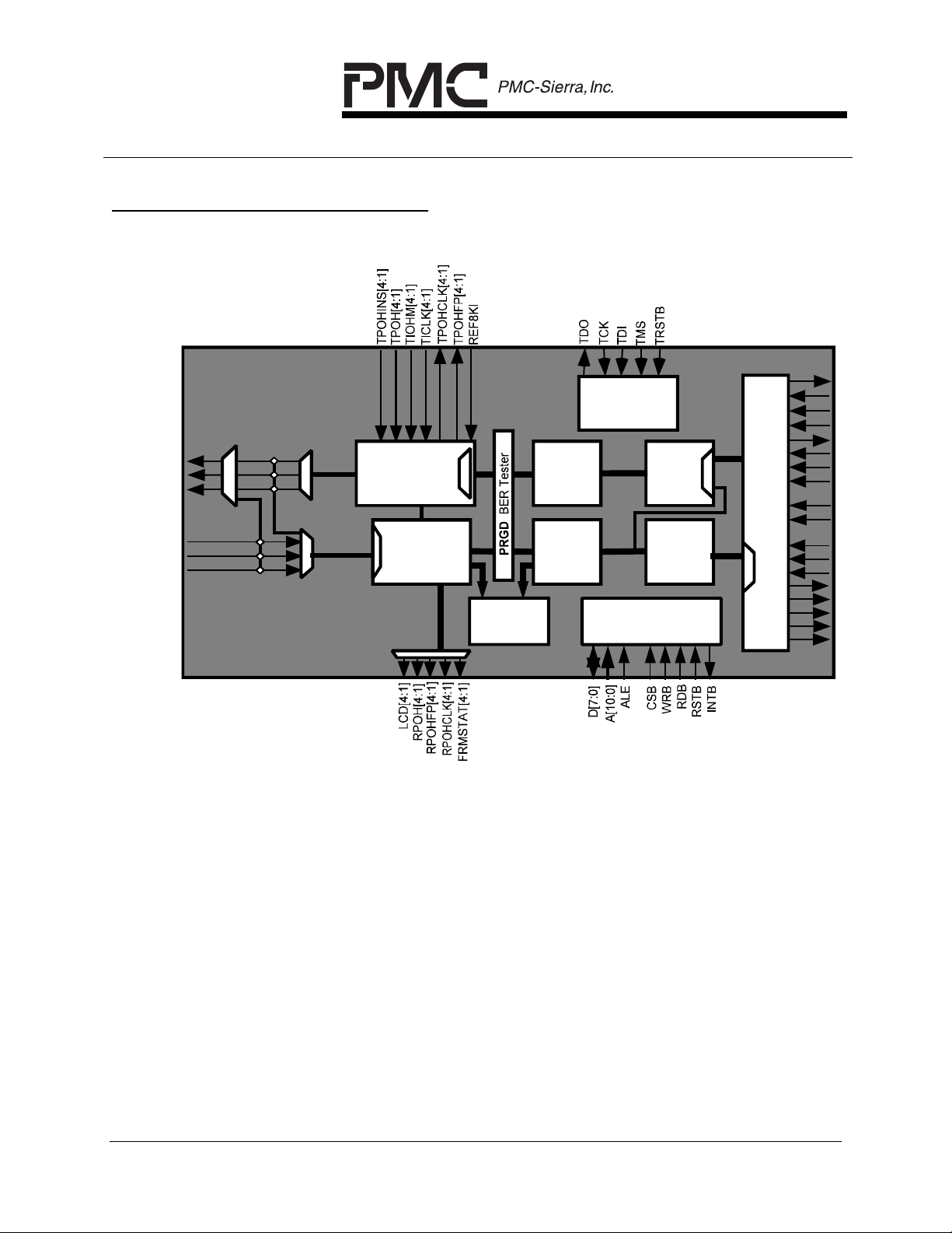
4 S/UNI-CDB BLOCK DIAGRAM
TDATO[4:1]
TOHM [4:1]
TCLK[4:1]
RCLK[4:1]
RDATI[4:1]
ROHM[ 4:1]
SPLT
Transmit ATM
and PLCP Framer
ATMF/SPLR
Receive
ATM and PLCP
Framer
CPPM
PLCP/cell
Perf. Monitor
TXCP_50
Tx
Cell
Processor
RXCP_50
Rx
Cell
Processor
IEEE P1149.1
JTAG Test
Access Port
Microprocessor I/F
TXFF
Tx
4 Cell
FIFO
RXFF
Rx
4 Cell
FIFO
System
I/F
DTCA [4:1]
TDAT[15:0]
TPRTY
TSOC
TCA
TADR[4:0]
TENB
TFCLK
PHY_ADR[2:0]
ATM8
RFCLK
RENB
RADR[4:0]
RCA
RSOC
RPRTY
RDAT[15:0]
DRCA[4:1]
PMC-SIERRA, INC. PROPRIETARY AND CONFIDENTIAL TO PMC-SIERRA INC., AND ITS CUSTOMERS’ INTERNAL USE 10

RELEASED
DATASHEET
PMC-2000313 ISSUE 2 SATURN USER NETWORK INTERFACE CELL DELINEATION BLOCK
PM7339 S/UNI-CDB
5 DATASHEET OVERVIEW
The PM7339 S/UNI-CDB is functionally equivalent to a PM7346 S/UNI-QJET
placed in DS3/E3/J2 Framer Bypass mode. The devices are software compatible and
pin compatible. This datasheet provides a complete pin-out description for the S/UNICDB, as well as any differences between these devices. A software initialization
sequence is required for the device to operate properly. This software initialization is
described in section 10.1. For a complete functional and register description, please
refer to the SUNI-QJET Datasheet, PMC-960835.
PMC-SIERRA, INC. PROPRIETARY AND CONFIDENTIAL TO PMC-SIERRA INC., AND ITS CUSTOMERS’ INTERNAL USE 11
RELEASED
PM7339 S/UNI-CDB
DATASHEET
PMC-2000313 ISSUE 2 SATURN USER NETWORK INTERFACE CELL DELINEATION BLOCK
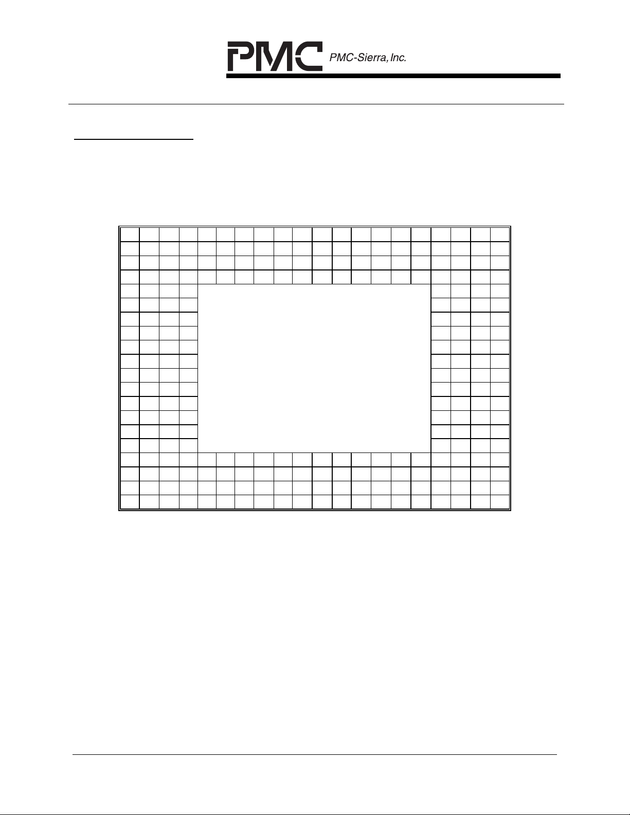
6 PIN DIAGRAM
The S/UNI-CDB is packaged in a 256-pin SBGA package having a body size of
27mm by 27mm and a pin pitch of 1.27 mm.
20 19 18 17 16 15 14 13 12 11 10 9 8 7 6 5 4 3 2 1
A VSS VSS VSS TDAT[10] TDAT[14] D[1] D[5] VSS A[3] A[7] VSS VSS ALE INTB TRSTB TOHM[4] RCLK[4] VSS VSS VSS A
B VSS VDD VDD TDAT[9] TDAT[13] D[0] D[4] A[0] A[2] A[6] A[9] A[10] WRB TDO TCK TCLK[4] TDATO[3] VDD VDD VSS B
C VS S VDD VDD TDAT[7] TDAT[11] TDAT[15] D[2] D[6] A[1] A[5] A[8] CSB RSTB TMS TDATO[4] ROHM[4] TCLK[3] VDD VDD VSS C
D TDAT[3] TDAT[4] TDAT[6] NC TDAT[8] TDAT[12] VDD D[3] D[7] A[ 4] VDD RDB TDI VDD RDATI[4] TOHM[3] BIAS TDATO[2] TCLK[2] RDATI[3] D
E TF CLK TD AT[0] TDA T[2] TDAT[5] TOHM[2] ROHM[3] RDATI[2] ROHM[2] E
F TADR[2] TADR[3] TADR[4] TDAT[1] RCLK[3] RCLK[2] TDATO[1] TOHM[1] F
G TSOC TPRTY TADR[1] VDD VDD TCLK[1] ROHM[1] RCLK[1] G
H BIAS TCA TENB TADR[0] RDATI[1] VSS NC VSS H
J VSS DTCA[2] DTCA[3] DTCA[4] VSS NC NC NC J
K VSS DTCA[1] PHY_ADR[2] VDD
L PHY_ADR[1] PHY_ADR[0] ATM8 DRCA[4] VDD NC NC VSS L
M DRCA[3] DRCA[2] DRCA[1] RSOC VSS NC NC VSS M
N VS S RCA RENB RADR[3] NC NC NC VSS N
P RFCLK RADR[4] RADR[2] VDD VDD VSS NC NC P
R RADR[1] RADR[0] RPRTY RDAT[13] NC NC NC VSS R
T RDA T[15] RDAT[14] RDAT[12] RDAT[9] FRMSTAT[2] REF8KI NC NC T
U RDAT[11] RDAT[10] RDAT[8] B IAS RDAT[6] RDAT[2] VDD TPOHCLK[4] REF8KO[4] VDD RPOHCLK[3] TPOHINS[2] RPOH[2] VDD TPOHCLK[1] RPOHCLK[1] BIAS FRMSTAT[1 ] FRM STAT[3 ] FRMSTA T[4] U
V VSS VDD VDD RDAT[7] RDAT[3] TICLK[4] TPOHINS[4] RPOH[4] TIOHM[3] TPOHCLK[3] RPOH[3] TIOHM[2] TPOHCLK[2] RPOHCLK[2] TIOHM[1] TPOHFP[1] REF8KO[1] VDD VDD VSS V
W VSS VDD VDD RDAT[5] RDAT[1] TIOHM[4] TPOHFP[4] RPOHCLK[4] TPOH[3] TPOHINS[3] LCD[3 ] TICLK[2] TPOH[2] LCD[2] TICLK[1] TPOHINS[1] RPOH[1] VDD VDD VSS W
Y VSS VSS VSS RDAT[4] RDAT[0] TPOH[4] LCD[4] TICLK[3] VSS VSS TPOHFP[3] REF8KO[3] VSS TPOHFP[2] REF8KO[2] TPOH[1] LCD[1] VSS VSS VSS Y
20 19 18 17 16 15 14 13 12 11 10 9 8 7 6 5 4 3 2 1
BOTTOM VIEW
NC VSS VSS NC K
PMC-SIERRA, INC. PROPRIETARY AND CONFIDENTIAL TO PMC-SIERRA INC., AND ITS CUSTOMERS’ INTERNAL USE 12

RELEASED
DATASHEET
PMC-2000313 ISSUE 2 SATURN USER NETWORK INTERFACE CELL DELINEATION BLOCK
PM7339 S/UNI-CDB
7 PIN DESCRIPTION
Pin Name Type Pin No. Function
TDATO[4]
TDATO[3]
TDATO[2]
TDATO[1]
Output C6
B4
D3
F2
Transmit Data (TDATO[4:1]). TDATO[4:1]
contains the transmit data stream when
the single-rail (unipolar) output format is
enabled
The TDATO[4:1] pin function selection is
controlled by the TFRM[1:0] and the TUNI
bits in the S/UNI-CDB Transmit
Configuration Registers. TDATO[4:1] is
updated on the falling edge of TCLK[4:1]
by default, and may be configured to be
updated on the rising edge of TCLK[4:1]
through the TCLKINV bit in the S/UNI-CDB
Transmit Configuration Registers. Finally,
TDATO[4:1] can be updated on the rising
edge of TICLK[4:1], enabled by the TICLK
bit in the S/UNI-CDB Transmit
Configuration Registers.
PMC-SIERRA, INC. PROPRIETARY AND CONFIDENTIAL TO PMC-SIERRA INC., AND ITS CUSTOMERS’ INTERNAL USE 13
RELEASED
DATASHEET
PMC-2000313 ISSUE 2 SATURN USER NETWORK INTERFACE CELL DELINEATION BLOCK
PM7339 S/UNI-CDB
Pin Name Type Pin No. Function
TOHM[4]
TOHM[3]
TOHM[2]
TOHM[1]
Output A5
D5
E4
F1
Transmit Overhead Mask (TOHM[4:1]).
TOHM[4:1] indicates the position of
overhead bits (non-payload bits) in the
transmission system stream aligned with
TDATO[4:1].
When a PLCP formatted signal is
transmitted, TOHM[4:1] is set to logic 1
once per transmission frame, and
indicates the DS1 or E1 frame alignment.
TOHM[4:1] is a delayed version of the
TIOHM[4:1] input, and indicates the
position of each overhead bit in the
transmission frame. TOHM[4:1] is
updated on the falling edge of TCLK[4:1].
The TOHM[4:1] pin function selection is
controlled by the TFRM[1:0] and the TUNI
bits in the S/UNI-CDB Transmit
Configuration Registers. TOHM[4:1] is
updated on the falling edge of TCLK[4:1]
by default, and may be enabled to be
updated on the rising edge of TCLK[4:1].
This sampling is controlled by the
TCLKINV bit in the S/UNI-CDB Transmit
Configuration Registers. Finally,
TOHM[4:1] can be updated on the rising
edge of TICLK[4:1], enabled by the TICLK
bit in the S/UNI-CDB Transmit
Configuration Registers.
TCLK[4]
TCLK[3]
TCLK[2]
TCLK[1]
Output B5
C4
D2
G3
Transmit Output Clock (TCLK[4:1]).
TCLK[4:1] provides the transmit direction
timing. TCLK[4:1] is a buffered version of
TICLK[4:1] and can be enabled to update
the TDATO[4:1] and TOHM[4:1] outputs on
its rising or falling edge.
PMC-SIERRA, INC. PROPRIETARY AND CONFIDENTIAL TO PMC-SIERRA INC., AND ITS CUSTOMERS’ INTERNAL USE 14

RELEASED
DATASHEET
PMC-2000313 ISSUE 2 SATURN USER NETWORK INTERFACE CELL DELINEATION BLOCK
PM7339 S/UNI-CDB
Pin Name Type Pin No. Function
RDATI[4]
RDATI[3]
RDATI[2]
RDATI[1]
ROHM[4]
ROHM[3]
ROHM[2]
ROHM[1]
Input D6
D1
E2
H4
Input C5
E3
E1
G2
Receive Data (RDATI[4:1]). RDATI[4:1]
contains the data stream when the singlerail (unipolar) NRZ input format is enabled.
The RDATI[4:1] pin function selection is
controlled by the RFRM[1:0] bits in the
S/UNI-CDB Configuration Registers.
RDATI[4:1] is sampled on the rising edge
of RCLK[4:1] by default, and may be
enabled to be sampled on the falling edge
of RCLK[4:1]. This sampling is controlled
by the RCLKINV bit in the S/UNI-CDB
Receive Configuration Registers.
Receive Overhead Mask (ROHM[4:1]).
When a DS1 or E1 PLCP or ATM directmapped signal is received, ROHM[4:1] is
pulsed once per transmission frame, and
indicates the DS1 or E1 frame alignment
relative to the RDATI[4:1] data stream.
When an alternate frame-based signal is
received, ROHM[4:1] indicates the position
of each overhead bit in the transmission
frame.
The RLCV/ROHM[4:1] pin function
selection is controlled by the RFRM[1:0]
bits in the S/UNI-CDB Receive
Configuration Registers, and the PLCPEN
bit in the SPLR Configuration register.
RLCV[4:1], and ROHM[4:1] are sampled
on the rising edge of RCLK[4:1] by default,
and may be enabled to be sampled on the
falling edge of RCLK[4:1]. This sampling
is controlled by the RCLKINV bit in the
S/UNI-CDB Receive Configuration
Registers.
RCLK[4]
RCLK[3]
RCLK[2]
RCLK[1]
Input A4
F4
F3
G1
Receive Clock (RCLK[4:1]). RCLK[4:1]
provides the receive direction timing.
RCLK[4:1] is the externally recovered
transmission system baud rate clock that
samples the RDATI[4:1] and
RLCV/ROHM[4:1] inputs on its rising or
falling edge.
PMC-SIERRA, INC. PROPRIETARY AND CONFIDENTIAL TO PMC-SIERRA INC., AND ITS CUSTOMERS’ INTERNAL USE 15

RELEASED
DATASHEET
PMC-2000313 ISSUE 2 SATURN USER NETWORK INTERFACE CELL DELINEATION BLOCK
PM7339 S/UNI-CDB
Pin Name Type Pin No. Function
REF8KI Input T3 Reference 8 kHz Input (REF8KI). The
PLCP frame rate is locked to an external 8
kHz reference applied on this input . An
internal phase-frequency detector
compares the transmit PLCP frame rate
with the externally applied 8 kHz reference
and adjusts the PLCP frame rate.
The REF8KI input must transition high
once every 125 µs for correct operation.
The REF8KI input is treated as an
asynchronous signal and must be “glitchfree”. If the LOOPT register bit is logic 1,
the PLCP frame rate is locked to the
RPOHFP[x] signal instead of the REF8KI
input.
TPOHINS[4]
TPOHINS[3]
TPOHINS[2]
TPOHINS[1]
TPOH[4]
TPOH[3]
TPOH[2]
TPOH[1]
Input V14
W11
U9
W5
Input Y15
W12
W8
Y5
Transmit Path Overhead Insertion
(TPOHINS[4:1]). TPOHINS[4:1] controls
the insertion of PLCP overhead octets on
the TPOH[4:1] input. When
TPOHINS[4:1] is logic 1, the associated
overhead bit in the TPOH[4:1] stream is
inserted in the transmit PLCP frame.
When TPOHINS[4:1] is logic 0, the PLCP
path overhead bit is generated and
inserted internally. TPOHINS[4:1] is
sampled on the rising edge of
TPOHCLK[4:1].
Transmit PLCP Overhead Data
(TPOH[4:1]). TPOH[4:1] contains the
PLCP path overhead octets (Zn, F1, B1,
G1, M1, M2, and C1) which may be
inserted in the transmit PLCP frame. The
octet data on TPOH[4:1] is shifted in order
from the most significant bit (bit 1) to the
least significant bit (bit 8). TPOH[4:1] is
sampled on the rising edge of
TPOHCLK[4:1].
PMC-SIERRA, INC. PROPRIETARY AND CONFIDENTIAL TO PMC-SIERRA INC., AND ITS CUSTOMERS’ INTERNAL USE 16

RELEASED
DATASHEET
PMC-2000313 ISSUE 2 SATURN USER NETWORK INTERFACE CELL DELINEATION BLOCK
PM7339 S/UNI-CDB
Pin Name Type Pin No. Function
TCELL[4]
TCELL[3]
TCELL[2]
TCELL[1]
TPOHCLK[4]
TPOHCLK[3]
TPOHCLK[2]
TPOHCLK[1]
TIOHM[4]
TIOHM[3]
TIOHM[2]
TIOHM[1]
Output W14
Y10
Y7
V5
Output U13
V11
V8
U6
Input W15
V12
V9
V6
Transmit Cell Indication (TCELL[4:1]).
TCELL[x] is valid when the TCELL bit in
the S/UNI-CDB Misc. register (09BH,
19BH, 29BH, 39BH) is set. TCELL[x]
pulses once for every cell (idle or
assigned) transmitted. TCELL[x] is
updated using timing derived from the
transmit input clock (TICLK[x]), and is
active for a minimum of 8 TICLK[x] periods
(or 8 RCLK[x] periods if loop-timed).
Transmit PLCP Overhead Clock
(TPOHCLK[4:1]). TPOHCLK[4:1] is active
when PLCP processing is enabled.
TPOHCLK[4:1] is nominally a 26.7 kHz
clock for a DS1 PLCP frame and a 33.7
kHz clock for an E1 based PLCP frame.
TPOHFP[4:1] is updated on the falling
edge of TPOHCLK[4:1]. TPOH[4:1], and
TPOHINS[4:1] are sampled on the rising
edge of TPOHCLK[4:1].
Transmit Input Overhead Mask
(TIOHM[4:1]). TIOHM[4:1] indicates the
position of overhead bits when not
configured for DS1 or E1 transmission
system streams. TIOHM[4:1] is delayed
internally to produce the TOHM[4:1]
output. When configured for operation
over a DS1 or an E1 transmission system
sublayer, TIOHM[4:1] is not required, and
should be set to logic 0. When configured
for other transmission systems,
TIOHM[4:1] is set to logic 1 for each
overhead bit position. TIOHM[4:1] is set to
logic 0 if the transmission system contains
no overhead bits. TIOHM[4:1] is sampled
on the rising edge of TICLK[4:1].
PMC-SIERRA, INC. PROPRIETARY AND CONFIDENTIAL TO PMC-SIERRA INC., AND ITS CUSTOMERS’ INTERNAL USE 17

RELEASED
DATASHEET
PMC-2000313 ISSUE 2 SATURN USER NETWORK INTERFACE CELL DELINEATION BLOCK
PM7339 S/UNI-CDB
Pin Name Type Pin No. Function
TICLK[4]
TICLK[3]
TICLK[2]
TICLK[1]
RPOHFP[4]
RPOHFP[3]
RPOHFP[2]
RPOHFP[1]
Input V15
Y13
W9
W6
Output U12
Y9
Y6
V4
Transmit Input Clock (TICLK[4:1]).
TICLK[4:1] provides the transmit direction
timing. TICLK[4:1] is the externally
generated transmission system baud rate
clock. It is internally buffered to produce
the transmit clock output, TCLK[4:1], and
can be enabled to update the TDATO[4:1]
and TOHM[4:1] outputs on the TICLK[4:1]
rising edge. The TICLK[4:1] maximum
frequency is 52 MHz.
Receive PLCP Overhead Frame Position
(RPOHFP[4:1]). RPOHFP[4:1] locates the
individual PLCP path overhead bits in the
receive overhead data stream, RPOH[4:1].
RPOHFP[4:1] is logic 1 while bit 1 (the
most significant bit) of the path user
channel octet (F1) is present in the
RPOH[4:1] stream. RPOHFP[4:1] is
updated on the falling edge of
RPOHCLK[4:1]. RPOHFP[4:1] is available
when the PLCPEN register bit is logic 1 in
the SPLR Configuration Register.
RPOH[4]
RPOH[3]
RPOH[2]
RPOH[1]
Output V13
V10
U8
W4
Receive PLCP Overhead Data
(RPOH[4:1]). RPOH[4:1] contains the
PLCP path overhead octets (Zn, F1, B1,
G1, M1, M2, and C1) extracted from the
received PLCP frame when the PLCP
layer is in-frame. When the PLCP layer is
in the loss of frame state, RPOH[4:1] is
forced to all ones. The octet data on
RPOH[4:1] is shifted out in order from the
most significant bit (bit 1) to the least
significant bit (bit 8). RPOH[4:1] is
updated on the falling edge of
RPOHCLK[4:1].
PMC-SIERRA, INC. PROPRIETARY AND CONFIDENTIAL TO PMC-SIERRA INC., AND ITS CUSTOMERS’ INTERNAL USE 18

RELEASED
DATASHEET
PMC-2000313 ISSUE 2 SATURN USER NETWORK INTERFACE CELL DELINEATION BLOCK
PM7339 S/UNI-CDB
Pin Name Type Pin No. Function
RPOHCLK[4]
RPOHCLK[3]
RPOHCLK[2]
RPOHCLK[1]
LCD[4]
LCD[3]
LCD[2]
LCD[1]
FRMSTAT[4]
FRMSTAT[3]
FRMSTAT[2]
FRMSTAT[1]
Output W13
U10
V7
U5
Output Y14
W10
W7
Y4
Output U1
U2
T4
U3
Receive PLCP Overhead Clock
(RPOHCLK[4:1]). RPOHCLK[4:1] is active
when PLCP processing is enabled. The
frequency of this signal depends on the
selected PLCP format. RPOHCLK[4:1] is
nominally a 26.7 kHz clock for a DS1
PLCP frame and a 33.7 kHz clock for an
E1 based PLCP frame. RPOHFP[4:1] and
RPOH[4:1] are updated on the falling edge
of RPOHCLK[4:1].
Loss of Cell Delineation (LCD[4:1]).
LCD[4:1] is an active high signal which is
asserted while the ATM cell processor has
detected a Loss of Cell Delineation defect.
Framer Status (FRMSTAT[4:1]).
FRMSTAT[4:1] is an active high signal
which can be configured to show when the
PLCP framer has detected certain
conditions. The FRMSTAT[4:1] outputs
can be programmed via the STATSEL[2:0]
bits in the S/UNI-CDB Configuration 2
Register to indicate: PLCP Loss of Frame,
PLCP Out of Frame, AIS, and Loss of
Signal. FRMSTAT[4:1] should be treated
as a glitch free asynchronous signal.
ATM8 Input L18 ATM Interface Bus Width Selection
(ATM8). The ATM8 input pin determines
whether the S/UNI-CDB works with a 8-bit
wide interface (RDAT[7:0] and TDAT[7:0])
or a 16-bit wide interface (RDAT[15:0] and
TDAT[15:0]). If ATM8 is set to logic 1,
then the 8-bit wide interface is chosen. If
ATM8 is set to logic 0, then the 16-bit wide
interface is chosen.
PMC-SIERRA, INC. PROPRIETARY AND CONFIDENTIAL TO PMC-SIERRA INC., AND ITS CUSTOMERS’ INTERNAL USE 19
RELEASED
DATASHEET
PMC-2000313 ISSUE 2 SATURN USER NETWORK INTERFACE CELL DELINEATION BLOCK
PM7339 S/UNI-CDB
Pin Name Type Pin No. Function
TDAT[15]
TDAT[14]
TDAT[13]
TDAT[12]
TDAT[11]
TDAT[10]
TDAT[9]
TDAT[8]
TDAT[7]
TDAT[6]
TDAT[5]
TDAT[4]
TDAT[3]
TDAT[2]
TDAT[1]
Input C15
A16
B16
D15
C16
A17
B17
D16
C17
D18
E17
D19
D20
E18
F17
Transmit Cell Data Bus (TDAT[15:0]). This
bus carries the ATM cell octets that are
written to the selected transmit FIFO.
TDAT[15:0] is sampled on the rising edge
of TFCLK and is considered valid only
when TENB is simultaneously asserted
and the S/UNI-CDB has been selected via
the TADR[4:2] and PHY_ADR[2:0] inputs.
The S/UNI-CDB can be configured to
operate with an 8-bit wide or 16-bit wide
ATM data interface via the ATM8 input pin.
When configured for the 8-bit wide
interface, TDAT[15:8] are not used and
should be tied to ground.
TDAT[0]
E19
PMC-SIERRA, INC. PROPRIETARY AND CONFIDENTIAL TO PMC-SIERRA INC., AND ITS CUSTOMERS’ INTERNAL USE 20

RELEASED
DATASHEET
PMC-2000313 ISSUE 2 SATURN USER NETWORK INTERFACE CELL DELINEATION BLOCK
PM7339 S/UNI-CDB
Pin Name Type Pin No. Function
TPRTY Input G19 Transmit bus parity (TPRTY). The
transmit parity (TPRTY) signal indicates
the parity of the TDAT[15:0] or TDAT[7:0]
bus. If configured for the 8-bit bus (via the
ATM8 input pin), then parity is calculated
over TDAT[7:0]. If configured for the 16-bit
bus, then parity is calculated over
TDAT[15:0].
A parity error is indicated by a status bit
and a maskable interrupt. Cells with parity
errors are inserted in the transmit stream,
so the TPRTY input may be unused.
Odd or even parity selection is made using
the TPTYP register bit. TPRTY is sampled
on the rising edge of TFCLK and is
considered valid only when TENB is
simultaneously asserted and the
S/UNI-CDB has been selected via the
TADR[4:0] and PHY_ADR[2:0] inputs.
TSOC Input G20 Transmit Start of Cell (TSOC). The
transmit start of cell (TSOC) signal marks
the start of cell on the TDAT bus. When
TSOC is high, the first word of the cell
structure is present on the TDAT bus. It is
not necessary for TSOC to be present for
each cell. An interrupt may be generated
if TSOC is high during any word other than
the first word of the cell structure. TSOC
is sampled on the rising edge of TFCLK
and is considered valid only when TENB is
simultaneously asserted and the
S/UNI-CDB has been selected via the
TADR[4:2] and PHY_ADR[2:0] inputs.
PMC-SIERRA, INC. PROPRIETARY AND CONFIDENTIAL TO PMC-SIERRA INC., AND ITS CUSTOMERS’ INTERNAL USE 21

RELEASED
DATASHEET
PMC-2000313 ISSUE 2 SATURN USER NETWORK INTERFACE CELL DELINEATION BLOCK
PM7339 S/UNI-CDB
Pin Name Type Pin No. Function
TENB Input H18 Transmit Multi-Phy Write Enable (TENB).
The TENB signal is an active low input
which is used along with the TADR[4:0]
inputs to initiate writes to the transmit
FIFOs. When sampled low using the
rising edge of TFCLK, the word on the
TDAT bus is written into the transmit FIFO
selected by the TADR[4:0] address bus.
When sampled high using the rising edge
of TFCLK, no write is performed, but the
TADR[4:0] address is latched to identify
the transmit FIFO to be accessed. A
complete 53 octet cell must be written to
the transmit FIFO before it is inserted into
the transmit stream. Idle cells are inserted
when a complete cell is not available.
TADR[4]
TADR[3]
TADR[2]
TADR[1]
TADR[0]
Input F18
F19
F20
G18
H17
Transmit Address (TADR[4:0]). The
TADR[4:0] bus is used to select the FIFO
(and hence port) that is written to using the
TENB signal and the FIFO whose cellavailable signal is visible on the TCA
output. TADR[4:0] is sampled on the
rising edge of TFCLK together with TENB.
Note that the null-PHY address 1FH is an
invalid address and will not be identified to
any port on the S/UNI-CDB.
PMC-SIERRA, INC. PROPRIETARY AND CONFIDENTIAL TO PMC-SIERRA INC., AND ITS CUSTOMERS’ INTERNAL USE 22
RELEASED
DATASHEET
PMC-2000313 ISSUE 2 SATURN USER NETWORK INTERFACE CELL DELINEATION BLOCK
PM7339 S/UNI-CDB
Pin Name Type Pin No. Function
TCA Output H19 Transmit Multi-Phy Cell Available (TCA).
The TCA signal indicates when a cell is
available in the transmit FIFO for the port
selected by TADR[4:0]. When high, TCA
indicates that the corresponding transmit
FIFO is not full and a complete cell may be
written. When TCA goes low, it can be
configured to indicate either that the
corresponding transmit FIFO is near full or
that the corresponding transmit FIFO is
full. TCA will transition low on the rising
edge of TFCLK which samples Payload
byte 43 (TCALEVEL0=0) or 47
(TCALEVEL0=1) for the 8-bit interface
(ATM8=1), or the rising edge of TFCLK
which samples Payload word 19
(TCALEVEL0=0) or 23 (TCALEVEL0=1)
for the 16-bit interface (ATM8=0) if the
PHY being polled is the same as the PHY
in use. To reduce FIFO latency, the FIFO
depth at which TCA indicates "full" can be
set to one, two, three or four cells. Note
that regardless of what fill level TCA is set
to indicate "full" at, the transmit cell
processor can store 4 complete cells.
TCA is tri-stated when either the null-PHY
address (1FH) or an address not matching
the address space set by PHY_ADR[2:0]
is latched (by TFCLK) from the TADR[4:2]
inputs.
The polarity of TCA (with respect the the
description above) is inverted when the
TCAINV register bit is set to logic 1.
TFCLK Input E20 Transmit FIFO Write Clock (TFCLK). This
signal is used to write ATM cells to the four
cell transmit FIFOs. TFCLK cycles at a 52
MHz or lower instantaneous rate.
Please note that the TFCLK input is not 5
V tolerant, it is a 3.3 V only input pin.
PMC-SIERRA, INC. PROPRIETARY AND CONFIDENTIAL TO PMC-SIERRA INC., AND ITS CUSTOMERS’ INTERNAL USE 23
 Loading...