


STANDARD PRODUCT
DATASHEET
PMC-2010142 ISSUE 2 ATM LAYER SOLUTION
PM7328 S/UNI-ATLAS-1K800
PM7328
S/UNI-ATLAS-1K800
ATM LAYER SOLUTION
DATASHEET
PROPRIETARY AND CONFIDENTIAL
RELEASED
ISSUE 2: JUNE 2001
PMC-Sierra, Inc. 105 - 8555 Baxter Place Burnaby, BC Canada V5A 4V7 604 .415.6000

STANDARD PRODUCT
DATASHEET
PMC-2010142 ISSUE 2 ATM LAYER SOLUTION
PM7328 S/UNI-ATLAS-1K800
CONTENTS
1 FEATURES.............................................................................................. 1
1.1 POLICING ..................................................................................... 5
1.2 CELL COUNTING ......................................................................... 5
2 APPLICATIONS....................................................................................... 7
3 REFERENCES......................................................................................... 9
4 APPLICATION EXAMPLES................................................................... 10
5 DESCRIPTION ...................................................................................... 11
6 PIN DIAGRAM ....................................................................................... 12
7 PIN DESCRIPTION................................................................................ 13
8 FUNCTIONAL DESCRIPTION............................................................... 49
8.1 INGRESS VC TABLE.................................................................. 52
8.2 CONNECTION IDENTIFICATION............................................... 54
8.2.1 INGRESS CONNECTION IDENTIFICATION ................... 54
8.3 SEARCH TABLE DATA STRUCTURE ....................................... 58
8.3.1 PRIMARY SEARCH TABLE ............................................. 59
8.3.2 SECONDARY SEARCH KEY TABLE .............................. 59
8.4 INGRESS CELL PROCESSING ................................................. 61
8.5 EGRESS VC TABLE ................................................................... 71
8.5.1 EGRESS CONNECTION IDENTIFICATION .................... 73
8.6 EGRESS CELL PROCESSING .................................................. 75
8.7 PERFORMANCE MONITORING ................................................ 84
8.7.1 PERFORMANCE MONITORING FLOWS........................ 96
8.8 CHANGE OF CONNECTION STATE ......................................... 99
8.9 HEADER TRANSLATION ......................................................... 100
8.10 CELL ROUTING........................................................................ 102
8.11 CELL RATE POLICING............................................................. 102
8.11.1 PER-PHY POLICING...................................................... 109
8.11.2 GUARANTEED FRAME RATE....................................... 113
PROPRIETARY AND CONFIDENTIAL i

STANDARD PRODUCT
DATASHEET
PMC-2010142 ISSUE 2 ATM LAYER SOLUTION
PM7328 S/UNI-ATLAS-1K800
8.11.3 CONTINUOUSLY VIOLATING MODE ........................... 116
8.11.4 S/UNI-ATLAS-1K800 POLICING CONFIGURATION..... 117
8.12 CELL COUNTING ..................................................................... 117
8.13 OPERATIONS, ADMINISTRATION AND MAINTENANCE (OAM)
CELL SERVICING..................................................................... 121
8.14 FAULT MANAGEMENT CELLS................................................ 124
8.15 LOOPBACK CELLS .................................................................. 126
8.16 ACTIVATION/DEACTIVATION CELLS ..................................... 126
8.17 SYSTEM MANAGEMENT CELLS............................................. 126
8.18 F4 TO F5 OAM PROCESSING................................................. 127
8.19 F5 TO F4 OAM PROCESSING................................................. 137
8.20 RESOURCE MANAGEMENT CELLS ....................................... 144
8.21 S/UNI-ATLAS-1K800 BACKGROUND PROCESSES............... 144
8.22 INGRESS BACKWARD OAM CELL INTERFACE .................... 146
8.23 EGRESS BACKWARD OAM CELL INTERFACE ..................... 147
8.24 JTAG TEST ACCESS PORT .................................................... 147
8.25 MICROPROCESSOR INTERFACE .......................................... 147
8.26 EXTERNAL SRAM ACCESS .................................................... 148
8.27 WRITING CELLS ...................................................................... 148
8.28 READING CELLS...................................................................... 152
8.29 S/UNI-ATLAS-1K800 DLL CLOCK OPERATION...................... 155
9 NORMAL MODE REGISTER MEMORY MAP..................................... 156
9.1 NORMAL MODE REGISTER DESCRIPTION .......................... 167
10 TEST FEATURES DESCRIPTION ...................................................... 436
10.1 TEST MODE 0 DETAILS .......................................................... 439
10.2 JTAG TEST PORT .................................................................... 439
11 OPERATION........................................................................................ 446
11.1 SCI-PHY EXTENDED CELL FORMAT ..................................... 446
11.2 SYNCHRONOUS STATIC RAMS ............................................. 448
11.2.1 INGRESS VC-TABLE SRAM.......................................... 448
PROPRIETARY AND CONFIDENTIAL ii

STANDARD PRODUCT
DATASHEET
PMC-2010142 ISSUE 2 ATM LAYER SOLUTION
PM7328 S/UNI-ATLAS-1K800
11.2.2 EGRESS VC-TABLE SRAM........................................... 449
11.3 ATM CELL PROCESSING........................................................ 450
11.3.1 OAM CELL FORMAT ..................................................... 450
11.4 INGRESS VC IDENTIFICATION SEARCH ALGORITHM......... 453
11.4.1 OVERVIEW .................................................................... 453
11.4.2 INGRESS PERFORMANCE MONITORING ACTIVATION /
DEACTIVATION ............................................................. 459
11.5 EGRESS VC TABLE OPERATION........................................... 460
11.5.1 INITIALIZATION PROCEDURE ..................................... 460
11.5.2 CONNECTION SETUP................................................... 460
11.5.3 EGRESS PERFORMANCE MONITORING ACTIVATION /
DEACTIVATION ............................................................. 461
11.6 JTAG SUPPORT....................................................................... 462
11.6.1 TAP CONTROLLER ....................................................... 463
12 FUNCTIONAL TIMING......................................................................... 468
12.1 INGRESS INPUT CELL INTERFACE ....................................... 468
12.2 INGRESS OUTPUT CELL INTERFACE ................................... 471
12.3 EGRESS INPUT CELL INTERFACE ........................................ 473
12.4 EGRESS OUTPUT CELL INTERFACE .................................... 476
13 ABSOLUTE MAXIMUM RATINGS....................................................... 479
14 D.C. CHARACTERISTICS ................................................................... 480
15 A.C. TIMING CHARACTERISTICS...................................................... 482
16 MECHANICAL INFORMATION ........................................................... 497
PROPRIETARY AND CONFIDENTIAL iii

STANDARD PRODUCT
DATASHEET
PMC-2010142 ISSUE 2 ATM LAYER SOLUTION
PM7328 S/UNI-ATLAS-1K800
LIST OF FIGURES
FIGURE 1 ........ S/UNI-ATLAS-1K800 IN OC3 MINI-DSLAM APPLICATION................................ 7
FIGURE 2 ........ S/UNI-ATLAS-1K800 BLOCK DIAGRAM........................................................... 10
FIGURE 3 ........ VC SEARCH KEY COMPOSITION.................................................................... 54
FIGURE 4 ........ PARAMETERS OF THE PRIMARY KEY AND SECONDARY KEY................... 56
FIGURE 5 ........ SEARCH KEY LOCATIONS WITHIN THE ROUTING WORD..........................57
FIGURE 6 ........ ATLAS SEARCH TABLE STRUCTURE ............................................................59
FIGURE 7 ........ EGRESS ROUTING WORD AND EGRESS LOOKUP ADDRESS ...................73
FIGURE 8 ........ S/UNI-ATLAS-1K800 PM FLOWS ..................................................................... 97
FIGURE 9 ........ F4 TO F5 OAM FLOWS...................................................................................128
FIGURE 10 ...... INGRESS TERMINATION OF F4 SEGMENT AND END-TO-END-POINT
CONNECTIONS. ..........................................................................129
FIGURE 11 ...... INGRESS TERMINATION OF F4 SEGMENT AND END-TO-END POINT
CONNECTION..............................................................................130
FIGURE 12 ...... INGRESS TERMINATION OF F4 SEGMENT END-POINT CONNECTION. .. 132
FIGURE 13 ...... INGRESS TERMINATION OF F4 END-TO-END POINT CONNECTION. ......133
FIGURE 14 ...... F5 TO F4 OAM FLOWS...................................................................................138
FIGURE 15 ...... EGRESS TERMINATION OF A VPC SEGMENT END-POINT ....................... 139
FIGURE 16 ...... VPC INTERMEDIATE POINT .......................................................................... 140
FIGURE 17 ...... VCC INTERMEDIATE POINT .......................................................................... 141
FIGURE 18 ...... VPC SEGMENT END-POINT .......................................................................... 141
FIGURE 19 ...... VCC SEGMENT END POINT .......................................................................... 142
FIGURE 20 ...... VPC SEGMENT END-POINT AND END-TO-END POINT .............................. 142
FIGURE 21 ...... INGRESS VPC END-TO-END POINT AND SEGMENT END-POINT, VC
SEGMENT END-POINT AND SEGMENT SOURCE POINT.
EGRESS VPC END-TO-END AND SEGMENT SOURCE
POINT WITH VCC SEGMENT END-POINT AND VCC
SEGMENT SOURCE POINT........................................................ 143
FIGURE 22 ...... INGRESS VPC END-TO-END AND SEGMENT END POINT WITH VC
INTERMEDIATE POINT. EGRESS VPC END-TO-END AND
SEGMENT SOURCE POINT WITH VC INTERMEDIATE
POINT AND VC SEGMENT SOURCE POINT.............................143
FIGURE 23 ...... INPUT OBSERVATION CELL (IN_CELL)........................................................ 442
FIGURE 24 ...... OUTPUT CELL (OUT_CELL)...........................................................................443
FIGURE 25 ...... BI-DIRECTIONAL CELL (IO_CELL) ................................................................ 444
FIGURE 26 ...... LAYOUT OF OUTPUT ENABLE AND BI-DIRECTIONAL CELLS ................... 445
FIGURE 27 ...... EIGHT BIT WIDE CELL FORMAT ................................................................... 447
FIGURE 28 ...... SIXTEEN BIT WIDE CELL FORMAT............................................................... 448
FIGURE 29 ...... COMMON OAM CELL FORMAT .....................................................................451
FIGURE 30 ...... SPECIFIC FIELDS FOR AIS/RDI FAULT MANAGEMENT CELL ...................451
FIGURE 31 ...... SPECIFIC FIELDS FOR THE FPM CELL ........................................................ 452
FIGURE 32 ...... SPECIFIC FIELDS FOR THE BR CELL........................................................... 452
FIGURE 33 ...... CONNECTION INSERTION W HEN BINARY TREE IS EMPTY...................... 456
FIGURE 34 ...... CONNECTION INSERTION W HEN BINARY TREE CONTAINS ONLY
SINGLE VC RECORD. ................................................................. 456
FIGURE 35 ...... CONNECTION INSERTION AT THE ROOT OF THE TREE. .........................457
FIGURE 36 ...... CONNECTION INSERTION IN THE MIDDLE OF THE BINARY TREE..........458
FIGURE 37 ...... NEW SECONDARY SEARCH TABLE ENTRY INSERTED AT A LEAF. ........458
FIGURE 38 ...... BOUNDARY SCAN ARCHITECTURE ............................................................. 462
FIGURE 39 ...... TAP CONTROLLER FINITE STATE MACHINE .............................................. 464
FIGURE 40 ...... INGRESS INPUT CELL INTERFACE (RPOLL=0)........................................... 468
FIGURE 41 ...... INGRESS INPUT CELL INTERFACE (RPOLL=1) EXAMPLE 1...................... 469
FIGURE 42 ...... INGRESS INPUT CELL INTERFACE (RPOLL=1) EXAMPLE 2...................... 470
PROPRIETARY AND CONFIDENTIAL iv

STANDARD PRODUCT
DATASHEET
PMC-2010142 ISSUE 2 ATM LAYER SOLUTION
PM7328 S/UNI-ATLAS-1K800
FIGURE 43 ...... INGRESS OUTPUT CELL INTERFACE (OTSEN=0) ...................................... 471
FIGURE 44 ...... INGRESS OUTPUT CELL INTERFACE (OTSEN=1) ...................................... 472
FIGURE 45 ...... EGRESS INPUT CELL INTERFACE (IPOLL=0)..............................................473
FIGURE 46 ...... EGRESS INPUT CELL INTERFACE POLLED MODE (IPOLL=1)...................475
FIGURE 47 ...... EGRESS OUTPUT CELL INTERFACE DIRECT MODE (TPOLL=0) .............. 476
FIGURE 48 ...... EGRESS OUTPUT CELL INTERFACE POLLED MODE (TPOLL=1) ............. 477
FIGURE 49 ...... MICROPROCESSOR INTERFACE READ TIMING ........................................ 483
FIGURE 50 ...... MICROPROCESSOR INTERFACE WRITE TIMING....................................... 485
FIGURE 51 ...... EGRESS INPUT CELL INTERFACE TIMING.................................................. 487
FIGURE 52 ...... INGRESS OUTPUT CELL INTERFACE TIMING ............................................ 488
FIGURE 53 ...... INGRESS INPUT CELL INTERFACE TIMING ................................................ 489
FIGURE 54 ...... EGRESS OUTPUT CELL INTERFACE TIMING.............................................. 490
FIGURE 55 ...... INGRESS SRAM INTERFACE TIMING ........................................................... 492
FIGURE 56 ...... EGRESS SRAM INTERFACE TIMING ............................................................493
FIGURE 57 ...... JTAG PORT INTERFACE TIMING .................................................................. 494
FIGURE 58 ...... ATLAS-1K800 THETA JA VS. AIR FLOW GRAPH .........................................496
FIGURE 59 ...... 432 PIN SBGA – 40 X 40 MM BODY -(B SUFFIX) .......................................... 497
PROPRIETARY AND CONFIDENTIAL v

STANDARD PRODUCT
DATASHEET
PMC-2010142 ISSUE 2 ATM LAYER SOLUTION
PM7328 S/UNI-ATLAS-1K800
LIST OF TABLES
TABLE 1 .......... INGRESS VC TABLE ......................................................................................... 53
TABLE 2 .......... INGRESS VC TABLE CELL FIELDS .................................................................55
TABLE 3 .......... INGRESS VC TABLE STATUS FIELD .............................................................. 62
TABLE 4 .......... INGRESS VC TABLE CONFIGURATION FIELD .............................................. 63
TABLE 5 .......... INGRESS VC TABLE OAM CONFIGURATION FIELD ..................................... 65
TABLE 6 .......... INGRESS INTERNAL STATUS FIELD .............................................................. 67
TABLE 7 .......... INGRESS VC TABLE MISCELLANEOUS FIELDS............................................ 68
TABLE 8 .......... INGRESS VC TABLE ACTIVATION FIELDS.....................................................70
TABLE 9 .......... EGRESS VC TABLE .......................................................................................... 71
TABLE 10 ........ EGRESS VC TABLE CONNECTION IDENTIFIER FIELDS .............................. 72
TABLE 11 ........ EGRESS VC TABLE ACTIVATION FIELD ........................................................ 76
TABLE 12 ........ EGRESS VC TABLE STATUS FIELD................................................................ 76
TABLE 13 ........ EGRESS VC TABLE CONFIGURATION FIELD................................................78
TABLE 14 ........ EGRESS OAM CONFIGURATION FIELD ......................................................... 79
TABLE 15 ........ EGRESS INTERNAL STATUS FIELD ...............................................................81
TABLE 16 ........ EGRESS VC TABLE MISCELLANEOUS FIELDS ............................................. 82
TABLE 17 ........ INTERNAL PM TABLE ....................................................................................... 84
TABLE 18 ........ PM TABLE CONFIGURATION FIELD ...............................................................85
TABLE 19 ........ QOS PARAMETERS FOR PERFORMANCE MONITORING............................ 88
TABLE 20 ........ INGRESS AND EGRESS CHANGE OF STATE FIFO .................................... 100
TABLE 21 ........ S/UNI-ATLAS-1K800 ACTIONS ON POLICING WITH COCUP=0 ................ 107
TABLE 22 ........ S/UNI-ATLAS-1K800 ACTIONS ON POLICING WITH COCUP=1 ................ 108
TABLE 23 ........ S/UNI-ATLAS-1K800 ACTIONS WITH PER-PHY POLICING ......................... 110
TABLE 24 ........ INTERNAL PER-PHY POLICING RAM............................................................ 111
TABLE 25 ........ PER-PHY AND PER-VC NON-COMPLIANT CELL COUNTING
PHYVCCOUNT=0......................................................................... 112
TABLE 26 ........ PER-PHY AND PER-VC NON-COMPLIANT CELL COUNTING
PHYVCCOUNT=1......................................................................... 113
TABLE 27 ...... INGRESS/EGRESS OAM CONFIGURATION FIELD......................................122
TABLE 28 ........ F4 TO F5 FAULT MANAGEMENT PROCESSING.......................................... 135
TABLE 29 ........ REGISTER MEMORY MAP ............................................................................. 156
TABLE 30 ........ INSTRUCTION REGISTER ............................................................................. 439
TABLE 31 ........ IDENTIFICATION REGISTER ......................................................................... 440
TABLE 32 ........ BOUNDARY SCAN REGISTER.......................................................................440
TABLE 33 ........ S/UNI-ATLAS-1K800 VC-TABLE AVAILABLE SRAM TYPES.........................449
TABLE 34 ........ OAM TYPE AND FUNCTION TYPE IDENTIFIERS......................................... 450
TABLE 35 ........ VC TABLE CONNECTION SETUP .................................................................. 460
TABLE 36 ........ ABSOLUTE MAXIMUM RATINGS ................................................................... 479
TABLE 37 ........ D.C. CHARACTERISTICS ...............................................................................480
TABLE 38 ........ MICROPROCESSOR INTERFACE READ ACCESS ......................................482
TABLE 39 ........ MICROPROCESSOR INTERFACE WRITE ACCESS ....................................484
TABLE 40 ........ JTAG PORT INTERFACE ................................................................................ 493
TABLE 41 ........ ORDERING INFORMATION............................................................................ 495
TABLE 42 ........ THERMAL INFORMATION ..............................................................................495
PROPRIETARY AND CONFIDENTIAL vi

STANDARD PRODUCT
DATASHEET
PMC-2010142 ISSUE 2 ATM LAYER SOLUTION
PM7328 S/UNI-ATLAS-1K800
1 FEATURES
• Monolithic single chip device which handles bi-directional ATM Layer
functions including VPI/VCI address translation, cell appending (ingress only),
cell rate policing (ingress only), per-connection counting and I.610 compliant
OAM requirements for 1024 VCs (virtual connections).
• Instantaneous bi-directional transfer rate of 800 Mbit/s supports a bi-
directional cell transfer rate of 1.42x10⁶ cells/s (one STS-12c or four STS-3c).
• The Ingress input interface supports an 8 or 16 bit SCI-PHY interface using
direct addressing for up to 4 PHY devices (compatible with Utopia Level 1
cell-level handshaking) and Multi-PHY addressing for up to 32 PHY devices
(Utopia Level 2 compatible).
• The Ingress output interface supports an 8 or 16 bit SCI-PHY (52 – 64 byte
extended ATM cell with prepend/postpend) interface (compatible with Utopia
Level 1 cell-level handshaking) to a switch fabric.
• The Egress input interface supports an 8 or 16 bit extended cell format SCI-
PHY interface using direct addressing for up to 4 PHY devices (compatible
with Utopia Level 1 cell-level handshaking) and Multi-PHY addressing for up
to 32 PHY devices (Utopia Level 2 compatible).
• The Egress output interface supports an 8 or 16 bit extended cell format SCI-
PHY interface using direct addressing for up to 4 PHY devices (compatible
with Utopia Level 1 cell-level handshaking) and Multi-PHY addressing for up
to 32 PHY devices (Utopia Level 2 compatible).
• Compatible with a wide range of switching fabrics and traffic management
architectures including per-VC or per-PHY queuing.
• Highly flexible OAM-type cell and connection identification which can use
arbitrary PHYID/VPI/VCI values and/or cell appended bytes for connection
identification (N.B. this is an ingress function only). A direct lookup function is
provided in the egress direction. The direct lookup can use an arbitrary
header or prepend/postpend location.
• Ingress functionality includes a highly flexible search engine that covers the
entire PHYID/VPI/VCI address range, programmable dual leaky bucket
UPC/NPC, per-connection CLP0 and CLP1 cell counts (programmable),
OAM-PM termination, generation and monitoring, and OAM-FM termination,
generation and alarm generation (monitoring).
PROPRIETARY AND CONFIDENTIAL TO PMC-SIERRA, INC 1

STANDARD PRODUCT
DATASHEET
PMC-2010142 ISSUE 2 ATM LAYER SOLUTION
PM7328 S/UNI-ATLAS-1K800
• Egress functionality includes programmable direct lookup function, OAM-PM
termination, generation and monitoring, per-connection CLP0 and CLP1 cell
counts (programmable) and OAM-FM termination, generation and alarm
generation (monitoring). An egress per-PHY output buffering scheme
resolves the head-of-line blocking issue.
• UPC/NPC function is a programmable dual leaky bucket policing device with
a programmable action (tag, discard, or count only) for each bucket. A total of
3 programmable 16 bit non-compliant cell counts are provided. The noncompliant cell counts may be programmed to count, for example, dropped
CLP0 cells, dropped CLP1 cells, and tagged CLP0 cells. The UPC/NPC
function also has a continuously violating mode, where a programmable
action is taken on all cells regardless of their compliance. AAL5 partial packet
discard is also provided so that the remainder of an AAL5 packet can be
tagged or discarded if a single cell in the packet is tagged or discarded as a
result of violating policing.
• In addition to the per-connection dual leaky bucket, a single leaky bucket
UPC/NPC function is provided on a per-PHY basis. A programmable action
(tag, discard or count only) may be configured for each PHY policing device.
Three programmable non-compliant cell counts are provided for each PHY.
The non-compliant cell counts may be programmed to count, for example,
dropped CLP0 cells, dropped CLP1 cells and tagged CLP0 cells. The perPHY policing parameters and non-compliant cell counts are maintained in an
on-chip RAM that can be programmed and read via the 16-bit general
purpose microprocessor interface.
• Guaranteed Frame Rate frame-based policing selectable on a per-connection
basis.
• OAM-Performance monitoring is provided in the ingress and egress direction
for bi-directional PM sessions. A maximum of 512 (256 bi-directional
sessions) PM sessions may be simultaneously active. PM is supported on the
F4 and F5 levels. The S/UNI-ATLAS-1K800 provides for the generation of
Forward Monitoring and Backward Reporting PM cells (both segment and
end-to-end), the termination of Forward Monitoring and Backward Reporting
cells, and for non-intrusive monitoring of Forward Monitoring and Backward
Reporting cells. The following statistics are collected when terminating or
monitoring PM flows:
1. Forward Impaired Block.
2. Forward Lost/Misinserted Impaired Block
3. Forward Severely Errored Cell Block (Lost).
PROPRIETARY AND CONFIDENTIAL TO PMC-SIERRA, INC 2

STANDARD PRODUCT
DATASHEET
PMC-2010142 ISSUE 2 ATM LAYER SOLUTION
PM7328 S/UNI-ATLAS-1K800
4. Forward Severely Errored Cell Block (Misinserted).
5. Forward Severely Errored Cell Block (BIP-16 violations).
6. Forward Severely Errored Cell Block Combined (non-saturating)
7. Forward Lost CLP0+1 cell count.
8. Forward Lost CLP0 cell count.
9. Forward Tagged CLP0 cell count
10. Forward Misinserted CLP0+1 cell count.
11. Forward Errored cell count.
12. Forward Total Lost CLP0+1 cell count.
13. Forward Total Lost CLP0 cell count.
14. Forward Lost Forward Monitoring cell count.
15. Backward Impaired Block.
16. Backward Lost/Misinserted Impaired Block.
17. Backward Severely Errored Cell Block (Lost).
18. Backward Severely Errored Cell Block (Misinserted).
19. Backward Severely Errored Cell Block (BIP-16 violations).
20. Backward Severely Errored Cell Block Combined (non-saturating)
21. Backward Severely Errored Cell Block Combined (saturating)
22. Backward Lost CLP0+1 cell count.
23. Backward Lost CLP0 cell count.
24. Backward Tagged CLP0 cell count.
25. Backward Misinserted CLP0+1 cell count.
26. Backward Errored cell count.
27. Backward Total Lost CLP0+1 cell count.
PROPRIETARY AND CONFIDENTIAL TO PMC-SIERRA, INC 3

STANDARD PRODUCT
DATASHEET
PMC-2010142 ISSUE 2 ATM LAYER SOLUTION
PM7328 S/UNI-ATLAS-1K800
28. Backward Total Lost CLP0 cell count.
29. Backward Lost Fwd Monitoring PM cell count.
30. Backward Lost Backward Reporting PM cell count.
31. Total Transmitted CLP0+1 cell count.
32. Total Transmitted CLP0 cell count.
Statistics for PM sessions are held in on-chip RAM that can be read at any
time through the 16-bit general-purpose microprocessor port.
Paced insertion of PM cells is provided.
PM block size generation and termination is per-session programmable
ranging from 128 – 32768 cells.
Each of the 512 PM sessions can be configured to be a source, sink or
non-intrusive monitoring point of PM cells.
• OAM-Fault Management is provided on a per-connection basis in the ingress
and egress directions. Simultaneous segment and end-to-end F4 and F5 AIS,
RDI and CC cell generation, termination and monitoring is supported. Alarm
bits and interrupt masks are provided on a per-connection basis. F4 to F5 AIS
alarm splitting is provided in the Ingress direction. Paced insertion of FM cells
is provided.
• OAM-Loopback extraction (to a Microprocessor Cell Interface) is per-
connection configurable in both the ingress and egress directions.Includes a
FIFO buffered microprocessor bus interface for cell insertion and extraction
(in both the ingress and egress directions), Ingress and Egress VC Table
access, control and status monitoring and configuration of the device.
• Supports DMA access for cell extraction.
• Uses common external Synchronous Flow-Through SRAM (with or without
parity) for maintaining per-connection information. Separate SRAM’s are used
for the Ingress and Egress context tables.
• Provides a standard 5 signal P1149.1 JTAG test port for boundary scan board
test purposes.
• Provides a generic 16 bit microprocessor bus interface for configuration,
control and status monitoring.
• Low power 0.35 micron, 3.3 V CMOS technology with a 3.3 V UTOPIA (SCI-
PHY), 3.3/5 V Microprocessor I/O interfaces and 3.3 V external synchronous
SRAM interfaces.
PROPRIETARY AND CONFIDENTIAL TO PMC-SIERRA, INC 4

STANDARD PRODUCT
DATASHEET
PMC-2010142 ISSUE 2 ATM LAYER SOLUTION
PM7328 S/UNI-ATLAS-1K800
• The UTOPIA (SCI-PHY) and external Synchronous SRAM interfaces are 52
MHz max.
• 432 Super BGA package.
1.1 Policing
• Policing is performed in the ingress direction for adherence to peak cell rate
(PCR), cell delay variation tolerance (CDVT), sustained cell rate (SCR) and
burst tolerance (BT). Violating cells can be noted, dropped or tagged.
• Policing is performed using the virtual scheduling Generic Cell Rate Algorithm
(GCRA) described in ITU-T I.371.
• Two policing instantiations available per VC. The policed cell streams can be
any combination of user cells, OAM cells, Resource Management, high
priority cells or low priority cells.
• Per-PHY policing may also be enabled. Each of 32 PHY devices may have a
single leaky bucket enabled, in addition to the dual leaky bucket of the
connection. Violating cells can be noted (counted only), dropped or tagged.
1.2 Cell Counting
• Counts maintained on a per-VC basis include total low priority cells, total high
priority cells and cells violating the traffic contract. Per-VC counts are
maintained for both the ingress and egress directions.
• Counts maintained on a per-PHY basis (in both the Ingress and Egress
directions) include:
• number of CLP0 cells received.
• number of CLP1 cells received.
• number of OAM cells received.
• number of RM cells received.
• number of errored OAM cells.
• number of errored RM cells.
• number of cells with unassigned/invalid VPI/VCI/PTI.
PROPRIETARY AND CONFIDENTIAL TO PMC-SIERRA, INC 5

STANDARD PRODUCT
DATASHEET
PMC-2010142 ISSUE 2 ATM LAYER SOLUTION
PM7328 S/UNI-ATLAS-1K800
• number of cells received with a non-zero GFC (ingress UNI only).
PROPRIETARY AND CONFIDENTIAL TO PMC-SIERRA, INC 6
STANDARD PRODUCT
DATASHEET
PMC-2010142 ISSUE 2 ATM LAYER SOLUTION
PM7328 S/UNI-ATLAS-1K800
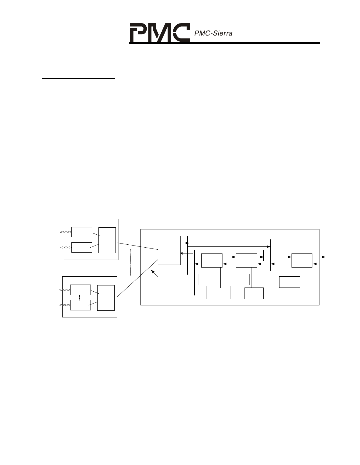
2 APPLICATIONS
• Mini DSL Access Multiplexers (Mini-DSLAMs).
• Multiservice Access Multiplexers.
• 3rd generation wireless base stations and base station controllers.
• Subscriber Access terminal devices.
• APON Subscriber Access CLE.
• LMDS Subscriber Access CLE.
• Integrated Access Devices.
Figure 1 S/UNI-ATLAS-1K800 in OC3 mini-DSLAM Application
line cards
up to 31
Utopia L2
ports
up to 31
Utopia L2
ports
DSL Phy
DSL Phy
line cards
DSL Phy
DSL Phy
S/UNI-
DUPLEX
S/UNI-
DUPLEX
200Mbps
LVDS
S/UNI-
VORTEX
Up to 8 LVDS links to
S/UNI-Duplex devices
per S/UNI-VORTEX
AnyPhy/
SciPhy
Context
SSRAM
S/UNIAPEX1K800
Packet/Cell
SDRAM
S/UNI-
ATLAS-
1K800
Ingress
SSRAM
Egress
SSRAM
Figure 1 shows the S/UNI-ATLAS-1K800 in a mini DSLAM application. The
S/UNI-APEX-1K800 acts as a cell buffer and traffic manager. The S/UNI-ATLAS1K800 provides address resolution and policing.
Phy
Host
CPU
core card
The mini-DSLAM application supports eight LIU devices per Line Card. Each
xDSL modem is connected by its Utopia port to a FPGA which provides an
interface to the AnyPhy bus. If Hot Swap capability is needed the bus signals
need to be passed through switching or tristate drivers to isolate the card when
being plugged in.
PROPRIETARY AND CONFIDENTIAL TO PMC-SIERRA, INC 7

STANDARD PRODUCT
DATASHEET
PMC-2010142 ISSUE 2 ATM LAYER SOLUTION
PM7328 S/UNI-ATLAS-1K800
The FPGA performs the task of converting the Utopia to signals compatible with
the APEX-1K800 and ATLAS-1K800.
PROPRIETARY AND CONFIDENTIAL TO PMC-SIERRA, INC 8

STANDARD PRODUCT
DATASHEET
PMC-2010142 ISSUE 2 ATM LAYER SOLUTION
PM7328 S/UNI-ATLAS-1K800
3 REFERENCES
• ATM Forum – ATM User-Network Interface Specification, V3.1 September,
1994.
• ITU-T Recommendation I.361 – “B-ISDN ATM Layer Specification”,
November 1995.
• ITU-T Recommendation I.371 – “Traffic Control and Congestion Control in B-
ISDN”, May, 1996.
• ITU-T Recommendation I.610 – “B-ISDN Operation and Maintenance
Principles and Functions”, June, 1997 (Rapporteur’s edition)
• Bell Communications Research – Broadband Switching System (BSS)
Generic Requirements, GR-1110-CORE, Issue 1, September 1994.
• Bell Communications Research – Asynchronous Transfer Mode (ATM) and
ATM Adaptation Layer (AAL) Protocols, GR-1113-CORE, Issue 1, July 1994.
• Bell Communications Research – Generic Requirements for Operations of
Broadband Switching Systems, GR-1248-CORE, Issue 3, August, 1996.
• IEEE 1149.1 – Standard Test Access Port and Boundary Scan Architecture,
May 21, 1990.
• PMC-940212, ATM SCI-PHY, “SATURN Compliant Interface for ATM
Devices”, July 1994, Issue 2.
• ATMF TM4.0 – ATM Forum Traffic Management Specification Version 4.0, af-
tm-0056.000, April, 1996.
PROPRIETARY AND CONFIDENTIAL TO PMC-SIERRA, INC 9
STANDARD PRODUCT
PM7328 S/UNI-ATLAS-1K800
DATASHEET
PMC-2010142 ISSUE 2 ATM LAYER SOLUTION
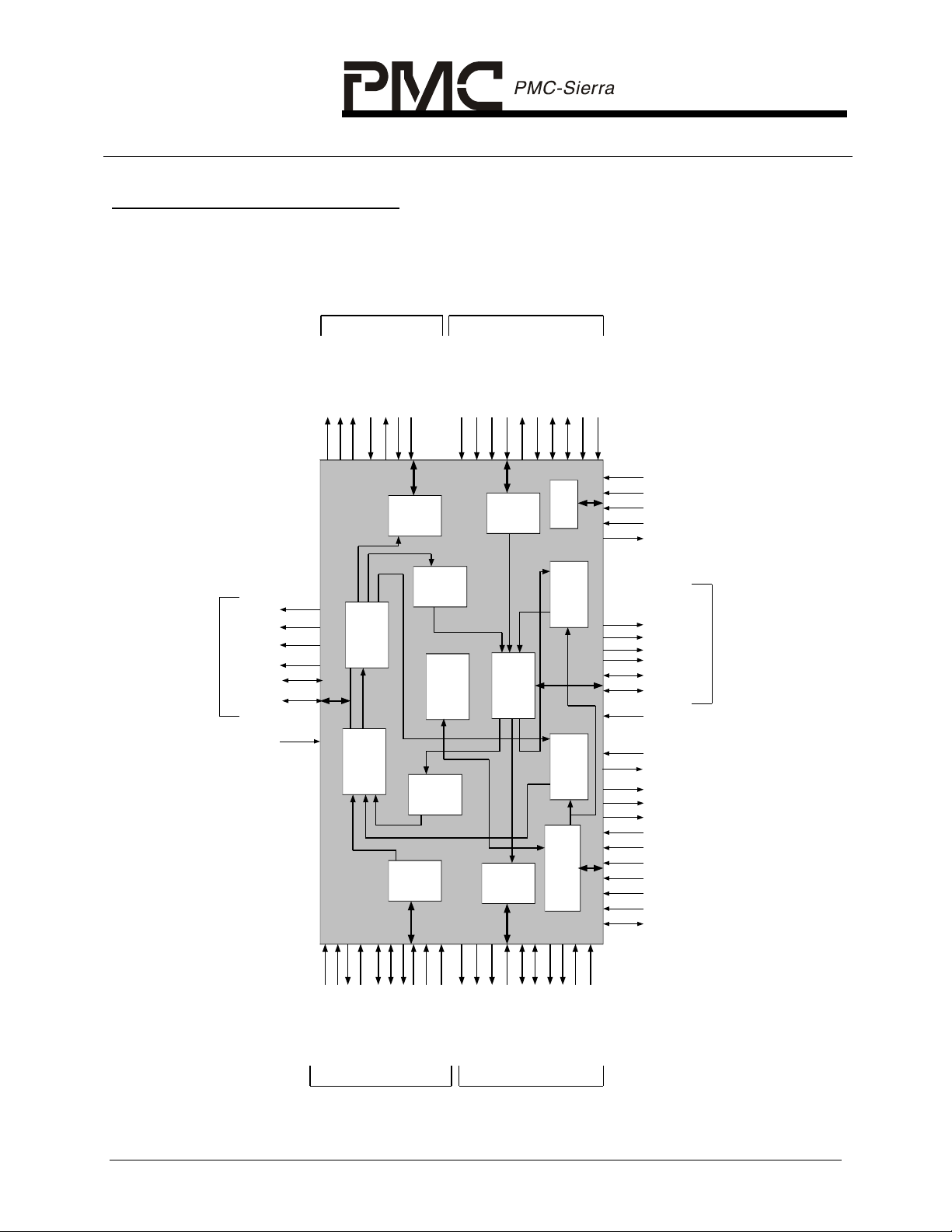
4 APPLICATION EXAMPLES
Figure 2 S/UNI-ATLAS-1K800 Block Diagram
(Slave)
SCI-PHY Level1 I nterfac e
]
0
:
5
1
[
y
t
t
a
r
d
p
o
o
M
A
R
S
s
u
o
n
o
r
h
c
n
y
S
l
a
n
r
e
t
x
E
o
T
isadsb
isoeb
isrwb
isa[19:16] [9:0]
isp[7:0]
isd[63:0]
isysc lk
b
n
c
o
s
o
s
s
l
l
e
e
r
g
C
n
I
s
h
s
c
e
r
r
a
g
e
n
S
I
n
k
e
l
e
a
d
s
c
c
r
f
t
o
o
o
o
t
s
s
u
e
p
t
r
u
g
n
O
I
r
o
s
s
e
c
o
r
P
e
n
i
g
n
E
s
t
s
u
e
r
p
g
n
I
n
I
]
0
:
5
1
[
t
a
d
i
e
c
l
a
l
f
e
r
e
C
t
n
I
d
e
r
s
c
a
l
s
a
l
f
e
w
e
r
r
k
e
g
C
c
t
E
a
n
I
B
n
s
Y
o
c
i
i
H
t
t
P
c
s
-
i
e
t
r
l
l
a
e
t
o
P
S
C
d
e
r
c
s
a
l
a
s
l
f
w
e
e
r
r
k
e
C
g
c
t
n
a
n
I
I
B
e
c
l
a
l
f
e
r
e
C
t
n
I
]
1
y
k
c
[
t
l
r
o
a
c
p
s
c
f
i
i
i
i
e
s
c
t
l
s
a
l
u
f
e
e
r
r
p
e
C
n
g
I
t
E
n
I
r
o
s
s
l
s
l
s
e
e
e
r
c
C
g
o
E
r
P
e
t
s
c
l
s
u
a
l
f
e
p
e
r
t
r
e
u
C
g
t
O
E
n
I
(Slave)
SCI-PHY Level1/Level2 Interface
]
2
:
4
[
]
b
2
n
:
e
3
r
[
]
a
w
4
i
c
[
/
i
/
]
a
]
1
[
b
n
e
r
w
i
0
c
3
:
:
i
/
2
4
d
[
[
l
r
r
i
a
v
a
i
l
d
d
l
o
d
d
p
a
a
i
i
i
trstb
e
c
G
a
f
A
r
T
e
t
J
n
I
r
o
s
s
e
s
e
c
l
s
c
a
l
f
e
o
e
r
r
r
e
C
g
p
t
E
o
n
r
I
c
i
M
r
o
s
s
e
s
e
c
l
s
c
a
l
e
f
o
e
r
r
r
e
g
C
p
t
n
o
I
n
r
I
c
i
M
r
o
s
s
e
e
c
c
a
f
o
r
r
e
p
t
o
n
r
I
c
i
M
tms
tck
tdi
tdo
M
A
R
S
esoeb
esrwb
esadsb
esp[3:0]
esd[31:0]
esysclk
busyb
edreq
idreq
intb
rstb
wrb
rdb
csb
ale
a[11:0]
d[15:0]
s
u
o
n
o
r
h
c
n
y
S
esa[19:16] [9:0]
l
a
n
r
e
t
x
E
o
T
halfsecclk
]
]
]
]
y
0
t
:
r
5
p
1
r
[
t
a
d
r
]
2
2
]
:
1
4
[
1
[
3
[
[
b
a
a
a
c
n
c
r
c
e
r
/
r
/
d
d
]
r
i
l
r
3
:
a
4
v
[
a
r
r
d
d
a
r
l
:
c
4
o
[
s
b
r
n
e
d
r
r
/
]
0
:
2
[
r
d
d
a
r
]
k
l
l
c
f
r
y
t
0
o
r
:
p
5
p
r
t
1
[
t
a
d
t
(Master)
SCI-PHY Level1 /Level2 I nterf ace
PROPRIETARY AND CONFIDENTIAL TO PMC-SIERRA, INC 10
]
]
]
]
]
1
2
1
4
:
[
[
[
3
a
a
b
[
c
c
n
t
a
t
/
e
c
r
t
d
/
i
l
]
w
t
3
a
:
v
4
a
[
t
r
d
d
a
t
l
c
k
l
2
l
o
o
:
c
s
f
4
p
t
t
t
[
b
n
e
r
w
t
/
]
0
:
2
[
r
d
d
a
t
(Master)
SCI-PHY Level1/Level2 Interface

STANDARD PRODUCT
DATASHEET
PMC-2010142 ISSUE 2 ATM LAYER SOLUTION
PM7328 S/UNI-ATLAS-1K800
5 DESCRIPTION
The S/UNI-ATLAS-1K800 is a bi-directional ATM Layer device that implements
the ATM layer functions including header translation, policing, fault management,
performance monitoring, per-connection and per-PHY counting. The S/UNIATLAS-1K800 is intended to be situated between a switch core and a physical
layer device. The S/UNI-ATLAS-1K800 supports a sustained throughput of
1.42x10
6
cells/s in both the ingress (from the PHY into the switch core) and the
egress (from the switch core to the PHY device) directions. The S/UNI-ATLAS1K800 uses external synchronous flow-through SRAM to store the perconnection data structures. The device is capable of supporting up to 1024
connections.
PROPRIETARY AND CONFIDENTIAL TO PMC-SIERRA, INC 11
STANDARD PRODUCT
PM7328 S/UNI-ATLAS-1K800
DATASHEET
PMC-2010142 ISSUE 2 ATM LAYER SOLUTION
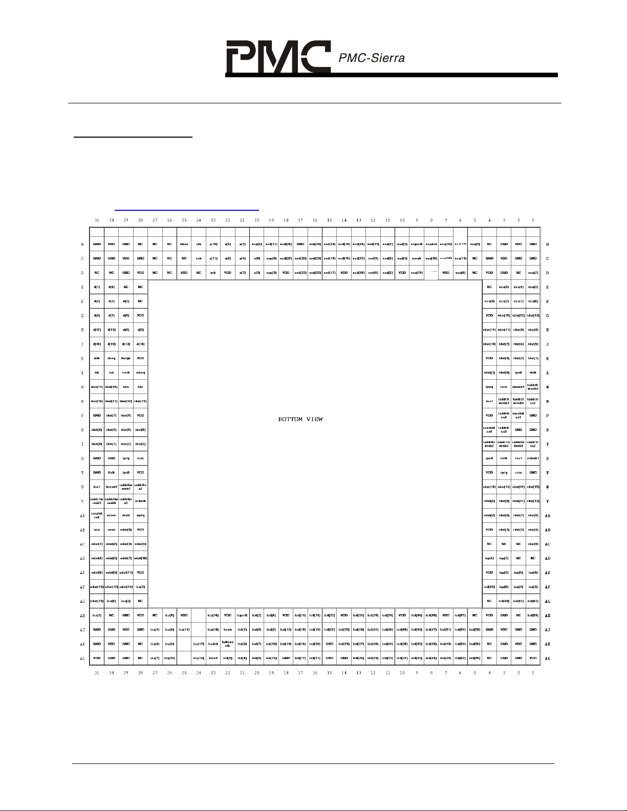
6 PIN DIAGRAM
The S/UNI-ATLAS-1K800 is packaged in a 432 thermally enhanced BGA -SBGA
package having a body size of 40 mm x 40 mm x 1.54 mm and a ball pitch of
1.27 mm. This pin diagram can be downloaded from the PMC-Sierra website
(http://www.pmc-sierra.com).
NC
NC
NC
NC
NC
NC
NC
NC
PROPRIETARY AND CONFIDENTIAL TO PMC-SIERRA, INC 12

STANDARD PRODUCT
DATASHEET
PMC-2010142 ISSUE 2 ATM LAYER SOLUTION
PM7328 S/UNI-ATLAS-1K800
7 PIN DESCRIPTION
Pin Name Type Pin No. Function
Ingress Input Cell Interface: 28 pins
RFCLK Input
RPOLL Input
U3 The Ingress Input Cell Interface clock (RFCLK) is
used to read words from the PHY receive side into
the S/UNI-ATLAS-1K800 Ingress Input Cell Interface.
RFCLK must cycle at a 52 MHz or lower
instantaneous rate. RSOC, RCA[4:1], RPRTY and
RDAT[15:0] are sampled on the rising edge of
RFCLK. RRDENB[4:1], RADDR[4:0] and RAVALID
are updated on the rising edge of RFCLK.
U4 The Ingress Input Cell Interface Poll pin (RPOLL) is
used to control whether the Ingress Input Cell
Interface operates in SCI-PHY Level 1 mode or SCIPHY Level 2 mode. If RPOLL is low, the Ingress Input
Cell Interface operates in SCI-PHY Level 1 mode
(compatible with UTOPIA Level 1 cell-level
handshaking). This is a direct addressing mode using
the RCA[4:1] inputs and the RRDENB[4:1] outputs. If
RPOLL is high, the Ingress Input Cell Interface
operates in a SCI-PHY Level 2 mode (compatible
with UTOPIA Level 2). This is a polled addressing
mode using the RADDR[4:0], RAVALID and
RRDENB[1] outputs, and the RCA[1] input. If fewer
than 32 PHY devices are used, the RAVALID pin
need not be connected.
Note: In direct addressing mode, the 4-PHY
configuration is not recommended. Instead the 4PHY address-polling mode should be used. This
does not apply to the Single or Dual-PHY
configurations.
RPOLL is assumed to be a static input.
PROPRIETARY AND CONFIDENTIAL TO PMC-SIERRA, INC 13

STANDARD PRODUCT
DATASHEET
PMC-2010142 ISSUE 2 ATM LAYER SOLUTION
PM7328 S/UNI-ATLAS-1K800
Pin Name Type Pin No. Function
RSOC Input
RCA[1]
I/O
RCA[2]
RCA[3]
RCA[4]
V2 The Ingress Input Cell Interface Start of Cell (RSOC)
marks the start of the cell on the RDAT[15:0] bus.
When RSOC is high, the first word of the cell
structure is present on the RDAT[15:0] stream. It is
not necessary for RSOC to be asserted for each cell.
An interrupt may be generated if RSOC is high during
any word other than the first word of the cell
structure.
RSOC is sampled on the rising edge of RFCLK and
considered valid only when one of the RRDENB[4:1]
signals so indicates.
U2
T1
R3
R4
The active polarity of these signals is programmable
and defaults to active high.
If the RPOLL pin is low, the ATLAS-1K800 asserts the
appropriate RRDENB[4:1] signal in response to a
round robin polling of the RCA[4:1] signals. Once
committed, the ATLAS-1K800 will transfer an entire
cell from a single PHY before servicing the next. The
ATLAS-1K800 will complete the read of an entire cell
even if the associated RCA[4:1] input is deasserted
during the cell transfer. Sampling of the RCA[4:1]
inputs resumes the cycle after the last octet of a cell
has been transferred.
Note, RCA[1] is an input only.
PROPRIETARY AND CONFIDENTIAL TO PMC-SIERRA, INC 14

STANDARD PRODUCT
DATASHEET
PMC-2010142 ISSUE 2 ATM LAYER SOLUTION
PM7328 S/UNI-ATLAS-1K800
Pin Name Type Pin No. Function
RCA[4:1]
(continued)
RRDENB[1]
RRDENB[2]
RRDENB[3]
RRDENB[4]
Output
U1
T4
T3
T2
If the RPOLL pin is high, the RCA[3:2] pins are
redefined as RADDR[4:3] and the RCA[4] pin is
redefined as RAVALID.
If the RPOLL pin is high, the ATLAS-1K800 polls up
to 32 PHYs using the PHY address signals
RADDR[4:0]. A PHY device being addressed by
RADDR[4:0] is expected to indicate whether or not it
has a complete cell available for transfer by driving
RCA[1] during the clock cycle following that in which
it is addressed. When a cell transfer is in progress,
the ATLAS-1K800 will not poll the PHY device which
is sending the cell and so PHY devices need not
support the cell availability indication during cell
transfer. The selection of a particular PHY device
from which to transfer a cell is indicated by the state
of RADDR[4:0] and when RRDENB[1] is asserted.
Note, RCA[1] is an input only. The RCA[4:1] signals
are sampled on the rising edge of RFCLK.
The active low read enable (RRDENB[4:1]) outputs
are used to initiate the reading of cells from a PHY
device into the Ingress Input Cell Interface.
If the RPOLL pin is low, the ATLAS-1K800 asserts
one of the RRDENB[4:1] outputs to transfer a cell
from one of up to 4 PHY devices. A valid word is
expected on the RDAT[15:0] bus at the second rising
edge of RFCLK after one of the enables is asserted.
When all of the enables are deasserted, no valid data
is expected.
The RRDENB[4:1] outputs are updated on the rising
edge of RFCLK.
If the RPOLL pin is high, the RRDENB[4:2] pins are
redefined as RADDR[2:0]. The RRDENB[1] pin is
used to transfer all cells. The source PHY is selected
by the RADDR[4:0] signals.
PROPRIETARY AND CONFIDENTIAL TO PMC-SIERRA, INC 15

STANDARD PRODUCT
DATASHEET
PMC-2010142 ISSUE 2 ATM LAYER SOLUTION
PM7328 S/UNI-ATLAS-1K800
Pin Name Type Pin No. Function
RADDR[4]
Output
RADDR[3]
RADDR[2]
RADDR[1]
RADDR[0]
RAVALID I/O
R3
T1
T2
T3
T4
If the RPOLL pin is high, the RADDR[4:0] pins are
used for PHY addressing. If the RPOLL pin is low, the
RADDR[4:0] pins are redefined as RCA[3:2] and
RRDENB[4:2].
If the RPOLL pin is high, the RADDR[4:0] signals are
used to address up to 32 PHY devices for the
purposes of polling and selection for cell transfer.
When conducting polling, in order to avoid bus
contention, the ATLAS-1K800 inserts gap cycles
during which RADDR[4:0] is set to 0x1F and
RAVALID is logic 0. When this occurs, no PHY device
should drive RCA[1] during the following clock cycle.
Polling is performed in incrementing sequential order.
The PHY device selected for transfer is based on the
RADDR[4:0] value present when RRDENB[1] is falls.
The RADDR[4:0] bus is updated on the rising edge of
RFCLK.
R4 If the RPOLL pin is high, the PHY Address Valid
(RAVALID) pin is active. If the RPOLL pin is low, the
RAVALID pin is redefined as RCA[4].
If the RPOLL pin is high, the RAVALID pin indicates
that the RADDR[4:0] bus is asserting a valid PHY
address for polling purposes. When this signal is
deasserted, the RADDR[4:0] bus is set to 0x1F.
RAVALID is not necessary when less than 32 PHY
devices are being polled. RAVALID is updated on the
rising edge of RFCLK.
PROPRIETARY AND CONFIDENTIAL TO PMC-SIERRA, INC 16

STANDARD PRODUCT
DATASHEET
PMC-2010142 ISSUE 2 ATM LAYER SOLUTION
PM7328 S/UNI-ATLAS-1K800
Pin Name Type Pin No. Function
RDAT[15]
RDAT[14]
RDAT[13]
RDAT[12]
RDAT[11]
RDAT[10]
RDAT[9]
RDAT[8]
RDAT[7]
RDAT[6]
RDAT[5]
RDAT[4]
RDAT[3]
RDAT[2]
RDAT[1]
RDAT[0]
Input
W1
W2
W3
Y1
Y2
W4
Y3
AA1
AA2
Y4
AA3
AB1
AB2
AA4
AB3
The Ingress Input Cell Interface cell data bus
(RDAT[15:0]) carries the ATM cell octets that are
written to the Ingress Input Cell Interface. The
RDAT[15:0] bus is sampled on the rising edge of
RFCLK and considered valid only when one of the
RRDENB[4:1] signals so indicates. RDAT[15:8] is
only valid if the RBUS8 register bit is low.
AC1
RPRTY Input
V3 The Ingress Input Cell Interface parity (RPRTY)
Ingress SRAM Interface: 96 pins
signal indicates the parity (programmable for odd or
even parity) of the RDAT[15:0] bus. If the RBUS8
register bit is low, the RPRTY signal indicates parity
over the RDAT[15:0] data bus. If RBUS8 is high, the
RPRTY signal indicates parity over the RDAT[7:0]
data bus. A maskable interrupt status is generated
upon a parity error; no other actions are taken. The
RPRTY signal is sampled on the rising edge of
RFCLK and is considered valid only when one of the
RRDENB[4:1] signals so indicates.
PROPRIETARY AND CONFIDENTIAL TO PMC-SIERRA, INC 17

STANDARD PRODUCT
DATASHEET
PMC-2010142 ISSUE 2 ATM LAYER SOLUTION
PM7328 S/UNI-ATLAS-1K800
Pin Name Type Pin No. Function
ISYSCLK Input
ISD[63]
I/O AG1
ISD[62]
ISD[61]
ISD[60]
ISD[59]
ISD[58]
ISD[57]
ISD[56]
ISD[55]
ISD[54]
ISD[53]
ISD[52]
ISD[51]
AH21 The Ingress System clock (ISYSCLK) is used for the
Ingress portion of the ATLAS-1K800. ISYSCLK must
cycle at a 52 MHz or lower instantaneous rate, but a
high enough rate to maintain an 800Mbit/s
throughput. ISADSB, ISOEB, ISRWB are updated on
the rising edge of ISYSCLK. When ISD[63:0] and
ISP[7:0] are outputs, they are updated on the rising
edge of ISYSCLK. When ISD[63:0] and ISP[7:0] are
inputs, they are sampled on the rising edge of
ISYSCLK.
The bi-directional Ingress VC Table SRAM data bus
AG2
AF4
AG3
AH1
(ISD[63:0]) pins interface directly with the
synchronous SRAM data ports.
A SRAM read is performed when the ATLAS-1K800
drives the address strobe (ISADSB) low and the
ISRWB output high. The ATLAS-1K800 tristates the
ISD[63:0] pins and samples the value driven by the
AJ5
AH6
AK5
SRAM on the second rising edge of the ISYSCLK
input after ISADSB is asserted.
A SRAM write is performed when the ATLAS-1K800
drives the address strobe low (ISADSB) and the
AL5
AJ6
AK6
AL6
AJ7
ISRWB output low. The ATLAS-1K800 presents valid
data on the ISD[63:0] pins upon the rising edge of
ISYSCLK which is written into the SRAM on the next
ISYSCLK rising edge. ISD[63:0] is tristated on the
rising edge of ISYSCLK. Contention is avoided by not
performing a write during the cycle after a read burst.
ISD[50]
PROPRIETARY AND CONFIDENTIAL TO PMC-SIERRA, INC 18
AH8

STANDARD PRODUCT
DATASHEET
PMC-2010142 ISSUE 2 ATM LAYER SOLUTION
PM7328 S/UNI-ATLAS-1K800
Pin Name Type Pin No. Function
ISD[49]
ISD[48]
ISD[47]
ISD[46]
ISD[45]
ISD[44]
ISD[43]
ISD[42]
ISD[41]
ISD[40]
ISD[39]
ISD[38]
ISD[37]
ISD[36]
ISD[35]
I/O AK7
AL7
AJ8
AH9
AK8
AL8
AJ9
AK9
AL9
AJ10
AH11
AK10
AL10
AJ11
AH12
Continued
ISD[34]
ISD[33]
ISD[32]
AK11
AL11
AJ12
PROPRIETARY AND CONFIDENTIAL TO PMC-SIERRA, INC 19

STANDARD PRODUCT
DATASHEET
PMC-2010142 ISSUE 2 ATM LAYER SOLUTION
PM7328 S/UNI-ATLAS-1K800
Pin Name Type Pin No. Function
ISD[31]
ISD[30]
ISD[29]
ISD[28]
ISD[27]
ISD[26]
ISD[25]
ISD[24]
ISD[23]
ISD[22]
ISD[21]
ISD[20]
ISD[19]
ISD[18]
ISD[17]
ISD[16]
I/O
AH13
AK12
AL12
AJ13
AK13
AL13
AJ14
AK14
AH15
AJ15
AL16
AK16
AJ16
AH16
AL17
Continued
AK17
PROPRIETARY AND CONFIDENTIAL TO PMC-SIERRA, INC 20

STANDARD PRODUCT
DATASHEET
PMC-2010142 ISSUE 2 ATM LAYER SOLUTION
PM7328 S/UNI-ATLAS-1K800
Pin Name Type Pin No. Function
ISD[15]
ISD[14]
ISD[13]
ISD[12]
ISD[11]
ISD[10]
ISD[9]
ISD[8]
ISD[7]
ISD[6]
ISD[5]
ISD[4]
ISD[3]
ISD[2]
ISD[1]
ISD[0]
I/O
AJ17
AK18
AH17
AJ18
AL19
AK19
AJ19
AL20
AK20
AH19
AJ20
AL21
AK21
AH20
AJ21
Continued
AL22
PROPRIETARY AND CONFIDENTIAL TO PMC-SIERRA, INC 21

STANDARD PRODUCT
DATASHEET
PMC-2010142 ISSUE 2 ATM LAYER SOLUTION
PM7328 S/UNI-ATLAS-1K800
Pin Name Type Pin No. Function
ISP[7]
ISP[6]
ISP[5]
ISP[4]
ISP[3]
ISP[2]
ISP[1]
ISP[0]
I/O
AD3
AE1
AE2
AD4
AE3
AF1
AF2
AF3
The Ingress VC Table SRAM parity (ISP[7:0]) pins
provide parity protection over the ISD[63:0] data bus.
ISP[0] completes odd parity for ISD[7:0]
ISP[1] completes odd parity for ISD[15:8]
ISP[2] completes odd parity for ISD[23:16]
ISP[3] completes odd parity for ISD[31:24]
ISP[4] completes odd parity for ISD[39:32]
ISP[5] completes odd parity for ISD[47:40]
ISP[6] completes odd parity for ISD[55:48]
ISP[7] completes odd parity for ISD[63:56]
ISP[7:0] has the same timing as ISD[63:0]. When
data are being written into the SRAM, the ATLAS1K800 generates correct parity. When data are being
read from the SRAM, the ATLAS-1K800 asserts a
maskable interrupt indication upon parity error
detection. No other action is taken, therefore, the
ISP[7:0] may be unconnected if parity protection is
not required.
PROPRIETARY AND CONFIDENTIAL TO PMC-SIERRA, INC 22

STANDARD PRODUCT
DATASHEET
PMC-2010142 ISSUE 2 ATM LAYER SOLUTION
PM7328 S/UNI-ATLAS-1K800
Pin Name Type Pin No. Function
ISA[19]
ISA[18]
ISA[17]
ISA[16]
ISA[9]
ISA[8]
ISA[7]
ISA[6]
ISA[5]
ISA[4]
ISA[3]
ISA[2]
ISA[1]
ISA[0]
Output
AJ23
AL24
AK24
AH23
AK26
AJ26
AL27
AK27
AH26
AJ27
AH31
AG29
AF28
AG30
The Ingress VC Table SRAM (ISA[19:0]) outputs
identify the SRAM locations accessed.
The least significant bits (ISA[9:0]) locate 1 of 1024
possible Ingress VC Table entries.
The four most significant bits (ISA[19:16]) identify the
fields within an Ingress VC Table record. In most
applications, the ISA[19:16] pins are decoded to
SRAM chip selects. Physical memory need not be
allocated for unused fields.
The ISA[9:0] outputs are also used to access the
Ingress VC Table Search Table.
The ISA[19:0] bus is updated on the rising edge of
ISYSCLK.
ISRWB Output
ISADSB Output
AJ22 The Ingress VC Table SRAM Read Write Bar
(ISRWB) qualifies the data and parity busses. If the
ISRWB output is asserted high, a read operation is
performed and the ATLAS-1K800 tristates the data
and parity busses so they may be driven by the
SRAM. If the ISRWB output is asserted low, a write
operation is performed and the ATLAS-1K800 drives
the data and parity busses.
ISRWB is updated on the rising edge of ISYSCLK.
AK23 The Ingress VC Table SRAM Address Strobe
(ISADSB) qualifies the address bus. If the ISADSB
output is asserted low, an SRAM access is initiated.
ISADSB is updated on the rising edge of ISYSCLK.
PROPRIETARY AND CONFIDENTIAL TO PMC-SIERRA, INC 23

STANDARD PRODUCT
DATASHEET
PMC-2010142 ISSUE 2 ATM LAYER SOLUTION
PM7328 S/UNI-ATLAS-1K800
Pin Name Type Pin No. Function
ISOEB Output
AL23 The Ingress VC Table asynchronous SRAM Output
Enable (ISOEB) controls the SRAM tristate outputs.
When ISOEB is low during a read cycle, the selected
SRAM (as determined by ISA[19:0] decoding) is
expected to drive the ISD[63:0] and ISP[7:0] data
busses.
ISOEB is updated on the rising edge of ISYSCLK.
Ingress Output Cell Interface: 22 pins
OFCLK Input
AA29 The Ingress Output Cell Interface clock (OFCLK) is
used to read words from the Ingress Output Cell
Interface. OFCLK must cycle at a 52 MHz or lower
instantaneous rate, but a high enough rate to avoid a
FIFO overflow. OSOC, OCA, OPRTY and
ODAT[15:0] are updated on the rising edge of
OFCLK. ORDENB is sampled on the rising edge of
OFCLK.
ORDENB Input
Y28 The active low read enable (ORDENB) signal is used
to indicate transfers from the Ingress Output Cell
Interface. When ORDENB is sampled low, using the
rising edge of OFCLK, a word is read from the
internal synchronous Ingress Output Cell Interface
FIFO, and output on bus ODAT[15:0]. When
ORDENB is sampled high, no read is performed and
outputs ODAT[15:0], OPRTY and OSOC are tristated
if the OTSEN input is high. ORDENB must operate in
conjunction with OFCLK to access the FIFO at a high
enough rate to avoid a FIFO overflow.
PROPRIETARY AND CONFIDENTIAL TO PMC-SIERRA, INC 24

STANDARD PRODUCT
DATASHEET
PMC-2010142 ISSUE 2 ATM LAYER SOLUTION
PM7328 S/UNI-ATLAS-1K800
Pin Name Type Pin No. Function
ODAT[15]
ODAT[14]
ODAT[13]
ODAT[12]
ODAT[11]
ODAT[10]
ODAT[9]
ODAT[8]
ODAT[7]
ODAT[6]
ODAT[5]
ODAT[4]
ODAT[3]
ODAT[2]
ODAT[1]
ODAT[0]
Tristate
AG31
AF29
AF30
AF31
AE29
AD28
AE30
AE31
AD29
AC28
AD30
AD31
AC29
AC30
AC31
The Ingress Output Cell Interface data bus
(ODAT[15:0]) carries the ATM cell octets that are read
from the Ingress Output Cell Interface FIFO. If the
OBUS8 register bit is high, only ODAT[7:0] carries
cell octets, The ODAT[15:0] bus is updated on the
rising edge of OFCLK.
When the Ingress Output Cell Interface is configured
for tristate operation using the OTSEN input, tristating
of the ODAT[15:0] output bus is controlled by the
ORDENB input.
When OTSEN is low, the ODAT[15:0] bus is low
when no cells are being transferred.
OPRTY
Tristate
AB29
AA28 The Ingress Output Cell Interface parity (OPRTY)
signal indicates the parity of the ODAT[15:0] data
bus. OPRTY is the parity (programmable odd or even
parity) calculation over the ODAT[15:0] data bus if the
OBUS8 register bit is low. If OBUS8 is high, OPRTY
indicates the parity of the ODAT[7:0] data bus.
OPRTY is updated on the rising edge of OFCLK.
When the Ingress Output Cell Interface is configured
for tristate operation using the OTSEN input, tristating
of the OPRTY output signal is controlled by the
ORDENB input.
PROPRIETARY AND CONFIDENTIAL TO PMC-SIERRA, INC 25

STANDARD PRODUCT
DATASHEET
PMC-2010142 ISSUE 2 ATM LAYER SOLUTION
PM7328 S/UNI-ATLAS-1K800
Pin Name Type Pin No. Function
OSOC
Tristate
OCA Output
OTSEN Input
AB30 The Ingress Output Cell Interface start of cell (OSOC)
signal marks the start of cell on the ODAT[15:0] data
bus. When OSOC is high, the first word of the cell
structure is present on the ODAT[15:0] bus. OSOC is
updated on the rising edge OFCLK.
When the Ingress Output Cell Interface is configured
for tristate operation using the OTSEN input, tristating
of the OSOC output is controlled by the ORDENB
input.
AB31 The active polarity of this signal is programmable and
defaults to active high.
The OCA signal indicates when the Ingress Output
Cell Interface has a cell available. When asserted,
OCA indicates that at least one cell is available to be
read from the Ingress Output Cell Interface FIFO.
The OCA signal is deasserted when the Ingress
Output Cell Interface has 0 to 4 words available for
the current cell. OCA is updated on the rising edge of
OFCLK.
AA30 The tristate enable, OTSEN, signal allows control
over the Ingress Output Cell Interface ODAT[15:0],
OPRTY, and OSOC outputs. When OTSEN is high,
the active low read enable input, ORDENB controls
when the ODAT[15:0], OPRTY, and OSOC outputs
are driven. When OTSEN is low, the ODAT[15:0],
OPRTY and OSOC outputs are always driven.
Egress Input Cell Interface: 28 pins
IFCLK Input
V30 The Egress Input Cell Interface clock (IFCLK) is used
to write words from the Traffic Shaper (or Switch Port)
transmit port into the S/UNI-ATLAS-1K800 Egress
Input Cell Interface. IFCLK must cycle at a 52 MHz or
lower instantaneous rate. ISOC, IPRTY, IDAT[15:0]
and IWRENB[4:1] are sampled on the rising edge of
IFCLK. IADDR[4:0], IAVALID and ICA[4:1] are
updated on the rising edge of IFCLK.
PROPRIETARY AND CONFIDENTIAL TO PMC-SIERRA, INC 26

STANDARD PRODUCT
DATASHEET
PMC-2010142 ISSUE 2 ATM LAYER SOLUTION
PM7328 S/UNI-ATLAS-1K800
Pin Name Type Pin No. Function
IPOLL Input
ISOC Input
V29 The Egress Input Cell Interface POLL pin (IPOLL) is
used to control whether the Egress Input Cell
Interface operates in SCI-PHY Level 1 mode or SCIPHY Level 2 mode. If IPOLL is low, the Egress Input
Cell Interface operates in SCI-PHY Level 1 mode
(compatible with UTOPIA Level 1 cell-level
handshaking). This is a direct addressing mode using
the ICA[4:1] outputs and the IWRENB[4:1] inputs. If
IPOLL is high, the Egress Input Cell Interface
operates in SCI-PHY Level 2 mode (compatible with
UTOPIA Level 2). This is a polled addressing mode
using the IADDR[4:0], IAVALID and IWRENB[1]
inputs, and the ICA[1] output. If fewer than 32 PHY
devices are used, the IAVALID pin can be tied high.
Note: In direct addressing mode, the 4-PHY
configuration is not recommended. Instead the 4PHY address-polling mode should be used. This
does not apply to the Single or Dual-PHY
configurations.
IPOLL is assumed to be a static input.
U28 The Egress Input Cell Interface Start of Cell (ISOC)
marks the start of the cell on the IDAT[15:0] bus.
When ISOC is high, the first word of the cell structure
is present on the IDAT[15:0] stream. It is not
necessary for ISOC to be asserted for each cell. An
interrupt may be generated if ISOC is high during any
word other than the first word of the cell structure.
ISOC is sampled on the rising edge of IFCLK and
considered valid only when one of the IWRENB[4:1]
signals so indicates.
ICA[1]
ICA[2]
ICA[3]
ICA[4]
O
I/O
I/O
I/O
W31
W28
Y29
AA31
The active polarity of these signals is programmable
and defaults to active high.
If the IPOLL pin is low, the ATLAS-1K800 asserts the
appropriate ICA[4:1] signal indicating the availability
of space in the Egress Input Cell Interface per-PHY 4
cell FIFO of the ATLAS-1K800. The Egress Input Cell
Interface of the ATLAS-1K800 must be programmed
to emulate the number of PHY devices to which the
ATLAS-1K800 is connected.
Note, ICA[1] is an output only.
PROPRIETARY AND CONFIDENTIAL TO PMC-SIERRA, INC 27

STANDARD PRODUCT
DATASHEET
PMC-2010142 ISSUE 2 ATM LAYER SOLUTION
PM7328 S/UNI-ATLAS-1K800
Pin Name Type Pin No. Function
ICA[4:1]
(continued)
IWRENB[1]
IWRENB[2]
IWRENB[3]
IWRENB[4]
If the IPOLL pin is high, the ICA[3:2] pins are
redefined as IADDR[4:3] and the ICA[4] pin is
redefined as IAVALID.
If the IPOLL pin is high, the ATLAS-1K800 asserts the
availability of space in the FIFO of a particular PHY
device when polled using the IADDR[4:0] and
IAVALID signals. The ATLAS-1K800 will drive the
ICA[1] signal to the appropriate value during the clock
cycle following that in which a particular PHY device
is addressed. When a cell transfer is in progress, the
ATLAS-1K800 will assert the availability of the PHY
device to which the current cell is being transmitted,
and the true availability of the PHY device will be
asserted 4 words before the end of the cell transfer.
The selection of a particular PHY device to which a
cell is to be transferred is indicated by the state of the
IADDR[4:0] bus when IWRENB[4:1] is asserted.
Note, ICA[1] is an output only.
I
I
I
I
W30
W29
Y31
Y30
The active low write enable (IWRENB[4:1]) inputs are
used to initiate the transfer of cells from the Traffic
Shaper into the ATLAS-1K800 Egress Input Cell
Interface.
If the IPOLL pin is low, the ATLAS-1K800 samples
the IWRENB[4:1] inputs to determine to which one of
up to 4 PHY devices a cell is to be written. A valid
word is expected on the IDAT[15:0] bus when one of
the enables is sampled low on the rising edge of
IFCLK. If a cell is written into the ATLAS-1K800 while
that particular PHY ICA[x] is deasserted, that cell
transfer is ignored, and a maskable interrupt is
asserted. If more than one enable is asserted
simultaneously, a maskable interrupt is asserted, and
the cell transfer is ignored.
If the IPOLL pin is high, the IWRENB[4:2] pins are
redefined as IADDR[2:0]. The IWRENB[1] pin is used
to transfer all cells. The destination PHY is selected
by the IADDR[4:0] signals.
PROPRIETARY AND CONFIDENTIAL TO PMC-SIERRA, INC 28

STANDARD PRODUCT
DATASHEET
PMC-2010142 ISSUE 2 ATM LAYER SOLUTION
PM7328 S/UNI-ATLAS-1K800
Pin Name Type Pin No. Function
IADDR[4]
IADDR[3]
IADDR[2]
IADDR[1]
I/O
I/O
I
I
I
IADDR[0]
IAVALID I/O
Y29
W28
Y30
Y31
W29
If the IPOLL pin is high, the IADDR[4:0] pins are used
for PHY addressing. If the IPOLL register bit is logic
pin is low, the IADDR[4:0] pins are redefined as
ICA[3:2] and IWRENB[4:2].
If the IPOLL pin is high, the IADDR[4:0] signals are
used to address up to 32 PHY devices for polling and
selection for cell transfer. The PHY devices selected
for transfer is based on the IADDR[4:0] value present
when the IWRENB[1] signal falls.
The IADDR[4:0] bus is sampled on the rising edge of
IFCLK.
AA31 If the IPOLL pin is high, the PHY address valid pin
(IAVALID) is active. If the IPOLL pin is low, the
IAVALID pin is redefined as ICA[4].
If the IPOLL pin is high, the IAVALID pin indicates
that the IADDR[4:0] bus is asserting a valid PHY
address for polling purposes. When this signal is
deasserted, the IADDR[4:0] bus must be set to 0x1F.
If fewer than 32 PHY devices are being polled and
the IAVALID pin is not functionally used, then
IAVALID must be tied high. IAVALID is sampled on
the rising edge of IFCLK.
PROPRIETARY AND CONFIDENTIAL TO PMC-SIERRA, INC 29

STANDARD PRODUCT
DATASHEET
PMC-2010142 ISSUE 2 ATM LAYER SOLUTION
PM7328 S/UNI-ATLAS-1K800
Pin Name Type Pin No. Function
IDAT[15]
IDAT[14]
IDAT[13]
IDAT[12]
IDAT[11]
IDAT[10]
IDAT[9]
IDAT[8]
IDAT[7]
IDAT[6]
IDAT[5]
IDAT[4]
IDAT[3]
IDAT[2]
IDAT[1]
IDAT[0]
Input
N28
M30
M31
N29
N30
N31
P29
R28
P30
R29
R30
R31
T28
T29
T30
The Egress Input Cell Interface cell data bus
(IDAT[15:0]) carries the ATM cell octets that are
written to the Egress Input Cell Interface. The
IDAT[15:0] bus is sampled on the rising edge of
IFCLK and considered valid only when one of the
IWRENB[4:1] signals so indicates. IDAT[15:8] is only
valid if the IBUS8 register bit is low.
T31
IPRTY Input
U29 The Egress Input Cell Interface parity (IPRTY) signal
indicates the parity (programmable for odd or even
parity) of the IDAT[15:0] bus. If the IBUS8 register bit
is low, the IPRTY signal indicates parity over the
IDAT[15:0] data bus. If IBUS8 is high, the IPRTY
signal indicates parity over the IDAT[7:0] data bus. A
maskable interrupt status is generated upon a parity
error; no other actions are taken. The IPRTY signal is
sampled on the rising edge of IFCLK and is
considered valid only when one of the IWRENB[4:1]
signals so indicates.
Egress Output Cell Interface: 28 pins
PROPRIETARY AND CONFIDENTIAL TO PMC-SIERRA, INC 30

STANDARD PRODUCT
DATASHEET
PMC-2010142 ISSUE 2 ATM LAYER SOLUTION
PM7328 S/UNI-ATLAS-1K800
Pin Name Type Pin No. Function
TFCLK Input
TPOLL Input
L1 The Egress Output Cell Interface clock (TFCLK) is
used to write words from the Egress Output Cell
Interface. TFCLK must cycle at a 52 MHz or lower
instantaneous rate, but a high enough rate to avoid a
FIFO overflow. TSOC, TWRENB[4:1], TADDR[4:0],
TAVALID, TPRTY and TDAT[15:0] are updated on the
rising edge of TFCLK. TCA[4:1] is sampled on the
rising edge of TFCLK.
L2 The Egress Output Cell Interface POLL pin (TPOLL)
is used to control whether the Egress Output Cell
Interface operates in SCI-PHY Level 1 mode or SCIPHY Level 2 mode. If TPOLL is low, the Egress
Output Cell Interface operates in SCI-PHY Level 1
mode (compatible with UTOPIA Level 1 cell-level
handshaking). This is a direct addressing mode using
the TCA[4:1] inputs and the TWRENB[4:1] outputs. If
TPOLL is high, the Egress Output Cell Interface
operates in SCI-PHY Level 2 mode (compatible with
UTOPIA Level 2). This is a polled addressing mode
using the TADDR[4:0], TAVALID and TWRENB[1]
outputs, and the TCA[1] input. If fewer than 32 PHY
devices are used, the TAVALID pin can be left
unconnected.
TSOC Output
Note: In direct addressing mode, the 4-PHY
configuration is not recommended. Instead the 4PHY address-polling mode should be used. This
does not apply to the Single or Dual-PHY
configurations.
TPOLL is assumed to be a static input.
M3 The Egress Output Cell Interface start of cell (TSOC)
indication signal marks the start of cell on the
TDAT[15:0] data bus. When TSOC is high, the first
word of the cell structure is present on the
TDAT[15:0] bus. TSOC is updated on the rising edge
of TFCLK.
PROPRIETARY AND CONFIDENTIAL TO PMC-SIERRA, INC 31

STANDARD PRODUCT
DATASHEET
PMC-2010142 ISSUE 2 ATM LAYER SOLUTION
PM7328 S/UNI-ATLAS-1K800
Pin Name Type Pin No. Function
TCA[4]
TCA[3]
TCA[2]
TCA[1]
TCA[4:1]
(continued)
I/O
P2
P3
N1
N4
The active polarity of these signals is programmable
and defaults to active high.
If the TPOLL pin is low, the ATLAS-1K800 samples
the state of the cell available signals of the PHY
devices to examine whether or not cells can be
transferred to the PHY devices. The ATLAS-1K800
will complete the writing of an entire cell into the PHY
device even if the associated TCA[4:1] input is
deasserted during the cell transfer. Sampling of the
TCA[4:1] signals resumes the cycle after the last
octet of a cell has been transferred.
If the TPOLL pin is high, the TCA[3:2] pins are
redefined as TADDR[4:3] and the TCA[4] pin is
redefined as TAVALID.
Note, TCA[1] is an input only.
If the TPOLL pin is high, the ATLAS-1K800 polls up to
32 PHYs using the PHY address signals TADDR[4:0].
A PHY device being addressed by TADDR[4:0] is
expected to indicate whether or not it has a complete
cell available for transfer by driving the TCA[1] during
the clock cycle following that in which it is addressed.
When a cell transfer is in progress, the ATLAS-1K800
will not poll the PHY device which is sending the cell
and so PHY devices need not support the cell
availability indication during cell transfer. The
selection of a particular PHY device to which a cell
will be written is indicated by the state of TADDR[4:0]
and when TWRENB[1] is asserted.
Note, TCA[1] is an input only.
PROPRIETARY AND CONFIDENTIAL TO PMC-SIERRA, INC 32

STANDARD PRODUCT
DATASHEET
PMC-2010142 ISSUE 2 ATM LAYER SOLUTION
PM7328 S/UNI-ATLAS-1K800
Pin Name Type Pin No. Function
TWRENB[4
]
TWRENB[3
]
TWRENB[2
]
TWRENB[1
]
TADDR[4]
TADDR[3]
TADDR[2]
TADDR[1]
TADDR[0]
Output
I/O
N2
N3
M1
M2
P3
N1
N2
N3
M1
The active low write enable (TWRENB[4:1]) signals
are used to indicate transfers from the Egress Output
Cell Interface to the PHY devices.
If the TPOLL pin is low, the ATLAS-1K800 asserts
one of the TWRENB[4:1] outputs to transfer a cell to
one of up to 4 PHY devices. A valid word is output on
the TDAT[15:0] bus at the same time one of the write
enables is asserted. When all of the enables are
deasserted, no valid data is output. The
TWRENB[4:1] outputs are updated on the rising edge
of TFCLK.
If the TPOLL pin is high, the TWRENB[4:2] pins are
redefined as TADDR[2:0].
Note, TWRENB[1] is an output only.
If the TPOLL pin is high, the TADDR[4:0] pins are
used for PHY addressing. If the TPOLL pin is low, the
TADDR[4:0] pins are redefined as TCA[3:2] and
TWRENB[4:2].
If the TPOLL pin is high, the TADDR[4:0] signals are
used to address up to 32 PHY devices for the
purposes of polling and selection for cell transfer.
When conducting polling, in order to avoid bus
contention, the ATLAS-1K800 inserts gap cycles
during which the TADDR[4:0] bus is set to 0x1F and
TAVALID is logic 0. When this occurs, no PHY device
should drive TCA[1] during the following clock cycle.
Polling is performed in incrementing sequential order.
The PHY device selected for transfer is based on the
TADDR[4:0] value present when TWRENB[1] falls.
The TADDR[4:0] bus is updated on the rising edge of
TFCLK.
PROPRIETARY AND CONFIDENTIAL TO PMC-SIERRA, INC 33

STANDARD PRODUCT
DATASHEET
PMC-2010142 ISSUE 2 ATM LAYER SOLUTION
PM7328 S/UNI-ATLAS-1K800
Pin Name Type Pin No. Function
TAVALI D I /O
TDAT[15]
Output
TDAT[14]
TDAT[13]
TDAT[12]
TDAT[11]
TDAT[10]
TDAT[9]
TDAT[8]
TDAT[7]
TDAT[6]
P2 If the TPOLL pin is high, the PHY Address Valid
(TAVALID) pin is active. If the TPOLL pin is low, the
TAVALID pin is redefined as TCA[4].
If the TPOLL pin is high, the TAVALID pin indicates
that the TADDR[4:0] bus is asserting a valid PHY
address for polling purposes. When this signal is
deasserted, the TADDR[4:0] bus is set to 0x1F.
TAVALID is not necessary when less than 32 PHY
devices are being polled. TAVALID is updated on the
rising edge of TFCLK.
G3
H4
G2
G1
The Egress Output Cell Interface cell data bus
(TDAT[15:0]) carries the ATM cell octets that are
written to the PHY devices. The TDAT[15:0] bus is
updated on the rising edge of TFCLK and considered
valid only when one of the TWRENB[4:1] signals so
indicates. TDAT[15:8] is only valid if the TBUS8
H3
register bit is low.
J4
H2
H1
J3
TDAT[5]
TDAT[4]
TDAT[3]
TDAT[2]
J2
J1
K3
L4
TDAT[1]
K2
TDAT[0]
K1
L3
PROPRIETARY AND CONFIDENTIAL TO PMC-SIERRA, INC 34

STANDARD PRODUCT
DATASHEET
PMC-2010142 ISSUE 2 ATM LAYER SOLUTION
PM7328 S/UNI-ATLAS-1K800
Pin Name Type Pin No. Function
TPRTY Output
M4 The Egress Output Cell Interface parity (TPRTY)
Egress SRAM Interface: 60 pins
ESYSCLK Input
B9 The Egress System clock (ESYSCLK) is used for the
signal indicates the parity (programmable for odd or
even parity) of the TDAT[15:0] bus. If the TBUS8
register bit is low, the TPRTY signal indicates parity
over the TDAT[15:0] data bus. If TBUS8 is high, the
TPRTY signal indicates parity over the TDAT[7:0]
data bus. The TPRTY signal is updated on the rising
edge of TFCLK and is considered valid only when
one of the TWRENB[4:1] signals so indicates.
Egress portion of the ATLAS-1K800. ESYSCLK must
cycle at a 52 MHz or lower instantaneous rate, but a
high enough rate to maintain an 800Mbit/s
throughput. ESADSB, ESOEB and ESRWB are
updated on the rising edge of ESYSCLK. When
ESD[31:0] and ESP[3:0] are outputs, they are
updated on the rising edge of ESYSCLK. When
ESD[31:0] and ESP[3:0] are inputs, they are sampled
on the rising edge of ESYSCLK.
PROPRIETARY AND CONFIDENTIAL TO PMC-SIERRA, INC 35

STANDARD PRODUCT
DATASHEET
PMC-2010142 ISSUE 2 ATM LAYER SOLUTION
PM7328 S/UNI-ATLAS-1K800
Pin Name Type Pin No. Function
ESD[31]
ESD[30]
ESD[29]
ESD[28]
ESD[27]
ESD[26]
ESD[25]
ESD[24]
ESD[23]
ESD[22]
ESD[21]
ESD[20]
ESD[19]
ESD[18]
ESD[17]
ESD[16]
I/O
B19
A19
C18
B18
D17
C17
A16
B16
C16
D16
A15
B15
C15
B14
D15
The bi-directional Egress VC Table SRAM data bus
(ESD[31:0]) pins interface directly with the
synchronous SRAM data ports.
A SRAM read is performed when the ATLAS-1K800
drives the address strobe (ESADSB) low and the
ESRWB output high. The ATLAS-1K800 tristates the
ESD[31:0] pins and samples the value driven by the
SRAM on the second rising edge of the ESYSCLK
input after ESADSB is asserted.
A SRAM write is performed when the ATLAS-1K800
drives the address strobe low (ESADSB) and the
ESRWB output low. The ATLAS-1K800 presents valid
data on the ESD[31:0] pins upon the rising edge of
ESYSCLK which is written into the SRAM on the next
ESYSCLK rising edge. ESD[31:0] is tristated on the
rising edge of ESYSCLK. Contention is avoided by
not performing a write during the cycle after a read
burst.
C14
PROPRIETARY AND CONFIDENTIAL TO PMC-SIERRA, INC 36

STANDARD PRODUCT
DATASHEET
PMC-2010142 ISSUE 2 ATM LAYER SOLUTION
PM7328 S/UNI-ATLAS-1K800
Pin Name Type Pin No. Function
ESD[15]
ESD[14]
ESD[13]
ESD[12]
ESD[11]
ESD[10]
ESD[9]
ESD[8]
ESD[7]
ESD[6]
ESD[5]
ESD[4]
ESD[3]
ESD[2]
ESD[1]
ESD[0]
I/O
A13
B13
C13
A12
B12
D13
C12
A11
B11
D12
C11
A10
B10
D11
C10
Continued
ESP[3]
ESP[2]
ESP[1]
ESP[0]
I/O
A9
D19
B20
A20
C19
The Egress VC Table SRAM parity (ESP[3:0]) pins
provide parity protection over the ESD[31:0] data bus.
ESP[0] completes the odd parity for ESD[7:0]
ESP[1] completes the odd parity for ESD[15:8]
ESP[2] completes the odd parity for ESD[23:16]
ESP[3] completes the odd parity for ESD[31:24]
ESP[3:0] has the same timing as ESD[31:0]. When
data are being written into the SRAM, the ATLAS1K800 generates correct parity. When data are being
read from the SRAM, the ATLAS-1K800 asserts a
maskable interrupt indication upon parity error
detection. No other action is taken, therefore, the
ESP[3:0] may be unconnected if parity protection is
not required.
PROPRIETARY AND CONFIDENTIAL TO PMC-SIERRA, INC 37

STANDARD PRODUCT
DATASHEET
PMC-2010142 ISSUE 2 ATM LAYER SOLUTION
PM7328 S/UNI-ATLAS-1K800
Pin Name Type Pin No. Function
ESA[19]
ESA[18]
ESA[17]
ESA[16]
ESA[9]
ESA[8]
ESA[7]
ESA[6]
ESA[5]
ESA[4]
ESA[3]
ESA[2]
ESA[1]
ESA[0]
Output
D9
C8
A7
B7
B5
D6
D1
E3
F4
E2
E1
F3
F2
The Egress VC Table SRAM (ESA[19:0]) outputs
identify the SRAM locations accessed.
The least significant bits (ESA[9:0]) locate 1 of 1024
possible Egress VC Table entries.
The four most significant bits (ESA[19:16]) identify
the fields within an Egress VC Table record. In most
applications, the ESA[19:16] pins are decoded to
SRAM chip selects. Physical memory need not be
allocated for unused fields.
The ESA[9:0] outputs are also used to access the
Egress VC Table Search Table.
The ESA[19:0] bus is updated on the rising edge of
ESYSCLK.
ESRWB Output
ESADSB Output
F1
C9 The Egress VC Table SRAM Read Write Bar
(ESRWB) qualifies the data bus. If the ESRWB
output is asserted high, the external SRAM samples
this signal and performs a read operation and the
ATLAS-1K800 tristates the ESD[31:0] and ESP[3:0]
pins so they may be driven by the external SRAM). If
the ESRWB output is asserted low, a write operation
is performed, and the S/UNI-ATLAS-1K800 drives the
ESD[31:0] and ESP[3:0] pins.
ESRWB is updated on the rising edge of ESYSCLK.
B8 The Egress VC Table SRAM Address Strobe
(ESADSB) qualifies the address bus. If the ESADSB
output is asserted low, the external SRAM samples
the address asserted by the S/UNI-ATLAS-1K800.
ESADSB is updated on the rising edge of ESYSCLK
PROPRIETARY AND CONFIDENTIAL TO PMC-SIERRA, INC 38

STANDARD PRODUCT
DATASHEET
PMC-2010142 ISSUE 2 ATM LAYER SOLUTION
PM7328 S/UNI-ATLAS-1K800
Pin Name Type Pin No. Function
ESOEB Output
A8 The Egress VC Table asynchronous SRAM Output
Microprocessor Interface: 38 pins
CSB Input
RDB Input
C24 CSB is low during ATLAS-1K800 Microprocessor
B24 RDB is low during ATLAS-1K800 Microprocessor
Enable (ESOEB) controls the SRAM tristate outputs.
When ESOEB is low during a read cycle, the
selected SRAM (as determined by the decoding of
the ESD[31:0] multiplexed address bus) is expected
to drive the ESD[31:0] and ESP[3:0] data busses.
ESOEB is updated on the rising edge of ESYSCLK.
Interface Port register accesses.
If CSB is not required (i.e. register accesses
controlled using RDB and WRB signals only), CSB
should be connected to an inverted version of the
RSTB input.
CSB is a 5V tolerant input.
Interface Port register read accesses. The ATLAS1K800 drives the D[15:0] bus with the contents of the
addressed register while RDB and CSB are low.
WRB Input
IDREQ Output
RDB is a 5V tolerant input.
D23 WRB is low during ATLAS-1K800 Microprocessor
Interface Port register write accesses. The D[15:0]
bus contents are clocked into the addressed register
on the rising edge of WRB while CSB is low.
WRB is a 5V tolerant input.
K30 The Ingress Microprocessor Cell Interface DMA
request (IDREQ) is asserted when the Ingress
Microprocessor Cell Interface contains a cell to be
read, and the DMAEN register bit in the Ingress MCIF
Configuration register is a logic 1. The first read of
the Ingress MCIF Data register will return the first
word of the cell. IDREQ is deasserted after the last
word of the cell has been read or an abort has been
signaled.
PROPRIETARY AND CONFIDENTIAL TO PMC-SIERRA, INC 39

STANDARD PRODUCT
DATASHEET
PMC-2010142 ISSUE 2 ATM LAYER SOLUTION
PM7328 S/UNI-ATLAS-1K800
Pin Name Type Pin No. Function
EDREQ Output
BUSYB Output
L28 The Egress Microprocessor Cell Interface DMA
request (EDREQ) is asserted when the Egress
Microprocessor Cell Interface contains a cell to be
read, and the DMAEN register in the Egress MCIF
configuration register is a logic 1. The first read of the
Egress MCIF Data register will return the first word of
the cell. EDREQ is deasserted after the last word of
the cell has been read or an abort has been signaled.
K29 The BUSYB output is asserted while a
microprocessor initiated access to external RAM data
is pending (for internal RAM accesses, a
microprocessor must poll the appropriate BUSY
register bit). The BUSYB output is deasserted after
the access has been completed. A microprocessor
access to external SRAM is typically completed within
37 ISYSCLK or ESYSCLK cycles. If the ISTANDBY
and ESTANDBY bits in the Master Configuration are
set to logic 1, the access time is reduced to less than
5 ISYSCLK or ESYSCLK cycles. The polarity of the
BUSYB output is programmable and defaults to
active low.
The BUSYB signal should be treated as a glitch-free
asynchronous output.
PROPRIETARY AND CONFIDENTIAL TO PMC-SIERRA, INC 40

STANDARD PRODUCT
DATASHEET
PMC-2010142 ISSUE 2 ATM LAYER SOLUTION
PM7328 S/UNI-ATLAS-1K800
Pin Name Type Pin No. Function
D[15]
D[14]
D[13]
D[12]
D[11]
D[10]
D[9]
D[8]
D[7]
D[6]
D[5]
D[4]
D[3]
D[2]
D[1]
D[0]
I/O
J31
J30
J29
H31
H30
J28
H29
G31
G30
H28
G29
F31
F30
F29
E31
The bi-directional data bus, D[15:0] is used during
ATLAS-1K800 Microprocessor Interface Port register
reads and write accesses. D[15:8] should contain the
most significant 8-bits and D[7:0] should contain the
least significant 8-bits of a word.
The bi-directional data bus, D[15:0], is a 5V tolerant
bus.
A[11]
A[10]
A[9]
A[8]
A[7]
A[6]
A[5]
A[4]
A[3]
A[2]
A[1]
A[0]
Input
E30
C23
B23
A23
C22
D21
B22
A22
C21
D20
B21
A21
C20
A[11:0] selects specific Microprocessor Interface Port
registers during ATLAS-1K800 register accesses.
A[11] is the Test Register Select (TRS) address pin.
TRS selects between normal and test mode register
accesses. TRS is high during test mode register
accesses, and is low during normal mode register
accesses.
A[11:0] is a 5V tolerant input bus.
PROPRIETARY AND CONFIDENTIAL TO PMC-SIERRA, INC 41

STANDARD PRODUCT
DATASHEET
PMC-2010142 ISSUE 2 ATM LAYER SOLUTION
PM7328 S/UNI-ATLAS-1K800
Pin Name Type Pin No. Function
ALE Input
Input
Interna
l PullUp
A24 ALE is active high and latches the address bus,
A[11:0], when low. When ALE is high, the internal
address latches are transparent. It allows the ATLAS1K800 to interface to a multiplexed address/data bus.
ALE is a 5V tolerant input.
HALFSECCLKInput AK22 The 0.5 second clock (HALFSECCLK) input provides
precise timing for events such as the generation of
CC, RDI and AIS cells and the declaration and
clearing of the AIS, RDI and CC alarms.
By default, the initiation of 0.5 second events is
based on the ISYSCLK period; therefore, the
HALFSECCLK input is ignored. If the SEL1SEC
register bit is logic 1, the HALFSECCLK input
becomes the source of the half second clock.
HALFSECCLK must be glitch free and may be
treated as an asynchronous input.
HALFSECCLK is a 5V tolerant input.
INTB Open
Drain
Output
K31 The Interrupt Request (INTB) output goes low when
an ATLAS-1K800 interrupt source is active and that
source is unmasked. INTB returns high when the
interrupt is acknowledged via an appropriate register
access. INTB is an open drain output.
RSTB Schmit
t
Trigger
Input
Interna
l PullUp
A25 The active low reset (RSTB) signal provides an
asynchronous ATLAS-1K800 reset. RSTB is a
Schmitt trigger input with an integral pull up resistor.
When RSTB is forced low, all ATLAS-1K800 registers
are forced to their default states.
RSTB is a 5V tolerant input.
IEEE P1149.1 (JTAG) Interface: 5 pins
TCK
Input
Internal
Pull-up
L30 The test clock (TCK) signal provides timing for test
operations that can be carried out using the IEEE
P1149.1 test access port.
TCK is a 5V tolerant input.
PROPRIETARY AND CONFIDENTIAL TO PMC-SIERRA, INC 42

STANDARD PRODUCT
DATASHEET
PMC-2010142 ISSUE 2 ATM LAYER SOLUTION
PM7328 S/UNI-ATLAS-1K800
Pin Name Type Pin No. Function
TMS
TDI
TDO
TRSTB
Input
Interna
l PullUp
M29 The test mode select (TMS) signal controls the test
operations that can be carried out using the IEEE
P1149.1 test access port. TMS is sampled on the
rising edge of TCK. TMS has an internal pull up
resistor.
TMS is a 5V tolerant input.
Input
Interna
l PullUp
L31 The test data input (TDI) signal carries test data into
the ATLAS-1K800 via the IEEE P1149.1 test access
port. TDI is sampled on the rising edge of TCK. TDI
has an internal pull-up resistor.
TDI is a 5V tolerant input.
Tristate M28 The test data output (TDO) signal carries test data
out of the ATLAS-1K800 via the IEEE P1149.1 test
access port. TDO is updated on the falling edge of
TCK. TDO is a tri-state output which is tri-stated
except when the scanning of data is in progress
Schmit
t
Trigger
Input
Interna
l PullUp
L29 The active low test reset (TRSTB) signal provides an
asynchronous ATLAS-1K800 test access port reset
via the IEEE P1149.1 test access port. TRSTB is a
Schmitt triggered input with an integral pull-up
resistor.
The JTAG TAP controller must be initialized when the
ATLAS-1K800 is powered up. If the JTAG port is not
used, TRSTB must be connected to the RSTB input
or GND.
TRSTB is a 5V tolerant input.
VBIAS Input
B25 +5V Bias (VBIAS). The VBIAS input is used to
implement the 5V tolerance on the inputs of the
Microprocessor and JTAG interfaces Interface.
If 5 volt tolerance is not required, VBIAS should be
connected to the 3.3 volt power supply (i.e. the same
as VDD).
PROPRIETARY AND CONFIDENTIAL TO PMC-SIERRA, INC 43

STANDARD PRODUCT
DATASHEET
PMC-2010142 ISSUE 2 ATM LAYER SOLUTION
PM7328 S/UNI-ATLAS-1K800
Pin Name Type Pin No. Function
VDD Power
A1
A31
B2
B30
C3
C29
D4
D7
D10
D14
D18
D22
D25
D28
G4
The VDD power pins should be connected to a welldecoupled +3.3V DC supply.
G28
K4
K28
PROPRIETARY AND CONFIDENTIAL TO PMC-SIERRA, INC 44

STANDARD PRODUCT
DATASHEET
PMC-2010142 ISSUE 2 ATM LAYER SOLUTION
PM7328 S/UNI-ATLAS-1K800
Pin Name Type Pin No. Function
VDD Power
P4
P28
V4
V28
AB4
AE4
AB28
AE28
AH4
AH7
AH10
AH14
AH18
AH22
AH25
Continued
AH28
AJ3
AJ29
AK2
AK30
AL1
AL31
PROPRIETARY AND CONFIDENTIAL TO PMC-SIERRA, INC 45

STANDARD PRODUCT
DATASHEET
PMC-2010142 ISSUE 2 ATM LAYER SOLUTION
PM7328 S/UNI-ATLAS-1K800
Pin Name Type Pin No. Function
GND
Ground A2
A3
A14
A17
A18
A29
A30
B1
B3
B17
B29
B31
C1
C2
C4
The ground pins should be connected to GND.
C28
C30
C31
D3
D29
P1
P31
R1
PROPRIETARY AND CONFIDENTIAL TO PMC-SIERRA, INC 46

STANDARD PRODUCT
DATASHEET
PMC-2010142 ISSUE 2 ATM LAYER SOLUTION
PM7328 S/UNI-ATLAS-1K800
Pin Name Type Pin No. Function
GND
Ground R2
U30
U31
V1
V31
AH3
AH29
AJ1
AJ2
AJ4
AJ30
AJ28
AJ31
AK1
AK3
Continued.
AK15
AK29
AK31
AL2
AL3
AL14
AL15
AL18
AL29
AL30
Notes on Pin Description:
1. All S/UNI-ATLAS-1K800 inputs and bi-directional pads present minimum
capacitive loading and operate at TTL logic levels.
PROPRIETARY AND CONFIDENTIAL TO PMC-SIERRA, INC 47

STANDARD PRODUCT
DATASHEET
PMC-2010142 ISSUE 2 ATM LAYER SOLUTION
PM7328 S/UNI-ATLAS-1K800
2. Inputs RSTB, ALE, TCK, TMS, TDI and TRSTB have internal pull-up
resistors.
3. The recommended power supply sequencing is as follows:
3.1 During power-up, the voltage on the VBIAS pin must be kept equal to or
greater than the voltage on the VDD pins to avoid damage to the device.
3.2The VDD power must be applied before input pins are driven or the input
current per pin be limited to less than the maximum DC input current
specification. (20 mA)
3.3Power down the device in the reverse sequence.
PROPRIETARY AND CONFIDENTIAL TO PMC-SIERRA, INC 48

STANDARD PRODUCT
DATASHEET
PMC-2010142 ISSUE 2 ATM LAYER SOLUTION
PM7328 S/UNI-ATLAS-1K800
8 FUNCTIONAL DESCRIPTION
The PM7328 ATM Layer Solution (S/UNI-ATLAS-1K800 or abbreviated as ATLAS1K800) is a monolithic integrated circuit that implements the ATM Layer functions
that include fault and performance monitoring, header translation and cell rate
policing. The S/UNI-ATLAS-1K800 is a bi-directional part which is intended to be
situated between the physical layer (PHY) devices and a switch core in the ingress
side, and a traffic shaper and the PHY devices in the egress side. The S/UNIATLAS-1K800 supports a sustained aggregate throughput of 1.42x10
6
cells/s in
both the ingress and egress directions. The S/UNI-ATLAS-1K800 uses external
SRAM to store per-VPI/VCI data structures. The device is capable of supporting up
to 1024 connections.
The Ingress Input Cell Interface can be connected to up to 32 PHY devices through
a SCI-PHY compatible bus. The 53-byte ATM cell is encapsulated in a data
structure that can contain prepended or postpended routing information. Received
cells are buffered in a four cell deep FIFO. All idle cells, physical layer and
unassigned cells are discarded. For the remaining cells, a subset of ATM header
and appended bits is used as a search key to find the VC Table record for the virtual
connection. If a connection is not provisioned and the search terminates
unsuccessfully as a result, the cell is discarded and the VPI/VCI value of the cell is
captured. If the search is successful, subsequent processing of the cell is dependent
on the contents of the cell and configuration fields in the VC Table Record.
The S/UNI-ATLAS-1K800 performs header translation, if so configured. The ATM
header is replaced by the contents of fields in the VC Table Record for that
connection. The VCI contents are passed through transparently for VPC
connections. In the Ingress direction appended bytes can be replaced, added or
removed. The egress direction only supports translation of the VCI, VPI or both.
PROPRIETARY AND CONFIDENTIAL TO PMC-SIERRA, INC 49

STANDARD PRODUCT
DATASHEET
PMC-2010142 ISSUE 2 ATM LAYER SOLUTION
PM7328 S/UNI-ATLAS-1K800
If the S/UNI-ATLAS-1K800 is the end point for a F4 or F5 OAM flow, the OAM cells
are terminated and processed. If the S/UNI-ATLAS-1K800 is not the end point, the
OAM cells are passed to the Ingress/Egress Output Cell Interface with an optional
copy passed to the Microprocessor Cell Interface FIFO. The reception of AIS or RDI
cells results in the appropriate alarms (segment or end-to-end alarm). The interrupts
corresponding to the alarm bits can be masked on a per-connection basis. When
configured as a sink of PM cells, upon the arrival of a Forward Monitoring cell, error
counts are updated and a Backward Reporting cell is optionally generated and
routed to the Output Cell Interface in the opposite direction. When configured as a
source of PM cells, the S/UNI-ATLAS-1K800 generates a Forward Monitoring cell
when the user cell block size (programmable on a per-connection basis) is reached.
Note, the insertion of PM cells is paced so that bursts of generated cells will not
cause a backup in the Ingress or Egress directions. Both the Egress and Ingress
interfaces allow for the generation and monitoring of PM flows. All generated
Backward Reporting cells are output to the Backward OAM Cell Interfaces so they
may be inserted in the opposite flow direction (e.g. if a Forward Monitoring cell is
terminated in the Ingress direction, a Backward Reporting PM cell will be generated
by the Ingress Cell Processor into the Ingress Backward OAM Cell Interface so that
it may be inserted in the Egress path), while generated Forward Monitoring cells are
output to the Output Cell Interface of the normal flow direction.
Cell rate policing is supported in the Ingress direction through a dual leaky bucket
policer which conforms to the ITU-T I.371 Generic Cell Rate Algorithm for each
connection. Each cell that violates the traffic contract can be noted, tagged or
discarded. To allow full flexibility, each GCRA instance can be programmed to police
any combination of user cells, OAM cells, Resource Management cells, high priority
cells or low priority cells. On a per-connection basis, one of eight policing
configurations may be chosen. Three 16-bit non-compliant cell counts are provided
on a per-connection basis. These counters are programmable and allow for the
counting of, for example, dropped CLP0 cells, dropped CLP1 cells and tagged CLP0
cells.
The S/UNI-ATLAS-1K800 also supports a single leaky bucket policer on a per-PHY
basis (up to 32 instances can be programmed). The PHY GCRA can police any or
all connections on a particular PHY. Each PHY GCRA has a programmable action
field that allows violating cells to be noted, tagged or discarded. Three configurable
non-compliant cell counts (on each PHY GCRA) are also provided. Each PHY
GCRA can be programmed to police any combination of user cells, OAM cells,
Resource Management cells, high priority cells or low priority cells. Any one of four
PHY policing configurations may be chosen.
The Ingress Output Cell Interface can be connected to the switch core through a
single PHY extended cell format SCI-PHY compatible bus interface. Cells are stored
in a four cell deep FIFO until the downstream devices are ready to accept them.
PROPRIETARY AND CONFIDENTIAL TO PMC-SIERRA, INC 50

STANDARD PRODUCT
DATASHEET
PMC-2010142 ISSUE 2 ATM LAYER SOLUTION
PM7328 S/UNI-ATLAS-1K800
The 16-bit Microprocessor Interface is provided for device configuration, control and
monitoring by an external microprocessor. This interface provides access to the
external SRAM to allow creation of the data structure, configuration of individual
connections, and monitoring of the connections. The Microprocessor Cell FIFO
gives access to the cell stream in both the ingress and egress directions.
Programmed cell types can be routed to the Microprocessor Cell FIFO (and
subsequently read through the Microprocessor cell interface). The microprocessor
can send cells to the Ingress Output Cell Interface and the Egress Output Cell
Interface.
The Egress Input Cell Interface can emulate up to 32 PHY devices through an 8 or
16 bit SCI-PHY compatible bus (compatible with UTOPIA Level1 and UTOPIA Level
2). This interface can be configured for up to 4 PHY direct addressing, or 32 PHY
polled addressing. Received cells are buffered in a per-PHY four cell deep FIFO (i.e.
a 4 cell FIFO is provided for each of the 32-PHY devices). All Physical Layer and
unassigned cells are discarded. For all other cells, a programmable 16-bit location in
the header, prepend words or postpend words is used to provide a direct lookup into
the VC Table Record for the virtual connection. The apparent FIFO depth control
can be configured to control the early deassertion of the Egress Input Cell Interface
cell available signal. The apparent FIFO depth can be configured from 1 to 4
(default) cells.
Egress cell processing includes F4 and F5 OAM-PM monitoring and generation, and
F4 and F5 OAM-FM monitoring and generation. The performance monitoring
statistics are held in an on-chip RAM that can be accessed through the
Microprocessor port. Two programmable 32-bit cell counts are also maintained on a
per-connection basis. The Egress Cell Processor requires a 50 MHz ESYSCLK
frequency to sustain a 622 Mbit/s throughput.
The Egress Output Cell Interface is a 8 or 16 bit SCI-PHY compatible interface
which can address up to four PHY devices using direct addressing or up to 32 PHY
devices using polled addressing. Cells are stored in a per-PHY four cell deep FIFO
and subsequently transferred to a PHY device. The per-PHY cell buffering
eliminates head-of-line blocking. The Egress Output Cell Interface can also be
configured to provide the early deassertion of its internal cell available signal (to the
Egress Cell Processor). The apparent FIFO depth can be configured from 1 to 4
(default) cells.
The S/UNI-ATLAS-1K800 is implemented in low power 0.35 micron 3.3 Volt CMOS
technology. All SCI-PHY interfaces are 3.3 Volt only, the SRAM interfaces are 3.3
Volt only, and the Microprocessor Interface and JTAG pins are 3.3V/5V tolerant.
The S/UNI-ATLAS-1K800 is packaged in a 432-pin Super BGA package.
PROPRIETARY AND CONFIDENTIAL TO PMC-SIERRA, INC 51

STANDARD PRODUCT
DATASHEET
PMC-2010142 ISSUE 2 ATM LAYER SOLUTION
PM7328 S/UNI-ATLAS-1K800
8.1 Ingress VC Table
The Ingress VC Table is a 15-row 64-bit data structure that contains context
information for up to 1024 connections. The Ingress VC Table is used for connection
identification, connection configuration and connection processing functions. The
connection identification fields of the VC Table are located in the first two rows of
the structure, and the remaining rows are used for connection configuration and cell
processing.
The Ingress VC Table is a total of 960 bits per connection, however, not all rows
need be used if features are disabled. Unused bits should be set to zero for
backward compatibility with future devices within the ATLAS-1K800 family.
PROPRIETARY AND CONFIDENTIAL TO PMC-SIERRA, INC 52

STANDARD PRODUCT
DATASHEET
PMC-2010142 ISSUE 2 ATM LAYER SOLUTION
PM7328 S/UNI-ATLAS-1K800
Table 1 Ingress VC Table
ISA
63 0
[19:1
6]
0000 Unused
(8)
0001 CLPc
c_en
(1)
0010 Status (8) Configuration
Selector
F4toF5A
IS
(1)
(6)
PHYI
D (5)
(14)
Left Leaf
(1)
Unuse
d (1)PMActive
Internal Status
Left Branch
2 (1)
(17)
(16)
PM
Addr
2 (7)
Configuration
Right Leaf
(1)
PM
Active
1 (1)
OAM
Branch (16)
PM
Addr
1(7)
Right
NNI
(1)
B (11)
VPC Pointer
(9)
0011 COCUP
(1)
0100 GFR
(1)
Reserved
(3)
Police
Configuration
Action
2 (2)
TAT2 (30) TAT1 (30)
Action
1 (2)
I2
(14)
L2
(14)
(14)
(3)
0101 PHY
Police
(1)
Remaining Frame
Count
(11)
Violate
(1)
GFR
State
(3)
NonCompliant3
(16)
NonCompliant2
(16)
0110 Ingress Cell Count 2 (32) Ingress Cell Count 1 (32)
Primary Table
Record (16)
Field
(16)
I1
NonCompliant1
(16)
VPI
(12)
VCI
(16)
L1
(14)
0111 Header (40) UDF (8) PrePo1
(8)
1000 PrePo3 (8) PrePo4
(8)
PrePo5
(8)
PrePo6
(8)
PrePo7
(8)
PrePo8
(8)
PrePo9
(8)
1001 Alternate Ingress Cell Count 2 (32) Alternate Ingress Cell Count 1 (32)
1010 Unused
(32)
Unused
(5)
Maximum
Frame
Length
(11)
Received
Segment AIS
Defect Type
(8)
Received
End-to-End
AIS Defect
Type (8)
1011 Received End-to-End AIS Defect Location [127:64] (Most significant bytes)
1100 Received End-to-End AIS Defect Location [63:0] (Least significant bytes)
1101 Received Segment AIS Defect Location [127:64] (Most significant bytes)
1110 Received Segment AIS Defect Location [63:0] (Least significant bytes)
PrePo2
(8)
PrePo10
(8)
PROPRIETARY AND CONFIDENTIAL TO PMC-SIERRA, INC 53

STANDARD PRODUCT
DATASHEET
PMC-2010142 ISSUE 2 ATM LAYER SOLUTION
PM7328 S/UNI-ATLAS-1K800
8.2 Connection Identification
8.2.1 Ingress Connection Identification
In the ingress direction, the ATLAS-1K800 makes use of a flexible approach to
identify incoming cells and to determine which record in the Ingress VC Table with
which they are associated. The ATLAS-1K800 identifies the VC record of each
connection by searching the Ingress VC Table using selected portions of the cell
header, prepend, postpend and the PHY address. To do this, the ATLAS-1K800
creates an internal Routing Word, which is the concatenation of the cell header, cell
prepend and cell postpend. The ATLAS-1K800 is programmed to select portions of
the Routing Word plus the PHY address to create a VC Search Key. The VC Search
Key, therefore, consists of portions of the cell’s header, prepend, postpend and PHY
address.
The figure below illustrates the Routing Word and VC Search Key construction. This
figure is not intended to imply any restrictions on the positioning of Field A and Field
B. These fields may occur anywhere within the appended octets or the ATM header.
The Primary Key and Secondary Key may also intersect.
Figure 3 VC Search Key Composition
Routing Word
Cell Prepend
Field A Field B
m
VC Search Key
START
A
STARTA-L
PHY
ID
Primay Key Secondary Key
Cell Postpend
START
A
Field A Field B VPI/VCI
B
Length <= 128
STARTB-L
Cell Header
VPI/V CI
47(NNI)
B
43(UNI)
HEC/UDF
020 15
PROPRIETARY AND CONFIDENTIAL TO PMC-SIERRA, INC 54

STANDARD PRODUCT
DATASHEET
PMC-2010142 ISSUE 2 ATM LAYER SOLUTION
PM7328 S/UNI-ATLAS-1K800
Table 2 Ingress VC Table Cell Fields
Name Description
PHYID[4:0] Indicates the Physical Layer device that this connection is associated with.
This field is used to determine the destination of all generated RDI and
Backward Reporting PM cells. This field is also used in determining the perPHY statistics.
Field B[10:0] Contains the value of the Secondary Search key field B from the cell header.
NNI If this bit is a logic 1, the NNI bit identifies the connection as belonging to a
Network-to-Network Interface. If this bit is a logic 0, the connection is part of
a UNI.
VPI[11:0] The VPI field identifies the Virtual Path of the connection. If the connection is
a UNI connection (as defined by the NNI bit of the VC Table), the four MSBs
of the VPI field are the GFC bits.
The VPI field represents the VPI (and GFC, if the connection is a UNI
connection) which will be inserted in all generated OAM cells.
VCI[15:0] The VCI field identifies the Virtual Channel of the connection. If the
connection is a VPC (F4) connection, then this field shall be encoded as all
zeros. If the VCI field is non-zero, then the connection is a VCC (F5)
connection.
This VCI field represents the VCI which will be inserted in all F5 generated
OAM cells If this field is encoded as all zeros, the generated OAM cells use
the correct VCI to indicate whether they are segment OAM cells (VCI=3) or
end-to-end OAM cells (VCI=4).
The ATLAS-1K800 divides the VC Search Key into two search keys – the Primary
Key and the Secondary Key. The Primary Key is 0 to 10 bits long. It is constructed
from two fields – the PHY ID field and Field A. The PHY ID field and Field A can be
programmed to be 0-5 bits and 0-10 bits long, respectively. The PHY ID field is the
SCI-PHY address and must, therefore, include sufficient bits to encode all the PHYs
at the PHY Layer interface of the ATLAS-1K800. Field A starts at location STARTA
of the Routing Word, and has length LA. The number of bits in Field A plus the
number of bits in the PHY ID field must be less than or equal to 10. Field A and the
PHYID are always LSB justified within the Primary Key (any unused MSBs are set to
logic 0).
The Secondary Key is 39 bits long and is composed of two fields. The first field,
Field B, is 0 to 11 bits long and may start anywhere in the Routing Word. Field B
parameters include starting position, STARTB and length, L
. The second field is
B
the 28-bit VPI/VCI. This field is always taken from the cell header.
PROPRIETARY AND CONFIDENTIAL TO PMC-SIERRA, INC 55

STANDARD PRODUCT
DATASHEET
PMC-2010142 ISSUE 2 ATM LAYER SOLUTION
PM7328 S/UNI-ATLAS-1K800
Field B and the VPI/VCI field are “right justified” i.e. shifted towards the LSB, within
the Secondary Key.
Figure 4 Parameters of the Primary Key and Secondary Key
Prim ary Key
PHY ID
L
P
0-5 bits
L
+ LA <= 10 bits
P
Field A
L
0-10 bits
A
Second ary Key
Unused Field B VPI/VCI
L
B
0-11 bits0-11 bits
LP + LA <= 26 bits
16 LSB
The user can program the ATLAS-1K800 with the length and position parameters of
Fields A and B.
The figure below provides a representation of how the ATLAS-1K800 creates the
Primary and Secondary Search Keys. Field location and length registers are used to
select Field A and Field B from the Routing Word. Field A and the PHY ID are
concatenated to form the Primary Search Key. Field B and the VPI/VCI field are
concatenated to form the Secondary Search Key.
PROPRIETARY AND CONFIDENTIAL TO PMC-SIERRA, INC 56

STANDARD PRODUCT
DATASHEET
PMC-2010142 ISSUE 2 ATM LAYER SOLUTION
PM7328 S/UNI-ATLAS-1K800
Figure 5 Search Key locations within the Routing word
Field B
Location
Registers
Field A
Location
Registers
STARTB, L
STARTA, L
B
Field B Size & Location
A
Field A Size & Location
PHY ID
Primary
Search Key
Field A
Secondary
Search Key
VPI/V CI
Once the search keys are assembled, the Primary Search Key is first used to
address an external direct look-up table (this is the Primary Table Record of the
Ingress VC Table at ISA[19:16]=0000). This table occupies 2n memory locations,
where n = LP + LA, i.e. the length of the Primary Search Key. The result of this direct
lookup is the address of a root node of a search tree. From this root node, the
Secondary Search Key is used by a patented search algorithm to find the Ingress
VC Table record address of the connection. The ATLAS-1K800 requires this table
record for cell processing functions. If the search process does not lead to the
successful identification of the cell concerned (i.e. the contents of the Ingress VC
Table address returned do not match the Secondary Search Key contents), the cell
is declared to be invalid, and will not be output. Optionally, the cell may be routed to
the Ingress Microprocessor Cell Interface for error logging.
The length of time required to perform the VC Table search is variable. Since the
Primary Search Key is used in a direct lookup, only one cycle is required to process
the Primary Search Key. The Secondary Search Key processing time is highly
dependent on the key’s contents, but the maximum number of processing cycles
required is equal to the number of bits in the Secondary Search Key which must be
examined to make a unique identification. Some VPI and VCI bits may always be
zero; therefore, they need not be used in the search. In some instances, the Primary
Search Key may overlap the Secondary Search Key; therefore, the intersecting bits
are only required for the confirmation of a search. If the number of bits used by the
binary search is no greater than 16, a sustained rate of 1.42x10
6
cells/s is
guaranteed. The general expression for guaranteed throughput is given below:
PROPRIETARY AND CONFIDENTIAL TO PMC-SIERRA, INC 57

STANDARD PRODUCT
DATASHEET
PMC-2010142 ISSUE 2 ATM LAYER SOLUTION
PM7328 S/UNI-ATLAS-1K800
Throughput+=
1
()()
periodISYSCLK depth ebinary tre max.17
cells/s
A total of 17 ISYSCLK cycles are dedicated to cell processing (this represents the
worst-case number of ISYSCLK cycles required for cell processing). The total
number of cycles allocated for searching is 18 (one for the Primary Search, sixteen
for the binary search and one cycle for the verification process).
Note, however, if the binary tree depth is less than 10, the throughput formula
becomes:
Throughput =
1
cells/s
period)YSCLK length)(IS wordcell(
where the cell word length is the number of 16-bit words in the cell.
The second word of the Ingress VC Table contains the Secondary Search Key and
the NNI bit. The Secondary Search Key (Field B, VPI and VCI) field is used to
confirm whether or not the incoming cell belongs to a provisioned virtual connection.
Any unused bits within this word must be set to zero. The NNI bit identifies if the
virtual connection belongs to a Network-Network Interface. If the NNI bit is set to
zero, the connection is part of a UNI, which means that the four MSBs of the VPI are
excluded from the Secondary Key verification. If the VCI field in the Ingress VC
Table is set to all zeros, this signifies the connection is a VPC, and the VCI field is to
be ignored.
8.3 Search Table Data Structure
The Primary and Secondary Search Key table fields reside in the Ingress VC Table.
The Primary Table Record entry is located in the least significant 10-bits of ingress
VC Table locations with ISA[19:16]=0000, and requires 2
(LP + LA)
words of memory.
The Secondary Search Key entry is located at locations with ISA[19:16]=0001 and
its size is bounded by the number of virtual connections supported.
PROPRIETARY AND CONFIDENTIAL TO PMC-SIERRA, INC 58

STANDARD PRODUCT
PM7328 S/UNI-ATLAS-1K800
DATASHEET
PMC-2010142 ISSUE 2 ATM LAYER SOLUTION
The figure below illustrates the relationship between the Primary Search Table Key,
Secondary Search Table Key and the Ingress VC Table.
Figure 6 Atlas Search Table Structure
(LP+LA)
2
-1
Ingress
VC
Table
Entry
Ingress
VC
Table
Entry
Primary Search Table
Secondary
Search
Table
Ingress
VC
Table
Entry
0
Ingress
VC
Table
Entry
Ingress
VC
Table
Entry
Ingress
VC
Table
Entry
Ingress
VC
Table
Entry
Ingress
VC
Table
Entry
Ingress
VC
Table
Entry
Ingress
VC
Table
Entry
Ingress
VC
Table
Entry
The following gives the immutable coding rules for the search data structures. The
coding supports numerous possible algorithms, but the Operations Section presents
an algorithm that is optimized for most applications.
8.3.1 Primary Search Table
The Primary Search Table contains an array of pointers that point to the roots of
binary trees. The table is directly indexed by the contents of the Primary Search
Key, as defined above.
The entire Primary Search Table must be initialized to all zeros. A table value of
zero represents a null pointer; therefore, the initial state means no provisioned
connections are defined. If a connection is added which results in a new binary
search tree (i.e. it is the only connection associated with a particular Primary Search
Key), the appropriate Primary Search Table location must point to the newly created
binary search tree root. If the last connection with a particular Primary Search Key is
removed, the associated Primary Search Table location must be set to all zeros.
8.3.2 Secondary Search Key Table
The Secondary Search Table consists of a set of binary search trees. Each tree’s
root is pointed to by an entry in the Primary Search Tree. Each node in the tree is
represented by a 40 bit data structure located at ISA[19:16]=0000. The fields of the
Secondary Search Table are described below.
63 0
PROPRIETARY AND CONFIDENTIAL TO PMC-SIERRA, INC 59

STANDARD PRODUCT
DATASHEET
PMC-2010142 ISSUE 2 ATM LAYER SOLUTION
PM7328 S/UNI-ATLAS-1K800
Unused
(8)
Selector
(6)
Left
Leaf
(1)
Left Branch
(10 LSB of 16
bit field used))
Right
Leaf
(1)
Right Branch
(10 LSB of 16
bit field used))
Primary Search
Key (10 LSB of
16 bit field
used)
Name Description
Selector The Selector field is a 6 bit field which is the index of the
Secondary Search Key bit upon which the branching decision
of the binary search is based. An index of zero represents the
LSB. If the selected bit is a logic 1, the Left Leaf and Left
Branch fields are subsequently used. Likewise, if the selected
bit is a logic 0, the Right Leaf and Right Branch are
subsequently used. Typically, the Selector value decreases
monotonically with the depth of the tree, but other search
sequences are supported by the flexibility of this bit.
Left Leaf This flag indicates if this node is a leaf. If Left Leaf is a logic 1,
the left branch is a leaf and the binary search terminates if the
decision bit is a logic 1. If Left Leaf is a logic 0, the Left
Branch value points to another node in the binary tree.
Left Branch The pointer to the node accessed if the decision bit is a logic
1. If Left Leaf is a logic 1, Left Branch contains the 10-bit
address identifying the VC Table Record for that connection. If
Left Leaf is a logic 0, Left Branch contains the (up to) 10-bit
address pointing to another Secondary Search Table entry.
Right Leaf This flag indicates if this node is a leaf. If Right Leaf is a logic
1, the Right Branch is a leaf and the binary search terminates
if the decision bit is a logic 0. If Right Leaf is a logic 0, the
Right Branch field points to another node in the binary tree.
Right Branch The pointer to the node accessed if the decision bit is a logic
0. If Right Leaf is a logic 1, Right Branch contains the (10-bit
address identifying the VC Table Address for that connection.
If Right Leaf is a logic 0, Right Branch contains the 10-bit
address pointing to another Secondary Search Table entry.
The above encoding defines the binary search tree recursively.
The following special cases must be respected:
1. A binary tree with only one connection must have both the Left and Right
Branches pointing to the solitary VC Table Record. Both the Left Leaf and Right
Leaf flags must be a logic 1.
PROPRIETARY AND CONFIDENTIAL TO PMC-SIERRA, INC 60

STANDARD PRODUCT
DATASHEET
PMC-2010142 ISSUE 2 ATM LAYER SOLUTION
PM7328 S/UNI-ATLAS-1K800
2. If the Primary Search Table is not used (i.e. LP = LA = 0), the root of the single
resulting binary search tree must be located at the Secondary Search Table
entry at ISA[9:0]=0x0000.
3. If the Primary Search Table is in use, no root node shall use location
ISA[9:0]=0x0000, although this location may be used for nodes at least one level
down. A value of 0x0000 in the Primary Table Record field represents a null
pointer.
8.4 Ingress Cell Processing
After an ingress VPI/VCI search has been completed for a cell, the resulting actions
are dependent upon the cell contents and the Ingress VC Table Record. Particular
features such as policing and OAM cell processing can be disabled on a global and
per-connection basis.
The Ingress VPI/VCI search results in a ISA[9:0] value which points to an Ingress
VC Table record. The fields of each VC Table record are described below. The
individual fields of the Ingress VC Table record are accessed by the ISA[19:16]
outputs. If particular features are disabled, the associated fields are unused and no
memory need be provided for them.
When a new VC is provisioned, the management software must initialize the
contents of the VC Table record. Once provisioned, the management software can
retrieve the contents of the VC Table record.
PROPRIETARY AND CONFIDENTIAL TO PMC-SIERRA, INC 61

STANDARD PRODUCT
DATASHEET
PMC-2010142 ISSUE 2 ATM LAYER SOLUTION
PM7328 S/UNI-ATLAS-1K800
Table 3 Ingress VC Table Status Field
The Status field of the Ingress VC Table is described below.
Bit Name Description
7 Reserved This bit should be set to zero when the connection is setup.
6 AIS_end_to
_end alarm
5 AIS_segme
nt alarm
4 RDI_end_to
_end alarm
3 RDI_segme
nt alarm
2 CC_end_to
_end alarm
1 CC_segme
nt alarm
This bit becomes a logic 1 upon receipt of a single end-to-end
AIS cell. The alarm status is cleared upon the receipt of a
single user or end-to-end CC cell, or if no end-to-end AIS cell
has been received within the last 2.5 +/- 0.5 sec.
This bit becomes a logic 1 upon receipt of a single segment
AIS cell. The alarm status is cleared upon the receipt of a
single user or segment CC or end-to-end CC cell, or if no
segment AIS cell has been received within the last 2.5 +/- 0.5
sec.
This bit becomes a logic 1 upon receipt of a single end-to-end
RDI cell. This bit is cleared if no end-to-end RDI cell has been
received within the last 2.5 +/- 0.5 sec.
This bit becomes a logic 1 upon receipt of a single segment
RDI cell. This bit is cleared if no segment RDI cell has been
received within the latest 2.5 +/- 0.5 sec.
This bit becomes a logic 1 if no user or end-to-end CC cell
has been received within the last 3.5 +/- 0.5 sec. This bit is
cleared upon receipt of a user cell, or end-to-end CC cell.
This bit becomes a logic 1 if no user, segment CC or end-toend CC cell has been received within the last 3.5 +/- 0.5 sec.
This bit is cleared upon receipt of a user cell, segment CC cell
or end-to-end CC cell.
0 XPOLICE The Excessive Policing bit is a logic 1 if any of the per-VC
non-compliant cell counts on this connection is greater than
32767 (i.e. the MSB on one or more of the non-compliant cell
counts is set to logic 1). This bit indicates that the noncompliant cell counts should be read and cleared to avoid
counter saturation.
PROPRIETARY AND CONFIDENTIAL TO PMC-SIERRA, INC 62

STANDARD PRODUCT
DATASHEET
PMC-2010142 ISSUE 2 ATM LAYER SOLUTION
PM7328 S/UNI-ATLAS-1K800
Table 4 Ingress VC Table Configuration Field
The Configuration field of the Ingress VC Table is shown below.
Bit Name Description
13 Active Identifies the connection as active. This bit is checked during
the S/UNI-ATLAS-1K800 background processes to determine
if the connection is still active. It is the responsibility of the
management software to set and clear this bit during
activation and deactivation, respectively, of a connection.
Cells received on a connection for which Active is a logic 0 will
be dropped, with an optional copy to the Ingress
Microprocessor Cell Interface if the InactiveToUP register bit
is a logic 1. These cells will not be counted by the Ingress Cell
Processor.
12 SegmentFlowThe SegmentFlow bit indicates whether or not an F5 (VCC)
connection is part of a defined segment. This bit is only
significant if the connection is an F5. When an F4 (VPC) is
terminated (i.e. there is an F4 connection end-point which is
associated with this F5 connection) at the Ingress of the
S/UNI-ATLAS-1K800, the F5 connections are switched. If the
SegmentFlow bit is logic 1, the F5 connection is considered to
be part of a segment flow. Thus, if an F4 End-to-End or
Segment AIS cell is terminated by the F4 connection
associated with this F5 connection, an F5 Segment AIS cell
will be generated while the F4 connection is in AIS alarm. If
the SegmentFlow bit is logic 0, an F5 End-to-End AIS cell will
be generated when the F4 connection is in AIS alarm.
The generation of F4 to F5 AIS cell generation process can
be disabled by using setting the F4toF5AIS bit at
ISA[19:16]=0001 to logic 0.
The SegmentFlow bit should not be set to a logic 1 at
segment end-points.
11 Count_Type This bit is used to address one of two possible combinations
of programmable cell counts. If this bit is a logic 0, the Cell
Count 1[31:0] and Cell Count 2[31:0] are programmed from
the settings in the Ingress Cell Counting Configuration 1
register 0x236. If this bit is a logic 1, the cell counts are
derived from the settings in Ingress Cell Counting
Configuration 2 register 0x237.
PROPRIETARY AND CONFIDENTIAL TO PMC-SIERRA, INC 63

STANDARD PRODUCT
DATASHEET
PMC-2010142 ISSUE 2 ATM LAYER SOLUTION
PM7328 S/UNI-ATLAS-1K800
Bit Name Description
10 FM_interrup
t_enable
This bit enables the generation of segment and end-to-end
AIS, RDI and Continuity Check alarm interrupts. If this bit is
logic 1, the ATLAS-1K800 will assert segment and end-to-end
AIS, RDI and Continuity Check interrupts, as required,
regardless of whether or not the ATLAS-1K800 is a
connection end-point (segment or end-to-end) for the
connection. The ATLAS-1K800 would normally be
programmed to assert interrupts at connection end-points
only. If this bit is logic 0, no alarm interrupts will be asserted,
however, the Status field will reflect the connection state.
9 LB_to_UP If this bit is a logic 1, all Loopback cells are copied to the
Ingress Microprocessor Cell Interface. The Drop_LB bit
determines whether or not Loopback cells are output to the
Ingress Output Cell Interface.
8 Drop_LB If this bit is a logic 1, Loopback cells are not output to the
Ingress Output Cell Interface. The LB_to_UP bit determines
whether or not Looopback cells are output to the Ingress
Microprocessor Cell Interface.
7 FM_to_UP If this bit is a logic 1, all Fault Management cells (AIS, RDI,
CC) are copied to the Ingress Microprocessor Cell Interface.
The Segment_Point and End_to_end_point bits determines
whether or not FM cells are output to the Ingress Output Cell
Interface.
6 Drop_UP If this bit is a logic 1, all cells are output to the Ingress
Microprocessor Cell Interface only (not to the Ingress Output
Cell Interface). The setting of this bit supercedes all other
routing bits. If the Drop_UP bit is set, the ATLAS-1K800 will
not output generated OAM cells (AIS, RDI, CC, Fwd PM and
Bwd PM) cells on this connection.
5 XPOLI_inter
rupt_enable
The Excessive Policing Interrupt enable bit controls whether
or not the S/UNI-ATLAS-1K800 will assert the XPOLI
interrupt. If this bit is a logic 1, then the ATLAS-1K800 will
assert the XPOLI interrupt whenever any of the per-VC noncompliant cell counts on this connection becomes greater
than 32767 (i.e. the MSB of one or more of the non-compliant
cell counts first set). If this bit is a logic 0, the XPOLI interrupt
will not be asserted.
PROPRIETARY AND CONFIDENTIAL TO PMC-SIERRA, INC 64

STANDARD PRODUCT
DATASHEET
PMC-2010142 ISSUE 2 ATM LAYER SOLUTION
PM7328 S/UNI-ATLAS-1K800
Bit Name Description
4:1 Defect_Typ
e[3:0]
The Defect_Type[3:0] bits choose which one of 16 possible
Defect Type settings (maintained in the Defect Type 1-16
registers 0x226 – 0x22D in the Ingress Cell Processor). For
example, if Defect_Type[3:0]=0000, the Defect Type 1 setting
will be used in generated AIS cells. RDI cells which are
generated as a result of the CC_RDI process, the per-PHY
register configurations 0x224, 0x225 (i.e. a forced generation
of an RDI cell) and RDI cells which are generated as a result
of the Send_RDI_Segment or Send_RDI_end_to_End bits
also this setting to determine which Defect Type will be
inserted.
0 COS_enableIf this bit is a logic 1, any change of alarm state on this
connection will result in a write to the Change of State FIFO (if
enabled via the COS register bit of the Ingress Cell Processor
Configuration register 0x200). If this bit is a logic 0, no writes
will be made to the COS FIFO.
The OAM Configuration field of the Ingress VC Table is described below.
Table 5 Ingress VC Table OAM Configuration Field
Bit Name Description
8 Send_AIS_
segment
7 Send_AIS_
end_to_end
6 Send_RDI_
segment
5 Send_RDI_
end_to_end
If this bit is a logic 1, a segment AIS cell is generated once
per second (nominally).
If this bit is a logic 1, an end-to-end AIS cell is generated once
per second (nominally).
If this bit is a logic 1, a segment RDI cell is generated once
per second (nominally).
If this bit is a logic 1, an end-to-end RDI cell is generated
once per second (nominally).
PROPRIETARY AND CONFIDENTIAL TO PMC-SIERRA, INC 65

STANDARD PRODUCT
DATASHEET
PMC-2010142 ISSUE 2 ATM LAYER SOLUTION
PM7328 S/UNI-ATLAS-1K800
Bit Name Description
4 CC_RDI If this bit is a logic 1, RDI cells are generated at one second
intervals upon the declaration of a CC_alarm and the state of
the AUTORDI bit in register 0x200. The type of RDI cell
(segment or end-to-end) generated depends upon the alarm
declaration (segment CC alarm or end-to-end CC alarm) and
whether or not the S/UNI-ATLAS-1K800 is an end point (endto-end point, segment end point, or both). If the ATLAS-1K800
is not an end point, the RDI cell will not be generated. If both
the segment and end-to-end CC alarms are asserted, then
both types of RDI cells will be generated if the ATLAS-1K800
is configured as both a segment end point and an end-to-end
point.
RDI cells which are generated as a result of the CC_RDI
function have the Defect Location and Defect Type values
which are programmed in the S/UNI-ATLAS-1K800 registers
OAM Defect Type0 and 1, 0x226-0x22D and OAM Defect
Location Octets 0 & 1, 0x22E-0x235, inserted in the Defect
Location and Defect Type fields of the cells.
3 CC_Activat
e_Segment
2 CC_Activat
e_End_to_
End
Enables Continuity Checking on segment flows. If the
ForceCC bit in the Cell Processor Configuration Register
0x238 is logic 0, then when no user cells are transmitted over
a 1.0 second (nominal) interval, a segment CC OAM cell is
generated. The segment CC cell is generated at an interval of
one per second (nominally).
If the ForceCC register bit is logic 1, then when the
CC_Activate_Segment bit is logic 1, a segment CC cell will be
generated at an interval of once per second (nominally),
regardless of the flow of user cells. ITU-T I.610 9.2.1.1.2,
9.2.2.1.2.
Enables Continuity Checking on end-to-end flows. If the
ForceCC bit in the Cell Processor Configuration Register
0x238 is logic 0, then when no user cells are transmitted over
a 1.0 second (nominal) interval, an end-to-end CC OAM cell is
generated. The end-to-end CC cell is generated at an interval
of one per second (nominally).
If the ForceCC register bit is logic 1, then when the
CC_Activate_End_to_End bit is logic 1, an end-to-end CC cell
will be generated at an interval of once per second
(nominally), regardless of the flow of user cells. ITU-T I.610
9.2.1.1.2, 9.2.2.1.2.
PROPRIETARY AND CONFIDENTIAL TO PMC-SIERRA, INC 66

STANDARD PRODUCT
DATASHEET
PMC-2010142 ISSUE 2 ATM LAYER SOLUTION
PM7328 S/UNI-ATLAS-1K800
Bit Name Description
1 Segment_P
oint
Defines the S/UNI-ATLAS-1K800 as a Segment termination
point. For F4 connections (VPCs), all cells with VCI = 3 are
terminated and processed. For F5 connections (VCCs), all
cells with PTI = 100 are terminated and processed.
0 End_to_En
d_Point
Defines the S/UNI-ATLAS-1K800 as an End-to-End
termination point. For F4 connections (VPCs), all cells with
VCI = 4 are terminated and processed. For F5 connections
(VCCs), all cells with PTI = 101 are terminated and
processed. An End-to-End termination point wil also terminate
all Segment connections, since by definition the End-to-End
point is the end point for all OAM traffic.
The Ingress Internal Status field contains connection state information. The count
fields decrement at a rate of once per second. The Ingress Internal Status field is
shown below.
Table 6 Ingress Internal Status Field
Bit Name Description
16:14 Reserved These bits should be set to zero at connection setup.
13 Send_Seg_
CC_Count
12 Send_End_
CC_Count
The Send_Seg_CC_Count is set to logic 1 (to provide a one
second count) at connection setup time and each time the
S/UNI-ATLAS-1K800 sends a user cell on this connection.
The count is decremented at one second intervals. If this
count reaches zero (i.e. if the S/UNI-ATLAS-1K800 writes
back a zero at a one second boundary and subsequently
reads a zero at the next one second boundary, indicating that
no user cells have been sent on this connection), then a
Segment CC cell is generated, if the CC_Activate_Segment
bit is set.
The Send_End_CC_Count is set to logic 1 (to provide one
second count) at connection setup time and each time the
S/UNI-ATLAS-1K800 sends a user cell on this connection.
The count is decremented at one second intervals. If this
count reaches zero (i.e. if the S/UNI-ATLAS-1K800 writes
back a zero at a one second boundary and subsequently
reads a zero at the next one second boundary, indicating that
no user cells have been sent on this connection), then an
End-to-End CC cell is generated, if the
PROPRIETARY AND CONFIDENTIAL TO PMC-SIERRA, INC 67

STANDARD PRODUCT
DATASHEET
PMC-2010142 ISSUE 2 ATM LAYER SOLUTION
PM7328 S/UNI-ATLAS-1K800
Bit Name Description
CC_Activate_End_to_End bit is set.
11: 10
Seg_CC_C
ount[1:0]
9:8 End_CC_C
ount[1:0]
7:6 Seg_RDI_C
ount[1:0]
5:4 End_RDI_C
ount[1:0]
3:2 Seg_AIS_C
ount[1:0]
The Seg_CC_Count is set to a value of 3 (to provide a 3.5 +/-
0.5 sec count) upon receipt of a user or segment CC cell, and
decremented at one second intervals. If the Seg_CC_Count
reaches 0, the CC_segment Alarm is raised.
The End_CC_Count is set to a value of 3 (to provide a 3.5 +/-
0.5 sec count) upon receipt of a user or end-to-end CC cell,
and decrements at one second intervals. If the
End_CC_Count reaches 0, the CC_end_to_end Alarm is
raised. ITU-T I.610 9.2.1.1.2, 9.2.2.1.2
The Seg_RDI_count is set to a value of 3 (to provide a 2.5 +/-
0.5 sec count) upon receipt of a segment RDI cell, and
decrements at one second intervals. If the Seg_RDI_Count
reaches 0, the RDI_segment Alarm is cleared.
The End_RDI_Count is set to a value of 3 (to provide a 2.5 +/-
0.5 sec count) upon receipt of an end-to-end RDI cell, and
decrements at one second intervals. If the End_RDI_count
reaches 0, the RDI_end_to_end Alarm is cleared.
The Seg_AIS_Count is set to a value of 3 (to provide a 2.5 +/-
0.5 sec count) upon receipt of a segment AIS cell, and
decrements at one second intervals. If the Seg_AIS_Count
reaches 0, the AIS_segment Alarm is cleared.
1:0 End_AIS_C
ount[1:0]
The End_AIS_Count is set to a value of 3 (to provide a 2.5 +/-
0.5 sec count) upon receipt of an end-to-end AIS cell, and
decrements at one second intervals. If the End_AIS_Count
reaches 0, the AIS_end_to_end Alarm is cleared.
Table 7 Ingress VC Table Miscellaneous Fields
Name Description
F4toF5AIS If this bit is logic 1, the F4 to F5 Fault Management scenarios
listed in Table 28 F4 to F5 Fault Management Processing are
enabled. If this bit is logic 0, no F5 Fault Management cells
will be generated as a result of the reception of F4 Fault
Management cells.
PROPRIETARY AND CONFIDENTIAL TO PMC-SIERRA, INC 68

STANDARD PRODUCT
DATASHEET
PMC-2010142 ISSUE 2 ATM LAYER SOLUTION
PM7328 S/UNI-ATLAS-1K800
Name Description
VPC Pointer[15:0] This field is used to point to the F4-OAM connections of a
terminated VPC. For a VCC connection, the VPC Pointer will
contain the address of the table entry for the F4 Segment
OAM VPC connection. For the segment OAM VPC
connection, the VPC Pointer will contain the address of the
table entry for the End-to-End OAM VPC connection. If the
VPC Pointer[15:0] field points to its own address, this
indicates that the current VCC is NOT part of a VPC
termination.
See section 8.18 for a description of the use of this field.
Ingress Cell Count 1
and 2 [31:0]
Alternate Cell Count
1 and 2 [31:0]
Received End-to-End
AIS Defect Location
[127:0]
Received End-to-End
AIS Defect Type [7:0]
These fields contain a configurable cell count, as described in
the Count_Type table field. The Alternate count is selected via
the Alternate_Count bit in the Ingress Cell Processor
Configuration register 0x238.
Note, these counts represent the state of the counts before
policing. The non-compliant cell counts can be subtracted to
determine the state of the counts after policing.
Cells received on connections with the Active bit equal to logic
0 will not be counted.
This field is used to store the Defect Location from a received
end-to-end AIS cell. This field is used in end-to-end RDI cells
generated via the AUTORDI function (see Ingress Cell
Processor Configuration 1 register 0x200). If RDI cell
generation is forced (using either the send_RDI Ingress VC
table bits or the per-phy RDI register bits 0x224 and 0x225) or
generated by the CC_RDI process, either the local Defect
Location field programmed in the Ingress Defect Location
registers, 0x22F-0x235, or an unused value (0x6A) will be
used.
This field is used to store the Defect Type from a received
end-to-end AIS cell. This field is used in end-to-end RDI cells
generated via the AUTORDI function (see Ingress Cell
Processor Configuration 1 register 0x200). If RDI cell
generation is forced (using either the send_RDI Ingress VC
table bits or the per-phy RDI register bits, 0x224 and 0x225)
or generated by the CC_RDI process, either the local Defect
Type field programmed in the Ingress Defect Type registers,
0x226-0x22D, or an unused value (0x6A) will be used.
PROPRIETARY AND CONFIDENTIAL TO PMC-SIERRA, INC 69

STANDARD PRODUCT
DATASHEET
PMC-2010142 ISSUE 2 ATM LAYER SOLUTION
PM7328 S/UNI-ATLAS-1K800
Name Description
Received Segment
AIS Defect Location
[127:0]
This field is used to store the Defect Location from a segment
AIS cell. This field is used in segment RDI cells generated via
the AUTORDI function (see Ingress Cell Processor
Configuration 1 register 0x200). If RDI cell generation is
forced (using either the send_RDI Ingress VC table bits or the
per-phy RDI register bits, 0x224 and 0x225) or generated by
the CC_RDI process, either the local Defect Location field
programmed in the Ingress Defect Location registers, 0x22F0x235, or an unused value (0x6A) will be used.
Received Segment
AIS Defect Type [7:0]
This field is used to store the Defect Type from a segment AIS
cell. This field is used in segment RDI cells generated via the
AUTORDI function (see Ingress Cell Processor Configuration
1 register 0x200). If RDI cell generation is forced (using either
the send_RDI Ingress VC table bits or the per-phy RDI
register bits, 0x224 and 0x225) or generated by the CC_RDI
process, either the local Defect Type field programmed in the
Ingress Defect Type registers, 0x226-0x22D, or an unused
value (0x6A) will be used.
Table 8 Ingress VC Table Activation Fields
Name Description
PM Active2 Indicates the PM session pointed to by PM Addr2[6:0] is
active.
PM Active1 Indicates the PM session pointed to by PM Addr1[6:0] is
active.
PM Addr2[6:0] Indicates which internal PM RAM Address is to be used for a
PM session.
PM Addr1[6:0] Indicates which internal PM RAM Address is to be used for a
PM session.
All fields relating to per-connection policing and per-phy policing are described in
Section 8.11. This includes all fields in rows ISA[19:16] = 0011, 0100, 0101 and the
Maximum Frame Length field in row ISA[19:16] = 1010.
All fields in rows ISA[19:16] = 0111 and 1000 are described in Section 8.9 Header
Translation.
PROPRIETARY AND CONFIDENTIAL TO PMC-SIERRA, INC 70

STANDARD PRODUCT
DATASHEET
PMC-2010142 ISSUE 2 ATM LAYER SOLUTION
PM7328 S/UNI-ATLAS-1K800
8.5 Egress VC Table
The Egress VC Table is a 16 row 32 bit data structure which contains context
information for up to 1024 connections.
Table 9 Egress VC Table
ESA
[19:16]
0001 Reserv
0010 Status
0011 Received End-to-
0100 Egress Cell Count 1 (32)
0101 Egress Cell Count 2 (32)
0110 Alternate Egress Cell Count 1 (32)
0111 Alternate Egress Cell Count 2 (32)
31 0
Activation Field[2:0] Connection Identifier Field [28:0]0000
Active
(1)
ed
(1)
End AIS Defect
(7)
Type
(8)
PM
Active2
(1)
COS_
Enable
(1)
PM
Active
(1)
Received Segment
NNI
(1)
VPC Pointer
(16)
Internal Status
AIS Defect Type
(8)
VPI
(12)
PM Addr2
(7)
(16)
Configuration
(11)
VCI
(16)
PM Addr1
(7)
OAM Configuration
(9)
PHYID
(5)
1000 Received End-to-End AIS Defect Location [127:96] (Most Significant Bytes)
1001 Received End-to-End AIS Defect Location [95:64]
1010 Received End-to-End AIS Defect Location [63:32]
1011 Received End-to-End AIS Defect Location [31:0] (Least Significant Bytes)
1100 Received Segment AIS Defect Location [127:96] (Most Significant Bytes)
1101 Received Segment AIS Defect Location [95:64]
1110 Received Segment AIS Defect Location [63:32]
1111 Received Segmen t AIS Defect Lo cat ion [31:0] (Least Significant Bytes)
The Egress VC Table requires 512 bits per connection, however, not all rows need
be populated with RAM if not all features are used. Unused bits should be set to
zero for backward compatibility with future devices within the S/UNI-ATLAS-1K800
family.
PROPRIETARY AND CONFIDENTIAL TO PMC-SIERRA, INC 71

STANDARD PRODUCT
DATASHEET
PMC-2010142 ISSUE 2 ATM LAYER SOLUTION
PM7328 S/UNI-ATLAS-1K800
The Egress VC Table Connection Identifier fields are described below.
Table 10 Egress VC Table Connection Identifier Fields
Bit Name Description
28 NNI If this bit is a logic 1, the NNI bit identifies the connection as
belonging to a Network-to-Network Interface. If this bit is a logic 0,
the connection is part of a UNI.
27:16 VPI The VPI field identifies the Virtual Path of the connection. If the
connection is a UNI connection (as defined by the NNI bit of the
VC Table), the four MSBs of the VPI field are the GFC bits.
The VPI field represents the VPI (and GFC, if the connection is a
UNI connection) which will be inserted in all generated OAM cells.
If header translation is enabled, all cells received from the Egress
Input Cell Interface, the Egress Backward OAM Cell Interface and
the Egress Microprocessor Cell Interface (when the E_UPHDRX
bit, register 0x061, is a logic 1) will have the VPI portion of their
header replaced with the contents of this field. If the connection is
a UNI connection, the GFC portion of the header will be replaced
with the VPI[11:8] field if the Egress Cell Processor is so
configured (GFC bit in register 0x280, set to logic 0). If the
connection is an NNI connection, the GFC register bit is ignored
and the VPI portion of the header will be replaced if header
translation is enabled.
15:0 VCI The VCI field identifies the Virtual Channel of the connection. If
the connection is a VPC (F4) connection, then this field shall be
encoded as all zeros. If the VCI field is non-zero, then the
connection is a VCC (F5) connection.
This VCI field represents the VCI which will be inserted in all F5
generated OAM cells. If this field is encoded as all zeros, the
generated OAM cells use the correct VCI to indicate whether they
are segment OAM cells (VCI=3) or end-to-end OAM cells (VCI=4).
If header translation is enabled, all F5 cells received from the
Egress Input Cell Interface will have the VCI portion of their
header replaced with this VCI field. If the connection is an F4
connection, the VCI portion of the cell header is passed
transparently.
PROPRIETARY AND CONFIDENTIAL TO PMC-SIERRA, INC 72

STANDARD PRODUCT
DATASHEET
PMC-2010142 ISSUE 2 ATM LAYER SOLUTION
PM7328 S/UNI-ATLAS-1K800
8.5.1 Egress Connection Identification
In the Egress direction, the S/UNI-ATLAS-1K800 uses a direct lookup for connection
identification. Any combination of prepend bytes, cell header (including HEC and
UDF bytes) and/or PHY ID may be used to form a direct lookup address. The
Egress Cell Processor forms an Egress Routing Word, as shown in the figure below,
and the Egress Lookup Address is formed from that routing word in up to three
parts.
Figure 7 Egress Routing Word and Egress Lookup Address
Egress Routing Word
Cell Prepend
Egress Look up Address
PHY[2:0]
START
Cell Postpend
Length <= 128
B
Length = 10
STARTB-L
START
B
Cell Header
VPI/VCI
47
A
0<= LengthA <= 10 0<= LengthB <= 100<= PHYID <= 5
HEC/UDF
ST ART A -L
0 20 15
A
The Egress Lookup Address can be a maximum of 10-bits in length (allowing up to
1024 connections). The Egress Lookup Address is LSB justified, and the unused
MSBs are set to zero.
PROPRIETARY AND CONFIDENTIAL TO PMC-SIERRA, INC 73

STANDARD PRODUCT
DATASHEET
PMC-2010142 ISSUE 2 ATM LAYER SOLUTION
PM7328 S/UNI-ATLAS-1K800
Ingress Generated RDI and Backward Reporting PM Cells
RDI and Backward Reporting PM cells which are generated by the Ingress Cell
Processor are routed to the Egress direction via the Egress Backward OAM Cell
Interface. In order to allow these cells to be header translated, counted and be part
of OAM cell flows, they must be looked up in the Egress VC Table. Thus, the
Ingress and Egress VC Table connection addresses must be related in one of four
ways. It is the responsibility of the management software to ensure
connections are setup in accordance with the rules and conditions described
below.
1. If the Ingress VC Table connection address is equal to the Egress VC Table
connection address (i.e. the ISA[9:0] and ESA[9:0] addresses, which represent
the pointer to a connection, are the same), the S/UNI-ATLAS-1K800-generated
RDI and Backward Reporting PM cells have their HEC and UDF byte locations
overwritten with the 16-bit VC Table connection address. This allows a direct
lookup to be performed.
2. If the Ingress VC Table connection address is not equal to the Egress VC Table
connection address, the Header[7:0] (the least significant 8-bits of the Header
field at ISA[19:16]=0111 which represents the HEC field) and UDF[7:0] fields of
the Ingress VC Table can be used to represent the associated Egress VC Table
connection address. The S/UNI-ATLAS-1K800-generated RDI and Backward
Reporting PM cells will contain these fields in the HEC and UDF byte locations.
This allows a direct lookup to be performed.
3. If the Ingress VC Table connection address is not equal to the Egress VC Table
connection address, the PrePo1[7:0] and PrePo2[7:0] fields at ISA[19:16] = 0111
can be used to represent the associated Egress VC Table connection address.
The S/UNI-ATLAS-1K800-generated RDI and Backward Reporting PM cells will
contain these fields in the HEC and UDF byte locations (the HEC field will
contain the contents of the PrePo1 field, and the UDF field will contain the
contents of the PrePo2 field). This allows a direct lookup to be performed.
4. Finally, if the S/UNI-ATLAS-1K800-generated RDI and Backward Reporting PM
cells can be uniquely identified by their PHYID[4:0], VPI[11:0] and VCI[15:0], the
Egress VC Table pointer can be extracted in exactly the same manner as cells
received from the Egress Input Cell Interface (this assumes that a direct
lookup of the cells is normally performed by extracting a pointer from
those same fields).
PROPRIETARY AND CONFIDENTIAL TO PMC-SIERRA, INC 74

STANDARD PRODUCT
DATASHEET
PMC-2010142 ISSUE 2 ATM LAYER SOLUTION
PM7328 S/UNI-ATLAS-1K800
Egress Generated RDI and Backward Reporting PM Cells
RDI and Backward Reporting PM cells which are generated by the Egress Cell
Processor are routed to the Ingress direction via the Ingress Backward OAM Cell
Interface. In order to allow these cells to be header translated, counted and be part
of OAM cell flows, they must be looked up in the Ingress VC Table. Thus, the
Ingress and Egress VC Table connection addresses must be related in one of two
ways. It is the responsibility of the management software to ensure
connections are setup in accordance with the rules and conditions described
below.
1. If the Egress VC Table connection address is equal to the Ingress VC Table
connection address (i.e. the ISA[9:0] and ESA[9:0] addresses, which represent
the pointer to a connection, are the same), the S/UNI-ATLAS-1K800-generated
RDI and Backward Reporting PM cells have their HEC and UDF byte locations
overwritten with the 10-bit VC Table connection address. This allows a direct
lookup to be performed. In this case, the cells are not subject to the search
algorithm as cell received from the Ingress Input Cell Interface, or the Ingress
Microprocessor Cell Interface (when I_UPHDRX bit in register 0x051 is set to
logic 1). The decision of which field to use for the search is controlled by the
BCIFHECUDF bit of the Egress Cell processor Direct Lookup Index
Configuration 1 register 0x282 and the Ingress BCIFHECUDF bit in the Ingress
Cell Processor Configuration 2 register 0x238.
2. If the Ingress and Egress VC Table connection addresses are not identical, then
a search must be performed in the Ingress direction, and the connection must be
uniquely identified by its PHYID[4:0], VPI[11:0] and VCI[15:0] fields. The HEC
and UDF fields of the S/UNI-ATLAS-1K800-generated RDI and Backward
Reporting PM cells are overwritten with the 16-bit connection address. As a
programmable option, the HEC byte can be overwritten with the PHYID[4:0] field
(LSB justified with the 3 MSBs set to logic 0, the UDF byte is then set to 0x6A).
This is controlled by the PHYIDinHEC register bit of the Egress Cell Processor
Configuration #1 register 0x280.
If any other prepend or postpend bytes are used in the Ingress Search algorithm,
this option will not work. It is the responsibility of the management software
to ensure the connection addresses and search fields are setup correctly.
8.6 Egress Cell Processing
After a direct lookup has been completed for a cell, the resulting actions are
dependent upon the cell contents and the Egress VC Table record. Particular
features such as cell counting and OAM Processing can be disabled on a global and
per-connection basis.
PROPRIETARY AND CONFIDENTIAL TO PMC-SIERRA, INC 75

STANDARD PRODUCT
DATASHEET
PMC-2010142 ISSUE 2 ATM LAYER SOLUTION
PM7328 S/UNI-ATLAS-1K800
The Egress direct lookup results in a ESA[9:0] value which points to an Egress VC
Table record. The fields of the Egress VC Table record are described below.
The Egress Cell Processor uses the ESA[19:0], ESRWB, ESOEB and ESADSB
pins to perform read and write accesses to the external synchronous SRAM.
When a new VC is provisioned, the management software must initialize the
contents of the VC Table record. Once provisioned, the management software can
retrieve the contents of the VC Table record.
The Egress Cell Processor performs an odd parity check of the received data. As a
programmable option, the Egress Cell Processor can also perform a parity check
over the extracted connection lookup address. The AddrParityEn bit in the Egress
Cell processor Configuration 1 register 0x280 enables address parity. The check
assumes that parity exists in the external SRAM, and is connected appropriately to
the ESD[35:0] pins. The Address parity checking uses the most significant parity bit
of the first row (i.e. ESA[19:16] = 0000), to perform its odd parity check. If the parity
is found to be in error, the BADVCtoUP bit, in register 0x280, determines whether
the cell will be output to the Egress Microprocessor Cell Interface for logging, or
discarded.
The Activation field of the Egress VC Table is shown below:
Table 11 Egress VC Table Activation Field
Bit Name Description
2 Active Identifies the connection as active. It is the responsibility of
the management software to set and clear this bit during
activation and deactivation, respectively, of a connection.
1 PM Active2 Indicates the PM session pointed to by PM Addr2[6:0] is
active.
0 PM Active1 Indicates the PM session pointed to by PM Addr1[6:0] is
active.
The Egress VC Table Status field is described below.
Table 12 Egress VC Table Status Field
Bit Name Description
6 Reserved This bit should be set to zero at connection setup.
5 AIS_end_to This bit becomes a logic 1 upon receipt of a single end-to-end
AIS cell. The alarm status is cleared upon the receipt of a
PROPRIETARY AND CONFIDENTIAL TO PMC-SIERRA, INC 76

STANDARD PRODUCT
DATASHEET
PMC-2010142 ISSUE 2 ATM LAYER SOLUTION
PM7328 S/UNI-ATLAS-1K800
Bit Name Description
_end alarm single user or end-to-end CC cell, or if no end-to-end AIS cell
has been received within the last 2.5 +/- 0.5 sec.
4 AIS_segme
nt alarm
3 RDI_end_to
_end alarm
2 RDI_segme
nt alarm
1 CC_end_to
_end alarm
0 CC_segme
nt alarm
This bit becomes a logic 1 upon receipt of a single segment
AIS cell. The alarm status is cleared upon the receipt of a
single user or segment CC or end-to-end CC cell, or if no
segment AIS cell has been received within the last 2.5 +/- 0.5
sec.
This bit becomes a logic 1 upon receipt of a single end-to-end
RDI cell. This bit is cleared if no end-to-end RDI cell has been
received within the last 2.5 +/- 0.5 sec.
This bit becomes a logic 1 upon receipt of a single segment
RDI cell. This bit is cleared if no segment RDI cell has been
received within the latest 2.5 +/- 0.5 sec.
This bit becomes a logic 1 if no user or end-to-end CC cell
has been received within the last 3.5 +/- 0.5 sec. This bit is
cleared upon receipt of a user cell, or end-to-end CC cell
This bit becomes a logic 1 if no user or segment CC, or endto-end CC cell has been received within the last 3.5 +/- 0.5
sec. This bit is cleared upon receipt of a user cell, segment
CC cell or end-to-end CC cell
PROPRIETARY AND CONFIDENTIAL TO PMC-SIERRA, INC 77

STANDARD PRODUCT
DATASHEET
PMC-2010142 ISSUE 2 ATM LAYER SOLUTION
PM7328 S/UNI-ATLAS-1K800
The Egress VC Table Configuration field is described below.
Table 13 Egress VC Table Configuration Field
Bit Name Description
10 Count_Type This bit is used to index one of two possible register locations,
which provide programmable options for cell counting on Cell
Count 1[31:0] and Cell Count 2[31:0]. If this bit is a logic 0, the
programmable option from the Egress VC Table Counting
Configuration 1 register 0x290 is chosen. If this bit is a logic 1,
the programmable option from the Egress VC Table Counting
Configuration 2 register 0x291, is chosen.
9 FM_interrup
t_enable
This bit enables the generation of segment and end-to-end
AIS, RDI and Continuity Check alarm interrupts. If this bit is
logic 1, the ATLAS-1K800 will assert segment and end-to-end
AIS, RDI and Continuity Check interrupts, as required,
regardless of whether or not the ATLAS-1K800 is a
connection end-point (segment or end-to-end) for the
connection. The ATLAS-1K800 would normally be
programmed to assert interrupts at connection end-points. If
this bit is logic 0, no alarm interrupts will be asserted,
however, the Status field will reflect the connection state.
8 LB_to_UP If this bit is a logic 1, all Loopback cells are copied to the
Egress Microprocessor Cell Interface. The Drop_LB bit
determines whether or not Loopback cells are output to the
Egress Output Cell Interface.
7 Drop_LB If this bit is a logic 1, Loopback cells are not output to the
Egress Output Cell Interface. The LB_to_UP bit determines
whether or not Loopback cells are output to the Egress
Microprocessor Interface.
6 FM_to_UP If this bit is a logic 1, all Fault Management cells (AIS, RDI,
CC) are copied to the Egress Microprocessor Cell Interface.
The Segment_Point and End_to_End_Point bits determine
whether or not FM cells are output to the Egress Output Cell
Interface.
5 Drop_UP If this bit is a logic 1, all cells are output to the Egress
Microprocessor Cell Interface only (not to the Egress Output
Cell Interface). The setting of this bit supercedes all other
routing bits. If the Drop_UP bit is set, the ATLAS-1K800 will
not output generated OAM cells (Fwd PM, Bwd PM and Fault
PROPRIETARY AND CONFIDENTIAL TO PMC-SIERRA, INC 78

STANDARD PRODUCT
DATASHEET
PMC-2010142 ISSUE 2 ATM LAYER SOLUTION
PM7328 S/UNI-ATLAS-1K800
Bit Name Description
management) on this connection.
4 Reserved This bit must be set to a logic 0 during connection
initialization.
[3:0] Defect_Typ
e[3:0]
The Defect_Type[3:0] is used to select 1 of 16 Defect Type
settings from the Egress OAM Defect Type registers, 0x2920x299. For example, if Defect_Type[3:0] = 0000, the Defect
Type 1 setting will be used in AIS cells which are generated
as a result of the Send_AIS_Segment,
Send_AIS_End_to_End bits being set, or as a result of a PerPHY AIS Cell Generation register, 0x28A and 0x28B, being
set. RDI cells which are generated as a result of the CC_RDI
process, the Per-PHY RDI Cell Generation register, 0x28C
and 0x28D, or the Send_RDI_Segment and
Send_RDI_end_to_end bits also use this setting to determine
which Defect Type will be inserted.
The Egress OAM Configuration Field is described below.
Table 14 Egress OAM Configuration Field
Bit Name Description
8 Send_AIS_
segment
7 Send_AIS_
end_to_end
If this bit is a logic 1, a segment AIS cell is generated once
per second (nominally).
If this bit is a logic 1, an end-to-end AIS cell is generated once
per second (nominally).
6 Send_RDI_
segment
5 Send_RDI_
end_to_end
If this bit is a logic 1, a segment RDI cell is generated once
per second (nominally).
If this bit is a logic 1, an end-to-end RDI cell is generated
once per second (nominally).
4 CC_RDI If this bit is a logic 1, RDI cells are generated at one second
intervals upon the declaration of a CC alarm. The type of RDI
cell (segment or end-to-end) generated depends upon the
alarm declaration (segment CC alarm or end-to-end CC
alarm) and whether or not the connection is configured as a
segment end point or end-to-end point, or both. If both the
segment and end-to-end CC alarms are asserted, then both
types of RDI cells will be generated (if the ATLAS-1K800 is
configured as both a segment end point and an end-to-end
point).
PROPRIETARY AND CONFIDENTIAL TO PMC-SIERRA, INC 79

STANDARD PRODUCT
DATASHEET
PMC-2010142 ISSUE 2 ATM LAYER SOLUTION
PM7328 S/UNI-ATLAS-1K800
Bit Name Description
RDI cells which are generated as a result of the CC_RDI
function, have the Defect Location and Defect Type values
which are programmed in the ATLAS-1K800 registers,
inserted in the Defect Location and Defect Type fields.
3 CC_Activat
e_Segment
2 CC_Activat
e_End_to_
End
Enables Continuity Checking on segment flows. If the
ForceCC bit in the Egress Cell Processor Direct Lookup Index
Configuration 2 register 0x283, is logic 0, then when no user
cells are transmitted over a 1.0 second (nominal) interval, a
segment CC OAM cell is generated. The segment CC cell is
generated at an interval of one per second (nominally).
If the ForceCC register bit is logic 1, then when the
CC_Activate_Segment bit is logic 1, a segment CC cell will be
generated at an interval of once per second (nominally),
regardless of the flow of user cells.
Enables Continuity Checking on end-to-end flows. If the
ForceCC bit in the Egress Cell Processor Direct Lookup Index
Configuration 2 register 0x283, is logic 0, then when no user
cells are transmitted over a 1.0 second (nominal) interval, an
end-to-end CC OAM cell is generated. The end-to-end CC
cell is generated at an interval of one per second (nominally).
If the ForceCC register bit is logic 1, then when the
CC_Activate_End_to_End bit is logic 1, an end-to-end CC cell
will be generated at an interval of once per second
(nominally), regardless of the flow of user cells. .
1 Segment_P
oint
Defines the S/UNI-ATLAS-1K800 as a Segment termination
point. For F4 connections (VPCs), all cells with VCI = 3 are
terminated and processed. For F5 connections (VCCs), all
cells with PTI = 100 are terminated and processed.
0 End_to_En
d_Point
Defines the S/UNI-ATLAS-1K800 as an End-to-End
termination point. For F4 connections (VPCs), all cells with
VCI = 4 are terminated and processed. For F5 connections
(VCCs), all cells with PTI = 101 are terminated and
processed. An End-to-End termination point will also
terminate all Segment connections, since by definition the
End-to-End point is the end point for all OAM traffic.
PROPRIETARY AND CONFIDENTIAL TO PMC-SIERRA, INC 80

STANDARD PRODUCT
DATASHEET
PMC-2010142 ISSUE 2 ATM LAYER SOLUTION
PM7328 S/UNI-ATLAS-1K800
The Egress Internal State field contains connection state information. The counts
are decremented at a rate of once per second. The Egress Internal Status field is
shown below.
Table 15 Egress Internal Status Field
Bit Name Description
15:14 Reserved These bits should be set to zero to guarantee future backward
compatibility.
13 Send_Seg_
CC_Count
12 Send_End_
CC_Count
11:10 Seg_CC_C
ount[1:0]
The Send_Seg_CC_Count is set to logic 1 (to provide a one
second count) at connection setup time and each time the
S/UNI-ATLAS-1K800 sends a user cell on this connection.
The count is decremented at one-second intervals. If this
count reaches zero (i.e. if the ATLAS-1K800 writes back a
zero at a one second boundary and subsequently reads a
zero at the next one second boundary, indicating that no user
cells have been sent on this connection), then a Segment CC
cell is generated, if the CC_Activate_Segment bit is set.
The Send_End_CC_Count is set to logic 1 (to provide one
second count) at connection setup time and each time the
S/UNI-ATLAS-1K800 sends a user cell on this connection.
The count is decremented at one second intervals. If this
count reaches zero (i.e. if the ATLAS-1K800 writes back a
zero at a one second boundary and subsequently reads a
zero at the next one second boundary, indicating that no user
cells have been sent on this connection), then an End-to-End
CC cell is generated, if the CC_Activate_End_to_End bit is
set
The Seg_CC_Count is set to a value of 3 (to provide a 3.5 +/-
0.5 sec count) upon receipt of a user or segment CC cell, and
decremented at one second intervals. If the Seg_CC_Count
reaches 0, the CC_segment Alarm is raised.
9:8 End_CC_C
ount[1:0]
The End_CC_Count is set to a value of 3 (to provide a 3.5 +/-
0.5 sec count) upon receipt of a user or end-to-end CC cell,
and decrements at one second intervals. If the
End_CC_Count reaches 0, the CC_end_to_end Alarm is
raised.
7:6 Seg_RDI_C
ount[1:0]
The Seg_RDI_count is set to a value of 3 (to provide a 2.5 +/-
0.5 sec count) upon receipt of a segment RDI cell, and
decrements at one second intervals. If the Seg_RDI_Count
reaches 0, the RDI_segment Alarm is cleared.
PROPRIETARY AND CONFIDENTIAL TO PMC-SIERRA, INC 81

STANDARD PRODUCT
DATASHEET
PMC-2010142 ISSUE 2 ATM LAYER SOLUTION
PM7328 S/UNI-ATLAS-1K800
Bit Name Description
5:4 End_RDI_C
ount[1:0]
The End_RDI_Count is set to a value of 3 (to provide a 2.5 +/-
0.5 sec count) upon receipt of an end-to-end RDI cell, and
decrements at one second intervals. If the End_RDI_count
reaches 0, the RDI_end_to_end Alarm is cleared.
3:2 Seg_AIS_C
ount[1:0]
The Seg_AIS_Count is set to a value of 3 (to provide a 2.5 +/-
0.5 sec count) upon receipt of a segment AIS cell, and
decrements at one second intervals. If the Seg_AIS_Count
reaches 0, the AIS_segment Alarm is cleared.
1:0 End_AIS_C
ount[1:0]
The End_AIS_Count is set to a value of 3 (to provide a 2.5 +/-
0.5 sec count) upon receipt of an end-to-end AIS cell, and
decrements at one second intervals. If the End_AIS_Count
reaches 0, the AIS_end_to_end Alarm is cleared.
Table 16 Egress VC Table Miscellaneous Fields
Name Description
PHYID[4:0] Indicates the Physical Layer device that this connection is
associated with. This field is used to determine the
destination of all generated OAM cells. RDI and Backward
Reporting Cells received from Ingress do not use this field,
instead the PHYID provided from the Ingress is used to
determine the destination.
VPC Pointer[15:0] This field is used to point to the F4 OAM VPC connections of
an aggregated VPC. For a VCC connection, the VPC Pointer
will contain the address of the table entry for the Segment F4
OAM VPC connection. If the VPC Pointer[15:0] field points to
itself, that VCC connection is not used on any VPC
Continuity Check process. The VPC Pointer should point to
itself for all F4 connections.
See section 8.19 for a description regarding the use of this
field.
COS_enable If this bit is a logic 1, any change of alarm state on this
connection will result in a write to the Change of State FIFO
(if enabled via the COS register bit of the Egress Cell
Processor Configuration register 0x280). If this bit is a logic
0, no writes will be made to the COS FIFO.
PROPRIETARY AND CONFIDENTIAL TO PMC-SIERRA, INC 82

STANDARD PRODUCT
DATASHEET
PMC-2010142 ISSUE 2 ATM LAYER SOLUTION
PM7328 S/UNI-ATLAS-1K800
Name Description
Egress Cell Count 1
and 2 [31:0]
Alternate Cell Count
1 and 2 [31:0]
Received End-toEnd AIS Defect
Location [127:0]
Received End-toEnd AIS Defect
Type [7:0]
These fields contain a configurable cell count, as described
in the Count_Type table bit. The Alternate count is selected
via the Alternate_Count bit in the Egress Cell Processor
Configuration 2 register 0x283.
This field is used to store the Defect Location from a
received end-to-end AIS cell. This field is used in end-to-end
RDI cells generated via the AUTORDI function (see Egress
Cell Processor Configuration 1 register 0x280). If RDI cell
generation is forced (using either the send_RDI Egress VC
table bits or the Per-PHY RDI Cell generation registers
0x28C-0x28D) or generated by the CC_RDI process, either
the local Defect Location field programmed in the Egress
Cell Processor OAM Defect Location registers 0x29A-0x2A1
or an unused value (0x6A) will be used.
This field is used to store the Defect Type from a received
end-to-end AIS cell. This field is used in end-to-end RDI cells
generated via the AUTORDI function (see Egress Cell
Processor Configuration 1 register 0x280). If RDI cell
generation is forced (using either the send_RDI Egress VC
table bits or the Per-PHY RDI Cell generation registers
0x28C-0x28D) or generated by the CC_RDI process, either
the local Defect Type field programmed in the Egress Cell
Processor OAM Defect Type registers 0x292-0x299 or an
unused value (0x6A) will be used.
Received Segment
AIS Defect Location
[127:0]
This field is used to store the Defect Location from a
segment AIS cell. This field is used in segment RDI cells
generated via the AUTORDI function (see Egress Cell
Processor Configuration 1 register 0x280). If RDI cell
generation is forced (using either the send_RDI Egress VC
table bits or the Per-PHY RDI Cell generation registers
0x28C-0x28D) or generated by the CC_RDI process, either
the local Defect Location field programmed in the Egress
Cell Processor OAM Defect Location registers 0x29A0x2A1or an unused value (0x6A) will be used.
PROPRIETARY AND CONFIDENTIAL TO PMC-SIERRA, INC 83

STANDARD PRODUCT
DATASHEET
PMC-2010142 ISSUE 2 ATM LAYER SOLUTION
PM7328 S/UNI-ATLAS-1K800
Name Description
Received Segment
AIS Defect Type
[7:0]
This field is used to store the Defect Type from a segment
AIS cell. This field is used in segment RDI cells generated
via the AUTORDI function (see Egress Cell Processor
Configuration 1 register 0x280). If RDI cell generation is
forced (using either the send_RDI Egress VC table bits or the
Per-PHY RDI Cell Generation register 0x28C-0x28D) or
generated by the CC_RDI process, either the local Defect
Type field programmed in the Egress Cell Processor OAM
Defect Type registers 0x292-0x299 or an unused value
(0x6A) will be used.
8.7 Performance Monitoring
The OAM-PM statistics are collected in an on-chip RAM accessible through the
microprocessor port. The Ingress Cell Processor and Egress Cell Processor
maintain separate internal PM RAMs.
Table 17 Internal PM
PM
Addr
[2:0]
79 0
000 PM
Configuration &
Status (16)
001 Fwd TRCC0 (16) Fwd TRCC0+1
010 Bwd TRCC0 (16) Bwd TRCC0+1
011 Fwd
Errors
(8)
100 Fwd Misinserted
Fwd
Impair
ed (8)
(16)
BIP-16 (16) Current Count
(16)
(16)
Fwd
Lost/Mi
s
Impair
ed (8)
Fwd Lost CLP0
Fwd
SECB
Errore
d (8)
(16)
Current Count
CLP0 (16)
Fwd TUC0 (16) Fwd TUC0+1
Bwd TUC0 (16) Bwd TUC0+1
Fwd
SECB
Lost
(8)
CLP0+1 (16)
Fwd
SECB
Misins
(8)
Fwd Lost
CLP0+1 (16)
(16)
(16)
Fwd
SECB
C (8)
Fwd Total Lost
CLP0 (16)
Fwd
Lost
FM
Cells
(8)
BLER
stored
(8)
Fwd
FMCS
N (8)
Bwd
FMCS
N (8)
Fwd Tagged
CLP0 (16)
Fwd Total Lost
CLP0+1 (16)
Fwd
BMCS
N (8)
Unuse
d
(8)
Bwd
BMCS
N (8)
PROPRIETARY AND CONFIDENTIAL TO PMC-SIERRA, INC 84

STANDARD PRODUCT
DATASHEET
PMC-2010142 ISSUE 2 ATM LAYER SOLUTION
PM7328 S/UNI-ATLAS-1K800
101 Bwd
Errors
(8)
110 Bwd Misinserted
111 Transmitted CLP0 Count (32) Transmitted CLP0+1 Count (32) Bwd
(16)
Bwd
Impair
ed (8)
Bwd
Lost/Mi
s
Impair
ed (8)
Bwd Lost CLP0
Bwd
SECB
Errore
d (8)
(16)
Bwd
SECB
Lost
(8)
CLP0+1 (16)
Bwd
SECB
Misins
(8)
Bwd Lost
Bwd
SECB
C (8)
Bwd Total Lost
CLP0 (16)
Bwd
SECB
C
Accum
. (8)
Bwd Tagged
CLP0 (16)
Bwd Total Lost
CLP0+1 (16)
Lost
FM
Cells
(8)
The Configuration Field of the internal PM Table is shown below.
Table 18 PM Table Configuration Field
Bit Name Description
15 Source_Fw
dPM
If this bit is a logic 1, the PM session is configured to source a
PM flow, and a Forward Monitoring cell is output from the
S/UNI-ATLAS-1K800 once per block of user cells (nominally).
Received Forward Monitoring and Backwards Reporting cells
will not be processed by this PM session. If the session is an
F4 session, then any generated F5 Fwd PM cells, F5-AIS or
F5-CC cells will be included in the user cell flow.
Bwd
Lost
BR
Cells
(8)
If the Source_FwdPM bit is a logic 0, then the PM session is
configured to process received Forward Monitoring and
Backwards Reporting cells. Termination of PM cells depends
only on whether the S/UNI-ATLAS-1K800 is configured as an
end-to-end or segment end point. If the Source_FwdPM bit is
a logic 0, and the S/UNI-ATLAS-1K800 is not configured as a
flow end point (segment or end-to-end), then the S/UNIATLAS-1K800 will monitor a PM flow.
14 Generate_B
wdPM
If this bit is a logic 1 and the Source_FwdPM bit is a logic 0, a
Backward Reporting PM cell is generated when an
appropriate Forward Monitoring PM cell is received. The
F4_F5B and ETE_SegB bits determine the type of Forward
Monitoring cells that are processed, and thus the type of
Backward Reporting cell that is generated. If the Fwd_PM0 bit
is a logic 1, then a Backward Reporting cell will not be
generated (the Fwd_PM0 bit is cleared upon receipt of the
first Forward Monitoring PM cell).
PROPRIETARY AND CONFIDENTIAL TO PMC-SIERRA, INC 85

STANDARD PRODUCT
DATASHEET
PMC-2010142 ISSUE 2 ATM LAYER SOLUTION
PM7328 S/UNI-ATLAS-1K800
Bit Name Description
13 F4_F5B If this bit is a logic 1, this PM address is for a F4 (VPC) PM
flow. F5 cells, including OAM cells, are user cells as far as this
flow is concerned.
If this bit is a logic 0, the PM address is for a F5 (VCC) PM
flow. F4 OAM cells are ignored.
12 ETE_SegB If this bit is a logic 1, this PM address is for an end-to-end PM
flow. Segment PM cells are ignored.
If this bit is a logic 0, this PM address is for a segment PM
flow. End-to-end PM cells are ignored.
Despite the setting of this bit, F5 OAM cells are treated as
user cells if the F4_F5B bit is logic 1.
11 Force_FwdPMThis bit controls the forced insertion of a Forward Monitoring
PM cell when the S/UNI-ATLAS-1K800 is configured to insert
Forward Monitoring PM cells. When the Force_FwdPM bit is
logic 1, the S/UNI-ATLAS-1K800 will force the insertion of a
Forward Monitoring PM cell when the current cell count of
CLP0+1 cells reaches N+N/2, where N is the programmed
block size, regardless of the state of the Forward Monitoring
Pacing register. If this bit is logic 0, then the S/UNI-ATLAS1K800 will not insert a Forward Monitoring PM cell unless the
Forward Monitoring Pacing register allows for a PM cell to be
inserted. This bit has no effect when Source_FwdPM is logic
0.
[10:9] Threshold_
Select[1:0]
These bits are used to index one of four possible threshold
selection register pairs (PM Threshold A1/A2 through PM
Threshold D1/D2) which hold the threshold values for Errored,
Misinserted and Lost Severely Errored Cell Blocks.
[8:5] Blocksize[3:0]The block size of PM cells selects the nominal block of user
cells as follows:
0000 128 cells
0001 256 cells
0010 512 cells
0011 1024 cells
0100 2048 cells
0101 4096 cells
0110 8192 cells
0111 16384 cells
1000 32768 cells
1001-1111 Reserved .
PROPRIETARY AND CONFIDENTIAL TO PMC-SIERRA, INC 86

STANDARD PRODUCT
DATASHEET
PMC-2010142 ISSUE 2 ATM LAYER SOLUTION
PM7328 S/UNI-ATLAS-1K800
Bit Name Description
4 Unused
3 Reserved This bit must be set to logic 0 at initialization time.
2 Bwd_PM_P
ending
This bit is a logic 1 if a Bwd PM cell is to be generated.
Normally, Bwd PM cells are generated immediately upon
receipt of a Fwd PM cell (if so configured), however, in the
event that the Bwd OAM cell FIFO is full, the request must be
left pending until such time as it can be sent.
1 Fwd_PM0 If Source_FwdPM is a logic 0, the Fwd_PM0 bit must be set
to a logic 1 initially. This bit is cleared upon receiving the first
Forward Monitoring cell. This clears the current cell count and
BIP-16. The Fwd_PM0 bit is used to denote the arrival of the
first Forward Monitoring cell. The Fwd_PM0 bit suppresses
accumulation of the Forward error counts. If this bit is not set,
error counts will be accumulated.
If Source_FwdPM is a logic 1, then if this bit is set to a logic 1
initially, rows 1 and 7 will be cleared at the end of the first
block of user cells. Initializing Row 0 is the responsibility of the
management software during setup.
0 Bwd_PM0 The Bwd_PM0 bit must be set to a logic 1 initially. This bit is
cleared upon receiving the first Backward Reporting cell. This
clears the TUC_0, TUC_0+1, TRCC_0 and TRCC_0+1
counts. The Bwd_PM0 bit suppresses accumulation of error
counts. If this bit is not set, error counts will be accumulated.
The QOS parameters of the internal PM table are described below.
PROPRIETARY AND CONFIDENTIAL TO PMC-SIERRA, INC 87

STANDARD PRODUCT
DATASHEET
PMC-2010142 ISSUE 2 ATM LAYER SOLUTION
PM7328 S/UNI-ATLAS-1K800
Table 19 QOS Parameters for Performance Monitoring
N.B. TUCD0 and TUCD0+1 (which are referred to in this table) are internally
computed values in accordance with Bellcore GR-1248-CORE, ITU-T I.610 and ITUT I.356.
Name Description
BIP16 When this PM instance is the source of forward monitoring cells,
the Bit-Interleaved Parity 16 is the even parity error detection
code computed over the information field of the block of user
data cells (CLP0+1) transmitted after the last Forward Monitoring
PM cell.
When this PM instance terminates or monitors Forward
Monitoring cells, BIP-16 is the even parity error detection code
computed over the information field of user data cells received
after the last Forward Monitoring PM cell.
Current Cell
Count CLP0 (16)
Current Cell
Count CLP0+1
(16)
When this PM process is the source of Forward Monitoring cells,
this count is incremented each time a CLP0 user cell is
transmitted. It is used along with the Fwd TUC_0 field to
determine the TUC_0 field of newly generated Forward PM cells.
When this PM process terminates/monitors Forward Monitoring
cells, this count is incremented each time a CLP0 user cell is
received. It is used along with Fwd TRCC_0 to determine the
new TRCC_0 upon reception of a Forward PM cell, and thus to
calculate the Total User Cell Difference CLP0.
When this PM process is the source of Forward Monitoring cells,
this count is incremented each time a user cell is transmitted.
Whenever this count equals or exceeds the programmed PM
block size, a request to generate a Forward PM cell will be
made, subject to cell slot availability and pacing. It is also used
along with the Fwd TUC_0+1 field to determine the TUC_0+1
field of newly generated Forward PM cells.
When this PM process terminates/monitors Forward Monitoring
cells, this count is incremented each time a user cell is received.
It is used along with Fwd TRCC_0+1 to determine the new
TRCC_0+1 upon reception of a Forward PM cell, and thus to
calculate the Total User Cell Difference CLP0+1.
PROPRIETARY AND CONFIDENTIAL TO PMC-SIERRA, INC 88

STANDARD PRODUCT
DATASHEET
PMC-2010142 ISSUE 2 ATM LAYER SOLUTION
PM7328 S/UNI-ATLAS-1K800
Name Description
BLER Stored (8) The Stored Block Error Result is the Block Error Result
calculated on reception of the previous Forward PM cell. It is
stored in this field until the generated Backwards Reporting cell
can use it.
Fwd TRCC_0
(16)
Total Received Cell Count CLP0. This field is used when
terminating/ monitoring Forward PM cells, and stores a running
count modulo 65536 of the total number of received CLP0 user
cells just previous to the most recent Forward Monitoring cell.
Fwd TRCC_0 is inserted in the TRCC_0 field of the generated
Backwards Reporting cell. It is also used along with the Current
Cell Count CLP0 to determine the new TRCC_0 upon reception
of a Forward PM cell.
Fwd TRCC_0+1
(16)
Total Received Cell Count CLP0+1. This field is used when
terminating/ monitoring Forward PM cells, and stores a running
count modulo 65536 of the total number of received user cells
just previous to the most recent Forward Monitoring cell. Fwd
TRCC_0+1 is inserted in the TRCC_0+1 field of the generated
Backwards Reporting cell. It is also used along with the Current
Cell Count CLP0+1 to determine the new TRCC_0+1 upon
reception of a Forward PM cell.
Fwd TUC_0 (16) Total CLP0 User Cells for Forward Monitoring PM Cells. TUC_0
indicates the number modulo 65536 of CLP 0 user cells
transmitted just before the transmission of a Forward PM cell.
If this PM process is the source of Forward PM cells then this
field stores the value of TUC_0 inserted into the most recent
generated Forward PM Cell, and is used together with the
Current Cell Count CLP0 to determine TUC_0 of the subsequent
generated PM cell. This is a running count and does not need to
be initialized.
If this PM process terminates/monitors Forward PM cells, then
this field stores the value of TUC_0 received from the most
recent Forward PM cell, and is used with the received PM cell’s
TUC_0 to determine the number of CLP0 user cells transmitted
between successive Forward PM cells. This count will be
initialized automatically on reception of the first Forward
Monitoring cell. When not a monitor point, Fwd TUC_0 will be
inserted in the TUC_0 field of generated Backwards Reporting
cells.
PROPRIETARY AND CONFIDENTIAL TO PMC-SIERRA, INC 89

STANDARD PRODUCT
DATASHEET
PMC-2010142 ISSUE 2 ATM LAYER SOLUTION
PM7328 S/UNI-ATLAS-1K800
Name Description
Fwd TUC_0+1
(16)
Total CLP0+1 User Cells. TUC_0+1 indicates the total number
modulo 65536 of CLP0 and CLP1 user cells transmitted just
before the transmission of a Forward PM cell.
If this PM process is the source of Forward PM cells then this
field stores the value of TUC_0+1 inserted into the most recent
generated Forward PM Cell, and is used together with the
Current Cell Count CLP0+1 to determine TUC_0+1 of the
subsequent generated PM cell. This is a running count and does
not need to be initialized.
If this PM process terminates/monitors Forward PM cells, then
this field stores the value of TUC_0+1 received from the most
recent Forward PM cell, and is used with the received PM cell’s
TUC_0+1 to determine the number of user cells transmitted
between successive Forward PM cells. This count will be
initialized automatically on reception of the first Forward
Monitoring cell. When not a monitor point, Fwd TUC_0+1 will be
inserted in the TUC_0+1 field of generated Backwards Reporting
cells.
Fwd FMCSN The Forward FM Cell Sequence Number. This field contains the
sequence number modulo 256 of the most recent Forward
Monitoring cell generated/received. The MCSN is incremented
for each PM cell generated/received during the PM session.
When Forward PM cells are terminated or monitored, the Fwd
MCSN is used to identify lost Forward PM cells.
If the Fwd FMCSN is out of sequence, then BIP-16 calculations
are not done, the Bit Error Code is sent as all-ones in the
Backwards Reporting cell, and the Fwd Lost FM Cells counter is
incremented by the number of lost FM cells. The calculation and
reporting of lost, misinserted, and tagged cells, impaired blocks,
and SECBs proceeds as normal. Any inference of SECBs due to
lost FM cells is left up to the management software.
Fwd BMCSN The Forward BR Monitoring Cell Sequence Number is used to
determine the MCSN for generated Backwards Reporting cells.
The Fwd BMCSN value is incremented each time a Backwards
Routing cell is generated. There is no need to initialize this
running count.
PROPRIETARY AND CONFIDENTIAL TO PMC-SIERRA, INC 90

STANDARD PRODUCT
DATASHEET
PMC-2010142 ISSUE 2 ATM LAYER SOLUTION
PM7328 S/UNI-ATLAS-1K800
Name Description
Bwd TRCC_0
(16)
Total Received Cell Count CLP0 for Backwards Reporting cells.
This field stores the TRCC_0 value received from the most
recent Backwards Reporting cell, and is used along with the
TRCC_0 field of newly received Backwards reporting cells to
determine the number of CLP0 user cells received by the far end
point between successive Forwards Monitoring cells. This count
will be initialized automatically on reception of the first BR cell.
Bwd TRCC_0+1
(16)
Total Received CLP0+1 User Cell Count for Backwards
Reporting cells. This field stores the TRCC_0+1 value received
from the most recent Backwards Reporting cell, and is used
along with the TRCC_0+1 field of newly received Backwards
reporting cells to determine the number of user cells received by
the far end point between successive Forwards Monitoring cells.
This count will be initialized automatically on reception of the first
BR cell.
Bwd TUC_0 (16) Total CLP0 User Cell Count for Backwards Reporting PM Cells.
This field stores the value of TUC_0 received from the most
recent Backwards Reporting cell, and is used with a newly
received BR cell’s TUC_0 to determine the number of cells
transmitted by the Forward Monitoring source point between
successive Forward PM cells. This count will be initialized
automatically on reception of the first BR cell.
Bwd TUC_0+1
(16)
Total CLP0+1 User Cell Count for Backwards Reporting PM
Cells. This field stores the value of TUC_0+1 received from the
most recent Backwards Reporting cell, and is used with a newly
received BR cell’s TUC_0+1 to determine the number of cells
transmitted by the Forward Monitoring source point between
successive Forward PM cells. This count will be initialized
automatically on reception of the first BR cell.
Bwd FMCSN (8) This field contains the Fwd MCSN copied from the most recently
received Backwards Reporting cell. It is used to infer the loss of
Forward Monitoring cells at the far end point. If the Bwd FMCSN
is out of sequence, then the Bwd Lost FM Cells count is
incremented by the number of lost FM cells, which is presumed
to be equal to the change in FMCSN less the change in BMCSN.
Any inference of SECBs due to lost FM cells is left up to the
management software.
PROPRIETARY AND CONFIDENTIAL TO PMC-SIERRA, INC 91

STANDARD PRODUCT
DATASHEET
PMC-2010142 ISSUE 2 ATM LAYER SOLUTION
PM7328 S/UNI-ATLAS-1K800
Name Description
Bwd BMCSN (8) This field contains the MCSN copied from the most recently
received Backwards Reporting cell. It is used to infer the loss of
Backwards Reporting cells. If the received Backwards Reporting
MCSN is out of sequence, then the Bwd Lost BR Cells Count will
be incremented by the number of missed MCSNs. All other
processing will proceed as normal.
Fwd Errored Cell
Count (8)
Bwd Errored Cell
Count (8)
Fwd Impaired
Blocks (8)
Bwd Impaired
Blocks (8)
Fwd Lost/
Misinserted
Impaired Blocks
(8)
Bwd Lost/
Misinserted
Impaired Blocks
(8)
Fwd SECB
Errored (8)
Bwd SECB
Errored (8)
The Errored Cell Count represents the number of BIP-16
violations (BIPV) during a PM session (on CLP0+1 cells). The
Errored Cell counter is incremented whenever the number of
BIPV is greater than 0 and less than MERROR in the selected
threshold register, so long as there are no lost or misinserted
cells, and the Forward MCSN is in sequence.
The Impaired Block count represents the sum of PM cell blocks
containing at least one BIP error, lost cell or misinserted cell
(CLP0+1).
The Lost/Misinserted Impaired Block count represents the sum
of the PM cell blocks for which there was at least one lost or
misinserted cell (CLP0+1). The Lost/Misinserted Block Impaired
Block count is incremented whenever there is a non-zero
TUCD_0+1.
Severely Errored Cell Block Errored Cells (CLP0+1). The SECB
Errored is incremented whenever the number of BIPV errors
exceeds MERROR in the selected threshold register, and there
are no lost/misinserted cells, and the Forward MCSN is in
sequence. The accumulation of SECB Errored inhibits the
accumulation of the count of BIP Errors.
Fwd SECB Lost
(8) Bwd SECB
Lost (8)
Severely Errored Cell Block Lost Cells. The SECB Lost is
incremented whenever the number of Lost CLP0+1 cells
exceeds MLOST in the selected threshold register. The
accumulation of SECB Lost inhibits the accumulation of the
count of Lost CLP0+1 cells.
Fwd SECB
Misinserted (8)
Bwd SECB
Misinserted(8)
Severely Errored Cell Block Misinserted Cells (CLP0+1). The
SECB Misinserted is incremented whenever the number of
Misinserted cells exceeds MMISINS in the selected threshold
register. The accumulation of SECB Misinserted inhibits the
accumulation of the count of Misinserted Cells.
PROPRIETARY AND CONFIDENTIAL TO PMC-SIERRA, INC 92

STANDARD PRODUCT
DATASHEET
PMC-2010142 ISSUE 2 ATM LAYER SOLUTION
PM7328 S/UNI-ATLAS-1K800
Name Description
Fwd SECBC (8) Forward Severely Errored Cell Blocks Combined. This running
counter increments each time a SECB is declared. This value is
inserted into the SECBC field of generated Backwards Reporting
cells.
Bwd SECBC (8) Backward Severely Errored Cell Blocks Combined. This value is
copied from the SECBC field of received Backwards Reporting
cells, and represents a rolling modulo-256 count of all Severely
Errored Cell Blocks. There is no need to initialize this running
counter.
Bwd SECBC
Accum. (8)
Fwd Lost FM
Cells (8)
Fwd Tagged
CLP0 Cells (16)
Bwd Tagged
CLP0 Cells (16)
Fwd Lost CLP0
(16)
Bwd Lost CLP0
(16)
Backward Accumulating SECBC Count. Whenever a received
BR cell has a SECBC field different from the stored Bwd
SECBC, this field is incremented by the modulo-256 difference.
This is a saturating counter that initializes itself when the first BR
cell is received.
The Fwd Lost FM Cells count uses the MCSN of received
Forward Monitoring cells to determine the number of lost FM
cells. Whenever the MCSN of a received FM cell is out of
sequence, this count is incremented by the difference between
the expected and received MCSN, and BIP-16 calculations are
suppressed.
Whenever there are less CLP0 cells received than were
transmitted (TUCD is negative) then those cells have either been
lost or tagged. The inference is made that if CLP0 cells were
lost, then they should be lost from the CLP0+1 stream as well.
Thus when TUCD0 < 0, the Lost CLP0 cells count is
incremented by the lesser of -TUCD0 and -TUCD0+1, and the
Tagged CLP0 Cell Count is incremented by (-TUCD0) – (TUCD0+1), so long as the result is positive. This count is not
incremented if the SECB Lost count is incremented.
The Lost CLP0 Cell Count represents the total number of Lost
CLP0 user cells during a PM session. The Lost CLP0 cell count
is incremented by the lesser of -TUCD_0 and -TUCD_0+1,
whenever that number is greater than zero. This count is not
incremented if the SECB Lost count is incremented.
PROPRIETARY AND CONFIDENTIAL TO PMC-SIERRA, INC 93
 Loading...