


RELEASED
DATASHEET
PMC-2000097 ISSUE 2 8 LINK CES/DBCES AAL1 SAR
PM73123 AAL1GATOR-8
PM73123
AAL1GATOR-8
8 LINK CES/DBCES ATM ADAPTATION
LAYER 1 (AAL1) SEGMENTATION AND
REASSEMBLY PROCESSOR
DATASHEET
PROPRIET A R Y A ND CONFIDENTIAL
RELEASED
ISSUE 2: AUGUST 2001
PROPRIETARY AND CONFIDENTIAL TO PMC-SIERRA, INC., AND FOR ITS CUSTOMERS’ INTERNAL USE i

RELEASED
DATASHEET
PMC-2000097 ISSUE 2 8 LINK CES/DBCES AAL1 SAR
PM73123 AAL1GATOR-8
REVISION HISTORY
Issue
No.
1 January
Issue
Date
Details of Change
Document created.
2000
2 August
Updated with additional detail and clarification.
2001
PROPRIETARY AND CONFIDENTIAL TO PMC-SIERRA, INC., AND FOR ITS CUSTOMERS’ INTERNAL USE ii

RELEASED
DATASHEET
PMC-2000097 ISSUE 2 8 LINK CES/DBCES AAL1 SAR
PM73123 AAL1GATOR-8
CONTENTS
1 FEATURES ............................................................................................20
2 APPLICATIONS .....................................................................................26
3 REFERENCES.......................................................................................27
4 APPLICATION EXAMPLES ...................................................................29
4.1 INTEGRA TED ACCESS DEVICE................................................29
4.2 ATM PASSIVE OPTICAL NETWORKS (APON)..........................30
5 BLOCK DIAGRAM .................................................................................31
6 DESCRIPTION.......................................................................................32
7 PIN DIAGRAM........................................................................................33
8 PIN DESCRIPTION................................................................................35
9 FUNCTIONAL DESCRIPTION............................................................... 64
9.1 UTOPIA INTERFACE BLOCK (UI)..............................................64
9.1.1 UTOPIA SOURCE INTERFACE (SRC_INTF)...................66
9.1.2 UTOPIA SINK INTERFACE (SNK_INTF)..........................69
9.1.3 UTOPIA MUX BLOCK (UMUX).........................................72
9.2 AAL1 SAR PROCESSING BLOCK (A1SP).................................73
9.2.1 AAL1 SAR TRANSMIT SIDE (TXA1SP)...........................75
9.2.2 AAL1 SAR RECEIVE SIDE (RXA1SP)...........................102
9.3 AAL1 CLOCK GENERATION CONTROL ................................. 137
9.3.1 DESCRIPTION ............................................................... 137
9.3.2 CGC BLOCK DIAGRAM.................................................139
9.3.3 FUNCTIONAL DESCRIPTION........................................139
PROPRIETARY AND CONFIDENTIAL TO PMC-SIERRA, INC., AND FOR ITS CUSTOMERS’ INTERNAL USE iii

RELEASED
DATASHEET
PMC-2000097 ISSUE 2 8 LINK CES/DBCES AAL1 SAR
PM73123 AAL1GATOR-8
9.4 PROCESSOR INTERFACE BLOCK (PROCI)...........................151
9.4.1 INTERRUPT DRIVEN ERROR/STATUS REPORTING.. 156
9.4.2 ADD QUEUE FIFO .........................................................159
9.5 RAM INTERFACE BLOCK (RAMI)............................................161
9.6 LINE INTERFACE BLOCK (AAL1_LI) ....................................... 162
9.6.1 CONVENTIONS..............................................................162
9.6.2 FUNCTIONAL DESCRIPTION........................................162
9.6.3 TRANSMIT DIRECTION.................................................167
9.7 JT AG TEST ACCESS PORT.....................................................171
10 MEMORY MAPPED REGISTER DESCRIPTION ................................172
10.1 INITIALIZATION ........................................................................173
10.2 A1SP AND LINE CONFIGURATION STRUCTURES................173
10.2.1 HS_LIN_REG..................................................................174
10.3 TRANSMIT STRUCTURES SUMMARY....................................179
10.3.1 P_FILL_CHAR................................................................ 181
10.3.2 T_SEQNUM_TBL...........................................................181
10.3.3 T_COND_SIG.................................................................182
10.3.4 T_COND_DATA.............................................................. 184
10.3.5 RESERVED (TRANSMIT SIGNALING BUFFER)...........185
10.3.6 T_OAM_QUEUE.............................................................186
10.3.7 T_QUEUE_TBL..............................................................187
10.3.8 RESERVED (TRANSMIT DATA BUFFER) .....................200
10.4 RECEIVE DATA STRUCTURES SUMMARY............................201
10.4.1 R_OAM_QUEUE_TBL....................................................203
PROPRIETARY AND CONFIDENTIAL TO PMC-SIERRA, INC., AND FOR ITS CUSTOMERS’ INTERNAL USE iv

RELEASED
DATASHEET
PMC-2000097 ISSUE 2 8 LINK CES/DBCES AAL1 SAR
PM73123 AAL1GATOR-8
10.4.2 R_OAM_CELL_CNT.......................................................204
10.4.3 R_DROP_OAM_CELL.................................................... 204
10.4.4 R_SRTS_CONFIG.......................................................... 205
10.4.5 R_CRC_SYNDROME.....................................................206
10.4.6 R_CH_TO_QUEUE_TBL................................................ 209
10.4.7 R_COND_SIG.................................................................212
10.4.8 R_COND_DATA..............................................................213
10.4.9 RESERVED (RECEIVE SRTS QUEUE).........................214
10.4.10 RESERVED (RECEIVE SIGNALING BUFFER)..........215
10.4.11 R_QUEUE_TBL...........................................................217
10.4.12 R_OAM_QUEUE.........................................................234
10.4.13 RESERVED (RECEIVE DATA BUFFER).....................235
11 NORMAL MODE REGISTER DESCRIPTION......................................237
11.1 COMMAND REGISTERS..........................................................238
11.2 RAM INTERFACE REGISTERS................................................ 244
11.3 UTOPIA INTERFACE REGISTERS...........................................246
11.4 LINE INTERFACE REGISTERS................................................255
11.5 DIRECT MODE REGISTERS....................................................255
11.6 INTERRUPT AND STATUS REGISTERS .................................258
11.7 IDLE CHANNEL DETECTION CONFIGURATION AND STATUS
REGISTERS..............................................................................274
11.8 DLL CONTROL AND STATUS REGISTERS.............................288
12 OPERATION ........................................................................................293
12.1 HARDWARE CONFIGURATION...............................................293
PROPRIETARY AND CONFIDENTIAL TO PMC-SIERRA, INC., AND FOR ITS CUSTOMERS’ INTERNAL USE v

RELEASED
DATASHEET
PMC-2000097 ISSUE 2 8 LINK CES/DBCES AAL1 SAR
PM73123 AAL1GATOR-8
12.2 START-UP................................................................................. 293
12.2.1 LINE CONFIGURATION.................................................294
12.2.2 QUEUE CONFIGURATION ............................................294
12.2.3 ADDING QUEUES.......................................................... 294
12.2.4 LINE CONFIGURATION DETAILS ................................. 294
12.3 UTOPIA INTERFACE CONFIGURATION..................................297
12.4 SPECIAL QUEUE CONFIGURATION MODES.........................297
12.4.1 AAL0...............................................................................297
12.5 JTAG SUPPORT .......................................................................298
12.5.1 TAP CONTROLLER........................................................299
13 FUNCTIONAL TIMING.........................................................................306
13.1 SOURCE UTOPIA.....................................................................307
13.2 SINK UTOPIA............................................................................312
13.3 PROCESSOR I/F ......................................................................318
13.4 EXTERNAL CLOCK GENERATION CONTROL I/F (CGC)....... 320
13.4.1 SRTS DATA OUTPUT ..................................................... 320
13.4.2 CHANNEL UNDERRUN STATUS OUTPUT...................321
13.4.3 ADAPTIVE STATUS OUTPUT........................................ 322
13.5 EXT FREQ SELECT INTERFACE.............................................323
13.6 LINE INTERFACE TIMING........................................................324
13.6.1 16 LINE MODE............................................................... 324
13.6.2 H-MVIP TIMING..............................................................327
13.6.3 DS3/E3 TIMING..............................................................331
14 ABSOLUTE MAXIMUM RATINGS.......................................................333
PROPRIETARY AND CONFIDENTIAL TO PMC-SIERRA, INC., AND FOR ITS CUSTOMERS’ INTERNAL USE vi

RELEASED
DATASHEET
PMC-2000097 ISSUE 2 8 LINK CES/DBCES AAL1 SAR
PM73123 AAL1GATOR-8
15 D.C. CHARACTERISTICS ................................................................... 334
16 A.C. TIMING CHARACTERISTICS......................................................336
16.1 RESET TIMING.........................................................................336
16.2 SYS_CLK TIMING..................................................................... 337
16.3 NCLK TIMING............................................................................338
16.4 MICROPROCESSOR INTERFACE TIMING CHARACTERISTICS
...................................................................................................339
16.5 EXTERNAL CLOCK GENERATION CONTROL INTERFACE... 343
16.6 RAM INTERFACE......................................................................344
16.7 UTOPIA INTERFACE................................................................345
16.8 LINE I/F TIMING........................................................................348
16.8.1 DIRECT LOW SPEED TIMING.......................................348
16.8.2 H-MVIP TIMING..............................................................350
16.8.3 HIGH SPEED TIMING ....................................................352
16.9 JT AG TIMING............................................................................ 354
17 ORDERING AND THERMAL INFORMATION......................................356
18 MECHANICAL INFORMATION ............................................................ 357
19 DEFINITIONS.......................................................................................359
PROPRIETARY AND CONFIDENTIAL TO PMC-SIERRA, INC., AND FOR ITS CUSTOMERS’ INTERNAL USE vii

RELEASED
DATASHEET
PMC-2000097 ISSUE 2 8 LINK CES/DBCES AAL1 SAR
PM73123 AAL1GATOR-8
LIST OF REGISTERS
REGISTER 0X80000: RESET AND DEVICE ID REGISTER (DEV_ID_REG)239
REGISTER 0X80010: A1SP COMMAND REGISTER (A_CMD_REG)...........240
REGISTER 0X80020 : A1SP ADD QUEUE FIFO REGISTER (A_ADDQ_FIFO)
.............................................................................................................242
REGISTER 0X80030 : A1SP CLOCK CONFIGURATION REGISTER
(A_CLK_CFG)...................................................................................... 243
REGISTER 0X80100: RAM CONFIGURATION REGISTER (RAM_CFG_REG)
.............................................................................................................245
REGISTER 0X80120: UI COMMON CONFIGURATION REGISTER
(UI_COMN_CFG).................................................................................247
REGISTER 0X80121: UI SOURCE CONFIG REG (UI_SRC_CFG).............249
REGISTER 0X80122: UI SINK CONFIG REG (UI_SNK_CFG)....................251
REGISTER 0X80123: SLAVE SOURCE ADDRESS CONFIG REGISTER
(UI_SRC_ADD_CFG)........................................................................... 253
REGISTER 0X80124: SLAVE SINK ADDRESS CONFIG REGISTER
(UI_SNK_ADD_CFG)...........................................................................254
REGISTER 0X80125: UI TO UI LOOPBACK VCI (U2U_LOOP_VCI)........... 255
REGISTER 0X80200H, 01H … 07H: LOW SPEED LINE N CONFIGURATION
REGISTERS(LS_LN_CFG_REG)........................................................ 256
REGISTER 0X80210H: LINE MODE REGISTER(LINE_MODE_REG)..........257
REGISTER 0X81000: MASTER INTERRUPT REGISTER (MSTR_INTR_REG)
.............................................................................................................259
REGISTER 0X81010: A1SP INTERRUPT REGISTER (A1SP_INTR_REG)..261
REGISTER 0X81020: A1SP STATUS REGISTER (A1SP_STAT_REG) ........263
REGISTER 0X81030: A1SP TRANSMIT IDLE STATE FIFO
(A1SP_TIDLE_FIFO) ...........................................................................265
PROPRIETARY AND CONFIDENTIAL TO PMC-SIERRA, INC., AND FOR ITS CUSTOMERS’ INTERNAL USE viii

RELEASED
DATASHEET
PMC-2000097 ISSUE 2 8 LINK CES/DBCES AAL1 SAR
PM73123 AAL1GATOR-8
REGISTER 0X81040: A1SP RECEIVE STATUS FIFO (A1SP_RSTAT_FIFO)268
REGISTER 0X81100: MASTER INTERRUPT ENABLE REGISTER
(MSTR_INTR_EN_REG)...................................................................... 270
REGISTER 0X81110: A1SP INTERRUPT ENABLE REGISTER
(A1SP_EN_REG)................................................................................. 271
REGISTER 0X81150: RECEIVE QUEUE ERROR ENABLE (RCV_Q_ERR_EN)
.............................................................................................................273
REGISTER 0X82000-0X8200F: A1SP RX CHANNEL ACTIVE TABLE..........275
REGISTER 0X82010-0X8201F: A1SP RX PENDING TABLE ........................277
REGISTER 0X82100-0X821FF: A1SP RX CHANGE POINTER TABLE
(RX_CHG_PTR)...................................................................................279
REGISTER 0X82200-0X8220F: A1SP TX CHANNEL ACTIVE TABLE ..........281
REGISTER 0X82210-0X82217: A1SP PATTERN MATCHING LINE
CONFIGURATION (PAT_MTCH_CFG )...............................................283
REGISTER 0X82220: A1SP IDLE DETECTION CONFIGURATION TABLE.. 284
REGISTER 0X82300-0X823FF: A1SP CAS/PATTERN MATCHING
CONFIGURA TION TABLE ...................................................................285
REGISTER 0X84000H: DLL CONFIGURATION REGISTER (DLL_CFG_REG)
.............................................................................................................289
REGISTER 0X84002H: DLL SW RESET REGISTER (DLL_SW_RST_REG)290
REGISTER 0X84003H: DLL CONTROL STATUS REGISTER (DLL_STAT_REG)291
PROPRIETARY AND CONFIDENTIAL TO PMC-SIERRA, INC., AND FOR ITS CUSTOMERS’ INTERNAL USE ix

RELEASED
DATASHEET
PMC-2000097 ISSUE 2 8 LINK CES/DBCES AAL1 SAR
PM73123 AAL1GATOR-8
LIST OF FIGURES
FIGURE 1. AAL1GATOR-8 IN AN INTEGRATED ACCESS DEVICE (IAD)
APPLICATION. .................................................................................................29
FIGURE 3. AAL1GA TOR-8 IN AN APON ONU APPLICA TION.........................30
FIGURE 5 - AAL1GATOR-8 INTERNAL BLOCK DIAGRAM ...........................31
FIGURE 6 DATA FLOW AND BUFFERING IN THE UI AND THE A1SP
BLOCKS 65
FIGURE 8 UI BLOCK DIAGRAM...................................................................66
FIGURE 10 A1SP BLOCK DIAGRAM.............................................................74
FIGURE 12 CAPTURE OF T1 SIGNALING BITS (SHIFT_CAS=0)................76
FIGURE 14 CAPTURE OF E1 SIGNALING BITS (SHIFT_CAS=0) ...............76
FIGURE 16 TRANSMIT FRAME TRANSFER CONTROLLER.......................76
FIGURE 18 T1 ESF SDF-MF FORMAT OF THE T_DATA_BUFFER..............78
FIGURE 20 T1 SF-SDF-MF FORMAT OF THE T_DATA_BUFFER................78
FIGURE 22 T1 SDF-FR FORMAT OF THE T_DATA_BUFFER......................79
FIGURE 24 E1 SDF-MF FORMAT OF THE T_DATA_BUFFER.....................80
FIGURE 26 E1 SDF-MF WITH T1 SIGNALING FORMAT OF THE
T_DATA_BUFFER............................................................................................80
FIGURE 28 E1 SDF-FR FORMAT OF THE T_DATA_BUFFER......................81
FIGURE 30 UNSTRUCTURED FORMAT OF THE T_DATA_BUFFER..........81
FIGURE 32 SDF-MF T1 ESF FORMAT OF THE T_SIGNALING_BUFFER....82
FIGURE 34 SDF-MF T1 SF FORMAT OF THE T_SIGNALING BUFFER ...... 82
FIGURE 36 SDF-MF E1 FORMAT OF THE T_SIGNALING_BUFFER...........82
FIGURE 38 SDF-MF E1 WITH T1 SIGNALING FORMAT OF THE
T_SIGNALING_BUFFER.................................................................................. 83
PROPRIETARY AND CONFIDENTIAL TO PMC-SIERRA, INC., AND FOR ITS CUSTOMERS’ INTERNAL USE x

RELEASED
DATASHEET
PMC-2000097 ISSUE 2 8 LINK CES/DBCES AAL1 SAR
PM73123 AAL1GATOR-8
FIGURE 40 TRANSMIT SIDE SRTS FUNCTION...........................................84
FIGURE 42 CAS IDLE DETECTION CONFIGURATION REGISTER
STRUCTURE.................................................................................................... 85
FIGURE 44 CAS IDLE DETECTION INTERRUPT WORD.............................86
FIGURE 46 PROCESSOR CONTROLLED IDLE DETECTION INTERRUPT
WORD 86
FIGURE 48 PROCESSOR CONTROLLED CONFIGURATION REGISTER
STRUCTURE.................................................................................................... 87
FIGURE 50 TX CHANNEL ACTIVE/IDLE BIT TABLE STRUCT URE..............87
FIGURE 52 PAT_MTCH_CFG REGISTER STRUCTURE.............................. 88
FIGURE 53 PATTERN MATCH IDLE DETECTION REGISTER STRUCTURE89
FIGURE 55 PATTERN MATCH IDLE DETECTION INTERRUPT WORD......89
FIGURE 57 FRAME ADVANCE FIFO OPERATION.......................................91
FIGURE 59 PAYLOAD GENERATION............................................................99
FIGURE 61 LOCAL LOOPBACK.................................................................. 102
FIGURE 63 CELL HEADER INTERPRETATION..........................................104
FIGURE 65 FAST SN ALGORITHM.............................................................. 110
FIGURE 67 RECEIVE CELL PROCESSING FOR FAST SN.........................111
FIGURE 69 ROBUST SN ALGORITHM........................................................ 114
FIGURE 71 CELL RECEPTION.................................................................... 116
FIGURE 73 T1 ESF SDF-MF FORMAT OF THE R_DATA_BUFFER........... 117
FIGURE 75 T1 SF SDF-MF FORMAT OF THE R_DATA_BUFFER ............. 117
FIGURE 77 T1 SDF-FR FORMAT OF THE R_DATA_BUFFER ................... 118
FIGURE 79 E1 SDF-MF FORMAT OF THE R_DATA_BUFFER................... 118
FIGURE 81 E1 SDF-MF WITH T1 SIGNALING FORMAT OF THE
R_DATA_BUFFER.......................................................................................... 119
PROPRIETARY AND CONFIDENTIAL TO PMC-SIERRA, INC., AND FOR ITS CUSTOMERS’ INTERNAL USE xi

RELEASED
DATASHEET
PMC-2000097 ISSUE 2 8 LINK CES/DBCES AAL1 SAR
PM73123 AAL1GATOR-8
FIGURE 83 E1 SDF-FR FORMAT OF THE R_DATA_BUFFER...................119
FIGURE 85 UNSTRUCTURED FORMAT OF THE R_DATA_BUFFER........120
FIGURE 87 T1 ESF SDF-MF FORMAT OF THE R_SIG_BUFFER..............120
FIGURE 89 T1 SF SDF-MF FORMAT OF THE R_SIG_BUFFER ................ 121
FIGURE 91 E1 SDF-MF FORMAT OF THE R_SIG_BUFFER......................121
FIGURE 93 E1 SDF-MF WITH T1 SIGNALING FORMAT OF THE
R_SIG_BUFFER.............................................................................................122
FIGURE 49 POINTER/STRUCTURE STATE MACHINE..............................127
FIGURE 96 OVERRUN DETECTION...........................................................129
FIGURE 52 DBCES RECEIVE SIDE BUFFERING ......................................132
FIGURE 54 OUTPUT OF T1 SIGNALING BITS (SHIFT_CAS=0)................ 134
FIGURE 56 OUTPUT OF E1 SIGNALING BITS (SHIFT_CAS=0)................134
FIGURE 58 CHANNEL-TO-QUEUE TABLE OPERATION ...........................136
FIGURE 60 RECEIVE SIDE SRTS SUPPORT.............................................137
FIGURE 62 SRTS DATA............................................................................... 141
FIGURE 64 CHANNEL STATUS FUNCTIONAL TIMING..............................141
FIGURE 66 ADAPTIVE DATA FUNCTIONAL TIMING..................................143
FIGURE 67 EXT FREQ SELECT FUNCTIONAL TIMING.............................144
FIGURE 69 RECEIVE SIDE SRTS SUPPORT.............................................145
FIGURE 71 DIRECT ADAPTIVE CLOCK OPERATION ............................... 147
FIGURE 73 MEMORY MAP..........................................................................152
FIGURE 75 A1SP SRAM MEMORY MAP.....................................................152
FIGURE 77 CONTROL REGISTERS MEMORY MAP..................................153
FIGURE 79 TRANSMIT DATA STRUCTURES MEMORY MAP ...................154
PROPRIETARY AND CONFIDENTIAL TO PMC-SIERRA, INC., AND FOR ITS CUSTOMERS’ INTERNAL USE xii

RELEASED
DATASHEET
PMC-2000097 ISSUE 2 8 LINK CES/DBCES AAL1 SAR
PM73123 AAL1GATOR-8
FIGURE 81 RECEIVE DATA STRUCTURES ...............................................155
FIGURE 83 NORMAL MODE REGISTERS MEMORY MAP ........................ 156
FIGURE 85 INTERRUPT HIERARCHY........................................................ 157
FIGURE 87 ADDQ_FIFO WORD STRUCTURE........................................... 159
FIGURE 89 LINE INTERFACE BLOCK ARCHITECT URE ........................... 164
FIGURE 91 CAPTURE OF T1 SIGNALING BITS.........................................167
FIGURE 93 CAPTURE OF E1 SIGNALING BITS ........................................167
FIGURE 95 OUTPUT OF T1 SIGNALING BITS...........................................168
FIGURE 97 OUTPUT OF E1 SIGNALING BITS........................................... 169
FIGURE 99 SDF-MF FORMAT OF THE T_SIGNALING BUFFER ............... 186
FIGURE 100 R_CRC_SYNDROME MASK BIT TABLE LEGEND................207
FIGURE 101 BOUNDARY SCAN ARCHITECT URE.....................................298
FIGURE 102 TAP CONTROLLER FINITE STATE MACHINE ......................300
FIGURE 103 INPUT OBSERVATION CELL (IN_CELL)................................303
FIGURE 104 OUTPUT CELL (OUT_CELL)..................................................304
FIGURE 105 BIDIRECTIONAL CELL (IO_CELL).........................................304
FIGURE 106 LAYOUT OF OUTPUT ENABLE AND BIDIRECTIONAL CELLS
305
FIGURE 107 PIPELINED SINGLE-CYCLE DESELECT SSRAM.................306
FIGURE 108 PIPELINED ZBT SSRAM........................................................306
FIGURE 109 SRC_INTF START OF TRANSFER TIMING (UTOPIA 1 ATM
MODE) 307
FIGURE 111 SRC_INTF END-OF-TRANSFER TIMING (UTOPIA 1 ATM MODE)308
FIGURE 113 UI_SRC_INTF START-OF-TRANSFER TIMING (UTOPIA 1 PHY
MODE) 308
PROPRIETARY AND CONFIDENTIAL TO PMC-SIERRA, INC., AND FOR ITS CUSTOMERS’ INTERNAL USE xiii

RELEASED
DATASHEET
PMC-2000097 ISSUE 2 8 LINK CES/DBCES AAL1 SAR
PM73123 AAL1GATOR-8
FIGURE 114 UI_SRC_INTF END-OF-TRANSFER (UTOPIA 1 PHY MODE)309
FIGURE 116 UI_SRC_INTF START-OF-TRANSFER TIMING (UTOPIA 2 PHY
MODE) 310
FIGURE 118 UI_SRC_INTF END-OF-TRANSFER TIMING (UTOPIA 2 PHY
MODE) 310
FIGURE 120 UI_SRC_INTF START-OF-TRANSFER TIMING (ANY-PHY PHY
MODE) 311
FIGURE 122 UI_SRC_INTF END-OF-TRANSFER TIMING (ANY-PHY PHY
MODE) 311
FIGURE 124 SNK_INTF START-OF-TRANSFER TIMING (UTOPIA 1 ATM
MODE) 312
FIGURE 126 SNK_INTF END-OF-TRANSFER TIMING (UTOPIA 1 ATM
MODE) 313
FIGURE 128 SNK_INTF START-OF-TRANSFER TIMING (UTOPIA 1 PHY
MODE) 314
FIGURE 130 SNK_INTF START-OF-TRANSFER UTOPIA 2 PHY MODE...314
FIGURE 132 SNK_INTF CLAV DISABLE UTOPIA 2 ( PHY MODE) ............315
FIGURE 134 SNK_INTF END-OF-TRANSFER UTOPIA 2 ( PHY MODE)....315
FIGURE 136 SNK_INTF START-OF-TRANSFER (ANY-PHY PHY MODE)..316
FIGURE 138 SNK_INTF END-OF-TRANSFER (ANY-PHY PHY MODE) ..... 317
FIGURE 140 MICROPROCESSOR WRITE ACCESS .................................318
FIGURE 142 MICROPROCESSOR READ ACCESS ................................... 319
FIGURE 144 MICROPROCESSOR WRITE ACCESS WITH ALE................319
FIGURE 146 MICROPROCESSOR READ ACCESS WITH ALE .................319
FIGURE 148 SRTS DATA............................................................................. 320
FIGURE 150 CHANNEL STATUS FUNCTIONAL TIMING............................321
FIGURE 152 ADAPTIVE DATA FUNCTIONAL TIMING................................323
PROPRIETARY AND CONFIDENTIAL TO PMC-SIERRA, INC., AND FOR ITS CUSTOMERS’ INTERNAL USE xiv

RELEASED
DATASHEET
PMC-2000097 ISSUE 2 8 LINK CES/DBCES AAL1 SAR
PM73123 AAL1GATOR-8
FIGURE 154 EXT FREQ SELECT FUNCTIONAL TIMING...........................324
FIGURE 156 RECEIVE LINE SIDE T1 TIMING(RL_CLK = 1.544 MHZ)......324
FIGURE 158 RECEIVE LINE SIDE E1 TIMING(RL_CLK = 2.048 MHZ)...... 325
FIGURE 160 MVIP-90 RECEIVE FUNCTIONAL TIMING.............................325
FIGURE 161 TRANSMIT LINE SIDE T1 TIMING(TL_CLK = 1.544 MHZ)....326
FIGURE 163 TRANSMIT LINE SIDE E1 TIMING(TL_CLK = 2.048 MHZ)....326
FIGURE 165 MVIP-90 TRANSMIT FUNCTIONAL TIMING..........................327
FIGURE 166 RECEIVE H-MVIP TIMING, CLOSE-UP VIEW........................328
FIGURE 168 RECEIVE H-MVIP TIMING, EXPANDED VIEW.......................329
FIGURE 169 TRANSMIT H-MVIP TIMING, CLOSE-UP VIEW ..................... 330
FIGURE 171 TRANSMIT H-MVIP TIMING, EXPANDED VIEW....................331
FIGURE 172 RECEIVE HIGH-SPEED FUNCTIONAL TIMING ....................331
FIGURE 174 TRANSMIT HIGH-SPEED FUNCTIONAL TIMING..................332
FIGURE 176 RSTB TIMING .........................................................................337
FIGURE 177 SYS_CLK TIMING...................................................................338
FIGURE 178 NCLK TIMING .........................................................................338
FIGURE 179 MICROPROCESSOR INTERFACE READ TIMING ................ 340
FIGURE 180 MICROPROCESSOR INTERFACE WRITE TIMING ..............342
FIGURE 181 EXTERNAL CLOCK GENERATION CONTROL INTERFACE
TIMING 343
FIGURE 182 RAM INTERFACE TIMING......................................................344
FIGURE 183 SINK UTOPIA INTERFACE TIMING ....................................... 346
FIGURE 184 SOURCE UTOPIA INTERFACE TIMING.................................347
FIGURE 185 TRANSMIT LOW SPEED INTERFACE TIMING .....................348
PROPRIETARY AND CONFIDENTIAL TO PMC-SIERRA, INC., AND FOR ITS CUSTOMERS’ INTERNAL USE xv

RELEASED
DATASHEET
PMC-2000097 ISSUE 2 8 LINK CES/DBCES AAL1 SAR
PM73123 AAL1GATOR-8
FIGURE 186 RECEIVE LOW SPEED INTERFACE TIMING........................ 349
FIGURE 187 H-MVIP SINK DATA & FRAME PULSE TIMING......................351
FIGURE 188 H-MVIP INGRESS DATA TIMING............................................351
FIGURE 189 TRANSMIT HIGH SPEED TIMING..........................................352
FIGURE 190 RECEIVE HIGH SPEED INTERFACE TIMING.......................353
FIGURE 191 JTAG PORT INTERFACE TIMING..........................................355
PROPRIETARY AND CONFIDENTIAL TO PMC-SIERRA, INC., AND FOR ITS CUSTOMERS’ INTERNAL USE xvi

RELEASED
DATASHEET
PMC-2000097 ISSUE 2 8 LINK CES/DBCES AAL1 SAR
PM73123 AAL1GATOR-8
LIST OF TABLES
TABLE 1 - LINE INTERFACE SIGNAL TABLE SELECTION......................... 50
TABLE 3 - LINE INTERFACE SUMMARY.....................................................56
TABLE 5 CFG_ADDR AND PHY_ADDR BIT USAGE IN SRC DIRECTION...69
TABLE 7 CFG_ADDR AND PHY_ADDR BIT USAGE IN SNK DIRECTION... 72
TABLE 9 MINIMUM PARTIAL CELL SIZE PERMITTED IF ALL CONNECTIONS
ARE ACTIVE...................................................................................................100
TABLE 10 CHANNEL STATUS.....................................................................142
TABLE 12 BUFFER DEPTH .........................................................................143
TABLE 14 FREQUENCY SELECT – T1 MODE............................................ 149
TABLE 16 FREQUENCY SELECT – E1 MODE ...........................................151
TABLE 18 LINE_MODE ENCODING............................................................ 163
TABLE 19 AAL1GATOR-8 MEMORY MAP................................................... 172
TABLE 20 A1SP AND LINE CONFIGURATION STRUCT URES SUMMARY1 73
TABLE 21 TRANSMIT STRUCTURES SUMMARY...................................... 179
TABLE 22 R_CRC_SYNDROME MASK BIT TABLE....................................207
TABLE 23R_QUEUE_TBL FORMAT .............................................................. 217
TABLE 24 REGISTER MEMORY MAP.........................................................238
TABLE 25 COMMAND REGISTER MEMORY MAP..................................... 238
TABLE 26 RAM INTERFACE REGISTERS MEMORY MAP ........................244
TABLE 27 UTOPIA INTERFACE REGISTERS MEMORY MAP...................246
TABLE 20 CFG_ADDR AND PHY_ADDR BIT USAGE IN SRC DIRECTION253
TABLE 29 CFG_ADDR AND PHY_ADDR BIT USAGE IN SNK DIRECTION254
TABLE 22 LINE INTERFACE REGISTER MEMORY MAP SUMMARY........ 255
PROPRIETARY AND CONFIDENTIAL TO PMC-SIERRA, INC., AND FOR ITS CUSTOMERS’ INTERNAL USE xvii

RELEASED
DATASHEET
PMC-2000097 ISSUE 2 8 LINK CES/DBCES AAL1 SAR
PM73123 AAL1GATOR-8
TABLE 23 DIRECT LOW SPEED MODE REGISTER MEMORY MAP ........255
TABLE 24 INTERRUPT AND STATUS REGISTERS MEMORY MAP.......... 258
TABLE 25 IDLE CHANNEL DETECTION CONFIGURATION AND STATUS
REGISTERS MEMORY MAP..........................................................................274
TABLE 26 DLL CONTROL AND STATUS REGISTERS MEMORY MAP......288
TABLE 27 CHANNEL STATUS.....................................................................321
TABLE 29 FRAME DIFFERENCE ................................................................322
TABLE 31 ABSOLUTE MAXIMUM RATINGS...............................................333
TABLE 32 AAL1GATOR-8 D.C. CHARACTERIST ICS..................................334
TABLE 33 RTSB TIMING..............................................................................336
TABLE 34 SYS_CLK TIMING.......................................................................337
TABLE 35 NCLK TIMING..............................................................................338
TABLE 36 MICROPROCESSOR INTERFACE READ ACCESS...................339
TABLE 37 MICROPROCESSOR INTERFACE WRITE ACCESS.................341
TABLE 38 EXTERNAL CLOCK GENERATION CONTROL INTERFACE..... 343
TABLE 39 RAM INTERFACE ........................................................................ 344
TABLE 40 UTOPIA SOURCE AND SINK INTERFACE................................345
TABLE 41 TRANSMIT LOW SPEED INTERFACE TIMING..........................348
TABLE 42 RECEIVE LOW SPEED INTERFACE TIMING............................349
TABLE 43 H-MVIP SINK TIMING..................................................................350
TABLE 44 H-MVIP SOURCE TIMING...........................................................351
TABLE 45 TRANSMIT HIGH SPEED INTERFACE TIMING.........................352
TABLE 46 RECEIVE HIGH SPEED INTERFACE TIMING ........................... 353
TABLE 47 JTAG PORT INTERFACE............................................................354
PROPRIETARY AND CONFIDENTIAL TO PMC-SIERRA, INC., AND FOR ITS CUSTOMERS’ INTERNAL USE xviii

RELEASED
DATASHEET
PMC-2000097 ISSUE 2 8 LINK CES/DBCES AAL1 SAR
PM73123 AAL1GATOR-8
TABLE 48 - AAL1GATOR-8 (PM73123) ORDERING INFORMATION..........356
TABLE 49 – AAL1GATOR-8 (PM73123) THERMAL INFORMATION .............356
PROPRIETARY AND CONFIDENTIAL TO PMC-SIERRA, INC., AND FOR ITS CUSTOMERS’ INTERNAL USE xix

RELEASED
DATASHEET
PMC-2000097 ISSUE 2 8 LINK CES/DBCES AAL1 SAR
PM73123 AAL1GATOR-8
1 FEATURES
The AAL1gator-8 AAL1 Segmentation And Reassembly (SAR) Processor
is a monolithic single chip device that provides DS1, E1, E3, or DS3 line
interface access to an ATM Adaptation Layer One (AAL1) Constant Bit
Rate (CBR) ATM network. It arbitrates access to an external SRAM for
storage of the configuration, the user data, and the statistics. The device
provides a microprocessor interface for configuration, management, and
statistics gathering. PMC-Sierra also provides a software device driver for
the AAL1gator-8 device.
• Compliant with the ATM Forum’s Circuit Emulation Services (CES)
specification (AF-VTOA-0078), and the ITU-T I.363.1
• Supports Dynamic Bandwidth Circuit Emulation Services (DBCES).
Compliant with the ATM Forum’s DBCES specification (AF-VTOA-
0085). Supports idle channel detection via processor intervention,
CAS signaling, or data pattern detection. Provides idle channel
indication on a per channel basis.
• Supports non-DBCES idle channel detection by activating a queue
when any of its constituent time slots are active, and deactivating a
queue when all of its constituent time slots are inactive.
• Provides AAL1 segmentation and reassembly of 8 individual E1 or T1
lines, 2 H-MVIP lines at 8 MHz, or 1 E3 or DS3 or STS-1 unstructured
line.
•
• Provides a standard UTOPIA level 2 Interface which optionally
supports parity and runs up to 52 MHz. Only Cell Level Handshaking
is supported. The following modes are supported:
• 8/16-bit Level 2, Multi-Phy Mode (MPHY)
• 8/16-bit Level 1, SPHY
• 8-bit Level 1, ATM Master
• Provides an optional 8/16-bit Any-PHY slave interface.
• Supports up to 256 Virtual Channels (VC).
PROPRIETARY AND CONFIDENTIAL TO PMC-SIERRA, INC., AND FOR ITS CUSTOMERS’ INTERNAL USE 20

RELEASED
DATASHEET
PMC-2000097 ISSUE 2 8 LINK CES/DBCES AAL1 SAR
PM73123 AAL1GATOR-8
• Supports n x 64 (consecutive channels) and m x 64 (non-consecutive
channels) structured data format.
• Provides transparent transmission of Common Channel Signaling
(CCS) and Channel Associated Signaling (CAS). Provides for
termination of CAS signaling.
• Allows the CAS nibble to be coincident with either the first or second
nibble of the data.
• Provides per-VC data and signaling conditioning in the transmit cell
direction and per DS0 data and signaling conditioning in the transmit
line direction. Data and signaling conditioning can be individually
enabled. Includes DS3 AIS conditioning support in both directions.
Transmit line conditioning options include programmable byte pattern,
pseudo-random pattern or old data. Conditioning automatically occurs
on underruns.
• In Cell Transmit direction, provides per-VC configuration of time slots
allocated, CAS signaling support, partial cell size, data and signaling
conditioning, ATM Cell header definition. Generates AAL1 sequence
numbers, pointers and SRTS values in accordance with ITU-T I.363.1.
Multicast connections are supported.
• In Cell Transmit direction provides counters for:
• Conditioned cells transmitted for each queue
• Cells which were suppressed for each queue
• Total number of cells transmitted for each queue
• In Cell Receive direction, provides per-VC configuration of time slots
allocated, CAS signaling support, partial cell size, sequence number
processing options, cell delay variation tolerance buffer depth,
maximum buffer depth. Processes AAL1 headers in accordance with
ITU-T I.363.1.
• In Cell Receive direction, supports the Fast Sequence Number
processing algorithm on all types of connections and Robust
Sequence Number processing on Unstructured Data Format (UDF)
connections. Cells are inserted/dropped to maintain bit integrity on
lost or misinserted cells. Bit integrity is maintained through any single
errored cell or up to six lost cells. Bit integrity can also optionally be
maintained even if an underrun occurs. Pointer bytes, signaling bytes,
PROPRIETARY AND CONFIDENTIAL TO PMC-SIERRA, INC., AND FOR ITS CUSTOMERS’ INTERNAL USE 21

RELEASED
DATASHEET
PMC-2000097 ISSUE 2 8 LINK CES/DBCES AAL1 SAR
PM73123 AAL1GATOR-8
and bitmask bytes are taken into account. Cell insertion options
include a programmable single byte pattern, pseudo-random data, or
old data .
• In Cell Receive direction provides counters for the following events
which include all counters required by the ATM Forum’s CES-IS 2.0
MIB:
• Incorrect sequence numbers per queue
• Incorrect sequence number protection fields per queue
• Total number of received cells per queue
• Total number of dropped cells per queue
• Total number of underruns per queue
• Total number of lost cells per queue
• Total number of overruns per queue
• Total number of reframes per queue
• Total number of pointer parity errors per queue
• Total number of misinserted cells per queue
• Total number of OAM or non-data cells received
• Total number of OAM or non-data cells dropped.
• For each receive queue the following sticky bits are maintained:
• Cell received
• Structured pointer rule error detected
• DBCES bitmask parity error
• Cell dropped due to blank allocation table
• Cells dropped due to pointer search
• Cell dropped due to forced underrun
PROPRIETARY AND CONFIDENTIAL TO PMC-SIERRA, INC., AND FOR ITS CUSTOMERS’ INTERNAL USE 22

RELEASED
DATASHEET
PMC-2000097 ISSUE 2 8 LINK CES/DBCES AAL1 SAR
PM73123 AAL1GATOR-8
• Cell dropped due to sequence number processing algorithm
• Valid pointer was received
• Pointer parity error detecte d
• SRTS resume from an underrun condition
• SRTS underrun occurred
• Resume occurred from an underrun condition
• Pointer reframe occurred
• Overrun condition detected
• Cell received while in an underrun
• Supports AAL0 mode, selectable on a per VC basis.
• Provides system side loopback support. When enabled and the
incoming VCI matches the programmable loopback VCI, the cell
received on the Receive UTOPIA interface is looped back to the
Transmit UTOPIA interface. Alternatively the UTOPIA interface can be
put into remote loopback mode where all incoming cells are looped
back out. Provides line side loopback, enabled on a per queue basis,
which can loop a single channel or any group of channels which can
be mapped to a single queue.
• Provides a patented frame based calendar queue service algorithm
with anti-clumping add-queue mechanism that produces minimal Cell
Delay Variation (CDV). In UDF mode uses non-frame based
scheduling to optimize CDV.
• Queues are added by making entries into an add-queue FIFO to
minimize queue activation overhead. An offset can be configured
when queue is added to distribute cell build times to minimize CDV
due to clumping.
• Provides single maskable, open-collector interrupt with master
interrupt register to facilitate in terrupt processing. The master interrupt
register indicates the following conditions each of which can be
masked:
• Error/status condition with the AAL1 block
PROPRIETARY AND CONFIDENTIAL TO PMC-SIERRA, INC., AND FOR ITS CUSTOMERS’ INTERNAL USE 23

RELEASED
DATASHEET
PMC-2000097 ISSUE 2 8 LINK CES/DBCES AAL1 SAR
PM73123 AAL1GATOR-8
• Ram parity error
• UTOPIA parity error
• Transmit UTOPIA FIFO is full
• Transmit UTOPIA transfer error
• UTOPIA loopback FIFO is full
• UTOPIA runt cell is detected
• For the AAL1 block the following conditions can cause an interrupt,
each of which can be masked. A 64 entry FIFO is used to track
receive and transmit status.
• A receive queue sticky bit was just set (individual mask per
sticky bit)
• Receive queue entered underrun state
• Receive queue exited underrun state
• DBCES bitmask changed
• Receive Status FIFO overflow
• Transmit Frame Advance FIFO full
• Reception of OAM cells
• Change in idle state of a channel enabled for idle channel
detection
• Transmit Channel Idle State change FIFO overflow
• Line frame resync event
• Transmit ATM Layer Processor (TALP) FIFO full
• Provides a 16-bit microprocessor interface to internal registers, and
one external 128K x 16(18) (10 ns) Pipelined Single-Cycle Deselect
Synchronous SRAMs, or Synchronous ZBT SRAMs.
PROPRIETARY AND CONFIDENTIAL TO PMC-SIERRA, INC., AND FOR ITS CUSTOMERS’ INTERNAL USE 24

RELEASED
DATASHEET
PMC-2000097 ISSUE 2 8 LINK CES/DBCES AAL1 SAR
PM73123 AAL1GATOR-8
• Provides a transmit buffer which can be used for Operations,
Administration and Maintenance (OAM) cells as well as any other
user-generated cells such as AAL5 cells for ATM signaling. A
corresponding receive buffer exists for the reception of OAM cells or
non-AAL1 data cells.
• Includes an internal E1/T1 clock synthesizer for each line which can
generate a nominal E1/T1 clock or be controlled via Synchronous
Residual Time Stamp (SRTS) clock recovery method in Unstructured
Data Format (UDF) mode or a programmable weighted moving
average adaptive clocking algorithm. DS3 and E3 SRTS or adaptive
clocking is supported using an external clock synthesizer and the clock
control port.
• The clock synthesizers can also be controlled externally to provide
customization of SRTS or adaptive algorithms. SRTS can also be
disabled via a hardware input. Adaptive and SRTS information is
output to a port for external processing for both low speed and high
speed mode, if needed. Buffer depth is provided in units of bytes. The
synthesizer can be set to 256 discrete frequencies between either +/100 ppm for E1 or +/-200 ppm for T1.
• Low-power 2.5 Volt CMOS technology with 3.3 Volt, 5 Volt tolerant I/O.
• 324-pin fine pitch plastic ball grid array (PBGA) package.
PROPRIETARY AND CONFIDENTIAL TO PMC-SIERRA, INC., AND FOR ITS CUSTOMERS’ INTERNAL USE 25

RELEASED
DATASHEET
PMC-2000097 ISSUE 2 8 LINK CES/DBCES AAL1 SAR
PM73123 AAL1GATOR-8
2 APPLICATIONS
• Multi-service A TM Switch
• A TM Access Concentrator
• Digital Cross Connect
• Computer Telephony Chassis with ATM infrastructure
• Wireless Local Loop Back Haul
• ATM Passive Optical Network Equipment
PROPRIETARY AND CONFIDENTIAL TO PMC-SIERRA, INC., AND FOR ITS CUSTOMERS’ INTERNAL USE 26

RELEASED
DATASHEET
PMC-2000097 ISSUE 2 8 LINK CES/DBCES AAL1 SAR
PM73123 AAL1GATOR-8
3 REFERENCES
Applicable Recommendations and Standards.
1. ANSI T1 Recommendation T1.403, Network-to-Customer Installation –
DS1 Metallic Interface, NY, NY, 1995.
2. ANSI T1 Recommendation T1.630, Broadband ISDN-ATM Adaptation
Layer for Constant Bit Rate Services, Functionality and Specification,
NY, NY, 1993.
3. ATM Forum, ATM User Network Interface (UNI) Specification, V 3.1,
Foster City, CA USA, September 1994.
4. ATM Forum, Circuit Emulation Service – Interoperability Specification
(CES-IS), V. 2.0, Foster City, CA USA, August 1996.
5. ATM Forum, Specifications of (DBCES) Dynamic Bandwidth Utilization
– in 64Kbps Time Slot Trunking Over ATM – Using CES, Foster City,
CA USA, (AF-VTOA-0085) July 1997.
6. ATM Forum, UTOPIA, an ATM-PHY Layer Specification, Level 1, V.
2.01, Foster City, CA USA, March 1994.
7. ATM Forum, UTOPIA, an ATM-PHY Layer Specification, Level 2, V.
1.0, Foster City, CA USA, June 1995.
8. ITU-T Recommendation G.703, Physical/Electrical Characteristics of
Hierarchical Digital Interfaces, April 1991.
9. ITU-T Recommendation I.363.1, B-ISDN ATM Adaptation Layer (AAL)
Specification, July 1995.
10. ITU-T Recommendation G.823, The Control of Jitter and Wander
within Digital Networks Which Are Based on the 2048 kbit/s Hierarchy,
March 1993.
11. ITU-T Recommendation G.824 The Control of Jitter and Wander within
Digital Networks Which Are Based on the 1544 kbit/s Hierarchy, March
1993.
12. PMC-971268, “High density T1/E1 framer with integrated VT/TU
mapper AND M13 multiplexer” (TEMUX), 2000, Issue 5.
13. GO-MVIP, “MVIP-90 Standard” Release 1.1, October 1994.
PROPRIETARY AND CONFIDENTIAL TO PMC-SIERRA, INC., AND FOR ITS CUSTOMERS’ INTERNAL USE 27

RELEASED
DATASHEET
PMC-2000097 ISSUE 2 8 LINK CES/DBCES AAL1 SAR
PM73123 AAL1GATOR-8
14. GO-MVIP, “H-MVIP Standard” Release 1.1a, January 1997.
PROPRIETARY AND CONFIDENTIAL TO PMC-SIERRA, INC., AND FOR ITS CUSTOMERS’ INTERNAL USE 28
UTOPIA L2/
RELEASED
DATASHEET
PMC-2000097 ISSUE 2 8 LINK CES/DBCES AAL1 SAR
PM73123 AAL1GATOR-8
4 APPLICATION EXAMPLES
An essential function for ATM networks is to emulate existing Time
Division Multiplexing (TDM) circuits. Since most voice and data services
are currently provided by TDM circuits, seamless interworking between
TDM and ATM has become a system requirement. The ATM Forum has
standardized an internetworking function that satisfies this requirement in
the Circuit Emulation Service (CES) Specification. The AAL1gator-8 is a
direct implementation of that service specification in silicon, including the
Nx64 channelized service and support of CAS.
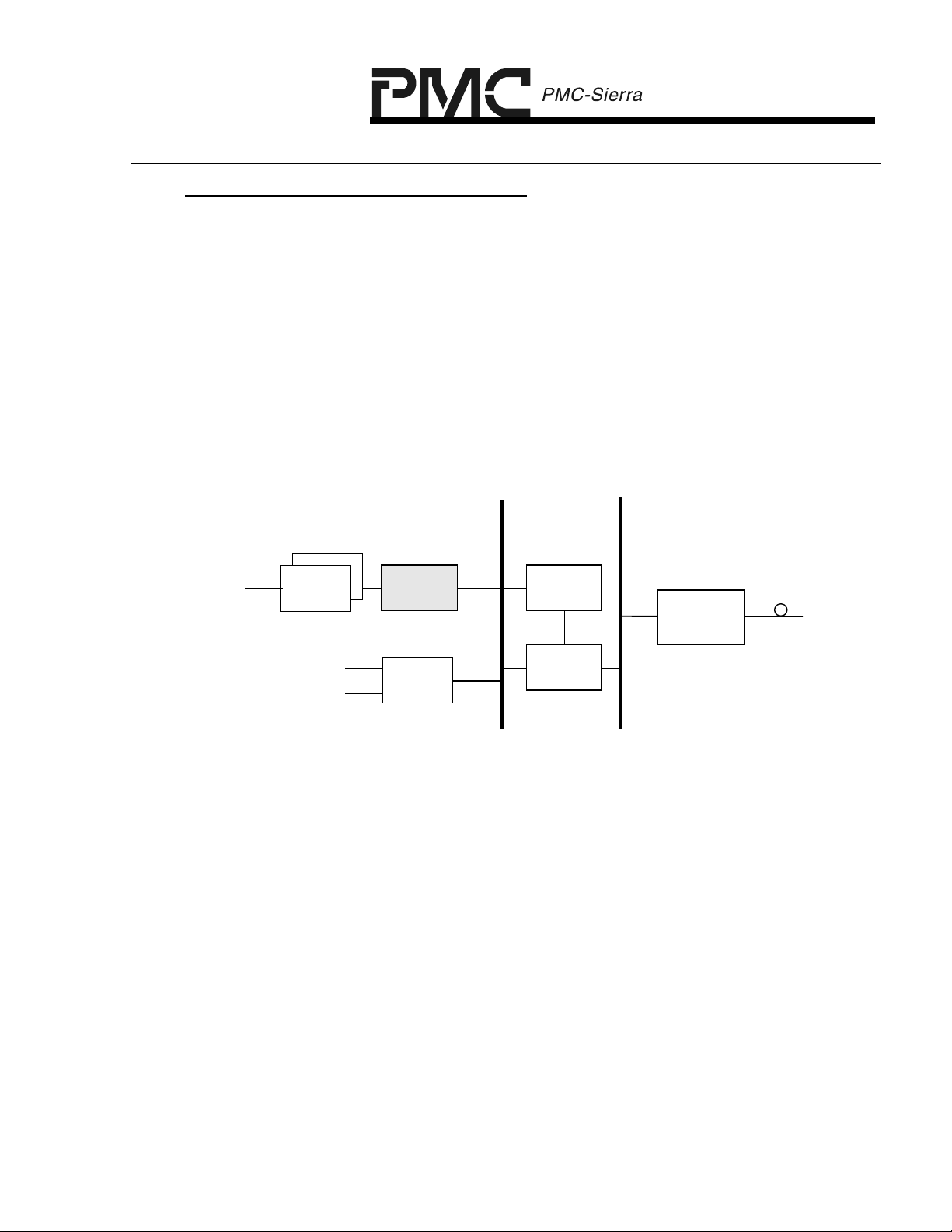
4.1 Integrated Access Device
An Integrated Access Device (IAD) consolidates voice, data, Internet, and
video wide-area network services using ATM over shared T1/E1 lines.
IADs can also unify the functions of many different types of equipment
including CSUs, DSUs and multiplexers. Figure 1 shows the AAL1gator-8
connected to PM4354 COMET-QUADs, a PM7329 S/UNI-APEX-1K800
Traffic Manager, a PM7328 S/UNI-ATLAS-1K800 ATM Layer device and
the PM7347 S/UNI-JET.
T1/E1 x 8
PM4354
COMET-
PM4354
QUAD
COMET-
QUAD
Ethernet
Video
PM73123
AAL1gator-8
ATM
Interworking
Function,
AAL5 SAR
Any-PHY
PM7329
S/UNI-APEX-
PM7328
S/UNI-ATLAS-
1K800
1K800
UTOPIA L2
PM7347
S/UNI-JET
DS3 LIU
Figure 1. AAL1gator-8 in an Integrated Access Device (IAD)
Application.
PROPRIETARY AND CONFIDENTIAL TO PMC-SIERRA, INC., AND FOR ITS CUSTOMERS’ INTERNAL USE 29
UTOPIA L2/
RELEASED
DATASHEET
PMC-2000097 ISSUE 2 8 LINK CES/DBCES AAL1 SAR
PM73123 AAL1GATOR-8
4.2 ATM Passive Optical Networks (APON)
The general architecture of a Passive Optical Network (PON) access
network consists of two key elements: the Optical Line Termination (OLT)
and the Optical Network Unit (ONU). The OLT is connected to the ONU
through a point-to-multipoint Passive Optical Network that consists of
fiber, splitters and other passive components. Typically, up to 32 ONUs
are connected to a single OLT, depending on the splitting factor. OLTs are
typically located in local exchanges and ONUs on street locations, in
buildings or even in homes. Figure 2 shows the use of the AAL1gator-8 in
an ONU application supporting CES functions.
Any-PHY
UTOPIA L2
T1/E1 x 8
PM4354
COMET-
PM4354
QUAD
COMET-
QUAD
PM73123
AAL1gator-8
PM7329
S/UNI-APEX-
1K800
Optical
Module
Ethernet
Video
ATM
Interworking
Function,
AAL5 SAR
PM7328
S/UNI-ATLAS-
1K800
Figure 2. AAL1gator-8 in an APON ONU Application.
PROPRIETARY AND CONFIDENTIAL TO PMC-SIERRA, INC., AND FOR ITS CUSTOMERS’ INTERNAL USE 30

RELEASED
DATASHEET
PMC-2000097 ISSUE 2 8 LINK CES/DBCES AAL1 SAR
PM73123 AAL1GATOR-8
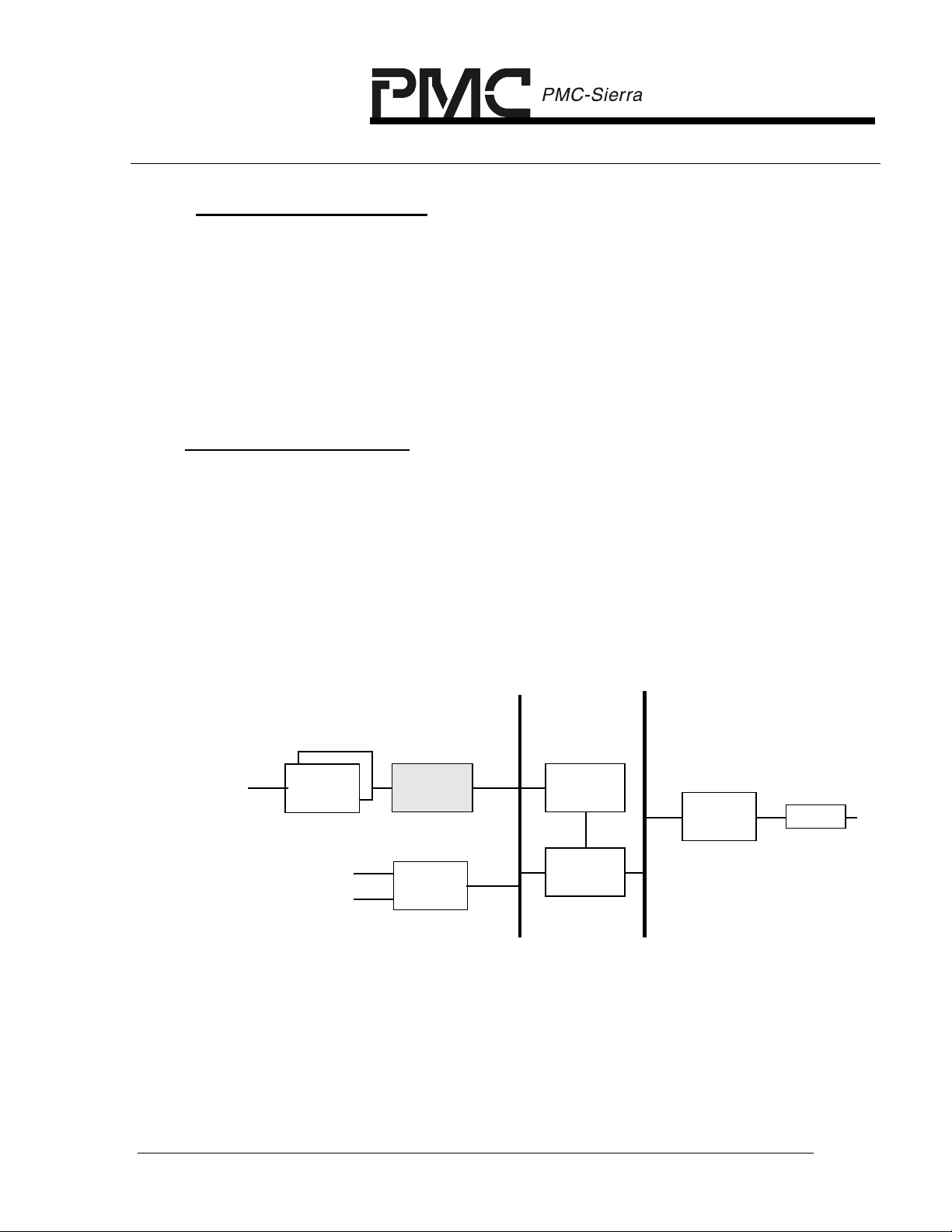
5 BLOCK DIAGRAM
The AAL1gator-8 contains an AAL1 SAR Processor (A1SP) which
performs the segmentation and re-assembly of the AAL1 cells. The A1SP
block interfaces to a common UTOPIA interface on one side and a line
Interface block on the other side, which can be configured to support
several different line protocols. The A1SP block connects to the RAM
interface. The processor interface block, which also contains the external
clock control interface, is shared by all blocks. The AAL1gator-8 supports
8 serial lines.
Figure 3 - AAL1gator-8 Internal Block Diagram
RSTB
SCAN_ENB
SCAN_MODEB
TATM_DATA[15:0]
TATM_PAR
TATM_ENB
TATM_SOC
TATM_CLAV
TATM_CLK
RPHY_ADD[4:0]
RATM_DATA[15:0]
RATM_PAR
RATM_ENB
RATM_SOC
RATM_CLAV
RATM_CLK
TPHY_ADD[4:0]
SYSCLK
NCLK
TL_CLK_OE
TL_CLK[7:0]
RL_CLK[7:0]
Clock
MUX
UTOPIA
Interface
JTAG
TDI
TDO
TRST
CRL_CLK
CTL_CLK
Line Interface
8
H-MVIP
8
A1SP
RAM
Interface
TCK
TMS
RAM_CSB
RAM_A[16:0]
RAM_D[15:0]
RAM_ADSCB
RAM_PAR[1:0]
RAM_WEB[1:0]
8
8
Direct
Processor
Interface
ALE
RDB
WRB
A[19:0]
RAM_OEB
D[15:0]
CSB
ACKB
External Clock
INTB
Interface
ADAP_STB
CGC_LINE[3:0]
CGC_DOUT[3:0]
SRTS_STB
CGC_VALID
CGC_SER_D
F0B
2
TL_DATA[7:0]
TL_SYNC[7:0]
8
TL_SIG[7:0]
RL_DATA[7:0]
RL_SYNC[7:0]
RL_SIG[7:0]
LINE_MODE
PROPRIETARY AND CONFIDENTIAL TO PMC-SIERRA, INC., AND FOR ITS CUSTOMERS’ INTERNAL USE 31

RELEASED
DATASHEET
PMC-2000097 ISSUE 2 8 LINK CES/DBCES AAL1 SAR
PM73123 AAL1GATOR-8
6 DESCRIPTION
The AAL1gator-8 AAL1 Segmentation And Reassembly (SAR) Processor
is a monolithic single chip device that provides DS1, E1, E3, or DS3 line
interface access to an ATM Adaptation Layer One (AAL1) Constant Bit
Rate (CBR) ATM network. It arbitrates access to an external SRAM for
storage of the configuration, the user data, and the statistics. The device
provides a microprocessor interface for configuration, management, and
statistics gathering. PMC-Sierra also provides a software device driver for
the AAL1gator-8 device.
PROPRIETARY AND CONFIDENTIAL TO PMC-SIERRA, INC., AND FOR ITS CUSTOMERS’ INTERNAL USE 32
TL_SYNC
TL_SYNC
TL_DATA
RL_DATA
RL_DATA
TL_DATA
TL_DATA
TL_SYNC
TATM_CL
TL_SYNC
RL_DATA
TL_DATA
TATM_CL
TL_SYNC
RL_DATA
TL_DATA
TL_SYNC
RL_DATA
TL_DATA
RL_DATA
RL_DATA
TL_SYNC
TL_DATA
TL_DATA
TL_SYNC
RL_DATA
RELEASED
DATASHEET
PMC-2000097 ISSUE 2 8 LINK CES/DBCES AAL1 SAR
PM73123 AAL1GATOR-8
7 PIN DIAGRAM
The AAL1gator-8 is manufactured in a 324 pin, fine pitch, plastic ball grid array
(PBGA) package. (23mm x 23 mm)
Bottom View of AAL1gator-8
22 21 20 19
RL_CLK
PQH
A
B
C
D
E
F
G
H
J
K
L
M
N
P
R
T
U
V
W
Y
AA
AB
[6]
RL_SIG
[6]
PQL
[6]
[5]
RL_CLK
[5]
TL_CLK
[4]
RL_CLK
[4]
TL_CLK
[3]
RL_CLK
[3]
RL_SIG
[3]
[2]
RL_SIG
[2]
TL_CLK
[1]
RL_SIG
[1]
RL_SYN
C [1]
PCL PPL
RESERV
ED_IN
TL_SIG
[0]
RL_CLK
[0]
[0]
RL_SYN
TL_CLK
TL_SIG
RL_CLK
RL_SIG
RL_SIG
TL_CLK
RL_CLK
RL_CLK
TL_CLK
RL_SIG
22 21 20 19
TL_CLK
[7]
[7]
RL_SIG
C [7]
[7]
RL_SYN
[6]
C [6]
[7]
[6]
[6]
[6]
PPH
[5]
TL_SIG
[5]
[5]
[4]
[5]
[4]
[4]
[3]
[4]
PCL
[3]
RL_SYN
PCH
C [3]
TL_SIG
[2]
[2]
RL_SYN
[2]
C [2]
TL_SIG
PPH
[1]
[1]
[1]
PCH
[0]
[0]
RL_SYN
PPL
RSTB
PQL
CGC_LIN
C [0]
PPH TRSTB PQH PPL
[0]
SRTS_STBHADAP_STBHCGC_LIN
RESERV
CGC_LIN
ED_OUT
18 17 16
RAM_D
PPH
[7]
[7]
PPL
PCL CRL_CLK
TL_CLK
[5]
RL_SYN
C [5]
PPL PPL
TL_SIG
[4]
RL_SYN
C [4]
TL_SIG
[3]
PPH GND GND GND GND GND GND nc
PPL GND GND GND GND GND GND PPL
[3]
[2]
[2]
[1]
[1]
[0]
E [1]
E [3]
[15]
LINE_MODERAM_D
[9]
TL_SIG
PPL CTL_CL K
[7]
RAM_D
[12]
CGC_VA
PCH PPH INTB CSB A [0] A [3] D [0 ] D [3] A [7] PPH D [7] A [10] D [9] PQH
LID
CGC_SE
E [2]
R_D
CGC_LIN
PPH
E [0]
18 17 16 15 14 13 12 11 10 9 8 7 6 5 4 3 2 1
15 14 13 12 11 10 9 8 7 6 5 4 3 2 1
RAM_OEBRAM_D
RAM_D
[14]
PQH PPL
TL_CLK_OECGC_DO
NCLK
CGC_DO
UT [3]
SCAN_ENBRAM_D
[10]
RAM_D
RAM_D
[11]
RAM_D
[13]
UT [1]
CGC_DO
UT [0]
PPL
RAM_D
[8]
RAM_D
PCH
RAM_D
RAM_D
[7]
GND GND GND GND GND GND
GND GND GND GND GND GND
GND GND GND GND GND GND
GND GND GND GND GND GND
PCL RDB A [1] PPL A [6] D [6] A [9] D [8] A [13] PPH D [15] A [12] A [18]
ACKB WRB A [2] PCH A [5] D [5] A [8] PCL D [10] A [14] D [13] PPL PPL A [1 7 ]
CGC_DO
ALE PPL D [1] A [4] D [4] PPL D [2] A [11] D [11] A [15] D [12] D [14] A [16]
UT [2]
RAM_WE
RAM_PA
RAM_AD
PPL
[4]
[5]
[6]
[3]
RAM_D
[1]
RAM_D
[2]
RAM_D
[0]
B [1]
RAM_AD
DR [8]
PCL
PPH
R [0]
RAM_WE
B [0]
RAM_AD
DR [16]
RAM_PA
R [1]
DR [14]
RAM_AD
DR [13]
RAM_AD
DR [12]
RAM_AD
DR [15]
RAM_AD
DR [10]
RAM_CSBRAM_AD
RAM_AD
DR [9]
PPL
PCH
DR [7]
RAM_AD
DR [5]
RAM_AD
DR [11]
RAM_AD
DR [6]
RAM_AD
DR [4]
RAM_AD
DR [2]
RAM_AD
SCB
RAM_AD
RAM_AD
DR [3]
DR [1]
TDO PPL TCLK
RAM_AD
TDI PPL
DR [0]
PQL PPH
PCH
K
TATM_D
ATA [7]
AV
TATM_D
ATA [0]
RATM_D
ATA [3]
RATM_D
ATA [7]
PPH
TPHY_A
DD [1]
PCH
RATM_D
ATA [10]
TMS SYSCLK
TATM_D
ATA [14]
TATM_D
RPHY_A
ATA [15]
TATM_PARTATM_D
TATM_D
ATA [12]
TATM_D
ATA [9]
RPHY_A
DD [2]
TATM_ENBTATM_SOCRPHY_A
TATM_D
ATA [6]
PQL
TATM_D
ATA [3]
RATM_D
ATA [2]
RATM_D
ATA [6]
TPHY_A
DD [0]
RATM_PARTPHY_A
RATM_D
ATA [9]
RATM_D
ATA [12]
RATM_D
ATA [15]
SCAN_M
ODEB
DD_RSX
TATM_D
ATA [13]
ATA [11]
TATM_D
PPH
ATA [10]
TATM_D
PCL
ATA [8]
RPHY_A
RPHY_A
DD [3]
DD [1]
DD [0]
TATM_D
TATM_D
ATA [5]
ATA [4]
TATM_D
TATM_D
ATA [2]
ATA [1]
RATM_D
PPH
ATA [0]
RATM_ENBRATM_D
ATA [1]
RATM_D
RATM_D
ATA [5]
ATA [4]
RATM_C
RATM_S
LAV
OC
RATM_C
DD [2]
LK
TPHY_A
PCL
DD [3]
RATM_D
RATM_D
ATA [11]
ATA [8]
TPHY_A
PPH
DD [4]
RATM_D
A [19]
ATA [13]
RATM_D
ATA [14]
A
B
C
D
E
F
G
H
J
K
L
M
N
P
R
T
U
V
W
Y
AA
AB
PROPRIETARY AND CONFIDENTIAL TO PMC-SIERRA, INC., AND FOR ITS CUSTOMERS’ INTERNAL USE 33

RELEASED
DATASHEET
PMC-2000097 ISSUE 2 8 LINK CES/DBCES AAL1 SAR
PM73123 AAL1GATOR-8
PROPRIETARY AND CONFIDENTIAL TO PMC-SIERRA, INC., AND FOR ITS CUSTOMERS’ INTERNAL USE 34

RELEASED
DATASHEET
PMC-2000097 ISSUE 2 8 LINK CES/DBCES AAL1 SAR
PM73123 AAL1GATOR-8
8 PIN DESCRIPTION
UTOPIA Interface Signals (52)
Pin Name Type Pin No. Function
Note signals have different meanings depending on whether the UTOPIA bus is in ATM
master mode, PHY mode or Any-PHY mode. The mode is controlled by the
UTOP_MODE and ANY-PHY_EN fields in the UI_SRC_CFG and UI_SNK_CFG
registers.
All outputs are tri-state when the chip is in reset or when UI_EN is disabled in the
UI_COMN_CFG register.
All outputs have a maximum output current (IMAX) = 8 mA.
TATM_CLK/RPHY_CLK Input F4
ATM: Transmit UTOPIA ATM Layer
Clock is the synchronization clock
input for the TATM interface.
TATM_SOC/RPHY_SOC
/RSOP
Output H2
PHY: Receive UTOPIA/Any-PHY
PHY Layer Clock is the
synchronization clock input for the
RPHY interface
Maximum frequency is 52 MHz.
ATM: Transmit UTOPIA ATM Layer
Start-Of-Cell is an active high signal
asserted by the AAL1gator-8 when
TATM_D contains the first valid byte
of the cell.
PHY: Receive Any-PHY/UTOPIA
PHY Layer Start-Of-Cell is an active
high signal asserted by the
AAL1gator-8 when RPHY_D[15:0]
contains the first valid word of the
cell. AAL1gator-8 drives this signal
only when the ATM layer has
selected it for a cell transfer.
Any-PHY: This pin is the Receive
Start of Packet (RSOP) signal which
functions just like RPHY_SOC.
PROPRIETARY AND CONFIDENTIAL TO PMC-SIERRA, INC., AND FOR ITS CUSTOMERS’ INTERNAL USE 35

RELEASED
DATASHEET
PMC-2000097 ISSUE 2 8 LINK CES/DBCES AAL1 SAR
PM73123 AAL1GATOR-8
Pin Name Type Pin No. Function
TATM_D[15]/RPHY_D[15]
TATM_D[14]/RPHY_D[14]
TATM_D[13]/RPHY_D[13]
TATM_D[12]/RPHY_D[12]
TATM_D[11]/RPHY_D[11]
TATM_D[10]/RPHY_D[10]
TATM_D[9]/RPHY_D[9]
TATM_D[8]/RPHY_D[8]
TATM_D[7]/RPHY_D[7]
TATM_D[6]/RPHY_D[6]
TATM_D[5]/RPHY_D[5]
TATM_D[4]/RPHY_D[4]
TATM_D[3]/RPHY_D[3]
TATM_D[2]/RPHY_D[2]
TATM_D[1]/RPHY_D[1]
TATM_D[0]/RPHY_D[0]
Output C2
B1
D2
E3
D1
E2
F3
F2
H4
J3
J2
J1
L3
K2
K1
K4
ATM: Transmit UTOPIA ATM Layer
Data Bits 7 to 0 form the byte-wide
data driven to the PHY layer. Bit 0 is
the Least Significant Bit (LSB). Bit 7
is the Most Significant Bit (MSB)
and is the first bit received for the
cell from the serial line.
Note that only the lower 8 bit of the
bus are used in ATM master mode.
PHY: Receive UTOPIA/Any-PHY
PHY Layer Data Bits 15 to 0 form
the word-wide data driven to the
ATM layer. This bus is only driven
when the ATM layer has selected
the UI_SRC_INTF for a cell transfer.
The upper byte is only used if
16_BIT_MODE is set in the
UI_SRC_CFG register. Otherwise
the upper byte is driven to 0’s. Bit 0
is the LSB. Bit 7 is the MSB of the
first byte and is the first bit received
for the cell from the serial line.
TATM_PAR/ RPHY_PAR Output D3
ATM: Transmit UTOPIA ATM Layer
Parity is a byte parity bit covering
TATM_D(7:0).
PHY: Receive UTOPIA/Any-PHY
PHY Layer Parity is either a byte
parity covering RPHY_D(7:0) or
word parity covering RPHY_D(15:0)
depending on the value of
16_BIT_MODE.
PROPRIETARY AND CONFIDENTIAL TO PMC-SIERRA, INC., AND FOR ITS CUSTOMERS’ INTERNAL USE 36

RELEASED
DATASHEET
PMC-2000097 ISSUE 2 8 LINK CES/DBCES AAL1 SAR
PM73123 AAL1GATOR-8
Pin Name Type Pin No. Function
TATM_ENB/RPHY_ENB
/RENB
Bidi H3
ATM: Transmit UTOPIA ATM Layer
Enable is an active low signal
asserted by the AAL1gator-8 during
cycles when TATM_D contains valid
data. It is not asserted until the
AAL1gator-8 is ready to send a full
cell.
PHY: Receive UTOPIA/Any-PHY
PHY Layer Enable is an active low
signal asserted by the ATM layer to
indicate RPHY_D and RPHY_SOC
will be sampled at the end of the
next cycle. If UTOP_MODE in
UI_SRC_CFG is set to UTOPIA
Level 2 Mode then the AAL1gator-8
will drive data only if RPHY_ADD
matches CFG_ADDR in the
UI_SRC_ADD_CFG register the
cycle before RPHY_ENB goes low.
Any-PHY: This pin is the RENB
input signal, which functions the
same as RPHY_ENB. The only
difference is that data is driven two
cycles after selection instead of just
one cycle.
PROPRIETARY AND CONFIDENTIAL TO PMC-SIERRA, INC., AND FOR ITS CUSTOMERS’ INTERNAL USE 37

RELEASED
DATASHEET
PMC-2000097 ISSUE 2 8 LINK CES/DBCES AAL1 SAR
PM73123 AAL1GATOR-8
Pin Name Type Pin No. Function
TATM_CLAV/RPHY_CLAV
/RPA
Bidi J4
ATM: Transmit UTOPIA ATM Layer
Cell Available is an active high
signal from the PHY layer device to
indicate that there is sufficient room
to accept a cell.
PHY: Receive UTOPIA/Any-PHY
PHY Layer Cell Available is an
active high signal asserted by the
AAL1gator-8 to indicate it is ready to
deliver a complete cell. In Utopia
Level 2 mode, this signal is driven
only when MPHY_ADD matches
CFG_ADDR in the
UI_SRC_ADD_CFG register in the
previous cycle. A pulldown resistor
is recommended.
Any-PHY: This pin is the Receive
Packet Available (RPA) signal which
functions the same as RPHY_CLAV
except for it is activated two cycles
after a matching address instead of
one.
PROPRIETARY AND CONFIDENTIAL TO PMC-SIERRA, INC., AND FOR ITS CUSTOMERS’ INTERNAL USE 38

RELEASED
DATASHEET
PMC-2000097 ISSUE 2 8 LINK CES/DBCES AAL1 SAR
PM73123 AAL1GATOR-8
Pin Name Type Pin No. Function
RPHY_ADD[4]/RSX
RPHY_ADD[3]/RCSB
RPHY_ADD[2]
RPHY_ADD[1]
RPHY_ADD[0]
I/O
Input
Input
Input
Input
C1
G2
G3
G1
H1
ATM: These signals are not used in
ATM mode.
PHY: Receive UTOPIA PHY Layer
Address (Bits 4 to 0) which selects
the UTOPIA receiver. These inputs
are used as an output enable for
RPHY_CLAV and to validate the
activation of RPHY_ENB. There are
internal pull-up resistors. These pins
are compared with CFG_ADDR[5:0]
in the UI_SRC_CFG_ADDR
register.
ANY-PHY: Receive Start
Transfer(RSX) is an active high
output which indicates the start of
an Any-PHY packet which identifies
the location of the prepended
address. ANY-PHY_EN in
UI_SRC_CFG register needs to be
set for this function.
Receive Chip Select Bar (RCSB) is
an active low input which is used to
select the AAL1gator-8 when polling
in Any-PHY mode. This input is
used to decode any Any-PHY
address bits greater than
RPHY_ADD[2]. This input goes low
one cycle after Any-PHY address is
valid.
ANY-PHY_EN and CS_MODE_EN
in UI_SRC_CFG register needs to
be set for this function. Otherwise
this bit functions as RPHY_ADD[3].
RPHY_ADD[2:0] is the bottom three
bits of the Any-PHY address and is
used to select the device when
polling. These pins are compared
with CFG_ADDR[2:0] in the
UI_SRC_CFG_ADDR register.
Note these pins must be tied to
ground when not used.
PROPRIETARY AND CONFIDENTIAL TO PMC-SIERRA, INC., AND FOR ITS CUSTOMERS’ INTERNAL USE 39

RELEASED
DATASHEET
PMC-2000097 ISSUE 2 8 LINK CES/DBCES AAL1 SAR
PM73123 AAL1GATOR-8
Pin Name Type Pin No. Function
RATM_CLK/ TPHY_CLK Input R1
ATM: Receive UTOPIA ATM Layer
Clock is the synchronization clock
input for synchronizing the RATM
interface.
PHY: Transmit UTOPIA/Any-PHY
PHY Layer Clock is the
synchronization clock input for
synchronizing the TPHY interface.
Maximum frequency is 52 MHz.
RA TM_SOC/ TPHY_SOC
/TSOP
Input P1 This signal has two definitions
depending on whether the UTOPIA
is in ATM mode or PHY mode.
ATM: Receive UTOPIA ATM Layer
Start-Of-Cell is an active high signal
asserted by the PHY layer when
RATM_D contains the first valid byte
of a cell.
PHY: Transmit UTOPIA/Any-PHY
PHY Layer Start-Of-Cell is an active
high signal asserted by the ATM
layer when TPHY_D contains the
first valid byte of a cell.
Any-PHY: This pin is the Transmit
Start of Packet (TSOP) signal which
functions just like TPHY_SOC. .
This signal is optional in this mode.
If unused, tie low.
PROPRIETARY AND CONFIDENTIAL TO PMC-SIERRA, INC., AND FOR ITS CUSTOMERS’ INTERNAL USE 40

RELEASED
DATASHEET
PMC-2000097 ISSUE 2 8 LINK CES/DBCES AAL1 SAR
PM73123 AAL1GATOR-8
Pin Name Type Pin No. Function
RATM_D[15]/TPHY_D[15]
RATM_D[14]/TPHY_D[14]
RATM_D[13]/TPHY_D[13]
RATM_D[12]/TPHY_D[12]
RATM_D[11]/TPHY_D[11]
RATM_D[10]/TPHY_D[10]
RATM_D[9]/TPHY_D[9]
RATM_D[8]/TPHY_D[8]
RATM_D[7]/TPHY_D[7]
RATM_D[6]/TPHY_D[6]
RATM_D[5]/TPHY_D[5]
RATM_D[4]/TPHY_D[4]
RATM_D[3]/TPHY_D[3]
RATM_D[2]/TPHY_D[2]
RATM_D[1]/TPHY_D[1]
RATM_D[0]/TPHY_D[0]
Input V3
Y1
W1
U3
U2
V4
T3
U1
P4
N3
N2
N1
N4
M3
M1
L2
ATM: Receive UTOPIA ATM Layer
Data Bits 7 to 0 form the byte-wide
data from the PHY layer device. Bit
0 is the LSB. Bit 7 is the MSB. This
is the first bit of the cell, which will
be transmitted on the serial line.
The upper byte is not used in ATM
mode.
PHY: Transmit UTOPIA/Any-PHY
PHY Layer Data Bits 15 to 0 form
the word-wide data from the ATM
layer device. Bit 0 is the LSB. Bit 7
is the MSB of the first byte. This is
the first bit of the cell, which will be
transmitted on the serial line. The
upper byte is only used if
16_BIT_MODE is set in the
UI_SNK_CFG register.
RATM_P AR/ TPH Y_PAR Input R3
ATM: Receive UTOPIA ATM Layer
Parity is a byte odd parity bit
covering RATM_D(7:0) or word odd
parity covering RATM_D(15:0)
depending on the value of
16_BIT_MODE.
PHY: Transmit UTOPIA/Any-PHY
PHY Layer Parity is either a byte
odd parity covering TPHY_D(7:0) or
word odd parity covering
TPHY_D(15:0) depending on the
value of 16_BIT_MODE.
PROPRIETARY AND CONFIDENTIAL TO PMC-SIERRA, INC., AND FOR ITS CUSTOMERS’ INTERNAL USE 41

RELEASED
DATASHEET
PMC-2000097 ISSUE 2 8 LINK CES/DBCES AAL1 SAR
PM73123 AAL1GATOR-8
Pin Name Type Pin No. Function
RATM_ENB/TPHY_ENB Bidi M2
ATM: Receive UTOPIA ATM Layer
Enable is an active low signal
asserted by the AAL1gator-8 to
indicate RATM_D and RATM_SOC
will be sampled at the end of the
next cycle. It will not be asserted
until the AAL1gator-8 is ready to
receive a full cell.
PHY: Transmit UTOPIA/Any-PHY
PHY Layer Enable is an active low
signal asserted by the ATM layer
device during cycles when
TPHY_D[15:0] contain valid data.
The AAL1gator-8 will accept data
only if TPHY_ADD matches
CFG_ADDR in the UI_SNK_CFG
register the cycle before TPHY_ENB
goes low
Any-PHY: This pin is the TENB
input signal, which functions the
same as TPHY_ENB.
PROPRIETARY AND CONFIDENTIAL TO PMC-SIERRA, INC., AND FOR ITS CUSTOMERS’ INTERNAL USE 42

RELEASED
DATASHEET
PMC-2000097 ISSUE 2 8 LINK CES/DBCES AAL1 SAR
PM73123 AAL1GATOR-8
Pin Name Type Pin No. Function
RATM_CLAV/TPHY_CLAV Bidi P2
ATM: Receive UTOPIA ATM Layer
Cell Available is an active high
signal asserted by the PHY layer to
indicate that there is a cell available
to send.
PHY: Receive UTOPIA/Any-PHY
PHY Layer Cell Available is an
active high signal asserted by the
AAL1gator-8 to indicate there is a
cell-space available. The
AAL1gator-8 drives this signal only
when TPHY_ADD matches
CFG_ADDR in the UI_SNK_CFG
register in the previous cycle. A
pulldown resistor is recommended.
Any-PHY: This pin is the Transmit
Packet Available (TPA) signal which
functions the same as TPHY_CLAV
except for it is activated two cycles
after a matching address instead of
one.
PROPRIETARY AND CONFIDENTIAL TO PMC-SIERRA, INC., AND FOR ITS CUSTOMERS’ INTERNAL USE 43

RELEASED
DATASHEET
PMC-2000097 ISSUE 2 8 LINK CES/DBCES AAL1 SAR
PM73123 AAL1GATOR-8
Pin Name Type Pin No. Function
TPHY_ADD[4]/TSX
TPHY_ADD[3]/TCSB
TPHY_ADD[2]
TPHY_ADD[1]
TPHY_ADD[0]
Input V1
T1
R2
T4
P3
ATM: These signals are not used in
ATM mode.
PHY: Transmit UTOPIA PHY Layer
Address (Bits 4 to 0) which selects
the UTOPIA transmitter. These
inputs are used as an output enable
for TPHY_CLAV and to validate the
activation of TPHY_ENB. There are
internal pull-up resistors. These
pins are compared with
CFG_ADDR[5:0] in the
UI_SNK_CFG_ADDR register.
ANY-PHY: Transmit Start
Transfer(TSX) is an active high input
which indicates the start of an AnyPHY packet which identifies the
location of the prepended address.
ANY-PHY_EN in UI_SNK_CFG
register needs to be set for this
function.
Transmit Chip Select Bar (TCSB) is
an active low input which is used to
select the AAL1gator-8 when polling
in Any-PHY mode. This input is
used to decode any Any-PHY
address bits greater than
TPHY_ADD[2]. This input goes low
one cycle after Any-PHY address is
valid.
ANY-PHY_EN and CS_MODE_EN
in UI_SNK_CFG register needs to
be set for this function. Otherwise
this bit functions as TPHY_ADD[3].
TPHY_ADD[2:0] is the bottom three
bits of the Any-PHY address and is
used to select the device when
polling. These pins are compared
with CFG_ADDR[2:0] in the
UI_SNK_CFG_ADDR register.
Note these pins must be tied to
ground when not used.
PROPRIETARY AND CONFIDENTIAL TO PMC-SIERRA, INC., AND FOR ITS CUSTOMERS’ INTERNAL USE 44

RELEASED
DATASHEET
PMC-2000097 ISSUE 2 8 LINK CES/DBCES AAL1 SAR
PM73123 AAL1GATOR-8
Microprocessor Interface Signals (43)
Pin Name Type Pin No. Function
D[15]
D[14]
D[13]
D[12]
D[11]
D[10]
D[9]
D[8]
D[7]
D[6]
D[5]
D[4]
D[3]
D[2]
D[1]
D[0]
I/O Y4
AB2
AA4
AB3
AB5
AA6
W5
Y7
W7
Y9
AA9
AB9
W10
AB7
AB11
W11
The bi-directional data signals (D[15:0])
provide a data bus to allow the AAL1gator-8
device to interface to an external microprocessor. Both read and write transactions
are supported. The microprocessor
interface is used to configure and monitor
the AAL1gator-8 device.
Maximum output current (IMAX) = 6 mA.
A[19]
A[18]
A[17]
A[16]
A[15]
A[14]
A[13]
A[12]
A[11]
A[10]
A[9]
A[8]
A[7]
A[6]
A[5]
A[4]
A[3]
A[2]
A[1]
A[0]
Input W2
Y2
AA1
AB1
AB4
AA5
Y6
Y3
AB6
W6
Y8
AA8
W9
Y10
AA10
AB10
W12
AA12
Y12
W13
The address signals (A[19:0]) provide an
address bus to allow the AAL1gator-8 device
to interface to an external micro-processor.
PROPRIETARY AND CONFIDENTIAL TO PMC-SIERRA, INC., AND FOR ITS CUSTOMERS’ INTERNAL USE 45

RELEASED
DATASHEET
PMC-2000097 ISSUE 2 8 LINK CES/DBCES AAL1 SAR
PM73123 AAL1GATOR-8
Pin Name Type Pin No. Function
ALE Input AB13 The address latch enable signal (ALE)
latches the A[19:0] signals during the
address phase of a bus transaction. When
ALE is set high, the address latches are
transparent. When ALE is set low, the
address latches hold the address provided
on A[19:0].
ALE has an internal pull-up resistor.
WRB Input AA13 The write strobe signal (WRB) qualifies write
accesses to the AAL1gator-8 device. When
CSB is set low, the D[15:0] bus contents are
clocked into the addressed register on the
rising edge of WRB.
Note that if CSB, WRB and RDB are all low,
all chip outputs are tristated. Therefore
WRB and RDB should never be active at the
same time during functional operation.
RDB Input Y13 The read strobe signal (RDB) qualifies read
accesses to the AAL1gator-8 device. When
CSB is set low, the AAL1gator-8 device
drives the D[15:0] bus with the contents of
the addressed register on the falling edge of
RDB.
Note that if CSB, WRB and RDB are all low,
all chip outputs are tristated. Therefore
WRB and RDB should never be active at the
same time during functional operation.
PROPRIETARY AND CONFIDENTIAL TO PMC-SIERRA, INC., AND FOR ITS CUSTOMERS’ INTERNAL USE 46

RELEASED
DATASHEET
PMC-2000097 ISSUE 2 8 LINK CES/DBCES AAL1 SAR
PM73123 AAL1GATOR-8
Pin Name Type Pin No. Function
CSB Input W14 The chip select signal (CSB) qualifies
read/write accesses to the AAL1gator-8
device. The CSB signal must be set low
during read and write accesses. When CSB
is set high, the microprocessor interface
signals are ignored by the AAL1gator-8
device.
If CSB is not required (register accesses
controlled only by WRB and RDB) then CSB
should be connected to an inverted version
of the RSTB signal.
Note that if CSB, WRB and RDB are all low,
all chip outputs are tristated.
ACKB Open-
Drain
Output
AA14 The ACKB is an active low signal which
indicates when processor read data is valid
or when a processor write operation has
completed. When inactive this signal is
tristated.
INTB Open-
W15 The interrupt signal (INTB) is an active low
Drain
Output
ACKB is an open drain output and should be
pulled high externally with a fast resistor.
Maximum output current (IMAX) = 6 mA
signal indicating that an enabled bit in the
MSTR_INTR_REG register was set. When
INTB is set low, the interrupt is active and
enabled. When INTB is tristate, there is no
interrupt pending or it is disabled.
INTB is an open drain output and should be
pulled high externally with a fast resistor.
Maximum output current (IMAX) = 6 mA
PROPRIETARY AND CONFIDENTIAL TO PMC-SIERRA, INC., AND FOR ITS CUSTOMERS’ INTERNAL USE 47

RELEASED
DATASHEET
PMC-2000097 ISSUE 2 8 LINK CES/DBCES AAL1 SAR
PM73123 AAL1GATOR-8
Ram 1 Interface Signals(41)
Pin Name Type Pin No. Function
RAM_D[15]
RAM_D[14]
RAM_D[13]
RAM_D[12]
RAM_D[11]
RAM_D[10]
RAM_D[9]
RAM_D[8]
RAM_D[7]
RAM_D[6]
RAM_D[5]
RAM_D[4]
RAM_D[3]
RAM_D[2]
RAM_D[1]
RAM_D[0]
I/O A17
B16
C15
D17
B15
A15
B17
B14
D14
C13
B13
A13
D13
C12
B12
D12
The bi-directional data signals (RAM_D[15:0])
provide a data bus to allow the AAL1gator-8
device to access an external 128Kx16(18)
RAM.
Maximum output current (IMAX) = 6 mA
RAM_A[16]
RAM_A[15]
RAM_A[14]
RAM_A[13]
RAM_A[12]
RAM_A[11]
RAM_A[10]
RAM_A[9]
RAM_A[8]
RAM_A[7]
RAM_A[6]
RAM_A[5]
RAM_A[4]
RAM_A[3]
RAM_A[2]
RAM_A[1]
RAM_A[0]
Output C10
D9
A9
B9
C9
D7
A8
C8
B11
B7
A6
C7
B6
A5
C6
A4
C5
The address signals (RAM_A[16:0]) provide
an address bus to allow the AAL1gator-8
device to address an external 128Kx16(18)
RAM.
Maximum output current (IMAX) = 6 mA.
RAM_OEB Output A16 RAM Output Enable is an active low signal
that enables the SRAM to drive data.
Maximum output current (IMAX) = 6 mA.
RAM_WEB[1] Output A11 RAM Write Enable One is an active low signal
for the high-byte write. Maximum output
current (IMAX) = 6 mA.
PROPRIETARY AND CONFIDENTIAL TO PMC-SIERRA, INC., AND FOR ITS CUSTOMERS’ INTERNAL USE 48

RELEASED
DATASHEET
PMC-2000097 ISSUE 2 8 LINK CES/DBCES AAL1 SAR
PM73123 AAL1GATOR-8
Pin Name Type Pin No. Function
RAM_WEB[0] Output B10 RAM Write Enable Zero is an active low signal
for the low-byte write. Maximum output current
(IMAX) = 6 mA.
RAM_CSB Output B8 RAM Chip Select is an active low chip-select
signal for external memory. Maximum output
current (IMAX) = 6 mA.
RAM_ADSCB/
RAM_R/WB
Output D6 This signal has different meanings depending
upon the type of SSRAM that the AAL1gator-8
is programmed to interface to.
Pipelined Single-Cycle Deselect SSRAM:
RAM Address Status Control is an active low
output for external memory and is used to
cause a new external address to be loaded
into the RAM.
RAM_PAR[1]
RAM_PAR[0]
I/O D10
A10
Pipelined ZBT SSRAM: RAM R/W indicates
the direction of the transfer.
Maximum output current (IMAX) = 6 mA.
RAM Parity is a two bit bi-directional signal
that indicates odd parity for the upper and
lower byte of RAM_D[15:0].
Maximum output current (IMAX) = 6 mA
PROPRIETARY AND CONFIDENTIAL TO PMC-SIERRA, INC., AND FOR ITS CUSTOMERS’ INTERNAL USE 49

RELEASED
DATASHEET
PMC-2000097 ISSUE 2 8 LINK CES/DBCES AAL1 SAR
PM73123 AAL1GATOR-8
NOTE: For different modes of the line interface the I/O is redefined.
For Direct mode there are 8 separate bi-directional lines which can
support lines up to 15 Mbps each with an aggregate bandwidth of 20
Mbps..Or line 0 can be put into highspeed mode and support data rates
up to 52 Mbps. For H-MVIP mode there are two 8 Mbps lines which are
compatible with the H-MVIP specification.
Table 1 defines which signal tables need to be used for each possible
mode. Select the mode of the line interface that will be used and refer to
the tables listed. Table 2 on page 56 shows how pins are shared between
the different modes.
Table 1 - Line Interface Signal Table Selection
Line Mode Line Interface Table
Direct Direct
H-MVIP H-MVIP
Line Interface Signals(Direct)(68)
Pin Name Type Pin No. Function
LINE_MODE Input B18 Determines the mode of operation for
the line interface:
0)Direct Mode
1)H-MVIP Mode
PROPRIETARY AND CONFIDENTIAL TO PMC-SIERRA, INC., AND FOR ITS CUSTOMERS’ INTERNAL USE 50

RELEASED
DATASHEET
PMC-2000097 ISSUE 2 8 LINK CES/DBCES AAL1 SAR
TL_SYNC[7]
TL_SYNC[6]
TL_SYNC[5]
TL_SYNC[4]
TL_SYNC[3]
TL_SYNC[2]
TL_SYNC[1]
TL_SYNC[0]
I/O A19
B22
F21
H21
K21
N22
T19
V19
Transmit Line Synchronization 7 to 0
are the transmit frame synchronization
indicators used in SDF-MF and SDFFR modes. Depending on the value of
MF_SYNC_MODE in the
LI_CFG_REG register for the line,
these signals either indicate a frame
boundary or a multi-frame boundary.
PM73123 AAL1GATOR-8
Depending on the value of
GEN_SYNC in the LIN_STR_MODE
register for that line, the sync signal is
either received from the corresponding
framer device 0 to 7 or it is generated
internally The Default mode of this
signal is to be a frame sync input.
When the MVIP_EN bit is set in
LS_Ln_CFG_REG then TL_SYNC[0]
is the F0B pin; the common frame
sync.
TL_DATA[7]
TL_DATA[6]
TL_DATA[5]
TL_DATA[4]
TL_DATA[3]
TL_DATA[2]
TL_DATA[1]
TL_DATA[0]
TL_SIG[7]
TL_SIG[6]
TL_SIG[5]
TL_SIG[4]
TL_SIG[3]
TL_SIG[2]
TL_SIG[1]
TL_SIG[0]
Output B19
E20
F22
J20
L20
P19
U19
V20
Output C18
D21
G20
H19
K19
N20
R20
Y22
Maximum output current (IMAX) = 6
mA.
Transmit Line Serial Data 7 to 0 carry
the received data to the corresponding
framer devices.
Maximum output current (IMAX) = 6
mA.
Transmit Line Signal 7 to 0 are the
CAS signaling outputs to the
corresponding framer devices in SDFMF mode. This is the default function
for this pin.
Maximum output current (IMAX) = 6
mA.
PROPRIETARY AND CONFIDENTIAL TO PMC-SIERRA, INC., AND FOR ITS CUSTOMERS’ INTERNAL USE 51
RELEASED
DATASHEET
PMC-2000097 ISSUE 2 8 LINK CES/DBCES AAL1 SAR
TL_CLK[7]/TSM[7]
TL_CLK[6]/TSM[6]
TL_CLK[5]/TSM[5]
TL_CLK[4]/TSM[4]
TL_CLK[3]/TSM[3]
TL_CLK[2]/TSM[2]
TL_CLK[1]/TSM[1]
TL_CLK[0]/TSM[0]
I/O A20
C21
E19
H22
K22
N21
R22
U21
Transmit Line Channel Clock 7 to 0 are
the clock lines for the sixteen lines.
They clock the data from the
AAL1gator-8 to the corresponding
framer devices.
Depending on the value of the
TL_CLK_OE pin and the
CLK_SOURCE_TX field in the
PM73123 AAL1GATOR-8
LIN_STR_MODE memory register,
these pins are either outputs or inputs.
If TLCLK_OUTPUT_EN is high, these
pins are outputs and the clock is
sourced internally at power up. This
can later be changed by the
CLK_SOURCE_TX field.
Note that if CLK_SOURCE_TX /=
“000” then this pin is an output, even if
it is not driving a clock. A clock will
only be driven if in E1 or T1 mode and
either the internal clock synthesizer is
being used or the clock is being
looped. CLK_SOURCE_TX = “001”,
“010, “011”, “100”, or “101”)
Note that if UDF_HS=1 in the
HS_LIN_REG, TL_CLK[7:1] should be
tied high.
Transmit Signaling Mirror is a copy of
the TL_SIG output. In Direct mode, if
CLK_SOURCE_TX=”111” then
signaling is output on this pin. This
option is used with devices that share
the same pin for clock and signaling.
In this mode CTL_CLK is used as the
line clock.
Maximum output current (IMAX) = 6
mA.
PROPRIETARY AND CONFIDENTIAL TO PMC-SIERRA, INC., AND FOR ITS CUSTOMERS’ INTERNAL USE 52

Input
RELEASED
DATASHEET
PMC-2000097 ISSUE 2 8 LINK CES/DBCES AAL1 SAR
PM73123 AAL1GATOR-8
CTL_CLK Input C16 Common Transmit Line Clock is a
transmit line clock which can be
shared across all lines. Whether this
clock is used or not for a given line is
dependent on the value of
CLK_SOURCE_TX in the
LINE_STR_MODE memory register for
that line.
RL_SYNC[7]
RL_SYNC[6]
RL_SYNC[5]
RL_SYNC[4]
RL_SYNC[3]
RL_SYNC[2]
RL_SYNC[1]
RL_SYNC[0]
B21
C20
F19
J19
M20
P20
U22
W20
Receive Line Synchronization 7 to 0
are the receive frame synchronization
indicators used in SDF-MF and SDFFR modes. Depending on the value of
MF_SYNC_MODE in the
LI_CFG_REG register for the line,
these signals either indicate a frame
boundary or a multi-frame boundary.
RL_DATA[7]
RL_DATA[6]
RL_DATA[5]
RL_DATA[4]
RL_DATA[3]
RL_DATA[2]
RL_DATA[1]
RL_DATA[0]
RL_SIG[7]
RL_SIG[6]
RL_SIG[5]
RL_SIG[4]
RL_SIG[3]
RL_SIG[2]
RL_SIG[1]
RL_SIG[0]
RL_CLK[7]
RL_CLK[6]
RL_CLK[5]
RL_CLK[4]
RL_CLK[3]
RL_CLK[2]
RL_CLK[1]
RL_CLK[0]
Input D20
E22
H20
K20
N19
R19
T20
AB22
Input B20
C22
G21
J21
M22
P22
T22
Y21
Input A21
E21
G22
J22
L22
P21
T21
AA22
Tie to ground if unused.
Receive Line Serial Data 7 to 0 carries
the receive data from the
corresponding framer devices.
Receive Line Signaling 7 to 0 carries
the CAS data from the corresponding
framer devices.
Receive Line Clock 7 to 0 is the clock
received from the corresponding
framer device used to clock in
RL_DATA, RL_SIG, and RL_SYNC.
PROPRIETARY AND CONFIDENTIAL TO PMC-SIERRA, INC., AND FOR ITS CUSTOMERS’ INTERNAL USE 53

RELEASED
DATASHEET
PMC-2000097 ISSUE 2 8 LINK CES/DBCES AAL1 SAR
PM73123 AAL1GATOR-8
CRL_CLK Input D18 Common Receive Line Clock is a
receive line clock which can be shared
across all lines. Whether this clock is
used or not for a given line is
dependent on the value of
CLK_SOURCE_RX in the
LIN_STR_MODE memory register for
that line.
When the MVIP_EN bit is set in
LS_Ln_CFG_REG then this is the C4B
input; the common 4.096 MHz clock.
Line Interface Signals(H-MVIP)(13)
Pin Name Type Pin No. Function
LINE_MODE Input B18 Determines the mode of operation for the
line interface:
0)Direct Mode
1)H-MVIP Mode
F0B Input V19 Frame Sync 0 is the active low frame
synchronization input signal used to
indicate the start of a frame.
TL_DATA[1]
TL_DATA[0]
Output U19
V20
Transmit Line Serial Data 1 to 0 carry the
received data to the corresponding framer
devices. or an H_MVIP backplane.
Maximum output current (IMAX) = 6 mA.
TL_SIG[1]
TL_SIG[0]
Output R20
Y22
Transmit Line Signal 1 to 0 are the CAS
signaling outputs to the corresponding
framer devices in SDF-MF mode. H-MVIP
does not support signaling directly, but
these signals can be used to transport
signaling if needed.
Maximum output current (IMAX) = 6 mA
C16B Input C16 Clock 16 MHz is the clock used to transfer
data across the H-MVIP bus. The clock
runs twice as fast as the data rate. This
common clock is used in both the receive
and transmit direction.
PROPRIETARY AND CONFIDENTIAL TO PMC-SIERRA, INC., AND FOR ITS CUSTOMERS’ INTERNAL USE 54

RELEASED
DATASHEET
PMC-2000097 ISSUE 2 8 LINK CES/DBCES AAL1 SAR
PM73123 AAL1GATOR-8
Pin Name Type Pin No. Function
RL_DATA[1]
RL_DATA[0]
Input T20
AB22
Receive Line Serial Data 1 to 0 carries the
receive data from the corresponding framer
devices or H-MVIP backplane.
RL_SIG[1]
RL_SIG[0]
Input T22
Y21
Receive Line Signaling 1 to 0 carries the
CAS data from the corresponding framer
devices.
H-MVIP does not support signaling directly,
but these signals can be used to transport
signaling if needed.
C4B Input D18 Clock 4 MHz is the clock used for
generating and sampling F0B. This
common clock is used in both the receive
and transmit direction.
PROPRIETARY AND CONFIDENTIAL TO PMC-SIERRA, INC., AND FOR ITS CUSTOMERS’ INTERNAL USE 55

RELEASED
DATASHEET
PMC-2000097 ISSUE 2 8 LINK CES/DBCES AAL1 SAR
PM73123 AAL1GATOR-8
The following table shows all modes at the same time and shows how
pins are redefined for the different modes.
Table 2 - Line Interface Summary
Direct H-MVIP Pin
TL_SYNC[7] A19
TL_SYNC[6] B22
TL_SYNC[5] F21
TL_SYNC[4] H21
TL_SYNC[3] K21
TL_SYNC[2] N22
TL_SYNC[1] T19
TL_SYNC[0] F0B V19
TL_DATA[7] B19
TL_DATA[6] E20
TL_DATA[5] F22
TL_DATA[4] J20
TL_DATA[3] L20
TL_DATA[2] P19
TL_DATA[1] TL_DATA[1] U19
TL_DATA[0] TL_DATA[0] V20
TL_SIG[7] C18
TL_SIG[6] D21
TL_SIG[5] G20
TL_SIG[4] H19
TL_SIG[3] K19
TL_SIG[2] N20
TL_SIG[1] TL_SIG[1] R20
TL_SIG[0] TL_SIG[0] Y22
TL_CLK[7] A20
PROPRIETARY AND CONFIDENTIAL TO PMC-SIERRA, INC., AND FOR ITS CUSTOMERS’ INTERNAL USE 56

RELEASED
DATASHEET
PMC-2000097 ISSUE 2 8 LINK CES/DBCES AAL1 SAR
PM73123 AAL1GATOR-8
Direct H-MVIP Pin
TL_CLK[6] C21
TL_CLK[5] E19
TL_CLK[4] H22
TL_CLK[3] K22
TL_CLK[2] N21
TL_CLK[1] R22
TL_CLK[0] U21
CTL_CLK C16B C16
RL_SYNC[7] B21
RL_SYNC[6] C20
RL_SYNC[5] F19
RL_SYNC[4] J19
RL_SYNC[3] M20
RL_SYNC[2] P20
RL_SYNC[1] U22
RL_SYNC[0] W20
RL_DATA[7] D20
RL_DATA[6] E22
RL_DATA[5] H20
RL_DATA[4] K20
RL_DATA[3] N19
RL_DATA[2] R19
RL_DATA[1] RL_DATA[1] T20
RL_DATA[0] RL_DATA[0] AB22
RL_SIG[7] B20
RL_SIG[6] C22
RL_SIG[5] G21
RL_SIG[4] J21
RL_SIG[3] M22
PROPRIETARY AND CONFIDENTIAL TO PMC-SIERRA, INC., AND FOR ITS CUSTOMERS’ INTERNAL USE 57

RELEASED
DATASHEET
PMC-2000097 ISSUE 2 8 LINK CES/DBCES AAL1 SAR
PM73123 AAL1GATOR-8
Direct H-MVIP Pin
RL_SIG[2] P22
RL_SIG[1] RL_SIG[1] T22
RL_SIG[0] RL_SIG[0] Y21
RL_CLK[7] A21
RL_CLK[6] E21
RL_CLK[5] G22
RL_CLK[4] J22
RL_CLK[3] L22
RL_CLK[2] P21
RL_CLK[1] T21
RL_CLK[0] AA22
CRL_CLK C4B D18
Clock Generation Control Interface(18)
Pin Name Type Pin No. Function
CGC_DOUT[3]
CGC_DOUT[2]
CGC_DOUT[1]
CGC_DOUT[0]
Output AB16
AB14
Y15
AA15
External Clock Generation Control Data Out
Bits 3 to 0 form the SRTS correction code
when SRTS_STBH is asserted; otherwise
CGC_DOUT[3:0] bits form the channel
status and frame difference when
ADAP_STBH is asserted.
CGC_LINE[3]
CGC_LINE[2]
CGC_LINE[1]
CGC_LINE[0]
Output AB19
AA18
W19
AB18
CGC Line Bits 3 to 0 form the line
CGC_DOUT corresponds to when
SRTS_STBH is asserted; otherwise
CGC_LINE[3:0] bits form the adaptive state
machine index when ADAP_STBH is
asserted.
SRTS_STBH Output AA20 SRTS Strobe indicates that an SRTS value is
present on CGC_DOUT[3:0].
CGC_LINE[4:0] indicates the line the SRTS
code controls.
PROPRIETARY AND CONFIDENTIAL TO PMC-SIERRA, INC., AND FOR ITS CUSTOMERS’ INTERNAL USE 58

RELEASED
DATASHEET
PMC-2000097 ISSUE 2 8 LINK CES/DBCES AAL1 SAR
PM73123 AAL1GATOR-8
Pin Name Type Pin No. Function
ADAP_STBH Output AA19 Adaptive Strobe indicates that the channel
status and byte difference are being played
out on the CGC_DOUT[3:0]. The nibbles are
identified by the values on CGC_LINE[4:0].
NCLK/
SRTS_DISB
Input AA16 Network Clock is the AT M network-derived
clock used for SRTS. If this signal is tied
low, SRTS is disabled. Internally this clock
can be divided down to a lower frequency.
The resulting clock should be 2.43 MHz for
T1 and E1mode, 38.88 MHz for E3 mode
and 77.76 MHz for DS3 mode.
TL_CLK_OE Input Y16 Transmit Line Clock Output Enable controls
whether or not the TL_CLK lines are inputs
or outputs between the time of hardware
reset and when the CLK_SOURCE_TX bits
are read. If high, all TL_CLK pins are
outputs. If low, all TL_CLK pins are inputs.
There is an internal pull-down resistor, so all
TL_CLK pins are inputs if the pin is not
connected. The value of this input is
overwritten by the CLK_SOURCE_TX bits in
the LIN_STR_MODE memory register.
CGC_SER_D Input AA17 External Clock Generation Control Serial
Data is an input used to allow external clock
control circuitry to pass frequency
information into the internal clock
synthesizer.
CGC_VALID Input W18 External Clock Generation Control Valid
signal is an active high input indicating that
the data on CGC_SER_D is valid. This
signal must transition from a low to a high at
the first valid data on CGC_SER_D and must
stay high through the whole clock control
word.
PROPRIETARY AND CONFIDENTIAL TO PMC-SIERRA, INC., AND FOR ITS CUSTOMERS’ INTERNAL USE 59

RELEASED
DATASHEET
PMC-2000097 ISSUE 2 8 LINK CES/DBCES AAL1 SAR
PM73123 AAL1GATOR-8
JTAG/TEST Signals(5)
Pin Name Type Pin No. Function
TCLK Input B3 The test clock signal provides timing for
test operations tat can be carried out
using the JTAG test access port.
TMS Input
Internal
Pull-up
A3 The test mode select signal controls the
test operations that can be carried out
using the JTAG test access port.
Maintain TMS tied high when not using
JTAG logic.
TDI Input
Internal
C4 The test data input signal is JTAG serial
input data
Pull-up
TDO Output B5 The test data output signal is JTAG
serial output data.
SCAN_ENB Input
Internal
Pull-up
SCAN_MODEB Input
Internal
Pull-up
TRSTB Schmitt
Trigger
Input
Internal
Pull-up
A14 An active low signal which, in SCAN
mode, is used to shift data. This signal
should be tied high for normal operation.
W3 When tied low enable SCAN mode.
This signal should be tied high for
normal operation.
Y19 The active low test reset signal is an
asynchronous reset for the JTAG
circuitry.
If JTAG logic will be used, one option is
to connect TRSTB to the RSTB input,
and keep TMS tied high while RSTB is
high; this maintains the JTAG logic in
reset during normal operation.
If JTAG logic will not be used, use the
option described above, or simply
ground TRSTB.
RESERVED_O
AB20 Not used, leave unconnected
UT
RESERVED_IN W22 Not used, tie to ground.
PROPRIETARY AND CONFIDENTIAL TO PMC-SIERRA, INC., AND FOR ITS CUSTOMERS’ INTERNAL USE 60

RELEASED
DATASHEET
PMC-2000097 ISSUE 2 8 LINK CES/DBCES AAL1 SAR
PM73123 AAL1GATOR-8
General Signals(3+power/gnd)
Pin Name Type Pin No. Function
RSTB Schmitt
Trigger
Input
Internal
AA21 Reset is an active low asynchronous
hardware reset. When RSTB is forced low,
all of the AAL1gator ’s internal registers are
reset to their default states.
Pull-up
SYS_CLK Input A2
System Clock. The maximum frequency is
45 MHz. This clock is used to clock the
majority of the logic inside the chip and also
determines the speed of the memory
interface and the external clock control
interface. This clock is also used for clock
synthesis. When clock synthesis is enabled
this clock must be 38.88 MHz.
VDD3.3
(PPH, PQH)
Power E1
L1
R4
W4
V2
Y5
W8
W16
AB17
Y18
Y20
R21
L19
F20
A22
A18
D16
D11
D4
Power (VDD3.3). The VDD3.3 pins should
be connected to a well decoupled +3.3V DC
power supply. These pins power the output
ports of the device. PQH pins are “quiet”
power pads.
PROPRIETARY AND CONFIDENTIAL TO PMC-SIERRA, INC., AND FOR ITS CUSTOMERS’ INTERNAL USE 61

RELEASED
DATASHEET
PMC-2000097 ISSUE 2 8 LINK CES/DBCES AAL1 SAR
PM73123 AAL1GATOR-8
Pin Name Type Pin No. Function
VDD2.5
(PCH)
Power E4
U4
AA11
W17
Power (VDD2.5). The VDD2.5 pins should
be connected to a well decoupled +2.5V DC
power supply. These pins power the core of
the device.
U20
M21
C14
A7
VSS
(PPL, PQL,
PCL)
Ground C3
F1
G4
K3
M4
T2
Ground (VSS). The VSS pins should be
connected to GND. PPL pins are ground
pins for ports. PQL pins are “quiet” ground
pins for ports. PCL pins are core ground
pins. All grounds should be connected
together.
AA2
AA3
AA7
AB8
Y1 1
AB12
Y14
AB15
Y17
AB21
W21
V21
V22
M19
L21
G19
D22
C19
C17
D19
D15
A12
C11
D8
D5
B4
PROPRIETARY AND CONFIDENTIAL TO PMC-SIERRA, INC., AND FOR ITS CUSTOMERS’ INTERNAL USE 62

RELEASED
DATASHEET
PMC-2000097 ISSUE 2 8 LINK CES/DBCES AAL1 SAR
PM73123 AAL1GATOR-8
Notes on Pin Description:
• All AAL1gator-8 inputs and bi-directionals present minimum capacitive
loading and are 5V tolerant.
• The AAL1gator-8 UTOPIA/Any-PHY outputs and bi-directional pins
have 8 mA drive capability. TDO has a 4 mA drive capability. Any other
outputs and bi-directional pins have 6 mA drive capability.
• All AAL1gator-8 outputs can be tristated under control of the IEEE
P1149.1 test access port, even those which do not tristate under
normal operation. All outputs and bi-directionals are 5 V tolerant when
tristated.
• All clock inputs (except TL_CLK) are Schmitt triggered. Inputs
RPHY_ADD[4]/RSX, RL_DATA[7:0], RPHY_A DDR[3:0],
TPHY_ADDR[4:0], RL_CLK[7:0], RL_SYNC[3:1], TL_CLK[7:0],
RATM_DATA[15:0], RATM_PAR, RATM_CLK, RATM_SOC,
TATM_CLK, D[15:0], RAM_PAR[1:0], WRB, CSB, RDB, NCLK,
CRL_CLK, CTL_CLK, SCAN_ENB, SCAN_MODEB, CGC_SER_D,
CGC_VALID, RSTB, ALE, TL_CLK_OE, TMS, TCLK, TD I and TRSTB
have internal pull-up resistors.
• Power to the VDD3.3 pins should be applied before power to the
VDD2.5 pins is applied. Similarly, power to the VDD2.5 pins should be
removed before power to the VDD3.3 pins is removed.
PROPRIETARY AND CONFIDENTIAL TO PMC-SIERRA, INC., AND FOR ITS CUSTOMERS’ INTERNAL USE 63

RELEASED
DATASHEET
PMC-2000097 ISSUE 2 8 LINK CES/DBCES AAL1 SAR
PM73123 AAL1GATOR-8
9 FUNCTIONAL DESCRIPTION
The AAL1gator-8 is divided into the following major blocks, all of which are
explained in this section:
• UTOPIA Interface Block (UTOPIAI)
• AAL1 SAR Processing Block (A1SP)
• Processor Interface Block (PROCI)
• RAM Interface Block (RAMI)
• Line Interface Block (LINEI)
• JTAG
9.1 UTOPIA Interface Block (UI)
The UI manages and responds to all control signals on the UTOPIA bus and
passes cells to and from the UTOPIA bus and the two Dual A1SP blocks. Both
8-bit and 16-bit UTOPIA interfaces with an optional single parity bit are
supported. Each direction can be configured independently and has its own
address configuration register.
The following UTOPIA modes are supported.
• UTOPIA Level One Master (8-bit only)
• UTOPIA Level One PHY
• UTOPIA Level Two PHY
• Any-PHY PHY
In the sink direction, the UI uses a 8-cell deep FIFO for buffering cells as they
wait to be sent to the A1SP block. In addition, the A1SP contains an 8-cell deep
FIFO. In the source direction, the UI uses a 4-cell deep FIFOs for holding cells
before they are sent out onto the UTOPIA bus. Also, the A1SP contains an 8-cell
deep FIFO. The data flow showing the FIFOs is shown in Figure 4.
PMC-SIERRA, INC. PROPRIETARY AND CONFIDENTIAL
64
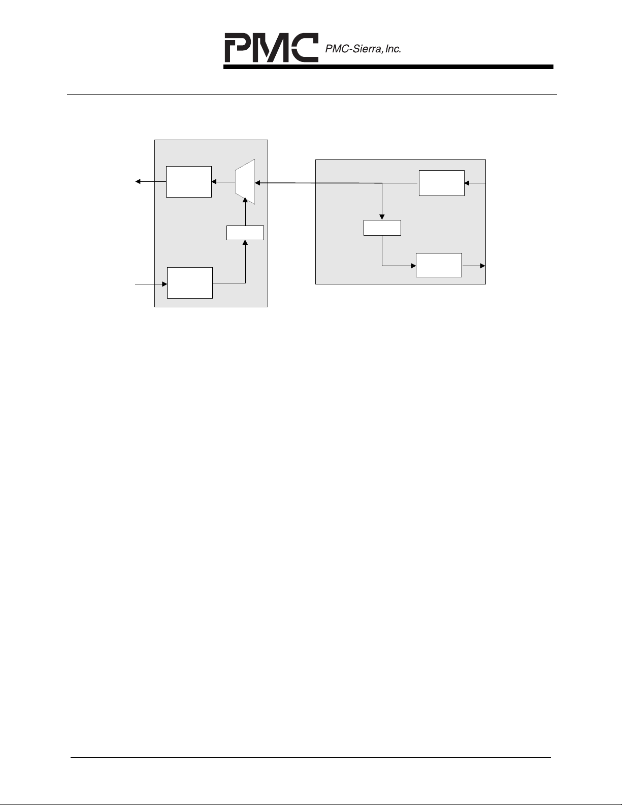
RELEASED
65
DATASHEET
PMC-2000097 ISSUE 2 8 LINK CES/DBCES AAL1 SAR
PM73123 AAL1GATOR-8
Figure 4 Data Flow and Buffering in the UI and the A1SP Blocks
UI
TUFIFO
(4 cells)
A1SP
TXA1SP
(8 cell FIFO)
3 Cell FIFO
RXA1SP
(8 cell FIFO)
RUFIFO
(8 cells)
3 Cell FIFO
In UTOPIA Level Two mode, the AAL1gator-8 responds on the UTOPIA bus as a
single port device.
For UTOPIA to UTOPIA loopback, there is a 3-cell FIFO in the UI Block. Lineside to Line-side loopback is done in the A1SP Block.
The UI_EN bit in the UI_COMN_CFG register enables both the source side and
sink side UTOPIA interface. This bit resets to the disabled state so that the chip
resets with all UTOPIA outputs tristated. Once the modes have been configured
and the interface enabled, then the outputs will drive to their correct values.
The UI block consists of 7 functions: UI Data Source Interface (SRC_INTF), UI
Data Sink Interface(SNK_INTF), 8-cell FIFO (FF8CELL), 4-cell FIFO (FF4CELL),
3-cell FIFO (FF3CELL), UMUX, and UI_REG. See Figure 5 for the block
diagram of the AAL1_UI block.
PMC-SIERRA, INC. PROPRIETARY AND CONFIDENTIAL
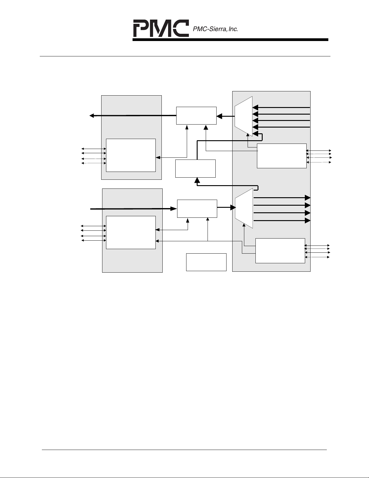
RELEASED
66
A1SP
A1SP
DATASHEET
PMC-2000097 ISSUE 2 8 LINK CES/DBCES AAL1 SAR
PM73123 AAL1GATOR-8
Figure 5 UI Block Diagram
UTOPIA Interface (UI) Block
UMUX
SRC_INTF
FF4CELL
MUX
Signals
to/from
each
block
TX UTOPIA
TXUTOPIA
SIGNALS
Interface and
FIFO
Output Logic
FF3CELL
SNK_INTF
FF8CELL
RX UTOPIA
RXUTOPIA
SIGNALS
Interface and
FIFO
Input Logic
9.1.1 UTOPIA Source Interface (SRC_INTF)
UI_REG
DEM
UX
Prioritization
and FIFO Input
Logic
Signals
to/from
each
block
DEMUX and FIFO
Output Logic
The SRC_INTF block (shown in Figure 5) conveys the cells received from the
UMUX block to the UTOPIA interface. Depending on the value of UTOP_MODE
field in the UI_SRC_CFG register, the UTOPIA interface will either act as an
UTOPIA master (controls the write enable signal) or as an UTOPIA PHY device
(controls the cell available signal). As a PHY device, the SRC_INTF can either
be a UTOPIA Level One device, where it is the only device on the UTOPIA bus,
or a UTOPIA Level Two device where other devices can coexist on the UTOPIA
bus. As a master device, the SRC_INTF can only function as a UTOPIA Level
One device.
If 16_BIT_MODE is set in the UI_SRC_CFG register then all 16 bits of the
UTOPIA data bus are used. 16_BIT_MODE must be ‘0’ in UTOPIA master
mode.
PMC-SIERRA, INC. PROPRIETARY AND CONFIDENTIAL

RELEASED
67
DATASHEET
PMC-2000097 ISSUE 2 8 LINK CES/DBCES AAL1 SAR
PM73123 AAL1GATOR-8
In master mode, the SRC_INTF block sources TATM_D, TATM_PAR,
TATM_SOC, and TATM_ENB while receiving TATM_CLAV. The Start-Of-Cell
(SOC) indication is generated coincident with the first word (only 8-bit mode is
supported) of each cell that is transmitted on TATM_D. TATM_D, TATM_PAR and
TATM_SOC are driven at all times. The TATM_ENB signal indicates which clock
cycles contain valid data for the UTOPIA bus. The device will not assert the
TATM_ENB signal until it has a full cell to send and the target device has
activated TATM_CLAV. The TATM_CLAV signal indicates whether the target
device is able to accept cells or not. Only cell level handshaking is supported. If
the target device is unable to accept any additional cells it must deactivate
TATM_CLAV no later than byte 49 of the current cell. No additional cells will be
sent until TATM_CLAV is activated.
In PHY mode, the SRC_INTF block sources RPHY_D[15:0], RPHY_PAR,
RPHY_SOC, and RPHY_CLAV, while receiving RPHY_ENB. The SOC indication
is generated coincident with the first word (8-bit or 16-bit) of each cell that is
transmitted on RPHY_D[15:0]. In PHY mode, the RPHY_D[15:0], RPHY_PAR,
and RATM_SOC signals are driven only when valid data is being sent; otherwise
they are tristated.
In UTOPIA Level 1 PHY mode, RPHY_CLAV is activated whenever a complete
cell is available to be sent. It remains active until the last byte has been read of
the last available complete cell. A cell is sent one cycle after RPHY_ENB goes
low. If RPHY_ENB goes high during the cell transfer, data is not sent each cycle
following one where RPHY_ENB is high.
RPHY_ADD[4:0] is an input and is used only in UTOPIA Level Two mode. Any
bus cycle following one where RPHY_ADD[4:0] matches CFG_ADDR(4:0) in the
UI_SRC_ADD_CFG register, the UI Block will drive RPHY_CLAV. Otherwise
RPHY_CLAV is tri-stated. If, in addition, during the previous cycle RPHY_ENB
was high and it is low in the current cycle, then the device is selected and the
SRC_INTF begins transmitting a cell the next cycle.
Parity is driven on TATM_PAR(RPHY_PAR) whenever TATM_D(RPHY_D[15:0])
is driven. EVEN_PAR will determine whether even parity or odd parity is
generated. Since odd parity is required by the ATM Forum, EVEN_PAR is
intended to be used for error checking only.
The AAL1gator-8 can tolerate temporary de-assertions of
TATM_CLAV/RPHY_ENB), but it is assumed that enough UTOPIA bandwidth is
present to accept the cells that the AAL1gator-8 can produce in a timely manner.
Once the 4-Cell FIFO fills up in th e UI, cells will begin filling up in the 8-cell FIFO
in the A1SP block. Anytime the UTOPIA FIFO fills up the T_UTOP_FULL
interrupt will go active in the MSTR_INTR_REG if it is enabled. This FIFO can fill
during normal operation and is not usually an indication of an error. However,
the A1SP FIFO should not normally fill. If they do fill it indicates there is some
PMC-SIERRA, INC. PROPRIETARY AND CONFIDENTIAL

RELEASED
68
DATASHEET
PMC-2000097 ISSUE 2 8 LINK CES/DBCES AAL1 SAR
PM73123 AAL1GATOR-8
congestion, which is impacting the UTOPIA interface and the TALP_FIFO_FULL
bit will go active in A1SP_INTR_REG. When the TALP FIFO fills, then TALP is
no longer able to build cells and data will start building up in the transmit buffer
and the frame_advance_fifo will fill. If this continues so that the
FR_ADV_FIFO_FULL bit goes active then data has been lost and the transmit
queues need to be reset. The T_UTOP_FULL indicator can be used to
determine when the UTOPIA Interface clears. It may also be desirable to disable
UI_EN so that the stored cells can be flushed.
The SRC_INTF circuit controls when a cell is transmitted from the internal 4 cell
FIFO. Since the UTOPIA can transmit cells at higher speeds than the TALP, and
since it is expected to see applications in a shared UTOPIA environment, cell
transmission from the SRC_INTF commences only when there is a full cell worth
of data available to transmit. The cell is then transmitted to the interface at the
UTOPIA TATM_CLK rate, in accordance with the TATM_FULLB/RPHY_ENB)
input. The maximum supported clock rate is 52 MHz.
9.1.1.1 Any-PHY Mode
If ANY-PHY_EN is set in the UI_SRC_CFG register then the SRC_INTF operates
as a single port Any-PHY slave device. In Any-PHY mode the RPHY_ADDR(4)
pin becomes the RSX pin and depending on the value of CS_MODE_EN, the
RPHY_ADDR(3) pin may become the RCSB signal instead.
In Any-PHY mode in-band addressing is used to allow more than the 32 possible
addresses available in UTOPIA mode. One extra word is prepended to the front
of each cell that is transmitted. The prepended word indicates the port address
sending the cell. The SRC_INTF uses CFG_ADDR(15:0) in the
UI_SRC_ADD_CFG register for the address prepend. If 16_BIT_MODE is low
then only the lower 8 bits are used.
During the cycle that the prepend address is active on the bus, RSX pulses high.
Because of the large number of possible ports, in the source direction, device
addresses are used for polling and device selection, instead of port addresses.
(Each device may control many ports) When a device is selected to send a cell,
the PHY device prepends the port address in front of the cell. Since, in this
direction the AAL1gator-8 is only a single port, the device address and port
address are the same. However, the AAL1gator-8 has only a limited number of
address pins. To accommodate systems, which are using a mix of different port
density Any-PHY devices, the RCSB signal is available to handle any additional
external decoding that is required. In Any-PHY mode, PHY devices respond with
RPHY_CLAV 2 cycles after their address is on the bus instead of the one cycle
required in UTOPIA mode. However, the timing of RCSB matches UTOPIA
timing so that a full cycle for external decoding is available.
PMC-SIERRA, INC. PROPRIETARY AND CONFIDENTIAL

RELEASED
DATASHEET
PMC-2000097 ISSUE 2 8 LINK CES/DBCES AAL1 SAR
PM73123 AAL1GATOR-8
Table 3 shows how the CFG_ADDR field is used in different modes.
Table 3 CFG_ADDR and PHY_ADDR Bit Usage in SRC direction
Polling Selection
MODE PHY_ADDR Pins CFG_ADDR PHY_ADDR Pins
UTOPIA-2
Single-Addr
Any-PHY
with CSB
[4:0]=device
[2:0]=device
[4:0]=device [4:0]=device [4:0]=device
[2:0]=device
[2:0]=device
CFG_ADDR is
prepended
Any-PHY
without
CSB
[3:0]=device
[3:0]=device
[3:0]=device
CFG_ADDR is
prepended
Notes:
• In Any-PHY mode, in the SRC direction the AAL1gator-8 will prepend the cell
with CFG_ADDR[15:0]. In 8-bit mode the cell will be prepended with
CFG_ADDR[7:0]
• In Any-PHY mode, if CS_MODE_EN=’1’ then CFG_ADDR[4:3] = “00”.
• In Any-PHY mode, if CS_MODE_EN=’0’ then CFG_ADDR[4]=”0”.
CFG_ADDR
[15:0]=device
[15:0]=device
9.1.2 UTOPIA Sink Interface (SNK_INTF)
The SNK_INTF block receives cells from the UTOPIA interface and sends them
to the UMUX interface. Depending on the value of the UTOP_MODE field in the
UI_SNK_CFG register, the UTOPIA interface acts either as an UTOPIA master
(controls the read enable signal) or as an UTOPIA PHY device (controls the cell
available signal). As a PHY device the SNK_INTF can either be a UTOPIA Level
One device, where it is the only device on the UTOPIA bus, or a UTOPIA Level
Two device where other devices can coexist on the UTOPIA bus. As a master
device the SNK_INTF can only function as a UTOPIA Level One device.
If 16_BIT_MODE is set in the UI_SNK_CFG register then all 16 bits of the
UTOPIA data bus are used. 16_BIT_MODE must be ‘0’ in UTOPIA master mode.
In master mode, the SNK_INTF block receives RATM_D, RATM_PAR,
RATM_SOC, and RATM_CLAV while driving RATM_ENB. Once the UI is
PMC-SIERRA, INC. PROPRIETARY AND CONFIDENTIAL
69

RELEASED
70
DATASHEET
PMC-2000097 ISSUE 2 8 LINK CES/DBCES AAL1 SAR
PM73123 AAL1GATOR-8
enabled in this mode, and, if the RATM_CLAV input signal is asserted, the
SNK_INTF block waits for an RATM_SOC signal from the PHY layer. Once the
RATM_SOC signal arrives, the cell is accepted as soon as possible. The StartOf-Cell (SOC) indication is received coincident with the first word (only 8-bit
mode is supported) of each cell that is received on RATM_D. An 8 cell FIFO
allows the interface to accept data at the maximum rate. If the FIFO fills, the
RATM_ENB signal will not be asserted again until the device is ready to accept
an entire cell. The RATM_ENB signal depends only on the cell space and is
independent of the state of the RATM_CLAV signal. The RATM_CLAV signal
indicates whether the target device has a cell to send or not. Only cell level
handshaking is supported.
In PHY mode, the SNK_INTF block receives TPHY_D[15:0], TPHY_SOC, and
TPHY_ENB while driving TPHY_CLAV. The cell available (TPHY_CLAV) signal
indicates when the device is ready to receive a complete cell. In UTOPIA Level
One mode, TPHY_CLAV is always driven.
In UTOPIA Level Two mode, SNK_INTF responds as a single address device.
When responding as a single address, TPHY_CLAV is driven the cycle following
ones in which TPHY_ADDR(4:0) matches CFG_ADDR(4:0) in
UI_SNK_ADD_CFG register. Otherwise TPHY_CLAV is tri-stated. If, in addition
to an address match, during the previous cycle TPHY_ENB was high and it is
low in the current cycle, then the device is selected and the SRC_INTF begins
accepting the cell that is being received.
The SNK_INTF block waits for an SOC. When an SOC signal arrives, a counter
is started, and 53 bytes are received. If a new SOC occurs within a cell, the
counter reinitializes. This means that the corrupted cell will be dropped and the
second good cell will be received. The SNK_INTF block stores the cell in the
receive FIFO. If the receive FIFO becomes full, it stops receiving cells. The
bytes are written to the FIFO with RATM_CLK. RATM_CLK is an input to the
AAL1gator-8. The maximum supported clock rate is 52 MHz.
Parity is always checked and a parity error will cause an interrupt if the
UTOP_PAR_ERR_EN bit is set in the MSTR_I NTR_EN_REG.
FORCE_EVEN_PARITY will determine whether even parity or odd parity is
checked. Since odd parity is required by the ATM Forum,
FORCE_EVEN_PARITY is intended to be used for error checking only. If an
error is detected the UTOP_PAR_ERR bit in the MSTR_INTR_REG is set, and
the corresponding enable bit is set in the MSTR_INTR_EN_REG then INTB will
go active. Any cell received with bad parity will still be processed as normal.
PMC-SIERRA, INC. PROPRIETARY AND CONFIDENTIAL

RELEASED
DATASHEET
PMC-2000097 ISSUE 2 8 LINK CES/DBCES AAL1 SAR
PM73123 AAL1GATOR-8
9.1.2.1 Any-PHY Mode
If ANY-PHY_EN is set in the UI_SNK_CFG register then the SNK_INTF operates
as a multi port Any-PHY slave device. In Any-PHY mode the TPHY_ADDR[4] pin
becomes the TSX pin and depending on the value of CS_MODE_EN, the
TPHY_ADDR(3) pin may become the TCSB signal instead.
In Any-PHY mode in-band addressing is used to allow more than the 32 possible
addresses available in UTOPIA mode. One extra word is prepended to the front
of each cell that is transmitted. The prepended word indicates the port address
to receive the cell. The SNK_INTF uses CFG_ADDR(15:2) in the
UI_SNK_ADD_CFG register to match with the address prepend. If
16_BIT_MODE is low then CFG_ADDR(7:2) is used. In both cases, polling
should only be done with PHY_ADDR[1:0] equal to “00”.
During the cycle that the prepend address is active on the bus, the TSX input
pulses high.
In the sink direction, port addresses are used for polling and device selection,
instead of device addresses. However the AAL1gator-8 has only a limited
number of address pins. To accommodate systems, which are using a mix of
different port density Any-PHY devices, the TCSB signal is available to handle
any additional external decoding that is required. In Any-PHY mode, PHY
devices respond with TPHY_CLAV 2 cycles after their address is on the bus
instead of the one cycle required in UTOPIA mode. However the timing of TCSB
matches UTOPIA timing so that a full cycle for external decoding is available.
Table 4 shows how the CFG_ADDR field is used in different modes.
PMC-SIERRA, INC. PROPRIETARY AND CONFIDENTIAL
71

RELEASED
DATASHEET
PMC-2000097 ISSUE 2 8 LINK CES/DBCES AAL1 SAR
PM73123 AAL1GATOR-8
Table 4 CFG_ADDR and PHY_ADDR Bit Usage in SNK direction
Polling Selection
MODE PHY_ADDR Pins CFG_ADDR PHY_ADDR Pins
UTOPIA-2
Single-Addr
Any-PHY
with CSB
[4:0]=device
[2]=device
[1:0]=”00”
[4:0]=device [4:0]=device [4:0]=device
[2]=device
[2]=device
[1:0]=”00”
addr is
prepended
Any-PHY
without
CSB
[3:2]=device
[1:0]=”00”
[3:2]=device
[3:2]=device
[1:0]=”00”
addr is
prepended
Notes:
• In Any-PHY mode, if CS_MODE_EN=’1’ then CFG_ADDR[4:3] = “00”. Else if
CS_MODE_EN=’0’ then CFG_ADDR[4]=”0”.
• In Any-PHY mode the upper 14 bits of the prepended address are compared
with CFG_ADDR[15:2]. The bottom two bits are not compared with this field.
Polling should be done with PHY_ADDR= “00”. If in 8-bit mode
CFG_ADDR[7:2] is used instead.
CFG_ADDR
[15:2]=device
[15:2]=device
9.1.3 UTOPIA Mux Block (UMUX)
The UMUX serves as the bridge between the A1SP block and the SNK_INTF
and SRC_INTF blocks.
In the source direction, the UMUX polls the A1SP block and the Loopback FIFO
using a least recently serviced algorithm to determine cell availability. In this
algorithm, once a particular source is serviced, it is put at the lowest priority of
the two sources.
If the SRC_INTF FIFO has room for a cell, the UMUX polls the A1SP block or
Loopback FIFO to determine if it has a cell. If so, a cell is read from the selected
A1SP block or Loopback FIFO and transferred into the SRC_INTF FIFO. If the
highest priority source does not have a cell, the other source is examined. The
A1SP block has an 8-cell FIFO. The Loopback FIFO is 3 cells.
PMC-SIERRA, INC. PROPRIETARY AND CONFIDENTIAL
72

RELEASED
DATASHEET
PMC-2000097 ISSUE 2 8 LINK CES/DBCES AAL1 SAR
PM73123 AAL1GATOR-8
In the sink direction, the UMUX waits until the SNK_INTF FIFO has a cell to
send. Once the SNK_INTF FIFO has a cell to send, the UMUX polls the A1SP
associated with the cell for availability. Once the A1SP has room for the cell, the
UMUX reads the cell out of the SNK_INTF FIFO and places it in the A1SP FIFO.
The UMUX also supports two forms of UTOPIA to UTOPIA loopback; global
loopback, where all cells are looped, and VC based loopback, where only a
specific VC is used to loopback cells. In global loopback all cells received by the
UTOPIA block are sent back out onto the UTOPIA bus. Global loopback is
enabled by setting the U2U_LOOP bit in the UI_COMN_CFG register. In VC
based loopback mode, any cell received with a VC that matches the loopback
VC is sent back out onto the UTOPIA bus. VC based loopback is enabled by
setting the VCI_U2U_LOOP bit in the UI_COMN_CFG register. The loopback
VC is programmable by writing the U2U_LOOP_VCI register. The 3-cell FIFO is
used for loopback.
9.2 AAL1 SAR Processing Block (A1SP)
The A1SP block is the main AAL1 SAR processing block. This block processes
8 E1/T1 lines. This block has the following major components.
• Transmit Frame Transfer Controller (TFTC) block
• Cell Service Decision (CSD) block
• Transmit Adaptation Layer Processor (TALP) block
• TALP FIFO (TFIFO) block
• Local Loopback Block (LOC_LPBK) block
• Receive Frame Transfer Controller (RFTC) block
• Receive Adaptation Layer Processor (RALP) block
• RALP FIFO (RFIFO) block
Figure 6 shows a block diagram of the AAL1gator-8 and the sequence of events
used to segment and reassemble the CBR data.
PMC-SIERRA, INC. PROPRIETARY AND CONFIDENTIAL
73

RELEASED
DATASHEET
PMC-2000097 ISSUE 2 8 LINK CES/DBCES AAL1 SAR
PM73123 AAL1GATOR-8
Figure 6 A1SP Block Diagram
Input from LI
Block
To External
Memory
Output to LI
Block
2
Transmit Frame
Transfer Controller
(TFTC)
1
Receive Frame
Transfer Controller
(RFTC)
Cell Service
Decision
(CSD)
3
Internal RAM
Microprocessor
Control Bus
4
Transmit Adaptation
Layer Processor
(TALP)
5 6
Local Loopback
Block (LOC_LPBK)
Receive Adaptation
Layer Processor
(RALP)
TALP FIFO Block
7
RALP FIFO Block
(TFIFO)
(RFIFO)
8910
Output to UI
Block
Input from UI
Block
1. TFTC stores line data into the memory 16 bits at a time.
2. When the TFTC finishes writing a complete frame into the memory, it notifies
the CSD of a frame completion by writing the line and frame number into a
FIFO. Idle channel detection is processed here if enabled.
3. The CSD checks a frame-based table for queues having sufficient data to
generate a cell. For each queue with enough data to generate a cell, the CSD
schedules the next cell generation occurrence in the table.
4. The CSD commands the TALP to generate a cell from the available data for
each of the ready queues identified in step 3.
5. The TALP generates the cell from the data and signaling buffers and writes
the cell into the TALP FIFO.
6. The TFIFO block buffers cells which will be transmitted out to the UTOPIA
Interface block.
7. If local loopback is enabled the cell is looped to RALP.
PMC-SIERRA, INC. PROPRIETARY AND CONFIDENTIAL
74

RELEASED
75
DATASHEET
PMC-2000097 ISSUE 2 8 LINK CES/DBCES AAL1 SAR
PM73123 AAL1GATOR-8
8. The RFIFO block buffers cells received from the UTOPIA Interface block.
9. The RALP performs pointer searches, checks for overrun and underrun
conditions, detects SN mismatches, checks for OAM cells, and extracts the
line data from the cells, and places the data into the receive buffer.
10. The RFTC plays the receiver buffer data onto the lines.
Four types of data are supported by the A1SP.
1. UDF-ML (Unstructured Data Format- Multi-Line). Unstructured bit stream for
line speeds < 15 Mbps. (supports 8 lines per A1SP) if all are under 2.5 Mbps).
2. UDF-HS (Unstructured Data Format- High Speed). Unstructured bit stream
for line speeds under 45 Mbps. (Only one line supported per A1SP).
3. SDF-FR (Structured Data Format- Frame). Channelized data without CAS
signaling. (Frame based structure).
4. SDF-MF (Structured Data Format- Multi-Frame). Channelized data with CAS
signaling. (Multi-Frame based structure).
9.2.1 AAL1 SAR Transmit Side (TxA1SP)
9.2.1.1 Transmit Frame Transfer Controller (TFTC)
The TFTC accepts deframed data from Line Interface Block. For structured data,
the TFTC uses the synchronization supplied by the Line Interface Block to
perform a serial-to-parallel conversion on the incoming data and then places this
data into a multiframe buffer in the order in which it arrives.
The TFTC monitors the frame sync signals and will realign when an edge is seen
on these signals that does not correspond to where it expects it to occur. It is not
necessary to provide an edge at the beginning of every frame or multiframe. The
AAL1gator-8 reads signaling during the last frame of every multiframe. For T1
mode, the AAL1gator-8 reads signaling on the 24
E1 mode, the AAL1gator-8 reads signaling on the 16th frame of the multiframe.
A special case of E1 mode exists that permits the use of T1 signaling with E1
framing. Normally an E1 multiframe consists of 16 frames of 32 timeslots, where
signaling changes on multiframe boundaries. When E1_WITH_T1_SIG is set in
LIN_STR_MODE and the line is in E1 mode, the TFTC will use a multiframe
consisting of 24 frames of 32 timeslots. In this mode, the AAL1gator-8 reads
signaling on the 24th frame of the multiframe.
th
frame of the multiframe. For
PMC-SIERRA, INC. PROPRIETARY AND CONFIDENTIAL

RELEASED
76
DATASHEET
PMC-2000097 ISSUE 2 8 LINK CES/DBCES AAL1 SAR
PM73123 AAL1GATOR-8
The AAL1gator-8 reads the signaling nibble for each channel when it reads the
last nibble of each channel’s data unless the SHIFT_CAS bit in the
LIN_STR_MODE register is set. If the SHIFT_CAS bit is set then the AAL1gator8 reads the signaling nibble for each channel when it reads the first nibble of
each channel’s data. See Figure 7 for an example of a T1 frame. See Figure 8
for an example of an E1 frame.
Figure 7 Capture of T1 Signaling Bits (SHIFT_CAS=0)
Line Signals During the Last Frame of a Multiframe
RL_SER
(timeslots
)
0 1 2 21 22 23
...
XXXX
ABCD
Channel 1
XXXX
ABCD
Channel 2
...
ABCD
Channel 21
XXXX
XXXX XXXX
...
ABCD
Channel 22 C hannel 23
ABCD
RL_SIG
XXX X - indi c at es sig naling is i gnored
XXXX
Channe l 0
Figure 8 Capture of E1 Signaling Bits (SHIFT_CAS=0)
Line Signals During the Last Frame of a Mu ltiframe
RL_SER
(timeslots
)
RL_SIG
XXX X - i n dica tes s ignaling is i gnored
0 1 2 29 30 31
ABCD
Channe l 0
XXXX
XXXX
ABCD
Channel 1
XXXX
ABCD
Channel 2
...
... ...
ABCD
XXXX XXXX
Channel 29
ABCD
XXXX
Channel 30 C hannel 31
Note:
• AAL1gator-8 treats all 32 timeslots identically. Although E1 data streams
contain 30 timeslots of channel data and 2 timeslots of control (timeslots 0
and 16), data and signaling for all 32 timeslots are stored in memory and can
be sent and received in cells.
ABCD
ABCD
Unstructured data is received without regard to the byte alignment of data within
a frame and is placed in the frame buffer in the order in which it arrives. Figure 9
shows the basic components of the TFTC.
Figure 9 Transmit Frame Transfer Controller
PMC-SIERRA, INC. PROPRIETARY AND CONFIDENTIAL
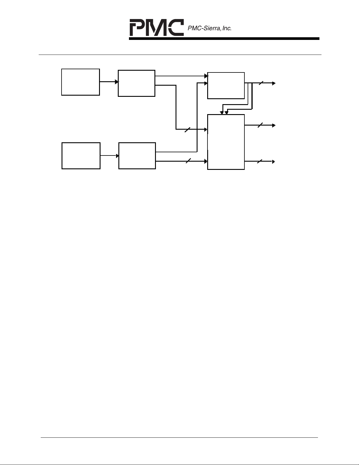
RELEASED
77
Interface
Line 0
Line 0
Interface
DATASHEET
PMC-2000097 ISSUE 2 8 LINK CES/DBCES AAL1 SAR
PM73123 AAL1GATOR-8
Line
•
•
•
Line 7
Line
Receive Line
Interface
•
•
•
Line 7
Receive Line
Interface
ATTN0
DATA0
ATTN7
DATA7
Line Encoder
ANY
16
Line-to-Memory
Interface
16
3
Line Number
4
Channel Pair
16
Data
The receive line interface is primarily a serial-to-parallel converter. Serial data,
which is derived from the RL_DATA signal from the LI Block, is supplied to a shift
register. The shift register clock is the RL_CLK input from the external framer.
When the data has been properly shifted in, it is transferred to a 2-byte holding
register by an internally derived channel clock. This clock is derived from the line
clock and the framing information.
The channel clock also informs the line-to-memory interface that two data bytes
are available from the line. When the two bytes are available, a line attention
signal is sent to the line encoder block. However, because the channel clock is
an asynchronous input to the line-to-memory interface, it is passed through a
synchronizer before it is supplied to the line encoder. Since there are eight
potential lines and each of them provides its own channel clock, they are
synchronized before being submitted to the line encoder.
The TFTC accommodates the T1 Super Frame (SF) mode by treating it like the
Extended Super Frame (ESF) format. The TFTC ignores every other frame pulse
and captures signaling data only on the last frame of odd SF multiframes. The
formatting of data in the signaling buffers is highly dependent on the operating
mode. Refer to section 7.6.6 “RESERVED (Transmit Signaling Buffer)” on page
136 for more information on the transmit signaling buffer.
Figure 10 shows the format of the transmit data buffer for ESF-formatted T1 data
for lines that are in the SDF-MF mode.
PMC-SIERRA, INC. PROPRIETARY AND CONFIDENTIAL

RELEASED
78
DS0s
DS0s
DATASHEET
PMC-2000097 ISSUE 2 8 LINK CES/DBCES AAL1 SAR
PM73123 AAL1GATOR-8
Figure 10 T1 ESF SDF-MF Format of the T_DATA_BUFFER
Frame Buffer Number
0 31
0
23
32
55
64
87
96
119
127
MF0
MF1
MF2
MF3
23
Figure 11 shows the format of the transmit data buffer for SF-formatted T1 data
for lines that are in the SDF-MF mode.
Figure 11 T1 SF-SDF-MF Format of the T_DATA_BUFFER
Frame Buffer Number
0 31
0
11
12
23
32
43
44
55
MF0
MF1
MF2
MF3
23
64
75
76
87
96
107
108
119
PMC-SIERRA, INC. PROPRIETARY AND CONFIDENTIAL
MF4
MF5
MF6
MF7

RELEASED
0
Fram e B u ff er Nu m ber
DATASHEET
PMC-2000097 ISSUE 2 8 LINK CES/DBCES AAL1 SAR
PM73123 AAL1GATOR-8
Figure 12 shows the format of the transmit data buffer for T1 data for lines that
are in the SDF-FR mode.
Figure 12 T1 SDF-FR Format of the T_DATA_BUFFER
32
64
96
127
DS0s
0
Fr ame 0
Fr ame 1
31
•
•
•
Fr am e 23
Fr am e 24
Fr am e 25
•
•
•
Fr am e 47
Fr am e 48
Fr am e 49
•
•
•
Fr am e 71
Fr am e 72
Fr am e 73
•
•
•
Fr am e 95
PMC-SIERRA, INC. PROPRIETARY AND CONFIDENTIAL
79
RELEASED
80
Frame Buff er Number
DS0s
DATASHEET
PMC-2000097 ISSUE 2 8 LINK CES/DBCES AAL1 SAR
PM73123 AAL1GATOR-8
Figure 13 shows the format of the transmit data buffer for E1 data for lines that
are in the SDF-MF mode.
Figure 13 E1 SDF-MF Format of the T_DATA_BUFFER
0 31
0
15
16
31
32
48
64
80
96
112
127
DS0s
MF0
MF1
MF2
MF3
MF4
MF5
MF6
MF7
Figure 14 shows the format of the transmit data buffer for E1 data using T1
signaling, for lines that are in SDF-MF mode
Figure 14 E1 SDF-MF with T1 Signaling Format of the T_DATA_BUFFER
Frame Buffer Number
PMC-SIERRA, INC. PROPRIETARY AND CONFIDENTIAL
23
32
55
64
87
96
119
127
0
0
31
MF0
MF1
MF2
MF3
RELEASED
DS0s
Data Bits
DATASHEET
PMC-2000097 ISSUE 2 8 LINK CES/DBCES AAL1 SAR
PM73123 AAL1GATOR-8
Figure 15 shows the format of the transmit data buffer for E1 data for lines that
are in the SDF-FR mode.
Figure 15 E1 SDF-FR Format of the T_DATA_BUFFER
Fr ame Bu ffer Number
127
0
0
Frame 0
Frame 1
Frame 2
•
•
•
Fr ame 12 7
31
Figure 16 shows the format of the transmit data buffer for lines that are in UDFML mode.
Figure 16 Unstructured Format of the T_DATA_BUFFER
F rame Buffer Number
0
0
256-Bit Internal Frame 0
256-Bit Internal Frame 1
255
127
256-Bit Intern al Frame 127
Figure 17, Figure 18, Figure 19 and Figure 20 show the contents of the transmit
signaling buffer for the different signaling modes. In all cases the upper nibble of
each byte is “0000”.
PMC-SIERRA, INC. PROPRIETARY AND CONFIDENTIAL
•
•
•
81

RELEASED
0
1
2
3
Channel 0
ABCD
ABCD
Channel 23
ABCD
Channel 22
ABCD
Channel 24
Channel 31
012
3
Channel 0
ABAB
ABAB
Channel 23
ABAB
Channel 22
ABAB
Channel 24
Channel 31
0
DATASHEET
PMC-2000097 ISSUE 2 8 LINK CES/DBCES AAL1 SAR
PM73123 AAL1GATOR-8
Figure 17 SDF-MF T1 ESF Format of the T_SIGNALING_BUFFER
0
Channel 1
Byte Address
Not Used
Not Used
Multifram e
Figure 18 SDF-MF T1 SF Format of the T_SIGNALING BUFFER
0
Channel 1
Multifram e/2
Byte Address
Not Used
Not Used
Figure 19 SDF-MF E1 Format of the T_SIGNALING_BUFFER
31
31
Multiframe
Byte Address
Channel 0
ABCD
Channel 1
ABCD
Channel 30
ABCD
7
Channel 31
ABCD
PMC-SIERRA, INC. PROPRIETARY AND CONFIDENTIAL
82
RELEASED
0
DATASHEET
PMC-2000097 ISSUE 2 8 LINK CES/DBCES AAL1 SAR
PM73123 AAL1GATOR-8
Figure 20 SDF-MF E1 with T1 Signaling Format of the
T_SIGNALING_BUFFER
Byte Address
Multiframe
Channel 0
ABCD
3
Channel 1
ABCD
Channel 30
ABCD
Channel 31
ABCD
9.2.1.1.1 Transmit Conditioning
The T_COND_DATA structure allows conditional data to be defined on a perDS0 basis and the T_COND_SIG structure allows conditioned signaling to be
defined on a per-DS0 basis. The TX_COND bit in the T_QUEUE_TBL allows the
cell building logic (described in Section 9.2.1.3 Transmit Adaptation Layer
Processor (TALP) on page 96) to be directed to build cells from the conditioned
data and signaling. To control whether conditioned data, conditioned signaling, or
both is used, set TX_COND_MODE in the TX_CONFIG register to the
appropriate value. The TX_COND bit and TX_COND_MODE bits can be set on a
per-queue basis.
By having independent control over whether signaling or data is conditioned, it is
possible to substitute the signaling which is carried in the CAS bits across the
ATM network while still passing the data received off the line. This is useful for
applications that may not be receiving the signaling with the data.
For HS_UDF mode the HS_TX_COND bit needs to be set in the HS_LIN_REG
register. When this bit is set cells with an all ones pattern will be generated. The
CMD_REG_ATTN bit needs to be written to a ‘1’ after the HS_TX_COND bit is
set for this function to take affect.
Under certain alarm conditions such as Loss of Signal (LOS), an Alarm Indication
Signal (AIS) needs to be transmitted downstream. This means that cells need to
be generated which carry an AIS pattern. The AAL1gator-8 does not do any
alarm processing and is dependent on the external framer for this functionality.
The framer would notify the processor of any alarm conditions and then the
processor would switch a particular queue from normal mode to a conditioned
mode by setting the TX_COND bit in the T_QUEUE_TBL.
Most AIS signals are an all ones pattern, so cells with this pattern can be
generated by setting T_COND_DATA to “FF”x and T_COND_SIG to “F”x. In E3
PMC-SIERRA, INC. PROPRIETARY AND CONFIDENTIAL
83
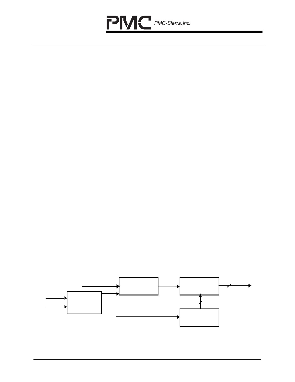
RELEASED
DATASHEET
PMC-2000097 ISSUE 2 8 LINK CES/DBCES AAL1 SAR
PM73123 AAL1GATOR-8
mode this can be done by setting HS_TX_COND bit to a ‘1’. However a DS3 AIS
signal is a framed “1010” pattern. This signal can be generated by setting the
HS_GEN_DS3_AIS bit in the HS_LIN_REG register. The CMD_REG_ATTN bit
needs to be written to a ‘1’ after the HS_GEN_DS3_AIS bit or the HS_TX_COND
bit is set for this function to take affect.
9.2.1.1.2 Transmit Signaling Freezing
Signaling freezing is a required function when transporting CAS. This function
holds the signaling unchanged when the incoming line fails. The PMC-Sierra
framers provide this function. If a framer is used that does not support signaling
freezing, this function must be provided externally.
9.2.1.1.3 SRTS for the Transmit Side
The transmit side supports SRTS only for unstructured data formats on a per-line
basis. SRTS support requires an input reference clock, NCLK. The input
reference frequency is defined as 155.52/2n MHz, where n is chosen such that
the reference clock frequency is greater than the frequency being transmitted,
but less than twice the frequency being transmitted (2 x RL_CLK > NCLK >
RL_CLK). For T1 or E1 implementation, the input reference clock frequency
must be 2.43 MHz. The transmit side can accept a reference clock speed of up
to 77.76 MHz, which is required for DS3 applications. Figure 21 on page 84
shows the process implemented for each UDF line enabled for SRTS, regardless
of the reference frequency. One bit of resulting 4-bit SRTS code is then inserted
into the CSI bit of each of the odd numbered cells for that line. There are four
odd cells in each 8 cell sequence, so each one carries a different SRTS bit. If
the line does not supply SRTS, then all odd CSI bits are set to 0. The 3008
divider is the number of data bits in eight cells (8 x 8 x 47). The divider is aligned
on the first cell generation after a reset or a resynchronization to the cell
generation process.
Figure 21 Transmit Side SRTS Function
Reset
Resync
Ser v e r C l oc k Freq ue nc y
RL_CLK
Cell Generati on
Divide By 3008 4 -Bi t La tc h
Arm
Input Reference Clock Freq uency
N_CLK
(F or T1 /E 1, 2. 4 3 MHz . F or T3, 77 .76 MH z .)
Latch
4 Bits
4-Bit Counter
4-b it SRTS C ode
4 Bit s
PMC-SIERRA, INC. PROPRIETARY AND CONFIDENTIAL
84

RELEASED
85
DATASHEET
PMC-2000097 ISSUE 2 8 LINK CES/DBCES AAL1 SAR
PM73123 AAL1GATOR-8
9.2.1.1.4 Idle Detection
Idle detection will be performed on a per queue basis using one of the following
three methods: channel associated signaling (CAS), out of band signaling
(processor controlled), or pattern matching. The status of each channel is stored
in the Active/Idle bit table. The mode for each channel is controlled by the value
of IDLE_CFG_n in the Idle Detection Configuration Table. The lower 16
channels or upper 16 channels of a line must not mix CAS or pattern matching
mode with processor controlled mode. This is to avoid contention updating the
active channel table.
9.2.1.1.4.1 CAS Idle Detection
CAS idle detection looks at the ABCD bits in both the receive and transmit
direction and compares them to values programmed on a per channel basis by
the processor. If two consecutive CAS values match in both the receive and
transmit direction the channel is considered to be idle. The format of the register
(AUTO_CONFIG_n) in the CAS/Pattern Matching Configuration Table, which the
processor programs with the idle ABCD patterns, is pictured below in Figure 22.
The register also provides mask fields for the receive and transmit directions
which allow any one of the ABCD bits to be ignored when looking for a match.
Figure 22 CAS Idle Detection Configuration Register Structure
15 11 7 3 0
RX MASK TX ABCDRX ABCDTX MASK
During CAS idle detection, a word is written to the Transmit Idle Interrupt FIFO
every time the status changes from active->idle or idle->active.
TIDLE_FIFO_EMPB is set as long as this FIFO contains any unread entries,
which will result in a maskable interrupt. The structure of the word contained in
the FIFO is shown in Figure 23. The upper eight bits indicate the channel that
encountered the status change and bit 0 indicates the status of the channel
(Active =1; Idle = 0). The processor accesses the FIFO by reading the
A1SP_TIDLE_FIFO register which will contain the top element of the FIFO.
PMC-SIERRA, INC. PROPRIETARY AND CONFIDENTIAL

RELEASED
86
DATASHEET
PMC-2000097 ISSUE 2 8 LINK CES/DBCES AAL1 SAR
PM73123 AAL1GATOR-8
Figure 23 CAS Idle Detection Interrupt Word
8
15 2
1
0871213
Line
9.2.1.1.4.2 Processor Controlled Idle Detection
In Processor controlled idle detection mode, it is the responsibility of the
processor to add or drop channels. This mode is used in conjunction with
common channel signaling (CCS) or if the processor wants to make its own
determination of channel activity based on the CAS bits.
During the processor controlled idle detection, a word is written to the Transmit
Idle Interrupt FIFO every time the value of the CAS nibble changes and then
remains stable for one additional multiframe. TIDLE_FIFO_EMPB is set as long
as this FIFO contains any unread entries, which will result in a maskable
interrupt. The structure of the word contained in the FIFO is shown in Figure 24.
The first eight bits indicate the channel, which encountered a change in the value
of CAS. The next four bits indicate the RX CAS value and the final four bits
indicate the TX CAS value.
TX refers to the CAS incoming on the TDM interface (H-MVIP RL_SIG or direct
mode RL_SIG), and RX refers to CAS incoming in ATM cells at the UTOPIA Cell
Sink interface.
StatusChannel Unused
Based on these new CAS values the processor can make a determination if the
channel should be marked as active or idle. The CAS values are de-bounced
internally one time, and any additional debounce must be done external to the
chip.
Figure 24 Processor Controlled Idle Detection Interrupt Word
1213
Line
Channel
The processor will also be able to mask out portions of the CAS and therefore
receive interrupts only when particular bits of the CAS change. Figure 25 shows
the structure of AUTO_CONFIG_n field in the CAS/Pattern Matching
Configuration Table. The lower byte is reserved and is used in detecting
PMC-SIERRA, INC. PROPRIETARY AND CONFIDENTIAL
7015 8
RX CAS
34
TX CAS
RELEASED
87
DATASHEET
PMC-2000097 ISSUE 2 8 LINK CES/DBCES AAL1 SAR
PM73123 AAL1GATOR-8
changes in the CAS values. Therefore, to avoid contention, the upper byte
should only be written when the idle detection is disabled.
Figure 25 Processor Controlled Configuration Register Structure
15 11 7 3 0
RX MASK ReservedReservedTX MASK
Once the processor determines that the status of a channel should change, the
processor should then write the TX Channel Active Table. The processor does
this by accessing the table 16 bits at a time. In most situation s the processor will
want to change a subset of the 16 channels accessed. Therefore, a readmodify-write will have to be performed.
Figure 26 shows the structure of the Active/Idle bit table. The index represents
the value that needs to be added to the base address of the table in order to
access the status for the channels located at that index.
Note that since the processor writes 16 bits at a time it is recommended that
processor intervention and automatic mode is not mixed within a group of 16
channels to avoid contention problems.
Figure 26 TX Channel Active/Idle Bit Table Structure
Index
13
14
15
Line Channel Status
0
1
2
0
0
1
6
7
7
15 14 13 12 11 10 9 8
31 30 29 28 27 26 25 24
15 14 13 12 11 10 9 8 7 6 5 4 3 2 1 0
31 30 29 28 27 26 25 24 23 22 21 20 19 18 17 16
15 14 13 12 11 10 9 8 7 6 5 4 3 2 1 0
31 30 29 28 27 26 25 24 23 22 21 20 19 18 17 16
7 6 5 4 3 2 1 0
23 22 21 20 19 18 17 16
PMC-SIERRA, INC. PROPRIETARY AND CONFIDENTIAL
RELEASED
88
DATASHEET
PMC-2000097 ISSUE 2 8 LINK CES/DBCES AAL1 SAR
PM73123 AAL1GATOR-8
9.2.1.1.4.3 Pattern Match Idle Detection
Pattern match idle detection compares the received byte with a programmed
pattern and a mask. If there is a mismatch of received data with the
programmed pattern during a programmable length of time, then the channel is
considered active. Otherwise, if the received channel bytes match the
unmasked pattern bits over the programmable length of time, the channel is
considered in an idle state and cell transmission will be suppressed.
Interval length refers to the amount of time that the patterns must match for it to
be considered a match event. This value is programmed in the Pattern Matching
Line Configuration register for the associated line. The Interval length is
programmed in units of 12 ms for T1 and units of 16 ms for E1. Since this is an
8 bit field, the maximum length of time is 3.1 (+/- 12 ms) seconds for T1 and 4.1
(+/- 16 ms) seconds for E1.
Figure 27 PAT_MTCH_CFG Register Structure
15 8 7 0
Rsvd
Internal Length = Duration of time data must
match before declaring an idle condition
Interval Length
Figure 28 shows the structure of the AUTO_CONFIG_n field in the CAS/Pattern
Matching Configuration Table. The lower byte contains the pattern the received
byte should be compared against. The upper byte is a mask field that can be
used to control which bits are monitored. Since the chip will be updating this
field during normal operation, it is best if the processor writes to the lower byte of
the register only during reset in order to avoid contention. .
PMC-SIERRA, INC. PROPRIETARY AND CONFIDENTIAL

RELEASED
DATASHEET
PMC-2000097 ISSUE 2 8 LINK CES/DBCES AAL1 SAR
PM73123 AAL1GATOR-8
Figure 28 Pattern Match Idle Detection Register Structure
15 8 7 0
PATTERN_MASK IDLE_PATTERN
During pattern match idle detection, a word is written to TIDLE_FIFO every time
the status changes from active->idle or idle->active. An interrupt is generated as
long as this FIFO contains any unread entries. The structure of the word
contained in the FIFO is shown in Figure 29. The upper eight bits indicate the
channel that encountered the status change and bit 0 indicates the status of the
channel (Active =1; Idle = 0). The processor accesses the FIFO by reading the
Status Interrupt register, which will contain the top element of th e FIFO.
Figure 29 Pattern Match Idle Detection Interrupt Word
15 9 0
15 2
Line
81213
9.2.1.2 Cell Service Decision (CSD) Circuit
The CSD circuit determines which cells are to be sent and when. It determines
this by implementing Transmit Calendar bit tables and Active/Idle bit tables.
When the TALP builds a cell, the CSD circuit performs a complex calculation
using credits to determine the frame in which the next cell from that queue
should be sent. The CSD circuit schedules a cell only when a cell is built by the
TALP. If SUPPRESS_TRANSMISSION bit in the TX_CONFIG word is set, then
the cell is scheduled, however, the cell is not transmitted.
In non-DBCES mode, a queue can be placed in idle detection mode by setting
the IDLE_DET_ENABLE in the TRANSMIT_CONFIG word within the queue
table. When a queue is set for idle detection mode and all the channels on a
given queue are inactive, cells are scheduled, but no cells are actually sent. This
mode also requires that one of the idle detection methods is enabled for all the
channels of the given queue. This can be done by programming the A1SP Idle
Detection Configuration Table.
1
StatusChannel Unused
The following steps (as well as Figure 30 on page 91) describe how the CSD
circuit schedules cells for the TALP to build.
PMC-SIERRA, INC. PROPRIETARY AND CONFIDENTIAL
89

RELEASED
90
DATASHEET
PMC-2000097 ISSUE 2 8 LINK CES/DBCES AAL1 SAR
PM73123 AAL1GATOR-8
1) Once the TFTC writes a complete frame into external memory, it writes the
line number and frame number of this frame into the FR_ADVANCE_FIFO. The
CSD circuit reads the line-frame number pair from the FR_ADVANCE_FIFO and
uses it as an index into the Transmit Calendar. The Transmit Calendar is
composed of eight-bit tables, one per line. Each bit table consists of 128 entries,
one per frame buffer. Each entry consists of 32 bits, one per queue. For each bit
set in the indexed entry in the Transmit Calendar, the CSD will schedule the
frame in which the next cell can be built for the corresponding queue, and notify
the TALP that enough data is available to build a cell for that queue.
2) The CSD circuit processes all queues from the Transmit Calendar entry
starting with the lowest queue number and proceeding to the highest. The
processing steps are as follows:
a) The CSD circuit obtains the QUE_CREDITS, and subtracts the average
number of credits per cell from it. The average number of credits,
AVG_SUB_VALU, is the number of credits that will be spent sending the
current cell. For structured lines, the average number of credits per cell is 46
7/8. For unstructured lines, the average number of credits per cell is 47.
b) Next, the CSD circuit computes the frame location for the next service by
subtracting the remaining credits from 47. It divides the result by the number
of channels, NUM_CHAN, dedicated to that queue. The number of channels
is calculated based upon the Active/Idle bit table and the channels allocated
to the queue. If the chip is in non-DBCES mode, NUM_CHAN is equal to the
number of channels allocated to the queue. If the chip is in DBCES mode,
NUM_CHAN is equal to the number of allocated channels that are active,
which is determined from the Active/Idle table. The result is a frame
differential.
c) The CSD then adds this frame differential to the present frame location to
determine the frame number of the next frame in which the TALP can build a
cell. The CSD circuit then sets a bit in the corresponding entry in the Transmit
Calendar and writes to the QUEUE_CREDITS.
d) The CSD circuit then adds the new credits back to the credit total for the
frame increment number. The number of new credits is equal to the frame
differential computed earlier, multiplied by the number of channels for that
queue. Once a queue is identified as requiring service, its identity is written to
the NEXT_SERV location.
e) The CSD circuit obtains the next queue for that frame and repeats steps a.
through d. The CSD circuit continues this process until there are no more
active queues for that frame.
PMC-SIERRA, INC. PROPRIETARY AND CONFIDENTIAL

RELEASED
DATASHEET
PMC-2000097 ISSUE 2 8 LINK CES/DBCES AAL1 SAR
PM73123 AAL1GATOR-8
3) After servicing all the queues for that frame, the CSD circuit advances to the
next active line located in the line queue. If there are no active lines, the CSD
circuit returns to the idle state to wait for the next line to request service.
Figure 30 shows how the CSD assigns credits to determine in which frames cells
should be sent.
Figure 30 Frame Advance FIFO Operation
Frame Boundaries
TFTC
RL_DATA(0
RL_FSYNC(0)
FR_ADVANCE_FIFO
The TFTC sees
frame advance
records this in the
FR_ADVANCE_FIFO
CSD
The CSD reads
frame
advances and
determines
cells to be sent
Set
NEXT_
SERV
RL_DATA(1
RL_FSYNC(1)
The following is an example of the calculations the CSD circuit performs. This
example assumes a structured line with four channels allocated to one queue in
non-DBCES mode.
1) The TFTC writes Line 3 and Frame 4 to the FR_ADVANCE_FIFO.
2) The CSD circuit determines the queue for which a cell is ready by finding a
set bit in the Transmit Calendar. In this example, it is queue number 100.
3) The CSD circuit reads the number of credits for queue number 100. The
number of credits is always greater than 47 because it is ready for service. In
this example, QUE_CREDITS = 59.375.
4) The CSD circuit subtracts AVG_SUB_VALU, the average number of credits
spent per cell. (Remember: For structured lines, the average number of
PMC-SIERRA, INC. PROPRIETARY AND CONFIDENTIAL
91

RELEASED
DATASHEET
PMC-2000097 ISSUE 2 8 LINK CES/DBCES AAL1 SAR
PM73123 AAL1GATOR-8
credits per cell is 46-7/8. For unstructured lines, the average number of
credits per cell is 47.)
Credits = 59.375 – 46.875
Credits = 12.5
5) The frame differential for the next service is computed from the number of
credits needed to exceed 47 and NUM_CHAN, the number of channels
allocated per frame.
47 – 12.5 = 34.5
34.5 / 4 = 8.625
Round 8.625 up, so the frame differential is 9.
6) Therefore, the next cell will be sent nine frames ahead of the current cell.
Next frame = present frame number + 9
7) The CSD circuit computes the number of credits for those nine frames and
adds the result to the total.
New credits = 9 x 4 = 36
QUE_CREDITS = 36 + 12.5 = 48.5
If the queue is on a line in SDF-MF mode, the CSD makes a signaling
adjustment to the QUE_CREDITS before writing this value to memory. (If the
queue is not in SDF-MF mode, the signaling adjustment is not made and the
QUE_CREDITS calculated in Step 7 is written to memory.)
The calculation determines the number of signaling bytes in the structure,
then generates an average number of signaling bytes inserted into cells per
frame, and finally multiplies this average number by the frame differential to
adjust the QUE_CREDITS.
8) The CSD converts the frame differential from units of frames to units of
one-eighth of multiframes.
In performing this calculation, the CSD also uses the FRAME_REMAINDER
value from the QUE_CREDITS location in the T_QUEUE_TBL. This example
assumes that FRAME_REMAINDER = 1 from the previous calculation on this
queue.
PMC-SIERRA, INC. PROPRIETARY AND CONFIDENTIAL
92

RELEASED
DATASHEET
PMC-2000097 ISSUE 2 8 LINK CES/DBCES AAL1 SAR
PM73123 AAL1GATOR-8
E1: Frame differential (in eighths of a multiframe) = (frame differential
+ FRAME_REMAINDER) / 2
T1: Frame differential (in eighths of a multiframe) = (frame differential
+ FRAME_REMAINDER) / 3
Frame differential = (9 + 1) / 3 = 10, or three-eighths of a multiframe,
remainder 1.
The CSD writes the remainder of this division into the FRAME_REMAINDER
location for use in the next calculation on this queue.
9) The CSD calculates the signaling credit adjustment by multiplying the
frame differential expressed in eighths of a multiframe by the number of
signaling bytes in a structure.
Number of signaling bytes in the structure = 4 channels x 0.5 bytes per
channel = 2 bytes per multiframe
Signaling adjustment = three eighths x 2 = 0.75 bytes
10) Then the CSD adds the signaling credit adjustment to the total and writes
the result to memory, in preparation for the next service on this queue.
QUEUE_CREDITS = 48.5 + 0.75 = 49.25 bytes
Unstructured lines use a different procedure. In the case of unstructured lines, a
cell will be sent every time 47 bytes are received. This assum es that no partial
cells are used for UDF mode.
For DBCES the algorithm is similar. The main change is that any time a channel
is activated or deactivated, the scheduling of the next bitmask cell has to
dynamically update to account for the change in the number of active channels.
If no channels are active a cell with an Inactive structure will be sent every 144
ms in T1 mode and 192 ms in E1 mode. DBCES is only supported for full cells.
9.2.1.2.1 Transmit CDV
The ideal minimum transmit CDV for all queue configurations is as follows. In
each case, the frame rate is assumed to be 125us.
• UDF-ML/LOW_CDV bit set: 0 us.
• SDF-FR/Single-DS0-with-no-pointer: 0 us.
PMC-SIERRA, INC. PROPRIETARY AND CONFIDENTIAL
93

RELEASED
DATASHEET
PMC-2000097 ISSUE 2 8 LINK CES/DBCES AAL1 SAR
PM73123 AAL1GATOR-8
• SDF-FR Partial cell configurations with bytes_per_cell/num_chan = an
integer: 0 us.
• All other configurations: 125 us.
The following items affect transmit CDV:
• Cell scheduling
• Contention with other cells scheduled at same time
• Actual cell build time
• UTOPIA contention
• OAM cell generation
1) The scheduler has a resolution of 125 µs. In other words, it works off a frame-
based clock to determine whether or not a cell should be sent during the current
frame. Therefore, if the ideal rate of cell transmission is not a multiple of 125 µs,
there will be 125 µs of CDV. The scheduler will never add more than 125 µs of
CDV.
For example, a single DS0 queue with no signaling and using full cells, will need
to build a cell every 47 frames. Therefore, a cell will be scheduled every 47
frames, and the scheduler will add no CDV. Also in UDF mode all cells are sent
every time 47 bytes are received so no CDV is added.
However, if signaling were added to the single DS0 queue, the extra byte that
occurs every 24 bytes (assuming T1 mode) requires compensation. In this case,
a cell will be sent every 46 or 47 frames. Therefore, there will be up to 125 µs of
CDV due to the scheduler.
Note that for UDF lines there is a LOW_CDV bit which can be set in the
LIN_STR_MODE memory register which will cause cells to be scheduled every
47 bytes instead of frame based. This eliminates the CDV caused by the
scheduler. This mode can only be used in UDF-ML mode when
BYTES_PER_CELL is 47. In High Speed mode cells are always scheduled
every 47 bytes which assumes that partial cells are never used in HS mode.
2) Only one cell can be built at a time. Thus if multiple queues are scheduled to
send cells during the same frame, additional delay will be incurred. If queues are
activated and deactivated so that the number of queues scheduled ahead of a
specific queue in the same frame changes, the resulting change in delay
translates to CDV. The scheduling of multiple cells at the same time is known as
PMC-SIERRA, INC. PROPRIETARY AND CONFIDENTIAL
94

RELEASED
95
DATASHEET
PMC-2000097 ISSUE 2 8 LINK CES/DBCES AAL1 SAR
PM73123 AAL1GATOR-8
clumping. It takes approximately 8 µs to build a cell normally but can take up to
15 us under worst case traffic and processor activity (Note this assumes a 38.88
MHz SYS_CLK). Therefore, each cell that is waited for could add up to 15 µs of
delay. When multiple queues are scheduled to send cells at the same time, the
cells will be built in sequential order, starting with 0 and going to 256. Therefore,
in a system that will be adding and dropping queues, the higher number queues
will experience more CDV than the lower number queues, depending on how
many queues are active at the time, and are scheduled within the same frame.
The AAL1gator-8 minimizes the effects of clumping by offsetting the schedule
point of each line by 1/8th of a frame. Also when queues are added, an offset
field can be supplie d which will force multiple cells on the same line to be
scheduled at different times. See Add Queue FIFO section in the Processor
Interface section for more details.
3) For configurations that will require sending a cell every n frames where n is an
integer divisor of 128 (for E1) or 96 (for T1), the cells will always be scheduled in
the same frame unless the offset field is set differently for each cell.
4) The actual build time of a cell depends on microprocessor activity and
contention with other internal state machines for the AAL1gator-8 memory bus.
Therefore there will be some minor CDV that is added on a per cell basis, based
on current microprocessor/memory traffic. This CDV is usually less than 4 µs and
is not very noticeable.
6) If there is backpressure on the UTOPIA bus, cells will not be able to be sent
which also causes CDV.
7) Since OAM cells have higher priority than data cells the transmission of OAM
cells should be distributed. An OAM cell can add up to 8 us of CDV assuming a
38.88 MHz SYS_CLK under worst case processor load.
PMC-SIERRA, INC. PROPRIETARY AND CONFIDENTIAL

RELEASED
96
DATASHEET
PMC-2000097 ISSUE 2 8 LINK CES/DBCES AAL1 SAR
PM73123 AAL1GATOR-8
9.2.1.3 Transmit Adaptation Layer Processor (TALP)
9.2.1.3.1 OAM Cell Generation
When an OAM cell transmission is requested, it is sent at the first available
opportunity. Transmit OAM cells have higher priority than cells scheduled by the
CSD circuit. Because of this, care should be taken to ensure that OAM cells do
not overwhelm the transmitter to such an extent that data cells are starved of
adequate opportunities. The rate of OAM cells must be limited for the AAL1gator8 to maintain its maximum CSD data rate.
To send an OAM cell, the microprocessor writes OAM cells into one of two
dedicated cell buffers located in external memory. When the cell is assembled in
the buffer, the microprocessor must set the appropriate bit in the Command
register The TALP sends the cell as soon as possible, then clears the
appropriate attention bit to indicate the requested cell has been sent. If requests
for both OAM cells are active at the time the command register is read by the
AAL1gator-8, OAM cell 0 will always be sent because it is assigned a higher
priority. Therefore, to control the order of OAM cell transmission, the
microprocessor should set only one OAM attention bit at a time and wait until it is
cleared before setting the other attention bit.
OAM cells can optionally have the 48-byte OAM payload CRC-10 protected. This
is accomplished by a CRC circuit that monitors the OAM cell as it is sent to the
TUTOPIA and computes the CRC on the fly. It then substitutes the 10 bit
resultant CRC, preceded by six 0s, for the last two bytes of the cell. The CRC
generation is enabled by setting Bit 0 in Word 2 of the T_OAM_CELL.
9.2.1.3.2 Data Cell Generation
If the TALP receives a request to send a CSD-scheduled data cell and there are
no OAM cell requests pending, it will do so as soon as it is free. It will look up the
predefined ATM header from the T_QUEUE_TBL (refer to section 7.6.8
“T_QUEUE_TBL” on page 122). It will then obtain a sequence number for that
queue from memory, and a structure pointer if necessary. After these bytes are
written to the TUTOPIA interface, the TALP will then go to the data and the
signaling frame buffers, locate the data bytes for the correct channels, and write
them in the correct order to the UTOPIA interface. This cell building process is
described in more detail in the following section.
PMC-SIERRA, INC. PROPRIETARY AND CONFIDENTIAL

RELEASED
97
DATASHEET
PMC-2000097 ISSUE 2 8 LINK CES/DBCES AAL1 SAR
PM73123 AAL1GATOR-8
9.2.1.3.2.1 Header Construction
The entire header is fixed per queue. Headers are maintained in the memory,
one per queue. These headers include a Header Error Check (HEC) character
for the fifth byte. The queue should be deactivated during header replacement to
prevent cells from being constructed with incorrect header values. A queue can
be paused by setting the SUPPRESS_TRANSMISSION bit in TX_CONFIG
register. Emissions are still scheduled, just the transmissions are suppressed.
For any cells that are suppressed, the T_SUPPRESSED_CELL_CNT is
incremented.
9.2.1.3.2.2 Payload Construction
Payload construction is the most complex task the TALP circuit performs. The
AAL1 requirements define much of the process, which is as follows:
1) The first byte of the payload is provided by a lookup into the T_QUEUE_TBL.
This first byte consists of the CSI bit, a 3-bit sequence number, and a 4-bit
sequence number protection field. The CSI bit is set depending on SRTS and
pointer requirements. The sequence number is incremented every time a new
cell is sent for the same VPI/VCI. If the queue has been configured for AAL0
mode, this step is not done and an additional data byte is loaded instead.
2) If the line is in one of the two structured modes, a structure pointer is needed
in one of the even-numbered cells. The TALP inserts structure pointers according
to the following rules:
• Only one pointer is inserted in each 8-cell sequence.
• A pointer is inserted in the first possible even-numbered cell of every 8-cell
sequence.
• A pointer value of 0 is inserted when the structure starts in the byte directly
after the pointer itself.
• A pointer value of 93 is inserted when the end of the structure coincides with
the end of the 93-octet block of AAL-user information.
• A dummy pointer value of 127 is inserted in cell number six if no start-ofstructure or end-of-structure occurs within the 8-cell sequence.
3) This algorithm supplies a constant number of structure pointers and, therefore,
data bytes, regardless of the structure size. The pointer is inserted in the seventh
byte location of the cell. To force the TALP to build a structure consisting of a
PMC-SIERRA, INC. PROPRIETARY AND CONFIDENTIAL

RELEASED
98
DATASHEET
PMC-2000097 ISSUE 2 8 LINK CES/DBCES AAL1 SAR
PM73123 AAL1GATOR-8
single DS0 with no signaling nibble and no pointer, set T_CHAN_UNSTRUCT =
1 in the QUEUE_CONFIG word of the T_QUEUE_TBL.
4) The TALP fills the rest of the cell payload with data and/or signaling
information. The T_CHAN_ALLOC table in the transmit queue table determines
which channels are dedicated to which queue. If a bit is set, the channel
represented by that bit is assigned to that queue. The TALP successively writes
the data from the marked channels into the UTOPIA interface. If the
LOOPBACK_ENABLE bit is set in the TX_CONFIG register then the cell is
written into a separate FIFO to be looped back to RALP. A queue-based
parameter, BYTES_PER_CELL, decides when enough payload bytes have been
obtained. If this number is fewer than 47, then the remaining bytes for the cell
are loaded with P_FILL_CHAR. This implies that because of the presence of the
structure pointer, the number of fill bytes will not be constant fo r structured data
queues.
DBCES mode requires some additional adjustments. A bitmask must be placed
at the beginning of a structure that is pointed to by a structure pointer. This
bitmask can be one to four bytes in length. Also, the active status of the
channels must be factored in. Only if a bit is set in the T_CHAN_ALLOC table
and the corresponding channel is active does the TALP write data from the
channel into the UTOPIA interface. If none of the channels is active, the cell will
be filled with the null bitmask.
5) The structure used for signaling is determined by the mode of the line and the
value of E1_WITH_T1_SIG. Normally the signaling structure will follow the mode
of the line. However, if the line is in E1 mode and E1_WITH_T1_SIG is set, then
a T1 signaling structure is used. This means that for a single DS0, signaling is
inserted after 24 data bytes instead of after 16 data bytes. If data is to be sent
from the data queue, this process continues byte-by-byte while updating pointers
and counters until one of the following occurs:
• The cell is complete.
• The last data byte for the last frame of the multiframe has been set.
6) When signaling information is to be sent, data is obtained from the signaling
locations of the multiframe, with the help of the channel allocation table
(T_CHAN_ALLOC). This process proceeds byte-by-byte until one of the following
occurs:
• The cell is complete.
• All signaling nibbles for all channels assigned to the queue have been sent.
Figure 31 shows an example of the payload generation process.
PMC-SIERRA, INC. PROPRIETARY AND CONFIDENTIAL
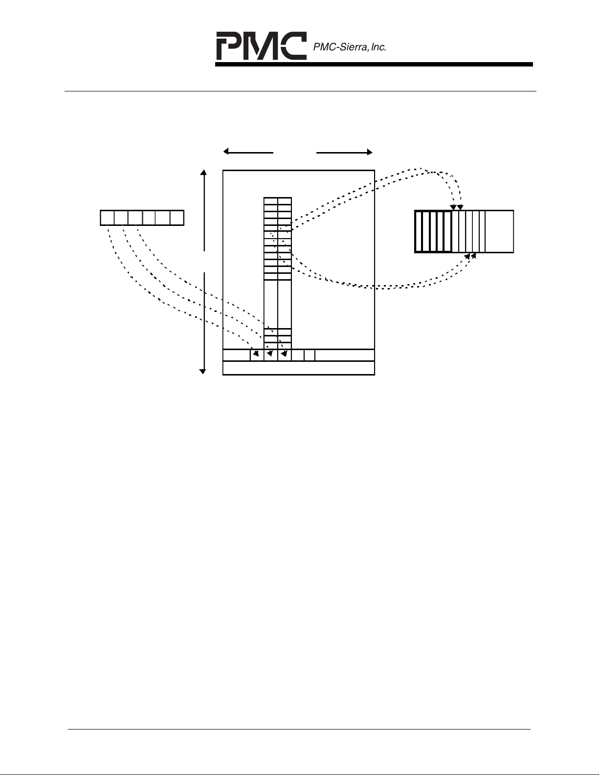
RELEASED
T ALP builds (segments) cell
DATASHEET
PMC-2000097 ISSUE 2 8 LINK CES/DBCES AAL1 SAR
PM73123 AAL1GATOR-8
Figure 31 Payload Generation
TFTC w r i tes th e byt es in
pair s into T_DATA_BUFFER
RL_SER
5 6 7 8 9 10
. . . .. . . .
0
Frames
127
Channel
0 31
6 7
T_DATA_BUFFER
from T_DATA_BUFFER. In
this case from DS0s 6 and 7.
For AAL0 mode the cell build process takes 48 bytes of line data and does not
add any AAL1 overhead bytes.
For DBCES mode, anytime a pointer is generated, the subsequent start of
structure will contain the bitmask field with the number of channels currently
active. Changes in the bitmask can only occur at this time.
9.2.1.3.3 Peak Cell Rates (PCRs)
For purposes of discussion, the following PCR information is assumed:
• Full cells are used,
• The PCR numbers are per line, and
• The SYS_CLK is 38.88 MHz.
9.2.1.3.3.1 Peak Cell Rates (PCRs) for Structured Cell Formats
• For structured connection without CAS, PCR <= 171 x n cells per second per
connection where 1 <= n <= 32 (assuming completely filled cells).
PMC-SIERRA, INC. PROPRIETARY AND CONFIDENTIAL
99

RELEASED
100
DATASHEET
PMC-2000097 ISSUE 2 8 LINK CES/DBCES AAL1 SAR
PM73123 AAL1GATOR-8
• For structured connection with CAS, PCR <= 182 x n cells per second per
connection where 1 <= n <= 32 (assuming completely filled cells).
• Each AAL1 cell is either 46 or 47 bytes, depending upon whether or not the cell
contains a structure pointer.
9.2.1.3.3.2 Peak Cell Rates (PCRs) for Unstructured Cell Formats
• PCR <= 4,107 cells per second for T1 (assuming 47 bytes for each AAL1 cell).
• PCR <= 5,447 cells per second for E1 (assuming 47 bytes for each AAL1 cell).
• PCR <= 118,980 cells per second for T3 (assuming 47 bytes for each AAL1 cell).
• PCR <= 91,405 cells per second for E3 (assuming 47 bytes for each AAL1 cell).
• If all eight lines are at the same rate, totaling 20 Mbps throughput for the device,
then the aggregate device PCR <= 53,191 cells per second for multiple-line
unstructured data format (assuming 47 bytes for each AAL1 cell). If all lines are
not at the same rate, the aggregate device PCR <= 46,542.
• PCR <= 1,000 cells per second per device for OAM cells. This rate of OAM cells
is calculated on the basis of up to four cells per second per VC. Transmitting and
receiving OAM cells at this rate consumes 20% of the microprocessor accesses.
9.2.1.3.3.3 Peak Cell Rates and Partial Cells
Partial Cells can be used to minimize the amount of delay required to assemble
a cell. However, the amount of overhead required for the same amount of TDM
data increases when partial cells are used. This overhead increases as the
number of data bytes per cell decreases. The following table shows the
minimum partial cell sizes that can be supported for the different modes of
operation if all connections are active on the device. If a smaller partial cell size
is desired, either some time slots/links must not be used or only a subset of the
connections must use that partial cell size. In any case the total PCR of the
device should not exceed 100,000 cells per second with a 38.88 MHz SYSCLK
or 110,000 cells per second with a 45 MHz SYSCLK.
Table 5 Minimum Partial Cell Size Permitted If A ll Connections Are Activ e
MODE SYS_CLK=38.88 MHz SYS_CLK = 45 MHz
T1 SDF-FR
PMC-SIERRA, INC. PROPRIETARY AND CONFIDENTIAL
16 14
 Loading...