

Page 1

查询1991089供应商
PRELIMINARY
REFERENCE DESIGN
PMC-1991089 ISSUE 2 AAL1GATOR-8 REFERENCE DESIGN
PM73123 AAL1GATOR-8
PM4354 COMET-QUAD
PM73123
AAL1GATOR-8
REFERENCE DESIGN
PRELIMINARY
ISSUE 2: JUNE 2001
PROPRIETARY AND CONFIDENTIAL TO PMC-SIERRA, INC., AND FOR ITS CUSTOMERS’ INTERNAL USE
Page 2
PRELIMINARY
REFERENCE DESIGN
PMC-1991089 ISSUE 2 AAL1GATOR-8 REFERENCE DESIGN
PM73123 AAL1GATOR-8
PM4354 COMET-QUAD
PUBIC REVISION HISTORY
Issue
Issue Date Details of Change
No.
1 December
Document created.
1999
2 June 2001 Updated COMET-QUAD decoupling (C4, C6, C14,
C21, C42, C49, C56, C65) in the schematics and
corrected power sequencing description.
Updated power calculations.
PROPRIETARY AND CONFIDENTIAL TO PMC-SIERRA, INC., AND FOR ITS CUSTOMERS’ INTERNAL USE
Page 3

PRELIMINARY
REFERENCE DESIGN
PMC-1991089 ISSUE 2 AAL1GATOR-8 REFERENCE DESIGN
PM73123 AAL1GATOR-8
PM4354 COMET-QUAD
CONTENTS
1 INTRODUCTION...................................................................................... 1
1.1 PURPOSE..................................................................................... 1
1.2 SCOPE.......................................................................................... 1
1.3 APPLICATIONS ............................................................................ 1
2 GENERAL DESCRIPTION....................................................................... 3
2.1 AAL1GATOR-8 ARCHITECTURE ................................................. 3
3 FEATURES .............................................................................................. 6
4 HIGH LEVEL DESIGN ............................................................................. 7
5 BLOCK DESCRIPTION ......................................................................... 13
5.1 AAL1GATOR-8............................................................................ 13
5.2 COMET ....................................................................................... 15
5.3 COMET-QUAD ............................................................................ 17
5.4 THE MICROPROCESSOR INTERFACE BLOCK....................... 18
5.5 AAL1GATOR-8 TO COMET/COMET-QUADS
INTERCONNECTIONS ............................................................... 19
5.6 THE FPGA BLOCK ..................................................................... 20
5.7 AAL1GATOR-8’S SRAM ............................................................. 21
5.8 REGULATORS BLOCK............................................................... 21
5.9 LED BLOCKS.............................................................................. 21
5.10 RESET BLOCK ........................................................................... 22
5.11 JTAG PORT ................................................................................ 22
5.12 TIMING BLOCK........................................................................... 22
5.13 UTOPIA INTERFACE .................................................................. 23
PROPRIETARY AND CONFIDENTIAL TO PMC-SIERRA, INC., AND FOR ITS CUSTOMERS’ INTERNAL USE i
Page 4

PRELIMINARY
REFERENCE DESIGN
PMC-1991089 ISSUE 2 AAL1GATOR-8 REFERENCE DESIGN
PM73123 AAL1GATOR-8
PM4354 COMET-QUAD
6 DESIGN ISSUES ................................................................................... 24
6.1 AAL1GATOR-8 DESIGN CONSIDERATIONS ............................ 24
6.1.1 POWER SUPPLY............................................................. 24
6.1.2 DECOUPLING.................................................................. 24
6.1.3 LINE MODE SELECTION................................................. 24
6.2 LINE TERMINATION ................................................................... 24
6.3 COMET DESIGN CONSIDERATIONS........................................ 24
6.3.1 POWER SUPPLY............................................................. 24
6.3.2 DECOUPLING.................................................................. 25
6.3.3 VOLTAGE REFERENCES................................................ 25
6.4 COMET-QUAD DESIGN CONSIDERATIONS ............................ 25
6.4.1 POWER SUPPLY SEQUENCING.................................... 25
6.4.2 DECOUPLING.................................................................. 26
6.4.3 VOLTAGE REFERENCES................................................ 26
6.5 MICROPROCESSOR INTERFACE ............................................ 26
6.6 POWER REQUIREMENTS......................................................... 31
7 IMPLEMENTATION DESCRIPTION ...................................................... 33
7.1 AAL1GATOR-8 WITH COMET SCHEMATICS ........................... 33
7.2 AAL1GATOR-8 WITH COMET-QUAD SCHEMATICS ................ 35
8 GLOSSARY ........................................................................................... 37
9 DEFINITIONS ........................................................................................ 38
10 REFERENCES....................................................................................... 39
11 DISCLAIMER ......................................................................................... 40
12 APPENDIX A: BILL OF MATERIALS (COMET VERSION) .................... 41
PROPRIETARY AND CONFIDENTIAL TO PMC-SIERRA, INC., AND FOR ITS CUSTOMERS’ INTERNAL USE ii
Page 5

PRELIMINARY
REFERENCE DESIGN
PMC-1991089 ISSUE 2 AAL1GATOR-8 REFERENCE DESIGN
PM73123 AAL1GATOR-8
PM4354 COMET-QUAD
13 APPENDIX B: BILL OF MATERIALS (COMET-QUAD VERSION)......... 43
14 APPENDIX C: AAL1GATOR-8 W/COMETS SCHEMATICS.................. 45
15 APPENDIX D: AAL1GATOR-8 W/COMET-QUADS SCHEMATICS ....... 46
PROPRIETARY AND CONFIDENTIAL TO PMC-SIERRA, INC., AND FOR ITS CUSTOMERS’ INTERNAL USE iii
Page 6

PRELIMINARY
REFERENCE DESIGN
PMC-1991089 ISSUE 2 AAL1GATOR-8 REFERENCE DESIGN
PM73123 AAL1GATOR-8
PM4354 COMET-QUAD
LIST OF FIGURES
FIGURE 1 AAL1GATOR-8 CONFIGURATIONS ............................................... 3
FIGURE 2 AAL1GATOR-8 AND COMETS ........................................................ 4
FIGURE 3 AAL1GATOR-8 AND COMET-QUADS............................................. 5
FIGURE 4 AAL1GATOR-8 REF DESIGN BLOCK DIAGRAM WITH COMETS 8
FIGURE 5 AAL1GATOR-8 REF DESIGN DIAGRAM WITH COMET-QUADS .. 9
FIGURE 6 GLUELESS AAL1GATOR-8 TO COMETS CONNECTION.............11
FIGURE 7 GLUELESS AAL1GATOR-8 TO COMET-QUADS CONNECTION .11
PROPRIETARY AND CONFIDENTIAL TO PMC-SIERRA, INC., AND FOR ITS CUSTOMERS’ INTERNAL USE iv
Page 7

PRELIMINARY
REFERENCE DESIGN
PMC-1991089 ISSUE 2 AAL1GATOR-8 REFERENCE DESIGN
PM73123 AAL1GATOR-8
PM4354 COMET-QUAD
LIST OF TABLES
TABLE 1 AAL1GATOR-8 TO COMET/COMET-QUAD CONNECTIONS ...... 19
TABLE 2 OSCILLATORS .............................................................................. 22
TABLE 3 AAL1GATOR-8’S UTOPIA OPERATING MODES ......................... 23
TABLE 4 INTERFACE PINOUT FOR AAL1GATOR-8 W/COMETS.............. 26
TABLE 5 INTERFACE PINOUT FOR AAL1GATOR-8 W/COMET-QUADS... 28
TABLE 6 ADDRESS SPACE FOR AAL1GATOR-8 W/COMETS .................. 30
TABLE 7 ADDRESS SPACE FOR AAL1GATOR-8 W/COMET-QUADS....... 30
TABLE 8 POWER CONSUMPTION FOR AAL1GATOR-8 W/COMETS .......... 31
TABLE 9 POWER FOR AAL1GATOR-8 W/COMET-QUADS........................... 31
TABLE 10 MAJOR COMPONENTS LIST 1 .................................................... 41
TABLE 11 MAJOR COMPONENTS LIST 2 .................................................... 43
PROPRIETARY AND CONFIDENTIAL TO PMC-SIERRA, INC., AND FOR ITS CUSTOMERS’ INTERNAL USE v
Page 8

PRELIMINARY
REFERENCE DESIGN
PMC-1991089 ISSUE 2 AAL1GATOR-8 REFERENCE DESIGN
PM73123 AAL1GATOR-8
PM4354 COMET-QUAD
1 INTRODUCTION
The AAL1gator-8 Reference Design assists customers in designing a Circuit
Emulation Service (CES) and/or a Dynamic Bandwidth Circuit Emulation Service
(DBCES) card. The CES/DBCES card is used to emulate circuit oriented
transmission characteristics to support Constant Bit Rate (CBR) traffic.
1.1 PURPOSE
This reference design will assist engineers in designing their products using
PMC-Sierra's AAL1gator-8, COMET and COMET-QUAD devices thereby
bringing customers’ designs to market earlier.
1.2 SCOPE
This document is a paper reference design and describes the scope and
deliverables required for the AAL1gator-8 Reference Design. Note that the
design was not actually built and tested, but has only been designed on paper.
This reference design is a modularized card with two design options:
1. AAL1gator-8, two COMET-QUADs, a microprocessor interface, and line
interfaces.
2. AAL1gator-8, eight COMETs, a microprocessor interface, and line interfaces.
A block diagram is shown for the two designs. Descriptions are provided for
each of the functional blocks and detailed implementation descriptions then
follow.
1.3 APPLICATIONS
Emulating existing TDM circuits is an essential function for ATM switches.
Currently TDM circuits provide most voice and data services and therefore
seamless interaction between TDM and ATM has become a system requirement.
The ATM Forum has standardized an internetworking function that satisfies this
requirement called the Circuit Emulation Services (CES) Specification.
The following are some application examples of the AAL1gator-8 Reference
Design:
• An 8-Link T1/E1 CES Cards in a PBX
PROPRIETARY AND CONFIDENTIAL TO PMC-SIERRA, INC., AND FOR ITS CUSTOMERS’ INTERNAL USE 1
Page 9

PRELIMINARY
PM73123 AAL1GATOR-8
PM4354 COMET-QUAD
REFERENCE DESIGN
PMC-1991089 ISSUE 2 AAL1GATOR-8 REFERENCE DESIGN
• TDM to ATM Access Service Concentrator
• Part of a TDM to ATM Multiservice ATM Switch
PROPRIETARY AND CONFIDENTIAL TO PMC-SIERRA, INC., AND FOR ITS CUSTOMERS’ INTERNAL USE 2
Page 10
PRELIMINARY
REFERENCE DESIGN
PMC-1991089 ISSUE 2 AAL1GATOR-8 REFERENCE DESIGN
PM73123 AAL1GATOR-8
PM4354 COMET-QUAD
2 GENERAL DESCRIPTION
2.1 AAL1gator-8 Architecture
The purpose of the AAL1gator-8 is to provide high density T1/E1, or DS3/E3/J2
line interfaces access to an AAL1 CBR ATM network. The AAL1gator-8 can
support 8 T1/E1 lines, 1 DS3/E3/STS-1 link or 2 8Mbps H-MVIP links. The
AAL1gator-8 is capable of supporting 256 VCs. On the system side, the
AAL1gator-8 supports a standard UTOPIA Level 2 interface that optionally
supports parity and runs up to 52 MHz. An optional 8/16-bit Any-PHY slave
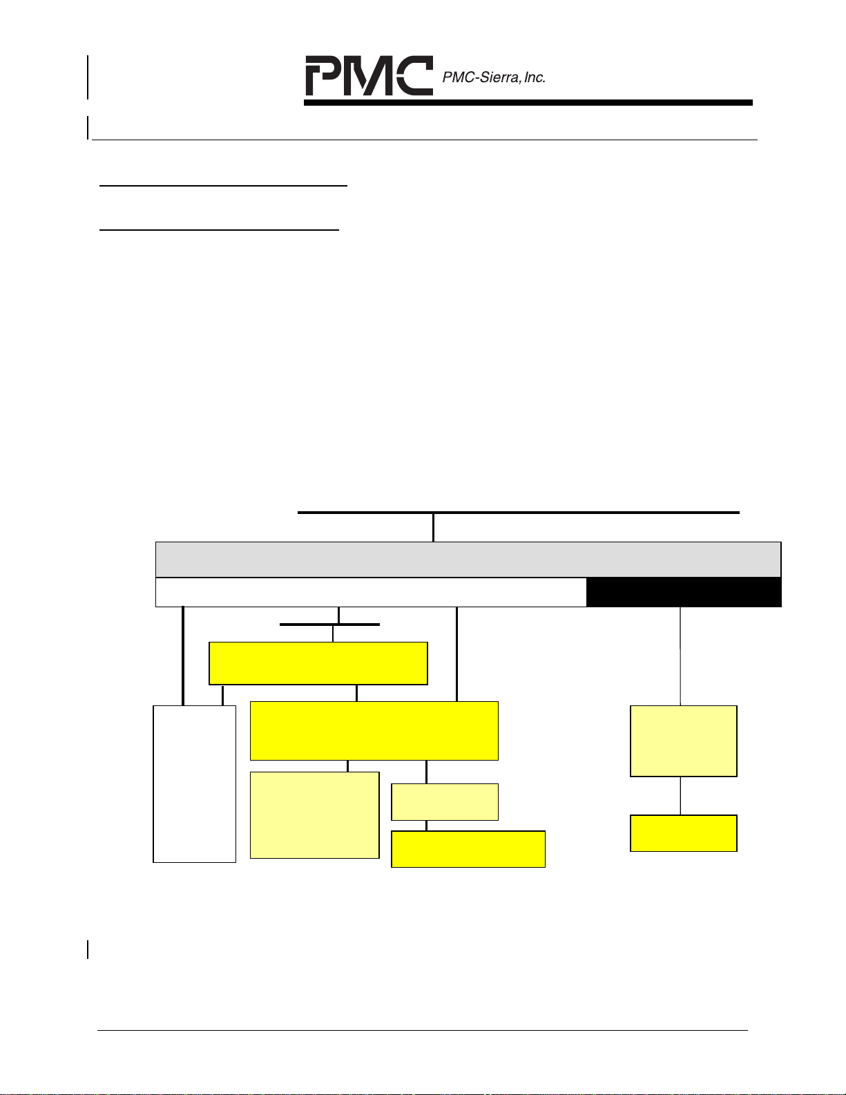
interface and UTOPIA Level 1 master/slave interface are also supported on the
system side. Figure 1 indicates the ways in which an AAL1gator-8 can be used
to connect to T1/E1 or DS3/E3 line interfaces.
Figure 1 AAL1gator-8 Configurations
T1/E1
Framer+LIU
(COMET)
or
(COMET-Q)
Any-PHY / UTOPIA
AAL1gator-8
Structured or unstructured T1/E1 with CAS support Unstructured DS3/E3
MVIP
TDM Switch
T1/E1 Framer
(TQUAD/EQUAD)
T1/E1
LIU
(QDSX)
M13 Mux
(D3MX)
DS3
LIU
DS3/E3
Framer
(S/UNI-QJET)
DS3/E3
LIU
Figures 2 and 3 show the system context in which the AAL1gator-8 devices
reside within the reference designs. In these designs each AAL1gator-8 can
interface with eight COMETs or two COMET-QUADs to support 8
structured/unstructured T1s or E1s.
PROPRIETARY AND CONFIDENTIAL TO PMC-SIERRA, INC., AND FOR ITS CUSTOMERS’ INTERNAL USE 3
Page 11
PRELIMINARY
REFERENCE DESIGN
PMC-1991089 ISSUE 2 AAL1GATOR-8 REFERENCE DESIGN
PM73123 AAL1GATOR-8
PM4354 COMET-QUAD
The PM4351 COMET is a single channel combined E1/T1 transceiver and
framer, and the PM4354 COMET-QUAD is a four channel combined E1/T1
transceiver and framer – both devices are capable for use in long and short haul
T1, J1 and E1 systems with a minimum of external circuitry. When used with the
COMETs or COMET-QUADs, AAL1gator-8 can be part of a multiservice switch
application which can provide circuit emulation services on E1 or T1 pipes.
Figure 2 AAL1gator-8 and COMETs
Data and Clock Lines
Line Interface
Line Interface
Line Interface
Line Interface
Line Interface
Line Interface
Line Interface
PM4351
COMET
PM4351
COMET
PM4351
COMET
PM4351
COMET
PM4351
COMET
PM4351
COMET
PM4351
COMET
PM73123
AAL1gator-8
UTOPIA / Any-
PHY
Line Interface
PROPRIETARY AND CONFIDENTIAL TO PMC-SIERRA, INC., AND FOR ITS CUSTOMERS’ INTERNAL USE 4
PM4351
COMET
Page 12
PRELIMINARY
REFERENCE DESIGN
PMC-1991089 ISSUE 2 AAL1GATOR-8 REFERENCE DESIGN
PM73123 AAL1GATOR-8
PM4354 COMET-QUAD
Figure 3 AAL1gator-8 and COMET-QUADs
Data and Clock Lines
PM4354
COMET-QUAD
PM73123
AAL1gator-8
UTOPIA / Any-
PHY
PM4354
COMET-QUAD
The COMETs or COMET-QUADs receive data through the T1/E1 line interfaces.
The formatted data is then passed through the T1/E1 framers to the AAL1gator-8
for CBR servicing. The cells are then routed through a UTOPIA L2 connector for
routing, switching, traffic policing and shaping.
In the transmit path, the AAL1gator-8 receives the ATM cells from the UTOPIA
bus. The AAL1gator-8 retrieves the data and signaling information, and places
the data to be transmitted over the T1 or E1 lines via the COMETs or COMETQUADs in the appropriate port and time slot.
PROPRIETARY AND CONFIDENTIAL TO PMC-SIERRA, INC., AND FOR ITS CUSTOMERS’ INTERNAL USE 5
Page 13

PRELIMINARY
REFERENCE DESIGN
PMC-1991089 ISSUE 2 AAL1GATOR-8 REFERENCE DESIGN
PM73123 AAL1GATOR-8
PM4354 COMET-QUAD
3 FEATURES
• Implementation strategy for the AAL1gator-8 in a Multi Service Access
Concentrator environment using the PM4351 COMET and PM4354 COMETQUAD.
• Supports 8 T1/E1 rates and channelized mode.
• Supports a CES.
• Supports independently clocked links.
• Has a microprocessor interface for configuration and monitoring.
PROPRIETARY AND CONFIDENTIAL TO PMC-SIERRA, INC., AND FOR ITS CUSTOMERS’ INTERNAL USE 6
Page 14

PRELIMINARY
REFERENCE DESIGN
PMC-1991089 ISSUE 2 AAL1GATOR-8 REFERENCE DESIGN
PM73123 AAL1GATOR-8
PM4354 COMET-QUAD
4 HIGH LEVEL DESIGN
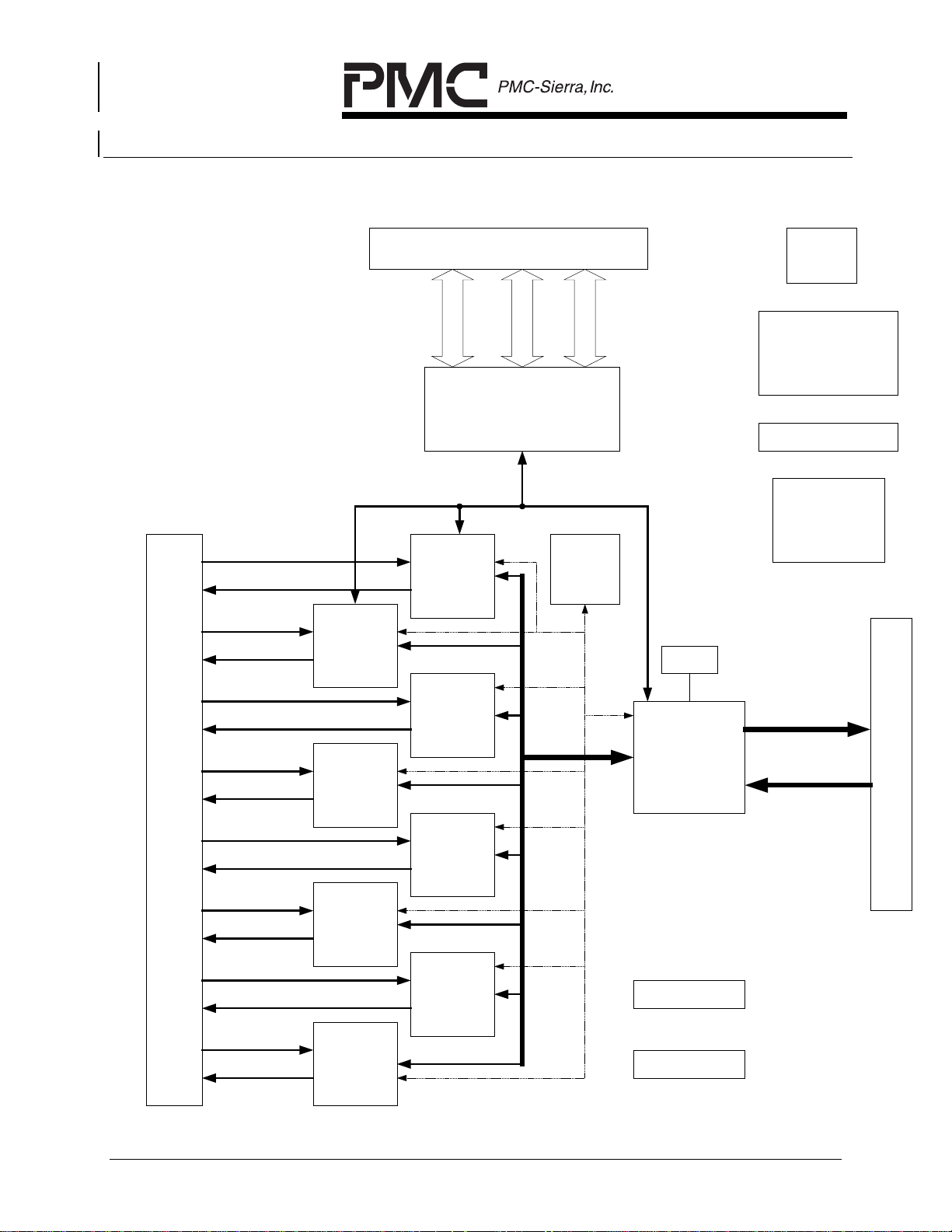
The block diagrams of the AAL1gator-8 reference design are shown in Figure 4
and Figure 5. Figure 4 illustrates the high level design of the reference design
with 8 COMET devices while Figure 5 shows the high level design with two
COMET-QUAD devices.
PROPRIETARY AND CONFIDENTIAL TO PMC-SIERRA, INC., AND FOR ITS CUSTOMERS’ INTERNAL USE 7
Page 15
PRELIMINARY
PM73123 AAL1GATOR-8
PM4354 COMET-QUAD
REFERENCE DESIGN
PMC-1991089 ISSUE 2 AAL1GATOR-8 REFERENCE DESIGN
Figure 4 AAL1gator-8 Ref Design Block Diagram with COMETs
Line
Interface
RXRING1 & RXTIP1
TXRING1 &TXTIP1
RXRING2 & RXTIP2
TXRING2 &TXTIP2
RXRING3 & RXTIP3
TXRING3 &TXTIP3
RXRING4 & RXTIP4
TXRING4 &TXTIP4
RXRING5 & RXTIP5
TXRING5 &TXTIP5
Microprocessor Interface
Data Bus
(Buffers/XCVRs, Decode Logic)
Address, Data and Control Bus
PM4351
COMET
PM4351
COMET
PM4351
COMET
PM4351
COMET
PM4351
COMET
Address Bus
Memory system
Data and clock
FPGA
Lines
Reset
Switch
Control Bus
2.5 V and 3.3 V
Regulators
Power LEDs
Oscillators
128Kx16
RAM
PM73123
AAL1gator-8
UTOPIA L2
UTIOPA
L2
Connect
RXRING6 & RXTIP6
PM4351
TXRING6 &TXTIP6
RXRING7 & RXTIP7
TXRING7 &TXTIP7
RXRING8 & RXTIP8
TXRING8 &TXTIP8
PROPRIETARY AND CONFIDENTIAL TO PMC-SIERRA, INC., AND FOR ITS CUSTOMERS’ INTERNAL USE 8
COMET
PM4351
COMET
PM4351
COMET
AAL1gator-8
ALARM LEDs
COMET ALARMS
LEDs
Page 16
PRELIMINARY
PM73123 AAL1GATOR-8
PM4354 COMET-QUAD
REFERENCE DESIGN
PMC-1991089 ISSUE 2 AAL1GATOR-8 REFERENCE DESIGN
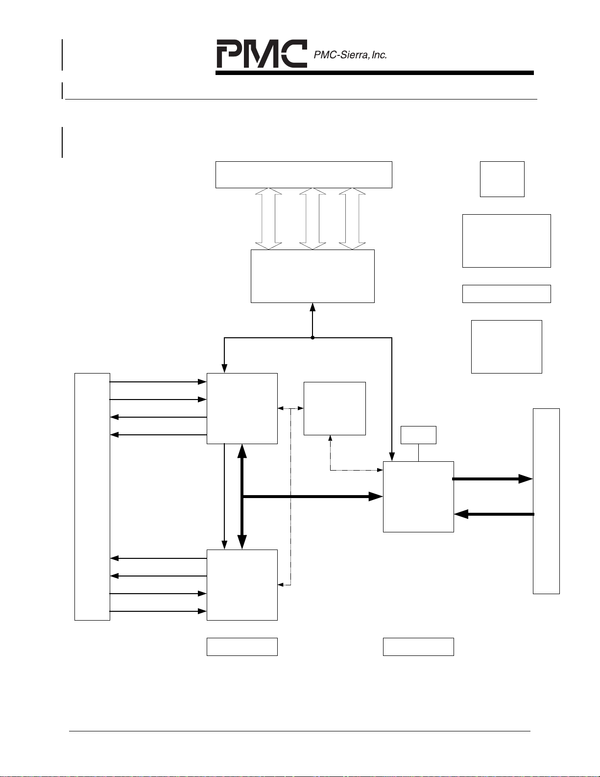
Figure 5 AAL1gator-8 Ref Design Diagram with COMET-QUADs
RXRING[4:1]
RXTIP[4:1]
TXTIP[4:1]
TXRING[4:1]
Microprocessor Interface
Data Bus
Memory system
(Buffers/XCVRs, Decode Logic)
Address, Data and Control Bus
PM4354
COMET-QUAD
Address Bus
FPGA
Reset
Switch
Control Bus
2.5 V and 3.3 V
Regulators
Power LEDs
Oscillators
128Kx16
RAM
Line
Interface
Data and clock Lines
PM73123
AAL1gator-8
TXRING[8:5]
TXTIP[8:5]
PM4354
RXTIP[8:5]
COMET-QUAD
RXRING[8:5]
COMET-QUAD
ALARMS LEDs
PROPRIETARY AND CONFIDENTIAL TO PMC-SIERRA, INC., AND FOR ITS CUSTOMERS’ INTERNAL USE 9
AAL1gator-8
ALARM LEDs
UTOPIA L2
UTIOPA
L2
Connect
Page 17

PRELIMINARY
REFERENCE DESIGN
PMC-1991089 ISSUE 2 AAL1GATOR-8 REFERENCE DESIGN
PM73123 AAL1GATOR-8
PM4354 COMET-QUAD
As illustrated, the designs contain the following functional blocks:
1. PM73123 AAL1gator-8
2. PM4351 COMET/PM4354 COMET-QUAD
3. Microprocessor and Memory System Interface
4. Field Programmable Gate Array (FPGA)
5. Line Interface
6. UTOPIA Interface
7. Power and Clock Sources
The hardware allows full access to the AAL1gator-8 and COMET/COMET-QUAD
devices via the microprocessor interface. Each COMET device acts as a single
line interface unit with the integrated long haul LIU, and a T1/E1 framer/deframer while each COMET-QUAD device acts as four line interface units with the
integrated long haul LIUs, and T1/E1 framers/de-framers.
In the receive path (from a T1 or E1 line), a COMET or COMET-QUAD converts
the incoming line data (in the form of channels) to a serial bit stream. The
AAL1gator-8 then receives this data and clocking information and builds AAL1
cells to be sent to the UTOPIA bus.
In the transmit path (to a T1 or E1 line), the AAL1gator-8 receives the ATM cells
from the UTOPIA bus. The AAL1gator-8 retrieves the data and signaling
information, and places the data to be transmitted over the T1 or E1 lines via the
COMETs/COMET-QUADs in the appropriate port and time slot.
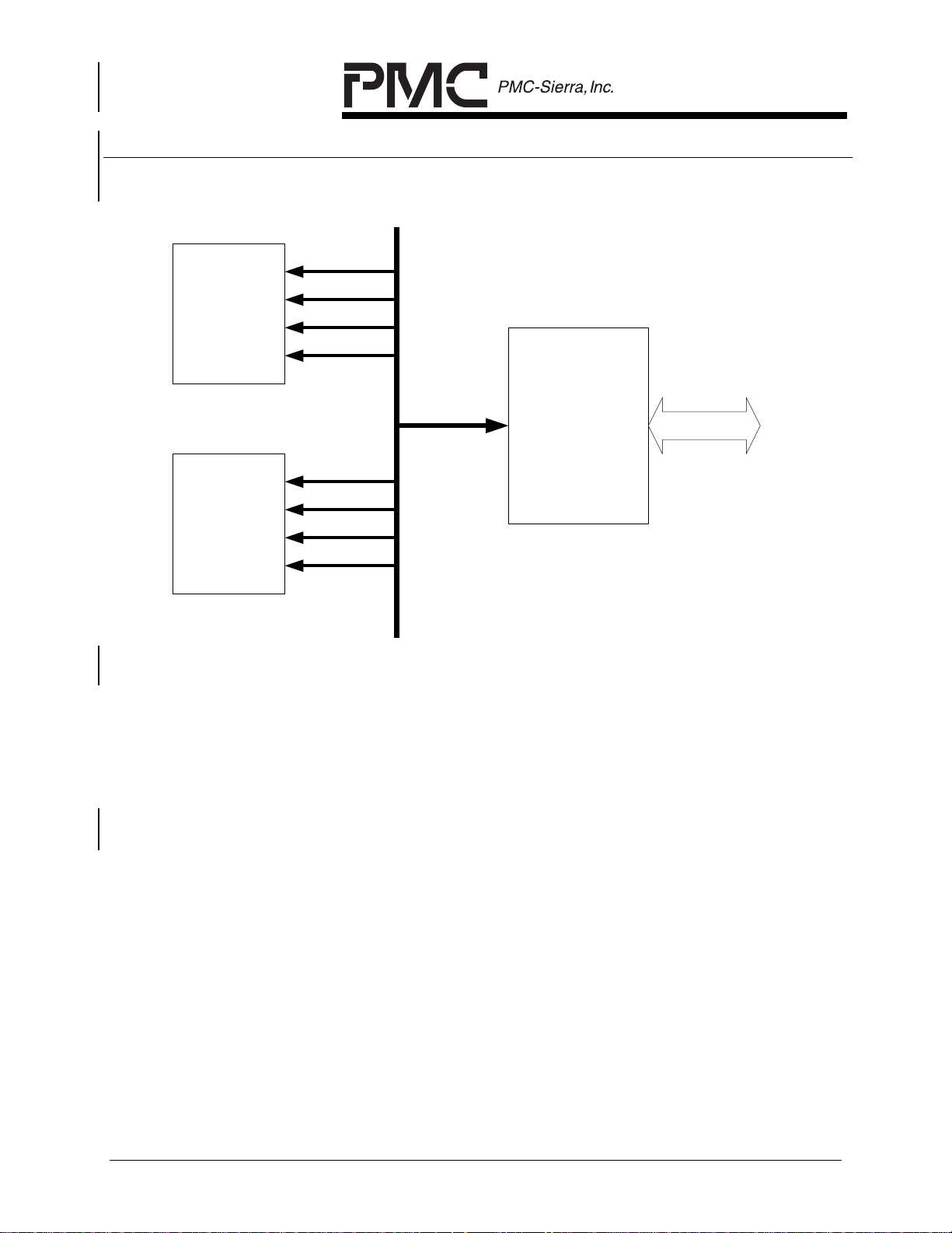
As illustrated in both Figure 4 and Figure 5, the connections from the FPGA to
the PMC’s devices are dotted lines. This is because it is possible to connect the
AAL1gator-8 to the COMETs or COMET-QUADs directly (i.e. without using a
FPGA). Figure 6 shows the direct connection between the AAL1gator-8 and
COMETs while Figure 7 illustrates this glueless interconnection between
AAL1gator-8 and COMET-QUADs.
PROPRIETARY AND CONFIDENTIAL TO PMC-SIERRA, INC., AND FOR ITS CUSTOMERS’ INTERNAL USE 10
Page 18
PRELIMINARY
PM73123 AAL1GATOR-8
PM4354 COMET-QUAD
REFERENCE DESIGN
PMC-1991089 ISSUE 2 AAL1GATOR-8 REFERENCE DESIGN
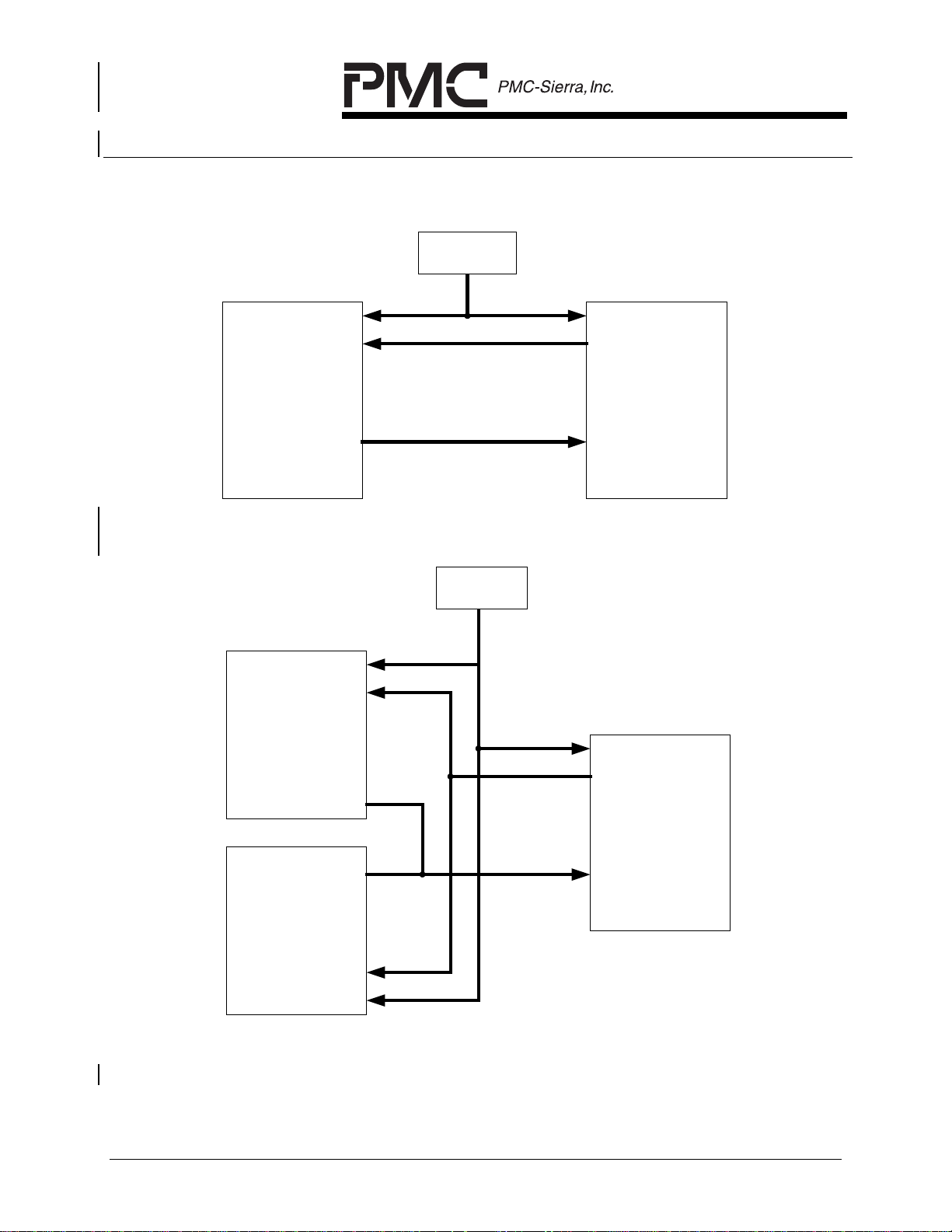
Figure 6 Glueless AAL1gator-8 to COMETs Connection
Optional
External Clock
Source
BTCLK[7..0] TL_CLK[7..0]
BTSIG[7..0] TL_SIG[7..0]
8 COMET Blocks
BTFP[7..0] TL_SYNC[7..0]
PM73123
AAL1gator-8
Figure 7 Glueless AAL1gator-8 to COMET-QUADs Connection
Optional
External Clock
Source
BTCLK[4..1]
BTSIG[4..1]
PM4354
COMET-QUAD
BTFP[4..1]
TL_CLK[7..0]
TL_SIG[7..0]
PM73123
AAL1gator-8
BTFP[4..1]
TL_SYNC[7..0]
PM4354
COMET-QUAD
BTSIG[4..1]
BTCLK[4..1]
The AAL1gator-8 also supports 8Mbit/s H-MVIP on the line interface, and the
COMET-QUAD also supports 8Mbit/s H-MVIP on the system interface.
PROPRIETARY AND CONFIDENTIAL TO PMC-SIERRA, INC., AND FOR ITS CUSTOMERS’ INTERNAL USE 11
Page 19

PRELIMINARY
REFERENCE DESIGN
PMC-1991089 ISSUE 2 AAL1GATOR-8 REFERENCE DESIGN
PM73123 AAL1GATOR-8
PM4354 COMET-QUAD
Therefore, an H-MVIP interface is optionally provided for the AAL1gator-8 with
COMET-QUAD Reference design.
The main purpose of the FPGA is to provide maximum clock distribution flexibility
by allowing for independently clocked links. The AAL1gator-8 is capable of
implementing SRTS and the Adaptive Clock Recovery algorithm on its own;
however, using an FPGA it is possible to implement an external Adaptive Clock
Recovery scheme or SRTS clock scheme. The FPGA is also used for the
generation of TL_CLK (AAL1gator-8) and BTCLK (COMET and COMET-QUAD).
In addition, the FPGA generates an appropriate signal for the AAL1gator-8
network clock pin, N_CLK, (at 2.43 MHz), and also distributes XCLK signals to
the 8 COMET or two COMET-QUAD devices from only two clock oscillators:
1.544 MHz and 2.048 MHz.
In H-MVIP mode, the FPGA is used to distribute the 16.384 MHz clock to the
AAL1gator-8’s C16B and to the COMET-QUADs’ CMV8MCLK input pins. The
FPGA is also used to distribute the 4.096 MHz Frame Pulse Clock to the
AAL1gator-8’s C4B and to the COMET-QUADs’ CMVPFC inputs, and to
generate the 8 kHz Common H-MVIP Frame Pulse from the Frame Pulse Clock.
In addition, in both Figures 6 and 7, the TL_SYNC pins of the AAL1gator-8 are
connected to the COMET BTFP pin or the COMET-QUAD BTFP pins (configured
as outputs). Depending on the value of MF_SYNC_MODE in the LI_CFG_REG
register of the AAL1gator-8 for the line, this allows for alignment of signaling bits
on multiframe boundaries or a frame boundary.
Power requirements of the boards are +5.0V, +3.3V and +2.5V. The AAL1gator8 and COMET-QUADs require +3.3V and +2.5V while COMETs require only
+3.3V. +5.0V is used as input to the COMETs’ BIAS pins and to generate the
+3.3V and +2.5V using voltage regulators.
In this reference design, the AAL1gator-8, COMET and COMET-QUAD devices
are configured with de-multiplexed microprocessor address and data bus. The
microprocessor interface has been provided through a 96-pin connector. This
interface provides configuration and monitoring for PMC-Sierra’s devices.
The memory sub-unit of the AAL1gator-8’s block contains a 128k x 16 SRAM
module connected to the AAL1gator-8 device’s RAM interface.
Two 80-pin female UTOPIA connectors carry the receive and transmit UTOPIA
signals between the AAL1gator-8 and an external PHY board or a Parallel Cell
Traffic Generator and Analyzer.
The designs also include several LED circuits for the device alarms and power
indications.
PROPRIETARY AND CONFIDENTIAL TO PMC-SIERRA, INC., AND FOR ITS CUSTOMERS’ INTERNAL USE 12
Page 20

PRELIMINARY
REFERENCE DESIGN
PMC-1991089 ISSUE 2 AAL1GATOR-8 REFERENCE DESIGN
PM73123 AAL1GATOR-8
PM4354 COMET-QUAD
5 BLOCK DESCRIPTION
5.1 AAL1gator-8
The AAL1 Segmentation and Reassembly (SAR) Processor (AAL1gator-8) is a
monolithic single chip device that provides DS1, E1, E3, or DS3 line interface
access to an ATM Adaptation Layer One (AAL1) Constant Bit Rate (CBR) ATM
network. It arbitrates access to an external (128K x 16/18 bits) 10ns SRAM for
storage of the configuration, the user data, and the statistics. Some of the
device’s important functionality is as follows:
• Compliant with the ATM Forum’s Circuit Emulation Services (CES)
specification (AF-VTOA-0078), and the ITU-T I.363.1
• Supports Dynamic Bandwidth Circuit Emulation Services (DBCES).
Compliant with the ATM Forum’s DBCES specification (AF-VTOA-0085).
• Supports idle channel detection via processor intervention, CAS signaling, or
data pattern detection.
• Provides idle channel indication on a per channel basis.
• Provides AAL1 segmentation and reassembly of 8 individual E1 or T1 lines, 2
H-MVIP lines at 8Mbit/s, or 1 E3 or DS3 line.
• Provides a standard 16/8 bits UTOPIA level 2 Interface which optionally
supports parity and runs up to 50 MHz. The following modes are supported:
• 16-bit Level 2, Multi-Phy Mode (MPHY)
• 8-bit Level 2, MPHY
• 8-bit Level 1, SPHY
• 8-bit Level 1, ATM Master
• Supports up to 256 Virtual Channels (VC).
The AAL1gator-8 is configured, controlled and monitored via a generic 8-bit
microprocessor bus through which all internal registers are accessed. All
sources of interrupts can be masked and acknowledged through the
microprocessor interface.
PROPRIETARY AND CONFIDENTIAL TO PMC-SIERRA, INC., AND FOR ITS CUSTOMERS’ INTERNAL USE 13
Page 21

PRELIMINARY
REFERENCE DESIGN
PMC-1991089 ISSUE 2 AAL1GATOR-8 REFERENCE DESIGN
PM73123 AAL1GATOR-8
PM4354 COMET-QUAD
In this reference design, the AAL1gator-8 is configured with the direct mode at
the line interface to connect to 8 COMETs or 2 COMET-QUADs. The line mode
of operation needs to be setup from hardware reset and cannot be changed
once the chip is powered up. The line mode is controlled by the AAL1gator-8’s
LINE_MODE pin. When the LINE_MODE pin is set to low using the provided
jumpers the AAL1gator-8 will support 8 low speed lines, or one high speed line,
to interface with the COMET or COMET-QUAD devices. When the LINE_MODE
pin is set to high, the AAL1gator-8 will be in H-MVIP mode when interfacing to
the COMET-QUADs. This mode is provided as an extra and optional interface
and can be ignored.
The UTOPIA interface of the AAL1gator-8 will power up with all outputs tri-stated
and will remain tri-stated until the UI_EN bit in the UI_COMN_CFG register is
set.
Also, during the hardware configuration of the AAL1gator-8, the TL_CLK_OE
signal is tied high to use the clock provided on its RL_CLK pin as its TL_CLK and
will drive this clock externally.
When the chip is taken out of hardware reset, the internal DLL on SYSCLK,
which used to maintain low skew on the RAM interface, will go into hunt mode
and will adjust the internal SYSCLK until it aligns with the external SYSCLK. The
microprocessor should poll the RUN bit in the DLL_STAT_REG register until this
bit is set. At this point, the entire chip with the exception of the microprocessor
interface and the DLL are in reset. Before any configuration can be done,
including accessing the RAM, the chip must be taken out of software reset by
clearing the SW_RESET bit in the DEV_ID_REG register. Then, the RAM
should be cleared to all zeros. At this point, the A1SP block is still in reset
because its SW_RESET bit in the CMD_REG register is still set. The line
interface is configured in the direct low speed mode indicated by the
LINE_MODE pins but all internal registers are in the reset state. The line
interface is out of reset at this point but will only be driving data as if all lines
and/or queues are disabled. The UTOPIA interface, as mentioned above, is
disabled and all UTOPIA outputs are tri-stated.
The software configuration of the AAL1gator-8 is done in three steps:
1. Line Configuration: while the A1SP is in reset, the memory mapped registers
which contain the line configuration (the LIN_STR_MODE and HS_LIN_REG
registers) can be initialized. Then, the CMD_ATTN bit in the CMD_REG
register can be set so that the A1SP can read its configuration. The
SW_RESET bit of the CMD_REG register should remain set.
2. Queue Configuration: the SW_RESET bit in the CMD_REG register is
cleared which takes A1SP out of reset. The R_CHAN_2_QUE_TBL will then
PROPRIETARY AND CONFIDENTIAL TO PMC-SIERRA, INC., AND FOR ITS CUSTOMERS’ INTERNAL USE 14
Page 22

PRELIMINARY
REFERENCE DESIGN
PMC-1991089 ISSUE 2 AAL1GATOR-8 REFERENCE DESIGN
PM73123 AAL1GATOR-8
PM4354 COMET-QUAD
begin a 640 SYSCLK cycle initialization, which reset each timeslot to playing
out conditioned data. At this point, the queues can be initialized as needed.
3. Adding Queues: By setting the corresponding bits in the ADDQ_FIFO
register, the queues are added.
For a more detailed description of the AAL1gator-8, please refer to [1].
5.2 COMET
The PM4351 Combined E1/T1 Transceiver (COMET) is a feature-rich monolithic
integrated circuit suitable for use in long haul and short haul T1 and E1 systems
with a minimum of external circuitry. The COMET is software configurable,
allowing feature selection without changes to external wiring.
Analog circuitry is provided to allow direct reception of long haul E1 and T1
compatible signals with up to 36 dB cable loss (at 1.024MHz in E1 mode) or up
to 36 dB cable loss (at 772 kHz in T1 mode) using a minimum of external
components. Typically, only line protection, a transformer and a line termination
resistor are required. Digital line inputs are provided for applications not
requiring a physical T1 or E1 interface.
The COMET recovers clock and data from the line and frames to incoming data.
In T1 mode, it can frame to several DS-1 signal formats: SF, ESF, T1DM (DDS)
and SLC®96. In E1 mode, the COMET frames to basic G.704 E1 signals and
CRC-4 multiframe alignment signals, and automatically performs the G.706
interworking procedure. AMI, HDB3 and B8ZS line codes are supported.
In T1 mode, the COMET generates framing for SF, ESF and T1DM (DDS)
formats. In E1 mode, the COMET generates framing for a basic G.704 E1
signal. The signaling multiframe alignment structure and the CRC multiframe
structure may be optionally inserted. Framing can be optionally disabled.
Internal analog circuitry allows direct transmission of long haul and short haul T1
and E1 compatible signals using a minimum of external components. Typically,
only line protection, a transformer and a line termination resistor are required.
Digitally programmable pulse shaping allows transmission of DSX-1 compatible
signals up to 655 feet from the cross-connect, E1 short haul pulses into 120 ohm
twisted pair or 75 ohm coaxial cable, E1 long haul pulses into 120 ohm twisted
pair as well as long haul DS-1 pulses into 100 ohm twisted pair with integrated
support for LBO filtering as required by the FCC rules. In addition, the
programmable pulse shape extending over 5-bit periods allows customization of
short haul and long haul line interface circuits to application requirements. Digital
line inputs and outputs are provided for applications not requiring a physical T1
or E1 interface.
PROPRIETARY AND CONFIDENTIAL TO PMC-SIERRA, INC., AND FOR ITS CUSTOMERS’ INTERNAL USE 15
Page 23

PRELIMINARY
REFERENCE DESIGN
PMC-1991089 ISSUE 2 AAL1GATOR-8 REFERENCE DESIGN
PM73123 AAL1GATOR-8
PM4354 COMET-QUAD
The COMET provides both a parallel microprocessor interface for controlling the
operation of the device and serial PCM interfaces that allow backplane rates
from 1.544 Mbit/s to 8.192 Mbit/s to be directly supported.
In this reference design, each COMET interfaces with the AAL1gator-8 can be
configured independently in T1 or E1 mode. After the power up or a
hardware/software reset, the following steps are performed to configure the
COMET:
1. Initialize the XLPG (Transmit Pulse Template) registers to clear the pulse
template.
2. Setup the XLPG to program the pulse template to generate short-haul or
long-haul pulses as specified in [2]. Also, set the amplitude of the pulse
template and enable the XLPG.
3. Program the COMET for T1 or E1 mode by writing to the E1/T1B bit of the
Global Configuration register.
4. Configure the Clock Synthesis Unit (CSU) by selecting 1.544MHz or
2.048MHz for the line rate (XCLK and TCLKO).
5. Configure the Clock and Data Recovery Unit (CDRC) to receive the
appropriate line decoding (AMI or B8ZS in T1 mode, HDB3 in E1 mode).
6. Configure the Receive and Transmit Elastic Stores units (RX-ELST and TXELST).
7. Set the framing format and line encoding for the transmitter (XBAS in T1
mode, E1-TRAN in E1 mode).
8. Program the framing format for the receiver.
9. Configure the framing format and the data rate for the facility data link.
10. Configure the Signaling Extraction Block register (SIGX).
11. Configure the Receive Line Interface (RLPS).
12. Configure the Transmit/Receive Jitter Attenuator and the Receive Option
registers to disable or enable the jitter attenuation on transmit or receive line
side.
13. Configure the Backplane Receive System Interface (BRIF) block (registers
0x30 and 0x31):
PROPRIETARY AND CONFIDENTIAL TO PMC-SIERRA, INC., AND FOR ITS CUSTOMERS’ INTERNAL USE 16
Page 24

PRELIMINARY
REFERENCE DESIGN
PMC-1991089 ISSUE 2 AAL1GATOR-8 REFERENCE DESIGN
PM73123 AAL1GATOR-8
PM4354 COMET-QUAD
• Full Frame mode
• BRCLK as an output
• BRPCM, BRSIG, and BRFP updated on the rising edge of
BRCLK
• BRCLK backplane rate (1.544MHz or 2.048MHz)
• BRFP (Backplane Frame Pulse) as an output
14. Configure the Backplane Transmit System Interface (BTIF) block (registers
0x40 and 0x41):
• Full Frame mode
• BRCLK as an input
• BTPCM, BTSIG, and BTFP updated on the rising edge of
• BTCLK backplane rate (1.544MHz or 2.048MHz)
• BRFP (Backplane Frame Pulse) as an output
15. Program the Receive Line Equalization table as stated in [2].
For more information about the COMET please refer to [2].
5.3 COMET-QUAD
The PM4354 Four Channel Combined E1/T1/J1 Transceiver and Framer
(COMET-QUAD) is a feature-rich monolithic integrated circuit suitable for use in
long haul and short haul T1, J1 and E1 systems with a minimum of external
circuitry. The COMET-QUAD is software configurable, allowing feature selection
without changes to external wiring.
Analog circuitry is provided to allow direct reception of long haul E1 and T1/J1
compatible signals typically with up to 43 dB cable loss at 1024 kHz (E1) and up
to 44 dB cable loss at 772 kHz (T1/J1) using a minimum of external components.
Typically, only line protection, a transformer and a line termination resistor are
required.
BTCLK
The COMET-QUAD recovers clock and data from the line and frames to
incoming data. In T1 mode, it can frame to SF and ESF signal formats. In E1
PROPRIETARY AND CONFIDENTIAL TO PMC-SIERRA, INC., AND FOR ITS CUSTOMERS’ INTERNAL USE 17
Page 25

PRELIMINARY
REFERENCE DESIGN
PMC-1991089 ISSUE 2 AAL1GATOR-8 REFERENCE DESIGN
PM73123 AAL1GATOR-8
PM4354 COMET-QUAD
mode, the COMET-QUAD frames to basic G.704 E1 signals and CRC-4
multiframe alignment signals, and automatically performs the G.706 interworking
procedure. AMI, HDB3 and B8ZS line codes are supported.
In T1 mode, the COMET-QUAD generates framing for SF and ESF formats. In
E1 mode, the COMET-QUAD generates framing for a basic G.704 E1 signal.
The signaling multiframe alignment structure and the CRC multiframe structure
may be optionally inserted. Framing can be optionally disabled.
Internal analog circuitry allows direct transmission of long haul and short haul T1
and E1 compatible signals using a minimum of external components. Typically,
only line protection, a transformer and a line termination resistor are required.
Digitally programmable pulse shaping allows transmission of DSX-1 compatible
signals up to 655 feet from the cross-connect, E1 short haul pulses into 120 ohm
twisted pair or 75 ohm coaxial cable, E1 long haul pulses into 120 ohm twisted
pair as well as long haul DS-1 pulses into 100 ohm twisted pair with integrated
support for LBO filtering as required by the FCC rules. In addition, the
programmable pulse shape extending over 5-bit periods allows customization of
short haul and long haul line interface circuits to application requirements.
Serial PCM interfaces to each T1 framer allow 1.544 Mbit/s backplane
receive/backplane transmit system interfaces to be directly supported. Tolerance
of gapped clocks allows other backplane rates to be supported with a minimum
of external logic.
In synchronous backplane systems 8Mbit/s H-MVIP interfaces are provided for
access channel associated signaling (CAS) and common channel signaling
(CCS) for each T1 or E1. The DS0 data channel H-MVIP and CAS H-MVIP
access is multiplexed with the serial PCM interface pins. The CCS signaling HMVIP interface is independent of the DS0 channel and CAS H-MVIP access. The
use of any of the H-MVIP interfaces requires that common clocks and frame
pulse be used along with T1/E1 slip buffers.
The COMET-QUAD is configured, controlled and monitored via a generic 8-bit
microprocessor bus through which all internal registers are accessed. All
sources of interrupts can be masked and acknowledged through the
microprocessor interface.
Please refer to [3] for more information about the COMET-QUAD.
5.4 The Microprocessor Interface Block
The microprocessor interface contains de-multiplexed address and data buses
and a control bus to perform the following functions on the AAL1gator-8
Reference Design:
PROPRIETARY AND CONFIDENTIAL TO PMC-SIERRA, INC., AND FOR ITS CUSTOMERS’ INTERNAL USE 18
Page 26
PRELIMINARY
REFERENCE DESIGN
PMC-1991089 ISSUE 2 AAL1GATOR-8 REFERENCE DESIGN
PM73123 AAL1GATOR-8
PM4354 COMET-QUAD
• Configuration of the AAL1gator-8 and COMET or COMET-QUAD devices
• Monitoring of alarms and interrupts in the AAL1gator-8 and COMET or
COMET-QUAD devices
In order to provide maximum system implementation flexibility, a particular
microprocessor has not been specified. However, the system microprocessor
must have the following minimum capabilities:
1. 23 bit address bus
2. 6 bit data bus
3. 3 programmable chip selects
4. 2 independent interrupt request lines
An example of a microprocessor that meets these minimum requirements is the
Motorola MC68340. Another option would be to implement the design in a PCI
or compact PCI system.
5.5 AAL1gator-8 to COMET/COMET-QUADs Interconnections
The AAL1gator-8 communicates with the COMET/COMET-QUAD devices via
framer bus signals listed in Table 1. Four bits of each signal group connects to
one COMET-QUAD device. For instance, TL_SYNC[3..0] are connected to the
COMET-QUAD 1, while TL_SYNC[7..4] are connected to COMET-QUAD 2.
Table 1 AAL1gator-8 to COMET/COMET-QUAD Connections
SIGNAL DESCRIPTION
TL_SYNC[7..0] The FPGA generates this signal for both the AAL1gator-8 and
COMET/COMET-QUADs. In T1 mode, this signal consists of a
pulse once every 193 bit periods.
TL_CLK[7..0] This is a clock signal at the transmit line rate. Its source is
determined by the configuration of the FPGA.
RL_CLK[7..0] Receive line clock at either 1.544 MHz or 2.048 MHz, derived from
the recovered line rate timing.
RL_SYNC[7..0] Carries receive frame synchronization from the COMET/COMET-
QUAD devices.
RL_SIG[7..0] Carries the CAS signaling information from the COMET/COMET-
QUAD devices.
RL_DATA[7..0] Carries the receive data from the COMET/COMET-QUAD devices.
TL_SIG[7..0] Carries the CAS signaling outputs to the COMET/COMET-QUAD
devices.
TL_DATA[7..0] Carries the serial data to the COMET/COMET-QUAD devices.
PROPRIETARY AND CONFIDENTIAL TO PMC-SIERRA, INC., AND FOR ITS CUSTOMERS’ INTERNAL USE 19
Page 27

PRELIMINARY
REFERENCE DESIGN
PMC-1991089 ISSUE 2 AAL1GATOR-8 REFERENCE DESIGN
PM73123 AAL1GATOR-8
PM4354 COMET-QUAD
5.6 The FPGA Block
If the direct connections between the AAL1gator-8 and the COMETs or the
COMET-QUADs are not used, depending upon the configuration, the Field
Programmable Gate Array (FPGA) performs the following optional functions:
1. Implements an external Adaptive Clock Recovery scheme if a designer would
like to perform an external algorithm instead of the AAL1gator-8’s own
internal algorithm.
2. Distributes XCLK source among the COMET or COMET-QUAD devices.
3. Generates the 8 kHz framing pulses.
4. Generates a software selected N_CLK signal (2.43 MHz) from the Network
clock.
Note that the AAL1gator-8 is capable of implementing SRTS or Adaptive Clock
Recovery scheme on its own; therefore, the FPGA is not required to perform
these methods, but it is required to perform the other functions as mentioned in
items 2-4 above.
In the adaptive Clock recovery mode, the AAL1gator-8 provides a queue depth
difference for controlling of an external clock. The FPGA latches the channel
status and frame difference and uses them to adjust the synthesized clock
frequency. If the queue depth is low, the clock frequency is reduced; however, if
the queue depth is high, the clock frequency is increased.
The FPGA also distributes XCLK signals to the 8 COMET or two COMET-QUAD
devices from only two clock oscillators: 1.544 MHz and 2.048 MHz.
Another function of the FPGA is to generate the 8 kHz framing pulse from the
transmit line clock (BTCLK in the COMET or in the COMET-QUAD) to the
framers. This 8 kHz signal connects to the AAL1gator-8 TL_SYNC input and the
COMET’s or COMET-QUAD’s BTFP input. In the T1 mode, the frame pulse
(BTFP) is one clock (BTCLK) period wide, generated every 193 bits. But, in the
E1 mode, the frame pulse is generated every 256 bits.
For implementation of the synchronous residual time stamp (SRTS), the
AAL1gator-8’s network clock (N_CLK) must be a 2.43 MHz signal. This signal is
generated by dividing a 155.52 MHz ATM network clock by 64 in the FPGA.
In the AAL1gator-8 with COMET-QUADs Reference Design, if the H-MVIP mode
is used, the FPGA is used to distribute the 16.384 MHz clock to the AAL1gator8’s C16B and to the COMET-QUADs’ CMV8MCLK input pins. The FPGA is also
used to distribute the 4.096 MHz Frame Pulse Clock to the AAL1gator-8’s C4B
PROPRIETARY AND CONFIDENTIAL TO PMC-SIERRA, INC., AND FOR ITS CUSTOMERS’ INTERNAL USE 20
Page 28

PRELIMINARY
REFERENCE DESIGN
PMC-1991089 ISSUE 2 AAL1GATOR-8 REFERENCE DESIGN
PM73123 AAL1GATOR-8
PM4354 COMET-QUAD
and to the COMET-QUADs’ CMVPFC inputs, and to generate the 8 kHz
Common H-MVIP Frame Pulse from the Frame Pulse Clock. The H-MVIP
common frame pulse is sampled on the falling edge of the 4.096 MHz clock and
occurs every 125us (i.e. occurs every 512 pulse).
5.7 AAL1gator-8’s SRAM
A 128k x 16 bit pipelined SRAM or ZBT RAM can be used to interface with
AAL1gator-8. In this reference design, a pipelined Synchronous NBT (No Bus
Turn Around) SRAM, GS841Z18, from GSI Technology is used due to low power
consumption (of approximately 100 mA at 3.3V less than other vendors). The
GS841Z18 SRAM (256k x 18) has 18 bi-directional data pins two of which
indicate odd parity for the lower and upper bytes of data. Note that since there is
not any 128k x 16-bit ZBT SRAMs in the market, a 256k x 16-bit ZBT SRAM is
used for this reference design.
Other manufacturers such as Cypress Semiconductor’s NoBL, Samsung
Electronics’ NtRAM, or Integrated Device Technology’s ZBT RAMS can also be
used instead of the GS841Z8 NBT SRAM due to the pin compatibility.
5.8 Regulators Block
To generate +3.3V and +2.5V voltages from +5V (Vcc), two low drop out voltage
regulators: LT1528 and LT1118CST are used in the AAL1gator-8 Reference
Design. The LT1528 voltage regulator provides up to 3A at 3.3V to the board.
The LT1118CST voltage regulator provides up to 0.500A at 2.5V to the
AAL1gator-8 with COMETs reference design and up to 0.750A at 2.5 V to the
AAL1gator-8 with COMET-QUADs reference design. Both regulators should be
in the DD package, so that no additional heat sink is required. The dissipated
heat for each regulator is:
P = (5 – 3.3) V x 3.0 A = 5.1 W for LT1528
P = (5 – 2.5) V x 0.5 A = 1.25 W for LT1118CST in AAL1gator-8 w/COMETs
P = (5 – 2.5) V x 0.75 A = 1.875 W for LT1118CST in AAL1gator-8 w/COMET-Q
5.9 LED Blocks
The LED blocks contain super green and yellow LEDs.
The 3 super green LEDs are used to show power status of +5V, +3.3V and
+2.5V power sources.
PROPRIETARY AND CONFIDENTIAL TO PMC-SIERRA, INC., AND FOR ITS CUSTOMERS’ INTERNAL USE 21
Page 29

PRELIMINARY
REFERENCE DESIGN
PMC-1991089 ISSUE 2 AAL1GATOR-8 REFERENCE DESIGN
PM73123 AAL1GATOR-8
PM4354 COMET-QUAD
The yellow LEDs are used for interrupt and alarm monitoring the AAL1gator-8,
COMET and COMET-QUAD devices.
5.10 RESET Block
The hardware reset circuitry is constructed with a pushbutton switch and the
MAX700 Power-Supply Monitor with Reset device circuitry.
5.11 JTAG Port
The JTAG port is connected among all devices to allow for boundary scan
testing. The signals are connected in the following way:
• TMS The Test Mode Select signal is connected in parallel among all
COMET/COMET-QUAD devices, NBT SRAM and the AAL1gator-8.
• TCK The Test Clock signal is connected in parallel among all
COMET/COMET-QUAD devices, NBT SRAM and the AAL1gator-8.
• TRSTB The Test Reset Select signal is connected in parallel among all
COMET/COMET-QUAD devices and the AAL1gator-8. The source of this
signal may either be the JTAG controller, or from a pushbutton activation
• TDI/TDO The Test Data Input/Test Data Output signal is connected serially
among all COMET/COMET-QUAD devices, NBT SRAM and the AAL1gator-8,
beginning with the AAL1gator-8, and ending with the last COMET/COMETQUAD device.
The JTAG port signals connect to an externally accessible header.
5.12 Timing Block
The timing block consists of the oscillators and part of the FPGA. The 50ppm
HCMOS oscillators chosen are packaged in half-sized metal can DIP. Table 2
shows the type and functionality of the oscillators used in the reference design.
Table 2 Oscillators
Frequency (MHz) PPM Usage
1.544 50 Provides XCLK signals to the COMETs or COMET-
QUADs in T1 mode.
2.048 50 Provides XCLK signals to the COMETs or COMET-
PROPRIETARY AND CONFIDENTIAL TO PMC-SIERRA, INC., AND FOR ITS CUSTOMERS’ INTERNAL USE 22
Page 30

PRELIMINARY
REFERENCE DESIGN
PMC-1991089 ISSUE 2 AAL1GATOR-8 REFERENCE DESIGN
PM73123 AAL1GATOR-8
PM4354 COMET-QUAD
QUADs in E1 mode.
38.88 50 Provides the AAL1gator-8’s system clock
(AAL1_SYSCLK) and the AAL1gator-8’s SRAM clock
(RAM_CLK)
4.096 50 Used in H-MVIP mode to generate and sample the H-
MVIP frame pulse signal.
16.384 50 Used in H-MVIP mode to provide the common clock
used to transfer data across the H-MVIP bus.
5.13 UTOPIA Interface
The AAL1gator-8 can communicate with any ATM layer devices (such as the
S/UNI-ATLAS) via the UTOPIA interface. Please refer to UTOPIA Interface
signals in the AAL1gator-8 data sheet [1] for description of the individual signals.
There are two possible bus modes of operation for the AAL1gator-8: UTOPIA
mode and Any-PHY mode. These configurations are possible through the
AAL1gator-8’s UI_Source_Config Register (UI_SRC_CFG). When the
ANY_PHY_EN bit in this register is cleared (ANY_PHY_EN = ‘0’), the AAL1gator8 is configured with a UTOPIA interface. When the ANY_PHY_EN bit is set
(ANY_PHY_EN = ‘1’), the device is in the Any-PHY mode. Also, the
UTOP_MODE [1:0] bits in this register selects the UTOPIA operating mode for
the source side interface as illustrated in Table 3.
Table 3 AAL1gator-8’s UTOPIA Operating Modes
UTOP_MODE[1:0] Operating Mode
‘00’ UTOPIA-Level 1 Master
‘01’ UTOPIA-Level 1 Slave
‘10’ UTOPIA-Level 2 Single Address Slave
‘11’ Reserved
PROPRIETARY AND CONFIDENTIAL TO PMC-SIERRA, INC., AND FOR ITS CUSTOMERS’ INTERNAL USE 23
Page 31

PRELIMINARY
REFERENCE DESIGN
PMC-1991089 ISSUE 2 AAL1GATOR-8 REFERENCE DESIGN
PM73123 AAL1GATOR-8
PM4354 COMET-QUAD
6 DESIGN ISSUES
6.1 AAL1gator-8 Design Considerations
6.1.1 Power Supply
The power to the +3.3V pins should be applied before power to +2.5V pins is
applied. All the ground pins (PPL, PQL, and PCL) should be connected together.
6.1.2 Decoupling
A 0.01µF capacitor is placed between power and ground for the +2.5V and
+3.3Vpins. The capacitors should be placed as close to the actual pin as
possible.
6.1.3 Line Mode Selection
The AAL1gator-8 can be configured to operate in direct mode by setting the
Line_Mode pin low or high for H-MVIP mode. For this purpose a set of jumpers
are provided to select ground (low) or +3.3V. (high). This hardware configuration
must be done prior to power up.
6.2 Line Termination
For each of the 8 line terminations to the COMET or COMET-QUAD devices, this
reference design uses a termination that compromises between 100 Ohm T1
and 120 Ohm E1. The 75 Ohm E1 termination has not been used.
6.3 COMET Design Considerations
6.3.1 Power Supply
During power-up, the BIAS pin must be equal to or greater than the voltage on
the VDD pins. This is accomplished with the voltage regulator. The voltage on
the BIAS pin is also the same one used to regulate the VDD voltage. Therefore,
the worst case is that the regulator malfunctions and shorts, which still leaves the
BIAS pin equal to VDD. Also, an extra protection diode is used to limit the VDD
to a maximum of 0.5V above the BIAS voltage.
Analog power pins must be applied after VDD or they must be current limited to
the maximum latch-up current of 100mA. A simple solution is to use a small
filtering network between the VDD and AVD pins to delay the power.
PROPRIETARY AND CONFIDENTIAL TO PMC-SIERRA, INC., AND FOR ITS CUSTOMERS’ INTERNAL USE 24
Page 32

PRELIMINARY
REFERENCE DESIGN
PMC-1991089 ISSUE 2 AAL1GATOR-8 REFERENCE DESIGN
PM73123 AAL1GATOR-8
PM4354 COMET-QUAD
The differential voltage measured between AVD supplies and VDD must be less
than 0.5V.
6.3.2 Decoupling
A 0.01µF capacitor is placed between power and ground for the VDDO pins. A
0.1µF capacitor is placed between power and ground for the VDDI pins. The
capacitors should be placed as close to the actual pin as possible.
The AVD pins require a filtering network between the VDD plane and each AVD
pin. The network is a single RC network with the resistor between the VDD
plane and the AVD pin and the capacitor from the AVD pin to the GND plane.
Please refer to the schematics in Appendix A for component values.
6.3.3 Voltage References
The Transmit Voltage Reference pin (TVREF) requires a 4.7uF capacitor to
analog ground and two 12.7Ohm resistors to the corresponding TxRING and
TxTIP pins.
The Reference Voltage Reference pin (RVREF), which is reserved for a precision
analog voltage or current reference, must be connected to a RC circuit
consisting of a 100 kohm resistor connected in parallel with a 10nF capacitor to
analog ground.
6.4 COMET-QUAD Design Considerations
6.4.1 Power Supply Sequencing
The following power up sequence for the COMET-QUAD must be followed:
1. +3.3V digital pins
2. +3.3V analog pins (TAVDx, CAVD, RAVDx, QAVD)
3. +2.5V digital pins
Power to the +3.3V pins, both analog and digital, must be applied before +2.5V.
Power to the +3.3V digital pins must be applied before power to the +3.3V
analog. A simple solution for the latter statement is to use a small filtering
network between the +3.3V digital and +3.3V analog pins to delay the power.
PROPRIETARY AND CONFIDENTIAL TO PMC-SIERRA, INC., AND FOR ITS CUSTOMERS’ INTERNAL USE 25
Page 33

PRELIMINARY
REFERENCE DESIGN
PMC-1991089 ISSUE 2 AAL1GATOR-8 REFERENCE DESIGN
PM73123 AAL1GATOR-8
PM4354 COMET-QUAD
6.4.2 Decoupling
0.01µF and 0.1µF capacitors are placed between power and ground for the VDD
(+2.5 V and +3.3V) pins. The capacitors should be placed as close to the actual
pins as possible.
The AVD pins require a filtering network between the VDD plane and each AVD
pin. The network is a single RC network with the resistor between the VDD
plane and the AVD pin and the capacitor from the AVD pin to the GND plane.
Please refer to the schematics in Appendix A for component values.
6.4.3 Voltage References
Each of The Transmit Common Mode pin (TxCM[1:4]) requires 4.7uF capacitors
to analog ground and two 12.7Ohm resistors to the corresponding TxRING and
TxTIP pins.
The Reference Voltage Reference pin (RVREF), which is reserved for a precision
analog voltage or current reference, must be connected to a RC circuit consisting
of a 100 kohm resistor connected in parallel with a 10nF capacitor to analog
ground.
6.5 Microprocessor Interface
Table 4 and Table 5 list the pin assignment of potential microprocessor interfaces
(96 pin DIN) for AAL1gator-8 reference design with COMETs and COMETQUADs, respectively. Note that these interfaces include all connections from the
microprocessor to the AAL1gator-8, COMET and COMET-QUAD devices, and
FPGA.
Table 4 Interface Pinout for AAL1gator-8 w/COMETs
PIN
NAME
UP_D(15)
PIN
TYPE
I/O A17
UP_D(14)
UP_D(13)
UP_D(12)
UP_D(11)
UP_D(10)
UP_D(9)
UP_D(8)
UP_D(7)
UP_D(6)
PIN
NUMBER
A18
A19
A20
A21
A22
A23
A24
A25
A26
FUNCTION
16 bit data bus
PROPRIETARY AND CONFIDENTIAL TO PMC-SIERRA, INC., AND FOR ITS CUSTOMERS’ INTERNAL USE 26
Page 34

PRELIMINARY
REFERENCE DESIGN
PMC-1991089 ISSUE 2 AAL1GATOR-8 REFERENCE DESIGN
PM73123 AAL1GATOR-8
PM4354 COMET-QUAD
PIN
NAME
UP_D(5)
UP_D(4)
UP_D(3)
UP_D(2)
UP_D(1)
UP_D(0)
UP_A(23)
UP_A(22)
UP_A(21)
UP_A(20)
UP_A(19)
UP_A(18)
UP_A(17)
UP_A(16)
UP_A(15)
UP_A(14)
UP_A(13)
UP_A(12)
UP_A(11)
UP_A(10)
UP_A(9)
UP_A(8)
UP_A(7)
UP_A(6)
UP_A(5)
UP_A(4)
UP_A(3)
UP_A(2)
UP_A(1)
UP_A(0)
PIN
TYPE
Input
(from uP)
PIN
NUMBER
A27
A28
A29
A30
A31
A32
C9
C10
C11
C12
C13
C14
C15
C16
C17
C18
C19
C20
C21
C22
C23
C24
C25
C26
C27
C28
C29
C30
C31
C32
FUNCTION
24 bit address bus
RDB_IN Input C7 Active Low read signal
WRB_IN Input C8 Active Low write signal.
AAL1_ACKB Input C1 Active Low acknowledge signal to
uP.
AAL1_INTB Output
(to uP)
C5 Active low interrupt request to uP.
from AAL1gator-8
IRQ2B Output C7 Active low interrupt request to uP
from Framer
RSTB Input A1 Active low global reset.
AAL1_CSB Input C2 Active low chip select. When
asserted, the AAL1gator-8 is
selected.
PROPRIETARY AND CONFIDENTIAL TO PMC-SIERRA, INC., AND FOR ITS CUSTOMERS’ INTERNAL USE 27
Page 35

PRELIMINARY
REFERENCE DESIGN
PMC-1991089 ISSUE 2 AAL1GATOR-8 REFERENCE DESIGN
PM73123 AAL1GATOR-8
PM4354 COMET-QUAD
PIN
NAME
PIN
TYPE
PIN
NUMBER
FUNCTION
CS2B Input C3 Active low chip select. When
asserted the COMET is selected.
CS3B Input C4 Active low chip select. When
asserted, the FPGA is selected.
GND n/a B1 – B26 GND. Ground Reference
Table 5 Interface Pinout for AAL1gator-8 w/COMET-QUADs
PIN
NAME
UP_D(15)
UP_D(14)
UP_D(13)
UP_D(12)
UP_D(11)
UP_D(10)
UP_D(9)
UP_D(8)
UP_D(7)
UP_D(6)
UP_D(5)
UP_D(4)
UP_D(3)
UP_D(2)
UP_D(1)
UP_D(0)
UP_A(21)
UP_A(20)
UP_A(19)
UP_A(18)
UP_A(17)
UP_A(16)
UP_A(15)
UP_A(14)
UP_A(13)
UP_A(12)
UP_A(11)
UP_A(10)
UP_A(9)
UP_A(8)
UP_A(7)
UP_A(6)
UP_A(5)
PIN
TYPE
I/O A17
Input
(from uP)
PIN
NUMBER
A18
A19
A20
A21
A22
A23
A24
A25
A26
A27
A28
A29
A30
A31
A32
C11
C12
C13
C14
C15
C16
C17
C18
C19
C20
C21
C22
C23
C24
C25
C26
C27
FUNCTION
16 bit data bus
22bit address bus
PROPRIETARY AND CONFIDENTIAL TO PMC-SIERRA, INC., AND FOR ITS CUSTOMERS’ INTERNAL USE 28
Page 36

PRELIMINARY
REFERENCE DESIGN
PMC-1991089 ISSUE 2 AAL1GATOR-8 REFERENCE DESIGN
PM73123 AAL1GATOR-8
PM4354 COMET-QUAD
PIN
NAME
UP_A(4)
UP_A(3)
UP_A(2)
UP_A(1)
UP_A(0)
PIN
TYPE
PIN
NUMBER
C28
C29
C30
C31
C32
FUNCTION
RDB_IN Input C7 Active Low read signal
WRB_IN Input C8 Active Low write signal.
AAL1_ACKB Input C1 Active Low acknowledge signal to uP.
AAL1_INTB Output
(to uP)
C5 Active low interrupt request to uP.
from AAL1gator-8
IRQ2B Output C7 Active low interrupt request to uP
from Framer
RSTB Input A1 Active low global reset.
AAL1_CSB Input C2 Active low chip select. When
asserted, the AAL1gator-8 is
selected.
CS2B Input C3 Active low chip select. When
asserted, the COMET-QUAD is
selected.
CS3B Input C4 Active low chip select. When
asserted, the FPGA is selected.
GND n/a B1 – B26 GND. Ground Reference
Figures 4 and 5 indicate the usage of external address buffers and data
transceivers. In order for the system to operate at the maximum frequency of
40.00 MHz, the address buffers must have a worst case propagation delay of
8ns, while the data transceivers must have a worst case delay of 10ns. For
these reasons the IDT74FCT163827CT was chosen as the address buffer. This
20 bit device has a maximum propagation delay of 4.4ns (50pF, 500Ω load). The
IDT74FCT163646 was chosen as the data transceiver. This 16-bit device has a
worst case propagation delay of 5.4ns under the same loading conditions.
When the microprocessor wishes to communicate with a COMET device, it
asserts an address as listed in the Table 6. When an appropriate address is
driven onto the bus, the microprocessor simultaneously asserts CS2B. Since
A23 is high, the decoder is then active. Address bits A[22..20] determine which
output of the decoder is driven low. One decoder output connects to the CSB
input of each COMET device. For example, if A[22..20] are 000, then decoder
output Y0 is driven low, which also asserts CSB of COMET0. No other COMET
PROPRIETARY AND CONFIDENTIAL TO PMC-SIERRA, INC., AND FOR ITS CUSTOMERS’ INTERNAL USE 29
Page 37

PRELIMINARY
REFERENCE DESIGN
PMC-1991089 ISSUE 2 AAL1GATOR-8 REFERENCE DESIGN
PM73123 AAL1GATOR-8
PM4354 COMET-QUAD
device is selected at this time. Address bits A[8..0] determine which register of
the COMET the microprocessor is communicating with.
In order to meet the timing requirements of the COMET devices (refer to [2]), the
3-8 decoder (74HCT138) must have a maximum propagation delay of 10ns.
With a 15pF load, the device has a typical delay of 13ns. At 50pf (VCC = 4.5),
the delay increases to 38ns, and therefore will meet the specifications.
Table 6 Address Space for AAL1gator-8 w/COMETs
DEVICE BASE ADDRESS ADDRESS RANGE
AAL1gator-8 000000h 000000 – 0FFFFFh
COMET0 800000h 800000 – 8001FFh
COMET1 900000h 900000 – 9001FFh
COMET2 A00000h A00000 – A001FFh
COMET3 B00000h B00000 – B001FFh
COMET4 C00000h C00000 – C001FFh
COMET5 D00000h D00000 – D001FFh
COMET6 E00000h E00000 – E001FFh
COMET7 F00000h F00000 – F001FFh
Table 7 shows the Address ranges of the devices used in the AAL1gator-8 with
COMET-QUADs reference design.
Table 7 Address Space for AAL1gator-8 w/COMET-QUADs
DEVICE BASE ADDRESS ADDRESS RANGE
AAL1gator-8 000000h 000000 – 0FFFFFh
COMET-QUAD0 200000h 200000 – 2007FFh
COMET-QUAD1 300000h 300000 – 3007FFh
Since the address and data buses are shared among many devices, a 20 bit
buffer and transceiver is used. This insures that clean signals are present on the
inputs of the devices, and that no data collisions occur. The buffer (FCT163827)
is not only placed on the address lines, but the various control signals such as
WRB and RDB as well. The 16-bit transceiver (FCT163646) is used in flow
through mode to control data bus access. The transceivers output enable is
controlled by the result of a logical AND of CS2B and CS3B. In this way,
whenever the microprocessor needs to communicate with either a
COMET/COMET-QUAD or the FPGA, either the CS2B, or CS3B signal must be
driven low, which drives the active low output enable signal of the transceiver
low. The transceivers’ direction is controlled by the WRB signal.
PROPRIETARY AND CONFIDENTIAL TO PMC-SIERRA, INC., AND FOR ITS CUSTOMERS’ INTERNAL USE 30
Page 38

PRELIMINARY
REFERENCE DESIGN
PMC-1991089 ISSUE 2 AAL1GATOR-8 REFERENCE DESIGN
PM73123 AAL1GATOR-8
PM4354 COMET-QUAD
6.6 Power Requirements
Table 8 provides the estimated power requirements for the AAL1gator-8
Reference Design with COMETs. Table 9 for AAL1gator-8 w/COMET-QUADs
provides the maximum power requirements for the AAL1gator-8 Reference
Design with COMET-QUADs.
Table 8 Power Consumption for AAL1gator-8 w/COMETs
5V Components
Quantity Current (mA) Power (mW)
74HCT138A (SOIC) 1 100 500
LEDs 3 15 225
74HCT08 1315
Misc, pullups/downs 1 100 500
Total 5V Power 1240 (mW)
3.3V Components
Quantity Current (mA) Power (mW)
COMET 8 250 6600
AAL1gator-8 1 122 402.6
FPGA 1 360 1188
GSI NBT SRAM 1 210 693
Oscillators 5 40 660
LEDs 8 20 528
Buffers/Transceivers 4 5.5 72.6
Misc. 1 200 660
Total 3.3V Power 10804.(mW)
2.5V Components
Quantity Current (mA) Power (mW)
AAL1gator-8 1 240 600
Total 2.5V Power 600 (mW)
Total Power 12644 (mW)
Table 9 Power for AAL1gator-8 w/COMET-QUADs
5V Components
74HCT138A (SOIC) 1 100 500
LEDs 3 15 225
74HCT08 1315
Misc, pullups/downs 1 100 500
Total 5V Power 1240 (mW)
PROPRIETARY AND CONFIDENTIAL TO PMC-SIERRA, INC., AND FOR ITS CUSTOMERS’ INTERNAL USE 31
Quantity Current (mA) Power (mW)
Page 39

PRELIMINARY
REFERENCE DESIGN
PMC-1991089 ISSUE 2 AAL1GATOR-8 REFERENCE DESIGN
PM73123 AAL1GATOR-8
PM4354 COMET-QUAD
3.3V Components
Quantity Current (mA) Power (mW)
COMET-QUAD 2 441 2910.6
AAL1gator-8 1 122 402.6
FPGA 1 360 1188
GSI NBT SRAM 1 210 693
Oscillators 5 40 660
LEDs 9 20 594
Buffers/Transceivers 4 5.5 72.6
Misc. 1 200 660
Total 3.3V Power 7181 (mW)
2.5V Components
Quantity Current (mA) Power (mW)
COMET-QUAD 238190
AAL1gator-8 1 240 600
Total 2.5V Power 790 (mW)
Total Power 9211 (mW)
PROPRIETARY AND CONFIDENTIAL TO PMC-SIERRA, INC., AND FOR ITS CUSTOMERS’ INTERNAL USE 32
Page 40

PRELIMINARY
REFERENCE DESIGN
PMC-1991089 ISSUE 2 AAL1GATOR-8 REFERENCE DESIGN
PM73123 AAL1GATOR-8
PM4354 COMET-QUAD
7 IMPLEMENTATION DESCRIPTION
The AAL1gator-8 with COMETs and the AAL1gator-8 with COMET-QUADs
reference design schematics were captured using Cadence software Concept
Schematics Capture tool.
7.1 AAL1GATOR-8 with COMET Schematics
Sheet 1: ROOT DRAWING
This sheet provides an overview of the major functional blocks of the AAL1gator8 plus COMET reference design. Also, it illustrates the interconnections among
the various blocks in the design. Groups of signals have been combined into a
bus type name format even though these signals are not typically made into
buses. This is done to make the schematic less cluttered and more readable
and to utilize the capabilities of the schematic capture tool. Some examples of
such signals are the TXTIP<7..0>, TL_DATA<7..0>, and TL_CLK<7..0>.
Sheets 2-9: COMET BLOCK
These sheets show the COMET devices and their power circuitry. The power
circuitry includes a schottky diode for protection while powering up the COMET
device and separate filtering circuitry for the analog and digital power pins. In
addition, the JTAG port is connected among the 8 COMET devices, and the
AAL1gator-8.
Sheets 10-13: LINE INTERFACE
These schematics show the termination, magnetic and protection circuitry for the
line interface. A Pulse T9021, a quad 1:2.42 transformer included with two Surge
Protector Diode Array, is used to couple four COMETs’ transmit and receive lines
to the connectors. The LC01-6 transient voltage suppressor (TVS) and the
Raychem PTC provide over voltage protection. A single footprint is provided for
both the bantam and RJ48C connectors.
Sheet 14: FPGA BLOCK
This sheet shows the interconnection of the Actel 42MX36 FPGA between the
AAL1gator-8 and the COMET devices. The 1.544 MHz and 2.048 MHz
oscillators are present to supply the XCLK signal to the COMET devices. The
38.88 MHz oscillator is present to supply the AAL1gator-8 system clock
(SYSCLK) and the AAL1gator-8’s ZBT RAM clock (RAM_CLK). The ATM
PROPRIETARY AND CONFIDENTIAL TO PMC-SIERRA, INC., AND FOR ITS CUSTOMERS’ INTERNAL USE 33
Page 41

PRELIMINARY
REFERENCE DESIGN
PMC-1991089 ISSUE 2 AAL1GATOR-8 REFERENCE DESIGN
PM73123 AAL1GATOR-8
PM4354 COMET-QUAD
Network clock is used by the FPGA to generate the 2.43 MHz NCLK. 0.1uF bulk
capacitors are specified, and should be placed at the corners of the FPGA.
The AAL1gator-8’s clock synthesizer’s interfaces are optionally provided to the
FPGA in order to provide customization of SRTS or adaptive recovery algorithms.
Note that the FPGA Mode pin is set to low except during the device programming
and debugging.
Note that the actual design of the FPGA has not been performed in this paper
reference design. The FPGA design can be implemented with schematics or a
hardware definition language.
Sheet 15: MEMORY SYSTEM BLOCK
This sheet indicates the connections between the system microprocessor, and
the AAL1gator-8, COMET devices, and FPGA. 20 bit buffers and 16 bit data
transceivers are present.
Sheets 16-18: AAL1GATOR-8 BLOCK
These sheets show how the AAL1gator-8 is connected into the system.
Page 16 illustrates the AAL1gator-8’s line interface, microprocessor interface,
JTAG connections, power supply signal connections, and the decoupling
capacitors. Note that the TLCLK_OE input pin is set high to make the TL_CLK
pins as outputs between the time of hardware reset and when the
CLK_SOURCE_TX bits are read. In the Direct mode, the Line_Mode pins are
grounded.
Page 17 shows the AAL1gator-8’s RAM interface with a 256k x 18-bit pipelined
GS841Z18 NBT SRAM. Since the RAM interface of the AAL1gator-8 is limited to
128k, the most significant bit of the SRAM is grounded. Bits 8 and 17 indicate
odd parity for the lower and upper bytes, respectively.
Page 18 shows the AAL1gator-8’s UTOPIA connection to a UTOPIA L2
connector to provide access to the UTOPIA bus externally.
Sheet 19: MICRO INTERFACE / POWER
This page shows the connections between the system microprocessor and the
reference design board. The LT1528 low drop out voltage regulator provides up
to 3A at 3.3V to the board. The LT1118CST voltage regulator provides up to
0.500A at 2.5V to the AAL1gator-8 reference design. Both regulators should be
in the DD package, so that no additional heat sink is required. Also, a pushbutton
PROPRIETARY AND CONFIDENTIAL TO PMC-SIERRA, INC., AND FOR ITS CUSTOMERS’ INTERNAL USE 34
Page 42

PRELIMINARY
REFERENCE DESIGN
PMC-1991089 ISSUE 2 AAL1GATOR-8 REFERENCE DESIGN
PM73123 AAL1GATOR-8
PM4354 COMET-QUAD
switch is included in the Reset circuitry to provide the hardware reset. This page
is also included the JTAG port, the power and interrupt status LED circuitry.
7.2 AAL1GATOR-8 with COMET-QUAD Schematics
Sheet 1: ROOT DRAWING
This sheet provides an overview of the major functional blocks of the AAL1gator8 plus COMET-QUAD reference design. Also, it illustrates the interconnections
among the various blocks in the design.
Sheets 2-3: COMET-QUAD BLOCK
These pages show the COMET-QUAD devices and their power circuitry.
Separate filtering circuitry for the analog and digital power pins is included. In
addition, the JTAG port is connected among the 2 COMET-QUAD devices, and
the AAL1gator-8. The H-MVIP signal interface is also provided for the optional
use.
Sheets 4-7:LINE INTERFACE
These schematic diagrams are the same as those for the COMET version.
Sheet 8: FPGA BLOCK
This sheet shows the interconnection of the FPGA between the AAL1gator-8 and
the COMET-QUAD devices. The 1.544 MHz and 2.048 MHz oscillators are
present to supply the XCLK signal to the COMET-QUAD devices. The38.88
MHz oscillator is present to supply the AAL1gator-8 system clock (SYSCLK) and
the AAL1gator-8’s ZBT RAM clock (RAM_CLK). The ATM network clock is used
by the FPGA to generate the 2.43 MHz NCLK. The 4.096 MHz and 16.384 MHz
oscillators are provided for H-MVIP mode’s common clock and frame pulses.
0.1uF bulk capacitors are specified, and should be placed at the corners of the
FPGA.
Sheet 9: MEMORY SYSTEM BLOCK
This sheet indicates the connections between the system microprocessor, and
the AAL1gator-8, COMET-QUAD devices, and FPGA. 20 bit buffers and 16 bit
data transceivers are present.
PROPRIETARY AND CONFIDENTIAL TO PMC-SIERRA, INC., AND FOR ITS CUSTOMERS’ INTERNAL USE 35
Page 43

PRELIMINARY
REFERENCE DESIGN
PMC-1991089 ISSUE 2 AAL1GATOR-8 REFERENCE DESIGN
PM73123 AAL1GATOR-8
PM4354 COMET-QUAD
Sheets 10-12: AAL1GATOR-8 BLOCK
These schematic diagrams are the same as those for the COMET version,
except the Line_Mode0 pin can be set to low for the Direct mode or high for the
H-MVIP mode.
Sheet 13: MICRO INTERFACE / POWER
This page shows the connections between the system microprocessor and the
reference design board. The LT1528 low drop out voltage regulator provides up
to 3A at 3.3V to the board. The LT1118CST voltage regulator provides up to
0.750A at 2.5V to the AAL1gator-8 and COMET-QUAD devices. Both regulators
should be in the DD package, so that no additional heat sink is required. Also, a
pushbutton switch is included in the Reset circuitry to provide the hardware reset.
This sheet is also included the JTAG port, the power and interrupt status LED
circuitry.
PROPRIETARY AND CONFIDENTIAL TO PMC-SIERRA, INC., AND FOR ITS CUSTOMERS’ INTERNAL USE 36
Page 44

PRELIMINARY
REFERENCE DESIGN
PMC-1991089 ISSUE 2 AAL1GATOR-8 REFERENCE DESIGN
PM73123 AAL1GATOR-8
PM4354 COMET-QUAD
8 GLOSSARY
AAL1 ATM Adaptation Layer 1
Any-PHY Interoperable version of UTOPIA and SCI-PHY
ATM Asynchronous Transfer Mode
CBR Constant Bit Rate
CES Circuit Emulation Services
COS Class of Service
PHY Physical Layer
SAR Segmentation and Re-assembly
SCI-PHY PMC-Sierra enhanced UTOPIA bus
SRTS Synchronous Residual Time Stamp
UTOPIA Universal Test & Operations PHY Interface for ATM
VBR Variable Bit Rate
VC Virtual Circuit
VCC Virtual Channel Connection
VCI Virtual Circuit Identifier
VP Virtual Path
VPC Virtual Path Connection
VPI Virtual Path Identifier
WAN Wide Area Network
ZBT Zero Bus Turnaround
PROPRIETARY AND CONFIDENTIAL TO PMC-SIERRA, INC., AND FOR ITS CUSTOMERS’ INTERNAL USE 37
Page 45

PRELIMINARY
REFERENCE DESIGN
PMC-1991089 ISSUE 2 AAL1GATOR-8 REFERENCE DESIGN
PM73123 AAL1GATOR-8
PM4354 COMET-QUAD
9 DEFINITIONS
AAL (ATM Adaptation Layer) – The layer above the ATM layer that allows users
to send packets larger than a cell. The ATM interface segments these packets,
transmits the cells individually, and reassembles them at the other end. The AAL
consists of two sub-layers: Convergence Sub-layer (CS) and Segmentation and
Reassmbly (SAR). The AAL supports many kinds of services with different traffic
characteristics and system requirements.
AAL1 (ATM Adaptation Layer 1) – The layer above the ATM Layer in the ATM
Protocol Model that handles adapting CBR traffic to an ATM network. Supports
connection-oriented services that require constant bit rates and have specific
timing and delay requirements. Examples are constant bit rate services like DS1
or DS3 transport.
CBR (Constant Bit Rate) – Constant Bit Rate (CBR) is one of the five service
categories of the ATM Layer. This service type allows a user to define a specific
cell delay, cell delay variation (CDV), and reserves a specific and fixed bandwidth
on the network. The CBR traffic includes voice, video, and circuit emulation
(e.g., T1 Circuit emulation). Voice and video that has been compressed may
have a variable transmission rate and therefore would not fit into this service
class.
CES (Circuit Emulation Service) – A service provided by ATM to emulate TDM
circuits by not only passing bits through an ATM network but maintaining
synchronization by providing end to end timing.
SAR (Segmentation and Reassembly) – The Segmentation and Reassembly
Layer is the lower of two sublayers (Convergence Sublayer (CS) and SAR) that
make up the ATM Adaptation Layer (AAL) as shown in the diagram below. The
SAR is responsible for mapping data from the AAL Convergence Sublayer into
the cell payloads of an ATM cell stream.
TDM (Time Division Multiplexing) – A method of multiplexing by which a
transmission channel is divided into discrete time intervals
PROPRIETARY AND CONFIDENTIAL TO PMC-SIERRA, INC., AND FOR ITS CUSTOMERS’ INTERNAL USE 38
Page 46

PRELIMINARY
REFERENCE DESIGN
PMC-1991089 ISSUE 2 AAL1GATOR-8 REFERENCE DESIGN
PM73123 AAL1GATOR-8
PM4354 COMET-QUAD
10 REFERENCES
1. PMC-Sierra Inc., PMC-1970624, “Combined E1/T1 Transceiver Standard
Product Data Sheet”, November 2000, Issue 10.
2. PMC-Sierra Inc., PMC-1990315, “COMET-QUAD Data Sheet”, May 2001,
Issue 6.
3. PMC-Sierra Inc., PMC-2000097, “AAL1gator-8 Data Sheet”, January 2000,
Issue 1.
PROPRIETARY AND CONFIDENTIAL TO PMC-SIERRA, INC., AND FOR ITS CUSTOMERS’ INTERNAL USE 39
Page 47

PRELIMINARY
REFERENCE DESIGN
PMC-1991089 ISSUE 2 AAL1GATOR-8 REFERENCE DESIGN
PM73123 AAL1GATOR-8
PM4354 COMET-QUAD
11 DISCLAIMER
This document is a paper reference design, and as such, has not been built or
tested as of this date.
PROPRIETARY AND CONFIDENTIAL TO PMC-SIERRA, INC., AND FOR ITS CUSTOMERS’ INTERNAL USE 40
Page 48

PRELIMINARY
REFERENCE DESIGN
PMC-1991089 ISSUE 2 AAL1GATOR-8 REFERENCE DESIGN
PM73123 AAL1GATOR-8
PM4354 COMET-QUAD
12 APPENDIX A: BILL OF MATERIALS (COMET VERSION)
Table 10 Major Components List 1
Ref. No Component Manufacture Package
Quantity
Type
U1 PM73123 AAL1gator-8 PMC-Sierra
PBGA 1
Inc.
U2-9 PM4351 COMET PMC-Sierra
CABGA 8
Inc.
U28-47 LC01-6 SEMTECH SMD 16
U15-16 T9021 1:2.42 Transformer Pulse Inc. SMD 2
U12 A42MX36 PQ208 FPGA ACTEL PQFP 1
U55 GS841Z18 NBT SRAM GSI
TQFP 1
Technology
U14 MAX700 Power Supply Monitor MAXIM SOIC 1
U51,
U53
74FCT163827 FAST 20 Bit
Buffer
IDT SOP 2
U52,
U54
U11 MC74HCT138AD 3-to-8
74FCT163646 FAST 16 Bit
Transceiver
IDT SOP 2
Motorola SOIC 1
Decoder
U10 MCHCT541 8 Bit Buffer Motorola SOIC 1
U56 LT1528 Voltage Regulator Linear
DD 1
Technology
U57 LT1118CST Voltage Regulator Linear
DD 1
Technology
Y1 HCMOS 38.880MHz, 50ppm
Oscillator
PROPRIETARY AND CONFIDENTIAL TO PMC-SIERRA, INC., AND FOR ITS CUSTOMERS’ INTERNAL USE 41
MMD
Components
Half-size
DIP
1
Page 49

PRELIMINARY
REFERENCE DESIGN
PMC-1991089 ISSUE 2 AAL1GATOR-8 REFERENCE DESIGN
PM73123 AAL1GATOR-8
PM4354 COMET-QUAD
Y2 HCMOS 1.544MHz, 50ppm
Oscillator
Y3 HCMOS 2.048MHz, 50ppm
Oscillator
MMD
Components
MMD
Components
Half-size
DIP
Half-size
DIP
F1 3.000A NANO Littlefuse SMD
Socket
F2 0.500A NANO Littlefuse SMD
Socket
SW1 Pushbutton switch PBS 1
TR1-32 TR250-180U Thermistor Raychem PTC 32
J1, J3,
J4, J6,
PC-834-C-Black Bantam
Covers
ADC
Telecomm.
J7, J9,
J10, J12,
J13, J15,
J16, J18,
J19, J21,
J22, J24
1
1
1
1
16
PROPRIETARY AND CONFIDENTIAL TO PMC-SIERRA, INC., AND FOR ITS CUSTOMERS’ INTERNAL USE 42
Page 50

PRELIMINARY
REFERENCE DESIGN
PMC-1991089 ISSUE 2 AAL1GATOR-8 REFERENCE DESIGN
PM73123 AAL1GATOR-8
PM4354 COMET-QUAD
13 APPENDIX B: BILL OF MATERIALS (COMET-QUAD VERSION)
Table 11 Major Components List 2
Ref. No Component Manufacture Package
Quantity
Type
U1 PM73123 AAL1gator-8 PMC-Sierra
PBGA 1
Inc.
U2-3 PM4354 COMET-QUAD PMC-Sierra
PBGA 8
Inc.
U20-23,
LC01-6 SEMTECH SMD 16
U26-29,
U32-35,
U38-41
U5-6 T9021 1:2.42 Transformer Pulse Inc. SMD 2
U9 A42MX36 PQ208 FPGA ACTEL PQFP 1
U7 GS841Z18 NBT SRAM GSI
TQFP 1
Technology
U14 MAX700 Power Supply Monitor MAXIM SOIC 1
U44, U46 74FCT163827 FAST 20 Bit
IDT SOP 2
Buffer
U45, U47 74FCT163646 FAST 16 Bit
IDT SOP 2
Transceiver
U4 MCHCT541 8 Bit Buffer Motorola SOIC 1
U11 MC74HCT138AD 3-to-8 Decoder Motorola SOIC 1
U42 LT1528 Voltage Regulator Linear
DD 1
Technology
U43 LT1118CST Voltage Regulator Linear
DD 1
Technology
Y1 HCMOS 38.880MHz, 50ppm MMD Half-size 1
PROPRIETARY AND CONFIDENTIAL TO PMC-SIERRA, INC., AND FOR ITS CUSTOMERS’ INTERNAL USE 43
Page 51

PRELIMINARY
REFERENCE DESIGN
PMC-1991089 ISSUE 2 AAL1GATOR-8 REFERENCE DESIGN
PM73123 AAL1GATOR-8
PM4354 COMET-QUAD
Oscillator Components DIP
Y2 HCMOS 1.544MHz, 50ppm
Oscillator
Y3 , HCMOS 2.048MHz, 50ppm
Oscillator
Y4 HCMOS 16.384MHz, 50ppm
Oscillator
Y5 HCMOS 4.096MHz, 50ppm
Oscillator
MMD
Components
MMD
Components
MMD
Components
MMD
Components
Half-size
DIP
Half-size
DIP
Half-size
DIP
Half-size
DIP
F2 Littlefuse, 3.000A NANO Littlefuse SMD
Socket
F1 Littlefuse, 0.750A NANO Littlefuse SMD
Socket
SW1 Pushbutton switch . PBS 1
TR1-32 Raychem, TR250-180U
Raychem PTC 32
Thermistor
1
1
1
1
1
1
J1, J3,
J4, J6,
J7, J9,
J10, J12,
J13, J15,
J16, J18,
J19, J21,
J22, J24
PC-834-C-Black Bantam Covers ADC
Tel eco mm
16
PROPRIETARY AND CONFIDENTIAL TO PMC-SIERRA, INC., AND FOR ITS CUSTOMERS’ INTERNAL USE 44
Page 52

PRELIMINARY
PM73123 AAL1GATOR-8
PM4354 COMET-QUAD
REFERENCE DESIGN
PMC-1991089 ISSUE 2 AAL1GATOR-8 REFERENCE DESIGN
14 APPENDIX C: AAL1GATOR-8 W/COMETS SCHEMATICS
PROPRIETARY AND CONFIDENTIAL TO PMC-SIERRA, INC., AND FOR ITS CUSTOMERS’ INTERNAL USE 45
Page 53
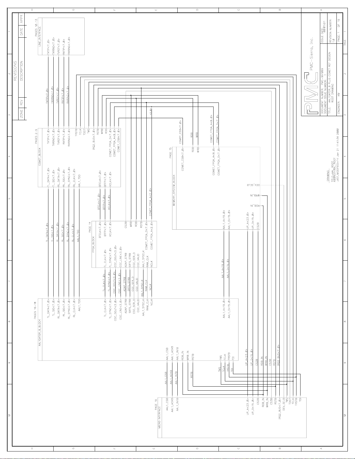
Page 54

Page 55

Page 56

Page 57
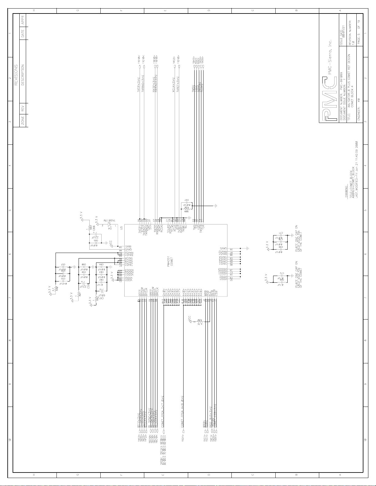
Page 58

Page 59

Page 60

Page 61

Page 62

Page 63

Page 64

Page 65
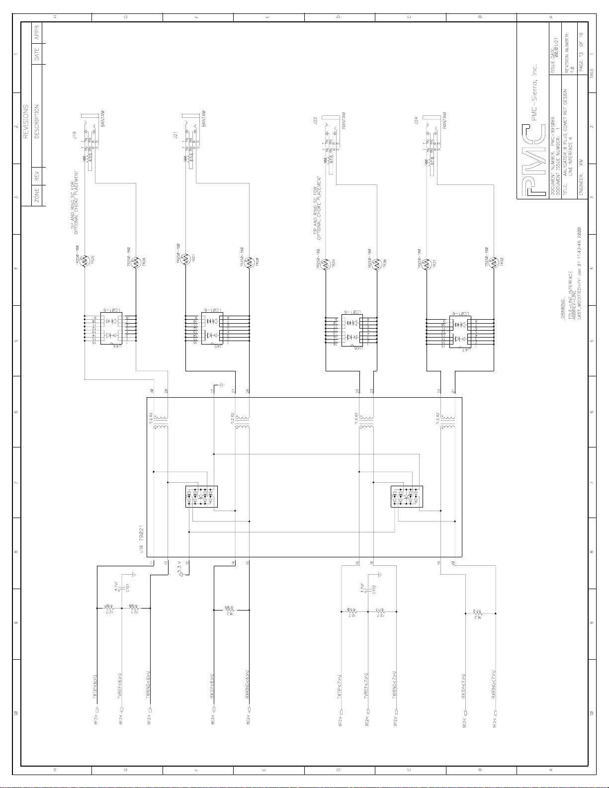
Page 66

Page 67

Page 68

Page 69

Page 70

Page 71

Page 72

PRELIMINARY
PM73123 AAL1GATOR-8
PM4354 COMET-QUAD
REFERENCE DESIGN
PMC-1991089 ISSUE 2 AAL1GATOR-8 REFERENCE DESIGN
15 APPENDIX D: AAL1GATOR-8 W/COMET-QUADS SCHEMATICS
PROPRIETARY AND CONFIDENTIAL TO PMC-SIERRA, INC., AND FOR ITS CUSTOMERS’ INTERNAL USE 46
Page 73
H
G
F
E
D
C
B
A
APPRDATE
1
REVISIONS
3254
PAGES 4-7
DESCRIPTION
REV
ZONE
PAGES 2-3
LINE_INTERFACE
TXCM<7..0>
TXTIP<7..0>
TXRING<7..0>
TXCM<7..0>
TXRING<7..0>
TXTIP<7..0>
TXCM<7..0>
TXTIP<7..0>
TXRING<7..0>
COMET_QUAD_BLOCK
TL_SIG<7..0>
RL_DATA<7..0>
TL_DATA<7..0>
RXTIP<7..0>
RXRING<7..0>
RXRING<7..0>
RXTIP<7..0>
RXTIP<7..0>
RXRING<7..0>
RL_CLK<7..0>
RL_SIG<7..0>
RL_SYNC<7..0>
TRSTB
AAL1_TDO
TCK
TDO1
TMS
RSTB
IRQ2_BUS<1..0>
BTCLK<7..0>
RDB
WRB
COMETQ_FPGA_D<7..0>
COMETQ_FPGA_A<10..0>
XCLK<1..0>
BTFP<7..0>
COMETQ_CSB<1..0>
CMV8MCLK
CMVFPC
CMVFPB
<2..0>
PAGE 9
RDB
WRB
COMETQ_CSB<1..0>
RDB
WRB
COMETQ_CSB<1..0>
COMETQ_FPGA_D<7..0>
COMETQ_FPGA_A<10..0>
COMETQ_FPGA_D<7..0>
COMETQ_FPGA_A<10..0>
DEV_SELB
WRB_IN
13
OF
1
1
00/01/21
PAGE:
ISSUE DATE:
REVISION NUMBER:
1.0
TRUE
PMC-Sierra, Inc.
1
PMC-991089
DOCUMENT NUMBER:
DOCUMENT ISSUE NUMBER:
2354
KM
AAL1GATOR_8 COMET_QUAD REF DESIGN
ROOT DRAWING
ENGINEER:
TITLE:
DRAWING
LAST_MODIFIED=Fri Jan 21 10:30:26 2000
ABBREV=AAL_ROOT
TITLE=AAL_ROOT
AAL1_TDO
RL_CLK<7..0>
RL_SIG<7..0>
TL_SIG<7..0>
RL_SYNC<7..0>
RL_DATA<7..0>
TL_DATA<7..0>
PAGES 10-12
9876
TL_SIG<7..0>
TL_DATA<7..0>
RL_DATA<7..0>
AAL1GATOR_8_BLOCK
RL_CLK<7..0>
RL_SIG<7..0>
RL_SYNC<7..0>
AAL1_TDO
PAGE 8
FPGA_BLOCK
XCLK<1..0>
BTFP<7..0>
BTCLK<7..0>
XCLK<1..0>
BTFP<7..0>
BTCLK<7..0>
TL_SYNC<7..0>
TL_CLK<7..0>
CGC_SER_D
TL_CLK<7..0>
TL_SYNC<7..0>
CGC_SER_D
CGC_VALID
CGC_SER_D
TL_CLK<7..0>
TL_SYNC<7..0>
CMV8MCLK
CMVFPC
CMVFPB
USED IN H-MVIP MODE
CMVFPB
CMVFPC
CMV8MCLK
CGC_LINE<3..0>
CGC_DOUT<3..0>
SRTS_STRB
ADAP_STRB
CGC_VALID
SRTS_STRB
ADAP_STRB
CGC_DOUT<3..0>
CGC_LINE<3..0>
ADAP_STRB
CGC_VALID
SRTS_STRB
CGC_LINE<3..0>
CGC_DOUT<3..0>
WRB
CS3B
RAM_CLK
NCLK
AAL1_SYSCLK
RAM_CLK
NCLK
AAL1_SYSCLK
NCLK
RAM_CLK
AAL1_SYSCLK
COMETQ_FPGA_A<2..0>
RDB
RSTB
COMETQ_FPGA_D<7..0>
COMETQ_FPGA_A<2..0>
C16B
C4B
C16B
C4B
USED IN H-MVIP MODE
C4B
C16B
AAL1_CSB
AAL1_CSB
MEMORY_SYSTEM_BLOCK
WRB_IN
RDB_IN
AAL1_ACKB
AAL1_INTB
RSTB
AAL1_INTB
AAL1_ACKB
RSTB
AAL1_A<19..0>
AAL1_D<15..0>
AAL1_A<19..0>
AAL1_D<15..0>
AAL1_D<15..0>
AAL1_A<19..0>
TRSTB
TMS
TCK
TMS
TRSTB
TCK
RDB_IN
UP_A<21..0>
UP_D<15..0>
CS2B
TDI
TDI
UP_D<15..0>
UP_A<21..0>
CS2B
RDB_IN
WRB_IN
CS3B
RSTB
IRQ2_BUS<1..0>
9876
TCK
TMS
CS3B
CS2B
PAGE 13
AAL1_CSB
AAL1_INTB
10
H
G
F
E
AAL1_ACKB
MICRO INTERFACE
D
C
UP_A<21..0>
UP_D<15..0>
RDB_IN
WRB_IN
RSTB
IRQ2_BUS<1..0>
B
TDO1
DEV_SELB
TRSTB
TDI
10
A
Page 74

H
G
F
E
D
C
B
A
APPRDATE
1
10C10< 3G2>
10C10< 3G2> 8F2>
REVISIONS
DESCRIPTION
RL_SIG<7..0>\I
RL_CLK<7..0>\I
REV
3254
ZONE
PM4354
COMET-QUAD
U2
PBGA
1023120333
BRCLK<4>
BRSIG<4>
BRSIG<3>
BRSIG<2>
BRSIG<1>
BRCLK<1>
BRCLK<2>
BRCLK<3>
1 OF 4
BTCLK<4>
BTCLK<3>
BTCLK<2>
BTCLK<1>
BTSIG<1>
BTSIG<2>
BTSIG<3>
BTSIG<4>
F3
G3
H16L2M14
J14M3M15
210012303123210
BTCLK<7..0>\I
TL_SIG<7..0>\I
10C5>
5B10>
5F10>
4B10>
4F10>
5B10>
RXTIP<3>\I
RXTIP<2>\I
RXTIP<1>\I
RXTIP<0>\I
RXRING<3>\I
C7
D10P7N10A7C10T7P10
RXTIP<3>
RXTIP<4>
RXTIP<2>
RXTIP<1>
RXRING<4>
2 OF 4
PM4354
COMET-QUAD
10D10< 3F2>
10D10< 3G2>
RL_DATA<7..0>\I
RL_SYNC<7..0>\I
BRFP<3>
BRFP<1>
BRFP<2>
BRFP<4>
BRPCM<3>
BRPCM<4>
BTPCM<3>
BTPCM<4>
BTFP<3>
BTFP<1>
BTFP<2>
BTFP<4>
H4
H14M1N13
BTFP<7..0>\I
TL_DATA<7..0>\I
8E2>
10D5>
5E10>
4B10>
4E10>
RXRING<2>\I
RXRING<1>\I
RXRING<0>\I
A8C9T8
P9
RVREF<1>
RVREF<2>
RVREF<3>
RVREF<4>
RXRING<3>
RXRING<2>
RXRING<1>
0212103
E1
F13P1N15E4G14R1P15E3G15P2P16E2F16N1N16
BRPCM<2>
CASBRD_BRPCM<1>
MVBTD
CCSBTD
BTPCM<2>
CMVFPC
CMV8MCLK
MVBRD_CCSBRD
CASBTD_BTPCM<1>
K3
F1
L4K1K2
F4
H13M4M16
R72
330
CMVFPC\I
CMV8MCLK\I
8D2>
8E2>
8C2>
XCLK<0>\I
330
R9
J13
R15
R16
L16
T15
PIO
XCLK
CTCLK
RSYNC
RES<8>
RES<7>
SYSTEM
CMVFPB
F2
CMVFPB\I
8D2>
0
TP4
1
RES<6>
RES<5>
RES<4>
RES<3>
R11
TP5
TP6
L14N3J15J4D8P8T16
111
RES<2>
RES<1>
TP7
LINE
C27
0.01UF
R98
C13
0.01UF
R8
C19
0.01UF
R94
C11
0.01UF
R12
100K
100K
100K
100K
3.3 V
4.7
3.3 V
COMET-QUAD
U2
PBGA
R102
4.7
C2
+
R1
PM4354
+
C1
0.01UF
22UF
QAVS<1>
QAVS<2>
4 OF 4
QAVD<1>
QAVD<2>
R14
C35
0.01UF
C33
22UF
3.3 V
3.3 V
3.3 V
1
3.3 V
RAVS1<3>
RAVS1<2>
RAVS1<1>
RAVS1<4>
RAVD1<3>
RAVD1<2>
RAVD1<1>
RAVD1<4>
B8B9R8T9C8
1
R96
1
R18
1
C9
C6
R4
RAVS2<3>
RAVS2<4>
RAVD2<3>
RAVD2<4>
C3
C4
R2
C25
0.01UF
C21
0.47UF
C17
0.01UF
C14
0.47UF
0.01UF
0.47UF
RAVS2<1>
RAVS2<2>
TAVS1<4>
RAVD2<1>
RAVD2<2>
TAVD1<4>
0.01UF
0.47UF
3.3 V
3.3 V
3.3 V
3.3 V
TAVS1<3>
TAVS1<2>
TAVS1<1>
TAVD1<3>
TAVD1<2>
TAVD1<1>
1
1
R89
1
R10
1
TAVS2<3>
TAVS2<4>
TAVD2<3>
TAVD2<4>
R100
C26
C22
R97
C18
0.01UF
C15
0.1UF
C10
0.01UF
C7
0.1UF
C4
B12N4R12C6D11P6N11D6B10N6R10D7A9N7R9D9T14
TAVS2<1>
TAVS2<2>
TAVS3<4>
TAVD3<4>
TAVD2<1>
TAVD2<2>
C31
0.01UF
C29
0.1UF
0.01UF
0.1UF
B5
A12R5T12
TAVS3<1>
TAVS3<2>
TAVS3<3>
TAVD3<1>
TAVD3<2>
TAVD3<3>
A5
C12T5P12A4D13T4P13A6C11T6P11B7A10R7T10
3.3 V
3.3 V
1
3.3 V
R3
1
3.3 V
G13
K16
L15
VSSC2_5<7>
VSSC2_5<5>
VSSC2_5<6>
VSSC2_5<3>
VSSC2_5<4>
VDDC2_5<8>
VDDC2_5<7>
VDDC2_5<6>
VDDC2_5<4>
VDDC2_5<5>
L1
H15
K15
M13
J16
C30
C28
R99
1
C24
0.01UF
C20
47UF
R95
1
C16
0.01UF
C12
47UF
R13
C8
0.01UF
C5
47UF
P14M2C14G2H1J3L3
VSS3_3<9>
VSS3_3<8>
VSSC2_5<1>
VSSC2_5<2>
VDDC2_5<1>
VDDC2_5<2>
VDDC2_5<3>
VDD3_3<6>
G1H3J1
G16
N14
2.5 V
0.01UF
47UF
B2D1J2
R2
G4
F14
L13
K13
VSS3_3<7>
VSS3_3<6>
VSS3_3<5>
VSS3_3<4>
VSS3_3<3>
VSS3_3<2>
VSS3_3<1>
VSSQ3_3<1>
VSSQ3_3<2>
VDDQ3_3<2>
VDDQ3_3<1>
VDD3_3<1>
VDD3_3<2>
VDD3_3<3>
VDD3_3<4>
VDD3_3<5>
CAVS
N8
C3D4K4
N2
H2
K14
3.3 V
3.3 V
8C9< 9E1<> 3B7<> 9D1>
COMETQ_FPGA_D<7..0>\I
3.3 V
7654312
D3
D<6>
D<5>
D<4>
D<3>
D<2>
D<1>
D<7>
CAVD
N9
4.7
R7
4.7K
0
B3A2A1B1C1C2D2
D<0>
J7
GND9
R101
GND11
GND10
GND1
GND2
G7
COMET_Q_1
DRAWING:
K10K9K8K7J10J9J8
GND16
GND15
GND14
GND13
GND12
GND6
GND5
GND8
GND7
GND3
GND4
H9
H8
H7G9G8
H10
G10
C34
0.01UF
C32
22UF
13F5>
13E2<
9C1>
9B1>
9C1>
RSTB\I
RDB\I
WRB\I
IRQ2_BUS<0>\I
COMETQ_CSB<0>\I
E15
E13
D14
E14T1E16
F15
RDB
ALE
CSB
WRB
RSTB
INTB
PMC-Sierra, Inc.
Thu May 17 11:12:19 2001
COMETQ
2.5 V
POWER
3.3 V
13
OF
1
2
01/05/16
PAGE:
ISSUE DATE:
REVISION NUMBER:
1.1
2
2354
PMC-991089
WT
AAL1GATOR_8 COMET_QUAD REF DESIGN
COMET_QUAD_1
ENGINEER:
TITLE:
DOCUMENT NUMBER:
DOCUMENT ISSUE NUMBER:
C23
0.01UF
C41
0.01UF
C147
0.01UF
C146
0.01UF
C37
0.01UF
C38
0.01UF
C39
0.01UF
C40
0.01UF
DECOUPLING CAPS: ONE PER TWO POWER PINS
U2
PBGA
TXTIP1<1>
TXTIP1<2>
TXTIP1<3>
TXTIP1<4>
B4
9876
10
H
A13P4R13
TXTIP<0>\I
TXTIP<1>\I
TXTIP<2>\I
TXTIP<3>\I
4G10<
4D10<
5G10<
5D10<
G
TXRING1<4>
TXTIP2<4>
TXTIP2<3>
TXTIP2<2>
TXTIP2<1>
B6
A11R6T11A3C13R4T13D5B11N5R11
TXRING<3>\I
5C10<
TXRING1<2>
TXRING1<3>
TXRING1<1>
TXRING2<3>
TXRING2<4>
TXRING<0>\I
TXRING<1>\I
TXRING<2>\I
4G10<
4C10<
5G10<
TXRING2<1>
TXRING2<2>
TXCM<4>
TXCM<3>
TXCM<2>
D12P5N12
TXCM<1>\I
TXCM<2>\I
TXCM<3>\I
4D10>
5G10>
5D10>
F
TXCM<1>
C5
TXCM<0>\I
4G10>
PM4354
3 OF 4
COMET-QUAD
A<10>
A<9>
A<8>
A<7>
A<6>
A<5>
A<4>
A<3>
A<2>
A<1>
PBGA
U2
D16
D15
109876453210
A<0>
B13
A14
B14
A15
B15
A16
B16
C15
C16
COMETQ_FPGA_A<10..0>\I
E
D
C
TDO
AAL1_TDO\I
TDO0
3A10<
B
TDI
TCK
T2R3T3
TCK\I
11E2>
13G5>
TMS
TRSTB
P3
TMS\I
TRSTB\I
13H5>
13G5>
MICRO_JTAG
9876
10
A
Page 75

H
G
F
E
D
C
B
A
APPRDATE
1
10C10< 2G2>
10C10< 2G2>
REVISIONS
DESCRIPTION
RL_SIG<7..0>\I
RL_CLK<7..0>\I
REV
3254
ZONE
765467545764765
BRCLK<4>
BRCLK<1>
BRCLK<2>
BRCLK<3>
PM4354
1 OF 4
COMET-QUAD
U3
BTCLK<4>
BTCLK<3>
BTCLK<2>
BTCLK<1>
F3
H16L2M14
7
BTCLK<7..0>\I
8F2>
7B10>
7F10>
RXTIP<7>\I
RXTIP<6>\I
RXTIP<3>
RXTIP<4>
2 OF 4
PM4354
COMET-QUAD
BRSIG<4>
BRSIG<3>
BRSIG<2>
BRSIG<1>
BTSIG<1>
BTSIG<2>
BTSIG<3>
BTSIG<4>
G3
J14M3M15
TL_SIG<7..0>\I
10C5>
6B10>
6F10>
7B10>
RXTIP<5>\I
RXTIP<4>\I
RXRING<7>\I
C7
D10P7N10A7C10T7P10
RXTIP<2>
RXTIP<1>
RXRING<4>
10D10< 2G2>
10D10< 2F2>
RL_SYNC<7..0>\I
RL_DATA<7..0>\I
BRFP<3>
BRFP<1>
BRFP<2>
BRFP<4>
BRPCM<3>
BRPCM<4>
BTPCM<3>
BTPCM<4>
BTFP<3>
BTFP<1>
BTFP<2>
BTFP<4>
H4
H14M1N13
BTFP<7..0>\I
TL_DATA<7..0>\I
8E2>
10D5>
7E10>
6B10>
6E10>
RXRING<6>\I
RXRING<5>\I
RXRING<4>\I
A8C9T8
P9
RVREF<1>
RVREF<2>
RVREF<3>
RVREF<4>
RXRING<3>
RXRING<2>
RXRING<1>
4
E1
F13P1N15E4G14R1P15E3G15P2P16E2F16N1N16
BRPCM<2>
CASBRD_BRPCM<1>
MVBTD
CCSBTD
BTPCM<2>
CMVFPC
CMV8MCLK
MVBRD_CCSBRD
CASBTD_BTPCM<1>
K3
F1
L4K1K2
F4
H13M4M16
456745674567456
R73
330
CMV8MCLK\I
CMVFPC\I
8E2>
8D2>
8C2>
XCLK<1>\I
R17
330
J13
R15
R16
L16
T15
PIO
XCLK
CTCLK
RSYNC
RES<8>
RES<7>
SYSTEM
CMVFPB
F2
CMVFPB\I
8D2>
0
TP8
1
RES<6>
RES<5>
RES<4>
RES<3>
R106
TP9
TP10
L14N3J15J4D8P8T16
111
RES<2>
RES<1>
TP11
LINE
C62
0.01UF
R116
C58
0.01UF
R115
C54
0.01UF
R111
C47
0.01UF
R107
100K
100K
100K
100K
3.3 V
4.7
3.3 V
COMET-QUAD
U3
R122
4.7
+
R117
PM4354
+
C67
0.01UF
C63
22UF
QAVS<1>
QAVS<2>
4 OF 4
QAVD<1>
QAVD<2>
R14
C74
0.01UF
C72
22UF
3.3 V3.3 V
3.3 V
1
3.3 V
RAVS1<3>
RAVS1<2>
RAVS1<1>
RAVS1<4>
RAVD1<3>
RAVD1<2>
RAVD1<1>
RAVD1<4>
B8B9R8T9C8
1
R113
1
R109
1
C45
C42
R104
RAVS2<3>
RAVS2<4>
RAVD2<3>
RAVD2<4>
C69
C65
R119
C60
0.01UF
C56
0.47UF
C52
0.01UF
C49
0.47UF
0.01UF
0.47UF
RAVS2<1>
RAVS2<2>
TAVS1<4>
RAVD2<1>
RAVD2<2>
TAVD1<4>
0.01UF
0.47UF
3.3 V
3.3 V
3.3 V
3.3 V
TAVS1<3>
TAVS1<2>
TAVS1<1>
TAVD1<3>
TAVD1<2>
TAVD1<1>
1
1
R110
1
R105
1
TAVS2<3>
TAVS2<4>
TAVD2<3>
TAVD2<4>
R120
C61
C57
R114
C53
0.01UF
C50
0.1UF
C46
0.01UF
C43
0.1UF
C4
B12N4R12C6D11P6N11D6B10N6R10D7A9N7R9D9T14
TAVS2<1>
TAVS2<2>
TAVS3<4>
TAVD3<4>
TAVD2<1>
TAVD2<2>
C70
0.01UF
C66
0.1UF
0.01UF
0.1UF
B5
A12R5T12
TAVS3<1>
TAVS3<2>
TAVS3<3>
TAVD3<1>
TAVD3<2>
TAVD3<3>
A5
C12T5P12A4D13T4P13A6C11T6P11B7A10R7T10
3.3 V
3.3 V
1
3.3 V
R103
1
3.3 V
G13
K16
L15
VSSC2_5<7>
VSSC2_5<5>
VSSC2_5<6>
VSSC2_5<3>
VSSC2_5<4>
VDDC2_5<8>
VDDC2_5<7>
VDDC2_5<6>
VDDC2_5<4>
VDDC2_5<5>
L1
H15
K15
M13
J16
C68
C64
R118
1
C59
0.01UF
C55
47UF
R112
1
C51
0.01UF
C48
47UF
R108
C44
0.01UF
C36
47UF
P14M2C14G2H1J3L3
VSS3_3<9>
VSS3_3<8>
VSSC2_5<1>
VSSC2_5<2>
VDDC2_5<1>
VDDC2_5<2>
VDDC2_5<3>
VDD3_3<6>
G1H3J1
G16
N14
2.5 V
3.3 V
0.01UF
47UF
R2
F14
L13
VSS3_3<7>
VSS3_3<6>
VSS3_3<5>
VSS3_3<4>
VSS3_3<3>
VDD3_3<1>
VDD3_3<2>
VDD3_3<3>
VDD3_3<4>
VDD3_3<5>
C3D4K4
N2
B2D1J2
G4
K13
VSS3_3<2>
VSS3_3<1>
VSSQ3_3<1>
VSSQ3_3<2>
VDDQ3_3<2>
VDDQ3_3<1>
CAVS
N8
H2
K14
3.3 V
CAVD
N9
4.7
J7
GND9
R121
Thu May 17 11:12:24 2001
COMETQ
COMET_Q_2
DRAWING:
K10K9K8K7J10J9J8
GND16
GND15
GND14
GND13
GND12
GND11
GND10
POWER
GND6
GND5
GND8
GND7
GND1
GND2
GND3
GND4
G7
H9
H8
H7G9G8
H10
G10
C73
0.01UF
C71
22UF
8C9< 9E1<> 2C7<>
9C1>
9B1>
9C1>
WRB\I
RDB\I
COMETQ_CSB<1>\I
COMETQ_FPGA_D<7..0>\I
R16
3.3 V
4.7K
021
67543
E15
D14
B3A2A1B1C1C2D2
D3
D<7>
D<6>
D<5>
D<4>
D<3>
D<2>
D<1>
D<0>
E14T1E16
RDB
CSB
WRB
01/05/16
ISSUE DATE:
PMC-Sierra, Inc.
2
PMC-991089
DOCUMENT NUMBER:
DOCUMENT ISSUE NUMBER:
C82
0.01UF
C81
0.01UF
C80
0.01UF
C79
2.5 V
3.3 V
13E2<
13F5>
RSTB\I
IRQ2_BUS<1>\I
E13
F15
ALE
RSTB
INTB
C78
0.01UF
C77
0.01UF
C76
0.01UF
C75
0.01UF
0.01UF
13
OF
1
3
PAGE:
REVISION NUMBER:
1.1
2354
WT
AAL1GATOR_8 COMET_QUAD REF DESIGN
COMET_QUAD_2
ENGINEER:
TITLE:
DECOUPLING CAPS: ONE PER TWO POWER PINS
U3
TXTIP1<1>
TXTIP1<2>
TXTIP1<3>
TXTIP1<4>
B4
9876
10
H
A13P4R13
TXTIP<4>\I
TXTIP<5>\I
TXTIP<6>\I
TXTIP<7>\I
6G10<
6D10<
7G10<
7D10<
G
TXRING1<4>
TXTIP2<4>
TXTIP2<3>
TXTIP2<2>
TXTIP2<1>
B6
A11R6T11A3C13R4T13D5B11N5R11
TXRING<7>\I
7C10<
TXRING1<2>
TXRING1<3>
TXRING1<1>
TXRING2<3>
TXRING2<4>
TXRING<4>\I
TXRING<5>\I
TXRING<6>\I
6G10<
6C10<
7G10<
TXRING2<1>
TXRING2<2>
TXCM<4>
TXCM<3>
TXCM<2>
D12P5N12
TXCM<7>\I
TXCM<6>\I
TXCM<5>\I
7D10>
7G10>
6D10>
F
TXCM<1>
C5
TXCM<4>\I
6G10>
PM4354
3 OF 4
COMET-QUAD
A<10>
A<9>
A<8>
A<7>
A<6>
A<5>
A<4>
A<3>
A<2>
A<1>
U3
D16
D15
A<0>
B13
A14
B14
A15
B15
A16
B16
C15
C16
012354678109
COMETQ_FPGA_A<10..0>\I
9D1>
E
D
C
B
TDO
TDI
TCK
T2R3T3
TCK\I
TDO1\I
TDO0
13G5>
13G5<
2B10>
TMS
TRSTB
P3
TMS\I
TRSTB\I
13H5>
13G5>
MICRO_JTAG
9876
10
A
Page 76

H
G
F
E
D
C
B
A
APPRDATE
1
BANTAM
REVISIONS
DESCRIPTION
J1
TN
RN
TRS
T
RTNS
RN
R39
100
REV
3254
ZONE
TIP AND RING SC FOR
OPTIONAL CHOKE PLACEMENT
TR1
TR250-180
9
10
11
12
13
14
15
16
LC01-6
U20
TR250-180
8
7
6
5
4
3
2
1
TR2
J3
TR250-180
TN
RN
TRS
T
RN
R38
100
13
OF
00/01/21
ISSUE DATE:
BANTAM
RTNS
TR3
LC01-6
9
10
11
12
13
14
15
16
U21
TR4
TR250-180
8
7
6
5
4
3
2
1
J4
BANTAM
TN
RN
TRS
T
RTNS
RN
R19
100
TIP AND RING SC FOR
OPTIONAL CHOKE PLACEMENT
TR5
TR250-180
LC01-6
9
10
11
12
13
14
15
16
U22
TR250-180
8
7
6
5
4
3
2
1
TR6
J6
TR250-180
TN
RN
TRS
T
RN
R20
100
BANTAM
RTNS
TR8
LC01-6
U23
TR250-180
8
7
6
5
4
3
2
1
TR7
9
10
11
12
13
14
15
16
PMC-Sierra, Inc.
1
PMC-991089
DOCUMENT NUMBER:
DOCUMENT ISSUE NUMBER:
1
4
PAGE:
REVISION NUMBER:
1.0
TRUE
2354
KM
AAL1GATOR_8 COMET_QUAD REF DESIGN
LINE INTERFACE 1
ENGINEER:
TITLE:
DRAWING
ABBREV=LINE
LAST_MODIFIED=Thu May 17 11:11:58 2001
TITLE=LINE_INTERFACE
40
2.42
1:
T9021
U5
1
4.7UF
C83
+
R22
R23
12.7
12.7
9876
7
37
2.42
1:
36
5
4
38
2
3
2.42
1:
33
35
8
6
2.42
:1
32
31
T
TP1
R21
100K
9
10
3.3 V
4.7UF
C84
+
R24
18.2
R25
12.7
R26
12.7
R27
18.2
9876
TXTIP<0>\I
TXCM<0>\I
TXRING<0>\I
RXTIP<0>\I
RXRING<0>\I
TXTIP<1>\I
10
2F10<
2G10>
H
2F10>
G
2G6<
F
2G6<
2G10>
E
D
TXCM<1>\I
2F10<
TXRING<1>\I
2F10>
C
RXTIP<1>\I
2G6<
B
RXRING<1>\I
10
2G6<
A
Page 77

H
G
F
E
D
C
B
A
APPRDATE
1
BANTAM
REVISIONS
DESCRIPTION
J7
TN
RN
TRS
T
RTNS
RN
R28
100
REV
3254
ZONE
TIP AND RING SC FOR
OPTIONAL CHOKE PLACEMENT
TR9
TR250-180
9
10
11
12
13
14
15
16
LC01-6
U26
TR250-180
8
7
6
5
4
3
2
1
TR10
J9
TR250-180
TN
RN
TRS
T
RN
R29
100
TR11
13
OF
00/01/21
ISSUE DATE:
BANTAM
RTNS
TR12
TR250-180
LC01-6
9
10
11
12
13
14
15
16
8
7
6
5
4
3
2
1
U27
J10
BANTAM
TN
RN
TRS
T
RTNS
RN
R30
100
TIP AND RING SC FOR
OPTIONAL CHOKE PLACEMENT
TR13
TR250-180
LC01-6
9
10
11
12
13
14
15
16
U28
TR250-180
8
7
6
5
4
3
2
1
TR14
J12
TR250-180
TN
RN
TRS
T
RN
R31
100
TR15
BANTAM
RTNS
TR16
TR250-180
LC01-6
9
10
11
12
13
14
15
16
8
7
6
5
4
3
2
1
U29
PMC-Sierra, Inc.
1
PMC-991089
DOCUMENT NUMBER:
DOCUMENT ISSUE NUMBER:
1
5
PAGE:
REVISION NUMBER:
1.0
TRUE
2354
KM
AAL1GATOR_8 COMET_QUAD REF DESIGN
LINE INTERFACE 2
ENGINEER:
TITLE:
DRAWING
LAST_MODIFIED=Thu May 17 11:12:00 2001
TITLE=LINE_INTERFACE
ABBREV=LINE
30
2.42
1:
T9021
U5
11
4.7UF
C85
+
R32
R33
12.7
12.7
9876
17
27
2.42
1:
26
15
14
28
13
2.42
1:
23
25
18
16
22
2.42
:1
21
201219
3.3 V
4.7UF
C86
+
R34
18.2
R35
12.7
R36
12.7
R37
18.2
9876
TXCM<2>\I
2F10<
G
TXRING<2>\I
2F10>
F
RXTIP<2>\I
2G6<
RXRING<2>\I
2G6<
E
TXTIP<3>\I
2G10>
D
TXCM<3>\I
2F10<
TXRING<3>\I
2G10>
C
RXTIP<3>\I
2G6<
B
RXRING<3>\I
10
2G6<
A
TXTIP<2>\I
10
2G10>
H
Page 78

H
G
F
E
D
C
B
A
APPRDATE
1
BANTAM
REVISIONS
DESCRIPTION
J13
TN
RN
TRS
T
RTNS
RN
R40
100
REV
3254
ZONE
TIP AND RING SC FOR
OPTIONAL CHOKE PLACEMENT
TR17
TR250-180
9
10
11
12
13
14
15
16
LC01-6
U32
TR250-180
8
7
6
5
4
3
2
1
TR18
J15
TR250-180
TN
RN
TRS
T
RN
R41
100
TR19
13
OF
1
6
00/01/21
PAGE:
ISSUE DATE:
REVISION NUMBER:
1.0
TRUE
BANTAM
RTNS
TR20
TR250-180
LC01-6
9
10
11
12
13
14
15
16
8
7
6
5
4
3
2
1
U33
J16
BANTAM
TN
RN
TRS
T
RTNS
RN
R42
100
TIP AND RING SC FOR
OPTIONAL CHOKE PLACEMENT
TR21
TR250-180
LC01-6
9
10
11
12
13
14
15
16
U34
TR250-180
8
7
6
5
4
3
2
1
TR22
J18
TR250-180
TN
RN
TRS
T
RN
R43
100
TR23
BANTAM
RTNS
TR24
TR250-180
LC01-6
9
10
11
12
13
14
15
16
8
7
6
5
4
3
2
1
U35
PMC-Sierra, Inc.
1
2354
PMC-991089
KM
AAL1GATOR_8 COMET_QUAD REF DESIGN
LINE INTERFACE 3
ENGINEER:
TITLE:
DOCUMENT NUMBER:
DOCUMENT ISSUE NUMBER:
DRAWING
LAST_MODIFIED=Thu May 17 11:12:06 2001
TITLE=LINE_INTERFACE
ABBREV=LINE
40
2.42
1:
T9021
U6
1
4.7UF
C87
+
R49
R48
12.7
12.7
9876
7
37
2.42
1:
36
5
4
38
2
3
2.42
1:
33
35
8
6
2.42
:1
32
31
9
10
3.3 V
4.7UF
C88
+
R47
18.2
R46
12.7
R45
12.7
R44
18.2
9876
TXTIP<4>\I
TXCM<4>\I
TXRING<4>\I
RXTIP<4>\I
10
3G10>
3F10<
3F10>
H
G
3G6<
F
RXRING<4>\I
3G6<
E
TXTIP<5>\I
3G10>
D
TXCM<5>\I
3F10<
TXRING<5>\I
3F10>
C
RXTIP<5>\I
3G6<
B
RXRING<5>\I
10
3G6<
A
Page 79

H
G
F
E
D
C
B
A
APPRDATE
1
BANTAM
REVISIONS
DESCRIPTION
J19
TN
RN
TRS
T
RTNS
RN
R56
100
REV
3254
ZONE
TIP AND RING SC FOR
OPTIONAL CHOKE PLACEMENT
TR25
TR250-180
9
10
11
12
13
14
15
16
LC01-6
U38
TR250-180
8
7
6
5
4
3
2
1
TR26
J21
TR250-180
TN
RN
TRS
T
RN
R57
100
TR27
13
OF
1
7
00/01/21
PAGE:
ISSUE DATE:
REVISION NUMBER:
1.0
TRUE
BANTAM
RTNS
TR28
TR250-180
LC01-6
9
10
11
12
13
14
15
16
8
7
6
5
4
3
2
1
U39
J22
BANTAM
TN
RN
TRS
T
RTNS
RN
R58
100
TIP AND RING SC FOR
OPTIONAL CHOKE PLACEMENT
TR29
TR250-180
LC01-6
9
10
11
12
13
14
15
16
U40
TR250-180
8
7
6
5
4
3
2
1
TR30
J24
TR250-180
TN
RN
TRS
T
RN
R59
100
TR31
BANTAM
RTNS
TR32
TR250-180
LC01-6
9
10
11
12
13
14
15
16
8
7
6
5
4
3
2
1
U41
PMC-Sierra, Inc.
1
2354
PMC-991089
KM
AAL1GATOR_8 COMET_QUAD REF DESIGN
LINE INTERFACE 4
ENGINEER:
TITLE:
DOCUMENT NUMBER:
DOCUMENT ISSUE NUMBER:
DRAWING
LAST_MODIFIED=Thu May 17 11:12:09 2001
TITLE=LINE_INTERFACE
ABBREV=LINE
30
2.42
1:
T9021
U6
11
4.7UF
C89
+
R55
R54
12.7
12.7
9876
17
27
2.42
1:
26
15
14
28
13
2.42
1:
23
25
18
16
22
2.42
:1
21
201219
3.3 V
4.7UF
C90
+
R53
18.2
R52
12.7
R51
12.7
R50
18.2
9876
TXTIP<6>\I
TXCM<6>\I
TXRING<6>\I
RXTIP<6>\I
RXRING<6>\I
TXTIP<7>\I
10
3G10>
3F10<
3F10>
H
G
3G6<
F
3G6<
3G10>
E
D
TXCM<7>\I
3F10<
TXRING<7>\I
3G10>
C
RXTIP<7>\I
3G6<
B
RXRING<7>\I
10
3G6<
A
Page 80

H
G
F
E
D
C
B
A
APPRDATE
1
C101
0.1UF
C102
REVISIONS
DESCRIPTION
3.3 V
0.1UF
C103
0.1UF
C104
0.1UF
REV
3254
PLACE ONE CAP ON EACH SIDE OF THE FPGA.
ZONE
U9
3.3 V
26
VCC
106
VCCI<1>
28
VCCI<2>
60
VCCI<3>
80
98
132
164
182
202
2
17
29
32
79
130
133
136
183
IO_C<40>
IO_C<39>
VCCI<4>
VCCI<5>
VCCI<6>
VCCI<7>
VCCI<8>
VCCA<1>
VCCA<2>
VCCA<3>
VCCA<4>
VCCA<5>
VCCA<6>
VCCA<7>
VCCA<8>
VCCA<9>
IO_A<40>
IO_A<41>
IO_C<38>
IO_C<37>
IO_C<36>
IO_C<35>
IO_A<36>
IO_A<37>
IO_A<38>
IO_A<39>
IO_C<33>
IO_C<34>
IO_C<32>
IO_C<31>
IO_A<34>
IO_A<35>
IO_A<32>
IO_A<33>
0
IO_C<30>
IO_C<29>
IO_C<28>
IO_C<27>
IO_A<29>
IO_A<30>
IO_A<31>
IO_A<28>
IO_C<23>
IO_C<24>
IO_C<26>
IO_C<25>
IO_A<27>
IO_A<26>
IO_A<25>
IO_A<24>
7654321
0
3G6< 2G6<
BTCLK<7..0>\I
7654321
68
RN2
1
206
2084567891011121314151618192021232425
IO_C<20>
IO_C<22>
IO_C<21>
IO_C<19>
IO_C<18>
IO_A<21>
IO_A<22>
IO_A<23>
IO_A<20>
IO_A<19>
201
203
204
205
IO_C<14>
IO_C<15>
IO_C<17>
IO_C<16>
IO_A<18>
IO_A<17>
IO_A<16>
IO_A<15>
7654321
0
9
10111213141516
RES_ARRAY_8
8765432
197
198
199
200
IO_C<13>
IO_C<12>
IO_C<11>
IO_C<10>
IO_A<12>
IO_A<11>
IO_A<13>
IO_A<14>
3G6< 2G6<
BTFP<7..0>\I
7
190
191
192
193
194
195
IO_C<4>
IO_C<5>
IO_C<9>
IO_C<8>
IO_C<7>
IO_C<6>
IO_A<10>
IO_A<9>
IO_A<8>
IO_A<7>
IO_A<6>
IO_A<5>
3
2132100
10B10<
C4B\I
USED IN H-MVIP MODE
0123456
181
185
187
189
IO_C<2>
IO_C<3>
IO_C<1>
IO_D<40>
IO_A<1>
IO_A<4>
IO_A<3>
IO_A<2>
IO_B<41>
3031333435363738394041424344454647484950515657585961626364666768697071727374757677
127
3F6< 2F6<
3F6< 2F6<
3F6< 2F6<
10B5<
CMVFPB\I
CMVFPC\I
CMV8MCLK\I
C16B\I
174
175
176
177
179
IO_D<39>
IO_D<36>
IO_D<37>
IO_D<38>
IO_B<40>
IO_B<39>
IO_B<38>
IO_B<37>
121
122
123
124
125
170
172
173
IO_D<32>
IO_D<33>
IO_D<34>
IO_D<35>
IO_B<36>
IO_B<35>
IO_B<34>
IO_B<33>
118
119
120
166
167
168
169
IO_D<29>
IO_D<30>
IO_D<31>
IO_B<32>
IO_B<31>
IO_B<30>
114
115
116
117
162
163
165
IO_D<26>
IO_D<25>
IO_D<27>
IO_D<28>
IO_B<26>
IO_B<27>
IO_B<28>
IO_B<29>
111
112
113
156
158
160
161
IO_D<24>
IO_D<23>
IO_D<22>
IO_D<21>
IO_B<23>
IO_B<24>
IO_B<25>
IO_B<22>
107
108
109
110
152
153
154
155
IO_D<19>
IO_D<20>
IO_D<18>
IO_D<17>
IO_B<20>
IO_B<21>
IO_B<18>
IO_B<19>
100
101
102
104
147
148
149
151
IO_D<13>
IO_D<14>
IO_D<15>
IO_D<16>
IO_B<14>
IO_B<15>
IO_B<16>
IO_B<17>
7
143
144
145
146
IO_D<9>
IO_D<10>
IO_D<11>
IO_D<12>
IO_B<10>
IO_B<11>
IO_B<12>
IO_B<13>
0123456
140
141
142
IO_D<8>
IO_D<7>
IO_B<8>
IO_B<9>
012
8
68
1
RN1
137
138
139
IO_D<6>
IO_D<5>
IO_D<4>
IO_D<3>
IO_B<4>
IO_B<5>
IO_B<6>
IO_B<7>
3F6< 2F7<
XCLK<1..0>\I
3.3 V
1
0
1.544MHZ
50PPM
567
432
196
171
134
135
IO_D<2>
IO_D<1>
QCLKD_IO
IO_B<3>
IO_B<2>
IO_B<1>
QCLKA_IO QCLKC_IO
QCLKB_IO
8182838485868788899092939495969799
65
91
HEADER2
3.3 V
1
2
8
Y2
3.3V
HCMOS
5
R74
22
186
180
CLKA_IO
MODE
3
J2
R60
10K
C93
0.1UF
C94
0.01UF
41
VDD
GND
NC/TS
OUT
CLKB_IO
DCLK_IO
SDI_IO
207
1595418855128
3.3 V
C91
C92
41
8
Y3
VDD
GND
3.3V
HCMOS
2.048MHZ
50PPM
NC/TS
OUT
5
R86
22
GND_<13>
GND_<12>
GND_<11>
GND_<10>
GND_<9>
GND_<8>
GND_<7>
GND_<6>
GND_<5>
GND_<4>
GND_<3>
GND_<2>
GND_<1>
PRB_IO
TMS_IO
TDI_IO
TDO_IO
TCK_IO
103
1
A42MX36_PQ208
PRA_IO
178
0.1UF
0.01UF
184
157
150
131
129
126
105
78
53
52
27
22
00/01/21
ISSUE DATE:
REVISION NUMBER:
1.0
PMC-Sierra, Inc.
1
PMC-991089
AAL1GATOR_8 COMET_QUAD REF DESIGN
FPGA BLOCK
TITLE:
DOCUMENT NUMBER:
DOCUMENT ISSUE NUMBER:
DRAWING
LAST_MODIFIED=Thu May 17 11:12:30 2001
ABBREV=FPGA_BLOCK
TITLE=FPGA_BLOCK
HDR14
P_14
14
P_13
13
P_12
12
P_11
11
P_10
10
P_9
9
P_8
8
P_7
7
P_6
6
P_5
5
P_4
4
P_3
3
P_2
2
P_1
1
J25
13
OF
1
8
PAGE:
2354
KM
ENGINEER:
9876
RSTB\I
13F5>
10
H
G
CS3B\I
RDB\I
WRB\I
9C1>
9C1>
13E5>
TL_SYNC<7..0>\I
TL_CLK<7..0>\I
CGC_VALID\I
CGC_SER_D\I
CGC_DOUT<3..0>\I
IN H-MVIP MODE TL_SYNC<0> IS F0B
10D5<>
10C5<>
10E10<
10E10<
10F10>
F
R14
22
CGC_LINE<3..0>\I
ADAP_STRB\I
SRTS_STRB\I
10E10>
10E10>
10E10>
USED FOR EXTERNAL ADAPTIVE ALGORITHM
5
OUT
NC/TS
VDD
GND
41
8
50PPM
Y4
16.384MHZ
3.3V
HCMOS
C99
0.01UF
C100
3.3 V
0.1UF
E
RAM_CLK\I
COMETQ_FPGA_D<7..0>\I
R15
22
5
H-MVIP COMMON CLOCK AND FRAME PLUSE CLOCK
50PPM
4.096MHZ
3.3V
11E7<
OUT
NC/TS
VDD
GND
9E1<> 3B7<> 2C7<>
41
8
Y5
HCMOS
C97
0.01UF
C98
3.3 V
0.1UF
D
AAL1_SYSCLK\I
NCLK\I
COMETQ_FPGA_A<2..0>\I
22
R6
5
9D1>
10E5<
OUT
VDD
8
Y1
50PPM
38.880MHZ
3.3V
HCMOS
3.3 V
C
PROGRAMMING AND DEBUGGING
MODE = GND,
EXCEPT DURING DEVICE
NETWORK_CLK
NC/TS
GND
41
3
C95
C96
0.01UF
0.1UF
1
2
4
SMA
J26
5
B
9876
10
A
Page 81

H
G
F
E
D
C
B
A
APPRDATE
1
3.3 V
C109
0.1UF
C110
0.1UF
C111
0.1UF
C112
0.1UF
REVISIONS
DESCRIPTION
3.3 V
C105
0.01UF
C106
0.01UF
PLACE CAPS NEAR EACH IC
C107
0.01UF
C108
0.01UF
REV
3254
ZONE
00/01/21
ISSUE DATE:
REVISION NUMBER:
1.0
1
991089
13
OF
1
9
PAGE:
2354
8C9< 3B7<> 2C7<>
8C9< 3B10< 2C10<
8G9< 3B7< 2B7<
8G9< 3B7< 2B7<
3B7< 2B7<
WRB\I
C113
VCC
0.1UF
C114
0.01UF
COMETQ_FPGA_D<7..0>\I
RDB\I
COMETQ_FPGA_A<10..0>\I
PMC-Sierra, Inc.
COMETQ_CSB<1..0>\I
KM
AAL1GATOR_8 COMET_QUAD REF DESIGN
MEMORY SYSTEM BLOCK
7654321
3.3 V
RES_ARRAY_8
9
8
7
10
6
11
5
12
4
13
3
14
2
15
1
16
RN3
4.7K
U47
33
8
B
74FCT
8
163646
A
24
7564320
0
ENGINEER:
TITLE:
DOCUMENT NUMBER:
DOCUMENT ISSUE NUMBER:
42414038373634
1234567
BBBBBBB
OE
29
CLKAB
CLKBA
302726
28
DIR
SBA
SAB
R71
31
330
MC74HCT138AD
U11
1234567
AAAAAAA
15161719202123
1
DEV_SELB\I
5
6
7
8
4.7K
13E5>
012345678
3.3 V
99
7
YYYYYYY
DEMUX
HCT138
4
3
2
1
RN5
1
0
1514131211109
1234567
2B2A
5
Y0
4
EN ENEN
0
2
1
6
1
S
S
S
123
567
8
432
1
RN4
330
DRAWING
LAST_MODIFIED=Thu May 17 11:12:43 2001
TITLE=MEMORY_SYSTEM_BLOCK
ABBREV=MEMORY_SYSTEM_BLOCK
10
10G10<
AAL1_A<19..0>\I
141615
131211
171819
14
10
YYYYYYYYY
10
74FCT163827
AAAAAAAAA
U44
43
17161415131211
19
18
10
235689101213
112233445566778899
Y
A
555452514948474544
10
9876
21
CS2B\I
13E5>
56
1
R67
330
R68
4.7K
151617192021232426
112233445566778899
12
Y
OEOE
28
29
A
424140383736343331
R69
330
R66
330
9876
1
56
R70
330
U45
U46
7654231
43
8
B
74FCT
8
163646
A
14
6754321
74FCT163827
9
101213
27
10
YYYYYYYYY
10
AAAAAAAAA
30
20
10
WRB_IN\I
RDB_IN\I
13E5>
13E5>
0
52514948474544
1234567
BBBBBBB
OE
1234567
CLKBA
CLKAB
DIR
SBA
SAB
AAAAAAA
2
3
568
55
54
0
3.3 V
14
10
YYYYYYYYY
10
74FCT163827
AAAAAAAAA
U46
43
012345678
10F5<>
897653402
12
OEOE
1
56
R61
330
27
10
YYYYYYYYY
10
74FCT163827
AAAAAAAAA
U44
30
987654312
1
151617192021232426
112233445566778899
12
Y
OEOE
28
29
A
R62
330
424140383736343331
0
AAL1_D<15..0>\I
1513141112910
33
8
B
74FCT
8
163646
A
U45
24
1514121311109
8
42414038373634
1234567
BBBBBBB
1234567
CLKBA
CLKAB
SAB
AAAAAAA
15161719202123
302726
8
3.3 V
235689101213
112233445566778899
12
Y
OEOE
A
555452514948474544
R65
OE
29
330
28
DIR
SBA
R63
31
330
R64
4.7K
10
H
G
F
E
UP_D<15..0>\I
UP_A<21..0>\I
13E5>
13D10<>
D
C
B
A
10
Page 82
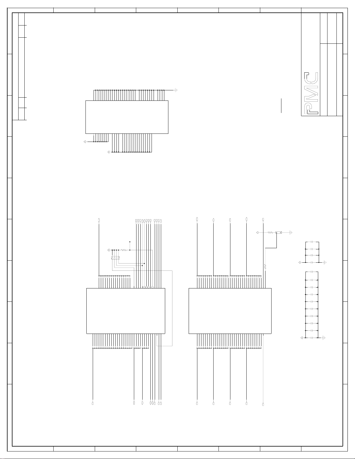
H
G
F
E
D
C
B
A
APPRDATE
1
REVISIONS
DESCRIPTION
REV
3254
ZONE
U1
2.5 V
W22
D8
B4
PPL_21
PPL_20
PPL_19
3 OF 5
PM73123
AAL1GATOR-8
PCH_8
PCH_7
PCH_6
A7
C14
M21
C17
A12
D15
PPL_16
PPL_17
PPL_18
PCH_5
PCH_4
PCH_3
U20
W17
AA11
M19
G19
C19
PPL_13
PPL_15
PPL_14
PCH_2
PCH_1
U4
E4
3.3 V
W21
V21
PPL_11
PPL_12
PQH_4
PQH_3
A22
AB12
Y17
AB15
PPL_9
PPL_10
PQH_2
PQH_1
Y18W4D16
Y11
PPL_7
PPL_8
PPH_15
AB8
PPL_5
PPL_6
PPH_14
PPH_13
L1
AA2
PPL_2
PPL_3
PPL_4
PPH_10
PPH_12
PPH_11
W8Y5V2R4E1
PPL_1
PPH_9
W16
AB17
PCL_8
PPH_7
PPH_8
Y20
AA7T2F1C3G4M4AA3
PCL_6
PCL_7
PPH_5
PPH_6
L19
R21
V22
Y14
PCL_5
PCL_4
PPH_3
PPH_4
A18D4D11
F20
L21
D19
PCL_3
PCL_2
PPH_2
PPH_1
C11
PCL_1
D22
PQL_4
PQL_3
K3D5AB21
PQL_2
PQL_1
POWER SUPPLY
Thu May 17 11:12:34 2001
AAL1
AAL1GATOR_8_1.1
DRAWING:
13
OF
00/01/21
ISSUE DATE:
PMC-Sierra, Inc.
1
1
10
PAGE:
REVISION NUMBER:
1.0
2354
PMC-991089
KM
AAL1GATOR_8 COMET_QUAD REF DESIGN
AAL1GATOR-8.1
ENGINEER:
TITLE:
DOCUMENT NUMBER:
DOCUMENT ISSUE NUMBER:
9876
PM73123
AAL1GATOR-8
U1
9D7<>
AAL1_D<15..0>\I
15
AB3
AA4
AB2
Y4
D13
D14
D15
2 OF 5
A14
A15
A16
A17
A18
A19
W2
Y2
Y6
AA1
AB1
AB4
AA5
19
D12
A13
AB5
D11
A12
Y3
3.3 V
8
1
RN7
9
1011121314
W5
AA6
D9D8D7D6D5
D10
A11
W6
AB6
3G6< 2G6<
3F6< 2F6<
13E5>
13E5>
13E5>
13E2<
13E5<
13G5>
13F5>
8C9>
13G5>
13H5>
13H5>
11E2< 8F9>
TP2
WRB_IN\I
RDB_IN\I
AAL1_SYSCLK\I
TCK\I
TMS\I
TDI\I
AAL1_INTB\I
TRSTB\I
RSTB\I
Y19
AA21
W3
RSTB
INTB
TCLK
TRSTB
SYSCLK
AAL1_TDOUTCGC_VALID\I
A3
C4AA17
TMS
TDI
TDO
AAL1_CSB\I
1
R91
AAL1_ACKB\I
4.7K
567
4.7K
432
012345678
W7
Y9
Y7
AA9
Y13
AA13
W10
AB7
AB11
AB9
W11
W14
AB13B5W15
AA14B3A2
D2D1D0
D3
D4
ALE
WRB
RDB
CSB
ACKB
SCAN_MODEB
MICRO/JTAG
A0A1CGC_DOUT3
CGC_DOUT2
CGC_DOUT1
CGC_DOUT0
NCLK
CGC_LINE0
CGC_LINE1
CGC_LINE2
CGC_LINE3
SRTS_STB
ADAP_STB
TL_CLK_OE
CGC_SER_D
AA18
CGC_VALID
W18
W19
Y16
AA16
AA19
AA20
AB18
0
A2A3A4A5A6A7A8A9A10
Y8
Y12
W12
Y10W9AA8
AA10
AB10
AA12
Y15
W13
AA15
AB19
AB16
AB14
231023456879101112131415161718
0
1
321
8F9>
TL_SYNC<7..0>\I
765432107654321
B22
F21
TL_SYNC7
TL_SYNC6
TL_SYNC5
1 OF 5
PM73123
AAL1GATOR-8
U1
RL_SYNC7
RL_SYNC6
RL_SYNC5
F19
C20
B21 A19
7
H21
K21
T19
N22
TL_SYNC4
TL_SYNC3
TL_SYNC2
TL_SYNC1
RL_SYNC4
RL_SYNC3
RL_SYNC2
RL_SYNC1
U22
P20
M20
J19
TL_DATA<7..0>\I
V19
B19
E20
J20
F22
U19
P19
L20
TL_SYNC0
TL_DATA7
TL_DATA6
TL_DATA5
TL_DATA4
TL_DATA3
TL_DATA2
TL_DATA1
RL_SYNC0
RL_DATA7
RL_DATA6
RL_DATA5
RL_DATA4
RL_DATA3
RL_DATA2
RL_DATA1
T20
R19
N19
K20
H20
E22
D20
W20
0
V20
TL_DATA0
RL_DATA0
AB22
TL_CLK<7..0>\I
TL_SIG<7..0>\I
7654321
0123456
7
A20
C18
D21
G20
H19
K19
N20
R20
Y22
TL_SIG7
TL_SIG6
TL_SIG5
TL_SIG4
TL_SIG3
TL_SIG2
TL_SIG1
TL_SIG0
RL_SIG7
RL_SIG6
RL_SIG5
RL_SIG4
RL_SIG3
RL_SIG2
RL_SIG1
RL_SIG0
A21
Y21
T22
P22
M22
J21
G21
C22
B20
8F9<>
E19
C21
H22
TL_CLK7
TL_CLK6
TL_CLK5
RL_CLK7
RL_CLK6
RL_CLK5
J22
G22
E21
3.3 V
K22
N21
TL_CLK4
TL_CLK3
TL_CLK2
RL_CLK4
RL_CLK3
RL_CLK2
P21
L22
8E2>
C16B\I
0
C16
U21
R22
TL_CLK1
TL_CLK0
CTL_CLK
RL_CLK1
RL_CLK0
CRL_CLK
T21
D18
AA22
0123456702134567012345670124356
LINE_MODE0 = ’GND’ WHEN DIRECT MODE
HEADER2
J5
R92
1
2
4.7K
330
R90
B18
2.5 V
LINE_MODE
LINE INTERFACE
3.3 V
C115
0.01UF
C116
0.01UF
C117
0.01UF
C118
0.01UF
C143
0.01UF
C119
0.01UF
C120
0.01UF
C121
0.01UF
C122
0.01UF
C123
0.01UF
C124
0.01UF
C125
0.01UF
C126
0.01UF
C127
0.01UF
DECOUPLING CAPS
ONE CAP PER TWO POWER PINS
9876
’HIGH’ WHEN H-MVIP MODE
AAL1_A<19..0>\I
CGC_DOUT<3..0>\I
CGC_LINE<3..0>\I
ADAP_STRB\I
SRTS_STRB\I
CGC_SER_D\I
NCLK\I
RL_SYNC<7..0>\I
C4B\I
RL_CLK<7..0>\I
RL_SIG<7..0>\I
RL_DATA<7..0>\I
C4B AND C16B ARE USED IN H-MVIP MODE
10
9H6>
H
G
F
8E9<
8E9<
8E9<
8E9<
8C9>
E
8E9>
3G2> 2G2>
D
3F2> 2F2>
3G2> 2G2>
C
3G2> 2G2>
8E2>
10
B
A
Page 83

H
G
F
E
D
C
B
A
APPRDATE
1
REVISIONS
DESCRIPTION
REV
3254
ZONE
TX POD
J28
AUX0
1
AUX1
GND
AUX2
48474644454342
49
GND
GND
GND
GND
GND
GND
GND
GND
GND
AUX6
AUX5
AUX4
AUX3
9
8567342
0
OUTPUT_D<15..0>
1514131211
C2B1D2E3D1E2F3F2H4J3J2F4J1J4L3K2K1K4C1
GND
GND
121110
56555453525150
57
GND
GND
GND
GND
GND
D9D4D5D6D7D8D3D0D1D2AUX7
17
18
14
987654321
10
GND
GND
D10
D11
1941161513
2021222324
GND
GND
GND
GND
GND
D15
D14
D13
D12
151413121110987654321
0
727169706668676465636261596058
73
GND
GND
GND
GND
GND
GND
GND
GND
GND
GND
A3A4A0A1A2
LENB
SOC
PRTY
293031
32
28
262725
43210
NOT USED IN ATM MODE
TATM_CLAV
RPHY_ADD<4..0>
TATM_PAR
TATM_ENB
43210
G1H1G3
G2
GND
GND
GND
CLAV0
CLAV1
CLAV2
353433
TATM_CLK
TATM_SOC
H2H3D3P2
GND
GND
CLAV3
80797877767574
GND
CLKIO
TRG_IN
EXTREF
4039383736
EBBI80
TRG_OUT
UTOPIA2 INTERFACE
567
8
330
432
1
RN10
Thu May 17 11:12:40 2001
AAL1
AAL1GATOR_8_1.3
DRAWING:
13
OF
1
12
00/01/21
PAGE:
ISSUE DATE:
REVISION NUMBER:
1.0
PMC-Sierra, Inc.
1
2354
PMC-991089
KM
AAL1GATOR_8 COMET_QUAD REF DESIGN
AAL1GATOR_8.3
ENGINEER:
TITLE:
DOCUMENT NUMBER:
DOCUMENT ISSUE NUMBER:
INPUT_D<15..0>
RX POD
9876
RECEPTACLE_RA RECEPTACLE_RA
J27
AUX0
1
AUX1
GND
AUX2
GND
AUX3
GND
AUX4
GND
AUX5
PBGA
GND
AUX6
U1
GND
8567342
TATM_D6
TATM_D7
TATM_D8
TATM_D9
TATM_D10
TATM_D11
TATM_D12
TATM_D13
TATM_D14
TATM_D15
5 OF 5
PM73123
AAL1GATOR-8
RATM_D6
RATM_D7
RATM_D8
RATM_D9
RATM_D10
RATM_D11
RATM_D12
RATM_D13
RATM_D14
RATM_D15
V3Y1W1U3U2V4T3U1P4N3N2N1N4M3M1
151413121110987654321
48474644454342
56555453525150
49
57
GND
GND
GND
GND
GND
GND
GND
GND
GND
GND
GND
GND
D10
9
0
D9D4D5D6D7D8D3D0D1D2AUX7
121110
17
18
1941161513
14
TATM_D3
TATM_D4
TATM_D5
RATM_D3
RATM_D4
RATM_D5
GND
GND
GND
D13
D12
D11
2021222324
TATM_D0
TATM_D1
TATM_D2
RPHY_ADD_RSX
TPHY_ADD4
RATM_D0
RATM_D1
RATM_D2
L2
43210
0
GND
GND
GND
GND
PRTY
D15
D14
151413121110987654321
RPHY_ADD3
RPHY_ADD0
RPHY_ADD1
RPHY_ADD2
TPHY_ADD3
TPHY_ADD0
TPHY_ADD1
TPHY_ADD2
RATM_PAR
R3V1T1R2T4
P3
GND
GND
GND
GND
GND
LENB
SOC
293031
28
262725
TATM_ENB
TATM_PAR
TATM_CLAV
RATM_CLAV
RATM_ENB
RATM_CLK
R1P1M2
727169706668676465636261596058
73
GND
GND
GND
GND
A3A4A0A1A2
32
43210
TATM_CLK
TATM_SOC
UTOPIA INTERFACE
RATM_SOC
80797877767574
GND
GND
GND
GND
GND
CLAV0
CLAV1
CLAV2
CLAV3
353433
GND
EXTREF
CLKIO
TRG_OUT
TRG_IN
4039383736
EBBI80
UTOPIA2 INTERFACE
TPHY_ADD<4..0>
RATM_ENB
RATM_CLK
RATM_CLAV
NOT USED IN ATM MODE
RATM_PAR
RATM_SOC
9876
567
8
330RN9
432
1
10
H
G
F
E
D
C
B
A
10
Page 84

H
G
F
E
D
C
B
A
APPRDATE
1
REVISIONS
DESCRIPTION
REV
3254
ZONE
3.3 V
7654321
74
DQA<9>
DQA<8>
DQA<7>
DQA<6>
4
11
20
27
54
61
70
77
VDD<1>
15
VDD<2>
41
VDD<3>
65
VDD<4>
91
A<17>
A<16>
A<15>
A<14>
U7
100MHZ
161514131211109876543210
DQA<5>
DQA<4>
DQA<3>
VDDQ<1>
VDDQ<2>
VDDQ<3>
VDDQ<4>
VDDQ<5>
VDDQ<6>
VDDQ<7>
VDDQ<8>
A<11>
A<13>
A<12>
0
DQA<1>
DQA<2>
A<9>
A<10>
1514131211
DQB<7>
DQB<6>
DQB<8>
DQB<9>
GS841Z18
(256K X 18)
A<8>
A<7>
A<6>
A<5>
32
9982814445464748495080
100
10
DQB<4>
DQB<3>
DQB<5>
A<4>
A<3>
A<2>
10E5>
2B10<
AAL1_TDOUT
AAL1_TDO\I
9
8
42
89121318192223245859626368697273
TDO
TDI
DQB<2>
DQB<1>
A<0>CKCE3
A<1>
3736353433
RAM_WE1B
RAM_WE0B
13H5>
13G5>
TMS\I
TCK\I
433839
TCK
TMS
CE2
CE1
88
866416
89
978594939298876614
ADVPDQEFTZZ
CKEGWBABB
8
4.7K
1
RN8
3.3 V
13
OF
1
11
00/01/21
PAGE:
ISSUE DATE:
REVISION NUMBER:
1.0
PMC-Sierra, Inc.
1
2354
PMC-991089
Thu May 17 11:12:37 2001
AAL1
AAL1GATOR_8_1.2
DRAWING:
VSS<1>
5
VSS<2>
10
VSS<3>
17
VSS<4>
21
VSS<5>
26
VSS<6>
40
VSS<7>
55
VSS<8>
60
VSS<9>
67
VSS<10>
71
VSS<11>
76
VSS<12>
90
LBO
31
567
432
3.3 V
KM
AAL1GATOR_8 COMET_QUAD REF DESIGN
AAL1GATOR-8.2
ENGINEER:
TITLE:
DOCUMENT NUMBER:
DOCUMENT ISSUE NUMBER:
C128
0.01UF
C129
0.01UF
C130
0.01UF
C131
0.01UF
C132
DECOUPLING CAPS
0.01UF
C133
0.01UF
RAM_D<15..0>
9876
RAM_PAR0
RAM_PAR1
RAM_A<16..0>
4 OF 5
PM73123
AAL1GATOR-8
U1
15
B16
D17
C15
RAM1_D13
RAM1_D14
RAM1_D15
RAM1_A14
RAM1_A15
RAM1_A16
D9
C10 A17
9
1011121314
B15
A15
B17
RAM1_D9
RAM1_D10
RAM1_D11
RAM1_D12
RAM1_A11
RAM1_A12
RAM1_A13
RAM1_A10
C9A8D7A9B9
B14
D14
C13
RAM1_D8
RAM1_D7
RAM1_D6
RAM1_A7
RAM1_A8
RAM1_A9
B11
B13
A13
D13
RAM1_D5
RAM1_D4
RAM1_D3
RAM1_A4
RAM1_A5
RAM1_A6
012345678
C12
B12
D12
A16B8A14
RAM1_D2
RAM1_D1
RAM1_D0
RAM1_OEB
RAM1_A0
RAM1_A1
RAM1_A2
RAM1_A3
A4C5C6B6A5C7A6B7C8
012345671089111213141516
RAM_CSB
D6
B10
A11
RAM1_CSB
RAM1_WEB0
RAM1_WEB1
RAM1_ADSCB
RAM_CLK\I
RAM_R/WB
RAM_OEB
8C9>
3.3 V
D10
A10
SCAN_ENB
RAM1_PAR1
RAM1_PAR0
RAM INTERFACE
4.7K
R93
1
TP3
9876
10
H
G
F
E
D
C
B
A
10
Page 85
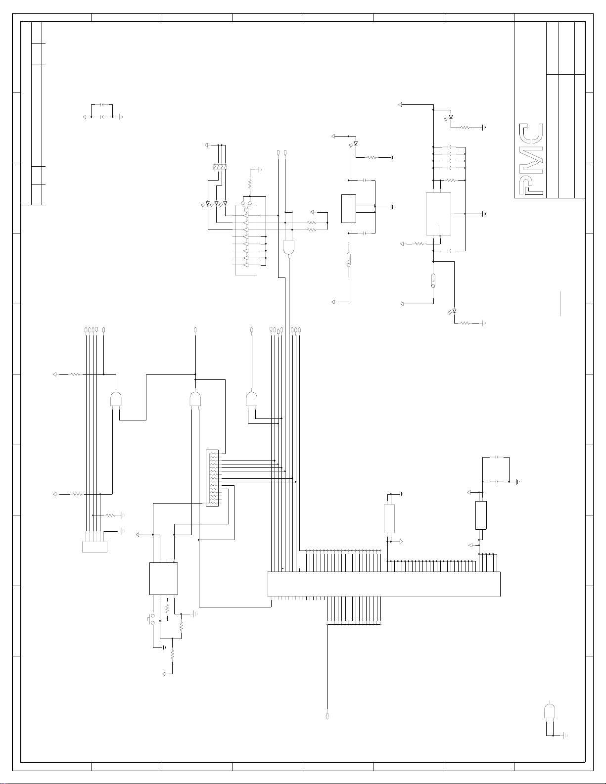
H
G
F
E
D
C
B
A
APPRDATE
1
C145
0.01UF
C144
3.3 V
0.1UF
REVISIONS
DESCRIPTION
REV
3254
ZONE
11E2< 10E5< 3A10< 2B10<
11E2< 10E5< 3A10< 2B10<
10E5< 3A10< 2B10<
10E5<
3B10>
3.3 V
567
8
270RN6
432
1
YELLOW
21
YELLOW
YELLOW
D121D221D3
10E5< 8G9< 3A7< 2B7<
AAL1GATOR-8 INTERRUPT LED
0
18
1
17
2
16
15
3
4
14
13
5
6
12
11
77
U4
COMET-QUADS INTERRUPT LEDS
330
1
19
Y
Y
Y
Y
Y
Y
Y
YA
R5
0
1
2
3
4
5
6
HCT541
9D5<
OE1 OE2
A
A
A
A
A
A
A
2
3
4
5
6
7
8
9
10E5>
3A7> 2B7>
10E5>
AAL1_INTB\I
IRQ2_BUS<1..0>\I
0
1
12
13
U8
HCT08
11
10F5< 9B8<
10E5< 9B8<
9A8<
8G9<
10E5<
9D10<
4.7K
4.7K
13
OF
00/01/21
ISSUE DATE:
1
13
PAGE:
REVISION NUMBER:
1.0
TRUE
3.3 V
21
SUPER_GREEN
D9
R80
2.5 V
21
SUPER_GREEN
D8
R78
270
C139
1UF
VOUT
4
2.5V
TAB
VCC
R88
R87
GND
2
GND
LT1118CST
VIN
U43
C140
31
1UF
F1
0.750A
VCC
VCC
VCC
1
VOUT
LT1528
VIN
U42
R81
5
4.7K
F2
3.000A
270
47UF
C134
47UF
C135
47UF
C136
47UF
C137
R79
330
2
SENS
GND
3
SHDN
4
C138
+
0.47UF
21
SUPER_GREEN
D10
R82
270
PMC-Sierra, Inc.
1
2354
PMC-991089
KM
AAL1GATOR_8 COMET_QUAD REF DESIGN
MICRO_INTERFACE
ENGINEER:
TITLE:
DOCUMENT NUMBER:
DOCUMENT ISSUE NUMBER:
DRAWING
LAST_MODIFIED=Thu May 17 11:12:14 2001
ABBREV=MICRO
TITLE=MICRO_INTERFACE
TMS\I
TDI\I
TCK\I
TDO1\I
TRSTB\I
R77
3.3 V3.3 V
4.7K
6
U10
HCT08
4
5
R75
4.7K
R76
4.7K
65432
1
J30
P_6
P_5
P_4
P_3
P_2
P_1
3.3 V
JTAG PORT
9876
RSTB\I
8
U10
HCT08
9
10
16
81
63
5
VCC
CTL
RESET
RESET
U14
SW1
MAX700
MR
GND
HYST
SENSE
4
27
R83
10K
PBNO
21
1.0K
R84
RES_ARRAY_15
RN11
4.7K
CS3B\I
CS2B\I
WRB_IN\I
AAL1_CSB\I
AAL1_ACKB\I
C1C2C3
C4C5C6C7C8C9C13
C1C2C3C4C5C6C7C8C9
A1A2A3A4A5A6A7A8A9
P1
A1A2A3A4A5A6A7A8A9
RDB_IN\I
UP_A<21..0>\I
21
20
C12
C11
C10
C10
C11
C12
A10
A11
A12
A12
A11
A10
181917161513141112910
C19
C18
C17
C16
C15
C14
C13
C14
C15
C16
C17
C18
C19
A13
A14
A15
A16
A17
A18
A19
A19
A18
A17
A16
A15
A14
A13
1514131112109876543
C141
+
1.0UF
C142
+
VCC
P<2>
P<1>
P<3> P<4>
SB1
?
12
34
GND1
210
86734
5
B16
B15
B14
B13
B12
B11
B10
C32
C31
C30
C29
C28
C27
C26
C25
C24
C23
C22
C21
C20
C20
C21
C22
C23
C24
C25
C26
C27
C28
C29
C30
C31
C32
A20
A21
A22
A23
A24
A25
A26
A27
A28
A29
A30
A31
A32
A32
A31
A30
A29
A28
A27
A26
A25
A24
A23
A22
A21
A20
210
B9B8B7B6B5B4B3B2B1
B01
B02
B03
B04
B05
B06
B07
B08
B09
B10
B11
B12
B13
B14
B15
B16
VCC1
B24
B23
B22
B21
B20
B19
B18
B17
B17
B18
B19
B20
B21
B22
B23
B24
47UF
P<2>
P<1>
P<3> P<4>
SB2
?
12
34
B32
B31
B30
B29
B28
B27
B26
B25
B25
B26
B27
B28
B29
B30
B31
B32
DIN96
9876
DEV_SELB\I
11
U10
HCT08
12
13
15
14
13
12
11
10
9
8
7
6
5
4
3
2
1
R85
931
3.3 V
UP_D<15..0>\I
10
9D10<>
H
G
F
E
D
C
B
3
U10
HCT08
1
2
10
CONNECT UNUSED INPUTS TO GND
A
Page 86

PRELIMINARY
PM73123 AAL1GATOR-8
PM4354 COMET-QUAD
REFERENCE DESIGN
PMC-1991089 ISSUE 2 AAL1GATOR-8 REFERENCE DESIGN
NOTES
PROPRIETARY AND CONFIDENTIAL TO PMC-SIERRA, INC., AND FOR ITS CUSTOMERS’ INTERNAL USE 47
Page 87

PRELIMINARY
REFERENCE DESIGN
PMC-1991089 ISSUE 2 AAL1GATOR-8 REFERENCE DESIGN
PM73123 AAL1GATOR-8
PM4354 COMET-QUAD
CONTACTING PMC-SIERRA, INC.
PMC-Sierra, Inc.
105-8555 Baxter Place Burnaby, BC
Canada V5A 4V7
Tel: (604) 415-6000
Fax: (604) 415-6200
Document Information: document@pmc-sierra.com
Corporate Information: info@pmc-sierra.com
Application Information: apps@pmc-sierra.com
(604) 415-4533
Web Site: http://www.pmc-sierra.com
None of the information contained in this document constitutes an express or implied warranty by PMC-Sierra, Inc. as to the sufficiency, fitness or
suitability for a particular purpose of any such information or the fitness, or suitability for a particular purpose, merchantability, performance, compatibility
with other parts or systems, of any of the products of PMC-Sierra, Inc., or any portion thereof, referred to in this document. PMC-Sierra, Inc. expressly
disclaims all representations and warranties of any kind regarding the contents or use of the information, including, but not limited to, express and
implied warranties of accuracy, completeness, merchantability, fitness for a particular use, or non-infringement.
In no event will PMC-Sierra, Inc. be liable for any direct, indirect, special, incidental or consequential damages, including, but not limited to, lost profits,
lost business or lost data resulting from any use of or reliance upon the information, whether or not PMC-Sierra, Inc. has been advised of the possibility
of such damage.
© 2001 PMC-Sierra, Inc.
PMC-1991089 (P2) Issue date: June 2001
PROPRIETARY AND CONFIDENTIAL TO PMC-SIERRA, INC., AND FOR ITS CUSTOMERS’ INTERNAL USE
 Loading...