

Page 1

STANDARD PRODUCT
PMC-Sierra, Inc.
PMC-951013 ISSUE 5 QUADRUPLE E1 FRAMER
PM6344 EQUAD
PM6344
EQUAD
QUADRUPLE E1 FRAMER
ISSUE 5: JUNE 1998
PMC-Sierra, Inc. 105 - 8555 Baxter Place Burnaby, BC Canada V5A 4V7 604 .415.6000
Page 2

STANDARD PRODUCT
PMC-Sierra, Inc.
PMC-951013 ISSUE 5 QUADRUPLE E1 FRAMER
PM6344 EQUAD
CONTENTS
1 FEATURES ........................................................................................................................1
2 APPLICATIONS .................................................................................................................4
3 REFERENCES ..................................................................................................................5
4 APPLICATION EXAMPLES ...............................................................................................7
5 BLOCK DIAGRAM.............................................................................................................8
6 PIN DIAGRAM.................................................................................................................11
7 PIN DESCRIPTION .........................................................................................................12
8 FUNCTIONAL DESCRIPTION ........................................................................................29
8.1 DIGITAL RECEIVE INTERFACE (DRIF).............................................................29
8.2 CLOCK AND DATA RECOVERY (CDRC)...........................................................29
8.3 FRAMER (FRMR)...............................................................................................31
8.4 PERFORMANCE MONITOR COUNTERS (PMON)...........................................38
8.5 HDLC RECEIVER (RFDL)..................................................................................38
8.6 ELASTIC STORE (ELST)...................................................................................39
8.7 SIGNALING EXTRACTOR (SIGX) .....................................................................39
8.8 BACKPLANE RECEIVE INTERFACE (BRIF).....................................................40
8.9 TRANSMITTER (TRAN).....................................................................................40
8.10 TRANSMIT PER-CHANNEL SERIAL CONTROLLER (PCSC)..........................41
8.11 HDLC TRANSMITTER (XFDL) ...........................................................................41
8.12 DIGITAL JITTER ATTENUATOR (DJAT).............................................................42
8.13 TIMING OPTIONS (TOPS).................................................................................46
8.14 DIGITAL E1 TRANSMIT INTERFACE (DTIF) .....................................................46
8.15 BACKPLANE TRANSMIT INTERFACE (BTIF)...................................................47
i
Page 3

STANDARD PRODUCT
PMC-Sierra, Inc.
PMC-951013 ISSUE 5 QUADRUPLE E1 FRAMER
PM6344 EQUAD
8.16 MICROPROCESSOR INTERFACE (MPIF)........................................................47
9 REGISTER DESCRIPTION.............................................................................................48
10 NORMAL MODE REGISTER DESCRIPTION.................................................................52
10.1 SIGX INDIRECT REGISTERS 96 (60H) - 127 (7FH) - SEGMENT 4: TYPICAL
PER-TIMESLOT CONFIGURATION AND SIGNALING TRUNK ......................156
10.2 REGISTERS 049-04FH, 0C9H-0CFH, 149H-14FH, 1C9H-1CFH: LATCHING
PERFORMANCE DATA.....................................................................................168
11 TEST FEATURES DESCRIPTION ................................................................................176
11.1 TEST MODE 0..................................................................................................176
12 FUNCTIONAL TIMING...................................................................................................180
12.1 RECEIVE BACKPLANE INTERFACE...............................................................182
13 OPERATION ..................................................................................................................191
13.1 USING THE INTERNAL FDL TRANSMITTER .................................................192
13.2 USING THE INTERNAL FDL RECEIVER.........................................................194
13.3 USING THE LOOPBACK MODES....................................................................201
13.3.1 PAYLOAD LOOPBACK........................................................................202
13.3.2 LINE LOOPBACK................................................................................203
13.3.3 DIAGNOSTIC DIGITAL LOOPBACK...................................................203
13.4 USING THE PER-CHANNEL SERIAL CONTROLLERS..................................204
13.4.1 INITIALIZATION...................................................................................204
13.4.2 DIRECT ACCESS MODE....................................................................205
13.4.3 INDIRECT ACCESS MODE ................................................................205
13.5 USING THE DIGITAL JITTER ATTENUATOR..................................................206
13.5.1 DEFAULT APPLICATION .....................................................................206
13.5.2 DATA BURST APPLICATION...............................................................206
ii
Page 4

STANDARD PRODUCT
PMC-Sierra, Inc.
PMC-951013 ISSUE 5 QUADRUPLE E1 FRAMER
PM6344 EQUAD
13.5.3 ELASTIC STORE APPLICATION ........................................................207
13.5.4 ALTERNATE TCLKO REFERENCE APPLICATION.............................207
13.5.5 CHANGING THE JITTER TRANSFER FUNCTION ............................208
13.5.6 RECEIVER JITTER ATTENUATION....................................................208
13.6 USING THE PERFORMANCE MONITOR COUNTER VALUES......................210
13.7 RESET PROCEDURE......................................................................................212
14 ABSOLUTE MAXIMUM RATINGS.................................................................................216
15 CAPACITANCE...............................................................................................................217
16 D.C. CHARACTERISTICS.............................................................................................218
17 MICROPROCESSOR INTERFACE TIMING CHARACTERISTICS...............................220
18 EQUAD I/O TIMING CHARACTERISTICS ....................................................................225
19 ORDERING AND THERMAL INFORMATION...............................................................239
20 MECHANICAL INFORMATION......................................................................................240
iii
Page 5

STANDARD PRODUCT
PMC-Sierra, Inc.
PMC-951013 ISSUE 5 QUADRUPLE E1 FRAMER
PM6344 EQUAD
LIST OF REGISTERS
REGISTER 000H, 080H, 100H, 180H: RECEIVE OPTIONS.......................................................53
REGISTER 001H, 081H, 101H, 181H: RECEIVE BACKPLANE OPTIONS.................................56
REGISTER 002H, 082H, 102H, 182H: DATALINK OPTIONS.......................................................60
REGISTER 003H, 083H, 103H, 183H: RECEIVE INTERFACE CONFIGURATION.....................63
REGISTER 004H, 084H, 104H, 184H: TRANSMIT INTERFACE CONFIGURATION ..................65
REGISTER 005H, 085H, 105H, 185H: TRANSMIT BACKPLANE OPTIONS...............................68
REGISTER 006H, 086H, 106H, 186H: TRANSMIT FRAMING OPTIONS ...................................70
REGISTER 007H, 087H, 107H, 187H: TRANSMIT TIMING OPTIONS........................................72
REGISTER 008H, 088H, 108H, 188H: INTERRUPT SOURCE....................................................77
REGISTER 009H, 089H, 109H, 189H: RECEIVE TS0 DATA LINK ENABLES .............................78
REGISTER 00AH, 08AH, 10AH, 18AH: MASTER DIAGNOSTICS..............................................80
REGISTER 00BH, 20BH: EQUAD MASTER TEST......................................................................82
REGISTER 00CH: EQUAD REVISION/CHIP ID/GLOBAL PMON UPDATE ................................84
REGISTER 00DH, 08DH, 10DH, 18DH: FRAMER RESET..........................................................85
REGISTER 00EH, 08EH, 10EH, 18EH: PHASE STATUS WORD (LSB)......................................86
REGISTER 00FH, 08FH, 10FH, 18FH: PHASE STATUS WORD (MSB)......................................88
REGISTER 010H, 090H, 110H, 190H: CDRC CONFIGURATION...............................................89
REGISTER 011H, 091H, 111H, 191H: CDRC INTERRUPT ENABLE .........................................91
REGISTER 012H, 092H, 112H, 192H: CDRC INTERRUPT STATUS ..........................................92
REGISTER 013H, 093H, 113H, 193H: CDRC ALTERNATE LOSS OF SIGNAL STATUS............94
REGISTERS 014H, 094H, 114H AND 194H: CHANNEL SELECT (0 TO 7)................................95
REGISTERS 015H, 095H, 115H AND 195H: CHANNEL SELECT (8 TO 15)..............................96
REGISTERS 016H, 096H, 116H AND 196H: CHANNEL SELECT (16 TO 23)............................97
iv
Page 6

STANDARD PRODUCT
PMC-Sierra, Inc.
PMC-951013 ISSUE 5 QUADRUPLE E1 FRAMER
PM6344 EQUAD
REGISTERS 017H, 097H, 117H AND 197H: CHANNEL SELECT (24 TO 31)............................98
REGISTER 018H, 098H, 118H, 198H: DJAT INTERRUPT STATUS ............................................99
REGISTER 019H, 099H, 119H, 199H: DJAT REFERENCE CLOCK DIVISOR (N1) CONTROL100
REGISTER 01AH, 09AH, 11AH, 19AH: DJAT OUTPUT CLOCK DIVISOR (N2) CONTROL.....101
REGISTER 01BH, 09BH, 11BH, 19BH: DJAT CONFIGURATION..............................................102
REGISTER 01CH, 09CH, 11CH, 19CH: ELST CONFIGURATION............................................104
REGISTER 01DH, 09DH, 11DH, 19DH: ELST INTERRUPT STATUS .......................................105
REGISTER 01EH, 09EH, 11EH, 19EH: ELST IDLE CODE.......................................................106
REGISTER 020H, 0A0H, 120H, 1A0H: FRMR FRAME ALIGNMENT OPTIONS......................107
REGISTER 021H, 0A1H, 121H, 1A1H: FRMR MAINTENANCE MODE OPTIONS...................109
REGISTER 022H, 0A2H, 122H, 1A2H: FRMR FRAMING STATUS INTERRUPT ENABLE.......111
REGISTER 023H, 0A3H, 123H, 1A3H: FRMR MAINTENANCE/ALARM STATUS INTERRUPT
ENABLE.........................................................................................................................112
REGISTER 024H, 0A4H, 124H, 1A4H: FRMR FRAMING STATUS INTERRUPT INDICATION.113
REGISTER 025H, 0A5H, 125H, 1A5H: FRMR MAINTENANCE/ALARM STATUS INTERRUPT
INDICATION...................................................................................................................114
REGISTER 026H, 0A6H, 126H, 1A6H: FRMR FRAMING STATUS ...........................................115
REGISTER 027H, 0A7H, 127H, 1A7H: FRMR MAINTENANCE/ALARM STATUS ....................117
REGISTER 028H, 0A8H, 128H, 1A8H: FRMR INTERNATIONAL/NATIONAL BITS ..................119
REGISTER 029H, 0A9H, 129H, 1A9H: FRMR EXTRA BITS.....................................................120
REGISTER 02AH, 0AAH, 12AH, 1AAH: FRMR CRC ERROR COUNTER - LSB......................121
REGISTER 02BH, 0ABH, 12BH, 1ABH: FRMR CRC ERROR COUNTER - MSB.....................122
REGISTER 02CH, 0ACH, 12CH, 1ACH: TS16 AIS ALARM STATUS.........................................123
REGISTER 030H, 0B0H, 130H, 1B0H: TPSC BLOCK CONFIGURATION................................124
REGISTER 031H, 0B1H, 131H, 1B1H: TPSC BLOCK µP ACCESS STATUS............................125
v
Page 7

STANDARD PRODUCT
PMC-Sierra, Inc.
PMC-951013 ISSUE 5 QUADRUPLE E1 FRAMER
PM6344 EQUAD
REGISTER 032H, 0B2H, 132H, 1B2H: TPSC BLOCK TIMESLOT INDIRECT
ADDRESS/CONTROL...................................................................................................126
REGISTER 033H, 0B3H, 133H, 1B3H: TPSC BLOCK TIMESLOT INDIRECT DATA BUFFER..127
TPSC INTERNAL REGISTERS 20-3FH: DATA CONTROL BYTE..............................................129
TPSC INTERNAL REGISTERS 40-5FH: IDLE CODE BYTE.....................................................131
REGISTER 034H, 0B4H, 134H, 1B4H: XFDL BLOCK CONFIGURATION ................................132
REGISTER 035H, 0B5H, 135H, 1B5H: XFDL INTERRUPT STATUS.........................................134
REGISTER 036H, 0B6H, 136H, 1B6H: XFDL TRANSMIT DATA................................................135
REGISTER 038H, 0B8H, 138H, 1B8H: RFDL CONFIGURATION .............................................136
REGISTER 039H, 0B9H, 139H, 1B9H: RFDL INTERRUPT CONTROL/STATUS......................137
REGISTER 03AH, 0BAH, 13AH, 1BAH: RFDL STATUS ............................................................139
REGISTER 03BH, 0BBH, 13BH, 1BBH: RFDL RECEIVE DATA ................................................142
REGISTERS 03CH, 0BCH, 13CH AND 1BCH: INTERRUPT ID/CLOCK MONITOR.................143
REGISTERS 03DH, 0BDH, 13DH AND 1BDH: BACKPLANE PARITY CONFIGURATION AND
STATUS..........................................................................................................................145
REGISTER 040H, 0C0H, 140H, 1C0H: SIGX BLOCK CONFIGURATION.................................147
REGISTER 041H, 0C1H, 141H, 1C1H: SIGX BLOCK µP ACCESS STATUS ............................149
REGISTER 042H, 0C2H, 142H, 1C2H: SIGX BLOCK TIME SLOT INDIRECT
ADDRESS/CONTROL...................................................................................................150
REGISTER 043H, 0C3H, 143H, 1C3H: SIGX BLOCK TIME SLOT INDIRECT DATA BUFFER.151
SIGX INDIRECT REGISTERS 33 (21H)- 47 (2FH) - SEGMENT 2: TYPICAL TIMESLOT
SIGNALING DATA REGISTER (TSS 1-15)....................................................................153
SIGX INDIRECT REGISTERS 49 (31H)- 63 (3FH) - SEGMENT 2: TYPICAL TIMESLOT
SIGNALING DATA REGISTER (TSS 17-31)..................................................................154
SIGX INDIRECT REGISTERS 64 (40H) - 95 (5FH) - SEGMENT 3: TYPICAL PER-TIMESLOT
PCM TRUNK CONDITIONING DATA REGISTER .........................................................155
CONDITIONING DATA REGISTER.............................................................................................156
vi
Page 8

STANDARD PRODUCT
PMC-Sierra, Inc.
PMC-951013 ISSUE 5 QUADRUPLE E1 FRAMER
PM6344 EQUAD
REGISTER 044H, 0C4H, 144H, 1C4H: TRAN CONFIGURATION.............................................158
REGISTER 045H, 0C5H, 145H, 1C5H: TRAN TRANSMIT ALARM/DIAGNOSTIC CONTROL.162
REGISTER 046H, 0C6H, 146H, 1C6H: TRAN INTERNATIONAL/NATIONAL CONTROL.........164
REGISTER 047H, 0C7H, 147H, 1C7H: TRAN EXTRA BITS CONTROL...................................166
REGISTER 048H, 0C8H, 148H, 1C8H: PMON CONTROL/STATUS..........................................167
REGISTER 049H, 0C9H, 149H, 1C9H: FRAMING BIT ERROR COUNT..................................169
REGISTER 04AH, 0CAH, 14AH, 1CAH: FAR END BLOCK ERROR COUNT LSB ...................170
REGISTER 04BH, 0CBH, 14BH, 1CBH: FAR END BLOCK ERROR COUNT MSB ..................171
REGISTER 04CH, 0CCH, 14CH, 1CCH: CRC ERROR COUNT LSB .......................................172
REGISTER 04DH, 0CDH, 14DH, 1CDH: CRC ERROR COUNT MSB ......................................173
REGISTER 04EH, 0CEH, 14EH, 1CEH: LINE CODE VIOLATION COUNT LSB.......................174
REGISTER 04FH, 0CFH, 14FH, 1CFH: LINE CODE VIOLATION COUNT MSB.......................175
vii
Page 9

STANDARD PRODUCT
PMC-Sierra, Inc.
PMC-951013 ISSUE 5 QUADRUPLE E1 FRAMER
PM6344 EQUAD
LIST OF FIGURES
FIGURE 1 - EXAMPLE 1. DS-3 TERMINAL MULTIPLEXER/CHANNEL BANK........................7
FIGURE 2 - CDRC JITTER TOLERANCE WITH ALGSEL = 1................................................30
FIGURE 3 - CDRC JITTER TOLERANCE WITH ALGSEL = 0................................................31
FIGURE 4 - BASIC FRAMING ALGORITHM FLOWCHART...................................................34
FIGURE 5 - DJAT JITTER TOLERANCE.................................................................................44
FIGURE 6 - DJAT MINIMUM JITTER TOLERANCE VS. XCLK ACCURACY..........................45
FIGURE 7 - DJAT JITTER TRANSFER...................................................................................46
FIGURE 8 - TRANSMIT TIMING OPTIONS............................................................................76
FIGURE 9 - TS16 RECEIVE DATALINK INTERFACE............................................................180
FIGURE 10 - TS0 RECEIVE DATALINK INTERFACE..............................................................180
FIGURE 11 - TS16 TRANSMIT DATALINK INTERFACE.........................................................181
FIGURE 12 - TS0 TRANSMIT DATALINK INTERFACE...........................................................181
FIGURE 13 - ROHM=0, BRX2RAIL=0, BRXSMFP=0 AND BRXCMFP=0..............................182
FIGURE 14 - RECEIVE COMPOSITE MULTIFRAME OUTPUT (BRXSMFP=1 AND
BRXCMFP=1) ......................................................................................................183
FIGURE 15 - RECEIVE OVERHEAD OUTPUT (ROHM=1)....................................................183
FIGURE 16 - ELSTBYP=1, SRSMFP=1, SRCMFP=1, BRXSMFP=1, BRXCMFP=0 .............184
FIGURE 17 - RECEIVE CHANNEL INTERFACE....................................................................184
FIGURE 18 - TRANSMIT BACKPLANE INTERFACE .............................................................185
FIGURE 19 - TRANSMIT CHANNEL INTERFACE..................................................................185
FIGURE 20 - MULTIPLEXED RECEIVE BACKPLANE INTERFACE......................................186
FIGURE 21 - MULTIPLEXED TRANSMIT BACKPLANE INTERFACE....................................188
FIGURE 22 - MULTIPLEXED TRANSMIT BACKPLANE INTERFACE WITH BTXMFP=1......190
viii
Page 10

STANDARD PRODUCT
PMC-Sierra, Inc.
PMC-951013 ISSUE 5 QUADRUPLE E1 FRAMER
PM6344 EQUAD
FIGURE 23 - TYPICAL DATA FRAME.....................................................................................197
FIGURE 24 - RFDL NORMAL DATA AND ABORT SEQUENCE.............................................198
FIGURE 25 - RFDL FIFO OVERRUN......................................................................................199
FIGURE 26 - XFDL NORMAL DATA SEQUENCE...................................................................200
FIGURE 27 - XFDL UNDERRUN SEQUENCE.......................................................................201
FIGURE 28 - PAYLOAD LOOPBACK ......................................................................................202
FIGURE 29 - LINE LOOPBACK..............................................................................................203
FIGURE 30 - DIAGNOSTIC DIGITAL LOOPBACK .................................................................204
FIGURE 31 - RECEIVE BACKPLANE INTERFACE WITH RCLKOSEL = 1............................209
FIGURE 32 - LCV COUNT VS. BER........................................................................................211
FIGURE 33 - FER COUNT VS. BER .......................................................................................211
FIGURE 34 - CRCE COUNT VS. BER ....................................................................................212
FIGURE 35 - MICROPROCESSOR READ ACCESS TIMING................................................221
FIGURE 36 - MICROPROCESSOR WRITE ACCESS TIMING...............................................223
FIGURE 37 - BACKPLANE TRANSMIT INPUT TIMING DIAGRAM .......................................225
FIGURE 38 - BACKPLANE TRANSMIT INPUT TIMING DIAGRAM .......................................226
FIGURE 39 - XCLK=37.056 MHZ INPUT TIMING ..................................................................227
FIGURE 40 - TCLKI INPUT TIMING........................................................................................228
FIGURE 41 - DIGITAL RECEIVE INTERFACE INPUT TIMING DIAGRAM.............................229
FIGURE 42 - TRANSMIT DATA LINK INPUT TIMING DIAGRAM...........................................230
FIGURE 43 - BACKPLANE RECEIVE TIMING DIAGRAM......................................................231
FIGURE 44 - BACKPLANE RECEIVE TIMING (RCLKOSEL = 1) DIAGRAM.........................232
FIGURE 45 - MULTIPLEXED BACKPLANE RECEIVE TIMING DIAGRAM............................233
FIGURE 46 - RECEIVE DATA LINK OUTPUT TIMING DIAGRAM..........................................234
ix
Page 11

STANDARD PRODUCT
PMC-Sierra, Inc.
PMC-951013 ISSUE 5 QUADRUPLE E1 FRAMER
PM6344 EQUAD
FIGURE 47 - RECOVERED FRAME OUTPUT TIMING DIAGRAM........................................234
FIGURE 48 - TRANSMIT INTERFACE OUTPUT TIMING DIAGRAM.....................................235
FIGURE 49 - TRANSMIT DATA LINK DMA INTERFACE OUTPUT TIMING DIAGRAM .........236
FIGURE 50 - RECEIVE DATA LINK DMA INTERFACE OUTPUT TIMING DIAGRAM............237
FIGURE 51 - 128 PIN COPPER LEADFRAME PLASTIC QUAD FLAT PACK (R SUFFIX) ....240
x
Page 12

STANDARD PRODUCT
PMC-Sierra, Inc.
PMC-951013 ISSUE 5 QUADRUPLE E1 FRAMER
PM6344 EQUAD
LIST OF TABLES
TABLE 1 - NORMAL MODE REGISTER MEMORY MAP.....................................................48
TABLE 2 -..............................................................................................................................74
TABLE 3 -..............................................................................................................................87
TABLE 4 -............................................................................................................................177
TABLE 5 -............................................................................................................................177
TABLE 6 - CONFIGURING THE EQUAD FROM RESET...................................................191
TABLE 7 -............................................................................................................................210
TABLE 8 - EQUAD CAPACITANCE.....................................................................................217
TABLE 9 - EQUAD D.C. CHARACTERISTICS....................................................................218
TABLE 10 - MICROPROCESSOR READ ACCESS (FIGURE 35).......................................220
TABLE 11 - MICROPROCESSOR WRITE ACCESS (FIGURE 36)......................................222
TABLE 12 - BACKPLANE TRANSMIT INPUT TIMING, MENB INPUT HIGH (FIGURE 37).225
TABLE 13 - BACKPLANE TRANSMIT INPUT TIMING, MENB INPUT LOW (FIGURE 37)..226
TABLE 14 - XCLK=49.152 MHZ INPUT (FIGURE 39)..........................................................227
TABLE 15 - TCLKI INPUT (FIGURE 40................................................................................227
TABLE 16 - DIGITAL RECEIVE INTERFACE INPUT TIMING (FIGURE 41) ........................228
TABLE 17 - TRANSMIT DATA LINK INPUT TIMING (FIGURE 42).......................................230
TABLE 18 - BACKPLANE RECEIVE TIMING, MENB INPUT HIGH (FIGURE 43)...............231
TABLE 19 - BACKPLANE RECEIVE TIMING, MENB INPUT HIGH, RCLKOSEL = 1 (FIGURE
44)........................................................................................................................232
TABLE 20 - MULTIPLEXED BACKPLANE RECEIVE TIMING, MENB INPUT LOW (FIGURE
45)........................................................................................................................233
TABLE 21 - RECEIVE DATA LINK OUTPUT TIMING (FIGURE 46).....................................234
TABLE 22 - RECOVERED FRAME PULSE OUTPUT TIMING (FIGURE 47).......................234
xi
Page 13

STANDARD PRODUCT
PMC-Sierra, Inc.
PMC-951013 ISSUE 5 QUADRUPLE E1 FRAMER
PM6344 EQUAD
TABLE 23 - TRANSMIT INTERFACE OUTPUT TIMING (FIGURE 48) ................................235
TABLE 24 - TRANSMIT DATA LINK DMA INTERFACE OUTPUT TIMING (FIGURE 49).....236
TABLE 25 - RECEIVE DATA LINK DMA INTERFACE OUTPUT TIMING (FIGURE 50) .......237
TABLE 26 - EQUAD ORDERING INFORMATION................................................................239
TABLE 27 - EQUAD THERMAL INFORMATION...................................................................239
xii
Page 14

STANDARD PRODUCT
PMC-Sierra, Inc.
PMC-951013 ISSUE 5 QUADRUPLE E1 FRAMER
PM6344 EQUAD
1
FEATURES
Integrates four full-featured E1 framers and transmitters in a single device for
•
terminating duplex E1 signals.
Software and functionally compatible with the PM6341 E1XC Single E1
•
Transceiver.
Pin compatible with the PM4344 Quad T1 Framer device.
•
Provides an 8-bit microprocessor bus interface for configuration, control, and
•
status monitoring.
Low power CMOS technology
•
Available in a 128 pin PQFP package.
•
Each one of four receiver sections:
Recovers clock and data using a digital phase locked loop for high jitter
•
tolerance. A direct clock input is provided to allow clock recovery to be bypassed.
Accepts dual rail or single rail digital PCM inputs.
•
Supports HDB3 or AMI line code.
•
Accepts gapped data streams to support higher rate demultiplexing.
•
Frames to a G.704 2048 kbit/s signal within 1 ms.
•
Frames to the signaling multiframe alignment when enabled.
•
Frames to the CRC multiframe alignment when enabled.
•
Provides loss of signal detection, and indicates loss of frame alignment
•
(OOF), loss of signaling multiframe alignment and loss of CRC multiframe
alignment.
Supports line and path performance monitoring according to ITU-T
•
recommendations. Accumulators are provided for counting:
CRC-4 errors to 1000 per second;
•
1
Page 15

STANDARD PRODUCT
PMC-Sierra, Inc.
PMC-951013 ISSUE 5 QUADRUPLE E1 FRAMER
PM6344 EQUAD
Far end block errors to 1000 per second;
Frame sync errors to 127 per second; and
Line code violations to 8191 per second.
• Indicates the reception of remote alarm and remote multiframe alarm.
• Indicates the reception of alarm indication signal (AIS) and time slot 16 AIS.
• Declares RED and AIS alarms using Q.516 recommended integration
periods.
• Provides an HDLC/LAPD interface for terminating a data link. Supports
polled, interrupt-driven, or DMA servicing of the HDLC interface.
• Optionally extracts the data link from timeslot 16 (64 kbit/s), which may be
used to receive common channel signaling, or from any combination of the
national bits in timeslot 0 of non-frame alignment signal frames (4 kbit/s - 20
kbit/s).
• Supports fractional E1 channel extraction.
• Provides a two-frame elastic store buffer for jitter and wander attenuation that
performs controlled slips and indicates slip occurrence and direction.
• Provides channel associated signaling extraction, with optional data inversion,
programmable idle code substitution, and up to 3 multiframes of signaling
debounce on a per-timeslot basis.
• Provides trunk conditioning which fo rces programmable trouble code
substitution and signaling conditioning on all timeslots or on selected
timeslots.
• Optionally provides dual rail digital PCM output signals to allow BPV
transparency. Also supports unframed mode.
• Supports transfer of PCM and signaling data to 2.048 Mbit/s or 16.384Mbit/s
backplane buses.
• Can be configured to attenuate jitter on the receive side by placing the digital
jitter attenuator in the receive path.
2
Page 16

STANDARD PRODUCT
PMC-Sierra, Inc.
PMC-951013 ISSUE 5 QUADRUPLE E1 FRAMER
PM6344 EQUAD
Each one of four transmitter sections:
Formats data to create a G.704 2048 kbit/s signal. Optionally inserts
•
signaling multiframe alignment signal. Optionally inserts CRC multiframe
structure including optional transmission of far end block errors.
Optionally accepts dual rail digital PCM inputs to allow BPV transparency.
•
Also supports unframed mode and framing bit, CRC, or data link by-pass.
Supports transfer of PCM and signaling data from 2.048 Mbit/s or
•
16.384Mbit/s backplane buses.
Provides channel associated signaling insertion, programmable idle code
•
substitution, digital milliwatt code substitution, and data inversion on a per
timeslot basis.
Provides trunk conditioning which fo rces programmable trouble code
•
substitution and signaling conditioning on all timeslots or on selected
timeslots.
Supports transmission of the alarm indication signal (AIS), timeslot 16 AIS,
•
remote alarm signal or remote multiframe alarm signal.
Provides an HDLC/LAPD interface for generating a data link. Supports
•
polled, interrupt-driven, or DMA servicing of the HDLC interface.
Optionally inserts the data link into timeslot 16 (64 kbit/s), which may be used
•
to transmit common channel signaling, or into any combination of the national
bits in timeslot 0 of non-frame alignment signal frames (4 kbit/s - 20 kbit/s).
Supports fractional E1 channel insertion.
•
Provides a digital phase locked loop for generation of a low jitter transmit
•
clock.
Provides a FIFO buffer for jitter attenuation and rate conversion in the
•
transmitter. FIFO full or empty indication allows for bit-stuffing in higher rate
multiplexing applications.
Supports HDB3 or AMI line code.
•
Provides dual rail or single rail digital PCM output signals.
•
3
Page 17

STANDARD PRODUCT
PMC-Sierra, Inc.
PMC-951013 ISSUE 5 QUADRUPLE E1 FRAMER
PM6344 EQUAD
2
APPLICATIONS
E1 Channel Service Units (CSU) and Data Service Units (DSU)
•
E1 Channel Banks and Multiplexers
•
Digital Private Branch Exchanges (PBX)
•
Digital Access and Cross-Connect Systems (DACS) and Electronic DSX
•
Cross-Connect Systems (EDSX)
E1 Frame Relay Interfaces
•
E1 ATM Interfaces
•
ISDN Primary Rate Interfaces (PRI)
•
SDH Byte Synchronous TU12 Mappers
•
Test Equipment
•
4
Page 18

STANDARD PRODUCT
PMC-Sierra, Inc.
PMC-951013 ISSUE 5 QUADRUPLE E1 FRAMER
PM6344 EQUAD
3
REFERENCES
1. ITU-T Recommendation G.704, - "Synchronous Frame Structures Used at
Primary and Secondary Hierarchical Levels", Vol. III, Fascicle III.4, 1988.
2. ITU-T Recommendation G.706, - "Frame Alignment and Cyclic Redundancy
Check (CRC) Procedures Relating to Basic Frame Structures Defined in
Recommendation G.704", Vol. III, Fascicle III.4 , 1988.
3. ITU-T Recommendation G.706, - "Frame Alignment and Cyclic Redundancy
Check (CRC) Procedures Relating to Basic Frame Structures Defined in
Recommendation G.704", 1991
4. ITU-T Recommendation G.711, - "Pulse Code Modulation (PCM) of Voice
Frequencies", Volume III, Fascicle III.3, 1988.
5. ITU-T Recommendation G.732, - "Characteristics of Primary PCM Multiplex
Equipment Operating at 2048 kbit/s", Vol. III, Fascicle III.4, 1988.
6. ITU-T Recommendation G.735, - "Characteristics of Primary PCM Multiplex
Equipment Operating at 2048 kbit/s and Offering Synchronous Digital Access
at 384 kbit/s and/or 64 kbit/s", Vol. III, Fascicle III.4, 1988.
7. ITU-T Recommendation G.821, - "Error Performance of an International
Digital Connection Forming Part of an Integrated Services Digital Network",
Vol. III, Fascicle III.5, 1988.
8. ITU-T Recommendation G.823, - "The Control of Jitter and Wander Within
Digital Networks Which are Based on the 2048 kbit/s Hierarchy", Vol. III,
Fascicle III.5, 1988.
9. ITU-T Recommendation O.151, - "Error Performance Measuring Equipment
For Digital Systems at the Primary Bit Rate and Above", Vol. IV, Fascicle IV.4,
1988.
10. ITU-T Blue Book, Recommendation O.162, - "Equipment to Perform in
Service Monitoring on 2048 kbit/s Signals", Vol. IV, Fascicle IV.4, 1988.
11. ITU-T Recommendation Q.506, - "Operations and maintenance functions",
Vol. VI, Fascicle VI.5, 1984.
12. ITU-T Recommendation Q.516, - "Operations and maintenance functions",
Vol. VI, Fascicle VI.5, 1984.
5
Page 19

STANDARD PRODUCT
PMC-Sierra, Inc.
PMC-951013 ISSUE 5 QUADRUPLE E1 FRAMER
PM6344 EQUAD
13. Transmission and Multiplexing (TM); Generic Functional Requirements for
SDH Transmission Equipment, Part 1: Generic Processes and Performance",
ETSI DE/TM-1015, November, 1993, Version 1.0.
6
Page 20
STANDARD PRODUCT
PMC-Sierra, Inc.
PMC-951013 ISSUE 5 QUADRUPLE E1 FRAMER
PM6344 EQUAD
4
DSX-3
APPLICATION EXAMPLES
Figure 1 - Example 1. DS-3 Terminal Multiplexer/Channel Bank
PM6344
EQUAD
PM6344
EQUAD
PM6344
EQUAD
PM6344
EQUAD
PM6344
EQUAD
PM6341
E1XC
Synchronous
DS0
Backplane
DS3
LIU
PM8313
D3MX
4 E1s
4 E1s
4 E1s
4 E1s
4 E1s
1 E1
Services
Example 1 shows a DS-3 Terminal Multiplexer/Channel Bank using 5 EQUAD
devices, PMC-Sierra's PM8313 D3MX M13 Multiplexer, the PM6341 E1XC E1
Transceiver, and Silicon System's SSI 78P236 DS-3 Line Interface Unit.
21 E1 signals can be multiplexed into a DSX-3 formatted signal. Five EQUAD
devices and a single E1XC device are used to terminate these 21 signals. The
DS-0 backplane data is transmitted and received using a 2.048 MHz system
clock.
7
Page 21

STANDARD PRODUCT
PMC-Sierra, Inc.
PMC-951013 ISSUE 5 QUADRUPLE E1 FRAMER
PM6344 EQUAD
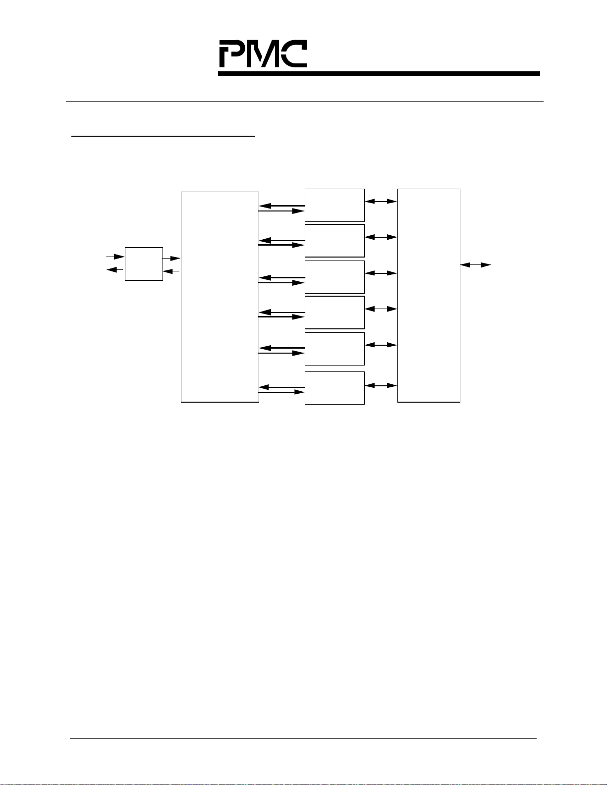
5
BLOCK DIAGRAM
TCLKI[1:4]
BTPCM/BTDP[1:4]/
BTSIG/BTDN[1:4]
BTFP[1:4]/MTFP*
BTCLK[1:4]/
MTCLK*
BRCLK*/MRCLK*
BRFPI*/MRFPI*
MENB*
XCLK/VCLK*
RCLKI[1:4]
RDP/RDD[1:4]
RDN/RLCV[1:4]
MTD*
BTIF
Backplane
Transmit
Interface
DRIF
DS-1
Receive
Interface
Internal
Bus
TRAN
BasicTransmitter:
Frame Generation,
Alarm Insertion,
Trunk Conditioning
Line Coding
PCSC
Per-channel
Controller:
Signalling,
Idle Insert
CDRC
Clock and
Data
Recovery
XFDL
HDLC
Transmitter
PMON
Performance
Monitor
Counters
FRMR
Framer:
Frame
Alignment,
Alarm
Detection
TOPS
Timing Options
DJAT
Digital Jitter
Attenuator
ELST
Elastic
Store
Digital Jitter
Attenuator
Optional placement
DJAT
Signalling
Extractor,
Condition
TRANSMITTER
DTIF
Digital
Transmit
Interface
RECEIVER
SIGX
Trunk
BRIF
Backplane
Receive
Interface
TCLKO[1:4]
TDP/TDD[1:4]
TDN/TFLG[1:4]
TDLCLK/
TDLUDR[1:4]
TDLSIG/
TDLINT[1:4]
BRPCM/BRDP[1:4]
BRSIG/BRDN[1:4]
BRFPO[1:4]
MRD*
RCLKO[1:4]
RFP[1:4]
A[9:0]*
RDB*
WRB*
CSB*
ALE*
INTB*
RSTB*
D[7:0]*
MPIF
Micro-
Processor
Interface
RFDL
HDLC
Receiver
* These signals are shared between all four framers.
Optional connections are shown with dashed lines.
8
RDLSIG/
RDLINT[1:4]
RDLCLK/
RDLEOM[1:4]
Page 22

STANDARD PRODUCT
PMC-Sierra, Inc.
PMC-951013 ISSUE 5 QUADRUPLE E1 FRAMER
PM6344 EQUAD
Description
The PM6344 Quadruple E1 Framer (EQUAD) is a feature-rich device suitable for
use in many E1 systems with a minimum of external circuitry. Each of the
framers and transmitters is independently software configurable, allowing feature
selection without changes to external wiring.
On the receive side, the EQUAD recovers clock and data and can be configured
to frame to a basic G.704 2048 kbit/s signal or also frame to the signaling
multiframe alignment signal and the CRC multiframe alignment signal.
The EQUAD also supports detection of various alarm conditions such as loss of
signal, loss of frame, loss of signaling multiframe, loss of CRC multiframe, and
reception of remote alarm signal, remote multiframe alarm signal, alarm
indication signal, and timeslot 16 alarm indication signal. The EQUAD detects
and indicates the presence of remote alarm and AIS patterns and also integrates
red and AIS alarms as per industry specifications.
Performance monitoring with accumulation of CRC-4 errors, far end block errors,
framing bit errors, and line code violation is provided. The EQUAD also detects
and terminates HDLC messages on a data link. The data link may be extracted
from timeslot 16 and used for common channel signaling or may be extracted
from the national bits.
An elastic store for slip buffering and adaptation to backplane timing is provided,
as is a signaling extractor that supports signaling debounce, signaling freezing,
idle code substitution, digital milliwatt tone substitution, data inversion, and
signaling bit fixing on a per-channel basis. Receive side data and signaling trunk
conditioning is also provided.
On the transmit side, the EQUAD generates framing for a basic G.704 2048
kbit/s signal, or framing can be optionally disabled. The signaling multiframe
alignment structure may be optionally inserted and the CRC multiframe structure
may be optionally inserted.
Channel associated signaling insertion, idle code substitution, digital milliwatt
tone substitution, and data inversion on a per-timeslot basis is also supported.
Transmit side data and signaling trunk conditioning is provided.
HDLC messages on a data link can be transmitted. The data link may be
inserted into timeslot 16 and used for common channel signaling or may be
inserted into the national bits. The EQUAD can generate a low jitter transmit
clock and provides a FIFO for transmit jitter attenuation. When not used for jitter
9
Page 23

STANDARD PRODUCT
PMC-Sierra, Inc.
PMC-951013 ISSUE 5 QUADRUPLE E1 FRAMER
PM6344 EQUAD
attenuation, the full or empty status of this FIFO is made available to facilitate
higher order multiplexing applications by controlling bit-stuffing logic.
The EQUAD provides a parallel microprocessor interface for controlling the
operation of the EQUAD device. Serial PCM interfaces allow 2.048 Mbit/s
backplanes to be directly supported. Tolerance of gapped clocks allows other
backplane rates to be supported with a minimum of external logic. Optional bit
interleaved multiplexing of the individual serial streams supports 16.384 Mbit/s
backplanes.
10
Page 24
STANDARD PRODUCT
PMC-Sierra, Inc.
PM6344 EQUAD
PMC-951013 ISSUE 5 QUADRUPLE E1 FRAMER
6
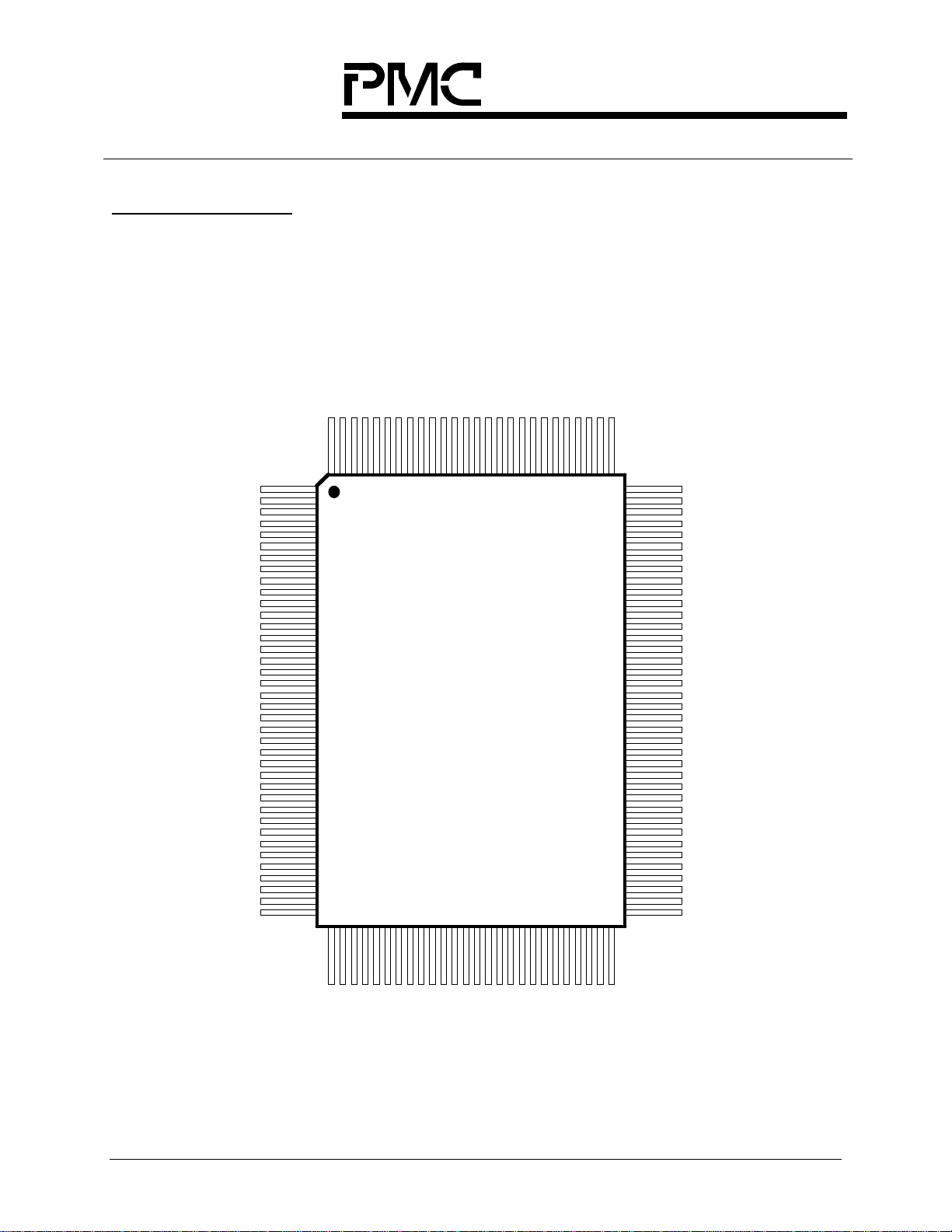
PIN DIAGRAM
The EQUAD is packaged in a 128-pin plastic QFP package having a body size of
14 mm by 20 mm and a pin pitch of 0.5 mm.
PHA[3]
BRPCM[1]/BRDP[1]
PLA[3]
BRPCM[2]/BRDP[2]
BRPCM[3]/BRDP[3]
BRPCM[4]/BRDP[4]
TDLCLK[1]/TDLUDR[1]
PIN 103
PIN 102
BRSIG[4]/BRDN[4]
BRSIG[3]/BRDN[3]
BRSIG[2]/BRDN[2]
BRSIG[1]/BRDN[1]
BRFPO[4]
BRFPO[3]
BRFPO[2]
BRFPO[1]
BRCLK/MRCLK
BRFPI/MRFPI
RCLKO[4]
RCLKO[3]
PLA[2]
PHA[2]
RCLKO[2]
RCLKO[1]
PLD[2]
PHD[2]
RFP[4]
RFP[3]
RFP[2]
RFP[1]
TCLKI[4]
TCLKI[3]
TCLKI[2]
TCLKI[1]
BTCLK[4]
BTCLK[3]
BTCLK[2]
BTCLK[1]/MTCLK
BTFP[4]
BTFP[3]
BTFP[2]
BTFP[1]/MTFP
BTSIG[4]/BTDN[4]
BTSIG[3]/BTDN[3]
BTSIG[2]/BTDN[2]
BTSIG[1]/BTDN[1]
PIN 65
PIN 1
PLA[5]
RDP[1]/RDD[1]
RDN[1]/RLCV[1]
RCLKI[1]
RDP[2]/RDD[2]
RDN[2]/RLCV[2]
RCLKI[2]
RDP[3]/RDD[3]
RDN[3]/RLCV[3]
RCLKI[3]
RDP[4]/RDD[4]
RDN[4]/RLCV[4]
RCLKI[4]
TCLKO[1]
TDP[1]/TDD[1]
TDN[1]/TFLG[1]
TCLKO[2]
PHA[0]
PLA[0]
PHD[0]
PLD[0]
TDP[2]/TDD[2]
TDN[2]/TFLG[2]
TCLKO[3]
TDP[3]/TDD[3]
TDN[3]/TFLG[3]
TCLKO[4]
TDP[4]/TDD[4]
TDN[4]/TFLG[4]
A[0]
A[1]
A[2]
A[3]
A[4]
A[5]
A[6]
A[7]
A[8]
PIN 38
PIN 128
PHA[4]
RDLCLK[3]/RDLEOM[3]
RDLCLK[4]/RDLEOM[4]
RDLSIG[1]/RDLINT[1]
PLA[4]
RDLSIG[2]/RDLINT[2]
RDLSIG[3]/RDLINT[3]
RDLSIG[4]/RDLINT[4]
Index Pin
RDLCLK[2]/RDLEOM[2]
PLD[3]
TDLCLK[4]/TDLUDR[4]
PHD[3]
TDLSIG[1]/TDLINT[1]
TDLSIG[2]TDLINT[2]
TDLSIG[3]/TDLINT[3]
TDLSIG[4]/TDLINT[4]
RDLCLK[1]/RDLEOM[1]
PM6344
EQUAD
Top
View
TDLCLK[2]/TDLUDR[2]
TDLCLK[3]/TDLUDR[3]
A[9]
RSTB
ALE
WRB
RDB
CSB
D[0]
MENB
D[1]
D[2]
D[3]
PLD[1]
PHD[1]
PHA[1]
PLA[1]
D[4]
D[5]
BTPCM[1]/BTDP[1]/MTD
XCLK/VCLK
D[7]
BTPCM[4]/BTDP[4]
BTPCM[3]/BTDP[3]
BTPCM[2]/BTDP[2]
MRD
INTB
D[6]
PIN 39 PIN 64
11
Page 25

STANDARD PRODUCT
PMC-Sierra, Inc.
PMC-951013 ISSUE 5 QUADRUPLE E1 FRAMER
PM6344 EQUAD
7
PIN DESCRIPTION
Pin Name Type Pin No. Function
MENB Input 45
RDP[1]
RDP[2]
RDP[3]
RDP[4] /
Input 2
5
8
11
Multiplex Enable (MENB). When this input is asserted
low, the four sets of PCM and signaling streams are
combined into a single bit interleaved 16.384 Mbit/s
serial stream. In the transmit direction, all data is
expected on MTD with alignment indicated by MTFP.
MTD and MTFP are sampled on the rising edge of
MTCLK. In the receive direction, data is presented on
MRD aligned with MRFPI. MRFPI is sampled on the
rising edge of MRCLK and MRD is updated on t h e
falling edge of MRCLK.
When this input is deasser ted high, each PCM and
signaling stream has its own dedicated pin.
MENB has an integral pull-up.
Receive Positive Line Pulse (RDP[4:1]). These inputs
are available when the EQUAD is configured to receive
dual-rail formatted data. The RDP[4:1] inputs may be
enabled for either RZ or NRZ waveforms. When
enabled for NRZ, this input may be enabled to be
sampled on the rising or falling edge of the
corresponding RCLKI[4:1]. When enabled for RZ, the
clocks are recovered from the corresponding RDP[4:1]
and RDN[4:1] inputs.
RDD[1]
RDD[2]
RDD[3]
RDD[4]
Receive Digital E1 Signal (RDD[4:1]). W hen the
EQUAD is configured to receive single-rail data, these
inputs may be enabled to be sampled on the rising or
falling edge of the corresponding RCLKI[4:1].
12
Page 26

STANDARD PRODUCT
PMC-Sierra, Inc.
PMC-951013 ISSUE 5 QUADRUPLE E1 FRAMER
PM6344 EQUAD
Pin Name Type Pin No. Function
RDN[1]
RDN[2]
RDN[3]
RDN[4] /
RLCV[1]
RLCV[2]
RLCV[3]
RLCV[4]
RCLKI[1]
RCLKI[2]
RCLKI[3]
RCLKI[4]
RCLKO[1]
RCLKO[2]
RCLKO[3]
RCLKO[4]
Input 3
6
9
12
Input 4
7
10
13
Output 87
88
91
92
Receive Digital Negative Line Pulse (RDN[4:1]). These
inputs are available when the EQUAD is configur ed to
receive dual-rail formatted data. The RDN[4:1] inputs
may be enabled for either RZ or NRZ waveforms. When
enabled for NRZ, these inputs may be enabled to be
sampled on the rising or falling edge of the
corresponding RCLKI[4:1]. When enabled for RZ, the
clocks are recovered from the corresponding RDP[4:1]
and RDN[4:1] inputs.
Receive Line Code Violation Indication (RLCV[4:1]).
When the EQUAD is configured to receive single-rail
data, this input may be enabled to be sampled on the
rising or falling edge of the corresponding RCLKI[4:1].
Receive Line Clock Inputs (RCLKI[4:1]). Each input is
an externally recovered 2.048 MHz line clock that may
be enabled to sample the RDP[x] and RDN[x] inputs on
its rising or falling edge when the input format is
enabled for dual-rail NRZ; or to sample the RDD[x] and
RLCV[x] inputs on its r ising or falling edge when the
input format is enabled for single-rail.
Recovered PCM Clock Output (RCLKO[4:1]). Each
output signal is the recovered 2.048 MHz clock,
synchronized to the XCLK signal. Each RCLKO[x]
signal is recovered from the RDP[x] and RDN[x] inputs
(if the input format is dual-rail RZ) or from the RCLKI[x ]
input (if the input format is NRZ).
When the ELST is by-passed or the RCLKOSEL
register bit is set, BRPCM[x] and BRSIG[x] are updated
on the falling edge of the associated RCLKO[x].
As an option, the digital attenuator's smooth 2.048 MHz
clock may be presented on RCLKO [ x ] . See the
Operations Section for details on this application.
13
Page 27

STANDARD PRODUCT
PMC-Sierra, Inc.
PMC-951013 ISSUE 5 QUADRUPLE E1 FRAMER
PM6344 EQUAD
Pin Name Type Pin No. Function
RFP[1]
RFP[2]
RFP[3]
RFP[4]
Output 81
82
83
84
Receive Frame Pulse ( RFP[ 4:1]). The RFP[x] out puts
are intended as a timing references.
When the EQUAD is configured for receive frame pulse
output, RFP[x] pulses high for 1 RCLKO cycle during bit
1 of each 256-bit frame, indicating the frame alignment
of the receive stream.
When configured for receive signaling multiframe
output, RFP[x] pulses high for 1 RCLKO[x] cycle during
bit 1 of frame 1 of the 16 frame signaling mult if rame,
indicating the signaling multiframe alignment of t he
receive stream. (Even when signaling multiframing is
disabled, the RFP[x] output continues to indicate the
position of bit 1 of every 16th frame.)
When configured for receive CRC multiframe output,
RFP[x] pulses high for 1 RCLKO[x] cycle during bit 1 of
frame 1 of every 16 frame CRC multiframe, indicating
the CRC multiframe alignment of t he r e ceive stream.
(Even when CRC multiframing is disabled, the RFP[x]
output continues to indicate the position of bit 1 of the
FAS f ram e every 16th frame.)
When configured for composite multiframe output,
RFP[x] goes high on the falling RCLKO[x] edge marking
the beginning of bit 1 of frame 1 of every 16 frame
signaling multiframe, indicating the signaling multiframe
alignment of the receive stream, and returns low on the
falling RCLKO[x] edge marking the ending of bit 1 of
frame 1 of every 16 frame CRC multiframe, indicating
the CRC multiframe alignment of t he r e ceive stream.
This mode allows both multiframe alignments to be
decoded externally from the single RFP[x] signal. Note
that if the signaling and CRC multiframe alignm ents are
coincident, RFP[x] will pulse high for 1 RCLKO[x] cycle
every 16 frames.
Each RFP[x] is updated on the falling edge of the
associated RCLKO[x]. RFP[x] should not be used when
register bit RCLKOSEL is set to a logic 1.
14
Page 28

STANDARD PRODUCT
PMC-Sierra, Inc.
PMC-951013 ISSUE 5 QUADRUPLE E1 FRAMER
PM6344 EQUAD
Pin Name Type Pin No. Function
RDLSIG[1]
RDLSIG[2]
RDLSIG[3]
RDLSIG[4]/
RDLINT[1]
RDLINT[2]
RDLINT[3]
RDLINT[4]
RDLCLK[1]
RDLCLK[2]
RDLCLK[3]
RDLCLK[4]/
Output 125
126
127
128
Output 119
120
123
124
Receive Data Link Signal (RDLSIG[4:1]). The
RDLSIG[4:1] signals are available on these outputs
when the associated inter nal HDLC receiver (RFDL) is
disabled from use, or, optionally, when fractional E1 is
extracted. RDLSIG contains the data link stream
extracted from the selected data link bits. The EQUAD
may be configured to utilize timeslot 16 as a data link or
utilize any combination of the national bits as a data link.
Each RDLSIG[x] is updated on the falling edge of the
associated RDLCLK[x].
Receive Data Link Interrupt (RDLINT[ 4: 1]). The
RDLINT[4:1] signals are available on these outputs
when the associated RFDL is enabled. Each RDLINT[x]
goes high when an event occurs which changes the
status of the associated HDLC receiver.
Receive Data Link Clock (RDLCLK[4:1]). The
RDLCLK[4:1] signals are available on these outputs
when the associated inter nal HDLC receiver (RFDL) is
disabled from use, or, optionally, when fractional E1 is
extracted. The rising edge of RDLCLK[x] can be used
to sample the data-link data or the fract ional E1 dat a on
the associated RDLSIG[x] when the internal HDLC
receiver is disabled or when fractional E1 is enabled
respectively.
RDLEOM[1]
RDLEOM[2]
RDLEOM[3]
RDLEOM[4]
Receive Data Link End of Message (RDLEOM[4:1]).
The RDLEOM[4:1] signals are available on these
outputs when the associated RFDL is enabled. Each
RDLEOM[x] goes high when the last byte of a received
sequence is read from the associated RFDL FIFO
buffer, or when the FIFO buffer is overrun.
15
Page 29

STANDARD PRODUCT
PMC-Sierra, Inc.
PMC-951013 ISSUE 5 QUADRUPLE E1 FRAMER
PM6344 EQUAD
Pin Name Type Pin No. Function
BRPCM[1]
BRPCM[2]
BRPCM[3]
BRPCM[4]/
Output 103
104
107
108
BRDP[1]
BRDP[2]
BRDP[3]
BRDP[4]
MRD Output 59
Backplane Receive PCM (BRPCM[4:1]). The
BRPCM[4:1] signals are available on these outputs
when the backplane is configured for single-rail output.
Each BRPCM[x] signal contains the recovered data
stream passed through the ELST block, and the SIGX
block. When the ELST is not by-passed or the
RCLKOSEL register bit is not set, the BRPCM[x] stream
is aligned to the backplane timing and is updated on the
falling edge of the associated BRCLK. When the ELST
is by-passed or the RCLKOSEL register bit is set,
BRPCM[x] is aligned to the receive line timing and is
updated on the falling edge of the associated RCLKO[x].
Backplane Receive Positive Line Pulse (BRDP[4:1]).
The BRDP[4:1] signals are available on these outputs
when the backplane is configured for dual-rail output.
Each BRDP[x] NRZ output represents the RZ r eceive
digital positive pulse signal extracted from the input
bipolar signal. BRDP[x] is updated on the falling edge of
the associated RCLKO[x].
Multiplexed Receive Data (MRD). When the multiplex
enable (MENB) input is asserted low, the four sets of
PCM and signaling streams are bit interleaved into a
single 16.384 Mbit/s serial st r eam presented on MRD
aligned with MRFPI. MRFPI is sampled on the rising
edge of MRCLK and MRD is updated on the falling edge
of MRCLK.
When MENB input is deasserted high, each PCM and
signaling stream has its own dedicated pin and MRD is
unused.
16
Page 30

STANDARD PRODUCT
PMC-Sierra, Inc.
PMC-951013 ISSUE 5 QUADRUPLE E1 FRAMER
PM6344 EQUAD
Pin Name Type Pin No. Function
BRSIG[1]
BRSIG[2]
BRSIG[3]
BRSIG[4]
BRDN[1]
BRDN[2]
BRDN[3]
BRDN[4]
Output 99
100
101
102
Backplane Receive Signaling (BRSIG[4:1]). The
BRSIG[4:1] signals are available on these outputs when
the backplane is configured for single-rail output. Each
BRSIG[x] contains the extracted signaling bits for each
channel in the frame, repeated for the entire
superframe. Each channel's signaling bits are valid in
bit locations 5,6,7,8 of the channel and are channelaligned with the BRPCM[x] data stream. When the
ELST is not by-passed or the RCLKOSEL register bit is
not set, the BRSIG[x] stream is aligned to the backplane
timing and is updated on the falling edge of BRCLK.
When the ELST is by-passed or the RCLKOSEL
register bit is set, BRSIG[x] is aligned to the receive line
timing and is updated on the falling edge of the
associated RCLKO[x].
Backplane Receive Negative Line Pulse (BRDN[4:1]).
The BRDN[4:1] signals are available on these outputs
when the backplane is configured for dual-rail output.
Each BRDN[x] NRZ output represents the RZ receive
digital negative pulse signal extracted from the input
bipolar signal. BRDN[x] is updated on the falling edge
of the associated RCLKO[x].
17
Page 31

STANDARD PRODUCT
PMC-Sierra, Inc.
PMC-951013 ISSUE 5 QUADRUPLE E1 FRAMER
PM6344 EQUAD
Pin Name Type Pin No. Function
BRFPO[1]
BRFPO[2]
BRFPO[3]
BRFPO[4]
Output 95
96
97
98
Backplane Frame Pulse Output (BRFPO[4:1]). When
the EQUAD is configured for backplane receive frame
pulse output, each BRFPO[x] pulses high for 1 BRCLK
cycle (or 1 RCLKO[x] cycle if ELST is by-passed or the
RCLKOSEL register bit is set) during bit 1 of each 256bit frame, indicating the frame alignment of the
BRPCM[x] data stream.
When configured for backplane receive signaling
multiframe output, BRFPO[ x ] pulses high for 1 BRCLK
cycle (or 1 RCLKO[x] cycle if ELST is by-passed) during
bit 1 of frame 1 of the 16 frame signaling mult if rame,
indicating the signaling multiframe alignment of t he
BRPCM[x] data stream. (Even when signaling
multiframing is disabled, the BRFPO[x] output continues
to indicate every 16th frame.)
When configured for backplane receive CRC multiframe
output, BRFPO[x] pulses high for 1 BRCLK cycle (or 1
RCLKO[x] cycle if ELST is by-passed) during bit 1 of
frame 1 of every 16 frame CRC multiframe, indicating
the CRC multiframe alignment of t he BRPCM [x] data
stream. (Even when CRC multiframing is disabled, the
BRFPO[x] output continues to indicate the position of bit
1 of the FAS frame every 16th frame.)
When configured for backplane receive composite
multiframe output, BRFPO[ x ] goes high on t he falling
BRCLK edge (or RCLKO[x] edge if ELST is by-passed)
marking the beginning of bit 1 of frame 1 of every 16
frame signaling multiframe, indicating the signaling
multiframe alignment of the BRPCM [ x] data stream, and
returns low on the falling BRCLK edge (or RCLKO[x]
edge if ELST is by-passed) marking the end of bit 1 of
frame 1 of every 16 frame CRC multiframe, indicating
the CRC multiframe alignment of t he BRPCM [ x] data
stream. In this mode both multiframe alignments can be
decoded externally from the single BRFPO[x] signal. If
the signaling and CRC multiframe alignments are
coincident, BRFPO[x] will pulse high for 1 clock cycle.
When configured for backplane receive overhead
output, BRFPO[x] is high for timeslot 0 and timeslot 16
of each 256-bit frame, indicating the overhead bit
positions of the BRPCM[x] data str eam .
BRFPO[x] is updated on the falling edge of the BRCLK
or RCLKO[x].
18
Page 32

STANDARD PRODUCT
PMC-Sierra, Inc.
PMC-951013 ISSUE 5 QUADRUPLE E1 FRAMER
PM6344 EQUAD
Pin Name Type Pin No. Function
BRCLK Input 94
MRCLK
BRFPI Input 93
Backplane Receive Clock (BRCLK). When the multiplex
enable (MENB) input is deasserted high, BRCLK is a
2.048MHz clock with optional gapping for adaptation to
non-uniform backplane data streams. BRCLK is
common to all four framers. The EQUAD may be
configured to ignore the BRCLK input and use the
RCLKO[x] signal in its place when the ELST is
bypassed or the RCLKOSEL register bit is set.
Multiplex Receive Clock (MRCLK). When the multiplex
enable (MENB) input is asserted low, MRCLK is a
16.384 MHz clock. MRFPI is sampled on the rising
edge of MRCLK and MRD is updated on the r ising edge
of MRCLK. The multiplexed bus can not be used if the
ELST is bypassed or the RCLKOSEL register bit is set.
Backplane Frame Pulse Input (BRFPI). When the
multiplex enable (MENB) input is deasserted high, this
input is used to frame align the received data to the
system backplane. BRFPI is common to all four
framers. If frame alignment only is required, a pulse at
least 1 BRCLK cycle wide must be provided on each
BRFPI every 256 bit periods.
MRFPI
Multiplexed Frame Pulse Input ( M RFPI ). When the
multiplex enable (MENB) input is asserted low, this input
aligns all four sets of PCM and signaling streams to
allow bit interleaved multiplexing. If f rame alignm ent
only is required, a pulse no more than 1 MRCLK cycle
wide must be provided on each MRFPI every 2048 bit
periods.
19
Page 33

STANDARD PRODUCT
PMC-Sierra, Inc.
PMC-951013 ISSUE 5 QUADRUPLE E1 FRAMER
PM6344 EQUAD
Pin Name Type Pin No. Function
BTPCM[1]
BTPCM[2]
BTPCM[3]
BTPCM[4]/
BTDP[1]
BTDP[2]
BTDP[3]
BTDP[4]
MTD
BTSIG[1]
BTSIG[2]
BTSIG[3]
BTSIG[4]
Input 61
62
63
64
Input 65
66
67
68
Backplane Transmit PCM (BTPCM[4:1]) . The nonreturn to zero, digital data streams to be transmit t ed are
input on these pins when the backplane is configured for
non-multiplexed single-rail input. The BTPCM[x] signal is
sampled on the rising edge of the associated BTCLK[x].
Backplane Transmit Positive Line Pulse (BTDP[4:1]).
The positive pulse of the dual-rail signals to be
transmitted is input on these pins when the backplane is
configured for non-multiplexed dual-rail input. In dualrail input mode, the BTDP[x] input by-passes the
transmitter and is fed directly into the DJAT. BTDP[x] is
sampled on the rising edge of the associated BTCLK[x].
Multiplexed Transmit Dat a (MTD). MTD shares a pin
with BTPCM[1]. BTPCM[4:2] are unused when the
multiplex enable (MENB) input is asserted low. When
the multiplex enable (MENB) input is asserted low, the
four sets of PCM and signaling streams are expected in
a single bit interleaved 16.384 Mbit/s serial stream.
Frame alignment is indicated by MTFP. MTD is sampled
on the rising edge of MTCLK.
Backplane Transmit Signaling (BTSIG[4:1]). The
BTSIG[4:1] input signals contain the signaling bits for
each channel in the transmit data frame, repeated for
the entire superframe. Each signal is input on the
BTSIG[x] pin when the backplane is configured for nonmultiplexed single-rail input. Each channel's signaling
bits are in bit locations 5,6,7,8 of t he channel and ar e
channel-aligned with the BTPCM[x] data stream.
BTSIG[x] is sampled on the rising edge of the
associated BTCLK[x].
BTDN[1]
BTDN[2]
BTDN[3]
BTDN[4]
If frame alignment is not required, BTFP[ x] may be tied
to power or ground.
Backplane Transmit Negative Line Pulse (BTDN[4:1]).
The negative pulse of the dual-rail signal to be
transmitted is input on these pins when the backplane is
configured for non-multiplexed dual-rail input. In dualrail input mode, the BTDN[x] input by-passes the
transmitter and is fed directly into the DJAT. BTDN[x] is
sampled on the rising edge of the associated BTCLK[x].
These inputs are unused when the multiplex enable
(MENB) input is asserted low.
20
Page 34

STANDARD PRODUCT
PMC-Sierra, Inc.
PMC-951013 ISSUE 5 QUADRUPLE E1 FRAMER
PM6344 EQUAD
Pin Name Type Pin No. Function
BTFP[1]
BTFP[2]
BTFP[3]
BTFP[4]
MTFP
Input 69
70
71
72
Backplane Transmit Frame Pulse (BTFP[4:1]). These
inputs are used to frame align the transmitters t o the
system backplane. If basic frame alignment only is
required, a pulse at least 1 BTCLK[x] cycle wide must
be provided on BTFP[x] at multiples of 256 bit periods.
If multiframe alignment is r equir ed, transmit multiframe
alignment must be enabled, and BTFP[x] must be
brought high to mark bit 1 of frame 1 of every 16 frame
signaling multiframe and brought low following bit 1 of
frame 1 of every 16 frame CRC multiframe. This mode
allows both multiframe alignments to be independently
controlled using the single BTFP[x] signal. Note that if
the signaling and CRC multiframe alignments are
coincident, BTFP[x] must pulse high for 1 BTCLK[x]
cycle every 16 frames. If register bit BTFPREF is set to
logic 1, BTFP[x] becomes the reference frame pulse for
the associated interface.
If frame alignment is not required, BTFP[ x] may be tied
to logic high or low.
Multiplexed Transmit Frame Pulse (MTFP). MTFP
shares a pin with BTFP[1]. BTFP[4:2] are unused when
the multiplex enable (MENB) input is asserted low.
When the multiplex enable (MENB) input is asserted
low, M TFP indicat es the frame alignment of the bit
interleaved PCM and signaling streams in the same way
as BTFP[x]. If basic frame alignment only is required, a
pulse 1 MTCLK cycle wide must be provided on MTFP
at multiples of 2048 clock periods. If multiframe
alignment is required, transmit mult if ram e alignment
must be enabled, and MTFP must be brought high to
mark bit 1 of f ram e 1 of t he first multiplexed PCM
stream (destined for transmitter number one) of every
16 frame signaling multiframe and brought low following
bit 1 of frame 1 of the first multiplexed PCM stream of
every 16 fram e CRC mult if ram e. This mode allows both
multiframe alignments to be independently cont r olled
using the single MTFP signal. All four interfaces will
have the same frame alignment. Note that if the
signaling and CRC multiframe alignments are
coincident, MTFP must pulse high for 1 MTCLK cycle
every 16 frames (32768 clock cycles). MTFP is
sampled on the rising edge of MTCLK.
21
Page 35

STANDARD PRODUCT
PMC-Sierra, Inc.
PMC-951013 ISSUE 5 QUADRUPLE E1 FRAMER
PM6344 EQUAD
Pin Name Type Pin No. Function
BTCLK[1]
BTCLK[2]
BTCLK[3]
BTCLK[4]
MTCLK
TDLSIG[1]
TDLSIG[2]
TDLSIG[3]
TDLSIG[4]/
Input 73
74
75
76
I/O 113
114
117
118
Backplane Transmit Clock (BTCLK[4:1]). BTCLK[4:1]
are the 2.048MHz transmit clocks with optional gapping
for adaptation from non-uniform backplane data
streams. The EQUAD may be configured to ignore the
BTCLK[x] input and use the associated RCLKO[x] signal
in its place.
Multiplexed Transmit Clock (MTCLK) . MTCLK shares a
pin with BTCLK[1]. BTCLK[4:2] are unused when the
multiplex enable (MENB) input is asserted low. When
the multiplex enable (MENB) input is asserted low, this
clock is 16.384 MHz. MTFP and MTD are sampled on
the rising edge of MTCLK.
Transmit Data Link Signal (TDLSIG[4:1]). The
TDLSIG[4:1] signals are input on this pin when the
associated internal HDLC t ransm it ter (XFDL) is disabled
from use, or if fractional E1 insertion is selected.
TDLSIG[x] is the source for the data stream to be
inserted int o t he selected data link bits. The EQUAD
may be configured to utilize timeslot 16 as a data link or
utilize any combination of the national bits as a data link.
If fractional E1 insertion is enabled, TDLSIG[x] is the
data source for the E1 channels enabled by the Channel
Select registers.
TDLINT[1]
TDLINT[2]
TDLINT[3]
TDLINT[4]
TDLSIG[x] is sampled on the rising edge of the
associated TDLCLK[x]. The TDLSIG[x] pins have
integral pull-ups.
Transmit Data Link Interr upt ( TDLINT[4:1]). The
TDLINT[4:1] signals are output on these pins when t he
associated XFDL is enabled. Each TDLINT[x] goes high
when the last data byte written to t he XFDL has been
set up for transmission and processor intervention is
required to either write control information t o end t he
message, or to provide more data.
22
Page 36

STANDARD PRODUCT
PMC-Sierra, Inc.
PMC-951013 ISSUE 5 QUADRUPLE E1 FRAMER
PM6344 EQUAD
Pin Name Type Pin No. Function
TDLCLK[1]
TDLCLK[2]
TDLCLK[3]
TDLCLK[4]/
TDLUDR[1]
TDLUDR[2]
TDLUDR[3]
TDLUDR[4]
TCLKO[1]
TCLKO[2]
TCLKO[3]
TCLKO[4]
Output 109
110
111
112
Output 14
17
24
27
Transmit Data Link Clock (TDLCLK[4:1]). The
TDLCLK[4:1] signals are available on this output when
the associated inter nal HDLC transmitter (XFDL) is
disabled from use, or if fractional E1 inser tion is
selected. The rising edge of TDLCLK[x] is used to
sample the data-link or fractional E1 data stream
contained on the associated TDLSIG[x] input. When the
EQUAD is not configured to transmit a data link and
fractional E1 is disabled, the TDLCLK[x] output is held
low.
Transmit Data Link Underrun ( TDLUDR[4:1]). The
TDLUDR[4:1] signals are available on this output when
the associated XFDL is enabled. TDLUDR[x] goes high
when the processor has failed to service the TDLINT[x]
interrupt before the transmit buffer is emptied.
Transmit Clock Output (TCLKO[4:1] ). The TDP[4:1],
TDN[4:1], and TDD[4:1] outputs may be enabled to be
updated on the rising or falling edge of the TCLKO[4:1]
outputs. TCLKO[x] is a 2. 048 MHz clock that is
adequately jitter and wander free in absolute terms to
permit an acceptable E1 signal to be generated.
Depending on the configuration of the EQUAD,
TCLKO[x] may be derived from TCLKI[x], RCLKO[x], or
BTCLK[x], with or without jit ter attenuation.
TDP[1]
TDP[2]
TDP[3]
TDP[4] /
TDD[1]
TDD[2]
TDD[3]
TDD[4]
Output 15
22
25
28
Transmit Digital Positive Line Pulse (TDP[4:1]). These
signals are available on the output when the EQUAD is
configured to transmit dual-rail data. The TDP[x] signal
can be formatted for either RZ or NRZ waveforms, and
can be enabled to be updated on the rising or falling
edge of the associated TCLKO [ x ].
Transmit Digital Data (TDD[4:1] ) . These signals are
available on the output when configured to transmit
single-rail data. The TDD[x] signal may be enabled to
be updated on the rising or falling edge of the
associated TCLKO[x].
23
Page 37

STANDARD PRODUCT
PMC-Sierra, Inc.
PMC-951013 ISSUE 5 QUADRUPLE E1 FRAMER
PM6344 EQUAD
Pin Name Type Pin No. Function
TDN[1]
TDN[2]
TDN[3]
TDN[4] /
TFLG[1]
TFLG[2]
TFLG[3]
TFLG[4]
TCLKI[1]
TCLKI[2]
TCLKI[3]
TCLKI[4]
Output 16
23
26
29
Input 77
78
79
80
Transmit Digital Negative Line Pulse (TDN[4:1] ). These
signals are available on the output when the EQUAD is
configured to transmit dual-rail data. The TDN[x] signal
can be formatted for either RZ or NRZ waveforms, and
can be enabled to be updated on the rising or falling
edge of the associated TCLKO [ x ].
Transmit FIFO Flag (TFLG[4:1] ) . These signals are
available when configured to transmit single-rail data.
The TFLG[x] output indicates when the transmit rate
conversion FIFO in DJAT is nearing an empty or a full
condition. Either indication may be selected. This
output may be enabled to be updated on the rising or
falling edge of the associated TCLKO[x].
Transmit Clock Input (TCLKI[x]). This input signal is
used to generate the TCLKO [ x ] clock signal. Depending
upon the configuration of the EQUAD, TCLKO[x] may be
derived directly from TCLKI[x] by dividing TCLKI[x] by 8,
or TCLKO[x] may be derived from TCLKI[x] after jitter
attenuation. If TCLKI[x] is jitter-fr ee when divided down
to 8 kHz, then it is possible to derive TCLKO[x] from
TCLKI[x] when TCLKI[x] is a multiple of 8 kHz (i.e. Nx8
kHz, for N equals 1 to 256). The EQUAD may be
configured to ignore the TCLKI[x] input and utilize
BTCLK[x] or RCLKO[x] instead. RCLKO[x] is also
substituted for TCLKI[x] if line loopback is enabled.
XCLK/ Input 60
VCLK
INTB Output 58
Crystal Clock Input (XCLK) . This signal provides timing
for many portions of the EQUAD. Depending on the
configuration of the EQUAD, XCLK is nominally a
49.152 MHz or 16.384 MHz 50% duty cycle clock.
When transmit clock generation or jitter attenuation is
not required, XCLK may be driven with a 16.384 MHz
clock. When transmit clock generation or jitter
attenuation is required, XCLK must be driven with a
49.152 MHz clock.
Vect or Clock (VCLK). The VCLK signal is used during
EQUAD production test to verify internal functionality.
Active low open-drain Interrupt signal (INTB). This
signal goes low when an unmasked interrupt event is
detected on any of the internal interrupt sources,
including the internal HDLC t ransceiver. Note that INTB
will remain low until all active, unmasked interrupt
sources are acknowledged at their source.
24
Page 38

STANDARD PRODUCT
PMC-Sierra, Inc.
PMC-951013 ISSUE 5 QUADRUPLE E1 FRAMER
PM6344 EQUAD
Pin Name Type Pin No. Function
CSB Input 44
D[0]
D[1]
D[2]
D[3]
D[4]
D[5]
D[6]
D[7]
I/O 46
47
48
49
54
55
56
57
RDB Input 43
WRB Input 42
Active low chip select (CSB). This signal must be low to
enable EQUAD register accesses. This signal must be
toggled high to clear the PMCTST register bit (register
00BH or 20BH) and to ensure the EQUAD will operate
in normal mode.
Bi-directional data bus (D[7:0]). This bus is used during
EQUAD read and write accesses.
Active low read enable (RDB). This signal is pulsed low
to enable a EQUAD register read access. The EQUAD
drives the D[7:0] bus with the contents of the addressed
register while RDB and CSB are both low.
Active low write strobe (WRB). This signal is pulsed low
to enable a EQUAD register write access. The D[7:0]
bus contents are clocked into the addressed normal
mode register on the rising edge of WRB while CSB is
low.
ALE Input 41
RSTB Input 40
A[0]
A[1]
A[2]
A[3]
A[4]
A[5]
A[6]
A[7]
A[8]
A[9]
Input 30
31
32
33
34
35
36
37
38
39
Address latch enable (ALE). This signal latches the
address bus contents, A[9:0], when low, allowing the
EQUAD to be interfaced to a multiplexed addr ess/ dat a
bus. When ALE is high, the address latches are
transparent. ALE has an integral pull-up.
Active low reset (RSTB). This signal is set low to
asynchronously reset the EQUAD. RSTB is a Schmitttrigger input with integral pull-up.
Address bus (A[9:0]). This bus selects specific registers
during EQUAD register accesses.
25
Page 39

STANDARD PRODUCT
PMC-Sierra, Inc.
PMC-951013 ISSUE 5 QUADRUPLE E1 FRAMER
PM6344 EQUAD
Pin Name Type Pin No. Function
PHA[0]
PHA[1]
PHA[2]
PHA[3]
PHA[4]
PHD[0]
PHD[1]
PHD[2]
PHD[3]
PLA[0]
PLA[1]
PLA[2]
PLA[3]
PLA[4]
PLA[5]
PLD[0]
PLD[1]
PLD[2]
PLD[3]
Power 18
52
89
105
121
Power 20
50
85
115
Ground 19
53
90
106
122
1
Ground 21
51
86
116
AC power pins (PHA[4:0]). These pins must be
connected to a common, well decoupled +5V DC supply
together with the DC power pins PHD[3:0] .
DC power pins (PHD[3:0]). These pins must be
connected to a common, well decoupled +5V DC supply
together with the AC power pins PHA[4:0].
AC ground pins (PLA[5:0]). These pins must be
connected to a common ground together with the DC
ground pins PLD[3:0].
DC ground pins (PLD[3:0]). These pins must be
connected to a common ground together with the AC
ground pins PLA[5:0].
Notes on Pin Description:
1. The PLA[5:0] and PLD[3:0] ground pins are not internally connected together.
Failure to connect these pins externally may cause malfunction or damage
the device. The PHA[4:0] and PHD[3:0] power pins are not internally
connected together. Failure to connect these pins externally may cause
malfunction or damage the device. These power supply connections must
all be utilized and must all connect to a common +5 V or ground rail, as
appropriate.
2. Inputs MENB, RSTB and ALE have integral pull-up resistors.
3. All outputs have 2 mA drive capability except for MRD and the D[7:0]
bidirectionals which have 4 mA drive capability.
4. All inputs and bidirectionals present minimum capacitive loading and operate
at TTL logic levels.
5. The TDLSIG/TDLINT[4:1] pins have integral pull-up resistors and default to
being inputs after a reset.
26
Page 40

STANDARD PRODUCT
PMC-Sierra, Inc.
PMC-951013 ISSUE 5 QUADRUPLE E1 FRAMER
PM6344 EQUAD
6. When an internal RFDL is enabled, the RDLINT[x] output goes high:
1) when the number of bytes specified in the RFDL Interrupt Status/Control
Register have been received on the data link,
2) immediately on detection of RFDL FIFO buffer overrun,
3) immediately on detection of end of message,
4) immediately on detection of an abort condition, or,
5) immediately on detection of the transition from receiving all ones to flags.
The interrupt is cleared at the start of the next RFDL Data Register read that
results in an empty FIFO buffer. This is independent of the FIFO buffer fill
level for which the interrupt is programmed. If there is still data remaining in
the buffer, RDLINT[x] will remain high. An interrupt due to a RFDL FIFO
buffer overrun condition is not cleared on a RFDL Data Register read but on a
RFDL Status Register read. The RDLINT[x] output can always be forced low
by disabling the RFDL (setting the EN bit in the RFDL Configuration Register
to logic 0), or by forcing the RFDL to terminate reception (setting the TR bit in
the RFDL Configuration Register to logic 1).
The RDLINT[x] output may be forced low by disabling the interrupts with the
RFDL Interrupt Status/Control Register. However, the internal interrupt latch
is not cleared, and the state of this latch can still be read through the RFDL
Interrupt Status/Control Register.
7. The RDLEOM[x] output goes high:
1) immediately on detection of RFDL FIFO buffer overrun,
2) when the data byte written into the RFDL FIFO buffer due to an end of
message condition is read,
3) when the data byte written into the RFDL FIFO buffer due to an abort
condition is read, or,
4) when the data byte written into the RFDL FIFO buffer due to the transition
from receiving all ones to flags is read.
RDLEOM[x] is set low by reading the associated RFDL Status Register or by
disabling the RFDL.
27
Page 41

STANDARD PRODUCT
PMC-Sierra, Inc.
PMC-951013 ISSUE 5 QUADRUPLE E1 FRAMER
PM6344 EQUAD
8. The TDLUDR[x] output goes high when the processor is unable to service the
TDLINT[x] request for more data before a specific time-out period. This
period is dependent upon the frequency of TDLCLK[x]:
1) for a TDLCLK[x] frequency of 4 kHz, the time-out is 1.0 ms;
2) for a TDLCLK[x] frequency of 20 kHz, the time-out is 0.2 ms;
3) for a TDLCLK[x] frequency of 64 kHz, the time-out is 62.5 µs.
28
Page 42

STANDARD PRODUCT
PMC-Sierra, Inc.
PMC-951013 ISSUE 5 QUADRUPLE E1 FRAMER
PM6344 EQUAD
8
FUNCTIONAL DESCRIPTION
8.1 Digital Receive Interface (DRIF)
The Digital E1 Receive Interface provides control over the various input options
available on the multifunctional digital receive pins RDP/RDD[x] and
RDN/RLCV[x]. When configured for dual-rail input, the multifunctional pins
become the RDP[x] and RDN[x] inputs. These inputs can be enabled to receive
either return-to-zero (RZ) or non-return-to-zero (NRZ) signals; the NRZ input
signals can be sampled on either the rising or falling edge of RCLKI[x]. When
the interface is configured for single-rail input, the multifunctional pins become
the RDD[x] and RLCV[x] inputs, which can be sampled on either the rising or
falling RCLKI[x] edge.
8.2 Clock and Data Recovery (CDRC)
The Clock and Data Recovery function is provided by a Data and Clock
Recovery (CDRC) block that provides clock and PCM data recovery, HDB3
decoding, bipolar violation detection, and loss of signal detection. The CDRC
block recovers the clock from the incoming RZ data pulses using a digital phaselocked-loop and recovers the NRZ data. Loss of signal is indicated after
exceeding a programmed threshold of 10, 15, 31, 63 or 175 consecutive bit
periods of the absence of pulses on both the positive and negative line pulse
inputs and is cleared after the occurrence of a single line pulse. An alternate
loss of signal indication is provided which is cleared only after 255 bit periods
during which no sequence of four consecutive zeros has been received. If
enabled, a microprocessor interrupt is generated when a loss of signal is
detected and when the signal returns.
The HDB3 decoding is summarized as follows: If a bipolar violation (BPV)
preceded by two zeros is received, the violation and the preceding three bit
periods are decoded as four zeros. If AMI line code is selected, no substitution is
made.
If HDB3 line code is selected, a line code violation is declared if any bipolar
violation is of the same polarity as the previous BPV or if the BPV is not
preceded by two spaces (the second criteria is maskable). If AMI line code is
selected, all bipolar violations are counted as line code violations.
The input jitter tolerance for E1 interfaces complies with ITU-T Recommendation
G.823. The tolerance is measured with a 215-1 sequence. The E1 jitter tolerance
is with ALGSEL set to 1 and to 0 is shown in Figure 2 and Figure 3.
29
Page 43

STANDARD PRODUCT
PMC-Sierra, Inc.
PMC-951013 ISSUE 5 QUADRUPLE E1 FRAMER
PM6344 EQUAD
Figure 2 - CDRC jitter tolerance with ALGSEL = 1
Measurement Limit
10
1.0
G823 Jitter
Tolerance
Specification
0.1
Jitter Amplitude (UIp-p)
0.01
10
.
.
100
Jitter Frequency (Hz)
1K
Measured
CDRC Jitter
Tolerance
(ALGSEL = 1)
10K
100K
30
Page 44

STANDARD PRODUCT
PMC-Sierra, Inc.
PMC-951013 ISSUE 5 QUADRUPLE E1 FRAMER
PM6344 EQUAD
Figure 3 - CDRC jitter tolerance with ALGSEL = 0
Measurement Limit
10
1.0
G823 Jitter
0.1
Tolerance
Specification
Jitter Amplitude (UIp-p)
0.01
10
.
.
100
Jitter Frequence (Hz)
1K
10K
Measured
CDRC Jitter
Tolerance
(ALGSEL = 0)
100K
8.3 Framer (FRMR)
The Framer (FRMR) block searches for frame alignment, CRC multiframe
alignment, and channel associated signaling (CAS) multiframe alignment in the
incoming recovered PCM stream.
Once the FRMR has found basic (or FAS) frame alignment, the incoming PCM
data is continuously monitored for FAS/NFAS framing bit errors. Framing bit
errors are accumulated in the framing bit error counter contained in the PMON
block. Once the FRMR has found CAS multiframe alignment, the PCM data is
continuously monitored for CAS multiframe alignment pattern errors. Once the
31
Page 45

STANDARD PRODUCT
PMC-Sierra, Inc.
PMC-951013 ISSUE 5 QUADRUPLE E1 FRAMER
PM6344 EQUAD
FRMR has found CRC multiframe alignment, the PCM data is continuously
monitored for CRC multiframe alignment pattern errors, and CRC-4 errors. The
FRMR also detects and indicates loss of frame, loss of CAS multiframe, and loss
of CRC multiframe, based on user-selectable criteria. The reframe operation can
be initiated by software (via the FRMR Frame Alignment Options Register), by
excessive CRC errors, or when CRC multiframe alignment is not found within 8
ms. The FRMR also identifies the position of the frame, the CAS multiframe, and
the CRC multiframe.
The FRMR extracts timeslot 16 for optional use as a data link and also extracts
the contents of the International bits (from both the FAS frames and the NFAS
frames), the National bits, and the Extra bits (from timeslot 16 of frame 0 of the
CAS multiframe), and stores them in the FRMR International/National Bits
Register, and the FRMR Extra Bits Register respectively.
The FRMR identifies the raw bit values for the remote (or distant frame) alarm
(bit 3 in timeslot 0 of NFAS frames) and the remote signaling multiframe (or
distant multiframe) alarm (bit 6 of timeslot 16 of frame 0 of the CAS multiframe)
via the FRMR International/National Bits Register, and the FRMR Extra Bits
Register respectively. Access is also provided to the "debounced" remote alarm
and remote signaling multiframe alarm bits which are set when the
corresponding signals have been a logic 1 for 2 or 3 consecutive occurrences, as
per Recommendation O.162. Detection of AIS and timeslot 16 AIS are provided;
AIS is also integrated and an AIS Alarm is indicated if the AIS condition has
persisted for at least 100 ms. The out of frame (OOF=1) condition is also
integrated, indicating a red Alarm if the OOF condition has persisted for at least
100 ms.
An interrupt may be generated to signal a change in the state of any status bits
(OOF, OOSMF, OOCMF, AIS, or RED), and to signal when any event (RRA,
RRMA, AISD, T16AISD, COFA, FER, SMFER, CMFER, CRCE, or FEBE) has
occurred.
Frame Find
The Frame Find Block searches for frame alignment using one of two userselectable algorithms, as defined in Recommendation G.706. Optionally, a two
frame check sequence can be added to either algorithm to provide protection
against false frame alignment in the presence of random mimic patterns.
The first algorithm finds frame alignment by using the following sequence:
1. Search for the presence of the correct 7-bit FAS;
32
Page 46

STANDARD PRODUCT
PMC-Sierra, Inc.
PMC-951013 ISSUE 5 QUADRUPLE E1 FRAMER
PM6344 EQUAD
2. Check that the FAS is absent in the following frame by verifying that bit 2 of
the assumed timeslot 0 byte is a logic 1;
3. Check that the correct 7-bit FAS is present in the assumed timeslot 0 byte of
the next frame.
If either of the conditions in steps 2 or 3 are not met, a new search for frame
alignment is initiated in the bit immediately following the errored timeslot 0 byte
location.
The second algorithm is similar to the first, but adds a one frame "hold-off" in
step 2 to begin a new search in the bit immediately following the second 7-bit
FAS that is checked. This "hold-off" is performed only after the condition in step
2 fails, providing a more robust algorithm which allows the framer to operate
correctly in the presence of fixed timeslot data imitating the FAS pattern.
A check sequence can be added to either algorithm to verify correct frame
alignment in the presence of random imitative FASs. Note that this check
sequence should be enabled when monitoring an unframed 215 -1 pseudo
random sequence to avoid framing to the single mimic framing pattern contained
in the sequence. The check consists of verifying correct frame alignment for an
additional two frames, as follows:
1. Once frame alignment (in frame "n") is determined, check that the FAS is
absent in the following frame (frame "n+1") by verifying that bit 2 of timeslot 0
is a logic 1;
2. Then, check that the correct 7-bit FAS is present in timeslot 0 of the next
frame (frame "n+2").
If either of the two conditions in the check sequence are not met, a new search
for frame alignment is initiated in the bit immediately following the errored byte
location when using the first algorithm, and is initiated in the bit immediately
following the byte location in frame "n+2" when using the second algorithm.
These algorithms a re illustrated in Figure 4.
33
Page 47

STANDARD PRODUCT
PMC-Sierra, Inc.
PMC-951013 ISSUE 5 QUADRUPLE E1 FRAMER
PM6344 EQUAD
Figure 4 - Basic Framing Algorithm Flowchart
Out of Frame
Synchronization
not
found
search for
7-bit FAS
pattern
Algorithm #1:
Bit 2=0
2nd FAS not
found
FAS Found &
Check Sequence
selected
Algorithm #1:
Bit 2=0
FAS not
found
found
Check if bit 2=1
in current byte loc.
of next frame
Bit 2=1
check
occurrence of
7-bit FAS in next
frame
Check bit 2 =1
Frame alignment
in following
established
frame
Bit 2=1
check
occurrence of
7-bit FAS in next
frame
FAS Found
Algorithm #2:
Bit 2 =0
Wait for byte
location in next
frame
Algorithm #2:
Bit 2 =0
FAS Found & No
Check Sequence
selected
Frame alignment
established
34
Page 48

STANDARD PRODUCT
PMC-Sierra, Inc.
PMC-951013 ISSUE 5 QUADRUPLE E1 FRAMER
PM6344 EQUAD
These algorithms provide robust framing operation even in the presence of
random bit errors: framing with algorithm #1 or #2 provides a 99.98% probability
of finding frame alignment within 1 ms in the presence of 10-3 bit error rate and
no mimic patterns.
Once frame alignment is found, the block sets the OOF indication low, indicates a
change of frame alignment (if it occurred), and monitors the frame alignment
signal, indicating errors occurring in the 7-bit FAS pattern and in bit 2 of NFAS
frames, and indicating the debounced value of the Remote Alarm bit (bit 3 of
NFAS frames). Using debounce, the Remote Alarm bit has <0.00001%
probability of being falsely indicated in the presence of a 10-3 bit error rate. The
block declares loss of frame alignment if 3 or 4 consecutive FASs have been
received in error or, additionally, if bit 2 of NFAS frames has been in error for 3
consecutive occasions. In the presence of a random 10-3 bit error rate the frame
loss criteria provides a mean time to falsely lose frame alignment of >12 minutes.
The Frame Find Block can be forced to initiate a frame search at any time when
any of the following conditions are met:
• the software re-frame bit (REFR) in the Frame Alignment Options Register
changes from logic 0 to logic 1;
• the CRC Frame Find Block is unable to find CRC multiframe alignment; or
• the CRC Frame Find Block accumulates excessive CRC evaluation errors
(≥ 915 CRC errors in 1 second) and is enabled to force a re-frame.
CRC Frame Find
Once the basic frame alignment has been found, the CRC Frame Find Block
searches for CRC multiframe alignment by observing whether the International
bits (bit 1 of timeslot 0) of NFAS frames follow the CRC multiframe alignment
pattern. Multiframe alignment is declared if at least two valid CRC multiframe
alignment signals are observed within 8 ms, with the time separating two
alignment signals being a multiple of 2 ms.
Once CRC multiframe alignment is found, the block sets the OOCMF indication
low, and monitors the multiframe alignment signal, indicating errors occurring in
the 6-bit pattern, and indicating the value of the FEBE bits (bit 1 of frames 13
and 15 of the multiframe).The block declares loss of CRC multiframe alignment if
four consecutive CRC multiframe alignment signals have been received in error,
or if frame alignment has been lost.
35
Page 49

STANDARD PRODUCT
PMC-Sierra, Inc.
PMC-951013 ISSUE 5 QUADRUPLE E1 FRAMER
PM6344 EQUAD
The CRC Frame Find Block will force the Frame Find Block to initiate a basic
frame search when CRC multiframe alignment has not been found for 8 ms.
CRC Check and AIS Detection
The CRC Check and AIS Detect Block computes the 4-bit CRC checksum for
each incoming sub-multiframe and compares this 4-bit result to the received
CRC remainder bits in the subsequent sub-multiframe. The block also
accumulates CRC errors over 1 second intervals, monitoring for excessive CRC
errors and optionally, forcing the Frame Find Block to initiate a frame search
when • 915 CRC errors occur in 1 second. The number of CRC errors
accumulated during the previous second is available by reading the FRMR CRC
Error Counter Registers.
The block also detects the occurrence of an unframed all-ones receive data
stream, indicating the AIS by setting the AISD indication when less than 3 zero
bits are received in 2 frames (512 consecutive bits); the AISD indication is reset
when 3 or more zeros in the E1 stream are observed, or when frame alignment is
found.
Signaling Frame Find
Once the basic frame alignment has been found, the Signaling Frame Find Block
searches for CAS multiframe alignment using one of two user-selectable
algorithms, one of which is compatible with Recommendation G.732. Once
frame alignment has been found, the first algorithm monitors timeslot 16 of each
frame; it declares CAS multiframe alignment when 15 consecutive frames with
bits 1-4 of timeslot 16 not containing the alignment pattern are observed to
precede a frame with timeslot 16 containing the correct alignment pattern. The
second algorithm, compatible with G.732, also monitors timeslot 16 of each
frame, and declares CAS multiframe alignment when non-zero bits 1-4 of
timeslot 16 are observed to precede a timeslot 16 containing the correct
alignment pattern.
Once CAS multiframe alignment has been found, the block sets the OOSMF
indication to logic 0, and monitors the CAS multiframe alignment signal,
indicating errors occurring in the 4-bit pattern, and indicating the debounced
value of the remote signaling multiframe alarm bit (bit 6 of timeslot 16 of frame 0
of the multiframe). Using debounce, the remote signaling multiframe alarm bit
has < 0.00001% probability of being falsely indicated in the presence of a 10-3 bit
error rate. This block also indicates the reception of timeslot 16 AIS when
timeslot 16 has been all-ones for two consecutive frames while out of CAS
multiframe. The block declares loss of CAS multiframe alignment if two
36
Page 50

STANDARD PRODUCT
PMC-Sierra, Inc.
PMC-951013 ISSUE 5 QUADRUPLE E1 FRAMER
PM6344 EQUAD
consecutive CAS multiframe alignment signals have been received in error, or
additionally, if all the bits in timeslot 16 are logic 0 for 1 or 2 (selectable) CAS
multiframes. Loss of CAS multiframe alignment is also declared if frame
alignment has been lost.
Alarm Integration
The Alarm Integrator Block monitors the OOF and the AIS indications, verifying
that each condition has persisted for 104 ms (±6 ms) before indicating the alarm
condition. The alarm is removed when the condition has been absent for 104 ms
(±6 ms).
The AIS alarm algorithm accumulates the occurrences of AISD (AIS detection).
AISD is defined as an unframed pattern with less than 3 zeros in two consecutive
frame times (512 bits). The Alarm Integrator Block counts the occurrences of
AISD over a 4 ms interval and indicates a valid AIS presence when 13 or more
AISD indications (of a possible 16) have been received. Each inter val with a
valid AIS presence indication increments an interval counter which declares AIS
Alarm when 25 valid intervals have been accumulated. An interval with no valid
AIS presence indication decrements the interval counter; the AIS Alarm
declaration is removed when the counter reaches 0. This algorithm provides a
99.8% probability of declaring an AIS Alarm within 104 ms in the presence of a
10-3 mean bit error rate.
The TS16 AIS alarm algorithm accumulates the occurrences of TS16AISD (TS16
AIS detection). TS16AISD is defined as two consecutive all ones time slot 16
bytes while out of signaling multiframe. Each interval with a valid TS16 AIS
presence indication increments an interval counter which declares TS16 AIS
Alarm when 22 valid intervals have been accumulated. An interval with no valid
TS16 AIS presence indication decrements the interval counter; the TS16 AIS
Alarm declaration is removed when the counter reaches 0. This algorithm
provides a 99.1% probability of declaring an TS16 AIS Alarm within 3.1 ms after
loss of signaling multiframe detection in the presence of a 10-3 mean bit error
rate.
The red alarm algorithm monitors occurrences of OOF over a 4 ms inter val,
indicating a valid OOF interval when one or more OOF indications occurred
during the interval, and indicating a valid in frame (INF) interval when no OOF
indication occurred for the entire interval. Each interval with a valid OOF
indication increments an interval counter which declares RED Alarm when 25
valid intervals have been accumulated. An interval with valid INF indication
decrements the interval counter; the RED Alarm declaration is removed when the
37
Page 51

STANDARD PRODUCT
PMC-Sierra, Inc.
PMC-951013 ISSUE 5 QUADRUPLE E1 FRAMER
PM6344 EQUAD
counter reaches 0. This algorithm biases OOF occurrences, leading to
declaration of red alarm when intermittent loss of frame alignment occurs.
8.4 Performance Monitor Counters (PMON)
The Performance Monitor Counters function is provided by the Performance
Monitor (PMON) block that accumulates CRC error events, frame
synchronization bit error events, line code violation events, and far end block
error events with saturating counters over consecutive intervals as defined by the
period of the supplied transfer clock signal (typically 1 second). When the transfer
clock signal is applied, the PMON block transfers the counter values into holding
registers and resets the counters to begin accumulating events for the interval.
The counters are reset in such a manner that error events occurring during the
reset are not missed. If enabled, an interrupt is generated whenever counter data
is transferred into the holding registers. If the holding registers are not read
between successive transfer clocks, an OVERRUN register bit is asserted.
Generation of the transfer clock within the EQUAD chip is performed by writing to
any counter register location (X4AH to X4FH) or by writing to the EQUAD
Revision/Chip ID/Global PMON Update register (00CH). The holding register
addresses are contiguous to facilitate polling operations.
8.5 HDLC Receiver (RFDL)
The HDLC Receiver function is provided by the RFDL block. The RFDL is a
microprocessor peripheral used to receive LAPD/HDLC frames on either Time
Slot 16 or the National Use bits of Time Slot 0.
The RFDL detects the change from flag characters to the first byte of data,
removes stuffed zeros on the incoming data stream, receives frame data, and
calculates the CRC Q.921 frame check sequence (FCS).
Received data is placed into a 4-level FIFO buffer. The Status Register contains
bits which indicate overrun, end of message, flag detected, and buffered data
available.
On end of message, the Status Register also indicates the FCS status and the
number of valid bits in the final data byte. Interrupts are generated when one,
two or three bytes (programmable via the RFDL configuration register) are stored
in the FIFO buffer. Interrupts are also generated when the terminating flag
sequence, abort sequence, or FIFO buffer overrun are detected.
38
Page 52

STANDARD PRODUCT
PMC-Sierra, Inc.
PMC-951013 ISSUE 5 QUADRUPLE E1 FRAMER
PM6344 EQUAD
When the internal HDLC receiver is disabled, the serial data extracted by the
FRMR block is output on the RDLSIG[x] pin and is updated on the falling clock
edge of the RDLCLK[x] pin.
8.6 Elastic Store (ELST)
The Elastic Store function is provided by the ELST block.
The Elastic Store (ELST) block synchronizes incoming PCM frames to the local
backplane clock, BRCLK. The frame data is buffered in a two frame circular data
buffer. Input data is written to the buffer using a write pointer and output data is
read from the buffer using a read pointer.
When the backplane timing is derived from the receive line data (i.e. the
RCLKO[x[ output is used), the elastic store can be bypassed to eliminate the 2
frame delay. In this configuration the elastic store can be used to measure
frequency differences between the recovered line clock and another 2.048 MHz
clock applied to the BRCLK input. A typical example might be to measure the
difference in frequency between two received E1 streams (i.e. East-West
frequency difference) by monitoring the number of SLIP occurrences of one
direction with respect to the other.
When the elastic store is being used, if the average frequency of the incoming
data is greater than the average frequency of the backplane clock, the write
pointer will catch up to the read pointer and the buffer will be filled. Under this
condition a controlled slip will occur when the read pointer crosses the next
frame boundary. The following frame of PCM data will be deleted.
If the average frequency of the incoming data is less than the average frequency
of the backplane clock, the read pointer will catch up to the write pointer and the
buffer will be empty. Under this condition a controlled slip will occur when the
read pointer crosses the next frame boundary. The last frame which was read
will be repeated.
A slip operation is always performed on a frame boundary.
To allow for the extraction of signaling information in the PCM data timeslots,
multiframe identification is also passed through the ELST.
8.7 Signaling Extractor (SIGX)
The Signaling Extraction function is provided by the Signaling Extractor (SIGX)
block. The block provides channel associated signaling (CAS) extraction from an
E1 signaling multiframe. Signaling data is extracted from timeslot 16 of each
39
Page 53

STANDARD PRODUCT
PMC-Sierra, Inc.
PMC-951013 ISSUE 5 QUADRUPLE E1 FRAMER
PM6344 EQUAD
frame within a signaling multiframe and buffered. The SIGX selectively
debounces the bits, and serializes the results onto the 2048 kbit/s serial stream
BRSIG[x] output. Buffered signaling data is aligned with its associated voice
timeslot in the E1 frame.
The SIGX provides user control over signaling freezing with a 95% confidence
level of freezing with valid signaling data for a 50% ones density out-of-frame
condition. The SIGX also provides control over timeslot data inversion, trunk
conditioning, and signaling debounce on a per-timeslot basis directly, via the
Microprocessor Interface (MPIF).
8.8 Backplane Receive Interface (BRIF)
The Backplane Receive Interface allows data to be presented to a backplane in
either a 2.048 Mbit/s or a 16.384 Mbit/s serial stream and allows BPV
transparency by outputting dual-rail data at 2.048 Mbit/s.
The block generates the output data stream on the BRPCM[x] pin containing 32
timeslot bytes of data. The BRSIG[x] output pin contains 30 bytes of signaling
nibble data located in the least significant nibble of each byte. The framing
alignment indication on the BRFPO[x] pin can be configured to indicate the first
bit of each 256-bit frame, the first bit of the first frame of the CRC multiframe, the
first bit of the first frame of the signaling multiframe or all overhead bits.
When configured for a multiplexed backplane, the four sets of PCM and signaling
streams are bit interleaved into a 16.384 Mbit/s serial stream. The MRFPI pin
must go to logic "1" for one MRCLK cycle to indicate the alignment of the first
PCM bit of the frame or multiframe from receiver number one.
8.9 Transmitter (TRAN)
The Transmitter function is provided by the TRAN block.
The TRAN generates a 2048 kbit/s data stream according to ITU-T
recommendations, providing individual enables for frame generation, CRC
multiframe generation, and channel associated signaling (CAS) multiframe
generation.
In concert with Transmit Per-Channel Serial Controller (TPSC), the TRAN block
provides per-timeslot control of idle code substitution, data inversion, digital
milliwatt substitution, selection of the signaling source and CAS data. All
timeslots can be forced into a trunk conditioning state (idle code substitution and
40
Page 54

STANDARD PRODUCT
PMC-Sierra, Inc.
PMC-951013 ISSUE 5 QUADRUPLE E1 FRAMER
PM6344 EQUAD
signaling substitution) by use of the master trunk conditioning bit in the
Configuration Register.
Common Channel Signaling (CCS) is supported in time slot 16 either through the
internal HDLC Transmitter (XFDL) or through a serial data input and clock output.
Support is provided for the transmission of AIS and TS16 AIS, and the
transmission of remote alarm and remote multiframe alarm signals.
PCM output signals may be selected to conform to HDB3 or AMI line coding.
8.10 Transmit Per-Channel Serial Controller (PCSC)
The Transmit Per-channel Serial Controller allows data and signaling trunk
conditioning or idle code to be applied on the transmit E1 stream on a pertimeslot basis. It also allows per-timeslot control of data inversion and application
of digital milliwatt.
The Transmit Per-channel Serial Controller function is provided by a Per-Channel
Serial Controller (PCSC) block. The TPSC interfaces directly to the TRAN block
and provides serial streams for signaling control, idle code data and PCM data
control.
The registers are accessible from the µP interface in an indirect address mode.
The BUSY indication signal can be polled from an internal status register to
check for completion of the current operation.
8.11 HDLC Trans m itter (XFDL)
The HDLC Transmitter function is provided by the XFDL block. The XFDL is
designed to provide a serial data link for the TRAN E1 Transmitter block. The
XFDL is used under microprocessor or DMA control to transmit HDLC data
frames in Time Slot 16 or in the Time Slot 0 National Use bits when the EQUAD
is enabled to use the internal HDLC transmitter. The XFDL performs all of the
data serialization, CRC generation, zero-bit stuffing, as well as flag, idle, and
abort sequence insertion. Data to be transmitted is provided on an interruptdriven basis by writing to a double-buffered transmit data register. Upon
completion of the frames, a CRC Q.921 frame check sequence is transmitted,
followed by idle flag sequences. If the transmit data register underflows, an abort
sequence is automatically transmitted.
When enabled for use (via the EN bit in the XFDL Configuration register), the
XFDL continuously transmits the flag character (01111110). Data bytes to be
transmitted are written into the Transmit Data Register. After the parallel-to-serial
41
Page 55

STANDARD PRODUCT
PMC-Sierra, Inc.
PMC-951013 ISSUE 5 QUADRUPLE E1 FRAMER
PM6344 EQUAD
conversion of each data byte, an interrupt is generated to signal the controller to
write the next byte into the Transmit Data Register. After the last data frame byte
is transmitted, the CRC word (if CRC insertion has been enabled), or a flag (if
CRC insertion has not been enabled) is transmitted. The XFDL then returns to
the transmission of flag characters.
If there are more than five consecutive ones in the raw transmit data or in the
CRC data, a zero is stuffed into the serial data output. This prevents the
unintentional transmission of flag or abort characters.
Abort characters can be continuously transmitted at any time by setting a control
bit. During transmission, an underrun situation can occur if data is not written to
the Transmit Data Register before the previous byte has been depleted. In this
case, an abort sequence is transmitted, and the controlling processor is notified
via the TDLUDR signal. Optionally, the interrupt and underrun signals can be
independently enabled to also generate an interrupt on the INTB output,
providing a means to notify the controlling processor of changes in the XFDL
operating status.
When the internal HDLC transmitter is disabled, the serial data to be transmitted
on data link can be input on the TDLSIG pin timed to the clock rate output on the
TDLCLK pin.
8.12 Digital Jitter Attenuator (DJAT)
The Digital Jitter Attenuation function is provided by the Digital Jitter Attenuator
(DJAT) block. The DJAT block receives jittered E1 data in NRZ format from TRAN
on two separate inputs, which allows bipolar violations to pass through the block
uncorrected. The incoming data streams are stored in a FIFO timed to the
transmit clock (either BTCLK[x] or RCLKO[x]). The respective input data emerges
from the FIFO timed to the jitter attenuated clock (TCLKO[x]) referenced to either
TCLKI[x], BTCLK[x], or RCLKO[x].
The jitter attenuator generates the jitter-free 2.048 MHz TCLKO[x] output transmit
clock by adaptively dividing the 49.152 MHz XCLK signal according to the phase
difference between the generated TCLKO[x] and input data clock to DJAT (either
BTCLK[x] or RCLKO[x]). Fluctuations in the phase of the input data clock are
attenuated by the phase-locked loop within DJAT so that the frequency of
TCLKO[x] is equal to the average frequency of the input data clock. Phase
fluctuations with a jitter frequency above 8.8 Hz are attenuated by 6 dB per
octave of jitter frequency. Wandering phase fluctuations with frequencies below
8.8 Hz are tracked by the generated TCLKO[x]. To provide a smooth flow of data
out of DJAT, TCLKO[x] is used to read data out of the FIFO.
42
Page 56

STANDARD PRODUCT
PMC-Sierra, Inc.
PMC-951013 ISSUE 5 QUADRUPLE E1 FRAMER
PM6344 EQUAD
If the FIFO read pointer (timed to TCLKO[x]) comes within one bit of the write
pointer (timed to the input data clock, BTCLK[x] or RCLKO[x]), DJAT will track the
jitter of the input clock. This permits the phase jitter to pass through
unattenuated, inhibiting the loss of data.
Jitter Characteristics
The DJAT Block provides excellent jitter tolerance and jitter attenuation while
generating minimal residual jitter. It can accommodate up to 35 UIpp of input
jitter at jitter frequencies above 9 Hz. For jitter frequencies below 9 Hz, more
correctly called wander, the tolerance increases 20 dB per decade. In most
applications the DJAT Block will limit jitter tolerance at lower jitter frequencies
only. For high frequency jitter, above 10 kHz for example, other factors such as
the clock and data recovery circuitry may limit jitter tolerance and must be
considered. For low frequency wander, below 10 Hz for example, other factors
such as slip buffer hysteresis may limit wander tolerance and must be
considered. The DJAT Block meets the low frequency jitter tolerance
requirements of ITU-T Recommendation G.823.
DJAT exhibits negligible jitter gain for jitter frequencies below 8.8 Hz, and
attenuates jitter at frequencies above 8.8 Hz by 20 dB per decade. In most
applications the DJAT Block will determine jitter attenuation for higher jitter
frequencies only. Wander, below 10 Hz for example, will essentially be passed
unattenuated through DJAT. Jitter, above 10 Hz for example, will be attenuated
as specified, however, outgoing jitter may be dominated by the generated
residual jitter of in cases where incoming jitter is insignificant. This generated
residual jitter is directly related to the use of 24X (49.152 MHz) digital phase
locked loop for transmit clock generation. DJAT meets the jitter attenuation
requirements of the ITU-T Recommendations G.737, G.738, G.739 and G.742.
Jitter T olerance
Jitter tolerance is the maximum input phase jitter at a given jitter frequency that a
device can accept without exceeding its linear operating range, or corrupting
data. For DJAT, the input jitter tolerance is 35 Unit Intervals peak-to-peak (UIpp)
with a worst case frequency offset of 308 Hz. It is 48 UIpp with no frequency
offset. The frequency offset is the difference between the frequency of XCLK
divided by 24 and that of the input data clock.
43
Page 57

STANDARD PRODUCT
PMC-Sierra, Inc.
PMC-951013 ISSUE 5 QUADRUPLE E1 FRAMER
PM6344 EQUAD
Figure 5 - DJAT Jitter Tolerance
The accuracy of the XCLK frequency and that of the DJAT PLL reference input
clock used to generate the jitter-free TCLKO[x] have an effect on the minimum
jitter tolerance. Given that the DJAT PLL reference clock accuracy can be ±103
Hz from 2.048 MHz, and that the XCLK input accuracy can be ±100 ppm from
49.152 MHz, the minimum jitter tolerance for various differences between the
frequency of PLL reference clock and XCLK/24 are shown in Figure 6.
44
Page 58

STANDARD PRODUCT
PMC-Sierra, Inc.
PMC-951013 ISSUE 5 QUADRUPLE E1 FRAMER
PM6344 EQUAD
Figure 6 - DJAT Minimum Jitter Tolerance vs. XCLK Accuracy
45
42.4
40
DJAT Minimum
39
Jitter Tolerance
UI pp
35
34.9
Max frequency
offset (PLL Ref
30
100 200 300 308
to XCLK)
XCLK Accuracy
0 10049
Jitter T ransfer
The output jitter for jitter frequencies from 0 to 8.8 Hz is no more than 0.1 dB
greater than the input jitter, excluding the residual jitter. Jitter frequencies above
8.8 Hz are attenuated at a level of 6 dB per octave, as shown in Figure 7.
Hz
± ppm
45
Page 59

STANDARD PRODUCT
PMC-Sierra, Inc.
PMC-951013 ISSUE 5 QUADRUPLE E1 FRAMER
PM6344 EQUAD
Figure 7 - DJAT Jitter Transfer
0
-10
-20
Jitter Gain
(dB)
-30
-40
-50
Frequency Range
G.737, G738,
G.739, G.742
max
DJAT
response
1
8.8
10
100 1k 10k
Jitter Frequency, Hz
In the non-attenuating mode, that is, when the FIFO is within one UI of
overrunning or under running, the tracking range is 1.963 to 2.133 MHz. The
guaranteed linear operating range for the jittered input clock is 2.048 MHz ±
1278 Hz with worst case jitter (42 UIpp) and maximum XCLK frequency offset (±
100 ppm). The nominal range is 2.048 MHz ± 103 Hz with no jitter or XCLK
frequency offset.
8.13 Timing Options (TOPS)
The Timing Options block provides a means of selecting the source of the
internal input clock to the DJAT block, the reference signal for the digital PLL, and
the clock source used to derive the output TCLKO[x] signal.
8.14 Digital E1 Transmit Interface (DTIF)
The Digital E1 Transmit Interface provides control over the various output options
available on the multifunctional digital transmit pins TDP/TDD[x] and
TDN/TFLG[x]. When configured for dual-rail output, the multifunctional pins
become the TDP[x] and TDN[x] outputs. These outputs can be formatted as
either return-to-zero (RZ) or non-return-to-zero (NRZ) signals and can be
46
Page 60

STANDARD PRODUCT
PMC-Sierra, Inc.
PMC-951013 ISSUE 5 QUADRUPLE E1 FRAMER
PM6344 EQUAD
updated on either the rising or falling edge of TCLKO[x]. When the interface is
configured for single-rail output, the multifunctional pins become the TDD[x] and
TFLG[x] outputs, which can be enabled to be updated on either the rising or
falling TCLKO[x] edge. Further, the TFLG[x] output can be enabled to indicate
FIFO empty or FIFO full status.
The DTIF block also provides Alarm Indication Signaling (AIS) generation
capability by generating alternating mark signals on the TDP/TDN[x] outputs, or
all-ones on the TDD[x] output, when the TAISEN bit is set in the Transmit E1
Interface Configuration register. This is useful when the internal loopback modes
are used.
8.15 Backplane Transmit Interface (BTIF)
The Backplane Transmit Interface allows data to be taken from a backplane in
either a 2.048 Mbit/s or 16.384 Mbit/s serial stream and allows BPV transparency
by accepting dual-rail data input at 2.048 Mbit/s.
When configured to receive a 2.048 Mbit/s data rate stream, the block expects
the input data stream on the BTPCM[x] pin to contain 32 timeslots. The
BTSIG[x] input pin must contain 30 bytes of signaling nibble data located in the
least significant nibble of each byte. The framing alignment indication on the
BTFP[x] pin indicates the framing bit position of the 256-bit frame (or, optionally,
the framing bit position of the first frame of the signaling multiframe frame, and
the CRC multiframe).
When configured to interface to a 16.384 Mbit/s serial stream, the four sets of
PCM and signaling streams are expected to be bit interleaved. The MTFP pin
marks the framing bit position of the first multiplexed PCM stream (destined for
transmitter number one) or, optionally, the framing bit position of the first frame of
the signaling multiframe frame, and the CRC multiframe. MTFP operates in a
similar fashion to BTFP[x], but is only valid at positions coincident with the first
multiplexed PCM stream. All four multiplexed interfaces will have the same
frame, signaling multiframe, and CRC multiframe alignment. See the Functional
Timing section for more details.
8.16 Microprocessor Interface (MPIF)
The Microprocessor Interface allows the EQUAD to be configured, controlled and
monitored via internal registers.
47
Page 61

STANDARD PRODUCT
PMC-Sierra, Inc.
PMC-951013 ISSUE 5 QUADRUPLE E1 FRAMER
PM6344 EQUAD
9
REGISTER DESCRIPTION
Table 1 - Normal Mode Register Memory Map
Address Register
#1 # 2 # 3 # 4
000H 080H 100H 180H Receive Options
001H 081H 101H 181H Receive Backplane Options
002H 082H 102H 182H Datalink Options
003H 083H 103H 183H Receive Interface Configuration
004H 084H 104H 184H Transmit Interface Configuration
005H 085H 105H 185H Transmit Backplane Options
006H 086H 106H 186H Transmit Framing and Bypass Options
007H 087H 107H 187H T r ansmit Timing Options
008H 088H 108H 188H Master Interrupt Source
009H 089H 109H 189H Receive TS0 Data Link Enables
00AH 08AH 10AH 18AH Master Diagnostics
00BH EQUAD Master Test
00CH EQUAD Revision/Chip ID/Global PMON
Update
08BH 10BH 18BH Reserved
08CH 10CH 18CH Reserved
00DH 08DH 10DH 18DH Framer Reset
00EH 08EH 10EH 18EH Phase Status Word (LSB)
00FH 08FH 10FH 18FH Phase Status Word (MSB)
010H 090H 110H 190H CDRC Configuration
011H 091H 111H 191H CDRC Interrupt Enable
012H 092H 112H 192H CDRC Interrupt Status
013H 093H 113H 193H Alternate Loss of Signal
48
Page 62

STANDARD PRODUCT
PMC-Sierra, Inc.
PMC-951013 ISSUE 5 QUADRUPLE E1 FRAMER
PM6344 EQUAD
Address Register
#1 # 2 # 3 # 4
014H 094H 114H 194H Channel Select (1 to 8)
015H 095H 115H 195H Channel Select (9 to 16)
016H 096H 116H 196H Channel Select (17 to 24)
017H 097H 117H 197H Channel Select (25 to 32)
018H 098H 118H 198H DJAT Interrupt Status
019H 099H 119H 199H DJAT Reference Clock Divisor (N1)
Control
01AH 09AH 11AH 19AH DJAT Output Clock Divisor (N2) Control
01BH 09BH 11BH 19BH DJAT Configuration
01CH 09CH 11CH 19CH ELST Configuration
01DH 09DH 11DH 19DH ELST Interrupt Enable/Status
01EH 09EH 11EH 19EH ELST Idle Code
01FH 09FH 11FH 19FH ELST Reserved
020H 0A0H 120H 1A0H FRMR Framing Alignment Options
021H 0A1H 121H 1A1H FRMR FRMR Maintenance Mode
Options
022H 0A2H 122H 1A2H FRMR Framing Status Interrupt Enable
023H 0A3H 123H 1A3H FRMR Maintenance/Alarm Status
Interrupt Enable
024H 0A4H 124H 1A4H FRMR Framing Status Interrupt
Indication
025H 0A5H 125H 1A5H FRMR Maintenance/Alarm Status
Interrupt Indication
026H 0A6H 126H 1A6H FRMR Framing Status
027H 0A7H 127H 1A7H FRMR Maintenance/Alarm Status
028H 0A8H 128H 1A8H FRMR International/National Bits
029H 0A9H 129H 1A9H FRMR Extra Bits
02AH 0AAH 12AH 1AAH FRMR CRC Error Count - LSB
49
Page 63

STANDARD PRODUCT
PMC-Sierra, Inc.
PMC-951013 ISSUE 5 QUADRUPLE E1 FRAMER
PM6344 EQUAD
Address Register
#1 # 2 # 3 # 4
02BH 0ABH 12BH 1ABH FRMR CRC Error Count - MSB
02CH 0ACH 12CH 1ACH TS16 AIS Alarm Status
02DH 0ADH 12DH 1ADH Reserved
02EH 0AEH 12EH 1AEH Reserved
02FH 0AFH 12FH 1AFH Reserved
030H 0B0H 130H 1B0H TPSC Configuration
031H 0B1H 131H 1B1H TPSC µP Access Status
032H 0B2H 132H 1B2H TPSC Timeslot Indirect Address/Control
033H 0B3H 133H 1B3H TPSC Timeslot Indirect Data Buffer
034H 0B4H 134H 1B4H XFDL Configuration
035H 0B5H 135H 1B5H XFDL Interrupt Status
036H 0B6H 136H 1B6H XFDL Transm it Data
037H 0B7H 137H 1B7H XFDL Reserved
038H 0B8H 138H 1B8H RFDL Configuration
039H 0B9H 139H 1B9H RFDL Interrupt Control/Status
03AH 0BAH 13AH 1BAH RFDL Status
03BH 0BBH 13BH 1BBH RFDL Receive Data
03CH 0BCH 13CH 1BCH Interrupt ID (reg 03CH only)/Clock
Monitor
03DH 0BDH 13DH 1BDH Backplane Parity Configuration and
Status
03EH 0BEH 13EH 1BEH Reserved
03FH 0BFH 13FH 1BFH Reserved
040H 0C0H 140H 1C0H SIGX Configuration
041H 0C1H 141H 1C1H SIGX µP Access Status
042H 0C2H 142H 1C2H SIGX Timeslot Indirect Address/Control
043H 0C3H 143H 1C3H SIGX Timeslot Indirect Data Buffer
50
Page 64

STANDARD PRODUCT
PMC-Sierra, Inc.
PMC-951013 ISSUE 5 QUADRUPLE E1 FRAMER
PM6344 EQUAD
Address Register
#1 # 2 # 3 # 4
044H 0C4H 144H 1C4H TRAN Configuration
045H 0C5H 145H 1C5H TRAN Transmit Alarm/Diagnostic Control
046H 0C6H 146H 1C6H TRAN International/National Control
047H 0C7H 147H 1C7H TRAN Extra Bits Control
048H 0C8H 148H 1C8H PMON Control/Status
049H 0C9H 149H 1C9H PMON FER Count
04AH 0CAH 14AH 1CAH PMON FEBE Count (LSB)
04BH 0CBH 14BH 1CBH PMON FEBE Count (MSB)
04CH 0CCH 14CH 1CCH PMON CRC Count (LSB)
04DH 0CDH 14DH 1CDH PMON CRC Count (MSB)
04EH 0CEH 14EH 1CEH PMON LCV Count (LSB)
04FH 0CFH 14FH 1CFH PMON LCV Count (MSB)
050H-
07FH
0D0H-
0FFH
150H-
17FH
1D0H-
1FFH
Reserved
200H-3FFH Reserved for Test
51
Page 65

STANDARD PRODUCT
PMC-Sierra, Inc.
PMC-951013 ISSUE 5 QUADRUPLE E1 FRAMER
PM6344 EQUAD
10
NORMAL MODE REGISTER DESCRIPTION
Normal mode registers are used to configure and monitor the operation of the
EQUAD. Normal mode registers (as opposed to test mode registers) are
selected when A[9] is low.
Notes on Normal Mode Register Bits:
1. Although the register bit descriptions for the four framers have been
combined, each framer is completely independent of the others.
2. Writing values into unused register bits has no effect. Reading back unused
bits can produce either a logic 1 or a logic 0; hence, unused register bits
should be masked off by software when read.
3. All configuration bits that can be written into can also be read back. This
allows the processor controlling the EQUAD to determine the programming
state of the chip.
4. Writeable normal mode register bits are cleared to zero upon reset unless
otherwise noted.
5. Writing into read-only normal mode register bit locations does not affect
EQUAD operation unless otherwise noted.
52
Page 66

STANDARD PRODUCT
PMC-Sierra, Inc.
PMC-951013 ISSUE 5 QUADRUPLE E1 FRAMER
PM6344 EQUAD
Register 000H, 080H, 100H, 180H: Receive Options
Bit Type Function Default
Bit 7 R/W WORDERR 0
Bit 6 R/W CNTNFAS 0
Bit 5 R/W ELSTBYP 0
Bit 4 R/W TRSLIP 0
Bit 3 Unused X
Bit 2 R/W SRSMFP 0
Bit 1 R/W SRCMFP 0
Bit 0 R/W TRKEN 0
This register allows software to configure the receive functions.
WORDERR:
The WORDERR bit determines how frame alignment signal (FAS) errors are
reported. When WORDERR is logic 1, one or more errors in the seven bit
FAS word results in a single framing error count. When WORDERR is logic 0,
each error in a FAS word results in a single framing error count.
CNTNFAS:
When the CNTNFAS bit is a logic 1, a zero in bit 2 of time slot 0 of non-frame
alignment signal (NFAS) frames results in an increment of the framing error
count. If WORDERR is also a logic 1, the word is defined as the eight bits
comprising the FAS pattern and bit 2 of time slot 0 of the next NFAS frame.
When the CNTNFAS bit is a logic 0, only errors in the FAS affect the framing
error count.
ELSTBYP:
The ELSTBYP bit allows the Elastic Store (ELST) block to be bypassed,
eliminating the one frame delay incurred through the ELST. When set to logic
1, the received data and clock inputs to ELST are internally routed directly to
the ELST outputs.
TRSLIP:
The TRSLIP bit allows the ELST block to be used to measure, through SLIP
indications, the frequency difference between the recovered receive line clock
53
Page 67

STANDARD PRODUCT
PMC-Sierra, Inc.
PMC-951013 ISSUE 5 QUADRUPLE E1 FRAMER
PM6344 EQUAD
and the transmit clock driving the TRAN block when the ELST is bypassed.
When TRSLIP is set to logic 1, the transmit clock input to TRAN is internally
substituted for the BRCLK input to the system side of the ELST. When
TRSLIP is set to logic 0, the BRCLK input is routed to the system side of the
ELST. The TRSLIP bit should only be set if ELSTBYP is set to logic 1.
SRSMFP, SRCMFP:
The SRSMFP and SRCMFP bits select the output signal seen on the output
RFP[x]. RFP[x] can be used to show the frame alignment when fractional E1
extraction is being used (RFRACE1 is set to logic 1 in the DataLink Options
register and the CH[32:1] bits are set appropriately in the Channel Select
registers). The following table summarizes the four configurations:
SRSMFP SRCMFP Result
0 0 Receive frame pulse output:
RFP[x] pulses high for 1 RCLKO[x] cycle during bit
1 of each 256-bit frame, indicating the frame
alignment of the RDLSIG[x] fractional E1 data
stream.
0 1 Receive CRC multiframe output:
RFP[x] pulses high for 1 RCLKO[x] cycle during bit
1 of frame 1 of every 16 frame CRC multiframe,
indicating the CRC multiframe alignment of the
RDLSIG[x] fractional E1 data stream. (Even when
CRC multiframing is disabled, the RFP[x] output
continues to indicate the position of bit 1 of the FAS
frame every 16th frame.)
1 0 Receive signaling multiframe output:
RFP[x] pulses high for 1 RCLKO[x] cycle during bit
1 of frame 1 of the 16 frame signaling multiframe,
indicating the signaling multiframe alignment of the
RDLSIG[x] fractional E1 data stream. (Even when
signaling multiframing is disabled, the RFP[x] output
continues to indicate the position of bit 1 of every
16th frame.)
54
Page 68

STANDARD PRODUCT
PMC-Sierra, Inc.
PMC-951013 ISSUE 5 QUADRUPLE E1 FRAMER
PM6344 EQUAD
SRSMFP SRCMFP Result
1 1 Receive composite multiframe output:
RFP[x] goes high on the falling RCLKO[x] edge
marking the beginning of bit 1 of frame 1 of every
16 frame signaling multiframe, indicating the
signaling multiframe alignment of the RDLSIG[x]
fractional E1 data stream, and returns low on the
falling RCLKO[x] edge marking the end of bit 1 of
frame 1 of every 16 frame CRC multiframe,
indicating the CRC multiframe alignment of the
RDLSIG[x] fractional E1 data stream. This mode
allows both multiframe alignments to be decoded
externally from the single RFP[x] signal. Note that if
the signaling and CRC multiframe alignments are
coincident, RFP[x] will pulse high for 1 RCLKO[x]
cycle every 16 frames.
TRKEN:
The TRKEN bit enables receive trunk conditioning upon an out-of-framecondition. If TRKEN is logic 1, the contents of the ELST Idle Code register
are inserted into all time slots (including TS0 and TS16) of BRPCM if the
framer is out-of-basic frame (i.e. the OOF status bit is logic 1). The TRKEN bit
only has effect if the BRX2RAIL and ELSTBYP bits are both logic 0. If
TRKEN is a logic 0, receive trunk conditioning can still be performed on a
per-timeslot basis via the SIGX Per-Timeslot Trunk Conditioning Data
Registers
Upon reset of the EQUAD, these bits are cleared to zero.
55
Page 69

STANDARD PRODUCT
PMC-Sierra, Inc.
PMC-951013 ISSUE 5 QUADRUPLE E1 FRAMER
PM6344 EQUAD
Register 001H, 081H, 101H, 181H: Receive Backplane Options
Bit Type Function Default
Bit 7 R/W RCLKOSEL 0
Bit 6 Unused X
Bit 5 R/W RXDMAGAT 0
Bit 4 R/W ROHM 0
Bit 3 R/W BRX2RAIL 0
Bit 2 R/W BRXSMFP 0
Bit 1 R/W BRXCMFP 0
Bit 0 R/W OOSMFAIS 0
This register allows software to configure the Receive backplane interface
format.
RCLKOSEL:
The RCLKOSEL bit selects the source of the RCLKO[x] output and the
internal elastic store output clock. If RCLKOSEL is a logic zero, RCLKO[x] is
the recovered clock derived from RDP[x] and RDN[x] or RCLKI[x] and the
internal elastic store output clock is BRCLK. If RCLKOSEL is a logic one,
RCLKO[x] and the internal elastic store output clock originate from the
smooth 2.048 MHz clock generated by the DJAT phase locked loop. If the
recovered clock is selected as the PLL reference, the configuration
implements jitter attenuation in the receive direction. See the Operations
Section for details on this application. TRSLIP must be set to logic 0.
RXDMAGAT:
The RXDMAGAT bit selects the gating of the RDLINT[x] output with the
RDLEOM[x] output when the internal HDLC receiver is used with DMA. When
RXDMAGAT is set to logic 1, the RDLINT[x] DMA output is gated with the
RDLEOM[x] output so that RDLINT[x] is forced to logic 0 when RDLEOM[x] is
logic 1. When RXDMAGAT is set to logic 0, the RDLINT[x] and RDLEOM[x]
outputs operate independently.
BRX2RAIL:
The BRX2RAIL bit selects whether the backplane receive data signal on the
multifunction outputs BRPCM/BRDP[x] and BRSIG/BRDN[x] are in either dual
56
Page 70

STANDARD PRODUCT
PMC-Sierra, Inc.
PMC-951013 ISSUE 5 QUADRUPLE E1 FRAMER
PM6344 EQUAD
rail or single rail format. When BRX2RAIL is set to logic 1, the multifunction
pins become the BRDP[x] and BRDN[x] dual rail outputs, which contain the
received positive and negative line pulses timed to the 2.048MHz receive line
rate, RCLKO[x]. When BRX2RAIL is set to logic 0, the multifunction pins
become the BRPCM[x] and BRSIG[x] digital outputs.
OOSMFAIS:
This bit controls the receive backplane signaling trunk conditioning in an out
of signaling multiframe condition. If OOSMFAIS is set to a logic 0, an
OOSMF indication from the FRMR does not affect the BRSIG[x] outputs.
When OOSMFAIS is a logic 1, an OOSMF indication from the FRMR will
cause the BRSIG[x] outputs to be set to all 1's.
ROHM, BRXSMFP, BRXCMFP:
The ROHM, BRXSMFP and BRXCMFP bits select the output signal seen on
the backplane output BRFPO[x]. The following table summarizes the
configurations:
ROHM BRXSMFP BRXCMFP Result
0 0 0 Backplane receive frame pulse output:
BRFPO[x] pulses high for 1 BRCLK cycle
(or 1 RCLKO[x] cycle if ELST is by-passed)
during bit 1 of each 256-bit frame, indicating
the frame alignment of the BRPCM[x] data
stream.
0 0 1 Backplane receive CRC multiframe output:
BRFPO[x] pulses high for 1 BRCLK cycle
(or 1 RCLKO[x] cycle if ELST is by-passed
or RCLKOSEL is set to logic 1) during bit 1
of frame 1 of every 16 frame CRC
multiframe, indicating the CRC multiframe
alignment of the BRPCM[x] data stream.
(Even when CRC multiframing is disabled,
the BRFPO[x] output continues to indicate
the position of bit 1 of the FAS frame every
16th frame).
57
Page 71

STANDARD PRODUCT
PMC-Sierra, Inc.
PMC-951013 ISSUE 5 QUADRUPLE E1 FRAMER
PM6344 EQUAD
ROHM BRXSMFP BRXCMFP Result
0 1 0 Backplane receive signaling multiframe
output:
BRFPO[x] pulses high for 1 BRCLK cycle
(or 1 RCLKO[x] cycle if ELST is by-passed
or RCLKOSEL is set to logic 1) during bit 1
of frame 1 of the 16 frame signaling
multiframe, indicating the signaling
multiframe alignment of the BRPCM[x] data
stream. (Even when signaling multiframing
is disabled, the BRFPO[x] output continues
to indicate the position of bit 1 of every 16
frame.)
0 1 1 Backplane receive composite multiframe
output:
BRFPO[x] goes high on the falling BRCLK
edge (or RCLKO[x] edge if ELST is bypassed or RCLKOSEL is set to logic 1)
marking the beginning of bit 1 of frame 1 of
every 16 frame signaling multiframe,
indicating the signaling multiframe
alignment of the BRPCM[x] data stream,
and returns low on the falling BRCLK edge
(or RCLKO[x] edge if ELST is by-passed or
RCLKOSEL is set to logic 1) marking the
end of bit 1 of frame 1 of every 16 frame
CRC multiframe, indicating the CRC
multiframe alignment of the BRPCM[x] data
stream. This mode allows both multiframe
alignments to be decoded externally from
the single BRFPO[x] signal. Note that if the
signaling and CRC multiframe alignments
are coincident, BRFPO[x] will pulse high for
1 BRCLK cycle (or RCLKO[x] cycle if ELST
is by-passed or RCLKOSEL is set to logic 1)
every 16 frames.
th
1 X X Backplane receive overhead output:
BRFPO[x] is high for timeslot 0 and timeslot
16 of each 256-bit frame, indicating the
overhead of the BRPCM[x] data stream.
58
Page 72

STANDARD PRODUCT
PMC-Sierra, Inc.
PMC-951013 ISSUE 5 QUADRUPLE E1 FRAMER
PM6344 EQUAD
Upon reset of the EQUAD, these bits are cleared to zero.
59
Page 73

STANDARD PRODUCT
PMC-Sierra, Inc.
PMC-951013 ISSUE 5 QUADRUPLE E1 FRAMER
PM6344 EQUAD
Register 002H, 082H, 102H, 182H: Datalink Options
Bit Type Function Default
Bit 7 R/W RXDMASIG 0
Bit 6 R/W RFRACE1 0
Bit 5 R/W TXDMASIG 0
Bit 4 R/W TFRACE1 0
Bit 3 R/W RDLINTE 0
Bit 2 R/W RDLEOME 0
Bit 1 R/W TDLINTE 0
Bit 0 R/W TDLUDRE 0
This register allows software to configure the datalink options.
RXDMASIG:
The RXDMASIG bit selects the internal HDLC receiver (RFDL) data-received
interrupt (INT) and end-of-message (EOM) signals to be output on the
RDLINT[x] and RDLEOM[x] pins. When RXDMASIG is set to logic 1, the
RDLINT[x] and RDLEOM[x] output pins can be used by a DMA controller to
process the datalink. When RXDMASIG is set to logic 0, the RFDL INT and
EOM signals are no longer available to a DMA controller; the signals on
RDLINT[x] and RDLEOM[x] become the extracted datalink data and clock,
RDLSIG[x] and RDLCLK[x]. In this mode, the data stream available on the
RDLSIG[x] output corresponds to the extracted datalink from Time Slot 16 or
the Time Slot 0 National Use bits depending on the state of the RXSAxEN
bits of the Receive TS0 Data Link Enable register. The RFRACE1 bit takes
precedent over RXDMASIG.
RFRACE1:
The RFRACE1 bit selects whether a fractional E1 is extracted and made
available on the RDLSIG[x] output, or whether the RDLINT/RDLSIG[x] and
RDLEOM/RDLCLK[x] pins operate as defined by the RXDMASIG bit. When
RFRACE1 is set to logic 1, the contents of the Channel Select registers
determine which channels are output on RDLSIG[x] with an aligned burst
clock output on RDLCLK[x]. When RFRACE1 is set to logic 0, the
RDLINT/RDLSIG[x] and RDLEOM/RDLCLK[x] pins contain the signals
selected by the RXDMASIG bit.
60
Page 74

STANDARD PRODUCT
PMC-Sierra, Inc.
PMC-951013 ISSUE 5 QUADRUPLE E1 FRAMER
PM6344 EQUAD
TXDMASIG:
The TXDMASIG bit selects the internal HDLC transmitter (XFDL) request fo r
service interrupt (INT) and data underrun (UDR) signals to be output on the
TDLINT[x] and TDLUDR[x] pins. When TXDMASIG is set to logic 1, the
TDLINT[x] and TDLUDR[x] output pins can be used by a DMA controller to
service the datalink. When TXDMASIG is set to logic 0, the XFDL INT and
UDR signals are no longer available to a DMA controller; the signals on
TDLINT[x] and TDLUDR[x] become the serial datalink data input and clock,
TDLSIG[x] and TDLCLK[x]. In this mode an external controller is responsible
for formatting the data stream presented on the TDLSIG[x] input to
correspond to the datalink in Time Slot 16 or the Time Slot 0 National Use
bits. If the TRAN block Configuration DLEN bit is logic 1 and the TRAN block
Configuration SIGEN bit is a logic 0, the TDLSIG data stream is inserted into
Time Slot 16 and the TDLCLK[x] pin is a 50% duty cycle 64 kHz clock;
otherwise, the TDLSIG[x] data stream is inserted into the Time Slot 0 National
Use positions enabled by the TXSAxEN bits. The TFRACE1 bit takes
precedent over TXDMASIG
In the default case TDLCLK[x] is a bursted 4 kHz clock and TDLSIG[x] is
inserted into the TS0 Sa4 bit.
TFRACE1:
The TFRACE1 bit selects whether a fractional E1 is inserted into a subset of
the channels of each frame via the TDLSIG[x] input, or whether the
TDLINT/TDLSIG[x] and TDLUDR/TDLCLK[x] pins operate as defined by the
TXDMASIG bit. When TFRACE1 is set to logic 1, the channel data is
expected on TDLSIG[x], sampled on the rising edge of a burst clock provided
on TDLCLK[x]. The channels inserted are determined by the Channel Select
registers; all others are inserted through BTPCM[x]. When TFRACE1 is set to
logic 0, the TDLINT/TDLSIG[x] and TDLUDR/TDLCLK[x] pins contain the
signals selected by the TXDMASIG bit.
RDLINTE:
The RDLINTE bit enables the RFDL received-data interrupt to also generate
an interrupt on the microprocessor interrupt, INTB. This allows a single
microprocessor to service the RFDL without needing to interface to the DMA
control signals. When RDLINTE is set to logic 1, an event causing an
interrupt in the RFDL (which is visible on the RDLINT output pin when
RXDMASIG is logic 1) also causes an interrupt to be generated on the INTB
output. When RDLINTE is set to logic 0, an interrupt event in the RFDL does
not cause an interrupt on INTB.
61
Page 75

STANDARD PRODUCT
PMC-Sierra, Inc.
PMC-951013 ISSUE 5 QUADRUPLE E1 FRAMER
PM6344 EQUAD
RDLEOME:
The RDLEOME bit enables the RFDL end-of-message interrupt to also
generate an interrupt on the microprocessor interrupt, INTB. This allows a
single microprocessor to service the RFDL without needing to interface to the
DMA control signals. When RDLEOME is set to logic 1, an end-of-message
event causing an EOM interrupt in the RFDL (which is visible on the
RDLEOM output pin when RXDMASIG is logic 1) also causes an interrupt to
be generated on the INTB output. When RDLEOME is set to logic 0, an EOM
interrupt event in the RFDL does not cause an interrupt on INTB. NOTE:
within the RFDL, an end-of-message event causes an interrupt on both the
EOM and INT RFDL interrupt outputs. See the Operation section for further
details on using the RFDL.
TDLINTE:
The TDLINTE bit enables the XFDL request for service interrupt to also
generate an interrupt on the microprocessor interrupt, INTB. This allows a
single microprocessor to service the XFDL without needing to interface to the
DMA control signals. When TDLINTE is set to logic 1, an request for service
interrupt event in the XFDL (which is visible on the TDLINT output pin when
TXDMASIG is logic 1) also causes and interrupt to be generated on the INTB
output. When TDLINTE is set to logic 0, an interrupt event in the XFDL does
not cause an interrupt on INTB.
TDLUDRE:
The TDLUDRE bit enables the XFDL transmit data underrun interrupt to also
generate an interrupt on the microprocessor interrupt, INTB. This allows a
single microprocessor to service the XFDL without needing to interface to the
DMA control signals. When TDLUDRE is set to logic 1, an underrun event
causing an interrup t in the XFDL (which is visible on the TDLUDR output pin
when TXDMASIG is logic 1) also causes and interrupt to be generated on the
INTB output. When TDLUDRE is set to logic 0, an underrun event in the
XFDL does not cause an interrupt on INTB.
Upon reset of the EQUAD, these bits are cleared to zero.
62
Page 76

STANDARD PRODUCT
PMC-Sierra, Inc.
PMC-951013 ISSUE 5 QUADRUPLE E1 FRAMER
PM6344 EQUAD
Register 003H, 083H, 103H, 183H: Receive Interface Configuration
Bit Type Function Default
Bit 7 Unused X
Bit 6 Unused X
Bit 5 R/W BPV 0
Bit 4 R/W RDNINV 0
Bit 3 R/W RDPINV 0
Bit 2 R/W RUNI 0
Bit 1 R/W RFALL 0
Bit 0 Unused X
This register enables the Receive Interface to handle the various input waveform
formats.
BPV:
The BPV bit enables only bipolar violations to indicate line code violations
and be accumulated in the PMON LCV Count Registers. When BPV is set to
logic 1, BPVs (which are not part of a valid HDB3 signature if HDB3 line
coding is used) generate an LCV indication and increment the PMON LCV
counter. When BPV is set to logic 0, both BPVs (which are not part of a valid
HDB3 signature if HDB3 line coding is used) and excessive zeros generate
an LCV indication and increment the PMON LCV counter. Excessive zeros is
a sequence of zeros greater than 3 bits long for both AMI and HDB3 encoded
signals.
RDPINV,RDNINV :
The RDPINV and RDNINV bits enable the Receive Interface to logically invert
the signals received on multifunction pins RDP/RDD[x] and RDN/RLCV[x],
respectively. When RDPINV is set to logic 1, the interface inverts the signal on
the RDP/RDD[x] input. When RDPINV is set to logic 0, the interface passes
the RDP/RDD[x] signal unaltered. When RDNINV is set to logic 1, the
interface inverts the signal on the RDN/RLCV[x] input. When RDNINV is set
to logic 0, the interface passes the RDN/RLCV[x] signal unaltered.
63
Page 77

STANDARD PRODUCT
PMC-Sierra, Inc.
PMC-951013 ISSUE 5 QUADRUPLE E1 FRAMER
PM6344 EQUAD
RUNI:
The RUNI bit enables the interface to receive unipolar digital data and line
code violation indications on the multifunction pins RDP/RDD[x] and
RDN/RLCV[x]. When RUNI is set to logic 1, the RDP/RDD[x] and
RDN/RLCV[x] multifunction pins become the data and line code violation
inputs, RDD[x] and RLCV[x], sampled on the selected RCLKI[x] edge. When
RUNI is set to logic 0, the RDP/RDD[x] and RDN/RLCV[x] multifunction pins
become the positive and negative pulse inputs, RDP[x] and RDN[x], sampled
on the selected RCLKI[x] edge.
RFALL:
The RFALL bit enables the Receive Interface to sample the multifunction pins
on the falling RCLKI[x] edge. When RFALL is set to logic 1, the interface is
enabled to sample either the RDD[x] and RLCV[x] inputs, or the RDP[x] and
RDN[x] inputs, on the falling RCLKI[x] edge. When RFALL is set to logic 0,
the interface is enabled to sample the inputs on the rising RCLKI[x] edge.
64
Page 78

STANDARD PRODUCT
PMC-Sierra, Inc.
PMC-951013 ISSUE 5 QUADRUPLE E1 FRAMER
PM6344 EQUAD
Register 004H, 084H, 104H, 184H: Transmit Interface Configuration
Bit Type Function Default
Bit 7 R/W FIFOBYP 0
Bit 6 R/W TAISEN 0
Bit 5 R/W TDNINV 0
Bit 4 R/W TDPINV 0
Bit 3 R/W TUNI 0
Bit 2 R/W FIFOFULL 0
Bit 1 R/W TRISE 0
Bit 0 R/W TRZ 0
This register enables the Transmit Interface to generate the required digital
output wave form format.
FIFOBYP:
The FIFOBYP bit enables the transmit bipolar input signals to DJAT to be
bypassed around the FIFO to the bipolar outputs. When jitter attenuation is
not being used the DJAT FIFO can be bypassed to reduce the delay through
the transmitter section by typically 24 bits. When FIFOBYP is set to logic 1,
the bipolar inputs to DJAT are routed around the FIFO and directly to the
bipolar outputs. When FIFOBYP is set to logic 0, the bipolar transmit data
passes through the DJAT FIFO.
Note that when FIFOBYP is set to a logic 1, the OCLKSEL1 bit in the
Transmit Timing Options register must also be set to logic 1.
TAISEN:
The TAISEN bit enables the interface to generate an unframed all-ones AIS
alarm on the TDP/TDD[x] and TDN[x] multifunction pins. When TAISEN is set
to logic 1 and TUNI is set to logic 0, the bipolar TDP[x] and TDN[x] outputs
are forced to pulse alternately, creating an all-ones signal; when TAISEN and
TUNI are both set to logic 1, the unipolar TDD[x] output is forced to all-ones.
When TAISEN is set to logic 0, the TDP/TDD[x] and TDN[x] multifunction
outputs operate normally. The transition to transmitting AIS on the TDP[x] and
TDN[x] outputs is done in such a way as to not introduce any bipolar
violations.
65
Page 79

STANDARD PRODUCT
PMC-Sierra, Inc.
PMC-951013 ISSUE 5 QUADRUPLE E1 FRAMER
PM6344 EQUAD
TDPINV,TDNINV:
The TDPINV and TDNINV bits enable the E1 Transmit Interface to logically
invert the signals output on the TDP/TDD[x] and TDN/TFLG [x] multifunction
pins, respectively. When TDPINV is set to logic 1, the TDP/TDD[x] output is
inverted. When TDPINV is set to logic 0, the TDP/TDD[x] output is not
inverted. When TDNINV is set to logic 1, the TDN/TFLG[x] output is inverted.
When TDNINV is set to logic 0, the TDN/TFLG[x] output is not inverted.
TUNI:
The TUNI bit enables the transmit interface to generate unipolar digital
outputs on the TDP/TDD[x] and TDN/TFLG[x] multifunction pins. When TUNI
is set to logic 1, the TDP/TDD[x] and TDN/TFLG[x] multifunction pins become
the unipolar outputs TDD[x] and TFLG[x], updated on the selected TCLKO[x]
edge. When TUNI is set to logic 0, the TDP/TDD[x] and TDN/TFLG[x]
multifunction pins become the bipolar outputs TDP[x] and TDN[x], also
updated on the selected TCLKO[x] edge.
FIFOFULL:
The FIFOFULL bit determines the indication given on the TFLG[x] output pin.
When FIFOFULL is set to logic 1, the TFLG[x] output indicates when the
Digital Jitter Attenuator's FIFO is within 4 bit positions of becoming full.
When FIFOFULL is set to logic 0, the TFLG[x] output indicates when the
Digital Jitter Attenuator's FIFO is within 4 bit positions of becoming empty.
TRISE:
The TRISE bit configures the interface to update the multifunction outputs on
the rising edge of TCLKO[x]. When TRISE is set to logic 1, the interface is
enabled to update the TDP/TDD[x] and TDN/TFLG[x] output pins on the rising
TCLKO[x] edge. When TRISE is set to logic 0, the interface is enabled to
update the outputs on the falling TCLKO[x] edge.
TRZ:
The TRZ bit configures the interface to transmit bipolar return-to-zero
formatted waveforms. When TRZ is set to logic 1, the interface is enabled to
generate the TDP[x] and TDN[x] output signals as RZ waveforms with
duration equal to half the TCLKO[x] period. When TRZ is set to logic 0, the
interface is enabled to generate the TDP[x] and TDN[x] output signals as NRZ
wave forms with duration equal to the TCLKO[x] period, updated on the
selected edge of TCLKO[x]. The TRZ bit can only be used when TUNI and
TRISE are set to logic 0.
66
Page 80

STANDARD PRODUCT
PMC-Sierra, Inc.
PMC-951013 ISSUE 5 QUADRUPLE E1 FRAMER
PM6344 EQUAD
When the system is reset, the contents of the register are set to logic 0, enabling
the Transmit Interface to output NRZ formatted positive and negative pulse data
on the TDP[x] and TDN[x] outputs, updated on the falling TCLKO[x] edge.
67
Page 81

STANDARD PRODUCT
PMC-Sierra, Inc.
PMC-951013 ISSUE 5 QUADRUPLE E1 FRAMER
PM6344 EQUAD
Register 005H, 085H, 105H, 185H: Transmit Backplane Options
Bit Type Function Default
Bit 7 Unused X
Bit 6 Unused X
Bit 5 R/W BTFPREF 0
Bit 4 Unused X
Bit 3 R/W BTXCLK 0
Bit 2 Unused X
Bit 1 R/W BTX2RAIL 0
Bit 0 R/W BTXMFP 0
This register allows software to configure the Transmit backplane interface
format.
BTFPREF:
The BTFPREF bit selects the source of the input frame pulse. When
BTFPREF is set to logic 1, BTFP[1] is used as the input transmit frame pulse
for the associated interface. If BTFPREF is set to logic 0, BTFP[4:1] are used
as the input transmit frame pulses for the associated interface. Note that
when BTFPREF is set to a logic 1, the corresponding BTCLK[x] must be
phase aligned to BTCLK[1] to ensure proper sampling of BTFP[1].
The BTFPREF bit in register 005H has no effect if MENB is a logic 0. In this
case, MTFP is used to generate internal frame pulses for each quadrant.
BTXCLK:
The BTXCLK bit selects the source of the TRAN transmit clock input signal.
When BTXCLK is set to logic 1, the TRAN transmit clock is driven with the
2.048MHz recovered PCM output clock (RCLKO[x]) from the receiver
section. When BTXCLK is set to logic 0, the TRAN transmit clock is driven
with the 2.048MHz backplane transmit clock (BTCLK[x]).
BTX2RAIL:
The BTX2RAIL bit selects whether the backplane transmit data signal
presented to the transmitter on the multifunction inputs BTPCM/BTDP[x] and
BTSIG/BTDN[x] are in either dual-rail or single-rail format. When BTX2RAIL
is set to logic 1, the multifunction pins become the BTDP[x] and BTDN[x]
68
Page 82

STANDARD PRODUCT
PMC-Sierra, Inc.
PMC-951013 ISSUE 5 QUADRUPLE E1 FRAMER
PM6344 EQUAD
dual-rail inputs, which bypass the TRAN and input directly into the jitter
attenuator. It is expected that the framing bits be already inserted into the
dual-rail streams before they are input on BTDP[x] and BTDN[x]. When
BTX2RAIL is set to logic 0, the multifunction pins become the BTPCM[x] and
BTSIG[x] digital inputs.
BTXMFP:
The BTXMFP bit selects the type of backplane frame alignment signal
presented to the transmitter BTFP[x] input. When BTXMFP is set to logic 1,
BTFP[x] must be brought high to mark bit 1 of frame 1 of every 16 frame
signaling multiframe and brought low following bit 1 of frame 1 of every 16
frame CRC multiframe. This mode allows both multiframe alignments to be
independently controlled using the single BTFP[x] signal. Note that if the
signaling and CRC multiframe alignments are coincident, BTFP[x] must pulse
high for 1 BTCLK[x] cycle at a multiple of 16 frames. When BTXMFP is set to
logic 0, a rising edge on the BTFP[x] indicates the first bit in each frame.
When the multiplexed transmit backplane is selected (MENB is low), the
BTXMFP bit must be set to the same value in all four quadrants of the
EQUAD. The MTFP pin is used in a similar way as BTFP[x] but is only
sampled on the clock cycles corresponding to the first multiplexed PCM
stream (destined for transmitter number one). MTFP must be brought high to
mark bit 1 of frame 1 of the first multiplexed PCM stream (destined for
transmitter number one) of every 16 frame signaling multiframe and brought
low following bit 1 of frame 1 of the first multiplexed PCM stream of every 16
frame CRC multiframe. All four interfaces will have the same frame alignment.
Upon reset of the EQUAD, these bits are cleared to zero.
69
Page 83

STANDARD PRODUCT
PMC-Sierra, Inc.
PMC-951013 ISSUE 5 QUADRUPLE E1 FRAMER
PM6344 EQUAD
Register 006H, 086H, 106H, 186H: Transmit Framing Options
Bit Type Function Default
Bit 7 R/W PATHCRC 0
Bit 6 Unused X
Bit 5 Unused X
Bit 4 R/W TXSA4EN 1
Bit 3 R/W TXSA5EN 0
Bit 2 R/W TXSA6EN 0
Bit 1 R/W TXSA7EN 0
Bit 0 R/W TXSA8EN 0
PATHCRC:
The PATHCRC bit allows upstream block errors to be preserved in the
transmit CRC bits. If PATHCRC is a logic 1, the CRC-4 bits are modified to
reflect any bit values in BTPCM[x] which have changed prior to transmission.
When PATHCRC is set to logic 0, the TRAN block is allowed to generate a
new CRC-4 value which overwrites the incoming CRC-4 word. For the
PATHCRC bit to be effective, the BTXMFP bit of the Transmit Backplane
Options register must be a logic 1; otherwise, the identification of the
incoming CRC-4 bits would be impossible. The PATHCRC bit only takes effect
if the GENCRC bit of the TRAN Configuration register (44H) is a logic 1 and
either the INDIS or FDIS bit in the same register are set to logic1.
TXSA4EN, TXSA5EN, TXSA6EN, TXSA7EN and TXSA8EN:
The TXSAxEN bits control the insertion of a data link into the Time Slot 0
National Use bits (Sa4 through Sa8).
These bits only have effect if the TRAN block Configuration DLEN bit is logic
0 or if the TRAN block Configuration SIGEN bit is logic 1. The TXSAxEN bits
take priority over the INDIS and FDIS bits of the TRAN block Configuration
register. The data link bits are still inserted if either INDIS or FDIS is logic 1.
If the TXDMASIG bit is a logic 1, the data link bits are sourced by the internal
HDLC transmitter; otherwise, the bits are sourced from the TDLSIG[x] pin. If
the TXSA4EN bit is logic 1, the TDLSIG[x] value is written into bit 4 of Time
Slot 0 of non-frame alignment signal frames. If the TXSA8EN bit is logic 1,
the TDLSIG[x] value is written into bit 8 of Time Slot 0 of non-frame alignment
70
Page 84

STANDARD PRODUCT
PMC-Sierra, Inc.
PMC-951013 ISSUE 5 QUADRUPLE E1 FRAMER
PM6344 EQUAD
signal frames. The other enable bits operate in an analogous fashion. A
clock pulse is generated on TDLCLK[x] for each enable that is logic 1. Any
combination of enable bits is allowed, resulting in a data rate between 4 kbit/s
and 20 kbit/s. Clearing all enable bits disables TS0 insertion. Any National
Use bits which are not included in the data link are sourced from either
BTPCM[x] or the TRAN block International/National Control register.
Upon reset of the EQUAD, all bits are logic 0 except TXSA4EN. By default, a 4
kbit/s data link is inserted into Sa4 from the TDLSIG[x] input.
71
Page 85

STANDARD PRODUCT
PMC-Sierra, Inc.
PMC-951013 ISSUE 5 QUADRUPLE E1 FRAMER
PM6344 EQUAD
Register 007H, 087H, 107H, 187H: Transmit Timing Options
Bit Type Function Default
Bit 7 R/W HSBPSEL 0
Bit 6 R/W XCLKSEL 0
Bit 5 R/W OCLKSEL1 0
Bit 4 R/W OCLKSEL0 0
Bit 3 R/W PLLREF1 0
Bit 2 R/W PLLREF0 0
Bit 1 R/W TCLKISEL 0
Bit 0 R/W SMCLKO 0
This register allows software to configure the options of the transmit timing
section.
HSBPSEL:
The HSBPSEL bit selects the source of the high-speed clock used in the
ELST, SIGX and TPSC blocks. This allows the EQUAD to interface to higher
rate backplanes (>2.048MHz) that are externally gapped; however, the
instantaneous backplane clock frequency must not exceed 3.0MHz. When
HSBPSEL is set to logic 1, the XCLK input signal is divided by 2 and used as
the high-speed clock to these blocks. XCLK must be driven with 49.152MHz.
When HSBPSEL is set to logic 0, the block high-speed clock is driven with
the internal 16.384MHz clock source selected by the XCLKSEL bit.
XCLKSEL:
The XCLKSEL bit selects the source of the high-speed clock used in the
CDRC, FRMR, and PMON blocks. When XCLKSEL is set to logic 1, the
XCLK input signal is used as the high-speed clock to these blocks. XCLK
must be driven with 16.384MHz. When XCLKSEL is set to logic 0, the block
high-speed clock is driven with XCLK divided by 3. XCLK must be driven with
49.152MHz.
OCLKSEL1, OCLKSEL0:
The OCLKSEL[1:0] bits select the source of the Digital Jitter Attenuator FIFO
output clock signal. When OCLKSEL1 is set to logic 1, the DJAT FIFO output
clock is driven with the input data clock driving the DJAT ICLK input. In this
72
Page 86

STANDARD PRODUCT
PMC-Sierra, Inc.
PMC-951013 ISSUE 5 QUADRUPLE E1 FRAMER
PM6344 EQUAD
mode the jitter attenuation is disabled and the input clock must be jitter-free.
When OCLKSEL1 is set to logic 0, the DJAT FIFO output clock is driven with
either the TCLKI[x] input clock or an internal smooth 2.048MHz clock, as
selected by the OCLKSEL0 bit. When OCLKSEL0 is set to logic 1, the DJAT
FIFO output clock is driven with the TCLKI[x] input clock. When OCLKSEL0 is
set to logic 0, the DJAT FIFO output clock is driven with the internal smooth
2.048 MHz clock selected by the TCLKISEL and SMCLKO bits.
In the case where the FIFOBYP bit in the Transmit Interface Configuration
register is set to a logic 1, the OCLKSEL1 but must be set to a logic 1.
PLLREF1, PLLREF0:
The PLLREF[1:0] bits select the source of the Digital Jitter Attenuator phase
locked loop reference signal as follows:
PLLREF1 PLLREF0 Source of PLL Reference
0 0 Transmit clock used by TRAN (
either the 2.048MHz BTCLK[x] or
the 2.048MHz RCLKO[x], as
selected by the BTXCLK register
bit)
0 1 BTCLK[x] input
1 0 RCLKO[x] output
1 1 TCLKI[x] input
TCLKISEL,SMCLKO:
The TCLKISEL and SMCLKO bits select the source of the internal smooth
2.048MHz and 16.384MHz output clock signals. When TCLKISEL and
SMCLKO are set to logic 0, the internal 2.048MHz clock signal is driven by
the smooth 2.048MHz clock source generated by DJAT. When TCLKISEL is
set to logic 0 and SMCLKO is set to logic 1, the internal 2.048MHz clock
signal is driven by the TCLKI[x] input signal divided by 8, and the internal
16.384MHz clock signal is driven by the TCLKI[x] input signal. When
TCLKISEL and SMCLKO are set to logic 1, the internal 2.048MHz clock
signal is driven by the XCLK input signal divided by 8, and the internal
16.384MHz clock signal is driven by the XCLK input signal. The combination
of TCLKISEL set to logic 1 and SMCLKO set to logic 0 should not be used.
The following table illustrates the required bit settings for these various clock
sources to affect the transmitted data:
73
Page 87

STANDARD PRODUCT
PMC-Sierra, Inc.
PMC-951013 ISSUE 5 QUADRUPLE E1 FRAMER
PM6344 EQUAD
Table 2 -
Input Transmit Data Bit Settings XCLK Freq Effect on Output Transmit
Data
Backplane transmit
data timed to 2.048
MHz BTCLK[x].
Backplane transmit
data timed to
>2.048MHz
backplane clock.
BTCLK[x] is externally
"gapped".
Backplane transmit
data timed to
BTCLK[x].
HSBPSEL =0
XCLKSEL =0
OCLKSEL1 =0
OCLKSEL0 =0
PLLREF1 =0
PLLREF0 =X
TCLKISEL =0
SMCLKO =0
PLLREF1 =1
PLLREF0 =0
PLLREF1 =1
PLLREF0 =1
HSBPSEL =1
XCLKSEL =0
OCLKSEL1 =0
OCLKSEL0 =0
PLLREF1 =0
PLLREF0 =X
TCLKISEL =0
SMCLKO =0
PLLREF1 =1
PLLREF0 =0
PLLREF1 =1
PLLREF0 =1
HSBPSEL =0
XCLKSEL =0
OCLKSEL1 =1
OCLKSEL0 =X
PLLREF1 =X
PLLREF0 =X
TCLKISEL =0
SMCLKO =0
XCLKSEL =1
TCLKISEL =1
SMCLKO =1
DJAT SYNC =0
49.152MHz Jitter attenuated. TCLKO[x]
is a smooth 2.048 MHz.
TCLKO[x] referenced to
BTCLK[x].
TCLKO[x] referenced to
RCLKO[x].
TCLKO[x] referenced to
TCLKI[x].
49.152MHz Jitter attenuated. TCLKO[x]
is a smooth 2.048MHz.
TCLKO[x] referenced to
externally "gapped"
transmit clock.
TCLKO[x] referenced to
RCLKO.
TCLKO[x] referenced to
TCLKI.
49.152MHz
No jitter attenuation.
TCLKO[x] is equal to
internal transmit clock,
either BTCLK[x], gapped
BTCLK[x], or RCLKO[x].
16.384MHz
Same as above.
74
Page 88

STANDARD PRODUCT
PMC-Sierra, Inc.
PMC-951013 ISSUE 5 QUADRUPLE E1 FRAMER
PM6344 EQUAD
Input Transmit Data Bit Settings XCLK Freq Effect on Output Transmit
Data
Backplane transmit
data timed to
BTCLK[x].
Backplane transmit
data timed to
BTCLK[x].
Backplane transmit
data timed to
BTCLK[x].
HSBPSEL =0
XCLKSEL =0
OCLKSEL1 =0
OCLKSEL0 =1
PLLREF1 =X
PLLREF0 =X
TCLKISEL =0
SMCLKO =0
XCLKSEL =1
TCLKISEL =1
SMCLKO =1
HSBPSEL =0
XCLKSEL =0
OCLKSEL1 =0
OCLKSEL0 =0
PLLREF1 =X
PLLREF0 =X
TCLKISEL =0
SMCLKO =1
XCLKSEL =1
HSBPSEL =0
XCLKSEL =1
OCLKSEL1 =0
OCLKSEL0 =0
PLLREF1 =X
PLLREF0 =X
TCLKISEL =1
SMCLKO =1
49.152MHz
16.384MHz
49.152MHz
16.384MHz
jitter-free
16.384MHz
No jitter attenuation.
TCLKO[x] is equal to
TCLKI[x] (useful for higher
rate MUX applications).
Same as above.
TCLKI[x] is a jitter-free
16.384MHz clock.
TCLKO[x] is equal to
TCLKI[x]÷8.
1
Same as above.
XCLK is a jitter-free
16.384MHz clock.
TCLKO[x] is equal to
XCLK÷8.
1
1. The register bits SYNC, CENT, and LIMIT in the DJAT Configuration Register
must be set to logic 0 in these configurations.
Upon reset of the EQUAD, these bits are cleared to zero, selecting digital jitter
attenuation with TCLKO[x] referenced to the backplane transmit clock, BTCLK[x].
Figure 8 illustrates the various bit setting options, with the reset condition
highlighted.
75
Page 89

STANDARD PRODUCT
PMC-Sierra, Inc.
PMC-951013 ISSUE 5 QUADRUPLE E1 FRAMER
PM6344 EQUAD
Figure 8 - Transmit Timing Options
BTCLK[x]
RCLKO[x]
TCLKI[x]
FIFO input
data clock
0
1
BTXCLK
01
PLLREF[1:0]
10
0
00
11
FIFO output
DJAT
FIFO
Smooth 2.048MHz
DJAT
PLL
Smooth
16.384
MHz
24X reference clock
for jitter attenuation
÷ 8
data clock
OCLKSEL1
0
1
OCLKSEL0
0
1
0
1
TCLKO[x]
1 0
"Jitter-free"
2.048MHz
SMCLKO
"Jitter-free"
16.384MHz
XCLK
(49.152MHz or
16.384MHz)
÷ 3
÷ 2
1
0
1
TCLKISEL
XCLKSEL
0
1
HSBPSEL
"High-speed" clock for CDRC
& FRMR (=16.384MHz)
"High-speed" clock for ELST,
SIGX, TPSC & RPSC (•6x max
backplane clockrate)
This diagram illustrates clock configurations for when the RCLKOSEL bit is set to
logic 0. See the Operations - Receiver Jitter Attenuation section for DJAT clock
configurations when RCLKOSEL is set to logic 1.
The DJAT requires a 49.152MHz clock; if a 16.384MHz clock is used for XCLK,
then the DJAT will not function and should be bypassed.
76
Page 90

STANDARD PRODUCT
PMC-Sierra, Inc.
PMC-951013 ISSUE 5 QUADRUPLE E1 FRAMER
PM6344 EQUAD
Register 008H, 088H, 108H, 188H: Interrupt Source
Bit Type Function Default
Bit 7 R DJAT 0
Bit 6 R PARITY 0
Bit 5 R FRMR/SA 0
Bit 4 R PMON 0
Bit 3 R ELST 0
Bit 2 R RFDL 0
Bit 1 R XFDL 0
Bit 0 R CDRC 0
This register allows software to determine the block which produced the interrupt
on the INTB output pin. The FRMR/SA bit is a logic 1 if either the FRMR or the
SACI bit (register 009H, Receive TS0 Data Link Enable register) is the source of
the interrupt.
Reading this register does not remove the interrupt indication; the corresponding
block's interrupt status register must be read to remove the interrupt indication.
77
Page 91

STANDARD PRODUCT
PMC-Sierra, Inc.
PMC-951013 ISSUE 5 QUADRUPLE E1 FRAMER
PM6344 EQUAD
Register 009H, 089H, 109H, 189H: Receive TS0 Data Link Enables
Bit Type Function Default
Bit 7 Unused X
Bit 6 R/W SACE 0
Bit 5 R SACI 0
Bit 4 R/W RXSA4EN 1
Bit 3 R/W RXSA5EN 0
Bit 2 R/W RXSA6EN 0
Bit 1 R/W RXSA7EN 0
Bit 0 R/W RXSA8EN 0
SACE:
The SACE bit enables the generation of an interrupt whenever there is a
change in the National bits that are not extracted to form a data link.
Changes in the National bits are not debounced, i.e. the interrupt is generated
immediately when the current va lue of the National bits differs from the
previous value. The value of the National bits can be read in the FRMR
International/National Bits Register.
SACI:
The SACI bit is set to logic one whenever there is a change in the National
bits that are not extracted to form a data link. The SACI bit is cleared
following a read of this register.
RXSA4EN, RXSA5EN, RXSA6EN, RXSA7EN and RXSA8EN:
The RXSAxEN bits control the extraction of a data link from the received Time
Slot 0 National Use bits (Sa4 through Sa8).
If RXDMASIG bit is set to logic one, the data link bits are terminated by the
internal HDLC receiver. If RXDMASIG is set to logic 0, the data link is
presented on RDLSIG[x]. If the RXSA4EN is logic 1, the RDLSIG[x] value is
extracted from bit 4 of Time Slot 0 of non-frame alignment signal frames. If the
RXSA8EN is logic 1, the RDLSIG[x] value is extracted from bit 8 of Time Slot
0 of non-frame alignment signal frames. The other enable bits operate in an
analogous fashion. A clock pulse is generated on RDLCLK[x] for each enable
78
Page 92

STANDARD PRODUCT
PMC-Sierra, Inc.
PMC-951013 ISSUE 5 QUADRUPLE E1 FRAMER
PM6344 EQUAD
that is logic 1. Any combination enable bits is allowed resulting in a data rate
between 4 kbit/s and 20 kbit/s.
If all RXSAxEN (where x is the values 4 to 8 inclusive) bits are set to logic 0,
Timeslot 16 is extracted and treated as a data link. If RXDMASIG is set to
logic 0, Timeslot16 is made available on the RDLSIG[x] output and
RDLCLK[x] is an associated 64 kHz clock. If RXDMASIG is logic 1, the data
link is terminated by the HDLC receiver and the RDLINT/RDLSIG[x] and
RDLEOM/RDLCLK[x] pins operate as a data link interrupt (RDLINT[x]) and a
end-of-message (RDLEOM[x]) indication.
Note that the RFRACE1 bit will force fractional E1 channel outputs on
RDLINT/RDLSIG[x] and RDLEOM/RDLCLK[x] if it is set to logic 1 as it has
the highest priority over the control of these outputs.
Upon reset of the EQUAD, all bits are logic 0 except RXSA4EN. By default, a 4
kbit/s data link is extracted from Sa4 and presented on the RDLSIG output.
79
Page 93

STANDARD PRODUCT
PMC-Sierra, Inc.
PMC-951013 ISSUE 5 QUADRUPLE E1 FRAMER
PM6344 EQUAD
Register 00AH, 08AH, 10AH, 18AH: Master Diagnostics
Bit Type Function Default
Bit 7 Unused X
Bit 6 Unused X
Bit 5 R/W PAYLB 0
Bit 4 R/W LINELB 0
Bit 3 Unused X
Bit 2 R/W DDLB 0
Bit 1 Unused X
Bit 0 R/W TXDIS 0
This register allows software to enable diagnostic modes.
PAYLB:
The PAYLB bit selects the payload loopback mode, where the received data
output from the ELST is internally connected to the transmit data input of the
TRAN. The data read out of ELST is timed to the transmitter clock, and the
transmit frame alignment is used to synchronize the output frame alignment
of ELST. During payload loopback, the data output on BRPCM[x] is forced to
logic 1. When PAYLB is set to logic 1, the payload loopback mode is enabled.
When PAYLB is set to logic 0, the loopback mode is disabled.
LINELB:
The LINELB bit selects the line loopback mode, where the recovered positive
and negative pulse outputs from the CDRC block are internally connected to
the digital inputs of the DJAT. When LINELB is set to logic 1, the line
loopback mode is enabled. When LINELB is set to logic 0, the line loopback
mode is disabled. Note that when line loopback is enabled, the Timing
Options Register settings should be reviewed to ensure the options are such
that data will pass error-free and "jitter"-free through DJAT (typically, the
default setting, 00H, for register 7 will be appropriate for line loopback).
DDLB:
The DDLB bit selects the diagnostic digital loopback mode, where the
transmit side outputs from DJAT are internally connected to the receive side
inputs. When DDLB is set to logic 1, the diagnostic digital loopback mode is
80
Page 94

STANDARD PRODUCT
PMC-Sierra, Inc.
PMC-951013 ISSUE 5 QUADRUPLE E1 FRAMER
PM6344 EQUAD
enabled. When DDLB is set to logic 0, the diagnostic digital loopback mode is
disabled.
The diagnostic digital loopback mode will operate with CDRC clock recovery
enabled or disabled and in unipolar or bipolar mode.
TXDIS:
The TXDIS bit provides a method of suppressing the output of the transmitter.
When TXDIS is set to logic 1, the digital output of TRAN is disabled by forcing
it to logic 0. When TXDIS is set to logic 0, the digital output of TRAN is not
suppressed. Zeroing of the transmitter takes place before HDB3 encoding. In
order to generate an all-zero's output, TXDIS and AMI encoding (in the E1
TRAN Configuration register) should be set.
Upon reset of the EQUAD, these register bits are cleared to zero.
81
Page 95

STANDARD PRODUCT
PMC-Sierra, Inc.
PMC-951013 ISSUE 5 QUADRUPLE E1 FRAMER
PM6344 EQUAD
Register 00BH, 20BH: EQUAD Master Test
Bit Type Function Default
Bit 7 W TST X
Bit 6 R/W A_TM[8] X
Bit 5 R/W A_TM[7] X
Bit 4 W PMCTST X
Bit 3 W DBCTRL 0
Bit 2 R/W IOTST 0
Bit 1 W HIZDATA 0
Bit 0 R/W HIZIO 0
This register is used to select EQUAD test features. All bits, except for PMCTST
and A_TM[8:7] are reset to zero by a hardware reset of the EQUAD; a software
reset of the EQUAD does not affect the state of the bits in this register. Refer to
the Test Features Description section for more information.
TST:
The TST bit performs a function similar to the PMCTST bit (see below), but
does not select A_TM[8:7] internally.
A_TM[8]:
The state of the A_TM[8] bit internally replaces the input address line A[8]
when PMCTST is set. This allows for more efficient use of the PMC
manufacturing test vectors.
A_TM[7]:
The state of the A_TM[7] bit internally replaces the input address line A[7]
when PMCTST is set. This allows for more efficient use of the PMC
manufacturing test vectors.
PMCTST:
The PMCTST bit is used to configure the EQUAD for PMC's manufacturing
tests. When PMCTST is set to logic 1, the EQUAD microprocessor port
becomes the test access port used to run the PMC manufacturing test
vectors. The PMCTST bit is logically "ORed" with the IOTST bit, and is
cleared by setting CSB to logic 1.
82
Page 96

STANDARD PRODUCT
PMC-Sierra, Inc.
PMC-951013 ISSUE 5 QUADRUPLE E1 FRAMER
PM6344 EQUAD
DBCTRL:
The DBCTRL bit is used to pass control of the data bus drivers to the CSB
pin. When the DBCTRL bit is set to logic 1, the CSB pin controls the output
enable for the data bus. While the DBCTRL bit is set, holding the CSB pin
high causes the EQUAD to drive the data bus and holding the CSB pin low
tri-states the data bus. The DBCTRL bit overrides the HIZDATA bit. The
DBCTRL bit only has effect if either the IOTST or PMCTST bit is set. The
DBCTRL bit is used to measure the drive capability of the data bus driver
pads.
IOTST:
The IOTST bit is used to allow normal microprocessor access to the test
registers and control the test mode in each block in the EQUAD for board
level testing. When IOTST is a logic 1, all blocks are held in test mode and
the microprocessor may write to a block's test mode 0 registers to manipulate
the outputs of the block and consequently the device outputs (refer to the
"Test Mode 0 Details" in the "Test Features" section).
HIZIO,HIZDATA:
The HIZIO and HIZDATA bits control the tri-state modes of the EQUAD .
While the HIZIO bit is a logic 1, all output pins of the EQUAD except the data
bus are held in a high-impedance state. The microprocessor interface is still
active. While the HIZDATA bit is a logic 1, the data bus is also held in a highimpedance state which inhibits microprocessor read cycles.
83
Page 97

STANDARD PRODUCT
PMC-Sierra, Inc.
PMC-951013 ISSUE 5 QUADRUPLE E1 FRAMER
PM6344 EQUAD
Register 00CH: EQUAD Revision/Chip ID/Global PMON Update
Bit Type Function Default
Bit 7 R TYPE[2] 0
Bit 6 R TYPE[1] 0
Bit 5 R TYPE[0] 1
Bit 4 R ID[4] 0
Bit 3 R ID[3] 0
Bit 2 R ID[2] 0
Bit 1 R ID[1] 0
Bit 0 R ID[0] 1
The version identification bits, ID[4:0], are set to a fixed value representing the
version number of the EQUAD.
The chip identification bits, TYPE[2:0], is set to logic 1 representing the EQUAD.
Writing any value to this register causes all performance monitor counters to be
updated simultaneously.
84
Page 98

STANDARD PRODUCT
PMC-Sierra, Inc.
PMC-951013 ISSUE 5 QUADRUPLE E1 FRAMER
PM6344 EQUAD
Register 00DH, 08DH, 10DH, 18DH: Framer Reset
Bit Type Function Default
Bit 7 Unused X
Bit 6 Unused X
Bit 5 Unused X
Bit 4 Unused X
Bit 3 Unused X
Bit 2 Unused X
Bit 1 Unused X
Bit 0 R/W RESET 0
RESET:
The RESET bit implements a software reset to the corresponding quadrant of
the EQUAD. If the RESET bit is a logic 1, the individual framer is held in
reset. This bit is not self-clearing; therefore, a logic 0 must be written to bring
the framer out of reset. Holding the framer in a reset state effectively puts it
into a low power, stand-by mode. A hardware reset clears the RESET bit,
thus deasserting the software reset.
85
Page 99

STANDARD PRODUCT
PMC-Sierra, Inc.
PMC-951013 ISSUE 5 QUADRUPLE E1 FRAMER
PM6344 EQUAD
Register 00EH, 08EH, 10EH, 18EH: Phase Status Word (LSB)
Bit Type Function Default
Bit 7 R PSB[7] X
Bit 6 R PSB[6] X
Bit 5 R PSB[5] X
Bit 4 R PSB[4] X
Bit 3 R PSB[3] X
Bit 2 R PSB[2] X
Bit 1 R PSB[1] X
Bit 0 R PSB[0] X
This register contains the least significant byte, PSB[7:0], of the 9-bit phase
status word. The 9-bit phase status word indicates the relative phase difference
between the received E1 line timing (available on RCLKO[x]) and system timing.
By utilizing the value of the phase status word, the system timing can be locked
to the receive line timing via an external software controlled phase-locked-loop.
The least significant 8 bits contained in this register indicate a count value (0-
255) of the number of system backplane clock cycles between successive 125µs
frame pulses. The most significant 5 bits (PSB[7:3]) represent a time slot number
(0-31) and the least significant 3 bits (PSB[2:0]) represent the bit number within
the timeslot (0-7). The count value corresponds to the location within the system
frame where the receive line-timed frame pulse occurred. If the received line
clock frequency is higher on average than the system clock frequency, the phase
status word value will be seen to decrease during successive register reads. If
the received line clock frequency is lower on average than the system clock
frequency, the phase status word value will be seen to increase during
successive register reads.
The 9th bit of the Phase Status Word indicates the "frame count" and will toggle
when two successive 8-bit counter values straddle a frame boundary. The
PSB[8] bit will toggle when the bit and timeslot count indicated by PSB[7:0]
exceeds timeslot 31, bit 7 or the count goes below timeslot 0, bit 0. This is
determined by comparing the PSB[7:6] bits of the current phase status word
value to those of the previous word value; PSB[8] is toggled only under the
following conditions (all other bit value transitions leave PSB[8] unchanged):
86
Page 100

STANDARD PRODUCT
PMC-Sierra, Inc.
PMC-951013 ISSUE 5 QUADRUPLE E1 FRAMER
PM6344 EQUAD
Table 3 -
Previous PSB[7:6] Current PSB[7:6] Effect on PSB[8]
00 11 toggle
11 00 toggle
The contents of the Phase Status Word registers (address 00EH and 00FH for
framer number 1) are internally updated on each receive line data frame pulse; a
write to either register address (00EH or 00FH for framer number 1) must be
performed to freeze the contents before this register and the Phase Status Word
(MSB) register can be read. The correct sequence for reading the contents of the
Phase Status Word of framer number 1 are:
1. Write to register address 00EH or 00FH
2. Read register address 00FH (read Phase Status Word MSB)
3. Read register address 00EH (read Phase Status Word LSB)
This write-before-read is analogous to the latching of performance monitor
counter values in PMON, and is required to ensure that the phase status word
value remains valid during the µP read. It is important to read the MSB register
before the LSB register because, once the Phase Status Word (LSB) register has
been read, the phase status word counter is unfrozen and the contents may
change immediately.
87
 Loading...