


PMC-Sierra, Inc.
S
TANDARD PRODUCT
PMC -940202 ISSUE 2. APR IL 7, 1995 APP_SA PI_UT P5
______________________________________________________________________________________________
PM5945 -UTP 5
PM5945-UTP5
SONET
ATM PHYSICAL INTERFACE
APPLICATION BOARD
FOR CAT-5 UTP
______________________________________________________________________________________________
PMC-Sierra, Inc. 8501 Commerce Court , Burnaby, BC Canada V5A 4N3 604 668 7300

PMC-Sierra, Inc.
S
TANDARD PRODUCT
PMC -940202 ISSUE 2. APR IL 7, 1995 APP_SA PI_UT P5
______________________________________________________________________________________________
PM5945 -UTP 5
OVERVIEW........................................................................................................................ 1
FUNCTIONAL DESCRIPTION....................................................................................... 2
DAUGHTERBOARD REGISTERS................................................................................ 9
INTERFACE DESCRIPTION.......................................................................................... 10
S/UNI REGISTER ADDRESS MAP.............................................................................. 17
RECEIVE DROP SIDE TIMING...................................................................................... 19
TRANSMIT DROP SIDE TIMING................................................................................... 22
CHARACTERISTICS....................................................................................................... 25
MICROPROCESSOR INTERFACE TIMING CHARACTERISTICS......................... 25
APPENDIX A: PAL EQUATIONS.................................................................................. 29
APPENDIX B: MECHANICAL DRAWINGS................................................................. 46
APPENDIX C: MATERIAL LIST..................................................................................... 47
APPENDIX D: COMPONENT PLACEMENT............................................................... 50
APPENDIX E: SCHEMATICS........................................................................................ 51
APPENDIX F: LAYOUT NOTES.................................................................................... 52
APPENDIX G: LAYOUT.................................................................................................. 58
______________________________________________________________________________________________
i

PMC-Sierra, Inc.
S
TANDARD PRODUCT
PMC -940202 ISSUE 2. APR IL 7, 1995 APP_SA PI_UT P5
______________________________________________________________________________________________
PM5945 -UTP 5
List of Figures
Figure 1: Receive Functional Timing.......................................................................... 19
Figure 2: Receive Interface Timing............................................................................. 21
Figure 3: Transmit Functional Timing......................................................................... 22
Figure 4: Transmit Interface Timing............................................................................ 24
Figure 5: Microprocessor Interface Read Timing ..................................................... 26
Figure 6: Microprocessor Interface Write Timing..................................................... 27
Figure 7: SAPI_UTP5 Drawing.................................................................................. 30
Figure 8: Edge Connector Mechanical Drawing...................................................... 30
______________________________________________________________________________________________
ii

PMC-Sierra, Inc.
S
TANDARD PRODUCT
PMC -940202 ISSUE 2. APR IL 7, 1995 APP_SA PI_UT P5
______________________________________________________________________________________________
PM5945 -UTP 5
List Of Tables
Table 1: Standard ROM Address and Content........................................................... 5
Table 2: SAPI_UTP5 ROM Address and Contents.................................................... 6
Table 3: Protocol Type.................................................................................................... 6
Table 4: Media Type....................................................................................................... 7
Table 5: Capability Field Assignment......................................................................... 8
Table 6: ASCII Table...................................................................................................... 8
Table 7: Edge Connector Pin Description.................................................................. 12
Table 8: S/UNI Register Address Map ........................................................................ 17
Table 9: Receive Interface Timing Parameters......................................................... 20
Table 10: Transmit Interface Timing Parameters..................................................... 23
Table 11: Characteristics............................................................................................... 25
Table 12: Microprocessor Interface Read Access Parameters............................... 25
Table 13: Microprocessor Interface Write Access Parameters............................... 27
______________________________________________________________________________________________
iii

PMC-Sierra, Inc.
S
TANDARD PRODUCT
PMC -940202 ISSUE 2. APR IL 7, 1995 APP_SA PI_UT P5
______________________________________________________________________________________________
PM5945 -UTP 5
OVERVIEW
The PM5945-UTP5 (SAPI-UTP5) daughter board contains the PMC PM5345 S/UNI155 (SATURN User Network Interface) device, the Cypress CY7B951 SONET/SDH
Serial Transceiver (a clock and data recovery and clock synthesis device), and the
CAT-5 UTP PMD in a complete CAT-5 UTP ATM (Asynchronous Transfer Mode)
physical interface. The S/UNI is an ATM physical layer processor for a SONET
STS-3C transmission system. This daughter board has been designed to mate with
National Semiconductor Corporation's DP83300VK Vicksburg EISA adapter
motherboard to form a complete evaluation system. It is configured, monitored, and
powered through a 100 pin edge connector that mates with the Vicksburg
motherboard. The motherboard provides all of the software and decoding logic
necessary to directly access all of the registers on the SAPI-UTP5 board.
The SAPI-UTP5 line side interface deploys the National Semiconductor's DP83223
Twisted Pair FDDI Transceiver (TWISTER) device plus some magnetics to couple
signals to and from Category 5 Unshielded Twisted Pair (UTP5) cables. The
TWISTER is capable of transmitting and receiving two-level (NRZ) datastreams at
155.52 MHz. The output of the clock and data recovery unit, Cypress SONET/SDH
Serial Transceiver (CY7B951), is ac-coupled to the SUNI's bit serial input. On the
transmit side, the SUNI's PECL data outputs connect directly to the CY7B951's
serial input which buffers the data and outputs the data directly to the TWISTER. On
the receive side, the TWISTER's receive section connects to the clock and data
recovery section of the CY7B951 and uses the SUNI's bit serial input. The
CY7B951 can mux the output data to the input of the PLL and transfer back the
recovered clock and data to the input of the S/UNI for diagnostic purposes. The
cables connect to the SAPI-UTP5 board via a RJ45 jack.
The SAPI-UTP5 drop side interface uses a 100 pin edge connector. The 22V10
PLDs transform the S/UNI drop side signals to comply with the UTOPIA like signals
of the Vicksburg motherboard. The receive drop side also incorporates an
additional FIFO as the internal 4 cell FIFO of the S/UNI device is insufficient to
handle the latency time between burst cell reads by the R-FRED device on the
Vicksburg motherboard.
______________________________________________________________________________________________
1
PMC-Sierra, Inc.
+
-
+
-
D
+
e
I
O
+
O
O
O
p
S
TANDARD PRODUCT
PM5945 -UTP 5
PMC -940202 ISSUE 2. APR IL 7, 1995 APP_SA PI_UT P5
______________________________________________________________________________________________
FUNCTIONAL DESCRIPTION
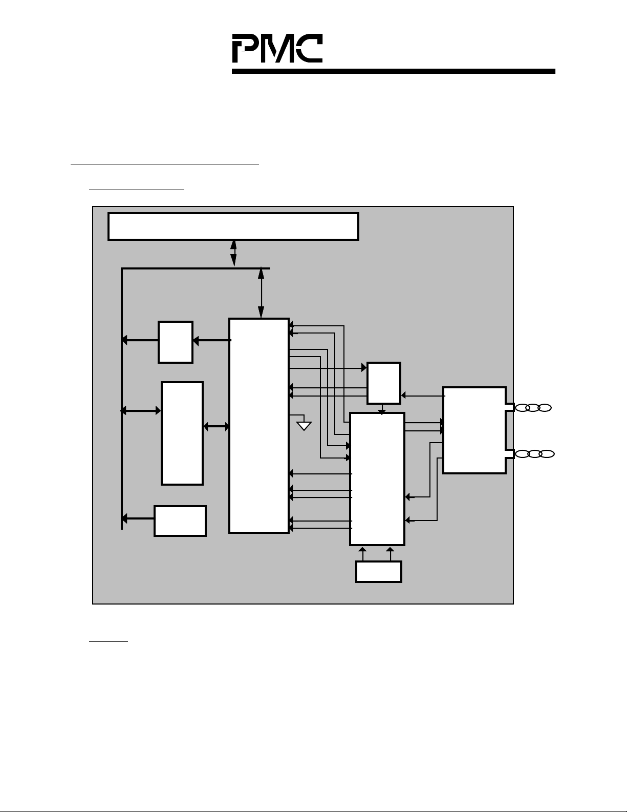
Block Diagram
UTOPIA Edge Connector Interface
TXCI-
Rx
FIF
UTOPIA
Interface
ID ROM
TXCI+
TXD+
tx line
bit serial
TXD-
POCLK
RSER
PICLK
PIN[7:0]
SUNI
Dropside FIFO interface
GPIN /LF
RXC+
RXC-
rx line
bit serial
RXD+
RXD-
LOS Generat
CLK
PAL
I/
/Loo
TClk+
TClk-
TSer+
TSer-
RClk+
RClk-
RSer+
CY7B951
Rser-
RefClk+ RefClk-
Tout
Tout-
Rin
Rin-
I
S
TXD+/-
Tx
Tx
Rx
Rx
TWISTER &
MAGNETICS
RXD+/-
19.44 MHz
Osc
S/UNI
The S/UNI is a monolithic integrated circuit that implements the SONET/SDH
processing and ATM mapping functions of a 155 Mbit/s SONET STS-3c User
Network Interface. It is the heart of the SAPI-UTP5 board; all traffic goes through the
S/UNI. On the line side, the S/UNI transmits SONET frames through the line
interface and receives frames from the line interface. On the drop side, the S/UNI
______________________________________________________________________________________________
2

PMC-Sierra, Inc.
S
TANDARD PRODUCT
PMC -940202 ISSUE 2. APR IL 7, 1995 APP_SA PI_UT P5
______________________________________________________________________________________________
PM5945 -UTP 5
sinks cells provided by the buffer interface and sources cells to the buffer interface.
Below, the S/UNI is briefly described.
The S/UNI receives SONET/SDH frames via a bit serial interface, and processes
section, line, and path overhead. It performs framing (A1, A2), descrambling, detects
alarm conditions, and monitors section, line, and path bit interleaved parity (B1, B2,
B3), accumulating error counts at each level for performance monitoring purposes.
Line and path far end block error indications (FEBE) are also accumulated. The
S/UNI interprets the received payload pointers (H1, H2) and extracts the
synchronous payload envelope which carries the received ATM cell payload.
The S/UNI frames to the ATM payload using cell delineation. Header check
sequence (HCS) error correction is provided. Idle/unassigned cells may be
dropped according to a programmable filter. Cells are also dropped upon detection
of an uncorrectable HCS error. The ATM cell payloads are descrambled. The ATM
cells that are passed are written to a four cell FIFO buffer. The received cells are
read from the FIFO using a generic 8-bit wide datapath interface. Counts of received
ATM cell headers that are erred and uncorrectable, and also those that are erred
and correctable, are accumulated independently for performance monitoring
purposes.
The S/UNI transmits SONET/SDH frames via a bit serial interface, and formats
section, line, and path overhead bytes appropriately. It performs framing pattern
insertion (A1, A2), scrambling, alarm signal insertion, and inserts section, line, and
path bit interleaved parity (B1, B2, B3) as required to allow performance monitoring
at the far end. Line and path far end block error indications (FEBE) are also
inserted. The S/UNI generates the payload pointer (H1, H2) and inserts the
synchronous payload envelope which carries the ATM cell payload. The S/UNI also
supports the insertion of a large variety of errors into the transmit stream, such as
framing pattern errors, bit interleaved parity errors, and illegal pointers, which are
useful for system diagnostics and tester applications.
Transmit ATM cells are written to an internal four cell FIFO using a generic 8-bit wide
datapath interface. Idle/unassigned cells are automatically inserted when the
internal FIFO contains less than one cell. The S/UNI provides generation of the
header check sequence and scrambles the payload of the ATM cells. Each of these
transmit ATM cell processing functions can be enabled or bypassed.
The S/UNI is configured, controlled and monitored via the microprocessor interface
on the UTOPIA connector.
For a complete description of the S/UNI, please refer to PMC-Sierra's PM5345
datasheet.
______________________________________________________________________________________________
3

PMC-Sierra, Inc.
S
TANDARD PRODUCT
PMC -940202 ISSUE 2. APR IL 7, 1995 APP_SA PI_UT P5
______________________________________________________________________________________________
PM5945 -UTP 5
CY7B951
The Cypress SONET/SDH Serial Transceiver is an integrated SONET clock and
data recovery/clock synthesis device. The internal receive PLL recovers a 155.52
MHz clock from an incoming NRZ or NRZI data and re-times the data. The receive
PLL uses a 19.44 MHz reference clock to provide a 155.52 MHz clock in the
absence of input data. The reference clock is also used to improve the PLL lock
time. The differential input data is re-timed by the recovered clock and presented as
the PECL differential output data.
The transmit section of the SONET/SDH Serial Transceiver contains a PLL that
takes a reference clock and multiplies it by 8 to produce a 155.52 MHz PECL
differential output clock. The transmit PECL differential input pair are used to buffer
the transmit PECL output of the S/UNI. This input can also be muxed into the
receive side PLL for clock and data recovery (used for diagnostic purposes).
TWISTER
The DP83223 TWISTER device is capable of transmitting and receiving either twolevel (NRZ) or three-level (MLT-3) signals. It allows links of up to 100 meters of
Category 5 Unshielded Twisted Pair (UTP5) cable and consists of a transmit and a
receive section.
The transmit section of the TWISTER contains a 100K ECL input buffer and a
Programmable Current Output Driver. The Programmable Current Output Driver in
this application is configured to output a current sourced NRZ datastream. The
transmit amplitude of the signal can be adjusted via an external resistor. The
nominal output voltage is 1.0 Volts peak to peak. An isolation transformer with 1:1
turns ratio plus a common mode choke is used to couple signals to UTP5 cable.
The receive section of the TWISTER consists of a differential input equalization
amplifier with signal detect circuitry, signal comparators with control logic, loopback
multiplexer logic and differential 100K ECL output drivers. The equalization
amplifier is set to the adaptive equalization mode. It incorporates a fixed nominal
receive input reference and compares it to the nominal transmit output amplitude to
approximate cable length and provide active compensation. The equalization
amplifier is optimized for a line voltage of 1.4 Volts peak to peak. Thus a step-up
transformer with 1:1.4 turns ratio plus a common mode choke is deployed to put the
line signal into the optimum operating range of the TWISTER's equalization
amplifier.
Line Interface
The line interface consists of the TWISTER connected to the CY7B951. To ensure
that there is a clock in the absence of incoming signal, the differential signal detect
(SD) outputs of the TWISTER are used to select between the serial and parallel
______________________________________________________________________________________________
4

PMC-Sierra, Inc.
S
TANDARD PRODUCT
PMC -940202 ISSUE 2. APR IL 7, 1995 APP_SA PI_UT P5
______________________________________________________________________________________________
PM5945 -UTP 5
mode of operation on the receive side of the S/UNI device. In the normal mode of
operation (good incoming signal) the S/UNI device is in the serial mode and accepts
clock and data from the high speed interface (RSER is high). In loss of signal
condition, the S/UNI device is switched to the parallel mode and accepts data from
the PICLK and PIN[7:0] inputs. The POCLK is switched to generate the 19.44 MHz
PICLK. This technique also guarantees that the S/UNI will generate a LOS
indication when the TWISTER loses incoming signal. This is achieved due to the
CY7B951 not squelching the data in a loss of signal condition.
The transmit line interface consists of the S/UNI PECL transmit outputs that are
buffered by the CY7B951 and then connected to the TWISTER's transmit section.
Outgoing data on TXO+/- pins is coupled to the line via a 1:1 turns ratio transformer.
The receive line interface consists of a 1:1.4 step-up transformer coupling data from
the UTP5 cables to the RXI+/- pins of the TWISTER. The received datastream is
equalized and output by the TWISTER to the CY7B951 which recovers the data and
clock and relays the them to the S/UNI via its PECL differential outputs.
An 8 pin 8 position RJ45 modular jack is used to connect to the UTP5 cables. The
unused pairs of cables are terminated via a resistor network to a common mode
termination point. The center taps of the transformers are also terminated to the
same point.
The S/UNI is configured for bit serial operation. The 155.52 MHz transmit clock
source is synthesized by the CY7B951 from a 19.44 MHz oscillator. The receive
clock and data recovery is supplied by the Cypress CY7B951 device. If the loop
back select is enabled on the CY7B951 the transmit data is muxed into the receive
PLL and the recovered clock and data are fed back to the S/UNI device. The S/UNI
can also be configured for loop time operation. When configured for loop time
operation, only a receive clock and data recovery device is required.
UTOPIA Identification ROM
The upper 32 bytes of the address space is used by the UTOPIA identification ROM
to hold the interface configuration information.
Table 1: Standard ROM Address and Content
Address Function Address Function
0x1E0 Protocol Type 0x1E4-0x1EB 64 or 48-bit Address
0x1E1 Media Type 0x1EC-0x1EF Reserved
0x1E2-0x1E3 Capability 0x1F0-0x1FF Manufacturer ID, Version
______________________________________________________________________________________________
5
PMC-Sierra, Inc.
S
TANDARD PRODUCT
PMC -940202 ISSUE 2. APR IL 7, 1995 APP_SA PI_UT P5
______________________________________________________________________________________________
PM5945 -UTP 5
The following information is stored in the UTOPIA identification ROM of the SAPIUTP5 board:
Table 2: SAPI_UTP5 ROM Address and Contents
Address HEX Value Address HEX Value
0x1E0 0C 0x1E4-0x1EB All 0's
0x1E1 01 0x1EC-0x1EF Reserved
0x1E2-0x1E3 21 0C 0x1F0-0x1FF 50 4D 43 2D 50 4D 35
39 34 35 2D 55 54 50 35
20
Protocol Type:
Contains an identifier for the type of framing/protocol used on this PHY interface.
The SAPI-UTP5 board has 0x0C programmed into this location which specifies
155.52 Mbps (SONET/OC-3) ATM Forum standard. The following values are
defined:
Table 3: Protocol Type
Val ue Framing Type
0x00-0x03 Reserved
0x04 44.736 Mbps (DS-3) ATM Forum Standard
0x05-0x07 Reserved
0x08 100 Mbps (4B/5B block coded) ATM Forum Standard
0x09-0x0B Reserved
0x0C 155.52 Mbps (SONET/OC-3) ATM Forum Standard
0x0D 155.52 Mbps (8B/10B block coded) ATM Forum
Standard
0x0E-0xFE Reserved
______________________________________________________________________________________________
6

PMC-Sierra, Inc.
S
TANDARD PRODUCT
PMC -940202 ISSUE 2. APR IL 7, 1995 APP_SA PI_UT P5
______________________________________________________________________________________________
PM5945 -UTP 5
0xFF Undefined/Unidentified Protocol Type
Media Type:
Contains an identifier for the type of media used on this PHY interface. The
SAPI-UTP5 board has 0x01 programmed into this location which specifies a
Category 5 Unshielded Twisted Pair (CAT5-UTP) cable. The following values
are defined:
Table 4: Media Type
Val ue Media Type
0x00 Category 3 Unshielded Twisted Pair (CAT3-UTP)
0x01 Category 5 Unshielded Twisted Pair (CAT5-UTP)
0x02 Shielded Twisted Pair (STP)
0x03 Reserved
0x04 Very Low-Cost Multimode Fiber (VLCMF, 150 m)
0x05 Low-Cost Multimode Fiber (LCMF, 500 m)
0x06 Multimode Fiber (MF, 2km)
0x07 Reserved
0x08 Single Mode Fiber (SMF)
0x09-0x0B Reserved
0x0C Coaxial Cable (COAX)
0x0D Reserved
0x0F Undefined/Unidentified Media Type
Capability:
Contains two octets which define the capability of the PHY interface. The SAPIUTP5 board has 0x21 & 0x0C programmed into octets 1 & 2 respectively. The
capabilities include:
1. TxRef, =1 when this interface supports the TxRefB UTOPIA signal.
______________________________________________________________________________________________
7
PMC-Sierra, Inc.
S
TANDARD PRODUCT
PMC -940202 ISSUE 2. APR IL 7, 1995 APP_SA PI_UT P5
______________________________________________________________________________________________
PM5945 -UTP 5
2. RxRef, =1 when this interface supports the RxRefB UTOPIA signal.
3. TxClav, =1 when this interface supports the TxClav UTOPIA signal.
4. RxClav, =1 when this interface supports the RxClav UTOPIA signal.
5. TxXon, =1 when this interface supports the TxXon UTOPIA signal.
6. Ver[3:0], 4 bits UTOPIA version number, value for this specification =1.
7. D16, =1 to indicate 16-bit datapath, 0 = 8-bit datapath.
8. HEC, =1 to indicate the HEC is carried in the UDF(1) field.
9. HCS, =1 to indicate HCS is carried in the UDF(2) field, for 16-bit mode
only.
10. NOTE "rsvd" stands for Reserved.
Assignments of fields are shown below.
Table 5: Capability Field Assignment
rsvd HCS HEC D16 Ver[3] Ver[2] Ver[1] Ver[0] octet 1
rsvd rsvd rsvd TxXon RxClav TxClav RxRef TxRef octet 2
64 or 48-bit Address:
Contains eight octets which define the 64 or 48-bit address of the PHY interface.
If a 48-bit address is used, the 2 most significant octets are zero filled. The
address is stored in Big-Endian format (MSB is in the LS address). The SAPIUTP5 board has 0x00 programmed into this location.
Reserved:
Reserved for future expansion.
Manufacturer ID, etc.:
Contains sixteen octets which identify the manufacturer of the PHY interface.
Using the ASCII character set (7-bit code) is encouraged. Three octets of ASCII
representing the manufacture ID and 13 octets of part number.
Table 6: ASCII Table
M.S
L.S
______________________________________________________________________________________________
01234567
8

PMC-Sierra, Inc.
S
TANDARD PRODUCT
PMC -940202 ISSUE 2. APR IL 7, 1995 APP_SA PI_UT P5
______________________________________________________________________________________________
0 NUL DLE SP 0 @ P \ p
1 SOH DC1 ! 1 A Q a q
2 STX DC2 " 2 B R b r
3 ETX DC3 # 3 C S c s
4 EOT DC4 $ 4 D T d t
5 ENQ NAK % 5 E U e u
6 ACK SYN & 6 F V f v
7 BEL ETB ' 7 G W g w
8 BS CAN ( 8 H X h z
PM5945 -UTP 5
9HTEM)9 IYiy
A LF SUM * : J Z j z
B VT ESC + ; K [ k
CFFFS, < L \ l |
DCRGS- = M ] m
ESORS. > N ^n~
FSIµS / ? O < - o DEL
PMC- PM5945-UTP5
50 4d 43 2D 50 4D 35 39 34 35 2D 55 54 50 35 20
DAUGHTERBOARD REGISTERS
The SAPI daughterboard has two write only register bits. One bit is a software reset bit
and the other is a transmit loopbacd enable bit.
______________________________________________________________________________________________
9

PMC-Sierra, Inc.
S
TANDARD PRODUCT
PMC -940202 ISSUE 2. APR IL 7, 1995 APP_SA PI_UT P5
______________________________________________________________________________________________
PM5945 -UTP 5
Software Reset
The software reset bit is at binary address 1110xxxxx (the most significant bit is at
the far left and the least significant is at the far right). The least significant 5 bits of
the address are don't cares. Writing a binary xxxxxxx1 to this address will hold the
S/UNI, the FIFO, and the PALs reset. Writing a binary xxxxxxx0 to this address will
remove the reset. The most significant 7 bits of data are don't cares. This is a writeonly bit. A hardware reset removes the software reset.
Transmit Loopback Enable
The transmit loopback enable bit is at binary address 1111xxxxx (the most
significant bit is at the far left and the least significant is at the far right). The least
significant 5 bits of the address are don't cares. Writing a binary xxxxxxx1 to this
address will mux the transmit output data going to the optics, into the inputs of the
clock and data recovery PLL. This is all done inside the Cypress CY7B951 device.
This allows a diagnostic loopback to be done at the Cypress part to verify the
connections and functionality between the Cypress device and the S/UNI device.
Writing a binary xxxxxxx0 to this address will disable transmit diagnostic loopback.
The most significant 7 bits of data are don't cares. This is a write only bit. A
hardware reset removes the transmit loopback enable (if it was set).
INTERFACE DESCRIPTION
UTOPIA Interface
The UTOPIA Interface makes the S/UNI drop side receive and transmit signals
compatible with the UTOPIA 1.04 interface specification. It consists of two high
speed 22V10 PALs, two high speed IDT74FCT377C buffers, and a receive
IDT72201 clocked FIFO. The 22V10 PALs can be replaced with faster versions if
you must run at a higher than 20 MHz TxClk and RxClk clock signals.
The Transmit drop side interface is controlled by the ATM layer through the edge
connector. All the transmit signals from the ATM layer change with respect to the
TxClk. All the input signals to the ATM layer are sampled on the rising edge of the
TxClk.
The S/UNI device asserts the TCA signal when it has a complete empty cell
available. This signal goes to the PAL (U17) and causes the TxFullB signal to the
ATM layer to be de-asserted (high). The ATM layer asserts the TxClavB signal (low)
when it has a complete Cell of data to transfer to the PHY device. The TxEnbB
signal from the ATM layer (Vicksburg card) is the output of the TxFullB signal from
the PHY layer gated with the TxClavB signal from the ATM layer. The way the
TxEnbB signal goes active (low) depends on whether the ATM layer is ready to send
a cell of data before the PHY layer becomes available to accept the data, or whether
______________________________________________________________________________________________
10

PMC-Sierra, Inc.
S
TANDARD PRODUCT
PMC -940202 ISSUE 2. APR IL 7, 1995 APP_SA PI_UT P5
______________________________________________________________________________________________
PM5945 -UTP 5
the PHY layer is ready to accept a cell of data before the ATM layer is ready to send
data.
The case where the ATM layer has a cell available for transmission before the PHY
layer is ready to accept the cell is handled as follows; The Vicksburg card drives the
TSOC signal active (high) and the TxData bus with valid octet byte zero coincident
with the assertion of the TxClavB signal, and waits for the TxFullB signal from the
PHY layer to go inactive (high). When the PHY device has a cell available, the
TxFullB signal goes inactive (high) and then the TxEnbB signal is immediately
asserted (low) (after a delay through a gate). On the next rising edge of the TxClk
signal, the second byte of data is driven onto the TxData bus and the TSOC signal is
de-asserted (low).
The case where the PHY layer is ready to accept a cell of data before the ATM layer
is ready to transmit the cell is handled as follows; The PHY layer de-asserts the
TxFullB signal (high) and waits for the TxEnbB signal to go active (low). When the
ATM layer has a cell available for transmission, the TxClavB is set active (low) on
the rising edge of the TxClk signal, and drives the TSOC signal active (high) and the
TxData bus with valid octet byte zero . The TxClavB signal sets the TxEnbB signal
active (low) through a gate delay.
In either case, the TxData bus is continually clocked into the first buffer (U18) by the
rising edges of the TxClk signal. The assertion of the TxEnbB signal enables the
TWRB signal to the S/UNI device. On the falling edge of the TWRB signal (rising
edge of TxClk) the data from U18 is clocked into the second buffer (U19). The clock
signal to U19 is generated by the PAL (inverted TxClk). The ATM layer updates the
TxData with new data on the rising edge of each TxClk signal while TxEnbB is
asserted and the TxFullB signal is de-asserted (high). If at the end of the current cell
transfer, another cell is available (TCA remains active), the TxFullB will still be
asserted (low) on the 51'st byte transferred. This is to accomodate the propagation
delay of TCA going inactive (low) at the end of a cell transfer and then being
sampled by the PAL (TCA must be sampled as it can go active at any time). This will
incur an extra clock delay per cell transfer. The TxClavB signal goes inactive (high)
for a minimum of two cycles per cell trasfer. There will be a 3 clock cycle delay per
cell transfer as the TxFullB and the TxClavB overlap.
The Receive drop side interface is controlled by the ATM layer through the edge
connector. All the receive signals from the ATM layer change with respect to the
RxClk. All the input signals to the ATM layer are sampled on the rising edge of the
RxClk. The receive side incorporates a external FIFO so that the S/UNI device does
not overrun due to the latency times between burst cell reads of the ATM layer
(Vicksburg mother board).
The S/UNI device asserts the RCA signal when it has a complete cell to transfer to
the FIFO. The RCA signal goes to the Receive PAL (U16) and the PAL asserts the
write enables to the receive FIFO. If the receive FIFO is not full (/FF high), the
______________________________________________________________________________________________
11

PMC-Sierra, Inc.
S
TANDARD PRODUCT
PMC -940202 ISSUE 2. APR IL 7, 1995 APP_SA PI_UT P5
______________________________________________________________________________________________
PM5945 -UTP 5
receive PAL will start clocking the data from the S/UNI into the FIFO by generating
the RRDB clock signal. The RSOC signal from the S/UNI is inserted into bit 9 of the
FIFO data inputs. The FIFO enables the /FF (active low FIFO Full) signal when it is
full which disables further transfer of data from the S/UNI to the FIFO. If the FIFO
gets full, the S/UNI will have transferred an indeterminate portion of a cell. The rest
of the cell will get transferred as soon as the FIFO de-activates the /FF signal. The
Receive PAL uses the RxCLK signal from the ATM layer to generate the WClk signal
going to the FIFO and the RRDB clock signal to the S/UNI. The WEN going to the
FIFO is disabled while the /FF is active (low). While the FIFO write enable is
disabled, the clock going to the FIFO is the same as the RxCLK. This is done
because the FIFO /FF signal will not be disabled (high) untill it gets a rising edge on
the WCLK input.
The RxEmptyB signal comes from the Receive FIFO /EF (active low Empty FIFO)
signal. The Receive FIFO de-asserts the the RxEmptyB signal (high) upon reception
of a single byte of data. On the next rising edge of the RxClk clock signal, the ATM
layer samples the RxEmptyB signal and on the following RxClk clock signal, the
ATM layer activates the RxEnbB signal (low) if it has an empty cell available. The
RxEnbB signal from the ATM layer goes to the Receive PAL (U16) and to the read
enable (/RDEN1) input of the receive FIFO. On the next rising edge of the RxCLK
signal after the RxEnbB signal goes active (low) the first byte of data is clocked out of
the FIFO along with the RSOC signal. The receive ATM layer ignores the data until it
sees a valid RSOC signal. Once cell transfer has commenced, the ATM layer
expects a complete cell transfer. If the FIFO is empty (RxEmptyB is active) and then
the S/UNI starts to transfer data to the FIFO, there might only be one byte in the FIFO
before the RxEmptyB signal could go inactive (high). For the FIFO to become empty,
the S/UNI must not have had any cells to transfer and therefore the first byte in the
FIFO would be the first byte of the Cell along with the valid RSOC signal. Since the
RxClk clock signal is generating the write and read clock signals to the FIFO as well
as the read clock signal to the S/UNI, the ATM layer cannot read the data out of the
FIFO faster than the S/UNI can write the data into the FIFO.
SAPI Board Edge Connector Interface
The SAPI UTOPIA Edge Connector Interface includes all the signals required to
connect the SAPI board to a high layer protocol entity (i.e. a AAL processor). Cells
can be written to the S/UNI transmit FIFO and read from the S/UNI receive FIFO
using this interface. The edge connector is made up of a 100 pin dual line female
connector is shown in table below. It consists of signals appropriate to read and
write to the registers of the devices on the daughter board, and it provides the
necessary power and ground. TTL signal levels are used on this interface.
Table 7: Edge Connector Pin Description
______________________________________________________________________________________________
12

PMC-Sierra, Inc.
S
TANDARD PRODUCT
PMC -940202 ISSUE 2. APR IL 7, 1995 APP_SA PI_UT P5
______________________________________________________________________________________________
PM5945 -UTP 5
Signal
Name Type
PIN
Function
GND Power 1 Ground
GND Power 2 Ground
TxDat[0]
TxDat[1]
TxDat[2]
TxDat[3]
TxDat[4]
TxDat[5]
TxDat[6]
TxDat[7]
I
I
I
I
I
I
I
I
3
5
9
11
4
6
10
12
The S/UNI is configured for the 8 bit FIFO interface,
TxDat[7:0] corresponds to a cell byte.
TxDat[7] corresponds to bit 1, the first bit received.
TxDat[0] corresponds to bit 8, the last bit received.
VCC Power 7 +5 Volts
VCC Power 8 +5 Volts
GND Power 13 Ground
TxPrty I 14 Transmit data bus (TxDat[7:0]) odd parity. Not
Used
TxSOC I 15 Transmit start of cell indication. Identifies the first
byte (word) of a cell on inputs TxDAT[7:0]
GND Power 16 Ground
GND Power 17 Ground
TxFullB O 18 Active low signal from the PHY to ATM layer,
asserted by the PHY layer 4 cycles before it is no
longer able to accept transmit data.
TxClavB I 19 Active low signal from the ATM layer to the PHY
layer, asserted by the ATM layer when it has a full
cell to transmit.
GND Power 20 Ground
GND Power 21 Ground
TxCLK I 2 2 The transmit transfer/synchronization clock
provided by the ATM to the PHY layer for
synchronizing transfers on the TxDATA bus.
(nominally at 20 MHz).
TxRefB I 2 3 Transmit Reference. Input for the purposes of
synchronization (e.g. 8 KHz frame marker or
SONET frame indicator). Not Used
______________________________________________________________________________________________
13

PMC-Sierra, Inc.
S
TANDARD PRODUCT
PMC -940202 ISSUE 2. APR IL 7, 1995 APP_SA PI_UT P5
______________________________________________________________________________________________
PM5945 -UTP 5
GND Power 24 Ground
GND Power 25 Ground
TxXon O 26 PHY layer flow control. 1= Xon, 0= Xoff. Asserted
by the PHY layer for normal transmission.
Deasserted by the PHY layer when the ATM link is
experiencing congestion. The response of the
ATM layer to this signal is user defined. Not Used.
TxEnbB 27 Active low transmit signal asserted by the ATM
layer during cycles when the TxDat contains valid
cell data.
GND Power 28 Ground
GND Power 29 Ground
RxDat[0]
RxDat[1]
RxDat[2]
RxDat[3]
RxDat[4]
RxDat[5]
RxDat[6]
RxDat[7]
O
O
O
O
O
O
O
O
31
33
37
39
30
32
38
40
RxDat[7:0] corresponds to a cell byte. Please refer
to the S/UNI datasheet for the byte cell data
structure.
RxDat[7] corresponds to bit 1, the first bit received.
RxDat[0] corresponds to bit 8, the last bit received.
RxPrty O 34 Receive data bus (RxDat[7:0]) odd parity. Not
Used
VCC Power 35 +5 Volts
VCC Power 36 +5 Volts
GND Power 41 Ground
Undefined 4 2
RxSOC O 43 Receive start of cell indication. Identifies the first
byte (word) of a cell on outputs RxDat[7:0]
GND Power 44 Ground
GND Power 45 Ground
RxEmptyB 0 46 Active low empty signal to indicate that in the
current cycle there is no valid data for delivery to
the ATM layer.
______________________________________________________________________________________________
14

PMC-Sierra, Inc.
S
TANDARD PRODUCT
PMC -940202 ISSUE 2. APR IL 7, 1995 APP_SA PI_UT P5
______________________________________________________________________________________________
PM5945 -UTP 5
RxEnbB I 47 Active low signal asserted by the ATM layer to
indicate that the RxDat[7:0] will be sampled at the
start of the next cycle. Sampling occurs on cycles
following those with RxENB asserted and
RxEmptyB Deasserted.
GND Power 48 Ground
GND Power 49 Ground
RxClk I 5 0 Transfer/synchronization clock provide by the ATM
layer for synchronizing transfers on RxDat
(nominally 20 MHz).
RxRefB O 5 1 Receive Reference. Output for the purposes of
synchronization (e.g. 8 KHz frame marker or
SONET frame indicator). Not Used.
GND Power 52 Ground
GND Power 53 Ground
RxClav O 54 Receive Cell Available Signal. Active high signal
from the PHY layer to the ATM layer, asserted to
indicate that there is a complete cell available for
transfer to the ATM layer.
RxFlush 55 Not Used
GND Power 56 Ground
GND Power 57 Ground
A[4] I 5 8 Address bus bit 7.
A[0] I 5 9 Address bus bit 6.
A[5] I 6 0 Address bus bit 5.
A[1] I 6 1 Address bus bit 4.
Undefined 6 2
VCC Power 63 +5 Volts
VCC Power 64 +5 Volts
A[2] I 6 5 Address bus bit 3.
A[6] I 6 6 Address bus bit 2.
A[3] I 6 7 Address bus bit 1.
A[7] I 6 8 Address bus bit 0.
______________________________________________________________________________________________
15

PMC-Sierra, Inc.
S
TANDARD PRODUCT
PMC -940202 ISSUE 2. APR IL 7, 1995 APP_SA PI_UT P5
______________________________________________________________________________________________
PM5945 -UTP 5
GND Power 69 Ground
GND Power 70 Ground
D[0] I/O 71 Data bus bit 0.
A[8] I 7 2 Address bit used to read the Standard PHY
registers.
D[1] I/O 73 Data bus bit 1.
D[4] I/O 74 Data bus bit 4.
GND Power 75 Ground
GND Power 76 Ground
D[2] I/O 77 Data bus bit 2.
D[5] I/O 78 Data bus bit 5.
D[3] I/O 79 Data bus bit 3.
D[6] I/O 80 Data bus bit 6.
GND Power 81 Ground
GND Power 82 Ground
Prty I/O 83 Data bus D[7:0] odd parity. Not Used.
D[7] I/O 84 Data bus bit 7.
VCC Power 85 +5 Volts
VCC Power 86 +5 Volts
Undefined 8 7
INTB O 88 Active low, open-drain interrupt signal.
CSB I 8 9 The S/UNI active low chip select signal.
GND Power 90 Ground
GND Power 91 Ground
RSTB I 92 Active low H/W reset.
RDB I 9 3 Active low read signal asserted to enable data from
the addressed location onto the D[7:0] bus.
GND Power 94 Ground
GND Power 95 Ground
RDY 96 Not Used
______________________________________________________________________________________________
16
PMC-Sierra, Inc.
S
TANDARD PRODUCT
PMC -940202 ISSUE 2. APR IL 7, 1995 APP_SA PI_UT P5
______________________________________________________________________________________________
PM5945 -UTP 5
WRB I 9 7 Active low write signal asserted to write data to the
addressed location from the D[7:0] bus.
ALE I 9 8 Address latch enable. When high, identifies that
address is valid on D[7:0]. Not Used.
GND Power 99 Ground
GND Power 100 Ground
______________________________________________________________________________________________
17
PMC-Sierra, Inc.
S
TANDARD PRODUCT
PMC -940202 ISSUE 2. APR IL 7, 1995 APP_SA PI_UT P5
______________________________________________________________________________________________
PM5945 -UTP 5
S/UNI REGISTER ADDRESS MAP
The microprocessor interface provides access to the S/UNI device registers via the
100 pin UTOPIA connector. The S/UNI address space extends from 00H to FFH.
Below is a list of the S/UNI device registers. For further details, please refer to the
"Saturn User Network Interface Device Datasheet".
Table 8: S/UNI Register Address Map
Address Register
0x00 S/UNI Master Reset and Identity
0x01 S/UNI Master Configuration
0x02 S/UNI Master Interrupt Status
0x04 S/UNI Master Clock Monitor
0x05 S/UNI Master Control
0x06-0x07 Reserved
0x08-0x0B Reserved
0x0C-0x0F Reserved
0x10 RSOP Control/Interrupt Enable
0x11 RSOP Status/Interrupt Status
0x12 RSOP Section BIP-8 LSB
0x13 RSOP Section BIP-8 MSB
0x14 TSOP Control
0x15 TSOP Diagnostic
0x16-0x17 TSOP Reserved
0x18 RLOP Control/Status
0x19 RLOP Interrupt Enable/Status
0x1A RLOP Line BIP-24 LSB
0x1B RLOP Line BIP-24
0x1C RLOP Line BIP-24 MSB
0x1D RLOP Line FEBE LSB
0x1E RLOP Line FEBE
0x1F RLOP Line FEBE MSB
0x20 TLOP Control
0x21 TLOP Diagnostic
0x22-0x23 TLOP Reserved
0x24-0x27 Reserved
0x28-0x2B Reserved
0x2C-0x2F Reserved
0x30 RPOP Status/Control
0x31 RPOP Interrupt Status
0x32 RPOP Reserved
0x33 RPOP Interrupt Enable
______________________________________________________________________________________________
18

PMC-Sierra, Inc.
S
TANDARD PRODUCT
PMC -940202 ISSUE 2. APR IL 7, 1995 APP_SA PI_UT P5
______________________________________________________________________________________________
PM5945 -UTP 5
0x34 RPOP Reserved
0x35 RPOP Reserved
0x36 RPOP Reserved
0x37 RPOP Path Signal Label
0x38 RPOP Path BIP-8 LSB / Load Meters
0x39 RPOP Path BIP-8 MSB
0x3A RPOP Path FEBE LSB
0x3BH RPOP Path FEBE MSB
0x3C-0x3F RPOP Reserved
0x40 TPOP Control/Diagnostic
0x41 TPOP Pointer Control
0x42 TPOP Source Control
0x43 TPOP Reserved
0x44 TPOP Reserved
0x45 TPOP Arbitrary Pointer LSB
0x46 TPOP Arbitrary Pointer MSB
0x47 TPOP Reserved
0x48 TPOP Path Signal Label
0x49 TPOP Path Status
0x4A TPOP Reserved
0x4B-0x4F TPOP Reserved
0x50 RACP Control/Status
0x51 RACP Interrupt Enable/Status
0x52 RACP Match Header Pattern
0x53 RACP Match Header Mask
0x54 RACP Correctable HCS Error Count
0x55 RACP Uncorrectable HCS Error Count
0x56-0x5F RACP Reserved
0x60 TACP Control/Status
0x61 TACP Idle/Unassigned Cell Header Pattern
0x62 TACP Idle/Unassigned Cell Payload Octet Pattern
0x63-0x67 TACP Reserved
0x68-0x7F Reserved
0x80 S/UNI Master Test
0x81-0xFF Reserved for Test
______________________________________________________________________________________________
19
PMC-Sierra, Inc.
X
XH1XH2XXX
X
S
TANDARD PRODUCT
PMC -940202 ISSUE 2. APR IL 7, 1995 APP_SA PI_UT P5
______________________________________________________________________________________________
PM5945 -UTP 5
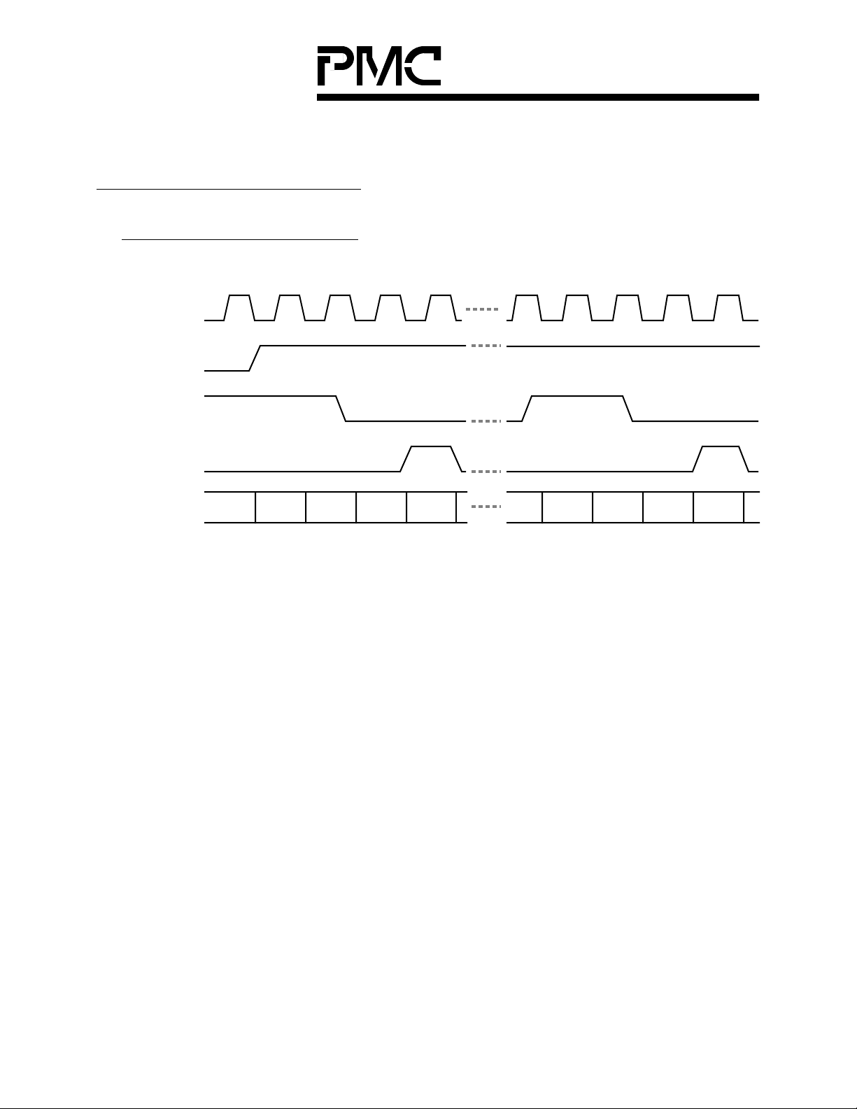
RECEIVE DROP SIDE TIMING
Receive Functional Timing
Figure 1: Receive Functional Timing
RxClk
RxEmptyB
RxEnbB
RxSOC
RxData
H1
P48
______________________________________________________________________________________________
20

PMC-Sierra, Inc.
S
TANDARD PRODUCT
PMC -940202 ISSUE 2. APR IL 7, 1995 APP_SA PI_UT P5
______________________________________________________________________________________________
PM5945 -UTP 5
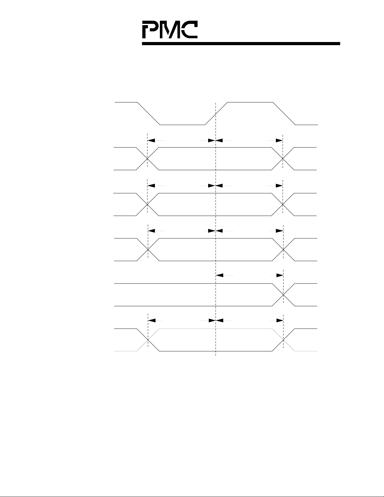
Receive Interface Timing
Table 9: Receive Interface Timing Parameters
Symbol Parameter Min Max Units
RxClk Frequency (nominaly 20 MHz) 20 MHz
RxClk Duty Cycle 40 60 %
tS
RxData
tH
RxData
tS
RxSOC
tH
RxSOC
tS
RxClavB
tH
RxClavB
tP
RxEnbB
tS
RxData
tH
RxData
RxData[7:0] Set-up Time to RxClk 10 ns
RxData[7:0] Hold Time to RxClk 1 ns
RxSOC Set-up Time to RxClk 10 ns
RxSOC Hold Time to RxClk 1 ns
RxClavB Set-up Time to RxClk 10 ns
RxClavB Hold Time to RxClk 1 ns
RxClk high to RxEnbB Valid 1 2 0 ns
RxData[7:0] Set-up Time to RxClk 10 ns
RxData[7:0] Hold Time to RxClk 1 ns
______________________________________________________________________________________________
21
PMC-Sierra, Inc.
k
C
t
P
t
H
t
S
t
H
t
S
t
H
t
S
t
H
t
S
S
TANDARD PRODUCT
PMC -940202 ISSUE 2. APR IL 7, 1995 APP_SA PI_UT P5
______________________________________________________________________________________________
Figure 2: Receive Interface Timing
PM5945 -UTP 5
RxCl
RxData[7:0]
RxSO
RxClavB
RxEnbB
RxData
RxSOC
RxClavB
RxEmptyB
RxData
RxSOC
RxClavB
RxEnbB
RxEmptyB
RxEmptyB
______________________________________________________________________________________________
22

PMC-Sierra, Inc.
7
XH2X
S
TANDARD PRODUCT
PMC -940202 ISSUE 2. APR IL 7, 1995 APP_SA PI_UT P5
______________________________________________________________________________________________
PM5945 -UTP 5
TRANSMIT DROP SIDE TIMING
Transmit Functional Timing
Figure 3: Transmit Functional Timing
TxClk
TxClavB
TxEnbB
TxFullB
TxSOC
TxData H1 P48 H1P4
H1
H2
H3
______________________________________________________________________________________________
23

PMC-Sierra, Inc.
S
TANDARD PRODUCT
PMC -940202 ISSUE 2. APR IL 7, 1995 APP_SA PI_UT P5
______________________________________________________________________________________________
PM5945 -UTP 5
Transmit Interface Timing
Table 10: Transmit Interface Timing Parameters
Symbol Parameter Min Max Units
TxClk Frequency (nominaly 20 MHz) 20 MHz
TxClk Duty Cycle 40 60 %
tP
TxData
tP
TxSOC
tP
TxClavB
tP
TxData
tP
TxEnbB
tS
TxFullB
tH
TxFullB
TxClk high TxData[7:0] Valid 1 20 ns
TxClk high TxSOC Valid 1 20 ns
TxClk high TxClavB Valid 1 20 ns
TxClk high TxData[7:0] Valid 1 20 ns
TxClk high TxEnbB Valid 1 20 ns
TxFullB Set-up Time to TxClk 10 ns
TxFullB Hold Time to TxClk 1 ns
______________________________________________________________________________________________
24

PMC-Sierra, Inc.
]
t
P
t
P
t
P
t
P
t
H
t
S
S
TANDARD PRODUCT
PMC -940202 ISSUE 2. APR IL 7, 1995 APP_SA PI_UT P5
______________________________________________________________________________________________
Figure 4: Transmit Interface Timing
PM5945 -UTP 5
TxClk
TxData
TxData[7:0
TxSOC
TxSOC
TxClavB
TxEnbB
TxFullB
TxFullB
TxClavB
TxEnbB
TxFullB
______________________________________________________________________________________________
25

PMC-Sierra, Inc.
S
TANDARD PRODUCT
PMC -940202 ISSUE 2. APR IL 7, 1995 APP_SA PI_UT P5
______________________________________________________________________________________________
PM5945 -UTP 5
CHARACTERISTICS
Table 11: Characteristics
Symbol Parameter Mi n Max Units Test Conditions
V
5DC
+5V DC Power
4.90 5.25 V
Supply Voltage
I
5DC
+5V DC Power
1.00 A V
5DC
= 5.0 V
+ 5%
Supply Current
T
A
Ambient
050°CV
DC
= 5.0 V
+ 5%
Temperature
MICROPROCESSOR INTERFACE TIMING CHARACTERISTICS
(TA = 0°C to +70°C, VDD = 5 V ±10%)
Microprocessor Interface Read Access
Table 12: Microprocessor Interface Read Access Parameters
Symbol Parameter Min Max Units
tH
AR
tS
AR
tP
RD Valid Read to Valid Data Propagation Delay 80 ns
Address to Valid Read Hold Time 20 ns
Address to Valid Read Set-up Time 25 n s
tZ
RD
tP
INTH
______________________________________________________________________________________________
Valid Read Negated to Output Tri-state 20 n s
Valid Read Deasserted to INTB High 50 ns
26

PMC-Sierra, Inc.
]
]
S
TANDARD PRODUCT
PMC -940202 ISSUE 2. APR IL 7, 1995 APP_SA PI_UT P5
______________________________________________________________________________________________
Figure 5: Microprocessor Interface Read Timing
PM5945 -UTP 5
A[8:0
(CSB+RDB)
INTB
D[7:0
tS
AR
Valid Address
tP
RD
Valid Data
tZ
tP
tH
AR
INTL
RD
Notes on Microprocessor Interface Read Timing:
1. Output propagation delay time is the time in nanoseconds from the 50% point of
the reference signal to the 30% or 70% point of the output.
2. A valid read cycle is defined as a logical OR of the CSB and the RDB signals.
3. When a set-up time is specified between an input and a clock, the set-up time is
the time in nanoseconds from the 1.4 Volt point of the input to the 1.4 Volt point of
the clock.
4. When a hold time is specified between an input and a clock, the hold time is
the time in nanoseconds from the 1.4 Volt point of the input to the 1.4 Volt point of
the clock.
______________________________________________________________________________________________
27

PMC-Sierra, Inc.
]
]
S
TANDARD PRODUCT
PMC -940202 ISSUE 2. APR IL 7, 1995 APP_SA PI_UT P5
______________________________________________________________________________________________
PM5945 -UTP 5
Microprocessor Interface Write Access
Table 13: Microprocessor Interface Write Access Parameters
Symbol Parameter Min Max Units
tS
DW
tS
AW
tH
AW
tS
DW Data to Valid Write Set-up Time 20 ns
tH
DW
tV
WR
Fig . 6 Microprocessor Interface Write Timing
Data to Valid Write Set-up Time 20 ns
Address to Valid Write Set-up Time 2 5 n s
Address to Valid Write Hold Time 20 ns
Data to Valid Write Hold Time 20 ns
Valid Write Pulse Width 40 n s
A[8:0
tS
AW
Valid Address
tV
WR
tH
AW
(CSB+WRB)
tH
DW
D[7:0
tS
DW
Valid Data
Notes on Microprocessor Interface Write Timing:
1 A valid write cycle is defined as a logical OR of the CSB and the WRB signals.
2. Microprocessor Interface timing applies to normal mode register accesses only.
3. When a set-up time is specified between an input and a clock, the set-up time is
the time in nanoseconds from the 1.4 Volt point of the input to the 1.4 Volt point of
the clock.
______________________________________________________________________________________________
28

PMC-Sierra, Inc.
S
TANDARD PRODUCT
PMC -940202 ISSUE 2. APR IL 7, 1995 APP_SA PI_UT P5
______________________________________________________________________________________________
PM5945 -UTP 5
4. When a hold time is specified between an input and a clock, the hold time is the
time in nanoseconds from the 1.4 Volt point of the input to the 1.4 Volt point of the
clock.
______________________________________________________________________________________________
29

PMC-Sierra, Inc.
S
TANDARD PRODUCT
PMC -940202 ISSUE 2. APR IL 7, 1995 APP_SA PI_UT P5
______________________________________________________________________________________________
PM5945 -UTP 5
APPENDIX A: PAL EQUATIONS
-- UTOPIA interface PAL U12
-- Used to generate the LOS and Chip Select Signals
-- to the S/UNI receive FIFOs
USE work.bv_math.all; -- necessary for inc_bv();
USE work.rtlpkg.all;
USE work.cypres.all;
ENTITY los_cs_pal IS
PORT (poclk0, poclk1, csb, rdb, wrb, a8, a6, a5,
rstb, a7, d0, sd: IN BIT;
rser, csbo, loopb,
prom_enb, brstb : OUT BIT;
piclk: INOUT x01z);
ATTRIBUTE order_code of los_cs_pal:ENTITY is "PAL22V10D-10PC";
ATTRIBUTE part_name of los_cs_pal:ENTITY IS "C22V10";
ATTRIBUTE pin_numbers of los_cs_pal:ENTITY IS
"poclk0:1 " &
"poclk1:2 " &
"csb:3 " &
"wrb:4 " &
"rdb:5 " &
"a8:6 " &
"a6:7 " &
"a5:8 " &
"rstb:9 " &
"a7:10 " &
"d0:11 " &
"sd:13 " &
"csbo:17 " &
"loopb:18 " &
"rser:19 " &
"prom_enb:21 " &
"brstb:22 " &
"piclk:23";
END los_cs_pal;
ARCHITECTURE behavior OF los_cs_pal IS
SIGNAL set_reset,piclk_b,hold, grst,rser_din,oe_d: BIT;
SIGNAL loopb_d,oe, loopb_en,loopb_dis,sd_sample: BIT;
SIGNAL high :BIT := '1';
______________________________________________________________________________________________
30

PMC-Sierra, Inc.
S
TANDARD PRODUCT
PMC -940202 ISSUE 2. APR IL 7, 1995 APP_SA PI_UT P5
______________________________________________________________________________________________
PM5945 -UTP 5
BEGIN
proc1: PROCESS
BEGIN
WAIT UNTIL (poclk0 = '1');
-- Sample the SD input
IF ( sd = '1' ) THEN
sd_sample <= '1';
ELSE
sd_sample <= '0';
END IF;
-- Set RSER low if loss of signal occurs
IF ( sd_sample = '1') THEN
rser_din <= '1';
ELSE
rser_din <= '0';
END IF;
END process;
proc2: PROCESS
BEGIN
-- Enable PICLK
IF ( rser_din = '0' AND sd_sample = '0'
AND rstb ='1' and set_reset = '0') THEN
oe <= '1';
ELSE
oe <= '0';
END IF;
-- Enable CSB
IF ( csb = '0' AND a8 = '0' ) THEN
csbo <= '0';
ELSE
csbo <= '1';
END IF;
-- Enable UTOPIA ID PROM
IF ( csb = '0' AND a8 = '1' AND a7 = '1' AND
a6 = '1' AND a5 = '1') THEN
prom_enb <= '0';
ELSE
prom_enb <= '1';
END IF;
______________________________________________________________________________________________
31

PMC-Sierra, Inc.
S
TANDARD PRODUCT
PMC -940202 ISSUE 2. APR IL 7, 1995 APP_SA PI_UT P5
______________________________________________________________________________________________
PM5945 -UTP 5
-- Set reset
IF rstb = '0' THEN
set_reset <= '0';
ELSIF (a8 = '1' AND a7 ='1' AND a6 = '1' AND
a5 = '0' AND d0 = '1' AND csb = '0' AND wrb = '0') THEN
set_reset <= '1';
-- Clear reset
ELSIF (a8 = '1' AND a7 ='1' AND a6 = '1' AND
a5 = '0' AND d0 = '0' AND csb = '0' AND wrb = '0') THEN
set_reset <= '0';
END IF;
-- BRSTB
IF (rstb = '0' OR set_reset ='1') THEN
brstb <= '0';
ELSIF (rstb = '1' and set_reset = '0' ) THEN
brstb <= '1';
END IF;
-- Disable LOOPB
IF rstb = '0' OR (a8 = '1' AND a7 ='1' AND
a6 = '1' AND a5 = '1' AND d0 = '0' AND csb = '0'
AND wrb = '0')
OR (a8 = '1' AND a7 ='1' AND a6 = '1' AND
a5 = '0' AND d0 = '1' AND csb = '0' AND wrb = '0') THEN
loopb_dis <= '1';
loopb_en <= '0';
-- Enable LOOPB
ELSIF (rstb = '1' AND a8 = '1' AND a7 ='1' AND
a6 = '1' AND a5 = '1' AND d0 = '1' AND csb = '0'
AND wrb = '0') THEN
loopb_en <= '1';
loopb_dis <= '0';
END IF;
END process;
b1:bufoe port map (poclk1,oe,piclk,piclk_b);
b2:buf port map (rser_din,rser);
b3:srl port map (loopb_dis,loopb_en,loopb);
END behavior;
______________________________________________________________________________________________
32

PMC-Sierra, Inc.
S
TANDARD PRODUCT
PMC -940202 ISSUE 2. APR IL 7, 1995 APP_SA PI_UT P5
______________________________________________________________________________________________
PM5945 -UTP 5
DESIGN EQUATIONS (06:44:11)
These equations were extracted from the LOS_CS1.RPT report file. They can be
used or the above VHDL code can be used to generate the proper .JED files. The
LOS_CS1.JED files are available on request.
/csbo =
/csb * /a8
loopb =
/loopb_en * loopb
+ loopb_dis * /loopb_en
rser.D =
sd_sample_BEH_i1_0_DFF.Q
rser.C =
poclk0
/prom_enb =
/csb * a8 * a7 * a6 * a5
brstb =
rstb * /set_reset
piclk =
poclk1
piclk.OE =
rstb * /set_reset * /sd_sample_BEH_i1_0_DFF.Q * /rser.Q
sd_sample_BEH_i1_0_DFF.D =
sd
sd_sample_BEH_i1_0_DFF.C =
poclk0
set_reset =
rstb * /csb * a8 * a7 * a6 * /a5 * d0 * /wrb
+ rstb * wrb * set_reset
+ rstb * a5 * set_reset
+ rstb * /a6 * set_reset
+ rstb * /a7 * set_reset
+ rstb * /a8 * set_reset
+ rstb * csb * set_reset
______________________________________________________________________________________________
33

PMC-Sierra, Inc.
S
TANDARD PRODUCT
PMC -940202 ISSUE 2. APR IL 7, 1995 APP_SA PI_UT P5
______________________________________________________________________________________________
PM5945 -UTP 5
loopb_en =
rstb * /csb * a8 * a7 * a6 * a5 * d0 * /wrb
+ rstb * /a5 * /d0 * loopb_en
+ rstb * wrb * loopb_en
+ rstb * /a6 * loopb_en
+ rstb * /a7 * loopb_en
+ rstb * /a8 * loopb_en
+ rstb * csb * loopb_en
/loopb_dis =
rstb * /csb * a8 * a7 * a6 * a5 * d0 * /wrb
+ rstb * /a5 * /d0 * /loopb_dis
+ rstb * wrb * /loopb_dis
+ rstb * /a6 * /loopb_dis
+ rstb * /a7 * /loopb_dis
+ rstb * /a8 * /loopb_dis
+ rstb * csb * /loopb_dis
______________________________________________________________________________________________
34

PMC-Sierra, Inc.
S
TANDARD PRODUCT
PMC -940202 ISSUE 2. APR IL 7, 1995 APP_SA PI_UT P5
______________________________________________________________________________________________
PM5945 -UTP 5
-- UTOPIA interface PAL U16
-- Used to interface the Vicksburg Motherboard F-FRED chip --
to the S/UNI receive FIFOs
USE work.bv_math.all; -- necessary for inc_bv();
USE work.rtlpkg.all;
ENTITY rx_pal IS
PORT (rxclk, resetb, rsoc, rca, RxenbB, low, paeb, pafb, ffb: IN BIT;
rrdb, wclk, wen1b: OUT BIT);
ATTRIBUTE order_code of rx_pal:ENTITY is "PAL22V10D-10PC";
ATTRIBUTE part_name of rx_pal:ENTITY IS "C22V10";
ATTRIBUTE pin_numbers of
rx_pal:ENTITY IS
"rxclk:1 " &
"paeb:5 " &
"RxenbB:6 " &
"rsoc:7 " &
"rca:8 " &
"pafb:9 " &
"ffb:10 " &
"resetb:11 " &
"low:13 " &
"rrdb:14 " &
"wclk:21 " &
"wen1b:23";
END rx_pal;
ARCHITECTURE behavior OF rx_pal IS
SIGNAL count:bit_vector(5 downto 0);
SIGNAL rca_sample: BIT;
SIGNAL high :BIT := '1';
SIGNAL wclk_d,wen1b_d,rrdb_d:BIT; -- dummy bits
BEGIN
proc1: PROCESS
- - VARIABLE CountEnable: BIT;
______________________________________________________________________________________________
35

PMC-Sierra, Inc.
S
TANDARD PRODUCT
PMC -940202 ISSUE 2. APR IL 7, 1995 APP_SA PI_UT P5
______________________________________________________________________________________________
PM5945 -UTP 5
BEGIN
WAIT UNTIL (rxclk = '1');
-- Reset
IF resetb = '0' THEN
rca_sample <= '0';
Count <= "111111";
-- SET counter to 0 if RSOC goes high
ELSIF ( rsoc = '1' ) THEN
Count <=
"000000";
-- Continue putting out data
ELSIF rsoc = '0' AND ffb ='1' AND
Count /= "111111" AND rca_sample = '1' THEN
Count <= inc_bv(Count); -- increment bit vector
END IF;
-- Counter rolls over when count = 53
ELSE
END IF;
END process;
proc2: PROCESS
BEGIN
-- Enable WEN1B to FIFO
IF ( ffB = '0' ) THEN
ELSE
END IF;
-- Enable RRDB to S/UNI
IF ( (rca = '0' AND Count /= "110011") OR resetb = '0'
OR wen1b_d ='1' OR rxclk = '1') THEN
IF Count = "110011" AND rsoc = '0' THEN
Count <= "111111";
END IF;
IF rca = '1' THEN
rca_sample <= '1';
rca_sample <= '0';
wen1b_d <= '1';
wen1b_d <= '0';
rrdb <= '1';
______________________________________________________________________________________________
36

PMC-Sierra, Inc.
S
TANDARD PRODUCT
PMC -940202 ISSUE 2. APR IL 7, 1995 APP_SA PI_UT P5
______________________________________________________________________________________________
PM5945 -UTP 5
ELSIF ( rca_sample = '1' AND resetb = '1' AND
wen1b_d ='0' AND rxclk = '0' ) THEN
rrdb <= '0';
END IF;
-- Enable WCLK to FIFO
IF ( wen1b_d = '1' AND rxclk = '1' ) THEN
wclk <= '1';
ELSIF ( wen1b_d = '1' AND rxclk = '0' ) THEN
wclk <= '0';
ELSIF ( (rca = '0' AND Count /= "110011") OR
resetb = '0' OR rxclk = '1') THEN
wclk <= '1';
ELSIF ( rca_sample = '1' AND resetb = '1' AND
wen1b_d ='0' AND rxclk = '0' ) THEN
wclk <= '0';
END IF;
END process;
b1:buf port map (wen1b_d,wen1b);
END behavior;
______________________________________________________________________________________________
37

PMC-Sierra, Inc.
S
TANDARD PRODUCT
PMC -940202 ISSUE 2. APR IL 7, 1995 APP_SA PI_UT P5
______________________________________________________________________________________________
PM5945 -UTP 5
DESIGN EQUATIONS (13:27:08)
These equations were extracted from the RX.RPT report file. They can be used or the
above VHDL code can be used to generate the proper .JED files. The RX.JED files are
available on request.
/rrdb =
ffb * /rxclk * resetb * count_0_.Q * count_1_.Q * /count_2_.Q *
/count_3_.Q * count_4_.Q * count_5_.Q * rca_sample.Q
+ ffb * /rxclk * resetb * /rrdb * count_0_.Q * count_1_.Q *
/count_2_.Q * /count_3_.Q * count_4_.Q * count_5_.Q
+ ffb * /rxclk * rca * resetb * rca_sample.Q
+ ffb * /rxclk * rca * resetb * /rrdb
/wclk =
/rxclk * resetb * count_0_.Q * count_1_.Q * /count_2_.Q *
/count_3_.Q * count_4_.Q * count_5_.Q * rca_sample.Q
+ /rxclk * resetb * count_0_.Q * count_1_.Q * /count_2_.Q *
/count_3_.Q * count_4_.Q * count_5_.Q * /wclk
+ /rxclk * rca * resetb * rca_sample.Q
+ /rxclk * rca * resetb * /wclk
+ /ffb * /rxclk
wen1b =
/ffb
rca_sample.D =
rca
rca_sample.C =
rxclk
count_5_.D =
ffb * count_0_.Q * count_1_.Q * count_2_.Q * count_3_.Q *
count_4_.Q * rca_sample.Q * /rsoc
+ count_5_.Q * /rsoc
+ /resetb
count_5_.C =
rxclk
/count_4_.D =
ffb * resetb * count_0_.Q * count_1_.Q * count_2_.Q * count_3_.Q *
count_4_.Q * /count_5_.Q * rca_sample.Q
+ resetb * /count_4_.Q * /rca_sample.Q
______________________________________________________________________________________________
38

PMC-Sierra, Inc.
S
TANDARD PRODUCT
PMC -940202 ISSUE 2. APR IL 7, 1995 APP_SA PI_UT P5
______________________________________________________________________________________________
PM5945 -UTP 5
+ resetb * /count_3_.Q * /count_4_.Q
+ resetb * /count_2_.Q * /count_4_.Q
+ resetb * /count_1_.Q * /count_4_.Q
+ resetb * /count_0_.Q * /count_4_.Q
+ /ffb * resetb * /count_4_.Q
+ resetb * rsoc
count_4_.C =
rxclk
count_3_.D =
ffb * count_0_.Q * count_1_.Q * count_2_.Q * /count_3_.Q *
rca_sample.Q * /rsoc
+ count_0_.Q * count_1_.Q * /count_2_.Q * count_4_.Q * count_5_.Q *
/rsoc
+ count_3_.Q * count_4_.Q * count_5_.Q * /rsoc
+ /count_2_.Q * count_3_.Q * /rsoc
+ /count_1_.Q * count_3_.Q * /rsoc
+ /count_0_.Q * count_3_.Q * /rsoc
+ count_3_.Q * /rca_sample.Q * /rsoc
+ /ffb * count_3_.Q * /rsoc
+ /resetb
count_3_.C =
rxclk
count_2_.D =
count_0_.Q * count_1_.Q * /count_2_.Q * /count_3_.Q * count_4_.Q *
count_5_.Q * /rsoc
+ ffb * count_0_.Q * count_1_.Q * /count_2_.Q * rca_sample.Q *
/rsoc
+ count_2_.Q * count_3_.Q * count_4_.Q * count_5_.Q * /rsoc
+ count_2_.Q * /rca_sample.Q * /rsoc
+ /ffb * count_2_.Q * /rsoc
+ /count_1_.Q * count_2_.Q * /rsoc
+ /count_0_.Q * count_2_.Q * /rsoc
+ /resetb
count_2_.C =
rxclk
count_1_.D =
count_1_.Q * /count_2_.Q * /count_3_.Q * count_4_.Q * count_5_.Q *
/rsoc
+ count_1_.Q * count_2_.Q * count_3_.Q * count_4_.Q * count_5_.Q *
______________________________________________________________________________________________
39

PMC-Sierra, Inc.
S
TANDARD PRODUCT
PMC -940202 ISSUE 2. APR IL 7, 1995 APP_SA PI_UT P5
______________________________________________________________________________________________
PM5945 -UTP 5
/rsoc
+ ffb * count_0_.Q * /count_1_.Q * rca_sample.Q * /rsoc
+ count_1_.Q * /rca_sample.Q * /rsoc
+ /ffb * count_1_.Q * /rsoc
+ /count_0_.Q * count_1_.Q * /rsoc
+ /resetb
count_1_.C =
rxclk
count_0_.D =
count_0_.Q * count_1_.Q * /count_2_.Q * /count_3_.Q * count_4_.Q *
count_5_.Q * /rsoc
+ count_0_.Q * count_1_.Q * count_2_.Q * count_3_.Q * count_4_.Q *
count_5_.Q * /rsoc
+ ffb * /count_0_.Q * rca_sample.Q * /rsoc
+ count_0_.Q * /rca_sample.Q * /rsoc
+ /ffb * count_0_.Q * /rsoc
+ /resetb
count_0_.C =
rxclk
______________________________________________________________________________________________
40

PMC-Sierra, Inc.
S
TANDARD PRODUCT
PMC -940202 ISSUE 2. APR IL 7, 1995 APP_SA PI_UT P5
______________________________________________________________________________________________
PM5945 -UTP 5
-- UTOPIA interface PAL U17
-- Used to interface the Vicksburg Motherboard F-FRED chip
-- to the S/UNI transmit FIFOs
USE work.bv_math.all; -- necessary for inc_bv();
USE work.rtlpkg.all;
ENTITY tx_pal IS
PORT (txclk, resetb, tsoc, tca, TxenbB, low, TxClavB: IN BIT;
twrb, bufclk, tsoc_out, TxFullB: OUT BIT);
ATTRIBUTE order_code of tx_pal:ENTITY is "PAL22V10D-10PC";
ATTRIBUTE part_name of tx_pal:ENTITY IS "C22V10";
ATTRIBUTE pin_numbers of tx_pal:ENTITY IS
"txclk:1 " &
"TxenbB:3 " &
"TxClavB:6 " &
"tsoc:7 " &
"tca:9 " &
"resetb:11 " &
"low:13 " &
"twrb:15 " &
"bufclk:22 " &
"TxFullB:23";
END tx_pal;
ARCHITECTURE behavior OF tx_pal IS
SIGNAL CountTemp: BIT_VECTOR(5 DOWNTO 0);
SIGNAL TxEnbB_sample,twrb_en: BIT;
BEGIN
proc1: PROCESS
- - VARIABLE CountEnable: BIT;
BEGIN
WAIT UNTIL (txclk = '1');
-- Sample TxEnbB
IF (TxEnbB = '1' OR TxClavb = '1' )
AND CountTemp = "111111" THEN
TxEnbB_sample <= '1';
ELSE
______________________________________________________________________________________________
41

PMC-Sierra, Inc.
S
TANDARD PRODUCT
PMC -940202 ISSUE 2. APR IL 7, 1995 APP_SA PI_UT P5
______________________________________________________________________________________________
PM5945 -UTP 5
TxEnbB_sample
<= '0'; END IF;
-- Resetb = 0
IF resetb = '0' THEN
CountTemp <= "111111";
TxEnbB_sample <= '1';
-- SET counter to 0 if TSOC goes high AND TxEnbB is low
ELSIF ( tsoc = '1' AND TxEnbB_sample = '0') THEN
CountTemp <= "000000";
-- Put out only the first byte of data if TxClavB is active (0) ELSIF
TxClavB = '0' AND CountTemp /= "111111" AND tca = '1'
AND TxEnbB_sample = '0' THEN
CountTemp <= inc_bv(CountTemp);
END IF;
-- Counter rolls over when count = 53
IF CountTemp = "110100" THEN
CountTemp <= "111111";
END IF;
END process;
proc2: PROCESS
BEGIN
IF (CountTemp = "110010" OR CountTemp = "110011" OR
CountTemp = "110100" OR CountTemp = "110100" OR
resetb = '0' OR tca = '0' ) THEN
TxFullB <= '0';
ELSE
TxFullB <= '1';
END IF;
-- Enable TWRB for the rest of the cell
IF (tca = '1' AND TSOC = '0' AND resetb = '1' AND
CountTemp /= "111111" AND TxEnbB_sample ='0') THEN
twrb_en <= '1';
ELSE
twrb_en <= '0';
END IF;
IF txclk = '0' AND twrb_en = '1' THEN
twrb <= '0';
ELSE
twrb <= '1';
______________________________________________________________________________________________
42

PMC-Sierra, Inc.
S
TANDARD PRODUCT
PMC -940202 ISSUE 2. APR IL 7, 1995 APP_SA PI_UT P5
______________________________________________________________________________________________
PM5945 -UTP 5
END IF;
IF txclk = '0' THEN
bufclk <= '1';
ELSE
bufclk <= '0';
END IF;
END process;
END behavior;
______________________________________________________________________________________________
43

PMC-Sierra, Inc.
S
TANDARD PRODUCT
PMC -940202 ISSUE 2. APR IL 7, 1995 APP_SA PI_UT P5
______________________________________________________________________________________________
PM5945 -UTP 5
DESIGN EQUATIONS (19:56:20)
These equations were extracted from the TX.RPT report file. They can be used or the
above VHDL code can be used to generate the proper .JED files. The TX.JED files are
available on request.
twrb =
counttemp_0_.Q * counttemp_1_.Q * counttemp_2_.Q *
counttemp_3_.Q * counttemp_4_.Q * counttemp_5_.Q
+ txenbb_sample.Q
+ txclk
+ tsoc
+ /tca
+ /resetb
bufclk =
/txclk
/txfullb =
/counttemp_0_.Q * /counttemp_1_.Q * counttemp_2_.Q *
/counttemp_3_.Q * counttemp_4_.Q * counttemp_5_.Q
+ counttemp_1_.Q * /counttemp_2_.Q * /counttemp_3_.Q *
counttemp_4_.Q * counttemp_5_.Q
+ /tca
+ /resetb
counttemp_5_.D =
tca * /tsoc * counttemp_0_.Q * counttemp_1_.Q * counttemp_2_.Q *
counttemp_3_.Q * counttemp_4_.Q * /txenbb_sample.Q * /txclavb
+ /counttemp_0_.Q * /counttemp_1_.Q * counttemp_2_.Q *
/counttemp_3_.Q * counttemp_4_.Q * counttemp_5_.Q
+ /tsoc * counttemp_5_.Q
+ counttemp_5_.Q * txenbb_sample.Q
+ /resetb
counttemp_5_.C =
txclk
counttemp_4_.D =
tca * /tsoc * counttemp_0_.Q * counttemp_1_.Q * counttemp_2_.Q *
counttemp_3_.Q * /counttemp_4_.Q * /txenbb_sample.Q * /txclavb
+ /counttemp_0_.Q * /counttemp_1_.Q * counttemp_2_.Q *
/counttemp_3_.Q * counttemp_4_.Q * counttemp_5_.Q
+ /tsoc * counttemp_4_.Q * counttemp_5_.Q
+ /tsoc * /counttemp_3_.Q * counttemp_4_.Q
+ /tsoc * /counttemp_1_.Q * counttemp_4_.Q
______________________________________________________________________________________________
44

PMC-Sierra, Inc.
S
TANDARD PRODUCT
PMC -940202 ISSUE 2. APR IL 7, 1995 APP_SA PI_UT P5
______________________________________________________________________________________________
PM5945 -UTP 5
+ /tsoc * /counttemp_0_.Q * counttemp_4_.Q
+ /tsoc * /counttemp_2_.Q * counttemp_4_.Q
+ /tsoc * counttemp_4_.Q * txclavb
+ /tca * /tsoc * counttemp_4_.Q
+ counttemp_4_.Q * txenbb_sample.Q
+ /resetb
counttemp_4_.C =
txclk
counttemp_3_.D =
tca * /tsoc * counttemp_0_.Q * counttemp_1_.Q * counttemp_2_.Q *
/counttemp_3_.Q * /txenbb_sample.Q * /txclavb
+ /counttemp_0_.Q * /counttemp_1_.Q * counttemp_2_.Q *
/counttemp_3_.Q * counttemp_4_.Q * counttemp_5_.Q
+ /tsoc * counttemp_3_.Q * counttemp_4_.Q * counttemp_5_.Q
+ /tsoc * /counttemp_2_.Q * counttemp_3_.Q
+ /tsoc * /counttemp_1_.Q * counttemp_3_.Q
+ /tsoc * /counttemp_0_.Q * counttemp_3_.Q
+ /tsoc * counttemp_3_.Q * txclavb
+ /tca * /tsoc * counttemp_3_.Q
+ counttemp_3_.Q * txenbb_sample.Q
+ /resetb
counttemp_3_.C =
txclk
counttemp_2_.D =
tca * /tsoc * counttemp_0_.Q * counttemp_1_.Q * /counttemp_2_.Q *
/txenbb_sample.Q * /txclavb
+ /counttemp_0_.Q * /counttemp_1_.Q * counttemp_2_.Q *
/counttemp_3_.Q * counttemp_4_.Q * counttemp_5_.Q
+ /tsoc * counttemp_2_.Q * counttemp_3_.Q * counttemp_4_.Q *
counttemp_5_.Q
+ /tsoc * /counttemp_1_.Q * counttemp_2_.Q
+ /tsoc * /counttemp_0_.Q * counttemp_2_.Q
+ /tsoc * counttemp_2_.Q * txclavb
+ /tca * /tsoc * counttemp_2_.Q
+ counttemp_2_.Q * txenbb_sample.Q
+ /resetb
counttemp_2_.C =
txclk
counttemp_1_.D =
______________________________________________________________________________________________
45

PMC-Sierra, Inc.
S
TANDARD PRODUCT
PMC -940202 ISSUE 2. APR IL 7, 1995 APP_SA PI_UT P5
______________________________________________________________________________________________
PM5945 -UTP 5
/tsoc * counttemp_1_.Q * counttemp_2_.Q * counttemp_3_.Q *
counttemp_4_.Q * counttemp_5_.Q
+ tca * /tsoc * counttemp_0_.Q * /counttemp_1_.Q *
/txenbb_sample.Q * /txclavb
+ /counttemp_0_.Q * /counttemp_1_.Q * counttemp_2_.Q *
/counttemp_3_.Q * counttemp_4_.Q * counttemp_5_.Q
+ /tsoc * /counttemp_0_.Q * counttemp_1_.Q
+ /tsoc * counttemp_1_.Q * txclavb
+ /tca * /tsoc * counttemp_1_.Q
+ counttemp_1_.Q * txenbb_sample.Q
+ /resetb
counttemp_1_.C =
txclk
counttemp_0_.D =
/tsoc * counttemp_0_.Q * counttemp_1_.Q * counttemp_2_.Q *
counttemp_3_.Q * counttemp_4_.Q * counttemp_5_.Q
+ /counttemp_0_.Q * /counttemp_1_.Q * counttemp_2_.Q *
/counttemp_3_.Q * counttemp_4_.Q * counttemp_5_.Q
+ tca * /tsoc * /counttemp_0_.Q * /txenbb_sample.Q * /txclavb
+ /tsoc * counttemp_0_.Q * txclavb
+ /tca * /tsoc * counttemp_0_.Q
+ counttemp_0_.Q * txenbb_sample.Q
+ /resetb
counttemp_0_.C =
txclk
txenbb_sample.D =
counttemp_0_.Q * counttemp_1_.Q * counttemp_2_.Q *
counttemp_3_.Q * counttemp_4_.Q * counttemp_5_.Q * txclavb
+ counttemp_0_.Q * counttemp_1_.Q * counttemp_2_.Q *
counttemp_3_.Q * counttemp_4_.Q * counttemp_5_.Q * txenbb
+ /resetb
txenbb_sample.C =
txclk
______________________________________________________________________________________________
46

PMC-Sierra, Inc.
A
0
0
S
TANDARD PRODUCT
PMC -940202 ISSUE 2. APR IL 7, 1995 APP_SA PI_UT P5
______________________________________________________________________________________________
PM5945 -UTP 5
APPENDIX B: MECHANICAL DRAWINGS
5.900
1.100
.820
.050 x 45º
2 PLCS
2.395
.220
.530
2.995
Unit: inches
0.337
0.220
SAPI-UTP5 Mechanical Drawing
Figure 7: SAPI_UTP5 Drawing
.710
.100
.650
.780
.580
.950
.449
HOLE DIAMETER
.140 x 4
.400
.310
.680
.520
.170
.195 .495
.128 x 2
.217
.100
.100
.050
.010
.26
.437
MP 103911-8 Edge Connector
Note: 100 pin, 100 position
Figure 8: Edge Connector Mechanical Drawing
______________________________________________________________________________________________
47
.10

PMC-Sierra, Inc.
S
TANDARD PRODUCT
PMC -940202 ISSUE 2. APR IL 7, 1995 APP_SA PI_UT P5
______________________________________________________________________________________________
PM5945 -UTP 5
APPENDIX C: MATERIAL LIST
Item Qty Reference Description
1 1 E1 19.44 MHz 10ppm DIP Osc, .5" case, PECL levels,
Connor-Winfield ECLFP5Q-19.44
2 1 U10 Saturn User Network Interface, 160 QFP, 0.025"
pitch PMC-Sierra PM5345-RC
3 1 U2 SONET/SDH Serial Transceiver, clock and data
recovery, 24-pin SOIC, Cypress CY7B951
5 3 U12, U16,
U17
CMOS PALs, 10ns prop, 28-pin PLCC, Cypress,
PALC22V10D-10JC
6 2 U18, U19 CMOS bus interface register, 10 bit, 24-pin SOIC J-
bend, IDT74FCT821Y
7 1 U 1 parallel synchronous FIFO, 1024x9 bit, 20 Mhz, 32-
pin PLCC, IDT72221L20J for PLCC
9 1 U 4 octal 3-state inverting buffer, 20-pin SOIC, Motorola
74HCT240DW
10 1 U11 32x8 ROM, 16pin DIP, AMD Am27S19, or
equivalent DIP ROM
11 1 U22 Twisted pair FDDI transceiver device (TWISTER), 28
pin PLCC, National Semiconductor DP83223
12 1 U21 high frequency transformer 1:1 turns ratio with
common mode choke, 16 pin SOIC, Valor
Electronics ST6021
13 1 U20 high frequency transformer 1:1.4 turns ratio with
common mode choke, 16 pin SOIC Valor Electronics
ST6023
14 1 J 1 edge connector, 100 pin, 100 position, 0.050" pitch,
AMP 103911-8
15 1 J2 RJ45 modular jack, 8 pin 8 position, SMT, AMP
555248-1
16 6 L3, L4, L5,
ferrite beads, 0.2", SMT, Fair-Rite #2743019446
L6, L7, L8
17 1 D1 LED, yellow, HP-HLMP-1400, style 010, 0.1"
spacing, right angle
18 1 D2 LED, green, HP-HLMP-1503, style 010, 0.1"
spacing, right angle
19 6 C45, C46,
capacitors, 100 pF ceramic 50V, surface mount 805
C47, C48,
C49, C50
______________________________________________________________________________________________
48

PMC-Sierra, Inc.
S
TANDARD PRODUCT
PMC -940202 ISSUE 2. APR IL 7, 1995 APP_SA PI_UT P5
______________________________________________________________________________________________
PM5945 -UTP 5
22 28 C1, C2, C3,
capacitors, 0.1 uF ceramic, 50V, 1206
C4, C5, C7,
C11, C13,
C16, C17,
C19, C28,
C29, C30,
C31, C32,
C33, C34,
C36, C37,
C40, C41,
C42, C44,
C53, C54,
C55, C56
23 4 C21, C22,
C51, C52
capacitors, 10uF solid tantalum 25V, radial leads,
0.1" spacing
24 1 C25 capacitor, 100uF electrolytic 25V, radial leads, 0.1"
spacing
25 8 R45, R46,
resistors , 50 Ohm, MF 1%, 1/8 Watt, type 805 SMT
R47, R48,
R49, R50,
R51, R52
26 2 R53, R54 resistors, 75 Ohm, 1/8 Watt, MF 1%, type 805 SMT
27 2 R19, R21 resistors, 75 Ohm, 1/8 Watt, MF 1%, type 1206 SMT
28 2 R10, R11 resistors, 121 Ohm, 1/8 Watt, MF 1%, type 1206 SMT
29 4 R22, R35,
resistors, 200 Ohm, 1/8 Watt, MF 1%, type 805 SMT
R36, R37
30 3 R30, R43,
resistors, 200 Ohm, 1/8 Watt, MF 1%, type 1206 SMT
R44
31 13 R1, R2, R3,
resistors, 332 Ohm, 1/8 Watt, MF 1%, type 1206 SMT
R4, R5, R6,
R23, R24,
R28, R29,
R38, R39,
R41
32 2 R12, R13 resistors, 619 Ohm, 1/8 Watt, MF 1%, type 1206 SMT
33 1 R42 resistors, 1.02K Ohm, 1/8 Watt, MF 1%, type 1206
SMT
34 2 R14, R15 resistors, 1.21K Ohm, 1/8 Watt, MF 1%, type 1206
SMT
35 1 R34 resistors, 1.27K Ohm, 1/8 Watt, MF 1%, type 1206
SMT
36 1 R33 resistors, 3.32K Ohm, 1/8 Watt, MF 1%, type 1206
SMT
______________________________________________________________________________________________
49

PMC-Sierra, Inc.
S
TANDARD PRODUCT
PMC -940202 ISSUE 2. APR IL 7, 1995 APP_SA PI_UT P5
______________________________________________________________________________________________
PM5945 -UTP 5
37 8 R16, R17,
R18, R20,
R31, R32,
R40, R55
resistors, 4.75K Ohm, 1/8 Watt, MF 1%, type 1206
SMT
______________________________________________________________________________________________
50

PMC-Sierra, Inc.
S
TANDARD PRODUCT
PMC -940202 ISSUE 2. APR IL 7, 1995 APP_SA PI_UT P5
______________________________________________________________________________________________
PM5945 -UTP 5
APPENDIX D: COMPONENT PLACEMENT
______________________________________________________________________________________________
51


PMC-Sierra, Inc.
S
TANDARD PRODUCT
PMC -940202 ISSUE 2. APR IL 7, 1995 APP_SA PI_UT P5
______________________________________________________________________________________________
PM5945 -UTP 5
APPENDIX E: SCHEMATICS
______________________________________________________________________________________________
52


PMC-Sierra, Inc.
S
TANDARD PRODUCT
PMC -940202 ISSUE 2. APR IL 7, 1995 APP_SA PI_UT P5
______________________________________________________________________________________________
PM5945 -UTP 5
APPENDIX F: LAYOUT NOTES
Background
The SAPI_UTP5 board is a 4-layer board that has both throughole and
surfacemount components with the number of surfacemount component being
dominant. Protel’s Autotrax version 2.0 for DOS is used to layout the board. The
schematics is done using OrCAD.
Trace Impedance Control
To reduce signal degradation due to reflection and radiation, the impedance of the
traces that carry high speed signals such as transmitted and received data should
be treated as transmission lines and terminated with matching impedance. Since
the UTP5 cables have a characteristic impedance of 50 Ohms, the traces connecting
the RJ45 connector and line side of both the TX and RX transformer should be 100
Ohms. The traces between the drop side of the TX transformer (U21) and the
TWISTER (U22) should also be 100 Ohms as the line side impedance is also reflect
to the drop side of the TX transformer. The RX transformer is a 1:1.4 step up
transformer. The line impedance seen by the dropside is thus 1.42 x 50 Ohm = 100
Ohm. Therefore 100 Ohm transmission lines are used. All other high speed
differential signals also use 100 Ohm transmission lines.
Line Side Drop side
1:1
50 Ohm
Transmission
Line
100 Ohm
Transmission
Line
RJ45
TX
TWISTER
RX
1:1.4
The low speed signals use 8 to 10 mil traces. Power and ground traces are all as
wide as the pads they connect to, up to a maximum width of 24 mil.
The traces are modeled as microstrip transmission lines. The calculation of the
trace width is calculated using the formula
______________________________________________________________________________________________
53

PMC-Sierra, Inc.
S
TANDARD PRODUCT
PMC -940202 ISSUE 2. APR IL 7, 1995 APP_SA PI_UT P5
______________________________________________________________________________________________
PM5945 -UTP 5
Zo =
87
ε
r +1.41
and based on the following layer setup:
t
1 Oz Copper
dielectric
Ground Plane
1 Oz Copper
dielectric
Power Plane
1 Oz Copper
dielectric
t
1 Oz Copper
where
ε
r = relative dielectric constant, nominally 5.0 for G -10 fibre - glass epoxy
t = thickness of the copper, fixed according to the weight of copper selected.
For 1 oz copper, the thickness is 1.4 mil. This thickness can be ignored
5.98 × h
× ln
0.8× w+t
w
ε
r
ε
r
ε
r
h
1
t
h2
h3
if w is great enough.
h1, h2, h3 = thickness of dielectric.
w = width of copper
The parameters h1, h2, and h3 can be specified. For example, if a 20 mil (including
the copper thickness on both sides of the board) two layer core is selected, dielectric
material that has the same relative dielectric constant can be added to the both
sides of the core to construct a 4 layer board.
Since all the controlled impedance traces are on the component side, only h1 is
relevant in calculating the trace width. The calculation for the reference design is
shown in the table below:
Note: The relative dielectric constant is specified to be between 4.8 and 5.4.
Parameter
ε
r
h (mil)
4.8 5.4 4.8 5.4
62 62 62 62
Data
______________________________________________________________________________________________
54

PMC-Sierra, Inc.
S
TANDARD PRODUCT
PMC -940202 ISSUE 2. APR IL 7, 1995 APP_SA PI_UT P5
______________________________________________________________________________________________
PM5945 -UTP 5
t (mil)
Zo (Ohm)
W (mil)
1.4 1.4 1.4 1.4
50 50 100 100
108.9 101.6 24.7 21.3
The value of the parameter h1 is chosen to be 62 mil. Since h1 is directly
proportional to the width of the traces, a small h1 will result in the 100 Ohm traces
being too thin to be accurately fabricated. Wider traces can be more precisely
manufactured, but they take up too much board space. Therefore, the thickness of
the board should be chosen so that the traces take up as little board space as
possible yet still leaving enough margin to allow accurate fabrication. In the layout
enclosed, the width of the 100 Ohm traces is 24 mil and that of the 50 Ohm traces is
104 mil.
Routing
Routing is based on the design considerations as well as manufacturability. Several
suggestions are listed below:
• Turns and corners should be rounded to curves to avoid discontinuity in the
signal path.
• Allow at least 10 mil clearance among vias, traces, and pads to prevent short and
reduce crosstalk. If possible, allow 20 mil or more clearance around vias as
manufacturers may have minimum clearance requirements. For the traces that
runs between pads of the 100 pin edge connector, clearance of 6 mil and trace
width of 8 mil can be used. However, the number and lengths such traces
should be kept to a minimum.
• The differential signal pairs should be of equal length so that both signals arrive
at the inputs at the same time. They should also run parallel and close to one
another for as long as possible so that noise will couple onto both lines and
become common mode noise which is ignored by the differential inputs. Even
though single ended inputs should not run parallel to one another in close
proximity, since all of the single ended signals that run parallel to one another on
the UTOPIA interface side are low speed signals and are sampled after they
have all settled down, they should not cause any concern.
• All power and ground traces should be made as wide as possible, up to 24 mil to
provide low impedance paths for the supply current as well as to allow quick
noise dissipation.
______________________________________________________________________________________________
55

PMC-Sierra, Inc.
S
TANDARD PRODUCT
PMC -940202 ISSUE 2. APR IL 7, 1995 APP_SA PI_UT P5
______________________________________________________________________________________________
PM5945 -UTP 5
• The oscillator used is a 14 pin DIP package. The connections to the oscillator is
setup so that an oscillator with a smaller footprint (8 pin) can also be plugged in
to save board space.
Power, Ground, and Decoupling Capacitors
Only one supply voltage, nominally +5 Volts, is used by all devices on the board and
referenced to by all PECL signals. One solid ground plane is also used. Ferrite
beads are deployed to prevent digital noise from entering analog circuits of both the
S/UNI and the TWISTER devices.
Bypass capacitors can supply transient current and help filter out power and ground
noise. They are placed as close to the pins as possible. Minimum of one 0.1 uF
bypass capacitor per device is used. Wherever possible, one 0.1 uF bypass
capacitor is placed at each power pin of each IC. For high speed IC's, such as the
CY7B951, an additional 0.01 uF bypass capacitor is added to each power pin. A 10
uF electrolytic bypass capacitor is also deployed by the S/UNI, the oscillator, and the
CY7B951 devices. A large electrolytic bypass capacitor (47 to 100 uF) should be
placed as near the power supply as possible.
Special Power and Ground Requirements of CY7B951
A special power plane is provided on the component side for the Cypress CY7B951
device. The power plane under the IC provides a low impedance path connecting
pin 6, 17, and 19.
______________________________________________________________________________________________
56

PMC-Sierra, Inc.
S
TANDARD PRODUCT
PMC -940202 ISSUE 2. APR IL 7, 1995 APP_SA PI_UT P5
______________________________________________________________________________________________
0.01 uF
PM5945 -UTP 5
1
0.1 uF
6
Vcc
19
0.1 uF
0.01 uF
0.1 uF
0.1 uF
17
= Via connected
to Vcc
Power Plane and Decoupling of CY7B951
Pin 6 of the CY7B951 provides current for all output pins and is internally connected
to pin 17 and 19. Its voltage fluctuates as the outputs switch. When the voltage
difference between pin 6 and pins 17 and 19 will be amplified, causing the voltage
fluctuation on pin 6 to increase. When the voltage at pin 6 fluctuates, the outputs it
drives will start to draw more current which causes the voltage on pin 6 to fluctuate
further. Testing has shown this fluctuation can reach 2 V p-p.
The low impedance power plane puts pin 6, 17, and 19 at the same voltage level so
that if pin 6 fluctuates due to outputs switching, pin 17 and 19 will follow, preventing
any voltage difference between them.
Mounting Hole Clearance Requirements
The following clearances are required in order for the board to be mounted onto the
Vicksburg Motherboard:
• On the component side, each mounting hole should have 0.25"x0.25" square
clearance centered at the center of the mounting hole.
______________________________________________________________________________________________
57

PMC-Sierra, Inc.
S
TANDARD PRODUCT
PMC -940202 ISSUE 2. APR IL 7, 1995 APP_SA PI_UT P5
______________________________________________________________________________________________
PM5945 -UTP 5
0.25
0.25
Component Side
• One the solder side, each of the three mounting holes for the Vicksburg
Motherboard has a rectangular clearance. The clearance of the mounting hole
for the bracket is also outlined in the following diagram.
0.2
0.2
0.2
0.25
0.25
0.65
Solder Side
Unit: inch
Misc
Following suggestions may be useful:
• Due to the high speed of the signals, ground leads of probe scopes should be
kept as short as possible. To aid signal probing, all ground and power vias
should be marked in some consistent fashion.
• All surfacemount capacitors are ceramic. RF rated capacitors are not essential.
• Label the positive terminals of polarized capacitors such as tantalum capacitors.
______________________________________________________________________________________________
58

PMC-Sierra, Inc.
S
TANDARD PRODUCT
PMC -940202 ISSUE 2. APR IL 7, 1995 APP_SA PI_UT P5
______________________________________________________________________________________________
PM5945 -UTP 5
APPENDIX G: LAYOUT
______________________________________________________________________________________________
59


 Loading...