


PM5371 TUDX
DATA SHEET
PMC-920525 ISSUE 6 SONET/SDH TRIBUTARY UNIT CROSS CONNECT
PM5371
TUDX
SONET/SDH TRIBUT ARY UNIT
CROSS CONNECT
DATA SHEET
ISSUE 6: SEPTEMBER 1998
PROPRIETARY AND CONFIDENTIAL TO PMC-SIERRA, INC., AND FOR ITS CUSTOMERS’ INTERNAL USE
PM5371 TUDX
DATA SHEET
PMC-920525 ISSUE 6 SONET/SDH TRIBUTARY UNIT CROSS CONNECT
REVISION HISTORY
Issue No. Issue Date Details of Change
6 September
1998
1. Corrected some formatting problems.
2. Corrected documentation errata from TUDX
errata document (issue 1). Issue 1 errata is now
obsolete.
3. Issue 5 contained two different mechanical
diagrams. Incorrect diagram was removed.
4. All references to PQFP changed to MQFP which
is a more technically correct description of the
package.
5 July 1998 Data Sheet Reformatted — No Change in Technical
Content.
PROPRIETARY AND CONFIDENTIAL TO PMC-SIERRA, INC., AND FOR ITS CUSTOMERS’ INTERNAL USE

PM5371 TUDX
DATA SHEET
PMC-920525 ISSUE 6 SONET/SDH TRIBUTARY UNIT CROSS CONNECT
CONTENTS
1 FEATURES....................................................................................1
2 APPLICATIONS.............................................................................2
3 REFERENCES..............................................................................3
4 APPLICATION EXAMPLES...........................................................4
5 BLOCK DIAGRAM.........................................................................7
6 DESCRIPTION..............................................................................9
7 PIN DIAGRAM.............................................................................10
8 PIN DESCRIPTION.....................................................................11
9 FUNCTIONAL DESCRIPTION....................................................23
9.1 INPUT BUS FORMATTER................................................23
9.2 OUTPUT BUS FORMATTER............................................23
9.3 SWITCHING ELEMENT ...................................................24
9.3.1 DATA MEMORIES..................................................25
9.3.2 CONNECTION MEMORY ......................................25
9.3.3 TIMING GENERATOR ...........................................26
9.3.4 OUTPUT MULTIPLEXER.......................................26
9.3.5 COMMON BUS INTERFACE.................................26
9.4 MICROPROCESSOR INTERFACE ..................................27
10 NORMAL MODE REGISTER DESCRIPTION.............................28
11 TEST FEATURES DESCRIPTION ..............................................47
11.1 I/O TEST MODE ...............................................................51
12 OPERATION................................................................................53
PROPRIETARY AND CONFIDENTIAL TO PMC-SIERRA, INC., AND FOR ITS CUSTOMERS’ INTERNAL USE
i

PM5371 TUDX
DATA SHEET
PMC-920525 ISSUE 6 SONET/SDH TRIBUTARY UNIT CROSS CONNECT
12.1 BASIC CONNECTION MEMORY ACCESS......................53
12.1.1CONNECTION MEMORY READ...........................53
12.1.2CONNECTION MEMORY WRITE..........................53
12.2 CONNECTION SET UP....................................................54
12.3 IDLE CODE INSERTION..................................................56
13 FUNCTIONAL TIMING ................................................................58
14 ABSOLUTE MAXIMUM RATINGS...............................................66
15 D.C. CHARACTERISTICS ...........................................................67
16 MICROPROCESSOR INTERFACE TIMING
CHARACTERISTICS...................................................................70
17 TUDX TIMING CHARACTERISTICS...........................................77
18 ORDERING AND THERMAL INFORMATION .............................82
19 MECHANICAL INFORMATION....................................................83
PROPRIETARY AND CONFIDENTIAL TO PMC-SIERRA, INC., AND FOR ITS CUSTOMERS’ INTERNAL USE
ii

PM5371 TUDX
DATA SHEET
PMC-920525 ISSUE 6 SONET/SDH TRIBUTARY UNIT CROSS CONNECT
LIST OF REGISTERS
REGISTER 00H: MASTER CONFIGURATION......................................29
REGISTER 01H: CONNECTION MEMORY CONTROL ........................31
REGISTER 02H: CLOCK MONITOR...................................................... 32
REGISTER 03H: MASTER RESET/REVISION ID.................................34
REGISTER 04H: PARITY CONFIGURATION.........................................35
REGISTER 05H: PARITY ERROR INTERRUPT ENABLE.....................36
REGISTER 06H: PARITY ERROR INTERRUPT STATUS......................37
REGISTER 07H: SYSTOLIC DELAY CONTROL...................................38
REGISTER 08H,0CH: CONNECTION ADDRESS HIGH.......................40
REGISTER 09H,0DH: CONNECTION ADDRESS LOW........................42
REGISTER 0AH,0EH: CONNECTION DATA HIGH................................43
REGISTER 0BH,0FH: CONNECTION DATA LOW.................................46
REGISTER 10H: MASTER TEST...........................................................49
PROPRIETARY AND CONFIDENTIAL TO PMC-SIERRA, INC., AND FOR ITS CUSTOMERS’ INTERNAL USE
iii

PM5371 TUDX
DATA SHEET
PMC-920525 ISSUE 6 SONET/SDH TRIBUTARY UNIT CROSS CONNECT
LIST OF FIGURES
FIGURE 1 - 2 X 2 TUDX SWITCH ARRAY USING SYSTOLIC
INTERCONNECT ..........................................................................4
FIGURE 2 - 2 X 2 TUDX SWITCH ARRAY USING BUSED
INTERCONNECT ..........................................................................5
FIGURE 3 - 2 X 2 TUDX SWITCH ARRAY USING HYBRID
INTERCONNECT ..........................................................................6
FIGURE 4 - OVERALL DEVICE..............................................................7
FIGURE 5 - EACH SWITCHING ELEMENT...........................................8
FIGURE 6 - SONET STS-3 CARRYING VT1.5 WITHIN STS-1............55
FIGURE 7 - SDH STM-1 CARRYING TU12 WITHIN VC3/AU3.............56
FIGURE 8 - SDH STM-1 CARRYING TU12 WITHIN TUG3..................56
FIGURE 9 - INPUT/OUTPUT BUS TIMING (SYSTOLIC DELAY
DISABLED)..................................................................................59
FIGURE 10- INPUT/OUTPUT BUS TIMING (SYSTOLIC DELAY
APPLIED TO SINL/SINR) ............................................................60
FIGURE 11- INPUT/OUTPUT BUS TIMING (SYSTOLIC DELAY
APPLIED TO DINT/DINB)............................................................61
FIGURE 12- INPUT/OUTPUT BUS TIMING (SYSTOLIC DELAY
APPLIED TO DOUTL/DOUTR)....................................................62
FIGURE 13- INPUT/OUTPUT BUS TIMING (SYSTOLIC DELAY
APPLIED TO SOUTT/SOUTB).....................................................64
FIGURE 14- PAGE TIMING....................................................................65
FIGURE 15- MICROPROCESSOR INTERFACE READ ACCESS
TIMING FOR INTEL MODE.........................................................71
FIGURE 16- MICROPROCESSOR INTERFACE READ ACCESS
TIMING FOR MOTOROLA MODE...............................................72
PROPRIETARY AND CONFIDENTIAL TO PMC-SIERRA, INC., AND FOR ITS CUSTOMERS’ INTERNAL USE
iv

PM5371 TUDX
DATA SHEET
PMC-920525 ISSUE 6 SONET/SDH TRIBUTARY UNIT CROSS CONNECT
FIGURE 17- MICROPROCESSOR INTERFACE WRITE ACCESS
TIMING FOR INTEL MODE.........................................................74
FIGURE 18- MICROPROCESSOR INTERFACE WRITE ACCESS
TIMING FOR MOTOROLA MODE...............................................75
FIGURE 19- INPUT TIMING..................................................................78
FIGURE 20- OUTPUT TIMING..............................................................80
FIGURE 21- METRIC QUAD FLAT PACK – MQFP (BODY
28X28X3.49MM)..........................................................................83
PROPRIETARY AND CONFIDENTIAL TO PMC-SIERRA, INC., AND FOR ITS CUSTOMERS’ INTERNAL USE
v

PM5371 TUDX
DATA SHEET
PMC-920525 ISSUE 6 SONET/SDH TRIBUTARY UNIT CROSS CONNECT
LIST OF TABLES
TABLE 1 - REGISTER MEMORY MAP ..............................................27
TABLE 2 - SYSTOLIC DELAY CONTROL..........................................38
TABLE 3 - SYSTOLIC ARRAY DELAY CONTROL.............................39
TABLE 4 - TEST MODE REGISTER MEMORY MAP.........................47
TABLE 5 - READING INPUT PIN VALUES.........................................51
TABLE 6 - FORCING OUPUT PIN VALUES.......................................51
TABLE 7 - CONNECTION SET UP ....................................................55
TABLE 8 - IDLE CODE INSERTION...................................................57
TABLE 9 - TUDX MAXIMUM RATINGS..............................................66
TABLE 10 - TUDX D.C. CHARACTERISTICS ......................................67
TABLE 11 - MICROPROCESSOR INTERFACE READ ACCESS
(FIGURE 15, FIGURE 16) ...........................................................70
TABLE 12 - MICROPROCESSOR INTERFACE WRITE ACCESS
(FIGURE 17, FIGURE 18) ...........................................................73
TABLE 13 - TUDX INPUT (FIGURE 19)...............................................77
TABLE 14 - TUDX OUTPUT (FIGURE 20)...........................................79
TABLE 15 - SYSTOLIC OUTPUT CONFIGURATION...........................79
TABLE 16 - BUSED OUTPUT CONFIGURATION................................79
TABLE 17 - PARALLEL BUSED OUTPUT CONFIGURATION .............79
TABLE 18 - ORDERING PM5372-RI....................................................82
PROPRIETARY AND CONFIDENTIAL TO PMC-SIERRA, INC., AND FOR ITS CUSTOMERS’ INTERNAL USE
vi

PM5371 TUDX
DATA SHEET
PMC-920525 ISSUE 6 SONET/SDH TRIBUTARY UNIT CROSS CONNECT
1
FEATURES
•
A single stage, non-blocking array of time switches for cross-connecting
SONET virtual tributaries (VTs) or SDH tributary units (TUs).
•
Provides non-blocking switching between two STS-3 (STM-1) byte serial input
streams and two STS-3 (STM-1) byte serial output streams.
•
Operates from a single 19.44 MHz clock.
•
Provides parity checking on input data buses and parity generation on output
data buses.
•
Allows programmable idle code insertion on a per VT or per TU basis.
•
Permits switching of any combination of SONET VT1.5, VT2, VT3, VT6, or
STS-1 channels. Permits switching of any combination of SDH TU11, TU12,
TU2, or TU3 channels.
•
Operates in conjunction with the PM5361 TUDX SONET/SDH Tributary Unit
Payload Processor which aligns SONET VTs or SDH TUs such that they can
be switched by the TUDX.
•
Cascadable in a systolic or bused manner to allow larger switching arrays to
be implemented. Provides control outputs that are programmable on a per
timeslot basis to facilitate construction of larger switching arrays.
•
Provides programmable delay to match data skew in the systolic array
application.
•
Provides a generic 8-bit microprocessor bus interface for configuration,
control, and status monitoring.
•
Low power, +5 Volt, CMOS technology. Device has TTL compatible inputs
and outputs.
•
160 pin metric quad flat pack (MQFP) package.
PROPRIETARY AND CONFIDENTIAL TO PMC-SIERRA, INC., AND FOR ITS CUSTOMERS’ INTERNAL USE
1

PM5371 TUDX
DATA SHEET
PMC-920525 ISSUE 6 SONET/SDH TRIBUTARY UNIT CROSS CONNECT
2
APPLICATIONS
•
SONET and SDH Wideband Cross-Connects
•
SONET and SDH Add-Drop and Terminal Multiplexers
PROPRIETARY AND CONFIDENTIAL TO PMC-SIERRA, INC., AND FOR ITS CUSTOMERS’ INTERNAL USE
2

PM5371 TUDX
DATA SHEET
PMC-920525 ISSUE 6 SONET/SDH TRIBUTARY UNIT CROSS CONNECT
3
REFERENCES
1. American National Standard for Telecommunications - Digital Hierarchy -
Optical Interface Rates and Formats Specification, ANSI T1.105-1988.
2. Bell Communications Research - SONET Transport Systems: Common
Generic Criteria, TR-TSY-000253, Issue 1, September 1989.
3. CCITT Blue Book, Recommendation G.708 - "Netwo rk Node Interface For
The Synchronous Digital Hierarchy", Volume III, Fascicle III.4, 1988.
4. CCITT Blue Book, Recommendation G.709 - "Synchronous Multiplexing
Structure", Volume III, Fascicle III.4, 1988.
5. CCITT Study Group XVIII, Report R 33 - "Recommendations Drafted By
Working Party XVIII/7" (Digital Hierarchies) To Be Approved In 1990 Including
Revised Draft Recommendations G.708 and G.709", June 1990.
6. Bell Communications Research - SONET Transport Systems: Common
Generic Criteria, TA-NWT-000253, Issue 6, September 1990.
PROPRIETARY AND CONFIDENTIAL TO PMC-SIERRA, INC., AND FOR ITS CUSTOMERS’ INTERNAL USE
3

PM5371 TUDX
DATA SHEET
PMC-920525 ISSUE 6 SONET/SDH TRIBUTARY UNIT CROSS CONNECT
4
APPLICATION EXAMPLES
Larger switching arrays can be constructed in a variety of manners using arrays
of TUDX devices. Systolic or bused interconnect methods can be used, or a
hybrid of the two approaches.
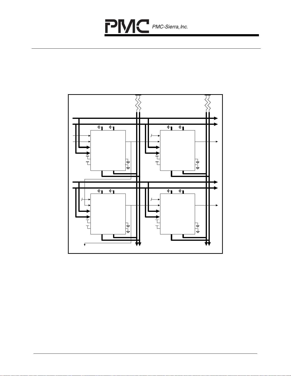
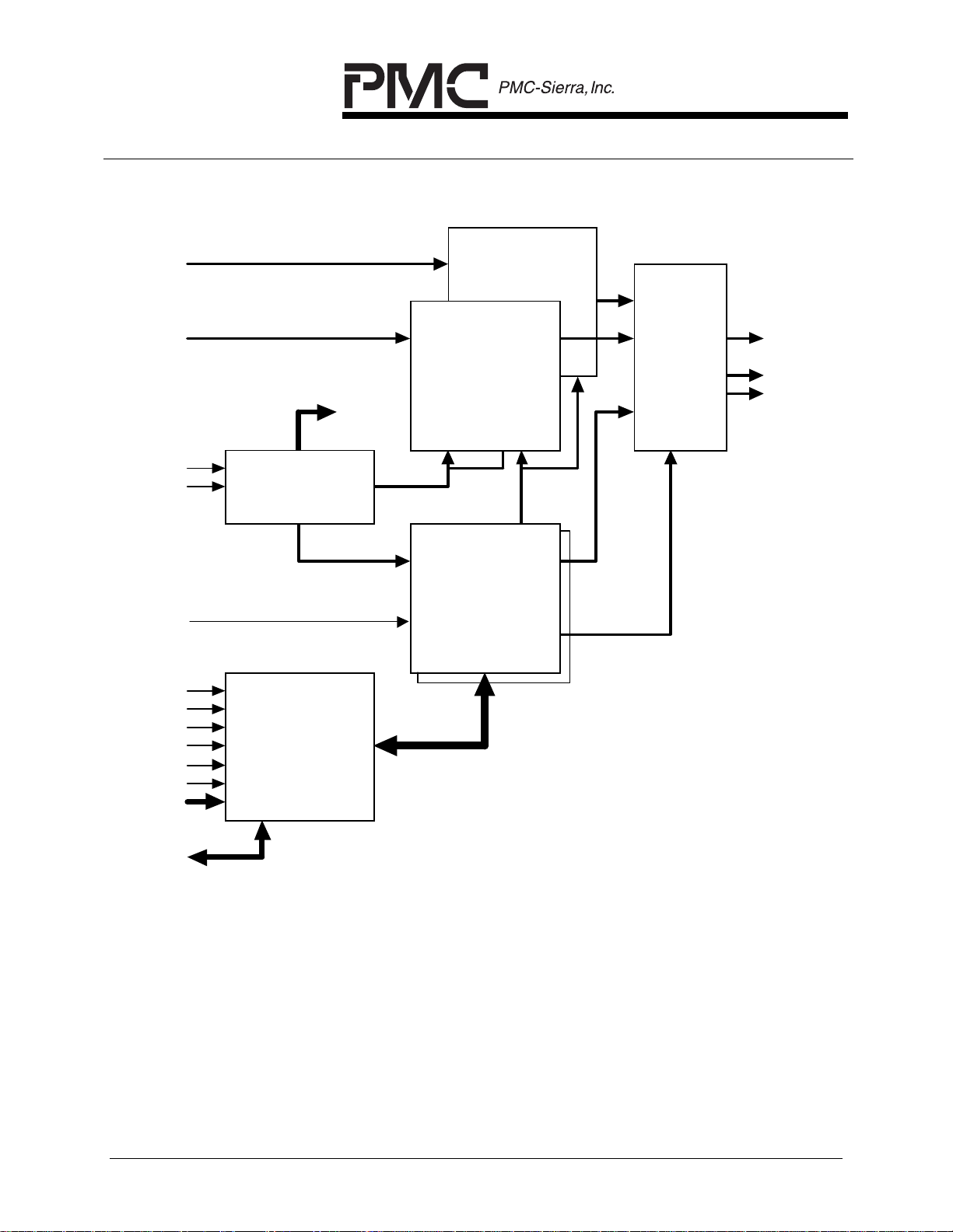
Figure 1 - 2 X 2 TUDX Switch Array Using Systolic Interconnect
SINL
TUDX
DOUTL
SINL
TUDX
DOUTL
'0'
SINR
IFP
OFP
'15'
ODEB
DOUTR
SINR
IFP
OFP
'15'
ODEB
DOUTR
'0'
'0'
'0'
SINL
SINR
SCLK
SFP
TUDX
DINT SOUTT
DINB SOUTB
OFSEB
SOBEB AOBEB
DOUTL
IFP
OFP
ODEB
DOUTR
'5' '10'
SINL
SINR
SCLK
SFP
TUDX
DINT SOUTT
DINB SOUTB
OFSEB
SOBEB AOBEB
DOUTL
IFP
OFP
ODEB
DOUTR
'5'
'10'
SCLK
SFP
DINT SOUTT
DINB SOUTB
OFSEB
SOBEB AOBEB
SCLK
SFP
DINT SOUTT
DINB SOUTB
OFSEB
SOBEB AOBEB
'15'
'15'
Systolic interconnect of TUDX devices is illustrated above. In this 2 x 2 array of
devices, PCM data is distributed left to right and gathered top to bottom with the
PCM data being re-timed as it passes through each device. Each PCM data bus
drives a single device, regardless of the size of the array and thus systolic
interconnect allows large arrays to be implemented without the use of additional
devices. In this example no systolic delay is required for the upper left hand and
lower right hand TUDX in the array. The Systolic Delay Control Register of the
lower left hand TUDX is programmed to insert a 5 clock period delay in the
DINT/DINB buses, and a 5 clock period delay in the DOUTL/DOUTR bu ses. The
PROPRIETARY AND CONFIDENTIAL TO PMC-SIERRA, INC., AND FOR ITS CUSTOMERS’ INTERNAL USE
4
PM5371 TUDX
DATA SHEET
PMC-920525 ISSUE 6 SONET/SDH TRIBUTARY UNIT CROSS CONNECT
Systolic Delay Control Register of the upper right hand TUDX is programmed to
insert a 5 clock period delay in the SINL/SINR buses, and the SOUTT/SOUTB
buses.
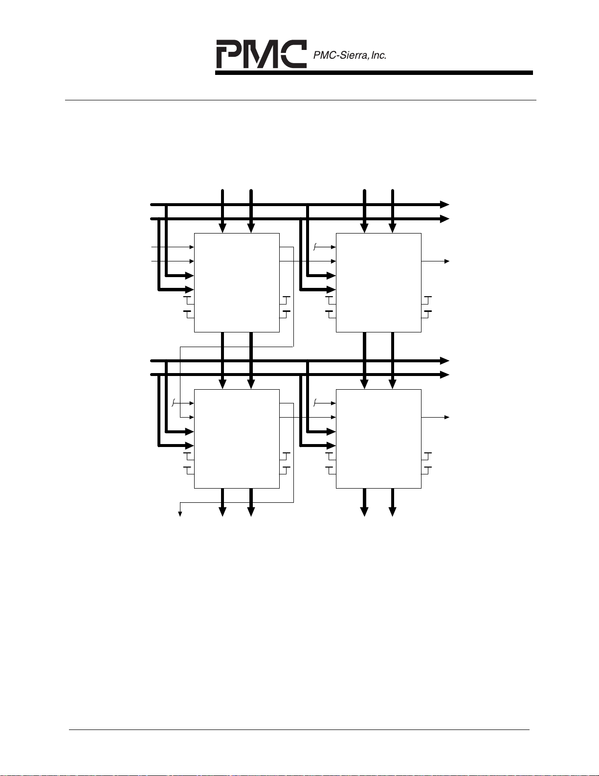
Figure 2 - 2 X 2 TUDX Switch Array Using Bused Interconnect
'5'
'0'
SINL
DOUTL
TUDX
SINR
OFP
IFP
ODEB
DOUTR
SCLK
SFP
DINT SOUTT
DINB SOUTB
OFSEB
SOBEB AOBEB
SINL
DOUTL
SINR
TUDX
DOUTR
SCLK
SFP
DINT SOUTT
DINB SOUTB
OFSEB
SOBEB AOBEB
'0'
SINL
DOUTL
SINR
TUDX
DOUTR
SINL
DOUTL
TUDX
SINR
OFP
IFP
ODEB
DOUTR
SCLK
SFP
DINT SOUTT
DINB SOUTB
OFSEB
SOBEB AOBEB
SCLK
SFP
DINT SOUTT
DINB SOUTB
OFSEB
SOBEB AOBEB
'5'
'0'
OFP
IFP
ODEB
'0'
OFP
IFP
ODEB
'5''5'
Bused interconnect of TUDX devices is illustrated above. In this 2 x 2 array of
devices, PCM data is distributed left to right on a common bus and gathered top
to bottom using a wired-OR type bus. Using this interconnect approach,
additional devices must be used to drive the distribution bus and sample the
wired-OR bus. To maximize the size of array that can be achieved using a wiredOR bus, the AOUTL and AOUTR buses may be parallel connected with the
DOUTL and DOUTR buses on a bit by bit basis in order to provide higher drive
levels. Due to the higher fan out of these buses, and the RC delay on the wiredOR bus, this approach cannot be extended to very large arrays without additional
circuitry. This bused array approach provides the minimum data delay through
the array (when a cross connection is made between the DINT/DINB buses and
PROPRIETARY AND CONFIDENTIAL TO PMC-SIERRA, INC., AND FOR ITS CUSTOMERS’ INTERNAL USE
5
PM5371 TUDX
DATA SHEET
PMC-920525 ISSUE 6 SONET/SDH TRIBUTARY UNIT CROSS CONNECT
the DOUTL/DOUTR buses) of nominally 275 clock periods versus 285 clock
periods using the systolic array approach.
Figure 3 - 2 X 2 TUDX Switch Array Using Hybrid Interconnect
'0'
'0'
'0'
SINL
SINR
SCLK
SFP
DINT SOUTT
DINB SOUTB
OFSEB
SOBEB AOBEB
TUDX
DOUTL
OFP
IFP
ODEB
DOUTR
'5'
SINL
SINR
SCLK
SFP
DINT SOUTT
DINB
OFSEB
SOBEB AOBEB
TUDX
DOUTL
OFP
IFP
SOUTB
ODEB
DOUTR
'0'
SINL
SINR
SCLK
SFP
DINT SOUTT
DINB SOUTB
OFSEB
SOBEB AOBEB
TUDX
DOUTL
OFP
IFP
ODEB
DOUTR
'5'
SINL
SINR
SCLK
SFP
DINT SOUTT
DINB
OFSEB
SOBEB AOBEB
TUDX
DOUTL
OFP
IFP
SOUTB
ODEB
DOUTR
'0'
'0'
'10''10'
A hybrid approach using a mix of bused and systolic interconnect of TUDX
devices is illustrated above. In this 2 x 2 array of devices, PCM data is distributed
left to right on a common bus and gathered top to bottom with the PCM data
being re-timed as it passes through each device. Using this interconnect
approach, additional devices must be used to drive the distribution buses. This
approach overcomes the RC delay of the wired-OR bus by using systolic
interconnect from top to bottom. In this example the Systolic Delay Control
registers in the two bottom TUDX devices are programmed to delay the
DINT/DINB buses by five clock periods to match the delay seen at the
SINL/SINR inputs to these devices.
PROPRIETARY AND CONFIDENTIAL TO PMC-SIERRA, INC., AND FOR ITS CUSTOMERS’ INTERNAL USE
6
PM5371 TUDX
DATA SHEET
PMC-920525 ISSUE 6 SONET/SDH TRIBUTARY UNIT CROSS CONNECT
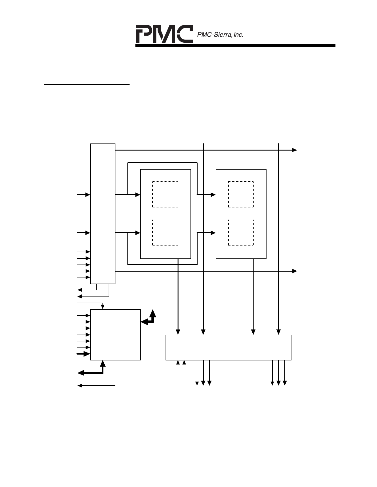
5
BLOCK DIAGRAM
Figure 4 - Overall Device
INPUT BUS FORMATTER
INPUT
DINT[8:0]
DINB[8:0]
SCLK
PAGE
SOBEB
SFP
OFSEB
BUS
FORMATTER
SWITCHING
TIME
SWITCH
ELEMENT
TIME
SWITCH
SINL[8:0]
SINR[8:0]
SOUTT[8:0]
SWITCHING
TIME
SWITCH
ELEMENT
TIME
SWITCH
SOUTB[8:0]
IFP
OFP
MBEB
RSTB
CS1B
CS2B
RDB
WRB
ALE
A[4:0]
D[7:0]
INTB
PROPRIETARY AND CONFIDENTIAL TO PMC-SIERRA, INC., AND FOR ITS CUSTOMERS’ INTERNAL USE
MICRO
INTERFACE
OUTPUT BUS FORMATTER
ODEB
AOBEB
DOUTL[8:0]
AOUTL[8:0]
COUTL
AOUTR[8:0]
DOUTR[8:0]
COUTR
7
PM5371 TUDX
DATA SHEET
PMC-920525 ISSUE 6 SONET/SDH TRIBUTARY UNIT CROSS CONNECT
Figure 5 - Each Switching Element
DINT[7:0]
DINB[7:0]
SCLK
SFP
PAGE
RSTB
TSTB
BSB
RDB
WRB
TRSB
A[1:0]
PCM
PCM
TIMING
TIMING
GENERATOR
READ ADDRESS
COMMON
BUS
INTERFACE
DATA
MEMORY
WRITE ADDRESS
CONNECTION
MEMORY
DATA
MEMORY
READ
ADDRESS
PCM
PCM
IDLE
CODE
OUTPUT
MUX
CONTROL
DOUT[7:0]
MAKE
COUT
D[7:0]
PROPRIETARY AND CONFIDENTIAL TO PMC-SIERRA, INC., AND FOR ITS CUSTOMERS’ INTERNAL USE
8

PM5371 TUDX
DATA SHEET
PMC-920525 ISSUE 6 SONET/SDH TRIBUTARY UNIT CROSS CONNECT
6
DESCRIPTION
The PM5371 TUDX SONET/SDH Tributary Unit Cross-Connect is a monolithic
integrated circuit that allows non-blocking switching of tributaries within two
SONET STS-3 or SDH STM-1 streams. Any tributary entering on either stream
can be connected to any same size tributary within either outgoing stream. The
TUDX can be programmed to cross-connect a mix of SONET VT1.5, VT2, VT3,
VT6, or STS-1 channels or SDH TU11, TU12, TU2, or TU3 channels.
Programmable idle code can also be inserted into any of these channels. The
TUDX allows cross-connection of up to 168 VT1.5 or TU11 streams, up to 126
VT2 or TU12 streams, or up to 42 VT6 or TU2 streams or any legal mix as
permitted by the SONET or SDH mappings.
The TUDX operates in conjunction with the PM5361 TUPP SONET/SDH
Tributary Unit Payload Processor which aligns SONET VTs or SDH TUs such that
they can be switched by the TUDX. Larger switches can be constructed using
arrays of TUDX devices. The TUDX is cascadable in a systolic or bused manner
and provides programmable control outputs that are useful in constructing larger
switching arrays.
No high speed clocks are required as the TUDX operates from a single 19.44
MHz clock. Parity checking is provided on input data buses and parity generation
is provided on output data buses. The TUDX is configured, controlled and
monitored via a generic 8-bit microprocessor bus interface.
The TUDX is implemented in low power, +5 Volt, CMOS technology. It has TTL
compatible inputs and outputs and is packaged in a 160 pin metric quad flat pack
(MQFP) package.
PROPRIETARY AND CONFIDENTIAL TO PMC-SIERRA, INC., AND FOR ITS CUSTOMERS’ INTERNAL USE
9
PM5371 TUDX
DATA SHEET
PMC-920525 ISSUE 6 SONET/SDH TRIBUTARY UNIT CROSS CONNECT
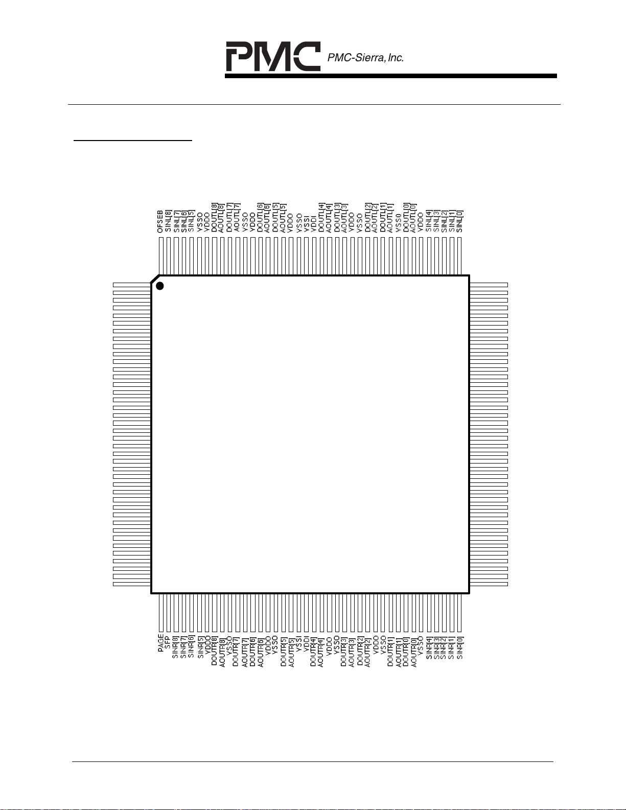
7
PIN 1
ODEB
AOBEB
DINT[0]
DINT[1]
DINT[2]
DINT[3]
DINT[4]
DINT[5]
DINT[6]
DINT[7]
DINT[8]
CS1B
CS2B
DINB[0]
VDDI
VSSI
DINB[1]
DINB[2]
DINB[3]
DINB[4]
DINB[5]
DINB[6]
DINB[7]
DINB[8]
SOBEB
VSSO
VDDO
PIN 40
PIN DIAGRAM
The TUDX is packaged in an 160 pin MQFP package having a body size of
28 mm by 28 mm and a pin pitch of 0.65 mm.
PIN 160
A[0]
A[1]
A[2]
A[3]
A[4]
Index
PIN 121
PM5371
TUDX
(TOP VIEW)
D[0]
D[1]
D[2]
D[3]
D[4]
D[5]
D[6]
D[7]
PIN 120
COUTL
VDDO
VSSO
SOUTT[0]
SOUTT[1]
SOUTT[2]
SOUTT[3]
SOUTT[4]
SOUTT[5]
SOUTT[6]
SOUTT[7]
SOUTT[8]
VDDO
VSSO
INTB
MBEB
RSTB
ALE
RDB_E
WRB_RWB
VDDI
VSSI
VSSO
SCLK
VDDO
SOUTB[0]
SOUTB[1]
SOUTB[2]
SOUTB[3]
SOUTB[4]
SOUTB[5]
SOUTB[6]
SOUTB[7]
SOUTB[8]
VDDO
VSSO
COUTR
OFP
IFP
VSSO
PIN 81
PIN 41
PROPRIETARY AND CONFIDENTIAL TO PMC-SIERRA, INC., AND FOR ITS CUSTOMERS’ INTERNAL USE
PIN 80
10
PM5371 TUDX
DATA SHEET
PMC-920525 ISSUE 6 SONET/SDH TRIBUTARY UNIT CROSS CONNECT
8
PIN DESCRIPTION
Pin Name Type Pin
Function
No.
SCLK Input 97 The system clock (SCLK) provides timing for TUDX
internal operation. SCLK is a 19.44 MHz, nominally
50% duty cycle clock.
VCLK The test vector clock (VCLK) provides timing for TUDX
production test.
SFP Input 42 The system frame pulse (SFP) determines the frame
boundaries on the DINT[8:0] and DINB[8:0] buses
(and SINL[8:0] and SINR[8:0] buses) when OFSEB is
high. SFP determines the frame boundaries on the
SOUTT[8:0] and SOUTB[8:0] buses when OFSEB is
low. SFP must be brought high once every frame (125
µs) to mark the first C1 byte of the transport envelope
frame of the buses in question. In systolic
applications where OFSEB is high, SFP marks the C1
byte of the SINL[8:0] and SINR[8:0] buses (or the
DINT[8:0] and DINB[8:0] buses) after the
programmable systolic delay has been inserted. See
the Application Examples and Functional Timing
sections for more information. SFP is sampled on the
rising edge of SCLK.
OFSEB Input 160 The active low output frame synchronization enable
(OFSEB) signal selects the system frame alignment
marked by SFP. When OFSEB is high, SFP is
coincident with the input frame pulse (IFP). When
OFSEB is low, SFP is coincident with the output frame
pulse (OFP). In most applications, OFSEB should be
held high. The OFSEB input has an integral pull up
resistor.
PROPRIETARY AND CONFIDENTIAL TO PMC-SIERRA, INC., AND FOR ITS CUSTOMERS’ INTERNAL USE
11
PM5371 TUDX
DATA SHEET
PMC-920525 ISSUE 6 SONET/SDH TRIBUTARY UNIT CROSS CONNECT
Pin Name Type Pin
Function
No.
IFP Output 82 The input frame pulse (IFP) marks the frame
boundaries on the DINT[8:0] and DINB[8:0] buses (or
SINL[8:0] and SINR[8:0] buses). IFP pulses high for a
single SCLK period to mark the first C1 byte of the
transport envelope frame of the buses in question. In
systolic array applications, IFP marks the frame
boundaries of the SINL[8:0] and SINR[8:0] buses (or
the DINT[8:0] and DINB[8:0] buses) after the
programmable systolic delay has been inserted. See
the Application Examples and Functional Timing
sections for more information. IFP is updated on the
rising edge of SCLK.
OFP Output 83 The output frame pulse (OFP) marks the frame
boundaries on the SOUTT[8:0] and SOUTB[8:0]
buses. OFP pulses high for a single SCLK period to
mark the first C1 byte of the transport envelope frame.
OFP is updated on the rising edge of SCLK.
DINT[0]
DINT[1]
DINT[2]
DINT[3]
Input 3
The top data input bus (DINT[8:0]) carries
4
5
6
SONET/SDH frame data in byte serial format. The
DINT[8] bit is a parity bit which is not passed through
the TUDX. The TUDX may be configured to check for
even or odd input bus parity and generate interrupts
when parity errors occur. The DINT[8:0] bus is
DINT[4]
DINT[5]
7
sampled on the rising edge of SCLK.
8
DINT[6]
DINT[7]
DINT[8]
PROPRIETARY AND CONFIDENTIAL TO PMC-SIERRA, INC., AND FOR ITS CUSTOMERS’ INTERNAL USE
9
10
11
12

PM5371 TUDX
DATA SHEET
PMC-920525 ISSUE 6 SONET/SDH TRIBUTARY UNIT CROSS CONNECT
Pin Name Type Pin
No.
DINB[0]
DINB[1]
DINB[2]
DINB[3]
DINB[4]
DINB[5]
DINB[6]
DINB[7]
DINB[8]
DOUTL[0]
DOUTL[1]
DOUTL[2]
DOUTL[3]
DOUTL[4]
DOUTL[5]
DOUTL[6]
Input 19
22
23
24
25
26
27
28
29
Output/
OD
Output
128
131
133
137
139
145
147
Function
The bottom data input bus (DINB[8:0]) carries
SONET/SDH frame data in byte serial format. The
DINT[8] bit is a parity bit which is not passed through
the TUDX. The TUDX may be configured to check for
even or odd input bus parity and generate interrupts
when parity errors occur. The DINB[8:0] bus is
sampled on the rising edge of SCLK.
The left data output bus (DOUTL[8:0]) carries
SONET/SDH frame data in byte serial format. The
DOUTL[8] bit is a parity bit which is generated by the
TUDX. The TUDX may be configured to generate
even or odd parity. The DOUTL[8:0] bus is updated on
the rising edge of SCLK. DOUTL may be configured
as a normal output or as an open drain output, the
latter mode being useful for constructing larger
switching arrays.
DOUTL[7]
DOUTL[8]
DOUTR[0]
DOUTR[1]
DOUTR[2]
DOUTR[3]
DOUTR[4]
DOUTR[5]
DOUTR[6]
DOUTR[7]
DOUTR[8]
PROPRIETARY AND CONFIDENTIAL TO PMC-SIERRA, INC., AND FOR ITS CUSTOMERS’ INTERNAL USE
Output/
OD
Output
151
153
73
71
67
65
61
57
53
51
48
The right data output bus (DOUTR[8:0]) carries
SONET/SDH frame data in byte serial format. The
DOUTR[8] bit is a parity bit which is generated by the
TUDX. The TUDX may be configured to generate
even or odd parity. The DOUTR[8:0] bus is updated
on the rising edge of SCLK. DOUTR may be
configured as a normal output or as an open drain
output, the latter mode being useful for constructing
larger switching arrays.
13

PM5371 TUDX
DATA SHEET
PMC-920525 ISSUE 6 SONET/SDH TRIBUTARY UNIT CROSS CONNECT
Pin Name Type Pin
No.
AOUTL[0]
AOUTL[1]
AOUTL[2]
AOUTL[3]
AOUTL[4]
AOUTL[5]
AOUTL[6]
AOUTL[7]
AOUTL[8]
AOUTR[0]
AOUTR[1]
AOUTR[2]
AOUTR[3]
AOUTR[4]
AOUTR[5]
AOUTR[6]
AOUTR[7]
AOUTR[8]
Output/
OD
Output
Output/
OD
Output
127
130
132
136
138
144
146
150
152
74
72
68
66
62
58
54
52
49
Function
The left auxiliary data output bus (AOUTL[8:0]) carries
SONET/SDH frame data in byte serial format. The
AOUTL[8] bit is a parity bit which is generated by the
TUDX. The TUDX may be configured to generate
even or odd parity. The AOUTL[8:0] bus is updated on
the rising edge of SCLK. AOUTL may be configured
as a normal output or as an open drain output, the
latter mode being useful for constructing larger
switching arrays. The AOUTL output bus carries the
same information as the DOUTL bus and the two
buses may be parallel connected on a bit by bit basis
when additional output drive is required. The AOUTL
bus is held in a high impedance mode to save power
when not enabled.
The right auxiliary data output bus (AOUTR[8:0])
carries SONET/SDH frame data in byte serial format.
The AOUTR[8] bit is a parity bit which is generated by
the TUDX. The TUDX may be configured to generate
even or odd parity. The AOUTR[8:0] bus is updated
on the rising edge of SCLK. AOUTR may be
configured as a normal output or as an open drain
output, the latter mode being useful for constructing
larger switching arrays. The AOUTR output bus
carries the same information as the DOUTR bus and
the two buses may be parallel connected on a bit by
bit basis when additional output drive is required. The
AOUTR bus is held in a high impedance mode to save
power when not enabled.
AOBEB Input 2 The active low auxiliary output bus enable (AOBEB)
signal enables the AOUTL and AOUTR when low.
When AOBEB is high, the AOUTL and AOUTR output
buses are held in a high impedance mode to save
power. The AOBEB input has an integral pull up
resistor.
PROPRIETARY AND CONFIDENTIAL TO PMC-SIERRA, INC., AND FOR ITS CUSTOMERS’ INTERNAL USE
14
PM5371 TUDX
DATA SHEET
PMC-920525 ISSUE 6 SONET/SDH TRIBUTARY UNIT CROSS CONNECT
Pin Name Type Pin
No.
SINL[0]
SINL[1]
SINL[2]
SINL[3]
SINL[4]
SINL[5]
SINL[6]
SINL[7]
SINL[8]
SINR[0]
SINR[1]
SINR[2]
SINR[3]
SINR[4]
SINR[5]
SINR[6]
SINR[7]
Input 121
122
123
124
125
156
157
158
159
Input 80
79
78
77
76
46
45
44
Function
The left systolic input bus (SINL[8:0]) carries
SONET/SDH frame data in byte serial format. The
SINL[8] bit is a parity bit which is not passed through
the TUDX. The TUDX may be configured to check for
even or odd input bus parity and generate interrupts
when parity errors occur. The SINL[8:0] bus is
sampled on the rising edge of SCLK. Data on the
SINL[8:0] bus is re-timed and may be routed to the
DOUTL[8:0] in place of information switched from the
DINT[8:0] bus, and is provided for constructing larger
switching arrays using systolic data flow.
The right systolic input bus (SINR[8:0]) carries
SONET/SDH frame data in byte serial format. The
SINR[8] bit is a parity bit which is not passed through
the TUDX. The TUDX may be configured to check for
even or odd input bus parity and generate interrupts
when parity errors occur. The SINR[8:0] bus is
sampled on the rising edge of SCLK. Data on the
SINR[8:0] bus is re-timed and may be routed to the
DOUTR[8:0] in place of information switched from the
DINB[8:0] bus, and is provided for constructing larger
switching arrays using systolic data flow.
SINR[8]
SOUTT[0]
SOUTT[1]
SOUTT[2]
SOUTT[3]
SOUTT[4]
SOUTT[5]
SOUTT[6]
SOUTT[7]
SOUTT[8]
PROPRIETARY AND CONFIDENTIAL TO PMC-SIERRA, INC., AND FOR ITS CUSTOMERS’ INTERNAL USE
43
Output 117
116
115
114
113
112
111
110
109
The left systolic output bus (SOUTT[8:0]) carries
SONET/SDH frame data in byte serial format. The
SOUTT[8] bit is a parity bit which is generated by the
TUDX. The TUDX may be configured to generate
even or odd parity. The SOUTT[8:0] bus is updated on
the rising edge of SCLK. The SOUTT[8:0] bus carries
a re-timed copy of the information sampled on the
DINT[8:0] bus and is provided for constructing larger
switching arrays using systolic data flow. The SOUTT
bus can be disabled to save power when not used.
15
PM5371 TUDX
DATA SHEET
PMC-920525 ISSUE 6 SONET/SDH TRIBUTARY UNIT CROSS CONNECT
Pin Name Type Pin
Function
No.
SOUTB[0]
SOUTB[1]
SOUTB[2]
SOUTB[3]
Output 95
94
93
92
The right systolic output bus (SOUTB[8:0]) carries
SONET/SDH frame data in byte serial format. The
SOUTB[8] bit is a parity bit which is generated by the
TUDX. The TUDX may be configured to generate
even or odd parity. The SOUTB[8:0] bus is updated
on the rising edge of SCLK. The SOUTB[8:0] bus
SOUTB[4]
SOUTB[5]
91
90
carries a re-timed copy of the information sampled on
the DINB[8:0] bus and is provided for constructing
larger switching arrays using systolic data flow. The
SOUTB[6]
SOUTB[7]
SOUTB[8]
89
88
87
SOUTB bus can be disabled to save power when not
used.
SOBEB Input 30 The active low systolic output bus enable (SOBEB)
signal enables the SOUTT and SOUTB output buses
when low. When SOBEB is high, the SOUTT and
SOUTB output buses are held in a high impedance
mode to save power. The SOBEB input has an
integral pull up resistor.
COUTL Output 120 The left control output signal (COUTL) is a software
programmable control stream (on a per timeslot basis)
that can be used for controlling external hardware
when constructing larger switching arrays. After reset,
COUTL defaults to always high until otherwise
programmed. COUTL is updated on the rising edge of
SCLK.
COUTR Output 84 The right control output bus (COUTR) is a software
programmable control stream (on a per timeslot basis)
that can be used for controlling external hardware
when constructing larger switching arrays. After reset,
COUTR defaults to always high until otherwise
programmed. COUTR is updated on the rising edge
of SCLK.
PROPRIETARY AND CONFIDENTIAL TO PMC-SIERRA, INC., AND FOR ITS CUSTOMERS’ INTERNAL USE
16

PM5371 TUDX
DATA SHEET
PMC-920525 ISSUE 6 SONET/SDH TRIBUTARY UNIT CROSS CONNECT
Pin Name Type Pin
Function
No.
ODEB Input 1 The active low open drain enable (ODEB) signal
configures the DOUTL and DOUTR output buses as
open drain outputs when low. When ODEB is high,
the DOUTL and DOUTR output buses are configured
as normal outputs. The ODEB input has an integral
pull up resistor.
PAGE Input 41 The page select (PAGE) signal selects the connection
memory pages that are used to control connections
within the TUDX. When PAGE is low, connection
memory page 0 of each switching element is used.
When PAGE is high, connection memory page 1 of
each switching element is used. The PAGE input is
sampled on the rising edge of SCLK. Internally, a
change in the active connection memory page is held
off until the next switching frame boundary (a delay of
up to approximately 14 us). While such a page swap
is pending, accesses to the connection memory by
the microprocessor should be avoided. Such a
pending page swap results in a connection memory
busy indication which can be polled. The PAGE input
has an integral pull down resistor.
MBEB Input 105 The active low Motorola bus enable (MBEB) signal
configures the TUDX for Motorola bus mode where
the RDB/E signal functions as E, and the WRB/RWB
signal functions as RWB. When MBEB is high, the
TUDX is configured for Intel bus mode where the
RDB/E signal functions as RDB. The MBEB input has
an integral pull up resistor.
CS1B Input 17 The active low chip select #1 (CS1B) signal is low
during TUDX register accesses.
If CS1B and CS2B are not required (i.e., registers
accesses are controlled using the RDB and WRB
signals only), CS1B and CS2B must be connected to
an inverted version of the RSTB input.
PROPRIETARY AND CONFIDENTIAL TO PMC-SIERRA, INC., AND FOR ITS CUSTOMERS’ INTERNAL USE
17
PM5371 TUDX
DATA SHEET
PMC-920525 ISSUE 6 SONET/SDH TRIBUTARY UNIT CROSS CONNECT
Pin Name Type Pin
Function
No.
CS2B Input 18 The active low chip select #2 (CS2B) signal is low
during TUDX register accesses.
If CS1B and CS2B are not required (i.e., registers
accesses are controlled using the RDB and WRB
signals only), CS1B and CS2B must be connected to
an inverted version of the RSTB input.
RDB Input 102 The active low read enable (RDB) signal is low during
TUDX register read accesses while in Intel bus mode
(MBEB = 1). The TUDX drives the D[7:0] bus with the
contents of the addressed register while RDB, CS1B,
and CS2B are low.
E Input 102 The active high external access (E) signal is high
during TUDX register access while in Motorola bus
mode (MBEB = 0).
WRB Input 101 The active low write strobe (WRB) signal is low during
a TUDX register write accesses while in In tel bus
mode (MBEB = 1). The D[7:0] bus contents are
clocked into the addressed register on the rising WRB
edge while CS1B and CS2B are low.
RWB The read/write select (RWB) signal selects between
TUDX register read and write accesses while in
Motorola bus mode (MBEB = 0). The TUDX drives the
D[7:0] bus with the contents of the addressed register
while CS1B and CS2B are low and RWB and E are
high. The D[7:0] bus contents are clocked into the
addressed register on the falling E edge while CS1B
and CS2B and RWB are low.
PROPRIETARY AND CONFIDENTIAL TO PMC-SIERRA, INC., AND FOR ITS CUSTOMERS’ INTERNAL USE
18

PM5371 TUDX
DATA SHEET
PMC-920525 ISSUE 6 SONET/SDH TRIBUTARY UNIT CROSS CONNECT
Pin Name Type Pin
No.
D[0]
D[1]
D[2]
D[3]
D[4]
D[5]
D[6]
D[7]
A[0]
A[1]
A[2]
A[3]
A[4]/TRS
I/O 31
32
33
34
37
38
39
40
Input 12
13
14
15
16
Function
The bidirectional data bus (D[7:0]) is used during
TUDX register read and write accesses.
The address bus (A[4:0]) selects specific registers
during TUDX register accesses.
The test register select (TRS) signal discriminates
between normal and test mode register accesses.
TRS is high during test mode register accesses, and
is low during normal mode register accesses. The
TRS input has an integral pull down resistor.
RSTB Input 104 The active low reset (RSTB) signal provides an
asynchronous TUDX reset. RSTB is a Schmitt
triggered input with an integral pull up resistor.
ALE Input 103 The address latch enable (ALE) is active high and
latches the address bus (A[4:0]) and TRS when low.
When ALE is high, the internal address latches are
transparent. It allows the TUDX to interface to a
multiplexed address/data bus. The ALE input has an
integral pull up resistor.
INTB OD
Output
106 The active low interrupt (INTB) signal goes low when
a TUDX interrupt source is active. INTB returns high
when the interrupt is acknowledged via an appropriate
register access. The INTB output is an open drain
output.
PROPRIETARY AND CONFIDENTIAL TO PMC-SIERRA, INC., AND FOR ITS CUSTOMERS’ INTERNAL USE
19
PM5371 TUDX
DATA SHEET
PMC-920525 ISSUE 6 SONET/SDH TRIBUTARY UNIT CROSS CONNECT
Pin Name Type Pin
No.
VDDI1
VDDI2
VDDI3
VDDI4
VSSI1
VSSI2
VSSI3
VSSI4
VDDO1
VDDO2
VDDO3
VDDO4
VDDO5
Power 20
60
100
140
Ground 21
59
99
141
Power 36
47
55
63
69
Function
The core power (VDDI) pins should be connected to a
well decoupled +5 V DC in common with VDDO.
The core ground (VSSI) pins should be connected to
GND in common with VSSO.
The pad ring power (VDDO) pins should be connected
to a well decoupled +5 V DC in common with VDDI.
VDDO6
VDDO7
VDDO8
VDDO9
VDDO10
VDDO11
VDDO12
VDDO13
VDDO14
86
96
108
119
126
135
143
148
154
PROPRIETARY AND CONFIDENTIAL TO PMC-SIERRA, INC., AND FOR ITS CUSTOMERS’ INTERNAL USE
20

PM5371 TUDX
DATA SHEET
PMC-920525 ISSUE 6 SONET/SDH TRIBUTARY UNIT CROSS CONNECT
Pin Name Type Pin
No.
VSSO1
VSSO2
VSSO3
VSSO4
VSSO5
VSSO6
VSSO7
VSSO8
VSSO9
VSSO10
VSSO11
VSSO12
VSSO13
Ground 35
50
56
64
70
75
81
85
98
107
118
129
134
Function
The pad ring ground (VSSO) pins should be
connected to GND in common with VSSI.
VSSO14
VSSO15
VSSO16
142
149
155
Notes on Pin Description:
1. All TUDX inputs and bidirectionals present minimum capacitive loading and
operate at TTL logic levels.
2. All TUDX digital outputs and bidirectionals have 2 mA drive capability, except
the INTB, SOUTT[8:0], SOUTB[8:0] outputs and D[7:0] bidirectionals, which
have 4 mA drive capability, and the DOUTL[8:0], DOUTR[8:0], AOUTL[8:0]
and AOUTR[8:0] outputs, which have 8 mA drive capability.
3. The VSSO and VSSI ground pins are not internally connected together.
Failure to connect these pins externally may cause malfunction or damage
the TUDX.
PROPRIETARY AND CONFIDENTIAL TO PMC-SIERRA, INC., AND FOR ITS CUSTOMERS’ INTERNAL USE
21

PM5371 TUDX
DATA SHEET
PMC-920525 ISSUE 6 SONET/SDH TRIBUTARY UNIT CROSS CONNECT
4. The VDDO and VDDI power pins are not internally connected together.
Failure to connect these pins externally may cause malfunction or damage
the TUDX.
PROPRIETARY AND CONFIDENTIAL TO PMC-SIERRA, INC., AND FOR ITS CUSTOMERS’ INTERNAL USE
22

PM5371 TUDX
DATA SHEET
PMC-920525 ISSUE 6 SONET/SDH TRIBUTARY UNIT CROSS CONNECT
9
FUNCTIONAL DESCRIPTION
9.1 Input Bus Formatter
The input bus formatter captures data sampled on the DINT and DINB buses
and distributes this data to the two switching elements within the TUDX. The
input bus formatter also re-times this captured data, delaying it 5 clock cycles
and outputs copies of the information from the DINT and DINB buses on the
SOUTT and SOUTB buses, respectively. When systolic interconnect is not used,
the SOUTT and SOUTB buses can be held in a high impedance mode to save
power by strapping the SOBEB input appropriately.
For systolic array applications, a programmable delay element provides
additional delay of 5, 10, or 15 clock cycles in the DINT and DINB data paths or
in the SOUTT and SOUTB data paths. For more information on the systolic array
application, see the Application Examples section.
The input bus formatter also provides timing signals for the other blocks within
the TUDX. The system clock, SCLK, is buffered and distributed to the switching
elements and the output bus formatter. Frame pulses for the incoming and
outgoing data streams, IFP and OFP, are generated with alignment dictated by
the system frame pulse input, SFP. These frame pulses are buffered and
distributed to the switching elements. One can select whether the SFP input will
generate a coincident IFP or OFP pulse using the OFSEB configuration input.
This option is useful when constructing larger switches using arrays of TUDX
devices. The input bus formatter generates the IFP and OFP outputs. Proper
generation of IFP and OFP requires that the input bus formatter be initialized
once per SONET/SDH frame (125 µs) by a pulse on the SFP input. In the
absence of a periodic SFP input, outputs IFP and OFP are not generated
correctly.
9.2 Output Bus Formatter
The output bus formatter selects the data to be output on the DOUTL and
DOUTR buses. This data is gathered from the switching elements or the SINL
and SINR buses, on a per timeslot basis, as programmed within the switching
elements. The output bus formatter also drives the COUTL and COUTR outputs
with control signals that are programmable, on a per timeslot basis, via the
switching elements. The delay from the SINL or SINR buses to the DOUTL or
DOUTR buses is 5 clock cycles. The delay from the DINT or DINB buses to the
DOUTL or DOUTR buses for a straight through connection (from each input
timeslot to its equivalent output timeslot) is 275 clock cycles (corresponding to
PROPRIETARY AND CONFIDENTIAL TO PMC-SIERRA, INC., AND FOR ITS CUSTOMERS’ INTERNAL USE
23

PM5371 TUDX
DATA SHEET
PMC-920525 ISSUE 6 SONET/SDH TRIBUTARY UNIT CROSS CONNECT
one SONET STS-3 or SDH STM-1 row of 270 bytes plus 5 clock cycles of retiming delay).
For systolic array applications, a programmable delay element provides an
additional delay of 5, 10 or 15 clock cycles in the SINL and SINR data paths or in
the DOUTL and DOUTR data paths.
The output bus formatter can be configured to drive the DOUTL and DOUTR
buses rail to rail or drive the DOUTL and DOUTR buses as open drain outputs.
The open drain output option is selected by strapping the ODEB input
appropriately. A second set of output buses, the AOUTL and AOUTR buses,
carry the same data as the DOUTL and DOUTR buses, respectively. These pairs
of buses can be strapped together on a bit by bit basis in order to provide higher
drive capability. This is particularly useful in implementing wired-OR type output
buses. When not required, the AOUTL and AOUTR buses can be held in a high
impedance mode to save power by strapping the AOBEB input appropriately.
9.3 Switching Element
Each switching element implements two single stage, non-blocking time switches
that each process an STS-3 or STM-1 rate stream. The channelization of each
time switch corresponds to 9 byte columns within the SONET/SDH frame. Thus
the basic switching granularity is 576 kbit/s (9 x 64 kbit/s). The frame rate of
each time switch corresponds to 1/9th of the SONET/SDH frame rate. The frame
rate is thus 13.89 us (125 us ÷ 9). The frame processed by each time switch
corresponds to 270 byte rows within the SONET/SDH frame. Two time switches
that connect to a common output bus are grouped within each switching element
such that they can share a common connection memory.
Cross-connection of the various size s of VTs (or TUs) is accomplished by setting
up group connections. A VT1.5, for example, occupies three 9 byte columns
within the SONET/SDH frame and thus a VT1.5 cross-connection can be set up
by making three connections of 576 kbit/s each. A TU12, in contrast, occupies
four 9 byte columns and thus a TU12 cross-connection can be set up by making
four connections of 576 kbit/s each. The time switches are double buffered so as
to exhibit constant frame delay which preserves byte sequence integrity during
group connections, regardless of the size and routing of the group connection.
Note that the switching elements assume that the tributaries to be crossconnected occupy fixed 9 byte columns within the SONET STS-3 or SDH STM-1
frame. In order to cross-connect VT1.5, VT2, VT3, or VT6 tributaries within an
STS-3 stream or TU11, TU12, TU2, or TU3 tributaries within an STM-1 stream,
the STS-3 or STM-1 stream must be preprocessed with the PM5361 TUPP or an
equivalent circuit. Such processing must ensure that all STS-1 or AU-3 or AU-4
PROPRIETARY AND CONFIDENTIAL TO PMC-SIERRA, INC., AND FOR ITS CUSTOMERS’ INTERNAL USE
24

PM5371 TUDX
DATA SHEET
PMC-920525 ISSUE 6 SONET/SDH TRIBUTARY UNIT CROSS CONNECT
pointer adjustments are absorbed into VT or TU pointer adjustments such that
the resulting STS-3 or STM-1 frame has its VTs or TUs occupying fixed,
appropriately phase aligned positions with respect to the overall transport
envelope frame, ready for switching.
The TUDX consists of two switching elements, each containing two time
switches, which results in a 2 by 2 array of time switches. Data from each of the
DINT and DINB buses is distributed and written into the two time switches in the
corresponding row. Data is collected for output on the DOUTL and DOUTR
buses from each of the two time switches in the corresponding column or
switching element, or from the associated SINL or SINR bus. The source of data
is programmable on a per timeslot basis within the switching elements. As only
one time switch in a column can source data during a given timeslot, time switch
outputs are powered down, rather than outputting data, 50% of the time.
In addition to implementing cross-connections, the switching elements are also
capable of inserting programmable idle code into outgoing timeslots. This idle
code is arbitrarily programmable on a per timeslot basis and thus through proper
programming, a fixed, arbitrary idle code can be inserted into any outgoing VT or
TU. This capability can be used to insert tributary path AIS or to insert fixed
codes used for system diagnostic purposes.
The switching elements are implemented in a classical manner with each having
a pair of data memories, a common connection memory, timing generator, output
multiplexer, and common bus interface.
9.3.1 Data Memories
The data memories each consist of two 270 x 8 RAMs implementing a double
buffered switch core. During each switching frame, data is written into sequential
locations in one page of memory, and read from the other page of memory
based on a list of addresses provided by the connection memory. At each
switching frame boundary (every 270 bytes) the function of the two memory
pages is reversed. The data memory is 8 bits wide to allow byte wide data to be
routed through the switching element. Two data memories are required, one for
each of the input buses connected to the switching element.
9.3.2 Connection Memory
The connection memory consists of a double buffered 270 x 13 RAM. During
each switching frame, information is sequentially read from the active memory
page and used to generate the read addresses for the data memory and control
the output multiplexer. Either connection memory can be written to or read from
PROPRIETARY AND CONFIDENTIAL TO PMC-SIERRA, INC., AND FOR ITS CUSTOMERS’ INTERNAL USE
25

PM5371 TUDX
DATA SHEET
PMC-920525 ISSUE 6 SONET/SDH TRIBUTARY UNIT CROSS CONNECT
via the common bus interface and thus its contents are programmable. In this
manner, the switching action of the data memory and output multiplexer are
programmable on a per timeslot basis. Normally one would only write to the
inactive page, performing all the programming required to implement ones
desired connections, and then trigger a page swap at a frame boundary. Use of
a double buffered connection memory and active page swapping allows tributary
connections (which are implemented as group connections of 576 kbit/s
timeslots) to be coherently made or broken.
9.3.3 Timing Generator
The timing generator consists of a frame counter and clock dividers. Buffered
versions of the various derived clocks are distributed to other blocks within the
switching element as are several phase delayed versions of the frame count, as
required in such a pipelined processing structure.
9.3.4 Output Multiplexer
The output multiplexer consists of logic that selects the source of information to
be output from the switching element. Such selection is controlled on a per
timeslot basis by the connection memory and is thus programmable. Output data
can be routed from the data memory, from the lower order bits of the connection
memory, or a null value can be inserted when no connection is being made. The
null value is chosen on the fly to minimize power dissipation. The ability to
source data from the connection memory itself is how programmable idle code
insertion is provided. During those timeslots when programmable idle code is
being inserted or no connection is being made through the switching element,
the reading of data from the data memory is suppressed in order to save power.
In addition to its selection function, the output multiplexer also re-times control
signals sourced by the connection memory that are used to control the output
bus formatter of the complete device.
9.3.5 Common Bus Interface
The common bus interface allows microprocessor access to the switching
element connection memory. Access is indirect, via registers located in the
common bus interface. Each connection memory access takes up to eight SCLK
cycles to complete as circuitry waits for opportunities when the connection
memory locations in question are not being accessed during the normal course
of switching element operation.
PROPRIETARY AND CONFIDENTIAL TO PMC-SIERRA, INC., AND FOR ITS CUSTOMERS’ INTERNAL USE
26

PM5371 TUDX
DATA SHEET
PMC-920525 ISSUE 6 SONET/SDH TRIBUTARY UNIT CROSS CONNECT
9.4 Microprocessor Interface
The microprocessor interface block provides normal and test mode registers, and
the logic required to connect to the microprocessor interface. The normal mode
registers are required for normal operation, and test mode registers are used to
enhance the testability of the TUDX. The register set is accessed as follows:
Table 1 - Register Memory Map
Address Register
00H TUDX Master Configuration
01H TUDX Connection Memory Control
02H TUDX Clock Monitor
03H TUDX Master Reset/Revision ID
04H TUDX Parity Configuration
05H TUDX Parity Error Interrupt Enable
06H TUDX Parity Error Interrupt Status
07H TUDX Systolic Delay Control
08H Left Switch Element Connection Address High
09H Left Switch Element Connection Address Low
0AH Left Switch Element Connection Data High
0BH Left Switch Element Connection Data Low
0CH Right Switch Element Connection Address High
0DH Right Switch Element Connection Address Low
0EH Right Switch Element Connection Data High
0FH Right Switch Element Connection Data Low
10H TUDX Master Test
11H-1FH Reserved for Test
For all register accesses, CS1B and CS2B must be low.
PROPRIETARY AND CONFIDENTIAL TO PMC-SIERRA, INC., AND FOR ITS CUSTOMERS’ INTERNAL USE
27

PM5371 TUDX
DATA SHEET
PMC-920525 ISSUE 6 SONET/SDH TRIBUTARY UNIT CROSS CONNECT
10
NORMAL MODE REGISTER DESCRIPTION
Normal mode registers are used to configure and monitor the operation of the
TUDX. Nor mal mode registers (as opposed to test mode registers) are selected
when TRS (A[4]) is low.
Notes on Normal Mode Register Bits:
1. Writing values into unused register bits has no effect. However, to ensure
software compatibility with future, feature-enhanced versions of the product,
unused register bits must be written with logic 0. Reading back unused bits
can produce either a logic 1 or a logic 0; hence unused register bits should be
masked off by software when read.
2. All configuration bits that can be written into can also be read back. This
allows the processor controlling the TUDX to determine the programming
state of the block.
3. Writeable normal mode register bits are cleared to logic 0 upon reset unless
otherwise noted.
4. Writing into read-only normal mode register bit locations does not affect
TUDX operation unless otherwise noted.
PROPRIETARY AND CONFIDENTIAL TO PMC-SIERRA, INC., AND FOR ITS CUSTOMERS’ INTERNAL USE
28

PM5371 TUDX
DATA SHEET
PMC-920525 ISSUE 6 SONET/SDH TRIBUTARY UNIT CROSS CONNECT
Register 00H: Master Configuration
Bit Type Function Default
Bit 7 Unused X
Bit 6 Unused X
Bit 5 Unused X
Bit 4 Unused X
Bit 3 R/W SELEN 0
Bit 2 R/W SEREN 0
Bit 1 R/W COUTLEN 0
Bit 0 R/W COUTREN 0
This register is used to enable the switching elements and the generation of the
programmable control output signals.
COUTLEN:
The COUTLEN bit enables the generation of the COUTL signal under control
of the left switching element; the switching element that routes between the
DINT and DOUTL buses, or DINB and DOUTL buses, respectively. After
reset, the COUTL signal is forced high, until the COUTLEN bit is set high.
COUTREN:
The COUTREN bit ernables the generation of the COUTR signal under
control of the right switching element; the switching element that routes
between the DINT and DOUTR buses, or DINB and DOUTR buses,
respectively. After reset, the COUTR signal is forced high, until the
COUTREN bit is set high.
SELEN:
The SELEN bit enables operation of the left switching element (the switching
element that routes between the DINT and DOUTL buses, or DINB and
DOUTL buses, respectively). After reset, the left switching element is held
reset to save power, until the SELEN bit is set high.
SEREN:
The SEREN bit enables operation of the right switching element (the
switching element that routes between the DINT and DOUTR buses, or DINB
PROPRIETARY AND CONFIDENTIAL TO PMC-SIERRA, INC., AND FOR ITS CUSTOMERS’ INTERNAL USE
29

PM5371 TUDX
DATA SHEET
PMC-920525 ISSUE 6 SONET/SDH TRIBUTARY UNIT CROSS CONNECT
and DOUTR buses, respectively). After reset, the right switching element is
held reset to save power, until the SEREN bit is set high.
Note that a switching element cannot be programmed until it is enabled.
While a switching element is disabled, the output bus formatter will not select
it as a source of data, thus passing through data from the SINL or SINR bus,
as appropriate.
PROPRIETARY AND CONFIDENTIAL TO PMC-SIERRA, INC., AND FOR ITS CUSTOMERS’ INTERNAL USE
30

PM5371 TUDX
DATA SHEET
PMC-920525 ISSUE 6 SONET/SDH TRIBUTARY UNIT CROSS CONNECT
Register 01H: Connection Memory Control
Bit Type Function Default
Bit 7 Unused X
Bit 6 Unused X
Bit 5 Unused X
Bit 4 Unused X
Bit 3 Unused X
Bit 2 R APAGE X
Bit 1 R EPAGE X
Bit 0 R/W IPAGE 0
This register is used to control and monitor the selection of the active connection
memory page.
IPAGE:
The IPAGE bit is used to internally select the active connection memory page.
When IPAGE is set high, page 1 is selected. When IPAGE is cleared low,
page 0 is selected, provided that the external PAGE input is also low.
EPAGE:
The EPAGE bit can be read to determine the state of the external PAGE
input.
APAGE:
The APAGE bit can be read to determine the active connection memory
page. APAGE is the logical OR of the IPAGE bit and the PAGE input (which
can be read via the EPAGE bit).
PROPRIETARY AND CONFIDENTIAL TO PMC-SIERRA, INC., AND FOR ITS CUSTOMERS’ INTERNAL USE
31

PM5371 TUDX
DATA SHEET
PMC-920525 ISSUE 6 SONET/SDH TRIBUTARY UNIT CROSS CONNECT
Register 02H: Clock Monitor
Bit Type Function Default
Bit 7 Unused X
Bit 6 Unused X
Bit 5 Unused X
Bit 4 Unused X
Bit 3 R DINBA X
Bit 2 R DINTA X
Bit 1 R SFPA X
Bit 0 R SCLKA X
This register is used to monitor the integrity of TUDX timing input signals.
SCLKA:
The SCLKA bit indicates that SCLK is active when high. SCLKA is set high
by a low to high transition on SCLK and is set low immediately following a
read of this register. This bit is intended to be polled to detect a system failure
that freezes the SCLK signal.
SFPA:
The SFPA bit indicates that SFP is active when high. SFPA is set high by a
SCLK sampled low to high transition on SFP and is set low immediately
following a read of this register. This bit is intended to be polled to detect a
system failure that freezes the SFP signal.
DINTA:
The DINTA bit indicates that DINT bus is active when high. DINTA is set high
when all bits of the DINT[8:0] bus have changed low to high after sampled by
SCLK and is set low immediately following a read of this register. This bit is
intended to be polled to detect a system failure that freezes any of the
DINT[8:0] bits.
DINBA:
The DINBA bit indicates that DINB bus is active when high. DINBA is set
high when all bits of the DINB[8:0] bus have changed low to high after
sampled by SCLK and is set low immediately following a read of this register.
PROPRIETARY AND CONFIDENTIAL TO PMC-SIERRA, INC., AND FOR ITS CUSTOMERS’ INTERNAL USE
32

PM5371 TUDX
DATA SHEET
PMC-920525 ISSUE 6 SONET/SDH TRIBUTARY UNIT CROSS CONNECT
This bit is intended to be polled to detect a system failure that freezes any of
the DINB[8:0] bits.
PROPRIETARY AND CONFIDENTIAL TO PMC-SIERRA, INC., AND FOR ITS CUSTOMERS’ INTERNAL USE
33

PM5371 TUDX
DATA SHEET
PMC-920525 ISSUE 6 SONET/SDH TRIBUTARY UNIT CROSS CONNECT
Register 03H: Master Reset/Revision ID
Bit Type Function Default
Bit 7 R/W RESET 0
Bit 6 R ID[6] 0
Bit 5 R ID[5] 0
Bit 4 R ID[4] 0
Bit 3 R ID[3] 0
Bit 2 R ID[2] 0
Bit 1 R ID[1] 0
Bit 0 R ID[0] 0
This register allows the revision of the TUDX to be read by software permitting
graceful migration to support for newer, feature enhanced versions of the TUDX,
should revision of the TUDX occur. This register also allows the TUDX to be
reset.
ID[6:0]:
The ID bits can be read to provide a binary TUDX revision number.
RESET:
The RESET bit allows the TUDX to be reset under software control. If the
RESET bit is a logic 1, the entire TUDX is held in reset. This bit is not selfclearing; therefore, a logic 0 must be written to bring the TUDX out of reset.
Holding the TUDX in a reset state effectively puts it into a low powe r, stand-by
mode. A hardware reset clears the RESET bit, thus de-asserting the
software reset.
PROPRIETARY AND CONFIDENTIAL TO PMC-SIERRA, INC., AND FOR ITS CUSTOMERS’ INTERNAL USE
34

PM5371 TUDX
DATA SHEET
PMC-920525 ISSUE 6 SONET/SDH TRIBUTARY UNIT CROSS CONNECT
Register 04H: Parity Configuration
Bit Type Function Default
Bit 7 R/W TODDO 0
Bit 6 R/W BODDO 0
Bit 5 R/W LODDO 0
Bit 4 R/W RODDO 0
Bit 3 R/W TODDI 0
Bit 2 R/W BODDI 0
Bit 1 R/W LODDI 0
Bit 0 R/W RODDI 0
This register is used to configure the parity polarity expected on input buses and
generated on output buses.
RODDI, LODDI, BODDI, TODDI:
These bits configure the parity expected on input buses. When high, odd
parity is expected. When low, even parity is expected. The RODDI bit
configures the SINR bus, the LODDI bit configures the SINL bus, the BODDI
bit configures the DINB bus, and the TODDI bit configures the DINT bus.
RODDO, LO DDO, BODDO, TODDO:
These bits configure the parity generated on output buses. When high, odd
parity is generated. When low, even parity is generated. The RODDO bit
configures the DOUTR bus, the LODDO bit configures the DOUTL bus, the
BODDO bit configures the SOUTB bus, and the TODDO bit configures the
SOUTT bus. Note that bad parity can be introduced for diagnostic purposes
by manipulating these bits.
PROPRIETARY AND CONFIDENTIAL TO PMC-SIERRA, INC., AND FOR ITS CUSTOMERS’ INTERNAL USE
35

PM5371 TUDX
DATA SHEET
PMC-920525 ISSUE 6 SONET/SDH TRIBUTARY UNIT CROSS CONNECT
Register 05H: Parity Error Interrupt Enable
Bit Type Function Default
Bit 7 Unused X
Bit 6 Unused X
Bit 5 Unused X
Bit 4 Unused X
Bit 3 R/W TPERE 0
Bit 2 R/W BPERE 0
Bit 1 R/W LPERE 0
Bit 0 R/W RPERE 0
This register is used to enable parity errors to generate interrupts.
RPERE, LPERE, BPERE, TPERE:
These bits enable parity errors on their respective input buses to generate
interrupts. When high, parity error interrupt generation is enabled. When low,
parity error interrupt generation is disabled, however, the parity error
indications may still be polled. The RPERE bit configures the SINR bus, the
LPERE bit configures the SINL bus, the BPERE bit configures the DINB bus,
and the TPERE bit configures the DINT bus.
PROPRIETARY AND CONFIDENTIAL TO PMC-SIERRA, INC., AND FOR ITS CUSTOMERS’ INTERNAL USE
36

PM5371 TUDX
DATA SHEET
PMC-920525 ISSUE 6 SONET/SDH TRIBUTARY UNIT CROSS CONNECT
Register 06H: Parity Error Interrupt Status
Bit Type Function Default
Bit 7 Unused X
Bit 6 Unused X
Bit 5 Unused X
Bit 4 Unused X
Bit 3 R TPERI X
Bit 2 R BPERI X
Bit 1 R LPERI X
Bit 0 R RPERI X
This register is used to identify the source of a parity error interrupt and
acknowledge such an interrupt.
RPERI, LPERI, BPERI, TPERI:
These bits are set high when a parity error on their respective input buses is
detected. If enabled, an interrupt will also occur. These bits are cleared low
immediately following a read of this register causing any active interrupt to be
de-asserted. These bits are latching and will remain high following the
detection of a single parity error until this register is read. These bits retain
their event capture functionality when interrupt generation is disabled and
may be polled to detect parity errors. The RPERI bit monitors the SINR bus,
the LPERI bit monitors the SINL bus, the BPERI bit monitors the DINB bus,
and the TPERI bit monitors the DINT bus.
PROPRIETARY AND CONFIDENTIAL TO PMC-SIERRA, INC., AND FOR ITS CUSTOMERS’ INTERNAL USE
37

PM5371 TUDX
DATA SHEET
PMC-920525 ISSUE 6 SONET/SDH TRIBUTARY UNIT CROSS CONNECT
Register 07H: Systolic Delay Control
Bit Type Function Default
Bit 7 Unused X
Bit 6 Unused X
Bit 5 R/W SOUTEN 0
Bit 4 R/W SINEN 0
Bit 3 R/W DOUTEN 0
Bit 2 R/W DINEN 0
Bit 1 R/W DS1 0
Bit 0 R/W DS0 0
This register is used to control the delay inserted into the SOUT, SIN, DOUT, and
DIN data paths. This feature is used in systolic array applications to match data
skew at the array boundaries for up to a 4 X 4 array without using external
components.
SOUTEN, SINEN, DOUTEN, DINEN:
These bits control the programmable delay elements, one of which is shared
between DIN and SOUT, the other between SIN and DOUT. The delay is
inserted when these bits are set high. It is not appropriate to set both DINEN
and SOUTEN high simultaneously, nor SINEN and DOUTEN. The delay
value for both delay elements is controlled by the DS1 and DS0 bits.
DS1, DS0:
The DS1 and DS0 bits select the delay value for both delay elements as
described in the following table:
Table 2 - Systolic Delay Control
DS1 DS0 Delay V alue
0 0 0 Not appropriate if any enable bits are logic 1.
01 5
10 10
11 15
PROPRIETARY AND CONFIDENTIAL TO PMC-SIERRA, INC., AND FOR ITS CUSTOMERS’ INTERNAL USE
38

PM5371 TUDX
DATA SHEET
PMC-920525 ISSUE 6 SONET/SDH TRIBUTARY UNIT CROSS CONNECT
When constructing a 4 X 4 systolic array, program the individual TUDX devices
with the following binary codes:
Table 3 - Systolic Array Delay Control
12 3 4
1
2
3
4
000000 010001 010010 110011
000101 000000 000000 100010
000110 000000 000000 100001
001111 001010 001001 000000
The systolic delays are applied to the TUDXs at the array periphery. In the first
(or top) row, the SINL[8:0] and SINR[8:0] buses are delayed by 0, 5, 10, and 15
additional clock periods (moving from left to right across the first row). In the
fourth (or bottom row, the DOUTL[8:0] and DOUTR[8:0] buses are delayed by 15,
10, 5, and 0 clock periods (again moving from left to right). In the first (or
leftmost) column, the DINT[8:0] and DINB[8:0] buses are delayed by 0, 5, 10,
and 15 clock periods (moving from the top to the bottom of the first column). In
the fourth (or rightmost) column, the SOUTT[8:0] and SOUTB[8:0] buses are
delayed by 15, 10, 5, and 0 clock periods (again moving from top to bottom). The
above array produces a 35 SCLK cycle delay between the input and output
busses.
PROPRIETARY AND CONFIDENTIAL TO PMC-SIERRA, INC., AND FOR ITS CUSTOMERS’ INTERNAL USE
39

PM5371 TUDX
DATA SHEET
PMC-920525 ISSUE 6 SONET/SDH TRIBUTARY UNIT CROSS CONNECT
Register 08H,0CH: Connection Address High
Bit Type Function Default
Bit 7 R/W RWB X
Bit 6 Unused X
Bit 5 Unused X
Bit 4 Unused X
Bit 3 Unused X
Bit 2 Unused X
Bit 1 R/W CMP X
Bit 0 R/W CA8 X
This register is used to trigger accesses to switching element connection
memory and specify the memory location to be accessed.
RWB:
The RWB bit selects the type of connection memory access. The completion
of a write access to this register will trigger a read of a switching element
connection memory if RWB is high. If RWB is low, the completion of a write
access to this register will trigger a write to a switching element connection
memory. The data to be written or data read is passed through the
Connection Data Low and Connection Data High registers. The connection
memory address and page to be accessed is determined by the Connection
Address Low and Connection Address High registers. A connection memory
access requires several SCLK cycles; completion of an access is indicated by
the BUSY bit in the Connection Data High register. The instantiation of the
Connection Address and Data registers utilized selects the switching element
to be programmed. Registers 08H-0BH control the left switching element,
and registers 0CH-0FH control the right switching element.
CMP:
The CMP bit, selects the connection memory page to be accessed. Selection
of which connection memory page is active is done using the PAGE input or
the Connection Memory Control register. A logic 1 on this bit directs the read
or write operation to the active page memory page. A logic 0 on this bit
directs the read or write operation to the inactive memory page. Accesses to
the active CM memory page are likely to be much longer than accesses to
the inactive memory page. This is because of the continual read accesses by
PROPRIETARY AND CONFIDENTIAL TO PMC-SIERRA, INC., AND FOR ITS CUSTOMERS’ INTERNAL USE
40

PM5371 TUDX
DATA SHEET
PMC-920525 ISSUE 6 SONET/SDH TRIBUTARY UNIT CROSS CONNECT
the internal timeslot counter to the active memory page. Each CM page is
broken into two independent banks of 135 X13. This increases the micro's
access rate to active memory pages.
CA8:
The CA8 bit , together with the CA7-CA0 bits of the Connection Address Low
register selects the connection memory location to be accessed.
PROPRIETARY AND CONFIDENTIAL TO PMC-SIERRA, INC., AND FOR ITS CUSTOMERS’ INTERNAL USE
41

PM5371 TUDX
DATA SHEET
PMC-920525 ISSUE 6 SONET/SDH TRIBUTARY UNIT CROSS CONNECT
Register 09H,0DH: Connection Address Low
Bit Type Function Default
Bit 7 R/W CA7 X
Bit 6 R/W CA6 X
Bit 5 R/W CA5 X
Bit 4 R/W CA4 X
Bit 3 R/W CA3 X
Bit 2 R/W CA2 X
Bit 1 R/W CA1 X
Bit 0 R/W CA0 X
This register is used to specify the memory location in switching element
connection memory to be accessed.
CA7-CA0:
The CA7-CA0 bits , together with the CA8 bit of the Connection Address High
register select the connection memory location to be accessed. Connection
memory locations correspond to outgoing timeslots on the DOUTL or DOUTR
buses. Each timeslot carries a 9 x 64 kbit/s channel corresponding to one
column in a 270 x 9 byte STS-3 (or STM-1) frame. Connection memory
address 0 corresponds to the first column (the column that starts with the A1
byte of STS-1 #1 in an STS-3 stream) and address 269 corresponds to the
last column (the column that ends with the last SPE byte of STS-1 #3 in an
STS-3 stream). See the sections on Operation, Functional Timing, and
Application Examples.
PROPRIETARY AND CONFIDENTIAL TO PMC-SIERRA, INC., AND FOR ITS CUSTOMERS’ INTERNAL USE
42

PM5371 TUDX
DATA SHEET
PMC-920525 ISSUE 6 SONET/SDH TRIBUTARY UNIT CROSS CONNECT
Register 0AH,0EH: Connection Data High
Bit Type Function Default
Bit 7 R BUSY 0
Bit 6 Unused X
Bit 5 Unused X
Bit 4 R/W COUT X
Bit 3 R/W MAKE X
Bit 2 R/W IDLE X
Bit 1 R/W TOP X
Bit 0 R/W CD8 X
This register is used to detect when accesses to switching element connection
memory are permitted and to pass data to connection memory during such
accesses.
BUSY:
The BUSY bit allows one to detect when a connection memory access is
permitted.
When a switching element connection memory access is triggered by writing
to the Connection Address High register, the BUSY bit is set high. The BUSY
bit returns low when the access is complete. In the case of a write access,
this means that one may begin manipulation of the various registers in
preparation for a subsequent access. In the case of a read, this means that
one may read valid data from the Connection Data High and Low registers
and then prepare for a subsequent access. While an access is in progress,
i.e. when the BUSY bit is high, no new data should be written to any of the
Connection Address or Connection Data registers. A connection memory
access requires a maximum of ~400 ns (i.e. eight 19.44 MHz clock cycles).
When a page swap is triggered via the Connection Memory Control register
or via the PAGE input, the BUSY bit is also set high. At the next switch frame
boundary (which can be up to ~ 14 us later) the page swap is implemented
and the BUSY bit returns low. During this intervening time, while a page
swap is pending, no new data should be written to any of the Connection
Address or Connection Data registers. Similarly, one should not trigger a
PROPRIETARY AND CONFIDENTIAL TO PMC-SIERRA, INC., AND FOR ITS CUSTOMERS’ INTERNAL USE
43

PM5371 TUDX
DATA SHEET
PMC-920525 ISSUE 6 SONET/SDH TRIBUTARY UNIT CROSS CONNECT
page swap until any previously initiated connection memory access is
complete.
COUT:
The COUT bit controls one of the COUTL or COUTR signals during the
corresponding outgoing timeslot on the DOUTL or DOUTR buses. By
programming the COUT bit, one can control the COUTL or COUTR signals
on a per timeslot basis. The COUT bit of the left switching element controls
the COUTL signal, the COUT bit of the right switching element controls the
COUTR signal.
MAKE:
The MAKE bit enables a connection to be established through the switching
element in question for the corresponding outgoing timeslot. When the MAKE
bit is set high, the switching element in question routes the corresponding
timeslot onto the data path leading to the DOUTL or DOUTR buses, as
appropriate. The source bus and timeslot to be connected are selected by
the TOP bit and CD8-CD0 bits. When the MAKE bit is set low, the switching
element in question is held inactive to save power during the processing
interval for the corresponding timeslot. When the MAKE bit is set low, data
entering on the SINL or SINR bus is routed to the DOUTL or DOUTR bus, as
appropriate for the switching element in question.
IDLE:
The IDLE bit enables the insertion of programmable idle code into the
corresponding outgoing timeslot. When the IDLE bit is set high, the switching
element in question routes the connection data programmed through the
CD8-CD0 bits onto the data path leading to the DOUTL or DOUTR buses, as
appropriate. The mapping is CD7 to DOUTL[7] or DOUTR[7], CD6 to
DOUTL[6] or DOUTR[6], and so on. CD8 is not mapped to DOUTL[8] or
DOUTR[8]; DOUTL[8] and DOUTR[8] are parity bits generated by the TUDX.
In this case the connection data is not used to specify an incoming timeslot to
be connected to an outgoing timeslot, but is used directly to form a
programmable idle code. When the IDLE bit is set low, the switching element
in question implements a normal time switching function. Note that the IDLE
bit has no effect unless the MAKE bit is set high.
TOP
The TOP bit , selects the source of the connection to be established through
the switching element in question for the corresponding outgoing timeslot.
When TOP is high, the DINT bus is selected. When TOP is low, the DINB bus
PROPRIETARY AND CONFIDENTIAL TO PMC-SIERRA, INC., AND FOR ITS CUSTOMERS’ INTERNAL USE
44

PM5371 TUDX
DATA SHEET
PMC-920525 ISSUE 6 SONET/SDH TRIBUTARY UNIT CROSS CONNECT
is selected. Note that the TOP bit has no effect unless the MAKE bit is set
high.
CD8
The CD8 bit , together with the CD7-CD0 bits of the Connection Data Low
register hold the connection memory data transfe rred dur ing connection
memory accesses.
Note that data read from the Connection Data High and Low registers reflects
the data read from the connection memories during the most recently
triggered read operation. It typically does not reflect the last data written to
these registers.
PROPRIETARY AND CONFIDENTIAL TO PMC-SIERRA, INC., AND FOR ITS CUSTOMERS’ INTERNAL USE
45

PM5371 TUDX
DATA SHEET
PMC-920525 ISSUE 6 SONET/SDH TRIBUTARY UNIT CROSS CONNECT
Register 0BH,0FH: Connection Data Low
Bit Type Function Default
Bit 7 R/W CD7 X
Bit 6 R/W CD6 X
Bit 5 R/W CD5 X
Bit 4 R/W CD4 X
Bit 3 R/W CD3 X
Bit 2 R/W CD2 X
Bit 1 R/W CD1 X
Bit 0 R/W CD0 X
This register is used to pass data to connection memory during switching
element connection memory accesses.
CD7-CD0:
The CD7-CD0 bits, together with the CD8 bit of the Connection Data High
register hold the connection memory data transfe rred dur ing connection
memory accesses. Connection memory data corresponds to incoming
timeslots on the DINT or DINB buses. Each timeslot carries a 9 x 64 kbit/s
channel corresponding to one column in a 270 x 9 byte STS-3 (or STM-1)
frame. Connection memory data of 0 corresponds to the first column (the
column that starts with the A1 byte of STS-1 #1 in an STS-3 stream) and data
of 269 corresponds to the last column (the column that ends with the last
SPE byte of STS-1 #3 in an STS-3 stream). Connection memory data may
also correspond to a programmable idle code. See the sections on
Operation, Functional Timing, and Application Examples.
Note that data read from the Connection Data High and Low registers reflects
the data read from the connection memories during the most recently
triggered read operation. It typically does not reflect the last data written to
these registers.
PROPRIETARY AND CONFIDENTIAL TO PMC-SIERRA, INC., AND FOR ITS CUSTOMERS’ INTERNAL USE
46

PM5371 TUDX
DATA SHEET
PMC-920525 ISSUE 6 SONET/SDH TRIBUTARY UNIT CROSS CONNECT
11
TEST FEATURES DESCRIPTION
Simultaneously asserting the CS1B, CS2B, RDB and WRB inputs low causes all
output pins and the data bus to be held in a high-impedance state, provided that
the MBEB input is held high. This test feature may be used for board testing.
Test mode registers are used to apply test vectors during production testing of
the TUDX. Test mode registers (as opposed to normal mode registers) are
selected when TRS (A[4]) is high.
Test mode registers may also be used for board testing. When all of the
constituent Telecom System Blocks within the TUDX are placed in test mode 0,
device inputs may be read and device outputs may be forced via the
microprocessor interface (refer to the section "Test Mode 0" for details).
Table 4 - Test Mode Register Memory Map
Address Register
00H-0FH Normal Mode Registers
10H TUDX Master Test
11H-13H Input Formatter Test Registers
14H-17H Output Formatter Test Registers
18H Left Switch Element Test Register 0
19H Left Switch Element Test Register 1
1AH Left Switch Element Test Register 2
1BH Left Switch Element Test Register 3
1CH Right Switch Element Test Register 0
1DH Right Switch Element Test Register 1
1EH Right Switch Element Test Register 2
1FH Right Switch Element Test Register 3
Notes on Test Mode Register Bits:
1. Writing values into unused register bits has no effect. However, to ensure
software compatibility with future, feature-enhanced versions of the product,
unused register bits must be written with logic 0. Reading back unused bits
PROPRIETARY AND CONFIDENTIAL TO PMC-SIERRA, INC., AND FOR ITS CUSTOMERS’ INTERNAL USE
47

PM5371 TUDX
DATA SHEET
PMC-920525 ISSUE 6 SONET/SDH TRIBUTARY UNIT CROSS CONNECT
can produce either a logic 1 or a logic 0; hence unused register bits should be
masked off by software when read.
2. Writable test mode register bits are not initialized upon reset unless otherwise
noted.
PROPRIETARY AND CONFIDENTIAL TO PMC-SIERRA, INC., AND FOR ITS CUSTOMERS’ INTERNAL USE
48

PM5371 TUDX
DATA SHEET
PMC-920525 ISSUE 6 SONET/SDH TRIBUTARY UNIT CROSS CONNECT
Register 10H: Master Test
Bit Type Function Default
Bit 7 Unused X
Bit 6 Unused X
Bit 5 Unused X
Bit 4 W PMCTST X
Bit 3 W MOTOTST 0
Bit 2 R/W IOTST 0
Bit 1 W HIZDATA 0
Bit 0 R/W HIZIO 0
This register is used to enable TUDX test features. All bits, except PMCTST, are
reset to zero by a reset of the TUDX.
HIZIO,HIZDATA:
The HIZIO and HIZDATA bits control the three state modes of the TUDX .
While the HIZIO bit is a logic 1, all output pins of the TUDX except the data
bus are held in a high-impedance state. The microprocessor interface is still
active. While the HIZDATA bit is a logic 1, the data bus is also held in a highimpedance state which inhibits microprocessor read cycles.
IOTST:
The IOTST bit is used to allow normal microprocessor access to the test
registers and control the test mode in each TSB block in the TUDX for board
level testing. When IOTST is a logic 1, all blocks are held in test mode and
the microprocessor may write to a block's test mode 0 registers to manipulate
the outputs of the block and consequently the device outputs (refer to the "I/O
Test Mode Details" in the "Test Features" section).
MOTOTST:
The MOTOTST bit is used to test the MOTOROLA interface. When
MOTOTST is logic 1 and the MBEB input is logic 0 the OFSEB and SOBEB
inputs are used to replace the function of E and RWB, respectively. This is
done because the fixed waveform shapes assigned to the RDB_E and
WRB_RWB inputs can not be used to test MOTOROLA type microprocessor
PROPRIETARY AND CONFIDENTIAL TO PMC-SIERRA, INC., AND FOR ITS CUSTOMERS’ INTERNAL USE
49

PM5371 TUDX
DATA SHEET
PMC-920525 ISSUE 6 SONET/SDH TRIBUTARY UNIT CROSS CONNECT
interface logic. This mode is also used to test the D.C. drive capability of the
D[7:0] device pins.
PMCTST:
The PMCTST bit is used to configure the TUDX for PMC's manufacturing
tests. When PMCTST is set to logic 1, the TUDX microprocessor port
becomes the test access port used to run the PMC "canned" manufacturing
test vectors. The PMCTST bit is logically "ORed" with the IOTST bit, and can
only be cleared by setting CSB to logic 1.
PROPRIETARY AND CONFIDENTIAL TO PMC-SIERRA, INC., AND FOR ITS CUSTOMERS’ INTERNAL USE
50

PM5371 TUDX
DATA SHEET
PMC-920525 ISSUE 6 SONET/SDH TRIBUTARY UNIT CROSS CONNECT
11.1 I/O T est Mode
In the I/O test mode, the TUDX allows the logic levels on the device inputs to be
read through the microprocessor interface, and allows the device outputs to be
forced to either logic level through the microprocessor interface.
To enable the I/O test mode, the IOTST bit in the Master Test register is set to
logic 1.
Reading the following address locations returns the values for the indicated
inputs.
Table 5 - Reading Input Pin Values
Addr Bit 7 Bit 6 Bit 5 Bit 4 Bit 3 Bit 2 Bit 1 Bit 0
11H DINT[7] DINT[6] DINT[5] DINT[4] DINT[3] DINT[2] DINT[1] DINT[0]
12H DINB[7] DINB[6] DINB[5] DINB[4] DINB[3] DINB[2] DINB[1] DINB[0]
13H SCLK OFSEB SFP PAGE SOBEB DINB[8] DINT[8]
14H SINR[7] SINR[6] SINR[5] SINR[4] SINR[3] SINR[2] SINR[1] SINR[0]
15H AOBEB ODEB SINL[8]
16H SINL[7] SINL[6] SINL[5] SINL[4] SINL[3] SINL[2] SINL[1] SINL[0]
17H AOBEB ODEB SINR[8]
Writing the following address locations forces the outputs to the value in the
corresponding bit position:
Table 6 - Forcing Ouput Pin Values
Addr Bit 7 Bit 6 Bit 5 Bit 4 Bit 3 Bit 2 Bit 1 Bit 0
11H SOT[7] SOT[6] SOT[5] SOT[4] SOT[3] SOT[2] SOT[1] SOT[0]
12H SOB[7] SOB[6] SOB[5] SOB[4] SOB[3] SOB[2] SOB[1] SOB[0]
13H INTB OFP IFP SOB[8] SOT[8]
14H DOR[7] DOR[6] DOR[5] DOR[4] DOR[3] DOR[2] DOR[1] DOR[0]
15H COUTL DOL[8]
16H DOL[7] DOL[6] DOL[5] DOL[4] DOL[3] DOL[2] DOL[1] DOL[0]
17H COUTR DOR[8]
SOUTT is abbreviated to SOT to fit the above table.
SOUTB is abbreviated to SOB to fit the above table.
PROPRIETARY AND CONFIDENTIAL TO PMC-SIERRA, INC., AND FOR ITS CUSTOMERS’ INTERNAL USE
51

PM5371 TUDX
DATA SHEET
PMC-920525 ISSUE 6 SONET/SDH TRIBUTARY UNIT CROSS CONNECT
DOUTL is abbreviated to DOL to fit the above table.
DOUTR is abbreviated to DOR to fit the above table.
PROPRIETARY AND CONFIDENTIAL TO PMC-SIERRA, INC., AND FOR ITS CUSTOMERS’ INTERNAL USE
52

PM5371 TUDX
DATA SHEET
PMC-920525 ISSUE 6 SONET/SDH TRIBUTARY UNIT CROSS CONNECT
12
OPERATION
12.1 Basic Connection Memory Access
12.1.1 Connection Memory Read
To perform a connection memory read, one selects an address in the range 0269, encodes this as a 9 bit binary value and writes the lower 8 bits of this value
into the Connection Address Low register. The upper bit of this address is then
written into the Connection Address High register while also setting the RWB bit
in the Connection Address High register to 1 and selecting the desired
connection memory page. The trailing edge of the write to the Connection
Address High register triggers the internal connection memory access by the
TUDX and a read access is performed due to the RWB bit being a 1. The access
requires up to ~400 ns to complete and one must wait this long or poll the BUSY
bit in the Connection Data High register to determine that the access has
completed. Once the access has completed as indicated by the BUSY bit going
low, one can then read valid data in the Connection Data High and Low registers
which was extracted during the just completed connection memory read access.
Note that once a connection memory read access is triggered by writing to the
Connection Address High register, no further changes should be made to the
Connection Address High or Low registers until the access has completed.
Similarly, prior to initiating any read access, one must ensure that any previously
triggered access or page swap has completed before one begins to alter relevant
register contents.
12.1.2 Connection Memory Write
To perform a connection memory write, one selects the data to be written and
writes this data into the Connection Data High and Low registers. One then
selects an address in the range 0-269, encodes this as a 9 bit binary va lue and
writes the lower 8 bits of this value into the Connection Address Low register.
The upper bit of this address is then written into the Connection Address High
register while also setting the RWB bit in the Connection Address High register to
0 and selecting the desired connection memory page. The trailing edge of the
write to the Connection Address High register triggers the internal connection
memory access by the TUDX and a write access is performed due to the RWB
bit being a 0. The access requires up to ~400 ns to complete and one must wait
this long or poll the BUSY bit in the Connection Data High register to determine
that the access has completed. Once the access has completed as indicated by
the BUSY bit going low, one is free to begin set up for subsequent accesses.
PROPRIETARY AND CONFIDENTIAL TO PMC-SIERRA, INC., AND FOR ITS CUSTOMERS’ INTERNAL USE
53

PM5371 TUDX
DATA SHEET
PMC-920525 ISSUE 6 SONET/SDH TRIBUTARY UNIT CROSS CONNECT
Note that once a connection memory write access is triggered by writing to the
Connection Address High register, no further changes should be made to the
Connection Address High or Low registers or the Connection Data High or Low
registers until the access has completed. Similarly, prior to initiating any write
access, one must ensure that any previously triggered access or page swap has
completed before one begins to alter relevant register contents.
12.2 Connection Set Up
To set up a connection, one must program connections for all of the 9 x 64 kbit/s
timeslots that together constitute the tributary being connected. In the case of a
VT1.5 or TU11, three connections must be programmed; in the case of a VT2 or
TU12, four connections; and in the case of a VT6 or TU2, twelve connections.
Any channel or tributary that can be constructed as a multiple of the basic 9 x 64
kbit/s timeslot may be switched using group connections.
To illustrate connection set up, consider the steps required to set up a VT1.5
cross-connection. For example, consider cross-connecting VT1.5 #1 of VT group
#1 in STS-1 #1 of the STS-3 stream on the DINT bus to VT1.5 #4 of VT group #7
in STS-1 #3 of the STS-3 stream on the DOUTL bus. The incoming VT1.5
occupies the 13th, 100th, and 187th columns in the STS-3 frame as shown in
Figure 1. The outgoing VT1.5 occupies the 96th, 183rd and 270th columns in the
STS-3 frame. To make the connection one must connect each incoming timeslot
occupied by the incoming VT1.5 to each outgoing timeslot occupied by the
outgoing VT1.5 in the order in which the timeslots are utilized, i.e. 13th timeslot to
96th timeslot, 100th timeslot to 183rd timeslot, and 187th timeslot to 270th
timeslot. The info rmation that must be written to the Connection Address and
Connection Data registers of the left switching element is as follows:
PROPRIETARY AND CONFIDENTIAL TO PMC-SIERRA, INC., AND FOR ITS CUSTOMERS’ INTERNAL USE
54

PM5371 TUDX
DATA SHEET
PMC-920525 ISSUE 6 SONET/SDH TRIBUTARY UNIT CROSS CONNECT
Table 7 - Connection Set Up
Connection
Address
Connection
Data
Connection/Notes
005FH 0A0CH 13th timeslot cross connects to 96th timeslot
CA=95, CD=12
COUT=0, MAKE=1, IDLE=0, TOP=1
00B6H 0963H 100th timeslot cross connects to 183rd timeslot
CA=182, CD=99
COUT=0, MAKE=1, IDLE=0, TOP=1
010DH 09BAH 187th timeslot cross connects to 270th timeslot
CA=269, CD=186
COUT=0, MAKE=1, IDLE=0, TOP=1
Figure 6 - SONET STS-3 Carrying VT1.5 Within STS-1
COL
ROW 1
123456789101112131415 270
A1 A1 A1 A2 A2 A2 C1 C1 C1 POH POH POH SPE SPE SPE SPE
2
B1 - - E1 - - F1 - - POH POH POH SPE SPE SPE SPE
3
D1 - - D2 - - D3 - H1 H1 H1 H2 H2 H2 H3 H3 H3 POH POH POH SPE SPE SPE SPE
4
B2 B2 B2 K1 - - K2 - - POH
5
D4 - - D5 - - D6 - - POH POH POH SPE SPE SPE SPE
6
D7 - - D8 - - D9 - - POH POH POH SPE SPE SPE SPE
7
D10 - - D11 - - D12 - -
8
Z1 - - Z2 - - E2 - - POH POH POH SPE SPE SPE SPE
9
First of 3 columns occupied by
VT1.5 #1 of VT group #1 of
STS-1 #1 of an STS-3 stream
(column set is 13, 100, 187)
POH
POH POH SPE SPE SPE SPE
POH POH SPE SPE SPE SPE
POH
POH POH SPE SPE SPE SPE
265 266
SPE SPE
SPE SPE
SPE SPE
SPE SPE
• • • •
SPE SPE
SPE SPE
SPE SPE
SPE SPE
SPE SPE
Last of 3 columns occupied by
VT1.5 #4 of VT group #7 of
STS-1 #3 of an STS-3 stream
(column set is 96, 183, 270)
267
SPE
SPE
SPE
SPE
SPE
SPE
SPE
SPE
SPE
268 269
SPE SPE
SPE SPE
SPE SPE
SPE SPE
SPE SPE
SPE SPE
SPE SPE
SPE SPE
SPE SPE
PROPRIETARY AND CONFIDENTIAL TO PMC-SIERRA, INC., AND FOR ITS CUSTOMERS’ INTERNAL USE
55

PM5371 TUDX
DATA SHEET
PMC-920525 ISSUE 6 SONET/SDH TRIBUTARY UNIT CROSS CONNECT
Figure 7 - SDH STM-1 Carrying TU12 Within VC3/AU3
COL
ROW 1
123456789101112131415 270
A1 A1 A1 A2 A2 A2 C1 C1 C1 POH POH POH SPE SPE SPE SPE
2
B1 - - E1 - - F1 - - POH POH POH SPE SPE SPE SPE
D1 - - D2 - - D3 - -
3
H1 H1 H1 H2 H2 H2 H3 H3 H3 POH POH POH SPE SPE SPE SPE
4
B2 B2 B2 K1 - - K2 - - POH
5
D4 - - D5 - - D6 - - POH POH POH SPE SPE SPE SPE
6
D7 - - D8 - - D9 - - POH POH POH SPE SPE SPE SPE
7
D10 - - D11 - - D12 - -
8
Z1 - - Z2 - - E2 - - POH POH POH SPE SPE SPE SPE
9
First of 4 columns occupied by
TU12 #1 of TUG2 #1 of VC3/
AU3 #1 of an STM-1 stream
(column set is 13, 76,142, 208)
POH
POH POH SPE SPE SPE SPE
POH POH SPE SPE SPE SPE
POH
POH POH SPE SPE SPE SPE
Figure 8 - SDH STM-1 Carrying TU12 Within TUG3
COL
ROW 1
1234567891011 192021 270
A1 A1 A1 A2 A2 A2 C1 C1 C1 POH SPE SPE SPE SPE SPE
2
B1 - - E1 - - F1 - - POH SPE SPE SPE SPE SPE
D1 - - D2 - - D3 - -
3
H1 H1 H1 H2 H2 H2 H3 H3 H3 POH SPE SPE SPE SPE SPE
4
B2 B2 B2 K1 - - K2 - - POH
5
D4 - - D5 - - D6 - - POH SPE SPE SPE SPE SPE
6
D7 - - D8 - - D9 - - POH SPE SPE SPE SPE SPE
7
D10 - - D11 - - D12 - -
8
Z1 - - Z2 - - E2 - - POH SPE SPE SPE SPE SPE
9
First of 4 columns occupied by
TU12 #1 of TUG2 #1 of
TUG3 #1 of an STM-1 stream
(column set is 19, 82, 145, 208)
POH
SPE SPE SPE SPE SPE
• • • •
SPE SPE SPE SPE SPE
POH
SPE SPE SPE SPE SPE
265 266
SPE SPE
SPE SPE
SPE SPE
SPE SPE
• • • •
SPE SPE
SPE SPE
SPE SPE
SPE SPE
SPE SPE
Last of 4 columns occupied by
TU12 #3 of TUG2 #7 of VC3/
AU3 #3 of an STM-1 stream
(column set is 75, 141, 207, 270)
265 266
SPE SPE
SPE SPE
SPE SPE
SPE SPE
• • • •
SPE SPE
SPE SPE
SPE SPE
SPE SPE
SPE SPE
Last of 4 columns occupied by
TU12 #3 of TUG2 #7 of
TUG3 #3 of an STM-1 stream
(column set is 81, 144, 207, 270)
267
SPE
SPE
SPE
SPE
SPE
SPE
SPE
SPE
SPE
267
SPE
SPE
SPE
SPE
SPE
SPE
SPE
SPE
SPE
268 269
SPE SPE
SPE SPE
SPE SPE
SPE SPE
SPE SPE
SPE SPE
SPE SPE
SPE SPE
SPE SPE
268 269
SPE SPE
SPE SPE
SPE SPE
SPE SPE
SPE SPE
SPE SPE
SPE SPE
SPE SPE
SPE SPE
12.3 Idle Code Insertion
To enable idle code insertion, one must program idle code insertion for all of the
9 x 64 kbit/s timeslots that together constitute the tributary being affected. In the
case of a VT1.5 or TU11, three insertions must be programmed; in the case of a
VT2 or TU12, four insertions; and in the case of a VT6 or TU2, twelve insertions.
Any channel or tributary that can be constructed as a multiple of the basic 9 x 64
kbit/s timeslot may be overwritten with idle code using a group insertion.
To illustrate idle code insertion set up, consider the steps required to set up idle
code insertion into a TU12. For example, consider inserting idle code into TU12
#1 of TUG2 #1 in VC3/AU3 #1 of the STM-1 stream on the DOUTR bus. The
outgoing TU12 occupies the 13th, 76th, 142nd and 208th columns in the STM-1
PROPRIETARY AND CONFIDENTIAL TO PMC-SIERRA, INC., AND FOR ITS CUSTOMERS’ INTERNAL USE
56

PM5371 TUDX
DATA SHEET
PMC-920525 ISSUE 6 SONET/SDH TRIBUTARY UNIT CROSS CONNECT
frame. To enable idle code insertion one must program idle code insertion for
each outgoing timeslot occupied by the outgoing TU12. One would normally
program the same idle code value for all timeslots occupied by the TU12 and
choose a value that results in a useful status indication in the TU12, such as all
ones for tributary path AIS. The information that must be written to the
Connection Address and Connection Data registers of the right switching
element is as follows:
Table 8 - Idle Code Insertion
Connection
Address
Connection
Data
Connection/Notes
000CH 0DFFH All ones inserted into 13th timeslot
CA=12, CD=all ones
COUT=0, MAKE=1, IDLE=1, TOP=0
004BH 0DFFH All ones inserted into 76th timeslot
CA=75, CD=all ones
COUT=0, MAKE=1, IDLE=1, TOP=0
008DH 0DFFH All ones inserted into 142nd timeslot
CA=141, CD=all ones
COUT=0, MAKE=1, IDLE=1, TOP=0
00CFH 0DFFH All ones inserted into 208th timeslot
CA=207, CD=all ones
COUT=0, MAKE=1, IDLE=1, TOP=0
PROPRIETARY AND CONFIDENTIAL TO PMC-SIERRA, INC., AND FOR ITS CUSTOMERS’ INTERNAL USE
57

PM5371 TUDX
DATA SHEET
PMC-920525 ISSUE 6 SONET/SDH TRIBUTARY UNIT CROSS CONNECT
13
FUNCTIONAL TIMING
The DINT, DINB, SINL and SINR buses are nominally frame aligned, as are the
DOUTL, DOUTR, SOUTT, and SOUTB buses. This alignment may be altered for
use in systolic array applications when required. There is nominally a five clock
cycle offset between the frame alignment of the input buses and the output
buses. The SFP input, which synchronizes the frame alignment of the TUDX
PCM buses, can be configured to mark the frame alignment of either the input or
output buses, depending on the strapping of the OFSEB input. The timing of the
AOUTL and AOUTR buses is identical to that of the DOUTL and DOUTR buses,
respectively.
PROPRIETARY AND CONFIDENTIAL TO PMC-SIERRA, INC., AND FOR ITS CUSTOMERS’ INTERNAL USE
58

PM5371 TUDX
DATA SHEET
PMC-920525 ISSUE 6 SONET/SDH TRIBUTARY UNIT CROSS CONNECT
Figure 9 - Input/Output Bus Timing (systolic delay disabled)
SCLK
SFP (OFSEB=1)
SFP (OFSEB=0)
IFP
DINT[8:0]
DINB[8:0]
SINL[8:0]
SINR[8:0]
OFP
DOUTL[8:0]/
AOUTL[8:0]
DOUTR[8:0]/
AOUTR[8:0]
SOUTT[8:0]
SOUTB[8:0]
A1A1 A2A2 A2C1C1 C1A1
A1A1 A2A2 A2C1C1 C1A1
A1A1 A2A2 A2C1C1 C1A1
A1A1 A2A2 A2C1C1 C1A1
A1A1 A2A2 A2C1C1 C1A1
A1A1 A2A2 A2C1C1 C1A1
A1A1 A2A2 A2C1C1 C1A1
A1A1 A2A2 A2C1C1 C1A1
The input/output bus timing diagram (Figure 9) illustrates the frame alignment
through the TUDX when the programmable systolic delay is set to zero for every
bus. SFP must occur once every SONET/SDH frame (9 rows), and is illustrated
marking the C1 byte position in the incoming stream (DINT, DINB) or the
outgoing stream (SOUTT, SOUTB) as selected by the OFSEB input. Output
OFP always marks the C1 byte position in the SOUTT and SOUTB streams.
OFP marks the C1 byte position in the DOUTL/DOUTR streams when a crossconnection has not been made through the device (the SINL/SINR streams flow
PROPRIETARY AND CONFIDENTIAL TO PMC-SIERRA, INC., AND FOR ITS CUSTOMERS’ INTERNAL USE
59

PM5371 TUDX
DATA SHEET
PMC-920525 ISSUE 6 SONET/SDH TRIBUTARY UNIT CROSS CONNECT
through the TUDX without modification). If a cross connection is made between
the DINT/DINB streams and the DOUTL/DOUTR streams, then the data on
DOUTL and DOUTR is delayed by 270 bytes due to the cross connection delay.
In figure 4, output OFP would mark the E2 byte position in the SONET/SDH
frame (i.e. the row immediately before the C1 row) if a cross connection is made
between DINT/DINB and DOUTL/DOUTR.
Figure 10 - Input/Output Bus Timing (systolic delay applied to SINL/SINR)
SCLK
SFP (OFSEB=1)
IFP
DINT[8:0]
DINB[8:0]
SINL[8:0]
SINR[8:0]
OFP
DOUTL[8:0]/
AOUTL[8:0]
DOUTR[8:0]/
AOUTR[8:0]
SOUTT[8:0]
SOUTB[8:0]
C1 C1 C1A2 A2 A2
4 5 6 7 8 9 10 11 12 13 14 15
C1 C1 C1A2 A2 A2
4 5 6 7 8 9 10 11 12 13 14 15
7+N
7+N
C1C1 C1A2 A2A2
26927012345678910
C1C1 C1A2 A2A2
26927012345678910
C1C1 C1A2 A2A2
26927012345678910
C1C1 C1A2 A2A2
26927012345678910
The input/output bus timing diagram (Figure 10) illustrates the frame alignmen t
through the TUDX when the programmable systolic delay is applied to the
PROPRIETARY AND CONFIDENTIAL TO PMC-SIERRA, INC., AND FOR ITS CUSTOMERS’ INTERNAL USE
60

PM5371 TUDX
DATA SHEET
PMC-920525 ISSUE 6 SONET/SDH TRIBUTARY UNIT CROSS CONNECT
SINL/SINR buses. It is assumed that a cross connection has not been made
through the device (the DOUTL/DOUTR streams are delayed versions of the
SINL/SINR streams). The SINL/SINR streams are delayed by N bytes (N=0, 5,
10, or 15) depending on the value programmed in the Systolic Delay Control
Register. This delay may be used in systolic array applications where the
SINL/SINR streams must be offset as they enter the array through the first (or
top) row.
Figure 11 - Input/Output Bus Timing (systolic delay applied to
DINT/DINB)
SCLK
SFP (OFSEB=1)
IFP
DINT[8:0]
DINB[8:0]
SINL[8:0]
SINR[8:0]
OFP
DOUTL[8:0]/
AOUTL[8:0]
DOUTR[8:0]/
AOUTR[8:0]
SOUTT[8:0]
7+N
7+N
C1 C1 C1A2 A2 A2
4 5 6 7 8 9 10 11 12 13 14 15
C1 C1 C1A2 A2 A2
4 5 6 7 8 9 10 11 12 13 14 15
C1C1 C1A2 A2A2
269 270 1 2 3 4 5 6 7 8 9 10
C1C1 C1A2 A2A2
269 270 1 2 3 4 5 6 7 8 9 10
C1C1 C1A2 A2A2
269 270 1 2 3 4 5 6 7 8 9 10
SOUTB[8:0]
269 270 1 2 3 4 5 6 7 8 9 10
PROPRIETARY AND CONFIDENTIAL TO PMC-SIERRA, INC., AND FOR ITS CUSTOMERS’ INTERNAL USE
C1C1 C1A2 A2A2
61

PM5371 TUDX
DATA SHEET
PMC-920525 ISSUE 6 SONET/SDH TRIBUTARY UNIT CROSS CONNECT
The input/output bus timing diagram (Figure 11) illustrates the frame alignmen t
through the TUDX when the programmable systolic delay is applied to the
DINT/DINB buses. It is assumed that a cross connection has not been made
through the device (the DOUTL/DOUTR streams are delayed versions of the
SINL/SINR streams). The DINT/DINB streams are delayed by N bytes (N=0, 5,
10, or 15) depending on the value programmed in the Systolic Delay Control
Register. This delay may be used in systolic array applications where the
DINT/DINB streams must be offset as they enter the array through the first (or
leftmost) column.
Figure 12 - Input/Output Bus Timing (systolic delay applied to
DOUTL/DOUTR)
SCLK
SFP (OFSEB=1)
IFP
DINT[8:0]
DINB[8:0]
SINL[8:0]
SINR[8:0]
OFP
DOUTL[8:0]/
AOUTL[8:0]
DOUTR[8:0]/
AOUTR[8:0]
SOUTT[8:0]
C1 C1 C1A2 A2 A2
4 5 6 7 8 9 10 11 12 13 14 15
C1 C1 C1A2 A2 A2
4 5 6 7 8 9 10 11 12 13 14 15
C1 C1 C1A2 A2 A2
4 5 6 7 8 9 10 11 12 13 14 15
C1 C1 C1A2 A2 A2
4 5 6 7 8 9 10 11 12 13 14 15
7-N
7-N
C1C1 C1A2 A2A2
269 270 1 2 3 4 5 6 7 8 9 10
SOUTB[8:0]
269 270 1 2 3 4 5 6 7 8 9 10
PROPRIETARY AND CONFIDENTIAL TO PMC-SIERRA, INC., AND FOR ITS CUSTOMERS’ INTERNAL USE
C1C1 C1A2 A2A2
62

PM5371 TUDX
DATA SHEET
PMC-920525 ISSUE 6 SONET/SDH TRIBUTARY UNIT CROSS CONNECT
The input/output bus timing diagram (Figure 13) illustrates the frame alignmen t
through the TUDX when the programmable systolic delay is applied to the
DOUTL/DOUTR buses. It is assumed that a cross connection has not been
made through the device (the DOUTL/DOUTR streams are delayed versions of
the SINL/SINR streams). The DOUTL/DOUTR streams are delayed by N bytes
(N=0, 5, 10, or 15) depending on the value programmed in the Systolic Delay
Control Register. This delay may be used in systolic array applications where the
DOUTL/DOUTR streams mu st be aligned as they exit the array from the last (or
bottom) row.
PROPRIETARY AND CONFIDENTIAL TO PMC-SIERRA, INC., AND FOR ITS CUSTOMERS’ INTERNAL USE
63

PM5371 TUDX
DATA SHEET
PMC-920525 ISSUE 6 SONET/SDH TRIBUTARY UNIT CROSS CONNECT
Figure 13 - Input/Output Bus Timing (systolic delay applied to
SOUTT/SOUTB)
SCLK
SFP (OFSEB=1)
IFP
DINT[8:0]
DINB[8:0]
SINL[8:0]
SINR[8:0]
OFP
DOUTL[8:0]/
AOUTL[8:0]
DOUTR[8:0]/
AOUTR[8:0]
SOUTT[8:0]
SOUTB[8:0]
C1 C1 C1A2 A2 A2
4 5 6 7 8 9 12+N
C1 C1 C1A2 A2 A2
456789
12+N
C1 C1 C1A2 A2 A2
456789
12+N
C1 C1 C1A2 A2 A2
456789
12+N
269 270 1 2 3 4 7+N
A2
269 270 1 2 3 4
4-N 7 8 9 10
4-N 7 8 9 10
7+N
6
6
C1C1 C1A2 A2
C1C1 C1A2
C1C1 C1A2
C1C1 C1A2
The input/output bus timing diagram (Figure 13) illustrates the frame alignmen t
through the TUDX when the programmable systolic delay is applied to the
SOUTT/SOUTB buses. It is assumed that a cross connection has not been
made through the device (the DOUTL/DOUTR streams are delayed versions of
the SINL/SINR streams). The SOUTT/SOUTB streams are delayed by N bytes
(N=0, 5, 10, or 15) depending on the value programmed in the Systolic Delay
Control Register. This offset may be used in systolic array applications where the
PROPRIETARY AND CONFIDENTIAL TO PMC-SIERRA, INC., AND FOR ITS CUSTOMERS’ INTERNAL USE
64

PM5371 TUDX
DATA SHEET
PMC-920525 ISSUE 6 SONET/SDH TRIBUTARY UNIT CROSS CONNECT
SOUTT/SOUTB streams must be delayed as they exit the array through the last
(or rightmost) column. This timing diagram differs from the previous three
systolic delay timing diagrams in that the output frame pulse (OFP) is delayed
identically to the SOUTT/SOUTB buses through the TUDX. OFP is delayed so
that each outgoing frame pulse from the last (or rightmost) column marks the
correct frame position in the SOUTT/SOUTB buses.
Figure 14 - Page Timing
DINT/DINB
SCLK
PAGE
SFP
Col 269 Col 270
valid
A1 A2A1 A1 A2 A2 C1
The page timing diagram (Figure 14) illustrates the sampling of the PAGE input
relative to the 270 byte row. The TUDX samples PAGE once per row during
column 269 as illustrated (it is assumed that no systolic delay is applied to the
DINT/DINB buses). PAGE is always sampled eight SCLK periods before SFP is
sampled (note that SFP must be set high once every nine rows while PAGE is
sampled once every row).
In systolic array applications, the individual TUDX frame alignments are offset.
These frame alignment offsets must be taken into account when changing the
PAGE input to ensure coherent connection memory page selection.
PROPRIETARY AND CONFIDENTIAL TO PMC-SIERRA, INC., AND FOR ITS CUSTOMERS’ INTERNAL USE
65

PM5371 TUDX
DATA SHEET
PMC-920525 ISSUE 6 SONET/SDH TRIBUTARY UNIT CROSS CONNECT
14 ABSOLUTE MAXIMUM RATINGS
Table 9 - TUDX Maximum Ratings
Ambient Temperature under Bias -40°C to +85°C
Storage Temperature -40°C to +125°C
Supply Voltage -0.5V to +6.0V
Voltage on Any Pin -0.5V to VDD+0.5V
Static Discharge Vol tage ±500 V
Latch-Up Current ±100 mA
DC Input Current ±20 mA
Lead Temperature +230°C
Absolute Maximum Junction Temperature +150°C
Power Dissipation 1.5 W
PROPRIETARY AND CONFIDENTIAL TO PMC-SIERRA, INC., AND FOR ITS CUSTOMERS’ INTERNAL USE
66

PM5371 TUDX
DATA SHEET
PMC-920525 ISSUE 6 SONET/SDH TRIBUTARY UNIT CROSS CONNECT
15 D.C. CHARACTERISTICS
(TA = -40°C to +85°C, VDD = 5 V ±10%)
Table 10 - TUDX D.C. Characteristics
Symbol Parameter Min Typ Max Units Conditions
V
V
V
V
V
IL
IH
OL
OH
T+
Input Low
Voltage
Input High
Voltage
Output or
Bidirectional
Low Voltage
Output or
Bidirectional
High V oltage
Reset Input
High V oltage
-0.5 0.8 Volts Guaranteed Input LOW
Voltage
2.0 V
+0.5
Volts Guaranteed Input HIGH
DD
Voltage
0.4 V olts VDD = min, IOL = 4 mA
for D[7:0] and INTB, 8
mA for DOUTL[8:0],
DOUTR[8:0],
AOUTL[8:0], and
AOUTR[8:0] and 2 mA
for all others, Note 3
2.4 V olts VDD = min, IOH = 4 mA
for D[7:0], 8 mA for
DOUTL[8:0],
DOUTR[8:0],
AOUTL[8:0], and
AOUTR[8:0] and 2 mA
for all others, Note 3
4.0 3.2 Volts
V
T-
Reset Input
0.8 Volts
Low Voltage
V
TH
Reset Input
0.5 Volts
Hysteresis
Voltage
I
ILPU
Input Low
+20 +200µA VIL = GND, Notes 1, 3
Current
I
IHPU
Input High
-10 0 µA VIH = VDD, Notes 1, 3
Current
PROPRIETARY AND CONFIDENTIAL TO PMC-SIERRA, INC., AND FOR ITS CUSTOMERS’ INTERNAL USE
67

PM5371 TUDX
DATA SHEET
PMC-920525 ISSUE 6 SONET/SDH TRIBUTARY UNIT CROSS CONNECT
Symbol Parameter Min Typ Max Units Conditions
I
ILPD
I
IHPD
I
IL
I
IH
C
IN
C
OUT
C
IO
I
DDOP1
Input Low
Current
Input High
Current
Input Low
Current
Input High
Current
Input
Capacitance
Output
Capacitance
Bidirectional
Capacitance
Operating
Current All
Connections
0 +10 µA VIL = GND, Notes 4, 3
-200 -20 µA VIH = VDD, Notes 4, 3
0 +10 µA VIL = GND, Notes 2, 3
-10 0 µA VIH = VDD, Notes 2, 3
5 pF Excluding Package,
Package Typically 2 pF
5 pF Excluding Package,
Package Typically 2 pF
5 pF Excluding Package,
Package Typically 2 pF
150 mA V
= 5.5 V, Outputs
DD
Unloaded, SCLK =
19.44 MHz, Alternating
Data, All Connections
I
DDOP2
Operating
Current
Switching
Elements
Not Enabled
50 mA V
= 5.5 V, Outputs
DD
Unloaded, SCLK =
19.44 MHz, Alternating
Data, Switching
Elements Not Enabled
PROPRIETARY AND CONFIDENTIAL TO PMC-SIERRA, INC., AND FOR ITS CUSTOMERS’ INTERNAL USE
68

PM5371 TUDX
DATA SHEET
PMC-920525 ISSUE 6 SONET/SDH TRIBUTARY UNIT CROSS CONNECT
Notes on D.C. Characteristics:
1. Input pin or bidirectional pin with internal pull-up resistor.
2. Input pin or bidirectional pin without internal pull-up resistor
3. Negative currents flow into the device (sinking), positive currents flow out of
the device (sourcing).
4. Input pin or bidirectional pin with internal pull-down resistor.
PROPRIETARY AND CONFIDENTIAL TO PMC-SIERRA, INC., AND FOR ITS CUSTOMERS’ INTERNAL USE
69

PM5371 TUDX
DATA SHEET
PMC-920525 ISSUE 6 SONET/SDH TRIBUTARY UNIT CROSS CONNECT
16 MICROPROCESSOR INTERFACE TIMING CHARACTERISTICS
(TA = -40°C to +85°C, VDD = 5 V ±10%)
Table 11 - Microprocessor Interface Read Access (Figure 15, Figure 16)
Symbol Parameter Min Max Units
tS
tH
tS
tH
tV
tS
tH
tS
tH
tP
tZ
tZ
AR
AR
ALR
ALR
L
RWB
RWB
LR
LR
RD
INT
RD
Address to Valid Read Set-up Time 25 ns
Address to Valid Read Hold Time 20 ns
Address to Latch Set-up Time 20 ns
Address to Latch Hold Time 20 ns
Valid Latch Pulse Width 20 ns
RWB to Valid Read Set-up Time 25 ns
RWB to Valid Read Hold Time 20 ns
Latch to Read Set-up 0 ns
Latch to Read Hold 20 ns
Valid Read to Valid Data Propagation Delay 80 ns
Valid INTB De-asserted to Output Hi-Z 50 ns
Valid Read De-asserted to Output Hi-Z 20 ns
PROPRIETARY AND CONFIDENTIAL TO PMC-SIERRA, INC., AND FOR ITS CUSTOMERS’ INTERNAL USE
70

PM5371 TUDX
DATA SHEET
PMC-920525 ISSUE 6 SONET/SDH TRIBUTARY UNIT CROSS CONNECT
Figure 15 - Microprocessor Interface Read Access Timing For Intel Mode
tS
AR
A[4:0]
ALE
(CS1B+CS2B+RDB)
INTB
D[7:0]
tS
ALR
Valid Address
tV
L
tS
LR
tH
AR
tH
ALR
tH
LR
tZ
INT
tP
RD
Valid Data
tZ
RD
Notes on Microprocessor Interface Read Timing In Intel Mode:
1. Output propagation delay time is the time in nanoseconds from the 1.4 Volt
point of the reference signal to the 1.4 Volt point of the output.
2. Maximum output propagation delays are measured with a 100 pF load on the
Microprocessor Interface data bus, (D[7:0]).
3. A valid read cycle is defined as a logical OR of the CS1B, CS2B and the RDB
signals.
4. Microprocessor Interface timing applies to normal mode register accesses
only.
5. In non-multiplexed address/data bus architectures, ALE should be held high,
parameters tS
6. Parameter tH
, tH
ALR
and tSAR are not applicable if address latching is used.
AR
, tVL, and tSLR are not applicable.
ALR
7. When a set-up time is specified between an input and a clock, the set-up time
is the time in nanoseconds from the 1.4 Volt point of the input to the 1.4 Volt
point of the clock.
PROPRIETARY AND CONFIDENTIAL TO PMC-SIERRA, INC., AND FOR ITS CUSTOMERS’ INTERNAL USE
71

PM5371 TUDX
DATA SHEET
PMC-920525 ISSUE 6 SONET/SDH TRIBUTARY UNIT CROSS CONNECT
8. When a hold time is specified between an input and a clock, the hold time is
the time in nanoseconds from the 1.4 Volt point of the clock to the 1.4 Volt
point of the input.
Figure 16 - Microprocessor Interface Read Access Timing For Motorola
Mode
tS
AR
A[4:0]
RWB
ALE
(!CS1B&!CS2B&E)
INTB
Valid Address
tH
tS
RWB
tS
ALR
tV
L
tS
LR
tH
ALR
RWB
tH
tZ
AR
INT
tH
LR
tZ
RD
tP
RD
D[7:0]
Valid Data
Notes on Microprocessor Interface Read Timing in Motorola Mode:
1. Output propagation delay time is the time in nanoseconds from the 1.4 Volt
point of the reference signal to the 1.4 Volt point of the output.
2. Maximum output propagation delays are measured with a 100 pF load on the
Microprocessor Interface data bus, (D[7:0]).
PROPRIETARY AND CONFIDENTIAL TO PMC-SIERRA, INC., AND FOR ITS CUSTOMERS’ INTERNAL USE
72

PM5371 TUDX
DATA SHEET
PMC-920525 ISSUE 6 SONET/SDH TRIBUTARY UNIT CROSS CONNECT
3. A valid read cycle is defined as a logical AND of the inverted CS1B, the
inverted CS2B and the RDB signals.
4. Microprocessor Interface timing applies to normal mode register accesses
only.
5. In non-multiplexed address/data bus architectures, ALE should be held high,
parameters tS
ALR
, tH
, tVL, and tSLR are not applicable.
ALR
6. Parameter tH
and tSAR are not applicable if address latching is used.
AR
7. When a set-up time is specified between an input and a clock, the set-up time
is the time in nanoseconds from the 1.4 Volt point of the input to the 1.4 Volt
point of the clock.
8. When a hold time is specified between an input and a clock, the hold time is
the time in nanoseconds from the 1.4 Volt point of the clock to the 1.4 Volt
point of the input.
Table 12 - Microprocessor Interface Write Access (Figure 17, Figure 18)
Symbol Parameter Min Max Units
tS
tS
tS
tH
tS
AW
DW
ALW
ALW
RWB
Address to Valid Write Set-up Time 25 ns
Data to Valid Write Set-up Time 20 ns
Address to Latch Set-up Time 20 ns
Address to Latch Hold Time 20 ns
RWB to Valid Write Set-up Time 25 ns
tH
RWB
tV
L
tS
LW
tH
LW
tH
DW
tH
AW
tV
WR
PROPRIETARY AND CONFIDENTIAL TO PMC-SIERRA, INC., AND FOR ITS CUSTOMERS’ INTERNAL USE
RWB to Valid Write Hold Time 20 ns
Valid Latch Pulse Width 20 ns
Latch to Write Set-up 0 ns
Latch to Write Hold 20 ns
Data to Valid Write Hold Time 20 ns
Address to Valid Write Hold Time 20 ns
V alid Write Pulse Width 40 ns
73

PM5371 TUDX
DATA SHEET
PMC-920525 ISSUE 6 SONET/SDH TRIBUTARY UNIT CROSS CONNECT
Figure 17 - Microprocessor Interface Write Access Timing For Intel Mode
tS
AW
A[4:0]
(CS1B+CS2B+WRB)
D[7:0]
ALE
tS
ALW
tV
L
Valid Address
tS
LW
tH
ALW
tV
WR
tS
DW
Valid Data
tH
tH
tH
DW
LW
AW
Notes on Microprocessor Interface Write Timing In Intel Mode:
1. A valid write cycle is defined as a logical OR of the CS1B, CS2B and WRB.
2. Microprocessor Interface timing applies to normal mode register accesses
only.
3. In non-multiplexed address/data bus architectures, ALE should be held high,
parameters tS
4. Parameters tH
ALW
AW
, tH
ALW
and tS
, tVL, and tSLW are not applicable.
are not applicable if address latching is used.
AW
5. Output propagation delay time is the time in nanoseconds from the 1.4 Volt
point of the reference signal to the 1.4 Volt point of the output.
6. When a set-up time is specified between an input and a clock, the set-up time
is the time in nanoseconds from the 1.4 Volt point of the input to the 1.4 Volt
point of the clock.
7. When a hold time is specified between an input and a clock, the hold time is
the time in nanoseconds from the 1.4 Volt point of the clock to the 1.4 Volt
point of the input.
PROPRIETARY AND CONFIDENTIAL TO PMC-SIERRA, INC., AND FOR ITS CUSTOMERS’ INTERNAL USE
74

PM5371 TUDX
DATA SHEET
PMC-920525 ISSUE 6 SONET/SDH TRIBUTARY UNIT CROSS CONNECT
Figure 18 - Microprocessor Interface Write Access Timing For Motorola
Mode
tS
AW
A[4:0]
Valid Address
RWB
ALE
(!CS1B&!CS2B&E)
D[7:0]
tS
RWB
tS
ALW
tV
tS
L
LW
tH
ALW
tV
WR
tS
DW
Valid Data
tH
RWB
tH
LW
tH
AW
tH
DW
Notes on Microprocessor Interface Write Timing In Motorola Mode:
1. A valid write cycle is defined as a logical AND of the inverted CS1B, inverted
CS2B and the E signal when RWB is low.
2. Microprocessor Interface timing applies to normal mode register accesses
only.
3. In non-multiplexed address/data bus architectures, ALE should be held high,
parameters tS
4. Parameters tH
ALW
AW
, tH
ALW
and tS
, tVL, and tSLW are not applicable.
are not applicable if address latching is used.
AW
5. Output propagation delay time is the time in nanoseconds from the 1.4 Volt
point of the reference signal to the 1.4 Volt point of the output.
6. When a set-up time is specified between an input and a clock, the set-up time
is the time in nanoseconds from the 1.4 Volt point of the input to the 1.4 Volt
point of the clock.
PROPRIETARY AND CONFIDENTIAL TO PMC-SIERRA, INC., AND FOR ITS CUSTOMERS’ INTERNAL USE
75

PM5371 TUDX
DATA SHEET
PMC-920525 ISSUE 6 SONET/SDH TRIBUTARY UNIT CROSS CONNECT
7. When a hold time is specified between an input and a clock, the hold time is
the time in nanoseconds from the 1.4 Volt point of the clock to the 1.4 Volt
point of the input.
PROPRIETARY AND CONFIDENTIAL TO PMC-SIERRA, INC., AND FOR ITS CUSTOMERS’ INTERNAL USE
76

PM5371 TUDX
DATA SHEET
PMC-920525 ISSUE 6 SONET/SDH TRIBUTARY UNIT CROSS CONNECT
17
TUDX TIMING CHARACTERISTICS
(TA = -40°C to +85°C, VDD = 5 V ±10%)
Table 13 - TUDX Input (Figure 19)
Symbol Description Min Max Units
SCLK Frequency (nominally
20 MHz
19.44MHz )
SCLK Duty Cycle 40 60 %
tS
tH
tS
tH
tS
tH
DIN
DIN
SFP
SFP
PAGE
PAGE
DIN Set-up Time 4 ns
DIN Hold Time 3 ns
SFP Set-Up Time 4 ns
SFP Hold Time 3 ns
PAGE Set-Up Time 4 ns
PAGE Hold Time 3 ns
PROPRIETARY AND CONFIDENTIAL TO PMC-SIERRA, INC., AND FOR ITS CUSTOMERS’ INTERNAL USE
77

PM5371 TUDX
DATA SHEET
PMC-920525 ISSUE 6 SONET/SDH TRIBUTARY UNIT CROSS CONNECT
Figure 19 - Input Timing
SCLK
SFP
DINT[8:0]
DINB[8:0]
SINL[8:0]
SINR[8:0]
tS
tS
tS
tS
tS
tS
SFP
DIN
DIN
DIN
DIN
PAGE
tH
tH
tH
tH
tH
tH
SFP
DIN
DIN
DIN
DIN
PAGE
PAGE
Notes on Input Timing:
1. When a set-up time is specified between an input and a clock, the set-up time
is the time in nanoseconds from the 1.4 Volt point of the input to the 1.4 Volt
point of the clock.
2. When a hold time is specified between an input and a clock, the hold time is
the time in nanoseconds from the 1.4 Volt point of the clock to the 1.4 Volt
point of the input.
PROPRIETARY AND CONFIDENTIAL TO PMC-SIERRA, INC., AND FOR ITS CUSTOMERS’ INTERNAL USE
78

PM5371 TUDX
DATA SHEET
PMC-920525 ISSUE 6 SONET/SDH TRIBUTARY UNIT CROSS CONNECT
Table 14 - TUDX Output (Figure 20)
Load = 60 pF, including 10 pF output capacitance.
Symbol Description Min Max Units
tPCOUT SCLK High to COUT Valid Propagation
525ns
Delay
tPFP SCLK High to FP Valid Propagation
525ns
Delay
Table 15 - Systolic Output Configuration
ODEB = 1, AOBEB = 1, load = 60 pF, including 10 pF output capacitance.
Symbol Description Min Max Units
TPDOUT SCLK High to DOUT Valid Propagation
540ns
Delay
Table 16 - Bused Output Configuration
ODEB = 0, AOBEB = 1, load = 600 ohm pullup and 50 pF , including 10 pF
output capacitance.
Symbol Description Min Max Units
TPDOUT SCLK High to DOUT Valid Propagation
540ns
Delay
Table 17 - Parallel Bused Output Configuration
ODEB = 0, AOBEB = 0, load = 300 ohm pullup and 100 pF , including 20 pF
output capacitance due to parallel DOUT/AOUT output connection.
Symbol Description Min Max Units
tPDOUT SCLK High to DOUT Valid Propagation
540ns
Delay
PROPRIETARY AND CONFIDENTIAL TO PMC-SIERRA, INC., AND FOR ITS CUSTOMERS’ INTERNAL USE
79

PM5371 TUDX
DATA SHEET
PMC-920525 ISSUE 6 SONET/SDH TRIBUTARY UNIT CROSS CONNECT
Figure 20 - Output Timing
SCLK
tP
DOUT
DOUTL[8:0]/
AOUTL[8:0]
tP
COUT
COUTL
tP
DOUT
DOUTR[8:0]/
AOUTR[8:0]
COUTR
SOUTT[8:0]
SOUTB[8:0]
IFP
OFP
tP
tP
tP
tP
tP
COUT
DOUT
DOUT
FP
FP
Notes on Output Timing:
1. Output propagation delay time is the time in nanoseconds from the 1.4 Volt
point of the reference signal to the 1.4 Volt point of the output signal in the
PROPRIETARY AND CONFIDENTIAL TO PMC-SIERRA, INC., AND FOR ITS CUSTOMERS’ INTERNAL USE
80

PM5371 TUDX
DATA SHEET
PMC-920525 ISSUE 6 SONET/SDH TRIBUTARY UNIT CROSS CONNECT
systolic application and to the 2.4 Volt point of the output signal in the bused
(open drain) applications.
PROPRIETARY AND CONFIDENTIAL TO PMC-SIERRA, INC., AND FOR ITS CUSTOMERS’ INTERNAL USE
81

PM5371 TUDX
DATA SHEET
PMC-920525 ISSUE 6 SONET/SDH TRIBUTARY UNIT CROSS CONNECT
18
ORDERING AND THERMAL INFORMATION
Table 18 - Ordering PM5372-RI
PART NO. DESCRIPTION
PM5371-RI 160 Pin Copper Leadframe Metric Quad Flat Pack (MQFP)
PART NO. AMBIENT TEMPERATURE Theta Ja Theta Jc
PM5371-RI -40°C to 85°C 45 °C/W 13 °C/W
PROPRIETARY AND CONFIDENTIAL TO PMC-SIERRA, INC., AND FOR ITS CUSTOMERS’ INTERNAL USE
82

PM5371 TUDX
DATA SHEET
PMC-920525 ISSUE 6 SONET/SDH TRIBUTARY UNIT CROSS CONNECT
19
MECHANICAL INFORMATION
Figure 21 - Metric Quad Flat Pack – MQFP (Body 28x28x3.49mm)
D
160
1
Pin 1
Designator
E
E1
D1
e
8-12 DEG
A
8-12 DEG
SEATING
PLANE
SEE DETAIL A
A
C
0.13-0.23
PACKAGE TYPE: 160 PIN METRIC PLASTIC QUAD FLATPACK-MQFP
BODY SIZE:
Dim.
Min.
Nom.
Max.
.25
28 x 28 x 3.49 MM
A
3.42
4.07
0-10 DEG.
L
A1
0.25
0.39
0-7 DEG
DETAIL A
A2
3.17
3.42
3.68
D
30.95
31.20
31.45
b
D1
27.85
28.00
28.10
STANDOFF
A1
30.95
31.20
31.45
A2
NOTES: 1) ALL DIMENSIONS IN MILLIMETER.
2) DIMENSIONS SHOWN ARE NOMINAL
3) FOOT LENGTH "L" IS MEASURED AT
C
LEAD COPLANARITY
ccc
C
E1E
27.85
28.00
28.10
L
0.73
0.88
1.03
WITH TOLERANCES AS INDICATED.
GAGE PLANE, 0.25 ABOVE SEATING PLANE.
cccbe
0.22
0.65
0.100.38
PROPRIETARY AND CONFIDENTIAL TO PMC-SIERRA, INC., AND FOR ITS CUSTOMERS’ INTERNAL USE
83

PM5371 TUDX
DATA SHEET
PMC-920525 ISSUE 6 SONET/SDH TRIBUTARY UNIT CROSS CONNECT
NOTES
PROPRIETARY AND CONFIDENTIAL TO PMC-SIERRA, INC., AND FOR ITS CUSTOMERS’ INTERNAL USE
84

PM5371 TUDX
DATA SHEET
PMC-920525 ISSUE 6 SONET/SDH TRIBUTARY UNIT CROSS CONNECT
CONTACTING PMC-SIERRA, INC.
PMC-Sierra, Inc.
105-8555 Baxter Place Burnaby, BC
Canada V5A 4V7
Tel: (604) 415-6000
Fax: (604) 415-6200
Document Information: document@pmc-sierra.com
Corporate Information: info@pmc-sierra.com
Application Information: apps@pmc-sierra.com
Web Site: http://www.pmc-sierra.com
None of the information contained in this document constitutes an express or implied warranty by PMC-Sierra, Inc. as to the sufficiency, fitness or
suitability for a particular purpose of any such information or the fitness, or suitability for a particular purpose, merchantability, performance, compatibility
with other parts or systems, of any of the products of PMC-Sierra, Inc., or any portion thereof, referred to in this document. PMC-Sierra, Inc. expressly
disclaims all representations and warranties of any kind regarding the contents or use of the information, including, but not limited to, express and implied
warranties of accuracy, completeness, merchantability, fitness for a particular use, or non-infringement.
In no event will PMC-Sierra, Inc. be liable for any direct, indirect, special, incidental or consequential damages, including, but not limited to, lost profits,
lost business or lost data resulting from any use of or reliance upon the information, whether or not PMC-Sierra, Inc. has been advised of the possibility
of such damage.
© 1998 PMC-Sierra, Inc.
PMC-920525 (R6) ref PMC-920103 (R12) Issue date: September 1998
PROPRIETARY AND CONFIDENTIAL TO PMC-SIERRA, INC., AND FOR ITS CUSTOMERS’ INTERNAL USE
 Loading...