

Page 1

PRELIMINARY
DATASHEET
PMC-2010672 ISSUE 1 HIGH DENSITY 84/63 CHANNEL VT/TU MAPPER
PM5366 TEMAP-84
AND M13 MULTIPLEXER
PM5366
TEMAP-84
HIGH DENSITY 84/63 CHANNEL VT/TU
MAPPER AND M13 MULTIPLEXER
DATASHEET
PROPRIETARY AND CONFIDENTIAL
PRELIMINARY
ISSUE 1: APRIL 2001
PMC-Sierra, Inc. 105 - 8555 Baxter Place Burnaby, BC Canada V5A 4V7 604 .415.6000
Page 2

PRELIMINARY
DATASHEET
PMC-2010672 ISSUE 1 HIGH DENSITY 84/63 CHANNEL VT/TU MAPPER
PM5366 TEMAP-84
AND M13 MULTIPLEXER
CONTENTS
1 FEATURES .............................................................................................. 1
2 APPLICATIONS ..................................................................................... 13
3 REFERENCES....................................................................................... 14
4 APPLICATION EXAMPLES ................................................................... 18
5 BLOCK DIAGRAM ................................................................................. 21
5.1 TOP LEVEL BLOCK DIAGRAM .................................................. 21
5.2 DS3/E3 FRAMER ONLY BLOCK DIAGRAM............................... 22
6 DESCRIPTION ...................................................................................... 23
7 PIN DIAGRAM ....................................................................................... 27
8 PIN DESCRIPTION................................................................................ 28
9 FUNCTIONAL DESCRIPTION............................................................... 61
9.1 TRANSPARENT VIRTUAL TRIBUTARIES ................................. 61
9.2 THE TRIBUTARY INDEXING...................................................... 62
9.3 T1 PERFORMANCE MONITORING ........................................... 64
9.4 E1 PERFORMANCE MONITORING........................................... 67
9.5 T1/E1 PERFORMANCE DATA ACCUMULATION....................... 73
9.6 T1/E1 HDLC RECEIVER............................................................. 73
9.7 T1/E1 RECEIVE AND TRANSMIT DIGITAL JITTER
ATTENUATORS .......................................................................... 74
9.8 T1/E1 PSEUDO RANDOM BINARY SEQUENCE GENERATION
AND DETECTION (PRBS).......................................................... 79
9.9 DS3 FRAMER (DS3-FRMR) ....................................................... 79
9.10 DS3 BIT ORIENTED CODE DETECTION .................................. 81
PROPRIETARY AND CONFIDENTIAL i
Page 3

PRELIMINARY
DATASHEET
PMC-2010672 ISSUE 1 HIGH DENSITY 84/63 CHANNEL VT/TU MAPPER
PM5366 TEMAP-84
AND M13 MULTIPLEXER
9.11 DS3/E3 HDLC RECEIVER (RDLC)............................................. 82
9.12 DS3/E3 PERFORMANCE MONITOR ACCUMULATOR (DS3/E3-
PMON) ........................................................................................ 82
9.13 DS3 TRANSMITTER (DS3-TRAN).............................................. 83
9.14 DS3/E3 HDLC TRANSMITTERS ................................................ 85
9.15 DS3 PSEUDO RANDOM PATTERN GENERATION AND
DETECTION (PRGD).................................................................. 86
9.16 M23 MULTIPLEXER (MX23)....................................................... 86
9.17 DS2 FRAMER (DS2 FRMR)........................................................ 87
9.18 M12 MULTIPLEXER (MX12)....................................................... 89
9.19 E3 FRAMER................................................................................ 90
9.20 E3 TRANSMITTER ..................................................................... 92
9.21 E3 TRAIL TRACE BUFFER......................................................... 94
9.22 TRIBUTARY PAYLOAD PROCESSOR (VTPP) .......................... 94
9.23 RECEIVE TRIBUTARY PATH OVERHEAD PROCESSOR
(RTOP)........................................................................................ 96
9.24 RECEIVE TRIBUTARY TRACE BUFFER (RTTB)....................... 98
9.25 RECEIVE TRIBUTARY BIT ASYNCHRONOUS DEMAPPER
(RTDM)........................................................................................ 99
9.26 RECEIVE TRIBUTARY BYTE SYNCHRONOUS DEMAPPER . 102
9.27 DS3 MAPPER DROP SIDE (D3MD)......................................... 103
9.28 TRANSMIT TRIBUTARY PATH OVERHEAD PROCESSOR
(TTOP) ...................................................................................... 106
9.29 TRANSMIT REMOTE ALARM PROCESSOR (TRAP).............. 107
9.30 TRANSMIT TRIBUTARY BIT ASYNCHRONOUS MAPPER
(TTMP) ...................................................................................... 108
PROPRIETARY AND CONFIDENTIAL ii
Page 4

PRELIMINARY
DATASHEET
PMC-2010672 ISSUE 1 HIGH DENSITY 84/63 CHANNEL VT/TU MAPPER
PM5366 TEMAP-84
AND M13 MULTIPLEXER
9.31 TRANSMIT TRIBUTARY BYTE SYNCHRONOUS MAPPER ... 109
9.32 DS3 MAPPER ADD SIDE (D3MA) ............................................ 109
9.33 EXTRACT SCALEABLE BANDWIDTH INTERCONNECT
(EXSBI) ......................................................................................111
9.34 INSERT SCALEABLE BANDWIDTH INTERCONNECT
(INSBI)........................................................................................112
9.35 FLEXIBLE BANDWIDTH PORTS ..............................................113
9.36 JTAG TEST ACCESS PORT......................................................113
9.37 MICROPROCESSOR INTERFACE ...........................................115
10 NORMAL MODE REGISTER DESCRIPTION ..................................... 138
11 TEST FEATURES DESCRIPTION ...................................................... 139
11.1 JTAG TEST PORT .................................................................... 142
12 OPERATION ........................................................................................ 149
12.1 TRIBUTARY INDEXING ............................................................ 149
12.2 CLOCK AND FRAME SYNCHRONIZATION CONSTRAINTS .. 151
12.3 DS3 FRAME FORMAT.............................................................. 154
12.4 SERVICING INTERRUPTS....................................................... 156
12.5 USING THE PERFORMANCE MONITORING FEATURES...... 156
12.6 USING THE INTERNAL DS3 OR E3 HDLC TRANSMITTER ... 160
12.7 USING THE INTERNAL DS3 OR E3 DATA LINK RECEIVER .. 164
12.8 T1/E1 LOOPBACK MODES...................................................... 168
12.9 DS3 AND E3 LOOPBACK MODES........................................... 170
12.10 TELECOM BUS MAPPER/DEMAPPER LOOPBACK MODES. 173
12.11 SBI BUS DATA FORMATS........................................................ 174
PROPRIETARY AND CONFIDENTIAL iii
Page 5

PRELIMINARY
DATASHEET
PMC-2010672 ISSUE 1 HIGH DENSITY 84/63 CHANNEL VT/TU MAPPER
PM5366 TEMAP-84
AND M13 MULTIPLEXER
12.12 JTAG SUPPORT ....................................................................... 196
13 FUNCTIONAL TIMING......................................................................... 204
13.1 DS3 LINE SIDE INTERFACE TIMING ...................................... 204
13.2 DS3 AND E3 SYSTEM SIDE INTERFACE TIMING.................. 208
13.3 TELECOM DROP BUS INTERFACE TIMING........................... 212
13.4 TELECOM ADD BUS INTERFACE TIMING.............................. 215
13.5 SONET/SDH SERIAL ALARM PORT TIMING .......................... 218
13.6 SBI DROP BUS INTERFACE TIMING ...................................... 219
13.7 SBI ADD BUS INTERFACE TIMING ......................................... 220
14 ABSOLUTE MAXIMUM RATINGS....................................................... 222
15 D.C. CHARACTERISTICS ................................................................... 223
16 MICROPROCESSOR INTERFACE TIMING CHARACTERISTICS..... 226
17 TEMAP-84 TIMING CHARACTERISTICS ........................................... 230
18 ORDERING AND THERMAL INFORMATION...................................... 252
19 MECHANICAL INFORMATION ............................................................ 253
PROPRIETARY AND CONFIDENTIAL iv
Page 6

PRELIMINARY
DATASHEET
PMC-2010672 ISSUE 1 HIGH DENSITY 84/63 CHANNEL VT/TU MAPPER
PM5366 TEMAP-84
AND M13 MULTIPLEXER
LIST OF FIGURES
FIGURE 1 - HIGH-DENSITY LINE CARD APPLICATION............................... 18
FIGURE 2 - OC-12 MULTI-SERVICE SWITCH APPLICATION ...................... 19
FIGURE 3 - FRACTIONAL DS3 APPLICATION.............................................. 19
FIGURE 4 - TEMAP-84 BLOCK DIAGRAM .................................................... 21
FIGURE 5 - DS3/E3 FRAMER ONLY MODE BLOCK DIAGRAM ................... 22
FIGURE 6 - PIN DIAGRAM ............................................................................. 27
FIGURE 7 - CRC MULTIFRAME ALIGNMENT ALGORITHM ......................... 70
FIGURE 8 - JITTER TOLERANCE T1 MODES............................................... 75
FIGURE 9 - JITTER TOLERANCE E1 MODES .............................................. 76
FIGURE 10- JITTER TRANSFER T1 MODES ................................................. 77
FIGURE 11 -JITTER TRANSFER E1 MODES.................................................. 78
FIGURE 12- DS3 FRAME STRUCTURE ....................................................... 154
FIGURE 13- FER COUNT VS. BER (E1 MODE) ........................................... 158
FIGURE 14- CRCE COUNT VS. BER (E1 MODE) ........................................ 159
FIGURE 15- FER COUNT VS. BER (T1 ESF MODE).................................... 159
FIGURE 16- CRCE COUNT VS. BER (T1 ESF MODE)................................. 160
FIGURE 17- CRCE COUNT VS. BER (T1 SF MODE)................................... 160
FIGURE 18- TYPICAL DATA FRAME............................................................. 167
FIGURE 19- EXAMPLE MULTI-PACKET OPERATIONAL SEQUENCE........ 167
FIGURE 20- T1/E1 LINE LOOPBACK............................................................ 169
FIGURE 21- T1/E1 DIAGNOSTIC DIGITAL LOOPBACK............................... 170
FIGURE 22- DS3 DIAGNOSTIC LOOPBACK DIAGRAM .............................. 171
PROPRIETARY AND CONFIDENTIAL v
Page 7

PRELIMINARY
DATASHEET
PMC-2010672 ISSUE 1 HIGH DENSITY 84/63 CHANNEL VT/TU MAPPER
PM5366 TEMAP-84
AND M13 MULTIPLEXER
FIGURE 23- DS3 AND E3 LINE LOOPBACK DIAGRAM............................... 172
FIGURE 24- DS2 LOOPBACK DIAGRAM ..................................................... 172
FIGURE 25- TELECOM DIAGNOSTIC LOOPBACK DIAGRAM.................... 173
FIGURE 26- TELECOM LINE LOOPBACK DIAGRAM .................................. 174
FIGURE 27- BOUNDARY SCAN ARCHITECTURE....................................... 196
FIGURE 28- TAP CONTROLLER FINITE STATE MACHINE......................... 198
FIGURE 29- INPUT OBSERVATION CELL (IN_CELL) .................................. 201
FIGURE 30- OUTPUT CELL (OUT_CELL) .................................................... 202
FIGURE 31- BIDIRECTIONAL CELL (IO_CELL) ........................................... 202
FIGURE 32- LAYOUT OF OUTPUT ENABLE AND BIDIRECTIONAL CELLS203
FIGURE 33- RECEIVE BIPOLAR DS3 STREAM........................................... 204
FIGURE 34- RECEIVE UNIPOLAR DS3 STREAM........................................ 204
FIGURE 35- RECEIVE BIPOLAR E3 STREAM ............................................. 205
FIGURE 36- RECEIVE UNIPOLAR E3 STREAM .......................................... 205
FIGURE 37- TRANSMIT BIPOLAR DS3 STREAM........................................ 206
FIGURE 38- TRANSMIT UNIPOLAR DS3 STREAM ..................................... 206
FIGURE 39- TRANSMIT BIPOLAR E3 STREAM........................................... 207
FIGURE 40- TRANSMIT UNIPOLAR E3 STREAM........................................ 207
FIGURE 41- FRAMER MODE DS3 TRANSMIT INPUT STREAM ................. 208
FIGURE 42- FRAMER MODE DS3 TRANSMIT INPUT STREAM WITH
TGAPCLK .................................................................................... 208
FIGURE 43- FRAMER MODE DS3 RECEIVE OUTPUT STREAM................ 209
FIGURE 44- FRAMER MODE DS3 RECEIVE OUTPUT STREAM WITH
RGAPCLK.................................................................................... 209
PROPRIETARY AND CONFIDENTIAL vi
Page 8

PRELIMINARY
DATASHEET
PMC-2010672 ISSUE 1 HIGH DENSITY 84/63 CHANNEL VT/TU MAPPER
PM5366 TEMAP-84
AND M13 MULTIPLEXER
FIGURE 45- FRAMER MODE G.751 E3 TRANSMIT INPUT STREAM ......... 209
FIGURE 46- FRAMER MODE G.751 E3 TRANSMIT INPUT STREAM WITH
TGAPCLK .................................................................................... 210
FIGURE 47- FRAMER MODE G.751 E3 RECEIVE OUTPUT STREAM........ 210
FIGURE 48- FRAMER MODE G.751 E3 RECEIVE OUTPUT STREAM WITH
RGAPCLK.................................................................................... 210
FIGURE 49- FRAMER MODE G.832 E3 TRANSMIT INPUT STREAM ..........211
FIGURE 50- FRAMER MODE G.832 E3 TRANSMIT INPUT STREAM WITH
TGAPCLK .....................................................................................211
FIGURE 51- FRAMER MODE G.832 E3 RECEIVE OUTPUT STREAM........ 212
FIGURE 52- FRAMER MODE G.832 E3 RECEIVE OUTPUT STREAM WITH
RGAPCLK.................................................................................... 212
FIGURE 53- TELECOM DROP BUS TIMING - STS-1 SPES / AU3 VCS ...... 213
FIGURE 54- TELECOM DROP BUS TIMING - LOCKED STS-1 SPES / AU3
VCS.............................................................................................. 214
FIGURE 55- TELECOM DROP BUS TIMING - AU4 VC................................. 215
FIGURE 56- TELECOM ADD BUS TIMING - LOCKED STS-1 SPES / AU3 VCS
..................................................................................................... 216
FIGURE 57- TELECOM ADD BUS TIMING - LOCKED AU4 VC CASE......... 217
FIGURE 58- REMOTE SERIAL ALARM PORT TIMING ................................ 219
FIGURE 59- SBI DROP BUS T1/E1 FUNCTIONAL TIMING.......................... 219
FIGURE 60- SBI DROP BUS DS3/E3 FUNCTIONAL TIMING....................... 220
FIGURE 61- SBI ADD BUS JUSTIFICATION REQUEST FUNCTIONAL
TIMING ........................................................................................ 220
FIGURE 62- DS3/E3 TRANSMIT INTERFACE TIMING................................. 231
FIGURE 63- DS3/E3 RECEIVE INTERFACE TIMING ................................... 234
FIGURE 64- LINE SIDE TELECOM BUS INPUT TIMING.............................. 237
PROPRIETARY AND CONFIDENTIAL vii
Page 9

PRELIMINARY
DATASHEET
PMC-2010672 ISSUE 1 HIGH DENSITY 84/63 CHANNEL VT/TU MAPPER
PM5366 TEMAP-84
AND M13 MULTIPLEXER
FIGURE 65- TELECOM BUS OUTPUT TIMING ............................................ 239
FIGURE 66- TELECOM BUS TRISTATE OUTPUT TIMING .......................... 239
FIGURE 67- SBI ADD BUS TIMING............................................................... 242
FIGURE 68- SBI DROP BUS TIMING............................................................ 244
FIGURE 69- SBI DROP BUS COLLISION AVOIDANCE TIMING .................. 244
FIGURE 70- EGRESS FLEXIBLE BANDWIDTH PORT TIMING................... 245
FIGURE 71- INGRESS FLEXIBLE BANDWIDTH PORT TIMING.................. 246
FIGURE 72- XCLK INPUT TIMING ................................................................ 247
FIGURE 73- TRANSMIT LINE INTERFACE TIMING ..................................... 248
FIGURE 74- REMOTE SERIAL ALARM PORT TIMING ................................ 249
FIGURE 75- JTAG PORT INTERFACE TIMING ............................................ 251
FIGURE 76- 324 PIN PBGA 23X23MM BODY............................................... 253
PROPRIETARY AND CONFIDENTIAL viii
Page 10

PRELIMINARY
DATASHEET
PMC-2010672 ISSUE 1 HIGH DENSITY 84/63 CHANNEL VT/TU MAPPER
PM5366 TEMAP-84
AND M13 MULTIPLEXER
LIST OF TABLES
TABLE 1 - E1 FRAMER FRAMING STATES ................................................ 71
TABLE 2 - PATH SIGNAL LABEL MISMATCH STATE.................................. 97
TABLE 3 - ASYNCHRONOUS T1 TRIBUTARY MAPPING......................... 100
TABLE 4 - ASYNCHRONOUS E1 TRIBUTARY MAPPING......................... 101
TABLE 5 - ASYNCHRONOUS DS3 MAPPING TO STS-1 (STM-0/AU3).... 103
TABLE 6 - DS3 AIS FORMAT...................................................................... 104
TABLE 7 - DS3 DESYNCHRONIZER CLOCK GAPPING ALGORITHM..... 106
TABLE 8 - DS3 SYNCHRONIZER BIT STUFFING ALGORITHM................ 111
TABLE 9 - REGISTER MEMORY MAP........................................................115
TABLE 10 - INSTRUCTION REGISTER ....................................................... 142
TABLE 11 - IDENTIFICATION REGISTER ................................................... 142
TABLE 12 - BOUNDARY SCAN REGISTER ................................................ 143
TABLE 13 - INDEXING FOR 1.544 MBIT/S TRIBUTARIES.......................... 150
TABLE 14 - INDEXING FOR 2.048 MBIT/S TRIBUTARIES.......................... 151
TABLE 15 - 77.76 SBI AND TELECOM BUS ALIGNMENT OPTIONS ........ 152
TABLE 16 - 19.44 MHZ SBI TO 77.76 MHZ TELECOM TO BUS ALIGNMENT
OPTIONS..................................................................................... 153
TABLE 17 - 77.76 MHZ SBI TO 19.44 MHZ TELECOM TO BUS ALIGNMENT
OPTIONS..................................................................................... 153
TABLE 18 - PMON COUNTER SATURATION LIMITS (E1 MODE).............. 157
TABLE 19 - PMON COUNTER SATURATION LIMITS (T1 MODE).............. 157
TABLE 20 - STRUCTURE FOR CARRYING MULTIPLEXED LINKS ........... 176
TABLE 21 - T1/TVT1.5 TRIBUTARY COLUMN NUMBERING...................... 176
PROPRIETARY AND CONFIDENTIAL ix
Page 11

PRELIMINARY
DATASHEET
PMC-2010672 ISSUE 1 HIGH DENSITY 84/63 CHANNEL VT/TU MAPPER
PM5366 TEMAP-84
AND M13 MULTIPLEXER
TABLE 22 - E1/TVT2 TRIBUTARY COLUMN NUMBERING ........................ 177
TABLE 23 - SBI T1/E1 LINK RATE INFORMATION ..................................... 180
TABLE 24 - SBI T1/E1 CLOCK RATE ENCODING....................................... 180
TABLE 25 - DS3 LINK RATE INFORMATION............................................... 181
TABLE 26 - DS3 CLOCK RATE ENCODING................................................ 181
TABLE 27 - T1 FRAMING FORMAT ............................................................. 182
TABLE 28 - T1 CHANNEL ASSOCIATED SIGNALING BITS........................ 183
TABLE 29 - E1 FRAMING FORMAT ............................................................. 185
TABLE 30 - E1 CHANNEL ASSOCIATED SIGNALING BITS ....................... 186
TABLE 31 - DS3 FRAMING FORMAT .......................................................... 187
TABLE 32 - DS3 BLOCK FORMAT............................................................... 188
TABLE 33 - DS3 MULTI-FRAME STUFFING FORMAT................................ 188
TABLE 34 - E3 FRAMING FORMAT ............................................................. 189
TABLE 35 - E3 FRAME STUFFING FORMAT .............................................. 190
TABLE 36 - TRANSPARENT VT1.5/TU11 FORMAT .................................... 191
TABLE 37 - TRANSPARENT VT2/TU12 FORMAT ....................................... 194
TABLE 38 - ABSOLUTE MAXIMUM RATINGS............................................. 222
TABLE 39 - D.C. CHARACTERISTICS......................................................... 223
TABLE 40 - MICROPROCESSOR INTERFACE READ ACCESS ................ 226
TABLE 41 - MICROPROCESSOR INTERFACE WRITE ACCESS............... 228
TABLE 42 - RSTB TIMING............................................................................ 230
TABLE 43 - DS3/E3 TRANSMIT INTERFACE TIMING................................. 230
TABLE 44 - DS3/E3 RECEIVE INTERFACE TIMING ................................... 234
PROPRIETARY AND CONFIDENTIAL x
Page 12

PRELIMINARY
DATASHEET
PMC-2010672 ISSUE 1 HIGH DENSITY 84/63 CHANNEL VT/TU MAPPER
PM5366 TEMAP-84
AND M13 MULTIPLEXER
TABLE 45 - LINE SIDE TELECOM BUS INPUT TIMING – 19.44 MHZ
(FIGURE 67) ................................................................................ 236
TABLE 46 - TELECOM BUS OUTPUT TIMING - 19.44 MHZ
(FIGURE 65 AND FIGURE 66) .................................................... 238
TABLE 47 - TELECOM BUS OUTPUT TIMING – 77.76 MHZ
(FIGURE 65 AND FIGURE 66) .................................................... 238
TABLE 48 - SBI ADD BUS TIMING – 19.44 MHZ (FIGURE 67) ................... 240
TABLE 49 - SBI ADD BUS TIMING – 77.76 MHZ (FIGURE 67) ................... 241
TABLE 50 - SBI DROP BUS TIMING - 19.44 MHZ
(FIGURE 65 FIGURE 68)............................................................. 242
TABLE 51 - SBI DROP BUS TIMING - 77.76 MHZ
(FIGURE 68 TO FIGURE 69)....................................................... 243
TABLE 52 - EGRESS FLEXIBLE BANDWIDTH PORT TIMING
(FIGURE 70) ................................................................................ 245
TABLE 53 - INGRESS FLEXIBLE BANDWIDTH PORT TIMING
(FIGURE 71) ................................................................................ 246
TABLE 54 - XCLK INPUT (FIGURE 72)........................................................ 247
TABLE 55 - TRANSMIT LINE INTERFACE TIMING (FIGURE 73) ............... 248
TABLE 56 - REMOTE SERIAL ALARM PORT TIMING ................................ 249
TABLE 57 - JTAG PORT INTERFACE.......................................................... 250
TABLE 58 - ORDERING INFORMATION...................................................... 252
TABLE 59 - THERMAL INFORMATION – THETA JA VS. AIRFLOW ............ 252
PROPRIETARY AND CONFIDENTIAL xi
Page 13

PRELIMINARY
DATASHEET
PMC-2010672 ISSUE 1 HIGH DENSITY 84/63 CHANNEL VT/TU MAPPER
PM5366 TEMAP-84
AND M13 MULTIPLEXER
1 FEATURES
• Integrates three SONET/SDH VT1.5/VT2/TU11/TU12 bit asynchronous or byte
synchronous mappers, three full featured M13 multiplexers with DS3 framers,
three E3 framers, and three SONET/SDH DS3 mappers in a single monolithic
device for terminating 84-1.544 Mbit/s or 63-2.048 Mbit/s data streams.
• Each SPE/DS3 independently programmable to allow the following modes of
operation:
• Five T1 modes of operation:
• Three STS-1, AU3 or TUG3 Bit Asynchronous VT1.5 or TU-11 Mappers with
ingress or egress per tributary link monitoring.
• Up to 84 T1 streams mapped as byte synchronous VT1.5 virtual tributaries into
three STS-1 SPEs or TU-11 tributary units into three STM-1/VC3 or TUG3 from a
STM-1/VC4.
• DS3 M13 Multiplexer with ingress or egress per link monitoring. Includes the
option to asynchronously map the DS3s into three STS-1/STM-0 SPEs.
• Up to 84 DS3 multiplexed 1.544 Mbit/s streams are mapped as bit asynchronous
VT1.5 virtual tributaries or TU-11 tributary units, providing a transmultiplexing
function between DS3 and SONET/SDH.
• Up to 63 T1 streams mapped as bit asynchronous TU-12 tributary units into three
STM-1/VC3 or TUG3 from a STM-1/VC4.
• Four E1 modes of operation:
• Three STS-1, AU3 or TUG3 Bit Asynchronous VT2 or TU-12 Mappers with
ingress or egress per tributary link monitoring.
• Up to 63 E1 streams mapped as byte synchronous VT2 virtual tributaries into
three STS-1 SPE or TU-12 tributary units into a STM-1/VC3 or TUG3 from a
STM-1/VC4.
• Up to 63 2.048 Mbit/s streams multiplexed into three DS3s following the ITU-T
G.747 recommendation. Includes the option to asynchronously map the DS3s
into three STS-1/STM-0 SPEs.
PROPRIETARY AND CONFIDENTIAL 1
Page 14

PRELIMINARY
DATASHEET
PMC-2010672 ISSUE 1 HIGH DENSITY 84/63 CHANNEL VT/TU MAPPER
PM5366 TEMAP-84
AND M13 MULTIPLEXER
• Up to 63 DS3 multiplexed 2.048 Mbit/s streams are mapped as bit asynchronous
VT2 virtual tributaries or TU-12 tributary units, providing a transmultiplexing
function between DS3 and SONET/SDH.
• Two unchannelized DS3 modes of operation:
• Standalone unchannelized DS3 framer mode for access to the entire DS3
payload.
• Up to three DS3 streams are mapped bit asynchronously into VC-3s.
• Standalone unchannelized E3 framer mode (ITU-T Rec. G.751 or G.832) for
access to the entire E3 payload.
• Up to 84 VT1.5/TU11 or 63 VT2/TU12 tributaries can be passed between the line
SONET/SDH bus and the SBI bus as transparent virtual tributaries with pointer
processing.
• Supports a byte serial Scaleable Bandwidth Interconnect (SBI) bus interface for
high density system side device interconnection of up to 84 T1 streams, 63 E1
streams, 3 DS3 streams or 3 E3 streams. This interface also supports
transparent virtual tributaries when used with the SONET/SDH mapper.
• Supports insertion and extraction of arbitrary rate (eg. fractional DS3) data
streams to and from the SBI bus interface.
• Provides jitter attenuation in the T1 or E1 receive and transmit directions.
• Provides three independent de-jittered 1.544 MHz or 2.048 MHz recovered
clocks for system timing and redundancy.
• Provides per link diagnostic and line loopbacks.
• Provides an on-board programmable binary sequence generator and detector for
error testing at DS3 and E3 rates. Includes support for patterns recommended in
ITU-T O.151.
• Also provides PRBS generators and detectors on each tributary for error testing
at 1.544 Mbit/s and 2.048 Mbit/s rates as recommended in ITU-T O.151 and
O.152.
• Supports the M23 and C-bit parity DS3 formats.
PROPRIETARY AND CONFIDENTIAL 2
Page 15

PRELIMINARY
DATASHEET
PMC-2010672 ISSUE 1 HIGH DENSITY 84/63 CHANNEL VT/TU MAPPER
PM5366 TEMAP-84
AND M13 MULTIPLEXER
• When configured to operate as a DS3 or E3 Framer, gapped transmit and
receive clocks can be optionally generated for interface to link layer devices
which only need access to payload data bits.
• DS3 or E3 Transmit clock source can be selected from either an external
oscillator or from the receive side clock (loop-timed).
• Provides a SONET/SDH Add/Drop bus interface with integrated VT1.5, TU-11,
VT2 and TU-12 mapper for T1and E1 streams. Also provides a DS3 mapper.
• System side interface is an SBI bus.
• Provides a generic 8-bit microprocessor bus interface for configuration, control
and status monitoring.
• Provides a standard 5 signal P1149.1 JTAG test port for boundary scan board
test purposes.
• Low power 1.8V/3.3V CMOS technology. All pins are 5V tolerant.
• 324-pin fine pitch PBGA package (23mm x 23mm). Supports industrial
temperature range (-40oC to 85oC) operation.
Each one of 84 T1 performance monitor sections:
• Provides non-intrusive performance monitoring of either ingress or egress paths,
as selected on a per-tributary basis.
• Frames to DS-1 signals in SF, SLC96 and ESF formats.
• Frames to TTC JT-G.704 multiframe formatted J1 signals. Supports the
alternate CRC-6 calculation for Japanese applications.
• Provides Red, Yellow, and AIS alarm integration.
• Supports RAI-CI and AIS-CI alarm detection and generation.
• Non-intrusive performance monitoring provided by the TEMAP-84 also
provides an HDLC interface with 128 bytes of buffering for terminating the
facility data link in either the ingress or egress paths, as selected on a pertributary basis.
• Provides Inband Loopback Code detection.
PROPRIETARY AND CONFIDENTIAL 3
Page 16

PRELIMINARY
DATASHEET
PMC-2010672 ISSUE 1 HIGH DENSITY 84/63 CHANNEL VT/TU MAPPER
PM5366 TEMAP-84
AND M13 MULTIPLEXER
• Provides performance monitoring counters sufficiently large as to allow
performance monitor counter polling at a minimum rate of once per second.
Optionally, updates the performance monitoring counters and interrupts the
microprocessor once per second.
• An unframed pseudo-random sequence user selectable from 27 –1, 211 –1, 215 –
1 or 220 –1, may be detected in the T1 stream in either the ingress or egress
directions. The detector counts pattern errors using a 16-bit non-saturating PRBS
error counter.
• Line side interface is either from the DS3 interface via the M13 multiplex or from
the SONET/SDH Drop bus via the VT1.5, TU-11, VT2 or TU-12 demapper.
• Frames in the presence of and detects the “Japanese Yellow” alarm.
Each one of 63 E1 performance monitor sections:
• Provides non-intrusive performance monitoring of either ingress or egress paths,
as selected on a per-tributary basis.
• Frames to ITU-T G.704 basic and CRC-4 multiframe formatted E1 signals. The
framing procedures are consistent ITU-T G.706 specifications.
• Non-intrusive performance monitoring provided by the TEMAP-84 also
provides an HDLC interface with 128 bytes of buffering for terminating the
facility data link in either the ingress or egress paths, as selected on a pertributary basis.
• Provides performance monitoring counters sufficiently large as to allow
performance monitor counter polling at a minimum rate of once per second.
Optionally, updates the performance monitoring counters and interrupts the
microprocessor once per second.
• An unframed pseudo-random sequence user selectable from 27 –1, 211 –1, 215 –
1 or 220 –1, may be detected in the E1 stream in either the ingress or egress
directions. The detector counts pattern errors using a 16-bit non-saturating PRBS
error counter.
Each one of 84 transmit tributaries:
• May be timed to its associated receive clock (loop timing) or may derive its timing
from a common egress clock or a common transmit clock; the transmit line clock
may be synthesized from an N*8 kHz reference.
• Provides a digital phase locked loop for generation of a low jitter transmit clock.
PROPRIETARY AND CONFIDENTIAL 4
Page 17

PRELIMINARY
DATASHEET
PMC-2010672 ISSUE 1 HIGH DENSITY 84/63 CHANNEL VT/TU MAPPER
PM5366 TEMAP-84
AND M13 MULTIPLEXER
• Provides a FIFO buffer for jitter attenuation in the transmitter.
Each one of three SONET/SDH Tributary Path Processing Sections:
• Interfaces with a byte wide Telecom Add/Drop bus, interfacing directly with the
PM5362 TUPP-PLUS and PM5342 SPECTRA-155 at 19.44 MHz.
• Seamlessly interfaces with a 77.76 MHz Drop bus. Interfaces to a 77.76 MHz
Add bus with minimal external logic.
• Compensates for pleisiochronous relationships between incoming and outgoing
higher level (STS-1, AU4, AU3) synchronous payload envelope frame rates
through processing of the lower level tributary pointers.
• Optionally frames to the H4 byte in the path overhead to determine tributary
multi-frame boundaries and generates change of loss-of-frame status interrupts.
• Detects loss of pointer (LOP) and re-acquisition for each tributary and optionally
generates interrupts.
• Detects tributary path alarm indication signal (AIS) and return to normal state for
each tributary and optionally generates interrupts
• Detects tributary elastic store underflow and overflow and optionally generates
interrupts.
• Provides individual tributary path signal label register that hold the expected label
and detects tributary path signal label mismatch alarms (PSLM) and return to
matched state for each tributary and optionally generates interrupts.
• Detects tributary path signal label unstable alarms (PSLU) and return to stable
state for each tributary and optionally generates interrupts.
• Detects assertion and removal of tributary extended remote defect indications
(RDI) for each tributary and optionally generates interrupts.
• Calculates and compares the tributary path BIP-2 error detection code for each
tributary and configurable to accumulate the BIP-2 errors on block or bit basis in
internal registers.
• Allows insertion of all-zeros or all-ones tributary idle code with unequipped
indication and valid pointer into any tributary under software control.
• Allows software to force the AIS insertion on a per tributary basis.
PROPRIETARY AND CONFIDENTIAL 5
Page 18

PRELIMINARY
DATASHEET
PMC-2010672 ISSUE 1 HIGH DENSITY 84/63 CHANNEL VT/TU MAPPER
PM5366 TEMAP-84
AND M13 MULTIPLEXER
• Inserts valid H4 byte and all-zeros fixed stuff bytes. Remaining path overhead
bytes (J1, B3, C2,G1, F2, Z3, Z4, Z5) are set to all-zeros.
• Inserts valid pointers and all-zeros transport overhead bytes on the outgoing
Telecom Add bus, with valid control signals.
• Support in-band error reporting by updating the FEBE, RDI and auxiliary RDI bits
in the V5 byte with the status of the incoming stream and remote alarm pins.
• Calculates and inserts the tributary path BIP-2 error detection code for each
tributary.
Each one of three SONET/SDH VT/TU Mapper Sections:
• Inserts up to 28 bit asynchronous mapped VT1.5 virtual tributaries into an STS-1
SPE from T1 streams.
• Inserts up to 28 bit asynchronous mapped TU-11 tributary units into a STM1/VC4 TUG3 or STM-1/VC3 from T1 streams.
• Inserts up to 28 byte synchronous mapped VT1.5 virtual tributaries into an STS-1
SPE or TU-11 tributary units into an STM-1/VC3 or TUG3 from a STM-1/VC4.
• Inserts up to 21 bit asynchronous mapped VT2 virtual tributaries into an STS-1
SPE from E1 streams.
• Inserts up to 21 bit asynchronous mapped TU-12 tributary units into an STM1/VC4 TUG3 or STM-1/VC3 from E1 or T1 streams.
• Processes the tributary trace message (J2) of the tributaries carried in each
STS-1/TUG-3 synchronous payload envelope.
• Bit asynchronous mapping assigns stuff control bits for all streams independently
using an all digital control loop. Stuff control bits are dithered to produce
fractional mapping jitter at the receiving desynchronizer.
• Sets all fixed stuff bits for asynchronous mappings to zeros or ones per
microprocessor control
• Extracts up to 28 bit asynchronous mapped VT1.5 virtual tributaries from an
STS-1 SPE into T1 streams via an optional elastic store.
• Extracts up to 28 bit asynchronous mapped TU-11 tributary units from an STM1/VC4 TUG3 or STM-1/VC3 into T1 streams via an optional elastic store.
PROPRIETARY AND CONFIDENTIAL 6
Page 19

PRELIMINARY
DATASHEET
PMC-2010672 ISSUE 1 HIGH DENSITY 84/63 CHANNEL VT/TU MAPPER
PM5366 TEMAP-84
AND M13 MULTIPLEXER
• Extracts up to 21 bit asynchronous mapped VT2 virtual tributaries from an STS-1
SPE into E1 streams via an optional elastic store.
• Extracts up to 21 bit asynchronous mapped TU-12 tributary units from an STM1/VC4 TUG3 or STM-1/VC3 into E1 or T1 streams via an optional elastic store.
• Demapper ignores all transport overhead bytes, path overhead bytes and stuff
(R) bits
• Performs majority vote C-bit decoding to detect stuff requests.
Each one of three SONET/SDH DS3 Mapper Sections:
• Maps a DS3 stream into an STS-1 SPE (AU3).
• Sets all fixed stuff (R) bits to zeros or ones per microprocessor control
• Extracts a DS3 stream from an STS-1 SPE (AU3).
• Demapper ignores all transport overhead bytes, path overhead bytes and stuff
(R) bits
• Performs majority vote C-bit decoding to detect stuff requests
• Complies with DS3 to STS-1 asynchronous mapping standards
Each one of three DS3 Receiver Sections:
• Frames to a DS3 signal with a maximum average reframe time of less than 1.5
ms (as required by TR-TSY-000009 Section 4.1.2 and TR-TSY-000191 Section
5.2).
• Decodes a B3ZS-encoded signal and indicates line code violations. The
definition of line code violation is software selectable.
• Provides indication of M-frame boundaries from which M-subframe boundaries
and overhead bit positions in the DS3 stream can be determined by external
processing.
• Detects the DS3 alarm indication signal (AIS) and idle signal. Detection
algorithms operate correctly in the presence of a 10-3 bit error rate.
• Detection times of 2.23 ms and 13.5 ms are supported. The fast detection time
meets the requirement of TR-TSY-000191 Section 5. The longer detection time
PROPRIETARY AND CONFIDENTIAL 7
Page 20

PRELIMINARY
DATASHEET
PMC-2010672 ISSUE 1 HIGH DENSITY 84/63 CHANNEL VT/TU MAPPER
PM5366 TEMAP-84
AND M13 MULTIPLEXER
meets the ANSI T1M1.3 Section 7.1.2.4 requirement that AIS be detected in less
than 100 ms and is intended for non-BOC (Bell Operating Company)
applications.
• Extracts valid X-bits and indicates far end receive failure (FERF). The far end
receive failure status only changes if the two X-bits are the same. The status is
buffered for two M-frames, ensuring a better than 99.99% chance of freezing the
correct status for the duration of the out of frame occurrence.
• Accumulates up to 65,535 line code violation (LCV) events per second, 65,535
P-bit parity error events per second, 1023 F-bit or M-bit (framing bit) events per
second, 65,535 excessive zero (EXZ) events per second, and when enabled for
C-bit parity mode operation, up to 16,383 C-bit parity error events per second,
and 16,383 far end block error (FEBE) events per second (note that, over a one
second interval, only 9399 P-bit errors, C-bit parity errors, or FEBE events can
occur).
• Detects and validates bit-oriented codes in the C-bit parity far end alarm and
control channel.
• Terminates the C-bit parity path maintenance data link with an integral HDLC
receiver having a 128-byte deep FIFO buffer with programmable interrupt
threshold. Supports polled or interrupt-driven operation. Selectable none, one or
two address match detection on first byte of received packet.
• Programmable pseudo-random test-sequence detection–(up to 2
32
-1 bit length
patterns conforming to ITU-T O.151 standards) and analysis features.
Each one of three DS3 Transmit Sections:
• Provides the overhead bit insertion for a DS3 stream.
• Provides a bit serial clock and data interface, and allows the M-frame boundary
and/or the overhead bit positions to be located via an external interface
• Provides B3ZS encoding.
• Generates an B3ZS encoded 100… repeating pattern to aid in pulse mask
testing.
• Inserts far end receive failure (FERF), the DS3 alarm indication signal (AIS) and
the idle signal when enabled by internal register bits.
PROPRIETARY AND CONFIDENTIAL 8
Page 21

PRELIMINARY
DATASHEET
PMC-2010672 ISSUE 1 HIGH DENSITY 84/63 CHANNEL VT/TU MAPPER
PM5366 TEMAP-84
AND M13 MULTIPLEXER
• Provides optional automatic insertion of far end receive failure (FERF) on
detection of loss of signal (LOS), out of frame (OOF), alarm indication signal
(AIS) or red alarm condition.
• Provides diagnostic features to allow the generation of line code violation error
events, parity error events, framing bit error events, and when enabled for the Cbit parity application, C-bit parity error events, and far end block error (FEBE)
events.
• Supports insertion of bit-oriented codes in the C-bit parity far end alarm and
control channel.
• Optionally inserts the C-bit parity path maintenance data link with an integral
HDLC transmitter. Supports polled and interrupt-driven operation.
• Provides programmable pseudo-random test sequence generation (up to 232-1
bit length sequences conforming to ITU-T O.151 standards) or any repeating
pattern up to 32 bits. The test pattern can be framed or unframed. Diagnostic
abilities include single bit error insertion or error insertion at bit error rates
ranging from 10-1 to 10-7.
M23 Multiplexer Section:
• Multiplexes 7 DS2 bit streams into a single M23 format DS3 bit stream.
• Performs required bit stuffing/destuffing including generation and interpretation of
C-bits.
• Includes required FIFO buffers for rate adaptation in the multiplex path.
• Allows insertion and detection of per DS2 payload loopback requests encoded in
the C-bits to be activated under microprocessor control.
• Internally generates a DS2 clock for use in integrated M13 or C-bit parity
multiplex applications. Alternatively accepts external DS2 clock reference.
• Allows per DS2 alarm indication signal (AIS) to be activated or cleared for either
direction under microprocessor control.
• Allows DS2 alarm indication signal (AIS) to be activated or cleared in the
demultiplex direction automatically upon loss of DS3 frame alignment or signal.
• Supports C-bit parity DS3 format.
PROPRIETARY AND CONFIDENTIAL 9
Page 22

PRELIMINARY
DATASHEET
PMC-2010672 ISSUE 1 HIGH DENSITY 84/63 CHANNEL VT/TU MAPPER
PM5366 TEMAP-84
AND M13 MULTIPLEXER
DS2 Framer Section:
• Frames to a DS2 (ANSI T1.107 section 8) signal with a maximum average
reframe time of less than 7 ms (as required by TR-TSY-000009 Section 4.1.2
and TR-TSY-000191 Section 5.2).
• Detects the DS2 alarm indication signal (AIS) in 9.9 ms in the presence of a 10
bit error rate.
• Extracts the DS2 X-bit remote alarm indication (RAI) bit and indicates far end
receive failure (FERF). The far end receive failure status only changes when the
associated bit has been in the same state for two consecutive frames. The
status is buffered for six M-frames, ensuring a better than 99.9% chance of
freezing the correct status for the duration of the out of frame occurrence.
• Accumulates up to 255 DS2 M-bit or F-bit error events per second.
DS2 Transmitter Section:
• Generates the required X, F, and M bits into the transmitted DS2 bit stream.
Allows inversion of inserted F or M bits for diagnostic purposes.
• Provides for transmission of far end receive failure (FERF) and alarm indication
signal (AIS) under microprocessor control.
• Provides optional automatic insertion of far end receive failure (FERF) on
detection of out of frame (OOF), alarm indication signal (AIS) or red alarm
condition.
-3
M12 Multiplexer Section:
• Multiplexes four DS1 or three 2048 kbit/s (according to ITU-T Rec. G.747) bit
streams into a single M12 format DS2 bit stream.
• Performs required bit stuffing including generation and interpretation of C-bits.
• Includes required FIFO buffers for rate adaptation in the multiplex path.
• Performs required inversion of second and fourth multiplexed DS1 streams as
required by ANSI T1.107 Section 7.2.
• Allows insertion and detection of per DS1 payload loopback requests encoded in
the C-bits to be activated under microprocessor control.
PROPRIETARY AND CONFIDENTIAL 10
Page 23

PRELIMINARY
DATASHEET
PMC-2010672 ISSUE 1 HIGH DENSITY 84/63 CHANNEL VT/TU MAPPER
PM5366 TEMAP-84
AND M13 MULTIPLEXER
• Allows per tributary alarm indication signal (AIS) to be activated or cleared for
either direction under microprocessor control.
• Allows automatic tributary AIS to be activated upon DS2 out of frame.
Each one of three E3 Framer Sections:
• Frames to G.751 and G.832 E3 unchannelized data streams.
• For G.832, terminates the Trail Trace and either the Network Requirement or the
General Purpose data link.
Each one of three E3 Transmit Sections:
• Provides frame insertion for the G.751 or G.832 E3 applications, alarm insertion,
and diagnostic features.
• For G.832, the Trail Trace is inserted, and an integral HDLC transmitter is
provided to insert either the Network Requirement or the General Purpose data
link.
Scaleable Bandwidth Interconnect (SBI) Bus:
• Provides a high density byte serial interconnect for all framed and unframed
TEMAP-84 links. Utilizes an Add/Drop configuration to asynchronously mutliplex
up to 84 T1s, 63 E1s, 3 E3s or 3 DS3s, with multiple payload or link layer
processors.
• Operates at either 19.44 MHz or 77.76 MHz.
• External devices can access unframed DS3, framed unchannelized DS3,
unframed E3, framed unchannelized E3, unframed (clear channel) T1s, framed
T1s (byte synchronous mapping only), unframed (clear channel) E1s, framed
E1s (byte synchronous mapping only), arbitrary rate clear channel data stream
(eg. fractional DS3), transparent virtual tributaries or transparent tributary units
over this interface.
• Up to three arbitrary rate data streams inserted into and extracted from the SBI
via bit serial ports.
• Transparent VT/TU access can be selected only when tributaries are mapped
into SONET/SDH.
PROPRIETARY AND CONFIDENTIAL 11
Page 24

PRELIMINARY
DATASHEET
PMC-2010672 ISSUE 1 HIGH DENSITY 84/63 CHANNEL VT/TU MAPPER
PM5366 TEMAP-84
AND M13 MULTIPLEXER
• Transmit timing is mastered either by the TEMAP-84 or a layer 2 device
connecting to the SBI bus. Timing mastership is selectable on a per tributary
basis, where a tributary is either an individual T1, E1, E3 or a DS3.
PROPRIETARY AND CONFIDENTIAL 12
Page 25

PRELIMINARY
DATASHEET
PMC-2010672 ISSUE 1 HIGH DENSITY 84/63 CHANNEL VT/TU MAPPER
PM5366 TEMAP-84
AND M13 MULTIPLEXER
2 APPLICATIONS
• SONET/SDH Add Drop Multiplexers
• SONET/SDH Terminal Multiplexers
• M23 Based M13 Multiplexer
• C-Bit Parity Based M13 Multiplexer
• Channelized and Unchannelized DS3 Frame Relay Interfaces
• Optical Access Equipment
PROPRIETARY AND CONFIDENTIAL 13
Page 26

PRELIMINARY
DATASHEET
PMC-2010672 ISSUE 1 HIGH DENSITY 84/63 CHANNEL VT/TU MAPPER
PM5366 TEMAP-84
AND M13 MULTIPLEXER
3 REFERENCES
• American National Standard for Telecommunications - Digital Hierarchy Synchronous DS3 Format Specifications, ANSI T1.103-1993
• American National Standard for Telecommunications – ANSI T1.105 –
“Synchronous Optical Network (SONET) – Basic Description Including Multiplex
Structure, Rates, and Formats,” October 27, 1995.
• American National Standard for Telecommunications – ANSI T1.105.02 –
“Synchronous Optical Network (SONET) – Payload Mappings,” October 27,
1995.
• American National Standard for Telecommunications - Digital Hierarchy Formats Specification, ANSI T1.107-1995
• American National Standard for Telecommunications - Digital Hierarchy - Layer 1
In-Service Digital Transmission Performance Monitoring, ANSI T1.231-1997
• American National Standard for Telecommunications - Carrier to Customer
Installation - DS-1 Metallic Interface Specification, ANSI T1.403-1995
• American National Standard for Telecommunications - Customer Installation–toNetwork - DS3 Metallic Interface Specification, ANSI T1.404-1994
• American National Standard for Telecommunications - Integrated Services Digital
Network (ISDN) Primary Rate- Customer Installation Metallic Interfaces Layer 1
Specification, ANSI T1.408-1990
• Bell Communications Research, TR–TSY-000009 - Asynchronous Digital
Multiplexes Requirements and Objectives, Issue 1, May 1986
• Bell Communications Research - DS-1 Rate Digital Service Monitoring Unit
Functional Specification, TA-TSY-000147, Issue 1, October, 1987
• Bell Communications Research - Alarm Indication Signal Requirements and
Objectives, TR-TSY-000191 Issue 1, May 1986
• Bell Communications Research - Wideband and Broadband Digital CrossConnect Systems Generic Criteria, TR-NWT-000233, Issue 3, November 1993
PROPRIETARY AND CONFIDENTIAL 14
Page 27

PRELIMINARY
DATASHEET
PMC-2010672 ISSUE 1 HIGH DENSITY 84/63 CHANNEL VT/TU MAPPER
PM5366 TEMAP-84
AND M13 MULTIPLEXER
• Bell Communications Research – Digital Interface Between The SLC96 Digital
Loop Carrier System And A Local Digital Switch, TR-TSY-000008, Issue 2,
August 1987
• Bellcore GR-253-CORE – “SONET Transport Systems: Common Criteria,” Issue
2, Revision 1, December 1997.
• Bell Communications Research - Integrated Digital Loop Carrier Generic
Requirements, Objectives, and Interface, TR-NWT-000303, Issue 2, December,
1992
• Bell Communications Research - Transport Systems Generic Requirements
(TSGR): Common Requirement, TR-TSY-000499, Issue 5, December, 1993
• Bell Communications Research - OTGR: Network Maintenance Transport
Surveillance - Generic Digital Transmission Surveillance, TR-TSY-000820,
Section 5.1, Issue 1, June 1990
• AT&T - Requirements For Interfacing Digital Terminal Equipment To Services
Employing The Extended Superframe Format, TR 54016, September, 1989.
• AT&T - Accunet T1.5 - Service Description and Interface Specification, TR 62411,
December, 1990
• ITU Study Group XVIII – Report R 105, Geneva, 9-19 June 1992
• ETSI - ETS 300 011 - ISDN Primary Rate User-Network Interface Specification
and Test Principles, 1992.
• ETSI - ETS 300 233 - Access Digital Section for ISDN Primary Rates, May 1994
• ETSI - ETS 300 324-1 - Signaling Protocols and Switching (SPS); V interfaces at
the Digital Local Exchange (LE) V5.1 Interface for the Support of Access
Network (AN) Part 1: V5.1 Interface Specification, February, 1994.
• ETSI - ETS 300 347-1 - Signaling Protocols and Switching (SPS); V Interfaces at
the Digital Local Exchange (LE) V5.2 Interface for the Support of Access
Network (AN) Part 1: V5.2 Interface Specification, September 1994.
• ETSI ETS 300 417-1-1 – “Transmission and Multiplexing (TM); Generic
Functional Requirements for Synchronous Digital Hierarchy (SDH) equipment;
Part 1-1: Generic processes and performance,” January, 1996.
• ETSI, Generic Functional Requirements for Synchronous Digital Hierarchy (SDH)
Equipment, Jan 1996
PROPRIETARY AND CONFIDENTIAL 15
Page 28

PRELIMINARY
DATASHEET
PMC-2010672 ISSUE 1 HIGH DENSITY 84/63 CHANNEL VT/TU MAPPER
PM5366 TEMAP-84
AND M13 MULTIPLEXER
• ITU-T - Recommendation G.704 - Synchronous Frame Structures Used at
Primary Hierarchical Levels, July 1995.
• ITU-T - Recommendation G.706 - Frame Alignment and CRC Procedures
Relating to G.704 Frame Structures, 1991.
• ITU-T Recommendation G.707 – Network Node Interface for the Synchronous
Digital Hierarchy, 1996
• ITU-T Recommendation G.747 – Second Order Digital Multiplex Equipment
Operating at 6312 kbit/s and Multiplexing Three Tributaries at 2048 kbit/s, 1988
• ITU-T Recommendation G.751, - CCITT Blue Book Fasc. III.4, "Digital Multiplex
Equipments Operating at the Third Order Bit Rate of 34,368 kbit/s and the Fourth
Order Bit Rate of 139,264 kbit/s and Using Positive Justification”, 1988
• ITU-T Recommendation G.775, - Loss of Signal (LOS) and Alarm Indication
Signal (AIS) Defect Detection and Clearance Criteria, 11/94
• ITU-T Recommendation G.783 – Characteristics of Synchronous Digital
Hierarchy (SDH) Equipment Functional Blocks, April, 1997.
• ITU-T Recommendation G.823, - The Control of Jitter and Wander within Digital
Networks which are Based on the 2048 kbit/s Hierarchy, 03/94
• ITU-T Recommendation G.832 - "Transport of SDH Elements on PDH Networks:
Frame and Multiplexing Structures", 1993.
• ITU-T Recommendation G.964, - V-Interfaces at the Digital Local Ex–hange (LE)
- V5.1 Interface (Based on 2048 kbit/s) for the Support of Access Network (AN),
June 1994.
• ITU-T Recommendation G.965, - V-Interfaces at the Digital Local Ex–hange (LE)
- V5.2 Interface (Based on 2048 kbit/s) for the Support of Access Network (AN),
March –995.
• ITU-T - Recommendation I.431 - Primary Rate User-Network Interface – Layer 1
Specification, 1993.
• ITU-T Recommendation O.151 – Error Performance Measuring Equipment
Operating at the Primary Rate and Above, October 1992
• ITU-T Recommendation O.152 – Error Performance Measuring Equipment for
Bit Rates of 64 kbit/s and N x 64 kbit/s, October 1992
PROPRIETARY AND CONFIDENTIAL 16
Page 29

PRELIMINARY
DATASHEET
PMC-2010672 ISSUE 1 HIGH DENSITY 84/63 CHANNEL VT/TU MAPPER
PM5366 TEMAP-84
AND M13 MULTIPLEXER
• ITU-T Recommendation O.153 - Basic Parameters for the Measurement of Error
Performance at Bit Rates below the Primary Rate, October 1992.
• ITU-T Recommendation Q.921 - ISDN User-Network Interface Data Link Layer
Specification, March 1993
• International Organization for Standardization, ISO 3309:1984 - High-Level Data
Link Control procedures - Frame Structure
• TTC Standard JT-G704 - Frame Structures on Primary and Secondary
Hierarchical Digital Interfaces, 1995.
• TTC Standard JT-G706 - Frame Synchronization and CRC Procedure
• TTC Standard JT-I431 - ISDN Primary Rate User-Network Interface Layer 1 -
Specification, 1995.
• Nippon Telegraph and Telephone Corporation - Technical Reference for HighSpeed Digital Leased Circuit Services, Third Edition, 1990.
PROPRIETARY AND CONFIDENTIAL 17
Page 30
PRELIMINARY
PM5366 TEMAP-84
DATASHEET
PMC-2010672 ISSUE 1 HIGH DENSITY 84/63 CHANNEL VT/TU MAPPER
AND M13 MULTIPLEXER
4 APPLICATION EXAMPLES
PM5366 TEMAP-84 in conjunction with PMC's PM4318 OCTLIU provides a highdensity line card for SONET/SDH Add/Drop Multiplexers' as shown in Figure 1.
Figure 1 - High-Density Line Card Application
Work
Prot
Prot
Dro pAdd
SBI
OC-12
PM5313
SPECT RA-62 2
PM5363
TUPP-622
PM4318
OCTLIU
8 x T1
or
8 x E1
OC-12
Eas t Ca rd
SPECT RA-62 2
West Card
PM5313
PM5363
TUPP-622
Tribut ary
Cross -Connec t
PM5366
TEMAP-84
PM4318
OCTLIU
PM4318
OCTLIU
Figure 2 shows a OC-12 Multi-Service Switch application, whereby PM5366
TEMAP-84 provides VT/TU mapping and Performance Monitoring. PM5366
TEMAP-84 connects seamlessly to PMC's link layer products using the
Scaleable Bandwidth Interconnect (SBI) bus.
PROPRIETARY AND CONFIDENTIAL 18
Page 31

PRELIMINARY
DATASHEET
PMC-2010672 ISSUE 1 HIGH DENSITY 84/63 CHANNEL VT/TU MAPPER
PM5366 TEMAP-84
AND M13 MULTIPLEXER
Figure 2 - OC-12 Multi-Service Switch Application
Telec om
PM536 6
TEMAP-84
PM5313
OC-1 2
SPECTRA-622
DS3
DS3
LIU
DS3
LIU
LIU
PM536 6
TEMAP-84
PM5366
TEMAP-84
PM536 6
TEMAP-84
Figure 3 - Fractional DS3 Application
PM7384
FREEDM -8 4
PM73122
AAL1 gat or -32
FPGA
Packet/Cell
Interne tworking
APPI
Function
SBI
Bus
Utopia
UtopiaSBI APP I
PM7324
S/ UNI-ATL AS
PM7826
S/ UNI-AP EX
O
O
K
P
T
L
F
A
C
M
D
S
R
R
R
PM5366
DS3
TEMAP-84
LIU
K
O
I
L
P
T
C
I
F
A
T
D
M
T
T
44.736
FPGA
MHz
To support evolving fractional DS3 applications, flow-controlled ports provide
access to SBI bus bandwidth. Several non-standard schemes have been
PROPRIETARY AND CONFIDENTIAL 19
T
N
A
E
K
D
L
W
C
W
B
F
B
W
I
F
B
I
F
I
K
Q
L
E
C
W
B
F
E
T
N
R
A
E
D
D
W
W
W
B
B
B
F
F
F
E
E
E
Page 32

PRELIMINARY
DATASHEET
PMC-2010672 ISSUE 1 HIGH DENSITY 84/63 CHANNEL VT/TU MAPPER
PM5366 TEMAP-84
AND M13 MULTIPLEXER
devised to use a portion of the DS3 payload. Given that these protocols are
subject to change, they are best supported by external programmable logic.
Figure 3 illustrates one implementation. Other implementations and applications
are possible.
In the ingress direction, the framed DS3 is presented to an FPGA, whose
responsibility it is to identify the utilitized bits of the payload. Valid bits are
indicated to the Ingress Flexible Bandwidth Port via an enable signal, IFBWEN.
The bits are collected into bytes by the TEMAP-84 and inserted into the payload
of the SBI Drop bus.
In the egress direction, an FPGA formats the payload of a DS3, while the
TEMAP-84 inserts the DS3 frame overhead. The FPGA contains a data buffer.
Based on the DS3 frame alignment dictated by the TMFPO signal, the FPGA
inserts bits from the data buffer into the DS3 payload according to the protocol
supported. To ensure the data buffer is replenished, the FPGA asserts the
EFBWDREQ signal to initiate the transfer of a bit. The Egress Flexible
Bandwidth Port responds by asserting EFWBEN coincident with EFWBDAT
presenting valid data. The SBI Add bus participates by modulating its
SAJUST_REQ output to match the SBI data rate to that required to keep internal
FIFOs centered.
PROPRIETARY AND CONFIDENTIAL 20
Page 33

PRELIMINARY
DATASHEET
PMC-2010672 ISSUE 1 HIGH DENSITY 84/63 CHANNEL VT/TU MAPPER
PM5366 TEMAP-84
AND M13 MULTIPLEXER
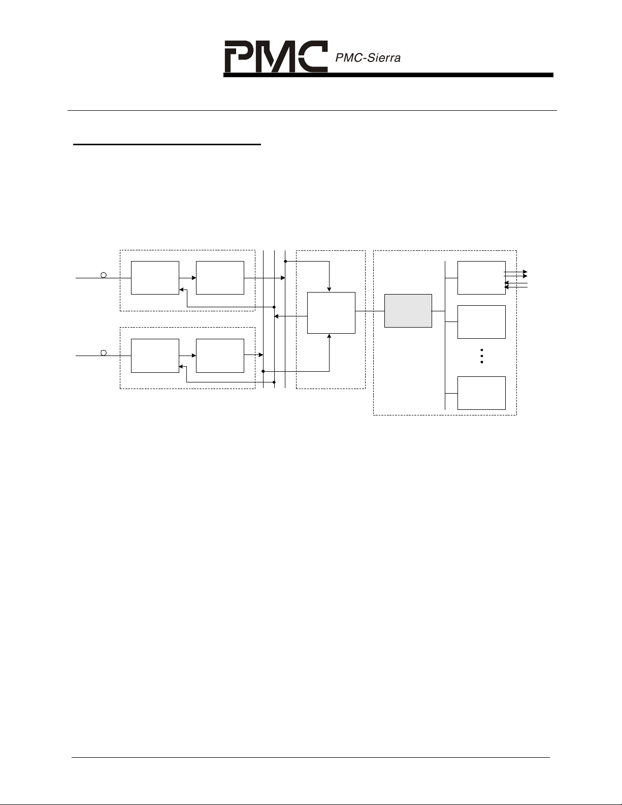
5 BLOCK DIAGRAM
5.1 Top Level Block Diagram
Figure 4 shows the complete TEMAP-84. T1 links can be multiplexed into the
DS3s or can be mapped into the telecom bus as SONET VT1.5 virtual tributaries
or as SDH TU-11 or TU-12 tributary units. E1 links can be mapped into the
telecom bus as SONET VT2 virtual tributaries or as SDH TU-12 tributary units.
System side access to the T1s and E1s is available through the SBI bus. DS3
line side access is via the clock and data interface for line interface units (LIUs)
or DS3 mapped into the SONET/SDH telecom bus. Unchannelized DS3 system
side access is available through the SBI bus.
Figure 4 - TEMAP-84 Block Diagram
LIUs
M13
M13
D3MA
Telecom Bus
M13
M13
VTPP
M13
M13
VTPP
Telecom Bus
M13
M13
D3MD
LIUs
DS3 /E3 Tx System I/F
M13
M13
DS3/E3
TRAN
TTOP
M13
M13
RTOP/
RTTB
M13
M13
DS3/E3
FRMR
DS3/E3 Rx System I/F
M13
M13
M13
TRAP
M13
M13
M13
M13
M13
PISO
INSBI
(byte)
TTMP
(bit)
RTDM
(bit)
EXSBI
(byte)
M13
M13
SIPO
Transm ux
datapath
T1/E1
JAT84
T1/E1
JAT84
Flexible
B/W Port
T1/E1
FRMR84
Ingress
Flexible
B/W Port
Egress
EXSBI
SBI 155
INSBI
PROPRIETARY AND CONFIDENTIAL 21
Page 34

PRELIMINARY
DATASHEET
PMC-2010672 ISSUE 1 HIGH DENSITY 84/63 CHANNEL VT/TU MAPPER
PM5366 TEMAP-84
AND M13 MULTIPLEXER
5.2 DS3/E3 Framer Only Block Diagram
Figure 5 shows the TEMAP-84 configured as a DS3 or E3 framer. In this mode
the TEMAP-84 provides access up to three full DS3/E3 unchannelized payloads.
The payload access (right side of diagram) has two clock and data interfacing
modes, one utilizing a gapped clock to mask out the DS3/E3 overhead bits and
the second utilizing an ungapped clock with overhead indications on a separate
overhead signal. The SBI bus can also be used to provide access to the
unchannelized DS3/E3.
Figure 5 - DS3/E3 Framer Only Mode Block Diagram
TDPR
Tx
HDLC
TICLK
TCLK
TPOS/TDAT
TNEG/TMFP
RCLK/VCLK
RPOS/RDAT
RNEG/RLCV
B3ZS/
HDB3
Encode
B3ZS/
HDB3
Decode
TRAN
DS3/E3
Transmit
Framer
FRMR
DS3/E3
Receive
Framer
TDATI
TFPO/TMFPO/TGAPCLK
TFPI/TMFPI
RGAPCLK/RSCLK
RDATO
RFPO/RMFPO
ROVRHD
RDLC
Rx
HDLC
PMON
Perf.
Monitor
3X
PROPRIETARY AND CONFIDENTIAL 22
Page 35

PRELIMINARY
DATASHEET
PMC-2010672 ISSUE 1 HIGH DENSITY 84/63 CHANNEL VT/TU MAPPER
PM5366 TEMAP-84
AND M13 MULTIPLEXER
6 DESCRIPTION
The PM5366 High Density 84/63 Channel VT/TU Mapper and M13 Multiplexer
(TEMAP-84) is a feature-rich device for use in any applications requiring high
density link termination over T1 and E1 (G.747) channelized DS3 or T1 and E1
channelized SONET/SDH facilities.
The TEMAP-84 supports asynchronous multiplexing and demultiplexing of 84
1.544 Mbit/s or 63 2.048 Mbit/s tributaries into three DS3 signals as specified by
ANSI T1.107, Bell Communications Research TR-TSY-000009 and ITU-T Rec.
G.747. It supports bit asynchronous or byte synchronous mapping and
demapping of 84 T1s or 63 E1s into SONET/SDH as specified by ANSI T1.105,
Bell Communications Research GR-253-CORE and ITU-T Recommendation
G.707. The TEMAP-84 also supports mapping of 63 T1s into SDH via TU-12s.
Up to 84 Transparent VT1.5s and TU-11s or 63 Transparent VT2s and TU-12s
can be transferred between the SONET/SDH interface and the SBI bus
interface.
This device can also be configured as a DS3 or E3 framer, providing external
access to the full DS3 or E3 payload, or a VT/TU mapper, providing access to
unframed 1.544 Mbit/s and 2.048 Mbit/s links.
The TEMAP-84 can be used as a SONET/SDH VT/TU mapper or M13
multiplexer with performance monitoring in either the ingress or egress direction
for up to 84 T1s or 63 E1s.
Each of the T1 and E1 jitter attenuators and performance monitors is
independently software configurable, allowing timing master and feature
selection without changes to external wiring. 1.544 Mbit/s and 63 2.048 Mbit/s
tributaries may be mixed at a VC-3/TUG-3/DS3 granularity.
In the ingress direction, each of the 84 T1 links is either demultiplexed from a
channelized DS3 or extracted from SONET VT1.5, TU-11 or TU-12 mapped bus.
Each T1 performance monitor can be configured to frame to the common DS1
signal formats (SF, SLC96, ESF).
T1 performance monitoring with accumulation of CRC-6 errors, framing bit
errors, out-of-frame events, and changes of frame alignment is provided. . The
TEMAP-84 also detects the presence of ESF bit oriented codes, and detects and
terminates HDLC messages on the ESF data link. The HDLC messages are
terminated in a 128 byte FIFO.
PROPRIETARY AND CONFIDENTIAL 23
Page 36

PRELIMINARY
DATASHEET
PMC-2010672 ISSUE 1 HIGH DENSITY 84/63 CHANNEL VT/TU MAPPER
PM5366 TEMAP-84
AND M13 MULTIPLEXER
In the ingress direction, each of the 63 2.048 Mbit/s links is either demultiplexed
from a DS3 according to ITU-T Rec. G.747 or extracted from SONET/SDH VT2
or TU-12 mapped bus.
The E1 performance monitors support detection of various alarm conditions such
as loss of frame, loss of signaling multiframe and loss of CRC multiframe. The
E1 framers also support reception of remote alarm signal, remote multiframe
alarm signal, alarm indication signal, and time slot 16 alarm indication signal.
E1 performance monitoring with accumulation of CRC-4 errors, far end block
errors and framing bit errors is provided. The TEMAP-84 provides a receive
HDLC controller for the detection and termination of messages on the national
use bits.
The TEMAP-84 can generate a low jitter transmit clock from a variety of clock
references, and also provides jitter attenuation in the receive path. Three jitter
attenuated recovered T1/E1 clocks can be routed outside the TEMAP-84 for
network timing applications.
A Scaleable Bandwidth Interconnect (SBI) high density byte serial system
interface provides higher levels of integration and dense interconnect. The SBI
bus interconnects up to 84 T1s or 63 E1 both synchronously or asynchronously.
The SBI allows transmit timing to be mastered by either the TEMAP-84 or link
layer device connected to the SBI bus. In addition to unframed T1s and E1s, the
TEMAP-84 can transport framed or unframed DS3 or E3 links over the SBI bus.
When configured as a DS3 multiplexer/demultiplexer or DS3 framer, the TEMAP84 accepts and outputs either digital B3ZS-encoded bipolar or unipolar signals
compatible with M23 and C-bit parity applications.
In the DS3 receive direction, the TEMAP-84 frames to DS3 signals with a
maximum average reframe time of 1.5 ms in the presence of 10
-3
bit error rate
and detects line code violations, loss of signal, framing bit errors, parity errors, Cbit parity errors, far end block errors, AIS, far end receive failure and idle code.
The DS3 framer is an off-line framer, indicating both out of frame (OOF) and
change of frame alignment (COFA) events. The error events (C-BIT, FEBE, etc.)
are still indicated while the framer is OOF, based on the previous frame
alignment. When in C-bit parity mode, the Path Maintenance Data Link and the
Far End Alarm and Control (FEAC) channels are extracted. HDLC receivers are
provided for Path Maintenance Data Link support. In addition, valid bit-oriented
codes in the FEAC channels are detected and are available through the
microprocessor port.
DS3 error event accumulation is also provided by the TEMAP-84. Framing bit
errors, line code violations, excessive zeros occurrences, parity errors, C-bit
PROPRIETARY AND CONFIDENTIAL 24
Page 37

PRELIMINARY
DATASHEET
PMC-2010672 ISSUE 1 HIGH DENSITY 84/63 CHANNEL VT/TU MAPPER
PM5366 TEMAP-84
AND M13 MULTIPLEXER
parity errors, and far end block errors are accumulated. Error accumulation
continues even while the off-line framers are indicating OOF. The counters are
intended to be polled once per second, and are sized so as not to saturate at a
-3
10
bit error rate. Transfer of count values to holding registers is initiated through
the microprocessor interface.
In the DS3 transmit direction, the TEMAP-84 inserts DS3 framing, X and P bits.
When enabled for C-bit parity operation, bit-oriented code transmitters and
HDLC transmitters are provided for insertion of the FEAC channels and the Path
Maintenance Data Links into the appropriate overhead bits. Alarm Indication
Signals, Far End Receive Failure and idle signal can be inserted using either
internal registers or can be configured for automatic insertion upon received
errors. When M23 operation is selected, the C-bit Parity ID bit (the first C-bit of
the first M sub-frame) is forced to toggle so that downstream equipment will not
confuse an M23-formatted stream with stuck-at-1 C-bits for C-bit Parity
application. Transmit timing is from an external reference or from the receive
direction clock.
The TEMAP-84 also supports diagnostic options which allow it to insert, when
appropriate for the transmit framing format, parity or path parity errors, F-bit
framing errors, M-bit framing errors, invalid X or P-bits, line code violations,
all-zeros, AIS, Remote Alarm Indications, and Remote End Alarms. A Pseudo
Random Binary Sequence (PRBS) can be inserted into a DS3 payload and
checked in the receive DS3 payload for bit errors. A fixed 100100… pattern is
available for insertion directly into the B3ZS encoder for proper pulse mask
shape verification.
The TEMAP-84 may be used as an E3 framer for the transport of framed but
unchannelized E3 data streams complying to the ITU-T Recommendations
G.751 or G.832. The line interface may be configured as either unipolar or
HDB3-encoded.
When configured in DS3 multiplexer mode, seven 6312 kbit/s data streams are
demultiplexed and multiplexed into and out of each DS3 signal. Bit stuffing and
rate adaptation is performed. The C-bits are set appropriately, with the option of
inserting DS2 loopback requests. Interrupts can be generated upon detection of
loopback requests in the received DS3. AIS may be inserted in the any of the
6312 kbit/s tributaries in both the multiplex and demultiplex directions. C-bit
parity is supported by sourcing a 6.3062723 MHz clock, which corresponds to a
stuffing ratio of 100%.
Framing to the demultiplexed 6312 kbit/s data streams supports DS2 (ANSI
TI.107) frame formats. The maximum average reframe time is 7ms for DS2. Far
end receive failure is detected and M-bit and F-bit errors are accumulated. The
DS2 framer is an off-line framer, indicating both OOF and COFA events. Error
PROPRIETARY AND CONFIDENTIAL 25
Page 38

PRELIMINARY
DATASHEET
PMC-2010672 ISSUE 1 HIGH DENSITY 84/63 CHANNEL VT/TU MAPPER
PM5366 TEMAP-84
AND M13 MULTIPLEXER
events (FERF, MERR, FERR, PERR, RAI, framing word errors) are still indicated
while the DS2 framer is indicating OOF, based on the previous alignment.
Each of the seven 6312 kbit/s multiplexers per DS3 may be independently
configured to multiplex and demultiplex four 1544 kbit/s DS1s or three
2048 kbit/s according to ITU-T Rec. G.747 into and out of a DS2 formatted
signal. Tributary frequency deviations are accommodated using internal FIFOs
and bit stuffing. The C-bits are set appropriately, with the option of inserting DS1
loopback requests. Interrupts can be generated upon detection of loopback
requests in the received DS2. AIS may be inserted in any of the low speed
tributaries in both multiplex and demultiplex directions.
When configured as a DS3 or E3 framer the unchannelized payload of the DS3
and E3 links are available to an external device.
The SONET/SDH line side interface provides STS-1 SPE synchronous payload
envelope processing and generation, TUG3 tributary unit group processing and
generation within a VC4 virtual container and VC3 virtual container processing
and generation. The payload processor aligns and monitors the performance of
SONET virtual tributaries (VTs) or SDH tributary units (TUs). Maintenance
functions per tributary include detection of loss of pointer, AIS alarm, tributary
path signal label mismatch and tributary path signal label unstable alarms.
Optionally interrupts can be generated due to the assertion and removal of any
of the above alarms. Counts are accumulated for tributary path BIP-2 errors on a
block or bit basis and for FEBE indications. The synchronous payload envelope
generator generates all tributary pointers and calculates and inserts tributary
path BIP-2. The generator also inserts FEBE, RDI and enhanced RDI in the V5
byte. Software can force AIS insertion on a per tributary basis.
A SONET/SDH mapper maps and demaps up to 84 T1s, 63 E1s or three DS3s
into three STS-1 SPEs, TUG3s or VC3s through three elastic stores. The fixed
stuff (R) bits are all set to zeros or ones under microprocessor control. The bit
asynchronous demapper performs majority vote C-bit decoding to detect stuff
requests for T1, E1 and DS3 asynchronous mappings. The VT1.5/VT2/TU11/TU-12 mapper uses an elastic store and a jitter attenuator capability to
minimize jitter introduced via bit stuffing.
The TEMAP-84 is configured, controlled and monitored via a generic 8-bit
microprocessor bus through which all internal registers are accessed. All
sources of interrupts can be masked and acknowledged through the
microprocessor interface.
PROPRIETARY AND CONFIDENTIAL 26
Page 39

PRELIMINARY
A
YAAA
DATASHEET
PMC-2010672 ISSUE 1 HIGH DENSITY 84/63 CHANNEL VT/TU MAPPER
PM5366 TEMAP-84
AND M13 MULTIPLEXER
7 PIN DIAGRAM
The TEMAP-84 is packaged in a 324-pin PBGA package having a body size of
23mm by 23mm and a ball pitch of 1.0 mm. The center 36 balls are not used as
signal I/Os and are thermal balls. Pin names and locations are defined in the Pin
Description Table in section 8. Mechanical information for this package is in the
section 19.
Figure 6 - Pin Diagram
22 21 20 19 18 17 16 15 14 13 12 11 10 9 8 7 6 5 4 3 2 1
B
C
M
N
R
U
W
D
E
F
G
324 PBGA
H
J
K
L
P
VSS VSS VSS VSS VSS VSS
VSS VSS VSS VSS VSS VSS
VSS VSS VSS VSS VSS VSS
VSS VSS VSS VSS VSS VSS
VSS VSS VSS VSS VSS VSS
VSS VSS VSS VSS VSS VSS
Bottom View
T
V
B
22 21 20 19 18 17 16 15 14 13 12 11 10 9 8 7 6 5 4 3 2 1
PROPRIETARY AND CONFIDENTIAL 27
Page 40

PRELIMINARY
DATASHEET
PMC-2010672 ISSUE 1 HIGH DENSITY 84/63 CHANNEL VT/TU MAPPER
PM5366 TEMAP-84
AND M13 MULTIPLEXER
8 PIN DESCRIPTION
Pin Name Type Pin
No.
DS3 and E3 Line Side Interface
RCLK[3]
RCLK[2]
RCLK[1]
RPOS/RDAT[3]
RPOS/RDAT[2]
RPOS/RDAT[1]
Input P1
T1
Y1
Input P2
U1
V3
Function
Receive Input Clocks (RCLK[3:1]). RCLK[3:1]
provide the receive direction timing for the three DS3s
or E3s. RCLK[3:1] are nominally 44.736 MHz or
34.368 MHz, 50% duty cycle clock inputs.
Positive Input Pulse (RPOS[3:1]). RPOS[3:1]
represent the positive pulses received on the B3ZSencoded DS3s or HDB3-encoded E3s when dual rail
input format is selected.
Receive Data Input (RDAT[3:1]). RDAT[3:1]
represent the NRZ (unipolar) DS3 or E3 input data
streams when single rail input format is selected.
RPOS[3:1] and RDAT[3:1] are sampled on the rising
edge of the associated RCLK by default and may be
enabled to be sampled on the falling edge of the
associated RCLK by setting the RFALL bit in the
DS3/E3 Master Receive Line Options register.
RNEG/RLCV[3]
RNEG/RLCV[2]
RNEG/RLCV[1]
TCLK[3]
TCLK[2]
TCLK[1]
Input P3
T3
W2
Output R3
V1
W3
Negative Input Pulse (RNEG[3:1]). RNEG[3:1]
represent the negative pulses received on the B3ZSencoded DS3s or HDB3-encoded E3s when dual rail
input format is selected.
Line code violation (RLCV[3:1]). RLCV[3:1]
represent receive line code violations when single rail
input format is selected.
RNEG[3:1] and RLCV[3:1] are sampled on the rising
edge of the associated RCLK by default and may be
enabled to be sampled on the falling edge of RCLK by
setting the RFALL bit in the DS3/E3 Master Receive
Line Options register.
Transmit Clock (TCLK[3:1]). TCLK[3:1] provide
timing for circuitry downstream of the DS3 and E3
transmitters of the TEMAP-84. TCLK[3:1] are
nominally 44.736 MHz or 34.368 MHz, 50% duty cycle
clocks.
PROPRIETARY AND CONFIDENTIAL 28
Page 41

PRELIMINARY
DATASHEET
PMC-2010672 ISSUE 1 HIGH DENSITY 84/63 CHANNEL VT/TU MAPPER
PM5366 TEMAP-84
AND M13 MULTIPLEXER
Pin Name Type Pin
No.
TPOS/TDAT[3]
TPOS/TDAT[2]
TPOS/TDAT[1]
TNEG/TMFP[3]
TNEG/TMFP[2]
TNEG/TMFP[1]
Output R2
U2
AA1
Output U4
W1
AB1
Function
Transmit Positive Pulse (TPOS[3:1]). TPOS[3:1]
represent the positive pulses transmitted on the B3ZSencoded DS3 or HDB3-encoded E3 lines when dualrail output format is selected.
Transmit Data Output (TDAT[3:1]). TDAT[3:1]
represent the NRZ (unipolar) DS3 output data streams
when single rail output format is selected.
TPOS[3:1] and TDAT[3:1] are updated on the falling
edge of the associated TCLK by default but may be
enabled to be updated on the rising edge of the
associated TCLK by setting the TRISE bit in the
DS3/E3 Master Transmit Line Options register.
TPOS[3:1] and TDAT[3:1] are updated on TICLK[3:1]
rather than TCLK[3:1] when the TICLK bit in the
DS3/E3 Master Transmit Line Options register is set.
Transmit Negative Pulse (TNEG[3:1]). TNEG[3:1]
represent the negative pulses transmitted on the
B3ZS-encoded DS3 or HDB3-encoded E3 lines when
dual-rail output format is selected.
TICLK[3]
TICLK[2]
TICLK[1]
Input T4
V4
Y2
Transmit Multiframe Pulse (TMFP[3:1]). These
signals mark the transmit frame alignment when
configured for single rail operation. TMFP[3:1] indicate
the position of overhead bits in the transmit
transmission system stream, TDAT[3:1]. TMFP[3:1]
are high during the first bit (X1) of the multiframe or E3
frame.
TNEG[3:1] and TMFP[3:1] are updated on the falling
edge of the associated TCLK by default but may be
enabled to be updated on the rising edge of the
associated TCLK by setting the TRISE bit in the
DS3/E3 Master Transmit Line Options register.
TNEG[3:1] and TMFP[3:1] are updated on TICLK[3:1]
rather than TCLK[3:1] when the TICLK bit in the
DS3/E3 Master Transmit Line Options register is set.
Transmit input clock (TICLK[3:1]). TICLK[3:1]
provides the transmit direction timing for the three
DS3s or E3s. TICLK[3:1] are nominally 44.736 MHz or
34.368 MHz, 50% duty cycle clocks.
PROPRIETARY AND CONFIDENTIAL 29
Page 42

PRELIMINARY
DATASHEET
PMC-2010672 ISSUE 1 HIGH DENSITY 84/63 CHANNEL VT/TU MAPPER
PM5366 TEMAP-84
AND M13 MULTIPLEXER
Pin Name Type Pin
Function
No.
DS3 and E3 System Side Interface
RGAPCLK/RSCLK
[3]
RGAPCLK/RSCLK
[2]
RGAPCLK/RSCLK
[1]
Output H4
L3
N3
Framer Recovered Gapped Clock (RGAPCLK[3:1]).
RGAPCLK[3:1] are valid when the TEMAP-84 is
configured as DS3 or E3 framers by setting the
OPMODE_SPEx[2:0] bits in the SPE Configuration
registers and the RXGAPEN bit in the DS3 and E3
Master Unchannelized Interface Options register.
RGAPCLK[x] is the recovered clock and timing
reference for RDATO[x]. RGAPCLK[3:1] are held
either high or low during bit positions which correspond
to overhead.
Framer Recovered Clock (RSCLK[3:1]). RSCLK[3:1]
are valid when the TEMAP-84 is configured as DS3 or
E3 framers by setting the OPMODE_SPEx[2:0] bits in
the SPE Configuration registers.
RSCLK[3:1] are the recovered clocks and timing
references for RDATO[3:1], RFPO/RMFPO[3:1], and
ROVRHD[3:1].
RDATO[3]
RDATO[2]
RDATO[1]
Output H2
K4
N2
Framer Receive Data (RDATO[3:1]). RDATO[3:1] are
valid when the TEMAP-84 is configured as DS3 or E3
framers by setting the OPMODE_SPEx[2:0] bits in the
SPE Configuration registers. RDATO[3:1] are the
received data aligned to RFPO/RMFPO[3:1] and
ROVRHD[3:1].
RDATO[3:1] are updated on either the falling or rising
edge of the associated RGAPCLK or RSCLK,
depending on the value of the RSCLKR bit in the DS3
and E3 Master Unchannelized Interface Options
register. By default, RDATO[3:1] will be updated on
the falling edge of the associated RGAPCLK[3:1] or
RSCLK[3:1].
PROPRIETARY AND CONFIDENTIAL 30
Page 43

PRELIMINARY
DATASHEET
PMC-2010672 ISSUE 1 HIGH DENSITY 84/63 CHANNEL VT/TU MAPPER
PM5366 TEMAP-84
AND M13 MULTIPLEXER
Pin Name Type Pin
No.
RFPO/RMFPO[3]
RFPO/RMFPO[2]
RFPO/RMFPO[1]
Output H1
K2
M2
Function
Framer Receive Frame Pulse/Multi-frame Pulse
(RFPO/RMFPO[3:1]). RFPO/RMFPO[3:1] are valid
when the TEMAP-84 is configured to be in framer only
mode by setting the OPMODE_SPEx[2:0] bits in the
SPE Configuration registers.
RFPO[3:1] are aligned to RDATO[3:1] and indicate the
position of the first bit in each DS3 M-subframe and
the first bit in each G.751 E3 or G.832 E3 frame.
RMFPO[3:1] are aligned to RDATO[3:1] and indicate
the position of the first bit in each DS3 M-frame and
the first bit in each G.751 or G.832 E3 frame. This is
selected by setting the RXMFPO bit in the DS3 and E3
Master Unchannelized Interface Options Registers.
RFPO/RMFPO[3:1] are updated on either the falling or
rising edge of the associated RSCLK depending on the
setting of the RSCLKR bit in the DS3 and E3 Master
Unchannelized Interface Options register.
ROVRHD[3]
ROVRHD[2]
ROVRHD[1]
Output H3
K1
N1
Framer Receive Overhead (ROVRHD[3:1]).
ROVRHD[3:1] are valid when the TEMAP-84 is
configured as DS3 or E3 framers by setting the
OPMODE_SPEx[2:0] bits in the SPE Configuration
registers.
ROVRHD[3:1] will be high whenever the data on
RDATO[3:1] corresponds to an overhead bit position.
ROVRHD[3:1] is updated on the either the falling or
rising edge of the associated RSCLK depending on the
setting of the RSCLKR bit in the DS3 and E3 Master
Unchannelized Interface Options register.
PROPRIETARY AND CONFIDENTIAL 31
Page 44

PRELIMINARY
DATASHEET
PMC-2010672 ISSUE 1 HIGH DENSITY 84/63 CHANNEL VT/TU MAPPER
PM5366 TEMAP-84
AND M13 MULTIPLEXER
Pin Name Type Pin
No.
TFPO/TMFPO/
Output F4
TGAPCLK[3]
TFPO/TMFPO/
J4
TGAPCLK[2]
TFPO/TMFPO/
M3
TGAPCLK[1]
Function
Framer Transmit Frame Pulse/Multi-frame Pulse
Reference (TFPO/TMFPO[3:1]). TFPO/TMFPO[3:1]
are valid when the TEMAP-84 is configured as DS3
framers by setting the OPMODE_SPEx[2:0] bits in the
SPE Configuration registers and setting the TXGAPEN
bit to 0 in the DS3 and E3 Master Unchannelized
Interface Options register.
In DS3 mode, TFPO[3:1] pulse high for 1 out of every
85 clock cycles, giving a reference M-subframe
indication. In E3 mode, TFPO[3:1] pulse high to mark
the first bit of the frame.
In DS3 mode, TMFPO[3:1] pulse high for 1 out of
every 4760 clock cycles, giving a reference M-frame
indication. TMFPO[3:1] behaves the same as
TFPO[3:1] for E3 applications. This is selected by
setting the TXMFPO bit in the DS3 and E3 Master
Unchannelized Interface Options Registers.
TFPO/TMFPO[3:1] will be updated on the falling edge
of TICLK when the associated TDATIFALL register bit
is a logic 0 and on the rising edge when TDATIFALL is
a logic 1.
Framer Gapped Transmit Clock (TGAPCLK[3:1]).
TGAPCLK[3:1] are valid when the TEMAP-84 is
configured as DS3 framers by setting the
OPMODE_SPEx[2:0] bits in the SPE Configuration
registers and setting the TXGAPEN bit to 1 in the DS3
and E3 Master Unchannelized Interface Options
register.
TGAPCLK[3:1] are derived from the transmit reference
clocks TICLK[3:1] or from the receive clock if looptimed. The overhead bit (gapped) positions are
generated internal to the device. TGAPCLK[3:1] are
held high during the overhead bit positions. This clock
is useful for interfacing to devices which source
payload data only.
TGAPCLK[3:1] are used to sample the associated
TDATI[3:1] inputs.
PROPRIETARY AND CONFIDENTIAL 32
Page 45

PRELIMINARY
DATASHEET
PMC-2010672 ISSUE 1 HIGH DENSITY 84/63 CHANNEL VT/TU MAPPER
PM5366 TEMAP-84
AND M13 MULTIPLEXER
Pin Name Type Pin
No.
TDATI[3]
TDATI[2]
TDATI[1]
TFPI/TMFPI[3]
TFPI/TMFPI[2]
TFPI/TMFPI[1]
Input G2
J3
L2
Input G1
J1
M1
Function
Framer Transmit Data (TDATI[3:1]). TDATI[3:1]
contain the serial data to be transmitted when the
TEMAP-84 is configured as DS3 framers by setting the
OPMODE_SPEx[2:0] bits in the SPE Configuration
registers. TDATI[3:1] are sampled on the rising edge
of the associated TICLK if the TXGAPEN bit in the
DS3 and E3 Master Unchannelized Interface Options
register is logic 0. If TXGAPEN is logic 1, then
TDATI[3:1] are sampled on the rising edge of
TGAPCLK. TDATI[3:1] can be configured to be
sampled on the falling edge of the associated TICLK or
TGAPCLK by setting the TDATIFALL bit in the DS3
and E3 Master Unchannelized Interface Options
register.
Framer Transmit Frame Pulse/Multiframe Pulse
(TFPI/TMFPI[3:1]). TFPI/TMFPI[3:1] are valid when
the TEMAP-84 is configured as DS3 or E3 framers by
setting the OPMODE_SPEx[2:0] bits in the SPE
Configuration registers.
TFPI[3:1] indicate the position of all overhead bits in
each DS3 M-subframe or the first bit in each G.751 E3
or G.832 E3 frame. TFPI[3:1] are not required to pulse
at every overhead bit.
TMFPI[3:1] indicate the position of the first bit in each
4760-bit DS3 M-frame or the first bit in each E3 frame.
TMFPI[3:1] are not required to pulse at every
multiframe boundary. This is selected by setting the
TXMFPI bit in the DS3 and E3 Master Unchannelized
Interface Options Registers.
TFPI/TMFPI[3:1] are sampled on the rising edge of the
associated TICLK. TDATI[3:1] can be configured to be
sampled on the falling edge of the associated TICLK
by setting the TDATIFALL bit to 1 in the DS3 and E3
Master Unchannelized Interface Options register.
PROPRIETARY AND CONFIDENTIAL 33
Page 46

PRELIMINARY
DATASHEET
PMC-2010672 ISSUE 1 HIGH DENSITY 84/63 CHANNEL VT/TU MAPPER
PM5366 TEMAP-84
AND M13 MULTIPLEXER
Pin Name Type Pin
Function
No.
Flexible Bandwidth Ports
Port #1 is associated with SBI SPE #1. Port #2 is associated with SBI SPE #2.
Port #3 is associated with SBI SPE #3.
IFBWCLK[3]
IFBWCLK[2]
IFBWCLK[1]
Input N22
K19
H19
The Ingress Flexible Bandwidth Clocks
(IFBWCLK[3:1]). The IFBWCLK[3:1] clocks provide
the timing for an arbitrary bandwidth payload to be
inserted into the System Drop Bus (SDDATA[7:0]).
Each clock is associated with one SPE and is only
used when the associated SPE is configured to carry a
fractional payload by the OPMODE_SPEx[2:0] bits of
the SPE Configuration registers.
IFBWCLK[3:1] may have a maximum frequency of
51.84 MHz and may be gapped if required.
Each IFBWCLK samples the associated
IFBWDAT[3:1] and IFBWEN[3:1] inputs on the rising
edge.
IFBWDAT[3]
IFBWDAT[2]
IFBWDAT[1]
IFBWEN[3]
IFBWEN[2]
IFBWEN[1]
Input N20
L20
J20
Input P19
L22
J21
The Ingress Flexible Bandwidth Data
(IFBWDAT[3:1]). These inputs present bit serial data
for insertion into the System Drop Bus (SDDATA[7:0]).
Only bits for which the associated IFBWEN input is
sampled high are accepted. Each data input is
associated with one SPE and is only used when the
associated SPE is configured to carry a fractional
payload by the OPMODE_SPEx[2:0] bits of the SPE
Configuration registers.
IFBWDAT[3:1] are sampled on the rising edge of the
associated IFBWCLK input.
The Ingress Flexible Bandwidth Enables
(IFBWEN[3:1]). A logic high on any of these inputs
indicates a valid bit on the associated IFBWDAT input.
The IFBWEN[3:1] inputs are constrained such that the
maximum data rate of each of IFBWDAT[3:1] is less
than 49.72 Mbit/s.
IFBWEN[3:1] are sampled on the rising edge of the
associated IFBWCLK input.
PROPRIETARY AND CONFIDENTIAL 34
Page 47

PRELIMINARY
DATASHEET
PMC-2010672 ISSUE 1 HIGH DENSITY 84/63 CHANNEL VT/TU MAPPER
PM5366 TEMAP-84
AND M13 MULTIPLEXER
Pin Name Type Pin
No.
EFBWCLK[3]
EFBWCLK[2]
EFBWCLK[1]
EFBWDREQ[3]
EFBWDREQ[2]
EFBWDREQ[1]
Input P22
M22
J22
Input P21
M21
J19
Function
The Egress Flexible Bandwidth Clocks
(EFBWCLK[3:1]). The EFBWCLK[3:1] clocks provide
the timing for an arbitrary bandwidth payload extracted
from the System Add Bus (SADATA[7:0]). Each clock
is associated with one SPE and is only used when the
associated SPE is configured to carry a fractional
payload by the OPMODE_SPEx[2:0] bits of the SPE
Configuration registers.
EFBWCLK[3:1] may have a maximum frequency of
51.84 MHz and may be gapped if required.
Each EFBWCLK samples the associated EBWDREQ
on the rising edge and updates the associated
EFBWDAT] and EFBWEN on the falling edge.
The Egress Flexible Bandwidth Data Requests
(EFBWREQ[3:1]). The data request input must be
asserted high for a EFBWCLK cycle for each bit of
data required. In response to sampling
EFWBDREQ[3:1] high, the associated EFBWDAT
output will either present an available bit a cycle later
with an accompanying assertion of the associated
EFBWEN or ignore the request if no data is ready. In
many applications (eg. frame relay and ATM), every
request will be acknowledged with data. In
applications where the source data is fixed, it is
permissible to hold EFBWDREQ[3:1] high, in which
case EFBWEN identifies valid bytes.
EFBWDREQ[3:1] are sampled on the rising edge of
the associated EFBWCLK input.
PROPRIETARY AND CONFIDENTIAL 35
Page 48

PRELIMINARY
DATASHEET
PMC-2010672 ISSUE 1 HIGH DENSITY 84/63 CHANNEL VT/TU MAPPER
PM5366 TEMAP-84
AND M13 MULTIPLEXER
Pin Name Type Pin
No.
EFBWDAT[3]
EFBWDAT[2]
EFBWDAT[1]
EFBWEN[3]
EFBWEN[2]
EFBWEN[1]
Output F21
B22
A19
Output E22
D20
B18
Function
The Egress Flexible Bandwidth Data
(EFBWDAT[3:1]). These outputs present bit serial
data extracted from the System Add Bus
(SADATA[7:0]). Only bits for which the associated
EFBWEN output is simultaneously high are valid.
Each data input is associated with one SPE and is only
used when the associated SPE is configured to carry a
fractional payload by the OPMODE_SPEx[2:0] bits of
the SPE Configuration registers.
EFBWDAT[3:1] are updated on the falling edge of the
associated EFBWCLK input.
The Egress Flexible Bandwidth Enables
(EFBWEN[3:1]). A logic high on any of these outputs
indicates a valid bit on the associated EFBWDAT
output. The EFBWEN[3:1] will only be asserted, with a
one cycle latency, in response to a sampled logic high
on the associated EFBWDREQ, and then only if data
is available for presenting on the associated
EFBWDAT.
Recovered T1 and E1 Clocks
RECVCLK1 Output F2
RECVCLK2 Output E4
RECVCLK3 Output G3
EFBWEN[3:1] are updated on the falling edge of the
associated EFBWCLK input.
Recovered Clock 1 (RECVCLK1). This clock output is
a recovered and de-jittered clock from any one of the
84 1.544 Mbit/s or 63 2.048Mbit/s tributaries.
Recovered Clock 2 (RECVCLK2). This clock output is
a recovered and de-jittered clock from any one of the
84 1.544 Mbit/s or 63 2.048Mbit/s tributaries.
Recovered Clock 3 (RECVCLK3). This clock output is
a recovered and de-jittered clock from any one of the
84 1.544 Mbit/s or 63 2.048Mbit/s tributaries.
PROPRIETARY AND CONFIDENTIAL 36
Page 49

PRELIMINARY
DATASHEET
PMC-2010672 ISSUE 1 HIGH DENSITY 84/63 CHANNEL VT/TU MAPPER
PM5366 TEMAP-84
AND M13 MULTIPLEXER
Pin Name Type Pin
No.
XCLK_T1 Input E2
XCLK_E1 Input F3
Function
T1 Crystal Clock Input (XCLK_T1). This input clocks
the digital phase locked loop that performs jitter
attenuation on the T1 recovered clocks which drive the
RECVCLK1/2/3 outputs. XCLK_T1 is nominally a
37.056 MHz ± 32ppm, 50% duty cycle clock.
This input may be tied to ground in applications that do
not use the RECVCLK1/2/3 outputs as 1.544 MHz
clocks.
E1 Crystal Clock Input (XCLK_E1). This input clocks
the digital phase locked loop that performs jitter
attenuation on the E1 recovered clocks which drive the
RECVCLK1/2/3 outputs. XCLK_E1 is nominally a
49.152 MHz ± 32ppm, 50% duty cycle clock when
configured for E1 modes.
This input may be tied to ground in applications that do
not use the RECVCLK1/2/3 outputs as 2.048 MHz
clocks.
Telecom Line Side Interface
LREFCLK Input Y4
Line Reference Clock (LREFCLK). This signal
provides reference timing for the SONET telecom bus
interface. On the incoming byte interface of the
telecom bus, LDC1J1V1, LDDATA[7:0], LDDP, LDPL,
LDTPL, LDV5, LDAIS and LAC1 are sampled of the
rising edge or LREFCLK. In the outgoing byte
interface, LADATA[7:0], LADP, LAPL, LAC1J1V1 and
LAOE/LATPL are updated on the rising edge of
LREFCLK.
This clock may be held low if the Telecom Bus
interface is unused.
This clock is nominally a 19.44 MHz +/-50ppm or
77.76 MHz +/-50ppm clock with a 50% duty cycle. This
clock must be phase locked to SREFCLK and can be
external connected to SREFCLK.
PROPRIETARY AND CONFIDENTIAL 37
Page 50

PRELIMINARY
DATASHEET
PMC-2010672 ISSUE 1 HIGH DENSITY 84/63 CHANNEL VT/TU MAPPER
PM5366 TEMAP-84
AND M13 MULTIPLEXER
Pin Name Type Pin
Function
No.
L77 Input AA4 The Line 77.76 MHz select input determines the
expected frequency of LREFCLK. If L77 is low,
LREFCLK is expected to be 19.44 MHz. If L77 is high,
LREFCLK is expected to be 77.76 MHz and data is
driven and sampled every fourth cycle.
L77 must be held static.
LAC1 Input W10
Line Add C1 Frame Pulse (LAC1). The Add bus
timing signal identifies the frame and multiframe
boundaries on the Add Data bus LADATA[7:0].
LAC1 is set high to mark the first C1 byte of the first
transport envelope frame of the 4 frame multiframe on
the LADATA[7:0] bus. LAC1 need not be presented on
every occurrence of the multiframe .
LAC1 is sampled on the rising edge of LREFCLK.
LAC1J1V1 OutputAA11
Line Add Bus Composite Timing Signal
(LAC1J1V1). The Add bus composite timing signal
identifies the frame, payload and tributary multiframe
boundaries on the Line Add Data bus LADATA[7:0].
LAC1J1V1 pulses high with the Line Add Payload
Active signal LAPL set low to mark the first STS-1
(STM-0/AU3) identification byte or equivalently the
STM identification byte C1. Optionally the LAC1J1V1
signal pulses high with LAPL set high to mark the path
trace byte J1. Optionally the LAC1J1V1 signal pulses
high on the V1 byte to indicate tributary multiframe
boundaries.
In a system with multiple TEMAP-84s sharing the
same Line Add bus only one device should have
LAC1J1V1 connected. All devices must be configured
via the TXPTR[9:0] bits in the SONET/SDH Transmit
Pointer Configuration and TTMP Telecom Interface
Configuration registers for the same J1 location.
When L77 high, LAC1J1V1 is only valid (i.e. identifies
the first C1, J1 and V1 of the concatenated STM-4
data stream) if the LSTM[1:0] bits in the Master Bus
Configuration register (0x0006) are set to “00”.
LAC1J1V1 is updated on the rising edge of LREFCLK.
PROPRIETARY AND CONFIDENTIAL 38
Page 51

PRELIMINARY
DATASHEET
PMC-2010672 ISSUE 1 HIGH DENSITY 84/63 CHANNEL VT/TU MAPPER
PM5366 TEMAP-84
AND M13 MULTIPLEXER
Pin Name Type Pin
Function
No.
LAOE/LATPL OutputAB11 The LATPLSEL bit of the SONET/SDH Master Egress
VTPP Configuration register determines the function of
this output. When LATPLSEL is logic 1, the signal is
LATPL. When LATPLSEL is logic 0, the signal is
LAOE.
Line Add Bus Output Enable (LAOE). The Add Bus
output enable signal is asserted high whenever the
Line Add Bus is being driven which is co-coincident
with the Line Add bus outputs coming out of tri-state.
This pin is intended to control an external multiplexer
when multiple TEMAP-84s are driving the Telecom Add
bus during their individual tributaries. This same
function is accomplished with the Add bus tristate
drivers but increased tolerance to tributary
configuration problems is possible with an external
mux. This output is controlled via the LAOE bit in the
TTMP Tributary Control registers when the egress
VTPP is bypassed. When the the egress VTPP is not
bypassed or a TU-3 is being mapped, LAOE is high.
Line Add Bus Tributary Payload Active (LDATPL).
The tributary payload active signal marks the bytes
carrying the tributary payload. LATPL is high during
each tributary payload byte on the LADATA[7:0] bus.
LATPL will be low during transport overhead, path
overhead, V1 bytes and V2 bytes. To indicate pointer
adjustments, LATPL will be asserted appropriately
during the V3 byte and following byte for the tributary.
LAOE/LATPL is updated on the rising edge of
LREFCLK.
PROPRIETARY AND CONFIDENTIAL 39
Page 52

PRELIMINARY
A
A
A
A
DATASHEET
PMC-2010672 ISSUE 1 HIGH DENSITY 84/63 CHANNEL VT/TU MAPPER
PM5366 TEMAP-84
AND M13 MULTIPLEXER
Pin Name Type Pin
No.
LADATA[0]
LADATA[1]
LADATA[2]
LADATA[3]
LADATA[4]
LADATA[5]
LADATA[6]
LADATA[7]
Output
Tristate
W14
Y13
A13
B13
W13
A12
W12
W11
Function
Line Add Bus Data (LADATA[7:0]). The add bus data
contains the SONET transmit payload data in byte
serial format. All transport overhead bytes are set to
00h. The phase relation of the SPE (VC) to the
transport frame is determined by the Add Bus
composite timing signal LAC1J1V1 and is software
programmable to any valid pointer offset. LADATA[7] is
the most significant bit (corresponding to bit 1 of each
serial word, the first bit to be transmitted).
By default, LADATA[7:0] is only asserted during the
SONET/SDH tributaries assigned to this device as
determined by the LAOE bit in the TTMP Tributary
Control registers. As options, LADATA[7:0] can be
driven during transport overhead, for all bytes of an
STM-1 when configured for 77.76MHz operation or all
the time.
LADATA[7:0] is updated on the rising edge of
LREFCLK.
LADP Output
Tristate
B14
Line Add Bus Data Parity (LADP). The Add Bus data
parity signal carries the parity of the outgoing signals.
The parity calculation encompasses the LADATA[7:0]
bus and optionally the LAC1J1V1 and LAPL signals.
LAC1J1V1 and LAPL can be included in the parity
calculation by setting the INCLAC1J1V1 and INCLAPL
register bits in the SONET/SDH Master Egress
Configuration register high, respectively. Odd parity is
selected by setting the LAOP register bit in the same
register high and even parity is selected by setting the
LAOP bit low.
By default, LADP is only asserted during the
SONET/SDH tributaries assigned to this device as
determined by the LAOE bit in the TTMP Tributary
Control registers. As options, LADP can be driven
during transport overhead, for all bytes of an STM-1
when configured for 77.76MHz operation or all the
time.
LADP is updated on the rising edge of LREFCLK.
PROPRIETARY AND CONFIDENTIAL 40
Page 53

PRELIMINARY
A
AA6A
AA5A
DATASHEET
PMC-2010672 ISSUE 1 HIGH DENSITY 84/63 CHANNEL VT/TU MAPPER
PM5366 TEMAP-84
AND M13 MULTIPLEXER
Pin Name Type Pin
No.
LAPL Output
A14
Tristate
LAV5 Output
W15
Tristate
Function
Line Add Bus Payload Active (LAPL). The Add Bus
payload active signal identifies the payload bytes on
LADATA[7:0]. LAPL is set high during path overhead
and payload bytes and low during transport overhead
bytes.
By default, LAPL is only asserted during the
SONET/SDH tributaries assigned to this device as
determined by the LAOE bit in the TTMP Tributary
Control registers. As options, LAPL can be driven
during transport overhead, for all bytes of an STM-1
when configured for 77.76MHz operation or all the
time.
LAPL is updated on the rising edge of LREFCLK.
Line Add Bus V5 Byte (LAV5). The outgoing tributary
V5 byte signal marks the various tributary V5 bytes.
LAV5 marks each tributary V5 byte on the LADATA[7:0]
bus when high.
LDDATA[0]
LDDATA[1]
LDDATA[2]
LDDATA[3]
LDDATA[4]
LDDATA[5]
LDDATA[6]
LDDATA[7]
Input W5
B5
Y3
Y6
B4
AB3
By default, LAV5 is only asserted during the
SONET/SDH tributaries assigned to this device as
determined by the LAOE bit in the TTMP Tributary
Control registers. As options, LAV5 can be driven
during transport overhead, for all bytes of an STM-1
when configured for 77.76MHz operation or all the
time.
LAV5 is updated on the rising edge of LREFCLK.
Line Drop Bus Data (LDDATA[7:0]). The drop bus
data contains the SONET/SDH receive payload data in
byte serial format. LDDATA[7] is the most significant
bit, corresponding to bit 1 of each serial word, the bit
transmitted first.
LDDATA[7:0] is sampled on the rising edge of
LREFCLK.
PROPRIETARY AND CONFIDENTIAL 41
Page 54

PRELIMINARY
DATASHEET
PMC-2010672 ISSUE 1 HIGH DENSITY 84/63 CHANNEL VT/TU MAPPER
PM5366 TEMAP-84
AND M13 MULTIPLEXER
Pin Name Type Pin
No.
LDDP Input Y7
LDC1J1V1 Input AB6
Function
Line Drop Bus Data Parity (LDDP). The incoming
data parity signal carries the parity of the incoming
signals. The parity calculation encompasses the
LDDATA[7:0] bus and optionally the LDC1J1V1 and
LDPL signals. LDC1J1V1 and LDPL can be included
in the parity calculation by setting the INCLDC1J1V1
and INCLDPL bits in the SONET/SDH Master Ingress
Configuration register high, respectively. Odd parity is
selected by setting the LDOP bit in the Master
SONET/SDH Ingress Configuration register high and
even parity is selected by setting the LDOP bit low.
LDDP is sampled on the rising edge of LREFCLK.
Line Drop C1/J1 Frame Pulse (LDC1J1V1). The
input C1/J1 frame pulse identifies the transport
envelope and synchronous payload envelope frame
boundaries on the incoming SONET stream.
LDC1J1V1 is set high while LDPL is low to mark the
first C1 byte of the transport envelope frame on the
LDDATA[7:0] bus. LDC1J1V1 is set high while LDPL is
high to mark each J1 byte of the synchronous payload
envelope(s) on the LDDATA[7:0] bus. LDC1J1V1 must
be present at every occurrence of the first C1 and all
J1 bytes.
Optionally LDC1J1V1 indicates multiframe alignment
when high during the first V1 bytes of each envelope.
LDC1J1V1 is sampled on the rising edge of LREFCLK.
LDPL Input AB7
Line Drop Bus Payload Active (LDPL). The payload
active signal identifies the bytes on LDDATA[7:0] that
carry payload bytes.
LDPL is set high during path overhead and payload
bytes and low during transport overhead bytes. LDPL
is set high during the H3 byte to indicate a negative
pointer justification and low during the byte following
H3 to indicate a positive pointer justification event.
LDPL is sampled on the rising edge of LREFCLK.
PROPRIETARY AND CONFIDENTIAL 42
Page 55

PRELIMINARY
DATASHEET
PMC-2010672 ISSUE 1 HIGH DENSITY 84/63 CHANNEL VT/TU MAPPER
PM5366 TEMAP-84
AND M13 MULTIPLEXER
Pin Name Type Pin
No.
LDV5 Input W6
LDTPL Input Y8
Function
Line Drop Bus V5 Byte (LDV5). The incoming
tributary V5 byte signal marks the various tributary V5
bytes. LDV5 marks each tributary V5 byte on the
LDDATA[7:0] bus when high. The LDV5 input is only
used if the Ingress VTPP is bypassed (i.e. the
IVTPPBYP bit of the SONET/SDH Master Ingress
Configuration register is logic 1.)
LDV5 is sampled on the rising edge of LREFCLK.
Line Drop Bus Tributary Payload Active (LDTPL).
The tributary payload active signal marks the bytes
carrying the tributary payload which have been
identified by an external payload processor. When this
signal is available, the internal pointer processor can
be bypassed. LDTPL is only respected for
asynchronously mapped tributaries.
LDTPL is high during each tributary payload byte on
the LDDATA[7:0] bus. In floating mode, LDTPL
contains valid data only for bytes in the VC3 or VC4
virtual containers, or the STS-1 SPE. It should be
ignored for bytes in the transport overhead. In locked
mode, LDTPL is low for transport overhead.
LDTPL is sampled on the rising edge of LREFCLK.
LDAIS Input AA8
Line Drop Bus Tributary Path Alarm Indication
Signal (LDAIS). The active high tributary path alarm
indication signal identifies tributaries on the incoming
data stream LDDATA[7:0] that are in AIS state. When
this signal is available, the internal pointer processor
can be bypassed. LDAIS is invalid when LDTPL is low.
LDAIS is only respected for asynchronously mapped
tributaries.
LDAIS is sampled on the rising edge of LREFCLK.
PROPRIETARY AND CONFIDENTIAL 43
Page 56

PRELIMINARY
DATASHEET
PMC-2010672 ISSUE 1 HIGH DENSITY 84/63 CHANNEL VT/TU MAPPER
PM5366 TEMAP-84
AND M13 MULTIPLEXER
Pin Name Type Pin
No.
RADEASTCK Input W7
RADEASTFP Input Y9
Function
Remote Alarm Port East Clock (RADEASTCK). The
remote serial alarm port east clock provides timing for
the east remote serial alarm port. It is nominally a
9.72 MHz clock, but can range from 1.344 MHz to
10 MHz.
Inputs RADEASTFP and RADEAST are sampled on
the rising edge of RADEASTCK.
Remote Alarm Port East Frame Pulse
(RADEASTFP). The remote serial alarm port east
frame pulse is used to locate the alarm bits of the
individual tributaries in the east remote serial alarm
port. RADEASTFP is set high to mark the first BIP-2
error bit of tributary TU #1 in TUG2 #1 of TUG3 #1
carried in RADEAST. RADEASTFP must be set high
to mark every occurrence of this bit. TEMAP-84 will
not flywheel on RADEASTFP in order to accommodate
a variety of RADEASTCK frequencies.
RADEASTFP is sampled on the rising edge of
RADEASTCK.
RADEAST Input AA9
Remote Alarm Port Data East (RADEAST). The
remote serial alarm port east carries the tributary path
BIP-2 error count, RDI status, and RFI status in the
east remote serial alarm port. The first BIP-2 error bit
of tributary TU #1 in TUG2 #1 of TUG3 #1 on
RADEAST is marked by a high level on RADEASTFP.
The status carried on RADEAST is software selectable
to be reported by the RDI, RFI and REI alarms and is
selectable to be associated with any tributary on the
outgoing data stream LADATA[7:0].
RADEAST is sampled on the rising edge of
RADEASTCK.
PROPRIETARY AND CONFIDENTIAL 44
Page 57

PRELIMINARY
A
DATASHEET
PMC-2010672 ISSUE 1 HIGH DENSITY 84/63 CHANNEL VT/TU MAPPER
PM5366 TEMAP-84
AND M13 MULTIPLEXER
Pin Name Type Pin
No.
RADWESTCK Input W9
RADWESTFP Input Y10
Function
Remote Alarm Port West Clock (RADWESTCK). The
remote serial alarm port west clock provides timing for
the west remote serial alarm port. It is nominally a
9.72 MHz clock, but can range from 1.344 MHz to
10 MHz.
Inputs RADWESTFP and RADWEST are sampled on
the rising edge of RADWESTCK.
Remote Alarm Port West Frame Pulse
(RADWESTFP). The remote serial alarm port west
frame pulse is used to locate the alarm bits of the
individual tributaries in the west remote serial alarm
port. RADWESTFP is set high to mark the first BIP-2
error bit of tributary TU #1 in TUG2 #1 of TUG3 #1
carried in RADWEST. RADWESTFP must be set high
to mark every occurrence of this bit. TEMAP-84 will
not flywheel on RADWESTFP in order to
accommodate a variety of RADWESTCK frequencies.
RADWESTFP is sampled on the rising edge of
RADWESTCK.
RADWEST Input
A10
Remote Alarm Port Data West (RADWEST). The
remote serial alarm port west carries the tributary path
BIP-2 error count, RDI status, and RFI status in the
west remote serial alarm port. The first BIP-2 error bit
of tributary TU #1 in TUG2 #1 of TUG3 #1 on
RADWEST is marked by a high level on RADWESTFP.
The status carried on RADWEST is software
selectable to be reported by the RDI, RFI and REI
alarms and is selectable to be associated with any
tributary on the outgoing data stream LADATA[7:0].
RADWESTFP is sampled on the rising edge of
RADWESTCK.
PROPRIETARY AND CONFIDENTIAL 45
Page 58

PRELIMINARY
A
DATASHEET
PMC-2010672 ISSUE 1 HIGH DENSITY 84/63 CHANNEL VT/TU MAPPER
PM5366 TEMAP-84
AND M13 MULTIPLEXER
Pin Name Type Pin
Function
No.
CLK52M Input
B10
52 MHz Clock Reference (CLK52M). The 52Mhz
clock reference is used to generate a gapped DS3
clock when demapping a DS3 from the SONET stream
and also to generate a gapped DS3/E3 clock when
receiving a DS3/E3 from the SBI bus interface. This
clock has two nominal values.The first is a nominal
51.84 MHz 50% duty cycle clock. The second is a
nominal 44.928 MHz 50% duty cycle clock. The
expected frequency is determined by the
FASTCLKFREQ bit of the SONET/SDH Master DS3
Clock Generation Control register. If E3 data rates are
being supported, CLK52M must be 51.84MHz.
Scaleable Bandwidth Interconnect Interface
CTCLK Input F19
Common Transmit Clock (CTCLK). This input signal
is used as a reference transmit tributary clock which
can be used in egress Clock Master modes. CTCLK
must be multiple of 8 kHz. The transmit clock is
derived by the jitter attenuator PLL using CTCLK as a
reference.
SREFCLK Input C10
The TEMAP may be configured to ignore the CTCLK
input and lock to the data or one of the recovered
Ingress clocks instead, RECVCLK1, RECVCLK2 and
RECVCLK3. The receive tributary clock is
automatically substituted for CTCLK if line loopback or
looptiming is enabled.
System Reference Clock (SREFCLK). This system
reference clock is a nominal 19.44 MHz +/-50ppm or
77.76 MHz +/-50ppm 50% duty cycle clock. This clock
is common to both the add and drop sides of the SBI
bus.
SREFCLK must be active for all applications, except
DS3/E3 framer only mode when the system interface is
serial clock and data. When the SYSOPT register bits
are binary 01 (H-MVIP interface), SREFCLK is
required to be 19.44 MHz.
When passing transparent virtual tributaries between
the telecom bus and the SBI bus, SREFCLK must be
the same as LREFCLK.
PROPRIETARY AND CONFIDENTIAL 46
Page 59

PRELIMINARY
DATASHEET
PMC-2010672 ISSUE 1 HIGH DENSITY 84/63 CHANNEL VT/TU MAPPER
PM5366 TEMAP-84
AND M13 MULTIPLEXER
Pin Name Type Pin
Function
No.
S77 Input D10 The SBI 77.76 MHz select input determines the
expected frequency of SREFCLK. If S77 is low,
SREFCLK is expected to be 19.44 MHz. If S77 is
high, SREFCLK is expected to be 77.76 MHz and data
is driven and sampled every fourth cycle.
This signal is a don't care when the SYSOPT register
bits are binary 01 (H-MVIP interface). In this mode,
SREFCLK is required to be 19.44 MHz.
S77 must be held static.
SDC1FP I/O B3
SBI Drop C1 Frame Pulse (SDC1FP). The SDC1FP
C1 frame pulse synchronizes devices interfacing to the
Insert SBI bus. The frame pulse indicates SBI bus
multiframe alignment which occurs every 500 µS,
therefore this signal is pulsed every 9720 SREFCLK
cycles (38880 cycles if S77 is high). This signal does
not need to occur every SBI multiframe and is also
used to indicate T1 and E1 multiframe alignment in
synchronous SBI mode by pulsing at multiples of every
12 SBI multiframes (48 T1/E1 frames). In synchronous
locked mode, as selected by the SYNCSBI context bit
programmed through the RX-SBI-ELST Indirect
Channel Data register, SDC1FP pulses every 116640
SREFCLK cycles (466560 cycles if S77 is high). If the
SYNCSBI bit is logic 1 for at least one tributary,
SDC1FP must indicate T1 and E1 multiframe
alignment.
The TEMAP-84 can be configured to generate this
frame pulse. Only one device on the SBI bus should
generate this signal. By default this signal is not
enabled to generate the frame pulse.
If a SDC1FP pulse is received at an unexpected cycle,
the Drop bus with become high-impedence until two
consecutive valid SDC1FP pulses occur.
The system frame pulse is a single SREFCLK cycle
long and is updated on the rising edge of SREFCLK.
PROPRIETARY AND CONFIDENTIAL 47
Page 60

PRELIMINARY
DATASHEET
PMC-2010672 ISSUE 1 HIGH DENSITY 84/63 CHANNEL VT/TU MAPPER
PM5366 TEMAP-84
AND M13 MULTIPLEXER
Pin Name Type Pin
No.
SAC1FP Input B11
SADATA[0]
SADATA[1]
SADATA[2]
SADATA[3]
SADATA[4]
SADATA[5]
SADATA[6]
SADATA[7]
Input A11
D12
B12
C12
D13
B13
C13
D14
SADP Input A14
Function
SBI Add C1 Frame Pulse (SAC1FP). The Extract C1
frame pulse synchronizes devices interfacing to the
Extract SBI bus. The frame pulse indicates SBI bus
multiframe alignment which occurs every 500 µS,
therefore this signal is pulsed every 9720 SREFCLK
cycles (38880 cycles if S77 is high). This signal does
not need to occur every SBI multiframe.SAC1FP is
sampled on the rising edge of SREFCLK.
System Add Bus Data (SADATA[7:0]). The System
add data bus is a time division multiplexed bus which
carries the E1, T1 and DS3 tributary data is byte serial
format over the SBI bus structure. This device only
monitors the add data bus during the timeslots
assigned to this device.
SADATA[7:0] is sampled on the rising edge of
SREFCLK.
System Add Bus Data Parity (SADP). The system
add bus signal carries the even or odd parity for the
add bus signals SADATA[7:0], SAPL and SAV5. The
TEMAP-84 monitors the add bus parity during all
cycles when S77 is low and during the entire selected
STM-1 when S77 is high.
SADP is sampled on the rising edge of SREFCLK.
PROPRIETARY AND CONFIDENTIAL 48
Page 61

PRELIMINARY
DATASHEET
PMC-2010672 ISSUE 1 HIGH DENSITY 84/63 CHANNEL VT/TU MAPPER
PM5366 TEMAP-84
AND M13 MULTIPLEXER
Pin Name Type Pin
No.
SAPL Input B14
Function
System Add Bus Payload Active (SAPL). The add
bus payload active signal indicates valid data within the
SBI bus structure. This signal must be high during all
octets making up a tributary. This signal goes high
during the V3 or H3 octet of a tributary to indicate
negative timing adjustments between the tributary rate
and the fixed SBI bus structure. This signal goes low
during the octet after the V3 or H3 octet of a tributary
to indicate positive timing adjustments between the
tributary rate and the fixed SBI bus structure.
In the flexible bandwidth configuration, SAPL may only
be asserted in response to a logic high on the
SAJUST_REQ. SAPL shall be high an equal or less
number of cycles than SAJUST_REQ. (Some
applications require an exact one-to-one
correspondence.)
The TEMAP-84 only monitors the add bus payload
active signal during the tributary timeslots assigned to
this device.
SAV5 Input C14
SAPL is sampled on the rising edge of SREFCLK.
System Add Bus Payload Indicator (SAV5). The add
bus payload indicator locates the position of the
floating payloads for each tributary within the SBI bus
structure. Timing differences between the tributary
timing and the synchronous SBI bus are indicated by
adjustments of this payload indicator relative to the
fixed SBI bus structure.
All timing adjustments indicated by this signal must be
accompanied by appropriate adjustments in the SAPL
signal.
The TEMAP-84 only monitors the add bus payload
indicator signal during the tributary timeslots assigned
to this device.
SAV5 is sampled on the rising edge of SREFCLK.
PROPRIETARY AND CONFIDENTIAL 49
Page 62

PRELIMINARY
DATASHEET
PMC-2010672 ISSUE 1 HIGH DENSITY 84/63 CHANNEL VT/TU MAPPER
PM5366 TEMAP-84
AND M13 MULTIPLEXER
Pin Name Type Pin
No.
SAJUST_REQ Output
A2
Tristate
Function
System Add Bus Justification Request
(SAJUST_REQ). The justification request signals the
Link Layer device to speed up, slow down or maintain
the rate which it is sending data to the TEMAP-84. This
is only used when the TEMAP-84 is the timing master
for the tributary transmit direction.
This active high signal indicates negative timing
adjustments when asserted high during the V3 or H3
octet of the tributary. In response to this the Link Layer
device sends an extra byte in the V3 or H3 octet of the
next SBI bus multi-frame.
Positive timing adjustments are requested by asserting
justification request high during the octet following the
V3 or H3 octet. The Link Layer device responds to this
request by not sending an octet during the V3 or H3
octet of the next multi-frame.
SAJUST_REQ has a different significance in the
flexible bandwidth mode. In this mode, SAJUST_REQ
is high for one SREFCLK cycle for each byte that can
be accepted. A valid byte on SADATA[7:0] with an
accompanying SAPL assertion is expected in
response.
The TEMAP-84 only drives the justification request
signal during the tributary timeslots assigned to this
device. When operating in 19.44 MHz mode (i.e. S77
low), SAJUST_REQ is aligned by the SAC1FP input.
When operating in 77.76 MHz mode (i.e. S77 high),
SAJUST_REQ’s alignment is relative to the SDC1FP
signal.
SAJUST_REQ is updated on the rising edge of
SREFCLK.
PROPRIETARY AND CONFIDENTIAL 50
Page 63

PRELIMINARY
DATASHEET
PMC-2010672 ISSUE 1 HIGH DENSITY 84/63 CHANNEL VT/TU MAPPER
PM5366 TEMAP-84
AND M13 MULTIPLEXER
Pin Name Type Pin
No.
SDDATA[0]
SDDATA[1]
SDDATA[2]
SDDATA[3]
SDDATA[4]
SDDATA[5]
SDDATA[6]
SDDATA[7]
SDDP Output
Output
Tristate
C5
A4
B5
C6
A5
B6
C7
D6
A6
Tristate
SDPL Output
A7
Tristate
Function
System Drop Bus Data (SDDATA[7:0]). The System
drop data bus is a time division multiplexed bus which
carries the E1, T1 and DS3 tributary data is byte serial
format over the SBI bus structure. This device only
drives the data bus during the timeslots assigned to
this device.
SDDATA[7:0] is updated on the rising edge of
SREFCLK.
System Drop Bus Data Parity (SDDP). The system
drop bus signal carries the even or odd parity for the
drop bus signals SDDATA[7:0], SDPL and SDV5.
Whenever the TEMAP-84 drives the data bus, the
parity is valid.
SDDP is updated on the rising edge of SREFCLK.
System Drop Bus Payload Active (SDPL). The
payload active signal indicates valid data within the SBI
bus structure. This signal is asserted during all octets
making up a tributary. This signal goes high during the
V3 or H3 octet of a tributary to accommodate negative
timing adjustments between the tributary rate and the
fixed SBI bus structure. This signal goes low during the
octet after the V3 or H3 octet of a tributary to
accommodate positive timing adjustments between the
tributary rate and the fixed SBI bus structure.
In the flexible bandwidth configuration, SDPL is
asserted for each byte as it becomes available.
Therefore, SDPL may be high or low arbitrarily during
any SREFCLK cycle.
The TEMAP-84 only drives the payload active signal
during the tributary timeslots assigned to this device.
SDPL is updated on the rising edge of SREFCLK.
PROPRIETARY AND CONFIDENTIAL 51
Page 64

PRELIMINARY
DATASHEET
PMC-2010672 ISSUE 1 HIGH DENSITY 84/63 CHANNEL VT/TU MAPPER
PM5366 TEMAP-84
AND M13 MULTIPLEXER
Pin Name Type Pin
No.
SDV5 Output
C8
Tristate
SBIACT Output A3
Function
System Drop Bus Payload Indicator (SDV5). The
payload indicator locates the position of the floating
payloads for each tributary within the SBI bus
structure. Timing differences between the tributary
timing and the synchronous SBI bus are indicated by
adjustments of this payload indicator relative to the
fixed SBI bus structure.
All timing adjustments indicated by this signal are
accompanied by appropriate adjustments in the SDPL
signal.
The TEMAP-84 only drives the payload Indicator signal
during the tributary timeslots assigned to this device.
SDV5 is updated on the rising edge of SREFCLK.
SBI Output Active (SBIACT). The SBI Output Active
indicator is high whenever the TEMAP-84 is driving the
SBI drop bus signals. This signal is used by other
TEMAP-84s or other SBI devices to detect SBI
configuration problems by detecting other devices
driving the SBI bus during the same tributary as the
device listening to this signal.
This output is updated on the rising edge or SREFCLK.
SBIDET[0]
SBIDET[1]
Input A15
B15
SBI Bus Activity Detection (SBIDET[1:0]). The SBI
bus activity detect input detects tributary collisions
between devices sharing the same SBI bus. Each SBI
device driving the bus also drives an SBI active signal
(SBIACT). This pair of activity detection inputs
monitors the active signals from two other SBI devices.
When unused this signal should be connected to
ground.
These inputs only have effect when the SBI bus is
configured for 19.44MHz (i.e. S77 is low).
A collision is detected when either of SBIDET[1:0]
signals are active concurrently with this device driving
SBIACT. When collisions occur the SBI drivers are
disabled and an interrupt is generated to signal the
collision.
PROPRIETARY AND CONFIDENTIAL 52
Page 65

PRELIMINARY
A
A
DATASHEET
PMC-2010672 ISSUE 1 HIGH DENSITY 84/63 CHANNEL VT/TU MAPPER
PM5366 TEMAP-84
AND M13 MULTIPLEXER
Pin Name Type Pin
No.
Microprocessor Interface
INTB OutputODT21
CSB Input
A15
RDB Input W17
WRB Input
B16
Function
Active low Open-Drain Interrupt (INTB). This signal
goes low when an unmasked interrupt event is
detected on any of the internal interrupt sources. Note
that INTB will remain low until all active, unmasked
interrupt sources are acknowledged at their source.
Active Low Chip Select (CSB). This signal is low
during TEMAP-84 register accesses.
The CSB input has an integral pull up resistor.
Active Low Read Enable (RDB). This signal is low
during TEMAP-84 register read accesses. The
TEMAP-84 drives the D[7:0] bus with the contents of
the addressed register while RDB and CSB are low.
Active Low Write Strobe (WRB). This signal is low
during a TEMAP-84 register write access. The D[7:0]
bus contents are clocked into the addressed register
on the rising WRB edge while CSB is low.
D[0]
D[1]
D[2]
D[3]
D[4]
D[5]
D[6]
D[7]
I/O U22
T20
V19
U21
U20
W22
Y22
Y21
Bidirectional Data Bus (D[7:0]). This bus provides
TEMAP-84 register read and write accesses.
PROPRIETARY AND CONFIDENTIAL 53
Page 66

PRELIMINARY
A
A
A
A
A
A
A
A
A
A
DATASHEET
PMC-2010672 ISSUE 1 HIGH DENSITY 84/63 CHANNEL VT/TU MAPPER
PM5366 TEMAP-84
AND M13 MULTIPLEXER
Pin Name Type Pin
No.
A[0]
A[1]
A[2]
A[3]
A[4]
A[5]
A[6]
A[7]
A[8]
A[9]
A[10]
A[11]
A[12]
Input
B22
A21
Y19
A20
A19
B20
A18
W19
B18
A17
W18
Y16
A16
RSTB Input W20
ALE Input
A22
Function
Address Bus (A[12:0]). This bus selects specific
registers during TEMAP-84 register accesses.
Signal A[12] selects between normal mode and test
mode register access. A[12] has an integral pull down
resistor. Tie A[12] directly to ground unless access to
bit HIZIO in test register 0x1000 is required.
Active Low Reset (RSTB). This signal provides an
asynchronous TEMAP-84 reset. RSTB is a Schmitt
triggered input with an integral pull up resistor.
Address Latch Enable (ALE). This signal is active
high and latches the address bus A[12:0] when low.
When ALE is high, the internal address latches are
transparent. It allows the TEMAP-84 to interface to a
multiplexed address/data bus. The ALE input has an
integral pull up resistor.
JTAG Interface
TCK Input B1
Test Clock (TCK). This signal provides timing for test
operations that can be carried out using the IEEE
P1149.1 test access port.
TMS Input D2
Test Mode Select (TMS). This signal controls the test
operations that can be carried out using the IEEE
P1149.1 test access port. TMS is sampled on the
rising edge of TCK. TMS has an integral pull up
resistor.
TDI Input E3
Test Data Input (TDI). This signal carries test data into
the TEMAP-84 via the IEEE P1149.1 test access port.
TDI is sampled on the rising edge of TCK. TDI has an
integral pull up resistor.
PROPRIETARY AND CONFIDENTIAL 54
Page 67

PRELIMINARY
A
DATASHEET
PMC-2010672 ISSUE 1 HIGH DENSITY 84/63 CHANNEL VT/TU MAPPER
PM5366 TEMAP-84
AND M13 MULTIPLEXER
Pin Name Type Pin
No.
TDO Output D1
TRSTB Input C1
Power and Ground Pins
VDD3.3[19]
VDD3.3[18]
VDD3.3[17]
VDD3.3[16]
VDD3.3[15]
VDD3.3[14]
VDD3.3[13]
VDD3.3[12]
VDD3.3[11]
VDD3.3[10]
VDD3.3[9]
VDD3.3[8]
VDD3.3[7]
VDD3.3[6]
VDD3.3[5]
VDD3.3[4]
VDD3.3[3]
VDD3.3[2]
VDD3.3[1]
Power A18
A22
B17
D11
D16
D4
E1
F20
L1
L19
R21
R4
V2
W16
W4
W8
Y18
Y20
Y5
Function
Test Data Output (TDO). This signal carries test data
out of the TEMAP-84 via the IEEE P1149.1 test access
port. TDO is updated on the falling edge of TCK. TDO
is a tri-state output which is inactive except when
scanning of data is in progress.
Active low Test Reset (TRSTB). This signal provides
an asynchronous TEMAP-84 test access port reset via
the IEEE P1149.1 test access port. TRSTB is a
Schmitt triggered input with an integral pull up resistor.
TRSTB must be asserted during the power up
sequence.
Note that if not used, TRSTB must be connected to the
RSTB input.
Power (VDD3.3[19:1]). The VDD3.3[19:1] pins should
be connected to a well decoupled +3.3V DC power
supply.
PROPRIETARY AND CONFIDENTIAL 55
Page 68

PRELIMINARY
AB2A
A
DATASHEET
PMC-2010672 ISSUE 1 HIGH DENSITY 84/63 CHANNEL VT/TU MAPPER
PM5366 TEMAP-84
AND M13 MULTIPLEXER
Pin Name Type Pin
No.
VDD1.8[19]
VDD1.8[18]
VDD1.8[17]
VDD1.8[16]
VDD1.8[15]
Power C2
D3
J2
R1
U3
VDD1.8[14]
VDD1.8[13]
VDD1.8[12]
VDD1.8[11]
VDD1.8[10]
VDD1.8[9]
VDD1.8[8]
VDD1.8[7]
VDD1.8[6]
VDD1.8[5]
VDD1.8[4]
VDD1.8[3]
VDD1.8[2]
VDD1.8[1]
B9
Y12
Y15
B19
N4
V20
U19
N21
K21
C22
C18
A13
B7
Function
Power (VDD1.8[19:1]). The VDD1.8[19:1] pins should
be connected to a well-decoupled +1.8V DC power
supply.
PROPRIETARY AND CONFIDENTIAL 56
Page 69

PRELIMINARY
AA2AA3AA7AB8A
A
A
DATASHEET
PMC-2010672 ISSUE 1 HIGH DENSITY 84/63 CHANNEL VT/TU MAPPER
PM5366 TEMAP-84
AND M13 MULTIPLEXER
Pin Name Type Pin
No.
VSS[87]
Ground
VSS[86]
VSS[85]
VSS[84]
VSS[83]
VSS[82]
VSS[81]
VSS[80]
VSS[79]
VSS[78]
VSS[77]
VSS[76]
VSS[75]
VSS[74]
VSS[73]
VSS[72]
VSS[71]
VSS[70]
VSS[69]
VSS[68]
VSS[67]
VSS[66]
VSS[65]
VSS[64]
VSS[63]
VSS[62]
VSS[61]
VSS[60]
VSS[59]
VSS[58]
VSS[57]
VSS[56]
VSS[55]
VSS[54]
VSS[53]
VSS[52]
VSS[51]
VSS[50]
VSS[49]
B12
B15
B21
A10
A12
A16
A17
B4
B10
B16
C11
C15
C17
C19
C3
C4
D15
D19
D22
D5
D8
F1
G4
G19
H20
H21
H22
J10
J11
J12
J13
J14
J9
K10
K11
Function
Ground (VSS3.3[69:1]). The VSS[69:1] pins should
be connected to GND.
PROPRIETARY AND CONFIDENTIAL 57
Page 70

PRELIMINARY
DATASHEET
PMC-2010672 ISSUE 1 HIGH DENSITY 84/63 CHANNEL VT/TU MAPPER
PM5366 TEMAP-84
AND M13 MULTIPLEXER
Pin Name Type Pin
No.
VSS[48]
VSS[47]
VSS[46]
VSS[45]
VSS[44]
VSS[43]
VSS[42]
VSS[41]
VSS[40]
VSS[39]
VSS[38]
VSS[37]
VSS[36]
VSS[35]
VSS[34]
VSS[33]
VSS[32]
VSS[31]
VSS[30]
VSS[29]
VSS[28]
VSS[27]
VSS[26]
VSS[25]
VSS[24]
VSS[23]
VSS[22]
VSS[21]
VSS[20]
VSS[19]
VSS[18]
VSS[17]
VSS[16]
VSS[15]
VSS[14]
VSS[13]
VSS[12]
VSS[11]
VSS[10]
VSS[9]
VSS[8]
VSS[7]
K12
K13
K14
K3
K9
K20
K22
L10
L11
L12
L13
L14
L21
L9
M10
M11
M12
M13
M14
M19
M4
M9
M20
N10
N11
N12
N13
N14
N9
N19
P10
P11
P12
P13
P14
P9
P20
R19
R20
R22
T2
T22
Function
PROPRIETARY AND CONFIDENTIAL 58
Page 71

PRELIMINARY
DATASHEET
PMC-2010672 ISSUE 1 HIGH DENSITY 84/63 CHANNEL VT/TU MAPPER
PM5366 TEMAP-84
AND M13 MULTIPLEXER
Pin Name Type Pin
No.
VSS[6]
VSS[5]
VSS[4]
VSS[3]
VSS[2]
VSS[1]
V21
V22
W21
Y11
Y14
Y17
Unused
Unused
A1
A8
A9
A20
A21
B2
B8
B9
B17
B19
B20
B21
C9
C16
C20
C21
D7
D9
D17
D18
D21
E19
E20
E21
F22
G20
G21
G22
L4
P4
T19
Function
These balls must be left floating.
PROPRIETARY AND CONFIDENTIAL 59
Page 72

PRELIMINARY
DATASHEET
PMC-2010672 ISSUE 1 HIGH DENSITY 84/63 CHANNEL VT/TU MAPPER
PM5366 TEMAP-84
AND M13 MULTIPLEXER
Notes on Pin Descriptions:
1. All TEMAP-84 inputs and bi-directionals present minimum capacitive loading
and operate at TTL logic levels.
2. All TEMAP-84 outputs and bi-directionals have at least 2 mA drive capability.
The bidirectional data bus outputs, D[7:0], have 4 mA drive capability. The
outputs TCLK[3:1], TPOS/TDAT[3:1], TNEG/TMFP[3:1],
RGAPCLK/RSCLK[3:1], RDATO[3:1], RFPO/RMFPO[3:1], ROVRHD[3:1],
TFPO/TMFPO/TGAPCLK[3:1], SBIACT, LAOE/LATPL, RECVCLK1,
RECVCLK2 and INTB have 4 mA drive capability. The SBI outputs and
telecom bus outputs, SDDATA[7:0], SDDP, SDPL, SDV5, SAJUST_REQ,
SAC1FP, LAV5, LAC1J1V1, LADATA[7:0], LADP and LAPL, have 8mA drive
capability. The bidirectional SBI signal SDC1FP has 8mA drive capability.
3. Inputs CSB, RSTB, ALE, TMS, TDI and TRSTB have internal pull-up
resistors.
4. Input A[12] has an internal pull-down resistor.
5. All unused inputs should be connected to GROUND.
6. Power to the VDD3.3 pins should be applied before power to the VDD1.8
pins is applied. Similarly, power to the VDD1.8 pins should be removed
before power to the VDD3.3 pins is removed.
PROPRIETARY AND CONFIDENTIAL 60
Page 73

PRELIMINARY
DATASHEET
PMC-2010672 ISSUE 1 HIGH DENSITY 84/63 CHANNEL VT/TU MAPPER
PM5366 TEMAP-84
AND M13 MULTIPLEXER
9 FUNCTIONAL DESCRIPTION
The TEMAP-84 supports a total throughput of 155.52Mbit/s (including overhead)
in both transmit (a.k.a. egress) and receive (a.k.a. ingress) directions. The
bandwidth is divided into three approximately equal data streams, each
independently configured relative to the others. Configurations include, but are
not limited to:
• 28 1.544 Mbit/s or 21 2.048 Mbit/s tributaries multiplexed into a
DS3 or mapped into a SONET/SDH structure.
• A single 44.736Mbit/s or 34.386Mbit/s stream. It may be a T3, E3
or clear channel. The 44.736Mbit/s data stream may be mapped
into a SONET/SDH structure.
9.1 Transparent Virtual Tributaries
Transparent virtual tributaries (TVTs) are supported when performing
VT1.5/TU11 or VT2/TU12 mapping into the Telecom Bus and the SBI Bus is
being used. Conceptually, a TVT is passed straight from the Telecom Bus to the
SBI Bus (and visa versa) with no knowledge of the mapping protocol or T1/E1
framing.
On the SBI Add Bus there are two methods of indicating transmit pointers. If the
ETVTPTRBYP or EPTRBYP bit is logic 1, the SAV5 input must indicate the
location of the V5 byte and the V1/V2 bytes need not be valid at the SBI Add
Bus. If both ETVTPTRBYP and EPTRBYP bit are logic 0, the V1/V2 bytes at the
SBI Add Bus must contain a pointer to the V5 byte. If the Egress VTPP is
bypassed (i.e. EVTPPBYP bit logic 1), the entire virtual tributary including V1-V5
is transferred without modification. The LAV5 output reflects the byte position
indicated by the SAV5 input. Alternately, the V1/V2 bytes may be required to
contain a valid pointer. When the Egress VTPPs are not bypassed, both a new
V1/V2 value is encoded and a LAV5 output pulse is generated to match.
The configuration of the Ingress VTPP determines the requirements for the
Telecom Drop Bus. If the Ingress VTPP is bypassed (i.e. IVTPPBYP is logic 1),
the J1 byte must be at pointer 522 decimal, the LDV5 input must indicate the
location of the V5 byte, encoding of V1/V2 is purely discretionary and the entire
virtual tributary including V1-V5 is transferred without modification. If IVTPPBYP
is logic 0, V1/V2 must contain a valid pointer. The V1/V2 will be modified in the
process of mapping the TVT into the SBI Drop Bus, which by definition has a
SPE alignment equivalent to a pointer of 522 decimal. If IVTPPBYP is logic 0,
tributary and path pointer justifications on the Telecom Drop Bus will result in
PROPRIETARY AND CONFIDENTIAL 61
Page 74

PRELIMINARY
DATASHEET
PMC-2010672 ISSUE 1 HIGH DENSITY 84/63 CHANNEL VT/TU MAPPER
PM5366 TEMAP-84
AND M13 MULTIPLEXER
corresponding rate justifications at the SBI Drop Bus as indicated by the SDPL
signal. Regardless of the IVTPPBYP bit state, the SDV5 output will always
indicate the V5 byte location.
9.2 The Tributary Indexing
The TEMUX-84 is capable of transporting 84 1.544 Mbit/s (T1) or 63 2.048
Mbit/s (E1) tributaries. This section explains the correspondence between the
indexing systems of the various mapping and multiplexing formats: SBI Bus,
Telecom Bus and M13. The listed index systems are used throughout the
document.
The SBI Bus tributary designation uses two integers: the first represents the byte
interleaved SPE number (range 1 to 3) and the second is the link index within the
SPE (range 1 to 28).
The Telecom Bus indexing follows the conventions of the ITU-T multiplexing
structure. The bandwidth is divided into three TUG-3s numbered 1 through 3,
each of which is composed of seven TUG-2s numbered 1 through 7, each of
which is composed of either three TU-12s numbered 1 through 3 or four TU-11s
numbered 1 through 4.
The three DS3s are divided into seven DS2s, each of which is composed of
either four 1.544 Mbit/s or three 2.048 Mbit/s tributaries.
The payload capacity is divided into three equal portions. Each of the following
lists represents one set of equivalent tributaries:
• SPE #1, TUG-3 #1 and DS3 #1
• SPE #2, TUG-3 #2 and DS3 #2
• SPE #3, TUG-3 #3 and DS3 #3
Table 13 and Table 14 provide the equivalencies between the various multiplex
and mapping formats. Alternately, the formats can be equated with the following
formulae:
1.544Mbit/s SBI LINK # = 7*(TU11-1) + TUG2
= 4*(DS2-1)+DS1
2.048Mbit/s SBI LINK # = 7*(TU12-1) + TUG2
= 3*(DS2-1)+E1
PROPRIETARY AND CONFIDENTIAL 62
Page 75

PRELIMINARY
DATASHEET
PMC-2010672 ISSUE 1 HIGH DENSITY 84/63 CHANNEL VT/TU MAPPER
PM5366 TEMAP-84
AND M13 MULTIPLEXER
Table 13 - Indexing for 1.544 Mbit/s Tributaries
SBI Bus
SPE, LINK
Telecom Bus
TUG-3, TUG-2,
DS3, DS2,
TU11
1,1 1,1,1 1,1,1
1,2 1,2,1 1,1,2
1,3 1,3,1 1,1,3
1,4 1,4,1 1,1,4
1,5 1,5,1 1,2,1
1,6 1,6,1 1,2,2
1,7 1,7,1 1,2,3
1,8 1,1,2 1,2,4
1,9 1,2,2 1,3,1
1,10 1,3,2 1,3,2
1,11 1,4,2 1,3,3
1,12 1,5,2 1,3,4
1,13 1,6,2 1,4,1
1,14 1,7,2 1,4,2
1,15 1,1,3 1,4,3
1,16 1,2,3 1,4,4
1,17 1,3,3 1,5,1
1,18 1,4,3 1,5,2
1,19 1,5,3 1,5,3
1,20 1,6,3 1,5,4
1,21 1,7,3 1,6,1
1,22 1,1,4 1,6,2
1,23 1,2,4 1,6,3
1,24 1,3,4 1,6,4
1,25 1,4,4 1,7,1
1,26 1,5,4 1,7,2
1,27 1,6,4 1,7,3
1,28 1,7,4 1,7,4
2,1 2,1,1 2,1,1
... ... ...
M13
DS1
PROPRIETARY AND CONFIDENTIAL 63
Page 76

PRELIMINARY
DATASHEET
PMC-2010672 ISSUE 1 HIGH DENSITY 84/63 CHANNEL VT/TU MAPPER
PM5366 TEMAP-84
AND M13 MULTIPLEXER
Table 14 - Indexing for 2.048 Mbit/s Tributaries
SBI Bus
SPE, LINK
Telecom Bus
TUG-3, TUG-2,
DS3, DS2, E1
TU12
1,1 1,1,1 1,1,1
1,2 1,2,1 1,1,2
1,3 1,3,1 1,1,3
1,4 1,4,1 1,2,1
1,5 1,5,1 1,2,2
1,6 1,6,1 1,2,3
1,7 1,7,1 1,3,1
1,8 1,1,2 1,3,2
1,9 1,2,2 1,3,3
1,10 1,3,2 1,4,1
1,11 1,4,2 1,4,2
1,12 1,5,2 1,4,3
1,13 1,6,2 1,5,1
1,14 1,7,2 1,5,2
1,15 1,1,3 1,5,3
1,16 1,2,3 1,6,1
1,17 1,3,3 1,6,2
1,18 1,4,3 1,6,3
1,19 1,5,3 1,7,1
1,20 1,6,3 1,7,2
1,21 1,7,3 1,7,3
2,1 2,1,1 2,1,1
... ... ...
M13
Clock and Frame Synchronization Constraints section indicates constraints on
bus alignments imposed by TVT support.
9.3 T1 Performance Monitoring
T1 framing can be performed on up to three sets of 28 tributaries for the purpose
of performance monitoring. The ingress or egress path may be monitored, as
selected on an individual tributary basis.
The T1 framing function searches for the framing bit pattern in the standard
Superframe (SF), SLC96 or Extended Superframe (ESF) framing formats.
When searching for frame each of the 193 (SF or SLC96) or each of the 772
(ESF) framing bit candidates is simultaneously examined.
PROPRIETARY AND CONFIDENTIAL 64
Page 77

PRELIMINARY
DATASHEET
PMC-2010672 ISSUE 1 HIGH DENSITY 84/63 CHANNEL VT/TU MAPPER
PM5366 TEMAP-84
AND M13 MULTIPLEXER
The time required to acquire frame alignment to an error-free ingress stream,
containing randomly distributed channel data (i.e. each bit in the channel data
has a 50% probability of being 1 or 0), is dependent upon the framing format.
For SF format, the T1 framer will determine frame alignment within 4.4ms 99
times out of 100. For SLC®96 format, the T1 framer will determine frame
alignment within 13ms. For ESF format, the T1 framer will determine frame
alignment within 15 ms 99 times out of 100.
Once the T1 framer has found frame, the ingress data is continuously monitored
for framing bit errors, bit error events (a framing bit error in SF or a CRC-6 error
in ESF), and severely errored framing events. The performance data is
accumulated for each tributary. The T1 framer also detects out-of-frame, based
on a selectable ratio of framing bit errors.
9.3.1 Inband Code Detection
The framer detects the presence of either of two programmable inband loopback
activate and deactivate code sequences in either framed or unframed data
streams (whether data stream is framed or unframed is not programmable) .
The loopback codes will be detected in the presence of a mean bit error rate of
up to 10-2. When the inband code is framed, the framing bits overwrite the code
bits, thus appearing to the receiver as a 2.6x10
-3 BER (which is within the
tolerable BER of 10-2).
Code indication is provided on the active high loopback activate (LBA) and
loopback deactivate (LBD) status bits. Changes in these status bits result in the
setting of corresponding interrupt status bits, LBAI and LBDI respectively, and
can also be configured to result in the setting of a maskable interrupt indication.
The inband loopback activate condition consists of a repetition of the
programmed activate code sequence in all bit positions for a minimum of 5.08
seconds (± 40 ms). The inband loopback deactivate condition consists of a
repetition of the programmed deactivate code sequence in all bit positions for a
minimum of 5.08 seconds (± 40 ms). Programmed codes can be from three to
eight bits in length.
The code sequence detection and timing is compatible with the specifications
defined in T1.403, TR-TSY-000312, and TR-TSY-000303.
9.3.2 T1 Bit Oriented Code Detection
The presence of 63 of the possible 64 bit oriented codes transmitted in the T1
Facility Data Link channel in ESF framing format is detected, as defined in ANSI
PROPRIETARY AND CONFIDENTIAL 65
Page 78

PRELIMINARY
DATASHEET
PMC-2010672 ISSUE 1 HIGH DENSITY 84/63 CHANNEL VT/TU MAPPER
th
T1.403 and in TR-TSY-000194. The 64
code (111111) is similar to the HDLC
PM5366 TEMAP-84
AND M13 MULTIPLEXER
flag sequence and is used to indicate no valid code received.
Bit oriented codes are received on the Facility Data Link channel as a 16-bit
sequence consisting of 8 ones, a zero, 6 code bits, and a trailing zero
(111111110xxxxxx0). The receiver declares a received code valid if it has been
observed for two consecutive times The code is declared removed if two code
sequences containing code values different from the detected code are received
two consecutive times.
Valid BOC are indicated through the BOCI status bit The BOC bits are set to all
ones (111111) if no valid code has been detected. An interrupt is generated to
signal when a detected code has been validated, or optionally, when a valid code
goes away (i.e. the BOC bits go to all ones).
9.3.3 T1 Alarm Integration
The presence of Yellow, Red, and AIS Carrier Fail Alarms (CFA) in SF, SLC96
or ESF formats is detected and integrated in accordance with the specifications
defined in ANSI T1.403 and TR-TSY-000191.
The presence of Yellow alarm is declared when the Yellow pattern has been
received for 425 ms (± 50 ms); the Yellow alarm is removed when the Yellow
pattern has been absent for 425 ms (± 50 ms). The presence of Red alarm is
declared when an out-of-frame condition has been present for 2.55 sec (± 40
ms); the Red alarm is removed when the out-of-frame condition has been absent
for 16.6 sec (± 500 ms). The presence of AIS alarm is declared when an out-offrame condition and all-ones in the PCM data stream have been present for 2.55
sec (±40 ms); the AIS alarm is removed when the AIS condition has been absent
for 16.6 sec (±500 ms).
CFA alarm detection algorithms operate in the presence of a 10-3 bit error rate.
9.3.3.1 Customer Interface Alarms
The RAI-CI and AIS-CI alarms defined in T1.403 are detected reliably.
By definition, RAI-CI is a repetitive pattern within the ESF data link with a period
of 1.08 seconds. It consists of sequentially interleaving 0.99 seconds of
00000000 11111111 (right-to-le ft) with 90 ms of 00111110 11111111.
RAI-CI is declared when a bit oriented code of “00111110 11111111” is validated
(i.e. two consecutive patterns) while RAI (a.k.a. Yellow alarm) is declared. RAI-
PROPRIETARY AND CONFIDENTIAL 66
Page 79

PRELIMINARY
DATASHEET
PMC-2010672 ISSUE 1 HIGH DENSITY 84/63 CHANNEL VT/TU MAPPER
PM5366 TEMAP-84
AND M13 MULTIPLEXER
CI is cleared upon deassertion of RAI or upon 28 consecutive 40ms intervals
without validation of “00111110 11111111”.
By definition, AIS-CI is a repetitive pattern of 1.26 seconds. It consists of 1.11
seconds of an unframed all ones pattern and 0.15 seconds of all ones modified
by the AIS-CI signature. The AIS-CI signature is a repetitive pattern 6176 bits in
length in which, if the first bit is numbered bit 0, bits 3088, 3474 and 5790 are
logical zeros and all other bits in the pattern are logical ones. AIS-CI is an
unframed pattern, so it is defined for all framing formats.
AIS-CI is declared between 1.40 and 2.56 seconds after initiation of the AIS-CI
signal and is deasserted 16.6 seconds after it ceases.
9.4 E1 Performance Monitoring
E1 framing can be performed on up to three sets of 21 tributaries for the purpose
of performance monitoring. The ingress or egress path may be monitored, as
selected on an indiividual tributary basis.
The E1 framing function searches for basic frame alignment, CRC multiframe
alignment, and channel associated signaling (CAS) multiframe alignment in the
incoming recovered PCM stream.
Once basic (or FAS) frame alignment has been found, the incoming PCM data
stream is continuously monitored for FAS/NFAS framing bit errors, which are
accumulated in a framing bit error counter dedicated to each tributary. Once
CRC multiframe alignment has been found, the PCM data stream is continuously
monitored for CRC multiframe alignment pattern errors and CRC-4 errors, which
are accumulated in a CRC error counter dedicated to each tributary. Once CAS
multiframe alignment has been found, the PCM data is continuously monitored
for CAS multiframe alignment pattern errors. The E1 framer also detects and
indicates loss of basic frame, loss of CRC multiframe, and loss of CAS
multiframe, based on user-selectable criteria. The reframe operation can be
initiated by software, by excessive CRC errors, or when CRC multiframe
alignment is not found within 400 ms.
The E1 framer extracts the contents of the International bits (from both the FAS
frames and the NFAS frames), the National bits, and the Extra bits (from timeslot
16 of frame 0 of the CAS multiframe). Moreover, the framer also extracts
submultiframe-aligned 4-bit codewords from each of the National bit positions
Sa4 to Sa8, and stores them in microprocessor-accessible registers that are
updated every CRC submultiframe.
The E1 framer identifies the raw bit values for the Remote (or distant frame)
Alarm (bit 3 in timeslot 0 of NFAS frames) and the Remote Signaling Multiframe
PROPRIETARY AND CONFIDENTIAL 67
Page 80

PRELIMINARY
DATASHEET
PMC-2010672 ISSUE 1 HIGH DENSITY 84/63 CHANNEL VT/TU MAPPER
PM5366 TEMAP-84
AND M13 MULTIPLEXER
(or distant multiframe) Alarm (bit 6 of timeslot 16 of frame 0 of the CAS
multiframe). Access is also provided to the "debounced" remote alarm and
remote signaling multiframe alarm bits which are set when the corresponding
signals have been a logic 1 for 4 (provided the RAIC bit is logic 1) and 3
consecutive occurrences, respectively, as per Recommendation O.162.
Detection of AIS and timeslot 16 AIS are provided. AIS is also integrated, and an
AIS Alarm is indicated if the AIS condition has persisted for at least 100 ms. The
out of frame (OOF=1) condition is also integrated, indicating a Red Alarm if the
OOF condition has persisted for at least 100 ms.
An interrupt may be generated to signal a change in the state of any status bits
(INF, INSMF, INCMF, AIS or RED), and to signal when any event (RAI, RMAI,
AISD, TS16AISD, COFA, FER, SMFER, CMFER, CRCE or FEBE) has occurred.
Additionally, interrupts may be generated every frame, CRC submultiframe, CRC
multiframe or signaling multiframe.
Basic Frame Alignment Procedure
The E1 framer searches for basic frame alignment using the algorithm defined in
ITU-T Recommendation G.706 sections 4.1.2 and 4.2.
The algorithm finds frame alignment by using the following sequence:
1. Search for the presence of the correct 7-bit FAS (‘0011011’);
2. Check that the FAS is absent in the following frame by verifying that bit 2 of
the assumed non-frame alignment sequence (NFAS) TS 0 byte is a logic 1;
3. Check that the correct 7-bit FAS is present in the assumed TS 0 byte of the
next frame.
If either of the conditions in steps 2 or 3 are not met, a new search for frame
alignment is initiated in the bit immediately following the second 7-bit FAS
sequence check. This "hold-off" is done to ensure that new frame alignment
searches are done in the next bit position, modulo 512. This facilitates the
discovery of the correct frame alignment, even in the presence of fixed timeslot
data imitating the FAS.
The algorithm provides robust framing operation even in the presence of random
bit errors; the algorithm provides a 99.98% probability of finding frame alignment
within 1 ms in the presence of 10-3 bit error rate and no mimic patterns.
Once frame alignment is found, the INF context bit is set to logic 1, a change of
frame alignment is indicated (if it occurred), and the frame alignment signal is
monitored for errors occurring in the 7-bit FAS pattern and in bit 2 of NFAS
PROPRIETARY AND CONFIDENTIAL 68
Page 81

PRELIMINARY
DATASHEET
PMC-2010672 ISSUE 1 HIGH DENSITY 84/63 CHANNEL VT/TU MAPPER
PM5366 TEMAP-84
AND M13 MULTIPLEXER
frames, and the debounced value of the Remote Alarm bit (bit 3 of NFAS frames)
is reported. Loss of frame alignment is declared if 3 consecutive FASs have
been received in error or, additionally, if bit 2 of NFAS frames has been in error
for 3 consecutive occasions. In the presence of a random 10
-3
bit error rate the
frame loss criteria provides a mean time to falsely lose frame alignment of >12
minutes.
The E1 framer can be forced to initiate a basic frame search at any time when
any of the following conditions are met:
• the software re-frame bit, REFR, in the T1/E1 Framer Indirect Channel Data
registers is set to logic 1;
• the CRC Frame Find Block is unable to find CRC multiframe alignment; or
• the CRC Frame Find Block accumulates excessive CRC evaluation errors (≥ 915
CRC errors in 1 second) and is enabled to force a re-frame under that condition.
CRC Multiframe Alignment Procedure
The E1 framer searches for CRC multiframe alignment by observing whether the
International bits (bit 1 of TS 0) of NFAS frames follow the CRC multiframe
alignment pattern. Multiframe alignment is declared if at least two valid CRC
multiframe alignment signals are observed within 8 ms, with the time separating
two alignment signals being a multiple of 2 ms
Once CRC multiframe alignment is found, the INCMF register bit is set to logic 1,
and the E1 framer monitors the multiframe alignment signal (MFAS), indicating
errors occurring in the 6-bit MFAS pattern, errors occurring in the received CRC
and the value of the FEBE bits (bit 1 of frames 13 and 15 of the multiframe).
The E1 framer declares loss of CRC multiframe alignment if basic frame
alignment is lost. However, once CRC multiframe alignment is found, it cannot
be lost due to errors in the 6-bit MFAS pattern.
Under the CRC-to-non-CRC interworking algorithm, if the E1 framer can achieve
basic frame alignment with respect to the incoming PCM data stream, but is
unable to achieve CRC-4 multiframe alignment within the subsequent 400 ms,
the distant end is assumed to be a non CRC-4 interface. The details of this
algorithm are illustrated in the state diagram in Figure 7.
PROPRIETARY AND CONFIDENTIAL 69
Page 82

PRELIMINARY
(Op
g)
DATASHEET
PMC-2010672 ISSUE 1 HIGH DENSITY 84/63 CHANNEL VT/TU MAPPER
PM5366 TEMAP-84
AND M13 MULTIPLEXER
Figure 7 - CRC Multiframe Alignment Algorithm
Out of Frame
3 consecutive FASor NFAS
errors; manual reframe; or
excessive CRC errors
FAS_Find_1
FAS
found
NFAS_Find
NFAS
found
next fram e
FAS_Find_2
FAS
found
next fram e
CRCMFA
NFAS
not found
next fram e
FAS
not found
next fram e
Start 400ms timer
and 8ms timer
BFA
8ms expire
8ms expire and
NOT(400ms expire)
Reset BFA to
most recently
found alignment
FAS_Find_1_Par
FAS
found
NFAS_Find_Par
NFAS
found
next fram e
FAS_Find_2_Par
FAS
found
next fram e
BFA_Par
CRCMFA_Par
NFAS
not found
next fram e
FAS
not found
next fram e
Start 8ms timer
400ms
expire
CRC to CRC
Interworking
PROPRIETARY AND CONFIDENTIAL 70
CRCMFA_Par
tional settin
CRC to non-CRC
Interworking
Page 83

PRELIMINARY
DATASHEET
PMC-2010672 ISSUE 1 HIGH DENSITY 84/63 CHANNEL VT/TU MAPPER
PM5366 TEMAP-84
AND M13 MULTIPLEXER
Table 1 - E1 framer Framing States
State Out of Frame Out of Offline Frame
FAS_Find_1 Yes No
NFAS_Find Yes No
FAS_Find_2 Yes No
BFA No No
CRC to CRC Interworking No No
FAS_Find_1_Par No Yes
NFAS_Find_Par No Yes
FAS_Find_2_Par No Yes
BFA_Par No No
CRC to non-CRC Interworking No No
The states of the primary basic framer and the parallel/offline framer in the E1
framer block at each stage of the CRC multiframe alignment algorithm are shown
in Table 1.
From an out of frame state, the E1 framer attempts to find basic frame alignment
in accordance with the FAS/NFAS/FAS G.706 Basic Frame Alignment procedure
outlined above. Upon achieving basic frame alignment, a 400 ms timer is
started, as well as an 8 ms timer. If two CRC multiframe alignment signals
separated by a multiple of 2 ms are observed before the 8 ms timer has expired,
CRC multiframe alignment is declared.
If the 8 ms timer expires without achieving multiframe alignment, a new offline
search for basic frame alignment is initiated. This search is performed in
accordance with the Basic Frame Alignment procedure outlined above.
However, this search does not immediately change the actual basic frame
alignment of the system (i.e., PCM data continues to be processed in
accordance with the first basic frame alignment found after an out of frame state
while this frame alignment search occurs as a parallel operation).
When a new basic frame alignment is found by this offline search, the 8 ms timer
is restarted. If two CRC multiframe alignment signals separated by a multiple of
2 ms are observed before the 8 ms timer has expired, CRC multiframe alignment
is declared and the basic frame alignment is set accordingly (i.e., the basic frame
alignment is set to correspond to the frame alignment found by the parallel offline
search, which is also the basic frame alignment corresponding to the newly
found CRC multiframe alignment).
Subsequent expirations of the 8 ms timer will likewise reinitiate a new search for
basic frame alignment. If, however, the 400 ms timer expires at any time during
this procedure, the E1 framer stops searching for CRC multiframe alignment and
declares CRC-to-non-CRC interworking. In this mode, the E1 framer may be
PROPRIETARY AND CONFIDENTIAL 71
Page 84

PRELIMINARY
DATASHEET
PMC-2010672 ISSUE 1 HIGH DENSITY 84/63 CHANNEL VT/TU MAPPER
PM5366 TEMAP-84
AND M13 MULTIPLEXER
optionally set to either halt searching for CRC multiframe altogether, or may
continue searching for CRC multiframe alignment using the established basic
frame alignment. In either case, no further adjustments are made to the basic
frame alignment, and no offline searches for basic frame alignment occur once
CRC-to-non-CRC interworking is declared: it is assumed that the established
basic frame alignment at this point is correct.
AIS Detection
When an unframed all-ones receive data stream is received, an AIS defect is
indicated by setting the AISD context bit to logic 1 when fewer than three zero
bits are received in 512 consecutive bits or, optionally, in each of two consecutive
periods of 512 bits. The AISD bit is reset to logic 0 when three or more zeros in
512 consecutive bits or in each of two consecutive periods of 512 bits. Finding
frame alignment will also cause the AISD bit to be set to logic 0.
E1 Alarm Integration
The OOF and the AIS defects are integrated, verifying that each condition has
persisted for 104 ms (± 6 ms) before indicating the alarm condition. The alarm is
removed when the condition has been absent for 104 ms (± 6 ms).
The AIS alarm algorithm accumulates the occurrences of AISD (AIS detection).
The E1 framer counts the occurrences of AISD over a 4 ms interval and indicates
a valid AIS is present when 13 or more AISD indications (of a possible 16) have
been received. Each interval with a valid AIS presence indication increments an
interval counter which declares AIS Alarm when 25 valid intervals have been
accumulated. An interval with no valid AIS presence indication decrements the
interval counter. The AIS Alarm declaration is removed when the counter
reaches 0. This algorithm provides a 99.8% probability of declaring an AIS Alarm
within 104 ms in the presence of a 10-3 mean bit error rate.
The Red alarm algorithm monitors occurrences of out of frame (OOF) over a
4 ms interval, indicating a valid OOF interval when one or more OOF indications
occurred during the interval, and indicating a valid in frame (INF) interval when
no OOF indication occurred for the entire interval. Each interval with a valid OOF
indication increments an interval counter which declares Red Alarm when 25
valid intervals have been accumulated. An interval with valid INF indication
decrements the interval counter; the Red Alarm declaration is removed when the
counter reaches 0. This algorithm biases OOF occurrences, leading to
declaration of Red alarm when intermittent loss of frame alignment occurs.
The E1 framer can also be disabled to allow reception of unframed data.
PROPRIETARY AND CONFIDENTIAL 72
Page 85

PRELIMINARY
DATASHEET
PMC-2010672 ISSUE 1 HIGH DENSITY 84/63 CHANNEL VT/TU MAPPER
PM5366 TEMAP-84
AND M13 MULTIPLEXER
9.5 T1/E1 Performance Data Accumulation
CRC error events, Frame Synchronization bit error events, and Out Of Frame
events, or optionally, Change of Frame Alignment (COFA) events are
accumulated with saturating counters over consecutive intervals as defined by
the period of the supplied transfer clock signal (typically 1 second). When the
transfer clock signal is applied, the counter values are transferred into holding
registers and resets the counters to begin accumulating events for the interval.
The counters are reset in such a manner that error events occurring during the
reset are not missed. If the holding registers are not read between successive
transfer clocks, the OVR context bit is asserted to indicate data loss.
A bit error event (BEE) is defined as an F-bit error for SF and SLC96 framing
format or a CRC-6 error for ESF framing format. A framing bit error (FER) is
defined as an Fs or Ft error for SF and SLC96 and an Fe error for ESF framing
format.
Generation of the transfer clock within the TEMAP-84 chip is generated precisely
once per second (i.e. 19440000 SREFCLK cycles) if the AUTOUPDATE bit of
the T1/E1 Framer Configuration and Status register is logic 1 or by writing to the
Global PMON Update register with the FRMR bit set.
9.6 T1/E1 HDLC Receiver
The HDLC Receiver is a microprocessor peripheral used to receive HDLC
frames on the 4 kHz ESF facility data link or the E1 Sa-bit data link. A data link
can also be extracted from any sub-set of bits within a single DS0.
The HDLC Receiver detects the change from flag characters to the first byte of
data, removes stuffed zeros on the incoming data stream, receives packet data,
and calculates the CRC-CCITT frame check sequence (FCS).
Received data is placed into a 128-byte FIFO buffer. An interrupt is generated
when a programmable number of bytes are stored in the FIFO buffer. Other
sources of interrupt are detection of the terminating flag sequence, abort
sequence, or FIFO buffer overrun.
The RHDL Indirect Channel Data Registers contain bits which indicate the
overrun or empty FIFO status, the interrupt status, and the occurrence end of
message bytes written into the FIFO. The RHDL Indirect Channel Data
Registers also indicates the abort, flag, and end of message status of the data
just read from the FIFO. On end of message, the RHDL Indirect Channel Data
Registers indicates the FCS status and if the packet contained a non-integer
number of bytes.
PROPRIETARY AND CONFIDENTIAL 73
Page 86

PRELIMINARY
DATASHEET
PMC-2010672 ISSUE 1 HIGH DENSITY 84/63 CHANNEL VT/TU MAPPER
PM5366 TEMAP-84
AND M13 MULTIPLEXER
9.7 T1/E1 Receive and Transmit Digital Jitter Attenuators
The TEMAP-84 contains two separate jitter attenuators, one between the receive
demultiplexed or demapped T1 or E1 link and the ingress interface and the other
between the egress interface and the transmit T1 or E1 link to be multiplexed
into DS3 or mapped into SONET/SDH. Each jitter attenuator receives jittered
data and stores the stream in a FIFO timed to the associated clock. The jitter
attenuated data emerges from the FIFO timed to the jitter attenuated clock. In
the receive jitter attenuator, the jitter attenuated clock is referenced to the
demultiplexed or demapped tributary receive clock. In the transmit jitter
attenuator, the jitter attenuated transmit tributary clock feeding the M13
multiplexer or SONET/SDH mapper may be referenced to either the data stream,
the CTCLK primary input, or the tributary receive clock.
Jitter Characteristics
The jitter attenuators provide excellent jitter tolerance and jitter attenuation while
generating minimal residual jitter. In T1 mode, each jitter attenuator can
accommodate up to 48 UIpp of input jitter at jitter frequencies above 4 Hz. For
jitter frequencies below 4 Hz, more correctly called wander, the tolerance
increases 20 dB per decade. In E1 mode each jitter attenuator can
accommodate up to 48 UIpp of input jitter at jitter frequencies above 5 Hz. For
jitter frequencies below 5 Hz, more correctly called wander, the tolerance
increases 20 dB per decade. In most applications, each jitter attenuator will limit
jitter tolerance at lower jitter frequencies only. The jitter attenuator meet the
stringent low frequency jitter tolerance requirements of AT&T TR 62411 and ITUT Recommendation G.823, and thus allow compliance with these standards and
the other less stringent jitter tolerance standards cited in the references.
The jitter attenuators exhibit negligible jitter gain for jitter frequencies below 3.4
Hz, and attenuates jitter at frequencies above 3.4 Hz by 20 dB per decade in T1
mode. It exhibits negligible jitter gain for jitter frequencies below 5 Hz, and
attenuates jitter at frequencies above 5 Hz by 20 dB per decade in E1 mode. In
most applications the jitter attenuators will determine jitter attenuation for higher
jitter frequencies only. Wander, below 10 Hz for example, will essentially be
passed unattenuated through the jitter attenuators. Jitter, above 10 Hz for
example, will be attenuated as specified, however, outgoing jitter may be
dominated by the waiting time jitter introduced by the multiplexing into DS3 or
mapping into SBI or SONET/SDH. The jitter attenuator allows the implied T1
jitter attenuation requirements for a TE or NT1 given in ANSI Standard T1.408,
and the implied jitter attenuation requirements for a type II customer interface
given in ANSI T1.403 to be met. The jitter attenuator meets the E1 jitter
PROPRIETARY AND CONFIDENTIAL 74
Page 87

PRELIMINARY
DATASHEET
PMC-2010672 ISSUE 1 HIGH DENSITY 84/63 CHANNEL VT/TU MAPPER
PM5366 TEMAP-84
AND M13 MULTIPLEXER
attenuation requirements of the ITU-T Recommendations G.737, G.738, G.739
and G.742.
Jitter Tolerance
Jitter tolerance is the maximum input phase jitter at a given jitter frequency that a
device can accept without exceeding its linear operating range, or corrupting
data. For T1 modes the jitter attenuator input jitter tolerance is 48 Unit Intervals
peak-to-peak (UIpp) with a worst case frequency offset of 278 Hz. For E1
modes the input jitter tolerance is 48 Unit Intervals peak-to-peak (UIpp) with a
worst case frequency offset of 369 Hz.
Figure 8 - Jitter Tolerance T1 Modes
100
48
28
10
Minimum Jitter
Tolerance
1.0
(UI pp)
Jitter Amplitude
0.1
0.01
1 10 100 1k 10k 100k
62411Min
acceptable
0.4
unacceptable
4.9 300
Jitter Frequency
(Hz)
PROPRIETARY AND CONFIDENTIAL 75
Page 88

PRELIMINARY
DATASHEET
PMC-2010672 ISSUE 1 HIGH DENSITY 84/63 CHANNEL VT/TU MAPPER
PM5366 TEMAP-84
AND M13 MULTIPLEXER
Figure 9 - Jitter Tolerance E1 Modes
100
40
10
1.5
1.0
(UI pp)
Jitter Amplitude
0.1
0.01
1 10 100 1k 10k 100k
Jitter Transfer
48
Minimum Jitter
Tolerance
ITU-T G.823 Min
acceptable
unacceptable
0.2
20 2.4k 18k
Jitter Frequency
(Hz)
The output jitter in T1 mode for jitter frequencies from 0 to 3.4 Hz is no more
than 0.1 dB greater than the input jitter, excluding the residual jitter. Jitter
frequencies above 3.4 Hz are attenuated at a level of 20 dB per decade, as
shown in Figure 10.
PROPRIETARY AND CONFIDENTIAL 76
Page 89

PRELIMINARY
DATASHEET
PMC-2010672 ISSUE 1 HIGH DENSITY 84/63 CHANNEL VT/TU MAPPER
PM5366 TEMAP-84
AND M13 MULTIPLEXER
Figure 10 - Jitter Transfer T1 Modes
0
-10
-20
Jitter Gain (dB)
-30
62411 Min
-40
-50
1 10 100 1k 10k 100k
3.4 20 350
Jitter
Attenuator
Response
43802 Max
62411 Max
Jitter Frequency
(Hz)
The output jitter in E1 mode for jitter frequencies from 0 to 5.0 Hz is no more
than 0.1 dB greater than the input jitter, excluding the residual jitter. Jitter
frequencies above 2.5 Hz are attenuated at a level of 20 dB per decade, as
shown in Figure 11.
PROPRIETARY AND CONFIDENTIAL 77
Page 90

PRELIMINARY
DATASHEET
PMC-2010672 ISSUE 1 HIGH DENSITY 84/63 CHANNEL VT/TU MAPPER
PM5366 TEMAP-84
AND M13 MULTIPLEXER
Figure 11 -Jitter Transfer E1 Modes
0
G.737, G.738,
G.739, G.742
-10
-20
Jitter Gain (dB)
-30
Max
unacceptable
acceptable
Jitter
Attenuator
Response
-40
-50
1 10 100 1k 10k 100k
5
40
400
Jitter Frequency
(Hz)
Frequency Range
The guaranteed linear operating range for the jittered input clock is 1.544 MHz ±
200 Hz with worst case jitter (48 UIpp) and maximum SREFCLK frequency offset
(± 50 ppm). The tracking range is 1.544 MHz ± 997 Hz with no jitter or
SREFCLK frequency offset.
The guaranteed linear operating range for the jittered input clock is 2.048 MHz ±
266 Hz with worst case jitter (48 UIpp) and maximum SREFCLK frequency offset
(± 50 ppm). The tracking range is 2.048 MHz ± 999 Hz with no jitter or
SREFCLK frequency offset.
PROPRIETARY AND CONFIDENTIAL 78
Page 91

PRELIMINARY
DATASHEET
PMC-2010672 ISSUE 1 HIGH DENSITY 84/63 CHANNEL VT/TU MAPPER
PM5366 TEMAP-84
AND M13 MULTIPLEXER
9.8 T1/E1 Pseudo Random Binary Sequence Generation and Detection (PRBS)
The Pseudo Random Binary Sequence Generator/Detector (PRBS) is a software
selectable PRBS generator and checker for 27-1, 211-1, 215-1 or 220-1 PRBS
polynomials for use in the unframed T1 and E1 links. PRBS patterns may be
generated and monitored in both the transmit or receive directions for all T1 and
E1 links simultaneously. The generator is capable of inserting single bit errors
under microprocessor control.
The detector auto-synchronizes to the expected PRBS pattern and accumulates
the total number of bit errors in a 16-bit counter. The error count accumulates
over the interval defined by writes to the Global PMON Update register. When a
transfer is triggered, the holding register is updated, and the counter reset to
begin accumulating for the next interval. The counter is reset in such a way that
no events are missed. The data is then available until the next transfer.
9.9 DS3 Framer (DS3-FRMR)
Three instances of the DS3 Framer are independently programmed. From each
the framed data is presented on RDATO[x], mapped into the SBI bus or may be
demultiplexed to 28 DS1s or 21 E1s (ITU-T Rec. G.747).
The DS3 Framer (DS3-FRMR) Block integrates circuitry required for decoding a
B3ZS-encoded signal and framing to the resulting DS3 bit stream. The
DS3-FRMR is directly compatible with the M23 and C-bit parity DS3 applications.
The DS3-FRMR decodes a B3ZS-encoded signal and provides indications of line
code violations. The B3ZS decoding algorithm and the LCV definition can be
independently chosen through software. A loss of signal (LOS) defect is also
detected for B3ZS encoded streams. LOS is declared when inputs RPOS and
RNEG contain zeros for 175 consecutive RCLK cycles. LOS is removed when
the ones density on RPOS and/or RNEG is greater than 33% for 175 ±1 RCLK
cycles.
The framing algorithm examines five F-bit candidates simultaneously. When at
least one discrepancy has occurred in each candidate, the algorithm examines
the next set of five candidates. When a single F-bit candidate remains in a set,
the first bit in the supposed M-subframe is examined for the M-frame alignment
signal (i.e., the M-bits, M1, M2, and M3 are following the 010 pattern). Framing
is declared, and out-of-frame is removed, if the M-bits are correct for three
consecutive M-frames while no discrepancies have occurred in the F-bits.
During the examination of the M-bits, the X-bits and P-bits are ignored. The
algorithm gives a maximum average reframe time of 1.5 ms.
PROPRIETARY AND CONFIDENTIAL 79
Page 92

PRELIMINARY
DATASHEET
PMC-2010672 ISSUE 1 HIGH DENSITY 84/63 CHANNEL VT/TU MAPPER
PM5366 TEMAP-84
AND M13 MULTIPLEXER
While the DS3-FRMR is synchronized to the DS3 M-frame, the F-bit and M-bit
positions in the DS3 stream are examined. An out-of-frame defect is detected
when 3 F-bit errors out of 8 or 16 consecutive F-bits are observed (as selected
by the M3O8 bit in the DS3 FRMR Configuration Register), or when one or more
M-bit errors are detected in 3 out of 4 consecutive M-frames. The M-bit error
criteria for OOF can be disabled by the MBDIS bit in the DS3 Framer
Configuration register. The 3 out of 8 consecutive F-bits out-of-frame ratio
provides more robust operation, in the presence of a high bit error rate, than the
3 out of 16 consecutive F-bits ratio. Either out-of-frame criteria allows an out-offrame defect to be detected quickly when the M-subframe alignment patterns or,
optionally, when the M-frame alignment pattern is lost.
Also while in-frame, line code violations, M-bit or F-bit framing bit errors, and Pbit parity errors are indicated. When C-bit parity mode is enabled, both C-bit
parity errors and far end block errors are indicated. These error indications, as
well as the line code violation and excessive zeros indication, are accumulated
over 1 second intervals with the Performance Monitor (DS3-PMON). Note that
the framer is an off-line framer, indicating both OOF and COFA events. Even if
an OOF is indicated, the framer will continue indicating performance monitoring
information based on the previous frame alignment.
Three DS3 maintenance signals (a RED alarm condition, the alarm indication
signal, and the idle signal) are detected by the DS3-FRMR. The maintenance
detection algorithm employs a simple integrator with a 1:1 slope that is based on
the occurrence of "valid" M-frame intervals. For the RED alarm, an M-frame is
said to be a "valid" interval if it contains a RED defect, defined as an occurrence
of an OOF or LOS event during that M-frame. For AIS and IDLE, an M-frame
interval is "valid" if it contains AIS or IDLE, defined as the occurrence of less than
15 discrepancies in the expected signal pattern (1010... for AIS, 1100... for IDLE)
while valid frame alignment is maintained. This discrepancy threshold ensures
the detection algorithms operate in the presence of a 10-3 bit error rate. For AIS,
the expected pattern may be selected to be: the framed "1010" signal; the
framed arbitrary DS3 signal and the C-bits all zero; the framed "1010" signal and
the C-bits all zero; the framed all-ones signal (with overhead bits ignored); or the
unframed all-ones signal (with overhead bits equal to ones). Each "valid" Mframe causes an associated integration counter to increment; "invalid" M-frames
cause a decrement. With the "slow" detection option, RED, AIS, or IDLE are
declared when the respective counter saturates at 127, which results in a
detection time of 13.5 ms. With the "fast" detection option, RED, AIS, or IDLE
are declared when the respective counter saturates at 21, which results in a
detection time of 2.23 ms (i.e., 1.5 times the maximum average reframe time).
RED, AIS, or IDLE are removed when the respective counter decrements to 0.
DS3 Loss of Frame detection is provided as recommended by ITU-T G.783 with
programmable integration periods of 1ms, 2ms, or 3ms. While integrating up to
PROPRIETARY AND CONFIDENTIAL 80
Page 93

PRELIMINARY
DATASHEET
PMC-2010672 ISSUE 1 HIGH DENSITY 84/63 CHANNEL VT/TU MAPPER
PM5366 TEMAP-84
AND M13 MULTIPLEXER
assert LOF, the counter will integrate up when the framer asserts an Out of
Frame condition and integrates down when the framer de-asserts the Out of
Frame condition. Once an LOF is asserted, the framer must not assert OOF for
the entire integration period before LOF is deasserted.
Valid X-bits are extracted by the DS3-FRMR to provide indication of far end
receive failure (FERF). A FERF defect is detected if the extracted X-bits are
equal and are logic 0 (X1=X2=0); the defect is removed if the extracted X-bits are
equal and are logic 1 (X1=X2=1). If the X-bits are not equal, the FERF status
remains in its previous state. The extracted FERF status is buffered for 2 Mframes before being reported within the DS3 FRMR Status register. This buffer
ensures a better than 99.99% chance of freezing the FERF status on a correct
value during the occurrence of an out of frame.
When the C-bit parity application is enabled, both the far end alarm and control
(FEAC) channel and the path maintenance data link are extracted. Codes in the
FEAC channel are detected by the Bit Oriented Code Detector (RBOC). HDLC
messages in the Path Maintenance Data Link are received by the Data Link
Receiver (RDLC).
The DS3-FRMR can be enabled to automatically assert the RAI indication in the
outgoing transmit stream upon detection of any combination of LOS, OOF or
RED, or AIS. The DS3-FRMR can also be enabled to automatically insert C-bit
Parity FEBE upon detection of receive C-bit parity error.
The DS3-FRMR may be configured to generate interrupts on error events or
status changes. All sources of interrupts can be masked or acknowledged via
internal registers. Internal registers are also used to configure the DS3-FRMR.
Access to these registers is via a generic microprocessor bus.
9.10 DS3 Bit Oriented Code Detection
The presence of 63 of the possible 64 bit oriented codes transmitted in the T1
Facility Data Link channel in ESF framing format is detected, as defined in ANSI
T1.403 and in TR-TSY-000194 or in the DS3 C-bit parity far-end alarm and
Th
control (FEAC) channel. The 64
sequence and is used to indicate no valid code received.
Bit oriented codes are received on the Facility Data Link channel or FEAC
channel as a 16-bit sequence consisting of 8 ones, a zero, 6 code bits, and a
trailing zero (111111110xxxxxx0). BOCs are validated when repeated at least 10
times. The receiver can be enabled to declare a received code valid if it has
been observed for 8 out of 10 times or for 4 out of 5 times, as specified by the
AVC context bit. The code is declared removed if two code sequences
code (111111) is similar to the HDLC flag
PROPRIETARY AND CONFIDENTIAL 81
Page 94

PRELIMINARY
DATASHEET
PMC-2010672 ISSUE 1 HIGH DENSITY 84/63 CHANNEL VT/TU MAPPER
PM5366 TEMAP-84
AND M13 MULTIPLEXER
containing code values different from the detected code are received in a moving
window of ten code periods.
Valid BOC are indicated through the RBOC Interrupt Status register. The BOC
bits are set to all ones (111111) if n o valid c ode has been detected. An interrupt
is generated to signal when a detected code has been validated, or optionally,
when a valid code goes away (i.e. the BOC bits go to all ones).
9.11 DS3/E3 HDLC Receiver (RDLC)
The RDLC is a microprocessor peripheral used to receive HDLC frames on the
DS3 C-bit parity Path Maintenance Data Link, E3 G.832 Network Operator byte,
E3 G.832 General Purpose Communications Channel or E3 G.751 National Use
bit.
The RDLC detects the change from flag characters to the first byte of data,
removes stuffed zeros on the incoming data stream, receives packet data, and
calculates the CRC-CCITT frame check sequence (FCS).
In the address matching mode, only those packets whose first data byte matches
one of two programmable bytes or the universal address (all ones) are stored in
the FIFO. The two least significant bits of the address comparison can be
masked for LAPD SAPI matching.
Received data is placed into a 128-byte FIFO buffer. An interrupt is generated
when a programmable number of bytes are stored in the FIFO buffer. Other
sources of interrupt are detection of the terminating flag sequence, abort
sequence, or FIFO buffer overrun.
The Status Register contains bits which indicate the overrun or empty FIFO
status, the interrupt status, and the occurrence of first flag or end of message
bytes written into the FIFO. The Status Register also indicates the abort, flag,
and end of message status of the data just read from the FIFO. On end of
message, the Status Register indicates the FCS status and if the packet
contained a non-integer number of bytes.
9.12 DS3/E3 Performance Monitor Accumulator (DS3/E3-PMON)
The Performance Monitor (PMON) Block interfaces directly with the DS3 Framer
(DS3-FRMR) and E3 Framer. Saturating counters are used to accumulate:
• line code violation (LCV) events
• parity error (PERR) events
PROPRIETARY AND CONFIDENTIAL 82
Page 95

PRELIMINARY
DATASHEET
PMC-2010672 ISSUE 1 HIGH DENSITY 84/63 CHANNEL VT/TU MAPPER
PM5366 TEMAP-84
AND M13 MULTIPLEXER
• path parity error (CPERR) events
• far end block error (FEBE) events
• excess zeros (EXZS)
• framing bit error (FERR) events
Due to the off-line nature of the DS3 and E3 Framers, PMON continues to
accumulate performance metrics even while the framer has declared OOF.
When an accumulation interval is signaled by a write to the PMON register
address space or to the Global PMON Update register, the PMON transfers the
current counter values into microprocessor accessible holding registers and
resets the counters to begin accumulating error events for the next interval. The
counters are reset in such a manner that error events occurring during the reset
period are not missed.
When counter data is transferred into the holding registers, an interrupt is
generated, providing the interrupt is enabled. If the holding registers have not
been read since the last interrupt, an overrun status bit is set. In addition, a
register is provided to indicate changes in the PMON counters since the last
accumulation interval.
Whenever counter data is transferred into the holding registers, an interrupt is
generated, providing the interrupt is enabled. If the holding registers have not
been read since the last interrupt, an overrun status bit is set.
9.13 DS3 Transmitter (DS3-TRAN)
Three DS3 transmitters are instantiated. Each may be programmed to provide
framing for unchannelized data from TDATI[x] or the SBI bus, or framing for
multiplexed T1s or E1s (ITU-T Rec. G.747).
The DS3 Transmitter (DS3-TRAN) Block integrates circuitry required to insert the
overhead bits into a DS3 bit stream and produce a B3ZS-encoded signal. The
T3-TRAN is directly compatible with the M23 and C-bit parity DS3 formats.
Status signals such as far end receive failure (FERF), the alarm indication signal,
and the idle signal can be inserted when their transmission is enabled by internal
register bits. FERF can also be automatically inserted on detection of any
combination of LOS, OOF or RED, or AIS by the DS3-FRMR.
PROPRIETARY AND CONFIDENTIAL 83
Page 96

PRELIMINARY
DATASHEET
PMC-2010672 ISSUE 1 HIGH DENSITY 84/63 CHANNEL VT/TU MAPPER
PM5366 TEMAP-84
AND M13 MULTIPLEXER
A valid pair of P-bits is automatically calculated and inserted by the DS3-TRAN.
When C-bit parity mode is selected, the path parity bits, and far end block error
(FEBE) indications are automatically inserted.
When enabled for C-bit parity operation, the FEAC channel is sourced by the bitoriented code transmitter. The path maintenance data link messages are
sourced by the TDPR data link transmitter.
The DS3-TRAN supports diagnostic modes in which it inserts parity or path parity
errors, F-bit framing errors, M-bit framing errors, invalid X or P-bits, line code
violations, or all-zeros.
9.13.1 DS3 Bit Oriented Code Generation
63 of the possible 64 bit oriented codes may be transmitted in the DS3 C-bit
parity Far-End Alarm and Control (FEAC) channel. The 64th code (111111) is
similar to the HDLC Flag sequence and is used to disable transmission of any bit
oriented codes. When transmission is disabled the FEAC channel is set to all
ones.
Bit oriented codes are transmitted on the DS3 Far-End Alarm and Control
channel as a 16-bit sequence consisting of 8 ones, a zero, 6 code bits, and a
trailing zero (111111110xxxxxx0) which is repeated as long as the code is not
111111. The code to be transmitted is programmed by writing to the XBOC code
registers when it is held until the latest code has been transmitted at least 10
times. An interrupt or polling mechanism is used to determine when the most
recent code written the XBOC register is being transmitted and a new code can
be accepted.
9.13.2 DS3 Transmitter Timing Sources
DS3 transmitter timing has three possible sources:
1. TICLK[3:1] input pins. If the system interface is SBI, then TEMAP-84 is
the SBI bus clock master, and uses the SAJUST_REQ output signal to
issue timing justification requests to the link-layer device. If the system
interface is serial clock and data, TEMAP-84 derives TGAPCLK[3:1]
from TICLK[3:1].)
2. Integral DS3 clock synthesizer, which generates a gapped DS3 clock
from the CLK52M input pin, in response to SBI bus timing justification
requests from the link-layer device. TEMAP-84 is the SBI bus clock
slave in this mode, and the SBI bus must be the system side option.
PROPRIETARY AND CONFIDENTIAL 84
Page 97

PRELIMINARY
DATASHEET
PMC-2010672 ISSUE 1 HIGH DENSITY 84/63 CHANNEL VT/TU MAPPER
PM5366 TEMAP-84
AND M13 MULTIPLEXER
External jitter attenuation is recommended when using this DS3 timing
option.
3. Recovered DS3 clock from the RCLK[3:1] input pins. If the system
interface is SBI, then TEMAP-84 is the SBI bus clock master, as in case
1 above. If the system interface is serial clock and data, TEMAP-84
derives TGAPCLK[3:1] from the recovered DS3 clock.)
In each case, the DS3 transmitter drives the selected DS3 clock source onto the
TCLK output pins of the DS3/E3 line side interface.
9.14 DS3/E3 HDLC Transmitters
The HDLC transmitter provides a serial data link for the DS3 C-bit parity path
maintenance data link, E3 G.832 Network Operator byte, E3 G.832 General
Purpose Communications Channel or E3 G.751 National Use bit. The HDLC
transmitter is used under microprocessor control to transmit HDLC data frames.
It performs all of the data serialization, CRC generation, zero-bit stuffing, as well
as flag, and abort sequence insertion. Upon completion of the message, a CRCCCITT frame check sequence (FCS) may be appended, followed by flags. If the
HDLC transmitter data FIFO underflows, an abort sequence is automatically
transmitted.
When enabled, the HDLC transmitter continuously transmits the flag sequence
(01111110) until data is r eady to be transmitted.
The default procedure provides automatic transmission of data once a complete
packet is written. All complete packets of data will be transmitted. After the last
data byte of a packet, the CRC word (if CRC insertion has been enabled) and a
flag, or just a flag (if CRC insertion has not been enabled) is transmitted. The
HDLC transmitter then returns to the transmission of flag characters until the
next packet is available for transmission. While working in this mode, the user
must only be careful to avoid overfilling the FIFO; underruns cannot occur unless
the packet is greater than 128 bytes long. The HDLC transmitter will force
transmission if the FIFO is filled up regardless of whether or not the packet has
been completely written into the FIFO.
A second mechanism transmits data when the FIFO depth has reached a user
configured upper threshold. The HDLC transmitter will continue to transmit data
until the FIFO depth has fallen below the upper threshold and the transmission of
the last packet with data above the upper threshold has completed. In this
mode, the user must be careful to avoid overruns and underruns. An interrupt
can be generated once the FIFO depth has fallen below a user configured lower
threshold as an indicator for the user to write more data.
PROPRIETARY AND CONFIDENTIAL 85
Page 98

PRELIMINARY
DATASHEET
PMC-2010672 ISSUE 1 HIGH DENSITY 84/63 CHANNEL VT/TU MAPPER
PM5366 TEMAP-84
AND M13 MULTIPLEXER
Interrupts can also be generated if the FIFO underflows while transmitting a
packet, when the FIFO falls below a lower threshold, when the FIFO is full, or if
the FIFO is overrun.
If there are more than five consecutive ones in the raw transmit data or in the
CRC data, a zero is stuffed into the serial data output. This prevents the
unintentional transmission of flag or abort sequences.
Abort characters can be continuously transmitted at any time by setting the ABT
bit. During packet transmission, an underrun situation can occur if data is not
written before the previous byte has been depleted. In this case, an abort
sequence is transmitted, and the controlling processor is notified via the UDRI
interrupt.
9.15 DS3 Pseudo Random Pattern Generation and Detection (PRGD)
The Pseudo Random Pattern Generator/Detector (PRGD) block is a software
programmable test pattern generator, receiver, and analyzer for the DS3
payload. Patterns may be generated in the transmit direction, and detected in
the receive direction. Two types of ITU-T O.151 compliant test patterns are
provided : pseudo-random and repetitive.
The PRGD can be programmed to generate any pseudo-random pattern with
length up to 232-1 bits or any user programmable bit pattern from 1 to 32 bits in
length. In addition, the PRGD can insert single bit errors or a bit error rate
between 10-1 to 10-7.
The PRGD can be programmed to check for the generated pseudo random
pattern. The PRGD can perform an auto synchronization to the expected pattern
and accumulates the total number of bits received and the total number of bit
errors in two 32-bit counters. The counters accumulate either over intervals
defined by writes to the Pattern Detector registers or upon writes to the Global
PMON Update Register. When a transfer is triggered, the holding registers are
updated, and the counters reset to begin accumulating for the next interval. The
counters are reset in such a way that no events are missed. The data is then
available in the holding registers until the next transfer.
9.16 M23 Multiplexer (MX23)
The M23 Multiplexer (MX23) integrates circuitry required to asynchronously
multiplex and demultiplex seven DS2 streams into, and out of, an M23 or C-bit
Parity formatted DS3 serial stream.
PROPRIETARY AND CONFIDENTIAL 86
Page 99

PRELIMINARY
DATASHEET
PMC-2010672 ISSUE 1 HIGH DENSITY 84/63 CHANNEL VT/TU MAPPER
PM5366 TEMAP-84
AND M13 MULTIPLEXER
When multiplexing seven DS2 streams into an M23 formatted DS3 stream, the
MX23 function performs rate adaptation to the DS3 by integral FIFO buffers. The
C-bits are also generated and inserted. Software control is provided to transmit
DS2 AIS and DS2 payload loopback requests. The loopback request is coded by
inverting one of the three C-bits (the default option is compatible with ANSI
T1.107a Section 8.2.1 and TR-TSY-000009 Section 3.7). The MX23 also
supports generation of a C-bit Parity formatted DS3 stream by providing an
internally generated DS2 rate clock corresponding to a 100% stuffing ratio.
Integrated M13 applications are supported by providing an internally generated
DS2 rate clock corresponding to a 39.1% stuffing ratio.
When demultiplexing seven DS2 streams from an M23 formatted DS3, the MX23
performs bit destuffing via interpretation of the C-bits. The MX23 also detects
and indicates DS2 payload loopback requests encoded in the C-bits. As per
ANSI T1.107a Section 8.2.1 and TR-TSY-000009 Section 3.7, the loopback
command is identified as C3 being the inverse of C1 and C2. Because TR-TSY000233 Section 5.3.14.1 recommends compatibility with non-compliant existing
equipment, the two other loopback command possibilities are also supported. As
per TR-TSY-000009 Section 3.7, the loopback request must be present for five
successive M-frames before declaration of detection. Removal of the loopback
request is declared when it has been absent for five successive M-frames.
DS2 payload loopback can be activated or deactivated under software control.
During payload loopback the DS2 stream being looped back still continues
unaffected in the demultiplex direction to the DS2 Framer. All seven
demultiplexed DS2 streams can also be replaced with AIS on an individual basis
under register control or they can be configured to be replaced automatically on
detection of out of frame, loss of signal, RED alarm or alarm indication signal.
9.17 DS2 Framer (DS2 FRMR)
The DS2 Framer (DS2-FRMR) integrates circuitry required for framing to a DS2
bit stream and is directly compatible with the M12 DS2 application.
The DS2 FRMR frames to a DS2 signal with a maximum average reframe time
of less than 7 ms. Both the F-bits and M-bits must be correct for a significant
period of time before frame alignment is declared. Once in frame, the DS2
FRMR provides indications of the M-frame and M-subframe boundaries, and
identifies the overhead bit positions in the incoming DS2 signal.
Depending on configuration, declaration of DS2 out-of-frame occurs when 2 out
of 4 or 2 out of 5 consecutive F-bits are in error (These two ratios are
recommended in TR-TSY-000009 Section 4.1.2) or when one or more M-bit
errors are detected in 3 out of 4 consecutive M-frames. The M-bit error criteria
for OOF can be disabled via the MBDIS bit in the DS2 Framer configuration
PROPRIETARY AND CONFIDENTIAL 87
Page 100

PRELIMINARY
DATASHEET
PMC-2010672 ISSUE 1 HIGH DENSITY 84/63 CHANNEL VT/TU MAPPER
PM5366 TEMAP-84
AND M13 MULTIPLEXER
register. Note that the DS2 framer is an off-line framer, indicating both OOF and
COFA. Error events continue to be indicated even when the FRMR is indicating
OOF, based on the previous frame alignment.
The RED alarm and alarm indication signal are detected by the DS2 FRMR in
9.9 ms for DS2 format. The framer employs a simple integration algorithm (with
a 1:1 slope) that is based on the occurrence of "valid" DS2 M-frame intervals.
For the RED alarm, a DS2 M-frame is said to be a "valid" interval if it contains a
RED defect, defined as the occurrence of an OOF event during that M-frame.
For AIS, a DS2 M-frame is said to be a "valid" interval if it contains AIS, defined
as the occurrence of less than 9 zeros while the framer is out of frame during
that M-frame. The discrepancy threshold ensures the detection algorithm
operates in the presence of bit error rates of up to 10
-3
. Each "valid" DS2 Mframe causes an integration counter to increment; "non-valid" DS2 M-frame
intervals cause a decrement. RED or AIS is declared if the associated integrator
count saturates at 53, resulting in a detection time of 9.9 ms. RED or AIS
declaration is deasserted when the associated count decrements to 0.
The DS2 X-bit is extracted by the DS2 FRMR to provide an indication of far end
receive failure. The FERF status is set to the current X/RAI state only if the two
successive X/RAI bits were in the same state. The extracted FERF status is
buffered for 6 DS2 M-frames before being reported within the DS2 FRMR Status
register. This buffer ensures a virtually 100% probability of freezing the FERF
status in a valid state during an out of frame occurrence. When an OOF occurs,
the FERF value is held at the state contained in the last buffer location
corresponding to the previous sixth M-frame. This location is not updated until
the OOF condition is deasserted. Meanwhile, the last four of the remaining five
buffer locations are loaded with the frozen FERF state while the first buffer
location corresponding to the current M-frame is continually updated every Mframe based on the above FERF definition. Once correct frame alignment has
been found and OOF is deasserted, the first buffer location will contain a valid
FERF status and the remaining five buffer locations are enabled to be updated
every M-frame.
DS2 M-bit and F-bit framing errors are indicated. These error indications are
accumulated for performance monitoring purposes in internal, microprocessor
readable counters. The performance monitoring accumulators continue to count
error indications even while the framer is indicating OOF.
The DS2 FRMR may be configured to generate interrupts on error events or
status changes. All sources of interrupts can be masked or acknowledged via
internal registers. Internal registers are also used to configure the DS2 FRMR.
PROPRIETARY AND CONFIDENTIAL 88
 Loading...