


PM5362 TUPP-PLUS
DATA SHEET
PMC-951010 ISSUE 6 SONET/SDH TRIBUTARY UNIT PAYLOAD PROCESSOR / PERFORMANCE MONITOR
PM5362
TUPP-PLUS
SONET/SDH TRIBUTARY UNIT PAYLOAD PROCESSOR /
PERFORMANCE MONITOR
DATA SHEET
ISSUE 6: MARCH 1998
PROPRIETARY AND CONFIDENTIAL TO PMC-SIERRA, INC., AND FOR ITS CUSTOMERS’ INTERNAL USE

PM5362 TUPP-PLUS
DATA SHEET
PMC-951010 ISSUE 6 SONET/SDH TRIBUTARY UNIT PAYLOAD PROCESSOR / PERFORMANCE MONITOR
PROPRIETARY AND CONFIDENTIAL TO PMC-SIERRA, INC., AND FOR ITS CUSTOMERS’ INTERNAL USE

PM5362 TUPP-PLUS
DATA SHEET
PMC-951010 ISSUE 6 SONET/SDH TRIBUTARY UNIT PAYLOAD PROCESSOR / PERFORMANCE MONITOR
CONTENTS
1 FEATURES ............................................................................................1
2 APPLICATIONS .....................................................................................5
3 REFERENCES.......................................................................................6
4 DESCRIPTION.......................................................................................8
5 PIN DIAGRAM .....................................................................................10
6 BLOCK DIAGRAM...............................................................................11
7 PIN DESCRIPTION..............................................................................12
8 FUNCTIONAL DESCRIPTION.............................................................41
8.1 INPUT BUS DEMULTIPLEXER.................................................41
8.2 OUTPUT BUS MULTIPLEXER..................................................41
8.3 TRIBUTARY PAYLOAD PROCESSOR......................................42
8.3.1 CLOCK GENERATOR....................................................42
8.3.2 INCOMING TIMING GENERAT OR.................................42
8.3.3 INCOMING MULTIFRAME DETECTOR.........................43
8.3.4 POINTER INTERPRETER .............................................43
8.3.5 PAYLOAD BUFFER ........................................................47
8.3.6 OUTGOING TIMING GENERAT OR................................47
8.3.7 POINTER GENERATOR................................................48
8.4 TRIBUTARY PATH OVERHEAD PROCESSOR........................51
8.4.1 CLOCK GENERATOR....................................................52
8.4.2 TIMING GENERATOR....................................................52
PROPRIETARY AND CONFIDENTIAL TO PMC-SIERRA, INC., AND FOR ITS CUSTOMERS’ INTERNAL USE
i

PM5362 TUPP-PLUS
DATA SHEET
PMC-951010 ISSUE 6 SONET/SDH TRIBUTARY UNIT PAYLOAD PROCESSOR / PERFORMANCE MONITOR
8.4.3 ERROR MONITOR.........................................................52
8.4.4 IN-BAND ERROR REPORT...........................................54
8.4.5 EXTRACT.......................................................................55
8.5 TRIBUTAR Y TRAC E BUFFER...................................................55
8.5.1 CLOCK GENERATOR....................................................55
8.5.2 TIMING GENERATOR....................................................56
8.5.3 EXTRACT.......................................................................56
8.5.4 ALARM MONITOR..........................................................56
8.5.5 BUFFER.........................................................................57
8.6 JTAG TEST ACCESS PORT.....................................................57
8.7 MICROPROCESSOR INTERFACE...........................................57
8.8 REGISTER MEMORY MAP ......................................................58
9 NORMAL MODE REGISTER DESCRIPTION.....................................66
9.1 MASTER REGISTERS..............................................................67
9.2 VTPP #1, VTPP #2 AND VTPP #3 REGISTERS ....................109
9.3 RTOP #1, RTOP #2 AND RTOP #3 REGISTERS...................143
9.4 RTTB #1, RTTB #2 AND RTTB #3 REGISTERS....................236
10 TEST FEATURES DESCRIPTION.....................................................261
10.1 I/O TEST MODE......................................................................266
10.2 JTAG TEST PORT...................................................................274
11 OPERATION ......................................................................................276
11.1 CONFIGURATION OPTIONS..................................................276
11.2 STS-1 MODE ..........................................................................277
PROPRIETARY AND CONFIDENTIAL TO PMC-SIERRA, INC., AND FOR ITS CUSTOMERS’ INTERNAL USE
ii

PM5362 TUPP-PLUS
DATA SHEET
PMC-951010 ISSUE 6 SONET/SDH TRIBUTARY UNIT PAYLOAD PROCESSOR / PERFORMANCE MONITOR
11.3 AU3 MODE..............................................................................278
11.4 AU4 MODE..............................................................................279
11.5 JTAG SUPPORT......................................................................281
11.5.1TAP CONTROLLER......................................................282
11.5.2BOUNDARY SCAN INSTRUCTIONS...........................285
12 FUNCTIONAL TIMING.......................................................................293
13 APPLICATION EXAMPLES ...............................................................309
14 ABSOLUTE MAXIMUM RATINGS.....................................................310
15 D.C. CHARACTERISTICS..................................................................311
16 MICROPROCESSOR INTERFACE TIMING
CHARACTERISTICS.........................................................................314
17 TUPP-PLUS TIMING CHARACTERISTICS.......................................322
18 ORDERING AND THERMAL INFORMATION....................................330
19 MECHANICAL INFORMATION..........................................................331
PROPRIETARY AND CONFIDENTIAL TO PMC-SIERRA, INC., AND FOR ITS CUSTOMERS’ INTERNAL USE
iii

PM5362 TUPP-PLUS
DATA SHEET
PMC-951010 ISSUE 6 SONET/SDH TRIBUTARY UNIT PAYLOAD PROCESSOR / PERFORMANCE MONITOR
LIST OF REGISTERS
REGISTER 00H: MASTER INCOMING CONFIGURATION ...........................67
REGISTER 01H: MASTER OUTGOING CONFIGURATION..........................69
REGISTER 02H: INPUT SIGNAL ACTIVITY MONITO R,
ACCUMULATION TRIGGER................................................................72
REGISTER 03H: MASTER RESET AND IDENTITY ......................................74
REGISTER 04H: VTPP #1 CONFIGURATION ...............................................75
REGISTER 05H: VTPP #2 CONFIGURATION ...............................................78
REGISTER 06H: VTPP #3 CONFIGURATION ...............................................81
REGISTER 07H: TRIBUTARY PAYLOAD PROCESSOR AND LOM
INTERRUPT ENABLE..........................................................................84
REGISTER 08H: TRIBUTARY PAYLOAD PROCESSOR
INTERRUPT AND LOM STATUS .........................................................86
REGISTER 09H: PARITY ERROR AND LOM INTERRUPT...........................88
REGISTER 0AH: TRIBUTARY PATH OVERHEAD PROCESSOR
AND TRIBUTARY TRACE BUFFER INTERRUPT ENABLE.................90
REGISTER 0BH: TRIBUTARY PATH OVERHEAD PROCESSOR
AND TRIBUTARY TRACE BUFFER INTERRUPT STATUS ..................92
REGISTER 0CH: RTOP #1 AND RTTB #1 CONFIGURATION.......................94
REGISTER 0DH: RTOP #2 AND RTTB #2 CONFIGURATION.......................96
REGISTER 0EH: RTOP #3 AND RTTB #3 CONFIGURATION.......................98
REGISTER 10H: TRIBUTARY ALARM AIS CONTROL................................100
REGISTER 11H: TRIBUTARY REMOTE DEFECT INDICATION
CONTROL..........................................................................................102
PROPRIETARY AND CONFIDENTIAL TO PMC-SIERRA, INC., AND FOR ITS CUSTOMERS’ INTERNAL USE
iv

PM5362 TUPP-PLUS
DATA SHEET
PMC-951010 ISSUE 6 SONET/SDH TRIBUTARY UNIT PAYLOAD PROCESSOR / PERFORMANCE MONITOR
REGISTER 12H: TRIBUTARY AUXILIARY REMOTE DEFECT
INDICATION CONTROL ....................................................................104
REGISTER 13H: TRIBUTARY PDI CONTROL.............................................107
REGISTER 20H, 40H, 60H: VTPP, TU3 OR TU #1 IN TUG2 #1,
CONFIGURATION AND STATUS.......................................................109
REGISTER 21H-26H, 41H-46H, 61H-66H: VTPP, TU #1 IN TUG2
#2 TO TUG2 #7, CONFIGURATION AND STATUS............................112
REGISTER 27H, 47H, 67H: VTPP, TU3 OR TU #1 IN TUG2 #1 TO
TUG2 #7, LOP INTERRUPT..............................................................114
REGISTER 28H-2EH, 48H-4EH, 68H-6EH: VTPP, TU #2 IN TUG2
#1 TO TUG2 #7, CONFIGURATION AND STATUS............................116
REGISTER 2FH, 4FH, 6FH: VTPP, TU #2 IN TUG2 #1 TO TUG2 #7,
LOP INTERRUPT...............................................................................119
REGISTER 30H-36H, 50H-56H, 70H-76H: VTPP, TU #3 IN TUG2
#1 TO TUG2 #7, CONFIGURATION AND STATUS............................120
REGISTER 37H, 57H, 77H: VTPP, TU #3 IN TUG2 #1 TO TUG2 #7,
LOP INTERRUPT...............................................................................123
REGISTER 38H-3EH, 58H-5EH, 78H-7EH: VTPP, TU #4 IN TUG2
#1 TO TUG2 #7, CONFIGURATION AND STATUS............................124
REGISTER 3FH, 5FH, 7FH: VTPP, TU #4 IN TUG2 #1 TO TUG2 #7,
LOP INTERRUPT...............................................................................127
REGISTER A0H, C0H, E0H: VTPP, TU3 OR TU #1 IN TUG2 #1,
ALARM STATUS.................................................................................128
REGISTER A1H-A6H, C1H-C6H, E1H-E6H: VTPP, TU #1 IN TUG2
#2 TO TUG2 #7, ALARM STATUS......................................................130
REGISTER A7H, C7H, E7H: VTPP, TU3 OR TU #1 IN TUG2 #1 TO
TUG2 #7, AIS INTERRUPT...............................................................132
REGISTER A8H-AEH, C8H-CEH, E8H-EEH: VTPP, TU #2 IN TUG2
#1 TO TUG2 #7, ALARM STATUS......................................................134
PROPRIETARY AND CONFIDENTIAL TO PMC-SIERRA, INC., AND FOR ITS CUSTOMERS’ INTERNAL USE
v

PM5362 TUPP-PLUS
DATA SHEET
PMC-951010 ISSUE 6 SONET/SDH TRIBUTARY UNIT PAYLOAD PROCESSOR / PERFORMANCE MONITOR
REGISTER AFH, CFH, EFH: VTPP, TU #2 IN TUG2 #1 TO TUG2 #7
AIS INTERRUPT................................................................................136
REGISTER B0H-B6H, D0H-D6H, F0H-F6H: VTPP, TU #3 IN TUG2
#1 TO TUG2 #7, ALARM STATUS......................................................137
REGISTER B7H, D7H, F7H: VTPP, TU #3 IN TUG2 #1 TO TUG2
#7, AIS INTERRUPT..........................................................................139
REGISTER B8H-BEH, D8H-DEH, F8H-FEH: VTPP, TU #4 IN TUG2
#1 TO TUG2 #7, ALARM STATUS......................................................140
REGISTER BFH, DFH, FFH: VTPP, TU #4 IN TUG2 #1 TO TUG2
#7, AIS INTERRUPT..........................................................................142
REGISTER 100H, 200H, 300H: RTOP, TU3 OR TU #1 IN TUG2 #1,
CONFIGURATION .............................................................................143
REGISTER 101H, 201H, 301H: RTOP, TU3 OR TU #1 IN TUG2 #1,
CONFIGURATION AND ALARM STATUS..........................................146
REGISTER 102H, 202H, 302H: RTOP, TU3 OR TU #1 IN TUG2 #1,
EXPECTED PATH SIGNAL LABEL....................................................149
REGISTER 103H, 203H, 303H: RTOP, TU3 OR TU #1 IN TUG2 #1,
ACCEPTED PATH SIGNAL LABEL....................................................150
REGISTER 104H, 204H, 304H: RTOP, TU3 OR TU #1 IN TUG2 #1,
BIP-2/BIP-8 ERROR COUNT LSB.....................................................151
REGISTER 105H, 205H, 305H: RTOP, TU3 OR TU #1 IN TUG2 #1,
BIP-2/BIP-8 ERROR COUNT MSB....................................................151
REGISTER 106H, 206H, 306H: RTOP, TU3 OR TU #1 IN TUG2 #1,
FEBE ERROR COUNT LSB..............................................................153
REGISTER 107H, 207H, 307H: RTOP, TU3 OR TU #1 IN TUG2 #1,
FEBE ERROR COUNT MSB.............................................................153
REGISTER 108H, 110H, 118H, 120H, 128H, 130H: REGISTER
208H, 210H, 218H, 220H, 228H, 230H: REGISTER 308H,
310H, 318H, 320H, 328H, 330H: RTOP, TU #1 IN TUG2 #2
TO TUG2 #7, CONFIGURATION .......................................................155
PROPRIETARY AND CONFIDENTIAL TO PMC-SIERRA, INC., AND FOR ITS CUSTOMERS’ INTERNAL USE
vi

PM5362 TUPP-PLUS
DATA SHEET
PMC-951010 ISSUE 6 SONET/SDH TRIBUTARY UNIT PAYLOAD PROCESSOR / PERFORMANCE MONITOR
REGISTER 109H, 111H, 119H, 121H, 129H, 131H: REGISTER
209H, 211H, 219H, 221H, 229H, 231H: REGISTER 309H,
311H, 319H, 321H, 329H, 331H: RTOP, TU #1 IN TUG2 #2
TO TUG2 #7, CONFIGURATION AND ALARM STATUS ...................158
REGISTER 10AH, 112H, 11AH, 122H, 12AH, 132H: REGISTER
20AH, 212H, 21AH, 222H, 22AH, 232H: REGISTER 30AH,
312H, 31AH, 322H, 32AH, 332H: RTOP, TU #1 IN TUG2 #2
TO TUG2 #7, EXPECTED PATH SIGNAL LABEL..............................161
REGISTER 10BH, 113H, 11BH, 123H, 12BH, 133H: REGISTER
20BH, 213H, 21BH, 223H, 22BH, 233H: REGISTER 30BH,
313H, 31BH, 323H, 32BH, 333H: RTOP, TU #1 IN TUG2 #2
TO TUG2 #7, ACCEPTED PATH SIGNAL LABEL..............................162
REGISTER 10CH, 114H, 11CH, 124H, 12CH, 134H: REGISTER
20CH, 214H, 21CH, 224H, 22CH, 234H: REGISTER 30CH,
314H, 31CH, 324H, 32CH, 334H: RTOP, TU #1 IN TUG2 #2
TO TUG2 #7, BIP-2 ERROR COUNT LSB.........................................163
REGISTER 10DH, 115H, 11DH, 125H, 12DH, 135H: REGISTER
20DH, 215H, 21DH, 225H, 22DH, 235H: REGISTER 30DH,
315H, 31DH, 325H, 32DH, 335H: RTOP, TU #1 IN TUG2 #2
TO TUG2 #7, BIP-2 ERROR COUNT MSB........................................163
REGISTER 10EH, 116H, 11EH, 126H, 12EH, 136H: REGISTER
20EH, 216H, 21EH, 226H, 22EH, 236H: REGISTER 30EH,
316H, 31EH, 326H, 32EH, 336H: TU #1 IN TUG2 #2 TO
TUG2 #7, FEBE ERROR COUNT LSB..............................................165
REGISTER 10FH, 117H, 11FH, 127H, 12FH, 137H: REGISTER
20FH, 217H, 21FH, 227H, 22FH, 237H: REGISTER 30FH,
317H, 31FH, 327H, 32FH, 337H: TU #1 IN TUG2 #2 TO
TUG2 #7, FEBE ERROR COUNT MSB.............................................165
REGISTER 138H, 238H, 338H: RTOP, TU3 OR TU #1 IN TUG2 #1
TO TUG2 #7, COPSL INTERRUPT ...................................................167
REGISTER 139H, 239H, 339H: RTOP, TU3 OR TU #1 IN TUG2 #1
TO TUG2 #7, PSLM INTERRUPT......................................................169
REGISTER 13AH, 23AH, 33AH: RTOP, TU3 OR TU #1 IN TUG2 #1
TO TUG2 #7, PSLU INTERRUPT......................................................171
PROPRIETARY AND CONFIDENTIAL TO PMC-SIERRA, INC., AND FOR ITS CUSTOMERS’ INTERNAL USE
vii

PM5362 TUPP-PLUS
DATA SHEET
PMC-951010 ISSUE 6 SONET/SDH TRIBUTARY UNIT PAYLOAD PROCESSOR / PERFORMANCE MONITOR
REGISTER 13BH, 23BH, 33BH: RTOP, TU3 OR TU #1 IN TUG2 #1
TO TUG2 #7, RDI INTERRUPT .........................................................173
REGISTER 13CH, 23CH, 33CH: RTOP, TU3 AUXILIARY RDI
INTERRUPT OR TU #1 IN TUG2 #1 TO TUG2 #7 RFI
INTERRUPT.......................................................................................175
REGISTER 13DH, 23DH, 33DH: RTOP, TU3 OR TU #1 IN TUG2 #1
TO TUG2 #7, IN BAND ERROR REPORTING
CONFIGURATION .............................................................................177
REGISTER 13EH, 23EH, 33EH: RTOP, TU3 OR TU #1 IN TUG2 #1
TO TUG2 #7, CONTROLLABLE OUTPUT
CONFIGURATION .............................................................................178
REGISTER 140H, 148H, 150H, 158H, 160H, 168H, 170H:
REGISTER 240H, 248H, 250H, 258H, 260H, 268H, 270H:
REGISTER 340H, 348H, 350H, 358H, 360H, 368H, 370H:
RTOP, TU #2 IN TUG2 #1 TO TUG2 #7, CONFIGURATION..............179
REGISTER 141H, 149H, 151H, 159H, 161H, 169H, 171H:
REGISTER 241H, 249H, 251H, 259H, 261H, 269H, 271H:
REGISTER 341H, 349H, 351H, 359H, 361H, 369H, 371H:
RTOP, TU #2 IN TUG2 #1 TO TUG2 #7, CONFIGURATION
AND ALARM STATUS........................................................................182
REGISTER 142H, 14AH, 152H, 15AH, 162H, 16AH, 172H:
REGISTER 242H, 24AH, 252H, 25AH, 262H, 26AH, 272H:
REGISTER 342H, 34AH, 352H, 35AH, 362H, 36AH, 372H:
RTOP, TU #2 IN TUG2 #1 TO TUG2 #7, EXPECTED PATH
SIGNAL LABEL..................................................................................185
REGISTER 143H, 14BH, 153H, 15BH, 163H, 16BH, 173H:
REGISTER 243H, 24BH, 253H, 25BH, 263H, 26BH, 273H:
REGISTER 343H, 34BH, 353H, 35BH, 363H, 36BH, 373H:
RTOP, TU #2 IN TUG2 #1 TO TUG2 #7, ACCEPTED PATH
SIGNAL LABEL..................................................................................186
REGISTER 144H, 14CH, 154H, 15CH, 164H, 16CH, 174H:
REGISTER 244H, 24CH, 254H, 25CH, 264H, 26CH, 274H:
REGISTER 344H, 34CH, 354H, 35CH, 364H, 36CH, 374H:
RTOP, TU #2 IN TUG2 #1 TO TUG2 #7, BIP-2 ERROR
COUNT LSB ......................................................................................187
PROPRIETARY AND CONFIDENTIAL TO PMC-SIERRA, INC., AND FOR ITS CUSTOMERS’ INTERNAL USE
viii

PM5362 TUPP-PLUS
DATA SHEET
PMC-951010 ISSUE 6 SONET/SDH TRIBUTARY UNIT PAYLOAD PROCESSOR / PERFORMANCE MONITOR
REGISTER 145H, 14DH, 155H, 15DH, 165H, 16DH, 175H:
REGISTER 245H, 24DH, 255H, 25DH, 265H, 26DH, 275H:
REGISTER 345H, 34DH, 355H, 35DH, 365H, 36DH, 375H:
RTOP, TU #2 IN TUG2 #1 TO TUG2 #7, BIP-2 ERROR
COUNT MSB......................................................................................187
REGISTER 146H, 14EH, 156H, 15EH, 166H, 16EH, 176H:
REGISTER 246H, 24EH, 256H, 25EH, 266H, 26EH, 276H:
REGISTER 346H, 34EH, 356H, 35EH, 366H, 36EH, 376H:
RTOP, TU #2 IN TUG2 #1 TO TUG2 #7, FEBE ERROR
COUNT LSB ......................................................................................189
REGISTER 147H, 14FH, 157H, 15FH, 167H, 16FH, 177H:
REGISTER 247H, 24FH, 257H, 25FH, 267H, 26FH, 277H:
REGISTER 347H, 34FH, 357H, 35FH, 367H, 36FH, 377H:
RTOP, TU #2 IN TUG2 #1 TO TUG2 #7, FEBE ERROR
COUNT MSB......................................................................................189
REGISTER 178H, 278H, 378H: RTOP, TU #2 IN TUG2 #1 TO TUG2
#7, COPSL INTERRUPT....................................................................191
REGISTER 179H, 279H, 379H: RTOP, TU #2 IN TUG2 #1 TO TUG2
#7, PSLM INTERRUPT......................................................................192
REGISTER 17AH, 27AH, 37AH: RTOP, TU #2 IN TUG2 #1 TO
TUG2 #7, PSLU INTERRUPT............................................................193
REGISTER 17BH, 27BH, 37BH: RTOP, TU #2 IN TUG2 #1 TO
TUG2 #7, RDI INTERRUPT...............................................................194
REGISTER 17CH, 27CH, 37CH: RTOP, TU #2 IN TUG2 #1 TO
TUG2 #7, RFI INTERRUPT...............................................................195
REGISTER 17DH, 27DH, 37DH: RTOP, TU #2 IN TUG2 #1 TO
TUG2 #7, IN BAND ERROR REPORTING
CONFIGURATION .............................................................................196
REGISTER 17EH, 27EH, 37EH: TU #2 IN TUG2 #1 TO TUG2 #7,
CONTROLLABLE OUTPUT CONFIGURATION................................197
REGISTER 180H, 188H, 190H, 198H, 1A0H, 1A8H, 1B0H:
REGISTER 280H, 288H, 290H, 298H, 2A0H, 2A8H, 2B0H:
PROPRIETARY AND CONFIDENTIAL TO PMC-SIERRA, INC., AND FOR ITS CUSTOMERS’ INTERNAL USE
ix

PM5362 TUPP-PLUS
DATA SHEET
PMC-951010 ISSUE 6 SONET/SDH TRIBUTARY UNIT PAYLOAD PROCESSOR / PERFORMANCE MONITOR
REGISTER 380H, 388H, 390H, 398H, 3A0H, 3A8H, 3B0H:
RTOP, TU #3 IN TUG2 #1 TO TUG2 #7, CONFIGURATION..............198
REGISTER 181H, 189H, 191H, 199H, 1A1H, 1A9H, 1B1H:
REGISTER 281H, 289H, 291H, 299H, 2A1H, 2A9H, 2B1H:
REGISTER 381H, 389H, 391H, 399H, 3A1H, 3A9H, 3B1H:
RTOP, TU #3 IN TUG2 #1 TO TUG2 #7, CONFIGURATION
AND ALARM STATUS........................................................................201
REGISTER 182H, 18AH, 192H, 19AH, 1A2H, 1AAH, 1B2H:
REGISTER 282H, 28AH, 292H, 29AH, 2A2H, 2AAH, 2B2H:
REGISTER 382H, 38AH, 392H, 39AH, 3A2H, 3AAH, 3B2H:
RTOP, TU #3 IN TUG2 #1 TO TUG2 #7, EXPECTED PATH
SIGNAL LABEL..................................................................................204
REGISTER 183H, 18BH, 193H, 19BH, 1A3H, 1ABH, 1B3H:
REGISTER 283H, 28BH, 293H, 29BH, 2A3H, 2ABH, 2B3H:
REGISTER 383H, 38BH, 393H, 39BH, 3A3H, 3ABH, 3B3H:
RTOP, TU #3 IN TUG2 #1 TO TUG2 #7, ACCEPTED PATH
SIGNAL LABEL..................................................................................205
REGISTER 184H, 18CH, 194H, 19CH, 1A4H, 1ACH, 1B4H:
REGISTER 284H, 28CH, 294H, 29CH, 2A4H, 2ACH, 2B4H:
REGISTER 384H, 38CH, 394H, 39CH, 3A4H, 3ACH, 3B4H:
RTOP, TU #3 IN TUG2 #1 TO TUG2 #7, BIP-2 ERROR
COUNT LSB ......................................................................................206
REGISTER 185H, 18DH, 195H, 19DH, 1A5H, 1ADH, 1B5H:
REGISTER 285H, 28DH, 295H, 29DH, 2A5H, 2ADH, 2B5H:
REGISTER 385H, 38DH, 395H, 39DH, 3A5H, 3ADH, 3B5H:
RTOP, TU #3 IN TUG2 #1 TO TUG2 #7, BIP-2 ERROR
COUNT MSB......................................................................................206
REGISTER 186H, 18EH, 196H, 19EH, 1A6H, 1AEH, 1B6H:
REGISTER 286H, 28EH, 296H, 29EH, 2A6H, 2AEH, 2B6H:
REGISTER 386H, 38EH, 396H, 39EH, 3A6H, 3AEH, 3B6H:
TU #3 IN TUG2 #1 TO TUG2 #7, FEBE ERROR COUNT
LSB....................................................................................................208
REGISTER 187H, 18FH, 197H, 19FH, 1A7H, 1AFH, 1B7H:
REGISTER 287H, 28FH, 297H, 29FH, 2A7H, 2AFH, 2B7H:
REGISTER 387H, 38FH, 397H, 39FH, 3A7H, 3AFH, 3B7H:
PROPRIETARY AND CONFIDENTIAL TO PMC-SIERRA, INC., AND FOR ITS CUSTOMERS’ INTERNAL USE
x

PM5362 TUPP-PLUS
DATA SHEET
PMC-951010 ISSUE 6 SONET/SDH TRIBUTARY UNIT PAYLOAD PROCESSOR / PERFORMANCE MONITOR
RTOP, TU #3 IN TUG2 #1 TO TUG2 #7, FEBE ERROR
COUNT MSB......................................................................................208
REGISTER 1B8H, 2B8H, 3B8H: RTOP, TU #3 IN TUG2 #1 TO
TUG2 #7, COPSL INTERRUPT.........................................................210
REGISTER 1B9H, 2B9H, 3B9H: RTOP, TU #3 IN TUG2 #1 TO
TUG2 #7, PSLM INTERRUPT...........................................................211
REGISTER 1BAH, 2BAH, 3BAH: RTOP, TU #3 IN TUG2 #1 TO
TUG2 #7, PSLU INTERRUPT............................................................212
REGISTER 1BBH, 2BBH, 3BBH: RTOP, TU #3 IN TUG2 #1 TO
TUG2 #7, RDI INTERRUPT...............................................................213
REGISTER 1BCH, 2BCH, 3BCH: RTOP, TU #3 IN TUG2 #1 TO
TUG2 #7, RFI INTERRUPT...............................................................214
REGISTER 1BDH, 2BDH, 3BDH: RTOP, TU #3 IN TUG2 #1 TO
TUG2 #7, IN BAND ERROR REPORTING
CONFIGURATION .............................................................................215
REGISTER 1BEH, 2BEH, 3BEH: RTOP, TU #3 IN TUG2 #1 TO
TUG2 #7, CONTROLLABLE OUTPUT CONFIGURATION................216
REGISTER 1C0H, 1C8H, 1D0H, 1D8H, 1E0H, 1E8H, 1F0H:
REGISTER 2C0H, 2C8H, 2D0H, 2D8H, 2E0H, 2E8H, 2F0H:
REGISTER 3C0H, 3C8H, 3D0H, 3D8H, 3E0H, 3E8H, 3F0H:
RTOP, TU #4 IN TUG2 #1 TO TUG2 #7, CONFIGURATION..............217
REGISTER 1C1H, 1C9H, 1D1H, 1D9H, 1E1H, 1E9H, 1F1H:
REGISTER 2C1H, 2C9H, 2D1H, 2D9H, 2E1H, 2E9H, 2F1H:
REGISTER 3C1H, 3C9H, 3D1H, 3D9H, 3E1H, 3E9H, 3F1H:
RTOP, TU #4 IN TUG2 #1 TO TUG2 #7, CONFIGURATION
AND ALARM STATUS........................................................................219
REGISTER 1C2H, 1CAH, 1D2H, 1DAH, 1E2H, 1EAH, 1F2H:
REGISTER 2C2H, 2CAH, 2D2H, 2DAH, 2E2H, 2EAH, 2F2H:
REGISTER 3C2H, 3CAH, 3D2H, 3DAH, 3E2H, 3EAH, 3F2H:
RTOP, TU #4 IN TUG2 #1 TO TUG2 #7, EXPECTED PATH
SIGNAL LABEL..................................................................................222
PROPRIETARY AND CONFIDENTIAL TO PMC-SIERRA, INC., AND FOR ITS CUSTOMERS’ INTERNAL USE
xi

PM5362 TUPP-PLUS
DATA SHEET
PMC-951010 ISSUE 6 SONET/SDH TRIBUTARY UNIT PAYLOAD PROCESSOR / PERFORMANCE MONITOR
REGISTER 1C3H, 1CBH, 1D3H, 1DBH, 1E3H, 1EBH, 1F3H:
REGISTER 2C3H, 2CBH, 2D3H, 2DBH, 2E3H, 2EBH, 2F3H:
REGISTER 3C3H, 3CBH, 3D3H, 3DBH, 3E3H, 3EBH, 3F3H:
RTOP, TU #4 IN TUG2 #1 TO TUG2 #7, PATH SIGNAL
LABEL................................................................................................223
REGISTER 1C4H, 1CCH, 1D4H, 1DCH, 1E4H, 1ECH, 1F4H:
REGISTER 2C4H, 2CCH, 2D4H, 2DCH, 2E4H, 2ECH,
2F4H: REGISTER 3C4H, 3CCH, 3D4H, 3DCH, 3E4H,
3ECH, 3F4H: RTOP, TU #4 IN TUG2 #1 TO TUG2 #7, BIP-2
ERROR COUNT LSB......................................................................... 224
REGISTER 1C5H, 1CDH, 1D5H, 1DDH, 1E5H, 1EDH, 1F5H:
REGISTER 2C5H, 2CDH, 2D5H, 2DDH, 2E5H, 2EDH,
2F5H: REGISTER 3C5H, 3CDH, 3D5H, 3DDH, 3E5H,
3EDH, 3F5H: RTOP, TU #4 IN TUG2 #1 TO TUG2 #7, BIP-2
ERROR COUNT MSB........................................................................224
REGISTER 1C6H, 1CEH, 1D6H, 1DEH, 1E6H, 1EEH, 1F6H:
REGISTER 2C6H, 2CEH, 2D6H, 2DEH, 2E6H, 2EEH, 2F6H:
REGISTER 3C6H, 3CEH, 3D6H, 3DEH, 3E6H, 3EEH, 3F6H:
RTOP, TU #4 IN TUG2 #1 TO TUG2 #7, FEBE ERROR
COUNT LSB ......................................................................................226
REGISTER 1C7H, 1CFH, 1D7H, 1DFH, 1E7H, 1EFH, 1F7H:
REGISTER 2C7H, 2CFH, 2D7H, 2DFH, 2E7H, 2EFH, 2F7H:
REGISTER 3C7H, 3CFH, 3D7H, 3DFH, 3E7H, 3EFH, 3F7H:
RTOP, TU #4 IN TUG2 #1 TO TUG2 #7, FEBE ERROR
COUNT MSB......................................................................................226
REGISTER 1F8H, 2F8H, 3F8H: RTOP, TU #4 IN TUG2 #1 TO
TUG2 #7, COPSL INTERRUPT.........................................................228
REGISTER 1F9H, 2F9H, 3F9H: RTOP, TU #4 IN TUG2 #1 TO
TUG2 #7, PSLM INTERRUPT...........................................................229
REGISTER 1FAH, 2FAH, 3FAH: RTOP, TU #4 IN TUG2 #1 TO
TUG2 #7, PSLU INTERRUPT............................................................230
REGISTER 1FBH, 2FBH, 3FBH: RTOP, TU #4 IN TUG2 #1 TO
TUG2 #7, RDI INTERRUPT...............................................................231
PROPRIETARY AND CONFIDENTIAL TO PMC-SIERRA, INC., AND FOR ITS CUSTOMERS’ INTERNAL USE
xii

PM5362 TUPP-PLUS
DATA SHEET
PMC-951010 ISSUE 6 SONET/SDH TRIBUTARY UNIT PAYLOAD PROCESSOR / PERFORMANCE MONITOR
REGISTER 1FCH, 2FCH, 3FCH: RTOP, TU #4 IN TUG2 #1 TO
TUG2 #7, RFI INTERRUPT...............................................................232
REGISTER 1FDH, 2FDH, 3FDH: RTOP, TU #4 IN TUG2 #1 TO
TUG2 #7, IN BAND ERROR REPORTING
CONFIGURATION .............................................................................233
REGISTER 1FEH, 2FEH, 3FEH: RTOP, TU #4 IN TUG2 #1 TO
TUG2 #7, CONTROLLABLE OUTPUT CONFIGURATION................234
REGISTER 1FFH, 2FFH, 3FFH: RTOP STATUS..........................................235
REGISTER 400H, 440H, 480H: RTTB, TU3 OR TU #1 IN TUG2 #1,
CONFIGURATION AND STATUS.......................................................236
REGISTER 401H-406H, 441H-446H, 481H-486H: RTTB, TU #1 IN
TUG2 #2 TO TUG2 #7, CONFIGURATION AND STATUS .................238
REGISTER 408H-40EH, 448H-44EH, 488H-48EH: RTTB, TU #2 IN
TUG2 #1 TO TUG2 #7, CONFIGURATION AND STATUS .................240
REGISTER 410H-416H, 450H-456H, 490H-496H: RTTB, TU #3 IN
TUG2 #1 TO TUG2 #7, CONFIGURATION AND STATUS .................242
REGISTER 418H-41EH, 458H-45EH, 498H-49EH: RTTB, TU #4
IN TUG2 #1 TO TUG2 #7, CONFIGURATION AND STATUS.............244
REGISTER 420H, 460H, 4A0H: RTTB, TU3 OR TU #1 IN TUG2 #1
TO TUG2 #7, TIM INTERR UPT..........................................................246
REGISTER 421H, 461H, 4A1H: RTTB, TU #2 IN TUG2 #1 TO
TUG2 #7, TIM INTERRUPT...............................................................248
REGISTER 422H, 462H, 4A2H: RTTB, TU #3 IN TUG2 #1 TO
TUG2 #7, TIM INTERRUPT...............................................................249
REGISTER 423H, 463H, 4A3H: RTTB, TU #4 IN TUG2 #1 TO
TUG2 #7, TIM INTERRUPT...............................................................250
REGISTER 424H, 464H, 4A4H: RTTB, TU3 OR TU #1 IN TUG2 #1
TO TUG2 #7, TIU INTERR UPT..........................................................251
REGISTER 425H, 465H, 4A5H: RTTB, TU #2 IN TUG2 #1 TO
TUG2 #7, TIU INTERRUPT................................................................253
PROPRIETARY AND CONFIDENTIAL TO PMC-SIERRA, INC., AND FOR ITS CUSTOMERS’ INTERNAL USE
xiii

PM5362 TUPP-PLUS
DATA SHEET
PMC-951010 ISSUE 6 SONET/SDH TRIBUTARY UNIT PAYLOAD PROCESSOR / PERFORMANCE MONITOR
REGISTER 426H, 466H, 4A6H: RTTB, TU #3 IN TUG2 #1 TO
TUG2 #7, TIU INTERRUPT................................................................254
REGISTER 427H, 467H, 4A7H: RTTB, TU #4 IN TUG2 #1 TO
TUG2 #7, TIU INTERRUPT................................................................255
REGISTER 428H, 468H, 4A8H: RTTB, TIU THRESHOLD...........................256
REGISTER 429H, 469H, 4A9H: RTTB, INDIRECT TRIBUTARY
SELECT.............................................................................................257
REGISTER 42AH, 46AH, 4AAH: RTTB, INDIRECT ADDRESS
SELECT.............................................................................................258
REGISTER 42BH, 46BH, 4ABH: RTTB, INDIRECT DATA SELECT............. 260
REGISTER 800H: MASTER TEST...............................................................265
TEST REGISTER 801H: (WRITE IN I/O TEST MODE)................................267
TEST REGISTER 802H: (WRITE IN I/O TEST MODE)................................268
TEST REGISTER 803H: (WRITE IN I/O TEST MODE)................................269
TEST REGISTER 804H: (WRITE IN I/O TEST MODE)................................270
TEST REGISTER 805H: (WRITE IN I/O TEST MODE)................................271
TEST REGISTER 801H: (READ IN I/O TEST MODE)..................................272
TEST REGISTER 802H: (READ IN I/O TEST MODE)..................................273
TEST REGISTER 803H: (READ IN I/O TEST MODE)..................................274
PROPRIETARY AND CONFIDENTIAL TO PMC-SIERRA, INC., AND FOR ITS CUSTOMERS’ INTERNAL USE
xiv

PM5362 TUPP-PLUS
DATA SHEET
PMC-951010 ISSUE 6 SONET/SDH TRIBUTARY UNIT PAYLOAD PROCESSOR / PERFORMANCE MONITOR
LIST OF FIGURES
FIGURE 1 - POINTER INTERPRETATION STATE DIAGRAM.......................44
FIGURE 2 - POINTER GENERATION STATE DIAGRAM..............................49
FIGURE 3 - SONET STS-3 CARRYING VT1.5 WITHIN STS-1...................278
FIGURE 4 - SDH STM-1 CARRYING TU12 WITHIN VC3/AU3...................278
FIGURE 5 - SDH STM-1 CARRYING TU12 WITHIN TUG3/AU4.................279
FIGURE 6 - SDH STM-1 CARRYING TU3 WITHIN TUG3 ..........................280
FIGURE 7 - SDH STM-1 CARRYING MIX OF TU11, TU12, TU3
WITHIN TUG3/A U4.......................................................................................280
FIGURE 8 - BOUNDARY SCAN ARCHITECTURE.....................................281
FIGURE 9 - TAP CONTROLLER FINITE STATE MACHINE........................283
FIGURE 10- INPUT OBSERVATION CELL (INPUT, CLOCK INPUT)...........290
FIGURE 11- OUTPUT CELL (OUTPUT, CLOCK OUTPUT,
OUTPUT ENABLE).......................................................................................291
FIGURE 12- BIDIRECTIONAL CELL (IO_CELL)......................................... 292
FIGURE 13- I/O CELL (I/O WITH OE PAIR).................................................292
FIGURE 14- INPUT BUS TIMING - SIMPLE STS-1/AU3 CASE ..................293
FIGURE 15- INPUT BUS TIMING - COMPLEX STS-1 / AU3 CASE............294
FIGURE 16- INPUT BUS TIMING - AU4 CASE............................................295
FIGURE 17- OUTPUT BUS TIMING - LOCKED STS-1 SPES / AU3
VCS CASE296
FIGURE 18- OUTPUT BUS TIMING - FLOATING STS-1 SPES /
A U3 VCS CASE............................................................................................297
FIGURE 19- OUTPUT BUS TIMING - LOCKED AU4 VC CASE..................299
PROPRIETARY AND CONFIDENTIAL TO PMC-SIERRA, INC., AND FOR ITS CUSTOMERS’ INTERNAL USE
xv

PM5362 TUPP-PLUS
DATA SHEET
PMC-951010 ISSUE 6 SONET/SDH TRIBUTARY UNIT PAYLOAD PROCESSOR / PERFORMANCE MONITOR
FIGURE 20- OUTPUT BUS TIMING - FLOATING AU4 VC CASE................300
FIGURE 21- BYTE INTERFACE, BY-PASSED MODE
FUNCTIONAL TIMING..................................................................................301
FIGURE 22- NIBBLE INTERFACE, BY-PASSED MODE
FUNCTIONAL TIMING..................................................................................302
FIGURE 23- TRIBUTARY PATH OVERHEAD SERIALIZATION
FUNCTIONAL TIMING..................................................................................304
FIGURE 24- RECEIVE ALARM PORT FUNCTIONAL TIMING....................306
FIGURE 25- NIBBLE INTERFACE MODE INPUT/OUTPUT
FUNCTIONAL TIMING..................................................................................308
FIGURE 26- SONET/SDH TRIBUTARY CROSS-CONNECT
APPLICATION ..............................................................................................309
FIGURE 27- MICROPROCESSOR INTERFACE READ TIMING
(INTEL MODE) ............................................................................................. 315
FIGURE 28- MICROPROCESSOR INTERFACE READ TIMING
(MOTOROLA MODE)....................................................................................316
FIGURE 29- MICROPROCESSOR INTERFACE WRITE TIMING
(INTEL MODE) ............................................................................................. 319
FIGURE 30- MICROPROCESSOR INTERFACE WRITE TIMING
(MOTOROLA MODE)....................................................................................320
FIGURE 31- INPUT TIMING.........................................................................323
FIGURE 32- STREAM OUTPUT TIMING.....................................................326
FIGURE 33- PATH OVERHEAD OUTPUT TIMING ......................................327
FIGURE 34- JTAG PORT INTERFACE TIMING...........................................329
FIGURE 35- METRIC PLASTIC QUAD FLATPACK - MQFP (BODY
28X28X3.49MM) 160 PIN MQFP - (R SUFFIX)............................................331
PROPRIETARY AND CONFIDENTIAL TO PMC-SIERRA, INC., AND FOR ITS CUSTOMERS’ INTERNAL USE
xvi

PM5362 TUPP-PLUS
DATA SHEET
PMC-951010 ISSUE 6 SONET/SDH TRIBUTARY UNIT PAYLOAD PROCESSOR / PERFORMANCE MONITOR
LIST OF TABLES
TABLE 1 - PATH SIGNAL LABEL MISMATCH STATE.................................53
TABLE 2 - TEST MODE REGISTER MEMORY MAP...............................261
TABLE 3 - INSTRUCTION REGISTER.....................................................274
TABLE 4 - BOUNDARY SCAN PIN ORDER.............................................286
TABLE 5 - TUPP-PLUS ABSOLUTE MAXIMUM RATINGS......................310
TABLE 6 - TUPP-PLUS D.C. CHARACTERISTICS...................................311
TABLE 7 - MICROPROCESSOR INTERFACE READ ACCESS
(FIGURE 27, FIGURE 28) ............................................................................314
TABLE 8 - MICROPROCESSOR INTERFACE WRITE ACCESS
(FIGURE 29, FIGURE 30) ............................................................................318
TABLE 9 - TUPP-PLUS INPUT (FIGURE 31)...........................................322
TABLE 10 - TUPP-PLUS STREAM OUTPUT (FIGURE 32) .......................325
TABLE 11 - TUPP-PLUS PATH OVERHEAD OUTPUT (FIGURE
33) 327
TABLE 12 - JTAG PORT INTERFACE (FIGURE 34)...................................328
TABLE 13 - TUPP-PLUS ORDERING INFORMATION...............................330
TABLE 14 - TUPP-PLUS THERMAL INFORMATION..................................330
PROPRIETARY AND CONFIDENTIAL TO PMC-SIERRA, INC., AND FOR ITS CUSTOMERS’ INTERNAL USE
xvii

PM5362 TUPP-PLUS
DATA SHEET
PMC-951010 ISSUE 6 SONET/SDH TRIBUTARY UNIT PAYLOAD PROCESSOR / PERFORMANCE MONITOR
PROPRIETARY AND CONFIDENTIAL TO PMC-SIERRA, INC., AND FOR ITS CUSTOMERS’ INTERNAL USE
xviii

PM5362 TUPP-PLUS
DATA SHEET
PMC-951010 ISSUE 6 SONET/SDH TRIBUTARY UNIT PAYLOAD PROCESSOR / PERFORMANCE MONITOR
1
FEATURES
Configurable, multi-channel, payload processor for aligning SONET virtual
•
tributaries (VTs) or SDH tributary units (TUs) in an STS-3 or STM-1 byte
serial data stream.
Transfers all incoming tributaries in the three STS-1 synchronous payload
•
envelopes of an STS-3 byte serial stream to the three STS-1 synchronous
payload envelopes of an outgoing STS-3 byte serial stream.
Transfers all incoming tributaries in the single AU4 or three AU3 administrative
•
units of an STM-1 byte serial stream to the single AU4 or three AU3
administrative units of an outgoing STM-1 byte serial stream.
Compensates for pleisiochronous relationships between incoming and
•
outgoing higher level (STS-1, AU4, AU3) payload frame rates through
processing of the lower level (VT6, VT3, VT2, VT1.5, TU3, TU2, TU12, or
TU11) tributary pointers.
Configurable to process any legal mix of tributaries such as VT1.5, VT2, VT3,
•
VT6, TU11, TU12, TU2, or TU3. Each VT group or TUG2 can be configured
to carry one of four tributary types. TUG2s can be multiplexed into VC3s or
TUG3s. Each TUG3 can also be configured to carry a single TU3.
Independently configurable for AU3 or AU4 frame format on incoming and
•
outgoing interfaces.
Configurable to process 16-byte or 64-byte format tributary path trace
•
messages (tributary trail trace identifiers).
Optionally frames to the H4 byte in the path overhead to determine tributary
•
multiframe boundaries. Inserts internally generated H4 bytes with leading
logic 1 bits into the outgoing administrative units.
Extracts and serializes the entire tributary path overhead for each tributary
•
into lower speed serial streams.
Extracts tributary size (SS) bits for each tributary into internal registers.
•
Detects loss of pointer (LOP) and re-acquisition for each tributary and
•
optionally generates interrupts.
PROPRIETARY AND CONFIDENTIAL TO PMC-SIERRA, INC., AND FOR ITS CUSTOMERS’ INTERNAL USE
1

PM5362 TUPP-PLUS
DATA SHEET
PMC-951010 ISSUE 6 SONET/SDH TRIBUTARY UNIT PAYLOAD PROCESSOR / PERFORMANCE MONITOR
Detects tributary path alarm indication signal (AIS) and return to normal state
•
for each tributary and optionally generates interrupts.
Detects tributary elastic store underflow and overflow errors and optionally
•
generates interrupts.
Extracts tributary path trace message (trail trace identifier) for each tributary
•
into internal buffers.
Provides individual tributary path trace message buffer that holds the
•
expected message and detects tributary path trace mismatch (trail trace
identifier mismatch) alarms (TIM) and return to matched state for each
tributary and optionally generates interrupts.
Detects tributary path trace unstable (trail trace identifier unstable) alarms
•
(TIU) and return to stable state for each tributary and optionally generates
interrupts.
Extracts tributary path signal label for each tributary into internal registers and
•
detects change of tributary path signal label events (COPSL) for each
tributary and optionally generates interrupts.
Provides individual tributary path signal label register that hold the expected
•
label and detects tributary path signal label mismatch alarms (PSLM) and
return to matched state for each tributary and optionally generates interrupts.
Detects tributary path signal label unstable alarms (PSLU) and return to
•
stable state for each tributary and optionally generates interrupts.
Detects tributary unequipped defect (UNEQ) and tributary path defect
•
indication (PDI-V).
Detects assertion and removal of tributary extended remote defect indications
•
(RDI) for each tributary and optionally generates interrupts.
Calculates and compares the tributary path BIP-2 error detection code for
•
each tributary and configurable to accumulate the BIP-2 errors, on block or bit
basis, in internal registers.
Calculates and compares the TU3 path BIP-8 error detection code for each
•
TU3 stream and accumulates the BIP-8 errors, on block or bit basis, in
internal registers.
PROPRIETARY AND CONFIDENTIAL TO PMC-SIERRA, INC., AND FOR ITS CUSTOMERS’ INTERNAL USE
2

PM5362 TUPP-PLUS
DATA SHEET
PMC-951010 ISSUE 6 SONET/SDH TRIBUTARY UNIT PAYLOAD PROCESSOR / PERFORMANCE MONITOR
Accumulates TU3 tributary far end block errors (FEBE) on a bit or a block
•
basis, in internal registers.
Allows insertion of all-zeros or all-ones tributary idle code with unequipped
•
indication and valid pointer into any tributary under software control. Idle
tributaries are identified by an output signal.
Identifies outgoing tributaries that are in AIS state by an output signal. Allows
•
software to force the AIS insertion on a per tributary basis.
Inserts valid H4 byte and all-zeros fixed stuff bytes on the outgoing stream.
•
Remaining path overhead bytes (J1, B3, C2, G1, F2, Z3, Z4, and Z5) can be
configured to be set to all-zeros or to reflect the value of the corresponding
POH bytes in the incoming stream.
Inserts valid pointers, and all-zeros transport overhead bytes on the outgoing
•
stream with valid "TeleCombus" control signals when configured to operate in
locked mode.
Supports in-band error reporting by updating the FEBE, RDI and auxiliary
•
RDI bits in the V5 byte (G1 in TU3) with the status of the incoming stream.
Provides low maximum tributary processing delay of 33 µs for VT1.5, 25 µs
•
for VT2, 17 µs for VT3, and 9 µs for VT6 streams.
Verifies parity on the IC1J1 and ISPE signals and on the incoming data
•
stream and generates parity on the outgoing data stream.
May be used for multiframe synchronization or ring closure at the head-end
•
node of a SONET/SDH ring.
Operates in conjunction with the PM5344 SPTX SONET/SDH Path
•
Terminating Transceiver to align tributaries such that they can be switched by
the PM5371 TUDX SONET/SDH Tributary Unit Cross-Connect. Provides
backwards compatibility with the PM5361 TUPP SONET/SDH Tributary Unit
Payload Processor.
Independently configurable incoming and outgoing interfaces that operate in
•
byte interface mode from a single 19.44 MHz clock or in nibble interface
mode from a single 38.88 MHz clock.
PROPRIETARY AND CONFIDENTIAL TO PMC-SIERRA, INC., AND FOR ITS CUSTOMERS’ INTERNAL USE
3

PM5362 TUPP-PLUS
DATA SHEET
PMC-951010 ISSUE 6 SONET/SDH TRIBUTARY UNIT PAYLOAD PROCESSOR / PERFORMANCE MONITOR
Provides a generic 8-bit microprocessor bus interface for configuration,
•
control, and status monitoring.
Provides a standard 5 signal IEEE P1149.1 JTAG test port for boundary scan
•
test purposes.
Low power, +5 Volt, CMOS technology, TTL compatible inputs and outputs.
•
160 pin plastic quad flat pack (PQFP) package
•
PROPRIETARY AND CONFIDENTIAL TO PMC-SIERRA, INC., AND FOR ITS CUSTOMERS’ INTERNAL USE
4

PM5362 TUPP-PLUS
DATA SHEET
PMC-951010 ISSUE 6 SONET/SDH TRIBUTARY UNIT PAYLOAD PROCESSOR / PERFORMANCE MONITOR
2
APPLICATIONS
SONET/SDH Wideband Cross-Connect
•
SONET/SDH Add-Drop Multiplexer
•
PROPRIETARY AND CONFIDENTIAL TO PMC-SIERRA, INC., AND FOR ITS CUSTOMERS’ INTERNAL USE
5

PM5362 TUPP-PLUS
DATA SHEET
PMC-951010 ISSUE 6 SONET/SDH TRIBUTARY UNIT PAYLOAD PROCESSOR / PERFORMANCE MONITOR
3
REFERENCES
1. American National Standard for Telecommunications - Digital Hierarchy -
Optical Interface Rates and Fo rmats Specification, ANSI T1.105-1991.
2. American National Standard for Telecommunications - Digital Hierarchy -
Optical Interface Rates and Fo rmats Specification - Supplement, ANSI
T1.105a-1991.
3. Committee T1 Contribution, "Draft of T1.105 - SONET Rates and Formats",
T1X1.5/94-033R2-1994.
4. Committee T1 Contribution, "Payload Defect Indication (PDI): triggers, Switch
Priorities, Timing and Proposed Text", T1X1.5/94-135R1, 1994.
5. Committee T1 Contribution, "Proposed ITU-T Contribution on Enhanced Path
RDI for SDH", T1X1.5/94-117, 1994.
6. ITU, Recommendation G.708 - "Network Node Interface For The
Synchronous Digital Hierarchy", 1993.
7. ITU, Recommendation G.709 - "Synchronous Multiplexing Structure", 1993.
8. ITU, Recommendation G.782 - "Types and general characteristics of
synchronous digital hierarchy (SDH) equipment", 1990.
9. ITU, Recommendation G.783 - "Characteristics of synchronous digital
hierarchy (SDH) equipment functional blocks", 1990.
10. Bell Communications Research - SONET Transport Systems: Common
Generic Criteria, TR-TSY-000253, Issue 2, December 1991.
11. Bell Communications Research - SONET Transport Systems: Common
Generic Criteria, GR-253-CORE, Issue 1, December 1994.
12. Bell Communications Research - SONET Add-Drop Multiplex Equipment
(SONET ADM) Generic Criteria, TR-NWT-000496, Issue 3, May 1992.
13. Bell Communications Research - SONET Dual-Fed Unidirectional Path
Switched Ring (UPSR) Equipment Generic Criteria, GR-1400-CORE, Issue 1,
March 1994.
PROPRIETARY AND CONFIDENTIAL TO PMC-SIERRA, INC., AND FOR ITS CUSTOMERS’ INTERNAL USE
6

PM5362 TUPP-PLUS
DATA SHEET
PMC-951010 ISSUE 6 SONET/SDH TRIBUTARY UNIT PAYLOAD PROCESSOR / PERFORMANCE MONITOR
14. European Telecommunications Standards Institute, Transmission and
Multiplexing (TM); Generic Functional Requirements for SDH Transmission
Equipment, Part 1, Generic Process and Performance, prETS 300 417-1-1,
June 1995.
PROPRIETARY AND CONFIDENTIAL TO PMC-SIERRA, INC., AND FOR ITS CUSTOMERS’ INTERNAL USE
7

PM5362 TUPP-PLUS
DATA SHEET
PMC-951010 ISSUE 6 SONET/SDH TRIBUTARY UNIT PAYLOAD PROCESSOR / PERFORMANCE MONITOR
4
DESCRIPTION
The PM5362 TUPP-PLUS SONET/SDH Tributary Unit Payload Processor /
Performance Monitor is a monolithic integrated circuit that implements a
configurable, multi-channel, payload processor that aligns and monitors
performance of SONET virtual tributaries (VTs) or SDH tributary units (TUs.).
When configured for SONET compatible operation, the TUPP-PLUS transfers all
tributaries in the three STS-1 synchronous payload envelopes of an incoming
STS-3 byte serial stream to the three STS-1 synchronous payload envelopes of
an outgoing STS-3 byte serial stream. Similarly, when configured for SDH
compatible operation, the TUPP-PLUS transfers all tributaries in the single AU4
or three AU3 administrative units of an incoming STM-1 byte serial stream to a
single AU4 or three AU3 administrative units of an outgoing STM-1 byte serial
stream. The TUPP-PLUS compensates for pleisiochronous relationships
between incoming and outgoing higher level (STS-1, AU4, AU3) synchronous
payload envelope frame rates through processing of the lower level (VT6, VT3,
VT2, VT1.5, TU3, TU2, TU12, TU11) tributary pointers.
The TUPP-PLUS is configurable to process any legal mix of tributaries. Each VT
group can be configured to carry any one of the four tributary types (VT1.5, VT2,
VT3, or VT6) and each TUG2 can be configured to carry any one of three
tributary types (TU11, TU12, or TU2). TUG2s can be multiplexed into a VC3 or a
TUG3. Alternatively, each TUG3 can be configured to carr y a TU3.
The TUPP-PLUS operates in conjunction with the PM5344 SONET/SDH Path
Terminating Transceiver to align tributaries such that they can be switched by the
PM5371 TUDX SONET/SDH Tributary Unit Cross-Connect.
The TUPP-PLUS provides useful maintenance functions. They include, for each
tributary, detection of loss of pointer, detection of AIS alarm, detection of tributary
path signal label mismatch and unstable alarms, detection of tributary path trace
mismatch and unstable alarms. Optionally, interrupts can be generated due to
the assertion and removal of any of the above alarm conditions. The
TUPP-PLUS counts received tributary path BIP-2 (BIP-8 for TU3) errors on a
block or bit basis and counts FEBE indications. The TUPP-PLUS also allows
insertion of tributary path AIS as a consequence of any of the above alarm
conditions. In addition, the TUPP-PLUS may insert tributary idle (unequipped)
into any tributary. Incoming tributary path trace messages and path signal labels
are stored in a set of microprocessor accessible registers. The TUPP-PLUS can
PROPRIETARY AND CONFIDENTIAL TO PMC-SIERRA, INC., AND FOR ITS CUSTOMERS’ INTERNAL USE
8

PM5362 TUPP-PLUS
DATA SHEET
PMC-951010 ISSUE 6 SONET/SDH TRIBUTARY UNIT PAYLOAD PROCESSOR / PERFORMANCE MONITOR
also insert inverted new data flag fields that can be used to diagnose
downstream pointer processing elements.
No auxiliary high speed clocks are required as the TUPP-PLUS operates from
either a single 19.44 MHz or a single 38.88 MHz line rate clock. The
TUPP-PLUS is configured, controlled and monitored via a generic 8-bit
microprocessor bus interface.
The TUPP-PLUS is implemented in low power, +5 Volt, CMOS technology. It has
TTL compatible inputs and outputs and is packaged in a 160 pin HPPQFP
package.
PROPRIETARY AND CONFIDENTIAL TO PMC-SIERRA, INC., AND FOR ITS CUSTOMERS’ INTERNAL USE
9
PM5362 TUPP-PLUS
DATA SHEET
PMC-951010 ISSUE 6 SONET/SDH TRIBUTARY UNIT PAYLOAD PROCESSOR / PERFORMANCE MONITOR
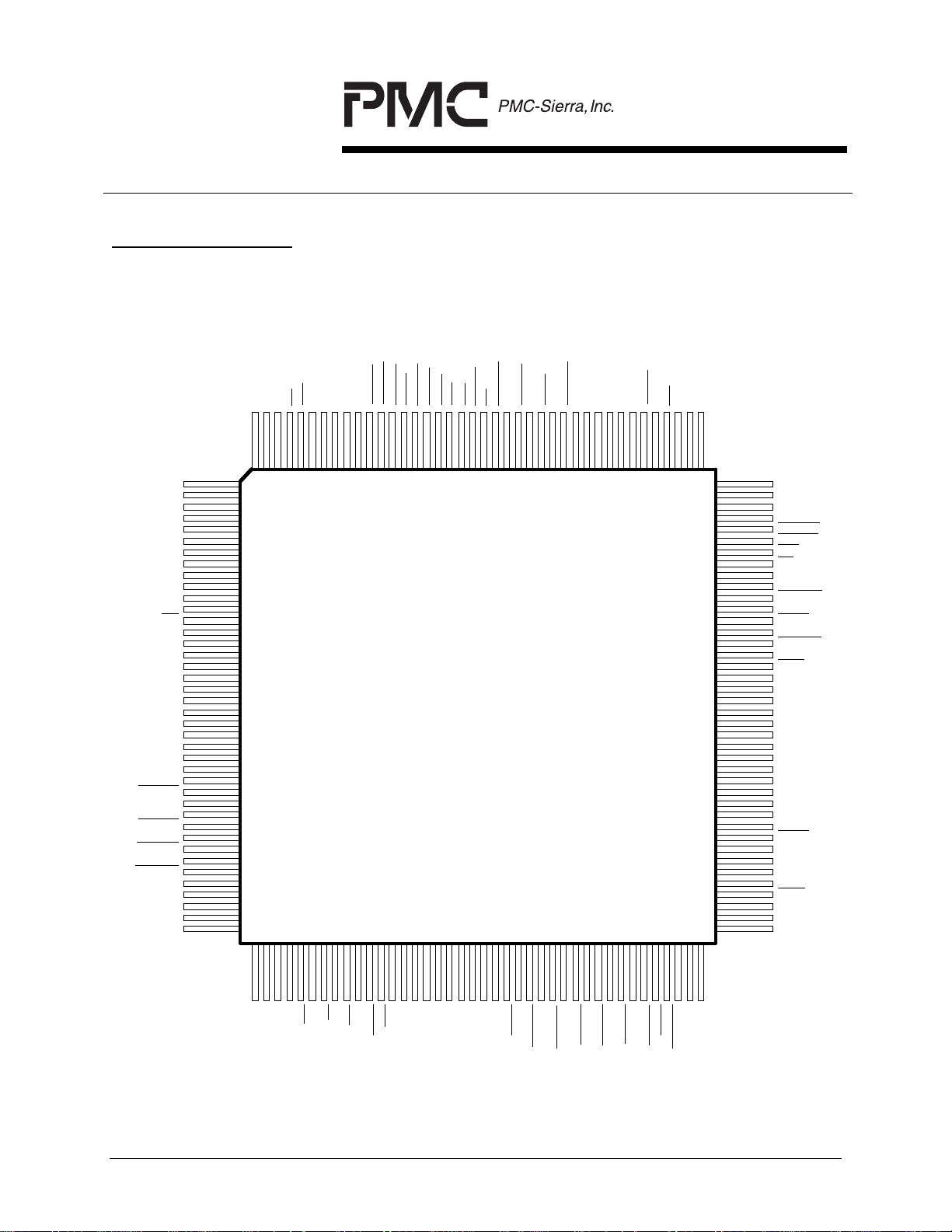
5
WRB_RWB
PIN DIAGRAM
The TUPP-PLUS is packaged in an 160 pin PQFP package having a body size of
28 mm by 28 mm and a pin pitch of 0.65 mm. Pins added since the PM5361TUPP are underlined.
VSSOAC
VDDOAC
VSSI
POHCK
OC1J1
OTMF
RAD
VSST
VSST
VSST
PIN 121
PIN 120
PIN 81
PIN 1
VSST
VSST
VSST
A[0]
A[1]
A[2]
A[3]
A[4]
A[5]
A[6]
A[7]
A[8]
CSB
MBEB
D[0]
D[1]
D[2]
D[3]
VDDODC
VDDI
VSSI
VSSODC
D[4]
D[5]
D[6]
D[7]
VDDOAC
INTB
VSSOAC
VSSODC
RSTB
VDDODC
ALE
A[11]/TRS
RDB_E
NC
VSST
VSST
VSST
PIN 40
PIN 160
VSST
VSST
VSST
A[9]
A[10]
VDDODC
VDDI
VSSODC
SCLK
VSSOAC
VSSI
GSCLK[0]
VDDOAC
NSCLK
IBMODE
LOM[1]
OBMODE
VDDI
VSSI
PM5362
TUPP-PLUS
POHEN[1]
LC1J1V1
LPL
VDDODC
OTV5
VSSODC
POH[1]
OTPL
POHFP[1]
OPL
VDDI
VSST
VSST
VSST
VDDODC
VSSODC
IDLE
AIS
VDDOAC
VSSOAC
POHEN[2]
OD[0]
POH[2]
OD[1]
POHFP[2]
OD[2]
TPOH
OD[3]
NC
VDDODC
VDDI
VSSI
VSSODC
NC
OD[4]
NC
OD[5]
NC
OD[6]
NC
OD[7]
LOM[2]
ODP
NC
VDDOAC
VSSOAC
COUT
NC
VSST
VSST
VSST
PIN 41
VSST
VSST
IC1J1
VSST
TCK
VDDI
TDI
IPL
TDO
VSSI
ITMF
TRSTB
TMS
ID[0]
NC
ID[1]
PROPRIETARY AND CONFIDENTIAL TO PMC-SIERRA, INC., AND FOR ITS CUSTOMERS’ INTERNAL USE
NC
ID[2]
NC
ID[3]
NC
ID[4]
ID[5]
LOM[3]
ID[6]
GSCLK[1]
POHFP[3]
ID[7]
VDDOAC
IDP
VDDODC
VDDI
VSSOAC
VSSI
VSSODC
POH[3]
POHEN[3]
VSST
VSST
PIN 80
VSST
10

PM5362 TUPP-PLUS
DATA SHEET
PMC-951010 ISSUE 6 SONET/SDH TRIBUTARY UNIT PAYLOAD PROCESSOR / PERFORMANCE MONITOR
6
BLOCK DIAGRAM
TRSTB
SCLK
NSCLK
IBMODE
OBMODE
GSCLK[1:0]
IC1J1
ITMF
ID[7:0]
TCK
TMS
TDI
IPL
IDP
JTAG
Controller
Input
Demux
Tributary
Payload
Processor
(VTPP)
Tributary
Payload
Processor
(VTPP)
Tributary
Payload
Processor
(VTPP)
Tributary
Path Overhead
Processor
(RTOP)
Tributary
Trace Buffer
(RTTB)
Tributary
Path Overhead
Processor
(RTOP)
Tributary
Trace Buffer
(RTTB)
Tributary
Path Overhead
Processor
(RTOP)
Tributary
Trace Buffer
(RTTB)
Output
Mux
TDO
OTMF
OC1J1
OPL
ODP
OTPL
OTV5
OD[7:0]
AIS
IDLE
COUT
TPOH
LC1J1V1
LPL
POH[3:1]
POHFP[3:1]
POHEN[3:1]
POHCK
RAD
LOM[3:1]
MBEB
RSTB
CSB
RDB
Microprocessor
Interface
WRB
ALE
A[11:0]
D[7:0]
PROPRIETARY AND CONFIDENTIAL TO PMC-SIERRA, INC., AND FOR ITS CUSTOMERS’ INTERNAL USE
INTB
11

PM5362 TUPP-PLUS
DATA SHEET
PMC-951010 ISSUE 6 SONET/SDH TRIBUTARY UNIT PAYLOAD PROCESSOR / PERFORMANCE MONITOR
7
PIN DESCRIPTION
Pin Name Type Pin
Function
No.
SCLK/ Input 153 The system clock (SCLK) provides timing for
TUPP-PLUS internal operations. SCLK is a
19.44 MHz, nominally 50% duty cycle, clock.
When either incoming interface is in nibble mode
(IBMODE set low) or the outgoing interface is in
nibble mode (OBMODE set low), SCLK must be
connected to GSCLK[0] externally.
In incoming byte interface mode (IBMODE set
high), IC1J1, IPL, ITMF, IDP, ID[7:0], OTMF,
OC1J1 and OPL are sampled on the rising edge
of SCLK. In outgoing byte interface mode
(OBMODE set high), ODP, OTPL, OTV5,
OD[7:0], AIS, IDLE, TPOH, LC1J1V1, LPL, and
LOM[3:1] are updated on the rising edge of
SCLK.
VCLK The test vector clock (VCLK) signal is used
during TUPP-PLUS production testing to verify
manufacture.
PROPRIETARY AND CONFIDENTIAL TO PMC-SIERRA, INC., AND FOR ITS CUSTOMERS’ INTERNAL USE
12

PM5362 TUPP-PLUS
DATA SHEET
PMC-951010 ISSUE 6 SONET/SDH TRIBUTARY UNIT PAYLOAD PROCESSOR / PERFORMANCE MONITOR
Pin Name Type Pin
Function
No.
NSCLK Input 147 The nibble interface mode system clock
(NSCLK) provides timing for TUPP-PLUS
internal operations in incoming or outgoing
nibble interface mode (IBMODE or OBMODE
set low). NSCLK is a 38.88 MHz, nominally 50%
duty cycle, clock.
In incoming nibble interface mode (IBMODE set
low), IC1J1, IPL, ITMF, IDP, ID[3:0] are sampled
on the rising edge of NSCLK. In outgoing nibble
interface mode (OBMODE set low), OTMF,
OC1J1 and OPL are sampled on the rising edge
of NSCLK, and ODP, OTPL, OTV5, OD[7:0],
AIS, IDLE, TPOH, LC1J1V1, LPL, and LOM[3:1]
are updated on the rising edge of NSCLK.
When the incoming and the outgoing interfaces
are in byte mode (IBMODE and OBMODE both
set high), NSCLK may be left unconnected.
NSCLK has an integral pull-up resistor.
IBMODE Input 145 The incoming byte interface mode signal
(IBMODE) configures the incoming interface
mode of the TUPP-PLUS. When IBMODE is set
low, nibble interface mode is selected. SCLK
must be connected to GSCLK[0]. IC1J1, IPL,
ITMF, IDP, ID[3:0] are sampled on the rising
edge of NSCLK. When IBMODE is set high,
byte interface mode is selected. IC1J1, IPL,
ITMF, IDP, ID[7:0] are sampled on the rising
edge of SCLK. IBMODE has an integral pull-up
resister.
PROPRIETARY AND CONFIDENTIAL TO PMC-SIERRA, INC., AND FOR ITS CUSTOMERS’ INTERNAL USE
13

PM5362 TUPP-PLUS
DATA SHEET
PMC-951010 ISSUE 6 SONET/SDH TRIBUTARY UNIT PAYLOAD PROCESSOR / PERFORMANCE MONITOR
Pin Name Type Pin
Function
No.
OBMODE Input 146 The outgoing byte interface mode signal
(OBMODE) configures the outgoing interface
mode of the TUPP-PLUS. When OBMODE is
set low, nibble interface mode is selected. SCLK
must be connected to GSCLK[0]. OTMF, OC1J1
and OPL are sampled on the rising edge of
NSCLK. ODP, OTPL, OTV5, OD[3:0], AIS, IDLE,
LC1J1V1, LPL, and LOM[3:1] are updated on
the rising edge of NSCLK. When OBMODE is
set high, byte interface mode is selected. OTMF,
OC1J1 and OPL are sampled on the rising edge
of SCLK. ODP, OTPL, OTV5, OD[7:0], AIS,
IDLE, LC1J1V1, LPL, and LOM[3:1] are updated
on the rising edge of SCLK. OBMODE has an
integral pull-up resister.
GSCLK[1]
GSCLK[0]
Output 65
149
The generated system clock (GSCLK[1:0])
signals provide timing for the TUPP-PLUS when
nibble mode is selected at the incoming or
outgoing interface (IBMODE or OBMODE set
low). GSCLK[1:0] are a divide by two of NSCLK.
GSCLK[0] must only be connected to SCLK
externally when IBMODE or OBMODE is set
low. GSCLK[1] is a exact replica of GSCLK[0]
and can be used to supply timing to external
devices that are operating in byte mode.
GSCLK[1:0] are updated on the rising edge of
NSCLK.
PROPRIETARY AND CONFIDENTIAL TO PMC-SIERRA, INC., AND FOR ITS CUSTOMERS’ INTERNAL USE
14

PM5362 TUPP-PLUS
DATA SHEET
PMC-951010 ISSUE 6 SONET/SDH TRIBUTARY UNIT PAYLOAD PROCESSOR / PERFORMANCE MONITOR
Pin Name Type Pin
Function
No.
IC1J1 Input 44 The input C1/J1 frame pulse (IC1J1) identifies
the transport envelope and synchronous
payload envelope frame boundaries on the
incoming stream.
In incoming byte interface mode (IBMODE set
high), IC1J1 is set high while IPL is low to mark
the first C1 byte of the transport envelope frame
on the ID[7:0] bus. IC1J1 is set high while IPL is
high to mark each J1 byte of the synchronous
payload envelope(s) on the ID[7:0] bus. IC1J1
must be present at every occurrence of the first
C1 and all J1 bytes. The TUPP-PLUS will ignore
a pulse on IC1J1 at the byte position of the V1
byte of the first tributary of each VC3 or the top
byte of the first fixed stuff column of each TUG3.
IC1J1 is sampled on the rising edge of SCLK.
In incoming nibble interface mode (IBMODE set
low), IC1J1 is set high while IPL is low to mark
the more significant nibble of the first C1 byte of
the transport envelope frame on the ID[3:0] bus.
IC1J1 is set high while IPL is high to mark the
more significant nibble of each J1 byte of the
synchronous payload envelope(s) on the ID[3:0]
bus. IC1J1 must be present at every occurrence
of the first C1 and all J1 bytes. The TUPP-PLUS
will ignore a pulse on IC1J1 at the byte position
of the V1 byte of the first tributary of each VC3
or the top byte of the first fixed stuff column of
each TUG3. IC1J1 must be set low during the
less significant nibble timeslots. IC1J1 is
sampled on the rising edge of NSCLK.
PROPRIETARY AND CONFIDENTIAL TO PMC-SIERRA, INC., AND FOR ITS CUSTOMERS’ INTERNAL USE
15

PM5362 TUPP-PLUS
DATA SHEET
PMC-951010 ISSUE 6 SONET/SDH TRIBUTARY UNIT PAYLOAD PROCESSOR / PERFORMANCE MONITOR
Pin Name Type Pin
Function
No.
IPL Input 48 The active high incoming payload active (IPL)
signal identifies the bytes within the transport
envelope frame on the incoming stream that
carry the VC3 or VC4 virtual containers, or the
STS-1 synchronous payload envelopes.
In incoming byte interface mode (IBMODE set
high), IPL must be brought high to mark each
payload byte on ID[7:0]. IPL is sampled on the
rising edge of SCLK.
In incoming nibble interface mode (IBMODE set
low), IPL must be brought high to mark the more
significant nibble of each payload byte on
ID[3:0]. IPL is ignored during the less significant
nibble timeslots. IPL is sampled on the rising
edge of NSCLK.
PROPRIETARY AND CONFIDENTIAL TO PMC-SIERRA, INC., AND FOR ITS CUSTOMERS’ INTERNAL USE
16

PM5362 TUPP-PLUS
DATA SHEET
PMC-951010 ISSUE 6 SONET/SDH TRIBUTARY UNIT PAYLOAD PROCESSOR / PERFORMANCE MONITOR
Pin Name Type Pin
Function
No.
ITMF Input 52 The active high incoming tributary multiframe
(ITMF) signal identifies the first frame of the
tributary multiframe for each STS-1 synchronous
payload envelope, AU3, or AU4 administrative
unit. ITMF is enabled by the setting the ITMFEN
register bit high. When ITMFEN bit is low, the
path overhead H4 byte is used to determine
tributary multiframe boundaries. ITMF is
selectable to pulse high during the third byte
after J1 of the first tributary or during the H4
byte which indicates that the next frame is the
first frame of the tributary multiframe. Selection
between marking each H4 or the third byte after
each J1 is controlled by the ITMFH4 register bit.
Pulses on ITMF are only effective during the H4
or third byte after each J1 byte positions, as
appropriate. ITMF is ignored at other byte
positions.
In incoming byte interface mode (IBMODE set
high), ITMF is sampled on the rising edge of
SCLK.
In incoming nibble interface mode (IBMODE set
low), ITMF marks the more significant nibble of
H4 or the third byte after J1, as appropriate. It is
ignored at the less significant nibble timeslots.
ITMF is sampled on the rising edge of NSCLK.
PROPRIETARY AND CONFIDENTIAL TO PMC-SIERRA, INC., AND FOR ITS CUSTOMERS’ INTERNAL USE
17

PM5362 TUPP-PLUS
DATA SHEET
PMC-951010 ISSUE 6 SONET/SDH TRIBUTARY UNIT PAYLOAD PROCESSOR / PERFORMANCE MONITOR
Pin Name Type Pin
Function
No.
IDP Input 70 The incoming data parity (IDP) signal carries the
parity of the incoming signals.
In incoming byte interface mode (IBMODE set
high), the parity calculation encompasses the
ID[7:0] bus and optionally the IC1J1 and the IPL
signals. IC1J1 and IPL can be included in the
parity calculation by setting the INCC1J1 and
INCPL register bits high, respectively. Odd
parity is selected by setting the IOP register bit
high, and even parity is selected by setting the
IOP bit low. IDP is sampled on the rising edge
of SCLK.
In incoming nibble interface mode (IBMODE set
low), The parity calculation encompasses the
ID[3:0] bus and optionally the IC1J1 and the IPL
signals. IC1J1 and IPL can be included in the
parity calculation by setting the INCC1J1 and
INCPL register bits high, respectively. Odd
parity is selected by setting the IOP register bit
high, and even parity is selected by setting the
IOP bit low. IDP is sampled on the rising edge
of NSCLK.
PROPRIETARY AND CONFIDENTIAL TO PMC-SIERRA, INC., AND FOR ITS CUSTOMERS’ INTERNAL USE
18

PM5362 TUPP-PLUS
DATA SHEET
PMC-951010 ISSUE 6 SONET/SDH TRIBUTARY UNIT PAYLOAD PROCESSOR / PERFORMANCE MONITOR
Pin Name Type Pin
No.
ID[0]
ID[1]
ID[2]
ID[3]
ID[4]
ID[5]
ID[6]
ID[7]
Input 54
56
58
60
62
64
66
68
Function
The incoming data bus (ID[7:0]) carries
SONET/SDH frame data in byte serial format.
In incoming byte interface mode (IBMODE set
high), ID[7] is the most significant bit,
corresponding to bit 1 of each serial word, the
bit transmitted first. ID[0] is the least significant
bit, corresponding to bit 8 of each serial word,
the last bit transmitted. The ID[7:0] bus is
sampled on the rising edge of SCLK.
In incoming nibble interface mode (IBMODE set
low), ID[3] is the most significant bit of each
nibble, corresponding to bit 1 or bit 5 of each
serial word, the bit transmitted first and fifth,
respectively. ID[0] is the least significant bit of
each nibble, corresponding to bit 4 or bit 8 of
each serial word, the fourth or last bit
transmitted, respectively. ID[7:4] is ignored. The
ID[3:0] bus is sampled on the rising edge of
NSCLK.
PROPRIETARY AND CONFIDENTIAL TO PMC-SIERRA, INC., AND FOR ITS CUSTOMERS’ INTERNAL USE
19

PM5362 TUPP-PLUS
DATA SHEET
PMC-951010 ISSUE 6 SONET/SDH TRIBUTARY UNIT PAYLOAD PROCESSOR / PERFORMANCE MONITOR
Pin Name Type Pin
No.
OC1J1 Input 127
Function
The outgoing composite frame pulse (OC1J1) marks
the transport frame and synchronous payload
envelope frame boundaries on the outgoing stream.
In outgoing byte interface mode (OBMODE set high),
and the OJ1EN register bit is set low, OC1J1 pulses
high to mark the firs t C1 byte of t he t ransport
envelope frame on the OD[7:0] bus. The OPL input
must be held low. The position of the J1 byte(s) is
implicit and fixed to the bytes immediately following
the last C1 byte. When the OJ1EN register bit is set
high, the OC1J1 signal pulses high while OPL is low
to mark the first C1 byte of the transport frame on
the OD[7:0] bus and pulses high while OPL is high to
mark each of the J1 bytes of the synchronous
payload envelope(s) on the OD[7:0] bus. OC1J1
must be present at every occurrence of the first C1
byte and all J1 bytes. A V1 pulse added to the
OC1J1 input will be ignored by the TUPP-PLUS.
OC1J1 is sampled on the rising edge of SCLK.
In outgoing nibble interface mode (OBMODE set
low), and the OJ1EN register bit is set low, OC1J1
pulses high to mark the mor e signif icant nibble of the
first C1 byte of the transport envelope frame on the
OD[3:0] bus. The OPL input must be held low. The
position of the J1 byte(s) is implicit and fixed to the
bytes immediately following the last C1 byte. When
the OJ1EN register bit is set high, t he O C1J1 signal
pulses high while OPL is low to mark the more
significant nibble of the first C1 byte of the transpor t
frame on the OD[3:0] bus and pulses high while OPL
is high to mark each of the J1 bytes of the
synchronous payload envelope(s) on the OD[3:0]
bus. OC1J1 must be pr esent at every occurrence of
the first C1 byte and all J1 bytes. A V1 pulse added
to the OC1J1 input will be ignored by the TUPP-
PLUS. OC1J1 must be set low during the less
significant nibble timeslots. OC1J1 is sampled on
the rising edge of NSCLK.
PROPRIETARY AND CONFIDENTIAL TO PMC-SIERRA, INC., AND FOR ITS CUSTOMERS’ INTERNAL USE
20

PM5362 TUPP-PLUS
DATA SHEET
PMC-951010 ISSUE 6 SONET/SDH TRIBUTARY UNIT PAYLOAD PROCESSOR / PERFORMANCE MONITOR
Pin Name Type Pin
Function
No.
OTMF Input 125 The active high outgoing tributary multiframe
(OTMF) signal identifies the first frame of the
tributary multiframe for each AU3, or AU4
administrative unit, or STS-1 synchronous
payload envelope. OTMF is selectable to pulse
high during the third byte after J1 of the first
tributary or during the H4 byte of the path
overhead which indicates that the next frame is
the first frame of the tributary multiframe.
Selection between marking the third byte after
each J1 or H4 bytes is controlled by the
OTMFH4 bit. Pulses on OTMF are only effective
during the H4 or third byte after each J1 byte
positions, as appropriate. OTMF is ignored at
other byte positions.
In outgoing byte interface mode (OBMODE set
high), OTMF is sampled on the rising edge of
SCLK.
In outgoing nibble interface mode (OBMODE set
low), OTMF is ignored at the less significant
nibble timeslots. OTMF is sampled on the rising
edge of NSCLK.
PROPRIETARY AND CONFIDENTIAL TO PMC-SIERRA, INC., AND FOR ITS CUSTOMERS’ INTERNAL USE
21

PM5362 TUPP-PLUS
DATA SHEET
PMC-951010 ISSUE 6 SONET/SDH TRIBUTARY UNIT PAYLOAD PROCESSOR / PERFORMANCE MONITOR
Pin Name Type Pin
Function
No.
COUT Output 85 The controlled output signal (COUT) is a
software programmable output that is controlled
by the COUTx register bit associated with each
tributary.
In outgoing byte interface mode (OBMODE set
high), COUT is synchronized to the OD[7:0] bus.
In floating mode, COUT contains valid data only
for bytes in the VC3 or VC4 virtual container(s),
or the STS-1 synchronous payload envelopes.
Its contents should be ignored for bytes in the
transport overhead. In locked mode, COUT is
set low for transport overhead bytes. COUT is
updated on the rising edge of SCLK.
In outgoing nibble interface mode (OBMODE set
low), COUT is synchronized to the OD[3:0] bus.
In floating mode, COUT contains valid data only
for bytes in the VC3 or VC4 virtual container(s),
or the STS-1 synchronous payload envelopes.
Its contents should be ignored for bytes in the
transport overhead. In locked mode, COUT is
set low for transport overhead bytes. COUT is
updated on the rising edge of NSCLK.
PROPRIETARY AND CONFIDENTIAL TO PMC-SIERRA, INC., AND FOR ITS CUSTOMERS’ INTERNAL USE
22

PM5362 TUPP-PLUS
DATA SHEET
PMC-951010 ISSUE 6 SONET/SDH TRIBUTARY UNIT PAYLOAD PROCESSOR / PERFORMANCE MONITOR
Pin Name Type Pin
No.
OPL Input 132
Function
The active high outgoing payload active (OPL) signal
identifies the bytes within the transport envelope frame on
the OD[7:0] bus that carry the VC3 or VC4 virtual
container(s), and the STS-1 synchronous payload
envelopes.
In outgoing byte interface mode (OBMODE set high), and
floating mode is enabled, OPL must be set high to mark
each payload byte. OD[7:0], OTPL, OTV5, AIS and IDLE
contain valid data only for bytes in the VC3 or VC4 virtual
container(s), or the STS-1 synchronous payload
envelopes. Their contents should be ignored for bytes in
the transport overhead as indicated by a low level on the
OPL input. In locked mode, the outgoing virtual container
(synchronous payload envelope) is locked with the J1 byte
immediately following the C1 byte and OPL should be held
low. During transport overhead byte locations on the
outgoing stream, OTPL, OTV5, AIS and IDLE are set low.
OD[7:0] is set to a valid pointer with offset of 522 and all-
zeros for other transport overhead bytes. OPL is sampled
on the rising edge of SCLK.
In outgoing nibble interface mode (OBMODE set low), and
floating mode is enabled, OPL must be set high to mark
the more significant nibble of each payload byte. OPL is
ignored during the less significant nibble. OD[3:0], OTPL,
OTV5, AIS and IDLE contain valid data only for bytes in
the VC3 or VC4 virtual container(s), or the STS-1
synchronous payload envelopes. Their contents should be
ignored for bytes in the transport overhead as indicated by
a low level on the OPL input. In locked mode, the outgoing
virtual container (synchronous payload envelope) is locked
with the J1 byte immediately following the C1 byte and
OPL should be held low. During transport overhead byte
locations on the outgoing stream, OTPL, OTV5, AIS and
IDLE are set low. OD[3:0] is set to a valid pointer with
offset of 522 and all-zeros for other transport overhead
bytes. OPL is ignored during the less significant nibble
timeslots. OPL is sampled on the rising edge of NSCLK.
PROPRIETARY AND CONFIDENTIAL TO PMC-SIERRA, INC., AND FOR ITS CUSTOMERS’ INTERNAL USE
23

PM5362 TUPP-PLUS
DATA SHEET
PMC-951010 ISSUE 6 SONET/SDH TRIBUTARY UNIT PAYLOAD PROCESSOR / PERFORMANCE MONITOR
Pin Name Type Pin
No.
OD[0]
OD[1]
OD[2]
OD[3]
OD[4]
OD[5]
OD[6]
OD[7]
Output 110
108
106
104
97
95
93
91
Function
The outgoing data bus (OD[7:0]) carries
SONET/SDH frame data in byte serial format.
In outgoing byte interface mode (OBMODE set
high), OD[7] is the most significant bit,
corresponding to bit 1 of each serial word, the
bit transmitted first. OD[0] is the least significant
bit, corresponding to bit 8 of each serial word,
the last bit transmitted. In floating mode,
OD[7:0] contains valid data only for bytes in the
VC3 or VC4 virtual container(s), or the STS-1
synchronous payload envelopes. Its contents
should be ignored for bytes in the transport
overhead. In locked mode, OD[7:0] is set to all-
zeros at transport overhead bytes, except for a
valid pointer with offset 522 at H1, H2 bytes.
The OD[7:0] bus is updated on the rising edge
of SCLK.
In outgoing nibble interface mode (OBMODE set
low), OD[3] is the most significant bit of each
nibble, corresponding to bit 1 or bit 5 of each
serial word, the bit transmitted first or fifth,
respectively. OD[0] is the least significant bit,
corresponding to bit 4 or bit 8 of each serial
word, the fourth or last bit transmitted,
respectively. OD[7:4] are set low. In floating
mode, OD[3:0] contains valid data only for bytes
in the VC3 or VC4 virtual container(s), or the
STS-1 synchronous payload envelopes. Its
contents should be ignored for bytes in the
transport overhead. In locked mode, OD[3:0] is
set to all-zeros at transport overhead bytes,
except for a valid pointer with offset 522 at H1,
H2 bytes. The OD[7:0] bus is updated on the
rising edge of NSCLK.
PROPRIETARY AND CONFIDENTIAL TO PMC-SIERRA, INC., AND FOR ITS CUSTOMERS’ INTERNAL USE
24

PM5362 TUPP-PLUS
DATA SHEET
PMC-951010 ISSUE 6 SONET/SDH TRIBUTARY UNIT PAYLOAD PROCESSOR / PERFORMANCE MONITOR
Pin Name Type Pin
Function
No.
ODP Output 89 The outgoing data parity (ODP) signal carries
the parity of the outgoing data stream, OD[7:0].
Odd parity is selected by setting the OOP
register bit high, and even parity is selected by
setting the OOP bit low. ODP is updated on the
rising of SCLK in outgoing byte interface mode
(OBMODE set high) and on the rising edge of
NSCLK in outgoing nibble interface mode
(OBMODE set low).
OTPL Output 134 The outgoing tributary payload active (OTPL)
signal marks the bytes carrying the tributary
payload.
In outgoing byte interface mode (OBMODE set
high), OTPL is set high to mark each tributary
payload byte on the OD[7:0] bus. In floating
mode, OTPL contains valid data only for bytes in
the VC3 or VC4 virtual container(s), or the
STS-1 synchronous payload envelopes. Its
contents should be ignored for bytes in the
transport overhead. In locked mode, OTPL is
set low for transport overhead. OTPL is updated
on the rising edge of SCLK.
In outgoing nibble interface mode (OBMODE set
low), OTPL is set high to mark each tr ibutary
payload byte on the OD[3:0] bus. In floating
mode, OTPL contains valid data only for bytes in
the VC3 or VC4 virtual container(s), or the
STS-1 synchronous payload envelopes. Its
contents should be ignored for bytes in the
transport overhead. In locked mode, OTPL is
set low for transport overhead. OTPL is updated
on the rising edge of NSCLK.
PROPRIETARY AND CONFIDENTIAL TO PMC-SIERRA, INC., AND FOR ITS CUSTOMERS’ INTERNAL USE
25

PM5362 TUPP-PLUS
DATA SHEET
PMC-951010 ISSUE 6 SONET/SDH TRIBUTARY UNIT PAYLOAD PROCESSOR / PERFORMANCE MONITOR
Pin Name Type Pin
Function
No.
OTV5 Output 136 The outgoing tributary V5 byte (OTV5) signal
marks the various tributary V5 bytes.
In outgoing byte interface mode (OBMODE set
high), OTV5 is set high to mark each tributary
V5 byte on the OD[7:0] bus. When the outgoing
tributary is a TU3, OTV5 marks the J1 byte of
the TU3. In floating mode, OTV5 contains valid
data only for bytes in the VC3 or VC4 virtual
container(s), or the STS-1 synchronous payload
envelopes. Its contents should be ignored for
bytes in the transport overhead. In locked
mode, OTV5 is set low for transport overhead
bytes. OTV5 is updated on the rising edge of
SCLK.
In outgoing nibble interface mode (OBMODE set
low), OTV5 is set high to mark each tr ibutary V5
byte on the OD[3:0] bus. When the outgoing
tributary is a TU3, OTV5 marks the J1 byte of
the TU3. In floating mode, OTV5 contains valid
data only for bytes in the VC3 or VC4 virtual
container(s), or the STS-1 synchronous payload
envelopes. Its contents should be ignored for
bytes in the transport overhead. In locked
mode, OTV5 is set low for transport overhead
bytes. OTV5 is updated on the rising edge of
NSCLK.
PROPRIETARY AND CONFIDENTIAL TO PMC-SIERRA, INC., AND FOR ITS CUSTOMERS’ INTERNAL USE
26

PM5362 TUPP-PLUS
DATA SHEET
PMC-951010 ISSUE 6 SONET/SDH TRIBUTARY UNIT PAYLOAD PROCESSOR / PERFORMANCE MONITOR
Pin Name Type Pin
Function
No.
AIS Output 114 The tributary alarm indication signal output (AIS)
marks tributaries on the outgoing stream that
are in AIS state.
In outgoing byte interface mode (OBMODE set
high), AIS is set high when AIS is inserted in the
associated tributary on the OD[7:0] and is set
low when the AIS is not inserted. In floating
mode, AIS contains valid data only for bytes in
the VC3 or VC4 virtual container(s), or the
STS-1 synchronous payload envelopes. Its
value should be ignored for bytes in the
transport overhead. In locked mode, AIS is set
low for transport overhead bytes. AIS is updated
on the rising edge of SCLK.
In outgoing nibble interface mode (OBMODE set
low), AIS is set high when AIS is inserted in the
associated tributary on the OD[3:0] and is set
low when the AIS is not inserted. In floating
mode, AIS contains valid data only for bytes in
the VC3 or VC4 virtual container(s), or the
STS-1 synchronous payload envelopes. Its
value should be ignored for bytes in the
transport overhead. In locked mode, AIS is set
low for transport overhead bytes. AIS is updated
on the rising edge of NSCLK.
PROPRIETARY AND CONFIDENTIAL TO PMC-SIERRA, INC., AND FOR ITS CUSTOMERS’ INTERNAL USE
27

PM5362 TUPP-PLUS
DATA SHEET
PMC-951010 ISSUE 6 SONET/SDH TRIBUTARY UNIT PAYLOAD PROCESSOR / PERFORMANCE MONITOR
Pin Name Type Pin
Function
No.
IDLE Output 115 The tributary idle indication signal output (IDLE)
marks tributaries on the outgoing stream that
are in idle state.
In outgoing byte interface mode (OBMODE set
high), IDLE is set high when idle code is
inserted in the associated tributary on the
OD[7:0] and is set low when the idle code is not
inserted. In floating mode, IDLE contains valid
data only for bytes in the VC3 or VC4 virtual
container(s), or the STS-1 synchronous payload
envelopes. Its value should be ignored for bytes
in the transport overhead. In locked mode, IDLE
is set low for transport overhead bytes. IDLE is
updated on the rising edge of SCLK.
In outgoing nibble interface mode (OBMODE set
low), IDLE is set high when idle code is inserted
in the associated tributary on the OD[3:0] and is
set low when the idle code is not inserted. In
floating mode, IDLE contains valid data only for
bytes in the VC3 or VC4 virtual container(s), or
the STS-1 synchronous payload envelopes. Its
value should be ignored for bytes in the
transport overhead. In locked mode, IDLE is set
low for transport overhead bytes. IDLE is
updated on the rising edge of NSCLK.
PROPRIETARY AND CONFIDENTIAL TO PMC-SIERRA, INC., AND FOR ITS CUSTOMERS’ INTERNAL USE
28

PM5362 TUPP-PLUS
DATA SHEET
PMC-951010 ISSUE 6 SONET/SDH TRIBUTARY UNIT PAYLOAD PROCESSOR / PERFORMANCE MONITOR
Pin Name Type Pin
Function
No.
TPOH Output 105 The outgoing tributary path overhead byte
(OTV5) signal marks the tributary path overhead
bytes in the outgoing stream. For streams in
TU3 mode, the J1, B3,C2, G1, F2, H4, Z3, Z4
and Z5 bytes are marked. For streams out of
TU3 mode, V5, J2, Z6 an Z7 bytes are marked.
In outgoing byte interface mode (OBMODE set
high), TPOH is set high to mark each tributary
path overhead byte on the OD[7:0] bus. In
floating mode, TPOH contains valid data only for
bytes in the VC3 or VC4 virtual container(s), or
the STS-1 synchronous payload envelopes. Its
contents should be ignored for bytes in the
transport overhead. In locked mode, TPOH is
set low for transport overhead bytes. TPOH is
updated on the rising edge of SCLK.
In outgoing nibble interface mode (OBMODE set
low), TPOH is set high to mark each tributary
path overhead byte on the OD[3:0] bus. In
floating mode, TPOH contains valid data only for
bytes in the VC3 or VC4 virtual container(s), or
the STS-1 synchronous payload envelopes. Its
contents should be ignored for bytes in the
transport overhead. In locked mode, TPOH is
set low for transport overhead bytes. TPOH is
updated on the rising edge of NSCLK.
PROPRIETARY AND CONFIDENTIAL TO PMC-SIERRA, INC., AND FOR ITS CUSTOMERS’ INTERNAL USE
29

PM5362 TUPP-PLUS
DATA SHEET
PMC-951010 ISSUE 6 SONET/SDH TRIBUTARY UNIT PAYLOAD PROCESSOR / PERFORMANCE MONITOR
Pin Name Type Pin
No.
LOM[3]
LOM[2]
LOM[1]
Output 63
90
144
Function
The loss of multiframe signals (LOM[3:1])
reports the tributary multiframe synchronization
status. LOM is set low when a correct sequence
on the H4 byte has been detected for four
frames. LOM is set high if a correct four frame
sequence is not detected in 1 millisecond.
LOM[3], LOM[2] and LOM[1] report the
synchronization status of STS-1 #1, #2 and #3,
respectively. In AU4 mode, LOM[3], LOM[2] and
LOM[1] report the synchronization status of
TUG3 #1, #2 and #3, respectively. LOM[3:1] are
updated on the rising edge of SCLK.
PROPRIETARY AND CONFIDENTIAL TO PMC-SIERRA, INC., AND FOR ITS CUSTOMERS’ INTERNAL USE
30

PM5362 TUPP-PLUS
DATA SHEET
PMC-951010 ISSUE 6 SONET/SDH TRIBUTARY UNIT PAYLOAD PROCESSOR / PERFORMANCE MONITOR
Pin Name Type Pin
Function
No.
LC1J1V1 Output 141 The locked mode composite frame pulse
(LC1J1V1) marks the transport, synchronous
payload envelope and tributary multiframe frame
boundaries on the outgoing stream. LC1J1V1 is
only active in locked mode (OJ1EN register bit
set low). LC1J1V1 is held low in floating mode
(OJ1EN set high).
In outgoing byte interface mode (OBMODE set
high), and locked mode is enabled (OJ1EN set
low), LC1J1V1 pulses high to mark the first C1
byte of the transport envelope frame on the
OD[7:0] bus. It also pulses high to mark the J1
byte(s) which is (are) register selectable to be
implicitly fixed to immediately follow the C1 bytes
or the H3 bytes. Optionally, LC1J1V1 also
marks the third byte after J1 of the first tributary
in each STS-1 (TUG3) stream when the LV1EN
register bit is set high. LC1J1V1 is updated on
the rising edge of SCLK.
In outgoing nibble interface mode (OBMODE set
low), and locked mode is enabled (OJ1EN set
low), LC1J1V1 pulses high to mark the more
significant nibble of the first C1 byte of the
transport envelope frame on the OD[3:0] bus. It
also pulses high to mark the more significant
nibble of the J1 byte(s) which is (are) register
selectable to be implicitly fixed to immediately
follow the C1 bytes or the H3 bytes. Optionally,
LC1J1V1 also marks the more significant nibble
of the third byte after J1 of the first tributary in
each STS-1 (TUG3) stream when the LV1EN
register bit is set high. LC1J1V1 is updated on
the rising edge of NSCLK.
PROPRIETARY AND CONFIDENTIAL TO PMC-SIERRA, INC., AND FOR ITS CUSTOMERS’ INTERNAL USE
31

PM5362 TUPP-PLUS
DATA SHEET
PMC-951010 ISSUE 6 SONET/SDH TRIBUTARY UNIT PAYLOAD PROCESSOR / PERFORMANCE MONITOR
Pin Name Type Pin
Function
No.
LPL Output 140 The locked mode payload active signal (LPL)
identifies synchronous payload envelope bytes
on the outgoing stream. LPL is only active in
locked mode (OJ1EN register bit set low). LPL
is held low in floating mode (OJ1EN set high). If
locked mode is enabled (OJ1EN set low), LPL is
set high to mark synchronous payload envelop
bytes and set low to mark transport overhead
bytes. LPL is updated on the rising edge of
SCLK in outgoing byte interface mode
(OBMODE set high) or on the rising edge of
NSCLK in outgoing nibble interface mode
(OBMODE set low).
POHCK Output 126 The tributary path overhead clock signal
(POHCK) provides timing to sample the
extracted tributary path overhead stream and
the receive alarm port. POHCK is nominally
9.72 MHz clock signals. The POH[3:1],
POHEN[3:1], POHFP[3:1] and RAD outputs are
updated on the falling edge of POHCK.
POH[3]
POH[2]
POH[1]
Output 76
109
135
The tributary path overhead signals (POH[3:1])
contains the tributary path overhead bytes (V5,
J2, Z6 and Z7) extracted from the ID[7:0] bus.
POH[3], POH[2] and POH[1] contain the
tributary path overhead bytes from STS-1 #1, #2
and #3, respectively. In AU4 mode, POH[3],
POH[2] and POH[1] contain the tributary path
overhead bytes from TUG3 #1, #2 and #3,
respectively. All four tributary overhead bytes of
each tributary is shifted out once per payload
frame. The corresponding POHEN signal is set
high to identify overhead bytes that are
presented for the first time. Each POH signal is
updated on the falling edge of POHCK.
PROPRIETARY AND CONFIDENTIAL TO PMC-SIERRA, INC., AND FOR ITS CUSTOMERS’ INTERNAL USE
32

PM5362 TUPP-PLUS
DATA SHEET
PMC-951010 ISSUE 6 SONET/SDH TRIBUTARY UNIT PAYLOAD PROCESSOR / PERFORMANCE MONITOR
Pin Name Type Pin
No.
POHFP[3]
POHFP[2]
POHFP[1]
POHEN[3]
POHEN[2]
POHEN[1]
Output 67
107
133
Output 77
111
139
Function
The tributary path overhead frame pulse signals
(POHFP[3:1]) may be used to locate the
individual path overhead bits of each tributary
for the corresponding STS-1 (TUG3) stream.
Each POHFP signal is set high to mark bit 1 (the
most significant bit) of the V5 byte of the first
tributary. POHFP[3], POHFP[2] and POHFP[1]
identify frame boundaries of the tributary path
overhead bytes from STS-1 #1, #2 and #3,
respectively. In AU4 mode, POHFP[3],
POHFP[2] and POHFP[1] identify frame
boundaries of TUG3 #1, #2 and #3, respectively.
Each POHFP signal is updated on the falling
edge of POHCK.
The tributary path overhead enable signals
(POHEN[3:1]) may be used to identify tributary
path overhead bytes that are being presented
on the corresponding POH stream for the first
time. Each POHEN signal is set high when a
fresh overhead byte is available on the
corresponding POH stream. POHEN is set low
when the tributary path overhead byte available
on the corresponding POH stream has already
been shifted out in a previous frame.
POHEN[3], POHEN[2] and POHEN[1] identify
the status of tributary path overhead bytes from
STS-1 #1, #2 and #3, respectively. In AU4
mode, POHFP[3], POHFP[2] and POHFP[1]
identify the status of tributary path overhead
bytes from TUG3 #1, #2 and #3, respectively.
Each POHEN signal is updated on the falling
edge of POHCK.
RAD Output 124 The receive alarm port (RAD) contains the
tributary path BIP error count, the RDI status
and the PDI status of each tributary in the
ID[7:0] bus. RAD is updated on the falling edge
of POHCK.
PROPRIETARY AND CONFIDENTIAL TO PMC-SIERRA, INC., AND FOR ITS CUSTOMERS’ INTERNAL USE
33

PM5362 TUPP-PLUS
DATA SHEET
PMC-951010 ISSUE 6 SONET/SDH TRIBUTARY UNIT PAYLOAD PROCESSOR / PERFORMANCE MONITOR
Pin Name Type Pin
Function
No.
MBEB Input 14 The active low Motorola bus enable (MBEB)
signal configures the TUPP-PLUS for Motorola
bus mode where the RDB/E signal functions as
E, and the WRB/RWB signal functions as RWB.
When MBEB is high, the TUPP-PLUS is
configured for Intel bus mode where the RDB/E
signal functions as RDB. The MBEB input has
an integral pull up resistor.
CSB Input 13 The active low chip select (CSB) signal is low
during TUPP-PLUS register accesses. If CSB is
not required (i.e., register accesses are
controlled by using the RDB/E and WRB/RWB
signals only), CSB must be connected to an
inverted version of RSTB.
RDB/ Input 35 The active low read enable (RDB) signal is low
during TUPP-PLUS register read accesses while
in Intel bus mode. The TUPP-PLUS drives the
D[7:0] bus with the contents of the addressed
register while RDB and CSB are low.
E The active high external access (E) signal is
high during TUPP-PLUS register access while in
Motorola bus mode.
WRB/ Input 37 The active low write strobe (WRB) signal is low
during a TUPP-PLUS register write accesses
while in Intel bus mode. The D[7:0] bus contents
are clocked into the addressed register on the
rising WRB edge while CSB is low.
RWB The read/write select (RWB) signal selects
between TUPP-PLUS register read and write
accesses while in Motorola bus mode. The
TUPP-PLUS drives the D[7:0] bus with the
contents of the addressed register while CSB is
low and RWB and E are high. The D[7:0] bus
contents are clocked into the addressed register
on the falling E edge while CSB and RWB are
low.
PROPRIETARY AND CONFIDENTIAL TO PMC-SIERRA, INC., AND FOR ITS CUSTOMERS’ INTERNAL USE
34

PM5362 TUPP-PLUS
DATA SHEET
PMC-951010 ISSUE 6 SONET/SDH TRIBUTARY UNIT PAYLOAD PROCESSOR / PERFORMANCE MONITOR
Pin Name Type Pin
No.
D[0]
D[1]
D[2]
D[3]
D[4]
D[5]
D[6]
D[7]
A[0]
A[1]
A[2]
A[3]
A[4]
I/O 15
16
17
18
23
24
25
26
Input 4
5
6
7
8
Function
The bidirectional data bus D[7:0] is used during
TUPP-PLUS register read and write accesses.
The address bus A[11:0] selects specific
registers during TUPP-PLUS register accesses.
A[5]
A[6]
A[7]
A[8]
A[9]
A[10]
9
10
11
12
157
156
A[11]/TRS 34 The test register select (TRS) signal selects
between normal and test mode register
accesses. TRS is high during test mode register
accesses, and is low during normal mode
register accesses.
RSTB Input 31 The active low reset (RSTB) signal provides an
asynchronous TUPP-PLUS reset. RSTB is a
Schmitt triggered input with an integral pull up
resistor.
PROPRIETARY AND CONFIDENTIAL TO PMC-SIERRA, INC., AND FOR ITS CUSTOMERS’ INTERNAL USE
35

PM5362 TUPP-PLUS
DATA SHEET
PMC-951010 ISSUE 6 SONET/SDH TRIBUTARY UNIT PAYLOAD PROCESSOR / PERFORMANCE MONITOR
Pin Name Type Pin
Function
No.
ALE Input 33 The address latch enable (ALE) is active high
and latches the address bus A[7:0] when low.
When ALE is high, the internal address latches
are transparent. It allows the TUPP-PLUS to
interface to a multiplexed address/data bus.
ALE has an integral pull up resistor.
INTB OD
Output
28 The active low interrupt (INTB) signal goes low
when a TUPP-PLUS interrupt source is active.
INTB returns high when the interrupt is
acknowledged via an appropriate register
access. INTB is an open drain output.
TCK Input 45 The test clock (TCK) signal provides timing for
test operations that can be carried out using the
IEEE P1149.1 test access port. TCK has an
integral pull up resistor.
TMS Input 53 The test mode select (TMS) signal controls the
test operations that can be carried out using the
IEEE P1149.1 test access port. TMS is sampled
on the rising edge of TCK. TMS has an integral
pull up resistor.
TDI Input 47 The test data input (TDI) signal carries test data
into the device via the IEEE P1149.1 test access
port. TDI is sampled on the rising edge of TCK.
TDI has an integral pull up resistor.
TDO Tristate 49 The test data output (TDO) signal carries test
data out of the device via the IEEE P1149.1 test
access port. TDO is updated on the falling edge
of TCK. TDO is a tristate output that is always
tristated except when scanning of data is in
progress.
TRSTB Input 51 The active low test reset (TRSTB) signal
provides an asynchronous test access port
reset. TRSTB is a Schmitt triggered input with
an integral pull up resistor. TRSTB must be
asserted during the power up sequence.
PROPRIETARY AND CONFIDENTIAL TO PMC-SIERRA, INC., AND FOR ITS CUSTOMERS’ INTERNAL USE
36

PM5362 TUPP-PLUS
DATA SHEET
PMC-951010 ISSUE 6 SONET/SDH TRIBUTARY UNIT PAYLOAD PROCESSOR / PERFORMANCE MONITOR
Pin Name Type Pin
No.
VDDI1
VDDI2
VDDI3
VDDI4
VDDI5
VDDI6
VDDI7
VSSI1
VSSI2
VSSI3
VSSI4
VSSI5
VSSI6
Power 20
46
72
101
131
143
155
Ground 21
50
74
100
128
142
Function
The core power (VDDI1 - VDDI7) pins should be
connected to a well decoupled +5 V DC in
common with VDDOAC and VDDODC.
The core ground (VSSI1 - VSSI7) pins should be
connected to GND in common with VSSOAC
and VSSODC.
VSSI7
VDDOAC1
VDDOAC2
VDDOAC3
VDDOAC4
VDDOAC5
VDDOAC6
VSSOAC1
VSSOAC2
VSSOAC3
VSSOAC4
VSSOAC5
VSSOAC6
151
Power 27
69
87
113
130
148
Ground 29
73
86
112
129
150
The pad ring switching power (VDDOAC1 -
VDDOAC6) pins should be connected to a well
decoupled +5 V DC in common with VDDI and
VDDODC.
The pad ring ground (VSSOAC1 - VSSOAC6)
pins should be connected to GND in common
with VSSI and VSSODC
PROPRIETARY AND CONFIDENTIAL TO PMC-SIERRA, INC., AND FOR ITS CUSTOMERS’ INTERNAL USE
37

PM5362 TUPP-PLUS
DATA SHEET
PMC-951010 ISSUE 6 SONET/SDH TRIBUTARY UNIT PAYLOAD PROCESSOR / PERFORMANCE MONITOR
Pin Name Type Pin
No.
VDDODC1
VDDODC2
VDDODC3
VDDODC4
VDDODC5
VDDODC6
VDDODC7
VSSODC1
VSSODC2
VSSODC3
VSSODC4
VSSODC5
VSSODC6
Power 19
32
71
102
117
137
154
Ground 22
30
75
99
116
138
Function
The pad ring static power (VDDODC1 -
VDDODC7) pins should be connected to a well
decoupled +5 V DC in common with VDDI and
VDDOAC.
The pad ring ground (VSSODC1 - VSSODC7)
pins should be connected to GND in common
with VSSI and VSSOAC.
VSSODC7
152
PROPRIETARY AND CONFIDENTIAL TO PMC-SIERRA, INC., AND FOR ITS CUSTOMERS’ INTERNAL USE
38

PM5362 TUPP-PLUS
DATA SHEET
PMC-951010 ISSUE 6 SONET/SDH TRIBUTARY UNIT PAYLOAD PROCESSOR / PERFORMANCE MONITOR
Pin Name Type Pin
No.
VSST1
VSST2
VSST3
VSST4
VSST5
VSST6
VSST7
VSST8
VSST9
VSST10
VSST11
VSST12
VSST13
Ground 1
2
3
38
39
40
41
42
43
78
79
80
81
Function
The thermal ground (VSST1 - VSST24) pins
should be connected to GND in common with
VSSI and VSSOAC.
VSST14
VSST15
VSST16
VSST17
VSST18
VSST19
VSST20
VSST21
VSST22
VSST23
VSST24
82
83
118
119
120
121
122
123
158
159
160
PROPRIETARY AND CONFIDENTIAL TO PMC-SIERRA, INC., AND FOR ITS CUSTOMERS’ INTERNAL USE
39

PM5362 TUPP-PLUS
DATA SHEET
PMC-951010 ISSUE 6 SONET/SDH TRIBUTARY UNIT PAYLOAD PROCESSOR / PERFORMANCE MONITOR
Notes on Pin Description:
1. All TUPP-PLUS inputs and bidirectionals present minimum capacitive loading
and operate at TTL logic levels.
2. All TUPP-PLUS digital outputs and bidirectionals have 4 mA drive capability,
except the INTB open drain output, the D[7:0] bidirectionals, the POHCK
output and the GSCLK[1] output have 8 mA drive capability.
3. The VSSOAC ground pins are not internally connected to the VSSODC nor
the VSSI ground pins. Failure to connect these pins externally may cause
malfunction or damage the TUPP-PLUS. The VSSODC and the VSSI ground
pins are internally connected.
4. The VDDOAC power pins are not internally connected to the VDDODC nor
the VDDI power pins. Failure to connect these pins externally may cause
malfunction or damage the TUPP-PLUS. The VDDODC and the VDDI power
pins are internally connected.
5. Pin numbers that are underlined are additions to the TUPP-PLUS that were
no-connects in the TUPP (PM5361).
PROPRIETARY AND CONFIDENTIAL TO PMC-SIERRA, INC., AND FOR ITS CUSTOMERS’ INTERNAL USE
40

PM5362 TUPP-PLUS
DATA SHEET
PMC-951010 ISSUE 6 SONET/SDH TRIBUTARY UNIT PAYLOAD PROCESSOR / PERFORMANCE MONITOR
8
FUNCTIONAL DESCRIPTION
8.1 Input Bus Demultiplexer
The input bus demultiplexer captures data sampled on the ID[7:0] bus and
distributes this data to the three tributary payload processors within the
TUPP-PLUS.
The input bus demultiplexer also provides timing signals for the other blocks
within the TUPP-PLUS. Frame alignment signals for the incoming data stream,
IC1J1, ITMF, and IPL, are sampled, buffered and distributed to the tributary
payload processors (VTPPs). In order to have synchronous operation of the
VTPPs with a single clock, the incoming data and control signals may be delayed
by up to two system clock cycles before distribution to the VTPPs. The delay is
used to align the incoming data with the outgoing data at each VTPP. The
amount of delay is adjusted such that the separation of the incoming STS/AU
frame and the outgoing frame at each VTPP appears to be in multiples of three
SCLK or six NSCLK periods.
When configured for AU4 mode, the input bus demultiplexer provides the
necessary timing coordination between the three tributary payload processors.
The single J1 byte marker input on IC1J1 is retimed and distributed to each of
the three tributary payload processors. The tributary multiframe detected by
VTPP #1 is distributed to the two other VTPPs, as VTPP #1 is the only one
receiving a valid H4 byte.
8.2 Output Bus Multiplexer
The output bus multiplexer gathers payload data from the three tributary payload
processors within the TUPP-PLUS and multiplexes this data onto the OD[7:0]
bus. It also multiplexes signals from each tributary payload processor that mark
tributary SPEs and tributary V5 bytes onto the shared OTPL and OTV5 signals.
The extracted tributary path overhead serial signals (POH[3:1], POHFP[3:1],
POHEN[3:1], POHCK[3:1] and RAD) are buffered by the output bus multiplexer
block.
The output bus multiplexer also provides timing signals for other blocks within the
TUPP-PLUS. Frame alignment signals for the outgoing data stream, OC1J1,
OPL and OTMF, are sampled, buffered and distributed to the tributary payload
processors (VTPPs), the tributary path overhead processors (RTOPs) and the
PROPRIETARY AND CONFIDENTIAL TO PMC-SIERRA, INC., AND FOR ITS CUSTOMERS’ INTERNAL USE
41

PM5362 TUPP-PLUS
DATA SHEET
PMC-951010 ISSUE 6 SONET/SDH TRIBUTARY UNIT PAYLOAD PROCESSOR / PERFORMANCE MONITOR
tributary trace buffers (RTTBs). The output bus multiplexer contains a four frame
counter that will flywheel in the absence of an active OTMF input, internally
generating tributary multiframe timing for the outgoing data stream. When
configured for locked output mode, i.e. when OJ1EN is low, the output bus
multiplexer will internally generate J1 and SPE timing for the outgoing data
stream that corresponds to the J1 bytes following the C1 bytes and no pointer
justifications at the STS-1 (AU3) or AU4 level. The locked transport and payload
frame boundaries are reported on the LC1J1V1 and LPL outputs. This timing
drives the outputs of the three VTPPs, RTOPs and RTTBs, substituting for the
function otherwise provided by the OC1J1 and OPL inputs.
When configured for AU4 mode, the output bus multiplexer provides the
necessary timing coordination between the three tributary payload processors.
This consists of deriving VC4 framing from the single J1 byte marker input on
OC1J1 and distributing this to each VTPP, RTOP and RTTB blocks.
8.3 Tributary Payload Processor
Each tributary payload processor (VTPP) processes the tributaries within an
STS-1, AU3, or TUG3. Each VTPP can be configured to process any legal mix of
VT1.5s, VT2s, VT3s, or VT6s that can be carried in an STS-1 or any legal mix of
TU11s, TU12s, TU2s, or TU3s, that can be carried in an AU3 or TUG3. The
number of tributaries managed by each VTPP ranges from 1 (when configured to
process a single TU3) to 28 (when configured to process all VT1.5s or
equivalently all TU11s).
8.3.1 Clock Generator
The clock generator derives va rious clocks from the 19.44 MHz system clock and
distributes them to other blocks within the tributary payload processor. The
overall design is totally synchronous, with processing occurring at a 6.48 MHz
rate in each tributary payload processor.
8.3.2 Incoming Timing Generator
The incoming timing generator identifies the incoming tributary being processed
at any given point in time. Based on the configuration of the VTPP (it can
process various mixes of tributary types), the incoming timing generator extracts
the STS-1 SPE, VC3, or a single TUG3 from a VC4, and identifies the bytes
within these envelopes that correspond to various types of overhead and those
that carry specific tributaries to be processed. The H4 byte is identified for the
PROPRIETARY AND CONFIDENTIAL TO PMC-SIERRA, INC., AND FOR ITS CUSTOMERS’ INTERNAL USE
42

PM5362 TUPP-PLUS
DATA SHEET
PMC-951010 ISSUE 6 SONET/SDH TRIBUTARY UNIT PAYLOAD PROCESSOR / PERFORMANCE MONITOR
incoming multiframe detector so that it can determine the incoming tributary
multiframe boundaries. The identification of specific tributaries allows the pointer
interpreter to be time-sliced across the mix of tributaries present in the incoming
data stream. The identification of the V1-V3 bytes of VTs, or TUs (or H1-H3 bytes
in the case of TU3s) allows the pointer interpreter to function.
8.3.3 Incoming Multiframe Detector
The multiframe alignment sequence in the path overhead H4 byte is monitored
for the bit patterns of 00, 01, 10, 11 in the two least significant bits. If an
unexpected value is detected, the primary multiframe will be kept, and a second
multiframe process will, in parallel, check for a phase shift. The primary process
will enter out of multiframe state (OOM). A new multiframe alignment is chosen,
and OOM state is exited when four consecutive correct multiframe patterns are
detected. Loss of multiframe (LOM) is declared after residing in the OOM state
at the ninth H4 byte without re-alignment. In counting to nine, the out of
sequence H4 byte that triggered the transition to the OOM state is counted as
the first. A new multiframe alignment is chosen, and LOM state is exited when
four consecutive correct multiframe patterns are detected. Changes in
multiframe alignments are detected and reported.
8.3.4 Pointer Interpreter
The pointer interpreter is a time-sliced state machine that can process up to 28
independent tributaries. The state vector is saved in RAM as directed by the
incoming timing generator. The pointer interpreter processes the incoming
tributary pointers such that all bytes within the tributary synchronous payload
envelope can be identified and written into the unique payload first-in first-out
buffer for the tributary in question. A marker that tags the V5 byte (or J1 byte in
the case of a TU3) is passed through the payload buffer. The incoming timing
generator directs the pointer interpreter to the correct payload buffer for the
tributary being processed.
The pointer interpreter processes the incoming pointers (V1/V2 or H1/H2 in TU3
mode) as specified in the references. The pointer value is used to determine the
location of the tributary path overhead byte (V5 or J1 in TU3) in the incoming
TUG3 or STS-1 (AU3) stream. The algorithm can be modeled by a finite state
machine. Within the pointer interpretation algorithm three states are defined (as
shown in Figure 1):
NORM_state (NORM)
PROPRIETARY AND CONFIDENTIAL TO PMC-SIERRA, INC., AND FOR ITS CUSTOMERS’ INTERNAL USE
43

PM5362 TUPP-PLUS
DATA SHEET
PMC-951010 ISSUE 6 SONET/SDH TRIBUTARY UNIT PAYLOAD PROCESSOR / PERFORMANCE MONITOR
AIS_state (AIS)
LOP_state (LOP)
The transition between states will be consecutive events (indications), e.g., three
consecutive AIS indications to go from the NORM_state to the AIS_state. The
kind and number of consecutive indications activating a transition is chosen such
that the behaviour is stable and insensitive to low BER. The only transition on a
single event is the one from the AIS_state to the NORM_state after receiving a
NDF enabled with a valid pointer value. It should be noted that, since the
algorithm only contains transitions based on consecutive indications, this implies
that, for example, non-consecutively received invalid indications do not activate
the transitions to the LOP_state.
Figure 1 - Pointer Interpretation State Diagram
inc_ind /
dec_ind
8 x inv_point
8 x NDF_enable
3 x eq_new_point
NDF_enable
NORM
3 x eq_new_point
NDF_enable
3 x AIS_ind
3 x eq_new_point
3 x AIS_ind
LOP
8 x inv_point
PROPRIETARY AND CONFIDENTIAL TO PMC-SIERRA, INC., AND FOR ITS CUSTOMERS’ INTERNAL USE
AIS
44

PM5362 TUPP-PLUS
DATA SHEET
PMC-951010 ISSUE 6 SONET/SDH TRIBUTARY UNIT PAYLOAD PROCESSOR / PERFORMANCE MONITOR
The following events (indications) are defined
norm_point : disabled NDF + ss + offset value equal to active offset
NDF_enable: enabled NDF + ss + offset value in range for the configured
tributary type
AIS_ind: H1 = 'hFF, H2 = 'hFF
inc_ind: disabled NDF + ss + majority of I bits inverted + no majority
of D bits inverted + previous NDF_enable, inc_ind or
dec_ind more than 3 frames ago
dec_ind: disabled NDF + ss + majority of D bits inverted + no majority
of I bits inverted + previous NDF_enable, inc_ind or dec_ind
more than 3 frames ago
inv_point: not any of above (i.e., not norm_point, and not NDF_enable,
and not AIS_ind, and not inc_ind and not dec_ind)
new_point: disabled_NDF + ss + offset value in range for the configured
tributary type but not equal to active offset
inc_req: disabled NDF + ss + majority of I bits inverted + no majority
of D bits inverted
dec_req: disabled NDF + ss + majority of D bits inverted + no majority
of I bits inverted
Notes:
1. Active offset is defined as the accepted current phase of the SPE (VC) in the
NORM_state and is undefined in the other states.
2. Enabled NDF is defined as the following bit patterns:
1001, 0001, 1101, 1011, 1000.
3. Disabled NDF is defined as the following bit patterns:
0110, 1110, 0010, 0100, 0111.
PROPRIETARY AND CONFIDENTIAL TO PMC-SIERRA, INC., AND FOR ITS CUSTOMERS’ INTERNAL USE
45

PM5362 TUPP-PLUS
DATA SHEET
PMC-951010 ISSUE 6 SONET/SDH TRIBUTARY UNIT PAYLOAD PROCESSOR / PERFORMANCE MONITOR
4. The remaining six NDF codes (0000, 0011, 0101, 1010, 1100, 1111) result in
an inv_point indication.
5. The legal range of pointer values for the five supported tributary types are:
VT1.5 : 0 .. 103
VT2 : 0 .. 139
VT3 : 0 .. 211
VT6 : 0 .. 427
TU3 : 0 .. 764
6. The requirement for previous NDF_enable, inc_ind or dec_ind be more than 3
frames ago may be optionally disabled.
7. New_point is also an inv_point.
8. The requirement for 3 consecutive AIS indications may be optionally disabled.
The transitions indicated in the state diagram are defined as follows:
inc_ind/dec_ind: offset adjustment (increment or decrement indication)
3 x eq_new_point: three consecutive equal new_point indications
NDF_enable: single NDF_enable indication
3 x AIS_ind: three consecutive AIS indications
8 x inv_point: eight consecutive inv_point indications
8 x NDF_enable eight consecutive NDF_enable indications
Notes:
1. The transitions from NORM_state to NORM_state do not represent state
changes but imply offset changes.
2. 3 x eq_new_point takes precedence over other events.
3. All three offset values received in 3 x eq_new_point must be identical.
PROPRIETARY AND CONFIDENTIAL TO PMC-SIERRA, INC., AND FOR ITS CUSTOMERS’ INTERNAL USE
46

PM5362 TUPP-PLUS
DATA SHEET
PMC-951010 ISSUE 6 SONET/SDH TRIBUTARY UNIT PAYLOAD PROCESSOR / PERFORMANCE MONITOR
4. "consecutive event counters" are reset to zero on a change of state.
The pointer interpreter block detects loss of pointer (LOP) in the incoming
tributaries. LOP is declared on entry to the LOP_state as a result of eight
consecutive invalid pointers or eight consecutive NDF enabled indications. LOP
is removed when the same valid pointer with normal NDF is detected for three
consecutive frames. Incoming tributary path AIS (pointer bytes set to all ones)
does not cause entry into the LOP state.
The pointer interpreter block also detects tributary path AIS in the incoming
tributaries. PAIS is declared on entry to the AIS_state after three consecutive
AIS indications. PAIS is removed when the same valid pointer with normal NDF
is detected for three consecutive frames or when a valid pointer with NDF
enabled is detected.
8.3.5 Payload Buffer
The payload buffer is a bank FIFO buffers. It is synchronous in operation and is
based on a time-sliced RAM. The three 19.44 MHz clock cycles in each 6.48
MHz period are shared between the read and write operations. The pointer
interpreter writes tributary payload data and the V5 (or TU3 J1) tag into the
payload buffer. A 16 byte FIFO buffer is provided for each of the (up to 28)
tributaries. Address information is also passed through the payload buffer to
allow FIFO fill status to be determined by the pointer generator.
8.3.6 Outgoing Timing Generator
The outgoing timing generator identifies the outgoing tributary byte being
processed. Based on the configuration of the VTPP, the outgoing timing
generator effectively constructs the STS-1 SPE, VC3, or VC4, and identifies the
bytes within these envelopes that correspond to various types of overhead and
bytes that carry specific tributaries. The identification of specific tributaries allows
the pointer generator to be time-sliced across the mix of tributaries to be sourced
in the outgoing data stream. The identification of the V1-V3 bytes of VTs, or TUs
(H1-H3 bytes of TU3s) allows the pointer generator to function.
The sequence of H4 bytes is generated by each tributary payload processor and
inserted into the outgoing administrative units. The six most significant bits of H4
are set to logic 1. The sequence of the remaining two H4 bits is determined by
the OTMF input.
PROPRIETARY AND CONFIDENTIAL TO PMC-SIERRA, INC., AND FOR ITS CUSTOMERS’ INTERNAL USE
47

PM5362 TUPP-PLUS
DATA SHEET
PMC-951010 ISSUE 6 SONET/SDH TRIBUTARY UNIT PAYLOAD PROCESSOR / PERFORMANCE MONITOR
8.3.7 Pointer Generator
The pointer generator block generates the tributary pointers (V1/V2 or H1/H2 in
TU3 mode) as specified in the references. The pointer value is used to
determine the location of the tributary path overhead byte (V5 or J1 in TU3
mode) on the outgoing stream. The algorithm can be modeled by a finite state
machine. Within the pointer generator algorithm, five states are defined (as
shown in Figure 2):
NORM_state (NORM)
AIS_state (AIS)
NDF_state (NDF)
INC_state (INC)
DEC_state (DEC)
The transition from the NORM to the INC, DEC, and NDF states are initiated by
events in the payload buffer block. The transition to/from the AIS state are
controlled by the pointer interpreter block. The transitions from INC, DEC, and
NDF states to the NORM state occur autonomously with the generation of
special pointer patterns.
PROPRIETARY AND CONFIDENTIAL TO PMC-SIERRA, INC., AND FOR ITS CUSTOMERS’ INTERNAL USE
48

PM5362 TUPP-PLUS
DATA SHEET
PMC-951010 ISSUE 6 SONET/SDH TRIBUTARY UNIT PAYLOAD PROCESSOR / PERFORMANCE MONITOR
Figure 2 - Pointer Generation State Diagram
PI_AIS
INC
PI_AIS
inc_ind
norm_point
PI_LOP
DEC
ES_lowerT
dec_ind
ES_upperT
NORM
NDF_enab;le
FO_discont
PI_AIS
PI_NORM
AIS
PI_AIS
AIS_ind
NDF
The following events, indicated in the state diagram (Figure 2), are defined:
ES_lowerT: ES filling is below the lower threshold + previous
inc_ind,dec_ind or NDF_enable more than three frames ago.
PROPRIETARY AND CONFIDENTIAL TO PMC-SIERRA, INC., AND FOR ITS CUSTOMERS’ INTERNAL USE
49

PM5362 TUPP-PLUS
DATA SHEET
PMC-951010 ISSUE 6 SONET/SDH TRIBUTARY UNIT PAYLOAD PROCESSOR / PERFORMANCE MONITOR
ES_upperT: ES filling is above the upper threshold + previous inc_ind,
dec_ind or NDF_enable more than three frames ago.
FO_discont: frame offset discontinuity
PI_AIS: PI in AIS state
PI_LOP: PI in LOP state
PI_NORM: PI in NORM state
Notes
1. A frame offset discontinuity occurs if an incoming NDF enabled is received, or
if an elastic store overflow/underflow occurred.
2. Transition to AIS state due to PI_LOP event may be optionally disabled.
The autonomous transitions indicated in the state diagram are defined as follows:
inc_ind: transmit the pointer with NDF disabled and inverted I bits,
transmit a stuff byte in the byte after H3, increment active
offset.
dec_ind: transmit the pointer with NDF disabled and inverted D bits,
transmit a data byte in the H3 byte, decrement active offset.
NDF_enable: accept new offset as active offset, transmit the pointer with
NDF enabled and new offset.
norm_point: transmit the pointer with NDF disabled and active offset.
AIS_ind: active offset is undefined, transmit an all-1's pointer and
payload.
Notes:
1. Active offset is defined as the phase of the SPE (VC).
2. Enabled NDF is defined as the bit pattern 1001.
3. Disabled NDF is defined as the bit pattern 0110.
PROPRIETARY AND CONFIDENTIAL TO PMC-SIERRA, INC., AND FOR ITS CUSTOMERS’ INTERNAL USE
50

PM5362 TUPP-PLUS
DATA SHEET
PMC-951010 ISSUE 6 SONET/SDH TRIBUTARY UNIT PAYLOAD PROCESSOR / PERFORMANCE MONITOR
The pointer generator is a time-sliced state machine that can process up to 28
independent tributaries. The state vector is saved in RAM at the address
associated with the current tributary. The pointer generator fills the outgoing
tributary synchronous payload envelopes with bytes read from the associated
FIFO in the payload buffer for the current tributary. The pointer generator creates
pointers in the V1-V3 bytes (or H1-H3 bytes in the case of TU3s) of the outgoing
data stream. The marker that tags the V5 byte (or J1 byte in the case of a TU3)
that is passed through the payload buffer is used to align the pointer. The
outgoing timing generator directs the pointer generator to the FIFO in the
payload buffer that is associated with the tributary being processed. The pointer
generator monitors the fill levels of the payload buffers and inserts outgoing
pointer justifications as necessary to avoid FIFO spillage. Normally, the pointer
generator has a FIFO dead band of two bytes. The dead band can be collapse
to one so that any incoming pointer justifications will be reflected by a
corresponding outgoing justification with no attenuation. Signals are output by
the pointer generator that identify outgoing V5 bytes (or J1 bytes in the case of a
TU3) and the tributary synchronous payload envelopes. These simplify the
design of mappers downstream of the TUPP-PLUS. On a per tributary basis,
tributary path AIS and tributary idle (unequipped) can be inserted as controlled
by microprocessor accessible registers. The idle code is selectable globally for
the entire VC3 or TUG3 to be all-zeros or all-ones. It is also possible to force an
inverted new data flag on individual tributaries for the purpose of diagnosing
downstream pointer processors. Tributary path AIS is automatically inserted into
outgoing tributaries if the pointer interpreter detects tributary path AIS on the
corresponding incoming tributary.
8.4 Tributary Path Overhead Processor
Each tributary path overhead processor (RTOP) monitors the outgoing stream of
an associated tributary payload processor (VTPP) and processes the tributaries
within an STS-1, AU3, or TUG3. Each RTOP can be configured to process any
legal mix of VT1.5s, VT2s, VT3s, or VT6s that can be carried in an STS-1 or any
legal mix of TU11s, TU12s, TU2s, or TU3s, that can be carried in an AU3 or
TUG3. The number of tributaries managed by each RTOP ranges from 1 (when
configured to process a single TU3) to 28 (when configured to process all VT1.5s
or all TU11s).
The RTOP provides tributary performance monitoring of incoming tributaries. Bit
interleaved parity of the incoming tributaries is computed and compared with the
BIP-2 code encoded in the V5 byte of the tributary. Errors between the computed
and received values are accumulated. RTOP also accumulates far end block
error codes. Incoming path signal label is debounced and compared with the
PROPRIETARY AND CONFIDENTIAL TO PMC-SIERRA, INC., AND FOR ITS CUSTOMERS’ INTERNAL USE
51

PM5362 TUPP-PLUS
DATA SHEET
PMC-951010 ISSUE 6 SONET/SDH TRIBUTARY UNIT PAYLOAD PROCESSOR / PERFORMANCE MONITOR
provisioned value. Path signal label unstable, path signal label mismatch and
change of path signal label event are identified.
8.4.1 Clock Generator
The clock generator derives va rious clocks from the 19.44 MHz system clock and
distributes them to other blocks within the tributary payload processor. The
overall design is totally synchronous, with processing occurring at a 6.48 MHz
rate in each tributary path overhead processor.
8.4.2 Timing Generator
The timing generator identifies the incoming tributary being processed at any
given point in time. Based on the configuration of the RTOP (it can process
various mixes of tributary types), the incoming timing generator extracts the STS1 SPE, VC3, or a single TUG3 from a VC4, and identifies the bytes within these
envelopes that correspond to various types of overhead and those that carry
specific tributaries to be processed. The identification of specific tributaries
allows the error monitor and extract blocks to be time-sliced across the mix of
tributaries present in the incoming data stream.
8.4.3 Error Monitor
The error monitor block is a time-sliced state machine. It relies on the timing
generator block to identify the tributary being processed. The error monitor block
contains a set of 12-bit counters that are used to accumulate tributary path BIP-2
errors, and a set of 11-bit counters to accumulate far end block errors (FEBE).
The contents of the counters may be transferred to a holding RAM, and the
counters reset under microprocessor control.
Tributary path BIP-2 errors are detected by comparing the tributary path BIP-2
bits in the V5 byte extracted from the current multiframe, to the BIP-2 value
computed for the previous multiframe. BIP-2 errors may be accumulated on a
block or nibble basis as controlled by software configurable registers. Far end
block errors (FEBEs) are detected by extracting the FEBE bit from the tributary
path overhead byte (V5).
Tributary path remote defect indication (RDI) and remote failure indication (RFI)
are detected by extracting bit 8 and bit 4 respectively of the tributary path
overhead byte (V5). The RDI is recognized when bit 8 of the V5 byte is set high
for five or ten consecutive multiframes while RFI is recognized when bit 4 of V5 is
PROPRIETARY AND CONFIDENTIAL TO PMC-SIERRA, INC., AND FOR ITS CUSTOMERS’ INTERNAL USE
52

PM5362 TUPP-PLUS
DATA SHEET
PMC-951010 ISSUE 6 SONET/SDH TRIBUTARY UNIT PAYLOAD PROCESSOR / PERFORMANCE MONITOR
set high for five or ten consecutive frames. In TU3 mode, RDI is recognized
when bit 5 of the G1 byte is set high for five or ten consecutive frames. Bit 5 of
the G1 byte is similarly processed for the status of the auxilia ry RDI state. The
RDI and RFI bits, and similarly bits 4 and 5 of a TU3 stream, may be treated as a
two-bit code word. A code change is only recognized when the code is
unchanged for five or ten frames.
The tributary path signal label (PSL) found in the tributary path overhead byte
(V5) is processed. (C2 in TU3 mode). An incoming PSL is accepted when it is
received unchanged for five consecutive multiframes. The accepted PSL is
compared with the associated provisioned value. The PSL match/mismatch state
is determined by the following:
Table 1 - Path Signal Label Mismatch State
Expected PSL Accepted PSL PSLM State
000 000 Match
000 001 Mismatch
000 PDI Code Mismatch
000
XXX ≠ 000, 001, PDI Code
Mismatch
001 000 Mismatch
001 001 Match
001 PDI Code Match
001
XXX ≠ 000, 001, PDI Code
Match
PDI Code 000 Mismatch
PDI Code 001 Match
PDI Code PDI Code Match
PDI Code
XXX ≠ 000, 001,
XXX ≠ 000, 001, PDI Code
000 Mismatch
Mismatch
PDI Code
XXX ≠ 000, 001,
001 Match
PDI Code
XXX ≠ 000, 001,
XXX Match
PDI Code
PROPRIETARY AND CONFIDENTIAL TO PMC-SIERRA, INC., AND FOR ITS CUSTOMERS’ INTERNAL USE
53

PM5362 TUPP-PLUS
DATA SHEET
PMC-951010 ISSUE 6 SONET/SDH TRIBUTARY UNIT PAYLOAD PROCESSOR / PERFORMANCE MONITOR
Expected PSL Accepted PSL PSLM State
XXX ≠ 000, 001,
YYY Mismatch
PDI Code
Each time an incoming PSL differs from the one in the previous multiframe, the
PSL unstable counter is incremented. Thus, a single bit error in the PSL in a
sequence of constant PSL values will cause the counter to increment twice, once
on the errored PSL and again on the first error-free PSL. The incoming PSL is
considered unstable when the counter reaches five. The counter is cleared when
the same PSL is received for five consecutive multiframes.
8.4.4 In-band Error Report
The in-band error report block optionally modifies the G1 byte of outgoing TU3
streams or the V5 byte of outgoing non-TU3 streams to report the number of
detected BIP errors and tributary path alarms. In-band error reporting is enabled
by the IBER regisiter bits in the RTOP In-band Error Reporting Configuration
registers.
When in-band error reporting is enabled for TU3 streams, bits 1 to 4 of the G1
byte is set to reflect the count of the number of BIP-8 errors detected in the
previous frame. Bit 5 is reports the RDI status. It is set high when the tributary
path alarms named in the Tributry Remote Defect Indication Control registers is
detected and the corresponding enable register bits is also set high. Similarly, bit
6 reports the auxiliary RDI status. It is set high when the tributary path alarms
named in the Tributry Auxiliary Remote Defect Indication Control registers is
detected and the corresponding enable register bits is also set high. Bits 7 and 8
are unmodified.
When in-band error reporting is enabled for non-TU3 streams, bit 3 of the V5
byte is set high when a BIP-2 error is detected in the previous multiframe. Bit 4 is
reports the RDI status. It is set high when the tributary path alarms named in the
Tributry Remote Defect Indication Control registers is detected and the
corresponding enable register bits is also set high. Similarly, bit 8 reports the
auxiliary RDI status. It is set high when the tributary path alarms named in the
Tributry Auxiliary Remote Defect Indication Control registers is detected and the
corresponding enable register bits is also set high. Bits 1, 2, 5, 6 and 7 are
unmodified.
PROPRIETARY AND CONFIDENTIAL TO PMC-SIERRA, INC., AND FOR ITS CUSTOMERS’ INTERNAL USE
54

PM5362 TUPP-PLUS
DATA SHEET
PMC-951010 ISSUE 6 SONET/SDH TRIBUTARY UNIT PAYLOAD PROCESSOR / PERFORMANCE MONITOR
8.4.5 Extract
The extract block uses timing information from the timing generator block to
extract, serialize and output the tributary path overhead bytes (V5, J2, Z6, Z7) of
all the processed tributaries on the POH output. The POHFP output is provided
to identify the most significant bit of the V5 byte of the first tributary on the POH
output. All four tributary path overhead bytes are shifted out within each payload
frame period. Therefore, each byte is shifted out more than once. The POHEN
output is used to identify fresh overhead bytes. POHEN is set high when the
tributary path overhead byte is shifted out for the first time. POHEN is set low
when the overhead byte is merely repeated. The tributary path overhead clock,
POHCK is nominally a 9.72 MHz clock.
8.5 T ributary T race Buffer
Each tributary trace buffer (RTTB) monitors the outgoing stream of an associated
tributary payload processor (VTPP) and processes the tributaries within an STS1, AU3, or TUG3. Each RTTB can be configured to process any legal mix of
VT1.5s, VT2s, VT3s, or VT6s that can be carried in an STS-1 or any legal mix of
TU11s, TU12s, TU2s, or TU3s, that can be carried in an AU3 or TUG3. The
number of tributaries managed by each RTTB ranges from 1 (when configured to
process a single TU3) to 28 (when configured to process all VT1.5s or all
TU11s).
The RTTB extracts the tributary path trace message contained in the J2 byte (J1
byte in TU3) to a set of internal buffers. The buffers are microprocessor
accessible to allow system software to examine the messages. Another set of
buffers is provided for system software to download the expected message. The
RTTB compares the received message with the provisioned message and
reports on the state of match. The RTTB also monitors for unstable incoming
tributary path trace messages.
8.5.1 Clock Generator
The clock generator derives va rious clocks from the 19.44 MHz system clock and
distributes them to other blocks within the tributary trace buffer. The overall
design is totally synchronous, with processing occurring at a 6.48 MHz rate in
each tributary trace buffer.
PROPRIETARY AND CONFIDENTIAL TO PMC-SIERRA, INC., AND FOR ITS CUSTOMERS’ INTERNAL USE
55

PM5362 TUPP-PLUS
DATA SHEET
PMC-951010 ISSUE 6 SONET/SDH TRIBUTARY UNIT PAYLOAD PROCESSOR / PERFORMANCE MONITOR
8.5.2 Timing Generator
The timing generator identifies the incoming tributary being processed at any
given point in time. Based on the configuration of the RTTB (it can process
various mixes of tributary types), the incoming timing generator extracts the STS1 SPE, VC3, or a single TUG3 from a VC4, and identifies the bytes within these
envelopes that correspond to various types of overhead and those that carry
specific tributaries to be processed. The identification of specific tributaries
allows the alarm monitor and extract blocks to be time-sliced across the mix of
tributaries present in the incoming data stream.
8.5.3 Extract
The extract block is a time-sliced state machine. It uses timing information from
the timing generator block to extract the tributary path trace message bytes (J2)
from all the processed tributaries in the incoming stream. Each tributary in the
incoming stream is allocated an individual receive buffer in the buffer block. The
length of the message and, consequently, the depth of the corresponding buffer
are register programmable to be 16 or 64 bytes. Bytes in the message may be
written to the corresponding buffer in a circular fashion or optionally be
synchronized to the framing pattern embedded in the message. For a 16 byte
message, the first byte is identified by a logic one in the most significant bit. For
a 64 byte message, the last two bytes are set to the ASCII characters of
carriage-return (0DH) and linefeed (0AH).
8.5.4 Alarm Monitor
The alarm monitor block is a time-sliced state machine. It relies on the timing
generator block to identify the tributary being processed. The alarm monitor
block accesses an individual capture and expected buffers in the buffer block for
each tributary in the incoming stream. It also monitors the received message for
consistency. When the identical message is received three or five times, as
controlled by the PER5 register bit, the message is accepted. This accepted
message is then compared with the expected message provision in the buffer
block. If the accepted message differs from the expected message, the trail trace
identifier mismatch (TIM) alarm is raised. TIM alarm is negated if the accepted
and expected messages match. An accepted message that contains all-zero
bytes is treated specially. If the expected messages is not also all-zeros, the TIM
alarm is not affected upon accepting of an all-zero message. If the expected
message is all-zeros, accepting an all-zeros message would negate TIM.
PROPRIETARY AND CONFIDENTIAL TO PMC-SIERRA, INC., AND FOR ITS CUSTOMERS’ INTERNAL USE
56

PM5362 TUPP-PLUS
DATA SHEET
PMC-951010 ISSUE 6 SONET/SDH TRIBUTARY UNIT PAYLOAD PROCESSOR / PERFORMANCE MONITOR
The alarm monitor block also monitors the incoming messages for stability. Two
algorithms are provided. In the first algorithm, each time the current incoming
message differs from the previous message, the corresponding unstable counter
is incremented by one. Thus, a single bit error in a message of a sequence of
constant messages will cause the counter to increment twice, once on the
corrupted message, and again on the first error free message. A trail trace
identifier unstable (TIU) alarm is raised when the counter exceeds the register
programmable threshold. The counter is cleared and TIU negated when a set of
identical messages is received and becomes the accepted message. In the
second algorithm, when the current incoming message differs from the previous
message, the corresponding counter starts incrementing once per message. A
trail trace identifier unstable (TIU) alarm is raised when the counter exceeds the
register programmable threshold. The counter is cleared and TIU negated when
a set of identical messages is received and becomes the accepted message.
8.5.5 Buffer
The buffer block contains two pages of memory, one page for capturing the
receive tributary path trace messages and the other for storing the expected
messages. Each tributary in the incoming stream is allocated a range of
addresses using high order interleaving keyed on the tributary group number and
the tributary number within the group. At the J2 byte (J1 byte in TU3 mode) of
each tributary, the receive and expected pages are read. The data from the
incoming stream, the receive page and the expected page are supplied to the
alarm monitor block for determination of trace identifier mismatch (TIM) and trace
identifier unstable (TIU) alarms. At the end of the cycle, the incoming data is
written to the receive page. The buffer block also contains an arbiter to allow
access to the receive and expected pages by the microprocessor when neither
the extract nor alarm monitor block requires access.
8.6 JTAG Test Access Port
The JTAG Test Access Port block provides JTAG support for boundary scan. The
standard JTAG EXTEST, SAMPLE, BYPASS, IDCODE and STCTEST
instructions are supported. The TUPP-PLUS identification code is 053620CD
hexadecimal.
8.7 Microprocessor Interface
The microprocessor interface block provides normal and test mode registers, and
the logic required to connect to the microprocessor interface. The normal mode
PROPRIETARY AND CONFIDENTIAL TO PMC-SIERRA, INC., AND FOR ITS CUSTOMERS’ INTERNAL USE
57

PM5362 TUPP-PLUS
DATA SHEET
PMC-951010 ISSUE 6 SONET/SDH TRIBUTARY UNIT PAYLOAD PROCESSOR / PERFORMANCE MONITOR
registers are required for normal operation, and test mode registers are used to
enhance the testability of the TUPP-PLUS. Tributary based normal mode
registers are arranged in order of transmission; TU #1 in TUG2 #1 of STS-1 #1 is
the first tributary transmitted, while TU #4 in TUG2 #7 of STS-1 #3 is the last.
The register set is accessed as follows:
8.8 Register Memory Map
Address Register
00H TUPP-PLUS Master Incoming Configuration
01H TUPP-PLUS Master Outgoing Configuration
02H Input Signal Activity Monitor, Accumulation Trigger
03H TUPP-PLUS Master Reset and Identity
04H VTPP #1 Configuration
05H VTPP #2 Configuration
06H VTPP #3 Configuration
07H Tributary Payload Processor and LOM Interrupt Enable
08H Tributary Payload Processor Interrupt and LOM Status
09H Parity Error and LOM Interrupt
0AH RTOP and RTTB Interrupt Enable
0BH RTOP and RTTB Interrupt Status
0CH RTOP #1 Configuration
0DH RTOP #2 Configuration
0EH RTOP #3 Configuration
0FH Reserved
10H Tributary Alarm AIS Control
11H Tributary Remote Defect Indication Control
12H Tributary Auxiliary Remote Defect Indication Control
13H Tributary Path Defect Indication Control
14H-1FH Reserved
PROPRIETARY AND CONFIDENTIAL TO PMC-SIERRA, INC., AND FOR ITS CUSTOMERS’ INTERNAL USE
58

PM5362 TUPP-PLUS
DATA SHEET
PMC-951010 ISSUE 6 SONET/SDH TRIBUTARY UNIT PAYLOAD PROCESSOR / PERFORMANCE MONITOR
Address Register
20H VTPP #1, TU3 or TU #1 in TUG2 #1, Configuration and
Status
21H VTPP #1, TU #1 in TUG2 #2, Configuration and Status
22H VTPP #1, TU #1 in TUG2 #3, Configuration and Status
23H VTPP #1, TU #1 in TUG2 #4, Configuration and Status
24H VTPP #1, TU #1 in TUG2 #5, Configuration and Status
25H VTPP #1, TU #1 in TUG2 #6, Configuration and Status
26H VTPP #1, TU #1 in TUG2 #7, Configuration and Status
27H VTPP #1, TU3 or TU #1 in TUG2 #1 to TUG2 #7, LOP
Interrupt
28H-2EH VTPP #1, TU #2 in TUG2 #1 to TUG2 #7, Configuration
and Status
2FH VTPP #1, TU #2 in TUG2 #1 to TUG2 #7, LOP Interrupt
30H-36H VTPP #1, TU #3 in TUG2 #1 to TUG2 #7, Configuration
and Status
37H VTPP #1, TU #3 in TUG2 #1 to TUG2 #7, LOP Interrupt
38H-3EH VTPP #1, TU #4 in TUG2 #1 to TUG2 #7, Configuration
and Status
3FH VTPP #1, TU #4 in TUG2 #1 to TUG2 #7, LOP Interrupt
40H-5FH VTPP #2 Configuration and Status, and LOP Interrupt
Registers
60H-7FH VTPP #3 Configuration and Status, and LOP Interrupt
Registers
80H-9FH Reserved
A0H VTPP #1, TU3, or TU #1 in TUG2 #1, Alarm Status
A1H VTPP #1, TU #1 in TUG2 #2, Alarm Status
A2H VTPP #1, TU #1 in TUG2 #3, Alarm Status
A3H VTPP #1, TU #1 in TUG2 #4, Alarm Status
A4H VTPP #1, TU #1 in TUG2 #5, Alarm Status
PROPRIETARY AND CONFIDENTIAL TO PMC-SIERRA, INC., AND FOR ITS CUSTOMERS’ INTERNAL USE
59

PM5362 TUPP-PLUS
DATA SHEET
PMC-951010 ISSUE 6 SONET/SDH TRIBUTARY UNIT PAYLOAD PROCESSOR / PERFORMANCE MONITOR
Address Register
A5H VTPP #1, TU #1 in TUG2 #6, Alarm Status
A6H VTPP #1, TU #1 in TUG2 #7, Alarm Status
A7H VTPP #1, TU3 or TU #1 in TUG2 #1 to TUG2 #7, AIS
Interrupt
A8H-AEH VTPP #1, TU #2 in TUG2 #1 to TUG2 #7, Alarm Status
AFH VTPP #1, TU #2 in TUG2 #1 to TUG2 #7, AIS Interrupt
B0H-B6H VTPP #1, TU #3 in TUG2 #1 to TUG2 #7, Alarm Status
B7H VTPP #1, TU #3 in TUG2 #1 to TUG2 #7, AIS Interrupt
B8H-BEH VTPP #1, TU #4 in TUG2 #1 to TUG2 #7, Alarm Status
BFH VTPP #1, TU #4 in TUG2 #1 to TUG2 #7, AIS Interrupt
C0H-DFH VTPP #2 Alarm Status, and AIS Interrupt Registers
E0H-FFH VTPP #3 Alarm Status, and AIS Interrupt Registers
100H RTOP #1, TU3 or TU #1 in TUG2 #1, Configuration
101H RTOP #1, TU3 or TU #1 in TUG2 #1, Config. and Alar m
Status
102H RTOP #1, TU3 or TU #1 in TUG2 #1, Expected Path Signal
Label
103H RTOP #1, TU3 or TU #1 in TUG2 #1, Accepted Path Signal
Label
104H RTOP #1, TU3 or TU #1 in TUG2 #1, BIP Count LSB
105H RTOP #1, TU3 or TU #1 in TUG2 #1, BIP Count MSB
106H RTOP #1, TU3 or TU #1 in TUG2 #1, FEBE Count LSB
107H RTOP #1, TU3 or TU #1 in TUG2 #1, FEBE Count MSB
108H-10FH RTOP #1, TU #1 in TUG2 #2, Configuration and Status
Registers
110H-117H RTOP #1, TU #1 in TUG2 #3, Configuration and Status
Registers
118H-11FH RTOP #1, TU #1 in TUG2 #4, Configuration and Status
Registers
PROPRIETARY AND CONFIDENTIAL TO PMC-SIERRA, INC., AND FOR ITS CUSTOMERS’ INTERNAL USE
60

PM5362 TUPP-PLUS
DATA SHEET
PMC-951010 ISSUE 6 SONET/SDH TRIBUTARY UNIT PAYLOAD PROCESSOR / PERFORMANCE MONITOR
Address Register
120H-127H RTOP #1, TU #1 in TUG2 #5, Configuration and Status
Registers
128H-12FH RTOP #1, TU #1 in TUG2 #6, Configuration and Status
Registers
130H-137H RTOP #1, TU #1 in TUG2 #7, Configuration and Status
Registers
138H RTOP #1, TU3 or TU #1 in TUG2 #1 to TUG2 #7, COPSL
Interrupt
139H RTOP #1, TU3 or TU #1 in TUG2 #1 to TUG2 #7, PSLM
Interrupt
13AH RTOP #1, TU3 or TU #1 in TUG2 #1 to TUG2 #7, PSLU
Interrupt
13BH RTOP #1, TU3 or TU #1 in TUG2 #1 to TUG2 #7, RDI
Interrupt
13CH RTOP #1, TU3 or TU #1 in TUG2 #1 to TUG2 #7, RFI
Interrupt
13DH RTOP #1, TU #1 In Band Error Repor ting Configuration
13EH RTOP #1, TU #1 Controllable Output Configuration
13FH Reserved
140H-147H RTOP #1, TU #2 in TUG2 #1, Configuration and Status
Registers
148H-14FH RTOP #1, TU #2 in TUG2 #2, Configuration and Status
Registers
150H-157H RTOP #1, TU #2 in TUG2 #3, Configuration and Status
Registers
158H-15FH RTOP #1, TU #2 in TUG2 #4, Configuration and Status
Registers
160H-167H RTOP #1, TU #2 in TUG2 #5, Configuration and Status
Registers
168H-16FH RTOP #1, TU #2 in TUG2 #6, Configuration and Status
Registers
PROPRIETARY AND CONFIDENTIAL TO PMC-SIERRA, INC., AND FOR ITS CUSTOMERS’ INTERNAL USE
61

PM5362 TUPP-PLUS
DATA SHEET
PMC-951010 ISSUE 6 SONET/SDH TRIBUTARY UNIT PAYLOAD PROCESSOR / PERFORMANCE MONITOR
Address Register
170H-177H RTOP #1, TU #2 in TUG2 #7, Configuration and Status
Registers
178H RTOP #1, TU #2 in TUG2 #1 to TUG2 #7, COPSL Interrupt
179H RTOP #1, TU #2 in TUG2 #1 to TUG2 #7, PSLM Interrupt
17AH RTOP #1, TU #2 in TUG2 #1 to TUG2 #7, PSLU Interrupt
17BH RTOP #1, TU #2 in TUG2 #1 to TUG2 #7, RDI Interrupt
17CH RTOP #1, TU #2 in TUG2 #1 to TUG2 #7, RFI Interrupt
17DH RTOP #1, TU #2 In Band Error Repor ting Configuration
17EH RTOP #1, TU #2 Configurable Output Control
17FH Reserved
180H-187H RTOP #1, TU #3 in TUG2 #1, Configuration and Status
Registers
188H-18FH RTOP #1, TU #3 in TUG2 #2, Configuration and Status
Registers
190H-197H RTOP #1, TU #3 in TUG2 #3, Configuration and Status
Registers
198H-19FH RTOP #1, TU #3 in TUG2 #4, Configuration and Status
Registers
1A0H-1A7H RTOP #1, TU #3 in TUG2 #5, Configuration and Status
Registers
1A8H-1AFH RTOP #1, TU #3 in TUG2 #6, Configuration and Status
Registers
1B0H-1B7H RTOP #1, TU #3 in TUG2 #7, Configuration and Status
Registers
1B8H RTOP #1, TU #3 in TUG2 #1 to TUG2 #7, COPSL Interrupt
1B9H RTOP #1, TU #3 in TUG2 #1 to TUG2 #7, PSLM Interrupt
1BAH RTOP #1, TU #3 in TUG2 #1 to TUG2 #7, PSLU Interrupt
1BBH RTOP #1, TU #3 in TUG2 #1 to TUG2 #7, RDI Interrupt
1BCH RTOP #1, TU #3 in TUG2 #1 to TUG2 #7, RFI Interrupt
PROPRIETARY AND CONFIDENTIAL TO PMC-SIERRA, INC., AND FOR ITS CUSTOMERS’ INTERNAL USE
62

PM5362 TUPP-PLUS
DATA SHEET
PMC-951010 ISSUE 6 SONET/SDH TRIBUTARY UNIT PAYLOAD PROCESSOR / PERFORMANCE MONITOR
Address Register
1BDH RTOP #1, TU #3 In Band Error Reporting Configuration
1BEH RTOP #1, TU #3 Configurable Output Control
1BFH Reserved
1C0H-1C7H RTOP #1, TU #4 in TUG2 #1, Configuration and Status
Registers
1C8H-1CFH RTOP #1, TU #4 in TUG2 #2, Configuration and Status
Registers
1D0H-1D7H RTOP #1, TU #4 in TUG2 #3, Configuration and Status
Registers
1D8H-1DFH RTOP #1, TU #4 in TUG2 #4, Configuration and Status
Registers
1E0H-1E7H RTOP #1, TU #4 in TUG2 #5, Configuration and Status
Registers
1E8H-1EFH RTOP #1, TU #4 in TUG2 #6, Configuration and Status
Registers
1F0H-1F7H RTOP #1, TU #4 in TUG2 #7, Configuration and Status
Registers
1F8H RTOP #1, TU #4 in TUG2 #1 to TUG2 #7, COPSL Interrupt
1F9H RTOP #1, TU #4 in TUG2 #1 to TUG2 #7, PSLM Interrupt
1FAH RTOP #1, TU #4 in TUG2 #1 to TUG2 #7, PSLU Interrupt
1FBH RTOP #1, TU #4 in TUG2 #1 to TUG2 #7, RDI Interrupt
1FCH RTOP #1, TU #4 in TUG2 #1 to TUG2 #7, RFI Interrupt
1FDH RTOP #1, TU #4 In Band Error Reporting Configuration
1FEH RTOP #1, TU #4 Configurable Output Control
1FFH RTOP #1 Status
200H-2FFH RTOP #2 Registers
300H-3FFH RTOP #3 Registers
400H RTTB #1, TU3 or TU #1 in TUG2 #1 Configuration and
Status
PROPRIETARY AND CONFIDENTIAL TO PMC-SIERRA, INC., AND FOR ITS CUSTOMERS’ INTERNAL USE
63

PM5362 TUPP-PLUS
DATA SHEET
PMC-951010 ISSUE 6 SONET/SDH TRIBUTARY UNIT PAYLOAD PROCESSOR / PERFORMANCE MONITOR
Address Register
401H RTTB #1, TU #1 in TUG2 #2 Configuration and Status
402H RTTB #1, TU #1 in TUG2 #3 Configuration and Status
403H RTTB #1, TU #1 in TUG2 #4 Configuration and Status
404H RTTB #1, TU #1 in TUG2 #5 Configuration and Status
405H RTTB #1, TU #1 in TUG2 #6 Configuration and Status
406H RTTB #1, TU #1 in TUG2 #7 Configuration and Status
407H Reserved
408H-40EH RTTB #1, TU #2 in TUG2 #1 to TUG2 #7, Configuration and
Status
40FH Reserved
410H-416H RTTB #1, TU #3 in TUG2 #1 to TUG2 #7, Configuration and
Status
417H Reserved
418H-41EH RTTB #1, TU #4 in TUG2 #1 to TUG2 #7, Configuration and
Status
41FH Reserved
420H RTTB #1, TU3 or TU #1 in TUG2 #1 to TUG2 #7, TIM
Interrupt
421H RTTB #1, TU #2 in TUG2 #1 to TUG2 #7, TIM Interrupt
422H RTTB #1, TU #3 in TUG2 #1 to TUG2 #7, TIM Interrupt
423H RTTB #1, TU #4 in TUG2 #1 to TUG2 #7, TIM Interrupt
424H RTTB #1, TU3 or TU #1 in TUG2 #1 to TUG2 #7, TIU
Interrupt
425H RTTB #1, TU #2 in TUG2 #1 to TUG2 #7, TIU Interrupt
426H RTTB #1, TU #3 in TUG2 #1 to TUG2 #7, TIU Interrupt
427H RTTB #1, TU #4 in TUG2 #1 to TUG2 #7, TIU Interrupt
428H RTTB #1, TIU Threshold
429H RTTB #1, Indirect Tributary Select
PROPRIETARY AND CONFIDENTIAL TO PMC-SIERRA, INC., AND FOR ITS CUSTOMERS’ INTERNAL USE
64

PM5362 TUPP-PLUS
DATA SHEET
PMC-951010 ISSUE 6 SONET/SDH TRIBUTARY UNIT PAYLOAD PROCESSOR / PERFORMANCE MONITOR
Address Register
42AH RTTB #1, Indirect Buffer Address
42BH RTTB #1, Indirect Data
42CH-43FH Reserved
440H-47FH RTTB #2 Registers
480H-4BFH RTTB #3 Registers
4C0H-7FFH Reserved
800H Master Test
801H-FFFH Reserved for Test
For all register accesses, CSB must be low.
PROPRIETARY AND CONFIDENTIAL TO PMC-SIERRA, INC., AND FOR ITS CUSTOMERS’ INTERNAL USE
65

PM5362 TUPP-PLUS
DATA SHEET
PMC-951010 ISSUE 6 SONET/SDH TRIBUTARY UNIT PAYLOAD PROCESSOR / PERFORMANCE MONITOR
9
NORMAL MODE REGISTER DESCRIPTION
Normal mode registers are used to configure and monitor the operation of the
TUPP-PLUS. Normal mode registers (as opposed to test mode registers) are
selected when A[11] is low.
Notes on Normal Mode Register Bits:
1. Writing values into unused register bits has no effect. However, to ensure
software compatibility with future, feature-enhanced versions of the product,
unused register bits must be written with logic 0. Reading back unused bits
can produce either a logic 1 or a logic 0; hence unused register bits should be
masked off by software when read.
2. All configuration bits that can be written into can also be read back. This
allows the processor controlling the TUPP-PLUS to determine the
programming state of the block.
3. Writable normal mode register bits are cleared to logic 0 upon reset unless
otherwise noted.
4. Writing into read-only normal mode register bit locations does not affect
TUPP-PLUS operation unless otherwise noted.
PROPRIETARY AND CONFIDENTIAL TO PMC-SIERRA, INC., AND FOR ITS CUSTOMERS’ INTERNAL USE
66

PM5362 TUPP-PLUS
DATA SHEET
PMC-951010 ISSUE 6 SONET/SDH TRIBUTARY UNIT PAYLOAD PROCESSOR / PERFORMANCE MONITOR
9.1 Master Registers
Register 00H: Master Incoming Configuration
Bit Type Function Default
Bit 7 R/W IPE 0
Bit 6 R/W LOPAIS 0
Bit 5 R/W INCIPL 0
Bit 4 R/W INCIC1J1 0
Bit 3 R/W IOP 0
Bit 2 R/W ITMFH4 0
Bit 1 R/W ITMFEN 0
Bit 0 R/W ICONCAT 0
This register configures the TUPP-PLUS functionality that are related to the
incoming data stream.
ICONCAT:
When set high, the ICONCAT bit configures the incoming section of the
TUPP-PLUS to operate in AU4 mode. When the ICONCAT bit is set low, the
incoming section operates in AU3 mode (or equivalently, STS-1 mode).
ITMFEN:
When set high, the ITMFEN bit enables the TUPP-PLUS to use the ITMF
input signal to locate tributary multiframe boundaries. The H4 bytes in the
incoming data stream are ignored. When ITMFEN is set low, the H4 bytes
are used to locate the boundaries, and the ITMF signal is ignored.
ITMFH4:
The ITMFH4 bit selects the location of the ITMF in the tributary multiframe.
When ITMFH4 is set high, ITMF is pulsed high to mark the H4 byte which
indicates that the next AU3/4 or STS-1 frame is the first frame of the tributary
multiframe. When ITMFH4 is set low, ITMF marks the third byte after J1.
ITMFH4 is ignored if ITMF is disabled by setting the ITMFEN bit low.
PROPRIETARY AND CONFIDENTIAL TO PMC-SIERRA, INC., AND FOR ITS CUSTOMERS’ INTERNAL USE
67

PM5362 TUPP-PLUS
DATA SHEET
PMC-951010 ISSUE 6 SONET/SDH TRIBUTARY UNIT PAYLOAD PROCESSOR / PERFORMANCE MONITOR
IOP:
The IOP bit controls the expected parity on the incoming parity signal IDP.
When IOP is set high, the parity of the parity signal set, together with IDP is
expected to be odd. When IOP is set low, the expected parity is even.
Membership of the parity signal set always includes ID[7:0], and may include
input signals IC1J1 and IPL as controlled by the INCIC1J1 and INCIPL bits,
respectively.
INCIC1J1:
The INCIC1J1 bit controls whether the IC1J1 input signal participates in the
incoming parity calculations. When INCIC1J1 is set high, the parity signal set
includes the IC1J1 input. When INCIC1J1 is set low, parity is calculated
without regard to the state of IC1J1. Selection of odd or even parity is
controlled by the IOP bit.
INCIPL:
The INCIPL bit controls the whether the IPL input signal participates in the
incoming parity calculations. When INCIPL is set high, the parity signal set
includes the IPL input. When INCIPL is set low, parity is calculated without
regard to the state of IPL. Selection of odd or even parity is controlled by the
IOP bit.
LOPAIS:
The LOPAIS bit is an active high AIS insertion enable. When LOPAIS is set
high, AIS is automatically generated on the outgoing data stream for all
tributaries that are in loss of pointer state. When LOPAIS is set low, the
generation of AIS on the outgoing data stream is inhibited. This bit is logically
OR'ed with the bit of the same name in Tributary Alarm AIS Control register.
IPE:
The IPE bit is an active high interrupt enable. When IPE is set high, the
occurrence of a parity error on the incoming parity signal set will cause an
interrupt to be asserted on the interrupt (INTB) output. When IPE is set low,
incoming parity errors will not cause an interrupt.
PROPRIETARY AND CONFIDENTIAL TO PMC-SIERRA, INC., AND FOR ITS CUSTOMERS’ INTERNAL USE
68

PM5362 TUPP-PLUS
DATA SHEET
PMC-951010 ISSUE 6 SONET/SDH TRIBUTARY UNIT PAYLOAD PROCESSOR / PERFORMANCE MONITOR
Register 01H: Master Outgoing Configuration
Bit Type Function Default
Bit 7 R/W LOCK0 0
Bit 6 Unused X
Bit 5 R/W POHPT 0
Bit 4 R/W LV1EN 0
Bit 3 R/W OOP 0
Bit 2 R/W OTMFH4 0
Bit 1 R/W OJ1EN 0
Bit 0 R/W OCONCAT 0
This register configures the TUPP-PLUS functionality that are related to the
outgoing data stream.
OCONCAT:
When set high, the OCONCAT bit configures the outgoing section of the
TUPP-PLUS to operate in AU4 mode. When the OCONCAT bit is set low, the
outgoing section operates in AU3 mode (or equivalently, STS-1 mode).
OJ1EN:
The OJ1EN bit selects the operation of the outgoing data stream to be in
floating or locked mode. When OJ1EN is set high, TUPP-PLUS output bus to
operate in floating mode where the OC1J1 signal marks the first C1 byte and
the J1 bytes in the outgoing data stream, OD[7:0]. The OPL input is used to
distinguish between bytes in the transport overhead and the payload
envelope, and consequently C1 and J1. Only one J1 byte, and one VC or
concatenated SPE, are expected to be marked when configured for AU4
mode (OCONCAT set high). Outputs LC1J1V1 and LPL are held low in
floating mode.
When the OJ1EN bit is low, the TUPP-PLUS output bus operates in locked
mode where the OC1J1 signal marks the first C1 byte only in the outgoing
data stream, OD[7:0]. In this mode, the OPL input must be logic zero for the
C1 byte. The TUPP-PLUS defaults to fixed output timing where the J1 bytes
PROPRIETARY AND CONFIDENTIAL TO PMC-SIERRA, INC., AND FOR ITS CUSTOMERS’ INTERNAL USE
69

PM5362 TUPP-PLUS
DATA SHEET
PMC-951010 ISSUE 6 SONET/SDH TRIBUTARY UNIT PAYLOAD PROCESSOR / PERFORMANCE MONITOR
of the STS-1, AU3 or AU4 synchronous payload envelopes can be controlled
by the LOCK0 bit to immediately follow the C1 bytes or the H3 bytes.
In either floating or locked mode, the OTMF input is used to establish the
transmit tributary multiframe boundaries on the outgoing data stream OD[7:0].
OTMFH4:
The OTMFH4 bit selects the location of the OTMF in the tributary multiframe.
When OTMFH4 is set high, OTMF is pulsed high to mark the H4 byte which
indicates that the next AU3/4 or STS-1 frame is the first frame of the tributary
multiframe. When OTMFH4 is set low, OTMF marks the third byte after J1.
OOP:
The OOP bit controls the parity placed on the outgoing parity signal ODP.
When OOP is set low, the parity of outgoing data stream OD[7:0], together
with ODP is even. When OOP is set high, the parity is odd.
LV1EN:
The LV1EN bit controls the identification of the third byte after J1 in the V1
frame in locked mode (OJ1EN set low). When LV1EN is set low, the LC1J1V1
output only indicates the C1 and J1 bytes. The third byte after J1 is not
indicated. When LV1EN is set high, the LC1J1V1 output indicates the C1, J1
and the third byte after J1. LV1EN is ignored in floating mode (OJ1EN set
high).
POHPT:
The POHPT bit controls the data of the path overhead column on the
outgoing STS-1 (AU3, AU4) streams. When POHPT is set low, the outgoing
POH columns (except the H4 byte) are set to all-zeros. When POHPT is set
high, the POH column (except the H4 byte) of the incoming stream is
transferred to the outgoing stream. A two frame elastic store buffer is
provided to absorb phase variations between the incoming and outgoing
frames.
LOCK0:
The LOCK0 bit controls the payload offset of the outgoing data stream in
locked mode (OJ1EN set low). When LOCK0 is set high, the J1 byte in the
outgoing data stream is forced to the byte immediately following the H3 bytes
(pointer offset zero). When LOCK0 is set low, the J1 byte is force to the byte
PROPRIETARY AND CONFIDENTIAL TO PMC-SIERRA, INC., AND FOR ITS CUSTOMERS’ INTERNAL USE
70

PM5362 TUPP-PLUS
DATA SHEET
PMC-951010 ISSUE 6 SONET/SDH TRIBUTARY UNIT PAYLOAD PROCESSOR / PERFORMANCE MONITOR
immediately following the C1 bytes (pointer offset 522). LOCK0 is ignored in
floating mode (OJ1EN set high).
PROPRIETARY AND CONFIDENTIAL TO PMC-SIERRA, INC., AND FOR ITS CUSTOMERS’ INTERNAL USE
71

PM5362 TUPP-PLUS
DATA SHEET
PMC-951010 ISSUE 6 SONET/SDH TRIBUTARY UNIT PAYLOAD PROCESSOR / PERFORMANCE MONITOR
Register 02H: Input Signal Activity Monitor, Accumulation Trigger
Bit Type Function Default
Bit 7 R OTMFA X
Bit 6 R OPLA X
Bit 5 R OC1J1A X
Bit 4 R IDA X
Bit 3 R ITMFA X
Bit 2 R IPLA X
Bit 1 R IC1J1A X
Bit 0 R SCLKA X
This register provides activity monitoring on major TUPP-PLUS inputs. When a
monitored input makes a low to high transition, the corresponding register bit is
set high. The bit will remain high until this register is read, at which point, all the
bits in this register are cleared. A lack of transitions is indicated by the
corresponding register bit reading low. This register should be read periodically
to detect for stuck at conditions.
Writing to this register delimits the accumulation intervals in the RTOP
accumulation registers. Counts accumulated in those registers are transferred to
holding registers where they can be read. The counters themselves are then
cleared to begin accumulating events for a new accumulation interval. To prevent
loss of data, accumulation intervals must be 0.5 second or shorter. The bits in
this register are not affected by write accesses.
SCLKA:
The SCLK active (SCLKA) bit monitors for low to high transitions on the SCLK
input. SCLKA is set high on a rising edge of SCLK, and is set low when this
register is read.
IC1J1A:
The IC1J1 active (IC1J1A) bit monitors for low to high transitions on the IC1J1
input. IC1J1A is set high on a rising edge of IC1J1, and is set low when this
register is read.
PROPRIETARY AND CONFIDENTIAL TO PMC-SIERRA, INC., AND FOR ITS CUSTOMERS’ INTERNAL USE
72

PM5362 TUPP-PLUS
DATA SHEET
PMC-951010 ISSUE 6 SONET/SDH TRIBUTARY UNIT PAYLOAD PROCESSOR / PERFORMANCE MONITOR
IPLA:
The IPL active (IPLA) bit monitors for low to high transitions on the IPL input.
IPLA is set high on a rising edge of IPL, and is set low when this register is
read.
ITMFA:
The ITMF active (ITMFA) bit monitors for low to high transitions on the ITMF
input. ITMFA is set high on a rising edge of ITMF, and is set low when this
register is read.
IDA:
The ID bus active (IDA) bit monitors for low to high transitions on the ID[7:0]
inputs. IDA is set high when rising edges have been observed on all the
signals on the ID[7:0] bus, and is set low when this register is read.
OC1J1A:
The OC1J1 active (OC1J1A) bit monitors for low to high transitions on the
OC1J1 input. OC1J1A is set high on a rising edge of OC1J1, and is set low
when this register is read.
OPLA:
The OPL active (OPLA) bit monitors for low to high transitions on the OPL
input. OPLA is set high on a rising edge of OPL, and is set low when this
register is read.
OTMFA:
The OTMF active (OTMFA) bit monitors for low to high transitions on the
OTMF input. OTMFA is set high on a rising edge of OTMF, and is set low
when this register is read.
PROPRIETARY AND CONFIDENTIAL TO PMC-SIERRA, INC., AND FOR ITS CUSTOMERS’ INTERNAL USE
73

PM5362 TUPP-PLUS
DATA SHEET
PMC-951010 ISSUE 6 SONET/SDH TRIBUTARY UNIT PAYLOAD PROCESSOR / PERFORMANCE MONITOR
Register 03H: Master Reset and Identity
Bit Type Function Default
Bit 7 R/W RESET 0
Bit 6 R TYPE 1
Bit 5 R ID[5] 0
Bit 4 R ID[4] 0
Bit 3 R ID[3] 0
Bit 2 R ID[2] 0
Bit 1 R ID[1] 0
Bit 0 R ID[0] 1
This register allows the revision of the TUPP-PLUS to be read by software
permitting graceful migration to support for newer, feature enhanced versions of
the TUPP-PLUS, should revision of the TUPP-PLUS occur. It also provides
software reset capability.
ID[5:0]:
The ID bits can be read to provide a binary TUPP-PLUS revision number.
TYPE:
The TYPE bit can be read to distinguish between the TUPP-PLUS and the
TUPP devices. The TYPE bit is set high in the TUPP-PLUS and set low in the
TUPP device.
RESET:
The RESET bit allows the TUPP-PLUS to be reset under software control. If
the RESET bit is a logic 1, the entire TUPP-PLUS is held in reset. This bit is
not self-clearing. Therefore, a logic 0 must be written to bring the
TUPP-PLUS out of reset. Holding the TUPP-PLUS in a reset state places it
into a low power, stand-by mode. A hardware reset clears the RESET bit,
thus negating the software reset. Otherwise the effect of a software reset is
equivalent to that of a hardware reset.
PROPRIETARY AND CONFIDENTIAL TO PMC-SIERRA, INC., AND FOR ITS CUSTOMERS’ INTERNAL USE
74

PM5362 TUPP-PLUS
DATA SHEET
PMC-951010 ISSUE 6 SONET/SDH TRIBUTARY UNIT PAYLOAD PROCESSOR / PERFORMANCE MONITOR
Register 04H: VTPP #1 Configuration
Bit Type Function Default
Bit 7 R/W TUGEN 0
Bit 6 R/W SOS 0
Bit 5 R/W MONIS 0
Bit 4 R/W ICODE 0
Bit 3 R/W NOFILT 0
Bit 2 R/W TU3 0
Bit 1 R/W ITUG3 0
Bit 0 R/W OTUG3 0
This register is used to enable the processing of STS-1 #1 (TUG3 #1) and
configure the major operational modes of VTPP #1.
OTUG3:
When set high, the OTUG3 bit configures the tributary payload processor to
process a TU3 or TUG2s that have been mapped into a TUG3 in the outgoing
data stream. When low, the tributary payload processor defaults to
processing TUG2s that have been mapped into a VC3, or equivalently, VT
groups that have been mapped into an STS-1.
ITUG3:
When set high, the ITUG3 bit configures the tributary payload processor to
process a TU3 or TUG2s that have been mapped into a TUG3 in the incoming
data stream. When low, the tributary payload processor defaults to
processing TUG2s that have been mapped into a VC3, or equivalently, VT
groups that have been mapped into an STS-1.
TU3:
When set high, the TU3 bit configures the tributary payload processor to
process a single TU3 that has been mapped into a TUG3. The programming
of the ITUG3 and OTUG3 bits are ignored. Both the incoming and outgoing
streams are affected simultaneously by the TU3 bit. When in TU3 mode,
registers 20H and 27H reflect TU3 status and configuration, all other registers
relating to TUG2s and the tributaries within TUG2s are disabled; data written
PROPRIETARY AND CONFIDENTIAL TO PMC-SIERRA, INC., AND FOR ITS CUSTOMERS’ INTERNAL USE
75

PM5362 TUPP-PLUS
DATA SHEET
PMC-951010 ISSUE 6 SONET/SDH TRIBUTARY UNIT PAYLOAD PROCESSOR / PERFORMANCE MONITOR
is ignored, data read is invalid. When not in TU3 mode, register 20H reflects
status and configuration of TUG2 #1, TU #1 and register 27H reflect LOP
interrupt status of TU #1 in all seven TUG #2s. When changing the value of
the TU3 bit, tributary processing must be disabled (TUGEN must have a value
of logic zero).
NOFILT:
The NOFILT bit controls the processing of incoming tributary pointers. When
a logic 0 is written to this location, illegal variations from normal tributary
pointer value (i.e. changes which do not correspond to pointer justification
events, and are not accompanied by a new data flag) are ignored unless a
consistent new value is received three times consecutively. When a logic 1 is
written to this location, variations take effect immediately and are passed
through the payload buffer unfiltered.
ICODE:
The ICODE bit controls the value inserted into tributary bytes when idle
insertion is enabled. When a logic 0 is written to this location, the idle code is
chosen to be all zeros. Setting ICODE to 1 sets the idle code to all ones. Idle
insertion only affects the tributary payload bytes which are overwritten with
the selected idle pattern. The outgoing pointer remains a function of the
incoming pointer and the relative multiframe alignment of the incoming and
outgoing streams. ICODE has no effect on pointer processing. In TU3 mode,
ICODE must be set to 0 for the C2 byte to indicate unequipped.
MONIS:
The MONIS bit controls the source of pointer justification interrupts. When
MONIS is set high, the incoming stream is monitored for tributary pointer
justification events. When MONIS is set low, the outgoing stream is
monitored for pointer justification events. Interrupts can be optionally
generated upon a pointer justification event in the monitored stream.
SOS:
The SOS bit controls the spacing between consecutive pointer justification
events on the incoming stream. When SOS is set high, the definition of
inc_ind and dec_ind indications includes the requirement that active offset
changes have occurred at least three frames ago. When SOS is set low,
pointer justification indications in the incoming stream are followed without
regard to the proximity of previous active offset change.
PROPRIETARY AND CONFIDENTIAL TO PMC-SIERRA, INC., AND FOR ITS CUSTOMERS’ INTERNAL USE
76

PM5362 TUPP-PLUS
DATA SHEET
PMC-951010 ISSUE 6 SONET/SDH TRIBUTARY UNIT PAYLOAD PROCESSOR / PERFORMANCE MONITOR
TUGEN:
When set high, the TUGEN bit enables the processing of tributaries in
STS-1 #1 (TUG3 #1). When TUGEN is low, VTPP #1, RTOP #1 and RTTB #1
are held in a low power, reset state. The data in STS-1 #1 (TUG3 #1) is retransmitted unchanged on the outgoing data stream. The amount of delay
from the incoming to the outgoing data stream is a function of the separation
between the IC1J1 and OC1J1 inputs. See the bypass functional timing
diagram for details. When TUGEN is toggled low, the VTTP #1, RTOP #1,
and RTTB #1 registers with addresses 0x20H and higher are reset to their
default states.
PROPRIETARY AND CONFIDENTIAL TO PMC-SIERRA, INC., AND FOR ITS CUSTOMERS’ INTERNAL USE
77

PM5362 TUPP-PLUS
DATA SHEET
PMC-951010 ISSUE 6 SONET/SDH TRIBUTARY UNIT PAYLOAD PROCESSOR / PERFORMANCE MONITOR
Register 05H: VTPP #2 Configuration
Bit Type Function Default
Bit 7 R/W TUGEN 0
Bit 6 R/W SOS 0
Bit 5 R/W MONIS 0
Bit 4 R/W ICODE 0
Bit 3 R/W NOFILT 0
Bit 2 R/W TU3 0
Bit 1 R/W ITUG3 0
Bit 0 R/W OTUG3 0
This register is used to enable the processing of STS-1 #2 (TUG3 #2) and
configure the major operational modes of VTPP #2.
OTUG3:
When set high, the OTUG3 bit configures the tributary payload processor to
process a TU3 or TUG2s that have been mapped into a TUG3 in the outgoing
data stream. When low, the tributary payload processor defaults to
processing TUG2s that have been mapped into a VC3, or equivalently, VT
groups that have been mapped into an STS-1.
ITUG3:
When set high, the ITUG3 bit configures the tributary payload processor to
process a TU3 or TUG2s that have been mapped into a TUG3 in the incoming
data stream. When low, the tributary payload processor defaults to
processing TUG2s that have been mapped into a VC3, or equivalently, VT
groups that have been mapped into an STS-1.
TU3:
When set high, the TU3 bit configures the tributary payload processor to
process a single TU3 that has been mapped into a TUG3. The programming
of the ITUG3 and OTUG3 bits are ignored. Both the incoming and outgoing
streams are affected simultaneously by the TU3 bit. When in TU3 mode,
registers 40H and 47H reflect TU3 status and configuration, all other registers
relating to TUG2s and the tributaries within TUG2s are disabled; data written
PROPRIETARY AND CONFIDENTIAL TO PMC-SIERRA, INC., AND FOR ITS CUSTOMERS’ INTERNAL USE
78

PM5362 TUPP-PLUS
DATA SHEET
PMC-951010 ISSUE 6 SONET/SDH TRIBUTARY UNIT PAYLOAD PROCESSOR / PERFORMANCE MONITOR
is ignored, and read data is invalid. When not in TU3 mode, register 40H
reflects status and configuration of TUG2 #1, TU #1 and register 47H reflect
LOP interrupt status of TU #1 in all seven TUG #2s. When changing the
value of the TU3 bit, tributary processing must be disabled (TUGEN must
have a value of logic zero).
NOFILT:
The NOFILT bit controls the processing of incoming tributary pointers. When
a logic 0 is written to this location, illegal variations from normal tributary
pointer value (i.e. changes which do not correspond to pointer justification
events, and are not accompanied by a new data flag) are ignored unless a
consistent new value is received three times consecutively. When a logic 1 is
written to this location, variations take effect immediately and are passed
through the payload buffer unfiltered.
ICODE:
The ICODE bit controls the value inserted into tributary bytes when idle
insertion is enabled. When a logic 0 is written to this location, the idle code is
chosen to be all zeros. Setting ICODE to 1 sets the idle code to all ones. Idle
insertion only affects the tributary payload bytes which are overwritten with
the selected idle pattern. The outgoing pointer remains a function of the
incoming pointer and the relative multiframe alignment of the incoming and
outgoing streams. ICODE has no effect on pointer processing. In TU3 mode,
ICODE must be set to 0 for the C2 byte to indicate unequipped.
MONIS:
The MONIS bit controls the source of pointer justification interrupts. When
MONIS is set high, the incoming stream is monitored for tributary pointer
justification events. When MONIS is set low, the outgoing stream is
monitored for pointer justification events. Interrupts can be optionally
generated upon a pointer justification event in the monitored stream.
SOS:
The SOS bit controls the spacing between consecutive pointer justification
events on the incoming stream. When SOS is set high, the definition of
inc_ind and dec_ind indications includes the requirement that active offset
changes have occurred at least three frames ago. When SOS is set low,
pointer justification indications in the incoming stream are followed without
regard to the proximity of previous active offset change.
PROPRIETARY AND CONFIDENTIAL TO PMC-SIERRA, INC., AND FOR ITS CUSTOMERS’ INTERNAL USE
79

PM5362 TUPP-PLUS
DATA SHEET
PMC-951010 ISSUE 6 SONET/SDH TRIBUTARY UNIT PAYLOAD PROCESSOR / PERFORMANCE MONITOR
TUGEN:
When set high, the TUGEN bit enables the processing of tributaries in
STS-1 #2 (TUG3 #2). When TUGEN is low, VTPP #2, RTOP #2 and RTTB #2
are held in a low power, reset state. The data in STS-1 #2 (TUG3 #2) is retransmitted unchanged on the outgoing data stream. The amount of delay
from the incoming to the outgoing data stream is a function of the separation
between the IC1J1 and OC1J1 inputs. See the bypass functional timing
diagram for details. When TUGEN is toggled low, the VTTP #2, RTOP #2,
and RTTB #2 registers with addresses 0x40H and higher are reset to their
default states.
PROPRIETARY AND CONFIDENTIAL TO PMC-SIERRA, INC., AND FOR ITS CUSTOMERS’ INTERNAL USE
80
 Loading...