


RELEASED
S/UNI-622-MAX
DATASHEET
PMC-1980589 ISSUE 6 SATURN USER NETWORK INTERFACE (622-MAX)
PMC-Sierra, Inc.
PM5356
S/UNI-622-MAX
PM5356
S/UNI-622-MAX
SATURN
USER NETWORK INTERFACE
(622-MAX)
R
S/
UNI -
622-MAX
DATASHEET
ISSUE 6: JUNE 2000
PMC-Sierra, Inc. 105 - 8555 Baxter Place Burnaby, BC Canada V5A 4V7 604 .415.6000

RELEASED
S/UNI-622-MAX
DATASHEET
PMC-1980589 ISSUE 6 SATURN USER NETWORK INTERFACE (622-MAX)
PMC-Sierra, Inc.
PM5356
S/UNI-622-MAX
REVISION HISTORY
ISSUE DATE DETAIL
6 June 2000 Corrected block diagram.
Corrected function name errors in Register 0x03: S/UNI-622
MAX Clock Monitors. Changed PTCLKI to PTCLK, REFCLKI
to REFCLK, RFCLKI to RFCLK, RCLKI to RCLK and TCLKI to
TCLK.
Added line loopback operation information to RXDINV and
TXDINV in Register 0x07: S/UNI-622-MAX Miscellaneous
Configuration.
Rewrote IINVCNT bit functionality for clarity. Register 0x30
(EXTD=1): RPOP Status/Control.
Rewrote DOOLI bit functionality to indicate change to DOOLV
bit and CRU out of lock conditions in Register 0.5C: CRSI
Configuration.
Rewrote DOOLE bit functionality to indicate change to DOOLV
register events in Register 0x5D: CRSI Status.
PMC-Sierra, Inc. 105 - 8555 Baxter Place Burnaby, BC Canada V5A 4V7 604 .415.6000
RELEASED
S/UNI-622-MAX
DATASHEET
PMC-1980589 ISSUE 6 SATURN USER NETWORK INTERFACE (622-MAX)
PMC-Sierra, Inc.
PM5356
S/UNI-622-MAX
ISSUE DATE DETAIL
5 Dec, 1999
#1 Modified section 9.4 (UTOPIA pin description) and
section 14.2 (Functional timing) to reflect operation of the RCA
signal
#2 DC characteristics update (Section 16)
#3 Registers updated with correct defaults and descriptions:
Register 0X01, Bit 4 (TFPEN), Defaults To 1, Not 0
Register 0X08, Description Incorrect
Register 0X09 Description Incorrect
New Register 0XFC: Concatenation Status And Enable
New Register 0XFD: Concatenation Interrupt Status
New Register Bit Required For OC-3 Operation (Register 0X07)
Register 0X5E Bit 5 (RTYPE) should be set to zero for
improved Jitter Tolerance
Register 0X00 Type Bits Incorrect
Loss Of Multi-frame Tributary AIS (LOMTUAIS) Bit 2 Incorrectly
Stated In Register 0X0D
#4 APS pin description modified
#6 Updated TFCLK timing specifications, RFCLK timing
specifications
#7 Diagnostic Loop-back Clarification
#8 Bit Error Rate Monitor Table Update
#9 Receive Data Requires 3 RFCLK Cycles Before
Becoming Valid (Utopia Level 3 Only)
#11 Receive Line AIS Insertion Is Not Gated By ALLONES
#12 Large Power Supply Glitch (Beyond Specification) Can
Cause Clock Synthesis Unit To Lose Lock To Reference.
4 January 4,
Corrected wrong pin number assignments in pin description.
1999
3 Dec 15,
General update
1999
2 Aug 30,
1998
Re-organized registers. Removed UDF. Update pin list and
block diagram. Add preliminary simulation and test sections
text.
PMC-Sierra, Inc. 105 - 8555 Baxter Place Burnaby, BC Canada V5A 4V7 604 .415.6000

RELEASED
S/UNI-622-MAX
DATASHEET
PMC-1980589 ISSUE 6 SATURN USER NETWORK INTERFACE (622-MAX)
PMC-Sierra, Inc.
PM5356
S/UNI-622-MAX
ISSUE DATE DETAIL
1 Jan 5, 1998 Created document
PMC-Sierra, Inc. 105 - 8555 Baxter Place Burnaby, BC Canada V5A 4V7 604 .415.6000

RELEASED
S/UNI-622-MAX
DATASHEET
PMC-1980589 ISSUE 6 SATURN USER NETWORK INTERFACE (622-MAX)
PMC-Sierra, Inc.
PM5356
S/UNI-622-MAX
CONTENTS
1 FEATURES..................................................................................................................................... 1
1.1 GENERAL ........................................................................................................................ 1
1.2 THE SONET RECEIVER.................................................................................................. 2
1.3 THE RECEIVE ATM PROCESSOR.................................................................................. 2
1.4 THE SONET TRANSMITTER........................................................................................... 3
1.5 THE TRANSMIT ATM PROCESSOR ............................................................................... 4
2 APPLICATIONS.............................................................................................................................. 5
3 REFERENCES ............................................................................................................................... 6
4 DEFINITIONS................................................................................................................................. 7
5 APPLICATION EXAMPLES.......................................................................................................... 10
6 BLOCK DIAGRAM........................................................................................................................ 13
7 DESCRIPTION ............................................................................................................................. 14
8 PIN DIAGRAM.............................................................................................................................. 16
9 PIN DESCRIPTION ...................................................................................................................... 17
9.1 SERIAL LINE SIDE INTERFACE SIGNALS................................................................... 17
9.2 PARALLEL LINE SIDE INTERFACE SIGNALS - CRU AND CSU BYPASS................... 19
9.3 CLOCKS AND ALARMS SIGNALS................................................................................. 22
9.4 ATM (UTOPIA) SYSTEM INTERFACE........................................................................... 24
9.5 MICROPROCESSOR INTERFACE SIGNALS ............................................................... 31
9.6 JTAG TEST ACCESS PORT (TAP) SIGNALS................................................................ 33
9.7 ANALOG SIGNALS........................................................................................................ 34
9.8 POWER AND GROUND................................................................................................. 35
10 FUNCTIONAL DESCRIPTION...................................................................................................... 41
10.1 RECEIVE LINE INTERFACE (CRSI-622)....................................................................... 41
10.2 RECEIVE SECTION OVERHEAD PROCESSOR (RSOP)............................................. 43
10.3 RECEIVE LINE OVERHEAD PROCESSOR (RLOP)..................................................... 45
10.4 THE RECEIVE APS, SYNCHRONIZATION EXTRACTOR AND BIT ERROR MONITOR
(RASE) ........................................................................................................................... 46
10.5 RECEIVE PATH OVERHEAD PROCESSOR (RPOP)....................................................47
10.6 RECEIVE ATM CELL PROCESSOR (RXCP)................................................................. 52
PROPRIETARY AND CONFIDENTIAL TO PMC-SIERRA INC., AND FOR ITS CUSTOMERS’ INTERNAL USE i

RELEASED
S/UNI-622-MAX
DATASHEET
PMC-1980589 ISSUE 6 SATURN USER NETWORK INTERFACE (622-MAX)
PMC-Sierra, Inc.
PM5356
S/UNI-622-MAX
10.7 TRANSMIT LINE INTERFACE (CSPI-622) .................................................................... 56
10.8 TRANSMIT SECTION OVERHEAD PROCESSOR (TSOP)........................................... 57
10.9 TRANSMIT LINE OVERHEAD PROCESSOR (TLOP)................................................... 58
10.10 TRANSMIT PATH OVERHEAD PROCESSOR (TPOP) ................................................. 58
10.11 TRANSMIT ATM CELL PROCESSOR (TXCP)............................................................... 60
10.12 ATM UTOPIA SYSTEM INTERFACES........................................................................... 61
10.13 JTAG TEST ACCESS PORT.......................................................................................... 63
10.14 MICROPROCESSOR INTERFACE................................................................................ 63
11 NORMAL MODE REGISTER DESCRIPTION.............................................................................. 69
12 TEST FEATURES DESCRIPTION.............................................................................................. 227
12.1 MASTER TEST AND T EST CONFIGURATION REGISTERS...................................... 227
12.2 JTAG TEST PORT........................................................................................................ 230
13 OPERATION............................................................................................................................... 237
13.1 SONET/SDH FRAME MAPPINGS AND OVERHEAD BYTE USAGE .......................... 237
13.2 ATM CELL DATA STRUCTURE.................................................................................... 242
13.3 SETTING SONET OR SDH MODE OF OPERATION................................................... 243
13.4 BIT ERROR RATE MONITOR...................................................................................... 245
13.5 AUTO ALARM CONTROL CONFIGURATION.............................................................. 246
13.6 CLOCKING OPTIONS.................................................................................................. 247
13.7 LOOPBACK OPERATION............................................................................................ 248
13.8 1+1 APS SUPPORT ..................................................................................................... 252
13.9 JTAG SUPPORT .......................................................................................................... 253
13.10 BOARD DESIGN RECOMMENDATIONS .................................................................... 258
13.11 POWER SUPPLIES ..................................................................................................... 259
13.12 INTERFACING TO ECL OR PECL DEVICES............................................................... 262
13.13 CLOCK SYNTHESIS AND RECOVERY....................................................................... 264
13.14 SYSTEM INTERFACE DLL OPERATION..................................................................... 265
14 FUNCTIONAL TIMING................................................................................................................ 267
14.1 PARALLEL LINE INTERFACE...................................................................................... 267
14.2 ATM UTOPIA LEVEL 2 SYSTEM INTERFACE............................................................. 268
14.3 ATM UTOPIA LEVEL 3 SYSTEM INTERFACE............................................................. 269
15 ABSOLUTE MAXIMUM RATINGS .............................................................................................. 272
PROPRIETARY AND CONFIDENTIAL TO PMC-SIERRA INC., AND FOR ITS CUSTOMERS’ INTERNAL USE ii

RELEASED
S/UNI-622-MAX
DATASHEET
PMC-1980589 ISSUE 6 SATURN USER NETWORK INTERFACE (622-MAX)
PMC-Sierra, Inc.
PM5356
S/UNI-622-MAX
16 D.C. CHARACTERISTICS..........................................................................................................273
17 MICROPROCESSOR INTERFACE TIMING CHARACTERISTICS............................................ 276
18 A.C. TIMING CHARACTERISTICS............................................................................................. 280
18.1 SYSTEM RESET TIMING............................................................................................. 280
18.2 PARALLEL LINE INTERFACE TIMING ........................................................................ 281
18.3 SERIAL LINE INTERFACE TIMING.............................................................................. 283
18.4 UTOPIA LEVEL 2 SYSTEM INTERFACE TIMING ....................................................... 284
18.5 UTOPIA LEVEL 3 SYSTEM INTERFACE TIMING ....................................................... 288
18.6 CLOCK AND FRAME PULSE INTERFACE TIMING.................................................... 291
18.7 JTAG TEST PORT TIMING.......................................................................................... 292
19 ORDERING AND THERMAL INFORMATION............................................................................. 294
20 MECHANICAL INFORMATION................................................................................................... 295
PROPRIETARY AND CONFIDENTIAL TO PMC-SIERRA INC., AND FOR ITS CUSTOMERS’ INTERNAL USE iii

RELEASED
S/UNI-622-MAX
DATASHEET
PMC-1980589 ISSUE 6 SATURN USER NETWORK INTERFACE (622-MAX)
PMC-Sierra, Inc.
PM5356
S/UNI-622-MAX
LIST OF TABLES
TABLE 1: POINTER INTERPRETER EVENT (INDICATIONS) DESCRIPTION......................................... 48
TABLE 2: POINTER INTERPRETER TRANSITION DESCRIPTION......................................................... 50
TABLE 3: REGISTER MEMORY MAP....................................................................................................... 63
TABLE 4: TEST MODE REGISTER MEMORY MAP ............................................................................... 227
TABLE 5: INSTRUCTION REGISTER (LENGTH - 3 BITS) ..................................................................... 230
TABLE 6: S/UNI-622-MAX IDENTIFICATION REGISTER....................................................................... 230
TABLE 7: S/UNI-622-MAX BOUNDARY SCAN REGISTER .................................................................... 230
TABLE 8: SETTINGS FOR SONET OR SDH OPERATION..................................................................... 244
TABLE 9: RECOMMENDED BERM SETTINGS...................................................................................... 246
TABLE 10: PATH RDI AND EXTENDED RDI REGISTER SETTINGS..................................................... 246
TABLE 11: 1+1 APS REGISTER 0X06 SETTINGS.................................................................................. 253
TABLE 12: ABSOLUTE MAXIMUM RATINGS ......................................................................................... 272
TABLE 13: D.C CHARACTERISTICS ...................................................................................................... 273
TABLE 14: MICROPROCESSOR INTERFACE READ ACCESS (FIGURE 35)....................................... 276
TABLE 15: MICROPROCESSOR INTERFACE WRITE ACCESS (FIGURE 36) ..................................... 278
TABLE 16: RSTB TIMING (FIGURE 37).................................................................................................. 280
TABLE 17: TRANSMIT PARALLEL LINE INTERFACE TIMING (FIGURE 38)......................................... 281
TABLE 18: RECEIVE PARALLEL LINE INTERFACE TIMING (FIGURE 39)........................................... 282
TABLE 19: RECEIVE SERIAL LINE INTERFACE TIMING (FIGURE 40)................................................. 283
TABLE 20: TRANSMIT UTOPIA LEVEL 2 SYSTEM INTERFACE TIMING (FIGURE 41)........................ 284
TABLE 21: RECEIVE UTOPIA LEVEL 2 SYSTEM INTERFACE TIMING (FIGURE 42) .......................... 286
TABLE 22: TRANSMIT UTOPIA LEVEL 3 SYSTEM INTERFACE TIMING (FIGURE 43)........................ 288
TABLE 23: RECEIVE UTOPIA LEVEL 3 SYSTEM INTERFACE TIMING (FIGURE 44) .......................... 290
TABLE 24: CLOCK AND FRAME PULSE INTERFACE TIMING (FIGURE 45)........................................ 291
TABLE 25: JTAG PORT INTERFACE (FIGURE 46)................................................................................. 292
TABLE 26: ORDERING INFORMATION.................................................................................................. 294
TABLE 27: THERMAL INFORMATION..................................................................................................... 294
PROPRIETARY AND CONFIDENTIAL TO PMC-SIERRA INC., AND FOR ITS CUSTOMERS’ INTERNAL USE iv

RELEASED
S/UNI-622-MAX
DATASHEET
PMC-1980589 ISSUE 6 SATURN USER NETWORK INTERFACE (622-MAX)
PMC-Sierra, Inc.
PM5356
S/UNI-622-MAX
LIST OF FIGURES
FIGURE 1: TYPICAL STS-12C/STM-4-4C ATM (UTOPIA LEVEL 2) SWITCH PORT APPLICATION........11
FIGURE 2: TYPICAL STS-12C/STM-4-4C ATM (UTOPIA LEVEL 3) SWITCH PORT APPLICATION........11
FIGURE 3: TYPICAL STS-12C/STM-4-4C S/UNI-622-MAX JITTER TOLERANCE .................................. 42
FIGURE 4: POINTER INTERPRETATION STATE DIAGRAM.................................................................... 48
FIGURE 5: CELL DELINEATION STATE DIAGRAM.................................................................................. 53
FIGURE 6: HCS VERIFICATION STATE DIAGRAM.................................................................................. 55
FIGURE 7: INPUT OBSERVATION CELL (IN_CELL).............................................................................. 235
FIGURE 8: OUTPUT CELL (OUT_CELL) ................................................................................................ 235
FIGURE 9: BIDIRECTIONAL CELL (IO_CELL) ....................................................................................... 236
FIGURE 10: LAYOUT OF OUTPUT ENABLE AND BIDIRECTIONAL CELLS......................................... 236
FIGURE 11: ATM MAPPING INTO THE STS-12C/STM-4-4C SPE..........................................................237
FIGURE 12: STS-12C/STM-4-4C OVERHEAD ....................................................................................... 238
FIGURE 13: 16-BIT WIDE, 27 WORD ATM CELL STRUCTURE............................................................. 242
FIGURE 14: 8-BIT WIDE, 54 BYTE ATM CELL STRUCTURE................................................................. 243
FIGURE 15: CLOCKING STRUCTURE................................................................................................... 247
FIGURE 16: LINE LOOPBACK MODE.................................................................................................... 249
FIGURE 17: SERIAL DIAGNOSTIC LOOPBACK MODE......................................................................... 250
FIGURE 18: PARALLEL DIAGNOSTIC LOOPBACK MODE................................................................... 250
FIGURE 19: PATH DIAGNOSTIC LOOPBACK MODE............................................................................ 251
FIGURE 20: DATA DIAGNOSTIC LOOPBACK MODE............................................................................ 251
FIGURE 21: 1+1 APS ARCHITECTURE.................................................................................................. 252
FIGURE 22: BOUNDARY SCAN ARCHITECTURE................................................................................. 254
FIGURE 23: TAP CONTROLLER FINITE STATE MACHINE................................................................... 255
FIGURE 24: POWER SUPPLY FILTERING AND DECOUPLING............................................................ 261
FIGURE 25: POWER SUPPLY COMPONENT LAYOUT......................................................................... 262
FIGURE 26: INTERFACING S/UNI-622-MAX PECL PINS TO 3.3V DEVICES........................................ 263
FIGURE 27: INTERFACING S/UNI-622-MAX PECL PINS TO 5.0V DEVICES........................................ 264
FIGURE 28: IN FRAME DECLARATION TIMING.................................................................................... 267
FIGURE 29: OUT OF FRAME DECLARATION TIMING .......................................................................... 268
FIGURE 30: PARALLEL TRANSMIT INTERFACE TIMING ..................................................................... 268
PROPRIETARY AND CONFIDENTIAL TO PMC-SIERRA INC., AND FOR ITS CUSTOMERS’ INTERNAL USE v

RELEASED
S/UNI-622-MAX
DATASHEET
PMC-1980589 ISSUE 6 SATURN USER NETWORK INTERFACE (622-MAX)
PMC-Sierra, Inc.
PM5356
S/UNI-622-MAX
FIGURE 31: TRANSMIT UTOPIA LEVEL 2 SYSTEM INTERFACE TIMING............................................ 269
FIGURE 32: RECEIVE UTOPIA LEVEL 2 SYSTEM INTERFACE TIMING............................................... 269
FIGURE 33: TRANSMIT UTOPIA LEVEL 3 SYSTEM INTERFACE TIMING............................................ 270
FIGURE 34: RECEIVE UTOPIA LEVEL 3 SYSTEM INTERFACE TIMING............................................... 271
FIGURE 35: MICROPROCESSOR INTERFACE READ TIMING............................................................. 276
FIGURE 36: MICROPROCESSOR INTERFACE WRITE TIMING........................................................... 278
FIGURE 37: RSTB TIMING DIAGRAM.................................................................................................... 280
FIGURE 38: TRANSMIT PARALLEL LINE INTERFACE TIMING DIAGRAM........................................... 281
FIGURE 39: RECEIVE PARALLEL LINE INTERFACE TIMING DIAGRAM ............................................. 282
FIGURE 40: RECEIVE SERIAL LINE INTERFACE TIMING DIAGRAM.................................................. 283
FIGURE 41: TRANSMIT UTOPIA LEVEL 2 SYSTEM INTERFACE TIMING DIAGRAM.......................... 285
FIGURE 42: RECEIVE UTOPIA LEVEL 2 SYSTEM INTERFACE TIMING DIAGRAM............................ 287
FIGURE 43: TRANSMIT UTOPIA LEVEL 3 SYSTEM INTERFACE TIMING DIAGRAM.......................... 289
FIGURE 44: RECEIVE UTOPIA LEVEL 3 SYSTEM INTERFACE TIMING DIAGRAM............................ 290
FIGURE 45: CLOCK AND FRAME PULSE INTERFACE TIMING........................................................... 291
FIGURE 46: JTAG PORT INTERFACE TIMING....................................................................................... 292
FIGURE 47: MECHANICAL DRAWING 304 PIN SUPER BALL GRID ARRAY (SBGA) .......................... 295
PROPRIETARY AND CONFIDENTIAL TO PMC-SIERRA INC., AND FOR ITS CUSTOMERS’ INTERNAL USE vi

RELEASED
S/UNI-622-MAX
DATASHEET
PMC-1980589 ISSUE 6 SATURN USER NETWORK INTERFACE (622-MAX)
PMC-Sierra, Inc.
PM5356
S/UNI-622-MAX
1 FEATURES
1.1 General
• Single chip ATM over SONET/SDH Physical Layer Device operating at 622.08
Mbit/s.
• Implements the ATM Forum User Network Interface Specification and the ATM
physical layer for Broadband ISDN according to CCITT Recommendation I.432.
• Processes duplex bit-serial 622.08 Mbit/s STS-12c/STM-4-4c data streams with
on-chip clock and data recovery and clock synthesis.
• Supports a duplex byte-serial 77.76 Mbyte/s STS-12c/STM-4-4c line side
interface for use in applications where by-passing clock recovery, clock
synthesis, and serializer-deserializer functionality is desired.
• Supports a byte-serial 19.44 Mbyte/s STS-3c/STM-1 line side interface on the
transmit and/or receive interface for use in applications where a 155.52 Mbit/s
data rate is desired.
• Supports clock recovery by-pass for use in applications where external clock
recovery is desired.
• Provides UTOPIA Level 2 16-bit wide System Interface (clocked up to 50 MHz)
with parity support for ATM applications.
• Provides UTOPIA Level 3 compatible 8-bit wide System Interface (clocked up to
100 MHz) with parity support for ATM applications.
• Provides support functions for a two chip solution for 1+1 APS operation.
• Provides a standard 5 signal IEEE 1149.1 JTAG test port for boundary scan
board test purposes.
• Provides a generic 8-bit microprocessor bus interface for configuration, control,
and status monitoring.
• Low power 3.3V CMOS with TTL compatible digital inputs and CMOS/TTL digital
outputs. PECL inputs and outputs are 3.3V and 5V compatible.
• Industrial temperature range (-40°C to +85°C).
PROPRIETARY AND CONFIDENTIAL TO PMC-SIERRA INC., AND FOR ITS CUSTOMERS’ INTERNAL USE 1

RELEASED
S/UNI-622-MAX
DATASHEET
PMC-1980589 ISSUE 6 SATURN USER NETWORK INTERFACE (622-MAX)
PMC-Sierra, Inc.
PM5356
S/UNI-622-MAX
• 304 pin Super BGA package.
1.2 The SONET Receiver
• Provides a serial interface at 622.08 Mbit/s with clock and data recovery.
• Frames to and de-scrambles the received STS-12c/STM-4-4c stream.
• Optionally frames to and de-scrambles a received STS-3c/STM-1 stream.
• Interprets the received payload pointer (H1, H2) and extracts the STS-12c/STM-
4-4c or STS-3c/STM-1 synchronous payload envelope and path overhead.
• Filters and captures the automatic protection switch channel (APS) bytes in
readable registers and detects APS byte failure.
• Captures and de-bounces the synchronization status (S1) nibble in a readable
register.
• Detects signal degrade (SD) and signal fail (SF) threshold crossing alarms based
on received B2 errors.
• Extracts the 16-byte or 64-byte section trace (J0/Z0) sequence and the 16-byte
or 64-byte path trace (J1) sequence into internal register banks.
• Detects loss of signal (LOS), out of frame (OOF), loss of frame (LOF), line alarm
indication signal (AIS-L), line remote defect indication (RDI-L), loss of pointer
(LOP), path alarm indication signal (AIS-P), path remote defect indication (RDIP), path extended remote defect indicator (extended RDI-P).
• Counts received section BIP-8 (B1) errors, received line BIP-96 (B2) errors, line
remote error indicates (REI-L), received path BIP-8 (B3) errors and path remote
error indications (REI-P) for performance monitoring purposes.
1.3 The Receive AT M Processor
• Extracts ATM cells from the received STS-12c/STM-4-4c or STS-3c/STM-1
payload using ATM cell delineation.
• Provides ATM cell payload de-scrambling.
• Performs header check sequence (HCS) error detection and correction, and
idle/unassigned cell filtering.
PROPRIETARY AND CONFIDENTIAL TO PMC-SIERRA INC., AND FOR ITS CUSTOMERS’ INTERNAL USE 2

RELEASED
S/UNI-622-MAX
DATASHEET
PMC-1980589 ISSUE 6 SATURN USER NETWORK INTERFACE (622-MAX)
PMC-Sierra, Inc.
PM5356
S/UNI-622-MAX
• Detects out of cell Delineation (OCD) and loss of cell delineation (LCD) alarms.
• Counts number of received cells, idle cells, errored cells and dropped cells.
• Provides a UTOPIA Level 2 compliant 16-bit wide datapath interface (clocked up
to 50 MHz) with parity support to read extracted cells from an internal four-cell
FIFO buffer.
• Provides a UTOPIA Level 3 compatible 8-bit wide datapath interface (clocked up
to 100 MHz) with parity support to read extracted cells from an internal four-cell
FIFO buffer.
1.4 The SONET Transmitter
• Synthesizes the 622.08 MHz transmit clock from a 77.76 MHz reference.
• Provides a differential PECL bit-serial interface at 622.08 Mbit/s.
• Inserts a register programmable path signal label (C2).
• Generates the transmit payload pointer (H1, H2) and inserts the path overhead.
• Optionally inserts the 16-byte or 64-byte section trace (J0/Z0) sequence and the
16-byte or 64-byte path trace (J1) sequence from internal register banks.
• Optionally inserts externally generated data communication channels (D1-D3,
D4-D12) via a 192 kbit/s (D1-D3) serial stream and a 576 kbit/s (D4-D12) serial
stream.
• Scrambles the t ransmitted STS-12c/STM-4-4c or STS -3c/STM-1 stream and
inserts the framing bytes (A1, A2).
• Optionally inserts register programmable APS bytes.
• Provides a byte-serial transmit path data stream allowing two devices to
implement 1+1 APS.
• Inserts path BIP-8 codes (B3), path remote error indications (REI-P ), line BIP-96
codes (B2), line remote error indications (REI-L), and section BIP-8 codes (B1) to
allow performance monitor i ng at the far end.
• Allows forced insertion of all-zeros data (after scrambling) and the corruption of
the section, line, or path BIP-8 codes for diagnostic purposes.
PROPRIETARY AND CONFIDENTIAL TO PMC-SIERRA INC., AND FOR ITS CUSTOMERS’ INTERNAL USE 3

RELEASED
S/UNI-622-MAX
DATASHEET
PMC-1980589 ISSUE 6 SATURN USER NETWORK INTERFACE (622-MAX)
PMC-Sierra, Inc.
PM5356
S/UNI-622-MAX
• Inserts ATM cells into the transmitted STS-12c/STM-4-4c or STS-3c/STM-1
payload.
1.5 The Transmit ATM Processor
• Provides idle/unassigned cell insertion.
• Provides HCS generation/insertion, and ATM cell payload scrambling.
• Counts number of transmitted and idle cells.
• Provides a UTOPIA Level 2 compliant 16-bit wide datapath interface (clocked up
to 50 MHz) with parity support for writing cells into an internal four-cell FIFO.
• Provides a UTOPIA Level 3 compatible 8-bit wide datapath interface (clocked up
to 100 MHz) with parity support for writing cells into an internal four-cell FIFO.
PROPRIETARY AND CONFIDENTIAL TO PMC-SIERRA INC., AND FOR ITS CUSTOMERS’ INTERNAL USE 4

RELEASED
S/UNI-622-MAX
DATASHEET
PMC-1980589 ISSUE 6 SATURN USER NETWORK INTERFACE (622-MAX)
PMC-Sierra, Inc.
PM5356
S/UNI-622-MAX
2 APPLICATIONS
• WAN and Edge ATM switches.
• LAN switches and hubs.
• Routers and Layer 3 Switches
• Network Interface Cards and Uplinks
PROPRIETARY AND CONFIDENTIAL TO PMC-SIERRA INC., AND FOR ITS CUSTOMERS’ INTERNAL USE 5

RELEASED
S/UNI-622-MAX
DATASHEET
PMC-1980589 ISSUE 6 SATURN USER NETWORK INTERFACE (622-MAX)
PMC-Sierra, Inc.
PM5356
S/UNI-622-MAX
3 REFERENCES
• ATM Forum - ATM User-Network Interface Specification, V3.1, October, 1995.
• ATM Forum - “UTOPIA, An ATM PHY Interface Specification, Level 2, Version 1”,
June, 1995.
• Bell Communications Research - GR-253-CORE “SONET Transport Systems:
Common Generic Criteria”, Issue 2, December 1995.
• Bell Communications Resea rch - GR-436-CORE “Digital Network
Synchronization Plan”, Issue 1 Revision 1, June 1996..
• ETS 300 417-1-1, "Generic Functional Requirements for Synchronous Digital
Hierarchy (SDH) Equipment", January, 1996.
• ITU-T Recommendation G.703 - "Physical/Electrical Characteristics of
Hierarchical Digital Interfaces", 1991.
• ITU-T Recommendation G.704 - "General Aspects of Digital Transmission
Systems; Terminal Equipment - Synchronous Frame Structures Used At 1544,
6312, 2048, 8488 and 44 736 kbit/s Hierarchical Levels", July, 1995.
• ITU, Recommendation G.707 - "Network Node Interface For The Synchronous
Digital Hierarchy", 1996.
• ITU Recommendation G781, “Structure of Recommendations on Equipment for
the Synchronous Design Hierarchy (SDH)”, January 1994.
• ITU, Recommendation G.783 - "Characteristics of Synchronous Digital Hierarchy
(SDH) Equipment Functional Blocks", 1996.
• ITU Recommendation I.432, “ISDN User Network Interfaces”, March 93.
PROPRIETARY AND CONFIDENTIAL TO PMC-SIERRA INC., AND FOR ITS CUSTOMERS’ INTERNAL USE 6

RELEASED
S/UNI-622-MAX
DATASHEET
PMC-1980589 ISSUE 6 SATURN USER NETWORK INTERFACE (622-MAX)
PMC-Sierra, Inc.
PM5356
S/UNI-622-MAX
4 DEFINITIONS
The following table defines the abbreviations for the S/UNI-622-MAX.
AIS Alarm Indication Signal
APS Automatic Protection Switching
ASSP Application Specific Standard Product
ATM Asynchronous Transfer Mode
BER Bit Error Rate
BIP Byte Interleaved Parity
CBI Common Bus Interface
CMOS Complementary Metal Oxide Semiconductor
CRC Cyclic Redundancy Check
CRSI CRU and Serial-In Parallel-Out
CRU Clock Recovery Unit
CSPI CSU and Parallel-In Serial-Out
CSU Clock Synthesis Unit
ECL Emitter Controlled Logic
ERDI Enhanced Remote Defect Indication
ESD Electrostatic Discharge
FEBE Far-End Block Error
FIFO First-In First-Out
GFC Generic Flow Control
HCS Header Check Sequence
LAN Local Area Network
LCD Loss of Cell Delineation
LOF Loss of Frame
LOH Line Overhead
LOP Loss of Pointer
LOS Loss of Signal
PROPRIETARY AND CONFIDENTIAL TO PMC-SIERRA INC., AND FOR ITS CUSTOMERS’ INTERNAL USE 7

RELEASED
S/UNI-622-MAX
DATASHEET
PMC-1980589 ISSUE 6 SATURN USER NETWORK INTERFACE (622-MAX)
PMC-Sierra, Inc.
PM5356
S/UNI-622-MAX
LOT Loss of Transition
NC No Connect, indicates an unused pin
NDF New Data Flag
NNI Network-Network Interface
ODL Optical Data Link
OOF Out of Frame
PECL Pseudo-ECL
PLL Phase-Locked Loop
PSL Path Signal Label
PSLM Path Signal Label Mismatch
RASE Receive APS, Synchronization Extractor and Bit
Error Monitor
RDI Remote Defect Indication
RLOP Receive Line Overhead Processor
RPOP Receive Path Overhead Processor
RSOP Receive Section Overhead Processor
RXCP Receive ATM Cell Processor
SBGA Super Ball Grid Array
SD Signal Degrade (alarm), Signal Detect (pin)
SDH Synchronous Digital Hierarchy
SF Signal Fail
SOH Section Overhead
SONET Synchronous Optical Network
SPE Synchronous Payload Envelope
TLOP Transmit Line Overhead Processor
TOH Transport Overhead
TPOP Transmit Path Overhead Processor
TSOP Transmit Section Overhead Processor
TXCP Transmit ATM Cell Processor
UI Un it Interval
PROPRIETARY AND CONFIDENTIAL TO PMC-SIERRA INC., AND FOR ITS CUSTOMERS’ INTERNAL USE 8
RELEASED
S/UNI-622-MAX
DATASHEET
PMC-1980589 ISSUE 6 SATURN USER NETWORK INTERFACE (622-MAX)
PMC-Sierra, Inc.
PM5356
S/UNI-622-MAX
UNI User-Network Interface
VCI Virtual Connection Indicator
VPI Virtual Path Indicator
WAN Wide Area Network
XOR Exclusive OR logic operator
PROPRIETARY AND CONFIDENTIAL TO PMC-SIERRA INC., AND FOR ITS CUSTOMERS’ INTERNAL USE 9

RELEASED
S/UNI-622-MAX
DATASHEET
PMC-1980589 ISSUE 6 SATURN USER NETWORK INTERFACE (622-MAX)
PMC-Sierra, Inc.
PM5356
S/UNI-622-MAX
5 APPLICATION EXAMPLES
The PM5357 S/UNI-622-MAX is applicable to equipment implementing
Asynchronous Transfer Mode (ATM) User-Network Interfaces (UNI) and ATM
Network-Network Interfaces (NNI).
The S/UNI-622-MAX may find application at either end of switch-to-switch links
or switch-to-terminal links, both in public network (WAN) and private network
(LAN) situations. The S/UNI-622-MAX performs the mapping of ATM cells into
the SONET/SDH STS-12c/STM-4-4c synchronous payload envelope (SPE) and
processes applicable SONET/SDH section, line and path overheads.
In a typical STS-12c/STM-4-4c ATM application, the S/UNI-622-MAX performs
clock and data recovery in the receive direction and clock synthesis in the
transmit direction of the line interface. The S/UNI-622-MAX can also be
configured to by-pass the clock recovery, clock synthesis, and serializer/deserializer functions. In this mode, an external clock and data recovery/serial-toparallel converter device is required in the receive direction, and an external
serial-to-parallel converter/clock synthesis device is required in the transmit
direction.
On the system side, the S/UNI-622-MAX interfaces directly with ATM layer
processors and switching or adaptation functions using a UTOPIA Level 2
compliant 16-bit (clocked up to 50 MHz) or an UTOPIA Level 3 8-bit (clocked up
to 100 MHz) synchronous FIFO style interface.
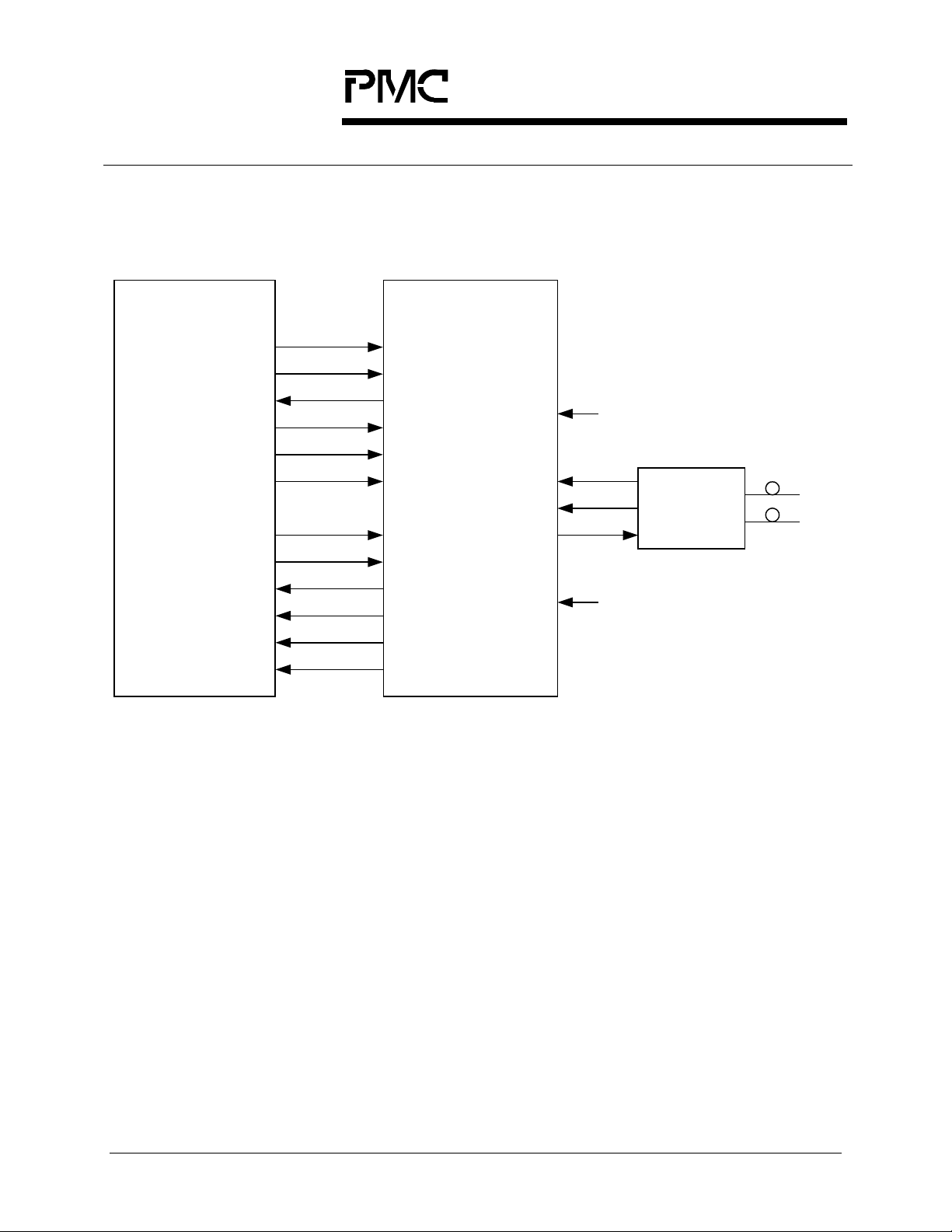
An application with a UTOPIA Level 2 system side interface is shown in Figure 1.
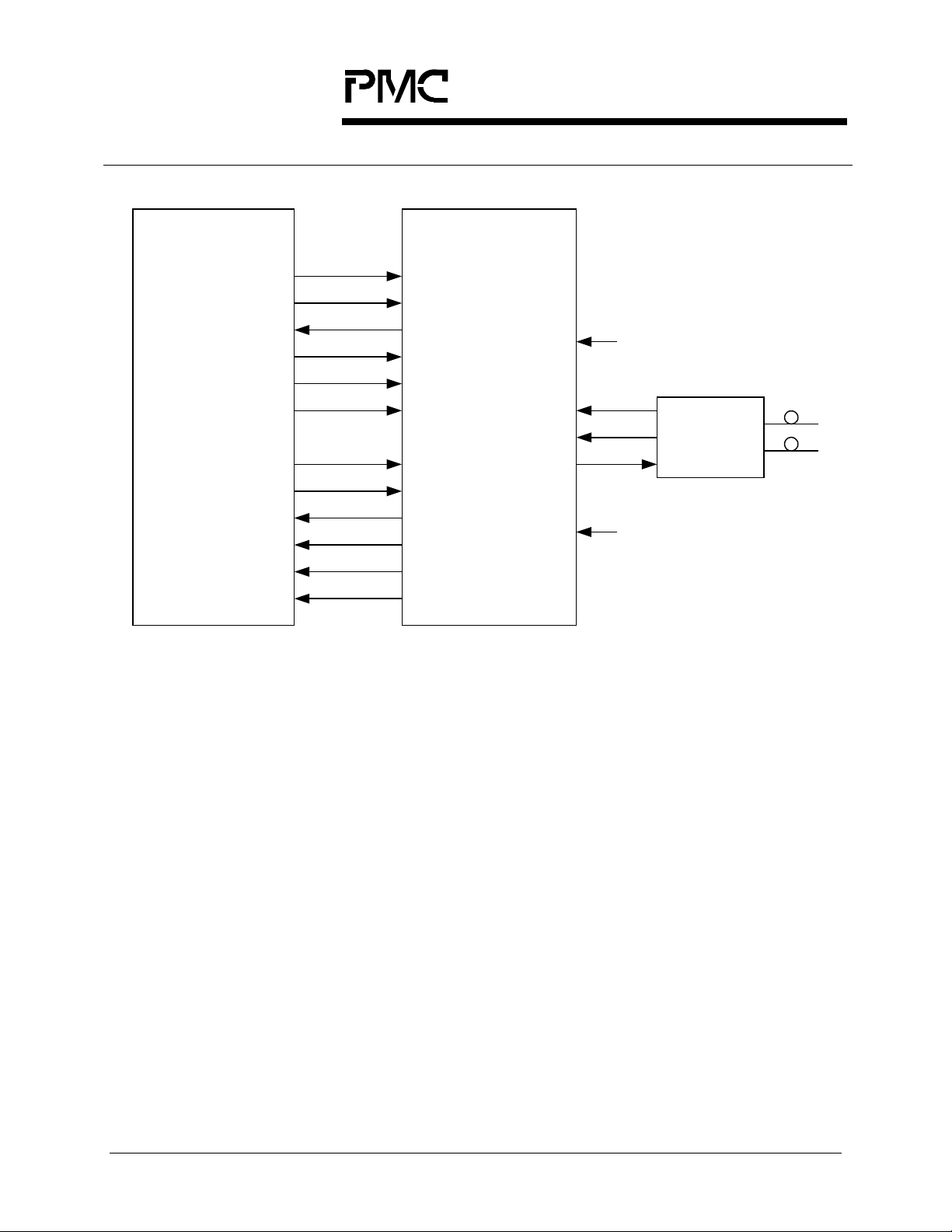
An application with a UTOPIA Level 3 system side is shown in Figure 2. The
initial configuration and ongoing control and monitoring of the S/UNI-622-MAX
are normally provided via a generic microprocessor interface.
PROPRIETARY AND CONFIDENTIAL TO PMC-SIERRA INC., AND FOR ITS CUSTOMERS’ INTERNAL USE 10
RELEASED
S/UNI-622-MAX
DATASHEET
PMC-1980589 ISSUE 6 SATURN USER NETWORK INTERFACE (622-MAX)
PMC-Sierra, Inc.
PM5356
S/UNI-622-MAX
Figure 1: Typical STS-12c/STM-4-4c ATM (UTOPIA Level 2) Switch Port
Application
UTOPIA Level 2
Interface
ATM Layer Device
PM5356
S/UNI-622-MAX
TxClk
TxEnb
TxClav
TxSOC
TxPrty
TxData[15:0]
RxClk
RxEnb
RxClav
RxSOC
RxPrty
RxData[15:0]
TFCLK
TENB
TCA
TSOC
TPRTY
TDAT[15:0]
RFCLK
RENB
RCA
RSOC
RPRTY
RDAT[15:0]
LIFSEL
RXD+/-
SD
TXD+/-
SYSSEL
0
Optical
Transceiver
0
ure 2: Typical STS-12c/STM-4-4c ATM (UTOPIA Level 3) Switch Port
Application
Fig
PROPRIETARY AND CONFIDENTIAL TO PMC-SIERRA INC., AND FOR ITS CUSTOMERS’ INTERNAL USE 11
RELEASED
S/UNI-622-MAX
DATASHEET
PMC-1980589 ISSUE 6 SATURN USER NETWORK INTERFACE (622-MAX)
PMC-Sierra, Inc.
PM5356
S/UNI-622-MAX
UTOPIA Level 3
Interface
ATM Layer Device
PM5356
S/UNI-622-MAX
TxClk
TxEnb
TxClav
TxSOC
TxPrty
TxData[7:0]
RxClk
RxEnb
RxVal
RxSOC
RxPrty
RxData[7:0]
TFCLK
TENB
TCA
TSOC
TPRTY
TDAT[7:0]
RFCLK
RENB
RVAL
RSOC
RPRTY
RDAT[7:0]
LIFSEL
RXD+/-
SD
TXD+/-
SYSSEL
0
Optical
Transceiver
1
PROPRIETARY AND CONFIDENTIAL TO PMC-SIERRA INC., AND FOR ITS CUSTOMERS’ INTERNAL USE 12
PROPRIETARY AND CONFIDENTIAL TO PMC-SIERRA INC., AND FOR ITS CUSTOMERS’ INTERNAL USE 13
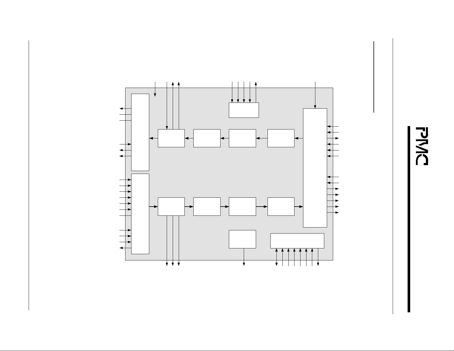
6 BLOCK DIAGRAM
PMC-1980589 ISSUE 6 SATURN USER NETWORK INTERFACE (622-MAX)
RELEASED
S/UNI-622-MAX
DATASHEET
TXD+/-
TDREF1, TDREF0
ATP[0]
PTCLK
POUT[7:0]
FPOUT
RBYP
PECLV
REFCLK+/-
RXD+/-
RRCLK+/-
SD
ATP[1]
PICLK
PIN[7:0]
FPIN
OOF
Tx Line
I/F
Rx Line
I/F
LIFSEL
TFPO
TFPI
Tx
Section O/H
Processor
Rx
Section O/H
Processor
TCLK
Tx
Line O/H
Processor
Rx
Line O/H
Processor
TRSTB
TMS
TCK
JTAG Test
Access Port
Tx
Path O/H
Processor
Rx
Path O/H
Processor
Rx APS,
Sync Status,
BERM
TDI
TDO
Tx
ATM Cell
Processor
Rx
ATM Cell
Processor
Microprocessor
Interface
SYSSEL
UTOPIA ATM Level 2
UTOPIA ATM Level 3
System Interface
TFCLK
TENB
TCA
TSOC
TPRTY
TDAT[15:0]
PMC-Sierra, Inc.
RFCLK
RENB
RCA
RSOC
RPRTY
RVAL
RDAT[15:0]
RFPO
RALARM
RCLK
APSP[4:0]
D[7:0]
A[8:0]
ALE
CSB
WRB
RDB
RSTB
INTB
S/UNI-622-MAX
PM5356

RELEASED
S/UNI-622-MAX
DATASHEET
PMC-1980589 ISSUE 6 SATURN USER NETWORK INTERFACE (622-MAX)
PMC-Sierra, Inc.
PM5356
S/UNI-622-MAX
7 DESCRIPTION
The PM5357 S/UNI-622-MAX SATURN User Network Interface is a monolithic
integrated circuit that implements SONET/SDH processing, ATM mapping over
SONET/SDH mapping functions at the STS-12c/STM-4-4c 622.08 Mbit/s rate.
The S/UNI-622-MAX receives SONET/SDH streams using a bit serial interface,
recovers the clock and data and processes section, line, and path overhead. The
S/UNI-622-MAX can also be configured for clock and data recovery and clock
synthesis by-pass where it receives SONET/SDH frames via a byte-serial
interface. The S/UNI-622-MAX performs framing (A1, A2), de-scrambling,
detects alarm conditions, and monitors section, line, and path bit interleaved
parity (B1, B2, B3), accumulating error counts at each level for performance
monitoring purposes. Line and path remote error indications (M1, G1) are also
accumulated. The S/UNI-622-MAX interprets the received payload pointers (H1,
H2) and extracts the synchronous payload envelope which carries the received
ATM cell payload.
When used to implement an ATM UNI or NNI, the S/UNI-622-MAX f r ames to the
ATM payload using cell delineation. HCS error correction is provided.
Idle/unassigned cells may be optionally dropped. Cells are also dropped upon
detection of an uncorrectable header check sequence error. The ATM cell
payloads are descrambled and are written to a four-cell FIFO buffer. The
received cells are read from the FIFO using a 16-bit wide UTOPIA Level 2
(clocked up to 50 MHz) or an 8-bit wide UTOPIA Level 3 (clocked up to 100 MHz)
datapath interface. Counts of received ATM cell headers that are errored and
uncorrectable and those that are errored and correctable are accumulated
independently for performance monitoring purposes.
The S/UNI-622-MAX transmits SONET/SDH streams using a bit serial interface.
The S/UNI-622-MAX can also be configured for clock and data recovery and
clock synthesis by-pass where it transmits the SONET/SDH frames via a byteserial interface. The S/UNI-622-MAX synthesizes the transmit clock from a
77.76MHz frequency reference and performs framing pattern insertion (A1, A2),
scrambling, alarm signal insertion, and creates section, line, and path bit
interleaved parity codes (B1, B2, B3) as required to allow performance
monitoring at the far end. Line and path remote error indications (M1, G1) are
also inserted. The S/UNI-622-MAX also supports the insertion of a large variety
of errors into the transmit stream, such as framing pattern errors, bit interleaved
parity errors, and illegal pointers, which are useful for system diagno stics and
tester applications.
PROPRIETARY AND CONFIDENTIAL TO PMC-SIERRA INC., AND FOR ITS CUSTOMERS’ INTERNAL USE 14

RELEASED
S/UNI-622-MAX
DATASHEET
PMC-1980589 ISSUE 6 SATURN USER NETWORK INTERFACE (622-MAX)
PMC-Sierra, Inc.
PM5356
S/UNI-622-MAX
When used to im plement an ATM UNI or NNI, ATM cells are writte n to an internal
four cell FIFO using a 16-bit wide UTOPIA Level 2 (clocked up to 50 MHz) or an
8-bit wide UTOPIA Level 3 (clocked up to 100 MHz) datapath interface.
Idle/unassigned cells are automatically inserted when the internal FIFO contains
less than one complete cell. The S/UNI-622-MAX provides generation of the
header check sequence and scrambles the payload of the ATM cells. Each of
these transmit ATM cell processing functions can be enabled or bypassed.
No line rate clocks are required directly by the S/UNI-622-MAX as it synthesizes
the transmit clock and recovers the receive clock using a 77.76 MHz reference
clock. The S/UNI-622-MAX outputs a differential PECL line data (TXD+/-).
The S/UNI-622-MAX is configured, controlled and monitored via a generic 8-bit
microprocessor bus interface. The S/UNI-622-MAX also provides a standard 5
signal IEEE 1149.1 JTAG test port for boundary scan board test purposes.
The S/UNI-622-MAX is implemented in low power, +3.3 Volt, CMOS technology.
It has TTL compatible digital inputs and TTL/CMOS compatible digital outputs.
High speed inputs and outputs support 3.3V and 5.0V compatible pseudo-ECL
(PECL). The S/UNI-622-MAX is packaged in a 304 pin SBGA package.
PROPRIETARY AND CONFIDENTIAL TO PMC-SIERRA INC., AND FOR ITS CUSTOMERS’ INTERNAL USE 15
RELEASED
S/UNI-622-MAX
DATASHEET
PMC-1980589 ISSUE 6 SATURN USER NETWORK INTERFACE (622-MAX)
PMC-Sierra, Inc.
PM5356
S/UNI-622-MAX
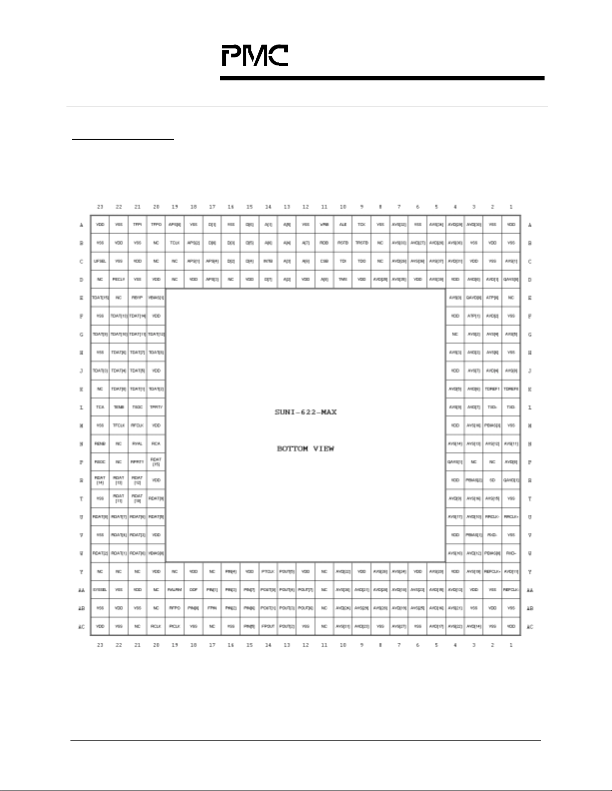
8 PIN DIAGRAM
The S/UNI-622-MAX is available in a 304 pin SBGA package having a body size
of 31 mm by 31 mm and a ball pitch of 1.27 mm.
PROPRIETARY AND CONFIDENTIAL TO PMC-SIERRA INC., AND FOR ITS CUSTOMERS’ INTERNAL USE 16

RELEASED
S/UNI-622-MAX
DATASHEET
PMC-1980589 ISSUE 6 SATURN USER NETWORK INTERFACE (622-MAX)
PMC-Sierra, Inc.
PM5356
S/UNI-622-MAX
9 PIN DESCRIPTION
9.1 Serial Line Side Interface Signals
Pin Name Type Pin
Function
No.
RBYP Input E21 The receive bypass (RBYP) input disables clock
recovery. If RBYP is high, RXD+/- is sampled on the
rising edge of RRCLK+/-. If RBYP is low, the receive
clock is recovered from the RXD+/- bit stream.
Please refer to the Operation section for a discussion
of the operating modes.
PECLV Input D22 The PECL signal voltage select (PELCV) selects
between 3.3V PECL signaling and 5V PECL signaling
for the PECL inputs. When PECLV is low, the PECL
inputs expect a 5V PECL signal. When PECLV is
high, the PECL inputs expect a 3.3V PECL signal.
The PECL biasing pins PBIAS should be set to the
appropriate voltage to prevent latchup.
Please refer to the Operation section for a discussion
of PECL interfacing issues.
REFCLK+
REFCLK-
Differential
PECL
Input
Y2
AA1
The differential reference clock inputs (REFCLK+/-)
provides a jitter-free 77.76 MHz reference clock for
both the clock recovery and the clock synthesis
circuits. REFCLK+/- is not required if the clock
recovery and clock synthesis features are not used.
Please refer to the Operation section for a discussion
of PECL interfacing issues and reference clocks.
RXD+
RXD-
Differential
PECL
Input
W1
V2
The receive differential data PECL inputs (RXD+/-)
contain the NRZ bit serial receive stream. The
receive clock is recovered from the RXD+/- bit stream
when RBYP is set low. RXD+/- is sampled on the
rising edge of RRCLK+/- when RBYP is set high.
Please refer to the Operation section for a discussion
of PECL interfacing issues.
PROPRIETARY AND CONFIDENTIAL TO PMC-SIERRA INC., AND FOR ITS CUSTOMERS’ INTERNAL USE 17

RELEASED
S/UNI-622-MAX
DATASHEET
PMC-1980589 ISSUE 6 SATURN USER NETWORK INTERFACE (622-MAX)
PMC-Sierra, Inc.
PM5356
S/UNI-622-MAX
Pin Name Type Pin
No.
RRCLK+
RRCLK-
Differential
PECL
U1
U2
Input
SD PECL
R2 The receive signal detect PECL input (SD) indicates
Input
TXD+
TXD-
Differential
PECL
L2
L1
Output
Function
When cloc k recovery is bypassed (RBYP set high),
RRCLK+/- is nominally a 622.08 MHz 50% duty cycle
clock and provides timing for the S/UNI-622-MAX
receive functions. In this case, RXD+/- is sampled on
the rising edge of RRCLK+/-. RRCLK+/- is ignored
when RBYP is set low.
Please refer to the Operation section for a discussion
of PECL interfacing issues.
the presence of valid receive signal power from the
Optical Physical Medium Dependent Device. A PECL
logic high indicates the presence of valid data. A
PECL logic low indicates a loss of signal.
Please refer to the Operation section for a discussion
of PECL interfacing issues
The transmit differential data PECL outputs (TXD+/-)
contain the 622.08 Mbit/s transmit stream. The
TXD+/- outputs are driven using the synthesized
clock from the CSU-622.
Please refer to the Operation section for a discussion
of PECL interfacing issues.
PROPRIETARY AND CONFIDENTIAL TO PMC-SIERRA INC., AND FOR ITS CUSTOMERS’ INTERNAL USE 18

RELEASED
S/UNI-622-MAX
DATASHEET
PMC-1980589 ISSUE 6 SATURN USER NETWORK INTERFACE (622-MAX)
PMC-Sierra, Inc.
PM5356
S/UNI-622-MAX
9.2 Parallel Line Side Interface Signals - CRU and CSU Bypass
Pin Name Type Pin
Function
No.
LIFSEL Input C23 T he line interface select (LIFSEL) selects between
serial and parallel line interface modes of operation.
When tied high, the parallel mode is selected by-
passing the clock and data recovery, clock synthesis
and the serializer/de-serializer functions.
When tied lo w, serial mode is se lected, enabling clock
and data recovery, clock synthesis and the
serializer/de-serializer functions. During this
operation, the parallel interface may be used for 1+1
APS operation. See the Operation section for more
discussion of 1+1 APS support.
PICLK Input AC19 The parallel input clock (PICLK) provides timing for
S/UNI-622-MAX receive function operation when the
device is configured for the parallel interface mode of
operation.
When the RS OC3 bit is set high , PICLK is a 19. 44
MHz nominally 50% duty cycle clock. When the
RSOC3 bit is set low, PICLK is a 77.76 MHz
nominally 50% duty cycle clock.
When parallel operation is not used, PICLK may be
used for 1+1 APS operation. See the Operation
section for more discussion of 1+1 APS.
OOF Output AA18 The out of frame (OOF) signal is high while the
S/UNI-622-MAX is out of frame. OOF is set low while
the S/UNI-622-MAX is in-frame. An out of frame
declaration occurs when four consecutive errored
framing patterns (A1 and A2 bytes) have been
received.
OOF is intended to enable an upstream framing
pattern detector to search for the framing pattern.
This alarm indication is also available via register
access. OOF is an asynchronous output with a
minimum period of one PICLK clock.
PROPRIETARY AND CONFIDENTIAL TO PMC-SIERRA INC., AND FOR ITS CUSTOMERS’ INTERNAL USE 19

RELEASED
S/UNI-622-MAX
DATASHEET
PMC-1980589 ISSUE 6 SATURN USER NETWORK INTERFACE (622-MAX)
PMC-Sierra, Inc.
PM5356
S/UNI-622-MAX
Pin Name Type Pin
Function
No.
FPIN Input AB17 The active-high framing position input (FPIN) signal
indicates the SONET/SDH frame position on the
PIN[7:0] bus. In parallel interface operation, the byte
on the PIN[7:0] bus indicated by FPIN is the third A2
of the SONET/SDH framing pattern. FPIN is sampled
on the rising edge of PICLK.
When parallel inte rface operation is not used, FPIN
may be used for 1+1 APS operation. In this mode,
FPIN marks the first synchronous payload envelope
byte after the J0/Z0 bytes on PIN[7:0]. See the
Operation section for more discussion of 1+1 APS.
PIN[0]
PIN[1]
PIN[2]
PIN[3]
PIN[4]
PIN[5]
PIN[6]
PIN[7]
Input AB18
AA17
AB16
AA16
Y16
AC15
AB15
AA15
In parallel interface operation, the data input
(PIN[7:0]) bus carries the byte-serial STS-12c/STM-44c or STS-3c/STM-1 stream. PIN[7] is the most
significant bit (corresponding to bit 1 of each serial
byte, the first bit received). PIN[0] is the least
significant bit (corresponding to bit 8 of each serial
byte, the last bit received). PIN[7:0] is sampled on
the rising edge of PICLK.
When parallel inte rface operation is not used,
PIN[7:0] may be used for 1+1 APS operation. In this
mode, PIN[7:0] carries the byte-serial STS-12c/STM4-4c transmit path. See the Operation section for
more discussion of 1+1 APS.
PTCLK Input Y14 The parallel transmit clock (PTCLK) provides timing
for S/UNI-622-MAX transmit function operation when
the device is configured for the parallel interface
mode of operation.
When TOC3 is low, PTCLK should be a 77.76 MHz
nominally 50% duty cycle clock free-running (non
gapped) clock. When TOC3 is high, PTCLK should
be a 19.44 MHz nominally 50% duty cycle clock.
PROPRIETARY AND CONFIDENTIAL TO PMC-SIERRA INC., AND FOR ITS CUSTOMERS’ INTERNAL USE 20

RELEASED
S/UNI-622-MAX
DATASHEET
PMC-1980589 ISSUE 6 SATURN USER NETWORK INTERFACE (622-MAX)
PMC-Sierra, Inc.
PM5356
S/UNI-622-MAX
Pin Name Type Pin
Function
No.
FPOUT Output AC14 In parallel interface operation, the parallel outgoing
stream frame pulse (FPOUT) marks the frame
alignment on the POUT[7:0] bus. FPOUT marks the
first synchronous payload envelope byte after the
J0/Z0 bytes. FPOUT is updated on the rising edge of
PTCLK.
When parallel inte rface operation is not used, FPOUT
may be used for 1+1 APS operation. In this mode,
FPOUT marks the first synchronous payload
envelope byte after the J0/Z0 bytes. FPOUT is
updated on the rising edge of TCLK. See the
Operation section for more discussion of 1+1 APS.
POUT[0]
POUT[1]
POUT[2]
POUT[3]
POUT[4]
POUT[5]
POUT[6]
POUT[7]
Output AA14
AB14
AC13
AB13
AA13
Y13
AB12
AA12
In parallel interface operation, the parallel outgoing
stream, (POUT[7:0]) carries the scrambled STS12c/STM-4-4c or ST S-3c/STM-1 stream in byte-serial
format. POUT[7] is the most significant bit
(corresponding to bit 1 of each serial word, the first bit
transmitted). POUT[0] is the least significant bit
(corresponding to bit 8 of each serial word, the last bit
transmitted). POUT[7:0] is updated on the rising
edge of PTCLK.
When parallel inte rface operation is not used,
POUT[7:0] may be used for 1+1 APS operation. In
this mode, POUT[7:0] carries the byte-serial STS12c/STM-4-4c transmit path and updates on the rising
edge of TCLK. See the Operation section for more
discussion of 1+1 APS.
PROPRIETARY AND CONFIDENTIAL TO PMC-SIERRA INC., AND FOR ITS CUSTOMERS’ INTERNAL USE 21

RELEASED
S/UNI-622-MAX
DATASHEET
PMC-1980589 ISSUE 6 SATURN USER NETWORK INTERFACE (622-MAX)
PMC-Sierra, Inc.
PM5356
S/UNI-622-MAX
9.3 Clocks and Alarms Signals
Pin Name Type Pin
Function
No.
RCLK Output AC20 The receive clock (RCLK) provides a timing reference
for the S/UNI-622-MAX receive function outputs.
RCLK is a 77.76 MHz, 50% duty cycle clock.
RFPO Output AB19 T he receive frame pulse output (RFPO), when the
framing alignment has been found (the OOF register
bit is low), is an 8 kHz signal derived from the receive
clock RCLK. RFPO pulses high for one RCLK cycle
every 9720 RCLK cycles (STS-12c / STM-4-4c).
RFPO is updated on the rising edge of RCLK.
RALRM Output AA19 The receive alarm (RALRM) output indicates the state
of the receive framing. RALRM is lo w if no receive
alarms are active. RALRM is optionally high if line
AIS (LAIS), path AIS (PAIS), line RDI (LRDI), path
RDI (PRDI), enhanced path RDI (PERDI), loss of
signal (LOS), loss of frame (LOF), out of frame
(OOF), loss of pointer (LOP), loss of pointer
concatenation (LOPC/AISC), loss of cell delineation
(LCD), signal fail BER (SFBER), signal degrade BER
(SDBER), path trace identification mismatch (TIM) or
path signal label mismatch (PSLM) is detected .
RALRM is an asynchronous output with a minimum
period of one RCLK clock.
TCLK Output B19 The transmit clock (TCLK) provides timing for the
S/UNI-622-MAX transmit function operation. TCLK is
a 77.76 MHz, 50% duty cycle clock.
TFPO Output A20 The active-high framing position output (TFPO) signal
is an 8 kHz signal derived from the transmit clock
TCLK. TFPO pulses high for one TCLK cycl e ever y
9720 TCLK cycles (STS-12c / STM-4-4c).
TFPO is updated on the rising edge of TCLK.
PROPRIETARY AND CONFIDENTIAL TO PMC-SIERRA INC., AND FOR ITS CUSTOMERS’ INTERNAL USE 22

RELEASED
S/UNI-622-MAX
DATASHEET
PMC-1980589 ISSUE 6 SATURN USER NETWORK INTERFACE (622-MAX)
PMC-Sierra, Inc.
PM5356
S/UNI-622-MAX
Pin Name Type Pin
Function
No.
TFPI Input A21 The active high framing position (TFPI) signal is an 8
kHz timing marker for the transmitter. TFPI is used to
align the SONET/SDH transport frame generated by
the S/UNI-622-MAX device to a system reference.
TFPI should be brought high for a single TCLK period
every 9720 TCLK cycles or a multiple thereof. TFPI
must be tied low if such synchronization is not
required.
TFPI is sampled on the rising edge of TCLK.
APS[0]
APS[1]
APS[2]
APS[3]
APS[4]
I/O A19
C18
B18
D17
C17
The APS Por t bus (A PS[4 :0]) is a bi-dir ecti o nal
control bus that can be used to implement a 1+1 APS
system. When the APSPOE register bit is set low, the
APS[4:0] bus is an input. Data on this bus is used by
TPOP to generate the path RDI and path FEBE.
When the APSOE registe r bit is set high, the APS[4:0]
bus is an output with data generated by RPOP.
APS[0] FEBE Clock (576 kHz)
APS[1] FEBE Data
APS[2] RDI[0] (G1 bit 5)
APS[3] RDI[1] (G1 bit 6)
APS[4] RDI[2] (G1 bit 7)
See the Operation section for more discussion of 1+1
APS.
PROPRIETARY AND CONFIDENTIAL TO PMC-SIERRA INC., AND FOR ITS CUSTOMERS’ INTERNAL USE 23

RELEASED
S/UNI-622-MAX
DATASHEET
PMC-1980589 ISSUE 6 SATURN USER NETWORK INTERFACE (622-MAX)
PMC-Sierra, Inc.
PM5356
S/UNI-622-MAX
9.4 ATM (UTOPIA) System Interface
Pin Name Type Pin
No.
Function
PROPRIETARY AND CONFIDENTIAL TO PMC-SIERRA INC., AND FOR ITS CUSTOMERS’ INTERNAL USE 24

RELEASED
S/UNI-622-MAX
DATASHEET
PMC-1980589 ISSUE 6 SATURN USER NETWORK INTERFACE (622-MAX)
PMC-Sierra, Inc.
PM5356
S/UNI-622-MAX
Pin Name Type Pin
No.
TFCLK Input
TDAT[0]
TDAT[1]
TDAT[2]
TDAT[3]
TDAT[4]
TDAT[5]
TDAT[6]
TDAT[7]
TDAT[8]
TDAT[9]
TDAT[10]
TDAT[11]
TDAT[12]
TDAT[13]
TDAT[14]
TDAT[15]
Input
M22 UTOPIA transmit FIFO write clock (TFCLK) is used to
K22
K21
K20
J23
J22
J21
H22
H21
H20
G23
G22
G21
G20
F22
F21
E23
Function
write ATM cells to the four cell transmit FIFO.
When in 16-bi t Level 2 ATM mode, TFCLK must cycle
at a 50 MHz to 40 MHz instantaneous rate, and must
be a free running clock (cannot be gapped).
When in 8-bit Level 3 ATM mode, TFCLK must c ycl e
at a 100 MHz to 60 MHz instantaneous rate, and
must be a free running clock (cannot be gapped).
The UTOPIA transmit cell data (TDAT[15:0]) bus
carries the ATM cell octets that are written to the
transmit FIFO.
In 16-bit Level 2 ATM mode, the TDAT[15:0] is
considered valid only when TENB is simultaneously
asserted.
In 8-bit Level 3 ATM mode, the TDAT[7:0] bus is
considered valid only when TENB is simultaneously
asserted. TDAT[15:8] are ignored.
TDAT[15:0] is sampled on the rising edge of TFCLK.
PROPRIETARY AND CONFIDENTIAL TO PMC-SIERRA INC., AND FOR ITS CUSTOMERS’ INTERNAL USE 25

RELEASED
S/UNI-622-MAX
DATASHEET
PMC-1980589 ISSUE 6 SATURN USER NETWORK INTERFACE (622-MAX)
PMC-Sierra, Inc.
PM5356
S/UNI-622-MAX
Pin Name Type Pin
No.
TSOC Input
TPRTY Input
L21 The UTOPIA transmit start of cell (TSOC) signal
L20 The UTOPIA transmit bus parity (TPRTY) signal
Function
marks the start of a cell structure on the TDAT bus.
In 16-bit Level 2 ATM mode, the first word of the cell
structure is present on the TDAT[15:0] bus when
TSOC is high. It is not necessary for TSOC to be
present for each cell.
In 8-bit Level 3 ATM mode, the first byte of the cell
structure is present on the TDAT[7:0] bus when
TSOC is high. TSOC must be present for each cell.
TSOC is considered valid only when TENB is
simultaneously asserted. TSOC is sampled on the
rising edge of TFCLK.
indicates the parity on the TDAT bus. A parity error is
indicated by a status bit and a maskable interrupt.
Cells with parity errors are inserted in the transmit
stream, so the TPRTY input may be unused.
TENB Input
In 16-bit Level 2 ATM mode, the TPRTY signal
indicates the parity on the TDAT [15:0] bus. Odd or
even parity selection is made in the TXCP registers.
In 8-bit Level 3 ATM mode, the TPRTY signal
indicates the parity on the TDAT [7:0] bus. Odd or
even parity selection is made in the TUL3 registers.
TPRTY is considered valid only when TENB is
simultaneously asserted. TPRTY is sampled on the
rising edge of TFCLK.
L22 The UTOPIA transmit write enable (TENB) signal is
an active low input which is used to initiate writes to
the transmit FIFO’s.
When TENB is sampled high, the information
sampled on the TDAT, TPRTY and TSOC signals are
invalid. When TENB is sampled low, the information
sampled on the TDAT, TPRTY and TSOC signals are
valid and are written into the transmit FIFO.
TENB is sampled on the rising edge of TFCLK.
PROPRIETARY AND CONFIDENTIAL TO PMC-SIERRA INC., AND FOR ITS CUSTOMERS’ INTERNAL USE 26

RELEASED
S/UNI-622-MAX
DATASHEET
PMC-1980589 ISSUE 6 SATURN USER NETWORK INTERFACE (622-MAX)
PMC-Sierra, Inc.
PM5356
S/UNI-622-MAX
Pin Name Type Pin
No.
TCA Output
L23 The UTOPIA transmit cell available (TCA) signal
Function
provides direct status indication of when cell space is
available in the transmit FIFO.
When set hi gh, TCA indicates that the corres ponding
transmit FIFO is not full and a complete cell may be
written. TCA is set low to either indicate that the
transmit FIFO is near full or that the transmit FIFO is
full. To reduce FIFO latency, the FIFO depth at which
TCA indicates "full" can be set to one, two, three or
four cells. Note that regardless of what fill level TCA
is set to indicate "full" at, the transmit cell processor
can store 4 complete cells.
In 16-bit Level 2 ATM mode, TCA will transition low
one TFCLK cycle after the payload word 19 or 23
(depending of the configuration in TXCP) is sampled
on the TDAT[15:0] bus.
In 8-bit Level 3 ATM mode, TCA will transition lo w on
the rising edge of TFCLK before the payload byte 45
is sampled on the TDAT[7:0] bus.
RFCLK Input
TCA is updated on the rising edge of TFCLK.
M21 The UTOPIA receive FIFO read clock (RFCLK).
RFCLK is used to read ATM cells from the four cell
receive FIFO.
When in 16-bit Level 2 ATM mode, RFCLK must cycle
at a 50 MHz to 40 MHz instantaneous rate, and must
be a free running clock (cannot be gapped).
When in 8-bit Level 3 ATM mode, RFCLK must cycl e
at a 100 MHz to 60 MHz instantaneous rate, and
must be a free running clock (cannot be gapped).
PROPRIETARY AND CONFIDENTIAL TO PMC-SIERRA INC., AND FOR ITS CUSTOMERS’ INTERNAL USE 27

RELEASED
S/UNI-622-MAX
DATASHEET
PMC-1980589 ISSUE 6 SATURN USER NETWORK INTERFACE (622-MAX)
PMC-Sierra, Inc.
PM5356
S/UNI-622-MAX
Pin Name Type Pin
No.
RDAT[0]
RDAT[1]
RDAT[2]
RDAT[3]
RDAT[4]
RDAT[5]
RDAT[6]
RDAT[7]
RDAT[8]
RDAT[9]
RDAT[10]
RDAT[11]
RDAT[12]
RDAT[13]
RDAT[14]
RDAT[15]
Output
W21
W22
W23
V21
V22
U20
U21
U22
U23
T20
T21
T22
R21
R22
R23
P20
RVAL Output
N21 The UTOPIA Level 3 receive data valid (RVAL) signal
Function
UTOPIA receive cell data (RDAT[15:0]) bus carries
the ATM cell octets that are read from the receive
FIFO.
In 16-bit Level 2 ATM mode, RDAT[15:0] is conside r
valid only when RENB is asserted. RDAT[15:0] is tristated when RENB is sampled high.
In 8-bit Level 3 ATM mode, only the RDAT[7:0]
signals are valid when RVAL is asserted. RDAT[15:8]
contain invalid data.
RDAT[15:0] is updated on the rising edge of RFCLK.
indicates the validity of the receive data signals.
When RVAL is high, the receive signals RDAT, RSOC
and RPRTY are valid. When RVAL is low, all receive
signals are invalid and must be disregarded.
In 16-bit Level 2 ATM mode, RVAL is invalid and must
be ignored.
In 8-bit Level 3 ATM mode, RVAL will be high when
valid data is on the RDAT bus. The RVAL will
transition low when the FIFO is empty. Once
deasserted, RVAL will remain deasserted until a
complete ATM cell is written into the receive FIFO.
RVAL is updated on the rising edge of RFCLK.
PROPRIETARY AND CONFIDENTIAL TO PMC-SIERRA INC., AND FOR ITS CUSTOMERS’ INTERNAL USE 28

RELEASED
S/UNI-622-MAX
DATASHEET
PMC-1980589 ISSUE 6 SATURN USER NETWORK INTERFACE (622-MAX)
PMC-Sierra, Inc.
PM5356
S/UNI-622-MAX
Pin Name Type Pin
No.
RSOC Output
RPRTY Output
P23 The UTOPIA receive start of cell (RSOC) signal
P21 The UTOPIA receive parity (RPRTY) signal indicates
Function
marks the start of a cell structure on the RDAT bus.
In 16-bit Level 2 ATM mode, the first word of the cell
structure is present on the RDAT[15:0] bus when
RSOC is high. RSOC is tri-stated when RENB is
sampled high.
In 8-bit Level 3 ATM mode, the first byte of the cell
structure is present on the RDAT[7:0] bus when
RSOC is high. RDAT[15:8] are invalid and mu st be
ignored.
RSOC is updated on the rising edge of RFCLK.
the parity of the RDAT bus.
When in 16-b i t Level 2 AT M m ode, the RPRTY signal
indicates the parity on the RDAT[15:0] bus. RPRTY
is tri-stated when RENB is sampled high. Odd or
even parity selection is made in the RXCP registers.
When in 8-bit Level 3 ATM mode, the RPRTY signal
indicates the parity on the RDAT[7:0] bus. Odd or
even parity selection is made in the RUL3 registers.
RPRTY is updated on the rising edge of RFCLK.
PROPRIETARY AND CONFIDENTIAL TO PMC-SIERRA INC., AND FOR ITS CUSTOMERS’ INTERNAL USE 29

RELEASED
S/UNI-622-MAX
DATASHEET
PMC-1980589 ISSUE 6 SATURN USER NETWORK INTERFACE (622-MAX)
PMC-Sierra, Inc.
PM5356
S/UNI-622-MAX
Pin Name Type Pin
No.
RENB Input
RCA Output
N23 The UTOPIA receive read enable (RENB) is used to
N20 The UTOPIA receive cell available (RCA) provides
Function
initiate reads from the receive FIFO. The system may
de-assert RENB if it is unable to accept more data.
In 16-bit Level 2 ATM mode, a read is not performed
and RDAT[15:0], RPRTY and RSOC will tristate when
RENB is sampled high. When RENB is sampled low,
the word on the RDAT[15:0] bus is read from the
receive FIFO and changes to the next value on the
next clock cycle.
In 8-bit Level 3 ATM mode, a read is not performed
and RDAT[7:0] does not change when RENB is
sampled high. W hen RENB is sampled low, the word
on the RDAT[7:0] bus is read from the receive FIFO
and changes to the next value on the next clock
cycle.
RENB is sampled on the rising edge of RFCLK.
direct status indication of when a cell is available in
the receive FIFO.
In 16-bit Level 2 mode, RCA can be configured to deassert when either zero or four bytes remain in the
FIFO. RCA will thus transition low on the rising edge
of RFCLK after payload word 24 or 19 is output on
the RDAT[15:0] bus depending on the RXCP
registers.
In 8-bit Level 3 mode, RCA is ignored as the RVAL
signal identifies valid data on the RDAT[7:0] bus.
RCA is updated on the rising edge of RFCLK.
PROPRIETARY AND CONFIDENTIAL TO PMC-SIERRA INC., AND FOR ITS CUSTOMERS’ INTERNAL USE 30

RELEASED
S/UNI-622-MAX
DATASHEET
PMC-1980589 ISSUE 6 SATURN USER NETWORK INTERFACE (622-MAX)
PMC-Sierra, Inc.
PM5356
S/UNI-622-MAX
9.5 Microprocessor Interface Signals
Pin Name Type Pin
Function
No.
CSB Input C11 The active-low chip select (CSB) signal is low during
S/UNI-622-MAX register accesses.
When CSB is hi gh, the RDB and WRB inputs are
ignored. When CSB is low, the RDB and WRB are
valid. CSB must be high when RSTB is low to
properly reset the chip.
If CSB is not required (i.e., registers accesses are
controlled using the RDB and WRB signals only),
CSB must be connected to an inverted version of the
RSTB input.
RDB Input B11 The active-low read enable (RDB) signal is low during
S/UNI-622-MAX register read accesses. The S/UNI622-MAX drives the D[7:0] bus with the contents of
the addressed register while RDB and CSB are low.
WRB Input A11 The active-low write strobe (WRB) signal is low
during a S/UNI-622-MAX register write accesses.
The D[7:0] bus contents are clocked into the
addressed register on the rising WRB edge while
CSB is low.
D[0]
D[1]
D[2]
D[3]
D[4]
D[5]
D[6]
D[7]
A[0]
A[1]
A[2]
A[3]
A[4]
A[5]
A[6]
A[7]
PROPRIETARY AND CONFIDENTIAL TO PMC-SIERRA INC., AND FOR ITS CUSTOMERS’ INTERNAL USE 31
I/O B17
A17
C16
B16
C15
B15
A15
D14
Input B14
A14
D13
C13
B13
A13
C12
B12
The bi-directional data bus D[7:0] is used during
S/UNI-622-MAX register read and write accesses.
The address bus A[7:0] selects specific registers
during S/UNI-622-MAX register accesses.

RELEASED
S/UNI-622-MAX
DATASHEET
PMC-1980589 ISSUE 6 SATURN USER NETWORK INTERFACE (622-MAX)
PMC-Sierra, Inc.
PM5356
S/UNI-622-MAX
Pin Name Type Pin
Function
No.
A[8] Input D11 The test register select (A[8]) signal selects between
normal and test mode register accesses. A[8] is high
during test mode register accesses, and is low during
normal mode register accesses. A[8] may be tied
low.
RSTB Input B10 T he active-low reset (RSTB) signal provides an
asynchronous S/UNI-622-MAX reset. RSTB is a
Schmitt triggered input with an integral pull-up
resistor.
CSB must be held high when RSTB is low in order to
properly reset this chip.
ALE Input A10 The address latch enable (ALE) is active-high and
latches the address bus A[8:0] when low. When ALE
is high, the internal address latches are transparent.
It allows the S/UNI-622-MAX to interface to a
multiplexed address/data bus. ALE has an integral
pull-up resistor.
INTB Output C14 The active-low interrupt (INTB) signal is set low when
a S/UNI-622-MAX interrupt source is active and that
source is unmasked. The S/UNI-622-MAX may be
enabled to report many alarms or events via
interrupts.
Examples of interrupt sources are loss of signal
(LOS), loss of frame (LOF), line AIS, line remote
defect indication (LRDI) detect, loss of pointer (LOP),
path AIS, path remote defect indication and others.
INTB is tri-stated when the all enabled interrupt
sources are acknowledged via an appropriate register
access. INTB is an open drain output.
PROPRIETARY AND CONFIDENTIAL TO PMC-SIERRA INC., AND FOR ITS CUSTOMERS’ INTERNAL USE 32

RELEASED
S/UNI-622-MAX
DATASHEET
PMC-1980589 ISSUE 6 SATURN USER NETWORK INTERFACE (622-MAX)
PMC-Sierra, Inc.
PM5356
S/UNI-622-MAX
9.6 JTAG Test Access Port (TAP) Signals
Pin Name Type Pin
Function
No.
TCK Input A9 The test clock (TCK) signal provides clock timing for
test operations that are carried out using the IEEE
P1149.1 test access port.
TMS Input D10 The test mode select (TMS) signal controls the test
operations that are carried out using the IEEE
P1149.1 test access port. TMS is sampled on the
rising edge of TCK. TMS has an integral pull-up
resistor.
TDI Input C10 The test data input (TDI) signal carries test data into
the S/UNI-622-MAX via the IEEE P1149.1 test access
port. TDI is sampled on the rising edge of TCK. TDI
has an integral pull-up resistor.
TDO Output C9 The test data output (TDO) signal carries test data
out of the S/UNI-622-MAX via the IEEE P1149.1 test
access port. TDO is updated on the falling edge of
TCK. TDO is a tristate output which is inactive except
when shifting boundary scan data is in progress.
TRSTB Input B9 The active-low test reset (TRSTB) signal provides an
asynchronous S/UNI-622-MAX test access port reset
via the IEEE P1149.1 test access port. TRSTB is a
Schmitt triggered input with an integral pull-up
resistor.
Note that when not being used, TRSTB may be tied
low or connected to the RSTB input.
PROPRIETARY AND CONFIDENTIAL TO PMC-SIERRA INC., AND FOR ITS CUSTOMERS’ INTERNAL USE 33

RELEASED
S/UNI-622-MAX
DATASHEET
PMC-1980589 ISSUE 6 SATURN USER NETWORK INTERFACE (622-MAX)
PMC-Sierra, Inc.
PM5356
S/UNI-622-MAX
9.7 Analog Signals
Pin Name Type Pin
No.
TDREF0
TDREF1
ATP[0]
ATP[1]
Analog K1
K2
Analog E2
F3
Function
The transmit data reference (TDREF0 and TDREF1)
analog pins are provided to create calibrated currents
for the PECL output transceivers TXD+/-. A 2.00K
ohm resistor is connected across the TDREF0 and
TDREF1 pins.
The receive and transmit analog test ports (ATP[1:0]).
These pins are used for manufacturing testing only
and should be tied to analog ground (AVS).
PROPRIETARY AND CONFIDENTIAL TO PMC-SIERRA INC., AND FOR ITS CUSTOMERS’ INTERNAL USE 34

RELEASED
S/UNI-622-MAX
DATASHEET
PMC-1980589 ISSUE 6 SATURN USER NETWORK INTERFACE (622-MAX)
PMC-Sierra, Inc.
PM5356
S/UNI-622-MAX
9.8 Power and Ground
Pin Name Type Pin
No.
VBIAS[0]
VBIAS[1]
PBIAS[0]
PBIAS[1]
PBIAS[2]
PBIAS[3]
Bias
Voltage
W20
E20
Bias
VoltageW2V3
R3
M2
Function
Digital input biases (VBIAS). When tied to +5V, the
VBIAS inputs are used to bias the wells of the digital
inputs so that the pads can tolerate up to 5V on their
inputs without forward biasing internal ESD protection
devices. When VBIAS are tied to +3.3V, the digital
inputs will only tolerate 3.3V level voltages.
The system interface inputs (RFCLK, RENB, TFCLK,
TENB, TDAT[15:0], TMOD, TERR, TSOC/TSOP,
TEOP and TPRTY) do not use the bias voltages and
are 3.3V tolerant only.
PECL input biases (PBIAS). When tied to +5V, the
PBIAS inputs are used to bias the wells in the PECL
inputs and output so that the pads can tolerate up to
5V without forward biasing internal ESD protection
devices. When the PBIAS inputs are tied to +3.3V,
the pads will only tolerate 3.3V level voltages.
PBIAS[0] REFCLK+/- Input
PBIAS[1] RXD+/- Input
PBIAS[2] RRCLK+/- Input
PBIAS[3] TXD+/- Output
Please see the Operation section for detailed
information on PECL interfacing issues.
QAVD[0]
QAVD[1]
Analog
PowerE3R1
The quiet power (QAVD) pins for the analog core.
QAVD should be connected to well-decoupled analog
+3.3V supply.
Please see the Operation section for detailed
information.
QAVS[0]
QAVS[1]
Analog
GroundD1P4
The quiet ground (QAVS) pins for the analog core.
QAVS should be connected to analog ground of the
QAVD supply.
Please see the Operation section for detailed
information.
PROPRIETARY AND CONFIDENTIAL TO PMC-SIERRA INC., AND FOR ITS CUSTOMERS’ INTERNAL USE 35

RELEASED
S/UNI-622-MAX
DATASHEET
PMC-1980589 ISSUE 6 SATURN USER NETWORK INTERFACE (622-MAX)
PMC-Sierra, Inc.
PM5356
S/UNI-622-MAX
Pin Name Type Pin
No.
VDD Digital
PowerA1A23
AA3
AA21
AB2
AB22
AC1
AC23
B2
B22
C3
C21
D4
D6
D9
D12
D15
D18
D20
F4
F20
J4
J20
M4
M20
R4
R20
V4
V20
Y4
Y6
Y9
Y12
Y15
Y18
Y20
Function
The digital power (VDD) pins should be connected to
a well-decoupled +3.3 V digital power supply.
PROPRIETARY AND CONFIDENTIAL TO PMC-SIERRA INC., AND FOR ITS CUSTOMERS’ INTERNAL USE 36

RELEASED
S/UNI-622-MAX
DATASHEET
PMC-1980589 ISSUE 6 SATURN USER NETWORK INTERFACE (622-MAX)
PMC-Sierra, Inc.
PM5356
S/UNI-622-MAX
Pin Name Type Pin
No.
VSS Digital
GroundA2A6
A8
A12
A16
A18
A22
AA2
AA22
AB1
AB3
AB21
AB23
AC2
AC6
AC8
AC12
AC16
AC18
AC22
B1
B3
B21
B23
C2
C22
D21
F1
F23
H1
H23
M1
M23
T1
T23
V1
V23
Function
The digital ground (VSS) pins should be connected to
the digital ground of the digital power supply.
PROPRIETARY AND CONFIDENTIAL TO PMC-SIERRA INC., AND FOR ITS CUSTOMERS’ INTERNAL USE 37

RELEASED
S/UNI-622-MAX
DATASHEET
PMC-1980589 ISSUE 6 SATURN USER NETWORK INTERFACE (622-MAX)
PMC-Sierra, Inc.
PM5356
S/UNI-622-MAX
Pin Name Type Pin
No.
AVD[0]
AVD[1]
AVD[2]
AVD[3]
AVD[4]
AVD[5]
AVD[6]
AVD[7]
AVD[8]
AVD[9]
AVD[10]
AVD[11]
AVD[12]
AVD[13]
AVD[14]
AVD[15]
AVD[16]
AVD[17]
AVD[18]
AVD[19]
AVD[20]
AVD[21]
AVD[22]
AVD[23]
AVD[24]
AVD[25]
AVD[26]
AVD[27]
AVD[28]
AVD[29]
AVD[30]
AVD[31]
Analog
PowerD3D2
F2
H3
J2
K4
K3
L3
P1
T4
U3
Y1
W3
AA4
AC3
AA5
AB5
AC5
AA7
AB7
AA8
AA9
Y10
AC9
AB10
D8
C7
B6
B5
A4
A3
C4
Function
The analog power (AVD) pins for the analog core.
The AVD pins should be connected through passive
filtering networks to a well-decoupled +3.3V analog
power supply.
Please see the Operation section for detailed
information.
PROPRIETARY AND CONFIDENTIAL TO PMC-SIERRA INC., AND FOR ITS CUSTOMERS’ INTERNAL USE 38

RELEASED
S/UNI-622-MAX
DATASHEET
PMC-1980589 ISSUE 6 SATURN USER NETWORK INTERFACE (622-MAX)
PMC-Sierra, Inc.
PM5356
S/UNI-622-MAX
Pin Name Type Pin
No.
AVS[0]
AVS[1]
AVS[2]
AVS[3]
AVS[4]
AVS[5]
AVS[6]
AVS[7]
AVS[8]
AVS[9]
AVS[10]
AVS[11]
AVS[12]
AVS[13]
AVS[14]
AVS[15]
AVS[16]
AVS[17]
AVS[18]
AVS[19]
AVS[20]
AVS[21]
AVS[22]
AVS[23]
AVS[24]
AVS[25]
AVS[26]
AVS[27]
AVS[28]
AVS[29]
AVS[30]
AVS[31]
AVS[32]
AVS[33]
AVS[34]
AVS[35]
AVS[36]
AVS[37]
AVS[38]
AVS[39]
Analog
GroundE4C1
G3
H4
G2
G1
H2
J3
J1
L4
M3
N1
N2
N3
N4
T2
T3
U4
W4
Y3
Y5
AB4
AC4
AA6
Y7
AB6
Y8
AC7
AB8
AB9
AA10
AC10
A7
B7
A5
D7
C6
C5
B4
D5
Function
The analog ground (AVS) pins for the analog core.
The AVS pins should be connected to the analog
ground of the analog power supply.
Please see the Operation section for detailed
information.
PROPRIETARY AND CONFIDENTIAL TO PMC-SIERRA INC., AND FOR ITS CUSTOMERS’ INTERNAL USE 39

RELEASED
S/UNI-622-MAX
DATASHEET
PMC-1980589 ISSUE 6 SATURN USER NETWORK INTERFACE (622-MAX)
PMC-Sierra, Inc.
PM5356
S/UNI-622-MAX
Notes on Pin Description:
1. All S/UNI-622-MAX inputs and bi-directional signals present minimum
capacitive loading and operate at TTL logic levels except the inputs marked
as Analog or differential pseudo-ECL (PECL).
2. The RDAT[15:0], RPRTY, RSOC/RS OP, REOP, RMOD, RERR, RCA/RPA,
RVAL, RCLK, RFPO, TCA/TPA, TCLK, TFPO, POUT[7:0], FPOUT and OOF
outputs have a 8mA drive capability. The TDO and INTB outputs have a
2mA drive capability. All other digital o utputs and bi-directional signals have
4mA drive capability.
3. The system interface inputs RFCLK, RENB, TFCLK, TENB, TDAT[15:0],
TMOD, TERR, TSOC/TSOP, TEOP and TPRTY do not use the ESD bias
voltages (VBIAS and PBIAS pins) and are 3.3V tolerate only. All other digital
inputs (excluding inputs marked Analog), may operate with 5V signalling with
appropriate ESD biasing.
4. The differential pseudo-ECL inputs and outputs should be terminated in a
passive network and interface at PECL levels as described in the Operation
section.
5. It is mandatory that every digital ground pin (VSS) be connected to the
printed circuit board ground plane to ensure reliable device operation.
6. It is mandatory that every digital power pin (VDD) be connected to the printed
circuit board power plane to ensure reliable device operation.
7. All analog power and ground pins can be sensitive to noise. They must be
isolated from the digital power and ground. Care must be taken to correctly
decouple these pins. Please refer to the Operation section and the S/UNI622-MAX reference design (PMC-981070) for more information.
8. Due to ESD protection structures in the pads it is necessary to exercise
caution when powering a device up or down. ESD protection devices behave
as diodes between power supply pins and from I/O pins to power supply pins.
Under extreme conditions it is possible to damage these ESD protection
devices or trigger latch up. Please adhere to the recommended power supply
sequencing as described in the Operation section of this document.
PROPRIETARY AND CONFIDENTIAL TO PMC-SIERRA INC., AND FOR ITS CUSTOMERS’ INTERNAL USE 40

RELEASED
S/UNI-622-MAX
DATASHEET
PMC-1980589 ISSUE 6 SATURN USER NETWORK INTERFACE (622-MAX)
PMC-Sierra, Inc.
PM5356
S/UNI-622-MAX
10 FUNCTIONAL DESCRIPTION
10.1 Receive Line Interface (CRSI-622)
The Receive Line Interface allows direct interface of the S/UNI-622-MAX to
optical modules (ODLs) or other medium interfaces. This block performs clock
and data recovery on the incoming 622.08 Mbit/s data stream and SONET/SDH
A1/A2 pattern framing.
Clock Recovery
The clock recovery unit recovers the clock from the incoming bit serial data
stream and is compliant with SONET and SDH jitter tolerance requirements. The
clock recovery unit utilizes a low frequency reference clock to train and monitor
its clock recovery PLL. Under loss of transition conditions, the clock recovery
unit continues to output a line rate clock that is locked to this reference for keep
alive purposes. The clock recovery unit utilizes a 77.76 MHz reference clock.
The clock recovery unit provides status bits that indicate whether it is locked to
data or the reference and also supports diagnostic loopback and a loss of signal
input that squelches normal input data.
Initially upon start-up, the PLL locks to the reference clock, REFCLK. W hen the
frequency of the recovered clock is within 488 ppm of the reference clock, the
PLL attempts to lock to the data. Once in data lock, the PLL reverts to the
reference clock if no data transitions occur in 96 bit periods or if the recovered
clock drifts beyond 488 ppm of the reference clock.
When the t ransmit clock is derived from the recovered clock (loop timing), the
accuracy of the transmit clock is directly related to the REFCLK reference
accuracy in the case of a loss of transition condition. To meet the Bellcore GR253-CORE SONET Network Element free-run accuracy specification, the
reference must be within +/-20 ppm. For LAN applications, the REFCLK
accuracy may be relaxed to +/-50 ppm.
The loop filter transfer function is optimized to enable the PLL to track the jitter,
yet tolerate the minimum transition density expected in a received SONET/SDH
data signal. The total loop dynamics of the clock recovery PLL yield a jitter
tolerance that exceeds the minimum tolerance specified for SONET/SDH
equipment by GR-253-COR E.
Note that for frequencies below 300Hz, the jitter tolerance is greater than 22
UIpp; 22UIpp is the maximum jitter tolerance of the test equipment. The dip in
PROPRIETARY AND CONFIDENTIAL TO PMC-SIERRA INC., AND FOR ITS CUSTOMERS’ INTERNAL USE 41

RELEASED
S/UNI-622-MAX
DATASHEET
PMC-1980589 ISSUE 6 SATURN USER NETWORK INTERFACE (622-MAX)
PMC-Sierra, Inc.
PM5356
S/UNI-622-MAX
the jitter tolerance curve between 10 kHz and 30 kHz is due to the clock
difference detector.
The typical jitter tolerance performance of the S/UNI-622-MAX is shown in Figure
3 with the GR-253-CORE jitter tolerance specification limits. The jitter tolerance
setup used a Hewlett Packard HFBR-5208M multi-mode fiber optic transceiver
with approximately -10 dBm input power. The RTYPE register bit in CRSI-622
was set to logic zero.
Note that for frequencies below 300Hz, the jitter tolerance is greater than 22
UIpp; 22UIpp is the maximum jitter tolerance of the test equipment. The dip in
the jitter tolerance curve between 10 kHz and 30 kHz is due to the clock
difference detector.
Figure 3: Typical STS-12c/STM-4-4c S/UNI-622-MAX Jitter Tolerance
100
10
Jitter Tolerance [UIpp]
1
0.1
10 100 1000 10000 100000 1000000 10000000
Jitter Frequency [Hz]
Serial to Parallel Converter
The Serial to Parallel Converter (SIPO) converts the received bit serial stream to
a byte serial stream. The SIPO searches for the initial SONET/SDH framing
pattern in the receive stream, and performs serial to parallel conversion on octet
boundaries.
PROPRIETARY AND CONFIDENTIAL TO PMC-SIERRA INC., AND FOR ITS CUSTOMERS’ INTERNAL USE 42

RELEASED
S/UNI-622-MAX
DATASHEET
PMC-1980589 ISSUE 6 SATURN USER NETWORK INTERFACE (622-MAX)
PMC-Sierra, Inc.
PM5356
S/UNI-622-MAX
While out of frame, the CRSI-622 block moni tor s the bit-ser i al STS-12c/STM-44c data stream for an occurrence of a A1 byte. The CRSI-622 adjusts its byte
alignment of the serial-to-parallel converter when three consecutive A1 bytes
followed by three consecutive A2 bytes occur in the data stream. The CRSI
informs the RSOP Framer block when this framing pattern has been detected to
reinitializes the RSOP to the new frame alignment.
While in frame, the CRSI-622 maintains the byte alignment of the serial-toparallel converter until RSOP declares out of frame.
10.2 Receive Section Overhead Processor (RSOP)
The Receive Section Overhead Processor (RSOP) provides frame
synchronization, descrambling, section level alarm and performance monitoring.
In addition, it extracts the section data communication channel from the section
overhead and provides it serially on output RSD.
Framer
The Framer Block determines the in-frame/out-of-frame status of the receive
stream. While in-frame, the framing bytes (A1, A2) in each frame are compared
against the expected pattern. Out-of-frame is declared when four consecutive
frames containing one or more framing pattern errors have been received.
While out of frame, the CRSI-622 block moni tor s the bit-ser i al STS-12c/STM-44c data stream for an occurrence of the framing pattern (A1, A2). The CRSI-622
informs the RSOP Framer block when three A1 bytes followed by three A2 bytes
has been detected to reinitializes the frame byte counter to the new alignment.
The Framer block declares frame alignment on the next SONET/SDH frame
when either all A1 and A2 bytes are seen error-free or when only the first A1 byte
and the first four bits of the last A2 byte are seen error-free depending upon the
selected framing algorithm.
Once in frame, the Framer block monitors the framing pattern sequence and
declares out of frame (OOF) when one or more bit errors in each framing pattern
are detected for four consecutive frames. Again, depending upon the algorithm
either 24 framing bytes are examined for bit errors each frame, or only the first
A1 byte and the first four bits of the last A2 byte are examined for bit errors each
frame.
When the para llel line interface PIN[7:0] is used, upstream circuitry monitors the
receive stream for an occurrence of the three A1 bytes followed by three A2
bytes framing pattern while out-of-frame. The upstream circuitry is expected to
pulse input FPIN when the third A2 byte has been detected. RSOP monitors the
PROPRIETARY AND CONFIDENTIAL TO PMC-SIERRA INC., AND FOR ITS CUSTOMERS’ INTERNAL USE 43

RELEASED
S/UNI-622-MAX
DATASHEET
PMC-1980589 ISSUE 6 SATURN USER NETWORK INTERFACE (622-MAX)
PMC-Sierra, Inc.
PM5356
S/UNI-622-MAX
receive data stream on PIN[7:0] for the framing pattern as before. Once in frame,
RSOP monitors the framing pattern sequence and sets the OOF pin when one or
more bit errors in each framing pattern are detected for four consecutive frames.
Descramble
The Descramble Block utilizes a frame synchronous descrambler to process the
receive stream. The generating polynomial is x7 + x6 + 1 and the sequence
length is 127. Details of the descrambling operation are provided in the
references. Note that the framing bytes (A1 and A2) and the trace/growth bytes
(J0/Z0) are not descrambled. A register bit is provided to disable the
descrambling operation.
Error Monitor
The Error Monitor Block calculates the received section BIP-8 error detection
code (B1) based on the scrambled data of the complete STS-12c/STM-4-4c
frame. The section BIP-8 code is based on a bit interleaved parity calculation
using even parity. The calculated BIP-8 code is compared with the BIP-8 code
extracted from the B1 byte of the following frame. Differences indicate that a
section level bit error has occurred. Up to 64000 (8 x 8000) bit errors can be
detected per second. The Error Monitor Block accumulates these section level
bit errors in a 16-bit saturating counter that can be read via the microprocessor
interface. Circuitry is provided to latch this counter so that its value can be read
while simultaneously resetting the internal counter to 0 or 1, if appropriate, so
that a new period of accumulation can begin without loss of any events. It is
intended that this counter be polled at least once per second so as not to miss bit
error events.
Loss of Signal
The Loss of Signal Block monitors the scrambled data of the receive stream for
the absence of 1's or 0’s. When 20 ± 3 µs of all zeros patterns or all ones
patterns are detected, a loss of signal (LOS) is declared. Loss of signal is
cleared when two valid framing words are detected and during the intervening
time, no loss of signal condition is detected. The LOS signal is optionally
reported on the RALRM output pin when enabled by the LOSEN Receive Alarm
Control Register bit.
Loss of Frame
The Loss of Frame Block monitors the in-frame / out-of-frame status of the
Framer Block. A loss of frame (LOF) is declared when an out-of-frame (OOF)
condition persists for 3 ms. The LOF is cleared when an in-frame condition
PROPRIETARY AND CONFIDENTIAL TO PMC-SIERRA INC., AND FOR ITS CUSTOMERS’ INTERNAL USE 44

RELEASED
S/UNI-622-MAX
DATASHEET
PMC-1980589 ISSUE 6 SATURN USER NETWORK INTERFACE (622-MAX)
PMC-Sierra, Inc.
PM5356
S/UNI-622-MAX
persists for a period of 3 ms. To provide for intermittent out-of-frame (or in-frame)
conditions, the 3 ms timer is not reset to zero until an in-frame (or out-of-frame)
condition persists for 3 ms. The LOF and OOF signals are optionally reported on
the RALRM output pin when enabled by the LOFEB and OOFEN Receive Alarm
Control Register bits.
10.3 Receive Line Overhead Processor (RLOP)
The Receive Line Overhead Processor (RLOP) provides line level alarm and
performance monitor i ng .
Line RDI Detect
The Line RDI Detect Block detects the presence of Line Remote Defect
Indication (LRDI) in the receive stream. Line RDI is declared when a 110 binary
pattern is detected in bits 6, 7, and 8 of the K2 byte, for three or five consecutive
frames. Line RDI is removed when any pattern other than 110 is detected in bits
6, 7, and 8 of the K2 byte for three or five consecutive frames. The LRDI signal
is optionally reported on the RALRM output pin when enabled by the LRDIEN
Receive Alarm Control Register bit.
Line AIS Detect
The Line AIS Block detects the presence of a Line Alarm Indication Signal (LAIS)
in the receive stream. Line AIS is declared when a 111 binary pattern is detected
in bits 6, 7, and 8 of the K2 byte, for three or five consecutive frames. Line AIS is
removed when any pattern other than 111 is detected in bits 6, 7, and 8 of the K2
byte for three or five consecutive frames. The LAIS signal is optionally reported
on the RALRM output pin when enabled by the LAISEN Receive Alarm Control
Register bit.
Error Monitor Block
The Error Monitor Block calculates the received line BIP-8 error detection codes
based on the Line Overhead bytes and synchronous payload envelopes of the
STS-12c/STM-4-4c stream. The line BIP-8 code is a bit interleaved parity
calculation using even parity. Details are provided in the references. The
calculated BIP-8 codes are compared with the BIP-8 codes extracted from the
following frame. Any differences indicate that a line layer bit error has occurred.
Optionally the RLOP can be configured to count a maximum of only one BIP
error per frame.
This block also extracts the line FEBE code from the M1 byte. The FEBE code is
contained in bits 2 to 8 of the M1 byte, and represents the number of line BIP-8
PROPRIETARY AND CONFIDENTIAL TO PMC-SIERRA INC., AND FOR ITS CUSTOMERS’ INTERNAL USE 45

RELEASED
S/UNI-622-MAX
DATASHEET
PMC-1980589 ISSUE 6 SATURN USER NETWORK INTERFACE (622-MAX)
PMC-Sierra, Inc.
PM5356
S/UNI-622-MAX
errors that were detected in the last frame by the far end. The FEBE code value
has 97 legal values (0 to 96) for an STS-12c/STM-4-4c stream. Illegal values
are interpreted as zero errors.
The Error Monitor Block accumulates B2 error events and FEBE events in two
20-bit saturating counters that can be read via the CBI. The contents of these
counters may be transferred to internal holding registers by writing to any one of
the counter addresses, or by using the TIP register bit feature. During a transfer,
the counter value is latched and the counter is reset to 0 (or 1, if there is an
outstanding event). Note, these counters should be polled at least once per
second to avoid saturation.
The B2 error event counters optionally can be configured to accumulate only
"word" errors. A B2 word error is defined as the occurrence of one or more B2 bit
error events during a frame. The B2 error counter is incremented by one for
each frame in which a B2 word error occurs.
In addition the FEBE events counters optionally can be configured to accumulate
only "word" events. A FEBE word event is defined as the occurrence of one or
more FEBE bit events during a frame. The FEBE event counter is incremented
by one for each frame in which a FEBE event occurs. If the extracted FEBE
value is in the range 1 to 4 the FEBE event counter will be incremented for each
and every FEBE bit. If the extracted FEBE value is greater than 4 the FEBE
event counter will be incremented by 4.
10.4 The Receive APS, Synchronization Extractor and Bit Error Monitor (RASE)
Automatic Protection Switch Control
The Automatic Protection Switch (APS) control block filters and captures the
receive automatic protection switch channel bytes (K1 and K2) allowing them to
be read via the RASE APS K1 Register and the RASE APS K2 Register. The
bytes are filtered for three frames before being written to these registers. A
protection switching byte failure alarm is declared when twelve successive
frames have been received, where no three consecutive frames contain identical
K1 bytes. The protection switching byte failure alarm is removed upon detection
of three consecutive frames containing identical K1 bytes. The detection of
invalid APS codes is done in software by polling the RASE APS K1 Register and
the RASE APS K2 Register.
Bit Error Rate Monitor
The Bit Error Monitor Block (BERM) calculates the received line BIP-96 error
detection code (B2) based on the line overhead and synchronous payload
PROPRIETARY AND CONFIDENTIAL TO PMC-SIERRA INC., AND FOR ITS CUSTOMERS’ INTERNAL USE 46

RELEASED
S/UNI-622-MAX
DATASHEET
PMC-1980589 ISSUE 6 SATURN USER NETWORK INTERFACE (622-MAX)
PMC-Sierra, Inc.
PM5356
S/UNI-622-MAX
envelope of the receive data stream. The line BIP-96 code is a bit interleaved
parity calculation using even parity. Details are provided in the references. The
calculated BIP code is compared with the BIP-96 code extracted from the B2
bytes of the following frame. Any differences indicate that a line layer bit error
has occurred. Up to 768,000 (96 BIP/frame x 8000 frames/second) bit errors can
be detected per second for STS-12c/STM-4-4c rate.
The BERM accumulates these line layer bit errors in a 20 bit saturating counter
that can be read via the microprocessor interface. During a read, the counter
value is latched and the counter is reset to 0 (or 1, if there is an outstanding
event). Note, this counter should be polled at least once per second to avoid
saturation that in turn may result in missed bit error events.
The BERM block is able to simultaneously monitor for signal fail (SF) or signal
degrade (SD) threshold crossing and provide alarms through software interrupts.
The bit error rates associated with the SF or SD alarms are programmable over a
range of 10-3 to 10-9. Details are provided in the Operation section.
Synchronization Status Extraction
The Synchronization Status Extraction (SSE) Block extracts the synchronization
status (S1) byte from the line overhead. The SSE block can be configured to
capture the S1 nibble after three or after eight frames with the same value
(filtering turned on) or after any change in the value (filtering turned off). The S1
nibble can be read via the CBI interface.
10.5 Receive Path Overhead Processor (RPOP)
The Receive Path Overhead Processor (RPOP) provides pointer interpretation,
extraction of path overhead, extraction of the synchronous payload envelope,
and path level alarm indication and performance monitoring.
Pointer Interpreter
The Pointer Interpreter interprets the incoming pointer (H1, H2) as specified in
the references. The pointer value is used to determine the location of the path
overhead (the J1 byte) in the incoming STS-12c/STM-4-4c stream. The
algorithm can be modeled by a finite state machine. Within the pointer
interpretation algorithm three states are defined as shown below:
NORM_state (NORM)
AIS_state (AIS)
LOP_state (LOP)
PROPRIETARY AND CONFIDENTIAL TO PMC-SIERRA INC., AND FOR ITS CUSTOMERS’ INTERNAL USE 47

RELEASED
S/UNI-622-MAX
DATASHEET
PMC-1980589 ISSUE 6 SATURN USER NETWORK INTERFACE (622-MAX)
PMC-Sierra, Inc.
PM5356
S/UNI-622-MAX
The transition between states will be consecutive events (indications), e.g., three
consecutive AIS indications to go from the NORM_state to the AIS_state. The
kind and number of consecutive indications activating a transition is chosen such
that the behavior is stable and insensitive to low BER. The only transition on a
single event is the one from the AIS_state to the NORM_state after receiving a
NDF enabled with a valid pointer value. It should be noted that, since the
algorithm only contains transitions based on consecutive indications, this implies
that, for example, non-consecutively received invalid indications do not activate
the transitions to the LOP_state.
Figure 4: Pointer Interpretation State Diagram
3 x eq_new_poi nt
inc_ind /
dec_ind
NDF_enable
NORM
3 x
eq_new_point
8 x
inv_point
LOP
The following table defines the events (indications) shown in the state diagram.
Table 1: Pointer Interpreter Event (Indications) Description
Event (Indication) Description
8 x
NDF_enabl e
3 x
eq_new_point
3 x AIS_i nd
8 x inv_poin t
3 x
AIS_i nd
NDF_enable
AIS
norm_point disabled NDF + ss + offset value equal to active offset
NDF_enable enabled NDF + ss + offset value in range of 0 to 782 or
enabled NDF + ss, if NDFPOR bit is set (Note that the
current pointer is not updated by an enabled NDF if the
PROPRIETARY AND CONFIDENTIAL TO PMC-SIERRA INC., AND FOR ITS CUSTOMERS’ INTERNAL USE 48

RELEASED
S/UNI-622-MAX
DATASHEET
PMC-1980589 ISSUE 6 SATURN USER NETWORK INTERFACE (622-MAX)
PMC-Sierra, Inc.
PM5356
S/UNI-622-MAX
pointer is out of range).
AIS_ind H1 = 'hFF, H2 = 'hFF
inc_ind disabled NDF + ss + majority of I bits inverted + no
majority of D bits inverted + previous NDF_enable, inc_ind
or dec_ind more than 3 frames ago
dec_ind disabled NDF + ss + majority of D bits inverted + no
majority of I bits inverted + previous NDF_enable, inc_ind
or dec_ind more than 3 frames ago
inv_point not any of above (i.e., not norm_point, and not
NDF_enable, and not AIS_ind, and not inc_ind and not
dec_ind)
new_point disabled_NDF + ss + offset value in range of 0 to 782 but
not equal to active offset
inc_req majority of I bits inverted + no majority of D bits inverted
dec_req majority of D bits inverted + no majority of I bits inverted
Note 1- active offset is defined as the accepted current phase of the SPE
(VC) in the NORM_state and is undefined in the other states.
Note 2 - enabled NDF is defined as the following bit patterns: 1001, 0001,
1101, 1011, 1000.
Note 3 - disabled NDF is defined as the following bit patterns: 0110, 1110,
0010, 0100, 0111.
Note 4 - the remaining six NDF codes (0000, 0011, 0101, 1010, 1100, 1111)
result in an inv_ndf indication.
Note 5 - ss bits are unspecified in SONET and has bit pattern 10 in SDH
Note 6 - the use of ss bits in definition of indications may be optionally
disabled.
Note 7 - the requirement that previous NDF_enable, inc_ind or dec_ind be
more than 3 frames ago may be optionally disabled.
Note 8 - new_point is also an inv_point.
Note 9 - LOP is not declared if all the following conditions exist:
• the received pointer is out of range (>782),
• the received pointer is static,
PROPRIETARY AND CONFIDENTIAL TO PMC-SIERRA INC., AND FOR ITS CUSTOMERS’ INTERNAL USE 49

RELEASED
S/UNI-622-MAX
DATASHEET
PMC-1980589 ISSUE 6 SATURN USER NETWORK INTERFACE (622-MAX)
PMC-Sierra, Inc.
PM5356
S/UNI-622-MAX
• the received pointer can be interpreted, according
to majority voting on the I and D bits, as a
positive or negative justification indication,
• after making the requested justification, the received
pointer continues to be interpretable as a
pointer justification.
When the received pointer returns to an in-range value, the S/UNI622-MAX will interpret it correctly.
Note 10 - L OP will exit at the third frame of a three frame sequence consisting
of one frame with NDF enabled followed by two frames with NDF
disabled, if all three pointers have the same legal value.
The transitions indicated in the state diagram are defined in the following table.
Table 2: Pointer Interpreter Transition Description
Transition Description
inc_ind/dec_ind offset adjustment (increment or decrement indication)
3 x eq_new_point three consecutive equal new_point indications
NDF_enable single NDF_enable indication
3 x AIS_ind three consecutive AIS indications
8 x inv_point eight consecutive inv_point indications
8 x NDF_enable eight consecutive NDF_enable indications
Note 1 - the transitions from NORM_state to NORM_state do not represent
state changes but imply offset changes.
Note 2 - 3 x new_point takes precedence over other events and if the
IINVCNT bit is set resets the inv_point count.
Note 3 - all three offset values received in 3 x eq_new_point must be
identical.
Note 4 - "consecutive event counters" are reset to zero on a change of state
except for consecutive NDF count.
The Pointer Interpreter detects loss of pointer (LOP) in the incoming STS12c/STM-4-4c stream. LOP is declared on entry to the LOP_state as a result of
eight consecutive invalid pointers or eight consecutive NDF enabled indications.
The alarm condition is reported in the receive alarm port and is optionally
PROPRIETARY AND CONFIDENTIAL TO PMC-SIERRA INC., AND FOR ITS CUSTOMERS’ INTERNAL USE 50

RELEASED
S/UNI-622-MAX
DATASHEET
PMC-1980589 ISSUE 6 SATURN USER NETWORK INTERFACE (622-MAX)
PMC-Sierra, Inc.
PM5356
S/UNI-622-MAX
returned to the source node by signaling the corresponding Transmit Path
Overhead Processor in the local S/UNI-622-MAX to insert a path RDI indication.
The Pointer Interpreter detects path AIS in the incoming STS-12c/STM-4-4c
stream. PAIS is declared on entry to the AIS_state after three consecutive AIS
indications. The alarm condition reported in the receive alarm port and is
optionally returned to the source node by signaling the corresponding Transmit
Path Overhead Processor in the local SONET/SDH equipment to insert a path
RDI indication.
Invalid pointer indications (inv_point), invalid NDF codes, new pointer indications
(new_point), discontinuous change of pointer alignment, and illegal pointer
changes are also detected and reported by the Pointer Interpreter block via
register bits. An invalid NDF code is any NDF code that does not match the NDF
enabled or NDF disabled definitions. The third occurrence of equal new_point
indications (3 x eq_new_point) is reported as a discontinuous change of pointer
alignment event (DISCOPA) instead of a new pointer event and the active offset
is updated with the receive pointer value. An illegal pointer change is defined as
a inc_ind or dec_ind indication that occurs within three frames of the previous
inc_ind, dec_ind or NDF_enable indications. Illegal pointer changes may be
optionally disabled via register bits.
The active offset value is used to extract the path overhead from the incoming
stream and can be read from an internal register.
SPE Timing
The SPE Timing Block provides SPE timing information to the Error Monitor and
the Extract blocks. The block contains a free running timeslot counter that is
initialized by a J1 byte identifier (which identifies the first byte of the SPE).
Control signals are provided to the Error Monitor and the Extract blocks to
identify the Path Overhead bytes and to downstream circuitry to extract the ATM
cell payload.
Error Monitor
The Error Monitor Block contains two 16-bit counters that are used to accumulate
path BIP-8 errors (B3), and far end block errors (FEBEs). The contents of the
two counters may be transferred to holding registers, and the counters reset
under microprocessor control.
Path BIP-8 errors are detected by comparing the path BIP-8 byte (B3) extracted
from the current frame, to the path BIP-8 computed for the previous frame.
PROPRIETARY AND CONFIDENTIAL TO PMC-SIERRA INC., AND FOR ITS CUSTOMERS’ INTERNAL USE 51

RELEASED
S/UNI-622-MAX
DATASHEET
PMC-1980589 ISSUE 6 SATURN USER NETWORK INTERFACE (622-MAX)
PMC-Sierra, Inc.
PM5356
S/UNI-622-MAX
FEBEs are detected by extracting the 4-bit FEBE field from the path status byte
(G1). The legal range for the 4-bit field is between 0000 and 1000, representing
zero to eight errors. Any othe r value is interpreted as zero errors.
Path RDI alarm is detected by extracting bit 5 of the path status byte. The PRDI
signal is set high when bit 5 is set high for five/ten consecutive frames. PRDI is
set low when bit 5 is low for five/ten consecutive frames. Auxiliary RDI alarm is
detected by extracting bit 6 of the path status byte. The Auxiliary RDI alarm is
indicated when bit 6 is set high for five/ten consecutive frames. The Auxiliary RDI
alarm is removed when bit 6 is low for five/ten consecutive frames. The
Enhanced RDI alarm is detected when the enhanced RDI code in bits 5,6,7 of
the path status byte indicates the same error codepoint for five/ten consecutive
frames. The Enhanced RDI alarm is removed when the enhanced RDI code in
bits 5,6,7 of the path status byte indicates the same non error codepoint for
five/ten consecutive frames. The ERDII maskable interrupt is set high when bits
5, 6 & 7 of the path status byte (G1) byte are set to a new codepoint for five or
ten consecutive frames. The ERDIV[2:0] signal reflects the state of the filtered
ERDI value (G1 byte bits 5, 6, & 7).
10.6 Receive ATM Cell Processor (RXCP)
The Receive ATM Ce ll Processor (RXCP) performs ATM cell delineation,
provides cell filtering based on idle/unassigned cell detection and HCS error
detection, and performs ATM cell payload descrambling. The RXCP also
provides a four-cell deep receive FIFO. This FIFO is used to separate the STS12c/STM-4-4c line timing from the higher layer ATM system timing.
Cell Delineation
Cell Delineation is the process of framing to ATM cell boundaries using the
header check sequence (HCS) field found in the cell header. The HCS is a CRC8 calculation over the first 4 octets of the ATM cell header. W hen performing
delineation, correct HCS calculations are assumed to indicate cell boundaries.
Cells are assumed to be byte-aligned to the synchronous payload envelope. The
cell delineation algorithm searches the 53 possible cell boundary candidates
individually to determine the valid cell boundary location. While searching for the
cell boundary location, the cell delineat ion circuit is in the HUNT state. When a
correct HCS is found, the cell delineation state machine locks on the particular
cell boundary, corresponding to the correct HCS, and enters the PRESYNC
state. The PRESYNC state validates the cell boundary location. If the cell
boundary is invalid, an incorrect HCS will be received within the next DELTA
cells, at which time a transition back to the HUNT state is executed. If no HCS
errors are detected in this PRESYNC period, the SYNC state is entered. While in
the SYNC state, synchronization is maintained until ALPHA consecutive incorrect
PROPRIETARY AND CONFIDENTIAL TO PMC-SIERRA INC., AND FOR ITS CUSTOMERS’ INTERNAL USE 52

RELEASED
S/UNI-622-MAX
DATASHEET
PMC-1980589 ISSUE 6 SATURN USER NETWORK INTERFACE (622-MAX)
PMC-Sierra, Inc.
PM5356
S/UNI-622-MAX
HCS patterns are detected. In such an event a transition is made back to the
HUNT state. The state diagram of the delineation process is shown in Figure 5.
Figure 5: Cell Delineation State Diagram
correct HCS
(byte by byte)
HUNT
Incorrect HCS
(cell by cell)
PRESYNC
ALPHA
consecutive
incorrect HCS's
(cell by cell)
SYNC
DELTA
consecutive
correct HCS's
(cell by cell)
The values of ALPHA and DELTA determine the robustness of the delineation
process. ALPHA determines the robustness against false misalignments due to
bit errors. DELTA determines the robustness against false delineation in the
synchronization process. ALPHA is chosen to be 7 and DELTA is chosen to be 6.
These values result in an average time to delineation of 8 µs for the STS12c/STM-4-4c rate.
Descrambler
The self-synchronous descrambler operates on the 48 byte cell payload only.
43
The circuitry descrambles the information field using the x
+ 1 polynomial. The
descrambler is disabled for the dura ti on o f the header and HCS fields and may
optionally be disabled for the payload.
Cell Filter and HCS Verification
Cells are filtered (or dropped) based on HCS errors and/or a cell header pattern.
Cell filtering is optional and is enabled through the RXCP registers. Cells are
PROPRIETARY AND CONFIDENTIAL TO PMC-SIERRA INC., AND FOR ITS CUSTOMERS’ INTERNAL USE 53

RELEASED
S/UNI-622-MAX
DATASHEET
PMC-1980589 ISSUE 6 SATURN USER NETWORK INTERFACE (622-MAX)
PMC-Sierra, Inc.
PM5356
S/UNI-622-MAX
passed to the receive FIFO while the cell delineation state machine is in the
SYNC state as described above. When both filtering and HCS checking are
enabled, cells are dropped if uncorrectable HCS errors are detected, or if the
corrected header contents match the pattern contained in the RXCP Match
Header Pattern and RXCP Match Header Mask registers. Idle or unassigned cell
filtering is accomplished by writing the appropriate cell header pattern into the
RXCP Match Header Pattern and RXCP Match Header Mask registers.
Idle/Unassigned cells are assumed to contain the all zeros pattern in the VCI and
VPI fields. The RXCP Match Header Pattern and RXCP Match Header Mask
registers allow filtering control over the contents of the GFC, PTI, and CLP fields
of the head er.
The HCS is a CRC-8 calculation o ver the first 4 octets of the ATM cell header.
The RXCP block verifies the received HCS using the polynomial, x8 + x2 + x + 1.
The coset polynomial, x6 + x4 + x2 + 1, is added (modulo 2) to the received HCS
octet before comparison with the calculated result. While the cell delineation
state machine in Figure 5 is in the SYNC state, the HCS verification circuit
implements the state machine shown in Figure 6.
In normal operation, the HCS verification state machine remains in the
'Correction Mode' state. Incoming cells containing no HCS errors are passed to
the receive FIFO. Incoming single-bit errors are corrected, and the resulting cell
is passed to the FIFO. Upon detection of a single-bit error or a multi-bit error, the
state machine transitions to the 'Detection Mode' state. In this state,
programmable HCS error filtering is provided. The detection of any HCS error
causes the corresponding cell to be dropped. The state machine transitions back
to the 'Correction Mode' state when M (where M = 1, 2, 4, 8) cells are received
with correct HCSs. The Mth cell is not discarded.
PROPRIETARY AND CONFIDENTIAL TO PMC-SIERRA INC., AND FOR ITS CUSTOMERS’ INTERNAL USE 54

RELEASED
S/UNI-622-MAX
DATASHEET
PMC-1980589 ISSUE 6 SATURN USER NETWORK INTERFACE (622-MAX)
PMC-Sierra, Inc.
PM5356
S/UNI-622-MAX
Figure 6: HCS Verification State Diagram
ATM DELINEATION
SYNC STATE
Apparent Multi-Bit Error
(Drop Cell)
ALPHA
consecutive
incorrect HCS's
(To HUNT state)
No Errors
Detected
(Pass Cell)
DELTA
consecutive
correct HCS's
(From PRESYNC
state)
CORRECTION
MODE
No Errors Detected
In M Cells
(Pass M Cell)
Single-Bit Error
(Correct Error
and Pass Cell)
th
Errors
Detected
(Drop Cell)
DETECTION
MODE
No Errors Detected
(Pass Cell)
Performance Monitor
The Performance Monitor consists of two 8-bit saturating HCS error event
counters and a 24-bit saturating receive cell counter. The first error counter
accumulates correctable HCS errors, which are HCS single-bit errors, detected
and corrected while the HCS Verification state machine is in the 'Correction
Mode' state. The second error counter accumulates uncorrectable HCS errors,
which are HCS bit errors detected while the HCS Verification state machine is in
the 'Detection Mode' state or HCS bit errors detected but not corrected while the
state machine is in the 'Correction Mode' state. The 24-bit receive cell counter
counts all cells written into the receive FIFO. Filtered cells are not counted.
Each counter may be read through the microprocessor interface. Circuitry is
provided to latch these counters so that their values can be read while
simultaneously resetting the internal counters to 0 or 1, if appropriate, so that a
new period of accumulation can begin without loss of any events. It is intended
that the counter be polled at least once per second so as not to miss any counted
events.
PROPRIETARY AND CONFIDENTIAL TO PMC-SIERRA INC., AND FOR ITS CUSTOMERS’ INTERNAL USE 55

RELEASED
S/UNI-622-MAX
DATASHEET
PMC-1980589 ISSUE 6 SATURN USER NETWORK INTERFACE (622-MAX)
PMC-Sierra, Inc.
PM5356
S/UNI-622-MAX
Receive FIFO
The Receive FIFO block contains storage for 4 cells, along with management
circuitry for reading and writing the FIFO. The receive FIFO provides for the
separation of the physical layer timing from the system timing.
Receive FIFO management functions include filling the re ceive FIFO, indicating
when cells are available to be read from the receive FIFO, maintaining the
receive FIFO read and write pointers, and detecting FIFO overrun conditions.
Upon detection of an overrun, the FIFO discards the current cell and discards the
incoming cells until there is room in the FIFO. FIFO overruns are indicated
through a maskable interrupt and register bit and are considered a system error.
10.7 Transmit Line Interface (CSPI-622)
The Transmit Line Interface allows to directly interface the S/UNI-622-MAX with
optical modules (ODLs) or other medium interfaces. This block performs clock
synthesis and performs parallel to serial conversion on the incoming outgoing
622.08 Mbit/s data stream.
Clock Synthesis
The transmit clock is synthesized from a 77.76 MHz reference by the clock
synthesis unit (CSU). The transfer function yields a typical low pass corner of 1
MHz, above which reference jitter is attenuated at least 20 dB per octave. The
design of the loop filter and PLL is optimized for minimum intrinsic jitter. With a
jitter free 77.76 MHz reference, the intrinsic jitter is typically less than 0.07 UI
RMS when measured using a high pass filter with a 12 kHz cutoff frequency.
The REFCLK reference should be within ±20 ppm to meet the SONET/SDH freerun accuracy requirements specified in GR-253-CORE. The CSU may require a
software reset when the supply voltage drops below the minimum operating level.
See the CSPI-622 register description for more information.
Parallel to Serial Converter
The Parallel to Serial Converter (PISO) converts the transmit byte serial stream
to a bit serial stream. The transmit bit serial stream appears on the TXD+/PECL output. When the parallel transmit interface mode is used, the PISO block
is not used.
PROPRIETARY AND CONFIDENTIAL TO PMC-SIERRA INC., AND FOR ITS CUSTOMERS’ INTERNAL USE 56

RELEASED
S/UNI-622-MAX
DATASHEET
PMC-1980589 ISSUE 6 SATURN USER NETWORK INTERFACE (622-MAX)
PMC-Sierra, Inc.
PM5356
S/UNI-622-MAX
10.8 Transmit Section Overhead Processor (TSOP)
The Transmit Section Overhead Processor (TSOP) provides frame pattern
insertion (A1, A2), scrambling, section level alarm signal insertion, and section
BIP-8 (B1) insertion. In addition, it inserts the section data communication
channel provided serially on input TSD.
Line AIS Insert
Line AIS insertion results in all bits of the SONET/SDH frame being set to 1
before scrambling except for the section overhead. The Line AIS Insert Block
substitutes all ones as described when enabled by the TLAIS input or through an
internal register accessed through the microprocessor interface. Activation or
deactivation of line AIS insertion is synchronized to frame boundaries.
BIP-8 Insert
The BIP-8 Insert Block calculates and inserts the BIP-8 error detection code (B1)
into the transmit stream.
The BIP-8 calculation is based on the scrambled data of the complete STS12c/STM-4-4c frame. The section BIP-8 code is based on a bit interleaved parity
calculation using even parity. Details are provided in the references. The
calculated BIP-8 code is then inserted into the B1 byte of the following frame
before scrambling. BIP-8 errors may be continuously inserted under register
control for diagnostic purposes.
Framing and Identity Insert
The Framing and Identity Insert Block inserts the framing bytes (A1, A2) and
trace/growth bytes (J0/Z0) into the STS-12c/STM-4-4c frame. Framing bit errors
may be continuously inserted under register control for diagnostic purposes.
Scrambler
The Scrambler Block utilizes a frame synchronous scramb ler to process the
transmit stream when enabled through an internal register accessed via the
microprocessor interface. The generating polynomial is x7 + x6 + 1. Precise
details of the scrambling operation are provided in the references. Note that the
framing bytes and the identity bytes are not scrambled. All zeros may be
continuously inserted (after scrambling) under register control for diagnostic
purposes.
PROPRIETARY AND CONFIDENTIAL TO PMC-SIERRA INC., AND FOR ITS CUSTOMERS’ INTERNAL USE 57

RELEASED
S/UNI-622-MAX
DATASHEET
PMC-1980589 ISSUE 6 SATURN USER NETWORK INTERFACE (622-MAX)
PMC-Sierra, Inc.
PM5356
S/UNI-622-MAX
The POUT[7:0] outputs are provided by the Scrambler block and are updated
with timing aligned to TCLK. It also provides the FPOUT signal.
10.9 Transmit Line Overhead Processor (TLOP)
The Transmit Line Overhead Processor (TLOP) provides line level alarm signal
insertion, and line BIP-96 insertion (B2). In addition, it inserts the line data
communication provided serially on input TLD.
APS Insert
The APS Insert Block inserts the two automatic protection switch (APS) channel
bytes in the Line Overhead (K1 and K2) into the transmit stream when enabled
by an internal register.
Line BIP Calculate
The Line BIP Calculate Block calculates the line BIP-96 error detection code (B2)
based on the line overhead and synchronous payload envelope of the transmit
stream. The line BIP-96 code is a bit interleaved parity calculation using even
parity. Details are provided in the references. The calculated BIP-96 code is
inserted into the B2 byte positions of the following frame. BIP-96 errors may be
continuously inserted under register control for diagnostic purposes.
Line RDI Insert
The Line RDI Insert Block controls the insertion of line remote defect indication.
Line RDI insertion is enabled through register control. Line RDI is inserted by
transmitting the code 110 (binary) in bit positions 6, 7, and 8 of the K2 byte
contained in the transmit stream.
Line FEBE Insert
The Line FEBE Insert Block accumulates line BIP-96 errors (B2) detected by the
Receive Line Overhead Processor and encodes far end block error indications in
the transmit Z2 byte.
10.10 Transmit Path Overhead Processor (TPOP)
The Transmit Path Overhead Processor (TPOP) provides transport frame
alignment generation, pointer generation (H1, H2), path overhead insertion and
the insertion of path level alarm signals.
PROPRIETARY AND CONFIDENTIAL TO PMC-SIERRA INC., AND FOR ITS CUSTOMERS’ INTERNAL USE 58

RELEASED
S/UNI-622-MAX
DATASHEET
PMC-1980589 ISSUE 6 SATURN USER NETWORK INTERFACE (622-MAX)
PMC-Sierra, Inc.
PM5356
S/UNI-622-MAX
Pointer Generator
The Pointer Ge nerator Block genera tes the outgoing paylo ad pointer (H1, H2) as
specified in the references. The concatenation indication (the NDF field set to
1001, I-bits and D-bits set to all ones, and unused bits set to all zeros) is inserted
in the second and third pointer byte locations in the transmit stream.
(1) A "normal pointer value" locates the start of the SPE. Note: 0 ≤ "normal
pointer value" ≤ 782, and the new data flag (NDF) field is set to 0110. Note that
values greater than 782 may be inserted, using internal registers, to generate a
loss of pointer alarm in downstream circuitry.
(2) Arbitrary "pointer values" may be generated using internal registers. These
new values may optionally be accompanied by a programmable new data flag.
New data flags may also be generated independently using internal registers.
(3) Positive pointer movements may be generated using a bit in an internal
register. A positive pointer movement is generated by inverting the five I-bits of
the pointer word. The SPE is not inserted during the positive stuff opportunity
byte position, and the pointer value is incremented by one. Positive pointer
movements may be inserted once per frame for diagnostic purposes.
(4) Negative pointer movements may be generated using a bit in an internal
register. A negative pointer movement is generated by inverting the five D-bits of
the pointer word. The SPE is inserted during the negative stuff opportunity byte
position, the H3 byte, and the pointer value is decremented by one. Negative
pointer movements may be inserted once per frame for diagnostic purposes.
The pointer value is used to insert the path overhead into the transmit stream.
The current pointer value may be read via internal registers.
BIP-8 Calculate
The BIP-8 Calculate Block performs a path bit interleaved parity calculation on
the SPE of the transmit stream. Details are provided in the references. The
resulting parity byte is inserted in the path BIP-8 (B3) byte position of the
subsequent frame. BIP-8 errors may be continuously inserted under register
control for diagnostic purposes.
FEBE Calculate
The FEBE Calculate Block accumulates far end block errors on a per frame
basis, and inserts the accumulated value (up to maximum value of eight) in the
FEBE bit positions of the path status (G1) byte. The FEBE information is derived
from path BIP-8 errors detected by the receive path overhead processor, RPOP.
PROPRIETARY AND CONFIDENTIAL TO PMC-SIERRA INC., AND FOR ITS CUSTOMERS’ INTERNAL USE 59

RELEASED
S/UNI-622-MAX
DATASHEET
PMC-1980589 ISSUE 6 SATURN USER NETWORK INTERFACE (622-MAX)
PMC-Sierra, Inc.
PM5356
S/UNI-622-MAX
Far end block errors may be inserted under register control for diagnostic
purposes.
10.11 Transmit ATM Cell Processor (TXCP)
The Transmit ATM Cell Processor (TXCP) provides rate adaptation via
idle/unassigned cell insertion, provides HCS generation and insertion, and
performs ATM cell scrambling. The TXCP contains a four cell transmit FIFO. An
idle or unassigned cell is transmitted if a complete ATM cell has not been written
into the FIFO.
Transmit FIFO
The Transmit FIFO is responsible for holding cell provided through the Transmit
System Interface until they are transmitted. The transmit FIFO can
accommodate a maximum of 4 cells. The cells are written in with a single 16 bit
data bus running off TFCLK and are read out using the SONET/SDH clock.
Internal read and write pointers track the cells and indicate th e fill status of the
Transmit FIFO. Separate read and write clock domains provide for separation of
the physical layer line timing from the System Link layer timing (TFCLK).
Idle/Unassigned Cell Generator
The Idle/Unassigned Cell Generator inserts idle or unassigned cells into the cell
stream when enabled. Registers are provided to program the GFC, PTI, and
CLP fields of the idle cell header and the idle cell payload. The idle cell HCS is
automatically calculated and inserted.
Scrambler
The Scrambler scrambles the 48 octet information field. Scrambling is performed
43
using a parallel implementation of the self-synchronous scrambler (x
+ 1
polynomial). The cell headers are transmitted unscrambled, and the scrambler
may optionally be disabled.
HCS Generator
The HCS Generator performs a CRC-8 calculation over the first four header
octets. A parallel implementation of the polynomial, x
8+x2
+x+1, is used. The
coset polynomial, x6+x4+x2+1, is added (modulo 2) to the residue. The HCS
Generator optionally inserts the result into the fifth octet of the header.
PROPRIETARY AND CONFIDENTIAL TO PMC-SIERRA INC., AND FOR ITS CUSTOMERS’ INTERNAL USE 60

RELEASED
S/UNI-622-MAX
DATASHEET
PMC-1980589 ISSUE 6 SATURN USER NETWORK INTERFACE (622-MAX)
PMC-Sierra, Inc.
PM5356
S/UNI-622-MAX
10.12 ATM UTOPIA System Interfaces
The S/UNI-622-MAX system interface can be configured for ATM cell data. The
system interface provides either a UTOPIA level 2 compliant bus or a UTOPIA
Level 3 compatible bus to allow the transfer of ATM cells between the ATM layer
device and the S/UNI-622-MAX.
10.12.1 Receive ATM Interface
The Receive ATM FIFO (RXCP) provides FIFO management at the S/UNI-622MAX receive cell interface. The receive FIFO contains four cells. The FIFO
provides the cell rate decoupling function between the transmission system
physical layer and the ATM layer.
In general, the management functions include filling the receive FIFO, indicating
when the receive FIFO contains cells, maintaining the receive FIFO read and
write pointers, and detecting FIFO overrun and underrun conditions.
UTOPIA Level 2 Interface
The UTOPIA Level 2 compliant interface accepts a read clock (RFCLK) and read
enable signal (RENB). The interface indicates the start of a cell (RSOC) and the
receive cell available status (RCA) when data is read from the receive FIFO
(using the rising edges of RFCLK). The RCA status changes from available to
unavailable when the FIFO is either empty (when RCALEVEL0 is high) or near
empty (when RCALEVEL0 is low). This interface also indicates FIFO overruns
via a maskable interrupt and register bits. Read accesses while RCA is a logic
zero will output invalid data. The FIFO is reset on FIFO overrun, causing up to 4
cells to be lost.
UTOPIA Level 3 Interface
The UTOPIA Level 3 compliant interface accepts a read clock (RFCLK) and read
enable signal (RENB). The interface indicates the start of a cell (RSOC) when
data is read from the receive FIFO (using the rising edges of RFCLK). The RVAL
signal indicates when data on the receive data bus RDAT[7:0] is valid. The
RPRTY signal reports the parity on the RDAT[7:0] bus (selectable as odd or even
parity). RVAL will not assert until RENB is asserted. This interface also indicates
FIFO overruns via a maskable interrupt and register bits. Read accesses while
RVAL is low are ignored and will output invalid data. The FIFO is reset on FIFO
overrun, causing up to 4 cells to be lost.
PROPRIETARY AND CONFIDENTIAL TO PMC-SIERRA INC., AND FOR ITS CUSTOMERS’ INTERNAL USE 61

RELEASED
S/UNI-622-MAX
DATASHEET
PMC-1980589 ISSUE 6 SATURN USER NETWORK INTERFACE (622-MAX)
PMC-Sierra, Inc.
PM5356
S/UNI-622-MAX
10.12.2 Transmit ATM Interface
The ATM Transmit FIFO (TXCP) provides FIFO management and the S/UNI-622MAX transmit cell interface. The transmit FIFO contains four cells. The FIFO
depth may be programmed to four, three, two, or one cells. The FIFO provides
the cell rate decoupling function between the transmission system physical layer
and the ATM layer .
In general, the management functions include emptying cells from the transmit
FIFO, indicating when the transmit FIFO is full, maintaining the transmit FIFO
read and write pointers and detecting a FIFO overrun condition.
The interface can be configured either as a 16-bit UTOPIA Level 2 interface, or
as an 8-bit UTOPIA Level 3 interface.
UTOPIA Level 2 Interface
The UTOPIA Level 2 compliant interface accepts a write clock (TFCLK), a write
enable signal (TENB), the start of a cell (TSOC) indication, and the parity bit
(TPRTY), when data is written to the transmit FIFO (using the rising edges of
TFCLK). The interface provides the transmit cell available status (TCA) which
can transition from "available" to "unavailable" when the transmit FIFO is near full
(when TCALEVEL0 is low) or when the FIFO is full (when TCALEVEL0 is high)
and can accept no more writes. To reduce FIFO latency, the FIFO depth at which
TCA indicates "full" can be set to one, two, three or four cells by the FIFODP[1:0]
bits of the TXCP Configuration 2 register. If the programmed depth is less than
four, more than one cell may be written after TCA is asserted as the TXCP still
allows four cells to be stored in its FIFO.
This interface also indicates FIFO overruns via a maskable interrupt and register
bit, but write accesses while TCA is low are not processed. The TXCP
automatically transmits idle cells until a full cell is availab le to be transmitted.
UTOPIA Level 3 Interface
The UTOPIA Level 3 compliant interface accepts a write clock (TFCLK), a write
enable signal (TENB), the start of a cell (TSOC) indication and the parity bit
(TPRTY) when data is written to the transmit FIFO (using the rising edges of the
TFCLK). To reduce FIFO latency, the FIFO depth at which TCA indicates “full”
can be set to one, two, three or four cells by the FIFODP[1:0] bits of the TXCP
Configuration 2 register. If the programmed depth is less than four, more than
one cell may be written after TCA is asserted as the TXCP still allows four cells to
be stored in its FIFO.
PROPRIETARY AND CONFIDENTIAL TO PMC-SIERRA INC., AND FOR ITS CUSTOMERS’ INTERNAL USE 62

RELEASED
S/UNI-622-MAX
DATASHEET
PMC-1980589 ISSUE 6 SATURN USER NETWORK INTERFACE (622-MAX)
PMC-Sierra, Inc.
PM5356
S/UNI-622-MAX
The interface also indicates FIFO overruns via a maskable interrupt and register
bits. The TXCP automatically transmits idle cells until a full cell is available to be
transmitted.
10.13 JTAG Test Access Port
The JTAG Test Access Port block provides JTAG support for boundary scan. The
standard JTAG EXTEST, SAMPLE, BYPASS, IDCODE and STCTEST
instructions are supported. The S/UNI-622-MAX identification code is
0x353560CD hexadecimal.
10.14 Microprocessor Interface
The microprocessor interface bl ock provides normal and test mode registers, and
the logic required to connect to the microprocessor interface. The normal mode
registers are required for normal operation, and test mode registers are used to
enhance the testability of the S/UNI-622-MAX. In the follo wing section every
register is documented and identified using the register number (REG #).
Addresses that are not shown are not used and must be treated as Reserved.
Table 3: Register Memory Map
Address Register Description
000 S/UNI-622-MAX Master Reset and Identity
001 S/UNI-622-MAX Master Configuration #1
002 S/UNI-622-MAX Master Configuration #2
003 S/UNI-622-MAX Clock Monitors
004 S/UNI-622-MAX Master Interrupt Status #1
005 S/UNI-622-MAX Master Interrupt Status #2
006 S/UNI-622-MAX APS Control and Status
007 S/UNI-622-MAX Miscellaneous Configuration
008 S/UNI-622-MAX Auto Line RDI Control
009 S/UNI-622-MAX Auto Path RDI Control
00A S/UNI-622-MAX Auto Enhanced Path RDI Control
00B S/UNI-622-MAX Receive RDI and Enhanced RDI Control
00C S/UNI-622-MAX Receive Line AIS Control
00D S/UNI-622-MAX Receive Path AIS Control
00E S/UNI-622-MAX Receive Alarm Control #1
00F S/UNI-622-MAX Receive Alarm Control #2
010 RSOP Control/Interrupt Enable
011 RSOP St atus/Interrupt Status
012 RSOP Section BIP-8 LSB
PROPRIETARY AND CONFIDENTIAL TO PMC-SIERRA INC., AND FOR ITS CUSTOMERS’ INTERNAL USE 63

RELEASED
S/UNI-622-MAX
DATASHEET
PMC-1980589 ISSUE 6 SATURN USER NETWORK INTERFACE (622-MAX)
PMC-Sierra, Inc.
PM5356
S/UNI-622-MAX
Address Register Description
013 RSOP Section BIP-8 MSB
014 TSOP Control
015 TSOP Diagnostic
016 TSOP Reserved
017 TSOP Reserved
018 RLOP Control/Status
019 RLOP Interrupt Enable/Interrupt Status
01A RLOP Line BIP-96 LSB
01B RLOP Line BIP-96
01C RLOP Line BIP-96 MSB
01D RLOP Line FEBE LSB
01E RLOP Line FEBE
01F RLOP Line FEBE MSB
020 TLOP Control
021 TLOP Diagnostic
022 TLOP Transm it K1
023 TLOP Transm it K2
024 TLOP Transmit Synchronization Message (S1)
025 TLOP Transmit J0/Z0
026 Reserved
027 Reserved
028 SSTB Control
029 SSTB Section Trace Identifier Status
02A SSTB Indirect Address Register
02B SSTB Indirect Data Register
02C SSTB Reserved
02D SSTB Reserved
02E SSTB Reserved
02F SSTB Reserved
030 RPOP Status/Control (EXTD=0)
030 RPOP Status/Control (EXTD=1)
031 RPOP Interrupt Status (EXTD=0)
031 RPOP Interrupt Status (EXTD=1)
032 RPOP Pointer Interrupt Status
033 RPOP Interrupt Enable (EXTD=0)
033 RPOP Interrupt Enable (EXTD=1)
034 RPOP Pointer Interrupt Enable
035 RPOP Pointer LSB
036 RPOP Pointer MSB
037 RPOP Path Signal Label
038 RPOP Path BIP-8 LSB
PROPRIETARY AND CONFIDENTIAL TO PMC-SIERRA INC., AND FOR ITS CUSTOMERS’ INTERNAL USE 64

RELEASED
S/UNI-622-MAX
DATASHEET
PMC-1980589 ISSUE 6 SATURN USER NETWORK INTERFACE (622-MAX)
PMC-Sierra, Inc.
PM5356
S/UNI-622-MAX
Address Register Description
039 RPOP Path BIP-8 MSB
03A RPOP Path FEBE LSB
03B RPOP Path FEBE MSB
03C RPOP RDI
03D RPOP Ring Contro l
03E RPOP Reserved
03F RPOP Reserved
040 TPOP Control/Diagnostic
041 TPOP Pointer Control
042 TPOP Reserved
043 TPOP Current Pointer LSB
044 TPOP Current Pointer MSB
045 TPOP Arbitrary Pointer LSB
046 TPOP Arbitrary Pointer MSB
047 TPOP Path Trace
048 TPOP Path Signal Label
049 TPOP Path Status
04A TPOP Reserved
04B TPOP Reserved
04C TPOP Reserved
04D TPOP Reserved
04E TPOP Concatenation LSB
04F TP OP Concatenation MSB
050 SPTB Control
051 SPTB Path Trace Identifier Status
052 SPTB Indirect Address Register
053 SPTB Indirect Data Register
054 SPTB Expected Path Signal Label
055 SPTB Path Signal Label Status
056 SPTB Reserved
057 SPTB Reserved
058 CSPI Configuration
059 CSPI Status
05A Reserved
05B CSPI Rese rved
05C CRSI Configuration
05D CRSI Status
05E Reserved
05F Reserved
060 RXCP Configuration 1
061 RXCP Configuration 2
PROPRIETARY AND CONFIDENTIAL TO PMC-SIERRA INC., AND FOR ITS CUSTOMERS’ INTERNAL USE 65

RELEASED
S/UNI-622-MAX
DATASHEET
PMC-1980589 ISSUE 6 SATURN USER NETWORK INTERFACE (622-MAX)
PMC-Sierra, Inc.
PM5356
S/UNI-622-MAX
Address Register Description
062 RXCP FIFO/UTOPIA Control and Configuration
063 RXCP Interrupt Enable and Counter Status
064 RXCP Status/Interrupt Status
065 RXCP LCD Count Threshold LSB
066 RXCP LCD Count Threshold MSB
067 RXCP Idle Cell Header Pattern
068 RXCP Id le Cell Header Mask
069 RXCP Co rrected HCS Error Count
06A RXCP Uncorrected HCS Error Count
06B RXCP Received Cell Count LSB
06C RXCP Received Cell Count
06D RXCP Received Cell Count MSB
06E RXCP Idle Cell Count LSB
06F RXCP Idle Cell Count
070 RXCP Idle Cell Count MSB
071 RXCP Reserved
072 RXCP Reserved
073 RXCP Reserved
074 RXCP Reserved
075 RXCP Reserved
076 RXCP Reserved
077 RXCP Reserved
078 RXCP Reserved
079 RXCP Reserved
07A RXCP Reserved
07B RXCP Reserved
07C RXCP Reserved
07D RXCP Reserved
07E RXCP Reserved
07F RXCP Reserved
080 TXCP Configura tion 1
081 TXCP Configura tion 2
082 TXCP Transmit Cell Status
083 TXCP Interrupt Enable/Status
084 TX CP Idle Cell Header Co ntrol
085 TXCP Idle Cell Payload Control
086 TXCP T ransmit Cell Counter LSB
087 TXCP Transmit Cell Counter
088 TXCP T ransmit Cell Counter MSB
089 T X CP Reserved
08A TXCP Reserve d
PROPRIETARY AND CONFIDENTIAL TO PMC-SIERRA INC., AND FOR ITS CUSTOMERS’ INTERNAL USE 66

RELEASED
S/UNI-622-MAX
DATASHEET
PMC-1980589 ISSUE 6 SATURN USER NETWORK INTERFACE (622-MAX)
PMC-Sierra, Inc.
PM5356
S/UNI-622-MAX
Address Register Description
08B TXCP Reserved
08C TXCP Reserved
08D TXCP Reserve d
08E TXCP Reserved
08F TXCP Reserved
090 RUL3 Configuration
091 RU L3 Reserved
092 TUL3 Config uration
093 TUL3 Reserved
094 Reserved
095 DLL RFCLK
096 DLL RFCLK
097 DLL RFCLK
098 DLL TFCLK
099 DLL TFCLK
09A DLL TFCLK
09B
DLL TFCLK
09C DLL PTCLK
09D DLL PTCLK
09E DLL PTCLK
09F DLL PTCLK
0E0 RASE Interrupt Enable
0E1 RASE Interrupt Status
0E2 RASE Configuration/Control
0E3 RASE SF BERM Accumulation Period LSB
0E4 RASE SF BERM Accumulation Period
0E5 RASE SF BERM Accumulation Period MSB
0E6 RASE SF BERM Saturation Threshold LSB
0E7 RASE SF BERM Saturation Threshold MSB
0E8 RASE SF BERM Declaring Threshold LSB
0E9 RASE SF BERM Declaring Threshold MSB
0EA RASE SF BERM Clearing Threshold LSB
0EB RASE SF BERM Clearing Threshold MSB
0EC RASE SD BERM Accumulation Period LSB
0ED RASE SD BERM Acc umulation Period
0EE RASE SD BERM Accumulation Period MSB
0EF RASE SD BERM Saturation Threshold LSB
0F0 RASE SD BERM Saturation Threshold MSB
0F1 RASE SD BERM Declaring Threshold LSB
0F2 RASE SD BERM Declaring Threshold MSB
0F3 RASE SD BERM Clearing Threshold LSB
PROPRIETARY AND CONFIDENTIAL TO PMC-SIERRA INC., AND FOR ITS CUSTOMERS’ INTERNAL USE 67

RELEASED
S/UNI-622-MAX
DATASHEET
PMC-1980589 ISSUE 6 SATURN USER NETWORK INTERFACE (622-MAX)
PMC-Sierra, Inc.
PM5356
S/UNI-622-MAX
Address Register Description
0F4 RASE SD BERM Clearing Threshold MSB
0F5 RASE Receive K1
0F6 RASE Receive K2
0F7 RASE Receive Z1/S1
0F8
Reserved
0F9 Reserved
0FA Reserved
0FB Reserved
0FC S/UNI-622-MAX Concatenation Status and Enable
0FD S/UNI-622-MAX Concatenation Interrupt Status
0FE Reserved
0FF Reserved
100 S/UNI-622-MAX Master Test Register
101
--
Reserved for Test
1FF
Notes on Register Memory Map:
• For all register accesses, CSB must be low.
• Addresses that are not shown must be treated as Reserved.
• A[8] is the test resister select (TRS) and should be set low for normal mode
register access.
PROPRIETARY AND CONFIDENTIAL TO PMC-SIERRA INC., AND FOR ITS CUSTOMERS’ INTERNAL USE 68

RELEASED
S/UNI-622-MAX
DATASHEET
PMC-1980589 ISSUE 6 SATURN USER NETWORK INTERFACE (622-MAX)
PMC-Sierra, Inc.
PM5356
S/UNI-622-MAX
11 NORMAL MODE REGISTER DESCRIPTION
Normal mode registers are used to configure and monitor the operation of the
S/UNI-622-MAX. Normal mode registers (as opposed to test mode registers) are
selected when TRS (A[8]) is low.
Notes on Normal Mode Register Bits:
1. Writing values into unused register bits has no effect. However, to ensure
software compatibility with future, feature-enhanced versions of the product,
unused register bits must be written with logic zero. Reading back unused
bits can produce either a logic one or a logic zero; hence, unused register bits
should be masked off by software when read.
2. All configuration bits that can be written into can also be read back. This
allows the processor controllin g the S/UNI-622-MAX to determine the
programming state of the block.
3. Writable normal mode register bits are cleared to logic zero upon reset
unless otherwise noted.
4. Writing into read-only normal mode register bit locations does not affect
S/UNI-622-MAX operation unless otherwise noted. Performance monitoring
counter registers are a common exception.
5. Certain register bits are reserved. These bits are associated with
megacell functions that are unused in this application. To ensure that the
S/UNI-622-MAX operates as intended, reserved register bits must be written
with their default value as indicated by the register bit description.
6. Writing any data to the Master Reset and Identity register (0x00)
simultaneously loads all the performance monitoring registers in RSOP,
RLOP, RPOP, SPTB, SSTB, RXCP, TXCP, RXFP and TXFP blocks in the
device.
Writing any data to the performance register in question may individually
trigger the performance registers in each block. In some cases, all
performance registers in the block are loaded. In other cases, only the
specific register being written will load. See the register descriptions for the
performance register in question for more information.
PROPRIETARY AND CONFIDENTIAL TO PMC-SIERRA INC., AND FOR ITS CUSTOMERS’ INTERNAL USE 69

RELEASED
S/UNI-622-MAX
DATASHEET
PMC-1980589 ISSUE 6 SATURN USER NETWORK INTERFACE (622-MAX)
PMC-Sierra, Inc.
PM5356
S/UNI-622-MAX
Register 0x00: S/UNI-622-MAX Master Reset and Identity
Bit Type Function Default
Bit 7 R/W RESET 0
Bit 6 R TYPE[3] 0
Bit 5 R TYPE[2] 1
Bit 4 R TYPE[1] 1
Bit 3 R TYPE[0] 1
Bit 2 R ID[2] 0
Bit 1 R ID[1] 1
Bit 0 R ID[0] 0
This register allows the revision number of the S/UNI-622-MAX to be read by
software permitting graceful migration to newer, feature-enhanced versions of the
S/UNI-622-MAX.
In addition, writing to this register simultaneously loads all the performance
monitor registers in the RSOP, RLOP, RPOP, SPTB, SSTB, RXCP, TXCP, RXFP,
and TXFP blocks.
ID[2:0]:
The ID bits can be read to provide a binary S/UNI-622-MAX revision number.
TYPE[3:0]:
The TYPE bits can be read to distinguish the S/UNI-622-MAX from the other
members of the S/UNI family of devices.
RESET:
The RESET bit allows the S/UNI-622-MAX to be reset under software control.
If the RESET bit is a logic one, the entire S/UNI-622-MAX is held in reset.
This bit is not self-clearing. Therefore, a logic zero must be written to bring
the S/UNI-622-MAX out of reset. Holding the S/UNI-622-MAX in a reset state
places it into a low power, stand-by mode. A hardware reset clears the
RESET bit, thus negating the software reset. Otherwise, the effect of a
software reset is equivalent to that of a hardware reset.
PROPRIETARY AND CONFIDENTIAL TO PMC-SIERRA INC., AND FOR ITS CUSTOMERS’ INTERNAL USE 70

RELEASED
S/UNI-622-MAX
DATASHEET
PMC-1980589 ISSUE 6 SATURN USER NETWORK INTERFACE (622-MAX)
PMC-Sierra, Inc.
PM5356
S/UNI-622-MAX
Register 0x01: S/UNI-622-MAX Master Configuration #1
Bit Type Function Default
Bit 7 R/W Reserved 0
Bit 6 R/W Reserved 0
Bit 5 R/W SDH_J0/Z0 0
Bit 4 R/W TFPEN 1
Bit 3 R/W DLE 0
Bit 2 R/W PDLE 0
Bit 1 R/W PCM 0
Bit 0 R TIP X
TIP:
The TIP bit is set to a logic one when the performance meter registers are
being loaded. Writing to the S/UNI-622-MAX Master Reset and Identity
register initiates an accumulation interval transfer and loads all the
performance meter registers in the RSOP, RLOP, RPOP, SPT B, RXCP, TXCP
and TXFP blocks.
TIP remains high while the transfer is in progress, and is set to a logic zero
when the transfer is complete. TIP can be polled by a microprocessor to
determine when the accumulation interval transfer is complete.
PCM:
The pointer concatenation mode select (PCM) determines the number of
H1/H2 pointer pairs used to determine loss of pointer concatenation (LOPC)
and pointer AIS (AISC). When PCM is set high, all H1/H2 pointer pairs are
processed. When PCM is set low, only four H1/H2 pointer pairs
(corresponding to the active STM-4-4c pointers) are processed.
PDLE:
The Parallel Diagnostic Loopback, PDLE bit enables the S/UNI-622-MAX
diagnostic loopback where the S/UNI-622-MAX’s Transmit Section Overhead
Processor (TSOP) is directly connected to its Receive Section Overhead
Processor (RSOP). When PDLE is logic one, loopback is enabled. Under
this operating condition, the S/UNI-622-MAX continues to operate normally in
the transmit direction. When PDLE is logic zero, the S/UNI-622-MAX
operates normally in both directions.
PROPRIETARY AND CONFIDENTIAL TO PMC-SIERRA INC., AND FOR ITS CUSTOMERS’ INTERNAL USE 71

RELEASED
S/UNI-622-MAX
DATASHEET
PMC-1980589 ISSUE 6 SATURN USER NETWORK INTERFACE (622-MAX)
PMC-Sierra, Inc.
PM5356
S/UNI-622-MAX
DLE:
The Diagnostic Loopback, DLE bit enables the S/UNI-622-MAX diagnostic
loopback where the S/UNI-622-MAX’s Transmit ATM (TXCP) are directly
connected to the Receive ATM (RXCP). When DLE is logic one, loopback is
enabled. Under this operating condition, the S/UNI-622-MAX does not
operate normally in the transmit direction or receive direction. When DLE is
logic zero, the S/UNI-622-MAX operates normally.
TFPEN:
The Transmit Frame Pulse Enable (TFPEN) enables the TFPI input. When
TFPEN is set low, the TFPI input is disabled. When TFPEN is set high, the
TFPI input is enabled.
SDH_J0/Z0
The SDH_J0/Z0 bit selects whether to insert SONET or SDH format J0/Z0
section overhead bytes into the transmit stream. When SDH_J0/Z0 is set
high, SDH format J0/Z0 bytes are selected for insertion. For this case, all the
J0/Z0 bytes are forced to the value programmed in the S/UNI-622-MAX
Transmit J0/Z0 register. When SDH_J0/Z0 is set low, SONET format J0/Z0
bytes are selected for insertion. For this case, the J0/Z0 bytes of a STS-N
signal are numbered incrementally from 1 to N.
When SDH_J0/Z0 is set high, the transmit section trace buffer enable bit,
TSTBEN can be used to overwrite the first J0/Z0 byte of a STS-N signal.
PROPRIETARY AND CONFIDENTIAL TO PMC-SIERRA INC., AND FOR ITS CUSTOMERS’ INTERNAL USE 72

RELEASED
S/UNI-622-MAX
DATASHEET
PMC-1980589 ISSUE 6 SATURN USER NETWORK INTERFACE (622-MAX)
PMC-Sierra, Inc.
PM5356
S/UNI-622-MAX
Register 0x02: S/UNI-622-MAX Master Configuration #2
Bit Type Function Default
Bit 7 R/W SLLE 0
Bit 6 R/W SDLE 0
Bit 5 R/W LOOPT 0
Bit 4 R/W DPLE 0
Bit 3 R/W AUTOLRDI 1
Bit 2 R/W AUTOPRDI 1
Bit 1 R/W AUTOLFEBE 1
Bit 0 R/W AUTOPFEBE 1
AUTOPFEBE
The AUTOPFEBE bit determines if the remote path block errors are sent upon
detection of an incoming path BIP error event. When AUTOPFEBE is set to
logic one, one path FEBE is inserted for each path BIP error event,
respectively. When AUTOPFEBE is set to logic zero, incoming path BIP error
events do not generate FEBE events.
AUTOLFEBE
The AUTOLFEBE bit determines if remote line block errors are sent upon
detection of an incoming line BIP error event. When AUTOLFEBE is set to
logic one, one line FEBE is inserted for each line BIP error event,
respectively. When AUTOLFEBE is set to logic zero, incoming line BIP error
events do not generate FEBE events.
AUTOPRDI
The AUTOPRDI bit determines whether STS path remote defect indication
(RDI) is sent immediately upon detection of an incoming alarm. When
AUTOPRDI is set to logic one, STS path RDI is inserted immediately upon
declaration of several alarms. Each alarm can individually be enabled and
disabled using the S/UNI-622-MAX Path RDI Control Registers.
AUTOLRDI
The AUTOLRDI bit determines if line remote defect indication (RDI) is sent
immediately upon detection of an incoming alarm. When AUTOLRDI is set to
logic one, line RDI is inserted immediately upon declaration of several alarms.
PROPRIETARY AND CONFIDENTIAL TO PMC-SIERRA INC., AND FOR ITS CUSTOMERS’ INTERNAL USE 73

RELEASED
S/UNI-622-MAX
DATASHEET
PMC-1980589 ISSUE 6 SATURN USER NETWORK INTERFACE (622-MAX)
PMC-Sierra, Inc.
PM5356
S/UNI-622-MAX
Each alarm can individually be enabled and disabled using the S/UNI-622MAX Line RDI Control Registers.
DPLE:
The Diagnostic Path Loopback, DPLE bit enables the S/UNI-622-MAX
diagnostic loopback where the S/UNI-622-MAX’s Transmit Path Overhead
Processor (TPOP) is directly connected to its Receive Path Overhead
Processor (RPOP). When DPLE is logic one, loopback is enabled. Under
this operating condition, the S/UNI-622-MAX continues to operates normally
in the transmit direction. When DPLE is logic zero, the S/UNI-622-MAX
operates normally.
LOOPT:
The LOOPT bit selects the source of timing for the transmit section of the
channel. When LOOPT is a logic zero, the transmitter timing is derived from
input REFCLK (Clock Synthesis Unit). When LOOPT is a logic one, the
transmitter timing is derived from the recovered clock (Clock Recovery Unit).
LOOPT should not be set if the WANS is being used. The SDLE, SLLE or
LOOPT bits should not be set high simultaneously.
SDLE:
The SDLE bit enables the serial diagnostic loopback. When SDLE is a logic
one, the transmit serial stream on the TXD+/- differential outputs is internally
connected to the received serial RXD+/- differential inputs. Under this
operating condition, the S/UNI-622-MAX continues to operates normally in the
transmit direction. The SDLE, SLLE or LOOPT bits should not be set high
simultaneously.
SLLE:
The SLLE bit enables the S/UNI-622-MAX line loopback mode when the
device is configured for 622.08 Mbit/s serial line interface mode of operation.
When SLLE is a logic one, the recovered data fr om the receive s erial RXD+/differential inputs is mapped to the TXD+/- differential outputs. Under this
operating condition, the S/UNI-622-MAX continues to operates normally in the
receive direction. The SDLE, SLLE or LOOPT bits should not be set high
simultaneously.
PROPRIETARY AND CONFIDENTIAL TO PMC-SIERRA INC., AND FOR ITS CUSTOMERS’ INTERNAL USE 74

RELEASED
S/UNI-622-MAX
DATASHEET
PMC-1980589 ISSUE 6 SATURN USER NETWORK INTERFACE (622-MAX)
PMC-Sierra, Inc.
PM5356
S/UNI-622-MAX
Register 0x03: S/UNI-622-MAX Clock Monitors
Bit Type Function Default
Bit 7 R TCLKA X
Bit 6 R RCLKA X
Bit 5 R RFCLKA X
Bit 4 R TFCLKA X
Bit 3 R Unused X
Bit 2 R REFCLKA X
Bit 1 R PICLKA X
Bit 0 R PTCLKA X
This register provides activity monitoring of the S/UNI-622-MAX clocks. When a
monitored clock signal makes a low to high transition, the corresponding register
bit is set high. The bit will remain high until this register is read, at which point all
the bits in this register are cleared. A lack of transitions is indicated by the
corresponding register bit reading low. This register should be read at periodic
intervals to detect clock failures.
PTCLKA:
The PTCLK active (PTCLKA) bit monitors for low to high transition on the
PTCLK parallel transmit clock input. PTCLK A is set high on a rising edge of
PTCLK and is set low when this register is read.
PICLKA:
The PICLK active (PICLKA) bit monitors for low to high transition on the
PICLK parallel receive clock input. PICLKA is set high on a rising edge of
PICLK and is set low when this register is read.
REFCLKA:
The REFCLK active (REFCLKA) bit monitors for low to high transition on the
REFCLK CSU-622 and CRU-622 refe rence clock input. REFCLKA is set high
on a rising edge of REFCLK and is set low when this register is read.
PROPRIETARY AND CONFIDENTIAL TO PMC-SIERRA INC., AND FOR ITS CUSTOMERS’ INTERNAL USE 75

RELEASED
S/UNI-622-MAX
DATASHEET
PMC-1980589 ISSUE 6 SATURN USER NETWORK INTERFACE (622-MAX)
PMC-Sierra, Inc.
PM5356
S/UNI-622-MAX
TFCLKA:
The TFCLK active (TFCLKA) bit monitors for low to high transition on the
TFCLK transmit system interface clock input. TFCLKI is set high on a rising
edge of PTLCK and is set low when this register is read.
RFCLKA:
The RFCLK active (RFCLKA) bit monitors for low to high transition on the
RFCLK receive system interface clock input. RFCLKA is set high on a rising
edge of RFCLK and is set low when this register is read.
RCLKA:
The RCLK active (RCLKA) bit monitors for low to high transition on the RCLK
receive line rate clock. RCLKA is set high on a rising edge of RCLK and is
set low when this register is read.
TCLKA:
The TCLK active (TCLKA) bit monitors for low to high transition on the TCLK
transmit line rate clock. TCLKA is set high on a rising edge of TCLK and is
set low when this register is read.
PROPRIETARY AND CONFIDENTIAL TO PMC-SIERRA INC., AND FOR ITS CUSTOMERS’ INTERNAL USE 76

RELEASED
S/UNI-622-MAX
DATASHEET
PMC-1980589 ISSUE 6 SATURN USER NETWORK INTERFACE (622-MAX)
PMC-Sierra, Inc.
PM5356
S/UNI-622-MAX
Register 0x04: S/UNI-622-MAX Master Interrupt Status #1
Bit Type Function Default
Bit 7 Unused X
Bit 6 R CONCATI X
Bit 5 R RASEI X
Bit 4 R TXCPI X
Bit 3 R RXCPI X
Bit 2 R RPOPI X
Bit 1 R RLOPI X
Bit 0 R RSOPI X
When the int errupt output I NTB goes low, this register allows the source of the
active interrupt to be identified down to the block level. Further register accesses
are required for the block in question to determine the cause of an active
interrupt and to acknowledge the interrupt source.
RSOPI:
The RSOPI bit is high when an interrupt request is active from the RSOP
block. The RSOP interrupt sources are enabled in the RSOP
Control/Interrupt Enable Register.
RLOPI:
The RLOPI bit is high when an interrupt request is active from the RLOP
block. The RLOP interrupt sources are enabled in the RLOP Interrupt
Enable/Status Register.
RPOPI:
The RPOPI bit is high when an interrupt request is active from the RPOP
block. The RPOP interrupt sources are enabled in the RPOP Interrupt Enable
Register.
RXCPI:
The RXCPI bit is high when an interrupt request is active from the RXCP
block. The RXCP interrupt sources are enabled in the RXCP Interrupt
Enable/Status Register.
PROPRIETARY AND CONFIDENTIAL TO PMC-SIERRA INC., AND FOR ITS CUSTOMERS’ INTERNAL USE 77

RELEASED
S/UNI-622-MAX
DATASHEET
PMC-1980589 ISSUE 6 SATURN USER NETWORK INTERFACE (622-MAX)
PMC-Sierra, Inc.
PM5356
S/UNI-622-MAX
TXCPI:
The TXCPI bit is high when an interrupt request is active from the TXCP
block. The TXCP interrupt sources are enabled in the TXCP Interrupt
Control/Status Register.
RASEI:
The RASEI bit is high when an interrupt request is active from the RASE
block. The RASE interrupt sources are enabled in the RASE Interrupt Enable
Register.
CONCATI:
The CONCAT I bit is high when an interrupt request is active from the
Concatenation Interrupt Status Register. The CONCAT interrupt sources are
enabled in the Concatenation Status and Enable Register.
PROPRIETARY AND CONFIDENTIAL TO PMC-SIERRA INC., AND FOR ITS CUSTOMERS’ INTERNAL USE 78

RELEASED
S/UNI-622-MAX
DATASHEET
PMC-1980589 ISSUE 6 SATURN USER NETWORK INTERFACE (622-MAX)
PMC-Sierra, Inc.
PM5356
S/UNI-622-MAX
Register 0x05: S/UNI-622-MAX Master Interrupt Status #2
Bit Type Function Default
Bit 7 R Reserved X
Bit 6 R CSPII X
Bit 5 R CRSII X
Bit 4 R Reserved X
Bit 3 R Reserved X
Bit 2 R Reserved X
Bit 1 R Reserved X
Bit 0 R Reserved X
When the int errupt output I NTB goes low, this register allows the source of the
active interrupt to be identified down to the block level. Further register accesses
are required for the block in question to determine the cause of an active
interrupt and to acknowledge the interrupt source.
CRSII:
The CRSII bit is high when an interrupt request is active from the Clock
Recovery and SIPO block (CRSI-622). The CRSI interrupt sources are
enabled in the Clock Recovery Interrupt Control/Status Register.
CSPII:
The CSPII bit is high when an interrupt request is active from the Clock
Synthesis and PISO block (CSPI-622). The CSPII interrupt sources are
enabled in the Clock Synthesis Interrupt Control/Status Register.
PROPRIETARY AND CONFIDENTIAL TO PMC-SIERRA INC., AND FOR ITS CUSTOMERS’ INTERNAL USE 79

RELEASED
S/UNI-622-MAX
DATASHEET
PMC-1980589 ISSUE 6 SATURN USER NETWORK INTERFACE (622-MAX)
PMC-Sierra, Inc.
PM5356
S/UNI-622-MAX
Register 0x06: S/UNI-622-MAX APS Configuration and Control
Bit Type Function Default
Bit 7 R/W APSFRST 0
Bit 6 R APSI X
Bit 5 Unused X
Bit 4 R/W APSFEBE 0
Bit 3 R/W APSRDI 0
Bit 2 R/W APSPD 0
Bit 1 R/W APSOE 0
Bit 0 R/W APSEN 0
This register controls the APS transmit path override and the transmit path RDI
and FEBE controls for 1+1 APS operation. See the Operation section for more
discussion
APSEN:
The APSEN bit controls the 1+1 APS mode of the S/UNI-622-MAX. When
APSEN is set high, the S/UNI-622-MAX transmit path data stream may be
supplied to another S/UNI-622-MAX using the POUT[7:0] bus. When APSEN
is set low, the S/UNI-622-MAX operates normally and POUT[7:0] is held at a
constant value.
APSOE:
The APSOE bit controls the direction of the APS[4:0] pins. When APSOE is
set low, the APS[4:0] pins are inputs and supply path RDI and FEBE
information to TPOP. When APSEN is set high, the APS[4:0] pins are outputs
and supply the receive path RDI and FEBE information from RPOP.
APSPD:
The APSPD bit controls overwriting of the transmit path data stream. When
APSPD is set high, the transmit path data stream from TPOP is overwritten
from the data sampled on the parallel input PIN[7:0] bus. A four-byte FIFO is
used to handle minor phase variations between the transmit clock TCLK and
the parallel input clock PICLK. When APSPD is set low, the TPOP path data
stream is used.
PROPRIETARY AND CONFIDENTIAL TO PMC-SIERRA INC., AND FOR ITS CUSTOMERS’ INTERNAL USE 80

RELEASED
S/UNI-622-MAX
DATASHEET
PMC-1980589 ISSUE 6 SATURN USER NETWORK INTERFACE (622-MAX)
PMC-Sierra, Inc.
PM5356
S/UNI-622-MAX
APSRDI:
The APSRDI bit control the overwriting of the transmit path RDI values. When
APSRDI is set high, the RDI information on the APS[4:0] pins is transmitted
by TPOP. When APSRDI is set low, the RDI information from RPOP is
transmitted by TPOP. The APSOE bit must be set low when APSRDI is set
high.
APSFEBE
The APSFEBE bit controls the overwriting of the transmit path FEBE values.
When APSFEBE is set high, the FEBE information on the APS[4:0] pins is
transmitted by TPOP. W hen APSFEBE is set low, the FEBE information from
RPOP is transmitted by TPOP. The APSOE bit must be set low when
APSFEBE is set high.
APSI:
The APS FIFO interrupt indicates if the APS FIFO has underrun or overrun.
The APSI register is set high when a FIFO underrun or overrun has occurred
since the register was last read. The APSI register is set low when the
register is read. This interrupt register should be periodically polled to ensure
the APS FIFO is operating normally when configured for 1+1 APS operation.
APSFRST:
The APS FIFO Reset bit controls the four-byte FIFO which handles minor
phase variations between the parallel input clock PTCLK and the transmit
clock TCLK. When APSFRST is set high, the FIFO is held in reset. When
APSFRST is set low, the FIFO may be reset during system reset. The
APSFRST should be set high for at least 4 TCLK cycles when either S/UNI622-MAX devices in the 1+1 APS configuration are reset.
PROPRIETARY AND CONFIDENTIAL TO PMC-SIERRA INC., AND FOR ITS CUSTOMERS’ INTERNAL USE 81

RELEASED
S/UNI-622-MAX
DATASHEET
PMC-1980589 ISSUE 6 SATURN USER NETWORK INTERFACE (622-MAX)
PMC-Sierra, Inc.
PM5356
S/UNI-622-MAX
Register 0x07: S/UNI-622-MAX Miscellaneous Configuration
Bit Type Function Default
Bit 7 Unused X
Bit 6 Unused X
Bit 5 R/W TX_LIFINV 0
Bit 4 R/W RX_LIFINV 0
Bit 3 R/W TSOC3 0
Bit 2 R/W RSOC3 0
Bit 1 R/W TXDINV 0
Bit 0 R/W RXDINV 0
RXDINV:
The receive inversion RXDINV controls the polarity of the receive data. When
RXDINV is set high, the polarity of the RXD+/- is inverte d. When RXDINV is
set low, the RXD+/- inputs operate normally.
RXDINV and TXDINV are ignored during line loopback operation (SLLE set
high).
TXDINV:
The transmit inversion TXDINV controls the polarity of the transmit data.
When TXDINV is set high, the polarity of the TXD+/- is inverted. When
TXDINV is set low, the TXD+/- outputs operate normally.
RXDINV and TXDINV are ignored during line loopback operation (SLLE set
high).
RSOC3:
The Receive SONET/SDH OC3 enable allows the S/UNI-622-MAX to process
receive STS-3c/STM-1 data streams using the parallel line interface. When
RSOC3 is set high, the SONET/SDH receive processors RSOP/RLOP/RPOP
are configured for STS-3c/STM-1 operation. When RSOC3 is set low, the
receive side of the S /UNI-622-MAX is configured for STS-12c/STM-4-4c
operation. Setting RSOC3 high when LIFSEL is low is invalid as the analog
interface only operates at STS-12c/STM-4-4c line rates.
PROPRIETARY AND CONFIDENTIAL TO PMC-SIERRA INC., AND FOR ITS CUSTOMERS’ INTERNAL USE 82

RELEASED
S/UNI-622-MAX
DATASHEET
PMC-1980589 ISSUE 6 SATURN USER NETWORK INTERFACE (622-MAX)
PMC-Sierra, Inc.
PM5356
S/UNI-622-MAX
TSOC3:
The Transmit SONET/SDH OC3 enable allows the S/UNI-622-MAX to
process transmit STS-3c/STM-1 data streams using the parallel line interface.
When TSOC3 is set high, the SO NET/SDH transmit processors
TSOP/TLOP/TPOP are configured for STS-3c/STM-1 operation. When
TSOC3 is set low, the transmit side of the S/UNI-622-MAX is configured for
STS-12c/STM-1 operation. Setting TSOC3 high when LIFSEL is low is invalid
as the analog interface only operates at STS-12c/STM-4-4c line rates.
RX_LIFINV:
The Receive LIFSEL Inversion select (RX_LIFINV) controls the interp retation
of the LIFSEL pin for the receive side. When RX_LIFINV is set high, the
polarity of the LIFSEL input is inverted. When RX_LIFINV is set low, the
LIFSEL input operates normally for the receive side.
TX_LIFINV:
The Transmit LIFSEL Inversion select (TX_LIFINV) controls the interpretation
of the LIFSEL pin for the transmit side. When TX_LIFINV is set high, the
polarity of the LIFSEL input is inverted. When TX_LIFINV is set low, the
LIFSEL input operates normally for the transmit side.
PROPRIETARY AND CONFIDENTIAL TO PMC-SIERRA INC., AND FOR ITS CUSTOMERS’ INTERNAL USE 83

RELEASED
S/UNI-622-MAX
DATASHEET
PMC-1980589 ISSUE 6 SATURN USER NETWORK INTERFACE (622-MAX)
PMC-Sierra, Inc.
PM5356
S/UNI-622-MAX
Register 0x08: S/UNI-622-MAX Auto Line RDI Control
Bit Type Function Default
Bit 7 R/W SDLRDI 0
Bit 6 R/W SFLRDI 0
Bit 5 R/W LOFLRDI 1
Bit 4 R/W LOSLRDI 1
Bit 3 R/W Reserved 0
Bit 2 R/W Reserved 0
Bit 1 R/W LAISLRDI 1
Bit 0 Unused X
This register controls the auto assertion of the line RDI in TLOP for the entire
SONET/SDH stream.
LAISLRDI:
The Line Alarm Indication Signal LRDI (LAISLRDI) controls the insertion of a
Line RDI in the transmit data stream upon detection of this alarm condition.
When LAISLRDI is set high, the transmit line RDI will be inserted. W hen
LAISLRDI is set low, no action is taken. This register bit is used only if the
AUTOLRDI register bit is also set high.
LOSLRDI:
The Loss of Signal LRDI (LOSLRDI) cont rols the insertion of a Line RDI in the
transmit data stream upon detection of this alarm condition. When LOSLRDI
is set high, the transmit line RDI will be inserted. When LOSLRDI is set low,
no action is taken. This register bit is used only if the AUTOLRDI register bit
is also set high.
LOFLRDI:
The Loss of Frame LRDI (LOFLRDI) controls the insertion of a Line RDI in the
transmit data stream upon detection of this alarm condition. When LOFLRDI
is set high, the transmit line RDI will be inserted. When LOFLRDI is set low,
no action is taken. This register bit is used only if the AUTOLRDI register bit
is also set high.
PROPRIETARY AND CONFIDENTIAL TO PMC-SIERRA INC., AND FOR ITS CUSTOMERS’ INTERNAL USE 84

RELEASED
S/UNI-622-MAX
DATASHEET
PMC-1980589 ISSUE 6 SATURN USER NETWORK INTERFACE (622-MAX)
PMC-Sierra, Inc.
PM5356
S/UNI-622-MAX
SFLRDI:
The Signal Fail BER LRDI (SFLRDI) controls the insertion of a Line RDI in the
transmit data stream upon detection of this alarm condition. When SFLRDI is
set high, the transmit line RDI will be inserted. When SFLRDI is set low, no
action is taken. This register bit is used only if the AUTOLRDI register bit is
also set high.
SDLRDI:
The Signal Degrade BER LRDI (SDLRDI) controls the insertion of a Line RDI
in the transmit data stream upon detection of this alarm condition. When
SDLRDI is set high, the transmit line RDI will be inserted. When SDLRDI is
set low, no action is taken. This register bit is used only if the AUTOLRDI
register bit is also set high.
PROPRIETARY AND CONFIDENTIAL TO PMC-SIERRA INC., AND FOR ITS CUSTOMERS’ INTERNAL USE 85

RELEASED
S/UNI-622-MAX
DATASHEET
PMC-1980589 ISSUE 6 SATURN USER NETWORK INTERFACE (622-MAX)
PMC-Sierra, Inc.
PM5356
S/UNI-622-MAX
Register 0x09: S/UNI-622-MAX Auto Path RDI Control
Bit Type Function Default
Bit 7 R/W LCDPRDI 0
Bit 6 R/W ALRMPRDI 0
Bit 5 R/W PAISPRDI 1
Bit 4 R/W Reserved 1
Bit 3 R/W LOPPRDI 1
Bit 2 R/W LOPCONPRDI 1
Bit 1 R/W Reserved 1
Bit 0 R/W Reserved 1
This register controls the auto assertion of path RDI (G1 bit 5) in the TPOP for
the entire SONET/SDH stream. Also see the Auto Enhanced Path RDI register.
LOPCONPRDI:
The Loss of Pointer Concatenation Indication PRDI (LOPCONPRDI) controls
the insertion of a Path RDI in the transmit data stream upon detection of this
alarm condition. When LOPCONPRDI is set high, the transmit line RDI will
be inserted. When LOPCONPRDI is set low, no action is taken. This register
bit is used only if the AUTOPRDI register bit is also set high.
LOPPRDI:
The Loss of Pointer Indication PRDI (LOPPRDI) controls the insertion of a
Path RDI in the transmit data stream upon detection of this alarm condition.
When LOPPRDI is se t high, the transmit line RDI will be inserted. When
LOPPRDI is set low, no action is taken. This register bit is used only if the
AUTOPRDI register bit is also set high.
PAISPRDI:
The Path Alarm Indication Signal PRDI (PAISPRDI) controls the insertion of a
Path RDI in the transmit data stream upon detection of this alarm condition.
When PAISPRDI is set high, the transmit line RDI will be inserted. When
PAISPRDI is set low, no action is taken. This register bit is used only if the
AUTOPRDI register bit is also set high.
PROPRIETARY AND CONFIDENTIAL TO PMC-SIERRA INC., AND FOR ITS CUSTOMERS’ INTERNAL USE 86

RELEASED
S/UNI-622-MAX
DATASHEET
PMC-1980589 ISSUE 6 SATURN USER NETWORK INTERFACE (622-MAX)
PMC-Sierra, Inc.
PM5356
S/UNI-622-MAX
ALRMPRDI:
The Line Alarm Indication Signal PRDI (ALRMPRDI) controls the insertion of
a Path RDI in the transmit data stream upon detection of one of the following
alarm conditions: Loss of Signal (LOS), Loss of Frame (LOF) and Line Alarm
Indication Signal (LAIS). When ALRMPRDI is set high, the transmit line RDI
will be inserted When ALRMPRDI is set low, no action is taken. This register
bit is used only if the AUTOPRDI register bit is also set high.
LCDPRDI:
The Loss of ATM Cell Delineation Signal PRDI (LCDPRDI) contro ls the
insertion of a Path RDI in the transmit data stream upon detection of this
alarm. When LCDPRDI is set high, the transmit path RDI will be inserte d.
When LCDPRDI is set low, no action is taken. This register bit is used only if
the AUTOPRDI register bit is also set high.
PROPRIETARY AND CONFIDENTIAL TO PMC-SIERRA INC., AND FOR ITS CUSTOMERS’ INTERNAL USE 87

RELEASED
S/UNI-622-MAX
DATASHEET
PMC-1980589 ISSUE 6 SATURN USER NETWORK INTERFACE (622-MAX)
PMC-Sierra, Inc.
PM5356
S/UNI-622-MAX
Register 0x0A: S/UNI-622-MAX Auto Enhanced Path RDI Control
Bit Type Function Default
Bit 7 R/W LCDEPRDI 0
Bit 6 R/W NOALMEPRDI 0
Bit 5 R/W NOPAISEPRDI 0
Bit 4 R/W Reserved 1
Bit 3 R/W NOLOPEPRDI 0
Bit 2 R/W
NOLOPCONEPRDI
0
Bit 1 R/W Reserved 0
Bit 0 R/W Reserved 1
This register controls the auto assertion of enhanced path RDI (G1 bit 5, 6 and 7)
in the TPOP for the entire SONET/SDH stream.
NOLOPCONEPRDI:
When set high, the NOLOPCO N EPRDI bit disables enhanced path RDI
assertion when loss of pointer concatenation (LOPCON) events are detected
in the receive stream. When NOLOPCONEPRDI is set high and LOPCON
occurs, bit 6 of the G1 byte is set low while bit 7 of the G1 byte is set high.
NOLOPCONEPRDI has precedence ov er PSLMER D I, TIU EPRD I, TIMEPRDI
and UNEQERDI.
When NOLOPCONEPRDI is set low, reporting of enhanced RDI is according
to PSLMERDI, TIUEPRDI, TIMEPRDI and UNEQERDI and the associated
alarm states.
NOLOPEPRDI:
When set high, the NOLOPEPRDI bit disables enhanced path RDI assertion
when loss of pointer (LOP) events are detected in the receive stream. When
NOLOPEPRDI is set high and LOP occurs, bit 6 of the G1 byte is set low
while bit 7 of the G1 byte is set high. NOLOPEPRDI has precedence over
PSLMERDI, TIUEPRDI, TIMEPRDI and UNEQERDI.
When NOLOPEPRDI is set low, reporting of enhanced RDI is according to
PSLMERDI, TIUEPRDI, TIMEPRDI and UNEQERDI and the associated
alarm states.
PROPRIETARY AND CONFIDENTIAL TO PMC-SIERRA INC., AND FOR ITS CUSTOMERS’ INTERNAL USE 88

RELEASED
S/UNI-622-MAX
DATASHEET
PMC-1980589 ISSUE 6 SATURN USER NETWORK INTERFACE (622-MAX)
PMC-Sierra, Inc.
PM5356
S/UNI-622-MAX
NOPAISEPRDI:
When set high, the NOPAISEPRDI bit disables enhanced path RDI assertion
when the path alarm indication signal state (PAIS) is detected in the receive
stream. When NOPAISEPRDI is set high and PAIS occurs, bit 6 of the G1
byte is set low while bit 7 of the G1 byte is set high. NOPAISEPRDI has
precedence over PSLMERDI, TIUEPRDI, TIMEPRDI and UNEQERDI.
When NOPAISEPRDI is set low, reporting of enhanced RDI is according to
PSLMERDI, TIUEPRDI, TIMEPRDI and UNEQERDI and the associated
alarm states.
NOALMEPRDI:
When set high, the NOALMEP RDI bit disables en hanced path RDI assertion
when loss of signal (LOS), loss of frame (LOF) or line alarm indication signal
(LAIS) events are detected in the receive stream. W hen NOALMEPRDI is set
high and one of the listed events occur, bit 6 of the G1 byte is set low while bit
7 of the G1 byte is set high. NOALMEPRDI has precedence over
PSLMERDI, TIUEPRDI, TIMEPRDI and UNEQERDI.
When NOALMEPRDI is set low, reporting of enhanced RDI is according to
PSLMERDI, TIUEPRDI, TIMEPRDI and UNEQERDI and the associated
alarm states.
LCDEPRDI:
When set high, the LCDEPRDI bi t enables enhanced path RDI assertion
when loss of ATM cell delineation (LCD) events are detected in the receive
stream. If enabled, when the event occurs, bit 6 of the G1 byte is set high
while bit 7 of the G1 byte is set low.
When LCDEPRDI is set low, loss of ATM cell delineation has no effect o n pat h
RDI. In addition, this bit has no effect when EPRDI_EN is set low.
PROPRIETARY AND CONFIDENTIAL TO PMC-SIERRA INC., AND FOR ITS CUSTOMERS’ INTERNAL USE 89

RELEASED
S/UNI-622-MAX
DATASHEET
PMC-1980589 ISSUE 6 SATURN USER NETWORK INTERFACE (622-MAX)
PMC-Sierra, Inc.
PM5356
S/UNI-622-MAX
Register 0x0B: S/UNI-622-MAX Receive RDI and Enhanced RDI Control
Bit Type Function Default
Bit 7 R/W PAISCONPRDI 0
Bit 6 R/W
NOPAISCONEPRDI
0
Bit 5 Unused X
Bit 4 Unused X
Bit 3 Unused X
Bit 2 R/W EPRDI_EN 0
Bit 1 R/W UNEQP RDI 1
Bit 0 R/W UNEQEPRDI 1
This register along with the Enhanced Path RDI Control register controls the auto
assertion of path RDI (G1 bit 5, 6 and 7) in the TPOP for the entire SONET/SDH
stream.
UNEQEPRDI:
When set high, the UNEQEPRDI bit enables enhanced path RDI assertion
when the path signal label in the receive stream indicates unequipped status.
When UNEQEPRDI is set high and the path signal label indicates
unequipped, bit 6 of the G1 byte is set high while bit 7 of the G1 byte is set
low.
When UNEQEPRDI is set low, path signal label unequipped status has no
effect on enhanced path RDI.
UNEQPRDI:
When set high, the UNEQPRDI bit enables path RDI assertion when the path
signal label in the receive stream indicates unequipped status. When
UNEQPRDI is set low, the path signal label unequipped status has no effect
on path RDI.
EPRDI_EN:
The EPRDI_EN bit enables the automatic insertion of enhanced RDI in the
local transmitter. When EPRDI_EN is a logic one, auto insertion is enabled
using the event enable bits in this register. When EPRDI_EN is a logic zero,
enhanced path RDI is not automatically inserted in the transmit stream.
PROPRIETARY AND CONFIDENTIAL TO PMC-SIERRA INC., AND FOR ITS CUSTOMERS’ INTERNAL USE 90
 Loading...