

PMC-Sierra,Inc.
622 Mbit/s ATM Physical Layer Device
PM5356
S/UNI-622-MAX
FEATURES
GENERAL
• ATM OC-12c (622 Mbit/s) PHY
• Provides on-chip clock and data
recovery and clock synthe s is.
• Exceeds Bellcore-GR-253 jitter
tolerance and transmit jitter
requirements.
• Provides a generic 8-bit
microprocessor interface for device
control and register access.
• Provides standard IEEE 1149.1 JTAG
test port for boundary scan.
SONET RECEIVER
• Recovers clock and data.
• Frames to and desc rambl es reco vered
stream.
• Filters and captures Automatic
Protection Switch bytes (K1,K2) and
detects APS byte failure.
• Detects signal degrade and signal
failure threshold crossing alarms.
• Captures and debounces
synchronization status byte (S1).
• Counts received section BIP-8 (B1),
line BIP-24 (B2), and path BIP-8 (B3)
errors, and line and path FEBEs.
• Detects LOS, OOF, LOF, LAIS, LRDI,
LOP, PAIS, PRDI and PERDI.
• Provides divide by 8 recovered clock.
• Provides 8 KHz receive frame pulses.
SONET TRANSMITTER
• Provides a transmit frame pulse input
to align the transport fr ame to a system
reference.
• Provides transmit clock as timing
reference for transmit outputs.
• Inserts register programmable APS
(K1, K2) and synchronization status
(S1) bytes.
• Inserts PAIS, PRDI, LAIS and LRDI.
• Scrambles transmit data stream.
ATM PROCESSOR
• Implements the ATM Forum User
Network Interface Specification.
• Inserts and extrac ts ATM cell s into an d
from the SONET SPE.
• Performs cell payload scrambling and
descrambling.
• Provides UTOPIA Level 2 and 8-bit
100 MHz UTOPIA Level 3 compliant
system interfaces.
• Provides synchronous 4 cell transmit
and receive FIFO buffers.
PACKAGING
• Implemented in low power 3.3 Volt
CMOS technology.
• Packaged in a 304pin ball grid array
(BGA) package.
• Industrial temperature range (-40°C to
+85°C).
APPLICATIONS
• Enterprise and Edge ATM switches.
• ATM switches and hubs.
• Multiprotocol switches.
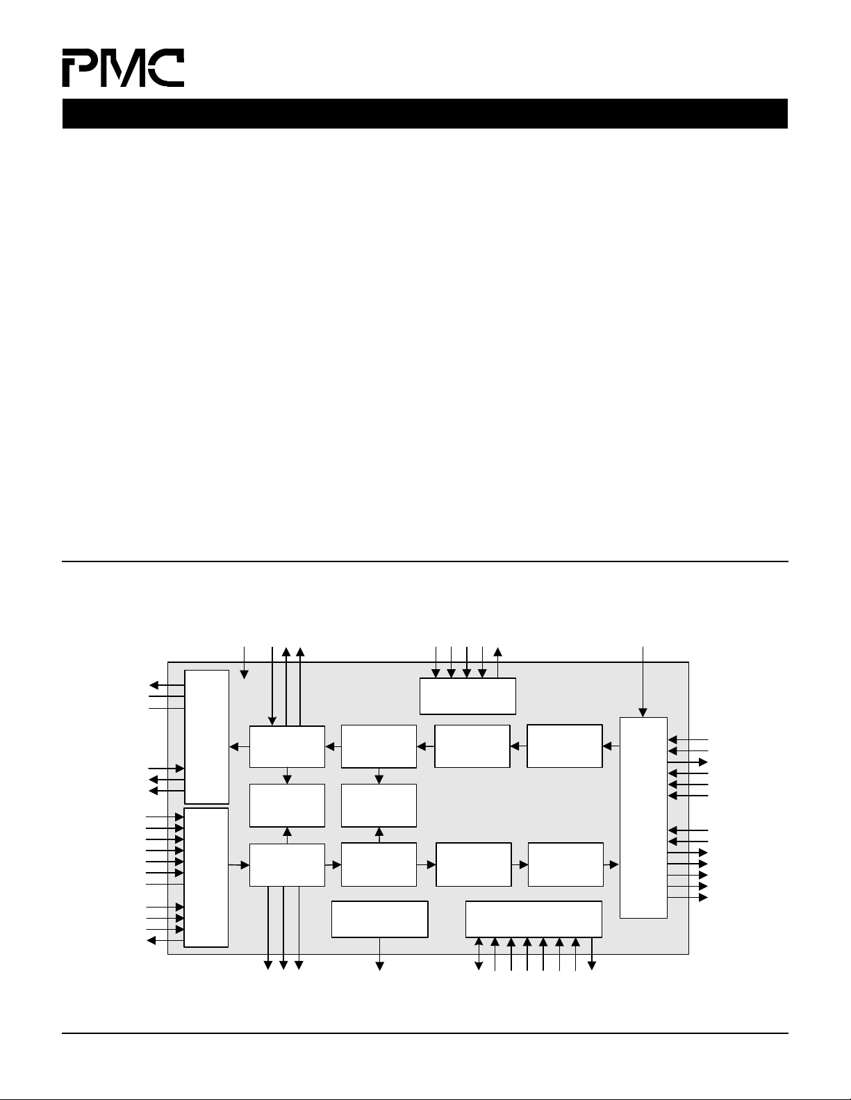
BLOCK DIAGRAM
TDREF1,TDREF0
TXD+/-
ATP[0]
PTCLK
POUT[7:0]
FPOUT
RBYP
PECLV
REFCLK+/-
RXD+/-
RRCLK+/-
SD
ATP[1]
PICLK
PIN[7:0]
FPIN
OOF
Tx
Line
I/F
Rx
Line
I/F
TFPI
LIFSEL
Tx Section
O/H
Processor
Section
Trace Buffer
Rx Section
O/H
Processor
TFPO
TCLK
Tx Line O/H
Processor
Path Trace
Buffer
Rx Line O/H
Processor
Rx APS, Sync
Status, BERM
TRSTB
TCK
TMS
TDI
JTAG Test
Access Port
Tx Path O/H
Processor
Rx Path O/H
Processor
TDO
Tx ATM Cell
Processor
Rx ATM Cell
Processor
Microprocessor
Interfaces
SYSSEL
Utopia ATM Level 2
Utopia ATM Level 3
TFCLK
TENB
TCA
TSOC
TPRTY
TDAT[15:0]
RFCLK
RENB
System Interface
RCA
RSOC
RPRTY
RVAL
RDAT[15:0]
ALE
CSB
RDB
RCLK
RFPO
RALARM
PMC-1981279 (R3) © 2001 PMC-Sierra, Inc.
APSP[4:0]
D[7:0]
A[8:0]
WRB
INTB
RSTB
622 Mbit/s ATM Physical Layer Device
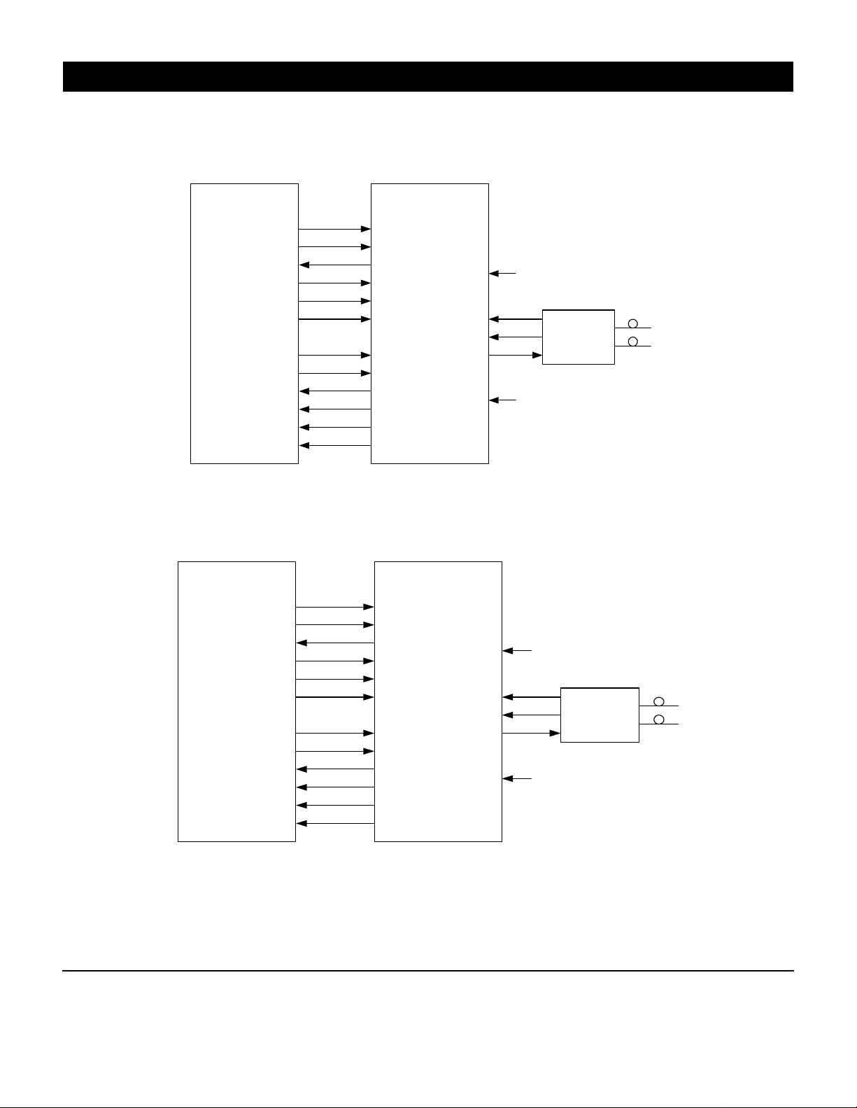
TYPICAL APPLICATIONS
UTOPIA LEVEL 2 APPLICATION
UTOPIA Level 2
Interface
ATM Layer Device
TxClk
TxEnb
TxClav
TxSOC
TxPrty
TxData[15:0]
RxClk
RxEnb
RxClav
RxSOC
RxPrty
RxData[15:0]
PM5356
S/UNI-622-MAX
TFCLK
TENB
TCA
TSOC
TPRTY
TDAT[15:0]
RFCLK
RENB
RCA
RSOC
RPRTY
RDAT[15:0]
LIFSEL
RXD+/-
TXD+/-
SYSSEL
SD
PM5356 S/UNI-622-MAX
1
Optical
Transceiver
0
UTOPIA LEVEL 3 APPLICATION
ATM Layer Device
TxClk
TxEnb
TxClav
TxSOC
TxPrty
TxData[7:0]
RxClk
RxEnb
RxVal
RxSOC
RxPrty
RxData[7:0]
UTOPIA Level 3
Interface
PM5356
S/UNI-622-MAX
TFCLK
TENB
TCA
TSOC
TPRTY
TDAT[7:0]
RFCLK
RENB
RVAL
RSOC
RPRTY
RDAT[7:0]
LIFSEL
RXD+/-
SD
TXD+/-
SYSSEL
1
Optical
Transceiver
1
Head Office:
PMC-Sierra, Inc.
8555 Baxter Place
Burnaby, B.C. V5A 4V7
Canada
Tel: 604.415.6000
Fax: 604.415.6200
To order documentation,
send email to:
document@pmc-sierra.com
or contact the head office,
Attn: Document Coordinator
All product documentation is available
on our web site at:
http://www.pmc-sierra.com
For corpo rate information,
send email to:
info@pmc-sierra.com
PMC-1981279 (R3)
© 2001 PMC-Sierra, Inc.
 Loading...