


PM5355 S/UNI-622
DATA SHEET
PMC-941027 ISSUE 3 SATURN USER NETWORK INTERFACE (622-Mb)
PROPRIETARY AND CONFIDENTIAL TO PMC-SIERRA, INC., AND FOR ITS CUSTOMERS’ INTERNAL USE
PM5355
TM
622
S/
UNI-
S/UNI-622
SATURN USER NETWORK INTERFACE
(622-MBIT/S) STANDARD PRODUCT
DATA SHEET
ISSUE 3: JUNE 1998

PM5355 S/UNI-622
DATA SHEET
PMC-941027 ISSUE 3 SATURN USER NETWORK INTERFACE (622-Mb)
PROPRIETARY AND CONFIDENTIAL TO PMC-SIERRA, INC., AND FOR ITS CUSTOMERS’ INTERNAL USE
PUBLIC REVISION HISTORY
Issue No. Issue Date Details of Change
3 June 1998 Data Sheet Reformatted — No Change in Technical
Content.
Generated R3 data sheet from PMC-930527, R8.
2 April 3,
1996
Update to Eng Doc Issue 7
1 October
1994
Creation of Document

PM5355 S/UNI-622
DATA SHEET
PMC-941027 ISSUE 3 SATURN USER NETWORK INTERFACE (622-Mb)
PROPRIETARY AND CONFIDENTIAL TO PMC-SIERRA, INC., AND FOR ITS CUSTOMERS’ INTERNAL USE
i
CONTENTS
1 FEATURES...............................................................................................1
1.1 THE RECEIVER SECTION: ..........................................................1
1.2 THE TRANSMITTER SECTION:....................................................2
2 APPLICATIONS .......................................................................................4
3 REFERENCES.........................................................................................5
4 APPLICATION EXAMPLES......................................................................6
5 BLOCK DIAGRAM....................................................................................8
6 DESCRIPTION.......................................................................................10
7 PIN DIAGRAM........................................................................................12
8 PIN DESCRIPTION................................................................................13
9 FUNCTIONAL DESCRIPTION...............................................................29
9.1 RECEIVE SECTION OVERHEAD PROCESSOR........................29
9.1.1 FRAMER...........................................................................29
9.1.2 DESCRAMBLE .................................................................30
9.1.3 ERROR MONITOR............................................................30
9.1.4 LOSS OF SIGNAL ............................................................30
9.1.5 LOSS OF FRAME.............................................................30
9.2 RECEIVE LINE OVERHEAD PROCESSOR ...............................31
9.2.1 LINE RDI DETECT............................................................31
9.2.2 LINE AIS DETECT............................................................31
9.2.3 AUTOMATIC PROTECTION SWITCH CONTRO L BLOCK31
9.2.4 ERROR MONITOR............................................................32

PM5355 S/UNI-622
DATA SHEET
PMC-941027 ISSUE 3 SATURN USER NETWORK INTERFACE (622-Mb)
PROPRIETARY AND CONFIDENTIAL TO PMC-SIERRA, INC., AND FOR ITS CUSTOMERS’ INTERNAL USE
ii
9.3 BYTE INTERLEAVED DEMULTIPLEXER....................................32
9.4 TRANSPORT OVERHEAD EXTRACT PORT..............................32
9.5 RECEIVE PATH OVERHEAD PROCESSOR...............................32
9.5.1 POINTER INTERPRETER................................................33
9.5.2 SPE TIMING......................................................................38
9.5.3 ERROR MONITOR............................................................38
9.6 PATH OVERHEAD EXTRACT......................................................39
9.7 RECEIVE ATM CELL PROCESSOR...........................................39
9.7.1 CELL DELINEATION.........................................................39
9.7.2 DESCRAMBLER...............................................................40
9.7.3 CELL FILTER AND HCS VERIFICATION..........................40
9.7.4 PERFORMANCE MONITOR.............................................42
9.7.5 GFC EXTRACTION PORT................................................42
9.7.6 RECEIVE FIFO.................................................................42
9.8 TRANSMIT SECTION OVERHEAD PROCESSOR.....................43
9.8.1 LINE AIS INSERT.............................................................43
9.8.2 BIP-8 INSERT...................................................................43
9.8.3 FRAMING AND IDENTITY INSERT..................................44
9.8.4 SCRAMBLER....................................................................44
9.9 TRANSMIT LINE OVERHEAD PROCESSOR.............................44
9.9.1 APS INSERT..................................................................... 44
9.9.2 LINE BIP CALCULATE......................................................44
9.9.3 LINE RDI INSERT.............................................................45

PM5355 S/UNI-622
DATA SHEET
PMC-941027 ISSUE 3 SATURN USER NETWORK INTERFACE (622-Mb)
PROPRIETARY AND CONFIDENTIAL TO PMC-SIERRA, INC., AND FOR ITS CUSTOMERS’ INTERNAL USE
iii
9.9.4 LINE FEBE INSERT..........................................................45
9.10 BYTE INTERLEAVED MULTIPLEXER ........................................45
9.11 TRANSPORT OVERHEAD INSERT PORT.................................45
9.12 TRANSMIT PATH OVERHEAD PROCESSOR............................46
9.12.1POINTER GENERATOR...................................................47
9.12.2BIP-8 CALCULATE...........................................................48
9.12.3FEBE CALCULATE...........................................................48
9.12.4SPE MULTIPLEXER..........................................................48
9.13 PATH OVERHEAD INSERT.........................................................48
9.14 TRANSMIT ATM CELL PROCESSOR.........................................50
9.14.1IDLE/UNASSIGNED CELL GENERATOR.........................50
9.14.2SCRAMBLER....................................................................50
9.14.3HCS GENERATOR............................................................ 50
9.14.4GFC INSERTION PORT ...................................................50
9.14.5TRANSMIT FIFO...............................................................51
9.15 SONET/SDH SECTION AND PATH TRACE BUFFERS...............51
9.15.1RECEIVE TRACE BUFFER (RTB)....................................51
9.15.2TRANSMIT TRACE BUFFER (TTB)..................................54
9.16 LINE SIDE INTERFACE...............................................................54
9.16.1RECEIVE INTERFACE......................................................54
9.16.2TRANSMIT INTERFACE...................................................55
9.17 DROP SIDE INTERFACE ............................................................55
9.17.1RECEIVE INTERFACE......................................................55

PM5355 S/UNI-622
DATA SHEET
PMC-941027 ISSUE 3 SATURN USER NETWORK INTERFACE (622-Mb)
PROPRIETARY AND CONFIDENTIAL TO PMC-SIERRA, INC., AND FOR ITS CUSTOMERS’ INTERNAL USE
iv
9.17.2TRANSMIT INTERFACE...................................................56
9.18 PARALLEL I/O PORT...................................................................56
9.19 JTAG TEST ACCESS PORT........................................................56
9.20 MICROPROCESSOR INTERFACE.............................................56
9.21 REGISTER MEMORY MAP.........................................................56
10 NORMAL MODE REGISTER DESCRIPTION........................................62
11 TEST FEATURES DESCRIPTION .......................................................194
11.1 TEST MODE REGISTER MEMORY MAP.................................194
11.2 TEST MODE 0 DETAILS...........................................................199
11.3 JTAG TEST PORT......................................................................202
12 OPERATION.........................................................................................207
13 FUNCTIONAL TIMING .........................................................................223
13.1 LINE SIDE RECEIVE INTERFACE............................................223
13.2 LINE SIDE TRANSMIT INTERFACE..........................................227
13.3 OVERHEAD ACCESS...............................................................229
13.4 GFC ACCESS............................................................................237
13.5 DROP SIDE RECEIVE INTERFACE..........................................238
13.6 DROP SIDE TRANSMIT INTERFACE .......................................241
14 ABSOLUTE MAXIMUM RATINGS........................................................242
15 D.C. CHARACTERISTICS ....................................................................243
16 MICROPROCESSOR INTERFACE TIMING CHARACTERISTICS......246
17 S/UNI-622 TIMING CHARACTERISTICS.............................................250
18 ORDERING AND THERMAL INFORMATION ......................................270

PM5355 S/UNI-622
DATA SHEET
PMC-941027 ISSUE 3 SATURN USER NETWORK INTERFACE (622-Mb)
PROPRIETARY AND CONFIDENTIAL TO PMC-SIERRA, INC., AND FOR ITS CUSTOMERS’ INTERNAL USE
v
19 MECHANICAL INFORMATION.............................................................271

PM5355 S/UNI-622
DATA SHEET
PMC-941027 ISSUE 3 SATURN USER NETWORK INTERFACE (622-Mb)
PROPRIETARY AND CONFIDENTIAL TO PMC-SIERRA, INC., AND FOR ITS CUSTOMERS’ INTERNAL USE
vi
LIST OF REGISTERS
REGISTER 0X00: S/UNI-622 MASTER RESET AND IDENTITY / LOAD
PERFORMANCE METERS....................................................................63
REGISTER 0X01: S/UNI-622 MASTER CONFIGURATION..............................64
REGISTER 0X02: S/UNI-622 MASTER INTERRUPT STATUS.........................67
REGISTER 0X03: PISO INTERRUPT...............................................................69
REGISTER 0X04: S/UNI-622 MASTER CONTROL/MONITOR........................70
REGISTER 0X05: S/UNI-622 MASTER AUTO ALARM ....................................73
REGISTER 0X06: S/UNI-622 PARALLEL OUTPUT PORT...............................74
REGISTER 0X07: S/UNI-622 PARALLEL INPUT PORT ...................................75
REGISTER 0X08: S/UNI-622 PARALLEL INPUT PORT VALUE.......................76
REGISTER 0X09: S/UNI-622 PARALLEL INPUT PORT ENABLE....................77
REGISTER 0X0A: S/UNI-622 TRANSMIT C1...................................................78
REGISTER 0X0B: S/UNI-622 APS CONTROL/STATUS...................................79
REGISTER 0X0C: S/UNI-622 RECEIVE K1 .....................................................81
REGISTER 0X0D: S/UNI-622 RECEIVE K2 .....................................................82
REGISTER 0X0E: S/UNI-622 RECEIVE Z1......................................................83
REGISTER 0X0F: S/UNI-622 TRANSMIT Z1....................................................84
REGISTER 0X10: RSOP CONTROL/INTERRUPT ENABLE............................85
REGISTER 0X11: RSOP STATUS/INTERRUPT STATUS.................................87
REGISTER 0X12: RSOP SECTION BIP-8 LSB................................................89
REGISTER 0X13: RSOP SECTION BIP-8 MSB...............................................90
REGISTER 0X14: TSOP CONTROL................................................................. 9 1

PM5355 S/UNI-622
DATA SHEET
PMC-941027 ISSUE 3 SATURN USER NETWORK INTERFACE (622-Mb)
PROPRIETARY AND CONFIDENTIAL TO PMC-SIERRA, INC., AND FOR ITS CUSTOMERS’ INTERNAL USE
vii
REGISTER 0X15: TSOP DIAGNOSTIC............................................................92
REGISTER 0X18: RLOP CONTROL/STATUS...................................................93
REGISTER 0X19: RLOP INTERRUPT ENABLE/INTERRUPT STATUS ...........95
REGISTER 0X1A: RLOP LINE BIP-96/24/8 LSB..............................................97
REGISTER 0X1B: RLOP LINE BIP-96/24/8......................................................98
REGISTER 0X1C: RLOP LINE BIP-96/24/8 MSB............................................. 99
REGISTER 0X1D: RLOP LINE FEBE LSB .....................................................100
REGISTER 0X1E: RLOP LINE FEBE .............................................................101
REGISTER 0X1F: RLOP LINE FEBE MSB.....................................................102
REGISTER 0X20: TLOP CONTROL...............................................................103
REGISTER 0X21: TLOP DIAGNOSTIC ..........................................................104
REGISTER 0X22: TLOP TRANSMIT K1.........................................................105
REGISTER 0X23: TLOP TRANSMIT K2.........................................................106
REGISTER 0X28 SSTB CONTROL................................................................107
REGISTER 0X29: SSTB SECTION TRACE IDENTIFIER STATUS.................109
REGISTER 0X2A: SSTB INDIRECT ADDRESS REGISTER..........................111
REGISTER 0X2B: SSTB INDIRECT DATA REGISTER...................................112
REGISTER 0X2C: SSTB EXPECTED CLOCK SYNCHRONIZATION MESSAGE
..............................................................................................................113
REGISTER 0X2D: SSTB CLOCK SYNCHRONIZATION MESSAGE STATUS114
REGISTER 0X30: RPOP STATUS/CONTROL................................................116
REGISTER 0X31: RPOP INTERRUPT STATUS .............................................117
REGISTER 0X32: RPOP POINTER INTERRUPT STATUS ............................118
REGISTER 0X33: RPOP INTERRUPT ENABLE............................................120

PM5355 S/UNI-622
DATA SHEET
PMC-941027 ISSUE 3 SATURN USER NETWORK INTERFACE (622-Mb)
PROPRIETARY AND CONFIDENTIAL TO PMC-SIERRA, INC., AND FOR ITS CUSTOMERS’ INTERNAL USE
viii
REGISTER 0X34: RPOP POINTER INTERRUPT ENABLE...........................122
REGISTER 0X35: RPOP POINTER LSB........................................................124
REGISTER 0X36: RPOP POINTER MSB.......................................................125
REGISTER 0X37: RPOP PATH SIGNAL LABEL.............................................126
REGISTER 0X38: RPOP PATH BIP-8 LSB .....................................................127
REGISTER 0X39: RPOP PATH BIP-8 MSB ....................................................128
REGISTER 0X3A: RPOP PATH FEBE LSB.....................................................129
REGISTER 0X3B: RPOP PATH FEBE MSB....................................................130
REGISTER 0X3C: RPOP RDI.........................................................................131
REGISTER 0X3D: RPOP RING CONTROL....................................................132
REGISTER 0X40: TPOP CONTROL/DIAGNOSTIC........................................134
REGISTER 0X41: TPOP POINTER CONTROL..............................................136
REGISTER 0X43: TPOP CURRENT POINTER LSB......................................139
REGISTER 0X44: TPOP CURRENT POINTER MSB.....................................140
REGISTER 0X45: TPOP ARBITRARY POINTER LSB ...................................141
REGISTER 0X46: TPOP ARBITRARY POINTER MSB ..................................142
REGISTER 0X47: TPOP PATH TRACE...........................................................143
REGISTER 0X48: TPOP PATH SIGNAL LABEL .............................................144
REGISTER 0X49: TPOP PATH STATUS..........................................................145
REGISTER 0X4A: TPOP PATH USER CHANNEL ..........................................147
REGISTER 0X4B: TPOP PATH GROWTH #1 (Z3)..........................................148
REGISTER 0X4C: TPOP PATH GROWTH #2 (Z4)..........................................149
REGISTER 0X4D TPOP PATH GROWTH #3 (Z5)..........................................150

PM5355 S/UNI-622
DATA SHEET
PMC-941027 ISSUE 3 SATURN USER NETWORK INTERFACE (622-Mb)
PROPRIETARY AND CONFIDENTIAL TO PMC-SIERRA, INC., AND FOR ITS CUSTOMERS’ INTERNAL USE
ix
REGISTER 0X50: RACP CONTROL...............................................................151
REGISTER 0X51: RACP INTERRUPT STATUS..............................................153
REGISTER 0X52: RACP INTERRUPT ENABLE/CONTROL..........................155
REGISTER 0X53: RACP MATCH HEADER PATTERN ...................................157
REGISTER 0X54: RACP MATCH HEADER MASK.........................................158
REGISTER 0X55: RACP CORRECTABLE HCS ERROR COUNT (LSB) .......159
REGISTER 0X56: RACP CORRECTABLE HCS ERROR COUNT (MSB) ......160
REGISTER 0X57: RACP UNCORRECTABLE HCS ERROR COUNT (LSB)..161
REGISTER 0X58: RACP UNCORRECTABLE HCS ERROR COUNT (MSB).162
REGISTER 0X59: RACP RECEIVE CELL COUNTER (LSB) .........................163
REGISTER 0X5A: RACP RECEIVE CELL COUNTER...................................164
REGISTER 0X5B: RACP RECEIVE CELL COUNTER (MSB)........................165
REGISTER 0X5C: GFC CONTROL/MISC. CONTROL ...................................166
REGISTER 0X60: TACP CONTROL/STATUS..................................................168
REGISTER 0X61: TACP IDLE/UNASSIGNED CELL HEADER PATTERN......170
REGISTER 0X62: TACP IDLE/UNASSIGNED CELL PAYLOAD OCTET
PATTERN..............................................................................................171
REGISTER 0X63: TACP FIFO CONTROL.......................................................172
REGISTER 0X64: TACP TRANSMIT CELL COUNTER (LSB) ........................174
REGISTER 0X65: TACP TRANSMIT CELL COUNTER ..................................175
REGISTER 0X66: TACP TRANSMIT CELL COUNTER (MSB).......................176
REGISTER 0X67: TACP FIXED STUFF / GFC ...............................................177
REGISTER 0X68 SPTB CONTROL................................................................179
REGISTER 0X69: SPTB PATH TRACE IDENTIFIER STATUS........................181

PM5355 S/UNI-622
DATA SHEET
PMC-941027 ISSUE 3 SATURN USER NETWORK INTERFACE (622-Mb)
PROPRIETARY AND CONFIDENTIAL TO PMC-SIERRA, INC., AND FOR ITS CUSTOMERS’ INTERNAL USE
x
REGISTER 0X6A: SPTB INDIRECT ADDRESS REGISTER..........................183
REGISTER 0X6B: SPTB INDIRECT DATA REGISTER...................................184
REGISTER 0X6C: SPTB EXPECTED PATH SIGNAL LABEL.........................185
REGISTER 0X6D: SPTB PATH SIGNAL LABEL STATUS...............................186
REGISTER 0X70: BERM CONTROL..............................................................188
REGISTER 0X71: BERM INTERRUPT...........................................................189
REGISTER 0X72: BERM LINE BIP ACCUMULATION PERIOD LSB .............190
REGISTER 0X73: BERM LINE BIP ACCUMULATION PERIOD MSB ............191
REGISTER 0X74: BERM LINE BIP THRESHOLD LSB..................................192
REGISTER 0X75: BERM LINE BIP THRESHOLD MSB.................................193
REGISTER 0X80: MASTER TEST..................................................................198

PM5355 S/UNI-622
DATA SHEET
PMC-941027 ISSUE 3 SATURN USER NETWORK INTERFACE (622-Mb)
PROPRIETARY AND CONFIDENTIAL TO PMC-SIERRA, INC., AND FOR ITS CUSTOMERS’ INTERNAL USE
xi
LIST OF FIGURES
FIGURE 1 - TYPICAL STS-12C/3C ATM INTERFACE......................................6
FIGURE 2 - TYPICAL STS-1 ATM INTERFACE.................................................7
FIGURE 3 - NORMAL OPERATING MODE.......................................................8
FIGURE 4 - LOOPBACK MODES......................................................................9
FIGURE 5 - ......................................................................................................12
FIGURE 6 - POINTER INTERPRETATION STATE DIAGRAM.........................34
FIGURE 7 - ITU G.783 CONCATENATION INDICATOR STATE DIAGRAM....37
FIGURE 8 - ITU G.783 CONCATENATION INDICATOR IMPLEMENTATION.38
FIGURE 9 - CELL DELINEATION STATE DIAGRAM.......................................40
FIGURE 10- HCS VERIFICATION STATE DIAGRAM.......................................41
FIGURE 11- STS-12C (STM-4C) DEFAULT TRANSPORT OVERHEAD VALUES
.......................................................................................................46
FIGURE 12- DEFAULT PATH OVERHEAD VALUES.........................................49
FIGURE 13- INPUT OBSERVATION CELL (IN_CELL)...................................204
FIGURE 14- OUTPUT CELL (OUT_CELL).....................................................205
FIGURE 15- BIDIRECTIONAL CELL (IO_CELL)............................................205
FIGURE 16- LAYOUT OF OUTPUT ENABLE AND BIDIRECTIONAL CELLS206
FIGURE 17- STS-1 MAPPING........................................................................207
FIGURE 18- STS-3C (STM-1) MAPPING.......................................................208
FIGURE 19- STS-12C (STM-4C) ATM MAPPING ..........................................209
FIGURE 20-16- BIT WIDE, 27-WORD STRUCTURE.....................................214
FIGURE 21- BOUNDARY SCAN ARCHITECTURE........................................217

PM5355 S/UNI-622
DATA SHEET
PMC-941027 ISSUE 3 SATURN USER NETWORK INTERFACE (622-Mb)
PROPRIETARY AND CONFIDENTIAL TO PMC-SIERRA, INC., AND FOR ITS CUSTOMERS’ INTERNAL USE
xii
FIGURE 22- TAP CONTROLLER FINITE STATE MACHINE ..........................219
FIGURE 23- IN FRAME DECLARATION ........................................................223
FIGURE 24- OUT OF FRAME DECLARATION ..............................................224
FIGURE 25- LOSS OF SIGNAL DECLARATION/REMOVAL.......................... 224
FIGURE 26- LOSS OF FRAME DECLARATION/REMOVAL ..........................225
FIGURE 27- LINE AIS AND LINE RDI DECLARATION/REMOVAL................225
FIGURE 28- LOSS OF POINTER DECLARATION/REMOVAL.......................226
FIGURE 29- PATH AIS DECLARATION/REMOVAL........................................226
FIGURE 30- PATH REMOTE DEFECT INDICATION DECLARATION/REMOVAL
.....................................................................................................227
FIGURE 31- STS-1 BIT-SERIAL TRANSMIT FRAME ALIGNMENT...............227
FIGURE 32- STS-12C BYTE-SERIAL TRANSMIT FRAME ALIGNMENT......228
FIGURE 33- STS-3C/1 BYTE-SERIAL TRANSMIT FRAME ALIGNMENT.....228
FIGURE 34- TRANSPORT OVERHEAD EXTRACTION.................................229
FIGURE 35- TRANSPORT OVERHEAD ORDERWIRE AND USER CHANNEL
EXTRACTION.................................................................................................230
FIGURE 36- TRANSPORT OVERHEAD DATA LINK CLOCK AND DATA
EXTRACTION.................................................................................................231
FIGURE 37- PATH OVERHEAD EXTRACTION..............................................232
FIGURE 38- TRANSPORT OVERHEAD INSERTION....................................233
FIGURE 39- TRANSPORT OVERHEAD ORDERWIRE AND USER CHANNEL
INSERTION.....................................................................................................234
FIGURE 40- TRANSPORT OVERHEAD DATA LINK CLOCK AND DATA
INSERTION.....................................................................................................235
FIGURE 41- PATH OVERHEAD INSERTION..................................................236
FIGURE 42- GFC EXTRACTION PORT.........................................................237

PM5355 S/UNI-622
DATA SHEET
PMC-941027 ISSUE 3 SATURN USER NETWORK INTERFACE (622-Mb)
PROPRIETARY AND CONFIDENTIAL TO PMC-SIERRA, INC., AND FOR ITS CUSTOMERS’ INTERNAL USE
xiii
FIGURE 43- GFC INSERTION PORT.............................................................238
FIGURE 44- RECEIVE SYNCHRONOUS FIFO, TSEN=0, RCALEVEL0=1 ...238
FIGURE 45- RECEIVE SYNCHRONOUS FIFO, TSEN=0, RCALEVEL0=0 ...239
FIGURE 46- RECEIVE SYNCHRONOUS FIFO, TSEN=1, RCALEVEL0=1 ...240
FIGURE 47- TRANSMIT SYNCHRONOUS FIFO...........................................241
FIGURE 48- MICROPROCESSOR INTERFACE READ TIMING....................247
FIGURE 49- MICROPROCESSOR INTERFACE WRITE TIMING..................249
FIGURE 50- LINE SIDE RECEIVE INTERFACE TIMING ...............................251
FIGURE 51- RECEIVE ALARM OUTPUT TIMING .........................................253
FIGURE 52- RECEIVE OVERHEAD ACCESS TIMING..................................255
FIGURE 53- RECEIVE GFC ACCESS TIMING..............................................257
FIGURE 54- LINE SIDE TRANSMIT INTERFACE TIMING.............................258
FIGURE 55- TRANSMIT ALARM INPUT TIMING...........................................259
FIGURE 56- TRANSMIT OVERHEAD ACCESS TIMING................................261
FIGURE 57- TRANSMIT GFC ACCESS TIMING............................................264
FIGURE 58- DROP SIDE RECEIVE INTERFACE TIMING.............................265
FIGURE 59- DROP SIDE TRANSMIT INTERFACE........................................267
FIGURE 60- JTAG PORT INTERFACE TIMING..............................................268

PM5355 S/UNI-622
DATA SHEET
PMC-941027 ISSUE 3 SATURN USER NETWORK INTERFACE (622-Mb)
PROPRIETARY AND CONFIDENTIAL TO PMC-SIERRA, INC., AND FOR ITS CUSTOMERS’ INTERNAL USE
xiv
LIST OF TABLES
TABLE 1 - ......................................................................................................13
TABLE 2 - ......................................................................................................53
TABLE 3 - ......................................................................................................56
TABLE 4 - ......................................................................................................64
TABLE 5 - ......................................................................................................65
TABLE 6 - ....................................................................................................155
TABLE 7 - ....................................................................................................173
TABLE 8 - ....................................................................................................177
TABLE 9 - ....................................................................................................194
TABLE 10 - ....................................................................................................199
TABLE 11 - ....................................................................................................201
TABLE 12 - INSTRUCTION REGISTER........................................................202
TABLE 13 - ....................................................................................................215
TABLE 14 - ....................................................................................................215
TABLE 15 - ....................................................................................................216
TABLE 16 - ABSOLUTE MAXIMUM RATINGS..............................................242
TABLE 17 - ....................................................................................................243
TABLE 18 - MICROPROCESSOR INTERFACE READ ACCESS (FIGURE 48) .
.....................................................................................................246
TABLE 19 - MICROPROCESSOR INTERFACE WRITE ACCESS (FIGURE 49)
.....................................................................................................248
TABLE 20 - LINE SIDE RECEIVE INTERFACE (FIGURE 50).......................250
TABLE 21 - RECEIVE ALARM OUTPUT (FIGURE 51).................................251

PM5355 S/UNI-622
DATA SHEET
PMC-941027 ISSUE 3 SATURN USER NETWORK INTERFACE (622-Mb)
PROPRIETARY AND CONFIDENTIAL TO PMC-SIERRA, INC., AND FOR ITS CUSTOMERS’ INTERNAL USE
xv
TABLE 22 - RECEIVE OVERHEAD ACCESS (FIGURE 52).........................254
TABLE 23 - RECEIVE OVERHEAD ACCESS (FIGURE 53).........................256
TABLE 24 - LINE SIDE TRANSMIT INTERFACE (FIGURE 54)....................257
TABLE 25 - TRANSMIT ALARM INPUT (FIGURE 55) ..................................258
TABLE 26 - TRANSMIT OVERHEAD ACCESS (FIGURE 56).......................260
TABLE 27 - TRANSMIT GFC ACCESS (FIGURE 57)...................................263
TABLE 28 - DROP SIDE RECEIVE INTERFACE (FIGURE 58)....................264
TABLE 29 - DROP SIDE TRANSMIT INTERFACE (FIGURE 59)..................266
TABLE 30 - JTAG PORT INTERFACE (FIGURE 60).....................................267
TABLE 31 - ....................................................................................................270
TABLE 32 - ....................................................................................................270

PM5355 S/UNI-622
DATA SHEET
PMC-941027 ISSUE 3 SATURN USER NETWORK INTERFACE (622-Mb)
PROPRIETARY AND CONFIDENTIAL TO PMC-SIERRA, INC., AND FOR ITS CUSTOMERS’ INTERNAL USE
xvi

PM5355 S/UNI-622
DATA SHEET
PMC-941027 ISSUE 3 SATURN USER NETWORK INTERFACE (622-Mb)
PROPRIETARY AND CONFIDENTIAL TO PMC-SIERRA, INC., AND FOR ITS CUSTOMERS’ INTERNAL USE
1
1
FEATURES
•
Monolithic Saturn User Network Interface that implements the ATM physical
layer for Broadband ISDN according to CCITT Recommendation I.432 and
the ATM Forum BISDN Inter Carrier Interface (B-ICI) Specification.
•
Supports a 77.76 Mbyte/s STS-12c (STM-4c), a 19.44 Mbyte/s STS-3c
(STM-1), a 6.48 Mbyte/s STS-1, or a 51.84 Mbit/s STS-1 line side interface.
•
Provides four-cell deep FIFO buffers in both the transmit and receive paths.
•
Provides a generic 8-bit microprocessor bus interface for configuration,
control, and status monitoring.
•
Provides a generic parallel output port and a generic parallel input port to
control and monitor front end line devices.
•
Provides a standard 5-signal P1149.1 JTAG test port for boundary scan
board test purposes.
•
Low-power, +5 Volt, CMOS technology.
•
208-pin high-performance plastic quad flat pack (PQFP) package.
1.1 The receiver section:
•
Frames to and descrambles the received STS-12c/3c/1 (STM-4c/1, AU-3)
stream.
•
Filters and captures the automatic protection switch channel (APS) bytes in
readable registers and detects APS byte failure.
•
Interprets the received payload pointer (H1, H2) and extracts the
STS-12c/3c/1 (STM-4c/1, AU-3) synchronous payload envelope and path
overhead.
•
Extracts ATM cells from the received STS-12c/3c/1 (STM-4c/1, AU-3)
synchronous payload envelope using ATM cell delineation and provides
optional ATM cell payload descrambling, header check sequence (HCS) error
detection and correction, and idle/unassigned cell filtering.
•
Provides a generic 16-bit wide datapath interface to read extracted cells from
an internal four-cell FIFO buffer.

PM5355 S/UNI-622
DATA SHEET
PMC-941027 ISSUE 3 SATURN USER NETWORK INTERFACE (622-Mb)
PROPRIETARY AND CONFIDENTIAL TO PMC-SIERRA, INC., AND FOR ITS CUSTOMERS’ INTERNAL USE
2
•
Extracts all transport overhead bytes and serializes them in four 5.184 Mbit/s
streams for optional external processing.
•
Extracts the section user channel (F1) and the order wire channels (E1, E2)
and serializes them into three independent 64 kbit/s streams for optional
external processing.
•
Extracts the data communication channels (D1-D3, D4-D12) and serializes
them at 192 kbit/s (D1-D3) and 576 kbit/s (D4-D12) for optional external
processing.
•
Extracts all path overhead bytes and serializes them at 576 kbit/s for optional
external processing.
•
Extracts the 16- or 64-byte section trace (C1) sequence and the 16- or 64byte path trace (J1) sequence into internal register banks.
•
Detects loss of signal (LOS), out of frame (OOF), loss of frame (LOF), line
alarm indication signal (AIS), line remote defect indication (LRDI), loss of
pointer (LOP), path alarm indication signal (AIS), path remote defect
indication signal (RDI-P) and loss of cell delineation (LCD).
•
Counts received section BIP-8 (B1) errors, received line BIP-96/24/8 (B2)
errors, line far end block errors (line FEBEs), received path BIP-8 (B3) errors
and path far end block errors (path FEBEs) for performance monitoring
purposes.
•
Counts received cells written into the receive FIFO, received HCS errored
cells that are discarded, and received HCS errored cells that are corrected
and passed on.
•
Extracts and serializes the GFC field from all received cells (including
idle/unassigned cells) for external processing.
1.2 The transmitter section:
•
Provides an internal four-cell FIFO into which cells are written using a generic
16-bit wide datapath interface.
•
Inserts the gener ic flow control (GFC) bits via a simple serial interface.
•
Counts transmit cells read from the transmit FIFO.

PM5355 S/UNI-622
DATA SHEET
PMC-941027 ISSUE 3 SATURN USER NETWORK INTERFACE (622-Mb)
PROPRIETARY AND CONFIDENTIAL TO PMC-SIERRA, INC., AND FOR ITS CUSTOMERS’ INTERNAL USE
3
•
Provides idle/unassigned cell insertion, HCS generation/insertion, and ATM
cell payload scrambling.
•
Inserts ATM cells into the transmitted STS-12c/3c/1 (STM-4c/1, AU-3)
synchronous payload envelope.
•
Inserts a register programmable path signal label.
•
Generates the transmit payload pointer (H1, H2) and inserts the path
overhead.
•
Optionally inserts the 16- or 64-byte section trace (C1) sequence and the 16or 64-byte path trace (J1) sequence from internal register banks.
•
Optionally inserts externally generated path overhead bytes received via a
576 kbit/s serial interface.
•
Optionally inserts externally generated data communication channels (D1-D3,
D4-D12) via a 192 kbit/s (D1-D3) serial stream and a 576 kbit/s (D4-D12)
serial stream.
•
Optionally inserts externally generated section user channel (F1) and
externally generated order wire channels (E1, E2) via three 64 kbit/s serial
interfaces.
•
Optionally inserts externally generated transport overhead bytes received via
four 5.184 Mbit/s serial interfaces.
•
Scrambles the transmitted STS-12c/3c/1 (STM-4c/1, AU-3) stream and
inserts the framing bytes (A1, A2) and the identity byte (C1).
•
Optionally inserts path alarm indication signal (AIS), path remote defect
indication (RDI-P), line alarm indication signal (AIS) and line remote defect
indication (LRDI) indication.
•
Optionally inserts register programmable APS bytes.
•
Inserts path BIP-8 codes (B3), path far end block error (FEBE) indications,
line BIP-96/24/8 codes (B2), line far end block error (FEBE) indications, and
section BIP-8 codes (B1) to allow performance monitoring at the far end.
•
Allows forced insertion of all-zeros data (after scrambling), the corruption of
the framing bytes or the corruption of the section, line, or path BIP-8 codes for
diagnostic purposes.

PM5355 S/UNI-622
DATA SHEET
PMC-941027 ISSUE 3 SATURN USER NETWORK INTERFACE (622-Mb)
PROPRIETARY AND CONFIDENTIAL TO PMC-SIERRA, INC., AND FOR ITS CUSTOMERS’ INTERNAL USE
4
2
APPLICATIONS
•
Workstations
•
LAN Switches and Hubs
•
Routers
•
Video Servers
•
Backbones
•
Broadband Switching Systems

PM5355 S/UNI-622
DATA SHEET
PMC-941027 ISSUE 3 SATURN USER NETWORK INTERFACE (622-Mb)
PROPRIETARY AND CONFIDENTIAL TO PMC-SIERRA, INC., AND FOR ITS CUSTOMERS’ INTERNAL USE
5
3
REFERENCES
1. ITU-T Recommendation G.709 - "Synchronous Multiplexing Structure,"
Helsinki, March 1993.
2. ITU-T Recommendation I.432 - "B-ISDN User-Network Interface-Physical
Interface Specification," Helsinki, March 1993.
3. Bell Communications Research - "SONET Transport Systems Common
Generic Criteria", GR-253-CORE, Issue 1, December 1994.
4. Bell Communications Research - "Generic Requirements for Operations of
Broadband Switching Systems", TA-NWT-00001248, Issue 2, October 1993.
5. ATM Forum - "622 Mbps Physical Layer Specification", af-phy-0046.000,
January 1996.
6. ANSI T1.105-1991, Telecommunications - Digital Hierarchy - Optical Interface
Rates and Formats Specifications (SONET)
7. IEEE 1149.1 - "Standard Te st Access Port and Boundary Scan Architecture",
May 21, 1990.
8. PMC-940212, ATM_SCI_PHY, "SATURN Compliant Interfaces For ATM
Devices," October 1995, Issue 3.
PM5355 S/UNI-622
DATA SHEET
PMC-941027 ISSUE 3 SATURN USER NETWORK INTERFACE (622-Mb)
PROPRIETARY AND CONFIDENTIAL TO PMC-SIERRA, INC., AND FOR ITS CUSTOMERS’ INTERNAL USE
6
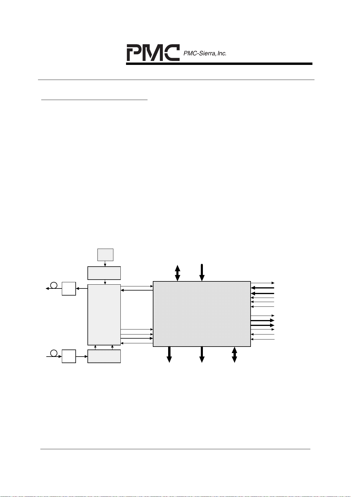
4
APPLICATION EXAMPLES
The S/UNI-622 is typically used to implement the core of an ATM User Network
Interface by which an ATM terminal is linked to an ATM switching system using
SONET/SDH-compatible transport. The S/UNI-622 may find application at either
end of terminal-to-switch links or switch-to-switch links, both in private network
(LAN) and public network (WAN) situations. In a typical STS-3c (STM-1) or
STS-12c (STM-4c) application, the S/UNI-622 requires a clock and data
recovery/serial-to-parallel converter device in the receive direction and a serialto-parallel converter/clock synthesis device in the transmit direction on the line
side. The clock synthesis function is not required if the transmit side is looptimed
to the receive clock. The initial configuration and ongoing control and monitoring
of the S/UNI-622 are normally provided via a generic microprocessor interface.
The S/UNI-622 supports a "hardware-only" operating mode fo r STS-12c
(STM-4c) where an external microprocessor is not required. This application is
shown in Figure 1.
Figure 1 - Typical STS-12c/3c ATM Interface
PIN[7:0]
FPIN
MICRO BUS
FOR CONFIG, STATUS
AND CONTROL
RECEIVE
ALARM DETECT
SIGNALS
RECEIVE
OVERHEAD
EXTRACT
TRANSMIT
ALARM INSERT
SIGNALS
TRANSMIT
OVERHEAD
INSERT
TWRENB
RDAT[15:0]
RSOC
RRDENB
TDAT[15:0]
TSOC
TSD+/-
RSD+/-
O/E
E/O
Clock & Data
Recovery
PM5355 S/UNI-622
SATURN
USER NETWORK INTERFACE
RCA
TCA
PICLK
OOF
Parallel-to-
Serial &
Serial to
Parallel
Converter
POUT[7:0]
TCLK
Ref.
Clock
TFCLK
RFCLK
RXPRTY[1:0]
TXPRTY[1:0]
Clock
Synthesis
TRANSMIT CELL
INTERFACE
RECEIVE CELL
INTERFACE
In a typical STS-1 application, the S/UNI-622 requires a clock and data recovery
device in the receive direction and a clock source in the transmit direction on the
line side. The initial configuration and ongoing control and monitoring of the
S/UNI-622 are normally provided via a generic microprocessor interface. A
typical STS-1 ATM Interface is shown in Figure 2. On the receive side, an
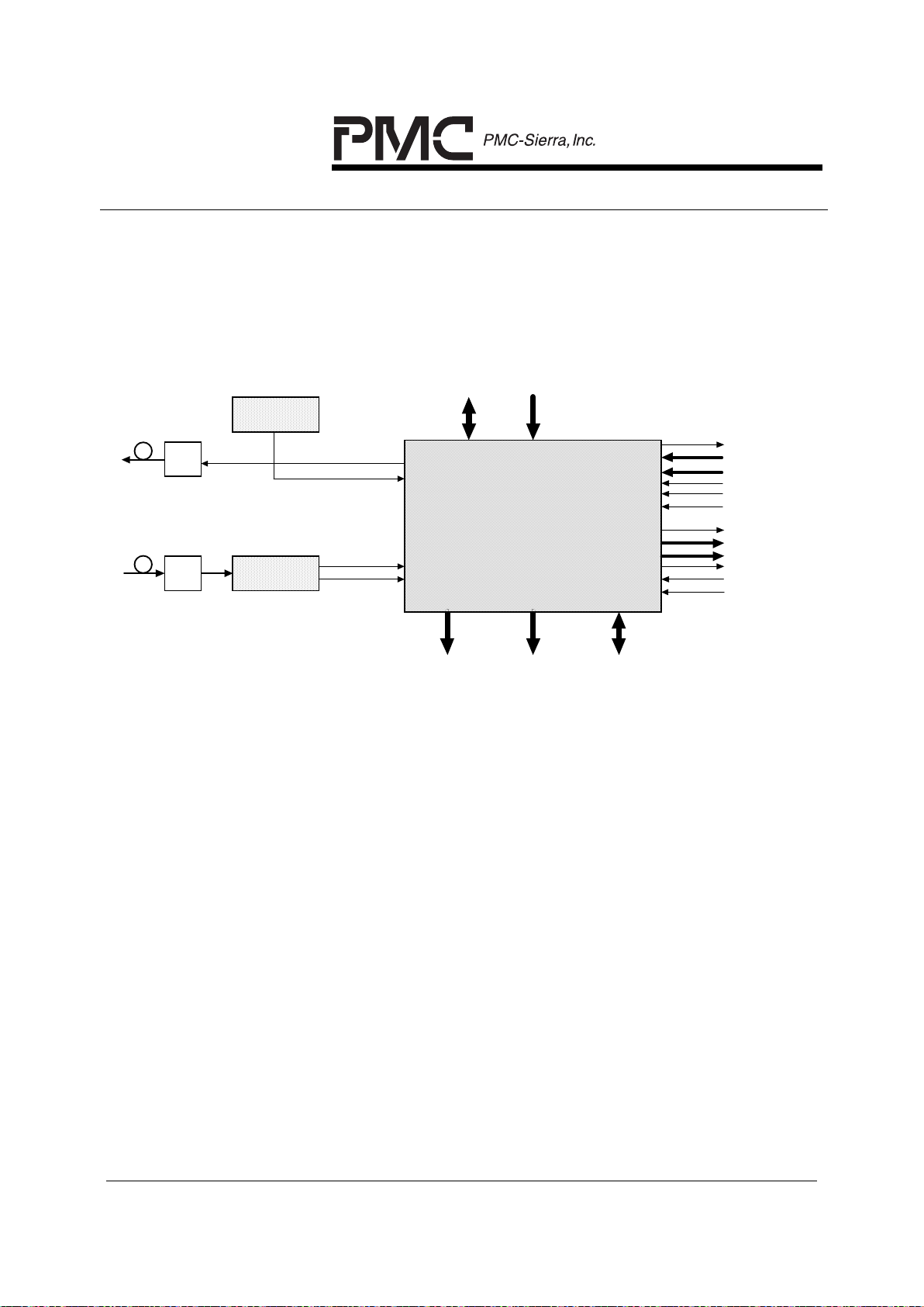
PM5355 S/UNI-622
DATA SHEET
PMC-941027 ISSUE 3 SATURN USER NETWORK INTERFACE (622-Mb)
PROPRIETARY AND CONFIDENTIAL TO PMC-SIERRA, INC., AND FOR ITS CUSTOMERS’ INTERNAL USE
7
external clock and data recovery device is used. On the transmit side, the
S/UNI-622 is configured for looptime operation where the receive clock, RSICLK,
is used as the transmit clock source.
Figure 2 - Typical STS-1 ATM Interface
RSIN
MICRO BUS
FOR CONFIG, STATUS
AND CONTROL
RECEIVE
ALARM DETECT
SIGNALS
RECEIVE
OVERHEAD
EXTRACT
TRANSMIT
ALARM INSERT
SIGNALS
TRANSMIT
OVERHEAD
INSERT
TWRENB
RDAT[15:0]
RSOC
RRDENB
TDAT[15:0]
TSOC
RSD
O/E
E/O
PM5355 S/UNI-622
SATURN
USER NETWORK INTERFACE
RCA
TCA
RSICLK
TSOUT
TFCLK
RFCLK
RXPRTY[1:0]
TXPRTY[1:0]
TSICLK
Clock & Data
Recovery
TRANSMIT CELL
INTERFACE
RECEIVE CELL
INTERFACE
51.84 MHz
Reference
PM5355 S/UNI-622
DATA SHEET
PMC-941027 ISSUE 3 SATURN USER NETWORK INTERFACE (622-Mb)
PROPRIETARY AND CONFIDENTIAL TO PMC-SIERRA, INC., AND FOR ITS CUSTOMERS’ INTERNAL USE
8
5
BLOCK DIAGRAM
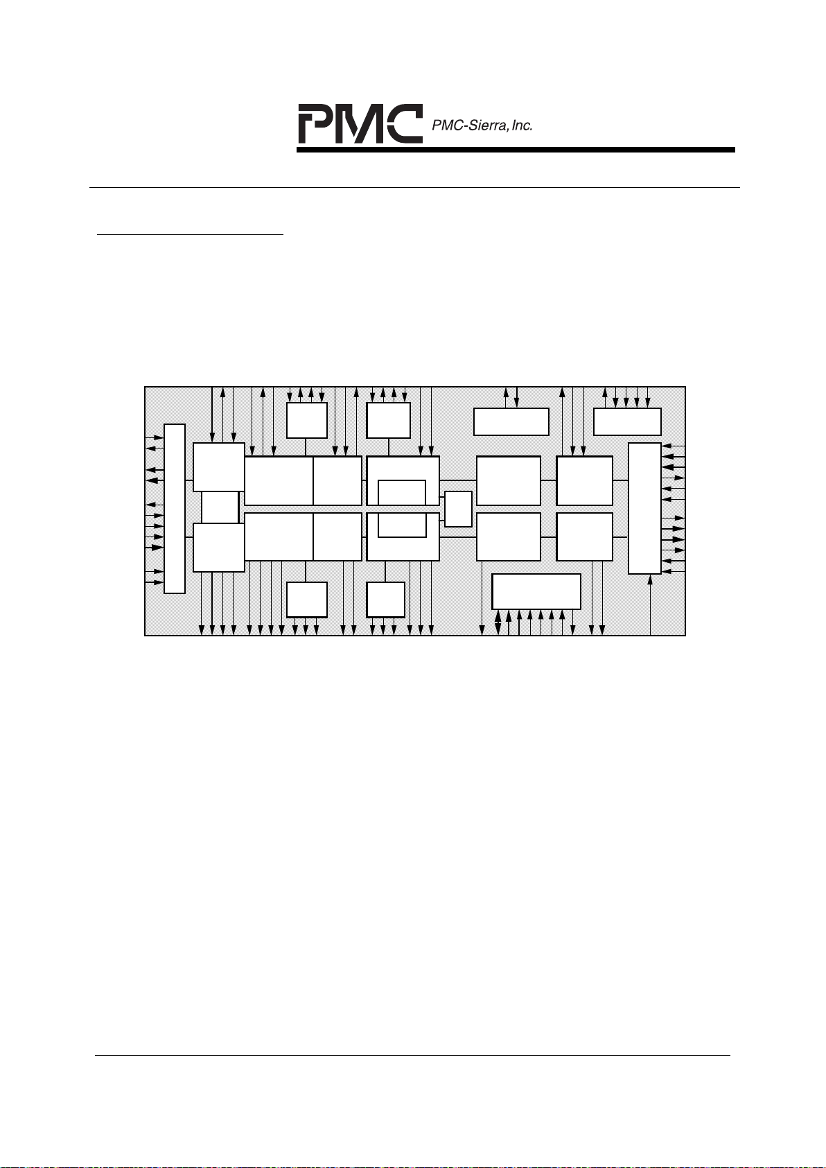
Figure 3 - Normal Operating Mode
Tx ATM
4 Cell
FIFO
Rx ATM
4 Cell
FIFO
Drop
Side
I/F
TDAT[15:0]
TCA
TSOC
RDAT[15:0]
RSOC
D[7:0]
A[7:0]
ALE
CSB
RDB
WRB
RSTB
INTB
Microprocessor I/F
TWRENB
Tx
Line O/H
Processor
Rx
Line O/H
Processor
TLD,TLOW
RLDCLK
RLD,RLOW
Tx ATM Cell
Processor
Rx ATM Cell
Processor
RCA
RRDENB
TMS
TCK
TDI
TDO
TRSTB
JTAG Test
Access Port
POUT[7:0]
PIN[7:0]
PICLK
OOF
FPOUT
FPIN
FPOS
L ine
Side
I/F
LCD
RPOH
TPOH
TPOHCLKRPOHCLK
TPOHFP
TPOHEN
RPOHFP
TPAIS
TPRDI
LOP
PAIS
PRDI
Path
O/H
Insert
Path
O/H
Extract
Rx Path O/H
Processor
Rx ConCat
Processor
Tx Path O/H
Processor
Tx ConCat
Processor
TFCLK
RFCLK
GROCLK
Transport
O/H
Insert
TTOH[4:1]
TTOHCLK
TTOHFP
TTOHEN
Transport
O/H
Extract
RTOH[4:1]
RTOHCLK
RTOHFP
TCLK
TFP
Byte
Interleaved
Demux
Byte
Interleaved
Mux
GTOCLK
POP[5:0]
PIP[3:0]
Parallel
Input/Output Port
TXPRTY[1:0]
RXPRTY[1:0]
TLAIS
LOS
LOF
Tx
Section O/H
Processor
RSDCLK,ROWCLK
RSD,RSOW,RSUC
TSDCLK,TOWCL
K
TSD,TSOW,TSUC
TLDCLK
TLRDI
LAIS
LRDI
Path
Trace
Buffer
TSOUT
TSICLK
RSICLK
RSIN
OHFP
TSEN
RGFC
RCP
TCP
TGFC
XOFF
Section
Trace
Buffer
Rx
Section O/H
Processor
PM5355 S/UNI-622
DATA SHEET
PMC-941027 ISSUE 3 SATURN USER NETWORK INTERFACE (622-Mb)
PROPRIETARY AND CONFIDENTIAL TO PMC-SIERRA, INC., AND FOR ITS CUSTOMERS’ INTERNAL USE
9
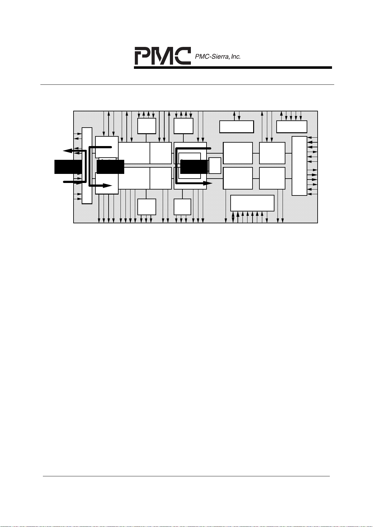
Figure 4 - Loopback Modes
Tx ATM
4 Cell
FIFO
Rx ATM
4 Cell
FIFO
Drop
Side
I/F
Microprocessor I/F
Tx
Line O/H
Processor
Rx
Line O/H
Processor
Tx ATM Cell
Processor
Rx ATM Cell
Processor
JTAG Test
Access Port
L ine
Side
I/F
Path
O/H
Insert
Path
O/H
Extract
Rx Path O/H
Processor
Rx ConCat
Processor
Tx Path O/H
Processor
Tx ConCat
Processor
Transport
O/H
Insert
Transport
O/H
Extract
Byte
Interleaved
Demux
Byte
Interleaved
Mux
Parallel
Input/Output Port
Tx
Section O/H
Processor
Rx
Section O/H
Processor
Path
Trace
Buffer
DIAGNOSTIC
PATH
LOOPBACK
Section
Trace
Buffer
STS-1
LINE
LOOPBACK
STS-1
DIAGNOSTIC
LOOPBACK

PM5355 S/UNI-622
DATA SHEET
PMC-941027 ISSUE 3 SATURN USER NETWORK INTERFACE (622-Mb)
PROPRIETARY AND CONFIDENTIAL TO PMC-SIERRA, INC., AND FOR ITS CUSTOMERS’ INTERNAL USE
10
6
DESCRIPTION
The PM5355 S/UNI-622 SATURN User Network Interface is a monolithic
integrated circuit that implements the SONET/SDH processing and ATM mapping
functions of a 622-Mbit/s ATM User Network Interface.
The S/UNI-622 receives SONET/SDH frames via a byte-serial interface (or bitserial interface for STS-1), and processes section, line, and path overhead. It
performs framing (A1, A2), performs descrambling, detects alarm conditions, and
monitors section, line, and path bit interleaved parity (B1, B2, B3), accumulating
error counts at each level for performance monitoring purposes. Line and path
far end block error indications (Z2, G1) are also accumulated. The S/UNI-622
interprets the received payload pointers (H1, H2) and extracts the synchronous
payload envelope which carries the received ATM cell payload. In addition to
basic processing of the received SONET/SDH overhead, the S/UNI-622 provides
convenient access to all overhead bytes, which are extracted and serialized on
lower rate interfaces, allowing additional external processing of overhead, if
desired.
The S/UNI-622 frames to the ATM payload using cell delineation. HCS error
correction is provided. Idle/unassigned cells may be dropped according to a
programmable filter. Cells are also dropped upon detection of an uncorrectable
header check sequence error. The ATM cell payloads are descrambled. The
ATM cells that are passed are written to a four-cell FIFO buffer. The received
cells are read from the FIFO using a generic 16-bit wide datapath interface.
Counts of errored received ATM cell headers that are uncorrectable and those
that are correctable are accumulated independently for performance monitoring
purposes.
The S/UNI-622 transmits SONET/SDH frames via a byte-serial interface (or bitserial interface for STS-1) and formats section, line, and path overhead
appropriately. It performs framing pattern insertion (A1, A2), scrambling, alarm
signal insertion, and creates section, line, and path bit interleaved parity (B1, B2,
B3) as required to allow performance monitoring at the far end. Line and path far
end block error indications (Z2, G1) are also inserted. The S/UNI-622 generates
the payload pointer (H1, H2) and inserts the synchronous payload envelope
which carries the ATM cell payload. In addition to the basic formatting of the
transmitted SONET/SDH overhead, the S/UNI-622 provides convenient access
to all overhead bytes, which are optionally inserted from lower rate serial
interfaces, allowing external sourcing of overhead, if desired. The S/UNI-622
also supports the insertion of a large variety of errors into the transmit stream,

PM5355 S/UNI-622
DATA SHEET
PMC-941027 ISSUE 3 SATURN USER NETWORK INTERFACE (622-Mb)
PROPRIETARY AND CONFIDENTIAL TO PMC-SIERRA, INC., AND FOR ITS CUSTOMERS’ INTERNAL USE
11
such as framing pattern errors, bit interleaved parity errors, and illegal pointers,
which are useful for system diagnostics and tester applications.
ATM cells are written to an internal four-cell FIFO using a generic 16-bit wide
datapath interface. Idle/unassigned cells are automatically inserted when the
internal FIFO contains less than one cell. Generic flow control (GFC) bits may be
inserted downstream of the FIFO via a serial link so that all FIFO latency may be
bypassed. The S/UNI-622 provides generation of the header check sequence
and scrambles the payload of the ATM cells. Each of these transmit ATM cell
processing functions can be enabled or bypassed.
No auxiliary clocks are required directly by the S/UNI-622 since it operates from
two line clocks. The S/UNI-622 is configured, controlled and monitored via a
generic 8-bit microprocessor bus interface. The S/UNI-622 also provides a
standard 5-signal P1149.1 JTAG test port for boundary scan board test
purposes.
The S/UNI-622 is implemented in low-power, +5 Volt, CMOS technology. It has
TTL compatible inputs and outputs and is packaged in a 208-pin PQFP package.
PM5355 S/UNI-622
DATA SHEET
PMC-941027 ISSUE 3 SATURN USER NETWORK INTERFACE (622-Mb)
PROPRIETARY AND CONFIDENTIAL TO PMC-SIERRA, INC., AND FOR ITS CUSTOMERS’ INTERNAL USE
12
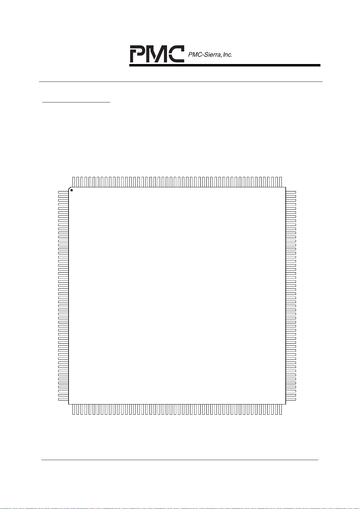
7
PIN DIAGRAM
The S/UNI-622 is packaged in a 208-pin slugged plastic QFP package having a
body size of 28 mm by 28 mm and a pin pitch of 0.5 mm.
Figure 5 -
PM 5355
S/UNI-622
RDAT[5]
RDAT[4]
RTOH[1]
RTOH[2]
RTOH[3]
RTOH[4]
VDD_AC
VSS_AC
FPOS
FPIN
PIN[0]
PIN[1]
PIN[2]
PIN[3]
PIN[4]
RDAT[7]
RDAT[8]
RDAT[9]
RDAT[10]
RDAT[11]
RDAT[12]
RDAT[13]
RDAT[14]
RDAT[15]
VDD_AC
VDD_DC
PIN[5]
PIN 1
PIN
2
08
PIN
1
57
PIN 156
PIN 52
PIN
53
PIN
1
04
Index
PIN 105
VSS_DC
VSS_AC
A[0]
A[1]
A[2]
A[3]
A[4]
A[5]
A[6]
A[7]
D[0]
D[1]
D[2]
D[3]
VDD_AC
VDD_DC
VSS_DC
VSS_AC
D[4]
D[5]
D[6]
D[7]
RSTB
CSB
WRB
RDB
INTB
VDD_DC
VSS_DC
TDA T[0]
TDA T[1]
TDA T[2]
TDA T[3]
TDA T[4]
TDA T[5]
TDA T[6]
TDA T[7]
TDA T[8]
TDA T[9]
TDAT[10]
ALE
PIN[6]
PIN[7]
RSIN
RSICLK
VDD_DC
PICLK
VSS_DC
POP[0]
POP[1]
POP[2]
POP[3]
POP[4]
POP[5]
VDD_DC
VSS_DC
TDI
TMS
TRSTB
TSOUT
FPOUT
POUT[0]
POUT[1]
VDD_AC
VDD_DC
VSS_DC
VSS_AC
POUT[2]
POUT[3]
POUT[4]
POUT[5]
POUT[6]
POUT[7]
VDD_DC
VSS_DC
PIP[0]
PIP[1]
PIP[2]
PIP[3]
GTOCLK
TLAIS
TLRDI
TLDCLK
TTOH[1]
VDD_AC
TPOH
TTOH[4]
TTOH[3]
TTOH[2]
VDD_DC
TPOHCLK
TPOHFP
TPOHEN
VSS_AC
VSS_DC
TFP
BUS8
TCK
TDO
TPRDI
TPAIS
TCP
XOF
F
VDD_DC
TFCLK
VSS_DC
TCA
TGFC
TSOC
TW
RE
NB
TDAT[15
]
TXPRTY[0]
TXPRTY[1]
TDAT[11
]
TDAT[12
]
TDAT[13
]
TDAT[14
]
RDAT[3]
RDAT[1]
RDAT[0]
RXPRTY[1]
RXPRTY[0]
RSOC
RDAT[2]
RCA
TSEN
VSS_DC
RFCLK
VDD_DC
LCD
RGFC
RCP
PRDI
VSS_AC
VDD_AC
PAIS
RPOH
RRDENB
VSS_DC
LOP
RPOHFP
RPOHCLK
OHFP
GROCLK
VDD_DC
RLDCLK
LAIS
LRDI
LOS
ROW
CLK
RLOW
RLD
VSS_DC
OOF
LOF
RSOW
RSUC
RSD
VDD_DC
RSDCLK
RTOHCLK
RTOHFP
VSS_AC
VDD_DC
VDD_AC
VSS_DC
RDAT[6]
TTOHCLK
TTOHEN
T
LO
W
TTO
HFP
TSDCLK
TSD
TSICLK
T
SO
W
TOW
CLK
VSS_DC
TCLK
VDD_DC
TSUC
TLD

PM5355 S/UNI-622
DATA SHEET
PMC-941027 ISSUE 3 SATURN USER NETWORK INTERFACE (622-Mb)
PROPRIETARY AND CONFIDENTIAL TO PMC-SIERRA, INC., AND FOR ITS CUSTOMERS’ INTERNAL USE
13
8
PIN DESCRIPTION
Table 1 -
Pin Name Type Pin
No.
Function
PICLK Input 137 The parallel input clock (PI CLK ) provi des timing for S/UNI-622 receive function
operation. PICLK is a 6.48 MHz (STS-1), 19.44 MHz (STS-3c /STM-1), or
77.76 MHz (STS-12c/STM-4c), nominally 50% duty cycle clock, depending on the
selected operating mode. PIN[7:0] and FPIN are sampled on the rising edge of
PICLK.
RX_VCLK The test vector clock (RX_VCLK) si gnal i s used during S/UNI-622 production
testing to verify internal functionality.
PIN[0]
PIN[1]
PIN[2]
PIN[3]
PIN[4]
PIN[5]
PIN[6]
PIN[7]
Input 148
147
146
145
144
143
142
141
The data input (PIN[7:0]) bus carries the byte-serial STS-12c / 3c/1 stream. PIN[7:0]
is sampled on the risi ng edge of PICLK. PIN[7] is the most si gni ficant bit
(corresponding to bit 1 of each serial word, the first bit received). PIN[0] is the
least significant bi t (corresponding to bit 8 of each word, the last bit received).
FPIN Input 149 The active-high framing position input (FPIN) signal indicates the SONET frame
position on the PIN[7:0] bus. The byte positi on i ndi c ated by FPIN is selected by the
FPOS input as described below. FPIN is sampled on the rising edge of PICLK.
FPOS Input 150 The frame position input (FPOS) selects the frame byte position in the SONET
frame indicated by the FPIN input. When FPOS is tied high and STS-3c or
STS-12c mode is selected, a pulse on FPIN marks the third A2 framing byte
position on the PIN[7:0] bus. When FP OS i s tied low and STS-3c or STS-12c
mode is selected, a puls e on FPIN marks the first synchronous payload envelope
byte position after the C1 bytes on PIN[7:0]. When configured for STS-1 mode, a
pulse on FPIN always marks the first synchronous payload envelope byte position
after the C1 byte on PIN[7:0].
RSICLK Input 139 The receive serial incoming clock (RSI CLK ) provides timing for processing the bit-
serial STS-1 receive stream , RSIN. RSICLK is nominally a 51.84 MHz, 50% duty
cycle clock. RSIN is sampled on the rising edge of RSICLK. RSICLK is divided by
eight to produce GROCLK when the bit-serial S TS-1 mode is selected. RSICLK
should be disabled when the bit-serial ST S -1 i nt erface is not used.
RSIN Input 140 The receive incoming serial stream (RSIN) carries the scrambled STS-1 stream in
bit-serial format. RSIN is sampled on the rising edge of RSICLK.

PM5355 S/UNI-622
DATA SHEET
PMC-941027 ISSUE 3 SATURN USER NETWORK INTERFACE (622-Mb)
PROPRIETARY AND CONFIDENTIAL TO PMC-SIERRA, INC., AND FOR ITS CUSTOMERS’ INTERNAL USE
14
Pin Name Type Pin
No.
Function
OOF Output 164 The out of frame (OOF) signal i s high while the S/UNI-622 is out of frame. OOF is
low while the S/UNI-622 is in-frame. An out of frame declaration occurs when four
consecutive errored framing patter ns (A1 and A2 bytes) have been received. OOF
is intended to be used to enable an upstream framing pattern detector to search for
the framing pattern. This alarm indication is also available via register acces s.
OOF is updated on the rising edge of PICLK.
GROCLK Out put 174 The generated receive outgoing clock (GROCLK) is nominally a 6.48 MHz or
19.44 MHz, 50% duty cycle clock.
When configured for STS-1 bit-serial m ode, GROCLK is the RS ICLK clock input
divided down by eight. For this mode, GROCLK is updated on the risi ng edge of
RSICLK and is expected to be used to dr i ve input P ICLK.
When configured for STS-1 or STS-3c byte-serial m ode, GROCLK is a fl owed
through version of PICLK.
When configured for STS-12c byte-serial mode, GROCLK is the PICLK clock input
divided by four. For this mode, GROCLK is updated on the rising edge of PICLK.
TCLK Input 97 The transmit clock (TCLK) provides timi ng for S/UNI -622 transmit function
operation. TCLK should be a 6.48 MHz (STS-1), 19.44 MHz (STS-3c/STM-1), or
77.76 MHz (STS-12c/STM-4c), nominally 50% duty cycle clock, depending on the
selected operating mode.
TX_VCLK The test vector clock (TX_VCLK) si gnal i s used during S/UNI-622 production
testing to verify internal functionality.
TFP Input 74 The acti ve high transmit frame pulse (TFP) signal is used to ali gn the SONET/SDH
transport frame generated by the S/UNI-622 device to a system reference. TFP
should be brought high for a single GTOCLK period every 810 (STS-1), 2430
(STS-3c), 2430 (STS-12c) GTOCLK cycles, or a multiple thereof. TFP may be tied
low if such synchronizat i on i s not required. The offset between a pulse applied t o
the TFP input and the resultant FPOUT pulse is 18 TCLK periods in STS-1 mode,
26 TCLK periods in STS-3c mode and 81 TCLK periods in STS-12c mode. TFP is
sampled on the rising edge of GTOCLK.
POUT[0]
POUT[1]
POUT[2]
POUT[3]
POUT[4]
POUT[5]
POUT[6]
POUT[7]
Output 122
121
116
115
114
113
112
111
The parallel outgoing stream, (POUT[7:0]), carries the scrambled STS-12/3c/1
stream in byte-serial format . POUT[7:0] is updated on the rising edge of TCLK.
POUT[7] is the most s i gni ficant bit (corresponding to bit 1 of each serial word, the
first bit transmitt ed). POUT[0] is the least significant bit (corresponding to bit 8 of
each serial word, the last bit transmitted).

PM5355 S/UNI-622
DATA SHEET
PMC-941027 ISSUE 3 SATURN USER NETWORK INTERFACE (622-Mb)
PROPRIETARY AND CONFIDENTIAL TO PMC-SIERRA, INC., AND FOR ITS CUSTOMERS’ INTERNAL USE
15
Pin Name Type Pin
No.
Function
FPOUT Output 123 The active-high framing position output (FPO UT) signal marks the frame alignment
on the POUT[7:0] bus. FPOUT goes high for a single TCLK period during the first
synchronous payload envelope byte after the twelve C1 bytes. FPOUT is updated
on the rising edge of TCLK.
TSICLK Input 104 The transmit serial incom i ng clock (TSICLK) provides timing for updating t he bi t-
serial outgoing stream when bi t -serial STS-1 mode is selected. TSICLK is
nominally a 51.84 MHz, 50% duty cycle clock. TSOUT is updated on the rising
edge of TSICLK. TSICLK should be disabled when the bit-serial STS-1 interface is
not used.
TSOUT Output 124 The transmit serial outgoing stream, (TSOUT), carries the scrambled stream in bit-
serial format when STS-1 bi t-serial mode is selected. TSOUT is updated on the
rising edge of TSICLK. In STS-1 bit-serial mode with line loopback or loop ti m e
modes enabled, TSOUT is updated on the rising edge of RSICLK.
GTOCLK Output 87 The generated transmit output clock (GTOCLK) is nominally a 6. 48 M Hz or
19.44 MHz, 50% duty cycle clock.
When configured for STS-1 bit-serial m ode, GTOCLK is the TSICLK clock input
divided down by eight. For this mode, GTOCLK is updated on the rising edge of
TSICLK and is expected to be used to dr i ve input TCLK. In STS-1 bit-serial mode
with line loopback or loop time modes enabled, GTOCLK is the RSICLK clock input
divided down by eight and is updated on the rising edge of RSICLK.
When configured for STS-1 or STS-3c byte-serial m ode, GTOCLK is a flowed
through version of TCLK.
When configured for STS-12c byte-serial mode, GTOCLK is the TCLK clock input
divided by four. For this mode, GTOCLK is updated on the r i s i ng edge of TCLK.
LOS Output 169 The loss of s i gnal (LOS) signal is set high when loss of signal is declared. This
occurs when a violating per i od (20 ± 3 µs ) of consecutive all-zeros bytes is
detected on the incoming STS-12c/3c/1 signal (before descrambling). LOS is
removed when two valid framing words (A1, A2) are detected and during the
intervening time, no violati ng period of consecutive all zeros patterns is detected.
This alarm indication is also available via register access. LOS is updated on the
rising edge of PICLK.
LOF Output 163 The loss of frame (LOF) signal is s et high when loss of frame is declared. Thi s
occurs when an out-of-frame conditi on (as i ndi cated by a high level on the OOF
output) persists for a period of 3 m s. LOF is removed when an in-frame condition
(as indicated by a low level on the OOF output) persists for a period of 3 ms. This
alarm indication i s also available via register access. LOF is updated on the rising
edge of PICLK.

PM5355 S/UNI-622
DATA SHEET
PMC-941027 ISSUE 3 SATURN USER NETWORK INTERFACE (622-Mb)
PROPRIETARY AND CONFIDENTIAL TO PMC-SIERRA, INC., AND FOR ITS CUSTOMERS’ INTERNAL USE
16
Pin Name Type Pin
No.
Function
LAIS Output 171 The line alarm indication signal (LAIS) is set high when line AIS is declared. This
occurs when a 111 binary pat tern is detected in bits 6, 7 and 8 of the K2 byte for
three or five consecutive frames as programmed using the RLOP Cont rol /Status
register. LAIS is removed when any pattern other than 111 i s detected in bits 6, 7
and 8 of the K2 byte for three or five consecutive frames as programmed using the
RLOP Control/Status register. This alarm indication is also available via register
access. LAIS is updated on the rising edge of P I CLK.
LRDI Output 170 The line remote defect indi cation (LRDI) signal is set high when line RDI is
declared. This occurs when a 110 binary pattern is detected in bits 6, 7 and 8 of
the K2 byte for three or five consecutive frames as programmed using the RLOP
Control/Status register. LRDI is removed when any pattern other than 110 is
detected in bits 6, 7 and 8 of the K2 byte for three or five consecutive frames as
programmed using the RLOP Control/Status regi ster. This alarm indication is also
available via register access. LRDI is updated on the rising edge of PICLK.
LOP Output 178 The loss of pointer (LOP) signal is set high when loss of pointer is decl ared. This
occurs when a valid pointer (H1, H2) is not found in eight consecutive frames, or if
eight consecutive new data flags are detected. LOP is removed when the same
valid and normal pointer with a normal new data flag is detected in three
consecutive frames. The loss of pointer stat e i s not entered if the incoming stream
contains path AIS. This alarm indication is also available via register access. LOP
is updated on the falling edge of GROCLK.
PA I S Output 182 The path AIS (PAIS) signal is set high when STS-path AIS is decl ared. This occurs
when an all-ones pattern is observed in the pointer bytes (H1, H2) for three
consecutive frames. Path AIS is removed when the same valid and normal pointer
is detected for three consecuti ve frames or a legal poi nt er wi th an active NDF is
received. This alarm indication is also available via register access. PAIS is
updated on the falling edge of GROCLK.
PRDI Output 185 The path remote defect indic ation (PRDI) signal is set high when a path remote
defect indication is detect ed. This occurs when bit 5 of the path status byte (G1) is
set high for five (or ten) consecutive frames. Path remote defect is removed when
bit 5 of the G1 byte is set low for five (or ten) consecutive frames. This indication is
also available via register access. PRDI is updated on the falling edge of
GROCLK.
LCD Output 188 The loss of cell delineation (LCD) signal indicates when cell delineation can not be
found. LCD transitions high when an out of cel l del i neation (OCD) anomaly has
persisted for 4 ms. Once asserted, LCD remains high until no OCD anomaly has
been detected for 4 ms at which time, LCD is set low. The OCD state is entered
when the cell delineation state machine is not in the SYNC state. Please refer to
the Functional Description section for an explanation of the cell delineation state
machine.
This alarm indication is also available via register access. LCD is updated on the
falling edge of GROCLK.

PM5355 S/UNI-622
DATA SHEET
PMC-941027 ISSUE 3 SATURN USER NETWORK INTERFACE (622-Mb)
PROPRIETARY AND CONFIDENTIAL TO PMC-SIERRA, INC., AND FOR ITS CUSTOMERS’ INTERNAL USE
17
Pin Name Type Pin
No.
Function
TLAIS Input 88 The active-high transmit line alarm indication (TLAIS) signal controls the i nsertion
of line AIS. Line AIS is inserted by overwriting the SONE T/SDH frame contents
with all ones (before scrambling). The section overhead is not overwritten. This
function can also be performed via register access. Line AIS insertion is internally
synchronized to frame boundaries. The TLAIS input take precedence over the
TTOH and TTOHEN inputs. TLAIS is sampled on the rising edge of TCLK.
TLRDI Input 89 The act i ve-high transmi t l i ne rem ote defect indication (TLRDI) signal controls the
insertion of l i ne RDI . Line RDI is inserted by transmitting the code 110 (binary) in
bit positions 6,7, and 8 of the K2 byte. This function can also be performed via
register access, or be enabled to occur automatically upon detection of receive line
AIS, loss of signal, or loss of frame. The TLRDI input takes precedence over the
TTOH and TTOHEN inputs. TLRDI is sampled on the rising edge of TCLK.
TPA I S Input 73 The active-high transmit path alar m i ndi cation (TPAIS) signal cont rol s the insertion
of STS-path AIS. A high level on TPAIS forces the inser tion of an all ones pattern
into the complete synchronous payload envelope, and the payload pointer bytes
(H1, H2). Pat h AIS insertion is internally synchronized to SPE frame boundaries.
This function can also be perfor med via register access. TPAIS is sampled on the
rising edge of GTOCLK.
TPRDI Input 72 The transmit path remote defect indication (TPRDI) signal controls the inser tion of
the path remote defect indication s i gnal . A high level on TPRDI forces a logic one
to be inserted i n t he path remote defect indication bit position in the path stat us
byte (G1). This f unction can also be performed via register access, or be enabled
to occur automaticall y upon detection of receive line AIS, loss of frame, loss of
signal, loss of pointer or path AIS. The TPOH and TPOHEN inputs take
precedence over the TPRDI input. TPRDI is sampled on the rising edge of
GTOCLK.
RFCLK Input 190 The receive FIFO clock (RFCLK) is used to read words from the synchronous FIFO
interface. RFCLK must cycle at a 52 MHz or lower rate, but at a high enough rate
to avoid FIFO overflow. RRDENB is sampled using the rising edge of RFCLK.
RSOC, RCA, RXPRTY[1:0] and RDAT[15: 0] are updated on the rising edge of
RFCLK.
RRDENB Input 186 The active-low receive read enable input (RRDENB) is used to initiate reads from
the receive FIFO. When sampled low using the rising edge of RFCLK, a word is
read from the internal s ynchronous FIFO and output on bus RDAT[15:0]. When
sampled high using the ris i ng edge of RFCLK, no read is performed and outputs
RDAT[15:0], RXPRTY[1:0] and RSOC are tristated if the TSEN input is high.
RRDENB must operate in conjuncti on wi th RFCLK to access the FIFO at an
instantaneous rate high enough to avoid FIFO overflows.

PM5355 S/UNI-622
DATA SHEET
PMC-941027 ISSUE 3 SATURN USER NETWORK INTERFACE (622-Mb)
PROPRIETARY AND CONFIDENTIAL TO PMC-SIERRA, INC., AND FOR ITS CUSTOMERS’ INTERNAL USE
18
Pin Name Type Pin
No.
Function
RDAT[0]
RDAT[1]
RDAT[2]
RDAT[3]
RDAT[4]
RDAT[5]
RDAT[6]
Tristate 198
199
200
201
202
203
204
The receive cell data (RDAT[15:0]) bus carries the ATM cell octets that are read
from the receive FIFO. RDAT[15:0] is updated on the rising edge of RFCLK .
When the S/UNI-622 is configured for tr i s tate operation using the TSEN input,
tristating of out put bus RDAT[15:0] is controlled by input RRDENB.
RDAT[7]
RDAT[8]
RDAT[9]
RDAT[10]
RDAT[11]
RDAT[12]
RDAT[13]
RDAT[14]
RDAT[15]
1
2
3
4
5
6
7
8
9
RXPRTY[0]
RXPRTY[1]
Tristate 196
197
The receive parity (RXPRTY[1:0]) signal s indicate the parity of the RDAT[15:0] bus.
In word parity mode, RXPRTY[1] is the parity calculation over the RDAT[15:0] bus
and RXPRTY[0] is unused. In byte parity mode, RXPRTY[1] is the parity
calculation over the RDAT[15:8] bus and RXPRTY[0] is the parity c al culation over
the RDAT[7:0] bus. Selection between word parity mode and byte parity m ode i s
made using a register bit. Odd or even parity selection is made using a regi s ter bit.
RXPRTY[1:0] is updated on the rising edge of RFCLK.
When the S/UNI-622 is configured for tr i s tate operation using the TSEN input,
tristating of out put bus RXPRTY[1:0] is control by input RRDENB.
RSOC Tri state 195 The receive start of c el l (RS O C) s i gnal marks the start of cell on the RDAT[15:0]
bus. When RSOC is high, the first word of the cell st ructure is present on the RDAT
bus. RSOC is updated on the rising edge of RFCLK.
When the S/UNI-622 is configured for tr i s tate operation using the TSEN input,
tristating of out put RSOC is control by input RRDENB.
RCA Output 194 The receive cell available (RCA) signal indicates when a cell is available in the
receive FIFO. When high, RCA indicates that the receive FIFO has at least one
cell available to be read. When RCA goes low, the receive FIFO contains only four
words or is empty. Selection is made using a bit in the RACP Interrupt
Enable/Control register. RCA is updated on the risi ng edge of RFCLK. The active
polarity of TCA is programmable and defaults to active-high.

PM5355 S/UNI-622
DATA SHEET
PMC-941027 ISSUE 3 SATURN USER NETWORK INTERFACE (622-Mb)
PROPRIETARY AND CONFIDENTIAL TO PMC-SIERRA, INC., AND FOR ITS CUSTOMERS’ INTERNAL USE
19
Pin Name Type Pin
No.
Function
TSEN Input 192 The tristate enable (TSEN) signal al l ows t ristate control over outputs RDAT[15:0],
RXPRTY[1:0] and RSOC. When TSEN is high, the active-low receive read enable
input, RRBENB, controls when output s RDAT[15:0], RXPRTY[1:0] and RSOC are
driven. When TSEN is low, out puts RDAT[15:0], RXPRTY[1:0] and RSOC are
always driven.
TFCLK I nput 65 The transmit FIFO cl ock (TFCLK) i s used to write words to the synchronous FIFO
interface. TFCLK must cycle at a 52 MHz or lower rate. TWRENB, TSOC,
TXPRTY[1:0] and TDAT[15:0] are sampled on the rising edge of TFCLK. In
addition, TCA is updated on the rising edge of TFCLK.
TWRENB Input 61 The active-low transmit write enable input (TWRENB) is used to initi ate writes to
the transmit FIFO. When sampled low using the rising edge of TFCLK, the 16-bit
word on TDAT[15:0] is written into the transmit FIFO. When sampled high using the
rising edge of TFCLK, no write is performed. A complete 53-octet c el l mus t be
written to the FIFO before it is inserted into the STS-12c/3c/1 SPE.
Idle/unassigned cells are i nserted when a complete cell is not available from the
FIFO.
TDAT[0]
TDAT[1]
TDAT[2]
TDAT[3]
TDAT[4]
TDAT[5]
TDAT[6]
TDAT[7]
TDAT[8]
Input 42
43
44
45
46
47
48
49
50
The transmit cell data (TDAT[15:0]) bus carries the ATM cell octets that are written
to the transmit FIFO. TDAT[15:0] is sampled on the r i s i ng edge of TFCLK and is
considered valid only when TWRENB is simultaneously ass erted.
TDAT[9]
TDAT[10]
TDAT[11]
TDAT[12]
TDAT[13]
TDAT[14]
TDAT[15]
51
52
53
54
55
56
57

PM5355 S/UNI-622
DATA SHEET
PMC-941027 ISSUE 3 SATURN USER NETWORK INTERFACE (622-Mb)
PROPRIETARY AND CONFIDENTIAL TO PMC-SIERRA, INC., AND FOR ITS CUSTOMERS’ INTERNAL USE
20
Pin Name Type Pin
No.
Function
TXPRTY[0]
TXPRTY[1]
Input 58
59
The transmit parity (TXPRTY[1:0]) si gnal s indicate the parity of the TDAT[ 15: 0] bus.
In word parity mode, TXPRTY[1] is expected to be the parity cal culation over the
TDAT[15:0] bus and TXPRTY[0] is ignored. In byte parity mode, TXPRTY[1] is
expected to be the parity calculat i on over the TDAT[15:8] bus and TXPRTY[0] is
expected to be the parity calc ul ation over the TDAT[7: 0] bus. Selection between
word parity mode and byte parity mode is m ade using a register bit. Odd or even
parity selection i s made using a register bit. TXP RTY[1:0] i s sampled on the rising
edge of TFCLK and is considered valid only when TWRENB is simultaneously
asserted.
TSOC Input 60 The transmit start of cell (TSOC) signal marks the start of cell on the TDAT[15:0]
bus. When TSOC is high, the first word of the cell structure is present on the
TDAT[15:0] st ream . It is not neces s ary for TS OC t o be present for each cell. An
interrupt may be generated if TSOC is high during any word other than the first
word of the cell structure. TSOC is sampled on the rising edge of TFCLK and is
considered valid only when TWRENB is simultaneously ass erted.
TCA Output 67 The transmit cell available (TCA) signal indicates when a cell is available in the
transmit FIFO. When high, TCA indicates that the transmit FIFO is not full. When
TCA goes low, it indicates that either the transmit FI FO i s near full and can accept
no more than four writes or that the transmi t FIFO is full. Selection is made using a
register bit. In addition, to reduce FIFO latency, the FIFO full level can be
programmed using bits in the FIFO register. TCA is updated on the rising edge of
TFCLK. The active polarity of TCA is programmable and defaults to active-high.
The TCA output is asserted (set hi gh) when the S/UNI-622 is reset.
XOFF Input 63 The XOFF pin should not be used, and must be forced low.
RTOH[1]
RTOH[2]
RTOH[3]
RTOH[4]
Output 156
155
154
153
The receive transport overhead bus (RTOH[4:1]) contains the receive transport
overhead bytes (A1, A2, C1, B1, E1, F1, D1-D3, H1-H3, B2, K1, K2, D4-D12, Z1,
Z2, and E2) extracted from the incoming stream.
When STS-12c (STM-4c) mode is selected, RTOH[1] contains the transport
overhead from STS-3 (STM-1) #1, RTOH[2] contains the transport overhead for
STS-3 (STM-1) #2, RTOH[3] contains the transport overhead for STS-3 (STM-1)
#3, and RTOH[4] contains the transport overhead for STS-3 (STM-1) #4.
When STS-3c (STM-1) or STS-1 mode is selected, RTOH[1] contains all the
transport overhead bytes. RTOH[4:2] are not used.
RTOH[4:1] is updated on the falling edge of RTOHCLK.
RTOHCLK Output 157 The receive transport overhead clock (RTOHCLK) is nominally a 5.184 MHz clock
(STS-12c/STS-3c) or a 1.728 MHz clock (STS-1) which provides timing to process
the extracted receive transport overhead. When STS-12c (STM-4c) or STS-3c
(STM-1) mode is selected, RTOHCLK is a gapped 6.48 MHz clock. When STS-1
mode is selected, RTOHCLK is a gapped 2.16 MHz clock. RTOHCLK is updated
on the falling edge of GROCLK.

PM5355 S/UNI-622
DATA SHEET
PMC-941027 ISSUE 3 SATURN USER NETWORK INTERFACE (622-Mb)
PROPRIETARY AND CONFIDENTIAL TO PMC-SIERRA, INC., AND FOR ITS CUSTOMERS’ INTERNAL USE
21
Pin Name Type Pin
No.
Function
RTOHFP Output 158 The receive transport overhead frame position (RTOHFP) signal is used to locate
the individual receive transport overhead bits in the transport overhead bus,
RTOH[4:1]. RTOHFP is set high while bit 1 (the most significant bit) of the first
framing byte (A1) is present in the RTOH[4:1] stream. RTOHFP is updated on the
falling edge of RTOHCLK.
RPOH Output 181 The receive path overhead data (RPOH) signal contains the path overhead bytes
(J1, B3, C2, G1, F2, H4, Z3, Z4 and Z5) extracted f rom the received STS-12c/3c/1
frame. RPOH is updated on the falling edge of RPOHCLK.
RPOHCLK Output 176 The receive path overhead clock (RPOHCLK) is nominall y a 576 kHz clock which
provides timing to process the extracted receive path overhead. RPOHCLK is a
gapped 648 KHz clock. RPOHCLK is updated on the falling edge of GROCLK.
RPOHFP Output 177 The receive path overhead frame position (RPOHFP) signal may be used to locate
the individual receive path overhead bits in the path overhead data stream, RPOH.
RPOHFP is logic one while bit 1 (the most significant bit) of the path trace byte (J1)
is present in the RPOH stream. RPOHFP is updated on the falling edge of
RPOHCLK.
RSDCLK Output 159 The receive secti on DCC clock (RSDCLK) is a 192 kHz clock us ed to update the
RSD output. RSDCLK is generated by gapping a 216 kHz clock.
RSD Output 160 The receive section DCC (RSD) signal contai ns the serial section data
communications channel (D1, D2 D3) extracted f rom t he i ncoming stream. RSD is
updated on the falling edge of RSDCLK.
RLDCLK Output 173 The receive line DCC clock (RLDCLK) is a 576 kHz clock used t o update the RLD
output. RLDCLK is generated by gapping a 2.16 MHz clock.
RLD Output 172 The receive line DCC (RLD) signal contains the serial line data communications
channel (D4 - D12) extracted from the incoming st ream . RLD is updated on the
falling edge of RLDCLK.
ROWCLK Output 168 The receive order wire clock (ROWCLK) is a 64 kHz clock used to update the
RSOW, RSUC, and RLOW outputs. ROWCLK is generated by gapping a 72 kHz
clock.
RSOW Output 162 The receive section order wire (RSOW) signal contains the sec tion order wire
channel (E1) extracted from the incoming stream. RSOW is updated on the falling
edge of ROWCLK.
RSUC Output 161 The receive section user channel (RSUC) si gnal contains the section user channel
(F1) extracted from the incoming stream. RSUC is updated on the falling edge of
ROWCLK.
RLOW Output 167 The receive line order wire (RLOW) signal contains the line order wire channel (E2)
extracted from the incoming stream. RLOW is updated on the falling edge of
ROWCLK.

PM5355 S/UNI-622
DATA SHEET
PMC-941027 ISSUE 3 SATURN USER NETWORK INTERFACE (622-Mb)
PROPRIETARY AND CONFIDENTIAL TO PMC-SIERRA, INC., AND FOR ITS CUSTOMERS’ INTERNAL USE
22
Pin Name Type Pin
No.
Function
OHFP Output 175 The overhead frame pulse (OHFP) signal identifies the start of a byte on outputs
RSOW, RSUC and RLOW. If required, OHFP is one GROCLK clock cycle wide
and can be used as a reset pulse for an external c ounter. Please refer to the
functional timing diagrams for details.
TTOH[4]
TTOH[3]
TTOH[2]
TTOH[1]
Input 83
84
85
86
The transmit transport overhead bus (TTOH[4:1]) contains the transport overhead
bytes (A1, A2, C1, E1, F1, D1-D3, H3, K1, K2, D4-D12, Z1, Z2 and E2) and error
masks (H1, H2, B1 and B2) which may be inserted or used to insert bit interleaved
parity errors or payload pointer bit errors i nto the overhead byte positions in the
outgoing stream. Insertion is c ontrolled by the TTOHEN input.
When STS-12c (STM-4c) mode is selected, TTOH[1] contains the transport
overhead for STS-3 (STM-1) #1. TTOH[2] contains t he transport overhead for
STS-3 (STM-1) #2. TTOH[3] contains the transport overhead for STS-3 (STM-1)
#3. TTOH[4] contains the transport overhead for STS-3 (STM-1) #4.
When STS-3c (STM-1) or STS-1 mode is selected, TTOH[1] contains all the
transport overhead bytes. TTOH[4:2] are not used.
The TTOH[4:1] inputs are sampled on the ri sing edge of TTOHCLK.
TTOHEN Input 101 The transmit transport overhead insert enable (TTOHEN) signal, together with
internal register bits, controls the source of the transport overhead data which is
transmitted. While TTOHEN is high, values sampled on t he TTOH[4:1] input bus
are inserted int o t he corresponding transport overhead bit position (for the A1, A2,
C1, E1, F1, D1-D3, K1, K2, H3, D4-D12, Z1, Z2 and E2 bytes). While TTOHEN is
low, default values are inserted i nto these transport overhead bit positions. A high
level on TTOHEN during the B1, B2 or H1-H2 bit positions enables an error mas k.
While an error mask is enabled, a high level on input TTOH causes the
corresponding B1, B2 or H1-H2 bit posi tion to be inverted. A low level on TTOH
allows the corresponding bit posit i on to pass through the S/UNI-622 uncorrupted.
TTOHEN is sampled on the rising edge of TTOHCLK.
TTOHCLK Output 99 The transmit transport overhead clock (TTOHCLK) is nominally a 5.184 MHz clock
(STS-12c/STS-3c) or a 1.728 MHz clock (STS-1) clock which provides timing for
upstream circuitry that sources the transport overhead stream, TTOH[4:1]. When
STS-12c (STM-4c) or STS-3c (STM-1) mode is selected, TTOHCLK is a gapped
6.48 MHz clock. When STS-1 mode is selected, TTOHCLK is a gapped 2.16 MHz
clock. TTOHCLK is updated in the rising edge of TCLK.
TTOHFP Output 100 The t ransmi t transport overhead frame position (TTOHFP) signal is used to locate
the individual transport overhead bits in the transport overhead bus, TTOH[4:1].
TTOHFP is set high while bit 1 (the most s i gni ficant bit) of the first framing byte
(A1) is expected in the incoming stream. TTOHFP is updated on the falling edge of
TTOHCLK.

PM5355 S/UNI-622
DATA SHEET
PMC-941027 ISSUE 3 SATURN USER NETWORK INTERFACE (622-Mb)
PROPRIETARY AND CONFIDENTIAL TO PMC-SIERRA, INC., AND FOR ITS CUSTOMERS’ INTERNAL USE
23
Pin Name Type Pin
No.
Function
TPOH Input 82 The transmit path overhead data (TPOH) signal contai ns the path overhead bytes
(J1, C2, G1, F2, Z3, Z4 and Z5) and error masks (B3 and H4) which may be
inserted or used to insert path BIP-8 or multiframe bit errors int o t he path overhead
byte positions in the STS-12c/3c/1 stream. Insertion i s controlled by the TP OHEN
input, or by bits in internal regi sters. TPOH is sampled on the r i sing edge of
TPOHCLK.
TPOHEN Input 77 The transmit path overhead insert enable (TPOHEN) s i gnal , together with internal
register bits, controls the source of the path overhead data which is inserted in the
POUT[7:0] stream. While TPOHEN is high, values sampled on the TPOH input are
inserted int o t he corresponding path overhead bit position (for the J1, C2, G1, F2,
Z3, Z4 and Z5 bytes). While TPOHEN is low, values obt ained from internal
registers are inserted into these path overhead bit positions. A high level on
TPOHEN during the H4 or B3 bit posi tions enables an error mask. While an error
mask is enabled, a high level on input TPOH causes the corresponding B3 or H4
bit position to be inverted. A low level on TPOH allows the corresponding bit
position to pass through the S/UNI-622 uncorrupted. TPOHEN is sampled on the
rising edge of TPOHCLK.
TPOHCLK Output 75 The transmit path overhead clock (TPOHCLK) is nominally a 576 kHz clock which
provides timing for upstream circuitry that sources the path overhead stream,
TPOH. TPOHCLK is a gapped 810 kHz clock. TPOHCLK is updated in the falling
edge of GROCLK.
TPOHFP Output 76 The transmit path overhead frame position (TPOHFP ) s i gnal m ay be used to locate
the individual path overhead bits in the path overhead data stream, TPOH.
TPOHFP is logic one while bit 1 (t he m ost significant bit) of the path trace byte (J1)
is expected in the TPOH stream. TPOHFP is updat ed on the falling edge of
TPOHCLK.
TOWCLK Output 95 The transmit order wire clock (TOWCLK) is a 64 kHz clock used to sample the
TSOW, TSUC, and TLOW inputs. TOWCLK is generated by gapping a 72 kHz
clock.
TSOW Input 94 The transmit section order wire (TS OW) signal c ontains the section order wire
channel (E1) inser t ed i nto the outgoing stream. When not used, this input should
be connected to logic zero. Overhead sourced using inputs TTOH[1] and TTOHEN
takes precedence over overhead sourced using TSOW. TSOW is sampled on the
rising edge of TOWCLK.
TSUC Input 93 The transmi t section user channel (TSUC) signal contains the sec tion user channel
(F1) inserted int o t he outgoing stream. When not used, this input should be
connected to logic zero. Overhead sourced using inputs TTOH[1] and TTOHEN
takes precedence over overhead sourced using TSUC. TSUC is sampled on the
rising edge of TOWCLK.

PM5355 S/UNI-622
DATA SHEET
PMC-941027 ISSUE 3 SATURN USER NETWORK INTERFACE (622-Mb)
PROPRIETARY AND CONFIDENTIAL TO PMC-SIERRA, INC., AND FOR ITS CUSTOMERS’ INTERNAL USE
24
Pin Name Type Pin
No.
Function
TLOW Input 92 The transmit l i ne order wi re (TLOW) signal c ontains the line order wire channel
(E2) inserted i nt o the outgoing stream. When not used, this input should be
connected to logic zero. Overhead sourced using inputs TTOH[1] and TTOHEN
takes precedence over overhead sourced using TLOW. TLOW is updated on the
rising edge of TOWCLK.
TSDCLK Output 102 The transmit section DCC clock (TSDCLK ) i s a 192 kHz clock used to sample the
TSD input. TSDCLK is generated by gapping a 216 kHz clock.
TSD Input 103 The transmit s ection DCC (TSD) signal contains the serial section data
communications channel (D1, D2 D3). When not used, this input should be
connected to logic zero. Overhead sourced using inputs TTOH[1] and TTOHEN
takes precedence over overhead sourced using TSD. TSD is sampled on the rising
edge of TSDCLK.
TLDCLK Output 90 The transmit line DCC clock (TLDCLK) is a 576 kHz clock used to sample the TLD
input. TLDCLK is generated by gapping a 2.16 MHz clock.
TLD Input 91 The transmit line DCC (TLD) signal contains the serial line data communications
channel (D4 - D12). When not used, this input s houl d be c onnected to logic zero.
Overhead sourced using inputs TTOH[1] and TTOHEN takes precedence over
overhead sourced using TLD. TLD is sampled on the rising edge of TLDCLK.
RCP Output 187 The receive cell pulse (RCP) signal marks the most significant bit (MSB) of a cell
header's GFC field on output, RGFC. RCP is updated on the falling edge of
GROCLK.
RGFC Output 193 The receive generic flow control (RGFC) signal contains the serialized GFC field
extracted from receive cells. The GFC field is output MSB first. The RCP output
identifies the MSB of every GFC field. The GFC Control register can be used to
gate off individual GFC bits. When the S/UNI-622 is in the OCD state, RGFC is
forced low. RGFC is updated on the falling edge of GROCLK.
TCP Output 68 The transmit cell pulse (TCP) signal is provided to locate the most significant GFC
bit (GFC[3]) of a cell's GFC f i el d sourced on input TGFC. TCP pulses high for one
GTOCLK period to identify the GTOCLK cycle before the cycle the GFC[3] bit is
output on TGFC. TCP is updated on the falling edge of GTOCLK.
TGFC Input 62 The transmit generic flow control (TGFC) input contains GFC bits that can be
inserted int o t he GFC fields of transmitted cells (including idle/unas signed cells).
Insertion is controlled using bits in the TACP Fixed Stuff/GFC register. TGFC is
sampled on the rising edge of GTOCLK.

PM5355 S/UNI-622
DATA SHEET
PMC-941027 ISSUE 3 SATURN USER NETWORK INTERFACE (622-Mb)
PROPRIETARY AND CONFIDENTIAL TO PMC-SIERRA, INC., AND FOR ITS CUSTOMERS’ INTERNAL USE
25
Pin Name Type Pin
No.
Function
POP[5]
POP[4]
POP[3]
POP[2]
POP[1]
POP[0]
Output 130
131
132
133
134
135
The parallel output port (POP[5:0]) is used to control the operation of front end line
devices. The s i gnal l evels on this parallel out put port correspond to the bit values
contained in the S/UNI-622 Parallel Output Port Regist er.
PIP[3]
PIP[2]
PIP[1]
PIP[0]
Input 105
106
107
108
The parallel input port (PI P[3:0]) is used to monitor the operation of front end line
devices. An interrupt may be generated when state changes are detected on the
monitored signals. State changes and the real-time signal l evels on this port are
available via the S/UNI-622 Parallel Input Port register.
CSB Input 36 The active-low chip select (CSB ) signal is low during S/UNI-622 register accesses.
Note that when not being used, CSB mus t be tied high. If CSB is not required (i.e.,
registers accesses are controlled using the RDB and WRB signals only), CSB must
be connected to an inverted version of the RSTB i nput.
RDB Input 38 The active-low read enable (RDB) signal is low during S/ UNI-622 register read
accesses. The S/UNI-622 drives the D[7:0] bus with the contents of the address ed
register while RDB and CSB are low.
WRB Input 37 The active-low write strobe (WRB) s i gnal i s low during a S/UNI-622 register write
accesses. The D[7:0] bus contents are clocked into the addressed register on the
rising WRB edge while CSB is low.
D[0]
D[1]
D[2]
D[3]
D[4]
D[5]
D[6]
D[7]
I/O 23
24
25
26
31
32
33
34
The bidirectional data bus D[7:0] is used during S/UNI-622 register read and write
accesses.
A[0]
A[1]
A[2]
A[3]
A[4]
A[5]
A[6]
Input 15
16
17
18
19
20
21
The address bus A[7:0] selects specific registers during S/UNI-622 register
accesses.

PM5355 S/UNI-622
DATA SHEET
PMC-941027 ISSUE 3 SATURN USER NETWORK INTERFACE (622-Mb)
PROPRIETARY AND CONFIDENTIAL TO PMC-SIERRA, INC., AND FOR ITS CUSTOMERS’ INTERNAL USE
26
Pin Name Type Pin
No.
Function
A[7]/TRS 22 The test register select (TRS) signal selects between normal and t est mode
register accesses. TRS is high during test mode register accesses, and is low
during normal mode regis t er accesses.
RSTB Input 35 The active-low reset (RSTB) si gnal provi des an asynchronous S/UNI-622 reset.
RSTB is a Schmitt triggered input with an integral pull-up resistor.
ALE Input 14 The addres s latch enable (ALE) is active-high and latches the address bus A[7:0]
when low. When ALE is high, the internal address latches are transparent. It
allows the S/UNI-622 to interface to a multi pl exed address/data bus. ALE has an
integral pull-up resistor.
INTB OD
Output
39 The active-low interrupt (INTB) signal goes low when a S/UNI-622 interrupt source
is active and that source is unmasked. The S/UNI-622 may be enabled to report
many alarms or events via interrupt s. Examples are loss of signal (LOS), loss of
frame (LOF), line AIS, line remote defect indication (LRDI) detect, loss of pointer
(LOP), path AIS, path remote defect indic ation detect and others. INTB is tristat ed
when the interrupt is acknowledged via an appropri at e regi ster access. INTB is an
open drain output.
TCK Input 70 The tes t clock (TCK) signal provides timing for test operations that are carried out
using the IEEE P1149.1 test access port.
TMS Input 126 The test mode select (TM S ) signal controls the test operations that are carried out
using the IEEE P1149.1 test access port. TMS is sampled on the rising edge of
TCK. TM S has an integral pull-up resistor.
TDI Input 127 The test data i nput (TDI) signal carries test data into the S/UNI-622 via the IEEE
P1149.1 test access port. TDI is sampled on the rising edge of TCK. TDI has an
integral pull-up resistor.
TDO Tristate 71 The test data output (TDO) signal carri es test data out of the S/UNI-622 via the
IEEE P1149.1 test access port. TDO is updated on the falling edge of TCK. TDO
is a tristate out put which is inactive except when scanning of data is in progress.
TRSTB Input 125 The active-low test reset (TRSTB ) signal provides an asynchronous S/UNI-622 test
access port reset v i a t he I EEE P1149. 1 t es t access port. TRSTB is a Schmitt
triggered input with an integral pull-up resistor.
Note that when not being used, TRSTB must be connected t o the RSTB input.
BUS8 Input 69 This pin must be connected to GND for proper operation of the S/UNI-622

PM5355 S/UNI-622
DATA SHEET
PMC-941027 ISSUE 3 SATURN USER NETWORK INTERFACE (622-Mb)
PROPRIETARY AND CONFIDENTIAL TO PMC-SIERRA, INC., AND FOR ITS CUSTOMERS’ INTERNAL USE
27
Pin Name Type Pin
No.
Function
VDD_AC1
VDD_AC2
VDD_AC3
VDD_AC4
VDD_AC5
VDD_AC6
VDD_AC7
Power 10
27
81
120
152
183
205
The AC power (VDD_AC1 - VDD_AC7) pins s houl d be connected to a well-
decoupled +5 V DC supply in common with VDD_DC.
VSS_AC1
VSS_AC2
VSS_AC3
VSS_AC4
VSS_AC5
VSS_AC6
VSS_AC7
Ground 13
30
78
117
151
184
208
The AC ground (VSS_AC1 - VSS_AC7) pins should be connected to GND in
common with VSS_DC.
VDD_DC1
VDD_DC2
VDD_DC3
VDD_DC4
VDD_DC5
VDD_DC6
VDD_DC7
Power 11
28
40
66
80
98
110
The DC power (VDD_DC1 - VDD_DC14) pins should be connected to a well-
decoupled +5 V DC supply in common with VDD_AC.
VDD_DC8
VDD_DC9
VDD_DC10
VDD_DC11
VDD_DC12
VDD_DC13
VDD_DC14
119
129
138
165
179
189
206

PM5355 S/UNI-622
DATA SHEET
PMC-941027 ISSUE 3 SATURN USER NETWORK INTERFACE (622-Mb)
PROPRIETARY AND CONFIDENTIAL TO PMC-SIERRA, INC., AND FOR ITS CUSTOMERS’ INTERNAL USE
28
Pin Name Type Pin
No.
Function
VSS_DC1
VSS_DC2
VSS_DC3
VSS_DC4
VSS_DC5
VSS_DC6
Ground 12
29
41
64
79
96
The DC ground (VSS_DC1 - VSS_DC14) pins should be connected to GND in
common with VSS_AC.
VSS_DC7
VSS_DC8
VSS_DC9
VSS_DC10
VSS_DC11
VSS_DC12
VSS_DC13
VSS_DC14
109
118
128
136
166
180
191
207
Notes on Pin Description:
1. All S/UNI-622 inputs and bidirectionals present minimum capacitive loading
and operate at TTL logic levels.
2. All S/UNI-622 outputs and bidirectionals have at least 2 mA drive capability.
The data bus outputs, D[7:0], have 4 mA drive capability. The FIFO interface
outputs, RDAT[15:0], RXPRTY[1:0], RCA, RSOC, and TCA, have 4 mA drive
capability. Outputs POUT[7:0], FPOUT, TSOUT, GTOCLK and GROCLK also
have 4 mA drive capability
3. Inputs RSTB, ALE, TMS, TDI and TRSTB have internal pull-up resistors.
4. The VSS_DC and VSS_AC ground pins are not internally connected together.
Failure to connect these pins externally may cause malfunction or damage
the S/UNI-622.
5. The VDD_DC and VDD_AC power pins are not internally connected together.
Failure to connect these pins externally may cause malfunction or damage
the S/UNI-622.

PM5355 S/UNI-622
DATA SHEET
PMC-941027 ISSUE 3 SATURN USER NETWORK INTERFACE (622-Mb)
PROPRIETARY AND CONFIDENTIAL TO PMC-SIERRA, INC., AND FOR ITS CUSTOMERS’ INTERNAL USE
29
9
FUNCTIONAL DESCRIPTION
9.1 Receive Section Overhead Processor
The Receive Section Overhead Processor (RSOP) provides frame
synchronization, descrambling, section level alarm and performance monitoring.
In addition, it extracts the section orderwire channel, the section user channel,
the section data communication channel from the section overhead and provides
them serially on outputs RSOW, RSUC and RSD, respectively. The RSOP is
intended to operate with an upstream device which performs clock and data
recovery, deserialization and preframing (to the A1 and A2 framing bytes).
9.1.1 Framer
The Framer Block determines the in-frame/out-of-frame status of the
STS-12c/3c/1 data stream. Output OOF reflects this status, and is updated with
timing aligned to PICLK.
While out of frame, upstream circuitry monitors the bit-serial STS-12c/3c/1 data
stream for an occurrence of the framing pattern (A1, A2). The upstream circuitry
is expected to pulse input FPIN when a framing pattern has been detected to
reinitializes the channel counter to the new alignment. The Framer block
declares frame alignment when either all A1 and A2 bytes are seen error-free or
when only the first A1 byte and the first four bits of the first A2 byte are seen
error-free depending upon the selected framing algorithm. The first algorithm
examines 24, 6 or 2 bytes depending on the mode, while the second algorithm
examines only the first occurrence of A1 and the first four bits of the first
occurrence of A2 in the sequence regardless of the mode. Once in frame, the
Framer block monitors the framing pattern sequence and declares OOF when
one or more bit errors in each framing pattern are detected for four consecutive
frames. Again, depending upon the algorithm either 24 framing bytes are
examined for bit errors each frame, or only the first A1 byte and the first four bits
of the first A2 byte are examined for bit errors each frame.
The performance of these framing algorithms in the presence of bit errors and
random data is robust. When looking for frame alignment, the performance of
each algorithm is dominated by the alignment algorithm used by the upstream
circuitry. Once in frame alignment, the Framer block continuously monitors the
framing pattern. When the incoming stream contains a 10
-3
bit error rate (BER),
the first algorithm provides a mean time between OOF occurrences of 4 minutes
for STS-1 mode, 14 seconds for STS-3c (STM-1) mode and 0.13 seconds for

PM5355 S/UNI-622
DATA SHEET
PMC-941027 ISSUE 3 SATURN USER NETWORK INTERFACE (622-Mb)
PROPRIETARY AND CONFIDENTIAL TO PMC-SIERRA, INC., AND FOR ITS CUSTOMERS’ INTERNAL USE
30
STS-12c (STM-4c) mode. The second algorithm provides a mean time between
OOF occurrences of 103 minutes independent of operating mode.
9.1.2 Descramble
The Descramble Block utilizes a frame synchronous descrambler to process the
received byte-serial stream. The generating polynomial is 1 + x6 + x7 and the
sequence length is 127. Details of the descrambling operation are provided in
the references. Note that the framing bytes (A1 and A2) and the identity bytes
(C1) are not descrambled. A register bit is provided to disable the descrambling
operation.
9.1.3 Error Monitor
The Error Monitor Block calculates the received section BIP-8 error detection
code (B1) based on the scrambled data of the complete STS-12c/3c/1 frame.
The section BIP-8 code is based on a bit interleaved parity calculation using
even parity. Details are provided in the references. The calculated BIP-8 code is
compared with the BIP-8 code extracted from the B1 byte of the fo llowing frame.
Differences indicate that a section level bit error has occurred. Up to 64000 (8 x
8000) bit errors can be detected per second. The Error Monitor Block
accumulates these section level bit errors in a 16-bit saturating counter that can
be read via the microprocessor interface. Circuitry is provided to latch this
counter so that its value can be read while simultaneously resetting the internal
counter to 0 or 1, if appropriate, so that a new period of accumulation can begin
without losing any events. It is intended that this counter be polled at least once
per second so that bit error events are not missed.
9.1.4 Loss of Signal
The Loss of Signal Block monitors the scrambled data of the complete
STS-12c/3c/1 stream for the absence of ones. When 20 ± 3 µs of all zeros
patterns is detected, a loss of signal (LOS) is declared. Loss of signal is cleared
when two valid framing words are detected and during the intervening time, no
loss of signal condition is detected. LOS is updated with timing aligned to
PICLK.
9.1.5 Loss of Frame
The Loss of Frame Block monitors the in-frame/out-of-frame status of the Framer
Block. A loss of frame (LOF) is declared when an out-of-frame (OOF) condition
persists for 3 ms. To provide fo r intermittent out-of-frame conditions, the 3 ms

PM5355 S/UNI-622
DATA SHEET
PMC-941027 ISSUE 3 SATURN USER NETWORK INTERFACE (622-Mb)
PROPRIETARY AND CONFIDENTIAL TO PMC-SIERRA, INC., AND FOR ITS CUSTOMERS’ INTERNAL USE
31
timer is not reset to zero until an in-frame condition persists for 3 ms. The loss of
frame is cleared when an in-frame condition persists for a period of 3 ms. LOF
indication is updated with timing aligned to PICLK.
9.2 Receive Line Overhead Processor
The Receive Line Overhead Processor (RLOP) provides line level alarm and
performance monitoring. In addition, it extracts the line orderwire channel and
the line data communication channel from the line overhead and provides them
serially on outputs RLOW and RLD respectively.
9.2.1 Line RDI Detect
The LRDI Detect Block detects the presence of line remote defect indications in
the STS-12c/3c/1 stream. Output LRDI is asserted when a 110 binary pattern is
detected in bits 6, 7 and 8 of the K2 byte for five consecutive frames. Line RDI is
removed when any pattern other than 110 is detected in bits 6, 7 and 8 of the K2
byte for five consecutive frames. LRDI is updated with timing aligned to PICLK.
9.2.2 Line AIS Detect
The Line AIS Block detects the presence of a Line Alarm Indication Signal (AIS)
in the STS-12c/3c/1 stream. Output LAIS is asserted when a 111 binary pattern
is detected in bits 6, 7 8 of the K2 byte for five consecutive frames. LAIS is
removed when any pattern other than 111 is detected in bits 6, 7 and 8 of the K2
byte for five consecutive frames. LAIS is updated with timing aligned to PICLK.
9.2.3 Automatic Protection Switch Control Block
The Automatic Protection Switch Control (APSC) Block filters and captures the
receive automatic protection switch channel bytes (K1 and K2) and allows them
to be read via the S/UNI-622 Receive K1 Register and the S/UNI-622 Receive
K2 Register. The bytes are filtered for three frames before being written to these
registers. A protection switching byte failure alarm is declared when twelve
successive frames have been received in which no three consecutive frames
contain identical K1 bytes. The protection switching byte failure alarm is removed
upon detection of three consecutive frames containing identical K1 bytes. The
detection of invalid APS codes is done in software by polling the S/UNI-622
Receive K1 Register and the S/UNI-622 Receive K2 Register.

PM5355 S/UNI-622
DATA SHEET
PMC-941027 ISSUE 3 SATURN USER NETWORK INTERFACE (622-Mb)
PROPRIETARY AND CONFIDENTIAL TO PMC-SIERRA, INC., AND FOR ITS CUSTOMERS’ INTERNAL USE
32
9.2.4 Error Monitor
The Error Monitor Block calculates the received line BIP error detection code
(B2) based on the line overhead and synchronous payload envelope of the
STS-12c/3c/1 stream. The line BIP code is a bit interleaved parity calculation
using even parity. Details are provided in the references. The calculated BIP
code is compared with the BIP code extracted from the STS-12c/3c/1 of the
following frame. Any differences indicate that a line layer bit error has occurred.
Up to 768000 (12 x 8 x 8000) bit errors can be detected per second.
The Error Monitor Block accumulates these line layer bit errors in a 16-bit
saturating counter that can be read via the microprocessor interface. During a
read, the counter value is latched and the counter is reset to 0 (or 1, if there is an
outstanding event). Note that this counter should be polled at least once per
second to avoid saturation which in turn may result in missed bit error events.
The Error Monitor Block also accumulates line far end block error indications
(contained in the Z2 byte).
9.3 Byte Interleaved Demultiplexer
The Byte Interleaved Demultiplexer block (BIDX) is only active when STS-12c
(STM-4c) mode is selected. It performs a 1:4 byte-serial to word- (four byte)
serial demultiplexing function on the incoming byte-serial STS-12c data stream.
The demultiplexed streams with a divide-by-four clock are made available to
downstream blocks for lower rate processing.
9.4 Transport Overhead Extract Port
The Transport Overhead Extract Port ( also known as the Receive Transport
Overhead Access Port, RTOP) extracts the entire receive transport overhead on
the RTOH[4:1] bus for optional external processing. Output RTOHFP is provided
to identify the most significant bit of the A1 framing bytes on RTOH[4:1]. The
transport overhead clock, RTOHCLK is nominally a 5.184 MHz (STS-12c,
STS-3c modes) or a 1.728 MHz (STS-1 mode) clock. RTOH[4:1] and RTOHFP
are updated with timing aligned to RTOHCLK.
9.5 Receive Path Overhead Processor
The Receive Path Overhead Processor (RPOP) provides pointer interpretation,
extraction of path overhead, and path level alarm indication. In conjunction with
the Receive Concatenation Processor (RCOP) sub block, the RPOP also

PM5355 S/UNI-622
DATA SHEET
PMC-941027 ISSUE 3 SATURN USER NETWORK INTERFACE (622-Mb)
PROPRIETARY AND CONFIDENTIAL TO PMC-SIERRA, INC., AND FOR ITS CUSTOMERS’ INTERNAL USE
33
identifies the synchronous payload envelope and monitors the performance of
the STS-12c/3c/1 line.
9.5.1 Pointer Interpreter
The Pointer Interpreter Block interprets the incoming pointer (H1, H2) as
specified in the references. The pointer value is used to determine the location of
the path overhead (the J1 byte) in the incoming STS-12c/3c/1 stream. The
algorithm can be modeled by a finite state machine. Within the pointer
interpretation algorithm three states are defined as shown in Figure 6:
NORM_state (NORM)
AIS_state (AIS)
LOP_state (LOP)
The transition between states will be consecutive events (indications), e.g., three
consecutive AIS indications to go from the NORM_state to the AIS_state. The
kind and number of consecutive indications activating a transition is chosen such
that the behaviour is stable and insensitive to low BER. The only transition on a
single event is the one from the AIS_state to the NORM_state after receiving a
NDF enabled with a valid pointer value. It should be noted that, since the
algorithm only contains transitions based on consecutive indications, nonconsecutively received invalid indications do not activate the transitions to the
LOP_state.

PM5355 S/UNI-622
DATA SHEET
PMC-941027 ISSUE 3 SATURN USER NETWORK INTERFACE (622-Mb)
PROPRIETARY AND CONFIDENTIAL TO PMC-SIERRA, INC., AND FOR ITS CUSTOMERS’ INTERNAL USE
34
Figure 6 - Pointer Interpretation State Diagram
NORM
in c _ in d /
dec_ ind
3 x eq_n ew _po int
NDF_enable
LOP
8
x
in
v_
p
oi
nt
8
x
ND
F
_e
na
b
le
3
x
e
q_
n
ew
_
po
i
nt
AIS
3 x AIS _ind
8 x inv_point
3
x
A
IS
_i
n
d
ND
F
_e
n
ab
l
e
3
x
e
q_
n
ew
_
po
i
nt
The following events (indications) are defined
norm_point: disabled NDF + ss + offset value equal to active offset
NDF_enable: enabled NDF + ss + offset value in range of 0 to 782
AIS_ind: H1 = 'hFF, H2 = 'hFF
inc_ind: disabled NDF + ss + majority of I bits inverted + no majority
of D bits inverted + previous NDF_enable, inc_ind or
dec_ind more than 3 frames ago

PM5355 S/UNI-622
DATA SHEET
PMC-941027 ISSUE 3 SATURN USER NETWORK INTERFACE (622-Mb)
PROPRIETARY AND CONFIDENTIAL TO PMC-SIERRA, INC., AND FOR ITS CUSTOMERS’ INTERNAL USE
35
dec_ind: disabled NDF + ss + majority of D bits inverted + no majority
of I bits inverted + previous NDF_enable, inc_ind or dec_ind
more than 3 frames ago
inv_point: not any of above (i.e., not norm_point, and not NDF_enable,
and not AIS_ind, and not inc_ind and not dec_ind)
new_point: disabled_NDF + ss + offset value in range of 0 to 782 but not
equal to active offset.
Note 1.- active offset is defined as the accepted current phase of the
SPE in the NORM_state and is undefined in the other
states.
Note 2 - enabled NDF is defined as the following bit patterns: 1001,
0001, 1101, 1011, 1000.
Note 3 - disabled NDF is defined as the following bit patterns: 0110,
1110, 0010, 0100, 0111.
Note 4 - the remaining six NDF codes (0000, 0011, 0101, 1010,
1100, 1111) result in an inv_point indication.
Note 5 - ss bits are unspecified in SONET and has bit pattern 10 in
SDH
Note 6 - the use of ss bits in definition of indications may be
optionally disabled.
Note 7 - the requirement for previous NDF_enable, inc_ind or
dec_ind be more than 3 frames ago may be optionally
disabled.
Note 8 - new_point is also an inv_point.
The transitions indicated in the state diagram are defined as follows:
inc_ind/dec_ind: offset adjustment (increment or decrement indication)
3 x eq_new_point: three consecutive equal new_point indications
NDF_enable: single NDF_enable indication
3 x AIS_ind: three consecutive AIS indications

PM5355 S/UNI-622
DATA SHEET
PMC-941027 ISSUE 3 SATURN USER NETWORK INTERFACE (622-Mb)
PROPRIETARY AND CONFIDENTIAL TO PMC-SIERRA, INC., AND FOR ITS CUSTOMERS’ INTERNAL USE
36
8 x inv_point: eight consecutive inv_point indications
8 x NDF_enable eight consecutive NDF_enable indications
Note 1 - the transitions from NORM_state to NORM_state do not
represent state changes but imply offset changes.
Note 2 - 3 x new_point takes precedence over 8 x inv_point.
Note 3 - all three offset values received in 3 x eq_new_point must be
identical.
Note 4 - "consecutive event counters" are reset to zero on a change
of state.
The Pointer Interpreter Block detects loss of pointer (LOP) in the incoming
STS-12c/3c/1 stream. LOP is declared (LOP output set high) on entry to the
LOP_state as a result of eight consecutive invalid pointers or eight consecutive
NDF enabled indications. LOP is removed (LOP output set low) when the same
valid pointer with normal NDF is detected for three consecutive frames. Incoming
STS Path AIS (pointer bytes set to all ones) does not cause entry into the LOP
state.
The Pointer Interpreter Block detects path AIS in the incoming STS-12c/3c/1
stream. PAIS is declared (PAIS output set high) on entry to the AIS_state after
three consecutive AIS indications. PAIS is removed (PAIS set low) when the
same valid pointer with normal NDF is detected for three consecutive frames or
when a valid pointer with NDF enabled is detected.
Invalid pointer indications (inv_point), invalid NDF codes, new pointer indications
(new_point), discontinuous change of pointer alignment, and illegal pointer
changes are also detected and reported by the Pointer Interpreter block via
register bits. An invalid NDF code is any NDF code that does not match the NDF
enabled or NDF disabled definitions. The third occurrence of equal new_point
indications (3 x eq_new_point) is reported as a discontinuous change of pointer
alignment event (DISCOPA) instead of a new pointer event and the active offset
is updated with the receive pointer value. An illegal pointer change is defined as
a inc_ind or dec_ind indication that occurs within three frames of the previous
inc_ind, dec_ind or NDF_enable indications. Illegal pointer changes may be
optionally disabled via register bits.
The pointer value is used to extract the path overhead from the incoming stream.
The current pointer value can be read from an internal register.

PM5355 S/UNI-622
DATA SHEET
PMC-941027 ISSUE 3 SATURN USER NETWORK INTERFACE (622-Mb)
PROPRIETARY AND CONFIDENTIAL TO PMC-SIERRA, INC., AND FOR ITS CUSTOMERS’ INTERNAL USE
37
The ATM Forum 622.08 Mbps Physical Layer Specification states that the
receiving equipment supporting the private/public UNI or the private NNI shall
check for the concatenation indication when interpreting the pointer as specified
in ANSI T1.105 and ITU G.709. T1.105 requires that one monitor the
concatenation indication bytes H1* and H2* but does not specify any action
when an error occurs. Hence the S/UNI-622 is compatible with the ANSI T1.105
concatenation indication specification. ITU G.709 refers one to ITU G.783. The
G.783 document defines, in Annex B, a state diagram, illustrated below, for the
interpretation of the concatenation pointers H1* and H2*. This functionality is not
contained in the S/UNI-622 but can be realized externally as illustrated in Figure
8.
Figure 7 - ITU G.783 Concatenation Indicator State Diagram
CONC
LOPC
N
x
in
v_
po
in
t
3 x
c
onc
_i
nc
AISC
3 x AIS _ind
N x inv_po int
3
x
A
IS
_i
n
d
3
x
co
nc
at
_ind

PM5355 S/UNI-622
DATA SHEET
PMC-941027 ISSUE 3 SATURN USER NETWORK INTERFACE (622-Mb)
PROPRIETARY AND CONFIDENTIAL TO PMC-SIERRA, INC., AND FOR ITS CUSTOMERS’ INTERNAL USE
38
Figure 8 - ITU G.783 Concatenation Indicator Implementation
LOPC
AISC
"R X TOH "
LO P
AIS
PM 5355
S/U N I- 622
"LOP "
"AI S"
External
Lo g i c
9.5.2 SPE Timing
The SPE Timing Block provides SPE timing information to the Error Monitor and
the Extract blocks. The block contains a free-running timeslot counter that is
initialized by a J1 byte identifier (which identifies the first byte of the SPE).
Control signals are provided to the Error Monitor and the Extract blocks to
identify the Path Overhead bytes and to downstream circuitry to extract the ATM
cell payload.
9.5.3 Error Monitor
The Error Monitor Block contains two 16-bit counters that are used to accumulate
path BIP-8 errors (B3), and far end block errors (FEBEs). The contents of the
two counters may be transferred to holding registers, and the counters reset
under microprocessor control.
Path BIP-8 errors are detected by comparing the path BIP-8 byte (B3) extracted
from the current frame, to the path BIP-8 computed for the previous frame. The
RPOP block performs the BIP-8 calculation over the STS-3c #1 portion of the
SPE while the RCOP sub block perfo rms the calculation over the remaining
STS-3c #2, #3 and #4 portions of the SPE. The two calculations are combined
by the RPOP to form the final BIP-8 code.
FEBEs are detected by extracting the 4-bit FEBE field from the path status byte
(G1). The legal range for the 4-bit field is between 0 (0000B) and 8 (1000B),
representing zero to eight errors. Any other value is interpreted as zero errors.

PM5355 S/UNI-622
DATA SHEET
PMC-941027 ISSUE 3 SATURN USER NETWORK INTERFACE (622-Mb)
PROPRIETARY AND CONFIDENTIAL TO PMC-SIERRA, INC., AND FOR ITS CUSTOMERS’ INTERNAL USE
39
The path remote defect indication is detected by extracting bit 5 of the path
status byte. The PRDI signal is set high when bit 5 is set high for five (or ten)
consecutive frames. PRDI is set low when bit 5 is low for five (or ten)
consecutive frames. PRDI is updated with timing aligned to GROCLK.
9.6 Path Overhead Extract
The Path Overhead Extract Block uses timing information from the SPE Timing
block to extract, serialize and output the Path Overhead bytes on output RPOH.
Output RPOHFP is provided to identify the most significant bit of the path trace
byte (J1) on RPOH. The path overhead clock, RPOHCLK is nominally a 576 kHz
clock. RPOH and RPOHFP are updated with timing aligned to RPOHCLK.
9.7 Receive ATM Cell Processor
The Receive ATM Cell Processor (RACP) performs ATM cell delineation,
provides cell filtering based on idle/unassigned cell detection and HCS error
detection, and performs ATM cell payload descrambling. The RACP also
provides a four-cell deep receive FIFO. This FIFO is used to separate the
STS-12c/3c/1 line timing from the higher layer ATM system timing. The cells are
passed in a twenty-seven word cell structure where a word is sixteen bits.
9.7.1 Cell Delineation
Cell delineation is the process of framing to ATM cell boundaries using the
header check sequence (HCS) field found in the cell header. The HCS is a
CRC-8 calculation over the first 4 octets of the ATM cell header. When
performing delineation, correct HCS calculations are assumed to indicate cell
boundaries. Cells must be byte aligned before insertion in the synchronous
payload envelope. The cell delineation algorithm searches the 53 possible cell
boundary candidates one by one to determine the valid cell boundary location.
While searching for the cell boundary location, the cell delineation circuit is in the
HUNT state. When a correct HCS is found, the cell delineation state machine
locks onto the particular cell boundary and enters the PRESYNC state. This
state validates the cell boundary location. If the cell boundary is invalid, an
incorrect HCS will be received within the next DELTA cells, at which point a
transition back to the HUNT state is executed. If no HCS erro rs are detected in
this PRESYNC period, the SYNC state is entered. While in the SYNC state,
synchronization is maintained until ALPHA consecutive incorrect HCS patterns
are detected. In such an event a transition is made back to the HUNT state. The
state diagram of the delineation process is shown in Figure 9.

PM5355 S/UNI-622
DATA SHEET
PMC-941027 ISSUE 3 SATURN USER NETWORK INTERFACE (622-Mb)
PROPRIETARY AND CONFIDENTIAL TO PMC-SIERRA, INC., AND FOR ITS CUSTOMERS’ INTERNAL USE
40
Figure 9 - Cell Delineation State Diagram
HUNT
PRESYNC
SYNC
correct HCS
(byte by byte)
DELTA
consecutive
correct HCS's
(cell by cell)
Incorrect HCS
(cell by cell)
ALPHA
consecutive
incorrect HCS's
(cell by cell)
The values of ALPHA and DELTA determine the robustness of the delineation
method. ALPHA determines the robustness against false misalignments due to
bit errors. DELTA determines the robustness against false delineation in the
synchronization process. ALPHA is 7, and DELTA is 6. These values result in a
maximum average time to delineate of 8 µs.
9.7.2 Descrambler
The self synchronous descrambler operates on the 48-byte cell payload only.
The circuitry descrambles the information field using the polynomial x43 + 1. The
descrambler is disabled for the duration of the header and HCS fields, and may
optionally be disabled.
9.7.3 Cell Filter and HCS Verification
Cells are filtered (or dropped) based on HCS errors and/or a cell header pattern.
Cell filtering is optional and is enabled through the RACP registers. Cells are
passed to the receive FIFO while the cell delineation state machine is in the
SYNC state as described above. When both filtering and HCS checking are
enabled, cells are dropped if uncorrectable HCS errors are detected, or if the

PM5355 S/UNI-622
DATA SHEET
PMC-941027 ISSUE 3 SATURN USER NETWORK INTERFACE (622-Mb)
PROPRIETARY AND CONFIDENTIAL TO PMC-SIERRA, INC., AND FOR ITS CUSTOMERS’ INTERNAL USE
41
corrected header contents match the pattern contained in the RACP Match
Header Pattern and RACP Match Header Mask registers. Idle or unassigned cell
filtering is accomplished by writing the appropriate cell header pattern into the
RACP Match Header Pattern and RACP Match Header Mask registers.
Idle/Unassigned cells are assumed to contain the all-zeros pattern in the VCI and
VPI fields. The RACP Match Header Pattern and RACP Match Header Mask
registers allow filtering control over the contents of the GFC, PTI and CLP fields
of the header.
The HCS is a CRC-8 calculation over the first 4 octets of the ATM cell header.
The RACP block verifies the received HCS using the polynomial, x8 + x2 + x + 1.
The coset polynomial, x6 + x4 + x2 + 1 is added (modulo 2) to the received HCS
octet before comparison with the calculated result. While the cell delineation
state machine (described above) is in the SYNC state, the HCS verification
circuit implements the state machine shown in Figure 10:
Figure 10 - HCS Verification State Diagram
DETECTION
MODE
ATM DELINEATION
SYNC STATE
CORRECTION
MODE
No Errors Detected
In M Cells
(Pass M Cell)
Apparent Multi-Bit Error
(Drop Cell)
Errors
Detected
(Drop Cell)
No Errors
Detected
(Pass Cell)
ALPHA
consecutive
incorrect HCS's
(To HUNT state)
DELTA
consecutive
correct HCS's
(From PRESYNC
state)
Single-Bit Error
(Correct Error
and Pass Cell)
th
No Errors Detected
(Pass Cell)

PM5355 S/UNI-622
DATA SHEET
PMC-941027 ISSUE 3 SATURN USER NETWORK INTERFACE (622-Mb)
PROPRIETARY AND CONFIDENTIAL TO PMC-SIERRA, INC., AND FOR ITS CUSTOMERS’ INTERNAL USE
42
In normal operation, the HCS verification state machine remains in the
'Correction Mode' state. Incoming cells containing no HCS errors are passed to
the receive FIFO. Incoming single-bit errors are corrected, and the resulting cell
is passed to the FIFO. Upon detection of a single- bit error or a multi-bit error,
the state machine transitions to the 'Detection Mode' state. In this state,
programmable HCS error filtering is provided. The detection of any HCS error
causes the corresponding cell to be dropped. The state machine transitions back
to the 'Correction Mode' state when M (where M = 1, 2, 4, 8) cells are received
with correct HCSs. The Mth cell is not discarded.
9.7.4 Performance Monitor
The Performance Monitor consists of two 12-bit saturating HCS error event
counters. One of the counters accumulates correctable HCS errors which are
single-bit HCS errors detected while the HCS Verification state machine is in the
'Correction Mode' state described above. The second counter accumulates
uncorrectable HCS errors which are HCS bit errors detected while the HCS
Verification state machine is in the 'Detection Mode' state or multiple bit HCS
errors detected while the state machine is in the 'Correction Mode' state as
described above.
Each counter may be read through the microprocessor interface. Circuitry is
provided to latch these counters so that their values can be read while
simultaneously resetting the internal counters to 0 or 1, if appropriate, so that a
new period of accumulation can begin without the loss of any events. It is
intended that the counter be polled at least once per second so as not to miss
HCS error events.
9.7.5 GFC Extraction Port
The GFC Extraction Port outputs the received GFC bits in a serial stream. The
four GFC bits are presented for each received cell, with the RCP output
indicating the position of the most significant bit. Individual GFC bits may be
masked through an internal register from appearing on the RGFC output. The
serial output is forced low when an uncorrected cell is received or if cell
delineation is lost.
9.7.6 Receive FIFO
The Receive FIFO provides FIFO management and the asynchronous interface
between the S/UNI-622 device and the external environment. The receive FIFO
can accommodate four cells. The receive FIFO provides for the separation of the
STS-12c/3c/1 line or physical layer timing from the ATM layer timing.

PM5355 S/UNI-622
DATA SHEET
PMC-941027 ISSUE 3 SATURN USER NETWORK INTERFACE (622-Mb)
PROPRIETARY AND CONFIDENTIAL TO PMC-SIERRA, INC., AND FOR ITS CUSTOMERS’ INTERNAL USE
43
The FIFO supports a data structure consists of twenty-seven 16-bit words
consisting of the 5-octet cell header and the 48-octet payload (the HCS byte,
along with the header status octet, is passed in this structure). Note that
depending on the selected cell filtering options, the header status may be an 1)
error-free header, 2) errored and corrected header, or 3) errored and
uncorrectable header.
Management functions include filling the receive FIFO, indicating when cells are
available to be read from the receive FIFO, maintaining the receive FIFO read
and write pointers, and detecting FIFO overrun and underrun conditions. Upon
detection of an overrun, the FIFO is automatically reset. Up to four cells may be
lost during the FIFO reset operation. Upon detection of an underrun, the
offending read is ignored. FIFO overruns are indicated through a maskable
interrupt and register bits. The FIFO interface provided to the system is a
synchronous interface emulating commercial synchronous FIFOs. All receive
FIFO signals, RSOC, RRDENB, RCA, RXPRTY[1:0] and RDAT[15:0] are either
sampled or updated on the rising edge of the RFCLK clock input.
9.8 Transmit Section Overhead Processor
The Transmit Section Overhead Processor (TSOP) provides frame pattern
insertion (A1, A2), scrambling, section level alarm signal insertion, and section
BIP-8 (B1) insertion. It presents a STS-12c/3c/1 data stream in byte-serial
format at 77.76-Mbyte/s to an off-chip serializer for transmission at the bit-serial
rate.
9.8.1 Line AIS Insert
Line AIS insertion results in all bits of the SONET/SDH frame, except for the
section overhead, being set to one before scrambling. The Line AIS Insert Block
substitutes all ones when enabled by the TLAIS input or through an internal
register accessed through the microprocessor interface. Activation and
deactivation of line AIS insertion is synchronized to frame boundaries.
9.8.2 BIP-8 Insert
The BIP-8 Insert Block calculates and inserts the BIP-8 error detection code (B1)
into the unscrambled STS-12c/3c/1 stream.
The BIP-8 calculation is based on the scrambled data of the complete
STS-12c/3c/1 frame. The section BIP-8 code is based on a bit interleaved parity
calculation using even parity. The calculated BIP-8 code is then inserted into the
B1 byte of the following frame before scrambling. Details are provided in the

PM5355 S/UNI-622
DATA SHEET
PMC-941027 ISSUE 3 SATURN USER NETWORK INTERFACE (622-Mb)
PROPRIETARY AND CONFIDENTIAL TO PMC-SIERRA, INC., AND FOR ITS CUSTOMERS’ INTERNAL USE
44
references. BIP-8 errors may be continuously inserted under register control for
diagnostic purposes.
9.8.3 Framing and Identity Insert
The Framing and Identity Insert Block inserts the framing bytes (A1, A2) and
identity bytes (C1) into the STS-12c/3c/1 frame. Framing bit errors may be
continuously inserted under register control for diagnostic purposes.
9.8.4 Scrambler
The Scrambler Block utilizes a frame synchronous scrambler to process the
transmit serial stream when enabled through an internal register accessed via
the microprocessor interface. The generating polynomial is 1 + x6 + x7. Precise
details of the scrambling operation are provided in the references. Note that the
framing bytes and the identity bytes are not scrambled.
The POUT[7:0] outputs are provided by the Scrambler Block and are updated
with timing aligned to TCLK. It also provides the FPOUT signal. All zeros may
be continuously inserted (after scrambling) under register control for diagnostic
purposes.
9.9 Transmit Line Overhead Processor
The Transmit Line Overhead Processor (TLOP) provides line level alarm signal
insertion and line BIP-96/24/8 inser tion (B2).
9.9.1 APS Insert
The APS Insert Block inserts the two automatic protection switch (APS) channel
bytes in the Line Overhead (K1 and K2) into STS-1 #1 of the STS-12c/3c/1
stream when enabled by an internal register.
9.9.2 Line BIP Calculate
The Line BIP Calculate Block calculates the line BIP-96/24/8 error detection
code (B2) based on the line overhead and synchronous payload envelope of the
STS-12c/3c/1 stream. The line BIP-96/24/8 code is a bit interleaved parity
calculation using even parity. Details are provided in the references. The
calculated BIP-96/24/8 code is inserted into the B2 byte positions of the following
frame. BIP-96/24/8 errors may be continuously inserted under register control for
diagnostic purposes.

PM5355 S/UNI-622
DATA SHEET
PMC-941027 ISSUE 3 SATURN USER NETWORK INTERFACE (622-Mb)
PROPRIETARY AND CONFIDENTIAL TO PMC-SIERRA, INC., AND FOR ITS CUSTOMERS’ INTERNAL USE
45
9.9.3 Line RDI Insert
The Line RDI Insert Block multiplexes the line overhead bytes into the
STS-12c/3c/1 output stream and optionally inserts line RDI. Line RDI is inserted
by this block when enabled via the TLRDI input or through register control. Line
RDI is inserted by transmitting the code 110 (binary) in bit positions 6, 7 and 8 of
the K2 byte contained in the STS-12c/3c/1 stream.
9.9.4 Line FEBE Insert
The Line FEBE Insert Block accumulates line BIP-96/24/8 errors (Z2) detected
by the Receive Line Overhead Processor and encodes far end block error
indications in the transmit Z2 byte.
9.10 Byte Interleaved Multiplexer
The Byte Interleaved Multiplexer block (BIMX) is only active when STS-12c
(STM-4c) mode is selected. It performs a 4:1 (32-bit word to byte) multiplexing
function on the incoming word serial stream from the Transmit Path Overhead
Processor (TPOP) block. The resulting multiplexed byte-serial stream is passed
to the Transmit Line Overhead Processor from which the line overhead
(multiplexer section) is added to the stream.
A generated transmit clock (GTOCLK) is provided for general use. GTOCLK is
the supplied transmit clock, TCLK, divided down by four.
9.11 Transport Overhead Insert Port
The Transport Overhead Insert Port (also known as the Transmit Transport
Overhead Access Port, TTOP) allows the complete transport overhead to be
inserted using the TTOH[4:1] bus, along with the transport overhead clock,
TTOHCLK, and the transport overhead frame position, TTOHFP. The transport
overhead clock, TTOHCLK, is nominally a 5.184 MHz (STS-12c and STS-3c
modes) or a 1.728 MHz (STS-1 mode) clock. The transport overhead enable
signal, TTOHEN, controls the insertion of transport overhead from the TTOH[4:1]
bus. When configured for STS-3c (STM-1) or STS-1 mode, only TTOH[1] is
required.
The state of the TTOHEN input determines whether the data sampled on
TTOH[4:1], or the default overhead byte values (shown in Figure 8) are inserted
in the STS-12c/3c/1 stream. For example, when configured for STS-12c
(STM-4c) mode, a high level on TTOHEN during the section user channel (F1) bit
positions causes the eight values shifted in on each of the TTOH inputs to be

PM5355 S/UNI-622
DATA SHEET
PMC-941027 ISSUE 3 SATURN USER NETWORK INTERFACE (622-Mb)
PROPRIETARY AND CONFIDENTIAL TO PMC-SIERRA, INC., AND FOR ITS CUSTOMERS’ INTERNAL USE
46
inserted into the four F1 byte position in the STS-12c stream. A low level on
TTOHEN during the section user channel bit positions causes the default value
(00H) to be inserted in the STS-12c stream. Other combinations are also
possible.
During the H1, H2, B1 and B2 byte positions in the TTOH[4:1] streams, a high
level on TTOHEN enables an error insertion mask. While an error mask is
enabled, a high level on inputs TTOH[4:1] causes the corresponding bits in the
H1, H2, B1 or B2 byte to be inverted. A low level on inputs TTOH[4:1] causes the
corresponding bits in the B1 or B2 byte to pass through the S/UNI-622
unmodified.
Figure 11 - STS-12c (STM-4c) Default Transport Overhead Values
* : C1 value defaults to 01 but can be programmed to
to be the 16 or 64 byte section trace message.
** : B1, B2 values depend on payload contents
***: Z2 value depends on incoming line bit errors.
When not configured for STS-1, the first Z2 byte
has a default value of 00.
A1
(F6)
A1
(F6)
A1
(F6)
A1
(F6)
A1
(F6)
A1
(F6)
A1
(F6)
A1
(F6)
A1
(F6)
A1
(F6)
A1
(F6)
A1
(F6)
A2
(28)
A2
(28)
A2
(28)
A2
(28)
A2
(28)
A2
(28)
A2
(28)
A2
(28)
A2
(28)
A2
(28)
A2
(28)
A2
(28)
C1
(*)
C1
(02)
C1
(03)
C1
(04)
C1
(05)
C1
(06)
C1
(07)
C1
(08)
C1
(09)
C1
(0A)
C1
(0B)
C1
(0C)
B1
(*) (00) (00) (00) (00) (00) (00) (00) (00) (00) (00) (00)
E1
(00) (00) (00) (00) (00) (00) (00) (00) (00) (00) (00) (00)
F1
(00) (00) (00) (00) (00) (00) (00) (00) (00) (00) (00) (00)
D1
(00) (00) (00) (00) (00) (00) (00) (00) (00) (00) (00) (00)
D2
(00) (00) (00) (00) (00) (00) (00) (00) (00) (00) (00) (00)
D3
(00) (00) (00) (00) (00) (00) (00) (00) (00) (00) (00) (00)
B2
(**)
K1
(00) (00) (00) (00) (00) (00) (00) (00) (00) (00) (00) (00)
K2
(00) (00) (00) (00) (00) (00) (00) (00) (00) (00) (00) (00)
D4
(00) (00) (00) (00) (00) (00) (00) (00) (00) (00) (00) (00)
D5
(00) (00) (00) (00) (00) (00) (00) (00) (00) (00) (00) (00)
D6
(00) (00) (00) (00) (00) (00) (00) (00) (00) (00) (00) (00)
D7
(00) (00) (00) (00) (00) (00) (00) (00) (00) (00) (00) (00)
D8
(00) (00) (00) (00) (00) (00) (00) (00) (00) (00) (00) (00)
D9
(00) (00) (00) (00) (00) (00) (00) (00) (00) (00) (00) (00)
D10
(00) (00) (00) (00) (00) (00) (00) (00) (00) (00) (00) (00)
D11
(00) (00) (00) (00) (00) (00) (00) (00) (00) (00) (00) (00)
D12
(00) (00) (00) (00) (00) (00) (00) (00) (00) (00) (00) (00)
Z1
(00)
Z2
(***)
E2
(00) (00) (00) (00) (00) (00) (00) (00) (00) (00) (00) (00)
B2
(**)
B2
(**)
B2
(**)
B2
(**)
B2
(**)
B2
(**)
B2
(**)
B2
(**)
B2
(**)
B2
(**)
B2
(**)
Z1
(00)
Z1
(00)
Z1
(00)
Z1
(00)
Z1
(00)
Z1
(00)
Z1
(00)
Z1
(00)
Z1
(00)
Z1
(00)
Z1
(00)
Z2
(00)
Z2
(***)
Z2
(00)
Z2
(00)
Z2
(00)
Z2
(00)
Z2
(00)
Z2
(00)
Z2
(00)
Z2
(00)
Z2
(00)
H1
(62)
H1
(93)
H1
(93)
H1
(93)
H1
(93)
H1
(93)
H1
(93)
H1
(93)
H1
(93)
H1
(93)
H1
(93)
H2
(08)
H1
(93)
H2
(FF)
H2
(FF)
H2
(FF)
H2
(FF)
H2
(FF)
H2
(FF)
H2
(FF)
H2
(FF)
H2
(FF)
H2
(FF)
H2
(FF)
H3
(00)
H3
(00)
H3
(00)
H3
(00)
H3
(00)
H3
(00)
H3
(00)
H3
(00)
H3
(00)
H3
(00)
H3
(00)
H3
(00)
9.12 Transmit Path Overhead Processor
The Transmit Path Overhead Processor (TPOP) provides transport frame
alignment generation, pointer generation (H1, H2), path overhead insertion and
the insertion of path level alarm signals. In conjunction with the Transmit
Concatenation Processor (TCOP), the TPOP also provides for insertion of the
synchronous payload envelope and path BIP-8 (B3) insertion.

PM5355 S/UNI-622
DATA SHEET
PMC-941027 ISSUE 3 SATURN USER NETWORK INTERFACE (622-Mb)
PROPRIETARY AND CONFIDENTIAL TO PMC-SIERRA, INC., AND FOR ITS CUSTOMERS’ INTERNAL USE
47
9.12.1 Pointer Generator
The Pointer Generator Block generates the outgoing payload pointer (H1, H2).
The block contains a free-running timeslot counter that locates the start of the
synchronous payload envelope based on the generated pointer value and the
SONET/SDH frame alignment.
The Pointer Generator Block generates the outgoing pointer as specified in the
references. The concatenation indication (the NDF field set to 1001, I-bits and
D-bits set to all ones, and unused bits set to all zeros) is inserted in the second
through twelfth pointer bytes. Rules 1 - 4 apply to the first pointer bytes of the
STS-12c/3c/1 stream:
1. A "normal pointer value" locates the start of the SPE. Note: 0 ≤ "normal
pointer value" ≤ 782, and the new data flag (NDF) field is set to 0110. Note
that values greater than 782 may be inserted, using internal registers, to
generate a loss of pointer alarm in downstream circuitry.
2. Arbitrary "pointer values" may be generated using internal registers. These
new values may optionally be accompanied by a programmable new data
flag. New data flags may also be generated independently using internal
registers.
3. Positive pointer movements may be generated using a bit in an internal
register. A positive pointer movement is generated by inverting the five I-bits
of the pointer word. The SPE is not inserted during the positive stuff
opportunity byte position, and the pointer value is incremented by one.
Positive pointer movements may be inserted once per frame for diagnostic
purposes.
4. Negative pointer movements may be generated using a bit in an internal
register. A negative pointer movement is generated by inverting the five Dbits of the pointer word. The SPE is inserted during the negative stuff
opportunity byte position, the H3 byte, and the pointer value is decremented
by one. Negative pointer movements may be inserted once per frame for
diagnostic purposes.
The pointer value is used to insert the path overhead into the incoming stream.
The current pointer value may be read via internal registers.

PM5355 S/UNI-622
DATA SHEET
PMC-941027 ISSUE 3 SATURN USER NETWORK INTERFACE (622-Mb)
PROPRIETARY AND CONFIDENTIAL TO PMC-SIERRA, INC., AND FOR ITS CUSTOMERS’ INTERNAL USE
48
9.12.2 BIP-8 Calculate
The BIP-8 Calculate Block performs a path bit interleaved parity calculation on
the STS-3c #1 portion of the outgoing STS-12c/3c/1 SPE stream. The TCOP
sub block performs the calculation over the remaining STS-3c #2, #3 and #4
portions of the SPE. The resulting parity bytes are combined and inserted into
the path BIP-8 (B3) byte position of the subsequent frame. BIP-8 errors may be
continuously inserted under register control for diagnostic purposes.
9.12.3 FEBE Calculate
The FEBE Calculate Block accumulates far end block errors on a per frame basis
and inserts the accumulated value (up to maximum value of eight) in the FEBE
bit positions of the path status (G1) byte. The FEBE information is derived from
path BIP-8 errors detected by the receive path overhead processor, RPOP. The
asynchronous nature of these signals implies that more than eight FEBE events
may be accumulated between transmit G1 bytes. If more than eight receive Path
BIP-8 errors are accumulated between transmit G1 bytes, the accumulation
counter is decremented by eight, and the remaining FEBEs are transmitted at
the next opportunity. Far end block errors may be inserted under register control
for diagnostic purposes.
9.12.4 SPE Multiplexer
The SPE Multiplexer Block multiplexes the payload pointer bytes, the SPE
stream, and the path overhead bytes into the STS-12c/3c/1 stream.
9.13 Path Overhead Insert
The Path Overhead Insert Block provides a bit-serial path overhead interface to
the TPOP. Any, or all, of the path overhead bytes may be sourced from, or
modified by, the bit-serial path overhead stream, TPOH. The individual bits of
each path overhead byte are shifted in using the TPOHCLK output. The
TPOHFP output is provided to identify when the most significant bit of the Path
Trace byte is expected on TPOH. The state of the TPOHEN input, together with
an internal register, determines whether the data sampled on TPOH, or the
default path overhead byte values (shown in the table below) are inserted in the
STS-12c/3c/1 stream. For example, a high level on TPOHEN during the path
signal label (C2) bit positions causes the eight values shifted in on TPOH to be
inserted in the C2 byte position in the STS-12c/3c/1 stream. A low level on
TPOHEN during the path trace bit positions causes the default value (00H) to be
inserted in the STS-12c/3c/1 stream. Other combinations are also possible.

PM5355 S/UNI-622
DATA SHEET
PMC-941027 ISSUE 3 SATURN USER NETWORK INTERFACE (622-Mb)
PROPRIETARY AND CONFIDENTIAL TO PMC-SIERRA, INC., AND FOR ITS CUSTOMERS’ INTERNAL USE
49
Note, for the J1 byte, insertion can also be sourced from the SPTB block. J1
byte insertion via the TPOHEN input takes precedence over insertion via the
SPTB block, which in turn takes precedence over insertion via the internal
register source.
During the B3 and H4 byte positions in the TPOH stream, a high level on
TPOHEN enables an error insertion mask. While the error mask is enabled, a
high level on input TPOH causes the corresponding bit in the B3 or H4 byte to be
inverted. A low level on TPOH causes the corresponding bit in the B3 or H4 byte
to pass through the TPOP unmodified.
Figure 12 - Default Path Overhead Values
J1
(*)
B3
(**)
C2
(13)
Z3
(00)
Z4
(00)
Z5
(00)
F2
(00)
H4
(00)
* J1 value defaults to 00H but can be programmed to
be the 16 or 64 byte path trace message.
** B3 value depend on payload contents.
*** G1 value depends on incoming path bit errors.
G1
(***)

PM5355 S/UNI-622
DATA SHEET
PMC-941027 ISSUE 3 SATURN USER NETWORK INTERFACE (622-Mb)
PROPRIETARY AND CONFIDENTIAL TO PMC-SIERRA, INC., AND FOR ITS CUSTOMERS’ INTERNAL USE
50
9.14 Transmit ATM Cell Processor
The Transmit ATM Cell Processor (TACP) provides rate adaptation via
idle/unassigned cell insertion, provides HCS generation and insertion, and
performs ATM cell scrambling. The TACP contains a four-cell transmit FIFO. An
idle or unassigned cell is transmitted if a complete ATM cell has not been written
into the FIFO.
9.14.1 Idle/Unassigned Cell Generator
The Idle/Unassigned Cell Generator inserts idle or unassigned cells into the cell
stream when enabled. Registers are provided to program the GFC, PTI and CLP
fields of the idle cell header and the idle cell payload. The idle cell HCS is
automatically calculated and inserted.
9.14.2 Scrambler
The Scrambler scrambles the 48-octet information field. Scrambling is performed
using a parallel implementation of the self-synchronous scrambler described in
the references. The cell headers are transmitted unscrambled, and the
scrambler may optionally be completely disabled.
9.14.3 HCS Generator
The HCS Generator performs a CRC-8 calculation over the first four header
octets. A parallel implementation of the polynomial, x8+x2+x+1 is used. The
coset polynomial, x6+x4+x2+1 is added (modulo 2) to the residue. The HCS
Generator optionally inserts the result into the fifth octet of the header.
9.14.4 GFC Insertion Port
The GFC Insertion Port provides the ability to insert the GFC value downstream
of the FIFO. The four GFC bits are received on a serial stream that is
synchronized to the transmit cell by a framing pulse. The GFC enable register
bits control the insertion of each serial bit. If the enable is cleared, the default
GFC value is inserted. For idle/unassigned cells, the default is the contents of
the TACP Idle/Unassigned Cell Header Control register. For assigned cells, the
default is the value written with the cell into the transmit FIFO.

PM5355 S/UNI-622
DATA SHEET
PMC-941027 ISSUE 3 SATURN USER NETWORK INTERFACE (622-Mb)
PROPRIETARY AND CONFIDENTIAL TO PMC-SIERRA, INC., AND FOR ITS CUSTOMERS’ INTERNAL USE
51
9.14.5 Transmit FIFO
The Transmit FIFO provides FIFO management and the asynchronous interface
between the S/UNI-622 device and the external environment. The transmit FIFO
can accommodate four cells. It provides for the separation of the STS-12c/3c/1
line or physical layer timing from the ATM layer timing.
The FIFO supports a data str u cture consists of twenty-seven 16-bit words
consisting of the 5-octet cell header and the 48-octet payload (the HCS byte,
along with the header error insertion control, is passed in this structure). Note
that the header error insertion control allows the programmable insertion of one
or more bit errors in the HCS octet.
Management functions include filling the transmit FIFO, indicating when cells are
available to be written to the transmit FIFO, maintaining the transmit FIFO read
and write pointers, and detecting a FIFO overrun condition. The FIFO depth can
be programmed to be from one to four cells deep. When configured for a depth
of four cells, the TCA output signal transitions low to indicate a full FIFO when
the FIFO contains four cells. To obtain maximum throughput with minimum FIFO
latency, the FIFO level should be programmed to three cells. Note that a cell is
not transmitted until the entire cell has been written into the FIFO.
When the FIFO is full and the upstream device writes into the FIFO, the TACP622 indicates a FIFO overrun condition using a maskable interrupt and register
bits. The offending write and all subsequent writes are ignored until there is
room in the FIFO.
The FIFO interface provided to the system is a synchronous interface emulating
commercial synchronous FIFOs. All transmit FIFO signals, TSOC, TWRENB,
TCA, TXPRTY[1:0] and TDAT[15:0] are either sampled or updated on the rising
edge of the TFCLK clock input.
9.15 SONET/SDH Section and Path Trace Buffers
The SONET/SDH Section Trace Buffer (SSTB) block and the SONET/SDH Path
Trace Buffer (SPTB) block are identical. The blocks can handle both 64-byte
CLLI messages in SONET and 16-byte E.164 messages in SDH. The generic
SONET/SDH Trace Buffer (STB) block is described below.
9.15.1 Receive Trace Buffer (RTB)
The RTB consists of two parts: the Trace Message Receiver and the Overhead
Byte Receiver.

PM5355 S/UNI-622
DATA SHEET
PMC-941027 ISSUE 3 SATURN USER NETWORK INTERFACE (622-Mb)
PROPRIETARY AND CONFIDENTIAL TO PMC-SIERRA, INC., AND FOR ITS CUSTOMERS’ INTERNAL USE
52
Trace Message Receiver:
The Trace Message Receiver (TMR) processes the trace message, and consists
of three sub-processes: Framer, Persistency, and Compare.
Framer:
The TMR handles the incoming 16-byte message by synchronizing to the byte
with the most significant bit set high, and places that byte in the first location in
the capture page of the internal RAM. In the case of the 64-byte message, the
TMR synchronizes to the trailing carriage return (0x0D), line feed (0x0A)
sequence and places the next byte in the first location in the capture page of the
internal RAM. The Framer block maintains an internal representation of the
resulting 16-byte or 64-byte "frame" cycle. If the phase of the start of frame
shifts, the framer adjusts accordingly and resets the persistency counter and
increments the unstable counter.
Frame synchronization may be disabled, in which case the RAM acts as a
circular buffer.
Persistency:
The Persistency process checks for repeated reception of the same 16-byte or
64-byte trace message. An unstable counter is incremented for each message
that differs from the previous received message. For example, a single corrupted
message in a field of constant messages causes the unstable count to increment
twice, once on receipt of the corrupted message, and again on the next
(uncorrupted) message. A section/path trace message unstable alarm is
declared when the count reaches eight.
The persistency counter is reset to zero, the unstable alarm is removed, and the
trace message is accepted when the same 16-byte or 64-byte message is
received three or five times consecutively (as determined by an internal register
bit). The accepted message is passed to the Compare process for comparison
with the expected message.
Compare:
A receive trace message mismatch alarm is declared if the accepted message
(i.e., the message that passed the persistency check) does not match the
expected message (previously downloaded to the receive expected page by the
microprocessor). The mismatch alarm is removed if the accepted message is allzero, or if the accepted message is identical to the expected message.

PM5355 S/UNI-622
DATA SHEET
PMC-941027 ISSUE 3 SATURN USER NETWORK INTERFACE (622-Mb)
PROPRIETARY AND CONFIDENTIAL TO PMC-SIERRA, INC., AND FOR ITS CUSTOMERS’ INTERNAL USE
53
Overhead Byte Receiver:
The Overhead Byte Receiver (OBR) processes the path signal label byte (C2)
and the synchronization status byte (Z1). The OBR consists of two subprocesses: Persistency and Compare.
Persistency:
The Persistency process checks for the repeated reception of the same C2 (Z1)
byte. An unstable counter is incremented for each received C2 (Z1) byte that
differs from the byte received in the previous frame. For example, a single
corrupted byte value in a sequence of constant values causes the unstable count
to increment twice, once on receipt of the corrupted value, and again on the next
(uncorrupted) value. A path signal label unstable alarm or a synchronization
status unstable alarm is declared when either unstable counter reaches five.
The unstable counter is reset to zero, the unstable alarm is removed, and the
byte value is accepted when the same label is received in five consecutive
frames. The accepted value is passed to the Compare process for comparison
with the expected value.
Compare:
A path signal label mismatch alarm or a synchronization status mismatch alarm
is declared if the accepted C2 or Z1 byte (i.e., the byte value that has passed the
persistency check) does not match the expected C2 or Z1 byte (previously
downloaded by the microprocessor). The mismatch alarm is cleared when the
accepted value matches the expected value.
The receive path signal label mismatch mechanism follows the table below:
Table 2 -
Expect Receive Action
00 00 Match
00 01 Mismatch
00 XX Mismatch
01 00 Mismatch
01 01 Match
01 XX Match

PM5355 S/UNI-622
DATA SHEET
PMC-941027 ISSUE 3 SATURN USER NETWORK INTERFACE (622-Mb)
PROPRIETARY AND CONFIDENTIAL TO PMC-SIERRA, INC., AND FOR ITS CUSTOMERS’ INTERNAL USE
54
Expect Receive Action
XX 00 Mismatch
XX 01 Match
XX XX Match
XX YY Mismatch
Note:
XX, YY = anything except 00H or 01H (XX not equal YY).
9.15.2 Transmit Trace Buffer (TTB)
The TTB sources the 16-byte or 64-byte trace identifier message. The TTB
contains one page of transmit trace identifier message memory. Identifier
message data bytes are written by the microprocessor into the message buffer
and inserted in the transmit stream. When the microprocessor is updating the
transmit page buffer, the TTB may be programmed to transmit null characters to
prevent transmission of partial messages.
9.16 Line Side Interface
A byte-serial TTL-compatible receive and transmit line side interface is provided
when configured for STS-12c (STM-4c), STS-3c (STM-1) or STS-1 operation. In
addition, for STS-1 operation, a bit-serial interface is also supported.
9.16.1 Receive Interface
The receive interface is either a generic byte-wide interface for interconnection
with an upstream serial-to-parallel converter or a bit-serial interface for operation
with an internal serial-to-parallel converter.
When operating with the upstream serial-to-parallel converter, the upstream
device is expected to provide data that is demultiplexed according to
SONET/SDH byte boundaries along with a 77.76 MHz (STS-12c), 19.44 MHz
(STS-3c) or 6.48 MHz (STS-1) clock. In addition, the upstream serial-to-parallel
converter is expected to provide a framing pattern detector that performs part of
the framing function. The serial-to-parallel converter need not perform
descrambling as this is provided by the S/UNI-622. When enabled to search for
frame alignment by the S/UNI-622 OOF output being high, the upstream device
should realign to any occurrence of the SONET/SDH framing pattern and provide

PM5355 S/UNI-622
DATA SHEET
PMC-941027 ISSUE 3 SATURN USER NETWORK INTERFACE (622-Mb)
PROPRIETARY AND CONFIDENTIAL TO PMC-SIERRA, INC., AND FOR ITS CUSTOMERS’ INTERNAL USE
55
an appropriate pulse on the S/UNI-622 FPIN input. The upstream device should
ignore framing patterns and retain its byte alignment when the S/UNI-622 OOF
output is low.
When operating in STS-1 mode, the bit-serial interface can be used. An internal
Serial-to-Parallel Converter (SIPO) block provides the first stage of digital
processing of the receive incoming STS-1 bit-serial data stream. The byte
alignment in the incoming stream is determined by searching for the 16-bit frame
alignment signal (A1, A2). The bit-serial stream (RSIN) is converted from serial
to parallel format in accordance with the determined byte alignment. In this
mode of operation, the generated divide-by-eight clock output on GROCLK
should be used to drive the input receive clock, PICLK.
9.16.2 Transmit Interface
The transmit interface is either a generic byte-wide interface for interconnection
with a downstream parallel-to-serial converter or a bit-serial interface for
operation with an internal parallel-to-serial converter.
When operating with the downstream parallel-to-serial converter, the S/UNI-622
device provides a byte-serial 77.76 Mbits/s (STS-12c), 19.44 Mbits/s (STS-3c) or
6.48 Mbits/s (STS-1) stream depending on the operating mode. The downstream
serializer is expected to accept the transmit stream in byte-serial format and
serializes it at the appropriate line rate.
When operating in STS-1 mode, the bit-serial interface can be used. An internal
Parallel-to-Serial Converter (PISO) block provides the final stage of digital
processing for the transmit STS-1 data stream. The PISO block converts the
data stream from parallel to serial format. In this mode of operation, the
generated divide-by-eight clock output on GTOCLK should be used to drive the
input transmit clock, TCLK.
9.17 Drop Side Interface
9.17.1 Receive Interface
The drop side receive interface can be accessed through a generic 19-bit wide
interface. External circuitry is notified, using the RCA signal, when a cell is
available in the receive FIFO. External circuitry may then read the cell from the
buffer as a word-wide stream (along with a bit marking the first word of the cell)
at instantaneous rates up to 52 MHz.

PM5355 S/UNI-622
DATA SHEET
PMC-941027 ISSUE 3 SATURN USER NETWORK INTERFACE (622-Mb)
PROPRIETARY AND CONFIDENTIAL TO PMC-SIERRA, INC., AND FOR ITS CUSTOMERS’ INTERNAL USE
56
The cell data structure supported is described in the Receive ATM Cell
Processor block description above.
9.17.2 Transmit Interface
The drop side transmit interface can be accessed through a generic 19-bit wide
interface. External circuitry is notified using the TCA signal when a cell may be
written to the transmit FIFO. The cell is written to the FIFO as a word-wide
stream (along with a bit marking the first word of the cell) at instantaneous rates
of up to 52 MHz.
The cell data structure supported is described in the Transmit ATM Cell
Processor block description above.
9.18 Parallel I/O Port
The Parallel Input/Output Port block provides six generic outputs and four
generic inputs that can be used to control and monitor front end devices. Typical
front end devices include parallel-to-serial conversion, serial-to-parallel
conversion, clock and data recovery, and clock synthesis integrated circuits.
9.19 JTAG Test Access Port
The JTAG Test Access Port block provides JTAG support for boundary scan. The
standard JTAG EXTEST, SAMPLE, BYPASS, IDCODE and STCTEST
instructions are supported. The S/UNI-622 identification code is 053550CD
hexadecimal.
9.20 Microprocessor Interface
The microprocessor interface block provides normal and test mode registers, and
the logic required to connect to the microprocessor interface. The normal mode
registers are required for normal operation, and test mode registers are used to
enhance the testability of the S/UNI-622. The register set is accessed as follows:
9.21 Register Memory Map
Table 3 -
Address Register
0x00 S/UNI-622 Master Reset and Identity / Load Performance Meters

PM5355 S/UNI-622
DATA SHEET
PMC-941027 ISSUE 3 SATURN USER NETWORK INTERFACE (622-Mb)
PROPRIETARY AND CONFIDENTIAL TO PMC-SIERRA, INC., AND FOR ITS CUSTOMERS’ INTERNAL USE
57
Address Register
0x01 S/UNI-622 Master Configuration
0x02 S/UNI-622 Master Interrupt Status
0x03 PISO Interrupt
0x04 S/UNI-622 Master Control/Monitor
0x05 S/UNI-622 Master Auto Alarm
0x06 S/UNI-622 Parallel Output Port
0x07 S/UNI-622 Parallel Input Port
0x08 S/UNI-622 Parallel Input Port Value
0x09 S/UNI-622 Parallel Input Port Enable
0x0A S/UNI-622 Transmit C1
0x0B S/UNI-622 APS Control/Status
0x0C S/UNI-622 Receive K1
0x0D S/UNI-622 Receive K2
0x0E S/UNI-622 Receive Z1
0x0F S/UNI-622 T r ansmit Z1
0x10 RSOP Control/Interrupt Enable
0x11 RSOP Status/Interrupt Status
0x12 RSOP Section BIP-8 LSB
0x13 RSOP Section BIP-8 MSB
0x14 TSOP Control
0x15 TSOP Diagnostic
0x16-0x17 TSOP Reserved
0x18 RLOP Control/Status
0x19 RLOP Interrupt Enable/Interrupt Status
0x1A RLOP Line BIP-96/24/8 LSB
0x1B RLOP Line BIP-96/24/8
0x1C RLOP Line BIP-96/24/8 MSB
0x1D RLOP Line FEBE LSB

PM5355 S/UNI-622
DATA SHEET
PMC-941027 ISSUE 3 SATURN USER NETWORK INTERFACE (622-Mb)
PROPRIETARY AND CONFIDENTIAL TO PMC-SIERRA, INC., AND FOR ITS CUSTOMERS’ INTERNAL USE
58
Address Register
0x1E RLOP Line FEBE
0x1F RLOP Line FEBE MSB
0x20 TLOP Control
0x21 TLOP Diagnostic
0x22 TLOP Transmit K1
0x23 TLOP Transmit K2
0x24-0x25 BIDX Reserved
0x26 BIMX Reserved
0x27 BIMX Reserved
0x28 SSTB Control
0x29 SSTB Status
0x2A SSTB Indirect Address
0x2B SSTB Indirect Data
0x2C SSTB Expected Clock Synchronization Message
0x2D SSTB Clock Synchronization Message Status
0x2E-0x2F SSTB Reserved
0x30 RPOP Status/Control
0x31 RPOP Interrupt Status
0x32 RPOP Pointer Interrupt Status
0x33 RPOP Interrupt Enable
0x34 RPOP Pointer Interrupt Enable
0x35 RPOP Pointer LSB
0x36 RPOP Pointer MSB
0x37 RPOP Path Signal Label
0x38 RPOP Path BIP-8 LSB
0x39 RPOP Path BIP-8 MSB
0x3A RPOP Path FEBE LSB
0x3B RPOP Path FEBE MSB

PM5355 S/UNI-622
DATA SHEET
PMC-941027 ISSUE 3 SATURN USER NETWORK INTERFACE (622-Mb)
PROPRIETARY AND CONFIDENTIAL TO PMC-SIERRA, INC., AND FOR ITS CUSTOMERS’ INTERNAL USE
59
Address Register
0x3C RPOP RDI
0x3D RPOP Ring Control
0x3E-0x3F RPOP Reserved
0x40 TPOP Control/Diagnostic
0x41 TPOP Pointer Control
0x42 TPOP Reserved
0x43 TPOP Current Pointer LSB
0x44 TPOP Current Pointer MSB
0x45 TPOP Arbitrary Pointer LSB
0x46 TPOP Arbitrary Pointer MSB
0x47 TPOP Path Trace
0x48 TPOP Path Signal Label
0x49 TPOP Path Status
0x4A TPOP Path User Channel
0x4B TPOP Path Growth #1 (Z3)
0x4C TPOP Path Growth #2 (Z4)
0x4D TPOP Path Growth #3 (Z5)
0x4E-0x4F TPOP Reserved
0x50 RACP Control
0x51 RACP Interrupt Status
0x52 RACP Interrupt Enable/Control
0x53 RACP Match Header Pattern
0x54 RACP Match Header Mask
0x55 RACP Correctable HCS Error Count (LSB)
0x56 RACP Correctable HCS Error Count (MSB)
0x57 RACP Uncorrectable HCS Error Count (LSB)
0x58 RACP Uncorrectable HCS Error Count (MSB)
0x59 RACP Receive Cell Counter (LSB)

PM5355 S/UNI-622
DATA SHEET
PMC-941027 ISSUE 3 SATURN USER NETWORK INTERFACE (622-Mb)
PROPRIETARY AND CONFIDENTIAL TO PMC-SIERRA, INC., AND FOR ITS CUSTOMERS’ INTERNAL USE
60
Address Register
0x5A RACP Receive Cell Counter
0x5B RACP Receive Cell Counter (MSB)
0x5C RACP GFC Control/Misc. Control
0x5D-0x5F RACP Reserved
0x60 TACP Control/Status
0x61 TACP Idle/Unassigned Cell Header Pattern
0x62 TACP Idle/Unassigned Cell Payload Octet Pattern
0x63 TACP FIFO Control
0x64 TACP Transmit Cell Counter (LSB)
0x65 TACP Transmit Cell Counter
0x66 TACP Transmit Cell Counter (MSB)
0x67 TACP Fixed Stuff / GFC
0x68 SPTB Control
0x69 SPTB Status
0x6A SPTB Indirect Address
0x6B SPTB Indirect Data
0x6C SPTB Expected Path Signal Label
0x6D SPTB Path Signal Label Status
0x6E-0x6F SPTB Reserved
0x70 BERM Control*
0x71 BERM Interrupt*
0x72 BERM Line BIP Accumulation Period LSB*
0x73 BERM Line BIP Accumulation Period MSB*
0x74 BERM Line BIP Threshold LSB*
0x75 BERM Line BIP Threshold MSB*
0x76-0x7F Reserved
0x80 S/UNI Master Test
0x81-0xFF Reserved for Test

PM5355 S/UNI-622
DATA SHEET
PMC-941027 ISSUE 3 SATURN USER NETWORK INTERFACE (622-Mb)
PROPRIETARY AND CONFIDENTIAL TO PMC-SIERRA, INC., AND FOR ITS CUSTOMERS’ INTERNAL USE
61
* Refer to the operations section for recommended settings

PM5355 S/UNI-622
DATA SHEET
PMC-941027 ISSUE 3 SATURN USER NETWORK INTERFACE (622-Mb)
PROPRIETARY AND CONFIDENTIAL TO PMC-SIERRA, INC., AND FOR ITS CUSTOMERS’ INTERNAL USE
62
10
NORMAL MODE REGISTER DESCRIPTION
Normal mode registers are used to configure and monitor the operation of the
S/UNI-622. Normal mode registers (as opposed to test mode registers) are
selected when TRS (A[7]) is low.
Notes on Normal Mode Register Bits:
1. Writing values into unused register bits has no effect. Howeve r, to ensure
software compatibility with future, feature-enhanced versions of the product,
unused register bits must be written with logic zero. Reading back unused
bits can produce either a logic one or a logic zero; hence, unused register bits
should be masked off by software when read.
2. All configuration bits that can be written into can also be read back. This
allows the processor controlling the S/UNI-622 to determine the programming
state of the block.
3. Writable normal mode register bits are cleared to logic zero upon reset unless
otherwise noted.
4. Writing into read-only normal mode register bit locations does not affe ct
S/UNI-622 operation unless otherwise noted.
5. Certain register bits are reserved. These bits are associated with megacell
functions that are unused in this application. To ensure that the S/UNI-622
operates as intended, reserved register bits must only be written with logic
zero. Similarly, writing to reserved registers should be avoided.

PM5355 S/UNI-622
DATA SHEET
PMC-941027 ISSUE 3 SATURN USER NETWORK INTERFACE (622-Mb)
PROPRIETARY AND CONFIDENTIAL TO PMC-SIERRA, INC., AND FOR ITS CUSTOMERS’ INTERNAL USE
63
Register 0x00: S/UNI-622 Master Reset and Identity / Load Performance
Meters
Bit Type Function Default
Bit 7 R/W RESET 0
Bit 6 R TYPE[2] 0
Bit 5 R TYPE[1] 0
Bit 4 R TYPE[0] 1
Bit 3 R ID[3] 0
Bit 2 R ID[2] 0
Bit 1 R ID[1] 0
Bit 0 R ID[0] 0
This register allows the revision number of the S/UNI-622 to be read by software
permitting graceful migration to newer, feature-enhanced versions of the
S/UNI-622.
In addition, writing to this register simultaneously loads all the performance meter
registers in the RSOP, RLOP, RPOP, RACP and TACP blocks.
ID[3:0]:
The ID bits can be read to provide a binary S/UNI-622 revision number.
TYPE[2:0]:
The TYPE bits can be read to distinguish the S/UNI-622 from the other
members of the S/UNI family of devices.
RESET:
The RESET bit allows the S/UNI-622 to be reset under software control. If
the RESET bit is a logic one, the entire S/UNI-622 is held in reset. This bit is
not self-clearing. Therefore, a logic zero must be written to bring the
S/UNI-622 out of reset. Holding the S/UNI-622 in a reset state places it into a
low power, stand-by mode. A hardware reset clears the RESET bit, thus
negating the software reset. Otherwise, the effect of a software reset is
equivalent to that of a hardware reset.

PM5355 S/UNI-622
DATA SHEET
PMC-941027 ISSUE 3 SATURN USER NETWORK INTERFACE (622-Mb)
PROPRIETARY AND CONFIDENTIAL TO PMC-SIERRA, INC., AND FOR ITS CUSTOMERS’ INTERNAL USE
64
Register 0x01: S/UNI-622 Master Configuration
Bit Type Function Default
Bit 7 R/W TPTBEN 0
Bit 6 R/W TSTBEN 0
Bit 5 R/W SDH_C1 0
Bit 4 R/W FIXPTR 1
Bit 3 R/W TMODE[1] 1
Bit 2 R/W TMODE[0] 1
Bit 1 R/W RMODE[1] 1
Bit 0 R/W RMODE[0] 1
RMODE[1:0]:
The RMODE[1:0] bits select the operation rate of the S/UNI-622's receive
side. The default configuration selects STS-12c rate operation.
Table 4 -
RMODE[1:0] MODE
00 STS-1 byte-serial
01 STS-3c (STM-1) byte-serial
10 STS-1 bit-serial
11 STS-12 c (STM-4c) byte-serial
Note:
Mode switching may require the switching of external clocks (PICLK, RSICLK).
The mode switch must be performed cleanly such that no internal clock glitches
are generated. The mode switch is accomplished cleanly by first switching the
external clock source, then resetting the S/UNI-622, then programming the
RMODE bits to select the desired rate.
TMODE[1:0]:
The TMODE[1:0] bits select the operation rate of the S/UNI-622's transmit
side. The default configuration selects STS-12c rate operation.

PM5355 S/UNI-622
DATA SHEET
PMC-941027 ISSUE 3 SATURN USER NETWORK INTERFACE (622-Mb)
PROPRIETARY AND CONFIDENTIAL TO PMC-SIERRA, INC., AND FOR ITS CUSTOMERS’ INTERNAL USE
65
Table 5 -
TMODE[1:0] MODE
00 STS-1 byte-serial
01 STS-3c (STM-1) byte-ser ial
10 STS-1 bit-serial
11 STS-12c (STM-4c) byte-serial
Note:
Mode switching may require the switching of external clocks (TCLK, TSICLK).
The mode switch must be performed cleanly such that no internal clock glitches
are generated. The mode switch is accomplished cleanly by first switching the
external clock source, then resetting the S/UNI-622, then programming the
TMODE bits to select the desired rate.
FIXPTR:
The FIXPTR bit disables trasnsmit payload pointer adjustments. If the
FIXPTR bit is a logic one, the transmit payload pointer is set at 522. If
FIXPTR is a logic zero, the payload pointer is controlled by the contents of the
TPOP Pointer Control register.
SDH_C1
The SDH_C1 bit selects whether to insert SONET or SDH format C1 section
overhead bytes into the transmit stream. When SDH_C1 is set high, SDH
format C1 bytes are selected fo r insertion. For this case, all the C1 bytes are
forced to the value programmed in the S/UNI-622 Transmit C1 register. When
SDH_C1 is set low, SONET format C1 bytes are selected for insertion. For
this case, the C1 bytes of a STS-N signal are numbered incrementally from 1
to N.
When SDH_C1 is set high, the transmit section trace buffer enable bit,
TSTBEN can be used to overwrite the first C1 byte of a STS-N signal.
TSTBEN
The TSTBEN bit controls whether the section trace message stored in the
SSTB block is inserted into the transmit stream (i.e., the first C1 byte). When
TSTBEN is set high and the SDH_C1 is set high, the message stored in the
SSTB is inserted into the transmit stream. When TSTBEN is set low or
SDH_C1 is set low, the section trace message is supplied by the TSOP block

PM5355 S/UNI-622
DATA SHEET
PMC-941027 ISSUE 3 SATURN USER NETWORK INTERFACE (622-Mb)
PROPRIETARY AND CONFIDENTIAL TO PMC-SIERRA, INC., AND FOR ITS CUSTOMERS’ INTERNAL USE
66
or via the corresponding TTOH input. Overhead insertion via the serial
overhead insertion inputs, TTOHEN and TTOH[4:1], takes precedence over
insertion via the SSTB block.
TPTBEN
The TPTBEN bit controls whether the path trace message stored in the SPTB
block is inserted into the transmit stream (i.e., the J1 byte). When TPTBEN is
set high, the message stored in the SPTB is inserted into the transmit stream.
When TPTBEN is set low, the path trace message is supplied by the TPOP
block or via the corresponding TPOH input. Overhead insertion via the serial
overhead insertion inputs, TPOHEN and TPOH, takes precedence over
insertion via the SPTB block.

PM5355 S/UNI-622
DATA SHEET
PMC-941027 ISSUE 3 SATURN USER NETWORK INTERFACE (622-Mb)
PROPRIETARY AND CONFIDENTIAL TO PMC-SIERRA, INC., AND FOR ITS CUSTOMERS’ INTERNAL USE
67
Register 0x02: S/UNI-622 Master Interrupt Status
Bit Type Function Default
Bit 7 R S/UNII X
Bit 6 R STBI X
Bit 5 R Reserved X
Bit 4 R TACPI X
Bit 3 R RACPI X
Bit 2 R RPOPI X
Bit 1 R RLOPI X
Bit 0 R RSOPI X
This register allows the source of an active interrupt to be identified down to the
block level. Further register accesses are required for the block in question to
determine the cause of an active interrupt and to acknowledge the interrupt
source.
RSOPI:
The RSOPI bit is high when an interrupt request is active from the RSOP
block. The RSOP interrupt sources are enabled in the RSOP
Control/Interrupt Enable Register.
RLOPI:
The RLOPI bit is high when an interrupt request is active from the RLOP
block. The RLOP interrupt sources are enabled in the RLOP Interrupt
Enable/Status Register.
RPOPI:
The RPOPI bit is high when an interrupt request is active from the RPOP
block. The RPOP interrupt sources are enabled in the RPOP Interrupt Enable
Register.
RACPI:
The RACPI bit is high when an interrupt request is active from the RACP
block. The RACP interrupt sources are enabled in the RACP Interrupt
Enable/Status Register.

PM5355 S/UNI-622
DATA SHEET
PMC-941027 ISSUE 3 SATURN USER NETWORK INTERFACE (622-Mb)
PROPRIETARY AND CONFIDENTIAL TO PMC-SIERRA, INC., AND FOR ITS CUSTOMERS’ INTERNAL USE
68
TACPI:
The TACPI bit is high when an interrupt request is active from the TACP block.
The TACP interrupt sources are enabled in the TACP Interrupt Control/Status
Register.
STBI:
The STBI bit is high when an interrupt request is active from either the SSTB
block or the SPTB block. The SSTB interrupt sources are enabled in the
SSTB Control Register and the SSTB Clock Synchronization Message Status
Register. The SPTB interrupt sources are enabled in the SPTB Control
Register and the SPTB Path Signal Label Status Register.
S/UNII:
The S/UNII bit is high when an interrupt request is active from the Parallel
Input/Output Block, the Z1 Change Block, the BERM Block, the PISO Block
or the APS Block. The Parallel Input/Output interrupt sources are enabled in
the S/UNI-622 Parallel Input Port Enable Register. The Z1 Change interrupt
source and the APS interrupt sources are enabled in the S/UNI-622 APS
Control/Status Register.

PM5355 S/UNI-622
DATA SHEET
PMC-941027 ISSUE 3 SATURN USER NETWORK INTERFACE (622-Mb)
PROPRIETARY AND CONFIDENTIAL TO PMC-SIERRA, INC., AND FOR ITS CUSTOMERS’ INTERNAL USE
69
Register 0x03: PISO Interrupt
Bit Type Function Default
Bit 7 Unused X
Bit 6 Unused X
Bit 5 Unused X
Bit 4 Unused X
Bit 3 Unused X
Bit 2 Unused X
Bit 1 R/W PAEE 0
Bit 0 R PAEI X
PAEI:
The PAEI bit is set high when a phase alignment error occurs. This bit is
cleared when the PISO Interrupt register is read.
PAEE:
The PAEE bit is an interrupt mask for phase alignment error events. When
PAEE is a logic one, an interrupt is generated when a phase alignment error
occurs.
PM5355 S/UNI-622
DATA SHEET
PMC-941027 ISSUE 3 SATURN USER NETWORK INTERFACE (622-Mb)
PROPRIETARY AND CONFIDENTIAL TO PMC-SIERRA, INC., AND FOR ITS CUSTOMERS’ INTERNAL USE
70
Register 0x04: S/UNI-622 Master Control/Monitor
Bit Type Function Default
Bit 7 R/W TCAINV 0
Bit 6 R/W RCAINV 0
Bit 5 R/W LLE 0
Bit 4 R/W DLE 0
Bit 3 R/W LOOPT 0
Bit 2 R/W DPLE 0
Bit 1 R PICLKA X
Bit 0 R TCLKA X
This register provides polarity control for outputs RCA and TCA, STS-1 loopback
control and activity monitoring on S/UNI-622 PICLK and TCLK clock inputs.
TCLKA:
The TCLK active (TCLKA) bit monitors activity on input TCLK to aid in the
detection of a loss of clock state. When TCLK makes a low to high transition,
the TCLKA bit is set high. The bit will remain high until this register is read at
which point the TCLKA bit is cleared. Therefore, a lack of transitions on TCLK
is indicated when TCLKA is low. This register should be read at periodic
intervals to detect clock failures.
PICLKA:
The PICLK active (PICLKA) bit monitors activity on input PICLK to aid in the
detection of a loss of clock state. When PICLK makes a low to high transition,
the PICLKA bit is set high. The bit will remain high until this register is read at
which point the PICLKA bit is cleared. Therefore, a lack of transitions on
PICLK is indicated when PICLKA is low. This register should be read at
periodic intervals to detect clock failures.
DPLE:
The Diagnostic Path Loopback, DPLE bit enables the S/UNI-622 diagnostic
loopback where the S/UNI-622's Transmit Path Overhead Processor (TPOP)
is directly connected to its Receive Path Overhead Processor (RPOP). When
DPLE is logic one, loopback is enabled. Under this operating condition, the

PM5355 S/UNI-622
DATA SHEET
PMC-941027 ISSUE 3 SATURN USER NETWORK INTERFACE (622-Mb)
PROPRIETARY AND CONFIDENTIAL TO PMC-SIERRA, INC., AND FOR ITS CUSTOMERS’ INTERNAL USE
71
S/UNI-622 continues to operates normally in the transmit direction. When
DPLE is logic zero, the S/UNI-622 operates normally.
LOOPT:
The LOOPT bit can only be used when configured for STS-1 bit-serial mode
in both the transmit and receive directions. In STS-1 bit-serial mode, the
LOOPT bit selects the source of timing for the transmit section of the
S/UNI-622.
When LOOPT is a logic zero, the transmitter timing is derived from input
TSICLK. When LOOPT is a logic one, the transmitter timing is derived from
receiver input RSICLK.
DLE:
The DLE bit can only be used when configured for STS-1 bit-serial mode in
both the transmit and receive directions. The DLE bit enables the S/UNI-622
diagnostic loopback where the S/UNI-622 transmitter is looped back to the
receiver.
When DLE is a logic one, output TSOUT is connected internally to input
RSIN. In addition, input clock TSICLK is used to replace RSICLK as the main
receive clock. When DLE is logic zero, the S/UNI-622 operates normally.
LLE:
The LLE bit can only be used when configured for STS-1 bit-serial mode in
both the transmit and receive directions. The LLE bit enables the S/UNI line
loopback where the receive bit stream is sampled, retimed and immediately
transmitted.
When LLE is a logic one, input RSIN is connected internally to output TSOUT
which is output with timing aligned to RSICLK. When LLE is logic zero, the
S/UNI-622 operates normally.
RCAINV:
The RCAINV bits select the active polarity of the RCA signal. The default
configuration selects RCA to be active high, indicating that a received cell is
available when high. When RCAINV is set to logic one, the RCA signal
becomes active low. If the state of the RCAINV bit has been changed, the
receive FIFO must be reset via the FIFORST bit in the RACP Control register
in order to properly initialize the RCA output.

PM5355 S/UNI-622
DATA SHEET
PMC-941027 ISSUE 3 SATURN USER NETWORK INTERFACE (622-Mb)
PROPRIETARY AND CONFIDENTIAL TO PMC-SIERRA, INC., AND FOR ITS CUSTOMERS’ INTERNAL USE
72
TCAINV:
The TCAINV bits select the active polarity of the TCA signal. The default
configuration selects TCA to be active high, indicating that a cell is available
in the transmit FIFO when high. When TCAINV is set to logic one, the TCA
signal becomes active low. If the state of the TCAINV bit has been changed,
the transmit FIFO must be reset via the FIFORST bit in the TACP
Control/Status register in order to properly initialize the TCA output.

PM5355 S/UNI-622
DATA SHEET
PMC-941027 ISSUE 3 SATURN USER NETWORK INTERFACE (622-Mb)
PROPRIETARY AND CONFIDENTIAL TO PMC-SIERRA, INC., AND FOR ITS CUSTOMERS’ INTERNAL USE
73
Register 0x05: S/UNI-622 Master Auto Alarm
Bit Type Function Default
Bit 7 Unused X
Bit 6 Unused X
Bit 5 Unused X
Bit 4 Unused X
Bit 3 Unused X
Bit 2 R/W AUTOFEBE 1
Bit 1 R/W AUTOLRDI 1
Bit 0 R/W AUTOPRDI 1
AUTOPRDI
The AUTOPRDI bit determines whether the path remote defect indication is
sent immediately upon detection of an incoming alarm. When AUTOPRDI is
set to logic one, the path remote defect indication is inserted immediately
upon declaration of loss of signal (LOS), loss of frame (LOF), line AIS, loss of
pointer (LOP), or STS path AIS.
AUTOLRDI
The AUTOLRDI bit determines whether line remote defect indication (LRDI) is
sent immediately upon detection of an incoming alarm. When AUTOLRDI is
set to logic one, line RDI is inserted immediately upon declaration of loss of
signal (LOS), loss of frame (LOF), or line AIS.
AUTOFEBE
The AUTOFEBE bit determines whether line and path far end block errors are
sent upon detection of an incoming line and path BIP error events. When
AUTOFEBE is set to logic one, one line or path FEBE is inserted for each line
or path BIP error event. When AUTOFEBE is set to logic zero, incoming line
or path BIP error events do not generate FEBE events.

PM5355 S/UNI-622
DATA SHEET
PMC-941027 ISSUE 3 SATURN USER NETWORK INTERFACE (622-Mb)
PROPRIETARY AND CONFIDENTIAL TO PMC-SIERRA, INC., AND FOR ITS CUSTOMERS’ INTERNAL USE
74
Register 0x06: S/UNI-622 Parallel Output Port
Bit Type Function Default
Bit 7 Unused X
Bit 6 Unused X
Bit 5 R/W POP[5] 1
Bit 4 R/W POP[4] 1
Bit 3 R/W POP[3] 1
Bit 2 R/W POP[2] 0
Bit 1 R/W POP[1] 0
Bit 0 R/W POP[0] 0
POP[5:0]:
The values written to the POP[5:0] bit in the S/UNI-622 Parallel Output Port
register directly correspond to the states set on the POP[5:0] output pins.
This provides a generic port useful for controlling parallel-to-serial conversion
devices, serial-to-parallel conversion devices, clock and data recovery
devices or clock synthesis devices. The default states for this port are chosen
so that POP[2:0] controls active-high signals while POP[5:3] controls activelow signals.

PM5355 S/UNI-622
DATA SHEET
PMC-941027 ISSUE 3 SATURN USER NETWORK INTERFACE (622-Mb)
PROPRIETARY AND CONFIDENTIAL TO PMC-SIERRA, INC., AND FOR ITS CUSTOMERS’ INTERNAL USE
75
Register 0x07: S/UNI-622 Parallel Input Port
Bit Type Function Default
Bit 7 R PIPI[7] X
Bit 6 R PIPI[6] X
Bit 5 R PIPI[5] X
Bit 4 R PIPI[4] X
Bit 3 R PIPI[3] X
Bit 2 R PIPI[2] X
Bit 1 R PIPI[1] X
Bit 0 R PIPI[0] X
PIPI[7:0]:
The PIPI[7:0] bits are interrupt indications. A logic one in any bit location
indicates that an event has occurred on the corresponding PIP[3:0] inputs. A
logic one in any of the PIPI[7:4] bit locations indicates that the signal on the
corresponding PIP[3:0] input has transitioned from logic zero to logic one (i.e.,
upon detection of a rising edge). A logic one in any of the PIPI[3:0] bit
locations indicates that the signal on the corresponding PIP[3:0] input has
transitioned either from logic zero to logic one or from logic one to logic zero
(i.e., upon a change of state). The PIPI[7:0] bits are cleared by reading this
register.
These register bits function independently from the S/UNI-622 Parallel Input
Port Enable register bits. The PIPI[7:0] bits will indicate events occurring on
the PIP[3:0] inputs regardless of whether or not these events are enabled to
generate an interrupt. The PIP[3:0] inputs are intended to monitor the
frequency lock indications of the front end clock recovery and clock synthesis
devices and one shot events like line code violations.

PM5355 S/UNI-622
DATA SHEET
PMC-941027 ISSUE 3 SATURN USER NETWORK INTERFACE (622-Mb)
PROPRIETARY AND CONFIDENTIAL TO PMC-SIERRA, INC., AND FOR ITS CUSTOMERS’ INTERNAL USE
76
Register 0x08: S/UNI-622 Parallel Input Port Value
Bit Type Function Default
Bit 7 Unused X
Bit 6 Unused X
Bit 5 Unused X
Bit 4 Unused X
Bit 3 R PIPV[3] X
Bit 2 R PIPV[2] X
Bit 1 R PIPV[1] X
Bit 0 R PIPV[0] X
PIPV[3:0]:
The PIPV[3:0] bits are real-time input port state indications. A logic one in
any bit location indicates that the signal on the corresponding PIP[3:0] input is
a logic one. A logic zero in any bit location indicates that the signal on the
corresponding PIP[3:0] input is a logic zero.

PM5355 S/UNI-622
DATA SHEET
PMC-941027 ISSUE 3 SATURN USER NETWORK INTERFACE (622-Mb)
PROPRIETARY AND CONFIDENTIAL TO PMC-SIERRA, INC., AND FOR ITS CUSTOMERS’ INTERNAL USE
77
Register 0x09: S/UNI-622 Parallel Input Port Enable
Bit Type Function Default
Bit 7 R/W PIPE[7] 0
Bit 6 R/W PIPE[6] 0
Bit 5 R/W PIPE[5] 0
Bit 4 R/W PIPE[4] 0
Bit 3 R/W PIPE[3] 0
Bit 2 R/W PIPE[2] 0
Bit 1 R/W PIPE[1] 0
Bit 0 R/W PIPE[0] 0
PIPE[7:0]:
The PIPE[7:0] bits are interrupt enables. When a logic one is written to these
locations, the occurrence of an event indicated using the corresponding
S/UNI-622 Parallel Input Port Register bit activates the interrupt, INTB. The
interrupt is cleared by reading the S/UNI-622 Parallel Input Port Register.
When a logic zero is written to these locations, the occurrence of an event as
indicated in the S/UNI-622 Parallel Input Port Register is inhibited from
activating the interrupt.

PM5355 S/UNI-622
DATA SHEET
PMC-941027 ISSUE 3 SATURN USER NETWORK INTERFACE (622-Mb)
PROPRIETARY AND CONFIDENTIAL TO PMC-SIERRA, INC., AND FOR ITS CUSTOMERS’ INTERNAL USE
78
Register 0x0A: S/UNI-622 Transmit C1
Bit Type Function Default
Bit 7 R/W C1[7] 1
Bit 6 R/W C1[6] 1
Bit 5 R/W C1[5] 0
Bit 4 R/W C1[4] 0
Bit 3 R/W C1[3] 1
Bit 2 R/W C1[2] 1
Bit 1 R/W C1[1] 0
Bit 0 R/W C1[0] 0
C1[7:0]:
The value written to these bit positions is inserted into the C1 byte positions
of the transmit stream when enabled using the SDH_C1 bit in the S/UNI-622
Master Configuration register. C1[7] is the most significant bit corresponding
to bit 1, the first bit transmitted. C1[0] is the least significant bit,
corresponding to bit 8, the last bit transmitted.
Insertion of the C1 byte via the serial overhead insertion inputs, TTOHEN and
TTOH[4:1], takes precedence over insertion via the Transmit C1 register.
Insertion of the section trace message (the first C1 byte when SDH_C1 is
high) also takes precedence over C1 insertion via the Transmit C1 register.

PM5355 S/UNI-622
DATA SHEET
PMC-941027 ISSUE 3 SATURN USER NETWORK INTERFACE (622-Mb)
PROPRIETARY AND CONFIDENTIAL TO PMC-SIERRA, INC., AND FOR ITS CUSTOMERS’ INTERNAL USE
79
Register 0x0B: S/UNI-622 APS Control/Status
Bit Type Function Default
Bit 7 R/W PSBFE 0
Bit 6 R/W COAPSE 0
Bit 5 R/W Z1E 0
Bit 4 R Z1I X
Bit 3 R PSBFI X
Bit 2 R COAPSI X
Bit 1 Unused X
Bit 0 R PSBFV X
PSBFV:
The PSBFV bit indicates the protection switching byte failure alarm state. The
alarm is declared (PSBFV is set high) when twelve successive frames, where
no three consecutive frames contain identical K1 bytes, have been received.
The alarm is removed (PSBFV is set low) when three consecutive frames
containing identical K1 bytes have been received.
COAPSI:
The COAPSI bit is set high when a new APS code value has been extracted
into the S/UNI-622 Receive K1/K2 Registers. The registers are updated
when the same new K1/K2 byte values are observed for three consecutive
frames. This bit is cleared when the S/UNI-622 APS Control/Status Register
is read.
PSBFI:
The PSBFI bit is set high when the protection switching byte failure alarm is
declared or removed. This bit is cleared when the S/UNI-622 APS
Control/Status Register is read.
Z1I:
The Z1I bit is set high when a new Z1 byte value has been extracted into the
S/UNI-622 Receive Z1 Register. The register is updated when a Z1 byte
value is extracted that is different than the Z1 byte value extracted in the
previous frame. This bit is cleared when the S/UNI-622 APS Control/Status
Register is read.

PM5355 S/UNI-622
DATA SHEET
PMC-941027 ISSUE 3 SATURN USER NETWORK INTERFACE (622-Mb)
PROPRIETARY AND CONFIDENTIAL TO PMC-SIERRA, INC., AND FOR ITS CUSTOMERS’ INTERNAL USE
80
Z1E:
The change of Z1 interrupt enable is an interrupt mask for changes in the
receive Z1 byte value. When Z1E is a logic one, an interrupt is generated
when the extracted Z1 byte is different from the Z1 byte extracted in the
previous frame.
COAPSE:
The change of APS byte interrupt enable is an interrupt mask for events
detected by the receive APS processor. When COAPSE is a logic one, an
interrupt is generated when a new K1/K2 code value has been extracted into
the S/UNI-622 Receive K1/K2 Registers.
PSBFE:
The change of protection switch byte failure alarm interrupt enable is an
interrupt mask for events detected by the receive APS processor. When
PSBFE is a logic one, an interrupt is generated upon a change in the
protection switch byte failure alarm state.

PM5355 S/UNI-622
DATA SHEET
PMC-941027 ISSUE 3 SATURN USER NETWORK INTERFACE (622-Mb)
PROPRIETARY AND CONFIDENTIAL TO PMC-SIERRA, INC., AND FOR ITS CUSTOMERS’ INTERNAL USE
81
Register 0x0C: S/UNI-622 Receive K1
Bit Type Function Default
Bit 7 R K1[7] X
Bit 6 R K1[6] X
Bit 5 R K1[5] X
Bit 4 R K1[4] X
Bit 3 R K1[3] X
Bit 2 R K1[2] X
Bit 1 R K1[1] X
Bit 0 R K1[0] X
K1[7:0]:
The K1[7:0] bits contain the current K1 code value. The contents of this
register are updated when a new K1 code value (different from the current K1
code value) has been received for three consecutive frames. An interrupt
may be generated when a new code value is received (using the COAPSE bit
in the S/UNI-622 APS Control Register). K1[7] is the most significant bit
corresponding to bit 1, the first bit received. K1[0] is the least significant bit,
corresponding to bit 8, the last bit received.

PM5355 S/UNI-622
DATA SHEET
PMC-941027 ISSUE 3 SATURN USER NETWORK INTERFACE (622-Mb)
PROPRIETARY AND CONFIDENTIAL TO PMC-SIERRA, INC., AND FOR ITS CUSTOMERS’ INTERNAL USE
82
Register 0x0D: S/UNI-622 Receive K2
Bit Type Function Default
Bit 7 R K2[7] X
Bit 6 R K2[6] X
Bit 5 R K2[5] X
Bit 4 R K2[4] X
Bit 3 R K2[3] X
Bit 2 R K2[2] X
Bit 1 R K2[1] X
Bit 0 R K2[0] X
K2[7:0]:
The K2[7:0] bits contain the current K2 code value. The contents of this
register are updated when a new K2 code value (different from the current K2
code value) has been received for three consecutive frames. An interrupt
may be generated when a new code value is received (using the COAPSE bit
in the S/UNI-622 APS Control Register). K2[7] is the most significant bit
corresponding to bit 1, the first bit received. K2[0] is the least significant bit,
corresponding to bit 8, the last bit received.
 Loading...