


PM5352 S/UNI STAR
DATA SHEET
PMC-1990421 ISSUE 2 SATURN USER NETWORK INTERFACE 155 (STAR)
PM5352
S/UNI-STAR
SATURN
USER NETWORK INTERFACE
(STAR)
DATA SHEET
ISSUE 2: FEBRUARY 2000
PROPRIETARY AND CONFIDENTIAL TO PMC-SIERRA, INC., AND FOR ITS CUSTOMERS’ INTERNAL USE

PM5352 S/UNI STAR
DATA SHEET
PMC-1990421 ISSUE 2 SATURN USER NETWORK INTERFACE 155 (STAR)
PUBLIC REVISION HISTORY
Issue
Issue Date Details of Change
No.
2 February,
2000
1 December,
1999
Added additional bytes to software
initialization (section 8.1) to further
reduce power consumption. DC
characteristics section was added.
Released data sheet (replaces draft
data sheet issue 2)
PROPRIETARY AND CONFIDENTIAL TO PMC-SIERRA, INC., AND FOR ITS CUSTOMERS’ INTERNAL USE i

PM5352 S/UNI STAR
DATA SHEET
PMC-1990421 ISSUE 2 SATURN USER NETWORK INTERFACE 155 (STAR)
TABLE OF CONTENTS
1 FEATURES.............................................................................................. 1
1.1 GENERAL..................................................................................... 1
1.2 THE SONET RECEIVER .............................................................. 2
1.3 THE RECEIVE ATM PROCESSOR .............................................. 3
1.4 THE RECEIVE POS PROCESSOR.............................................. 3
1.5 THE SONET TRANSMITTER ....................................................... 4
1.6 THE TRANSMIT ATM PROCESSOR............................................ 4
1.7 THE TRANSMIT POS PROCESSOR ........................................... 5
2 APPLICATIONS....................................................................................... 6
3 REFERENCES......................................................................................... 7
4 DATASHEET OVERVIEW........................................................................ 9
5 PIN DIAGRAM ....................................................................................... 10
6 PIN DESCRIPTION.................................................................................11
6.1 LINE SIDE INTERFACE SIGNALS..............................................11
6.2 SECTION AND LINE STATUS DCC SIGNALS........................... 14
6.3 ATM (UTOPIA) AND PACKET OVER SONET (POS-PHY)
SYSTEM INTERFACE ................................................................ 15
6.4 MICROPROCESSOR INTERFACE SIGNALS............................ 34
6.5 JTAG TEST ACCESS PORT (TAP) SIGNALS............................ 36
6.6 ANALOG SIGNALS..................................................................... 37
6.7 POWER AND GROUND ............................................................. 37
7 MICROPROCESSOR INTERFACE....................................................... 45
8 OPERATIONS........................................................................................ 56
8.1 DEVICE INITIALIZATION............................................................ 56
PROPRIETARY AND CONFIDENTIAL TO PMC-SIERRA, INC., AND FOR ITS CUSTOMERS’ INTERNAL USE ii

PM5352 S/UNI STAR
DATA SHEET
PMC-1990421 ISSUE 2 SATURN USER NETWORK INTERFACE 155 (STAR)
9 TEST FEATURES DESCRIPTION ........................................................ 57
9.1 MASTER TEST REGISTER........................................................ 57
9.2 JT AG TEST POR T...................................................................... 59
10 DC CHARACTERISTICS....................................................................... 69
1 1 ORDERING AND THERMAL INFORMA TION........................................ 70
12 MECHANICAL INFORMATION.............................................................. 71
PROPRIETARY AND CONFIDENTIAL TO PMC-SIERRA, INC., AND FOR ITS CUSTOMERS’ INTERNAL USE iii

PM5352 S/UNI STAR
DATA SHEET
PMC-1990421 ISSUE 2 SATURN USER NETWORK INTERFACE 155 (STAR)
1 FEATURES
1.1 General
• Single chip ATM User-Network Interface operating at 155.52 Mbit/s.
• Implements the ATM Forum User Network Interface Specification and
the ATM physical layer for Broadband ISDN according to CCITT
Recommendation I.432.
• Implements the Point-to-Point Protocol (PPP) over SONET/SDH
specification according to RFC 1619/1662 of the PPP Working Group
of the Internet Engineering Task Force (IETF).
• Processes duplex 155.52 Mbit/s STS-3c (STM-1) data streams with
on-chip clock and data recovery and clock synthesis.
• Exceeds Bellcore GR-253-CORE jitter tolerance and intrinsic jitter
criteria.
• Exceeds Bellcore GR-253-CORE jitter transfer and phase variation
criteria.
• Provides control circuitry required to exceed Bellcore GR-253-CORE
WAN clocking requirements related to wander transfer, holdover and
long term stability when using an external VCXO.
• Compatible with ATM Forum’s Utopia Level 2 Specification with Multi-
PHY addressing and parity support.
• Implements the POS-PHY 16-bit System Interface for Packet over
SONET/SDH (POS) applicat ions. This system interface is similar to
Utopia Level 2, but adapted to packet transfer. Both byte-level and
packet-level transfer modes are supported.
• Provides a standard 5 signal IEEE 1149.1 JTAG test port for boundary
scan board test purposes.
• Provides a generic 8-bit microprocessor bus interface for configuration,
control, and status monitoring.
• Low power 3.3V CMOS with PECL and TTL compatible inputs and
CMOS/TTL outputs, with 5V tolerance inputs (system side interface is
3.3V only).
PROPRIETARY AND CONFIDENTIAL TO PMC-SIERRA, INC., AND FOR ITS CUSTOMERS’ INTERNAL USE 1

PM5352 S/UNI STAR
DATA SHEET
PMC-1990421 ISSUE 2 SATURN USER NETWORK INTERFACE 155 (STAR)
• Industrial temperature range (-40°C to +85°C).
• 304 pin Super BGA package.
1.2 The SONET Receiver
• Provides a serial interface at 155.52 Mbit/s.
• Recovers the clock and data.
• Frames to and de-scrambles the recovered stream.
• Detects signal degrade (SD) and signal fail (SF) threshold crossing
alarms based on received B2 errors.
• Captures and debounces the synchronization status (S1) byte in a
readable register.
• Filters and captures the automatic protection switch channel (K1, K2)
bytes in readable registers and detects APS byte failure.
• Counts received section BIP-8 (B1) errors, received line BIP-24 (B2)
errors, line far end block errors (FEBE), and received path BIP-8 (B3)
errors and path far end block errors (FEBE).
• Detects loss of signal (LOS), out of frame (OOF), loss of frame (LOF),
line alarm indication signal (LAIS), line remote defect indication (LRDI),
loss of pointer (LOP), path alarm indication signal (PAIS), path remote
defect indication (PRDI) and path extended remote defect indicator
(PERDI).
• Extracts the section and line data communication channels (D1-D3
and D4-12) as selected in internal register banks and serializes them
at 192 Kbit/s (D1-D3) and 576 Kbit/s (D4-D12) for optional external
processing.
• Extracts the 16 or 64 byte section trace (J0) sequence and the 16 or
64 byte path trace (J1) sequence into internal register banks.
• Interprets the received payload pointer (H1, H2) and extracts the STS-
3c (STM-1) synchronous payload envelope and path overhead.
• Provides a divide by 8 recovered clock (19.44 MHz).
• Provides a 8KHz receive frame pulse.
PROPRIETARY AND CONFIDENTIAL TO PMC-SIERRA, INC., AND FOR ITS CUSTOMERS’ INTERNAL USE 2

PM5352 S/UNI STAR
DATA SHEET
PMC-1990421 ISSUE 2 SATURN USER NETWORK INTERFACE 155 (STAR)
1.3 The Receive ATM Processor
• Extracts ATM cells from the received STS-3c (STM-1) synchronous
payload envelope using ATM cell delineation.
• Provides ATM cell payload de-scrambling.
• Performs header check sequence (HCS) error detection and
correction, and idle/unassigned cell filtering.
• Detects Out of Cell Delineation (OCD) and Loss of Cell Delineation
(LCD).
• Counts number of received cells, idle cells, errored cells and dropped
cells.
• Provides a synchronous 8-bit wide, four-cell FIFO buffer.
1.4 The Receive POS Processor
• Generic design that supports packet based link layer protocols, like
PPP, HDLC and Frame Relay.
• Performs self synchronous POS data de-scrambling on SPE payload
(x43+1 polynomial).
• Performs flag sequence detection and terminates the received POS
frames.
• Performs frame check sequence (FCS) validation. The POS
processor supports the validation of both CRC-CCITT and CRC-32
frame check sequences.
• Performs Control Escape de-stuffing.
• Checks for packet abort sequence.
• Checks for octet aligned packet lengths and for minimum and
maximum packet lengths. Automatically deletes short packets
(software configurable), and marks those exceeding the maximum
length as errored.
• Provides a synchronous 256 byte FIFO buffer accessed through a 16-
bit data bus on the POS-PHY System Interface.
PROPRIETARY AND CONFIDENTIAL TO PMC-SIERRA, INC., AND FOR ITS CUSTOMERS’ INTERNAL USE 3

PM5352 S/UNI STAR
DATA SHEET
PMC-1990421 ISSUE 2 SATURN USER NETWORK INTERFACE 155 (STAR)
1.5 The SONET Transmitter
• Synthesizes the 155.52 MHz transmit clock from a 19.44 MHz
reference.
• Provides a differential TTL serial interface (can be adapted to PECL
levels) at 155.52 Mbit/s with both line rate data (TXD+/-) and clock
(TXC+/-).
• Provides a transmit frame pulse input to align the transport frames to a
system reference.
• Provides a transmit byte clock (divide by eight of the synthesized line
rate clock) to provide a timing reference for the transmit outputs.
• Optionally inserts register programmable APS (K1, K2) and
synchronization status (S1) bytes.
• Optionally inserts path alarm indication signal (PAIS), path remote
defect indication (PRDI), line alarm indication signal (LAIS) and line
remote defect indication (LRDI).
• Inserts path BIP-8 codes (B3), path far end block error (G1)
indications, line BIP-24 codes (B2), line far end block error (M1)
indications, and section BIP-8 codes (B1) to allow performance
monitoring at the far end.
• Optionally inserts the section and line data communication channels
(D1-D3 or D4-12) via a 192 kbit/s (D1-D3) and 576 kbit/s (D4-D12)
serial stream.
• Optionally inserts the 16 or 64 byte section trace (J0) sequence and
the 16 or 64 byte path trace (J1) sequence from internal register
banks.
• Scrambles the transmitted STS-3c (STM-1) stream and inserts the
framing bytes (A1,A2).
• Inserts ATM cells or POS frames into the transmitted STS-3c (STM-1)
synchronous payload envelope.
1.6 The Transmit ATM Processor
• Provides idle/unassigned cell insertion.
PROPRIETARY AND CONFIDENTIAL TO PMC-SIERRA, INC., AND FOR ITS CUSTOMERS’ INTERNAL USE 4

PM5352 S/UNI STAR
DATA SHEET
PMC-1990421 ISSUE 2 SATURN USER NETWORK INTERFACE 155 (STAR)
• Provides HCS generation/insertion, and ATM cell payload scrambling.
• Counts number of transmitted and idle cells.
• Provides a synchronous 8-bit wide, four cell FIFO buffer.
1.7 The Transmit POS Processor
• Generic design that supports any packet based link layer protocol, like
PPP, HDLC and Frame Relay.
• Performs self synchronous POS data scrambling (X43 + 1 polynomial).
• Encapsulates packets within a POS frame.
• Performs flag sequence insertion.
• Performs byte stuffing for transparency processing.
• Performs frame check sequence generation. The POS processor
supports the generation of both CRC-CCITT and CRC-32 frame check
sequences.
• Aborts packets under the direction of the host or when the FIFO
underflows.
• Provides a synchronous 256 byte FIFO buffer accessed through
the16-bit data bus on the POS-PHY System Interface.
PROPRIETARY AND CONFIDENTIAL TO PMC-SIERRA, INC., AND FOR ITS CUSTOMERS’ INTERNAL USE 5

PM5352 S/UNI STAR
DATA SHEET
PMC-1990421 ISSUE 2 SATURN USER NETWORK INTERFACE 155 (STAR)
2 APPLICATIONS
• DSLAM uplinks
• Access Concentrators
• WAN and edge ATM switches.
• LAN switches and hubs.
• Layer 3 switches.
• Multiservice switches (FR, ATM, IP, etc..).
PROPRIETARY AND CONFIDENTIAL TO PMC-SIERRA, INC., AND FOR ITS CUSTOMERS’ INTERNAL USE 6

PM5352 S/UNI STAR
DATA SHEET
PMC-1990421 ISSUE 2 SATURN USER NETWORK INTERFACE 155 (STAR)
3 REFERENCES
• Bell Communications Research - GR-253-CORE “SONET Transport
Systems: Common Generic Criteria”, Issue 2, December 1995.
• Bell Communications Research - GR-436-CORE “Digital Network
Synchronization Plan”, Issue 1 Revision 1, June 1996..
• ITU-T Recommendation G.703 - "Physical/Electrical Characteristics of
Hierarchical Digital Interfaces", 1991.
• ITU-T Recommendation G.704 - "General Aspects of Digital
Transmission Systems; Terminal Equipment - Synchronous Frame
Structures Used At 1544, 6312, 2048, 8488 and 44 736 kbit/s
Hierarchical Levels", July, 1995.
• ITU, Recommendation G.707 - "Network Node Interface For The
Synchronous Digital Hierarchy", 1996.
• ITU Recommendation G781, “Structure of Recommendations on
Equipment for the Synchronous Design Hierarchy (SDH)”, January
1994.
• ITU, Recommendation G.783 - "Characteristics of Synchronous Digital
Hierarchy (SDH) Equipment Functional Blocks", 1996.
• ITU Recommendation I.432, “ISDN User Network Interfaces”, March
93.
• ATM Forum - ATM User-Network Interface Specification, V3.1,
October, 1995.
• ATM Forum - “UTOPIA, An ATM PHY Interface Specification, Level 2,
Version 1”, June, 1995.
• IETF Network Working Group – RFC-1619 “Point to Point Protocol
(PPP) over SONET/SDH Specification”, May 1994.
• IETF Network Working Group - RFC-1661 “The Point to Point Protocol
(PPP)”, July 1994.
• IETF Network Working Group - RFC-1662 “PPP in HDLC like framing”,
July 1994.
PROPRIETARY AND CONFIDENTIAL TO PMC-SIERRA, INC., AND FOR ITS CUSTOMERS’ INTERNAL USE 7

PM5352 S/UNI STAR
DATA SHEET
PMC-1990421 ISSUE 2 SATURN USER NETWORK INTERFACE 155 (STAR)
• PMC-971147 “Saturn Compliant Interface for Packet over SONET
Physical Layer and Link Layer Devices, Level 2”, Issue 3, February
1998.
• PMC-950820 “SONET/SDH Bit Error Threshold Monitoring Application
Note”, Issue 2, September 1998.
PROPRIETARY AND CONFIDENTIAL TO PMC-SIERRA, INC., AND FOR ITS CUSTOMERS’ INTERNAL USE 8

PM5352 S/UNI STAR
DATA SHEET
PMC-1990421 ISSUE 2 SATURN USER NETWORK INTERFACE 155 (STAR)
4 DATASHEET OVERVIEW
The PM5352 S/UNI-STAR is functionally equivalent to a single channel
PM5351 S/UNI-TETRA (TETRA channel #4). The devices are software
compatible and pin compatible. This datasheet provides a complete pinout description for the S/UNI-STAR, as well as any differences between
these devices (including boundary scan register, test mode 0 register). For
a complete functional and register description, please refer to the PMC-
971240.
PROPRIETARY AND CONFIDENTIAL TO PMC-SIERRA, INC., AND FOR ITS CUSTOMERS’ INTERNAL USE 9
PM5352 S/UNI STAR
DATA SHEET
PMC-1990421 ISSUE 2 SATURN USER NETWORK INTERFACE 155 (STAR)
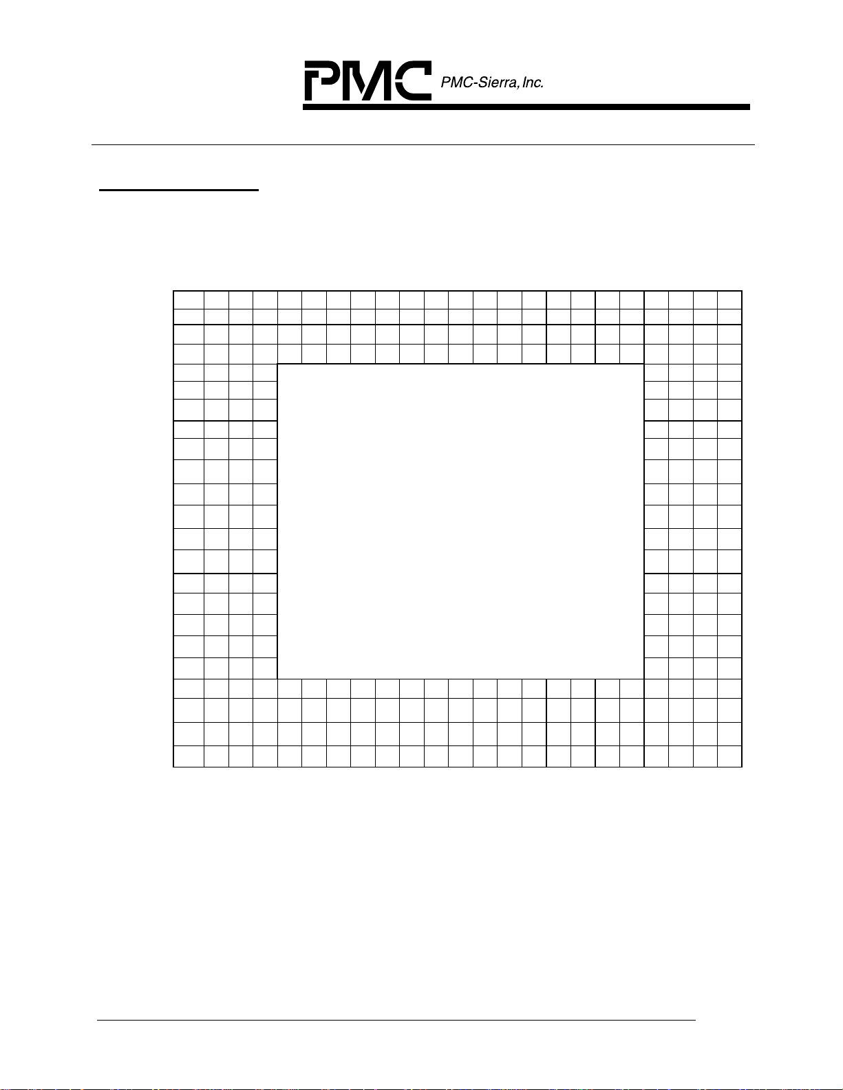
5 PIN DIAGRAM
The S/UNI-STAR is available in a 304 pin SBGA package having a body
size of 31 mm by 31 mm and a ball pitch of 1.27 mm.
2322212019181716151413121110987654321
A
VDD VSS TDAT[12] TDAT[15] PHY_OEN VSS D[2] VSS A[0] A[3] A[7] VSS A[10] WRB TDO VSS N/C VSS N/C RAVD1_B RAVS1_B VSS VDD
B VSS VDD VSS TDAT[13] STPA N/C D[1] D[4] D[6] A[2] A[6] A[9] CSB RSTB TMS TCK N/C N/C QAVS_2 N/C VSS VDD VSS
C TDAT[7] VSS VDD TDAT[10] TDAT[14] TEOP BIAS D[3] D[5] A[1] A[5] A[8] ALE INTB TRSTB N/C N/C QAVD_2 N/C RAVD1_C VDD VSS N/C
D TDAT[4] TDAT[6] TDAT[9] VDD TDAT[11] VDD TERR D[0] VDD D[7] A[4] VDD RDB TDI VDD N/C N/C VDD RAVS1_C VDD N/C N/C VSS
E TDAT[0] TDAT[3] TDAT[5] TDAT[8] N/C VSS VSS N/C
F VSS TMOD TDAT[2] VDD VDD RAVS1_A N/C VSS
G VDD TADR[0] TADR[2] T DAT[1] RAVD1_A N/C VSS VSS
H VSS TPRTY V DD T ADR[1] N/C RAVS2_A RAVD2_A VSS
J
TCA / PTPA TENB
K N/C
L REOP RERR N/C N/C RAVD2_B TAVD1_A T AVS1_A TAVD1_B
M VSS RVAL
N
N/C N/C N/C
RSOC /
P
RSOP
R
RADR[2] RADR[0] VDD VDD VDD N/C N/C ATB3
T VSS VDD RPRTY RDAT[13] RAVS3_A N/C N/C VSS
U
RDAT[15] RDAT[14] RDAT[ 12] RDAT[9] TXCP VSS RAVD3_A N/C
V
VSS RDAT[11] RDAT[8] VDD VDD TXCN VSS VSS
W RDAT[10] RDAT[7] RDAT[5] RDAT[2] RAVS4_A SD T XDP VSS
Y
RDAT[6] RDAT[4] RDAT[1] VDD RMOD VDD N/C N/C VDD N/C N/C VDD N/C N/C VDD VS S TFPI VDD RAVS4_C VDD RAVD4_A RX- TXDN
AA RDAT[3] VSS VDD RDAT[0] N/C N/C N/C RLD N/C N/C N/C N/C TLDCLK TSDCLK TLD VSS VSS QAVD_1 C- RAVD4_C VDD VSS R X+
TSOC /
VDD VDD VSS N/C RAVD2_C
TSOP
DTCA /
BIAS TFCLK
DTPA
DRCA /
VDD VDD TAVS1_B RAVD3_B VSS
DRPA
RCA /
PRPA
RENB RFCLK RADR[1] ATB2 ATB1 ATB0 RAVS3_C
BOTTOM VIEW
RAVS2_C RAVS2_B N/C N/C
RAVD3_C RAVS3_B N/C N/C
AB VSS VDD VSS N/C RLDCLK RSD N/C N/C RALRM RCLK RFPO N/C TFPO N/C N/C VSS TSD VSS QAVS_1 C+ VSS VDD VSS
AC
VDD VSS RSDCLK N/C N/C VSS N/C VSS N/C N/C N/C VSS TCLK N/C N/C VSS VSS VSS REFCLK RAVD4_B RAVS4_B VSS VDD
PROPRIETARY AND CONFIDENTIAL TO PMC-SIERRA, INC., AND FOR ITS CUSTOMERS’ INTERNAL USE 10

PM5352 S/UNI STAR
DATA SHEET
PMC-1990421 ISSUE 2 SATURN USER NETWORK INTERFACE 155 (STAR)
6 PIN DESCRIPTION
6.1 Line Side Interface Signals
Pin Name Type Pin
Function
No.
REFCLK Input AC5 The reference clock input (REFCLK) must provide a
jitter-free 19.44 MHz reference clock. It is used as
the reference clock by both clock recovery and
clock synthesis circuits.
When the WAN Synchronization controller is used,
REFCLK is supplied using a VCXO. In this
application, the transmit direction can be looped
timed to any of the line receivers in order to meet
wander transfer and holdover requirements.
.
RXD+
RXD-
Differential
PECL
inputs
AA1
Y2
The receive differential data inputs (RXD+, RXD-)
contain the NRZ bit serial receive stream. The
receive clock is recovered from the RXD+/- bit
stream. Please refer to the Operation section for a
discussion of PECL interfacing issues.
SD Single-
Ended
PECL
Input
W3 The Signal Detect pin (SD) indicates the presence
of valid receive signal power from the Optical
Physical Medium Dependent Device. A PECL high
indicates the presence of valid data and a PECL
low indicates a loss of signal. It is mandatory that
SD be terminated into the equivalent network that
RXD+/- is terminated into.
.
RCLK Output AB14 The receive byte clock (RCLK) provides a timing
reference for the S/UNI-STAR receive outputs.
RCLK is a divide by eight of the recovered line rate
clock (19.44 MHz).
.
PROPRIETARY AND CONFIDENTIAL TO PMC-SIERRA, INC., AND FOR ITS CUSTOMERS’ INTERNAL USE 11

PM5352 S/UNI STAR
t
t
DATA SHEET
PMC-1990421 ISSUE 2 SATURN USER NETWORK INTERFACE 155 (STAR)
Pin Name Type Pin
Function
No.
RFPO Output AB13 The Receive Frame Pulse Output (RFPO), when
the framing alignment is found (the OOF register bit
is logic zero), is an 8 kHz signal derived from the
receive line clock. RFPO pulses high for one RCLK
cycle every 2430 RCLK cycles (STS-3c (STM-1)).
RFPO is updated on the rising edge of RCLK.
RALRM Output AB15 The Receive Alarm (RALRM) output indicates the
state of the receive framing. RALRM is low if no
receive alarms are active. RALRM is high if line
AIS (LAIS), path AIS (PAIS), line RDI (LRDI), path
RDI (PRDI), enhanced path RDI (PERDI), loss of
signal (LOS), loss of frame (LOF), out of frame
(OOF), loss of pointer (LOP), loss of cell delineation
(LCD), signal fail BER (SFBER), signal degrade
BER (SDBER), path trace identification mismatch
(TIM), path signal la bel mismatch (PSLM) is
detected in the channel. Each alarm can be
individually enabled using bits in the S/UNI-STAR
Channel Alarm Control registers #1 and #2.
TXD+
TXD-
TXC+
TXC-
Differential
TTL outpu
(externally
converted
to PECL)
Differential
TTL outpu
(externally
converted
to PECL)
W2
Y1
U4
V3
RALRM is updated on the rising edge of RCLK.
.
The transmit differential data outputs (TXD+, TXD-)
contain the 155.52 Mbit/s transmit stream.
.
The transmit differential clock outputs (TXC+, TXC-)
contain the 155.52 Mbit/s transmit clock.
TXC+/- must be enabled by setting the TXC_OE
register bit to logic one.
PROPRIETARY AND CONFIDENTIAL TO PMC-SIERRA, INC., AND FOR ITS CUSTOMERS’ INTERNAL USE 12

PM5352 S/UNI STAR
DATA SHEET
PMC-1990421 ISSUE 2 SATURN USER NETWORK INTERFACE 155 (STAR)
Pin Name Type Pin
Function
No.
TFPI Input Y7 The active high framing position (TFPI) signal is an
8 kHz timing marker for the transmitter. TFPI is
used to align the SONET/SDH transport frame
generated by the S/UNI-STAR device to a system
reference. TFPI is internally used to align a master
frame pulse counter. When TFPI is not used, this
counter is free-running.
TFPI should be brought high for a single TCLK
period every 2430 (STS-3c (STM-1)) TCLK cycles,
or a multiple thereof. TFPI shall be tied low if such
synchronization is not required. TFPI cannot be
used as an input to a loop-timed channel. For TFPI
to operate correctly it is required that the
TCLK/TFPO output be configured to output the
CSU byte clock.
The TFPI_EN register bits allow use of the global
framing pulse counter and TFPI for framing
alignment.
TFPI is sampled on the rising edge of TCLK, but
only when the TTSEL register bit is set to logic zero.
When TTSEL is set to logic one, TFPI is unused.
TFPO Output AB11 The Transmit Frame Pulse Output (TFPO) pulses
high for one TCLK cycle every 2430 TCLK cycles
and provides an 8 KHz timing reference. TFPO can
be enabled using TFPO_CH[1:0] configuration
register bits, with the restriction that the device must
be self-timed (not in loop-timed or line-loopback
modes). TFPO is updated on the rising edge of
TCLK.
TCLK Output AC11 The transmit byte clock (TCLK) output provides a
timing reference for the S/UNI-STAR self-timed
channel. TCLK always provide a divide by eight of
the synthesized line rate clock and thus has a
nominal frequency of 19.44 MHz. TFPI is sampled
on the rising edge of TCLK. TCLK does not apply to
internally loop-timed channels, in which case RCLK
provides transmit timing information.
PROPRIETARY AND CONFIDENTIAL TO PMC-SIERRA, INC., AND FOR ITS CUSTOMERS’ INTERNAL USE 13

PM5352 S/UNI STAR
DATA SHEET
PMC-1990421 ISSUE 2 SATURN USER NETWORK INTERFACE 155 (STAR)
6.2 Section and Line Status DCC Signals
Pin Name Type Pin
Function
No.
RSD Output AB18 The receive se ction DCC (RSD) signal contains the
section data communications channel (D1-D3)
RSDCLK Output AC21 The receive section DCC clock (RSDCLK) is used
to clock out the section DCC.
RSDCLK is a 192 kHz clock used to update the
RSD output. RSDCLK is generated by gapping a
216 kHz clock.
TSD Input AB7 The transmit section DCC (TSD) signal contains the
section data communications channel (D1-D3).
TSD is sampled on the rising edge of TSDCLK.
TSDCLK Output AA10 The transmit section DCC clock (TSDCLK) is used
to clock in the section DCC.
TSDCLK is a 192 kHz clock used to sample the
TSD input. TSDCLK is generated by gapping a 216
kHz clock.
RLD Output AA16 The re ceive line DCC (RLD) signal contains the line
data communications channel (D4-D12).
RLDCLK Output AB19 The receive line DCC clock (RLDCLK) is use d to
clock out the line DCC.
RLDCLK is a 576 kHz clock used to update the
RLD output. RLDCLK is generated by gapping a
2.16 MHz clock.
TLD Input AA9 The transmit line DCC (TLD) signal contains the
line data communications channel (D4-D12).
TLD is sampled on the rising edge of TLDCLK.
TLDCLK Output AA11 The transmit line DCC clock (TLDCLK) is used to
clock in the line DCC.
TLDCLK is a 576 kHz clock used to sample the
TLD input. TLDCLK is generated by gapping a 2.16
MHz clock.
PROPRIETARY AND CONFIDENTIAL TO PMC-SIERRA, INC., AND FOR ITS CUSTOMERS’ INTERNAL USE 14

PM5352 S/UNI STAR
DATA SHEET
PMC-1990421 ISSUE 2 SATURN USER NETWORK INTERFACE 155 (STAR)
6.3 ATM (UTOPIA) and Packet over SONET (POS-PHY) System Interface
Pin Name Type Pin
No.
TDAT[15]
TDAT[14]
TDAT[13]
TDAT[12]
TDAT[11]
TDAT[10]
TDAT[9]
TDAT[8]
TDAT[7]
TDAT[6]
TDAT[5]
TDAT[4]
TDAT[3]
TDAT[2]
TDAT[1]
TDAT[0]
TDAT[15]
TDAT[14]
TDAT[13]
TDAT[12]
TDAT[11]
TDAT[10]
TDAT[9]
TDAT[8]
TDAT[7]
TDAT[6]
TDAT[5]
TDAT[4]
TDAT[3]
TDAT[2]
TDAT[1]
TDAT[0]
Input
(ATM)
Input
(POS)
A20
C19
B20
A21
D19
C20
D21
E20
C23
D22
E21
D23
E22
F21
G20
E23
A20
C19
B20
A21
D19
C20
D21
E20
C23
D22
E21
D23
E22
F21
G20
E23
Function
UTOPIA Transmit Cell Data Bus (TDAT[15:0 ] ).
This data bus carries the ATM cell octets that are
written to the selected transmit FIFO. TDAT[15:0] is
considered valid only when TENB is simultaneously
asserted and the S/UNI-STAR is selected via
TADR[2:0].
TDAT[15:0] is sampled on the rising edge of
TFCLK.
POS-PHY Transmit Packet Data Bus (TDAT[15:0]).
This data bus carries the POS packet octets that
are written to the selected transmit FIFO.
TDAT[15:0] is considered valid only when TENB is
simultaneously asserted and the S/UNI-STAR is
selected via TADR[2:0].
TDAT[15:0] is sampled on the rising edge of
TFCLK.
PROPRIETARY AND CONFIDENTIAL TO PMC-SIERRA, INC., AND FOR ITS CUSTOMERS’ INTERNAL USE 15

PM5352 S/UNI STAR
DATA SHEET
PMC-1990421 ISSUE 2 SATURN USER NETWORK INTERFACE 155 (STAR)
Pin Name Type Pin
No.
TPRTY Input
H22 UTOPIA Transmit bus parity (TPRTY) signal.
(ATM)
TPRTY Input
H22 POS-PHY Transmit bus parity (TPRTY) signal.
(POS)
Function
The transmit parity (TPRTY) signal indicates the
parity of the TDAT[15:0] bus. A parity error is
indicated by a status bit and a maskable interrupt.
Cells with parity errors are inserted in the transmit
stream, so the TPRTY input may be unused. Odd
or even parity selection is made using the RXPTYP
register bit.
TPRTY is considered valid only when TENB is
simultaneously asserted and the S/UNI-STAR is
selected via TADR[2:0].
TPRTY is sampled on the rising edge of TFCLK.
The transmit parity (TPRTY) signal indicates the
parity of the TDAT[15:0] bus. A parity error is
indicated by a status bit and a maskable interrupt.
Packets with parity errors are inserted in the
transmit stream, so the TPRTY input may be
unused. Odd or even parity selection is made using
the RXPTYP register bit. TPRTY is considered valid
only when TENB is simultaneously asserted and
the S/UNI-STAR is selected via TADR[2: 0].
TPRTY is sampled on the rising edge of TFCLK
TSOC Input
(ATM)
J21 UTOPIA Transmit Start of Cell (TSOC) signal.
The transmit start of cell (TSOC) signal marks the
start of cell on the TDAT bus. When TSOC is high,
the first word of the cell structure is present on the
TDAT bus. It is not necessary for TSOC to be
present for each cell. An interrupt may be
generated if TSOC is high during any word other
than the first word of the cell structure.
TSOC is considered valid only when TENB is
simultaneously asserted and the S/UNI-STAR is
selected via TADR[2:0].
TSOC is sampled on the rising edge of TFCLK.
PROPRIETARY AND CONFIDENTIAL TO PMC-SIERRA, INC., AND FOR ITS CUSTOMERS’ INTERNAL USE 16

PM5352 S/UNI STAR
DATA SHEET
PMC-1990421 ISSUE 2 SATURN USER NETWORK INTERFACE 155 (STAR)
Pin Name Type Pin
No.
TSOP Input
J21 POS-PHY Transmit Start of Packet (TSOP) signals.
(POS)
TENB Input
J22 UTOPIA Transmit Multi-PHY Write Enable (TENB)
(ATM)
Function
TSOP indicates the first word of a packet. TSOP is
required to be present at the beginning of every
packet for proper operation.
TSOP is considered valid only when TENB is
simultaneously asserted and the S/UNI-STAR is
selected via TADR[2:0].
TSOP is sampled on the rising edge of TFCLK.
signal.
The TENB signal is an active low input which is
used along with the TADR[2:0] inputs to initiate
writes to the transmit FIFO’s.
TENB works as follows. When sampled high, no
write is performed, but the TADR[2:0] address is
latched to identify the transmit FIFO to be
accessed. When TENB is sampled low, the word on
the TDAT bus is written into the transmit FIFO that
is selected by the TADR[2:0} address bus. A
complete 53 octet cell must be written to the
transmit FIFO before it is inserted into the transmit
stream. Idle cells are inserted when a complete cell
is not available. While TENB is deasserted,
TADR[2:0] can be used for polling TCA.
TENB is sampled on the rising edge of TFCLK.
PROPRIETARY AND CONFIDENTIAL TO PMC-SIERRA, INC., AND FOR ITS CUSTOMERS’ INTERNAL USE 17

PM5352 S/UNI STAR
DATA SHEET
PMC-1990421 ISSUE 2 SATURN USER NETWORK INTERFACE 155 (STAR)
Pin Name Type Pin
No.
TENB Input
J22 POS-PHY Transmit Multi-PHY Write Enable (TENB)
(POS)
TADR[2]
TADR[1]
TADR[0]
Input
(ATM)
G21
H20
G22
Function
signal.
The S/UNI-STAR supports both byte-level and
packet-level transfer. Packet-level transfer operates
in a similar fashion to Utopia, with a selection phase
when TENB is deasserted and a transfer phase
when TENB is asserted. While TENB is asserted,
TADR[2:0] is used for polling PTPA and the
currently selected PHY status is provided on STPA.
Byte level transfer works on a cycle basis. When
TENB is asserted, data is transferred to the
selected PHY. Nothing happens when TENB is
deasserted. Polling is not available and packet
availability is indicated by DTPA.
TENB is sampled on the rising edge of TFCLK.
Transmit Address (T ADR[2:0]) . The TADR[2:0] bus
is used for device selection and device polling in
accordance with the Utopia Level 2 standard.
When TADR[2:0] is set to the same value as the
PHY_ADR[2:0] inputs than the transmit interface of
this S/UNI-STAR is either being selected or polled.
Note that the null-phy address 0x7 is an invalid
Address and cannot be used to select the S/UNISTAR.
TADR[2:0] is sampled on the rising edge of TFCLK.
TADR[2]
TADR[1]
TADR[0]
Input
(POS)
G21
H20
G22
POS-PHY Transmit Write Address (TADR[2:0])
signals.
The TADR[2:0] bus is used to select the FIFO (and
hence port) that is written to using the TENB signal.
In packet level transfer mode, TADR[2:0] is also
used for polling on PTPA.
Note that address 0x7 is the null-PHY address and
cannot be used to select theS/UNI-STAR.
TADR[2:0] is sampled on the rising edge of TFCLK.
PROPRIETARY AND CONFIDENTIAL TO PMC-SIERRA, INC., AND FOR ITS CUSTOMERS’ INTERNAL USE 18

PM5352 S/UNI STAR
DATA SHEET
PMC-1990421 ISSUE 2 SATURN USER NETWORK INTERFACE 155 (STAR)
Pin Name Type Pin
No.
TCA Output
J23 UTOPIA Transmit multi-PHY Cell Available (TCA)
(ATM)
Function
The TCA signal indicates when a cell is available in
the transmit FIFO for the port polled by TADR[2:0]
when TENB is asserted. When high, TCA indicates
that the transmit FIFO is not full and a complete cell
may be written. When TCA goes low, it can be
configured to indicate either that the transmit FIFO
is near full or that the transmit FIFO is full. TCA will
transition low on the rising edge of TFCLK after the
Payload word 19 (TCALEVEL0=0) or 23
(TCALEVEL0=1) is sampled if the PHY being polled
is the same as the PHY in use. To reduce FIFO
latency, the FIFO depth at which TCA indicates
"full" can be set to one, two, three or four cells.
Note that regardless of what fill level TCA is set to
indicate "full" at, the transmit cell processor can
store 4 complete cells.
TCA is tri-stated when either the null-PHY address
(0x7) or an address not matching the address set
by PHY_ADR[2:0] is latched from the TADR[2:0]
inputs when TENB is high.
TCA is updated on the rising edge of TFCLK.
PROPRIETARY AND CONFIDENTIAL TO PMC-SIERRA, INC., AND FOR ITS CUSTOMERS’ INTERNAL USE 19

PM5352 S/UNI STAR
DATA SHEET
PMC-1990421 ISSUE 2 SATURN USER NETWORK INTERFACE 155 (STAR)
Pin Name Type Pin
Function
No.
PTPA J23 POS-PHY Polled Transmit multi-PHY Packet
Available (PTPA).
PTPA transitions high when a programmable
minimum number of bytes is available in the polled
transmit FIFO (TPAHW M[7:0] register bits). Once
high, PTPA indicates that the transmit FIFO is not
full. When PTPA transitions low, it optionally
indicates that the transmit FIFO is full or near full
(TPALWM[7:0] register bits). PTPA allows to poll
the PHY address selected by TADR[2:0] when
TENB is asserted.
PTPA is tri-stated when either the null-PHY address
(0x7) or an address not matching the address set
by PHY_ADR[2:0] is latched from the TADR[2:0]
inputs when TENB is high.
PTPA is only available in POS-PHY packet-level
transfer mode, as selected by the POS_PLVL
register bit. PTPA is tristated in byte-level transfer
mode. PTPA is updated on the rising edge of
TFCLK.
PROPRIETARY AND CONFIDENTIAL TO PMC-SIERRA, INC., AND FOR ITS CUSTOMERS’ INTERNAL USE 20

PM5352 S/UNI STAR
DATA SHEET
PMC-1990421 ISSUE 2 SATURN USER NETWORK INTERFACE 155 (STAR)
Pin Name Type Pin
No.
STPA Output
B19 POS-PHY Selected multi-PHY Transmit Packet
(POS)
Function
Available (STPA) signal.
STPA transitions high when a predefined
(TPAHWM[7:0] register bits) minimum number of
bytes is available in the selected transmit FIFO (the
FIFO that data is written into). Once high, STPA
indicates that the transmit FIFO is not full. When
STPA transitions low, it optionally indicates that the
transmit FIFO is full or near full (TPALWM[7:0]
register bits). STPA always provide status
indication for the selected PHY in order to avoid
FIFO overflows while polling is performed.
The PHY Layer device shall tristate STPA when
TENB is deasserted. STPA shall also be tristated
when either the null-PHY address (0x7H) or an
address not matching the address set by
PHY_ADR[2:0] is presented on the TADR[2:0]
signals when TENB is sampled high (deasserted
during the previous clock cycle).
TFCLK Input
(ATM)
TFCLK Input
(POS)
STPA is only available in POS-PHY packet-level
transfer mode, as selected by the POS_PLVL
register bit. STPA is tristated in byte-level transfer
mode. STPA is updated on the rising edge of
TFCLK.
K20 UTOPIA Transmit FIFO Write Clock (TFCLK).
This signal is used to write ATM cells to the four cell
transmit FIFOs.
TFCLK cycles at a 50 MHz or lower instantaneous
rate.
K20 POS-PHY Transmit FIFO Write Clock (TFCLK).
This signal is used to write packet octets into the
256 bytes packet FIFO’s.
TFCLK cycles at a 50 MHz or lower instantaneous
rate.
PROPRIETARY AND CONFIDENTIAL TO PMC-SIERRA, INC., AND FOR ITS CUSTOMERS’ INTERNAL USE 21

PM5352 S/UNI STAR
DATA SHEET
PMC-1990421 ISSUE 2 SATURN USER NETWORK INTERFACE 155 (STAR)
Pin Name Type Pin
No.
DTCA Output
K22 UTOPIA Direct Transmit Cell Available (DTCA).
(ATM)
Function
These output signals provide direct status indication
of when a cell is available in the transmit FIFO for
the corresponding port. When high, DTCA indicates
that the corresponding transmit FIFO is not full and
a complete cell may be written. When DTCA goes
low, it can be configured to indicate either that the
corresponding transmit FIFO is near full or that the
corresponding transmit FIFO is full. DTCA will
transition low on the rising edge of TFCLK after the
Payload word 19 (TCALEVEL0=0) or 23
(TCALEVEL0=1) is sampled if the PHY being polled
is the same as the PHY in use. To reduce FIFO
latency, the FIFO depth at which DTCA indicates
"full" can be set to one, two, three or four cells.
Note that regardless of what fill level DTCA is set to
indicate "full" at, the transmit cell processor can
store 4 complete cells
DTCA are updated on the rising edge of TFCLK.
PROPRIETARY AND CONFIDENTIAL TO PMC-SIERRA, INC., AND FOR ITS CUSTOMERS’ INTERNAL USE 22

PM5352 S/UNI STAR
DATA SHEET
PMC-1990421 ISSUE 2 SATURN USER NETWORK INTERFACE 155 (STAR)
Pin Name Type Pin
No.
DTPA Output
K22 POS-PHY Direct Transmit Packet Available (DTPA).
(POS)
Function
These output signals provide direct status indication
of when some programmable number of bytes is
available in the transmit FIFO, for the
corresponding port. When transitioning high, DTPA
indicates that the transmit FIFO has enough room
to store data. The transition level is selected by the
TXFP Transmit Packet Available Low Water-mark
(TPALWM[7:0]) register. When DTPA transitions
low, it indicates that the transmit FIFO is either full
or near full as selected by the TXFP Transmit
Packet Available High Water-mark (TPAHWM[7:0])
register. This last option provides the Link Layer
system with some look ahead capability in order to
avoid FIFO overruns and smoothly transition
between PHY’s.
DTPA are updated on the rising edge of TFCLK.
TMOD Input
(POS)
F22 POS-PHY Transmit Word Modulo (TMOD) signal.
TMOD indicates the size of the current word. TMOD
is only used during the last word transfer of a
packet, at the same time TEOP is asserted. During
a packet transfer every word must be complete
except the last word, which can be composed of 1
or 2 bytes. TMOD set high indicates a 1-byte word
(present on MSB’s, LSB’s are discarded) while
TMOD set low indicates a 2-byte word.
TMOD is considered valid only when TENB is
simultaneously asserted and the S/UNI-STAR is
selected via TADR[2:0].
TMOD is sampled on the rising edge of TFCLK.
PROPRIETARY AND CONFIDENTIAL TO PMC-SIERRA, INC., AND FOR ITS CUSTOMERS’ INTERNAL USE 23

PM5352 S/UNI STAR
DATA SHEET
PMC-1990421 ISSUE 2 SATURN USER NETWORK INTERFACE 155 (STAR)
Pin Name Type Pin
No.
TEOP Input
C18 POS-PHY Transmit End of Packet (TEOP).
(POS)
TERR Input
D17 POS -PHY Transmit Erro r (TERR).
(POS)
Function
The active high TEOP signal marks the end of a
packet on the TDAT[15:0] bus. When TEOP is
high, the last word of the packet is present on the
TDAT[15:0] data bus and TMOD indicates how
many bytes this last word is composed of. It is legal
to set TSOP high at the same time TEOP is high.
This provides support for one or two byte packets,
as indicated by the value of TMOD.
TEOP is considered valid only when TENB is
simultaneously asserted and the S/UNI-STAR is
selected via TADR[2:0].
TEOP is sampled on the rising edge of TFCLK.
The transmit error indicator (TERR) is used to
indicate that the current packet must be aborted.
TERR should only be asserted during the last word
transfer of a packet. Packets marked with TERR will
be appended with the abort sequence (0x7D-0x7E)
when transmission.
TERR is considered valid only when TENB is
simultaneously asserted and the S/UNI-STAR is
selected via TADR[2:0].
TERR is sampled on the rising edge of TFCLK.
PROPRIETARY AND CONFIDENTIAL TO PMC-SIERRA, INC., AND FOR ITS CUSTOMERS’ INTERNAL USE 24

PM5352 S/UNI STAR
DATA SHEET
PMC-1990421 ISSUE 2 SATURN USER NETWORK INTERFACE 155 (STAR)
Pin Name Type Pin
No.
RDAT[15]
RDAT[14]
RDAT[13]
RDAT[12]
RDAT[11]
RDAT[10]
RDAT[9]
RDAT[8]
RDAT[7]
RDAT[6]
RDAT[5]
RDAT[4]
RDAT[3]
RDAT[2]
RDAT[1]
RDAT[0]
RDAT[15]
RDAT[14]
RDAT[13]
RDAT[12]
RDAT[11]
RDAT[10]
RDAT[9]
RDAT[8]
RDAT[7]
RDAT[6]
RDAT[5]
RDAT[4]
RDAT[3]
RDAT[2]
RDAT[1]
RDAT[0]
Output
(ATM)
Output
(POS)
U23
U22
T20
U21
V22
W23
U20
V21
W22
Y23
W21
Y22
AA23
W20
Y21
AA20
U23
U22
T20
U21
V22
W23
U20
V21
W22
Y23
W21
Y22
AA23
W20
Y21
AA20
Function
UTOPIA Receive Cell Data Bus (RDAT[15:0]).
This data bus carries the ATM cells that are read
from the receive FIFO selected by RADR[2:0].
RDAT[15:0] is tri-stated when RENB is high.
RDAT[15:0] is tristated when RENB is high.
RDAT[15:0] is also tristated when either the nullPHY address (0x7H) or an address not matching
the address space is latched from the RADR[2:0]
inputs when RENB is high.
RDAT[15:0] is updated on the rising edge of
RFCLK.
POS-PHY Receive Packet Data Bus (RDAT[15:0]).
This data bus carries the POS packet octets that
are read from the selected receive FIFO.
RDAT[15:0] is considered valid only when RVAL is
asserted.
RDAT[15:0] is tristated when RENB is high.
RDAT[15:0] is also tristated when either the nullPHY address (0x7H) or an address not matching
the address space is latched from the RADR[2:0]
inputs.
RDAT[15:0] is updated on the rising edge of
RFCLK.
PROPRIETARY AND CONFIDENTIAL TO PMC-SIERRA, INC., AND FOR ITS CUSTOMERS’ INTERNAL USE 25

PM5352 S/UNI STAR
DATA SHEET
PMC-1990421 ISSUE 2 SATURN USER NETWORK INTERFACE 155 (STAR)
Pin Name Type Pin
No.
RPRTY Output
T21 UTOPIA Receive Parity (RPRTY).
(ATM)
RPRTY Output
T21 POS-PHY Receive Parity (RPRTY).
(POS)
Function
The receive parity (RPRTY) signal indicates the
parity of the RDAT bus. RPRTY reflects the parity
of RDAT[15:0]. Odd or even parity selection is
made by using the RXPTYP register bit (in ATM cell
processors, the four RXCP shall be programmed
with the same parity setting).RPRTY is tristated
when RENB is high. RPRTY is also tristated when
either the null-PHY address (0x7H) or an address
not matching the address space is latched from the
RADR[2:0] inputs when RENB is high.
RPRTY is updated on the rising edge of RFCLK.
The receive parity (RPRTY) signal indicates the
parity of the RDAT bus. Odd or even parity
selection is made by using the RXPTYP register bit
(in POS Frame Processors; the four RXFP shall be
programmed with the same parity setting). RPRTY
is tristated when RENB is high. RPRTY is also
tristated when either the null-PHY address (0x7H)
or an address not matching the address space is
latched from the RADR[2:0] inputs.
RPRTY is updated on the rising edge of RFCLK.
RSOC Output
(ATM)
P23 UTOPIA Receive Start of Cell (RSOC).
RSOC marks the start of cell on the RDAT bus.
RSOC is tristated when RENB is deasserted.
RSOC is also tristated when either the null-PHY
address (0x7H) or an address not matching the
address space is latched from the RADR[2:0] inputs
when RENB is high.
RSOC is sampled on the rising edge of RFCLK.
PROPRIETARY AND CONFIDENTIAL TO PMC-SIERRA, INC., AND FOR ITS CUSTOMERS’ INTERNAL USE 26

PM5352 S/UNI STAR
DATA SHEET
PMC-1990421 ISSUE 2 SATURN USER NETWORK INTERFACE 155 (STAR)
Pin Name Type Pin
No.
RSOP Output
P23 POS-PHY Receive Start of Packet (RSOP).
(POS)
RENB Input
P22 UTOPIA Receive multi-PHY Read Enable (RENB).
(ATM)
Function
RSOP marks the first word of a packet transfer.
RSOP is tristated when RENB is deasserted. RSOP
is also tristated when either the null-PHY address
(0x7H) or an address not matching the address
space is latched from the RADR[2:0] inputs.
RSOP/RSOP is sampled on the rising edge of
RFCLK
The RENB signal is used to initiate reads from the
receive FIFO’s. RENB works as follows. When
RENB is sampled high, no read is performed and
RDAT[15:0], RPRTY and RSOC are tristated, and
the address on RADR[2:0] is latched to select the
device or port for the next FIFO access. When
RENB is sampled low, the word on the RDAT bus is
read from the selected receive FIFO.
RENB must operate in conjunction with RFCLK to
access the FIFO’s at a high enough rate to prevent
FIFO overflows. The system may de-assert RENB
at anytime it is unable to accept another byte.
RENB is sampled on the rising edge of RFCLK.
PROPRIETARY AND CONFIDENTIAL TO PMC-SIERRA, INC., AND FOR ITS CUSTOMERS’ INTERNAL USE 27

PM5352 S/UNI STAR
DATA SHEET
PMC-1990421 ISSUE 2 SATURN USER NETWORK INTERFACE 155 (STAR)
Pin Name Type Pin
No.
RENB Input
P22 POS-PHY Receive multi-PHY Read Enable
(POS)
Function
(RENB).
The S/UNI-STAR supports both byte-level and
packet-level transfer. Packet-level transfer operates
as described above, with a selection phase when
RENB is deasserted and a transfer phase when
RENB is asserted. While RENB is asserted,
RADR[2:0] is used fo r polling RPA. Byte level
transfer works on a cycle basis. When RENB is
asserted data is transferred from the selected PHY
and RADR[2:0] is used to select the PHY. Nothing
happens when RENB is deasserted. Polling is not
possible; packet availability is directly indicated by
DRPA.
During a data transfer, RVAL shall be monitored
since it will indicate if the data is valid. Once RVAL
is deasserted, RENB or RADR[2:0] must be used to
select a new PHY for data transfer.
RADR[2]
RADR[1]
RADR[0]
Input
(ATM)
R23
P20
R22
RENB must operate in conjunction with RFCLK to
access the FIFO’s at a high enough rate to prevent
FIFO overflows. The system may de-assert RENB
at anytime it is unable to accept another byte.
RENB is sampled on the rising edge of RFCLK.
Receive Address (RADR[2:0]). The RADR[2:0] bus
is used for device selection and device polling in
accordance with the Utopia Level 2 standard.
When RADR[2:0] is set to the same value as the
PHY_ADR[2:0] inputs than the receive interface of
this S/UNI-STAR is either being selected or polled.
Note that the null phy address 7H is an invalid
address and cannot be used to select the S/UNISTAR.
RADR[2:0] is sampled on the rising edge of TFCLK.
PROPRIETARY AND CONFIDENTIAL TO PMC-SIERRA, INC., AND FOR ITS CUSTOMERS’ INTERNAL USE 28

PM5352 S/UNI STAR
DATA SHEET
PMC-1990421 ISSUE 2 SATURN USER NETWORK INTERFACE 155 (STAR)
Pin Name Type Pin
No.
RADR[2]
RADR[1]
RADR[0]
RCA Output
Input
(POS)
R23
P20
R22
N20 UTOPIA Receive multi-PHY Cell Available (RCA).
(ATM)
Function
POS-PHY Receive Read Address (RADR).
The RADR signal is used to select the FIFO (and
hence port) that is read from using the RENB
signal.
The RADR bus is used to select the FIFO (and
hence port) that is written to using the TENB signal
and the FIFO's whose packet available signal is
visible on the PRPA polling output.
Note that address 0x7H is the null-PHY address
and will not be identified with the S/UNI-STAR.
RADR is sampled on the rising edge of RFCLK.
RCA indicates when a cell is available in the receive
FIFO ( when the STAR is selected by RADR[2:0]).
RCA can be configured to be de-asserted when
either zero or four bytes remain in the
selected/addressed FIFO. RCA will thus transition
low on the rising edge of RFCLK after Payload word
24 (RCALEVEL0=1) or 19 (RCALEVEL0=0) is
output if the PHY being polled is the same as the
PHY in use.
RCA is tristated when either the null-PHY address
(0x7H) or an address not matching the device
address is latched from the RADR[2:0] inputs when
RENB is high.
RCA is updated on the rising edge of RFCLK.
PROPRIETARY AND CONFIDENTIAL TO PMC-SIERRA, INC., AND FOR ITS CUSTOMERS’ INTERNAL USE 29

PM5352 S/UNI STAR
DATA SHEET
PMC-1990421 ISSUE 2 SATURN USER NETWORK INTERFACE 155 (STAR)
Pin Name Type Pin
No.
PRPA Output
N20 POS-PHY Polled mu lti-PHY Receive Packet
(POS)
Function
Available (PRPA) signal.
PRPA indicates when data is available in the polled
receive FIFO. When PRPA is high, the receive
FIFO has at least one end of packet or a predefined
number of bytes to be read (the number of bytes
might be user programmable). PRPA is low when
the receive FIFO fill level is below the assertion
threshold and the FIFO contains no end of packet.
PRPA allows to poll every PHY while transferring
data from the selected PHY.
PRPA is driven by a PHY layer device when its
address is polled on RADR[2:0]. A PHY layer device
shall tristate PRPA when either the null-PHY
address (0x7H) or an address not matching the
address set by the PHY_ADR[2:0] register bits is
provided on RADR[2:0].
PRPA is only available in POS-PHY packet-level
transfer mode, as selected by the POS_PLVL
register bit. PRPA is tristated in byte-level transfer
mode. PRPA is updated on the rising edge of
RFCLK.
PROPRIETARY AND CONFIDENTIAL TO PMC-SIERRA, INC., AND FOR ITS CUSTOMERS’ INTERNAL USE 30

PM5352 S/UNI STAR
DATA SHEET
PMC-1990421 ISSUE 2 SATURN USER NETWORK INTERFACE 155 (STAR)
Pin Name Type Pin
No.
RVAL Output
M22 POS-PHY Receive Data Valid (RVAL ).
(POS)
Function
RVAL indicates the validity of the receive data
signals. When RVAL is high, the Receive signals
(RDAT, RSOP, REOP, RMOD, RPRTY and RERR)
are valid. When RVAL is low, all Receive signals are
invalid and must be disregarded. RVAL will
transition low on a FIFO empty condition or on an
end of packet. . No data will be removed from the
receive FIFO while RVAL is deasserted. Once
deasserted, RVAL will remain deasserted until the
current PHY is deselected.
RVAL allows to monitor the selected PHY during a
data transfer, while monitoring other PHY’s is done
using DRPA.
RVAL is tristated when RENB is deasserted. RVAL
is also tristated when either the null-PHY address
(0x7H) or an address not matching the PHY layer
device address is presented on the RADR[2:0]
signals.
RFCLK Input
(ATM)
RFCLK Input
(ATM)
RVAL is updated on the rising edge of RFCLK.
P21 UTOPIA Receive FIFO Read Clock (RFCLK).
RFCLK is used to read ATM cells from the receive
FIFO’s. RFCLK must cycle at a 50 MHz or lower
instantaneous rate, but at a high enough rate to
avoid FIFO overflows.
P21 POS-PHY Receive FIFO Read Clock (RFCLK).
This signal is used to read packets from the receive
FIFO’s. RFCLK must cycle at a 50 MHz or lower
instantaneous rate, but at a high enough rate to
avoid FIFO overflows.
PROPRIETARY AND CONFIDENTIAL TO PMC-SIERRA, INC., AND FOR ITS CUSTOMERS’ INTERNAL USE 31

PM5352 S/UNI STAR
DATA SHEET
PMC-1990421 ISSUE 2 SATURN USER NETWORK INTERFACE 155 (STAR)
Pin Name Type Pin
No.
DRCA Output
M21 UTOPIA Direct Receive Cell Available (DRCA).
(ATM)
DRPA Output
M21 POS-PHY Direct Receive Packet Available
(POS)
Function
These output signals provides direct status
indication of when a cell is available in the receive
FIFO for the corresponding port. DRCA can be
configured to be de-asserted when either zero or
four bytes remain in the selected/addressed FIFO.
DRCA will thus transition low on the rising edge of
RFCLK after Payload word 24 (RCALEVEL0=1) or
19 (RCALEVEL0=0) is output if the PHY being
polled is the same as the PHY in use.
DRCA[x] is updated on the rising edge of RFCLK.
DRPA provides a direct status indication. DRPA
indicates when data is available in the receive
FIFO. When DRPA is high, the receive FIFO has at
least one end of packet or a programmable
minimum number of bytes to be read. DRPA is
otherwise low. The polarity of DRPA can be inverted
with the RPAINV register bit.
RMOD Output
(POS)
DRPA is updated on the rising edge of RFCLK.
Y19 POS-PHY Receive Modulo (RMOD).
The RMOD signal indicates the number of bytes
carried by the RDAT[15:0] bus during the last word
of a packet transfer. During a packet transfer every
word must be complete except the last word which
can be composed of 1 or 2 bytes. RMOD set high
indicate a single byte word (present on MSB’s,
LSB’s are discarded) while RMOD set low indicates
a two byte word. RMOD is only used in POS mode.
RMOD is tristated when RENB is deasserted.
RMOD is also tristated when either the null-PHY
address (0x7H) or an address not matching the
address space set by PHY_ADR[2:0] is latched
from the RADR[2:0] inputs when RENB is high.
RMOD is updated on the rising edge of RFCLK.
PROPRIETARY AND CONFIDENTIAL TO PMC-SIERRA, INC., AND FOR ITS CUSTOMERS’ INTERNAL USE 32

PM5352 S/UNI STAR
DATA SHEET
PMC-1990421 ISSUE 2 SATURN USER NETWORK INTERFACE 155 (STAR)
Pin Name Type Pin
No.
REOP Output
L23 POS-PHY Receive End Of Packet (REOP).
(POS)
RERR Output
L22 POS-PHY Receive Error (RERR).
Function
The REOP signal marks the end of packet on the
RDAT[15:0] bus. When the RXFP-50 is selected,
REOP is set high to mark the last word of the
packet presented on the RDAT[15:0] bus. During
this same cycle RMOD is used to indicate if the last
word has 1 or 2 bytes. It is legal to set RSOP high
at the same time REOP is high. This provides
support for one or two bytes packets, as indicated
by the value of RMOD. REOP is only used in POS
mode.
REOP is tristated when RENB is deasserted. REOP
is also tristated when either the null-PHY address
(0x7H) or an address not matching the address
space is latched from the RADR[2:0] inputs when
RENB is high.
REOP is updated on the rising edge of RFCLK.
(POS)
The RERR signal indicates that the current packet
is aborted. RERR can only be asserted during the
last word transfer, at the same time REOP is
asserted. RERR is only used in POS mode.
RERR is tristated when RENB is deasserted. RERR
is also tristated when either the null-PHY address
(0x7H) or an address not matching the address
space is latched from the RADR[2:0] inputs when
RENB is high.
RERR is updated on the rising edge of RFCLK.
PROPRIETARY AND CONFIDENTIAL TO PMC-SIERRA, INC., AND FOR ITS CUSTOMERS’ INTERNAL USE 33

PM5352 S/UNI STAR
DATA SHEET
PMC-1990421 ISSUE 2 SATURN USER NETWORK INTERFACE 155 (STAR)
Pin Name Type Pin
No.
PHY_OEN Input
A19 The PHY Output Enable (PHY_OEN) signal
(ATM/
POS)
Function
controls the operation of the system interface.
When set to logic zero, all System Interface outputs
are held tristate. When PHY_OEN is set to logic
one, the interface is enabled. PHY_OEN can be
overwritten by the PHY_EN Master System
Interface Configuration register bit. PHY_OEN and
PHY_EN are OR’ed together to enable the
interface.
When the S/UNI-STAR is the only PHY layer device
on the bus, PHY_OEN can safely be tied to logic
one. When the S/UNI-STAR shares the bus with
other devices, then PHY_OEN must be tied to logic
zero, and the PHY_EN register bit used to enable
the bus once its PHY_ADR[2:0] is programmed in
order to avoid conflicts.
6.4 Microprocessor Interface Signals
Pin Name Type Pin
Function
No.
CSB Input B11 The active-low chip select (CSB) signal is low
during S/UNI-STAR register accesses.
Note that when not being used, CSB must be tied
high. If CSB is not required (i.e., registers accesses
are controlled using the RDB and WRB signals
only), CSB must be connected to an inverted
version of the RSTB input.
RDB Input D11 The active-low read enable (RDB) signal is low
during S/UNI-STA R register read accesses. The
S/UNI-STAR drives the D[7:0] bus with the contents
of the addressed register while RDB and CSB are
low.
WRB Input A10 The active-low write strobe (WRB) signal is low
during a S/UNI-STAR register write accesses. The
D[7:0] bus contents are clocked into the addressed
register on the rising WRB edge while CSB is low.
PROPRIETARY AND CONFIDENTIAL TO PMC-SIERRA, INC., AND FOR ITS CUSTOMERS’ INTERNAL USE 34

PM5352 S/UNI STAR
DATA SHEET
PMC-1990421 ISSUE 2 SATURN USER NETWORK INTERFACE 155 (STAR)
Pin Name Type Pin
No.
D[0]
D[1]
D[2]
D[3]
D[4]
D[5]
D[6]
D[7]
A[0]
A[1]
A[2]
A[3]
A[4]
A[5]
A[6]
A[7]
A[8]
A[9]
I/O D16
B17
A17
C16
B16
C15
B15
D14
Input A15
C14
B14
A14
D13
C13
B13
A13
C12
B12
Function
The bi-directional data bus D[7:0] is used during
S/UNI-STAR register read and write accesses.
The address bus A[9:0] selects specific registers
during S/UNI-STAR register accesses.
Except for S/UNI-STAR global registers.
A[10]/TRS Input A11 The test register select (TRS) signal selects
between normal and test mode register accesses.
TRS is high during test mode register accesses,
and is low during normal mode register accesses.
RSTB Input
pull-up
B10 The active-low reset (RSTB) signal provides an
asynchronous S/UNI-STAR reset. RSTB is a
Schmitt triggered input with an integral pull-up
resistor.
ALE Input
pull-up
C11 The address latch enable (ALE) is active-high and
latches the address bus A[7:0] when low. When
ALE is high, the internal address latches are
transparent. It allows the S/UNI-STAR to interface
to a multiplexed address/data bus. ALE has an
integral pull-up resistor.
PROPRIETARY AND CONFIDENTIAL TO PMC-SIERRA, INC., AND FOR ITS CUSTOMERS’ INTERNAL USE 35

PM5352 S/UNI STAR
DATA SHEET
PMC-1990421 ISSUE 2 SATURN USER NETWORK INTERFACE 155 (STAR)
Pin Name Type Pin
Function
No.
INTB Output
Open-
drain
C10 The active-low interrupt (INTB) signal goes low
when a S/UNI-STA R interrupt source is active and
that source is unmasked. The S/UNI-STAR may be
enabled to report many alarms or events via
interrupts.
Examples of interrupt sources are loss of signal
(LOS), loss of frame (LOF), line AIS, line remote
defect indication (LRDI) detect, loss of pointer
(LOP), path AIS, path remote defect indication
detect and others.
INTB is tristated when the interrupt is
acknowledged via an appropriate register access.
INTB is an open drain output.
6.5 JTAG Test Access Port (TAP) Signals
Pin Name Type Pin
Function
No.
TCK Input B8 The test clock (TCK) signal provides timing for test
operations that are carried out using the IEEE
P1149.1 test access port.
TMS Input
pull-up
B9 The test mode select (TMS) signal controls the test
operations that are carried out using the IEEE
P1149.1 test access port. TMS is sampled on the
rising edge of TCK. TMS has an integral pull-up
resistor.
TDI Input
pull-up
D10 The test data input (TDI) signal carries test data into
the S/UNI-STAR via the IEEE P1149.1 test access
port. TDI is sampled on the rising edge of TCK.
TDI has an integral pull-up resistor.
TDO Tristate A9 T he test data output (TDO) signal carries test data
out of the S/UNI-STAR via the IEEE P1149.1 test
access port. TDO is updated on the falling edge of
TCK. TDO is a tristate output which is inactive
except when scanning of data is in progress.
PROPRIETARY AND CONFIDENTIAL TO PMC-SIERRA, INC., AND FOR ITS CUSTOMERS’ INTERNAL USE 36

PM5352 S/UNI STAR
DATA SHEET
PMC-1990421 ISSUE 2 SATURN USER NETWORK INTERFACE 155 (STAR)
Pin Name Type Pin
TRSTB Input
pull-up
6.6 Analog Signals
Pin Name Type Pin
C+
Analog AB4
C-
ATB0
Analog I/O P2
ATB1
ATB2
ATB3
Function
No.
C9 The active-low test reset (TRSTB) signal provides
an asynchronous S/UNI-STAR test access port
reset via the IEEE P1149.1 test access port.
TRSTB is a Schmitt triggered input with an integral
pull-up resistor.
Note that when not being used, TRSTB must be
connected to the RSTB input.
Function
No.
The analog CP and CN pins are provided for
AA5
applications that must meet SONET/SDH jitter
transfer specifications. A TBD nF ceramic capacitor
can be attached across C+ and C-.
The Analog Test Bus (ATB). These pins are used
P3
P4
for manufacturing testing only and should be
connected ground.
R1
6.7 Power and Ground
Pin Name Type Pin
BIAS Bias
Voltage
PROPRIETARY AND CONFIDENTIAL TO PMC-SIERRA, INC., AND FOR ITS CUSTOMERS’ INTERNAL USE 37
No.
K21
C17
Function
I/O Bias (BIAS). When tied to +5V via a 1 KΩ
resistor, the BIAS input is used to bias the wells in
the input and I/O pads so that the pads can tolerate
5V on their inputs without forward biasing internal
ESD protection devices. When BIAS is tied to
+3.3V, the inputs and bi-directional inputs will only
tolerate 3.3V level inputs.

PM5352 S/UNI STAR
DATA SHEET
PMC-1990421 ISSUE 2 SATURN USER NETWORK INTERFACE 155 (STAR)
Pin Name Type Pin
No.
VDD Power A1
A23
B2
B22
C3
C21
D4
D6
D9
D12
D15
D18
D20
F4
F20
J4
J20
M4
M20
R4
R20
V4
V20
Y4
Y6
Y9
Y12
Y15
Y18
Y20
AA3
AA21
AB2
AB22
AC1
AC23
R21
T22
H21
G23
Function
The digital power (VDD) pins should be connected
to a well-decoupled +3.3 V DC supply.
PROPRIETARY AND CONFIDENTIAL TO PMC-SIERRA, INC., AND FOR ITS CUSTOMERS’ INTERNAL USE 38

PM5352 S/UNI STAR
DATA SHEET
PMC-1990421 ISSUE 2 SATURN USER NETWORK INTERFACE 155 (STAR)
Pin Name Type Pin
No.
VSS Ground A2
A6
A8
A12
A16
A18
A22
B1
B3
B21
B23
C2
C22
F1
F23
H1
H23
M1
M23
T1
T23
V1
V23
AA2
AA22
AB1
AB3
AB21
AB23
AC2
AC6
AC8
AC12
AC16
AC18
AC22
Function
The digital ground (VSS) pins should be connected
to ground.
PROPRIETARY AND CONFIDENTIAL TO PMC-SIERRA, INC., AND FOR ITS CUSTOMERS’ INTERNAL USE 39

PM5352 S/UNI STAR
DATA SHEET
PMC-1990421 ISSUE 2 SATURN USER NETWORK INTERFACE 155 (STAR)
Pin Name Type Pin
No.
VSS Ground -
E2
D1
G1
G2
W1
V2
E3
J3
U3
AB6
AA7
Y8
VSS Ground
AC7
AA8
AB8
Function
The digital ground (VSS) pins should be connected
to ground.
PROPRIETARY AND CONFIDENTIAL TO PMC-SIERRA, INC., AND FOR ITS CUSTOMERS’ INTERNAL USE 40

PM5352 S/UNI STAR
DATA SHEET
PMC-1990421 ISSUE 2 SATURN USER NETWORK INTERFACE 155 (STAR)
Pin Name Type Pin
No.
N/C No
connect-K23
L20
L21
N23
N22
N21
AA13
Y13
AC14
AA12
AB12
AC13
AA14
AC15
Y14
C1
D2
E1
F2
T2
U1
E4
D3
H4
G3
R3
R2
AB17
Y16
AA17
AC20
AA19
AB20
AB9
Y10
AC9
Function
No connect
PROPRIETARY AND CONFIDENTIAL TO PMC-SIERRA, INC., AND FOR ITS CUSTOMERS’ INTERNAL USE 41

PM5352 S/UNI STAR
DATA SHEET
PMC-1990421 ISSUE 2 SATURN USER NETWORK INTERFACE 155 (STAR)
Pin Name Type Pin
No.
N/C No
connect-AA15
AB16
AC17
AC19
Y17
AA18
AB10
AC10
Y1 1K
2
K1
N2
N1
B4
C5
T3
J2
D8
D7
C8
C7
B18
B7
B6
A7
A5.
Function
No connect
QAVD Analog
Power
QAVS Analog
Ground
PROPRIETARY AND CONFIDENTIAL TO PMC-SIERRA, INC., AND FOR ITS CUSTOMERS’ INTERNAL USE 42
AA6
C6
AB5
B5
The quiet analog power (QAVD) pins for the analog
core. QAVD should be connected to analog +3.3V.
The quiet analog ground (QAVS) pins for the analog
core. QAVS should be connected to analog GND.

PM5352 S/UNI STAR
DATA SHEET
PMC-1990421 ISSUE 2 SATURN USER NETWORK INTERFACE 155 (STAR)
Pin Name Type Pin
No.
AVD Analog
PowerG4A4
C4
H2
L4
J1
U2
M2
N4
Y3
AC4
AA4
L3
L1
AVS Analog
GroundF3A3
D5
H3
K3
K4
T4
N3
P1
W4
AC3
Y5
L2
M3
Function
The analog power (AVD) pins for the analog core.
AVD should be connected to analog +3.3V.
The analog ground (AVS) pins for the analog core.
AVS should be connected to analog GND.
Notes on Pin Description:
1. All S/UNI-STAR inputs and bi-directionals present minimum capacitive
loading and operate at TTL logic levels except: the SD, RXD+ and RXDinputs which operate at pseudo-ECL (PECL) logic levels
2. The RDAT[7:0], RPRTY, RSOC, REOP , RMOD, RERR, RCA, TCA,
TCLK and RCLK outputs have a 4 mA drive capability. The TXD+ and
TXD- outputs are met to be terminated in a passive network and interface
at PECL levels.
PROPRIETARY AND CONFIDENTIAL TO PMC-SIERRA, INC., AND FOR ITS CUSTOMERS’ INTERNAL USE 43

PM5352 S/UNI STAR
DATA SHEET
PMC-1990421 ISSUE 2 SATURN USER NETWORK INTERFACE 155 (STAR)
3. It is mandatory that every ground pin (VSS) be connected to the printed
circuit board ground plane to ensure a reliable device operation.
4. It is mandatory that every power pin (VDD) be connected to the printed
circuit board power plane to ensure a reliable device operation.
5. All analog power and ground can be sensitive to noise. They must be
isolated from the digital power and ground. Care must be taken to
decouple these pins from each other and all other analog power and
ground pins.
6. Due to ESD protection structures in the pads it is necessary to exercise
caution when powering a device up or down. ESD protection devices
behave as diodes between power supply pins and from I/O pins to power
supply pins. Under extreme conditions it is possible to blow these ESD
protection devices or trigger latch up. Please adhere to the
recommended power supply sequencing as described in the
OPERATION section of PM5351 S/UNI-TETRA datasheet.
7. Some device pins can be made 5V tolerant by connecting the BIAS pins
to a 5V power supply, while some other pins are 3.3V only. In summary,
the system interface (ATM or POS) is 3.3V only while the microprocessor
interface, SONET and line interfaces are 5V tolerant.
3.3V only I/O’s:
RDAT[15:0], RSOC/RSOP, RPRTY, RENB, REOP, RMOD, RERR, RVAL,
TDAT[15:0], TSOC/TSOP, TPRTY, TENB, TEOP, TMOD, TERR,
RCA/RPA, DRCA/DRPA, TCA/PTPA, STPA, DTCA/DTPA,
RADR[3:0], TADR[3:0], PHY_OEN
5V tolerant I/O’s:
REFCLK,
RCLK, RFPO, RALRM,
TCLK, TFPO, TFPI,
RSD, RSDCLK, TSD, TSDCLK. RLD, RLDCLK, TLD, TLDCLK.,
D[7:0], A[10:0], WRB, RDB, CSB, RSTB, INTB, ALE,
TRSTB, TCK, TMS, TDI, TDO,
PROPRIETARY AND CONFIDENTIAL TO PMC-SIERRA, INC., AND FOR ITS CUSTOMERS’ INTERNAL USE 44

PM5352 S/UNI STAR
DATA SHEET
PMC-1990421 ISSUE 2 SATURN USER NETWORK INTERFACE 155 (STAR)
7 MICROPROCESSOR INTERFACE
The microprocessor interface block provides normal and test mode
registers, and the logic required to connect to the microprocessor
interface. The normal mode registers are required for normal operation,
and test mode registers are used to enhance the testability of the
S/UNI-STAR. The register set is accessed as shown in Table 1. In the
following section every register is documented and identified using the
register number (REG #).. Addresses that are not shown are not used and
must be treated as Reserved.
Table 1: Register Memory Map
REG#Address
Description
A[10:0]
00 000 S/UNI-STAR Master Reset and Identity
01 001 S/UNI-STAR Master Configuration
02 002 S/UNI-STAR Master System Interface Config
03 003 S/UNI-S TAR Master Clock Monitor
04 004 S/UNI-STAR Master Interrupt Status
05 305 S/UNI-STAR Channel Reset and Performance
Monitoring Update
06 206 S/UNI-STAR Channel Configuration
07 307 S/UNI-STAR Channel Control
08 308 S/UNI-STAR Channel Control Extensions
09 309 Reserved
0A 30A S/UNI-STAR Channel Interrupt Status 1
0B 30B S/UNI-STAR Channel Interrupt Status 2
0C 00C CSPI Control and Status (Clock Synthesis)
0D 00D Reserved
0E 30E CRSI Control and Status (Clock Recovery)
0F 30F Reserved
10 310 RSOP Control/Interrupt Enable
11 311 RSOP Status/Interrupt Status
12 312 RSOP Section BIP-8 LSB
13 313 RSOP Section BIP-8 MSB
14 314 TSOP Control
15 315 TSOP Diagnostic
16 316 Reserved
17 317 Reserved
18 318 RLOP Control/Status
19 319 RLOP Interrupt Enable/Status
1A 31A RLOP Line BIP-24 LSB
PROPRIETARY AND CONFIDENTIAL TO PMC-SIERRA, INC., AND FOR ITS CUSTOMERS’ INTERNAL USE 45

PM5352 S/UNI STAR
DATA SHEET
PMC-1990421 ISSUE 2 SATURN USER NETWORK INTERFACE 155 (STAR)
REG#Address
Description
A[10:0]
1B 31B RLOP Line BIP-24
1C 31C RLOP Line BIP-24 MSB
1D 31D RLOP Line FEBE LSB
1E 31E RLOP Line FEBE
1F 31F RLOP Line FEBE MSB
20 320 TLOP Control
21 321 TLOP Diagnostic
22 322 TLOP Transmit K1
23 323 TLOP Transmit K2
24 324 S/UNI-STAR Channel Transmit Synchronization
Message (S1)
25 325 S/UNI-STAR Channel Transmit J0/Z0
26 326 Reserved
27 327 Reserved
28 328 SSTB Control
29 329 SSTB Status
2A 32A SSTB Indirect Address
2B 32B SSTB Indirect Data
2C 32C Reserved
2D 32D Reserved
2E 32E Reserved
2F 32F Reserved
30 330 RPOP Status/Control (EXTD=0)
30 330 RPOP Status/Control (EXTD=1)
31 331 RPOP Interrupt Status (EXTD=0)
31 331 RPOP Interrupt Status (EXTD=1)
32 332 RPOP Pointer Interrupt Status
33 333 RPOP Interrupt Enable (EXTD=0)
33 333 RPOP Interrupt Enable (EXTD=1)
34 334 RPOP Pointer Interrupt Enable
35 335 RPOP Pointer LSB
36 336 RPOP Pointer MSB and RDI Filter Control
37 337 RPOP Path Signal Label
38 338 RPOP Path BIP-8 LSB
39 339 RPOP Path BIP-8 MSB
3A 33A RPOP Path FEBE LSB
3B 33B RPOP Path FEBE MSB
3C 33C RPOP Auxiliary RDI
3D 33D RPOP Path BIP-8 Configuration
3E 33E Reserved
3F 33F Reserved
PROPRIETARY AND CONFIDENTIAL TO PMC-SIERRA, INC., AND FOR ITS CUSTOMERS’ INTERNAL USE 46

PM5352 S/UNI STAR
DATA SHEET
PMC-1990421 ISSUE 2 SATURN USER NETWORK INTERFACE 155 (STAR)
REG#Address
Description
A[10:0]
40 340 TPOP Control/Diagnostic
41 341 TPOP Pointer Control
42 342 Reserved
43 343 TPOP Current Pointer LSB
44 344 TPOP Current Pointer MSB
45 345 TPOP Arbitrary Pointer LSB
46 346 TPOP Arbitrary Pointer MSB
47 347 TPOP Path Trace
48 348 TPOP Path Signal Label
49 349 TPOP Path Status
4A 34A Reserved
4B 34B Reserved
4C 34C Reserved
4D 34D Reserved
4E 34E Reserved
4F 34F Reserved
50 350 SPTB Control
51 351 SPTB Status
52 352 SPTB Indirect Address
53 353 SPTB Indirect Data
54 354 SPTB Expected Path Signal Label
55 355 SPTB Path Signal Label Status
56 356 SPTB Reserved
57 357 SPTB Reserved
58 358 Reserved
59 359 Reserved
5A 35A Reserved
5B 35B Reserved
5C 35C Reserved
5D 35D Reserved
5E 35E Reserved
5F 35F Reserved
60 360 RXCP Configuration 1
61 361 RXCP Configuration 2
62 362 RXCP FIFO/UTOPIA Control & Config
63 363 RXCP Interrupt Enables and Counter Status
64 364 RXCP Status/Interrupt Status
65 365 RXCP LCD Count Threshold (MSB)
66 366 RXCP LCD Count Threshold (LSB)
67 367 RXCP Idle Cell Header Pattern
68 368 RXCP Idle Cell Header Mask
PROPRIETARY AND CONFIDENTIAL TO PMC-SIERRA, INC., AND FOR ITS CUSTOMERS’ INTERNAL USE 47

PM5352 S/UNI STAR
DATA SHEET
PMC-1990421 ISSUE 2 SATURN USER NETWORK INTERFACE 155 (STAR)
REG#Address
Description
A[10:0]
69 369 RXCP Corrected HCS Error Count
6A 36A RXCP Uncorrected HCS Error Count
6B 36B RXCP Received Cell Count LSB
6C 36C RXCP Received Cell Count
6D 36D RXCP Received Cell Count MSB
6E 36E RXCP Idle Cell Count LSB
6F 36F RXCP Idle Cell Count
70 370 RXCP Idle Cell Count MSB
71 371 Reserved
72 372 Reserved
73 373 Reserved
74 374 Reserved
75 375 Reserved
76 376 Reserved
77 377 Reserved
78 378 Reserved
79 379 Reserved
7A 37A Reserved
7B 37B Reserved
7C 37C Reserved
7D 37D Reserved
7E 37E Reserved
7F 37F Reserved
80 380 TXCP Configuration 1
81 381 TXCP Configuration 2
82 382 TXCP Transmit Cell Status
83 383 TXCP Interrupt Enable/Status
84 384 TXCP Idle Cell Header Control
85 385 TXCP Idle Cell Payload Control
86 386 TXCP Transmit Cell Counter LSB
87 387 TXCP Transmit Cell Counter
88 388 TXCP Transmit Cell Counter MSB
89 389 Reserved
8A 38A Reserved
8B 38B Reserved
8C 38C Reserved
8D 38D Reserved
8E 38E Reserved
8F 38F Reserved
90 390 S/UNI-STAR Channel Auto Line RDI Control
91 391 S/UNI-STAR Channel Auto Path RDI Control
PROPRIETARY AND CONFIDENTIAL TO PMC-SIERRA, INC., AND FOR ITS CUSTOMERS’ INTERNAL USE 48

PM5352 S/UNI STAR
DATA SHEET
PMC-1990421 ISSUE 2 SATURN USER NETWORK INTERFACE 155 (STAR)
REG#Address
Description
A[10:0]
92 392 S/UNI-STAR Channel Auto Enhanced Path RDI
Control
93 393 S/UNI-STAR Channel Receive RDI and Enhanced
RDI Control Extensions
94 394 S/UNI-STAR Channel Receive Line AIS Control
95 395 S/UNI-STAR Channel Receive Path AIS Control
96 396 S/UNI-STAR Channel Receive Alarm Control #1
97 397 S/UNI-STAR Channel Receive Alarm Control #2
98 398 Reserved
99 399 Reserved
9A 39A Reserved
9B 39B Reserved
9C 39C Reserved
9D 39D Reserved
9E 39E Reserved
9F 39F Reserved
A0 3A0 RXFP-50 Configuration
A1 3A1 RXFP-50 Configuration/Interrupt Enables
A2 3A2 RXFP-50 Interrupt Status
A3 3A3 RXFP-50 Minimum Packet Size
A4 3A4 RXFP-50 Maximum Packet Size (LSB)
A5 3A5 RXFP-50 Maximum Packet Size (MSB)
A6 3A6 RXFP-50 Receive Initiation Level
A7 3A7 RXFP-50 Receive Packet Available High Mark
A8 3A8 RXFP-50 Receive Byte Counter (LSB)
A9 3A9 RXFP-50 Receive Byte Counter
AA 3AA RXFP-50 Receive Byte Counter
AB 3AB RXFP-50 Receive Byte Counter (MSB)
AC 3AC RXFP-50 Receive Frame Counter (LSB)
AD 3AD RXFP-50 Receive Frame Counter
AE 3AE RXFP-50 Receive Frame Counter (MSB)
AF 3AF RXFP-50 Aborted Frame Count (LSB)
B0 3B0 RXFP-50 Aborted Frame Count (MSB)
B1 3B1 RXFP-50 FCS Error Frame Count (LSB)
B2 3B2 RXFP-50 FCS Error Frame Count (LSB)
B3 3B3 RXFP-50 Min Length Frame Count (LSB)
B4 3B4 RXFP-50 Min Length Frame Count (MSB)
B5 3B5 RXFP-50 Max Length Frame Count (LSB)
B6 3B6 RXFP-50 Max Length Frame Count (MSB)
B7 3B7 Reserved
B8 3B8 Reserved
PROPRIETARY AND CONFIDENTIAL TO PMC-SIERRA, INC., AND FOR ITS CUSTOMERS’ INTERNAL USE 49

PM5352 S/UNI STAR
DATA SHEET
PMC-1990421 ISSUE 2 SATURN USER NETWORK INTERFACE 155 (STAR)
REG#Address
Description
A[10:0]
B9 3B9 Reserved
BA 3BA Reserved
BB 3BB Reserved
BC 3BC Reserved
BD 3BD Reserved
BE 3BE Reserved
BF 3BF Reserved
C0 3C0 TXFP-50 Interrupt Enable/Status Configuration 1
C1 3C1 TXFP-50 Configuration 2
C2 3C2 TXFP-50 Control
C3 3C3 TXFP-50 Transmit Packet Available Low Water Mark
C4 3C4 TXFP-50 Transmit Packet Available High Water Mark
C5 3C5 TXFP-50 Transmit Byte Counter (LSB)
C6 3C6 TXFP-50 Transmit Byte Counter
C7 3C7 TXFP-50 Transmit Byte Counter
C8 3C8 TXFP-50 Transmit Byte Counter (MSB)
C9 3C9 TXFP-50 Transmit Frame Counter (LSB)
CA 3CA TXFP-50 Transmit Frame Counter
CB 3CB TXFP-50 Transmit Frame Counter (MSB)
CC 3CC TXFP-50 Transmit User Aborted Frame Count (LSB)
CD 3CD TXFP-50 Transmit User Aborted Frame Count (MSB)
CE 3CE TXFP-50 Transmit Underrun Aborted Frame Count
(LSB)
CF 3CF TXFP-50 Transmit Underrun Aborted Frame Count
(MSB)
D0 3D0 WANS Configuration Register
D1 3D1 WANS Interrupt & Status Register
D2 3D2 WANS Phase Word (LSB)
D3 3D3 WANS Phase Word
D4 3D4 WANS Phase Word
D5 3D5 WANS Phase Word (MSB)
D6 3D6 Reserved
D7 3D7 Reserved
D8 3D8 Reserved
D9 3D9 WANS Reference Period (LSB)
DA 3DA WANS Reference Period (MSB)
DB 3DB WANS Phase Counter Period (LSB)
DC 3DC WANS Phase Counter Period (MSB)
DD 3DD WANS Phase Average Period
DE 3DE Reserved
DF 3DF Reserved
PROPRIETARY AND CONFIDENTIAL TO PMC-SIERRA, INC., AND FOR ITS CUSTOMERS’ INTERNAL USE 50

PM5352 S/UNI STAR
DATA SHEET
PMC-1990421 ISSUE 2 SATURN USER NETWORK INTERFACE 155 (STAR)
REG#Address
Description
A[10:0]
E0 3E0 RASE Interrupt Enable
E1 3E1 RASE Interrupt Status
E2 3E2 RASE Configuration/Control
E3 3E3 RASE SF BERM Accumulation Period (LSB)
E4 3E4 RASE SF BERM Accumulation Period
E5 3E5 RASE SF BERM Accumulation Period (MSB)
E6 3E6 RASE SF BERM Saturation Threshold (LSB)
E7 3E7 RASE SF BERM Saturation Threshold (MSB)
E8 3E8 RASE SF BERM Declaring Threshold (LSB)
E9 3E9 RASE SF BERM Declaring Threshold (MSB)
EA 3EA RASE SF BERM Clearing Threshold (LSB)
EB 3EB RASE SF BERM Clearing Threshold (MSB)
EC 3EC RASE SD BERM Accumulation Period (LSB)
ED 3ED RASE SD BERM Accumulation Period
EE 3EE RASE SD BERM Accumulation Period (MSB)
EF 3EF RASE SD BERM Saturation Threshold (LSB)
F0 3F0 RASE SD BERM Saturation Threshold (MSB)
F1 3F1 RASE SD BERM Declaring Threshold (LSB)
F2 3F2 RASE SD BERM Declaring Threshold (MSB)
F3 3F3 RASE SD BERM Clearing Threshold (LSB)
F4 3F4 RASE SD BERM Clearing Threshold (MSB)
F5 3F5 RASE APS K1
F6 3F6 RASE APS K2
F7 3F7 RASE Synchronization Status S1
F8 3F8 Reserved
F9 3F9 Reserved
FA 3FA Reserved
FB 3FB Reserved
FC 3FC Reserved
FD 3FD Reserved
FE 3FE Reserved
FF 3FF Reserved
400 S/UNI-STAR Master Test Register
701
Reserved for Test
-
7FF
PROPRIETARY AND CONFIDENTIAL TO PMC-SIERRA, INC., AND FOR ITS CUSTOMERS’ INTERNAL USE 51

PM5352 S/UNI STAR
DATA SHEET
PMC-1990421 ISSUE 2 SATURN USER NETWORK INTERFACE 155 (STAR)
Notes on Register Memory Map:
• For all register accesses, CSB must be low.
• Addresses that are not shown must be treated as Reserved.
A[10] is the test resister select (TRS) and should be set to logic zero for normal
mode register access.
PROPRIETARY AND CONFIDENTIAL TO PMC-SIERRA, INC., AND FOR ITS CUSTOMERS’ INTERNAL USE 52

PM5352 S/UNI STAR
DATA SHEET
PMC-1990421 ISSUE 2 SATURN USER NETWORK INTERFACE 155 (STAR)
Register 0x01: S/UNI-STAR Master Configuration
Bit Type Function Default
Bit 7 R/W PECLV 0
Bit 6 R/W Reserved 0
Bit 5 R/W Reserved 0
Bit 4 R/W Reserved 0
Bit 3 R/W TXC_OE 0
Bit 2 R/W Reserved 0
Bit 1 R/W Reserved 1
Bit 0 R/W Reserved 1
TXC_OE:
The differential line rate clock output enable (TXC_OE). TXC_OE
enables the TXC+/- outputs. When TXC_OE is set to logic zero TXC+/is not active (high impedance). When TXC_OE is set to logic one,
TXC+/- provides a line rate clock output.
PECLV:
The PECL receiver input voltage (PECLV) bit configures the PECL
receiver level shifter. When PECLV is set to logic zero, the PECL
receivers are configured to operate with a 3.3V input voltage. When
PECLV is set to logic one, the PECL receivers are configured to
operate with a 5.0V input voltage.
Reserved:
The reserved bits must be programmed to their default value proper
operation.
PROPRIETARY AND CONFIDENTIAL TO PMC-SIERRA, INC., AND FOR ITS CUSTOMERS’ INTERNAL USE 53

PM5352 S/UNI STAR
DATA SHEET
PMC-1990421 ISSUE 2 SATURN USER NETWORK INTERFACE 155 (STAR)
Register 0x03: S/UNI-STAR Master Clock Monitor
Bit Type Function Default
Bit 7 R RCLK X
Bit 6 - Reserved X
Bit 5 - Reserved X
Bit 4 R Reserved X
Bit 3 R TCLKA X
Bit 2 R RFCLKA X
Bit 1 R TFCLKA X
Bit 0 R REFCLKA X
This register provides activity monitoring on S/UNI-STAR clocks. When a
monitored clock signal makes a low to high transition, the corresponding
register bit is set high. The bit will remain high until this register is read, at
which point, all the bits in this register are cleared. A lack of transitions is
indicated by the corresponding register bit reading low. This register
should be read at periodic intervals to detect clock failures.
REFCLKA:
The REFCLK active (REFCLKA) bit monitors for low to high transitions
on the REFCLK reference clock input. REFCLKA is set high on a
rising edge of REFCLK, and is set low when this register is read.
TFCLKA:
The TFCLK active (TFCLKA) bit monitors for low to high transitions on
the TFCLK transmit FIFO clock input. TFCLKA is set high on a rising
edge of TFCLK, and is set low when this register is read.
RFCLKA:
The RFCLK active (RFCLKA) bit monitors for low to high transitions on
the RFCLK receive FIFO clock input. RFCLKA is set high on a rising
edge of RFCLK, and is set low when this register is read.
PROPRIETARY AND CONFIDENTIAL TO PMC-SIERRA, INC., AND FOR ITS CUSTOMERS’ INTERNAL USE 54

PM5352 S/UNI STAR
DATA SHEET
PMC-1990421 ISSUE 2 SATURN USER NETWORK INTERFACE 155 (STAR)
TCLKA:
The TCLK active (TCLKA) bit monitors for low to high transitions on
the TCLK output. TCLKA is set high on a rising edge of TCLK, and is
set low when this register is read.
RCLKA:
RCLK active (RCLKA) bit monitors for low to high transitions on the
RCLK output. RCLKA is set high on a rising edge of RCLK, and is set
low when this register is read.
PROPRIETARY AND CONFIDENTIAL TO PMC-SIERRA, INC., AND FOR ITS CUSTOMERS’ INTERNAL USE 55

PM5352 S/UNI STAR
DATA SHEET
PMC-1990421 ISSUE 2 SATURN USER NETWORK INTERFACE 155 (STAR)
8 OPERATIONS
8.1 Device initialization
The S/UNI-STAR needs to be initialized to reduce power consumption.
The following sequence should be executed to ensure proper power
consumption prior to operation of the device.
1 Write Register 0x00F with 0x0F
2 Write Register 0x10F with 0x0F
3 Write Register 0x20F with 0x0F
4 Write Register 0x001 with 0x33
5 Write Register 0x205 with 0x80
6 Write Register 0x007 with 0x01
7 Write Register 0x107 with 0X01
PROPRIETARY AND CONFIDENTIAL TO PMC-SIERRA, INC., AND FOR ITS CUSTOMERS’ INTERNAL USE 56

PM5352 S/UNI STAR
DATA SHEET
PMC-1990421 ISSUE 2 SATURN USER NETWORK INTERFACE 155 (STAR)
9 TEST FEATURES DESCRIPTION
Simultaneously asserting (low) the CSB, RDB and WRB inputs causes all
digital output pins and the data bus to be held in a high-impedance state.
This test feature may be used for board testing.
Test mode registers are used to apply test vectors during production
testing of the S/UNI-STAR. Test mode registers (as opposed to normal
mode registers) are selected when TRS (A[10]) is high.
Test mode registers may also be used for board testing. When all of the
TSBs within the S/UNI-STAR are placed in test mode 0, device inputs may
be read and device outputs may be forced via the microprocessor
interface (refer to the section "Test Mode 0" for details).
In addition, the S/UNI-STAR also supports a standard IEEE 1149.1 fivesignal JTAG boundary scan test port for use in board testing. All digital
device inputs may be read and all digital device outputs may be forced via
the JTAG test port.
Table 2: Test Mode Register Memory Map
Address Register
0x000-0x3FF Normal Mode Registers
0x400 Master Test Register
0x401-0x7FF Reserved For Test
9.1 Master Test Register
Notes on Test Mode Register Bits:
1. Writing values into unused register bits has no effect. However, to
ensure software compatibility with future, feature-enhanced versions of
the product, unused register bits must be written with logic zero.
Reading back unused bits can produce either a logic one or a logic
zero; hence, unused register bits should be masked off by software
when read.
2. Writable test mode register bits are not initialized upon reset unless
otherwise noted.
PROPRIETARY AND CONFIDENTIAL TO PMC-SIERRA, INC., AND FOR ITS CUSTOMERS’ INTERNAL USE 57

PM5352 S/UNI STAR
DATA SHEET
PMC-1990421 ISSUE 2 SATURN USER NETWORK INTERFACE 155 (STAR)
Register 0x400: Master Test
Bit Type Function Default
Bit 7 Unused X
Bit 6 W Reserved X
Bit 5 W PMCATST X
Bit 4 W PMCTST X
Bit 3 W DBCTRL 0
Bit 2 R/W IOT ST 0
Bit 1 W HIZDATA 0
Bit 0 R/W HIZIO 0
This register is used to enable S/UNI-STAR test features. All bits, except
PMCTST, PMCATST and BYPASS are reset to zero by a reset of the
S/UNI-STAR using either the RSTB input or the Master Reset register.
PMCTST and BYPASS are reset when CSB is logic one. PMCATST is
reset when both CSB is high and RSTB is low. PMCTST, PMCATST and
BYPASS can also be reset by writing a logic zero to the corresponding
register bit.
HIZIO, HIZDATA:
The HIZIO and HIZDATA bits control the tri-state modes of the
S/UNI-STAR . While the HIZIO bit is a logic one, all output pins of the
S/UNI-STAR except the data bus and output TDO are held tri-state.
The microprocessor interface is still active. While the HIZDATA bit is a
logic one, the data bus is also held in a high-impedance state which
inhibits microprocessor read cycles. The HIZDATA bit is overridden by
the DBCTRL bit.
IOTST:
The IOTST bit is used to allow normal microprocessor access to the
test registers and control the test mode in each TSB block in the
S/UNI-STAR for board level testing. When IOTST is a logic one, all
blocks are held in test mode and the microprocessor may write to a
block's test mode 0 registers to manipulate the outputs of the block
and consequentially the device outputs (refer to the "Test Mode 0
Details" in the "Test Features" section).
PROPRIETARY AND CONFIDENTIAL TO PMC-SIERRA, INC., AND FOR ITS CUSTOMERS’ INTERNAL USE 58

PM5352 S/UNI STAR
DATA SHEET
PMC-1990421 ISSUE 2 SATURN USER NETWORK INTERFACE 155 (STAR)
DBCTRL:
The DBCTRL bit is used to pass control of the data bus drivers to the
CSB pin. When the DBCTRL bit is set to logic one and either IOTST
or PMCTST are logic one, the CSB pin controls the output enable for
the data bus. While the DBCTRL bit is set, holding the CSB pin high
causes the S/UNI-STAR to drive the data bus and holding the CSB pin
low tri-states the data bus. The DBCTRL bit overrides the HIZDATA
bit. The DBCTRL bit is used to measure the drive capability of the
data bus driver pads.
PMCTST:
The PMCTST bit is used to configure the S/UNI-STAR for PMC's
manufacturing tests. When PMCTST is set to logic one, the
S/UNI-STAR microprocessor port becomes the test access port used
to run the PMC "canned" manufacturing test vectors. The PMCTST bit
is logically "ORed" with the IOTST bit, and can be cleared by setting
CSB to logic one or by writing logic zero to the bit.
PMCATST:
The PMCATST bit is used to configure the analog portion of the
S/UNI-STAR for PMC's manufacturing tests.
Reserved:
The reserved bit must be programmed to logic one for proper
operation.
9.2 JTAG Test Port
The S/UNI-STAR JTAG Test Access Port (TAP) allows access to the TAP
controller and the 4 TAP registers: instruction, bypass, device
identification and boundary scan. Using the TAP, device input logic levels
can be read, device outputs can be forced, the device can be identified
and the device scan path can be bypassed. For more details on the JTAG
port, please refer to the Operations section.
Table 3: Instruction Register (Length - 3 bits)
Instructions Selected Register Instruction Codes,
IR[2:0]
EXTEST Boundary Scan 000
IDCODE Identification 001
SAMPLE Boundary Scan 010
PROPRIETARY AND CONFIDENTIAL TO PMC-SIERRA, INC., AND FOR ITS CUSTOMERS’ INTERNAL USE 59

PM5352 S/UNI STAR
DATA SHEET
PMC-1990421 ISSUE 2 SATURN USER NETWORK INTERFACE 155 (STAR)
Instructions Selected Register Instruction Codes,
IR[2:0]
BYPASS Bypass 011
BYPASS Bypass 100
STCTEST Boundary Scan 101
BYPASS Bypass 110
BYPASS Bypass 111
Table 4: Identification Register
Length 32 bits
Version number 0H
Part Number 5351H
Manufacturer's identification code 0CDH
Device identification 053510CDH
Table 5: Boundary Scan Register (Length – 155 bits)
PIN/ENABLE REG. BIT CELL
ID CONTROL
TYPE
N/C 154 T 1 HIZ_OEB
N/C 153 T 0 HIZ_OEB
N/C 152 T 1 HIZ_OEB
RALRM 151 T 1 HIZ_OEB
RDAT[0] 150 T 0 RX_UTOPIA_OEB
RDAT[1] 149 T 0 RX_UTOPIA_OEB
RDAT[2] 148 T 1 RX_UTOPIA_OEB
RDAT[3] 147 T 1 RX_UTOPIA_OEB
RDAT[4] 146 T 0 RX_UTOPIA_OEB
RDAT[5] 145 T 0 RX_UTOPIA_OEB
RDAT[6] 144 T 0 RX_UTOPIA_OEB
RDAT[7] 143 T 0 RX_UTOPIA_OEB
PROPRIETARY AND CONFIDENTIAL TO PMC-SIERRA, INC., AND FOR ITS CUSTOMERS’ INTERNAL USE 60

PM5352 S/UNI STAR
DATA SHEET
PMC-1990421 ISSUE 2 SATURN USER NETWORK INTERFACE 155 (STAR)
PIN/ENABLE REG. BIT CELL
ID CONTROL
TYPE
RDAT[8] 142 T 1 RX_UTOPIA_OEB
RDAT[9] 141 T 0 RX_UTOPIA_OEB
RDAT[10] 140 T 0 RX_UTOPIA_OEB
RDAT[11] 139 T 0 RX_UTOPIA_OEB
RDAT[12] 138 T 1 RX_UTOPIA_OEB
RDAT[13] 137 T 0 RX_UTOPIA_OEB
RDAT[14] 136 T 1 RX_UTOPIA_OEB
RDAT[15] 135 T 0 RX_UTOPIA_OEB
RPRTY 134 T 1 RX_UTOPIA_OEB
Vdd 133 I 1
Vdd 132 I 0
RADR[0] 131 I 0
RADR[1] 130 I 1
RADR[2] 129 I 0
RFCLK 128 I 1
RENB 127 I 0
RVAL 126 T 0 RX_UTOPIA_OEB
REOP 125 T 0 RX_UTOPIA_OEB
RERR 124 T 0 RX_UTOPIA_OEB
RSOC_RSOP 123 T 0 RX_UTOPIA_OEB
N/C 122 T 0 HIZ_OEB
N/C 121 T 0 HIZ_OEB
N/C 120 T 0 HIZ_OEB
DTCA_DTPA 119 T 0 HIZ_OEB
RCA_PRPA 118 T 0 RCA_PRPA_OEB
N/C 117 T 0 HIZ_OEB
N/C 116 T 0 HIZ_OEB
N/C 115 T 0 HIZ_OEB
DRCA_DRPA 114 T 0 HIZ_OEB
PROPRIETARY AND CONFIDENTIAL TO PMC-SIERRA, INC., AND FOR ITS CUSTOMERS’ INTERNAL USE 61

PM5352 S/UNI STAR
DATA SHEET
PMC-1990421 ISSUE 2 SATURN USER NETWORK INTERFACE 155 (STAR)
PIN/ENABLE REG. BIT CELL
ID CONTROL
TYPE
TCA_PTPA 113 T 0 TCA_PTPA_OEB
TFCLK 112 I 0
TENB 111 I 0
TSOC_TSOP 110 I 0
TPRTY 109 I 0
Vdd 108 I 0
Vdd 107 I 0
TADR[0] 106 I 0
TADR[1] 105 I 0
TADR[2] 104 I 0
TMOD 103 I 0
TDAT[0] 102 I 0
TDAT[1] 101 I 0
TDAT[2] 100 I 0
TDAT[3] 99 I 0
TDAT[4] 98 I 0
TDAT[5] 97 I 0
TDAT[6] 96 I 0
TDAT[7] 95 I 0
TDAT[8] 94 I 0
TDAT[9] 93 I 0
TDAT[10] 92 I 0
TDAT[11] 91 I 0
TDAT[12] 90 I 0
TDAT[13] 89 I 0
TDAT[14] 88 I 0
TDAT[15] 87 I 0
STPA 86 T 0 STPA_OEB
STPA_OEB 85 E 0
PROPRIETARY AND CONFIDENTIAL TO PMC-SIERRA, INC., AND FOR ITS CUSTOMERS’ INTERNAL USE 62

PM5352 S/UNI STAR
DATA SHEET
PMC-1990421 ISSUE 2 SATURN USER NETWORK INTERFACE 155 (STAR)
PIN/ENABLE REG. BIT CELL
ID CONTROL
TYPE
TEOP 84 I 0
TERR 83 I 0
PHY_OEN 82 I 0
D_OEB[0] 81 E 0
D[0] 80 B 0 D_OEB[0]
D_OEB[1] 79 E 0
D[1] 78 B 0 D_OEB[1]
D_OEB[2] 77 E 0
D[2] 76 B 0 D_OEB[2]
D_OEB[3] 75 E 0
D[3] 74 B 0 D_OEB[3]
D_OEB[4] 73 E 0
D[4] 72 B 0 D_OEB[4]
D_OEB[5] 71 E 0
D[5] 70 B 0 D_OEB[5]
D_OEB[6] 69 E 0
D[6] 68 B 0 D_OEB[6]
D_OEB[7] 67 E 0
D[7] 66 B 0 D_OEB[7]
A[0] 65 I 0
A[1] 64 I 0
A[2] 63 I 0
A[3] 62 I 0
A[4] 61 I 0
A[5] 60 I 0
A[6] 59 I 0
A[7] 58 I 0
A[8] 57 I 0
A[9] 56 I 0
PROPRIETARY AND CONFIDENTIAL TO PMC-SIERRA, INC., AND FOR ITS CUSTOMERS’ INTERNAL USE 63

PM5352 S/UNI STAR
DATA SHEET
PMC-1990421 ISSUE 2 SATURN USER NETWORK INTERFACE 155 (STAR)
PIN/ENABLE REG. BIT CELL
TYPE
A[10] 55 I 0
CSB 54 I 0
ALE 53 I 0
RDB 52 I 0
WRB 51 I 0
RSTB 50 I 0
INTB 49 O 0
HIZ_OEB 48 E 0
RX_UTOPIA_OEB47 E 0
TCA_PTPA_OEB46 E 0
RCA_PRPA_OEB45 E 0
ID CONTROL
TFPI 44 I 0
REFCLK 43 I 0
Vss 42 I 0
Vss 41 I 0
Vss 40 I 0
TSD 39 I 0
Vss 38 I 0
Vss 37 I 0
Vss 36 I 0
TLD 35 I 0
N/C 34 T 0 HIZ_OEB
N/C 33 T 0 HIZ_OEB
N/C 32 T 0 HIZ_OEB
TSDCLK 31 T 0 HIZ_OEB
N/C 30 T 0 HIZ_OEB
N/C 29 T 0 HIZ_OEB
PROPRIETARY AND CONFIDENTIAL TO PMC-SIERRA, INC., AND FOR ITS CUSTOMERS’ INTERNAL USE 64

PM5352 S/UNI STAR
DATA SHEET
PMC-1990421 ISSUE 2 SATURN USER NETWORK INTERFACE 155 (STAR)
PIN/ENABLE REG. BIT CELL
ID CONTROL
TYPE
N/C 28 T 0 HIZ_OEB
TLDCLK 27 T 0 HIZ_OEB
TFPO 26 T 0 HIZ_OEB
TCLK 25 T 0 HIZ_OEB
N/C 24 T 0 HIZ_OEB
N/C 23 T 0 HIZ_OEB
N/C 22 T 0 HIZ_OEB
RFPO 21 T 0 HIZ_OEB
N/C 20 T 0 HIZ_OEB
N/C 19 T 0 HIZ_OEB
N/C 18 T 0 HIZ_OEB
RCLK 17 T 0 HIZ_OEB
N/C 16 T 0 HIZ_OEB
N/C 15 T 0 HIZ_OEB
N/C 14 T 0 HIZ_OEB
RLD 13 T 0 HIZ_OEB
N/C 12 T 0 HIZ_OEB
N/C 11 T 0 HIZ_OEB
N/C 10 T 0 HIZ_OEB
RSD 9 T 0 HIZ_OEB
N/C 8 T 0 HIZ_OEB
N/C 7 T 0 HIZ_OEB
N/C 6 T 0 HIZ_OEB
RLDCLK 5 T 0 HIZ_OEB
N/C 4 T 0 HIZ_OEB
N/C 3 T 0 HIZ_OEB
N/C 2 T 0 HIZ_OEB
RSDCLK 1 T 0 HIZ_OEB
RMOD 0 T 0 RX_UTOPIA_OEB
PROPRIETARY AND CONFIDENTIAL TO PMC-SIERRA, INC., AND FOR ITS CUSTOMERS’ INTERNAL USE 65

PM5352 S/UNI STAR
DATA SHEET
PMC-1990421 ISSUE 2 SATURN USER NETWORK INTERFACE 155 (STAR)
NOTES:
1. N/C specifies a BSC that is present but not bonded out to a package
pin.
2. Vdd and Vss specify BSCs that are connected to device pins which
are permanently tied to Vdd and Vss respectively.
3. D_OENB[7:0] is the active low output enable for D[7:0].
4. RX_UTOPIA_OEB is the active low output enable for RSOC/RSOP,
RDAT[15:0], RXPRTY, RMOD, RERR, RVAL.
5. TCA_PTPA_OEB is the active low output enable for TCA/PTPA.
6. RCA_PRPA_OEB is the active low output enable for RCA/PRPA.
7. STPA_OEB is the active low output enable for STPA.
8. When set high, INTB will be set to high impedance.
9. HIZ_OEB is the active low output enable for all OUT_CELL types
except those listed above.
10. A[7] is the first bit of the boundary scan chain.
9.2.1 Boundary Scan Cells
In the following diagrams, CLOCK-DR is equal to TCK when the current
controller state is SHIFT-DR or CAPTURE-DR, and unchanging
otherwise. The multiplexer in the center of the diagram selects one of four
inputs, depending on the status of select lines G1 and G2. The ID Code
bit is as listed in the Boundary Scan Register table located above.
PROPRIETARY AND CONFIDENTIAL TO PMC-SIERRA, INC., AND FOR ITS CUSTOMERS’ INTERNAL USE 66

PM5352 S/UNI STAR
DATA SHEET
PMC-1990421 ISSUE 2 SATURN USER NETWORK INTERFACE 155 (STAR)
Figure 1: Input Observation Cell (IN_CELL)
IDCODE
Input
Pad
G1
G2
SHIFT-DR
1 2
1 2
MUX
1 2
I.D. Code bit
1 2
CLOCK-DR
Scan Chain In
Figure 2: Output Cell (OUT_CELL)
EXTEST
Scan Chain Out
INPUT
to internal
logic
D
C
Scan Chain Out
G1
Output or Enable
from system logic
1
MUX
1
IDOODE
SHIFT-DR
G1
G2
12
12
MUX
D
D
12
I.D. code bit
12
CLOCK-DR
UPDATE-DR
Scan Chain In
PROPRIETARY AND CONFIDENTIAL TO PMC-SIERRA, INC., AND FOR ITS CUSTOMERS’ INTERNAL USE 67
C
C
OUTPUT
or Enable

PM5352 S/UNI STAR
DATA SHEET
PMC-1990421 ISSUE 2 SATURN USER NETWORK INTERFACE 155 (STAR)
Figure 3: Bidirectional Cell (IO_CELL)
Scan Chain Out
INPUT
to internal
EXTEST
G1
logic
OUTPUT from
internal logic
IDCODE
SHIFT-DR
INPUT
from pin
I.D. code bit
CLOCK-DR
UPDATE-DR
Scan Chain In
Figure 4: Layout of Output Enable and Bidirectional Cells
OUTPUT ENABLE
from internal
logic (0 = drive)
G1
G2
1 2
1 2
MUX
1 2
1 2
Scan Chain Out
OUT_CELL
D
C
1
1
D
MUX
C
OUTPUT
to pin
INPUT to
internal logic
OUTPUT from
internal logic
IO_CELL
I/O
PAD
Scan Chain In
PROPRIETARY AND CONFIDENTIAL TO PMC-SIERRA, INC., AND FOR ITS CUSTOMERS’ INTERNAL USE 68

PM5352 S/UNI STAR
DATA SHEET
PMC-1990421 ISSUE 2 SATURN USER NETWORK INTERFACE 155 (STAR)
10 DC CHARACTERISTICS
The following is the typical and maximum current consumption of the
PM5352 S/UNI-STAR while in ATM mode and POS mode (with and
without use of the TXC clock pin).
PARAMETER UNIT UPPER LIMIT
SPEC
IDDOP in ATM mode (with TXC disabled) mA 280 215mA
IDDOP in ATM mode (with TXC enabled) mA 310 235mA
IDDOP in POS mode (with TXC disabled) mA 330 245mA
IDDOP in POS mode (with TXC enabled) mA 360 265mA
TYPICAL
PROPRIETARY AND CONFIDENTIAL TO PMC-SIERRA, INC., AND FOR ITS CUSTOMERS’ INTERNAL USE 69

PM5352 S/UNI STAR
DATA SHEET
PMC-1990421 ISSUE 2 SATURN USER NETWORK INTERFACE 155 (STAR)
11 ORDERING AND THERMAL INFORMATION
Table 6: Ordering Information
PART NO. DESCRIPTION
PM5352-BI 304-pin Ball Grid Array (SBGA)
Table 7: Thermal Information
PART NO. Ambient TEMPERATURE Theta Ja Theta Jc
PM5352-BI -40°C to 85°C 22 °C/W 1 °C/W
PROPRIETARY AND CONFIDENTIAL TO PMC-SIERRA, INC., AND FOR ITS CUSTOMERS’ INTERNAL USE 70

PM5352 S/UNI STAR
DATA SHEET
PMC-1990421 ISSUE 2 SATURN USER NETWORK INTERFACE 155 (STAR)
12 MECHANICAL INFORMATION
Figure 5:- Mechanical Drawing 304 Pin Super Ball Grid Array (SBGA)
PROPRIETARY AND CONFIDENTIAL TO PMC-SIERRA, INC., AND FOR ITS CUSTOMERS’ INTERNAL USE 71

PM5352 S/UNI STAR
DATA SHEET
PMC-1990421 ISSUE 2 SATURN USER NETWORK INTERFACE 155 (STAR)
NOTES
PROPRIETARY AND CONFIDENTIAL TO PMC-SIERRA, INC., AND FOR ITS CUSTOMERS’ INTERNAL USE 72

PM5352 S/UNI STAR
DATA SHEET
PMC-1990421 ISSUE 2 SATURN USER NETWORK INTERFACE 155 (STAR)
CONTACTING PMC-SIERRA, INC.
PMC-Sierra, Inc.
105-8555 Baxter Place Burnaby, BC
Canada V5A 4V7
Tel: (604) 415-6000
Fax: (604) 415-6200
Document Information: document@pmc-sierra.com
Corporate Information: info@pmc-sierra.com
Application Information: apps@pmc-sierra.com
(604) 415-4533
Web Site: http://www.pmc-sierra.com
None of the information contained in this document constitutes an express or implied warranty by PMC-Sierra, Inc. as to the sufficiency, fitness or
suitability for a particular purpose of any such information or the fitness, or suitability for a particular purpose, merchantability, pe rformance, compatibility
with other parts or systems, of any of the products of PMC-Sierra, Inc., or any portion thereof, referred to in this document. PMC-Sierra, Inc. expressly
disclaims all representations and warranties of any kind regarding the contents or use of the information, including, but not limited to, express and
implied warranties of accuracy, completeness, merchantability, fitness for a particular use, or non-infringement.
In no event will PMC-Sierra, Inc. be liable for any direct, indirect, special, incidental or consequential damages, including, but not limited to, lost profits,
lost business or lost data resulting from any use of or reliance upon the information, whether or not PMC-Sierra, Inc. has been advised of the possibility
of such damage.
© 2000 PMC-Sierra, Inc.
PMC-1990421 R2 Issue date: February 2000
PROPRIETARY AND CONFIDENTIAL TO PMC-SIERRA, INC., AND FOR ITS CUSTOMERS’ INTERNAL USE
 Loading...