


PMC-Sierra, Inc.
/
S/UNI-QUAD
DATASHEET
PMC-971239 ISSUE 6 SATURN USER NETWORK INTERFACE (155-QUAD)
PM5349 S/UNI-QUAD
PM5349
®
UNI-
S
QUAD
155-
S/UNI-QUAD
SATURN
USER NETWORK INTERFACE
(155-QUAD)
DATASHEET
ISSUE 6: JULY 1999
PMC-Sierra, Inc. 105 - 8555 Baxter Place Burnaby, BC Canada V5A 4V7 604 .415.6000

PMC-Sierra, Inc.
S/UNI-QUAD
DATASHEET
PMC-971239 ISSUE 6 SATURN USER NETWORK INTERFACE (155-QUAD)
PM5349 S/UNI-QUAD
REVISION HISTORY
Issue
Issue Date Details of Change
No.
6 July, 1999 General Update:
•
Section 4: Augmented the DEFINITIONS table
•
Section 9.6: Changed TDO output drive from 2mA to 1mA, changed
other DC currents from 16mA to 4mA and 4mA to 2mA
•
Section 11: Added RPOP PAISCONV and LOPCONV status bits in
Register 0x30
•
Section 11: Clarified EPRDIEN register bit description in Register
0x40
•
Section 11: Added H4INSB register bit to Register 0x82
•
Section 11: Fixed logic level specification in Register 0x91
•
Section 11: Changed Z1/S1_CAP bit description in Register 0xE2
•
Section 13.8: Enhanced Power Supply Sequencing information
•
Section 13.9: Analog Power Supply Filtering new recommendations
•
Section 16: DC Characteristics updated into include IDDOP values
•
Section 19: Maximum temperature changed from TC = +85°C to TA
= +85°C. Added Airflow versus Theta JA chart.
5 January, 1999 General update
4 September, 1998 General Update
PMC-Sierra, Inc. 105 - 8555 Baxter Place Burnaby, BC Canada V5A 4V7 604 .415.6000

PMC-Sierra, Inc.
S/UNI-QUAD
DATASHEET
PMC-971239 ISSUE 6 SATURN USER NETWORK INTERFACE (155-QUAD)
PM5349 S/UNI-QUAD
CONTENTS
1 FEATURES ........................................................................................................................1
1.1 GENERAL.............................................................................................................1
1.2 THE SONET RECEIVER......................................................................................1
1.3 THE RECEIVE ATM PROCESSOR......................................................................2
1.4 THE SONET TRANSMITTER...............................................................................2
1.5 THE TRANSMIT A TM PROCESSOR ...................................................................3
2 APPLICATIONS .................................................................................................................4
3 REFERENCES ..................................................................................................................5
4 DEFINITIONS....................................................................................................................6
5 APPLICATION EXAMPLES...............................................................................................7
6 BLOCK DIAGRAM.............................................................................................................8
7 DESCRIPTION ..................................................................................................................9
8 PIN DIAGRAM.................................................................................................................11
9 PIN DESCRIPTION .........................................................................................................12
9.1 LINE SIDE INTERFACE SIGNALS ....................................................................12
9.2 UTOPIA LEVEL 2 SYSTEM INTERFACE ..........................................................15
9.3 MICROPROCESSOR INTERFACE SIGNALS ...................................................23
9.4 JTAG TEST ACCESS PORT (TAP) SIGNALS....................................................25
9.5 ANALOG SIGNALS ............................................................................................26
9.6 POWER AND GROUND.....................................................................................26
10 FUNCTIONAL DESCRIPTION ........................................................................................32
10.1 RECEIVE LINE INTERFACE (CRSI)..................................................................32
10.1.1 CLOCK RECOVERY.......................................................................32
10.1.2 SERIAL TO P ARALLEL CONVERTER ...........................................33
10.2 RECEIVE SECTION OVERHEAD PROCESSOR (RSOP)................................33
10.2.1 FRAMER.........................................................................................33
10.2.2 DESCRAMBLE................................................................................34
10.2.3 ERROR MONITOR..........................................................................34
10.2.4 LOSS OF SIGNAL ..........................................................................34
10.2.5 LOSS OF FRAME...........................................................................35
Proprietary and Confidential to PMC-SIERRA, Inc., and for its Customers’ Internal Use
I

PMC-Sierra, Inc.
S/UNI-QUAD
DATASHEET
PMC-971239 ISSUE 6 SATURN USER NETWORK INTERFACE (155-QUAD)
PM5349 S/UNI-QUAD
10.3 RECEIVE LINE OVERHEAD PROCESSOR (RLOP).........................................35
10.3.1 LINE RDI DETECT..........................................................................35
10.3.2 LINE AIS DETECT..........................................................................35
10.3.3 ERROR MONITOR BLOCK............................................................35
10.4 THE RECEIVE APS, SYNCHRONIZATION EXTRACTOR AND BIT ERROR
MONITOR (RASE)..............................................................................................36
10.4.1 AUTOM ATIC PROTECTION SWITCH CONTROL..........................36
10.4.2 BIT ERROR RATE MONITOR.........................................................37
10.4.3 SYNCHRONIZATION STATUS EXTR ACTION................................37
10.5 RECEIVE PATH OVERHEAD PROCESSOR (RPOP)........................................38
10.5.1 POINTER INTERPRETER..............................................................38
10.5.2 SPE TIMING....................................................................................42
10.5.3 ERROR MONITOR..........................................................................42
10.6 RECEIVE ATM CELL PROCESSO R (RXCP) .................................................... 43
10.6.1 CELL DELINEATION.......................................................................43
10.6.2 DESCRAMBLER.............................................................................44
10.6.3 CELL FILTER AND HCS VERIFICATION .......................................44
10.6.4 PERFORMANCE MONITOR ..........................................................46
10.7 TRANSMIT LINE INTERFACE (CSPI) ...............................................................46
10.7.1 CLOCK SYNTHESIS ...................................................................... 46
10.7.2 PARALLEL TO SERIAL CONVERTER ...........................................47
10.8 TRANSMIT SECTION OVERHEAD PROCESSOR (TSOP)..............................47
10.8.1 LINE AIS INSERT ...........................................................................47
10.8.2 BIP-8 INSERT.................................................................................47
10.8.3 FRAMING AND IDENTITY INSERT ...............................................48
10.8.4 SCRAMBLER..................................................................................48
10.9 TRANSMIT LINE OVERHEAD PROCESSOR (TLOP) ......................................48
10.9.1 APS INSERT...................................................................................48
10.9.2 LINE BIP CALCULATE....................................................................48
10.9.3 LINE RDI INSERT...........................................................................48
10.9.4 LINE FEBE INSERT........................................................................49
10.10 TRANSMIT PATH OVERHEAD PROCESSOR (TPOP) ..................................... 49
Proprietary and Confidential to PMC-SIERRA, Inc., and for its Customers’ Internal Use
II

PMC-Sierra, Inc.
S/UNI-QUAD
DATASHEET
PMC-971239 ISSUE 6 SATURN USER NETWORK INTERFACE (155-QUAD)
PM5349 S/UNI-QUAD
10.10.1 POINTER GENERATOR.................................................................49
10.10.2 BIP-8 CALCULATE..........................................................................50
10.10.3 FEBE CALCULATE.........................................................................50
10.11 TRANSMIT ATM CELL PROCESSOR (TXCP) ..................................................50
10.11.1 IDLE/UNASSIGNED CELL GENERATOR......................................50
10.11.2 SCRAMBLER..................................................................................50
10.11.3 HCS GENERATOR..........................................................................51
10.12 UTOPIA LEVEL 2 SYSTEM INTERFACE ..........................................................51
10.12.1 RECEIVE ATM INTERFACE...........................................................51
10.12.2 TRANSMIT ATM INTERFACE.........................................................51
10.13 JTAG TEST ACCESS PORT...............................................................................52
10.14 MICROPROCESSOR INTERFACE....................................................................52
11 NORMAL MODE REGISTER DESCRIPTION ................................................................59
12 TEST FEATURES DESCRIPTION ................................................................................193
12.1 MASTER TEST REGISTER .............................................................................193
12.2 TEST MODE 0 DETAILS..................................................................................195
12.3 JTAG TEST PORT ............................................................................................196
12.3.1 BOUNDARY SCAN CELLS...........................................................198
13 OPERATION ..................................................................................................................201
13.1 SONET/SDH FRAME MAPPINGS AND OVERHEAD BYTE USAGE.............201
13.1.1 ATM MAPPING..............................................................................201
13.1.2 TRANSPORT AND PATH OVERHEAD BYTES............................202
13.2 ATM CELL DATA STRUCTURE........................................................................204
13.3 BIT ERROR RATE MONITOR ..........................................................................205
13.4 CLOCKING OPTIONS......................................................................................206
13.5 LOOPBACK OPERATION ................................................................................208
13.6 JTAG SUPPORT...............................................................................................212
13.6.1 TAP CONTROLLER ......................................................................213
13.6.1.1 STATES ............................................................................215
13.6.1.2 INSTRUCTIONS ..............................................................216
13.7 BOARD DESIGN RECOMMENDATIONS ........................................................217
13.8 POWER SUPPLY SEQUENCING ....................................................................218
Proprietary and Confidential to PMC-SIERRA, Inc., and for its Customers’ Internal Use
III

PMC-Sierra, Inc.
S/UNI-QUAD
DATASHEET
PMC-971239 ISSUE 6 SATURN USER NETWORK INTERFACE (155-QUAD)
PM5349 S/UNI-QUAD
13.9 ANALOG POWER SUPPLY FILTERING ..........................................................219
13.10 INTERFACING TO ECL OR PECL DEVICES ..................................................220
13.11 INITIALIZING THE S/UNI-QUAD......................................................................222
13.12 USING THE S/UNI-QUAD WITH A 5 VOLT ODL..............................................222
14 FUNCTIONAL TIMING ..................................................................................................223
14.1 ATM UTOPIA LEVEL 2 SYSTEM INTERFACE................................................223
15 ABSOLUTE MAXIMUM RATINGS.................................................................................226
16 D.C. CHARACTERISTICS.............................................................................................227
17 MICROPROCESSOR INTERFACE TIMING CHARACTERISTICS..............................229
18 A.C. TIMING CHARACTERISTICS................................................................................233
18.1 SYSTEM RESET TIMING.................................................................................233
18.2 REFERENCE TIMING ......................................................................................233
18.3 ATM SYSTEM INTERFACE TIMING................................................................234
18.4 TRANSMIT AND RECEIVE FRAME PULSES.................................................238
18.5 JTAG TEST PORT TIMING...............................................................................239
19 ORDERING AND THERMAL INFORMATION...............................................................242
20 MECHANICAL INFORMATION .....................................................................................244
Proprietary and Confidential to PMC-SIERRA, Inc., and for its Customers’ Internal Use
IV

PMC-Sierra, Inc.
S/UNI-QUAD
DATASHEET
PMC-971239 ISSUE 6 SATURN USER NETWORK INTERFACE (155-QUAD)
PM5349 S/UNI-QUAD
1 FEATURES
1.1 General
Single chip QUAD ATM User-Network Interface operating at 155.52 Mbit/s.
•
Implements the ATM Forum User Network Interface Specification and the
•
ATM physical layer for Broadband ISDN according to CCITT
Recommendation I.432.
Processes duplex 155.52 Mbit/s STS-3c (STM-1) data streams with on-chip
•
clock and data recovery and clock synthesis.
Exceeds Bellcore GR-253-CORE jitter tolerance and intrinsic jitter criteria.
•
Fully implements the ATM Forum’s Utopia Level 2 Specification with Multi-
•
PHY addressing and parity support.
Provides a standard 5 signal IEEE 1149.1 JTAG test port for boundary scan
•
board test purposes.
Provides a generic 8-bit microprocessor bus interface for configuration,
•
control, and status monitoring.
Low power 3.3V CMOS with PECL and TTL compatible inputs and
•
CMOS/TTL outputs, with 5V tolerance inputs (system side interface is 3.3V
only).
Industrial temperature range (-40°C to +85°C).
•
304 pin Super BGA package.
•
1.2 The SONET Receiver
Provides a serial interface at 155.52 Mbit/s.
•
Recovers the clock and data.
•
Frames to and de-scrambles the recovered stream.
•
Detects signal degrade (SD) and signal fail (SF) threshold crossing alarms
•
based on received B2 errors.
Proprietary and Confidential to PMC-Sierra, Inc., and for its Customers’ Internal Use
1

PMC-Sierra, Inc.
S/UNI-QUAD
DATASHEET
PMC-971239 ISSUE 6 SATURN USER NETWORK INTERFACE (155-QUAD)
Captures and debounces the synchronization status (S1) byte in a readable
•
PM5349 S/UNI-QUAD
register.
Filters and captures the automatic protection switch channel (K1, K2) bytes in
•
readable registers and detects APS byte failur e.
Counts received section BIP-8 (B1) errors, received line BIP-24 (B2) errors,
•
line far end block errors (FEBE), received path BIP-8 (B3) errors and path far
end block errors (FEBE).
Detects loss of signal (LOS), out of frame (OOF), loss of frame (LOF), line
•
alarm indication signal (LAIS), line remote defect indication (LRDI), loss of
pointer (LOP), path alarm indication signal (PAIS), path remote defect
indication (PRDI) and path extended remote defect indicator (PERDI).
Interprets the received payload pointer (H1, H2) and extracts the STS-3c
•
(STM-1) synchronous payload envelope and path overhead.
Provides individual divide by 8 recovered clocks (19.44 MHz) for each
•
channel.
Provides individual 8KHz receive frame pulses for each channel.
•
1.3 The Receive ATM Processor
Extracts ATM cells from the received STS-3c (STM-1) synchronous payload
•
envelope using ATM cell delineation.
Provides ATM cell payload de-scrambling.
•
Performs header check sequence (HCS) error detection and correction, and
•
idle/unassigned cell filtering.
Detects Out of Cell Delineation (OCD) and Loss of Cell Delineation (LCD).
•
Counts number of received cells, idle cells, errored cells and dropped cells.
•
Provides a synchronous 8-bit wide, four-cell FIFO buffer.
•
1.4 The SONET Transmitter
Synthesizes the 155.52 MHz transmit clock from a 19.44 MHz reference.
•
Proprietary and Confidential to PMC-Sierra, Inc., and for its Customers’ Internal Use
2

PMC-Sierra, Inc.
S/UNI-QUAD
DATASHEET
PMC-971239 ISSUE 6 SATURN USER NETWORK INTERFACE (155-QUAD)
Provides a differential TTL serial interface (can be adapted to PECL levels) at
•
PM5349 S/UNI-QUAD
155.52 Mbit/s.
Provides a single transmit frame pulse input across the four channels to align
•
the transport frames to a system reference.
Provides a single transmit byte clock (divide by eight of the synthesized line
•
rate clock) to provide a timing reference for the transmit outputs.
Optionally inserts register programmable APS (K1, K2) and synchronization
•
status (S1) bytes.
Optionally inserts path alarm indication signal (PAIS), path remote defect
•
indication (PRDI), line alarm indication signal (LAIS) and line remote defect
indication (LRDI).
Inserts path BIP-8 codes (B3), path far end block error (G1) indications, line
•
BIP-24 codes (B2), line far end block error (M1) indications, and section BIP-8
codes (B1) to allow performance monitoring at the far end.
Scrambles the transmitted STS-3c (STM-1) stream and inserts the framing
•
bytes (A1, A2).
Inserts ATM cells into the transmitted STS-3c (STM-1) synchronous payload
•
envelope.
1.5 The Transmit ATM Processor
Provides idle/unassigned cell insertion.
•
Provides HCS generation/insertion, and ATM cell payload scrambling.
•
Counts number of transmitted and idle cells.
•
Provides a synchronous 8-bit wide, four cell FIFO buffer.
•
Proprietary and Confidential to PMC-Sierra, Inc., and for its Customers’ Internal Use
3

PMC-Sierra, Inc.
S/UNI-QUAD
DATASHEET
PMC-971239 ISSUE 6 SATURN USER NETWORK INTERFACE (155-QUAD)
PM5349 S/UNI-QUAD
2 APPLICATIONS
LAN switches and hubs.
•
Layer 3 switches.
•
Multiservice switches (FR, ATM, IP, etc..).
•
Gibabit and terabit routers.
•
Proprietary and Confidential to PMC-Sierra, Inc., and for its Customers’ Internal Use
4

PMC-Sierra, Inc.
S/UNI-QUAD
DATASHEET
PMC-971239 ISSUE 6 SATURN USER NETWORK INTERFACE (155-QUAD)
PM5349 S/UNI-QUAD
3 REFERENCES
Bell Communications Research - GR-253-CORE “SONET Transport Systems:
•
Common Generic Criteria”, Issue 2, December 1995.
Bell Communications Research - GR-436-CORE “Digital Network
•
Synchronization Plan”, Issue 1 Revision 1, June 1996..
ITU-T Recommendation G.703 - "Physical/Electrical Characteristics of
•
Hierarchical Digital Interfaces", 1991.
ITU-T Recommendation G.704 - "General Aspects of Digital Transmission
•
Systems; Terminal Equipment - Synchronous Frame Structures Used At 1544,
6312, 2048, 8488 and 44 736 kbit/s Hierarchical Levels", July, 1995.
ITU, Recommendation G.707 - "Network Node Interface For The Synchronous
•
Digital Hierarchy", 1996.
ITU Recommendation G781, “Structure of Recommendations on Equipment
•
for the Synchronous Design Hierarchy (SDH)”, January 1994.
ITU, Recommendation G.783 - "Characteristics of Synchronous Digital
•
Hierarchy (SDH) Equipment Functional Blocks", 1996.
ITU Recommendation I.432, “ISDN User Network Interfaces”, March 93.
•
ATM Forum - ATM User-Network Interface Specification, V3.1, October, 1995.
•
ATM Forum - “UTOPIA, An ATM P HY Interface Specification, Level 2, Version
•
1”, June, 1995.
PMC-950820 “SONET/SDH Bit Error Threshold Monitoring Application Note”,
•
Issue 2, September 1998.
Proprietary and Confidential to PMC-Sierra, Inc., and for its Customers’ Internal Use
5

PMC-Sierra, Inc.
S/UNI-QUAD
DATASHEET
PMC-971239 ISSUE 6 SATURN USER NETWORK INTERFACE (155-QUAD)
PM5349 S/UNI-QUAD
4 DEFINITIONS
The following table defines the abbreviations for the S/UNI-QUAD.
CRSI CRU and SIPO
CRU Clock Recovery Unit
CSPI CSU and PISO
CSU Clo ck Synthesis Unit
RASE Receive APS, Synchronization Extractor and
Bit Error Monitor
RLOP Receive Line Overhead Processor
RPOP Receive Path Overhead Processor
RSOP Receive Section Overhead Processor
RXCP Receive ATM Cell Processor
TLOP Transmit Line Overhead Processor
TPOP Transmit Path Overhead Processor
TSOP Transmit Section Overhead Processor
TXCP Transmit ATM Cell Processor
Proprietary and Confidential to PMC-Sierra, Inc., and for its Customers’ Internal Use
6
PMC-Sierra, Inc.
y
y
[
]
]
[
]
[
]
p
S/UNI-QUAD
DATASHEET
PMC-971239 ISSUE 6 SATURN USER NETWORK INTERFACE (155-QUAD)
PM5349 S/UNI-QUAD
5 APPLICATION EXAMPLES
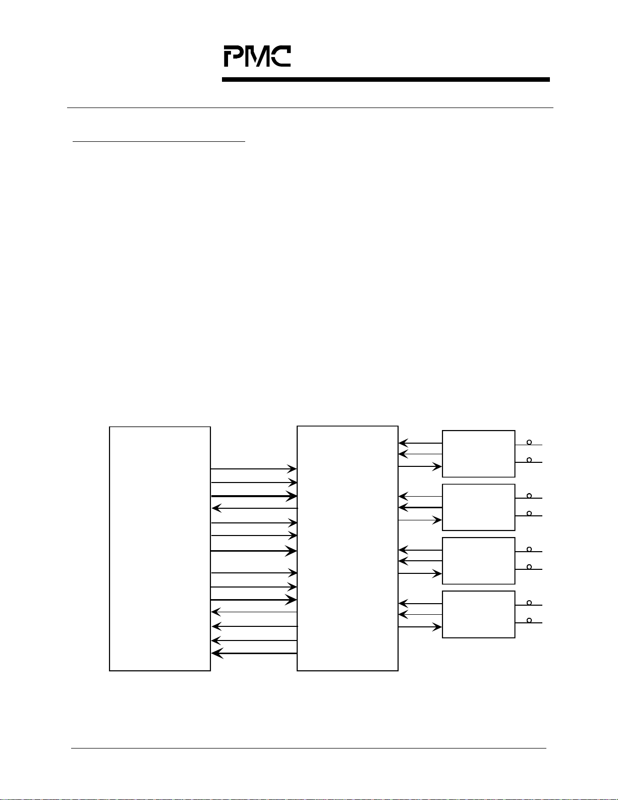
The PM5349 S/UNI-QUAD is intended for use in equipment implementing
Asynchronous Transfer Mode (ATM) User-Network Interfaces (UNI). The S/UNIQUAD may find application at either end of switch-to-switch links or switch-toterminal links. The S/UNI-QUAD performs the ma pping of ATM cells into the
SONET/SDH STS-3c (STM-1) synchronous payload envelope (SPE) and
processes applicable SONET/SDH section, line and path overhead.
In a typical STS-3c (STM-1) ATM application, the S/UNI-QUAD performs clock
and data recovery for the receive direction and clock synthesis for the transmit
direction of the line interface. On the system side, the S/UNI-QUAD interfaces
directly with ATM layer processors and switching or adaptation functions using a
Utopia Level 2 compliant synchronous FIFO style interface. The initial
configuration and ongoing control and monitoring of the S/UNI-QUAD are
normally provided via a generic microprocessor interface. This application is
shown in Figure 1.
Figure 1: Typical STS-3c (STM-1) ATM Switch Port Application
ATM Layer Device
TxClk
TxEnb
TxAddr<4:0>
TxClav
TxSOC
TxPrt
TxData<15:0>
RxClk
RxEnb
RxAddr<4:0>
RxCla v
RxSOC
RxPrt
RxData<15:0>
Uto
Interface
ia Level 2
PM5349
S/UNI-155-QUAD
TFCLK
TENB
4:0
TADR
TCA
TSOC
TPRTY
TDAT[15:0
RFCLK
RENB
4:0
RADR
RCA
RSOC
RPRTY
RDAT
15:0
RXD1+/SD1
TXD1+/-
RXD2+/SD2
TXD2+/-
RXD3+/SD3
TXD3+/-
RXD4+/SD4
TXD4+/-
Optical
Transceiver
Optical
Transceiver
Optical
Transceiver
Optical
Transceiver
Proprietary and Confidential to PMC-Sierra, Inc., and for its Customers’ Internal Use
7
PMC-Sierra, Inc.
S/UNI-QUAD
PM5349 S/UNI-QUAD
DATASHEET
PMC-971239 ISSUE 6 SATURN USER NETWORK INTERFACE (155-QUAD)
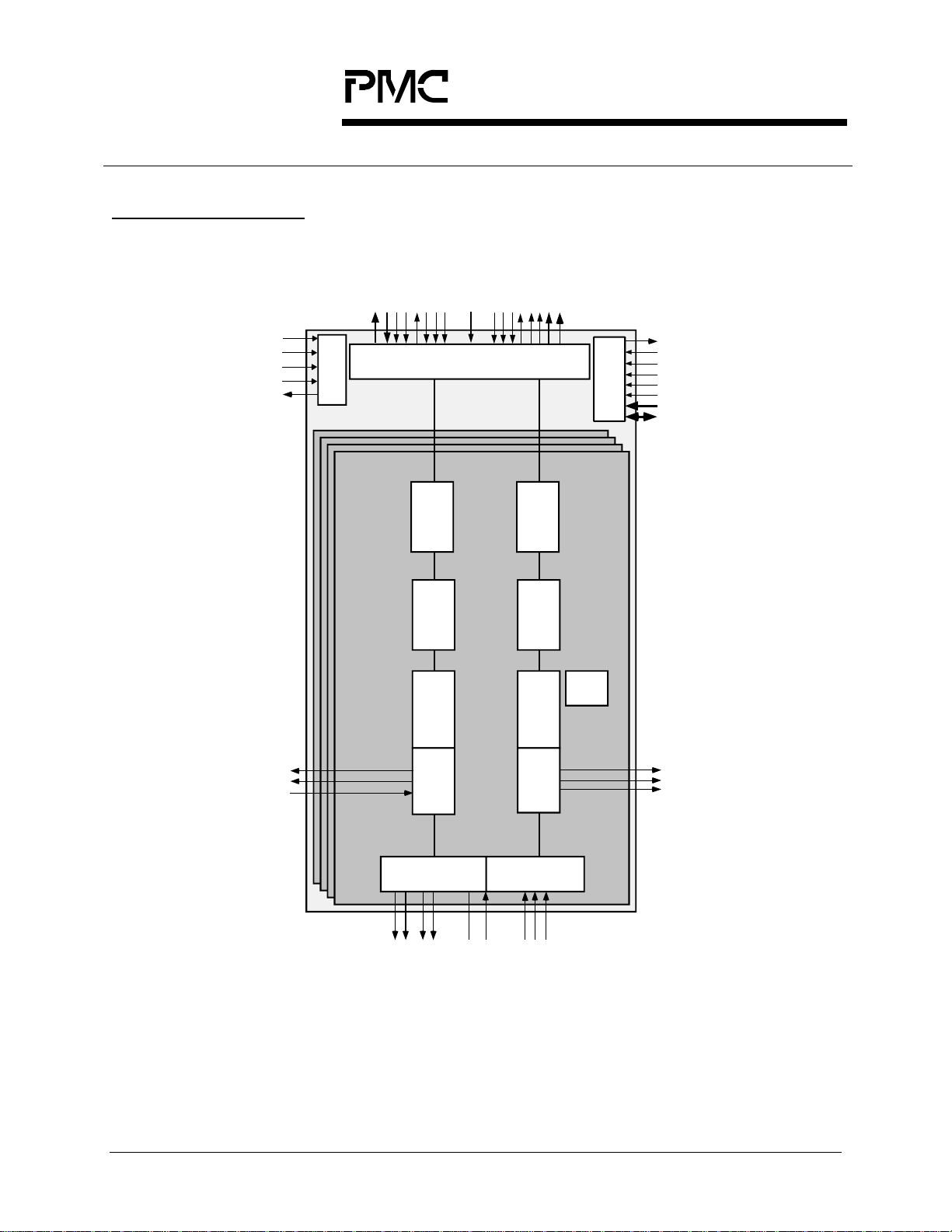
6 BLOCK DIAGRAM
TRSTB
TCK
TMS
TDI
TDO
:0]
TSOC
TDAT[15
TPRTY
TCA
DTCA[4:1]
st
JTAG T e
Access Port
Tx
Tx
Tx
OEN
PHY_
TFCLKTENB
TADR[4:0]
Utopia
System Interface
ATM Cell
Processor
Path O/H
Processor
Line O/H
Processor
RFCLK RADR[4:0]
RENB
RCA
]
RPRTY
RSOC
RDAT[15:0
DRCA[4:1]
INTB
or
ess
F
I/
proc
cro
Mi
Rx
ATM Cell
processor
Rx
Path O/H
Processor
Rx
APS,
Sync,
Rx
Line O/H
Processor
BERM
RSTB
RDB
WRB
CSB
ALE
A[10:0]
D[7:0]
TCLK
TFPO
TFPI
Tx
Processor
Section O/H
I/F
Tx Line
ATB0-3
TXD1-4 -
TXD1-4 +
TXC1-4 -
TXC1-4 +
REFCLK
Proprietary and Confidential to PMC-Sierra, Inc., and for its Customers’ Internal Use
Rx
Processor
Section O/H
I/F
Rx Line
-
+
SD1-4
RXD1-4
RXD1-4
RCLK1-4
RFPO1-4
RALRM1-4
8

PMC-Sierra, Inc.
S/UNI-QUAD
DATASHEET
PMC-971239 ISSUE 6 SATURN USER NETWORK INTERFACE (155-QUAD)
PM5349 S/UNI-QUAD
7 DESCRIPTION
The PM5349 S/UNI-QUAD SATURN User Network Interface is a monolithic
integrated circuit that implements four channel SONET/SDH processing and ATM
mapping functions at the STS-3c (STM-1) 155.52 Mbit/s rate.
The S/UNI-QUAD receives SONET/SDH streams using a bit serial interface,
recovers the clock and data and processes section, line, and path overhead. It
performs framing (A1, A2), de-scrambling, detects alarm conditions, and monitors
section, line, and path bit interleaved parity (B1, B2, B3), accumulating error
counts at each level for performance monitoring purposes. Line and path far end
block error indications (M1, G1) are also accumulated. The S/UNI-QUAD
interprets the received payload pointers (H1, H2) and extracts the synchronous
payload envelope which carries the received ATM cell payload.
The S/UNI-QUAD frames to the ATM payload using cell delineation. HCS error
correction is provided. Idle/unassigned cells may be dropped according to a
programmable filter. Cells are also dropped upon detection of an uncorrectable
header check sequence error. The ATM cell payloads are descrambled. The ATM
cells that are passed are written to a four cell FIFO buffer. The received cells are
read from the FIFO using a 16-bit wide Utopia level 2 compliant datapath
interface. Counts of received ATM cell headers that are errored and uncorrectable
and also those that are errored and correctable are accumulated independently
for performance monitoring purposes.
The S/UNI-QUAD transmits SONET/SDH streams using a bit serial interface and
formats section, line, and path overhead appropriately. It synthesizes the transmit
clock from a lower frequency reference and performs framing pattern insertion
(A1, A2), scrambling, alarm signal insertion, and creates section, line, and path
bit interleaved parity (B1, B2, B3) as required to allow performance monitoring at
the far end. Line and path far end block error indications (M1, G1) are also
inserted. The S/UNI-QUAD generates the payload pointer (H1, H2) and inserts
the synchronous payload envelope which carries the ATM cell payload. The
S/UNI-QUAD also supports the insertion of a large variety of errors into the
transmit stream, such as framing pattern errors, bit interleaved parity errors, and
illegal pointers, which are useful for system diagnostics and tester applications.
ATM cells are written to an internal four cell FIFO using a 16-bit wide Utopia Level
2 datapath interface. Idle/unassigned cells are automatically inserted when the
internal FIFO contains less than one cell. The S/UNI-QUAD provides generation
of the header check sequence and scrambles the payload of the ATM cells. Each
of these transmit ATM cell processing functions can be enabled or bypassed.
Proprietary and Confidential to PMC-Sierra, Inc., and for its Customers’ Internal Use
9

PMC-Sierra, Inc.
S/UNI-QUAD
DATASHEET
PMC-971239 ISSUE 6 SATURN USER NETWORK INTERFACE (155-QUAD)
PM5349 S/UNI-QUAD
No line rate clocks are required directly by the S/UNI-QUAD as it synthesizes the
transmit clock and recovers the receive clock using a 19.44 MHz reference clock.
The S/UNI-QUAD outputs a differential TTL (externally coverted to PECL) line
data (TXD+/-).
The S/UNI-QUAD is configured, controlled and monitored via a generic 8-bit
microprocessor bus interface. The S/UNI-QUAD also provides a standard 5
signal IEEE 1149.1 JTAG test port for boundary scan board test purposes.
The S/UNI-QUAD is implemented in low power, +3.3 Volt, CMOS technology. It
has TTL and pseudo-ECL (PECL) compatible inputs and TTL/CMOS compatible
outputs and is packaged in a 304 pin SBGA package.
Proprietary and Confidential to PMC-Sierra, Inc., and for its Customers’ Internal Use
10
PMC-Sierra, Inc.
S/UNI-QUAD
PM5349 S/UNI-QUAD
DATASHEET
PMC-971239 ISSUE 6 SATURN USER NETWORK INTERFACE (155-QUAD)
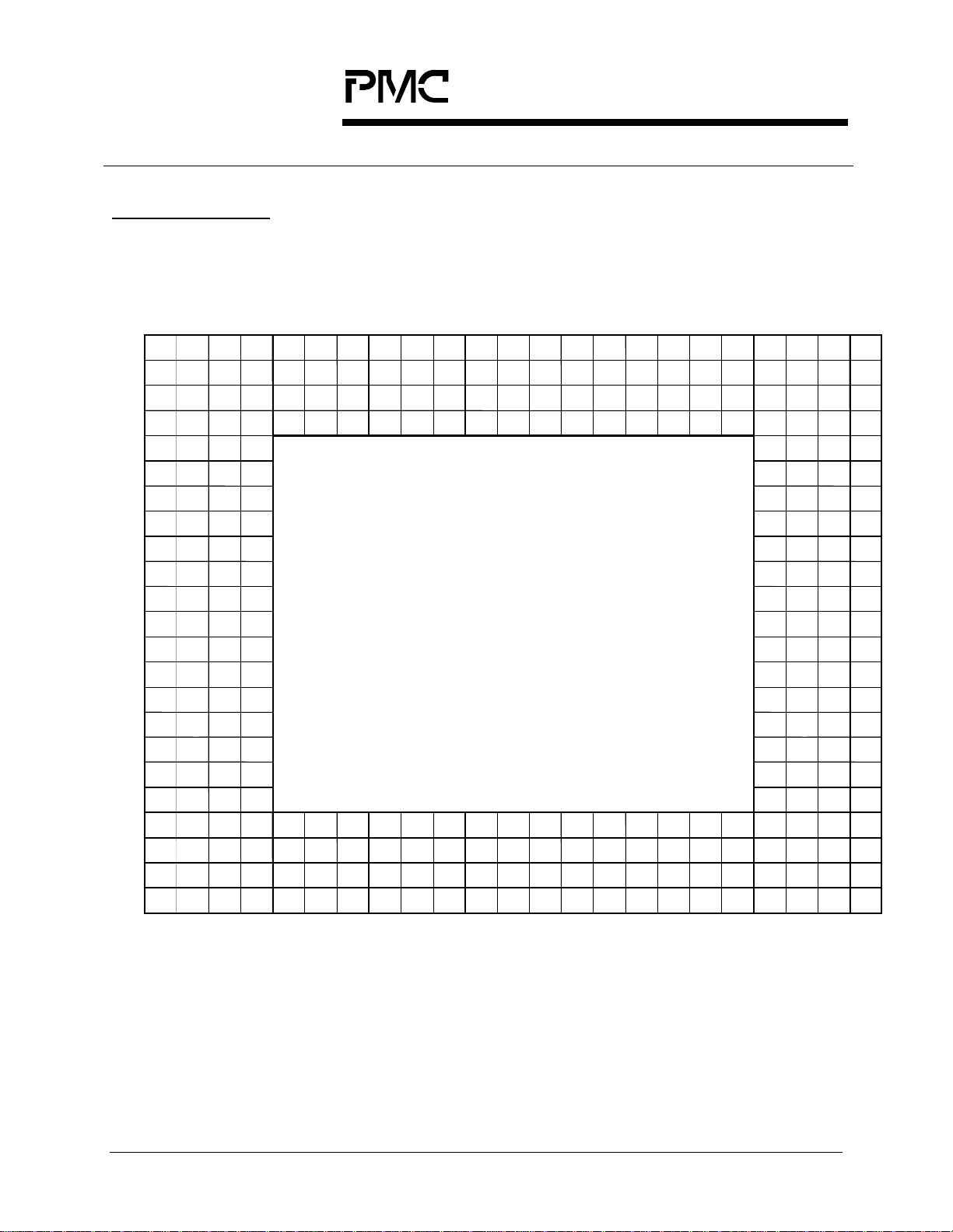
8 PIN DIAGRAM
The S/UNI-QUAD is available in a 304 pin SBGA package having a body size of
31 mm by 31 mm and a ball pitch of 1.27 mm.
23 22 21 20 19 18 17 16 15 14 13 12 11 10 9 8 7 6 5 4 3 2 1
VDD VSS TDAT[12] TDAT[15] PHY_OEN VSS D[2] VSS A[0] A[3] A[7] VSS A[10] WRB TDO VSS N/C VSS N/C RAVD1_B RAVS1_B VSS VDD
A
VSS VDD VSS TDAT[13] N/C N/C D[1] D[4] D[6] A[2] A[6] A[9] CSB RSTB TMS TCK N/C N/C QAVS_5 N/C VSS VDD VSS
B
TDAT[7] VSS VDD TDAT[10] TDAT[14] N/C BIAS D[3] D[5] A[1] A[5] A[8] ALE INTB TRSTB N/C N/C QAVD_5 N/C RAVD1_C VDD VSS TXD1P
C
TDAT[4] TDAT[6] TDAT[9] VDD TDAT[11] VDD N/C D[0] VDD D[7] A[4] VDD RDB TDI VDD N/C N/C VDD RAVS1_C VDD N/C TXD1N RX1-
D
TDAT[0] TDAT[3] TDAT[5] TDAT[8] N/C SD1 RX1+ TXD2P
E
VSS N/C TDAT[2] VDD VDD RAVS1_A TXD2N VSS
F
TADR[0] TADR[2] TADR[4] TDAT[1] RAVD1_A N/C RX2- RX2+
G
VSS TPRTY TADR[1] TADR[3] N/C RAVS2_A RAVD2_A VSS
H
TCA
J
DTCA[3] DTCA[4]
K
L
N/C N/C
M
VSS N/C
DRCA[3] DRCA[2] DRCA[1] RCA
N
RSOC
P
R
RADR[4] RADR[2] RADR[1] VDD VDD N/C N/C ATB3
VSS RADR[0] RPRTY RDAT[13] RAVS3_A N/C TXD3P VSS
T
RDAT[15] RDAT[14] RDAT[12] RDAT[9] N/C SD3 RAVD3_A TXD3N
U
VSS RDAT[11] RDAT[8] VDD VDD N/C RX3- VSS
V
RDAT[10] RDAT[7] RDAT[5] RDAT[2] RAVS4_A SD4 TXD4P RX3+
W
RDAT[6] RDAT[4] RDAT[1] VDD N/C VDD N/C N/C VDD RALRM3 RCLK2 VDD N/C N/C VDD N/C TFPI VDD RAVS4_C VDD RAVD4_A RX4- TXD4N
Y
RDAT[3] VSS VDD RDAT[0] N/C N/C N/C N/C N/C RALRM1 RCLK1 RFPO1 N/C N/C N/C N/C N/C QAVD_1 N/C RAVD4_C VDD VSS RX4+
AA
VSS VDD VSS N/C N/C N/C N/C N/C RALRM4 RCLK4 RFPO4 RFPO2 TFPO N/C N/C N/C N/C N/C QAVS_1 N/C VSS VDD VSS
AB
VDD VSS N/C N/C N/C VSS N/C VSS RALRM2 RCLK3 RFPO3 VSS TCLK N/C N/C VSS N/C VSS REFCLK RAVD4_B RAVS4_B VSS VDD
AC
TSOC
TENB
RENB RFCLK RADR[3] ATB2 ATB1 ATB0 RAVS3_C
VDD VDD SD2 N/C RAVD2_C
BIAS TFCLK RAVS2_C RAVS2_B N/C N/C
DTCA[1] DTCA[2]
DRCA[4]
VDD VDD TAVS1_B RAVD3_B VSS
RAVD2_B TAVD1_A TAVS1_A TAVD1_B
RAVD3_C RAVS3_B N/C N/C
BOTT OM VIEW
Proprietary and Confidential to PMC-Sierra, Inc., and for its Customers’ Internal Use
11

PMC-Sierra, Inc.
S/UNI-QUAD
DATASHEET
PMC-971239 ISSUE 6 SATURN USER NETWORK INTERFACE (155-QUAD)
PM5349 S/UNI-QUAD
9 PIN DESCRIPTION
9.1 Line Side Interface Signals
Pin Name Type Pin
Function
No.
REFCLK Input AC5 The reference clock input (REFCLK) must provide a
jitter-free 19.44 MHz reference clock. It is used as
the reference clock by both clock recovery and clock
synthesis circuits.
This pin is shared by all channels.
RXD1+
RXD1RXD2+
RXD2RXD3+
RXD3RXD4+
RXD4-
SD1
SD2
SD3
SD4
Differential
PECL
inputs
Single-
Ended
PECL
Input
E2
D1
G1
G2
W1
V2
AA1
Y2
E3
J3
U3
W3
The receive differential data inputs (RXD+, RXD-)
contain the NRZ bit serial receive stream. The
receive clock is recovered from the RXD+/- bit
stream. Please refer to the Operation section for a
discussion of PECL interfacing issues.
This pin is available independently for each channel.
The Signal Detect pin (SD) indicates the presence
of valid receive signal power from the Optical
Physical Medium Dependent Device. A PECL high
indicates the presence of valid data and a PECL low
indicates a loss of signal. It is mandatory that SD be
terminated into the equivalent network that RXD+/is terminated into.
This pin is available independently for each channel.
RCLK1
RCLK2
RCLK3
RCLK4
Output AA13
Y13
AC14
AB14
The receive byte clock (RCLK) provides a timing
reference for the S/UNI-QUAD receive outputs.
RCLK is a divide by eight of the recovered line rate
clock (19.44 MHz).
This pin is available independently for each channel.
Proprietary and Confidential to PMC-Sierra, Inc., and for its Customers’ Internal Use
12

PMC-Sierra, Inc.
S/UNI-QUAD
DATASHEET
PMC-971239 ISSUE 6 SATURN USER NETWORK INTERFACE (155-QUAD)
PM5349 S/UNI-QUAD
Pin Name Type Pin
No.
RFPO1
RFPO2
RFPO3
RFPO4
RALRM1
RALRM2
RALRM3
RALRM4
Output AA12
AB12
AC13
AB13
Output AA14
AC15
Y14
AB15
Function
The Receive Frame Pulse Output (RFPO), when the
framing alignment is found (the OOF register bit is
logic zero), is an 8 kHz signal derived from the
receive line clock. RFPO pulses high for one RCLK
cycle every 2430 RCLK cycles (STS-3c (STM-1)).
RFPO is updated on the rising edge of RCLK.
This pin is available independently for each channel.
The Receive Alarm (RALRM) output indicates the
state of the receive framing. RALRM is low if no
receive alarms are active. RALRM is high if line AIS
(LAIS), path AIS (PAIS), line RDI (LRDI), path RDI
(PRDI), enhanced path RDI (PERDI), loss of signal
(LOS), loss of frame (LOF), out of frame (OOF),
loss of pointer (LOP), loss of cell delineation (LCD),
signal fail BER (SFBER), signal degrade BER
(SDBER), or path signal label mismatch (PSLM) is
detected in the associated channel. Each alarm can
be individually enabled using bits in the S/UNIQUAD Channel Alarm Control registers #1 and #2.
TXD1+
TXD1TXD2+
TXD2TXD3+
TXD3TXD4+
TXD4-
Differential
TTL output
(externally
converted
to PECL)
C1
D2
E1
F2
T2
U1
W2
Y1
RALRM is updated on the rising edge of RCLK.
This pin is available independently for each channel.
The transmit differential data outputs (TXD+, TXD-)
contain the 155.52 Mbit/s transmit stream.
This pin is available independently for each channel.
Proprietary and Confidential to PMC-Sierra, Inc., and for its Customers’ Internal Use
13
PMC-Sierra, Inc.
S/UNI-QUAD
DATASHEET
PMC-971239 ISSUE 6 SATURN USER NETWORK INTERFACE (155-QUAD)
PM5349 S/UNI-QUAD
Pin Name Type Pin
Function
No.
TFPI Input Y7 The active high framing position (TFPI) signal is an
8 kHz timing marker for the transmitter. TFPI is used
to align the SONET/SDH transport frame generated
by the S/UNI-QUAD device to a system reference.
TFPI is internally used to align a master frame pulse
counter. When TFPI is not used, this counter is freerunning.
TFPI should be brought high for a single TCLK
period every 2430 (STS-3c (STM-1)) TCLK cycles,
or a multiple thereof. TFPI shall be tied low if such
synchronization is not required. TFPI cannot be
used as an input to a loop-timed channel. For TFPI
to operate correctly it is required that the
TCLK/TFPO output be configured to output the
CSU byte clock.
The TFPI_EN register bits allow to individually
configure each channel to use the global framing
pulse counter and TFPI for framing alignment.
TFPI is sampled on the rising edge of TCLK, but
only when the TTSEL register bit is set to logic zero.
When TTSEL is set to logic one, TFPI is unused.
This pin is shared by all channels.
TCLK Output AC11 The transmit byte clock (TCLK) output provides a
timing reference for the S/UNI-QUAD self-timed
channels. TCLK always provide a divide by eight of
the synthesized line rate clock and thus has a
nominal frequency of 19.44 MHz. TFPI is sampled
on the rising edge of TCLK. TCLK does not apply to
internally loop-timed channels, in which case the
channel’s RCLK provides transmit timing
information.
Proprietary and Confidential to PMC-Sierra, Inc., and for its Customers’ Internal Use
14

PMC-Sierra, Inc.
S/UNI-QUAD
DATASHEET
PMC-971239 ISSUE 6 SATURN USER NETWORK INTERFACE (155-QUAD)
PM5349 S/UNI-QUAD
Pin Name Type Pin
Function
No.
TFPO Output AB11 The Transmit Frame Pulse Output (TFPO) pulses
high for one TCLK cycle every 2430 TCLK cycles
and provides an 8 KHz timing reference. TFPO can
be assigned to any of the four channels using
TFPO_CH[1:0] configuration register bits, with the
restriction that the selected channel must be selftimed (not in loop-timed or line-loopback modes).
TFPO is updated on the rising edge of TCLK.
9.2 UTOPIA Level 2 System Interface
Pin Name Type Pin
Function
No.
TDAT[15]
TDAT[14]
TDAT[13]
TDAT[12]
TDAT[11]
TDAT[10]
TDAT[9]
TDAT[8]
TDAT[7]
TDAT[6]
TDAT[5]
TDAT[4]
TDAT[3]
TDAT[2]
TDAT[1]
TDAT[0]
Input A20
C19
B20
A21
D19
C20
D21
E20
C23
D22
E21
D23
E22
F21
G20
E23
UTOPIA Transmit Cell Data Bus (TDAT[15:0]).
This data bus carries the ATM cell octets that are
written to the selected transmit FIFO. TDAT[15:0] is
considered valid only when TENB is simultaneously
asserted and the S/UNI-QUAD is selected via
TADR[4:0].
TDAT[15:0] is sampled on the rising edge of TFCLK.
Proprietary and Confidential to PMC-Sierra, Inc., and for its Customers’ Internal Use
15

PMC-Sierra, Inc.
S/UNI-QUAD
DATASHEET
PMC-971239 ISSUE 6 SATURN USER NETWORK INTERFACE (155-QUAD)
PM5349 S/UNI-QUAD
Pin Name Type Pin
Function
No.
TPRTY Input H22 UTOPIA Transmit bus parity (TPRTY) signal.
The transmit parity (TPRTY) signal indicates the
parity of the TDAT[15:0] bus. A parity error is
indicated by a status bit and a maskable interrupt.
Cells with parity errors are inserted in the transmit
stream, so the TPRTY input may be unused. Odd or
even parity selection is made independently for
each channel using the RXPTYP register bit.
TPRTY is considered valid only when TENB is
simultaneously asserted and the S/UNI-QUAD is
selected via TADR[4:0].
TPRTY is sampled on the rising edge of TFCLK.
TSOC Input J21 UTOPIA Transmit Start of Cell (TSOC) signal.
The transmit start of cell (TSOC) signal marks the
start of cell on the TDAT bus. When TSOC is high,
the first word of the cell structure is present on the
TDAT bus. It is not necessary for TSOC to be
present for each cell. An interrupt may be
generated if TSOC is high during any word other
than the first word of the cell structure.
TSOC is considered valid only when TENB is
simultaneously asserted and the S/UNI-QUAD is
selected via TADR[4:0].
TSOC is sampled on the rising edge of TFCLK.
Proprietary and Confidential to PMC-Sierra, Inc., and for its Customers’ Internal Use
16

PMC-Sierra, Inc.
S/UNI-QUAD
DATASHEET
PMC-971239 ISSUE 6 SATURN USER NETWORK INTERFACE (155-QUAD)
PM5349 S/UNI-QUAD
Pin Name Type Pin
Function
No.
TENB Input J22 UTOPIA Transmit Multi-PHY Write Enable (TENB)
signal.
The TENB signal is an active low input which is
used along with the TADR[4:0] inputs to initiate
writes to the transmit FIFO’s.
TENB works as follows. When sampled high, no
write is performed, but the TADR[4:0] address is
latched to identify the transmit FIFO to be
accessed. When TENB is sampled low, the word on
the TDAT bus is written into the transmit FIFO that is
selected by the TADR[4:0] address bus. A complete
53 octet cell must be written to the transmit FIFO
before it is inserted into the transmit stream. Idle
cells are inserted when a complete cell is not
available. While TENB is deasserted, TADR[4:0] can
be used for polling TCA.
TENB is sampled on the rising edge of TFCLK.
TADR[4]
TADR[3]
TADR[2]
TADR[1]
TADR[0]
Input G21
H20
G22
H21
G23
UTOPIA Transmit Write Address (TADR[4:0])
signals.
The TADR[4:0] bus is used to select the FIFO (and
hence port) that is written to using the TENB signal
and the FIFO's whose cell available signal is visible
on the TC A poll ing output.
Note that address 0x1F is the null-PHY address and
cannot be assigned to any port on the S/UNI-QUAD.
TADR[4:0] is sampled on the rising edge of TFCLK.
Proprietary and Confidential to PMC-Sierra, Inc., and for its Customers’ Internal Use
17
PMC-Sierra, Inc.
S/UNI-QUAD
DATASHEET
PMC-971239 ISSUE 6 SATURN USER NETWORK INTERFACE (155-QUAD)
PM5349 S/UNI-QUAD
Pin Name Type Pin
Function
No.
TCA Output J23 UTOPIA Transmit multi-PHY Cell Available (TCA)
The TCA signal indicates when a cell is available in
the transmit FIFO for the port polled by TADR[4:0]
when TENB is asserted. When high, TCA indicates
that the corresponding transmit FIFO is not full and
a complete cell may be written. Wh en TCA goes
low, it can be configured to indicate either that the
corresponding transmit FIFO is near full or that the
corresponding transmit FIFO is full. TCA will
transition low on the rising edge of TFCLK after the
Payload word 19 (TCALEVEL0=0) or 23
(TCALEVEL0=1) is sampled if the PHY being polled
is the same as the PHY in use. To reduce FIFO
latency, the FIFO depth at which TCA indicates "full"
can be set to one, two, three or four cells. Note that
regardless of what fill level TCA is set to indicate
"full" at, the transmit cell processor can store 4
complete cells.
TCA is tri-stated when either the null-PHY address
(0x1F) or an address not matching the address
space set by PHY_ADR[2:0] is latched from the
TADR[4:0] inputs when TENB is high.
TCA is updated on the rising edge of TFCLK.
TFCLK Input K20 UTOPIA Transmit FIFO Write Clock (TFCLK).
This signal is used to write ATM cells to the four cell
transmit FIFOs.
TFCLK cycles at a 50 MHz or lower instantaneous
rate.
Proprietary and Confidential to PMC-Sierra, Inc., and for its Customers’ Internal Use
18

PMC-Sierra, Inc.
S/UNI-QUAD
DATASHEET
PMC-971239 ISSUE 6 SATURN USER NETWORK INTERFACE (155-QUAD)
PM5349 S/UNI-QUAD
Pin Name Type Pin
No.
DTCA[4]
DTCA[3]
DTCA[2]
DTCA[1]
Output K22
K23
L20
L21
Function
UTOPIA Direct Transmit Cell Available (DTCA[4:1]).
These output signals provide di r ect status indi cation
of when a cell is available in the transmit FIFO for
the corresponding port. When high, DTCA indicates
that the corresponding transmit FIFO is not full and
a complete cell may be written. Wh en DTCA goes
low, it can be configured to indicate either that the
corresponding transmit FIFO is near full or that the
corresponding transmit FIFO is full. DTCA will
transition low on the rising edge of TFCLK after the
Payload word 19 (TCALEVEL0=0) or 23
(TCALEVEL0=1) is sampled if the PHY being polled
is the same as the PHY in use. To reduce FIFO
latency, the FIFO depth at which DTCA indicates
"full" can be set to one, two, three or four cells. Note
that regardless of what fill level DTCA is set to
indicate "full" at, the transmit cell processor can
store 4 complete cells
RDAT[15]
RDAT[14]
RDAT[13]
RDAT[12]
RDAT[11]
RDAT[10]
RDAT[9]
RDAT[8]
RDAT[7]
RDAT[6]
RDAT[5]
RDAT[4]
RDAT[3]
RDAT[2]
RDAT[1]
RDAT[0]
Output U23
U22
T20
U21
V22
W23
U20
V21
W22
Y23
W21
Y22
AA23
W20
Y21
AA20
DTCA[4:1] are updated on the rising edge of
TFCLK.
UTOPIA Receive Cell Data Bus (RDAT[15:0]).
This data bus carries the ATM cells that are read
from the receive FIFO selected by RADR[4:0].
RDAT[15:0] is tri-stated when RENB is high.
RDAT[15:0] is tristated when RENB is high.
RDAT[15:0] is also tristated when either the nullPHY address (0x1F) or an address not matching
the address space is latched from the RADR[4:0]
inputs when RENB is high.
RDAT[15:0] is updated on the rising edge of
RFCLK.
Proprietary and Confidential to PMC-Sierra, Inc., and for its Customers’ Internal Use
19

PMC-Sierra, Inc.
S/UNI-QUAD
DATASHEET
PMC-971239 ISSUE 6 SATURN USER NETWORK INTERFACE (155-QUAD)
PM5349 S/UNI-QUAD
Pin Name Type Pin
Function
No.
RPRTY Output T21 UTOPIA Receive Parity (RPRTY).
The receive parity (RPRTY) signal indicates the
parity of the RDAT bus. RPRTY reflects the parity of
RDAT[15:0]. Odd or even parity selection is made
independently for every channel by using the
RXPTYP register bit (in ATM cell processors, the
four RXCP shall be programmed with the same
parity setting).RPRTY is tristated when RENB is
high. RPRTY is also tristated when either the nullPHY address (0x1F) or an address not matching
the address space is latched from the RADR[4:0]
inputs when RENB is high.
RPRTY is updated on the rising edge of RFCLK.
RSOC Output P23 UTOPIA Receive Start of Cell (RSOC).
RSOC marks the start of cell on the RDAT bus.
RSOC is tristated when RENB is deasserted.
RSOC is also tristated when either the null-PHY
address (0x1F) or an address not matching the
address space is latched from the RADR[4:0] inputs
when RENB is high.
RSOC is sampled on the rising edge of RFCLK.
RENB Input P22 UTOPIA Receive multi-PHY Read Enable (RENB).
The RENB signal is used to initiate reads from the
receive FIFO’s. RENB works as follows. When
RENB is sampled high, no read is performed and
RDAT[15:0], RPRTY and RSOC are tristated, and
the address on RADR[4:0] is latched to select the
device or port for the next FIFO access. When
RENB is sampled low, the word on the RDAT bus is
read from the selected receive FIFO.
RENB must operate in conjunction with RFCLK to
access the FIFO’s at a high enough rate to prevent
FIFO overflows. The system may de-assert RENB
at anytime it is unable to accept another byte.
RENB is sampled on the rising edge of RFCLK.
Proprietary and Confidential to PMC-Sierra, Inc., and for its Customers’ Internal Use
20

PMC-Sierra, Inc.
S/UNI-QUAD
DATASHEET
PMC-971239 ISSUE 6 SATURN USER NETWORK INTERFACE (155-QUAD)
PM5349 S/UNI-QUAD
Pin Name Type Pin
Function
No.
RADR[4]
RADR[3]
RADR[2]
RADR[1]
RADR[0]
Input
R23
P20
R22
R21
T22
UTOPIA Receive Read Address (RADR[4:0]).
The RADR[4:] signal is used to select the FIFO (and
hence port) that is read from using the RENB signal
and the FIFO whose cell available signal is visible
on the RCA output.
Note that address 0x1F is the null-PHY address and
will not be identified to any port on the
S/UNI-QUAD.
RADR[4:0] is sampled on the rising edge of RFCLK.
RCA Output N20 UTOPIA Receive multi-PHY Cell Available (RCA).
RCA indicates when a cell is available in the receive
FIFO for the port selected by RADR[4:0]. RCA can
be configured to be de-asser ted when either zero or
four bytes remain in the selected/addressed FIFO.
RCA will thus transition low on the rising edge of
RFCLK after Payload word 24 (RCALEVEL0=1) or
19 (RCALEVEL0=0) is output if the PHY being
polled is the same as the PHY in use.
RCA is tristated when either the null-PHY address
(0x1F) or an address not matching the address
space is latched from the RADR[4:0] inputs when
RENB is high.
RCA is updated on the rising edge of RFCLK.
RFCLK Input P21 UTOPIA Receive FIFO Read Clock (RFCLK).
RFCLK is used to read ATM cells from the receive
FIFO’s. RFCLK must cycle at a 50 MHz or lower
instantaneous rate, but at a high enough rate to
avoid FIFO overflows.
Proprietary and Confidential to PMC-Sierra, Inc., and for its Customers’ Internal Use
21
PMC-Sierra, Inc.
S/UNI-QUAD
DATASHEET
PMC-971239 ISSUE 6 SATURN USER NETWORK INTERFACE (155-QUAD)
PM5349 S/UNI-QUAD
Pin Name Type Pin
Function
No.
DRCA[4]
DRCA[3]
DRCA[2]
DRCA[1]
Output M21
N23
N22
N21
UTOPIA Direct Receive Cell Available (DRCA[4:1]).
These output signals provides di r ect status
indication of when a cell is available in the receive
FIFO for the corresponding port. DRCA can be
configured to be de-asserted when either zero or
four bytes remain in the selected/addressed FIFO.
DRCA will thus transition low on the rising edge of
RFCLK after Payload word 24 (RCALEVEL0=1) or
19 (RCALEVEL0=0) is output if the PHY being
polled is the same as the PHY in use.
DRCA[x] is updated on the rising edge of RFCLK.
PHY_OEN Input A19 The PHY Output Enable (PHY_OEN) signal controls
the operation of the system interface. When set to
logic zero, all System Interface outputs are held
tristate. When PHY_OEN is set to logic one, the
interface is enabled. PHY_OEN can be overwritten
by the PHY_EN Master System Interface
Configuration register bit. PHY_OEN and PHY_EN
are OR’ed together to enable the interface.
When the S/UNI-QUAD is the only PHY layer device
on the bus, PHY_O EN can safely be tied to logic
one. When the S/UNI-QUAD shares the bus with
other devices, then PHY_OEN must be tied to logic
zero, and the PHY_EN register bit used to enable
the bus once its PHY_ADR[2:0] is programmed in
order to avoid conflicts.
Proprietary and Confidential to PMC-Sierra, Inc., and for its Customers’ Internal Use
22

PMC-Sierra, Inc.
S/UNI-QUAD
DATASHEET
PMC-971239 ISSUE 6 SATURN USER NETWORK INTERFACE (155-QUAD)
PM5349 S/UNI-QUAD
9.3 Microprocessor Interface Signals
Pin Name Type Pin
Function
No.
CSB Input B11 The active-low chip select (CSB) signal is low
during S/UNI-QUAD register accesses.
Note that when not being used, CSB must be tied
high. If CSB is not required (i.e., registers accesses
are controlled using the RDB and WRB signals
only), CSB must be connected to an inverted
version of the RSTB input.
RDB Input D11 The active-low read enable (RDB) signal is low
during S/UNI-QUAD register read accesses. The
S/UNI-QUAD drives the D[7:0] bus with the contents
of the addressed register while RDB and CSB are
low.
WRB Input A10 The active-low write strobe (WRB) signal is low
during a S/UNI-QUAD register write accesses. The
D[7:0] bus contents are clocked into the addressed
register on the rising WRB edge while CSB is low.
D[0]
D[1]
D[2]
D[3]
D[4]
D[5]
D[6]
D[7]
I/O D16
B17
A17
C16
B16
C15
B15
D14
The bi-directional data bus D[7:0] is used during
S/UNI-QUAD register read and write accesses.
A[0]
A[1]
A[2]
A[3]
A[4]
A[5]
A[6]
A[7]
A[8]
A[9]
Proprietary and Confidential to PMC-Sierra, Inc., and for its Customers’ Internal Use
Input A15
C14
B14
A14
D13
C13
B13
A13
C12
B12
The address bus A[9:0] selects specific registers
during S/UNI-QUAD register accesses.
Except for S/UNI-QUAD global registers, the A[9:8]
bits allow to select which channel is being
accessed. The A[7:0] bits allow to select which
register is being access within a given channel
address space.
23

PMC-Sierra, Inc.
S/UNI-QUAD
DATASHEET
PMC-971239 ISSUE 6 SATURN USER NETWORK INTERFACE (155-QUAD)
PM5349 S/UNI-QUAD
Pin Name Type Pin
Function
No.
A[10]/TRS Input A11 The test register select (TRS) signal selects
between normal and test mode register accesses.
TRS is high during test mode register accesses,
and is low during normal mode register accesses.
RSTB Input
pull-up
B10 The active-low reset (RSTB) signal provides an
asynchronous S/UNI-QUAD reset. RSTB is a
Schmitt triggered input with an integral pull-up
resistor.
ALE Input
pull-up
C11 The address latch enable (ALE) is active-high and
latches the address bus A[7:0] when low. When
ALE is high, the internal address latches are
transparent. It allows the S/UNI-QUAD to interface
to a multiplexed address/data bus. ALE has an
integral pull-up resistor.
INTB Output
Open-
drain
C10 The active-low interrupt (INTB) signal goes low
when a S/UNI-QUAD interrupt source is active and
that source is unmasked. The S/UNI-QUAD may be
enabled to report many alarms or events via
interrupts.
Examples of interrupt sources are loss of signal
(LOS), loss of frame (LOF), line AIS, line remote
defect indication (LRDI) detect, loss of pointer
(LOP), path AIS, path remote defect indication
detect and others.
INTB is tristated when the interrupt is acknowledged
via an appropriate register access. INTB is an open
drain output.
Proprietary and Confidential to PMC-Sierra, Inc., and for its Customers’ Internal Use
24

PMC-Sierra, Inc.
S/UNI-QUAD
DATASHEET
PMC-971239 ISSUE 6 SATURN USER NETWORK INTERFACE (155-QUAD)
PM5349 S/UNI-QUAD
9.4 JTAG Test Access Port (TAP) Signals
Pin Name Type Pin
Function
No.
TCK Input B8 The test clock (TCK) signal provides timing for test
operations that are carried out using the IEEE
P1149.1 test access port.
TMS Input
pull-up
B9 The test mode select (TMS) signal controls the test
operations that are carried out using the IEEE
P1149.1 test access port. TMS is sampled on the
rising edge of TCK. TMS has an integral pull-up
resistor.
TDI Input
pull-up
D10 The test data input (TDI) signal carries test data into
the S/UNI-QUAD via the IEEE P1149.1 test access
port. TDI is sampled on the rising edge of TCK. TDI
has an integral pull-up resistor.
TDO Tristate A9 The test data output (TDO) signal carries test data
out of the S/UNI-QUAD via the IEEE P1149.1 test
access port. TDO is updated on the falling edge of
TCK. TDO is a tristate output which is inactive
except when scanning of data is in progress.
TRSTB Input
pull-up
C9 The active-low test reset (TRSTB) signal provides
an asynchronous S/UNI-QUAD test access port
reset via the IEEE P1149.1 test access port.
TRSTB is a Schmitt triggered input with an integral
pull-up resistor.
Note that when not being used, TRSTB must be
connected to the RSTB input.
Proprietary and Confidential to PMC-Sierra, Inc., and for its Customers’ Internal Use
25

PMC-Sierra, Inc.
S/UNI-QUAD
DATASHEET
PMC-971239 ISSUE 6 SATURN USER NETWORK INTERFACE (155-QUAD)
PM5349 S/UNI-QUAD
9.5 Analog Signals
Pin Name Type Pin
ATB0
Analog I/O P2
ATB1
ATB2
ATB3
9.6 Power and Ground
Pin Name Type Pin
BIAS Bias
Voltage
No.
P3
P4
R1
No.
K21
C17
Function
The Analog Test Bus (ATB). These pins are used for
manufacturing testing only and should be connected
ground.
Function
I/O Bias (BIAS). When tied to +5V via a 1 KΩ
resistor, the BIAS input is used to bias the wells in
the input and I/O pads so that the pads can tolerate
5V on their inputs without forward biasing internal
ESD protection devices. When BIAS is tied to
+3.3V, the inputs and bi-direction al inputs will only
tolerate 3.3V level inputs.
Proprietary and Confidential to PMC-Sierra, Inc., and for its Customers’ Internal Use
26

PMC-Sierra, Inc.
S/UNI-QUAD
DATASHEET
PMC-971239 ISSUE 6 SATURN USER NETWORK INTERFACE (155-QUAD)
PM5349 S/UNI-QUAD
Pin Name Type Pin
No.
VDD Power A1
A23
B2
B22
C3
C21
D4
D6
D9
D12
D15
D18
D20
F4
F20
J4
J20
M4
M20
R4
R20
V4
V20
Y4
Y6
Y9
Y12
Y15
Y18
Y20
AA3
AA21
AB2
AB22
AC1
AC23
Function
The digital power (VDD) pins should be connected
to a well-decoupled +3.3 V DC supply.
Proprietary and Confidential to PMC-Sierra, Inc., and for its Customers’ Internal Use
27

PMC-Sierra, Inc.
S/UNI-QUAD
DATASHEET
PMC-971239 ISSUE 6 SATURN USER NETWORK INTERFACE (155-QUAD)
PM5349 S/UNI-QUAD
Pin Name Type Pin
No.
VSS Ground A2
A6
A8
A12
A16
A18
A22
B1
B3
B21
B23
C2
C22
F1
F23
H1
H23
M1
M23
T1
T23
V1
V23
AA2
AA22
AB1
AB3
AB21
AB23
AC2
AC6
AC8
AC12
AC16
AC18
AC22
Function
The digital ground (VSS) pins should be connected
to ground.
Proprietary and Confidential to PMC-Sierra, Inc., and for its Customers’ Internal Use
28

PMC-Sierra, Inc.
S/UNI-QUAD
DATASHEET
PMC-971239 ISSUE 6 SATURN USER NETWORK INTERFACE (155-QUAD)
PM5349 S/UNI-QUAD
Pin Name Type Pin
No.
QAVD Analog
Power
QAVS Analog
Ground
AA6
C6
AB5
B5
AVD Analog
PowerG4A4
C4
H2
L4
J1
U2
M2
N4
Y3
AC4
AA4
L3
L1
Function
QAVD1
QAVD2
The quiet analog power (QAVD) pins for the analog
core. QAVD should be connected to analog +3.3V.
QAVS1
QAVS2
The quiet analog ground (QAVS) pins for the analog
core. QAVS should be connected to analog GND.
RAVD1_A - Channel #1 PECL Input Buffer
RAVD1_B - Channel #1 CRU
RAVD1_C - Channel #1 CRU
RAVD2_A - Channel #2 PECL Input Buffer
RAVD2_B - Channel #2 CRU
RAVD2_C - Channel #2 CRU
RAVD3_A - Channel #3 PECL Input Buffer
RAVD3_B - Channel #3 CRU
RAVD3_C - Channel #3 CRU
RAVD4_A - Channel #4 PECL Input Buffer
RAVD4_B - Channel #4 CRU
RAVD4_C - Channel #4 CRU
TAVD1_A - CSU
TAVD1_B - CSU
The analog power (AVD) pins for the analog core.
AVD should be connected to analog +3.3V.
Proprietary and Confidential to PMC-Sierra, Inc., and for its Customers’ Internal Use
29

PMC-Sierra, Inc.
S/UNI-QUAD
DATASHEET
PMC-971239 ISSUE 6 SATURN USER NETWORK INTERFACE (155-QUAD)
PM5349 S/UNI-QUAD
Pin Name Type Pin
No.
AVS Analog
GroundF3A3
D5
H3
K3
K4
T4
N3
P1
W4
AC3
Y5
L2
M3
Notes on Pin Description:
Function
RAVS1_A - Channel #1 PECL Input Buffer
RAVS1_B - Channel #1 CRU
RAVS1_C - Channel #1 CRU
RAVS2_A - Channel #2 PECL Input Buffer
RAVS2_B - Channel #2 CRU
RAVS2_C - Channel #2 CRU
RAVS3_A - Channel #3 PECL Input Buffer
RAVS3_B - Channel #3 CRU
RAVS3_C - Channel #3 CRU
RAVS4_A - Channel #4 PECL Input Buffer
RAVS4_B - Channel #4 CRU
RAVS4_C - Channel #4 CRU
TAVS1_A - CSU
TAVS1_B - CSU
The analog ground (AVS) pins for the analog core.
AVS should be connected to analog GND.
1. All S/UNI-QUAD inputs and bi-directionals present minimum capacitive
loading and operate at TTL logic levels except: the SD, RXD+ and RXDinputs which operate at pseudo-ECL (PECL) logic levels
2. The RDAT[7:0], RPRTY, RSOC, DRCA4-1, RCA, DTCA4-1, TCA, TCLK and
RCLK1-4 outputs have a 4 mA DC drive capability. The TDO output has a 1
mA drive capability. All the other outputs have a 2 mA DC drive capability.
The TXD+ and TXD- outputs are met to be terminated in a passive network
and interface at PECL levels.
3. It is mandatory that every ground pin (VSS) be connected to the printed
circuit board ground plane to ensure a reliable device operation.
4. It is mandatory that every power pin (VDD) be connected to the printed circuit
board power plane to ensure a reliable device operation.
5. All analog power and ground can be sensitive to noise. They must be
isolated from the digital power and ground. Care must be taken to decouple
these pins from each other and all other analog power and ground pins.
Proprietary and Confidential to PMC-Sierra, Inc., and for its Customers’ Internal Use
30

PMC-Sierra, Inc.
S/UNI-QUAD
DATASHEET
PMC-971239 ISSUE 6 SATURN USER NETWORK INTERFACE (155-QUAD)
PM5349 S/UNI-QUAD
Power supply filtering recommendations are provided in the
OPERATION section of this document.
6. Due to ESD protection structures in the pads it is necessary to exercise
caution when powering a device up or down. ESD protection devices behave
as diodes between power supply pins and from I/O pins to power suppl y pins.
Under extreme conditions it is possible to blow these ESD protection devices
or trigger latch up. Please adhere to the recommended power supply
sequencing as described in the OPERATION section of this document.
7. If it is intended to substitute a S/UNI-QUAD in a S/UNI-TETRA socket,
special attention must be given to the NC pins. The requirement is that no
S/UNI-QUAD input pin is left floating when used in a S/UNI-QUAD socket.
Please refer to the relevant PMC-Sierra, Inc. application note.
8. Some device pins can be made 5V tolerant by connecting the BIAS pins to a
5V power supply, while some other pins are 3.3V only. In summary, the
system interface is 3.3V only while the microprocessor interface, SONET and
line interfaces can be 5V tolerant.
3.3V only I/O’s:
RDAT[15:0], RSOC, RPRTY, RENB,
TDAT[15:0], TSOC, TPRTY, TENB,
RCA, DRCA4-1, TCA, DTCA4-1,
RADR[5:0], TADR[5:0], PHY_OEN
5V tolerant I/O’s:
REFCLK, RXD
RCLK4-1, RFPO4-1, RALRM4-1,
TCLK, TFPO, TFPI,
D[7:0], A[10:0], WRB, RDB, CSB, RSTB, INTB, ALE,
TRSTB, TCK, TMS, TDI, TDO,
Proprietary and Confidential to PMC-Sierra, Inc., and for its Customers’ Internal Use
31

PMC-Sierra, Inc.
S/UNI-QUAD
DATASHEET
PMC-971239 ISSUE 6 SATURN USER NETWORK INTERFACE (155-QUAD)
PM5349 S/UNI-QUAD
10 FUNCTIONAL DESCRIPTION
10.1 Receive Line Interface (CRSI)
The Receive Line Interface allows to directly interface the S/UNI-QUAD with
optical modules (ODLs) or other medium interfaces. This block performs clock
and data recovery and performs serial to parallel conversion on the incoming
155.52 Mbit/s data stream.
10.1.1 Clock Recovery
The clock recovery unit recovers the clock from the incoming bit serial data
stream. The clock recovery unit is fully compliant with SONET and SDH jitter
tolerance requirements. The clock recovery unit utilizes a low frequency
reference clock to train and monitor its clock recovery PLL. Under loss of signal
conditions, the clock recovery unit continues to output a line rate clock that is
locked to this reference for keep alive purposes. The clock recovery unit utilizes a
reference clocks at 19.44 MHz. The clock recovery unit provides status bits that
indicate whether it is locked to data or the reference. The clock recovery unit also
supports diagnostic loopback and a loss of signal input that squelches normal
input data.
Initially, the PLL locks to the reference clock, REFCLK. When the frequency of
the recovered clock is within 488 ppm of the reference clock, the PLL attempts to
lock to the data. Once in data lock, the PLL reverts to the reference clock if no
data transitions occur in 80 bit periods or if the recovered clock drifts beyond 488
ppm of the reference clock.
When the transmit clock is derived from the recovered clock (loop timing), the
accuracy of the transmit clock is directly related to the REFCLK reference
accuracy in the case of a loss of signal condition. To meet the Bellcore GR-253CORE SONET Network Element free-run accuracy specification, the refe rence
must be within +/-20ppm. When not loop timed, the REFCLK accuracy may be
relaxed to +/-50ppm.
The loop filter transfer function is optimized to enable the PLL to track the jitter,
yet tolerate the minimum transition density expected in a received SONET/SDH
data signal. The total loop dynamics of the clock recovery PLL yield a jitter
tolerance that exceeds the minimum tolerance proposed for SONET equipment
by GR-253-CORE (Figure 3).
Proprietary and Confidential to PMC-Sierra, Inc., and for its Customers’ Internal Use
32

PMC-Sierra, Inc.
S/UNI-QUAD
DATASHEET
PMC-971239 ISSUE 6 SATURN USER NETWORK INTERFACE (155-QUAD)
PM5349 S/UNI-QUAD
Figure 2: Typical STS-3c (STM-1) Jitter Tolerance
100
10
GR-253-CORE
1
0.1
100 1000 10000 100000 1000000 10000000
Jitter Freq. (Hz)
Note that for frequencies below 300 Hz, the jitter tolerance is greater than 15
UIpp; 15 UIpp is the maximum jitter tolerance of the test equipment. Also note
that the dip in the tolerance curve between 300 Hz and 10 kHz is due to the
S/UNI-QUAD's internal clock difference detector: if the recovered clock drifts
beyond 488 ppm of the reference, the PLL locks to the reference clock.
10.1.2 Serial to Parallel Converter
The Serial to Parallel Converter (SIPO) converts the received bit serial stream to
a byte serial stream. The SIPO searches for the SONET/SDH framing pattern
(A1, A2) in the receive stream, and performs serial to parallel conversion on octet
boundaries.
10.2 Receive Section Overhead Processor (RSOP)
The Receive Section Overhead Processor (RSOP) provides frame
synchronization, de-scrambling, section level alarm and performance monitoring.
10.2.1 Framer
The Framer Block determines the in-frame/out-of-frame status of the receive
stream.
Proprietary and Confidential to PMC-Sierra, Inc., and for its Customers’ Internal Use
33

PMC-Sierra, Inc.
S/UNI-QUAD
DATASHEET
PMC-971239 ISSUE 6 SATURN USER NETWORK INTERFACE (155-QUAD)
PM5349 S/UNI-QUAD
While in-frame, the framing bytes (A1, A2) in each frame are compared against
the expected pattern. Out-of-frame is declared when four consecutive frames
containing one or more framing pattern errors have been received.
While out-of-frame, the SIPO block monitors the receive stream for an occurrence
of the framing pattern. When a framing pattern is recognized, the Framer block
verifies that an error free framing pattern is present in the next frame before
declaring in-frame.
10.2.2 Descramble
The Descramble Block utilizes a frame synchronous descrambler to process the
receive stream. The generating polynomial is x7 + x6 + 1 and the sequence
length is 127. Details of the de-scrambling operation are provided in the
references. Note that the framing bytes (A1 and A2) and the trace/growth bytes
(J0/Z0) are not descrambled. A register bit is provided to disable the descrambling operation.
10.2.3 Error Monitor
The Error Monitor Block calculates the received section BIP-8 error detection
code (B1) based on the scrambled data of the complete STS-3c (STM-1) frame.
The section BIP-8 code is based on a bit interleaved parity calculation using even
parity. Details are provided in the references. The calculated BIP-8 code is
compared with the BIP-8 code extracted from the B1 byte of the following frame.
Differences indicate that a section level bit error has occurred. Up to 64000 (8 x
8000) bit errors can be detected per second. The Error Monitor Block
accumulates these section level bit errors in a 16-bit saturating counter that can
be read via the microprocessor interface. Circuitry is provided to latch this
counter so that its value can be read while simultaneously resetting the internal
counter to 0 or 1, if appropriate, so that a new period of accumulation can begin
without loss of any events. It is intended that this counter be polled at least once
per second so as not to miss bit error events.
10.2.4 Loss of Signal
The Loss of Signal Block monitors the scrambled data of the receive stream for
the absence of 1's. When 20 ± 3 µs of all zeros patterns is detected, a loss of
signal (LOS) is declared. Loss of signal is cleared when two valid framing words
are detected and during the intervening time, no loss of signal condition is
detected. The LOS signal is optionally reported on the RALRM output pin when
enabled by the LOSEN Receive Alarm Control Register bit.
Proprietary and Confidential to PMC-Sierra, Inc., and for its Customers’ Internal Use
34

PMC-Sierra, Inc.
S/UNI-QUAD
DATASHEET
PMC-971239 ISSUE 6 SATURN USER NETWORK INTERFACE (155-QUAD)
PM5349 S/UNI-QUAD
10.2.5 Loss of Frame
The Loss of Frame Block monitors the in-frame / out-of-frame status of the
Framer Block. A loss of frame (LOF) is declared when an out-of-frame (OOF)
condition persists for 3 ms. The LOF is cleared when an in-frame condition
persists for a period of 3 ms. To provide for intermittent out-of-frame (or in-frame)
conditions, the 3 ms timer is not reset to zero until an in-frame (or out-of-frame)
condition persists for 3 ms. The LOF and OOF signals are optionally reported on
the RALRM output pin when enabled by the LOFEB and OOFEN Receive Alarm
Control Register bits.
10.3 Receive Line Overhead Processor (RLOP)
The Receive Line Overhead Processor (RLOP) provides line level alarm and
performance monitoring.
10.3.1 Line RDI Detect
The Line RDI Detect Block detects the presence of Line Remote Defect
Indication (LRDI) in the receive stream. Line RDI is declared when a 110 binary
pattern is detected in bits 6, 7, and 8 of the K2 byte, for three or five consecutive
frames. Line RDI is removed when any pattern other than 110 is detected in bits
6, 7, and 8 of the K2 byte for three or five consecutive frames. The LRDI signal is
optionally reported on the RALRM output pin when enabled by the LRDIEN
Receive Alarm Control Register bit.
10.3.2 Line AIS Detect
The Line AIS Block detects the presence of a Line Alarm Indication Signal (LAIS)
in the receive stream. Line AIS is declared when a 111 binary pattern is detected
in bits 6, 7, and 8 of the K2 byte, for three or five consecutive frames. Line AIS is
removed when any pattern other than 111 is detected in bits 6, 7, and 8 of the K2
byte for three or five consecutive frames. The LAIS signal is optionally repor ted
on the RALRM output pin when enabled by the LAISEN Receive Alarm Control
Register bit.
10.3.3 Error Monitor Block
The Error Monitor Block calculates the received line BIP-8 error detection codes
based on the Line Overhead bytes and synchronous payload envelopes of the
STS-3c (STM-1) stream. The line BIP-8 code is a bit interleaved parity calculation
using even parity. Details are provided in the references. The calculated BIP-8
Proprietary and Confidential to PMC-Sierra, Inc., and for its Customers’ Internal Use
35

PMC-Sierra, Inc.
S/UNI-QUAD
DATASHEET
PMC-971239 ISSUE 6 SATURN USER NETWORK INTERFACE (155-QUAD)
PM5349 S/UNI-QUAD
codes are compared with the BIP-8 codes extracted from the following frame. Any
differences indicate that a line layer bit error has occurred. Optionally the RLOP
can be configured to count a maximum of only one BIP error per frame.
This block also extracts the line FEBE code from the third Z2 byte. The FEBE
code is contained in bits 2 to 8 of the Z2 byte, and represents the number of line
BIP-8 errors that were detected in the last frame by the far end. The FEBE code
value has 25 legal values (0 to 24) for an STS-3c (STM-1) stream. Illegal values
are interpreted as zero errors.
The Error Monitor Block accumulates B2 error events and FEBE events in two 20
bit saturating counter that can be read via the microprocessor interface. The
contents of these counters may be transferred to internal holding registers by
writing to any one of the counter addresses, or by using the TIP register bit
feature. During a transfer, the counter value is latched and the counter is reset to
0 (or 1, if there is an outstanding event). Note, these counters should be polled at
least once per second to avoid saturation.
The B2 error events counters optionally can be configured to accumulate only
"word" errors. A B2 word error is defined as the occurrence of one or more B2 bit
error events during a frame. The B2 error counter is incremented by one for each
frame in which a B2 word error occurs.
In addition the FEBE events counters optionally can be configured to accumulate
only "word" events. In STS-3c (STM-1) framing a FEBE word event is defined as
the occurrence of one or more FEBE bit events during a frame. The FEBE event
counter is incremented by one for each frame in which a FEBE event occurs.
10.4 The Receive APS, Synchronization Extractor and Bit Error Monitor (RASE)
10.4.1 Automatic Protection Switch Control
The Automatic Protection Switch (APS) control block filters and captures the
receive automatic protection switch channel bytes (K1 and K2) allowing them to
be read via the RASE APS K1 Register and the RASE APS K2 Register. The
bytes are filtered for three frames before being written to these registers. A
protection switching byte failure alarm is declared when twelve successive
frames have been received, where no three consecutive frames contain identical
K1 bytes. The protection switching byte failure alarm is removed upon detection
of three consecutive frames containing identical K1 bytes. The detection of
invalid APS codes is done in software by polling the RASE APS K1 Reg ister and
the RASE APS K2 Register.
Proprietary and Confidential to PMC-Sierra, Inc., and for its Customers’ Internal Use
36

PMC-Sierra, Inc.
S/UNI-QUAD
DATASHEET
PMC-971239 ISSUE 6 SATURN USER NETWORK INTERFACE (155-QUAD)
PM5349 S/UNI-QUAD
10.4.2 Bit Error Rate Monitor
The Bit Error Monitor Block (BERM) calculates the received line BIP-24 error
detection code (B2) based on the line overhead and synchronous payload
envelope of the receive data stream. The line BIP-24 code is a bit interleaved
parity calculation using even parity. Details are provided in the references. The
calculated BIP code is compared with the BIP-24 code extracted from the B2
byte(s) of the following frame. Any differences indicate that a line layer bit error
has occurred. Up to 192000 (24 BIP/frame x 8000 frames/second) bit errors can
be detected per second for STS-3c (STM-1) rate.
The BERM accumulates these line layer bit errors in a 20 bit saturating counter
that can be read via the microprocessor interface. Dur ing a read, the counter
value is latched and the counter is reset to 0 (or 1, if there is an outstanding
event). Note, this counter should be polled at least once per second to avoid
saturation which in turn may result in missed bit error events.
The BERM block is able to simultaneously monitor for signal fail (SF) or signal
degrade (SD) threshold crossing and provide alarms through software interrupts.
The bit error rates associated with the SF or SD alarms are programmable over a
range of 10-3 to 10-9. Details are provided in the Operations section.
In both declaring and clearing detection states, the accumulated BIP count is
continuously compared against the threshold. This allows to rapidly declare in the
presence of error bursts or error rates that significantly exceed the monitored
BER. This behavior allows meeting the ITU-T G.783 detection requirements at
various error rates (where the detection time is a function of the actual BER, for a
given monitored BER.
10.4.3 Synchronization Status Extraction
The Synchronization Status Extraction (SSE) Block extracts the synchronization
status (S1) byte from the line overhead. The SSE block can be configured to
capture the S1 nibble after three or after eight frames with the same value
(filtering turned on) or after any change in the value (filtering turned off). The S1
nibble can be read via the microprocessor interface.
Optionally, the SSE can be configured to perform filtering based on the whole S1
byte. Although this mode of operation is not standard, it might become useful in
the future.
Proprietary and Confidential to PMC-Sierra, Inc., and for its Customers’ Internal Use
37

PMC-Sierra, Inc.
S/UNI-QUAD
DATASHEET
PMC-971239 ISSUE 6 SATURN USER NETWORK INTERFACE (155-QUAD)
PM5349 S/UNI-QUAD
10.5 Receive Path Overhead Processor (RPOP)
The Receive Path Overhead Processor (RPOP) provides pointer interpretation,
extraction of path overhead, extraction of the synchronous payload envelope, and
path level alarm indication and performance monitoring.
10.5.1 Pointer Interpreter
The Pointer Interpreter interprets the incoming pointer (H1, H2) as specified in
the references. The pointer value is used to determine the location of the path
overhead (the J1 byte) in the incoming STS-3c (STM-1) stream. The algorithm
can be modeled by a finite state machine. Within the pointer interpretation
algorithm three states are defined as shown below:
NORM_state (NORM)
AIS_state (AIS)
LOP_state (LOP)
The transition between states will be consecutive events (indications), e.g., three
consecutive AIS indications to go from the NORM_state to the AIS_state. The
kind and number of consecutive indications activating a transition is chosen such
that the behavior is stable and insensitive to low BER. The only transition on a
single event is the one from the AIS_state to the NORM_state after receiving a
NDF enabled with a valid pointer value. It should be noted that, since the
algorithm only contains transitions based on consecutive indications, this implies
that, for example, non-consecutively received invalid indications do not activate
the transitions to the LOP_state.
Proprietary and Confidential to PMC-Sierra, Inc., and for its Customers’ Internal Use
38

PMC-Sierra, Inc.
S/UNI-QUAD
DATASHEET
PMC-971239 ISSUE 6 SATURN USER NETWORK INTERFACE (155-QUAD)
PM5349 S/UNI-QUAD
Figure 3: Pointe r Interpretation State Diagram
3 x eq_new_poi nt
inc_ind /
dec_ind
NDF_enable
NORM
3 x
eq_new_poi nt
8 x
inv_point
LOP
8 x
NDF_enabl e
3 x
eq_new_poi nt
3 x AIS_i nd
8 x inv_po int
3 x
AIS_i nd
NDF_enable
AIS
The following table defines the events (indications) shown in the state diagram.
Table 1: Pointer Interpreter Event (Indications) Description
Event (Indication) Description
norm_point disabled NDF + ss + offset value equal to active offset
NDF_enable enabled NDF + ss + offset value in range of 0 to 782 or
enabled NDF + ss, if NDFPOR bit is set (Note that the
current pointer is not updated by an enabled NDF if the
pointer is out of range).
AIS_ind H1 = 'hFF, H2 = 'hFF
inc_ind disabled NDF + ss + majority of I bits inverted + no
majority of D bits inverted + previous NDF_enable, inc_ind
or dec_ind more than 3 frames ago
dec_ind disabled NDF + ss + majority of D bits inverted + no
Proprietary and Confidential to PMC-Sierra, Inc., and for its Customers’ Internal Use
39

PMC-Sierra, Inc.
S/UNI-QUAD
DATASHEET
PMC-971239 ISSUE 6 SATURN USER NETWORK INTERFACE (155-QUAD)
PM5349 S/UNI-QUAD
majority of I bits inverted + previous NDF_enable, inc_ind
or dec_ind more than 3 frames ago
inv_point not any of above (i.e., not norm_point, and not
NDF_enable, and not AIS_ind, and not inc_ind and not
dec_ind)
new_point disabled_NDF + ss + offset value in range of 0 to 782 but
not equal to active offset
inc_req majority of I bits inverted + no majority of D bits inverted
dec_req majority of D bits inverted + no majority of I bits inverted
Note 1.- active offset is defined as the accepted current phase of the SPE
(VC) in the NORM_state and is undefined in the other states.
Note 2 - enabled NDF is defined as the following bit patterns: 1001, 0001,
1101, 1011, 1000.
Note 3 - disabled NDF is defined as the following bit patterns: 0110, 1110,
0010, 0100, 0111.
Note 4 - the remaining six NDF codes (0000, 0011, 0101, 1010, 1100, 1111)
result in an inv_point indication.
Note 5 - ss bits are unspecified in SONET and has bit pattern 10 in SDH
Note 6 - the use of ss bits in definition of indications may be optionally
disabled.
Note 7 - the requirement for previous NDF_enable, inc_ind or dec_ind be
more than 3 frames ago may be optionally disabled.
Note 8 - new_point is also an inv_point.
Note 9 - LOP is not declared if all the following conditions exist:
• the received pointer is out of range (>782),
• the received pointer is static,
• the received pointer can be interpreted, according
to majority voting on the I and D bits, as a
positive or negative justification indication,
• after making the requested justification, the received
pointer continues to be interpretable as a
pointer justification.
Proprietary and Confidential to PMC-Sierra, Inc., and for its Customers’ Internal Use
40

PMC-Sierra, Inc.
S/UNI-QUAD
DATASHEET
PMC-971239 ISSUE 6 SATURN USER NETWORK INTERFACE (155-QUAD)
PM5349 S/UNI-QUAD
When the received pointer returns to an in-range value, the
S/UNI/QUAD will interpret it correctly.
Note 10 - LOP will exit at the third frame of a three frame sequence consisting
of one frame with NDF enabled followed by two frames with NDF
disabled, if all three pointers have the same legal value.
The transitions indicated in the state diagram are defined in the fo llowing table.
Table 2: Pointer Interpreter Transition Description
Transition Description
inc_ind/dec_ind offset adjustment (increment or decrement indication)
3 x eq_new_point three consecutive equal new_point indications
NDF_enable single NDF_enable indication
3 x AIS_ind three consecutive AIS indications
8 x inv_point eight consecutive inv_point indications
8 x NDF_enable eight consecutive NDF_enable indications
Note 1 - the transitions from NORM_state to NORM_state do not represent
state changes but imply offset changes.
Note 2 - 3 x new_point takes precedence over other events and if the
IINVCNT bit is set resets the inv_point count.
Note 3 - all three offset values received in 3 x eq_new_point must be
identical.
Note 4 - "consecutive event counters" are reset to zero on a change of state
except for consecutive NDF count.
The Pointer Interpreter detects loss of pointer (LOP) in the incoming STS-3c
(STM-1) stream. LOP is declared on entry to the LOP_state as a result of eight
consecutive invalid pointers or eight consecutive NDF enabled indications. The
alarm condition is reported in the receive alarm por t and is optionally returned to
the source node by signaling the corresponding Transmit Path Overhead
Processor in the local S/UNI-QUAD to insert a path RDI indication.
The Pointer Interpreter detects path AIS in the incoming STS-3c (STM-1)
stream. PAIS is declared on entry to the AIS_state after three consecutive AIS
indications. The alarm condition reported in the receive alarm port and is
Proprietary and Confidential to PMC-Sierra, Inc., and for its Customers’ Internal Use
41

PMC-Sierra, Inc.
S/UNI-QUAD
DATASHEET
PMC-971239 ISSUE 6 SATURN USER NETWORK INTERFACE (155-QUAD)
PM5349 S/UNI-QUAD
optionally returned to the source node by signaling the corresponding Transmit
Path Overhead Processor in the local SONET/SDH equipment to insert a path
RDI indication.
Invalid pointer indications (inv_point), invalid NDF codes, new pointer indications
(new_point), discontinuous change of pointer alig nment, and illegal pointer
changes are also detected and reported by the Pointer Interpreter block via
register bits. An invalid NDF code is any NDF code that does not match the NDF
enabled or NDF disabled definitions. The third occurrence of equal new_point
indications (3 x eq_new_point) is reported as a discontinuous change of pointer
alignment event (DISCOPA) instead of a new pointer event and the active offset
is updated with the receive pointer value. An illegal pointer change is defined as
a inc_ind or dec_ind indication that occurs within three frames of the previous
inc_ind, dec_ind or NDF_enable indications. Illegal pointer changes may be
optionally disabled via register bits.
The active offset value is used to extract the path overhead from the incoming
stream and can be read from an internal register.
10.5.2 SPE Timing
The SPE Timing Block provides SPE timing information to the Error Monitor and
the Extract blocks. The block contains a free running timeslot counter that is
initialized by a J1 byte identifier (which identifies the first byte of the SPE).
Control signals are provided to the Error Monitor and the Extract blocks to identify
the Path Overhead bytes and to downstream circuitry to extract the ATM cell
payload.
10.5.3 Error Monitor
The Error Monitor Block contains two 16-bit counters that are used to accumulate
path BIP-8 errors (B3), and far end block errors (FEBEs). The contents of the two
counters may be transferred to holding registers, and the counters reset under
microprocessor control.
Path BIP-8 errors are detected by comparing the path BIP-8 byte (B3) extracted
from the current frame, to the path BIP-8 computed for the previous frame.
FEBEs are detected by extracting the 4-bit FEBE field from the path status byte
(G1). The legal range for the 4-bit field is between 0000 and 1000, representing
zero to eight errors. Any other value is interpreted as zero errors.
Proprietary and Confidential to PMC-Sierra, Inc., and for its Customers’ Internal Use
42

PMC-Sierra, Inc.
S/UNI-QUAD
DATASHEET
PMC-971239 ISSUE 6 SATURN USER NETWORK INTERFACE (155-QUAD)
PM5349 S/UNI-QUAD
Path RDI alarm is detected by extracting bit 5 of the path status byte. The PRDI
signal is set high when bit 5 is set high for five/ten consecutive frames. PRDI is
set low when bit 5 is low for five/ten consecutive frames. Auxiliary RDI alarm is
detected by extracting bit 6 of the path status byte. The Auxiliary RDI alarm is
indicated when bit 6 is set high for five/ten consecutive frames. The Auxiliary RDI
alarm is removed when bit 6 is low for five/ten consecutive frames. The
Enhanced RDI alarm is detected when the enhanced RDI code in bits 5,6,7 of
the path status byte indicates the same error codepoint for five/ten consecutive
frames. The Enhanced RDI alarm is removed when the enhanced RDI code in
bits 5,6,7 of the path status byte indicates the same non error codepoint for
five/ten consecutive frames. The ERDII maskable interrupt is set high when bits
5, 6 & 7 of the path status byte (G1) byte are set to a new codepoint for five or ten
consecutive frames. The ERDIV[2:0] signal reflects the state of the filtered ERDI
value (G1 byte bits 5, 6, & 7).
10.6 Receive ATM Cell Processor (RXCP)
The Receive ATM Cell Processor (RXCP) performs ATM cell delineation,
provides cell filtering based on idle/unassigned cell detection and HCS error
detection, and performs ATM cell payload de-scrambling. The RXCP also
provides a four cell deep receive FIFO. This FIFO is used to separate the STS-3c
(STM-1) line timing from the higher layer ATM system timing.
10.6.1 Cell Delineation
Cell Delineation is the process of framing to ATM cell boundaries using the
header check sequence (HCS) field found in the cell header. The HCS is a
CRC-8 calculation over the first 4 octets of the ATM cell header. When
performing delineation, correct HCS calculations are assumed to indicate cell
boundaries. Cells are assumed to be byte-aligned to the synchronous payload
envelope. The cell delineation algorithm searches the 53 possible cell boundary
candidates individually to determine the valid cell boundary location. While
searching for the cell boundary location, the cell delineation circuit is in the HUNT
state. When a correct HCS is found, the cell delineation state machine locks on
the particular cell boundary, corresponding to the correct HCS, and enters the
PRESYNC state. The PRESYNC state validates the cell boundary location. If
the cell boundary is invalid, an incorrect HCS will be received within the next
DELTA cells, at which time a transition back to the HUNT state is executed. If no
HCS errors are detected in this PRESYNC period, the SYNC state is entered.
While in the SYNC state, synchronization is main tained until ALPHA consecutive
incorrect HCS patterns are detected. In such an event a transition is made back
to the HUNT state. The state diagram of the delineation process is shown in
Figure 4.
Proprietary and Confidential to PMC-Sierra, Inc., and for its Customers’ Internal Use
43

PMC-Sierra, Inc.
S/UNI-QUAD
DATASHEET
PMC-971239 ISSUE 6 SATURN USER NETWORK INTERFACE (155-QUAD)
PM5349 S/UNI-QUAD
Figure 4: Cell Delineation State Diagram
correct HCS
(byte by byte)
HUNT
Incorrect HCS
(cell by cell)
ALPHA
consecutive
incorrect HCS's
(cell by cell)
SYNC
PRESYNC
DELTA
consecutive
correct HCS's
(cell by cell)
The values of ALPHA and DELTA determine the robustness of the delineation
process. ALPHA determines the robustness against false misalignments due to
bit errors. DELTA determines the robustness against false delineation in the
synchronization process. ALPHA is chosen to be 7 and DELTA is chosen to be 6.
These values result in an average time to delineation of 33.66 µs for the STS-3c
(STM-1) rate.
10.6.2 Descrambler
The self synchronous descrambler operates on the 48 byte cell payload only. The
circuitry descrambles the information field using the x43 + 1 polynomial. The
descrambler is disabled for the duration of the header and HCS fields and may
optionally be disabled for the payload.
10.6.3 Cell Filter and HCS Verification
Cells are filtered (or dropped) based on HCS errors and/or a cell header pattern.
Cell filtering is optional and is enabled through the RXCP registers. Cells are
passed to the receive FIFO while the cell delineation state machine is in the
SYNC state as described above. When both filtering and HCS checking are
Proprietary and Confidential to PMC-Sierra, Inc., and for its Customers’ Internal Use
44

PMC-Sierra, Inc.
S/UNI-QUAD
DATASHEET
PMC-971239 ISSUE 6 SATURN USER NETWORK INTERFACE (155-QUAD)
PM5349 S/UNI-QUAD
enabled, cells are dropped if uncorrectable HCS errors are detected, or if the
corrected header contents match the pattern contained in the RXCP Match
Header Pattern and RXCP Match Header Mask registers. Idle or unassigned cell
filtering is accomplished by writing the appropriate cell header pattern into the
RXCP Match Header Pattern and RXCP Match Header Mask registers.
Idle/Unassigned cells are assumed to contain the all zeros pattern in the VCI and
VPI fields. The RXCP Match Header Pattern and RXCP Match Header Mask
registers allow filtering control over the contents of the GFC, PTI, and CLP fields
of the header.
The HCS is a CRC-8 calculation over the first 4 octets of the ATM cell header.
The RXCP block verifies the received HCS using the polynomial, x8 + x2 + x + 1.
The coset polynomial, x6 + x4 + x2 + 1, is added (modulo 2) to the received HCS
octet before comparison with the calculated result. While the cell delineation
state machine (described above) is in the SYNC state, the HCS verification circuit
implements the state machine shown in Figure 5.
No Errors
Detected
(Pass Cell)
DELTA
consecutive
correct HCS's
(From PRESYNC
state)
Figure 5: HCS Verification State Diagram
ATM DELINEATION
SYNC STATE
CORRECTION
MODE
No Errors Detected
In M Cells
(Pass M Cell)
Apparent Multi-Bit Error
(Drop Cell)
Single-Bit Error
(Correct Error
and Pass Cell)
DETECTION
MODE
th
No Errors Detected
(Pass Cell)
ALPHA
consecutive
incorrect HCS's
(To HUNT state)
Errors
Detected
(Drop Cell)
Proprietary and Confidential to PMC-Sierra, Inc., and for its Customers’ Internal Use
45

PMC-Sierra, Inc.
S/UNI-QUAD
DATASHEET
PMC-971239 ISSUE 6 SATURN USER NETWORK INTERFACE (155-QUAD)
PM5349 S/UNI-QUAD
In normal operation, the HCS ver ification state machine remains in the
'Correction Mode' state. Incoming cells containing no HCS errors are passed to
the receive FIFO. Incoming single-bit errors are corrected, and the resulting cell
is passed to the FIFO. Upon detection of a single-bit error or a multi-bit error, the
state machine transitions to the 'Detection Mode' state. In this state,
programmable HCS error filtering is provided. The detection of any HCS error
causes the corresponding cell to be dropped. The state machine transitions back
to the 'Correction Mode' state when M (where M = 1, 2, 4, 8) cells are received
with correct HCSs. The Mth cell is not discarded.
10.6.4 Performance Monitor
The Performance Monitor consists of two 12-bit saturating HCS error event
counters and a 21-bit saturating receive cell counter. One of the counters
accumulates correctable HCS errors which are HCS single-bit errors detected
and corrected while the HCS Verification state machine is in the 'Correction
Mode' state. The second counter accumulates uncorrectable HCS errors which
are HCS bit errors detected while the HCS Verification state machine is in the
'Detection Mode' state or HCS bit errors detected but not corrected while the
state machine is in the 'Correction Mode' state. The 21-bit receive cell counter
counts all cells written into the receive FIFO. Filtered cells are not counted.
Each counter may be read through the microprocessor interface. Circuitry is
provided to latch these counters so that their values can be read while
simultaneously resetting the internal counters to 0 or 1, if appropriate, so that a
new period of accumulation can begin without loss of any events. It is intended
that the counter be polled at least once per second so as not to miss HCS error
events.
10.7 Transmit Line Interface (CSPI)
The Transmit Line Interface allows to directly interface the S/UNI-QUAD with
optical modules (ODLs) or other medium interfaces. This block performs clock
synthesis and performs parallel to serial conversion of the incoming outgoing
155.52 Mbit/s data stream.
10.7.1 Clock Synthesis
The transmit clock is synthesized from a 19.44 MHz reference. The transfer
function yields a typical low pass corner of 2.0 MHz above which reference jitter
is attenuated at 1 2 dB per octave. The design of the loop f ilter and PLL is
optimized for minimum intrinsic jitter. With a jitter free 19.44 MHz reference, the
Proprietary and Confidential to PMC-Sierra, Inc., and for its Customers’ Internal Use
46

PMC-Sierra, Inc.
S/UNI-QUAD
DATASHEET
PMC-971239 ISSUE 6 SATURN USER NETWORK INTERFACE (155-QUAD)
PM5349 S/UNI-QUAD
intrinsic jitter is typically less than 0.01 UI RMS when measured using a high
pass filter with a 12 kHz cutoff frequency.
The REFCLK reference should be within ±20 ppm to meet the SONET free-run
accuracy requirements specified in GR-253-CORE.
10.7.2 Parallel to Serial Converter
The Parallel to Serial Converter (PISO) converts the transmit byte serial stream
to a bit serial stream. Every self-timed channel (a self-timed channel is one that
uses the CSU output clock) share a common line rate clock and byte clock, which
can be output as TCLK. Only self-timed channels can be synchronized using the
TFPI input. When a channel is loop-timed, TCLK, TFPI and TFPI are no more
available and the receive signals shall be used instead to extract timing
information.
10.8 Transmit Section Overhead Processor (TSOP)
The Transmit Section Overhead Processor (TSOP) provides frame pattern
insertion (A1, A2), scrambling, section level alarm signal insertion, and section
BIP-8 (B1) insertion.
10.8.1 Line AIS Insert
Line AIS insertion results in all bits of the SONET/SDH frame being set to 1
before scrambling except for the section overhead. The Line AIS Insert Block
substitutes all ones as described when enabled through an internal register (Reg
0x14, TSOP) accessed through the microprocessor interface. Activation or
deactivation of line AIS insertion is synchronized to frame boundaries.
10.8.2 BIP-8 Insert
The BIP-8 Insert Block calculates and inserts the BIP-8 error detection code (B1)
into the transmit stream.
The BIP-8 calculation is based on the scrambled data of the complete STS-3c
(STM-1) frame. The section BIP-8 code is based on a bit interleaved parity
calculation using even parity. Details are provided in the references. The
calculated BIP-8 code is then inserted into the B1 byte of the following frame
before scrambling. BIP-8 errors may be continuously inserted under register
control for diagnostic purposes.
Proprietary and Confidential to PMC-Sierra, Inc., and for its Customers’ Internal Use
47

PMC-Sierra, Inc.
S/UNI-QUAD
DATASHEET
PMC-971239 ISSUE 6 SATURN USER NETWORK INTERFACE (155-QUAD)
PM5349 S/UNI-QUAD
10.8.3 Framing and Identity Insert
The Framing and Identity Insert Block inserts the framing bytes (A1, A2) into the
STS-3c (STM-1) frame. Framing bit errors may be continuously inserted under
register control for diagnostic purposes.
10.8.4 Scrambler
The Scrambler Block utilizes a frame synchronous scrambler to process the
transmit stream when enabled through an internal register accessed via the
microprocessor interface. The generating polynomial is x7 + x6 + 1. Precise
details of the scrambling operation are provided in the references. Note that the
framing bytes and the identity bytes are not scrambled. All zeros may be
continuously inserted (after scrambling) under register control for diagnostic
purposes.
10.9 Transmit Line Overhead Processor (TLOP)
The Transmit Line Overhead Processor (TLOP) provides line level alarm signal
insertion, and line BIP-24 insertion (B2).
10.9.1 APS Insert
The APS Insert Block inserts the two automatic protection switch (APS) channel
bytes in the Line Overhead (K1 and K2) into the transmit stream when enabled
by an internal register.
10.9.2 Line BIP Calculate
The Line BIP Calculate Block calculates the line BIP-24 error detection code (B2)
based on the line overhead and synchronous payload envelope of the transmit
stream. The line BIP-24 code is a bit interleaved parity calculation using even
parity. Details are provided in the references. The calculated BIP-24 code is
inserted into the B2 byte positions of the following frame. BIP-24 errors may be
continuously inserted under register control for diagnostic purposes.
10.9.3 Line RDI Insert
The Line RDI Insert Block controls the insertion of line remote defect indication.
Line RDI insertion is enabled using the TLRDI input, or register control. Line RDI
is inserted by transmitting the code 110 (binary) in bit positions 6, 7, and 8 of the
K2 byte contained in the transmit stream.
Proprietary and Confidential to PMC-Sierra, Inc., and for its Customers’ Internal Use
48

PMC-Sierra, Inc.
S/UNI-QUAD
DATASHEET
PMC-971239 ISSUE 6 SATURN USER NETWORK INTERFACE (155-QUAD)
PM5349 S/UNI-QUAD
10.9.4 Line FEBE Insert
The Line FEBE Insert Block accumulates line BIP-24 errors (B2) detected by the
Receive Line Overhead Processor and encodes far end block error indications in
the transmit M1 byte.
10.10 Transmit Path Overhead Processor (TPOP)
The Transmit Path Overhead Processor (TPOP) provides transport frame
alignment generation, pointer generation (H1, H2), path overhead insertion and
the insertion of path level alarm signals.
10.10.1
Pointer Generator
The Pointer Generator Block generates the outgoing payload pointer (H1, H2) as
specified in the references. The concatenation indication (the NDF field set to
1001, I-bits and D-bits set to all ones, and unused bits set to all zeros) is inserted
in the second and third pointer byte locations in the transmit stream.
• (1) A "normal pointer value" locates the start of the SPE. Note: 0 ≤ "normal
pointer value" ≤ 782, and the new data flag (NDF) field is set to 0110. Note
that values greater than 782 may be inserted, using internal registers, to
generate a loss of pointer alarm in downstream circuitry.
• (2) Arbitrary "pointer values" may be generated using internal registers.
These new values may optionally be accompanied by a programmable new
data flag. New data flags may also be generated independently using internal
registers.
• (3) Positive pointer movements may be generated using a bit in an internal
register. A positive pointer movement is generated by inverting the five I-bits
of the pointer word. The SPE is not inserted during the positive stuff
opportunity byte position, and the pointer value is incremented by one.
Positive pointer movements may be inserted once per frame for diagnostic
purposes.
• (4) Negative pointer movements may be generated using a bit in an internal
register. A negative pointer movement is generated by inverting the five D-bits
of the pointer word. The SPE is inserted during the negative stuff opportunity
byte position, the H3 byte, and the pointer value is decremented by one.
Negative pointer movements may be inserted once per frame for diagnostic
purposes.
Proprietary and Confidential to PMC-Sierra, Inc., and for its Customers’ Internal Use
49

PMC-Sierra, Inc.
S/UNI-QUAD
DATASHEET
PMC-971239 ISSUE 6 SATURN USER NETWORK INTERFACE (155-QUAD)
PM5349 S/UNI-QUAD
The pointer value is used to insert the path overhead into the transmit stream.
The current pointer value may be read via internal registers.
10.10.2
BIP-8 Calculate
The BIP-8 Calculate Block performs a path bit interleaved parity calculation on
the SPE of the transmit stream. Details are provided in the references. The
resulting parity byte is inserted in the path BIP-8 (B3) byte position of the
subsequent frame. BIP-8 errors may be continuously inserted under register
control for diagnostic purposes.
10.10.3
FEBE Calculate
The FEBE Calculate Block accumulates far end block errors on a per frame
basis, and inserts the accumulated value (up to maximum value of eight) in the
FEBE bit positions of the path status (G1) byte. The FEBE information is derived
from path BIP-8 errors detected by the receive path overhead processor, RPOP.
Far end block errors may be inserted under register control for diagnostic
purposes.
10.11 Transmit ATM Cell Processor (TXCP)
The Transmit ATM Cell Processor (TXCP) provides rate adaptation via
idle/unassigned cell insertion, provides HCS generation and insertion, and
performs ATM cell scrambling. The TXCP contains a four cell transmit FIFO. An
idle or unassigned cell is transmitted if a complete ATM cell has not been written
into the FIFO.
10.11.1
Idle/Unassigned Cell Generator
The Idle/Unassigned Cell Generator inserts idle or unassigned cells into the cell
stream when enabled. Registers are provided to program the GFC, PTI, and
CLP fields of the idle cell header and the idle cell payload. The idle cell HCS is
automatically calculated and inserted.
10.11.2
Scrambler
The Scrambler scrambles the 48 octet information field. Scrambling is performed
using a parallel implementation of the self synchronous scrambler (x43 + 1
polynomial) described in the references. The cell headers are transmitted
unscrambled, and the scrambler may optionally be disabled.
Proprietary and Confidential to PMC-Sierra, Inc., and for its Customers’ Internal Use
50

PMC-Sierra, Inc.
S/UNI-QUAD
DATASHEET
PMC-971239 ISSUE 6 SATURN USER NETWORK INTERFACE (155-QUAD)
PM5349 S/UNI-QUAD
10.11.3
HCS Generator
The HCS Generator performs a CRC-8 calculation over the first four header
octets. A parallel implementation of the polynomial, x8+x2+x+1, is used. The
coset polynomial, x6+x4+x2+1, is added (modulo 2) to the residue. The HCS
Generator optionally inserts the result into the fifth octet of the header.
10.12 UTOPIA Level 2 System Interface
The S/UNI-QUAD system interface provides a Utopia level 2 compliant bus to
transfer ATM cells between the ATM layer device and the S/UNI-QUAD.
10.12.1
Receive ATM Interface
The Receive ATM FIFO (RXCP) provides FIFO management at the S/UNI-QUAD
receive cell interface. The receive FIFO contains four cells. The FIFO provides
the cell rate decoupling function between the transmission system physical layer
and the ATM layer.
In general, the management functions include filling the receive FIFO, indicating
when the receive FIFO contains cells, maintaining the receive FIFO read and
write pointers, and detecting FIFO overrun and underrun conditions.
10.12.2
The FIFO interface is “UTOPIA Level 2" compliant and accepts a read clock
(RFCLK) and read enable signal (RENB). The receive FIFO output bus
(RDAT[15:0]) is tri-stated when RENB is logic one or if the PHY device address
(RADR[4:0]) selected does not match this device's address. The interface
indicates the start of a cell (RSOC) and the receive cell available status (RCA
and DRCA[4:1]) when data is read from the receive FIFO (using the rising edges
of RFCLK). The RCA (and DRCA[x]) status changes from available to
unavailable when the FIFO is either empty (RCALEVEL0=1) or near empty
(RCALEVEL0 is logic zero). This interface also indicates FIFO overruns via a
maskable interrupt and register bits. Read accesses while RCA (or DRCA[x]) is a
logic zero will output invalid data. The FIFO is reset on FIFO overrun, causing up
to 4 cells to be lost.
Transmit ATM Interface
The ATM Transmit FIFO (TXCP) provides FIFO management at the S/UNI-QUAD
transmit cell interface. The transmit FIFO contains four cells. The FIFO depth
may be programmed to four, three, two, or one cells. The FIFO provides the cell
Proprietary and Confidential to PMC-Sierra, Inc., and for its Customers’ Internal Use
51

PMC-Sierra, Inc.
S/UNI-QUAD
DATASHEET
PMC-971239 ISSUE 6 SATURN USER NETWORK INTERFACE (155-QUAD)
PM5349 S/UNI-QUAD
rate decoupling function between the transmission system physical layer and the
ATM layer.
In general, the management functions include emptying cells from the transmit
FIFO, indicating when the transmit FIFO is full, maintaining the transmit FIFO
read and write pointers, and detecting a FIFO overrun condition.
The FIFO interface is “UTOPIA Level 2” compliant and accepts a write clock
(TFCLK), a write enable signal (TENB), the start of a cell (TSOC) indication, the
parity bit (TPRTY), and the ATM device address (TADR[4:0]) when data is written
to the transmit FIFO (using the rising edges of TFCLK). The interface provides
the transmit cell available status (TCA and DTCA[4:1]) which can transition from
"available" to "unavailable" when the transmit FIFO is near full (when
TCALEVEL0 is logic zero) or when the FIFO is full (when TCALEVEL0 is logic
one) and can accept no more writes. To reduce FIFO latency, the FIFO depth at
which TCA and DTCA[x] indicates "full" can be set to one, two, three or four cells
by the FIFODP[1:0] bits of TXCP Configuration 2 register. If the programmed
depth is less than four, more than one cell may be written after TCA or DTCA[x] is
asserted as the TXCP still allows four cells to be stored in its FIFO. This interface
also indicates FIFO overruns via a maskable interrupt and register bit, but write
accesses while TCA or DTCA[x] is logic zero are not processed. The TXCP
automatically transmits idle cells until a full cell is available to be transmitted.
10.13 JTAG Test Access Port
The JTAG Test Access Port block provides JTAG support for boundary scan. The
standard JTAG EXTEST, SAMPLE, BYPASS, IDCODE and STCTEST
instructions are supported. The S/UNI-QUAD identification code is 053490CD
hexadecimal.
10.14 Microprocessor Interface
The microprocessor interface block provides normal and test mode registers, and
the logic required to connect to the microprocessor interface. The normal mode
registers are required for normal operation, and test mode registers are used to
enhance the testability of the S/UNI-QUAD. Th e register set is accessed as
shown in Table 3. In the following section every register is documented and
identified using the register number (REG #). The corresponding memory map
address for every channel (CH #1,2,3,4) is given in the table. Addresses that are
not shown are not used and must be treated as Reserved.
Table 3: Register Memory Map
Address A[10:0] Description
Proprietary and Confidential to PMC-Sierra, Inc., and for its Customers’ Internal Use
52

PMC-Sierra, Inc.
S/UNI-QUAD
DATASHEET
PMC-971239 ISSUE 6 SATURN USER NETWORK INTERFACE (155-QUAD)
PM5349 S/UNI-QUAD
REG#CH
#1
CH
#2
CH
#3
CH
#4
00 000 S/UNI-QUAD Master Reset and Identity
01 001 S/UNI-QUAD Master Configura tion
02 002 S/UNI-QUAD Master System Interface Config
03 003 S/UNI-QUAD Master Clock Monitor
04 004 S/UNI-QUAD Master Interrupt Status
05 005 105 205 305 S/UNI-QUAD Channel Reset and Performance
Monitoring Update
06 006 106 206 206 S/UNI-QUAD Channel Configuration
07 007 107 207 307 S/UNI-QUAD Channel Control
08 008 108 208 308 S/UNI-QUAD Channel Control Extensions
09 009 109 209 309 Reserved
0A 00A 10A 20A 30A S/UNI-QUAD Channel Interrupt Status 1
0B 00B 10B 20B 30B Reserved
0C 00C CSPI Control and Status (Clock Synthesis)
0D 00D Reserved
0E 00E 10E 20E 30E CRSI Control and Status (Clock Recovery)
0F 00F 10F 20F 30F Reserved
10 010 110 210 310 RSOP Control/Interrupt Enable
11 011 111 211 311 RSOP Status/Interrupt Status
12 012 112 212 312 RSOP Section BIP-8 LSB
13 013 113 213 313 RSOP Section BIP-8 MSB
14 014 114 214 314 TSOP Control
15 015 115 215 315 TSOP Diagnostic
16 016 116 216 316 Reserved
17 017 117 217 317 Reserved
18 018 118 218 318 RLOP Control/Status
19 019 119 219 319 RLOP Interrupt Enable/Status
1A 01A 11A 21A 31A RLOP Line BIP-24 LSB
1B 01B 11B 21B 31B RLOP Line BIP-24
1C 01C 11C 21C 31C RLOP Line BIP-24 MSB
1D 01D 11D 21D 31D RLOP Line FEBE LSB
1E 01E 11E 21E 31E RLOP Line FEBE
1F 01F 11F 21F 31F RLOP Line FEBE MSB
20 020 120 220 320 TLOP Control
21 021 121 221 321 TLOP Diagnostic
22 022 122 222 322 TLOP Transmit K1
23 023 123 223 323 TLOP Transmit K2
24 024 124 224 324 S/UNI-QUAD Channel Transmit Synchronization
Message (S1)
Proprietary and Confidential to PMC-Sierra, Inc., and for its Customers’ Internal Use
53

PMC-Sierra, Inc.
S/UNI-QUAD
DATASHEET
PMC-971239 ISSUE 6 SATURN USER NETWORK INTERFACE (155-QUAD)
PM5349 S/UNI-QUAD
Address A[10:0]
REG#CH
#1
CH
#2
CH
#3
CH
#4
Description
25 025 125 225 325 Reserved
26 026 126 226 326 Reserved
27 027 127 227 327 Reserved
28 028 128 228 328
29 029 129 229 329
2A 02A 12A 22A 32A
2B 02B 12B 22B 32B
Reserved
Reserved
Reserved
Reserved
2C 02C 12C 22C 32C Reserved
2D 02D 12D 22D 32D Reserved
2E 02E 12E 22E 32E Reserved
2F 02F 12F 22F 32F Reserved
30 030 130 230 330 RPOP Status/Control (EXTD=0)
30 030 130 230 330 RPOP Status/Control (EXTD=1)
31 031 131 231 331 RPOP Interrupt Status (EXTD=0)
31 031 131 231 331 RPOP Interrupt Status (EXTD=1)
32 032 132 232 332 RPOP Pointer Interrupt Status
33 033 133 233 333 RPOP Interrupt Enable (EXTD=0)
33 033 133 233 333 RPOP Interrupt Enable (EXTD=1)
34 034 134 234 334 RPOP Pointer Interrupt Enable
35 035 135 235 335 RPOP Pointer LSB
36 036 136 236 336 RPOP Pointer MSB and RDI Filter Control
37 037 137 237 337 RPOP Path Signal Label
38 038 138 238 338 RPOP Path BIP-8 LSB
39 039 139 239 339 RPOP Path BIP-8 MSB
3A 03A 13A 23A 33A RPOP Path FEBE LSB
3B 03B 13B 23B 33B RPOP Path FEBE MSB
3C 03C 13C 23C 33C RPOP Auxiliary RDI
3D 03D 13D 23D 33D RPOP Path BIP-8 Configuration
3E 03E 13E 23E 33E Reserved
3F 03F 13F 23F 33F Reserved
40 040 140 240 340 TPOP Control/Diagnostic
41 041 141 241 341 TPOP Pointer Control
42 042 142 242 342 Reserved
43 043 143 243 343 TPOP Current Pointer LSB
44 044 144 244 344 TPOP Current Pointer MSB
45 045 145 245 345 TPOP Arbitrary Pointer LSB
46 046 146 246 346 TPOP Arbitrary Pointer MSB
47 047 147 247 347 Reserved
Proprietary and Confidential to PMC-Sierra, Inc., and for its Customers’ Internal Use
54

PMC-Sierra, Inc.
S/UNI-QUAD
DATASHEET
PMC-971239 ISSUE 6 SATURN USER NETWORK INTERFACE (155-QUAD)
PM5349 S/UNI-QUAD
Address A[10:0]
REG#CH
#1
CH
#2
CH
#3
CH
#4
Description
48 048 148 248 348 TPOP Path Signal Label
49 049 149 249 349 TPOP Path Status
4A 04A 14A 24A 34A Reserved
4B 04B 14B 24B 34B Reserved
4C 04C 14C 24C 34C Reserved
4D 04D 14D 24D 34D Reserved
4E 04E 14E 24E 34E Reserved
4F 04F 14F 24F 34F Reserved
50 050 150 250 350 Reserved
51 051 151 251 351 Reserved
52 052 152 252 352 Reserved
53 053 153 253 353 Reserved
54 054 154 254 354 Reserved
55 055 155 255 355 Reserved
56 056 156 256 356 Reserved
57 057 157 257 357 Reserved
58 058 158 258 358 Reserved
59 059 159 259 359 Reserved
5A 05A 15A 25A 35A Reserved
5B 05B 15B 25B 35B Reserved
5C 05C 15C 25C 35C Reserved
5D 05D 15D 25D 35D Reserved
5E 05E 15E 25E 35E Reserved
5F 05F 15F 25F 35F Reserved
60 060 160 260 360 RXCP Configuration 1
61 061 161 261 361 RXCP Configuration 2
62 062 162 262 362 RXCP FIFO/UTOPIA Control & Config
63 063 163 263 363 RXCP Interrupt Enables and Counter Status
64 064 164 264 364 RXCP Status/Interrupt Status
65 065 165 265 365 RXCP LCD Count Threshold (MSB)
66 066 166 266 366 RXCP LCD Count Threshold (LSB)
67 067 167 267 367 RXCP Idle Cell Header Pattern
68 068 168 268 368 RXCP Idle Cell Header Mask
69 069 169 269 369 RXCP Corrected HCS Error Count
6A 06A 16A 26A 36A RXCP Uncorrected HCS Error Count
6B 06B 16B 26B 36B RXCP Received Cell Count LSB
6C 06C 16C 26C 36C RXCP Received Cell Count
6D 06D 16D 26D 36D RXCP Received Cell Count MSB
Proprietary and Confidential to PMC-Sierra, Inc., and for its Customers’ Internal Use
55

PMC-Sierra, Inc.
S/UNI-QUAD
DATASHEET
PMC-971239 ISSUE 6 SATURN USER NETWORK INTERFACE (155-QUAD)
PM5349 S/UNI-QUAD
Address A[10:0]
REG#CH
#1
CH
#2
CH
#3
CH
#4
Description
6E 06E 16E 26E 36E RXCP Idle Cell Count LSB
6F 06F 16F 26F 36F RXCP Idle Cell Count
70 070 170 270 370 RXCP Idle Cell Count MSB
71 071 171 271 371 Reserved
72 072 172 272 372 Reserved
73 073 173 273 373 Reserved
74 074 174 274 374 Reserved
75 075 175 275 375 Reserved
76 076 176 276 376 Reserved
77 077 177 277 377 Reserved
78 078 178 278 378 Reserved
79 079 179 279 379 Reserved
7A 07A 17A 27A 37A Reserved
7B 07B 17B 27B 37B Reserved
7C 07C 17C 27C 37C Reserved
7D 07D 17D 27D 37D Reserved
7E 07E 17E 27E 37E Reserved
7F 07F 17F 27F 37F Reserved
80 080 180 280 380 TXCP Configuration 1
81 081 181 281 381 TXCP Configuration 2
82 082 182 282 382 TXCP Transmit Cell Status/Configuration Options
83 083 183 283 383 TXCP Interrupt Enable/Status
84 084 184 284 384 TXCP Idle Cell Header Control
85 085 185 285 385 TXCP Idle Cell Payload Control
86 086 186 286 386 TXCP Transmit Cell Counter LSB
87 087 187 287 387 TXCP Transmit Cell Counter
88 088 188 288 388 TXCP Transmit Cell Counter MSB
89 089 189 289 389 Reserved
8A 08A 18A 28A 38A Reserved
8B 08B 18B 28B 38B Reserved
8C 08C 18C 28C 38C Reserved
8D 08D 18D 28D 38D Reserved
8E 08E 18E 28E 38E Reserved
8F 08F 18F 28F 38F Reserved
90 090 190 290 390
91 091 191 291 391
92 092 192 292 392
S/UNI-QUAD Channel Auto Line RDI Control
S/UNI-QUAD Channel Auto Path RDI Control
S/UNI-QUAD Channel Auto Enhanced Path RDI
Control
Proprietary and Confidential to PMC-Sierra, Inc., and for its Customers’ Internal Use
56

PMC-Sierra, Inc.
S/UNI-QUAD
DATASHEET
PMC-971239 ISSUE 6 SATURN USER NETWORK INTERFACE (155-QUAD)
PM5349 S/UNI-QUAD
Address A[10:0]
REG#CH
#1
CH
#2
CH
#3
93 093 193 293 393
CH
#4
S/UNI-QUAD Channel Receive RDI and Enhanced
Description
RDI Control Extensions
94 094 194 294 394
95 095 195 295 395
S/UNI-QUAD Channel Receive Line AIS Control
S/UNI-QUAD Channel Receive Path AIS Control
96 096 196 296 396 S/UNI-QUAD Channel Receive Alarm Control #1
97 097 197 297 397 S/UNI-QUAD Channel Receive Alarm Control #2
98 -DF098 -
0DF
198 -
1DF
298 -
2DF
398 -
3DF
Reserved
E0 0E0 1E0 2E0 3E0 RASE Interrupt Enable
E1 0E1 1E1 2E1 3E1 RASE Interrupt Status
E2 0E2 1E2 2E2 3E2 RASE Configuration/Control
E3 0E3 1E3 2E3 3E3 RASE SF BERM Accumulation Period (LSB)
E4 0E4 1E4 2E4 3E4 RASE SF BERM Accumulation Period
E5 0E5 1E5 2E5 3E5 RASE SF BERM Accumulation Period (MSB)
E6 0E6 1E6 2E6 3E6 RASE SF BERM Saturation Threshold (LSB)
E7 0E7 1E7 2E7 3E7 RASE SF BERM Saturation Threshold (MSB)
E8 0E8 1E8 2E8 3E8 RASE SF BERM Declaring Threshold (LSB)
E9 0E9 1E9 2E9 3E9 RASE SF BERM Declaring Threshold (MSB)
EA 0EA 1EA 2EA 3EA RASE SF BERM Clearing Threshold (LSB)
EB 0EB 1EB 2EB 3EB RASE SF BERM Clearing Threshold (MSB)
EC 0EC 1EC 2EC 3EC RASE SD BERM Accumulation Period (LSB)
ED 0ED 1ED 2ED 3ED RASE SD BERM Accumulation Period
EE 0EE 1EE 2EE 3EE RASE SD BERM Accumulation Period (MSB)
EF 0EF 1EF 2EF 3EF RASE SD BERM Saturation Threshold (LSB)
F0 0F0 1F0 2F0 3F0 RASE SD BERM Saturation Threshold (MSB)
F1 0F1 1F1 2F1 3F1 RASE SD BERM Declaring Threshold (LSB)
F2 0F2 1F2 2F2 3F2 RASE SD BERM Declaring Threshold (MSB)
F3 0F3 1F3 2F3 3F3 RASE SD BERM Clearing Threshold (LSB)
F4 0F4 1F4 2F4 3F4 RASE SD BERM Clearing Threshold (MSB)
F5 0F5 1F5 2F5 3F5 RASE APS K1
F6 0F6 1F6 2F6 3F6 RASE APS K2
F7 0F7 1F7 2F7 3F7 RASE Synchroniz ation Status S1
F8 0F8 1F8 2F8 3F8
F9 0F9 1F9 2F9 3F9
FA 0FA 1FA 2FA 3FA
FB 0FB 1FB 2FB 3FB
FC 0FC 1FC 2FC 3FC
FD 0FD 1FD 2FD 3FD
Reserved
Reserved
Reserved
Reserved
Reserved
Reserved
Proprietary and Confidential to PMC-Sierra, Inc., and for its Customers’ Internal Use
57

PMC-Sierra, Inc.
S/UNI-QUAD
DATASHEET
PMC-971239 ISSUE 6 SATURN USER NETWORK INTERFACE (155-QUAD)
PM5349 S/UNI-QUAD
Address A[10:0]
REG#CH
#1
CH
#2
CH
#3
CH
FE 0FE 1FE 2FE 3FE
FF 0FF 1FF 2FF 3FF
400 S/UNI-QUAD Master Test Register
401
-
4FF
501
-
5FF
601
-
6FF
701
7FF
Notes on Register Memory Map:
For all register accesses, CSB must be low.
•
Addresses that are not shown must be treated as Reserved.
•
A[10] is the test resister select (TRS) and should be set to logic zero for
•
normal mode register access.
Description
#4
Reserved
Reserved
Reserved for Test
-
Proprietary and Confidential to PMC-Sierra, Inc., and for its Customers’ Internal Use
58

PMC-Sierra, Inc.
S/UNI-QUAD
DATASHEET
PMC-971239 ISSUE 6 SATURN USER NETWORK INTERFACE (155-QUAD)
PM5349 S/UNI-QUAD
11 NORMAL MODE REGISTER DESCRIPTION
Normal mode registers are used to configure and monitor the operation of the
S/UNI-QUAD. Normal mode registers (as opposed to test mode registers) are
selected when TRS (A[10]) is low.
Notes on Normal Mode Register Bits:
1. Writing values into unused register bits has no effect. However, to ensure
software compatibility with future, feature-enhanced versions of the product,
unused register bits must be written with logic zero. Reading back unused
bits can produce either a logic one or a logic zero; hence, unused register bits
should be masked off by software when read.
2. All configuration bits that can be written into can also be read back. This
allows the processor controlling the S/UNI-QUAD to determine the
programming state of the block.
3. Writable normal mode register bits are cleared to logic zero upon reset unless
otherwise noted.
4. Writing into read-only normal mode register bit locations does not affect
S/UNI-QUAD operation unless otherwise noted. Performance monitoring
counters registers are a common exception.
5. Certain register bits are reserved. These bits are associated with megacell
functions that are unused in this application. To ensure that the S/UNI-QUAD
operates as intended, reserved register bits must be written with their default
value as indicated by the register bit description.
Proprietary and Confidential to PMC-Sierra, Inc., and for its Customers’ Internal Use
59

PMC-Sierra, Inc.
S/UNI-QUAD
DATASHEET
PMC-971239 ISSUE 6 SATURN USER NETWORK INTERFACE (155-QUAD)
PM5349 S/UNI-QUAD
Register 0x00: S/UNI-QUAD Master Reset and Identity
Bit Type Function Default
Bit 7 R/W RESET 0
Bit 6 R TYPE[3] 1
Bit 5 R TYPE[2] 1
Bit 4 R TYPE[1] 1
Bit 3 R TYPE[0] 0
Bit 2 R ID[2] 0
Bit 1 R ID[1] 0
Bit 0 R ID[0] 1
This register allows the revision of the S/UNI-QUAD to be read by software
permitting graceful migration to support newer feature enhanced versions of the
S/UNI-QUAD. It also provides software reset capability.
In addition, writing to this register simultaneously loads all the performance meter
registers in the RSOP, RLOP, RPOP, RXCP and TXCP blocks.
ID[2:0]:
The ID bits can be read to provide a binary S/UNI-QUAD revision number.
TYPE[3:0]:
The TYPE bits distinguish the S/UNI-QUAD from the other members of the
S/UNI family of devices.
RESET:
The RESET bit allows the S/UNI-QUAD to be reset under software control. If
the RESET bit is a logic one, the entire S/UNI-QUAD is held in reset. This bit
is not self-clearing. Therefore, a logic zero must be written to bring the
S/UNI-QUAD out of reset. Holding the S/UNI-QUAD in a reset state places it
into a low power, stand-by mode. A hardware reset clears the RESET bit,
thus negating the software reset. Otherwise, the effect of a software reset is
equivalent to that of a hardware reset.
Proprietary and Confidential to PMC-Sierra, Inc., and for its Customers’ Internal Use
60

PMC-Sierra, Inc.
S/UNI-QUAD
DATASHEET
PMC-971239 ISSUE 6 SATURN USER NETWORK INTERFACE (155-QUAD)
PM5349 S/UNI-QUAD
Register 0x01: S/UNI-QUAD Master Configuration
Bit Type Function Default
Bit 7 R/W PECLV 0
Bit 6 R/W Reserved 0
Bit 5 R/W TFPO_CH[1] 0
Bit 4 R/W TFPO_CH[0] 0
Bit 3 R/W Reserved 0
Bit 2 R/W Reserved 0
Bit 1 R/W Reserved 1
Bit 0 R/W Reserved 1
TFPO_CH[1:0]:
The transmit frame pulse channel select (TFPO_CH[1:0]) bits selects which
channel’s transmit frame pulse is available on the TFPO output pin. Since the
RFPO1-4 output pins are providing transmit timing information for loop-timed
channels, it is suggested (but not mandatory) that a self-timed channel be
selected. Self-timed channels all operate off the same clock synthesis unit
and thus have a common timing reference (their frequency will be identical
although their frame pulses might not be aligned).
Table 5: TFPO Channel Selection
TFPO_CH[1:0] Selected Channel
00 Channel #1
01 Channel #2
10 Channel #3
11 Channel #4
PECLV:
The PECL reveiver input voltage (PECLV) bit configures the PECL receiver
level shifter. When PECLV is set to logic zero, the PECL receivers are
configured to operate with a 3.3V input voltage. When PECLV is set to logic
one, the PECL receivers are configured to operate with a 5.0V input voltage.
Proprietary and Confidential to PMC-Sierra, Inc., and for its Customers’ Internal Use
61

PMC-Sierra, Inc.
S/UNI-QUAD
DATASHEET
PMC-971239 ISSUE 6 SATURN USER NETWORK INTERFACE (155-QUAD)
PM5349 S/UNI-QUAD
Reserved:
The reserved bits must be programmed to their default value proper
operation.
Proprietary and Confidential to PMC-Sierra, Inc., and for its Customers’ Internal Use
62

PMC-Sierra, Inc.
S/UNI-QUAD
DATASHEET
PMC-971239 ISSUE 6 SATURN USER NETWORK INTERFACE (155-QUAD)
PM5349 S/UNI-QUAD
Register 0x02: S/UNI-QUAD Master System Interface Control
Bit Type Function Default
Bit 7 R/W PHY_ADR[2] 0
Bit 6 R/W PHY_ADR[1] 0
Bit 5 R/W PHY_ADR[0] 0
Bit 4 R/W PHY_EN 0
Bit 3 Unused X
Bit 2 R/W Reserved 0
Bit 1 R/W Reserved 0
Bit 0 R/W Reserved 0
PHY_EN:
The PHY_EN enables the System Interface (Utopia bus).
When set to logic zero, all the output signals of the System Interface are held
in high impedance. When set to logic one, the System Interface is driven. This
register bit must be set to logic one to start using the device. If the System
Interface is shared by several PHY layer devices, they should all be
configured with their own unique PHY_ADR[2:0] (see below) value before
enabling them, otherwise conflicts could occur on the bus resulting in
damages to the devices.
PHY_ADR[2:0]:
The PHY_ADR[2:0] is Device Identification Address (PHY_ADR[2:0]). The
PHY_ADR[2:0] register bits are the most-significant bits of the address space
which this S/UNI-QUAD occupies. When the PHY_ADR[2:0] inputs match the
TADR[4:2] or RADR[4:2] inputs, then one of the four quadrants (as
determined by the TADR[1:0] or RADR[1:0] inputs) in this S/UNI-QUAD is
selected for transmit or receive operations. Note that the null-PHY address
0x1F is the null-PHY address and cannot be assigned to any port on the
S/UNI-QUAD.
Proprietary and Confidential to PMC-Sierra, Inc., and for its Customers’ Internal Use
63

PMC-Sierra, Inc.
S/UNI-QUAD
DATASHEET
PMC-971239 ISSUE 6 SATURN USER NETWORK INTERFACE (155-QUAD)
PM5349 S/UNI-QUAD
Register 0x03: S/UNI-QUAD Master Clock Monitor
Bit Type Function Default
Bit 7 R RCLK4A X
Bit 6 R RCLK3A X
Bit 5 R RCLK2A X
Bit 4 R RCLK1A X
Bit 3 R TCLKA X
Bit 2 R RFCLKA X
Bit 1 R TFCLKA X
Bit 0 R REFCLKA X
This register provides activity monitoring on S/UNI-QUAD clocks. When a
monitored clock signal makes a low to high transition, the corresponding register
bit is set high. The bit will remain high until this register is read, at which point, all
the bits in this register are cleared. A lack of transitions is indicated by the
corresponding register bit reading low. This register should be read at periodic
intervals to detect clock failures.
REFCLKA:
The REFCLK active (REFCLKA) bit monitors for low to high transitions on the
REFCLK reference clock input. REFCLKA is set high on a rising edge of
REFCLK, and is set low when this register is read.
TFCLKA:
The TFCLK active (TFCLKA) bit monitors for low to high transitions on the
TFCLK transmit FIFO clock input. TFCLKA is set high on a rising edge of
TFCLK, and is set low when this register is read.
RFCLKA:
The RFCLK active (RFCLKA) bit monitors for low to high transitions on the
RFCLK receive FIFO clock input. RFCLKA is set high on a rising edge of
RFCLK, and is set low when this register is read.
TCLKA:
The TCLK active (TCLKA) bit monitors for low to high transitions on the TCLK
output. TCLKA is set high on a rising edge of TCLK, and is set low when this
register is read.
Proprietary and Confidential to PMC-Sierra, Inc., and for its Customers’ Internal Use
64

PMC-Sierra, Inc.
S/UNI-QUAD
DATASHEET
PMC-971239 ISSUE 6 SATURN USER NETWORK INTERFACE (155-QUAD)
PM5349 S/UNI-QUAD
RCLK1A:
The Channel #1 RCLK active (RCLK1A) bit monitors for low to high transitions
on the RCLK1 output. RCLK1A is set high on a rising edge of RCLK1, and is
set low when this register is read.
RCLK2A:
The Channel #2 RCLK active (RCLK2A) bit monitors for low to high transitions
on the RCLK2 output. RCLK2A is set high on a rising edge of RCLK2, and is
set low when this register is read.
RCLK3A:
The Channel #3 RCLK active (RCLK3A) bit monitors for low to high transitions
on the RCLK3 output. RCLK3A is set high on a rising edge of RCLK3, and is
set low when this register is read.
RCLK4A:
The Channel #4 RCLK active (RCLK4A) bit monitors for low to high transitions
on the RCLK4 output. RCLK4A is set high on a rising edge of RCLK4, and is
set low when this register is read.
Proprietary and Confidential to PMC-Sierra, Inc., and for its Customers’ Internal Use
65

PMC-Sierra, Inc.
S/UNI-QUAD
DATASHEET
PMC-971239 ISSUE 6 SATURN USER NETWORK INTERFACE (155-QUAD)
PM5349 S/UNI-QUAD
Register 0x04: S/UNI-QUAD Master Interrupt Status
Bit Type Function Default
Bit 7 Unused X
Bit 6 Unused X
Bit 5 Unused X
Bit 4 R CSUI X
Bit 3 R CHNL4I X
Bit 2 R CHNL3I X
Bit 1 R CHNL2I X
Bit 0 R CHNL1I X
When the interrupt output INTB goes low, this register allows the source of an
active interrupt to be identified down to the channel level. Further register
accesses are required for the channel in question to determine the cause of an
active interrupt and to acknowledge the interrupt source.
CHNL1I:
The CHNL1I bit is high when an interrupt request is active from the channel
#1. The Channel #1 Interrupt Status register should be read to identify the
source of the interrupt.
CHNL2I:
The CHNL2I bit is high when an interrupt request is active from the channel
#2. The Channel #2 Interrupt Status register should be read to identify the
source of the interrupt.
CHNL3I:
The CHNL3I bit is high when an interrupt request is active from the channel
#3. The Channel #3 Interrupt Status register should be read to identify the
source of the interrupt.
CHNL4I:
The CHNL4I bit is high when an interrupt request is active from the channel
#4. The Channel #4 Interrupt Status register should be read to identify the
source of the interrupt.
Proprietary and Confidential to PMC-Sierra, Inc., and for its Customers’ Internal Use
66

PMC-Sierra, Inc.
S/UNI-QUAD
DATASHEET
PMC-971239 ISSUE 6 SATURN USER NETWORK INTERFACE (155-QUAD)
PM5349 S/UNI-QUAD
CSUI:
The CSUI bit is high when an interrupt request is active from the Clock
Synthesis and PISO block (CSPI, Clock Synthesis Unit). The CSUI interrupt
sources are enabled in the Clock Synthesis Interrupt Control/Status Register.
Proprietary and Confidential to PMC-Sierra, Inc., and for its Customers’ Internal Use
67

PMC-Sierra, Inc.
S/UNI-QUAD
DATASHEET
PMC-971239 ISSUE 6 SATURN USER NETWORK INTERFACE (155-QUAD)
PM5349 S/UNI-QUAD
Register 0x05: S/UNI-QUAD Channel Reset and Monitoring Update
Bit Type Function Default
Bit 7 R/W CHRESET 0
Bit 6 Unused X
Bit 5 Unused X
Bit 4 Unused X
Bit 3 Unused X
Bit 2 Unused X
Bit 1 Unused X
Bit 0 R TIP X
This register provides software reset capability on a per channel basis. It also
loads, by writing this register (without setting the CHRESET bit), all the error
counters in the RSOP, RLOP, RPOP, RXCP and TXCP blocks.
TIP:
The TIP bit is set to a logic one when any value with the CHRESET bit set to
logic zero is written to this register. Such a write initiates an accumulation
interval transfer and loads all the performance meter registers in the RSOP,
RLOP, RPOP, RXCP and TXCP blocks for channel #1. TIP remains high while
the transfer is in progress, and is set to a logic zero when the transfer is
complete. TIP can be polled by a microprocessor to determine when the
accumulation interval transfer is complete.
CHRESET:
The CHRESET bit allows the Channel to be reset under software control. If
the CHRESET bit is a logic one, the entire channel is held in reset. This bit is
not self-clearing. Therefore, a logic zero must be written to bring the channel
out of reset. Holding a channel in a reset state places it into a low power,
stand-by mode. A hardware reset clears the CHRESET bit, thus negating the
software reset. Otherwise, the effect of a software reset is equivalent to that
of a hardware reset.
Proprietary and Confidential to PMC-Sierra, Inc., and for its Customers’ Internal Use
68

PMC-Sierra, Inc.
S/UNI-QUAD
DATASHEET
PMC-971239 ISSUE 6 SATURN USER NETWORK INTERFACE (155-QUAD)
PM5349 S/UNI-QUAD
Register 0x06: S/UNI-QUAD Channel Configuration
Bit Type Function Default
Bit 7 R/W AUTOPFEBE 1
Bit 6 R/W AUTOLFEBE 1
Bit 5 R/W AUTOLRDI 1
Bit 4 R/W AUTOPRDI 1
Bit 3 R/W Reserved 0
Bit 2 R/W Reserved 0
Bit 1 R/W Reserved 0
Bit 0 R/W Reserved 1
AUTOPRDI
The AUTOPRDI bit determines whether STS path remote defect indication
(RDI) is sent immediately upon detection of an incoming alarm. When
AUTOPRDI is set to logic one, STS path RDI is inserted immediately upon
declaration of several alarms. Each alarm can individually be enabled and
disabled using the S/UNI-QUAD Channel Path RDI Control Registers.
AUTOLRDI
The AUTOLRDI bit determines if line remote defect indication (RDI) is sent
immediately upon detection of an incoming alarm. When AUTOLRDI is set to
logic one, line RDI is inserted immediately upon declaration of several
alarms. Each alarm can individually be enabled and disabled using the S/UNIQUAD Channel Line RDI Control Registers.
AUTOPFEBE
The AUTOPFEBE bit determines if the path far end block errors are sent upon
detection of an incoming path BIP error events. When AUTOPFEBE is set to
logic one, one path FEBE is inserted for each path BIP error event,
respectively. When AUTOPFEBE is set to logic zero, incoming path BIP error
events do not generate FEBE events.
AUTOLFEBE
The AUTOLFEBE bit determines if line far end block errors are sent upon
detection of an incoming line BIP error events. When AUTOLFEBE is set to
logic one, one line FEBE is inserted for each line BIP error event, respectively.
When AUTOLFEBE is set to logic zero, incoming line BIP error events do not
generate FEBE events.
Proprietary and Confidential to PMC-Sierra, Inc., and for its Customers’ Internal Use
69

PMC-Sierra, Inc.
S/UNI-QUAD
DATASHEET
PMC-971239 ISSUE 6 SATURN USER NETWORK INTERFACE (155-QUAD)
PM5349 S/UNI-QUAD
Register 0x07: S/UNI-QUAD Channel Control
Bit Type Function Default
Bit 7 R/W TFPI_EN 0
Bit 6 R/W Reserved 0
Bit 5 R/W RXDINV 0
Bit 4 Unused X
Bit 3 R/W PDLE 0
Bit 2 R/W LLE 0
Bit 1 R/W SDLE 0
Bit 0 R/W LOOPT 0
This register controls the timing and high speed loopback features of the
S/UNI-QUAD.
LOOPT:
The LOOPT bit selects the source of timing for the transmit section of the
channel. When LOOPT is a logic zero, the transmitter timing is derived from
input REFCLK (Clock Synthesis Unit) is used. When LOOPT is a logic one,
the transmitter timing is derived from the recovered clock. (Clock Recovery
Unit).
SDLE:
The SDLE bit enables the serial diagnostic loopback. When SDLE is a logic
one, the transmit serial stream is connected to the receive stream. The SDLE
and the LLE bits should not be set high simultaneously.
LLE:
The LLE bit enables the S/UNI-QUAD line loopback. When LLE is a logic
one, the value on RXD+/- differential inputs is synchronously mapped to the
TXD+/- differential outputs, after clock recovery. The SDLE and the LLE bits
should not be set high simultaneously.
PDLE:
The PDLE bit enables the parallel diagnostic loopback. When PDLE is a logic
one, the transmit parallel stream is connected to the receive stream. The
loopback point is between the TPOP and the RPOP blocks. Blocks upstream
of the loopback point continue to operate normally. For example line AIS may
be inserted in the transmit stream upstream of the loopback point using the
TSOP Control register.
Proprietary and Confidential to PMC-Sierra, Inc., and for its Customers’ Internal Use
70

PMC-Sierra, Inc.
S/UNI-QUAD
DATASHEET
PMC-971239 ISSUE 6 SATURN USER NETWORK INTERFACE (155-QUAD)
PM5349 S/UNI-QUAD
RXDINV:
The RXDINV bit selects the active polarity of the RXD+/- signals. The default
configuration selects RXD+ to be active high and RXD- to be active low.
When RXDINV is set to logic one, RXD+ to be active low and RXD- to be
active high.
TFPI_EN:
The TFPI_EN bit controls the framing alignment in the transmit direction.
When TFPI_EN is set to logic one the transmit SONET/SDH framing is
aligned to a master (available to all four channels) framing pulse counter,
which can also be aligned to the TFPI device input. When TFPI_EN is set to
logic zero the transmit framing alignment is arbitrary. External framing
(TFPI_EN set to logic one) shall only be used when the channel is in selftimed mode. TFPI_EN should always be set to logic zero when the channel is
loop-timed (LOOPT set to logic one) or in line loopback (LLE set to logic one).
Proprietary and Confidential to PMC-Sierra, Inc., and for its Customers’ Internal Use
71

PMC-Sierra, Inc.
S/UNI-QUAD
DATASHEET
PMC-971239 ISSUE 6 SATURN USER NETWORK INTERFACE (155-QUAD)
PM5349 S/UNI-QUAD
Register 0x08: S/UNI-QUAD Channel Control Extension
Bit Type Function Default
Bit 7 Unused X
Bit 6 Unused X
Bit 5 Unused X
Bit 4 Unused X
Bit 3 Unused X
Bit 2 R/W Reserved 0
Bit 1 R/W Reserved 0
Bit 0 R/W Reserved 0
This register controls the timing and high speed loopback features of the
S/UNI-QUAD.
Reserved:
The reserved bits must be programmed to their default value proper
operation.
Proprietary and Confidential to PMC-Sierra, Inc., and for its Customers’ Internal Use
72

PMC-Sierra, Inc.
S/UNI-QUAD
DATASHEET
PMC-971239 ISSUE 6 SATURN USER NETWORK INTERFACE (155-QUAD)
PM5349 S/UNI-QUAD
Register 0x0A: S/UNI-QUAD Channel Interrupt Status #1
Bit Type Function Default
Bit 7 Unused X
Bit 6 R RASEI X
Bit 5 R CRUI X
Bit 4 R TXCPI X
Bit 3 R RXCPI X
Bit 2 R RPOPI X
Bit 1 R RLOPI X
Bit 0 R RSOPI X
This register allows the source of an active interrupt to be identified down to the
block level within a given channel. Further register accesses are required for the
block in question to determine the cause of an active interrupt and to
acknowledge the interrupt source.
RSOPI:
The RSOPI bit is high when an interrupt request is active from the RSOP
block. The RSOP interrupt sources are enabled in the RSOP Control/Interrupt
Enable Register.
RLOPI:
The RLOPI bit is high when an interrupt request is active from the RLOP
block. The RLOP interrupt sources are enabled in the RLOP Interrupt
Enable/Status Register.
RPOPI:
The RPOPI bit is high when an interrupt request is active from the RPOP
block. The RPOP interrupt sources are enabled in the RPOP Interrupt Enable
Register.
RXCPI:
The RXCPI bit is high when an interrupt request is active from the RXCP
block. The RXCP interrupt sources are enabled in the RXCP Interrupt
Enable/Status Register.
Proprietary and Confidential to PMC-Sierra, Inc., and for its Customers’ Internal Use
73

PMC-Sierra, Inc.
S/UNI-QUAD
DATASHEET
PMC-971239 ISSUE 6 SATURN USER NETWORK INTERFACE (155-QUAD)
PM5349 S/UNI-QUAD
TXCPI:
The TXCPI bit is high when an interrupt request is active from the TXCP
block. The TXCP interrupt sources are enabled in the TXCP Interrupt
Control/Status Register.
CRUI:
The CRUI bit is high when an interrupt request is active from the Clock
Recovery and SIPO block (CRSI, Clock Recovery Unit). The CRUI interrupt
sources are enabled in the Clock Recovery Interrupt Control/Status Register.
RASEI:
The RASEI bit is high when an interrupt request is active from the RASE
block. The RASE interrupt sources are enabled in the RASE Interrupt Enable
Register.
Proprietary and Confidential to PMC-Sierra, Inc., and for its Customers’ Internal Use
74

PMC-Sierra, Inc.
S/UNI-QUAD
DATASHEET
PMC-971239 ISSUE 6 SATURN USER NETWORK INTERFACE (155-QUAD)
PM5349 S/UNI-QUAD
Register 0x0C: CSPI (Clock Synthesis) Control and Status
Bit Type Function Default
Bit 7 R/W Reserved 0
Bit 6 R/W Reserved 0
Bit 5 R TROOLI X
Bit 4 Unused X
Bit 3 R TROOLV X
Bit 2 Unused X
Bit 1 R/W TROOLE 0
Bit 0 R/W Reserved 0
This register controls the clock synthesis and reports the state of the transmit
phase locked loop.
TROOLE:
The TROOLE bit is an interrupt enable for the transmit reference out of lock
status. When TROOLE is set to logic one, an interrupt is generated when the
TROOLV bit changes state.
TROOLV:
The transmit reference out of lock status indicates the clock synthesis phase
locked loop is unable to lock to the reference on REFCLK. TROOLV is a logic
one if the divided down synthesized clock frequency is not within 488 ppm of
the REFCLK frequency.
TROOLI:
The TROOLI bit is the transmit reference out of lock interrupt status bit.
TROOLI is set high when the TROOLV bit of the S/UNI-QUAD Clock
Synthesis Control and Status register changes state. TROOLV indicates the
clock synthesis phase locked loop is unable to lock to the reference on
REFCLK and is a logic one if the divided down synthesized clock frequency is
not within 488 ppm of the REFCLK frequency. TROOLI is cleared when this
register is read.
Reserved:
The reserved bits must be programmed to logic zero for proper operation.
Proprietary and Confidential to PMC-Sierra, Inc., and for its Customers’ Internal Use
75

PMC-Sierra, Inc.
S/UNI-QUAD
DATASHEET
PMC-971239 ISSUE 6 SATURN USER NETWORK INTERFACE (155-QUAD)
PM5349 S/UNI-QUAD
Register 0x0D: CSPI (Clock Synthesis) Reserved
Bit Type Function Default
Bit 7 Unused X
Bit 6 Unused X
Bit 5 Unused X
Bit 4 Unused X
Bit 3 R/W Reserved 0
Bit 2 R/W Reserved 0
Bit 1 R/W Reserved 0
Bit 0 R/W Reserved 0
Reserved:
The reserved bits must be programmed to logic zero for proper operation.
Proprietary and Confidential to PMC-Sierra, Inc., and for its Customers’ Internal Use
76

PMC-Sierra, Inc.
S/UNI-QUAD
DATASHEET
PMC-971239 ISSUE 6 SATURN USER NETWORK INTERFACE (155-QUAD)
PM5349 S/UNI-QUAD
Register 0x0E: CRSI (Clock Recovery) Control and Status
Bit Type Function Default
Bit 7 R/W Reserved 0
Bit 6 R RROOLI X
Bit 5 R RDOOLI X
Bit 4 R RROOLV X
Bit 3 R RDOOLV X
Bit 2 R/W RROOLE 0
Bit 1 R/W RDOOLE 0
Bit 0 R/W Reserved 0
This register controls the clock recovery and reports the state of the receive
phase locked loop.
RDOOLE:
The RDOOLE bit is an interrupt enable for the receive data out of lock status.
When RDOOLE is set to logic one, an interrupt is generated when the
RDOOLV bit changes state.
RROOLE:
The RROOLE bit is an interrupt enable for the reference out of lock status.
When RROOLE is set to logic one, an interrupt is generated when the
RROOLV bit changes state.
RDOOLV:
The receive data out of lock status indicates the clock recovery phase locked
loop is unable to lock to the incoming data stream. RDOOLV is a logic one if
the divided down recovered clock frequency is not within 488 ppm of the
REFCLK frequency or if no transitions have occurred on the RXD+/- inputs for
more than 80 bit periods.
RROOLV:
The receive reference out of lock status indicates the clock recovery phase
locked loop is unable to lock to the receive reference (REFCLK). RROOLV
should be polled after a power up reset to determine when the CRU PLL is
operational. When RROOLV is a logic one, the CRU is unable to lock to the
receive reference. When RROOLV is a logic zero, the CRU is locked to the
receive reference. The RROOLV bit may remain set at logic one for several
Proprietary and Confidential to PMC-Sierra, Inc., and for its Customers’ Internal Use
77

PMC-Sierra, Inc.
S/UNI-QUAD
DATASHEET
PMC-971239 ISSUE 6 SATURN USER NETWORK INTERFACE (155-QUAD)
PM5349 S/UNI-QUAD
hundred milliseconds after the removal of the power on reset as the CRU PLL
locks to the receive reference clock.
RDOOLI:
The RDOOLI bit is the receive data out of lock interrupt status bit. RDOOLI is
set high when the RDOOLV bit of the S/UNI-QUAD Clock Recovery Control
and Status register changes state. RDOOLI is cleared when this register is
read.
RROOLI:
The RROOLI bit is the receive reference out of lock interrupt status bit.
RROOLI is set high when the RROOLV bit of the Clock Synthesis Control and
Status register changes state. RROOLI is cleared when this register is read.
Reserved:
The reserved bits must be programmed to logic zero for proper operation.
Proprietary and Confidential to PMC-Sierra, Inc., and for its Customers’ Internal Use
78

PMC-Sierra, Inc.
S/UNI-QUAD
DATASHEET
PMC-971239 ISSUE 6 SATURN USER NETWORK INTERFACE (155-QUAD)
PM5349 S/UNI-QUAD
Register 0x0F: CRSI (Clock Recovery) Reserved
Bit Type Function Default
Bit 7 R/W Reserved 0
Bit 6 R/W Reserved 0
Bit 5 R/W Reserved 0
Bit 4 R/W Reserved 0
Bit 3 R/W Reserved 0
Bit 2 R/W Reserved 0
Bit 1 R/W Reserved 0
Bit 0 R/W Reserved 0
Reserved:
The reserved bits must be programmed to logic zero for proper operation.
Proprietary and Confidential to PMC-Sierra, Inc., and for its Customers’ Internal Use
79

PMC-Sierra, Inc.
S/UNI-QUAD
DATASHEET
PMC-971239 ISSUE 6 SATURN USER NETWORK INTERFACE (155-QUAD)
PM5349 S/UNI-QUAD
Register 0x10: RSOP Control/Interrupt Enable
Bit Type Function Default
Bit 7 R/W BIPWORD 0
Bit 6 R/W DDS 0
Bit 5 W FOOF X
Bit 4 R/W ALGO2 0
Bit 3 R/W BIPEE 0
Bit 2 R/W LOSE 0
Bit 1 R/W LOFE 0
Bit 0 R/W OOFE 0
OOFE:
The OOFE bit is an interrupt enable for the out of frame alarm. When OOFE
is set to logic one, an interrupt is generated when the out of frame alarm
changes state.
LOFE:
The LOFE bit is an interrupt enable for the loss of frame alarm. When LOFE
is set to logic one, an interrupt is generated when the loss of frame alarm
changes state.
LOSE:
The LOSE bit is an interrupt enable for the loss of signal alarm. When LOSE
is set to logic one, an interrupt is generated when the loss of signal alarm
changes state.
BIPEE:
The BIPEE bit is an interrupt enable for the section BIP-8 errors. When
BIPEE is set to logic one, an interrupt is generated when a section BIP-8 error
(B1) is detected.
ALGO2:
The ALGO2 bit position selects the framing algorithm used to confirm and
maintain the frame alignment. When a logic one is written to the ALGO2 bit
position, the framer is enabled to use the second of the framing algorithms
where only the first A1 framing byte and the first 4 bits of the last A2 framing
byte (12 bits total) are examined. This algorithm examines only 12 bits of the
framing pattern regardless of the STS mode; all other framing bits are
ignored. When a logic zero is written to the ALGO2 bit position, the framer is
Proprietary and Confidential to PMC-Sierra, Inc., and for its Customers’ Internal Use
80

PMC-Sierra, Inc.
S/UNI-QUAD
DATASHEET
PMC-971239 ISSUE 6 SATURN USER NETWORK INTERFACE (155-QUAD)
PM5349 S/UNI-QUAD
enabled to use the first of the framing algorithms where all the A1 framing
bytes and all the A2 framing bytes are examined. This algorithm examines all
48 bits of the STS-3c (STM-1/AU3/AU4) framing pattern.
FOOF:
The FOOF bit controls the framing of the RSOP. When a logic one is written
to FOOF, the RSOP is forced out of frame at the next frame boundary. The
FOOF bit is a write only bit, register reads may yield a logic one or a logic
zero.
DDS:
The DDS bit is set to logic one to disable the de-scrambling of the STS-3c
(STM-1) stream. When DDS is a logic zero, de-scrambling is enabled.
BIPWORD:
The BIPWORD bit position enables the accumulating of section block BIP
errors. When a logic one is written to the BIPWORD bit position, one or more
errors in the BIP-8 byte result in a single error accumulated in the B1 error
counter. When a logic zero is written to the BIPWORD bit position, all errors
in the B1 byte are accumulated in the B1 error counter.
Reserved:
The reserved bits must be programmed to logic zero for proper operation.
Proprietary and Confidential to PMC-Sierra, Inc., and for its Customers’ Internal Use
81

PMC-Sierra, Inc.
S/UNI-QUAD
DATASHEET
PMC-971239 ISSUE 6 SATURN USER NETWORK INTERFACE (155-QUAD)
PM5349 S/UNI-QUAD
Register 0x11: RSOP Status/Interrupt Status
Bit Type Function Default
Bit 7 Unused X
Bit 6 R BIPEI X
Bit 5 R LOSI X
Bit 4 R LOFI X
Bit 3 R OOFI X
Bit 2 R LOSV X
Bit 1 R LOFV X
Bit 0 R OOFV X
OOFV:
The OOFV bit is read to determine the out-of-frame state of the RSOP. When
OOFV is high, the RSOP is out of frame. When OOFV is low, the RSOP is inframe.
LOFV:
The LOFV bit is read to determine the loss of frame state of the RSOP. When
LOFV is high, the RSOP has declared loss of frame.
LOSV:
The LOSV bit is read to determine the loss of signal state of the RSOP. When
LOSV is high, the RSOP has declared loss of signal.
OOFI:
The OOFI bit is the out of frame interrupt status bit. OOFI is set high when a
change in the out-of-frame state occurs. This bit is cleared when this register
is read.
LOFI:
The LOFI bit is the loss of frame interrupt status bit. LOFI is set high when a
change in the loss-of-frame state occurs. This bit is cleared when this register
is read.
LOSI:
The LOSI bit is the loss of signal interrupt status bit. LOSI is set high when a
change in the loss-of-signal state occurs. This bit is cleared when this register
is read.
Proprietary and Confidential to PMC-Sierra, Inc., and for its Customers’ Internal Use
82

PMC-Sierra, Inc.
S/UNI-QUAD
DATASHEET
PMC-971239 ISSUE 6 SATURN USER NETWORK INTERFACE (155-QUAD)
PM5349 S/UNI-QUAD
BIPEI:
The BIPEI bit is the section BIP-8 interrupt status bit. BIPEI is set high when
a section layer (B1) bit error is detected. This bit is cleared when this register
is read.
Proprietary and Confidential to PMC-Sierra, Inc., and for its Customers’ Internal Use
83

PMC-Sierra, Inc.
S/UNI-QUAD
DATASHEET
PMC-971239 ISSUE 6 SATURN USER NETWORK INTERFACE (155-QUAD)
PM5349 S/UNI-QUAD
Register 0x12: RSOP Section BIP-8 LSB
Bit Type Function Default
Bit 7 R SBE[7] X
Bit 6 R SBE[6] X
Bit 5 R SBE[5] X
Bit 4 R SBE[4] X
Bit 3 R SBE[3] X
Bit 2 R SBE[2] X
Bit 1 R SBE[1] X
Bit 0 R SBE[0] X
Register 0x13: RSOP Section BIP-8 MSB
Bit Type Function Default
Bit 7 R SBE[15] X
Bit 6 R SBE[14] X
Bit 5 R SBE[13] X
Bit 4 R SBE[12] X
Bit 3 R SBE[11] X
Bit 2 R SBE[10] X
Bit 1 R SBE[9] X
Bit 0 R SBE[8] X
SBE[15:0]:
Bits SBE[15:0] represent the number of section BIP-8 errors (individual or
block) that have been detected since the last time the error count was polled.
The error count is polled by writing to either of the RSOP Section BIP-8
Register addresses. Such a write transfers the internally accumulated error
count to the Section BIP-8 registers within approximately 7 µs and
simultaneously resets the internal counter to begin a new cycle of error
accumulation. This transfer and reset is carried out in a manner that ensures
that coincident events are not lost.
The count can also be polled by writing to the Master Reset and Identity /
Load Performance Meters register (0x05). Writing to register 0x05
simultaneously loads all the performance meter registers in the RSOP, RLOP,
RPOP, RXCP and TXCP blocks.
Proprietary and Confidential to PMC-Sierra, Inc., and for its Customers’ Internal Use
84

PMC-Sierra, Inc.
S/UNI-QUAD
DATASHEET
PMC-971239 ISSUE 6 SATURN USER NETWORK INTERFACE (155-QUAD)
PM5349 S/UNI-QUAD
Register 0x14: TSOP Control
Bit Type Function Default
Bit 7 Unused X
Bit 6 R/W DS 0
Bit 5 R/W Reserved 0
Bit 4 R/W Reserved 0
Bit 3 R/W Reserved 0
Bit 2 R/W Reserved 0
Bit 1 R/W Reserved 0
Bit 0 R/W LAIS 0
LAIS:
The LAIS bit controls the insertion of line alarm indication signal (AIS). When
LAIS is set to logic one, the TSOP inserts AIS into the transmit SONET/SDH
stream. Activation or deactivation of line AIS insertion is synchronized to
frame boundaries. Line AIS insertion results in all bits of the SONET/SDH
frame being set to one prior to scrambling except for the section overhead.
DS:
The DS bit is set to logic one to disable the scrambling of the STS-3c (STM-1)
stream. When DS is a logic zero, scrambling is enabled.
Reserved:
The reserved bits must be programmed to logic zero for proper operation.
Proprietary and Confidential to PMC-Sierra, Inc., and for its Customers’ Internal Use
85

PMC-Sierra, Inc.
S/UNI-QUAD
DATASHEET
PMC-971239 ISSUE 6 SATURN USER NETWORK INTERFACE (155-QUAD)
PM5349 S/UNI-QUAD
Register 0x15: TSOP Diagnostic
Bit Type Function Default
Bit 7 Unused X
Bit 6 Unused X
Bit 5 Unused X
Bit 4 Unused X
Bit 3 Unused X
Bit 2 R/W DLOS 0
Bit 1 R/W DBIP8 0
Bit 0 R/W DFP 0
DFP:
The DFP bit controls the insertion of a single bit error continuously in the most
significant bit (bit 1) of the A1 section overhead framing byte. When DFP is
set to logic one, the A1 bytes are set to 0x76 instead of 0xF6.
DBIP8:
The DBIP8 bit controls the insertion of bit errors continuously in the section
BIP-8 byte (B1). When DBIP8 is set to logic one, the B1 byte is inverted.
DLOS:
The DLOS bit controls the insertion of all zeros in the transmit stream. When
DLOS is set to logic one, the transmit stream is forced to 0x00.
Proprietary and Confidential to PMC-Sierra, Inc., and for its Customers’ Internal Use
86

PMC-Sierra, Inc.
S/UNI-QUAD
DATASHEET
PMC-971239 ISSUE 6 SATURN USER NETWORK INTERFACE (155-QUAD)
PM5349 S/UNI-QUAD
Register 0x18: RLOP Control/Status
Bit Type Function Default
Bit 7 R/W BIPWORD 0
Bit 6 R/W ALLONES 0
Bit 5 R/W AISDET 0
Bit 4 R/W LRDIDET 0
Bit 3 R/W BIPWORDO 0
Bit 2 R/W FEBEWORD 0
Bit 1 R LAISV X
Bit 0 R LRDIV X
LRDIV:
The LRDIV bit is read to determine the remote defect indication state of the
RLOP. When LRDIV is high, the RLOP has declared line RDI.
LAISV:
The LAISV bit is read to determine the line AIS state of the RLOP. When
LAISV is high, the RLOP has declared line AIS.
FEBEWORD:
The FEBEWORD bit controls the accumulation of FEBEs. When
FEBEWORD is logic one, the FEBE event counter is incremented only once
per frame, whenever one or more FEBE bits occur during that frame. When
FEBEWORD is logic zero, the FEBE event counter is incremented for each
and every FEBE bit that occurs during that frame (the counter can be
incremented up to 24).
BIPWORDO:
The BIPWORDO bit controls the indication of B2 errors reported to the TLOP
block for insertion as FEBEs. When BIPWORDO is logic one, the BIP errors
are indicated once per frame whenever one or more B2 bit errors occur
during that frame. When BIPWORD0 is logic zero, BIP errors are indicated
once for every B2 bit error that occurs during that frame. The accumulation of
B2 error events functions independently and is controlled by the BIPWORD
register bit..
Proprietary and Confidential to PMC-Sierra, Inc., and for its Customers’ Internal Use
87

PMC-Sierra, Inc.
S/UNI-QUAD
DATASHEET
PMC-971239 ISSUE 6 SATURN USER NETWORK INTERFACE (155-QUAD)
PM5349 S/UNI-QUAD
LRDIDET:
The LRDIDET bit determines the Line LRDI detection algorithm. When
LRDIDET is set to logic one, Line LRDI is declared when a 110 binary pattern
is detected in bits 6,7 and 8 of the K2 byte for three consecutive frames.
When LRDIDET is set to logic zero, Line LRDI is declared when a 110 binary
pattern is detected in bits 6,7 and 8 of the K2 byte for five consecutive frames.
AISDET:
The AISDET bit determines the Line AIS detection algorithm. When AISDET
is set to logic one, Line AIS is declared when a 111 binary pattern is detected
in bits 6,7 and 8 of the K2 byte for three consecutive frames. When AISDET
is set to logic zero, Line AIS is declared when a 111 binary pattern is detected
in bits 6,7 and 8 of the K2 byte for five consecutive frames.
ALLONES:
The ALLONES bit controls automatically forcing the SONET frame passed to
downstream blocks to logical all-ones whenever LAIS is detected. When
ALLONES is set to logic one, the SONET frame is forced to logic one
immediately when the LAIS alarm is declared. When LAIS is removed, the
received byte is immediately returned to carrying data. When ALLONES is
set to logic zero, the received byte carries the data regardless of the state of
LAIS.
BIPWORD:
The BIPWORD bit controls the accumulation of B2 errors. When BIPWORD
is logic one, the B2 error event counter is incremented only once per frame
whenever one or more B2 bit errors occur during that frame. When
BIPWORD is logic zero, the B2 error event counter is incremented for each
B2 bit error that occurs during that frame (the counter can be incremented up
to 24 times per frame).
Reserved:
The reserved bits must be programmed to logic zero for proper operation.
Proprietary and Confidential to PMC-Sierra, Inc., and for its Customers’ Internal Use
88

PMC-Sierra, Inc.
S/UNI-QUAD
DATASHEET
PMC-971239 ISSUE 6 SATURN USER NETWORK INTERFACE (155-QUAD)
PM5349 S/UNI-QUAD
Register 0x19: RLOP Interrupt Enable/Interrupt Status
Bit Type Function Default
Bit 7 R/W FEBEE 0
Bit 6 R/W BIPEE 0
Bit 5 R/W LAISE 0
Bit 4 R/W LRDIE 0
Bit 3 R FEBEI X
Bit 2 R BIPEI X
Bit 1 R LAISI X
Bit 0 R LRDII X
LRDII:
The LRDII bit is the line far end receive failure interrupt status bit. LRDII is set
high when a change in the line RDI state occurs. This bit is cleared when this
register is read.
LAISI:
The LAISI bit is the line AIS interrupt status bit. LAISI is set high when a
change in the line AIS state occurs. This bit is cleared when this register is
read.
BIPEI:
The BIPEI bit is the line BIP interrupt status bit. BIPEI is set high when a line
layer (B2) bit error is detected. This bit is cleared when this register is read.
FEBEI:
The FEBEI bit is the line far end block error interrupt status bit. FEBEI is set
high when a line layer FEBE (M1) is detected. This bit is cleared when this
register is read.
LRDIE:
The LRDIE bit is an interrupt enable for the line remote defect indication
alarm. When LRDIE is set to logic one, an interrupt is generated when line
RDI changes state.
LAISE:
The LAISE bit is an interrupt enable for line AIS. When LAISE is set to logic
one, an interrupt is generated when line AIS changes state.
Proprietary and Confidential to PMC-Sierra, Inc., and for its Customers’ Internal Use
89

PMC-Sierra, Inc.
S/UNI-QUAD
DATASHEET
PMC-971239 ISSUE 6 SATURN USER NETWORK INTERFACE (155-QUAD)
PM5349 S/UNI-QUAD
BIPEE:
The BIPEE bit is an interrupt enable for the line BIP-24 errors. When BIPEE
is set to logic one, an interrupt is generated when a line BIP-24 error (B2) is
detected.
FEBEE:
The FEBEE bit is an interrupt enable for the line far end block errors. When
FEBEE is set to logic one, an interrupt is generated when FEBE (M1) is
detected.
Proprietary and Confidential to PMC-Sierra, Inc., and for its Customers’ Internal Use
90

PMC-Sierra, Inc.
S/UNI-QUAD
DATASHEET
PMC-971239 ISSUE 6 SATURN USER NETWORK INTERFACE (155-QUAD)
PM5349 S/UNI-QUAD
Register 0x1A: RLOP Line BIP-24 LSB
Bit Type Function Default
Bit 7 R LBE[7] X
Bit 6 R LBE[6] X
Bit 5 R LBE[5] X
Bit 4 R LBE[4] X
Bit 3 R LBE[3] X
Bit 2 R LBE[2] X
Bit 1 R LBE[1] X
Bit 0 R LBE[0] X
Register 0x1B: RLOP Line BIP-24
Bit Type Function Default
Bit 7 R LBE[15] X
Bit 6 R LBE[14] X
Bit 5 R LBE[13] X
Bit 4 R LBE[12] X
Bit 3 R LBE[11] X
Bit 2 R LBE[10] X
Bit 1 R LBE[9] X
Bit 0 R LBE[8] X
Proprietary and Confidential to PMC-Sierra, Inc., and for its Customers’ Internal Use
91

PMC-Sierra, Inc.
S/UNI-QUAD
DATASHEET
PMC-971239 ISSUE 6 SATURN USER NETWORK INTERFACE (155-QUAD)
PM5349 S/UNI-QUAD
Register 0x1C: RLOP Line BIP-24 MSB
Bit Type Function Default
Bit 7 Unused X
Bit 6 Unused X
Bit 5 Unused X
Bit 4 Unused X
Bit 3 R LBE[19] X
Bit 2 R LBE[18] X
Bit 1 R LBE[17] X
Bit 0 R LBE[16] X
LBE[19:0]
Bits LBE[19:0] represent the number of line BIP-24 errors (individual or block)
that have been detected since the last time the error count was polled. The
error count is polled by writing to any of the RLOP Line BIP Registers or Line
FEBE Register addresses. Such a write transfers the internally accumulated
error count to the Line BIP Registers within approximately 7 µs and
simultaneously resets the internal counter to begin a new cycle of error
accumulation.
The count can also be polled by writing to the
and Monitoring Update register (0x05)
. Writing to register 0x05 simultaneously
S/UNI-QUAD Channel Reset
loads all the performance meter registers in the RSOP, RLOP, RPOP, RXCP
and TXCP blocks.
Proprietary and Confidential to PMC-Sierra, Inc., and for its Customers’ Internal Use
92

PMC-Sierra, Inc.
S/UNI-QUAD
DATASHEET
PMC-971239 ISSUE 6 SATURN USER NETWORK INTERFACE (155-QUAD)
PM5349 S/UNI-QUAD
Register 0x1D: RLOP Line FEBE LSB
Bit Type Function Default
Bit 7 R LFE[7] X
Bit 6 R LFE[6] X
Bit 5 R LFE[5] X
Bit 4 R LFE[4] X
Bit 3 R LFE[3] X
Bit 2 R LFE[2] X
Bit 1 R LFE[1] X
Bit 0 R LFE[0] X
Register 0x1E: RLOP Line FEBE
Bit Type Function Default
Bit 7 R LFE[15] X
Bit 6 R LFE[14] X
Bit 5 R LFE[13] X
Bit 4 R LFE[12] X
Bit 3 R LFE[11] X
Bit 2 R LFE[10] X
Bit 1 R LFE[9] X
Bit 0 R LFE[8] X
Proprietary and Confidential to PMC-Sierra, Inc., and for its Customers’ Internal Use
93

PMC-Sierra, Inc.
S/UNI-QUAD
DATASHEET
PMC-971239 ISSUE 6 SATURN USER NETWORK INTERFACE (155-QUAD)
PM5349 S/UNI-QUAD
Register 0x1F: RLOP Line FEBE MSB
Bit Type Function Default
Bit 7 Unused X
Bit 6 Unused X
Bit 5 Unused X
Bit 4 Unused X
Bit 3 R LFE[19] X
Bit 2 R LFE[18] X
Bit 1 R LFE[17] X
Bit 0 R LFE[16] X
LFE[19:0]
Bits LFE[19:0] represent the number of line FEBE errors (individual or block)
that have been detected since the last time the error count was polled. The
error count is polled by writing to any of the RLOP Line BIP Registers or Line
FEBE Register addresses. Such a write transfers the internally accumulated
error count to the Line FEBE Registers within approximately 7 µs and
simultaneously resets the internal counter to begin a new cycle of error
accumulation.
The count can also be polled by writing to the
and Monitoring Update register (0x05)
. Writing to register 0x05 simultaneously
S/UNI-QUAD Channel Reset
loads all the performance meter registers in the RSOP, RLOP, RPOP, RXCP
and TXCP blocks.
Proprietary and Confidential to PMC-Sierra, Inc., and for its Customers’ Internal Use
94
 Loading...