


PM5345 S/UNI-155
DATA SHEET
PMC-930305 ISSUE 4 SATURN USER NETWORK INTERFACE
PM5345
S/UNI-155
SATURN USER NETWORK INTERFACE
TELECOM STANDARD PRODUCT
DATA SHEET
ISSUE 4: JUNE 1998
PROPRIETARY AND CONFIDENTIAL TO PMC-SIERRA, INC., AND FOR ITS CUSTOMERS’ INTERNAL USE

PM5345 S/UNI-155
DATA SHEET
PMC-930305 ISSUE 4 SATURN USER NETWORK INTERFACE
PUBLIC REVISION HISTORY
Issue No. Issue Date Details of Change
4 June 1998 Data Sheet Reformatted — No
Change in Technical Content.
Generated R4 data sheet from
PMC-920404, R11.
PROPRIETARY AND CONFIDENTIAL TO PMC-SIERRA, INC., AND FOR ITS CUSTOMERS’ INTERNAL USE

PM5345 S/UNI-155
DATA SHEET
PMC-930305 ISSUE 4 SATURN USER NETWORK INTERFACE
CONTENTS
1 FEATURES...............................................................................................1
1.1 THE RECEIVER SECTION: ..........................................................1
1.2 THE TRANSMITTER SECTION:....................................................1
2 APPLICATIONS........................................................................................1
3 REFERENCES.........................................................................................1
4 APPLICATION INFORMATION.................................................................1
5 INTERFACE EXAMPLES .........................................................................1
6 BLOCK DIAGRAM....................................................................................1
7 DESCRIPTION.........................................................................................1
8 PIN DIAGRAM..........................................................................................1
9 PIN DESCRIPTION..................................................................................1
10 FUNCTIONAL DESCRIPTION.................................................................1
10.1 SERIAL TO PARALLEL CONVERTER...........................................1
10.2 RECEIVE SECTION OVERHEAD PROCESSOR..........................1
10.2.1FRAMER.............................................................................1
10.2.2DESCRAMBLE ...................................................................1
10.2.3ERROR MONITOR..............................................................1
10.2.4LOSS OF SIGNAL ..............................................................1
10.2.5LOSS OF FRAME...............................................................1
10.3 RECEIVE LINE OVERHEAD PROCESSOR .................................1
10.3.1FERF DETECT ...................................................................1
10.3.2LINE AIS DETECT..............................................................1
PROPRIETARY AND CONFIDENTIAL TO PMC-SIERRA, INC., AND FOR ITS CUSTOMERS’ INTERNAL USE
i

PM5345 S/UNI-155
DATA SHEET
PMC-930305 ISSUE 4 SATURN USER NETWORK INTERFACE
10.3.3ERROR MONITOR..............................................................1
10.4 TRANSPORT OVERHEAD EXTRACT PORT................................1
10.5 RECEIVE PATH OVERHEAD PROCESSOR.................................1
10.5.1POINTER INTERPRETER..................................................1
10.5.2SPE TIMING........................................................................1
10.5.3ERROR MONITOR..............................................................1
10.5.4PATH FERF DETECT..........................................................1
10.6 PATH OVERHEAD EXTRACT........................................................1
10.7 RECEIVE ATM CELL PROCESSOR .............................................1
10.7.1CELL DELINEATION...........................................................1
10.7.2DESCRAMBLER.................................................................1
10.7.3CELL FILTER AND HCS VERIFICATION............................1
10.7.4PERFORMANCE MONITOR...............................................1
10.7.5RECEIVE FIFO ...................................................................1
10.8 PARALLEL TO SERIAL CONVERTER...........................................1
10.9 TRANSMIT SECTION OVERHEAD PROCESSOR.......................1
10.9.1LINE AIS INSERT ...............................................................1
10.9.2BIP-8 INSERT.....................................................................1
10.9.3FRAMING AND IDENTITY INSERT....................................1
10.9.4SCRAMBLER......................................................................1
10.10 TRANSMIT LINE OVERHEAD PROCESSOR...............................1
10.10.1 BIP-24 CALCULATE.........................................................1
10.10.2 LINE FERF INSERT..........................................................1
PROPRIETARY AND CONFIDENTIAL TO PMC-SIERRA, INC., AND FOR ITS CUSTOMERS’ INTERNAL USE
ii

PM5345 S/UNI-155
DATA SHEET
PMC-930305 ISSUE 4 SATURN USER NETWORK INTERFACE
10.10.3 LINE FEBE INSERT .........................................................1
10.11 TRANSPORT OVERHEAD INSERT PORT...................................1
10.12 TRANSMIT PATH OVERHEAD PROCESSOR..............................1
10.12.1 POINTER GENERATOR...................................................1
10.12.2 BIP-8 CALCULATE...........................................................1
10.12.3 FEBE CALCULATE...........................................................1
10.12.4 ATH FERF INSERT...........................................................1
10.12.5 SPE MULTIPLEXER.........................................................1
10.13 PATH OVERHEAD INSERT...........................................................1
10.14 TRANSMIT ATM CELL PROCESSOR...........................................1
10.14.1 IDLE/UNASSIGNED CELL GENERATOR ........................1
10.14.2 SCRAMBLER....................................................................1
10.14.3 HCS GENERATOR ...........................................................1
10.14.4 TRANSMIT FIFO...............................................................1
10.15 LINE SIDE INTERFACE.................................................................1
10.15.1 RECEIVE INTERFACE.....................................................1
10.15.2 TRANSMIT INTERFACE...................................................1
10.16 DROP SIDE INTERFACE..............................................................1
10.16.1 RECEIVE INTERFACE.....................................................1
10.16.2 TRANSMIT INTERFACE...................................................1
10.17 MICROPROCESSOR INTERFACE ...............................................1
10.18 JTAG TEST ACCESS PORT..........................................................1
10.19 REGISTER MEMORY MAP...........................................................1
PROPRIETARY AND CONFIDENTIAL TO PMC-SIERRA, INC., AND FOR ITS CUSTOMERS’ INTERNAL USE
iii

PM5345 S/UNI-155
DATA SHEET
PMC-930305 ISSUE 4 SATURN USER NETWORK INTERFACE
11 NORMAL MODE REGISTER DESCRIPTION..........................................1
12 TEST FEATURES DESCRIPTION...........................................................1
12.1 TEST MODE REGISTER MEMORY MAP.....................................1
12.2 TEST MODE 0 DETAILS...............................................................1
12.3 JTA G TEST POR T..........................................................................1
13 OPERATION.............................................................................................1
14 FUNCTIONAL TIMING .............................................................................1
14.1 LINE SIDE RECEIVE INTERFACE................................................1
14.2 OVERHEAD ACCESS ...................................................................1
14.3 LINE SIDE TRANSMIT INTERFACE..............................................1
14.4 DROP SIDE RECEIVE INTERFACE..............................................1
14.5 DROP SIDE TRANSMIT INTERFACE ...........................................1
15 ABSOLUTE MAXIMUM RATINGS............................................................1
16 D.C. CHARACTERISTICS ........................................................................1
17 MICROPROCESSOR INTERFACE TIMING CHARACTERISTICS..........1
18 S/UNI TIMING CHARA CTERISTICS........................................................1
19 ORDERING AND THERMAL INFORMATION ..........................................1
20 MECHANICAL INFORMATION.................................................................1
PROPRIETARY AND CONFIDENTIAL TO PMC-SIERRA, INC., AND FOR ITS CUSTOMERS’ INTERNAL USE
iv

PM5345 S/UNI-155
DATA SHEET
PMC-930305 ISSUE 4 SATURN USER NETWORK INTERFACE
LIST OF REGISTERS
REGISTER 0X00: S/UNI MASTER RESET AND IDENTITY...............................1
REGISTER 0X01: S/UNI MASTER CONFIGURATION.......................................1
REGISTER 0X02: S/UNI MASTER INTERRUPT STATUS..................................1
REGISTER 0X04: S/UNI MASTER CLOCK MONITOR ......................................1
REGISTER 0X05: S/UNI MASTER CONTROL...................................................1
REGISTER 0X10: RSOP CONTROL/INTERRUPT ENABLE..............................1
REGISTER 0X11: RSOP STATUS/INTERRUPT STATUS ...................................1
REGISTER 0X12: RSOP SECTION BIP-8 LSB..................................................1
REGISTER 0X13: RSOP SECTION BIP-8 MSB.................................................1
REGISTER 0X14: TSOP CONTROL...................................................................1
REGISTER 0X15: TSOP DIAGNOSTIC..............................................................1
REGISTER 0X18: RLOP CONTROL/STATUS.....................................................1
REGISTER 0X19: RLOP INTERRUPT ENABLE/INTERRUPT STATUS.............1
REGISTER 0X1A: RLOP LINE BIP-24 LSB........................................................1
REGISTER 0X1B: RLOP LINE BIP-24................................................................1
REGISTER 0X1C: RLOP LINE BIP-24 MSB.......................................................1
REGISTER 0X1D: RLOP LINE FEBE LSB .........................................................1
REGISTER 0X1E: RLOP LINE FEBE .................................................................1
REGISTER 0X1F: RLOP LINE FEBE MSB.........................................................1
REGISTER 0X20: TLOP CONTROL...................................................................1
REGISTER 0X21: TLOP DIAGNOSTIC ..............................................................1
REGISTER 0X30: RPOP STATUS/CONTROL....................................................1
PROPRIETARY AND CONFIDENTIAL TO PMC-SIERRA, INC., AND FOR ITS CUSTOMERS’ INTERNAL USE
v

PM5345 S/UNI-155
DATA SHEET
PMC-930305 ISSUE 4 SATURN USER NETWORK INTERFACE
REGISTER 0X31: RPOP INTERRUPT STATUS .................................................1
REGISTER 0X33: RPOP INTERRUPT ENABLE................................................1
REGISTER 0X37: RPOP PATH SIGNAL LABEL.................................................1
REGISTER 0X38: RPOP PATH BIP-8 LSB / LOAD METERS.............................1
REGISTER 0X39: RPOP PATH BIP-8 MSB ........................................................1
REGISTER 0X3A: RPOP PATH FEBE LSB.........................................................1
REGISTER 0X3B: RPOP PATH FEBE MSB........................................................1
REGISTER 0X40: TPOP CONTROL/DIAGNOSTIC............................................1
REGISTER 0X41: TPOP POINTER CONTROL..................................................1
REGISTER 0X42: TPOP SOURCE CONTROL...................................................1
REGISTER 0X45: TPOP ARBITRARY POINTER LSB .......................................1
REGISTER 0X46: TPOP ARBITRARY POINTER MSB ......................................1
REGISTER 0X48: TPOP PATH SIGNAL LABEL .................................................1
REGISTER 0X49: TPOP PATH STATUS..............................................................1
REGISTER 0X50: RACP CONTROL/STATUS ....................................................1
REGISTER 0X51: RACP INTERRUPT ENABLE/STATUS ..................................1
REGISTER 0X52: RACP MATCH HEADER PATTERN .......................................1
REGISTER 0X53: RACP MATCH HEADER MASK.............................................1
REGISTER 0X54: RACP CORRECTABLE HCS ERROR COUNT......................1
REGISTER 0X55: RACP UNCORRECTABLE HCS ERROR COUNT ................1
REGISTER 0X60: TACP CONTROL/STATUS......................................................1
REGISTER 0X61: TACP IDLE/UNASSIGNED CELL HEADER PATTERN..........1
REGISTER 0X62: TACP IDLE/UNASSIGNED CELL PAYLOAD
OCTET PATTERN.....................................................................................1
PROPRIETARY AND CONFIDENTIAL TO PMC-SIERRA, INC., AND FOR ITS CUSTOMERS’ INTERNAL USE
vi

PM5345 S/UNI-155
DATA SHEET
PMC-930305 ISSUE 4 SATURN USER NETWORK INTERFACE
REGISTER 0X80: MASTER TEST......................................................................1
PROPRIETARY AND CONFIDENTIAL TO PMC-SIERRA, INC., AND FOR ITS CUSTOMERS’ INTERNAL USE
vii

PM5345 S/UNI-155
DATA SHEET
PMC-930305 ISSUE 4 SATURN USER NETWORK INTERFACE
LIST OF FIGURES
FIGURE 1 - EXAMPLE 1. OPTICAL ATM ADAPTER INTERFACE...................1
FIGURE 2 - EXAMPLE 2. UTP-5 ATM ADAPTER INTERFACE........................1
FIGURE 3 - EXAMPLE 3. OC-12 ATM SWITCH PORT CARD INTERFACE....1
FIGURE 4 - RECOMMENDED INTERFACE WITH CY7B951 ...........................1
FIGURE 5 - RECOMMENDED INTERFACE WITH AD802................................1
FIGURE 6 - CELL DELINEATION STATE DIAGRAM.........................................1
FIGURE 7 - HCS VERIFICATION STATE DIAGRAM .........................................1
FIGURE 8 - DEFAULT TRANSPORT OVERHEAD VALUES..............................1
FIGURE 9 - DEFAULT PATH OVERHEAD VALUES...........................................1
FIGURE 10- OVERHEAD BYTE USAGE............................................................1
FIGURE 11- 16-BIT WORD WIDTH DATA STRUCTURE....................................1
FIGURE 12- 8-BIT WORD WIDTH DATA STRUCTURE......................................1
FIGURE 13- LOOPBACK OPERATION..............................................................1
FIGURE 14- BOUNDARY SCAN ARCHITECTURE............................................1
FIGURE 15- TAP CONTROLLER FINITE STATE MACHINE ..............................1
FIGURE 16- IN FRAME DECLARATION (BIT SERIAL
INTERFACE, RSER=1).......................................................................................1
FIGURE 17- IN FRAME DECLARATION (BYTE SERIAL
INTERFACE, RSER=0).......................................................................................1
FIGURE 18- OUT OF FRAME DECLARATION ..................................................1
FIGURE 19- LOSS OF SIGNAL DECLARATION/REMOVAL..............................1
FIGURE 20- LOSS OF FRAME DECLARATION/REMOVAL ..............................1
FIGURE 21- LINE AIS AND LINE FERF DECLARATION/REMOVAL.................1
PROPRIETARY AND CONFIDENTIAL TO PMC-SIERRA, INC., AND FOR ITS CUSTOMERS’ INTERNAL USE
viii

PM5345 S/UNI-155
DATA SHEET
PMC-930305 ISSUE 4 SATURN USER NETWORK INTERFACE
FIGURE 22- LOSS OF POINTER DECLARATION/REMOVAL...........................1
FIGURE 23- PATH AIS DECLARATION/REMOVAL............................................1
FIGURE 24- PATH YELLOW ALARM DECLARATION/REMOVAL......................1
FIGURE 25- TRANSPORT OVERHEAD EXTRACTION.....................................1
FIGURE 26- PATH OVERHEAD EXTRACTION..................................................1
FIGURE 27- TRANSPORT OVERHEAD INSERTION........................................1
FIGURE 28- PATH OVERHEAD INSERTION......................................................1
FIGURE 29- FRAME ALIGNMENT.....................................................................1
FIGURE 30- RECEIVE FIFO ..............................................................................1
FIGURE 31- TRANSMIT FIFO............................................................................1
FIGURE 32-........................................................................................................1
FIGURE 33- MICROPROCESSOR INTERFACE READ TIMING........................1
FIGURE 34- MICROPROCESSOR INTERFACE WRITE TIMING ......................1
FIGURE 35- LINE SIDE RECEIVE INTERFACE TIMING...................................1
FIGURE 36- RECEIVE ALARM OUTPUT TIMING .............................................1
FIGURE 37- RECEIVE OVERHEAD ACCESS TIMING......................................1
FIGURE 38- LINE SIDE TRANSMIT INTERFACE TIMING.................................1
FIGURE 39- TRANSMIT ALARM INPUT TIMING...............................................1
FIGURE 40- TRANSMIT OVERHEAD ACCESS TIMING....................................1
FIGURE 41- DROP SIDE RECEIVE INTERFACE TIMING (TSEN = 0)..............1
FIGURE 42- DROP SIDE RECEIVE INTERFACE TIMING (TSEN = 1)..............1
FIGURE 43- DROP SIDE TRANSMIT INTERFACE............................................1
FIGURE 44- JTAG PORT INTERFACE TIMING..................................................1
PROPRIETARY AND CONFIDENTIAL TO PMC-SIERRA, INC., AND FOR ITS CUSTOMERS’ INTERNAL USE
ix

PM5345 S/UNI-155
DATA SHEET
PMC-930305 ISSUE 4 SATURN USER NETWORK INTERFACE
LIST OF TABLES
TABLE 1 - ........................................................................................................1
TABLE 2 - ........................................................................................................1
TABLE 3 - ........................................................................................................1
TABLE 4 - ........................................................................................................1
TABLE 5 - ........................................................................................................1
TABLE 6 - INSTRUCTION REGISTER............................................................1
TABLE 7 - IDENTIFICATION REGISTER........................................................1
TABLE 8 - BOUNDARY SCAN REGISTER.....................................................1
TABLE 9 - ........................................................................................................1
TABLE 10 - ........................................................................................................1
TABLE 11 - MICROPROCESSOR INTERFACE READ ACCESS
(FIGURE 33) .......................................................................................................1
TABLE 12 - MICROPROCESSOR INTERFACE WRITE ACCESS
(FIGURE 34) .......................................................................................................1
TABLE 13 - LINE SIDE RECEIVE INTERFACE (FIGURE 35)...........................1
TABLE 14 - RECEIVE ALARM OUTPUT (FIGURE 36).....................................1
TABLE 15 - RECEIVE OVERHEAD ACCESS (FIGURE 37).............................1
TABLE 16 - LINE SIDE TRANSMIT INTERFACE (FIGURE 38)........................1
TABLE 17 - TRANSMIT ALARM INPUT (FIGURE 39) ......................................1
TABLE 18 - TRANSMIT OVERHEAD ACCESS (FIGURE 40)...........................1
TABLE 19 - DROP SIDE RECEIVE INTERFACE (FIGURE 41)........................1
TABLE 20 - DROP SIDE RECEIVE INTERFACE (FIGURE 42)........................1
TABLE 21 - DROP SIDE TRANSMIT INTERFACE (FIGURE 43)......................1
PROPRIETARY AND CONFIDENTIAL TO PMC-SIERRA, INC., AND FOR ITS CUSTOMERS’ INTERNAL USE
x

PM5345 S/UNI-155
DATA SHEET
PMC-930305 ISSUE 4 SATURN USER NETWORK INTERFACE
TABLE 22 - JTAG PORT INTERFACE (FIGURE 44).........................................1
TABLE 23 - ........................................................................................................1
TABLE 24 - ........................................................................................................1
PROPRIETARY AND CONFIDENTIAL TO PMC-SIERRA, INC., AND FOR ITS CUSTOMERS’ INTERNAL USE
xi

PM5345 S/UNI-155
DATA SHEET
PMC-930305 ISSUE 4 SATURN USER NETWORK INTERFACE
PROPRIETARY AND CONFIDENTIAL TO PMC-SIERRA, INC., AND FOR ITS CUSTOMERS’ INTERNAL USE
xii

PM5345 S/UNI-155
DATA SHEET
PMC-930305 ISSUE 4 SATURN USER NETWORK INTERFACE
1
FEATURES
Monolithic Saturn Network Interface that implements the ATM physical layer
•
for Broadband ISDN according to the ATM Forum User Network Interface
Specification and CCITT Recommendation I.432.
Operates at 155.52 MHz in conjunction with an external clock and data
•
recovery device. Provides on-chip parallel to serial and serial to parallel
circuits with pseudo ECL interfaces to process a duplex 155.52 Mbit/s STS3c/STM-1 data stream.
Supports a 19.44 Mbyte/s line interface option for devices requiring a byte-
•
serial STS-3c/STM-1 interface.
Provides 4 cell deep FIFO buffers in both transmit and receive paths with a
•
byte-wide or word-wide system side datapath interface.
Provides a generic 8-bit microprocessor bus interface for configuration,
•
control, and status monitoring.
Provides a standard 5 signal P1149.1 JTAG test port for boundary scan board
•
test purposes.
Low power, +5 Volt, CMOS technology.
•
160 pin high performance plastic quad flat pack (PQFP) package.
•
1.1 The receiver section:
Frames to the recovered 155.52 Mbit/s stream or to an 19.44 Mbyte/s stream
•
and descrambles the received STS-3c (STM-1) stream.
Interprets the received payload pointer (H1, H2), extracting the STS-3c
•
synchronous payload envelope (VC4) and path overhead.
Extracts ATM cells from the received STS-3c synchronous payload envelope
•
using ATM cell delineation and provides optional ATM cell payload
descrambling, header check sequence (HCS) error detection and error
correction, and idle/unassigned cell filtering.
Provides a generic 8 bit wide or 16 bit wide datapath interface to read
•
extracted cells from an internal four cell FIFO buffer.
PROPRIETARY AND CONFIDENTIAL TO PMC-SIERRA, INC., AND FOR ITS CUSTOMERS’ INTERNAL USE
1

PM5345 S/UNI-155
DATA SHEET
PMC-930305 ISSUE 4 SATURN USER NETWORK INTERFACE
Extracts all transport overhead bytes and serializes them at 5.184 Mbit/s for
•
optional external processing.
Extracts all path overhead bytes and serializes them at 576 kbit/s for optional
•
external processing.
Detects loss of signal (LOS), out of frame (OOF), loss of frame (LOF), line
•
alarm indication signal (AIS), line far end receive failure (FERF), loss of
pointer (LOP), path alarm indication signal (AIS), and path yellow alarm.
Counts received section BIP-8 (B1) errors, received line BIP-24 (B2) errors,
•
line far end block errors (FEBE), received path BIP-8 (B3) errors and path far
end block erro rs (FEBE) for performance monitoring purposes.
Counts received HCS errored cells that are discarded, and received HCS
•
errored cells that are corrected and passed on for performance monitoring
purposes.
1.2 The transmitter section:
Provides an internal four cell FIFO into which cells are written using a generic
•
8 bit wide or 16 bit wide datapath interface
Provides idle/unassigned cell insertion, HCS generation/insertion, and ATM
•
cell payload scrambling.
Inserts ATM cells into the transmitted STS-3c (STM-1) synchronous payload
•
envelope using H4 framing.
Generates the transmit payload pointer (H1, H2) and inserts the path
•
overhead.
Optionally inserts externally generated path overhead bytes received via a
•
576 kbit/s serial interface.
Scrambles the transmitted STS-3c (STM-1) stream and inserts framing bytes
•
(A1, A2) and the identity byte (C1).
Optionally inserts externally generated transport overhead bytes received via
•
a 5.184 Mbit/s serial interface.
Interfaces to a downstream physical media device at 155.52 Mbit/s using
•
differential outputs. Alternately, the S/UNI can interface to a parallel to serial
converter at 19.44 Mbyte/s
PROPRIETARY AND CONFIDENTIAL TO PMC-SIERRA, INC., AND FOR ITS CUSTOMERS’ INTERNAL USE
2

PM5345 S/UNI-155
DATA SHEET
PMC-930305 ISSUE 4 SATURN USER NETWORK INTERFACE
Optionally inserts path alarm indication signal (AIS), path yellow alarm
•
indication (PYEL), line alarm indication signal (AIS) and line far end receive
failure (FERF) indication.
Inserts path BIP-8 codes (B3), path far end block error (FEBE) indications,
•
line BIP-24 codes (B2), line far end block error (FEBE) indications, section
BIP-8 codes (B1) to allow performance monitoring at the far end.
Allows forced insertion of all zero s data (after scrambling) or corruption of
•
framing byte or section, line, or path BIP-8 codes for diagnostic purposes.
PROPRIETARY AND CONFIDENTIAL TO PMC-SIERRA, INC., AND FOR ITS CUSTOMERS’ INTERNAL USE
3

PM5345 S/UNI-155
DATA SHEET
PMC-930305 ISSUE 4 SATURN USER NETWORK INTERFACE
2
APPLICATIONS
SONET/SDH Based ATM Switching Systems
•
SONET/SDH Based ATM Terminals
•
B-ISDN User-Network Interfaces
•
B-ISDN Network Node Interfaces
•
B-ISDN Test Equipment
•
PROPRIETARY AND CONFIDENTIAL TO PMC-SIERRA, INC., AND FOR ITS CUSTOMERS’ INTERNAL USE
4

PM5345 S/UNI-155
DATA SHEET
PMC-930305 ISSUE 4 SATURN USER NETWORK INTERFACE
3
REFERENCES
•
ITU-T Recommendation I.432 - "B-ISDN User-Network Interface - Physical
Layer Specification", March 1993.
ANSI T1.624-1993 - "Broadband ISDN User-Network Interfaces - Rates and
•
Formats Specifications".
ATM Forum - ATM User-Network Interface Specification, V3.0, 1993.
•
PROPRIETARY AND CONFIDENTIAL TO PMC-SIERRA, INC., AND FOR ITS CUSTOMERS’ INTERNAL USE
5
PM5345 S/UNI-155
DATA SHEET
PMC-930305 ISSUE 4 SATURN USER NETWORK INTERFACE
4
APPLICATION INFORMATION
The S/UNI is typically used to implement the core of an ATM User Network
Interface by which an ATM terminal is linked to an ATM switching system or ATM
switching systems are linked together using SONET/SDH compatible transport.
The S/UNI may find application at either end of terminal to switch links or switch
to switch links, both in private network (LAN) and public network (WAN)
situations.
In this application the S/UNI typically connects on its line side with a twisted pair
line receiver or optical receiver, plus a clock and data recovery device and a
twisted pair line driver or laser for the transmitter. In this application, the S/UNI is
loop timed internally (the recovered 155.52 MHz clock is used in the transmit
direction). The drop side interfaces directly with ATM adaptation layer
processors. The initial configuration and ongoing control and monitoring of the
S/UNI are normally provided via a generic microprocessor interface. The S/UNI
supports a "hardware-only" operating mode where an external microprocessor is
not required. Typical ATM Adapter card applications are shown in Figure 1 and
Figure 2.
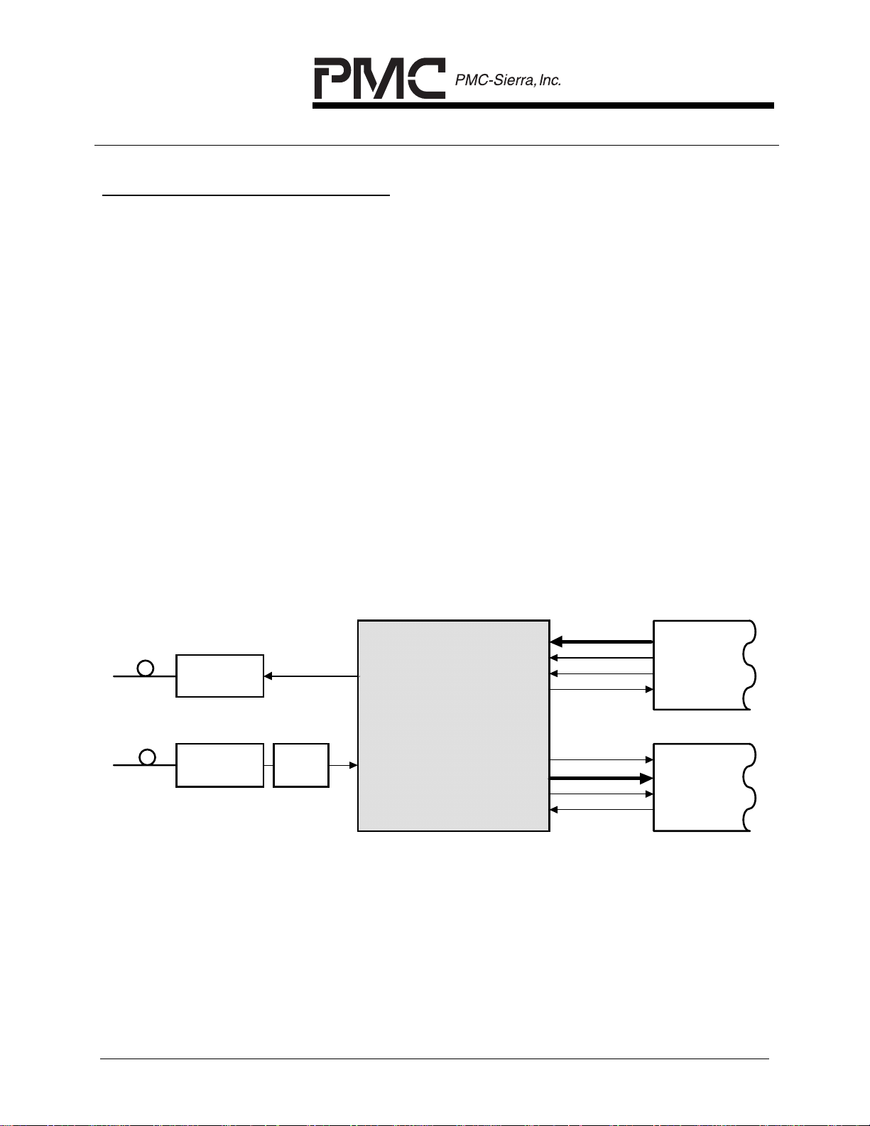
Figure 1 - Example 1. Optical ATM Adapter Interface
Optical
Transmitter
Optical
Receiver
Clock
Recovery
PM5345
S/UNI
SATURN
USER NETWORK
INTERFACE
TDAT[15:0]
TSOC
TWRB
TCA
RCA
RDAT[7:0]
RSOC
RRDB
Transmit
AAL
Processor
ATM Terminal
Receive
AAL
Processor
PROPRIETARY AND CONFIDENTIAL TO PMC-SIERRA, INC., AND FOR ITS CUSTOMERS’ INTERNAL USE
6
PM5345 S/UNI-155
DATA SHEET
PMC-930305 ISSUE 4 SATURN USER NETWORK INTERFACE
Figure 2 - Example 2. UTP-5 ATM Adapter Interface
Line Driver
&
Transformer
TDAT[15:0]
TSOC
TWRB
TCA
PM5345
Transmit
AAL
Processor
S/UNI
ATM Terminal
Receive
AAL
Processor
Transformer
&
Line Receiver
Clock
Recovery
SATURN
USER NETWORK
INTERFACE
RCA
RDAT[7:0]
RSOC
RRDB
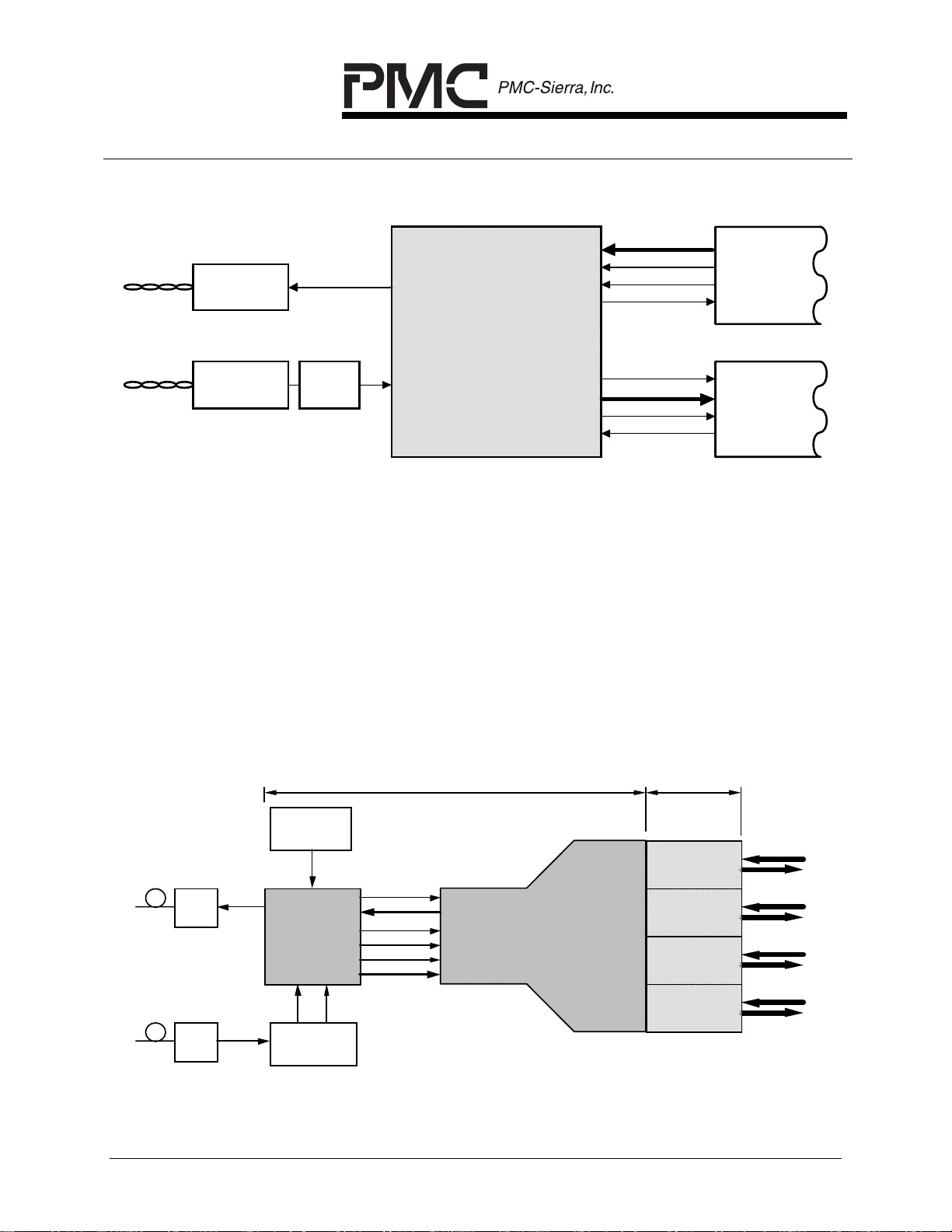
Figure 3 shows a configuration in which the PM5345 S/UNI is used with a
PM5312 SONET/SDH Transport Overhead Terminating Transceiver (STTX) and a
PM5318 622 Mbit/s Serial/Parallel Converter (SIPO) to implement an ATM
backbone interface.
In this application, four STS-3/STM-1 ATM streams are multiplexed into a single
STS-12/STM-4 stream for transport over fiber optic cables. The function of the
PM5312, PM5318, clock recovery and clock synthesis are also available in the
PM5712B 622 Mbit/s SONET/SDH Line Interface Module (SLIM).
Figure 3 - Example 3. OC-12 ATM Switch Port Card Interface
STS-3c (STM-1)
ATM Termination
PM5345
S/UNI-155
OPTICAL
FACILITY
E/O
O/E
Clock
Synthesis
Serial /
Parallel
Conversion
Clock
Recovery
STS-3(STM-1) To STS-12 (STM-4) MUX
OOF
TOUT[7:0]
TCLK
RICLK
RIFP
RIN[7:0]
PM5312
STTX
#1
#2
#3
#4
ATM
SWITCH
CORE
PROPRIETARY AND CONFIDENTIAL TO PMC-SIERRA, INC., AND FOR ITS CUSTOMERS’ INTERNAL USE
7
PM5345 S/UNI-155
DATA SHEET
PMC-930305 ISSUE 4 SATURN USER NETWORK INTERFACE
5
INTERFACE EXAMPLES
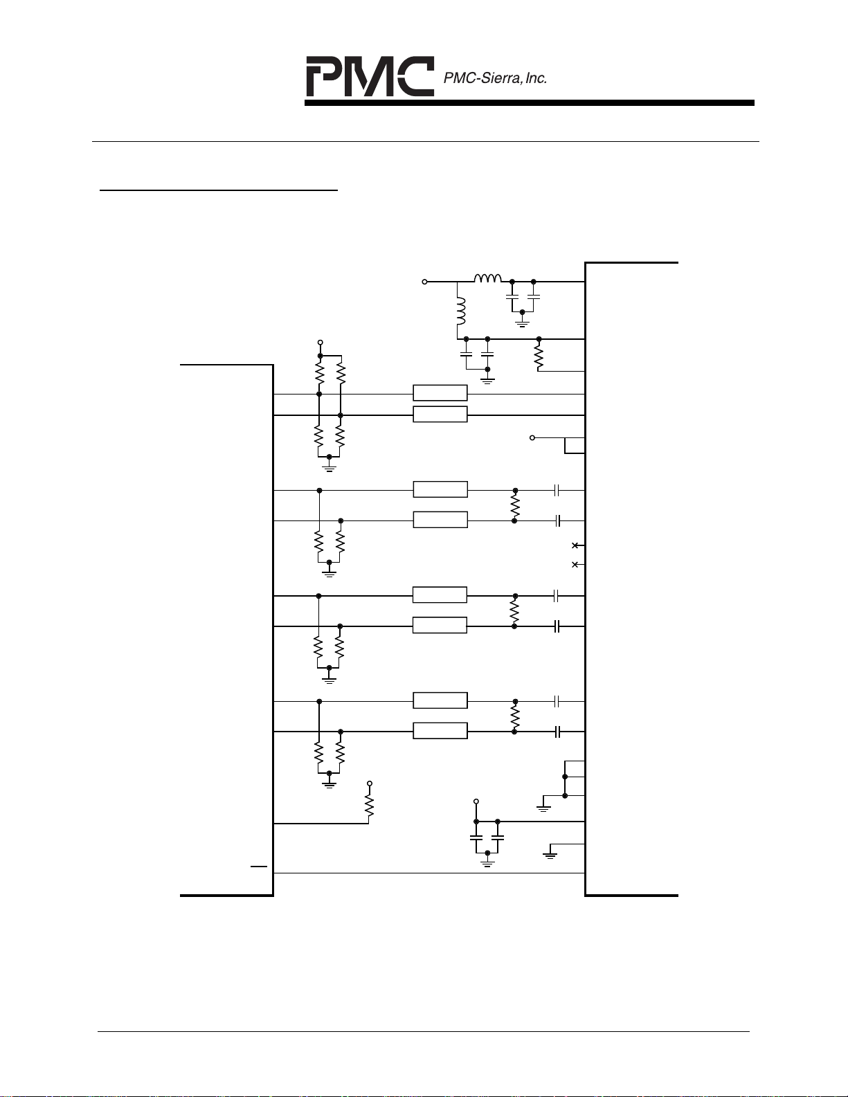
Figure 4 - Recommended Interface with CY7B951
FB
Ω
Ω
Ω
Ω
Ω
Ω
Ω
Ω
Vcc
FB
10µF
0.1µF
Vcc
0.1µF
0.01µF
100
0.01µF
0.01µF
100
0.01µF
0.01µF
100
0.01µF
0.1µF
630
Ω
Ω
Ω
RAVD (141)
TAVD1 (15)
Ω
VT2 (24)
TXD+ (22)
TXD- (23)
TSER (26)
RSER (25)
TXCI+ (14)
TXCI- (13)
TXCO+ (19)
TXCO- (1 8 )
RXD+ (143)
RXD- (142)
PM 5345
RXC+ (139)
RXC- (138)
RAVS (140)
TAVS1 (16)
TAVS2 (21)
TAVD2 (20)
VT1 (17)
(14) TSER+
(13) TSER-
(15) TCLK+
(16) TCLK-
(21) R S E R +
(22) R S E R -
CY7B 951
(23) RCLK+
(24) RCLK-
(5) M ODE
59
312
330
330
330
V
REF
Vcc
10µF
Ω
59
Ω
Z0 = 50
Z0 = 50
Ω
312
Ω
Z0 = 50
Z0 = 50
Ω
330
Ω
Z0 = 50
Z0 = 50
Ω
330
Ω
Z0 = 50
Z0 = 50
Ω
330
Ω
Vcc
4.7k
Ω
10µF
(20) L FI
GPIN (8 1)
In Figure 4, the interface between the S/UNI and the Cypress CY7B951 is
shown.
PROPRIETARY AND CONFIDENTIAL TO PMC-SIERRA, INC., AND FOR ITS CUSTOMERS’ INTERNAL USE
8

PM5345 S/UNI-155
DATA SHEET
PMC-930305 ISSUE 4 SATURN USER NETWORK INTERFACE
For optimal performance, the following guidelines should be followed:
• All power pins should be well decoupled, with the capacitors placed as close
as possible to the S/UNI power pins.
• Termination resistors and capacitors should be placed as close as possible to
the end of the transmission line.
• Source pull-down resistors should be placed as close as possible to the start
of the transmission line.
• Traces marked "Zo=50Ω" should be controlled impedance traces. These
traces should be kept as short as possible. Other controlled impedances can
be used. Contact PMC-Sierra's applications department for information on
using the S/UNI in "non-50Ω" controlled impedance environments.
• All inductors are Fair-Rite Products Corp #274-3019-446.
PROPRIETARY AND CONFIDENTIAL TO PMC-SIERRA, INC., AND FOR ITS CUSTOMERS’ INTERNAL USE
9
PM5345 S/UNI-155
DATA SHEET
PMC-930305 ISSUE 4 SATURN USER NETWORK INTERFACE
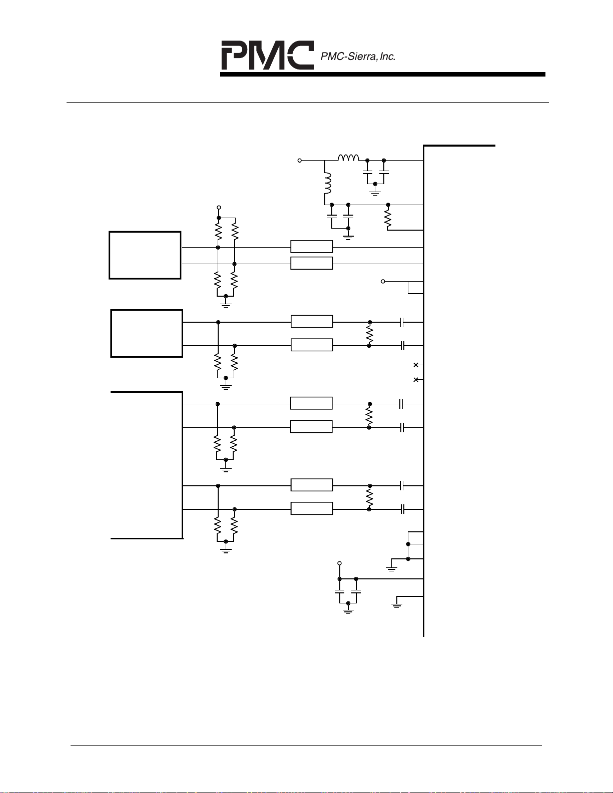
Figure 5 - Recommended Interface with AD802
Transm it
PMD
155.52 MHz
Oscillator
(2) D ATAOU T+
(1) D ATAOU T-
AD802
(5) C L KOUT+
(4) C L KOUT-
59
312
330
330
330
REF
V
10µF
0.1µF
RAVD (141)
FB
FB
Vcc
10µF
Ω
Ω
59
312
Ω
Z0 = 50
Z0 = 50
Ω
Ω
Ω
0.1µF
Vcc
630
TAVD1 (15)
Ω
VT2 (24)
TXD+ (22)
TXD- (23)
TSER (26)
RSER (25)
0.01µF
Z0 = 50
Z0 = 50
Ω
330
Ω
Ω
Ω
100
Ω
0.01µF
TXCI+ (14)
TX C I- (1 3 )
TXCO+ (19)
TX C O- (18 )
0.01µF
Z0 = 50
Z0 = 50
Ω
330
Ω
Ω
Ω
100
Ω
RXD+ (14 3)
RXD- (142)
0.01µF
PM 5345
0.01µF
Z0 = 50
Z0 = 50
Ω
330
Ω
Ω
Ω
Vcc
Ω
100
0.01µF
RXC+ (13 9)
RXC- (138)
RAVS (140)
TAVS1 (16)
TAVS2 (21)
TAVD2 (20)
10µF
0.1µF
VT1 (17)
In Figure 5, the interface between the S/UNI and the Analog Devices AD802 is
shown. In addition to the AD802, a 155.52 MHz oscillator provides the transmit
clock to the S/UNI. Oscillator vendors include CTS Corporation, C-MAC Quartz
Crystals Ltd., and Connor Winfield.
PROPRIETARY AND CONFIDENTIAL TO PMC-SIERRA, INC., AND FOR ITS CUSTOMERS’ INTERNAL USE
10

PM5345 S/UNI-155
DATA SHEET
PMC-930305 ISSUE 4 SATURN USER NETWORK INTERFACE
For optimal performance, the following guidelines should be followed:
• All power pins should be well decoupled, with the capacitors placed as close
as possible to the S/UNI power pins.
• Termination resistors and capacitors should be placed as close as possible to
the end of the transmission line.
• Source pull-down resistors should be placed as close as possible to the start
of the transmission line.
• Traces marked "Zo=50Ω" should be controlled impedance traces. These
traces should be kept as short as possible. Other controlled impedances can
be used. Contact PMC-Sierra's applications department for information on
using the S/UNI in "non-50Ω" controlled impedance environments.
• All inductors are Fair-Rite Products Corp #274-3019-446.
PROPRIETARY AND CONFIDENTIAL TO PMC-SIERRA, INC., AND FOR ITS CUSTOMERS’ INTERNAL USE
11
PM5345 S/UNI-155
DATA SHEET
PMC-930305 ISSUE 4 SATURN USER NETWORK INTERFACE
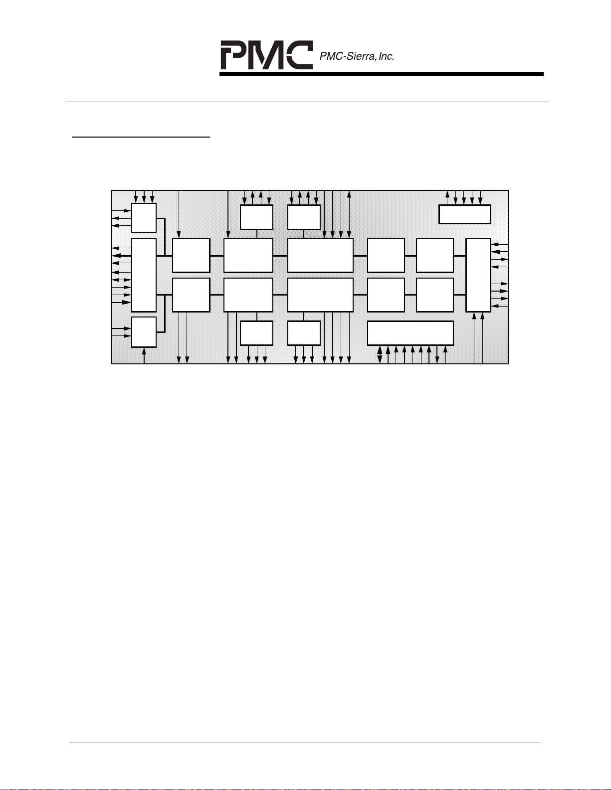
6
POUT[7:0]
BLOCK DIAG RAM
VT2
VT1
TSER
TLAIS
TXCI+/-
TXCO+/-
TXD+/-
FPOUT Tx ATM
POCLK
OOF
PICLK
FPIN
FPOS
PIN[7:0]
RXC+/RXD+/-
Par/
Ser
L ine
Side
I/F
Ser/
Par
RSER
Tx
Section
O/H
Processor
Rx
Section
O/H
Processor
LOF
LOS
TFERFLAIS
Transport
Overhead
Line O/H
Processor
Line O/H
Processor
Transport
Overhead
FERF
TTOH
TTOHFP
Insert
Tx
Rx
Extract
RTOH
TTOHEN
TTOHCLK
RTOHFP
RTOHCLK
TPOH
TPOHCLK
TPOHFP
Path
Overhead
Insert
Processor
Processor
Path
Overhead
Extract
RPOH
RPOHFP
TPOHEN
Tx
Path
O/H
Rx
Path
O/H
RPOHCLK
TFP
LOP
TPAIS
PAIS
TPYEL
PYEL
RCLK
TCLK
Cell
Processor
Rx ATM
Cell
Processor
Microprocessor
A[7:0]
D[7:0]
ALE
I/F
CSB
WRB
Tx ATM
4 Cell
FIFO
Rx ATM
4 Cell
FIFO
RDB
RSTB
TDO
JTAG Test
Access Port
INTB
GPIN
TDI
TCK
TMS
Drop
Side
I/F
BUS8
TRSTB
TSEN
TSOC
TDAT[15:0]
TCA
TWRB
RSOC
RDAT[15:0]
RCA
RRDB
PROPRIETARY AND CONFIDENTIAL TO PMC-SIERRA, INC., AND FOR ITS CUSTOMERS’ INTERNAL USE
12

PM5345 S/UNI-155
DATA SHEET
PMC-930305 ISSUE 4 SATURN USER NETWORK INTERFACE
7
DESCRIPTION
The PM5345 S/UNI SATURN User Network Interface is a monolithic integrated
circuit that implements the SONET/SDH processing and ATM mapping functions
of a 155 Mbit/s ATM User-Network Interface.
The S/UNI receives SONET/SDH frames, via a bit serial or byte serial interface,
and processes section, line, and path overhead. It performs framing (A1, A2),
descrambling, detects alarm conditions, and monitors section, line, and path bit
interleaved parity (B1, B2, B3), accumulating error counts at each level for
performance monitoring purposes. Line and path far end block error indications
(Z2, G1) are also accumulated. The S/UNI interprets the received payload
pointers (H1, H2) and extracts the synchronous payload envelope which carries
the received ATM cell payload. In addition to its basic processing of the received
SONET/SDH overhead, the S/UNI provides convenient access to all overhead
bytes, which are extracted and serialized on lower rate interfaces, allowing
additional external processing of overhead.
The S/UNI frames to the ATM payload using cell delineation. HCS error
correction is provided. Idle/unassigned cells may be dropped according to a
programmable filter. Cells are also dropped upon detection of an uncorrectable
header check sequence error. The ATM cell payloads are descrambled. The
ATM cells that are passed are written to a four cell FIFO buffer. The received
cells are read from the FIFO using a generic 9 bit wide or 17 bit wide datapath
interface. Counts of received ATM cell headers that are errored and
uncorrectable and also those that are errored and correctable are accumulated
independently for performance monitoring purposes.
The S/UNI transmits SONET/SDH frames, via a bit serial or a byte serial
interface, and formats section, line, and path overhead appropriately. It performs
framing pattern insertion (A1, A2), scrambling, alarm signal insertion, and
creates section, line, and path bit interleaved parity (B1, B2, B3) as required to
allow performance monitoring at the far end. Line and path far end block error
indications (Z2, G1) are also inserted. The S/UNI generates the payload pointer
(H1, H2) and inserts the synchronous payload envelope which carries the ATM
cell payload. In addition to its basic formatting of the transmitted SONET/SDH
overhead, the S/UNI provides convenient access to all overhead bytes, which are
optionally inserted from lower rate serial interfaces, allowing external sourcing of
overhead. The S/UNI also supports the insertion of a large variety of errors into
the transmit stream, such as framing pattern errors, bit interleaved parity errors,
and illegal pointers, which are useful for system diagnostics and tester
applications.
PROPRIETARY AND CONFIDENTIAL TO PMC-SIERRA, INC., AND FOR ITS CUSTOMERS’ INTERNAL USE
13

PM5345 S/UNI-155
DATA SHEET
PMC-930305 ISSUE 4 SATURN USER NETWORK INTERFACE
ATM cells are written to an internal four cell FIFO using a generic 9 bit wide or 17
bit wide datapath interface. Idle/unassigned cells are automatically inserted
when the internal FIFO contains less than one cell. The S/UNI provides
generation of the header check sequence and scrambles the payload of the ATM
cells. Each of these transmit ATM cell processing functions can be enabled or
bypassed.
No auxiliary clocks are required directly by the S/UNI as it operates from two
155.52 MHz clocks (bit serial line interface) or two 19.44 MHz clocks (byte serial
interface). The S/UNI is configured, controlled and monitored via a generic 8-bit
microprocessor bus interface. The S/UNI also provides a standard 5 signal
P1149.1 JTAG test port for boundary scan board test purposes.
The S/UNI is implemented in low power, +5 Volt, CMOS technology. It has TTL
and pseudo ECL (PECL) compatible inputs and outputs and is packaged in a
160 pin PQFP package.
PROPRIETARY AND CONFIDENTIAL TO PMC-SIERRA, INC., AND FOR ITS CUSTOMERS’ INTERNAL USE
14
PM5345 S/UNI-155
5
2
DATA SHEET
PMC-930305 ISSUE 4 SATURN USER NETWORK INTERFACE
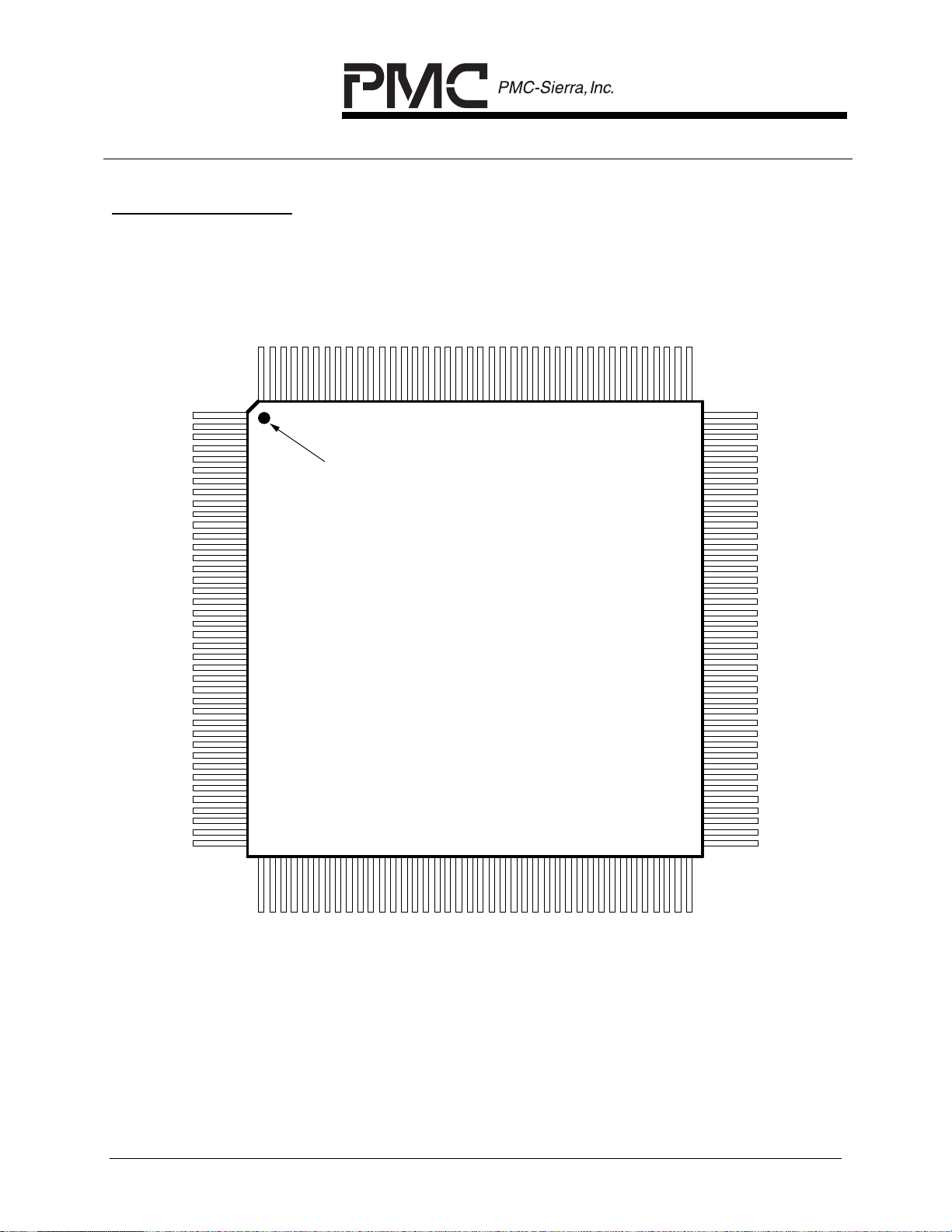
8
PIN DIAG RAM
The S/UNI is packaged in an 160 pin PQFP package having a body size of
28 mm by 28 mm and a pin pitch of 0.65 mm.
PIN3
PIN 160
POUT1
POUT2
POUT0
FPIN
RCLK
VSSO
VDDI
VDDO
PICLK
PIN7
PIN6
PIN5
PIN4
PIN2
PIN1
PIN0
RXD+
RXD-
RAVS
RAVD
RXC+
RXC-
RDAT1
VSSO
RDAT14
RDAT13
VDDO
RDAT1
RDAT11
VSSI
RDAT10
VSSO
RDAT9
RDAT8
RDAT7
VDDO
RDAT5
RDAT6
PIN 1
POUT3
POUT4
POUT5
POUT6
POUT7
VSSO
TCLK
VDDO
POCLK
FPOUT
FPOS/MLT
VSSI
TXCI-
TXCI+
TAVD1
TAVS1
VT1
TXCOTXCO+
TAVD2
TAVS2
TXD+
TXD-
VT2
RSER
TSER
TFP
TPAIS
TLAIS
TPYEL
TFERF
OOF
LOS
LOF
LOP
VSSO
PAIS
LAIS
PYEL
FERF
Index
PM5345
S/UNI
(Top View)
VSSO
PIN 121
PIN 120
RDAT4
RDAT3
RDAT2
RDAT1
VDDO
RDAT0
VSSO
RSOC
RCA
RRDB
BUS8
TSEN
RDB
WRB
D7
D6
D5
D4
VDDO
VDDI
TCK
VSSO
D3
D2
D1
D0
INTB
A7
A6
A5
A4
A3
A2
A1
A0
CSB
ALE
RSTB
TRSTB
GPIN
PIN 40
PIN 41 PIN 80
RTOHFP
TTOHEN
TPOHEN
TPOH
TPOHFP
VDDO
TPOHCLK
RPOHFP
RPOH
VSSO
RPOHCLK
TTOH
PROPRIETARY AND CONFIDENTIAL TO PMC-SIERRA, INC., AND FOR ITS CUSTOMERS’ INTERNAL USE
RTOH
TTOHFP
TTOHCLK
RTOHCLK
TWRB
VDDI
TCA
TSOC
TDAT0
TDAT1
TDAT2
TDAT3
TDAT4
TDAT5
TDAT6
TDAT7
VSSI
TDAT8
TDAT9
TDAT11
TDAT10
TDAT13
TDAT12
TDAT15
TDAT14
TDO
TDI
TMS
PIN 81
15

PM5345 S/UNI-155
DATA SHEET
PMC-930305 ISSUE 4 SATURN USER NETWORK INTERFACE
9
PIN DESCRIPTION
Table 1 -
Pin Name Type Pin
Function
No.
RSER Input 25 The receive serial input (RSER) selects the
receive line interface. RSER is tied high to
select the 155.52 Mbit/s interface (on pins
RXC+, RXC-, RXD+, and RXD-). RSER is tied
low to select the 19.44 Mbyte/s interface (on
pins PICLK, PIN[7:0], and FPIN).
RXD+
RXD-
Input 143
142
The receive differential data inputs (RXD+,
RXD-) contain the 155.52 Mbit/s receive STS-
3c (STM-1) stream when the bit serial interface
is selected (RSER is tied high). RXD+/- is
sampled on the rising edge of RXC+/- (the
falling edge may be used by reversing RXC+/-
).
RXC+
RXC-
Input 139
138
The receive differential clock inputs (RXC+,
RXC-) contain the receive clock when the bit
serial interface is selected (RSER is tied high).
RXC+/- is nominally a 155.52 MHz, 50% duty
cycle clock. This clock is divided by eight
internally to produce RCLK when the bit serial
interface is selected and provide timing for the
S/UNI receive functions. RXD+/- is sampled
on the rising edge of RXC+/-.
PROPRIETARY AND CONFIDENTIAL TO PMC-SIERRA, INC., AND FOR ITS CUSTOMERS’ INTERNAL USE
16

PM5345 S/UNI-155
DATA SHEET
PMC-930305 ISSUE 4 SATURN USER NETWORK INTERFACE
Pin Name Type Pin
Function
No.
PICLK I/O 153 The parallel input clock (PICLK) provides
timing for sampling the received SONET STS-
3c (STM-1) stream that is input by the S/UNI
when the byte serial interface is selected
(RSER is tied low). This clock provides timing
for S/UNI receive function operation. PICLK is
nominally a 19.44 MHz, 50% duty cycle clock.
PIN[7:0] and FPIN are sampled on the rising
edge of PICLK. RCLK is a buffered version of
PICLK when the byte serial interface is
selected. When the 155 Mbit/s serial interface
is selected (RSER is tied high), PICLK
becomes an output and must not be driven.
RX_VCLK The test vector clock (RX_VCLK) signal is
used during S/UNI production testing to verify
internal functionality.
PIN[0]
PIN[1]
PIN[2]
PIN[3]
Input 144
145
146
147
The data input (PIN[7:0]) bus carries the STS-
3c (STM-1) stream when the byte serial
interface is selected (RSER is tied low).
PIN[7:0] is sampled on the rising edge of
PICLK. PIN[7] is the most significant bit
(corresponding to bit 1 of each serial word, the
PIN[4]
PIN[5]
148
149
first bit transmitted). PIN[0] is the least
significant bit (corresponding to bit 8 of each
word, the last bit transmitted).
PIN[6]
150
PIN[7]
151
FPOS/MLT Input 11 The dual function input (FPOS/MLT) selects
both the transmit encoding scheme and the
receive frame pulse location depending on the
line side interface selected using inputs TSER
and RSER.
PROPRIETARY AND CONFIDENTIAL TO PMC-SIERRA, INC., AND FOR ITS CUSTOMERS’ INTERNAL USE
17

PM5345 S/UNI-155
DATA SHEET
PMC-930305 ISSUE 4 SATURN USER NETWORK INTERFACE
Pin Name Type Pin
No.
Function
When the byte serial receive interface is
selected (RSER=0), the FPOS/MLT input
selects the frame byte position in the SONET
frame indicated by the FPIN input. When
FPOS/MLT is tied high, a pulse on FPIN ma rks
the third A2 framing byte position on the
PIN[7:0] bus. When FPOS/MLT is tied low, a
pulse on FPIN marks the first synchronous
payload envelope byte position after the three
C1 bytes on PIN[7:0].
When the bit serial transmit interface is
selected (TSER=1), the FPOS/MLT input
selects MLT-3 encoding of the transmit stream.
When FPOS/MLT is tied high, an MLT-3
encoded data stream is transmitted on the
TXCO+/- and TXD+/- outputs. When
FPOS/MLT is tied low, 155 Mbit/s clock and
data are inserted on the TXCO+/- and TXD+/-
outputs.
FPIN Input 157 The active high framing position input (FPIN)
signal indicates the SONET frame position on
the PIN[7:0] bus. The byte position indicated
by FPIN is selected by the FPOS/MLT input as
described above. FPIN is sampled on the
rising edge of PICLK.
OOF Output 32 The out of frame (OOF) signal is high while the
S/UNI is out of frame. OOF is low while the
S/UNI is in-frame. An out of frame occurs
when 4 consecutive errored framing patterns
(A1 and A2 bytes) have been received. OOF
is intended to be used to enable an upstream
framing pattern detector to search for the
framing pattern when the byte serial interface
is selected. This alarm indication is also
available via register access. OOF is updated
on the falling edge of RCLK.
PROPRIETARY AND CONFIDENTIAL TO PMC-SIERRA, INC., AND FOR ITS CUSTOMERS’ INTERNAL USE
18

PM5345 S/UNI-155
DATA SHEET
PMC-930305 ISSUE 4 SATURN USER NETWORK INTERFACE
Pin Name Type Pin
Function
No.
RCLK Output 156 The receive clock (RCLK) output provides a
timing reference for S/UNI receive outputs.
RCLK is a 19.44 MHz, nominally 50% duty
cycle clock. RCLK is a buffered version of
PICLK when the byte serial interface is
selected (RSER is tied low). RCLK is a divide
by eight of RXC+/- when the bit serial interface
is selected (RSER is tied high).
TSER Input 26 The transmit serial input (TSER) selects the
transmit line interface. TSER is tied high to
select the 155.52 Mbit/s interface (on pins
TXCI+, TXCI-, TXCO+, TXCO-, TXD+, and
TXD-). TSER is tied low to select the 19.44
Mbyte/s interface (on pins TCLK, FPOUT, and
POUT[7:0]).
TXD+
TXD-
Output 22
23
The transmit differential data/positive pulse
outputs (TXD+, TXD-) contain either NRZ or
MLT-3 encoded data when the bit serial
interface is selected (TSER is tied high).
TXCI+
TXCI-
Input 14
13
When NRZ encoding is selected (FPOS/MLT is
tied low), the 155.52 Mbit/s transmit STS-3c
(STM-1) stream TXD+/- is updated on the
falling edge of TXCO+/-.
When MLT-3 encoding is selected (FPOS/MLT
is tied high), the TXD+/- outputs contain the
positive pulses of the MLT-3 encoded stream.
The transmit differential clock inputs (TXCI+,
TXCI-) contain the transmit clock when the bit
transmit serial interface is selected. TXCI+/- is
nominally a 155.52 MHz, 50% duty cycle clock.
This clock provides timing for the S/UNI
transmit functions. TXCI+/- may be left
unconnected when S/UNI loop timing is
enabled (using the S/UNI Master Control
Register).
PROPRIETARY AND CONFIDENTIAL TO PMC-SIERRA, INC., AND FOR ITS CUSTOMERS’ INTERNAL USE
19

PM5345 S/UNI-155
DATA SHEET
PMC-930305 ISSUE 4 SATURN USER NETWORK INTERFACE
Pin Name Type Pin
Function
No.
TXCO+
TXCO-
Output 19
18
The transmit differential clock/negative pulse
outputs (TXCO+, and TXCO-) contain either
the transmit output clock or MLT-3 encoded
data when the bit serial interface is selected
(TSER is tied high).
When NRZ encoding is selected (FPOS/MLT is
tied low), TXCO+/- is a buffered version of
TXCI+/-. TXD+/- is updated on the falling edge
of TXCO+/-.
When MLT-3 encoding is selected (FPOS/MLT
is tied high), the TXCO+/- outputs contain the
negative pulses of the MLT-3 encoded stream.
POCLK Output 9 The parallel output clock (POCLK) signal
provides timing for processing of the data that
is output by the S/UNI. POCLK is nominally a
19.44 MHz, 50% duty cycle clock. POCLK is a
buffered version of TCLK when the byte serial
interface is selected (TSER is tied low).
POCLK is a divide by eight of TXCI+/- when
the bit serial interface is selected (TSER is tied
high).
POUT[0]
POUT[1]
POUT[2]
POUT[3]
Output 158
159
160
1
The scrambled data output (POUT[7:0]) bus
carries data when the byte serial interface is
selected (TSER is tied low). POUT[7:0] is
updated on the rising edge of TCLK. POUT[7]
is the most significant bit (corresponding to bit
1 of each serial word, the first bit transmitted).
POUT[4]
POUT[5]
2
3
POUT[0] is the least significant bit
(corresponding to bit 8 of each serial word, the
last bit transmitted).
POUT[6]
POUT[7]
PROPRIETARY AND CONFIDENTIAL TO PMC-SIERRA, INC., AND FOR ITS CUSTOMERS’ INTERNAL USE
4
5
20

PM5345 S/UNI-155
DATA SHEET
PMC-930305 ISSUE 4 SATURN USER NETWORK INTERFACE
Pin Name Type Pin
Function
No.
FPOUT Output 10 The active high framing position output
(FPOUT) signal marks the frame alignment on
the POUT[7:0] bus. FPOUT goes high for a
single TCLK period while the first synchronous
payload envelope byte after the three C1 bytes
is present on POUT[7:0]. FPOUT is updated
on the rising edge of TCLK.
LOS Output 33 The loss of signal (LOS) signal is set high
when loss of signal is declared. This occurs
when a violating period (20 ± 3 µs) of
consecutive all zeros bytes is detected on the
incoming STS-3c(STM-1) signal (before
descrambling). LOS is removed when two
valid framing words (A1, A2) are detected and
during the intervening time, no violating period
of consecutive all zeros patterns is detected.
This alarm indication is also available via
register access. LOS is updated on the falling
edge of RCLK.
LOF Output 34 The loss of frame (LOF) signal is set high
when loss of frame is declared. This occurs
when an out-of-frame condition (as indicated
by a high level on the OOF output) persists for
a period of 3 ms. LOF is removed when an in-
frame condition (as indicated by a low level on
the OOF output) persists for a period of 3 ms.
This alarm indication is also available via
register access. LOF is updated on the falling
edge of RCLK.
PROPRIETARY AND CONFIDENTIAL TO PMC-SIERRA, INC., AND FOR ITS CUSTOMERS’ INTERNAL USE
21

PM5345 S/UNI-155
DATA SHEET
PMC-930305 ISSUE 4 SATURN USER NETWORK INTERFACE
Pin Name Type Pin
Function
No.
LAIS Output 38 The line alarm indication signal (LAIS) is set
high when line AIS is declared. This occurs
when a 111 binary pattern is detected in bits
6,7,8 of the K2 byte for five consecutive
frames. LAIS is removed when any pattern
other than 111 is detected in bits 6, 7, and 8 of
the K2 byte for five consecutive frames. This
alarm indication is also available via register
access. LAIS is updated on the falling edge of
RCLK.
FERF Output 40 The line far end receive failure (FERF) signal is
set high when line FERF is declared. This
occurs when a 110 binary pattern is detected
in bits 6, 7, and 8 of the K2 byte for five
consecutive frames. FERF is removed when
any pattern other than 110 is detected in bits
6, 7, and 8 of the K2 byte for five consecutive
frames. This alarm indication is also available
via register access. FERF is updated on the
falling edge of RCLK.
LOP Output 35 The loss of pointer (LOP) signal is set high
when loss of pointer is declared. This occurs
when a valid pointer (H1, H2) is not found in
eight consecutive frames, or if eight
consecutive new data flags are detected. LOP
is removed when the same valid and normal
pointer with a normal new data flag is detected
in three consecutive frames. The loss of
pointer state is not entered if the incoming
stream contains path AIS. This alarm
indication is also available via register access.
LOP is updated on the falling edge of RCLK.
PROPRIETARY AND CONFIDENTIAL TO PMC-SIERRA, INC., AND FOR ITS CUSTOMERS’ INTERNAL USE
22

PM5345 S/UNI-155
DATA SHEET
PMC-930305 ISSUE 4 SATURN USER NETWORK INTERFACE
Pin Name Type Pin
Function
No.
PAIS Output 37 The path AIS (PAIS) signal is set high when
STS-path AIS is declared. This occurs when
an all ones pattern is observed in the pointer
bytes (H1, H2) for three consecutive frames.
Path AIS is removed when the same valid and
normal pointer is detected for three
consecutive frames or a legal pointer with an
active NDF is received. This alarm indication is
also available via register access. PAIS is
updated on the falling edge of RCLK.
PYEL Output 39 The path yellow (PYEL) signal is set high when
STS-path yellow alarm is declared. This
occurs when bit 5 of the path status byte (G1)
is set high for ten consecutive frames. Path
yellow is removed when bit 5 of the G1 byte is
set low for ten consecutive frames. This alarm
indication is also available via register access.
PYEL is updated on the falling edge of RCLK.
TLAIS Input 29 The active high transmit line alarm indication
(TLAIS) signal controls the insertion of line
AIS. Line AIS is inserted by overwriting the
SONET/SDH frame contents with all ones
(before scrambling). The section overhead is
not overwritten. This function can also be
performed via register access. Line AIS
insertion is internally synchronized to frame
boundaries. The TLAIS input takes
precedence over the TTOH and TTOHEN
inputs. TLAIS is samp led on the rising edge of
POCLK.
PROPRIETARY AND CONFIDENTIAL TO PMC-SIERRA, INC., AND FOR ITS CUSTOMERS’ INTERNAL USE
23

PM5345 S/UNI-155
DATA SHEET
PMC-930305 ISSUE 4 SATURN USER NETWORK INTERFACE
Pin Name Type Pin
Function
No.
TFERF Input 31 The active high transmit line far end receive
failure (TFERF) signal controls the insertion of
line FERF. Line FERF is inserted by
transmitting the code 110 (binary) in bit
positions 6,7, and 8 of the K2 byte. This
function can also be performed via register
access, or be enabled to occur automatically
upon detection of receive line AIS, loss of
signal, or loss of frame. The TFERF input
takes precedence over the TTOH and TTOHEN
inputs. TFERF is sampled on the r ising edge
of POCLK.
TPAIS Input 28 The active high transmit path alarm indication
(TPAIS) signal controls the insertion of STS-
path AIS. A high level on TPAIS forces the
insertion of an all ones pattern into the
complete synchronous payload envelope, and
the payload pointer bytes (H1, H2). Path AIS
insertion is internally synchronized to SPE
frame boundaries. This function can also be
performed via register access. TPAIS is
sampled on the rising edge of POCLK.
TPYEL Input 30 The transmit path yellow alarm (TPYEL) signal
controls the insertion of path yellow alarm. A
high level on TPYEL forces a logic one to be
inserted in the path yellow bit position in the
path status byte (G1). This function can also
be performed via register access, or be
enabled to occur automatically upon detection
of receive line AIS, loss of frame, loss of
signal, loss of pointer, or STS-path AIS. The
TPOH and TPOHEN inputs take precedence
over the TPYEL input. TPYEL is sampled on
the rising edge of POCLK.
PROPRIETARY AND CONFIDENTIAL TO PMC-SIERRA, INC., AND FOR ITS CUSTOMERS’ INTERNAL USE
24

PM5345 S/UNI-155
DATA SHEET
PMC-930305 ISSUE 4 SATURN USER NETWORK INTERFACE
Pin Name Type Pin
Function
No.
TSEN Input 109 The tristate enable (TSEN) input selects the
configuration of the receive datapath
(RDAT[15:0]). When TSEN is tied high,
RDAT[15:0] normally operates as a tristate bus
controlled by RRDB. When RRDB is high,
RDAT[15:0] is tristated. When RRDB is low,
RDAT[15:0] is enabled. When TSEN is tied
low, RDAT[15:0] normally operates as an
output bus, and is always enabled, regardless
of the state of RRDB
BUS8 Input 110 The bus width select (BUS8) input sele cts the
transmit and receive datapath widths. When
BUS8 is tied high, a 9-bit interface consisting
of a start of cell indication, and an 8-bit octet
bus is selected. When BUS8 is tied low, a 17-
bit interface consisting of a start of cell
indication, and a 16-bit word bus is selected.
RRDB Input 111 The active low receive read strobe (RRDB) is
used to read ATM cells from the receive FIFO.
When active, RRDB must cycle at a 25 MHz or
lower instantaneous rate, but at a high enough
rate to avoid FIFO overflow. RSOC is updated
on the rising edge of RRDB. RDAT[15:0] are
updated on the falling edge of RRDB.
PROPRIETARY AND CONFIDENTIAL TO PMC-SIERRA, INC., AND FOR ITS CUSTOMERS’ INTERNAL USE
25

PM5345 S/UNI-155
DATA SHEET
PMC-930305 ISSUE 4 SATURN USER NETWORK INTERFACE
Pin Name Type Pin
No.
RDAT[0]
RDAT[1]
RDAT[2]
RDAT[3]
RDAT[4]
RDAT[5]
RDAT[6]
RDAT[7]
RDAT[8]
RDAT[9]
RDAT[10]
RDAT[11]
RDAT[12]
Tristate 115
117
118
119
120
122
123
125
``•`
````
`ü``
```•
````
Function
```ü`````•``````ü`````•``````ü`````•``````ü`````•``````ü
`````````••••at are read from the receive FIFO.
When the 17-bit datapath is selected (BUS8 is
tied low), RDAT[15:0] contains the 16-bit wide
word bus. When the 9-bit datapath is selected
(BUS8 is tied high), RDAT[7:0] contains the 8-
bit wide word bus (RDAT[15:8] is not used).
The RDAT[15:0] bus is tristate d while RRDB is
high, and TSEN is high. The RDAT[15:0] bus is
always driven when TSEN is low, regardless of
the leve l of RRDB. RDAT[15:0] is updated on
the falling edge of RRDB.
RDAT[13]
RDAT[14]
RDAT[15]
``ü`
````
•```
RSOC Output 113 The receive start of cell (RSOC) signal marks
the start of cell on the RDAT[15:0] bus. When
RSOC is high, the first word of the selected
data structure is present on the RDAT[15:0]
stream. RSOC is updated on the rising edge
of RRDB.
RCA Output 112 The receive cell available (RCA) signal
indicates when a cell is available in the receive
FIFO. The low to high transition of RCA
(indicating that the receive FIFO is not empty)
occurs on the falling edge of RCLK. The high
to low transition of RCA (indicating that the
receive FIFO is empty) occurs on the falling
edge of RRDB. The active polarity of this
signal is programmable and defaults to active
high.
PROPRIETARY AND CONFIDENTIAL TO PMC-SIERRA, INC., AND FOR ITS CUSTOMERS’ INTERNAL USE
26

PM5345 S/UNI-155
DATA SHEET
PMC-930305 ISSUE 4 SATURN USER NETWORK INTERFACE
Pin Name Type Pin
Function
No.
TCLK I/O 7 The transmit clock (TCLK) provides timing for
S/UNI transmit function operation when the
byte serial interface is selected (TSER is tied
low). TCLK must be a 19.44 MHz, nominally
50% duty cycle clock. POCLK is a buffered
version of TCLK when byte serial interface is
selected.
When the 155 Mbit/s serial interface is
selected (TSER is tied high), TCLK becomes
an output and should not be driven.
TX_VCLK The test vector clock (TX_VCLK) signal is used
during S/UNI production testing to verify
internal functionality.
TFP Input 27 The active high transmit frame pulse (TFP)
signal is used to align the SONET/SDH
transport frame generated by the S/UNI device
to a system reference when the byte serial
interface is selected (TSER is low). TFP
should be brought high for a single TCLK
period every 2430 TCLK cycles or a multiple
thereof. TFP may be tied low if such
synchronization is not required. The offset
between an active TFP input and the resultant
FPOUT pulse is 24 TCLK periods. TFP is
sampled on the rising edge of TCLK.
TWRB Input 58 The transmit write strobe (TWRB) is used to
write ATM cells to the four cell transmit FIFO.
When active, TWRB cycles at a 25 MHz or
lower instantaneous rate. A complete 53 octet
cell must be written to the FIFO before being
inserted in the STS-3c (STM-1) SPE.
Idle/unassigned cells are inserted when a
complete cell is not available. TDAT[15:0] and
TSOC are sampled on the rising edge of
TWRB.
PROPRIETARY AND CONFIDENTIAL TO PMC-SIERRA, INC., AND FOR ITS CUSTOMERS’ INTERNAL USE
27

PM5345 S/UNI-155
DATA SHEET
PMC-930305 ISSUE 4 SATURN USER NETWORK INTERFACE
Pin Name Type Pin
No.
TDAT[0]
TDAT[1]
TDAT[2]
TDAT[3]
TDAT[4]
TDAT[5]
TDAT[6]
TDAT[7]
TDAT[8]
TDAT[9]
TDAT[10]
TDAT[11]
TDAT[12]
Input 61
62
63
64
65
66
67
68
70
71
72
73
74
Function
The transmit cell data (TDAT[15:0]) bus carries
the ATM cell octets that are written to the
transmit FIFO. When the 17-bit datapath is
selected (BUS8 is tied low), TDAT[15:0]
contains the 16-bit wide word bus. When the
9-bit datapath is selected (BUS8 is tied high),
TDAT[7:0] contains the 8-bit wide octet bus
(TDAT[15:8] is not used). TDAT[15:0] is
sampled on the rising edge of TWRB.
TDAT[13]
TDAT[14]
TDAT[15]
75
76
77
TSOC Input 60 The transmit start of cell (TSOC) signal marks
the start of cell on the TDAT[15:0] bus. When
TSOC is high, the first word of the selected
data structure is present on the TDAT[15:0]
stream. It is not necessary for TSOC to be
present at each cell. An interrupt may be
generated if TSOC is high during any word
other than the first word of the selected data
structure. TSOC is sampled on the rising edge
of TWRB.
PROPRIETARY AND CONFIDENTIAL TO PMC-SIERRA, INC., AND FOR ITS CUSTOMERS’ INTERNAL USE
28

PM5345 S/UNI-155
DATA SHEET
PMC-930305 ISSUE 4 SATURN USER NETWORK INTERFACE
Pin Name Type Pin
Function
No.
TCA Output 59 The transmit cell available (TCA) signal
indicates when a cell is available in the
transmit FIFO. The low to high transition of
TCA (indicating that the transmit FIFO is not
full) occurs on the falling edge of POCLK. The
high to low transition of TCA (indicating that
the transmit FIFO is full) occurs on the falling
edge of TWRB. The active polarity of this
signal is programmable and defaults to active
high.
RTOH Output 54 The receive transport overhead data (RTOH)
signal contains the receive transport overhead
bytes (A1, A2, C1, B1, E1, F1, D1-D3, H1-H3,
B2, K1, K2, D4-D12, Z1, Z2, and E2) extracted
from the received SONET/SDH frame. RTOH
is updated on the falling edge of RTOHCLK.
RTOHCLK Output 56 The receive transport overhead clock
(RTOHCLK) is nominally a 5.184 MHz clock
which provides timing to process the extracted
receive transport overhead. RTOHCLK is a
gapped 6.48 MHz clock. RTOHCLK is updated
on the falling edge of RCLK.
RTOHFP Output 55 The receive transport overhead frame position
(RTOHFP) signal may be used to locate the
individual receive transport overhead bits in
the transport overhead data stream, RTOH.
RTOHFP is logic one while bit 1 (the most
significant bit) of the first framing byte (A1) is
present in the RTOH stream. RTOHFP is
updated on the falling edge of RTOHCLK.
RPOH Output 46 The receive path overhead data (RPOH) signal
contains the path overhead bytes (J1, B3, C2,
G1, F2, H4, Z3, Z4, and Z5) extracted from the
received STS-3c (STM-1) frame. RPOH is
updated on the falling edge of RPOHCLK.
PROPRIETARY AND CONFIDENTIAL TO PMC-SIERRA, INC., AND FOR ITS CUSTOMERS’ INTERNAL USE
29

PM5345 S/UNI-155
DATA SHEET
PMC-930305 ISSUE 4 SATURN USER NETWORK INTERFACE
Pin Name Type Pin
Function
No.
RPOHCLK Output 48 The receive path overhead clock (POHCLK) is
nominally a 576 kHz clock which provides
timing to process the extracted receive path
overhead. RPOHCLK is a gapped 2.16 MHz
clock. RPOHCLK is updated on the falling
edge of RCLK.
RPOHFP Output 47 The receive path overhead frame position
(RPOHFP) signal may be used to locate the
individual receive path overhead bits in the
path overhead data stream, RPOH. RPOHFP
is logic one while bit 1 (the most significant bit)
of the path trace byte (J1) is present in the
RPOH stream. RPOHFP is updated on the
falling edge of RPOHCLK.
TTOH Input 51 The transmit transport overhead data (TTOH)
signal contains the transport overhead bytes
(A1, A2, C1, E1, F1, D1-D3, K1, K2, D4-D12,
Z1, Z2, and E2) and error masks (B1, B2, H1,
and H2) which may be inserted, or used to
insert section/line BIP or payload pointer bit
errors into the transport overhead byte
positions transmit STS-3c (STM-1) stream.
Insertion is controlled by the TTOHEN input, or
by bits in internal registers. TTOH is sampled
on the rising edge of TTOHCLK.
PROPRIETARY AND CONFIDENTIAL TO PMC-SIERRA, INC., AND FOR ITS CUSTOMERS’ INTERNAL USE
30

PM5345 S/UNI-155
DATA SHEET
PMC-930305 ISSUE 4 SATURN USER NETWORK INTERFACE
Pin Name Type Pin
Function
No.
TTOHEN Input 49 The transmit transport overhead insert enable
(TTOHEN) signal, together with internal
register bits, controls the source of the
transport overhead data which is transmitted.
While TTOHEN is high, values sampled on the
TTOH input are inserted into the
corresponding transport overhead bit position
(for the A1, A2, C1, E1, F1, D1-D3, K1, K2,
H3, D4-D12, Z1, Z2, and E2 bytes). While
TTOHEN is low, default values are inserted
into these transport overhead bit positions. A
high level on TTOHEN during the B1, B2 or
H1-H2 bit positions enables an error mask.
While the error mask is enabled, a high level
on input TTOH causes the corresponding B1,
B2 or H1-H2 bit position to be inverted. A low
level on TTOH allows the corresponding bit
position to pass through the S/UNI
uncorrupted. TTOHEN is sampled on the
rising edge of TTOHCLK.
TTOHCLK Output 53 The transmit transport overhead clock
(TTOHCLK) is nominally a 5.184 MHz clock
which provides timing for upstream circuitry
that sources the transport overhead stream,
TTOH. TTOHCLK is a gapped 6.48 MHz clock.
TTOHCLK is updated in the falling edge of
POCLK.
TTOHFP Output 52 The transmit transport overhead frame position
(TTOHFP) signal may be used to locate the
individual transport overhead bits in the
transport overhead data stream, TTOH.
TTOHFP is logic one while bit 1 (the most
significant bit) of the first framing byte (A1) is
expected in the TTOH stream. TTOHFP is
updated on the falling edge of TTOHCLK.
PROPRIETARY AND CONFIDENTIAL TO PMC-SIERRA, INC., AND FOR ITS CUSTOMERS’ INTERNAL USE
31

PM5345 S/UNI-155
DATA SHEET
PMC-930305 ISSUE 4 SATURN USER NETWORK INTERFACE
Pin Name Type Pin
Function
No.
TPOH Input 42 The transmit path overhead data (TPOH)
signal contains the path overhead bytes (J1,
C2, G1, F2, Z3, Z4, and Z5) and error masks
(B3, and H4) which may be inserted, or used
to insert path BIP-8 or multiframe bit errors into
the path overhead byte positions in the STS-3c
(STM-1) stream. Insertion is controlled by the
TPOHEN input, or by bits in internal registers.
TPOH is sampled on the rising edge of
TPOHCLK.
TPOHEN Input 41 The transmit path overhead insert enable
(TPOHEN) signal, together with internal
register bits, controls the source of the path
overhead data which is inserted in the
POUT[7:0] stream. While TPOHEN is high,
values sampled on the TPOH input are
inserted into the corresponding path overhead
bit position (for the J1, C2, G1, F2, Z3, Z4, and
Z5 bytes). While TPOHEN is low, values
obtained from internal registers are inserted
into these path overhead bit positions. A high
level on TPOHEN during the H4 or B3 bit
positions enables an error mask. While the
error mask is enabled, a high level on input
TPOH causes the corresponding B3 or H4 bit
position to be inverted. A low level on TPOH
allows the corresponding bit position to pass
through the S/UNI uncorrupted. TPOHEN is
sampled on the rising edge of TPOHCLK.
TPOHCLK Output 44 The transmit path overhead clock (TPOHCLK)
is nominally a 576 kHz clock which provides
timing for upstream circuitry that sources the
path overhead stream, TPOH. TPOHCLK is a
gapped 2.16 MHz clock. TPOHCLK is updated
in the falling edge of POCLK.
PROPRIETARY AND CONFIDENTIAL TO PMC-SIERRA, INC., AND FOR ITS CUSTOMERS’ INTERNAL USE
32

PM5345 S/UNI-155
DATA SHEET
PMC-930305 ISSUE 4 SATURN USER NETWORK INTERFACE
Pin Name Type Pin
Function
No.
TPOHFP Output 43 The transmit path overhead frame position
(TPOHFP) signal may be used to locate the
individual path overhead bits in the path
overhead data stream, TPOH. TPOHFP is
logic one while bit 1 (the most significant bit) of
the path trace byte (J1) is expected in the
TPOH stream. TPOHFP is updated on the
falling edge of TPOHCLK.
GPIN Input 81 The general purpose input (GPIN) signal may
be used to monitor the state of an external
alarm or status point (such as a lock detect
alarm from an external PMD). An interrupt may
be enabled when this signal changes state.
GPIN may be asynchronous but should be
glitch free. GPIN has an integral pull down
resistor.
CSB Input 85 The active low chip select (CSB) signal is low
during S/UNI register accesses. If register
accesses are controlled using only the RDB
and WRB signals, CSB should be connected to
an inverted version of the RSTB input.
RDB Input 108 The active low read enable (RDB) signal is low
during S/UNI register read accesses. The
S/UNI drives the D[7:0] bus with the contents
of the addressed register while RDB and CSB
are low.
WRB Input 107 The active low write strobe (WRB) signal is low
during a S/UNI register write accesses. The
D[7:0] bus contents are clocked into the
addressed register on the rising WRB edge
while CSB is low.
PROPRIETARY AND CONFIDENTIAL TO PMC-SIERRA, INC., AND FOR ITS CUSTOMERS’ INTERNAL USE
33

PM5345 S/UNI-155
DATA SHEET
PMC-930305 ISSUE 4 SATURN USER NETWORK INTERFACE
Pin Name Type Pin
No.
D[0]
D[1]
D[2]
D[3]
D[4]
D[5]
D[6]
D[7]
A[0]
A[1]
A[2]
A[3]
A[4]
I/O 95
96
97
98
103
104
105
106
Input 86
87
88
89
90
Function
The bidirectional data bus D[7:0] is used
during S/UNI register read and write accesses.
The address bus A[7:0] selects specific
registers during S/UNI register accesses.
A[5]
A[6]
91
92
A[7]/TRS 93 The test register select (TRS) signal selects
between normal and test mode register
accesses. TRS is high during test mode
register accesses, and is low during normal
mode register accesses. TRS has an integral
pull down resistor.
RSTB Input 83 The active low reset (RSTB) signal provides an
asynchronous S/UNI reset. RSTB is a Schmitt
triggered input with an integral pull up resistor.
ALE Input 84 The address latch enable (ALE) is active high
and latches the address bus A[7:0] when low.
When ALE is high, the internal address latches
are transparent. It allows the S/UNI to
interface to a multiplexed address/data bus.
ALE has an integral pull up resistor.
PROPRIETARY AND CONFIDENTIAL TO PMC-SIERRA, INC., AND FOR ITS CUSTOMERS’ INTERNAL USE
34

PM5345 S/UNI-155
DATA SHEET
PMC-930305 ISSUE 4 SATURN USER NETWORK INTERFACE
Pin Name Type Pin
Function
No.
INTB OD
Output
94 The active low interrupt (INTB) signal goes low
when a S/UNI interrupt source is active, and
that source is unmasked. The S/UNI may be
enabled to report many alarms or events via
interrupts. Examples are loss of signal (LOS),
loss of frame (LOF), line AIS, line far end
receive failure (FERF), loss of pointer (LOP),
path AIS, path yellow, and many others. INTB
returns high when the interrupt is
acknowledged via an appropriate register
access. INTB is an open drain output.
TCK Input 100 The test clock (TCK) signal provides timing for
test operations that can be carried out using
the IEEE P1149.1 test access port.
TMS Input 80 The test mode select (TMS) signal controls the
test operations that can be carried out using
the IEEE P1149.1 test access port. TMS is
sampled on the rising edge of TCK. TMS has
an integral pull up resistor.
TDI Input 79 The test data input (TDI) signal carries test
data into the S/UNI via the IEEE P1149.1 test
access port. TDI is sampled on the rising edge
of TCK. TDI has an integral pull up resistor.
TDO Tristate 78 The test data output (TDO) signal carries test
data out of the S/UNI via the IEEE P1149.1
test access port. TDO is updated on the falling
edge of TCK. TDO is a tri-state output which is
inactive except when scanning of data is in
progress.
TRSTB Input 82 The active low test reset (TRSTB) signal
provides an asynchronous S/UNI test access
port reset via the IEEE P1149.1 test access
port. If the JTAG por t is not used, TRSTB
should be tied to RSTB for proper operation.
TRSTB has an integral pull up resistor.
PROPRIETARY AND CONFIDENTIAL TO PMC-SIERRA, INC., AND FOR ITS CUSTOMERS’ INTERNAL USE
35

PM5345 S/UNI-155
DATA SHEET
PMC-930305 ISSUE 4 SATURN USER NETWORK INTERFACE
Pin Name Type Pin
No.
VDDI1
VDDI2
VDDI3
VSSI1
VSSI2
VSSI3
VDDO1
VDDO2
VDDO3
VDDO4
VDDO5
VDDO6
VDDO7
Power 57
101
154
Ground 12
69
129
Power 8
45
102
116
124
133
152
Function
The core power (VDDI1 - VDDI3) pins should
be connected to a well decoupled +5 V DC in
common with VDDO.
The core ground (VSSI1 - VSSI3) pins should
be connected to GND in common with VSSO.
The pad ring power (VDDO1 - VDDO7) pins
should be connected to a well decoupled +5 V
DC in common with VDDI.
VSSO1
VSSO2
VSSO3
VSSO4
VSSO5
VSSO6
VSSO7
VSSO8
VSSO9
Ground 6
36
50
99
114
121
128
137
155
The pad ring ground (VSSO1 - VSSO9) pins
should be connected to GND in common with
VSSI.
VT1 Input 17 The transmit PECL logic high reference (VT1)
pin must be connected to GND.
PROPRIETARY AND CONFIDENTIAL TO PMC-SIERRA, INC., AND FOR ITS CUSTOMERS’ INTERNAL USE
36

PM5345 S/UNI-155
DATA SHEET
PMC-930305 ISSUE 4 SATURN USER NETWORK INTERFACE
Pin Name Type Pin
Function
No.
Input 24 The transmit PECL logic low reference (VT2)
pin is used to control the logic low voltage level
of the output PECL pins, TXCO+/- and TXD+/-.
VT2
VT2 should be connected to TAVD1 through a
reference resistor. The PECL outputs can be
used in a 50Ω controlled impedance
environment. Under these conditions, the
reference resistor value is recommended to be
630Ω, ±1%. Additional details are provided in
the Interface Examples section.
TAVD1 Ref 15 The reference (TAVD1) pin for the transmit
PECL circuitry. TAVD1 should be connected to
the Transmit Analog Reference Supply.
TAVS1 Ground 16 The ground (TAVS1) pin for the transmit PECL
circuitry. TAVS1 should be connected to GND.
TAVD2 Power 20 The power (TAVD2) pin for the transmit PECL
driver pads TAVD2 should be connected to the
PECL Driver Supply (normally the +5V D.C.
digital supply).
TAVS2 Ground 21 The ground (TAVS2) pin for the transmit PECL
driver pads TAVS2 should be connected to
GND.
RAVD Ref 141 The reference (RAVD) pin for the receive
PECL circuitry. RAVD should be connected to
the Receive Analog Reference Supply.
RAVS Ground 140 The ground (RAVS) pin for the receive PECL
circuitry RAVS should be connected to GND.
Notes on Pin Description:
1. All S/UNI inputs and bidirectionals present minimum capacitive loading and
operate at TTL logic levels except for the TXCI+, TXCI-, RXC+, RXC-, RXD+,
and RXD- differential inputs which operate at pseudo ECL (PECL) logic
levels.
2. Most S/UNI digital outputs and bidirectionals have 4 mA drive capability,
except the POCLK and RCLK outputs which have 8 mA drive capability. All 4
PROPRIETARY AND CONFIDENTIAL TO PMC-SIERRA, INC., AND FOR ITS CUSTOMERS’ INTERNAL USE
37

PM5345 S/UNI-155
DATA SHEET
PMC-930305 ISSUE 4 SATURN USER NETWORK INTERFACE
mA and 8 mA outputs are slew rate limited except for the FIFO interface
outputs RSOC, RDAT[15:0], RCA and TCA. Differential outputs TXCO+,
TXCO-, TXD+, TXD- operate at pseudo ECL (PECL) logic levels.
3. The VSSO and VSSI ground pins are not internally connected together.
Failure to connect these pins externally may cause malfunction or damage
the S/UNI.
4. The VDDO and VDDI power pins are not inter nally connected together.
Failure to connect these pins externally may cause malfunction or damage
the S/UNI.
PROPRIETARY AND CONFIDENTIAL TO PMC-SIERRA, INC., AND FOR ITS CUSTOMERS’ INTERNAL USE
38

PM5345 S/UNI-155
DATA SHEET
PMC-930305 ISSUE 4 SATURN USER NETWORK INTERFACE
10
FUNCTIONAL DESCRIPTION
10.1 Serial to Parallel Converter
The Serial to Parallel Converter (SIPO) converts the received 155.52 Mbit/s
SONET stream to a 19.44 Mbyte/s stream. The SIPO searches for the
SONET/SDH framing pattern (A1, A2 ) in the incoming stream, and performs
serial to parallel conversion on octet boundaries.
10.2 Receive Section Overhead Processor
The Receive Section Overhead Processor (RSOP) provides frame
synchronization, descrambling, section level alarm and performance monitoring.
10.2.1 Framer
The Framer Block determines the in-frame/out-of-frame status of the STS-3c
data stream. Output OOF reflects this status, and is updated with timing aligned
to RCLK.
While in-frame, the framing bytes (A1, A2) in each frame are compared against
the expected pattern. Out-of-frame is declared when four consecutive frames
containing one or more framing pattern errors have been received.
While out-of-frame, upstream circuitry (the SIPO block or an external serial to
parallel converter depending on the interface selected using the RSER input)
monitors the bit serial STS-3c data stream for an occurrence of the framing
pattern. A high level on input FPIN (when the byte serial interface is selected)
reinitializes the channel counter to the new frame alignment. The Framer Block
verifies that an error free framing pattern is present in the next frame before
declaring in-frame.
10.2.2 Descramble
The Descramble Block utilizes a frame synchronous descrambler to process the
received byte serial stream. The generating polynomial is 1 + x6 + x7 and the
sequence length is 127. Details of the descrambling operation are provided in
the references. Note that the framing bytes (A1 and A2) and the identity bytes
(C1) are not descrambled. A register bit is provided to disable the descrambling
operation.
PROPRIETARY AND CONFIDENTIAL TO PMC-SIERRA, INC., AND FOR ITS CUSTOMERS’ INTERNAL USE
39

PM5345 S/UNI-155
DATA SHEET
PMC-930305 ISSUE 4 SATURN USER NETWORK INTERFACE
10.2.3 Error Monitor
The Error Monitor Block calculates the received section BIP-8 error detection
code (B1) based on the scrambled data of the complete STS-3c frame. The
section BIP-8 code is based on a bit interleaved par ity calculation using even
parity. Details are provided in the references. The calculated BIP-8 code is
compared with the BIP-8 code extracted from the B1 byte of the following frame.
Differences indicate that a section level bit error has occurred. Up to 64000 (8 x
8000) bit errors can be detected per second. The Error Monitor Block
accumulates these section level bit errors in a 16 bit saturating counter that can
be read via the microprocessor interface. Circuitry is provided to latch this
counter so that its value can be read while simultaneously resetting the internal
counter to 0 or 1, if appropriate, so that a new period of accumulation can begin
without loss of any events. It is intended that this counter be polled at least once
per second so as not to miss bit error events.
10.2.4 Loss of Signal
The Loss of Signal Block monitors the scrambled data of the complete STS-3c
stream for the absence of 1's. When 20 ± 3 µs of all zeros patterns is detected, a
loss of signal (LOS) is declared. Loss of signal is cleared when two valid framing
words are detected and during the intervening time, no loss of signal condition is
detected. LOS is updated with timing aligned to RCLK.
10.2.5 Loss of Frame
The Loss of Frame Block monitors the in-frame / out-of-frame status of the
Framer Block. A loss of frame (LOF) is declared when an out-of-frame (OOF)
condition persists for 3 ms. To provide for intermittent out-of-frame conditions,
the 3 ms timer is not reset to zero until an in-frame condition persists for 3 ms.
The loss of frame is cleared when an in frame condition persists for a period of 3
ms. LOF is updated with timing aligned to RCLK.
10.3 Receive Line Overhead Processor
The Receive Line Overhead Processor (RLOP) provides line level alarm and
performance monitoring.
10.3.1 FERF Detect
The FERF Detect Block detects the presence of Line Far End Receive Failure in
the STS-3c stream. Output FERF is asserted when a 110 binary pattern is
PROPRIETARY AND CONFIDENTIAL TO PMC-SIERRA, INC., AND FOR ITS CUSTOMERS’ INTERNAL USE
40

PM5345 S/UNI-155
DATA SHEET
PMC-930305 ISSUE 4 SATURN USER NETWORK INTERFACE
detected in bits 6, 7, and 8 of the K2 byte, for five consecutive frames. FERF is
removed when any pattern other than 110 is detected in bits 6, 7, and 8 of the
K2 byte for five consecutive frames. FERF is updated with timing aligned to
RCLK.
10.3.2 Line AIS Detect
The Line AIS Block detects the presence of a Line Alarm Indication Signal (AIS)
in the STS-3c stream. Output LAIS is asser ted when a 111 binary pattern is
detected in bits 6,7,8 of the K2 byte, for five consecutive frames. LAIS is
removed when any pattern other than 111 is detected in bits 6, 7, and 8 of the
K2 byte for five consecutive frames. LAIS is updated with timing aligned to
RCLK.
10.3.3 Error Monitor
The Error Monitor Block calculates the received line BIP-24 error detection code
(B2) based on the line overhead and synchronous payload envelope of the STS3c (STM-1) stream. The line BIP-24 code is a bit interleaved par ity calculation
using even parity. Details are provided in the references. The calculated BIP-24
code is compared with the BIP-24 code extracted from the STS-3c (STM-1) of
the following frame. Any differences indicate that a line layer bit error has
occurred. Up to 192000 (3 x 8 x 8000) bit errors can be detected per second in
an STS-3c (STM-1).
The Error Monitor Block accumulates these line layer bit errors in a 20 bit
saturating counter that can be read via the microprocessor interface. During a
read, the counter value is latched and the counter is reset to 0 (or 1, if there is an
outstanding event). Note, this counter should be polled at least once per second
to avoid saturation which in turn may result in missed bit error events.
The Error Monitor Block also accumulates line far end block error indications
(contained in the Z2 byte) in a similar manner.
10.4 Transport Overhead Extract Port
The Transport Overhead Extract Port ( also known as the Receive Transport
Overhead Access Port, RTOP) extracts the 81 bytes of receive transport
overhead and serializes them at 5.184 Mbit/s on RTOH for optional external
processing.
PROPRIETARY AND CONFIDENTIAL TO PMC-SIERRA, INC., AND FOR ITS CUSTOMERS’ INTERNAL USE
41

PM5345 S/UNI-155
DATA SHEET
PMC-930305 ISSUE 4 SATURN USER NETWORK INTERFACE
Output RTOHFP is provided to identify the most significant bit of the A1 framing
byte on RTOH. The transport overhead clock, RTOHCLK is nominally a 5.184
MHz clock. RTOH and RTOHFP are updated with timing aligned to RTOHCLK.
In turn, RTOHCLK is updated with timing aligned to RCLK.
10.5 Receive Path Overhead Processor
The Receive Path Overhead Processor (RPOP) provides pointer interpretation,
extraction of path overhead, extraction of the synchronous payload envelope,
and path level alarm and performance monitoring.
10.5.1 Pointer Interpreter
The Pointer Interpreter Block interprets the incoming pointer (H1, H2) as
specified in the references. The pointer value is used to determine the location of
the path overhead in the incoming STS-3c (or STM-1) stream (the J1 byte).
1. A "normal pointer value" locates the start of the SPE. Note: 0 ≤ "normal
pointer value" ≤ 782, and the new data flag (NDF) field is set to 0110.
2. Any variation from the "normal pointer value" is ignored unless a consistent
new value is received three times consecutively, or the new value conforms to
one of rules 3, 4, or 5.
3. If the majority of the I-bits of the pointer word are inverted, a positive stuff
operation is indicated. The SPE is not present during the three positive stuff
opportunity byte positions, and the pointer value is incremented by one.
4. If the majority of the D-bits of the pointer word are inverted, a negative stuff
operation is indicated. The SPE is present during the three negative stuff
opportunity byte positions, the H3 bytes, and the pointer value is
decremented by one.
5. If the NDF field of the pointer is set to 1001 (at least three of the four bits
matching), then the coincident pointer value (if normal) replaces the current
pointer value at the offset indicated by the new pointer value.
The Pointer Interpreter Block detects loss of pointer (LOP) in the incoming
STS-3c or STM-1 stream. The LOP signal is set high when a "normal pointer
value" (according to the rules described above) is not found in eight consecutive
frames. The LOP signal is set low when a "normal pointer value" is detected in
three consecutive frames. Incoming STS Path AIS (H1 and H2 set to all ones)
does not cause entry into the LOP state. LOP is updated with timing aligned to
RCLK.
PROPRIETARY AND CONFIDENTIAL TO PMC-SIERRA, INC., AND FOR ITS CUSTOMERS’ INTERNAL USE
42

PM5345 S/UNI-155
DATA SHEET
PMC-930305 ISSUE 4 SATURN USER NETWORK INTERFACE
The Pointer Interpreter Block detects path AIS in the incoming STS-3c or STM-1
stream. The PAIS signal is set high when an all ones pattern is detected in the
pointer bytes (H1 and H2) for three consecutive frames. The PAIS signal is set
low when a valid pointer is detected for three consecutive frames. PAIS is
updated with timing aligned to RCLK.
The pointer value is used to extract the path overhead from the incoming stream.
10.5.2 SPE Timing
The SPE Timing Block provides SPE timing information to the Error Monitor and
the Extract blocks. The block contains a free running timeslot counter that is
initialized by a J1 byte identifier (which identifies the first byte of the SPE).
Control signals are provided to the Error Monitor and the Extract blocks to
identify the Path Overhead bytes and to downstream circuitry to extract the ATM
cell payload.
10.5.3 Error Monitor
The Error Monitor Block contains two 16-bit counters that are used to accumulate
path BIP-8 errors (B3), and far end block errors (FEBE). The contents of the two
counters may be transferred to holding registers, and the counters reset under
microprocessor control.
Path BIP-8 errors are detected by comparing the path BIP-8 byte (B3) extracted
from the current frame, to the path BIP-8 computed for the previous frame.
FEBEs are detected by extracting the 4-bit FEBE field from the path status byte
(G1). The legal range for the 4-bit field is between 0000 and 1000, representing
zero to eight errors. Any other value is interpreted as zero errors.
Path yellow alarm is detected by extracting bit 5 of the path status byte. The
PYEL signal is set high when bit 5 is set high for ten consecutive frames. PYEL
is set low when bit 5 is low for ten consecutive frames. PYEL is updated with
timing aligned to RCLK.
10.5.4 Path FERF Detect
The Path FERF Detect block monitors the receive path status byte (G1) for the
path FERF indication. Path FERF is declared when the 4-bit FEBE field is set to
1001 binary for two consecutive G1 bytes. Path FERF is removed when the 4-bit
FEBE field is not set to 1001 hexadecimal for two consecutive G1 bytes.
PROPRIETARY AND CONFIDENTIAL TO PMC-SIERRA, INC., AND FOR ITS CUSTOMERS’ INTERNAL USE
43

PM5345 S/UNI-155
DATA SHEET
PMC-930305 ISSUE 4 SATURN USER NETWORK INTERFACE
10.6 Path Overhead Extract
The Path Overhead Extract Block uses timing information from the SPE Timing
block to extract, serialize and output the Path Overhead bytes on output RPOH.
Output RPOHFP is provided to identify the most significant bit of the path trace
byte (J1) on RPOH. The path overhead clock, RPOHCLK is nominally a 576 kHz
clock. RPOH and RPOHFP are updated with timing aligned to RPOHCLK. In
turn, RPOHCLK is updated with timing aligned to RCLK.
10.7 Receive ATM Cell Processor
The Receive ATM Cell Processor (RACP) performs ATM cell delineation,
provides cell filtering based on idle/unassigned cell detection and HCS error
detection, and performs ATM cell payload descrambling. The RACP also
provides a four cell deep receive FIFO. This FIFO passes data structures
consisting of either 27 16-bit words, or 53 8-bit words and is used to separate the
STS-3c line timing from the higher layer ATM system timing.
10.7.1 Cell Delineation
Cell Delineation is the process of framing to ATM cell boundaries using the
header check sequence (HCS) field found in the cell header. The HCS is a
CRC-8 calculation over the first 4 octets of the ATM cell header. When perfor ming
delineation, correct HCS calculations are assumed to indicate cell boundaries.
Cells must be byte aligned before insertion in the synchronous payload
envelope. The cell delineation algorithm searches the 53 possible cell boundary
candidates one at a time to determine the valid cell boundary location. While
searching for the cell boundary location, the cell delineation circuit is in the
HUNT state. When a correct HCS is found, the cell delineation state machine
locks on the particular cell boundary and enters the PRESYNC state. This state
validates the cell boundary location. If the cell boundary is invalid then an
incorrect HCS will be received within the next DELTA cells, at which point a
transition back to the HUNT state is executed. If no HCS errors are dete cted in
this PRESYNC period then the SYNC state is entered. While in the SYNC state,
synchronization is maintained until ALPHA consecutive incorrect HCS patterns
are detected. In such an event a transition is made back to the HUNT state. The
state diagram of the delineation process is shown in Figure 6.
PROPRIETARY AND CONFIDENTIAL TO PMC-SIERRA, INC., AND FOR ITS CUSTOMERS’ INTERNAL USE
44

PM5345 S/UNI-155
DATA SHEET
PMC-930305 ISSUE 4 SATURN USER NETWORK INTERFACE
Figure 6 - Cell Delineation State Diagram
correct HCS
(byte by byte)
HUNT
Incorrect HCS
(cell by cell)
ALPHA
consecutive
incorrect HCS's
(cell by cell)
SYNC
PRESYNC
DELTA
consecutive
correct HCS's
(cell by cell)
The values of ALPHA and DELTA determine the robustness of the delineation
method. ALPHA deter mines the robustness against false misalignments due to
bit errors. DELTA determines the robustness against false delineation in the
synchronization process. ALPHA is chosen to be 7 and DELTA is chosen to be 6.
These values result in a maximum average time to delineate of 31 µs.
10.7.2 Descrambler
The self synchronous descrambler operates on the 48 byte cell payload only.
The circuitry descrambles the information field using the 'x43 + 1' polynomial.
The descrambler is disabled for the duration of the header and HCS fields, and
may optionally be disabled.
10.7.3 Cell Filter and HCS Verification
Cells are filtered (or dropped) based on HCS errors and/or a cell header pattern.
Cell filtering is optional and is enabled through the RACP registers. Cells are
passed to the receive FIFO while the cell delineation state machine is in the
SYNC state as described above. When both filtering and HCS checking are
enabled, cells are dropped if uncorrectable HCS errors are detected, or if the
PROPRIETARY AND CONFIDENTIAL TO PMC-SIERRA, INC., AND FOR ITS CUSTOMERS’ INTERNAL USE
45

PM5345 S/UNI-155
DATA SHEET
PMC-930305 ISSUE 4 SATURN USER NETWORK INTERFACE
corrected header contents match the pattern contained in the 'Match Header
Pattern' and 'Match Header Mask' registers. Idle or unassigned cell filtering is
accomplished by writing the appropriate cell header pattern into the 'Match
Header Pattern' and 'Match Header Mask' registers. Idle/Unassigned cells are
assumed to contain the all zeros pattern in the VCI and VPI fields. The 'Match
Header Pattern' and 'Match Header Mask' registers allow filtering control over the
contents of the GFC, PTI, and CLP fields of the header.
The HCS is a CRC-8 calculation over the first 4 octets of the ATM cell header.
The RACP block verifies the received HCS using the polynomial, x8 + x2 + x +
1. The coset polynomial, x6 + x4 + x2 + 1 is added (modulo 2) to the received
HCS octet before comparison with the calculated result. While the cell
delineation state machine (described above) is in the SYNC state, the HCS
verification circuit implements the state machine shown in Figure 7:
Figure 7 - HCS Verification State Diagram
No Errors
Detected
(Pass Cell)
DELTA
consecutive
correct HCS's
(From PRESYNC
state)
ATM DELINEATION
SYNC
CORRECTION
MODE
STATE
Apparant Multi-Bit Error
Single Bit Error
(Correct Error
and Pass Cell)
No Errors Detected
(Pass Cell)
ALPHA
consecutive
incorrect HCS's
(To HUNT state)
(Drop Cell)
Errors
Detected
(Drop Cell)
DETECTION
MODE
PROPRIETARY AND CONFIDENTIAL TO PMC-SIERRA, INC., AND FOR ITS CUSTOMERS’ INTERNAL USE
46

PM5345 S/UNI-155
DATA SHEET
PMC-930305 ISSUE 4 SATURN USER NETWORK INTERFACE
In normal operation, the HCS verification state machine remains in the
'Correction Mode' state. Incoming cells containing no HCS erro rs are passed to
the receive FIFO. Incoming single bit errors are corrected, and the resulting cell
is passed to the FIFO. Upon detection of a single bit error or a multi bit error, the
state machine transitions to the 'Detection Mode' state. In this state, the
detection of any HCS error causes the corresponding cell to be dropped. Cells
containing an error-free HCS are passed, and the state machine transitions back
to the 'Correction Mode' state.
10.7.4 Performance Monitor
The Performance Monitor consists of two 8-bit saturating HCS error event
counters. One of the counters accumulates correctable HCS errors (that is
single HCS bit errors detected while the HCS Verification state machine is in the
'Correction Mode' state described above). The second counter accumulates
uncorrectable HCS errors (that is HCS bit errors detected while the HCS
Verification state machine is in the 'Detection Mode' state or multiple HCS bit
errors detected while the state machine is in the 'Correction Mode' state as
described above).
Each counter may be read through the microprocessor interface. Circuitry is
provided to latch these counters so that their values can be read while
simultaneously resetting the internal counters to 0 or 1, if appropriate, so that a
new period of accumulation can begin without loss of any events. It is intended
that the counter be polled at least once per second so as not to miss HCS error
events.
10.7.5 Receive FIFO
The Receive FIFO provides FIFO management and the asynchronous interface
between the S/UNI device and the external environment. The receive FIFO can
accommodate four cells. The receive FIFO provides for the separation of the
STS-3c line or physical layer timing from the ATM layer timing.
The FIFO supports two data structures. The first data stru cture consists of 27
16-bit words comprising the 5 octet cell header and the 48 octet payload (the
HCS byte, along with the header status octet, is passed in this structure). Note
that depending on the selected cell filtering options, the header status may be
one of the following 1) error-free header, 2) errored and corrected header, or 3)
errored and uncorrectable header. The second data structure consists of 53 8-bit
words, comprising the 5 octet cell header, and the 48 octet payload.
PROPRIETARY AND CONFIDENTIAL TO PMC-SIERRA, INC., AND FOR ITS CUSTOMERS’ INTERNAL USE
47

PM5345 S/UNI-155
DATA SHEET
PMC-930305 ISSUE 4 SATURN USER NETWORK INTERFACE
Management functions include filling the receive FIFO, indicating when cells are
available to be read from the receive FIFO, maintaining the receive FIFO read
and write pointers, and detecting FIFO overrun and underrun conditions. Upon
detection of an overrun or underrun condition, the FIFO is automatically reset.
Up to four cells may be lost during the FIFO reset operation. FIFO overruns and
underruns are indicated through a maskable interrupt and register bits. The
synchronous interface provided to an external device indicates the start of a cell
(RSOC) when data is read from the receive FIFO (using RRDB). The
asynchronous interface provided to an external device indicates the cell available
status (RCA). The cell available status changes from unavailable to available on
write cell boundaries with timing derived from the receive line clock (RCLK). The
FIFO status changes from available to unavailable on read cell boundaries with
timing aligned to the receive read clock (RRDB).
10.8 Parallel to Serial Converter
The Parallel to Serial Converter (PISO) converts the internal 19.44 Mbyte/s STS3c (STM-1) stream to a 155.52 Mbit/s stream.
10.9 Transmit Section Overhead Processor
The Transmit Section Overhead Processor (TSOP) provides frame pattern
insertion (A1, A2), scrambling, section level alarm signal insertion, and section
BIP-8 (B1) insertion.
10.9.1 Line AIS Insert
Line AIS insertion results in all bits of the SONET/SDH frame being set to 1
before scrambling except for the section overhead. The Line AIS Insert Block
substitutes all ones as described when enabled by the TLAIS input or through an
internal register accessed through the microprocessor interface. Activation or
deactivation of line AIS insertion is synchronized to frame boundaries.
10.9.2 BIP-8 Insert
The BIP-8 Insert Block calculates and inserts the BIP-8 error detection code (B1)
into the unscrambled STS-3c (STM-1) stream.
The BIP-8 calculation is based on the scrambled data of the complete STS-3c
frame. The section BIP-8 code is based on a bit interleaved par ity calculation
using even parity. Details are provided in the references. The calculated BIP-8
code is then inserted into the B1 byte of the following frame before scrambling.
PROPRIETARY AND CONFIDENTIAL TO PMC-SIERRA, INC., AND FOR ITS CUSTOMERS’ INTERNAL USE
48

PM5345 S/UNI-155
DATA SHEET
PMC-930305 ISSUE 4 SATURN USER NETWORK INTERFACE
BIP-8 errors may be continuously inserted under register control for diagnostic
purposes.
10.9.3 Framing and Identity Insert
The Framing and Identity Insert Block inserts the framing bytes (A1, A2) and
identity bytes (C1) into the STS-3c (STM-1) frame. Framing bit errors may be
continuously inserted under register control for diagnostic purposes.
10.9.4 Scrambler
The Scrambler Block utilizes a frame synchronous scrambler to process the
transmit serial stream when enabled through an internal register accessed via
the microprocessor interface. The generating polynomial is 1 + x6 + x7. Precise
details of the scrambling operation are provided in the references. Note that the
framing bytes and the identity bytes are not scrambled.
The POUT[7:0] outputs are provided by the Scrambler Block and are updated
with timing aligned to TCLK. It also provides the FPOUT signal. All zeros may
be continuously inserted (after scrambling) under register control for diagnostic
purposes.
10.10 Transmit Line Overhead Processor
The Transmit Line Overhead Processor (TLOP) provides line level alarm signal
insertion, and line BIP-24 insertion (B2).
10.10.1
BIP-24 Calculate
The BIP-24 Calculate Block calculates the line BIP-24 error detection code (B2)
based on the line overhead and synchronous payload envelope of the STS-3c
(STM-1) stream. The line BIP-24 code is a bit interleaved parity calculation using
even parity. Details are provided in the references. The calculated BIP-24 code
is inserted into the B2 byte positions of the following frame. BIP-24 errors may
be continuously inserted under register control for diagnostic purposes.
10.10.2
Line FERF Insert
The Line FERF Insert Block multiplexes the line overhead bytes into the STS-3c
(STM-1) output stream and optionally inserts line FERF. Line FERF is inserted
by this block when enabled via the TFERF input, or register control. Line FERF
PROPRIETARY AND CONFIDENTIAL TO PMC-SIERRA, INC., AND FOR ITS CUSTOMERS’ INTERNAL USE
49

PM5345 S/UNI-155
DATA SHEET
PMC-930305 ISSUE 4 SATURN USER NETWORK INTERFACE
is inserted by transmitting the code 110 (binary) in bit positions 6, 7, and 8 of the
K2 byte contained in the STS-3c stream.
10.10.3
Line FEBE Insert
The Line FEBE Insert Block accumulates line BIP-24 errors (Z2) detected by the
Receive Line Overhead Processor and encodes far end block error indications in
the transmit Z2 byte.
10.11 Transport Overhead Insert Port
The Transport Overhead Insert Port (also known as the Transmit Transport
Overhead Access Port, TTOP) optionally inserts the 81 bytes of transmit
transport overhead from a data stream received serially at 5.184 Mbit/s on TTOH
from optional external sources. The TTOHFP output is provided to identify when
the most significant bit of the A1 framing byte is expected on TTOH. An enable
signal, TTOHEN, is provided to allow per byte control of such optional transpor t
overhead insertion.
The state of the TTOHEN input determines whether the data sampled on TTOH,
or the default overhead byte values (shown in figure 5) are inserted in the STS3c (STM-1) stream. For example, a high level on TTOHEN during the section
user channel (F1) bit positions causes the eight values shifted in on TTOH to be
inserted in the F1 byte position in the STS-3c stream. A low level on TTOHEN
during the section user channel bit positions causes the default value (0x00) to
be inserted in the STS-3c stream. Other combinations are also possible.
During the H1, H2, B1 and B2 byte positions in the TTOH stream, a high level on
TTOHEN enables an error insertion mask. While the error mask is enabled, a
high level on input TTOH causes the corresponding bit in the H1, H2, B1 or B2
byte to be inverted. A low level on TTOH causes the corresponding bit in the B1
or B2 byte to pass through the S/UNI uncorrupted.
PROPRIETARY AND CONFIDENTIAL TO PMC-SIERRA, INC., AND FOR ITS CUSTOMERS’ INTERNAL USE
50

PM5345 S/UNI-155
DATA SHEET
PMC-930305 ISSUE 4 SATURN USER NETWORK INTERFACE
Figure 8 - Default Transport Overhead Values
A1
(0xF6)
B1
(*)
A1
(0xF6)
(0x00) (0x00)
A1
(0xF6)
D1
(0xFF) (0x00) (0x00)
H1
(*)
B2
(*)
H1
(0x93)
B2
(*)
H1
(0x93)
B2
(*)
D4
(0xFF) (0x00) (0x00)
D7
(0xFF) (0x00) (0x00)
D10
(0xFF) (0x00) (0x00)
Z1
(0x00)
Z1
(0x00)
Z1
(0x00)
A2
(0x28)
A2
(0x28)
A2
(0x28)
E1
(0x00) (0x00) (0x00)
D2
(0xFF) (0x00) (0x00)
H2
(*)
H2
(0xFF)
H2
(0xFF)
K1
(0x00) (0x00) (0x00)
D5
(0xFF) (0x00) (0x00)
D8
(0xFF) (0x00) (0x00)
D11
(0xFF) (0x00) (0x00)
Z2
(0x00)
Z2
(0x00)
Z2
(*)
C1
(0x01)
C1
(0x02)
C1
(0x03)
F1
(0x00) (0x00) (0x00)
D3
(0xFF) (0x00) (0x00)
H3
(0x00)
H3
(0x00)
H3
(0x00)
K2
(0x00) (0x00) (0x00)
D6
(0xFF) (0x00) (0x00)
D9
(0xFF) (0x00) (0x00)
D12
(0xFF) (0x00) (0x00)
E2
(0x00) (0x00) (0x00)
* : B1, B2 values depend on payload contents
H1, H2 values depend on startup conditions
Z2 value depends on incoming line bit errors
10.12 Transmit Path Overhead Processor
The Transmit Path Overhead Processor (TPOP) provides transport frame
alignment generation, pointer generation (H1, H2), path overhead insertion,
insertion of the synchronous payload envelope, insertion of path level alarm
signals and path BIP-8 (B3) insertion.
10.12.1
Pointer Generator
The Pointer Generator Block generates the outgoing payload pointer (H1, H2).
The block contains a free running timeslot counter that locates the start of the
PROPRIETARY AND CONFIDENTIAL TO PMC-SIERRA, INC., AND FOR ITS CUSTOMERS’ INTERNAL USE
51

PM5345 S/UNI-155
DATA SHEET
PMC-930305 ISSUE 4 SATURN USER NETWORK INTERFACE
synchronous payload envelope based on the generated pointer value and the
SONET/SDH frame alignment.
The Pointer Generator Block generates the outgoing pointer as specified in the
references. The concatenation indication (the NDF field set to 1001, I-bits and
D-bits set to all ones, and unused bits set to all zeros) is inserted in the second
and third pointer bytes. BIP-8 Calculate
The BIP-8 Calculate Block performs a path bit interleaved parity calculation on
the SPE of the outgoing STS-3c (STM-1) stream. The resulting parity byte is
inserted in the path BIP-8 (B3) byte position of the subsequent frame. BIP-8
errors may be continuously inserted under register control for diagnostic
purposes.
10.12.3
10.12.4
FEBE Calculate
The FEBE Calculate Block accumulates far end block errors on a per frame
basis, and inserts the accumulated value (up to maximum value of eight) in the
FEBE bit positions of the path status (G1) byte. The FEBE information is der ived
from path BIP-8 errors detected by the receive path overhead processor, RPOP.
The asynchronous nature of these signals implies that more than eight FEBE
events may be accumulated between transmit G1 bytes. If more than eight
receive Path BIP-8 errors are accumulated between transmit G1 bytes, the
accumulation counter is decremented by eight, and the remaining FEBEs are
transmitted at the next opportunity. Far end block errors may be inser ted under
register control for diagnostic purposes.
Path FERF Insert
The Path FERF Insert block is used to insert the Path FERF indication into the
Path Status (G1) byte. Under register control, the 1001 binary Path FERF
indicator can be inserted into the FEBE field of the G1 byte. Path FERF insertion
takes precedence over both path overhead insertion by the Path Overhead Insert
block and FEBE code insertion by the FEBE Calculate block.
10.12.5
SPE Multiplexer
The SPE Multiplexer Block multiplexes the payload pointer bytes, the SPE
stream, and the path overhead bytes into the STS-3c (STM-1) stream.
PROPRIETARY AND CONFIDENTIAL TO PMC-SIERRA, INC., AND FOR ITS CUSTOMERS’ INTERNAL USE
52

PM5345 S/UNI-155
DATA SHEET
PMC-930305 ISSUE 4 SATURN USER NETWORK INTERFACE
10.13 Path Overhead Insert
The Path Overhead Insert Block provides a bit serial path overhead interface to
the TPOP. Any, or all of the path overhead bytes may be sourced from, or
modified by the bit serial path overhead stream, TPOH. The individual bits of
each path overhead byte are shifted in using the TPOHCLK output. The
TPOHFP output is provided to identify when the most significant bit of the Path
Trace byte is expected on TPOH. The state of the TPOHEN input, together with
an internal register, determines whether the data sampled on TPOH, or the
default path overhead byte values (shown in the table below) are inserted in the
STS-3c (STM-1) stream. For example, a high level on TPOHEN during the path
trace (J1) bit positions causes the eight values shifted in on TPOH to be inserted
in the J1 byte position in the STS-3c stream. A low level on TPOHEN dur ing the
path trace bit positions causes the default value (0x00) to be inserted in the STS3c stream. Other combinations are also possible.
During the B3 and H4 byte positions in the TPOH stream, a high level on
TPOHEN enables an error insertion mask. While the error mask is enabled, a
high level on input TPOH causes the corresponding bit in the B3 or H4 byte to be
inverted. A low level on TPOH causes the corresponding bit in the B3 or H4 byte
to pass through the TPOP uncorr upted.
PROPRIETARY AND CONFIDENTIAL TO PMC-SIERRA, INC., AND FOR ITS CUSTOMERS’ INTERNAL USE
53

PM5345 S/UNI-155
DATA SHEET
PMC-930305 ISSUE 4 SATURN USER NETWORK INTERFACE
Figure 9 - Default Path Overhead Values
J1
(0x00)
B3
(*)
C2
(0x13)
G1
(*)
F2
(0x00)
H4
(*)
* : B3 value depend on payload contents
G1 value depends on incoming path bit errors
H4 value depends on cell boundary offset
10.14 Transmit ATM Cell Processor
The Transmit ATM Cell Processor (TACP) inserts H4 framing, provides rate
adaptation via idle/unassigned cell insertion, provides HCS generation and
insertion, and performs ATM cell scrambling. The TACP contains a four cell
transmit FIFO. An idle or unassigned cell is transmitted if a complete ATM cell
has not been written into the FIFO.
Z3
(0x00)
Z4
(0x00)
Z5
(0x00)
PROPRIETARY AND CONFIDENTIAL TO PMC-SIERRA, INC., AND FOR ITS CUSTOMERS’ INTERNAL USE
54

PM5345 S/UNI-155
DATA SHEET
PMC-930305 ISSUE 4 SATURN USER NETWORK INTERFACE
10.14.1
10.14.2
10.14.3
Idle/Unassigned Cell Generator
The Idle/Unassigned Cell Generator inserts idle or unassigned cells into the cell
stream when enabled. Registers are provided to program the GFC, PTI, and
CLP fields of the idle cell header and the idle cell payload. The idle cell HCS is
automatically calculated and inserted.
Scrambler
The Scrambler scrambles the 48 octet information field. Scrambling is performed
using a parallel implementation of the self synchronous scrambler described in
the references. The cell headers are transmitted unscrambled, and the
scrambler may optionally be completely disabled.
HCS Generator
The HCS Generator performs a CRC-8 calculation over the first four header
octets. A parallel implementation of the polynomial, x8+x2+x+1 is used. The
coset polynomial, x6+x4+x2+1 is added (modulo 2) to the residue. The HCS
Generator optionally inserts the result into the fifth octet of the header.
10.14.4
Transmit FIFO
The Transmit FIFO provides FIFO management and the asynchronous in terface
between the S/UNI device and the external environment. The transmit FIFO can
accommodate four cells. It provides for the separation of the STS-3c line or
physical layer timing from the ATM layer timing.
The FIFO supports two data structures. The first data stru cture consists of 27
16-bit words comprising the 5 octet cell header and the 48 octet payload (the
HCS byte, along with the header error insertion control, is passed in this
structure). Note that the header error insertion control allows the programmable
insertion of one or more bit errors in the HCS octet. The second data structure
consists of 53 8-bit words, comprising the 5 octet cell header, and the 48 octet
payload.
Management functions include filling the transmit FIFO, indicating when cells are
available to be written to the transmit FIFO, maintaining the transmit FIFO read
and write pointers, and detecting a FIFO overrun condition.
Upon detection of an overrun condition, the FIFO is automatically reset. The four
cells contained in the overrun FIFO are flushed. Typically, one of the four cells is
PROPRIETARY AND CONFIDENTIAL TO PMC-SIERRA, INC., AND FOR ITS CUSTOMERS’ INTERNAL USE
55

PM5345 S/UNI-155
DATA SHEET
PMC-930305 ISSUE 4 SATURN USER NETWORK INTERFACE
being read out of the transmit FIFO when the flushing event occurs. The flushing
event corrupts this cell, and the corrupted cell continues to be read out and is
inserted in the transmit stream. Any or all of the bytes may be corrupted in this
transmitted cell. Note that the HCS calculation occurs after the cell is corrupted,
and the result is that a corrupted cell with a valid HCS may be inserted in the
transmit stream.
FIFO overruns are indicated through a maskable interrupt and register bits. The
synchronous interface provided to an external device expects the start of a cell
(TSOC) when the first word of the selected data structure is written to the FIFO
(using TWRB). The asynchronous interface provided to an external device
indicates the cell available status (TCA). The FIFO status changes from cell
unavailable to cell available on read cell boundaries with timing derived from the
transmit line clock (POCLK). The FIFO status changes from cell available to cell
unavailable on write cell boundaries with timing aligned to the transmit write clock
(TWRB).
10.15 Line Side Interface
A 19.44 Mbyte/s TTL-compatible receive and transmit line side interface is
provided. The bit serial or byte serial line interface selection is done using the
TSER and RSER inputs.
10.15.1
Receive Interface
The low speed receive interface is a generic byte wide interface for
interconnection with an upstream serial to parallel converter, or with an upstream
byte interleaved demultiplexer.
When operating with the serial to parallel converter, the device is expected to
provide data that is demultiplexed according to SONET/SDH byte boundaries
along with a 19.44 MHz clock. In addition, the upstream serial to parallel
converter is expected to provide a framing pattern detector that performs part of
the framing function. The serial to parallel converter need not perform
descrambling as this is provided by the S/UNI. When enabled to search for
frame alignment by the S/UNI OOF output being high, the upstream device
should realign to any occurrence of the SONET/SDH framing pattern, and
provide an appropriate pulse on the S/UNI FPIN input. The upstream device
should ignore framing patterns and retain its byte alignment when the S/UNI
OOF output is low.
PROPRIETARY AND CONFIDENTIAL TO PMC-SIERRA, INC., AND FOR ITS CUSTOMERS’ INTERNAL USE
56

PM5345 S/UNI-155
DATA SHEET
PMC-930305 ISSUE 4 SATURN USER NETWORK INTERFACE
When operating with the byte interleaved demultiplexer, the receive interface
processes an STS-3c/STM-1 streams which has been demultiplexed from a
higher rate stream such as an STS-12/STM-4. In this case, the frame alignment
is known, and the demultiplexer indicates the frame alignment by providing an
appropriate pulse on the FPIN input.
10.15.2
Transmit Interface
The low speed transmit interface is a generic byte wide interface for
interconnection with a downstream parallel to serial converter, or a downstream
byte interleaved multiplexer.
When operating with the parallel to serial converter, the transmit interface
provides scrambled data and a 19.44 MHz clock.
When operating with the byte interleaved multiplexer, the transmit interface
provides an STS-3c/STM-1 stream which is multiplexed to a higher rate stream
such as an STS-12/STM-4. In this case, the transmit interface provides
unscrambled data and a 19.44 MHz clock.
10.16 Drop Side Interface
10.16.1
Receive Interface
The drop side receive in terface can be accessed through a generic 16-bit or 8-bit
wide interface.
10.16.2
External circuitry is notified, using the RCA signal, when a cell is available in the
receive FIFO. External circuitry may then read the cell from the buffer as a word
wide stream (along with a bit marking the first word of the cell) at instantaneous
rates of up to 25 MHz.
Two cell data structure options are supported as described in the Receive ATM
Cell Processor block description above.
Transmit Interface
The drop side transmit interface can be accessed through a generic 16-bit or 8bit wide interface.
External circuitry is notified, using the TCA signal, when a cell may be written to
the transmit FIFO. The cell is written to the FIFO as a word wide stream (along
PROPRIETARY AND CONFIDENTIAL TO PMC-SIERRA, INC., AND FOR ITS CUSTOMERS’ INTERNAL USE
57

PM5345 S/UNI-155
DATA SHEET
PMC-930305 ISSUE 4 SATURN USER NETWORK INTERFACE
with a bit marking the first word of the cell) at instantaneous rates of up to 25
MHz.
Two cell data structure options are supported as described in the Transmit ATM
Cell Processor block description above.
10.17 Microprocessor Interface
The microprocessor interface block provides normal and test mode registers, and
the logic required to connect to the microprocessor interface. The normal mode
registers are required for normal operation, and test mode registers are used to
enhance the testability of the S/UNI. The register set is accessed as follows:
10.18 JTAG Test Access Port
The JTAG Test Access Port block provides JTAG support for boundary scan. The
standard JTAG EXTEST, SAMPLE, BYPASS, IDCODE and STCTEST
instructions are supported. The S/UNI identification code is 053450CD
hexadecimal.
10.19 Register Memory Map
Table 2 -
Address Register
0x00 S/UNI Master Reset and Identity
0x01 S/UNI Master Configuration
0x02 S/UNI Master Interrupt Status
0x04 S/UNI Master Clock Monitor
0x05 S/UNI Master Control
0x06-0x07 Reserved
0x08-0x0B Reserved
0x0C-0x0F Reserved
0x10 RSOP Control/Interrupt Enable
0x11 RSOP Status/Interrupt Status
0x12 RSOP Section BIP-8 LSB
0x13 RSOP Section BIP-8 MSB
PROPRIETARY AND CONFIDENTIAL TO PMC-SIERRA, INC., AND FOR ITS CUSTOMERS’ INTERNAL USE
58

PM5345 S/UNI-155
DATA SHEET
PMC-930305 ISSUE 4 SATURN USER NETWORK INTERFACE
Address Register
0x14 TSOP Control
0x15 TSOP Diagnostic
0x16-0x17 TSOP Reserved
0x18 RLOP Control/Status
0x19 RLOP Interrupt Enable/Status
0x1A RLOP Line BIP-24 LSB
0x1B RLOP Line BIP-24
0x1C RLOP Line BIP-24 MSB
0x1D RLOP Line FEBE LSB
0x1E RLOP Line FEBE
0x1F RLOP Line FEBE MS B
0x20 TLOP Control
0x21 TLOP Diagnostic
0x22-0x23 TLOP Reserved
0x24-0x27 Reserved
0x28-0x2B Reserved
0x2C-0x2F Reserved
0x30 RPOP Status/Control
0x31 RPOP Interrupt Status
0x32 RPOP Reserved
0x33 RPOP Interrupt Enable
0x34 RPOP Reserved
0x35 RPOP Reserved
0x36 RPOP Reserved
0x37 RPOP Path Signal Label
0x38 RPOP Path BIP-8 LSB / Load Meters
0x39 RPOP Path BIP-8 MSB
0x3A RPOP Path FEBE LSB
PROPRIETARY AND CONFIDENTIAL TO PMC-SIERRA, INC., AND FOR ITS CUSTOMERS’ INTERNAL USE
59

PM5345 S/UNI-155
DATA SHEET
PMC-930305 ISSUE 4 SATURN USER NETWORK INTERFACE
Address Register
0x3BH RPOP Path FEBE MSB
0x3C-0x3F RPOP Reserved
0x40 TPOP Control/Diagnostic
0x41 TPOP Pointer Control
0x42 TPOP Source Control
0x43 TPOP Reserved
0x44 TPOP Reserved
0x45 TPOP Arbitrary Pointer LSB
0x46 TPOP Arbitrary Pointer MSB
0x47 TPOP Reserved
0x48 TPOP Path Signal Label
0x49 TPOP Path Status
0x4A TPOP Reserved
0x4B-0x4F TPOP Reserved
0x50 RACP Control/Status
0x51 RACP Interrupt Enable/Status
0x52 RACP Match Header Pattern
0x53 RACP Match Header Mask
0x54 RACP Correctable HCS Error Count
0x55 RACP Uncorrectable HCS Error Count
0x56-0x5F RACP Reserved
0x60 TACP Control/Status
0x61 TACP Idle/Unassigned Cell Header
Pattern
0x62 TACP Idle/Unassigned Cell Payload
Octet Pattern
0x63-0x67 TACP Reserved
0x68-0x7F Reserved
0x80 S/UNI Master Test
PROPRIETARY AND CONFIDENTIAL TO PMC-SIERRA, INC., AND FOR ITS CUSTOMERS’ INTERNAL USE
60

PM5345 S/UNI-155
DATA SHEET
PMC-930305 ISSUE 4 SATURN USER NETWORK INTERFACE
Address Register
0x81-0xFF Reserved for Test
PROPRIETARY AND CONFIDENTIAL TO PMC-SIERRA, INC., AND FOR ITS CUSTOMERS’ INTERNAL USE
61

PM5345 S/UNI-155
DATA SHEET
PMC-930305 ISSUE 4 SATURN USER NETWORK INTERFACE
11
NORMAL MODE REGISTER DESCRIPTION
Normal mode registers are used to configure and monitor the operation of the
S/UNI. Normal mode registers (as opposed to test mode registers) are selected
when TRS (A[7]) is low.
Notes on Normal Mode Register Bits:
1. Writing values into unused register bits has no effect. However, to ensure
software compatibility with future, feature-enhanced versions of the product,
unused register bits must be written with logic zero. Reading back unused
bits can produce either a logic one or a logic zero; hence unused register bits
should be masked off by software when read.
2. All configuration bits that can be written into can also be read back. This
allows the processor controlling the S/UNI to determine the programming
state of the block.
3. Writable normal mode register bits are cleared to logic zero upon reset unless
otherwise noted.
4. Writing into read-only normal mode register bit locations does not affect
S/UNI operation unless otherwise noted.
5. Certain register bits are reserved. These bits are associated with megacell
functions that are unused in this application. To ensure that the S/UNI
operates as intended, reserved register bits must only be written with logic
zero. Similarly, writing to reserved registers should be avoided.
PROPRIETARY AND CONFIDENTIAL TO PMC-SIERRA, INC., AND FOR ITS CUSTOMERS’ INTERNAL USE
62

PM5345 S/UNI-155
DATA SHEET
PMC-930305 ISSUE 4 SATURN USER NETWORK INTERFACE
Register 0x00: S/UNI Master Reset and Identity
Bit Type Function Default
Bit 7 R/W RESET 0
Bit 6 R ID[6] 0
Bit 5 R ID[5] 0
Bit 4 R ID[4] 0
Bit 3 R ID[3] 0
Bit 2 R ID[2] 0
Bit 1 R ID[1] 0
Bit 0 R ID[0] 0
This register allows the revision of the S/UNI to be read by software permitting
graceful migration to support for newer, feature enhanced versions of the S/UNI.
It also provides software reset capability.
ID[6:0]:
The ID bits can be read to provide a binary S/UNI revision number.
RESET:
The RESET bit allows the S/UNI to be reset under software control. If the
RESET bit is a logic one, the entire S/UNI is held in reset. This bit is not selfclearing. Therefore, a logic zero must be written to bring the S/UNI out of
reset. Holding the S/UNI in a reset state places it into a low power, stand-by
mode. A hardware reset clears the RESET bit, thus negating the software
reset. Otherwise the effect of a software reset is equivalent to that of a
hardware reset.
PROPRIETARY AND CONFIDENTIAL TO PMC-SIERRA, INC., AND FOR ITS CUSTOMERS’ INTERNAL USE
63

PM5345 S/UNI-155
DATA SHEET
PMC-930305 ISSUE 4 SATURN USER NETWORK INTERFACE
Register 0x01: S/UNI Master Configuration
Bit Type Function Default
Bit 7 R/W GPINE 0
Bit 6 R/W AUTOFEBE 1
Bit 5 R/W AUTOFERF 1
Bit 4 R/W AUTOYEL 1
Bit 3 R/W TCAINV 0
Bit 2 R/W RCAINV 0
Bit 1 R/W MODE[1] 0
Bit 0 R/W MODE[0] 1
MODE[1:0]:
The MODE[1:0] bits select the operational rate. The default configuration
selects STS-3c rate operation. Other combinations are reserved for selecting
STS-1 or STS-12 rate operation in future versions.
RCAINV:
The RCAINV bits select the active polarity of the RCA signal. The default
configuration selects RCA to be active high, indicating that a received cell is
available when high. When RCAINV is set to logic one, the RCA signal
becomes active low.
TCAINV:
The TCAINV bits select the active polarity of the TCA signal. The default
configuration selects TCA to be active high, indicating that a cell is available
in the transmit FIFO when high. When TCAINV is set to logic one, the TCA
signal becomes active low.
AUTOYEL
The AUTOYEL bit determines whether STS path yellow alarm is sent
immediately upon detection of an incoming alarm. When AUTOYEL is set to
logic one, STS path yellow alarm is inserted immediately upon declaration of
loss of signal (LOS), loss of frame (LOF), line AIS, loss of pointer (LOP), or
STS path AIS.
PROPRIETARY AND CONFIDENTIAL TO PMC-SIERRA, INC., AND FOR ITS CUSTOMERS’ INTERNAL USE
64

PM5345 S/UNI-155
DATA SHEET
PMC-930305 ISSUE 4 SATURN USER NETWORK INTERFACE
AUTOFERF
The AUTOFERF bit determines whether line fa r end receive failure (FERF) is
sent immediately upon detection of an incoming alarm. When AUTOFERF is
set to logic one, line FERF is inserted immediately upon declaration of loss of
signal (LOS), loss of frame (LOF), or line AIS.
AUTOFEBE
The AUTOFEBE bit determines whether line and path far end block errors are
sent upon detection of an incoming line and path BIP error events. When
AUTOFEBE is set to logic one, one line or path FEBE is inserted for each line
or path BIP error event. When AUTOFEBE is set to logic zero, incoming line
or path BIP error events do not generate FEBE events.
GPINE
The GPINE bit is an interrupt enable for the GPIN input. When GPINE is set
to logic one, an interrupt is generated when the GPIN input changes state.
PROPRIETARY AND CONFIDENTIAL TO PMC-SIERRA, INC., AND FOR ITS CUSTOMERS’ INTERNAL USE
65

PM5345 S/UNI-155
DATA SHEET
PMC-930305 ISSUE 4 SATURN USER NETWORK INTERFACE
Register 0x02: S/UNI Master Interrupt Status
Bit Type Function Default
Bit 7 R GPINV X
Bit 6 R PFERFI X
Bit 5 R GPINI X
Bit 4 R TACPI X
Bit 3 R RACPI X
Bit 2 R RPOPI X
Bit 1 R RLOPI X
Bit 0 R RSOPI X
This register allows the source of an active interrupt to be identified down to the
block level. Further register accesses are required for the block in question to
determine the cause of an active interrupt and to acknowledge the interrupt
source.
RSOPI:
The RSOPI bit is high when an interrupt request is active from the RSOP
block. The RSOP interrupt sources are enabled in the RSOP
Control/Interrupt Enable Register.
RLOPI:
The RLOPI bit is high when an interrupt request is active from the RLOP
block. The RLOP interrupt sources are enabled in the RLOP Interrupt
Enable/Status Register.
RPOPI:
The RPOPI bit is high when an interrupt request is active from the RPOP
block. The RPOP interrupt sources are enabled in the RPOP Interrupt Enable
Register.
RACPI:
The RACPI bit is high when an interrupt request is active from the RACP
block. The RACP interrupt sources are enabled in the RACP Interr upt
Enable/Status Register.
PROPRIETARY AND CONFIDENTIAL TO PMC-SIERRA, INC., AND FOR ITS CUSTOMERS’ INTERNAL USE
66

PM5345 S/UNI-155
DATA SHEET
PMC-930305 ISSUE 4 SATURN USER NETWORK INTERFACE
TACPI:
The TACPI bit is high when an interrupt request is active from the TACP block.
The TACP interrupt sources are enabled in the TACP Interrupt Control/Status
Register.
GPINI:
The GPINI bit is high when a transition is detected on the GPIN input. The
interrupt is acknowledged by reading this register. This bit is reset immediately
after a read to this register. The GPIN interrupt is enabled in the S/UNI
Master Configuration Register.
PFERFI:
The PFERFI interrupt bit is set high when entering and exiting path FERF.
Path FERF is declared when the binary pattern, 1001 is detected in the Path
Status (G1) byte's FEBE field fo r two consecutive G1 bytes. Path FERF is
removed when two consecutive non 1001 binary patterns are detected in the
G1 byte. This bit is reset immediately after a read to this register. The PFERFI
interrupt is enabled in the S/UNI Master Control Register.
GPINV:
The GPINV bit reflects the current value of the S/UNI GPIN input.
PROPRIETARY AND CONFIDENTIAL TO PMC-SIERRA, INC., AND FOR ITS CUSTOMERS’ INTERNAL USE
67

PM5345 S/UNI-155
DATA SHEET
PMC-930305 ISSUE 4 SATURN USER NETWORK INTERFACE
Register 0x04: S/UNI Master Clock Monitor
Bit Type Function Default
Bit 7 Unused X
Bit 6 Unused X
Bit 5 Unused X
Bit 4 Unused X
Bit 3 Unused X
Bit 2 Unused X
Bit 1 R RCLKA X
Bit 0 R POCLKA X
This register provides activity monitoring on S/UNI clock inputs. When a
monitored input makes a low to high transition, the corresponding register bit is
set high. The bit will remain high until this register is read, at which point, all the
bits in this register are cleared. A lack of transitions is indicated by the
corresponding register bit reading low. This register should be read at periodic
intervals to detect clock failures. Depending on the selected interface (bit serial
or byte serial), this register monitors activity on the PICLK and TCLK inputs, or
the RXC+/- and TXCI+/- inputs.
POCLKA:
The POCLK active (POCLKA) bit monitors for low to high transitions on the
POCLK output. POCLKA is set high on a rising edge of POCLK, and is set
low when this register is read.
RCLKA:
The RCLK active (RCLKA) bit monitors for low to high transitions on the
RCLK output. RCLKA is set high on a rising edge of RCLK, and is set low
when this register is read.
PROPRIETARY AND CONFIDENTIAL TO PMC-SIERRA, INC., AND FOR ITS CUSTOMERS’ INTERNAL USE
68

PM5345 S/UNI-155
DATA SHEET
PMC-930305 ISSUE 4 SATURN USER NETWORK INTERFACE
Register 0x05: S/UNI Master Control
Bit Type Function Default
Bit 7 R/W PFERFE 0
Bit 6 R PFERFV X
Bit 5 R/W TPFERF 0
Bit 4 Unused X
Bit 3 Unused X
Bit 2 R/W LLE 0
Bit 1 R/W DLE 0
Bit 0 R/W LOOPT 0
This register controls the timing and high speed loopback features of the S/UNI.
LOOPT:
The LOOPT bit selects the source of timing for the transmit section of the
S/UNI. Loop time operation should only be activated while the bit serial
interface is selected. When LOOPT is a logic zero, the transmitter timing is
derived from inputs TXCI+ and TXCI- when the bit serial interface is selected
(TSER is tied high), or from the TCLK input when the byte serial interface is
selected (TSER is tied low).
When LOOPT is a logic one, and the bit serial interface is selected (TSER
and RSER are both tied high), the transmitter timing is derived from the
receiver, inputs RXCI+ and RXCI-. Loop timed operation is not supported
when the byte serial interface is selected (TSER and RSER are both tied
low). For byte serial operation, loop time operation should be performed in the
bit serial PMD.
DLE:
The DLE bit enables the S/UNI diagnostic loopback. Diagnostic loopback
may only be activated while the bit serial interface is selected. When DLE is a
logic one, the transmit STS-3c stream is connected to the receive stream.
The diagnostic loopback may be performed only when the bit serial interfaces
are selected.
PROPRIETARY AND CONFIDENTIAL TO PMC-SIERRA, INC., AND FOR ITS CUSTOMERS’ INTERNAL USE
69

PM5345 S/UNI-155
DATA SHEET
PMC-930305 ISSUE 4 SATURN USER NETWORK INTERFACE
LLE:
The LLE bit enables the S/UNI line loopback. Line loopback may only be
activated while the bit serial interface is selected (TSER and RSER are both
tied high). When LLE is a logic one, RXD+, RXD-, RXC+, and RXC- are
connected internally to TXD+, TXD-, TXCO+, and TXCO- respectively.
TPFERF:
The TPFERF bit forces the S/UNI to transmit PATH FERF. When TPFERF is
set to logic one, Path FERF is transmitted by setting the Path Status (G1)
byte's FEBE field to 1001 binary. When TPFERF is set to logic zero, the G1
byte's FEBE field is inserted by the TPOP block.
PFERFV:
The PFERFV bit reflects the current Path FERF state. When logic one, the
S/UNI is currently detecting Path FERF in the receive stream. When logic
zero, Path FERF is not detected in the receive stream.
PFERFE:
The PFERFE bit enables the S/UNI Path FERF interrupt. When logic one, the
S/UNI INTB output is asserted when there is a change in the Path FERF
state. When logic zero, the S/UNI INTB output is not affected by the change in
Path FERF states.
PROPRIETARY AND CONFIDENTIAL TO PMC-SIERRA, INC., AND FOR ITS CUSTOMERS’ INTERNAL USE
70

PM5345 S/UNI-155
DATA SHEET
PMC-930305 ISSUE 4 SATURN USER NETWORK INTERFACE
Register 0x10: RSOP Control/Interrupt Enable
Bit Type Function Default
Bit 7 R/W Reserved 0
Bit 6 R/W DDS 0
Bit 5 W FOOF X
Bit 4 R/W Reserved 0
Bit 3 R/W BIPEE 0
Bit 2 R/W LOSE 0
Bit 1 R/W LOFE 0
Bit 0 R/W OOFE 0
OOFE:
The OOFE bit is an interrupt enable for the out of frame alarm. When OOFE
is set to logic one, an interrupt is generated when the out of frame alarm
changes state.
LOFE:
The LOFE bit is an interrupt enable for the loss of frame alarm. When LOFE
is set to logic one, an interrupt is generated when the loss of frame alarm
changes state.
LOSE:
The LOSE bit is an interrupt enable for the loss of signal alarm. When LOSE
is set to logic one, an interrupt is generated when the loss of signal alarm
changes state.
BIPEE:
The BIPEE bit is an interrupt enable for the section BIP-8 errors. When
BIPEE is set to logic one, an interrupt is generated when a section BIP-8
error (B1) is detected.
FOOF:
The FOOF bit controls the framing of the RSOP. When a logic one is written
to FOOF, the RSOP is forced out of frame at the next frame boundary. The
FOOF bit is a write only bit, register reads may yield a logic one or a logic
zero.
PROPRIETARY AND CONFIDENTIAL TO PMC-SIERRA, INC., AND FOR ITS CUSTOMERS’ INTERNAL USE
71

PM5345 S/UNI-155
DATA SHEET
PMC-930305 ISSUE 4 SATURN USER NETWORK INTERFACE
DDS:
The DDS bit is set to logic one to disable the descrambling of the STS-3c
(STM-1) stream. When DDS is a logic zero, descrambling is enabled.
Reserved:
The reserved bits must be programmed to logic zero for proper operation.
PROPRIETARY AND CONFIDENTIAL TO PMC-SIERRA, INC., AND FOR ITS CUSTOMERS’ INTERNAL USE
72

PM5345 S/UNI-155
DATA SHEET
PMC-930305 ISSUE 4 SATURN USER NETWORK INTERFACE
Register 0x11: RSOP Status/Interrupt Status
Bit Type Function Default
Bit 7 Unused X
Bit 6 R BIPEI X
Bit 5 R LOSI X
Bit 4 R LOFI X
Bit 3 R OOFI X
Bit 2 R LOSV X
Bit 1 R LOFV X
Bit 0 R OOFV X
OOFV:
The OOFV bit is read to determine the out of frame state of the RSOP. When
OOFV is high, the RSOP is out of frame. When OOFV is low, the RSOP is inframe.
LOFV:
The LOFV bit is read to determine the loss of frame state of the RSOP. When
LOFV is high, the RSOP has declared loss of frame.
LOSV:
The LOSV bit is read to determine the loss of signal state of the RSOP. When
LOSV is high, the RSOP has declared loss of signal.
OOFI:
The OOFI bit is the out of frame interrupt status bit. OOFI is set high when a
change in the out of frame state occurs. This bit is cleared when this register
is read.
LOFI:
The LOFI bit is the loss of frame interrupt status bit. LOFI is set high when a
change in the loss of frame state occurs. This bit is cleared when this register
is read.
PROPRIETARY AND CONFIDENTIAL TO PMC-SIERRA, INC., AND FOR ITS CUSTOMERS’ INTERNAL USE
73

PM5345 S/UNI-155
DATA SHEET
PMC-930305 ISSUE 4 SATURN USER NETWORK INTERFACE
LOSI:
The LOSI bit is the loss of signal interrupt status bit. LOSI is set high when a
change in the loss of signal state occurs. This bit is cleared when this register
is read.
BIPEI:
The BIPEI bit is the section BIP-8 interrupt status bit. BIPEI is set high when
a section layer (B1) bit error is detected. This bit is cleared when this register
is read.
PROPRIETARY AND CONFIDENTIAL TO PMC-SIERRA, INC., AND FOR ITS CUSTOMERS’ INTERNAL USE
74

PM5345 S/UNI-155
DATA SHEET
PMC-930305 ISSUE 4 SATURN USER NETWORK INTERFACE
Register 0x12: RSOP Section BIP-8 LSB
Bit Type Function Default
Bit 7 R SBE[7] X
Bit 6 R SBE[6] X
Bit 5 R SBE[5] X
Bit 4 R SBE[4] X
Bit 3 R SBE[3] X
Bit 2 R SBE[2] X
Bit 1 R SBE[1] X
Bit 0 R SBE[0] X
PROPRIETARY AND CONFIDENTIAL TO PMC-SIERRA, INC., AND FOR ITS CUSTOMERS’ INTERNAL USE
75

PM5345 S/UNI-155
DATA SHEET
PMC-930305 ISSUE 4 SATURN USER NETWORK INTERFACE
Register 0x13: RSOP Section BIP-8 MSB
Bit Type Function Default
Bit 7 R SBE[15] X
Bit 6 R SBE[14] X
Bit 5 R SBE[13] X
Bit 4 R SBE[12] X
Bit 3 R SBE[11] X
Bit 2 R SBE[10] X
Bit 1 R SBE[9] X
Bit 0 R SBE[8] X
SBE[15:0]:
Bits SBE[15:0] represent the number of section BIP-8 errors (B1) that have
been detected since the last time the error count was polled. The error count
is polled by writing to either of the RSOP Section BIP-8 Register addresses.
Such a write transfers the internally accumulated error count to the Section
BIP-8 registers within approximately 1µs and simultaneously resets the
internal counter to begin a new cycle of error accumulation. This transfer and
reset is carried out in a manner that ensures that coincident events are not
lost.
The error count can also be polled by writing to the RPOP Path BIP-8 LSB /
Load Meters register (0x38). Writing to register address 0x38 loads all the
error counter registers in the RSOP, RLOP, RPOP and RACP blocks.
PROPRIETARY AND CONFIDENTIAL TO PMC-SIERRA, INC., AND FOR ITS CUSTOMERS’ INTERNAL USE
76

PM5345 S/UNI-155
DATA SHEET
PMC-930305 ISSUE 4 SATURN USER NETWORK INTERFACE
Register 0x14: TSOP Control
Bit Type Function Default
Bit 7 Unused X
Bit 7 R/W DS 0
Bit 5 R/W Reserved 0
Bit 3 R/W Reserved 0
Bit 3 R/W Reserved 0
Bit 2 R/W Reserved 0
Bit 1 R/W Reserved 0
Bit 0 R/W LAIS 0
LAIS:
The LAIS bit controls the insertion of line alarm indication signal (AIS). When
LAIS is set to logic one, the TSOP inserts AIS into the transmit SONET
stream. Activation or deactivation of line AIS insertion is synchronized to
frame boundaries. Line AIS insertion results in all bits of the SONET frame
being set to 1 prior to scrambling except for the section overhead. The LAIS
bit is logically ORed with the external TLAIS input.
The DC1 bit controls the overwriting of the identity byte(s) in the STS-3c stream.
When DC1 is set low, the identity bytes of the constituent STS-1s in the STS-3c
stream are programmed as specified in the references: STS-1 #1 C1 = 01
hexadecimal, STS-1 #2 C1 = 02 hexadecimal, STS-1 #N C1 = N hexadecimal.
When DC1 is set high the PIN[7:0] identity byte positions in each of the
constituent STS-1s are not overwritten.
DS:
The DS bit is set to logic one to disable the scrambling of the STS-3c (STM-1)
stream. When DS is a logic zero, scrambling is enabled.
Reserved:
The reserved bits must be programmed to logic zero for proper operation.
PROPRIETARY AND CONFIDENTIAL TO PMC-SIERRA, INC., AND FOR ITS CUSTOMERS’ INTERNAL USE
77

PM5345 S/UNI-155
DATA SHEET
PMC-930305 ISSUE 4 SATURN USER NETWORK INTERFACE
Register 0x15: TSOP Diagnostic
Bit Type Function Default
Bit 7 Unused X
Bit 7 Unused X
Bit 5 Unused X
Bit 4 Unused X
Bit 3 Unused X
Bit 2 R/W DLOS 0
Bit 1 R/W DBIP8 0
Bit 0 R/W DFP 0
DFP:
The DFP bit controls the insertion of a single bit error continuously in the
most significant bit (bit 1) of the A1 section overhead framing byte. When
DFP is set to logic one, the A1 bytes are set to 0x76 instead of 0xF6.
DBIP8:
The DBIP8 bit controls the insertion of bit errors continuously in the section
BIP-8 byte (B1). When DBIP8 is set to logic one, the B1 byte is inverted.
DLOS:
The DLOS bit controls the insertion of all zeros in the STS-3c (STM-1)
stream. When DLOS is set to logic one, the transmit stream is forced to 0x00.
PROPRIETARY AND CONFIDENTIAL TO PMC-SIERRA, INC., AND FOR ITS CUSTOMERS’ INTERNAL USE
78

PM5345 S/UNI-155
DATA SHEET
PMC-930305 ISSUE 4 SATURN USER NETWORK INTERFACE
Register 0x18: RLOP Control/Status
Bit Type Function Default
Bit 7 R/W Reserved 0
Bit 6 R/W Reserved 0
Bit 5 R/W Reserved 0
Bit 4 R/W Reserved 0
Bit 3 R/W Reserved 0
Bit 2 Unused X
Bit 1 R LAISV 0
Bit 0 R FERFV 0
FERFV:
The FERFV bit is read to determine the far end receive failure state of the
RLOP. When FERFV is high, the RLOP has declared line FERF.
LAISV:
The LAISV bit is read to determine the line AIS state of the RLOP. When
LAISV is high, the RLOP has declared line AIS.
Reserved:
The reserved bits must be programmed to logic zero for proper operation.
PROPRIETARY AND CONFIDENTIAL TO PMC-SIERRA, INC., AND FOR ITS CUSTOMERS’ INTERNAL USE
79

PM5345 S/UNI-155
DATA SHEET
PMC-930305 ISSUE 4 SATURN USER NETWORK INTERFACE
Register 0x19: RLOP Interrupt Enable/Interrupt Status
Bit Type Function Default
Bit 7 R/W FEBEE 0
Bit 6 R/W BIPEE 0
Bit 5 R/W LAISE 0
Bit 4 R/W FERFE 0
Bit 3 R FEBEI X
Bit 2 R BIPEI X
Bit 1 R LAISI X
Bit 0 R FERFI X
FERFI:
The FERFI bit is the far end receive failure interrupt status bit. FERFI is set
high when a change in the line FERF state occurs. This bit is cleared when
this register is read.
LAISI:
The LAISI bit is the line AIS interrupt status bit. LAISI is set high when a
change in the line AIS state occurs. This bit is cleared when this register is
read.
BIPEI:
The BIPEI bit is the line BIP-24 interrupt status bit. BIPEI is set high when a
line layer (B2) bit error is detected. This bit is cleared when this register is
read.
FEBEI:
The FEBEI bit is the line far end block error interrupt status bit. FEBEI is set
high when a line layer FEBE (Z2) is detected. This bit is cleared when this
register is read.
FERFE:
The FERFE bit is an interrupt enable for the far end receive failure alarm.
When FERFE is set to logic one, an interrupt is generated when the FERF
alarm changes state.
PROPRIETARY AND CONFIDENTIAL TO PMC-SIERRA, INC., AND FOR ITS CUSTOMERS’ INTERNAL USE
80

PM5345 S/UNI-155
DATA SHEET
PMC-930305 ISSUE 4 SATURN USER NETWORK INTERFACE
LAISE:
The LAISE bit is an interrupt enable for line AIS. When LAISE is set to logic
one, an interrupt is generated when line AIS changes state.
BIPEE:
The BIPEE bit is an interrupt enable for the line BIP-24 errors. When BIPEE
is set to logic one, an interrupt is generated when a line BIP-24 error (B2) is
detected.
FEBEE:
The FEBEE bit is an interrupt enable for the line far end block erro rs. When
FEBE (Z2) is detected.
PROPRIETARY AND CONFIDENTIAL TO PMC-SIERRA, INC., AND FOR ITS CUSTOMERS’ INTERNAL USE
81

PM5345 S/UNI-155
DATA SHEET
PMC-930305 ISSUE 4 SATURN USER NETWORK INTERFACE
Register 0x1A: RLOP Line BIP-24 LSB
Bit Type Function Default
Bit 7 R LBE[7] X
Bit 6 R LBE[6] X
Bit 5 R LBE[5] X
Bit 4 R LBE[4] X
Bit 3 R LBE[3] X
Bit 2 R LBE[2] X
Bit 1 R LBE[1] X
Bit 0 R LBE[0] X
PROPRIETARY AND CONFIDENTIAL TO PMC-SIERRA, INC., AND FOR ITS CUSTOMERS’ INTERNAL USE
82

PM5345 S/UNI-155
DATA SHEET
PMC-930305 ISSUE 4 SATURN USER NETWORK INTERFACE
Register 0x1B: RLOP Line BIP-24
Bit Type Function Default
Bit 7 R LBE[15] X
Bit 6 R LBE[14] X
Bit 5 R LBE[13] X
Bit 4 R LBE[12] X
Bit 3 R LBE[11] X
Bit 2 R LBE[10] X
Bit 1 R LBE[9] X
Bit 0 R LBE[8] X
PROPRIETARY AND CONFIDENTIAL TO PMC-SIERRA, INC., AND FOR ITS CUSTOMERS’ INTERNAL USE
83

PM5345 S/UNI-155
DATA SHEET
PMC-930305 ISSUE 4 SATURN USER NETWORK INTERFACE
Register 0x1C: RLOP Line BIP-24 MSB
Bit Type Function Default
Bit 7 Unused X
Bit 6 Unused X
Bit 5 Unused X
Bit 4 Unused X
Bit 3 R LBE[19] X
Bit 2 R LBE[18] X
Bit 1 R LBE[17] X
Bit 0 R LBE[16] X
LBE[19:0]
Bits LBE[19:0] represent the number of line BIP-24 errors (B2) that have been
detected since the last time the error count was polled. The error count is
polled by writing to any of the RLOP Line BIP-24 Register or Line FEBE
Register addresses. Such a write transfers the in ternally accumulated error
count to the Line BIP-24 Registers within approximately 1µs and
simultaneously resets the internal counter to begin a new cycle of error
accumulation.
The error count can also be polled by writing to the RPOP Path BIP-8 LSB /
Load Meters register (0x38). Writing to register address 0x38 loads all the
error counter registers in the RSOP, RLOP, RPOP and RACP blocks.
PROPRIETARY AND CONFIDENTIAL TO PMC-SIERRA, INC., AND FOR ITS CUSTOMERS’ INTERNAL USE
84

PM5345 S/UNI-155
DATA SHEET
PMC-930305 ISSUE 4 SATURN USER NETWORK INTERFACE
Register 0x1D: RLOP Line FEBE LSB
Bit Type Function Default
Bit 7 R LFE[7] X
Bit 6 R LFE[6] X
Bit 5 R LFE[5] X
Bit 4 R LFE[4] X
Bit 3 R LFE[3] X
Bit 2 R LFE[2] X
Bit 1 R LFE[1] X
Bit 0 R LFE[0] X
PROPRIETARY AND CONFIDENTIAL TO PMC-SIERRA, INC., AND FOR ITS CUSTOMERS’ INTERNAL USE
85

PM5345 S/UNI-155
DATA SHEET
PMC-930305 ISSUE 4 SATURN USER NETWORK INTERFACE
Register 0x1E: RLOP Line FEBE
Bit Type Function Default
Bit 7 R LFE[15] X
Bit 6 R LFE[14] X
Bit 5 R LFE[13] X
Bit 4 R LFE[12] X
Bit 3 R LFE[11] X
Bit 2 R LFE[10] X
Bit 1 R LFE[9] X
Bit 0 R LFE[8] X
PROPRIETARY AND CONFIDENTIAL TO PMC-SIERRA, INC., AND FOR ITS CUSTOMERS’ INTERNAL USE
86
 Loading...