


PM5344 SPTX
DATA SHEET
PMC-930531 ISSUE 6 SONET/SDH PATH TERMINATING TRANSCEIVER
PROPRIETARY AND CONFIDENTIAL TO PMC-SIERRA, INC., AND FOR ITS CUSTOMERS’ INTERNAL USE
PM5344
SPTX
SONET/SDH PATH TERMINATING
TRANSCEIVER TELECOM
DATA SHEET
ISSUE 6: JULY 1998

PM5344 SPTX
DATA SHEET
PMC-930531 ISSUE 6 SONET/SDH PATH TERMINATING TRANSCEIVER
PROPRIETARY AND CONFIDENTIAL TO PMC-SIERRA, INC., AND FOR ITS CUSTOMERS’ INTERNAL USE
PUBLIC REVISION HISTORY
Issue No Date of issue Details of Change
6 July 1998 Data Sheet Reformatted — No Change in
Technical Content.
Generated R5 data sheet from PMC-920813, P8

PM5344 SPTX
DATA SHEET
PMC-930531 ISSUE 6 SONET/SDH PATH TERMINATING TRANSCEIVER
PROPRIETARY AND CONFIDENTIAL TO PMC-SIERRA, INC., AND FOR ITS CUSTOMERS’ INTERNAL USE
i
CONTENTS
1 FEATURES......................................................................................................................................1
1.1 THE RECEIVER SECTION:..............................................................................................1
1.2 THE TRANSMITTER SECTION:.......................................................................................3
2 APPLICATIONS...............................................................................................................................5
3 REFERENCES................................................................................................................................6
4 APPLICATION EXAMPLES.............................................................................................................7
5 BLOCK DIAGRAM...........................................................................................................................9
6 DESCRIPTION..............................................................................................................................10
7 PIN DIAGRAM...............................................................................................................................12
8 PIN DESCRIPTION.......................................................................................................................13
9 FUNCTIONAL DESCRIPTION......................................................................................................25
9.1 RECEIVE PATH OVERHEAD PROCESSOR...................................................................25
9.1.1 POINTER INTERPRETER................................................................................25
9.1.2 MULTIFRAME FRAMER...................................................................................29
9.1.3 SPE TIMING......................................................................................................30
9.1.4 ERROR MONITOR............................................................................................30
9.1.5 PATH OVERHEAD EXTRACT...........................................................................30
9.1.6 TANDEM CONNECTION ORIGINATE..............................................................31
9.1.7 RECEIVE ALARM PORT..................................................................................31
9.2 RECEIVE PATH TRACE BUFFER...................................................................................31
9.3 RECEIVE TELECOM BUS ALIGNER...............................................................................33
9.3.1 ELASTIC STORE..............................................................................................33
9.3.2 POINTER GENERATOR...................................................................................34

PM5344 SPTX
DATA SHEET
PMC-930531 ISSUE 6 SONET/SDH PATH TERMINATING TRANSCEIVER
PROPRIETARY AND CONFIDENTIAL TO PMC-SIERRA, INC., AND FOR ITS CUSTOMERS’ INTERNAL USE
ii
9.3.3 TANDEM CONNECTION ALARM.....................................................................36
9.4 TRANSMIT PATH OVERHEAD PROCESSOR................................................................37
9.4.1 BIP-8 CALCULATE...........................................................................................37
9.4.2 FEBE CALCULATE...........................................................................................37
9.4.3 TRANSMIT ALARM PORT................................................................................37
9.4.4 PATH OVERHEAD INSERT...............................................................................38
9.4.5 SPE MULTIPLEXER.........................................................................................38
9.4.6 GENERATED BUS CONTROLLER...................................................................38
9.5 TRANSMIT TELECOM BUS ALIGNER............................................................................39
9.5.1 ELASTIC STORE..............................................................................................40
9.5.2 POINTER GENERATOR...................................................................................40
9.5.3 TANDEM CONNECTION ALARM.....................................................................40
9.6 TRANSMIT PATH TRACE BUFFER................................................................................41
9.7 TELECOMBUS INTERFACE...........................................................................................41
9.8 MICROPROCESSOR INTERFACE.................................................................................41
9.9 REGISTER MEMORY MAP ............................................................................................41
10 NORMAL MODE REGISTER DESCRIPTION...............................................................................45
11 TEST FEATURES DESCRIPTION ..............................................................................................128
11.1 TEST MODE REGISTER MEMORY MAP.....................................................................128
11.2 I/O TEST MODE............................................................................................................130
12 OPERATION................................................................................................................................140
12.1 CONFIGURATION OPTIONS........................................................................................140
12.1.1 STS-1 (SINGLE AU3) MODE..........................................................................140
12.1.2 STS-3 (TRIPLE AU3) MODE ..........................................................................141

PM5344 SPTX
DATA SHEET
PMC-930531 ISSUE 6 SONET/SDH PATH TERMINATING TRANSCEIVER
PROPRIETARY AND CONFIDENTIAL TO PMC-SIERRA, INC., AND FOR ITS CUSTOMERS’ INTERNAL USE
iii
12.1.3 STS-3C (AU4) MODE.....................................................................................141
12.1.4 ORIGINATING TCTE MODE...........................................................................141
12.1.5 TRANSMIT TCTE TERMINATING MODE.......................................................141
12.1.6 PA TH AND TCTE TERMINATING MODE ........................................................141
12.1.7 RECEIVE TCTE BYPASS MODE....................................................................142
12.1.8 TRANSMIT TCTE BYPASS MODE.................................................................142
13 FUNCTIONAL TIMING ................................................................................................................143
13.1 RECEIVE SECTION......................................................................................................143
13.1.1 RECEIVE STREAM TIMING...........................................................................143
13.1.2 EXTERNAL PATH TERMINATION RECEIVE BUS TIMING............................144
13.1.3 DROP BUS TIMING ........................................................................................147
13.1.4 RECEIVE LOW-SPEED INTERFACE TIMING................................................150
13.1.5 RECEIVE ALARM STATUS TIMING................................................................153
13.2 TRANSMIT SECTION...................................................................................................155
13.2.1 GENERATED BUS TIMING.............................................................................155
13.2.2 ADD BUS TIMING...........................................................................................158
13.2.3 TRANSMIT LOW-SPEED INTERFACE TIMING..............................................161
13.2.4 TRANSMIT BUS TIMING ................................................................................163
13.2.5 ELASTIC STORE BYPASS TIMING................................................................166
14 ABSOLUTE MAXIMUM RATINGS...............................................................................................170
15 D.C. CHARACTERISTICS ...........................................................................................................171
16 MICROPROCESSOR INTERFACE TIMING CHARACTERISTICS .............................................174
17 SPTX TIMING CHARACTERISTICS ...........................................................................................181
18 ORDERING AND THERMAL INFORMATION .............................................................................195

PM5344 SPTX
DATA SHEET
PMC-930531 ISSUE 6 SONET/SDH PATH TERMINATING TRANSCEIVER
PROPRIETARY AND CONFIDENTIAL TO PMC-SIERRA, INC., AND FOR ITS CUSTOMERS’ INTERNAL USE
iv
19 MECHANICAL INFORMATION....................................................................................................196

PM5344 SPTX
DATA SHEET
PMC-930531 ISSUE 6 SONET/SDH PATH TERMINATING TRANSCEIVER
PROPRIETARY AND CONFIDENTIAL TO PMC-SIERRA, INC., AND FOR ITS CUSTOMERS’ INTERNAL USE
v
LIST OF REGISTERS
REGISTER 00H: SPTX MASTER CONFIGURATION..................................................................................46
REGISTER 01H: SPTX MASTER ALARM CONFIGURATION ....................................................................49
REGISTER 02H: SPTX MASTER PARITY CONFIGURATION ....................................................................51
REGISTER 03H: SPTX MASTER RESET AND IDENTITY.........................................................................53
REGISTER 04H: SPTX MASTER INTERRUPT STATUS #1........................................................................54
REGISTER 05H: SPTX MASTER INTERRUPT STATUS #2........................................................................55
REGISTER 06H: SPTX MASTER TRANSMIT CONTROL...........................................................................56
REGISTER 07H: SPTX MASTER LOOPBACK, ADD BUS CONTROL .......................................................57
REGISTER 08H: SPTX MASTER SIGNAL ACTIVITY MONITOR, ACCUMULATION TRIGGER ................58
REGISTER 10H, 50H, 90H: RPOP STATUS AND CONTROL.....................................................................60
REGISTER 11H, 51H, 91H: RPOP ALARM INTERRUPT STATUS .............................................................62
REGISTER 12H, 52H, 92H: RPOP POINTER INTERRUPT STATUS..........................................................63
REGISTER 13H, 53H, 93H: RPOP ALARM INTERRUPT...........................................................................65
REGISTER 14H, 54H, 94H: POINTER INTERRUPT ENABLE.................................................................... 67
REGISTER 15H, 55H, 95H: RPOP POINTER LSB.....................................................................................69
REGISTER 16H, 56H, 96H: RPOP POINTER MSB ....................................................................................70
REGISTER 17H, 57H, 97H: RPOP PATH SIGNAL LABEL ..........................................................................71
REGISTER 18H, 58H, 98H: RPOP PATH BIP-8 LSB...................................................................................72
REGISTER 19H, 59H, 99H: PATH BIP-8 MSB.............................................................................................73
REGISTER 1AH, 5AH, 9AH: RPOP FEBE LSB...........................................................................................74
REGISTER 1BH, 5BH, 9BH: RPOP FEBE MSB..........................................................................................75
REGISTER 1CH, 5CH, 9CH: RPOP TRIBUTARY MULTIFRAME STATUS AND CONTROL.......................76
REGISTER 1DH, 5DH, 9DH: RPOP TANDEM CONNECTION AND RING CONTROL...............................78

PM5344 SPTX
DATA SHEET
PMC-930531 ISSUE 6 SONET/SDH PATH TERMINATING TRANSCEIVER
PROPRIETARY AND CONFIDENTIAL TO PMC-SIERRA, INC., AND FOR ITS CUSTOMERS’ INTERNAL USE
vi
REGISTER 1EH, 5EH, 9EH: RPOP TANDEM CONNECTION IEC COUNT LSB........................................80
REGISTER 1FH, 5FH, 9FH: RPOP TANDEM CONNECTION IEC COUNT MSB........................................81
REGISTER 24H, 64H, A4H: PMON RECEIVE POSITIVE POINTER JUSTIFICATION COUNT.................82
REGISTER 25H, 65H, A5H: PMON RECEIVE NEGATIVE POINTER JUSTIFICATION COUNT................83
REGISTER 26H, 66H, A6H: PMON TRANSMIT POSITIVE POINTER JUSTIFICATION COUNT...............84
REGISTER 27H, 67H, A7H: PMON TRANSMIT NEGATIVE POINTER JUSTIFICATION COUNT..............85
REGISTER 28H, 68H, A8H: RTAL CONTROL.............................................................................................86
REGISTER 29H, 69H, A9H: RTAL INTERRUPT STATUS AND DIAGNOSTIC............................................88
REGISTER 2AH, 6AH, AAH: RTAL ALARM AND DIAGNOSTIC CONTROL ...............................................91
REGISTER 30H, 70H, B0H: TPOP CONTROL............................................................................................93
REGISTER 31H, 71H, B1H: TPOP GENERATED BUS CONTROL.............................................................95
REGISTER 32H, 72H, B2H: TPOP SOURCE CONTROL............................................................................97
REGISTER 33H, 73H, B3H: TPOP CURRENT POINTER LSB ...................................................................98
REGISTER 34H, 74H, B4H: TPOP CURRENT POINTER MSB ..................................................................99
REGISTER 35H, 75H, B5H: TPOP PAYLOAD POINTER LSB...................................................................100
REGISTER 36H, 76H, B6H: TPOP PAYLOAD POINTER MSB..................................................................101
REGISTER 37H, 77H, B7H: TPOP PATH TRACE ......................................................................................102
REGISTER 38H, 78H, B8H: TPOP PATH SIGNAL LABEL ........................................................................103
REGISTER 39H, 79H, B9H: TPOP PATH STATUS ....................................................................................104
REGISTER 3AH, 7AH, BAH: TPOP PATH USER CHANNEL ....................................................................106
REGISTER 3BH, 7BH, BBH: TPOP PATH GROWTH #1 ...........................................................................107
REGISTER 3CH, 7CH, BCH: TPOP PATH GROWTH #2...........................................................................108
REGISTER 3DH, 7DH, BDH: TPOP TANDEM CONNECTION MAINTENANCE.......................................109
REGISTER 3EH: TPOP CONCATENATION LSB.......................................................................................110

PM5344 SPTX
DATA SHEET
PMC-930531 ISSUE 6 SONET/SDH PATH TERMINATING TRANSCEIVER
PROPRIETARY AND CONFIDENTIAL TO PMC-SIERRA, INC., AND FOR ITS CUSTOMERS’ INTERNAL USE
vii
REGISTER 3FH: TPOP CONCATENATION MSB......................................................................................111
REGISTER 40H, 80H, C0H: TTAL CONTROL...........................................................................................112
REGISTER 41H, 81H, C1H: TTAL INTERRUPT STATUS AND DIAGNOSTIC ..........................................114
REGISTER 42H, 82H, C2H: TTAL ALARM AND DIAGNOSTIC CONTROL ..............................................117
REGISTER 48H, 88H, C8H: SPTB CONTROL..........................................................................................119
REGISTER 49H, 89H, C9H: SPTB PATH TRACE IDENTIFIER STATUS...................................................121
REGISTER 4AH, 8AH, CAH: SPTB INDIRECT ADDRESS REGISTER....................................................123
REGISTER 4BH, 8BH, CBH: SPTB INDIRECT DATA REGISTER ............................................................124
REGISTER 4CH, 8CH, CCH: SPTB EXPECTED PATH SIGNAL LABEL ..................................................125
REGISTER 4DH, 8DH, CDH: SPTB PATH SIGNAL LABEL STATUS ........................................................126
REGISTER 100H: MASTER TEST ............................................................................................................129
TEST REGISTER 101H: (WRITE IN I/O TEST MODE) .............................................................................131
TEST REGISTER 102H: (WRITE IN I/O TEST MODE) .............................................................................132
TEST REGISTER 103H: (WRITE IN I/O TEST MODE) .............................................................................133
TEST REGISTER 104H: (WRITE IN I/O TEST MODE) .............................................................................134
TEST REGISTER 101H: (READ IN I/O TEST MODE)...............................................................................135
TEST REGISTER 102H: (READ IN I/O TEST MODE)...............................................................................136
TEST REGISTER 103H: (READ IN I/O TEST MODE)...............................................................................137
TEST REGISTER 104H: (READ IN I/O TEST MODE)...............................................................................138
TEST REGISTER 105H: (READ IN I/O TEST MODE)...............................................................................139

PM5344 SPTX
DATA SHEET
PMC-930531 ISSUE 6 SONET/SDH PATH TERMINATING TRANSCEIVER
PROPRIETARY AND CONFIDENTIAL TO PMC-SIERRA, INC., AND FOR ITS CUSTOMERS’ INTERNAL USE
viii
LIST OF FIGURES
FIGURE 1 - 155 MBIT/S STS-3/STM-1 ADD-DROP OR TERMINAL MUX INTERFACE .......................7
FIGURE 2 - 622 MBIT/S STS-12/STM-4 ADD-DROP MULTIPLEXER AGGREGATE INTERFACE.......8
FIGURE 3 - POINTER INTERPRETATION STATE DIAGRAM..............................................................26
FIGURE 4 - POINTER GENERATION STATE DIAGRAM.....................................................................35
FIGURE 5 - STS-1 (SINGLE AU3) RECEIVE STREAM TIMING .......................................................143
FIGURE 6 - STS-3 (STM1 - AU3) RECEIVE STREAM TIMING.........................................................144
FIGURE 7 - STS-3C (STM1 - AU4) RECEIVE STREAM TIMING ......................................................144
FIGURE 8 - STS-1 MODE RECEIVE BUS TIMING............................................................................145
FIGURE 9 - STS-3 (STM1 - AU3) MODE RECEIVE BUS TIMING.....................................................146
FIGURE 10 - STS-3C (STM1 - AU4) MODE RECEIVE BUS TIMING..................................................147
FIGURE 11 - STS-1 MODE DROP BUS TIMING.................................................................................148
FIGURE 12 - STS-3 (STM1 - AU3) MODE DROP BUS TIMING..........................................................149
FIGURE 13 - STS-3C (STM1 - AU4) MODE DROP BUS TIMING........................................................150
FIGURE 14 - RECEIVE PATH OVERHEAD EXTRACTION TIMING ....................................................151
FIGURE 15 - RECEIVE ALARM PORT TIMING...................................................................................152
FIGURE 16 - RECEIVE TANDEM CONNECT MAINTENANCE INSERTION TIMING .........................153
FIGURE 17 - LOSS OF POINTER (LOP) DECLARATION/REMOVAL TIMING....................................153
FIGURE 18 - PATH AIS (PAIS) DECLARATION/REMOVAL TIMING....................................................154
FIGURE 19 - PATH FERF ALARM (PFERF) DECLARATION/REMOVAL TIMING...............................154
FIGURE 20 - LOSS OF MULTIFRAME (LOM) DECLARATION/REMOVAL TIMING............................155
FIGURE 21 - STS-1 MODE GENERATED BUS TIMING......................................................................156
FIGURE 22 - STS-3 (STM1 - AU3) MODE GENERATED BUS TIMING...............................................157
FIGURE 23 - STS-3C (STM1 - AU4) MODE GENERATED BUS TIMING............................................158

PM5344 SPTX
DATA SHEET
PMC-930531 ISSUE 6 SONET/SDH PATH TERMINATING TRANSCEIVER
PROPRIETARY AND CONFIDENTIAL TO PMC-SIERRA, INC., AND FOR ITS CUSTOMERS’ INTERNAL USE
ix
FIGURE 24 - STS-1 MODE ADD BUS TIMING....................................................................................159
FIGURE 25 - STS-3 (STM1 - AU3) MODE ADD BUS TIMING.............................................................160
FIGURE 26 - STS-3C (STM1 - AU4) MODE ADD BUS TIMING ..........................................................161
FIGURE 27 - TRANSMIT PATH OVERHEAD INSERTION TIMING ......................................................162
FIGURE 28 - TRANSMIT ALARM PORT TIMING ................................................................................163
FIGURE 29 - STS-1 MODE TRANSMIT BUS TIMING .........................................................................164
FIGURE 30 - STS-3 (STM1 - AU3) MODE TRANSMIT BUS TIMING ..................................................165
FIGURE 31 - STS-3C (STM1 - AU4) MODE TRANSMIT BUS TIMING................................................166
FIGURE 32 - STS-1 (SINGLE AU3) RECEIVE ELASTIC STORE BYPASS TIMING ...........................166
FIGURE 33 - STS-3 (STM1 - AU3) RECEIVE ELASTIC STORE BYPASS TIMING.............................167
FIGURE 34 - STS-3C (STM1 - AU4) RECEIVE ELASTIC STORE BYPASS TIMING..........................167
FIGURE 35 - STS-1 (SINGLE AU3) TRANSMIT ELASTIC STORE BYPASS TIMING.........................168
FIGURE 36 - STS-3 (STM1 - AU3) TRANSMIT ELASTIC STORE BYPASS TIMING..........................168
FIGURE 37 - STS-3C (STM1 - AU4) TRANSMIT ELASTIC STORE BYPASS TIMING........................169
FIGURE 38 - MICROPROCESSOR INTERFACE READ TIMING (INTEL MODE)...............................175
FIGURE 39 - MICROPROCESSOR INTERFACE READ TIMING (MOTOROLA MODE).....................176
FIGURE 40 - MICROPROCESSOR INTERFACE WRITE TIMING (INTEL MODE)..............................178
FIGURE 41 - MICROPROCESSOR INTERFACE WRITE TIMING (MOTOROLA MODE)....................179
FIGURE 42 - RECEIVE LINE INPUT TIMING......................................................................................182
FIGURE 43 - RECEIVE ALARM OUTPUT TIMING..............................................................................183
FIGURE 44 - RECEIVE OVERHEAD AND ALARM PORT OUTPUT TIMING......................................184
FIGURE 45 - RECEIVE TANDEM CONNECTION INPUT TIMING.......................................................185
FIGURE 46 - DROP BUS INPUT TIMING............................................................................................185
FIGURE 47 - DROP BUS OUTPUT TIMING........................................................................................186

PM5344 SPTX
DATA SHEET
PMC-930531 ISSUE 6 SONET/SDH PATH TERMINATING TRANSCEIVER
PROPRIETARY AND CONFIDENTIAL TO PMC-SIERRA, INC., AND FOR ITS CUSTOMERS’ INTERNAL USE
x
FIGURE 48 - GENERATED BUS INPUT TIMING.................................................................................187
FIGURE 49 - GENERATED BUS OUTPUT TIMING.............................................................................188
FIGURE 50 - ADD BUS INPUT TIMING...............................................................................................189
FIGURE 51 - TRANSMIT OVERHEAD INPUT TIMING........................................................................190
FIGURE 52 - TRANSMIT OVERHEAD OUTPUT TIMING....................................................................190
FIGURE 53 - TRANSMIT ALARM PORT INPUT TIMING..................................................................... 191
FIGURE 54 - TRANSMIT STREAM INPUT TIMING.............................................................................192
FIGURE 55 - TRANSMIT STREAM OUTPUT TIMING.........................................................................193
FIGURE 56 - 160 PIN COPPER LEADFRAME PLASTIC QUAD FLAT PACK (R SUFFIX):.................196

PM5344 SPTX
DATA SHEET
PMC-930531 ISSUE 6 SONET/SDH PATH TERMINATING TRANSCEIVER
PROPRIETARY AND CONFIDENTIAL TO PMC-SIERRA, INC., AND FOR ITS CUSTOMERS’ INTERNAL USE
xi
LIST OF TABLES
TABLE 1- PIN DESCRIPTION.....................................................................................................................13
TABLE 2- PATH SIGNAL LABEL MATCH/MISMATCH.................................................................................32
TABLE 3- REGISTER MEMORY MAP.........................................................................................................41
TABLE 4- RECEIVE ELASTIC STORE DEPTH CONTROL........................................................................89
TABLE 5- TRANSMIT ELASTIC STORE DEPTH CONTROL ....................................................................115
TABLE 6- TEST MODE REGISTER MEMORY MAP.................................................................................128
TABLE 7- D.C. CHARACTERISTICS.........................................................................................................171
TABLE 8- MICROPROCESSOR INTERFACE READ ACCESS (FIGURE 38, FIGURE 39)......................174
TABLE 9- MICROPROCESSOR INTERFACE WRITE ACCESS (FIGURE 40, FIGURE 41).....................177
TABLE 10 - RECEIVE LINE INPUT TIMING (FIGURE 42)................................................................181
TABLE 11 - RECEIVE ALARM OUTPUT TIMING (FIGURE 43)........................................................182
TABLE 12 - RECEIVE OVERHEAD AND ALARM PORT OUTPUT TIMING (FIGURE 44)................183
TABLE 13 - RECEIVE TANDEM CONNECTION INPUT TIMING (FIGURE 45)................................184
TABLE 14 - DROP BUS INPUT TIMING (FIGURE 46)......................................................................185
TABLE 15 - DROP BUS OUTPUT TIMING (FIGURE 47)..................................................................186
TABLE 16 - GENERATED BUS INPUT TIMING (FIGURE 48)...........................................................187
TABLE 17 - GENERATED BUS OUTPUT TIMING (FIGURE 49).......................................................187
TABLE 18 - ADD BUS INPUT TIMING (FIGURE 50).........................................................................188
TABLE 19 - TRANSMIT OVERHEAD INPUT TIMING (FIGURE 51)..................................................189
TABLE 20 - TRANSMIT OVERHEAD OUTPUT TIMING (FIGURE 52)..............................................190
TABLE 21 - TRANSMIT ALARM PORT INPUT TIMING (FIGURE 53)...............................................191
TABLE 22 - TRANSMIT STREAM INPUT TIMING (FIGURE 54).......................................................191
TABLE 23 - TRANSMIT STREAM OUTPUT TIMING (FIGURE 55)...................................................192

PM5344 SPTX
DATA SHEET
PMC-930531 ISSUE 6 SONET/SDH PATH TERMINATING TRANSCEIVER
PROPRIETARY AND CONFIDENTIAL TO PMC-SIERRA, INC., AND FOR ITS CUSTOMERS’ INTERNAL USE
xii
TABLE 24 - ORDERING INFORMATION...........................................................................................195
TABLE 25 - THERMAL INFORMATION .............................................................................................195

PM5344 SPTX
DATA SHEET
PMC-930531 ISSUE 6 SONET/SDH PATH TERMINATING TRANSCEIVER
PROPRIETARY AND CONFIDENTIAL TO PMC-SIERRA, INC., AND FOR ITS CUSTOMERS’ INTERNAL USE
1
1
FEATURES
·
Monolithic SONET/SDH Path Terminating Transceiver that terminates the path
overhead of one or three STS-1 (AU3) paths or a single STS-3c (AU4) path.
·
Maps one or three STS-1 (AU3) payloads or a single STS-3c (AU4) payload
to system timing reference, accommodating plesiochronous timing offsets
between the references through pointer processing.
·
Operates at 19.44 MHz or 6.48 MHz, processing a duplex 19.44 Mbyte/s or
6.48 Mbyte/s data stream.
·
Supports line loopback from line side receive stream to transmit stream and
diagnostic loopback from ADD bus interface to DROP bus interface.
·
Operates in conjunction with the PM5343 STXC, or with the PM5312 STTX
and PM5318 SIPO to form a complete physical interface up to photonics.
·
Provides a generic 8-bit microprocessor bus interface for configuration,
control, and status monitoring.
·
Low power, +5 Volt, CMOS technology, TTL compatible inputs and outputs.
·
160 pin plastic quad flat pack (PQFP) package.
1.1 The receiver section:
·
Operates in STS-3 (AU3) or STS-3c (AU4) mode.
·
Accepts a byte serial line side multiplex of three STS-1 (AU3) streams or a
single STS-3c (AU4) stream, interprets the STS (AU) pointer bytes (H1, H2,
and H3), and extracts the synchronous payload envelope(s) and inser ts the
synchronous payload envelope(s) into a bus referenced to system timing,
using pointer processing.
·
Extracts and processes the three STS-1 (AU3) path overhead streams or the
single STS-3c (AU4) path overhead stream.
·
Detects loss of pointer (LOP).
·
Detects loss of tributary multiframe (LOM).
·
Detects path alarm indication signal (AIS).

PM5344 SPTX
DATA SHEET
PMC-930531 ISSUE 6 SONET/SDH PATH TERMINATING TRANSCEIVER
PROPRIETARY AND CONFIDENTIAL TO PMC-SIERRA, INC., AND FOR ITS CUSTOMERS’ INTERNAL USE
2
·
Detects path FERF alarm.
·
Extracts and serializes the entire path overhead from the three STS-1 (AU3)
or single STS-3c (AU4) stream. Identifies the positions of the path overhead
bytes in the serialized streams.
·
Extracts the path signal label (C2) byte into an internal register and detects
for path signal label unstable and for signal label mismatch with the expected
signal label that is downloaded by the microprocessor.
·
Extracts the 64 byte or 16 byte path trace (J1) message into an internal
register bank.
·
Detects for unstable path trace message and mismatch with the expected
path trace message that is downloaded by the microprocessor.
·
Detects received path BIP-8 and counts received path BIP-8 errors for
performance monitoring purposes. Path BIP-8 errors are also available on an
output pin. BIP-8 errors are selectable to be treated on a bit basis or block
basis.
·
Counts received path far end block errors (FEBEs) for performance
monitoring purposes.
·
Extracts the three STS-1 (AU3) payloads or single STS-3c (AU4) payload and
presents it on a byte serial bus.
·
Supports Telecombus interfaces by indicating the location of the STS
identification byte (C1), the path trace byte(s) (J1), the first tributary overhead
byte(s) (V1), and all synchronous payload envelope bytes in the byte serial
stream. Also generates bus parity.
·
Accomodates phase and frequency differences between the receive stream
and the DROP bus via pointer adjustments in the DROP bus.
·
Supports tandem connection origination applications by sourcing a new
tandem path maintenance byte (Z5) reporting the received BIP-8 errors and
the data link message and correcting subsequent path BIP-8 bytes (B3) to
reflect the change in Z5.
·
Supports tandem connection termination applications by accumulating the
incoming error count (IEC) and extracting the tandem connection data link
carried in the tandem path maintenance byte (Z5).

PM5344 SPTX
DATA SHEET
PMC-930531 ISSUE 6 SONET/SDH PATH TERMINATING TRANSCEIVER
PROPRIETARY AND CONFIDENTIAL TO PMC-SIERRA, INC., AND FOR ITS CUSTOMERS’ INTERNAL USE
3
·
Maintains existing pointer value during incoming signal failures in tandem
path terminating mode.
·
Maintains the existing tributary multiframe sequence on the H4 byte until a
new phase alignment has been verified.
·
Provides a "Telecombus" line side receive interface when path termination is
done by an upstream device.
·
Provides a serial alarm port communication of FEBE and path FERF alarms
to the transmit stream in the returning direction.
1.2 The transmitter section:
·
Operates in STS-1 (AU3) or STS-3c (AU4) mode.
·
Accepts a byte serial multiplex of three STS-1 (AU3) streams or an STS-3c
(AU4) stream, extracts the synchronous payload envelope(s) and inserts the
synchronous payload envelope(s) with a generated pointer into the transmit
system, using pointer processing.
·
Supports system side "Telecombus" interfaces by accepting indications of the
location of the STS identification byte (C1), the path trace byte(s) (J1), the
first tributary overhead byte(s) (V1), and all synchronous payload envelope
bytes in the byte serial stream.
·
Provides line side "Telecombus" interface on the transmit stream indicating
the location of the STS identification byte (C1), the path trace byte(s) (J1), the
first tributary overhead byte(s) (V1), and all synchronous payload envelope
bytes.
·
Accomodates phase and frequency differences between the ADD bus and
the transmit stream via pointer adjustments in the transmit stream.
·
Optionally inserts STS path alarm indication signal (AIS).
·
Optionally inserts STS path FERF alarm.
·
Inserts the path overhead bytes in the three STS-1 (AU3) or single STS-3c
(AU4) stream. The path overhead bytes may be sourced from internal
registers or from bit serial path overhead input streams. Path overhead
insertion may also be disabled.
·
Optionally calculates and inserts path BIP-8 error detection codes.

PM5344 SPTX
DATA SHEET
PMC-930531 ISSUE 6 SONET/SDH PATH TERMINATING TRANSCEIVER
PROPRIETARY AND CONFIDENTIAL TO PMC-SIERRA, INC., AND FOR ITS CUSTOMERS’ INTERNAL USE
4
·
Optionally inserts the path FEBE count into the path status byte (G1) based
on BIP-8 errors detected in the receive path.
·
Inserts the path signal label (C2) byte from an internal register.
·
Inserts the 64 byte or 16 byte path trace (J1) message from an internal
register bank.
·
Errors may be inserted in the path BIP8 byte (B3) for diagnostic purposes.
·
Optionally inserts all-ones payload data for unequipped operations.
·
Optionally generates cyclical tributary multiframe pattern.
·
Supports in-band error reporting of BIP-8 and path alarms in the path status
byte (G1).

PM5344 SPTX
DATA SHEET
PMC-930531 ISSUE 6 SONET/SDH PATH TERMINATING TRANSCEIVER
PROPRIETARY AND CONFIDENTIAL TO PMC-SIERRA, INC., AND FOR ITS CUSTOMERS’ INTERNAL USE
5
2
APPLICATIONS
·
SONET/SDH Add Drop Multiplexers
·
SONET/SDH Terminal Multiplexers
·
SONET/SDH Cross Connects
·
SONET/SDH Tandem Path Termination Equipment
·
SONET/SDH Test Equipment

PM5344 SPTX
DATA SHEET
PMC-930531 ISSUE 6 SONET/SDH PATH TERMINATING TRANSCEIVER
PROPRIETARY AND CONFIDENTIAL TO PMC-SIERRA, INC., AND FOR ITS CUSTOMERS’ INTERNAL USE
6
3
REFERENCES
1. American National Standard for Telecommunications - Digital Hierarchy Optical Interface Rates and Formats Specification, ANSI T1.105-1988.
2. American National Standard for Telecommunications - Layer 1 In-Service
Digital Transmission Performance Monitoring, T1X1.3/93-005R1, April 1993.
3. Bell Communications Research - SONET Transport Systems: Common
Generic Criteria, TR-TSY-000253, Issue 2, December 1991.
4. CCITT Study Group XVIII - Report R 105, Geneva, 9 - 19 June 1992.
5. CCITT Recommendation G781M, 13 October, 1992.
6. ETSI DE/TM1015, "Generic Functional Requirement for SDH Transmission
Equipment", Version 0.4, February 1993.
7. CCITT Study Group XVII - Contribution D2166 - "Tandem Connection /
Tandem Connection Bundle Maintenance - Working Solution", June 1992.
PM5344 SPTX
DATA SHEET
PMC-930531 ISSUE 6 SONET/SDH PATH TERMINATING TRANSCEIVER
PROPRIETARY AND CONFIDENTIAL TO PMC-SIERRA, INC., AND FOR ITS CUSTOMERS’ INTERNAL USE
7
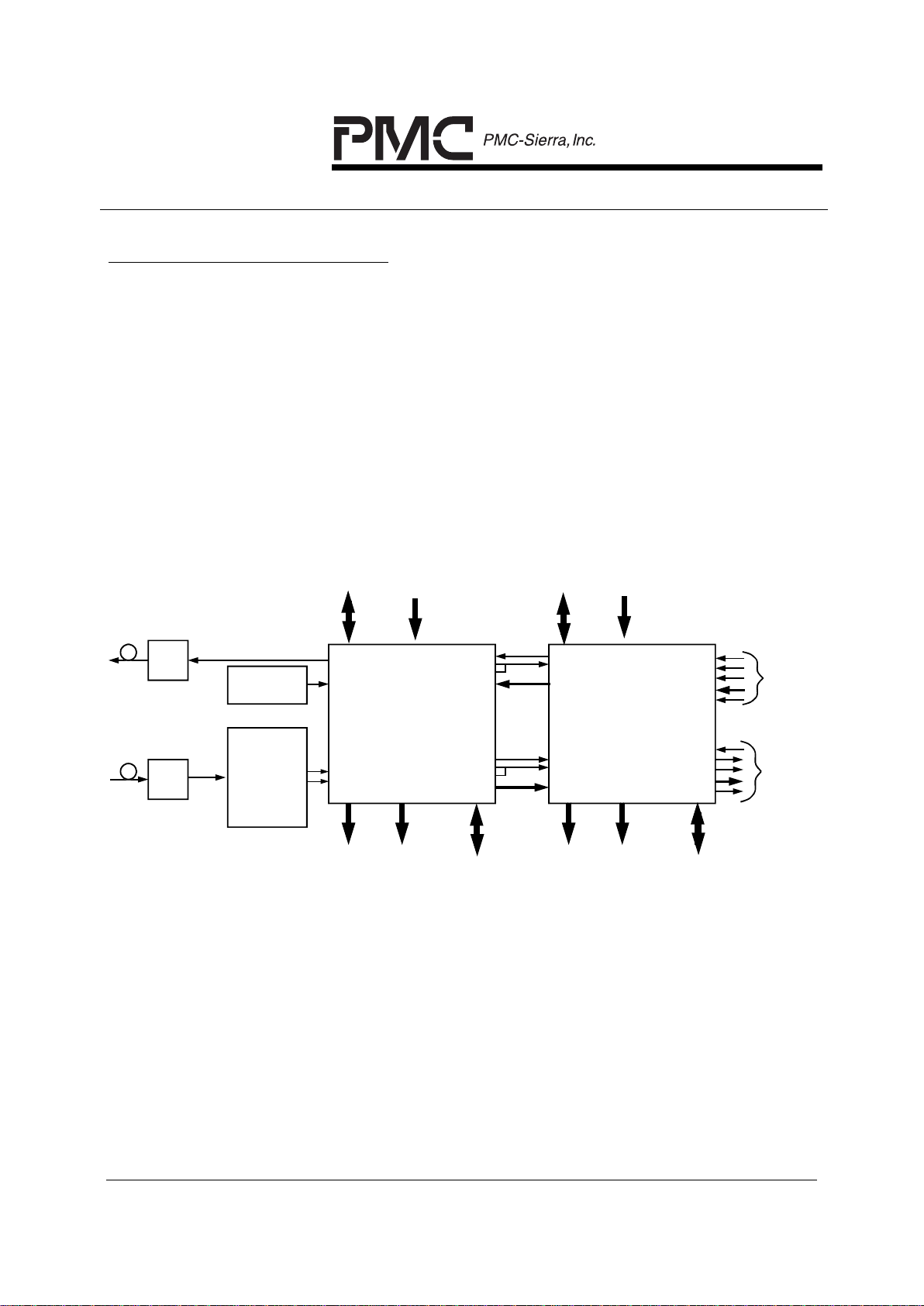
4
APPLICATION EXAMPLES
The following two examples show the SPTX used in typical SONET/SDH network
equipment applications. In the first example, the SPTX is paired with the PM5343
STXC 155 Mbit/s Section and Line overhead terminating transceiver to provide a
complete 155 Mbit/s SONET STS-3 or STS-3c/SDH STM-1 interface. In the
second example, four SPTX chips are used in conjunction with the PM5312
STTX 622 Mbit/s Section and Line overhead terminating transceiver to provide a
complete 622 Mbit/s SONET STS-12/SDH STM-4 interface. In both cases
external clock recovery and synthesis is available from a number of commercial
sources (additional information is available from PMC).
Figure 1 - 155 Mbit/s STS-3/STM-1 Add-Drop or Terminal Mux Interface
RECEIVE
ALARM DETECT
SIGNALS
TRANSMIT
ALARM INSERT
SIGNALS
TRANSMIT
TRANSPORT
OVERHEAD
ACCESS
RSD+/-
O/E
E/O
RXD+/-
RXC+/-
TXD+/-
PM5343 STXC
155 Mbit/s
Transport O verhead
Transceiver
Clock/Data
Recover
y
TXCI+/-
Clock
Generation
MICRO BUS
FOR CONFIG,
STATUS
AND CONTROL
RECEIVE
ALARM DETECT
SIGNALS
TRANSMIT
ALARM INSERT
SIGNALS
TRANSMIT
PATH
OVERHEAD
ACCESS
PM5344 SPTX
Path
Termin a ting
Transceiver
GTICLK
TICLK
TIFP
TIN[7:0]
TCK
FPOUT
TD[7:0 ]
GRICLK
RICLK
ROFP
ROU T [7:0]
PICLK
IFP
RD[7 :0]
DCK
DC1J1V1
DD[7 :0]
DPL
DDP
Telecombus
Drop
Interface
ACK
AC1J1V1
AD[7:0]
APL
ADP
Telecombus
Add
Interface
RECEIVE
PATH
OVERHEAD
ACCESS
MICRO BUS
FOR CONFIG,
STATUS
AND CONTROL
RECEIVE
TRANSPORT
OVERHEAD
ACCESS
PM5344 SPTX
DATA SHEET
PMC-930531 ISSUE 6 SONET/SDH PATH TERMINATING TRANSCEIVER
PROPRIETARY AND CONFIDENTIAL TO PMC-SIERRA, INC., AND FOR ITS CUSTOMERS’ INTERNAL USE
8
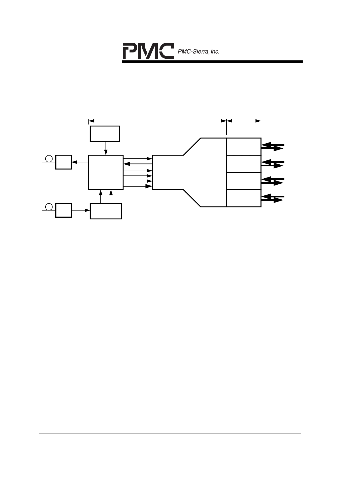
Figure 2 - 622 Mbit/s STS-12/STM-4 Add-Drop Multiplexer Aggregate
Interface
ADD-DROP
MUX
BACKPLANE
E/O
O/E
PM5318
SIPO
PM5312
STTX
Clock
S
y
nthesis
Clock
Recover
y
OOF
TOUT[7:0]
TCLK
RICLK
RIFP
RIN[7:0]
PM5344
SPTX
#1
#2
#3
#4
OPTICAL
FACILIT Y
STS-3(STM -1) To STS-12 (S TM-4) MUX
STS-3c (S TM-1)
Path T e rm in at io n
PM5344 SPTX
DATA SHEET
PMC-930531 ISSUE 6 SONET/SDH PATH TERMINATING TRANSCEIVER
PROPRIETARY AND CONFIDENTIAL TO PMC-SIERRA, INC., AND FOR ITS CUSTOMERS’ INTERNAL USE
9
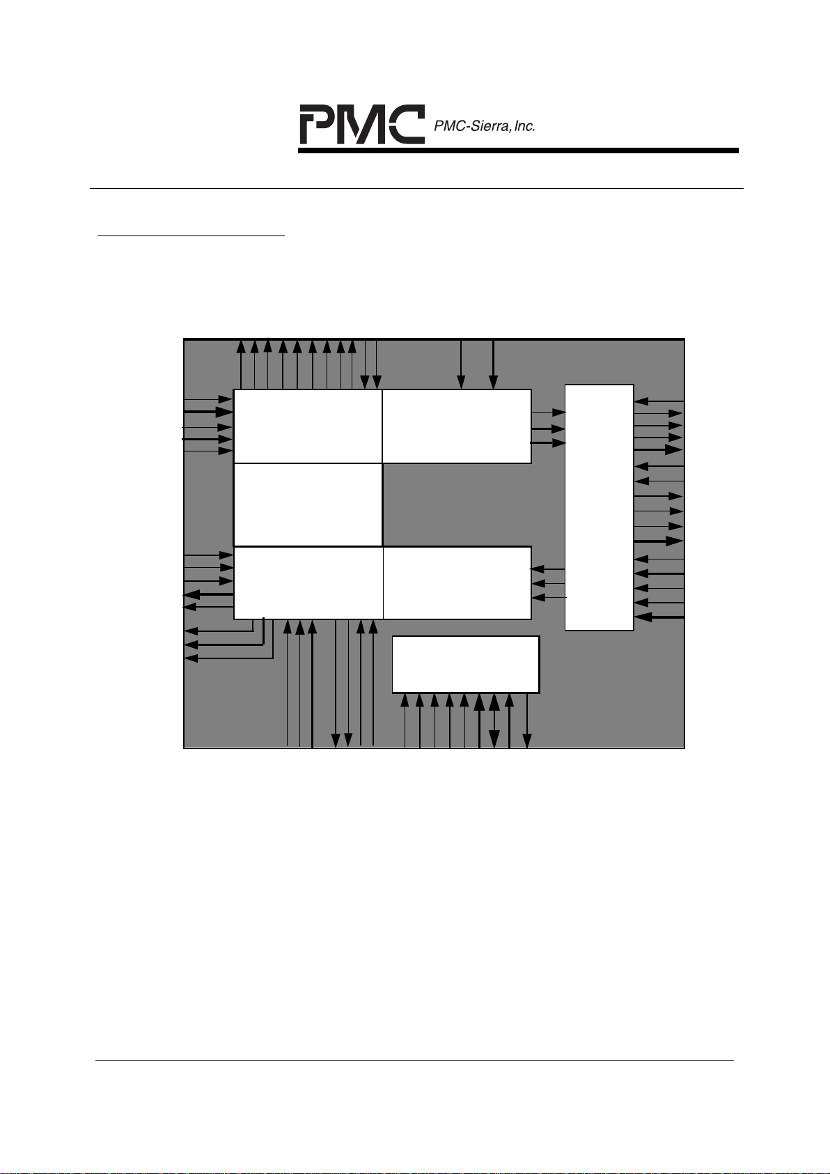
5
BLOCK DIAGRAM
PIC LK /RCK
IFP/RC 1J1V 1
PIN[7:0]/RD[7:0]
TCK
TD[7:0]
Tr ip le S T S - 1 (A U 3 ) /
Single STS-3c (AU4)
Receiv e Path Overhead
Process or
(3 x RPOP)
Tr ip le S T S - 1 (A U 3 ) /
Single STS-3c (AU4)
Path Tra ce B u ffer
(3 x SPTB)
Telecombu s
Interfac e
AD[7:0]
ADP
AC1J1V 1
APL
ACK
GC1J1V1
GPL
GFP
DD[7:0]
DDP
DC1J1V 1
DPL
DCK
LO
P
[3:
1
]
PA
IS
[3:
1
]
P
F
E
R
F
[3
:1
]
R
P
O
H
C
K
[3
:1
]
R
P
O
H
F
P
[3
:1
]
R
P
O
H
[3
:1
]
B
IP
E
[3
:1
]
R
T
C
E
N
[3
:1
]
R
T
C
O
H
[3
:1
]
Tr ip le T r a n s mi t
Telec o mbus
Aligner/Interface
(3 x TTA L)
D
F
P
GD[1:0]
LOM
[3
:1
]
Tr ip le Re c eiv e
Teleco mbus
A ligner/In terface
(3 x RTAL)
Microprocessor
Inter f a c e
C
S
B
R
D
B
W
R
B
AL
E
A[
8:
0]
D[7
:0
]
M
B
E
B
R
S
T
B
IN
T
B
GDP
TPAIS [3 :1 ]
TFP
RPL
RDP
FPO UT
TC1J1V1
TDP
TPL
R
A
D
T
P
O
H
E
N
[3
:1
]
T
P
O
H
[3
:1
]
T
P
O
H
F
P
[3
:1
]
T
P
O
H
C
K
[3
:1
]
T
A
F
P
TA
C
K
TA
D
GMFP
Tr ip le S T S - 1 (A U 3 ) /
Single STS-3c (A U4)
Transmit Path Overhead
Processor
(3 x TPOP)
DP
A
IS
[3
:1
]

PM5344 SPTX
DATA SHEET
PMC-930531 ISSUE 6 SONET/SDH PATH TERMINATING TRANSCEIVER
PROPRIETARY AND CONFIDENTIAL TO PMC-SIERRA, INC., AND FOR ITS CUSTOMERS’ INTERNAL USE
10
6
DESCRIPTION
The PM5344 SPTX SONET/SDH Path Terminating Transceiver is a monolithic
integrated circuit that implements payload alignment and path termination for
three STS-1 (AU3) paths or a single STS-3c (AU4) path, mapping these payloads
onto a Telecombus-like system backplane.
The SPTX operates in conjunction with the PM5343 STXC SONET/SDH
Transport Terminating Transceiver to form a complete system for terminating
section, line, and path overhead of a SONET STS-3 (SDH STM-1) or SONET
STS-1 electrical interface. Four SPTX devices operate in conjunction with the
PM5712 SLIM SONET/SDH Line Interface Module to form a complete system for
terminating section, line, and path overhead of a SONET STS-12 (SDH STM-4)
electrical interface.
The SPTX provides receive path termination for a SONET STS-1, STS-3 or STS3c stream, or equivalently, an AU3 or an SDH STM-1 stream carrying three AU3s
or one AU4. The SPTX interprets the received payload pointers (H1, H2) and
extracts the synchronous payload envelope (virtual container). The extracted
SPE (VC) is placed on a Telecombus DROP bu s. Frequency offsets (e.g., due to
plesiochronous network boundaries, or the loss of a primary reference timing
source) and phase differences (due to normal network operation) between the
received data stream and the DROP bus are accommodated by pointer
adjustments in the DROP bus. In addition to its basic processing of the received
SONET/SDH overhead, the SPTX provides convenient access to all overhead
bytes, which are extracted and serialized on lower rate interfaces, allowing
additional external processing of overhead, if desired.
The SPTX provides transmit path origination for a SONET STS-1, STS-3 or STS3c stream, or equivalently, an AU3 or an SDH STM-1 stream carrying three AU3s
or one AU4. The SPTX generates the transmit payload pointers (H1, H2) and
inserts the synchronous payload envelope (virtual container) from a Telecombus
ADD bus into the transmit stream. Frequency offsets (e.g., due to
plesiochronous network boundaries, or the loss of a primary reference timing
source) and phase differences (due to normal network operation) between the
transmit data stream and the ADD bus are accommodated by pointer
adjustments in the transmit stream. In addition to its basic processing of the
transmit SONET/SDH overhead, the SPTX provides convenient access to all
overhead bytes, which are inserted serially on lower rate interfaces, allowing
additional external sourcing of overhead, if desired. The SPTX also supports the
insertion of a large variety of errors into the transmit stream, such as bit
interleaved parity errors, and inverted NDF flags, which are useful for system

PM5344 SPTX
DATA SHEET
PMC-930531 ISSUE 6 SONET/SDH PATH TERMINATING TRANSCEIVER
PROPRIETARY AND CONFIDENTIAL TO PMC-SIERRA, INC., AND FOR ITS CUSTOMERS’ INTERNAL USE
11
diagnostics and tester applications.The SPTX supports in-band error reporting
where the path status byte (G1) inserted in the DROP bus reflects the number of
BIP-8 errors detected and the path FERF status. The SPTX can be
programmed to pass the path status byte on the ADD bus through unmodified.
This feature allows the transmit path processor to be located remotely to the
receive processor without having to incur the cost of routing an alarm port.
The SPTX supports tandem connection termination applications where the
tandem connection maintenance byte (Z5) carries the incoming BIP-8 error
count, a tandem data link, and a path AIS code. The incoming error count is
accumulated and the receive data link is serialized for external processing. A
new data link can be inserted from a low speed serial input. An incoming signal
failure alarm (ISF) is used to convey path AIS in place of all-ones in the pointer
(H1, H2).
The SPTX maintains a large number of statistics for performance monitoring
purposes. BIP-8 errors, and tandem path incoming error counts are
accumulated. In addition, the SPTX is selectable to accumulate positive and
negative pointer justifications that it receives or justifications that it generates on
the DROP bus. It also accumulates positive and negative pointer justifications in
the transmit stream. Excessive justifications may be indicative of clock
synchronization failures.
In STS-3c, STS-3 (AU4, three AU3s) applications, no auxiliary high speed clocks
are required as the SPTX operates from a set of plesiochronous 19.44 MHz
clocks. In STS-1 (single AU3) applications, the SPTX operates from a set of
plesiochronous 6.48 MHz clocks. The SPTX is configured, controlled and
monitored via a generic 8-bit microprocessor bus interface.
The SPTX is implemented in low power, +5 Volt, CMOS technology. It has TTL
compatible inputs and outputs and is packaged in a 160 pin PQFP package.

PM5344 SPTX
DATA SHEET
PMC-930531 ISSUE 6 SONET/SDH PATH TERMINATING TRANSCEIVER
PROPRIETARY AND CONFIDENTIAL TO PMC-SIERRA, INC., AND FOR ITS CUSTOMERS’ INTERNAL USE
12
7
PIN DIAGRAM
The SPTX is packaged in an 160 pin PQFP package having a body size of
28 mm by 28 mm and a pin pitch of 0.65 mm.
PIN 1
PIN 160
TOP
VIEW
PIN 40
PIN 41 PIN 80
PIN 81
PIN 120
PIN 121
TPAIS [3]
TDP
TPL
TC1J1V1
VDDO
VSSO
TD [0]
TD [1]
TD [2]
TD [3]
TD [4]
VDDO
TD[5]
VSSO
TD [6]
TD [7]
TFP
FPOUT
TCK
VDDI
VSSI
PICLK/RCK
IFP/RC1J1V1
PIN [0 ]/R D [0]
PIN [1 ]/R D [1]
PIN [2 ]/R D [2]
PIN [3 ]/R D [3]
PIN [4 ]/R D [4]
PIN [5 ]/R D [5]
PIN [6 ]/R D [6]
PIN [7 ]/R D [7]
RPL
RDP
MBEB
ALE
A [0]
A [1]
A [2]
A [3]
A [4]
A [5]
A [6]
A [7]
A [8]/TRS
RSTB
CSB
D [0]
D [1]
D [2]
VSSO
VDDO
D [3]
D [4]
D [5]
D [6]
D [7]
INTB
RDB/E
WRB/R
WB
VDDI
VSSI
VDDO
VSSO
LOP [1]
LOP [2]
LOP [3]
PAIS [1]
PAIS [2]
PAIS [3]
PFERF [1]
PFERF [2]
PFERF [3]
LOM [1]
VDDO
VSSO
LOM [2]
LOM [3]
BIPE [1]
BIPE [2]
BIPE [3]
APL
AC1J1V1
AD [0 ]
AD [1 ]
AD [2 ]
AD [3 ]
AD [4 ]
AD [5 ]
AD [6 ]
AD [7 ]
ACK
GFP
GMFP
GD [O]
GD [1 ]
GC1J1V1
GPL
VDDO
VSSO
VDDI
VSSI
GDP
DCK
DFP
DD [0]
DD [1]
DD [2]
DD [3]
DD [4]
DD [5]
DD [6]
VDDO
VSSO
DD [7]
DC1J1V1
DPL
DDP
DP A IS [1 ]
DP A IS [2 ]
DP A IS [3 ]
TP O HEN [3 ]
TP O HEN [2 ]
TP O HEN [1 ]
TP O H [2]
TP O H [1]
ADP
TPOHFP [2]
TPOHFP [1]
TP O H [3]
VSSO
TPOHCK [1]
TPOHFP [3]
TPOHCK [3]
TPOHCK [2]
VDDO
TAD
TAFP
TACK
VDDI
VSSI
RAD
RTCEN [3]
RTCEN [2]
RTCEN [1]
RTCOH [3]
RTCOH [2]
RTCOH [1]
RP O H [3]
RP O H [2]
RP O H [1]
VSSO
RP O HFP [2 ]
RP O HFP [1 ]
RPOHCK [1]
RP O HFP [3 ]
VDDO
TPAIS [
2]
TPAIS [
1]
RPOHCK [3]
RPOHCK [2]
PM5344
SPTX
Index

PM5344 SPTX
DATA SHEET
PMC-930531 ISSUE 6 SONET/SDH PATH TERMINATING TRANSCEIVER
PROPRIETARY AND CONFIDENTIAL TO PMC-SIERRA, INC., AND FOR ITS CUSTOMERS’ INTERNAL USE
13
8
PIN DESCRIPTION
Table 1 - Pin Description
Pin Name Type Pin
No.
Function
PICLK / Input 22 The parallel input clock (PICLK) provides timing for sampling t he receive
SONET/SDH stream, P I N[7:0] when external path term i nation is disabled. PICLK
is nominally a 19.44 MHz or 6.48 MHz, 50% duty cycle clock. Inputs PIN[7:0] and
IFP are sampled on the ris i ng edge of PICLK. Inputs RPL and RDP are ignored.
Outputs LOP[3:1], PAIS[3:1], and PFERF[3:1] are updated on the rising edge of
PICLK.
RCK The RECEIVE bus clock (RCK) provides t i m i ng for the RE CEIVE bus interface
when external path termi nation is enabled. RCK is nominally a 19.44 MHz or 6.48
MHz, 50% duty cycle clock. Outputs LOP[3:1], LOM[3:1], PAIS[3:1], PFERF[3:1],
BIPE[3:1], RAD, RPOH[3:1], RPOHFP[3:1], are RPOHCLK[3:1] are inactive.
Inputs RTCEN[3:1] and RTCOH[3:1] are ignored. Inputs RD[7:0], RC1J1V1, RPL,
and RDP are sampled on the rising edge of RCK.
PIN[7]
PIN[6]
PIN[5]
PIN[4]
PIN[3]
PIN[2]
PIN[1]
PIN[0] /
Input 31
30
29
28
27
26
25
24
The parallel receive data bus (PIN[7:0]) carries t he SONET/SDH frame in byte
serial format when external path termination is dis abled. PIN[7] is the most
significant bit (c orresponding to bit 1 of each serial word, the f i rst bit transmitted).
PIN[0] is the least significant bit (corres pondi ng t o bi t 8 of each serial word, the last
bit transmitted). PIN[7:0] is sampled on t he rising edge of PICLK.
RD[7]
RD[6]
RD[5]
RD[4]
RD[3]
RD[2]
RD[1]
RD[0]
The RECEIVE bus data (RD[7:0]) carries the SONET/SDH frame in byte serial
format when external path termination is enabled. RD[7] is the most significant bi t
(corresponding to bit 1 of each s erial word, the first bit transmit t ed). RD[0] is the
least significant bi t (corresponding to bit 8 of each seri al word, the l ast bit
transmitted). RD[7:0] is sampled on the risi ng edge of RCK.

PM5344 SPTX
DATA SHEET
PMC-930531 ISSUE 6 SONET/SDH PATH TERMINATING TRANSCEIVER
PROPRIETARY AND CONFIDENTIAL TO PMC-SIERRA, INC., AND FOR ITS CUSTOMERS’ INTERNAL USE
14
Pin Name Type Pin
No.
Function
IFP / Input 23 The active high framing posit i on signal (IFP) indicates when the fi rst byte of the
synchronous payload envelope (SPE byte 1 of STS-1 #1) is available on the
PIN[7:0] bus when external path termination is disabled. Note that IFP has a fixed
relationship to the SONET/SDH frame; the start of the SPE is determined by the
STS (AU) pointer and may change relative to IFP. IFP is sampled on the rising
edge of PICLK.
RC1J1V1 The receive composite timing si gnal (RC1J1V1) indicates the frame, payload and
tributary multiframe boundaries on the RECEIVE bus when external path
termination is enabled. RC1J1V1 pulses high with the RECEIVE bus payload
active signal (RPL) set low to mark the first STS-1 identif i cation byte or equivalently
the STM identificat i on byte. RC1J1V1 pulses high with RPL set high to mark the
path trace byte (J1). Optionally, the RC1J 1V 1 signal pulses high with RPL set hi gh
on the V1 byte to indicate tributary multiframe boundaries. RC1J1V1 is sampled on
the rising edge of RCK.
RPL Input 32 The RECEIVE bus payload active signal (RPL) indicates when RD[7:0] is carrying
a payload byte. I t is set high during path overhead and payload bytes and low
during transport overhead bytes. RPL is set high during the H3 byte to indicat e a
negative pointer justificati on event and set low during t he byte following H3 to
indicate a positive pointer just i fication event. RPL is ignored when external path
termination is di sabled. RPL is sampled on the rising edge of RCK .
RDP Input 33 The RECEIVE bus data parity signal (RDP) indicates the parity of the RECEI VE
bus signals. The RECEI VE data bus (RD[7:0]) is always included in parity
calculations. Internal register bits controls the inclusion of t he RPL and RC1J1V1
signals in parity calculations and the sense (odd/even) of the parity. RDP is
ignored when external path term i nation is disabled. RDP is sampled on the rising
edge of RCK.
RPOHCK[3]
RPOHCK[2]
RPOHCK[1]
Output 158
157
156
The receive path overhead clocks (RPOHCK[3:1]) provide timing t o process the
BIPE[3:1] signal s, to insert tandem pat h i ncoming error count and data link, and to
sample the extracted path overhead for the corresponding STS-1 (AU3) stream.
RPOHCK[3:1] are nominally 576 kHz clocks. In STS-3c (AU4) mode or STS-1
mode, only RPOHCK[1] is active. RTCEN[3:1], and RTCOH[3:1] are sampled on
the rising edge of the corres pondi ng RPOHCK signal. BIPE[3:1], RPOH[3:1] and
RPOHFP[3:1] are updated on the falling edge of the corres ponding RPOHCK
signal.
RPOHCK[1] provides timing for the serial receive alarm indication port (RAD),
which is updated on the falling edge of RPOHCK[1].
RPOHCK[3:1] are inactive when external path termination is enabled.

PM5344 SPTX
DATA SHEET
PMC-930531 ISSUE 6 SONET/SDH PATH TERMINATING TRANSCEIVER
PROPRIETARY AND CONFIDENTIAL TO PMC-SIERRA, INC., AND FOR ITS CUSTOMERS’ INTERNAL USE
15
Pin Name Type Pin
No.
Function
RPOH[3]
RPOH[2]
RPOH[1]
Output 150
149
148
The receive path overhead data signals (RPOH[3:1]) contai n the path overhead
bytes (J1, B3, C2, G1, F2, H4, Z3, Z4, and Z5) extracted from the path overhead of
the corresponding STS-1 (AU3) stream. In STS-3c (AU4) mode or STS-1 mode,
only RPOH[1] is active. Each RPOH signal is updated on the falling edge of the
corresponding RPOHCK signal.
RPOH[3:1] are inactive when external pat h termination is enabled.
RPOHFP[3]
RPOHFP[2]
RPOHFP[1]
Output 155
152
151
The receive path overhead frame position signals (RPOHFP[3:1]) may be used to
locate the individual path overhead bits in the path overhead data stream for the
corresponding STS-1 (AU3) stream. Each RPOHFP[3:1] signal is logic 1 when bit
1 (the most signific ant bit) of the path trace byte (J1) is present in the
corresponding RPOH stream. In STS-3c (AU4) mode or STS-1 mode, only
RPOHFP[1] is active. Each RPOHFP signal is updated on the falling edge of the
corresponding RPOHCK signal.
RPOHFP[1] may be used to located the BIP error count and path FERF indicati on
bits on the receive alarm port data signal (RAD). RPOHFP[1] is logic 1 when t he
first of eight BIP error positions from the first S T S-1 (AU3) or the STS-3c (AU4)
stream is present on the rec ei ve alarm data signal (RAD).
RPOHFP[3:1] are inactive when external path termination is enabled.
RTCEN[3]
RTCEN[2]
RTCEN[1]
Input 144
143
142
The receive tandem connection overhead insert enable signals (RTCEN[3:1])
control the insertion of incoming error count and data l i nk i n the tandem connection
maintenance byte (Z5), on a bit-by-bit basis. When RTCEN is set high, the data on
the corresponding RTCOH stream is inserted into the associ ated bit in the Z5 byte.
RTCEN has significance only dur i ng t he the J1 byte positions in the RPOHCK
clock sequence and is ignored at all ot her t i mes. In STS-3c (AU4) mode or STS-1
mode, only RTCEN[1] is signific ant. RTCE N i s sampled on the rising edge of the
corresponding RPOHCK signal.
RTCEN[3:1] are ignored when external path termination is enabled.
RTCOH[3]
RTCOH[2]
RTCOH[1]
Input 147
146
145
The receive tandem connection overhead data signals (RTCOH[3:1]) contai n the
incoming error count and data link m essage to be inserted i nto the tandem
connection maintenance byte (Z5). When RTCEN is set high, the values sampled
on RTCOH is inserted into t he Z5 byte. When RTCEN is set low, t he I EC field of
Z5 reports the incoming path BIP error count and the data li nk field is set to all
ones. In STS-3c (AU4) mode or STS-1 mode, only RTCEN[1] is significant.
RTCOH is sampled on the rising edge of the corresponding RPOHCK signal.
RTCOH[3:1] are ignored when external path termination is enabled.

PM5344 SPTX
DATA SHEET
PMC-930531 ISSUE 6 SONET/SDH PATH TERMINATING TRANSCEIVER
PROPRIETARY AND CONFIDENTIAL TO PMC-SIERRA, INC., AND FOR ITS CUSTOMERS’ INTERNAL USE
16
Pin Name Type Pin
No.
Function
BIPE[3]
BIPE[2]
BIPE[1]
Output 80
79
78
The bit interleaved parity error signals (B IPE[3:1]) signal is s et hi gh for one
RPOHCK period for each path BIP-8 error detec t ed (up to eight per frame) or once
if any of the BIP-8 bits are i n error dependi ng on whet her BIP-8 errors are treated
on a bit or block basis. Pat h BIP-8 errors are detected by comparing the extracted
path BIP-8 byte (B3) with the comput ed BIP-8 for the previous frame. In STS-3c
(AU4) mode or STS-1 mode, only BIP[1] is acti ve. BIPE[3:1] is updated on t he
falling edge of RPOHCK.
BIPE[3:1] are inactive when external path termination i s enabled.
RAD Output 139 The receive alarm port data signal (RAD) contains the pat h B IP error count and the
path FERF status of the t hree receive STS-1 (AU3) streams or the single STS-3c
(AU4) stream. RAD is updated on the falling edge of RPOHCK[1].
RAD is inactive when external path t ermination is enabled.
LOP[3]
LOP[2]
LOP[1]
Output 66
65
64
The loss of pointer signals (LOP [3:1]) indicate the loss of poi nter state in the
associated SONET/S DH stream. LOP is set high when invalid STS pointers are
received in eight consecutive frames, or if eight consecutive enabled NDFs are
detected in the corresponding ST S-1 (AU3) stream. The loss of pointer s t ate is
exited (LOP set low) when the same valid STS pointer, with disabled NDF, is
detected for three consecutive frames. In STS-3c (AU4) mode, only LOP[1] is
active and loss of pointer state (LOP[1]) depends only on the first of three H1, H2
bytes; the value of the concatenation indicators do not affect LOP[1] signal. In
STS-1 mode, only LOP[1] is active. LOP[3:1] are updated on the ris i ng edge of
PICLK.
LOP[3:1] are inactive when external pat h termination is enabled.
PAIS[3]
PAIS[2]
PAIS[1]
Output 69
68
67
The path alarm indicati on signals (PAI S[3:1]) indicate the STS path AIS state
associated with the SO NE T/SDH stream. PAIS is set hi gh when an al l ones
pattern is observed in the STS-1 pointer bytes (H1, and H2) for three consecuti ve
frames in the corresponding STS-1 (AU3) stream. Path AIS is removed when the
same valid pointer with normal NDF i s detected for three consecutive frames or a
single valid pointer with NDF set is received. In STS-3c (AU4) mode, only PAI S[1]
is active and depends only on the firs t of three H1, H2 bytes; the value of the
concatenation indicators do not affect PAIS[1]. In STS-1 mode, only PAIS[ 1] is
active. PAI S[3:1] are updated on the rising edge of P ICLK.
PAIS[3:1] are inactive when external path termination is enabled.
PFERF[3]
PFERF[2]
PFERF[1]
Output 72
71
70
The path far end receive failure signals (PFERF[3:1]) indicate the STS path FERF
state associated wi t h the SONET/SDH stream. PFERF is set high when the path
FERF alarm bit (bit 5) of the STS path status (G1) byte is set high for five
consecutive frames. STS path FERF is removed when bit 5 of the G1 byte is set
low for five consecutive frames. In STS-3c (AU4) mode and STS-1 mode, only
PFERF[1] is active. PFERF[3:1] are updated on the ris i ng edge of PICLK.
PFERF[3:1] are inactive when exter nal pat h termination is enabled.

PM5344 SPTX
DATA SHEET
PMC-930531 ISSUE 6 SONET/SDH PATH TERMINATING TRANSCEIVER
PROPRIETARY AND CONFIDENTIAL TO PMC-SIERRA, INC., AND FOR ITS CUSTOMERS’ INTERNAL USE
17
Pin Name Type Pin
No.
Function
LOM[3]
LOM[2]
LOM[1]
Output 77
76
73
The loss of multiframe signals (LOM [3:1]) indicate the tributar y multiframe
synchronization st at us associated with the SONE T/ SDH stream. LOM is set low
when a correct sequence has been detec t ed for four consecut i ve frames. LOM is
set high if a correct four frame sequence is not detected in eight frames. In STS-3c
(AU4) mode and STS-1 mode, only LOM[1] is active. LOM[3:1] are updated on the
rising edge of PICLK.
LOM[3:1] are inactive when external pat h termination is enabled.
DCK Input 98 The DROP bus clock (DCK) provides timing for the DROP bus interface. DCK is
nominally a 19.44 MHz or 6.48 MHz, 50% duty cycle clock. Frequency offsets
between PICLK/RCK and DCK are accomm odat ed by pointer j ustification events
on the DROP bus. DFP i s sampled on the rising edge of DCK. Outputs DPL,
DC1J1V1, DDP and DD[7:0] are updated on t he rising edge of DCK.
DFP Input 97 The active high DROP bus reference frame position signal (DFP) i ndi cates when
the first byte of the synchronous payload envelope (SPE byte 1 of STS-1 #1) is
available on the DD[7:0] bus. Note t hat DFP has a fixed relationship to the
SONET/SDH frame; the start of the SPE is determined by the STS (AU) pointer
and may change relative to DFP. DFP is sampled on the r i sing edge of DCK.
DPAIS[3:1] Input 81
82
83
The active high DROP bus path alarm indication signal s (DPAIS[3:1]) controls the
insertion of pat h AIS in the DROP bus DD[7:0]. A high level on DPAI S forces the
insertion of the all ones pat tern into the complete SPE, and the payload pointer
bytes (H1, H2, and H3). DROP bus path AIS insertion can also be inserted via
register access or in res ponse to ISF code in termi nat i ng tandem connection
termination equipment appl i cations. In STS-3c (AU4) mode or STS-1 mode, only
DPAIS[1] is significant. DPAI S [3:1] is sampled on the rising edge of DCK.
DD[7]
DD[6]
DD[5]
DD[4]
DD[3]
DD[2]
DD[1]
DD[0]
Output 87
90
91
92
93
94
95
96
The DROP bus data (DD[7:0]) contains the SONET/S DH rec ei ve payload data.
The transport overhead bytes, with the exception of the H1, H2 poi nter bytes, are
set to zeros. The fixed stuff columns in a t ributary mapped SPE (VC) may also be
optionally set to zero or NPI . DD[7] is the most significant bit (corres pondi ng t o bi t
1 of each serial word, the firs t bit transmitted). DD[0] is the least signifi cant bit
(corresponding to bit 8 of each s erial word, the last bit transmitt ed). DD[7:0] is
updated on the rising edge of DCK.
DPL Output 85 The active high DROP bus payload active signal (DPL) indicates when the DD[7:0]
is carrying a payload byte. It is set high during path overhead and payload bytes
and low during transport overhead bytes. DPL is set high during the H3 byte to
indicate a negative pointer justif i cation event and set low during the byte following
H3 to indicate a positive pointer jus tification event. DPL is updated on the rising
edge of DCK.

PM5344 SPTX
DATA SHEET
PMC-930531 ISSUE 6 SONET/SDH PATH TERMINATING TRANSCEIVER
PROPRIETARY AND CONFIDENTIAL TO PMC-SIERRA, INC., AND FOR ITS CUSTOMERS’ INTERNAL USE
18
Pin Name Type Pin
No.
Function
DC1J1V1 Output 86 The DROP bus composite timing signal (DC1J1V1) indi cates the frame, payload
and tributary multiframe boundaries on the DROP data bus DD[7:0]. DC1J1V1
pulses high with the DROP bus payload active signal (DPL) set low to mar k the first
STS-1 Identificati on byte or equivalentl y the STM identification byte (C1).
DC1J1V1 pulses high with DPL s et high to mark the path trace byte (J1).
Optionally, the DC1J1V1 signal pulses high on the V1 byte to indicate tributary
multiframe boundaries. DC1J1V1 is updated on the rising edge of DCK.
DDP Output 84 The DROP bus data parity signal (DDP) indicates the parity of the DROP bus
signals. The DROP data bus (DD[7:0]) i s al ways included i n parity calculations.
The internal register bits control the inclusion of t he DPL and DC1J1V1 signals in
parity calculati on and the sense (odd/even) of the parity. DDP is updated on the
rising edge of DCK.
ACK Input 110 The ADD bus clock (ACK) provides timing for the ADD bus and the GENERATED
bus interfaces. ACK is nominally a 19.44 MHz or 6.48 MHz, 50% duty cycle clock.
Inputs AD[7:0], A P L, AC1J1V1, GFP and GMFP are sampled on the ris i ng edge of
ACK. Outputs GPL, GC1J1V1, and GD[1:0] are updated on the risi ng edge of
ACK.
AD[7]
AD[6]
AD[5]
AD[4]
AD[3]
AD[2]
AD[1]
AD[0]
Input 111
112
113
114
115
116
117
118
The ADD bus data (AD[7:0]) contains t he S O NE T/SDH transmit payload data. The
transport overhead bytes, including the H1, H2 pointer bytes, are ignored. The
phase relation of the SPE (VC) to the transport frame is determined by the ADD
bus composite timing signal (AC1J1V1). AD[7] is the most significant bit
(corresponding to bit 1 of each s erial word, the first bit transmit t ed). AD[0] is the
least significant bi t (corresponding to bit 8 of each seri al word, the l ast bit
transmitted). AD[7:0] is sampled on the rising edge of ACK.
APL Input 120 The ADD bus payload active signal (APL) indic at es when AD[7:0] is carrying a
payload byte. I t is set high during path overhead and payload bytes and low during
transport overhead bytes. APL is set high during the H3 byte to indicate a negat i ve
pointer justificat i on event and set low during the byte following H3 to indic ate a
positive pointer justific ation event. APL is sampled on the rising edge of ACK.
AC1J1V1 Input 119 The ADD bus composite timing signal (AC1J1V1) identifies the frame, payload and
tributary multiframe boundaries on the ADD data bus AD[7:0]. AC1J1V1 pulses
high with the ADD bus payload active signal (APL) set low to mark the first STS-1
Identification byte or equivalently t he STM identification byte (C1). AC1J1V1
pulses high with APL set hi gh to mark the path trace byte (J1). The AC1J1V1
signal pulses high on the V1 byte to indicate tributar y multiframe boundaries.
AC1J1V1 is sampled on the rising edge of ACK.

PM5344 SPTX
DATA SHEET
PMC-930531 ISSUE 6 SONET/SDH PATH TERMINATING TRANSCEIVER
PROPRIETARY AND CONFIDENTIAL TO PMC-SIERRA, INC., AND FOR ITS CUSTOMERS’ INTERNAL USE
19
Pin Name Type Pin
No.
Function
ADP Input 121 The ADD bus data parity signal (ADP) indicates the parity of the ADD bus signals.
The ADD data bus (AD[7:0]) is always included in pari t y calculations. Internal
register bits controls the inclusion of the APL and AC1J1V1 si gnal s in parity
calculations and the sense (odd/even) of the parity. ADP is sampled on the r i sing
edge of ACK.
GFP Input 109 The active high GENE RATED bus reference frame position signal (GFP) indicates
when the first byte of the synchronous payload envelope (SPE byte 1 of STS-1 #1)
is available on the GD[1:0] bus. Note that GFP has a fixed relationship to t he
SONET/SDH frame; the start of the SPE is determined by the STS (AU) pointer
and may change relative to GFP. GFP is sampled on the r i sing edge of ACK.
GMFP Input 108 The active high GENERATED reference multiframe position signal (GMFP) is used
to align the SONET/SDH tributary multiframe boundary on the GE NERATED bus.
GMFP should be brought high for a single ACK period every 9720 ACK cycles, or
multiples thereof. GMFP may be tied low if such synchronization is not required. A
pulse on GMFP realigns the GENERATED bus to be the first of four frames in the
multiframe. I.e., the frame containing the V1 bytes. In S T S-1 mode, GMFP is
sampled one ACK cycle after the J1 indication on GC1J1V1. In STS-3/3c modes,
GMFP is sampled three ACK cycles after the J1 indication. GMFP is ignored at
other byte positions. GMFP is sampled on the rising edge of ACK.
GD[1]
GD[0]
Output 106
107
The GENERATED bus data (GD[1:0]) contains cyclical multiframe count carried in
the H4 byte. The sequence is i ni tialized to 'b01 by a high pulse on GMFP, and
increments at the byte following J1. GD[1:0] is updated on the risi ng edge of ACK.
GPL Output 104 The GENERATED bus pay l oad active signal (GPL) indicates when GD[1:0] is
carrying a payload byte. GPL distinguishes between payload and transport
overhead timeslots in the GENERATED bus. Since the GENE RATED bus is
expected to have fixed timing relationship with the ADD bus, access m odul es may
use GPL to locate payload timeslots in the ADD bus. GPL is updated on the rising
edge of ACK.
GC1J1V1 Output 105 The GENE RATED bus composite timing signal (GC1J1V1) identifies the frame,
payload and tributary multiframe boundaries on the GENERATED data bus
GD[1:0]. GC1J1V1 pulses high with the GENERATED bus pay l oad active signal
(GPL) set low to mark the fi rst STS-1 Identificati on byte or equivalently the STM
identification byte (C1). GC1J1V1 pulses high with GPL set hi gh to mark the path
trace byte (J1). The GC1J1V1 signal pulses high on the V1 byte to indicate
tributary multiframe boundaries. Since the GENERATED bus is expected to have
fixed timing relationship with the ADD bus, access modules may use GC1J1V1 to
located the frame, payload and tributary multiframe boundaries on the ADD bus.
GC1J1V1 is updated on the ris i ng edge of ACK.

PM5344 SPTX
DATA SHEET
PMC-930531 ISSUE 6 SONET/SDH PATH TERMINATING TRANSCEIVER
PROPRIETARY AND CONFIDENTIAL TO PMC-SIERRA, INC., AND FOR ITS CUSTOMERS’ INTERNAL USE
20
Pin Name Type Pin
No.
Function
GDP Output 99 The GENERATE D bus data par i ty signal (GDP) indicates t he parity of the
GENERATED bus signal s. The GENERATED data bus (GD[1:0]) is always
included in parity cal culations. The internal register bits cont rol the inclusion of the
GPL and GC1J1V1 signals in pari ty calculation and the sense (odd/ even) of the
parity. GDP is updated on t he rising edge of ACK.
TCK Input 19 The transmit reference clock (TCK) provides timing for SPTX transmit f unc tions.
TCK is nominally a 19.44 MHz or 6.48 MHz, 50% duty cycle clock. Frequency
offsets between TCK and ACK are accommodated by pointer justification events on
the transmit data stream. Inputs TFP, TPAIS[3:1] and TPFERF[3:1] are sampled on
the rising edge of TCK. Outputs TD[7:0], TPL, TDP, TC1J1V1 and FPOUT are
updated on the rising edge of TCK, while TPOHCLK[3:1] is updated on the falling
edge of TCK.
TFP Input 17 The active high transmit reference frame position (TFP) is used to align the
SONET/SDH transpor t frame generated by the SPTX device to a system
reference. TFP indicates when the first byte of the sync hronous payload envelope
(SPE byte 1 of STS-1 #1) is available on the TD[7:0] bus. TFP should be brought
high for a single TCK period every 2430 TCK cycles, or multiples thereof. TFP may
be tied low if such synchronization is not required. TFP is sampled on the ri sing
edge of TCK.
TD[7]
TD[6]
TD[5]
TD[4]
TD[3]
TD[2]
TD[1]
TD[0]
Output 16
15
12
11
10
9
8
7
The TRANSMIT bus data (TD[7:0]) carries the SONET/S DH frame in byte serial
format. The transport overhead bytes, with the exception of H1, H2 pointer bytes,
are set to zero. The fixed stuff columns in a tributary based SPE (VC) may be
optionally set to zero or NPI . TD[7] is the most significant bit (corresponding to bit
1 of each serial word, the firs t bit transmitted). TD[0] is the least significant bit
(corresponding to bit 8 of each s erial word, the last bit transmitt ed). TD[7:0] is
updated on the rising edge of TCK.
TPL Out put 3 The TRANSMIT bus payload active signal (TPL) indic at es when TD[7:0] is carrying
a payload byte. I t is set high during path overhead and payload bytes and low
during transport overhead bytes. TPL is set high during t he H3 byte to i ndi cate a
negative pointer justificati on event and set low during t he byte following H3 to
indicate a positive pointer just i fication event. TPL is updated on t he rising edge of
TCK.
TC1J1V1 Output 4 The TRANSMIT bus composite timing signal (TC1J1V1) i dent i fies the frame,
payload and tributary multiframe boundaries on the TRANSMIT data bus TD[ 7:0].
TC1J1V1 pulses high with the TRANSMIT bus payload active signal (TPL) set l ow
to mark the first STS-1 Identification byte or equivalently t he STM identification
byte (C1). TC1J1V1 puls es hi gh wi th TPL set high to mark the path trace byte (J1).
The TC1J1V1 signal pulses high on the V1 byte to indicate tributary multiframe
boundaries. TC1J 1V1 is updated on the rising edge of TCK.

PM5344 SPTX
DATA SHEET
PMC-930531 ISSUE 6 SONET/SDH PATH TERMINATING TRANSCEIVER
PROPRIETARY AND CONFIDENTIAL TO PMC-SIERRA, INC., AND FOR ITS CUSTOMERS’ INTERNAL USE
21
Pin Name Type Pin
No.
Function
TDP Output 2 The TRANSMIT bus parity signal (TDP) i ndi cates the parity of the TRANSMIT bus
signals. The TRANSMIT data bus (TD[7:0]) i s al ways included i n parity
calculations. The internal register bits control the incl usion of the TPL and
TC1J1V1 signals in parit y calculation and the sense (odd/even) of the parity. TDP
is updated on the rising edge of TCK.
TPAIS[3]
TPAIS[2]
TPAIS[1]
Input 1
160
159
The active high transmit path alar m i ndi cation signals (TPAIS[3:1]) control s the
insertion of pat h AIS in the TRANSMIT bus TD[7:0]. A hi gh l evel on TPAIS forces
the insertion of the all ones pattern into the complete SPE, and the payload pointer
bytes (H1, H2, and H3). Transmit path AIS insertion can also be inserted v i a
register access or in res ponse to ISF code in termi nat i ng tandem connection
termination equipment appl i cations. In STS-3c (AU4) mode or STS-1 mode, only
TPAIS[ 1] is significant. TPAI S [3:1] is sampled on the rising edge of TCK.
TPOH[3]
TPOH[2]
TPOH[1]
Input 124
123
122
The path overhead data signals (TPOH[3:1])... signal contains t he path overhead
bytes (J1, C2, G1, F2, Z3, Z4, and Z5) and error mas k (B3 and H4) which may be
inserted, or used to insert multiframe sequence bit errors into the path overhead
byte positions in the TRANSMIT bus TD[7:0]. Insertion is controlled by the
corresponding TPOHEN input, or by bits in internal registers. In STS-3c (AU4)
mode or STS-1 mode, only TPOH[1] is significant. Each TPOH input is sampled on
the rising edge of the corres pondi ng TPOHCK output.
TPOHEN[3]
TPOHEN[2]
TPOHEN[1]
Input 135
134
133
The transmit path overhead insert enable signals (TP OHEN[3:1]), together with
internal register bits, control the source of the path overhead data which is inserted
in the TRANSMIT bus TD[7:0]. While TPOHEN is high, values sampled on the
TPOH input are inser t ed i nto the corresponding path overhead bit position (for the
J1, C2, G1, F2, Z3, Z4, and Z5 bytes). While TP OHE N is low, values obtained from
internal registers are i nserted into these pat h overhead bit positions. A high level
on TPOHEN during the B3 bit positions enables an error mask. While the error
mask is enabled, a high level on input TPOH causes the corresponding B3 bit
position to be inverted. A low level on TP OH al l ows t he c orresponding bit position
to pass through the SPTX uncorrupted. In STS-3c (AU4) mode or STS-1 mode,
only TPOHEN[1] is significant. Each TPOHEN input is sampled on the rising edge
of the corresponding TPOHCK output.
TPOHCK[3]
TPOHCK[2]
TPOHCK[1]
Output 132
131
128
The transmit path overhead clocks (TPOHCK[3:1]) provide t i m i ng to update the
corresponding path overhead stream, TPOH. In STS-3c (AU4) mode, TPOHCK[1]
is a 576kHz clock and TPOHCK[3:2] are inactive. TPOH and TPOHEN are
sampled on the rising edge of t he corresponding TPOHCLK.
TPOHFP[3]
TPOHFP[2]
TPOHFP[1]
Output 127
126
125
The path overhead frame position signals (TPOHFP[3:1]) may be used to locate
the individual path overhead bits in the overhead data stream, TPOH. TPOHFP is
logic 1 when bit 1 (the most s i gni ficant bit) of the Path Trace byte (J1) is present in
the TPOH stream. In STS-3c (AU4) m ode or S T S -1 m ode, only TPOHFP[1] is
active. Each TPOHFP out put is updated on the falling edge of the corresponding
TPOHCK output.

PM5344 SPTX
DATA SHEET
PMC-930531 ISSUE 6 SONET/SDH PATH TERMINATING TRANSCEIVER
PROPRIETARY AND CONFIDENTIAL TO PMC-SIERRA, INC., AND FOR ITS CUSTOMERS’ INTERNAL USE
22
Pin Name Type Pin
No.
Function
FPOUT Output 18 The frame pulse output signal (FPOUT) marks the first SPE byte in the TRANSMIT
bus TD[7:0] (the byte after the last C1 byte). The transmit f rame ali gnm ent of peer
SPTX devices may be synchronized by connecti ng t he FPOUT signal of the master
to the transmit frame pulse input (TFP) of al l t he S PTX devices in the set. FPOUT
is updated on the rising edge of TCK.
TAD Input 138 The transmit alarm port dat a s i gnal (TAD) contains the path FEBE error count and
the path FERF status of t he three associated receive STS-1 (AU3) streams or the
single STS-3c (AU4) stream. TAD is sampled on the rising edge of TACK.
TAFP Input 137 The transmit alarm port frame pulse signal (TAFP) marks the first bit of the t ransmi t
alarm message in eac h S O NE T (SDH) frame. TAFP is pulsed high to mark t he first
FEBE bit location of the first STS-1 (AU3) stream or the first FEBE bit location of
the single STS-3c (AU4) stream. TAFP is sampled on the rising edge of TACK.
TACK Input 136 The transmit alarm port clock (TACK) provides t i ming for transmit alarm por t . TACK
is nominally a 576 kHz cl ock. Inputs TAD and TAFP are sampled on the rising edge
of T ACK.
CSB Input 46 The active low chip select (CSB) si gnal i s low during SPTX register acces ses.
RDB Input 58 The active low read enable (RDB) signal is low during S PTX register read
accesses. The SPTX drives the D[7:0] bus with the contents of the addressed
register while RDB and CSB are low.
E The active high external access signal (E) is set high during SPTX register access
while in Motorola bus mode.
WRB Input 59 The active low write strobe (WRB) signal is l ow during a SPTX register write
accesses. The D[7:0] bus contents are clocked into the addressed register on the
rising WRB edge while CSB is low.
RWB The read/write select signal (RWB) selects between SPTX register read and write
accesses while in Mot orol a bus mode. The SPTX drives the data bus D[7:0] with
the contests of the addressed register while CSB is low and RWB and E are high.
The contents of D[7:0] are clocked into the addressed register on the falling E edge
while CSB and RWB are low.
D[0]
D[1]
D[2]
D[3]
D[4]
D[5]
D[6]
D[7]
I/O 47
48
49
52
53
54
55
56
The bidirectional data bus D[7:0] is used during SPTX register read and wri te
accesses.

PM5344 SPTX
DATA SHEET
PMC-930531 ISSUE 6 SONET/SDH PATH TERMINATING TRANSCEIVER
PROPRIETARY AND CONFIDENTIAL TO PMC-SIERRA, INC., AND FOR ITS CUSTOMERS’ INTERNAL USE
23
Pin Name Type Pin
No.
Function
A[0]
A[1]
A[2]
A[3]
A[4]
A[5]
A[6]
Input 36
37
38
39
40
41
42
The address bus A[8:0] selects specific registers dur i ng S PTX register accesses.
A[7]
A[8]/TRS
4344The test register selec t (TRS) signal selects between norm al and test mode
register accesses. TRS is high during test mode register accesses, and is low
during normal mode regis t er accesses. TRS has an integral pull down resistor.
RSTB Input 45 The active low reset (RSTB) signal provides an asynchronous SPTX reset. RSTB
is a Schmitt triggered input with an integral pull up resistor.
ALE Input 35 The address latch enable (ALE) is active high and latches t he address bus A[8:0]
when low. When ALE is high, the internal address latches are transparent. It
allows the SPTX to interface to a multi pl exed address/data bus. ALE has an
integral pull up resistor.
MBEB Input 34 The active low Motorola bus enable (MBEB) signal configures the SPTX for
Motorola bus mode where the RDB/E signal functions as E, and the WRB/RWB
signal functions as RWB. When MBEB is high, the SPTX is configured for Intel bus
mode where the RDB/E signal functions as RDB. The MBEB input has an integral
pull up resistor.
INTB OD
Output
57 The active low interrupt (INTB) signal goes low when a SPTX i nterrupt source is
active, and that source is unmasked. The SPTX may be enabled to report several
alarms or events via interrupts. Examples are changes i n the loss of pointer state,
changes in the path AIS s t ate, changes in the path FERF state, changes i n the
path status, path BIP-8 error events, FEBE events, pointer adjustment events and
pointer error events. INTB returns high when t he i nterrupt is acknowledged via an
appropriate register acces s. INTB is an open drain output.
VDDI1
VDDI2
VDDI3
VDDI4
Power 20
60
101
141
The core power (VDDI1 - VDDI4) pins should be connected to a well decoupled +5
V DC in common with VDDO.
VSSI1
VSSI2
VSSI3
VSSI4
Ground 21
61
100
140
The core ground (VSSI1 - VSSI4) pins should be connected to GND in common
with VSSO.

PM5344 SPTX
DATA SHEET
PMC-930531 ISSUE 6 SONET/SDH PATH TERMINATING TRANSCEIVER
PROPRIETARY AND CONFIDENTIAL TO PMC-SIERRA, INC., AND FOR ITS CUSTOMERS’ INTERNAL USE
24
Pin Name Type Pin
No.
Function
VDDO1
VDDO2
VDDO3
VDDO4
VDDO5
VDDO6
VDDO7
VDDO8
VDDO9
Power 5
13
51
62
74
89
103
130
154
The pad ring power (VDDO1 - VDDO9) pins should be connected to a well
decoupled +5 V DC in common with VDDI.
VSSO1
VSSO2
VSSO3
VSSO4
VSSO5
VSSO6
VSSO7
VSSO8
VSSO9
Ground 6
14
50
63
75
88
102
129
153
The pad ring ground (VSSO1 - VSSO9) pins should be connected to GND in
common with VSSI.
Notes on Pin Description:
1. All SPTX inputs and bidirectionals present minimum capacitive loading and
operate at TTL logic levels.
2. All SPTX digital outputs and bidirectionals have 2 mA drive capability, except
the INTB open drain output and D[7:0] bidirectionals, which have 4 mA drive
capability. All outputs use slew rate limited pads.
3. The VSSO and VSSI ground pins are not internally connected together.
Failure to connect these pins externally may cause malfunction or damage
the SPTX.
4. The VDDO and VDDI power pins are not internally connected together.
Failure to connect these pins externally may cause malfunction or damage
the SPTX.

PM5344 SPTX
DATA SHEET
PMC-930531 ISSUE 6 SONET/SDH PATH TERMINATING TRANSCEIVER
PROPRIETARY AND CONFIDENTIAL TO PMC-SIERRA, INC., AND FOR ITS CUSTOMERS’ INTERNAL USE
25
9
FUNCTIONAL DESCRIPTION
9.1 Receive Path Overhead Processor
The Receive Path Overhead Processor (RPOP) provides pointer interpretation,
extraction of path overhead, extraction of the synchronous payload envelope
(virtual container), and path level alarm and performance monitoring. In tandem
path origination mode, RPOP generates an IEC based on its received path BIP-8
errors and inserts the tandem path data link. In tandem path termination mode,
RPOP accumulates incoming error counts (IEC) and extracts the tandem
connection data link. Optionally, the RPOP will overwrite the fixed stuff columns
in a tributary mapped SPE (VC) with zeros or nu ll pointer indications in the NPI
bytes.
Diagnostic loopback of the SPTX can be enabled to connect the RPOP receive
data stream to the TRANSMIT bus interface of the Transmit Telecombus Aligner
block.
9.1.1 Pointer Interpreter
The Pointer Interpreter Block interprets the incoming pointer (H1, H2) as
specified in the references. The pointer value is used to determine the location of
the path overhead (the J1 byte) in the incoming STS-3c (AU4) or STS-1 (AU3)
stream. The algorithm can be modelled by a finite state machine. Within the
pointer interpretation algorithm three states are defined (as shown in Figure 3):
NORM_state (NORM)
AIS_state (AIS)
LOP_state (LOP)
The transition between states will be consecutive events (indications), e.g., three
consecutive AIS indications to go from the NORM_state to the AIS_state. The
kind and number of consecutive indications activating a transition is chosen such
that the behaviour is stable and insensitive to low BER. The only transition on a
single event is the one from the AIS_state to the NORM_state after receiving a
NDF enabled with a valid pointer value. It should be noted that, since the
algorithm only contains transitions based on consecutive indications, this implies
that, for example, non-consecutively received invalid indications do not activate
the transitions to the LOP_state.

PM5344 SPTX
DATA SHEET
PMC-930531 ISSUE 6 SONET/SDH PATH TERMINATING TRANSCEIVER
PROPRIETARY AND CONFIDENTIAL TO PMC-SIERRA, INC., AND FOR ITS CUSTOMERS’ INTERNAL USE
26
Figure 3 - Pointer Interpretation State Diagram
NORM
inc_ind /
dec_ind
3 x eq_new_point
NDF_enable
LOP
8 x inv_point
8 x NDF_enable
3 x eq_new_point
AIS
3 x AIS_ind
8 x inv_point
3 x AIS_ind
NDF_enable
3 x eq_new_point
The following events (indications) are defined
norm_point : disabled NDF + ss + offset value equal to active offset
NDF_enable: enabled NDF + ss + offset value in range of 0 to 782
AIS_ind: H1 = 'hFF, H2 = 'hFF
inc_ind: disabled NDF + ss + majority of I bits inverted + no majority
of D bits inverted + previous NDF_enable, inc_ind dec_ind
more than 3 frames ago
dec_ind: disabled NDF + ss + majority of D bits inverted + no of I bits
inverted + previous NDF_enable, inc_ind dec_ind more than
3 frames ago

PM5344 SPTX
DATA SHEET
PMC-930531 ISSUE 6 SONET/SDH PATH TERMINATING TRANSCEIVER
PROPRIETARY AND CONFIDENTIAL TO PMC-SIERRA, INC., AND FOR ITS CUSTOMERS’ INTERNAL USE
27
inv_point: not any of above (i.e., not norm_point, and not NDF_enable,
and not AIS_ind, and not inc_ind and not dec_ind)
new_point: disabled_NDF + ss + offset value in range of 0 to 782 but not
equal to active offset
inc_req: disabled NDF + ss + majority of I bits inverted + no majority
of D bits inverted
dec_req: disabled NDF + ss + majority of D bits inverted + no majority
of I bits inverted
Note 1.- active offset is defined as the accepted current phase of the
SPE (VC) in the NORM_state and is undefined in the other
states.
Note 2 - enabled NDF is defined as the following bit patterns: 1001,
0001, 1101, 1011, 1000.
Note 3 - disabled NDF is defined as the following bit patterns: 0110,
1110, 0010, 0100, 0111.
Note 4 - the remaining six NDF codes (0000, 0011, 0101, 1010,
1100, 1111) result in an inv_point indication.
Note 5 - ss bits are unspecified in SONET and has bit pattern 10 in
SDH
Note 6 - the use of ss bits in definition of indications may be
optionally disabled.
Note 7 - the requirement for previous NDF_enable, inc_ind or
dec_ind be more than 3 frames ago may be optionally
disabled.
Note 8 - new_point is also an inv_point.
Note 9 - LOP is not declared if all the following conditions exist:
the received pointer is out of range (>782),
the received pointer is static,

PM5344 SPTX
DATA SHEET
PMC-930531 ISSUE 6 SONET/SDH PATH TERMINATING TRANSCEIVER
PROPRIETARY AND CONFIDENTIAL TO PMC-SIERRA, INC., AND FOR ITS CUSTOMERS’ INTERNAL USE
28
the received pointer can be interpreted, according to voting
on the I and D bits, as a positive or negative justification
indication,
after making the requested justification, the received pointer
continues to be interpretable as a pointer justification.
When the received pointer returns to an in-range value, the
SPTX will interpret it correctly.
Note 10 - LOP will exit at the third frame of a three frame sequence
consisting of one frame with NDF enabled followed by two
frames with NDF disabled, if all three pointers have the
same legal value.
The transitions indicated in the state diagram are defined as follows:
inc_ind/dec_ind: offset adjustment (increment or decrement indication)
3 x eq_new_point: three consecutive equal new_point indications
NDF_enable: single NDF_enable indication
3 x AIS_ind: three consecutive AIS indications
8 x inv_point: eight consecutive inv_point indications
8 x NDF_enable eight consecutive NDF_enable indications
Note 1 - the transitions from NORM_state to NORM_state do not
represent state changes but imply offset changes.
Note 2 - 3 x new_point takes precedence over 8 x inv_point.
Note 3 - all three offset values received in 3 x eq_new_point must be
identical.
Note 4 - "consecutive event counters" are reset to zero on a change
of state except for consecutive NDF count.
The Pointer Interpreter Block detects loss of pointer (LOP) in the incoming STS-1
or STS3c stream. LOP is declared on entry to the LOP_state as a result of eight
consecutive invalid pointers or eight consecutive NDF enabled indications. Path
AIS is inserted in the DROP bus when LOP is declared. The alarm condition is
reported in the receive alarm port and is optionally returned to the source node

PM5344 SPTX
DATA SHEET
PMC-930531 ISSUE 6 SONET/SDH PATH TERMINATING TRANSCEIVER
PROPRIETARY AND CONFIDENTIAL TO PMC-SIERRA, INC., AND FOR ITS CUSTOMERS’ INTERNAL USE
29
by signalling the corresponding Transmit Path Overhead Processor in the local
SPTX to insert a path FERF indication. Alternatively, if in-band error reporting is
enabled, the path FERF bit in DROP bus G1 byte is set to indicate the LOP
alarm to the TPOP is a remote SPTX. Path AIS is optionally inserted in the drop
bus when LOP is declared.
The Pointer Interpreter Block detects path AIS in the incoming STS-1 or STS-3c
stream. PAIS is declared on entry to the AIS_state after three consecutive AIS
indications. Path AIS is inserted in the DROP bus when AIS is declared. The
alarm condition reported in the receive alarm port and is optionally returned to
the source node by signalling the corresponding Transmit Path Overhead
Processor in the local SPTX to insert a path FERF indication. Alternatively, if inband error reporting is enabled, the path FERF bit in DROP bus G1 byte is set to
indicate the LOP alarm to the TPOP is a remote SPTX.
Invalid pointer indications (inv_point), invalid NDF codes, new pointer indications
(new_point), discontinuous change of pointer alignment, and illegal pointer
changes are also detected and reported by the Pointer Interpreter block via
register bits. An invalid NDF code is any NDF code that does not match the NDF
enabled or NDF disabled definitions. The third occurrence of equal new_point
indications (3 x eq_new_point) is reported as a discontinuous change of pointer
alignment event (DISCOPA) instead of a new pointer event and the active offset
is updated with the receive pointer value. An illegal pointer change is defined as
a inc_ind or dec_ind indication that occurs within three frames of the previous
inc_ind, dec_ind or NDF_enable indications. Illegal pointer changes may be
optionally disabled via register bits.
The active offset value is used to extract the path overhead from the incoming
stream and can be read from an internal register.
9.1.2 Multiframe Framer
The multiframe alignment sequence in the path overhead H4 byte is monitored
for the bit patterns of 00, 01, 10, 11 in the two least significant bits. If an
unexpected value is detected, the primary multiframe will be kept, and a second
multiframe process will, in parallel, check for a phase shift. The primary process
will enter out of multiframe state (OOM). A new multiframe alignment is chosen,
and OOM state is exited when four consecutive correct multiframe patterns are
detected. Loss of multiframe (LOM) is declared after residing in the OOM state
for eight frames without re-alignment. A new multiframe alignment is chosen,
and LOM state is exited when four consecutive correct multiframe patterns are
detected.

PM5344 SPTX
DATA SHEET
PMC-930531 ISSUE 6 SONET/SDH PATH TERMINATING TRANSCEIVER
PROPRIETARY AND CONFIDENTIAL TO PMC-SIERRA, INC., AND FOR ITS CUSTOMERS’ INTERNAL USE
30
A spurious LOM alarm can occur if there is a change in the H4 phase and a bit
error occurs in frames 5-8 (where frame 1 is the first frame with the new H4
alignment).
9.1.3 SPE Timing
The SPE Timing Block provides SPE timing information to the Error Monitor and
the Extract blocks. The block contains a free running timeslot counter that is
initialized by a J1 byte identifier (which identifies the first byte of the SPE).
Control signals are provided to the Error Monitor and the Extract blocks to
identify the Path Overhead bytes.
9.1.4 Error Monitor
The Error Monitor Block contains three 16-bit counters that are used to
accumulate path BIP-8 errors (B3), far end block errors (FEBE), and tandem
path incoming error counts (IEC). The contents of the counters may be
transferred to holding registers, and the counters reset under microprocessor
control.
Path BIP-8 errors are detected by comparing the path BIP-8 byte (B3) extracted
from the current frame, to the path BIP-8 computed for the previous frame. BIP-8
errors are selectable to be counted as bit errors or as block errors via register
bits. When in-band error reporting is enabled, the error count is inserted into the
path status byte (G1) of the DROP bus.
FEBEs are detected by extracting the 4-bit FEBE field from the path status byte
(G1). The legal range for the 4-bit field is between 0000 and 1000, representing
zero to eight errors. Any other value is interpreted as zero errors.
Path FERF alarm is detected by extracting bit 5 of the path status byte. The
PFERF signal is set high when bit 5 is set high for five consecutive frames.
PFERF is set low when bit 5 is low for five consecutive frames.
IECs are detected by extracting the 4-bit IEC field from the tandem path
maintenance byte (Z5). The legal range for the 4-bit field is between 0000 and
1000, representing zero to eight errors. Any other value is interpreted as zero
errors.
9.1.5 Path Overhead Extract
The Path Overhead Extract Block uses timing information from the SPE Timing
block to extract, serialize and output the Path Overhead bytes on output RPOH.

PM5344 SPTX
DATA SHEET
PMC-930531 ISSUE 6 SONET/SDH PATH TERMINATING TRANSCEIVER
PROPRIETARY AND CONFIDENTIAL TO PMC-SIERRA, INC., AND FOR ITS CUSTOMERS’ INTERNAL USE
31
Output RPOHFP is provided to identify the most significant bit of the path trace
byte (J1) on RPOH. The path overhead clock, RPOHCK is nominally a 576 kHz
clock. RPOH and RPOHFP are updated with timing aligned to RPOHCLK.
9.1.6 Tandem Connection Originate
The Tandem Connection Originate block updates the path BIP byte (B3) and the
tandem connection maintenance byte (Z5) on the DROP bus when RPOP
originates a tandem connection. Incoming BIP-8 errors are counted and
encoded in the incoming error count field of the Z5 byte. The tandem connection
data link is placed into the data link field of the Z5 byte. The B3 byte is updated
to reflect the changes made to the Z5 byte. When LOP or path AIS alarms are
declared, the incoming error count field of the Z5 byte is set to indicate incoming
signal failure (ISF = 'b1111). The H1, H2 pointer bytes are frozen to the previous
active offset. Path overhead and payload bytes are set to all ones. The tandem
connection data link remains active and the path BIP-8 byte remains valid.
9.1.7 Receive Alarm Port
Received path BIP errors and defect indications (RDI) are communicated to the
transmit path overhead processor (TPOP) in a remote SPTX via the receive
alarm port. The port carries the count of received path BIP errors. Insertion of
path AIS in the DROP bus is reported in the alarm port and will trigger the
remote TPOP to signal path FERF in the transmit stream.
9.2 Receive Path Trace Buffer
The receive portion of the SONET Path Trace Buffer (SPTB) captures the
received path trace identifier message (J1 bytes) into microprocessor readable
registers. It contains two pages of trace message memory. One is designated
the capture page and the other the expected page. Path trace identifier data
bytes from the receive stream are written into the capture page. The expected
identifier message is downloaded by the microprocessor into the expected page.
On receipt of a trace identifier byte, it is written into next location in the capture
page. The received byte is compared with the data from the previous message in
the capture page. An identifier message is accepted if it is received unchanged
three times, or optionally, five times. The accepted message is then compared
with the expected message. If enabled, an interrupt is generated when the
accepted message changes from matching to mismatching the expected
message and vice versa. If the current message differs from the previous
message the unstable counter is incremented by one. When the unstable count
reaches eight, the received message is declared unstable. The received
message is declared stable and the unstable counter reset, when the received

PM5344 SPTX
DATA SHEET
PMC-930531 ISSUE 6 SONET/SDH PATH TERMINATING TRANSCEIVER
PROPRIETARY AND CONFIDENTIAL TO PMC-SIERRA, INC., AND FOR ITS CUSTOMERS’ INTERNAL USE
32
message passes the persistency criterion (three or five identical receptions) for
being accepted. An interrupt may be optionally generated on entry to and exit
from the unstable state. Optionally, path AIS may be inserted in the DROP bus
when the receive message is in the mismatched or unstable state.
The length of the path trace identifier message is selectable between 16 bytes
and 64 bytes. When programmed for 16 byte messages, the SPTB synchronizes
to the byte with the most significant bit set to high and places the byte at the first
location in the capture page. When programmed for 64 byte messages, the
SPTB synchronizes to the trailing carriage return (CR = 0DH), line feed (LF =
0AH) sequence and places the next byte at the head of the capture page. This
enables the path trace message to be appropriately aligned for interpretation by
the microprocessor. Synchronization may be disabled, in which case, the
memory acts as a circular buffer.
The path signal label (PSL) found in the path overhead byte (C2) is processed.
An incoming PSL is accepted when it is received unchanged for five consecutive
frames. The accepted PSL is compared with the provisioned value. The PSL
match/mismatch state is determined as follows:
Table 2 - Path Signal Label Match/Mismatch
Expected PSL Accepted PSL PSLM State
00 00 Match
00 01 Mismatch
00
X ¹ 00
Mismatch
01 00 Mismatch
01 01 Match
01
X ¹ 01
Match
X ¹ 00, 01
00 Mismatch
X ¹ 00, 01
01 Match
X ¹ 00, 01
XMatch
X ¹ 00, 01
YMismatch
Each time an incoming PSL differs from the one in the previous frame, the PSL
unstable counter is incremented. Thus, a single bit error in the PSL in a
sequence of constant PSL values will cause the counter to increment twice, once
on the errored PSL and again on the first error-free PSL. The incoming PSL is

PM5344 SPTX
DATA SHEET
PMC-930531 ISSUE 6 SONET/SDH PATH TERMINATING TRANSCEIVER
PROPRIETARY AND CONFIDENTIAL TO PMC-SIERRA, INC., AND FOR ITS CUSTOMERS’ INTERNAL USE
33
considered unstable, when the counter reaches five. The counter is cleared
when the same PSL is received for five consecutive frames.
9.3 Receive T elecombus Aligner
The Receive Te lecombus Aligner (RTAL) block takes the payload data from an
STS-1 (AU3 or TUG3) stream from the Receive Path Overhead Processor and
inserts it in a Telecombus DROP bus. It aligns the frame of the received STS-1
(AU3) stream to the frame of the DROP bus. In an STS-3c (AU4) system, the
first STS-1 (TUG3) in a STS-3c (AU4) stream is processed by an RTAL in master
mode controlling two RTALs in slave mode. The alignment is accomplished by
recalculating the STS (AU) payload pointer value based on the offset between
the transport overhead of the receive stream and that of the DROP bus.
Frequency offsets (e.g., due to plesiochronous network boundaries, or the loss of
a primary reference timing source) and phase differences (due to normal network
operation) between the receive data stream and the DROP bus are
accommodated by pointer adjustments in the DROP bus. DROP bus pointer
justification events are indicated and are accumulated in the Performance
Monitor (PMON) block. Large differences between the number and type of
received pointer justification events as indicated by the RPOP block, and pointer
justification events generated by the RTAL block may indicate network
synchronization failure.
When the RPOP block detect a loss of multiframe, the RTAL may optionally
insert all ones in the tributary portion of the SPE. The path overhead column and
the fixed stuff columns are unaffected.
The RTAL may optionally insert the tributary multiframe sequence and clear the
fixed stuff columns. The tr ibutary multiframe sequence is a four byte pattern
('hFC, 'hFD, 'hFE, 'hFF) applied to the H4 byte. The H4 byte of the frame
containing the tributary V1 bytes is set to 'hFD. The fixed stuff columns of a
synchronous payload envelope (virtual container) may optionally be over-written
all-zeros in the fixed stuff bytes.
9.3.1 Elastic Store
The Elastic Store block perform rate adaptation between the receive data stream
and the DROP bus. The entire received payload, including path overhead bytes,
is written into in a first-in-first-out (FIFO) buffer at the receive byte rate. Each
FIFO word stores a payload data byte and a one bit tag labelling the J1 byte.
Receive pointer justifications are accommodated by writing into the FIFO during
the negative stuff opportunity byte or by not writing during the positive stuff

PM5344 SPTX
DATA SHEET
PMC-930531 ISSUE 6 SONET/SDH PATH TERMINATING TRANSCEIVER
PROPRIETARY AND CONFIDENTIAL TO PMC-SIERRA, INC., AND FOR ITS CUSTOMERS’ INTERNAL USE
34
opportunity byte. Data is read out of the FIFO in the Elastic Store block at the
DROP bus rate by the Pointer Generator block. Analogously, pointer
justifications on the DROP bus are accommodated by reading from the FIFO
during the negative stuff opportunity byte or by not reading during the positive
stuff opportunity byte. The Elastic Store block may be optionally by-passed if the
DROP bus is synchronous to receive stream.
The FIFO read and write addresses are monitored. Pointer justification requests
will be made to the Pointer Generator block based on the proximity of the
addresses relative to programmable thresholds. The Pointer Generator block
schedules a pointer increment event if the FIFO depth is below the lower
threshold and a pointer decrement event of the depth is above the upper
threshold. FIFO underflow and overflow events are detected and path AIS is
optionally inserted in the DROP bus for three frames to alert downstream
elements of data corruption.
9.3.2 Pointer Generator
The Pointer Generator Block generates the DROP bus pointer (H1, H2) as
specified in the references. The pointer value is used to determine the location of
the path overhead (the J1 byte) in the DROP bus STS-3 (AU4) or STS-1 (AU3)
stream. The algorithm can be modelled by a finite state machine. Within the
pointer generator algorithm, five states are defined (as shown in Figure 4):
NORM_state (NORM)
AIS_state (AIS)
NDF_state (NDF)
INC_state (INC)
DEC_state (DEC)
The transition from the NORM to the INC, DEC, and NDF states are initiated by
events in the Elastic Store (ES) block. The transition to/from the AIS state are
controlled by the pointer interpreter (PI) in the Receive Path Overhead Processor
block. The transitions from INC, DEC, and NDF states to the NORM state occur
autonomously with the generation of special pointer pattens.

PM5344 SPTX
DATA SHEET
PMC-930531 ISSUE 6 SONET/SDH PATH TERMINATING TRANSCEIVER
PROPRIETARY AND CONFIDENTIAL TO PMC-SIERRA, INC., AND FOR ITS CUSTOMERS’ INTERNAL USE
35
Figure 4 - Pointer Generation State Diagram
NORM
DEC
INC
NDF
AIS
ES_upperT
dec_ind
ES_lowerT
inc_ind
norm_point
PI_AIS
AIS_ind
PI_AIS
PI_NORM
NDF_enab;le
FO_discont
PI_AIS
PI_LOP
PI_AIS
The following events, indicated in the state diagram (Figure 2), are defined:
ES_lowerT: ES filling is below the lower threshold + previous inc_ind,
dec_ind or NDF_enable more than three frames ago.
ES_upperT: ES filling is above the upper threshold + previous inc_ind,
dec_ind or NDF_enable more than three frames ago.

PM5344 SPTX
DATA SHEET
PMC-930531 ISSUE 6 SONET/SDH PATH TERMINATING TRANSCEIVER
PROPRIETARY AND CONFIDENTIAL TO PMC-SIERRA, INC., AND FOR ITS CUSTOMERS’ INTERNAL USE
36
FO_discont: frame offset discontinuity
PI_AIS: PI in AIS state
PI_LOP: PI in LOP state
PI_NORM: PI in NORM state
Note 1 - A frame offset discontinuity occurs if an incoming NDF
enabled isreceived, or if an ES overflow/underflow occurred.
The autonomous transitions indicated in the state diagram are defined as follows:
inc_ind: transmit the pointer with NDF disabled and inverted I bits,
transmit a stuff byte in the byte after H3, increment active
offset.
dec_ind: transmit the pointer with NDF disabled and inverted D bits,
transmit a data byte in the H3 byte, decrement active offset.
NDF_enable: accept new offset as active offset, transmit the pointer
withNDF enabled and new offset.
norm_point: transmit the pointer with NDF disabled and active offset.
AIS_ind: active offset is undefined, transmit an all-1's pointer and
payload.
Note 1 - active offset is defined as the phase of the SPE (VC).
Note 2 - the ss bits are undefined in SONET, and has bit pattern 10 in
SDH
Note 3 - enabled NDF is defined as the bit pattern 1001.
Note 4 - disabled NDF is defined as the bit pattern 0110.
9.3.3 Tandem Connection Alarm
When terminating a tandem connection, the Tandem Connection Alarm block
converts Incoming Signal Failure code (ISF) in the tandem connection
maintenance byte (Z5) to path AIS in the DROP bus. The ISF code can be
optionally filtered so that path AIS is only inserted after detecting ISF in three
consecutive frames. Similarly, path AIS is removed after three consecutive
frames where ISF is not present. When filtering is disabled, path AIS is

PM5344 SPTX
DATA SHEET
PMC-930531 ISSUE 6 SONET/SDH PATH TERMINATING TRANSCEIVER
PROPRIETARY AND CONFIDENTIAL TO PMC-SIERRA, INC., AND FOR ITS CUSTOMERS’ INTERNAL USE
37
immediately inserted on detection on ISF and removed on detection of inactive
ISF code.
9.4 Transmit Path Overhead Processor
The Transmit Path Overhead Processor (TPOP) provides transport frame
alignment generation, path overhead insertion, insertion of the synchronous
payload envelope, insertion of path level alarm signals and path BIP-8 (B3)
insertion. Path overhead insertion is disabled at intermediate tandem connection
nodes.
9.4.1 BIP-8 Calculate
The BIP-8 Calculate Block performs a path bit interleaved parity calculation on
the SPE (VC) of the outgoing STS-1 (AU3) or STS-3c (AU4) stream. The fixed
stuff columns in the VC3 format may be optionally excluded from BIP
calculations. The resulting parity byte is inserted in the path BIP-8 (B3) byte
position of the subsequent frame. BIP-8 errors may be continuously inserted
under register control for diagnostic purposes.
9.4.2 FEBE Calculate
The FEBE Calculate Block accumulates far end block errors on a per frame
basis, and inserts the accumulated value (up to maximum value of eight) in the
FEBE bit positions of the path status (G1) byte. The FEBE information is derived
from path BIP-8 errors detected by the Receive Path Overhead Processor,
RPOP. The asynchronous nature of these signals implies that more than eight
FEBE events may be accumulated between transmit G1 bytes. If more than
eight receive Path BIP-8 errors are accumulated between transmit G1 bytes, the
accumulation counter is decremented by eight, and the remaining FEBEs are
transmitted at the next opportunity. Alternatively, path FEBE can be accumulated
from FEBE error counts reported on the transmit alarm port when the local SPTX
is paired with a receive section of a remote SPTX. Far end block errors may be
inserted under register control for diagnostic purposes. Optionally, FEBE
insertion may be disabled and the incoming G1 byte passes through unchanged
to support applications where the received path processing does not reside in
the local SPTX.
9.4.3 Transmit Alarm Port
Received path BIP errors and defect indications (RDI) from Receive Path
Overhead Processors (RPOP) in a remote SPTX is communicated to the local

PM5344 SPTX
DATA SHEET
PMC-930531 ISSUE 6 SONET/SDH PATH TERMINATING TRANSCEIVER
PROPRIETARY AND CONFIDENTIAL TO PMC-SIERRA, INC., AND FOR ITS CUSTOMERS’ INTERNAL USE
38
SPTX via the transmit alarm port. When the port is enabled, BIP error counts
and defect indications are inserted in the FEBE and path FERF positions of the
path status byte in the transmit stream.
9.4.4 Path Overhead Insert
The Path Overhead Insert Block provides a bit serial path overhead interface to
the TPOP. Any, or all of the path overhead bytes may be sourced from, or
modified by the bit serial path overhead stream, TPOH. The individual bits of
each path overhead byte are shifted in using the TPOHCLK output. The
TPOHFP output is provided to identify when the most significant bit of the Path
Trace byte is expected on TPOH. The state of the TPOHEN input, together with
an internal register, determines whether the data sampled on TPOH, or the
default path overhead byte values are inserted in each STS-1 (AU3) or STS-3c
(AU4) stream. For example, a high level on TPOHEN during the path label (C2)
bit positions causes the eight values shifted in on TPOH to be inserted in the C2
byte position in the transmit stream. A low level on TPOHEN during the path
signal label bit positions causes the default value ('h01) to be inserted. The path
trace byte is optionally sourced from the Transmit Path Trace Buffer block.
During the B3 and H4 byte positions in the TPOH stream, a high level on
TPOHEN enables an error insertion mask. While the error mask is enabled, a
high level on input TPOH causes the corresponding bit in the B3 or H4 byte to be
inverted. A low level on TPOH causes the corresponding bit in the B3 or H4 byte
to be processed normally without corruption.
9.4.5 SPE Multiplexer
The SPE Multiplexer Block multiplexes the payload pointer bytes, the SPE
stream, and the path overhead bytes into the transmit stream. When in-band
error reporting is enabled, the FEBE and path FERF bits of the path status (G1)
byte has already been formed by the corresponding Receive Path Overhead
Processor and is transmitted unchanged.
9.4.6 GENERATED Bus Controller
The GENERATED Bus Controller block provides timing on the GENERATED bus
of the SPTX. It controls the GC1J1V1 and GPL signals to indicate the position of
the STS (STM) frame and the SPE (VC) within the frame. Downstream access
modules may then generate AC1J1V1 and APL based upon this alignment. The
phase of the synchronous payload envelope (virtual container) in the
GENERATED bus transport frame is indicated by separation of the GC1J1V1

PM5344 SPTX
DATA SHEET
PMC-930531 ISSUE 6 SONET/SDH PATH TERMINATING TRANSCEIVER
PROPRIETARY AND CONFIDENTIAL TO PMC-SIERRA, INC., AND FOR ITS CUSTOMERS’ INTERNAL USE
39
pulse marking the J1 byte from the pulse marking the C1 byte. The relative
position of the pulses may be changed by:
1. Discontinuous STS (AU) pointer offsets may be generated by accessing
internal SPTX registers If a valid value (i.e., 0 • pointer value • 782) is written
to the appropriated SPTX register, the GC1J1V1 pulse indicating J1 will
immediately jump to the corresponding byte position. If a va lue greater than
782 is transferred, the J1 indication pulse remains in its present byte position.
2. Positive pointer movements may be generated by accessing internal SPTX
registers. The GPL signal is set low during the positive stuff opportunity byte
position, and the GC1J1V1 pulse indicating J1 will be delayed one byte
position. Positive pointer move ments may be inserted once per frame.
3. Negative pointer movements may be generated by accessing internal SPTX
registers. The GPL signal is set high during the negative stuff opportunity
byte position (H3), and the GC1J1V1 pulse indicating J1 will be advanced
one byte position. Negative pointer movements may be inserted once per
frame.
The GENERATED Bus Controller block can be configured to ensure that no
positive or negative stuffs occur within three frames of the last pointer event .
Discontinuous pointer offset events can still occur in any frame. Positive and
negative pointer justifications are provided primarily for diagnostic purposes.
9.5 Transmit Telecombus Aligner
The Transmit Telecombus Aligner (TTAL) block takes the STS-1 SPE (VC3) data
from the ADD bus and aligns it to the frame of the transmit stream. In an STS-3c
(AU4) system, the first STS-1 (first third of VC4) in the stream is processed by an
TTAL in master mode controlling two TTALs in slave mode. The alignment is
accomplished by recalculating the STS (AU) payload pointer value based on the
offset between the transport overhead of the ADD bus and the transmit stream.
Frequency offsets (e.g., due to plesiochronous network boundaries, or the loss of
a primary reference timing source) and phase differences (due to normal network
operation) between the ADD and the transmit stream are accommodated by
pointer adjustments in the transmit stream.
The TTAL may optionally insert the tributary multiframe sequence and clear the
fixed stuff columns. The tributary multiframe sequence is a four byte pattern
('hFC, 'hFD, 'hFE, 'hFF) applied to the H4 byte. The H4 byte of the frame
containing the tributary V1 bytes is set to 'hFD. The fixed stuff columns of a

PM5344 SPTX
DATA SHEET
PMC-930531 ISSUE 6 SONET/SDH PATH TERMINATING TRANSCEIVER
PROPRIETARY AND CONFIDENTIAL TO PMC-SIERRA, INC., AND FOR ITS CUSTOMERS’ INTERNAL USE
40
synchronous payload envelope (virtual container) may optionally be over-written
with all-zeros in the fixed stuff bytes.
9.5.1 Elastic Store
The Elastic Store block perform rate adaptation between the ADD bus and the
transmit stream. The entire ADD bus payload, including path overhead bytes, is
written into in a first-in-first-out (FIFO) buffer at the ADD bus byte rate. Each
FIFO word stores a payload data byte and a one bit tag labelling the J1 byte.
ADD bus pointer justifications are accommodated by writing into the FIFO during
the negative stuff opportunity byte or by not writing during the positive stuff
opportunity byte. Data is read out of the FIFO in the Elastic Store block at the
transmit stream rate by the Pointer Generator block. Analogously, pointer
justifications on the transmit stream are accommodated by reading from the
FIFO during the negative stuff opportunity byte or by not reading during the
positive stuff opportunity byte. The Elastic Store block may be optionally bypassed if the transmit stream is synchronous to ADD bus.
The FIFO read and write addresses are monitored. Pointer justification requests
are made to the Pointer Generator block based on the proximity of the addresses
relative to programmable thresholds. The Pointer Generator block schedules a
pointer increment event if the FIFO depth is below the lower threshold and a
pointer decrement event if the depth is above the upper threshold. FIFO
underflow and overflow events are detected and path AIS is inserted in the
transmit stream for three frames to alert downstream elements of data
corruption.
9.5.2 Pointer Generator
The Pointer Generator Block generates the transmit stream pointer (H1, H2) as
specified in the references. The pointer value is used to determine the location of
the path overhead (the J1 byte) in the transmit STS-3 (AU4) or STS-1 (AU3)
stream. The algorithm is identical to that described in the Receive Telecombus
Interface block (Figure 4).
9.5.3 Tandem Connection Alarm
In terminating tandem connection termination equipment applications, the
Tandem Connection Alarm block converts Incoming Signal Failure code (ISF) in
the tandem connection maintenance byte (Z5) to path AIS in the transmit stream.
The ISF code can be optionally filtered so that path AIS is only inserted after
detecting ISF in three consecutive frames. Similarly, path AIS is removed after
three consecutive frames where ISF is not present. When filtering is disabled,

PM5344 SPTX
DATA SHEET
PMC-930531 ISSUE 6 SONET/SDH PATH TERMINATING TRANSCEIVER
PROPRIETARY AND CONFIDENTIAL TO PMC-SIERRA, INC., AND FOR ITS CUSTOMERS’ INTERNAL USE
41
path AIS is immediately inserted on detection of ISF and removed on detection
of inactive ISF code.
9.6 Transmit Path Trace Buffer
The transmit portion of the SONET Path Trace Buffer (SPTB) sources the path
trace identifier message (J1) for the Transmit Overhead Processor block. The
length of the trace message is selectable between 16 bytes and 64 bytes. The
SPTB contains one page of transmit trace identifier message memory. Identifier
message data bytes are written by the microprocessor into the message buffer
and delivered serially to the Transmit Overhead Processor block for insertion in
the transmit stream. When the microprocessor is updating the transmit page
buffer, SPTB may be programmed to transmit null characters to prevent
transmission of partial messages.
9.7 Telecombus Interface
The Telecombus Interface block converts signals defined in the Telecombus
standard to those useable by TSBs. It performs multiplexing and demultiplexing
functions in STS-3 (AU3) mode to deliver and collect data at STS-1 rate from the
three Receive Telecombus Aligner and Transmit Transport Overhead Processors
to the STS-3 line rate. To accommodate unequipped application on the ADD
bus, the Te lecombus Interface block may be programmed to set the ADD bus
SPE bytes to all ones. When line loopback is enabled, the Telecombus Interface
block replaces the data received on the ADD bus by the data placed on the
DROP bus.
9.8 Microprocessor Interface
The microprocessor interface block provides normal and test mode registers, and
the logic required to connect to the microprocessor interface. The normal mode
registers are required for normal operation, and test mode registers are used to
enhance the testability of the SPTX. The register set is accessed as follows:
9.9 Register Memory Map
Table 3 - Register Memory Map
Address Register
00H SPTX Master Configuration
01H SPTX Master Alarm Configuration

PM5344 SPTX
DATA SHEET
PMC-930531 ISSUE 6 SONET/SDH PATH TERMINATING TRANSCEIVER
PROPRIETARY AND CONFIDENTIAL TO PMC-SIERRA, INC., AND FOR ITS CUSTOMERS’ INTERNAL USE
42
Address Register
02H SPTX Master Parity Configuration
03H SPTX Master Reset and Identity
04H SPTX Master Interrupt Status #1
05H SPTX Master Interrupt Status #2
06H SPTX Master Transmit Control
07H SPTX Master Loopback, ADD Bus Control
08H SPTX Input Signal Activity Monitor, Accumulation Trigger
09H-0FH Reserved
10H RPOP #1, Status and Control
11H RPOP #1, Alarm Interrupt Status
12H RPOP #1, Pointer Interrupt Status
13H RPOP #1, Alarm Interrupt Enable
14H RPOP #1, Pointer Interrupt Enable
15H RPOP #1, Pointer LSB
16H RPOP #1, Pointer MSB
17H RPOP #1, Path Signal Label
18H RPOP #1, Path BIP-8 Count LSB
19H RPOP #1, Path BIP-8 Count MSB
1AH RPOP #1, Path FEBE Count LSB
1BH RPOP #1, Path FEBE Count MSB
1CH RPOP #1, Tributary Multiframe Status and Control
1DH RPOP #1, Tandem Connection and Ring Control
1EH RPOP #1, Tandem Connection IEC Count LSB
1FH RPOP #1, Tandem Connection IEC Count MSB
20H-23H Reser ved
24H PMON #1, Receive Positive Pointer Justification Count
25H PMON #1, Receive Negative Pointer Justification Count
26H PMON #1, Transmit Positive Pointer Justification Count

PM5344 SPTX
DATA SHEET
PMC-930531 ISSUE 6 SONET/SDH PATH TERMINATING TRANSCEIVER
PROPRIETARY AND CONFIDENTIAL TO PMC-SIERRA, INC., AND FOR ITS CUSTOMERS’ INTERNAL USE
43
Address Register
27H PMON #1, Transmit Negative Pointer Justification Count
28H RTAL #1, Control
29H RTAL #1, Interrupt Status and Control
2AH RTAL #1, Alarm and DiagnosticControl
2BH Reserved
2CH- 2FH Reserved
30H TPOP #1, Control
31H TPOP #1, Payload Pointer Control
32H TPOP #1, Source Control
33H TPOP #1, Current Pointer LSB
34H TPOP #1, Current Pointer MSB
35H TPOP #1, Payload Pointer LSB
36H TPOP #1, Payload Pointer MSB
37H TPOP #1, Path Trace
38H TPOP #1, Path Signal Label
39H TPOP #1, Path Status
3AH TPOP #1, Path User Channel
3BH TPOP #1, Path Growth 1
3CH TPOP #1, Path Growth 2
3DH TPOP #1, Path Growth 3
3EH TPOP #1, Concatenation LSB
3FH TPOP #1, Concatenation MSB
40H TTAL #1, Control
41H TTAL #1, Interrupt Status and Control
42H TTAL #1, Alarm and Diagnostic Control
43H Reserved
44H-47H Reser ved
48H SPTB #1, Control

PM5344 SPTX
DATA SHEET
PMC-930531 ISSUE 6 SONET/SDH PATH TERMINATING TRANSCEIVER
PROPRIETARY AND CONFIDENTIAL TO PMC-SIERRA, INC., AND FOR ITS CUSTOMERS’ INTERNAL USE
44
Address Register
49H SPTB #1, Status
4AH SPTB #1, Indirect Address
4BH SPTB #1, Indirect Data
4CH SPTB #1, Expected Path Signal Label
4DH SPTB #1, Path Signal Label Status
4EH-4FH Reserved
50H-5FH RPOP #2 Registers
60H-67H PMON #2 Registers
68H-6BH RTAL #2 Registers
6CH-6FH Reserved
70H-7FH TPOP #2 Registers
80H-83H TTAL #2 Registers
84H-87H Reser ved
88H-8FH SPTB #2 Registers
90H-9FH RPOP #3 Registers
A0H-A7H PMON #3 Registers
A8H-ABH RTAL #3 Registers
ACH-AFH Reserved
B0H-BFH TPOP #3 Registers
C0H-C3H TTAL #3 Registers
C4H-C7H Reserved
C8H-CFH SPTB #3 Registers
D0H-FFH Reserved
100H Master Test
101H-1FFH Reserved for Test
For all register accesses, CSB must be low.

PM5344 SPTX
DATA SHEET
PMC-930531 ISSUE 6 SONET/SDH PATH TERMINATING TRANSCEIVER
PROPRIETARY AND CONFIDENTIAL TO PMC-SIERRA, INC., AND FOR ITS CUSTOMERS’ INTERNAL USE
45
10
NORMAL MODE REGISTER DESCRIPTION
Normal mode registers are used to configure and monitor the operation of the
SPTX. Normal mode registers (as opposed to test mode registers) are selected
when TRS (A[8]) is low.
Notes on Normal Mode Register Bits:
1. Writing values into unused register bits has no effect. However, to ensure
software compatibility with future, feature-enhanced versions of the product,
unused register bits must be written with logic 0. Reading back unused bits
can produce either a logic 1 or a logic 0; hence unused register bits should be
masked off by software when read.
2. All configuration bits that can be written into can also be read back. This
allows the processor controlling the SPTX to determine the programming
state of the block.
3. Writeable normal mode register bits are cleared to logic 0 upon reset unless
otherwise noted.
4. Writing into read-only normal mode register bit locations does not affect
SPTX operation unless otherwise noted.

PM5344 SPTX
DATA SHEET
PMC-930531 ISSUE 6 SONET/SDH PATH TERMINATING TRANSCEIVER
PROPRIETARY AND CONFIDENTIAL TO PMC-SIERRA, INC., AND FOR ITS CUSTOMERS’ INTERNAL USE
46
Register 00H: SPTX Master Configuration
Bit Type Function Default
Bit 7 R/W TESBYP 0
Bit 6 R/W RESBYP 0
Bit 5 R/W EXTPT 0
Bit 4 R/W MONRS 0
Bit 3 R/W Reserved 0
Bit 2 R/W DISV1 0
Bit 1 R/W CONCAT 0
Bit 0 R/W STS-1 0
This register allows the operational mode of the SPTX to be configured.
STS-1:
When set high, the STS-1 bit configures the SPTX to process a single STS-1
(AU3) stream. Clock signals (PICLK, DCK, ACK, and TCLK) are at 6.48 MHz.
When STS-1 is set low, the SPTX is configured to process an STS-3 (three
AU3) streams or an STS-3c (AU4) stream. Clock signals (PICLK, DCK, ACK,
and TCLK) are at 19.44 MHz. When in STS-1 mode, outputs RPOH[3:2],
RPOHCK[3:2], RPOHFP[3:2], BIPE[3:2], LOP[3:2], PAIS[3:2], PFERF[3:2],
LOM[3:2], TPOHCK[3:2], and TPOHFP[3:2] are inactive. Inputs RTCEN[3:2],
RTCOH[3:2], TPFERF[3:2], TPAIS[3:2], TPOH[3:2], and TPOHEN[3:2] are
ignored.
CONCAT:
When set high, the CONCAT bit configures the SPTX to operate with
concatenated payload in the receive and transmit streams, i.e., STS-3c (AU4)
streams. When the CONCAT bit is set low, the SPTX operates with
non-concatenated payloads, i.e., STS-3 (AU3) streams. CONCAT has no
effect when STS-1 is set high. When in STS-3c (AU4) mode, outputs
RPOH[3:2], RPOHCK[3:2], RPOHFP[3:2], BIPE[3:2], LOP[3:2], PAIS[3:2],
PFERF[3:2], LOM[3:2], TPOHCK[3:2], and TPOHFP[3:2] are inactive. Inputs
RTCEN[3:2], RTCOH[3:2], TPFERF[3:2], TPAIS[3:2], TPOH[3:2], and
TPOHEN[3:2] are ignored.

PM5344 SPTX
DATA SHEET
PMC-930531 ISSUE 6 SONET/SDH PATH TERMINATING TRANSCEIVER
PROPRIETARY AND CONFIDENTIAL TO PMC-SIERRA, INC., AND FOR ITS CUSTOMERS’ INTERNAL USE
47
DISV1:
When set high, the DISV1 bit configures the DC1J1V1, GC1J1V1, and
TC1J1V1 outputs to mark only the frame and synchronous payload envelope
(virtual container) alignments (C1 and J1 bytes). DC1J1V1, GC1J1V1, and
TC1J1V1 will not indicate the tributary multiframe alignment. When DISV1 is
set low, DC1J1V1, GC1J1V1, and TC1J1V1 mark all three of the frame,
payload envelope and tributary multiframe alignments.
Reserved:
The Reserved register bit must be written to logical low for correct operation
of the SPTX.
EXTPT:
When set high, the EXTPT bit configures the SPTX to operate in external
path termination mode. The internal receiver path overhead processor is
disabled. The receive data is taken from the RECEIVE bus. Transport
overhead and payload bytes are distinguished by the RPL input. Frame and
SPE alignment are identified by the RC1J1V1 input. Performance monitoring
related to the incoming pointer and the path overhead column is disabled.
When EXTPT is set low, the internal path overhead processor terminates the
path of the receive stream. Inputs RPL and RDP are ignored.
MONRS:
When set high, the MONRS selects the receive side pointer justification
events counters to monitor the receive stream directly. When MONRS is set
low, the counters accumulates pointer justification events on the DROP bus.
RESBYP:
When set high, the RESBYP bits forces the elastic store in the Receive
Telecombus Aligner to be bypassed. The DROP bus stream will be
synchronous to the receive stream. The DCK input will be ignored and
circuitry timed by DCK will be clocked by PICLK. The transport frame on the
DROP bus will be locked to the receive stream and the DFP input is ignored.
RESBYP must be set low when EXTPT is set high.
TESBYP:
When set high, the TESBYP bits forces the elastic store in the Transmit
Telecombus Aligner to be bypassed. The transmit stream will be synchronous
to the ADD bus. The TCK input will be ignored and circuitry timed by TCK will
be clocked by ACK. The transport frame in the transmit strea m will be locked
to that on the ADD bus and the TFP input is ignored.

PM5344 SPTX
DATA SHEET
PMC-930531 ISSUE 6 SONET/SDH PATH TERMINATING TRANSCEIVER
PROPRIETARY AND CONFIDENTIAL TO PMC-SIERRA, INC., AND FOR ITS CUSTOMERS’ INTERNAL USE
48
Register 01H: SPTX Master Alarm Configuration
Bit Type Function Default
Bit 7 R/W RXSEL[1] 0
Bit 6 R/W RXSEL[0] 0
Bit 5 R/W PSLUAIS 1
Bit 4 R/W PSLMAIS 1
Bit 3 R/W LOPAIS 1
Bit 2 R/W LOMAIS 1
Bit 1 R/W TIUAIS 1
Bit 0 R/W TIMAIS 1
This register allows the operational mode of the SPTX to be configured.
TIMAIS:
When set high, the TIMAIS bit enables path AIS insertion on the DROP bus
when path trace message mismatch (TIM) events are detected in the receive
stream. When TIMAIS is set low, trace identifier mismatch events have no
effect on the DROP bus.
TIUAIS:
When set high, the TIUAIS bit enables path AIS insertion on the DROP bus
when path trace message unstable (TIU) events are detected in the receive
stream. When TIUAIS is set low, trace identifier mismatch events have no
effect on the DROP bus.
LOMAIS:
When set high, the LOMAIS bit enables tributary path AIS insertion on the
DROP bus when loss of multiframe (LOM) events are detected in the receive
stream. The path overhead (POH), the fixed stuff, and the pointer bytes (H1,
H2) are unaffected. When LOMAIS is set low, loss of multiframe events have
no effect on the DROP bus.
LOPAIS:
When set high, the LOPAIS bit enables path AIS insertion on the DROP bus
when loss of pointer (LOP) events are detected in the receive stream. When
LOPAIS is set low, loss of pointer events have no effect on the DROP bus.

PM5344 SPTX
DATA SHEET
PMC-930531 ISSUE 6 SONET/SDH PATH TERMINATING TRANSCEIVER
PROPRIETARY AND CONFIDENTIAL TO PMC-SIERRA, INC., AND FOR ITS CUSTOMERS’ INTERNAL USE
49
PSLMAIS:
When set high, the PSLMAIS bit enables path AIS insertion on the DROP bus
when path signal label mismatch (PSLM) events are detected in the receive
stream. When PSLMAIS is set low, path signal label mismatch events have
no effect on the DROP bus.
PSLUAIS:
When set high, the PSLUAIS bit enables path AIS insertion on the DROP bus
when path signal label unstable (PSLU) events are detected in the receive
stream. When PSLUAIS is set low, path signal label unstable events have no
effect on the DROP bus.
RXSEL0-RXSEL1:
The RXSEL[1:0] bits controls the source of the associated receive section of
the transmit stream. When RXSEL[1:0] is set to 'b00, the receive section is
chosen to be one in the local SPTX. The path FEBE count and path FERF
status of the transmit stream is taken from the local RPOP. When RXSEL[1:0]
is set to 'b01, a remote receive section is chosen and it reports the detected
path BIP-8 error count and the path AIS status of its DROP bus via the
transmit alarm port. The path status byte in the transmit stream carries the
path FEBE and path FERF indications reported in the transmit alarm port.
When RXSEL[1:0] is set to 'b10, inband error reporting is chosen. The
associated receive section forms a new G1 byte reporting on the path BIP-8
errors detected and path AIS status. The local transmit section pass the
FEBE and path FERF bits on the ADD bus to the transmit stream unmodified.
When RXSEL[1:0] is set to 'b11, the path status byte in the transmit stream is
not associate with any receive stream. No FEBE nor path FERF will be
reported.

PM5344 SPTX
DATA SHEET
PMC-930531 ISSUE 6 SONET/SDH PATH TERMINATING TRANSCEIVER
PROPRIETARY AND CONFIDENTIAL TO PMC-SIERRA, INC., AND FOR ITS CUSTOMERS’ INTERNAL USE
50
Register 02H: SPTX Master Parity Configuration
Bit Type Function Default
Bit 7 R RPI X
Bit 6 R/W RPE 0
Bit 5 R API X
Bit 4 R/W APE 0
Bit 3 R/W OODPG 0
Bit 2 R/W ODDPC 0
Bit 1 R/W INCPL 0
Bit 0 R/W INCC1J1V1 0
This register allows the parity insertion in the ADD and GENERATED busses of
the SPTX to be configured.
INCC1J1V1:
The INCC1J1V1 bit controls the whether the composite timing signals
(AC1J1V1, DC1J1V1, GC1J1V1,RC1J1V1,TC1J1V1) in the ADD, DROP and
GENERATED busses are used to calculate the corresponding parity signals
(ADP, DDP, GDP). When INCC1J1V1 is set high, the parity signal set
includes the C1J1V1 signal. When INCC1J1V1 is set low, parity is calculated
without regard to the state of the corresponding C1J1V1 signal on the three
busses.
INCPL:
The INCPL bit controls the whether the payload active signal (APL, DPL,
GPL,RPL,TPL) in the ADD, DROP and GENERATED busses are used to
calculate the corresponding parity signals (ADP, DDP, and GDP, respectively).
When INCPL is set high, the parity signal set includes the PL signal. When
INCPL is set low, parity is calculated without regard to the state of the
corresponding PL signal on the three busses.
ODDPC:
The ODDPC bit controls the parity expected on the RECEIVE, and ADD bus
parity signals (RDP, ADP). When set high, the ODDPC bit configures the bus
parity including the corresponding parity signal to be odd. When set low, the
ODDPC bit configures the bus parity to be even.

PM5344 SPTX
DATA SHEET
PMC-930531 ISSUE 6 SONET/SDH PATH TERMINATING TRANSCEIVER
PROPRIETARY AND CONFIDENTIAL TO PMC-SIERRA, INC., AND FOR ITS CUSTOMERS’ INTERNAL USE
51
ODDPG:
The ODDPG bit controls the parity placed on the DROP bus, GENERATED
bus, and TRANSMIT bus parity signals (DDP, GDP, TDP). When set high, the
ODDPG bit configures the bus parity including the corresponding parity signal
to be odd. When set low, the ODDPG bit configures the bus parity to be
even.
APE:
The APE bit controls the assertion of interrupts when a parity error is
detected in the ADD bus. When APE is set high, an interrupt will be asserted
(INTB set low) when a parity error has been detected in the ADD bus. When
APE is set low, ADD bus parity errors will not affect the interrupt output.
API:
The ADD bus parity interrupt status bit (API) reports the status of the ADD
bus parity interrupt. API is set high on detection of a parity error on the ADD
bus. This bit and the interupt are cleared when this register is read.
RPE:
The RPE bit controls the assertion of interrupts when a parity error is
detected in the RECEIVE bus. When RPE is set high, an interrupt will be
asserted (INTB set low) when a parity error has been detected in the
RECEIVE bus. When RPE is set low, RECEIVE bus parity errors will not
affect the interrupt output.
RPI:
The RECEIVE bus parity interrupt status bit (RPI) reports the status of the
RECEIVE bus parity interrupt. RPI is set high on detection of a parity error
on the RECEIVE bus. This bit and the interupt are cleared when this register
is read.

PM5344 SPTX
DATA SHEET
PMC-930531 ISSUE 6 SONET/SDH PATH TERMINATING TRANSCEIVER
PROPRIETARY AND CONFIDENTIAL TO PMC-SIERRA, INC., AND FOR ITS CUSTOMERS’ INTERNAL USE
52
Register 03H: SPTX Master Reset and Identity
Bit Type Function Default
Bit 7 R/W RESET 0
Bit 6 R ID[6] 0
Bit 5 R ID[5] 0
Bit 4 R ID[4] 0
Bit 3 R ID[3] 0
Bit 2 R ID[2] 0
Bit 1 R ID[1] 0
Bit 0 R ID[0] 1
This register allows the revision of the SPTX to be read by software permitting
graceful migration to support for newer, feature enhanced versions of the SPTX,
should revision of the SPTX occur. It also provides software reset capability.
ID[6:0]:
The ID bits can be read to provide a binary SPTX revision number.
RESET:
The RESET bit allows the SPTX to be reset under software control. If the
RESET bit is a logic 1, the entire SPTX is held in reset. This bit is not selfclearing. Therefore, a logic 0 must be written to bring the SPTX out of reset.
Holding the SPTX in a reset state places it into a low power, stand-by mode.
A hardware reset clears the RESET bit, thus negating the software reset.
Otherwise the effect of a software reset is equivalent to that of a hardware
reset.

PM5344 SPTX
DATA SHEET
PMC-930531 ISSUE 6 SONET/SDH PATH TERMINATING TRANSCEIVER
PROPRIETARY AND CONFIDENTIAL TO PMC-SIERRA, INC., AND FOR ITS CUSTOMERS’ INTERNAL USE
53
Register 04H: SPTX Master Interrupt Status #1
Bit Type Function Default
Bit 7 R DPAIS X
Bit 6 Unused X
Bit 5 R RPOP3I 0
Bit 4 R RPOP2I 0
Bit 3 R RPOP1I 0
Bit 2 R RTAL3I 0
Bit 1 R RTAL2I 0
Bit 0 R RTAL1I 0
This register, together with the SPTX Master Interrupt Status #2 register, allow
the source of an active interrupt to be identified down to the block level. Further
register accesses to the block in question are required in order to determine
each specific cause of an active interrupt and to acknowledge each interrupt
source.
RTALnI:
The RTALnI bits are high when an interrupt request is active from the
corresponding RTAL block.
RPOPnI:
The RPOPnI bits are high when an interrupt request is active from the
corresponding RPOP block.
DPAIS:
The DROP bus alarm indiction signal (DPAIS) bit is set high when path AIS is
inserted in the DROP bus. In STS-3 mode, DPAIS is set high when AIS is
inserted in any of the three STS-1 streams
These register bits are not cleared on read.

PM5344 SPTX
DATA SHEET
PMC-930531 ISSUE 6 SONET/SDH PATH TERMINATING TRANSCEIVER
PROPRIETARY AND CONFIDENTIAL TO PMC-SIERRA, INC., AND FOR ITS CUSTOMERS’ INTERNAL USE
54
Register 05H: SPTX Master Interrupt Status #2
Bit Type Function Default
Bit 7 R TPAIS X
Bit 6 Unused X
Bit 5 R TTAL3I 0
Bit 4 R TTAL2I 0
Bit 3 R TTAL1I 0
Bit 2 R SPTB3I 0
Bit 1 R SPTB2I 0
Bit 0 R SPTB1I 0
This register, together with the SPTX Master Interrupt Status #1 register, allow
the source of an active interrupt to be identified down to the block level. Further
register accesses to the block in question are required in order to determine
each specific cause of an active interrupt and to acknowledge each interrupt
source.
SPTBnI:
The SPTBnI bits are high when an interrupt request is active from the
corresponding SPTB block.
TTALnI:
The TTALnI bits are high when an interrupt request is active from the
corresponding TTAL block.
TPAIS
The transmit stream alarm indiction signal (TPAIS) bit is set high when path
AIS is inserted in the transmit stream. In STS-3 mode, TPAIS is set high
when AIS is inserted in any of the three STS-1 streams
These register bits are not cleared on read.

PM5344 SPTX
DATA SHEET
PMC-930531 ISSUE 6 SONET/SDH PATH TERMINATING TRANSCEIVER
PROPRIETARY AND CONFIDENTIAL TO PMC-SIERRA, INC., AND FOR ITS CUSTOMERS’ INTERNAL USE
55
Register 06H: SPTX Master Transmit Control
Bit Type Function Default
Bit 7 Unused X
Bit 6 Unused X
Bit 5 R/W TDIS3 0
Bit 4 R/W TDIS2 0
Bit 3 R/W TDIS1 0
Bit 2 R/W TPTB3EN 0
Bit 1 R/W TPTB2EN 0
Bit 0 R/W TPTB1EN 0
This register controls the insertion of path overhead in the transmit stream.
TPTBnEN:
The TPTBnEN bits controls whether the path trace message stored in the
TPTB block is inserted in the transmit stream. When TPTBnEN is set high,
the message in the corresponding transmit path trace buffer (TPTB) is
inserted in the transmit stream. When TPTBnEN is set low, the path trace
message is supplied by the TPOP block or via the corresponding TPOH input.
The TPTBnEN bits must be set low and the serial TPOH stream must be
disable to prevent path trace insertion at intermediate tandem connection
nodes.
TDISn:
The TDISn bits controls the insertion of path overhead bytes in the transmit
stream. When TDIS is set high, the path overhead bytes of the corresponding
transmit stream is sourced from the ADD bus. Serial path overhead insertion
and corruption via the TPOH input is still available. However, setting TPOHEN
high during the B3 byte field corrupts the transmitted byte in an unpredictiable
fashion. All other POH bytes may be modified via the TPOH inputs as
controlled by the TPOP source control register bits and the TPOHEN input
normally. When TDIS is set low, path overhead is processed normally. The
TDISn bits must be set high and the TPOHEN[3:1] inputs set low to disable
path overhead insertion at inter mediate tandem connection nodes.

PM5344 SPTX
DATA SHEET
PMC-930531 ISSUE 6 SONET/SDH PATH TERMINATING TRANSCEIVER
PROPRIETARY AND CONFIDENTIAL TO PMC-SIERRA, INC., AND FOR ITS CUSTOMERS’ INTERNAL USE
56
Register 07H: SPTX Master Loopback, ADD Bus Control
Bit Type Function Default
Bit 7 Unused X
Bit 6 Unused X
Bit 5 Unused X
Bit 4 R/W LLBEN 0
Bit 3 R/W DLBEN 0
Bit 2 R/W ADDUE3 0
Bit 1 R/W ADDUE2 0
Bit 0 R/W ADDUE1 0
This register provides control of line and diagnostic loopback of the SPTX.
LLBEN:
When set high, the line loopback enable bit (LLBEN) activates line loopback
in the SPTX. Data from the receive stream propagates to the DROP bus and
replaces the data on the ADD bus. When LLBEN is set low, line loopback is
disabled, data on the ADD bus is transmitted on the transmit stream.
DLBEN:
When set high, the diagnostic loopback enable bit (DLBEN) activates
diagnostic loopback in the SPTX. Data from the ADD bus propagates to the
transmit stream and replaces the data on the receive stream. When DLBEN
is set low, diagnostic loopback is disabled, data on the receive stream is
propagated to the DROP bus.
ADDUEn:
When set high, the ADDUEn bits configure the corresponding STS-1 (AU3)
stream in the ADD bus as unequipped. Payload bytes from that STS-1
stream are overwritten with all-ones. When ADDUEn is set low, the STS-1
stream is equipped and carrying valid data.

PM5344 SPTX
DATA SHEET
PMC-930531 ISSUE 6 SONET/SDH PATH TERMINATING TRANSCEIVER
PROPRIETARY AND CONFIDENTIAL TO PMC-SIERRA, INC., AND FOR ITS CUSTOMERS’ INTERNAL USE
57
Register 08H: SPTX Master Signal Activity Monitor, Accumulation Trigger
Bit Type Function Default
Bit 7 R PINA X
Bit 6 R IFPA/RCA X
Bit 5 R ADA X
Bit 4 R ACA X
Bit 3 R TCKA X
Bit 2 R PICLKA X
Bit 1 R DCKA X
Bit 0 R ACKA X
This register provides activity monitoring on major SPTX inputs. When a
monitored input makes a low to high transition, the corresponding register bit is
set high. The bit will remain high until this register is read, at which point, all the
bits in this register are cleared. A lack of transitions is indicated by the
corresponding register bit reading low. This register should be read periodically
to detect stuck at conditions.
Writing to this register delimits accumulation intervals in the PMON and RPOP
accumulation registers. Counts accumulated in those registers are transferred to
holding registers where they can be read. The counters themselves are then
cleared to begin accumulating the associated events for the new accumulation
interval. The bits in this register are not affected by write accesses.
ACKA:
The ACK active (ACKA) bit monitors for low to high transitions on the ACK
input. ACKA is set high on a rising edge of ACK, and is set low when this
register is read.
DCKA:
The DCK active (DCKA) bit monitors for low to high transitions on the DCK
input. DCKA is set high on a rising edge of DCK, and is set low when this
register is read.

PM5344 SPTX
DATA SHEET
PMC-930531 ISSUE 6 SONET/SDH PATH TERMINATING TRANSCEIVER
PROPRIETARY AND CONFIDENTIAL TO PMC-SIERRA, INC., AND FOR ITS CUSTOMERS’ INTERNAL USE
58
PICLKA:
The PICLK active (PICLKA) bit monitors for low to high transitions on the
PICLK input. PICLKA is set high on a rising edge of PICLK, and is set low
when this register is read.
TCKA:
The TCK active (TCKA) bit monitors for low to high transitions on the TCK
input. TCKA is set high on a rising edge of TCKA, and is set low when this
register is read.
ACA:
The ADD bus control active (ACA) bit monitors for low to high transitions on
the APL, AC1J1V1 and ADP inputs. ACA is set high when rising edges have
been observed on all three signals, and is set low when this register is read.
ADA:
The ADD bus data active (ADA) bit monitors for low to high transitions on the
AD[7:0] bus. ADA is set high when rising edges have been observed on all
the signals in AD[7:0], and is set low when this register is read.
IFPA/RCA:
When external path termination is disabled (EXPPT low the IFP active (IFPA)
bit monitors for low to high transitions on the IFP input. IFPA is set high on a
rising edge of IFP, and is set low when this register is read. When external
path termination is enabled, the RECEIVE bus control active (RCA) bit
monitors for low to high transitions on the RPL, RC1J1V1 and RDP inputs.
RCA is set high when rising edges have been observed on all three signals,
and is set low when this register is read.
PINA:
The receive data active (PINA) bit monitors for low to high transitions on the
PIN[7:0] bus. PINA is set high when rising edges have been observed on all
the signals in PIN[7:0], and is set low when this register is read.

PM5344 SPTX
DATA SHEET
PMC-930531 ISSUE 6 SONET/SDH PATH TERMINATING TRANSCEIVER
PROPRIETARY AND CONFIDENTIAL TO PMC-SIERRA, INC., AND FOR ITS CUSTOMERS’ INTERNAL USE
59
Register 10H, 50H, 90H: RPOP Status and Control
Bit Type Function Default
Bit 7 R/W Reserved 0
Bit 6 R LOPCON X
Bit 5 R LOP X
Bit 4 R PAISCON X
Bit 3 R PAIS X
Bit 2 R PFERF X
Bit 1 R NEWPTRI X
Bit 0 R/W NEWPTRE 0
This register provides configuration and reports the status of the corresponding
RPOP.
NEWPTRE:
When a 1 is written to the NEWPTRE interrupt enable bit position, the reception
of a new_point indication will activate the interrupt (INT) output.
NEWPTRI:
The NEWPTRI bit is set to logic 1 when a new_point indication is received. This
bit (and the interrupt) are cleared when this register is read.
PFERF:
The path FERF status bit (PFERF) indicates reception of path FERF alarm in
the receive stream.
PAIS:
The path AIS status bit (PAIS) indicates reception of path AIS alarm in the
receive stream.
PAISCON:
The concatenation path AIS status bit (PAISCON) indicates reception of path
AIS alarm in the concatenation indicator in the receive stream.

PM5344 SPTX
DATA SHEET
PMC-930531 ISSUE 6 SONET/SDH PATH TERMINATING TRANSCEIVER
PROPRIETARY AND CONFIDENTIAL TO PMC-SIERRA, INC., AND FOR ITS CUSTOMERS’ INTERNAL USE
60
LOP:
The loss of pointer status bit (LOP) indicates entry to the LOP_state in the
RPOP pointer interpreter state machine.
LOPCON:
The concatenated loss of pointer status bit (LOPCON) indicates entry to
LOP_state for the concatenated streams in the RPOP pointer interpreter.
Reserved:
The Reserved bit must be programmed to logic zero for proper operation of
the SPTX

PM5344 SPTX
DATA SHEET
PMC-930531 ISSUE 6 SONET/SDH PATH TERMINATING TRANSCEIVER
PROPRIETARY AND CONFIDENTIAL TO PMC-SIERRA, INC., AND FOR ITS CUSTOMERS’ INTERNAL USE
61
Register 11H, 51H, 91H: RPOP Alarm Interrupt Status
Bit Type Function Default
Bit 7 R Reserved X
Bit 6 R LOPCONI X
Bit 5 R LOPI X
Bit 4 R PAISCONI X
Bit 3 R PAISI X
Bit 2 R PFERFI X
Bit 1 R BIPEI X
Bit 0 R FEBEI X
This register allows identification and acknowledgement of path level alarm and
error event interrupts.
FEBEI
The FEBE interrupt status bit (FEBEI) is set high when a path FEBE is
detected.
BIPEI:
The BIP error interrupt status bit (BIPEI) is set high when a path BIP-8 error
is detected.
PFERFI, PAISI, PAISCONI, LOPI, LOPCONI:
The PFERFI, PAISI, PAISCONI, LOPI and LOPCONI interrupt status bits are
set high on assertion and removal of the corresponding alarm states.
Reserved:
The Reserved bit is an interrupt status bit and must be ignored when this
register is read.
These bits (and the interrupt) are cleared when the this register is read.

PM5344 SPTX
DATA SHEET
PMC-930531 ISSUE 6 SONET/SDH PATH TERMINATING TRANSCEIVER
PROPRIETARY AND CONFIDENTIAL TO PMC-SIERRA, INC., AND FOR ITS CUSTOMERS’ INTERNAL USE
62
Register 12H, 52H, 92H: RPOP Pointer Interrupt Status
Bit Type Function Default
Bit 7 R ILLJREQI X
Bit 6 R CONCATI X
Bit 5 R DISCOPAI X
Bit 4 R INVNDFI X
Bit 3 R Reserved X
Bit 2 R NSEI X
Bit 1 R PSEI X
Bit 0 R NDFI X
This register allows identification and acknowledgement of pointer event
interrupts.
NDFI:
The NDF enabled indication interrupt status bit (NDFI) is set high when one
of the NDF enable patterns is observed in the receive stream.
PSEI, NSEI:
The positive and negative justification event interrupt status bits (PSEI, NSEI)
are set high when the RPOP block responds to an inc_ind or dec_ind
indication, respectively, in the receive stream.
Reserved:
The Reserved bit is an interrupt status bit and must be ignored when this
register is read.
INVNDFI:
The invalid NDF interrupt status bit (NDFI) is set high when an invalid NDF
code is observed on the receive stream.
DISCOPAI:
The discontinuous pointer change interrupt status bit (DISCOPAI) is set high
when the RPOP active offset is changed due to receiving the same valid
pointer for three consecutive frames (3 x eq_new_point indication).

PM5344 SPTX
DATA SHEET
PMC-930531 ISSUE 6 SONET/SDH PATH TERMINATING TRANSCEIVER
PROPRIETARY AND CONFIDENTIAL TO PMC-SIERRA, INC., AND FOR ITS CUSTOMERS’ INTERNAL USE
63
ILLJREQI:
The illegal justification request interrupt status bit (ILLJREQI) is set high when
the RPOP detects a positive or negative pointer justification request (inc_req,
dec_req) that occurs within three frames of a previous justification event
(inc_ind, dec_ind) or an active offset change due to an NDF enable indication
(NDF_enable).
CONCATI:
The concatenation indication error interrupt status bit (CONCATI) is set high
when the SPTX is operating in concatenation mode and an error is detected
in the concatenation indicators of STS-1 #2 and STS-1 #3.
These bits (and the interrupt) are cleared when this register is read.

PM5344 SPTX
DATA SHEET
PMC-930531 ISSUE 6 SONET/SDH PATH TERMINATING TRANSCEIVER
PROPRIETARY AND CONFIDENTIAL TO PMC-SIERRA, INC., AND FOR ITS CUSTOMERS’ INTERNAL USE
64
Register 13H, 53H, 93H: RPOP Alarm Interrupt
Bit Type Function Default
Bit 7 R/W Reserved 0
Bit 6 R/W LOPCONE 0
Bit 5 R/W LOPE 0
Bit 4 R/W PAISCONE 0
Bit 3 R/W PAISE 0
Bit 2 R/W PFERFE 0
Bit 1 R/W BIPEE 0
Bit 0 R/W FEBEE 0
This register allows interrupt generation to be enabled or disabled for alarm and
error events.
FEBEE:
When a 1 is written to the FEBEE interrupt enable bit position, the reception
of one or more FEBEs will activate the interrupt (INTB) output.
BIPEE:
When a 1 is written to the BIPEE interrupt enable bit position, the detection of
one or more path BIP-8 errors will activate the interrupt (INTB) output.
PFERFE:
When a 1 is written to the PFERFE interrupt enable bit position, a change in
the path FERF state will activate the interrupt (INTB) output.
PAISE:
When a 1 is written to the PAISE interrupt enable bit position, a change in the
path AIS state will activate the interrupt (INTB) out put.
PAISCONE:
When a 1 is written to the PAISCONE interrupt enable bit position, a change
in the concatenation path AIS state will activate the interrupt (INTB) output.

PM5344 SPTX
DATA SHEET
PMC-930531 ISSUE 6 SONET/SDH PATH TERMINATING TRANSCEIVER
PROPRIETARY AND CONFIDENTIAL TO PMC-SIERRA, INC., AND FOR ITS CUSTOMERS’ INTERNAL USE
65
LOPE:
When a 1 is written to the LOPE interrupt enable bit position, a change in the
loss of pointer state will activate the interrupt (INTB) output.
LOPCONE:
When a 1 is written to the LOPCONE interrupt enable bit position, a change
in the concatenation loss of pointer state will activate the interrupt (INT)
output.
Reserved:
The Reserved bit imust be set low for correct operation of the SPTX.

PM5344 SPTX
DATA SHEET
PMC-930531 ISSUE 6 SONET/SDH PATH TERMINATING TRANSCEIVER
PROPRIETARY AND CONFIDENTIAL TO PMC-SIERRA, INC., AND FOR ITS CUSTOMERS’ INTERNAL USE
66
Register 14H, 54H, 94H: Pointer Interrupt Enable
Bit Type Function Default
Bit 7 R/W ILLJREQE 0
Bit 6 R/W CONCATE 0
Bit 5 R/W DISCOPAE 0
Bit 4 R/W INVNDFE 0
Bit 3 R/W Reserved 0
Bit 2 R/W NSEE 0
Bit 1 R/W PSEE 0
Bit 0 R/W NDFE 0
This register allows interrupt generation to be enabled or disabled for pointer
events.
NDFE:
When a 1 is written to the NDFE interrupt enable bit position, the detection of
an NDF_enable indication will activate the interrupt (INTB) output.
PSEE:
When a 1 is written to the PSEE interrupt enable bit position, a positive
pointer adjustment event will activate the interrupt (INTB) output.
NSEE:
When a 1 is written to the NSEE interrupt enable bit position, a negative
pointer adjustment event will activate the interrupt (INTB) output.
Reserved:
The Reserved bit must be programmed to logic zero for proper operation of
the SPTX.
INVNDFE:
When a 1 is written to the INVNDFE interrupt enable bit position, an invalid
NDF code will activate the interrupt (INTB) output.

PM5344 SPTX
DATA SHEET
PMC-930531 ISSUE 6 SONET/SDH PATH TERMINATING TRANSCEIVER
PROPRIETARY AND CONFIDENTIAL TO PMC-SIERRA, INC., AND FOR ITS CUSTOMERS’ INTERNAL USE
67
DISCOPAE:
When a 1 is written to the DISCOPAE interrupt enable bit position, a change
of pointer alignment event will activate the interrupt (INTB) output.
CONCATE:
When a 1 is written to the CONCATE interrupt enable bit position, an invalid
Concatenation Indicator event will activate the interrupt (INTB) output.
ILLJREQE:
When a 1 is written to the ILLJREQE interrupt enable bit position, an illegal
pointer justification request will activate the interrupt (INTB) output.

PM5344 SPTX
DATA SHEET
PMC-930531 ISSUE 6 SONET/SDH PATH TERMINATING TRANSCEIVER
PROPRIETARY AND CONFIDENTIAL TO PMC-SIERRA, INC., AND FOR ITS CUSTOMERS’ INTERNAL USE
68
Register 15H, 55H, 95H: RPOP Pointer LSB
Bit Type Function Default
Bit 7 R PTR7 X
Bit 6 R PTR6 X
Bit 5 R PTR5 X
Bit 4 R PTR4 X
Bit 3 R PTR3 X
Bit 2 R PTR2 X
Bit 1 R PTR1 X
Bit 0 R PTR0 X
The register reports the lower eight bits of the active offset.
PTR7-PTR0:
The PTR7 - PTR0 bits contain the eight LSBs of the active offset value as
derived from the H1 and H2 bytes. To ensure reading a valid pointer, the
NDFI, NSEI and PSEI bits of the RPOP Pointer Interrupt Status register
should be read before and after reading this register to ensure that the
pointer value did not changed during the register read.

PM5344 SPTX
DATA SHEET
PMC-930531 ISSUE 6 SONET/SDH PATH TERMINATING TRANSCEIVER
PROPRIETARY AND CONFIDENTIAL TO PMC-SIERRA, INC., AND FOR ITS CUSTOMERS’ INTERNAL USE
69
Register 16H, 56H, 96H: RPOP Pointer MSB
Bit Type Function Default
Bit 7 Unused X
Bit 6 Unused X
Bit 5 Unused X
Bit 4 R CONCAT X
Bit 3 R S1 X
Bit 2 R S0 X
Bit 1 R PTR9 X
Bit 0 R PTR8 X
This register reports the upper two bits of the active offset, the SS bits in the
receive pointer.
PTR9 - PTR8:
The PTR9 - PTR8 bits contain the two MSBs of the current pointer value as
derived from the H1 and H2 bytes. Thus, to ensure reading a valid pointer, the
NDFI, NSEI and PSEI bits of the Pointer Interrupt Status register should be
read before and after reading this register to ensure that the pointer value did
not changed during the register read.
S0, S1:
The S0 and S1 bits contain the two S bits received in the last H1 byte.These
bits should be software debounced.
CONCAT:
The CONCAT bit is set high if the H1, H2 pointer byte received matches the
concatenation indication (one of the five NDF_enable patterns in the NDF
field, don't care in the size field, and all-ones in the pointer offset field).

PM5344 SPTX
DATA SHEET
PMC-930531 ISSUE 6 SONET/SDH PATH TERMINATING TRANSCEIVER
PROPRIETARY AND CONFIDENTIAL TO PMC-SIERRA, INC., AND FOR ITS CUSTOMERS’ INTERNAL USE
70
Register 17H, 57H, 97H: RPOP Path Signal Label
Bit Type Function Default
Bit 7 R PSL7 X
Bit 6 R PSL6 X
Bit 5 R PSL5 X
Bit 4 R PSL4 X
Bit 3 R PSL3 X
Bit 2 R PSL2 X
Bit 1 R PSL1 X
Bit 0 R PSL0 X
This register reports the path label byte in the receive stream.
PSL7 - PSL0:
The PSL7 - PSL0 bits contain the path signal label byte (C2). The value in
this register is updated to a new path signal label value if the same new value
is observed for three consecutive frames.

PM5344 SPTX
DATA SHEET
PMC-930531 ISSUE 6 SONET/SDH PATH TERMINATING TRANSCEIVER
PROPRIETARY AND CONFIDENTIAL TO PMC-SIERRA, INC., AND FOR ITS CUSTOMERS’ INTERNAL USE
71
Register 18H, 58H, 98H: RPOP Path BIP-8 LSB
Bit Type Function Default
Bit 7 R BE7 X
Bit 6 R BE6 X
Bit 5 R BE5 X
Bit 4 R BE4 X
Bit 3 R BE3 X
Bit 2 R BE2 X
Bit 1 R BE1 X
Bit 0 R BE0 X
This register reports the lower eight bits.of the BIP-8 error counter.

PM5344 SPTX
DATA SHEET
PMC-930531 ISSUE 6 SONET/SDH PATH TERMINATING TRANSCEIVER
PROPRIETARY AND CONFIDENTIAL TO PMC-SIERRA, INC., AND FOR ITS CUSTOMERS’ INTERNAL USE
72
Register 19H, 59H, 99H: Path BIP-8 MSB
Bit Type Function Default
Bit 7 R BE15 X
Bit 6 R BE14 X
Bit 5 R BE13 X
Bit 4 R BE12 X
Bit 3 R BE11 X
Bit 2 R BE10 X
Bit 1 R BE9 X
Bit 0 R BE8 X
This register reports the upper eight bits of the BIP-8 error counter.
BE0 - BE15:
Bits BE0 through BE15 represent the number of path bit-interleaved parity
errors that have been detected since the last time the path BIP-8 registers
were polled by writing to the SPTX Accumulation Trigger register. The write
access transfers the internally accumulated error count to the path BIP-8
registers within twelve PICLK cycles (or ~ 1 µs) and simultaneously resets the
internal counter to begin a new cycle of error accumulation.

PM5344 SPTX
DATA SHEET
PMC-930531 ISSUE 6 SONET/SDH PATH TERMINATING TRANSCEIVER
PROPRIETARY AND CONFIDENTIAL TO PMC-SIERRA, INC., AND FOR ITS CUSTOMERS’ INTERNAL USE
73
Register 1AH, 5AH, 9AH: RPOP FEBE LSB
Bit Type Function Default
Bit 7 R FE7 X
Bit 6 R FE6 X
Bit 5 R FE5 X
Bit 4 R FE4 X
Bit 3 R FE3 X
Bit 2 R FE2 X
Bit 1 R FE1 X
Bit 0 R FE0 X
This register reports the lower eight bits of the FEBE accumulation counter.

PM5344 SPTX
DATA SHEET
PMC-930531 ISSUE 6 SONET/SDH PATH TERMINATING TRANSCEIVER
PROPRIETARY AND CONFIDENTIAL TO PMC-SIERRA, INC., AND FOR ITS CUSTOMERS’ INTERNAL USE
74
Register 1BH, 5BH, 9BH: RPOP FEBE MSB
Bit Type Function Default
Bit 7 R FE15 X
Bit 6 R FE14 X
Bit 5 R FE13 X
Bit 4 R FE12 X
Bit 3 R FE11 X
Bit 2 R FE10 X
Bit 1 R FE9 X
Bit 0 R FE8 X
This register reports the upper eight bits of the FEBE accumulation counter.
FE0 - FE15:
Bits FE0 through FE15 represent the number of far end block errors that have
been received since the last time the FEBE registers were polled by writing to
SPTX Accumulation Trigger register. The write access transfers the internally
accumulated error count to the FEBE registers within twelve PICLK cycles
(or ~ 1 µs) and simultaneously resets the internal counter to begin a new
cycle of error accumulation.

PM5344 SPTX
DATA SHEET
PMC-930531 ISSUE 6 SONET/SDH PATH TERMINATING TRANSCEIVER
PROPRIETARY AND CONFIDENTIAL TO PMC-SIERRA, INC., AND FOR ITS CUSTOMERS’ INTERNAL USE
75
Register 1CH, 5CH, 9CH: RPOP Tributary Multiframe Status and Control
Bit Type Function Default
Bit 7 R LOMI X
Bit 6 R LOMV X
Bit 5 R/W LOME 0
Bit 4 Unused X
Bit 3 R COMAI X
Bit 2 R/W COMAE 0
Bit 1 Unused X
Bit 0 Unused X
This register reports the status of the multiframe framer and enables interrupts
due to framer events.
COMAE:
The change of multiframe alignment interrupt enable bit (COMAE) controls
the generation of interrupts on when the SPTX dectect a change in the
multiframe phase. When LOME is set high, an interrupt is generated upon
change of multiframe alignment. When COMAE is set low, COMA has no
effect on the interrupt output (INTB).
COMAI:
The change of multiframe alignment interrupt status bit (COMAI) is set high
on changes in the multiframe alignment. This bit is cleared (and the interrupt
acknowledged) when this register is read.
LOME:
The loss of multiframe interrupt enable bit (LOME) controls the generation of
interrupts on declaration and removal of loss of multiframe indication (LOM).
When LOME is set high, an interrupt is generated upon loss of mu ltiframe.
When LOME is set low, LOM has no effect on the interrupt output (INTB).
LOMV:
The loss of multiframe status bit (LOMV) reports the current state of the
multiframe framer monitoring the receive stream. LOMV is set high when loss

PM5344 SPTX
DATA SHEET
PMC-930531 ISSUE 6 SONET/SDH PATH TERMINATING TRANSCEIVER
PROPRIETARY AND CONFIDENTIAL TO PMC-SIERRA, INC., AND FOR ITS CUSTOMERS’ INTERNAL USE
76
of multiframe is declared and is set low when multiframe alignment has been
acquired.
LOMI:
The loss of multiframe interrupt status bit (LOMI) is set high on changes in
the loss of multiframe status. This bit is cleared (and the interrupt
acknowledged) when this register is read.

PM5344 SPTX
DATA SHEET
PMC-930531 ISSUE 6 SONET/SDH PATH TERMINATING TRANSCEIVER
PROPRIETARY AND CONFIDENTIAL TO PMC-SIERRA, INC., AND FOR ITS CUSTOMERS’ INTERNAL USE
77
Register 1DH, 5DH, 9DH: RPOP Tandem Connection and Ring Control
Bit Type Function Default
Bit 7 R/W SOS 0
Bit 6 R/W ENSS 0
Bit 5 R/W BLKBIP 0
Bit 4 R/W DISFS 0
Bit 3 Unused X
Bit 2 R/W CDIFF 0
Bit 1 R/W ISF 0
Bit 0 R/W OTCTE 0
This register contains tandem connection and ring control bits.
OTCTE:
When set high, the OTCTE bit configures the RPOP to operates as a piece of
originating TCTE (tandem connection terminating equipment). RPOP will
place the receive BIP-8 error count from the previous frame on the IEC field
and source the tandem path data link presented on the corresponding
RTCOH input in the DL field of the tandem connection maintenance byte (Z5)
on the DROP bus. The BIP-8 byte (B3) is updated to reflect the current and
all previous modifications of the Z5 byte. When a loss of pointer or path AIS
event is detected in the receive stream, RPOP will maintain the previous
pointer on the H1, H2 bytes, and set the IEC field to indicate ISF (IEC =
'b1111). Correct B3 and Z5 bytes, and all ones on remaining synchronous
payload envelope (virtual container) bytes will be placed on the DROP bus.
When OTCTE is set high, the H4BYP bit in the RTAL Control register must be
set high. When OTCTE is set low, RPOP is not an originating TCTE; payload
data in receive stream is placed on the DROP bus unmodified.
ISF:
The ISF bit controls the insertion of incoming signal failure codes in the SPE
bytes. When ISF is set high, the IEC field of the Z5 byte is set to indicated
ISF ('b1111). The tandem connection data link remains active. An error-free
path BIP is inserted in the B3 byte. All remaining SPE bytes are set to allones. When ISF is set low, data is processed normally. ISF is ignored when
OTCTE is set low.

PM5344 SPTX
DATA SHEET
PMC-930531 ISSUE 6 SONET/SDH PATH TERMINATING TRANSCEIVER
PROPRIETARY AND CONFIDENTIAL TO PMC-SIERRA, INC., AND FOR ITS CUSTOMERS’ INTERNAL USE
78
CDIFF:
The CDIFF bit controls the method of accumulating incoming error counts.
When CDIFF is set low, the Tandem Connection IEC Count registers
accumulate the counts reported in the IEC field of the Z5 byte directly. When
CDIFF is set low, the Tandem Connection IEC Count registers accumulate the
absolute value of the difference between the number of BIP errors detected in
the current frame and the IEC count value.
DISFS:
When set high, the DISFS bit controls the BIP-8 calculations to ignore the
fixed stuffed columns in an AU3 carrying a VC3. When DISFS is set low,
BIP-8 calculations include the fixed stuff columns in an STS-1 stream. This
bit is ignored when the SPTX is processing an STS-3c (STM-1/AU4) stream.
BLKBIP:
When set high, the block BIP-8 bit (BLKBIP) indicates that path BIP-8 errors
are to be reported and accumulated on a block basis. A single BIP error is
accumulated and reported to the return transmit path overhead processor if
any of the BIP-8 results indicates a mismatch. When BLKBIP is set low, BIP8 errors are accumulated and reported on a bit basis.
ENSS:
The enable size bit (ENSS) controls whether the SS bits in the payload
pointer are used to determine offset changes in the pointer interpreter state
machine. When a logic 1 is written to this bit, an incorrect SS bit pattern
(i.e.,¹10).will prevent RPOP from issuing NDF_enable, inc_ind and dec_ind
indications. When a logic 0 is written to this bit, the SS bits received do not
affect active offset change events. Regardless of the logic state of the ENSS
bit, an incorrect SS bit pattern will trigger an inv_point indication.
SOS:
The stuff opportunity spacing control bit (SOS) controls the spacing between
consecutive pointer justification events on the receive stream. When a logic 1
is written to this bit, the definition of inc_ind and dec_ind indications includes
the requirement that active offset changes have occurred a least three frame
ago. When a logic 0 is written to this bit, pointer justification indications in the
receive stream are followed without regard to the proximity of previous active
offset changes.

PM5344 SPTX
DATA SHEET
PMC-930531 ISSUE 6 SONET/SDH PATH TERMINATING TRANSCEIVER
PROPRIETARY AND CONFIDENTIAL TO PMC-SIERRA, INC., AND FOR ITS CUSTOMERS’ INTERNAL USE
79
Register 1EH, 5EH, 9EH: RPOP Tandem Connection IEC Count LSB
Bit Type Function Default
Bit 7 R IEC7 X
Bit 6 R IEC6 X
Bit 5 R IEC5 X
Bit 4 R IEC4 X
Bit 3 R IEC3 X
Bit 2 R IEC2 X
Bit 1 R IEC1 X
Bit 0 R IEC0 X
This register reports the lower eight bits of the incoming error count counter.

PM5344 SPTX
DATA SHEET
PMC-930531 ISSUE 6 SONET/SDH PATH TERMINATING TRANSCEIVER
PROPRIETARY AND CONFIDENTIAL TO PMC-SIERRA, INC., AND FOR ITS CUSTOMERS’ INTERNAL USE
80
Register 1FH, 5FH, 9FH: RPOP Tandem Connection IEC Count MSB
Bit Type Function Default
Bit 7 R IEC15 X
Bit 6 R IEC14 X
Bit 5 R IEC13 X
Bit 4 R IEC12 X
Bit 3 R IEC11 X
Bit 2 R IEC10 X
Bit 1 R IEC9 X
Bit 0 R IEC8 X
This register reports the upper eight bits of the incoming error count counter.
IEC0 - IEC15:
Bits IEC0 through IEC15 represent the sum of the tandem connection
incoming error counts that have been detected since the last time the tandem
connection incoming error count registers were polled by writing to the SPTX
Accumulation Trigger register. The write access transfers the internally
accumulated error count to the tandem connection incoming error count
registers within twelve PICLK cycles (or ~ 1 µs) and simultaneously resets the
internal counter to begin a new cycle of error accumulation.

PM5344 SPTX
DATA SHEET
PMC-930531 ISSUE 6 SONET/SDH PATH TERMINATING TRANSCEIVER
PROPRIETARY AND CONFIDENTIAL TO PMC-SIERRA, INC., AND FOR ITS CUSTOMERS’ INTERNAL USE
81
Register 24H, 64H, A4H: PMON Receive Positive Pointer Justification Count
Bit Type Function Default
Bit 7 R RPJE[7] X
Bit 6 R RPJE[6] X
Bit 5 R RPJE[5] X
Bit 4 R RPJE[4] X
Bit 3 R RPJE[3] X
Bit 2 R RPJE[2] X
Bit 1 R RPJE[1] X
Bit 0 R RPJE[0] X
This register reports the number of positive pointer justification events that
occurred on the receive side in the previous accumulation interval. The counter
is selectable to accumulate positive pointer justifications in the receive stream
when the MONRS bit in the SPTX Master Configuration register is set high, and
to accumulate justifications on the DROP bus when MONRS is set low.
RPJE0 - RPJE7:
Bits RPJE0 through RPJE7 represent the number of positive pointer
justification events observed on the receive stream since the RPJE register
was polled by writing to SPTX Accumulation Trigger register. The write
access transfers the internally accumulated error count to the RPJE register
within twelve PICLK cycles (or ~ 1 µs) and simu ltaneously resets the internal
counter to begin a new cycle of error accumulation.

PM5344 SPTX
DATA SHEET
PMC-930531 ISSUE 6 SONET/SDH PATH TERMINATING TRANSCEIVER
PROPRIETARY AND CONFIDENTIAL TO PMC-SIERRA, INC., AND FOR ITS CUSTOMERS’ INTERNAL USE
82
Register 25H, 65H, A5H: PMON Receive Negative Pointer Justification
Count
Bit Type Function Default
Bit 7 R RNJE[7] X
Bit 6 R RNJE[6] X
Bit 5 R RNJE[5] X
Bit 4 R RNJE[4] X
Bit 3 R RNJE[3] X
Bit 2 R RNJE[2] X
Bit 1 R RNJE[1] X
Bit 0 R RNJE[0] X
This register reports the number of negative pointer justification events that
occurred on the receive side in the previous accumulation interval. The counter
is selectable to accumulate negative pointer justifications in the receive stream
when the MONRS bit in the SPTX Master Configuration register is set high, and
to accumulate justifications on the DROP bus when MONRS is set low.
RNJE0 - RNJE7:
Bits RNJE0 through RNJE7 represent the number of negative pointer
justification events observed on the receive side since the RNJE register was
polled by writing to SPTX Accumulation Trigger register. The write access
transfers the internally accumulated error count to the RNJE register within
twelve PICLK cycles (or ~ 1 µs) and simu ltaneously resets the internal
counter to begin a new cycle of error accumulation.

PM5344 SPTX
DATA SHEET
PMC-930531 ISSUE 6 SONET/SDH PATH TERMINATING TRANSCEIVER
PROPRIETARY AND CONFIDENTIAL TO PMC-SIERRA, INC., AND FOR ITS CUSTOMERS’ INTERNAL USE
83
Register 26H, 66H, A6H: PMON Transmit Positive Pointer Justification Count
Bit Type Function Default
Bit 7 R TPJE [7] X
Bit 6 R TPJE [6] X
Bit 5 R TPJE [5] X
Bit 4 R TPJE [4] X
Bit 3 R TPJE [3] X
Bit 2 R TPJE [2] X
Bit 1 R TPJE [1] X
Bit 0 R TPJE [0] X
This register reports the number on positive pointer justification events that
occurred on the transmit stream in the previous accumulation interval.
TPJE 0 - TPJE 7:
Bits TPJE 0 through TPJE 7 represent the number of positive pointer
justification events inserted in the transmit stream since the TPJE register
was polled by writing to SPTX Accumulation Trigger register. The write
access transfers the internally accumulated error count to the TPJE register
within twelve PICLK cycles (or ~ 1 µs) and simu ltaneously resets the internal
counter to begin a new cycle of error accumulation.

PM5344 SPTX
DATA SHEET
PMC-930531 ISSUE 6 SONET/SDH PATH TERMINATING TRANSCEIVER
PROPRIETARY AND CONFIDENTIAL TO PMC-SIERRA, INC., AND FOR ITS CUSTOMERS’ INTERNAL USE
84
Register 27H, 67H, A7H: PMON Transmit Negative Pointer Justification
Count
Bit Type Function Default
Bit 7 R TNJE [7] X
Bit 6 R TNJE [6] X
Bit 5 R TNJE [5] X
Bit 4 R TNJE [4] X
Bit 3 R TNJE [3] X
Bit 2 R TNJE [2] X
Bit 1 R TNJE [1] X
Bit 0 R TNJE [0] X
This register reports the number of negative pointer justification events that
occurred on the transmit stream in the previous accumulation interval.
TNJE 0 - TNJE 7:
Bits TNJE 0 through TNJE 7 represent the number of negative pointer
justification events inserted in the transmit stream since the TNJE register
was polled by writing to SPTX Accumulation Trigger register. The write
access transfers the internally accumulated error count to the TNJE register
within twelve PICLK cycles (or ~ 1 µs) and simu ltaneously resets the internal
counter to begin a new cycle of error accumulation.

PM5344 SPTX
DATA SHEET
PMC-930531 ISSUE 6 SONET/SDH PATH TERMINATING TRANSCEIVER
PROPRIETARY AND CONFIDENTIAL TO PMC-SIERRA, INC., AND FOR ITS CUSTOMERS’ INTERNAL USE
85
Register 28H, 68H, A8H: RTAL Control
Bit Type Function Default
Bit 7 R/W Reserved 0
Bit 6 R/W H4BYP 0
Bit 5 R/W CLRFS 0
Bit 4 R/W SSS 1
Bit 3 R/W ISFE 0
Bit 2 R/W ESEE 0
Bit 1 R/W DPJEE 0
Bit 0 R/W IPAIS 0
This register allows the operation of the Receive Telecombus Aligner to be
configured.
IPAIS:
The insert path alar m indication signal (IPAIS) bit controls the insertion of
PAIS in the DROP bus. When IPAIS is set high, path AIS is inserted in the
DROP bus. The pointer bytes (H1, H2 and H3) and the entire SPE (VC) are
set to all-ones. Path FERF indication is reported in the receive alarm port
and to the companion TPOP in the SPTX. Normal operation resumes when
the IPAIS bit is set low.
DPJEE:
The DROP bus pointer justification event interrupt enable bit (DPJEE)
controls the activation of the interrupt output when a pointer justification is
inserted in the DROP bus. When DPJEE is set high, insertion of pointer
justification events in the DROP bus will activate th e interrupt (INTB) output.
When DPJEE is set low, insertion of pointer justification events in the DROP
bus will not affect INTB.
ESEE:
The elastic store error interrupt enable bit (ESEE) controls the activation of
the interrupt output when a FIFO underflow or overflow has been detected in
the elastic store . When ESEE is set high, FIFO flow error events affect the
interrupt (INTB) output. When ESEE is set low, FIFO flow error events will not
affect INTB.

PM5344 SPTX
DATA SHEET
PMC-930531 ISSUE 6 SONET/SDH PATH TERMINATING TRANSCEIVER
PROPRIETARY AND CONFIDENTIAL TO PMC-SIERRA, INC., AND FOR ITS CUSTOMERS’ INTERNAL USE
86
ISFE:
The incoming signal failure interrupt enable bit (ISFE) controls the activation
of the interrupt output when the status of the ISF code in the tandem
connection maintenance byte changes to indicate failure or to indicate normal
operation.
SSS:
The set ss bit (SSS) controls the value of the ss field in the H1 pointer byte in
the DROP bus. When SSS is set high, the ss bits are set to 'b10. When SSS
is set low, the ss bits are set to 'b00.
CLRFS:
The clear fixed stuff column bit (CLRFS) enables the setting of the fixed stuff
columns to zero. When a logic 1 is written to CLRFS, the fixed stuff column
data are set to 00H. When a logic 0 is written to CLRFS, the fixed stuff
column data from the receive stream is placed on the DROP bus unchanged.
The location of the fixed stuff columns in the synchronous payload envelope
(virtual container) is dependent on the whether the SPTX is processing
concatenated payload.
H4BYP:
The tributary multiframe bypass bit (H4BYP) controls whether the RTAL block
overwrites the H4 byte in the path overhead with an internally generated
sequence. When H4BYP is set high, the H4 byte carried in the receive
stream is placed on the DROP bus unchanged. When H4BYP is set low, the
H4 byte is replaced by the sequence 'hFC, 'hFD, 'hFE and 'hFF. The phase of
the four frames in the multiframe is synchronized by the multiframe framer in
the RPOP block. In originating tandem connection terminating equipment
mode (OTCTE set high in RPOP Tandem Connection and Ring Control
register), H4BYP must be set high for proper operation of the SPTX.
Reserved:
The Reserved bit must be set low for correct operation of the SPTX.
 Loading...