


PM5312 STTX
DATA SHEET
PMC-930829 ISSUE 5 SONET/SDH TRANSPORT TERMINATING TRANSCEIVER
PROPRIETARY AND CONFIDENTIALTO PMC-SIERRA, INC., AND FOR ITS CUSTOMERS’ INTERNAL USE
PM5312
STTX
SONET/SDH TRANSPORT OVERHEAD TERMINA TING TRANSCEIVER
TELECOM STANDARD PRODUCT
DATA SHEET
ISSUE 5: JULY 1998

PM5312 STTX
DATA SHEET
PMC-930829 ISSUE 5 SONET/SDH TRANSPORT TERMINATING TRANSCEIVER
PROPRIETARY AND CONFIDENTIALTO PMC-SIERRA, INC., AND FOR ITS CUSTOMERS’ INTERNAL USE
PUBLIC REVISION HISTORY
Issue No Date of issue Details of Change
5 July 1998 Data Sheet Reformatted — No Change in
Technical Content.
Generated R5 data sheet from PMC-920813, P8

PM5312 STTX
DATA SHEET
PMC-930829 ISSUE 5 SONET/SDH TRANSPORT TERMINATING TRANSCEIVER
PROPRIETARY AND CONFIDENTIALTO PMC-SIERRA, INC., AND FOR ITS CUSTOMERS’ INTERNAL USE
i
CONTENTS
1 FEATURES................................................................................................1
2 APPLICATIONS.........................................................................................3
3 REFERENCES.......................................................................................... 3
4 APPLICATION EXAMPLES....................................................................... 4
5 BLOCK DIAGRAM..................................................................................... 6
6 DESCRIPTION.......................................................................................... 7
7 PIN DIAGRAM...........................................................................................8
8 PIN DESCRIPTION................................................................................... 9
9 FUNCTIONAL DESCRIPTION................................................................ 31
9.1 SERIAL TO PARALLEL CONVERTER..........................................31
9.2 RECEIVE SECTION OVERHEAD PROCESSOR.........................31
9.3 RECEIVE LINE OVERHEAD PROCESSOR ................................ 32
9.4 BYTE INTERLEAVED DEMULTIPLEXER..................................... 34
9.5 RECEIVE TRANSPORT OVERHEAD ACCESS........................... 34
9.6 RING CONTROL PORT................................................................34
9.7 TRANSMIT TRANSPORT OVERHEAD ACCESS ........................ 35
9.8 BYTE INTERLEAVED MULTIPLEXER ......................................... 36
9.9 TRANSMIT LINE OVERHEAD PROCESSOR..............................36
9.10 TRANSMIT SECTION OVERHEAD PROCESSOR......................37
9.11 PARALLEL TO SERIAL CONVERTER..........................................38
9.12 MICROPROCESSOR INTERFACE .............................................. 38
10 REGISTER DESCRIPTION.....................................................................39

PM5312 STTX
DATA SHEET
PMC-930829 ISSUE 5 SONET/SDH TRANSPORT TERMINATING TRANSCEIVER
PROPRIETARY AND CONFIDENTIALTO PMC-SIERRA, INC., AND FOR ITS CUSTOMERS’ INTERNAL USE
ii
11 TEST FEATURES DESCRIPTION .......................................................... 84
12 FUNCTIONAL TIMING ............................................................................ 89
13 ABSOLUTE MAXIMUM RATINGS.........................................................108
14 D.C. CHARACTERISTICS ..................................................................... 109
15 MICROPROCESSOR INTERFACE TIMING
CHARACTERISTICS.............................................................................111
16 STTX TIMING CHARACTERISTICS ..................................................... 116
16.1 INPUT TIMING............................................................................ 116
16.2 OUTPUT TIMING........................................................................ 123
17 ORDERING AND THERMAL INFORMATION ....................................... 131
18 MECHANICAL INFORMATION .............................................................. 132

PM5312 STTX
DATA SHEET
PMC-930829 ISSUE 5 SONET/SDH TRANSPORT TERMINATING TRANSCEIVER
PROPRIETARY AND CONFIDENTIALTO PMC-SIERRA, INC., AND FOR ITS CUSTOMERS’ INTERNAL USE
iii
LIST OF REGISTERS
ADDRESS 00H: MASTER CONFIGURATION ................................................... 41
ADDRESS 01H: MASTER CONTROL/ENABLE................................................ 44
ADDRESS 02H: MASTER INTERRUPT STATUS .............................................. 46
ADDRESS 03H: MASTER RESET AND IDENTITY........................................... 48
ADDRESS 04H: TLOP CONTROL..................................................................... 50
ADDRESS 05H: TLOP DIAGNOSTIC................................................................53
ADDRESS 06H: TRANSMIT K1.........................................................................54
ADDRESS 07H: TRANSMIT K2.........................................................................55
ADDRESS 08H: RLOP CONTROL/STATUS ...................................................... 56
ADDRESS 09H: RLOP INTERRUPT ENABLE AND STATUS............................ 58
ADDRESS 0AH: B2 ERROR COUNT #1...........................................................60
ADDRESS 0DH: FEBE ERROR COUNT #1...................................................... 62
ADDRESS 10H: RSOP CONTROL.................................................................... 64
ADDRESS 11H: RSOP INTERRUPT STATUS................................................... 66
ADDRESS 12H: B1 ERROR COUNT #1............................................................ 68
ADDRESS 14H: SERIALIZER OUTPUT PORT................................................. 69
ADDRESS 15H: SERIALIZER INPUT PORT ENABLE...................................... 70
ADDRESS 16H: BIMX INTERRUPT...................................................................71
ADDRESS 17H: RING CONTROL.....................................................................72
REGISTER 18H: TSOP CONTROL.................................................................... 74
REGISTER 19H: TSOP DIAGNOSTIC............................................................... 77
REGISTER 1AH: TRANSMIT Z1........................................................................ 78

PM5312 STTX
DATA SHEET
PMC-930829 ISSUE 5 SONET/SDH TRANSPORT TERMINATING TRANSCEIVER
PROPRIETARY AND CONFIDENTIALTO PMC-SIERRA, INC., AND FOR ITS CUSTOMERS’ INTERNAL USE
iv
REGISTER 1BH: RECEIVE Z1 .......................................................................... 79
REGISTER 1CH: PISO INTERRUPT................................................................. 80
ADDRESS 1DH: RECEIVE K1........................................................................... 81
ADDRESS 1EH: RECEIVE K2........................................................................... 82
ADDRESS 1FH: SERIALIZER CONFIGURATION INPUT PORT
STATUS/VALUE....................................................................................... 83
ADDRESS 23H: MASTER TEST........................................................................ 86

PM5312 STTX
DATA SHEET
PMC-930829 ISSUE 5 SONET/SDH TRANSPORT TERMINATING TRANSCEIVER
PROPRIETARY AND CONFIDENTIALTO PMC-SIERRA, INC., AND FOR ITS CUSTOMERS’ INTERNAL USE
1
1
FEATURES
•
Monolithic SONET/SDH Transport Overhead Terminating Transceiver for use
in STS-1, STS-3 (STM-1), or STS-12 (STM-4) line interface applications.
•
Operates in one of four modes: STS-1 bit serial mode, STS-1 byte serial
mode, STS-3/STM-1 byte serial mode, or STS-12/STM-4 byte serial mode.
•
Provides independent control of the transmit and receive operating modes.
•
Performs byte interleaved multiplexing of lower rate drop side SONET/SDH
data streams. STS-3 to STS-1, STM-4 to STM-1 and STS-12 to STS-3
multiplexing modes are supported.
•
Processes byte serial data at 6.48 Mbyte/s, 19.44 Mbyte/s or 77.76 Mbyte/s
depending on the mode selected.
•
Frames to the receive stream by monitoring the status of the upstream
pattern detector provided by available Serial to Parallel / Parallel to Serial
front end devices.
•
Optionally inserts the framing bytes (A1, A2) and the STS identification bytes
(C1) into the transmit stream.
•
Optionally descrambles the receive STS-1, STS-3/STM-1 or STS-12/STM-4
stream. Optionally scrambles the transmit STS-1, STS-3/STM-1 or
STS-12/STM-4 stream.
•
Calculates and compares the bit interleaved parity error detection codes (B1,
B2) for the receive stream. Calculates and inserts B1 and B2 in the transmit
stream.
•
Optionally inserts line far end block errors (FEBE) into the Z2 growth byte
based on received B2 errors.
•
Accumulates near end errors (B1, B2) and far end errors (Z2) for
performance monitoring purposes.
•
Extracts the order wire channels (E1, E2) of the receive stream and serializes
them at 64 kbit/s. Optionally inserts the order wire channels into the transmit
stream.

PM5312 STTX
DATA SHEET
PMC-930829 ISSUE 5 SONET/SDH TRANSPORT TERMINATING TRANSCEIVER
PROPRIETARY AND CONFIDENTIALTO PMC-SIERRA, INC., AND FOR ITS CUSTOMERS’ INTERNAL USE
2
•
Extracts the data communication channels (D1-D3, D4-D12) and serializes
them at 192 kbit/s (D1-D3) and 576 kbit/s (D4-D12). Optionally inserts the
data communication channels into the transmit stream.
•
Extracts the section user channel (F1) and serializes it at 64 kbit/s. Optionally
inserts the section user channel into the transmit stream.
•
Extracts the automatic protection switch (APS) channel (K1, K2) and
serializes it at 128 kbit/s. Detects loss of signal (LOS), out of frame (OOF),
loss of frame (LOF), far end receive failure (FERF), line alarm indication
signal (AIS), and protection switching byte failure alarms.
•
Inserts FERF and AIS in the transmit stream.
•
Provides loss of signal insertion, framing pattern error insertion, and coding
violation insertion (B1 and B2) for diagnostic purposes. Provides a transmit
and receive ring control port, allowing alarm and maintenance signal control
and status to be passed between mate STTXs for applications in ring-based
add drop multiplexers.
•
Low power +5 Volt 0.8 micron CMOS with TTL/CMOS compatible inputs and
outputs.
•
208 pin copper slugged PQFP package.

PM5312 STTX
DATA SHEET
PMC-930829 ISSUE 5 SONET/SDH TRANSPORT TERMINATING TRANSCEIVER
PROPRIETARY AND CONFIDENTIALTO PMC-SIERRA, INC., AND FOR ITS CUSTOMERS’ INTERNAL USE
3
2
APPLICATIONS
•
OC-N to OC-M multiplexers
•
SONET/SDH add drop multiplexers
•
SONET/SDH terminal multiplexers
•
Broadband ISDN user network interfaces
•
ATM T ransmission systems
•
SONET/SDH test equipment
3
REFERENCES
1. American National Standard for Telecommunications - Digital Hierarchy -
Optical Interface Rates and Formats Specification, ANSI T1.105-1991.
2. Bell Communications Research - SONET Transport Systems: Common
Generic Criteria, TR-NWT-000253, Issue 2, December, 1991.
PM5312 STTX
DATA SHEET
PMC-930829 ISSUE 5 SONET/SDH TRANSPORT TERMINATING TRANSCEIVER
PROPRIETARY AND CONFIDENTIALTO PMC-SIERRA, INC., AND FOR ITS CUSTOMERS’ INTERNAL USE
4
4
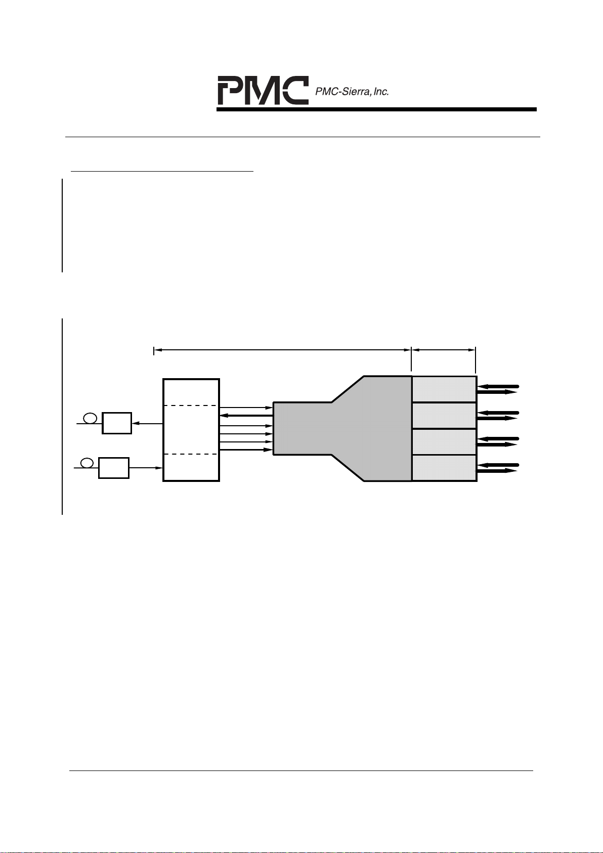
APPLICATION EXAMPLES
The following two diagrams shown the STTX used in an ATM application as an
STS-3c/STM-1 to STS-12/STM-4 multiplexer using four PM5345 SUNI-155 ATM
interface chips, and in an add-drop multiplexer application using four PM5344
SPTX path termination chips instead of the SUNI-155 chips to achieve access to
circuit-switched bandwidth. Ser ial to Parallel / Parallel to Serial conversion, clock
recovery and clock synthesis is available from a number of commercial sources.
Figure 1 - 622 Mbit/s SONET/SDH Asynchronous Transfer Mode
Multiplexer
PM5312
STTX
E/O
O/E
OOF
TOUT[7:0]
TCLK
RICLK
RIFP
RIN[7:0]
PM5345
S/UNI-155
#1
#2
#3
#4
OPTICAL
FACILITY
ATM
SWITCH
CORE
STS-3(STM-1) To STS-12 (STM-4) MUX
STS-3c (STM-1)
ATM Termination
Parallel
to/from
Serial
Conversion
Clock
Synthesis
Clock
Recovery
622 Mbit/s Front End *
* Contact PMC-Sierra Applications regarding
622 Mbit/s Front End alternatives
PM5312 STTX
DATA SHEET
PMC-930829 ISSUE 5 SONET/SDH TRANSPORT TERMINATING TRANSCEIVER
PROPRIETARY AND CONFIDENTIALTO PMC-SIERRA, INC., AND FOR ITS CUSTOMERS’ INTERNAL USE
5
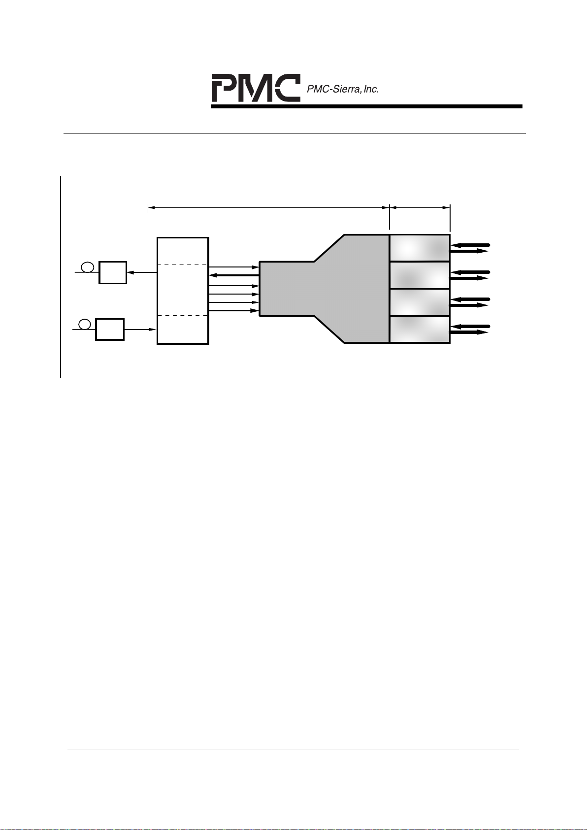
Figure 2 - 622 Mbit/s SONET/SDH Add-Drop Multiplexer Aggregate
Interface
ADD-DROP
MUX
BACKPLANE
PM5312
STTX
E/O
O/E
OOF
TOUT[7:0]
TCLK
RICLK
RIFP
RIN[7:0]
PM5344
SPTX
#1
#2
#3
#4
OPTICAL
FACILITY
STS-3(STM-1) To STS-12 (STM-4) MUX
STS-3c (STM-1)
Path Termination
Parallel
to/from
Serial
Conversion
Clock
Synthesis
Clock
Recovery
622 Mbit/s Front End *
* Contact PMC-Sierra Applications regarding
622 Mbit/s Front End alternatives
PM5312 STTX
DATA SHEET
PMC-930829 ISSUE 5 SONET/SDH TRANSPORT TERMINATING TRANSCEIVER
PROPRIETARY AND CONFIDENTIALTO PMC-SIERRA, INC., AND FOR ITS CUSTOMERS’ INTERNAL USE
6
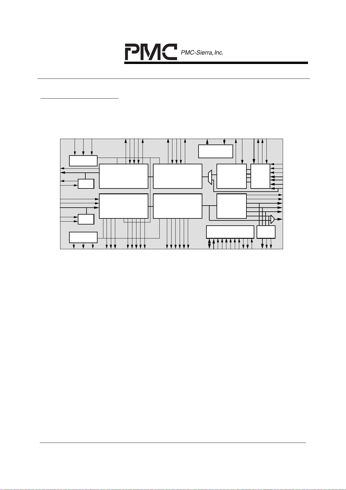
5
BLOCK DIAGRAM
TOUT[7:0]
RIN[7:0]
RICLK
RIFP
Status Control Port
TLAIS/TRCPDA
T
TIN1[7:0]
ROUT1[7:0]
ROCLK
D[7:0]
A[4:0]
ALE
CSB/LCSB
RDB
WRB
RSTB
INTB/LINTB
Microprocessor
I/F
Rx
O/H
Access
Tx
O/H
Access
TTOH[4:1]
RTOH[4:1]
TTOHCLK
RTOHCLK
LOS/RRCPFP
LOF
RTOHFP
TTOHFP
Rx Section
(Regenerator Section)
O/H Processor
Rx Line
(Multiplexer Section)
O/H Processor
TTOHEN
TFERF/TRCPFP
LAIS/RRCPDAT
FERF/RRCPCLK
TICLK
TOFP
OOF
B1E
RLAIS/TRCPCL
K
RSDCLK
RSD
RSOW
RSUC
ROWCLK
B2E
RLDCLK
RLD
RLOW
RAPS
RAPSCLK
ROUT2[7:0]
ROUT3[7:0]
ROUT4[7:0]
ROFP
Byte Interleaved
Multiplex
TIN2[7:0]
TIN3[7:0]
TIN4[7:0]
TIFP
TDIS
Tx Line
(Multiplexer Section)
O/H Processor
Tx Section
(Regenerator Section)
O/H Processor
TCLK
TSDCLK
TSD
TSOW
TSUC
TOWCLK
TLDCLK
TLD
TLOW
TAPS
TAPSCLK
Par/Ser
TSOUT
TSICLK
Ser/Par
RSICLK
RSIN
SCPO[5:0] *
SCPI[3:0] *
GTICLK
A[5]/SCSB
* SINTB
* SLIM
* NOT AVAILABLE WITH
180 CPGA PACKAGING OPTION
Transmit Ring
Control Port
Receive Ring
Control Port
Byte Interleaved
Demultiplex

PM5312 STTX
DATA SHEET
PMC-930829 ISSUE 5 SONET/SDH TRANSPORT TERMINATING TRANSCEIVER
PROPRIETARY AND CONFIDENTIALTO PMC-SIERRA, INC., AND FOR ITS CUSTOMERS’ INTERNAL USE
7
6
DESCRIPTION
The PM5312 STTX SONET/SDH Transport Overhead Terminating Transceiver
processes the transport overhead (regenerator and multiplexer section overhead)
of STS-1, STS-3/STM-1, and STS-12/STM-4 streams and optionally provides
byte interleaved multiplexing of lower rate streams.
The STTX may be used on the line side of four PM5344 SPTX SONET/SDH
Path Terminating Transceiver devices to implement a full SONET/SDH path
transmission system capable of terminating 12 STS-1 or four STS-3/STM-1
channels.
In a similar fashion, the STTX may be used on the line side of four PM5345 SUNI
Saturn User Network Interface devices to implement an Asynchronous Transfer
Mode (ATM) Multiplexer which takes four logical ATM streams operating at 155
Mbit/s and synchronously multiplexes them into a single 622 Mbit/s stream.
PM5312 STTX
DATA SHEET
PMC-930829 ISSUE 5 SONET/SDH TRANSPORT TERMINATING TRANSCEIVER
PROPRIETARY AND CONFIDENTIALTO PMC-SIERRA, INC., AND FOR ITS CUSTOMERS’ INTERNAL USE
8
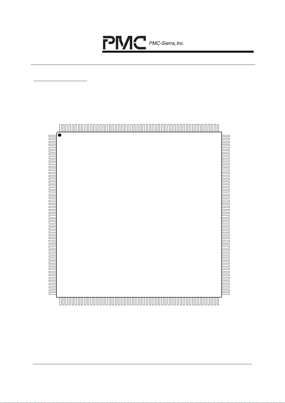
7
PIN DIAGRAM
The STTX is available in a 208 pin slugged PQFP package having a body size of
28 mm by 28 mm and a pin pitch of 0.5 mm.
PM5312
STTX
TOP VIEW
TAPSCLK
TLD
TLDCLK
TSD
VDDO
VSSO
TCLK
TSDCLK
TFERF/TRCPFP
TLAIS/TRCPDAT
TSICLK
TSOUT
NC
NC
D[6]
D[7]
INTB/LINTB
VSSO
RDB
WRB
CSB/LCSB
SCPI[1]
TIN1[2]
SCPI[0]
VSSI
VDDI
TIN1[1]
TIN1[0]
TIN2[2]
TIN2[1]
NC
TIN3[7]
TIN3[6]
TIN3[5]
TIN3[4]
TIN3[3]
TIN3[2]
TIN3[1]
TIN3[0]
TIN2[7]
TIN2[6]
TIN2[5]
TIN2[4]
NC
NC
NC
NC
TOFP
VSSO
TOUT[7]
TOUT[6]
TOUT[5]
TOUT[4]
TOUT[3]
TOUT[2]
VSSO
VDDO
TOUT[1]
B1E
NC
TIN4[0]
TIN4[1]
TIN4[2]
TIN4[3]
TIN4[4]
TIN4[5]
VDDI
VSSI
TIN4[6]
TIN4[7]
TTOH[1]
TTOH[2]
TTOH[3]
NC
ROUT2[0]
ROUT1[7]
ROUT1[6]
ROUT1[5]
ROUT1[4]
ROUT1[3]
VDDI
VSSI
ROUT1[2]
ROUT1[1]
VSSO
RTOHFP
NC
TIN2[3]
TIN2[0]
TIN1[7]
TOUT[0]
TTOH[4]
TTOHEN
TTOHFP
TTOHCLK
VDDO
ROUT2[1]
ROUT2[2]
FERF/RRCPCLK
LOS/RRCPFP
LAIS/RRCPDAT
ROUT1[0]
RTOHCLK
TIN1[6]
TIN1[5]
TIN1[4]
TIN1[3]
GTICLK
D[0]
SCPO[0]
D[1]
SCPO[1]
ROUT2[3]
VSSO
RLOW
RSOW
RSUC
ROWCLK
ROUT2[4]
SCPO[2]
ROUT2[5]
SCPO[3]
D[2]
VSSO
SLIM
VDDO
D[3]
SINTB
D[4]
RAPS
ROUT2[6]
VSSO
VDDO
ROUT2[7]
SCPO[4]
ROUT3[0]
SCPO[5]
ROUT3[1]
SCPI[3]
RAPSCLK
SCPI[2]
RLD
RLDCLK
VDDO
B2E
TIFP
TDIS
TLOW
TSOW
TSUC
VDDO
TOWCLK
TAPS
D[5]
NC
LOF
OOF
RIN[7]
RIN[6]
RIN[5]
RIN[4]
RIN[3]
ROUT3[2]
ROUT3[3]
ROUT3[4]
ROUT3[5]
VDDO
ROUT3[6]
ROUT3[7]
ROUT4[0]
TICLK
RSTB
ALE
A[0]
A[1]
A[2]
A[3]
A[4]
A[5]/SCSB
RTOH[1]
RTOH[2]
RTOH[3]
RTOH[4]
ROUT4[1]
ROUT4[2]
ROUT4[3]
VSSO
ROUT4[4]
ROUT4[5]
ROUT4[6]
ROUT4[7]
ROFP
ROCLK
VDDO
RSIN
RIN[2]
RIN[1]
RIN[0]
RIFP
VDDI
VSSI
RLAIS/TRCPCLK
RSD
RSDCLK
RSICLK
RICLK
VSSO
PIN 52
PIN 53
PIN 104
PIN 105
PIN 1
PIN 208
PIN 157
PIN 156
Index
NC

PM5312 STTX
DATA SHEET
PMC-930829 ISSUE 5 SONET/SDH TRANSPORT TERMINATING TRANSCEIVER
PROPRIETARY AND CONFIDENTIALTO PMC-SIERRA, INC., AND FOR ITS CUSTOMERS’ INTERNAL USE
9
8
PIN DESCRIPTION
Pin Name Pin
Type
PQFP
Pin
No.
Function
RICLK/ Input 153 The receive incoming clock (RICLK) provides
timing for processing the byte serial receive
stream, RIN[7:0]. RICLK is nominally a 6.48
MHz (STS-1), 19.44 MHz (STS-3/STM-1 ), or
77.76 MHz (STS-12/STM-4) 50% duty cycle
clock, depending on the selected operating
mode. RIN[7:0], and RIFP are sampled on the
rising edge of RICLK.
The receive vector clock (RVCLK) is used
during STTX production test to verify internal
functionality.
RIN[7]
RIN[6]
RIN[5]
RIN[4]
RIN[3]
RIN[2]
RIN[1]
RIN[0]
Input
Input
Input
Input
Input
Input
Input
Input
138
139
140
141
142
143
144
145
The receive incoming stream (RIN[7:0]) carries
the scrambled STS-1, STS-3/STM-1, or STS-
12/STM-4 stream in byte serial format. RIN[7]
is the most significant bit (corresponding to bit 1
of each serial PCM word, the first bit
transmitted). RIN[0] is the least significant bit
(corresponding to bit 8 of each serial PCM
word, the last bit transmitted). RIN[7:0] is
sampled on the rising edge of RICLK.
RIFP Input 146 The active high receive incoming framing
position (RIFP) signal indicates the frame
alignment in the incoming stream, RIN[7:0].
RIFP is sampled on the rising edge of RICLK.
RSICLK/ Input 152 The receive serial incoming clock (RSICLK)
provides timing for processing the bit serial
receive stream, RSIN. RSICLK is nominally a
51.84 MHz, 50% duty cycle clock. RSIN is
sampled on the rising edge of RSICLK.
RSICLK is divided by eight to produce ROCLK
when the bit serial STS-1 mode is selected.
RSICLK should be disabled when the bit serial
STS-1 interface is not used.
RSIN Input 158 The receive incoming serial stream (RSIN)
carries the scrambled STS-1 stream in bit serial
format. RSIN is sampled on the rising edge of
RSICLK.

PM5312 STTX
DATA SHEET
PMC-930829 ISSUE 5 SONET/SDH TRANSPORT TERMINATING TRANSCEIVER
PROPRIETARY AND CONFIDENTIALTO PMC-SIERRA, INC., AND FOR ITS CUSTOMERS’ INTERNAL USE
10
Pin Name Pin
Type
PQFP
Pin
No.
Function
RLAIS/ Input 149 The receive line AIS insertion (RLAIS) signal
controls the insertion of line AIS in the receive
outgoing streams, ROUT1[7:0], ROUT2[7:0],
ROUT3[7:0], and ROUT4[7:0] when the ring
control port is disabled. When RLAIS is high,
line AIS is inserted in the outgoing streams.
Line AIS is also optionally inserted
automatically upon detection of loss of signal,
loss of frame, or line AIS in the incoming
stream. RLAIS is sampled on the rising edge of
RICLK.
TRCPCLK The transmit ring control port clock (TRCPCLK)
signal provides timing for the transmit ring
control port when the ring control port is
enabled (the enabling and disabling of the ring
control port is controlled by a bit in the Master
Control Register). TRCPCLK is nomina lly a
3.24 MHz, 50% duty cycle clock and is normally
connected to the RRCPCLK output of a mate
STTX in ring-based add-drop multiplexer
applications. TRCPFP and TRCPDAT are
sampled on the rising edge of TRCPCLK.
OOF Output 137 The out of frame (OOF) signal is set high while
the STTX is unable to find a valid framing
pattern (A1, A2) in the incoming stream. OOF is
set low when a valid framing pattern is detected.
OOF is updated on the rising edge of RICLK.
LOF Output 136 The loss of frame (LOF) signal is set high when
an out of frame state persists for 3 ms. LOF is
set low when an in frame state persists for 3 ms.
LOF is updated on the rising edge of RICLK.

PM5312 STTX
DATA SHEET
PMC-930829 ISSUE 5 SONET/SDH TRANSPORT TERMINATING TRANSCEIVER
PROPRIETARY AND CONFIDENTIALTO PMC-SIERRA, INC., AND FOR ITS CUSTOMERS’ INTERNAL USE
11
Pin Name Pin
Type
PQFP
Pin
No.
Function
LOS/ Output 120 Loss of signal (LOS) is active when the ring
control port is disabled. Loss of signal (LOS) is
set high when a violating period (20 ± 2.5 µs) of
consecutive all zeros patterns is detected in the
incoming stream. LOS is set low when two valid
framing words (A1, A2) are detected, and during
the intervening time (125 µs), no violating
period of all zeros patterns is observed. LOS is
updated on the rising edge of RICLK.
RRCPFP The receive ring control port frame position
(RRCPFP) signal identifies bit positions in the
receive ring control port data (RRCPDAT) when
the ring control port is enabled (the enabling
and disabling of the ring control port is
controlled by a bit in the Master Control
Register). RRCPFP is high during the filtered
K1, K2 bit positions, the change of APS value
bit position, the protection switch byte failure bit
position, and the send AIS and send FERF bit
positions in the RRCPDAT stream. RRCPFP is
normally connected to the TRCPFP input of a
mate STTX in ring-based add-drop multiplexer
applications. RRCPFP is updated on the falling
edge of RRCPCLK.
B1E Output 135 The B1 error clock (B1E) is a return to zero
signal that pulses once for every section bit
interleaved parity error (B1) detected in the
incoming stream. Up to eight pulses may occur
on B1E per frame.

PM5312 STTX
DATA SHEET
PMC-930829 ISSUE 5 SONET/SDH TRANSPORT TERMINATING TRANSCEIVER
PROPRIETARY AND CONFIDENTIALTO PMC-SIERRA, INC., AND FOR ITS CUSTOMERS’ INTERNAL USE
12
Pin Name Pin
Type
PQFP
Pin
No.
Function
FERF/ Output 119 The far end receive failure (FERF) signal is
active when the ring control port is disabled.
FERF is set high when line FERF is detected in
the incoming stream. FERF is declared when a
110 binary pattern is detected in bits 6, 7, and 8
of the K2 byte for three or five consecutive
frames. FERF is removed when any pattern
other than 110 is detected in bits 6, 7, and 8 of
the K2 byte for three or five consecutive frames.
This alarm indication is also available through
register access. FERF is updated on the rising
edge of RICLK.
RRCPCLK The receive ring control port clock (RRCPCLK)
signal provides timing for the receive ring
control port when the ring control port is
enabled (the enabling and disabling of the ring
control port is controlled by a bit in the Master
Control Register). RRCPCLK is nominally a
3.24 MHz, 50% duty cycle clock and is normally
connected to the TRCPCLK input of a mate
STTX in ring-based add-drop multiplexer
applications. RRCPFP and RRCPDAT are
updated on the falling edge of RRCPCLK.

PM5312 STTX
DATA SHEET
PMC-930829 ISSUE 5 SONET/SDH TRANSPORT TERMINATING TRANSCEIVER
PROPRIETARY AND CONFIDENTIALTO PMC-SIERRA, INC., AND FOR ITS CUSTOMERS’ INTERNAL USE
13
Pin Name Pin
Type
PQFP
Pin
No.
Function
LAIS/ Output 121 The line alarm indication (LAIS) signal is active
when the ring control port is disabled. LAIS is
set high when line AIS is detected in the
incoming stream. LAIS is declared when a 111
binary pattern is detected in bits 6, 7, and 8 of
the K2 byte for three or five consecutive frames.
LAIS is removed when any pattern other than
111 is detected in bits 6, 7, and 8 of the K2 byte
for three or five consecutive frames. This alarm
indication is also available through register
access. LAIS is updated on the rising edge of
RICLK.
RRCPDAT The receive ring control port data (RRCPDAT)
signal contains the receive ring control port data
stream when the ring control port is enabled
(the enabling and disabling of the ring control
port is controlled by a bit in the Master Control
Register). The receive ring control port data
consists of the filtered K1, K2 byte values, the
change of APS value bit position, the protection
switch byte failure status bit position, the send
AIS and send FERF bit positions, and the line
FEBE bit positions. RRCPDAT is normally
connected to the TRCPDAT input of a mate
STTX in ring-based add-drop multiplexer
applications. RRCPDAT is updated on the
falling edge of RRCPCLK.
B2E Output 134 The B2 error clock (B2E) is a return to zero
signal that pulses once for every line bit
interleaved parity error (B2) detected in the
incoming stream. Up to 8 (STS-1), 24 (STS-
3/STM-1), or 96 (STS-12/STM-4) pulses may
occur on B2E, per frame.
RSDCLK Output 151 The receive section DCC clock (RSDCLK) is a
192 kHz clock used to update the RSD output.
RSDCLK is generated by gapping a 216 kHz
clock.

PM5312 STTX
DATA SHEET
PMC-930829 ISSUE 5 SONET/SDH TRANSPORT TERMINATING TRANSCEIVER
PROPRIETARY AND CONFIDENTIALTO PMC-SIERRA, INC., AND FOR ITS CUSTOMERS’ INTERNAL USE
14
Pin Name Pin
Type
PQFP
Pin
No.
Function
RSD Output 150 The receive section DCC (RSD) signal contains
the section data communications channel (D1,
D2, D3) extracted from the incoming stream.
RSD is updated on the falling edge of RSDCLK.
ROWCLK Output 126 The receive order wire clock (ROWCLK) is a 64
kHz clock used to update the RSOW, RSUC,
and RLOW outputs. ROWCLK is generated by
gapping a 72 kHz clock.
RSOW Output 124 The receive section order wire (RSOW) signal
contains the section order wire channel (E1)
extracted from the incoming stream. RSOW is
updated on the falling edge of ROWCLK.
RSUC Output 125 The receive section user channel (RSUC) signal
contains the section user channel (F1) extracted
from the incoming stream. RSUC is updated on
the falling edge of ROWCLK.
RLOW Output 123 The receive line order wire (RLOW) signal
contains the line order wire channel (E2)
extracted from the incoming stream. RLOW is
updated on the falling edge of ROWCLK.
RLDCLK Output 1 32 The receive line DCC clock (RLDCLK) is a 576
kHz clock used to update the RLD output.
RLDCLK is generated by gapping a 2.16 MHz
clock.
RLD Output 131 The receive line DCC (RLD) signal contains the
line data communications channel (D4 - D12)
extracted from the incoming stream. RLD is
updated on the falling edge of RLDCLK.
RAPSCLK Output 129 The receive automatic protection switch channel
clock (RAPSCLK) is a 128 kHz clock used to
update the RAPS output. RAPSCLK is
generated by gapping a 144 kHz clock.
RAPS Output 127 The receive automatic protection switch channel
(RAPS) signal carries the automatic protection
switch channel (K1, K2) extracted from the
incoming stream. RAPS is updated on the
falling edge of RAPSCLK.

PM5312 STTX
DATA SHEET
PMC-930829 ISSUE 5 SONET/SDH TRANSPORT TERMINATING TRANSCEIVER
PROPRIETARY AND CONFIDENTIALTO PMC-SIERRA, INC., AND FOR ITS CUSTOMERS’ INTERNAL USE
15
Pin Name Pin
Type
PQFP
Pin
No.
Function
RTOH[4]
RTOH[3]
RTOH[2]
RTOH[1]
Output
Output
Output
Output
2
3
4
5
The receive transport overhead bus
(RTOH[4:1]) contains the receive transport
overhead bytes (A1, A2, C1, B1, E1, F1, D1-D3,
H1-H3, B2, K1, K2, D4-D12, Z1, Z2, and E2)
extracted from the incoming stream. When
STS-12/STM-4 mode is selected, RTOH[1]
contains the transport overhead from STS-
3/STM-1 #1, RTOH[2] contains the transport
overhead for
STS-3/STM-1 #2, RTOH[3] contains the
transport overhead for STS-3/STM-1 #3, and
RTOH[4] contains the transport overhead for
STS-3/STM-1 #4. When STS-3/STM-1 mode or
STS-1 mode are selected, the complete
transport overhead is extracted on RTOH[1].
RTOH[4:1] is updated on the falling edge of
RTOHCLK.
RTOHCLK Output 205 The receive transport overhead clock
(RTOHCLK) is nominally a 5.184 MHz clock that
provides timing to process the extracted receive
transport overhead bus, RTOH[4:1]. RTOHCLK
is a gapped 6.48 MHz clock when accessing the
transport overhead of STS-3/STM-1 streams.
RTOHCLK is a gapped 2.16 MHz clock when
accessing the transport overhead of an STS-1
stream.
RTOHFP Output 207 The receive transport overhead frame position
(RTOHFP) signal is used to locate the individual
receive transport overhead bits in the transport
overhead bus, RTOH[4:1]. RTOHFP is set high
while bit 1 (the most significant bit) of the first
framing byte (A1) is present in the RTOH[4:1]
stream. RTOHFP is updated on the falling edge
of RTOHCLK.

PM5312 STTX
DATA SHEET
PMC-930829 ISSUE 5 SONET/SDH TRANSPORT TERMINATING TRANSCEIVER
PROPRIETARY AND CONFIDENTIALTO PMC-SIERRA, INC., AND FOR ITS CUSTOMERS’ INTERNAL USE
16
Pin Name Pin
Type
PQFP
Pin
No.
Function
ROCLK Output 160 The receive outgoing clock (ROCLK) provides
timing for updating the demultiplexed byte serial
STS-1 or STS-3/STM-1 outputs, ROUT1[7:0],
ROUT2[7:0], ROUT3[7:0], and ROUT4[7:0]
when 1:3 or 1:4 byte interleaved multiplexing is
enabled. ROCLK is nominally a 6.48 MHz, or
19.44 MHz clock, depending on the
demultiplexing mode selected. ROCLK remains
inactive when demultiplexing is bypassed.
When the bit serial STS-1 receive interface is
enabled, ROCLK becomes the generated byte
serial clock. ROCLK is a 6.48 MHz clock that is
generated by dividing the receive serial
incoming clock (RSICLK) by eight. ROCLK
must be connected externally to the receive
incoming clock (RICLK) when processing a bit
serial
STS-1 stream.
ROUT1[7]
ROUT1[6]
ROUT1[5]
ROUT1[4]
ROUT1[3]
ROUT1[2]
ROUT1[1]
ROUT1[0]
Output
Output
Output
Output
Output
Output
Output
Output
195
196
197
198
199
202
203
204
The receive outgoing #1 bus, (ROUT1[7:0]),
carries demultiplexed STS-1 or STS-3/STM-1
streams in byte serial format. ROUT1[7] is the
most significant bit (corresponding to bit 1 of
each serial PCM word, the first bit received).
ROUT1[0] is the least significant bit
(corresponding to bit 8 of each serial PCM
word). ROUT1[7:0] is updated on the falling
edge of ROCLK.
ROUT1[7:0] contains the entire descrambled
outgoing stream and is updated on the rising
edge of RICLK when demultiplexing is
bypassed, or when the bit serial STS-1 mode is
selected. Note that demultiplex bypass is
supported for STS-3 mode only.

PM5312 STTX
DATA SHEET
PMC-930829 ISSUE 5 SONET/SDH TRANSPORT TERMINATING TRANSCEIVER
PROPRIETARY AND CONFIDENTIALTO PMC-SIERRA, INC., AND FOR ITS CUSTOMERS’ INTERNAL USE
17
Pin Name Pin
Type
PQFP
Pin
No.
Function
ROUT2[7]
ROUT2[6]
ROUT2[5]
ROUT2[4]
ROUT2[3]
ROUT2[2]
ROUT2[1]
ROUT2[0]
Output
Output
Output
Output
Output
Output
Output
Output
182
185
187
189
190
191
192
194
The receive outgoing #2 bus, (ROUT2[7:0]),
carries demultiplexed STS-1 or STS-3/STM-1
streams in byte serial format. ROUT2[7] is the
most significant bit (corresponding to bit 1 of
each serial PCM word, the first bit received).
ROUT2[0] is the least significant bit
(corresponding to bit 8 of each serial PCM
word). ROUT2[7:0] is updated on the falling
edge of ROCLK.
ROUT3[7]
ROUT3[6]
ROUT3[5]
ROUT3[4]
ROUT3[3]
ROUT3[2]
ROUT3[1]
ROUT3[0]
Output
Output
Output
Output
Output
Output
Output
Output
171
172
174
175
176
177
178
180
The receive outgoing #3 bus, (ROUT3[7:0]),
carries demultiplexed STS-1 or STS-3/STM-1
streams in byte serial format. ROUT3[7] is the
most significant bit (corresponding to bit 1 of
each serial PCM word, the first bit transmitted).
ROUT3[0] is the least significant bit
(corresponding to bit 8 of each serial PCM
word). ROUT3[7:0] is updated on the falling
edge of ROCLK.
ROUT4[7]
ROUT4[6]
ROUT4[5]
ROUT4[4]
ROUT4[3]
ROUT4[2]
ROUT4[1]
ROUT4[0]
Output
Output
Output
Output
Output
Output
Output
Output
162
163
164
165
167
168
169
170
The receive outgoing #4 bus, (ROUT4[7:0]),
carries demultiplexed STS-3/STM-1 streams in
byte serial format. ROUT4[7] is the most
significant bit (corresponding to bit 1 of each
serial PCM word, the first bit transmitted).
ROUT4[0] is the least significant bit
(corresponding to bit 8 of each serial PCM
word). ROUT4[7:0] is updated on the falling
edge of ROCLK. ROUT4[7:0] is not used when
demultiplexing an STS-3 stream into three STS-
1 streams.

PM5312 STTX
DATA SHEET
PMC-930829 ISSUE 5 SONET/SDH TRANSPORT TERMINATING TRANSCEIVER
PROPRIETARY AND CONFIDENTIALTO PMC-SIERRA, INC., AND FOR ITS CUSTOMERS’ INTERNAL USE
18
Pin Name Pin
Type
PQFP
Pin
No.
Function
ROFP Output 161 The active high receive outgoing frame position
(ROFP) signal is set high once per frame in the
byte position immediately following the C1 bytes
in the ROUT1[7:0], ROUT2[7:0], ROUT3[7:0],
and ROUT4[7:0] STS-1 or STS-3/STM-1
streams. ROFP is updated on the falling edge
of ROCLK.
ROFP is also used to mark the alignment of the
RSOW, RSUC, RLOW and RAPS bit streams.
ROFP is updated on the rising edge of RICLK
when demultiplexing is bypassed, or when the
bit serial STS-1 mode is selected. Note that
demultiplex bypass is supported for STS-3
mode only.
TCLK/ Input 97 The transmit clock (TCLK) provides timing for
multiplexing the byte serial incoming streams,
TIN1[7:0], TIN2[7:0], TIN3[7:0] and TIN4[7:0],
into a higher rate stream. TCLK is nominally a
6.48 MHz, 19.44 MHz or 77.76 MHz 50% duty
cycle clock, depending on the operating mode
selected. When multiplexing is bypassed, or
when STS-1 mode is selected, the incoming
stream, TIN1[7:0], is sampled on the rising edge
of TCLK.
TVCLK The transmit vector clock (TVCLK) is used
during STTX production test to verify internal
functionality.

PM5312 STTX
DATA SHEET
PMC-930829 ISSUE 5 SONET/SDH TRANSPORT TERMINATING TRANSCEIVER
PROPRIETARY AND CONFIDENTIALTO PMC-SIERRA, INC., AND FOR ITS CUSTOMERS’ INTERNAL USE
19
Pin Name Pin
Type
PQFP
Pin
No.
Function
GTICLK Output 34 The generated transmit clock (GTICLK) is used
in contra-directional timing-based systems to
provide timing for upstream circuitry. GTICLK is
a divide by four of the high speed multiplex
clock (TCLK) when STS-3 to STS-12
multiplexing is enabled. GTICLK is a divide by
three of TCLK when STS-1 to STS-3
multiplexing is enabled. GTICLK must be
connected directly to
TICLK for these contra-directional multiplexing
applications. GTICLK is a divide by eight of the
transmit serial incoming clock (TSICLK) when
the bit serial STS-1 mode is enabled. GTICLK
must be connected directly to TCLK for these
contra-directional STS-1 applications.
TICLK Input 14 The transmit incoming clock (TICLK) provides
timing to sample the byte serial incoming
streams prior to multiplexing. TICLK is
synchronous with, but arbitrarily phase aligned
to TCLK. TICLK is nominally a 6.48 MHz, or
19.44 MHz clock. TIN1[7:0], TIN2[7:0],
TIN3[7:0], TIN4[7:0], TDIS, and TIFP are
sampled on the rising edge of TICLK.
TSICLK Input 101 The transmit serial incoming clock (TSICLK)
provides timing for updating the bit serial
outgoing stream when STS-1 mode is selected.
TSICLK is nominally a 51.84 MHz, 50% duty
cycle clock. TSOUT is updated on the rising
edge of TSICLK. TSICLK should be disabled
when the bit serial STS-1 interface is not used.

PM5312 STTX
DATA SHEET
PMC-930829 ISSUE 5 SONET/SDH TRANSPORT TERMINATING TRANSCEIVER
PROPRIETARY AND CONFIDENTIALTO PMC-SIERRA, INC., AND FOR ITS CUSTOMERS’ INTERNAL USE
20
Pin Name Pin
Type
PQFP
Pin
No.
Function
TIN1[7]
TIN1[6]
TIN1[5]
TIN1[4]
TIN1[3]
TIN1[2]
TIN1[1]
TIN1[0]
Input 71
72
73
74
75
77
81
82
The transmit incoming #1 bus, (TIN1[7:0]),
carries STS-1 or STS-3/STM-1 streams in byte
serial format. TIN1[7] is the most significant bit
(corresponding to bit 1 of each serial PCM
word, the first bit transmitted). TIN1[0] is the
least significant bit (corresponding to bit 8 of
each serial PCM word). TIN1[7:0] is sampled on
the rising edge of TICLK.
TIN1[7:0] contains the entire incoming stream
and is sampled on the rising edge of TCLK
when multiplexing is bypassed, or when the
STS-1 mode is selected. Note that multiplex
bypass is supported for STS-3 mode only.
TIN2[7]
TIN2[6]
TIN2[5]
TIN2[4]
TIN2[3]
TIN2[2]
TIN2[1]
TIN2[0]
Input 63
64
65
66
67
68
69
70
The transmit incoming #2 bus, (TIN2[7:0]),
carries STS-1 or STS-3/STM-1 streams in byte
serial format. TIN2[7] is the most significant bit
(corresponding to bit 1 of each serial PCM
word, the first bit transmitted). TIN2[0] is the
least significant bit (corresponding to bit 8 of
each serial PCM word). TIN2[7:0] is sampled on
the rising edge of TICLK.
TIN3[7]
TIN3[6]
TIN3[5]
TIN3[4]
TIN3[3]
TIN3[2]
TIN3[1]
TIN3[0]
Input 55
56
57
58
59
60
61
62
The transmit incoming #3 bus, (TIN3[7:0]),
carries STS-1 or STS-3/STM-1 streams in byte
serial format. TIN3[7] is the most significant bit
(corresponding to bit 1 of each serial PCM
word, the first bit transmitted). TIN3[0] is the
least significant bit (corresponding to bit 8 of
each serial PCM word). TIN3[7:0] is sampled on
the rising edge of TICLK.
TIN4[7]
TIN4[6]
TIN4[5]
TIN4[4]
TIN4[3]
TIN4[2]
TIN4[1]
TIN4[0]
Input 42
43
46
47
48
49
50
51
The transmit incoming #4 bus, (TIN3[7:0]),
carries STS-3/STM-1 streams in byte serial
format. TIN4[7] is the most significant bit
(corresponding to bit 1 of each serial PCM
word, the first bit transmitted). TIN4[0] is the
least significant bit (corresponding to bit 8 of
each serial PCM word). TIN4[7:0] is sampled on
the rising edge of TICLK. TIN4[7:0] is not used
when multiplexing three STS-1 streams to an
STS-3 stream.

PM5312 STTX
DATA SHEET
PMC-930829 ISSUE 5 SONET/SDH TRANSPORT TERMINATING TRANSCEIVER
PROPRIETARY AND CONFIDENTIALTO PMC-SIERRA, INC., AND FOR ITS CUSTOMERS’ INTERNAL USE
21
Pin Name Pin
Type
PQFP
Pin
No.
Function
TIFP Input 83 The active high transmit incoming framing
position (TIFP) signal indicates the frame
alignment for incoming streams. A high level on
TIFP marks the byte immediately following the
C1 bytes in the transmit STS-1 or STS-3 (STM-
1) streams, TIN1[7:0], TIN2[7:0], TIN3[7:0], and
TIN4[7:0]. TIFP is sampled on the rising edge
of TICLK.
TIFP is sampled on the rising edge of TCLK
when multiplexing is bypassed, or when the bit
serial STS-1 mode is selected. Note that
multiplex bypass is supported for STS-3 mode
only.
TDIS Input 84 The active high transmit disable (TDIS) signal
selectively disables overwriting each of the
STS-1 or STS-3 (STM-1) streams with the
corresponding overhead byte. TDIS is sampled
on the rising edge of TICLK.
TDIS is sampled on the rising edge of TCLK
when multiplexing is bypassed, or when the bit
serial STS-1 mode is selected. Note that TDIS
takes precedence over the values shifted in on
the transmit transport overhead interface
(TTOH[4:1]) using TTOHEN.
In general, the value on TIN[7:0] passes through
transparently if TDIS is high. Three exceptions
exist:
1) Bits 6 to 8 of the K2 byte may be overwritten
by an active FERF indication ("110") regardless
of the state of TDIS.
2) If TDIS is high during the section BIP byte
(B1), the TIN[7:0] value becomes an error mask
for the generated section BIP.
3) If TDIS is high during the line BIP bytes (B2),
the TIN[7:0] value becomes an error mask for
the generated line BIP.

PM5312 STTX
DATA SHEET
PMC-930829 ISSUE 5 SONET/SDH TRANSPORT TERMINATING TRANSCEIVER
PROPRIETARY AND CONFIDENTIALTO PMC-SIERRA, INC., AND FOR ITS CUSTOMERS’ INTERNAL USE
22
Pin Name Pin
Type
PQFP
Pin
No.
Function
TTOH[4]
TTOH[3]
TTOH[2]
TTOH[1]
Input 38
39
40
41
The transmit transport overhead bus (TTOH[4:1)
contains the transport overhead bytes (A1, A2,
C1, E1, F1, D1-D3, H3, K1, K2, D4-D12, Z1, Z2,
and E2) and error masks (H1, H2, B1, and B2)
which may be inserted, or used to insert bit
interleaved parity errors or payload pointer bit
errors into the overhead byte positions in the
outgoing stream. Insertion is controlled by the
TTOHEN input. When STS-12/STM-4 mode is
enabled, TTOH[1] contains the transport
overhead for STS-3/STM-1 #1. TTOH[2]
contains the transport overhead for STS-3/STM-
1 #2. TTOH[3] contains the transport overhead
for STS-3/STM-1 #3. TTOH[4] contains the
transport overhead for STS-3/STM-1 #4. When
STS-3/STM-1 mode or STS-1 mode are
selected, TTOH[1] contains the transport
overhead for the entire stream. TTOH[4:1] is
sampled on the rising edge of TTOHCLK.
TTOHFP Output 36 The transmit transport overhead frame position
(TTOHFP) signal is used to locate the individual
transport overhead bits in the transport
overhead bus, TTOH[4:1]. TTOHFP is set high
while bit 1 (the most significant bit) of the first
framing byte (A1) is expected in the incoming
stream. TTOHFP is also used to mark the
alignment of the TSUC, TSOW, TLOW, and
TAPS bit streams. TTOHFP is updated on the
falling edge of TTOHCLK.
TTOHCLK Output 35 The transmit transport overhead clock
(TTOHCLK) is nominally a 5.184 MHz (1.728
MHz for STS-1) clock that provides timing for
upstream circuitry that sources the transport
overhead bus, TTOH[4:1]. TTOHCLK is a
gapped 6.48 MHz clock when accessing the
transport overhead of STS-3/STM-1 streams.
TTOHCLK is a gapped 2.16 MHz clock when
accessing the transport overhead of an STS-1
stream.

PM5312 STTX
DATA SHEET
PMC-930829 ISSUE 5 SONET/SDH TRANSPORT TERMINATING TRANSCEIVER
PROPRIETARY AND CONFIDENTIALTO PMC-SIERRA, INC., AND FOR ITS CUSTOMERS’ INTERNAL USE
23
Pin Name Pin
Type
PQFP
Pin
No.
Function
TTOHEN Input 37 The transmit transport overhead insert enable
(TTOHEN) signal controls the source of the
transport overhead data which is inserted in the
TOUT[7:0] stream. While TTOHEN is high (and
TDIS is low), values sampled on the TTOH input
are inserted into the corresponding transport
overhead bit position (for the A1, A2, C1, E1,
F1, D1-D3, H3, K1, K2, D4-D12, Z1, Z2, and E2
bytes). While TTOHEN is low, the default values
are inserted into these transport overhead bit
positions. A high level on TTOHEN during the
H1, H2, B1, or B2 bit positions enables an error
mask. While the error mask is enabled, a high
level on inputs TTOH[4:1] causes the
corresponding H1, H2, B1 or B2 bit positions to
be inverted. A low level on TTOH allows the
corresponding bit positions to pass through the
STTX uncorrupted. TTOHEN is sampled on the
rising edge of TTOHCLK.

PM5312 STTX
DATA SHEET
PMC-930829 ISSUE 5 SONET/SDH TRANSPORT TERMINATING TRANSCEIVER
PROPRIETARY AND CONFIDENTIALTO PMC-SIERRA, INC., AND FOR ITS CUSTOMERS’ INTERNAL USE
24
Pin Name Pin
Type
PQFP
Pin
No.
Function
TFERF/ Input 99 The active high transmit far end receive failure
(TFERF) signal controls the insertion of a far
end receive fa ilure indication in the outgoing
stream when the ring control port is disabled.
When TFERF is set high, bits 6, 7, and 8 of the
K2 byte are set to the pattern 110. Line FERF
may also be inserted using the FERF bit in the
TLOP Control Register, or upon detection of
loss of signal, loss of frame, or line AIS in the
receive stream, using the AUTOFERF bit in the
Master Control/Enable Register. TFERF is
sampled on the rising edge of TCLK.
TRCPFP The transmit ring control port frame position
(TRCPFP) signal identifies bit positions in the
transmit ring control port data (TRCPDAT) when
the ring control port is enabled (the enabling
and disabling of the ring control port is
controlled by a bit in the Master Control
Register). TRCPFP is high during the filtered
K1, K2 bit positions, the change of APS value
bit position, the protection switch byte failure bit
position, and the send AIS and send FERF bit
positions in the TRCPDAT stream. TRCPFP is
normally connected to the RRCPFP output of a
mate STTX in ring-based add-drop multiplexer
applications. TRCPFP is sampled on the rising
edge of TRCPCLK.
 Loading...