


PRELIMINARY
PM4332 TE-32
DATA SHEET
PMC-2011402 ISSUE 1 HIGH DENSITY 32 CHANNEL T1/E1/J1 FRAMER
PMC-Sierra, Inc. 105 - 8555 Baxter Place Burnaby, BC Canada V5A 4V7 604 .415.6000
PM4332
TE-32
HIGH DENSITY 32 CHANNEL T1/E1/J1
FRAMER
DATA SHEET
PROPRIETARY AND CONFIDENTIAL
PRELIMINARY
ISSUE 1: JUNE 2001

PRELIMINARY
PM4332 TE-32
DATA SHEET
PMC-2011402 ISSUE 1 HIGH DENSITY 32 CHANNEL T1/E1/J1 FRAMER
PROPRIETARY AND CONFIDENTIAL TO PMC-SIERRA, INC., AND FOR THE INTERNAL USE OF ITS CUSTOMERS i
CONTENTS
1 FEATURES .............................................................................................. 1
2 APPLICATIONS ....................................................................................... 7
3 REFERENCES......................................................................................... 8
4 APPLICATION EXAMPLES ....................................................................11
5 BLOCK DIAGRAM ................................................................................. 14
6 DESCRIPTION....................................................................................... 16
7 PIN DIAGRAM ....................................................................................... 19
8 PIN DESCRIPTION................................................................................ 20
9 FUNCTIONAL DESCRIPTION............................................................... 49
9.1 T1 FRAMING............................................................................... 49
9.2 E1 FRAMING .............................................................................. 51
9.3 T1/E1 PERFORMANCE MONITORING...................................... 58
9.4 T1/E1 HDLC RECEIVER............................................................. 59
9.5 T1/E1 ELASTIC STORE (ELST) ................................................. 60
9.6 T1/E1 SIGNALING EXTRACTION .............................................. 60
9.7 T1/E1 RECEIVE PER-CHANNEL CONTROL ............................. 61
9.8 T1 TRANSMITTER...................................................................... 61
9.9 E1 TRANSMITTER...................................................................... 63
9.10 T1/E1 HDLC TRANSMITTERS ................................................... 63
9.11 T1/E1 RECEIVE AND TRANSMIT DIGITAL JITTER
ATTENUATORS .......................................................................... 64
9.12 T1/E1 PSEUDO RANDOM BINARY SEQUENCE GENERATION
AND DETECTION (PRBS).......................................................... 70

PRELIMINARY
PM4332 TE-32
DATA SHEET
PMC-2011402 ISSUE 1 HIGH DENSITY 32 CHANNEL T1/E1/J1 FRAMER
PROPRIETARY AND CONFIDENTIAL TO PMC-SIERRA, INC., AND FOR THE INTERNAL USE OF ITS CUSTOMERS ii
9.13 EGRESS H-MVIP SYSTEM INTERFACE ................................... 70
9.14 INGRESS SYSTEM H-MVIP INTERFACE.................................. 72
9.15 EXTRACT SCALEABLE BANDWIDTH INTERCONNECT (EXSBI)
.................................................................................................... 74
9.16 INSERT SCALEABLE BANDWIDTH INTERCONNECT (INSBI). 75
9.17 JTAG TEST ACCESS PORT ....................................................... 76
9.18 MICROPROCESSOR INTERFACE ............................................ 77
10 NORMAL MODE REGISTER DESCRIPTION ....................................... 85
10.1 TOP LEVEL MASTER REGISTERS ........................................... 86
10.2 T1/E1 MASTER CONFIGURATION REGISTERS .....................110
10.3 T1/E1 RECEIVE JITTER ATTENUATOR (RJAT) REGISTERS..118
10.4 T1/E1 TRANSMIT JITTER ATTENUATOR (TJAT) REGISTERS122
10.5 T1/E1 RECEIVE H-MVIP PER-CHANNEL CONTROLLER (RPCC)
REGISTERS.............................................................................. 126
10.6 T1/E1 RECEIVE SBI PER-CHANNEL CONTROLLER (RPCC-SBI)
REGISTERS.............................................................................. 142
10.7 T1/E1 RECEIVE H-MVIP ELASTIC STORE (RX-MVIP-ELST)
REGISTERS.............................................................................. 159
10.8 T1/E1 RECEIVE SBI ELASTIC STORE (RX-SBI-ELST)
REGISTERS.............................................................................. 166
10.9 T1/E1 TRANSMIT ELASTIC STORE (TX-ELST) REGISTERS. 177
10.10 T1/E1 TRANSMIT PER-CHANNEL CONTROLLER (TPCC)
REGISTERS.............................................................................. 186
10.11 T1/E1 RECEIVE HDLC CONTROLLER (RHDL) REGISTERS . 203
10.12 T1/E1 TRANSMIT HDLC CONTROLLER (THDL) REGISTERS 214
10.13 T1/E1 SIGNALING EXTRACTOR REGISTERS........................ 226

PRELIMINARY
PM4332 TE-32
DATA SHEET
PMC-2011402 ISSUE 1 HIGH DENSITY 32 CHANNEL T1/E1/J1 FRAMER
PROPRIETARY AND CONFIDENTIAL TO PMC-SIERRA, INC., AND FOR THE INTERNAL USE OF ITS CUSTOMERS iii
10.14 T1/E1 TRANSMITTER REGISTERS......................................... 237
10.15 T1/E1 FRAMER REGISTERS................................................... 249
10.16 SYSTEM SIDE SBI (SCALEABLE BANDWIDTH INTERCONNECT)
MASTER CONFIGURATION REGISTER ................................. 283
10.17 SYSTEM SIDE EXSBI (EXTRACT SCALEABLE BANDWIDTH
INTERCONNECT) REGISTERS ............................................... 287
10.18 SYSTEM SIDE INSBI (INSERT SCALEABLE BANDWIDTH
INTERCONNECT) REGISTERS ............................................... 299
10.19 FULL FEATURED T1/E1 PATTERN GENERATORS AND
RECEIVERS...............................................................................311
10.20 T1/E1 PATTERN GENERATOR AND DETECTOR REGISTERS311
10.21 LINE SIDE SBI MASTER CONFIGURATION REGISTERS ...... 336
10.22 LINE SIDE INSBI REGISTERS................................................. 342
10.23 LINE SIDE EXSBI REGISTERS................................................ 349
11 TEST FEATURES DESCRIPTION....................................................... 361
11.1 JTAG TEST PORT .................................................................... 363
12 OPERATION ........................................................................................ 370
12.1 SLC96 .................................................................................... 370
12.2 SERVICING INTERRUPTS....................................................... 371
12.3 USING THE PERFORMANCE MONITORING FEATURES ...... 372
12.4 USING THE INTERNAL T1/E1 DATA LINK RECEIVER............ 376
12.5 USING THE INTERNAL T1/E1 DATA LINK TRANSMITTER..... 378
12.6 USING THE TIME-SLICED T1/E1 TRANSCEIVERS ................ 380
12.7 T1 AUTOMATIC PERFORMANCE REPORT FORMAT ............ 381
12.8 T1/E1 FRAMER LOOPBACK MODES...................................... 383

PRELIMINARY
PM4332 TE-32
DATA SHEET
PMC-2011402 ISSUE 1 HIGH DENSITY 32 CHANNEL T1/E1/J1 FRAMER
PROPRIETARY AND CONFIDENTIAL TO PMC-SIERRA, INC., AND FOR THE INTERNAL USE OF ITS CUSTOMERS iv
12.9 LINE SIDE SBI BUS LOOPBACK MODE ................................. 385
12.10 SBI BUS DATA FORMATS ........................................................ 385
12.11 H-MVIP DATA FORMAT ............................................................ 396
12.12 JTAG SUPPORT ....................................................................... 401
13 FUNCTIONAL TIMING......................................................................... 409
13.1 SBI BUS INTERFACE TIMING.................................................. 409
13.2 EGRESS H-MVIP LINK TIMING................................................ 410
13.3 INGRESS H-MVIP LINK TIMING ...............................................411
14 ABSOLUTE MAXIMUM RATINGS ....................................................... 412
15 D.C. CHARACTERISTICS ................................................................... 413
16 MICROPROCESSOR INTERFACE TIMING CHARACTERISTICS ..... 416
17 TE-32 TIMING CHARACTERISTICS ................................................... 420
18 ORDERING AND THERMAL INFORMATION...................................... 434
19 MECHANICAL INFORMATION ............................................................ 435
LIST OF FIGURES
FIGURE 1 - EDGE ROUTER LINE CARD.........................................................11
FIGURE 2 - MULTISERVICE SWITCH............................................................. 12
FIGURE 3 - VOICE GATEWAY APPLICATION................................................. 13
FIGURE 4 - TE-32 BLOCK DIAGRAM ............................................................ 14
FIGURE 5 - PIN DIAGRAM ............................................................................. 19
FIGURE 6 - CRC MULTIFRAME ALIGNMENT ALGORITHM ......................... 55
FIGURE 7 - JITTER TOLERANCE T1 MODES............................................... 66

PRELIMINARY
PM4332 TE-32
DATA SHEET
PMC-2011402 ISSUE 1 HIGH DENSITY 32 CHANNEL T1/E1/J1 FRAMER
PROPRIETARY AND CONFIDENTIAL TO PMC-SIERRA, INC., AND FOR THE INTERNAL USE OF ITS CUSTOMERS v
FIGURE 8 - JITTER TOLERANCE E1 MODES .............................................. 67
FIGURE 9 - JITTER TRANSFER T1 MODES ................................................. 68
FIGURE 10-JITTER TRANSFER E1 MODES.................................................. 69
FIGURE 11 - EGRESS CLOCK SLAVE: H-MVIP.............................................. 71
FIGURE 12- INGRESS CLOCK SLAVE: H-MVIP............................................. 72
FIGURE 13 - INSERT SBI SYSTEM INTERFACE............................................ 75
FIGURE 14- FER COUNT VS. BER (E1 MODE) ........................................... 373
FIGURE 15- CRCE COUNT VS. BER (E1 MODE) ........................................ 374
FIGURE 16- FER COUNT VS. BER (T1 ESF MODE).................................... 375
FIGURE 17- CRCE COUNT VS. BER (T1 ESF MODE)................................. 376
FIGURE 18- CRCE COUNT VS. BER (T1 SF MODE) ................................... 376
FIGURE 19- T1/E1 LINE LOOPBACK............................................................ 384
FIGURE 20- T1/E1 DIAGNOSTIC DIGITAL LOOPBACK............................... 384
FIGURE 21- BOUNDARY SCAN ARCHITECTURE....................................... 401
FIGURE 22- TAP CONTROLLER FINITE STATE MACHINE......................... 403
FIGURE 23- INPUT OBSERVATION CELL (IN_CELL) .................................. 406
FIGURE 24- OUTPUT CELL (OUT_CELL) .................................................... 407
FIGURE 25- BIDIRECTIONAL CELL (IO_CELL)............................................ 407
FIGURE 26- LAYOUT OF OUTPUT ENABLE AND BIDIRECTIONAL CELLS 408
FIGURE 27- SBI BUS T1/E1 FUNCTIONAL TIMING ..................................... 409
FIGURE 28- SYSTEM INTERFACE SBI ADD BUS JUSTIFICATION REQUEST
FUNCTIONAL TIMING................................................................. 410
FIGURE 29- EGRESS 8.192 MBIT/S H-MVIP LINK TIMING ..........................411
FIGURE 30- INGRESS 8.192 MBIT/S H-MVIP LINK TIMING .........................411

PRELIMINARY
PM4332 TE-32
DATA SHEET
PMC-2011402 ISSUE 1 HIGH DENSITY 32 CHANNEL T1/E1/J1 FRAMER
PROPRIETARY AND CONFIDENTIAL TO PMC-SIERRA, INC., AND FOR THE INTERNAL USE OF ITS CUSTOMERS vi
FIGURE 31- LINE SIDE SBI BUS INPUT TIMING ......................................... 421
FIGURE 32- LINE SIDE SBI BUS OUTPUT TIMING ..................................... 422
FIGURE 33- LINE SIDE SBI BUS TRISTATE OUTPUT TIMING.................... 422
FIGURE 34- SYSTEM SIDE SBI ADD BUS TIMING...................................... 424
FIGURE 35- SYSTEM SIDE SBI DROP BUS TIMING................................... 426
FIGURE 36- SYSTEM SIDE SBI DROP BUS COLLISION AVOIDANCE TIMING
..................................................................................................... 426
FIGURE 37- H-MVIP EGRESS DATA & FRAME PULSE TIMING.................. 428
FIGURE 38- H-MVIP INGRESS DATA TIMING.............................................. 429
FIGURE 39- XCLK INPUT TIMING ................................................................ 430
FIGURE 40- TRANSMIT LINE INTERFACE TIMING ..................................... 431
FIGURE 41- JTAG PORT INTERFACE TIMING............................................. 433
FIGURE 42- 324 PIN PBGA 23X23MM BODY............................................... 435
LIST OF TABLES
TABLE 1 - E1 FRAMER FRAMING STATES ................................................ 56
TABLE 2 - REGISTER MEMORY MAP......................................................... 77
TABLE 3 - SYSTEM SIDE EXSBI TRIB_TYP ENCODING......................... 294
TABLE 4 - SYSTEM INTERFACE INSBI TRIB_TYP ENCODING .............. 307
TABLE 5 - GENERATOR CONTROLLER INDIRECT REGISTER MAP ..... 327
TABLE 6 - GENERATOR CONTROLLER INDIRECT REGISTERS 0X20-0X3F:
DDS CONTROL BYTE................................................................. 329
TABLE 7 - GENERATOR CONTROLLER INDIRECT REGISTERS 0X40-0X5F:
BIT ENABLE BYTE...................................................................... 330
TABLE 8 - RECEIVER CONTROLLER INDIRECT REGISTER MAP ......... 334

PRELIMINARY
PM4332 TE-32
DATA SHEET
PMC-2011402 ISSUE 1 HIGH DENSITY 32 CHANNEL T1/E1/J1 FRAMER
PROPRIETARY AND CONFIDENTIAL TO PMC-SIERRA, INC., AND FOR THE INTERNAL USE OF ITS CUSTOMERS vii
TABLE 9 - RECEIVER CONTROLLER INDIRECT REGISTERS 0X40-0X5F:
BIT ENABLE BYTE...................................................................... 335
TABLE 10 - INSTRUCTION REGISTER ....................................................... 363
TABLE 11 - IDENTIFICATION REGISTER ................................................... 363
TABLE 12 - BOUNDARY SCAN REGISTER ................................................ 364
TABLE 13 - PMON COUNTER SATURATION LIMITS (E1 MODE).............. 372
TABLE 14 - PMON COUNTER SATURATION LIMITS (T1 MODE).............. 372
TABLE 15 - PERFORMANCE REPORT MESSAGE STRUCTURE AND
CONTENTS ................................................................................. 381
TABLE 16 - PERFORMANCE REPORT MESSAGE STRUCTURE NOTES 382
TABLE 17 - PERFORMANCE REPORT MESSAGE CONTENTS................ 383
TABLE 18 - 19.44 MHZ SBI STRUCTURE FOR CARRYING MULTIPLEXED
LINKS........................................................................................... 387
TABLE 19 - 77.76 MHZ SBI (SBI336) STRUCTURE FOR CARRYING
MULTIPLEXED LINKS................................................................. 387
TABLE 20 - T1 TRIBUTARY COLUMN NUMBERING .................................. 387
TABLE 21 - E1 TRIBUTARY COLUMN NUMBERING .................................. 388
TABLE 22 - SBI T1/E1 LINK RATE INFORMATION...................................... 390
TABLE 23 - SBI T1/E1 CLOCK RATE ENCODING....................................... 390
TABLE 24 - T1 FRAMING FORMAT ............................................................. 391
TABLE 25 - T1 CHANNEL ASSOCIATED SIGNALING BITS........................ 393
TABLE 26 - E1 FRAMING FORMAT ............................................................. 394
TABLE 27 - E1 CHANNEL ASSOCIATED SIGNALING BITS ....................... 396
TABLE 28 - DATA AND CAS T1 H-MVIP FORMAT ....................................... 397
TABLE 29 - DATA AND CAS E1 H-MVIP FORMAT....................................... 398

PRELIMINARY
PM4332 TE-32
DATA SHEET
PMC-2011402 ISSUE 1 HIGH DENSITY 32 CHANNEL T1/E1/J1 FRAMER
PROPRIETARY AND CONFIDENTIAL TO PMC-SIERRA, INC., AND FOR THE INTERNAL USE OF ITS CUSTOMERS viii
TABLE 30 - CCS H-MVIP FORMAT .............................................................. 399
TABLE 31 - ABSOLUTE MAXIMUM RATINGS ............................................. 412
TABLE 32 - D.C. CHARACTERISTICS......................................................... 413
TABLE 33 - MICROPROCESSOR INTERFACE READ ACCESS................. 416
TABLE 34 - MICROPROCESSOR INTERFACE WRITE ACCESS............... 418
TABLE 35 - RSTB TIMING............................................................................ 420
TABLE 36 - LINE SIDE SBI BUS INPUT TIMING (FIGURE 34) ................... 420
TABLE 37 - LINE SIDE SBI BUS OUTPUT TIMING (FIGURE 32 AND FIGURE
33)................................................................................................ 421
TABLE 38 - SYSTEM SIDE SBI ADD BUS TIMING – 19.44 MHZ (FIGURE 34)
..................................................................................................... 423
TABLE 39 - SYSTEM SIDE SBI ADD BUS TIMING – 77.76 MHZ (FIGURE 34)
..................................................................................................... 423
TABLE 40 - SYSTEM SIDE SBI DROP BUS TIMING – 19.44 MHZ (FIGURE 35
AND FIGURE 36)......................................................................... 424
TABLE 41 - SYSTEM SIDE SBI DROP BUS TIMING – 77.76 MHZ (FIGURE 35
AND FIGURE 36)......................................................................... 425
TABLE 42 - H-MVIP EGRESS TIMING (FIGURE 37) .................................. 427
TABLE 43 - H-MVIP INGRESS TIMING (FIGURE 38).................................. 428
TABLE 44 - XCLK INPUT (FIGURE 39)........................................................ 430
TABLE 45 - TRANSMIT LINE INTERFACE TIMING (FIGURE 40) ............... 431
TABLE 46 - JTAG PORT INTERFACE .......................................................... 432
TABLE 47 - ORDERING INFORMATION...................................................... 434
TABLE 48 - THERMAL INFORMATION – THETA JA VS. AIRFLOW ............ 434

PRELIMINARY
PM4332 TE-32
DATA SHEET
PMC-2011402 ISSUE 1 HIGH DENSITY 32 CHANNEL T1/E1/J1 FRAMER
PROPRIETARY AND CONFIDENTIAL TO PMC-SIERRA, INC., AND FOR THE INTERNAL USE OF ITS CUSTOMERS 1
1 FEATURES
• High Density 32 channel T1/E1/J1 framer.
• Software selectable between T1/J1 or E1 operation on a per device basis.
• Supports 8 Mbit/s H-MVIP on the system interface for all T1 or E1 links, a
separate 8 Mbit/s H-MVIP system interface for all T1 or E1 CAS channels and
a separate 8 Mbit/s H-MVIP system interface for all T1 or E1 CCS and
V5.1/V5.2 channels.
• Supports a byte serial Scaleable Bandwidth Interconnect (SBI) bus interface
for high density system side device interconnection of up to 32 T1 streams, 32
E1 streams.
• Provides jitter attenuation in the T1 or E1 receive and transmit directions.
• Provides three independent de-jittered T1 or E1 recovered clocks for system
timing and redundancy.
• Provides per link diagnostic and line loopbacks.
• Also provides PRBS generators and detectors on each tributary for error
testing at DS1, E1 and NxDS0 rates as recommended in ITU-T O.151 and
O.152.
• Provides a generic 8-bit microprocessor bus interface for configuration,
control and status monitoring. Provides a standard 5 signal P1149.1 JTAG
test port for boundary scan board test purposes.
• Low power 1.8V/3.3V CMOS technology. All pins are 5V tolerant.
• 324-pin fine pitch PBGA package (23mm x 23mm). Supports industrial
temperature range (-40 oC to 85 oC) operation.
• Line side interface is SBI bus.
• System side interface is either H-MVIP or SBI bus.
Each one of 32 T1 receiver sections:
• Frames to DS-1 signals in SF, SLC96 and ESF formats.

PRELIMINARY
PM4332 TE-32
DATA SHEET
PMC-2011402 ISSUE 1 HIGH DENSITY 32 CHANNEL T1/E1/J1 FRAMER
PROPRIETARY AND CONFIDENTIAL TO PMC-SIERRA, INC., AND FOR THE INTERNAL USE OF ITS CUSTOMERS 2
• Frames to TTC JT-G.704 multiframe formatted J1 signals. Supports the
alternate CRC-6 calculation for Japanese applications.
• Provides Red, Yellow, and AIS alarm integration.
• Supports RAI-CI and AIS-CI alarm detection and generation.
• Provides ESF bit-oriented code detection and an HDLC/LAPD interface for
terminating the ESF facility data link.
• Provides Inband Loopback Code generation and detection.
• Indicates signaling state change, and two superframes of signaling debounce
on a per-DS0 basis.
• Provides an HDLC interface with 128 bytes of buffering for terminating the
facility data link.
• Provides performance monitoring counters sufficiently large as to allow
performance monitor counter polling at a minimum rate of once per second.
Optionally, updates the performance monitoring counters and interrupts the
microprocessor once per second, timed to the receive line.
• Provides an optional elastic store, which may be used to time the ingress
streams to a common clock and frame alignment in support of a H-MVIP
interface.
• Provides DS-1 robbed bit signaling extraction and insertion, with optional data
inversion, programmable idle code substitution, digital milliwatt code
substitution, bit fixing, and two superframes of signaling debounce on a perchannel basis.
• A pseudo-random sequence user selectable from 27 –1, 211 –1, 215 –1 or 220 –
1, may be detected in the T1 stream in either the ingress or egress directions.
The detector counts pattern errors using a 16-bit non-saturating PRBS error
counter. The pseudo-random sequence can be the entire T1 or any
combination of DS0s within a framed T1.
• Frames in the presence of and detects the “Japanese Yellow” alarm.
• Supports the alternate CRC-6 calculation for Japanese applications.
• Provides external access for up to three de-jittered recovered T1 clocks.

PRELIMINARY
PM4332 TE-32
DATA SHEET
PMC-2011402 ISSUE 1 HIGH DENSITY 32 CHANNEL T1/E1/J1 FRAMER
PROPRIETARY AND CONFIDENTIAL TO PMC-SIERRA, INC., AND FOR THE INTERNAL USE OF ITS CUSTOMERS 3
Each one of 32 E1 receiver sections:
• Frames to ITU-T G.704 basic and CRC-4 multiframe formatted E1 signals.
The framing procedures are consistent ITU-T G.706 specifications.
• Provides an HDLC interface with 128 bytes of buffering for terminating the
national use bit data link.
• Extracts 4-bit codewords from the E1 national use bits as specified in
ETS 300 233.
• V5.2 link indication signal detection.
• Provides performance monitoring counters sufficiently large as to allow
performance monitor counter polling at a minimum rate of once per second.
Optionally, updates the performance monitoring counters and interrupts the
microprocessor once per second, timed to the receive line.
• Provides a two-frame elastic store buffer for backplane rate adaptation that
performs controlled slips and indicates slip occurrence and direction.
• Frames to the E1 signaling multiframe alignment when enabled and extracts
channel associated signaling. Alternatively, a common channel signaling data
link may be extracted from timeslot 16.
• Can be programmed to generate an interrupt on change of signaling state.
• Provides trunk conditioning which forces programmable trouble code
substitution and signaling conditioning on all channels or on selected
channels.
• A pseudo-random sequence user selectable from 27 –1, 211 –1, 215 –1 or 220 –
1, may be detected in the E1 stream in either the ingress or egress directions.
The detector counts pattern errors using a 16-bit non-saturating PRBS error
counter. The pseudo-random sequence can be the entire E1 or any
combination of timeslots within the framed E1.
• Provides external access for up to three de-jittered recovered E1 clocks.
Each one of 32 T1 transmitter sections:
• May be timed to its associated receive clock (loop timing) or may derive its
timing from a common egress clock or a common transmit clock; the transmit
line clock may be synthesized from an N*8 kHz reference.

PRELIMINARY
PM4332 TE-32
DATA SHEET
PMC-2011402 ISSUE 1 HIGH DENSITY 32 CHANNEL T1/E1/J1 FRAMER
PROPRIETARY AND CONFIDENTIAL TO PMC-SIERRA, INC., AND FOR THE INTERNAL USE OF ITS CUSTOMERS 4
• Provides minimum ones density through Bell (bit 7), GTE or “jammed bit 8”
zero code suppression on a per-DS0 basis. Provides a 128 byte buffer to
allow insertion of the facility data link using the host interface.
• Supports transmission of the alarm indication signal (AIS) or the Yellow alarm
signal in SF, SLC96 and ESF formats.
• Provides transparency for the F-bit to support SLC96 data link insertion.
• Autonomously transmits an ESF Performance Report Message each second.
• Provides a digital phase locked loop for generation of a low jitter transmit
clock.
• Provides a FIFO buffer for jitter attenuation and rate conversion in the
transmitter.
• Supports the alternate ESF CRC-6 calculation for Japanese applications.
• A pseudo-random sequence user selectable from 27 –1, 211 –1, 215 –1 or 220 –
1, may be inserted into the T1 stream in either the ingress or egress
directions. The pseudo-random sequence can be inserted into the entire T1 or
any combination of DS0s within the framed T1.
Each one of 32 E1 transmitter sections:
• Provides a FIFO buffer for jitter attenuation and rate conversion in the
transmit path.
• Transmits G.704 basic and CRC-4 multiframe formatted E1.
• Supports unframed mode and framing bit, CRC, or data link by-pass.
• Provides signaling insertion, programmable idle code substitution, digital
milliwatt code substitution, and data inversion on a per channel basis.
• Provides trunk conditioning which forces programmable trouble code
substitution and signaling conditioning on all channels or on selected
channels.
• Provides a digital phase locked loop for generation of a low jitter transmit
clock.
• A pseudo-random sequence user selectable from 27 –1, 211 –1, 215 –1 or 220 –
1, may be inserted into the E1 stream in either the ingress or egress

PRELIMINARY
PM4332 TE-32
DATA SHEET
PMC-2011402 ISSUE 1 HIGH DENSITY 32 CHANNEL T1/E1/J1 FRAMER
PROPRIETARY AND CONFIDENTIAL TO PMC-SIERRA, INC., AND FOR THE INTERNAL USE OF ITS CUSTOMERS 5
directions. The pseudo-random sequence can be inserted into the entire E1
or any combination of timeslots within the framed E1.
• Optionally inserts a datalink in the E1 national use bits.
• Supports 4-bit codeword insertion in the E1 national use bits as specified in
ETS 300 233
• Supports transmission of the alarm indication signal (AIS) and the remote
alarm indication (RAI) signal.
Six full featured T1/E1 Pattern Generators and Detectors:
• Each generator and detector pair may be associated with any one of the 32
T1s or E1s.
• Any sub-set of DS0s within a tributary may be selected.
• Provides programmable pseudo-random test sequence generation (up to 232-
1 bit length sequences conforming to ITU-T O.151 standards) or any
repeating pattern up to 32 bits. Diagnostic abilities include single bit error
insertion or error insertion at bit error rates ranging from 10-1 to 10-7.
Synchronous System Interfaces:
• Provides eight 8 Mbit/s H-MVIP data interfaces for synchronous access to all
the DS0s of all 32 T1 links or all timeslots of all 32 E1s.
• Provides 8 8 Mbit/s H-MVIP interfaces for synchronous access to all channel
associated signaling (CAS) bits for all T1 DS0s or E1 timeslots. The CAS bits
occupy one nibble of every byte on the H-MVIP interfaces and are repeated
over the entire T1 or E1 multi-frame.
• Provides three 8 Mbit/s H-MVIP interfaces for common channel signaling
(CCS) channels as well as V5.1 and V5.2 channels. In T1 mode DS0 24 is
available through this interface. In E1 mode timeslots 15, 16 and 31 are
available through this interface. Optionally, timeslot 0 may be presented
instead of timeslot 15.
• All links accessed via the H-MVIP interface will be synchronously timed to the
common H-MVIP clock and frame alignment signals, CMV8MCLK, CMVFP,
CMVFPC.

PRELIMINARY
PM4332 TE-32
DATA SHEET
PMC-2011402 ISSUE 1 HIGH DENSITY 32 CHANNEL T1/E1/J1 FRAMER
PROPRIETARY AND CONFIDENTIAL TO PMC-SIERRA, INC., AND FOR THE INTERNAL USE OF ITS CUSTOMERS 6
• H-MVIP access for Channel Associated Signaling is available with the
Scaleable Bandwidth Interconnect bus as an optional replacement for CAS
access over the SBI bus as well as with the H-MVIP data interface. Common
Channel Signaling H-MVIP access is available with the SBI bus, serial PCM
and H-MVIP data interfaces.
• Alarm status, T1 F-bit and inband signaling control is available using
otherwise unused bit positions.
• Compatible with H-MVIP PCM backplanes supporting 8.192 Mbit/s.
Scaleable Bandwidth Interconnect (SBI) Bus:
• Provides a high density byte serial interconnect for all TE-32 links. Utilizes an
Add/Drop configuration to asynchronously multiplex up to 32 T1s or 32 E1s
with multiple payload or link layer processors.
• External devices can access framed T1s and framed E1s over this interface.
• Framed T1 access can be selected on a per T1 basis. Framed E1 access
can be selected on a per E1 basis.
• At the system interface, synchronous access for T1 DS0 channels or E1
timeslots is supported in a locked format mode. Selectable on a per tributary
basis.
• At the system interface, channel associated signaling bits for channelized T1
and E1 are explicitly identified across the bus.
• Transmit timing is mastered either by the TE-32 or a layer 2 device
connecting to the system interface SBI bus. Timing mastership is selectable
on a per tributary basis, where a tributary is either an individual T1, E1.
• The line side SBI bus provides a time switch capability in support of
redundancy.
• The system side SBI operates at either 19.44 MHz or 77.76 MHz. The line
side SBI operates at 19.44 MHz.

PRELIMINARY
PM4332 TE-32
DATA SHEET
PMC-2011402 ISSUE 1 HIGH DENSITY 32 CHANNEL T1/E1/J1 FRAMER
PROPRIETARY AND CONFIDENTIAL TO PMC-SIERRA, INC., AND FOR THE INTERNAL USE OF ITS CUSTOMERS 7
2 APPLICATIONS
• Multiservice Switches
• Voice Gateways
• Wireless Base Station Controllers
• Edge Routers
• Multiservice Add-Drop Multiplexers
• Digital Access Cross-Connect Systems

PRELIMINARY
PM4332 TE-32
DATA SHEET
PMC-2011402 ISSUE 1 HIGH DENSITY 32 CHANNEL T1/E1/J1 FRAMER
PROPRIETARY AND CONFIDENTIAL TO PMC-SIERRA, INC., AND FOR THE INTERNAL USE OF ITS CUSTOMERS 8
3 REFERENCES
• American National Standard for Telecommunications - Digital Hierarchy - Formats
Specification, ANSI T1.107-1995
• American National Standard for Telecommunications - Digital Hierarchy - Layer 1
In-Service Digital Transmission Performance Monitoring, ANSI T1.231-1997
• American National Standard for Telecommunications - Carrier to Customer
Installation - DS-1 Metallic Interface Specification, ANSI T1.403-1995
• American National Standard for Telecommunications - Integrated Services Digital
Network (ISDN) Primary Rate- Customer Installation Metallic Interfaces Layer 1
Specification, ANSI T1.408-1990
• Bell Communications Research, TR–TSY-000009 - Asynchronous Digital
Multiplexes Requirements and Objectives, Issue 1, May 1986
• Bell Communications Research - DS-1 Rate Digital Service Monitoring Unit
Functional Specification, TA-TSY-000147, Issue 1, October, 1987
• Bell Communications Research - Alarm Indication Signal Requirements and
Objectives, TR-TSY-000191 Issue 1, May 1986
• Bell Communications Research - Wideband and Broadband Digital CrossConnect Systems Generic Criteria, TR-NWT-000233, Issue 3, November 1993
• Bell Communications Research – Digital Interface Between The SLC96 Digital
Loop Carrier System And A Local Digital Switch, TR-TSY-000008, Issue 2,
August 1987
• Bell Communications Research - Integrated Digital Loop Carrier Generic
Requirements, Objectives, and Interface, TR-NWT-000303, Issue 2, December,
1992
• Bell Communications Research - Transport Systems Generic Requirements
(TSGR): Common Requirement, TR-TSY-000499, Issue 5, December, 1993
• Bell Communications Research - OTGR: Network Maintenance Transport
Surveillance - Generic Digital Transmission Surveillance, TR-TSY-000820,
Section 5.1, Issue 1, June 1990

PRELIMINARY
PM4332 TE-32
DATA SHEET
PMC-2011402 ISSUE 1 HIGH DENSITY 32 CHANNEL T1/E1/J1 FRAMER
PROPRIETARY AND CONFIDENTIAL TO PMC-SIERRA, INC., AND FOR THE INTERNAL USE OF ITS CUSTOMERS 9
• AT&T - Requirements For Interfacing Digital Terminal Equipment To Services
Employing The Extended Superframe Format, TR 54016, September 1989.
• AT&T - Accunet T1.5 - Service Description and Interface Specification, TR 62411,
December, 1990
• ITU Study Group XVIII – Report R 105, Geneva, 9-19 June 1992
• ETSI - ETS 300 011 - ISDN Primary Rate User-Network Interface Specification
and Test Principles, 1992.
• ETSI - ETS 300 233 - Access Digital Section for ISDN Primary Rates, May 1994
• ETSI - ETS 300 324-1 - Signaling Protocols and Switching (SPS); V interfaces at
the Digital Local Exchange (LE) V5.1 Interface for the Support of Access Network
(AN) Part 1: V5.1 Interface Specification, February, 1994.
• ETSI - ETS 300 347-1 - Signaling Protocols and Switching (SPS); V Interfaces at
the Digital Local Exchange (LE) V5.2 Interface for the Support of Access Network
(AN) Part 1: V5.2 Interface Specification, September 1994.
• ITU-T - Recommendation G.704 - Synchronous Frame Structures Used at
Primary Hierarchical Levels, July 1995.
• ITU-T - Recommendation G.706 - Frame Alignment and CRC Procedures
Relating to G.704 Frame Structures, 1991.
• ITU-T - Recommendation G.732 – Characteristics of Primary PCM Multiplex
Equipment Operating at 2048 kbit/s, 1993.
• ITU-T Recommendation G.775, - Loss of Signal (LOS) and Alarm Indication
Signal (AIS) Defect Detection and Clearance Criteria, 11/94
• ITU-T Recommendation G.823, - The Control of Jitter and Wander within Digital
Networks which are Based on the 2048 kbit/s Hierarchy, 03/94
• ITU-T Recommendation G.964, - V-Interfaces at the Digital Local Ex–hange (LE)
- V5.1 Interface (Based on 2048 kbit/s) for the Support of Access Network (AN),
June 1994.
• ITU-T Recommendation G.965, - V-Interfaces at the Digital Local Ex–hange (LE)
- V5.2 Interface (Based on 2048 kbit/s) for the Support of Access Network (AN),
March –995.

PRELIMINARY
PM4332 TE-32
DATA SHEET
PMC-2011402 ISSUE 1 HIGH DENSITY 32 CHANNEL T1/E1/J1 FRAMER
PROPRIETARY AND CONFIDENTIAL TO PMC-SIERRA, INC., AND FOR THE INTERNAL USE OF ITS CUSTOMERS 10
• ITU-T - Recommendation I.431 - Primary Rate User-Network Interface – Layer 1
Specification, 1993.
• ITU-T Recommendation O.151 – Error Performance Measuring Equipment
Operating at the Primary Rate and Above, October 1992
• ITU-T Recommendation O.152 – Error Performance Measuring Equipment for Bit
Rates of 64 kbit/s and N x 64 kbit/s, October 1992
• ITU-T Recommendation O.153 - Basic Parameters for the Measurement of Error
Performance at Bit Rates below the Primary Rate, October 1992.
• ITU-T Recommendation Q.921 - ISDN User-Network Interface Data Link Layer
Specification, March 1993
• International Organization for Standardization, ISO 3309:1984 - High-Level Data
Link Control procedures - Frame Structure
• TTC Standard JT-G704 - Frame Structures on Primary and Secondary
Hierarchical Digital Interfaces, 1995.
• TTC Standard JT-G706 - Frame Synchronization and CRC Procedure
• TTC Standard JT-I431 - ISDN Primary Rate User-Network Interface Layer 1 -
Specification, 1995.
• Nippon Telegraph and Telephone Corporation - Technical Reference for HighSpeed Digital Leased Circuit Services, Third Edition, 1990.
• GO-MVIP, Multi-Vendor Integration Protocol, MVIP-90, Release 1.1, 1994
• GO-MVIP, H-MVIP Standard, Release1.1a, 1997
PRELIMINARY
PM4332 TE-32
DATA SHEET
PMC-2011402 ISSUE 1 HIGH DENSITY 32 CHANNEL T1/E1/J1 FRAMER
PROPRIETARY AND CONFIDENTIAL TO PMC-SIERRA, INC., AND FOR THE INTERNAL USE OF ITS CUSTOMERS 11
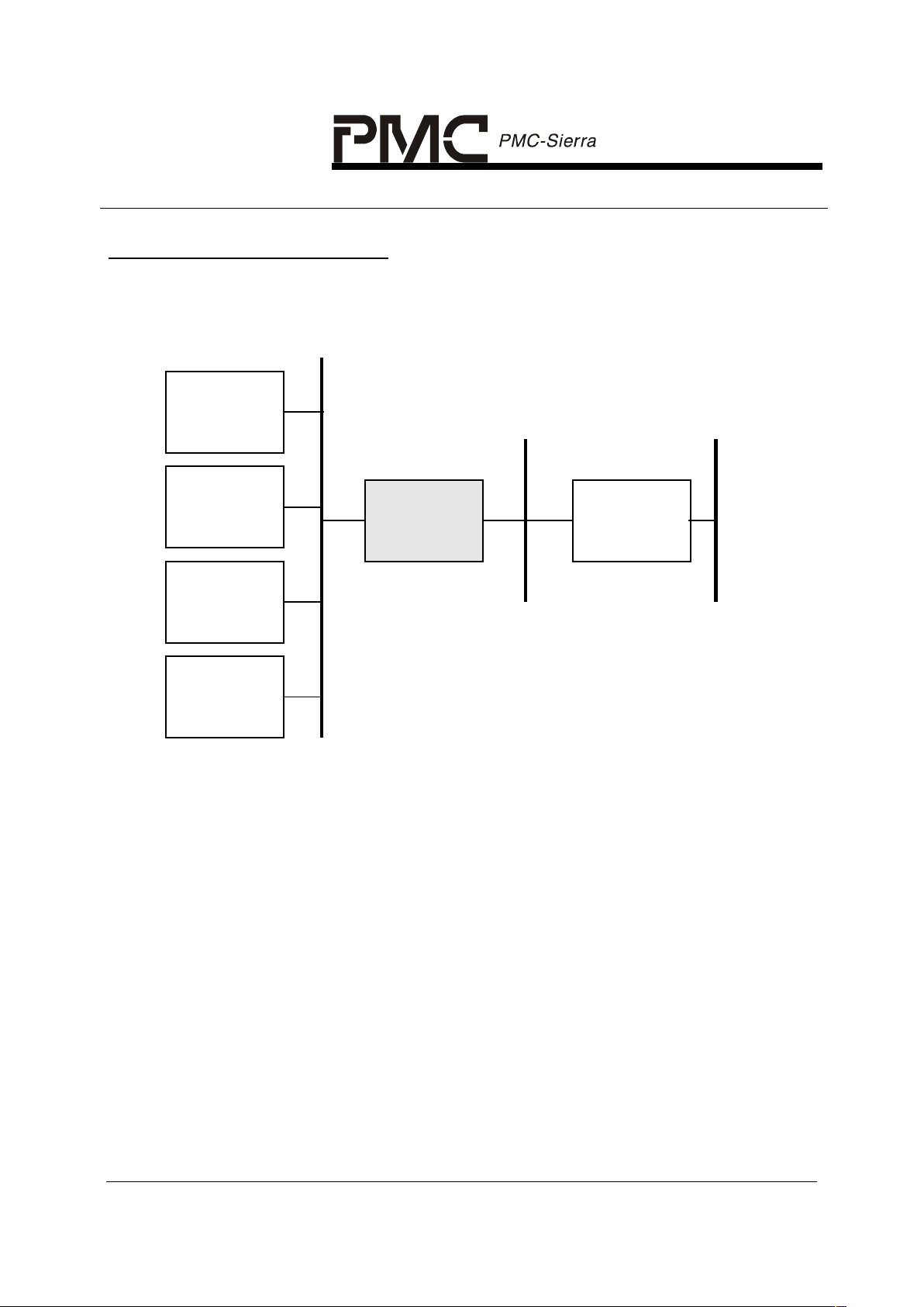
4 APPLICATION EXAMPLES
Figure 1 - Edge Router Line Card
PM4318
OCTLIU
PM4318
OCTLIU
PM4318
OCTLIU
PM4318
OCTLIU
PM4332
TE32
SBI
SBI
PM7384
FREEDM-
84P672
PCI
Figure 1illustrates a 32-Channel T1/E1/J1 Edge Router Line Card using the
FREEDM-84P672 (PM7384) and the OCTLIU (PM4318).
PRELIMINARY
PM4332 TE-32
DATA SHEET
PMC-2011402 ISSUE 1 HIGH DENSITY 32 CHANNEL T1/E1/J1 FRAMER
PROPRIETARY AND CONFIDENTIAL TO PMC-SIERRA, INC., AND FOR THE INTERNAL USE OF ITS CUSTOMERS 12
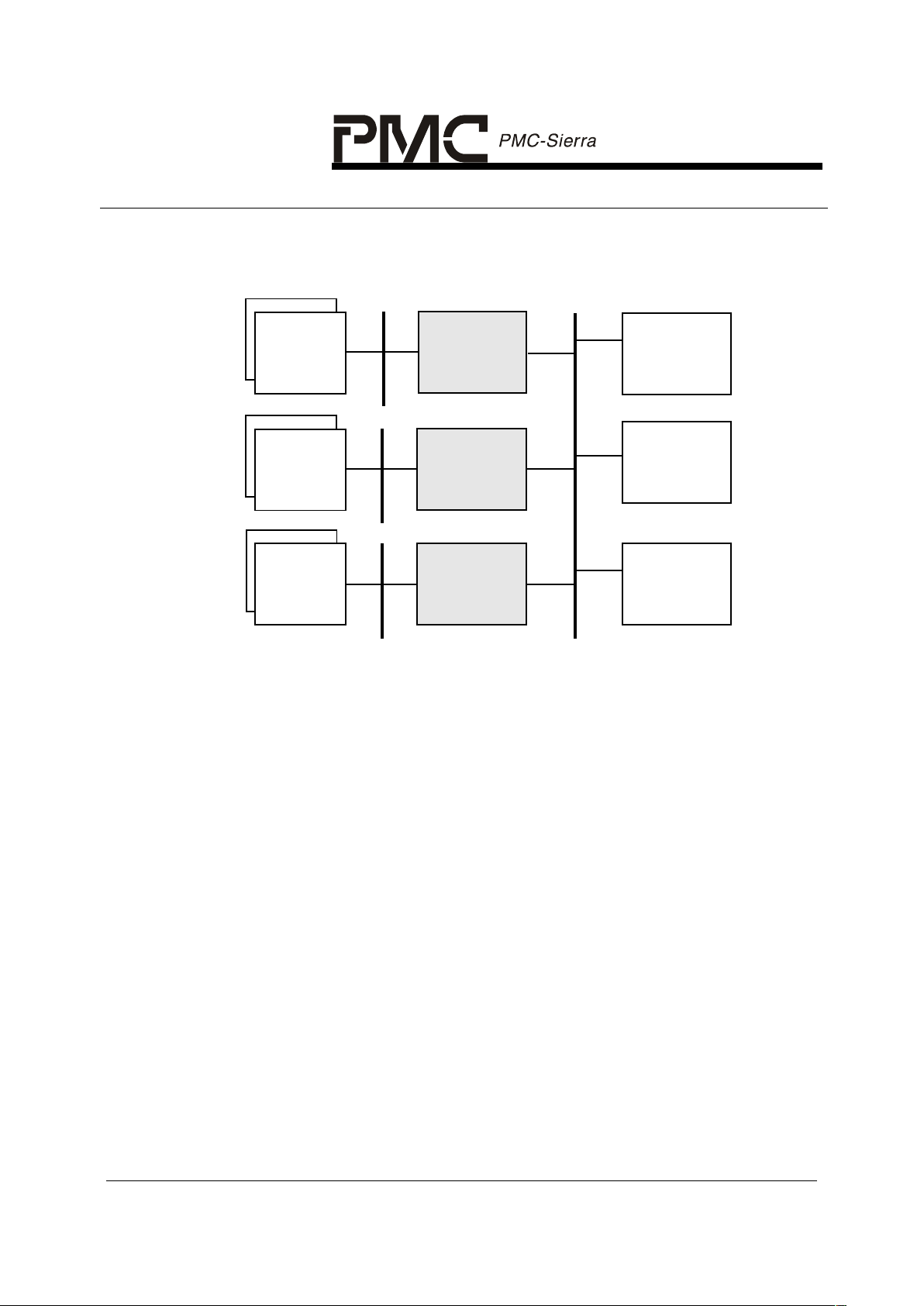
Figure 2 - Multiservice Switch
PM4332
TE32
19.44 MHz
SBI
19.44 MHz
SBI
PM4332
TE32
PM4332
TE32
PM7389
FREEDM-
84A1024
PM7341
S/UNI-
IMA-84
PM73122
AAL1gator-32
PM4318
OCTLIU
PM4318
OCTLIU
4 x OCTLIU
PM4318
OCTLIU
PM4318
OCTLIU
4 x OCTLIU
PM4318
OCTLIU
PM4318
OCTLIU
4 x OCTLIU
Figure 2 illustrates how frame relay (FREEDM-84A1024), circuit emulation
(AAL1gator-32) and ATM inverse multiplexing (S/UNI-IMA-84) may all be
supported on a single platform using a common SBI bus as the enabling
technology. A high density T1/E1/J1 line interface is provided through an SBI bus
connection to the OCTLIU (PM4318).
PRELIMINARY
PM4332 TE-32
DATA SHEET
PMC-2011402 ISSUE 1 HIGH DENSITY 32 CHANNEL T1/E1/J1 FRAMER
PROPRIETARY AND CONFIDENTIAL TO PMC-SIERRA, INC., AND FOR THE INTERNAL USE OF ITS CUSTOMERS 13
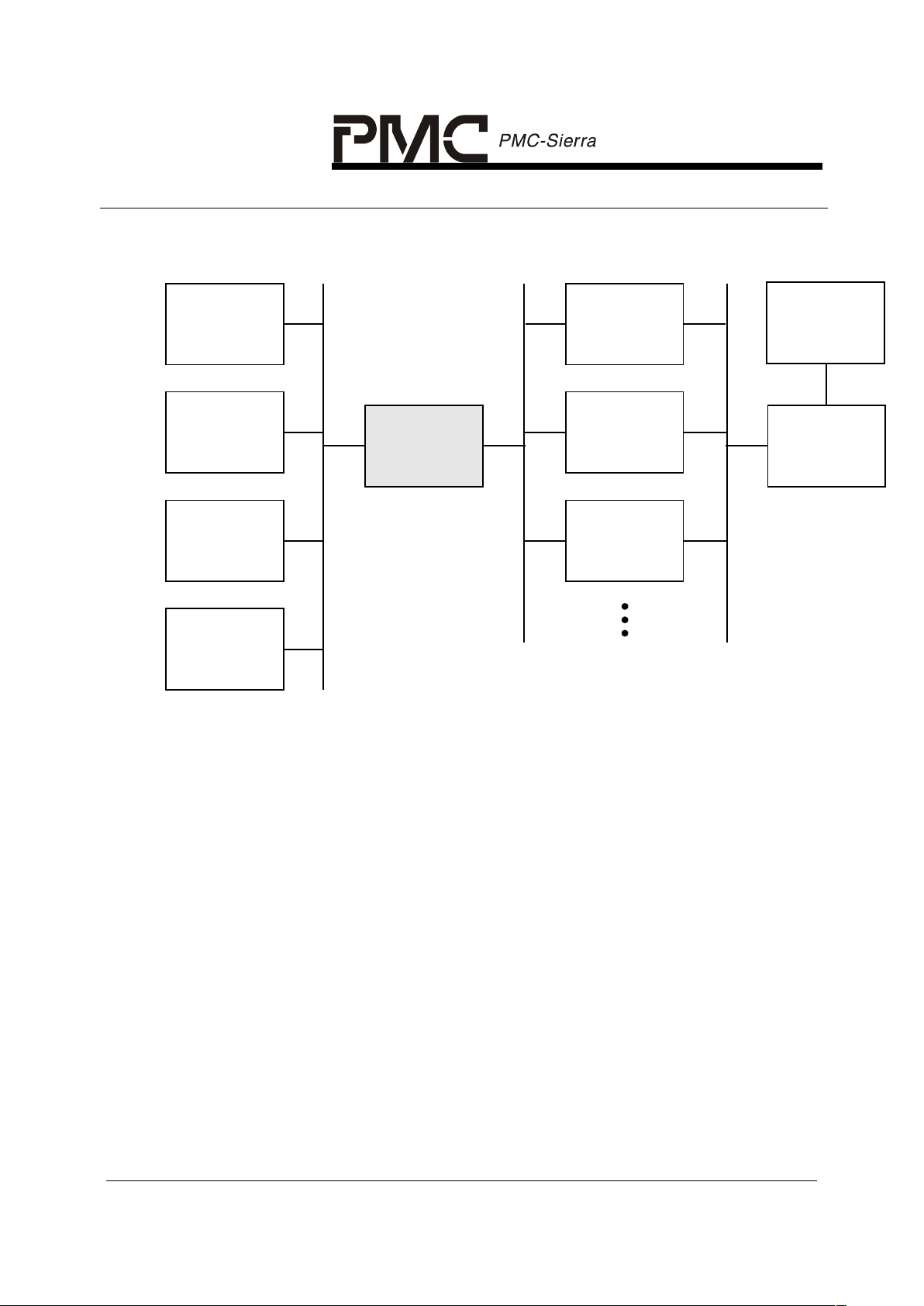
Figure 3 - Voice Gateway Application
PM4318
OCTLIU
PM4318
OCTLIU
PM4318
OCTLIU
PM4318
OCTLIU
PM4332
TE32
SBI
PCM Highway
H-MVIP
VoATM
DSP
VoATM
DSP
VoATM
DSP
PM7326
S/UNI-APEX
PM7324
S/UNI-ATLAS
Utopia L2
Figure 3 illustrates a typical voice gateway application using VoATM processing
and ATM traffic management (PM7326, PM7324).
PRELIMINARY
PM4332 TE-32
DATA SHEET
PMC-2011402 ISSUE 1 HIGH DENSITY 32 CHANNEL T1/E1/J1 FRAMER
PROPRIETARY AND CONFIDENTIAL TO PMC-SIERRA, INC., AND FOR THE INTERNAL USE OF ITS CUSTOMERS 14
5 BLOCK DIAGRAM
Figure 4 - TE-32 Block Diagram
LADATA[7:0]
LADP
LAV5
LAPL
JTAG uP Interface
System
Side SBI
Extract
INTB
RDB
WRB
CSB
ALE
A[12:0]
D[7:0]
TRSTB
TDO
TDI
TMS
TCK
T1/E1
Transmitter;
HDLC
Transmitter,
PRBS
Generator
Egress
H-MVIP
System
Side SBI
Insert
Ingress
H-MVIP
LAC1FPO
LAC1FPI
Line Side
SBI Insert
Line Side
SBI Extract
LDDATA[7:0]
LDDP
LDV5
LDPL
LDC1FP
RJAT
Digital Jitter
Attenuator
T1/E1 Framer;
HDLC Receiver,
PMON, PRBS
Checker
ELST
Elastic
Store
T1/E1
SIGX
TJAT
Digital Jitter
Attenuator
ELST
Elastic
Store
LREFCLK
Recovered
Clock
RSTB
SREFCLK
SAC1FP
SDC1FP
CMVFPC
MVED[1:8]
SAJUST_REQ
SADATA[7:0]
SADP
SAPL
SAV5
SDDATA[7:0]
SDDP
SDPL
SDV5
SBIACT
SBIDET[1:0]
CASED[1:8]
CCSED[1:3]
CMVFPB
CMV8MCLK
CMVFPC
CMVFPB
CMV8MCLK
MVID[1:8]
CASID[1:8]
CCSID[1:3]
TS0ID
CTCLK
S77
RECVCLK1
RECVCLK3
RECVCLK2
XCLK_T1
XCLK_E1

PRELIMINARY
PM4332 TE-32
DATA SHEET
PMC-2011402 ISSUE 1 HIGH DENSITY 32 CHANNEL T1/E1/J1 FRAMER
PROPRIETARY AND CONFIDENTIAL TO PMC-SIERRA, INC., AND FOR THE INTERNAL USE OF ITS CUSTOMERS 15

PRELIMINARY
PM4332 TE-32
DATA SHEET
PMC-2011402 ISSUE 1 HIGH DENSITY 32 CHANNEL T1/E1/J1 FRAMER
PROPRIETARY AND CONFIDENTIAL TO PMC-SIERRA, INC., AND FOR THE INTERNAL USE OF ITS CUSTOMERS 16
6 DESCRIPTION
The PM4332 High Density 32 Channel T1/E1 Framer is a feature-rich device for
use in any application requiring high density framing of T1/J1 and E1 links.
Each of the T1 and E1 framers and transmitters is independently software
configurable, allowing timing master and feature selection without changes to
external wiring. However, mixed framing modes are not supported. The framers
must be all configured for either T1 or E1 framing.
T1 Operation
In the ingress direction, each of the 32 T1 links is extracted from the Scaleable
Bandwidth Interconnect (SBI) bus. A Scaleable Bandwidth Interconnect (SBI)
high density byte serial line interface provides higher levels of integration and
dense interconnect. Each T1 framer detects the presence of Yellow and AIS
patterns and also integrates Yellow, Red, and AIS alarms.
T1 performance monitoring with accumulation of CRC-6 errors, framing bit errors,
out-of-frame events, and changes of frame alignment is provided. The TE-32
also detects the presence of ESF bit oriented codes, and detects and terminates
HDLC messages on the ESF data link. The HDLC messages are terminated in a
128 byte FIFO. An elastic store that optionally supports slip buffering and
adaptation to backplane timing is provided, as is a signaling extractor that
supports signaling debounce, signaling freezing and interrupt on signaling state
change on a per-DS0 basis. The TE-32 also supports inband loopback code
generation and detection, idle code substitution, digital milliwatt code insertion,
data link extraction, trunk conditioning, data sign and magnitude inversion, and
pattern generation and detection on a per-DS0 basis.
In the egress direction, framing is generated for 32 T1s into an SBI add bus. A
Scaleable Bandwidth Interconnect (SBI) high density byte serial line interface
provides higher levels of integration and dense interconnect. Each T1 transmitter
frames to SF or ESF DS1 formats, or framing can be optionally disabled. The
TE-32 supports signaling insertion, idle code substitution, data insertion, line
loopback, data inversion and zero-code suppression on a per-DS0 basis. PRBS
generation and detection is supported on a framed and unframed T1 basis.
E1 Operation
In the ingress direction, each of the 32 E1 links is extracted from Scaleable
Bandwidth Interconnect (SBI). Each E1 framer detects and indicates the
presence of remote alarm and AIS patterns and also integrates Red and AIS
alarms.

PRELIMINARY
PM4332 TE-32
DATA SHEET
PMC-2011402 ISSUE 1 HIGH DENSITY 32 CHANNEL T1/E1/J1 FRAMER
PROPRIETARY AND CONFIDENTIAL TO PMC-SIERRA, INC., AND FOR THE INTERNAL USE OF ITS CUSTOMERS 17
The E1 framers support detection of various alarm conditions such as loss of
frame, loss of signaling multiframe and loss of CRC multiframe. The E1 framers
also support reception of remote alarm signal, remote multiframe alarm signal,
alarm indication signal, and time slot 16 alarm indication signal.
E1 performance monitoring with accumulation of CRC-4 errors, far end block
errors and framing bit errors is provided. The TE-32 provides a receive HDLC
controller for the detection and termination of messages on the national use bits.
Detection of the 4-bit Sa-bit codewords defined in ITU-T G.704 and ETSI 300-233
is supported. V5.2 link ID signal detection is also supported. An interrupt may be
generated on any change of state of the Sa codewords. An elastic store for slip
buffering and rate adaptation to backplane timing is provided, as is a signaling
extractor that supports signaling debounce, signaling freezing, idle code
substitution, digital milliwatt tone substitution, data inversion, and signaling bit
fixing on a per-channel basis. Receive side data and signaling trunk conditioning
is also provided.
In the egress direction, framing is generated for 32 E1s into SBI add bus. Each
E1 transmitter generates framing for a basic G.704 E1 signal. The signaling
multiframe alignment structure and the CRC multiframe structure may be
optionally inserted. Framing can be optionally disabled. Transmission of the 4-bit
Sa codewords defined in ITU-T G.704 and ETSI 300-233 is supported. PRBS
generation or detection is supported on a framed and unframed E1 basis.
General Operation
The TE-32 can generate a low jitter transmit clock from a variety of clock
references, and also provides jitter attenuation in the receive path. Three jitter
attenuated recovered T1/E1 clocks can be routed outside the TE-32 for network
timing applications.
In synchronous backplane systems, 8 Mbit/s H-MVIP interfaces are provided for
access to 768 DS0 channels, channel associated signaling (CAS) for all 768 DS0
channels and common channel signaling (CCS) for all 32 T1s or 32 E1s (or
combination thereof). The CCS signaling H-MVIP interface is independent of the
DS0 channel and CAS H-MVIP access. The use of any of the H-MVIP interfaces
requires that common clocks and frame pulse be used along with T1 slip buffers.
A Scaleable Bandwidth Interconnect (SBI) high density byte serial system
interface provides higher levels of integration and dense interconnect. The SBI
bus interconnects up to 32 T1s or E1s both synchronously or asynchronously.
The SBI allows transmit timing to be mastered by either the TE-32 or link layer
device connected to the system SBI bus. Error event accumulation is also
provided by the TE-32. Framing bit errors, and far end block errors are
accumulated. Error accumulation continues even while the off-line framers are

PRELIMINARY
PM4332 TE-32
DATA SHEET
PMC-2011402 ISSUE 1 HIGH DENSITY 32 CHANNEL T1/E1/J1 FRAMER
PROPRIETARY AND CONFIDENTIAL TO PMC-SIERRA, INC., AND FOR THE INTERNAL USE OF ITS CUSTOMERS 18
indicating OOF. The counters are intended to be polled once per second, and
are sized so as not to saturate at a 10
-3
bit error rate. Transfer of count values to
holding registers is initiated through the microprocessor interface.
The TE-32 is configured, controlled and monitored via a generic 8-bit
microprocessor bus through which all internal registers are accessed. All
sources of interrupts can be masked and acknowledged through the
microprocessor interface.
PRELIMINARY
PM4332 TE-32
DATA SHEET
PMC-2011402 ISSUE 1 HIGH DENSITY 32 CHANNEL T1/E1/J1 FRAMER
PROPRIETARY AND CONFIDENTIAL TO PMC-SIERRA, INC., AND FOR THE INTERNAL USE OF ITS CUSTOMERS 19
7 PIN DIAGRAM
The TE-32 is packaged in a 324-pin PBGA package having a body size of 23mm
by 23mm and a ball pitch of 1.0 mm. The center 36 balls are not used as signal
I/Os and are thermal balls. Pin names and locations are defined in the Pin
Description Table in section 8. Mechanical information for this package is in
section 19.
Figure 5 - Pin Diagram
22 21 20 19 18 17 16 15 14 13 12 11 10 9 8 7 6 5 4 3 2 1
A
B
C
D
E
F
G
H
324 PBGA
J
VSS VSS VSS VSS VSS VSS
K
VSS VSS VSS VSS VSS VSS
L
VSS VSS VSS VSS VSS VSS
M
VSS VSS VSS VSS VSS VSS
N
VSS VSS VSS VSS VSS VSS
P
VSS VSS VSS VSS VSS VSS
R
T
Bottom View
U
V
W
Y
AA
AB
22 21 20 19 18 17 16 15 14 13 12 11 10 9 8 7 6 5 4 3 2 1

PRELIMINARY
PM4332 TE-32
DATA SHEET
PMC-2011402 ISSUE 1 HIGH DENSITY 32 CHANNEL T1/E1/J1 FRAMER
PROPRIETARY AND CONFIDENTIAL TO PMC-SIERRA, INC., AND FOR THE INTERNAL USE OF ITS CUSTOMERS 20
8 PIN DESCRIPTION
Pin Name Type Pin
No.
Function
H-MVIP System Side Interfaces
CMV8MCLK Input T22 Common 8M H-MVIP Clock (CMV8MCLK). The
common 8.192 Mbit/s H-MVIP data provides the
data clock for receive and transmit links
configured for operation in 8.192 Mbit/s H-MVIP
mode.
CMV8MCLK is used to sample the MVED[1:8],
CASED[1:8] and CCSED[1:3] inputs and update
MVID[1:8], CASID[1:8], CCSID[1:3] and TS0ID
outputs. CMV8MCLK is nominally a 50% duty
cycle clock with a frequency of 16.384 MHz.
The H-MVIP interfaces are enabled via the
SYSOPT[1:0] bits in the Global Configuration
register. If the TE-32 is not configured for HMVIP operation, this clock may be tied high or
low.
CMVFPC Input R20 Common H-MVIP Frame Pulse Clock
(CMVFPC). The common 8.192 Mbit/s H-MVIP
frame pulse clock provides the frame pulse clock
for receive and transmit links configured for
operation in 8.192 Mbit/s H-MVIP mode.
CMVFPC is used to sample CMVFPB. CMVFPC
is nominally a 50% duty cycle clock with a
frequency of 4.096 MHz. The falling edge of
CMVFPC must be aligned with the falling edge of
CMV8MCLK with no more than ±10ns skew.
The H-MVIP interfaces are enabled via the
SYSOPT[1:0] bits in the Global Configuration
register. If the TE-32 is not configured for HMVIP operation, this clock may be tied high or
low.

PRELIMINARY
PM4332 TE-32
DATA SHEET
PMC-2011402 ISSUE 1 HIGH DENSITY 32 CHANNEL T1/E1/J1 FRAMER
PROPRIETARY AND CONFIDENTIAL TO PMC-SIERRA, INC., AND FOR THE INTERNAL USE OF ITS CUSTOMERS 21
Pin Name Type Pin
No.
Function
CMVFPB Input R22 Common H-MVIP Frame Pulse (CMVFPB). The
active low common frame pulse for 8.192 Mbit/s
H-MVIP signals references the beginning of each
frame for links operating in 8.192 Mbit/s H-MVIP
mode.
If the CMMFP bit of the Master H-MVIP Interface
Configuration register is a logic 1, the CMVFPB
is becomes a multiframe pulse. Mulitframe
alignment is only relevant when the T1 F-bit or
the E1 TS0 is being carried transparently in the
egress direction and alignment to CAS signaling
is required. To support any combination of SF,
SLC96, ESF and E1, the CMVFPB must pulse
low at a multiple of 48 frames at the beginning of
the frame.
The H-MVIP interfaces are enabled via the
SYSOPT[1:0] bits in the Global Configuration
register. If the TE-32 is not configured for HMVIP operation, this frame pulse may be tied
high or low.
The CMVFPB frame pulse occurs at multiples of
125us and is sampled on the falling edge of
CMVFPC.

PRELIMINARY
PM4332 TE-32
DATA SHEET
PMC-2011402 ISSUE 1 HIGH DENSITY 32 CHANNEL T1/E1/J1 FRAMER
PROPRIETARY AND CONFIDENTIAL TO PMC-SIERRA, INC., AND FOR THE INTERNAL USE OF ITS CUSTOMERS 22
Pin Name Type Pin
No.
Function
MVID[1]/SDC1FP
MVID[2]/SBIACT
MVID[3]/SAJUST_REQ
MVID[4]/SDDATA[0]
MVID[5]/SDDATA[4]
MVID[6]/SDDATA[5]
MVID[7]/SDDATA[6]
MVID[8]/SDDATA[7]
Output B3
A3
A2
C5
A5
B6
C7
D6
H-MVIP Ingress Data (MVID[1:8]). MVID[x]
carries the recovered T1 or E1 channels which
have passed through the elastic store. Each
MVID[x] signal carries the channels of four
complete T1s or E1s.
MVID[x] is aligned to the common H-MVIP
16.384 Mbit/s clock, CMV8MCLK, frame pulse
clock, CMVFPC, and frame pulse, CMVFPB.
MVID[x] is updated on every second rising or
falling edge of the common H-MVIP 16.384Mb /s
clock, CMV8MCLK, as fixed by the common HMVIP frame pulse clock, CMVFPC. The
updating edge of CMV8MCLK is selected via the
CMVIDE bit in the Master and H-MVIP Interface
Configuration register.
Each of MVID[1:4] and MVID[5:8] carries 16
independent T1s or E1s.
MVID[1:8] share the same pins as SDC1FP,
SBIACT, SAJUST_REQ, SDDATA[0] and
SDDATA[4:7]. MVID[1:8] are selected when the
SYSOPT[1:0] are set to “01” (H-MVIP), in the
Global Configuration register.

PRELIMINARY
PM4332 TE-32
DATA SHEET
PMC-2011402 ISSUE 1 HIGH DENSITY 32 CHANNEL T1/E1/J1 FRAMER
PROPRIETARY AND CONFIDENTIAL TO PMC-SIERRA, INC., AND FOR THE INTERNAL USE OF ITS CUSTOMERS 23
Pin Name Type Pin
No.
Function
CASID[1]
CASID[2]
CASID[3]
CASID[4]
CASID[5]
CASID[6]
CASID[7]
CASID[8]
Output B18
A19
A20
B19
D20
B22
C21
D21
Channel Associated Signaling Ingress Data
(CASID[1:8]). Each CASID[x] signal carries
CAS for four complete T1s or E1s. CASID[x]
carries the corresponding CAS values of the
channel carried in MVID[x]. It also carries the
framer and alarm statuses.
CASID[x] is aligned to the common H-MVIP
16.384 Mbit/s clock, CMV8MCLK, frame pulse
clock, CMVFPC, and frame pulse, CMVFPB.
CASID[x] is updated on every second rising or
falling edge of CMV8MCLK as fixed by the
common H-MVIP frame pulse clock, CMVFPC.
The updating edge of CMV8MCLK is selected via
the CMVIDE bit in the Master H-MVIP Interface
Configuration register.
Each of CASID[1:4] and CASID[5:8] carries 16
independent T1s or E1s.
CCSID[1]
CCSID[2]
CCSID[3]
Output C16
D18
B17
Common Channel Signaling Ingress Data
(CCSID[1:3]). In T1 mode, CCSID[1] carries the
32 common channel signaling channels
extracted from each of the 32 T1s. In E1 mode,
CCSID[1:3] carries up to 3 timeslots (15,16, 31)
from each of the 32 E1s. CCSID is formatted
according to the H-MVIP standard.
CCSID[x] is aligned to the common H-MVIP
16.384 Mbit/s clock, CMV8MCLK, frame pulse
clock, CMVFPC, and frame pulse, CMVFPB.
CCSID is updated on every second rising or
falling edge of CMV8MCLK as fixed by the
common H-MVIP frame pulse clock, CMVFPC.
The updating edge of CMV8MCLK is selected via
the CMVIDE bit in the Master H-MVIP Interface
Configuration register.

PRELIMINARY
PM4332 TE-32
DATA SHEET
PMC-2011402 ISSUE 1 HIGH DENSITY 32 CHANNEL T1/E1/J1 FRAMER
PROPRIETARY AND CONFIDENTIAL TO PMC-SIERRA, INC., AND FOR THE INTERNAL USE OF ITS CUSTOMERS 24
Pin Name Type Pin
No.
Function
TS0ID Output D17 E1 Timeslot 0 Ingress Data (TS0ID). In E1
mode, TS0ID carries the first timeslot of each
frame.
TS0ID is aligned to the common H-MVIP
16.384 Mbit/s clock, CMV8MCLK, frame pulse
clock, CMVFPC, and frame pulse, CMVFPB.
TS0ID is updated on every second rising or
falling edge of CMV8MCLK as fixed by the
common H-MVIP frame pulse clock, CMVFPC.
The updating edge of CMV8MCLK is selected via
the CMVIDE bit in the Master H-MVIP Interface
Configuration register.
MVED[1]
MVED[2]
MVED[3]/S77
MVED[4]/SAC1FP
MVED[5]/SADATA[3]
MVED[6]/SADATA[4]
MVED[7]/SADATA[5]
MVED[8]/SADATA[6]
Input B10
A10
D10
B11
C12
D13
B13
C13
H-MVIP Egress Data (MVED[1:8]). The egress
data streams to be transmitted are input on these
pins. Each MVED[x] signal carries the channels
of four complete T1s or E1s formatted according
to the H-MVIP standard.
MVED[x] is aligned to the common H-MVIP
16.384 Mbit/s clock, CMV8MCLK, frame pulse
clock, CMVFPC, and frame pulse, CMVFPB.
MVED[x] is sampled on every second rising or
falling edge of CMV8MCLK as fixed by the
common H-MVIP frame pulse clock, CMVFPC.
The sampling edge of CMV8MCLK is selected
via the CMVEDE bit in the Master Common
Ingress Serial and H-MVIP Interface
Configuration register.
Each of MVED[1:4] and MVED[5:8] carries 16
independent T1s or E1s.
MVED[3:8] share the same pins as S77,
SAC1FP, and SADATA[3:6] respectively.
MVED[3:8] are selected when the SYSOPT[1:0]
are set to “01” (H-MVIP), in the Global
Configuration register.

PRELIMINARY
PM4332 TE-32
DATA SHEET
PMC-2011402 ISSUE 1 HIGH DENSITY 32 CHANNEL T1/E1/J1 FRAMER
PROPRIETARY AND CONFIDENTIAL TO PMC-SIERRA, INC., AND FOR THE INTERNAL USE OF ITS CUSTOMERS 25
Pin Name Type Pin
No.
Function
CASED[1]
CASED[2]
CASED[3]
CASED[4]
CASED[5]
CASED[6]
CASED[7]
CASED[8]
Input H19
J20
J21
J22
K19
L20
L22
M22
Channel Associated Signaling Egress Data
(CASED[1:8]). Each CASED[x] signal carries
CAS for four complete T1s or E1s formatted
according to the H-MVIP standard. CASED[x]
carries the corresponding CAS values of the
channel data carried in MVED[x]. CASED[x] may
also present inband information for the control of
signaling insertion.
CASED[x] is aligned to the common H-MVIP
16.384 Mbit/s clock, CMV8MCLK, frame pulse
clock, CMVFPC, and frame pulse, CMVFPB.
CASED[x] is sampled on every second rising or
falling edge of CMV8MCLK as fixed by the
common H-MVIP frame pulse clock, CMVFPC.
The sampling edge of CMV8MCLK is selected
via the CMVEDE bit in the Master H-MVIP
Interface Configuration register.
Each of CASED[1:4] and CASED[5:8] carries 16
independent T1s or E1s.
CCSED[1]
CCSED[2]
CCSED[3]
Input H20
H21
H22
Common Channel Signaling Egress Data
(CCSED[1:3]). In T1 mode CCSED[1] carries
the common channel signaling channels to be
transmitted in each of the T1s. In E1 mode
CCSED carries up to 3 timeslots (15,16, 31) to
be transmitted in each of the E1s. CCSED is
formatted according to the H-MVIP standard.
CCSED is aligned to the common H-MVIP
16.384 Mbit/s clock, CMV8MCLK, frame pulse
clock, CMVFPC, and frame pulse, CMVFPB.
CCSED is sampled on every second rising or
falling edge of CMV8MCLK as fixed by the
common H-MVIP frame pulse clock, CMVFPC.
The sampling edge of CMV8MCLK is selected
via the CMVEDE bit in the Master H-MVIP
Interface Configuration register.

PRELIMINARY
PM4332 TE-32
DATA SHEET
PMC-2011402 ISSUE 1 HIGH DENSITY 32 CHANNEL T1/E1/J1 FRAMER
PROPRIETARY AND CONFIDENTIAL TO PMC-SIERRA, INC., AND FOR THE INTERNAL USE OF ITS CUSTOMERS 26
Pin Name Type Pin
No.
Function
Recovered T1 and E1 Clocks
RECVCLK1 Output F2 Recovered Clock 1 (RECVCLK1). This clock
output is a recovered and de-jittered clock from
any one of the 32 T1 framers or E1 framers.
RECVCLK2 Output E4 Recovered Clock 2 (RECVCLK2). This clock
output is a recovered and de-jittered clock from
any one of the 32 T1 framers or E1 framers.
RECVCLK3 Output G3 Recovered Clock 3 (RECVCLK3). This clock
output is a recovered and de-jittered clock from
any one of the 32 T1 framers or E1 framers.
XCLK_T1 Input E2 T1 Crystal Clock Input (XCLK_T1). This input
clocks the digital phase locked loop that performs
jitter attenuation on the T1 recovered clocks
which drive the RECVCLK1/2/3 outputs.
XCLK_T1 is nominally a 37.056 MHz ± 32ppm,
50% duty cycle clock.
This input may be tied to ground in applications
that do not use the RECVCLK1/2/3 outputs as
support T1.
XCLK_E1 Input F3 E1 Crystal Clock Input (XCLK_E1). This input
clocks the digital phase locked loop that performs
jitter attenuation on the E1 recovered clocks
which drive the RECVCLK1/2/3 outputs.
XCLK_E1 is nominally a 49.152 MHz ± 32ppm,
50% duty cycle clock when configured for E1
modes.
This input may be tied to ground in applications
that do not use the RECVCLK1/2/3 outputs as
support E1.

PRELIMINARY
PM4332 TE-32
DATA SHEET
PMC-2011402 ISSUE 1 HIGH DENSITY 32 CHANNEL T1/E1/J1 FRAMER
PROPRIETARY AND CONFIDENTIAL TO PMC-SIERRA, INC., AND FOR THE INTERNAL USE OF ITS CUSTOMERS 27
Pin Name Type Pin
No.
Function
SBI Line Side Interface
LREFCLK Input Y4 Line Reference Clock (LREFCLK). This signal
provides reference timing for the line side SBI
bus interface. On the incoming byte interface of
the line side SBI bus, LDC1FP, LDDATA[7:0],
LDDP, LDPL, LDV5 and LAC1FPI are sampled of
the rising edge or LREFCLK. In the outgoing byte
interface, LADATA[7:0], LADP, LAPL, LAV5 and
LAC1FPO are updated on the rising edge of
LREFCLK.
This clock is nominally a 19.44 MHz +/-50ppm
clock with a 50% duty cycle. This clock must be
phase locked to SREFCLK and can be externally
connected to SREFCLK, when the S77 input is
logic ‘0’.
LAC1FPI Input W10 Line Add C1 Frame Pulse Input (LAC1FPI).
The Add bus timing signal identifies the frame
and multiframe boundaries on the Add Data bus
LADATA[7:0].
LAC1FPI is set high to mark the first C1 byte of
the first transport envelope frame of the 4 frame
multiframe on the LADATA[7:0] bus. LAC1FPI
need not be presented on every occurrence of
the multiframe.
LAC1FPI is sampled on the rising edge of
LREFCLK.
LAC1FPO Output AA11 Line Add Bus C1 Frame Pulse Output
(LAC1FPO). The Add bus C1 frame pulse output
identifies the frame boundaries on the Line Add
Data bus LADATA[7:0]. LAC1FPO pulses high to
mark the first C1 byte of the SBI multiframe.
LAC1FPO will align to LAC1FPI if present, but
fly-wheels in its absence.
Multiple TE-32’s cannot be connected to the
same line side SBI bus interface.
LAC1FPO is updated on the rising edge of
LREFCLK.

PRELIMINARY
PM4332 TE-32
DATA SHEET
PMC-2011402 ISSUE 1 HIGH DENSITY 32 CHANNEL T1/E1/J1 FRAMER
PROPRIETARY AND CONFIDENTIAL TO PMC-SIERRA, INC., AND FOR THE INTERNAL USE OF ITS CUSTOMERS 28
Pin Name Type Pin
No.
Function
LAPL Output AB11 Line Add Bus Tributary Payload Active
(LAPL). The tributary payload active signal
marks the bytes carrying the tributary payload.
LAPL is high during each tributary payload byte
on the LADATA[7:0] bus. LAPL will be low during
transport overhead, path overhead, V1 bytes and
V2 bytes. To indicate pointer adjustments, LAPL
will be asserted appropriately during the V3 byte
and following byte for the tributary.
Multiple TE-32’s cannot be connected to the
same line side SBI bus interface.
LAPL is updated on the rising edge of LREFCLK.
LADATA[0]
LADATA[1]
LADATA[2]
LADATA[3]
LADATA[4]
LADATA[5]
LADATA[6]
LADATA[7]
Output
Tristate
W14
Y13
A
A13
A
B13
W13
A
A12
W12
W11
Line Add Bus Data (LADATA[7:0]). The add
bus data contains the line side SBI Add bus
payload data in byte serial format. All transport
overhead bytes are set to 00h. LADATA[7] is the
most significant bit (corresponding to bit 1 of
each serial word, the first bit to be transmitted).
By default, LADATA[7:0] is only asserted during
the tributaries assigned to this device as
determined by the ENBL bit in the Line Side
INSBI Tributary Control Indirect Access Data
register. As options, LADATA[7:0] can be driven
all the time or during the first nine columns.
LADATA[7:0] is updated on the rising edge of
LREFCLK.
LADP Output
Tristate
A
B14 Line Add Bus Data Parity (LADP). The Add Bus
data parity signal carries the parity of the
outgoing signals. The parity calculation
encompasses the LADATA[7:0] bus, the LAV5
signal and the LAPL signal. Odd parity is
selected by setting the LAOP register bit to logic
1 and even parity is selected by setting the LAOP
bit to logic 0.
LADP is valid for all non-tristate cycles.
LADP is updated on the rising edge of LREFCLK.

PRELIMINARY
PM4332 TE-32
DATA SHEET
PMC-2011402 ISSUE 1 HIGH DENSITY 32 CHANNEL T1/E1/J1 FRAMER
PROPRIETARY AND CONFIDENTIAL TO PMC-SIERRA, INC., AND FOR THE INTERNAL USE OF ITS CUSTOMERS 29
Pin Name Type Pin
No.
Function
LAV5 Output
Tristate
W15 Line Add Bus V5 Byte (LAV5). The outgoing
tributary V5 byte signal marks the various
tributary V5 bytes. LAV5 marks each tributary V5
byte on the LADATA[7:0] bus when high.
By default, LAV5 is only asserted during the
T1/E1 tributaries assigned to this device as
determined by the ENBL bit in Line Side INSBI
Tributary Control Indirect Access Data register.
As options, LAV5 can be driven all the time or
during the first nine columns.
LAV5 is updated on the rising edge of LREFCLK.
LDDATA[0]
LDDATA[1]
LDDATA[2]
LDDATA[3]
LDDATA[4]
LDDATA[5]
LDDATA[6]
LDDATA[7]
Input W5
AA6
AB5
Y3
Y6
AA5
AB4
AB3
Line Drop Bus Data (LDDATA[7:0]). The drop
bus data contains the T1/E1 receive payload data
in byte serial format. LDDATA[7] is the most
significant bit, corresponding to bit 1 of each
serial word, the bit transmitted first.
LDDATA[7:0] is sampled on the rising edge of
LREFCLK.
LDDP Input Y7 Line Drop Bus Data Parity (LDDP). The
incoming data parity signal carries the parity of
the incoming signals. The parity calculation
encompasses the LDDATA[7:0] bus, the LDV5
signal and the LDPL signal. Odd parity is
selected by setting the SBI_PAR_CTL bit in the
Line Side EXSBI Control Register high and even
parity is selected by setting the SBI_PAR_CTL bit
low.
LDDP is sampled on the rising edge of
LREFCLK.

PRELIMINARY
PM4332 TE-32
DATA SHEET
PMC-2011402 ISSUE 1 HIGH DENSITY 32 CHANNEL T1/E1/J1 FRAMER
PROPRIETARY AND CONFIDENTIAL TO PMC-SIERRA, INC., AND FOR THE INTERNAL USE OF ITS CUSTOMERS 30
Pin Name Type Pin
No.
Function
LDC1FP Input AB6 Line Drop C1 Frame Pulse (LDC1FP). The
LDC1FP provides frame synchronization for
devices connected via an SBI interface. LDC1FP
is asserted, for one LREFCLK cycle, for the first
C1 byte of the SBI multiframe on the
LDDATA[7:0] bus. This signal occurs every
500µS (i.e. every 9720 LREFCLK cycles).
LDC1FP is sampled on the rising edge of
LREFCLK.
LDV5 Input W6 Line Drop Bus V5 Byte (LDV5). The incoming
tributary V5 byte signal marks the various
tributary V5 bytes. LDV5 marks each tributary V5
byte on the LDDATA[7:0] bus when high.
LDV5 is sampled on the rising edge of
LREFCLK.
LDPL Input Y8 Line Drop Bus Tributary Payload Active
(LDPL). The tributary payload active signal
marks the bytes carrying the tributary payload
which have been identified by an external
payload processor. When this signal is available,
the internal pointer processor can be bypassed.
LDPL is only respected for asynchronously
mapped tributaries.
LDPL is high during each tributary payload byte
on the LDDATA[7:0] bus.
LDPL is sampled on the rising edge of
LREFCLK.

PRELIMINARY
PM4332 TE-32
DATA SHEET
PMC-2011402 ISSUE 1 HIGH DENSITY 32 CHANNEL T1/E1/J1 FRAMER
PROPRIETARY AND CONFIDENTIAL TO PMC-SIERRA, INC., AND FOR THE INTERNAL USE OF ITS CUSTOMERS 31
Pin Name Type Pin
No.
Function
SBI System Side Interface
CTCLK Input F19 Common Transmit Clock (CTCLK). This input
signal is used as a reference transmit tributary
clock which can be used in egress Clock Master
modes. CTCLK must be multiple of 8 kHz. The
transmit clock is derived by the jitter attenuator
PLL using CTCLK as a reference.
The TE-32 may be configured to ignore the
CTCLK input and lock to the data or one of the
recovered Ingress clocks instead, RECVCLK1,
RECVCLK2 and RECVCLK3. The receive
tributary clock is automatically substituted for
CTCLK if line loopback or looptiming is enabled.
S77/MVED[3] Input D10 System Side SBI 77.76 MHz Select (S77). This
input determines the frequency of SREFCLK. If
S77 is low, SREFCLK is expected to be
19.44MHz. If S77 is high, SREFCLK is expected
to be 77.76 MHz and data is driven and sampled
every fourth cycle.
This signal is a don’t care when the
SYSOPT[1:0] register bits are binary “01” (HMVIP inteface). In this mode SREFCLK is
required to be 19.44 MHz.
S77 is expected to be held static.
S77 shares the same pin as MVED[3]. S77 is
selected when the SYSOPT[1:0] bits are set to
“10” or “11”, in the Global Configuration register.
SREFCLK Input C10 System Reference Clock (SREFCLK). This
system reference clock is a nominal 19.44 MHz
+/-50ppm pr 77.76 MHz +/-50ppm 50% duty
cycle clock. This clock is common to both the add
and drop sides of the SBI bus.
SREFCLK must be active for all applications.
When the SYSOPT[1:0] register bits are binary
“01” (H-MVIP interface), SREFCLK is required to
be 19.44 MHz.

PRELIMINARY
PM4332 TE-32
DATA SHEET
PMC-2011402 ISSUE 1 HIGH DENSITY 32 CHANNEL T1/E1/J1 FRAMER
PROPRIETARY AND CONFIDENTIAL TO PMC-SIERRA, INC., AND FOR THE INTERNAL USE OF ITS CUSTOMERS 32
Pin Name Type Pin
No.
Function
SDC1FP/MVID[1] I/O B3 SBI Drop C1 Frame Pulse (SDC1FP). The
SDC1FP C1 frame pulse synchronizes devices
interfacing to the Insert SBI bus. The frame pulse
indicates SBI bus multiframe alignment which
occurs every 500 µS, therefore this signal is
pulsed every 9720 SREFCLK cycles (38880
cycles if S77 is high). This signal does not need
to occur every SBI multiframe and is also used to
indicate T1 and E1 multiframe alignment in
synchronous SBI mode by pulsing at multiples of
every 12 SBI multiframes (48 T1/E1 frames). In
synchronous locked mode, as selected by the
SYNCSBI context bit programmed through the
RX-SBI-ELST Indirect Channel Data register,
SDC1FP pulses every 116640 SREFCLK cycles
(466560 cycles if S77 is high). If the SYNCSBI
bit is logic 1 for at least one tributary, SDC1FP
must indicate T1 and E1 multiframe alignment.
The TE-32 can be configured to generate this
frame pulse. Only one device on the SBI bus
should generate this signal. By default this
signal is not enabled to generate the frame
pulse.
If a SDC1FP pulse is received at an unexpected
cycle, the Drop bus with become high-impedence
until two consecutive valid SDC1FP pulses occur.
The system frame pulse is a single SREFCLK
cycle long and is updated on the rising edge of
SREFCLK.
This signal must be held low if the SBI bus is not
being used.
SDC1FP shares the same pin as MVID[1].
SDC1FP is selected when the SYSOPT[1:0] bits
are set to “10” or “11”, in the Global Configuration
register.

PRELIMINARY
PM4332 TE-32
DATA SHEET
PMC-2011402 ISSUE 1 HIGH DENSITY 32 CHANNEL T1/E1/J1 FRAMER
PROPRIETARY AND CONFIDENTIAL TO PMC-SIERRA, INC., AND FOR THE INTERNAL USE OF ITS CUSTOMERS 33
Pin Name Type Pin
No.
Function
SAC1FP/MVED[4] Input B11 SBI Add C1 Frame Pulse (SAC1FP). The
Extract C1 frame pulse synchronizes devices
interfacing to the Extract SBI bus. The frame
pulse indicates SBI bus multiframe alignment
which occurs every 500 µS, therefore this signal
is pulsed every 9720 SREFCLK cycles (38880
cycles if S77 is high). This signal does not need
to occur every SBI multiframe. SAC1FP is
sampled on the rising edge of SREFCLK.
This signal must be held low if the SBI bus is not
being used.
SAC1FP shares the same pin as MVED[4].
SAC1FP is selected when the SYSOPT[1:0] bits
are set to “10” or “11”, in the Global Configuration
register.
SADATA[0]
SADATA[1]
SADATA[2]
SADATA[3]/MVED[5]
SADATA[4]/MVED[6]
SADATA[5]/MVED[7]
SADATA[6]/MVED[8]
SADATA[7]
Input A11
D12
B12
C12
D13
B13
C13
D14
System Add Bus Data (SADATA[7:0]). The
System add data bus is a time division
multiplexed bus which carries the E1, T1 and
DS3 tributary data is byte serial format over the
SBI bus structure. This device only monitors the
add data bus during the timeslots assigned to
this device.
SADATA[7:0] is sampled on the rising edge of
SREFCLK.
SADATA[3:6] share the same pins as MVED[5:8].
SADATA[3:6] is selected when the SYSOPT[1:0]
bits are set to “10” or “11”, in the Global
Configuration register.
SADP Input A14 System Add Bus Data Parity (SADP). The
system add bus signal carries the even or odd
parity for the add bus signals SADATA[7:0],
SAPL and SAV5. The TE-32 monitors the add
bus parity cycles when S77 is low and during the
entire selected STM-1 when S77 is high.
SADP is sampled on the rising edge of
SREFCLK.

PRELIMINARY
PM4332 TE-32
DATA SHEET
PMC-2011402 ISSUE 1 HIGH DENSITY 32 CHANNEL T1/E1/J1 FRAMER
PROPRIETARY AND CONFIDENTIAL TO PMC-SIERRA, INC., AND FOR THE INTERNAL USE OF ITS CUSTOMERS 34
Pin Name Type Pin
No.
Function
SAPL Input B14 System Add Bus Payload Active (SAPL). The
add bus payload active signal indicates valid data
within the SBI bus structure. This signal must be
high during all octets making up a tributary. This
signal goes high during the V3 octet of a tributary
to indicate negative timing adjustments between
the tributary rate and the fixed SBI bus structure.
This signal goes low during the octet after the V3
octet of a tributary to indicate positive timing
adjustments between the tributary rate and the
fixed SBI bus structure.
The TE-32 only monitors the add bus payload
active signal during the tributary timeslots
assigned to this device.
SAPL is sampled on the rising edge of
SREFCLK.
SAV5 Input C14 System Add Bus Payload Indicator (SAV5).
The add bus payload indicator locates the
position of the floating payloads for each tributary
within the SBI bus structure. Timing differences
between the tributary timing and the synchronous
SBI bus are indicated by adjustments of this
payload indicator relative to the fixed SBI bus
structure.
All timing adjustments indicated by this signal
must be accompanied by appropriate
adjustments in the SAPL signal.
The TE-32 only monitors the add bus payload
indicator signal during the tributary timeslots
assigned to this device.
SAV5 is sampled on the rising edge of
SREFCLK.

PRELIMINARY
PM4332 TE-32
DATA SHEET
PMC-2011402 ISSUE 1 HIGH DENSITY 32 CHANNEL T1/E1/J1 FRAMER
PROPRIETARY AND CONFIDENTIAL TO PMC-SIERRA, INC., AND FOR THE INTERNAL USE OF ITS CUSTOMERS 35
Pin Name Type Pin
No.
Function
SAJUST_REQ/
MVID[3]
Output
Tristate
A2 System Add Bus Justification Request
(SAJUST_REQ). The justification request signals
the Link Layer device to speed up, slow down or
maintain the rate which it is sending data to the
TE-32. This is only used when the TE-32 is the
timing master for the tributary transmit direction.
This active high signal indicates negative timing
adjustments when asserted high during the V3
octet of the tributary. In response to this the Link
Layer device sends an extra byte in the V3 octet
of the next SBI bus multi-frame.
Positive timing adjustments are requested by
asserting justification request high during the
octet following the V3 octet. The Link Layer
device responds to this request by not sending
an octet during the V3 octet of the next multiframe.
SAJUST_REQ has a different significance in the
flexible bandwidth mode. In this mode,
SAJUST_REQ is high for one SREFCLK cycle
for each byte that can be accepted. A valid byte
on SADATA[7:0] with an accompanying SAPL
assertion is expected in response.
The TE-32 only drives the justification request
signal during the tributary timeslots assigned to
this device. When operating in 19.44 MHz mode
(i.e. S77 low), SAJUST_REQ is aligned by the
SAC1FP input. When operating in 77.76 MHz
mode (i.e. S77 high), SAJUST_REQ’s alignment
is relative to the SDC1FP signal.
SAJUST_REQ is updated on the rising edge of
SREFCLK.
SAJUST_REQ shares the same pin as MVID[3].
SAJUST_REQ is selected when the
SYSOPT[1:0] bits are set to “10” or “11”, in the
Global Configuration register.

PRELIMINARY
PM4332 TE-32
DATA SHEET
PMC-2011402 ISSUE 1 HIGH DENSITY 32 CHANNEL T1/E1/J1 FRAMER
PROPRIETARY AND CONFIDENTIAL TO PMC-SIERRA, INC., AND FOR THE INTERNAL USE OF ITS CUSTOMERS 36
Pin Name Type Pin
No.
Function
SDDATA[0]/MVID[4]
SDDATA[1]
SDDATA[2]
SDDATA[3]
SDDATA[4]/MVID[5]
SDDATA[5]/MVID[6]
SDDATA[6]/MVID[7]
SDDATA[7]/MVID[8]
Output
Tristate
C5
A4
B5
C6
A5
B6
C7
D6
System Drop Bus Data (SDDATA[7:0]). The
System drop data bus is a time division
multiplexed bus which carries the E1 and T1
tributary data is byte serial format over the SBI
bus structure. This device only drives the data
bus during the timeslots assigned to this device.
SDDATA[7:0] is updated on the rising edge of
SREFCLK.
SDDATA[0] and SDDATA[4:7] share the same
pins as MVID[4] and MVID[5:8]. SDDATA[0] and
SDDATA[4:7] are selected when the
SYSOPT[1:0] bits are set to “10” or “11”, in the
Global Configuration register.
SDDP Output
Tristate
A6 System Drop Bus Data Parity (SDDP). The
system drop bus signal carries the even or odd
parity for the drop bus signals SDDATA[7:0],
SDPL and SDV5. Whenever the TE-32 drives the
data bus, the parity is valid.
SDDP is updated on the rising edge of
SREFCLK.

PRELIMINARY
PM4332 TE-32
DATA SHEET
PMC-2011402 ISSUE 1 HIGH DENSITY 32 CHANNEL T1/E1/J1 FRAMER
PROPRIETARY AND CONFIDENTIAL TO PMC-SIERRA, INC., AND FOR THE INTERNAL USE OF ITS CUSTOMERS 37
Pin Name Type Pin
No.
Function
SDPL Output
Tristate
A7 System Drop Bus Payload Active (SDPL). The
payload active signal indicates valid data within
the SBI bus structure. This signal is asserted
during all octets making up a tributary. This signal
goes high during the V3 octet of a tributary to
accommodate negative timing adjustments
between the tributary rate and the fixed SBI bus
structure. This signal goes low during the octet
after the V3 octet of a tributary to accommodate
positive timing adjustments between the tributary
rate and the fixed SBI bus structure.
In the flexible bandwidth configuration, SDPL is
asserted for each byte as it becomes available.
Therefore, SDPL may be high or low arbitrarily
during any SREFCLK cycle.
The TE-32 only drives the payload active signal
during the tributary timeslots assigned to this
device.
SDPL is updated on the rising edge of
SREFCLK.
SDV5 Output
Tristate
C8 System Drop Bus Payload Indicator (SDV5).
The payload indicator locates the position of the
floating payloads for each tributary within the SBI
bus structure. Timing differences between the
tributary timing and the synchronous SBI bus are
indicated by adjustments of this payload indicator
relative to the fixed SBI bus structure.
A
ll timing adjustments indicated by this signal are
accompanied by appropriate adjustments in the
SDPL signal.
The TE-32 only drives the payload Indicator
signal during the tributary timeslots assigned to
this device.
SDV5 is updated on the rising edge of
SREFCLK.

PRELIMINARY
PM4332 TE-32
DATA SHEET
PMC-2011402 ISSUE 1 HIGH DENSITY 32 CHANNEL T1/E1/J1 FRAMER
PROPRIETARY AND CONFIDENTIAL TO PMC-SIERRA, INC., AND FOR THE INTERNAL USE OF ITS CUSTOMERS 38
Pin Name Type Pin
No.
Function
SBIACT/MVID[2] Output A3 SBI Output Active (SBIACT). The SBI Output
Active indicator is high whenever the TE-32 is
driving the SBI drop bus signals. This signal is
used by other TE-32s or other SBI devices to
detect SBI configuration problems by detecting
other devices driving the SBI bus during the
same tributary as the device listening to this
signal.
This output is updated on the rising edge or
SREFCLK.
SBIACT shares the same pin as MVID[2].
SBIACT is selected when the SYSOPT[1:0] bits
are set to “10” or “11”, in the Global Configuration
register.
SBIDET[0]
SBIDET[1]
Input A15
B15
SBI Bus Activity Detection (SBIDET[1:0]). The
SBI bus activity detect input detects tributary
collisions between devices sharing the same SBI
bus. Each SBI device driving the bus also drives
an SBI active signal (SBIACT). This pair of
activity detection inputs monitors the active
signals from two other SBI devices. When
unused this signal should be connected to
ground.
These inputs only have effect when the SBI bus
is configured for 19.44 MHz (i.e. S77 is low).
A collision is detected when either of
SBIDET[1:0] signals are active concurrently with
this device driving SBIACT. When collisions
occur the SBI drivers are disabled and an
interrupt is generated to signal the collision.
Microprocessor Interface
INTB OutputODT21 Active low Open-Drain Interrupt (INTB). This
signal goes low when an unmasked interrupt
event is detected on any of the internal interrupt
sources. Note that INTB will remain low until all
active, unmasked interrupt sources are
acknowledged at their source.

PRELIMINARY
PM4332 TE-32
DATA SHEET
PMC-2011402 ISSUE 1 HIGH DENSITY 32 CHANNEL T1/E1/J1 FRAMER
PROPRIETARY AND CONFIDENTIAL TO PMC-SIERRA, INC., AND FOR THE INTERNAL USE OF ITS CUSTOMERS 39
Pin Name Type Pin
No.
Function
CSB Input
A
A15 Active Low Chip Select (CSB). This signal is
low during TE-32 register accesses.
The CSB input has an integral pull up resistor.
RDB Input W17 Active Low Read Enable (RDB). This signal is
low during TE-32 register read accesses. The
TE-32 drives the D[7:0] bus with the contents of
the addressed register while RDB and CSB are
low.
WRB Input
A
B16 Active Low Write Strobe (WRB). This signal is
low during a TE-32 register write access. The
D[7:0] bus contents are clocked into the
addressed register on the rising WRB edge while
CSB is low.
D[0]
D[1]
D[2]
D[3]
D[4]
D[5]
D[6]
D[7]
I/O U22
T20
V19
U21
U20
W22
Y22
Y21
Bidirectional Data Bus (D[7:0]). This bus
provides TE-32 register read and write accesses.
A[0]
A[1]
A[2]
A[3]
A[4]
A[5]
A[6]
A[7]
A[8]
A[9]
A[10]
A[11]
A[12]
Input
A
B22
A
A21
Y19
A
A20
A
A19
A
B20
A
A18
W19
A
B18
A
A17
W18
Y16
A
A16
Address Bus (A[12:0]). This bus selects specific
registers during TE-32 register accesses.
A[12] has an internal pull down resistor. Tie
A[12] directly to ground unless access to bit
HIZIO in the Master Test Register (0x1000) is
required.

PRELIMINARY
PM4332 TE-32
DATA SHEET
PMC-2011402 ISSUE 1 HIGH DENSITY 32 CHANNEL T1/E1/J1 FRAMER
PROPRIETARY AND CONFIDENTIAL TO PMC-SIERRA, INC., AND FOR THE INTERNAL USE OF ITS CUSTOMERS 40
Pin Name Type Pin
No.
Function
RSTB Input W20 Active Low Reset (RSTB). This signal provides
an asynchronous TE-32 reset. RSTB is a
Schmitt triggered input with an integral pull up
resistor.
ALE Input
A
A22 Address Latch Enable (ALE). This signal is
active high and latches the address bus A[12:0]
when low. When ALE is high, the internal
address latches are transparent. It allows the
TE-32 to interface to a multiplexed address/data
bus. The ALE input has an integral pull up
resistor.
JTAG Interface
TCK Input B1 Test Clock (TCK). This signal provides timing for
test operations that can be carried out using the
IEEE P1149.1 test access port.
TMS Input D2 Test Mode Select (TMS). This signal controls
the test operations that can be carried out using
the IEEE P1149.1 test access port. TMS is
sampled on the rising edge of TCK. TMS has an
integral pull up resistor.
TDI Input E3 Test Data Input (TDI). This signal carries test
data into the TE-32 via the IEEE P1149.1 test
access port. TDI is sampled on the rising edge
of TCK. TDI has an integral pull up resistor.
TDO Output D1 Test Data Output (TDO). This signal carries test
data out of the TE-32 via the IEEE P1149.1 test
access port. TDO is updated on the falling edge
of TCK. TDO is a tri-state output which is
inactive except when scanning of data is in
progress.

PRELIMINARY
PM4332 TE-32
DATA SHEET
PMC-2011402 ISSUE 1 HIGH DENSITY 32 CHANNEL T1/E1/J1 FRAMER
PROPRIETARY AND CONFIDENTIAL TO PMC-SIERRA, INC., AND FOR THE INTERNAL USE OF ITS CUSTOMERS 41
Pin Name Type Pin
No.
Function
TRSTB Input C1 Active low Test Reset (TRSTB). This signal
provides an asynchronous TE-32 test access
port reset via the IEEE P1149.1 test access port.
TRSTB is a Schmitt triggered input with an
integral pull up resistor. TRSTB must be asserted
during the power up sequence.
Note that if not used, TRSTB must be connected
to the RSTB input.
Power and Ground Pins
VDD3.3[19]
VDD3.3[18]
VDD3.3[17]
VDD3.3[16]
VDD3.3[15]
VDD3.3[14]
VDD3.3[13]
VDD3.3[12]
VDD3.3[11]
VDD3.3[10]
VDD3.3[9]
VDD3.3[8]
VDD3.3[7]
VDD3.3[6]
VDD3.3[5]
VDD3.3[4]
VDD3.3[3]
VDD3.3[2]
VDD3.3[1]
Power A18
A22
A
B17
D11
D16
D4
E1
F20
L1
L19
R21
R4
V2
W16
W4
W8
Y18
Y20
Y5
Power (VDD3.3[19:1]). The VDD3.3[19:1] pins
should be connected to a well decoupled +3.3V
DC power supply.

PRELIMINARY
PM4332 TE-32
DATA SHEET
PMC-2011402 ISSUE 1 HIGH DENSITY 32 CHANNEL T1/E1/J1 FRAMER
PROPRIETARY AND CONFIDENTIAL TO PMC-SIERRA, INC., AND FOR THE INTERNAL USE OF ITS CUSTOMERS 42
Pin Name Type Pin
No.
Function
VDD1.8[19]
VDD1.8[18]
VDD1.8[17]
VDD1.8[16]
VDD1.8[15]
VDD1.8[14]
VDD1.8[13]
VDD1.8[12]
VDD1.8[11]
VDD1.8[10]
VDD1.8[9]
VDD1.8[8]
VDD1.8[7]
VDD1.8[6]
VDD1.8[5]
VDD1.8[4]
VDD1.8[3]
VDD1.8[2]
VDD1.8[1]
Power C2
D3
J2
R1
U3
AB2
AB9
Y12
Y15
A
B19
N4
V20
U19
N21
K21
C22
C18
A13
B7
Power (VDD1.8[19:1]). The VDD1.8[19:1] pins
should be connected to a well-decoupled +1.8V
DC power supply.

PRELIMINARY
PM4332 TE-32
DATA SHEET
PMC-2011402 ISSUE 1 HIGH DENSITY 32 CHANNEL T1/E1/J1 FRAMER
PROPRIETARY AND CONFIDENTIAL TO PMC-SIERRA, INC., AND FOR THE INTERNAL USE OF ITS CUSTOMERS 43
Pin Name Type Pin
No.
Function
VSS[83]
VSS[82]
VSS[81]
VSS[80]
VSS[79]
VSS[78]
VSS[77]
VSS[76]
VSS[75]
VSS[74]
VSS[73]
VSS[72]
VSS[71]
VSS[70]
VSS[69]
VSS[68]
VSS[67]
VSS[66]
VSS[65]
VSS[64]
VSS[63]
VSS[62]
VSS[61]
VSS[60]
VSS[59]
VSS[58]
VSS[57]
VSS[56]
VSS[55]
VSS[54]
VSS[53]
VSS[52]
VSS[51]
VSS[50]
VSS[49]
VSS[48]
VSS[47]
VSS[46]
VSS[45]
VSS[44]
VSS[43]
VSS[42]
VSS[41]
VSS[40]
Ground
AA4
A12
AA2
AA3
AA7
A
B12
A
B15
A
B21
AB8
B4
C11
C17
C19
C3
C4
D15
D19
D22
D5
D8
F1
G19
G4
J10
J11
J12
J13
J14
J9
J19
K10
K11
K12
K13
K14
M21
K20
K22
K3
K9
L10
L11
L12
L13
Ground (VSS3.3[83:1]). The VSS[83:1] pins
should be connected to GND.

PRELIMINARY
PM4332 TE-32
DATA SHEET
PMC-2011402 ISSUE 1 HIGH DENSITY 32 CHANNEL T1/E1/J1 FRAMER
PROPRIETARY AND CONFIDENTIAL TO PMC-SIERRA, INC., AND FOR THE INTERNAL USE OF ITS CUSTOMERS 44
Pin Name Type Pin
No.
Function
VSS[39]
VSS[38]
VSS[37]
VSS[36]
VSS[35]
VSS[34]
VSS[33]
VSS[32]
VSS[31]
VSS[30]
VSS[29]
VSS[28]
VSS[27]
VSS[26]
VSS[25]
VSS[24]
VSS[23]
VSS[22]
VSS[21]
VSS[20]
VSS[19]
VSS[18]
VSS[17]
VSS[16]
VSS[15]
VSS[14]
VSS[13]
VSS[12]
VSS[11]
VSS[10]
VSS[9]
VSS[8]
VSS[7]
VSS[6]
VSS[5]
VSS[4]
VSS[3]
VSS[2]
VSS[1]
L14
L21
L9
M10
M11
M12
M13
M14
M19
M20
M4
M9
N10
N11
N12
N13
N14
N19
N22
N20
N9
P10
P11
P12
P13
P14
P19
P22
P21
P20
P9
R19
T2
V21
V22
W21
Y11
Y14
Y17

PRELIMINARY
PM4332 TE-32
DATA SHEET
PMC-2011402 ISSUE 1 HIGH DENSITY 32 CHANNEL T1/E1/J1 FRAMER
PROPRIETARY AND CONFIDENTIAL TO PMC-SIERRA, INC., AND FOR THE INTERNAL USE OF ITS CUSTOMERS 45
Pin Name Type Pin
No.
Function
Unused or Unconnected
Unused B20
A21
B21
E20
E21
C20
E22
F21
E19
G20
F22
G21
G22
These balls must be left floating.

PRELIMINARY
PM4332 TE-32
DATA SHEET
PMC-2011402 ISSUE 1 HIGH DENSITY 32 CHANNEL T1/E1/J1 FRAMER
PROPRIETARY AND CONFIDENTIAL TO PMC-SIERRA, INC., AND FOR THE INTERNAL USE OF ITS CUSTOMERS 46
Pin Name Type Pin
No.
Function
Unconnected A1
B2
L4
P4
T19
P1
T1
Y1
P2
U1
V3
P3
T3
W2
T4
V4
Y2
G2
J3
L2
G1
J1
M1
A16
C15
B16
A17
AB7
AA8
W7
Y9
AA9
W9
Y10
A
A10
A
B10
R3
V1
W3
R2
U2
AA1
These balls have no internal connections. They
may be left floating or tied to a static logic level.

PRELIMINARY
PM4332 TE-32
DATA SHEET
PMC-2011402 ISSUE 1 HIGH DENSITY 32 CHANNEL T1/E1/J1 FRAMER
PROPRIETARY AND CONFIDENTIAL TO PMC-SIERRA, INC., AND FOR THE INTERNAL USE OF ITS CUSTOMERS 47
Pin Name Type Pin
No.
Function
Unconnected U4
W1
AB1
H4
L3
N3
H2
K4
N2
H1
K2
M2
H3
K1
N1
F4
J4
M3
B8
A8
D7
C9
B9
A9
D9
A
A14
These balls have no internal connections. They
may be left floating or tied to a static logic level.
Notes on Pin Descriptions:
1. All TE-32 inputs and bi-directionals present minimum capacitive loading and
operate at TTL logic levels.
2. All TE-32 outputs and bi-directionals have at least 2 mA drive capability. The
bidirectional data bus outputs, D[7:0], have 4 mA drive capability. The outputs
RECVCLK1, RECVCLK2, RECVCLK3, CASID[1:8], CCSID[1:3], TS0ID, TDO
and INTB have 4 mA drive capability. The outputs MVID[2]/SBIACT,
MVID[3]/SAJUST_REQ, MVID[4]/SDDATA[0], MVID[5:8]/SDDATA[4:7],
SDDP, SDPL, SDV5, LAV5, LAC1FPO, LADATA[7:0], LADP and LAPL have
8mA drive capability. The bidirectional signal SDC1FP/MVID[1] has 8mA drive
capability.

PRELIMINARY
PM4332 TE-32
DATA SHEET
PMC-2011402 ISSUE 1 HIGH DENSITY 32 CHANNEL T1/E1/J1 FRAMER
PROPRIETARY AND CONFIDENTIAL TO PMC-SIERRA, INC., AND FOR THE INTERNAL USE OF ITS CUSTOMERS 48
3. Inputs CSB, RSTB, ALE, TMS, TDI and TRSTB have internal pull-up
resistors.
4. Input A[12] has an internal pull-down resistor.
5. All unused inputs should be connected to GROUND.
6. Power to the VDD3.3 pins should be applied before power to the VDD1.8 pins
is applied. Similarly, power to the VDD1.8 pins should be removed before
power to the VDD3.3 pins is removed.

PRELIMINARY
PM4332 TE-32
DATA SHEET
PMC-2011402 ISSUE 1 HIGH DENSITY 32 CHANNEL T1/E1/J1 FRAMER
PROPRIETARY AND CONFIDENTIAL TO PMC-SIERRA, INC., AND FOR THE INTERNAL USE OF ITS CUSTOMERS 49
9 FUNCTIONAL DESCRIPTION
The TE-32 supports a total throughput of 65.64Mbit/s (including overhead) in
both transmit (a.k.a. egress) and receive (a.k.a. ingress) directions.
9.1 T1 Framing
T1 framing can be performed on up to 32 tributaries.
The T1 framing function searches for the framing bit pattern in the standard
Superframe (SF), SLC96 or Extended Superframe (ESF) framing formats.
When searching for frame each of the 193 (SF or SLC96) or each of the 772
(ESF) framing bit candidates is simultaneously examined.
The time required to acquire frame alignment to an error-free ingress stream,
containing randomly distributed channel data (i.e. each bit in the channel data
has a 50% probability of being 1 or 0), is dependent upon the framing format.
For SF format, the T1 framer will determine frame alignment within 4.4ms 99
times out of 100. For SLC®96 format, the T1 framer will determine frame
alignment within 13ms. For ESF format, the T1 framer will determine frame
alignment within 15 ms 99 times out of 100.
Once the T1 framer has found frame, the ingress data is continuously monitored
for framing bit errors, bit error events (a framing bit error in SF or a CRC-6 error
in ESF), and severely errored framing events. The performance data is
accumulated for each tributary. The T1 framer also detects out-of-frame, based
on a selectable ratio of framing bit errors.
The framing function can also be disabled to allow reception of unframed data.
9.1.1 Inband Code Detection
The framer detects the presence of either of two programmable inband loopback
activate and deactivate code sequences in either framed or unframed data
streams (whether data stream is framed or unframed is not programmable). The
loopback codes will be detected in the presence of a mean bit error rate of up to
10-2. When the inband code is framed, the framing bits overwrite the code bits,
thus appearing to the receiver as a 2.6x10
-3 BER (which is within the tolerable
BER of 10-2).
Code indication is provided on the active high loopback activate (LBA) and
loopback deactivate (LBD) status bits. Changes in these status bits result in the

PRELIMINARY
PM4332 TE-32
DATA SHEET
PMC-2011402 ISSUE 1 HIGH DENSITY 32 CHANNEL T1/E1/J1 FRAMER
PROPRIETARY AND CONFIDENTIAL TO PMC-SIERRA, INC., AND FOR THE INTERNAL USE OF ITS CUSTOMERS 50
setting of corresponding interrupt status bits, LBAI and LBDI respectively, and
can also be configured to result in the setting of a maskable interrupt indication.
The inband loopback activate condition consists of a repetition of the
programmed activate code sequence in all bit positions for a minimum of 5.08
seconds (± 40 ms). The inband loopback deactivate condition consists of a
repetition of the programmed deactivate code sequence in all bit positions for a
minimum of 5.08 seconds (± 40 ms). Programmed codes can be from three to
eight bits in length.
The code sequence detection and timing is compatible with the specifications
defined in T1.403, TR-TSY-000312, and TR-TSY-000303.
9.1.2 T1 Bit Oriented Code Detection
The presence of 63 of the possible 64 bit oriented codes transmitted in the T1
Facility Data Link channel in ESF framing format is detected, as defined in ANSI
T1.403 and in TR-TSY-000194. The 64
th
code (111111) is similar to the HDLC
flag sequence and is used to indicate no valid code received.
Bit oriented codes are received on the Facility Data Link channel as a 16-bit
sequence consisting of 8 ones, a zero, 6 code bits, and a trailing zero
(111111110xxxxxx0). The receiver declares a received code valid if it has been
observed for two consecutive times. The code is declared removed if two code
sequences containing code values different from the detected code are received
two consecutive times.
Valid BOC are indicated through the BOCI status bit. The BOC bits are set to all
ones (111111) if no valid c od e ha s b een de tec ted . An in te rrupt i s g enerated to
signal when a detected code has been validated, or optionally, when a valid code
goes away (i.e. the BOC bits go to all ones).
9.1.3 T1 Alarm Integration
The presence of Yellow, Red, and AIS Carrier Fail Alarms (CFA) in SF, SLC96
or ESF formats is detected and integrated in accordance with the specifications
defined in ANSI T1.403 and TR-TSY-000191.
The presence of Yellow alarm is declared when the Yellow pattern has been
received for 400 ms (± 50 ms); the Yellow alarm is removed when the Yellow
pattern has been absent for 400 ms (± 50 ms). The presence of Red alarm is
declared when an out-of-frame condition has been present for 2.55 sec (± 40
ms); the Red alarm is removed when the out-of-frame condition has been absent
for 16.6 sec (± 500 ms). The presence of AIS alarm is declared when an out-of-

PRELIMINARY
PM4332 TE-32
DATA SHEET
PMC-2011402 ISSUE 1 HIGH DENSITY 32 CHANNEL T1/E1/J1 FRAMER
PROPRIETARY AND CONFIDENTIAL TO PMC-SIERRA, INC., AND FOR THE INTERNAL USE OF ITS CUSTOMERS 51
frame condition and all-ones in the PCM data stream have been present for 2.55
sec (±40 ms); the AIS alarm is removed when the AIS condition has been absent
for 16.6 sec (±500 ms).
CFA alarm detection algorithms operate in the presence of a 10
-3
bit error rate.
9.1.3.1 Customer Interface Alarms
The RAI-CI and AIS-CI alarms defined in T1.403 are detected reliably.
By definition, RAI-CI is a repetitive pattern within the ESF data link with a period
of 1.08 seconds. It consists of sequentially interleaving 0.99 seconds of
0000 00 00 11111111 (righ t- to -le ft) wit h 9 0 m s of 00111110 11111111 .
RAI-CI is declared when a bit oriented code of “00111110 11111111” is validated
(i.e. two consecutive patterns) while RAI (a.k.a. Yellow alarm) is declared. RAI-CI
is cleared upon deassertion of RAI or upon 28 consecutive 40ms intervals
without validation of “00111110 11111111 ”.
By definition, AIS-CI is a repetitive pattern of 1.26 seconds. It consists of 1.11
seconds of an unframed all ones pattern and 0.15 seconds of all ones modified
by the AIS-CI signature. The AIS-CI signature is a repetitive pattern 6176 bits in
length in which, if the first bit is numbered bit 0, bits 3088, 3474 and 5790 are
logical zeros and all other bits in the pattern are logical ones. AIS-CI is an
unframed pattern, so it is defined for all framing formats.
AIS-CI is declared between 1.40 and 2.56 seconds after initiation of the AIS-CI
signal and is deasserted 16.6 seconds after it ceases.
9.2 E1 Framing
E1 framing can be performed on up to 32 tributaries.
The E1 framing function searches for basic frame alignment, CRC multiframe
alignment, and channel associated signaling (CAS) multiframe alignment in the
incoming recovered PCM stream.
Once basic (or FAS) frame alignment has been found, the incoming PCM data
stream is continuously monitored for FAS/NFAS framing bit errors, which are
accumulated in a framing bit error counter dedicated to each tributary. Once
CRC multiframe alignment has been found, the PCM data stream is continuously
monitored for CRC multiframe alignment pattern errors and CRC-4 errors, which
are accumulated in a CRC error counter dedicated to each tributary. Once CAS
multiframe alignment has been found, the PCM data is continuously monitored

PRELIMINARY
PM4332 TE-32
DATA SHEET
PMC-2011402 ISSUE 1 HIGH DENSITY 32 CHANNEL T1/E1/J1 FRAMER
PROPRIETARY AND CONFIDENTIAL TO PMC-SIERRA, INC., AND FOR THE INTERNAL USE OF ITS CUSTOMERS 52
for CAS multiframe alignment pattern errors. The E1 framer also detects and
indicates loss of basic frame, loss of CRC multiframe, and loss of CAS
multiframe, based on user-selectable criteria. The reframe operation can be
initiated by software, by excessive CRC errors, or when CRC multiframe
alignment is not found within 400 ms.
The E1 framer extracts the contents of the International bits (from both the FAS
frames and the NFAS frames), the National bits, and the Extra bits (from timeslot
16 of frame 0 of the CAS multiframe). Moreover, the framer also extracts
submultiframe-aligned 4-bit codewords from each of the National bit positions
Sa4 to Sa8, and stores them in microprocessor-accessible registers that are
updated every CRC submultiframe.
The E1 framer identifies the raw bit values for the Remote (or distant frame)
Alarm (bit 3 in timeslot 0 of NFAS frames) and the Remote Signaling Multiframe
(or distant multiframe) Alarm (bit 6 of timeslot 16 of frame 0 of the CAS
multiframe). Access is also provided to the "debounced" remote alarm and
remote signaling multiframe alarm bits which are set when the corresponding
signals have been a logic 1 for 4 (provided the RAIC bit is logic 1) and 3
consecutive occurrences, respectively, as per Recommendation O.162.
Detection of AIS and timeslot 16 AIS are provided. AIS is also integrated, and an
AIS Alarm is indicated if the AIS condition has persisted for at least 100 ms. The
out of frame (OOF=1) condition is also integrated, indicating a Red Alarm if the
OOF condition has persisted for at least 100 ms.
An interrupt may be generated to signal a change in the state of any status bits
(INF, INSMF, INCMF, AIS or RED), and to signal when any event (RAI, RMAI,
AISD, TS16AISD, COFA, FER, SMFER, CMFER, CRCE or FEBE) has occurred.
Additionally, interrupts may be generated every frame, CRC submultiframe, CRC
multiframe or signaling multiframe.
Basic Frame Alignment Procedure
The E1 framer searches for basic frame alignment using the algorithm defined in
ITU-T Recommendation G.706 sections 4.1.2 and 4.2.

PRELIMINARY
PM4332 TE-32
DATA SHEET
PMC-2011402 ISSUE 1 HIGH DENSITY 32 CHANNEL T1/E1/J1 FRAMER
PROPRIETARY AND CONFIDENTIAL TO PMC-SIERRA, INC., AND FOR THE INTERNAL USE OF ITS CUSTOMERS 53
The algorithm finds frame alignment by using the following sequence:
1. Search for the presence of the correct 7-bit FAS (‘0011011’);
2. Check that the FAS is absent in the following frame by verifying that bit 2 of the
assumed non-frame alignment sequence (NFAS) TS 0 byte is a logic 1;
3. Check that the correct 7-bit FAS is present in the assumed TS 0 byte of the
next frame.
If either of the conditions in steps 2 or 3 are not met, a new search for frame
alignment is initiated in the bit immediately following the second 7-bit FAS
sequence check. This "hold-off" is done to ensure that new frame alignment
searches are done in the next bit position, modulo 512. This facilitates the
discovery of the correct frame alignment, even in the presence of fixed timeslot
data imitating the FAS.
The algorithm provides robust framing operation even in the presence of random
bit errors; the algorithm provides a 99.98% probability of finding frame alignment
within 1 ms in the presence of 10-3 bit error rate and no mimic patterns.
Once frame alignment is found, the INF context bit is set to logic 1, a change of
frame alignment is indicated (if it occurred), and the frame alignment signal is
monitored for errors occurring in the 7-bit FAS pattern and in bit 2 of NFAS
frames, and the debounced value of the Remote Alarm bit (bit 3 of NFAS frames)
is reported. Loss of frame alignment is declared if 3 consecutive FASs have
been received in error or, additionally, if bit 2 of NFAS frames has been in error
for 3 consecutive occasions. In the presence of a random 10-3 bit error rate the
frame loss criteria provides a mean time to falsely lose frame alignment of >12
minutes.
The E1 framer can be forced to initiate a basic frame search at any time when
any of the following conditions are met:
• the software re-frame bit, REFR, in the T1/E1 Framer Indirect Channel Data
registers is set to logic 1;
• the CRC Frame Find Block is unable to find CRC multiframe alignment; or
• the CRC Frame Find Block accumulates excessive CRC evaluation errors
(≥ 915 CRC errors in 1 second) and is enabled to force a re-frame under that
condition.

PRELIMINARY
PM4332 TE-32
DATA SHEET
PMC-2011402 ISSUE 1 HIGH DENSITY 32 CHANNEL T1/E1/J1 FRAMER
PROPRIETARY AND CONFIDENTIAL TO PMC-SIERRA, INC., AND FOR THE INTERNAL USE OF ITS CUSTOMERS 54
CRC Multiframe Alignment Procedure
The E1 framer searches for CRC multiframe alignment by observing whether the
International bits (bit 1 of TS 0) of NFAS frames follow the CRC multiframe
alignment pattern. Multiframe alignment is declared if at least two valid CRC
multiframe alignment signals are observed within 8 ms, with the time separating
two alignment signals being a multiple of 2 ms
Once CRC multiframe alignment is found, the INCMF register bit is set to logic 1,
and the E1 framer monitors the multiframe alignment signal (MFAS), indicating
errors occurring in the 6-bit MFAS pattern, errors occurring in the received CRC
and the value of the FEBE bits (bit 1 of frames 13 and 15 of the multiframe). The
E1 framer declares loss of CRC multiframe alignment if basic frame alignment is
lost. However, once CRC multiframe alignment is found, it cannot be lost due to
errors in the 6-bit MFAS pattern.
Under the CRC-to-non-CRC interworking algorithm, if the E1 framer can achieve
basic frame alignment with respect to the incoming PCM data stream, but is
unable to achieve CRC-4 multiframe alignment within the subsequent 400 ms,
the distant end is assumed to be a non CRC-4 interface. The details of this
algorithm are illustrated in the state diagram in Figure 6.

PRELIMINARY
PM4332 TE-32
DATA SHEET
PMC-2011402 ISSUE 1 HIGH DENSITY 32 CHANNEL T1/E1/J1 FRAMER
PROPRIETARY AND CONFIDENTIAL TO PMC-SIERRA, INC., AND FOR THE INTERNAL USE OF ITS CUSTOMERS 55
Figure 6 - CRC Multiframe Alignment Algorithm
FAS_Find_1
NFAS_Find
FAS_Find_2
BFA
CRC to CRC
Interworking
FAS_Find_1_Par
NFAS_Find_Par
FAS_Find_2_Par
BFA_Par
CRC to non-CRC
Interworking
FAS
found
NFAS
found
next fram e
FAS
found
next fram e
CRCMFA
NFAS
not found
next fram e
FAS
not found
next frame
FAS
found
NFAS
not found
next fram e
FAS
not found
next fram e
NFAS
found
next fram e
400ms
expire
FAS
found
next fram e
Start 400ms timer
and 8ms timer
8ms expire
8ms expire and
NOT(400ms expire)
CRCMFA_Par
Start 8ms timer
Reset BFA to
most recently
found alignment
Out of Frame
CRCMFA_Par
(Op
tional settin
g)
3 consecutiv e FASor NFAS
errors; m anual refram e; or
excessive CRC errors

PRELIMINARY
PM4332 TE-32
DATA SHEET
PMC-2011402 ISSUE 1 HIGH DENSITY 32 CHANNEL T1/E1/J1 FRAMER
PROPRIETARY AND CONFIDENTIAL TO PMC-SIERRA, INC., AND FOR THE INTERNAL USE OF ITS CUSTOMERS 56
Table 1 - E1 framer Framing States
State Out of Frame Out of Offline Frame
FAS_Find_1 Yes No
NFAS_Find Yes No
FAS_Find_2 Yes No
BFA No No
CRC to CRC Interworking No No
FAS_Find_1_Par No Yes
NFAS_Find_Par No Yes
FAS_Find_2_Par No Yes
BFA_Par No No
CRC to non-CRC Interworking No No
The states of the primary basic framer and the parallel/offline framer in the E1
framer block at each stage of the CRC multiframe alignment algorithm are shown
in Table 1.
From an out of frame state, the E1 framer attempts to find basic frame alignment
in accordance with the FAS/NFAS/FAS G.706 Basic Frame Alignment procedure
outlined above. Upon achieving basic frame alignment, a 400 ms timer is
started, as well as an 8 ms timer. If two CRC multiframe alignment signals
separated by a multiple of 2 ms are observed before the 8 ms timer has expired,
CRC multiframe alignment is declared.
If the 8 ms timer expires without achieving multiframe alignment, a new offline
search for basic frame alignment is initiated. This search is performed in
accordance with the Basic Frame Alignment procedure outlined above.
However, this search does not immediately change the actual basic frame
alignment of the system (i.e., PCM data continues to be processed in accordance
with the first basic frame alignment found after an out of frame state while this
frame alignment search occurs as a parallel operation).
When a new basic frame alignment is found by this offline search, the 8 ms timer
is restarted. If two CRC multiframe alignment signals separated by a multiple of
2 ms are observed before the 8 ms timer has expired, CRC multiframe alignment
is declared and the basic frame alignment is set accordingly (i.e., the basic frame
alignment is set to correspond to the frame alignment found by the parallel offline
search, which is also the basic frame alignment corresponding to the newly found
CRC multiframe alignment).
Subsequent expirations of the 8 ms timer will likewise reinitiate a new search for
basic frame alignment. If, however, the 400 ms timer expires at any time during
this procedure, the E1 framer stops searching for CRC multiframe alignment and
declares CRC-to-non-CRC interworking. In this mode, the E1 framer may be
optionally set to either halt searching for CRC multiframe altogether, or may

PRELIMINARY
PM4332 TE-32
DATA SHEET
PMC-2011402 ISSUE 1 HIGH DENSITY 32 CHANNEL T1/E1/J1 FRAMER
PROPRIETARY AND CONFIDENTIAL TO PMC-SIERRA, INC., AND FOR THE INTERNAL USE OF ITS CUSTOMERS 57
continue searching for CRC multiframe alignment using the established basic
frame alignment. In either case, no further adjustments are made to the basic
frame alignment, and no offline searches for basic frame alignment occur once
CRC-to-non-CRC interworking is declared: it is assumed that the established
basic frame alignment at this point is correct.
AIS Detection
When an unframed all-ones receive data stream is received, an AIS defect is
indicated by setting the AISD context bit to logic 1 when fewer than three zero
bits are received in 512 consecutive bits or, optionally, in each of two consecutive
periods of 512 bits. The AISD bit is reset to logic 0 when three or more zeros in
512 consecutive bits or in each of two consecutive periods of 512 bits. Finding
frame alignment will also cause the AISD bit to be set to logic 0.
Signaling Frame Alignment
Once the basic frame alignment has been found, the E1 framer searches for
Channel Associated Signaling (CAS) multiframe alignment using the following
G.732 compliant algorithm: signaling multiframe alignment is declared when at
least one non-zero time slot 16 bit is observed to precede a time slot 16
containing the correct CAS alignment pattern, namely four zeros (“0000”) in the
first four bit positions of timeslot 16.
Once signaling multiframe alignment has been found, the E1 framer sets the
INSMF context bit of the tributary to logic 1, and monitors the signaling
multiframe alignment signal, indicating errors occurring in the 4-bit pattern, and
indicating the debounced value of the Remote Signaling Multiframe Alarm bit (bit
6 of timeslot 16 of frame 0 of the multiframe).
This E1 framer also indicates the reception of TS 16 AIS when time slot 16 has
been received with three or fewer zeros in each of two consecutive multiframe
periods. The TS16AIS status is cleared when each of two consecutive signaling
multiframe periods contain four or more zeros OR when the signaling multiframe
signal is found.
The block declares loss of CAS multiframe alignment if two consecutive CAS
multiframe alignment signals have been received in error, or additionally, if all the
bits in time slot 16 are logic 0 for 1 or 2 (selectable) CAS multiframes. Loss of
CAS multiframe alignment is also declared if basic frame alignment has been
lost.

PRELIMINARY
PM4332 TE-32
DATA SHEET
PMC-2011402 ISSUE 1 HIGH DENSITY 32 CHANNEL T1/E1/J1 FRAMER
PROPRIETARY AND CONFIDENTIAL TO PMC-SIERRA, INC., AND FOR THE INTERNAL USE OF ITS CUSTOMERS 58
National Bit Extraction
The E1 framer extracts and assembles the submultiframe-aligned National bit
codewords Sa4[1:4] , Sa5[1:4] , Sa6[1:4] , Sa7[1:4] and Sa8[1:4]. The
corresponding register values are updated upon generation of the CRC
submultiframe interrupt.
This E1 framer also detects the V5.2 link ID signal, which is detected when 2 out
of 3 Sa7 bits are zeros. Upon reception of this Link ID signal, the V52LINKV
context bit is set to logic 1. This bit is cleared to logic 0 when 2 out of 3 Sa7 bits
are ones.
E1 Alarm Integration
The OOF and the AIS defects are integrated, verifying that each condition has
persisted for 104 ms (± 6 ms) before indicating the alarm condition. The alarm is
removed when the condition has been absent for 104 ms (± 6 ms).
The AIS alarm algorithm accumulates the occurrences of AISD (AIS detection).
The E1 framer counts the occurrences of AISD over a 4 ms interval and indicates
a valid AIS is present when 13 or more AISD indications (of a possible 16) have
been received. Each interval with a valid AIS presence indication increments an
interval counter which declares AIS Alarm when 25 valid intervals have been
accumulated. An interval with no valid AIS presence indication decrements the
interval counter. The AIS Alarm declaration is removed when the counter
reaches 0. This algorithm provides a 99.8% probability of declaring an AIS Alarm
within 104 ms in the presence of a 10-3 mean bit error rate.
The Red alarm algorithm monitors occurrences of out of frame (OOF) over a
4 ms interval, indicating a valid OOF interval when one or more OOF indications
occurred during the interval, and indicating a valid in frame (INF) interval when
no OOF indication occurred for the entire interval. Each interval with a valid OOF
indication increments an interval counter which declares Red Alarm when 25
valid intervals have been accumulated. An interval with valid INF indication
decrements the interval counter; the Red Alarm declaration is removed when the
counter reaches 0. This algorithm biases OOF occurrences, leading to
declaration of Red alarm when intermittent loss of frame alignment occurs.
The E1 framer can also be disabled to allow reception of unframed data.
9.3 T1/E1 Performance Monitoring
CRC error events, Frame Synchronization bit error events, and Out Of Frame
events, or optionally, Change of Frame Alignment (COFA) events are

PRELIMINARY
PM4332 TE-32
DATA SHEET
PMC-2011402 ISSUE 1 HIGH DENSITY 32 CHANNEL T1/E1/J1 FRAMER
PROPRIETARY AND CONFIDENTIAL TO PMC-SIERRA, INC., AND FOR THE INTERNAL USE OF ITS CUSTOMERS 59
accumulated with saturating counters over consecutive intervals as defined by
the period of the supplied transfer clock signal (typically 1 second). When the
transfer clock signal is applied, the counter values are transferred into holding
registers and resets the counters to begin accumulating events for the interval.
The counters are reset in such a manner that error events occurring during the
reset are not missed. If the holding registers are not read between successive
transfer clocks, the OVR context bit is asserted to indicate data loss.
A bit error event (BEE) is defined as an F-bit error for SF and SLC96 framing
format or a CRC-6 error for ESF framing format. A framing bit error (FER) is
defined as an Fs or Ft error for SF and SLC96 and an Fe error for ESF framing
format.
The transfer clock within the TE-32 chip is generated precisely once per second
(i.e. 19440000 SREFCLK cycles) if the AUTOUPDATE bit of the T1/E1 Framer
Configuration and Status register is logic 1 or by writing to the Global PMON
Update register with the FRMR bit set. Coincident with the counter transfer, a
Performance Report Message (PRM) is transmitted for each T1 tributary for
which the PRMEN context bit is logic 1.
9.4 T1/E1 HDLC Receiver
The HDLC Receiver is a microprocessor peripheral used to receive HDLC
frames on the 4 kHz ESF facility data link or the E1 Sa-bit data link. A data link
can also be extracted from any sub-set of bits within a single DS0.
The HDLC Receiver detects the change from flag characters to the first byte of
data, removes stuffed zeros on the incoming data stream, receives packet data,
and calculates the CRC-CCITT frame check sequence (FCS).
Received data is placed into a 128-byte FIFO buffer. An interrupt is generated
when a programmable number of bytes are stored in the FIFO buffer. Other
sources of interrupt are detection of the terminating flag sequence, abort
sequence, or FIFO buffer overrun.
The RHDL Indirect Channel Data Registers contain bits which indicate the
overrun or empty FIFO status, the interrupt status, and the occurrence end of
message bytes written into the FIFO. The RHDL Indirect Channel Data Registers
also indicates the abort, flag, and end of message status of the data just read
from the FIFO. On end of message, the RHDL Indirect Channel Data Registers
indicates the FCS status and if the packet contained a non-integer number of
bytes.

PRELIMINARY
PM4332 TE-32
DATA SHEET
PMC-2011402 ISSUE 1 HIGH DENSITY 32 CHANNEL T1/E1/J1 FRAMER
PROPRIETARY AND CONFIDENTIAL TO PMC-SIERRA, INC., AND FOR THE INTERNAL USE OF ITS CUSTOMERS 60
9.5 T1/E1 Elastic Store (ELST)
Frame slip buffers exist in both the ingress and egress directions.
In the ingress direction, the Elastic Store (ELST) synchronizes ingress frames to
the common ingress H-MVIP clock and frame pulse (CMV8MCLK, CMVFP,
CMVFPC) in H-MVIP modes. When using the SBI bus, the elastic store is
required in locked or slave mode.
In the egress direction, the Elastic Store is required in H-MVIP mode or in SBI
slave or locked modes when the transmit data is loop timed or referenced to one
of the recovered clocks (RECVCLK1, RECVCLK2, RECVCLK3).
The frame data is buffered in a two frame circular data buffer. Input data is
written to the buffer using a write pointer and output data is read from the buffer
using a read pointer. When the elastic store is being used, if the average
frequency of the incoming data is greater than the average frequency of the
backplane/transmit clock, the write pointer will catch up to the read pointer and
the buffer will be filled. Under this condition a controlled slip will occur when the
read pointer crosses the next frame boundary. The subsequent frame is deleted.
If the average frequency of the incoming data is less than the average frequency
of the backplane/transmit clock, the read pointer will catch up to the write pointer
and the buffer will be empty. Under this condition a controlled slip will occur
when the read pointer crosses the next frame boundary. The previous frame is
repeated.
A slip operation is always performed on a frame boundary.
When the ingress timing is recovered from the receive data, the ingress elastic
store can be bypassed to eliminate the 2 frame delay.
To allow for the extraction of signaling information in the data channels,
superframe identification is also passed through the ELST.
For payload conditioning, the ingress ELST may optionally insert a
programmable idle code into all channels when the framer is out of frame
synchronization. This code is set to all 1’s when the ELST is reset.
9.6 T1/E1 Signaling Extraction
Channel associated signaling (CAS) is extracted from an E1 signaling multiframe or from ESF, SLC96 and SF T1 formats.

PRELIMINARY
PM4332 TE-32
DATA SHEET
PMC-2011402 ISSUE 1 HIGH DENSITY 32 CHANNEL T1/E1/J1 FRAMER
PROPRIETARY AND CONFIDENTIAL TO PMC-SIERRA, INC., AND FOR THE INTERNAL USE OF ITS CUSTOMERS 61
In T1 mode, signaling bit are extracted from the received data streams for ESF,
SLC96 and SF framing formats. The signaling states are optionally debounced
and serialized onto the CASID[x] H-MVIP outputs or CAS bits within the SBI Bus
structure. Debouncing is performed on the entire signaling state. This CASID[x]
output is channel aligned with the MVID[x] output, and the signaling bits are
repeated for the entire superframe, allowing downstream logic to reinsert
signaling into any frame, as determined by system timing. The signaling data
stream contains the A,B,C,D bits in the lower 4 channel bit locations (bits 5, 6, 7
and 8) in ESF framing format. In SF and SLC96 format, bits 5 and 6 contain
the A and B bits from every second superfame and bits 7 and 8 contain the A and
B bits from the alternate superframes. The four bits are updated every 24 frames
and are debounced collectively.
Three superframes for ESF and six superframes for SLC96 and SF worth of
signal are buffered to ensure that there is a greater than 95% probability that the
signaling bits are frozen in the correct state for a 50% ones density out-of-frame
condition, as specified in TR-TSY-000170 and BELL PUB 43801. With signaling
debounce enabled, the per-channel signaling state must be in the same state for
2 ESF superframes or 4 SF/SLC96 superframes before appearing on the serial
output stream.
One superframe or signaling-multiframe of signal freezing is provided on the
occurrence of slips. When a slip event occurs, output signaling for the entire
superframe in which the slip occurred is frozen; the signaling is unfrozen when
the next slip-free superframe occurs.
Control over timeslot signaling bit fixing and signaling debounce is provided on a
per-timeslot basis.
An interrupt is provided to indicate a change of signaling state on a per channel
basis.
9.7 T1/E1 Receive Per-Channel Control
Data and signaling trunk conditioning may be applied on the ingress stream on a
per-channel basis. Also provided is per-channel control of data inversion and the
detection and generation of pseudo-random patterns. These operations occur on
the data after its passage through frame slip buffer, so that data and signaling
conditioning may overwrite the trouble code.
9.8 T1 Transmitter
The T1 transmitter generates the 1.544 Mbit/s T1 data streams according to SF,
SLC96 or ESF frame formats.

PRELIMINARY
PM4332 TE-32
DATA SHEET
PMC-2011402 ISSUE 1 HIGH DENSITY 32 CHANNEL T1/E1/J1 FRAMER
PROPRIETARY AND CONFIDENTIAL TO PMC-SIERRA, INC., AND FOR THE INTERNAL USE OF ITS CUSTOMERS 62
The transmitter provides per-channel control of idle code substitution, data
inversion (either all 8 bits, sign bit magnitude or magnitude only), and zero code
suppression. Three types of zero code suppression (GTE, Bell and "jammed bit
8") are supported and selected on a per-channel basis to provide minimum ones
density control. Context bits provide per-channel control of robbed bit signaling
and selection of the signaling source. All channels can be forced into a trunk
conditioning state by the Master Trunk Conditioning (MTRK) context bit. The
transmitter may source pseudo-random bit sequences (PRBS) in a selected subset of channels, while simultaneously monitoring the data from the system
interface for PRBS errors.
A data link is provided for ESF mode. The data link sources include bit oriented
codes and HDLC messages. If the T1_FDL_DIS context bit is logic 1, the data
link is sourced from the F-bit position of the H-MVIP or SBI interface. Support is
provided for the transmission of framed or unframed Inband Code sequences
and transmission of AIS, Yellow, AIS-CI and RAI-CI (ESF only) alarm signals for
all formats.
If the AUTOUPDATE bit of the T1/E1 Framer Configuration and Status register is
logic 1, the T1 transmitter automatically sends an ANSI T1.403-formatted
performance report on the T1 facility data link once per second.
The F-bit may be passed transparently from either the H-MVIP or SBI interface.
To support alignment of the robbed bit signaling to the F-bits, the C8MVFPB input
may be redefined as a superframe alignment pulse.
The transmitter can be disabled for framing via the FDIS context bit.
9.8.1 SLC96
SLC96 is partially supported. The F-bits must be sourced from the system
interface. To pass the F-bits transparently, the FDIS context bit must be set.
Also, a superframe alignment must be provided to ensure the robbed-bit
signaling is inserted in the correct frames relative to the F-bits. To ensure the
framing is not corrupted, the timing must be configured to avoid controlled frame
slips.
When using the SBI interface, it is recommended the transmit frame slip buffer be
bypassed and that the transmit clock be locked to the data stream (i.e. TJAT
LOOPT and REFSEL context bits logic 0).
With an H-MVIP interface, the transmit elastic store cannot be bypassed, so the
transmit clock must be locked to CTCLK which must be presented a clock that is
locked to CMV8MCLK.

PRELIMINARY
PM4332 TE-32
DATA SHEET
PMC-2011402 ISSUE 1 HIGH DENSITY 32 CHANNEL T1/E1/J1 FRAMER
PROPRIETARY AND CONFIDENTIAL TO PMC-SIERRA, INC., AND FOR THE INTERNAL USE OF ITS CUSTOMERS 63
9.8.2 T1 Bit Oriented Code Generation
63 of the possible 64 bit oriented codes may be transmitted in the Facility Data
Link (FDL) channel in ESF framing format, as defined in ANSI T1.403-1995.
When transmission is disabled the FDL is set to all ones.
Bit oriented codes are transmitted on the T1 Facility Data Link as a 16-bit
sequence consisting of 8 ones, a zero, 6 code bits, and a trailing zero
(111111110xxxxxx0) which is repeated as long as the code is not 111111. When
driving the T1 facility data link the transmitted bit oriented codes have priority
over any data transmitted except for ESF Yellow Alarm. The code to be
transmitted is programmed by writing to the BOC code context bits where it is
held until the latest code has been transmitted at least 10 times.
9.9 E1 Transmitter
The E1 transmitter generates a 2048 kbit/s data streams according to ITU-T
recommendations, providing individual enables for frame generation, CRC
multiframe generation, and channel associated signaling (CAS) multiframe
generation.
The E1 transmitter provides per-timeslot control of idle code substitution, data
inversion, digital milliwatt substitution, selection of the signaling source and CAS
data. All timeslots can be forced into a trunk conditioning state (idle code
substitution and signaling substitution) by use of the master trunk conditioning
(MTRK) context bit. The transmitter may source pseudo-random bit sequences
(PRBS) in a selected sub-set of channels, while simultaneously monitoring the
data from the system interface for PRBS errors.
Common Channel Signaling (CCS) is supported in time slots 15, 16 and 31.
Support is provided for the transmission of AIS and TS16 AIS, and the
transmission of remote alarm (RAI) and remote multiframe alarm signals.
The National Use bits (Sa-bits) can be sourced from the National Bits Codeword
context bits as 4-bit codewords aligned to the submultiframe. Alternatively, the
Sa-bits may individually carry data links sourced from the internal HDLC
controller, or may be passed transparently from the MVED[x] inputs.
9.10 T1/E1 HDLC Transmitters
The HDLC transmitter provides a serial data link for the 4 kHz ESF facility data
link or E1 Sa-bit data link. The data link may also be presented in any sub-set of
bits within a selected DS0. The HDLC transmitter is used under microprocessor
control to transmit HDLC data frames. It performs all of the data serialization,

PRELIMINARY
PM4332 TE-32
DATA SHEET
PMC-2011402 ISSUE 1 HIGH DENSITY 32 CHANNEL T1/E1/J1 FRAMER
PROPRIETARY AND CONFIDENTIAL TO PMC-SIERRA, INC., AND FOR THE INTERNAL USE OF ITS CUSTOMERS 64
CRC generation, zero-bit stuffing, as well as flag, and abort sequence insertion.
Upon completion of the message, a CRC-CCITT frame check sequence (FCS)
may be appended, followed by flags. If the HDLC transmitter data FIFO
underflows, an abort sequence is automatically transmitted.
When enabled, the HDLC transmitter continuously transmits the flag sequence
(01111110) u ntil d ata i s r eady to be transmitted.
The default procedure provides automatic transmission of data once a complete
packet is written. All complete packets of data will be transmitted. After the last
data byte of a packet, the CRC word (if CRC insertion has been enabled) and a
flag, or just a flag (if CRC insertion has not been enabled) is transmitted. The
HDLC transmitter then returns to the transmission of flag characters until the next
packet is available for transmission. While working in this mode, the user must
only be careful to avoid overfilling the FIFO; underruns cannot occur unless the
packet is greater than 128 bytes long.
A second mechanism transmits data when the FIFO depth has reached a user
configured upper threshold. The HDLC transmitter will continue to transmit data
until the FIFO depth has fallen below the upper threshold and the transmission of
the last packet with data above the upper threshold has completed. In this mode,
the user must be careful to avoid overruns and underruns. An interrupt can be
generated once the FIFO depth has fallen below a user configured lower
threshold as an indicator for the user to write more data.
Interrupts can also be generated if the FIFO underflows while transmitting a
packet, when the FIFO falls below a lower threshold, when the FIFO is full, or if
the FIFO is overrun.
If there are more than five consecutive ones in the raw transmit data or in the
CRC data, a zero is stuffed into the serial data output. This prevents the
unintentional transmission of flag or abort sequences.
Abort characters can be continuously transmitted at any time by setting the ABT
bit. During packet transmission, an underrun situation can occur if data is not
written before the previous byte has been depleted. In this case, an abort
sequence is transmitted, and the controlling processor is notified via the UDRI
interrupt.
9.11 T1/E1 Receive and Transmit Digital Jitter Attenuators
The TE-32 contains two separate jitter attenuators, one between the line side
receive T1 or E1 link and the ingress interface and the other between the egress
interface and the line side transmit T1 or E1 link. Each jitter attenuator receives

PRELIMINARY
PM4332 TE-32
DATA SHEET
PMC-2011402 ISSUE 1 HIGH DENSITY 32 CHANNEL T1/E1/J1 FRAMER
PROPRIETARY AND CONFIDENTIAL TO PMC-SIERRA, INC., AND FOR THE INTERNAL USE OF ITS CUSTOMERS 65
jittered data and stores the stream in a FIFO timed to the associated clock. The
jitter attenuated data emerges from the FIFO timed to the jitter attenuated clock.
In the receive jitter attenuator, the jitter attenuated clock is referenced to the
demultiplexed or demapped tributary receive clock. In the transmit jitter
attenuator, the jitter attenuated transmit tributary clock feeding the line side SBI
interface may be referenced to either the data stream, the CTCLK primary input,
or the tributary receive clock.
Jitter Characteristics
The jitter attenuators provide excellent jitter tolerance and jitter attenuation while
generating minimal residual jitter. In T1 mode, each jitter attenuator can
accommodate up to 48 UIpp of input jitter at jitter frequencies above 4 Hz. For
jitter frequencies below 4 Hz, more correctly called wander, the tolerance
increases 20 dB per decade. In E1 mode each jitter attenuator can
accommodate up to 48 UIpp of input jitter at jitter frequencies above 5 Hz. For
jitter frequencies below 5 Hz, more correctly called wander, the tolerance
increases 20 dB per decade. In most applications, each jitter attenuator will limit
jitter tolerance at lower jitter frequencies only. The jitter attenuator meet the
stringent low frequency jitter tolerance requirements of AT&T TR 62411 and ITUT Recommendation G.823, and thus allow compliance with these standards and
the other less stringent jitter tolerance standards cited in the references.
The jitter attenuators exhibit negligible jitter gain for jitter frequencies below 3.4
Hz, and attenuates jitter at frequencies above 3.4 Hz by 20 dB per decade in T1
mode. It exhibits negligible jitter gain for jitter frequencies below 5 Hz, and
attenuates jitter at frequencies above 5 Hz by 20 dB per decade in E1 mode. In
most applications the jitter attenuators will determine jitter attenuation for higher
jitter frequencies only. Wander, below 10 Hz for example, will essentially be
passed unattenuated through the jitter attenuators. Jitter, above 10 Hz for
example, will be attenuated as specified, however, outgoing jitter may be
dominated by the waiting time jitter introduced by mapping into SBI. The jitter
attenuator allows the implied T1 jitter attenuation requirements for a TE or NT1
given in ANSI Standard T1.408, and the implied jitter attenuation requirements for
a type II customer interface given in ANSI T1.403 to be met. The jitter attenuator
meets the E1 jitter attenuation requirements of the ITU-T Recommendations
G.737, G.738, G.739 and G.742.
Jitter Tolerance
Jitter tolerance is the maximum input phase jitter at a given jitter frequency that a
device can accept without exceeding its linear operating range, or corrupting
data. For T1 modes the jitter attenuator input jitter tolerance is 48 Unit Intervals
peak-to-peak (UIpp) with a worst case frequency offset of 278 Hz. For E1 modes

PRELIMINARY
PM4332 TE-32
DATA SHEET
PMC-2011402 ISSUE 1 HIGH DENSITY 32 CHANNEL T1/E1/J1 FRAMER
PROPRIETARY AND CONFIDENTIAL TO PMC-SIERRA, INC., AND FOR THE INTERNAL USE OF ITS CUSTOMERS 66
the input jitter tolerance is 48 Unit Intervals peak-to-peak (UIpp) with a worst
case frequency offset of 369 Hz.
Figure 7 - Jitter Tolerance T1 Modes
0.01
0.1
1.0
10
28
100
1 10 100 1k 10k 100k
0.4
Jitter Amplitude
(UI pp)
Jitter Frequency
(Hz)
acceptable
unacceptable
62411Min
48
Minimum Jitter
Tolerance
4.9 300

PRELIMINARY
PM4332 TE-32
DATA SHEET
PMC-2011402 ISSUE 1 HIGH DENSITY 32 CHANNEL T1/E1/J1 FRAMER
PROPRIETARY AND CONFIDENTIAL TO PMC-SIERRA, INC., AND FOR THE INTERNAL USE OF ITS CUSTOMERS 67
Figure 8 - Jitter Tolerance E1 Modes
0.01
0.1
1.0
10
40
100
1 10 100 1k 10k 100k
0.2
Jitter Amplitude
(UI pp)
Jitter Frequency
(Hz)
acceptable
unacceptable
ITU-T G.823 Min
48
Minimum Jitter
Tolerance
1.5
20 2.4k 18k
Jitter Transfer
The output jitter in T1 mode for jitter frequencies from 0 to 3.4 Hz is no more than
0.1 dB greater than the input jitter, excluding the residual jitter. Jitter frequencies
above 3.4 Hz are attenuated at a level of 20 dB per decade, as shown in Figure
9.

PRELIMINARY
PM4332 TE-32
DATA SHEET
PMC-2011402 ISSUE 1 HIGH DENSITY 32 CHANNEL T1/E1/J1 FRAMER
PROPRIETARY AND CONFIDENTIAL TO PMC-SIERRA, INC., AND FOR THE INTERNAL USE OF ITS CUSTOMERS 68
Figure 9 - Jitter Transfer T1 Modes
1 10 100 1k 10k 100k
Jitter Gain (dB)
Jitter Frequency
(Hz)
-50
-40
-30
-20
-10
0
43802 Max
62411 Max
62411 Min
Jitter
Attenuator
Response
3.4 20 350
The output jitter in E1 mode for jitter frequencies from 0 to 5.0 Hz is no more than
0.1 dB greater than the input jitter, excluding the residual jitter. Jitter frequencies
above 2.5 Hz are attenuated at a level of 20 dB per decade, as shown in Figure
10.

PRELIMINARY
PM4332 TE-32
DATA SHEET
PMC-2011402 ISSUE 1 HIGH DENSITY 32 CHANNEL T1/E1/J1 FRAMER
PROPRIETARY AND CONFIDENTIAL TO PMC-SIERRA, INC., AND FOR THE INTERNAL USE OF ITS CUSTOMERS 69
Figure 10 -Jitter Transfer E1 Modes
1 10 100 1k 10k 100k
Jitter Gain (dB)
Jitter Frequency
(Hz)
-50
-40
-30
-20
-10
0
G.737, G.738,
G.739, G.742
Max
Jitter
Attenuator
Response
5
unacceptable
acceptable
400
40
Frequency Range
The guaranteed linear operating range for the jittered input clock is 1.544 MHz ±
200 Hz with worst case jitter (48 UIpp) and maximum SREFCLK frequency offset
(± 50 ppm). The tracking range is 1.544 MHz ± 997 Hz with no jitter or
SREFCLK frequency offset.
The guaranteed linear operating range for the jittered input clock is 2.048 MHz ±
266 Hz with worst case jitter (48 UIpp) and maximum SREFCLK frequency offset
(± 50 ppm). The tracking range is 2.048 MHz ± 999 Hz with no jitter or
SREFCLK frequency offset.

PRELIMINARY
PM4332 TE-32
DATA SHEET
PMC-2011402 ISSUE 1 HIGH DENSITY 32 CHANNEL T1/E1/J1 FRAMER
PROPRIETARY AND CONFIDENTIAL TO PMC-SIERRA, INC., AND FOR THE INTERNAL USE OF ITS CUSTOMERS 70
9.12 T1/E1 Pseudo Random Binary Sequence Generation and Detection (PRBS)
The Pseudo Random Binary Sequence Generator/Detector (PRBS) is a software
selectable PRBS generator and checker for 2
7
-1, 211-1, 215-1 or 220-1 PRBS
polynomials for use in the T1 and E1 links. PRBS patterns may be generated
and monitored in both the transmit or receive directions for all T1 and E1 links
simultaneously. The generator is capable of inserting single bit errors under
microprocessor control.
The detector auto-synchronizes to the expected PRBS pattern and accumulates
the total number of bit errors in a 16-bit counter. The error count accumulates
over the interval defined by writes to the Global PMON Update register. When a
transfer is triggered, the holding register is updated, and the counter reset to
begin accumulating for the next interval. The counter is reset in such a way that
no events are missed. The data is then available until the next transfer.
In addition to the basic PRBS generators and receivers associated with each
T1/E1 link, six full featured generator/receiver pairs are available for association
with any software selectable link. Any subset of bits within a frame (except the
T1 F-bit) may be programmed to carry either a pseudo-random or fixed pattern.
The six generators can be programmed to generate any pseudo-random pattern
with length up to 2
32
-1 bits or any user programmable bit pattern from 1 to 32 bits
in length. It also can generate the four DDS codes specified by Bellcore GR-819CORE. In addition, the PRGD can insert single bit errors or a bit error rate
between 10-1 to 10-7.
The six receivers can be programmed to check for the generated pseudo random
pattern. The receivers can perform an auto synchronization to the expected
pattern and accumulates the total number of bits received and the total number of
bit errors in two 32-bit counters. The counters accumulate either over intervals
defined by writes to the Pattern Detector registers or upon writes to the Global
PMON Update Register. When a transfer is triggered, the holding registers are
updated, and the counters reset to begin accumulating for the next interval. The
counters are reset in such a way that no events are missed. The data is then
available in the holding registers until the next transfer.
9.13 Egress H-MVIP System Interface
The Egress H-MVIP System Interface (Figure 11) provides system side H-MVIP
access for up to 32 T1 or E1 transmit streams. There are three separate
interfaces for data, CAS signaling and CCS signaling. The H-MVIP signaling
interfaces can be used in combination with the SBI interface in certain
applications. Control of the system side interface is global to TE-32 and is

PRELIMINARY
PM4332 TE-32
DATA SHEET
PMC-2011402 ISSUE 1 HIGH DENSITY 32 CHANNEL T1/E1/J1 FRAMER
PROPRIETARY AND CONFIDENTIAL TO PMC-SIERRA, INC., AND FOR THE INTERNAL USE OF ITS CUSTOMERS 71
selected through the SYSOPT[1:0] bits in the Global Configuration register. The
system interface options are H-MVIP, SBI bus and SBI bus with CAS or CCS HMVIP.
Figure 11 - Egress Clock Slave: H-MVIP
TRANSMITTER
MVED[1 :8]
CASED[1:8]
CMVFP B
CMVFPC
Inputs Time d
t
o
CMV 8MC LK
CCSED[1:3]
CMV8MCLK
T1/E1Tran smitter:
Frame Gene ration,
A
larm Ins ertio n,
Signali ng Ins ertion,
Trunk Co nditioni ng
Egress
System
Inte rfac e
TJAT
FIFO
TJAT
Digital PLL
EL ST
Elas tic
Store
to Line
Side SBI
Interface
CTCLK
When Clock Slave: H-MVIP mode is enabled a 8.192 Mbit/s H-MVIP egress
interface multiplexes up to 768 channels from 32 T1s or E1s, up to 768 channel
associated signaling (CAS) channels from 32 T1s or E1s and common channel
signaling from up to 32 T1s or E1s. The H-MVIP interfaces use common clocks,
CMV8MCLK and CMVFPC, and frame pulse, CMVFPB, for synchronization.
Eight H-MVIP data signals, MVED[1:8], share pins with the SBI inputs to provide
H-MVIP access for up to 768 data channels. The H-MVIP mapping is fixed such
that each group of four nearest neighbor T1 or E1 links make up the individual
8.192 Mbit/s H-MVIP signal. This mode is selected when the SYSOPT[1:0] bits
in the Global Configuration register are set to H-MVIP.
The option exists to transmit at a rate locked to the CTCLK input, to a selected
recovered clock or to be looped timed. Regardless of transmit timing source, the
transmit elastic store may not be bypassed.
A separate eight signal H-MVIP interface is for access to the channel associated
signaling for 768 channels. The CAS H-MVIP interface is time division
multiplexed exactly the same way as the data channels. The CAS H-MVIP is
synchronized with the H-MVIP data channels when SYSOPT[1:0] is set to HMVIP mode. Over a T1 or E1 multi-frame, the four CAS bits per channel are
repeated with each data byte. Four stuff bits are used to pad each CAS nibble
(ABCD bits) out to a full byte in parallel with each data byte. Optionally, the third
and fourth bit of each byte may be used as inband control of whether CAS
signalling is inserted or whether the timeslot is 64 kbit/s clear channel.
The CAS H-MVIP interface can be used in parallel with the SBI Add bus as an
alternative method for accessing the CAS bits while data transfer occurs over the

PRELIMINARY
PM4332 TE-32
DATA SHEET
PMC-2011402 ISSUE 1 HIGH DENSITY 32 CHANNEL T1/E1/J1 FRAMER
PROPRIETARY AND CONFIDENTIAL TO PMC-SIERRA, INC., AND FOR THE INTERNAL USE OF ITS CUSTOMERS 72
SBI bus. This is selected when the SYSOPT[1:0] bits in the Global Configuration
register are set to “SBI Interface with CAS or CCS H-MVIP Interface”.
A separate H-MVIP interface consisting of three signals is used to time division
multiplex the common channel signaling (CCS) for all T1s and E1s and
additionally the V5 channels in E1 mode. The CCS H-MVIP interface,
CCSED[1:3], is not multiplexed with any other pins. CCSED[1:3] can be used in
parallel with the Clock Slave:H-MVIP mode when SYSOPT[1:0] is set to “H-MVIP
Interface” or in parallel with the SBI Add bus when SYSOPT[1:0] is set to “SBI
Interface with CAS or CCS H-MVIP Interface”. The TS16 CCS and V5 channels
for E1 tributaries and channel 24 CCS for T1 tributaries can be enabled when the
CCS16EN, CCS15EN, CCS31EN and/or CCSEN context bits are set to logic 1
through the T1/E1 Transmitter Indirect Channel Data Registers.
When accessing the CAS or CCS signaling via the H-MVIP interface in parallel
with the SBI interface a transmit signaling elastic store is used to adapt any
timing differences between the data interface and the CAS or CCS H-MVIP
interface.
9.14 Ingress System H-MVIP Interface
The Ingress System Interface (Figure 12) provides H-MVIP access for up to 32
T1 or E1 receive streams. When enabled for 8.192 Mbit/s H-MVIP there are
three separate interfaces for data and signaling. The H-MVIP signaling interfaces
can be used in combination with the SBI interface in certain applications. Control
of the system side interface is global to TE-32 and is selected through the
SYSOPT[1:0] bits in the Global Configuration register at address 0x0002. The
system interface options are H-MVIP, SBI bus and SBI bus with CAS or CCS HMVIP. The ingress H-MVIP interface is always a clock slave.
Figure 12 - Ingress Clock Slave: H-MVIP
Ingress
System
Inte rfac e
MVID [1: 8]
CASID[ 1:8]
CMVFP
CMVFPC
Inp ut s Ti me d
to C MV8 MCL K
CCSID[1 :3]
CMV8MCLK
T1/E1 FRMR
Framer:
Frame A lignmen t,
A
larm Ext raction
RECEIVER
RJAT
Digita l Jitte
r
A
ttenuato
r
ELST
Elas tic
Store
From Line
Side SBI
Interface

PRELIMINARY
PM4332 TE-32
DATA SHEET
PMC-2011402 ISSUE 1 HIGH DENSITY 32 CHANNEL T1/E1/J1 FRAMER
PROPRIETARY AND CONFIDENTIAL TO PMC-SIERRA, INC., AND FOR THE INTERNAL USE OF ITS CUSTOMERS 73
When Clock Slave: H-MVIP mode is enabled a 8.192 Mbit/s H-MVIP ingress
interface multiplexes up to 768 channels from 32 T1s or E1s, up to 768 channel
associated signaling (CAS) channels from 32 T1s or E1s and common channel
signaling (CCS) from up to 32 T1s or E1s. The H-MVIP interfaces use common
clocks, CMV8MCLK and CMVFPC, and frame pulse, CMVFPB, for
synchronization.
The three ingress H-MVIP interfaces operate independently except that using
any one of these forces the T1 or E1 framer to operate in synchronous mode,
meaning that elastic stores are used.
Eight H-MVIP data signals, MVID[1:8] provide H-MVIP access for up to 768 data
channels. The H-MVIP mapping is fixed such that each group of four nearest
neighbor T1 or E1 links make up the individual 8.192 Mbit/s H-MVIP signal. This
mode is selected when the SYSOPT[1:0] bits in the Global Configuration register
are set to H-MVIP.
A separate H-MVIP interface consisting of eight pins is for access to the channel
associated signaling for all of the 768 data channels. The CAS is time division
multiplexed exactly the same way as the data channels and is synchronized with
the H-MVIP data channels. Over a T1 or E1 multi-frame, the four CAS bits per
channel are repeated with each data byte.
The CAS H-MVIP interface can be used in parallel with the SBI Drop bus as an
alternative method for accessing the CAS bits while data transfer occurs over the
SBI bus. This is selected when the SYSOPT[1:0] bits in the Global Configuration
register are set to “SBI Interface with CAS or CCS H-MVIP Interface”.
A separate H-MVIP interface consisting of three signals is used to time division
multiplex the common channel signaling (CCS) for all T1s and E1s and
additionally the V5 channels in E1 mode. The CCS H-MVIP interface,
CCSID[1:3], is not multiplexed with any other pins. CCSID[1:3] can be used in
parallel with the Clock Slave:H-MVIP mode when SYSOPT[1:0] is set to “H-MVIP
Interface” and any of the CCSEN, CCS16EN, CCS15EN and CCS31EN bits for
the tributary are set to logic 1 through the T1/E1 Transmitter Indirect Channel
Data registers or the SBI Add bus when SYSOPT[1:0] is set to “SBI Interface with
CAS or CCS H-MVIP Interface” and any of the CCSEN, CCS16EN, CCS15EN
and CCS31EN bits for the tributary are set to logic 1 through the T1/E1
Transmitter Indirect Channel Data registers.
The TS0ID output provides the contents of E1 TS0.
When accessing the CAS or CCS signaling via the H-MVIP interface in parallel
with the SBI interface a receive signaling elastic store is used to adapt any timing
differences between the data interface and the CAS or CCS H-MVIP interface.

PRELIMINARY
PM4332 TE-32
DATA SHEET
PMC-2011402 ISSUE 1 HIGH DENSITY 32 CHANNEL T1/E1/J1 FRAMER
PROPRIETARY AND CONFIDENTIAL TO PMC-SIERRA, INC., AND FOR THE INTERNAL USE OF ITS CUSTOMERS 74
9.15 Extract Scaleable Bandwidth Interconnect (EXSBI)
The Extract Scaleable Bandwidth Interconnect block demaps up to 32
1.544 Mbit/s links, 32 2.048 Mbit/s links from the SBI shared bus. The
1.544 Mbit/s links can be unframed (on the line side) or they can be T1 framed
(on the system side). The 2.048 Mbit/s links can be unframed (line side) or they
can be E1 framed (system side). The SBI Bus Data Formats section provides the
details of the mapping formats.
9.15.1 System Side SBI Add Bus
All egress links extracted from the SBI bus can be timed from the source or from
the TE-32. When timing is from the source, the 1.544 Mbit/s or 2.048 Mbit/s,
internal clocks are slaved to the arrival rate of the data. A T1/E1 tributary may be
transmitted at a rate different from that of the SBI bus if the tributary is looped
timed, locked to the CTCLK input or locked to a selected recovered clock. In this
case, the frame slip buffer (ELST) must be used to adapt the data rate.
When the TE-32 is the SBI egress clock master for a link, clocks are sourced
from within the TE-32. The data rate is set by the frequency of the CTCLK input,
one of the three recovered clocks (RECVCLK1, RECVCLK2, or RECVCLK3).
Based on buffer fill levels, the EXSBI sends link rate adjustment commands to
the link source indicating that it should send one additional or one fewer bytes of
data during the next 500 µS interval. Failure of the source to respond to these
commands will ultimately result in overflows or underflows which can be
configured to generate per link interrupts.
Channelized T1s extracted from the SBI bus optionally have the channel
associated signaling (CAS) bits explicitly defined and carried in parallel with the
DS0s.
9.15.2 Line Side SBI Drop Bus
The line side SBI Drop bus can only be a timing slave. It has no mechanism for
requesting justifications; it simply accepts tributary bytes at the rate offered.
For T1, any out of band signaling that may be encoded in S1S2S3S4 bits is
ignored on the line side SBI Drop bus. The PP bits are ignored. It is assumed
the signaling is transported in the robbed bit positions of the DS0s. For E1, the
signaling multiframe alignment is not communicated via the PP bits. The E1
framer establishes signaling multiframe assuming TS16 contains a valid
multiframe alignment pattern.
Note: Multiple TE-32’s cannot be connected to the same Line Side SBI bus.

PRELIMINARY
PM4332 TE-32
DATA SHEET
PMC-2011402 ISSUE 1 HIGH DENSITY 32 CHANNEL T1/E1/J1 FRAMER
PROPRIETARY AND CONFIDENTIAL TO PMC-SIERRA, INC., AND FOR THE INTERNAL USE OF ITS CUSTOMERS 75
9.16 Insert Scaleable Bandwidth Interconnect (INSBI)
The Insert Scaleable Bandwidth Interconnect block maps up to 32 1.544 Mbit/s
links or 32 2.048 Mbit/s links into the SBI shared bus. The 1.544 Mbit/s and
2.048 Mbit/s links can be unframed (on the line side), or they can be T1/E1
channelized when sourced by the T1/E1 framers (on the system side). The SBI
Bus Data Formats section provides the details of the mapping formats.
9.16.1 System Side SBI Drop Bus
Figure 13 - Insert SBI System Interface
SDDATA[7:0]
SDDP
SDC1FP
SDPL
SREFCLK
T1/E1 FRMR
Framer:
Frame A lignmen t,
A
larm Ext raction
RECEIVER
RJAT
Digita l Jitter
A
ttenuato
r
ELST
Elas tic
Store
From Line
Side SBI
Interface
SDV5
INSBI
Ingress
System
Inte rfac e
Links inserted into the SBI bus can be synchronous to the SBI bus (by setting
SYNCH_TRIB=1 in the INSBI Control RAM) or timed from the upstream data
source via the line side SBI bus. When SYNCH_TRIB is logic 0, the INSBI
makes link rate adjustments by adding or deleting an extra byte of data over a
500 µS interval based on buffer fill levels. Timing adjustments are detected by
the receiving SBI interface by explicit signals in the SBI bus structure. When
SYNCH_TRIB is logic 1, the tributary is “locked” in which no timing adjustments
are allowed. The frame slip buffer (ELST) must be in the datapath in “locked”
mode.
The INSBI always sends valid link rate information across the SBI Drop bus,
which contains both ClkRate(1:0) and Phase(3:0) field information. This gives an
external device receiving data from the INSBI three methods of creating a
recovered link clock: the ClkRate field, the Phase field, or just the rate of data
flow across the SBI drop bus.
Channelized T1s inserted into the SBI bus optionally have the channel
associated signaling (CAS) bits explicitly defined and carried in parallel with the
DS0s or timeslots.

PRELIMINARY
PM4332 TE-32
DATA SHEET
PMC-2011402 ISSUE 1 HIGH DENSITY 32 CHANNEL T1/E1/J1 FRAMER
PROPRIETARY AND CONFIDENTIAL TO PMC-SIERRA, INC., AND FOR THE INTERNAL USE OF ITS CUSTOMERS 76
9.16.2 Line Side SBI Add Bus
In a strict sense, the line side SBI Add Bus is best thought of as SBI compatible
as opposed to compliant to the full SBI bus definition.
The line side SBI Add Bus can only act as a timing master; it has no
AJUST_REQ input by which to receive flow control information. The link rates
are determined by the CTCLK input, by the recovered clocks from the drop bus
or by system interface bit rates.
There is no collision detection capability via SBIDET and SBIACT signals.
Instead, parity is provided for the detection of data corruption and misconfiguration.
For T1, the S1S2S3S4 bits are unused. Any channel associated signaling is
transported in the robbed bit positions of the DS0s. The PP bits are generated,
but they carry no useful information. For E1, the signaling multiframe alignment
is not communicated; the PP octet is irrelevant. A valid signaling multiframe
alignment pattern is encoded in TS16.
Note: Multiple TE-32’s cannot be connected to the same Line Side SBI bus.
9.17 JTAG Test Access Port
The JTAG Test Access Port block provides JTAG support for boundary scan. The
standard JTAG EXTEST, SAMPLE, BYPASS, IDCODE and STCTEST
instructions are supported. The TE-32 identification code is 143320CD
hexadecimal.

PRELIMINARY
PM4332 TE-32
DATA SHEET
PMC-2011402 ISSUE 1 HIGH DENSITY 32 CHANNEL T1/E1/J1 FRAMER
PROPRIETARY AND CONFIDENTIAL TO PMC-SIERRA, INC., AND FOR THE INTERNAL USE OF ITS CUSTOMERS 77
9.18 Microprocessor Interface
The Microprocessor Interface Block provides normal and test mode registers, the
interrupt logic, and the logic required to connect to the Microprocessor Interface.
The Register Memory Map in Table 2 shows where the normal mode registers
are accessed. The resulting register organization splits into sections: Master
configuration registers, T1/E1 Framer registers and SBI registers.
On power up reset the TE-32 defaults to 32 T1 framers with the SBI buses
disabled. System side access defaults to the SBI bus without any tributaries
enabled which will leave the SBI Drop bus tristated. By default interrupts will not
be enabled and automatic alarm generation is disabled. For proper operation
some register configuration is necessary.
Table 2 - Register Memory Map
Address Register
0x0000 Revision
0x0001 Global Reset
0x0002 Global Configuration
0x0003 SPE #1 Configuration
0x0004 SPE #2 Configuration
0x0005 SPE #3 Configuration
0x0006 Bus Configuration
0x0007 Global Performance Monitor Update
0x0008 Reference Clock Select
0x0009 Recovered Clock#1 Select
0x000A Recovered Clock#2 Select
0x000B Recovered Clock#3 Select
0x000C Master H-MVIP Interface Configuration
0x000D Master Clock Monitor #1
0x0010 Master Interrupt Source
0x0011 Master Interrupt Source T1E1

PRELIMINARY
PM4332 TE-32
DATA SHEET
PMC-2011402 ISSUE 1 HIGH DENSITY 32 CHANNEL T1/E1/J1 FRAMER
PROPRIETARY AND CONFIDENTIAL TO PMC-SIERRA, INC., AND FOR THE INTERNAL USE OF ITS CUSTOMERS 78
Address Register
0x0012 Master Interrupt Source Line Side SBI
0x0015 Master Interrupt Source System Interface SBI
0x0020 Master SBIDET0 Collision Detect LSB
0x0021 Master SBIDET0 Collision Detect MSB
0x0022 Master SBIDET1 Collision Detect LSB
0x0023 Master SBIDET1 Collision Detect MSB
0x0040 T1/E1 Master Configuration
0x0042 T1/E1 PRGD #1 Tributary Select
0x0043 T1/E1 PRGD #2 Tributary Select
0x0044 T1/E1 PRGD #3 Tributary Select
0x0045 T1/E1 PRGD #4 Tributary Select
0x0046 T1/E1 PRGD #5 Tributary Select
0x0047 T1/E1 PRGD #6 Tributary Select
0x0048 RJAT Indirect Status
0x0049 RJAT Indirect Channel Address Register
0x004A RJAT Indirect Channel Data Register
0x004C TJAT Indirect Status
0x004D TJAT Indirect Channel Address Register
0x004E TJAT Indirect Channel Data Register
0x0050 RPCC-MVIP Indirect Status/Time-slot Address
0x0051 RPCC-MVIP Indirect Channel Address Register
0x0052-0x0056 RPCC-MVIP Indirect Channel Data Registers
0x0057 RPCC-MVIP Configuration Bits
0x0058 - 0x005D RPCC-MVIP Interrupt Status
0x0063 RPCC-MVIP PRBS Error Insertion
0x0064 RPCC-MVIP PRBS Error Insert Status
0x0068 RPCC-SBI Indirect Status/Time-slot Address
0x0069 RPCC-SBI Indirect Channel Address Register

PRELIMINARY
PM4332 TE-32
DATA SHEET
PMC-2011402 ISSUE 1 HIGH DENSITY 32 CHANNEL T1/E1/J1 FRAMER
PROPRIETARY AND CONFIDENTIAL TO PMC-SIERRA, INC., AND FOR THE INTERNAL USE OF ITS CUSTOMERS 79
Address Register
0x006A-0x006E RPCC-SBI Indirect Channel Data Registers
0x006F RPCC-SBI Configuration Bits
0x0070 - 0x0075 RPCC-SBI Interrupt Status
0x007B RPCC-SBI PRBS Error Insertion
0x007C RPCC-SBI PRBS Error Insert Status
0x0083 RX-MVIP-ELST Idle Code
0x0084 - 0x0089 RX-MVIP-ELST Slip Status
0x008F - 0x0094 RX-MVIP-ELST Slip Direction
0x009A RX-MVIP-ELST Slip Interrupt Enable
0x00A0 RX-SBI-ELST Indirect Status
0x00A1 RX-SBI-ELST Indirect Channel Address Register
0x00A2 RX-SBI-ELST Indirect Channel Data Register
0x00A3 RX-SBI-ELST Idle Code
0x00A4 - 0x00A9 RX-SBI-ELST Slip Status
0x00AF - 0x00B4 RX-SBI-ELST Slip Direction
0x00BA RX-SBI-ELST Slip Interrupt Enable
0x00C0 TX-ELST Indirect Status
0x00C1 TX-ELST Indirect Channel Address Register
0x00C2 TX-ELST Indirect Channel Data Register
0x00C4 - 0x00C9 TX-ELST Slip Status
0x00CF - 0x00D4 TX-ELST Slip Direction
0x0DA TX-ELST Slip Interrupt Enable
0x0100 TPCC Indirect Status/Time-slot Address
0x0101 TPCC Indirect Channel Address Register
0x0102-0x0106 TPCC Indirect Channel Data Registers
0x0107 TPCC Configuration
0x0108 - 0x010D TPCC Interrupt Status
0x0113 TPCC PRBS Error Insertion

PRELIMINARY
PM4332 TE-32
DATA SHEET
PMC-2011402 ISSUE 1 HIGH DENSITY 32 CHANNEL T1/E1/J1 FRAMER
PROPRIETARY AND CONFIDENTIAL TO PMC-SIERRA, INC., AND FOR THE INTERNAL USE OF ITS CUSTOMERS 80
Address Register
0x0114 TPCC PRBS Error Insert Status
0x0118 RHDL Indirect Status
0x0119 RHDL Indirect Channel Address Register
0x011A - 0x011D RHDL Indirect Channel Data Registers
0x011E RHDL Interrupt Control
0x011F - 0x0124 RHDL Interrupt Status
0x0130 THDL Indirect Status
0x0131 THDL Indirect Channel Address Register
0x0132 - 0x0136 THDL Indirect Channel Data Registers
0x0137 - 0x013C THDL Interrupt Status
0x0150 SIGX Indirect Status/Time-slot Address
0x0151 SIGX Indirect Channel Address Register
0x0152 - 0x0156 SIGX Indirect Channel Data Registers
0xx157 SIGX Configuration
0x0158 - 0x015D Change of Signaling Status
0x0163 Change of Signaling Status Interrupt Enable
0x0168 T1/E1 Transmitter Indirect Status
0x0169 T1/E1 Transmitter Indirect Channel Address
0x016A - 0x016F T1/E1 Transmitter Indirect Channel Data Registers
0x0170 T1/E1 Framer Indirect Status
0x0171 T1/E1 Framer Indirect Channel Address Register
0x0172 - 0x0186 T1/E1 Framer Indirect Channel Data Registers
0x0187 T1/E1 Framer Configuration and Status
0x0188 - 0x018D T1/E1 Framer Interrupt Status
0x01C0 System Side SBI Master Reset / Bus Signal Monitor
0x01C1 System Side SBI Master Configuration
0x01C2 System Side SBI Bus Master Configuration
0x01D0 System Side EXSBI Control

PRELIMINARY
PM4332 TE-32
DATA SHEET
PMC-2011402 ISSUE 1 HIGH DENSITY 32 CHANNEL T1/E1/J1 FRAMER
PROPRIETARY AND CONFIDENTIAL TO PMC-SIERRA, INC., AND FOR THE INTERNAL USE OF ITS CUSTOMERS 81
Address Register
0x01D1 System Side EXSBI FIFO Underrun Interrupt Status
0x01D2 System Side EXSBI FIFO Overrun Interrupt Status
0x01D3 System Side EXSBI Tributary RAM Indirect Access Address
0x01D4 System Side EXSBI Tributary RAM Indirect Access Control
0x01D5 System Side EXSBI Tributary Mapping Indirect Access Data
0x01D6 System Side EXSBI Tributary Control Indirect Access Data
0x01D7 System Side SBI Parity Error Interrupt Status
0x01DE System Side EXSBI Depth Check Interrupt Status
0x01DF System Side EXSBI FIFO Control
0x01E0 System Side INSBI Control
0x01E1 System Side INSBI FIFO Underrun Interrupt Status
0x01E2 System Side INSBI FIFO Overrun Interrupt Status
0x01E3 System Side INSBI Tributary Indirect Access Address
0x01E4 System Side INSBI Tributary Indirect Access Control
0x01E5 System Side INSBI Tributary Mapping Indirect Access Data
0x01E6 System Side INSBI Tributary Control Indirect Access Data
0x01F1 System Side INSBI Depth Check Interrupt Status
0x01F2 System Side INSBI External ReSynch Interrupt Status
0x0500, 0x0520,
0x0540, 0x0560,
0x0580, 0x05A0
T1/E1 Pattern Generator and Detector Control
0x0501, 0x0521,
0x0541, 0x0561,
0x0581, 0x05A1
T1/E1 Pattern Generator and Detector Interrupt
Enable/Status
0x0502, 0x0522,
0x0542, 0x0562,
0x0582, 0x05A2
T1/E1 Pattern Generator and Detector Length
0x0503, 0x0523,
0x0543, 0x0563,
0x0583, 0x05A3
T1/E1 Pattern Generator and Detector Tap

PRELIMINARY
PM4332 TE-32
DATA SHEET
PMC-2011402 ISSUE 1 HIGH DENSITY 32 CHANNEL T1/E1/J1 FRAMER
PROPRIETARY AND CONFIDENTIAL TO PMC-SIERRA, INC., AND FOR THE INTERNAL USE OF ITS CUSTOMERS 82
Address Register
0x0504, 0x0524,
0x0544, 0x0564,
0x0584, 0x05A4
T1/E1 Pattern Generator and Detector Error Insertion
0x0508, 0x0528,
0x0548, 0x0568,
0x0588, 0x05A8
T1/E1 Pattern Generator and Detector Pattern Insertion #1
0x0509, 0x0529,
0x0549, 0x0569,
0x0589, 0x05A9
T1/E1 Pattern Generator and Detector Pattern Insertion #2
0x050A, 0x052A,
0x054A, 0x056A,
0x058A, 0x05AA
T1/E1 Pattern Generator and Detector Pattern Insertion #3
0x050B, 0x052B,
0x054B, 0x056B,
0x058B, 0x05AB
T1/E1 Pattern Generator and Detector Pattern Insertion #4
0x050C, 0x052C,
0x054C, 0x056C,
0x058C, 0x05AC
T1/E1 Pattern Generator and Detector Pattern Detector #1
0x050D, 0x052D,
0x054D, 0x056D,
0x058D, 0x05AD
T1/E1 Pattern Generator and Detector Pattern Detector #2
0x050E, 0x052E,
0x054E, 0x056E,
0x058E, 0x05AE
T1/E1 Pattern Generator and Detector Pattern Detector #3
0x050F, 0x052F,
0x054F, 0x056F,
0x058F, 0x05AF
T1/E1 Pattern Generator and Detector Pattern Detector #4
0x0510, 0x0530,
0x0550, 0x0570,
0x0590, 0x05B0
Generator Controller Configuration
0x0511, 0x0531,
0x0551, 0x0571,
0x0591, 0x05B1
Generator Controller µP Access Status
0x0512, 0x0532,
0x0552, 0x0572,
0x0592, 0x05B2
Generator Controller Channel Indirect Address/Control

PRELIMINARY
PM4332 TE-32
DATA SHEET
PMC-2011402 ISSUE 1 HIGH DENSITY 32 CHANNEL T1/E1/J1 FRAMER
PROPRIETARY AND CONFIDENTIAL TO PMC-SIERRA, INC., AND FOR THE INTERNAL USE OF ITS CUSTOMERS 83
Address Register
70x0513, 0x0533,
0x0553, 0x0533,
0x0593, 0x05B3
Generator Controller Channel Indirect Data Buffer
0x0514, 0x0534,
0x0554, 0x0574,
0x0594, 0x05B4
Receiver Controller Configuration
0x0515, 0x0535,
0x0555, 0x0575,
0x0595, 0x05B5
Receiver Controller µP Access Status
0x0516, 0x0536,
0x0556, 0x0576,
0x0596, 0x05B6
Receiver Controller Channel Indirect Address/Control
0x0517, 0x0537,
0x0557, 0x0577,
0x0597, 0x05B7
Receiver Controller Channel Indirect Data Buffer
0x0700 Line Side SBI Master Reset
0x0702 Line Side SBI Master Egress Configuration
0x070A Line Side SBI Master Loopback Control
0x070B Line Side SBI Bus Signal Monitor
0x0900, 0x0902,
0x0904, 0x0906,
0x0908, 0x090A,
0x090C, 0x0940,
0x0942, 0x0944,
0x0946, 0x0948,
0x094A, 0x094C
T1/E1 Mode Configuration 1
0x09C0 Line Side INSBI Control
0x09C1 Line Side INSBI FIFO Underrun Interrupt Status
0x09C2 Line Side INSBI FIFO Overrun Interrupt Status
0x09C3 Line Side INSBI Tributary Indirect Access Address
0x09C4 Line Side INSBI Tributary Indirect Access Control
0x09C6 Line Side INSBI Tributary Control Indirect Access Data
0x09E0 Line Side EXSBI Control

PRELIMINARY
PM4332 TE-32
DATA SHEET
PMC-2011402 ISSUE 1 HIGH DENSITY 32 CHANNEL T1/E1/J1 FRAMER
PROPRIETARY AND CONFIDENTIAL TO PMC-SIERRA, INC., AND FOR THE INTERNAL USE OF ITS CUSTOMERS 84
Address Register
0x09E3 Line Side EXSBI Tributary RAM Indirect Access Address
0x09E4 Line Side EXSBI Tributary RAM Indirect Access Control
0x09E6 Line Side EXSBI Tributary Control RAM Indirect Access
Data
0x09E7 Line Side SBI Parity Error Interrupt Status
0x09EE Line Side EXSBI Depth Check Interrupt Status
0x0x9EF Line Side EXSBI FIFO Control
0x0D00, 0x0D01,
0x0D02, 0x0D03,
0x0D04, 0x0D05,
0x0D06, 0x0D20,
0x0D21, 0x0D22,
0x0D23, 0x0D24,
0x0D25, 0x0D26
T1/E1 Mode Configuration 2
0x0D80, 0x0D81,
0x0D82, 0x0D83,
0x0D84, 0x0D85,
0x0D86, 0x0DA0,
0x0DA1, 0x0DA2,
0x0DA3, 0x0DA4,
0x0DA5, 0x0DA6
T1/E1 Mode Configuration 3
0x0E00, 0x0E01,
0x0E02, 0x0E03,
0x0E04, 0x0E05,
0x0E06, 0x0E20,
0x0E21, 0x0E22,
0x0E23, 0x0E24,
0x0E25, 0x0E26
T1/E1 Mode Configuration 4
0x1000 Master Test
For all register accesses, CSB must be low.

PRELIMINARY
PM4332 TE-32
DATA SHEET
PMC-2011402 ISSUE 1 HIGH DENSITY 32 CHANNEL T1/E1/J1 FRAMER
PROPRIETARY AND CONFIDENTIAL TO PMC-SIERRA, INC., AND FOR THE INTERNAL USE OF ITS CUSTOMERS 85
10 NORMAL MODE REGISTER DESCRIPTION
Normal mode registers are used to configure and monitor the operation of the
TE-32. Normal mode registers (as opposed to test mode registers) are selected
when TRS (A[12]) is low.
Notes on Normal Mode Register Bits:
1. Writing values into unused register bits typically has no effect. However, to
ensure software compatibility with future, feature-enhanced versions of the
product, unused register bit must be written with logic 0. Reading back
unused bits can produce either a logic 1 or a logic 0; hence unused register
bits should be masked off by software when read.
2. All configuration bits that can be written into can also be read back. This
allows the processor controlling the TE-32 to determine the programming
state of the block.
3. Writeable normal mode register bits are cleared to logic 0 upon reset unless
otherwise noted.
4. Writing into read-only normal mode register bit locations does not affect TE32 operation unless otherwise noted.
5. Write Logic 1 to clear bits are indicated by W12C. (W12C = “Write One to
Clear”)

PRELIMINARY
PM4332 TE-32
DATA SHEET
PMC-2011402 ISSUE 1 HIGH DENSITY 32 CHANNEL T1/E1/J1 FRAMER
PROPRIETARY AND CONFIDENTIAL TO PMC-SIERRA, INC., AND FOR THE INTERNAL USE OF ITS CUSTOMERS 86
10.1 Top Level Master Registers
Register 0x0000: Revision
Bit Type Function Default
Bit 7 R TYPE[3] 0
Bit 6 R TYPE[2] 1
Bit 5 R TYPE[1] 0
Bit 4 R TYPE[0] 0
Bit 3 R ID[3] 0
Bit 2 R ID[2] 0
Bit 1 R ID[1] 0
Bit 0 R ID[0] 1
ID[3:0]:
The version identification bits ID[3:0], are set to a fixed value representing the
version number of the TE-32. These bits can be read by software to
determine the version number.
TYPE[3:0]:
The type identification bits TYPE[3:0], identify this device from other products
in the same Asynchronous Multiplexer family of devices.

PRELIMINARY
PM4332 TE-32
DATA SHEET
PMC-2011402 ISSUE 1 HIGH DENSITY 32 CHANNEL T1/E1/J1 FRAMER
PROPRIETARY AND CONFIDENTIAL TO PMC-SIERRA, INC., AND FOR THE INTERNAL USE OF ITS CUSTOMERS 87
Register 0x0001: Global Reset
Bit Type Function Default
Bit 7 Unused X
Bit 6 Unused X
Bit 5 Unused X
Bit 4 Unused X
Bit 3 Unused X
Bit 2 Unused X
Bit 1 Unused X
Bit 0 R/W RESET 0
RESET:
The RESET bit implements a software reset for the entire TE-32. If the
RESET bit is a logic 1, the entire TE-32 is held in reset. This bit is not selfclearing; therefore, a logic 0 must be written to bring the TE-32 out of reset.
Holding the TE-32 in a reset state effectively puts it into a low power, stand-by
mode. A hardware reset clears the RESET bit, thus deasserting the software
reset.

PRELIMINARY
PM4332 TE-32
DATA SHEET
PMC-2011402 ISSUE 1 HIGH DENSITY 32 CHANNEL T1/E1/J1 FRAMER
PROPRIETARY AND CONFIDENTIAL TO PMC-SIERRA, INC., AND FOR THE INTERNAL USE OF ITS CUSTOMERS 88
Register 0x0002: Global Configuration
Bit Type Function Default
Bit 7 R/W MINTE 0
Bit 6 Unused X
Bit 5 Unused X
Bit 4 Unused X
Bit 3 Unused X
Bit 2 Unused X
Bit 1 R/W SYSOPT[1] 1
Bit 0 R/W SYSOPT[0] 0
MINTE:
The Master Interrupt Enable allows internal interrupt statuses to be
propagated to the interrupt output. If MINTE is logic 1, INTB will be asserted
low upon the assertion of an interrupt status bit whose individual enable is
set. If MINTE is logic 0, INTB is unconditionally high-impedance.
SYSOPT[1:0]:
The System Side Options bits, SYSOPT[1:0], configure the system side
interface of the TE-32. The possible system side interface selections are HMVIP backplane interfaces, Scaleable Bandwidth Interconnect bus interface
and a combination SBI bus with CAS or CCS H-MVIP interface. The following
table shows the SYSOPT[1:0] values for each system side interface
configuration:
SYSOPT[1:0] System Interface Mode
00 Reserved
01 H-MVIP Interface
10 SBI Interface (default)
11 SBI Interface with CAS or CCS H-MVIP Interface

PRELIMINARY
PM4332 TE-32
DATA SHEET
PMC-2011402 ISSUE 1 HIGH DENSITY 32 CHANNEL T1/E1/J1 FRAMER
PROPRIETARY AND CONFIDENTIAL TO PMC-SIERRA, INC., AND FOR THE INTERNAL USE OF ITS CUSTOMERS 89
Register 0x0003: SPE #1 Configuration
Bit Type Function Default
Bit 7 Unused X
Bit 6 Unused X
Bit 5 R/W E1T1B_SPE1 0
Bit 4 R/W Reserved 1
Bit 3 R/W Reserved 0
Bit 2 R/W Reserved 0
Bit 1 R/W Reserved 0
Bit 0 R/W Reserved 0
Register 0x0004: SPE #2 Configuration
Bit Type Function Default
Bit 7 Unused X
Bit 6 Unused X
Bit 5 R/W E1T1B_SPE2 0
Bit 4 R/W Reserved 1
Bit 3 R/W Reserved 0
Bit 2 R/W Reserved 0
Bit 1 R/W Reserved 0
Bit 0 R/W Reserved 0

PRELIMINARY
PM4332 TE-32
DATA SHEET
PMC-2011402 ISSUE 1 HIGH DENSITY 32 CHANNEL T1/E1/J1 FRAMER
PROPRIETARY AND CONFIDENTIAL TO PMC-SIERRA, INC., AND FOR THE INTERNAL USE OF ITS CUSTOMERS 90
Register 0x0005: SPE #3 Configuration
Bit Type Function Default
Bit 7 Unused X
Bit 6 Unused X
Bit 5 R/W E1T1B_SPE3 0
Bit 4 R/W Reserved 1
Bit 3 R/W Reserved 0
Bit 2 R/W Reserved 0
Bit 1 R/W Reserved 0
Bit 0 R/W Reserved 0
E1T1B_SPEx:
The E1T1B_SPEx bits configure the T1/E1 framers associated with the
system side SPE to be configured as either T1 framers or E1 framers. When
E1T1B_SPEx is a logic 0 the T1/E1 framers are configured as T1 framers.
When E1T1B_SPEx is a logic 1 the T1/E1 framers are configured as E1
framers.
The RESET bit of the T1/E1 Master Configuration register should be set then
cleared after any the E1T1B_SPEx bit have been modified.
Note: All E1T1B_SPEx bits must be set to the same value, either all T1 or all
E1. Mixed modes are not supported.
Reserved:
These bits must be set to the default for correct operation.

PRELIMINARY
PM4332 TE-32
DATA SHEET
PMC-2011402 ISSUE 1 HIGH DENSITY 32 CHANNEL T1/E1/J1 FRAMER
PROPRIETARY AND CONFIDENTIAL TO PMC-SIERRA, INC., AND FOR THE INTERNAL USE OF ITS CUSTOMERS 91
Register 0x0006: Bus Configuration
Bit Type Function Default
Bit 7 Unused X
Bit 6 R/W GSOE 0
Bit 5 R/W SSTM[1] 1
Bit 4 R/W SSTM[0] 0
Bit 3 R/W Reserved 0
Bit 2 R/W LADDOE 0
Bit 1 R/W Reserved 0
Bit 0 R/W Reserved 0
LADDOE:
The Line ADD Bus output enable bit, LADDOE, determines if only driven for
enabled links or always. When LADDOE is a logic 1, the Line ADD Bus
signals are driven permanently. When LADDOE is a logic 0, the Line ADD
Bus signals are driven only during valid data and are otherwise tristated, with
the exception of LAPL.
The Line ADD Bus defaults to high impedance upon reset.
SSTM[1:0]
These bits are only relevant when the S77 input is high.
The System Side SBI STM-1 Select bits, SSTM[1:0], determine during which
one of the four byte interleaved STM-1s the TE-32 drives SADATA[7:0] and
expects data on SDDATA[7:0]:
SSTM[1:0] Byte Alignment
00 Byte aligned to SAC1FP and SDC1FP,
and every fourth byte thereafter.
01 Byte after SAC1FP and SDC1FP, and
every fourth byte thereafter.
10 Two bytes after SAC1FP and SDC1FP,
and every fourth byte thereafter.
 Loading...