


STANDARD PRODUCT
DATASHEET
PMC-2011596 ISSUE 1 HIGH DENSITY T1/E1 FRAMER
PM4328 TECT3
AND M13 MULTIPLEXER
PM4328
TECT3
HIGH DENSITY T1/E1 FRAMER WITH
INTEGRATED M13 MULTIPLEXER
DATASHEET
PROPRIETARY AND CONFIDENTIAL
ISSUE 1: AUGUST 2001
PMC-Sierra, Inc. 105 - 8555 Baxter Place Burnaby, BC Canada V5A 4V7 604 .415.6000

STANDARD PRODUCT
DATASHEET
PMC-2011596 ISSUE 1 HIGH DENSITY T1/E1 FRAMER
PM4328 TECT3
AND M13 MULTIPLEXER
CONTENTS
1 FEATURES...............................................................................................1
2 APPLICATIONS...................................................................................... 11
3 REFERENCES .......................................................................................12
4 APPLICATION EXAMPLES....................................................................15
5 BLOCK DIAGRAM..................................................................................16
5.1 TOP LEVEL BLOCK DIAGRAM...................................................16
5.2 M13 MULTIPLEXER MODE BLOCK DIAGRAM..........................18
5.3 DS3 FRAMER ONLY BLOCK DIAGRAM.....................................18
6 DESCRIPTION .......................................................................................20
7 PIN DIAGRAM ........................................................................................25
8 PIN DESCRIPTION ................................................................................26
9 FUNCTIONAL DESCRIPTION ...............................................................55
9.1 T1 FRAMER (T1-FRMR)..............................................................55
9.2 E1 FRAMER (E1-FRMR) .............................................................55
9.3 PERFORMANCE MONITOR COUNTERS (T1/E1-PMON) .........62
9.4 BIT ORIENTED CODE DETECTOR (RBOC) ..............................63
9.5 HDLC RECEIVER (RDLC)...........................................................63
9.6 T1 ALARM INTEGRATOR (ALMI)................................................64
9.7 ELASTIC STORE (ELST) ............................................................65
9.8 SIGNALING ELASTIC STORES (RX-SIG-ELST AND TX_SIG-
ELST)...........................................................................................65
9.9 SIGNALING EXTRACTOR (SIGX)...............................................66
PROPRIETARY AND CONFIDENTIAL i

STANDARD PRODUCT
DATASHEET
PMC-2011596 ISSUE 1 HIGH DENSITY T1/E1 FRAMER
PM4328 TECT3
AND M13 MULTIPLEXER
9.10 RECEIVE PER-CHANNEL SERIAL CONTROLLER (RPSC) ......67
9.11 BASIC TRANSMITTER (XBAS)...................................................67
9.12 E1 TRANSMITTER (E1-TRAN) ...................................................68
9.13 TRANSMIT PER-CHANNEL SERIAL CONTROLLER (TPSC) ....68
9.14 SIGNALING ALIGNER (SIGA) .....................................................68
9.15 BIT ORIENTED CODE GENERATOR (XBOC)............................69
9.16 HDLC TRANSMITTERS (TDPR) .................................................69
9.17 T1 AUTOMATIC PERFORMANCE REPORT GENERATION
(APRM) ........................................................................................70
9.18 RECEIVE AND TRANSMIT DIGITAL JITTER ATTENUATOR (RJAT,
TJAT) ...........................................................................................71
9.19 TIMING OPTIONS (TOPS) ..........................................................77
9.20 PSEUDO RANDOM BINARY SEQUENCE GENERATION AND
DETECTION (PRBS) ...................................................................77
9.21 PSEUDO RANDOM PATTERN GENERATION AND DETECTION
(PRGD) ........................................................................................77
9.22 DS3 FRAMER (DS3-FRMR) ........................................................78
9.23 PERFORMANCE MONITOR ACCUMULATOR (DS3-PMON) .....80
9.24 DS3 TRANSMITTER (DS3-TRAN) ..............................................81
9.25 M23 MULTIPLEXER (MX23)........................................................82
9.26 DS2 FRAMER (DS2-FRMR) ........................................................82
9.27 M12 MULTIPLEXER (MX12)........................................................84
9.28 EGRESS SYSTEM INTERFACE (ESIF) ......................................85
9.29 INGRESS SYSTEM INTERFACE (ISIF) ......................................91
9.30 EXTRACT SCALEABLE BANDWIDTH INTERCONNECT (EXSBI)
.....................................................................................................96
PROPRIETARY AND CONFIDENTIAL ii

STANDARD PRODUCT
DATASHEET
PMC-2011596 ISSUE 1 HIGH DENSITY T1/E1 FRAMER
PM4328 TECT3
AND M13 MULTIPLEXER
9.31 INSERT SCALEABLE BANDWIDTH INTERCONNECT (INSBI) .97
9.32 SCALEABLE BANDWIDTH INTERCONNECT PISO (SBIPISO).98
9.33 SCALEABLE BANDWIDTH INTERCONNECT SIPO (SBISIPO).98
9.34 JTAG TEST ACCESS PORT........................................................98
9.35 MICROPROCESSOR INTERFACE .............................................98
10 NORMAL MODE REGISTER DESCRIPTION...................................... 118
11 TEST FEATURES DESCRIPTION ....................................................... 119
11.1 JTAG TEST PORT.....................................................................121
12 OPERATION.........................................................................................134
12.1 DS3 FRAME FORMAT...............................................................134
12.2 SERVICING INTERRUPTS .......................................................136
12.3 USING THE PERFORMANCE MONITORING FEATURES.......136
12.4 USING THE INTERNAL FDL TRANSMITTER...........................140
12.5 USING THE INTERNAL DATA LINK RECEIVER.......................144
12.6 T1 AUTOMATIC PERFORMANCE REPORT FORMAT.............148
12.7 USING THE PER-CHANNEL SERIAL CONTROLLERS............150
12.8 T1/E1 FRAMER LOOPBACK MODES ......................................151
12.9 DS3 LOOPBACK MODES .........................................................154
12.10 SBI BUS DATA FORMATS.........................................................157
12.11 H-MVIP DATA FORMAT.............................................................166
12.12 SERIAL CLOCK AND DATA FORMAT.......................................170
12.13 PRGD PATTERN GENERATION...............................................170
12.14 JTAG SUPPORT........................................................................175
13 FUNCTIONAL TIMING .........................................................................183
PROPRIETARY AND CONFIDENTIAL iii

STANDARD PRODUCT
DATASHEET
PMC-2011596 ISSUE 1 HIGH DENSITY T1/E1 FRAMER
PM4328 TECT3
AND M13 MULTIPLEXER
13.1 DS3 LINE SIDE INTERFACE TIMING .......................................183
13.2 DS3 SYSTEM SIDE INTERFACE TIMING ................................185
13.3 SBI DROP BUS INTERFACE TIMING .......................................187
13.4 SBI ADD BUS INTERFACE TIMING..........................................188
13.5 EGRESS H-MVIP LINK TIMING ................................................188
13.6 INGRESS H-MVIP LINK TIMING...............................................189
13.7 EGRESS SERIAL CLOCK AND DATA INTERFACE TIMING ....190
13.8 INGRESS SERIAL CLOCK AND DATA INTERFACE TIMING ...195
14 ABSOLUTE MAXIMUM RATINGS........................................................199
15 D.C. CHARACTERISTICS....................................................................200
16 MICROPROCESSOR INTERFACE TIMING CHARACTERISTICS......202
17 TECT3 TIMING CHARACTERISTICS ..................................................206
18 ORDERING AND THERMAL INFORMATION ......................................234
19 MECHANICAL INFORMATION.............................................................235
LIST OF FIGURES
FIGURE 1: CHANNELIZED DS3 CIRCUIT EMULATION APPLICATION .........15
FIGURE 2: HIGH DENSITY FRAME RELAY APPLICATION ............................15
FIGURE 3: TECT3 BLOCK DIAGRAM..............................................................17
FIGURE 4: M13 MULTIPLEXER BLOCK DIAGRAM ........................................18
FIGURE 5: DS3 FRAMER ONLY MODE BLOCK DIAGRAM............................19
FIGURE 6: PIN DIAGRAM ................................................................................25
FIGURE 7: CRC MULTIFRAME ALIGNMENT ALGORITHM ............................59
PROPRIETARY AND CONFIDENTIAL iv

STANDARD PRODUCT
DATASHEET
PMC-2011596 ISSUE 1 HIGH DENSITY T1/E1 FRAMER
PM4328 TECT3
AND M13 MULTIPLEXER
FIGURE 8: DJAT JITTER TOLERANCE T1 MODES ........................................73
FIGURE 9: DJAT JITTER TOLERANCE E1 MODES........................................74
FIGURE 10: DJAT MINIMUM JITTER TOLERANCE VS. XCLK ACCURACY T1
MODES..........................................................................................75
FIGURE 11: DJAT MINIMUM JITTER TOLERANCE VS. XCLK ACCURACY E1
MODES..........................................................................................75
FIGURE 12: DJAT JITTER TRANSFER T1 MODES.........................................76
FIGURE 13: DJAT JITTER TRANSFER E1 MODES ........................................76
FIGURE 14: CLOCK MASTER: NXCHANNEL..................................................86
FIGURE 15: CLOCK MASTER: CLEAR CHANNEL..........................................87
FIGURE 16: CLOCK SLAVE: EFP ENABLED...................................................87
FIGURE 17: CLOCK SLAVE: EXTERNAL SIGNALING....................................88
FIGURE 18: CLOCK SLAVE: CLEAR CHANNEL .............................................88
FIGURE 19: CLOCK SLAVE: H-MVIP...............................................................89
FIGURE 20: CLOCK MASTER: SERIAL DATA AND H-MVIP CCS...................90
FIGURE 21: CLOCK MASTER: FULL T1/E1 ....................................................92
FIGURE 22: CLOCK MASTER: NXCHANNEL..................................................92
FIGURE 23: CLOCK MASTER: CLEAR CHANNEL..........................................93
FIGURE 24: CLOCK SLAVE: EXTERNAL SIGNALING....................................93
FIGURE 25: CLOCK SLAVE: H-MVIP...............................................................94
FIGURE 26: CLOCK SLAVE: SERIAL DATA AND H-MVIP CCS ......................95
FIGURE 27: DS3 FRAME STRUCTURE ........................................................134
FIGURE 28: FER COUNT VS. BER (E1 MODE) ............................................138
FIGURE 29: CRCE COUNT VS. BER (E1 MODE)..........................................139
PROPRIETARY AND CONFIDENTIAL v

STANDARD PRODUCT
DATASHEET
PMC-2011596 ISSUE 1 HIGH DENSITY T1/E1 FRAMER
PM4328 TECT3
AND M13 MULTIPLEXER
FIGURE 30: FER COUNT VS. BER (T1 ESF MODE).....................................139
FIGURE 31: CRCE COUNT VS. BER (T1 ESF MODE)..................................140
FIGURE 32: CRCE COUNT VS. BER (T1 SF MODE) ....................................140
FIGURE 33: TYPICAL DATA FRAME..............................................................147
FIGURE 34: EXAMPLE MULTI-PACKET OPERATIONAL SEQUENCE .........147
FIGURE 35: T1/E1 LINE LOOPBACK.............................................................152
FIGURE 36: T1/E1 DIAGNOSTIC DIGITAL LOOPBACK................................153
FIGURE 37: PER-CHANNEL LOOPBACK.....................................................154
FIGURE 38: DS3 DIAGNOSTIC LOOPBACK DIAGRAM ...............................155
FIGURE 39: DS3 LINE LOOPBACK DIAGRAM..............................................156
FIGURE 40: DS2 LOOPBACK DIAGRAM.......................................................156
FIGURE 41: PRGD PATTERN GENERATOR.................................................171
FIGURE 42: BOUNDARY SCAN ARCHITECTURE ........................................175
FIGURE 43: TAP CONTROLLER FINITE STATE MACHINE..........................177
FIGURE 44: INPUT OBSERVATION CELL (IN_CELL) ...................................180
FIGURE 45: OUTPUT CELL (OUT_CELL) .....................................................181
FIGURE 46: BIDIRECTIONAL CELL (IO_CELL).............................................181
FIGURE 47: LAYOUT OF OUTPUT ENABLE AND BIDIRECTIONAL CELLS 182
FIGURE 48: RECEIVE BIPOLAR DS3 STREAM............................................183
FIGURE 49: RECEIVE UNIPOLAR DS3 STREAM .........................................183
FIGURE 50: TRANSMIT BIPOLAR DS3 STREAM .........................................184
FIGURE 51: TRANSMIT UNIPOLAR DS3 STREAM.......................................184
FIGURE 52: FRAMER MODE DS3 TRANSMIT INPUT STREAM ..................185
PROPRIETARY AND CONFIDENTIAL vi

STANDARD PRODUCT
DATASHEET
PMC-2011596 ISSUE 1 HIGH DENSITY T1/E1 FRAMER
PM4328 TECT3
AND M13 MULTIPLEXER
FIGURE 53: FRAMER MODE DS3 TRANSMIT INPUT STREAM WITH
TGAPCLK ....................................................................................185
FIGURE 54: FRAMER MODE DS3 RECEIVE OUTPUT STREAM.................186
FIGURE 55: FRAMER MODE DS3 RECEIVE OUTPUT STREAM WITH
RGAPCLK....................................................................................186
FIGURE 56: SBI DROP BUS T1 FUNCTIONAL TIMING ................................187
FIGURE 57: SBI DROP BUS DS3 FUNCTIONAL TIMING .............................187
FIGURE 58: SBI ADD BUS JUSTIFICATION REQUEST FUNCTIONAL TIMING
.....................................................................................................188
FIGURE 59: EGRESS 8.192 MBPS H-MVIP LINK TIMING ............................189
FIGURE 60: INGRESS 8.192 MBPS H-MVIP LINK TIMING...........................189
FIGURE 61: T1 EGRESS INTERFACE CLOCK MASTER: NXCHANNEL MODE
.....................................................................................................190
FIGURE 62: E1 EGRESS INTERFACE CLOCK MASTER : NXCHANNEL MODE190
FIGURE 63: T1 AND E1 EGRESS INTERFACE CLOCK MASTER: CLEAR
CHANNEL MODE ........................................................................190
FIGURE 64: T1 EGRESS INTERFACE CLOCK SLAVE: EFP ENABLED MODE
.....................................................................................................191
FIGURE 65: E1 EGRESS INTERFACE CLOCK SLAVE : EFP ENABLED MODE
.....................................................................................................191
FIGURE 66: T1 EGRESS INTERFACE CLOCK SLAVE: EXTERNAL SIGNALING
MODE ..........................................................................................192
FIGURE 67: E1 EGRESS INTERFACE CLOCK SLAVE : EXTERNAL
SIGNALING MODE......................................................................192
FIGURE 68: T1 EGRESS INTERFACE 2.048 MHZ CLOCK SLAVE: EFP
ENABLED MODE ........................................................................193
FIGURE 69: T1 EGRESS INTERFACE 2.048 MHZ CLOCK SLAVE: EXTERNAL
SIGNALING MODE......................................................................194
PROPRIETARY AND CONFIDENTIAL vii

STANDARD PRODUCT
DATASHEET
PMC-2011596 ISSUE 1 HIGH DENSITY T1/E1 FRAMER
PM4328 TECT3
AND M13 MULTIPLEXER
FIGURE 70: T1 AND E1 EGRESS INTERFACE CLOCK SLAVE: CLEAR
CHANNEL MODE ........................................................................194
FIGURE 71: T1 INGRESS INTERFACE CLOCK MASTER : FULL CHANNEL
MODE ..........................................................................................195
FIGURE 72: E1 INGRESS INTERFACE CLOCK MASTER : FULL CHANNEL
MODE ..........................................................................................195
FIGURE 73: T1 INGRESS INTERFACE CLOCK MASTER: NXCHANNEL MODE196
FIGURE 74: E1 INGRESS INTERFACE CLOCK MASTER: NXCHANNEL MODE196
FIGURE 75: T1 AND E1 INGRESS INTERFACE CLOCK MASTER: CLEAR
CHANNEL MODE ........................................................................196
FIGURE 76: T1 INGRESS INTERFACE CLOCK SLAVE: EXTERNAL
SIGNALING MODE......................................................................197
FIGURE 77: E1 INGRESS INTERFACE CLOCK SLAVE: EXTERNAL
SIGNALING MODE......................................................................197
FIGURE 78: T1 INGRESS INTERFACE 2.048 MHZ CLOCK SLAVE: EXTERNAL
SIGNALING MODE......................................................................198
FIGURE 79: MICROPROCESSOR INTERFACE READ TIMING....................203
FIGURE 80: MICROPROCESSOR INTERFACE WRITE TIMING..................205
FIGURE 81: RSTB TIMING.............................................................................206
FIGURE 82: DS3 TRANSMIT INTERFACE TIMING .......................................208
FIGURE 83: DS3 RECEIVE INTERFACE TIMING.......................................... 211
FIGURE 84: SBI ADD BUS TIMING ................................................................214
FIGURE 85: SBI DROP BUS TIMING.............................................................216
FIGURE 86: SBI DROP BUS COLLISION AVOIDANCE TIMING ...................216
FIGURE 87: H-MVIP EGRESS DATA & FRAME PULSE TIMING...................218
FIGURE 88: H-MVIP INGRESS DATA TIMING ...............................................219
FIGURE 89: XCLK INPUT TIMING .................................................................220
PROPRIETARY AND CONFIDENTIAL viii

STANDARD PRODUCT
DATASHEET
PMC-2011596 ISSUE 1 HIGH DENSITY T1/E1 FRAMER
PM4328 TECT3
AND M13 MULTIPLEXER
FIGURE 90: EGRESS INTERFACE TIMING - CLOCK SLAVE: EFP ENABLED
MODE ..........................................................................................221
FIGURE 91: EGRESS INTERFACE TIMING - CLOCK SLAVE: EXTERNAL
SIGNALING MODE......................................................................222
FIGURE 92: EGRESS INTERFACE INPUT TIMING - CLOCK MASTER :
NXCHANNEL MODE ...................................................................223
FIGURE 93: EGRESS INTERFACE INPUT TIMING - CLOCK MASTER : CLEAR
CHANNEL MODE ........................................................................224
FIGURE 94: EGRESS INTERFACE INPUT TIMING - CLOCK MASTER :
SERIAL DATA AND H-MVIP CCS MODE ....................................225
FIGURE 95: EGRESS INTERFACE INPUT TIMING - CLOCK SLAVE : CLEAR
CHANNEL MODE ........................................................................226
FIGURE 96: INGRESS INTERFACE TIMING - CLOCK SLAVE MODES .......228
FIGURE 97: INGRESS INTERFACE TIMING - CLOCK MASTER MODES....229
FIGURE 98: TRANSMIT LINE INTERFACE TIMING ......................................230
FIGURE 99: JTAG PORT INTERFACE TIMING..............................................233
FIGURE 100: 324 PIN PBGA 23X23MM BODY..............................................235
LIST OF TABLES
TABLE 1: E1-FRMR FRAMING STATES ..........................................................60
TABLE 2: REGISTER MEMORY MAP ..............................................................99
TABLE 3: INSTRUCTION REGISTER ............................................................121
TABLE 4: IDENTIFICATION REGISTER.........................................................122
TABLE 5: BOUNDARY SCAN CHAIN .............................................................122
TABLE 6: PMON COUNTER SATURATION LIMITS (E1 MODE) ...................137
TABLE 7: PMON COUNTER SATURATION LIMITS (T1 MODE) ...................137
PROPRIETARY AND CONFIDENTIAL ix

STANDARD PRODUCT
DATASHEET
PMC-2011596 ISSUE 1 HIGH DENSITY T1/E1 FRAMER
PM4328 TECT3
AND M13 MULTIPLEXER
TABLE 8: PERFORMANCE REPORT MESSAGE STRUCTURE AND
CONTENTS .................................................................................148
TABLE 9: PERFORMANCE REPORT MESSAGE STRUCTURE NOTES......149
TABLE 10: PERFORMANCE REPORT MESSAGE CONTENTS ...................149
TABLE 11: STRUCTURE FOR CARRYING MULTIPLEXED LINKS ...............158
TABLE 12: T1 TRIBUTARY COLUMN NUMBERING......................................158
TABLE 13: SBI T1 LINK RATE INFORMATION ..............................................160
TABLE 14: SBI T1 CLOCK RATE ENCODING ...............................................160
TABLE 15: DS3 LINK RATE INFORMATION ..................................................161
TABLE 16: DS3 CLOCK RATE ENCODING ...................................................161
TABLE 17: T1 FRAMING FORMAT.................................................................162
TABLE 18: T1 CHANNEL ASSOCIATED SIGNALING BITS ...........................164
TABLE 19: DS3 FRAMING FORMAT ..............................................................165
TABLE 20: DS3 BLOCK FORMAT ..................................................................166
TABLE 21: DS3 MULTI-FRAME STUFFING FORMAT ...................................166
TABLE 22: DATA AND CAS T1 H-MVIP FORMAT ..........................................166
TABLE 23: DATA AND CAS E1 H-MVIP FORMAT IN G.747 MODE ...............167
TABLE 24: CCS T1 H-MVIP FORMAT ............................................................168
TABLE 25: CCS E1 H-MVIP FORMAT IN G.747 MODE .................................168
TABLE 26: PSEUDO RANDOM PATTERN GENERATION (PS BIT = 0)........173
TABLE 27: REPETITIVE PATTERN GENERATION (PS BIT = 1)...................174
TABLE 28: ABSOLUTE MAXIMUM RATINGS ................................................199
TABLE 29: D.C. CHARACTERISTICS ............................................................200
TABLE 30: MICROPROCESSOR INTERFACE READ ACCESS ....................202
PROPRIETARY AND CONFIDENTIAL x

STANDARD PRODUCT
DATASHEET
PMC-2011596 ISSUE 1 HIGH DENSITY T1/E1 FRAMER
PM4328 TECT3
AND M13 MULTIPLEXER
TABLE 31: MICROPROCESSOR INTERFACE WRITE ACCESS ..................204
TABLE 32: RTSB TIMING ...............................................................................206
TABLE 33: DS3 TRANSMIT INTERFACE TIMING..........................................206
TABLE 34: DS3 RECEIVE INTERFACE TIMING............................................210
TABLE 35: SBI ADD BUS TIMING (FIGURE 84) ............................................213
TABLE 36: SBI DROP BUS TIMING (FIGURE 85 TO FIGURE 86) ................214
TABLE 37: H-MVIP EGRESS TIMING (FIGURE 87).......................................217
TABLE 38: H-MVIP INGRESS TIMING (FIGURE 88) .....................................218
TABLE 39: XCLK INPUT (FIGURE 89) ...........................................................220
TABLE 40: EGRESS INTERFACE TIMING - CLOCK SLAVE: EFP ENABLED
MODE (FIGURE 90) ....................................................................221
TABLE 41: EGRESS INTERFACE TIMING - CLOCK SLAVE: EXTERNAL
SIGNALING (FIGURE 91) ...........................................................222
TABLE 42: EGRESS INTERFACE INPUT TIMING - CLOCK MASTER :
NXCHANNEL MODE (FIGURE 92) .............................................223
TABLE 43: EGRESS INTERFACE INPUT TIMING - CLOCK MASTER : CLEAR
CHANNEL MODE (FIGURE 92) ..................................................224
TABLE 44: EGRESS INTERFACE INPUT TIMING - CLOCK MASTER : SERIAL
DATA AND H-MVIP CCS MODE (FIGURE 92)............................225
TABLE 45: EGRESS INTERFACE INPUT TIMING - CLOCK SLAVE : CLEAR
CHANNEL MODE (FIGURE 92) ..................................................226
TABLE 46: INGRESS INTERFACE TIMING - CLOCK SLAVE MODES (FIGURE
96)................................................................................................227
TABLE 47: INGRESS INTERFACE TIMING - CLOCK MASTER MODES
(FIGURE 97)................................................................................229
TABLE 48: TRANSMIT LINE INTERFACE TIMING (FIGURE 98)...................230
TABLE 49: JTAG PORT INTERFACE .............................................................232
PROPRIETARY AND CONFIDENTIAL xi

STANDARD PRODUCT
DATASHEET
PMC-2011596 ISSUE 1 HIGH DENSITY T1/E1 FRAMER
PM4328 TECT3
AND M13 MULTIPLEXER
TABLE 50: ORDERING AND THERMAL INFORMATION ...............................234
TABLE 51: THERMAL INFORMATION – THETA JA VS. AIRFLOW ...............234
PROPRIETARY AND CONFIDENTIAL xii

STANDARD PRODUCT
DATASHEET
PMC-2011596 ISSUE 1 HIGH DENSITY T1/E1 FRAMER
PM4328 TECT3
AND M13 MULTIPLEXER
1 FEATURES
· Integrates 28 T1 framers, 21 E1 framers and a full featured M13 multiplexer
with DS3 framer in a single monolithic device for terminating DS3 multiplexed
T1 or E1 streams.
· Four fundamental modes of operation:
· Up to 28 T1 streams M13 multiplexed into a serial DS3.
· Up to 21 E1 streams multiplexed into a DS3 following the ITU-T G.747
recommendation. This E1 mode of operation is restricted to using the
serial clock and data or H-MVIP system interfaces.
· DS3 M13 Multiplexer with ingress or egress per link monitoring.
· Unchannelized DS3 framer mode for access to the entire DS3 payload.
· Supports transfer of PCM data to/from 1.544MHz and 2.048MHz serial
interface system-side devices. Also supports a fractional T1 or E1 system
interface with independent ingress/egress Nx64Kb/s rates. Supports a 2.048
MHz system-side interface for T1 mode without external clock gapping.
· Supports 8Mb/s H-MVIP on the system interface for all T1 or E1 links, a
separate 8Mb/s H-MVIP system interface for all T1 or E1 CAS channels and
a separate 8Mb/s H-MVIP system interface for all T1 or E1 CCS and
V5.1/V5.2 channels.
· Supports a byte serial Scaleable Bandwidth Interconnect (SBI) bus interface
for high density system side device interconnection of up to 84 T1 streams or
3 DS3 streams.
· Provides jitter attenuation in the T1 or E1 receive and transmit directions.
· Provides two independent de-jittered T1 or E1 recovered clocks for system
timing and redundancy.
· Provides per-DS0 line loopback and per link diagnostic and line loopbacks.
· Provides an on-board programmable binary sequence generator and detector
for error testing at DS3 rates. Includes support for patterns recommended in
ITU-T O.151.
PROPRIETARY AND CONFIDENTIAL 1

STANDARD PRODUCT
DATASHEET
PMC-2011596 ISSUE 1 HIGH DENSITY T1/E1 FRAMER
PM4328 TECT3
AND M13 MULTIPLEXER
· Also provides PRBS generators and detectors on each tributary for error
testing at DS1, E1 and NxDS0 rates as recommended in ITU-T O.151 and
O.152.
· Provides robbed bit signaling extraction and insertion on a per-DS0 basis.
· Provides programmable idle code substitution, data and sign inversion, and
digital milliwatt code insertion on a per-DS0 basis.
· Supports the M23 and C-bit parity DS3 formats.
· Standalone unchannelized DS3 framer mode for access to the entire DS3
payload.
· When configured to operate as a DS3 Framer, gapped transmit and receive
clocks can be optionally generated for interface to link layer devices which
only need access to payload data bits.
· DS3 Transmit clock source can be selected from either an external oscillator
or from the receive side clock (loop-timed).
· Register level compatibility with the PM4388 TOCTL Octal T1 Framer, the
PM6388 EOCTL Octal E1 Framer, the PM4351 COMET E1/T1 transceiver
and the PM8313 D3MX M13 Multiplexer/Demultiplexer.
· Provides a generic 8-bit microprocessor bus interface for configuration,
control and status monitoring.
· Provides a standard 5 signal P1149.1 JTAG test port for boundary scan board
test purposes.
· Low power 2.5V/3.3V CMOS technology. All pins are 5V tolerant.
· 324-pin fine pitch PBGA package (23mm x 23mm). Supports industrial
temperature range (-40oC to 85oC) operation.
Each one of 28 T1 receiver sections:
· Frames to DS-1 signals in SF and ESF formats.
· Frames to TTC JT-G.704 multiframe formatted J1 signals. Supports the
alternate CRC-6 calculation for Japanese applications.
· Accepts gapped data streams to support higher rate demultiplexing.
PROPRIETARY AND CONFIDENTIAL 2

STANDARD PRODUCT
DATASHEET
PMC-2011596 ISSUE 1 HIGH DENSITY T1/E1 FRAMER
PM4328 TECT3
AND M13 MULTIPLEXER
· Provides Red, Yellow, and AIS alarm integration.
· Provides ESF bit-oriented code detection and an HDLC/LAPD interface for
terminating the ESF facility data link.
· Indicates signaling state change, and two superframes of signaling debounce
on a per-DS0 basis.
· Provides an HDLC interface with 128 bytes of buffering for terminating the
facility data link.
· Provides performance monitoring counters sufficiently large as to allow
performance monitor counter polling at a minimum rate of once per second.
Optionally, updates the performance monitoring counters and interrupts the
microprocessor once per second, timed to the receive line.
· Provides an optional elastic store which may be used to time the ingress
streams to a common clock and frame alignment, or to facilitate per-DS0
loopbacks.
· Provides DS-1 robbed bit signaling extraction, with optional data inversion,
programmable idle code substitution, digital milliwatt code substitution, bit
fixing, and two superframes of signaling debounce on a per-channel basis.
· A pseudo-random sequence user selectable from 211 –1, 215 –1 or220 –1, may
be detected in the T1 stream in either the ingress or egress directions. The
detector counts pattern errors using a 24-bit non-saturating PRBS error
counter. The pseudo-random sequence can be the entire T1 or any
combination of DS0s within a framed T1.
· Line side interface is the DS3 interface via the M13 multiplex.
· System side interface is either serial clock and data, H-MVIP or SBI bus.
· Frames in the presence of and detects the “Japanese Yellow” alarm.
· Provides external access for up to two de-jittered recovered T1 clocks.
Each one of 21 E1 receiver sections:
· Frames to ITU-T G.704 basic and CRC-4 multiframe formatted E1 signals.
The framing procedures are consistent ITU-T G.706 specifications.
· Provides an HDLC interface with 128 bytes of buffering for terminating the
national use bit data link.
PROPRIETARY AND CONFIDENTIAL 3

STANDARD PRODUCT
DATASHEET
PMC-2011596 ISSUE 1 HIGH DENSITY T1/E1 FRAMER
PM4328 TECT3
AND M13 MULTIPLEXER
· Extracts 4-bit codewords from the E1 national use bits as specified in
ETS 300 233.
· V5.2 link indication signal detection.
· Provides performance monitoring counters sufficiently large as to allow
performance monitor counter polling at a minimum rate of once per second.
Optionally, updates the performance monitoring counters and interrupts the
microprocessor once per second, timed to the receive line.
· Provides a two-frame elastic store buffer for backplane rate adaptation that
performs controlled slips and indicates slip occurrence and direction.
· Frames to the E1 signaling multiframe alignment when enabled and extracts
channel associated signaling. Alternatively, a common channel signaling data
link may be extracted from timeslot 16.
· Can be programmed to generate an interrupt on change of signaling state.
· Provides trunk conditioning which forces programmable trouble code
substitution and signaling conditioning on all channels or on selected
channels.
· A pseudo-random sequence user selectable from 211 –1, 215 –1 or220 –1, may
be detected in the E1 stream in either the ingress or egress directions. The
detector counts pattern errors using a 24-bit non-saturating PRBS error
counter. The pseudo-random sequence can be the entire E1 or any
combination of timeslots within the framed E1.
· Line side interface is the DS3 interface mutiplexed as per the G.747
recommendation.
· System side interface is either serial clock and data or H-MVIP.
· Provides external access for up to two de-jittered recovered E1 clocks.
Each one of 28 T1 transmitter sections:
· May be timed to its associated receive clock (loop timing) or may derive its
timing from a common egress clock or a common transmit clock; the transmit
line clock may be synthesized from an N*8kHz reference.
· Provides minimum ones density through Bell (bit 7), GTE or “jammed bit 8”
zero code suppression on a per-DS0 basis.
PROPRIETARY AND CONFIDENTIAL 4

STANDARD PRODUCT
DATASHEET
PMC-2011596 ISSUE 1 HIGH DENSITY T1/E1 FRAMER
PM4328 TECT3
AND M13 MULTIPLEXER
· Provides a 128 byte buffer to allow insertion of the facility data link using the
host interface.
· Supports transmission of the alarm indication signal (AIS) or the Yellow alarm
signal in both SF and ESF formats.
· Provides a digital phase locked loop for generation of a low jitter transmit
clock.
· Provides a FIFO buffer for jitter attenuation and rate conversion in the
transmitter.
· Automatically generates and transmits DS-1 performance report messages to
ANSI T1.231and ANSI T1.408 specifications.
· Supports the alternate ESF CRC-6 calculation for Japanese applications.
· A pseudo-random sequence user selectable from 211 –1, 215 –1 or 220 –1,
may be inserted into the T1 stream in either the ingress or egress directions.
The pseudo-random sequence can be inserted into the entire T1 or any
combination of DS0s within the framed T1.
· Line side interface is through the DS3 Interface via the M13 multiplex.
· System side interface is either serial clock and data, H-MVIP or SBI bus.
Each one of 21 E1 transmitter sections:
· Provides a FIFO buffer for jitter attenuation and rate conversion in the
transmit path.
· Transmits G.704 basic and CRC-4 multiframe formatted E1.
· Supports unframed mode and framing bit, CRC, or data link by-pass.
· Provides signaling insertion, programmable idle code substitution, digital
milliwatt code substitution, and data inversion on a per channel basis.
· Provides trunk conditioning which forces programmable trouble code
substitution and signaling conditioning on all channels or on selected
channels.
· Provides a digital phase locked loop for generation of a low jitter transmit
clock.
PROPRIETARY AND CONFIDENTIAL 5

STANDARD PRODUCT
DATASHEET
PMC-2011596 ISSUE 1 HIGH DENSITY T1/E1 FRAMER
PM4328 TECT3
AND M13 MULTIPLEXER
· A pseudo-random sequence user selectable from 211 –1, 215 –1 or 220 –1,
may be inserted into the E1 stream in either the ingress or egress directions.
The pseudo-random sequence can be inserted into the entire E1 or any
combination of timeslots within the framed E1.
· Optionally inserts a datalink in the E1 national use bits.
· Supports 4-bit codeword insertion in the E1 national use bits as specified in
ETS 300 233
· Supports transmission of the alarm indication signal (AIS) and the Yellow
alarm signal.
· Line side interface is the DS3 interface mutiplexed as per the G.747
recommendation.
· System side interface is either serial clock and data or H-MVIP
DS3 Receiver Section:
· Frames to a DS3 signal with a maximum average reframe time of less than
1.5 ms (as required by TR-TSY-000009 Section 4.1.2 and TR-TSY-000191
Section 5.2).
· Decodes a B3ZS-encoded signal and indicates line code violations. The
definition of line code violation is software selectable.
· Provides indication of M-frame boundaries from which M-subframe
boundaries and overhead bit positions in the DS3 stream can be determined
by external processing.
· Detects the DS3 alarm indication signal (AIS) and idle signal. Detection
-3
algorithms operate correctly in the presence of a 10
bit error rate.
· Extracts valid X-bits and indicates far end receive failure (FERF).
· Accumulates up to 65,535 line code violation (LCV) events per second,
65,535 P-bit parity error events per second, 1023 F-bit or M-bit (framing bit)
events per second, 65,535 excessive zero (EXZ) events per second, and
when enabled for C-bit parity mode operation, up to 16,383 C-bit parity error
events per second, and 16,383 far end block error (FEBE) events per
second.
PROPRIETARY AND CONFIDENTIAL 6

STANDARD PRODUCT
DATASHEET
PMC-2011596 ISSUE 1 HIGH DENSITY T1/E1 FRAMER
PM4328 TECT3
AND M13 MULTIPLEXER
· Detects and validates bit-oriented codes in the C-bit parity far end alarm and
control channel.
· Terminates the C-bit parity path maintenance data link with an integral HDLC
receiver having a 128-byte deep FIFO buffer with programmable interrupt
threshold. Supports polled or interrupt-driven operation. Selectable none,
one or two address match detection on first byte of received packet.
· Programmable pseudo-random test-sequence detection–(up to 2
32
-1 bit
length patterns conforming to ITU-T O.151 standards) and analysis features.
DS3 Transmit Section:
· Provides the overhead bit insertion for a DS3 stream.
· Provides a bit serial clock and data interface, and allows the M-frame
boundary and/or the overhead bit positions to be located via an external
interface
· Provides B3ZS encoding.
· Generates an B3Zs encoded 100… repeating pattern to aid in pulse mask
testing.
· Inserts far end receive failure (FERF), the DS3 alarm indication signal (AIS)
and the idle signal when enabled by internal register bits.
· Provides optional automatic insertion of far end receive failure (FERF) on
detection of loss of signal (LOS), out of frame (OOF), alarm indication signal
(AIS) or red alarm condition.
· Provides diagnostic features to allow the generation of line code violation
error events, parity error events, framing bit error events, and when enabled
for the C-bit parity application, C-bit parity error events, and far end block
error (FEBE) events.
· Supports insertion of bit-oriented codes in the C-bit parity far end alarm and
control channel.
· Optionally inserts the C-bit parity path maintenance data link with an integral
HDLC transmitter. Supports polled and interrupt-driven operation.
· Provides programmable pseudo-random test sequence generation (up to
232-1 bit length sequences conforming to ITU-T O.151 standards) or any
PROPRIETARY AND CONFIDENTIAL 7

STANDARD PRODUCT
DATASHEET
PMC-2011596 ISSUE 1 HIGH DENSITY T1/E1 FRAMER
PM4328 TECT3
AND M13 MULTIPLEXER
repeating pattern up to 32 bits. The test pattern can be framed or unframed.
Diagnostic abilities include single bit error insertion or error insertion at bit
error rates ranging from 10-1 to 10-7.
M23 Multiplexer Section:
· Multiplexes 7 DS2 bit streams into a single M23 format DS3 bit stream.
· Performs required bit stuffing/destuffing including generation and
interpretation of C-bits.
· Includes required FIFO buffers for rate adaptation in the multiplex path.
· Allows insertion and detection of per DS2 payload loopback requests
encoded in the C-bits to be activated under microprocessor control.
· Internally generates DS2 clock for use in integrated M13 or C-bit parity
multiplex applications. Alternatively accepts external DS2 clock reference.
· Allows per DS2 alarm indication signal (AIS) to be activated or cleared for
either direction under microprocessor control.
· Allows DS2 alarm indication signal (AIS) to be activated or cleared in the
demultiplex direction automatically upon loss of DS3 frame alignment or
signal.
· Supports C-bit parity DS3 format.
DS2 Framer Section:
· Frames to a DS2 (ANSI T1.107 section 8) signal with a maximum average
reframe time of less than 7 ms (as required by TR-TSY-000009 Section 4.1.2
and TR-TSY-000191 Section 5.2).
· Detects the DS2 alarm indication signal (AIS) in 9.9 ms in the presence of a
10-3 bit error rate.
· Extracts the DS2 X-bit remote alarm indication (RAI) bit and indicates far end
receive failure (FERF).
· Accumulates up to 255 DS2 M-bit or F-bit error events per second.
PROPRIETARY AND CONFIDENTIAL 8

STANDARD PRODUCT
DATASHEET
PMC-2011596 ISSUE 1 HIGH DENSITY T1/E1 FRAMER
PM4328 TECT3
AND M13 MULTIPLEXER
DS2 Transmitter Section:
· Generates the required X, F, and M bits into the transmitted DS2 bit stream.
Allows inversion of inserted F or M bits for diagnostic purposes.
· Provides for transmission of far end receive failure (FERF) and alarm
indication signal (AIS) under microprocessor control.
· Provides optional automatic insertion of far end receive failure (FERF) on
detection of out of frame (OOF), alarm indication signal (AIS) or red alarm
condition.
M12 Multiplexer Section:
· Multiplexes four DS1 bit streams into a single M12 format DS2 bit stream.
· Performs required bit stuffing including generation and interpretation of C-
bits.
· Includes required FIFO buffers for rate adaptation in the multiplex path.
· Performs required inversion of second and fourth multiplexed DS1 streams
as required by ANSI T1.107 Section 7.2.
· Allows insertion and detection of per DS1 payload loopback requests
encoded in the C-bits to be activated under microprocessor control.
· Allows per tributary alarm indication signal (AIS) to be activated or cleared for
either direction under microprocessor control.
· Allows automatic tributary AIS to be activated upon DS2 out of frame.
Synchronous System Interfaces:
· Provides seven 8Mb/s H-MVIP data interfaces for synchronous access to all
the DS0s of all 28 T1 links or all timeslots of all 21 E1s. T1 DS0s are bundled
from four T1 links in sequential order (i.e. 1-4, 5-8, 9-12, 13-16, 17-20, 21-24,
25-28). In normal mode, E1 timeslots are bundled from 4 E1 links in
sequential order (i.e. 1-4, 5-8, 9-12, 13-16, 17-20 and 21 by itself). In G.747
mode, E1 timeslots are bundled from 3 E1 links in sequential order, spaced
by a reserved timeslot on every 4th frame (i.e. 1-3/X, 4-6/X, 7-9/X, 10-12/X,
13-15/X, 16-18/X, 19-21/X).
PROPRIETARY AND CONFIDENTIAL 9

STANDARD PRODUCT
DATASHEET
PMC-2011596 ISSUE 1 HIGH DENSITY T1/E1 FRAMER
PM4328 TECT3
AND M13 MULTIPLEXER
· Provides seven 8Mb/s H-MVIP interfaces for synchronous access to all
channel associated signaling (CAS) bits for all T1 DS0s or E1 timeslots. The
CAS bits occupy one nibble of every byte on the H-MVIP interfaces and are
repeated over the entire T1 or E1 multi-frame.
· Provides a single 8Mb/s H-MVIP interface for common channel signaling
(CCS) channels as well as V5.1 and V5.2 channels. In T1 mode DS0 24 is
available through this interface. In E1 mode timeslots 15, 16 and 31 are
available through this interface.
· All links accessed via the H-MVIP interface will be synchronously timed to the
common H-MVIP clock and frame alignment signals, CMV8MCLK, CMVFP,
CMVFPC.
· H-MVIP access for Channel Associated Signaling is available with the
Scaleable Bandwidth Interconnect bus as an optional replacement for CAS
access over the SBI bus as well as with the H-MVIP data interface. Common
Channel Signaling H-MVIP access is available with the SBI bus, serial PCM
and H-MVIP data interfaces.
· Compatible with H-MVIP PCM backplanes supporting 8.192 Mbit/s.
Scaleable Bandwidth Interconnect (SBI) Bus:
· Provides a high density byte serial interconnect for all framed and unframed
TECT3 links. Utilizes an Add/Drop configuration to asynchronously mutliplex
up to 84 T1s or 3 DS3s, equivalent to three TECT3s, with multiple payload or
link layer processors.
· External devices can access unframed DS3, framed unchannelized DS3,
unframed (clear channel) T1s or framed T1s over this interface.
· Framed and unframed T1 access can be selected on a per T1 basis.
· Synchronous access for T1 DS0 channels is supported in a locked format
mode.
· Channel associated signaling bits for channelized T1 are explicitly identified
across bus.
· Transmit timing is mastered either by the TECT3 or a layer 2 device
connecting to the SBI bus. Timing mastership is selectable on a per tributary
basis, where a tributary is either an individual T1 or a DS3.
PROPRIETARY AND CONFIDENTIAL 10

STANDARD PRODUCT
DATASHEET
PMC-2011596 ISSUE 1 HIGH DENSITY T1/E1 FRAMER
PM4328 TECT3
AND M13 MULTIPLEXER
2 APPLICATIONS
· High density T1 interfaces for multiplexers, multi-service switches, routers
and digital modems.
· High density E1 interfaces for multiplexers, multi-service switches, routers
and digital modems.
· Frame Relay switches and access devices (FRADS)
· M23 Based M13 Multiplexer
· C-Bit Parity Based M13 Multiplexer
· Channelized and Unchannelized DS3 Frame Relay Interfaces
PROPRIETARY AND CONFIDENTIAL 11

STANDARD PRODUCT
DATASHEET
PMC-2011596 ISSUE 1 HIGH DENSITY T1/E1 FRAMER
PM4328 TECT3
AND M13 MULTIPLEXER
3 REFERENCES
· American National Standard for Telecommunications - Digital Hierarchy Synchronous DS3 Format Specifications, ANSI T1.103-1993
· American National Standard for Telecommunications - Digital Hierarchy Formats Specification, ANSI T1.107-1995
· American National Standard for Telecommunications - Digital Hierarchy - Layer 1
In-Service Digital Transmission Performance Monitoring, ANSI T1.231-1997
· American National Standard for Telecommunications - Carrier to Customer
Installation - DS-1 Metallic Interface Specification, ANSI T1.403-1995
· American National Standard for Telecommunications - Customer Installation–toNetwork - DS3 Metallic Interface Specification, ANSI T1.404-1994
· American National Standard for Telecom–unications - Integrated Services Digital
Network (ISDN) Primary Rate- Customer Installation Metallic Interfaces Layer 1
Specification, ANSI T1.408-1990
· Bell Communications Research, TR–TSY-000009 - Asynchronous Digital
Multiplexes Requirements and Objectives, Issue 1, May 1986
· Bell Communications Research - DS-1 Rate Digital Service Monitoring Unit
Functional Specification, TA-TSY-000147, Issue 1, October, 1987
· Bell Communications Research - Alarm Indication Signal Requirements and
Objectives, TR-TSY-000191 Issue 1, May 1986
· Bell Communications Research - Wideband and Broadband Digital CrossConnect Systems Generic Criteria, TR-NWT-000233, Issue 3, November 1993
· Bell Communications Research - Integrated Digital Loop Carrier Generic
Requirements, Objectives, and Interface, TR-NWT-000303, Issue 2, December,
1992
· Bell Communications Research - Transport Systems Generic Requirements
(TSGR): Common Requirement, TR-TSY-000499, Issue 5, December, 1993
· Bell Communications Research - OTGR: Network Maintenance Transport
Surveillance - Generic Digital Transmission Surveillance, TR-TSY-000820,
Section 5.1, Issue 1, June 1990
PROPRIETARY AND CONFIDENTIAL 12

STANDARD PRODUCT
DATASHEET
PMC-2011596 ISSUE 1 HIGH DENSITY T1/E1 FRAMER
PM4328 TECT3
AND M13 MULTIPLEXER
· AT&T - Requirements For Interfacing Digital Terminal Equipment To Services
Employing The Extended Superframe Format, TR 54016, September, 1989.
· AT&T - Accunet T1.5 - Service Description and Interface Specification, TR 62411,
December, 1990
· ITU Study Group XVIII – Report R 105, Geneva, 9-19 June 1992
· ETSI - ETS 300 011 - ISDN Primary Rate User-Network Interface Specification
and Test Principles, 1992.
· ETSI - ETS 300 233 - Access Digital Section for ISDN Primary Rates, May 1994
· ETSI - ETS 300 324-1 - Signaling Protocols and Switching (SPS); V interfaces at
the Digital Local Exchange (LE) V5.1 Interface for the Support of Access
Network (AN) Part 1: V5.1 Interface Specification, February, 1994.
· ETSI - ETS 300 347-1 - Signaling Protocols and Switching (SPS); V Interfaces at
the Digital Local Exchange (LE) V5.2 Interface for the Support of Access
Network (AN) Part 1: V5.2 Interface Specification, September 1994.
· ITU-T - Recommendation G.704 - Synchronous Frame Structures Used at
Primary Hierarchical Levels, July 1995.
· ITU-T - Recommendation G.706 - Frame Alignment and CRC Procedures
Relating to G.704 Frame Structures, 1991.
· ITU-T - Recommendation G.732 – Characteristics of Primary PCM Multiplex
Equipment Operating at 2048 kbit/s, 1993.
· ITU-T Recommendation G.747 – Second Order Digital Multiplex Equipment
Operating at 6312kbit/s and Multiplexing Three Tributaries at 2048 kbit/s, 1988
· ITU-T Recommendation G.775, - Loss of Signal (LOS) and Alarm Indication
Signal (AIS) Defect Detection and Clearance Criteria, 11/94
· ITU-T Recommendation G.823, - The Control of Jitter and Wander within Digital
Networks which are Based on the 2048 kbit/s Hierarchy, 03/94
· ITU-T Recommendation G.964, - V-Interfaces at the Digital Local Ex–hange (LE)
- V5.1 Interface (Based on 2048 kbit/s) for the Support of Access Network (AN),
June 1994.
PROPRIETARY AND CONFIDENTIAL 13

STANDARD PRODUCT
DATASHEET
PMC-2011596 ISSUE 1 HIGH DENSITY T1/E1 FRAMER
PM4328 TECT3
AND M13 MULTIPLEXER
· ITU-T Recommendation G.965, - V-Interfaces at the Digital Local Ex–hange (LE)
- V5.2 Interface (Based on 2048 kbit/s) for the Support of Access Network (AN),
March –995.
· ITU-T - Recommend–tion I.431 - Primary Rate User-Network Interface – Layer 1
Specification, 1993.
· ITU-T Recommendation O.151 – Error Performance Measuring Equipment
Operating at the Primary Rate and Above, October 1992
· ITU-T Recommendation O.152 – Error Performance Measuring Equipment for
Bit Rates of 64 kbit/s and N x 64 kbit/s, October 1992
· ITU-T Recommendation O.153 - Basic Parameters for the Measurement of Error
Performance at Bit Rates below the Primary Rate, October 1992.
· ITU-T Recommendation Q.921 - ISDN User-Network Interface Data Link Layer
Specification, March 1993
· International Organization for Standardization, ISO 3309:1984 - High-Level Data
Link Control procedures - Frame Structure
· PMC-Sierra Inc., PMC-1980577 – Saturn Compatible Scaleable Bandwidth
Interface (SBI) Specification, Issue 3, 1998
· TTC Standard JT-G704 - Frame Structures on Primary and Secondary
Hierarchical Digital Interfaces, 1995.
· TTC Standard JT-G706 - Frame Synchronization and CRC Procedure
· TTC Standard JT-I431 - ISDN Primary Rate User-Network Interface Layer 1 -
Specification, 1995.
· Nippon Telegraph and Telephone Corporation - Technical Reference for HighSpeed Digital Leased Circuit Services, Third Edition, 1990.
· GO-MVIP, Multi-Vendor Integration Protocol, MVIP-90, Release 1.1, 1994
· GO-MVIP, H-MVIP Standard, Release1.1a, 1997
PROPRIETARY AND CONFIDENTIAL 14
STANDARD PRODUCT
DATASHEET
PMC-2011596 ISSUE 1 HIGH DENSITY T1/E1 FRAMER
PM4328 TECT3
AND M13 MULTIPLEXER
4 APPLICATION EXAMPLES
Figure 1: Channelized DS3 Circuit Emulation Application
PM4328
DS3 LIU
DS3 LIU
DS3 LIU
TECT3
28 T1/21 E1 Framer
M13 Mux, DS3 framer
PM4328
TECT3
28 T1/21 E1 Framer
M13 Mux, DS3 framer
PM4328
TECT3
28 T1/21 E1 Framer
M13 Mux, DS3 framer
SBI
Bus
Figure 2: High Density Frame Relay Application
PM4328
DS3 LIU
DS3 LIU
DS3 LIU
High Density T1/E1 Frame Relay Port Card
TECT3
28 T1/21 E1 Framer
M13 Mux, DS3 framer
PM4328
TECT3
28 T1/21 E1 Framer
M13 Mux, DS3 framer
PM4328
TECT3
28 T1/21 E1 Framer
M13 Mux, DS3 framer
PM73122
AAL1gator-32
ATM SAR
PM73122
AAL1gator-32
ATM SAR
PM73122
AAL1gator-32
ATM SAR
SBI
Bus
Utopia
Bus
PM7384
FREEDM
84P672
High Density
HDLC
Controller
PCI
Bus
PROPRIETARY AND CONFIDENTIAL 15

STANDARD PRODUCT
DATASHEET
PMC-2011596 ISSUE 1 HIGH DENSITY T1/E1 FRAMER
PM4328 TECT3
AND M13 MULTIPLEXER
5 BLOCK DIAGRAM
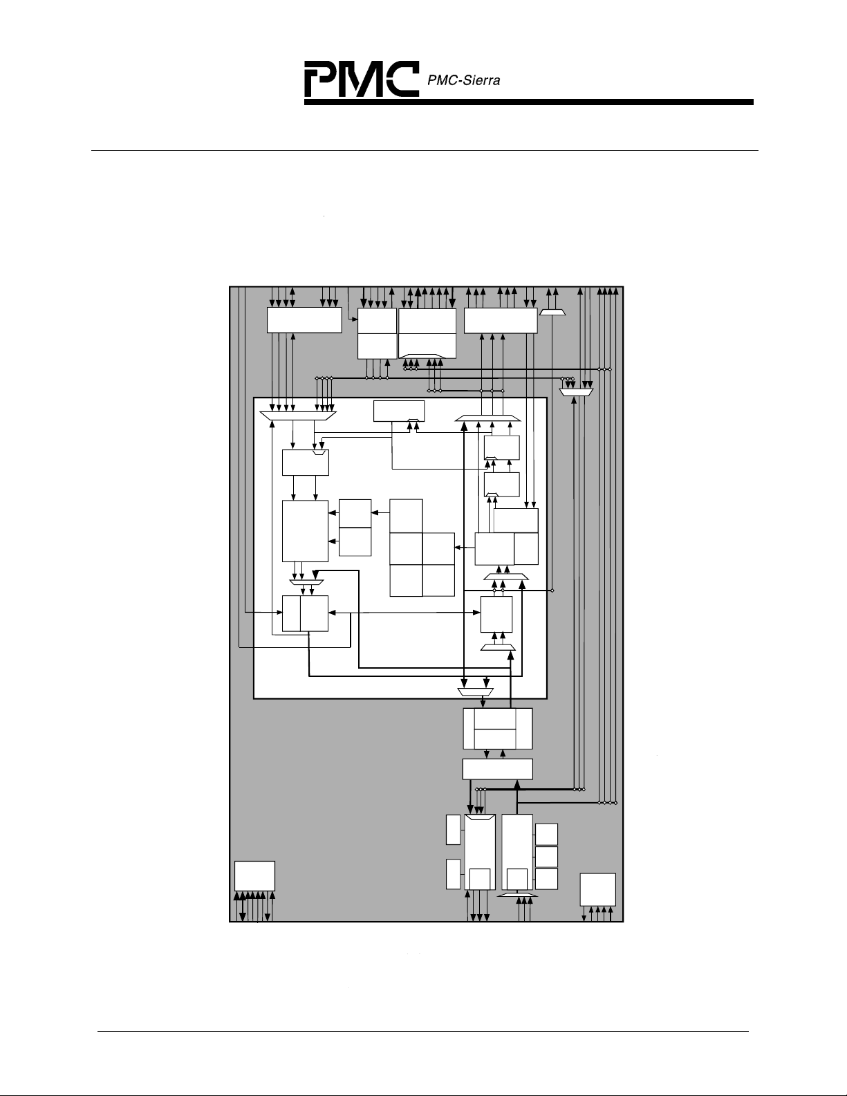
5.1 Top Level Block Diagram
The diagram below shows the complete TECT3. T1 or E1 links can be
multiplexed into a DS3 (E1s following the ITU-T G.747 recommendation).
System side access to the T1s is available via the serial clock and data, H-MVIP
or SBI bus interfaces. System side access to the E1s is available via the serial
clock and data or H-MVIP interfaces. DS3 line side access is via the clock and
data interface for line interface units. Unchannelized DS3 system side access is
available through a serial clock and data interface or the SBI bus, both shown at
the top of the diagram.
PROPRIETARY AND CONFIDENTIAL 16
STANDARD PRODUCT
DATASHEET
PMC-2011596 ISSUE 1 HIGH DENSITY T1/E1 FRAMER
PM4328 TECT3
AND M13 MULTIPLEXER
Figure 3: TECT3 Block Diagram
K
L
C
B
M
8
P
]
/
]
F
V
/
8
]
]
8
2
V
M
M
C
/
C
K
/
K
L
L
P
K
L
F
C
C
E
E
T
C
X
C
C
C
]
7
8
:
2
:
:
7
2
1
:
]
8
2
:
1
[
D
E
1
1
:
[
[
[
1
1
G
[
P
I
K
F
S
L
E
E
C
E
M
[
D
D
2
D
E
E
5
E
S
S
K
V
C
L
A
M
C
C
C
Q
]
0
:
7
[
A
T
P
A
D
D
A
A
S
S
]
]
0
E
:
R
7
[
_
K
A
L
T
S
C
5
L
F
U
J
V
P
E
A
A
A
R
S
S
S
S
T
T
P
C
P
A
5
L
F
A
V
P
D
D
I
1
B
D
D
D
D
C
S
S
S
S
S
S
]
/
0
]
:
8
8
1
2
]
[
:
2
]
:
8
T
1
8
1
[
2
[
:
E
2
G
:
1
K
I
D
[
I
1
L
[
S
P
I
B
C
D
F
I
I
S
I
C
P
F
]
V
2
]
7
:
7
:
1
[
1
[
D
I
D
I
S
V
A
M
C
1
K
K
M
L
L
C
/
C
C
D
K
I
S
C
C
V
V
L
P
C
C
F
C
E
E
I
I
C
C
R
R
K
L
/
C
O
O
S
P
P
I
R
F
/
F
P
M
K
K
F
M
T
/
O
P
F
T
D
L
L
M
R
H
C
/
O
C
I
T
/
R
P
T
P
O
T
I
V
A
A
A
A
P
P
D
F
O
G
G
D
F
T
T
R
R
R
R
T
e
s
c
m
s
F
a
e
I
f
e
t
r
r
S
s
e
g
E
y
t
E
S
n
I
r
0
e
l
l
S
C
o
D
S
r
-
t
P
r
n
e
T
o
P
C
,
,
:
N
g
r
n
n
,
n
A
i
e
o
o
n
i
i
t
n
t
R
t
t
o
i
r
i
o
a
T
t
i
e
r
-
t
m
r
i
s
e
1
s
e
d
n
n
n
s
E
I
n
/
e
a
n
o
I
r
g
S
G
n
T
C
i
A
m
l
c
e
i
r
k
B
a
s
a
m
n
n
l
X
a
a
u
-
g
A
r
i
r
B
1
F
T
S
T
s
n
r
o
r
e
i
t
t
o
t
t
i
S
p
T
a
J
P
O
u
A
l
n
O
J
a
g
t
e
T
i
T
n
t
i
t
g
i
A
m
i
D
T
I
I
B
B
S
S
X
E
l
O
e
l
S
l
I
a
P
r
I
a
B
P
S
r
e
t
t
i
C
R
L
m
P
s
D
D
n
T
H
a
r
T
d
r
e
o
t
t
n
C
e
a
e
r
d
i
O
r
e
o
B
n
O
C
X
e
t
i
G
B
s
s
I
s
I
s
e
r
g
E
o
t
S
B
R
P
s
s
B
e
B
u
u
r
S
S
g
B
B
N
I
n
I
l
O
l
e
l
l
P
a
l
I
i
a
i
r
o
a
S
r
t
r
I
e
e
a
B
S
S
P
S
r
n
-
o
r
/
r
t
r
e
e
c
t
o
n
e
t
t
t
e
a
a
e
G
P
D
e
c
e
M
r
n
s
R
o
a
n
o
t
i
t
o
P
m
n
u
r
p
A
o
s
A
o
-
f
e
r
M
1
e
R
T
P
r
r
o
e
I
C
L
D
R
N
O
M
P
t
C
v
m
i
a
L
r
M
r
e
a
L
D
g
c
l
e
e
A
H
A
t
R
n
I
e
c
d
s
r
n
a
m
r
o
f
r
e
P
r
e
r
t
o
o
e
C
t
t
e
n
t
i
c
e
d
n
i
O
n
e
r
o
u
o
t
B
o
e
O
C
M
R
t
C
D
i
B
e
s
c
m
s
a
F
e
e
f
I
t
r
r
s
S
e
I
g
y
t
n
I
S
n
I
r
0
e
l
l
S
C
o
D
S
r
-
t
P
r
n
e
R
o
P
C
r
g
o
n
t
i
X
l
c
a
a
G
I
r
n
t
S
g
x
i
E
S
c
i
T
e
t
r
S
s
o
t
a
L
l
S
E
E
R
,
M
t
n
M
n
o
e
R
m
F
-
a
r
1
F
E
/
1
T
2
1
X
M
R
M
R
F
1
#
A
i
e
t
m
R
M
r
c
m
r
A
a
a
l
n
e
r
R
t
g
A
i
m
x
F
l
a
E
A
r
F
r
o
s
r
r
r
e
1
e
t
o
t
t
T
i
T
a
m
J
u
8
A
J
R
2
1
M
2
S
D
3
2
X
M
a
l
r
n
2
a
t
e
i
F
f
t
t
g
i
o
1
A
D
E
e
n
1
2
O
X
/
U
n
X
e
s
M
U
v
2
E
e
M
1
D
S
M
r
/
f
e
o
R
m
e
M
a
r
n
R
F
F
O
X
/
3
U
X
2
U
M
M
E
M
D
r
e
o
-
c
s
F
o
a
s
I
r
f
e
r
P
c
i
c
e
t
M
o
M
r
n
I
P
]
]
B
B
B
B
B
E
0
0
:
:
L
T
T
S
D
R
3
7
A
S
N
[
C
R
1
I
W
[
D
R
A
PROPRIETARY AND CONFIDENTIAL 17
C
L
R
D
P
H
D
T
t
x
i
r
T
C
C
A
E
O
F
B
X
x
T
R
e
N
m
3
s
A
M
m
S
n
a
R
R
D
a
r
T
r
F
F
T
e
S
S
d
Z
Z
o
c
3
3
n
B
B
E
T
K
P
K
L
A
F
L
C
D
C
M
I
T
T
T
/
T
/
S
G
O
E
P
N
T
T
r
.
N
o
f
t
i
r
O
n
e
e
r
M
o
P
v
e
i
3
P
M
e
m
S
c
a
D
e
r
F
R
C
C
x
L
L
R
D
D
H
R
e
C
C
d
x
O
A
o
R
c
E
B
e
F
R
D
T
K
V
L
A
C
C
L
D
R
R
R
/
/
S
G
E
O
N
P
R
R
s
s
e
c
t
G
r
c
A
o
A
T
P
t
J
s
e
T
I
B
S
K
O
D
T
L
D
M
T
S
C
T
T
T
R
T
STANDARD PRODUCT
DATASHEET
PMC-2011596 ISSUE 1 HIGH DENSITY T1/E1 FRAMER
PM4328 TECT3
AND M13 MULTIPLEXER
5.2 M13 Multiplexer Mode Block Diagram
Figure 4 shows the TECT3, configured as a M13 multiplexer, connected to a
synchronous H-MVIP system side bus. In this example the TECT3 provides
synchronous access to the fully channelized T1s (access to all DS0s)
multiplexed into the DS3. There is also synchronous H-MVIP access to all
channel associated signaling channels (CAS). An additional H-MVIP interface
can be used to provide synchronous access to the common channel signaling
channels (CCS), although this same information is available within the data HMVIP signals.
Figure 4: M13 Multiplexer Block Diagram
TOPS
Timing Options
TJAT
Digital Jitter
Attenuator
TDPR
XBOC
Tx
Tx
HDLC
FEAC
TICLK
TCLK
TPOS/TDAT
TNEG/TMFP
RCLK
RPOS/RDAT
RNEG/RLCV
B3ZS
Encode
B3ZS
Decode
RBOC
FEAC
TRAN
DS3
Trans mit
Framer
FRMR
DS3
Receive
Framer
PMON
RDLC
Perf.
Rx
Rx
Monitor
HDLC
MX23
M23
MUX/
DEMUX
#1
MX12
FRMR
DS2
MUX/
Framer
DEMUX
One of Seven
FRMR/M12s
M12
RJAT
Digital Jitter
Atte nua tor
One of 28 T1 or
21 E1 Fr amers
PMON
Performance
Monitor
Counters
RBOC
Bit Oriented
Code
Detecto r
T1-XBAS/E1-TRAN
BasicTransmitter:
Frame Generation,
Alarm Insertion,
Signaling Insertion,
Trunk Conditioning
XBOC
Bit Oriented
Code
Generator
RDLC
HDLC
Receiver
ALMI
Alarm
Integrator
T1/E1-FRMR
Frame
Alignment,
Alarm
Extraction
FRAM
Framer RAM
TDPR
HDLC
Transmitt er
T1-APRM
Auto
Performance
Response
Monitor
ELST
Elastic
Store
SIGX
Signaling
Extracto r
TPSC
Per-DS0
Controller
RPSC
Per-DS0
Controller
PRBS
Pattern
Gener-
ator/
Detector
ESIF
Egress
System
Interface
ISIF
Ingress
System
Interface
XCLK
CTCLK
CMV8MC LK
CMVFPB
MVED[1:7]
CASED[1:7]
CCSED
MVID[1:7 ]
CASID[1:7]
CCSID
CIFP
CICLK/CMVFPC
RECVCLK1
RECVCLK2
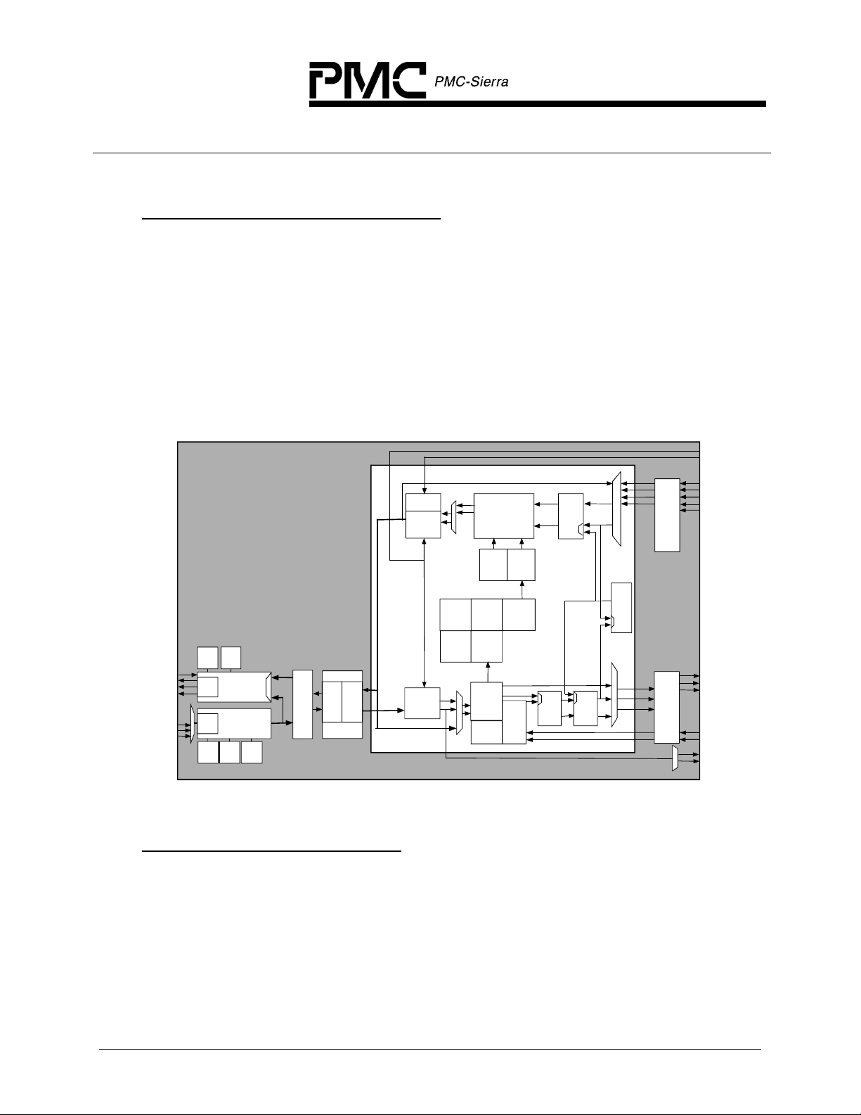
5.3 DS3 Framer Only Block Diagram
Figure 5 shows the TECT3 configured as a DS3 framer. In this mode the TECT3
provides access to the full DS3 unchannelized payload. The payload access
(right side of diagram) has two clock and data interfacing modes, one utilizing a
gapped clock to mask out the DS3 overhead bits and the second utilizing an
ungapped clock with overhead indications on a separate overhead signal. The
SBI bus can also be used to provide access to the unchannelized DS3.
PROPRIETARY AND CONFIDENTIAL 18

STANDARD PRODUCT
DATASHEET
PMC-2011596 ISSUE 1 HIGH DENSITY T1/E1 FRAMER
PM4328 TECT3
AND M13 MULTIPLEXER
Figure 5: DS3 Framer Only Mode Block Diagram
TDPR
Tx
HDLC
TICLK
TCLK
TPOS/TDAT
TNEG/TMFP
RCLK
RPOS/RDAT
RNEG/RLCV
B3ZS
Encode
B3ZS
Decode
TRAN
DS3
Transmit
Framer
FRMR
DS3
Receive
Framer
TDATI
TFPO/TMFPO/TGAPCLK
TFPI/TMFPI
RGAPCLK/RSCLK
RDATO
RFPO/RMFPO
ROVRHD
RDLC
Rx
HDLC
PMON
Perf.
Monitor
PROPRIETARY AND CONFIDENTIAL 19

STANDARD PRODUCT
DATASHEET
PMC-2011596 ISSUE 1 HIGH DENSITY T1/E1 FRAMER
PM4328 TECT3
AND M13 MULTIPLEXER
6 DESCRIPTION
The PM4328 High Density T1/E1 Framer with Integrated M13 Multiplexer
(TECT3) is a feature-rich device for use in any applications requiring high density
link termination over T1 or E1 channelized DS3.
The TECT3 supports asynchronous multiplexing and demultiplexing of 28 DS1s
into a DS3 signal as specified by ANSI T1.107 and Bell Communications
Research TR-TSY-000009.
This device can also be configured as a DS3 framer, providing external access to
the full DS3 payload.
The TECT3 can be used as an M13 multiplexer with performance monitoring in
either the ingress or egress direction for up to 28 T1s or 21 E1s. In this
configuration the T1 and E1 transmit framers are disabled and either the ingress
or egress T1 or E1 signals are routed to the T1 or E1 framers for performance
monitoring purposes.
Each of the T1 and E1 framers and transmitters is independently software
configurable, allowing timing master and feature selection without changes to
external wiring. This device is able to operate in T1 mode or E1 mode but not a
mix of T1 and E1 modes.
In the ingress direction, each of the 28 T1 framers is demultiplexed from a
channelized DS3 . Each T1 framer can be configured to frame to either of the
common DS1 signal formats: (SF, ESF) or to be bypassed (unframed mode).
Each T1 framer detects and indicates the presence of Yellow and AIS patterns
and also integrates Yellow, Red, and AIS alarms.
T1 performance monitoring with accumulation of CRC-6 errors, framing bit
errors, out-of-frame events, and changes of frame alignment is provided. The
TECT3 also detects the presence of ESF bit oriented codes, and detects and
terminates HDLC messages on the ESF data link. The HDLC messages are
terminated in a 128 byte FIFO. An elastic store that optionally supports slip
buffering and adaptation to backplane timing is provided, as is a signaling
extractor that supports signaling debounce, signaling freezing and interrupt on
signaling state change on a per-DS0 basis. The TECT3 also supports idle code
substitution, digital milliwatt code insertion, data extraction, trunk conditioning,
data sign and magnitude inversion, and pattern generation or detection on a perDS0 basis.
In the egress direction, framing is generated for 28 T1s into the DS3. Each T1
transmitter frames to SF or ESF DS1 formats, or framing can be optionally
PROPRIETARY AND CONFIDENTIAL 20

STANDARD PRODUCT
DATASHEET
PMC-2011596 ISSUE 1 HIGH DENSITY T1/E1 FRAMER
PM4328 TECT3
AND M13 MULTIPLEXER
disabled. The TECT3 supports signaling insertion, idle code substitution, data
insertion, line loopback, data inversion and zero-code suppression on a per-DS0
basis. PRBS generation or detection is supported on a framed and unframed T1
basis.
In the ingress direction, each of the 21 E1 framers is extracted from the DS3
following the ITU-T G.747 recommendation. Each E1 framer detects and
indicates the presence of remote alarm and AIS patterns and also integrates Red
and AIS alarms.
The E1 framers support detection of various alarm conditions such as loss of
frame, loss of signaling multiframe and loss of CRC multiframe. The E1 framers
also support reception of remote alarm signal, remote multiframe alarm signal,
alarm indication signal, and time slot 16 alarm indication signal.
E1 performance monitoring with accumulation of CRC-4 errors, far end block
errors and framing bit errors is provided. The TECT3 provides a receive HDLC
controller for the detection and termination of messages on the national use bits.
Detection of the 4-bit Sa-bit codewords defined in ITU-T G.704 and ETSI 300233 is supported. V5.2 link ID signal detection is also supported. An interrupt
may be generated on any change of state of the Sa codewords. An elastic store
for slip buffering and rate adaptation to backplane timing is provided, as is a
signaling extractor that supports signaling debounce, signaling freezing, idle
code substitution, digital milliwatt tone substitution, data inversion, and signaling
bit fixing on a per-channel basis. Receive side data and signaling trunk
conditioning is also provided.
In the egress direction, framing is generated for 21 E1s into the DS3 following
the ITU-T G.747 recommendation.Each E1 transmitter generates framing for a
basic G.704 E1 signal. The signaling multiframe alignment structure and the
CRC multiframe structure may be optionally inserted. Framing can be optionally
disabled. Transmission of the 4-bit Sa codewords defined in ITU-T G.704 and
ETSI 300-233 is supported. PRBS generation or detection is supported on a
framed and unframed E1 basis.
The TECT3 can generate a low jitter transmit clock from a variety of clock
references, and also provides jitter attenuation in the receive path. Two low jitter
recovered T1 clocks can be routed outside the TECT3 for network timing
applications.
Serial PCM interfaces to each T1 framer allow 1.544 Mbit/s ingress/egress
system interfaces to be directly supported. Tolerance of gapped clocks allows
other backplane rates to be supported with a minimum of external logic.
PROPRIETARY AND CONFIDENTIAL 21

STANDARD PRODUCT
DATASHEET
PMC-2011596 ISSUE 1 HIGH DENSITY T1/E1 FRAMER
PM4328 TECT3
AND M13 MULTIPLEXER
In synchronous backplane systems 8Mb/s H-MVIP interfaces are provided for
access to 672 DS0 channels, channel associated signaling (CAS) for all 672
DS0 channels and common channel signaling (CCS) for all 28 T1s. The DS0
data channel H-MVIP and CAS H-MVIP access is multiplexed with the serial
PCM interface pins. The CCS signaling H-MVIP interface is independent of the
DS0 channel and CAS H-MVIP access. The use of any of the H-MVIP interfaces
requires that common clocks and frame pulse be used along with T1 slip buffers.
A Scaleable Bandwidth Interconnect (SBI) high density byte serial system
interface provides higher levels of integration and dense interconnect. The SBI
bus interconnects up to 84 T1s both synchronously or asynchronously. The SBI
allows transmit timing to be mastered by either the TECT3 or link layer device
connected to the SBI bus. This interconnect allows up to 3 TECT3s to be
connected in parallel to provide the full complement of 84 T1s of traffic. In
addition to framed T1s, the TECT3 can transport unframed T1 links and framed
or unframed DS3 links over the SBI bus.
When configured as a DS3 multiplexer/demultiplexer or DS3 framer, the TECT3
accepts and outputs either or both digital B3ZS-encoded bipolar and unipolar
signals compatible with M23 and C-bit parity applications.
In the DS3 receive direction, the TECT3 frames to DS3 signals with a maximum
average reframe time of 1.5 ms in the presence of 10
-3
bit error rate and detects
line code violations, loss of signal, framing bit errors, parity errors, C-bit parity
errors, far end block errors, AIS, far end receive failure and idle code. The DS3
framer is an off-line framer, indicating both out of frame (OOF) and change of
frame alignment (COFA) events. The error events (C-BIT, FEBE, etc.) are still
indicated while the framer is OOF, based on the previous frame alignment. When
in C-bit parity mode, the Path Maintenance Data Link and the Far End Alarm and
Control (FEAC) channels are extracted. HDLC receivers are provided for Path
Maintenance Data Link support. In addition, valid bit-oriented codes in the FEAC
channels are detected and are available through the microprocessor port.
Error event accumulation is also provided by the TECT3. Framing bit errors, line
code violations, excessive zeros occurrences, parity errors, C-bit parity errors,
and far end block errors are accumulated. Error accumulation continues even
while the off-line framers are indicating OOF. The counters are intended to be
-3
polled once per second, and are sized so as not to saturate at a 10
bit error
rate. Transfer of count values to holding registers is initiated through the
microprocessor interface.
In the DS3 transmit direction, the TECT3 inserts DS3 framing, X and P bits.
When enabled for C-bit parity operation, bit-oriented code transmitters and
HDLC transmitters are provided for insertion of the FEAC channels and the Path
Maintenance Data Links into the appropriate overhead bits. Alarm Indication
PROPRIETARY AND CONFIDENTIAL 22

STANDARD PRODUCT
DATASHEET
PMC-2011596 ISSUE 1 HIGH DENSITY T1/E1 FRAMER
PM4328 TECT3
AND M13 MULTIPLEXER
Signals, Far End Receive Failure and idle signal can be inserted using either
internal registers or can be configured for automatic insertion upon received
errors. When M23 operation is selected, the C-bit Parity ID bit (the first C-bit of
the first M sub-frame) is forced to toggle so that downstream equipment will not
confuse an M23-formatted stream with stuck-at-1 C-bits for C-bit Parity
application. Transmit timing is from an external reference or from the receive
direction clock.
The TECT3 also supports diagnostic options which allow it to insert, when
appropriate for the transmit framing format, parity or path parity errors, F-bit
framing errors, M-bit framing errors, invalid X or P-bits, line code violations,
all-zeros, AIS, Remote Alarm Indications, and Remote End Alarms. A Pseudo
Random Binary Sequence (PRBS) can be inserted into a DS3 payload and
checked in the receive DS3 payload for bit errors. A fixed 100100… pattern is
available for insertion directly into the B3ZS encoder for proper pulse mask
shape verification.
When configured in DS3 multiplexer mode, seven 6312 kbit/s data streams are
demultiplexed and multiplexed into and out of the DS3 signal. Bit stuffing and
rate adaptation is performed. The C-bits are set appropriately, with the option of
inserting DS2 loopback requests. Interrupts can be generated upon detection of
loopback requests in the received DS3. AIS may be inserted in the any of the
6312 kbit/s tributaries in both the multiplex and demultiplex directions. C-bit
parity is supported by sourcing a 6.3062723 MHz clock, which corresponds to a
stuffing ratio of 100%.
Framing to the demultiplexed 6312 kbit/s data streams supports DS2 (ANSI
TI.107) frame formats. The maximum average reframe time is 7ms for DS2. Far
end receive failure is detected and M-bit and F-bit errors are accumulated. The
DS2 framer is an off-line framer, indicating both OOF and COFA events. Error
events (FERF, MERR, FERR, PERR, RAI, framing word errors) are still indicated
while the DS2 framer is indicating OOF, based on the previous alignment.
Each of the seven 6312 kbit/s multiplexers may be independently configured to
multiplex and demultiplex four 1544 kbit/s DS1s into and out of a DS2 formatted
signal. Tributary frequency deviations are accommodated using internal FIFOs
and bit stuffing. The C-bits are set appropriately, with the option of inserting DS1
loopback requests. Interrupts can be generated upon detection of loopback
requests in the received DS2. AIS may be inserted in any of the low speed
tributaries in both multiplex and demultiplex directions.
When configured as a DS3 framer the unchannelized payload of the DS3 link is
available to an external device.
PROPRIETARY AND CONFIDENTIAL 23

STANDARD PRODUCT
DATASHEET
PMC-2011596 ISSUE 1 HIGH DENSITY T1/E1 FRAMER
PM4328 TECT3
AND M13 MULTIPLEXER
The TECT3 is configured, controlled and monitored via a generic 8-bit
microprocessor bus through which all internal registers are accessed. All
sources of interrupts can be masked and acknowledged through the
microprocessor interface.
PROPRIETARY AND CONFIDENTIAL 24

A
Y AA A
STANDARD PRODUCT
DATASHEET
PMC-2011596 ISSUE 1 HIGH DENSITY T1/E1 FRAMER
PM4328 TECT3
AND M13 MULTIPLEXER
7 PIN DIAGRAM
The TECT3 is currently planned to be packaged in a 324-pin PBGA package
having a body size of 23mm by 23mm and a ball pitch of 1.0 mm. The center 36
balls are not used as signal I/Os and are thermal balls. Pin names and locations
are defined in the Pin Description Table in section 8. Mechanical information for
this package is in the section 19.
Figure 6: Pin Diagram
22 21 20 19 18 17 16 15 14 13 12 11 10 9 8 7 6 5 4 3 2 1
B
C
D
E
F
G
H
J
K
L
M
N
P
R
T
U
V
324 PBGA
VSS VSS VSS VSS VSS VSS
VSS VSS VSS VSS VSS VSS
VSS VSS VSS VSS VSS VSS
VSS VSS VSS VSS VSS VSS
VSS VSS VSS VSS VSS VSS
VSS VSS VSS VSS VSS VSS
Bottom View
W
B
22 21 20 19 18 17 16 15 14 13 12 11 10 9 8 7 6 5 4 3 2 1
PROPRIETARY AND CONFIDENTIAL 25

A
STANDARD PRODUCT
DATASHEET
PMC-2011596 ISSUE 1 HIGH DENSITY T1/E1 FRAMER
PM4328 TECT3
AND M13 MULTIPLEXER
8 PIN DESCRIPTION
Pin Name Type Pin
Function
No.
DS3 Line Side Interface
RCLK Input W5
Receive Input Clock (RCLK). RCLK provides the
receive direction timing. RCLK is a DS3, nominally a
44.736 MHz, 50% duty cycle clock input.
RPOS/RDAT
Input Y7
Positive Input Pulse (RPOS). RPOS represents the
positive pulses received on the B3ZS-encoded DS3
when dual rail input format is selected.
Receive Data Input (RDAT). RDAT represents the
NRZ (unipolar) DS3 input data stream when single rail
input format is selected.
RPOS and RDAT are sampled on the rising edge of
RCLK by default and may be enabled to be sampled
on the falling edge of RCLK by setting the RFALL bit in
the DS3 Master Receive Line Options register.
RNEG/RLCV
Input AB6
Negative Input Pulse (RNEG). RNEG represents the
negative pulses received on the B3ZS-encoded DS3
when dual rail input format is selected.
Line code violation (RLCV). RLCV represents receive
line code violations when single rail input format is
selected.
RNEG and RLCV are sampled on the rising edge of
RCLK by default and may be enabled to be sampled
on the falling edge of RCLK by setting the RFALL bit in
the DS3 Master Receive Line Options register.
TCLK Output
A7
Transmit Clock (TCLK). TCLK provides timing for
circuitry downstream of the DS3 transmitter of the
TECT3. TCLK is nominally a 44.736 MHz, 50% duty
cycle clock.
PROPRIETARY AND CONFIDENTIAL 26

A
A
STANDARD PRODUCT
DATASHEET
PMC-2011596 ISSUE 1 HIGH DENSITY T1/E1 FRAMER
PM4328 TECT3
AND M13 MULTIPLEXER
Pin Name Type Pin
Function
No.
TPOS/TDAT Output
B7
Transmit Positive Pulse (TPOS). TPOS represents
the positive pulses transmitted on the B3ZS-encoded
DS3 line when dual-rail output format is selected.
Transmit Data Output (TDAT). TDAT represents the
NRZ (unipolar) DS3 output data stream when single
rail output format is selected.
TPOS and TDAT are updated on the falling edge of
TCLK by default but may be enabled to be updated on
the rising edge of TCLK by setting the TRISE bit in the
DS3 Master Transmit Line Options register. TPOS and
TDAT are updated on TICLK rather than TCLK when
the TICLK bit in the DS3 Master Transmit Line Options
register is set.
TNEG/TMFP Output W6
Transmit Negative Pulse (TNEG). TNEG represents
the negative pulses transmitted on the B3ZS-encoded
DS3 line when dual-rail output format is selected.
Transmit Multiframe Pulse (TMFP). This signal
marks the transmit M-frame alignment when
configured for single rail operation. TMFP indicates
the position of overhead bits in the transmit
transmission system stream, TDAT. TMFP is high
during the first bit (X1) of the multiframe.
TNEG and TMFP are updated on the falling edge of
TCLK by default but may be enabled to be updated on
the rising edge of TCLK by setting the TRISE bit in the
DS3 Master Transmit Line Options register. TNEG and
TMFP are updated on TICLK rather than TCLK when
the TICLK bit in the DS3 Master Transmit Line Options
register is set.
TICLK Input
A6
Transmit input clock (TICLK). TICLK provides the
transmit direction timing. TICLK is nominally a 44.736
MHz, 50% duty cycle clock.
This clock is only required when using the DS3
transmitter with the DS3 line side interface. When not
used this clock input should be connected to ground.
PROPRIETARY AND CONFIDENTIAL 27

A
p
STANDARD PRODUCT
DATASHEET
PMC-2011596 ISSUE 1 HIGH DENSITY T1/E1 FRAMER
PM4328 TECT3
AND M13 MULTIPLEXER
Pin Name Type Pin
Function
No.
XCLK/VCLK Input E20
Crystal Clock Input (XCLK). This 24 times T1 or E1
clock provides timing for many of the T1 and E1
portions of TECT3. XCLK is nominally a 37.056 MHz ±
32ppm, 50% duty cycle clock when configured for T1
modes and is nominally a 49.152 MHz ± 32ppm, 50%
duty cycle clock when configured for E1 modes.
This clock is required for all operating modes of the
TECT3.
Test Vector Clock (VCLK). This signal is used during
production testing.
DS3 System Side Interface
RGAPCLK/RSCLK Output Y3
Framer Recovered Gapped Clock (RGAPCLK).
RGAPCLK is valid when the TECT3 is configured as a
DS3 framer by setting the OPMODE[1:0] bits in the
Global Configuration register and the RXGAPEN bit in
the DS3 Master Unchannelized Interface Options
register.
RGAPCLK is the recovered clock and timing reference
for RDATO. RGAPCLK is held either high or low
during bit positions which correspond to overhead.
Framer Recovered Clock (RSCLK). RSCLK is valid
when the TECT3 is configured as a DS3 framer by
setting the OPMODE[1:0] bits in the Global
Configuration register.
RSCLK is the recovered clock and timing reference for
RDATO, RFPO/RMFPO, and ROVRHD.
This signal shares a signal pin with ICLK[1]. When
enabled for unchannelized DS3 operation this signal
will be RGAPCLK/RSCLK, otherwise it will be ICLK[1].
RDATO Output
A5
Framer Receive Data (RDATO). RDATO is valid when
the TECT3 is configured as a DS3 framer by setting
the OPMODE[1:0] bits in the Global Configuration
register. RDATO is the received data aligned to
RFPO/RMFPO and ROVRHD.
RDATO is updated on either the falling or rising edge
of RGAPCLK or RSCLK, de
ending on the value of
PROPRIETARY AND CONFIDENTIAL 28

STANDARD PRODUCT
DATASHEET
PMC-2011596 ISSUE 1 HIGH DENSITY T1/E1 FRAMER
PM4328 TECT3
AND M13 MULTIPLEXER
Pin Name Type Pin
No.
RFPO/RMFPO Output AB5
Function
the RSCLKR bit in the DS3 Master Unchannelized
Interface Options register. By default RDATO will be
updated on the falling edge of RGAPCLK or RSCLK.
This signal shares a signal pin with ID[1] and MVID[1].
This signal will be RDATO only when enabled for
unchannelized DS3 operation.
Framer Receive Frame Pulse/Multi-frame Pulse
(RFPO/RMFPO). RFPO/RMFPO is valid when the
TECT3 is configured to be in framer only mode by
setting the OPMODE[1:0] bits in the Global
Configuration register.
RFPO is aligned to RDATO and indicates the position
of the first bit in each DS3 M-subframe.
RMFPO is aligned to RDATO and indicates the
position of the first bit in each DS3 M-frame. This is
selected by setting the RXMFPO bit in the Master
Framer Configuration Registers.
RFPO/RMFPO is updated on either the falling or rising
edge of RSCLK depending on the setting of the
RSCLKR bit in the DS3 Master Unchannelized
Interface Options register.
This signal shares a signal pin with IFP[1]. When
enabled for unchannelized DS3 operation this signal
will be RFPO/RMFPO, otherwise it will be IFP[1].
ROVRHD Output Y6
Framer Receive Overhead (ROVRHD). ROVRHD is
valid when the TECT3 is configured as a DS3 framer
by setting the OPMODE[1:0] bits in the Global
Configuration register.
ROVRHD will be high whenever the data on RDATO
corresponds to an overhead bit position. ROVRHD is
updated on the either the falling or rising edge of
RSCLK depending on the setting of the RSCLKR bit in
the DS3 Master Unchannelized Interface Options
register.
This signal shares a signal pin with ID[2] and
CASID[1]. This signal will be ROVRHD only when
enabled for unchannelized DS3 operation.
PROPRIETARY AND CONFIDENTIAL 29

A
g
STANDARD PRODUCT
DATASHEET
PMC-2011596 ISSUE 1 HIGH DENSITY T1/E1 FRAMER
PM4328 TECT3
AND M13 MULTIPLEXER
Pin Name Type Pin
No.
TFPO/TMFPO/
Output AB3
TGAPCLK
Function
Framer Transmit Frame Pulse/Multi-frame Pulse
Reference (TFPO/TMFPO). TFPO/TMFPO is valid
when the TECT3 is configured as a DS3 framer by
setting the OPMODE[1:0] bits in the Global
Configuration register and setting the TXGAPEN bit to
0 in the DS3 Master Unchannelized Interface Options
register.
TFPO pulses high for 1 out of every 85 clock cycles,
giving a reference M-subframe indication.
TMFPO pulses high for 1 out of every 4760 clock
cycles, giving a reference M-frame indication.
TFPO/TMFPO is updated on the falling edge of TICLK.
TFPO/TMFPO can be configured to be updated on the
rising edge of TICLK by setting the TDATIFALL bit to
1in the DS3 Master Unchannelized Interface Options
register..
Framer Gapped Transmit Clock (TGAPCLK).
TGAPCLK is valid when the TECT3 is configured as a
DS3 framer by setting the OPMODE[1:0] bits in the
Global Configuration register and setting the
TXGAPEN bit to 1 in the DS3 Master Unchannelized
Interface Options register.
TGAPCLK is derived from the transmit reference clock
TICLK or from the receive clock if loop-timed. The
overhead bit (gapped) positions are generated internal
to the device. TGAPCLK is held high during the
overhead bit positions. This clock is useful for
interfacing to devices which source payload data only.
TGAPCLK is used to sample TDATI and TFPI/TMFPI
when TXGAPEN is set to 1.
This signal shares a signal pin with ECLK[1]. When
enabled for unchannelized DS3 operation this signal
will be TFPO/TMFPO/TGAPCLK, otherwise it will be
ECLK[1].
TDATI Input
B4
Framer Transmit Data (TDATI). TDATI contains the
serial data to be transmitted when the TECT3 is
confi
PROPRIETARY AND CONFIDENTIAL 30
ured as a DS3 framer by setting the

STANDARD PRODUCT
DATASHEET
PMC-2011596 ISSUE 1 HIGH DENSITY T1/E1 FRAMER
PM4328 TECT3
AND M13 MULTIPLEXER
Pin Name Type Pin
No.
TFPI/TMFPI Input AA3
Function
OPMODE[1:0] bits in the Global Configuration register.
TDATI is sampled on the rising edge of TICLK if the
TXGAPEN bit in the DS3 Master Unchannelized
Interface Options register is logic 0. If TXGAPEN is
logic 1, then TDATI is sampled on the rising edge of
TGAPCLK. TDATI can be configured to be sampled on
the falling edge of TICLK or TGAPCLK by setting the
TDATIFALL bit in the DS3 Master Unchannelized
Interface Options register.
This signal shares a signal pin with ED[1] and
MVED[1]. This signal will be TDATI only when enabled
for unchannelized DS3 operation.
Framer Transmit Frame Pulse/Multiframe Pulse
(TFPI/TMFPI). TFPI/TMFPI is valid when the TECT3
is configured as a DS3 framer by setting the
OPMODE[1:0] bits in the Global Configuration register.
TFPI indicates the position of all overhead bits in each
DS3 M-subframe. TFPI is not required to pulse at
every frame boundary.
TMFPI indicates the position of the first bit in each DS3
M-frame. TMFPI is not required to pulse at every
multiframe boundary.
TFPI/TMFPI is sampled on the rising edge of TICLK if
the TXGAPEN bit in the DS3 Master Unchannelized
Interface Options register is logic 0. If TXGAPEN is
logic 1, then TFPI/TMFPI is sampled on the rising edge
of TGAPCLK. TFPI/TMFPI can be configured to be
sampled on the falling edge of TICLK or TGAPCLK by
setting the TDATIFALL bit to 1in the DS3 Master
Unchannelized Interface Options register.
This signal shares a signal pin with ED[2] and
CASED[1]. This signal will be TFPI/TMFPI only when
enabled for unchannelized DS3 operation.
PROPRIETARY AND CONFIDENTIAL 31

A
A
A
A
[11]
A
A
STANDARD PRODUCT
DATASHEET
PMC-2011596 ISSUE 1 HIGH DENSITY T1/E1 FRAMER
PM4328 TECT3
AND M13 MULTIPLEXER
Pin Name Type Pin
Function
No.
T1 and E1 System Side Serial Clock and Data Interface
ICLK[1]/ISIG[1]
ICLK[2]/ISIG[2]
ICLK[3]/ISIG[3]
ICLK[4]/ISIG[4]
ICLK[5]/ISIG[5]
ICLK[6]/ISIG[6]
ICLK[7]/ISIG[7]
ICLK[8]/ISIG[8]
ICLK[9]/ISIG[9]
ICLK[10]/ISIG[10]
ICLK[11]/ISIG[11]
ICLK[12]/ISIG[12]
ICLK[13]/ISIG[13]
ICLK[14]/ISIG[14]
ICLK[15]/ISIG[15]
ICLK[16]/ISIG[16]
ICLK[17]/ISIG[17]
ICLK[18]/ISIG[18]
ICLK[19]/ISIG[19]
ICLK[20]/ISIG[20]
ICLK[21]/ISIG[21]
ICLK[22]/ISIG[22]
ICLK[23]/ISIG[23]
ICLK[24]/ISIG[24]
ICLK[25]/ISIG[25]
ICLK[26]/ISIG[26]
ICLK[27]/ISIG[27]
ICLK[28]/ISIG[28]
Output Y3
B2
B20
B21
W22
Y20
H22
F19
W3
A1
H3
H1
L22
K19
F22
G20
T3
U1
D1
C1
H19
G19
E19
F21
K3
J4
E3
D2
Ingress Clocks (ICLK[1:28]). The Ingress Clocks are
active when the external signaling interface is disabled.
Each ingress clock is optionally a smoothed (jitter
attenuated) version of the associated receive clock
from the DS3 multiplexer. When the Clock Master:
NxChannel mode is active, ICLK[x] is a gapped version
of the smoothed receive clock. When Clock Master:
Full T1/E1 mode is active, IFP[x] and ID[x] are updated
on the active edge of ICLK[x]. When the Clock Master:
NxDS0 mode is active, ID[x] is updated on the active
edge of ICLK[x].
Ingress Signaling (ISIG[1:28]). When the Clock
Slave: External Signaling mode is enabled, each
ISIG[x] contains the extracted signaling bits for each
channel in the frame, repeated for the entire
superframe. Each channel’s signaling bits are valid in
bit locations 5,6,7,8 of the channel and are channelaligned with the ID[x] data stream. ISIG[x] is updated
on the active edge of the common ingress clock,
CICLK.
In E1 mode only ICLK[1:21] and ISIG[1:21] are used.
ICLK[1]/ISIG[1] shares a pin with the DS3 system
interface signal RGAPCLK/RSCLK.
IFP[1]
Output
IFP[2]
IFP[3]
IFP[4]
IFP[5]
IFP[6]
IFP[7]
IFP[8]
IFP[9]
IFP[10]
IFP
PROPRIETARY AND CONFIDENTIAL 32
B5
V3
W20
A22
Y21
W21
K22
K21
Y1
W1
F4
Ingress Frame Pulse (IFP[1:28]). The IFP[x] outputs
are intended as timing references.
IFP[x] indicates the frame alignment or the superframe
alignment of the ingress stream, ID[x].
When Clock Master: Full T1/E1 mode is active, IFP[x]
is updated on the active edge of the associated
ICLK[x]. When Clock Master: NxDS0 mode is active,
ICLK[x] is gapped during the pulse on IFP[x]. When
the Clock Slave ingress modes are active, IFP[x] is
updated on the active edge of CICLK. I the Clear

A
A
A
A
A
STANDARD PRODUCT
DATASHEET
PMC-2011596 ISSUE 1 HIGH DENSITY T1/E1 FRAMER
PM4328 TECT3
AND M13 MULTIPLEXER
Pin Name Type Pin
No.
IFP[12]
IFP[13]
IFP[14]
IFP[15]
IFP[16]
IFP[17]
IFP[18]
IFP[19]
IFP[20]
IFP[21]
IFP[22]
IFP[23]
IFP[24]
IFP[25]
IFP[26]
IFP[27]
IFP[28]
ID[1]
ID[2]
ID[3]
ID[4]
ID[5]
ID[6]
ID[7]
ID[8]
ID[9]
ID[10]
ID[11]
ID[12]
ID[13]
ID[14]
ID[15]
ID[16]
ID[17]
ID[18]
ID[19]
ID[20]
ID[21]
ID[22]
ID[23]
ID[24]
Output AA5
G1
V20
Y22
K20
J19
W4
V1
E1
D9
U19
R22
J22
J20
K1
K2
D8
9
Y6
A20
T19
R19
P20
G22
G21
Y2
W2
G4
H2
P21
P22
12
D12
U2
V4
D11
11
M19
L19
D10
10
Function
Channel modes IFP[x] is not used.
In E1 mode only IFP[1:21] is used.
IFP[1] shares a pin with the DS3 system interface
signal RFPO/RMFPO. IFP[20,27,28] shares pins with
the SBI interface signals SDDP, SDPL, SDV5.
Ingress Data (ID[1:28]). Each ID[x] signal contains
the recovered data stream which may have been
passed through the elastic store.
When the Clock Slave ingress modes are active, the
ID[x] stream has passed through the elastic store and
is aligned to the common ingress timing. In this mode
ID[x] is updated on the active edge of CICLK.
When the Clock Master ingress modes are active, ID[x]
is aligned to the receive line timing and is updated on
the active edge of the associated ICLK[x].
In E1 mode only ID[1:21] are used.
ID[1,5,9,13,17,21,25] share pins with the H-MVIP data
signals MVID[1:7]. ID[2,6,10,14,18,22,26] share pins
with the H-MVIP CAS signals CASID[1:7]. ID[1] shares
a pin with the DS3 system interface signal RDATO.
ID[2] shares a pin with the DS3 system interface signal
ROVRHD. ID[15,16,19,20,23,24,27,28] shares pins
with the SBI interface bus SDDATA[7:0].
PROPRIETARY AND CONFIDENTIAL 33

j
(
STANDARD PRODUCT
DATASHEET
PMC-2011596 ISSUE 1 HIGH DENSITY T1/E1 FRAMER
PM4328 TECT3
AND M13 MULTIPLEXER
Pin Name Type Pin
Function
No.
ID[25]
ID[26]
ID[27]
ID[28]
CICLK Input N1
J1
H4
B10
C10
Common Ingress Clock (CICLK). CICLK is either a
1.544MHz clock in T1 mode or a 2.048MHz clock in T1
or E1 modes, with optional gapping for adaptation to
non-uniform backplane data streams. CICLK is
common to all 28 T1 or 21 E1 framers. CIFP is
sampled on the active edge of CICLK.
When the Clock Slave ingress modes are active, ID[x],
ISIG[x], and IFP[x] are updated on the active edge of
CICLK.
CICLK is a nominal 1.544 or 2.048 MHz clock +/50ppm with a 50% duty cycle.
This signal shares a pin with the H-MVIP signal
CMVFPC. By default this input is CICLK.
CIFP Input P4
Common Ingress Frame Pulse (CIFP). When the
elastic store is enabled (Clock Slave mode is active on
the ingress side), CIFP is used to frame align the
ingress data to the system frame alignment. CIFP is
common to all 28 T1 or 21 E1 framers. When frame
alignment is required, a pulse at least 1 CICLK cycle
wide must be provided on CIFP a maximum of once
every frame (nominally 193 or 256 bit times).
CIFP is sampled on the active edge of CICLK as
selected by the CIFE bit in the Master Common
Ingress Serial and H-MVIP Interface Configuration
register.
CTCLK Input M3
Common Transmit Clock (CTCLK). This input signal
is used as a reference transmit tributary clock which
can be used in egress Clock Master modes.
Depending on the configuration of the TECT3, CTCLK
may be a line rate clock (so the transmit clock is
generated directly from CTCLK, or from CTCLK after
itter attenuation), or a multiple of 8kHz (Nx8khz, where
1£N£256) so long as CTCLK is jitter-free when divided
down to 8kHz
in which case the transmit clock is
PROPRIETARY AND CONFIDENTIAL 34

STANDARD PRODUCT
DATASHEET
PMC-2011596 ISSUE 1 HIGH DENSITY T1/E1 FRAMER
PM4328 TECT3
AND M13 MULTIPLEXER
Pin Name Type Pin
Function
No.
derived by the DJAT PLL using CTCLK as a
reference).
The TECT3 may be configured to ignore the CTCLK
input and utilize CECLK or one of the recovered
Ingress clocks instead, RECVCLK1 and RECVCLK2.
Receive tributary clock[x] is automatically substituted
for CTCLK if line loopback is enabled.
CECLK Input N4
Common Egress Clock (CECLK). The common
egress clock is used to time the egress interface when
Clock Slave mode is enabled in the egress side.
CECLK may be a 1.544MHz or 2.048MHz clock with
optional gapping for adaptation from non-uniform
system clocks. When the Clock Slave: EFP Enabled
mode is active, CEFP and ED[x] are sampled on the
active edge of CECLK, and EFP[x] is updated on the
active edge of CECLK. When the Clock Slave:
External Signaling mode is active, CEFP, ESIG[x] and
ED[x] are sampled on the active edge of CECLK.
CECLK is a nominal 1.544 or 2.048 MHz clock +/50ppm with a 50% duty cycle.
This signal shares a pin with the H-MVIP signal
CMV8MCLK. By default this input is CECLK.
CEFP Input M2
Common Egress Frame Pulse (CEFP). CEFP may
be used to frame align the framers to the system
backplane. If frame alignment only is required, a pulse
at least 1 CECLK cycle wide must be provided on
CEFP every 193 bit times for T1 mode or every 256 bit
times for T1 and E1 modes (T1 mode using 2.048MHz
clock). If superframe alignment is required, transmit
superframe alignment must be enabled, and a pulse at
least 1 CECLK cycle wide must be provided on CEFP
every 12 or 24 frame times for T1 mode, on the first Fbit of the multiframe.
CEFP is sampled on the active edge of CECLK as
selected by the CEFE bit in the Master Common
Egress Serial and H-MVIP Interface Configuration
register. CEFP has no effect in the Clock Master
egress modes.
PROPRIETARY AND CONFIDENTIAL 35

A
A7 A
A
A
A
STANDARD PRODUCT
DATASHEET
PMC-2011596 ISSUE 1 HIGH DENSITY T1/E1 FRAMER
PM4328 TECT3
AND M13 MULTIPLEXER
Pin Name Type Pin
No.
ED[1]
ED[2]
ED[3]
ED[4]
ED[5]
ED[6]
Input AB4
A3
P19
N20
N21
N22
ED[7]
ED[8]
ED[9]
ED[10]
ED[11]
ED[12]
ED[13]
ED[14]
ED[15]
ED[16]
ED[17]
ED[18]
ED[19]
ED[20]
ED[21]
ED[22]
ED[23]
ED[24]
ED[25]
ED[26]
ED[27]
ED[28]
2
T2
R4
3
B4
N19
M22
D6
C7
P2
M1
D4
B6
C20
E22
5
B5
L1
L2
4
C5
Function
This signal shares a pin with the H-MVIP signal
CMVFPB. By default this input is CEFP.
Egress Data (ED[1:28]). The egress data streams to
be transmitted are input on these pins. When the
Clock Master modes are active, ED[x] is sampled on
the active edge of ECLK[x], except for Clock Master:
Serial Data and H-MVIP CCS, when ED[x] is sampled
on the active edge of ICLK[x]. When the Clock Slave
egress modes are active, ED[x] is sampled on the
active edge of CECLK, except for Clock Slave: Clear
channel mode when ED[x] is sampled on the active
edge of ECLK[x].
In E1 mode only ED[1:21] are used.
ED[1,5,9,13,17,21,25] share pins with the H-MVIP data
signals MVED[1:7]. ED[2,6,10,14,18,22,26] share pins
with the H-MVIP CAS signals CASED[1:7]. ED[1]
shares a pin with the DS3 system interface signal
TDATI. ED[2] shares a pin with the DS3 system
interface signal TFPI/TMFPI.
ED[7,8,11,12,15,16,19,20,23,24,27,28] shares pins
with the SBI interface add bus signals.
PROPRIETARY AND CONFIDENTIAL 36

A
A
A
A
STANDARD PRODUCT
DATASHEET
PMC-2011596 ISSUE 1 HIGH DENSITY T1/E1 FRAMER
PM4328 TECT3
AND M13 MULTIPLEXER
Pin Name Type Pin
No.
ECLK[1]/EFP[1]/ESIG[1]
I/O
ECLK[2]/EFP[2]/ESIG[2]
ECLK[3]/EFP[3]/ESIG[3]
ECLK[4]/EFP[4]/ESIG[4]
ECLK[5]/EFP[5]/ESIG[5]
ECLK[6]/EFP[6]/ESIG[6]
ECLK[7]/EFP[7]/ESIG[7]
ECLK[8]/EFP[8]/ESIG[8]
ECLK[9]/EFP[9]/ESIG[9]
ECLK[10]/EFP[10]/ESIG[10]
ECLK[11]/EFP[11]/ESIG[11]
ECLK[12]/EFP[12]/ESIG[12]
ECLK[13]/EFP[13]/ESIG[13]
ECLK[14]/EFP[14]/ESIG[14]
ECLK[15]/EFP[15]/ESIG[15]
ECLK[16]/EFP[16]/ESIG[16]
ECLK[17]/EFP[17]/ESIG[17]
ECLK[18]/EFP[18]/ESIG[18]
ECLK[19]/EFP[19]/ESIG[19]
ECLK[20]/EFP[20]/ESIG[20]
ECLK[21]/EFP[21]/ESIG[21]
ECLK[22]/EFP[22]/ESIG[22]
ECLK[23]/EFP[23]/ESIG[23]
ECLK[24]/EFP[24]/ESIG[24]
ECLK[25]/EFP[25]/ESIG[25]
ECLK[26]/EFP[26]/ESIG[26]
ECLK[27]/EFP[27]/ESIG[27]
ECLK[28]/EFP[28]/ESIG[28]
Function
B3
Egress Clock (ECLK[1:28]). When the Clock
Y4
Y19
V22
T21
T22
T1
G2
G3
U21
V19
D21
C21
U4
R1
D3
F1
Master mode is active, ECLK[x] is an output
and is used to sample the associated egress
A21
data, ED[x]. ECLK[x] is a version of the
B22
transmit clock[x] which is generated from the
receive clock or the common transmit clock,
CTCLK.
When in Clock Master: NxChannel mode,
B1
ECLK[x] is gapped during the framing bit
position and optionally for between 1 and 23
DS0 channels or 1 and 32 channel timeslots in
the associated ED[x] stream. When Clock
Master: Clear Channel is active ECLK[x] is not
gapped.
When in Clock Slave: Clear Channel mode
this input is an input and is used to sampled
ED[x].
ED[x] is sampled on the active edge of the
associated ECLK[x].
T20
U22
B22
D20
L3
K4
E4
F2
Egress Frame Pulse (EFP[1:28]). When the
Clock Slave: EFP Enabled mode is active, the
EFP[1:28] outputs indicate the frame
alignment or the superframe alignment of
each of the 28 framers.
EFP[x] is updated on the active edge of
CECLK.
Egress Signaling (ESIG[1:28]). When the
Clock Slave: External Signaling mode is
active, the ESIG[1:28] input carries the
signaling bits for each channel in the transmit
data frame, repeated for the entire superfram’.
Each channel’s signaling bits are in bit
locations 5,6,7,8 of the channel and are
frame-aligned by the common egress frame
pulse, CEFP.
ESIG[x] is sampled on the active edge of
CECLK.
PROPRIETARY AND CONFIDENTIAL 37

STANDARD PRODUCT
DATASHEET
PMC-2011596 ISSUE 1 HIGH DENSITY T1/E1 FRAMER
PM4328 TECT3
AND M13 MULTIPLEXER
Pin Name Type Pin
Function
No.
H-MVIP System Side Interfaces
CMV8MCLK Input N4
Common 8M H-MVIP Clock (CMV8MCLK). The
common 8.192 Mbps H-MVIP data provides the data
clock for receive and transmit links configured for
operation in 8.192 Mbps H-MVIP mode.
CMV8MCLK is used to sample data on MVID[1:7],
MVED[1:7], CASID[1:7], CASED[1:7], CCSID and
CCSED. CMV8MCLK is nominally a 50% duty cycle
clock with a frequency of 16.384MHz.
The H-MVIP interfaces are enabled via the
SYSOPT[2:0] bits in the Global Configuration register.
This signal shares a pin with CECLK. By default this
input is CECLK.
ECLK[1]/EFP[1]/ESIG[1] shares a pin with the
DS3 system interface output signal
TFPO/TMFPO/TGAPCLK.
CMVFPC Input N1
Common H-MVIP Frame Pulse Clock (CMVFPC).
The common 8.192 Mbps H-MVIP frame pulse clock
provides the frame pulse clock for receive and transmit
links configured for operation in 8.192 Mbps H-MVIP
mode.
CMVFPC is used to sample CMVFPB. CMVFPC is
nominally a 50% duty cycle clock with a frequency of
4.096 MHz. The falling edge of CMVFPC must be
aligned with the falling edge of CMV8MCLK with no
more than ±10ns skew.
The H-MVIP interfaces are enabled via the
SYSOPT[2:0] bits in the Global Configuration register.
This signal shares a pin with CICLK. By default this
input is CICLK.
CMVFPB Input M2
Common H-MVIP Frame Pulse (CMVFPB). The
active low common frame pulse for 8.192 Mbps HMVIP signals references the beginning of each frame
for links operating in 8.192Mbps H-MVIP mode.
The H-MVIP interfaces are enabled via the
PROPRIETARY AND CONFIDENTIAL 38

STANDARD PRODUCT
DATASHEET
PMC-2011596 ISSUE 1 HIGH DENSITY T1/E1 FRAMER
PM4328 TECT3
AND M13 MULTIPLEXER
Pin Name Type Pin
No.
MVID[1]
MVID[2]
MVID[3]
MVID[4]
MVID[5]
MVID[6]
MVID[7]
Output AA5
R19
Y2
P21
U2
M19
J1
Function
SYSOPT[2:0] bits in the Global Configuration register.
The CMVFPB frame pulse occurs every 125us for a
and is sampled on the falling edge of CMVFPC.
This signal shares a pin with CEFP. By default this
input is CEFP.
H-MVIP Ingress Data (MVID[1:7]). MVID[x] carries the
recovered T1 or E1 channels which have passed
through the elastic store. Each MVID[x] signal carries
the channels of four complete T1s or E1s. MVID[x]
carries the T1 or E1 data equivalent to ID[(4x-3):(4x)].
MVID[x] is aligned to the common H-MVIP 16.384Mb/s
clock, CMV8MCLK, frame pulse clock, CMVFPC, and
frame pulse, CMVFPB. MVID[x] is updated on every
second rising or falling edge of the common H-MVIP
16.384Mb /s clock, CMV8MCLK, as fixed by the
common H-MVIP frame pulse clock, CMVFPC. The
updating edge of CMV8MCLK is selected via the
CMVIDE bit in the Master Common Ingress Serial and
H-MVIP Interface Configuration register.
CASID[1]
CASID[2]
CASID[3]
CASID[4]
CASID[5]
CASID[6]
CASID[7]
Output Y6
P20
W2
P22
V4
L19
H4
In E1 mode only MVID[1:6] are used.
MVID[1:7] shares the same pins as
ID[1,5,9,13,17,21,25].
Channel Associated Signaling Ingress Data
(CASID[1:7]). CASID[x] carries the channel associated
signaling stream extracted from all the T1 or E1
channels. Each CASID[x] signal carries CAS for four
complete T1s or E1s. CASID[x] carries the
corresponding CAS values of the channel carried in
MVID[x].
CASID[x] is aligned to the common H-MVIP
16.384Mb/s clock, CMV8MCLK, frame pulse clock,
CMVFPC, and frame pulse, CMVFPB. CASID[x] is
updated on every second rising or falling edge of
CMV8MCLK as fixed by the common H-MVIP frame
pulse clock, CMVFPC. The updating edge of
CMV8MCLK is selected via the CMVIDE bit in the
Master Common Ingress Serial and H-MVIP Interface
PROPRIETARY AND CONFIDENTIAL 39

STANDARD PRODUCT
DATASHEET
PMC-2011596 ISSUE 1 HIGH DENSITY T1/E1 FRAMER
PM4328 TECT3
AND M13 MULTIPLEXER
Pin Name Type Pin
Function
No.
Configuration register.
CASID[1:7] shares the same pins as
ID[2,6,10,14,18,22,26].
CCSID Output T4
Common Channel Signaling Ingress Data (CCSID).
In T1 mode CCSID carries the 28 common channel
signaling channels extracted from each of the 28 T1s.
In E1 mode CCSID carries up to 3 timeslots (15,16,
31) from each of the 21 E1s. CCSID is formatted
according to the H-MVIP standard.
CCSID is aligned to the common H-MVIP 16.384Mb/s
clock, CMV8MCLK, frame pulse clock, CMVFPC, and
frame pulse, CMVFPB. CCSID is updated on every
second rising or falling edge of CMV8MCLK as fixed
by the common H-MVIP frame pulse clock, CMVFPC.
The updating edge of CMV8MCLK is selected via the
CMVIDE bit in the Master Common Ingress Serial and
H-MVIP Interface Configuration register.
MVED[1]
MVED[2]
MVED[3]
MVED[4]
MVED[5]
MVED[6]
MVED[7]
Input AB4
N21
T2
N19
P2
C20
L1
MVIP Egress Data (MVED[1:7]). The egress data
streams to be transmitted are input on these pins.
Each MVED[x] signal carries the channels of four
complete T1s formatted according to the H-MVIP
standard. MVED[x] carries the egress data equivalent
to ED[(4x-3):(4x)].
MVID[x] is aligned to the common H-MVIP 16.384Mb/s
clock, CMV8MCLK, frame pulse clock, CMVFPC, and
frame pulse, CMVFPB. MVID[x] is sampled on every
second rising or falling edge of CMV8MCLK as fixed
by the common H-MVIP frame pulse clock, CMVFPC.
The sampling edge of CMV8MCLK is selected via the
CMVEDE bit in the Master Common Ingress Serial and
H-MVIP Interface Configuration register.
In E1 mode only MVED[1:6] are used.
MVED[1:7] shares the same pins as
ED[1,5,9,13,17,21,25].
CASED[1]
CASED[2]
CASED[3]
PROPRIETARY AND CONFIDENTIAL 40
Input AA3
N22
R4
Channel Associated Signaling Egress Data
(CASED[1:7]). CASED[x] carries the channel
associated signaling stream to be transmitted in the T1

STANDARD PRODUCT
DATASHEET
PMC-2011596 ISSUE 1 HIGH DENSITY T1/E1 FRAMER
PM4328 TECT3
AND M13 MULTIPLEXER
Pin Name Type Pin
Function
No.
CASED[4]
CASED[5]
CASED[6]
CASED[7]
M22
M1
E22
L2
DS0s or E1 timeslots. Each CASED[x] signal carries
CAS for four complete T1s or E1s formatted according
to the H-MVIP standard. CASED[x] carries the
corresponding CAS values of the channel data carried
in MVED[x].
CASED[x] is aligned to the common H-MVIP
16.384Mb/s clock, CMV8MCLK, frame pulse clock,
CMVFPC, and frame pulse, CMVFPB. CASED[x] is
sampled on every second rising or falling edge of
CMV8MCLK as fixed by the common H-MVIP frame
pulse clock, CMVFPC. The sampling edge of
CMV8MCLK is selected via the CMVEDE bit in the
Master Common Ingress Serial and H-MVIP Interface
Configuration register.
CASED[1:7] shares the same pins as
ED[2,6,10,14,18,22,26].
CCSED Input P1
Common Channel Signaling Egress Data (CCSED).
In T1 mode CCSED carries the 28 common channel
signaling channels to be transmitted in each of the 28
T1s. In E1 mode CCSED carries up to 3 timeslots
(15,16, 31) to be transmitted in each of the 21 E1s.
CCSED is formatted according to the H-MVIP
standard.
CCSED is aligned to the common H-MVIP 16.384Mb/s
clock, CMV8MCLK, frame pulse clock, CMVFPC, and
frame pulse, CMVFPB. CCSED is sampled on every
second rising or falling edge of CMV8MCLK as fixed
by the common H-MVIP frame pulse clock, CMVFPC.
The sampling edge of CMV8MCLK is selected via the
CMVEDE bit in the Master Common Ingress Serial and
H-MVIP Interface Configuration register.
PROPRIETARY AND CONFIDENTIAL 41

A
A
A
STANDARD PRODUCT
DATASHEET
PMC-2011596 ISSUE 1 HIGH DENSITY T1/E1 FRAMER
PM4328 TECT3
AND M13 MULTIPLEXER
Pin Name Type Pin
Function
No.
Recovered T1 and E1 Clocks
RECVCLK1 Output D22
Recovered Clock 1 (RECVCLK1). This clock output is
a recovered and de-jittered clock from any one of the
28 T1 framers or 21 E1 framers.
RECVCLK2 Output C22
Recovered Clock 2 (RECVCLK2). This clock output is
a recovered and de-jittered clock from any one of the
28 T1 framers or 21 E1 framers.
Scaleable Bandwidth Interconnect Interface
SREFCLK Input B7
System Reference Clock (SREFCLK). This system
reference clock is a nominal 19.44MHz +/-50ppm 50%
duty cycle clock. This clock is common to both the add
and drop sides of the SBI bus.
SC1FP I/O
System C1 Frame Pulse (SC1FP). The System C1
6
Frame Pulse is used to synchronize devices interfacing
to the SBI bus. This signal is common to both the add
and drop sides of the system SBI bus.
By default, SC1FP is an input. The TECT3 can
alternatively be configured to generate this frame pulse
- as an output on SC1FP - for use by all other devices
connected to the same SBI bus. Note that all devices
interconnected via an SBI interface must be
synchronized to an SC1FP signal from a single
common source.
s an input, SC1FP is sampled on the rising edge of
SREFCLK. It normally indicates SBI mutiframe
alignment, and thus should be asserted for a single
SREFCLK cycle every 9720 SREFCLK cycles or some
multiple thereof (i.e. every 9720*N SREFCLK cycles,
where N is a positive integer). In synchronous SBI
mode, however, SC1FP is used to indicate T1
signaling multiframe alignment, and thus should be
asserted for a single SREFCLK cycle once every 12
SBI mutiframes (48 T1 frames or 116640 SREFCLK
cycles).
s an output, SC1FP is generated on the rising edge
PROPRIETARY AND CONFIDENTIAL 42

A
A
A
STANDARD PRODUCT
DATASHEET
PMC-2011596 ISSUE 1 HIGH DENSITY T1/E1 FRAMER
PM4328 TECT3
AND M13 MULTIPLEXER
Pin Name Type Pin
Function
No.
of SREFCLK. It normally indicates SBI mutiframe
alignment by pulsing high once every 9720 SREFCLK
cycles. In synchronous SBI mode, however, SC1FP is
used to indicate T1 signaling multiframe alignment by
pulsing once every 12 SBI mutiframes (48 T1 frames
or 116640 SREFCLK cycles).
SADATA[0]
SADATA[1]
SADATA[2]
SADATA[3]
SADATA[4]
SADATA[5]
SADATA[6]
SADATA[7]
Input D6
C7
D4
B6
5
B5
4
C5
System Add Bus Data (SADATA[7:0]). The System
add data bus is a time division multiplexed bus which
carries the T1 and DS3 tributary data is byte serial
format over the SBI bus structure. This device only
monitors the add data bus during the timeslots
assigned to this device.
SADATA[7:0] is sampled on the rising edge of
SREFCLK.
This bus shares pins with
ED[15,16,19,20,23,24,27,28].
SADP Input
2
System Add Bus Data Parity (SADP). The system
add bus signal carries the even or odd parity for the
add bus signals SADATA[7:0], SAPL and SAV5. The
TECT3 monitors parity across all links on the add bus.
SADP is sampled on the rising edge of SREFCLK.
This signal shares a pin with signal ED[8].
SAPL Input B4
System Add Bus Payload Active (SAPL). The add
bus payload active signal indicates valid data within the
SBI bus structure. This signal must be high during all
octets making up a tributary. This signal goes high
during the V3 or H3 octet of a tributary to indicate
negative timing adjustments between the tributary rate
and the fixed SBI bus structure. This signal goes low
during the octet after the V3 or H3 octet of a tributary
to indicate positive timing adjustments between the
tributary rate and the fixed SBI bus structure.
The TECT3 only monitors the add bus payload active
signal during the tributary timeslots assigned to this
device.
SAPL is sampled on the rising edge of SREFCLK.
PROPRIETARY AND CONFIDENTIAL 43

A
A
j
STANDARD PRODUCT
DATASHEET
PMC-2011596 ISSUE 1 HIGH DENSITY T1/E1 FRAMER
PM4328 TECT3
AND M13 MULTIPLEXER
Pin Name Type Pin
Function
No.
This signal shares a pin with signal ED[12].
SAV5 Input
3
System Add Bus Payload Indicator (SAV5). The add
bus payload indicator locates the position of the
floating payloads for each tributary within the SBI bus
structure. Timing differences between the tributary
timing and the synchronous SBI bus are indicated by
adjustments of this payload indicator relative to the
fixed SBI bus structure.
ll timing adjustments indicated by this signal must be
accompanied by appropriate adjustments in the SAPL
signal.
The TECT3 only monitors the add bus payload
Indicator signal during the tributary timeslots assigned
to this device.
SAV5 is sampled on the rising edge of SREFCLK.
This signal shares a pin with signal ED[11].
SAJUST_REQ Output
Tristate
D7
System Add Bus Justification Request
(SAJUST_REQ). The justification request signals the
Link Layer device to speed up, slow down or maintain
the rate which it is sending data to the TECT3. This is
only used when the TECT3 is the timing master for the
tributary transmit direction.
This active high signal indicates negative timing
adjustments when asserted high during the V3 or H3
octet of the tributary. In response to this the Link Layer
device sends an extra byte in the V3 or H3 octet of the
next SBI bus multi-frame.
Positive timing adjustments are requested by asserting
ustification request high during the octet following the
V3 or H3 octet. The Link Layer device responds to this
request by not sending an octet during the V3 or H3
octet of the next multi-frame.
The TECT3 only drives the justification request signal
during the tributary timeslots assigned to this device.
SAJUST_REQ is updated on the rising edge of
SREFCLK.
PROPRIETARY AND CONFIDENTIAL 44

A
A
A
A
pay
STANDARD PRODUCT
DATASHEET
PMC-2011596 ISSUE 1 HIGH DENSITY T1/E1 FRAMER
PM4328 TECT3
AND M13 MULTIPLEXER
Pin Name Type Pin
Function
No.
SDDATA[0]
SDDATA[1]
SDDATA[2]
SDDATA[3]
SDDATA[4]
SDDATA[5]
SDDATA[6]
SDDATA[7]
Output
Tristate
12
D12
D11
11
D10
10
B10
C10
System Drop Bus Data (SDDATA[7:0]). The System
drop data bus is a time division multiplexed bus which
carries the T1 and DS3 tributary data is byte serial
format over the SBI bus structure. This device only
drives the data bus during the timeslots assigned to
this device.
SDDATA[7:0] is updated on the rising edge of
SREFCLK.
This bus shares pins with ID[15,16,19,20,23,24,27,28].
SDDP Output
Tristate
D9
System Drop Bus Data Parity (SDDP). The system
drop bus signal carries the even or odd parity for the
drop bus signals SDDATA[7:0], SDPL and SDV5. The
TECT3 only drives the data bus parity during the
timeslots assigned to this device unless configured for
bus master mode. In this case, all undriven links
should be driven externally with correctly generated
parity.
SDDP is updated on the rising edge of SREFCLK.
This signal shares a pin with IFP[20].
SDPL Output
Tristate
D8
System Drop Bus Payload Active (SDPB). The
payload active signal indicates valid data within the SBI
bus structure. This signal is asserted during all octets
making up a tributary. This signal goes high during the
V3 or H3 octet of a tributary to accommodate negative
timing adjustments between the tributary rate and the
fixed SBI bus structure. This signal goes low during the
octet after the V3 or H3 octet of a tributary to
accommodate positive timing adjustments between the
tributary rate and the fixed SBI bus structure.
The TECT3 only drives the payload active signal
during the tributary timeslots assigned to this device.
SDPL is updated on the rising edge of SREFCLK.
This signal shares a pin with IFP[27].
SDV5 Output
Tristate
9
System Drop Bus Payload Indicator (SDV5). The
payload indicator locates the position of the floating
loads for each tributary within the SBI bus
PROPRIETARY AND CONFIDENTIAL 45

A
A
A
STANDARD PRODUCT
DATASHEET
PMC-2011596 ISSUE 1 HIGH DENSITY T1/E1 FRAMER
PM4328 TECT3
AND M13 MULTIPLEXER
Pin Name Type Pin
Function
No.
structure. Timing differences between the tributary
timing and the synchronous SBI bus are indicated by
adjustments of this payload indicator relative to the
fixed SBI bus structure.
ll timing adjustments indicated by this signal are
accompanied by appropriate adjustments in the SDPL
signal.
The TECT3 only drives the payload Indicator signal
during the tributary timeslots assigned to this device.
SDV5 is updated on the rising edge of SREFCLK.
This signal shares a pin with IFP[28].
SBIACT Output
8
SBI Output Active (SBIACT). The SBI Output Active
indicator is high whenever the TECT3 is driving the SBI
drop bus signals. This signal is used by other TECT3s
or other SBI devices to detect SBI configuration
problems by detecting other devices driving the SBI
bus during the same tributary as the device listening to
this signal.
This output is updated on the rising edge or SREFCLK.
CLK52M Input P3
52MHz Clock Reference (CLK52M). The 52Mhz clock
reference is used to generate a gapped DS3 clock
when receiving a DS3 from the SBI bus interface. This
clock has two nominal values.
The first is a nominal 51.84MHz 50% duty cycle clock.
The second is a nominal 44.928MHz 50% duty cycle
clock.
When this clock is not used this input must be
connected to ground.
SBIDET[0]
SBIDET[1]
Input C8
7
SBI Bus Activity Detection (SBIDET[1:0]). The SBI
bus activity detect input detects tributary collisions
between devices sharing the same SBI bus. Each SBI
device driving the bus also drives an SBI active signal
(SBIACT). This pair of activity detection inputs
monitors the active signals from two other SBI devices.
When unused this signal should be connected to
ground.
PROPRIETARY AND CONFIDENTIAL 46

A
A
STANDARD PRODUCT
DATASHEET
PMC-2011596 ISSUE 1 HIGH DENSITY T1/E1 FRAMER
PM4328 TECT3
AND M13 MULTIPLEXER
Pin Name Type Pin
Function
No.
collision is detected when either of SBIDET[1:0]
signals are active concurrently with this device driving
SBIACT. When collisions occur the SBI drivers are
disabled and an interrupt is generated to signal the
collision.
These signals are sampled on the rising edge of
SREFCLK.
SBIDET[1] is shared with serial interface signal ED[7].
Microprocessor Interface
INTB Output
OD
16
Active low Open-Drain Interrupt (INTB). This signal
goes low when an unmasked interrupt event is
detected on any of the internal interrupt sources. Note
that INTB will remain low until all active, unmasked
interrupt sources are acknowledged at their source.
CSB Input D16
Active Low Chip Select (CSB). This signal is low
during TECT3 register accesses. CSB has an integral
pull up resistor.
RDB Input B16
Active Low Read Enable (RDB). This signal is low
during TECT3 register read accesses. The TECT3
drives the D[7:0] bus with the contents of the
addressed register while RDB and CSB are low.
WRB Input C15
Active Low Write Strobe (WRB). This signal is low
during a TECT3 register write access. The D[7:0] bus
contents are clocked into the addressed register on the
rising WRB edge while CSB is low.
PROPRIETARY AND CONFIDENTIAL 47

A
A
A
A
A
A
A
A
A
A
A
A
A
A
A
A
A
A
A
A
A
A
STANDARD PRODUCT
DATASHEET
PMC-2011596 ISSUE 1 HIGH DENSITY T1/E1 FRAMER
PM4328 TECT3
AND M13 MULTIPLEXER
Pin Name Type Pin
No.
D[0]
D[1]
D[2]
D[3]
D[4]
D[5]
D[6]
D[7]
[0]
[1]
[2]
[3]
[4]
[5]
[6]
[7]
[8]
[9]
[10]
[11]
[12]
[13]
I/O C14
B14
14
D14
C13
B13
13
D13
Input A17
C16
D18
D19
B17
18
19
20
C18
B19
B20
21
C19
B21
Function
Bidirectional Data Bus (D[7:0]). This bus provides
TECT3 register read and write accesses.
Address Bus (A[13:0]). This bus selects specific
registers during TECT3 register accesses.
Signal A[13] selects between normal mode and test
mode register access. A[13] has an integral pull down
resistor.
RSTB Input
22
Active Low Reset (RSTB). This signal provides an
asynchronous TECT3 reset. RSTB is a Schmitt
triggered input with an integral pull up resistor.
LE Input D17
Address Latch Enable (ALE). This signal is active
high and latches the address bus A[13:0] when low.
When ALE is high, the internal address latches are
transparent. It allows the TECT3 to interface to a
multiplexed address/data bus. The ALE input has an
integral pull up resistor.
JTAG Interface
TCK Input C3
Test Clock (TCK). This signal provides timing for test
operations that can be carried out using the IEEE
P1149.1 test access port.
PROPRIETARY AND CONFIDENTIAL 48

A
A
A
A
A
A
A
STANDARD PRODUCT
DATASHEET
PMC-2011596 ISSUE 1 HIGH DENSITY T1/E1 FRAMER
PM4328 TECT3
AND M13 MULTIPLEXER
Pin Name Type Pin
Function
No.
TMS Input C2
Test Mode Select (TMS). This signal controls the test
operations that can be carried out using the IEEE
P1149.1 test access port. TMS is sampled on the
rising edge of TCK. TMS has an integral pull up
resistor.
TDI Input C4
Test Data Input (TDI). This signal carries test data into
the TECT3 via the IEEE P1149.1 test access port. TDI
is sampled on the rising edge of TCK. TDI has an
integral pull up resistor.
TDO Output B3
Test Data Output (TDO). This signal carries test data
out of the TECT3 via the IEEE P1149.1 test access
port. TDO is updated on the falling edge of TCK. TDO
is a tri-state output which is inactive except when
scanning of data is in progress.
TRSTB Input B1
Active low Test Reset (TRSTB). This signal provides
an asynchronous TECT3 test access port reset via the
IEEE P1149.1 test access port. TRSTB is a Schmitt
triggered input with an integral pull up resistor. TRSTB
must be asserted during the power up sequence.
Miscellaneous Pins
NO CONNECT
1
B2
11
B11
B8
W7
W8
B9
W9
Y10
A10
B10
W10
Y11
Note that if not used, TRSTB must be connected to the
RSTB input.
No Connect. These pins are not connected to any
internal logic.
PROPRIETARY AND CONFIDENTIAL 49

A
A
A
A
A
A
A
A
STANDARD PRODUCT
DATASHEET
PMC-2011596 ISSUE 1 HIGH DENSITY T1/E1 FRAMER
PM4328 TECT3
AND M13 MULTIPLEXER
Pin Name Type Pin
No.
Power and Ground Pins
VDD3.3[17]
VDD3.3[16]
VDD3.3[15]
VDD3.3[14]
VDD3.3[13]
VDD3.3[12]
VDD3.3[11]
VDD3.3[10]
VDD3.3[9]
VDD3.3[8]
VDD3.3[7]
VDD3.3[6]
VDD3.3[5]
VDD3.3[4]
VDD3.3[3]
VDD3.3[2]
VDD3.3[1]
Power N2
A12
L21
C12
F3
M4
U3
Y5
A9
A14
Y18
U20
M21
F20
C17
B11
D5
Function
Power (VDD3.3[17:1]). The VDD3.3[17:1] pins should
be connected to a well decoupled +3.3V DC power
supply.
VDD2.5[8]
VDD2.5[7]
VDD2.5[6]
VDD2.5[5]
VDD2.5[4]
VDD2.5[3]
VDD2.5[2]
VDD2.5[1]
VSS3.3[45]
VSS3.3[44]
VSS3.3[43]
VSS3.3[42]
VSS3.3[41]
VSS3.3[40]
VSS3.3[39]
VSS3.3[38]
VSS3.3[37]
VSS3.3[36]
VSS3.3[35]
VSS3.3[34]
VSS3.3[33]
VSS3.3[32]
Power J2
R2
A8
A15
R21
H21
15
C9
Ground N3
Y12
L20
B12
E2
L4
V2
A4
Y9
W11
Y14
Y17
A19
V21
Power (VDD2.5[8:1]). The VDD2.5[8:1] pins should
be connected to a well-decoupled +2.5V DC power
supply.
Ground (VSS3.3[45:1]). The VSS3.3[45:1] pins
should be connected to GND.
PROPRIETARY AND CONFIDENTIAL 50

A
A
A
A
A
A
A
A
A
A
A
A
A
STANDARD PRODUCT
DATASHEET
PMC-2011596 ISSUE 1 HIGH DENSITY T1/E1 FRAMER
PM4328 TECT3
AND M13 MULTIPLEXER
Pin Name Type Pin
No.
VSS3.3[31]
VSS3.3[30]
VSS3.3[29]
VSS3.3[28]
VSS3.3[27]
VSS3.3[26]
VSS3.3[25]
VSS3.3[24]
VSS3.3[23]
VSS3.3[22]
VSS3.3[21]
VSS3.3[20]
VSS3.3[19]
VSS3.3[18]
VSS3.3[17]
VSS3.3[16]
VSS3.3[15]
VSS3.3[14]
VSS3.3[13]
VSS3.3[12]
VSS3.3[11]
VSS3.3[10]
VSS3.3[9]
VSS3.3[8]
VSS3.3[7]
VSS3.3[6]
VSS3.3[5]
VSS3.3[4]
VSS3.3[3]
VSS3.3[2]
VSS3.3[1]
M20
J21
E21
B18
D15
C11
B8
C6
W12
W13
A13
Y13
W14
B14
W15
W16
B15
W17
B16
Y16
A16
B17
B13
B12
A17
B18
W18
A18
B19
W19
A2
Function
VSSQ[4]
VSSQ[3]
VSSQ[2]
VSSQ[1]
PROPRIETARY AND CONFIDENTIAL 51
Ground N3
Y12
L20
B12
Ground (VSSQ[4:1]). The VSSQ[4:1] pins should be
connected to GND.

STANDARD PRODUCT
DATASHEET
PMC-2011596 ISSUE 1 HIGH DENSITY T1/E1 FRAMER
PM4328 TECT3
AND M13 MULTIPLEXER
Pin Name Type Pin
No.
VSS2.5[8]
VSS2.5[7]
VSS2.5[6]
VSS2.5[5]
VSS2.5[4]
VSS2.5[3]
VSS2.5[2]
VSS2.5[1]
VSS[36]
VSS[35]
VSS[34]
VSS[33]
VSS[32]
VSS[31]
VSS[30]
VSS[29]
VSS[28]
VSS[27]
VSS[26]
VSS[25]
VSS[24]
VSS[23]
VSS[22]
VSS[21]
VSS[20]
VSS[19]
VSS[18]
VSS[17]
VSS[16]
VSS[15]
VSS[14]
VSS[13]
VSS[12]
VSS[11]
VSS[10]
VSS[9]
VSS[8]
VSS[7]
VSS[6]
VSS[5]
VSS[4]
J3
R3
Y8
Y15
R20
H20
B15
B9
J14
J13
J12
J11
J10
J9
K14
K13
K12
K11
K10
K9
L14
L13
L12
L11
L10
L9
M14
M13
M12
M11
M10
M9
N14
N13
N12
N11
N10
N9
P14
P13
P12
Function
Ground (VSS2.5[8:1]). The VSS2.5[8:1] pins should
be connected to GND.
Thermal Ground (VSS). The VSS[36:1] pins should
be connected to a ground plane for enhanced thermal
conductivity.
PROPRIETARY AND CONFIDENTIAL 52

STANDARD PRODUCT
DATASHEET
PMC-2011596 ISSUE 1 HIGH DENSITY T1/E1 FRAMER
PM4328 TECT3
AND M13 MULTIPLEXER
Pin Name Type Pin
No.
VSS[3]
VSS[2]
VSS[1]
P11
P10
P9
Function
PROPRIETARY AND CONFIDENTIAL 53

STANDARD PRODUCT
DATASHEET
PMC-2011596 ISSUE 1 HIGH DENSITY T1/E1 FRAMER
PM4328 TECT3
AND M13 MULTIPLEXER
NOTES ON PIN DESCRIPTIONS:
1. All TECT3 inputs and bi-directionals present minimum capacitive loading and
operate at TTL logic levels.
2. All TECT3 outputs and bi-directionals have at least 2 mA drive capability. The
bidirectional data bus outputs, D[7:0], have 4 mA drive capability. The outputs
TCLK, TPOS/TDAT, TNEG/TMFP, RGAPCLK/RSCLK, RDATAO,
RFPO/RMFPO, ROVRHD, TFPO/TMFPO/TGAPCLK, SBIACT, RECVCLK1,
RECVCLK2, MVID[7:0], CASID[7:0], CCSID and INTB have 4 mA drive
capability. The SBI outputs , SDDATA[7:0], SDDP, SDPL, SDV5, and
SAJUST_REQ, have 8 mA drive capability. The bidirectional SBI signal
SC1FP has 8 mA drive capability.
3. IOL = -2mA for others.
4. Inputs RSTB, ALE, TMS, TDI, TRSTB and CSB have internal pull-up
resistors.
5. Input A[13] has an internal pull-down resistor.
6. All unused inputs should be connected to GROUND.
7. All TECT3 outputs can be tristated under control of the IEEE P1149.1 test
access port, even those which do not tristate under normal operation. All
outputs and bi-directionals are 5 V tolerant when tristated.
8. Power to the VDD3.3 and VDDQ pins should be applied before power to the
VDD2.5 pins is applied. Similarly, power to the VDD2.5 pins should be
removed before power to the VDD3.3 and VDDQ pins are removed.
9. All TECT3 inputs are 5V tolerant.
PROPRIETARY AND CONFIDENTIAL 54

STANDARD PRODUCT
DATASHEET
PMC-2011596 ISSUE 1 HIGH DENSITY T1/E1 FRAMER
PM4328 TECT3
AND M13 MULTIPLEXER
9 FUNCTIONAL DESCRIPTION
9.1 T1 Framer (T1-FRMR)
The T1 framing function is provided by the T1-FRMR block. This block searches
for the framing bit position in the ingress stream. It works in conjunction with the
FRAM block to search for the framing bit pattern in the standard superframe
(SF), or extended superframe (ESF) framing formats. When searching for frame,
the FRMR simultaneously examines each of the 193 (SF) or each of the 772
(ESF) framing bit candidates. The FRAM block is addressed and controlled by
the FRMR while frame synchronization is acquired.
The time required to acquire frame alignment to an error-free ingress stream,
containing randomly distributed channel data (i.e. each bit in the channel data
has a 50% probability of being 1 or 0), is dependent upon the framing format.
For SF format, the T1-FRMR block will determine frame alignment within 4.4ms
99 times out of 100. For ESF format, the T1-FRMR will determine frame
alignment within 15 ms 99 times out of 100.
Once the T1-FRMR has found frame, the ingress data is continuously monitored
for framing bit errors, bit error events (a framing bit error in SF or a CRC-6 error
in ESF), and severely errored framing events. The T1-FRMR also detects out-offrame, based on a selectable ratio of framing bit errors.
The T1-FRMR can also be disabled to allow reception of unframed data.
9.2 E1 Framer (E1-FRMR)
The E1 framing function is provided by the E1-FRMR block. The E1-FRMR block
searches for basic frame alignment, CRC multiframe alignment, and channel
associated signaling (CAS) multiframe alignment in the incoming recovered PCM
stream.
Once the E1-FRMR has found basic (or FAS) frame alignment, the incoming
PCM data stream is continuously monitored for FAS/NFAS framing bit errors.
Framing bit errors are accumulated in the framing bit error counter contained in
the PMON block. Once the E1-FRMR has found CRC multiframe alignment, the
PCM data stream is continuously monitored for CRC multiframe alignment
pattern errors, and CRC-4 errors. CRC-4 errors are accumulated in the CRC
error counter of the PMON block. Once the E1-FRMR has found CAS
multiframe alignment, the PCM data is continuously monitored for CAS
multiframe alignment pattern errors. The E1-FRMR also detects and indicates
loss of basic frame, loss of CRC multiframe, and loss of CAS multiframe, based
PROPRIETARY AND CONFIDENTIAL 55

STANDARD PRODUCT
DATASHEET
PMC-2011596 ISSUE 1 HIGH DENSITY T1/E1 FRAMER
PM4328 TECT3
AND M13 MULTIPLEXER
on user-selectable criteria. The reframe operation can be initiated by software
(via the E1-FRMR Frame Alignment Options Register), by excessive CRC errors,
or when CRC multiframe alignment is not found within 400 ms. The E1-FRMR
also identifies the position of the frame, the CAS multiframe, and the CRC
multiframe.
The E1-FRMR extracts the contents of the International bits (from both the FAS
frames and the NFAS frames), the National bits, and the Extra bits (from timeslot
16 of frame 0 of the CAS multiframe), and stores them in the E1-FRMR
International/National Bits register and the E1-FRMR Extra Bits register.
Moreover, the FRMR also extracts submultiframe-aligned 4-bit codewords from
each of the National bit positions Sa4 to Sa8, and stores them in
microprocessor-accessible registers that are updated every CRC submultiframe.
The E1-FRMR identifies the raw bit values for the Remote (or distant frame)
Alarm (bit 3 in timeslot 0 of NFAS frames) and the Remote Signaling Multiframe
(or distant multiframe) Alarm (bit 6 of timeslot 16 of frame 0 of the CAS
multiframe) via the E1-FRMR International/National Bits Register, and the
E1-FRMR Extra Bits Register respectively. Access is also provided to the
"debounced" remote alarm and remote signaling multiframe alarm bits which are
set when the corresponding signals have been a logic 1 for 2 or 3 consecutive
occurrences, as per Recommendation O.162. Detection of AIS and timeslot 16
AIS are provided. AIS is also integrated, and an AIS Alarm is indicated if the AIS
condition has persisted for at least 100 ms. The out of frame (OOF=1) condition
is also integrated, indicating a Red Alarm if the OOF condition has persisted for
at least 100 ms.
An interrupt may be generated to signal a change in the state of any status bits
(OOF, OOSMF, OOCMF, AIS or RED), and to signal when any event (RAI, RMAI,
AISD, TS16AISD, COFA, FER, SMFER, CMFER, CRCE or FEBE) has occurred.
Additionally, interrupts may be generated every frame, CRC submultiframe, CRC
multiframe or signaling multiframe.
Basic Frame Alignment Procedure
The E1-FRMR searches for basic frame alignment using the algorithm defined in
ITU-T Recommendation G.706 sections 4.1.2 and 4.2.
PROPRIETARY AND CONFIDENTIAL 56

STANDARD PRODUCT
DATASHEET
PMC-2011596 ISSUE 1 HIGH DENSITY T1/E1 FRAMER
PM4328 TECT3
AND M13 MULTIPLEXER
The algorithm finds frame alignment by using the following sequence:
1. Search for the presence of the correct 7-bit FAS (‘0011011’);
2. Check that the FAS is absent in the following frame by verifying that bit 2 of
the assumed non-frame alignment sequence (NFAS) TS 0 byte is a logic 1;
3. Check that the correct 7-bit FAS is present in the assumed TS 0 byte of the
next frame.
If either of the conditions in steps 2 or 3 are not met, a new search for frame
alignment is initiated in the bit immediately following the second 7-bit FAS
sequence check. This "hold-off" is done to ensure that new frame alignment
searches are done in the next bit position, modulo 512. This facilitates the
discovery of the correct frame alignment, even in the presence of fixed timeslot
data imitating the FAS.
Once frame alignment is found, the block sets the OOF indication low, indicates
a change of frame alignment (if it occurred), and monitors the frame alignment
signal, indicating errors occurring in the 7-bit FAS pattern and in bit 2 of NFAS
frames, and indicating the debounced value of the Remote Alarm bit (bit 3 of
NFAS frames). Using debounce, the Remote Alarm bit has <0.00001%
probability of being falsely indicated in the presence of a 10
-3
bit error rate. The
block declares loss of frame alignment if 3 consecutive FASs have been received
in error or, additionally, if bit 2 of NFAS frames has been in error for 3
consecutive occasions. In the presence of a random 10-3 bit error rate the frame
loss criteria provides a mean time to falsely lose frame alignment of >12 minutes.
The E1-FRMR can be forced to initiate a basic frame search at any time when
any of the following conditions are met:
· the software re-frame bit in the E1-FRMR Frame Alignment Options register
goes to logic 1;
· the CRC Frame Find Block is unable to find CRC multiframe alignment; or
· the CRC Frame Find Block accumulates excessive CRC evaluation errors
(³ 915 CRC errors in 1 second) and is enabled to force a re-frame under that
condition.
CRC Multiframe Alignment Procedure
The E1-FRMR searches for CRC multiframe alignment by observing whether the
International bits (bit 1 of TS 0) of NFAS frames follow the CRC multiframe
alignment pattern. Multiframe alignment is declared if at least two valid CRC
PROPRIETARY AND CONFIDENTIAL 57

STANDARD PRODUCT
DATASHEET
PMC-2011596 ISSUE 1 HIGH DENSITY T1/E1 FRAMER
PM4328 TECT3
AND M13 MULTIPLEXER
multiframe alignment signals are observed within 8 ms, with the time separating
two alignment signals being a multiple of 2 ms
Once CRC multiframe alignment is found, the OOCMFV register bit is set to
logic 0, and the E1-FRMR monitors the multiframe alignment signal, indicating
errors occurring in the 6-bit MFAS pattern, errors occurring in the received CRC
and the value of the FEBE bits (bit 1 of frames 13 and 15 of the multiframe).
The E1-FRMR declares loss of CRC multiframe alignment if basic frame
alignment is lost. However, once CRC multiframe alignment is found, it cannot
be lost due to errors in the 6-bit MFAS pattern.
Under the CRC-to-non-CRC interworking algorithm, if the E1-FRMR can achieve
basic frame alignment with respect to the incoming PCM data stream, but is
unable to achieve CRC-4 multiframe alignment within the subsequent 400 ms,
the distant end is assumed to be a non CRC-4 interface. The details of this
algorithm are illustrated in the state diagram in Figure 7.
PROPRIETARY AND CONFIDENTIAL 58

A
A
_
A
(Op
g)
STANDARD PRODUCT
DATASHEET
PMC-2011596 ISSUE 1 HIGH DENSITY T1/E1 FRAMER
PM4328 TECT3
AND M13 MULTIPLEXER
Figure 7: CRC Multiframe Alignment Algorithm
Out of Frame
3 consecutive FASor NFAS
errors; manual reframe; or
excessive CRC errors
FAS_Find_1
FA S
found
NF A S
found
next fram e
FAS_Find_2
FAS
found
next fram e
CR C MF A
NF A S
not found
next fram e
NFAS_Find
Start 400ms timer
and 8ms timer
BF
FAS
not found
next fram e
8ms ex pire
Reset BF
most recently
found alignment
NF A S
found
next fram e
FAS
found
next fram e
8ms expire and
NOT( 400ms exp ire)
to
CR CM F A_ Par
FAS_Find_1_Par
FAS
found
NFAS_Find_Par
FAS_Find_2_Par
Start 8ms timer
BF
NF A S
not found
next fram e
FA S
not found
next fram e
Par
400m s
expir e
CRCto CRC
Interworking
PROPRIETARY AND CONFIDENTIAL 59
CR CM F A_ Par
tion al set tin
CRCto non-CRC
Interworking

STANDARD PRODUCT
DATASHEET
PMC-2011596 ISSUE 1 HIGH DENSITY T1/E1 FRAMER
PM4328 TECT3
AND M13 MULTIPLEXER
Table 1: E1-FRMR Framing States
State Out of Frame Out of Offline Frame
FAS_Find_1 Yes No
NFAS_Find Yes No
FAS_Find_2 Yes No
BFA No No
CRC to CRC Interworking No No
FAS_Find_1_Par No Yes
NFAS_Find_Par No Yes
FAS_Find_2_Par No Yes
BFA_Par No No
CRC to non-CRC Interworking No No
The states of the primary basic framer and the parallel/offline framer in the
E1-FRMR block at each stage of the CRC multiframe alignment algorithm are
shown in Table 1.
From an out of frame state, the E1-FRMR attempts to find basic frame alignment
in accordance with the FAS/NFAS/FAS G.706 Basic Frame Alignment procedure
outlined above. Upon achieving basic frame alignment, a 400 ms timer is
started, as well as an 8 ms timer. If two CRC multiframe alignment signals
separated by a multiple of 2 ms are observed before the 8 ms timer has expired,
CRC multiframe alignment is declared.
If the 8 ms timer expires without achieving multiframe alignment, a new offline
search for basic frame alignment is initiated. This search is performed in
accordance with the Basic Frame Alignment procedure outlined above.
However, this search does not immediately change the actual basic frame
alignment of the system (i.e., PCM data continues to be processed in
accordance with the first basic frame alignment found after an out of frame state
while this frame alignment search occurs as a parallel operation).
When a new basic frame alignment is found by this offline search, the 8 ms timer
is restarted. If two CRC multiframe alignment signals separated by a multiple of
2 ms are observed before the 8 ms timer has expired, CRC multiframe alignment
is declared and the basic frame alignment is set accordingly (i.e., the basic frame
alignment is set to correspond to the frame alignment found by the parallel offline
search, which is also the basic frame alignment corresponding to the newly
found CRC multiframe alignment).
Subsequent expirations of the 8 ms timer will likewise reinitiate a new search for
basic frame alignment. If, however, the 400 ms timer expires at any time during
this procedure, the E1-FRMR stops searching for CRC multiframe alignment and
declares CRC-to-non-CRC interworking. In this mode, the E1-FRMR may be
PROPRIETARY AND CONFIDENTIAL 60

STANDARD PRODUCT
DATASHEET
PMC-2011596 ISSUE 1 HIGH DENSITY T1/E1 FRAMER
PM4328 TECT3
AND M13 MULTIPLEXER
optionally set to either halt searching for CRC multiframe altogether, or may
continue searching for CRC multiframe alignment using the established basic
frame alignment. In either case, no further adjustments are made to the basic
frame alignment, and no offline searches for basic frame alignment occur once
CRC-to-non-CRC interworking is declared: it is assumed that the established
basic frame alignment at this point is correct.
AIS Detection
When an unframed all-ones receive data stream is received, an AIS defect is
indicated by setting the AISD bit to logic 1 when fewer than three zero bits are
received in 512 consecutive bits or, optionally, in each of two consecutive periods
of 512 bits. The AISD bit is reset to logic 0 when three or more zeros in 512
consecutive bits or in each of two consecutive periods of 512 bits. Finding frame
alignment will also cause the AISD bit to be set to logic 0.
Signaling Frame Alignment
Once the basic frame alignment has been found, the E1-FRMR searches for
Channel Associated Signaling (CAS) multiframe alignment using the following
G.732 compliant algorithm: signaling multiframe alignment is declared when at
least one non-zero time slot 16 bit is observed to precede a time slot 16
containing the correct CAS alignment pattern, namely four zeros (“0000”) in the
first four bit positions of timeslot 16.
Once signaling multiframe alignment has been found, the E1-FRMR sets the
OOSMFV bit of the E1-FRMR Framing Status register to logic 0, and monitors
the signaling multiframe alignment signal, indicating errors occurring in the 4-bit
pattern, and indicating the debounced value of the Remote Signaling Multiframe
Alarm bit (bit 6 of timeslot 16 of frame 0 of the multiframe). Using debounce, the
Remote Signaling Multiframe Alarm bit has < 0.00001% probability of being
falsely indicated in the presence of a 10
-3
bit error rate.
The block declares loss of CAS multiframe alignment if two consecutive CAS
multiframe alignment signals have been received in error, or additionally, if all the
bits in time slot 16 are logic 0 for 1 or 2 (selectable) CAS multiframes. Loss of
CAS multiframe alignment is also declared if basic frame alignment has been
lost.
National Bit Extraction
The E1-FRMR extracts and assembles the submultiframe-aligned National bit
codewords Sa4[1:4] , Sa5[1:4] , Sa6[1:4] , Sa7[1:4] and Sa8[1:4]. The
PROPRIETARY AND CONFIDENTIAL 61

STANDARD PRODUCT
DATASHEET
PMC-2011596 ISSUE 1 HIGH DENSITY T1/E1 FRAMER
PM4328 TECT3
AND M13 MULTIPLEXER
corresponding register values are updated upon generation of the CRC
submultiframe interrupt.
This E1-FRMR also detects the V5.2 link ID signal, which is detected when 2 out
of 3 Sa7 bits are zeros. Upon reception of this Link ID signal, the V52LINKV bit
of the E1-FRMR Framing Status register is set to logic 1. This bit is cleared to
logic 0 when 2 out of 3 Sa7 bits are ones.
Alarm Integration
The OOF and the AIS defects are integrated, verifying that each condition has
persisted for 104 ms (± 6 ms) before indicating the alarm condition. The alarm is
removed when the condition has been absent for 104 ms (± 6 ms).
The AIS alarm algorithm accumulates the occurrences of AISD (AIS detection).
The E1-FRMR counts the occurrences of AISD over a 4 ms interval and
indicates a valid AIS is present when 13 or more AISD indications (of a possible
16) have been received. Each interval with a valid AIS presence indication
increments an interval counter which declares AIS Alarm when 25 valid intervals
have been accumulated. An interval with no valid AIS presence indication
decrements the interval counter. The AIS Alarm declaration is removed when the
counter reaches 0. This algorithm provides a 99.8% probability of declaring an
AIS Alarm within 104 ms in the presence of a 10
-3
mean bit error rate.
The Red alarm algorithm monitors occurrences of OOF over a 4 ms interval,
indicating a valid OOF interval when one or more OOF indications occurred
during the interval, and indicating a valid in frame (INF) interval when no OOF
indication occurred for the entire interval. Each interval with a valid OOF
indication increments an interval counter which declares Red Alarm when 25
valid intervals have been accumulated. An interval with valid INF indication
decrements the interval counter; the Red Alarm declaration is removed when the
counter reaches 0. This algorithm biases OOF occurrences, leading to
declaration of Red alarm when intermittent loss of frame alignment occurs.
The E1-FRMR can also be disabled to allow reception of unframed data.
9.3 Performance Monitor Counters (T1/E1-PMON)
The Performance Monitor Counters function is provided by the PMON block.
The block accumulates CRC error events, Frame Synchronization bit error
events, and Out Of Frame events, or optionally, Change of Frame Alignment
(COFA) events with saturating counters over consecutive intervals as defined by
the period of the supplied transfer clock signal (typically 1 second). When the
transfer clock signal is applied, the PMON transfers the counter values into
PROPRIETARY AND CONFIDENTIAL 62

STANDARD PRODUCT
DATASHEET
PMC-2011596 ISSUE 1 HIGH DENSITY T1/E1 FRAMER
PM4328 TECT3
AND M13 MULTIPLEXER
holding registers and resets the counters to begin accumulating events for the
interval. The counters are reset in such a manner that error events occurring
during the reset are not missed. If the holding registers are not read between
successive transfer clocks, an OVERRUN register bit is asserted.
Generation of the transfer clock within the TECT3 chip is performed by writing to
any counter register location or by writing to the Global PMON Update register.
The holding register addresses are contiguous to facilitate faster polling
operations.
9.4 Bit Oriented Code Detector (RBOC)
The Bit Oriented Code detection function is provided by the RBOC block. This
block detects the presence of 63 of the possible 64 bit oriented codes
transmitted in the T1 Facility Data Link channel in ESF framing format, as
defined in ANSI T1.403 and in TR-TSY-000194 or in the DS3 C-bit parity far-end
alarm and control (FEAC) channel. The 64
HDLC flag sequence and is used by the RBOC to indicate no valid code
received.
Bit oriented codes are received on the Facility Data Link channel or FEAC
channel as a 16-bit sequence consisting of 8 ones, a zero, 6 code bits, and a
trailing zero (111111110xxxxxx0). BOCs are validated when repeated at least 10
times. The RBOC can be enabled to declare a received code valid if it has been
observed for 8 out of 10 times or for 4 out of 5 times, as specified by the AVC bit
in the RBOC Configuration/Interrupt Enable register. The RBOC declares that
the code is removed if two code sequences containing code values different from
the detected code are received in a moving window of ten code periods.
Valid BOC are indicated through the RBOC Interrupt Status register. The BOC
bits are set to all ones (111111) if no valid code has been detected. An interrupt
is generated to signal when a detected code has been validated, or optionally,
when a valid code goes away (i.e. the BOC bits go to all ones).
Th
code (111111 ) is similar to t he
9.5 HDLC Receiver (RDLC)
The RDLC is a microprocessor peripheral used to receive HDLC frames on the
4kHz ESF facility data link, the E1 Sa-bit data link, the DS3 C-bit parity Path
Maintenance Data Link or a specified channel within a T1 or E1 stream.
The RDLC detects the change from flag characters to the first byte of data,
removes stuffed zeros on the incoming data stream, receives packet data, and
calculates the CRC-CCITT frame check sequence (FCS).
PROPRIETARY AND CONFIDENTIAL 63

STANDARD PRODUCT
DATASHEET
PMC-2011596 ISSUE 1 HIGH DENSITY T1/E1 FRAMER
PM4328 TECT3
AND M13 MULTIPLEXER
In the address matching mode, only those packets whose first data byte matches
one of two programmable bytes or the universal address (all ones) are stored in
the FIFO. The two least significant bits of the address comparison can be
masked for LAPD SAPI matching.
Received data is placed into a 128-level FIFO buffer. An interrupt is generated
when a programmable number of bytes are stored in the FIFO buffer. Other
sources of interrupt are detection of the terminating flag sequence, abort
sequence, or FIFO buffer overrun.
The Status Register contains bits which indicate the overrun or empty FIFO
status, the interrupt status, and the occurrence of first flag or end of message
bytes written into the FIFO. The Status Register also indicates the abort, flag,
and end of message status of the data just read from the FIFO. On end of
message, the Status Register indicates the FCS status and if the packet
contained a non-integer number of bytes.
9.6 T1 Alarm Integrator (ALMI)
The T1 Alarm Integration function is provided by the ALMI block. This block
detects the presence of Yellow, Red, and AIS Carrier Fail Alarms (CFA) in SF, or
ESF formats. The alarm detection and integration is compatible with the
specifications defined in ANSI T1.403 and TR-TSY-000191.
The ALMI block declares the presence of Yellow alarm when the Yellow pattern
has been received for 425 ms (± 50 ms); the Yellow alarm is removed when the
Yellow pattern has been absent for 425 ms (± 50 ms). The presence of Red
alarm is declared when an out-of-frame condition has been present for 2.55 sec
(± 40 ms); the Red alarm is removed when the out-of-frame condition has been
absent for 16.6 sec (± 500 ms). The presence of AIS alarm is declared when an
out-of-frame condition and all-ones in the PCM data stream have been present
for 1.5 sec (±100 ms); the AIS alarm is removed when the AIS condition has
been absent for 16.8 sec (±500 ms).
CFA alarm detection algorithms operate in the presence of a 10
The ALMI also indicates the presence or absence of the Yellow, Red, and AIS
alarm signal conditions over 40 ms, 40 ms, and 60 ms intervals, respectively,
allowing an external microprocessor to integrate the alarm conditions via
software with any user-specific algorithms. Alarm indication is provided through
internal register bits.
-3
bit error rate.
PROPRIETARY AND CONFIDENTIAL 64

STANDARD PRODUCT
DATASHEET
PMC-2011596 ISSUE 1 HIGH DENSITY T1/E1 FRAMER
PM4328 TECT3
AND M13 MULTIPLEXER
9.7 Elastic Store (ELST)
The Elastic Store (ELST) synchronizes ingress frames to the common ingress
clock and frame pulse (CICLK, CIFP) in the Clock Slave ingress modes or to the
common ingress H-MVIP clock and frame pulse (CMV8MCLK, CMVFP,
CMVFPC) in H-MVIP modes. The frame data is buffered in a two frame circular
data buffer. Input data is written to the buffer using a write pointer and output
data is read from the buffer using a read pointer.
When the elastic store is being used, if the average frequency of the incoming
data is greater than the average frequency of the backplane clock, the write
pointer will catch up to the read pointer and the buffer will be filled. Under this
condition a controlled slip will occur when the read pointer crosses the next
frame boundary. The subsequent ingress frame is deleted.
If the average frequency of the incoming data is less than the average frequency
of the backplane clock, the read pointer will catch up to the write pointer and the
buffer will be empty. Under this condition a controlled slip will occur when the
read pointer crosses the next frame boundary. The previous ingress frame is
repeated.
A slip operation is always performed on a frame boundary.
When the ingress timing is recovered from the receive data the elastic store can
be bypassed to eliminate the 2 frame delay. In this configuration (the Clock
Master ingress modes), the elastic store is used to synchronize the ingress
frames to the transmit line clock so that per-DS0 loopbacks may be enabled.
To allow for the extraction of signaling information in the data channels,
superframe identification is also passed through the ELST.
For payload conditioning, the ELST may optionally insert a programmable idle
code into all channels when the framer is out of frame synchronization. This
code is set to all 1’s when the ELST is reset.
If the data is required to pass through the TECT3 unchanged during an out-offrame condition, then the elastic store may be bypassed.
9.8 Signaling Elastic Stores (RX-SIG-ELST and TX_SIG-ELST)
There are two additional elastic stores used to adapt the differences in rate
between the CAS or CCS H-MVIP signaling rates and the serial clock and data
or SBI data rates when in simultaneous SBI or serial clock and data with
PROPRIETARY AND CONFIDENTIAL 65

STANDARD PRODUCT
DATASHEET
PMC-2011596 ISSUE 1 HIGH DENSITY T1/E1 FRAMER
PM4328 TECT3
AND M13 MULTIPLEXER
signaling H-MVIP. These elastic stores are identical to the elastic store described
in section 9.7.
When simultaneous SBI with CAS or CCS H-MVIP is selected by the
SYSOPT[2:0] bits in the Global Configuration register these elastic stores
eliminate the need for the H-MVIP interface clock and frame alignment to be
externally synchronized to the rate and frame alignment of the individual links
carries over the SBI interface. Any rate differences between the H-MVIP
interface and an individual link will result in a controlled slip in the CAS or CCS
data relative to the data channels of the individual T1 links.
When simultaneous serial clock and data with CCS H-MVIP is selected these
elastic stores eliminate the need for the H-MVIP interface clock and frame
alignment to be externally synchronized to the rate and frame alignment of the
individual serial streams. As with simultaneous SBI mode, any rate differences
between the H-MVIP interface and an individual link will result in a controlled slip
in the CCS signaling relative to the data channels of the individual T1 links.
9.9 Signaling Extractor (SIGX)
The Signaling Extraction (SIGX) block provides channel associated signaling
(CAS) extraction from an E1 signaling multi-frame or from ESF, and SF T1
formats.
In T1 mode, the SIGX block provides signaling bit extraction from the received
data stream for ESF and SF framing formats. It selectively debounces the bits,
and serializes the results onto the ISIG[x] outputs or CAS bits within the SBI Bus
structure. Debouncing is performed on individual signaling bits. This ISIG[x]
output is channel aligned with ID[x] output, and the signaling bits are repeated for
the entire superframe, allowing downstream logic to reinsert signaling into any
frame, as determined by system timing. The signaling data stream contains the
A,B,C,D bits in the lower 4 channel bit locations (bits 5, 6, 7 and 8) in ESF
framing format; in SF format the A and B bits are repeated in locations C and D
(i.e. the signaling stream contains the bits ABAB for each channel).
The SIGX block contains three superframes worth of signal buffering to ensure
that there is a greater than 95% probability that the signaling bits are frozen in
the correct state for a 50% ones density out-of-frame condition, as specified in
TR-TSY-000170 and BELL PUB 43801. With signaling debounce enabled, the
per-channel signaling state must be in the same state for 2 superframes before
appearing on the serial output stream.
The SIGX block provides one superframe or signaling-multiframe of signal
freezing on the occurrence of slips. When a slip event occurs, the SIGX freezes
PROPRIETARY AND CONFIDENTIAL 66

STANDARD PRODUCT
DATASHEET
PMC-2011596 ISSUE 1 HIGH DENSITY T1/E1 FRAMER
PM4328 TECT3
AND M13 MULTIPLEXER
the output signaling for the entire superframe in which the slip occurred; the
signaling is unfrozen when the next slip-free superframe occurs.
The SIGX also provides control over timeslot signaling bit fixing, data inversion
and signaling debounce on a per-timeslot basis.
The SIGX block also provides an interrupt to indicate a change of signaling state
on a per channel basis.
9.10 Receive Per-Channel Serial Controller (RPSC)
The RPSC allows data and signaling trunk conditioning to be applied on the
ingress stream on a per-channel basis. It also allows per-channel control of data
inversion, the extraction of clock and data on ICLK[x] and ID[x] (when the Clock
Master: NxChannel mode is active), and the detection or generation of pseudorandom patterns. The RPSC operates on the data after its passage through
ELST, so that data and signaling conditioning may overwrite the ELST trouble
code.
9.11 Basic Transmitter (XBAS)
The T1 Basic Transmitter (XBAS) block generates the 1.544 Mbit/s T1 data
stream according to SF or ESF frame formats.
In concert with the Transmit Per-Channel Serial Controller (TPSC), the XBAS
block, provides per-channel control of idle code substitution, data inversion
(either all 8 bits, sign bit magnitude or magnitude only), and zero code
suppression. Three types of zero code suppression (GTE, Bell and "jammed bit
8") are supported and selected on a per-channel basis to provide minimum ones
density control. An internal signaling control stream provides per-channel control
of robbed bit signaling and selection of the signaling source. All channels can be
forced into a trunk conditioning state (idle code substitution and signaling
conditioning) by use of the Master Trunk Conditioning (MTRK) bit in the T1-XBAS
Configuration Register.
A data link is provided for ESF mode. The data link sources include bit oriented
codes and HDLC messages. Support is provided for the transmission of AIS or
Yellow alarm signals for all formats.
The transmitter can be disabled for framing via the FDIS disable bit in the T1/E1
Transmit Framing and Bypass Options register. When transmitting ESF
formatted data, the framing bit, datalink bit, or the CRC-6 bit from the egress
stream can be by-passed to the output data stream via the same T1/E1 Transmit
PROPRIETARY AND CONFIDENTIAL 67

STANDARD PRODUCT
DATASHEET
PMC-2011596 ISSUE 1 HIGH DENSITY T1/E1 FRAMER
PM4328 TECT3
AND M13 MULTIPLEXER
Framing and Bypass Options register. Finally, the transmitter can be by-passed
completely to provide a clear channel operating mode.
9.12 E1 Transmitter (E1-TRAN)
The E1 Transmitter (E1-TRAN) generates a 2048 kbit/s data stream according to
ITU-T recommendations, providing individual enables for frame generation, CRC
multiframe generation, and channel associated signaling (CAS) multiframe
generation.
In concert with Transmit Per-Channel Serial Controller (TPSC), the E1-TRAN
block provides per-timeslot control of idle code substitution, data inversion, digital
milliwatt substitution, selection of the signaling source and CAS data. All
timeslots can be forced into a trunk conditioning state (idle code substitution and
signaling substitution) by use of the master trunk conditioning bit in the E1-TRAN
Transmit Alarm/Diagnostic Control register.
Common Channel Signaling (CCS) is supported in time slot 16 through the
Transmit Channel Insertion (TXCI) block. Support is provided for the
transmission of AIS and TS16 AIS, and the transmission of remote alarm (RAI)
and remote multiframe alarm signals.
The National Use bits (Sa-bits) can be sourced from the E1-TRAN National Bits
Codeword registers as 4-bit codewords aligned to the submultiframe.
Alternatively, the Sa-bits may individually carry data links sourced from the
internal HDLC controller, or may be passed transparently from the ED[x] input.
9.13 Transmit Per-Channel Serial Controller (TPSC)
The Transmit Per-Channel Serial Controller allows data and signaling trunk
conditioning or idle code to be applied on the transmit DS-1 stream on a perchannel basis. It also allows per-channel control of zero code suppression, data
inversion, channel loopback (from the ingress stream), channel insertion, and the
detection or generation of pseudo-random patterns.
The TPSC interfaces directly to the E1-TRAN and T1-XBAS block and provides
serial streams for signaling control, idle code data and egress data control.
9.14 Signaling Aligner (SIGA)
The Signaling Aligner is a block that is only applicable in T1 operating modes.
When enabled, the Signaling Aligner is positioned in the egress path before the
T1-XBAS. Its purpose is to ensure that if the signaling on ESIG[x] is changed in
the middle of a superframe, the XBAS completes transmitting the A,B,C, and D
PROPRIETARY AND CONFIDENTIAL 68

STANDARD PRODUCT
DATASHEET
PMC-2011596 ISSUE 1 HIGH DENSITY T1/E1 FRAMER
PM4328 TECT3
AND M13 MULTIPLEXER
bits for the current superframe before switching to the new values. This permits
signaling integrity to be preserved independent of the superframe alignment of
the T1-XBAS or the signaling data source.
9.15 Bit Oriented Code Generator (XBOC)
The Bit Oriented Code Generator function is provided by the XBOC block. This
block transmits 63 of the possible 64 bit oriented codes in the Facility Data Link
(FDL) channel in ESF framing format, as defined in ANSI T1.403-1989 or in the
DS3 C-bit parity Far-End Alarm and Control (FEAC) channel. The 64th code
(111111) is similar to the HDLC Flag sequence and is used in the XBOC to
disable transmission of any bit oriented codes. When transmission is disabled
the FDL or FEAC channel is set to all ones.
Bit oriented codes are transmitted on the T1 Facility Data Link or DS3 Far-End
Alarm and Control channel as a 16-bit sequence consisting of 8 ones, a zero, 6
code bits, and a trailing zero (111111110xxxxxx0) which is repeated as long as
the code is not 111111. W hen driving the T1 facility data link the transmitted bit
oriented codes have priority over any data transmitted except for ESF Yellow
Alarm. The code to be transmitted is programmed by writing to the XBOC code
registers when it is held until the last code has been transmitted at least 10
times. An interrupt or polling mechanism is used to determine when the most
recent code written the XBOC register is being transmitted and a new code can
be accepted.
9.16 HDLC Transmitters (TDPR)
The HDLC Transmitter (TDPR) provides a serial data link for the 4 kHz ESF
facility data link, E1 Sa-bit data link, the DS3 C-bit parity path maintenance data
link or a specified channel within a T1 or E1 stream. The TDPR is used under
microprocessor control to transmit HDLC data frames. It performs all of the data
serialization, CRC generation, zero-bit stuffing, as well as flag, and abort
sequence insertion. Upon completion of the message, a CRC-CCITT frame
check sequence (FCS) may be appended, followed by flags. If the TDPR
transmit data FIFO underflows, an abort sequence is automatically transmitted.
When enabled, the TDPR continuously transmits the flag sequence (01111110)
until data is ready to be transmitted. Data bytes to be transmitted are written into
the Transmit Data Register. The TDPR performs a parallel-to-serial conversion
of each data byte before transmitting it.
The default procedure provides automatic transmission of data once a complete
packet is written. All complete packets of data will be transmitted. After the last
data byte of a packet, the CRC word (if CRC insertion has been enabled) and a
PROPRIETARY AND CONFIDENTIAL 69

STANDARD PRODUCT
DATASHEET
PMC-2011596 ISSUE 1 HIGH DENSITY T1/E1 FRAMER
PM4328 TECT3
AND M13 MULTIPLEXER
flag, or just a flag (if CRC insertion has not been enabled) is transmitted. The
TDPR then returns to the transmission of flag characters until the next packet is
available for transmission. While working in this mode, the user must only be
careful to avoid overfilling the FIFO; underruns cannot occur unless the packet is
greater than 128 bytes long. The TDPR will force transmission if the FIFO is
filled up regardless of whether or not the packet has been completely written into
the FIFO.
The second procedure transmits data only when the FIFO depth has reached a
user configured upper threshold. The TDPR will continue to transmit data until
the FIFO depth has fallen below the upper threshold and the transmission of the
last packet with data above the upper threshold has completed. In this mode,
the user must be careful to avoid overruns and underruns. An interrupt can be
generated once the FIFO depth has fallen below a user configured lower
threshold as an indicator for the user to write more data.
Interrupts can also be generated if the FIFO underflows while transmitting a
packet, when the FIFO falls below a lower threshold, when the FIFO is full, or if
the FIFO is overrun.
If there are more than five consecutive ones in the raw transmit data or in the
CRC data, a zero is stuffed into the serial data output. This prevents the
unintentional transmission of flag or abort sequences.
Abort characters can be continuously transmitted at any time by setting the ABT
bit in the TDPR Configuration register. During packet transmission, an underrun
situation can occur if data is not written to the TDPR Transmit Data register
before the previous byte has been depleted. In this case, an abort sequence is
transmitted, and the controlling processor is notified via the UDRI interrupt.
9.17 T1 Automatic Performance Report Generation (APRM)
In compliance with the ANSI T1.231, T1.403 and T1.408 standards, a
performance report is generated each second for T1 ESF applications. The
report conforms to the HDLC protocol and is inserted into the ESF facility data
link.
The performance report can only be transmitted if the TDPR is configured to
insert the ESF Facility Data Link and the PREN bit of the TDPR Configuration
register is logic 1. The performance report takes precedence over incompletely
written packets, but it does not pre-empt packets already being transmitted.
See the Operation section for details on the performance report encoding.
PROPRIETARY AND CONFIDENTIAL 70

STANDARD PRODUCT
DATASHEET
PMC-2011596 ISSUE 1 HIGH DENSITY T1/E1 FRAMER
PM4328 TECT3
AND M13 MULTIPLEXER
9.18 Receive and Transmit Digital Jitter Attenuator (RJAT, TJAT)
The Digital Jitter Attenuation function is provided by the DJAT blocks. Each
framer in the TECT3 contains two separate jitter attenuators, one between the
receive demultiplexed or demapped T1 or E1 link and the ingress interface
(RJAT) and the other between the egress interface and the transmit T1 or E1 link
to be multiplexed into DS3 (TJAT). Each DJAT block receives jittered data and
stores the stream in a FIFO timed to the associated receive jittered clock. The
jitter attenuated data emerges from the FIFO timed to the jitter attenuated clock.
In the RJAT, the jitter attenuated clock (ICLK[x]) is referenced to the
demultiplexed tributary receive clock. In the TJAT, the jitter attenuated transmit
tributary clock feeding the M13 multiplexer may be referenced to either CTCLK,
CECLK, or the tributary receive clock.
In T1 mode each jitter attenuator generates its output clock by adaptively dividing
the 37.056 MHz XCLK signal according to the phase difference between the jitter
attenuated clock and the input reference clock. Jitter fluctuations in the phase of
the reference clock are attenuated by the phase-locked loop within each DJAT
so that the frequency of the jitter attenuated clock is equal to the average
frequency of the reference. To best fit the jitter attenuation transfer function
recommended by TR 62411, phase fluctuations with a jitter frequency above 6.6
Hz are attenuated by 6 dB per octave of jitter frequency. Wandering phase
fluctuations with frequencies below 6.6 Hz are tracked by the jitter attenuated
clock. The jitter attenuated clock (ICLK[x] for the RJAT and transmit clock for the
TJAT) are used to read data out of the FIFO.
In E1 mode each jitter attenuator generates the jitter-free 2.048 MHz output
clock by adaptively dividing the 49.152 MHz XCLK signal according to the phase
difference between the jitter attenuated clock and input reference clock.
Fluctuations in the phase of the input data clock are attenuated by the phaselocked loop within DJAT so that the frequency of the jitter attenuated clock is
equal to the average frequency of the input data clock. Phase fluctuations with a
jitter frequency above 8.8 Hz are attenuated by 6 dB per octave of jitter
frequency. Wandering phase fluctuations with frequencies below 8.8 Hz are
tracked by the jitter attenuated clock. To provide a smooth flow of data out of
DJAT, the jitter attenuated clock is used to read data out of the FIFO.
The TJAT and RJAT have programmable divisors in order to generate the jitter
attenuated clock from the various reference sources. The divisors are set using
the TJAT and RJAT Jitter Attenuator Divider N1 and N2 registers. The following
formula must be met in order to select the values of N1 and N2:
Fin/(N1 + 1) = Fout/(N2 + 1)
PROPRIETARY AND CONFIDENTIAL 71

STANDARD PRODUCT
DATASHEET
PMC-2011596 ISSUE 1 HIGH DENSITY T1/E1 FRAMER
PM4328 TECT3
AND M13 MULTIPLEXER
where Fin is the input reference clock frequency and Fout is the output jitter
attenuated clock frequency. The values on N1 and N2 can range between 1 and
256. Fin ranges from 8KHz to 2.048MHz in 8KHz increments.
If the FIFO read pointer comes within one bit of the write pointer, DJAT will track
the jitter of the input clock. This permits the phase jitter to pass through
unattenuated, inhibiting the loss of data.
Jitter Characteristics
Each DJAT Block provides excellent jitter tolerance and jitter attenuation while
generating minimal residual jitter. In T1 mode each DJAT can accommodate up
to 28 UIpp of input jitter at jitter frequencies above 6 Hz. For jitter frequencies
below 6 Hz, more correctly called wander, the tolerance increases 20 dB per
decade. In E1 mode each DJAT can accommodate up to 35 UIpp of input jitter at
jitter frequencies above 9 Hz. For jitter frequencies below 9 Hz, more correctly
called wander, the tolerance increases 20 dB per decade. In most applications
the each DJAT Block will limit jitter tolerance at lower jitter frequencies only. For
high frequency jitter, above 10 kHz for example, other factors such as clock and
data recovery circuitry may limit jitter tolerance and must be considered. For low
frequency wander, below 10 Hz for example, other factors such as slip buffer
hysteresis may limit wander tolerance and must be considered. The DJAT
blocks meet the stringent low frequency jitter tolerance requirements of AT&T TR
62411, ITU-T Recommendation G.823 and thus allow compliance with this
standard and the other less stringent jitter tolerance standards cited in the
references.
The DJAT exhibits negligible jitter gain for jitter frequencies below 6.6 Hz, and
attenuates jitter at frequencies above 6.6 Hz by 20 dB per decade in T1 mode. It
exhibits negligible jitter gain for jitter frequencies below 8.8 Hz, and attenuates
jitter at frequencies above 8.8 Hz by 20 dB per decade in E1 mode. In most
applications the DJAT Blocks will determine jitter attenuation for higher jitter
frequencies only. Wander, below 10 Hz for example, will essentially be passed
unattenuated through DJAT. Jitter, above 10 Hz for example, will be attenuated
as specified, however, outgoing jitter may be dominated by the generated
residual jitter in cases where incoming jitter is insignificant. This generated
residual jitter is directly related to the use of 24X (37.056 MHz or 49.152 MHz)
digital phase locked loop for transmit clock generation. DJAT meets the jitter
transfer requirements of AT&T TR 62411. The DJAT allows the implied T1 jitter
attenuation requirements for a TE or NT1 given in ANSI Standard T1.408, and
the implied jitter attenuation requirements for a type II customer interface given in
ANSI T1.403 to be met. The DJAT meets the E1 jitter attenuation requirements
of the ITU-T Recommendations G.737, G.738, G.739 and G.742.
PROPRIETARY AND CONFIDENTIAL 72

A
STANDARD PRODUCT
DATASHEET
PMC-2011596 ISSUE 1 HIGH DENSITY T1/E1 FRAMER
PM4328 TECT3
AND M13 MULTIPLEXER
Jitter Tolerance
Jitter tolerance is the maximum input phase jitter at a given jitter frequency that a
device can accept without exceeding its linear operating range, or corrupting
data. For T1 modes the DJAT input jitter tolerance is 29 Unit Intervals peak-topeak (UIpp) with a worst case frequency offset of 354 Hz. For E1 modes the
input jitter tolerance is 35 Unit Intervals peak-to-peak (UIpp) with a worst case
frequency offset of 308 Hz. In either mode jitter tolerance is 48 UIpp with no
frequency offset. The frequency offset is the difference between the frequency
of XCLK divided by 24 and that of the input data clock.
Figure 8: DJAT Jitter Tolerance T1 Modes
100
Jitter
mplitude,
UIpp
28
10
1.0
0.1
0.01
110
4.9 0.3k
100
Jitter Frequency, Hz
acceptable
unacceptable
1k 10k
29
DJAT minimum
tolerance
0.2
100k
PROPRIETARY AND CONFIDENTIAL 73

STANDARD PRODUCT
DATASHEET
PMC-2011596 ISSUE 1 HIGH DENSITY T1/E1 FRAMER
PM4328 TECT3
AND M13 MULTIPLEXER
Figure 9: DJAT Jitter Tolerance E1 Modes
The accuracy of the XCLK frequency and that of the reference clock used to
generate the jitter attenuated clock have an effect on the minimum jitter
tolerance. Given that the DJAT PLL reference clock accuracy can be ±200 Hz
from 1.544 MHz or be ±103 Hz from 2.048 MHz, and that the XCLK input
accuracy can be ±100 ppm from 37.056 MHz or ±100 ppm from 49.152 MHz, the
minimum jitter tolerance for various differences between the frequency of PLL
reference clock and XCLK ÷ 24 are shown in Figure 10 and Figure 11.
An XCLK input accuracy of ±100 ppm is only acceptable if an accurate line rate
reference is provided. If TJAT is left to free-run without a reference, or
referenced to a derivative of XCLK, then XCLK accuracy must be ±32 ppm.
PROPRIETARY AND CONFIDENTIAL 74

STANDARD PRODUCT
DATASHEET
PMC-2011596 ISSUE 1 HIGH DENSITY T1/E1 FRAMER
PM4328 TECT3
AND M13 MULTIPLEXER
Figure 10: DJAT Minimum Jitter Tolerance vs. XCLK Accuracy T1 Modes
40
36
DJAT Minimum
Jitter Tolerance
UI pp
35
30
34
29
Max frequency
offset (PLL Ref
to XCLK)
25
100 200 300 354
XCLK Accuracy
250
0 10032
Hz
± ppm
Figure 11: DJAT Minimum Jitter Tolerance vs. XCLK Accuracy E1 Modes
45
42.4
40
DJAT Minimum
39
Jitter Tolerance
UI pp
Max frequency
offset (PLL Ref
35
30
100 200 300 308
34.9
Hz
to XCLK)
XCLK Accuracy
0 10049
± ppm
Jitter Transfer
The output jitter in T1 mode for jitter frequencies from 0 to 6.6 Hz is no more
than 0.1 dB greater than the input jitter, excluding the residual jitter. Jitter
frequencies above 6.6 Hz are attenuated at a level of 6 dB per octave, as shown
in Figure 12.
PROPRIETARY AND CONFIDENTIAL 75

STANDARD PRODUCT
DATASHEET
PMC-2011596 ISSUE 1 HIGH DENSITY T1/E1 FRAMER
PM4328 TECT3
AND M13 MULTIPLEXER
Figure 12: DJAT Jitter Transfer T1 Modes
0
-10
62411
max
43802
max
Jitter Gain
(dB)
62411
-20
-30
min
DJAT
response
-40
-50
1 10 100 1k 10k
6.6
Jitter Frequency, Hz
The output jitter in E1 mode for jitter frequencies from 0 to 8.8 Hz is no more
than 0.1 dB greater than the input jitter, excluding the residual jitter. Jitter
frequencies above 8.8 Hz are attenuated at a level of 6 dB per octave, as shown
in Figure 13.
Figure 13: DJAT Jitter Transfer E1 Modes
PROPRIETARY AND CONFIDENTIAL 76

STANDARD PRODUCT
DATASHEET
PMC-2011596 ISSUE 1 HIGH DENSITY T1/E1 FRAMER
PM4328 TECT3
AND M13 MULTIPLEXER
Frequency Range
In the non-attenuating mode for T1 rates, that is, when the FIFO is within one UI
of overrunning or under running, the tracking range is 1.48 to 1.608 MHz. The
guaranteed linear operating range for the jittered input clock is 1.544 MHz ± 200
Hz with worst case jitter (29 UIpp) and maximum XCLK frequency offset (± 100
ppm). The nominal range is 1.544 MHz ± 963 Hz with no jitter or XCLK
frequency offset.
In the non-attenuating mode for E1 rates the tracking range is 1.963 to 2.133
MHz. The guaranteed linear operating range for the jittered input clock is 2.048
MHz ± 1278 Hz with worst case jitter (42 UIpp) and maximum XCLK frequency
offset (± 100 ppm).
9.19 Timing Options (TOPS)
The Timing Options block provides a means of selecting the source of the
internal input clock to the TJAT block, the reference clock for the TJAT digital
PLL, and the clock source used to derive the transmit clock to the M13 mux.
9.20 Pseudo Random Binary Sequence Generation and Detection (PRBS)
The Pseudo Random Binary Sequence Generator/Detector (PRBS) block is a
software selectable PRBS generator and checker for 211-1, 215-1 or 220-1 PRBS
polynomials for use in the T1 and E1 links. PRBS patterns may be generated in
either the transmit or receive directions, and detected in the opposite direction.
The PRBS block can perform an auto synchronization to the expected PRBS
pattern and accumulates the total number of bit errors in two 24-bit counters.
The error count accumulates over the interval defined by to the Global PMON
Update Register. When an accumulation is forced, the holding register is
updated, and the counter reset to begin accumulating for the next interval. The
counter is reset in such a way that no events are missed. The data is then
available in the Error Count registers until the next accumulation.
9.21 Pseudo Random Pattern Generation and Detection (PRGD)
The Pseudo Random Pattern Generator/Detector (PRGD) block is a software
programmable test pattern generator, receiver, and analyzer for the DS3
payload. Patterns may be generated in the transmit direction, and detected in
the receive direction. Two types of ITU-T O.151 compliant test patterns are
provided : pseudo-random and repetitive.
PROPRIETARY AND CONFIDENTIAL 77

STANDARD PRODUCT
DATASHEET
PMC-2011596 ISSUE 1 HIGH DENSITY T1/E1 FRAMER
PM4328 TECT3
AND M13 MULTIPLEXER
The PRGD can be programmed to generate any pseudo-random pattern with
length up to 2
32
-1 bits or any user programmable bit pattern from 1 to 32 bits in
length. In addition, the PRGD can insert single bit errors or a bit error rate
between 10-1 to 10-7.
The PRGD can be programmed to check for the generated pseudo random
pattern. The PRGD can perform an auto synchronization to the expected pattern
and accumulates the total number of bits received and the total number of bit
errors in two 32-bit counters. The counters accumulate either over intervals
defined by writes to the Pattern Detector registers, upon writes to the Global
PMON Update Register or automatically once a second. When an accumulation
is forced, the holding registers are updated, and the counters reset to begin
accumulating for the next interval. The counters are reset in such a way that no
events are missed. The data is then available in the holding registers until the
next accumulation.
9.22 DS3 Framer (DS3-FRMR)
The DS3 Framer (DS3-FRMR) Block integrates circuitry required for decoding a
B3ZS-encoded signal and framing to the resulting DS3 bit stream. The
DS3-FRMR is directly compatible with the M23 and C-bit parity DS3 applications.
The DS3-FRMR decodes a B3ZS-encoded signal and provides indications of line
code violations. The B3ZS decoding algorithm and the LCV definition can be
independently chosen through software. A loss of signal (LOS) defect is also
detected for B3ZS encoded streams. LOS is declared when inputs RPOS and
RNEG contain zeros for 175 consecutive RCLK cycles. LOS is removed when
the ones density on RPOS and/or RNEG is greater than 33% for 175 ±1 RCLK
cycles.
The framing algorithm examines five F-bit candidates simultaneously. When at
least one discrepancy has occurred in each candidate, the algorithm examines
the next set of five candidates. When a single F-bit candidate remains in a set,
the first bit in the supposed M-subframe is examined for the M-frame alignment
signal (i.e., the M-bits, M1, M2, and M3 are following the 010 pattern). Framing
is declared, and out-of-frame is removed, if the M-bits are correct for three
consecutive M-frames while no discrepancies have occurred in the F-bits.
During the examination of the M-bits, the X-bits and P-bits are ignored. The
algorithm gives a maximum average reframe time of 1.5 ms.
While the DS3-FRMR is synchronized to the DS3 M-frame, the F-bit and M-bit
positions in the DS3 stream are examined. An out-of-frame defect is detected
when 3 F-bit errors out of 8 or 16 consecutive F-bits are observed (as selected
by the M3O8 bit in the DS3 FRMR Configuration Register), or when one or more
PROPRIETARY AND CONFIDENTIAL 78

STANDARD PRODUCT
DATASHEET
PMC-2011596 ISSUE 1 HIGH DENSITY T1/E1 FRAMER
PM4328 TECT3
AND M13 MULTIPLEXER
M-bit errors are detected in 3 out of 4 consecutive M-frames. The M-bit error
criteria for OOF can be disabled by the MBDIS bit in the DS3 Framer
Configuration register. The 3 out of 8 consecutive F-bits out-of-frame ratio
provides more robust operation, in the presence of a high bit error rate, than the
3 out of 16 consecutive F-bits ratio. Either out-of-frame criteria allows an out-offrame defect to be detected quickly when the M-subframe alignment patterns or,
optionally, when the M-frame alignment pattern is lost.
Also while in-frame, line code violations, M-bit or F-bit framing bit errors, and Pbit parity errors are indicated. When C-bit parity mode is enabled, both C-bit
parity errors and far end block errors are indicated. These error indications, as
well as the line code violation and excessive zeros indication, are accumulated
over 1 second intervals with the Performance Monitor (PMON). Note that the
framer is an off-line framer, indicating both OOF and COFA events. Even if an
OOF is indicated, the framer will continue indicating performance monitoring
information based on the previous frame alignment.
Three DS3 maintenance signals (a RED alarm condition, the alarm indication
signal, and the idle signal) are detected by the DS3-FRMR. The maintenance
detection algorithm employs a simple integrator with a 1:1 slope that is based on
the occurrence of "valid" M-frame intervals. For the RED alarm, an M-frame is
said to be a "valid" interval if it contains a RED defect, defined as an occurrence
of an OOF or LOS event during that M-frame. For AIS and IDLE, an M-frame
interval is "valid" if it contains AIS or IDLE, defined as the occurrence of less than
15 discrepancies in the expected signal pattern (1010... for AIS, 1100... for IDLE)
while valid frame alignment is maintained. This discrepancy threshold ensures
the detection algorithms operate in the presence of a 10
-3
bit error rate. For AIS,
the expected pattern may be selected to be: the framed "1010" signal; the
framed arbitrary DS3 signal and the C-bits all zero; the framed "1010" signal and
the C-bits all zero; the framed all-ones signal (with overhead bits ignored); or the
unframed all-ones signal (with overhead bits equal to ones). Each "valid" Mframe causes an associated integration counter to increment; "invalid" M-frames
cause a decrement. With the "slow" detection option, RED, AIS, or IDLE are
declared when the respective counter saturates at 127, which results in a
detection time of 13.5 ms. With the "fast" detection option, RED, AIS, or IDLE
are declared when the respective counter saturates at 21, which results in a
detection time of 2.23 ms (i.e., 1.5 times the maximum average reframe time).
RED, AIS, or IDLE are removed when the respective counter decrements to 0.
DS3 Loss of Frame detection is provided as recommended by ITU-T G.783 with
programmable integration periods of 1ms, 2ms, or 3ms. While integrating up to
assert LOF, the counter will integrate up when the framer asserts an Out of
Frame condition and integrates down when the framer de-asserts the Out of
Frame condition. Once an LOF is asserted, the framer must not assert OOF for
the entire integration period before LOF is deasserted.
PROPRIETARY AND CONFIDENTIAL 79

STANDARD PRODUCT
DATASHEET
PMC-2011596 ISSUE 1 HIGH DENSITY T1/E1 FRAMER
PM4328 TECT3
AND M13 MULTIPLEXER
Valid X-bits are extracted by the DS3-FRMR to provide indication of far end
receive failure (FERF). A FERF defect is detected if the extracted X-bits are
equal and are logic 0 (X1=X2=0); the defect is removed if the extracted X-bits are
equal and are logic 1 (X1=X2=1). If the X-bits are not equal, the FERF status
remains in its previous state. The extracted FERF status is buffered for 2 Mframes before being reported within the DS3 FRMR Status register. This buffer
ensures a better than 99.99% chance of freezing the FERF status on a correct
value during the occurrence of an out of frame.
When the C-bit parity application is enabled, both the far end alarm and control
(FEAC) channel and the path maintenance data link are extracted. Codes in the
FEAC channel are detected by the Bit Oriented Code Detector (RBOC). HDLC
messages in the Path Maintenance Data Link are received by the Data Link
Receiver (RDLC).
The DS3-FRMR can be enabled to automatically assert the RAI indication in the
outgoing transmit stream upon detection of any combination of LOS, OOF or
RED, or AIS. The DS3-FRMR can also be enabled to automatically insert C-bit
Parity FEBE upon detection of receive C-bit parity error.
The DS3-FRMR may be configured to generate interrupts on error events or
status changes. All sources of interrupts can be masked or acknowledged via
internal registers. Internal registers are also used to configure the DS3-FRMR.
Access to these registers is via a generic microprocessor bus.
9.23 Performance Monitor Accumulator (DS3-PMON)
The Performance Monitor (PMON) Block interfaces directly with the DS3 Framer
(DS3-FRMR). Saturating counters are used to accumulate:
· line code violation (LCV) events
· parity error (PERR) events
· path parity error (CPERR) events
· far end block error (FEBE) events
· excess zeros (EXZS)
· framing bit error (FERR) events
Due to the off-line nature of the DS3 Framer, PMON continues to accumulate
performance meters even while the DS3-FRMR has declared OOF.
PROPRIETARY AND CONFIDENTIAL 80

STANDARD PRODUCT
DATASHEET
PMC-2011596 ISSUE 1 HIGH DENSITY T1/E1 FRAMER
PM4328 TECT3
AND M13 MULTIPLEXER
When an accumulation interval is signaled by a write to the PMON register
address space, the PMON transfers the current counter values into
microprocessor accessible holding registers and resets the counters to begin
accumulating error events for the next interval. The counters are reset in such a
manner that error events occurring during the reset period are not missed.
When counter data is transferred into the holding registers, an interrupt is
generated, providing the interrupt is enabled. If the holding registers have not
been read since the last interrupt, an overrun status bit is set. In addition, a
register is provided to indicate changes in the PMON counters since the last
accumulation interval.
Whenever counter data is transferred into the holding registers, an interrupt is
generated, providing the interrupt is enabled. If the holding registers have not
been read since the last interrupt, an overrun status bit is set.
9.24 DS3 Transmitter (DS3-TRAN)
The DS3 Transmitter (DS3-TRAN) Block integrates circuitry required to insert the
overhead bits into a DS3 bit stream and produce a B3ZS-encoded signal. The
T3-TRAN is directly compatible with the M23 and C-bit parity DS3 formats.
When configured for the C-bit parity application, all overhead bits are inserted.
When configured for the M23 application, all overhead bits except the stuff
control bits (the C-bits) are inserted; the C-bits are inserted by the upstream
MX23 TSB.
Status signals such as far end receive failure (FERF), the alarm indication signal,
and the idle signal can be inserted when their transmission is enabled by internal
register bits. FERF can also be automatically inserted on detection of any
combination of LOS, OOF or RED, or AIS by the DS3-FRMR.
A valid pair of P-bits is automatically calculated and inserted by the DS3-TRAN.
When C-bit parity mode is selected, the path parity bits, and far end block error
(FEBE) indications are automatically inserted.
When enabled for C-bit parity operation, the FEAC channel is sourced by the
XBOC bit-oriented code transmitter. The path maintenance data link messages
are sourced by the TDPR data link transmitter.
The DS3-TRAN supports diagnostic modes in which it inserts parity or path parity
errors, F-bit framing errors, M-bit framing errors, invalid X or P-bits, line code
violations, or all-zeros.
PROPRIETARY AND CONFIDENTIAL 81

STANDARD PRODUCT
DATASHEET
PMC-2011596 ISSUE 1 HIGH DENSITY T1/E1 FRAMER
PM4328 TECT3
AND M13 MULTIPLEXER
9.25 M23 Multiplexer (MX23)
The M23 Multiplexer (MX23) integrates circuitry required to asynchronously
multiplex and demultiplex seven DS2 streams into, and out of, an M23 or C-bit
Parity formatted DS3 serial stream.
When multiplexing seven DS2 streams into an M23 formatted DS3 stream, the
MX23 TSB performs rate adaptation to the DS3 by integral FIFO buffers,
controlled by timing circuitry. The C-bits are also generated and inserted by the
timing circuitry. Software control is provided to transmit DS2 AIS and DS2
payload loopback requests. The loopback request is coded by inverting one of
the three C-bits (the default option is compatible with ANSI T1.107a Section
8.2.1 and TR-TSY-000009 Section 3.7). The TSB also supports generation of a
C-bit Parity formatted DS3 stream by providing an internally generated DS2 rate
clock corresponding to a 100% stuffing ratio. Integrated M13 applications are
supported by providing an internally generated DS2 rate clock corresponding to a
39.1% stuffing ratio.
When demultiplexing seven DS2 streams from an M23 formatted DS3, the MX23
performs bit destuffing via interpretation of the C-bits. The MX23 also detects
and indicates DS2 payload loopback requests encoded in the C-bits. As per
ANSI T1.107a Section 8.2.1 and TR-TSY-000009 Section 3.7, the loopback
command is identified as C3 being the inverse of C1 and C2. Because TR-TSY000233 Section 5.3.14.1 recommends compatibility with non-compliant existing
equipment, the two other loopback command possibilities are also supported. As
per TR-TSY-000009 Section 3.7, the loopback request must be present for five
successive M-frames before declaration of detection. Removal of the loopback
request is declared when it has been absent for five successive M-frames.
DS2 payload loopback can be activated or deactivated under software control.
During payload loopback the DS2 stream being looped back still continues
unaffected in the demultiplex direction to the DS2 Framer. All seven
demultiplexed DS2 streams can also be replaced with AIS on an individual basis
under register control or they can be configured to be replaced automatically on
detection of out of frame, loss of signal, RED alarm or alarm indication signal.
9.26 DS2 Framer (DS2-FRMR)
The FRMR DS2 Framer integrates circuitry required for framing to a DS2 bit
stream and is directly compatible with the M12 DS2 application. The FRMR can
also be configured to frame to a G.747 bit stream.
The DS2 FRMR frames to a DS2 signal with a maximum average reframe time
of less than 7 ms and frames to a G.747 signal with a maximum average reframe
PROPRIETARY AND CONFIDENTIAL 82

STANDARD PRODUCT
DATASHEET
PMC-2011596 ISSUE 1 HIGH DENSITY T1/E1 FRAMER
PM4328 TECT3
AND M13 MULTIPLEXER
time of 1 ms. In DS2 mode, both the F-bits and M-bits must be correct for a
significant period of time before frame alignment is declared. In G.747 mode,
frame alignment is declared if the candidate frame alignment signal has been
correct for 3 consecutive frames (in accordance with CCITT Rec. G.747 Section
4). Once in frame, the DS2 FRMR provides indications of the M-frame and Msubframe boundaries, and identifies the overhead bit positions in the incoming
DS2 signal or provides indications of the frame boundaries and overhead bit
positions in the incoming G.747 signal.
Depending on configuration, declaration of DS2 out-of-frame occurs when 2 out
of 4 or 2 out of 5 consecutive F-bits are in error (These two ratios are
recommended in TR-TSY-000009 Section 4.1.2) or when one or more M-bit
errors are detected in 3 out of 4 consecutive M-frames. The M-bit error criteria
for OOF can be disabled via the MBDIS bit in the DS2 Framer configuration
register. In G.747 mode, out-of-frame is declared when four consecutive frame
alignment signals are incorrectly received (in accordance with CCITT Rec. G.747
Section 4). Note that the DS2 framer is an off-line framer, indicating both OFF
and COFA. Error events continue to be indicated even when the FRMR is
indicating OOF, based on the previous frame alignment.
The RED alarm and alarm indication signal are detected by the DS2 FRMR in
9.9 ms for DS2 format and in 6.9 ms for G.747 format. The framer employs a
simple integration algorithm (with a 1:1 slope) that is based on the occurrence of
"valid" DS2 M-frame or G.747 frame intervals. For the RED alarm, a DS2 Mframe (or G.747 frame, depending upon the framing format selected) is said to
be a "valid" interval if it contains a RED defect, defined as the occurrence of an
OOF event during that M-frame (or G.747 frame). For AIS, a DS2 M-frame (or
G.747 frame) is said to be a "valid" interval if it contains AIS, defined as the
occurrence of less than 9 zeros while the framer is out of frame during that Mframe (or G.747 frame). The discrepancy threshold ensures the detection
algorithm operates in the presence of bit error rates of up to 10-3. Each "valid"
DS2 M-frame (or G.747 frame) causes an integration counter to increment; "nonvalid" DS2 M-frame (or G.747 frame) intervals cause a decrement. RED or AIS
is declared if the associated integrator count saturates at 53, resulting in a
detection time of 9.9 ms for DS2 and 6.9 ms for G.747. RED or AIS declaration
is deasserted when the associated count decrements to 0.
The DS2 X-bit or G.747 remote alarm indication (RAI) bit is extracted by the DS2
FRMR to provide an indication of far end receive failure. The FERF status is set
to the current X/RAI state only if the two successive X/RAI bits were in the same
state. The extracted FERF status is buffered for 6 DS2 M-frames or 6 G.747
frames before being reported within the DS2 FRMR Status register. This buffer
ensures a virtually 100% probability of freezing the FERF status in a valid state
during an out of frame occurrence in DS2 mode, and ensures a better than
99.9% probability of freezing the valid status during an OOF occurrence in G.747
PROPRIETARY AND CONFIDENTIAL 83

STANDARD PRODUCT
DATASHEET
PMC-2011596 ISSUE 1 HIGH DENSITY T1/E1 FRAMER
PM4328 TECT3
AND M13 MULTIPLEXER
mode. When an OOF occurs, the FERF value is held at the state contained in
the last buffer location corresponding to the previous sixth M-frame or G.747
frame. This location is not updated until the OOF condition is deasserted.
Meanwhile, the last four of the remaining five buffer locations are loaded with the
frozen FERF state while the first buffer location corresponding to the current Mframe/ G.747 frame is continually updated every M-frame/G.747 frame based on
the above FERF definition. Once correct frame alignment has been found and
OOF is deasserted, the first buffer location will contain a valid FERF status and
the remaining five buffer locations are enabled to be updated every M-frame or
G.747 frame.
DS2 M-bit and F-bit framing errors are indicated as are G.747 framing word
errors (or bit errors) and G.747 parity errors. These error indications are
accumulated for performance monitoring purposes in internal, microprocessor
readable counters. The performance monitoring accumulators continue to count
error indication even while the framer is indicating OOF.
The DS2 FRMR may be configured to generate interrupts on error events or
status changes. All sources of interrupts can be masked or acknowledged via
internal registers. Internal registers are also used to configure the DS2 FRMR.
9.27 M12 Multiplexer (MX12)
The MX12 M12 Multiplexer integrates circuitry required to asynchronously
multiplex and demultiplex four DS1 streams into, and out of, an M12 formatted
DS2 serial stream (as defined in ANSI T1.107 Section 7) and to support
asynchronous multiplexing and demultiplexing of three 2048 kbit/s into and out of
a G.747 formatted 6312 kbit/s high speed signal (as defined in CCITT Rec.
G.747).
When multiplexing four DS1 streams into an M12 formatted DS2 stream, the
MX12 TSB performs logical inversion on the second and fourth tributary streams.
Rate adaptation to the DS2 is performed by integral FIFO buffers, controlled by
timing circuitry. The FIFO buffers accommodate in excess of 5.0 UIpp of
sinusoidal jitter on the DS1 clocks for all jitter frequencies. X, F, M, and C bits
are also generated and inserted by the timing circuitry. Software control is
provided to transmit Far End Receive Failure (FERF) indications, DS2 AIS, and
DS1 payload loopback requests. The loopback request is coded by inverting one
of the three C-bits (the default option is compatible with ANSI T1.107a Section
8.2.1 and TR-TSY-000009 Section 3.7).Two diagnostic options are provided to
invert the transmitted F or M bits.
When demultiplexing four DS1 streams from an M12 formatted DS2, the MX12
performs bit destuffing via interpretation of the C-bits. The MX12 also detects
and indicates DS1 payload loopback requests encoded in the C-bits. As per
PROPRIETARY AND CONFIDENTIAL 84

STANDARD PRODUCT
DATASHEET
PMC-2011596 ISSUE 1 HIGH DENSITY T1/E1 FRAMER
PM4328 TECT3
AND M13 MULTIPLEXER
ANSI T1.107 Section 7.2.1.1 and TR-TSY-000009 Section 3.7, the loopback
command is identified as C3 being the inverse of C1 and C2. Because TR-TSY000233 Section 5.3.14.1 recommends compatibility with non-compliant existing
equipment, the two other loopback command possibilities are also supported. As
per TR-TSY-000009 Section 3.7, the loopback request must be present for five
successive M-frames before declaration of detection. Removal of the loopback
request is declared when it has been absent for five successive M-frames.
DS1 payload loopback can be activated or deactivated under software control.
During payload loopback the DS1 stream being looped back still continues
unaffected in the demultiplex direction. The second and fourth demultiplexed
DS1 streams are logically inverted, and all four demultiplexed DS1 streams can
be replaced with AIS on an individual basis.
Similar functionality supports CCITT Recommendation G.747. The FIFO is still
required for rate adaptation. The frame alignment signal and parity bit are
generated and inserted by the timing circuitry. Software control is provided to
transmit Remote Alarm Indication (RAI), high speed signal AIS, and the reserved
bit. A diagnostic option is provided to invert the transmitted frame alignment
signal and parity bit.
When demultiplexing three 2048 kbit/s streams from a G.747 formatted 6312
kbit/s stream, the MX12 performs bit destuffing via interpretation of the C-bits.
Tributary payload loopback can be activated or deactivated under software
control. Although no remote loopback request has been defined for G.747,
inversion of the third C-bit triggers a loopback request detection indication in
anticipation of Recommendation G.747 refinement. All three demultiplexed 2048
kbit/s streams can be replaced with AIS on an individual basis.
9.28 Egress System Interface (ESIF)
The Egress System Interface (ESIF) block provides system side serial clock and
data access as well as H-MVIP access for up to 28 T1 or 21 E1 transmit
streams. There are several master and slave clocking modes for serial clock and
data system side access to the T1 and E1 streams. When enabled for 8.192Mb/s
H-MVIP there are three separate interfaces for data, CAS signaling and CCS
signaling. The H-MVIP signaling interfaces can be used in combination with the
serial clock and data and SBI interface in certain applications. Control of the
system side interface is global to TECT3 and is selected through the
SYSOPT[2:0] bits in the Global Configuration register at address 0001H. The
system interface options are serial clock and data, H-MVIP, SBI bus, SBI bus
with CAS or CCS H-MVIP and serial clock and data with CCS H-MVIP.
Two Clock Master modes provide a serial clock and data egress interface with
per link clocking provided by TECT3. The clock master modes are Clock Master:
PROPRIETARY AND CONFIDENTIAL 85

STANDARD PRODUCT
DATASHEET
PMC-2011596 ISSUE 1 HIGH DENSITY T1/E1 FRAMER
PM4328 TECT3
AND M13 MULTIPLEXER
NxChannel and Clock Master: Clear Channel. Four Clock slave modes provide
three serial clock and data egress interfaces and a H-MVIP interface all with
externally sourced clocking. The slave modes are Clock Slave: EFP Enabled,
Clock Slave: External Signaling, Clock Slave: Clear Channel and Clock Slave: HMVIP. The egress serial clock and data interface clocking modes are selected via
the EMODE[2:0] bits in the T1/E1 Egress Serial Interface Mode Select register.
In all egress Clock Master modes the transmit clock can be sourced from either
the common transmit clock, CTCLK, one of the two recovered clocks,
RECVCLK1 and RECVCLK2, or the received clock for that link. The selection
between CTCLK, RECVCLK1 and RECVCLK2 as the reference transmit clock is
the same for all T1/E1 framers. Jitter attenuation can be applied to all master
mode clocks with the TJAT.
Figure 14: Clock Master: NxChannel
CTCLK
ED[1:28]
ECLK[1:28]
ED[x] Timed
to ECLK[x]
ESIF
Egress
System
Interface
T1-XB AS/E1-T RAN
BasicTransmitter:
Frame Generation,
Alarm Insertion,
Signaling Insertion,
Trunk Conditioning
Line Coding
TJAT
Digital PLL
TRANSMITTER
Receive CLK[1:28]
Transmit CLK[1:28]
Tran sm it D ata[1:28]
Clock Master: NxChannel mode does not indicate frame alignment to the
upstream device. Instead, ECLK[x] is gapped on a per channel basis so that a
subset of the 24 channels in a T1 frame or 32 channels in an E1 frame are
inserted on ED[x]. Channel insertion is controlled by the IDLE_CHAN bits in the
TPSC block’s Egress Control Bytes. The framing bit position is always gapped,
so the number of ECLK[x] pulses is controllable from 0 to 192 pulses per T1
frame or 0 to 256 pulses per E1 frame on a per-channel basis. The parity
functions should not be enabled in NxChannel mode.
PROPRIETARY AND CONFIDENTIAL 86

STANDARD PRODUCT
DATASHEET
PMC-2011596 ISSUE 1 HIGH DENSITY T1/E1 FRAMER
PM4328 TECT3
AND M13 MULTIPLEXER
Figure 15: Clock Master: Clear Channel
CTCLK
ED[1:28]
ECLK[1:28]
ED[x] Timed
to ECLK[x]
ESIF
Egress
System
Interface
TJAT
Digital PLL
Receive CLK[1:28]
Transmit CLK[1:28]
Transm it Data[1 :28]
TRANSMITTER
Clock Master: Clear Channel mode has no frame alignment therefore no frame
alignment is indicated to the upstream device. ECLK[x] is a continuous clock at
1.544Mb/s for T1 links or 2.048Mb/s for E1 links.
Figure 16: Clock Slave: EFP Enabled
TRANSMITTER
ED[1:28 ]
EFP[1:28]
CECLK
Inputs Timed
to CEC LK
CEFP
ESIF
Egress
System
Interface
T1-XBAS/E1-TRAN
Bas icTrans mitter:
Frame Generation,
Alarm Insertion,
Signaling Insertion,
Trunk Conditioning
Line Coding
TJAT
Digital PLL
TJAT
FIFO
Transmit CLK[1:28]
Transm it Da ta[1 :28 ]
In Clock Slave: EFP Enabled mode, the egress interface is clocked by the
common egress clock, CECLK. The transmitter is either frame-aligned or
superframe-aligned to the common egress frame pulse, CEFP, via the CEMFP
bit in the Master Egress Slave Mode Serial Interface Configuration register.
EFP[x] is configurable to indicate the frame alignment or the superframe
alignment of ED[x]. CECLK can be enabled to be either a 1.544 MHz clock for
T1 links or a 2.048 MHz clock for T1 and E1 links. The CECLK2M bit in the
Master Egress Slave Mode Serial Interface Configuration register selects the
2.048MHz clock for T1 operation.
PROPRIETARY AND CONFIDENTIAL 87
 Loading...