


PM6341 E1XC
DATA SHEET
PMC-910419 ISSUE 8 E1 FRAMER/TRANSCEIVER
PROPRIETARY AND CONFIDENTIAL TO PMC-SIERRA, INC., AND FOR ITS CUSTOMERS’ INTERNAL USE
PM6341
E1XC
E1 FRAMER/TRANSCEIVER
DATA SHEET
ISSUE 8: JUNE 1998

PM6341 E1XC
DATA SHEET
PMC-910419 ISSUE 8 E1 FRAMER/TRANSCEIVER
PROPRIETARY AND CONFIDENTIAL TO PMC-SIERRA, INC., AND FOR ITS CUSTOMERS’ INTERNAL USE
PUBLIC REVISION HISTORY
Issue
No.
Issue
Date
Details of Change
8 June
1998
Data Sheet Reformatted — No
Change in Technical Content.
Generated R8 data sheet from
PMC-901204, R10
7 February
1996
Update to rev 9 of Eng Doc
6 June
1995
Update to rev 6 of Eng Doc
5
4
3
2
1 Creation of Document

PM6341 E1XC
DATA SHEET
PMC-910419 ISSUE 8 E1 FRAMER/TRANSCEIVER
PROPRIETARY AND CONFIDENTIAL TO PMC-SIERRA, INC., AND FOR ITS CUSTOMERS’ INTERNAL USE
i
CONTENTS
1 FEATURES...............................................................................................1
2 APPLICATIONS........................................................................................4
3 REFERENCES.........................................................................................5
4 APPLICATION EXAMPLES......................................................................7
5 BLOCK DIAGRAM..................................................................................10
6 DESCRIPTION.......................................................................................11
7 PIN DIAGRAM........................................................................................13
8 PIN DESCRIPTION................................................................................15
9 FUNCTIONAL DESCRIPTION...............................................................40
9.1 DIGITAL RECEIVE INTERFACE (DRIF)......................................40
9.2 ANALOG PULSE SLICER (RSLC) ..............................................40
1.3 CLOCK AND DATA RECOVERY (CDRC)....................................42
1.4 FRAMER (FRMR)........................................................................44
1.4.1 FRAME FIND....................................................................45
1.4.2 CRC FRAME FIND............................................................48
1.4.3 CRC CHECK AND AIS DETECTION................................49
1.1.4 SIGNALLING FRAME FIND..............................................49
1.1.5 ALARM INTEGRATION.....................................................50
1.5 PERFORMANCE MONITOR COUNTERS (PMON)....................51
1.6 HDLC RECEIVER (RFDL)...........................................................51
1.7 ELASTIC STORE (ELST)............................................................52
1.8 SIGNALLING EXTRACTOR (SIGX).............................................52

PM6341 E1XC
DATA SHEET
PMC-910419 ISSUE 8 E1 FRAMER/TRANSCEIVER
PROPRIETARY AND CONFIDENTIAL TO PMC-SIERRA, INC., AND FOR ITS CUSTOMERS’ INTERNAL USE
ii
1.9 BACKPLANE RECEIVE INTERFACE (BRIF) ..............................53
1.10 TRANSMITTER (TRAN) ..............................................................53
1.11 TRANSMIT PER-CHANNEL SERIAL CONTROLLER (TPSC)....54
1.12 HDLC TRANSMITTER (XFDL) ....................................................54
1.13 DIGITAL JITTER ATTENUATOR (DJAT).......................................55
1.14 TIMING OPTIONS (TOPS)..........................................................59
1.15 DIGITAL DS-1 TRANSMIT INTERFACE (DTIF)...........................60
1.16 ANALOG PULSE GENERATOR (XPLS)......................................60
1.17 BACKPLANE TRANSMIT INTERFACE (BTIF)............................62
1.18 MICROPROCESSOR INTERFACE (MPIF) .................................6 2
10 REGISTER DESCRIPTION....................................................................63
11 NORMAL MODE REGISTER DESCRIPTION........................................66
11.1 INTERNAL REGISTERS .............................................................67
1.1.1 REGISTERS 49-4FH: LATCHING PERFORMANCE DATA
........................................................................................177
12 TEST FEATURES DESCRIPTION .......................................................187
12.1 INTERNAL REGISTERS ...........................................................190
12.2 TEST MODE 0...........................................................................191
13 TIMING DIAGRAMS.............................................................................193
14 OPERATIONS.......................................................................................198
14.1 CONFIGURING THE E1XC FROM RESET...............................198
14.2 USING THE INTERNAL FDL TRANSMITTER...........................199
14.3 USING THE INTERNAL FDL RECEIVER..................................201
14.3.1KEY USED ON SUBSEQUENT DIAGRAMS:.................205

PM6341 E1XC
DATA SHEET
PMC-910419 ISSUE 8 E1 FRAMER/TRANSCEIVER
PROPRIETARY AND CONFIDENTIAL TO PMC-SIERRA, INC., AND FOR ITS CUSTOMERS’ INTERNAL USE
iii
14.4 USING THE LOOPBACK MODES.............................................208
14.4.1PAYLOAD LOOPBACK ...................................................209
14.4.2LINE LOOPBACK............................................................209
14.4.3DIAGNOSTIC DIGITAL LOOPBACK...............................210
14.4.4DIAGNOSTIC METALLIC LOOPBACK...........................211
14.5 USING THE PER-CHANNEL SERIAL CONTROLLERS ...........212
14.5.1INITIALIZATION ..............................................................212
14.5.2DIRECT ACCESS MODE ...............................................212
14.5.3INDIRECT ACCESS MODE............................................213
14.6 INTERFACING TO THE ANALOG PULSE SLICER...................213
1.7 ALTERNATIVE LONGITUDINALLY BALANCED RECEIVE
INTERFACE...............................................................................218
1.8 PROGRAMMING THE XPLS WA VEFORM TEMPLATE ............221
1.9 CODE REGISTER PROGRAMMING SEQUENCE FOR CUSTOM
WAVEFORMS............................................................................224
1.10 USING THE DIGITAL JITTER ATTENUATOR............................224
1.10.1DEFAULT APPLICATION.................................................224
1.10.2DATA BURST APPLICATION ..........................................225
1.10.3ELASTIC STORE APPLICATION....................................225
1.10.4ALTERNATE TCLKO REFERENCE APPLICATION........226
1.10.5CHANGING THE JITTER TRANSFER FUNCTION ........226
1.11 USING THE PERFORMANCE MONITOR COUNTER VALUES226
2 ABSOLUTE MAXIMUM RATINGS ........................................................230
3 CAPACITANCE.....................................................................................231

PM6341 E1XC
DATA SHEET
PMC-910419 ISSUE 8 E1 FRAMER/TRANSCEIVER
PROPRIETARY AND CONFIDENTIAL TO PMC-SIERRA, INC., AND FOR ITS CUSTOMERS’ INTERNAL USE
iv
4 D.C. CHARACTERISTICS ...................................................................232
5 MICROPROCESSOR INTERFACE TIMING CHARACTERISTICS......234
6 E1XC I/O TIMING CHARACTERISTICS ..............................................239
7 ANALOG CHARACTERISTICS............................................................252
8 ORDERING AND THERMAL INFORMATION ......................................254
9 MECHANICAL INFORMATION............................................................255

PM6341 E1XC
DATA SHEET
PMC-910419 ISSUE 8 E1 FRAMER/TRANSCEIVER
PROPRIETARY AND CONFIDENTIAL TO PMC-SIERRA, INC., AND FOR ITS CUSTOMERS’ INTERNAL USE
v
LIST OF REGISTERS
REGISTER 00H: E1XC RECEIVE OPTIONS ...................................................67
REGISTER 01H: E1XC RECEIVE BACKPLANE OPTIONS.............................70
REGISTER 02H: E1XC DATALINK OPTIONS...................................................73
REGISTER 03H: E1XC RECEIVE INTERFACE CONFIGURATION .................76
REGISTER 04H: E1XC TRANSMIT INTERFACE CONFIGURATION...............78
REGISTER 05H: E1XC TRANSMIT BACKPLANE OPTIONS...........................81
REGISTER 06H: E1XC TRANSMIT FRAMING OPTIONS................................83
REGISTER 07H: E1XC TRANSMIT TIMING OPTIONS....................................85
REGISTER 08H: E1XC MASTER INTERRUPT SOURCE................................91
REGISTER 09H: RECEIVE TS0 DATA LINK ENABLES....................................92
REGISTER 0AH: E1XC MASTER DIAGNOSTICS ...........................................94
REGISTER 0BH: E1XC MASTER TEST...........................................................96
REGISTER 0CH: E1XC REVISION/CHIP ID ....................................................98
REGISTER 0DH: E1XC MASTER RESET........................................................99
REGISTER 0EH: E1XC PHASE STATUS WORD (LSB) .................................100
REGISTER 0FH: E1XC PHASE STATUS WORD (MSB).................................102
REGISTER 10H: CDRC BLOCK CONFIGURATION.......................................103
REGISTER 11H: CDRC BLOCK INTERRUPT ENABLE.................................105
REGISTER 12H: CDRC INTERRUPT STATUS...............................................106
REGISTER 13H: ALTERNATE LOSS OF SIGNAL STATUS............................108
REGISTER 14H: XPLS BLOCK LINE LENGTH CONFIGURATION ...............109
REGISTER 15H: XPLS BLOCK CONTROL/STATUS......................................111

PM6341 E1XC
DATA SHEET
PMC-910419 ISSUE 8 E1 FRAMER/TRANSCEIVER
PROPRIETARY AND CONFIDENTIAL TO PMC-SIERRA, INC., AND FOR ITS CUSTOMERS’ INTERNAL USE
vi
REGISTER REGISTER 16H: XPLS BLOCK CODE INDIRECT ADDRESS....112
REGISTER 17H: XPLS BLOCK CODE INDIRECT DATA................................114
REGISTER 18H: DJAT BLOCK INTERRUPT STATUS....................................115
REGISTER 19H: DJAT BLOCK REFERENCE CLOCK DIVISOR (N1) CONTROL
..............................................................................................................116
REGISTER 1AH: DJAT BLOCK OUTPUT CLOCK DIVISOR (N2) CONTROL
..............................................................................................................117
REGISTER 1BH: DJAT BLOCK CONFIGURATION........................................118
REGISTER 1CH: ELST CONFIGURATION.....................................................120
REGISTER 1DH: ELST INTERRUPT STATUS................................................121
REGISTER 1EH: ELST IDLE CODE...............................................................122
REGISTER REGISTER 20H: FRMR FRAME ALIGNMENT OPTIONS...........123
REGISTER 21H: FRMR MAINTENANCE MODE OPTIONS ..........................125
REGISTER 22H: FRMR FRAMING STATUS INTERRUPT ENABLE..............127
REGISTER 23H: FRMR MAINTENANCE/ALARM STATUS INTERRUPT
ENABLE ...............................................................................................128
REGISTER 24H: FRMR FRAMING STATUS INTERRUPT INDICATION........129
REGISTER 25H: FRMR MAINTENANCE/ALARM STATUS INTERRUPT
INDICATION .........................................................................................130
REGISTER 26H: FRMR FRAMING STATUS...................................................131
REGISTER 27H: FRMR MAINTENANCE/ALARM STATUS............................132
REGISTER 28H: FRMR INTERNATIONAL/NATIONAL BITS..........................134
REGISTER 29H: FRMR EXTRA BITS ............................................................135
REGISTER 2AH: FRMR CRC ERROR COUNTER – LSB..............................136
REGISTER 2BH: FRMR CRC ERROR COUNTER – MSB.............................137

PM6341 E1XC
DATA SHEET
PMC-910419 ISSUE 8 E1 FRAMER/TRANSCEIVER
PROPRIETARY AND CONFIDENTIAL TO PMC-SIERRA, INC., AND FOR ITS CUSTOMERS’ INTERNAL USE
vii
REGISTER 2CH: TS16 AIS ALARM STATUS .................................................138
REGISTER 30H: TPSC BLOCK CONFIGURATION........................................139
REGISTER 31H: TPSC BLOCK µP ACCESS STATUS...................................140
REGISTER 32: TPSC BLOCK TIMESLOT INDIRECT ADDRESS/CONTROL141
REGISTER 33H: TPSC BLOCK TIMESLOT INDIRECT DATA BUFFER.........142
TPSC INTERNAL REGISTERS 20-3FH: DATA CONTROL BYTE...................144
TPSC INTERNAL REGISTERS 40-5FH: IDLE CODE BYTE..........................147
REGISTER 34H: XFDL BLOCK CONFIGURATION........................................148
REGISTER 35H: XFDL BLOCK INTERRUPT STATUS...................................150
REGISTER 36H: XFDL BLOCK TRANSMIT DATA..........................................151
REGISTER 38H: RFDL BLOCK CONFIGURATION........................................152
REGISTER 39H: RFDL BLOCK INTERRUPT CONTROL/STATUS ................153
REGISTER 3AH: RFDL BLOCK STATUS........................................................155
REGISTER 3BH: RFDL BLOCK RECEIVE DATA............................................157
REGISTER 40H: SIGX BLOCK CONFIGURATION ........................................158
REGISTER 41H: SIGX BLOCK µP ACCESS STATUS....................................160
REGISTER 42H: SIGX BLOCK TIME SLOT INDIRECT ADDRESS/CONTROL
..............................................................................................................161
REGISTER 43H: SIGX BLOCK TIME SLOT INDIRECT DATA BUFFER.........162
SIGX INDIRECT REGISTERS 33 (21H)- 47 (2FH) - SEGMENT 1: TYPICAL
TIMESLOT SIGNALLING DATA REGISTER (TSS 1-15)......................164
SIGX INDIRECT REGISTERS 49 (31H)- 63 (3FH) - SEGMENT 2: TYPICAL
TIMESLOT SIGNALLING DATA REGISTER (TSS 17-31)....................165
SIGX INDIRECT REGISTERS 64 (40H) - 95 (5FH) - SEGMENT 3: TYPICAL
PER-TIMESLOT PCM TRUNK CONDITIONING DATA REGISTER .....166

PM6341 E1XC
DATA SHEET
PMC-910419 ISSUE 8 E1 FRAMER/TRANSCEIVER
PROPRIETARY AND CONFIDENTIAL TO PMC-SIERRA, INC., AND FOR ITS CUSTOMERS’ INTERNAL USE
viii
SIGX INDIRECT REGISTERS 96 (60H) - 127 (7FH) - SEGMENT 4:TYPICAL
PER-TIMESLOT CONFIGURATION AND SIGNALLING TRUNK
CONDITIONING DATA REGISTER ......................................................167
REGISTER 44: TRAN BLOCK CONFIGURATION..........................................169
REGISTER 45: TRAN BLOCK TRANSMIT ALARM/DIAGNOSTIC CONTROL172
REGISTER 46: TRAN BLOCK INTERNATIONAL/NATIONAL CONTROL.......174
REGISTER 47: TRAN BLOCK EXTRA BITS CONTROL................................175
REGISTER 48H: PMON BLOCK CONTROL/STATUS....................................176
REGISTER 49: FRAMING BIT ERROR COUNT.............................................178
REGISTER 4A: FAR END BLOCK ERROR COUNT LSB...............................179
REGISTER 4B: FAR END BLOCK ERROR COUNT MSB..............................180
REGISTER 4C: CRC ERROR COUNT LSB....................................................181
REGISTER 4D: CRC ERROR COUNT MSB...................................................182
REGISTER 4E: LINE CODE VIOLATION COUNT LSB...................................183
REGISTER 4F: LINE CODE VIOLATION COUNT MSB..................................184
REGISTER 5CH: RSLC BLOCK CONFIGURATION.......................................185
REGISTER 5DH: RSLC BLOCK INTERRUPT ENABLE/STATUS...................186
REGISTER 0BH: E1XC MASTER TEST.........................................................190

PM6341 E1XC
DATA SHEET
PMC-910419 ISSUE 8 E1 FRAMER/TRANSCEIVER
PROPRIETARY AND CONFIDENTIAL TO PMC-SIERRA, INC., AND FOR ITS CUSTOMERS’ INTERNAL USE
ix
LIST OF FIGURES
FIGURE 1 - ATM E1 AND DS1 USER NETWORK INTERFACE .......................7
FIGURE 2 - DS0 CROSS-CONNECT................................................................8
FIGURE 3 - 68 PIN PLCC (Q-SUFFIX):...........................................................13
FIGURE 4 - 80 PIN PQFP (R-SUFFIX):...........................................................14
FIGURE 5 - EXTERNAL ANALOG RECEIVE INTERFACE CIRCUIT .............42
FIGURE 6 - CDRC JITTER TOLERANCE.......................................................44
FIGURE 7 - BASIC FRAMING ALGORITHM FLOWCHART ...........................47
FIGURE 8 - DJAT JITTER TOLERANCE.........................................................57
FIGURE 9 - DJAT MINIMUM JITTER TOLERANCE VS. XCLK ACCURACY...58
FIGURE 10- DJAT JITTER TRANSFER............................................................59
FIGURE 11- EXTERNAL ANALOG TRANSMIT INTERFACE CIRCUIT...........62
FIGURE 12- TRANSMIT TIMING OPTIONS.....................................................90
FIGURE 13- TS16 TRANSMIT DATALINK INTERFACE..................................193
FIGURE 14- TS0 TRANSMIT DATALINK INTERFACE....................................193
FIGURE 15- TS16 RECEIVE DATALINK INTERFACE....................................194
FIGURE 16- TS0 RECEIVE DATALINK INTERFACE......................................194
FIGURE 17- RECEIVE BACKPLANE INTERFACE ........................................195
FIGURE 18- RECEIVE COMPOSITE MULTIFRAME OUTPUT (BRXSMFP=1
AND BRXCMFP=1):.............................................................................196
FIGURE 19- RECEIVE OVERHEAD OUTPUT (ROHM=1):............................196
FIGURE 20- RECEIVE LINE DATA INTERFACE ............................................196
FIGURE 21- TRANSMIT BACKPLANE INTERFACE......................................197

PM6341 E1XC
DATA SHEET
PMC-910419 ISSUE 8 E1 FRAMER/TRANSCEIVER
PROPRIETARY AND CONFIDENTIAL TO PMC-SIERRA, INC., AND FOR ITS CUSTOMERS’ INTERNAL USE
x
FIGURE 22- TYPICAL DATA FRAME..............................................................204
FIGURE 23- RFDL NORMAL DATA AND ABORT SEQUENCE......................205
FIGURE 24- RFDL FIFO OVERRUN ..............................................................206
FIGURE 25- XFDL NORMAL DATA SEQUENCE ...........................................207
FIGURE 26- XFDL UNDERRUN SEQUENCE................................................208
FIGURE 27- PAYLOAD LOOPBACK...............................................................209
FIGURE 28- LINE LOOPBACK.......................................................................210
FIGURE 29- DIAGNOSTIC DIGITAL LOOPBACK..........................................211
FIGURE 30- DIAGNOSTIC METALLIC LOOPBACK.......................................212
FIGURE 31- LONGITUDINALLY BALANCED RECEIVE LINE INTERFACE..219
FIGURE 32- CODE REGISTER SEQUENCE DURING G.803 (120Ω) PULSE
GENERATION ......................................................................................223
FIGURE 33- LCV COUNT VS. BER................................................................227
FIGURE 34- FER COUNT VS. BER................................................................228
FIGURE 35- CRCE COUNT VS. BER.............................................................229
FIGURE 36- MICROPROCESSOR READ ACCESS TIMING.........................235
FIGURE 37- MICROPROCESSOR WRITE ACCESS TIMING .......................237
FIGURE 38- BACKPLANE TRANSMIT INPUT TIMING DIAGRAM................239
FIGURE 39- XCLK=49.152MHZ INPUT TIMING............................................240
FIGURE 40- TCLKI INPUT TIMING ................................................................242
FIGURE 41- DIGITAL RECEIVE INTERFACE INPUT TIMING DIAGRAM......243
FIGURE 42- TRANSMIT DATA LINK INPUT TIMING DIAGRAM....................244
FIGURE 43- BACKPLANE RECEIVE INPUT TIMING DIAGRAM...................245
FIGURE 44- RECEIVE DATA LINK OUTPUT TIMING DIAGRAM...................246

PM6341 E1XC
DATA SHEET
PMC-910419 ISSUE 8 E1 FRAMER/TRANSCEIVER
PROPRIETARY AND CONFIDENTIAL TO PMC-SIERRA, INC., AND FOR ITS CUSTOMERS’ INTERNAL USE
xi
FIGURE 45- BACKPLANE RECEIVE OUTPUT TIMING DIAGRAM...............246
FIGURE 46- RECOVERED DATA OUTPUT TIMING DIAGRAM.....................247
FIGURE 47- TRANSMIT INTERFACE OUTPUT TIMING DIAGRAM..............248
FIGURE 48- TRANSMIT DATA LINK DMA INTERFACE OUTPUT TIMING
DIAGRAM.............................................................................................249
FIGURE 49- RECEIVE DATA LINK DMA INTERFACE OUTPUT TIMING
DIAGRAM.............................................................................................250
FIGURE 50- ANALOG RECEIVE DATA INPUT TIMING DIAGRAM................252
FIGURE 51- 68 PIN PLASTIC LEADED CHIP CARRIER (Q SUFFIX)...........255
FIGURE 52- 80 PIN COPPER LEADFRAME PLASTIC QUAD FLAT PACK (R
SUFFIX):...............................................................................................256

PM6341 E1XC
DATA SHEET
PMC-910419 ISSUE 8 E1 FRAMER/TRANSCEIVER
PROPRIETARY AND CONFIDENTIAL TO PMC-SIERRA, INC., AND FOR ITS CUSTOMERS’ INTERNAL USE
xii
LIST OF TABLES
TABLE 1 - RECOMMENDED RX NETWORK VALUES.................................41
TABLE 2 - NORMAL MODE REGISTER MEMORY MAP .............................63
TABLE 3 - TRANSMIT TIMING OPTIONS.....................................................87
TABLE 4 - XPLS CODE REGISTER MEMORY MAP..................................112
TABLE 5 - TPSC INDIRECT MEMORY MAP...............................................142
TABLE 6 - A-LAW DIGITAL MILLIWATT PATTERN......................................145
TABLE 7 - µ-LAW DIGITAL MILLIWATT PATTERN......................................145
TABLE 8 - SIGX INDIRECT MEMORY MAP...............................................162
TABLE 9 - TEST MODE REGISTER MEMORY MAP..................................187
TABLE 10 - E1XC DEFAULT SETTINGS.......................................................198
TABLE 11 - RSLC PERFORMANCE LIMITS ................................................216
TABLE 12 - RECOMMENDED RX NETWORK VALUES...............................218
TABLE 13 - ALTERNATIVE NETWORK RSLC PERFORMANCE LIMITS.....220
TABLE 14 - RECOMMENDED ALTERNATIVE NETWORK VALUES ............221
TABLE 15 - XPLS TYPICAL OUTPUT PULSE AMPLITUDES......................221
TABLE 16 - BER REQUIRED FOR PMON COUNTER SATURATION..........227
TABLE 17 - E1XC D.C. CHARACTERISTICS................................................232
TABLE 18 - MICROPROCESSOR READ ACCESS (FIGURE 36)................234
TABLE 19 - MICROPROCESSOR WRITE ACCESS (FIGURE 37)...............237
TABLE 20 - BACKPLANE TRANSMIT INPUT TIMING (FIGURE 38)............239
TABLE 21 - XCLK=49.152MHZ INPUT (FIGURE 39)....................................240
TABLE 22 - TCLKI INPUT (FIGURE 40)........................................................241

PM6341 E1XC
DATA SHEET
PMC-910419 ISSUE 8 E1 FRAMER/TRANSCEIVER
PROPRIETARY AND CONFIDENTIAL TO PMC-SIERRA, INC., AND FOR ITS CUSTOMERS’ INTERNAL USE
xiii
TABLE 23 - DIGITAL RECEIVE INTERFACE INPUT TIMING (FIGURE 41) .242
TABLE 24 - TRANSMIT DATA LINK INPUT TIMING (FIGURE 42)................244
TABLE 25 - BACKPLANE RECEIVE INPUT TIMING (FIGURE 43)..............245
TABLE 26 - RECEIVE DATA LINK OUTPUT TIMING (FIGURE 44)..............246
TABLE 27 - BACKPLANE RECEIVE OUTPUT TIMING (FIGURE 45)..........246
TABLE 28 - RECOVERED DATA OUTPUT TIMING (FIGURE 46).................247
TABLE 29 - TRANSMIT INTERFACE OUTPUT TIMING (FIGURE 47)..........248
TABLE 30 - TRANSMIT DATA LINK DMA INTERFACE OUTPUT TIMING
(FIGURE 48).........................................................................................249
TABLE 31 - RECEIVE DATA LINK DMA INTERFACE OUTPUT TIMING
(FIGURE 49).........................................................................................250
TABLE 32 - RECEIVE ANALOG INPUT THRESHOLD.................................252
TABLE 33 - ANALOG RECEIVE DATA INPUT TIMING (FIGURE 50) ...........252
TABLE 34 - TRANSMIT PULSE SYMMETRY ...............................................253
TABLE 35 - E1XC ORDERING INFORMATION............................................254
TABLE 36 - E1XC THERMAL INFORMATION...............................................254

PM6341 E1XC
DATA SHEET
PMC-910419 ISSUE 8 E1 FRAMER/TRANSCEIVER
PROPRIETARY AND CONFIDENTIAL TO PMC-SIERRA, INC., AND FOR ITS CUSTOMERS’ INTERNAL USE
xiv

PM6341 E1XC
DATA SHEET
PMC-910419 ISSUE 8 E1 FRAMER/TRANSCEIVER
PROPRIETARY AND CONFIDENTIAL TO PMC-SIERRA, INC., AND FOR ITS CUSTOMERS’ INTERNAL USE
1
1
FEATURES
•
Integrates a full-featured E1 transceiver in a single device with analog
circuitry for receiving and transmitting G.703 2048 kbit/s compatible signals
and digital circuitry for terminating the duplex digital signal.
•
Pin compatible with the PMC PM4341A T1 Framer/Transceiver device.
•
Provides an 8-bit microprocessor bus interface for configuration, control, and
status monitoring.
•
Low power CMOS technology.
•
Available in either a 68 pin PLCC or an 80 pin PQFP package.
The receiver section:
•
Provides analog circuitry for receiving a G.703 2048 kbit/s signal with up to 6
dB of cable attenuation. Direct digital inputs are also provided to allow for bypassing the analog front-end.
•
Recovers clock and data using a digital phase locked loop for high jitter
tolerance. A direct clock input is provided to allow clock recovery to be bypassed.
•
Accepts dual rail or single rail digital PCM inputs.
•
Supports HDB3 or AMI line code.
•
Accepts gapped data streams to support higher rate demultiplexing.
•
Frames to a G.704 2048 kbit/s signal within 1 ms.
•
Frames to the signalling multiframe alignment when enabled.
•
Frames to the CRC multiframe alignment when enabled.
•
Provides loss of signal detection, and indicates loss of frame alignment
(OOF), loss of signalling multiframe alignment and loss of CRC multiframe
alignment.
•
Supports line and path performance monitoring according to ITU-T
recommendations. Accumulators are provided for counting:
•
CRC-4 errors to 1000 per second;
•
Far end block errors to 1000 per second;
•
Frame sync errors to 127 per second; and
•
Line code violations to 8191 per second.

PM6341 E1XC
DATA SHEET
PMC-910419 ISSUE 8 E1 FRAMER/TRANSCEIVER
PROPRIETARY AND CONFIDENTIAL TO PMC-SIERRA, INC., AND FOR ITS CUSTOMERS’ INTERNAL USE
2
•
Indicates the reception of remote alarm and remote multiframe alarm.
•
Indicates the reception of alarm indication signal (AIS) and time slot 16 AIS.
•
Declares RED and AIS alarms using Q.516 recommended integration
periods.
•
Provides an HDLC/LAPD interface for terminating a data link. Supports
polled, interrupt-driven, or DMA servicing of the HDLC interface.
•
Optionally extracts the data link from timeslot 16 (64 kbit/s), which may be
used to receive common channel signalling, or from any combination of the
national bits in timeslot 0 of non-frame alignment signal frames (4 kbit/s - 20
kbit/s).
•
Provides a two-frame elastic store buffer for jitter and wander attenuation that
performs controlled slips and indicates slip occurrence and direction.
•
Provides channel associated signalling extraction, with optional data
inversion, programmable idle code substitution, and up to 3 multiframes of
signalling debounce on a per-timeslot basis.
•
Provides trunk conditioning which forces programmable trouble code
substitution and signalling conditioning on all timeslots or on selected
timeslots.
•
Optionally provides dual rail digital PCM output signals to allow BPV
transparency. Also supports unframed mode.
•
Supports transfer of received PCM and signalling data to 2048 kbit/s
backplane buses.
The transmitter section:
•
Supports transfer of transmitted PCM and signalling data from 2048 kbit/s
backplane buses.
•
Formats data to create a G.704 2048 kbit/s signal. Optionally inserts
signalling multiframe alignment signal. Optionally inserts CRC multiframe
structure including optional transmission of far end block errors.
•
Optionally accepts dual rail digital PCM inputs to allow BPV transparency.
Also supports unframed mode.
•
Provides channel associated signalling insertion, programmable idle code
substitution, digital milliwatt code substitution, and data inversion on a per
timeslot basis.

PM6341 E1XC
DATA SHEET
PMC-910419 ISSUE 8 E1 FRAMER/TRANSCEIVER
PROPRIETARY AND CONFIDENTIAL TO PMC-SIERRA, INC., AND FOR ITS CUSTOMERS’ INTERNAL USE
3
•
Provides trunk conditioning which forces programmable trouble code
substitution and signalling conditioning on all timeslots or on selected
timeslots.
•
Supports transmission of the alarm indication signal (AIS), timeslot 16 AIS,
remote alarm signal or remote multiframe alarm signal.
•
Provides an HDLC/LAPD interface for generating a data link. Supports
polled, interrupt-driven, or DMA servicing of the HDLC interface.
•
Optionally inserts the data link into timeslot 16 (64 kbit/s), which may be used
to transmit common channel signalling, or into any combination of the
national bits in timeslot 0 of non-frame alignment signal frames (4 kbit/s - 20
kbit/s).
•
Provides a digital phase locked loop for generation of a low jitter transmit
clock.
•
Provides a FIFO buffer for jitter attenuation and rate conversion in the
transmitter. FIFO full or empty indication allows for bit-stuffing in higher rate
multiplexing applications.
•
Supports HDB3 or AMI line code.
•
Provides analog circuitry for transmitting a G.703 compatible 2048 kbit/s
signal on a 75 Ω coaxial line or a 120 Ω symmetrical line. Digitally
programmable line build out is provided.
•
Provides dual rail or single rail digital PCM output signals.

PM6341 E1XC
DATA SHEET
PMC-910419 ISSUE 8 E1 FRAMER/TRANSCEIVER
PROPRIETARY AND CONFIDENTIAL TO PMC-SIERRA, INC., AND FOR ITS CUSTOMERS’ INTERNAL USE
4
2
APPLICATIONS
•
E1 ATM Interfaces
•
E1 Frame Relay Interfaces
•
E1 & E3 Multiplexers (MUX)
•
Digital Private Branch Exchanges (DPBX)
•
Digital Access and Cross-Connect Systems (DACS)
•
Electronic Cross-Connect Systems (EDSX)
•
E1 & E3 Test Equipment (TEST)
•
ISDN Primary Rate Interfaces (PRI)
•
E1 Channel Service Units (CSU) and Data Service Units (DSU)
•
SONET/SDH Add/Drop Multiplexers (ADM)

PM6341 E1XC
DATA SHEET
PMC-910419 ISSUE 8 E1 FRAMER/TRANSCEIVER
PROPRIETARY AND CONFIDENTIAL TO PMC-SIERRA, INC., AND FOR ITS CUSTOMERS’ INTERNAL USE
5
3
REFERENCES
1. ITU-T Recommendation G.703, - "Physical/Electrical Characteristics of
Hierarchical Digital Networks", Sept. 1991.
2. ITU-T Recommendation G.704, - "Synchronous Frame Structures Used at
Primary and Secondary Hierarchical Levels", Oct. 1991.
3. ITU-T Recommendation G.706, - "Frame Alignment and Cyclic Redundancy
Check (CRC) Procedures Relating to Basic Frame Structures Defined in
Recommendation G.704", Aug. 1991
4. ITU-T Recommendation G.711, - "Pulse Code Modulation (PCM) of Voice
Frequencies", June 1990.
5. ITU-T Recommendation G.732, - "Characteristics of Primary PCM Multiplex
Equipment Operating at 2048 kbit/s", June 1990.
6. ITU-T Recommendation G.735, - "Characteristics of Primary PCM Multiplex
Equipment Operating at 2048 kbit/s and Offering Synchronous Digital Access
at 384 kbit/s and/or 64 kbit/s", July 1990.
7. ITU-T Recommendation G.821, - "Error Performance of an International
Digital Connection Forming Part of an Integrated Services Digital Network",
July 1990.
8. ITU-T Recommendation G.823, - "The Control of Jitter and Wander Within
Digital Networks Which are Based on the 2048 kbit/s Hierarchy", Jan. 1994.
9. ITU-T Recommendation O.151, - "Error Performance Measuring Equipment
For Digital Systems at the Primary Bit Rate and Above", July 1993.
10. ITU-T Blue Book, Recommendation O.162, - "Equipment to Perform in
Service Monitoring on 2048 kbit/s Signals", Vol. IV, Fascicle IV.4, 1988.
11. ITU-T Recommendation Q.506, - "Operations and maintenance functions",
Vol. VI, Fascicle VI.5, 1984.
12. ITU-T Recommendation Q.516, - "Operations and maintenance functions",
Vol. VI, Fascicle VI.5, 1984.
13. Transmission and Multiplexing (TM); Generic Functional Requirements for
SDH Transmission Equipment, Pa rt 1: Generic Processes and Performance",
ETSI DE/TM-1015, November, 1993, Version 1.0.

PM6341 E1XC
DATA SHEET
PMC-910419 ISSUE 8 E1 FRAMER/TRANSCEIVER
PROPRIETARY AND CONFIDENTIAL TO PMC-SIERRA, INC., AND FOR ITS CUSTOMERS’ INTERNAL USE
6
14. American National Standard for Telecommunications, ANSI T1.102-1992 -
"Digital Hierarchy - Electrical Interfaces".
PM6341 E1XC
DATA SHEET
PMC-910419 ISSUE 8 E1 FRAMER/TRANSCEIVER
PROPRIETARY AND CONFIDENTIAL TO PMC-SIERRA, INC., AND FOR ITS CUSTOMERS’ INTERNAL USE
7
4
APPLICATION EXAMPLES
Figure 1 - ATM E1 and DS1 User Network Interface
+5V
AD[7:0]
ALE
RDB
WRB
RESB
INT
Intel/
Motorola
Single Chip
µP
RAS
REF
RRC
TC
TAP
TAN
BRPCM
BRFPO
RCLKO
BTPCM
BTFP
BTCLK
TCLKO
TCLKI
PM 6341
E1XC E1
Transceiver
PM7345
S/UNI-PDH
SATURN
User-Network
Interface for
PDH
RPOS/RDAT
RNEG/ROHM
RCLK
TIOHM
C13/CADD
TPOS/TDAT
TNEG/TOHM
TCLK
TICLK
From Master
reset circuitry
From chip select
decode circuitry
49.152 MHz
RX
CELL
INTERFACE
TX
CELL
INTERFACE
ATM/SMDS
Ad aptation
Layer
Processor
(SA R o r
policing
functions)
RRDENB
FRDB/RFCLK
RSOC
REOH
REOC
FRDATA[7:0 ]
RFIFOE/RCA
TWRENB
FWR B/TFCLK
TSO C
FW DATA[7 :0]
TFIFOFB /TCA
TPO H CLK
TPO H FP
TPO HINS
TPO H
RPOHCLK
RPOHFP
RPOH
TOHINS
TOH
INTB
A[7:0]
D[7:0]
ALE
RDB
WRB
CSB
RSTB
XCLK
2.048
MHz
A[8:0
]
D[7:0]
ALE
RDB
WRB
CSB
RS
TB
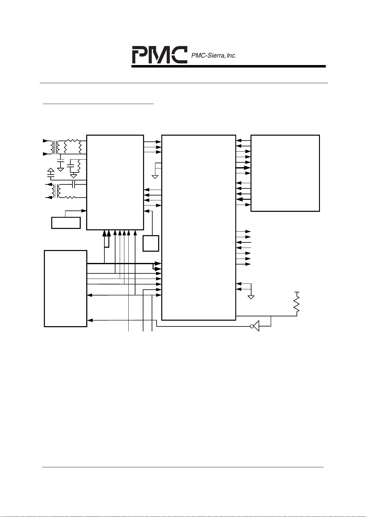
Figure 1 shows the PM6341 E1XC used with the PM7345 Saturn User Network
Interface for PDH (S/UNI-PDH™) to implement an ATM wide area User Network
Interface (UNI) or Network Node Interface (NNI).
In this example, the E1 LIU and framing functions are provided by the PM6341
E1XC. The combination of the E1XC with the S/UNI-PDH allows both PLCP
formatted E1 signals and ITU-T G.804 compliant E1 signals to be processed.
The G.804 specification defines ATM cell mappings for a variety of transmission
formats, including the 2.048 Mbit/s E1 format.
PM6341 E1XC
DATA SHEET
PMC-910419 ISSUE 8 E1 FRAMER/TRANSCEIVER
PROPRIETARY AND CONFIDENTIAL TO PMC-SIERRA, INC., AND FOR ITS CUSTOMERS’ INTERNAL USE
8
Figure 2 - DS0 Cross-connect
E-
1
Tr
a
n
s
mi
t
A
V
D
+
S
T
i0
S
T
i1
S
T
i2
S
T
i3
S
T
i4
S
T
i5
S
T
i6
S
T
i7
F
0
i
C
4
i
S
T
o
0
S
T
o
1
S
T
o
2
S
T
o
3
S
T
o
4
S
T
o
5
S
T
o
6
S
T
o
7
C
S
T
o
OD
E
C
S
D
S
R/
W
D
T
A
A[
5
:0
]
D[7
:0
]
MT8980 D X
PM6341 E1XC
B
T
P
C
M
B
T
S
IG
B
T
F
P
B
T
C
L
K
BR
C
LK
BR
F
P
I
BR
P
C
M
BR
S
IG
BR
F
PO
T
A
P
T
A
N
T
C
R
A
S
RE
F
RR
C
E-
1
Re
c
e
iv
e
A
V
S
A
V
S
4.0
96
MH
z
D
Q
Q
B
to
t
ra
ns
c
ei
ve
rs
#3
&
4
to
t
ra
ns
c
ei
ve
rs
#3
&
4
#
1
BR
P
C
M
BR
S
IG
BR
P
C
M
BR
S
IG
fr
om
t
ra
ns
ce
iv
e
r
#3
fr
om
t
ra
ns
ce
iv
e
r
#4
PM6341 E1XC
B
T
P
C
M
B
T
S
IG
B
T
F
P
B
T
C
L
K
BR
C
LK
BR
F
P
I
BR
P
C
M
BR
S
IG
BR
F
PO
T
A
P
T
A
N
T
C
R
A
S
RE
F
RR
C
#
2
E-
1
Re
c
e
iv
e
A
V
S
A
V
S
Sy
st
e
m
Fr
am
e
Pu
lse
D
Q
Q
B
D
Q
Q
B
Gl
u
e
log
ic
c
a
n
b
e
im
pl
e
me
n
ted
us
in
g
o
ne
74
HC
T
00
an
d
o
ne
74
H
CT
17
5
p
a
ck
.
2.
0
4
8M
H
z
E-
1
Tr
a
n
s
mi
t
A
V
D
+

PM6341 E1XC
DATA SHEET
PMC-910419 ISSUE 8 E1 FRAMER/TRANSCEIVER
PROPRIETARY AND CONFIDENTIAL TO PMC-SIERRA, INC., AND FOR ITS CUSTOMERS’ INTERNAL USE
9
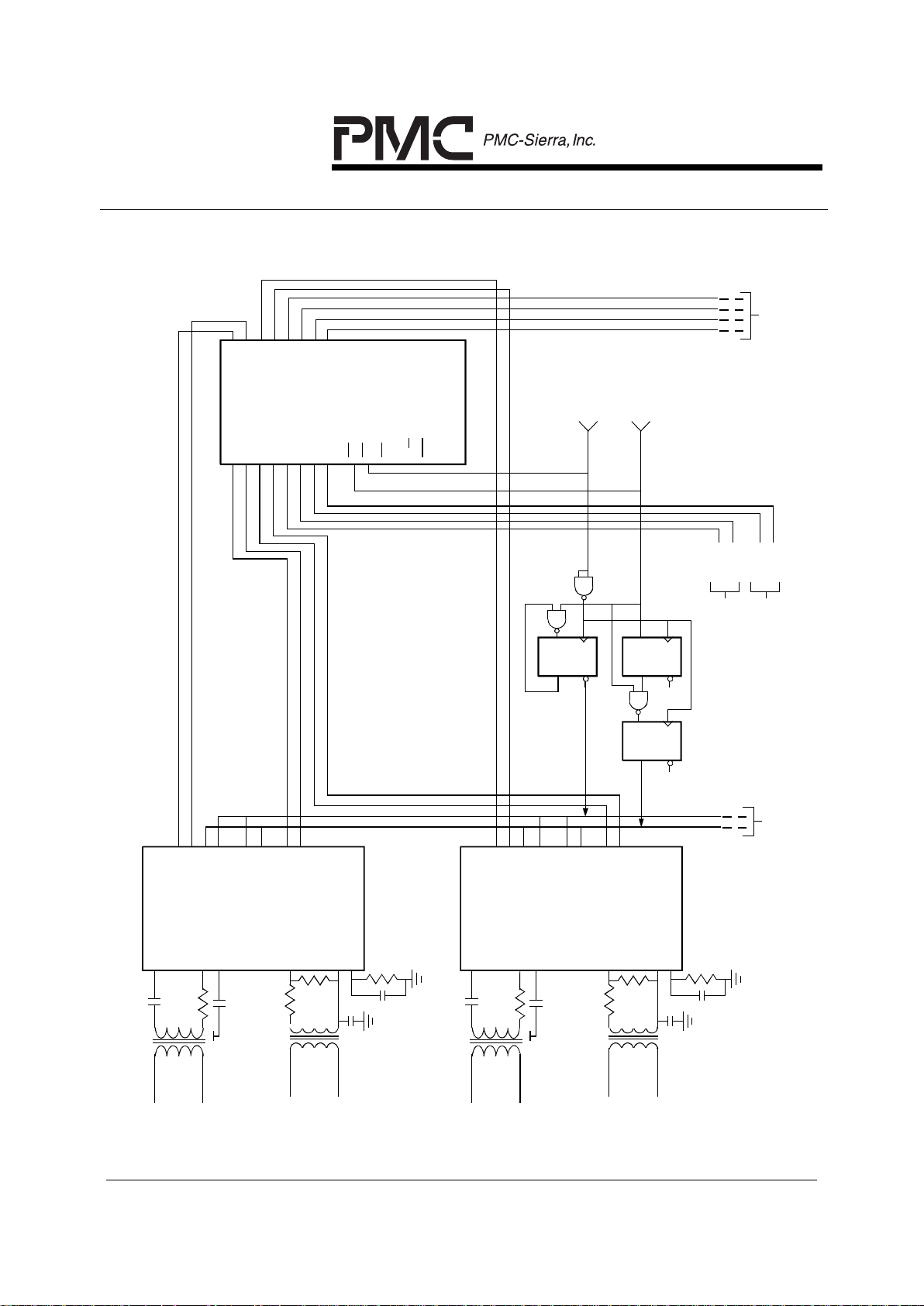
Figure 2 is an application utilizing 4 PM6341 E1XC chips and a Mitel MT8980
Digital Time/Space Switch to implement a simple DS0 cross-connect. An
alternate architecture could use two MT8980, one as a voice switch and the
other as a signalling switch, and 8 E1XCs to cross-connect 8 E1's. ( Note: a true
implementation would require redundancy in the switch core.)
The "system frame pulse" signal is stretched through the two D-FF into a pulse
of 488ns duration, which is used to frame align the data out of each E1XC
through the elastic store and to provide frame alignment indication to the
transmitters. The raw system frame pulse signal is used to indicate frame
alignment synchronization to the MT8980. Another D-FF is configured as a
toggle to generate a 2.048MHz clock from the system 4.096MHz clock source,
synchronized to the system frame pulse.
PM6341 E1XC
DATA SHEET
PMC-910419 ISSUE 8 E1 FRAMER/TRANSCEIVER
PROPRIETARY AND CONFIDENTIAL TO PMC-SIERRA, INC., AND FOR ITS CUSTOMERS’ INTERNAL USE
10
5
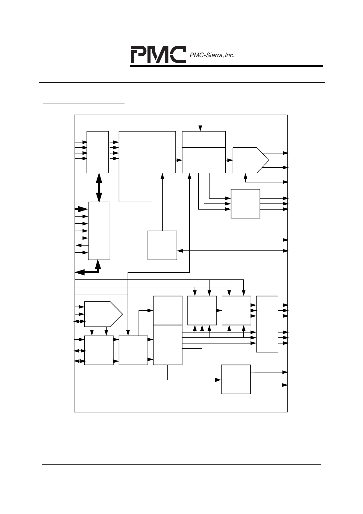
BLOCK DIAGRAM
XCLK/VCL K
BRFPI
BRCLK
RCLKI
RDP/RDD/
SDP
RDN/RLCV/
SDN
RAS
REF
RRC
TCL KI
BTPCM/BTDP
BTCLK
BTSIG/BTDN
INTB
D[7:0]
A[7:0]
RDB
WRB
CSB
ALE
RSTB
BTFP
BRPCM/BRDP
BRSIG/BRDN
BRFPO
RCLKO
RFP
RDPCM/RPCM
RDLC LK/
RDLEOM
RDLSIG/
RDLINT
RFDL
HDLC
Receiver
TDP /TD D
TCL KO
TDN /TFL G
TAN
TAP
TDL S IG/
TDL INT
TDLC L K /
TDLU D R
TC
MPIF
Micro-
Processor
Inter face
Internal
Bus
RECEIVER
TRANSMITTER
BTIF
Backplane
Transmit
Inter face
TRAN
Tra nsmitte r:
Frame Generation,
Alarm Insertion,
Trunk Conditioning
Line Coding
TOPS
Timing Options
DJAT
Digital Jitter
Attenuator
XPLS
Analog Pulse
Generator
DTIF
Digital
Transmit
Interface
PCSC
Per-channel
Controller:
Sign alling, Idle
Control
XFDL
HDLC
Transm itter
RSLC
Analog
Pulse Slicer
DRIF
Digital
Receive
Interface
CDRC
Clock and
Data
Recovery
FRMR
Framer:
Frame
Alignment,
Alarm
Detection
PMON
Performance
Monitor
Counters
ELST
Elastic
Store
SIGX
Signalling
Extractor,
Trunk
Conditioner
BRIF
Backplane
Receive
Interface

PM6341 E1XC
DATA SHEET
PMC-910419 ISSUE 8 E1 FRAMER/TRANSCEIVER
PROPRIETARY AND CONFIDENTIAL TO PMC-SIERRA, INC., AND FOR ITS CUSTOMERS’ INTERNAL USE
11
6
DESCRIPTION
The PM6341 E1 Framer/Transceiver (E1XC) is a feature-rich device suitable for
use in many E1 systems (such as CSU, DSU, CH BANK, MUX, DPBX, DACS,
and ESDX) with a minimum of external circuitry. The E1XC is software
configurable, allowing feature selection without changes to external wiring.
On the receive side, the E1XC recovers clock and data and can be configured to
frame to a basic G.704 2048 kbit/s signal or also frame to the signalling
multiframe alignment signal and the CRC multiframe alignment signal.
Analog circuitry is provided to allow direct reception of a G.703 2048 kbit/s signal
with up to 6 dB of loss by using only an external transformer and passive
components.
The E1XC also supports detection of various alarm conditions such as loss of
signal, loss of frame, loss of signalling multiframe, loss of CRC multiframe, and
reception of remote alarm signal, remote multiframe alarm signal, alarm
indication signal, and timeslot 16 alarm indication signal. The E1XC detects and
indicates the presence of remote alarm and AIS patterns and also integrates red
and AIS alarms as per industry specifications.
Performance monitoring with accumulation of CRC-4 errors, far end block errors,
framing bit errors, and line code violation is provided. The E1XC also detects
and terminates HDLC messages on a data link. The data link may be extracted
from timeslot 16 and used for common channel signalling or may be extracted
from the national bits.
An elastic store for slip buffering and adaptation to backplane timing is provided,
as is a channel associated signalling extractor that supports signalling debounce,
signalling freezing, idle code substitution, and data inversion on a per-timeslot
basis. Receive side data and signalling trunk conditioning is also provided.
On the transmit side, the E1XC generates framing for a basic G.704 2048 kbit/s
signal, or framing can be optionally disabled. The signalling multiframe alignment
signal may be optionally inserted and the CRC multiframe structure may be
optionally inserted.
Internal analog circuitry allows direct transmission of a G.703 2048 kbit/s signal
into either a 75 Ω or 120 Ω line using only an external transformer.

PM6341 E1XC
DATA SHEET
PMC-910419 ISSUE 8 E1 FRAMER/TRANSCEIVER
PROPRIETARY AND CONFIDENTIAL TO PMC-SIERRA, INC., AND FOR ITS CUSTOMERS’ INTERNAL USE
12
Channel associated signalling insertion, idle code substitution, digital milliwatt
tone substitution, and data inversion on a per-timeslot basis is also supported.
Transmit side data and signalling trunk conditioning is provided.
HDLC messages on a data link can be transmitted. The data link may be
inserted into timeslot 16 and used for common channel signalling or may be
inserted into the national bits. The E1XC can generate a low jitter transmit clock
and provides a FIFO for transmit jitter attenuation. When not used for jitter
attenuation, the full or empty status of this FIFO is made available to facilitate
higher order multiplexing applications by controlling bit-stuffing logic.
Interfaces include both a parallel microprocessor port for controlling the
operation of the device and a serial PCM interface that allows 2048 kbit/s
backplanes to be directly supported. Tolerance of gapped clocks allows other
backplane rates to be supported with a minimum of external logic.

PM6341 E1XC
DATA SHEET
PMC-910419 ISSUE 8 E1 FRAMER/TRANSCEIVER
PROPRIETARY AND CONFIDENTIAL TO PMC-SIERRA, INC., AND FOR ITS CUSTOMERS’ INTERNAL USE
13
7
PIN DIAGRAM
Figure 3 - 68 Pin PLCC (Q-Suffix):
PM6341
9 8 7 6 5 4 3 2 1 6867666564636261
XCLK/VCLK
BTPCM/BTDP
BTSIG/BTDN
BTFP
BTCLK
TCLKI
TCLKO
TDP/TDD
VSSO[0]
VDDO[0]
TDN/TFLG
TDLCLK/TDLUDR
TDLSIG/TDLINT
TAVS
TAVD
TAN
VDDO[3]
27 28 29 30 31 32 33 34 35 36 37 38 39 40 41 42 43
A[0]
A[1]
A[2]
A[3]
A[4]
A[5]
A[6]
A[7]
ALE
BRFPI
BRCLK
RFP
RDLCLK/RDLEOM
RDLSIG/RDLINT
RCLKO
RDPCM/RPCM
VSSO[2]
10
11
12
13
14
15
16
17
18
19
20
21
22
23
24
25
26
CSB
RSTB
INTB
D[0]
D[1]
D[2]
D[3]
VSSO[1]
VSSI[0]
VDDI[0]
VDDO[1]
D[4]
D[5]
D[6]
D[7]
RDB
WRB
60
59
58
57
56
55
54
53
52
51
50
49
48
47
46
45
44
VSSO[3]
TC
TAP
RAVD
RAVS
RAS
RRC
REF
VSSI[1]
VDDI[1]
RCLKI
BRFPO
BRPCM/BRDP
BRSIG/BRDN
RDP/RDD/SDP
RDN/RLCV/SDN
VDDO[2]
(TOP VIEW)
PM6341 E1XC
DATA SHEET
PMC-910419 ISSUE 8 E1 FRAMER/TRANSCEIVER
PROPRIETARY AND CONFIDENTIAL TO PMC-SIERRA, INC., AND FOR ITS CUSTOMERS’ INTERNAL USE
14
Figure 4 - 80 Pin PQFP (R-suffix):
(TOP VIEW)
PM6341
60
59
58
57
56
55
54
53
52
51
50
49
48
47
46
45
44
43
42
41
1
2
3
4
5
6
7
8
9
10
11
12
13
14
15
16
17
18
19
20
NC
CSB
RSTB
INTB
D[0]
D[1]
D[2]
D[3]
VSSO[1]
VSSI[0]
VDDI[0]
VDDO[1]
D[4]
D[5]
D[6]
D[7]
RDB
WRB
NC
NC
NC
NC
VSSO[3]
TC
TAP
RAVD
RAVS
RAS
RRC
REF
VSSI[1]
VDDI[1]
RCLKI
BRFPO
BRPCM/BRDP
BRSIG/BRDN
RDP/RDD/SDP
RDN/RLCV/SDN
VDDO[2]
NC
22232425262728293031323334353637383940
21
A[0]
A[1]
A[2]
A[3]
A[4]
A[5]
A[6]
A[7]
ALE
BRFPI
BRCLK
RFP
RDLCLK/RDLEOM
RDLSIG/RDLINT
RCLKO
RDPCM/RPCM
VSSO[2]
NC
NC
NC
79787776757473727170696867666564636261
80
NC
XCLK/VCLK
BTPCM/BTDP
BTSIG/BTDN
BTFP
BTCLK
TCLKI
TCLKO
TDP/TDD
VSSO[0]
VDDO[0]
TDN/TFLG
TDLCLK/TDLUD
R
TDLSIG/TDLINT
TAVS
TAVD
TANNCVDDO[3]
NC

PM6341 E1XC
DATA SHEET
PMC-910419 ISSUE 8 E1 FRAMER/TRANSCEIVER
PROPRIETARY AND CONFIDENTIAL TO PMC-SIERRA, INC., AND FOR ITS CUSTOMERS’ INTERNAL USE
15
8
PIN DESCRIPTION
Pin No.Pin Name Type
PQFP PLCC
Function
RDP/ I/O 44 46 Receive Digital Positive Line Pulse
(RDP). This input is available when
the E1XC is configured to receive
dual-rail formatted data. The RDP
input can be enabled for either RZ or
NRZ waveforms. When enabled for
NRZ, this input may be enabled to be
sampled on the rising or falling edge
of RCLKI. When enabled for RZ, clock
is recovered from the RDP and RDN
inputs.
RDD/ Receive Digital Data (RDD). When
the E1XC is configured to receive
single-rail data, this input may be
enabled to be sampled on the rising or
falling edge of RCLKI.
SDP Sliced Positive Line Pulse (SDP). This
pin becomes an output when the
receive analog line interface is
powered up. A positive pulse on the
SDP output corresponds to the
sampled positive pulse excursion on
the RAS input.
RDN/ I/O 43 45 Receive Digital Negative Line Pulse
(RDN). This input is available when
the E1XC is configured to receive
dual-rail formatted data. The RDN
input can be enabled for either RZ or
NRZ waveforms. When enabled for
NRZ, this input may be enabled to be
sampled on the rising or falling edge
of RCLKI. When enabled for RZ, clock
is recovered from the RDP and RDN
inputs.

PM6341 E1XC
DATA SHEET
PMC-910419 ISSUE 8 E1 FRAMER/TRANSCEIVER
PROPRIETARY AND CONFIDENTIAL TO PMC-SIERRA, INC., AND FOR ITS CUSTOMERS’ INTERNAL USE
16
Pin No.Pin Name Type
PQFP PLCC
Function
RLCV/ I/O 43 45 Receive Line Code Violation Indication
(RLCV). When the E1XC is
configured to receive single-rail data,
this input may be enabled to be
sampled on the rising or falling edge
of RCLKI.
SDN Sliced Negative Line Pulse (SDN).
This pin becomes an output when the
receive analog line interface is
powered up. A positive pulse on the
SDN output corresponds to the
sampled negative pulse excursion on
the RAS input.
RCLKI Input 48 50 Receive Line Clock Input (RCLKI).
This input is an externally recovered
2.048 MHz line clock that may be
enabled to sample the RDP and RDN
inputs on its rising or falling edge
when the input format is enabled for
dual-rail NRZ; or to sample the RDD
and RLCV inputs on its rising or falling
edge when the input format is enabled
for single-rail.
RAS Input 53 55 Receive Analog Signal (RAS). This
analog input samples the AC signal
on an external isolation transformer. It
is connected to the positive lead of the
transformer secondary through a
passive attenuation network.
REF I/O 51 53 Receive Reference (REF). This
analog bidirectional pin provides DC
bias to an external isolation
transformer. It is connected to the
negative lead of the transformer
secondary and to a decoupling
capacitor to RAVS.

PM6341 E1XC
DATA SHEET
PMC-910419 ISSUE 8 E1 FRAMER/TRANSCEIVER
PROPRIETARY AND CONFIDENTIAL TO PMC-SIERRA, INC., AND FOR ITS CUSTOMERS’ INTERNAL USE
17
Pin No.Pin Name Type
PQFP PLCC
Function
RRC I/O 52 54 Receive Peak Hold R-C Network
(RRC). This analog bidirectional pin is
connected to an external parallel
resistor/capacitor network to RAVS.
This network is necessary to the
operation of the internal peak detector
that tracks the incoming signal level.
RAVD Power 55 57 Receive Analog Power (RAVD). This
pin provides the +5V supply to the
receive analog line interface. If the
receive analog line interface is not
used, the power consumption of the
E1XC can be reduced by connecting
the RAVD pin to the analog ground
pin, RAVS. RAVD must be connected
to a common, well decoupled +5 VDC
supply together with the VDDO[3:0]
and VDDI[1:0] pins. Care must be
taken to avoid coupling noise induced
on the VDDO and VDDI pins into the
RAVD pin.
RAVS Ground 54 56 Receive Analog Ground (RAVS). This
pin provides the ground supply to the
receive analog line interface. RAVS
must be connected to a common
ground together with the VSSO[3:0]
and VSSI[1:0] pins. Care must be
taken to avoid coupling noise induced
on the VSSO and VSSI pins into the
RAVS pin.

PM6341 E1XC
DATA SHEET
PMC-910419 ISSUE 8 E1 FRAMER/TRANSCEIVER
PROPRIETARY AND CONFIDENTIAL TO PMC-SIERRA, INC., AND FOR ITS CUSTOMERS’ INTERNAL USE
18
Pin No.Pin Name Type
PQFP PLCC
Function
RCLKO Output 36 41 Recovered PCM Clock Output
(RCLKO). This output signal is the
recovered 2.048 MHz clock,
synchronized to the XCLK signal. The
RCLKO signal is recovered from the
received analog inputs (if the interface
is powered up), from the RDP and
RDN inputs (if the input format is dualrail RZ), or from the RCLKI input (if
the input format is NRZ).
RDPCM/ Output 37 42 Recovered Decoded PCM (RDPCM).
This output is available when the
E1XC is configured for decoded data
output. This NRZ output signal is the
recovered data stream with HDB3
decoding applied, if HDB3 decoding is
enabled. It is updated on the falling
edge of RCLKO. The RDPCM signal
is not meant to be used when the
digital receive interface is configured
for unipolar operation (RUNI = 1 and
RDIEN = 1), since the data should be
available at the RDD input.
RPCM Recovered PCM (RPCM). This output
is available when the E1XC is
configured for raw data output. This
NRZ output signal is the recovered
data stream without optional HDB3
decoding applied. It is updated on the
falling edge of RCLKO.

PM6341 E1XC
DATA SHEET
PMC-910419 ISSUE 8 E1 FRAMER/TRANSCEIVER
PROPRIETARY AND CONFIDENTIAL TO PMC-SIERRA, INC., AND FOR ITS CUSTOMERS’ INTERNAL USE
19
Pin No.Pin Name Type
PQFP PLCC
Function
RFP Output 33 38 Receive Frame Pulse (RFP). When
the E1XC is configured for receive
frame pulse output, RFP pulses high
for 1 RCLKO cycle during bit 1 of each
256-bit frame, indicating the frame
alignment of the RDPCM data stream.
When configured for receive signalling
multiframe output, RFP pulses high for
1 RCLKO cycle during bit 1 of frame 1
of the 16 frame signalling multiframe,
indicating the signalling multiframe
alignment of the RDPCM data stream.
(Even when signalling multiframing is
disabled, the RFP output continues to
indicate the position of bit 1 of every
16th frame.)
When configured for receive CRC
multiframe output, RFP pulses high for
1 RCLKO cycle during bit 1 of frame 1
of every 16 frame CRC multiframe,
indicating the CRC multiframe
alignment of the RDPCM data stream.
(Even when CRC multiframing is
disabled, the RFP output continues to
indicate the position of bit 1 of the
FAS frame every 16th frame.)

PM6341 E1XC
DATA SHEET
PMC-910419 ISSUE 8 E1 FRAMER/TRANSCEIVER
PROPRIETARY AND CONFIDENTIAL TO PMC-SIERRA, INC., AND FOR ITS CUSTOMERS’ INTERNAL USE
20
Pin No.Pin Name Type
PQFP PLCC
Function
RFP Output 33 38 When configured for composite
multiframe output, RFP goes high on
the falling RCLKO edge marking the
beginning of bit 1 of frame 1 of every
16 frame signalling multiframe,
indicating the signalling multiframe
alignment of the RDPCM data stream,
and returns low on the falling RCLKO
edge marking the ending of bit 1 of
frame 1 of every 16 frame CRC
multiframe, indicating the CRC
multiframe alignment of the RDPCM
data stream. This mode allows both
multiframe alignments to be decoded
externally from the single RFP signal.
Note that if the signalling and CRC
multiframe alignments are coincident,
RFP will pulse high for 1 RCLKO cycle
every 16 frames.
RFP does not indicate the frame or
multiframe alignment of RDPCM when
the digital receive interface is
configured for unipolar operation
(RUNI = 1 and RDIEN = 1 in register
03H.)
RFP is updated on the falling edge of
RCLKO.

PM6341 E1XC
DATA SHEET
PMC-910419 ISSUE 8 E1 FRAMER/TRANSCEIVER
PROPRIETARY AND CONFIDENTIAL TO PMC-SIERRA, INC., AND FOR ITS CUSTOMERS’ INTERNAL USE
21
Pin No.Pin Name Type
PQFP PLCC
Function
RDLSIG/ Output 35 40 Receive Data Link Signal (RDLSIG).
The RDLSIG signal is available on this
output when the internal HDLC
receiver (RFDL) is disabled from use.
RDLSIG contains the data link stream
extracted from the selected data link
bits. The E1XC may be configured to
utilize timeslot 16 as a data link or
utilize any combination of the national
bits as a data link. RDLSIG is
updated on the falling edge of
RDLCLK.
RDLINT Receive Data Link Interrupt (RDLINT).
The RDLINT signal is available on this
output when RFDL is enabled.
RDLINT goes high when an event
occurs which changes the status of
the HDLC receiver.
RDLCLK/ Output 34 39 Receive Data Link Clock (RDLCLK).
The RDLCLK signal is available on
this output when the internal HDLC
receiver (RFDL) is disabled from use.
RDLCLK is used to process the data
stream contained on the RDLSIG
output. When the E1XC is not
configured to extract a data link, the
RDLCLK output is held low. In all
other formats the rising edge of
RDLCLK can be used to sample the
data on RDLSIG.
RDLEOM Receive Data Link End of Message
(RDLEOM). The RDLEOM signal is
available on this output when RFDL is
enabled. RDLEOM goes high when
the last byte of a received sequence is
read from the RFDL FIFO buffer, or
when the FIFO buffer is overrun.

PM6341 E1XC
DATA SHEET
PMC-910419 ISSUE 8 E1 FRAMER/TRANSCEIVER
PROPRIETARY AND CONFIDENTIAL TO PMC-SIERRA, INC., AND FOR ITS CUSTOMERS’ INTERNAL USE
22
Pin No.Pin Name Type
PQFP PLCC
Function
BRPCM/ Output 46 48 Backplane Receive PCM (BRPCM).
The BRPCM signal is available on this
output when the backplane is
configured for single-rail output.
BRPCM contains the recovered data
stream passed through ELST and the
SIGX. When the ELST is not bypassed, the BRPCM stream is aligned
to the backplane timing and is
updated on the falling edge of
BRCLK. When the ELST is bypassed, BRPCM is aligned to the
receive line timing and is updated on
the falling edge of RCLKO.
BRDP Backplane Receive Positive Line
Pulse (BRDP). The BRDP signal is
available on this output when the
backplane is configured for dual-rail
output. The BRDP NRZ output
represents the RZ receive digital
positive pulse signal extracted from
the input bipolar signal. BRDP is
updated on the falling edge of
RCLKO.

PM6341 E1XC
DATA SHEET
PMC-910419 ISSUE 8 E1 FRAMER/TRANSCEIVER
PROPRIETARY AND CONFIDENTIAL TO PMC-SIERRA, INC., AND FOR ITS CUSTOMERS’ INTERNAL USE
23
Pin No.Pin Name Type
PQFP PLCC
Function
BRSIG/ Output 45 47 Backplane Receive Signalling
(BRSIG). The BRSIG signal is
available on this output when the
backplane is configured for single-rail
output. BRSIG contains the extracted
signalling bits for each timeslot in the
frame, repeated for the entire
signalling multiframe. Each timeslot's
signalling bits are valid in bit locations
5,6,7,8 of the timeslot and are
timeslot-aligned with the BRPCM data
stream. When the ELST is not bypassed, the BRSIG stream is aligned
to the backplane timing and is
updated on the falling edge of
BRCLK. When the ELST is bypassed, BRSIG is aligned to the
receive line timing and is updated on
the falling edge of RCLKO.
BRDN Backplane Receive Negative Line
Pulse (BRDN). The BRDN signal is
available on this output when the
backplane is configured for dual-rail
output. The BRDN NRZ output
represents the RZ receive digital
negative pulse signal extracted from
the input bipolar signal. BRDN is
updated on the falling edge of
RCLKO.

PM6341 E1XC
DATA SHEET
PMC-910419 ISSUE 8 E1 FRAMER/TRANSCEIVER
PROPRIETARY AND CONFIDENTIAL TO PMC-SIERRA, INC., AND FOR ITS CUSTOMERS’ INTERNAL USE
24
Pin No.Pin Name Type
PQFP PLCC
Function
BRFPO Output 47 49 Backplane Frame Pulse Output
(BRFPO). When the E1XC is
configured for backplane receive
frame pulse output, BRFPO pulses
high for 1 BRCLK cycle (or 1 RCLKO
cycle if ELST is by-passed) during bit
1 of each 256-bit frame, indicating the
frame alignment of the BRPCM data
stream.
When configured for backplane
receive signalling multiframe output,
BRFPO pulses high for 1 BRCLK
cycle (or 1 RCLKO cycle if ELST is bypassed) during bit 1 of frame 1 of the
16 frame signalling multiframe,
indicating the signalling multiframe
alignment of the BRPCM data stream.
(Even when signalling multiframing is
disabled, the BRFPO output continues
to indicate every 16th frame.)
When configured for backplane
receive CRC multiframe output,
BRFPO pulses high for 1 BRCLK
cycle (or 1 RCLKO cycle if ELST is bypassed) during bit 1 of frame 1 of
every 16 frame CRC multiframe,
indicating the CRC multiframe
alignment of the BRPCM data stream.
(Even when CRC multiframing is
disabled, the BRFPO output continues
to indicate the position of bit 1 of the
FAS frame every 16th frame.)

PM6341 E1XC
DATA SHEET
PMC-910419 ISSUE 8 E1 FRAMER/TRANSCEIVER
PROPRIETARY AND CONFIDENTIAL TO PMC-SIERRA, INC., AND FOR ITS CUSTOMERS’ INTERNAL USE
25
Pin No.Pin Name Type
PQFP PLCC
Function
BRFPO Output 47 49 When configured for backplane
receive composite multiframe output,
BRFPO goes high on the falling
BRCLK edge (or RCLKO edge if
ELST is by-passed) marking the
beginning of bit 1 of frame 1 of every
16 frame signalling multiframe,
indicating the signalling multiframe
alignment of the BRPCM data stream,
and returns low on the falling BRCLK
edge (or RCLKO edge if ELST is bypassed) marking the end of bit 1 of
frame 1 of every 16 frame CRC
multiframe, indicating the CRC
multiframe alignment of the BRPCM
data stream. This mode allows both
multiframe alignments to be decoded
externally from the single BRFPO
signal. If the signalling and CRC
multiframe alignments are coincident,
BRFPO will pulse high for 1 clock
cycle.
When configured for backplane
receive overhead output, BRFPO is
high for timeslot 0 and timeslot 16 of
each 256-bit frame, indicating the
overhead bit positions of the BRPCM
data stream.
BRFPO is updated on the falling edge
of BRCLK or RCLKO.

PM6341 E1XC
DATA SHEET
PMC-910419 ISSUE 8 E1 FRAMER/TRANSCEIVER
PROPRIETARY AND CONFIDENTIAL TO PMC-SIERRA, INC., AND FOR ITS CUSTOMERS’ INTERNAL USE
26
Pin No.Pin Name Type
PQFP PLCC
Function
BRCLK Input 32 37 Backplane Receive Clock (BRCLK).
This clock should be 2.048MHz with
optional gapping for adaptation to
non-uniform backplane data streams.
The E1XC may be configured to
ignore the BRCLK input and use the
RCLKO signal in its place when the
ELST is bypassed.
BRFPI Input 31 36 Backplane Frame Pulse Input
(BRFPI). This input is used to frame
align the received data to the system
backplane. A pulse at least 1 BRCLK
cycle wide must be provided on
BRFPI at multiples of 256 bit periods.
BRFPI is sampled on the rising edge
of BRCLK.
BTPCM/ Input 77 8 Backplane Transmit PCM (BTPCM).
When the backplane is configured for
single-rail input, the BTPCM inputs
the data stream to be transmitted, and
is sampled on the rising edge of
BTCLK.
BTDP Backplane Transmit Positive Line
Pulse (BTDP). When the backplane is
configured for dual-rail input, the
BTDP input by-passes the transmitter
and is fed directly into the DJAT.
BTDP is sampled on the rising edge
of BTCLK.

PM6341 E1XC
DATA SHEET
PMC-910419 ISSUE 8 E1 FRAMER/TRANSCEIVER
PROPRIETARY AND CONFIDENTIAL TO PMC-SIERRA, INC., AND FOR ITS CUSTOMERS’ INTERNAL USE
27
Pin No.Pin Name Type
PQFP PLCC
Function
BTSIG/ Input 76 7 Backplane Transmit Signalling
(BTSIG). When the backplane is
configured for single-rail input, the
BTSIG input signal contains the
signalling bits for each timeslot in the
transmit data frame, repeated for the
entire signalling multiframe. Each
timeslot's signalling bits are in bit
locations 5,6,7,8 of the timeslot and
are timeslot-aligned with the BTPCM
data stream. BTSIG is sampled on
the rising edge of BTCLK.
BTDN Backplane Transmit Negative Line
Pulse (BTDN). When the backplane is
configured for dual-rail input, the
BTDN input by-passes the transmitter
and is fed directly into the DJAT.
BTDN is sampled on the rising edge
of BTCLK.

PM6341 E1XC
DATA SHEET
PMC-910419 ISSUE 8 E1 FRAMER/TRANSCEIVER
PROPRIETARY AND CONFIDENTIAL TO PMC-SIERRA, INC., AND FOR ITS CUSTOMERS’ INTERNAL USE
28
Pin No.Pin Name Type
PQFP PLCC
Function
BTFP Input 75 6 Backplane Transmit Frame Pulse
(BTFP). This input is used to frame
align the transmitter to the system
backplane. If basic frame alignment
only is required, a pulse at least 1
BTCLK cycle wide must be provided
on BTFP at multiples of 256 bit
periods. If multiframe alignment is
required, transmit multiframe
alignment must be enabled, and
BTFP must be brought high to mark
bit 1 of frame 1 of every 16 frame
signalling multiframe and brought low
following bit 1 of frame 1 of every 16
frame CRC multiframe. This mode
allows both multiframe alignments to
be independently controlled using the
single BTFP signal. Note that if the
signalling and CRC multiframe
alignments are coincident, BTFP must
pulse high for 1 BTCLK cycle every 16
frames.
BTCLK Input 74 5 Backplane Transmit Clock (BTCLK).
This clock should be 2.048MHz with
optional gapping for adaptation from
non-uniform backplane data streams.
The E1XC may be configured to
ignore the BTCLK input and use the
RCLKO signal in its place.

PM6341 E1XC
DATA SHEET
PMC-910419 ISSUE 8 E1 FRAMER/TRANSCEIVER
PROPRIETARY AND CONFIDENTIAL TO PMC-SIERRA, INC., AND FOR ITS CUSTOMERS’ INTERNAL USE
29
Pin No.Pin Name Type
PQFP PLCC
Function
TDLSIG/ I/O 66 65 Transmit Data Link Signal (TDLSIG).
The TDLSIG signal is input on this pin
when the internal HDLC transmitter
(XFDL) is disabled from use. TDLSIG
is the source for the data stream to be
inserted into the selected data link
bits. The E1XC may be configured to
utilize timeslot 16 as a data link or
utilize any combination of the national
bits as a data link. TDLSIG is
sampled on the rising edge of
TDLCLK.
TDLINT Transmit Data Link Interrupt (TDLINT).
The TDLINT signal is output on this
pin when XFDL is enabled. TDLINT
goes high when the last data byte
written to the XFDL has been set up
for transmission and processor
intervention is required to either write
control information to end the
message, or to provide more data.

PM6341 E1XC
DATA SHEET
PMC-910419 ISSUE 8 E1 FRAMER/TRANSCEIVER
PROPRIETARY AND CONFIDENTIAL TO PMC-SIERRA, INC., AND FOR ITS CUSTOMERS’ INTERNAL USE
30
Pin No.Pin Name Type
PQFP PLCC
Function
TDLCLK/ Output 67 66 Transmit Data Link Clock (TDLCLK).
The TDLCLK signal is available on this
output when the internal HDLC
transmitter (XFDL) is disabled from
use. The rising edge of TDLCLK is
used to sample the data stream
contained on the TDLSIG input. When
the E1XC is not configured to insert a
data link, the TDLCLK output is held
low.
TDLUDR Transmit Data Link Underrun
(TDLUDR). The TDLUDR signal is
available on this output when XFDL is
enabled. TDLUDR goes high when
the processor has failed to service the
TDLINT interrupt before the transmit
buffer is emptied.
TCLKO Output 72 3 Transmit Clock Output (TCLKO). The
TDP, TDN, and TDD outputs may be
enabled to be updated on the rising or
falling edge of TCLKO. The TAP and
TAN outputs are also driven with
timing derived from TCLKO. TCLKO is
a 2.048 MHz clock that is adequately
jitter and wander free in absolute
terms to permit an acceptable G.703
2048 kbit/s signal to be generated.
Depending on the configuration of the
E1XC, TCLKO may be derived from
TCLKI, RCLKO, or BTCLK, with or
without jitter attenuation.

PM6341 E1XC
DATA SHEET
PMC-910419 ISSUE 8 E1 FRAMER/TRANSCEIVER
PROPRIETARY AND CONFIDENTIAL TO PMC-SIERRA, INC., AND FOR ITS CUSTOMERS’ INTERNAL USE
31
Pin No.Pin Name Type
PQFP PLCC
Function
TDP/ Output 71 2 Transmit Digital Positive Line Pulse
(TDP). This signal is available on the
output when the E1XC is configured
to transmit dual-rail data. The TDP
signal can be formatted for either RZ
or NRZ waveforms, and can be
enabled to be updated on the rising or
falling edge of TCLKO.
TDD Transmit Digital Data (TDD). This
signal is available on the output when
configured to transmit single-rail data.
The TDD signal may be enabled to be
updated on the rising or falling edge of
TCLKO.
TDN/ Output 68 67 Transmit Digital Negative Line Pulse
(TDN). This signal is available on the
output when the E1XC is configured
to transmit dual-rail data. The TDN
signal can be formatted for either RZ
or NRZ waveforms, and can be
enabled to be updated on the rising or
falling edge of TCLKO.
TFLG Transmit FIFO Flag (TFLG). This
signal is available when configured to
transmit single-rail data. The TFLG
output indicates when the transmit
rate conversion FIFO in DJAT is
nearing an empty or a full condition.
Either indication may be selected.
This output may be enabled to be
updated on the rising or falling edge of
TCLKO.

PM6341 E1XC
DATA SHEET
PMC-910419 ISSUE 8 E1 FRAMER/TRANSCEIVER
PROPRIETARY AND CONFIDENTIAL TO PMC-SIERRA, INC., AND FOR ITS CUSTOMERS’ INTERNAL USE
32
Pin No.Pin Name Type
PQFP PLCC
Function
TAP Output 56 58 Transmit Analog Positive Pulse (TAP).
This analog output drives an AC
signal through an external matching
transformer. It is connected to the
positive lead of the transformer
primary.
An analog Transmit Monitor Positive
point is internally bonded to this
output and is used to monitor the
positive pulses on the transmit line.
TAN Output 63 62 Transmit Analog Negative Pulse
(TAN). This analog output drives an
AC signal through an external
matching transformer. It is connected
to the negative lead of the transformer
primary.
An analog Transmit Monitor Negative
point is internally bonded to this
output and is used to monitor the
negative pulses on the transmit line.
TC I/O 57 59 Transmit Reference Decoupling
Capacitor (TC). This analog
bidirectional provides decoupling for
an internal reference generator. It is
connected to a decoupling capacitor
to TA VD .

PM6341 E1XC
DATA SHEET
PMC-910419 ISSUE 8 E1 FRAMER/TRANSCEIVER
PROPRIETARY AND CONFIDENTIAL TO PMC-SIERRA, INC., AND FOR ITS CUSTOMERS’ INTERNAL USE
33
Pin No.Pin Name Type
PQFP PLCC
Function
TAVD Power 64 63 Transmit Analog Power (TAVD). This
pin provides the +5 V supply to the
transmit analog line interface. Even if
the transmit analog line interface is
not used, a +5 V supply must be
provided. The transmit analog line
interface remains in a low power
consumption state after reset until
enabled. TAVD must be connected to
a common, well decoupled +5 VDC
supply together with the VDDO[3:0]
and VDDI[1:0] pins. Care must be
taken to avoid coupling noise induced
on the VDDO and VDDI pins into the
TAVD pin.
TAVS Ground 65 64 Transmit Analog Ground (TAVS). This
pin provides the ground supply to the
transmit analog line interface. TAVS
must be connected to a common
ground together with the VSSO[3:0]
and VSSI[1:0] pins. Care must be
taken to avoid coupling noise induced
on the VSSO and VSSI pins into the
TAVS pin.

PM6341 E1XC
DATA SHEET
PMC-910419 ISSUE 8 E1 FRAMER/TRANSCEIVER
PROPRIETARY AND CONFIDENTIAL TO PMC-SIERRA, INC., AND FOR ITS CUSTOMERS’ INTERNAL USE
34
Pin No.Pin Name Type
PQFP PLCC
Function
TCLKI Input 73 4 Transmit Clock Input (TCLKI). This
input signal is used to generate the
TCLKO clock signal. Depending upon
the configuration of the E1XC, TCLKO
may be derived directly from TCLKI by
dividing TCLKI by 8, or TCLKO may
be derived from TCLKI after jitter
attenuation and frequency
multiplication (default is a frequency
ratio of one). If TCLKI is jitter-free
when divided down to 8 kHz, then it is
possible to derive TCLKO from TCLKI
when TCLKI is a multiple of 8 kHz (i.e.
Nx8 kHz, for N equals 1 to 256). The
E1XC may be configured to ignore the
TCLKI input and utilize BTCLK or
RCLKO instead. RCLKO is also
substituted for TCLKI if line loopback
is enabled.
XCLK/ Input 78 9 Crystal Clock Input (XCLK). This
signal provides timing for many
portions of the E1XC. Depending on
the configuration of the E1XC, XCLK
is nominally a 49.152 MHz or 16.384
MHz, 50% duty cycle clock. When
transmit clock generation or jitter
attenuation is not required, XCLK may
be driven with a 16.384 MHz clock.
When transmit clock generation or
jitter attenuation are required, XCLK
must be driven with a 49.152 MHz
clock.
VCLK Vector Clock (VCLK). The VCLK
signal is used during E1XC production
test to verify internal functionality.

PM6341 E1XC
DATA SHEET
PMC-910419 ISSUE 8 E1 FRAMER/TRANSCEIVER
PROPRIETARY AND CONFIDENTIAL TO PMC-SIERRA, INC., AND FOR ITS CUSTOMERS’ INTERNAL USE
35
Pin No.Pin Name Type
PQFP PLCC
Function
INTB Output 4 12 Active low open-drain Interrupt signal
(INTB). This signal goes low when an
unmasked interrupt event is detected
on any of the internal interrupt
sources, including the internal HDLC
transceiver. No te that INTB will
remain low until all active, unmasked
interrupt sources are acknowledged at
their source.
CSB Input 2 10 Active low chip select (CSB). This
signal must be low to enable E1XC
register accesses. Note that when not
being used, CSB must be tied high. If
CSB is not required (i.e. register
accesses are controlled using the
RDB and WRB signals only), CSB
must be connected to an inverted
version of the RSTB input. In any
case, CSB must be high at least once
after a powerup in order to clear
internal test modes.
D[0]
D[1]
D[2]
D[3]
D[4]
D[5]
D[6]
D[7]
I/O 5
6
7
8
13
14
15
16
13
14
15
16
21
22
23
24
Bidirectional data bus (D[7:0]). This
bus is used during E1XC read and
write accesses.

PM6341 E1XC
DATA SHEET
PMC-910419 ISSUE 8 E1 FRAMER/TRANSCEIVER
PROPRIETARY AND CONFIDENTIAL TO PMC-SIERRA, INC., AND FOR ITS CUSTOMERS’ INTERNAL USE
36
Pin No.Pin Name Type
PQFP PLCC
Function
RDB Input 17 25 Active low read enable (RDB). This
signal is pulsed low to enable a E1XC
register read access. The E1XC
drives the D[7:0] bus with the contents
of the addressed register while RDB
and CSB are both low.
WRB Input 18 26 Active low write strobe (WRB). This
signal is pulsed low to enable a E1XC
register write access. The D[7:0] bus
contents are clocked into the
addressed normal mode register on
the rising edge of WRB while CSB is
low.
ALE Input 30 35 Address latch enable (ALE). This
signal latches the address bus, A[7:0],
when low. This allows the E1XC to be
interfaced to a multiplexed
address/data bus. When ALE is high,
the address latches are transparent.
RSTB Input 3 11 Active low reset (RSTB). This signal
asynchronously resets the E1XC.
A[0]
A[1]
A[2]
A[3]
A[4]
A[5]
A[6]
A[7]
Input 22
23
24
25
26
27
28
29
27
28
29
30
31
32
33
34
Address bus (A[7:0]). This bus selects
specific registers during E1XC register
accesses.

PM6341 E1XC
DATA SHEET
PMC-910419 ISSUE 8 E1 FRAMER/TRANSCEIVER
PROPRIETARY AND CONFIDENTIAL TO PMC-SIERRA, INC., AND FOR ITS CUSTOMERS’ INTERNAL USE
37
Pin No.Pin Name Type
PQFP PLCC
Function
VDDO[0]
VDDO[1]
VDDO[2]
VDDO[3]
Power 69
12
42
62
68
20
44
61
Pad ring power pins (VDDO[3:0]).
These pins must be connected to a
common, well decoupled +5 VDC
supply together with the VDDI[1:0]
pins. Care must be taken to avoid
coupling noise induced on the VDDO
pins into the VDDI pins.
VDDI[0]
VDDI[1]
Power 11
49
19
51
Core power pins (VDDI[1:0]). These
pins must be connected to a common,
well decoupled +5 VDC supply
together with the VDDO[3:0] pins.
VSSO[0]
VSSO[1]
VSSO[2]
VSSO[3]
Ground 70
9
38
58
1
17
43
60
Pad ring ground pins (VSSO[3:0]).
These pins must be connected to a
common ground together with the
VSSI[1:0] pins. Care must be taken to
avoid coupling noise induced on the
VSSO pins into the VSSI pins.
VSSI[0]
VSSI[1]
Ground 10
50
18
52
Core ground pins (VSSI[1:0]). These
pins must be connected to a common
ground together with the VSSO[3:0]
pins.
Notes on Pin Description:
1. VDDI and VSSI are the +5 V and ground connections, respectively, for the
core circuitry of the device. VDDO and VSSI are the +5 V and ground
connections, respectively, for the pad ring circuitry of the device. TAVD and
TAVS are the +5 V and ground connections, respectively, for the transmit
analog circuitry of the device. These power supply connections must all be
utilized and must all connect to a common +5 V or ground rail, as appropriate.
There is no low impedance connection within the PM6341 between the core,
pad ring, and transmit analog supply rails. Failure to properly make these
connections may result in improper operation or damage to the device. Care
must be taken to avoid coupling of noise into the transmit analog supply rails.
2. RAVD and RAVS are the +5 V and ground connections, respectively, for the
receive analog circuitry of the device. These power supply connections need

PM6341 E1XC
DATA SHEET
PMC-910419 ISSUE 8 E1 FRAMER/TRANSCEIVER
PROPRIETARY AND CONFIDENTIAL TO PMC-SIERRA, INC., AND FOR ITS CUSTOMERS’ INTERNAL USE
38
only be used if the receive analog function is desired and should then
connect to a common +5 V or ground rail, as appropriate, with the core, pad
ring, and transmit analog supply rails. There is no low impedance connection
within the PM6341 between the receive analog supply rail and other supply
rails. When the receive analog function is not desired, RAVD should be
connected to RAVS. Care must be taken to avoid coupling of noise into the
receive analog supply rails.
3. Inputs RSTB and ALE have integral pull-up resistors.
4. The TDLSIG/TDLINT pin has an integral pull-up resistor and defaults to being
an input after a reset.

PM6341 E1XC
DATA SHEET
PMC-910419 ISSUE 8 E1 FRAMER/TRANSCEIVER
PROPRIETARY AND CONFIDENTIAL TO PMC-SIERRA, INC., AND FOR ITS CUSTOMERS’ INTERNAL USE
39
9
FUNCTIONAL DESCRIPTION
9.1 Digital Receive Interface (DRIF)
The Digital Receive Interface provides control over the various input options
available on the multifunctional digital receive pins RDP/RDD/SDP and
RDN/RLCV/SDN. When configured for dual-rail input, the multifunctional pins
become the RDP and RDN inputs. These inputs can be enabled to receive either
return-to-zero (RZ) or non-return-to-zero (NRZ) signals; the NRZ input signals
can be sampled on either the rising or falling edge of RCLKI. When the interface
is configured for single-rail input, the multifunctional pins become the RDD and
RLCV inputs, which can be sampled on either the rising or falling RCLKI edge.
Finally, when the analog interface is used, the multifunction pins become the
SDP and SDN outputs, indicating the sliced pulses corresponding to the received
positive and negative analog line pulses.
9.2 Analog Pulse Slicer (RSLC)
The Analog E1 Pulse Slicer function is provided by the RSLC block. The Receive
Data Slicer (RSLC) block provides the first stage of signal conditioning for a
G.703 2048 kbit/s serial data stream by converting bipolar line signals to dual rail
RZ pulses. Before an RZ output pulse is generated by the RSLC block, bipolar
input signals must rise to 50% (for G.703 2048 kbit/s) of their peak amplitude.
This level is referred to as the Slicing Level. The threshold criteria insures
accurate pulse or mark recognition in the presence of noise.
The RSLC block provides a squelch alarm, which occurs when input pulses are
below the squelching level threshold. In this state, data is not sliced, which
prevents the detection of noise on an idle transmission line. The SQ status bit in
register 5DH goes high whenever the RSLC block is squelching the input signal.
The RSLC can be configured (in register 5DH) to generate an interrupt whenever
the SQ status bit goes high.
The RSLC block relies on an external network for compliance to G.703 120 Ω
twisted pair or G.703 75 Ω coax. The RSLC block is configured via an off-chip
attenuator pad (see Figure 5). The following network values are recommended
for the two intended applications:

PM6341 E1XC
DATA SHEET
PMC-910419 ISSUE 8 E1 FRAMER/TRANSCEIVER
PROPRIETARY AND CONFIDENTIAL TO PMC-SIERRA, INC., AND FOR ITS CUSTOMERS’ INTERNAL USE
40
Table 1 - Recommended Rx Network Values
Signal Type Turns
Ratio
(N ± 5%)
R1
(Ω ± 1%)
R2
(Ω ± 1%)
Squelch Level on the
Primary
G.703
Zo = 120Ω
1:2 357 121 276 mV ± 20%
Zo = 75Ω
1:2 205 95.3 220 mV ± 20%
Tight tolerances are required on the resistors and turns ratio to meet the return
loss specification.
For details on how these values were determined, refer to the section entitled
"Interfacing to the Analog Pulse Slicer" in the "Operation" section of this
databook.

PM6341 E1XC
DATA SHEET
PMC-910419 ISSUE 8 E1 FRAMER/TRANSCEIVER
PROPRIETARY AND CONFIDENTIAL TO PMC-SIERRA, INC., AND FOR ITS CUSTOMERS’ INTERNAL USE
41
Figure 5 - External Analog Receive Interface Circuit
T
R
1:N
316 kΩ ±10
47 nF
±10%
RAS
REF
V
RAVS
RAVD
RRC0.1 µF
± 10%
R2
R1
DD
Notes:
(Zin = 10k
Ω
± 10%)
2. Recommended Transformers:
1. All capacitors ceramic
3. Alternatively, a dual part containing both the 1:2CT & 1:1.36 transformers can be used, i.e.:
BH Electronics 500-1775 (1:1:1);
Pulse Engineering PE 64931 (1:1:1); or
Pulse Engineering PE 65341 (1:1:1) (for extended temp range)
BH Electronics 500-1777;
Pulse Engineering PE64952; or
Pulse Engineering PE65774 (for extended temp range)
The RSLC block can be disabled by strapping the receive analog power pin,
RAVD to ground. When RLSC is disabled, the E1XC accepts RZ input pulses on
the RDP/RDD and RDN/RLCV pins.
9.3 Clock and Data Recovery (CDRC)
The Clock and Data Recovery function is provided by a Data and Clock
Recovery (CDRC) block that provides clock and PCM data recovery, HDB3
decoding, bipolar violation detection, and loss of signal detection. The CDRC
block recovers the clock from the incoming RZ data pulses using a digital phase-

PM6341 E1XC
DATA SHEET
PMC-910419 ISSUE 8 E1 FRAMER/TRANSCEIVER
PROPRIETARY AND CONFIDENTIAL TO PMC-SIERRA, INC., AND FOR ITS CUSTOMERS’ INTERNAL USE
42
locked-loop and recovers the NRZ data. Loss of signal is indicated after
exceeding a programmed threshold of 10, 31, 63 or 175 consecutive bit periods
of the absence of pulses on both the positive and negative line pulse inputs and
is cleared after the occurrence of a single line pulse. An alternate loss of signal
indication is provided which is cleared only after 255 bit periods during which no
sequence of four consecutive zeros has been received. If enabled, a
microprocessor interrupt is generated when a loss of signal is detected and when
the signal returns.
The HDB3 decoding is summarized as follows: If a bipolar violation (BPV)
preceded by two zeros is received, the violation and the preceding three bit
periods are decoded as four zeros. If AMI line code is selected, no substitution is
made.
If HDB3 line code is selected, a line code violation is declared if any bipolar
violation is of the same polarity as the previous BPV or if the BPV is not
preceded by two spaces (the second criteria is maskable). If AMI line code is
selected, all bipolar violations are counted as line code violations.
The input jitter tolerance of CDRC complies with ITU-T Recommendation G.823.

PM6341 E1XC
DATA SHEET
PMC-910419 ISSUE 8 E1 FRAMER/TRANSCEIVER
PROPRIETARY AND CONFIDENTIAL TO PMC-SIERRA, INC., AND FOR ITS CUSTOMERS’ INTERNAL USE
43
Figure 6 - CDRC Jitter Tolerance
10 10 10 10
12345
SINEWAVE JITTER FREQUENCY, Hz - LOG SCALE
10
1
0.1
2.0
1.5
1.8
10
2.4
IN SPEC
REGION
DPLL TOLERANCE
WITH 25% ONES
DENSITY
(ALGSEL=0)
DPLL TOLERANCE WITH
14 ZEROS RESTRICTION
(ALGSEL=0)
REC. G823 JITTER
TOLERANCE
SPECIFICATION
0.2
SINEWAVE
JITTER
AMPLITUDE
P. TO P. (UI)
LOG SCALE
25% ONES
DENSITY
(ALGSEL=1)
Max tolerance ceiling of 256 UI at 2.048 MHz
BRCLK - limit ed b y 256 bit frame slip buffe r.
9.4 Framer (FRMR)
The Framer (FRMR) block searches for frame alignment, CRC multiframe
alignment, and channel associated signalling (CAS) multiframe alignment in the
incoming recovered PCM stream.
Once the FRMR has found basic (or FAS) frame alignment, the incoming PCM
data is continuously monitored for FAS/NFAS framing bit errors. Framing bit
errors are accumulated in the framing bit error counter contained in the PMON
block. Once the FRMR has found CAS multiframe alignment, the PCM data is
continuously monitored for CAS multiframe alignment pattern errors. Once the
FRMR has found CRC multiframe alignment, the PCM data is continuously
monitored for CRC multiframe alignment pattern errors, and CRC-4 errors. The
FRMR also detects and indicates loss of frame, loss of CAS multiframe, and loss

PM6341 E1XC
DATA SHEET
PMC-910419 ISSUE 8 E1 FRAMER/TRANSCEIVER
PROPRIETARY AND CONFIDENTIAL TO PMC-SIERRA, INC., AND FOR ITS CUSTOMERS’ INTERNAL USE
44
of CRC multiframe, based on user-selectable criteria. The reframe operation can
be initiated by software (via the FRMR Frame Alignment Options Register), by
excessive CRC errors, or when CRC multiframe alignment is not found within 8
ms. The FRMR also identifies the position of the frame, the CAS multiframe, and
the CRC multiframe.
The FRMR extracts timeslot 16 for optional use as a data link and also extracts
the contents of the International bits (from both the FAS frames and the NFAS
frames), the National bits, and the Extra bits (from timeslot 16 of frame 0 of the
CAS multiframe), and stores them in the FRMR International/National Bits
Register, and the FRMR Extra Bits Register respectively.
The FRMR identifies the raw bit values for the remote (or distant frame) alarm
(bit 3 in timeslot 0 of NFAS frames) and the remote signalling multiframe (or
distant multiframe) alarm (bit 6 of timeslot 16 of frame 0 of the CAS multiframe)
via the FRMR International/National Bits Register, and the FRMR Extra Bits
Register respectively. Access is also provided to the "debounced" remote alarm
and remote signalling multiframe alarm bits which are set when the
corresponding signals have been a logic 1 for 2 or 3 consecutive occurrences, as
per Recommendation O.162. Detection of AIS and timeslot 16 AIS are provided;
AIS is also integrated and an AIS Alarm is indicated if the AIS condition has
persisted for at least 100 ms. The out of frame (OOF=1) condition is also
integrated, indicating a red Alarm if the OOF condition has persisted for at least
100 ms.
An interrupt may be generated to signal a change in the state of any status bits
(OOF, OOSMF, OOCMF, AIS, or RED), and to signal when any event (RRA,
RRMA, AISD, T16AISD, COFA, FER, SMFER, CMFER, CRCE, or FEBE) has
occurred.
9.4.1 Frame Find
The Frame Find Block searches for frame alignment using one of two userselectable algorithms, as defined in Recommendation G.706. Optionally, a two
frame check sequence can be added to either algorithm to provide protection
against false frame alignment in the presence of random mimic patterns.
The first algorithm finds frame alignment by using the following sequence:
1. Search for the presence of the correct 7-bit FAS;
2. Check that the FAS is absent in the following frame by verifying that bit 2 of the
assumed timeslot 0 byte is a logic 1;

PM6341 E1XC
DATA SHEET
PMC-910419 ISSUE 8 E1 FRAMER/TRANSCEIVER
PROPRIETARY AND CONFIDENTIAL TO PMC-SIERRA, INC., AND FOR ITS CUSTOMERS’ INTERNAL USE
45
3. Check that the correct 7-bit FAS is present in the assumed timeslot 0 byte of
the next frame.
If either of the conditions in steps 2 or 3 are not met, a new search for frame
alignment is initiated in the bit immediately following the errored timeslot 0 byte
location.
The second algorithm is similar to the first, but adds a one frame "hold-off" in
step 2 to begin a new search in the bit immediately following the second 7-bit
FAS that is checked. This "hold-off" is performed only the condition in step 2
fails, providing a more robust algorithm which allows the framer to operate
correctly in the presence of fixed timeslot data imitating the FAS pattern.
A check sequence can be added to either algorithm to verify correct frame
alignment in the presence of random imitative FASs. Note that this check
sequence should be enabled when monitoring an unframed 215 -1 pseudo
random sequence to avoid framing to the single mimic framing pattern contained
in the sequence. The check consists of verifying correct frame alignment for an
additional two frames, as follows:
• once frame alignment (in frame "n") is determined, check that the FAS is
absent in the following frame (frame "n+1") by verifying that bit 2 of timeslot 0
is a logic 1;
• then, check that the correct 7-bit FAS is present in timeslot 0 of the next
frame (frame "n+2").
If either of the two conditions in the check sequence are not met, a new search
for frame alignment is initiated in the bit immediately following the errored byte
location when using the first algorithm, and is initiated in the bit immediately
following the byte location in frame "n+2" when using the second algorithm.
These algorithms are illustrated in Figure 7.

PM6341 E1XC
DATA SHEET
PMC-910419 ISSUE 8 E1 FRAMER/TRANSCEIVER
PROPRIETARY AND CONFIDENTIAL TO PMC-SIERRA, INC., AND FOR ITS CUSTOMERS’ INTERNAL USE
46
Figure 7 - Basic Framing Algorithm Flowchart
Out of Frame
Synchronization
search for
7-bit FAS
pattern
Check if bit 2=1
in current byte loc.
of next frame
check
occurrence of
7-bit FAS in next
frame
not
found
found
Algorithm #1:
Bit 2=0
Wait for byte
location in next
frame
Bit 2=1
Algorithm #2:
Bit 2 =0
2nd FAS not
found
FAS Found &
Check Sequence
selected
Frame alignment
established
Check bit 2 =1
in following
frame
check
occurrence of
7-bit FAS in next
frame
Algorithm #1:
Bit 2=0
Bit 2=1
Algorithm #2:
Bit 2 =0
FAS not
found
FAS Found
Frame alignment
established
FAS Found & No
Check Sequence
selected

PM6341 E1XC
DATA SHEET
PMC-910419 ISSUE 8 E1 FRAMER/TRANSCEIVER
PROPRIETARY AND CONFIDENTIAL TO PMC-SIERRA, INC., AND FOR ITS CUSTOMERS’ INTERNAL USE
47
These algorithms provide robust framing operation even in the presence of
random bit errors: framing with algorithm #1 or #2 provides a 99.98% probability
of finding frame alignment within 1 ms in the presence of 10-3 bit error rate and
no mimic patterns.
Once frame alignment is found, the block sets the OOF indication low, indicates a
change of frame alignment (if it occurred), and monitors the frame alignment
signal, indicating errors occurring in the 7-bit FAS pattern and in bit 2 of NFAS
frames, and indicating the debounced value of the Remote Alarm bit (bit 3 of
NFAS frames). Using debounce, the Remote Alarm bit has <0.00001%
probability of being falsely indicated in the presence of a 10-3 bit error rate. The
block declares loss of frame alignment if 3 or 4 consecutive FASs have been
received in error or, additionally, if bit 2 of NFAS frames has been in error for 3
consecutive occasions. In the presence of a random 10-3 bit error rate the frame
loss criteria provides a mean time to falsely lose frame alignment of >12 minutes.
The Frame Find Block can be forced to initiate a frame search at any time when
any of the following conditions are met:
• the software re-frame bit in the Frame Alignment Options Register goes to
logic 1;
• the CRC Frame Find Block is unable to find CRC multiframe alignment; or
• the CRC Frame Find Block accumulates excessive CRC evaluation errors
(= 915 CRC errors in 1 second) and is enabled to force a re-frame.
9.4.2 CRC Frame Find
Once the basic frame alignment has been found, the CRC Frame Find Block
searches for CRC multiframe alignment by observing whether the International
bits (bit 1 of timeslot 0) of NFAS frames follow the CRC multiframe alignment
pattern. Multiframe alignment is declared if at least two valid CRC multiframe
alignment signals are observed within 8 ms, with the time separating two
alignment signals being a multiple of 2 ms.
Once CRC multiframe alignment is found, the block sets the OOCMF indication
low, and monitors the multiframe alignment signal, indicating errors occurring in
the 6-bit pattern, and indicating the value of the FEBE bits (bit 1 of frames 13
and 15 of the multiframe).The block declares loss of CRC multiframe alignment if
four consecutive CRC multiframe alignment signals have been received in error,
or if frame alignment has been lost.
The CRC Frame Find Block will force the Frame Find Block to initiate a basic
frame search when CRC multiframe alignment has not been found for 8 ms.

PM6341 E1XC
DATA SHEET
PMC-910419 ISSUE 8 E1 FRAMER/TRANSCEIVER
PROPRIETARY AND CONFIDENTIAL TO PMC-SIERRA, INC., AND FOR ITS CUSTOMERS’ INTERNAL USE
48
9.4.3 CRC Check and AIS Detection
The CRC Check and AIS Detect Block computes the 4-bit CRC checksum for
each incoming sub-multiframe and compares this 4-bit result to the received
CRC remainder bits in the subsequent sub-multiframe. The block also
accumulates CRC errors over 1 second intervals, monitoring for excessive CRC
errors and optionally, forcing the Frame Find Block to initiate a frame search
when ≥ 915 CRC errors occur in 1 second. The number of CRC errors
accumulated during the previous second is available by reading the FRMR CRC
Error Counter Registers.
The block also detects the occurrence of an unframed all-ones receive data
stream, indicating the AIS by setting the AISD indication when less than 3 zero
bits are received in 2 frames (512 consecutive bits); the AISD indication is reset
when 3 or more zeros in the E1 stream are observed, or when frame alignment is
found.
9.4.4 Signalling Frame Find
Once the basic frame alignment has been found, the Signalling Frame Find Block
searches for CAS multiframe alignment using one of two user-selectable
algorithms, one of which is compatible with Recommendation G.732. Once
frame alignment has been found, the first algorithm monitors timeslot 16 of each
frame; it declares CAS multiframe alignment when 15 consecutive frames with
bits 1-4 of timeslot 16 not containing the alignment pattern are observed to
precede a frame with timeslot 16 containing the correct alignment pattern. The
second algorithm, compatible with G.732, also monitors timeslot 16 of each
frame, and declares CAS multiframe alignment when non-zero bits 1-4 of
timeslot 16 are observed to precede a timeslot 16 containing the correct
alignment pattern.
Once CAS multiframe alignment has been found, the block sets the OOSMF
indication to logic 0, and monitors the CAS multiframe alignment signal,
indicating errors occurring in the 4-bit pattern, and indicating the debounced
value of the remote signalling multiframe alarm bit (bit 6 of timeslot 16 of frame 0
of the multiframe). Using debounce, the remote signalling multiframe alarm bit
has
< 0.00001% probability of being falsely indicated in the presence of a 10-3 bit
error rate. This block also indicates the reception of timeslot 16 AIS when
timeslot 16 has been all-ones for two consecutive frames while out of CAS
multiframe. The block declares loss of CAS multiframe alignment if two
consecutive CAS multiframe alignment signals have been received in error, or

PM6341 E1XC
DATA SHEET
PMC-910419 ISSUE 8 E1 FRAMER/TRANSCEIVER
PROPRIETARY AND CONFIDENTIAL TO PMC-SIERRA, INC., AND FOR ITS CUSTOMERS’ INTERNAL USE
49
additionally, if all the bits in timeslot 16 are logic 0 for 1 or 2 (selectable) CAS
multiframes. Loss of CAS multiframe alignment is also declared if frame
alignment has been lost.
9.4.5 Alarm Integration
The Alarm Integrator Block monitors the OOF and the AIS indications, verifying
that each condition has persisted for 104 ms (±6 ms) before indicating the alarm
condition. The alarm is removed when the condition has been absent for 104 ms
(±6 ms).
The AIS alarm algorithm accumulates the occurrences of AISD (AIS detection).
AISD is defined as an unframed pattern with less than 3 zeros in two consecutive
frame times (512 bits). The Alarm Integrator Block counts the occurrences of
AISD over a 4 ms interval and indicates a valid AIS presence when 13 or more
AISD indications (of a possible 16) have been received. Each interval with a
valid AIS presence indication increments an interval counter which declares AIS
Alarm when 25 valid intervals have been accumulated. An interval with no valid
AIS presence indication decrements the interval counter; the AIS Alarm
declaration is removed when the counter reaches 0. This algorithm provides a
99.8% probability of declaring an AIS Alarm within 104 ms in the presence of a
10-3 mean bit error rate.
The TS16 AIS alarm algorithm accumulates the occurrences of T16AISD (TS16
AIS detection). T16AISD is defined as two consecutive all ones time slot 16
bytes while out of signalling multiframe. Each interval with a valid TS16 AIS
presence indication increments an interval counter which declares TS16 AIS
Alarm when 22 valid intervals have been accumulated. An interval with no valid
TS16 AIS presence indication decrements the interval counter; the TS16 AIS
Alarm declaration is removed when the counter reaches 0. This algorithm
provides a 99.1% probability of declaring an TS16 AIS Alarm within 3.1 ms after
loss of signalling multiframe detection in the presence of a 10-3 mean bit error
rate.
The red alarm algorithm monitors occurrences of OOF over a 4 ms interval,
indicating a valid OOF interval when one or more OOF indications occurred
during the interval, and indicating a valid in frame (INF) interval when no OOF
indication occurred for the entire interval. Each interval with a valid OOF
indication increments an interval counter which declares RED Alarm when 25
valid intervals have been accumulated. An interval with valid INF indication
decrements the interval counter; the RED Alarm declaration is removed when the
counter reaches 0. This algorithm biases OOF occurrences, leading to
declaration of red alarm when intermittent loss of frame alignment occurs.

PM6341 E1XC
DATA SHEET
PMC-910419 ISSUE 8 E1 FRAMER/TRANSCEIVER
PROPRIETARY AND CONFIDENTIAL TO PMC-SIERRA, INC., AND FOR ITS CUSTOMERS’ INTERNAL USE
50
9.5 Performance Monitor Counters (PMON)
The Performance Monitor Counters function is provided by the Performance
Monitor (PMON) block that accumulates CRC error events, frame
synchronization bit error events, line code violation events, and far end block
error events with saturating counters over consecutive intervals as defined by the
period of the supplied transfer clock signal (typically 1 second). When the transfer
clock signal is applied, the PMON block transfers the counter values into holding
registers and resets the counters to begin accumulating events for the interval.
The counters are reset in such a manner that error events occurring during the
reset are not missed. If enabled, an interrupt is generated whenever counter data
is transferred into the holding registers. If the holding registers are not read
between successive transfer clocks, an OVERRUN register bit is asserted.
Generation of the transfer clock within the E1XC chip is performed by writing to
any counter register location. The holding register addresses are contiguous to
facilitate polling operations.
9.6 HDLC Receiver (RFDL)
The HDLC Receiver function is provided by the RFDL block. The RFDL is a
microprocessor peripheral used to receive LAPD/HDLC frames on either Time
Slot 16 or the National use bits of Time Slot 0.
The RFDL detects the change from flag characters to the first byte of data,
removes stuffed zeros on the incoming data stream, receives frame data, and
calculates the CRC Q.921 frame check sequence (FCS).
Received data is placed into a 4-level FIFO buffer. The Status Register contains
bits which indicate overrun, end of message, flag detected, and buffered data
available.
On end of message, the Status Register also indicates the FCS status and the
number of valid bits in the final data byte. Interrupts are generated when one,
two or three bytes (programmable via the RFDL configuration register) are stored
in the FIFO buffer. Interrupts are also generated when the terminating flag
sequence, abort sequence, or FIFO buffer overrun are detected.
When the internal HDLC receiver is disabled, the serial data extracted by the
FRMR TSB is output on the RDLSIG pin updated on the falling clock edge of the
RDLCLK pin.

PM6341 E1XC
DATA SHEET
PMC-910419 ISSUE 8 E1 FRAMER/TRANSCEIVER
PROPRIETARY AND CONFIDENTIAL TO PMC-SIERRA, INC., AND FOR ITS CUSTOMERS’ INTERNAL USE
51
9.7 Elastic Store (ELST)
The Elastic Store function is provided by the ELST block.
The Elastic Store (ELST) block synchronizes incoming PCM frames to the local
backplane clock, BRCLK. The frame data is buffered in a two frame circular data
buffer. Input data is written to the buffer using a write pointer and output data is
read from the buffer using a read pointer.
When the backplane timing is derived from the receive line data (i.e. the RCLKO
output is used), the elastic store can be bypassed to eliminate the 2 frame delay.
In this configuration the elastic store can be used to measure frequency
differences between the recovered line clock and another 2.048 MHz clock
applied to the BRCLK input. A typical example might be to measure the
difference in frequency between two received T1 streams (i.e. East-West
frequency difference) by monitoring the number of SLIP occurrences of one
direction with respect to the other.
When the elastic store is being used, if the average frequency of the incoming
data is greater than the average frequency of the backplane clock, the write
pointer will catch up to the read pointer and the buffer will be filled. Under this
condition a controlled slip will occur when the read pointer crosses the next
frame boundary. The following frame of PCM data will be deleted.
If the average frequency of the incoming data is less than the average frequency
of the backplane clock, the read pointer will catch up to the write pointer and the
buffer will be empty. Under this condition a controlled slip will occur when the
read pointer crosses the next frame boundary. The last frame which was read
will be repeated.
A slip operation is always performed on a frame boundary.
To allow for the extraction of signalling information in the PCM data timeslots,
multiframe identification is also passed through the ELST.
9.8 Signalling Extractor (SIGX)
The Signalling Extraction function is provided by the Signalling Extractor (SIGX)
block. The TSB provides channel associated signalling (CAS) extraction from an
E1 signalling multiframe. Signalling data is extracted from timeslot (TS) 16 of
each frame within a signalling multiframe and buffered. The SIGX selectively
debounces the bits, and serializes the results onto the 2048 kbit/s serial stream
BRSIG output. Buffered signalling data is aligned with its associated voice

PM6341 E1XC
DATA SHEET
PMC-910419 ISSUE 8 E1 FRAMER/TRANSCEIVER
PROPRIETARY AND CONFIDENTIAL TO PMC-SIERRA, INC., AND FOR ITS CUSTOMERS’ INTERNAL USE
52
timeslot in the E1 frame and output in PMC format. Both the output data stream
and the output signalling stream are compatible with the TRAN E1 Transmitter
block.
The SIGX provides user control over signalling freezing with a 95% confidence
level of freezing with valid signalling data for a 50% ones density out-of-frame
condition. The SIGX also provides control over timeslot data inversion, trunk
conditioning, and signalling debounce on a per-timeslot basis directly, via the
Common Bus Interface (CBI).
9.9 Backplane Receive Interface (BRIF)
The Backplane Receive Interface allows data to be presented to a backplane in a
2048 kbit/s serial stream, allows BPV transparency by outputting dual-rail data at
2048 kbit/s, and allows access to the recovered PCM stream (either the HDB3
decoded stream, or the undecoded stream) at 2048 kbit/s.
The block generates the output data stream on the BRPCM pin containing 32
timeslot bytes of data. The BRSIG out put pin contains 30 bytes of signalling
nibble data located in the least significant nibble of each byte. The framing
alignment indication on the BRFPO pin can be configured to indicate the first bit
of each 256-bit frame, the first bit of the first frame of the CRC multiframe, the
first bit of the first frame of the signalling multiframe or all overhead bits.
9.10 Tra nsmitter (TRAN)
The Transmitter function is provided by the TRAN block.
The TRAN generates a 2048 kbit/s data stream according to ITU-T
recommendations, providing individual enables for frame generation, CRC
multiframe generation, and channel associated signalling (CAS) multiframe
generation.
In concert with Transmit Per-Channel Serial Controller (TPSC), the TRAN block
provides per-timeslot control of idle code substitution, data inversion, digital
milliwatt substitution, selection of the signalling source and CAS data. All
timeslots can be forced into a trunk conditioning state (idle code substitution and
signalling substitution) by use of the master trunk conditioning bit in the
Configuration Register.
Common Channel Signalling (CCS) is supported in time slot 16 either through
the internal HDLC Transmitter (XFDL) or through a serial data input and clock

PM6341 E1XC
DATA SHEET
PMC-910419 ISSUE 8 E1 FRAMER/TRANSCEIVER
PROPRIETARY AND CONFIDENTIAL TO PMC-SIERRA, INC., AND FOR ITS CUSTOMERS’ INTERNAL USE
53
output. Support is provided for the transmission of AIS and TS16 AIS, and the
transmission of remote alarm and remote multiframe alarm signals.
PCM output signals may be selected to conform to HDB3 or AMI line coding.
9.11 Transmit Per-channel Serial Controller (TPSC)
The Transmit Per-channel Serial Controller allows data and signalling trunk
conditioning or idle code to be applied on the transmit E-1 stream on a pertimeslot basis. It also allows per-timeslot control of data inversion and application
of digital milliwatt.
The Transmit Per-channel Serial Controller function is provided by a Per-Channel
Serial Controller (PCSC) block. The TPSC interfaces directly to the TRAN block
and provides serial streams for signalling control, idle code data and PCM data
control.
The registers are accessible from the µP interface in an indirect address mode.
The BUSY indication signal can be polled from an internal status register to
check for completion of the current operation.
9.12 HDLC Transmitter (XFDL)
The HDLC Transmitter function is provided by the XFDL block. The XFDL is
designed to provide a serial data link for the TRAN E1 Transmitter block. The
XFDL is used under microprocessor or DMA control to transmit HDLC data
frames in Time Slot 16 or in the Time Slot 0 National Use bits when the E1XC is
enabled to use the internal HDLC transmitter. The XFDL performs all of the data
serialization, CRC generation, zero-bit stuffing, as well as flag, idle, and abort
sequence insertion. Data to be transmitted is provided on an interrupt-driven
basis by writing to a double-buffered transmit data register. Upon completion of
the frames, a CRC Q.921 frame check sequence is transmitted, followed by idle
flag sequences. If the transmit data register underflows, an abort sequence is
automatically transmitted.
When enabled for use (via the EN bit in the XFDL Configuration register), the
XFDL continuously transmits the flag character (01111110). Data bytes to be
transmitted are written into the Transmit Data Register. After the parallel-to-serial
conversion of each data byte, an interrupt is generated to signal the controller to
write the next byte into the Transmit Data Register. After the last data frame byte
is transmitted, the CRC word (if CRC insertion has been enabled), or a flag (if
CRC insertion has not been enabled) is transmitted. The XFDL then returns to
the transmission of flag characters.

PM6341 E1XC
DATA SHEET
PMC-910419 ISSUE 8 E1 FRAMER/TRANSCEIVER
PROPRIETARY AND CONFIDENTIAL TO PMC-SIERRA, INC., AND FOR ITS CUSTOMERS’ INTERNAL USE
54
If there are more than five consecutive ones in the raw transmit data or in the
CRC data, a zero is stuffed into the serial data outp ut. This prevents the
unintentional transmission of flag or abort characters.
Abort characters can be continuously transmitted at any time by setting a control
bit. During transmission, an underrun situation can occur if data is not written to
the Transmit Data Register before the previous byte has been depleted. In this
case, an abort sequence is transmitted, and the controlling processor is notified
via the TDLUDR signal. Optionally, the interrupt and underrun signals can be
independently enabled to also generate an interrupt on the INTB output,
providing a means to notify the controlling processor of changes in the XFDL
operating status.
When the internal HDLC transmitter is disabled, the serial data to be transmitted
on data link can be input on the TDLSIG pin timed to the clock rate output on the
TDLCLK pin.
9.13 Digital Jitter Attenuator (DJAT)
The Digital Jitter Attenuation function is provided by the Digital Jitter Attenuator
(DJAT) block. The DJAT block receives jittered, dual-rail E1 data in NRZ format
from TRAN on two separate inputs, which allows bipolar violations to pass
through the block uncorrected. The incoming data streams are stored in a FIFO
timed to the transmit clock (either BTCLK or RCLKO). The respective input data
emerges from the FIFO timed to the jitter attenuated clock (TCLKO) referenced
to either TCLKI, BTCLK, or RCLKO.
The jitter attenuator generates the jitter-free 2.048 MHz TCLKO output transmit
clock by adaptively dividing the 49.152 MHz XCLK signal according to the phase
difference between the generated TCLKO and input data clock to DJAT (either
BTCLK or RCLKO). Jittered fluctuations in the phase of the input data clock are
attenuated by the phase-locked loop within DJAT so that the frequency of TCLKO
is equal to the average frequency of the input data clock. Phase fluctuations with
a jitter frequency above 8.8 Hz are attenuated by 6 dB per octave of jitter
frequency. Wandering phase fluctuations with frequencies below 8.8 Hz are
tracked by the generated TCLKO. To provide a smooth flow of data out of DJAT,
TCLKO is used to read data out of the FIFO.
If the FIFO read pointer (timed to TCLKO) comes within one bit of the write
pointer (timed to the input data clock, BTCLK or RCLKO), DJAT will track the jitter
of the input clock. This permits the phase jitter to pass through unattenuated,
inhibiting the loss of data.

PM6341 E1XC
DATA SHEET
PMC-910419 ISSUE 8 E1 FRAMER/TRANSCEIVER
PROPRIETARY AND CONFIDENTIAL TO PMC-SIERRA, INC., AND FOR ITS CUSTOMERS’ INTERNAL USE
55
Jitter Characteristics
The DJAT Block provides excellent jitter tolerance and jitter attenuation while
generating minimal residual jitter. It can accommodate up to 35 UIpp of input
jitter at jitter frequencies above 9 Hz. For jitter frequencies below 9 Hz, more
correctly called wander, the tolerance increases 20 dB per decade. In most
applications the DJAT Block will limit jitter tolerance at lower jitter frequencies
only. For high frequency jitter, above 10 kHz for example, other factors such as
clock and data recovery circuitry may limit jitter tolerance and must be
considered. For low frequency wander, below 10 Hz for example, other factors
such as slip buffer hysteresis may limit wander tolerance and must be
considered. The DJAT Block meets the low frequency jitter tolerance
requirements of ITU-T Recommendation G.823.
DJAT exhibits negligible jitter gain for jitter frequencies below 8.8 Hz, and
attenuates jitter at frequencies above 8.8 Hz by 20 dB per decade. In most
applications the DJAT Block will determine jitter attenuation for higher jitter
frequencies only. Wander, below 10 Hz for example, will essentially be passed
unattenuated through DJAT. Jitter, above 10 Hz for example, will be attenuated
as specified, however, outgoing jitter may be dominated by generated residual
jitter in cases where incoming jitter is insignificant. This generated residual jitter
is directly related to the use of 24X (49.152 MHz) digital phase locked loop for
transmit clock generation. DJAT meets the jitter attenuation requirements of the
ITU-T Recommendations G.737, G.738, G.739 and G.742.
Jitter T olerance
Jitter tolerance is the maximum input phase jitter at a given jitter frequency that a
device can accept without exceeding its linear operating range, or corrupting
data. For DJAT, the input jitter tolerance is 35 Unit Intervals peak-to-peak (UIpp)
with a worst case frequency offset of 308 Hz. It is 48 UIpp with no frequency
offset. The frequency offset is the difference between the frequency of XCLK
divided by 24 and that of the input data clock.

PM6341 E1XC
DATA SHEET
PMC-910419 ISSUE 8 E1 FRAMER/TRANSCEIVER
PROPRIETARY AND CONFIDENTIAL TO PMC-SIERRA, INC., AND FOR ITS CUSTOMERS’ INTERNAL USE
56
Figure 8 - DJAT Jitter Tolerance
100
10
1.0
0.1
1
10
100 1k 10k
Jitter Frequency, Hz
Jitter
Amplitude,
UI pp
0.01
100k
35
acceptable
CCITT G.823
unacceptable
Region
0.2
DJAT
minimum
tolerance
1.5
20
2.4k 18k
40
The accuracy of the XCLK frequency and that of the DJAT PLL reference input
clock used to generate the jitter-free TCLKO have an effect on the minimum jitter
tolerance. Given that the DJAT PLL reference clock accuracy can be ±103 Hz
from 2.048 MHz, and that the XCLK input accuracy can be ±100 ppm from
49.152 MHz, the minimum jitter tolerance for various differences between the
frequency of PLL reference clock and XCLK/24 are shown in Figure 9.

PM6341 E1XC
DATA SHEET
PMC-910419 ISSUE 8 E1 FRAMER/TRANSCEIVER
PROPRIETARY AND CONFIDENTIAL TO PMC-SIERRA, INC., AND FOR ITS CUSTOMERS’ INTERNAL USE
57
Figure 9 - DJAT Minimum Jitter Tolerance vs. XCLK Accuracy
100 200 300 308
DJAT Minimum
Jitter Tolerance
UI pp
45
40
35
30
0 10049
Max frequency
offset (PLL Ref
to XCLK)
XCLK Accuracy
Hz
± ppm
34.9
39
42.4
Jitter T ransfer
The output jitter for jitter frequencies from 0 to 8.8 Hz is no more than 0.1 dB
greater than the input jitter, excluding residual jitter. Jitter frequencies above 8.8
Hz are attenuated at a level of 6 dB per octave, as shown in Figure 10.

PM6341 E1XC
DATA SHEET
PMC-910419 ISSUE 8 E1 FRAMER/TRANSCEIVER
PROPRIETARY AND CONFIDENTIAL TO PMC-SIERRA, INC., AND FOR ITS CUSTOMERS’ INTERNAL USE
58
Figure 10 - DJAT Jitter Transfer
0
-10
-20
-30
-40
-50
1
10
100 1k 10k
Jitter Frequency, Hz
Jitter Gain
(dB)
8.8
G.737, G738,
G.739, G.742
max
DJAT
response
40
-19.5
Unacceptable
Region
Jitter Generation
When no jitter is applied to the input port, the jitter attenuator generates 0.042
UIpp (1/24 UIpp) of output jitter.
Frequency Range
In the non-attenuating mode, that is, when the FIFO is within one UI of
overrunning or under running, the tracking range is 1.963 to 2.133 MHz. The
guaranteed linear operating range for the jittered input clock is 2.048 MHz ±
1278 Hz with worst case jitter (42 UIpp) and maximum XCLK frequency offset (±
100 ppm). The nominal range is 2.048 MHz ± 103 Hz with no jitter or XCLK
frequency offset.
9.14 Timing Options (TOPS)
The Timing Options block provides a means of selecting the source of the
internal input clock to the DJAT block, the reference signal for the digital PLL, and
the clock source used to derive the output TCLKO signal.

PM6341 E1XC
DATA SHEET
PMC-910419 ISSUE 8 E1 FRAMER/TRANSCEIVER
PROPRIETARY AND CONFIDENTIAL TO PMC-SIERRA, INC., AND FOR ITS CUSTOMERS’ INTERNAL USE
59
9.15 Digital DS-1 Transmit Interface (DTIF)
The Digital DS-1 Transmit Interface provides control over the various output
options available on the multifunctional digital transmit pins TDP/TDD and
TDN/TFLG. When configured for dual-rail output, the multifunctional pins
become the TDP and TDN outputs. These outputs can be formatted as either
return-to-zero (RZ) or non-return-to-zero (NRZ) signals and can be updated on
either the rising or falling edge of TCLKO. When the interface is configured for
single-rail output, the multifunctional pins become the TDD and TFLG outputs,
which can be enabled to be updated on either the rising or falling TCLKO edge.
Further, the TFLG output can be enabled to indicate FIFO empty or FIFO full
status.
The DTIF block also provides Alarm Indication Signalling (AIS) generation
capability by generating alternating mark signals on the TDP/TDN outputs, or allones on the TDD output, when the TAISEN bit is set in the Transmit Interface
Configuration register. This is useful when the internal loopback modes are used.
9.16 Analog Pulse Generator (XPLS)
The Analog Pulse Generator function is provided by the Transmit Pulse
Generator block (XPLS) block that converts Non Return to Zero (NRZ) pulses
into Alternate Mark Inversion (AMI) line signals suitable for use in a G.703 2048
kbit/s intra-office environment. The dual-rail NRZ pulses are supplied by the
DJAT block. A logical "1" on the TDP output from DJAT causes a positive pulse
to be transmitted; a similar signal on the TDN output from DJAT causes a
negative pulse to be transmitted. If both TDP and TDN are logical "0" or "1," no
output pulse is transmitted.
The output pulse shape is synthesized digitally with an internal Digital to Analog
(D/A) converter. The converter is updated eight times per 2048 kbit/s period with
words stored in a ROM. These words define the output pulse shape. The ROM
words are ITU-T G.703 2048 kbit/s compatible. If an external circuit different
from that recommended in Figure 10 is used, the pulse generator permits
creation of custom pulse shapes. Refer to the Operations section for details.
AMI signalling is created by exciting either the internal TIP or RING DRIVERS
that drive a line-coupling transformer differentially via the TAP and TAN outputs.
This differential driving scheme insures a small positive to negative pulse
imbalance. The drivers, with the step-up transformer, amplify the output pulses
to their final levels. The TIP and RING drivers also supply the high current
capability required to drive the low impedance output load.

PM6341 E1XC
DATA SHEET
PMC-910419 ISSUE 8 E1 FRAMER/TRANSCEIVER
PROPRIETARY AND CONFIDENTIAL TO PMC-SIERRA, INC., AND FOR ITS CUSTOMERS’ INTERNAL USE
60
The default line build out is a 50% duty cycle square pulse compatible with the
ITU-T G.703 specification for a 120 Ω symmetrical line. A separate build out is
available for 75 Ω coaxial line.
A small, high-frequency negative-going spike may be observed on the falling
edge of the transmit pulse. This spike can be filtered out by using the optional
"snubbing" network shown in Figure 11.
The XPLS includes a driver performance monitor to detect nonfunctional links.
Two monitor inputs, PM_TIP and PM_RING, are internally bonded to the XPLS's
own TAP and TAN outputs. If no pulses are detected alternately across the
PM_TIP or PM_RING monitor points for 62 consecutive TCLKO periods, the
monitored link is declared failed. The XPLS can be programmed to produce an
interrupt whenever the link monitor state changes.
The XPLS block provides Alarm Indication Signalling (AIS) generation capability
by generating alternating mark signals on the link when the TAIS bit is
programmed high. This is useful when the internal loopback modes are used.

PM6341 E1XC
DATA SHEET
PMC-910419 ISSUE 8 E1 FRAMER/TRANSCEIVER
PROPRIETARY AND CONFIDENTIAL TO PMC-SIERRA, INC., AND FOR ITS CUSTOMERS’ INTERNAL USE
61
Figure 11 - External Analog Transmit Interface Circuit
1:1.36
T
R
VDD
470nF ± 10%
TAVS
TAVD
TC
TAP
TAN
0.68µF
± 20 %, 5 0 V
Reco m m ended T ransform ers:
BH E lectronics 50 0-17 76 (1:1.36 );
Pulse Engineering PE 6493 7 (1:1.36); or
Pulse Engineering PE 6534 0 (1:1.36)
Ê
(for extended temp ra nge)
Alternatively, a dual part containing the 1:2C T & 1:1 .36 transformer s
necessa ry for the receiver and the transmitter circuits can be used, i.e.:
BH Electronics 500- 1777;
Pulse Engineering PE 64952; or
Pulse Eng ineering PE 6577 4
Ê
(for extended temp range)
R1
G.703 Zo=120½, R1=2.7½ +/-5%, 1/8W
G.703 Zo= 75½, R1=6.2½ +/-5%, 1/8W
47½
± 10 %
1nF
± 10 %
optional
"snubbing
network"
9.17 Backplane Transmit Interface (BTIF)
The Backplane Transmit Interface allows data to be taken from a backplane in a
2048kbit/s serial stream and allows BPV transparency by accepting dual-rail
data.
9.18 Microprocessor Interface (MPIF)
The Microprocessor Interface allows the E1XC to be configured, controlled and
monitored via internal registers.

PM6341 E1XC
DATA SHEET
PMC-910419 ISSUE 8 E1 FRAMER/TRANSCEIVER
PROPRIETARY AND CONFIDENTIAL TO PMC-SIERRA, INC., AND FOR ITS CUSTOMERS’ INTERNAL USE
62
10
REGISTER DESCRIPTION
Table 2 - Normal Mode Register Memory Map
Address Register
00H E1XC Receive Options
01H E1XC Receive Backplane Options
02H E1XC Datalink Options
03H E1XC Receive Interface Configuration
04H E1XC Transmit Interface Configuration
05H E1XC Transmit Backplane Options
06H E1XC Transmit Framing Options
07H E1XC Transmit Timing Options
08H E1XC Master Interrupt Source
09H E1XC Receive TS0 Data Link Enables
0AH E1XC Master Diagnostics
0BH E1XC Master Test
0CH E1XC Revision/Chip ID
0DH E1XC Master Reset
0EH E1XC Phase Status Word (LSB)
0FH E1XC Phase Status Word (MSB)
10H CDRC block Configuration
11H CDRC block Interrupt Enable
12H CDRC block Interrupt Status
13H Alternate Loss of Signal
14H XPLS block Line Length Configuration
15H XPLS block Control/Status
16H XPLS block CODE Indirect Address
17H XPLS block CODE Indirect Data
18H DJAT block Interrupt Status

PM6341 E1XC
DATA SHEET
PMC-910419 ISSUE 8 E1 FRAMER/TRANSCEIVER
PROPRIETARY AND CONFIDENTIAL TO PMC-SIERRA, INC., AND FOR ITS CUSTOMERS’ INTERNAL USE
63
Address Register
19H DJAT block Reference Clock Divisor (N1) Control
1AH DJAT block Output Clock Divisor (N2) Control
1BH DJAT block Configuration
1CH ELST block Configuration
1DH ELST block Interrupt Enable/Status
1EH ELST block Idle Code
1FH ELST Reserved
20H FRMR block Framing Alignment Options
21H FRMR block FRMR Maintenance Mode Options
22H FRMR block Framing Status Interrupt Enable
23H FRMR block Maintenance/Alarm Status Interrupt
Enable
24H FRMR block Framing Status Interrupt Indication
25H FRMR block Maintenance/Alarm Status Interrupt
Indication
26H FRMR block Framing Status
27H FRMR block Maintenance/Alarm Status
28H FRMR block International/National Bits
29H FRMR block Extra Bits
2AH FRMR block CRC Error Count - LSB
2BH FRMR block CRC Error Count - MSB
2CH TS16 AIS Alarm Status
2DH - 2FH Reserved
30H TPSC block Configuration
31H TPSC block µP Access Status
32H TPSC block Timeslot Indirect Address/Control
33H TPSC block Timeslot Indirect Data Buffer
34H XFDL block Configuration
35H XFDL block Interrupt Status

PM6341 E1XC
DATA SHEET
PMC-910419 ISSUE 8 E1 FRAMER/TRANSCEIVER
PROPRIETARY AND CONFIDENTIAL TO PMC-SIERRA, INC., AND FOR ITS CUSTOMERS’ INTERNAL USE
64
Address Register
36H XFDL block Transmit Data
37H XFDL Reserved
38H RFDL block Configuration
39H RFDL block Interrupt Control/Status
3AH RFDL block Status
3BH RFDL block Receive Data
3CH - 3FH Reserved
40H SIGX block Configuration
41H SIGX block µP Access Status
42H SIGX block Timeslot Indirect Address/Control
43H SIGX block Timeslot Indirect Data Buffer
44H TRAN block Configuration
45H TRAN block Transmit Alarm/Diagnostic Control
46H TRAN block International/National Control
47H TRAN block Extra Bits Control
48H PMON block Control/Status
49H PMON block FER Count
4AH PMON block FEBE Count (LSB)
4BH PMON block FEBE Count (MSB)
4CH PMON block CRC Count (LSB)
4DH PMON block CRC Count (MSB)
4EH PMON block LCV Count (LSB)
4FH PMON block LCV Count (MSB)
50H-5BH Reserved
5CH RSLC block Configuration
5DH RSLC block Interrupt Enable/Status

PM6341 E1XC
DATA SHEET
PMC-910419 ISSUE 8 E1 FRAMER/TRANSCEIVER
PROPRIETARY AND CONFIDENTIAL TO PMC-SIERRA, INC., AND FOR ITS CUSTOMERS’ INTERNAL USE
65
11
NORMAL MODE REGISTER DESCRIPTION
Normal mode registers are used to configure and monitor the operation of the
E1XC. Normal mode registers (as opposed to test mode registers) are selected
when A[7] is low.
Notes on Normal Mode Register Bits:
1. Writing values into unused register bits has no effect. Reading back unused
bits can produce either a logic 1 or a logic 0; hence, unused register bits
should be masked off by software when read.
2. All configuration bits that can be written into can also be read back. This
allows the processor controlling the E1XC to determine the programming
state of the chip.
3. Writeable normal mode register bits are cleared to zero upon reset unless
otherwise noted.
4. Writing into read-only normal mode register bit locations does not affect
E1XC operation unless otherwise noted.

PM6341 E1XC
DATA SHEET
PMC-910419 ISSUE 8 E1 FRAMER/TRANSCEIVER
PROPRIETARY AND CONFIDENTIAL TO PMC-SIERRA, INC., AND FOR ITS CUSTOMERS’ INTERNAL USE
66
11.1 Internal Registers
Register 00H: E1XC Receive Options
Bit Type Function Default
Bit 7 R/W WORDERR 0
Bit 6 R/W CNTNFAS 0
Bit 5 R/W ELSTBYP 0
Bit 4 R/W TRSLIP 0
Bit 3 R/W SRPCM 0
Bit 2 R/W SRSMFP 0
Bit 1 R/W SRCMFP 0
Bit 0 R/W TRKEN 0
This register allows software to configure the receive functions of the E1XC.
WORDERR:
The WORDERR bit determines how frame alignment signal (FAS) errors are
reported. When WORDERR is logic 1, one or more errors in the seven bit
FAS word results in a single framing error count. When WORDERR is logic 0,
each error in a FAS word results in a single framing error count.
CNTNFAS:
When the CNTNFAS bit is a logic 1, a zero in bit 2 of time slot 0 of non-frame
alignment signal (NFAS) frames results in an increment of the framing error
count. If WORDERR is also a logic 1, the word is defined as the eight bits
comprising the FAS pattern and bit 2 of time slot 0 of the next NFAS frame.
When the CNTNFAS bit is a logic 0, only errors in the FAS affect the framing
error count.
ELSTBYP:
The ELSTBYP bit allows the Elastic Store (ELST) block to be bypassed,
eliminating the one frame delay incurred through the ELST. When set to logic
1, the received data and clock inputs to ELST are internally routed directly to
the ELST outputs.
TRSLIP:
The TRSLIP bit allows the ELST block to be used to measure, through SLIP
indications, the frequency difference between the recovered receive line clock

PM6341 E1XC
DATA SHEET
PMC-910419 ISSUE 8 E1 FRAMER/TRANSCEIVER
PROPRIETARY AND CONFIDENTIAL TO PMC-SIERRA, INC., AND FOR ITS CUSTOMERS’ INTERNAL USE
67
and the transmit clock driving the TRAN block when the ELST is bypassed.
When TRSLIP is set to logic 1, the transmit clock input to TRAN is internally
substituted for the BRCLK input to the system side of the ELST. When
TRSLIP is set to logic 0, the BRCLK input is routed to the system side of the
ELST. The TRSLIP bit should only be set if ELSTBYP is set to logic 1.
SRPCM:
The SRPCM bit selects the output signal seen on the multifunction output
RPCM/ RDPCM. When set to logic 1, the multifunction output becomes
RPCM, the undecoded PCM output from the Clock and Data Recovery
(CDRC) block. When SRPCM is set to logic 0, the multifunction output
becomes RDPCM, the HDB3-decoded PCM output from the CDRC block.
SRSMFP, SRCMFP:
The SRSMFP and SRCMFP bits select the output signal seen on the output
RFP. The following table summarizes the four configurations:
SRSMFP SRCMFP Result
0 0 Receive frame pulse output:
RFP pulses high for 1 RCLKO cycle during bit 1
of each 256-bit frame, indicating the frame
alignment of the RDPCM/RPCM data stream.
0 1 Receive CRC multiframe output:
RFP pulses high for 1 RCLKO cycle during bit 1
of frame 1 of every 16 frame CRC multiframe,
indicating the CRC multiframe alignment of the
RDPCM/RPCM data stream. (Even when CRC
multiframing is disabled, the RFP output
continues to indicate the position of bit 1 of the
FAS frame every 16th frame.)
1 0 Receive signalling multiframe output:
RFP pulses high for 1 RCLKO cycle during bit 1
of frame 1 of the 16 frame signalling multiframe,
indicating the signalling multiframe alignment of
the RDPCM/RPCM data stream. (Even when
signalling multiframing is disabled, the RFP
output continues to indicate the position of bit 1
of every 16th frame.)

PM6341 E1XC
DATA SHEET
PMC-910419 ISSUE 8 E1 FRAMER/TRANSCEIVER
PROPRIETARY AND CONFIDENTIAL TO PMC-SIERRA, INC., AND FOR ITS CUSTOMERS’ INTERNAL USE
68
SRSMFP SRCMFP Result
1 1 Receive composite multiframe output:
RFP goes high on the falling RCLKO edge
marking the beginning of bit 1 of frame 1 of every
16 frame signalling multiframe, indicating the
signalling multiframe alignment of the
RPCM/RDPCM data stream, and returns low on
the falling RCLKO edge marking the end of bit 1
of frame 1 of every 16 frame CRC multiframe,
indicating the CRC multiframe alignment of the
RPCM/RDPCM data stream. This mode allows
both multiframe alignments to be decoded
externally from the single RFP signal. Note that if
the signalling and CRC multiframe alignments
are coincident, RFP will pulse high for 1 RCLKO
cycle every 16 frames.
TRKEN:
The TRKEN bit enables receive trunk conditioning upon an out-of-framecondition. If TRKEN is logic 1, the contents of the ELST Idle Code register
are inserted into all time slots (including TS0 and TS16) of BRPCM if the
framer is out-of-basic frame (i.e. the OOF status bit is logic 1). The TRKEN bit
only has effect if the BRX2RAIL and ELSTBYP bits are both logic 0. If
TRKEN is a logic 0, receive trunk conditioning can still be performed on a
per-timeslot basis via the SIGX Per-Timeslot Trunk Conditioning Data
Registers
Upon reset of the E1XC, these bits are cleared to zero.

PM6341 E1XC
DATA SHEET
PMC-910419 ISSUE 8 E1 FRAMER/TRANSCEIVER
PROPRIETARY AND CONFIDENTIAL TO PMC-SIERRA, INC., AND FOR ITS CUSTOMERS’ INTERNAL USE
69
Register 01H: E1XC Receive Backplane Options
Bit Type Function Default
Bit 7 Unused X
Bit 6 Unused X
Bit 5 R/W RXDMAGAT 0
Bit 4 R/W ROHM 0
Bit 3 R/W BRX2RAIL 0
Bit 2 R/W BRXSMFP 0
Bit 1 R/W BRXCMFP 0
Bit 0 Unused X
This register allows software to configure the Receive backplane interface format
of the E1XC.
RXDMAGAT:
The RXDMAGAT bit selects the gating of the RDLINT output with the
RDLEOM output when the internal HDLC receiver is used with DMA. When
RXDMAGAT is set to logic 1, the RDLINT DMA output is gated with the
RDLEOM output so that RDLINT is forced to logic 0 when RDLEOM is logic
1. When RXDMAGAT is set to logic 0, the RDLINT and RDLEOM outputs
operate independently.
BRX2RAIL:
The BRX2RAIL bit selects whether the backplane receive data signal on the
multifunction outputs BRPCM/BRDP and BRSIG/BRDN are in either dual rail
or single rail format. When BRX2RAIL is set to logic 1, the multifunction pins
become the BRDP and BRDN dual rail outputs, which contain the received
positive and negative line pulses timed to the 2.048MHz receive line rate,
RCLKO. When BRX2RAIL is set to logic 0, the multifunction pins become the
BRPCM and BRSIG digital outputs.
ROHM, BRXSMFP, BRXCMFP:
The ROHM, BRXSMFP and BRXCMFP bits select the output signal seen on
the backplane output BRFPO. The following table summarizes the
configurations:

PM6341 E1XC
DATA SHEET
PMC-910419 ISSUE 8 E1 FRAMER/TRANSCEIVER
PROPRIETARY AND CONFIDENTIAL TO PMC-SIERRA, INC., AND FOR ITS CUSTOMERS’ INTERNAL USE
70
ROHM BRXSMFP BRXCMFP Result
0 0 0 Backplane receive frame pulse
output:
BRFPO pulses high for 1 BRCLK
cycle (or 1 RCLKO cycle if ELST is
by-passed) during bit 1 of each
256-bit frame, indicating the frame
alignment of the BRPCM data
stream.
0 0 1 Backplane receive CRC multiframe
output:
BRFPO pulses high for 1 BRCLK
cycle (or 1 RCLKO cycle if ELST is
by-passed) during bit 1 of frame 1
of every 16 frame CRC multiframe,
indicating the CRC multiframe
alignment of the BRPCM data
stream. (Even when CRC
multiframing is disabled, the
BRFPO output continues to
indicate the position of bit 1 of the
FAS frame every 16th frame).
0 1 0 Backplane receive signalling
multiframe output:
BRFPO pulses high for 1 BRCLK
cycle (or 1 RCLKO cycle if ELST is
by-passed) during bit 1 of frame 1
of the 16 frame signalling
multiframe, indicating the signalling
multiframe alignment of the
BRPCM data stream. (Even when
signalling multiframing is disabled,
the BRFPO output continues to
indicate the position of bit 1 of
every 16th frame.)

PM6341 E1XC
DATA SHEET
PMC-910419 ISSUE 8 E1 FRAMER/TRANSCEIVER
PROPRIETARY AND CONFIDENTIAL TO PMC-SIERRA, INC., AND FOR ITS CUSTOMERS’ INTERNAL USE
71
ROHM BRXSMFP BRXCMFP Result
0 1 1 Backplane receive composite
multiframe output:
BRFPO goes high on the falling
BRCLK edge (or RCLKO edge if
ELST is by-passed) marking the
beginning of bit 1 of frame 1 of
every 16 frame signalling
multiframe, indicating the signalling
multiframe alignment of the
BRPCM data stream, and returns
low on the falling BRCLK edge (or
RCLKO edge if ELST is bypassed) marking the end of bit 1 of
frame 1 of every 16 frame CRC
multiframe, indicating the CRC
multiframe alignment of the
BRPCM data stream. This mode
allows both multiframe alignments
to be decoded externally from the
single BRFPO signal. Note that if
the signalling and CRC multiframe
alignments are coincident, BRFPO
will pulse high for 1 BRCLK cycle
(or RCLKO cycle if ELST is bypassed) every 16 frames.
1 X X Backplane receive overhead
output:
BRFPO is high for timeslot 0 and
timeslot 16 of each 256-bit frame,
indicating the overhead of the
BRPCM data stream.
Upon reset of the E1XC, these bits are cleared to zero.

PM6341 E1XC
DATA SHEET
PMC-910419 ISSUE 8 E1 FRAMER/TRANSCEIVER
PROPRIETARY AND CONFIDENTIAL TO PMC-SIERRA, INC., AND FOR ITS CUSTOMERS’ INTERNAL USE
72
Register 02H: E1XC Datalink Options
Bit Type Function Default
Bit 7 R/W RXDMASIG 0
Bit 6 Unused X
Bit 5 R/W TXDMASIG 0
Bit 4 Unused X
Bit 3 R/W RDLINTE 0
Bit 2 R/W RDLEOME 0
Bit 1 R/W TDLINTE 0
Bit 0 R/W TDLUDRE 0
This register allows software to configure the datalink options of the E1XC.
RXDMASIG:
The RXDMASIG bit selects the internal HDLC receiver (RFDL) data-received
interrupt (INT) and end-of-message (EOM) signals to be output on the
RDLINT and RDLEOM pins. When RXDMASIG is set to logic 1, the RDLINT
and RDLEOM output pins can be used by a DMA controller to process the
datalink. When RXDMASIG is set to logic 0, the RFDL INT and EOM signals
are no longer available to a DMA controller; the signals on RDLINT and
RDLEOM become the extracted datalink data and clock, RDLSIG and
RDLCLK. In this mode, the data stream available on the RDLSIG output
corresponds to the extracted datalink from Time Slot 16 or the Time Slot 0
National Use bits depending on the state of the RXSAxEN bits of the Receive
TS0 Data Link Enables register.
TXDMASIG:
The TXDMASIG bit selects the internal HDLC transmitter (XFDL) request for
service interrupt (INT) and data underrun (UDR) signals to be output on the
TDLINT and TDLUDR pins. When TXDMASIG is set to logic 1, the TDLINT
and TDLUDR output pins can be used by a DMA controller to service the
datalink. When TXDMASIG is set to logic 0, the XFDL INT and UDR signals
are no longer available to a DMA controller; the signals on TDLINT and
TDLUDR become the serial datalink data input and clock, TDLSIG and
TDLCLK. In this mode an external controller is responsible for formatting the
data stream presented on the TDLSIG input to correspond to the datalink in
Time Slot 16 or the Time Slot 0 National Use bits. If the TRAN block
Configuration DLEN bit is logic 1 and the TRAN block Configuration SIGEN

PM6341 E1XC
DATA SHEET
PMC-910419 ISSUE 8 E1 FRAMER/TRANSCEIVER
PROPRIETARY AND CONFIDENTIAL TO PMC-SIERRA, INC., AND FOR ITS CUSTOMERS’ INTERNAL USE
73
bit is a logic 0, the TDLSIG data stream is inserted into Time Slot 16 and the
TDLCLK pin is a 50% duty cycle 64 kHz clock; otherwise, the TDLSIG data
stream is inserted into the Time Slot 0 National Use positions enabled by the
TXSAxEN bits.
In the default case TDLCLK is a bursted 4 kHz clock and TDLSIG is inserted
into the TS0 Sa4 bit.
RDLINTE:
The RDLINTE bit enables the RFDL received-data interrupt to also generate
an interrupt on the microprocessor interrupt, INTB. This allows a single
microprocessor to service the RFDL without needing to interface to the DMA
control signals. When RDLINTE is set to logic 1, an event causing an
interrupt in the RFDL (which is visible on the RDLINT output pin when
RXDMASIG is logic 1) also causes an interrupt to be generated on the INTB
output. When RDLINTE is set to logic 0, an interrupt event in the RFDL does
not cause an interrupt on INTB.
RDLEOME:
The RDLEOME bit enables the RFDL end-of-message interrupt to also
generate an interrupt on the microprocessor interrupt, INTB. This allows a
single microprocessor to service the RFDL without needing to interface to the
DMA control signals. When RDLEOME is set to logic 1, an end-of-message
event causing an EOM interrupt in the RFDL (which is visible on the
RDLEOM output pin when RXDMASIG is logic 1) also causes an interrupt to
be generated on the INTB output. When RDLEOME is set to logic 0, an EOM
interrupt event in the RFDL does not cause an interrupt on INTB. NOTE:
within the RFDL, an end-of-message event causes an interrupt on both the
EOM and INT RFDL interrupt outputs. See the Operation section for further
details on using the RFDL.
TDLINTE:
The TDLINTE bit enables the XFDL request for service interrupt to also
generate an interrupt on the microprocessor interrupt, INTB. This allows a
single microprocessor to service the XFDL without needing to interface to the
DMA control signals. When TDLINTE is set to logic 1, an request for service
interrupt event in the XFDL (which is visible on the TDLINT output pin when
TXDMASIG is logic 1) also causes and interrupt to be generated on the INTB
output. When TDLINTE is set to logic 0, an interrupt event in the XFDL does
not cause an interrupt on INTB.
TDLUDRE:
The TDLUDRE bit enables the XFDL transmit data underrun interrupt to also
generate an interrupt on the microprocessor interrupt, INTB. This allows a

PM6341 E1XC
DATA SHEET
PMC-910419 ISSUE 8 E1 FRAMER/TRANSCEIVER
PROPRIETARY AND CONFIDENTIAL TO PMC-SIERRA, INC., AND FOR ITS CUSTOMERS’ INTERNAL USE
74
single microprocessor to service the XFDL without needing to interface to the
DMA control signals. When TDLUDRE is set to logic 1, an underrun event
causing an interrupt in the XFDL (which is visible on the TDLUDR output pin
when TXDMASIG is logic 1) also causes and interrupt to be generated on the
INTB output. When TDLUDRE is set to logic 0, an underrun event in the
XFDL does not cause an interrupt on INTB.
Upon reset of the E1XC, these bits are cleared to zero.

PM6341 E1XC
DATA SHEET
PMC-910419 ISSUE 8 E1 FRAMER/TRANSCEIVER
PROPRIETARY AND CONFIDENTIAL TO PMC-SIERRA, INC., AND FOR ITS CUSTOMERS’ INTERNAL USE
75
Register 03H: E1XC Receive Interface Configuration
Bit Type Function Default
Bit 7 Unused X
Bit 6 R/W SDOEN 0
Bit 5 R/W RDIEN 0
Bit 4 R/W RDNINV 0
Bit 3 R/W RDPINV 0
Bit 2 R/W RUNI 0
Bit 1 R/W RFALL 0
Bit 0 Unused X
This register enables the Receive Interface to handle the various input waveform
formats.
SDOEN:
The SDOEN bit enables the sliced positive and negative pulses from the
analog receive slicer to be visible on the SDP and SDN pins when the Analog
G.703 E1 Receive Slicer is active. When SDOEN is set to logic 1, the
multifunction pins SDP/RDP/RDD and SDN/RDN/RLCV become the sliced
positive and negative pulse outputs, SDP and SDN. Pulses will be seen on
the SDP and SDN outputs if RSLC is powered up. When SDOEN is set to
logic 0, the multifunction pins SDP/RDP/RDD and SDN/RDN/RLCV become
the digital inputs, RDP/RDD and RDN/RLCV. The function of the digital inputs
is determined by the RUNI bit.
RDIEN:
The RDIEN bit enables data received on the digital inputs, RDP/RDD and
RDN/RLCV, to be used internally instead of the outputs from the Analog
G.703 E1 Receive Slicer. When RDIEN is set to logic 1 and SDOEN is set to
logic 0, digital data input on the multifunction pins RDP/RDD and RDN/RLCV
are handled in accordance with the remaining bit setting in this register and
the resulting signals are used internally to drive the clock and data recovery
block. When RDIEN is set to logic 0, the output signals from the analog
RSLC are used intern ally to drive the CDRC block.
RDPINV,RDNINV:
The RDPINV and RDNINV bits enable the Receive Interface to logically invert
the signals received on multifunction pins SDP/RDP/RDD and

PM6341 E1XC
DATA SHEET
PMC-910419 ISSUE 8 E1 FRAMER/TRANSCEIVER
PROPRIETARY AND CONFIDENTIAL TO PMC-SIERRA, INC., AND FOR ITS CUSTOMERS’ INTERNAL USE
76
SDN/RDN/RLCV, respectively. When RDPINV is set to logic 1, the interface
inverts the signal on the RDP/RDD input. When RDPINV is set to logic 0, the
interface passes the RDP/RDD signal unaltered. When RDNINV is set to logic
1, the interface inverts the signal on the RDN/RLCV input. When RDNINV is
set to logic 0, the interface passes the RDN/RLCV signal unaltered.
RUNI:
The RUNI bit enables the interface to receive unipolar digital data and line
code violation indications on the multifunction pins SDP/RDP/RDD and
SDN/RDN/RLCV. When RUNI is set to logic 1, the SDP/RDP/RDD and
SDN/RDN/RLCV multifunction pins become the data and line code violation
inputs, RDD and RLCV, sampled on the selected RCLKI edge. When RUNI is
set to logic 0, the SDP/RDP/RDD and SDN/RDN/RLCV multifunction pins
become the positive and negative pulse inputs, RDP and RDN, sampled on
the selected RCLKI edge.
RFALL:
The RFALL bit enables the Receive Interface to sample the multifunction pins
on the falling RCLKI edge. When RFALL is set to logic 1, the interface is
enabled to sample either the RDD and RLCV inputs, or the RDP and RDN
inputs, on the falling RCLKI edge. When RFALL is set to logic 0, the interface
is enabled to sample the inputs on the rising RCLKI edge.

PM6341 E1XC
DATA SHEET
PMC-910419 ISSUE 8 E1 FRAMER/TRANSCEIVER
PROPRIETARY AND CONFIDENTIAL TO PMC-SIERRA, INC., AND FOR ITS CUSTOMERS’ INTERNAL USE
77
Register 04H: E1XC Transmit Interface Configuration
Bit Type Function Default
Bit 7 R/W FIFOBYP 0
Bit 6 R/W TAISEN 0
Bit 5 R/W TDNINV 0
Bit 4 R/W TDPINV 0
Bit 3 R/W TUNI 0
Bit 2 R/W FIFOFULL 0
Bit 1 R/W TRISE 0
Bit 0 R/W TRZ 0
This register enables the Transmit Interface to generate the required digital
output waveform format.
FIFOBYP:
The FIFOBYP bit enables the transmit bipolar input signals to DJAT to be
bypassed around the FIFO to the bipolar outputs. When jitter attenuation is
not being used, and the XPLS pulse driver is being driven with a "jitter-free"
16.384MHz clock on TCLKI, the DJAT FIFO can be bypassed to reduce the
delay through the transmitter section by typically 24 bits. NOTE: under this
condition, the BTCLK signal must be synchronous to the TCLKI and the
SMCLKO bit of the Transmit Timing Options register must be set. When
FIFOBYP is set to logic 1, the bipolar inputs to DJAT are routed around the
FIFO and directly into XPLS. When FIFOBYP is set to logic 0, the bipolar
transmit data passes through the DJAT FIFO.
TAISEN:
The TAISEN bit enables the interface to generate an unframed all-ones AIS
alarm on the TDP/TDD and TDN/TFLG multifunction pins. When TAISEN is
set to logic 1 and TUNI is set to logic 0, the bipolar TDP and TDN outputs are
forced to pulse alternately, creating an all-ones signal; when TAISEN and
TUNI are both set to logic 1, the unipolar TDD output is forced to all-ones.
When TAISEN is set to logic 0, the TDP/TDD and TDN/TFLG multifunction
outputs operate normally. The transition to transmitting AIS on the TDP and
TDN outputs is done in such a way as to not introduce any bipolar violations.

PM6341 E1XC
DATA SHEET
PMC-910419 ISSUE 8 E1 FRAMER/TRANSCEIVER
PROPRIETARY AND CONFIDENTIAL TO PMC-SIERRA, INC., AND FOR ITS CUSTOMERS’ INTERNAL USE
78
TDPINV,TDNINV:
The TDPINV and TDNINV bits enable the E1/DS1A Transmit Interface to
logically invert the signals output on the TDP/TDD and TDN/TFLG
multifunction pins, respectively. When TDPINV is set to logic 1, the TDP/TDD
output is inverted. When TDPINV is set to logic 0, the TDP/TDD output is not
inverted. When TDNINV is set to logic 1, the TDN/TFLG output is inverted.
When TDNINV is set to logic 0, the TDN/TFLG output is not inverted.
TUNI:
The TUNI bit enables the transmit interface to generate unipolar digital
outputs on the TDP/TDD and TDN/TFLG multifunction pins. When TUNI is
set to logic 1, the TDP/TDD and TDN/TFLG multifunction pins become the
unipolar outputs TDD and TFLG, updated on the selected TCLKO edge.
When TUNI is set to logic 0, the TDP/TDD and TDN/TFLG multifunction pins
become the bipolar outputs TDP and TDN, also updated on the selected
TCLKO edge. When the TUNI is set to logic 1 (unipolar mode) the analog
transmit data outputs, TAP and TAN, from the XPLS cannot be used.
FIFOFULL:
The FIFOFULL bit determines the indication given on the TFLG output pin.
When FIFOFULL is set to logic 1, the TFLG output indicates when the Digital
Jitter Attenuator's FIFO is within 4 bit positions of becoming full. When
FIFOFULL is set to logic 0, the TFLG output indicates when the Digital Jitter
Attenuator's FIFO is within 4 bit positions of becoming empty.
TRISE:
The TRISE bit configures the interface to update the multifunction outputs on
the rising edge of TCLKO. When TRISE is set to logic 1, the interface is
enabled to update the TDP/TDD and TDN/TFLG output pins on the rising
TCLKO edge. When TRISE is set to logic 0, the interface is enabled to
update the outputs on the falling TCLKO edge.
TRZ:
The TRZ bit configures the interface to transmit bipolar return-to-zero
formatted waveforms. When TRZ is set to logic 1, the interface is enabled to
generate the TDP and TDN output signals as RZ waveforms with duration
equal to half the TCLKO period. When TRZ is set to logic 0, the interface is
enabled to generate the TDP and TDN output signals as NRZ waveforms with
duration equal to the TCLKO period, updated on the selected edge of TCLKO.
The TRZ bit can only be used when TUNI and TRISE are set to logic 0.

PM6341 E1XC
DATA SHEET
PMC-910419 ISSUE 8 E1 FRAMER/TRANSCEIVER
PROPRIETARY AND CONFIDENTIAL TO PMC-SIERRA, INC., AND FOR ITS CUSTOMERS’ INTERNAL USE
79
When the system is reset, the contents of the register are set to logic 0, enabling
the Transmit Interface to output NRZ formatted positive and negative pulse data
on the TDP and TDN outputs, updated on the falling TCLKO edge.

PM6341 E1XC
DATA SHEET
PMC-910419 ISSUE 8 E1 FRAMER/TRANSCEIVER
PROPRIETARY AND CONFIDENTIAL TO PMC-SIERRA, INC., AND FOR ITS CUSTOMERS’ INTERNAL USE
80
Register 05H: E1XC Transmit Backplane Options
Bit Type Function Default
Bit 7 Unused X
Bit 6 Unused X
Bit 5 Unused X
Bit 4 Unused X
Bit 3 R/W BTXCLK 0
Bit 2 Unused X
Bit 1 R/W BTX2RAIL 0
Bit 0 R/W BTXMFP 0
This register allows software to configure the Transmit backplane interface
format.
BTXCLK:
The BTXCLK bit selects the source of the TRAN transmit clock input signal.
When BTXCLK is set to logic 1, the TRAN transmit clock is driven with the
2.048MHz recovered PCM output clock (RCLKO) from the receiver section.
When BTXCLK is set to logic 0, the TRAN transmit clock is driven with the
2.048MHz backplane transmit clock (BTCLK). Note that this bit must be set
to logic 1 when Line Loopback is enabled.
BTX2RAIL:
The BTX2RAIL bit selects whether the backplane transmit data signal
presented to the transmitter on the multifunction inputs BTPCM/BTDP and
BTSIG/BTDN are in either dual-rail or single-rail format. When BTX2RAIL is
set to logic 1, the multifunction pins become the BTDP and BTDN dual-rail
inputs, which bypass the TRAN and input directly into the jitter attenuator. It is
expected that the framing bits be already inserted into the dual-rail streams
before they are input on BTDP and BTDN. When BTX2RAIL is set to logic 0,
the multifunction pins become the BTPCM and BTSIG digital inputs.
BTXMFP:
The BTXMFP bit selects the type of backplane frame alignment signal
presented to the transmitter BTFP input. When BTXMFP is set to logic 1,
BTFP must be brought high to mark bit 1 of frame 1 of every 16 frame
signalling multiframe and brought low following bit 1 of frame 1 of every 16
frame CRC multiframe. This mode allows both multiframe alignments to be

PM6341 E1XC
DATA SHEET
PMC-910419 ISSUE 8 E1 FRAMER/TRANSCEIVER
PROPRIETARY AND CONFIDENTIAL TO PMC-SIERRA, INC., AND FOR ITS CUSTOMERS’ INTERNAL USE
81
independently controlled using the single BTFP signal. Note that if the
signalling and CRC multiframe alignments are coincident, BTFP must pulse
high for 1 BTCLK cycle at a multiple of 16 frames. When BTXMFP is set to
logic 0, a rising edge on the BTFP indicates the first bit in each frame.
Upon reset of the E1XC, these bits are cleared to zero.

PM6341 E1XC
DATA SHEET
PMC-910419 ISSUE 8 E1 FRAMER/TRANSCEIVER
PROPRIETARY AND CONFIDENTIAL TO PMC-SIERRA, INC., AND FOR ITS CUSTOMERS’ INTERNAL USE
82
Register 06H: E1XC Transmit Framing Options
Bit Type Function Default
Bit 7 R/W PATHCRC 0
Bit 6 Unused X
Bit 5 Unused X
Bit 4 R/W TXSA4EN 1
Bit 3 R/W TXSA5EN 0
Bit 2 R/W TXSA6EN 0
Bit 1 R/W TXSA7EN 0
Bit 0 R/W TXSA8EN 0
PATHCRC:
The PATHCRC bit allows upstream block errors to be preser ved in the
transmit CRC bits. If PATHCRC is a logic 1, the CRC-4 bits are modified to
reflect any bit values in BTPCM which have changed prior to transmission.
When PATHCRC is set to logic 0, the TRAN block is allowed to generate a
new CRC-4 value which overwrites the incoming CRC-4 word. For the
PATHCRC bit to be effective, the BTXMFP bit of the Transmit Backplane
Options register must be a logic 1; otherwise, the identification of the
incoming CRC-4 bits would be impossible. The PATHCRC bit only takes effect
if the GENCRC bit of the TRAN Configuration register (44H) is a logic 1 and
either the INDIS or FDIS bit in the same register are set to logic1.
TXSA4EN, TXSA5EN, TXSA6EN, TXSA7EN and TXSA8EN:
The TXSAxEN bits control the insertion of a data link into the Time Slot 0
National Use bits (Sa4 through Sa8).
These bits only have effect if the TRAN block Configuration DLEN bit is logic
0 or if the TRAN block Configuration SIGEN bit is logic 1. The TXSAxEN bits
take priority over the INDIS and FDIS bits of the TRAN block Configuration
register. The data link bits are still inser t ed if either INDIS or FDIS is logic 1.
If the TXDMASIG bit is a logic 1, the data link bits are sourced by the internal
HDLC transmitter; otherwise, the bits are sourced from the TDLSIG pin. If the
TXSA4EN bit is logic 1, the TDLSIG value is written into bit 4 of Time Slot 0 of
non-frame alignment signal frames. If the TXSA8EN bit is logic 1, the
TDLSIG value is written into bit 8 of Time Slot 0 of non-frame alignment signal
frames. The other enable bits operate in an analogous fashion. A clock pulse

PM6341 E1XC
DATA SHEET
PMC-910419 ISSUE 8 E1 FRAMER/TRANSCEIVER
PROPRIETARY AND CONFIDENTIAL TO PMC-SIERRA, INC., AND FOR ITS CUSTOMERS’ INTERNAL USE
83
is generated on TDLCLK for each enable that is logic 1. Any combination of
enable bits is allowed, resulting in a data rate between 4 kbit/s and 20 kbit/s.
Clearing all enables disables insertion. Any National Use bits which are not
included in the data link are sourced from either BTPCM or the TRAN block
International/National Control register.
Upon reset of the E1XC, all bits are logic 0 except TXSA4EN. By default, a 4
kbit/s data link is inserted into Sa4 from the TDLSIG input.

PM6341 E1XC
DATA SHEET
PMC-910419 ISSUE 8 E1 FRAMER/TRANSCEIVER
PROPRIETARY AND CONFIDENTIAL TO PMC-SIERRA, INC., AND FOR ITS CUSTOMERS’ INTERNAL USE
84
Register 07H: E1XC Transmit Timing Options
Bit Type Function Default
Bit 7 R/W HSBPSEL 0
Bit 6 R/W XCLKSEL 0
Bit 5 R/W OCLKSEL1 0
Bit 4 R/W OCLKSEL0 0
Bit 3 R/W PLLREF1 0
Bit 2 R/W PLLREF0 0
Bit 1 R/W TCLKISEL 0
Bit 0 R/W SMCLKO 0
This register allows software to configure the options of the transmit timing
section.
HSBPSEL:
The HSBPSEL bit selects the source of the high-speed clock used in the
ELST, SIGX and TPSC blocks. This allows the E1XC to interface to higher
rate backplanes (>2.048MHz) that are externally gapped; however, the
instantaneous backplane clock frequency must not exceed 3.0MHz. When
HSBPSEL is set to logic 1, the XCLK input signal is divided by 2 and used as
the high-speed clock to these blocks. XCLK must be driven with 49.152MHz.
When HSBPSEL is set to logic 0, the block high-speed clock is driven with
the internal 16.384MHz clock source selected by the XCLKSEL bit.
XCLKSEL:
The XCLKSEL bit selects the source of the high-speed clock used in the
CDRC, FRMR, and PMON blocks. When XCLKSEL is set to logic 1, the
XCLK input signal is used as the high-speed clock to these blocks. XCLK
must be driven with 16.384MHz. When XCLKSEL is set to logic 0, the block
high-speed clock is driven with the internal DJAT generated smooth
16.384MHz clock source. XCLK must be driven with 49.152MHz.
OCLKSEL1, OCLKSEL0:
The OCLKSEL[1:0] bits select the source of the Digital Jitter Attenuator FIFO
output clock signal. When OCLKSEL1 is set to logic 1, the DJAT FIFO output
clock is driven with the input data clock driving the DJAT ICLK input. In this
mode the jitter attenuation is disabled and the input clock must be jitter-free.
When OCLKSEL1 is set to logic 0, the DJAT FIFO output clock is driven with
 Loading...