


RELEASED
DATASHEET
PMC-1991129 ISSUE 7 DUAL GIGABIT ETHERNET CONTROLLER
PM3386
PM3386
S/UNI-2xGE
DUAL GIGABIT ETHERNET
CONTROLLER
DATASHEET
PROPRIETARY AND CONFIDENTIAL
RELEASED
ISSUE 7: JULY 2001
PROPRIETARY AND CONFIDENTIAL TO PMC-SIERRA, INC., AND FOR ITS CUSTOMERS’ INTERNAL USE

RELEASED
DATASHEET
PMC-1991129 ISSUE 7 DUAL GIGABIT ETHERNET CONTROLLER
PM3386
REVISION HISTORY
Issue
Issue Date Originator Details of Change
No.
7 July 2001 Karen
Leandro
6 Feb 2001 Karen
Leandro
5 Dec 2000 Karen
Leandro
4 June 2000 Stuart
Robinson
Release to Production Datasheet
Updated DC Characteristics with qualified
values
Added SERDES Mode
Added GMII/TBI Mode
Modified timing contained within SERDES
Transmit Data Timing
Modified timing contained within SERDES
Received Data Timing
Added to register descriptions.
Updated register defaults
Added pinout and register section.
3 May 2000 Stuart
Robinson
2 Nov 1999 Stuart
Robinson
1 Sept 1999 Stuart
Robinson
Included Timing Diagrams
Preliminary release
Created Document.
PROPRIETARY AND CONFIDENTIAL TO PMC-SIERRA, INC., AND FOR ITS CUSTOMERS’ INTERNAL USE

RELEASED
DATASHEET
PMC-1991129 ISSUE 7 DUAL GIGABIT ETHERNET CONTROLLER
PM3386
CONTENTS
1 DEFINITIONS .......................................................................................... 1
2 FEATURES .............................................................................................. 3
2.1 GENERAL ..................................................................................... 3
2.2 LINE SIDE INTERFACE................................................................ 3
2.3 GIGABIT ETHERNET MAC........................................................... 4
2.4 FLOW CONTROL ......................................................................... 4
2.5 STATISTICS.................................................................................. 4
3 APPLICATIONS ....................................................................................... 5
4 REFERENCES......................................................................................... 6
5 APPLICATION EXAMPLES ..................................................................... 7
6 BLOCK DIAGRAM ................................................................................. 10
7 DESCRIPTION ...................................................................................... 12
8 PIN DIAGRAM ....................................................................................... 15
9 PIN DESCRIPTION................................................................................ 16
10 FUNCTIONAL DESCRIPTION............................................................... 43
10.1 SERIALIZER-DESERIALIZER (SERDES) .................................. 43
10.2 ENHANCED GIGABIT MEDIA ACCESS CONTROL (EGMAC) .. 44
10.2.1 EGMAC GENERAL .......................................................... 44
10.2.2 EGMAC EGRESS DIRECTION........................................ 44
10.2.3 EGMAC INGRESS DIRECTION....................................... 45
10.2.4 EGMAC FLOW CONTROL - MAC CONTROL
SUBLAYER....................................................................... 46
10.2.5 EGMAC AUTO-NEGOTIATION ........................................ 48
PROPRIETARY AND CONFIDENTIAL TO PMC-SIERRA, INC., AND FOR ITS CUSTOMERS’ INTERNAL USE

RELEASED
DATASHEET
PMC-1991129 ISSUE 7 DUAL GIGABIT ETHERNET CONTROLLER
PM3386
10.2.6 EGMAC ADDRESS FILTER LOGIC ................................. 48
10.3 MANAGEMENT STATISTICS (MSTAT) ...................................... 48
10.4 POS-PHY LEVEL 3 PHYSICAL LAYER INTERFACE ................. 49
10.4.1 POS-PHY LEVEL 3 GENERAL ........................................ 49
10.4.2 POS-PHY LEVEL 3 INGRESS PHYSICAL LAYER
INTERFACE (PL3IP) ........................................................ 49
10.4.3 POS-PHY LEVEL 3 EGRESS PHYSICAL LAYER
INTERFACE (PL3EP) ....................................................... 50
10.5 MICROPROCESSOR INTERFACE ............................................ 51
10.6 JTAG TEST ACCESS PORT INTERFACE.................................. 51
11 NORMAL MODE REGISTER DESCRIPTION ....................................... 52
12 TEST FEATURES DESCRIPTION ...................................................... 234
12.1 JTAG TEST PORT .................................................................... 235
13 OPERATION ........................................................................................ 236
13.1 POWER ON SEQUENCE ......................................................... 236
13.2 SYSTEM RESET....................................................................... 236
13.3 GMII VS. SERDES CONFIGURATION ..................................... 237
13.4 SYSTEM CLOCKING................................................................ 237
13.4.1 PHY-LINK FREQUENCY SELECTION........................... 237
13.4.2 GMII MODE CLOCKING ................................................ 237
13.4.3 SERDES MODE CLOCKING ......................................... 238
13.5 INTERFACING TO ODL ............................................................ 238
13.6 GMII INTERFACING ................................................................. 239
13.7 TBI INTERFACING.................................................................... 240
13.8 ENABLING AND DISABLING DATA FLOWS ............................ 241
PROPRIETARY AND CONFIDENTIAL TO PMC-SIERRA, INC., AND FOR ITS CUSTOMERS’ INTERNAL USE

RELEASED
DATASHEET
PMC-1991129 ISSUE 7 DUAL GIGABIT ETHERNET CONTROLLER
PM3386
13.8.1 ENABLING AND DISABLING INGRESS DATA FLOW... 241
13.8.2 ENABLING AND DISABLING EGRESS DATA FLOW .... 241
13.9 REGISTER ACCESS PROCEDURES ...................................... 241
13.9.1 PL3IP REGISTER ACCESS PROCEDURE ................... 242
13.9.2 PL3EP REGISTER ACCESS PROCEDURE.................. 242
13.9.3 EGMAC REGISTER ACCESS PROCEDURE................ 242
13.10 FRAME DATA AND BYTE FORMAT ......................................... 243
13.11 SERDES LOOPBACK............................................................... 244
13.12 GMII LOOPBACK...................................................................... 244
13.13 IFG MANIPULATION................................................................. 245
13.14 FRAME LENGTH SUPPORT.................................................... 245
13.15 TRANSMIT PADDING AND CRC GENERATION ..................... 246
13.16 MII OPERATIONS ..................................................................... 248
13.16.1 MII READ ACCESS ................................................... 248
13.16.2 MII WRITE ACCESS ................................................. 248
13.17 AUTO-NEGOTIATION............................................................... 248
13.17.1 MONITORING AUTO-NEGOTIATION ....................... 250
13.17.2 MODIFYING AUTO-NEGOTIATION .......................... 250
13.17.3 CONTROL OF AUTO-NEGOTIATION ....................... 250
13.18 TX_ER ASSERTION CRITERIA................................................ 250
13.19 FRAME FILTERING .................................................................. 251
13.19.1 GROUP MULTICAST ADDRESS FILTERING ........... 251
13.19.2 EXACT MATCH FILTER PROGRAM OPTIONS........ 252
13.19.3 EXACT MATCH FILTER OPERATION ...................... 253
PROPRIETARY AND CONFIDENTIAL TO PMC-SIERRA, INC., AND FOR ITS CUSTOMERS’ INTERNAL USE

RELEASED
DATASHEET
PMC-1991129 ISSUE 7 DUAL GIGABIT ETHERNET CONTROLLER
PM3386
13.19.4 ADDRESS FILTER ACCEPT / DISCARD
EVALUATION ................................................................. 253
13.19.5 ADDRESS FILTER PROGRAMMING ....................... 254
13.20 PAUSE FLOW CONTROL ........................................................ 255
13.20.1 INTERNAL FIFO FLOW CONTROL .......................... 257
13.20.2 EXTERNAL SIDE-BAND PAUSE REQUEST ............ 257
13.20.3 EXTERNAL HOST BASED PAUSE REQUEST......... 258
13.20.4 RECEPTION OF 802.3 PAUSE FRAMES. ................ 258
13.21 INGRESS POS-PHY BUFFER THRESHOLDS ........................ 258
13.22 EGRESS POS-PHY BUFFER THRESHOLDS.......................... 260
13.23 POS-PHY PARITY SELECTION ............................................... 262
13.24 POS-PHY FRAME BURST SIZES ............................................ 262
13.25 INTERRUPT HANDLING .......................................................... 262
13.26 JTAG SUPPORT ....................................................................... 262
13.26.1 TAP CONTROLLER................................................... 264
13.27 FIELD GUIDE TO FIRST PACKET............................................ 268
14 FUNCTIONAL TIMING......................................................................... 270
14.1 POS-PHY LEVEL 3 INTERFACE .............................................. 270
14.2 GMII INTERFACE ..................................................................... 275
14.3 MICROPROCESSOR INTERFACE .......................................... 277
15 ABSOLUTE MAXIMUM RATINGS....................................................... 281
16 D.C. CHARACTERISTICS ................................................................... 282
17 INTERFACE TIMING CHARACTERISTICS......................................... 285
18 ORDERING AND THERMAL INFORMATION...................................... 304
PROPRIETARY AND CONFIDENTIAL TO PMC-SIERRA, INC., AND FOR ITS CUSTOMERS’ INTERNAL USE

RELEASED
DATASHEET
PMC-1991129 ISSUE 7 DUAL GIGABIT ETHERNET CONTROLLER
PM3386
19 MECHANICAL INFORMATION ............................................................ 305
PROPRIETARY AND CONFIDENTIAL TO PMC-SIERRA, INC., AND FOR ITS CUSTOMERS’ INTERNAL USE

RELEASED
DATASHEET
PMC-1991129 ISSUE 7 DUAL GIGABIT ETHERNET CONTROLLER
PM3386
1 DEFINITIONS
CSMA/CD Carrier Sense Multiple Access with Collision Detection.
1000BASE-T IEEE 802.3-1998 Physical Layer specification for 1000 Mb/s
CSMA/CD LAN using four pairs of Category 5 balanced copper
cabling.
1000BASE-SX IEEE 802.3-1998 using short wavelength laser devices over
multimode fiber
1000BASE-LX IEEE 802.3-1998 using long wavelength laser devices over
multimode and single-mode fiber.
Auto-Negotiation The algorithm that allows two devices at either end of a link
segment to negotiate common data service functions.
Base Page The first 16-bit message exchanged during IEEE 802.3-1998
Auto-Negotiation.
Comma The seven-bit sequence that is part of an 8B/10B code-group
that is used for the purpose of code-group alignment.
Comma- The seven-bit sequence (1100000) of an encoded data
stream.
Comma+ The seven-bit sequence (0011111) of an encoded data stream.
Data Frame Consists of Destination Address, Source Address, Length
Field, logical link control (LLC) Data, PAD, and Frame Check
Sequence.
DTE Any source or destination of data connected to the local area
network.
EOF End of frame.
EOP End of packet
Even Parity The count of the number of 1’s in the data word of n bits. If
there are an odd number of 1s, then the parity bit will be a 1 so
that including the parity bit, the number of 1s are an even
number.
Frame Same as Data Frame
Full Duplex A mode of operation that supports simultaneous
communication between a pair of stations, provided that the
Physical Layer is capable of supporting simultaneous
transmission and reception without interference.
GMII Gigabit Media Independent Interface.
IPG Inter-Packet Gap (IPG): A delay or time gap between
CSMA/CD physical packets intended to provided interframe
recovery time for other CSMA/CD sublayers and for the
Physical Medium.
MIB Management Information Base (MIB): A repository of
information to describe the operation of specific network
device.
PROPRIETARY AND CONFIDENTIAL TO PMC-SIERRA, INC., AND FOR ITS CUSTOMERS’ INTERNAL USE
1

RELEASED
DATASHEET
PMC-1991129 ISSUE 7 DUAL GIGABIT ETHERNET CONTROLLER
PM3386
MAC Media Access Control (MAC): The data link sublayer that is
responsible for transferring data to and from the Physical
Layer.
MII Media independent Interface (MII): A transparent signal
interface at the bottom of the Reconciliation sublayer.
Next Page General class of pages optionally transmitted by Auto-
Negotiation able devices following the base page word
negotiation.
Nibble A group of four data bits. The unit of exchange on the MII.
Packet The logical unit of data transferred across the POS-PHY Level
3 interface. This generally corresponds to the Data Frame as
defined previously, although the CRC may or may not be
present in the POS-PHY Level 3 egress direction.
Physical Packet Consists of a Data Frame as defined previously, preceded by
the Preamble and the Start Frame Delimiter, encoded, as
appropriate, for the Physical Layer (PHY) type.
POS-PHY SATURN compatible Packet over SONET interface
specification for physical layer devices. POS-PHY level 3
defines an interface for bit rates up to and including 2.488
Gbit/s.
PL3 Short hand notation for the POS-PHY Level 3 term.
Odd Parity The count of the number of 1’s in the data word of n bits. If
there are an odd number of 1s, then the parity bit will be a 0 so
that including the parity bit, the number of 1s are an odd
number
SOF Start of Frame.
SOP Start of Packet.
PROPRIETARY AND CONFIDENTIAL TO PMC-SIERRA, INC., AND FOR ITS CUSTOMERS’ INTERNAL USE
2

RELEASED
DATASHEET
PMC-1991129 ISSUE 7 DUAL GIGABIT ETHERNET CONTROLLER
PM3386
2 FEATURES
2.1 General
• Two port full-duplex Gigabit Ethernet Controller with an industry standard POS-PHY
Level 3 system interface.
• Provides direct connect to optics via two internal Serializer/Deserializer (SERDES)
• Provides connection to copper Gigabit Ethernet physical layer devices via two GMII
interfaces.
• Incorporates dual SERDES, compatible to IEEE 802.3 1998 PMA physical layer
specification.
• Provides on-chip data recovery and clock synthesis.
• Supports dual IEEE 802.3 -1998 GMII interfaces for connection to copper Gigabit
Ethernet physical layer devices.
• Provides dual standard IEEE 802.3 Gigabit Ethernet MACs for frame verification.
• Enables frame filtering on 8 unicast or 64 multicast entries.
• Internal 16k byte egress and 64k byte ingress FIFOs per channel to accommodate
system latencies.
• Incorporates SATURN POS-PHY Level 3 32-bit System Interface clocked up to
104 MHz (32 bit mode only).
• Line side loopback capability for system level diagnostic capability.
• Includes 16 bit generic microprocessor interface for device initialization, control,
register and per port statistics access.
• Provides a standard 5 signal P1149.1 JTAG test port for boundary scan board test
purposes.
• Low power 1.8V CMOS device with 3.3V TTL compatible digital inputs (5V TTL
compatible microprocessor inputs) and 3.3V CMOS/TTL compatible digital outputs
within a 352 pin 27mm by 27mm UBGA package.
• Industrial temperature range (-40°C to +85°C).
2.2 Line Side Interface
• SERDES interface provides 2 differential pairs at 1250 MHz for connection to
electrical optical modules.
• GMII interface provides 8 bit wide TX & RX data interfaces at 125 MHz with control
signals for connection to copper Gigabit Ethernet physical layer devices.
• Allows selection between SERDES and GMII interface on a per channel basis.
PROPRIETARY AND CONFIDENTIAL TO PMC-SIERRA, INC., AND FOR ITS CUSTOMERS’ INTERNAL USE
3

RELEASED
DATASHEET
PMC-1991129 ISSUE 7 DUAL GIGABIT ETHERNET CONTROLLER
PM3386
2.3 Gigabit Ethernet MAC
• Verifies frame integrity (i.e. FCS and length checks).
• Erred frames can be filtered or passed to higher layer device.
• Automatic Base page Auto-Negotiation, extended Auto-Negotiation (Next Page)
supported via host.
• Egress Ethernet physical frame encapsulation (pad to min size, add preamble, IFG
and CRC generation).
• Supports Ethernet 2.0, IEEE 802.3 LLC and IEEE 802.3 SNAP/LLC encoding
formats and VLAN tagged frames.
• Provides 8 unicast exact-match address filters to filter frames based on DA or SA
with optional VID.
• Each address filter can be programmed to indicate whether to accept or discard
based on a match.
• Provides a 64 group multicast address filter.
• Supports 64 byte minimum size frames and jumbo frames up to 9.6K bytes.
• Programmable Inter-packet gap (IPG).
• System side loopback through GMAC for diagnostic capability.
2.4 Flow Control
• Supports IEEE 802.3-1998 flow control at each Ethernet port if enabled.
• Programmable watermarks for full/empty FIFO thresholds.
• Automatic generation of PAUSE frames based on FIFO fill levels.
• Upper layer device can flow control Ethernet ports using side-band or host signaling
to cause generation of a PAUSE frame.
• Provides side-band Paused state indication to upstream devices.
• Loss-less flow control on all valid frames up to 9.6k bytes.
2.5 Statistics
• 40 bit counters are used to ensure rollover compliance with IEEE 802.3–1998.
• Minimum 58 minutes before rollover.
• Provides port statistic counters needed to support the standard 802.3-1998, SNMP,
and RMON Management Information Base (MIB) implementations.
PROPRIETARY AND CONFIDENTIAL TO PMC-SIERRA, INC., AND FOR ITS CUSTOMERS’ INTERNAL USE
4

RELEASED
DATASHEET
PMC-1991129 ISSUE 7 DUAL GIGABIT ETHERNET CONTROLLER
PM3386
3 APPLICATIONS
• Core Routers
• Edge Routers
• Enterprise Edge Routers
• Multi-Service Switches/Routers
• SONET/SDH Transport Muxes
PROPRIETARY AND CONFIDENTIAL TO PMC-SIERRA, INC., AND FOR ITS CUSTOMERS’ INTERNAL USE
5

RELEASED
DATASHEET
PMC-1991129 ISSUE 7 DUAL GIGABIT ETHERNET CONTROLLER
PM3386
4 REFERENCES
• IEEE 802.3-1998 Carrier Sense Multiple Access with Collision Detection
(CSMA/CD) Access Method and Physical Layer Specifications
• PMC-980495 SATURN Compatible Interface For Packet Over SONET Physical
Layer And Link Layer Devices (Level 3)
• RFC 1757 Remote Network Monitoring Management Information Base
• RFC 1213 Management Information Base for Network Management of TCP/IP-
based internets: MIB-II
• RFC 2233 The Interfaces Group MIB using SMIv2
• RFC 2665 Definitions of Managed Objects for the Ethernet-like Interface Types
PROPRIETARY AND CONFIDENTIAL TO PMC-SIERRA, INC., AND FOR ITS CUSTOMERS’ INTERNAL USE
6

RELEASED
DATASHEET
PMC-1991129 ISSUE 7 DUAL GIGABIT ETHERNET CONTROLLER
PM3386
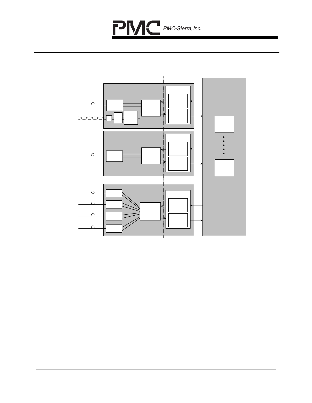
5 APPLICATION EXAMPLES
The PM3386 S/UNI-2xGE is applicable to equipment implementing high density
Gigabit Ethernet interfaces. The PM3386 is a dual channel SERDES and GMAC
with embedded FIFOs that provides a high density and low power Gigabit
Ethernet solution for direct connection to electrical optical modules. Alternatively,
a GMII interface is provided for connection to copper Gigabit Ethernet physical
layer devices.
On the system side, the POS-PHY Level 3 (32 bit synchronous FIFO style
interface clocked up to 104 MHz) allows a common connection to higher layer
devices. A common system interface simplifies multi-service equipment utilizing
some or all of the following physical layer options:
• OC-48 POS/ATM
• 4xOC-12 POS/ATM
• 16xOC-3 POS/ATM
• Channelized POS/ATM
• High density DS3
• Gigabit Ethernet
The PM3386 is particularly suited for the following applications:
• Core Routers
• Edge Routers
• Enterprise Edge Routers
• Multi-Service Switches/Routers
• SONET/SDH Transport Muxes
These applications require various interfaces (Gigabit Ethernet, ATM, POS, DS3)
which use the POS-PHY Level 3 interface. Service cards for various physical
layer options can re-use upper layer devices and board design to improve timeto market. The use of Gigabit Ethernet within Internet points of presence
(POPs), Super POPs and Transport POPs is increasing due to the requirement
of inexpensive high-speed Layer 2 interconnect. Thus, connections between
PROPRIETARY AND CONFIDENTIAL TO PMC-SIERRA, INC., AND FOR ITS CUSTOMERS’ INTERNAL USE
7

RELEASED
DATASHEET
PMC-1991129 ISSUE 7 DUAL GIGABIT ETHERNET CONTROLLER
PM3386
Edge Routers and Core Routers within a POP are provided via Gigabit Ethernet.
Co-located server clusters are also connected via Gigabit Ethernet to POP
routers. Similarly, Gigabit Ethernet is becoming the choice for connection
between Enterprise Routers and Multi-Service switches. Transport equipment is
looking to provide Ethernet directly over SONET/SDH for wide area transparent
bridging.
In a typical application the S/UNI-2xGE performs data recovery on the Gigabit
Ethernet stream, MAC level frame checks and sends the frame to an upper layer
device (such as an IP processor) for forwarding via the POS-PHY level 3
interface. The S/UNI-2xGE maintains extensive statistics for SNMP and RMON
applications. On egress, frames are formatted into physical frames with the
proper inter-frame gap, preamble and start of frame delimiter. The physical
packet is then serialized for transmission over an external electrical optical
module. The initial configuration and ongoing control and monitoring of the
S/UNI-2xGE are provided via a generic microprocessor interface. The following
diagram shows a typical multi-service card application for the PM3386 S/UNI2xGE with similar cards for OC48 and Quad OC-12 ports.
PROPRIETARY AND CONFIDENTIAL TO PMC-SIERRA, INC., AND FOR ITS CUSTOMERS’ INTERNAL USE
8
RELEASED
PM3386
DATASHEET
PMC-1991129 ISSUE 7 DUAL GIGABIT ETHERNET CONTROLLER
Figure 1 PM3386 Typical Application Example
POS-PHY
Level 3
Gigabit Ethernet
Twisted Pair
Gigabit Ethernet
OC-48
OC-12
OC-12
OC-12
OC-12
Optical
Transceiver
Mag
Optical
Transceiver
Optical
Transceiver
Optical
Transceiver
Optical
Transceiver
Optical
Transceiver
TX +/-
RX +/-
Copper
GE PHY
TX +/-
RX +/-
Quad OC-12 POS
Gigabit Ethernet
Line Card # 1
PM3386
S/UNI 2xGE
GMII
OC-48 POS
Line Card # 2
PM5381
S/UNI 2488
Line Card # n
PM5380
S/UNI 4x622
Upper Layer
Device(s)
Scheduler
Classification/
Forwarding
Upper Layer
Device(s)
Scheduler
Classification
Forwarding
Upper Layer
Device(s)
Scheduler
Classification
Forwarding
Switch Fabric
Switch Fabric
Device
Switch Fabric
Device
PROPRIETARY AND CONFIDENTIAL TO PMC-SIERRA, INC., AND FOR ITS CUSTOMERS’ INTERNAL USE
9

RELEASED
PM3386
DATASHEET
PMC-1991129 ISSUE 7 DUAL GIGABIT ETHERNET CONTROLLER
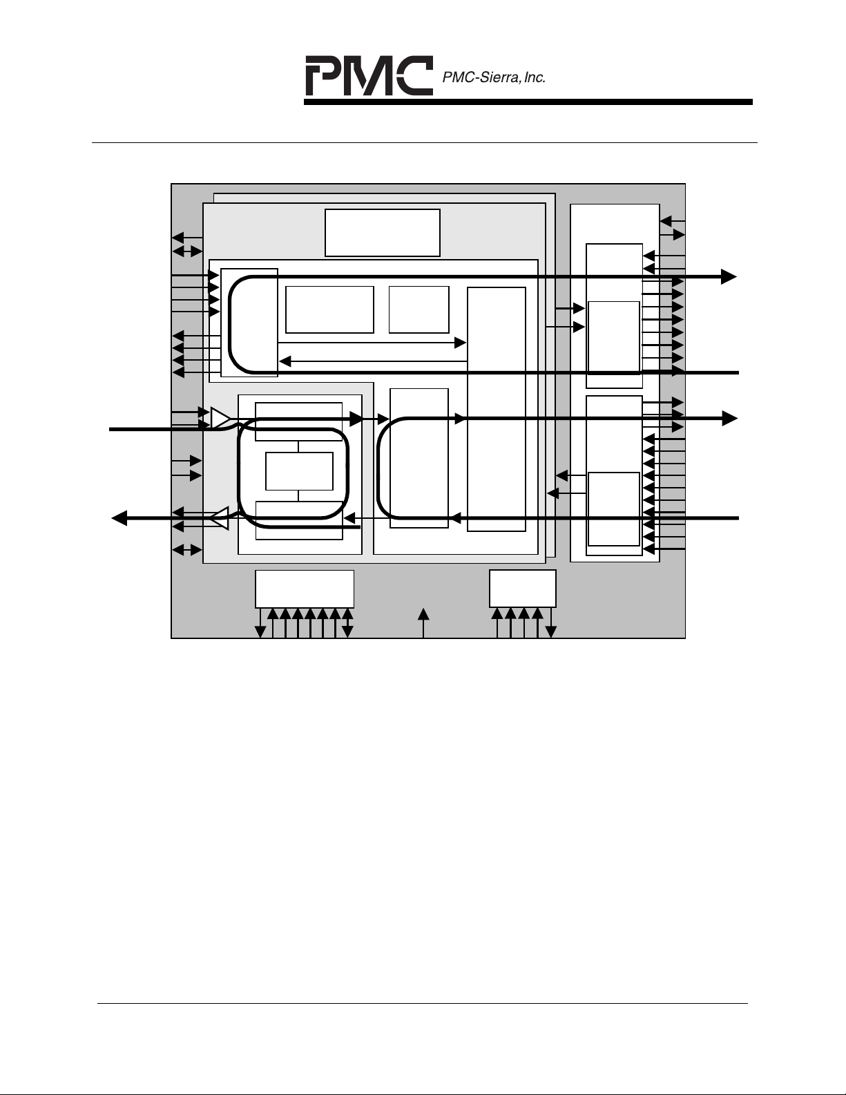
6 BLOCK DIAGRAM
Figure 2 - PM3386 Dual Gigabit Ethernet to POS-PHY Level 3
MDC
MDIO
RX_CLK
RX_DV
RX_ER
RXD [7:0]
GTX_CLK
TX_EN
TX_ER
TXD [7:0]
RXD +/-
SD
CLK125
TXD +/-
ATP[3:0]
GMII
Interface
Data Recovery/
Serial to Parallel
Parallel to Serial
Managment
Statistics
Enhanced Gigabit MAC
Flow Ctrl /
Auto-Negotiation
Address
Filtering
Gigabit
Media
Access
Controller
8B/10B
PLL Clock
Multiply
Encoder/
Decoder
SERDES PCS MAC
Microprocessor
Interface
JTAG
POS-PHY
Level 3
Ingress
Interface
POS
PHY
Ingress
FIFO
Egress
Interface
POS
PHY
Egress
FIFO
PAUSE [1:0]
PAUSED [1:0]
RFCLK
RENB
RDAT[31:0]
RMOD[1:0]
RPRTY
RVAL
RSOP
REOP
RERR
RSX
DTPA[1:0]
STPA
PTPA
TADR
TFCLK
TENB
TDAT[31:0]
TMOD[1:0]
TPRTY
TSOP
TEOP
TERR
TSX
ALE
CSB
RDB
INTB
A [10:0]
WDB
RSTB
D [15: 0]
PMD_SEL [1:0]
TMS
TRSTB
TDI
TCK
TDO
PROPRIETARY AND CONFIDENTIAL TO PMC-SIERRA, INC., AND FOR ITS CUSTOMERS’ INTERNAL USE
10
RELEASED
PM3386
DATASHEET
PMC-1991129 ISSUE 7 DUAL GIGABIT ETHERNET CONTROLLER
Figure 3 PM3386 Device Loop Back Paths
MDC
MDIO
RX_CLK
RX_DV
RX_ER
RXD [7:0]
GTX_CLK
TX_EN
TX_ER
TXD [7:0]
RXD +/-
SD
CLK125
TXD +/-
ATP[3:0]
GMII
Interface
Data Recovery/
Serial to Parallel
Parallel to Serial
Managment
Statistics
Enhanced Gigabit MAC
Flow Ctrl /
Auto-Negotiation
Address
Filtering
Gigabit
Media
Access
Controller
8B/10B
PLL Clo ck
Multiply
Encoder/
Decoder
SERDES PCS MAC
Microprocessor
Interface
JTAG
POS-PHY
Level 3
Ingress
Interface
POS
PHY
Ingress
FIFO
Egress
Interface
POS
PHY
Egress
FIFO
PAUSE [1:0]
PAUSED [1:0]
RFCLK
RENB
RDAT[31:0]
RMOD[1:0]
RPRTY
RVAL
RSOP
REOP
RERR
RSX
DTPA[1:0]
STPA
PTPA
TADR
TFCLK
TENB
TDAT[31: 0]
TMOD[1:0]
TPRTY
TSOP
TEOP
TERR
TSX
ALE
CSB
RDB
INTB
A [10:0]
WDB
RSTB
D [15:0]
PMD_SEL [1:0]
TRSTB
TDI
TCK
TDO
TMS
PROPRIETARY AND CONFIDENTIAL TO PMC-SIERRA, INC., AND FOR ITS CUSTOMERS’ INTERNAL USE
11

RELEASED
DATASHEET
PMC-1991129 ISSUE 7 DUAL GIGABIT ETHERNET CONTROLLER
PM3386
7 DESCRIPTION
The PM3386 is a monolithic integrated circuit that implements a two port full
duplex 1000 Mbit/s Gigabit Ethernet MAC data transport device. The PM3386
provides line interface connectivity provided by an on-chip SERDES and GMII
functions and data transport to the up stream device via the industry standard
POS-PHY Level 3 interface.
Serializer-Deserializer (SERDES)
The PM3386 has two internal serializer-deserializer transceivers. The SERDES
are IEEE 802.3-1998 Gigabit Ethernet compatible supporting gigabit data
transfer flows. The SERDES is based on the X3T11 10 Bit specification. The
PM3386 receives and transmits Gigabit Ethernet streams using a bit serial
interface for direct connection to optical transceiver devices. The SERDES
performs data recovery and serial to parallel conversion for connection to the
Enhanced Gigabit Media Access Control block.
Gigabit Media Independent Interface (GMII)
For Gigabit Ethernet over copper support, the PM3386 provides dual standard
GMII interfaces. A copper Gigabit Ethernet physical layer device can be
connected to the PM3386 via this interface.
Enhanced Gigabit Media Access Control (EGMAC)
The Enhanced Gigabit Media Access Control (EGMAC) block provides an
integrated IEEE 802.3-1998 Gigabit Ethernet Media Access Control (MAC)
supporting high performance 1000Base capability. The EGMAC has line side
interfaces for connection to internal (SERDES) and external Gigabit PHY via
GMII on each Gigabit Ethernet port. The Enhanced Gigabit MAC (EGMAC)
incorporates all of the Gigabit Ethernet MAC functions including AutoNegotiation, statistics, and the MAC Control Sub-layer that adheres to IEEE
802.3-1998 providing support for PAUSE control frames. The EGMAC provides
basic frame integrity checks to validate incoming frames. The EGMAC also
provides simple line rate ingress address filtering support via 8 exact-match MAC
address and VID unicast filters, one 64-bin hash-based multicast filter, and the
ability to filter or accept matched frames on a per instance programmable
fashion. All inquires for filtering are done at line rate with no system latency
introduced for look up cycles.
PROPRIETARY AND CONFIDENTIAL TO PMC-SIERRA, INC., AND FOR ITS CUSTOMERS’ INTERNAL USE
12

RELEASED
DATASHEET
PMC-1991129 ISSUE 7 DUAL GIGABIT ETHERNET CONTROLLER
PM3386
Management Statistics (MSTAT)
The PM3386 also incorporates a rich set of per port RMON, SNMP, and Etherlike
Management Information Base counters. Deep statistical counters are used for
management counts providing a minimum rollover time of greater than 58
minutes. All counts are easily managed via the Management Statistics (MSTAT)
block.
POS-PHY Level 3 Interface (PL3)
The PM3386 can connect to a single upper layer device through a POS-PHY
Level 3 Interface. The POS-PHY Level 3 interface is a 32-bit wide interface with
a clock rate from 60 to 104 MHz. POS-PHY Level 3 was developed with the
cooperation of the SATURN Development Group to cover all application bit rates
up to and including 3.2 Gbit/s. This interface provides standards support for
interoperation between the PM3386, a multiple PHY layer device, connecting to
one Link Layer device. The interface stresses simplicity of operation to allow
forward migration to more elaborate PHY and Link Layer devices. The POSPHY interface contains 64KB receive and 16KB transmit FIFOs per channel.
These FIFOs contain programmable thresholds specifying full and empty
conditions.
Receive Direction
In the receive direction, the PM3386 can be configured to use the internal
SERDES or the GMII interface on a per channel basis. For SERDES operation,
a Gigabit Ethernet bit stream is received from an external optical transceiver.
The data is recovered and converted from serial to parallel data for connection to
the EGMAC block. The EGMAC terminates the 8B/10B line codes and performs
frame integrity checks (frame length, FCS etc). For GMII operation, the physical
packet is sourced from an external copper physical layer device to the PM3386
via the GMII interface (8 bits clocked at 125 MHz). The EGMAC accepts the 8 bit
data and performs frame integrity checks once the complete frame is received.
The EGMAC can optionally filter erred frames.
Statistics are updated and the frame is sent to the POS-PHY Level 3 interface.
The FIFO’s in the POS-PHY interface accommodate system latencies and allows
for loss-less flow control up to 9.6k bytes. The received frames are then read
through the POS-PHY Level 3 (32 bits clocked from 60-104 MHz) system side
interface.
Transmit Direction
In the transmit direction, packets to be transmitted are written into the POS-PHY
TX FIFO through the POS-PHY Level 3 interface (32 bits clocked from 60-104
PROPRIETARY AND CONFIDENTIAL TO PMC-SIERRA, INC., AND FOR ITS CUSTOMERS’ INTERNAL USE
13

RELEASED
DATASHEET
PMC-1991129 ISSUE 7 DUAL GIGABIT ETHERNET CONTROLLER
PM3386
MHz) from the upper layer device. The channel is selected by the upper layer
device and is indicated in-band on the POS-PHY interface. The EGMAC builds a
properly formatted Ethernet physical packet (padding to minimum size and
inserting the preamble, start of frame delimiter (SFD) and the inter-packet gap
(IPG)). Statistics are updated and the physical packet is sent to the SERDES or
the GMII interface.
For SERDES operation, the EGMAC encodes the physical packet using 8B/10B
encoding and passes the physical packet to the SERDES block. The SERDES
performs parallel to serial conversion using an internally synthesized 1250 MHz
clock. The bit stream is sent to an external optical transceiver for transmission
over fiber cable. For GMII operation, the EGMAC sends the physical packet byte
by byte across the GMII interface (8 bits clocked at 125 MHz) to an external
copper Gigabit Ethernet physical layer device. The copper Gigabit Ethernet
physical layer device then transmits the physical packet over copper cable.
Flow Control
Flow control is handled in the EGMAC block. When a PAUSE control frame is
received, the PM3386 will optionally terminate transmission (after the current
frame is sent) and assert the appropriate channel side band flow control output
to indicate the paused condition. The received PAUSE control frame can be
optionally filtered or passed to the link layer device via the POS-PHY Level 3
interface.
PAUSE control frames are transmitted either under link layer control using
channel side band flow control inputs, under link layer control transparent to the
PM3386, host based PAUSE frame control or under internal control based on
receive FIFO levels. All four methods can provide for loss-less flow control.
General
The PM3386 is configured, controlled and monitored via a generic 16-bit
microprocessor bus interface. The PM3386 also provides a standard 5 signal
IEEE 1149.1 JTAG test port for boundary scan board test purposes.
The PM3386 is implemented in low power, +1.8 Volt, CMOS technology with 5V
TTL compatible digital inputs and 3.3V TTL/CMOS compatible digital outputs.
The PM3386 is packaged in a 352-pin UBGA package.
PROPRIETARY AND CONFIDENTIAL TO PMC-SIERRA, INC., AND FOR ITS CUSTOMERS’ INTERNAL USE
14

RELEASED
DATASHEET
PMC-1991129 ISSUE 7 DUAL GIGABIT ETHERNET CONTROLLER
PM3386
8 PIN DIAGRAM
The PM3386 is packaged in a 352-pin Ultra Ball Grid Array (UBGA) having a
body size of 27mm by 27mm.
Table 1 PM3386 Pin Diagram
26 25 24 23 22 21 20 19 18 17 16 15 14 13 12 11 10 9 8 7 6 5 4 3 2 1
RXD1
RXD1
VSS VSS NC
VSS VDDO VSS NC
VSS VSS VDDO NC
VSS VSS VDDO VDDO NC
VSS NC VDDO NC NC NC NC NC
PMD_
VSSQ
SEL1
CLK1
VSS
25
AVDH AVDQ AVDL AVDL VDDO
RXSD
VSS
1
RXD1+RXD1
-
VSS AVDH AVDH NC VDDQ
TXD1-TXD1
+
AVDL AVDL AVDH AVDL VDDO
AVDL AVDL AVDQ AVDL
RXD0-RXD0+RXSD
VSS AVDL AVDL VDDO
TXD0+TXD0
-
VSS NC
TXD0
TXD0
[3]
[2]
TXD0
VSS
[5]
TXD0
NC
[7]
VSS NC VDDO NC NC NC VSSQ
VSS VSS VDDO VDDO VDDI
VSS VSS VDDO NC
VSS VDDO VSS
VSS VSS
[2]
VDDI VDDI NC NC NC
VDDQ AVDL NC RSTB
AVDH VDDO NC
AVDL AVDL
ATP0 ATP1 VDDI
AVDH VDDI
0
AVDH NC RSX
PMD_
VDDI VDDO RERR REOP
SEL0
TXD0
TXD0
[0]
[1]
TXD0
VDDO
[4]
TXD0
VDDI NC VDDQ
[6]
TX_EN0RX_DV0RXD0
TX_ER0RX_ER0RXD0
RX_ER1TX_EN1TXD1
[6]
RXD1
RXD1
[3]
[7]
RXD1
RXD1
[0]
[4]
RXD1
[1]
RX_C
LK0
GTX_
RXD0
CLK0
[7]
[5]
RXD0
[6]
[3]
RX_C
LK1
RX_DV1GTX_
RXD1
[5]
VDDI VDDO NC
RXD0
[4]
RXD0
[2]
RXD0
[0]
TXD1
[5]
[2]
TX_ER1TXD1
[4]
TXD1
CLK1
[7]
VDDI VDDO
RXD0
MDC
[1]
TDAT
MDIO
[29]
TDAT
TDAT
[30]
[27]
VSSQ ALE CSB VSS VSS A[6] A[3] A[1]
TXD1
INTB RDB A[9] A[8] A[5] A[2]
[1]
TXD1
TXD1
[3]
[0]
TXD1
VDDI VDDQ NC VDDO VDDI
[6]
TDAT
VDDI VDDQ VDDO NC
[31]
TDAT
TDAT
[28]
[25]
TDAT
TDAT
[26]
[23]
TDAT
TDAT
[24]
[22]
A[10
WRB
TDAT
[21]
TDAT
[20]
VSSQ VSS VSS
A[7] A[4] A[0]
]
TDAT
TDAT
[19]
[16]
TDAT
TDAT
[18]
[17]
TDAT
[11]
TDAT
[13]
TDAT
[14]
TDAT
[15]
D[15]D[11
D[12
]
D[14
VDDI NC VDDO D[0] TDO NC VDDO NC NC NC
]
TDAT
VDDI
[2]
TDAT
TDAT
[8]
[5]
TDAT
TDAT
[10]
[7]
TDAT
TDAT
[12]
[9]
D[13]D[10
]
D[9] D[6] D[3] TCK
VDDO VDDI
TDAT
[1]
TDAT
[4]
TDAT
[6]
D[7] D[4] D[1] TDI NC VSS VSS
]
D[8] D[5] D[2] TMS NC VSS VDDO VSS
TRST
NC VDDO VSS NC
B
RDAT
[2]
RDAT
[4]
RDAT
RDAT
[5]
[8]
RDAT
[10]
RDAT
[14]
RDAT
[17]
RDAT
RDAT
[21]
[20]
RDAT
[24]
RDAT
RDAT
[30]
[28]
RPRTYRDAT
VDDI RVAL
PAUSE1PAUS
ED0
TMOD
VDDI NC VDDO NC NC NC
[1]
TENB TEOP
TDAT
[0]
TDAT
[3]
TMOD
[0]
TPRT
TSX
Y
TFCL
TSOP TERR PTPA
K
STPA NC VDDO VSS NC
DTPA
TADR
VSS VDDO VSS
[1]
DTPA
[0]
RDAT
RDAT
VDDI
[1]
RDAT
RDAT
[3]
RDAT
VSSQ
[7]
RDAT
RDAT
[9]
[11]
RDAT
RDAT
[12]
[13]
RDAT
RDAT
[15]
[16]
RDAT
[18]
RDAT
[19]
RDAT
RDAT
[23]
[22]
RDAT
RDAT
[26]
[25]
RDAT
[29]
[27]
RDAT
[31]
RMOD
RFCL
[1]
RMOD
RSOP
PAUS
RENB
ED1
PAUS
VSS VSS
[0]
[6]
VSS
VSS
[0]
E0
A
B
C
D
E
F
G
H
J
K
L
M
N
P
R
T
U
V
W
K
Y
AA
AB
AC
AD
AE
AF
PROPRIETARY AND CONFIDENTIAL TO PMC-SIERRA, INC., AND FOR ITS CUSTOMERS’ INTERNAL USE
15

RELEASED
DATASHEET
PMC-1991129 ISSUE 7 DUAL GIGABIT ETHERNET CONTROLLER
PM3386
9 PIN DESCRIPTION
Table 2 - Serial Line Side Interface Signals
Pin Name Type Pin No. Function
CLK125 Schmitt
G25
Input
RXD0+
RXD0-
Differential
PECL
Input
R25
R26
RXSD0 Input R24
PHY Reference Clock (Port 0)
125 MHz reference clock used to generate
GTX_CLK0 or GTX_CLK1 during GMII
mode. The Clock Synthesis Unit uses this
clock as it’s input reference during
SERDES mode.
Please refer to the Operations section for a
discussion of clock mode selection
interfacing issues.
Receive Differential Data (Port 0)
These PECL inputs (RXD0+/-) contain the
8B/10B bit serial receive stream. The
receive data is recovered from the RXD0+/bit stream.
Receive Signal Detect (Port 0)
RXSD0 indicates the presence of valid
receive signal power from the Optical
Physical Medium Dependent Device. A
logic level high indicates the presence of
valid data. A logic low indicates a loss of
signal.
RXD1+
RXD1-
Differential
PECL
Input
K26
K25
Receive Differential Data (Port 1)
The PECL inputs RXD1+/- contain the
8B/10B bit serial receive stream. The
receive data is recovered from the RXD1+/bit stream.
PROPRIETARY AND CONFIDENTIAL TO PMC-SIERRA, INC., AND FOR ITS CUSTOMERS’ INTERNAL USE
16

RELEASED
DATASHEET
PMC-1991129 ISSUE 7 DUAL GIGABIT ETHERNET CONTROLLER
PM3386
Pin Name Type Pin No. Function
RXSD1 Input J25
TXD0+
TXD0-
TXD1+
TXD1-
ATP0
ATP1
Differential
PECL
Output
Differential
PECL
Output
BiDirectional
CMOS
U26
U25
M25
M26
M24
M23
Receive Signal Detect (Port 1)
RXSD1 indicates the presence of valid
receive signal power from the Optical
Physical Medium Dependent Device. A
logic level high indicates the presence of
valid data. A logic low indicates a loss of
signal.
Transmit Differential Data (Port 0)
The PECL outputs TXD0+/- contain the
1.25 Gbit/s transmit stream. The TXD0+/outputs are driven using the CSU clock.
Transmit Differential Data (Port 1)
The PECL outputs TXD1+/- contain the
1.25 Gbit/s transmit stream. The TXD1+/outputs are driven using the CSU clock.
Receive and Transmit Analog Test Ports
The ATP[1:0] pins are used for
manufacturing testing only and should be
tied to analog ground.
Table 3 -Gigabit Media Independent Interface (GMII)
Signal Name Direction Pin No. Function
GTX_CLK0 Output AD22
GMII Transmit Clock (Port 0)
125 MHz reference clock supplied by the
PM3386.
TXD0[0]
TXD0[1]
TXD0[2]
TXD0[3]
TXD0[4]
TXD0[5]
TXD0[6]
TXD0[7]
PROPRIETARY AND CONFIDENTIAL TO PMC-SIERRA, INC., AND FOR ITS CUSTOMERS’ INTERNAL USE
Output W24
W23
W25
W26
Y24
Y25
AA24
AA25
GMII Transmit Data (Port 0)
Byte-wide transmit data is output on these
pins synchronously to the PHY device.
The least significant bit, TXD0[0] is the first
bit transferred on the line.
This signal is updated on the rising edge of
GTX_CLK0.
17

RELEASED
DATASHEET
PMC-1991129 ISSUE 7 DUAL GIGABIT ETHERNET CONTROLLER
PM3386
Signal Name Direction Pin No. Function
TX_EN0 Output AE23
TX_ER0 Output AF24
Transmit Enable (Port 0)
When in GMII mode this signal is an active
high signal asserted when valid data is
present on the TXD0[7:0] and TX_ER0
pins. This signal is updated on the rising
edge of GTX_CLK0.
When in SERDES mode this signal
enables operation of the external
transmitter. When asserted (default active
low) it indicates the potential presence of
valid transmit data. When de-asserted
indicates the absence of valid transmit
data. Note that while in SERDES mode
the polarity of this signal is programmable
to support interoperability with differing
optical transmitters.
GMII Transmit Coding Error (Port 0)
Active high signal asserted when an error
is detected during transmission. Please
refer to the Operations section for a full
listing of error conditions reported by the
PM3386 using the TX_ER0 output.
This signal is updated on the rising edge of
GTX_CLK0.
RX_CLK0 Schmitt
Input
AC21
GMII Receive Clock (Port 0)
125 MHz GMII reference clock received
from the PHY device.
RXD0[0]
RXD0[1]
RXD0[2]
RXD0[3]
RXD0[4]
RXD0[5]
RXD0[6]
RXD0[7]
PROPRIETARY AND CONFIDENTIAL TO PMC-SIERRA, INC., AND FOR ITS CUSTOMERS’ INTERNAL USE
Input AF20
AD19
AE20
AF21
AD20
AE21
AF22
AD21
GMII Receive Data (Port 0)
Byte-wide receive data is input on these
pins synchronously from the PHY device.
The least significant bit, RXD0[0] is
expected to contain the first bit received on
the line.
This signal is synchronized to RX_CLK0.
18

RELEASED
DATASHEET
PMC-1991129 ISSUE 7 DUAL GIGABIT ETHERNET CONTROLLER
PM3386
Signal Name Direction Pin No. Function
RX_DV0 Input AE22
RX_ER0 Input AF23
GTX_CLK1 Output C19
TXD1[0]
TXD1[1]
TXD1[2]
TXD1[3]
TXD1[4]
TXD1[5]
Output C16
B17
A18
C17
B18
A19
GMII Receive Data Valid (Port 0)
Active high signal asserted when valid data
is present on the RXD0[7:0] and RX_ER0
pins.
This signal is synchronized to RX_CLK0.
GMII Receive Error (Port 0)
Active high signal asserted when there has
been an error during the received physical
packet.
This signal is synchronized to RX_CLK0.
GMII Transmit Clock (Port 1)
125 MHz reference clock supplied by the
PM3386.
GMII Transmit Data (Port 1)
Byte-wide transmit data is output on these
pins synchronously to the PHY device.
The least significant bit, TXD1[0] is the first
bit transferred on the line.
This signal is updated on the rising edge of
GTX_CLK1.
TXD1[6]
TXD1[7]
PROPRIETARY AND CONFIDENTIAL TO PMC-SIERRA, INC., AND FOR ITS CUSTOMERS’ INTERNAL USE
D17
C18
19

RELEASED
DATASHEET
PMC-1991129 ISSUE 7 DUAL GIGABIT ETHERNET CONTROLLER
PM3386
Signal Name Direction Pin No. Function
TX_EN1 Output A20
TX_ER1 Output B19
Transmit Enable (Port 1)
When in GMII mode this signal is an active
high signal asserted when valid data is
present on the TXD1[7:0] and TX_ER1
pins. This signal is updated on the rising
edge of GTX_CLK1.
When in SERDES mode this signal
enables operation of the external
transmitter. When asserted (default active
low) it indicates the potential presence of
valid transmit data. When de-asserted
indicates the absence of valid transmit
data. Note that while in SERDES mode
the polarity of this signal is programmable
to support interoperability with differing
optical transmitters.
GMII Transmit Coding Error (Port 1)
Active high signal asserted when an error
is detected during transmission. Please
refer to the Operations section for a full
listing of error conditions reported by the
PM3386 using the TX_ER1 output. This
signal is updated on the rising edge of
GTX_CLK1.
RX_CLK1 Schmitt
Input
B20
GMII Receive Clock (Port 1)
125 MHz GMII reference clock received
from the PHY device.
RXD1[0]
RXD1[1]
RXD1[2]
RXD1[3]
RXD1[4]
RXD1[5]
RXD1[6]
RXD1[7]
PROPRIETARY AND CONFIDENTIAL TO PMC-SIERRA, INC., AND FOR ITS CUSTOMERS’ INTERNAL USE
Input C22
D21
A23
B22
C21
D20
A22
B21
GMII Receive Data (Port 1)
Byte-wide receive data is input on these
pins synchronously from the PHY device.
The least significant bit, RXD1[0] is
expected to contain the first bit received on
the line.
This signal is synchronized to RX_CLK1.
20

RELEASED
DATASHEET
PMC-1991129 ISSUE 7 DUAL GIGABIT ETHERNET CONTROLLER
PM3386
Signal Name Direction Pin No. Function
RX_DV1 Input C20
RX_ER1 Input A21
MDC Output AD18
MDIO I/O
AE19
Internal
pull-down
GMII Receive Data Valid (Port 1)
Active high signal asserted when valid data
is present on the RXD1[7:0] and RX_ER1
pins.
This signal is synchronized to RX_CLK1
GMII Receive Error (Port 1)
Active high signal asserted when there has
been an error during the received physical
packet.
This signal is synchronized to RX_CLK1.
MII Management Data Clock
MDC provides the MII reference clock for
communication between the PM3386 and
other transceivers.
MII Management Data
When configured as an input, the external
PHY supplies status during MII
Management read cycles. When
configured as an output, the PM3386
supplies control during MII Management
write/read cycles and data during MII
Management write cycles.
Data values on the MDIO pin are updated
and sampled on the rising edge of MDC.
Table 4 -POS-PHY Level 3 Transmit Interface
Signal Name Direction Pin No. Function
TFCLK Schmitt
Input
AF7
POS-PHY Transmit FIFO Write Clock
TFCLK is used to synchronize data transfer
transactions between the higher layer
device and the PM3386. TFCLK cycles at
a 60 to 104 MHz rate.
PROPRIETARY AND CONFIDENTIAL TO PMC-SIERRA, INC., AND FOR ITS CUSTOMERS’ INTERNAL USE
21

RELEASED
DATASHEET
PMC-1991129 ISSUE 7 DUAL GIGABIT ETHERNET CONTROLLER
PM3386
Signal Name Direction Pin No. Function
TDAT[0]
TDAT[1]
TDAT[2]
TDAT[3]
TDAT[4]
TDAT[5]
TDAT[6]
TDAT[7]
TDAT[8]
TDAT[9]
TDAT[10]
TDAT[11]
TDAT[12]
TDAT[13]
TDAT[14]
TDAT[15]
TDAT[16]
TDAT[17]
TDAT[18]
TDAT[19]
TDAT[20]
TDAT[21]
TDAT[22]
TDAT[23]
TDAT[24]
TDAT[25]
TDAT[26]
TDAT[27]
TDAT[28]
TDAT[29]
TDAT[30]
TDAT[31]
Input
AE8
AD9
AC10
AF8
AE9
AD10
AF9
AE10
AD11
AF10
AE11
AC12
AF11
AD12
AE12
AF12
AD13
AE13
AE14
AD14
AE15
AD15
AF16
AE16
AF17
AD16
AE17
AF18
AD17
AE18
AF19
AC17
POS-PHY Transmit Packet Data Bus
This bus carries the packet octets that are
written to the selected transmit FIFO and
the in-band port address to select the
desired transmit FIFO. The TDAT bus is
considered valid only when TENB is
simultaneously asserted.
When a 32-bit interface is used, data must
be transmitted in big endian order on
TDAT[31:0].
TDAT[31:0] is sampled on the rising edge
of TFCLK.
PROPRIETARY AND CONFIDENTIAL TO PMC-SIERRA, INC., AND FOR ITS CUSTOMERS’ INTERNAL USE
22

RELEASED
DATASHEET
PMC-1991129 ISSUE 7 DUAL GIGABIT ETHERNET CONTROLLER
PM3386
Signal Name Direction Pin No. Function
TERR Input AF5
TENB Input AD8
POS-PHY Transmit Error Indicator
Active high signal used to indicate that the
current packet must be aborted. TERR
should only be considered valid when
TENB and TEOP are simultaneously
asserted.
TERR is sampled on the rising edge of
TFCLK.
POS-PHY Transmit Write Enable
Active low signal used to control the flow of
data to the transmit FIFOs.
When TENB is high, the TDAT[31:0],
TMOD, TSOP, TEOP, TPRTY and TERR
signals are invalid and are ignored by the
PM3386. However, the TSX signal if
asserted is valid and is processed by the
PM3386 only when TENB is high.
When TENB is low, the TDAT[31:0], TMOD,
TSOP, TEOP, TPRTY and TERR signals
are valid and are processed by the
PM3386. The TSX signal is ignored by the
PM3386 when TENB is low.
TENB is sampled on the rising edge of
TFCLK.
TPRTY Input AE6
POS-PHY Transmit bus parity
The transmit parity (TPRTY) signal
indicates the parity calculated over the
TDAT bus. TPRTY is considered valid only
when TENB or TSX are asserted.
By default the PM3386 uses odd parity.
The PM3386 supports both even and odd
parity. The PM3386 reports any parity error
to the host processor via a maskable
interrupt, but does not interfere with the
transferred data.
TPRTY is sampled on the rising edge of
TFCLK.
PROPRIETARY AND CONFIDENTIAL TO PMC-SIERRA, INC., AND FOR ITS CUSTOMERS’ INTERNAL USE
23

RELEASED
DATASHEET
PMC-1991129 ISSUE 7 DUAL GIGABIT ETHERNET CONTROLLER
PM3386
Signal Name Direction Pin No. Function
TMOD[0]
TMOD[1]
Input AD6
AC7
TSX Input AE7
POS-PHY Transmit Word Modulo
TMOD[1:0] indicates the number of valid
bytes of data in TDAT[31:0]. The TMOD
bus should always be all zero, except
during the last double-word transfer of a
packet on TDAT[31:0]. When TEOP and
TENB are asserted, the number of valid
packet data bytes on TDAT[31:0] is
specified by TMOD[1:0].
TMOD[1:0] = “00” TDAT[31:0] valid
TMOD[1:0] = “01” TDAT[31:8] valid
TMOD[1:0] = “10” TDAT[31:16] valid
TMOD[1:0] = “11” TDAT[31:24] valid
TMOD [1:0] is sampled on the rising edge
of TFCLK.
POS-PHY Transmit Start of Transfer
Active high signal indicating when the inband port address is present on the
TDAT[31:0] bus. When TSX is high and
TENB is high (not asserted), the value of
contained within TDAT[7:0] is the address
of the transmit FIFO to be selected.
TDAT[7:0] == 0 selects channel zero.
TDAT[7:0] == 1 selects channel one.
Subsequent data transfers on the TDAT
bus will fill the FIFO specified by this inband address.
If TDAT[7:0] is not 0 or 1 no channel within
the PM3386 device will be selected.
Subsequent data transfers on the TDAT
bus to address outside of 0 or 1 will be
dropped at the PL3 interface.
TSX is considered valid only when TENB is
not asserted.
TSX is sampled on the rising edge of
TFCLK.
PROPRIETARY AND CONFIDENTIAL TO PMC-SIERRA, INC., AND FOR ITS CUSTOMERS’ INTERNAL USE
24

RELEASED
DATASHEET
PMC-1991129 ISSUE 7 DUAL GIGABIT ETHERNET CONTROLLER
PM3386
Signal Name Direction Pin No. Function
TSOP Input AF6
TEOP Input AD7
POS-PHY Transmit Start of Packet
Active high signal used to delineate the
packet boundaries on the TDAT bus.
When TSOP is high, the start of the packet
is present on the TDAT bus.
TSOP is required to be present at the
beginning of every packet and is
considered valid only when TENB is
asserted.
TSOP is sampled on the rising edge of
TFCLK.
POS-PHY Transmit End of Packet
Active high signal used to delineate the
packet boundaries on the TDAT bus.
When TEOP is high, the end of the packet
is present on the TDAT bus.
Note that TMOD[1:0] indicates the number
of valid bytes the last double word is
composed of when TEOP and TENB are
asserted.
TEOP is required to be present at the end
of every packet and is considered valid only
when TENB is asserted.
TEOP is sampled on the rising edge of
TFCLK.
PROPRIETARY AND CONFIDENTIAL TO PMC-SIERRA, INC., AND FOR ITS CUSTOMERS’ INTERNAL USE
25

RELEASED
DATASHEET
PMC-1991129 ISSUE 7 DUAL GIGABIT ETHERNET CONTROLLER
PM3386
Signal Name Direction Pin No. Function
TADR Input AE5
PTPA Output AF4
POS-PHY Transmit PHY Address
The TADR signal is used with the PTPA
signal to poll the transmit FIFOs packet
available status.
When TADR is sampled on the rising edge
of TFCLK by the PM3386, the polled
packet available indication PTPA signal is
updated with the status of the port specified
by the TADR address on the following rising
edge of TFCLK.
TADR = 0 = channel 0
TADR = 1 = channel 1
TADR is sampled on the rising edge of
TFCLK.
POS-PHY Polled-PHY Transmit Packet
Available
PTPA transitions high when a predefined
(user programmable) minimum number of
bytes are available in the polled transmit
FIFO. Once high, PTPA indicates that the
transmit FIFO is not full. When PTPA
transitions low, it indicates that the transmit
FIFO is full or near full (user
programmable).
PTPA allows the polling of the PM3386
channel selected by TADR address pin.
The port which PTPA reports is updated on
the following rising edge of TFCLK after the
PM3386 channel address on TADR is
sampled by the PM3386 device.
PTPA is updated on the rising edge of
TFCLK.
PROPRIETARY AND CONFIDENTIAL TO PMC-SIERRA, INC., AND FOR ITS CUSTOMERS’ INTERNAL USE
26

RELEASED
DATASHEET
PMC-1991129 ISSUE 7 DUAL GIGABIT ETHERNET CONTROLLER
PM3386
Signal Name Direction Pin No. Function
STPA Output AD5
POS-PHY Selected-PHY Transmit Packet
Available
STPA transitions high when a predefined
(user programmable) minimum number of
bytes are available in the transmit FIFO
specified by the in-band address on TDAT
bus. Once high, STPA indicates the
transmit FIFO is not full. When STPA
transitions low, it indicates that the transmit
FIFO is full or near full (user
programmable).
STPA always provides status indication for
the selected port of the PM3386 device in
order to avoid FIFO overflows while polling
is performed. The port which STPA reports
is updated on the following rising edge of
TFCLK after the PM3386 channel address
on TDAT is sampled by the PM3386
device.
STPA is updated on the rising edge of
TFCLK.
DTPA0
DTPA1
Output AF3
AE4
POS-PHY Direct Transmit Packet
Available
Active high signals that provide direct
status indication for the corresponding
ports in the PM3386. DTPA[1:0] transitions
high when a predefined (user
programmable) minimum number of byes
are available in the transmit FIFO. Once
high, the DTPA[1:0] signals indicate that its
corresponding transmit FIFO is not full.
When DTPA[1:0] transitions low, it indicates
that its transmit FIFO is full or near full.
(user programmable).
DTPA0 corresponds to channel zero.
DTPA1 corresponds to channel one.
DTPA0 and DTPA1 are updated on the
rising edge of TFCLK.
PROPRIETARY AND CONFIDENTIAL TO PMC-SIERRA, INC., AND FOR ITS CUSTOMERS’ INTERNAL USE
27

RELEASED
DATASHEET
PMC-1991129 ISSUE 7 DUAL GIGABIT ETHERNET CONTROLLER
PM3386
Table 5 - POS-PHY Level 3 Receive Interface
Signal Name Direction Pin No. Function
RFCLK Schmitt
W1
Input
RVAL Output W3
POS-PHY Receive FIFO Write Clock
RFCLK is used to synchronize data
transfer transactions between the higher
layer device and the PM3386. RFCLK
cycles at a rate of 60 to 104 MHz.
POS-PHY Receive Data Valid
Active high signal indicating the validity of
the receive data signals. RVAL will
transition low when a receive FIFO is
empty, at the end of a data burst from a
given channel.
When RVAL is high, the RDAT[31:0],
RPRTY, RMOD[1:0], RSOP, REOP and
RERR signals are valid. When RVAL is
low, the RDAT[31:0], RPRTY, RMOD[1:0],
RSOP, REOP and RERR signals are
invalid and must be disregarded.
The RSX signal is only valid when RVAL is
low.
RVAL is updated on the rising edge of
RFCLK.
PROPRIETARY AND CONFIDENTIAL TO PMC-SIERRA, INC., AND FOR ITS CUSTOMERS’ INTERNAL USE
28

RELEASED
DATASHEET
PMC-1991129 ISSUE 7 DUAL GIGABIT ETHERNET CONTROLLER
PM3386
Signal Name Direction Pin No. Function
RENB Input AA1
POS-PHY Receive Read Enable
Active low signal used to control the flow of
data from the PM3386.
The higher layer device may de-assert
RENB at anytime if it is unable to accept
data from the PM3386.
When RENB is sampled low by the
PM3386, the upper level device is signaling
that it can receive data.
RSX may then be asserted to indicate a
new address on the RDAT[0] bus pin or
RVAL may be asserted indicating validity of
read data and control on the RDAT[31:0],
RPRTY, RMOD[1:0], RSOP, REOP, and
RERR signals. Note that these signals will
be updated on the following rising edge of
the RFCLK.
When RENB is sampled high by the
PM3386, the upper level device is signaling
that it can no longer accept data.
On the following rising edge of RFCLK, if
active, the RVAL signal will remain
asserted signifying valid data and control
on RDAT[31:0], RPRTY, RMOD[1:0],
RSOP, REOP, and RERR.
RENB is sampled on the rising edge of
RFCLK.
PROPRIETARY AND CONFIDENTIAL TO PMC-SIERRA, INC., AND FOR ITS CUSTOMERS’ INTERNAL USE
29

RELEASED
DATASHEET
PMC-1991129 ISSUE 7 DUAL GIGABIT ETHERNET CONTROLLER
PM3386
Signal Name Direction Pin No. Function
RDAT[0]
RDAT[1]
RDAT[2]
RDAT[3]
RDAT[4]
RDAT[5]
RDAT[6]
RDAT[7]
RDAT[8]
RDAT[9]
RDAT[10]
RDAT[11]
RDAT[12]
RDAT[13]
RDAT[14]
RDAT[15]
RDAT[16]
RDAT[17]
RDAT[18]
RDAT[19]
RDAT[20]
RDAT[21]
RDAT[22]
RDAT[23]
RDAT[24]
RDAT[25]
RDAT[26]
RDAT[27]
RDAT[28]
RDAT[29]
RDAT[30]
RDAT[31]
Output
F1
G2
H3
H2
J3
K4
H1
J2
K3
K2
L3
K1
L2
L1
M3
M2
M1
N3
N2
P2
P3
P4
R1
R2
R3
T1
T2
U1
T3
U2
T4
V1
POS-PHY Receive Packet Data Bus
The RDAT[31:0] bus carries the packet
octets that are read from the receive FIFO
and the in-band port address of the
selected receive FIFO.
The in-band address on RDAT[0] is
considered valid only when RVAL is deasserted (LOW) and RSX is asserted
(HIGH).
The data on RDAT[31:0] is considered valid
only when RVAL is asserted(HIGH).
Data is presented on the data bus in big
endian order on RDAT[31:0].
RDAT[31:0] is updated on the rising edge
of RFCLK.
PROPRIETARY AND CONFIDENTIAL TO PMC-SIERRA, INC., AND FOR ITS CUSTOMERS’ INTERNAL USE
30

RELEASED
DATASHEET
PMC-1991129 ISSUE 7 DUAL GIGABIT ETHERNET CONTROLLER
PM3386
Signal Name Direction Pin No. Function
RPRTY Output U3
RMOD[0]
RMOD[1]
Output Y1
W2
POS-PHY Receive Parity
The receive parity (RPRTY) signal
indicates the parity calculated over the
RDAT bus. RPRTY is only valid when
RVAL or RSX is asserted. The PM3386
supports both odd and even parity over the
RDAT bus.
RPRTY is updated on the rising edge of
RFCLK.
POS-PHY Receive Word Modulo
RMOD[1:0] indicates the number of valid
bytes of data in RDAT[31:0]. The RMOD
bus must always be zero, except during the
last double-word transfer of a packet on
RDAT[31:0]. When REOP and RVAL are
asserted, the number of valid packet data
bytes on RDAT[31:0] is specified by
RMOD[1:0].
RMOD[1:0] = “00” RDAT[31:0] valid
RSOP Output Y2
RMOD[1:0] = “01” RDAT[31:8] valid
RMOD[1:0] = “10” RDAT[31:16] valid
RMOD[1:0] = “11” RDAT[31:24] valid
RMOD[1:0] is considered valid only when
RVAL and REOP are asserted.
RMOD[1:0] is updated on the rising edge of
RFCLK.
POS-PHY Receive Start of Packet
Active high signal used to delineate the
packet boundaries on the RDAT bus.
When RSOP is high, the start of the packet
is present on the RDAT bus.
RSOP is required to be present at the start
of every packet and is only considered
valid when RVAL is asserted.
RSOP is updated on the rising edge of
RFCLK.
PROPRIETARY AND CONFIDENTIAL TO PMC-SIERRA, INC., AND FOR ITS CUSTOMERS’ INTERNAL USE
31

RELEASED
DATASHEET
PMC-1991129 ISSUE 7 DUAL GIGABIT ETHERNET CONTROLLER
PM3386
Signal Name Direction Pin No. Function
REOP Output V2
RERR Output V3
POS-PHY Receive End Of Packet
Active high signal used to delineate the
packet boundaries on the RDAT bus.
When REOP is high, the end of the packet
is present on the RDAT bus.
Note that RMOD[1:0] indicates the number
of valid bytes the last double word is
composed of when REOP and RVAL are
asserted.
REOP is required to be present at the end
of every packet and is considered valid
only when RVAL is asserted.
REOP is updated on the rising edge of
RFCLK.
POS-PHY Receive error indicator
Active high signal used to indicate that the
current packet is aborted and should be
discarded. RERR shall only be asserted
when REOP and RVAL are asserted.
Conditions that can cause RERR to be set
may be, but are not limited to, FIFO
overflow, abort sequence detection and
FCS error.
RERR is updated on the rising edge of
RFCLK.
PROPRIETARY AND CONFIDENTIAL TO PMC-SIERRA, INC., AND FOR ITS CUSTOMERS’ INTERNAL USE
32

RELEASED
DATASHEET
PMC-1991129 ISSUE 7 DUAL GIGABIT ETHERNET CONTROLLER
PM3386
Signal Name Direction Pin No. Function
RSX Output U4
POS-PHY Receive Start of Transfer
RSX indicates when the in-band port
address is present on the RDAT bus.
When RSX is high and RVAL is low, the
value of RDAT[0] is the address of the
receive FIFO to be selected by the
PM3386. Subsequent data transfers on
the RDAT bus will be from the FIFO
specified by this in-band address.
RSX is considered valid only when RVAL is
not asserted.
RSX is considered valid only when RENB
was asserted on the previous cycle.
RSX is updated on the rising edge of
RFCLK.
Table 6 - Side-band Flow Control
Name Type Pin No. Description
PAUSE0
PAUSE1
Input
Internal
pull-down
AB1
Y4
PAUSE Control
Assertion of the PAUSE0 or PAUSE1
signals may cause (programmed option)
the PM3386 on a per channel basis to
transmit 802.3-1998 PAUSE frames and
either drop at the MAC layer or pass to the
POS-PHY L3 client any further incoming
frames (programmed option). De-assertion
of the PAUSE0 or PAUSE1 signal can
cause the removal of the PAUSE condition
on a per channel basis.
Due to the programmability options for
these pins please see the PAUSE flow
control section in the Operations section.
PAUSE0 and PAUSE1 are active high
signals.
PAUSE0 and PAUSE1 are sampled on the
rising edge of the RFCLK.
PROPRIETARY AND CONFIDENTIAL TO PMC-SIERRA, INC., AND FOR ITS CUSTOMERS’ INTERNAL USE
33

RELEASED
DATASHEET
PMC-1991129 ISSUE 7 DUAL GIGABIT ETHERNET CONTROLLER
PM3386
PAUSED0
PAUSED1
Output Y3
AA2
PAUSED Status
The PAUSED0 and PAUSED1 signals
indicate the reception and execution of
802.3-1998 PAUSE control frames on the
given port of the PM3386.
An asserted (high) PAUSED0 or PAUSED1
pin indicates that the corresponding
channels ingress PAUSE timer is non-zero.
This also typically indicates (if enabled via
the FCRX bit in the EGMAC GMACC1-
Config Register) that the given channel is
in a paused state.
De-assertion of the PAUSED0 or
PAUSED1 pin indicates that the
corresponding channels PAUSE counter is
now zero. This also typically indicates that
the given channel is no longer pausing on
that channel. Please refer to the FCRX bit
definition for more information.
PAUSED0 and PAUSED1 are updated on
the rising edge of RFCLK.
Table 7 Microprocessor Interface
Pin Name Type Pin No. Function
CSB Input A15
Active-low chip select
The CSB signal is low during PM3386
register accesses.
If CSB is not required (i.e., registers
accesses are controlled using the RDB and
WRB signals only), CSB must be
connected tied low.
RDB Input B15
Active-low read enable
The RDB signal is low during PM3386
register read accesses. The PM3386
drives the D[15:0] bus with the contents of
the addressed register while RDB and CSB
are low.
PROPRIETARY AND CONFIDENTIAL TO PMC-SIERRA, INC., AND FOR ITS CUSTOMERS’ INTERNAL USE
34

RELEASED
DATASHEET
PMC-1991129 ISSUE 7 DUAL GIGABIT ETHERNET CONTROLLER
PM3386
Pin Name Type Pin No. Function
WRB Input C15
D[0]
D[1]
D[2]
D[3]
D[4]
D[5]
D[6]
D[7]
D[8]
D[9]
D[10]
D[11]
D[12]
D[13]
D[14]
D[15]
A[0]
A[1]
A[2]
A[3]
A[4]
A[5]
A[6]
A[7]
A[8]
A[9]
A[10]
I/O
Input
D7
A5
B6
C7
A6
B7
C8
A7
B8
C9
A8
B9
C10
A9
D11
B10
C11
A10
B11
A11
C12
B12
A12
C13
B13
B14
C14
Active-low write strobe
The WRB signal is low during a PM3386
register write accesses. The D[15:0] bus
contents are clocked into the addressed
register on the rising WRB edge while CSB
is low.
The bi-directional data bus
D[15:0] is used during PM3386 register
read and write accesses.
Address bus
A[10:0] selects specific registers during
PM3386 register accesses.
ALE Input
Internal
pull-up
A16
Address latch enable
ALE is active-high and latches the address
bus A[10:0] when low. When ALE is high,
the internal address latches are
transparent. It allows the PM3386 to
interface to a multiplexed address/data
bus. ALE has an integral pull-up resistor.
PROPRIETARY AND CONFIDENTIAL TO PMC-SIERRA, INC., AND FOR ITS CUSTOMERS’ INTERNAL USE
35

RELEASED
DATASHEET
PMC-1991129 ISSUE 7 DUAL GIGABIT ETHERNET CONTROLLER
PM3386
Pin Name Type Pin No. Function
INTB Output
Open
Drain
B16
Active-low interrupt
INTB is set low when a PM3386 interrupt
source is active and that source is
unmasked. The PM3386 may be enabled
to report many alarms or events via
interrupts.
INTB is tri-stated when the interrupt is
acknowledged via an appropriate register
access. INTB is an open drain output.
Table 8 - Device Miscellaneous
Name Type Pin No. Description
RSTB Schmitt
input
Internal
pull-up
G3
Master Reset
This active low reset signal input provides
an asynchronous reset to the device.
RSTB is a Schmitt triggered input with an
internal pull-up resistor. When RSTB is
forced low, all device registers are forced to
their default states.
PMD_SEL0
PMD_SEL1
Input
Internal
pull-down
V24
F25
Physical Medium Select
These active high signals select between
using the on-board SERDES or external
transceiver via the GMII pins.
A low (tied to VSS) will select internal
SERDES.
A high (tied to VDDO) will select external
transceiver via the GMII pins.
These pins are required to be tied to VDDO
or VSS prior to device power up.
PROPRIETARY AND CONFIDENTIAL TO PMC-SIERRA, INC., AND FOR ITS CUSTOMERS’ INTERNAL USE
36

RELEASED
DATASHEET
PMC-1991129 ISSUE 7 DUAL GIGABIT ETHERNET CONTROLLER
PM3386
Table 9 - JTAG Test Access Port (TAP) Signals
Name Type Pin No. Description
TCK Input C6
TMS Input
B5
Internal
pull-up
TDI Input
A4
Internal
pull-up
TDO Output D6
JTAG Test Clock
The JTAG test clock (TCK) signal provides
clock timing for test operations that are
carried out using the IEEE P1149.1 test
access port. TCK must be tied to VSS or
VDDO when not in JTAG test.
JTAG Test Mode Select
TMS controls the test operations that are
carried out using the IEEE P1149.1 test
access port. TMS is sampled on the rising
edge of TCK. TMS has an internal pull up
resistor.
JTAG test Input
TDI carries test data into the PM3386 via
the IEEE P1149.1 test access port. TDI is
sampled on the rising edge of TCK. TDI
has an internal pull-up resistor
JTAG Test Output
TDO carries test data out of the PM3386
via the IEEE P1149.1 test access port.
TDO is updated on the falling edge of TCK.
TDO is a tri-state output which is inactive
except when in the progress of shifting
boundary scan data out.
TRSTB Schmitt
Input
Internal
pull-up
C5
JTAG Test Reset
TRSTB provides an asynchronous reset for
testing via the IEEE P1149.1 test access
port. TRSTB is a Schmitt triggered input
with and internal put-up resistor.
Note that when not being used for JTAG
testing the TRSTB pin must be connected
to the RSTB input for proper normal mode
operation.
PROPRIETARY AND CONFIDENTIAL TO PMC-SIERRA, INC., AND FOR ITS CUSTOMERS’ INTERNAL USE
37

RELEASED
DATASHEET
PMC-1991129 ISSUE 7 DUAL GIGABIT ETHERNET CONTROLLER
PM3386
Table 10 Power and Grounds
Pin Name Type Pin No. Function
VDDI Power F23
F24
V23
AA23
AC22
AC20
AC16
AC11
AC8
AC6
W4
R4
M4
G1
D10
1.8V Digital power to the core logic
D12
D16
D19
PROPRIETARY AND CONFIDENTIAL TO PMC-SIERRA, INC., AND FOR ITS CUSTOMERS’ INTERNAL USE
38

RELEASED
DATASHEET
PMC-1991129 ISSUE 7 DUAL GIGABIT ETHERNET CONTROLLER
PM3386
Pin Name Type Pin No. Function
VDDO Power D23
C24
B25
D18
D13
D8
D4
C3
B2
H4
N4
V4
AC4
AD3
AE2
3.3V Digital power to the I/O
AC9
AC14
AC19
AC23
AD24
AE25
Y23
T23
J23
D24
E24
AB24
AC24
PROPRIETARY AND CONFIDENTIAL TO PMC-SIERRA, INC., AND FOR ITS CUSTOMERS’ INTERNAL USE
39

RELEASED
DATASHEET
PMC-1991129 ISSUE 7 DUAL GIGABIT ETHERNET CONTROLLER
PM3386
Pin Name Type Pin No. Function
VDDQ Power G24
AC15
AA3
L4
D15
AVDH Analog
Power
H26
J24
L25
L24
N24
R23
U24
AVDL Analog
Power
G23
H23
H24
3.3V Digital Quite power to the I/O
3.3V Analog power to analog cells. Insure
these inputs are connected to a welldecoupled +3.3V DC supply.
1.8V Analog power to analog cells. Insure
these inputs are connected to a welldecoupled +1.8V DC supply.
AVDQ Analog
Power
K23
K24
N26
N25
N23
P23
P25
P26
T24
T25
H25
P24
3.3V Analog Quite power to analog cells.
Insure these inputs are connected to a
well-decoupled +3.3V DC supply.
PROPRIETARY AND CONFIDENTIAL TO PMC-SIERRA, INC., AND FOR ITS CUSTOMERS’ INTERNAL USE
40

RELEASED
DATASHEET
PMC-1991129 ISSUE 7 DUAL GIGABIT ETHERNET CONTROLLER
PM3386
Pin Name Type Pin No. Function
VSS Ground A26
B26
C25
A25
B24
A14
A13 B3
A2 A1
B1 C2
N1 P1
AD2
AE1
AF1
AF2
AE3
AF13
AF14
AE24
AF25
AF26
AE26
AD25
AD26
AC25
AC26
AB26
Y26
V26
T26
L26 J26
G26
E26
D26
D25
C26
F26
AF15
AB2 J1
A17
Device ground
PROPRIETARY AND CONFIDENTIAL TO PMC-SIERRA, INC., AND FOR ITS CUSTOMERS’ INTERNAL USE
41

RELEASED
DATASHEET
PMC-1991129 ISSUE 7 DUAL GIGABIT ETHERNET CONTROLLER
PM3386
Notes on Pin Description:
1. All PM3386 inputs and bi-directional signals present minimum capacitive
loading and operate at TTL logic levels except the inputs marked as Analog
or PECL.
2. The GTX_CLK0, GTX_CLK1, TXD0[7:0], TXD1[7:0], TX_ER0, TX_ER1,
TX_EN0, TX_EN1, MDC, MDIO, STPA, PTPA, DTPA[1:0], RVAL,
RDATA[31:0], RPRTY, RMOD[1:0], RSOP, REOP, RERR, RSX, PAUSED0,
PAUSED1, D[15:0], INTB, and TDO outputs have 6mA drive capability.
3. All digital inputs are 5V tolerant.
4. The PECL inputs and outputs should be terminated in a passive network and
interface at PECL levels as described in the Operations section.
5. It is mandatory that every ground pin (VSS) be connected to the printed
circuit board ground plane to ensure reliable device operation.
6. It is mandatory that every digital power pin (VDDI, VDDO, and VDDQ) be
connected to the printed circuit board power planes to ensure reliable device
operation.
7. All analog power pins can be sensitive to noise. They must be isolated from
the digital power. Care must be taken to correctly decouple these pins.
8. It is mandatory that every analog power pin (AVDL, AVDH, and AVDQ) be
de-coupled from but connected to the printed circuit board power planes to
ensure reliable device operation.
8. Due to ESD protection structures in the pads it is necessary to exercise
caution when powering a device up or down. ESD protection devices behave
as diodes between power supply pins and from I/O pins to power supply pins.
Under extreme conditions it is possible to damage these ESD protection
devices or trigger latch up. Please adhere to the recommended power supply
sequencing as described in the Operation section of this document.
PROPRIETARY AND CONFIDENTIAL TO PMC-SIERRA, INC., AND FOR ITS CUSTOMERS’ INTERNAL USE
42

RELEASED
DATASHEET
PMC-1991129 ISSUE 7 DUAL GIGABIT ETHERNET CONTROLLER
PM3386
10 FUNCTIONAL DESCRIPTION
The PM3386 provides a high density and low power solution for implementing
Gigabit Ethernet connectivity. The PM3386 is a dual Gigabit Ethernet controller
with integrated SERDES and GMAC functions connecting to a standard POSPHY Level 3 system interface. The PM3386 accepts serial bit streams from
optical transceiver devices or Gigabit Ethernet PHY devices and performs Media
Access Control frame verification. Statistics are maintained and the frame is
forwarded to internal FIFOs for the POS-PHY Level 3 interface. The PM3386
may be connected to an upper layer device via the POS-PHY Level 3 interface
for classification and forwarding.
The PM3386 is partitioned into the following major functional blocks. The
operation of each block is described in more detail in subsequent sections.
• SERDES
• Enhanced Gigabit Media Access Control
• Ethernet Statistics
• Address Filtering
• POS-PHY Level 3 System Interface
• Microprocessor Interface
10.1 Serializer-Deserializer (SERDES)
The PM3386 has two internal serializer-deserializer transceivers. The SERDES
is IEEE 802.3-1998 Gigabit Ethernet compatible supporting gigabit data transfer
flows. The SERDES is based on the X3T11 10 Bit specification. The PECL cells
used to implement the SERDES are capable of both 5V and 3.3V low voltage
PECL operation as they can be AC coupled within the system design.
The transmitter section of the SERDES accepts 10-bit wide parallel data and
serializes this data into a high-speed serial data stream. The parallel data is
8B/10B encoded data. An internally generated reference clock is then multiplied
to generate the 1250 MHz serial clock used to clock the encoded data out the
high-speed output at a rate of 1250 Mbit/s. The high-speed outputs are capable
of interfacing directly to a separate fiber optic module for optical transmission.
PROPRIETARY AND CONFIDENTIAL TO PMC-SIERRA, INC., AND FOR ITS CUSTOMERS’ INTERNAL USE
43

RELEASED
DATASHEET
PMC-1991129 ISSUE 7 DUAL GIGABIT ETHERNET CONTROLLER
PM3386
The receiver section accepts a serial electrical data stream at 1250 Mbit/s and
recovers the original 10-bit wide parallel data. The receiver Clock Recovery Unit
(CRU) locks onto the incoming serial signal and facilitates the recovery of the
high-speed serial data. The serial data is converted back into 10-bit parallel
data, recognizing the 8B/10B comma character to establish byte alignment. The
recovered parallel data is presented to the EGMAC.
10.2 Enhanced Gigabit Media Access Control (EGMAC)
10.2.1 EGMAC General
The PM3386 integrates standard IEEE 802.3-1998 Gigabit Ethernet Media
Access Control interfaces for connection to internal serializer-deserializers
(SERDES) or external transceivers using Gigabit Media Independent Interface
(GMII) pins on each gigabit Ethernet port. The dual ports of the PM3386 are
capable of operation in either SERDES or GMII mode. The ports can be
configured to operate independently from each other using the PMD_SEL0 and
PMD_SEL1 pins.
The EGMAC is capable of supporting normal Ethernet frame sizes of 1518
bytes, VLAN tagged frame sizes of 1522 bytes, and Jumbo frames sizes up to
9.6k bytes. The Transmit Max Frame Length and the Receive Max Frame
Length registers contain the values associate with maximum accepted Ethernet
frame sizes. By default these registers contain a value of 1518 bytes. This
allows for normal frame sizes as well as 1522 VLAN tagged frames to be
accepted. The EGMAC will base all frame length calculations and statistics off of
these registers. The EGMAC takes into account the VLAN tagging of frames to
ensure their proper representation in the statistics gathering process. Note that it
is possible to program the ingress and egress maximum frame sizes separately.
10.2.2 EGMAC Egress Direction
In the egress direction packet data from the PL3EP is presented to the EGMAC
synchronizing transmit FIFO. The EGMAC/PL3EP interface is a push style
interface. If packet data is available for transmit the PL3EP will push (transfer)
data to the EGMAC. The PL3EP will notify the EGMAC of the start and end of
packets by using simple end of packet and start of packet indications. The
PL3EP will also present to the EGMAC an error signal that is asserted when an
error condition is observed on the POS-PHY bus or if an internal error is
encountered in the egress data path.
The EGMAC has an upper bound of 9.6k bytes on the size of egress frames.
The egress direction of the EGMAC can accept packets of a minimum size of 14
bytes. Egress packets sent to the EGMAC that are of the minimum 14 bytes but
PROPRIETARY AND CONFIDENTIAL TO PMC-SIERRA, INC., AND FOR ITS CUSTOMERS’ INTERNAL USE
44

RELEASED
DATASHEET
PMC-1991129 ISSUE 7 DUAL GIGABIT ETHERNET CONTROLLER
PM3386
are less than the minimum 64 byte frame length required by 802.3-1998 have
the programmed option to be padded appropriately to 64 bytes (68 bytes for
VLAN tagged frames) and optionally have the associated 32 bit CRC appended
to the frame prior to transmit. The user may also elect to program the EGMAC to
insert the Frame Check Sequence (FCS) field.
In the case that the link device disregards the flow control information provided
by DTPA0, DTPA1, STPA, or PTPA and continues to write to the PM3386 in an
attempt to overflow the egress FIFO the PM3386 will truncate the current packet
when the FIFO becomes full. At this time the PM3386 will wait until a minimum
packet can be accepted and then resume data transfer.
In the event that the link device can not deliver the data fast enough to the
PM3386, placing the PM3386 in a case of FIFO underrun, the current packet will
be truncated sending all bytes currently available and then the PM3386 will resync to TSOP. In all error cases the CRC-32 that is kept over the packet will be
invalidated and appended to the frame as it is transmitted thereby signaling an
error.
Following each frame transmission the EGMAC provides a statistical vector to
the MSTAT block that updates statistic collection counters maintained in system
visible registers. Please refer to the MSTAT functional description and Register
section of this document for a full list of port statistics.
10.2.3 EGMAC Ingress Direction
In the ingress direction the SERDES or GMII presents receive physical packet to
the EGMAC. The EGMAC scans the preamble looking for the Start Frame
Delimiter (SFD). By default the preamble and SFD are stripped converting the
physical packet to a frame. The EGMAC will then compare the destination
address in the frame to the address filtering logic for the given port. If enabled
the address filtering logic may be programmed to accept or reject incoming
frames. The EGMAC is also programmable to accept all frames regardless of
validity.
The EGMAC supports ingress frame sizes of up to 9.6k bytes. The EGMAC
interfaces to the PL3IP using a simple push style interface. The EGMAC signals
start of frame and end of frame while transferring data information to the PL3IP.
There are two decision points at which the frame forwarding and filtering
decisions are made. The first decision point is at the beginning of the ingress
frame. At this point and once the SA, DA, and the possible VID fields are
recognized the frame may be filtered based on the address filter logic described
later. If the frame is to be forwarded the incoming data will be written to the
PROPRIETARY AND CONFIDENTIAL TO PMC-SIERRA, INC., AND FOR ITS CUSTOMERS’ INTERNAL USE
45

RELEASED
DATASHEET
PMC-1991129 ISSUE 7 DUAL GIGABIT ETHERNET CONTROLLER
PM3386
EGMAC ingress FIFO in preparation for frame transfer. If the frame is to be
filtered the frame will not be written to the EGMAC FIFO and the EGMAC will resync to the next incoming ingress frame.
The second decision point is at the end of the frame. The EGMAC will perform
frame integrity checks such as length and CRC. If the frame violates these
integrity checks the frame will need to be discarded. Discarding a frame can be
done in two possible ways. The cases are described below.
1. If the number of bytes that have been written to the EGMAC ingress
FIFO are less than the programmed value within the EGMAC Receive
FIFO Forwarding Threshold register, the frame in its entirety is stored
within the FIFO, and will therefore be dropped within the EGMAC. The
EGMAC will flush this frame from the FIFO and resume reception of
ingress traffic on the next start of frame indication.
2. If the number of bytes that have been written to the EGMAC ingress
FIFO are greater than the programmed value within the EGMAC Receive
FIFO Forwarding Threshold register the frame will have started draining
from the FIFO and therefore can not be dropped within the PM3386. In
this case the frame will be marked as bad by assertion of the RX_ERR bit
on the EGMAC PL3IP interface. This indication is carried to the POSPHY Level 3 interface and will cause the assertion of the RERR bit on the
last byte transfer of the packet.
As mentioned above ingress frames are held in the receive FIFO within the
EGMAC until the byte count exceeds the forwarding threshold programmed in
the EGMAC Receive FIFO Forwarding Threshold register or until End Of
Frame (EOF). Frames that contain errors and are greater than the programmed
value within the EGMAC Receive FIFO Forwarding Threshold register will be
marked as erred by the PM3386 but will not be discarded within the PM3386.
The EGMAC will distinguish between unicast, broadcast, and multicast frames.
The EGMAC can be programmed to forwarded or filter frames based on unicast,
broadcast, or multicast type frames.
10.2.4 EGMAC Flow Control - MAC Control Sublayer
The PM3386 provides loss-less frame flow control for frame sizes up to 9.6k
bytes over 1000BASE TX, 1000BASE SX, and 1000BASE LX implementations.
The EGMAC interface contains the MAC Control Sublayer which adheres to
IEEE 802.3-1998 and provides support for Control frames. The EGMAC
performs the functions out lined in IEEE 802.3-1998 Clause 31 “MAC Control”
and Annexes 31A and 31B. Clause 31 introduces the optional MAC Control
PROPRIETARY AND CONFIDENTIAL TO PMC-SIERRA, INC., AND FOR ITS CUSTOMERS’ INTERNAL USE
46

RELEASED
DATASHEET
PMC-1991129 ISSUE 7 DUAL GIGABIT ETHERNET CONTROLLER
PM3386
sublayer to the popular layer stack. This sublayer provides for real-time control
and manipulation of the MAC operation. The clause defines MAC control frames
distinguishable by their unique Length/Type field identifier.
The EGMAC supports Annex 31A opcode PAUSE by implementing Annex31B’s
frame based flow control scheme which utilizes PAUSE Control frames. The
purpose of flow control is to slow down the aggregate rate of frames that the
other end of a link is sending. Finite FIFO depths have a tendency to overflow
when line-rate frames are being received and the upper layer device cannot
keep up. Thus to prevent the overflow of the FIFOs, flow control is used. A MAC
Control client wishing to inhibit transmission of data frames from the PM3386
generates a PAUSE Control frame which contains the reserved multicast
address (01-80-C2-00-00-01), the Control frame type field 88-08, the PAUSE
opcode, 00-01, and the pauseTimer, a 16-bit value expressed in pause quanta of
512 bit times. When the EGMAC receives a PAUSE Control frame, it loads the
Pause Timer with the value sent in the pauseTime filed. If pauseTime is nonzero and the FCRX bit within the EGMAC GMACC1-Config Register is
asserted, the EGMAC will pause from transmitting frames and will wait for
pauseTime number of slot times before resuming operation. If, however, the
pauseTime value is equal to zero, the EGMAC is allowed to resume transmitting
data frames. At any time if the EGMAC is receiving PAUSE control frames the
EGMAC will assert the PAUSED0 or PAUSED1 status pins. These pins will be
held asserted until the EGMAC pauseTime counts down to zero and the EGMAC
resumes transmitting data frames. It is possible depending on the system
requirements to allow ingress PAUSE Control frames to be processed or not
processed at the EGMAC layer (see FCRX bit) and PAUSE Control frames to be
dropped at the EGMAC layer or passed to the upper layer device(see
PASS_CTRL bit).
If for any reason the upstream device needs to stop incoming frames, it can
accomplish this by four different ways. First, the upper layer device can send
802.3-1998 PAUSE Control frames of its own. Second, the upper layer device
can assert the PAUSE0 or PAUSE1 pins on the device to have the EGMAC
automatically send PAUSE Control frames. Third, the system processor can
initiate PAUSE operation via configuration registers in the EGMAC. Fourth, the
link device can de-assert RENB and cause the FIFO fill levels in the PL3IP block
to fill and start automatic flow control. Note that even though the EGMAC can be
sending egress PAUSE Control frames the ingress channel will still be
operational with the exception of normal blocking of the POS-PHY L3 data-path
from the link level. Please refer to the Operations section under PAUSE Flow
Control for programming options.
At the end of a PAUSE operation the PM3386 will send a PAUSE frame with a
null Pause Timer value allowing quick PAUSE off signaling to downstream
devices.
PROPRIETARY AND CONFIDENTIAL TO PMC-SIERRA, INC., AND FOR ITS CUSTOMERS’ INTERNAL USE
47

RELEASED
DATASHEET
PMC-1991129 ISSUE 7 DUAL GIGABIT ETHERNET CONTROLLER
PM3386
10.2.5 EGMAC Auto-Negotiation
The EGMAC implements Clause 37 of the IEEE 802.3-1998 Standard, AutoNegotiation function, type 1000BASE-X. The Auto-Negotiation for 1000BASE-X
function provides the means to exchange information between two devices that
share a link segment allowing management the ability to configure both devices
in such a way that takes maximum advantage of their capabilities. After a reset
occurs the EGMAC senses whether or not Auto-Negotiation is enabled. If so the
EGMAC will start Auto-Negotiation exactly following the state diagram as outlined
in 802.3-1998 Clause 37. Base page Auto-Negotiation is therefore completely
taken care of by the EGMAC.
Above base page Auto-Negotiation, the EGMAC communicates between the
host processor and an external MII physical device by means of a two wire
interface. The EGMAC block produces the clock (MDC) and the general MII I/O
pin MDIO. The host controls the EGMAC MII via the MII management registers.
10.2.6 EGMAC Address Filter Logic
The EGMAC provides a rich set of address filtering options. The host
microprocessor has complete programmable access to all filtering features.
The EGMAC can perform 8 separate exact-match MAC/VID unicast filter
operations. Each unicast filter will perform an exact match on either the DA or
the SA, and an optional exact match on the VID. If enabled, each unicast filter
channel can be programmed to indicate ACCEPT or DISCARD upon match.
Each unicast filter channel can be enabled separately.
The EGMAC also includes a 64-bin hash-based multicast filter. This hash-based
filter utilizes 6-bits of the CRC-32 output taken over the MAC DA to provide the
standard imperfect multicast filtering capability. The multicast filter output will be
asserted only if the IEEE Group/Functional bit is set in the DA of the frame (Most
significant bit of the least significant byte of the MAC DA). If enabled, the filter
output will indicate ACCEPT only. If not enabled, it will indicate nothing.
10.3 Management Statistics (MSTAT)
The MSTAT block is used to accumulate Ethernet specific counts used for
supporting management agents such RMON, SNMP, and Etherlike interfaces.
The MSTAT provides counter width support for compliance with 802.3-1998
PROPRIETARY AND CONFIDENTIAL TO PMC-SIERRA, INC., AND FOR ITS CUSTOMERS’ INTERNAL USE
48

RELEASED
DATASHEET
PMC-1991129 ISSUE 7 DUAL GIGABIT ETHERNET CONTROLLER
PM3386
rollover requirements of 58 minutes. The MSTAT supports full system probing
with counter snapshotting via shadow registers. Incorporated into the MSTAT
block is a fully programmable interrupt array enabling per counter rollover
monitoring with interrupt reporting.
10.4 POS-PHY Level 3 Physical Layer Interface
10.4.1 POS-PHY Level 3 General
The PM3386 can connect to a single upper level device through a POS-PHY
Level 3 Interface. The POS-PHY Level 3 interface is a 32-bits wide interface
with a clock rate of 104 MHz. POS-PHY Level 3 was developed with the
cooperation of the SATURN Development Group to cover all application bit rates
up to and including 3.2 Gbit/s. The POS-PHY Level 3 specification defines the
requirements for interoperation between devices such as the multi-PHY PM3386
and a single Link Layer device. Each channel within the PM3386 contains a 64k
byte ingress and 16k byte egress POS-PHY latency FIFO.
10.4.2 POS-PHY Level 3 Ingress Physical Layer Interface (PL3IP)
As a POS-PHY slave device, hence in the ingress or receive direction, the
PM3386 outputs received packets to the upper layer device whenever data is
available. The interface accepts a read clock (RFCLK) and read enable signal
(RENB) when data is read from the ingress FIFO (using the rising edge of the
RFCLK). The start of packet (RSOP) marks the first byte of received packet data
on the RDAT[31:0] bus. The RPRTY signal reports parity on the RDAT[31:0]
bus. Parity defaults to odd but may be programmed for even parity. The end of
a packet is indicated by the REOP signal. The RERR signal is provided to
indicate that an error in a received packet has occurred. The RVAL signal is
used to indicate when RSOP, REOP, RERR, and RDAT[31:0] are valid. RSX
indicates the start of transfer and marks the clock cycle where the in-band
channel address is given on the RDAT[31:0] bus.
In the event that the upper level device cannot accept data it can de-assert
RENB. At this point the specific port’s POS-PHY interface ingress 64k byte FIFO
will start to fill up. When the FIFO exceeds the programmed high water mark
flow control threshold the ingress FIFO will assert an indication to the EGMAC to
start PAUSE flow control. The ingress POS-PHY FIFO will continue to keep the
flow control signal high until the number of entries in the FIFO have decreased to
the programmed low water mark flow control threshold level.
PROPRIETARY AND CONFIDENTIAL TO PMC-SIERRA, INC., AND FOR ITS CUSTOMERS’ INTERNAL USE
49

RELEASED
DATASHEET
PMC-1991129 ISSUE 7 DUAL GIGABIT ETHERNET CONTROLLER
PM3386
In the event that the link layer device does not re-assert RENB to continue the
data flow the PM3386 will buffer the incoming frames from the line side interface
until all the buffer facilities within the PM3386 are exhausted. At this time the
PM3386 will no longer accept data from the line side. All data bits will be
dropped at the line interface until resources within the PM3386 become
available. At this time the PM3386 will re-sync to physical packet and continue
reception. In the event that the PM3386 truncates a frame because of resource
exhaustion the frame will be marked as erred by asserting the RERR bit on the
last interface transaction for the packet transfer as specified by the PL3 bus
protocol.
The POS-PHY ingress FIFO will absorb in-flight frames when the PM3386 is
placed into a PAUSE flow control state from the upper level device. The FIFO
will accept a number of maximum size 9.6k byte frames without loss.
The scheduling of packets through the ingress POS-PHY interface is controlled
via a simple round robin approach that fairly switches between both Gigabit
Ethernet channels. The POS-PHY bursts packets across the interface using
programmable burst sizes.
10.4.3 POS-PHY Level 3 Egress Physical Layer Interface (PL3EP)
The POS-PHY Level 3 compliant interface consists of a write clock (TFCLK), a
write enable signal (TENB), the start of packet (TSOP) indication, the end of
packet (TEOP) indication, erred packet (TERR) indication, and the parity bit
(TPRTY).
The PM3386 supports all three POS-PHY Level 3 egress status modes. The
STPA signal reports the selected egress FIFO’s fill status. The PTPA signal
shows the FIFO fill status for the polled channel. The DTPA[1:0] signal pins
show the direct FIFO fill status on a per-channel basis. The TSX signal indicates
when the in-band channel selection is given on the TDAT[7:0] pins. This is done
at the beginning of each transfer sequence. If the in-band address does not
equal 0 or 1 subsequent data transfers on the TENB bus will be dropped.
The TMOD[1:0] signal is provided to indicate whether 1, 2, 3, or 4 bytes are valid
on the final word transfer of the packet(TEOP is asserted). A packet may be
aborted by asserting the TERR signal at the end of the packet.
In the egress direction the PM3386 collects packets into the PM3386 egress
FIFO and delays data transfer to the PM3386 EGMAC for transmission until the
number of bytes gathered are equal to or greater than the PL3EP Channel
Minimum Frame Size register or until end of packet (via TEOP) is signaled.
Each packet must satisfy one of the two forwarding conditions prior to
PROPRIETARY AND CONFIDENTIAL TO PMC-SIERRA, INC., AND FOR ITS CUSTOMERS’ INTERNAL USE
50

RELEASED
DATASHEET
PMC-1991129 ISSUE 7 DUAL GIGABIT ETHERNET CONTROLLER
PM3386
transmission. This allows for programmable MAC underrun protection
depending upon the application.
10.5 Microprocessor Interface
The PM3386 uses a simple 16 bit multiplexed or non-multiplexed microprocessor
interface that is commonly found on PMC-Sierra devices.
The PM3386 supports complete accessibility to internal resources from the host
microprocessor. This allows the host to read and write all host accessible
registers and chip data structures.
10.6 JTAG Test Access Port Interface
The JTAG Test Access Port block provides JTAG support for boundary scan.
The standard JTAG EXTEST, SAMPLE, BYPASS, IDCODE and STCTEST
instructions are supported. The PM3386 identification code is 033860CD
hexadecimal.
PROPRIETARY AND CONFIDENTIAL TO PMC-SIERRA, INC., AND FOR ITS CUSTOMERS’ INTERNAL USE
51

RELEASED
DATASHEET
PMC-1991129 ISSUE 7 DUAL GIGABIT ETHERNET CONTROLLER
PM3386
11 NORMAL MODE REGISTER DESCRIPTION
This section describes the normal mode registers in the device.
Table 11 - PM3386 General Memory Map
Group Address Range (Hex)
Top 0x0 to 0x7
PL3IP 0x100 to 0x14F
PL3EP 0x200 to 0x24B
EGMAC 0 0x300 to 0x376
EGMAC 1 0x400 to 0x476
MSTAT 0 0x500 to 0x5E9
MSTAT 1 0x600 to 0x6E9
SERDES 0x700 to 0x71F
Table 12 PM3386 Specific Memory Map
Address (Hex) Register
Top Level Registers
0x0 Identification Register
0x1 Product Revision Register
0x2 Reset Control Register
0x3 Interrupt Status Register
0x4 Device Status Register
0x5 Reference Out of Lock Status Register
0x6 Data Out Of Lock Status Register
0x7 Software Resource Register
PROPRIETARY AND CONFIDENTIAL TO PMC-SIERRA, INC., AND FOR ITS CUSTOMERS’ INTERNAL USE
52

RELEASED
DATASHEET
PMC-1991129 ISSUE 7 DUAL GIGABIT ETHERNET CONTROLLER
PM3386
Address (Hex) Register
PL3IP Common Configuration Registers
0x100 Reserved
0x101 PL3IP Interrupt Status
0x102 PL3IP Interrupt Mask
0x103 PL3IP Configuration Register
0x104 PL3IP Equalization Threshold Limit
0x105 PL3IP Equalization Difference Limit
0x106 Reserved
0x107 Reserved
0x108 – 0x11f Reserved
PL3IP Channel Specific Registers
Channel 0 Channel 1
0x120 0x140 PL3IP Channel High Watermark
0x121 0x141 PL3IP Channel Low Watermark
0x122 0x142 PL3IP Channel Packet Burst Mask
PL3EP Common Configuration Registers
0x200 Reserved
0x201 PL3EP Interrupt Status
0x202 PL3EP Interrupt Mask
0x203 PL3EP Configuration Register
0x204 Reserved
0x205 Reserved
0x206 Reserved
0x207 – 0x21f Reserved
PL3EP Channel Specific Registers
Channel 0 Channel 1
0x220 0x240 PL3EP Channel FIFO Reserve
0x221 0x241 PL3EP Channel Minimum Frame Size
PROPRIETARY AND CONFIDENTIAL TO PMC-SIERRA, INC., AND FOR ITS CUSTOMERS’ INTERNAL USE
53

RELEASED
DATASHEET
PMC-1991129 ISSUE 7 DUAL GIGABIT ETHERNET CONTROLLER
PM3386
Address (Hex) Register
EGMAC Registers
Channel 0 Channel 1
0x300 0x400 EGMAC - GMACC0: Config Register Low Word
0x301 0x401 EGMAC - GMACC0: Config Register High Word
0x302 0x402 EGMAC - GMACC1: Config Register Low Word
0x303 0x403 EGMAC - GMACC1: Config Register High Word
0x304 0x404 EGMAC - GMACC2: Config Register Low Word
0x305 0x405 EGMAC - GMACC2: Config Register High Word
0x306 0x406 EGMAC - GPCSC: PHY Config Low Word
0x307 0x407 EGMAC - GPCSC: PHY Config High Word
0x308 0x408 EGMAC - SA: Station Address [15:0]
0x309 0x409 EGMAC - SA: Station Address [31:16]
0x30A 0x40A EGMAC - SA: Station Address [47:32]
0x30C 0x40C EGMAC - TPID: VLAN Tag ID Register
0x310 0x410 EGMAC - RX_MAXFR: Receive Max Frame Length
0x316 0x416 Reserved
0x318 0x418 EGMAC - ANCTL: Auto-Negotiation Control
0x31A 0x41A EGMAC - ANSTT: Auto-Negotiation Status
0x31C 0x41C EGMAC - ANADV: Auto-Negotiation Advert low word
0x31D 0x41D EGMAC - ANADV: Auto-Negotiation Advert high word
0x31E 0x41E EGMAC - ANLPA: Auto-Neg Link Part Able low word
0x31F 0x41F EGMAC - ANLPA: Auto-Neg Link Part Able high word
0x320 EGMAC - MCMD: MII Managment Command
0x322 EGMAC - MADR: MII Management PHY Address
0x324 EGMAC - MWTD: MII Management Write Data
0x326 EGMAC - MRDD: MII Management Read Data
0x328 EGMAC - MIND: MII Management Indicators
0x332 0x432 EGMAC – Transmit Control
PROPRIETARY AND CONFIDENTIAL TO PMC-SIERRA, INC., AND FOR ITS CUSTOMERS’ INTERNAL USE
54

RELEASED
DATASHEET
PMC-1991129 ISSUE 7 DUAL GIGABIT ETHERNET CONTROLLER
PM3386
Address (Hex) Register
0x333 0x433 EGMAC: Control register
0x334 0x434 EGMAC: PAUSE Timer register
0x335 0x435 EGMAC: PAUSE Interval register
0x336 0x436 EGMAC: Transmit Max Frame Length
0x337 0x437 EGMAC: Receive FIFO Forwarding Threshold
0x338 0x438 Reserved
0x339 0x439 EGMAC: Exact Match Address 0 A Register
0x33A 0x43A EGMAC: Exact Match Address 0 B Register
0x33B 0x43B EGMAC: Exact Match Address 0 C Register
0x33C 0x43C EGMAC: Exact Match Address 1 A Register
0x33D 0x43D EGMAC: Exact Match Address 1 B Register
0x33E 0x43E EGMAC: Exact Match Address 1 C Register
0x33F 0x43F EGMAC: Exact Match Address 2 A Register
0x340 0x440 EGMAC: Exact Match Address 2 B Register
0x341 0x441 EGMAC: Exact Match Address 2 C Register
0x342 0x442 EGMAC: Exact Match Address 3 A Register
0x343 0x443 EGMAC: Exact Match Address 3 B Register
0x344 0x444 EGMAC: Exact Match Address 3 C Register
0x345 0x445 EGMAC: Exact Match Address 4 A Register
0x346 0x446 EGMAC: Exact Match Address 4 B Register
0x347 0x447 EGMAC: Exact Match Address 4 C Register
0x348 0x448 EGMAC: Exact Match Address 5 A Register
0x349 0x449 EGMAC: Exact Match Address 5 B Register
0x34A 0x44A EGMAC: Exact Match Address 5 C Register
0x34B 0x44B EGMAC: Exact Match Address 6 A Register
0x34C 0x44C EGMAC: Exact Match Address 6 B Register
0x34D 0x44D EGMAC: Exact Match Address 6 C Register
0x34E 0x44E EGMAC: Exact Match Address 7 A Register
PROPRIETARY AND CONFIDENTIAL TO PMC-SIERRA, INC., AND FOR ITS CUSTOMERS’ INTERNAL USE
55

RELEASED
DATASHEET
PMC-1991129 ISSUE 7 DUAL GIGABIT ETHERNET CONTROLLER
PM3386
Address (Hex) Register
0x34F 0x44F EGMAC: Exact Match Address 7 B Register
0x350 0x450 EGMAC: Exact Match Address 7 C Register
0x351 0x451 EGMAC: Exact Match VID 0 Register
0x352 0x452 EGMAC: Exact Match VID 1 Register
0x353 0x453 EGMAC: Exact Match VID 2 Register
0x354 0x454 EGMAC: Exact Match VID 3 Register
0x355 0x455 EGMAC: Exact Match VID 4 Register
0x356 0x456 EGMAC: Exact Match VID 5 Register
0x357 0x457 EGMAC: Exact Match VID 6 Register
0x358 0x458 EGMAC: Exact Match VID 7 Register
0x359 0x459 EGMAC: Multicast Hash Low Word Register
0x35A 0x45A EGMAC: Multicast Hash MidLow Word Register
0x35B 0x45B EGMAC: Multicast Hash MidHigh Word Register
0x35C 0x45C EGMAC: Multicast Hash High Word Register
0x35D 0x45D EGMAC: Address Filter Control 0 Register
0x35E 0x45E EGMAC: Address Filter Control 1 Register
0x35F 0x45F EGMAC: Address Filter Control 2 Register
0x360 0x460 EGMAC: Address Filter Control 3 Register
MSTAT Registers
Channel 0 Channel 1
0x500 0x600 MSTAT: Control
0x501 0x601 MSTAT: Counter Rollover 0
0x502 0x602 MSTAT: Counter Rollover 1
0x503 0x603 MSTAT: Counter Rollover 2
0x504 0x604 MSTAT: Counter Rollover 3
0x505 0x605 MSTAT: Interrupt Mask 0
0x506 0x606 MSTAT: Interrupt Mask 1
0x507 0x607 MSTAT: Interrupt Mask 2
PROPRIETARY AND CONFIDENTIAL TO PMC-SIERRA, INC., AND FOR ITS CUSTOMERS’ INTERNAL USE
56

RELEASED
DATASHEET
PMC-1991129 ISSUE 7 DUAL GIGABIT ETHERNET CONTROLLER
PM3386
Address (Hex) Register
0x508 0x608 MSTAT: Interrupt Mask 3
0x509 0x609 MSTAT Counter Write Address
0x50A 0x60A MSTAT Counter Write Data Low
0x50B 0x60B MSTAT Counter Write Data Middle
0x50C 0x60C MSTAT Counter Write Data High
0x50D-
0x50F
0x60D-
0x60F
Reserved
0x510 0x610 Low
0x511 0x611 Mid
0x512 0x612 High
0x514 0x614 Low
0x515 0x615 Mid
0x516 0x616 High
0x518 0x618 Low
0x519 0x619 Mid
0x51A 0x61A High
0x51C 0x61C Low
0x51D 0x61D Mid
0x51E 0x61E High
MSTAT Counter Registers
FramesReceivedOK
OctetsReceivedOK
FramesReceived
OctetsReceived
0x520 0x620 Low
UnicastFramesReceivedOK
0x521 0x621 Mid
0x522 0x622 High
0x524 0x624 Low
MulticastFramesReceivedOK
0x525 0x625 Mid
0x526 0x626 High
PROPRIETARY AND CONFIDENTIAL TO PMC-SIERRA, INC., AND FOR ITS CUSTOMERS’ INTERNAL USE
57

RELEASED
DATASHEET
PMC-1991129 ISSUE 7 DUAL GIGABIT ETHERNET CONTROLLER
PM3386
Address (Hex) Register
0x528 0x628 Low
0x529 0x629 Mid
0x52A 0x62A High
0x52C 0x62C Low
0x52D 0x62D Mid
0x52E 0x62E High
0x530 0x630 Low
0x531 0x631 Mid
0x532 0x632 High
0x534 0x634 Low
0x535 0x635 Mid
0x536 0x636 High
0x538 0x638 Low
0x539 0x639 Mid
0x53A 0x63A High
BroadcastFramesReceivedOK
TaggedFramesReceivedOK
PAUSEMACControlFrameReceived
MACControlFrameReceived
FrameCheckSequenceErrors
0x53C 0x63C Low
FramesLostDueToInternalMACError
0x53D 0x63D Mid
0x53E 0x63E High
0x540 0x640 Low
SymbolError
0x541 0x641 Mid
0x542 0x642 High
0x544 0x644 Low
InRangeLengthErrors
0x545 0x645 Mid
0x546 0x646 High
0x548 0x648 Low
Reserved
0x549 0x649 Mid
0x54A 0x64A High
PROPRIETARY AND CONFIDENTIAL TO PMC-SIERRA, INC., AND FOR ITS CUSTOMERS’ INTERNAL USE
58

RELEASED
DATASHEET
PMC-1991129 ISSUE 7 DUAL GIGABIT ETHERNET CONTROLLER
PM3386
Address (Hex) Register
0x54C 0x64C Low
0x54D 0x64D Mid
0x54E 0x64E High
0x550 0x650 Low
0x551 0x651 Mid
0x552 0x652 High
0x554 0x654 Low
0x555 0x655 Mid
0x556 0x656 High
0x558 0x658 Low
0x559 0x659 Mid
0x55A 0x65A High
0x55C 0x65C Low
0x55D 0x65D Mid
0x55E 0x65E High
FramesTooLongErrors
Jabbers
Fragments
UndersizedFrames
ReceiveFrames64Octets
0x560 0x660 Low
ReceiveFrames65to127Octets
0x561 0x661 Mid
0x562 0x662 High
0x564 0x664 Low
ReceiveFrames128to255Octets
0x565 0x665 Mid
0x566 0x666 High
0x568 0x668 Low
ReceiveFrames256to511Octets
0x569 0x669 Mid
0x56A 0x66A High
0x56C 0x66C Low
ReceiveFrames512to1023Octets
0x56D 0x66D Mid
0x56E 0x66E High
PROPRIETARY AND CONFIDENTIAL TO PMC-SIERRA, INC., AND FOR ITS CUSTOMERS’ INTERNAL USE
59

RELEASED
DATASHEET
PMC-1991129 ISSUE 7 DUAL GIGABIT ETHERNET CONTROLLER
PM3386
Address (Hex) Register
0x570 0x670 Low
0x571 0x671 Mid
0x572 0x672 High
0x574 0x674 Low
0x575 0x675 Mid
0x576 0x676 High
0x578 0x678 Low
0x579 0x679 Mid
0x57A 0x67A High
0x57C 0x67C Low
0x57D 0x67D Mid
0x57E 0x67E High
0x580 0x680 Low
0x581 0x681 Mid
0x582 0x682 High
ReceiveFrames1024to1518Octets
ReceiveFrames1519toMAXOctets
JumboOctetsReceivedOK
FilteredOctets
FilteredUnicastFrames
0x584 0x684 Low
FilteredMulticastFrames
0x585 0x685 Mid
0x586 0x686 High
0x588 0x688 Low
FilteredBroadcastFrames
0x589 0x689 Mid
0x58A 0x68A High
0x590 0x690 Low
FramesTransmittedOK
0x591 0x691 Mid
0x592 0x692 High
0x594 0x694 Low
OctetsTransmittedOK
0x595 0x695 Mid
0x596 0x696 High
PROPRIETARY AND CONFIDENTIAL TO PMC-SIERRA, INC., AND FOR ITS CUSTOMERS’ INTERNAL USE
60

RELEASED
DATASHEET
PMC-1991129 ISSUE 7 DUAL GIGABIT ETHERNET CONTROLLER
PM3386
Address (Hex) Register
0x598 0x698 Low
0x599 0x699 Mid
0x59A 0x69A High
0x59C 0x69C Low
0x59D 0x69D Mid
0x59E 0x69E High
0x5A0 0x6A0 Low
0x5A1 0x6A1 Mid
0x5A2 0x6A2 High
0x5A4 0x6A4 Low
0x5A5 0x6A5 Mid
0x5A6 0x6A6 High
0x5A8 0x6A8 Low
0x5A9 0x6A9 Mid
0x5AA 0x6AA High
OctetsTransmitted
FramesLostDueToInternalMACTransmissionError
TransmitSystemError
UnicastFramesTransmittedAttempted
UnicastFramesTransmittedOK
0x5AC 0x6AC Low
MulticastFramesTransmittedAttempted
0x5AD 0x6AD Mid
0x5AE 0x6AE High
0x5B0 0x6B0 Low
MulticastFramesTransmittedOK
0x5B1 0x6B1 Mid
0x5B2 0x6B2 High
0x5B4 0x6B4 Low
BroadcastFramesTransmittedAttempted
0x5B5 0x6B5 Mid
0x5B6 0x6B6 High
0x5B8 0x6B8 Low
BroadcastFramesTransmittedOK
0x5B9 0x6B9 Mid
0x5BA 0x6BA High
PROPRIETARY AND CONFIDENTIAL TO PMC-SIERRA, INC., AND FOR ITS CUSTOMERS’ INTERNAL USE
61

RELEASED
DATASHEET
PMC-1991129 ISSUE 7 DUAL GIGABIT ETHERNET CONTROLLER
PM3386
Address (Hex) Register
0x5BC 0x6BC Low
0x5BD 0x6BD Mid
0x5BE 0x6BE High
0x5C0 0x6C0 Low
0x5C1 0x6C1 Mid
0x5C2 0x6C2 High
0x5C4 0x6C4 Low
0x5C5 0x6C5 Mid
0x5C6 0x6C6 High
0x5C8 0x6C8 Low
0x5C9 0x6C9 Mid
0x5CA 0x6CA High
0x5CC 0x6CC Low
0x5CD 0x6CD Mid
0x5CE 0x6CE High
PAUSEMACCTRLFramesTransmitted
MACCTRLFramesTransmitted
TransmittedFrames64Octets
TransmittedFrames65to127Octets
TransmittedFrames128to255Octets
0x5D0 0x6D0 Low
TransmittedFrames256to511Octets
0x5D1 0x6D1 Mid
0x5D2 0x6D2 High
0x5D4 0x6D4 Low
TransmittedFrames512to1023Octets
0x5D5 0x6D5 Mid
0x5D6 0x6D6 High
0x5D8 0x6D8 Low
TransmittedFrames1024to1518Octets
0x5D9 0x6D9 Mid
0x5DA 0x6DA High
0x5DC 0x6DC Low
TransmittedFrames1519toMAXOctets
0x5DD 0x6DD Mid
0x5DE 0x6DE High
PROPRIETARY AND CONFIDENTIAL TO PMC-SIERRA, INC., AND FOR ITS CUSTOMERS’ INTERNAL USE
62

RELEASED
DATASHEET
PMC-1991129 ISSUE 7 DUAL GIGABIT ETHERNET CONTROLLER
PM3386
Address (Hex) Register
0x5E0 0x6E0 Low
JumboOctetsTransmittedOK
0x5E1 0x6E1 Mid
0x5E2 0x6E2 High
SERDES
0x700 SERDES Lock Detect Change
0x701 SERDES Lock Detect Mask
0x702 Reserved
0x703 0x713 SERDES Port Configuration
0x704 0x714 Reserved
0x705 0x715 SERDES Port TX Mode
0x706 0x716 Reserved
0x707 0x717 Reserved
0x708 0x718 SERDES Port CRU Mode
PROPRIETARY AND CONFIDENTIAL TO PMC-SIERRA, INC., AND FOR ITS CUSTOMERS’ INTERNAL USE
63

RELEASED
DATASHEET
PMC-1991129 ISSUE 7 DUAL GIGABIT ETHERNET CONTROLLER
PM3386
Register 0x0H: Identification Register
Bit Type Function Default
Bit 15 R ID[15] 0
Bit 14 R ID[14] 0
Bit 13 R ID[13] 1
Bit 12 R ID[12] 1
Bit 11 R ID[11] 0
Bit 10 R ID[10] 0
Bit 9 R ID[9] 1
Bit 8 R ID[8] 1
Bit 7 R ID[7] 1
Bit 6 R ID[6] 0
Bit 5 R ID[5] 0
Bit 4 R ID[4] 0
Bit 3 R ID[3] 0
Bit 2 R ID[2] 1
Bit 1 R ID[1] 1
Bit 0 R ID[0] 0
ID[15:0]:
The Identification register presents a valid PMC product ID number for the
device. This register is read only. The default value is 3386.
PROPRIETARY AND CONFIDENTIAL TO PMC-SIERRA, INC., AND FOR ITS CUSTOMERS’ INTERNAL USE
64

RELEASED
DATASHEET
PMC-1991129 ISSUE 7 DUAL GIGABIT ETHERNET CONTROLLER
PM3386
Register 0x1H: Product Revision Register
Bit Type Function Default
Bit 15:0 R Revision X
PROPRIETARY AND CONFIDENTIAL TO PMC-SIERRA, INC., AND FOR ITS CUSTOMERS’ INTERNAL USE
65

RELEASED
DATASHEET
PMC-1991129 ISSUE 7 DUAL GIGABIT ETHERNET CONTROLLER
PM3386
Revision
PROPRIETARY AND CONFIDENTIAL TO PMC-SIERRA, INC., AND FOR ITS CUSTOMERS’ INTERNAL USE
66

RELEASED
DATASHEET
PMC-1991129 ISSUE 7 DUAL GIGABIT ETHERNET CONTROLLER
PM3386
This register is read only. This register presents the current device revision
PROPRIETARY AND CONFIDENTIAL TO PMC-SIERRA, INC., AND FOR ITS CUSTOMERS’ INTERNAL USE
67

RELEASED
DATASHEET
PMC-1991129 ISSUE 7 DUAL GIGABIT ETHERNET CONTROLLER
PM3386
PROPRIETARY AND CONFIDENTIAL TO PMC-SIERRA, INC., AND FOR ITS CUSTOMERS’ INTERNAL USE
68

RELEASED
DATASHEET
PMC-1991129 ISSUE 7 DUAL GIGABIT ETHERNET CONTROLLER
PM3386
Register 0x2H: Reset Control Register
Bit Type Function Default
Bit 15:7 R Reserved 0
Bit 6 R/W RESET_PL3EPB 1
Bit 5 R/W RESET_PL3IPB 1
Bit 4 R/W DIS_STRETCH 0
Bit 3:2 R Reserved 0
Bit 1 R/W ARESETB 1
Bit 0 R/W DRESETB 1
The Reset Control Register generates the reset source output used by blocks in
the PM3386.
DRESETB:
Master digital device reset. Performing a hardware reset will clear this bit to a
1. Setting this bit to a 0 will cause the digital portion of the device to reset. It
is the responsibility of the programmer to de-assert or set this bit to a one in
order to perform a proper software reset sequence. Please refer to the
operations section of this document for instructions concerning resetting this
device using software.
ARESETB:
Master analog device reset. Performing a hardware reset will clear this bit to
a 1. Setting this bit to a 0 will cause the analog portion of the device to reset.
It is the responsibility of the programmer to de-assert or set this bit to a one in
order to perform a proper software reset sequence. Please refer to the
operations section of this document for instructions concerning resetting this
device using software.
DIS_STRETCH:
By default the internal digital reset is held asserted approximately 10ms after
the de-assertion of the RSTB pin. To disable this delay the DIS_STRETCH
bit can be set to logic 1. This will terminate the internal digital reset delay. By
default this bit is disabled. Please refer to the operations section for further
information.
PROPRIETARY AND CONFIDENTIAL TO PMC-SIERRA, INC., AND FOR ITS CUSTOMERS’ INTERNAL USE
69

RELEASED
DATASHEET
PMC-1991129 ISSUE 7 DUAL GIGABIT ETHERNET CONTROLLER
PM3386
RESET_PL3IPB:
This bit allows for software reset of the PL3IP logic. By default this pin is not
asserted or logic 1. To reset the PL3IP the programmer must set this bit to
logic 0, wait for a minimum of 100 ns (there is no maximum), and then set
this bit back to logic 1.
RESET_PL3EP:
This bit allows for software reset of the PL3EP logic. By default this pin is not
asserted or logic 1. To reset the PL3EP the programmer must set this bit to
logic 0, wait for a minimum of 100 ns (there is no maximum), and then set
this bit back to logic 1.
PROPRIETARY AND CONFIDENTIAL TO PMC-SIERRA, INC., AND FOR ITS CUSTOMERS’ INTERNAL USE
70

RELEASED
DATASHEET
PMC-1991129 ISSUE 7 DUAL GIGABIT ETHERNET CONTROLLER
PM3386
Register 0x3H: Interrupt Status Register
Bit Type Function Default
Bit 15:6 R Reserved 0
Bit 7 R DOOL_INT 0
Bit 6 R ROOL_INT 0
Bit 5 R Reserved 0
Bit 4 R Reserved 0
Bit 3 R PL3EP_INT 0
Bit 2 R PL3IP_INT 0
Bit 1 R MSTAT1_INT 0
Bit 0 R MSTAT0_INT 0
X_INT:
Interrupt indication bits. Theses bits indicate that the given interrupt is
currently active. In general this is a global interrupt status indication. Simply
reading this register does not clear the interrupt. Each interrupt source may
have its own requirements for clearing the interrupt condition. Further
specification on each interrupt bit can be found in the Operation section of
this document. A logical NOR of all the X_INT signals produces the active
low INTB signal used to notify the external processor of an interrupt condition.
The following table provides the block source interrupt and mask registers
that make up the top level interrupt bits as listed above.
PROPRIETARY AND CONFIDENTIAL TO PMC-SIERRA, INC., AND FOR ITS CUSTOMERS’ INTERNAL USE
71

RELEASED
DATASHEET
PMC-1991129 ISSUE 7 DUAL GIGABIT ETHERNET CONTROLLER
PM3386
Table 13 Interrupt Bit Resource Mapping
Top Level
Interrupt Bit
Block Level Interrupt Register
(Interrupt Source)
Block Level Interrupt Mask
Register
DOOL_INT Register 0x700 Bits[1:0] Register 0x701 Bits[1:0]
ROOL_INT Register 0x700 Bits[15],[9:8] Register 0x701 Bits[15],[9:8]
PL3EP_INT Register 0x201 Bits[7:0] Register 0x202 Bits[7:0]
PL3IP_INT Register 0x101 Bits[15:0] Register 0x102 Bits[15:0]
MSTAT1_INT Register 0x601 Bits[15], [13:0] Register 0x605 Bits[15],[13:0]
Register 0x602 Bits[14:0] Register 0x606 Bits[14:0]
Register 0x603 Bits[15:0] Register 0x607 Bits[15:0]
Register 0x604 Bits[5:0] Register 0x608 Bits[5:0]
MSTAT0_INT Register 0x501 Bits[15], [13:0] Register 0x505 Bits[15],[13:0]
Register 0x502 Bits[14:0] Register 0x506 Bits[14:0]
Register 0x503 Bits[15:0] Register 0x507 Bits[15:0]
Register 0x504 Bits[5:0] Register 0x508 Bits[5:0]
PROPRIETARY AND CONFIDENTIAL TO PMC-SIERRA, INC., AND FOR ITS CUSTOMERS’ INTERNAL USE
72

RELEASED
DATASHEET
PMC-1991129 ISSUE 7 DUAL GIGABIT ETHERNET CONTROLLER
PM3386
Register 0x4H: Device Status Register
Bit Type Function Default
Bit 15 R Reserved 1
Bit 14 R Reserved 1
Bit 13:6 R Reserved 0
Bit 5 R DLL1_ERR 0
Bit 4 R DLL1_RUN 0
Bit 3 R Reserved 0
Bit 2 R Reserved 0
Bit 1 R DLL0_ERR 0
Bit 0 R DLL0_RUN 0
The Device Status Register provides the ability to monitor device operation.
DLL0_RUN:
The DLL0 run status (DLL0_RUN) indicates the DLL0 has locked to the
reference clock RFCLK input (Active high).
DLL0_ERR:
The DLL0 error status (DLL0_ERR) indicates the DLL0 has run out of delay
line and can not achieve lock (Active High).
DLL1_RUN
The DLL1 run status (DLL1_RUN) indicates the DLL1 has locked to the
reference clock (TFCLK_TREE) input (Active High).
PROPRIETARY AND CONFIDENTIAL TO PMC-SIERRA, INC., AND FOR ITS CUSTOMERS’ INTERNAL USE
73

RELEASED
DATASHEET
PMC-1991129 ISSUE 7 DUAL GIGABIT ETHERNET CONTROLLER
PM3386
DLL1_ERR:
PROPRIETARY AND CONFIDENTIAL TO PMC-SIERRA, INC., AND FOR ITS CUSTOMERS’ INTERNAL USE
74

RELEASED
DATASHEET
PMC-1991129 ISSUE 7 DUAL GIGABIT ETHERNET CONTROLLER
PM3386
The DLL1 error status (DLL1_ERR) indicates the DLL1 has run out of delay
PROPRIETARY AND CONFIDENTIAL TO PMC-SIERRA, INC., AND FOR ITS CUSTOMERS’ INTERNAL USE
75

RELEASED
DATASHEET
PMC-1991129 ISSUE 7 DUAL GIGABIT ETHERNET CONTROLLER
PM3386
PROPRIETARY AND CONFIDENTIAL TO PMC-SIERRA, INC., AND FOR ITS CUSTOMERS’ INTERNAL USE
76

RELEASED
DATASHEET
PMC-1991129 ISSUE 7 DUAL GIGABIT ETHERNET CONTROLLER
PM3386
Register 0x5H: Reference Out Of Lock Status Register
Bit Type Function Default
Bit 15 R TX_ROOL 1
Bit 14:2 R Reserved 0
Bit 1 R RX_ROOL1 1
Bit 0 R RX_ROOL0 1
The Reference Out Of Lock Status Register provides information from the
SERDES blocks of the device.
RX_ROOL0:
Receive Reference Out Of Lock Condition Channel 0 (Active logic 1). The
receive clock is not trained to the reference frequency.
RX_ROOL1:
Receive Reference Out Of Lock Condition Channel 1 (Active logic 1). The
receive clock is not trained to the reference frequency.
PROPRIETARY AND CONFIDENTIAL TO PMC-SIERRA, INC., AND FOR ITS CUSTOMERS’ INTERNAL USE
77

RELEASED
DATASHEET
PMC-1991129 ISSUE 7 DUAL GIGABIT ETHERNET CONTROLLER
PM3386
TX_ROOL:
PROPRIETARY AND CONFIDENTIAL TO PMC-SIERRA, INC., AND FOR ITS CUSTOMERS’ INTERNAL USE
78

RELEASED
DATASHEET
PMC-1991129 ISSUE 7 DUAL GIGABIT ETHERNET CONTROLLER
PM3386
Transmit Reference Out Of Lock Condition (Active logic 1). The transmit
clock is not trained to the reference frequency. All ports share a single
PROPRIETARY AND CONFIDENTIAL TO PMC-SIERRA, INC., AND FOR ITS CUSTOMERS’ INTERNAL USE
79

RELEASED
DATASHEET
PMC-1991129 ISSUE 7 DUAL GIGABIT ETHERNET CONTROLLER
PM3386
PROPRIETARY AND CONFIDENTIAL TO PMC-SIERRA, INC., AND FOR ITS CUSTOMERS’ INTERNAL USE
80

RELEASED
DATASHEET
PMC-1991129 ISSUE 7 DUAL GIGABIT ETHERNET CONTROLLER
PM3386
Register 0x6H: Data Out of Lock Status Register
Bit Type Function Default
Bit 15:2 R Reserved 0
Bit 1 R RX_DOOL1 1
Bit 0 R RX_DOOL0 1
The Data Out of Lock Status Register provides information for the SERDES
block of the device.
RX_DOOL0:
Receive Data Out Of Lock Condition Channel 0 (Active logic 1). The receive
clock is not aligned to the selected data steam.
PROPRIETARY AND CONFIDENTIAL TO PMC-SIERRA, INC., AND FOR ITS CUSTOMERS’ INTERNAL USE
81

RELEASED
DATASHEET
PMC-1991129 ISSUE 7 DUAL GIGABIT ETHERNET CONTROLLER
PM3386
RX_DOOL1:
PROPRIETARY AND CONFIDENTIAL TO PMC-SIERRA, INC., AND FOR ITS CUSTOMERS’ INTERNAL USE
82

RELEASED
DATASHEET
PMC-1991129 ISSUE 7 DUAL GIGABIT ETHERNET CONTROLLER
PM3386
Receive Data Out Of Lock Condition Channel 1 (Active logic 1). The receive
PROPRIETARY AND CONFIDENTIAL TO PMC-SIERRA, INC., AND FOR ITS CUSTOMERS’ INTERNAL USE
83

RELEASED
DATASHEET
PMC-1991129 ISSUE 7 DUAL GIGABIT ETHERNET CONTROLLER
PM3386
PROPRIETARY AND CONFIDENTIAL TO PMC-SIERRA, INC., AND FOR ITS CUSTOMERS’ INTERNAL USE
84

RELEASED
DATASHEET
PMC-1991129 ISSUE 7 DUAL GIGABIT ETHERNET CONTROLLER
PM3386
Register 0x7H: Software Resource Register
Bit Type Function Default
Bit 15:0 R/W User_Defined X
User_Defined:
The Software Resource register does not control any internal function within
the PM3386. This register is not reset. This register is read/writeable for use
by software.
PROPRIETARY AND CONFIDENTIAL TO PMC-SIERRA, INC., AND FOR ITS CUSTOMERS’ INTERNAL USE
85

RELEASED
DATASHEET
PMC-1991129 ISSUE 7 DUAL GIGABIT ETHERNET CONTROLLER
PM3386
Register 0x101H: PL3IP Interrupt Status
Bit Type Function Default
Bit 15 R IP_IS[15] 0
Bit 14 R Reserved 0
Bit 13 R IP_IS[13] 0
Bit 12-8 R Reserved 0
Bit 7 R IP_IS[7] 0
Bit 6 R Reserved 0
Bit 5 R IP_IS[5] 0
Bit 4-0 R Reserved 0
The PL3IP Interrupt Status register is used to capture error status bits from both
channels. This register is used in conjunction with the PL3IP Interrupt Mask
register. This register is read only to the user. A read of this register will clear
the register and the interrupt.
IP_IS[5] – Channel 0 Software Programmed Fault
The software programmed fault occurs when the user programs the PL3IP
Channel Low Watermark Register 0x121 to a larger value than the PL3IP
Channel High Watermark Register 0x120.
IP_IS[7] – Channel 0 Equalization Indication
Indicates that at some time during the operation of the PL3IP that the
equalization for this channel was activated.
IP_IS[13] – Channel 1 Software Programmed Fault
A software programmed fault occurs when the user programs the PL3IP
Channel Low Watermark Register 0x141 to a larger value then the PL3IP
Channel High Watermark Register 0x140.
IP_IS[15] – Channel 1 Equalization Indication
Indicates that at some time during the operation of the PL3IP that the
equalization for this channel was activated.
PROPRIETARY AND CONFIDENTIAL TO PMC-SIERRA, INC., AND FOR ITS CUSTOMERS’ INTERNAL USE
86

RELEASED
DATASHEET
PMC-1991129 ISSUE 7 DUAL GIGABIT ETHERNET CONTROLLER
PM3386
Register 0x102H: PL3IP Interrupt Mask
Bit Type Function Default
Bit 15 R IP_IM[15] 0
Bit 14 R/W Reserved 0
Bit 13 R/W IP_IM[13] 0
Bit 12-8 R/W Reserved 0
Bit 7 R IP_IM[7] 0
Bit 6 R/W Reserved 0
Bit 5 R/W IP_IM[5] 0
Bit 4-0 R/W Reserved 0
The PL3IP Interrupt Mask register is used to mask out errors when determining
when to send an interrupt. A bit set in any location will enable the corresponding
interrupt notification by unmasking the possible pending interrupt. This is a user
programmable register.
IP_IM[5] – Channel 0 Software Programmed Fault Mask
Mask bit for error type specified in corresponding bit location in the Pl3IP
Interrupt Status register.
IP_IM[7] – Channel 0 Equalization Indication Mask
Mask bit for indication type specified in corresponding bit location in the Pl3IP
Interrupt Status register.
IP_IM[13] – Channel 1 Software Programmed Fault Mask
Mask bit for error type specified in corresponding bit location in the Pl3IP
Interrupt Status register.
IP_IM[15] – Channel 1 Equalization Indication Mask
Mask bit for indication type specified in corresponding bit location in the Pl3IP
Interrupt Status register.
PROPRIETARY AND CONFIDENTIAL TO PMC-SIERRA, INC., AND FOR ITS CUSTOMERS’ INTERNAL USE
87

RELEASED
DATASHEET
PMC-1991129 ISSUE 7 DUAL GIGABIT ETHERNET CONTROLLER
PM3386
Register 0x103H: PL3IP Configuration Register
Bit Type Function Default
Bit 15 R Reserved 0
Bit 14 R Reserved 0
Bit 13 R Reserved 0
Bit 12 R Reserved 0
Bit 11 R Reserved 0
Bit 10 R Reserved 0
Bit 9 R Reserved 0
Bit 7 R/W IP_CR[7] 1
Bit 6 R/W IP_CR[6] 0
Bit 5 R/W IP_CR[5] 0
Bit 4 R/W IP_CR[4] 0
Bit 3 R/W IP_CR[3] 0
Bit 2 R/W IP_CR[2] 0
Bit 1 R/W IP_CR[1] 0
Bit 0 R/W IP_CR[0] 0
The PL3IP Configuration Register controls the enabling and disabling of features
for the PL3IP. Writing a 1 to a non-reserved bit location will cause the feature to
be enabled.
IP_CR[0] - Channel 0 Protocol Check Enable
This bit turns on the protocol checking feature and does not allow corrupted
packets to be written into the FIFO. Disabling this feature may be useful for
system diagnostics. High is on. Low is off.
IP_CR[1] - Channel 1 Protocol Check Enable
This bit turns on the protocol checking feature and does not allow corrupted
packets to be written into the FIFO. Disabling this feature may be useful for
system diagnostics. High is on. Low is off.
PROPRIETARY AND CONFIDENTIAL TO PMC-SIERRA, INC., AND FOR ITS CUSTOMERS’ INTERNAL USE
88

RELEASED
DATASHEET
PMC-1991129 ISSUE 7 DUAL GIGABIT ETHERNET CONTROLLER
PM3386
IP_CR[2] - Enable Equalized Transfer Mode
Enable equalized transfer mode. When enabled, the threshold register and
the limit register will be used to evaluate the state of both channels.
IP_CR[3] - Parity Odd or Even Generation
Parity Generation mode for the PL3IP. The default is odd mode parity
generation (0). If set high (1), even mode parity generation will be used. Once
set, the same mode is used on both channels.
IP_CR[5:4] - RFCLK Transfer Gap Selection
Bits [5:4] are used to set the transfer gap selection for the POS-PHY L3
interface. The rate is programmable from 0 to 3 RFCLK cycles. This will allow
the user to program the latency between selection of new channel and
transmitting of a new packet.
Table 11-14: Transfer Gap Rate
IP_CR[5:4] Gap Transfer Rate
00(Default) 0 RFCLKs
01 1 RFCLKs
10 2 RFCLKs
11 3 RFCLKs
IP_CR[6] – Pause Mode Selection
Pause Mode Selection controls how the PAUSE0 and PAUSE1 pins are
used.
If Pause Mode Selection is low (default) the PAUSE0 and PAUSE1 inputs
control the PAUSE frame generation for their respective channels. Setting
PAUSE0 or PAUSE1 to high will cause the PM3386 to start sending pause
frames on their corresponding channels as described in the Operations
section. Setting PAUSE0 or PAUSE1 low, and the PM3386 was previously
sending PAUSE frames, the PM3386 will send an xoff PAUSE frame on that
channel.
If Pause Mode Selection is high the PAUSE0 and PAUSE1 pins are masked
from directly effecting the PAUSE frame generation. In this case when the
user asserts the PAUSE0 or PAUSE1 pins the respective channel will finish
sending on the PL3 bus the remaining number of bytes in the programmed
PROPRIETARY AND CONFIDENTIAL TO PMC-SIERRA, INC., AND FOR ITS CUSTOMERS’ INTERNAL USE
89

RELEASED
DATASHEET
PMC-1991129 ISSUE 7 DUAL GIGABIT ETHERNET CONTROLLER
PM3386
minimum burst size or until EOP is detected and then hold off sending data
on the channel until the PAUSE0 or PAUSE1 pins are de-asserted. Upon deassertion, if available, data will continue to be transferred across the PL3
interface for that channel. Please refer to the Operation section for more
detail on this feature.
IP_CR[7] – Channel Enable
Channel Enable is used to update configuration values into the PL3IP when
required due to configuration change. The differing PL3IP configuration
registers (0x104, 0x105, 0x120, 0x121, 0x122, 0x140, 0x141, 0x142) may be
written to at any time but will only update when this bit is cleared. The user
programs the PL3IP configuration registers and then writes a zero to this bit
to update the registers within the PL3IP. This bit will automatically return to
one when the update is complete..
PROPRIETARY AND CONFIDENTIAL TO PMC-SIERRA, INC., AND FOR ITS CUSTOMERS’ INTERNAL USE
90

RELEASED
DATASHEET
PMC-1991129 ISSUE 7 DUAL GIGABIT ETHERNET CONTROLLER
PM3386
Register 0x104H: PL3IP Equalization Threshold Limit
Bit Type Function Default
Bit 15 R Reserved 0
Bit 14 R Reserved 0
Bit 13 R Reserved 0
Bit 12 R Reserved 0
Bit 11 R Reserved 0
Bit 10 R Reserved 0
Bit 9 R Reserved 0
Bit 8 R Reserved 0
Bit 7 R Reserved 0
Bit 6 R Reserved 0
Bit 5 R Reserved 0
Bit 4 R Reserved 0
Bit 3 R Reserved 0
Bit 2 R/W IP_ETL[2] 1
Bit 1 R/W IP_ETL[1] 1
Bit 0 R/W IP_ETL[0] 0
The PL3IP Equalization Threshold Limit is used when the equalized transfer
mode is enabled. This register can be written at any time but is only updated
internally by using the PL3IP Configuration register.
IP_ETL[2:0]
PL3IP Threshold Limit Register is used to set the upper limit in bytes for
equalization support. Please refer to the Operations section for more
information on equalization. Table 15 provides the programmable options.
PROPRIETARY AND CONFIDENTIAL TO PMC-SIERRA, INC., AND FOR ITS CUSTOMERS’ INTERNAL USE
91

RELEASED
DATASHEET
PMC-1991129 ISSUE 7 DUAL GIGABIT ETHERNET CONTROLLER
PM3386
Table 15 Equalization Threshold Limits
IP_ETL[2:0] Equalization Threshold Limit
000 512
001 1024
010 2048
011 4096
100 8192
101 16384
110 (default) 32768
111 32768
PROPRIETARY AND CONFIDENTIAL TO PMC-SIERRA, INC., AND FOR ITS CUSTOMERS’ INTERNAL USE
92

RELEASED
DATASHEET
PMC-1991129 ISSUE 7 DUAL GIGABIT ETHERNET CONTROLLER
PM3386
Register 0x105H: PL3IP Equalization Difference Limit
Bit Type Function Default
Bit 15 R Reserved 0
Bit 14 R Reserved 0
Bit 13 R Reserved 0
Bit 12 R Reserved 0
Bit 11 R Reserved 0
Bit 10 R Reserved 0
Bit 9 R Reserved 0
Bit 8 R Reserved 0
Bit 7 R Reserved 0
Bit 6 R Reserved 0
Bit 5 R Reserved 0
Bit 4 R Reserved 0
Bit 3 R Reserved 0
Bit 2 R/W IP_EDL[2] 1
Bit 1 R/W IP_EDL[1] 1
Bit 0 R/W IP_EDL[0] 0
The PL3IP Equalization Difference Limit Register is used when the equalized
transfer mode is enabled. This register can be written at any time but is only
updated by using the PL3IP Configuration register.
IP_EDL[2:0]
PL3IP Equalization Difference Limit is used to set the maximum difference in
bytes between the two channels FIFOs. Default is 32768 bytes, or the 1/2
FIFO storage space. The lower limit supported by the hardware is 512 bytes.
Please refer to the Operations section for more information on equalization.
Table 16 provides the accepted programmable options.
PROPRIETARY AND CONFIDENTIAL TO PMC-SIERRA, INC., AND FOR ITS CUSTOMERS’ INTERNAL USE
93
 Loading...