


ELAN 8X10
DATA SHEET
PMC-970109 ISSUE 3 8 PORT ETHERNET SWITCH
PM3350 ELAN 8 X10
PM3350
ELAN 8X10
8 PORT ETHERNET SWITCH
DATA SHEET
ISSUE 3: APRIL 1998
PROPRIETARY AND CONFIDENTIAL TO PMC-SIERRA, INC., AND PMC-SIERRA, INC. CUSTOMERS ONLY

ELAN 8X10
DATA SHEET
PMC-970109 ISSUE 3 8 PORT ETHERNET SWITCH
PM3350 ELAN 8 X10
PROPRIETARY AND CONFIDENTIAL TO PMC-SIERRA, INC., AND PMC-SIERRA, INC. CUSTOMERS ONLY

ELAN 8X10
DATA SHEET
PMC-970109 ISSUE 3 8 PORT ETHERNET SWITCH
PM3350 ELAN 8 X10
CONTENTS
FEATURES........................................................................................................... 5
BLOCK DIAGRAM................................................................................................. 7
DESCRIPTION...................................................................................................... 8
DEVICE DATA ...................................................................................................... 9
Introduction.....................................................................................................9
Switch Processor............................................................................................9
Multichannel DMA Processor.........................................................................9
Ethernet/IEEE 802.3 MAC Interfaces...........................................................10
Expansion Port.............................................................................................10
Local Memory Controller ..............................................................................10
Clocking and Test.........................................................................................11
TYPICAL SYSTEM APPLICATIONS................................................................... 12
Simple 8-Port Switch....................................................................................12
Low-cost 10/100 Mbit/s Switch.....................................................................12
PRIMARY FEATURES AND BENEFITS............................................................. 14
Wire-speed Packet switching.......................................................................14
Combined Input- and Output-buffered switch...............................................14
Modular design.............................................................................................14
Advanced switching features........................................................................14
Spanning tree bridging capabilities...............................................................15
Management and monitoring support...........................................................15
Autoconfiguration via Local PROM/EEPROM..............................................15
PIN DIAGRAM..................................................................................................... 16
256-Pin SBGA Pin Diagram........................................................................16
PIN DESCRIPTION............................................................................................. 18
Functional Grouping.....................................................................................21
PCI Expansion Bus Interface .......................................................................22
MAU Interface Pins ......................................................................................23
Local Memory Interface................................................................................24
PROPRIETARY AND CONFIDENTIAL TO PMC-SIERRA, INC., AND PMC-SIERRA, INC. CUSTOMERS ONLY i

ELAN 8X10
DATA SHEET
PMC-970109 ISSUE 3 8 PORT ETHERNET SWITCH
PM3350 ELAN 8 X10
Clock Inputs and Outputs.............................................................................25
Miscellaneous Inputs and Outputs...............................................................26
DC CHARACTERISTICS .................................................................................... 28
Absolute Maximum Ratings..........................................................................28
Recommended Operating Conditions..........................................................28
D.C. Characteristics......................................................................................29
AC CHARACTERISTICS..................................................................................... 30
PCI Bus Interface.........................................................................................31
MAC Interface ..............................................................................................32
Memory Interface .........................................................................................34
60 ns EDO DRAM AC Timing................................................................ 34
150 ns EEPROM/EPROM AC Timing.................................................... 34
Clocking........................................................................................................38
Miscellaneous...............................................................................................38
FUNCTIONAL DESCRIPTION............................................................................ 39
Overview.......................................................................................................39
System Components....................................................................................39
System Block Diagram........................................................................... 41
System Memory Map............................................................................. 43
Device Internal Blocks..................................................................................45
Switch Processor................................................................................... 45
Ethernet MAC Interfaces........................................................................ 46
Multichannel DMA Controller ................................................................. 49
Memory Controller.................................................................................. 50
PCI Expansion Port................................................................................ 51
Watchdog Timer Facility ........................................................................ 55
Configuration and Initialization.....................................................................56
Two-step process................................................................................... 56
Four-step process.................................................................................. 56
Device Configuration.............................................................................. 57
System Bootstrap Image........................................................................ 59
Configuration Parameters......................................................................63
Stand-Alone System Boot...................................................................... 63
Master/Slave System Boot..................................................................... 63
Host-Controlled System Boot ................................................................. 63
Self Test and Error Reporting ................................................................ 64
Data Structures ............................................................................................65
PROPRIETARY AND CONFIDENTIAL TO PMC-SIERRA, INC., AND PMC-SIERRA, INC. CUSTOMERS ONLY ii

ELAN 8X10
DATA SHEET
PMC-970109 ISSUE 3 8 PORT ETHERNET SWITCH
PM3350 ELAN 8 X10
Switch Processor Operating Environment.............................................. 65
Packet Buffers........................................................................................ 68
Data Descriptors .................................................................................... 71
Local Port Descriptor Tables.................................................................. 76
Expansion Port Descriptor Tables.......................................................... 85
Address Hash Table .............................................................................. 89
Work Queue........................................................................................... 98
Free Pools.............................................................................................. 99
Spanning Tree Support Data Structures.............................................. 100
RTOS Requirements............................................................................ 101
UDP/IP Protocol Stack Requirements.................................................. 102
SNMP Requirements ........................................................................... 102
Storage Requirements......................................................................... 102
Switching System Initialization ...................................................................105
Switching Between Local Ports..................................................................105
Switching Via The Expansion Bus..............................................................112
Address Learning and Aging......................................................................124
Buffer and Queue Management.................................................................132
Statistics Collection ....................................................................................137
Messaging Protocol....................................................................................141
Spanning Tree Operation........................................................................... 141
RTOS Operation.........................................................................................141
UDP/IP Protocol Stack Operation...............................................................141
SNMP Operation........................................................................................141
Device Interface Via PCI............................................................................141
Frame Transfer to Non-ELAN Devices ................................................ 141
Participation in Address Learning ........................................................ 141
Participation in the Messaging Protocol............................................... 141
Accessing Variables and Statistics ...................................................... 141
Byte Ordering....................................................................................... 142
ELAN 1x100 / ELAN 8x10 Expansion Bus Data Transfer Rates.......... 144
PCI REGISTER/MEMORY ACCESS ................................................................ 150
PCI Configuration Space............................................................................150
PCI Configuration Registers................................................................. 151
PCI Memory Space....................................................................................160
Local Memory Access.......................................................................... 161
Device Control/Status Registers.......................................................... 162
Device Configuration Registers............................................................ 164
Device Debug Registers ...................................................................... 169
PROPRIETARY AND CONFIDENTIAL TO PMC-SIERRA, INC., AND PMC-SIERRA, INC. CUSTOMERS ONLY iii

ELAN 8X10
DATA SHEET
PMC-970109 ISSUE 3 8 PORT ETHERNET SWITCH
PM3350 ELAN 8 X10
Request and Acknowledge Counter Registers..................................... 169
PROGRAMMER'S MODEL............................................................................... 170
Local Memory Map.....................................................................................170
Register Map..............................................................................................170
General-Purpose Registers.................................................................. 170
Special-Purpose Registers................................................................... 170
Control Registers ................................................................................. 172
Register Descriptions .................................................................................175
CPU Special Registers......................................................................... 175
Device Control Registers ..................................................................... 176
RPCIM Functional Block (PCI access DMA channel).................................185
Serial Communications Controller logic (SCC module)..............................203
Interrupts....................................................................................................215
Coprocessor Condition Tests.....................................................................216
General-Purpose Inputs.............................................................................216
General-Purpose Outputs ..........................................................................217
Programming Notes ...................................................................................218
General Switching Firmware Structure................................................. 218
Local Port Interrupt Handlers............................................................... 218
Work Queue Interrupt Handler............................................................. 218
Expansion Port Counter Interrupt Handler........................................... 218
Expansion Port Data Transfer Interrupt Handler .................................. 218
Alarm Interrupt Handlers...................................................................... 218
Background Task Dispatcher............................................................... 219
SYSTEM IMPLEMENTATION CONSIDERATIONS.......................................... 220
Power Supply Sequencing.........................................................................220
System Reset.............................................................................................220
Device Configuration..................................................................................220
PCI Interfacing............................................................................................220
PCI Bus Arbitration.....................................................................................220
Memory Bus Loading .................................................................................220
ORDERING AND THERMAL INFORMATION .................................................. 221
MECHANICAL INFORMATION......................................................................... 222
THERMALLY ENHANCED BALL GRID ARRAY(SBGA) ...........................222
256 PIN SBGA -27x27 MM BODY - (B SUFFIX)........................................222
PROPRIETARY AND CONFIDENTIAL TO PMC-SIERRA, INC., AND PMC-SIERRA, INC. CUSTOMERS ONLY iv

ELAN 8X10
DATA SHEET
PMC-970109 ISSUE 3 8 PORT ETHERNET SWITCH
PM3350 ELAN 8 X10
FEATURES
• Single-chip, 8-port 10BaseT Ethernet switch device for low-cost unmanaged and
managed networks.
• On-chip 50 MHz RISC CPU processor core, multi-channel DMA controller,
MAC-layer interface logic, FIFOs, PCI-based expansion port and a flexible
memory controller.
• CPU supports background applications running on local OS (e.g., SNMP or
RMON), and real-time data oriented applications (e.g., packet forwarding and
filtering decisions).
• Concurrently switches packets between 8 independent half-duplex ports at the
full Ethernet rate of 10 Mbit/s.
• Fully compatible with the PM3351 1-port 10/100 Mbit/s switch device; may be
used to create a compact and inexpensive mixed 10/100 Mbit/s switch.
• Store-and-forward operation with full error checking and filtering.
• Filtering and switching at wire rates (up to 14,880 packets per second per port),
supporting a mix of Ethernet and IEEE 802.3 protocols.
• Performs all address learning, address table management and aging functions
for up to 32,768 MAC addresses (limited by external memory) with an address
learning rate of up to 10,000 addresses per second.
• Maximum broadcast/multicast rate of 14,880 packets per second per port with
configurable broadcast storm rate limiting.
• Low-latency operation in both unicast and broadcast modes.
• Implements the Link Partition function to isolate malfunctioning segments or
hosts.
• IEEE 802.1d compliant spanning-tree transparent bridging supported on-chip,
with configurable aging time and packet lifetime control.
• On-chip user-enabled backpressure flow control with configurable per-port
buffer thresholds and limits.
• Expandable to 64 ports without loss in throughput using multiple PM3350
devices via an on-chip 1 Gbit/s expansion port.
PROPRIETARY AND CONFIDENTIAL TO PMC-SIERRA, INC., AND PMC-SIERRA, INC. CUSTOMERS ONLY 5

ELAN 8X10
DATA SHEET
PMC-970109 ISSUE 3 8 PORT ETHERNET SWITCH
PM3350 ELAN 8 X10
• Expansion port supports a peak system bandwidth of 1 Gbit/s, and is compatible
with industry-standard PCI bus (version 2.1).
• Interfaces directly to industry-standard 10BaseT Ethernet Medium Access Unit
devices (LXT944 or similar) with no glue logic.
• Configuration, management, MIB statistics and diagnostics available in-band or
out-of-band.
• Maintains and collects per-port and per-host statistics at wire rates, allowing a
network switch comprised of PM3351 and PM3350 chips to implement RMON
statistics (EtherStats and HostStats) using supplied on-chip firmware.
• Fully static CMOS operation at 50 MHz clock rates.
• 3.3 Volt core, 5 Volt compatible I/O
• 256 pin SBGA package.
PROPRIETARY AND CONFIDENTIAL TO PMC-SIERRA, INC., AND PMC-SIERRA, INC. CUSTOMERS ONLY 6
ELAN 8X10
DATA SHEET
PMC-970109 ISSUE 3 8 PORT ETHERNET SWITCH
PM3350 ELAN 8 X10
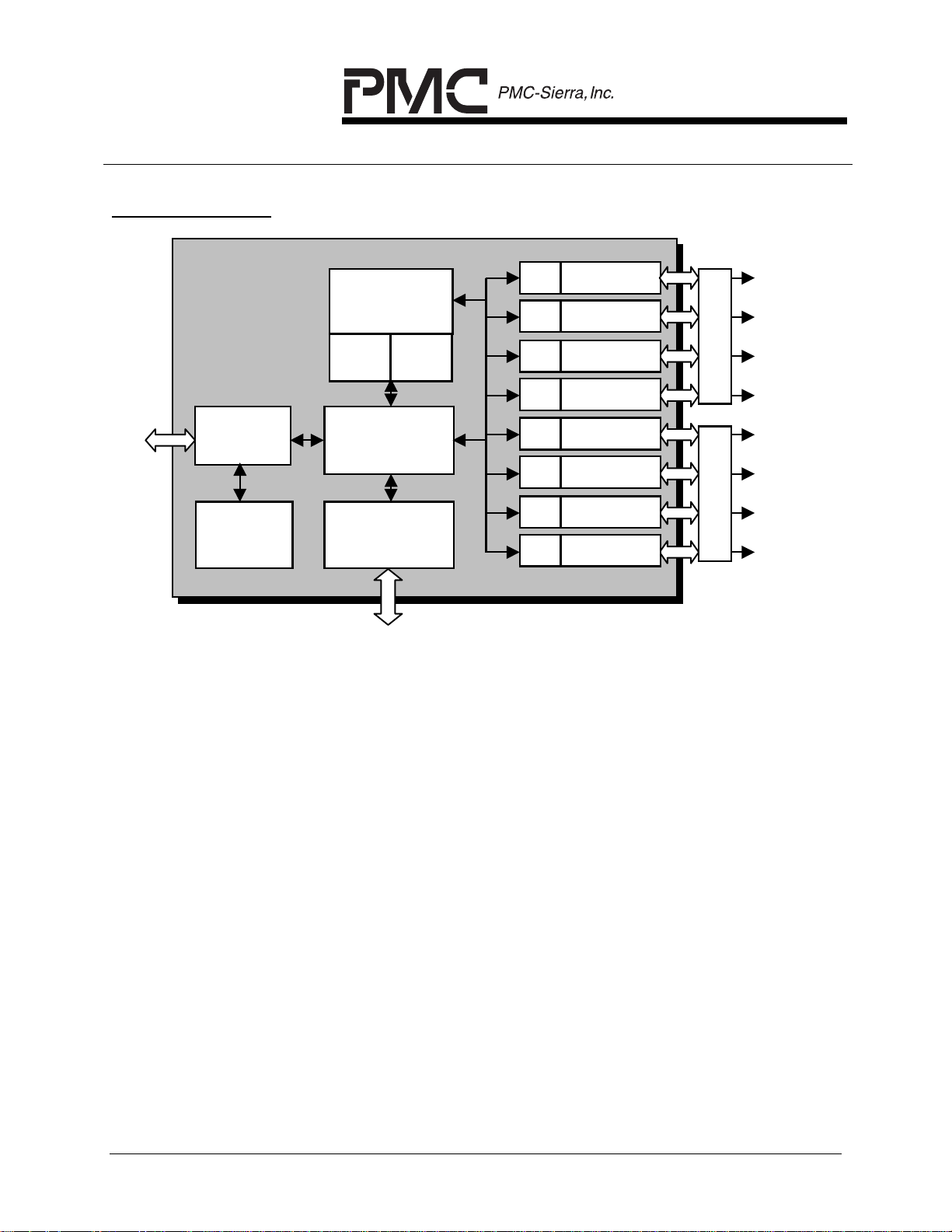
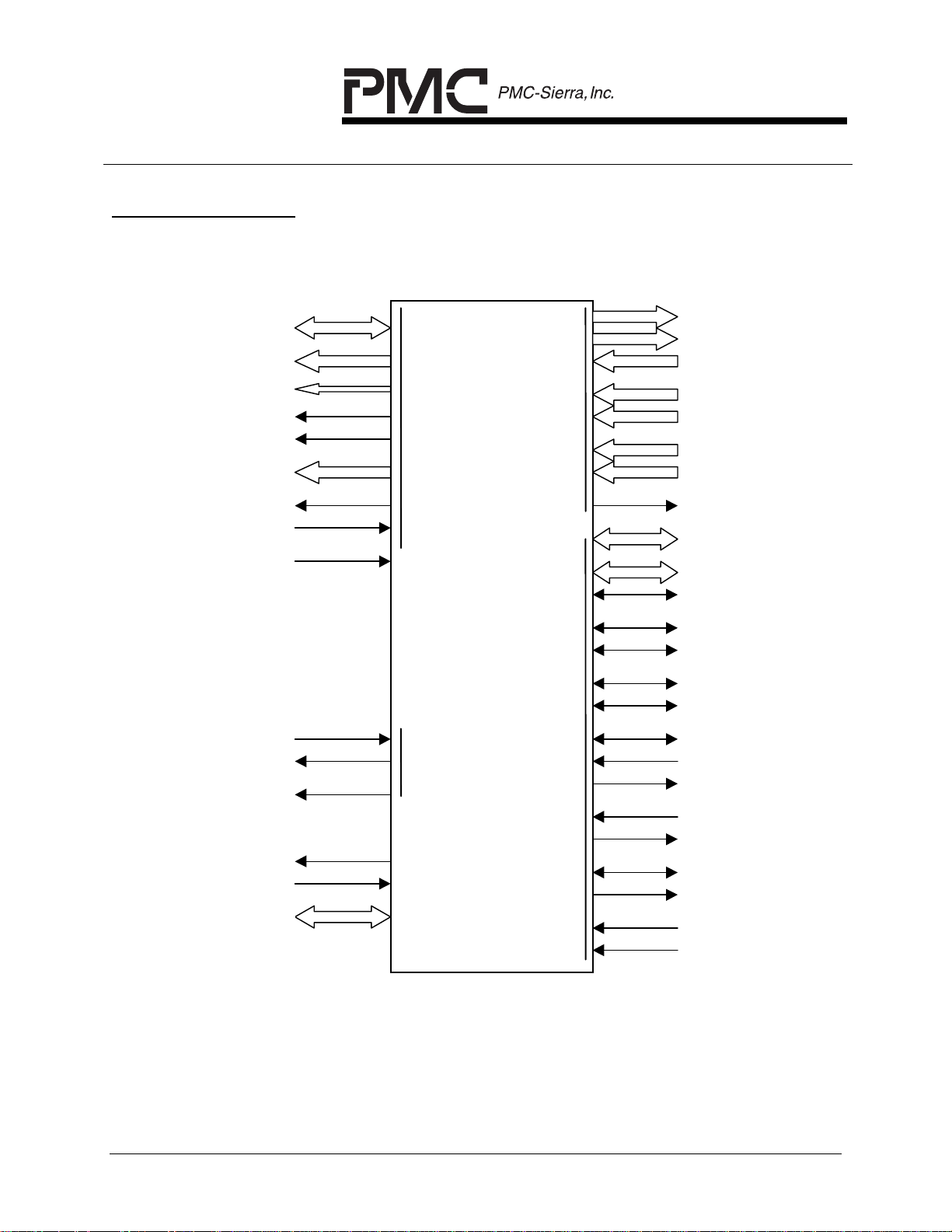
BLOCK DIAGRAM
10BaseT MAC
50 MHz
Embedded
Processor
FIFO
FIFO
10BaseT MAC
10BaseT
10BaseT
PCI Bus
Interface
I
Cache
Multi-Channel
DMA
D
Cache
FIFO
FIFO
FIFO
10BaseT MAC
10BaseT MAC
10BaseT MAC
Quad Ethernet
Interface Adapter
10BaseT
10BaseT
10BaseT
Controller
10BaseT MAC
FIFO
PCI Expansion Bus
Expansion
Registers
External
Memory
Interface
FIFO
FIFO
10BaseT MAC
10BaseT MAC
EDO DRAM / EPROM
Quad Ethernet
Interface Adapter
10BaseT
10BaseT
10BaseT
PROPRIETARY AND CONFIDENTIAL TO PMC-SIERRA, INC., AND PMC-SIERRA, INC. CUSTOMERS ONLY 7

ELAN 8X10
DATA SHEET
PMC-970109 ISSUE 3 8 PORT ETHERNET SWITCH
PM3350 ELAN 8 X10
DESCRIPTION
The PM3350 is a low-cost, highly integrated, stand-alone, single-chip switching device
for Ethernet/IEEE 802.3 switching and bridging applications. The device supports all
processing required for switching Ethernet/IEEE 802.3 packets between eight
independent half-duplex 10 Mbit/s ports. In addition, a switch built around the ELAN
8x10 can be expanded simply by connecting up to 7 additional devices to the on-chip
1 Gbit/s expansion port. Switch configuration and management can be performed either
remotely (in-band), via the on-chip SNMP MIB, agent and integrated TCP/UDP/IP
stack, or from a local CPU interfaced to the expansion port. The ELAN 8x10 also
collects per-port and per-host RMON statistics at wire rates on all ports. The ELAN
8x10 chip contains all the required elements of a high-performance Ethernet switch:
MAC-layer interfaces, buffer FIFOs, a high-speed DMA engine for fast packet transfers,
a local memory interface for up to 16 MB of external buffer memory, a compatible PCI
bus master and slave unit for modular expansion, and a switch processing unit that
implements the switching and bridging functions. The only additional components
required to create a complete 8-port switch are Ethernet Medium Access Unit (MAU)
devices, line transformers, a bank of external memory and a system clock.
The ELAN 8x10 device is implemented in high-density CMOS technology for low cost
and high performance. It is available in a 256-pin SBGA, and is ideally suited for
compact, low-cost desktop, workgroup and departmental Ethernet switching
applications.
PROPRIETARY AND CONFIDENTIAL TO PMC-SIERRA, INC., AND PMC-SIERRA, INC. CUSTOMERS ONLY 8

ELAN 8X10
DATA SHEET
PMC-970109 ISSUE 3 8 PORT ETHERNET SWITCH
PM3350 ELAN 8 X10
DEVICE DATA
Introduction
The PM3350 ELAN 8x10 offers a complete system-level solution, integrating all
required elements (except packet-buffer/address-table memory and transceiver logic) in
a single high-density VLSI chip. It is a true single-chip managed switch; all the required
functions, including address learning/aging, management, RMON-level statistics
collection, spanning tree support and self-configuration, are performed by the ELAN
8x10 without need for external CPUs or logic. In addition, the functions required for
expandability are also integrated into the device.
The ELAN 8x10 is built around a RISC CPU based Switch Processor core, coupled with
a multi-channel DMA controller, MAC-layer interface logic, FIFOs, a PCI-based
expansion port and a flexible memory controller.
Switch Processor
An on-chip Switch Processor is primarily responsible for performing the Ethernet / IEEE
802.3 packet switching functions, and can switch packets arriving simultaneously from
the eight 10BaseT ports and the expansion port at full wire rates using address tables
that it creates and maintains in external local memory. Store-and-forward switching is
performed, allowing the Switch Processor to detect CRC, length and alignment errors
and reject bad packets. The Switch Processor also supports IEEE 802.3
group/functional address handling. Address aging, topology change updates, and
statistics collection are performed by the Switch Processor as well.
The Switch Processor unit allows the device to support high-level capabilities. In
addition, it implements the full IEEE 802.1d spanning-tree transparent bridging protocol,
which allows the ELAN 8x10 to act as a eight-port expandable learning bridge,
performing learning, filtering and redirection at full speed. Finally, the Switch Processor
can host an SNMP agent for powerful remote switch configuration and diagnostic
capabilities, allowing systems built around the ELAN 8x10 to be managed in-band using
standard management platforms. When additional switch devices are connected to the
ELAN 8x10 expansion port, the Switch Processors in all ELAN 8x10s intercommunicate
to transparently support a distributed SNMP MIB.
In host-based applications, the host CPU may bypass the on-chip SNMP agent to
communicate directly with the Switch Processor for configuration, control and
monitoring purposes.
Multichannel DMA Processor
The on-chip DMA Coprocessor contains eleven independent and concurrently operating
channels, one for each of the eight 10BaseT ports and three dedicated to the
PROPRIETARY AND CONFIDENTIAL TO PMC-SIERRA, INC., AND PMC-SIERRA, INC. CUSTOMERS ONLY 9

ELAN 8X10
DATA SHEET
PMC-970109 ISSUE 3 8 PORT ETHERNET SWITCH
PM3350 ELAN 8 X10
expansion port. The DMA Coprocessor operates under the control of the Switch
Processor unit to transfer packets and data at high speed between the 10BaseT ports,
the local memory and the expansion port. It also computes 32-bit IEEE Frame Check
Sequence (FCS) CRC remainders over the transferred data, allowing the Switch
Processor to filter packets with errors and generate CRCs for transmitted packets as
required.
Ethernet/IEEE 802.3 MAC Interfaces
Eight independent Ethernet/IEEE 802.3 MAC-layer interfaces are built into the ELAN
8x10 chip. These interfaces connect directly to external 10BaseT Medium Access Unit
(MAU) devices via the industry-standard 7-wire serial interface, and perform most of the
MAC-layer processing tasks required for CSMA/CD networks. In addition, each MAC
interface contains a 32-byte FIFO buffer that enhances throughput and minimizes
latency issues.
The signaling protocol used on the 7-wire serial interfaces supported by the ELAN 8x10
chip follows that required by the Advanced Micro Devices, Inc (AMD) Am7990 LANCE
device.
Expansion Port
A 32-bit parity-checked expansion port is provided to allow systems using the ELAN
8x10 to be expanded transparently from 8 to 64 ports. The expansion port supports a
peak throughput of 1 Gbit/s, and requires only a single external PAL or similar device
(to serve as a bus arbiter). Packets received on an ELAN 8x10 MAC port that are
destined for an external ELAN 8x10 are transferred over the expansion bus prior to
transmission on the designated destination port. Broadcast and multicast packets are
handled using a two-level replication scheme, in which the broadcast/multicast packet is
first transferred to all of the external ELAN 8x10s, after which it is transmitted out the
required destination ports without any further use of the expansion bus. In addition,
ELAN 8x10s interconnected via the expansion port exchange information to maintain
the distributed MIB.
Local Memory Controller
An external local memory is used for holding configuration information, MAC address
tables and statistics tables, node management data, packet buffers, and host
communication queues (if a local host CPU is present). The ELAN 8x10 integrates a
memory controller that is capable of addressing and directly driving up to 16 Mbytes of
external memory, divided into four banks of 4 Mbytes each, with decoded selects for
each bank. Independent, software programmable access times may be set for each
bank, allowing a glueless interface to a mix of EDO DRAM, EEPROM, EPROM and
ROM in the same system. An external memory timing generator may also be used if
desired. The memory controller accepts simultaneous requests from the Switch
PROPRIETARY AND CONFIDENTIAL TO PMC-SIERRA, INC., AND PMC-SIERRA, INC. CUSTOMERS ONLY 10

ELAN 8X10
DATA SHEET
PMC-970109 ISSUE 3 8 PORT ETHERNET SWITCH
PM3350 ELAN 8 X10
Processor, the DMA processor, and the expansion port, and efficiently partitions the
100 Mbytes/s peak memory port bandwidth among them.
The ELAN 8x10 is capable of auto-configuring after power-up via an 8-bit EPROM or
EEPROM connected to the memory port. Parameters (such as the MAC address, IP
address, configuration options, etc.) may be placed in this EPROM or EEPROM, and
will be loaded automatically by the ELAN 8x10.
Clocking and Test
The ELAN 8x10 is implemented in fully-static CMOS technology, and is intended to
operate at a device clock frequency of 50 MHz (40 MHz for the expansion port bus).
The Switch Processor performs a comprehensive power on self test (POST), and can
report failure conditions and device status, if necessary, via an 8-bit LED interface
register connected to the local memory port.
PROPRIETARY AND CONFIDENTIAL TO PMC-SIERRA, INC., AND PMC-SIERRA, INC. CUSTOMERS ONLY 11
ELAN 8X10
DATA SHEET
PMC-970109 ISSUE 3 8 PORT ETHERNET SWITCH
PM3350 ELAN 8 X10
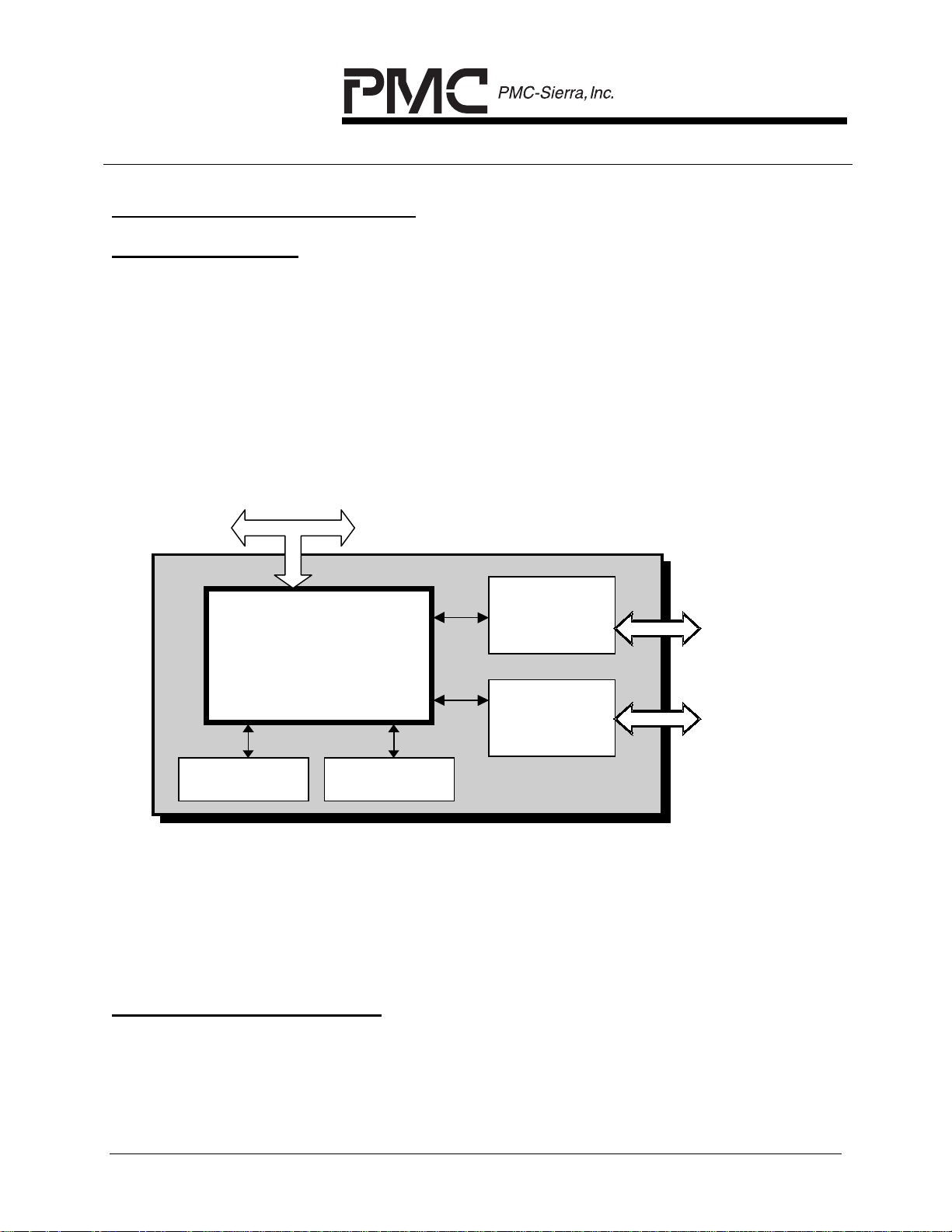
TYPICAL SYSTEM APPLICATIONS
Simple 8-Port Switch
The ELAN 8x10 chip can act as a stand-alone managed or unmanaged switching
device in low-cost, compact switch applications. Such a switch can be created from
ELAN 8x10 chips (one for every 8 ports), a bank of two 256k x 16-bit 60 nsec EDO
chips per ELAN 8x10 chip, a 32k x 8-bit EPROM or EEPROM for initialization and
configuration information, two LXT944 or similar quad Ethernet Interface Adapters, and
suitable passive components (filters, transformers, crystal oscillators, etc.) A block
diagram of a typical 8-port 10BaseT stackable switch is given below. The PCI
expansion bus allows multiple ELAN 8x10 switch assemblies to be easily stacked up to
a maximum of 64 10Mbit/s ports.
PCI Bus Expansion Bus
Quad
ELAN 8x10
PM3350
10BaseT
Interface
Quad
10BaseT
10BaseT
Ports 1-4
10BaseT
Ports 5-8
Interface
EDO DRAM
EEPROM
Managed 8-Port Ethernet Switch
The above system will operate as a fully managed system simply by replacing the 32k x
8-bit EEPROM with a 256k x 8-bit EPROM or EEPROM containing the SNMP agent,
support firmware, spanning tree, and TCP/IP stack.
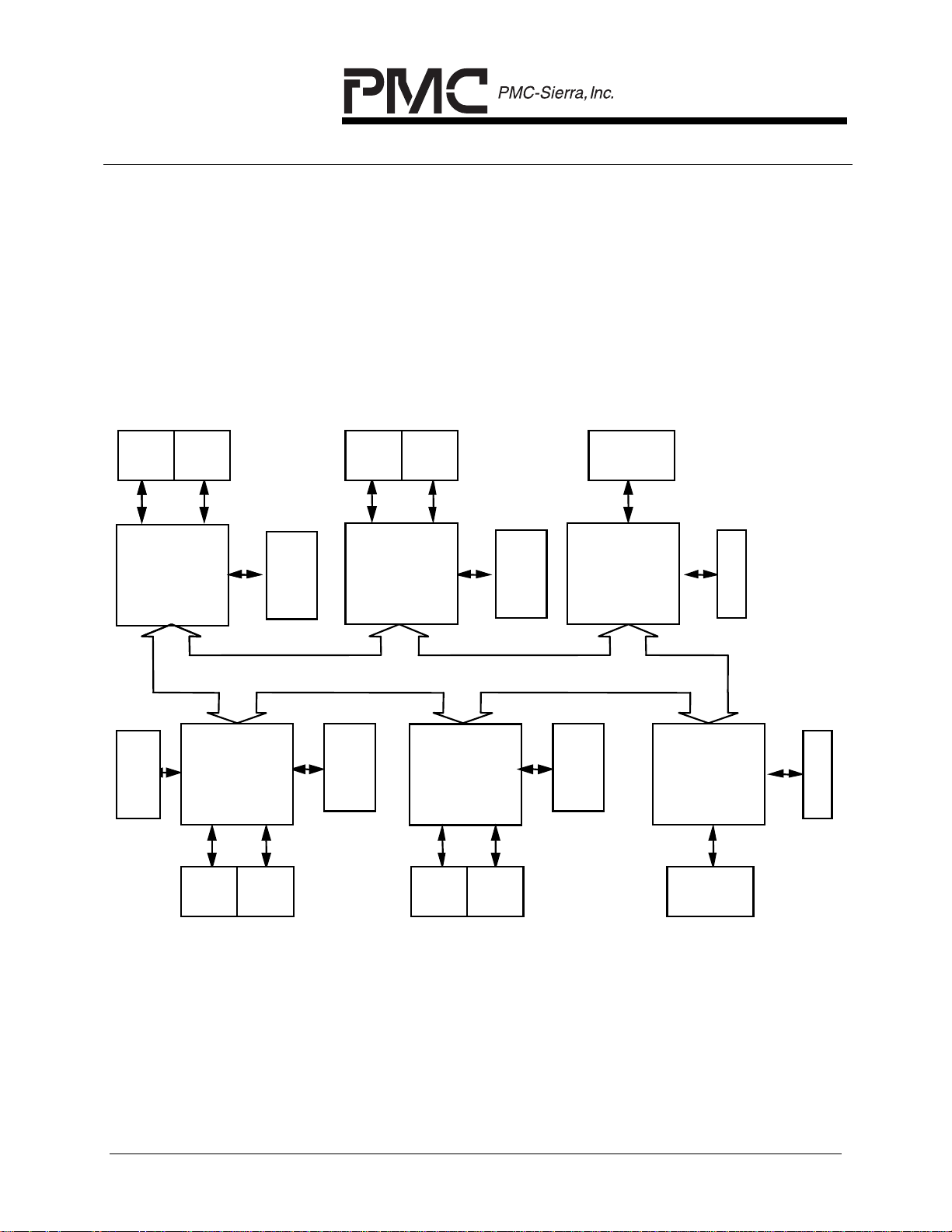
Low-cost 10/100 Mbit/s Switch
The ELAN 8x10 chip can be part of a 10/100 switch using the ELAN 1x100 10/100
Mbit/s switch chip. Together they can form a workgroup or desktop switch supporting a
high-speed server or backbone port in low-cost, compact Ethernet switching hub
applications. Such a switch can be created from one or two PM3351 devices (one for
PROPRIETARY AND CONFIDENTIAL TO PMC-SIERRA, INC., AND PMC-SIERRA, INC. CUSTOMERS ONLY 12
ELAN 8X10
SRAM
SRAM
DATA SHEET
PMC-970109 ISSUE 3 8 PORT ETHERNET SWITCH
PM3350 ELAN 8 X10
every 100 Mbit/s port required), 1 to 7 PM3350 chips (one for every eight 10 Mbit/s
ports required), a bank of memory per device (60 nsec EDO DRAM for each PM3350,
15 ns SRAM for each PM3351) for holding packet buffers and switching tables, a single
32k x 8-bit EEPROM device for configuration information, two LXT944 10BaseT
interface adapters per PM3350 chip, one LXT970 100 Mbit/s PHY device per PM3351,
and suitable passive components (filters, transformers, crystal oscillators, etc.) A block
diagram of a typical 32-port 10BaseT stackable switching hub with two 100 Mbit/s
server/backbone ports is given in the following diagram. The PCI expansion bus is used
seamlessly to stack the ELAN 8x10s and ELAN 1x100s.
8 x 10BaseT 10/100BaseT8 x 10BaseT
Quad
PHY
Quad
PHY
ELAN 8x10
8x10BaseT
PM3350
EEPROM
Quad
ELAN 8x10
8x10BaseT
PM3350
Quad
PHY
PHY
EDO
DRAM
Quad
PHY
Quad
PHY
ELAN 8x10
8x10BaseT
PM3350
PCI Backplane
ELAN 8x10
EDO
DRAM
8 x 10BaseT
PM3350
Quad
PHY
Quad
PHY
EDO
DRAM
10/100
PHY
ELAN 1x100
1x10/100
BaseT
PM3351
EDO
DRAM
ELAN 1x100
1x10/100
BaseT
PM3351
10/100
PHY
8 x 10BaseT 8 x 10BaseT
10/100BaseT
Expandable 10/100 Mbit/s Ethernet Switch
PROPRIETARY AND CONFIDENTIAL TO PMC-SIERRA, INC., AND PMC-SIERRA, INC. CUSTOMERS ONLY 13

ELAN 8X10
DATA SHEET
PMC-970109 ISSUE 3 8 PORT ETHERNET SWITCH
PM3350 ELAN 8 X10
PRIMARY FEATURES AND BENEFITS
Wire-speed Packet switching
Each ELAN 8x10 chip offers 8 separate Ethernet ports all capable of accepting and
processing packets simultaneously at wire rates (ranging from 14,880 packets/sec per
port with a packet length of 64 bytes to 813 packets/sec per port with 1518 byte
packets), immediately multiplying the aggregate bandwidth of the target network by a
factor of eight. In addition, the low cost and compact size permitted by the single-chip
ELAN 8x10 solution makes micro-segmentation highly feasible, allowing even more
improvement in bandwidth.
Combined Input- and Output-buffered switch
The ELAN 8x10 implements a hybrid input-buffered/output-queued switching algorithm
which minimizes packet loss, allows packet buffers to be allocated on a demand basis,
and permits limits to be established to prevent any one port from consuming all system
buffer memory. Buffer limits are configured on a per-port basis. Packet storage is
allocated within the external memory by the ELAN 8x10 from a central pool using an
on-demand method, employing linked lists of small, fixed-length buffers to hold variable
sized packets in order to maximize memory utilization.
Modular design
Multiple ELAN 8x10 chips interconnect seamlessly, allowing transparent expansion of
switching hubs from 8 to 64 ports without significant redesign. The 1 Gbit/s expansion
port bandwidth ensures that network capacity grows linearly as more ELAN 8x10 chips
are added (up to the maximum number of supported ports).
Advanced switching features
The ELAN 8x10 directly implements backpressure flow control (as a user-selectable
option), with configurable thresholds and limits, to minimize packet loss in heavily
loaded networks. Backpressure is performed by jamming, or colliding with, incoming
packets on an individual port when the port has run out of buffer space; all other ports
continue to run normally, with no head-of-line blocking effects. The ELAN 8x10 also
implements per-packet lifetime control to ensure that transmit queues are flushed
properly in the event of bottlenecks at the output ports. Address aging is handled onchip, as is purging of the address table in the event of a network reconfiguration.
Broadcast storm rate limiting is implemented (with configurable rate limits) to reduce the
effects of high broadcast rates on the traffic flowing through the switch.
PROPRIETARY AND CONFIDENTIAL TO PMC-SIERRA, INC., AND PMC-SIERRA, INC. CUSTOMERS ONLY 14

ELAN 8X10
DATA SHEET
PMC-970109 ISSUE 3 8 PORT ETHERNET SWITCH
PM3350 ELAN 8 X10
Spanning tree bridging capabilities
The ELAN 8x10 optionally implements the 802.1d spanning tree protocol, allowing it to
interoperate with IEEE-standard transparent bridges. The spanning tree protocol is
supported by the on-chip Switch Processor unit, and does not require an external CPU
for implementation.
Management and monitoring support
The ELAN 8x10 maintains full RMON port and host statistics for all ports and all learned
MAC addresses at wire rates. These statistics may be retrieved either in-band (via
SNMP agent) or out-of-band (via the expansion bus).
The ELAN 8x10 implements an optional on-chip SNMP agent on top of an integral
UDP/IP protocol stack, supporting SNMP and the RFC1493 bridge MIB. When multiple
ELAN 8x10 chips are present in a system, they may be configured to intercommunicate
and create a distributed MIB in a transparent manner. Alternatively, the system vendor
may elect to disable the SNMP agent and access the ELAN 8x10 statistics and
configuration variables directly from the expansion port.
Status codes may be displayed on a set of LEDs (Light Emitting Diodes) during self-test
and operation at the system implementer's discretion. These status codes are output to
a register mapped into the ELAN 8x10 memory data bus at a specific address location.
Device failure during self-test, or specific operating conditions, may be displayed using
front-panel LEDs connected to the register.
Autoconfiguration via Local PROM/EEPROM
The ELAN 8x10 will automatically self-configure upon power-up using user-defined
parameters supplied in an external EPROM or EEPROM. The EPROM/ EEPROM may
be connected to the memory bus and mapped to any address range; the ELAN 8x10
will automatically locate the EPROM or EEPROM and load the configuration
parameters from it. The ELAN 8x10 also contains hardware that enables it to write to
standard 3.3-volt EEPROM devices, thus permitting configuration information to be
changed dynamically.
PROPRIETARY AND CONFIDENTIAL TO PMC-SIERRA, INC., AND PMC-SIERRA, INC. CUSTOMERS ONLY 15

ELAN 8X10
DATA SHEET
PMC-970109 ISSUE 3 8 PORT ETHERNET SWITCH
PM3350 ELAN 8 X10
PIN DIAGRAM
The ELAN 8x10 is packaged in a 256-pin cavity-down SBGA, with 188 signal pins and
associated VDD (supply) and VSS (ground) pins.
256-Pin SBGA Pin Diagram
20 19 18 17 16 15 14 13 12 11
VSS VSS VSS
A
VSS VDD VDD MRAS_
B
VSS VDD VDD MWEN_1_
C
MRDY_ MRD_ MWEN_2_ VDD MWEN_0_
D
MCS_3_ MCS_2_ MCS_0_ MWEN_3_
E
MDATA_31MDATA_27MDATA_24MDATA_2
0
MDATA_28MDATA_25MDATA_21MDATA_17MDATA_15MDATA_1
MDATA_30MDATA_26MDATA_23MDATA_19MDATA_16MDATA_1
MDATA_2
9
MDATA_22MDATA_18MDATA_1
VDD
MDATA_14MDATA_1
VSS
0
1
2
3
MADDR_2 MADDR_1 MADDR_0 MCS_1_
F
MADDR_6 MADDR_5 MADDR_3 VDD
G
MADDR_1
H
J
K
MADDR_15MADDR_16MADDR_17MADDR_1
L
MADDR_1
M
N
TXD_7 TCLK_7 CD_6 VDD
P
RCLK_6 RXD_6 TEN_6 COL_5
R
TXD_6 TCLK_6 CD_5 TEN_5
T
RCLK_5 RXD_5 TXD_5 VDD COL_4 RXD_4 VDD RXD_3 CD_2 VDD
U
V
W
MADDR_8 MADDR_7 MADDR_4
0
MADDR_12MADDR_1
VSS
MADDR_13MADDR_1
VSS
COL_7 CD_7 RXD_7
9
VSS RCLK_7 TEN_7 COL_6
VSS VDD VDD TCLK_5 LBK TCLK_4 RCLK_3 TCLK_3 RXD_2 TCLK_2
VSS VDD VDD CD_4 TEN_4 COL_3 TEN_3 COL_2 TEN_2 TXD_2
MADDR_9
1
4
VDD
8
256 BGA
BOTTOM VIEW
VSS VSS VSS RCLK_4 TXD_4 CD_3 TXD_3 RCLK_2 VSS VSS
Y
20 19 18 17 16 15 14 13 12 11
PROPRIETARY AND CONFIDENTIAL TO PMC-SIERRA, INC., AND PMC-SIERRA, INC. CUSTOMERS ONLY 16

ELAN 8X10
DATA SHEET
PMC-970109 ISSUE 3 8 PORT ETHERNET SWITCH
PM3350 ELAN 8 X10
10987654321
VSS VSS MDATA_5 MDATA_1 DBG_2 PC_3 PC_7 VSS VSS VSS
MDATA_8 MDATA_7 MDATA_3 MDATA_0 DBG_1 PC_4 PC_8 VDD VDD VSS
MDATA_9 MDATA_6 MDATA_2 MINTR_ DBG_0 PC_6 PC_10 VDD VDD VSS
VDD MDATA_4 MGWE_ VDD PC_5 PC_9 VDD N/C N/C ERST_
N/C TST_ RST_ GNT_
INT_ REQ_ AD_31 AD_30
VDD AD_29 AD_27 AD_26
AD_28 AD_25 CBE_3_ VSS
AD_24 VDD5 IDEL_ AD_23
AD_22 AD_21 AD_20 AD_19
VDD AD_18 AD_17 VSS
IRDY_ CBE_2_ AD_16 VSS
SERR_ DEVSEL_ TRDY_ FRAME_
256 BGA
VDD PAR PERR_ STOP_
A
B
C
D
E
F
G
H
J
K
L
M
N
P
BOTTOM VIEW
COL_1 TXD_1 RCLK_0 VDD AD_2 AD_6 VDD PCI_CLK AD_8 AD_9
MCLK RXD_1 TCLK_1 RXD_0 TCLK_0 AD_3 CBE_0_ VDD VDD VSS
SYSCLK RCLK_1 TEN_1 CD_0 TXD_0 AD_1 AD_5 VDD VDD VSS
CLK20 CD_1 VSS COL_0 TEN_0 AD_0 AD_4 VSS VSS VSS
AD_11 AD_14 AD_15 CBE_1_
AD_7 AD_10 AD_12 AD_13
R
T
U
V
W
Y
10987654321
PROPRIETARY AND CONFIDENTIAL TO PMC-SIERRA, INC., AND PMC-SIERRA, INC. CUSTOMERS ONLY 17
ELAN 8X10
DATA SHEET
PMC-970109 ISSUE 3 8 PORT ETHERNET SWITCH
PM3350 ELAN 8 X10
PIN DESCRIPTION
PIN SIGNAL PIN SIGNAL PIN SIGNAL
D1 ERST_ R3 AD_14 W12 TEN_2
E3 TST_ T1 AD_13 V12 RXD_2
F4 INT_ T2 AD_12 Y13 RCLK_2
E2 RST_ R4 AD_11 U12 CD_2
E1 GNT_ T3 AD_10 W13 COL_2
F3 REQ_ U1 AD_9 V13 TCLK_3
F2 AD_31 U2 AD_8 Y14 TXD_3
F1 AD_30 T4 AD_7 W14 TEN_3
G3 AD_29 U3 PCI_CLK U13 RXD_3
H4 AD_28 V4 CBE_0_ V14 RCLK_3
G2 AD_27 U5 AD_6 Y15 CD_3
G1 AD_26 W4 AD_5 W15 COL_3
H3 AD_25 Y4 AD_4 V15 TCLK_4
J4 AD_24 V5 AD_3 Y16 TXD_4
H2 CBE_3_ U6 AD_2 W16 TEN_4
J3 VDD5 W5 AD_1 U15 RXD_4
J2 IDSEL_ Y5 AD_0 V16 LBK
J1 AD_23 V6 TCLK_0 Y17 RCLK_4
K4 AD_22 W6 TXD_0 W17 CD_4
K3 AD_21 Y6 TEN_0 U16 COL_4
K2 AD_20 V7 RXD_0 V17 TCLK_5
K1 AD_19 U8 RCLK_0 U18 TXD_5
L3 AD_18 W7 CD_0 T17 TEN_5
L2 AD_17 Y7 COL_0 U19 RXD_5
M2 AD_16 V8 TCLK_1 U20 RCLK_5
M3 CBE_2_ U9 TXD_1 T18 CD_5
N1 FRAME_ W8 TEN_1 R17 COL_5
M4 IRDY_ V9 RXD_1 T19 TCLK_6
N2 TRDY_ W9 RCLK_1 T20 TXD_6
N3 DEVSEL_ Y9 CD_1 R18 TEN_6
P1 STOP_ U10 COL_1 R19 RXD_6
P2 PERR_ V10 MCLK R20 RCLK_6
N4 SERR_ W10 SYSCLK P18 CD_6
P3 PAR Y10 CLK20 N17 COL_6
R1 CBE_1_ V11 TCLK_2 P19 TCLK_7
R2 AD_15 W11 TXD_2 P20 TXD_7
PROPRIETARY AND CONFIDENTIAL TO PMC-SIERRA, INC., AND PMC-SIERRA, INC. CUSTOMERS ONLY 18
ELAN 8X10
DATA SHEET
PMC-970109 ISSUE 3 8 PORT ETHERNET SWITCH
PM3350 ELAN 8 X10
PIN SIGNAL PIN SIGNAL PIN SIGNAL
N18 TEN_7 F17 MCS_1_ D11 MDATA_13
M17 RXD_7 E18 MCS_0_ C11 MDATA_12
N19 RCLK_7 D20 MRDY_ B11 MDATA_11
M18 CD_7 D19 MRD_ A11 MDATA_10
M19 COL_7 E17 MWEN_3_ C10 MDATA_9
M20 MADDR_19 D18 MWEN_2_ B10 MDATA_8
L17 MADDR_18 C17 MWEN_1_ B9 MDATA_7
L18 MADDR_17 D16 MWEN_0_ C9 MDATA_6
L19 MADDR_16 B17 MRAS_ A8 MDATA_5
L20 MADDR_15 A17 MDATA_31 D9 MDATA_4
K18 MADDR_14 C16 MDATA_30 B8 MDATA_3
K19 MADDR_13 D15 MDATA_29 C8 MDATA_2
J19 MADDR_12 B16 MDATA_28 A7 MDATA_1
J18 MADDR_11 A16 MDATA_27 B7 MDATA_0
H20 MADDR_10 C15 MDATA_26 D8 MGWE_
J17 MADDR_9 B15 MDATA_25 C7 MINTR_
H19 MADDR_8 A15 MDATA_24 A6 DBG_2
H18 MADDR_7 C14 MDATA_23 B6 DBG_1
G20 MADDR_6 D13 MDATA_22 C6 DBG_0
G19 MADDR_5 B14 MDATA_21 A5 PC_3
H17 MADDR_4 A14 MDATA_20 B5 PC_4
G18 MADDR_3 C13 MDATA_19 D6 PC_5
F20 MADDR_2 D12 MDATA_18 C5 PC_6
F19 MADDR_1 B13 MDATA_17 A4 PC_7
F18 MADDR_0 C12 MDATA_16 B4 PC_8
E20 MCS_3_ B12 MDATA_15 D5 PC_9
E19 MCS_2_ A12 MDATA_14 C4 PC_10
D3 N/C E4 N/C D2 N/C
PROPRIETARY AND CONFIDENTIAL TO PMC-SIERRA, INC., AND PMC-SIERRA, INC. CUSTOMERS ONLY 19
ELAN 8X10
DATA SHEET
PMC-970109 ISSUE 3 8 PORT ETHERNET SWITCH
PM3350 ELAN 8 X10
Pin Signal Pin Signal
B2 VDD A1 VSS
B3 A2
B18 A3
B19 A9
C2 A10
C3 A13
C18 A18
C19 A19
D4 A20
D7 B1
D10 B20
D14 C1
D17 C20
G4 H1
G17 J20
K17 K20
L4 L1
P4 M1
P17 N20
U4 V1
U7 V20
U11 W1
U14 W20
U17 Y1
V2 Y2
V3 Y3
V18 Y8
V19 Y11
W2 Y12
W3 Y18
W18 Y19
W19 Y20
All VDD and VSS lines
be connected to supply and ground respectively. Standard
must
decoupling practices should be followed for proper device operation.
PROPRIETARY AND CONFIDENTIAL TO PMC-SIERRA, INC., AND PMC-SIERRA, INC. CUSTOMERS ONLY 20
ELAN 8X10
DATA SHEET
PMC-970109 ISSUE 3 8 PORT ETHERNET SWITCH
PM3350 ELAN 8 X10
Functional Grouping
The following diagram shows the functional grouping of the ELAN 8x10 signal pins.
MDATA[31:0]
MADDR[19:0]
MCS_[3:0]
MRAS_
MRD_
MWE_[3:0]
MGWE_
MRDY_
MINTR
SYSCLK
MCLK
CLK20
Local
Memory
Interface
PM3350
8-Port
Ethernet
Switch
Clocking
8 x
MAU
PCI
Expansion
Bus
Interface
TXD[7:0]
TEN[7:0]
TCLK[7:0
RXD[7:0]
RCLK[7:0]
CD[7:0]
COL[7:0
LBK
AD[31:0]
CBE_[3:0]
PAR
FRAME_
TRDY_
IRDY_
STOP_
DEVSEL_
IDSEL
REQ_
GNT_
ERST_
TST_
DBG[2:0]
PROPRIETARY AND CONFIDENTIAL TO PMC-SIERRA, INC., AND PMC-SIERRA, INC. CUSTOMERS ONLY 21
INT_
PERR_
SERR_
PCI_CLK
RST_

ELAN 8X10
DATA SHEET
PMC-970109 ISSUE 3 8 PORT ETHERNET SWITCH
PM3350 ELAN 8 X10
PCI Expansion Bus Interface
Signal Name Size Type Description
AD[31:0] 32 I/O
CBE_[3:0] 4 I/O
PAR 1 I/O
FRAME_ 1 I/O
IRDY_ 1 I/O
TRDY_ 1 I/O
STOP_ 1 I/O
DEVSEL_ 1 I/O
IDSEL 1 I
REQ_ 1 O
GNT_ 1 I
INT_ 1 OD
PERR_ 1 I/O
SERR_ 1 OD
PCI_CLK 1 I
Multiplexed PCI address/data bus, used by an external bus master (e.g., a PCI
host) or the ELAN 8x10 to transfer addresses or data.
Command/Byte-Enable lines. These lines supply a command (during PCI address
phases) or byte enables (during data phases) for each bus transaction.
Address/data/command parity, supplies the even parity computed over the
AD[31:0] and CBE_[3:0] lines during valid data phases; it is sampled (when the
ELAN 8x10 is acting as a target) or driven (when the ELAN 8x10 acts as an
initiator) one clock edge after the respective data phase.
Bus transaction delimiter (framing signal); a HIGH-to-LOW transition on this signal
indicates that a new transaction is beginning (with an address phase); a LOW-toHIGH transition indicates that the next valid data phase will end the currently
ongoing transaction.
Transaction Initiator (master) ready, used by the transaction initiator or bus master
to indicate that it is ready for a data transfer. A valid data phase ends with data
transfer when both IRDY_ and TRDY_ are sampled asserted on the same clock
edge.
Transaction Target ready, used by the transaction target or bus slave to indicate
that it is ready for a data transfer. A valid data phase ends with data transfer when
both IRDY_ and TRDY_ are sampled asserted on the same clock edge.
Transaction termination request, driven by the current target or slave to abort,
disconnect or retry the current transfer.
Device select acknowledge: driven by a target to indicate to the initiator that the
address placed on the AD[31:0] lines (together with the command on the
CBE_[3:0] lines) has been decoded and accepted as a valid reference to the
target's address space. Once asserted, it is held asserted until FRAME_ is
de-asserted; otherwise, it indicates (in conjunction with STOP_ and TRDY_) a
target-abort.
Device identification (slot) select. Assertion of IDSEL signals the ELAN 8x10 that it
is being selected for a configuration space access.
Bus request (to bus arbiter), asserted by the ELAN 8x10 to request control of the
PCI bus.
Bus grant (from bus arbiter); this indicates to the ELAN 8x10 that it has been
granted control of the PCI bus, and may begin driving the address/data and control
lines after the current transaction has ended (indicated by FRAME_, IRDY_ and
TRDY_ all de-asserted simultaneously).
Open Drain Interrupt request. This pin signals an interrupt request to an external
PCI host system. The INT_ pin should be tied to the INTA* line on the PCI bus.
Bus parity error signal, asserted by the ELAN 8x10 as a bus slave, or sampled by
the ELAN 8x10 as a bus master, to indicate a parity error on the AD[31:0] and
CBE_[3:0] lines.
Open Drain System error, used by the ELAN 8x10 to indicate a system error, or a
parity error on the AD[31:0] and CBE_[3:0] lines during an address phase.
PCI bus clock; supplies the PCI bus clock signal to the ELAN 8x10.
PROPRIETARY AND CONFIDENTIAL TO PMC-SIERRA, INC., AND PMC-SIERRA, INC. CUSTOMERS ONLY 22

ELAN 8X10
DATA SHEET
PMC-970109 ISSUE 3 8 PORT ETHERNET SWITCH
PM3350 ELAN 8 X10
RST_ 1 I
PCI bus reset (system reset). Performs a hardware reset of the ELAN 8x10 and
associated peripherals when asserted. The RST_ input uses a Schmitt trigger to
accommodate slow rise and fall times, allowing a simple RC network to be used to
provide power-on reset capability.
MAU Interface Pins
Signal Name Size Type Description
TXD[7:0] 8 O
TEN[7:0] 8 O
TCLK[7:0] 8 I
RXD[7:0] 8 I
RCLK[7:0] 8 I
CD[7:0] 8 I
Transmit data outputs (to 8 MAUs). The TXD lines are used to carry outgoing
data bytes to the Medium Access Units (MAUs). Each bit of the bus is
connected to the serial transmit data input of a separate MAU device. The
TXD[7:0] lines are synchronous to the TCLK[7:0] lines (TXD[0] to TCLK[0], and
so on). Data are driven on to the TXD[7:0] lines after the rising edge of the
corresponding TCLK[7:0] input, and may be sampled on the next rising edge of
the latter.
Transmit enables. The data carried on the TXD[7:0] lines is only valid when the
TEN[7:0] lines are active. This also indicates to the MAU devices that the ELAN
8x10 is acquiring the medium. Each of the TEN[7:0] lines should be connected
to a separate MAU device. The TEN[7:0] outputs are asserted or de-asserted on
the rising edge of the corresponding TCLK[7:0] input, and may be sampled on
the next rising edge of the latter.
Transmit clocks; these inputs provide the synchronization references for the
TXD[7:0] and TEN[7:0] lines. TCLK[7:0] should be driven with a 10 MHz transmit
data clock reference by the external MAU devices (each MAU device should
drive a separate line of the TCLK[7:0] bus). Each of the TCLK[7:0] lines may be
driven completely asynchronously to all the others. The rising edges of the
TCLK[7:0] signals are used as timing references. The TCLK[7:0] inputs are
Schmitt-triggered for improved resistance to slow rise and fall times.
Receive data inputs (from 8 MAUs). The RXD lines transfer incoming serial
received data from the external MAU devices to the ELAN 8x10. Each bit of the
bus is connected to the serial receive data output of a separate MAU device.
The RXD[7:0] lines are sampled synchronously by the ELAN 8x10 at the rising
edges of the clocks supplied on the RCLK[7:0] inputs (RXD[0] to RCLK[0], and
so on).
Receive clocks; should be driven by the external MAU devices with the receive
clock references recovered from the incoming serial receive data. The
RCLK[7:0] inputs need not be driven with a continuous clock reference;
however, they must be running whenever the CD[7:0] inputs are asserted, and
must continue running for at least five clock cycles after the CD[7:0] inputs
transition LOW in order to permit the internal MAC logic to function properly.
The RCLK[7:0] inputs are Schmitt-triggered for improved resistance to slow rise
and fall times.
Receive carrier detect signals. These carrier detect inputs should be driven with
the carrier detect (i.e., data being received from the medium) signals generated
by the eight external MAU devices, and are sampled synchronously to the rising
edges of the clocks input on the RCLK[7:0] lines and the TCLK[7:0] lines to
implement the CSMA/CD algorithm. The data presented on RXD[7:0] are only
sampled when the corresponding CD[7:0] lines are asserted HIGH. (If not all of
the eight ELAN 8x10 MAC ports are connected to external MAU devices, the CD
inputs for to the missing MAU devices should be tied LOW.)
PROPRIETARY AND CONFIDENTIAL TO PMC-SIERRA, INC., AND PMC-SIERRA, INC. CUSTOMERS ONLY 23

ELAN 8X10
DATA SHEET
PMC-970109 ISSUE 3 8 PORT ETHERNET SWITCH
PM3350 ELAN 8 X10
COL[7:0] 8 I
LBK 1 O
Receive collision detect signals. These inputs pass the collision detect and SQE
test signals generated by the external MAU devices to the ELAN 8x10. They are
sampled synchronously to the TCLK[7:0] clock references (COL[0] corresponds
to TCLK[0], and so on), and should be asserted by the MAU devices to indicate
collisions on the medium as well as to signal a successful SQE test after
transmit. If not all of the 8 collision signal inputs are connected to external MAU
devices, the unused inputs should be tied LOW.
MAU loopback mode select (all 8 ports). This pin can be left as a no-connect
or wired to the loopback mode input of an attached PHY device. The loopback
mode feature on the PM3350 is not operational. Hence, this pin has no implied
functionality.
Local Memory Interface
Signal Name Size Type Description
MDATA[31:0] 32 I/O
MADDR[19:0] 20 O
MCS_[3:0] 4 O
MRAS_ 1 O
Memory data bus. MDATA[31:0] carries the data driven to the external local
memory by the ELAN 8x10 during local memory writes, and the data sent back
to the ELAN 8x10 by the memory devices during local memory reads. In
addition, configuration information is latched from the MDATA[31:0] lines
during ELAN 8x10 reset and loaded into an internal configuration register;
either pullup-pulldown resistors or tri-state buffers (enabled by the RST
drive configuration data on to the MDATA[31:0] lines during reset.
All MDATA[31:0] pins have internal pullups.
Memory address bus; supplies a word-aligned address to the external memory
devices (i.e., address bits 22 through 2 of the 24-bit byte address generated by
the internal ELAN 8x10 logic), and thus selects a single 32-bit word to be read
or written. Up to 4 MB of memory may be directly addressed in each bank
using these address lines. In addition, the lower 11 bits of MADDR[19:0] (i.e.,
MADDR[10:0]) carry a multiplexed row/column address when DRAM accesses
are being made, with the row address being presented when MRAS_
and the column address being presented when it is low. Multiplexing for 8-, 9-,
10- and 11-bit column addresses is supported. Up to 4 MB of memory may be
addressed in each bank when multiplexing is enabled for that bank (i.e., by
configuring the bank for DRAM accesses).
Memory bank chip selects. The MCS_[3:0] outputs select one of four memory
banks; each bank is 4 megabytes in size. They are decoded directly from the
most significant 2 bits (bits 23 and 22) of the 24-bit physical byte address
generated by the internal ELAN 8x10 logic, and are synchronous to MEMCLK.
When driving DRAM memory devices other than 2-CAS DRAMs, the
MCS_[3:0] signals function as the Column Address Strobe (CAS) signals to the
memories.
DRAM Row Address Strobe output; supplies the Row Address Strobe (RAS)
signal to one or more external DRAM banks. It is asserted to latch the row
address supplied on the MADDR lines into the DRAM array, and allow the
column address to be output one cycle later. It may be tied directly to the RAS*
inputs of standard asynchronous DRAM devices.
*
input)
is high
PROPRIETARY AND CONFIDENTIAL TO PMC-SIERRA, INC., AND PMC-SIERRA, INC. CUSTOMERS ONLY 24

ELAN 8X10
DATA SHEET
PMC-970109 ISSUE 3 8 PORT ETHERNET SWITCH
PM3350 ELAN 8 X10
MRD_ 1 O
MWE_[3:0] 4 O
MGWE_ 1 O
MRDY_ 1 I
MINTR_ 1 I
Memory read enable. This output signals the external memory banks that a
read is being performed and data should be output on the MDATA[31:0] lines
from the specified address. The MRD_ output may be tied to the OE* inputs of
standard memory devices.
Memory write enables, used by the ELAN 8x10 to enable the data presented
on individual byte lanes of MDATA[31:0] to be individually written to memory.
MWE_[0] corresponds to MDATA[7:0], MWE_[1] corresponds to MDATA[15:8],
and so on. When using 2-CAS asynchronous DRAM devices, the MWE_[3:0]
outputs should be connected to the memory CAS* inputs; otherwise, the
MWE_[3:0] outputs should be connected to the appropriate byte write enables.
Global memory write enable. This signal is used to signal that a write access
is occurring, and should be connected to the WE* inputs of dual CAS
asynchronous DRAM devices.
Memory ready input. If an external memory timing generator is used, it can be
connected to the MRDY_ input to force the ELAN 8x10 to insert wait states into
memory accesses. If the MRDY_
the MADDR[15:0], MCS_[3:0], MRD_
values (as well as MDATA[31:0] for memory writes).
The MRDY* input is only sampled by the ELAN 8x10 when performing an
SRAM-type access; it is ignored for all other memory types. If an external
memory timing generator is not used, the MRDY
Local interrupt input. The MINTR_ may be used to provide an interrupt input to
the ELAN 8x10 in special applications. If the MINTR_ input is not used, it
should be tied HIGH.
line is de-asserted, the ELAN 8x10 will hold
and MWR_[3:0] lines at their present
_
line should be tied LOW.
Clock Inputs and Outputs
Signal Name Size Type Description
SYSCLK 1 I
MCLK 1 O
CLK20 1 O
50 MHz master device clock input, This should be driven by a 50 MHz
symmetrical clock source with a duty cycle between 40% and 60%. It is re-timed
and driven out on the MEMCLK line, and is also used in the internal device
logic.
50 MHz clock output derived from SYSCLK; supplies the re-timed 50 MHz clock
(input on the SYSCLK pin) to external devices.
20 MHz clock output (for use by MAU devices). The 50 MHz input clock is
internally divided by 2.5 and output as an asymmetrical 20 MHz clock reference
on the CLK20 output; this clock may be used as an input to external MAU
devices.
PROPRIETARY AND CONFIDENTIAL TO PMC-SIERRA, INC., AND PMC-SIERRA, INC. CUSTOMERS ONLY 25

ELAN 8X10
DATA SHEET
PMC-970109 ISSUE 3 8 PORT ETHERNET SWITCH
PM3350 ELAN 8 X10
Miscellaneous Inputs and Outputs
Signal Name Size Type Description
VDD5 1 I
TST_ 1 I
ERST_ 1 OD
DBG[2:0] 3 I/O
PC[10:3] 8 O
The 5 volt bias pin must be connected to 5.0 volts for the input and bi-directional
pins to be 5 volt tolerant. This pin may be tied to VDD provided the maximum
static signal level is below VDD + 0.3V.
During power-up, the voltage on the VDD5 pin must be kept equal to or greater
then the voltage on all input pins to avoid damage to the device. In addition, the
voltage on the VDD5 pin is to be kept greater than or equal to the voltage on the
VDD pins.
Test select signal used for production testing. It must be tied high for correct
operation.
Open-drain external reset output. The ERST_ pin is driven low by the ELAN
8x10 to reset other components in the system. This output is asserted for a preset duration (10 milliseconds) upon the detection of a falling edge on the RST_
input, or when the ELAN 8x10 senses a condition requiring a system hardware
reset. It is an open-drain output, and should be pulled up using a 2.2k resistor.
The ERST_ output may be tied directly to the RST_ input to implement a
debounce function in pushbutton reset applications. (Note that the ERST_
output should be left unconnected in host-based applications where the ELAN
8x10 must not be allowed to reset the host CPU.)
PMC hardware debug pins. These pins are used for hardware debug and
should not be used. These pins should be implemented as no-connects.
PMC hardware debug pins. Program counter selected outputs. These pins are
used for hardware debug and should not be used. These pins should be
implemented as no-connects.
Notes on Pin Description:
1. All inputs and bi-directionals present minimal capacitive loading and operate at TTL
logic levels.
2. All digital outputs and bi-directionals have 2 mA D.C. drive capability.
3. Pins MDATA[31:0], MINTR_,RST_, GNT_, TST_ and DBG[2:0] have internal pullup resistors.
PROPRIETARY AND CONFIDENTIAL TO PMC-SIERRA, INC., AND PMC-SIERRA, INC. CUSTOMERS ONLY 26
ELAN 8X10
DATA SHEET
PMC-970109 ISSUE 3 8 PORT ETHERNET SWITCH
PM3350 ELAN 8 X10
DC CHARACTERISTICS
Absolute Maximum Ratings
Maximum rating are the worst case limits that the device can withstand without
sustaining permanent damage. They are not indicative of normal mode operation
conditions.
Parameter Symbol Value Units
Supply Voltage Vdd -0.3 to +5.0. Vdc
VDD5 pin voltage with
respect to Vss
Input Voltage Vin VDD5 +0.3 Vdc
Input Current Iin +/-10 mAdc
Static Discharge
Voltage
Latch-Up Current ±100 mA
Lead Temperature +220 °C
Storage Temperature Tst -45 to +125 °C
Junction Temperature Tj +125 °C
Vbias Minimum: VDD – 0.3V
Maximum: 5.5V
±1000 V
Vdc
Recommended Operating Conditions
Parameter Symbol Value Unit
s
Min Nom Max
Supply Voltage Vdd +3.13 +3.30 +3.47 Vdc
VDD5 pin voltage Vbias +4.75 +5.0 +5.25 Vdc
Operating Ambient Temp. Ta 0 +70 °C
NOTE: the PM3350 has been characterized over the industrial temperature range (Ta =
-40°C to +85°C). All DC and AC parametrics met the limits presented in the following
tables. In addition the package thermal characteristics of the 256-pin SBGA and power
consumption of the device are such that the device can be operated without any forced
air (i.e. still air) over the full industrial temperature range.
PROPRIETARY AND CONFIDENTIAL TO PMC-SIERRA, INC., AND PMC-SIERRA, INC. CUSTOMERS ONLY 27
ELAN 8X10
DATA SHEET
PMC-970109 ISSUE 3 8 PORT ETHERNET SWITCH
PM3350 ELAN 8 X10
D.C. Characteristics
DC characteristics are specified over recommended operating conditions (TA = 0°C to
+70°C, VDD = 3.3 V ±5%).
Parameter Description TTL I/Os PCI I/Os Units
Min Max Min Max
Vih Input High Voltage 2.0 VDD +
0.5
Vil Input Low Voltage -0.5 0.8 -0.5 0.8 Vdc
Voh Output High Voltage (VDD =
min, IOH = 2 mA, Note 2)
2.4 Vdd 2.4 Vdd Vdc
2.0 VDD +
0.5
Vdc
Vol Output Low Voltage (VDD =
min, IOL = -2 mA, Note 2)
Iil Input Low Leakage Current,
Note 3
Iih Input High Leakage Current,
Note 3
Iilpu Input Low Current (Pull ups,
VIL = GND, Notes 1)
Iihpu Input High Current (Pull ups,
VIH = VDD, Notes 1)
Iddop Supply Current, VDD = 3.47V,
Outputs Unloaded, SYSCLK =
50MHz
0 0.4 0 0.4 Vdc
-10 10 -10 10 µA
-10 10 -10 10 µA
+100 +20 µA
-10 +10 µA
450 mA
Notes on D.C. Characteristics:
1. Input pin or bi-directional pin with internal pull-up resistor.
2. Output pin or bi-directional pins. Voh not measured on open drain ouputs
3. Negative currents flow into the device (sinking), positive currents flow out of the
device (sourcing).
PROPRIETARY AND CONFIDENTIAL TO PMC-SIERRA, INC., AND PMC-SIERRA, INC. CUSTOMERS ONLY 28

ELAN 8X10
DATA SHEET
PMC-970109 ISSUE 3 8 PORT ETHERNET SWITCH
PM3350 ELAN 8 X10
AC CHARACTERISTICS
AC characteristics are specified over recommended operating conditions (TA = 0°C to
+70°C, VDD = 3.3 V ±5%).
The PM3350 only supports 5V signalling environment
Notes on Input Timing:
1. When a set-up time is specified between an input and a clock, the set-up time is
the time in nanoseconds from the 1.4 Volt point of the input to the 1.4 Volt point
of the clock.
2. When a hold time is specified between an input and a clock, the hold time is the
time in nanoseconds from the 1.4 Volt point of the clock to the 1.4 Volt point of
the input.
Notes on Output Timing:
1. Output propagation delay time is the time in nanoseconds from the 1.4 Volt point
of the reference signal to the 1.4 Volt point of the output.
2. Maximum and minimum output propagation delays are specified with a 50 pF
load on the outputs, unless otherwise noted.
3. Output tri-state delay is the time in nanoseconds from the 1.4 Volt point of the
reference signal to ±300mV of the termination voltage on the output. The test
load is 50Ω to 1.4V in parallel with 10 pF to GND.
Notes on Typical Values:
AC parameters that are shown as Typical in the following tables are tested for
functionality under typical conditions. No guarantees are implied for max or min
performance.
PROPRIETARY AND CONFIDENTIAL TO PMC-SIERRA, INC., AND PMC-SIERRA, INC. CUSTOMERS ONLY 29

ELAN 8X10
DATA SHEET
PMC-970109 ISSUE 3 8 PORT ETHERNET SWITCH
PM3350 ELAN 8 X10
PCI Bus Interface
Parameter Description MIN TYP MAX Units
Tpsu Setup time of all PCI inputs from PCICLK rising 7 nsec
Tph Hold time of all PCI inputs from PCICLK rising 0 nsec
Tpon Min Float to active delay of all outputs from
PCICLK rising
Tpoff Max Active to float delay of all outputs from
PCICLK rising
Tpval Signal valid of all outputs from PCICLK rising 2 13 nsec
Trstoff RST* active to output float delay 40 nsec
PCICLK
2 nsec
28 nsec
Tpsu
PCI Inputs
Tph
Tpoff
PCI Outputs
Tpon
NOTES:
(1) PCI inputs are considered to be those signals that are driven
by an external PCI device, while PCI outputs are signals that
are driven by the PM3350. Note that many of the PCI signals
are treated as outputs in some cycles and inputs in others.
Tpval
PROPRIETARY AND CONFIDENTIAL TO PMC-SIERRA, INC., AND PMC-SIERRA, INC. CUSTOMERS ONLY 30

ELAN 8X10
DATA SHEET
PMC-970109 ISSUE 3 8 PORT ETHERNET SWITCH
PM3350 ELAN 8 X10
MAC Interface
Parameter Description MIN MAX Units
Ftsc TCLK frequency 0 10 MHz
TCLK duty cycle 40 60 Percent
Ttod TXD delay from TCLK 3 20 nsec
Ttsu COL setup to TCLK 20 nsec
Tth COL hold to TCLK 20 nsec
Ftsc
TCLK
Ttod
TXD
COL
Ttsu
Tth
MAC Interface Transmit Signals
NOTES:
(1) Timing waveform is identical for all MAC ports
PROPRIETARY AND CONFIDENTIAL TO PMC-SIERRA, INC., AND PMC-SIERRA, INC. CUSTOMERS ONLY 31

ELAN 8X10
DATA SHEET
PMC-970109 ISSUE 3 8 PORT ETHERNET SWITCH
PM3350 ELAN 8 X10
Parameter Description MIN MAX Units
Frpc RCLK frequency 0 10 MHz
RCLK duty cycle 40 60 Percent
Trpsu RXD,CD setup to RCLK 20 nsec
Trph RXD,CD hold to RCLK 20 nsec
Frpc
RCLK
Trpsu Trph
RXD
Trpsu Trph
CD
NOTES:
MAC Interface Receive Signals
(1) Timing waveform is identical for all MAC ports
PROPRIETARY AND CONFIDENTIAL TO PMC-SIERRA, INC., AND PMC-SIERRA, INC. CUSTOMERS ONLY 32

ELAN 8X10
DATA SHEET
PMC-970109 ISSUE 3 8 PORT ETHERNET SWITCH
PM3350 ELAN 8 X10
Memory Interface
60 ns EDO DRAM AC Timing
Parameter Description MIN TYP MAX Units
TCKP MCLK period 20 nsec
TARD Row address stable to MRAS* fall delay 15 nsec
TRAW Row address width 35 nsec
TACD Column address stable to CAS* fall delay 15 nsec
TCAW Column address width 35 nsec
TCP CAS* period 35 nsec
TCPL CAS* low time 15 nsec
TWDS Write data setup to CAS* fall 15 nsec
TWDH Write data hold to CAS* fall 15 nsec
TRDS Read data setup to CAS* fall 20 nsec
TRDH Read data hold from CAS* fall 0 nsec
TREC Read data HiZ to write data drive 15 nsec
150 ns EEPROM/EPROM AC Timing
Parameter Description MIN TYP MAX Units
TCKP MCLK period 20 ns
TMAOD Max MADDR[17:0] delay from SYSCLK (read, first cycle) 21 ns
TCEW Min MCS*[3:0] pulse width 190 ns
TOEW Min MRD* pulse width 190 ns
TMDIS Min MDATA[31:0] setup to SYSCLK (read, 11th cycle) 10 ns
TRDH Min MDATA[31:0] hold from MRD* rise (read, 12th cycle)
(by design, data is latched internally in the cycle before the
rise of MRD*)
TWAW Min MADDR[17:0] setup to MWE*[3:0] rise 190 ns
TWAH Min MADDR[17:0] hold from MWE*[3:0] rise 40 ns
TWP Min MWE*[3:0] pulse width (write, second cycle) 190 ns
TWDS Min MDATA[31:0] setup to MWE*[3:0] rise 180 ns
TWDH Min MDATA[31:0] hold to MWE*[3:0] rise 15 ns
0 ns
PROPRIETARY AND CONFIDENTIAL TO PMC-SIERRA, INC., AND PMC-SIERRA, INC. CUSTOMERS ONLY 33

ELAN 8X10
0
DATA SHEET
PMC-970109 ISSUE 3 8 PORT ETHERNET SWITCH
PM3350 ELAN 8 X10
EEPROM/EPROM WRITE CYCLE
0ns 100ns 200ns 3
1 2 3 4 5 6 7 8 9 10 11 12 13 14 15
SYSCLK
MCLK
TWAW
TWP
TWDS
MWE*[3:0]
TCEW
MCS*[3:0]
MRD*
ADDR[17:0]
DATA[31:0]
TMAOD TWAH
TWDH
PROPRIETARY AND CONFIDENTIAL TO PMC-SIERRA, INC., AND PMC-SIERRA, INC. CUSTOMERS ONLY 34

ELAN 8X10
DATA SHEET
PMC-970109 ISSUE 3 8 PORT ETHERNET SWITCH
PM3350 ELAN 8 X10
EEPROM/EPROM READ CYCLE
0ns 100n 200n 3
1 2 3 4 5 6 7 8 9 10 11 12 13 14 15
SYSCL
MCL
MWE*[3:
TCE
MCS*[3:
TOE
MRD
MADDR[17:
MDATA[31:
TMAO
TRD
TMDI
PROPRIETARY AND CONFIDENTIAL TO PMC-SIERRA, INC., AND PMC-SIERRA, INC. CUSTOMERS ONLY 35

ELAN 8X10
PM3350 ELAN 8 X10
DATA SHEET
PMC-970109 ISSUE 3 8 PORT ETHERNET SWITCH
60 ns Single CAS EDO DRAM
tCKP
MCLK
MADDR[19:0]
MRAS*
MCS[n]*
MRD*
tRAW tCAW
ROW COL1 COL2 COL3 COL4
tARD tACD
tCP
tCPL
MDATA[31:0]
MCLK
MADDR[19:0]
MRAS*
MCS[n]*
MWR[3:0]*
MDATA[31:0]
MCLK
MADDR[19:0]
MRAS*
MCS[n]*
MWR[3:0]*
D1
tRDS
tRDH
4-Word Burst Read
tCKP
tRAW tCAW
ROW COL1 COL2 COL3
tARD tACD
tCP
tCPL
D1 D2 D3 D4
tWDS tW DH
4-Word Burst Write
tCKP
tRAW tCAW
ROW COL1 COL2
tARD tACD
tCP
tCPL
D2 D3 D4
COL4
MRD*
MDATA[31:0]
DRP / 12-96
D1
tREC
1-Word Read Followed by Write
D2
tWDS tWDH
DON'T CARE
UNDEFINED
Notes:
(1) Pin definitions shown above are for single CAS DRAM. Dual CAS DRAM is supported by selecting the
MDCAS bit in the memory configuration register. In this mode, the CAS signals are driven by
MWE*[3:0] and the RAS signals are driven by MCS*[3:0].
(2)
Asserting the MSLO bit in the memory configuration register extends the CAS low time to support 80
nS DRAM
PROPRIETARY AND CONFIDENTIAL TO PMC-SIERRA, INC., AND PMC-SIERRA, INC. CUSTOMERS ONLY 36

ELAN 8X10
DATA SHEET
PMC-970109 ISSUE 3 8 PORT ETHERNET SWITCH
PM3350 ELAN 8 X10
Clocking
Parameter Description MIN TYP MAX Units
Fck
SYSCLK frequency
1
1 50 50.5 MHz
Tch SYSCLK High Pulse Width 8 nsec
Tcl SYCLK Low Pulse Width 8 nsec
Fpck
PCICLK frequency
2
0 40 40.5 MHz
Tpch PCICLK High Pulse Width 11 nsec
Tpcl PCICLK Low Pulse Width 11 nsec
Trst RST* active time after PCICLK and SYSCLK
10 usec
stable
Notes:
1) The minimum clock frequency for SYSCLK is required to reliably refresh local
DRAM memory. The nominal frequency of 50 MHz must be provided for full
throughput.
2) The minimum clock frequency for PCICLK reflects completely static operation.
The nominal frequency of 40 MHz must be provided for full throughput.
Miscellaneous
Parameter Description MIN MAX Units
Tmisu MINTR* setup to posedge SYSCLK 10 nsec
Tmih MINTR* hold to posedge SYSCLK 0 nsec
PROPRIETARY AND CONFIDENTIAL TO PMC-SIERRA, INC., AND PMC-SIERRA, INC. CUSTOMERS ONLY 37

ELAN 8X10
DATA SHEET
PMC-970109 ISSUE 3 8 PORT ETHERNET SWITCH
PM3350 ELAN 8 X10
FUNCTIONAL DESCRIPTION
Overview
This section will provide an overview of the PM3350 ELAN 8x10 system and internal
components, the device initialization and configuration process, the structures built and
used by the device to perform its functions, and a brief description of how packets are
switched by the device.
System Components
In order to describe the functions and operation of the ELAN 8x10 device, it is first
necessary to discuss the operating environment that is intended to be built around it. A
typical simple switching system utilizing the ELAN 8x10 de vice consists of:
1. The ELAN 8x10 device itself.
2. A set of DRAM devices that provide the operating memory for the ELAN 8x10,
mapped to the lowest bank of the ELAN 8x10 address space (i.e., addresses
starting at 0x000000 hex). The amount of DRAM provided is a systemdependent parameter; the minimum amount required is 1 MB of RAM.
3. An EPROM containing the bootstrap image for the ELAN 8x10, i.e., the
operating firmware, operating parameters, and system initialization code; this
EPROM is mapped into the second lowest bank of the ELAN 8x10 memory
address space, i.e., the 4 MB address range starting at address 0x400000 hex.
The size of the EPROM is highly dependent on the operating configuration of
the ELAN 8x10, with the minimum requirement being 32 kB.
4. External transceiver devices that implement the PHY layer functions required for
10BaseT Ethernet.
5. An LED register, connected to a bank of eight LEDs, that may be used to report
status information for diagnostic purposes if required. The LED register is
mapped into the third bank of ELAN 8x10 memory address space, starting at
0x800000 hex.
6. A system voltage monitor or other means of asserting a system reset for a
specified time after the power supply voltage has stabilized, plus, if necessary, a
pushbutton switch for forcing a system reset after power-up.
7. A set of pull-up and pull-down resistors that are connected to the ELAN 8x10
data bus in order to drive device configuration information on to the data bus
during system reset.
Note that the above system description assumes, for simplicity, a single ELAN 8x10
device in the system. Multiple devices may be interconnected via the PCI expansion
PROPRIETARY AND CONFIDENTIAL TO PMC-SIERRA, INC., AND PMC-SIERRA, INC. CUSTOMERS ONLY 38

ELAN 8X10
DATA SHEET
PMC-970109 ISSUE 3 8 PORT ETHERNET SWITCH
PM3350 ELAN 8 X10
port of the ELAN 8x10 to build larger switches; however, the fundamental system
operation does not change as additional ELAN devices are used.
RAM requirements for other system configurations may be computed using parameters
supplied later in this document.
PROPRIETARY AND CONFIDENTIAL TO PMC-SIERRA, INC., AND PMC-SIERRA, INC. CUSTOMERS ONLY 39
ELAN 8X10
DATA SHEET
PMC-970109 ISSUE 3 8 PORT ETHERNET SWITCH
PM3350 ELAN 8 X10
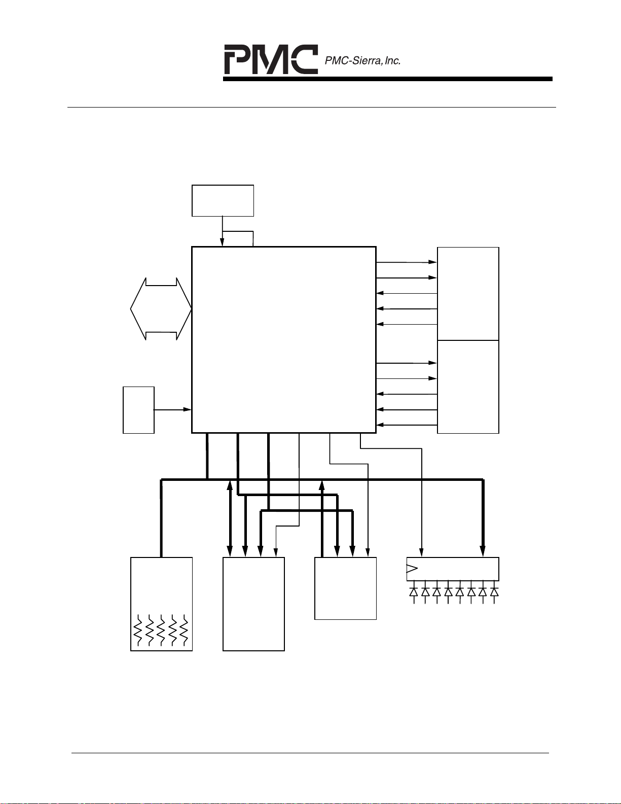
System Block Diagram
The following diagram represents a high-level view of the simple switch system
described above:
Power-On
Reset
RST* ERST*
TXD[3:0]
PCI Bus
TEN[3:0]
RXD[3:0]
CRS[3:0]
COL[3:0]
Quad
MAU
(PHY)
PM3350
TXD[7:4]
50
MHz
Clock
SYSCLK
TEN[7:4]
RXD[7:4]
CRS[7:4]
MDATA[31:0]
MADDR[17:0]
MRD, MWR[3:0]
MCS[1]
MCS[0]
MCS[2]
COL[7:4]
Quad
MAU
(PHY)
MDATA[7:0]
Device
D A R/W CAS* D A OE* CS*
MDATA[7:0]
LED
Config
Pull-up/
Pull-down
DRAM
EPROM
Resistors
In the diagram above, the quad-PHY devices, the EPROM, the DRAM and the 50 MHz
clock oscillator are all created in a straightforward manner from off-the-shelf parts. The
PROPRIETARY AND CONFIDENTIAL TO PMC-SIERRA, INC., AND PMC-SIERRA, INC. CUSTOMERS ONLY 40

ELAN 8X10
DATA SHEET
PMC-970109 ISSUE 3 8 PORT ETHERNET SWITCH
PM3350 ELAN 8 X10
device configuration resistors are merely resistor pull-ups and pull-downs that drive the
memory data bus lines to specific values during reset, as described later; the resistor
values used are not critical, and may range from 4.7k to 10k.
It is assumed that the minimum recommended configuration of 1 megabyte of DRAM
and 32 Kbytes of EPROM are used. A typical implementation would use two 256k x 16bit dual-CAS 60 ns Extended Data Out (EDO) DRAMs, together with a 256 kbit (32k x
8-bit) 150 ns EPROM. Larger memories may also be used if more buffer space or MAC
addresses are to be supported; if this is done, the configuration parameters in the
EPROM must be changed to reflect the increased memory size. The DRAM and
EPROM device types and speeds are defined by the setting of the pull-up / pull-down
resistors on the memory data bus at reset time.
The power-on reset generator can be created either from discrete components, or from
a low-cost CPU monitor; the ERST_ output from the ELAN 8x10 chip is strapped to the
reset signal to implement the watchdog capability of the ELAN device. Note that the
ERST_ output may, as an alternative, be used to signal some external processor that
the ELAN 8x10 device has encountered a fatal error condition requiring a software or
hardware reset; in this case, the ERST_ output should be pulled up using a 4.7k
resistor.
The LED register is implemented using a simple 8-bit TTL register with a clock enable
that is tied to the indicated chip select output from the ELAN 8x10. Eight LEDs may be
connected to the outputs of this register to present the diagnostic status codes output
by the ELAN 8x10 firmware during self-test, system boot and operation. If a simple TTL
register is used, the LED register is effectively write-only; writes to this register will
modify the state of the LEDs, but reads from this register return invalid values. A readback register can be used if this is a significant issue.
The first three chip select lines from the ELAN 8x10 (i.e., MCS_[0], MCS_[1] and
MCS_[2]) are tied to the DRAM, the EPROM and the LED register, respectively; the
remaining chip select is unused. This maps the DRAM into the first 4 MB bank of
address space, the EPROM into the second bank, and the LED register into the third
bank. The address map in the following subsection gives the 24-bit address ranges
assigned to each resource.
This system has only been presented to serve as a basis for the following discussion on
the device and system operation, and is not intended to serve as a complete example
or reference design. More details on actual system construction with the ELAN 8x10
may be found in the relevant application notes and reference design documents.
PROPRIETARY AND CONFIDENTIAL TO PMC-SIERRA, INC., AND PMC-SIERRA, INC. CUSTOMERS ONLY 41
ELAN 8X10
DATA SHEET
PMC-970109 ISSUE 3 8 PORT ETHERNET SWITCH
PM3350 ELAN 8 X10
System Memory Map
The ELAN 8x10 device uses a single linear (flat) byte-addressable 16 MB address
space for accessing memory and memory-mapped devices. The external memory map
for the system described above is quite straightforward. From the point of view of the
local memory bus, it is as follows (note that the memory addresses shown increase
upwards):
0xffffff
Unused Bank 3
0xc00000
0xbfffff
Unused Bank 2
0x800004
0x800000
0x4fffff
LED Register
Unused
0x420000
0x41ffff
Boot EPROM
(32 kB; occupies 128 kB)
0x400000
0x3fffff
Unused
0x100000
0x0fffff
System DRAM
(1 MB)
0x000000
Bank 1
Bank 0
Note that the 32 kB boot EPROM actually occupies 128 kB of address space. This is
because the EPROM is only 8 bits wide (i.e., a 32k x 8-bit configuration), and so is
connected to the least significant byte lane of the memory data bus. Hence each byte of
the EPROM takes up a full 32 bits worth of address space, leading to the 128 kB
requirement.
In a similar manner to the 8-bit wide EPROM, the LED register is mapped to the least
significant 8 bits of the data bus, but takes up a full 32 bits of address space. No other
device is shown as being mapped to the ELAN 8x10 address space in this simple and
minimal system; however, other devices (such as RS232-C serial ports) may be
interfaced as well, provided that firmware is developed to support them.
PROPRIETARY AND CONFIDENTIAL TO PMC-SIERRA, INC., AND PMC-SIERRA, INC. CUSTOMERS ONLY 42

ELAN 8X10
DATA SHEET
PMC-970109 ISSUE 3 8 PORT ETHERNET SWITCH
PM3350 ELAN 8 X10
When viewed from the PCI bus, the ELAN 8x10 device appears to take up a 16 MB
block of contiguous addresses in the total 4 GB PCI address space. A virtually identical
memory map is presented to the PCI bus when accessing the ELAN 8x10 device as a
PCI slave (target), with the exception that a set of device control and communication
registers are implemented in the uppermost 64 kB of the 16 MB address space used by
the ELAN 8x10 device (note that the memory addresses shown increase upwards):
Rest of PCI Address Space
0xBBffffff
Device Control Registers
0xBBff0000
0xBBfeffff
Unused Bank 3
0xBBc00000
0xBBbfffff
Unused Bank 2
0xBB800004
0xBB800000
0xBB4fffff
LED Register
Unused
0xBB420000
0xBB41ffff
Boot EPROM
(32 kB; occupies 128 kB)
0xBB400000
0xBB3fffff
Unused
0xBB100000
0xBB0fffff
System DRAM
(1 MB)
0xBB000000
Rest of PCI Address Space
Bank 1
Bank 0
The start address of the block occupied by the ELAN 8x10 is defined by the setting of
the memory base address register within the PCI configuration register space of the
ELAN 8x10 device, and is represented by the BB component of the addresses given in
the table above. The memory base address register may be set to any arbitrary value
via a PCI configuration write after system reset, provided that the base address is on a
PROPRIETARY AND CONFIDENTIAL TO PMC-SIERRA, INC., AND PMC-SIERRA, INC. CUSTOMERS ONLY 43

ELAN 8X10
DATA SHEET
PMC-970109 ISSUE 3 8 PORT ETHERNET SWITCH
PM3350 ELAN 8 X10
16 MB boundary and that the ELAN 8x10 operating firmware parameters are set
consistently with the selected base address.
Device Internal Blocks
The ELAN 8x10 consists of the following major components: a Switch Processor, eight
MAC interfaces, a DMA Controller, a memory controller and a PCI expansion port. In
addition, it also implements a watchdog reset circuit and some auxiliary functions.
Switch Processor
The Switch Processor is a 50 MHz proprietary RISC processor that executes the
firmware required for carrying out all the packet switching and device control functions
of the ELAN 8x10. It is specifically designed to support LAN protocols at high speeds in
a closed embedded system environment. The Switch Processor contains various
hardware features that permit it to carry out all of its functions at maximum efficiency,
and is tightly coupled to the rest of the ELAN 8x10 device logic
The Switch Processor interfaces to the rest of the ELAN 8x10 device via several
dedicated hardware ports:
1. It uses a special control register access bus to read or write any of up to 96 16-
bit control registers that are implemented by the internal hardware units; these
registers are used to set configuration parameters in various ELAN 8x10 units,
read the unit status, set various operating parameters (such as address
pointers), and perform device self-test.
2. It implements a set of thirteen level-sensitive hardware interrupts that are
connected to various blocks within the ELAN 8x10; these interrupts are the
primary task dispatching entity for the base switching code. Assertion of an
interrupt line causes the corresponding interrupt service routine (ISR) to begin
executing, and execution normally proceeds until the ISR has finished servicing
the unit that required attention.
3. A set of 32 general-purpose outputs and 15 general-purpose inputs are
provided. These are connected to various low-level control and status signals
presented by various ELAN 8x10 internal logic blocks. The general-purpose
inputs and outputs considerably speed up the testing of the state of the logic
blocks and also the control of their functions, as multiple tests on inputs or
multiple modifications of outputs can be performed in a single instruction.
4. A set of 16 coprocessor condition tests are implemented by the Switch
Processor. These inputs are used to signal high-level device conditions
generated by various ELAN 8x10 functional units to the Switch Processor
firmware.
PROPRIETARY AND CONFIDENTIAL TO PMC-SIERRA, INC., AND PMC-SIERRA, INC. CUSTOMERS ONLY 44

ELAN 8X10
DATA SHEET
PMC-970109 ISSUE 3 8 PORT ETHERNET SWITCH
PM3350 ELAN 8 X10
The internal and external registers implemented by the Switch Processor and the
associated ELAN 8x10 functional units, as well as the view of the debug registers from
the PCI bus interface, are presented in subsequent sections.
The Switch Processor expects to locate its operating firmware as part of a
boot image
present in the external memory space. The format of the boot image is described later.
Ethernet MAC Interfaces
Eight identical interfaces to external Ethernet/IEEE 802.3 MAU devices are provided
on-chip. The ELAN 8x10 performs only the 802.3 MAC-layer functions: serial/ parallel
conversion, packet generation and extraction, jamming and backoff after collision,
deference, interframe gap enforcement, and buffering. These are performed with a
combination of dedicated hardware in the MAC interfaces and microcode running on
the Switch Processor. The external transceivers (MAU devices) are expected to
implement all the standard 10BaseT MAU functions: line driving/receiving, clock
generation and recovery, Manchester encoding and decoding, and carrier and collision
detect.
Each MAC interface unit consists of the following functional blocks:
• Interfaces to the receive and transmit ports of the external 10 Mb/s MAU
devices. These interfaces transfer serial, independently clocked receive and
transmit data between the ELAN 8x10 and the MAU, and also allow the MAU to
report carrier detect and collision status.
• A serializer/deserializer that converts between the 8-bit parallel data format used
by the ELAN 8x10 MAC logic and the 1-bit serial format used by the MAU.
• A 32-byte bi-directional FIFO buffer that holds parallel transmit data prior to
parallel-to-serial conversion, and receive data words after serial-to-parallel
conversion. The FIFO buffer also decouples the external MAU transmit and
receive clocks from the internal ELAN 8x10 device clock, and converts between
a byte-wide interface to the serializer/deserializer and a word-wide interface to
the DMA Controller.
• Control/status registers and logic that allows the Switch Processor to control the
MAC port and the MAU devices, and also to monitor status. The control/status
registers contain the timers required for the CSMA/CD algorithm.
During transmission, 32-bit parallel data to be transmitted are placed in the bidirectional FIFO buffer of each MAC port by the DMA Controller. After any required
deference or interframe gap time, these are read out as 8-bit bytes, serialized and sent
to the external MAU for transmission on to the twisted-pair or coaxial link. The IEEE
802.3 standard 2-part interframe gap timing algorithm is implemented.
PROPRIETARY AND CONFIDENTIAL TO PMC-SIERRA, INC., AND PMC-SIERRA, INC. CUSTOMERS ONLY 45

ELAN 8X10
DATA SHEET
PMC-970109 ISSUE 3 8 PORT ETHERNET SWITCH
PM3350 ELAN 8 X10
If a collision is detected (as reported by the external MAU) the MAC port forces
transmission of a jam sequence (of configurable length) and then halts transmission for
the specified backoff time, flushing its FIFO at the same time and signaling a collision.
An internal backoff timer is then loaded with the appropriate value; when the backoff
period is timed out, the MAC logic will re-attempt transmission. The computation of the
backoff period used for each collision on each MAC channel is implemented by the
Switch Processor, using a random number generator modified according to the
truncated binary exponential backoff algorithm specified by the IEEE 802.3 standard.
The Switch processor always pre-loads the backoff period that will be used for the next
collision into a backoff reload register within the MAC channel, thereby avoiding
collision backoff time variation due to firmware latencies.
Data received from the twisted-pair or coaxial cable by the MAU are converted to 8-bit
parallel bytes by the deserializer and written to the FIFO, and subsequently read out by
the DMA Controller as a stream of 32-bit words. The MAC logic performs the preamble
detection and stripping necessary to frame to the incoming data. As few as 14
consecutive bits of valid preamble (i.e., a 1010... bit pattern) may be presented to the
MAC port, along with an SFD, to guarantee proper frame synchronization; this permits
the phase locked loop settling time requirements in the physical layer transceivers to be
considerably relaxed. If an invalid pattern is detected in the preamble prior to receiving
a valid SFD, then the MAC logic rejects the entire frame, waits until the carrier sense
from the physical layer transceiver goes inactive, and begins looking for the next valid
frame.
After the carrier sense input from the external transceiver is de-asserted (indicating that
frame reception has ended), the ELAN 8x10 MAC logic blinds the receiver for a
programmable interval. During this time, transients on the carrier sense input will be
ignored (unless the MAC port was transmitting just previously) as per the IEEE 802.3
standard. The blind timer also defines the minimum tolerable interframe gap that can be
accepted by the MAC port during back-to-back frame receives.
The MAC logic also implements an internal configurable jabber counter to time out
excessively long transmissions or reception; thus the ELAN 8x10 does not require the
external MAU to provide jabber protection.
Each MAC channel implements an optional flow-control mechanism to backpressure
the channel in the case of local congestion (e.g., an out-of-buffers condition).
Backpressure is accomplished by continuously transmitting an extended jam sequence
(all-zeros) pattern, with gaps of one standard interframe spacing inserted periodically to
prevent the backpressure pattern from being interpreted as a jabber. Collisions
encountered during backpressure will not cause the MAC channel logic to back off in
the normal manner; instead, the MAC channel will send the standard jam pattern, time
out a normal interframe gap, and then resume the backpressure pattern. If, during
backpressure, the MAC channel detects that one or more frames are ready to be
transmitted over the channel by the ELAN 8x10 (e.g., a frame was received from some
PROPRIETARY AND CONFIDENTIAL TO PMC-SIERRA, INC., AND PMC-SIERRA, INC. CUSTOMERS ONLY 46

ELAN 8X10
DATA SHEET
PMC-970109 ISSUE 3 8 PORT ETHERNET SWITCH
PM3350 ELAN 8 X10
other channel that is destined for an end-station on the flow-controlled channel), the
MAC channel will cease transmitting the backpressure pattern, wait for a normal
interframe gap, and then transmit the desired frame(s). After all the pending frames
have been transmitted, the MAC logic will resume backpressuring the channel.
The backpressure mechanism described above is an optional feature that may be
enabled on a per-port basis by means of configuration parameters in the boot image. It
should be noted that the backpressure method will result in the complete shutdown of
the MAC channel (i.e., even local segment traffic will not be allowed to proceed), and so
it is recommended that backpressure be enabled only on ports that are connected to a
small number of end-stations.
The ELAN 8x10 MAC channels also provide a frame type filtering feature that extracts
the 16-bit EtherType fields of incoming frames (occupying the portion of the Ethernet
frame header immediately after the destination and source MAC addresses), compares
it to a programmable 16-bit value, and signals the Switch Processor firmware if a match
is found. This facility may be used, for example, to quickly identify MAC Control frames
(defined in IEEE 802.3x) or Address Resolution Protocol frames belonging to the
TCP/IP protocol. The Switch Processor firmware may then handle such marked frames
in a special manner.
Each MAC channel maintains a pair of control and status registers that allow the Switch
Processor to monitor and manage the state of the MAC channels. The MAC interfaces
are configurable (as a group) by a set of configuration registers that are loaded at
initialization time. The following parameters are configurable:
Parameter Min Max Units
Interframe spacing, Part 1 0 255 bit times
Interframe spacing, Part 2 0 255 bit times
Transmitted preamble length (not
including SFD byte)
Jam length (after collision) 1 255 bit times
Maximum frame size 1 4095 bytes
Minimum frame size 1 255 bytes
Late collision threshold 0 1024 bit times
Receiver blind time 0 255 bit times
EtherType comparison value 0 65535 N/A
0 255 bits
It should be noted that the Part 1 interframe spacing may be set to zero, in which case
the interframe behavior of the ELAN 8x10 MAC defaults to that specified by the
Ethernet V2.0 standard. If the Part 1 interframe spacing is non-zero, then the minimum
interframe gap that can be tolerated by the MAC port during back-to-back frame receive
will be the
greater
of the Part 1 interframe spacing and the receiver blind time.
PROPRIETARY AND CONFIDENTIAL TO PMC-SIERRA, INC., AND PMC-SIERRA, INC. CUSTOMERS ONLY 47

ELAN 8X10
DATA SHEET
PMC-970109 ISSUE 3 8 PORT ETHERNET SWITCH
PM3350 ELAN 8 X10
Note:
None of the MAC control, status or configuration registers are visible from the
PCI bus interface; they may be accessed only by the Switch Processor. More
details on individual registers within the MAC channels are given later.
Multichannel DMA Controller
The DMA Controller is responsible for performing all data block transfers within the
ELAN 8x10 and for computing the 32-bit Ethernet CRC check performed on packets
received from or transmitted to the MAU channels. A special feature of the DMA
Controller is its ability to automatically allocate buffer storage from a central free pool
(organized as a linked list pointed to by a dedicated device register) when receiving
data from a MAC channel or the expansion port. In addition, the DMA Controller
implements an address hash table look-up capability that automatically resolves the
source and destination MAC addresses of incoming Ethernet frames using an address
table built in external RAM.
The DMA Controller supports a total of eleven separate channels, all of which may be
running concurrently. Each channel is assigned a dedicated set of locations within an
internal register file to hold transfer parameters and status. All but two of the DMA
channels are capable of handling linked-lists of fixed-length
packet buffers
, which are
chained together in varying numbers to hold Ethernet packets of different lengths. The
eleven channels are dedicated to various functions as follows:
• Eight channels are used to perform data transfers between the 8 MAC channel
FIFOs and the local memory, copying data from the local memory to the MAC
FIFOs on transmit or from the FIFOs to the local memory on receive. These
channels are capable of generating (on receive) and following (on transmit)
linked-lists of packet buf fers in external memory. A 32-bit CRC is computed on
both transmit and receive data transfers; the CRC result may be optionally
appended to the transmit data, and is accessible to the Switch Processor
firmware in the form of a CRC check error bit after a packet has been received.
Packet buffers are automatically allocated from a central free pool on receive.
The source and destination MAC addresses of frames received from the MAC
channels will also be extracted and used to look up the address entries in an
external hash table.
• One channel is used to perform block transfers from the external PCI expansion
bus to the local memory. This channel can follow a chain of remote source
packet buffers, reading data over the PCI bus and creating a corresponding
chain of packet buffers in the local memory, automatically allocating the required
local packet buffers from the free pool.
PROPRIETARY AND CONFIDENTIAL TO PMC-SIERRA, INC., AND PMC-SIERRA, INC. CUSTOMERS ONLY 48

ELAN 8X10
DATA SHEET
PMC-970109 ISSUE 3 8 PORT ETHERNET SWITCH
PM3350 ELAN 8 X10
• One channel is used to perform block transfers from the local memory to
external memory space accessible via the PCI expansion bus. This channel is
not intended to handle packet data; it is generally used for special control and
inter-device communication functions.
• The last channel facilitates the packet exchange handshake that takes place
between multiple ELAN 8x10 devices located on the same PCI bus. This
channel can be set up to perform up to seven writes in a single series of PCI
transactions to special request and acknowledge counters in up to seven
external ELAN 8x10 devices. The request and acknowledge counters are used
to indicate the presence of a packet being forwarded and to acknowledge
receipt of the packet, respectively.
Transfers are initiated under firmware control by the Switch Processor. In operation,
the Switch Processor loads the appropriate locations within the DMA register file with
the desired transfer parameters, and then enables the channel using the DMA control
register. The DMA Controller logic then reads out the transfer parameters into internal
temporary registers, performs the transfer, and updates the register file. The DMA
automatically multiplexes channel transfers by switching to a new channel after a burst
of up to 4 data words (i.e., 16 bytes) has been read or written, thus minimizing latency.
Memory Controller
An external memory is required to hold packet buffers for received and transmitted
Ethernet packets, as well as data structures needed to perform switching and support
system management. The external memory may also contain extension firmware for
the on-chip Switch Processor. The ELAN 8x10 therefore contains an integral memory
controller unit to support a variety of standard memories without glue logic.
The memory controller addresses a total of 16,777,216 bytes (16 megabytes) of EDO
DRAM, ROM, EPROM and EEPROM (either separately or in combination). The
address space is divided into four banks, each of which has an independently
programmable access time. This allows a mix of fast and slow devices to be used in
the system. Memory device types or speeds cannot be mixed within a bank (i.e., a
bank cannot consist of part EDO DRAM and part EPROM, for example). Memory
devices of different types must be assigned to different banks, and selected with
different chip selects.
Programming of EEPROM devices is done under control of Switch Processor
microcode.
To support memories other than those listed above, or special applications, a memory
ready input pin (MRDY_) is provided. This pin is sampled by the ELAN 8x10 when
accessing memories in asynchronous SRAM mode; it may be driven inactive prior to
the end of any memory cycle by an external memory timing generator to suitably
PROPRIETARY AND CONFIDENTIAL TO PMC-SIERRA, INC., AND PMC-SIERRA, INC. CUSTOMERS ONLY 49

ELAN 8X10
DATA SHEET
PMC-970109 ISSUE 3 8 PORT ETHERNET SWITCH
PM3350 ELAN 8 X10
lengthen the access cycle. The MRDY_ pin should be tied LOW (permanently asserted)
if it is not used.
The ELAN 8x10 generates four separate write enables to enable individual bytes within
each addressed 32-bit word to be written to independently of the others. This allows
the ELAN 8x10 to perform byte (8-bit), halfword (16-bit), tribyte (24-bit) and fullword (32bit) memory accesses without using read-modify-write operations.
An interrupt pin (MINTR_) is provided for special applications. A LOW level on this pin
causes an interrupt to be generated to the internal Switch Processor, the PCI bus (via
the INT_ output), or both. The use of this interrupt input is application dependent and
beyond the scope of this datasheet. The MINTR_ pin should be tied HIGH (deasserted) if it is not used.
The memory controller is capable of sustaining a throughput of 84 Mbytes/s (672
Mbit/s) to and from standard EDO DRAM devices, with peak throughputs of 100
Mbytes/s during burst accesses.
PCI Expansion Port
The ELAN 8x10 includes a PCI v2.1 compatible bus master and slave interface, which
serves as an expansion port allowing multiple ELAN 8x10s to be seamlessly
interconnected in the same system. The expansion port supports a maximum PCI bus
clock of 40 MHz (resulting in a >1 Gbit/s peak transfer rate and a sustained throughput
of over 400 Mbit/s), and contains several FIFOs to increase burst throughput and
perform clock synchronization. This port may be used for expanding a switch built
around 8-port ELAN 8x10 chips (to a maximum of 64 ports In this application, the onchip DMA Controller uses the PCI master interface to notify other ELAN 8x10 devices
of the presence of packets to be transferred, and to copy packets or data structures
under control of the Switch Processor between external ELAN 8x10 devices to the local
memory space. Note that data are never transferred directly between the MAC
channels and the PCI bus.
The PCI bus master interface serves to allow the DMA controller as well as the CPU to
initiate transactions on the PCI bus. The bus master is compatible with the PCI v2.1
specifications for standard transaction initiator devices, and can perform configuration
space as well as memory space read and write transfers. (Note that the ELAN 8x10
does not support I/O space transactions.) The PCI bus master unit contains a 64-byte
write FIFO to buffer data being written by the ELAN 8x10 device to an external target on
the PCI bus, as well as a 128-byte read FIFO to hold data that has been read from an
external target. These FIFOs permit the bus master to operate using long burst
transactions for increasing the PCI bus bandwidth utilization. The bus master interface
is also compatible with the PCI v2.1 latency timer requirements, and supports back-toback transfers.
PROPRIETARY AND CONFIDENTIAL TO PMC-SIERRA, INC., AND PMC-SIERRA, INC. CUSTOMERS ONLY 50

ELAN 8X10
DATA SHEET
PMC-970109 ISSUE 3 8 PORT ETHERNET SWITCH
PM3350 ELAN 8 X10
The PCI slave interface logic within the expansion port block responds to transfer
requests from external bus masters, performing the necessary accesses and
transferring the requested data. The slave interface logic acts as a responder during
frame transfers between devices belonging to the ELAN chipset, supplying Ethernet
frame data to requesters as necessary. An external processor can also use the PCI
slave interface to gain access to internal device registers and data structures in the
local memory space, or to download firmware or data to the ELAN 8x10 Switch
Processor. The slave interface unit contains a 32-byte write FIFO and a 128-byte read
FIFO to improve burst behavior during PCI reads and writes: the write FIFO buffers
data being written to the ELAN 8x10 by external devices, while the read FIFO holds
data read from local memory or internal registers in response to PCI memory read
commands from external requesters. Note that the slave interface only responds to
configuration space and memory space reads and writes; I/O space reads and writes
are not supported. The slave interface conforms to the access latency, access ordering
and disconnect rules of the PCI v2.1 standard. A set of special registers are provided in
the PCI configuration space that may be used to alter the access latency rules imposed
by the slave logic in order to improve PCI bus utilization if required.
The expansion port also contains hardware to speed up intercommunication between
ELAN 8x10 devices via the PCI bus. This hardware takes the form of seven request
counters and seven acknowledge counters. Each request/ acknowledge counter pair is
dedicated to supporting communications with a specific external ELAN 8x10 device. An
external ELAN 8x10 device will increment a request counter to signal that a packet or
message data is available to be read, and will increment an acknowledge counter to
acknowledge that it (the external ELAN 8x10) has read a message or packet from the
local ELAN 8x10. Standard PCI reads and writes can be used to increment the request
and acknowledge counters. More details on these counters are supplied below.
The expansion port is compatible with the "PCI Local Bus Specification", release 2.1.
To support the use of the ELAN 8x10 in standalone switch system applications, a
simple external bus arbiter (easily implemented in a single programmable logic device)
must be provided to arbitrate between PCI bus accesses of multiple ELAN 8x10
devices.
The PCI bus interface within the expansion port runs synchronously to the PCI bus
clock, which must be supplied on the PCI_CLK input pin. The duty cycle of the
PCI_CLK pin is as specified in the PCI Local Bus Specification whereas the operating
frequency used by the ELAN expansion bus interface is 40 MHz, as opposed to the PCI
Local Bus Specification value of 33 MHz. The ELAN 8x10 PCI bus interface implements
synchronization logic to transfer data between the PCI bus clock domain and the
internal device clock.
PCI Transactions Supported
The on-chip PCI interface is capable of initiating the following commands:
PROPRIETARY AND CONFIDENTIAL TO PMC-SIERRA, INC., AND PMC-SIERRA, INC. CUSTOMERS ONLY 51

ELAN 8X10
DATA SHEET
PMC-970109 ISSUE 3 8 PORT ETHERNET SWITCH
PM3350 ELAN 8 X10
• memory read
• memory write
• configuration read
• configuration write
The on-chip PCI interface supports the following PCI commands as a target:
• memory read
• memory write
• configuration read
• configuration write
• memory read multiple
• memory read line
• memory write and invalidate
PCI Vendor ID and Device Number
The vendor ID assigned to the ELAN 8x10 device (in the PCI configuration register
space) is 11F8 hexadecimal, while the device number is 3350 hexadecimal. The class
code for the ELAN 8x10 is set to 0x020000 hexadecimal.
Slave Read Prefetching
The PCI bus slave logic contains a 128-byte read FIFO buffer to speed up reads made
from this ELAN 8x10 device over the PCI bus. This FIFO has a prefetch capability that
is activated when accessing external memory space: it attempts to read ahead and
speculatively obtain more data words than have been actually requested by the
transaction master, thereby potentially increasing the efficiency of burst transfers.
The prefetch capability functions as follows. Initially, the PCI slave read FIFO is empty,
and remains so until the PCI slave is idle. When a read transaction is initiated by an
external bus master, the PCI slave logic will perform a disconnect with retry (after a
configurable amount of cycles) because the read FIFO is empty and no data can be
returned. The slave logic then decodes the target address of the read: if it corresponds
to external memory space, then the prefetch capability is activated. The slave logic
subsequently requests the memory controller to begin fetching from the target memory
address; the data returned are placed into the slave read FIFO, and the PCI slave logic
continues to fetch additional data words at consecutive addresses until the slave read
FIFO is full. Up to 128 bytes of data may be fetched in this way and placed into the
slave read FIFO.
At some point, the original PCI transaction initiator (bus master) is expected to retry the
access. (According to the rules of the PCI bus, it is an error for the bus master to
abandon an access that has been terminated with a disconnect-and-retry.) The PCI
slave logic will compare the address being requested by the PCI bus master for the
PROPRIETARY AND CONFIDENTIAL TO PMC-SIERRA, INC., AND PMC-SIERRA, INC. CUSTOMERS ONLY 52

ELAN 8X10
DATA SHEET
PMC-970109 ISSUE 3 8 PORT ETHERNET SWITCH
PM3350 ELAN 8 X10
retried transaction to the address from which it began the prefetch; if a match occurs,
the slave logic will return the data present in the read FIFO in a continuous burst of
back-to-back data phases on the PCI bus. The burst of transfers on the PCI bus will
continue as long as (1) the read FIFO is not empty and (2) the bus master does not
terminate the access.
If the read FIFO empties during a transfer (possibly because the memory controller
cannot satisfy the requests from the PCI slave logic at a sufficient rate), the PCI slave
logic will issue another disconnect with retry, and continue to request the memory
controller for more data. The bus master is again expected to retry the access, and the
cycle continues.
If the bus master terminates the access in any way, the PCI slave logic will stop placing
data on the PCI bus and flush the read FIFO to discard any remaining unread data
words. It will then proceed to fulfill the next PCI read or write access.
The use of the PCI slave read FIFO enhances the ability of the PCI slave logic to
maintain the utilization of the PCI bus by transferring data in long bursts. If sufficient
delay is inserted by the bus master between the initial disconnected access and the
subsequent retry, the PCI slave will have time to read ahead by a substantial number of
words (up to 32) and can therefore transfer data in a long burst when the bus master
finally retries the access.
To further improve the efficiency of the PCI slave interface, the slave logic has the
capability of latching and holding up to two different target read addresses from two
different bus masters at a time. This allows the first bus master to make a read access,
which will be disconnected with retry by the PCI slave logic after the target address has
been latched; another bus master can then make another read access at a different
address, which will also be disconnected with retry by the slave logic after the address
has been latched. (Only two such addresses can be latched by the slave; if yet a third
master makes another read access to another address, the slave logic will also
disconnect this master with a retry, but will not latch the address internally.) The
availability of the second read address means that the PCI slave logic can begin
immediately fetching data from the second location into the read FIFO after the first bus
master terminates its access, without waiting for the second bus master to retry the
access, and hence the PCI slave logic can improve its utilization of the available
memory and PCI bus bandwidth.
Note:
Writes are not allowed to be completed out-of-sequence with reads, and vice
versa.
PROPRIETARY AND CONFIDENTIAL TO PMC-SIERRA, INC., AND PMC-SIERRA, INC. CUSTOMERS ONLY 53

ELAN 8X10
DATA SHEET
PMC-970109 ISSUE 3 8 PORT ETHERNET SWITCH
PM3350 ELAN 8 X10
Watchdog Timer Facility
The ELAN 8x10 device incorporates a simple internal watchdog timer that optionally
initiates an automatic system hardware reset if some catastrophic error occurs that
causes the Switch Processor to lock up or enter an undefined state. The watchdog
timer is built around the 16-bit WTIMER device control register (described in more detail
in a later section).
The WTIMER register principally acts as a down-counter, decrementing its value by 1
every millisecond until it reaches zero. Firmware running on the Switch Processor will,
under normal circumstances, periodically reload the WTIMER register with a non-zero
value before it reaches zero. If however, the Switch Processor firmware encounters
some serious system fault that prevents it from reloading the WTIMER register before it
has counted down to zero, the watchdog facility will assert the ERST_ output LOW for
one millisecond. If the ERST_ output is tied to the system reset line (this is made
possible by the fact that ERST_ is an open-drain output), then the watchdog timer
facility will effectively reset the entire system. Alternatively, the ERST_ output can tied
to a resistive pull-up and simply monitored by an external system processor; a hardware
or software reset of the ELAN 8x10 device should be performed if the ERST_ output
goes LOW.
The value used by the Switch Processor firmware to reload the WTIMER register is a
configurable parameter, and should be chosen to ensure that false system resets do
not occur under high loads without simultaneously incurring an excessive system
recovery time. The maximum reload interval is approximately 65 seconds; the minimum
interval is about 2 milliseconds. A value of 1-2 seconds is recommended.
If the WTIMER register is loaded with all-ones (0xffff hex) the watchdog timer facility will
be disabled, and the WTIMER register will be prevented from counting down and
asserting the ERST_ output. (The watchdog facility can hence be disabled by the
system implementer by setting the configurable reload value to 0xffff hex.) Note that the
WTIMER register rolls over to 0xffff after it has counted down to zero, thereby
automatically disabling itself after the 1 millisecond reset duration is over. If the
WTIMER register is left untouched by the initialization process, then it will default to a
disabled state, i.e., it will remain loaded with 0xffff and, as a result, will not count down.
If the Switch Processor itself detects an unrecoverable fault that requires a general
system reset, then the Switch Processor firmware will write a value of zero to the
WTIMER register under program control. This will cause the ERST_ pin to be
immediately asserted (driven LOW), potentially causing a hardware reset or notifying
the system processor that a fault has occurred.
PROPRIETARY AND CONFIDENTIAL TO PMC-SIERRA, INC., AND PMC-SIERRA, INC. CUSTOMERS ONLY 54

ELAN 8X10
DATA SHEET
PMC-970109 ISSUE 3 8 PORT ETHERNET SWITCH
PM3350 ELAN 8 X10
Configuration and Initialization
Initialization and configuration can be considered as either a two step or four step
process. The two-step process is the default, and used for most normal applications;
the four-step proce ss may be followed to over-ride the default con figuration information
for special purposes.
Two-step process
For a two-step process all of the basic device and system configuration information is
taken from the local memory interface of this ELAN 8x10 chip using this sequence:
• Basic hardware configuration information, comprising a 32-bit device and
memory configuration word, is latched by the ELAN 8x10 from the memory data
lines into internal registers upon RST_ transitioning high (i.e., upon the trailing
edge of a hardware reset). The 32-bit configuration word is held in the
MCONFIG (Memory Configuration) and DCONFIG (Device Configuration)
registers.
• The remaining device configuration and initialization information is obtained
automatically by the ELAN 8x10 by scanning for an external EPROM or
EEPROM, and reading a bootstrap image from it. The bootstrap image contains
a number of system-dependent configuration parameters, the operating
firmware for the Switch Processor, and any code required for a Real-Time
Operating System, SNMP agent, spanning tree processing, etc.
Four-step process
For a four-step process not all of the basic device and system configuration is taken
from the local memory of this ELAN 8x10 chip: an external host processor, or a master
ELAN 8x10 device, is expected to modify or download configuration and bootstrap data.
1. Configuration information is latched from the memory data lines into internal
registers upon RST_ transitioning high as described above. The RISCRUN bit
(bit 30, see the next section) of the 32-bit configuration data word must be
cleared to ensure that the Switch Processor enters a halt state immediately after
reset. The PCIRUN bit (bit 31) of th e configuration data word may also be
cleared if the external host processor intends to carry out the normal PCI
configuration register setup process as per the PCI specification.
2. The DCONFIG and MCONFIG registers of the device are accessible via the PCI
bus interface, and may be modified if necessary by the system master. It is also
possible for the system master to download a preformatted bootstrap image to
the RAM interfaced to the device; the ELAN 8x10 will locate the bootstrap image
and self-initialize from it.
PROPRIETARY AND CONFIDENTIAL TO PMC-SIERRA, INC., AND PMC-SIERRA, INC. CUSTOMERS ONLY 55

ELAN 8X10
DATA SHEET
PMC-970109 ISSUE 3 8 PORT ETHERNET SWITCH
PM3350 ELAN 8 X10
3. A software reset is performed to the device using the HCTRL register, also
accessible via the PCI bus, by writing the GRES bit first to a logic 1 and then to
a logic 0. Note that GRES must remain asserted a minimum of 128 PCI clock
cycles. The updated DCONFIG and MCONFIG register information will be
internally latched upon de-assertion of the GRES bit.
4. The remaining device configuration and initialization will be obtained by
scanning for and reading a bootstrap image contained in an external EPROM or
EEPROM, or downloaded into system RAM by the master processor.
Device Configuration
Basic device and system configuration (i.e., memory types and speeds for various
banks, the PCI base address for this ELAN 8x10 device, and auto-boot and
master/slave enable flags) are supplied by means of resistor pull-ups and pull-downs
connected to the 32-bit data bus. This configuration information is latched into internal
registers upon the second SYSCLK rising edge after the RST_ input to the ELAN 8x10
transitions high, and sets up the ELAN 8x10 internal hardware. The 32 bits of
configuration data presented on the memory data bus are latched into the 16-bit
DCONFIG and MCONFIG registers internal to the ELAN 8x10; these registers may also
be accessed by the Switch Processor and by external devices via the PCI bus.
As an alternative to resistor pull-ups and pull-downs, a tri-state buffer or tri-statable
register may be used to drive configuration information on to the data bus during reset.
Care should be taken to remove the data by tri-stating the buffer or register no earlier
than 2 SYSCLK periods after the trailing edge of the RST* input, and no later than 10
SYSCLK periods after the latter (to prevent memory data bus contention).
The memory data bus is mapped to configuration bits as follows:
Device Pin Register Bit Description
MDATA[31] PCIRUN This input selects the default operating mode of the PCI
interface.
If logic 1:
• The on-chip PCI interface latches its slave memory base
address from the CHIPID configuration bits (MDATA[25:22]).
• The PCI Command Register bits for "Bus Master" and
"Memory Space" are set (1), thereby allowing the device to
respond to PCI memory space accesses and to be a bus master.
If logic 0
• The PCI interface has a memory base address of 0.
• The PCI Command Register bits for "Bus Master" and
"Memory Space" are cleared (0); the device is disabled from
responding to PCI memory space accesses and will not be a bus
master.
MDATA[30] RISCRUN A low on this signal halts the Switch Processor upon reset,
effectively placing the device into stand-by mode.
PROPRIETARY AND CONFIDENTIAL TO PMC-SIERRA, INC., AND PMC-SIERRA, INC. CUSTOMERS ONLY 56

ELAN 8X10
DATA SHEET
PMC-970109 ISSUE 3 8 PORT ETHERNET SWITCH
PM3350 ELAN 8 X10
MDATA[29] RSTTM For test purposes only. Pull low for correct operation.
MDATA[28] IMDIS Internal memory disable: if high, the internal Switch Processor
ROM is disabled at initialization time.
MDATA[27] PCI3V If high, configures the PCI interface for the 3.3V signaling
environment. If low, configures the PCI interface for the 5V
signaling environment. Must be set to logic 0 since all AC
parametric testing done with the 5V signaling conditions.
MDATA[26] FIRM Reserved for use by Switch Processor firmware.
MDATA[25:22] CHIPID[3:0] These bits determine the PCI memory base address at
initialization time if the PCIRUN configuration bit is high. In this
case, the CHIPID[3:0] inputs are zero-extended to 8 bits and
loaded into the most significant byte of the Memory Base
Address register in the PCI configuration register space.
MDATA[21:16] RTCDIV[5:0] Real time clock divider: selects the divide ratio used for the
internal real-time clock prescaler. This field must be set
numerically equal to the frequency, in megahertz, of the clock
supplied on the SYSCLK input.
MDATA[15:14] MXSEL[1:0] These inputs select the row/column multiplexing used for EDO
DRAM devices.
MXSEL
00
01
10
11
Column
Address Bits
8
9
10
11
DRAM Configurations
Supported
64K x N & 128K x N
256K x N & 512K x N
1024K x N & 2048K x N
4 Meg x N & 8 Meg x N
MDATA[13] MSLO The MSLO bit extends read and write cycles to accommodate
slower local memory devices. If MSLO is high, memory
accesses will be to 80ns DRAM. If MSLO is low, 60ns DRAM is
expected. The PM3350 is intended to be used with 60ns EDO
DRAM; hence, MSLO must be a logic 0. The access time for
ROM is always 150ns, respectively, regardless of the state of the
MSLO bit.
MDATA[12] MDCAS
This bit identifies the type of DRAM connected to the
memory interface. If MDCAS is high, the memory interface
will generate control signals for 2-CAS DRAMs; otherwise,
it generates signals for single CAS DRAMs.
MDATA[11:9] MTYPE3[2:0] Indicates the type of memory connected to the MCS[3]* output:
MTYPE3[2:0]
000
001
010
011
100
101
110
111
MDATA[8:6] MTYPE2[2:0] Indicates the memory type associated with MCS[2]*. The
encoding is the same as for MTYPE3[2:0].
Selected memory type
Reserved
Reserved
Reserved
Reserved
Reserved
200ns (E)EPROM
60ns EDO DRAM
Reserved
PROPRIETARY AND CONFIDENTIAL TO PMC-SIERRA, INC., AND PMC-SIERRA, INC. CUSTOMERS ONLY 57

ELAN 8X10
DATA SHEET
PMC-970109 ISSUE 3 8 PORT ETHERNET SWITCH
MDATA[5:3] MTYPE1[2:0] Indicates the memory type associated with MCS[1]*. The
encoding is the same as for MTYPE3[2:0].
MDATA[2:0] MTYPE0[2:0] Indicates the memory type associated with MCS[0]*. The
encoding is the same as for MTYPE3[2:0].
PM3350 ELAN 8 X10
After the hardware configuration information has been latched from the data bus, it is
loaded into the DCONFIG and MCONFIG registers. The lower 16 bits of the
configuration word (i.e., bits 0 through 15, latched from MDATA[15:0]) are loaded into
the MCONFIG register, with MDATA[0] being loaded into the LSB of MCONFIG. The
upper 16 bits (i.e., corresponding to MDATA[31:16]) are loaded into the DCONFIG
register in a similar fashion.
System Bootstrap Image
The ELAN 8x10 is designed to self-initialize upon power-up, using information and
operating firmware supplied as a pre-determined image (referred to as the
boot image
)
in external memory (typically, EPROM or EEPROM). The boot image may be located
anywhere in the 16 MB address space, but must start on a 64 kB boundary. The ELAN
8x10 expects the boot image to be formatted in a predefined manner, as described
below. The boot image consists of a boot header and a set of boot data blocks.
Boot Header
The boot image is distinguished by a special 32-bit signature followed by a predefined
configuration header. The ELAN 8x10 will, therefore, perform some basic initialization
indicated by the hardware configuration word loaded from the data bus after reset, and
then begin scanning the entire memory space at 64 kB boundaries for the boot image
signature. It expects to find the four bytes of the signature aligned on four consecutive
32-bit boundaries, as indicated in the following table:
Offset from 64kB
Boundary
+0 XXXXXXC8
+4 XXXXXXA8
+8 XXXXXX37
+12 XXXXXX59
Expected Contents (hex)
The use of a signature to locate the boot image, rather than an explicit address, implies
that it is not necessary to indicate the exact location of the configuration image to the
ELAN 8x10. Instead, the boot image may be located anywhere throughout the 16 MB
address space. In addition, a boot image need not even be supplied using an EPROM
or EEPROM; it may also be downloaded to RAM by an external device or host
processor.
PROPRIETARY AND CONFIDENTIAL TO PMC-SIERRA, INC., AND PMC-SIERRA, INC. CUSTOMERS ONLY 58
ELAN 8X10
DATA SHEET
PMC-970109 ISSUE 3 8 PORT ETHERNET SWITCH
PM3350 ELAN 8 X10
The ELAN 8x10 expects to find executable firmware code within the boot image that will
perform the actual initialization process. However, the boot image is only 8 bits wide,
and thus the firmware code supplied within it cannot be directly executed by the ELAN
8x10 Switch Processor, which uses 32-bit instructions located on 32-bit boundaries. It is
thus necessary for the ELAN 8x10 to copy the boot image to a block of RAM that is set
aside for the purpose, and to convert the 8-bit boot image to a 32-bit version so that the
boot firmware code can be directly executed.
When a proper boot image signature is found, therefore, the ELAN 8x10 will
automatically go on to read a preformatted header within the boot image. This header
should supply information required to copy the boot image to a pre-allocated block of
RAM, and is formatted as follows:
Field
Size,
Bytes
1 +16 HDRFLAGS Boot image processing flags
3 +20,+24,+28 CPYTARGET Target RAM block to copy 8-bit boot
2 +32,+36 CPYSIZE Amount of data to copy in 64-by te
3 +40,+44,+48 CPYFROM Source of copy data within boot image
3 +52,+56,+60 BOOTSTART Starting address of bootstrap firmware
4 +64,+68,+72,+76 CHECKSUM 32-bit checksum, computed over entire
4 +80,+84,+88,+92 SPACER Must be set to 0x00000000
Byte Offsets
from Start
Mnemonic Description
image to
blocks
in target RAM block (valid after copy
completed)
boot image (including checksum field)
hexadecimal
The HDRFLAGS field supplies some control bits that determine how the ELAN 8x10 will
handle the boot image, and is formatted as follows:
7654 0
EightBit CpyInt JmpInt reserved
EightBit:
If set, indicates that the boot image is formatted as an eight-bit-wide memory
block (following the general format that has already been presented);
otherwise, indicates a 32-bit boot image in a special format. This bit is
intended for factory use only, and should always be set by the customer.
CpyInt:
If this bit is set, the contents of the boot image should be copied to the
PROPRIETARY AND CONFIDENTIAL TO PMC-SIERRA, INC., AND PMC-SIERRA, INC. CUSTOMERS ONLY 59

ELAN 8X10
DATA SHEET
PMC-970109 ISSUE 3 8 PORT ETHERNET SWITCH
PM3350 ELAN 8 X10
internal instruction RAM of the Switch Processor rather than a block of
external memory. This bit should be set only if the EightBit flag is also set
(i.e., for a standard 8-bit-wide boot image).
JmpInt:
The JmpInt bit signifies, if set, that the BOOTSTART address indicates an
address present in the instruction RAM of the Switch Processor, rather than
an address in a block of external memory. This bit should be set only if the
EightBit flag is also set (i.e., for a standard 8-bit-wide boot image).
In general, the HDRFLAGS field should be set to 0x80 hex, i.e., indicating an 8-bit-wide
boot image with no special copy or branch options.
Note that the boot image header above is described as it would appear in the 8-bit
image contained within an EPROM or EEPROM that is connected to the leastsignificant byte lane of the memory data bus. Each byte within the EPROM or
EEPROM, therefore, will start on a 32-bit boundary and occupy the least-significant 8
bits of a memory word; the upper 24 bits of the word will be ignored by the ELAN 8x10.
The ELAN 8x10 will copy data bytes from the EPROM or EEPROM boot image to
consecutive byte addresses in a block of 32-bit wide RAM, thereby converting the 8-bit
boot image to a 32-bit boot image. An alternative view of the boot header, giving the
components of the header as they would appear after the boot image has been copied
to 32-bit RAM, is given below:
0x59 0x37 0xa8 0xc8 0
CPYTARGET[23:0] HDRFLAGS[7:0] 4
CPYFROM[15:0] CPYSIZE[15:0] 8
BOOTSTART[23:0] CPYFROM[23:16] 12
CHECKSUM[31:0] 16
SPACER[31:0] 20
The CPYTARGET, CPYSIZE and CPYFROM fields of the header define a block
transfer that must be performed from the boot image to an area of RAM in order to
convert the 8-bit boot image to a 32-bit image. After the copy and conversion has been
done, the BOOTSTART field denotes a 24-bit address from which the ELAN 8x10
Switch Processor will begin executing code. The code at this location (presumably
within the copied 32-bit boot image) is completely responsible for initializing the ELAN
8x10 system and environment, and for initiating normal operation.
The CHECKSUM field contains a 32-bit checksum computed over the entire boot
image. The bootstrap firmware will recompute this checksum and compare it with the
value in the CHECKSUM field. If a mismatch occurs, the ELAN 8x10 will consider the
boot image as invalid, and will terminate the system initialization and startup process
and report an error.
PROPRIETARY AND CONFIDENTIAL TO PMC-SIERRA, INC., AND PMC-SIERRA, INC. CUSTOMERS ONLY 60

ELAN 8X10
DATA SHEET
PMC-970109 ISSUE 3 8 PORT ETHERNET SWITCH
PM3350 ELAN 8 X10
Boot Data
In addition to the signature, header and bootstrap firmware code, the boot image is
expected to contain configuration information such as the sizes of memory buffer pools,
buffer limits defined on a per-port basis, predetermined MAC addresses to be placed in
the routing tables, the location of external ELAN 8x10s, the MAC address and IP
address assigned to this ELAN 8x10, and so on. The boot image must also supply the
operating firmware that is required by the ELAN 8x10 for packet switching and
management. The general layout of the boot image is as shown below (note that the
memory addresses increase downwards):
0 Boot Image Signature
Boot Image Header
Boot Tag Space
Bootstrap Firmware Code
Auxiliary Configuration Information
Auxiliary Firmware Code
32
Master Operating Code
Kbytes
RTOS Firmware Code (optional)
UDP/IP Stack Firmware Code
(optional)
256
Kbytes
SNMP Agent/MIB Firmware Code
(optional)
As shown, the basic bootstrap code and the master switch operating firmware occupy
32 Kbytes of EPROM/EEPROM space; if an SNMP agent is required (with the
associated UDP/IP stack and RTOS firmware), then the boot image size requirements
rise to 256 Kbytes. Contact the factory for more information on the boot image, and the
means of creating one.
The bootstrap firmware code performs a brief self-test, testing external memory and
verifying the boot image checksum. The status of each stage of the self-test is output
as writes of binary codes to the (configurable) memory location at which the optional
LED register may be located. After the self-test completes, the ELAN 8x10 uses the
information read from the boot image to set up the fixed and dynamic data structures in
external and internal RAM, and then initiates normal operation.
PROPRIETARY AND CONFIDENTIAL TO PMC-SIERRA, INC., AND PMC-SIERRA, INC. CUSTOMERS ONLY 61

ELAN 8X10
DATA SHEET
PMC-970109 ISSUE 3 8 PORT ETHERNET SWITCH
PM3350 ELAN 8 X10
In a multiple-ELAN 8x10 system, a single ELAN 8x10 may be designated as a master
and possess a boot image in an EPROM or EEPROM. This ELAN 8x10 is then
responsible for initializing and configuring all the other ELAN 8x10s in the system via
the expansion port interface. This is facilitated by the RISCRUN configuration bit
supplied on the memory data buses of all of the ELAN 8x10s in the system. In this
application, the master ELAN 8x10 should have its RISCRUN bit pulled HIGH during
reset, and all of the other slaves should have the corresponding bits pulled LOW,
ensuring that they enter standby mode The master ELAN 8x10 can then configure
itself, download boot information to the RAM interfaced to the remaining ELAN 8x10s,
and finally enable all of the slave ELAN 8x10s to start running. The slave devices can
then initialize themselves using the downloaded information.
Configuration Parameters
This section describes the various configuration parameters that can be adjusted by the
system implementer to create a boot image for various system types and options. The
configuration parameters are primarily located in a header file that is read as part of the
bootstrap image creation process.
This section is TBD
.
Stand-Alone System Boot
This section describes how a stand-alone ELAN 8x10 system (i.e., one containing only
one device, or one where every ELAN 8x10 device possesses its own EPROM/
EEPROM that provides a boot image) initializes itself.
This section is TBD
.
Master/Slave System Boot
The boot-up process implemented in a master/slave ELAN 8x10 system, consisting of a
single master ELAN 8x10 device and one or more slave devices, is described here. In
such a system, only the master device possesses an EPROM or EEPROM containing
the primary boot image; the slaves receive their boot images in the form of downloads
by the master device to predetermined areas of slave device external RAM.
This section is TBD
Host-Controlled System Boot
In a host-controlled system, it is expected that all of the ELAN 8x10 devices are
configured as slaves, i.e., they do not possess EPROMs or EEPROMs containing boot
images that permit them to self-configure at power-up. Instead, they enter a halt state
after system reset and wait for the host (i.e., system master processor) to download the
required boot image and enable them to begin executing it.
PROPRIETARY AND CONFIDENTIAL TO PMC-SIERRA, INC., AND PMC-SIERRA, INC. CUSTOMERS ONLY 62

ELAN 8X10
DATA SHEET
PMC-970109 ISSUE 3 8 PORT ETHERNET SWITCH
PM3350 ELAN 8 X10
This section is TBD
.
Self Test and Error Reporting
The bootstrap firmware code is expected to implement any required power-on self-test
(POST) functions that are required by the system of which the ELAN 8x10 is a part. If
any of the POST routines detects an error, it is expected to halt the bootstrap process
and write a special code to the (optional) LED register that is mapped into the ELAN
8x10 memory address space. If the LED register is implemented, then the failure
indication can be obtained for diagnostic purposes.
Currently, two primary types of self-test routines are implemented:
1. A checksum is computed over the complete boot image and compared to the
pre-computed checksum in the boot image header. If a mismatch is detected,
then the boot image is considered to be corrupted, and cannot be used for
system initialization.
2. A destructive RAM test is performed over the entire RAM space with the
exception of the space occupied by the boot image itself. The RAM test is quite
simple, and consists of writing a known pseudo-random value to each location in
the RAM and then reading the data back. If the data read is not equal to that
written, then the RAM is considered to be defective, and the system cannot
begin operation. (The RAM self-test is not intended to be an exhaustive device
test aimed at unconditionally detecting a faulty RAM, but merely a fast and
simple test for a gross go/no-go check.)
Additional self-test routines will be implemented in the bootstrap firmware code as
developed.
In addition to the self-test functions performed upon system start-up, the ELAN 8x10
operating firmware also performs numerous checks of its internal state during normal
system operation. If an unrecoverable error is detected, the ELAN 8x10 will output a
status code to the LED register, and then attempt to restart itself (and possibly the
entire system) via the internal watchdog reset facility. If the internal watchdog reset
output (as driven onto the ERST* pin) is connected to the global system reset, then the
ELAN 8x10 will reset the entire system; otherwise, the ERST* pin should be monitored
by an external system master to determine when the ELAN 8x10 is halted due to some
fatal error, and must be reset in order to continue.
PROPRIETARY AND CONFIDENTIAL TO PMC-SIERRA, INC., AND PMC-SIERRA, INC. CUSTOMERS ONLY 63

ELAN 8X10
DATA SHEET
PMC-970109 ISSUE 3 8 PORT ETHERNET SWITCH
PM3350 ELAN 8 X10
In general, LEDs 6 and 7 (i.e., the most significant bits of the LED register) are intended
to be used to provide a general failure indication; LED 5 indicates whether the failure
occurred at self-test and initialization time, or whether the failure occurred during normal
operation; and the rest of the LEDs supply a diagnostic code that can be used to
identify the cause of the failure. The codes written out to the LED register upon
detection of any device failure are defined below:
Failure LED7 LED6 LED5 LED4 LED3 LED2 LED1 LED0
Boot Checksum Blinking On Off Off Off Off Off On
RAM test Blinking On Off Off Off Off On Off
Operational error Blinking On On Code[4] Code[3] Code[2] Code[1] Code[0]
If a failure is detected at any time that causes the ELAN 8x10 to halt normal operation,
the most significant LED (connected to bit 7 of the LED register) will be made to blink
on and off at a 0.5 second rate. The next-most-significant LED (i.e., bit 6 of the LED
register) will be turned ON by writing a zero to this bit position of the LED register; this
serves as a global failure indication, and may alternatively be polled by system
hardware to determine whether a failure has occurred. LED number 5 indicates whether
the failure occurred during system boot-up or normal operation: if it is lit, the system
encountered an unrecoverable error during operation. The remaining five LEDs are
used to signal an error-specific code that can be used for diagnostic purposes. The
codes signaling errors during operation are TBD.
Data Structures
It is assumed that an earlier bootstrap initialization and configuration phase will have set
up some predefined data structures in ELAN 8x10 local memory. These are the Switch
Processor operating environment (stacks, memory pool, local variables, etc.), Data
Descriptors, fixed-length Packet Buffers, the Port Descriptor Table (with the associated
per-port section of the Management Information Base), the MAC address hash table
(which also contains the per-host section of the Management Information Base), and
data associated with the IEEE 802.1d spanning tree bridge configuration algorithm.
The data structures, their function, and the operations performed on them are
described below. In addition, the memory requirements for each type of structure, as
well as the general memory map expected by the Switch Processor operating firmware,
are provided in this section.
Switch Processor Operating Environment
The Switch Processor requires a small operating environment (i.e., data structures and
variables) for performing basic packet switching functions. This environment is set up in
the external RAM during the bootstrap initialization and configuration phase. The entire
operating environment occupies about 40 Kbytes of space, and must be located
PROPRIETARY AND CONFIDENTIAL TO PMC-SIERRA, INC., AND PMC-SIERRA, INC. CUSTOMERS ONLY 64

ELAN 8X10
DATA SHEET
PMC-970109 ISSUE 3 8 PORT ETHERNET SWITCH
PM3350 ELAN 8 X10
starting at address 0x000000 hex in the external memory. Note that the operating
environment excludes the space used by Ethernet frame buffers and the queuing
structures used to track them, and also does not include the code, data or stack spaces
that are required by the (optional) real-time OS, UDP/IP stack, or SNMP agent
firmware.
The general layout of the operating environment is as follows (note that the memory
addresses increase downwards):
0x000000
Reserved for switching firmware
0x001FFF
0x002000
Frequently used variables and parameters
0x00207f
0x002080
0x0020ff
0x002100
0x00237f
0x002380
0x0023ff
0x002400
0x00247f
0x002480
0x0025ff
0x002600
0x0029ff
Register save space for switching code
Local Port Descriptors
Expansion Port Descriptors
Dispatch Table
Miscellaneous variables and tables
Port Descriptor Error Counters
0x002a00
Hash Pointer Array
0x00a9ff
PROPRIETARY AND CONFIDENTIAL TO PMC-SIERRA, INC., AND PMC-SIERRA, INC. CUSTOMERS ONLY 65

ELAN 8X10
DATA SHEET
PMC-970109 ISSUE 3 8 PORT ETHERNET SWITCH
PM3350 ELAN 8 X10
The components of the operating environment are as follows:
1. The first 8192 bytes of space are reserved for holding switching firmware code.
This space is intended to serve as a backup for the internal 8192 byte
instruction RAM present in the ELAN 8x10.
2. The next 128 bytes are used to hold various frequently referenced variables,
such as the exception masks, broadcast counters, etc. These variables normally
reside in the Switch Processor data cache, and hence their memory image may
be inconsistent until the cache is flushed to memory.
3. A block of 128 bytes is reserved for use by the switching firmware as a register
save space during interrupts.
4. A set of eight Local Port Descriptors is placed in the next 640 bytes. Note that
only the first 512 bytes of this space is actually used; the remainder is reserved
for future applications. The Local Port Descriptors usually reside in the Switch
Processor data cache, and this region of memory will thus contain out-of-date
values until the data cache is flushed. The Local Port Descriptors are described
in further detail below.
5. A set of eight Expansion Port Descriptors occupies another 128 bytes. As in the
case of the Local Port Descriptors, the Expansion Port Descriptors are normally
cached and the memory region will not be updated until a data cache flush. The
Expansion Port Descriptors are discussed in more detail below.
6. A dispatch table, used to hold addresses of handlers for special situations or for
error recovery purposes. A block of 128 bytes is reserved for the dispatch table.
Note that the dispatch table is not cached.
7. The next 384 bytes are reserved for miscellaneous variables utilized on an
infrequent basis by the switching firmware. These variables include tables of
constants, such as the pseudo-random number generator table used by the
collision handling firmware. These variables are not cached.
8. 1024 bytes are reserved for a set of 8 local port error counter blocks to hold
error and collision statistics for each of the local (MAC) ports. Each counter
block requires 96 bytes of storage. Note that only the first 768 bytes of this
space is actually used; the remainder is reserved for future applications. These
counters are also described in more detail below.
9. The next 32768 bytes are reserved for the Hash Pointer Array. This array forms
the base of the MAC address hash table; each 4-byte entry in the array contains
a pointer to a chain of hash buckets that hold the actual per-MAC information
required for packet switching. The entire array is cleared to zero (NULL) during
PROPRIETARY AND CONFIDENTIAL TO PMC-SIERRA, INC., AND PMC-SIERRA, INC. CUSTOMERS ONLY 66

ELAN 8X10
DATA SHEET
PMC-970109 ISSUE 3 8 PORT ETHERNET SWITCH
PM3350 ELAN 8 X10
the initialization process. The Hash Pointer Array contains a total of 8192
pointers.
The first 1024 bytes of the operating environment are normally cached by the Switch
Processor in the data cache. As the data cache uses a write-back policy, the actual
memory locations corresponding to the cached structures may be out-of-date (i.e., not
reflect the most recent information written to the locations by the firmware). For
instance, the per-port SNMP counters contained within the Local Port Descriptors are
cached, and hence the memory images of the per-port counters may not be up-to-date.
Thus the Switch Processor must be forced to flush the data cache to update the
external memory locations prior to reading them from an external CPU via the PCI bus.
This can be accomplished via the messaging interface described further within this
section.
It is the responsibility of the bootstrap and initialization firmware contained within the
boot image to set up and initialize the entire operating environment described above.
Variables and Tables in Operating Environment
In addition to the major data structures (i.e., the register save space, the local and
expansion port descriptors, the port descriptor error counters, and the hash pointer
array), the Switch Processor operating environment contains a number of variables and
tables used during normal operation. Some of these memory locations (those located
between addresses 0x002000 and 0x0023ff in the memory map above) are normally
expected to be cached in the Switch Processor data cache, while the remainder are
never loaded into the data cache by the operating firmware. This section describes
these variables and their expected values.
The remainder of This section is TBD.
Packet Buffers
Ethernet packets are stored in the external RAM by the ELAN 8x10 chip in small, fixed
length
packet buffers
; multiple packet buffers are chained in a linked list to hold a
complete Ethernet packet. The size of the packet buffers is determined at configuration
time, and may range from 64 to 240 bytes; the default is 80 bytes.
Each packet buffer contains an 8-byte header holding various control information, and
from 0 to at most (N - 8) bytes of payload, comprising Ethernet frame data. (In this
context 'N' denotes the total size of each packet buffer: the default 80-byte packet
buffers will contain at most 72 bytes of payload.) The Ethernet data stored in the packet
buffers includes the Ethernet header and CRC fields.
A MAC channel byte-swap control bit is implemented on a channel-by-channel basis in
the LWCTRL device control register (see register descriptions below). If the byte swap
PROPRIETARY AND CONFIDENTIAL TO PMC-SIERRA, INC., AND PMC-SIERRA, INC. CUSTOMERS ONLY 67

ELAN 8X10
DATA SHEET
PMC-970109 ISSUE 3 8 PORT ETHERNET SWITCH
PM3350 ELAN 8 X10
control is set to the default of zero, indicating no byte swap, the packet buffers have the
following format (where 'N' is the total size of the packet buffer in bytes):
31 24 23 16 15 8 7 0 Byte Offset
Size NextPB 0
LastSize RefCount unused, reserved 4
PayloadByte0 PayloadByte1 PayloadByte2 PayloadByte3 8
PayloadByte4 PayloadByte5 PayloadByte6 PayloadByte7 12
.... ....
PayloadByte(n-4) PayloadByte(n-3) PayloadByte(n-2) PayloadByte(n-1) (N-4)
If the MAC channel is set up to swap the incoming frame bytes, then the payload field
of the packet buffers will be byte-swapped, but the headers will be left unchanged, as
shown below:
31 24 23 16 15 8 7 0 Byte Offset
Size NextPB 0
LastSize RefCount unused, reserved 4
PayloadByte3 PayloadByte2 PayloadByte1 PayloadByte1 8
PayloadByte7 PayloadByte6 PayloadByte5 PayloadByte4 12
.... ....
PayloadByte(n-1) PayloadByte(n-2) PayloadByte(n-3) PayloadByte(n-4) (N-4)
NextPB:
24-bit pointer to next packet buffer in linked-list of packet buffers constituting
a frame. If no next packet buffer exists (i.e., this is the tail of the linked-list),
then this field is NULL (all-zeros).
Size:
8-bit size of packet buffer payload (excludes the 8-byte header), in bytes.
RefCount:
8-bit reference count associated with packet: gives the number of queues that
are pointing to this packet buffer.
LastSize:
8-bit count of total number of valid bytes (including the 8-byte header) in the
last packet buffer in the linked-list of buffers. Only valid if this is the first
packet buffer in the linked-list, and there is more than one packet buffer in the
linked-list.
PROPRIETARY AND CONFIDENTIAL TO PMC-SIERRA, INC., AND PMC-SIERRA, INC. CUSTOMERS ONLY 68

ELAN 8X10
DATA SHEET
PMC-970109 ISSUE 3 8 PORT ETHERNET SWITCH
PM3350 ELAN 8 X10
PayloadByte0 - PayloadByte(n-4):
8-bit packet buffer payload bytes: contains Ethernet frame data for the frame
contained within the linked-list of packet buffers.
The NextPB field in the packet buffer header contains a pointer to the next packet
buffer in the chain of buffers that holds the entire Ethernet frame. If this is the last (or
only) buffer in the chain, then this field is set to zero to indicate a NULL pointer. The
Size field holds the number of valid payload bytes (i.e., excluding the 8 packet buffer
header bytes) in the packet buffer payload field; for an 80-byte packet buffer, the value
in this byte can range between 0 and 72. A value of zero indicates a completely empty
packet buffer with no data, which will simply be skipped over by the hardware or
firmware with no ill effects.
The RefCount field holds a reference count indicating the number of ports or devices to
which the packet buffer contents must be transmitted, and is used to determine when
the packet buffer may be freed. The reference count is normally 1 for unicast frames,
and equals the sum of the number of destination ports and devices for broadcasts; it is
only valid for the last packet buffer in a chain (i.e., when the next packet buffer pointer
is NULL), and is ignored in other buffers.
The LastSize field in the header holds the total number of valid bytes, including the
header, in the last packet buffer in a linked list of buffers. It should be placed in the first
packet buffer in the chain, and is principally used to optimize processing of packet
buffers by the hardware. This field is ignored if there is only one packet buffer in the
chain, or if the buffer under consideration is not the first one in the chain.
The remaining bytes in the packet buffer contain the payload, consisting of Ethernet
frame bytes received by one of the MAC channels of the ELAN 8x10 (or created via
software). The bytes are placed into the packet buffer in the order depicted above,
depending on the setting of the byte swap hardware configuration bit. Note that
'PayloadByte0' in the above diagrams refers to the first byte received from the medium
for the payload of the given packet buffer; in the case of the first packet buffer in a
chain, this byte will contain the LSB of the 48-bit MAC destination address in the
Ethernet frame header.
Packet buffer chains may also be used by the various chips in the system to contain
message data that is to be exchanged between devices interfaced to the PCI bus. If a
packet buffer holds message data rather than Ethernet frame data, then the format of
the header is unchanged, but the payload field is formatted in a message-specific
manner.
Data contained within packet buffers is never cached by the Switch Processor, and
hence the contents of any packet buffer may be read at any time via the PCI expansion
port. In normal operation, packet buffers are primarily manipulated by the DMA
hardware; the Switch Processor usually writes only the RefCount and LastSize fields.
PROPRIETARY AND CONFIDENTIAL TO PMC-SIERRA, INC., AND PMC-SIERRA, INC. CUSTOMERS ONLY 69

ELAN 8X10
DATA SHEET
PMC-970109 ISSUE 3 8 PORT ETHERNET SWITCH
PM3350 ELAN 8 X10
Data Descriptors
Ethernet packets being buffered within the ELAN 8x10 system are tracked by means of
16-byte
data descriptors
. Data descriptors form the primary queuing element in the
ELAN 8x10 device: they are used to form receive, transmit and expansion port queues,
as well as to hold message information and special packet handling queues. All data
descriptors have the same general format, and contain pointers to the first and last
packet buffer of a packet buffer chain holding an Ethernet packet, flags fields that
indicate the processing to be performed on the packet, and other information
associated with the packet.
Data descriptors are formatted as follows:
31 24 23 16 15 8 7 0 Byte Offset
Flags NextDD 0
NumPBs FirstPB 4
SrcPort LastPB 8
SrcChip HashBkt 12
NextDD:
24-bit pointer to next data descriptor in linked-list of data descriptors forming
queue.
Flags:
8-bit data descriptor flags field, formatted as below.
FirstPB:
24-bit pointer to first packet buffer in linked-list of packet buffers containing
frame data. If NULL (zero), no packet buffer chain exists for this data
descriptor; this is only valid for special message data descriptors.
NumPBs:
8-bit count of packet buffers in chain pointed to by FirstPB.
LastPB:
24-bit pointer to last packet buffer in linked-list of packet buffers pointed to by
FirstPB.
SrcPort:
8-bit source port index within device: indicates the MAC channel upon which
the packet was received. For the ELAN 8x10, this ranges from 0 through 7.
HashBkt:
24-bit pointer to source or destination hash bucket.
PROPRIETARY AND CONFIDENTIAL TO PMC-SIERRA, INC., AND PMC-SIERRA, INC. CUSTOMERS ONLY 70

ELAN 8X10
DATA SHEET
PMC-970109 ISSUE 3 8 PORT ETHERNET SWITCH
PM3350 ELAN 8 X10
SrcChip:
8-bit index of source device that received packet. For the ELAN 8x10 system,
this must range from 0 through 7.
The NextDD field in the data descriptor contains a pointer to the next data descriptor in
a chain of descriptors that constitutes a queue of Ethernet frames or messages. If this
is the last (or only) element in the queue or chain, then this field is set to zero to
indicate a NULL pointer.
The Flags field holds a set of flag bits and bitfields that provide type and control
information for the data descriptor, and is formatted as follows:
765 43 0
Learn Special Type Ty peSpecific
Learn:
If set, indicates that the source address (SA) field of the Ethernet frame
pointed to by this descriptor contains a new MAC address that must be
learned by the device. Only valid for Ethernet frames received by the ELAN
8x10 from the PCI expansion port; should not be set if the data descriptor
points to a message.
Special:
If set, indicates that the data contained within the packet buffer chain pointed
to by this data descriptor requires special processing by the firmware, and
should not be treated as a normal Ethernet frame. This bit is typically set to
indicate a message that is being passed between devices on the PCI
expansion port.
Type:
This 2-bit field contains the type of frame pointed to by the data descriptor
FirstPB field, and is interpreted as follows:
The above definitions of the Type field are only valid if the Special bit is clear,
indicating that this data descriptor points to a normal Ethernet frame.
TypeSpecific:
The 4-bit TypeSpecific field is used to hold information specific to the type of
Type Interpretation
00 Unicast frame from remote device
01 Unicast frame from local MAC channel
10 Broadcast frame from remote device
11 Broadcast frame from local MAC channel
PROPRIETARY AND CONFIDENTIAL TO PMC-SIERRA, INC., AND PMC-SIERRA, INC. CUSTOMERS ONLY 71

ELAN 8X10
DATA SHEET
PMC-970109 ISSUE 3 8 PORT ETHERNET SWITCH
PM3350 ELAN 8 X10
information carried by the data descriptor, or the purpose for which the data
descriptor is being used. In the case of message descriptors, this field is used
carry a code that identifies the type of message being sent from one chip to
another. For normal data descriptors that point to frame data being
processed, this field is usually set to zero. The mark-and-sweep algorithm
used to maintain the transmit queues will also utilize this field to determine
when a particular transmit queue has been excessively blocked.
The FirstPB and LastPB fields contain the 24-bit addresses of the head and tail,
respectively, of the linked-list of packet buffers that are associated with this data
descriptor. If only one packet buffer is present in the linked-list, then the FirstPB and
LastPB pointers contain the same value. It is an error for the FirstPB field to be zero in
any valid data descriptor that points to an Ethernet frame; however, message data
descriptors (i.e., those used for exchanging messages between ELAN 8x10 devices)
may optionally have the FirstPB field set to zero, if the entire content of the message
can be placed in unused fields of the data descriptor. The NumPBs field contains the
count of the number of packet buffers contained within the linked-list of packet buffers,
and may range between 1 and 255.
The SrcPort and SrcChip fields indicate the source port index and the source device
index, respectively, on which the Ethernet frame entered the system. The values in the
SrcPort field are directly derived from the hardware indices assigned to the various
physical MAC channels of the ELAN 8x10; the value placed in the SrcChip field by any
ELAN 8x10 device is assigned as a system parameter during the device boot-up and
initialization process, using data obtained from the boot image. If the Learn bit is set in
the data descriptor Flags field, then both of these fields are used to associate the
source MAC address within the Ethernet frame with a particular device and physical
port.
The HashBkt field holds the 24-bit local memory address of the address hash bucket
associated with either the source or destination MAC address in the Ethernet frame
header. If the Ethernet frame is to be broadcast (or the Learn bit is set, and the frame
must be flooded), the HashBkt field holds the memory address of the hash bucket
corresponding to the source MAC address in the source device's address space; if, on
the other hand, the frame is a unicast, then the HashBkt field contains the memory
address of the hash bucket for the destination MAC address in the destination device's
address space. (The distinction between the source and destination device address
spaces only applies to frame transfers across the PCI expansion bus; if the frame is
being switched locally, or there is only one ELAN 8x10 device in the system, then the
source and destination address spaces are the same.) The HashBkt field has a dual
purpose: it is used to learn the memory address of a source hash bucket during
broadcasts and floods, and is also used to indicate a target destination hash bucket to
use in switching unicast frames once address learning is complete. More details on the
use of the HashBkt field in various situations will be provided in subsequent sections.
PROPRIETARY AND CONFIDENTIAL TO PMC-SIERRA, INC., AND PMC-SIERRA, INC. CUSTOMERS ONLY 72

ELAN 8X10
DATA SHEET
PMC-970109 ISSUE 3 8 PORT ETHERNET SWITCH
PM3350 ELAN 8 X10
Note that the HashBkt field is not used when the data descriptor does not point to an
Ethernet frame.
A slightly different format is used for data descriptors when they are being transferred
between internal firmware routines within the ELAN 8x10 during frame reception on the
eight local MAC channels. This format is strictly transient, and is never visible when the
data descriptor is presented to an external entity or packet driver firmware, but may be
observed if the contents of the work queue (see below) are inspected directly via the
PCI bus interface. The format is as follows:
31 24 23 16 15 8 7 0 Byte
Offset
Flags NextDD 0
NumPBs FirstPB 4
SrcPort LastPB 8
DstHBIndx SrcHBIndx 12
NextDD:
24-bit pointer to next data descriptor in linked-list of data descriptors forming
work queue.
Flags:
8-bit data descriptor flags field, formatted as below.
FirstPB:
24-bit pointer to first packet buffer in linked-list of packet buffers containing
frame data.
NumPBs:
8-bit count of packet buffers in chain pointed to by FirstPB.
LastPB:
24-bit pointer to last packet buffer in linked-list of packet buffers pointed to by
FirstPB.
SrcPort:
8-bit source port index within device: indicates the MAC channel upon which
the packet was received. For the ELAN 8x10, this ranges from 0 through 7.
SrcHBIndx:
16-bit encoded index of source hash bucket found by address table lookup
hardware.
PROPRIETARY AND CONFIDENTIAL TO PMC-SIERRA, INC., AND PMC-SIERRA, INC. CUSTOMERS ONLY 73

ELAN 8X10
DATA SHEET
PMC-970109 ISSUE 3 8 PORT ETHERNET SWITCH
PM3350 ELAN 8 X10
DstHBIndx:
16-bit encoded index of destination hash bucket found by address table
lookup hardware.
The NextDD, FirstPB, NumPBs, LastPB and SrcPort fields all correspond to the
similarly named fields in normal data descriptors, and perform the same functions. The
Flags field, however, is formatted in a slightly different manner, as shown below:
76543210
0001ARPTDribbleDMissSMiss
SMiss:
If set, indicates that the SrcHBIndx field is invalid (the address table lookup
hardware did not find a match for the source MAC address).
DMiss:
If set, indicates that the DstHBIndx field is invalid (the address table lookup
hardware did not find a match for the destination MAC address).
Dribble:
Indicates a dribble bit error during the reception of the frame (i.e., additional
bits were received beyond the end of the frame, but the CRC was found to be
valid).
ARPT:
If set, denotes that the 16-bit EtherType field within the frame contains the
type code assigned to Address Resolution Protocol (ARP) frames (0x0806
hexadecimal).
The SMiss and DMiss bits signify, if set, that the address lookup failed for the source
and destination MAC addresses, respectively. This notification is supplied by the
address table lookup hardware after it attempts to search the hash table for the 48-bit
MAC addresses in the received frame. The Dribble bit is used to signal the switching
firmware that a dribble error was detected during the reception of the frame, and the
suitable dribble error counter should be updated. Finally, the ARPT bit is set whenever
the EtherType field of the received frame (corresponding to the IEEE 802.3 Length
field) equals the value assigned to ARP frames, or 0x0806 hex.
The SrcHBIndx and DstHBIndx fields contain the encoded 16-bit indices of the 24-bit
source and destination hash buckets, respectively, that are returned by the address
table lookup hardware after a search for the MAC addresses within the Ethernet frame.
(If either of the searches fail, then the corresponding field contains invalid information,
and should not be used.) The encoding is performed by first subtracting the 24-bit base
address of the start of the hash bucket array to produce an offset into the array (rather
than the absolute address returned by the address table lookup hardware), and then
PROPRIETARY AND CONFIDENTIAL TO PMC-SIERRA, INC., AND PMC-SIERRA, INC. CUSTOMERS ONLY 74

ELAN 8X10
DATA SHEET
PMC-970109 ISSUE 3 8 PORT ETHERNET SWITCH
PM3350 ELAN 8 X10
shuffling the bits in order to compact the 24-bit offset into a 16-bit quantity. The
resulting format is as follows:
15 6 5 0
HBOff (bits 15:6) HBOff (bits 21:16)
HBOff:
24-bit offset of hash bucket or forwarding tag found during search of address
table for given MAC address.
The compaction of the 24-bit offset into 16 bits takes advantage of the fact that all hash
buckets (and consequently forwarding tags) are expected to be aligned on 64-byte
boundaries, and hence the lower 6 bits of the offset will always be zero; also, the hash
bucket array cannot span memory banks, and hence the uppermost 2 bits of the offset
will also be zero. The bit field shuffling is done to minimize the computational
requirements of the index generation. When the switching firmware removes the data
descriptor from the work queue, it will immediately convert the encoded hash bucket
indices into their 24-bit absolute address equivalents (assuming that the SMiss and/or
DMiss bits are not set) and thereafter use only the 24-bit addresses, discarding the
encoded forms.
As previously noted, the above data descriptor format is only used internally during a
normally invisible portion of the firmware processing cycle; hence it is irrelevant to all
but the most specialized applications.
Data descriptors are never cached by the Switch Processor, and hence the contents of
any data descriptor that is not actually being processed by the Switch Processor may
be read at any time via the PCI expansion port. The Switch Processor is usually the
only entity that allocates, creates, manipulates and de-allocates data descriptors. (An
exception is during frame transfer across the PCI bus: in this case, the DMA hardware
is responsible for copying the contents of remote data descriptors to local memory.)
Local Port Descriptor Tables
A set of data structures, collectively referred to as the
Local Port Descriptor Table,
is
associated with the eight MAC interfaces within the ELAN 8x10. The local port
descriptor table contains three types of structures: a local port descriptor, which
contains various control/status and packet statistics fields, and is updated whenever a
packet is received or transmitted by that MAC interface; a chain of data descriptors
(attached to the local port descriptor), referred to as the
transmit queue
, that holds
Ethernet frames waiting to be transmitted out the MAC interface; and a set of packet
error statistics fields, known as the
port descriptor error counters
, which tracks various
error counts that are updated on an infrequent basis during normal operation. A
separate copy of these three data structures is maintained for each of the eight MAC
channel ports that are implemented by the ELAN 8x10. All of these data structures are
PROPRIETARY AND CONFIDENTIAL TO PMC-SIERRA, INC., AND PMC-SIERRA, INC. CUSTOMERS ONLY 75

ELAN 8X10
DATA SHEET
PMC-970109 ISSUE 3 8 PORT ETHERNET SWITCH
PM3350 ELAN 8 X10
under the sole control of the Switch Processor, and never modified or read by the rest
of the ELAN 8x10 hardware.
Local Port Descriptor Structure
Local port descriptors are associated on a one-to-one basis with the eight physical MAC
channels (assigned indices from 0 through 7), with the port descriptor at the lowest
address being assigned to MAC channel index zero, and so on. (The memory map
already given shows the location of the local port descriptors in the external memory.)
Each local port descriptor structure occupies 64 bytes, and is formatted as follows:
31 24 23 16 15 8 7 0 Byte Offset
NumCollide FirstTDD 0
PortNum LastTDD 4
MulticastMask MaxBuffers 8
PortFlags Reserved BackoffMask 12
TXFrames 16
TXOctets 20
TXDeferred 24
Reserved 28
RXUcastFrames 32
RXUcastOctets 36
RXFrames64 40
RXFrames65-127 44
RXFrames128-255 48
RXFrames256-511 52
RXFrames512-1023 56
RXFrames1024-1518 60
FirstTXDD:
24-bit pointer to first data descriptor in transmit queue for this MAC channel.
NumCollide:
8-bit count of collisions experienced so far while attempting to transmit frame
at head of transmit queue for this MAC channel; cleared to zero before
starting transmit for each frame.
LastTXDD:
24-bit pointer to last data descriptor in transmit queue for this MAC channel.
PROPRIETARY AND CONFIDENTIAL TO PMC-SIERRA, INC., AND PMC-SIERRA, INC. CUSTOMERS ONLY 76

ELAN 8X10
DATA SHEET
PMC-970109 ISSUE 3 8 PORT ETHERNET SWITCH
PM3350 ELAN 8 X10
PortNum:
8-bit logical port index assigned to the physical MAC channel with which this
port descriptor is associated.
MaxBuffers:
16-bit count of packet buffers that remain to be allocated to hold incoming
received frames; flow control or packet discard will be initiated when this
count goes to zero.
MulticastMask:
16-bit mask used to restrict broadcasts and multicasts received on this port to
a subset of the ports on this ELAN 8x10 and a subset of the devices in the
system.
BackoffMask:
16-bit mask used to limit the range of collision backoff values generated by
the truncated binary exponential backoff algorithm for this port. Note that only
the lower 10 bits are significant; the upper 6 bits of this field should always be
set to zero.
PortFlags:
8-bit per-port control flags.
TXFrames:
32-bit count of valid frames transmitted on this port.
TXOctets:
32-bit count of valid bytes transmitted on this port.
TXDeferred:
32-bit count of transmitted frames that experienced carrier deference during
the transmission process.
RXUcastFrames:
32-bit count of valid unicast frames received on this port.
RXUcastOctets:
32-bit count of valid bytes from unicast frames received on this port.
RXFrames64:
32-bit count of frames received on this port that were 64 bytes in size.
RXFrames65-127:
32-bit count of frames received on this port that ranged between 65 and 127
bytes in size, inclusive.
PROPRIETARY AND CONFIDENTIAL TO PMC-SIERRA, INC., AND PMC-SIERRA, INC. CUSTOMERS ONLY 77

ELAN 8X10
DATA SHEET
PMC-970109 ISSUE 3 8 PORT ETHERNET SWITCH
PM3350 ELAN 8 X10
RXFrames128-255:
32-bit count of frames received on this port that ranged between 128 and 255
bytes in size, inclusive.
RXFrames256-511:
32-bit count of frames received on this port that ranged between 256 and 511
bytes in size, inclusive.
RXFrames512-1023:
32-bit count of frames received on this port that ranged between 512 and
1023 bytes in size, inclusive.
RXFrames1024-1518:
32-bit count of frames received on this port that ranged between 1024 and
1518 bytes in size, inclusive.
The FirstDD and the LastDD fields serve to control the transmit queue for the MAC
channel associated with this local port descriptor: the FirstDD contains the 24-bit
memory address of the data descriptor at the head of the queue, while the LastDD field
points to the data descriptor at the tail of the queue. If the queue is empty, the FirstDD
and LastDD fields are set to NULL; otherwise, the fields define a linked-list of data
descriptors that in turn point to the chains of packet buffers containing the Ethernet
frame data that must be transmitted out this physical port. Initially, the FIrstDD and
LastDD fields are set to NULL (i.e., representing an empty transmit queue.) As frames
are queued for transmit, these are changed to point to the respective data descriptors;
as frames are transmitted, they are updated, until finally they return to holding NULL
pointers when no more frames are present on the transmit queue. It is illegal for
anything other than valid Ethernet frames to be queued on the transmit queues
maintained by the local port descriptors.
The NumCollide field is used to track the number of consecutive collisions encountered
when attempting to transmit a given frame. It is cleared to zero prior to starting the
transmit of every frame. If a collision terminates the frame transmission attem pt, this
field is incremented by one; if the count of collisions for this frame exceeds the predefined maximum (generally, a default value of 16, according to the IEEE 802.3
standard), then the frame is discarded and an error is reported. The value of the
NumCollide field is also used in generating the backoff counter value according to the
IEEE 802.3 collision backoff algorithm.
The PortNum field contains the logical port number assigned to the physical MAC port
corresponding to this local port descriptor. This field must be set to the physical index of
the MAC port at startup time. The SrcPort field in data descriptors pointing to frames
received on this MAC port is initialized from the PortNum field.
PROPRIETARY AND CONFIDENTIAL TO PMC-SIERRA, INC., AND PMC-SIERRA, INC. CUSTOMERS ONLY 78

ELAN 8X10
DATA SHEET
PMC-970109 ISSUE 3 8 PORT ETHERNET SWITCH
PM3350 ELAN 8 X10
MaxBuffers is expected to be initialized (during the system boot-up process) with the
maximum number of packet buffers that may be used by the MAC port associated with
this local port descriptor during the reception of Ethernet frames. This field is
decremented (by the firmware) with the number of packet buffers used by each
received Ethernet frame; when it becomes less than or equal to zero, the switching
firmware will refuse to accept any more frames, and will discard frames if received. The
field is incremented whenever an Ethernet frame that was received on this MAC port
has been completely transmitted or transferred, and its packet buffers are freed. If
backpressure is enabled for this port and the value of the MaxBuffers field becomes
less than zero, backpressure is started on the MAC channel preventing any more
frames from entering on the port. Once the MaxBuffers becomes greater than zero,
backpressure is halted allowing frames to enter the port again. More on backpressure is
TBD.
The 16-bit MulticastMask field is used to restrict broadcasts, multicasts and floods of
packets received on the MAC channel with which this local port descriptor is
associated. The lower 8 bits of this mask correspond to the eight local MAC channels,
while the upper 8 bits of the mask correspond to the eight possible devices in the
system. The MulticastMask field is logically ANDed with the global restriction mask
managed by the spanning tree protocol entity to permit broadcasts to be further
restricted on a port-by-port basis.
A 16-bit BackoffMask is provided to allow the range of collision backoff values to be
adjusted on a port-by-port basis. The BackoffMask field contents are logically ANDed
with the standard random backoff value generated according to the IEEE 802.3 backoff
timer computation algorithm. The uppermost 6 bits of the BackoffMask must be set to
zero. The lower 10 bits should normally be set to all-ones, if the IEEE 802.3 standard
backoff algorithm (which specifies a range of 0 to 1023 slot times, inclusive) is to be
adhered to; however, smaller ranges of backoff values may be generated by reducing
the number of '1' bits set in this mask.
The PortFlags field supplies several port-specific control bits that are used to determine
the operating mode of the switching firmware when handling Ethernet frames that are
received from or transmitted to this port. This field is formatted as:
765 43210
BackPEn BackPRn Type reserved TXBlkd RXBlkd Special
BackPEn:
If set, indicates that backpressure flow control is enabled for this port. This bit
is normally set via a configuration parameter at system initialization time.
BackPRn:
If set, indicates that backpressure flow control is running for this port.
PROPRIETARY AND CONFIDENTIAL TO PMC-SIERRA, INC., AND PMC-SIERRA, INC. CUSTOMERS ONLY 79

ELAN 8X10
DATA SHEET
PMC-970109 ISSUE 3 8 PORT ETHERNET SWITCH
PM3350 ELAN 8 X10
Type:
This 2-bit field is used to initialize the 2-bit frame Type subfield in the Flags
fields of data descriptors corresponding to Ethernet frames received on this
MAC channel. Normally set to 01 binary, corresponding to unicast frames
received on a local MAC channel.
TXBlkd:
If set, indicates that the MAC channel is blocked to transmit; i.e., no frames
can be transmitted out this MAC channel. Normally used by the spanning tree
algorithm.
RXBlkd:
If set, indicates that the MAC channel is blocked to received; i.e., frames
received on this MAC channel must be discarded. Normally used by the
spanning tree algorithm.
Special:
If set, indicates that the data descriptors created for Ethernet frames received
on this MAC channel should have the Special flag bits set in their Flags fields,
causing them to be specially handled by the switching firmware. Normally set
to zero; usually set to a '1' by the spanning tree algorithm.
The remainder of the local port descriptor holds per-port counters that are maintained
and updated by the switching firmware in order to support the SNMP and RMON MIB
statistics. A total of 11 32-bit counters are implemented. Note that the TXDeferred
counter tracks the number of frames whose transmission was delayed due to the need
to defer to received frames as stipulated by the Carrier Sense Multiple Access protocol
of IEEE 802.3. (This counter is part of the standard Ethernet MIB, and is typically used
to track the utilization of the link.)
The Switch Processor caches all of the eight local port descriptors during normal
operation. The in-memory copy of the local port descriptors, therefore, is likely to be
'stale' (i.e., outdated by information in the Switch Processor's data cache). The local
port descriptors should preferably be read, if desired, by using the message interface
maintained by the Switch Processor. If the contents of the local port descriptors must
be directly read over the PCI bus, the Switch Processor data cache must be flushed
prior to the read, again via the message interface. (The operation of the message
interface is described below.)
Transmit Queue
Each local port descriptor maintains, as already described, a queue of frames that are
awaiting transmission out the MAC channel. These frames have typically been received
on some other port, and are directed to the given MAC channel during the switching
process.
PROPRIETARY AND CONFIDENTIAL TO PMC-SIERRA, INC., AND PMC-SIERRA, INC. CUSTOMERS ONLY 80

ELAN 8X10
DATA SHEET
PMC-970109 ISSUE 3 8 PORT ETHERNET SWITCH
PM3350 ELAN 8 X10
The transmit queue is constructed out of a linked-list of data descriptors, with each
descriptor pointing to an Ethernet frame to be transmitted. The FirstDD and LastDD
pointers in the local port descriptor point to the head and the tail of the transmit queue,
respectively. The transmit queue imposes a First-In-First-Out (FIFO) discipline: new
frames to be transmitted are always added to the tail of the queue, and the actual
transmit process always removes frames from the head of the queue in order to
transmit them. Note that a frame will remain in the transmit queue until its transmission
has been completed successfully, or it is discarded for some reason.
The data descriptors and packet buffers in the transmit queue are never cached, and
hence they can be inspected directly via the PCI bus interface. Note, however, that the
head and tail pointers of the queue are located in the local port descriptor, which is itself
a cached structure, as already mentioned.
Port Descriptor Counter Structure
The eight port descriptor counter structures are considered to be auxiliary data
structures to the local port descriptors. Each local port descriptor is associated on a
one-to-one basis with a 64-byte port descriptor counter structure (previously described),
and contains various error and collision counters that are infrequently updated during
normal operation. The purpose of separating these counters from the local port
descriptor structures is to reduce the amount of data that must be cached in the Switch
Processor data cache: the port descriptor counter structures are not cached by the
Switch Processor.
PROPRIETARY AND CONFIDENTIAL TO PMC-SIERRA, INC., AND PMC-SIERRA, INC. CUSTOMERS ONLY 81

ELAN 8X10
DATA SHEET
PMC-970109 ISSUE 3 8 PORT ETHERNET SWITCH
PM3350 ELAN 8 X10
Each port descriptor counter structure is formatted as follows:
31 24 23 16 15 8 7 0 Byte Offset
SingleCollide 0
MultCollide 4
LateCollide 8
CollideAbort 12
RXErrorOctets 16
AlignErrors 20
CRCErrors 24
DribbleErrors 28
MACErrors 32
LongErrors 36
JabberErrors 40
ShortErrors 44
RuntErrors 48
DropErrors 52
TXErrors 56
Reserved 60
RXBcastFrames 64
RXBcastOctets 68
RXFloodFrames 72
RXFloodOctets 76
RXMcastFrames 80
RXMcastOctets 84
Reserved 88
Reserved 92
SingleCollide:
32-bit count of single collisions encountered when attempting to transmit
frames out this MAC port.
MultCollide:
32-bit count of multiple collisions encountered when attempting to transmit
frames out this MAC port.
LateCollide:
32-bit count of late collisions encountered when attempting to transmit frames
out this MAC port.
PROPRIETARY AND CONFIDENTIAL TO PMC-SIERRA, INC., AND PMC-SIERRA, INC. CUSTOMERS ONLY 82

ELAN 8X10
DATA SHEET
PMC-970109 ISSUE 3 8 PORT ETHERNET SWITCH
PM3350 ELAN 8 X10
CollideAbort:
32-bit count of transmit frames that were discarded due to excessive
collisions for this MAC port.
RXErrorOctets:
32-bit count of bytes in errored frames received on this MAC port.
AlignErrors:
32-bit count of frames received on this MAC port with alignment errors
greater than 7 bits (DribbleError).
CRCErrors:
32-bit count of frames received on this MAC port with CRC errors.
DribbleErrors:
32-bit count of frames received on this MAC port with extra bits (1-7).
MACErrors:
32-bit count of frames received on this MAC port that were discarded due to
internal MAC errors.
LongErrors:
32-bit count of frames received on this MAC port with valid CRCs but longer
than the preset maximum frame length.
JabberErrors:
32-bit count of frames received on this MAC port with invalid CRCs and
longer than the preset maximum frame length.
ShortErrors:
32-bit count of frames received on this MAC port with valid CRCs but below
the preset minimum frame length.
RuntErrors:
32-bit count of frames received on this MAC port with invalid CRCs and below
the preset minimum frame length.
DropErrors:
32-bit count of frames received on this MAC port that were dropped due to
lack of buffer space to hold them (i.e., due to congestion).
TXErrors:
32-bit count of frames that were dropped while being transmitted out this
MAC port due to internal errors (transmit FIFO underflow).
PROPRIETARY AND CONFIDENTIAL TO PMC-SIERRA, INC., AND PMC-SIERRA, INC. CUSTOMERS ONLY 83

ELAN 8X10
DATA SHEET
PMC-970109 ISSUE 3 8 PORT ETHERNET SWITCH
PM3350 ELAN 8 X10
RXBcastFrames:
32-bit count of frames received on this MAC port which were broadcast.
RXBcastOctets:
32-bit count of bytes in frames received on this MAC port which were
broadcast.
RXFloodFrames:
32-bit count of frames received on this MAC port which were flooded.
RXFloodOctets:
32-bit count of bytes in frames received on this MAC port which were flooded.
RXMcastFrames:
32-bit count of frames received on this MAC port which were multicast.
RXMcastOctets:
32-bit count of bytes in frames received on this MAC port which were
multicast.
The counters maintained within the port descriptor counter structures correspond to
those required by the RMON and SNMP MIBs.
The port descriptor counter structures occupy the memory locations described in the
address map previously given, with the port descriptor counter structure for physical
port 0 occupying the lowest address, and so on. As the port descriptor counter
structures are not cached, they may be read at any time via PCI bus accesses.
Expansion Port Descriptor Tables
A set of data structures, collectively referred to as the
Expansion Port Descriptor Table
is associated with the PCI expansion port. The Expansion Port Descriptor Table
consists of eight 16-byte
expansion port descriptors
, each representing one of the (at
most) eight ELAN 8x10 (or compatible) devices in the system, along with an associated
set of eight
frame transfer queues
that contain frames pending to be transferred to the
particular device. As noted, a single expansion port descriptor and the corresponding
frame transfer queue is assigned to each device present on the PCI bus; as there can
be at most seven external devices (i.e., excluding the device being considered), only
seven of the eight expansion port descriptors are used, and the eighth descriptor is left
untouched.
Note that the use of the expansion port descriptors is not limited to communicating with
ELAN 8x10 devices. Any device that implements the same transfer protocol can be
interfaced to the ELAN 8x10 PCI bus interface and assigned an expansion port
descriptor (with the associated frame transfer queue), and the ELAN 8x10 device will
transfer frames to this device without any special considerations.
,
PROPRIETARY AND CONFIDENTIAL TO PMC-SIERRA, INC., AND PMC-SIERRA, INC. CUSTOMERS ONLY 84

ELAN 8X10
DATA SHEET
PMC-970109 ISSUE 3 8 PORT ETHERNET SWITCH
PM3350 ELAN 8 X10
Expansion Port Descriptor Structure
Each expansion port descriptor is assigned to a logical device, with indices ranging from
0 through 7. The expansion port descriptor structures are mapped into the memory
locations as given in the foregoing address map, with the structure corresponding to
logical device index zero being mapped into the lowest memory address, and so on. An
expansion port descriptor occupies 16 bytes, and is formatted as follows:
31 24 23 16 15 8 7 0 Byte Offset
ChipNum FirstDD 0
CtrMask LastDD 4
reserved MaxBuffers 8
RemoteDD 12
FirstDD:
24-bit pointer to first data descriptor waiting in transfer queue to be
transferred to remote device.
ChipNum:
8-bit index assigned to remote chip corresponding to this expansion port
descriptor; must be 0 for expansion port descriptor zero, and so on.
LastDD:
24-bit pointer to last data descriptor in transfer queue for this remote device.
CtrMask:
8-bit mask passed to DMA hardware when attempting to increment a request
or acknowledge counter in the remote device; must correspond to ChipNum.
MaxBuffers:
16-bit count of packet buffers that remain to be allocated to hold incoming
frames transferred from the remote device; when this count goes to zero, no
more frames will be tran s ferred.
RemoteDD:
32-bit PCI address of next data descriptor pointing to frame to be transferred
from remote device. Generally, the uppermost 8 bits of this field remain
constant, and give the upper 8 bits of the PCI base address set for the
remote device; the lower 24 bits vary, and give the offset of the data
descriptor with reference to the PCI base address.
The FirstDD and the LastDD fields serve to control the transfer queue for frames
waiting to be transferred to the remote device associated with this expansion port
descriptor. FirstDD contains the 24-bit memory address of the data descriptor at the
PROPRIETARY AND CONFIDENTIAL TO PMC-SIERRA, INC., AND PMC-SIERRA, INC. CUSTOMERS ONLY 85

ELAN 8X10
DATA SHEET
PMC-970109 ISSUE 3 8 PORT ETHERNET SWITCH
PM3350 ELAN 8 X10
head of the transfer queue, while the LastDD field points to the data descriptor at the
tail of the queue. The fields define a linked-list of data descriptors that in turn point to
the chains of packet buffers containing the Ethernet frame data that must be transferred
to the remote device. They are handled in a special manner, as follows.
Initially, the FirstDD and LastDD fields are set to point to a single empty data descriptor,
i.e., one containing a NULL NextDD field and a NULL FirstPB field. When a frame
needs to be transferred to the remote device, the following steps are performed:
1. The blank data descriptor in the transfer queue is updated to point to the frame,
i.e., the FirstPB, LastPB, Flags, SrcPort, SrcChip and HashBkt fields are set up
properly.
2. A new empty data descriptor is allocated and attached to the former (by setting
the NextDD field of the former to point to the new empty data descriptor).
3. The LastDD field in the expansion port descriptor is updated to point to the new
empty data descriptor.
The process is repeated as additional frames are queued for transfer to the remote
device. (Note that the LastDD field always points to an empty data descriptor, which will
be filled in when the next frame is queued.)
When the remote device acknowledges that it has completed the transfer of a given
frame, the data descriptor at the head of the transfer queue (pointed to by FirstDD) is
removed and freed, and the FirstDD pointer is advanced to the next data descriptor in
the queue. It is illegal for either the FirstDD or the LastDD fields to be NULL.
The ChipNum and CtrMask fields are statically configured during initialization. ChipNum
should be loaded with the index of the remote device, and is used by the firmware
during consistency checks. The CtrMask field contains an 8-bit mask with the bit
corresponding to the numeric index of the remote device (i.e., the least significant bit
corresponds to device zero, and so on) set, and all of the other bits cleared. The mask
is loaded into the DMA Controller when the firmware desires to increment either the
request or acknowledge counter in the remote device during expansion port frame
transfers.
MaxBuffers serves to impose a limit on the number of packet buffers that can be
consumed by frame transfers from the given remote device into local memory. This field
is set up during initialization to the desired (configurable) value, and is decremented for
each packet buffer used to hold frames copied over the PCI bus from the remote
device. (It is incremented as these packet buffers are freed after the frames have been
completely transmitted, or discarded.) If this field becomes equal to or less than zero,
the firmware will halt further transfers from the specific remote device, preventing it from
unfairly using up all of the local buffer space. All subsequent requests from the same
device, will be ignored. A special 'holdoff' mechanism is implemented in the expansion
PROPRIETARY AND CONFIDENTIAL TO PMC-SIERRA, INC., AND PMC-SIERRA, INC. CUSTOMERS ONLY 86

ELAN 8X10
DATA SHEET
PMC-970109 ISSUE 3 8 PORT ETHERNET SWITCH
PM3350 ELAN 8 X10
port logic to reduce the frequency of request interrupts upon request by the firmware
when MaxBuffers goes to zero.
The RemoteDD field holds the 32-bit PCI address of the data descriptor at the head of
the remote device's frame transfer queue assigned to this ELAN 8x10 (i.e., the
counterpart of the local frame transfer queue maintained by the FirstDD/LastDD pair in
this expansion port descriptor.) This field is set up during system initialization. The
uppermost 8 bits are loaded with the 8 MSBs of the PCI base address of the remote
device. The lower 24 bits are loaded with the FirstDD field of the expansion port
descriptor in the remote device (i.e., the address of the empty data descriptor initially
allocated to the remote device's transmit queue.) After frame transfer from the remote
device begins, the uppermost 8 bits of the RemoteDD field remain the same, but the
lower 24 bits are progressively updated by the firmware as frames are copied from the
remote device. The frame transfer queue discipline described above makes the
updating of this field simple: the NextDD field of the last data descriptor to be copied
from the remote device is simply loaded into the lower 24 bits of the RemoteDD field. (It
will be obvious that the 24 LSBs of the RemoteDD field in this ELAN 8x10 device will
always equal the FirstDD field in the expansion port descriptor of the remote device,
i.e., the head of the frame transfer queue.)
As already noted, the expansion port descriptor corresponding to the index assigned to
the ELAN 8x10 device itself (i.e., the device implementing the expansion port
descriptor) is not used. Thus expansion port descriptor 0 in device 0 is not used,
expansion port descriptor 1 in device 1 is not used, and so on. (Obviously, it is
meaningless for a device to transfer frames to
itself
across the PCI bus.)
Unlike local port descriptors, the data queued on an expansion port descriptor need not
be restricted to Ethernet frames. Inter-device messages are exchanged by formatting
them into packet buffers and then placing them on the expansion port descriptor
transfer queues corresponding to the target devices. The data descriptor flags should
be set up properly to ensure that the messages are handled specially by the remote
devices, and not treated as normal Ethernet frames. If the message is sufficiently
compact, the packet buffers may be dispensed with and the entire message can be
packed into the data descriptor; in this case, the FirstPB field of the data descriptor
should be set to a NULL.
The expansion port descriptor structures are all cached by the Switch Processor in its
data cache during normal operation; hence the in-memory copies of the expansion port
descriptors may be out-of-date, and cannot be read directly from the PCI bus interface
in a reliable manner unless a data cache flush is performed first via the message
interface.
PROPRIETARY AND CONFIDENTIAL TO PMC-SIERRA, INC., AND PMC-SIERRA, INC. CUSTOMERS ONLY 87

ELAN 8X10
DATA SHEET
PMC-970109 ISSUE 3 8 PORT ETHERNET SWITCH
PM3350 ELAN 8 X10
Frame Transfer Queue
A set of eight frame transfer queues are used to exchange forwarded packets and
messages with up to seven external ELAN 8x10 devices that are part of the same
switch. On a given ELAN 8x10 device, each frame transfer queue is dedicated to
transferring data to a single external device (another ELAN 8x10, or any other device
implementing the same transfer protocol).
The frame transfer queues are maintained by means of the FirstDD and LastDD
pointers in the expansion port descriptors corresponding to the external devices. Each
queue consists of a linked list of data descriptors, with each data descriptor pointing in
the usual manner to the start and end of a list of packet buffers to be transferred from
the local ELAN 8x10 to the remote device.
When an Ethernet frame or a message is to be forwarded to a remote device, the
Switch Processor in the ELAN 8x10 will, as already described, initialize the blank data
descriptor at the tail of the corresponding frame transfer queue to point to the packet
buffers containing the Ethernet frame or message, and allocate a new blank descriptor
to form the new tail of the transfer queue. It will then notify the remote device that data
are available to be read from the frame transfer queue. The remote device is
responsible for reading the contents of the data descriptor and all of the associated
packet buffers from the local ELAN 8x10 memory space over the PCI bus. When the
read is complete, the remote device must signal the local ELAN 8x10 that the data have
been transferred and the queued packet and data descriptor can be freed.
None of the frame transfer queue data structures are cached by the Switch Processor;
thus they may be read at will over the PCI bus interface without difficulty.
Address Hash Table
The ELAN 8x10 stores all learned or pre-configured Ethernet addresses using a
table
approach. Each entry in the address hash table is associated with a particular 48-
hash
bit IEEE MAC address. The table contains all of the information required to accept,
process and switch packets to known (i.e., previously learned or set up) addresses. (In
consonance with standard bridging practice, packets destined for unknown (not
previously seen or set up) destinations must be flooded to all ports, or those determined
using the standard IEEE 802.1d spanning tree.) The hash table also serves to hold perhost statistics information.
Note that when multiple ELAN 8x10 devices are present in a system the hash table
becomes a distributed data structure, with a separate table being maintained by each
device and kept consistent by exchanging information among the different ELAN 8x10
devices according to a predefined protocol.
PROPRIETARY AND CONFIDENTIAL TO PMC-SIERRA, INC., AND PMC-SIERRA, INC. CUSTOMERS ONLY 88

ELAN 8X10
DATA SHEET
PMC-970109 ISSUE 3 8 PORT ETHERNET SWITCH
PM3350 ELAN 8 X10
The hash table consists of three types of data structures: an array referred to as the
hash pointer array of between 256 and 8,192 pointers, a set of 64-byte data structures
called hash buckets which hold information for locally reachable hosts on a per MAC
address basis, and a set of 16-byte forwarding tags which hold abbreviated information
for hosts reachable via external devices on a per-MAC address basis. (Note that the
forwarding tags are only 16 bytes in terms of formatted data, but are actually stored into
64-byte blocks of memory for simplicity.)
Each pointer in the hash array points to a linked-list of zero or more hash buckets
and/or forwarding tags. Each hash bucket or forwarding tag corresponds to a particular
MAC address; only one hash bucket or forwarding tag may be present for a given MAC
address in any device. (In addition, only one hash bucket may be present for a given
MAC address in a complete system; however, multiple forwarding tags may be present
in the various devices that point to this hash bucket.)
To access the hash bucket for a specific MAC address, the hash lookup engine in the
DMA Controller first creates a
hash key
and uses it to generate an index into the hash
pointer array. The hash key is obtained by dividing the 48-bit MAC address into three
16-bit blocks:
47 32 31 16 15 0
Block 2Block 1Block 0
The three blocks are logically XORed together to create a single 16-bit value, which is
then logically ANDed with a configurable 16-bit bitmask to obtain the index into the hash
pointer array. The purpose of the bitmask is to limit the range of the indices to the
actual size of the hash table. If there are 8,192 entries in the table, the bitmask should
be defined such that the 13 LSBs are set to '1', and the 3 MSBs are set to '0'.
The hash lookup engine uses the index to locate the corresponding pointer within the
hash pointer array, and reads the pointer to obtain the first element of the linked-list of
hash buckets and/or forwarding tags that must be searched. It then scans the linkedlist, comparing the complete 48-bit MAC address to be resolved with the MAC address
fields within the hash buckets or forwarding tags, until the required hash bucket or
forwarding tag is found (or no more entries are present in the linked-list). If a match is
found, then the search is declared successful, and the memory address of the hash
bucket or forwarding tag is passed to the Switch Processor. If the complete linked-list is
traversed without finding a match, then the search is considered to have failed (i.e., the
specified source or destination MAC address is not present in the address table), and
an indication is accordingly passed to the Switch Processor by the hardware.
Hash Pointer Array
The hash pointer array is simply a linear array of 4-byte elements; each element
contains a pointer to a linked list of hash buckets and/or forwarding tags.
PROPRIETARY AND CONFIDENTIAL TO PMC-SIERRA, INC., AND PMC-SIERRA, INC. CUSTOMERS ONLY 89

ELAN 8X10
DATA SHEET
PMC-970109 ISSUE 3 8 PORT ETHERNET SWITCH
31 24 23 0
Unused Pointer to bucket/tag (NULL if none) ...
Unused Pointer to bucket/tag (NULL if none) 4N
Unused Pointer to bucket/tag (NULL if none) 4N+4
Unused Pointer to bucket/tag (NULL if none) 4N+8
Unused Pointer to bucket/tag (NULL if none) 4N+12
Unused Pointer to bucket/tag (NULL if none) ...
PM3350 ELAN 8 X10
The hash pointer array occupies the locations in memory as described by the address
map given previously. Initially, all the pointers in the array are set to zero (NULL),
indicating that no MAC address is present in the hash table. As MAC addresses are
learned (or statically created), the hash buckets or forwarding tags corresponding to
these addresses are inserted into the hash table, and the relevant pointers in the array
are updated to point to the linked-lists of hash buckets and/or forwarding tags. Note that
newly learned addresses are always placed at the
of any linked-list thus created.
head
The size of the hash array, which determines the probability of collisions (i.e., the
probability that multiple MAC addresses will be associated with a single hash pointer
array index, leading to the need for traversing a linked-list), is a configurable parameter
that may be set at initialization.
The contents of the hash array are never cached by the Switch Processor in its data
cache; thus the hash array may be read via the PCI bus interface without data
consistency issues.
PROPRIETARY AND CONFIDENTIAL TO PMC-SIERRA, INC., AND PMC-SIERRA, INC. CUSTOMERS ONLY 90

ELAN 8X10
DATA SHEET
PMC-970109 ISSUE 3 8 PORT ETHERNET SWITCH
PM3350 ELAN 8 X10
Hash Buckets
Hash buckets are created to store frame handling and statistics information for all MAC
addresses that are discovered to be directly reachable via a local MAC channel on the
ELAN 8x10 device. Each hash bucket contains, in addition to the IEEE 802.3 MAC
address with which it is associated, various fields used in forwarding the incoming
frame, controlling the aging process, and maintaining per-host statistics. The format of
a 64-byte hash bucket is given below:
31 24 23 16 15 8 7 0 Byte Offset
reserved NextHB 0
MACAddr[23:16] MACAddr[31:24] MACAddr[7:0] MACAddr[15:8] 4
MulticastMask MACAddr[39:32] MACAddr[47:40] 8
HBFlags LPDPtr 12
TXFrames 16
TXOctets 20
RXErrorFrames 24
RXMcstFrames 28
RXFloodFrames 32
RXBcstFrames 36
RXUcstFrames 40
RXOctets 44
AgeControl 48
CreateTime 52
Reserved 56
Reserved 60
NextHB:
24-bit pointer to next hash bucket or forwarding tag in linked-list; NULL if
none.
MACAddr:
48-bit IEEE 802.3 MAC address associated with this hash bucket.
MulticastMask:
16-bit mask used to restrict multicasts directed to this MAC address to a
subset of the ports on this ELAN 8x10 and a subset of the devices in the
system. Only valid for multicast MAC addresses, as indicated by the proper
setting of the HBFlags field.
PROPRIETARY AND CONFIDENTIAL TO PMC-SIERRA, INC., AND PMC-SIERRA, INC. CUSTOMERS ONLY 91

ELAN 8X10
DATA SHEET
PMC-970109 ISSUE 3 8 PORT ETHERNET SWITCH
PM3350 ELAN 8 X10
LPDPtr:
24-bit address of the local port descriptor assigned to the physical ELAN
8x10 port associated with this MAC address.
HBFlags:
8-bit per-MAC control flags, formatted as described below.
TXFrames:
32-bit count of total number of frames transmitted to this MAC address.
TXOctets:
32-bit count of total number of bytes transmitted to this MAC address.
RXErrorFrames:
32-bit count of frames received from this MAC address with errors.
RXMcstFrames:
32-bit count of valid multicast (i.e., IEEE 802.3 group/functional address)
frames received on this port.
RXFloodFrames:
32-bit count of frames received on this port which need to be flooded.
RXBcstFrames:
32-bit count of valid broadcast frames received on this port
RXUcstFrames:
32-bit count of valid unicast frames received on this port.
RXOctets:
32-bit count of total bytes (errored or otherwise) received on this port.
AgeControl:
32-bit timestamp (obtained from the CLOCK register pair within the Switch
Processor) when a frame was last received from this MAC address.
CreateTime:
32-bit timestamp (obtained from the CLOCK register pair within the Switch
Processor) when this hash bucket was created.
The NextHB field contains a 24-bit pointer to the next hash bucket (or forwarding tag) in
the linked-list of hash buckets. It is NULL (all-zeros) if this hash bucket forms the end of
the chain. The MACAddr field spans two consecutive words, and contains the complete
48-bit MAC address associated with this hash bucket; it is compared to the address
extracted from the Ethernet packet during the address table lookup process to ensure
that the proper hash bucket has been found.
PROPRIETARY AND CONFIDENTIAL TO PMC-SIERRA, INC., AND PMC-SIERRA, INC. CUSTOMERS ONLY 92

ELAN 8X10
DATA SHEET
PMC-970109 ISSUE 3 8 PORT ETHERNET SWITCH
PM3350 ELAN 8 X10
The 16-bit MulticastMask field is used to restrict broadcasts, multicasts and floods of
packets directed to a given multicast MAC address (i.e., when the contents of the
MACAddr field is an IEEE group/functional address). The lower 8 bits of this mask
correspond to the eight local MAC channels, while the upper 8 bits of the mask
correspond to the eight possible devices in the system. The MulticastMask field is
logically ANDed with the global restriction mask managed by the spanning tree protocol
entity to implement multicasts on a per-MAC-address basis. It is ignored for unicast
frames, or for hash buckets corresponding to source MAC addresses in received
Ethernet frames.
The LPDPtr field contains a 24-bit pointer to the local port descriptor associated with
this MAC address, i.e., corresponding to the physical port from which the given MAC
address is reachable, and on which frames destined for this MAC address must be
transmitted. This field is set up during the learning process (when the hash bucket is
created) to point to the local port descriptor for the port on which the packet with the
unknown source address was received. This address is the primary switching control
value, and is used to locate the transmit queue on which the frame must be placed.
The LPDPtr field of hash buckets that are resolved during the source MAC address
lookup process will be compared by the Switch Processor to the address of the local
port descriptor corresponding to the physical MAC channel on which the Ethernet frame
actually arrived. It is an error for this compare to indicate a mismatch, as this implies
that the host corresponding to the source MAC address has apparently moved from
one physical port to another within this ELAN 8x10 device. The Switch Processor will
then declare a topology change situation, and perform the required topology change
update process.
The HBFlags field supplies several MAC-address-specific control bits that are used to
determine the operating mode of the switching firmware when handling Ethernet frames
that are received from or transmitted to this MAC address. This field is formatted as:
765 43210
NoAge Special Type reserved
NoAge:
If set, denotes a permanent hash bucket (i.e., one that the aging process is
not permitted to remove). Normally cleared for addresses learned by the
ELAN 8x10.
Special:
If set, indicates that the frame data must not be processed by the normal
switching firmware, but must be handled specially by external code. Normally
zero.
PROPRIETARY AND CONFIDENTIAL TO PMC-SIERRA, INC., AND PMC-SIERRA, INC. CUSTOMERS ONLY 93

ELAN 8X10
DATA SHEET
PMC-970109 ISSUE 3 8 PORT ETHERNET SWITCH
PM3350 ELAN 8 X10
Type:
This 2-bit field denotes the type of MAC address (and hence the disposition
of the Ethernet frame directed towards the MAC address). It is interpreted as
follows:
Type Interpretation
00 Invalid for hash buckets, reserved for forwarding tags
01 Unicast MAC address reachable via a local MAC channel
10 Invalid for hash buckets, reserved for forwarding tags
11 Broadcast MAC address reachable via a local MAC channel
The Type field is only valid if the Special bit is clear, indicating that the frame
can be treated as a normal Ethernet frame. The Type field of the hash bucket
corresponding to the destination MAC address is generally used to set up the
Type subfield of the Flags field of the data descriptor (and thus to switch the
frame).
The AgeControl field holds a 32-bit timestamp which records the absolute time a frame
was last received from the source host with a MAC address corresponding to this hash
bucket. The timestamp has a resolution of 1 microsecond and a range of approximately
1.12 hours. It is used during the aging process to locate hash buckets that have not
been refreshed for some time, and are thus candidates for removal. The Switch
Processor updates the AgeControl field with the contents of its built-in CLOCK real-time
clock register whenever it receives a valid Ethernet frame, and the hash lookup engine
resolves the source MAC address in the frame to the given hash bucket.
The CreateTime field is similar to the AgeControl field, but holds the time of creation for
this hash bucket for RMON and SNMP counter purposes.
The remainder of the local port descriptor holds per-MAC counters that are maintained
and updated by the switching firmware in order to support the RMON MIB statistics. A
total of seven 32-bit counters are implemented. Note that the RXErrorFrames counter is
only updated if sufficient bytes of the frame are received to permit the hash lookup
engine to successfully resolve the source hash bucket.
The Switch Processor does not cache any hash bucket at any time in its internal data
cache. It is therefore possible to read the contents of any hash bucket via the PCI bus
interface without data consistency issues.
Forwarding Tags
A 16-byte forwarding tag (occupying the first 16 bytes of a 64-byte memory block, with
the remaining 48 bytes being unused) is created whenever it is necessary to record that
a particular MAC address is reachable by an external device (such as another ELAN
PROPRIETARY AND CONFIDENTIAL TO PMC-SIERRA, INC., AND PMC-SIERRA, INC. CUSTOMERS ONLY 94

ELAN 8X10
DATA SHEET
PMC-970109 ISSUE 3 8 PORT ETHERNET SWITCH
PM3350 ELAN 8 X10
8x10), and frames directed to this MAC address should be directed to that device via
the PCI expansion port. Forwarding tags have the following format:
31 24 23 16 15 8 7 0 Byte Offset
ChipNum NextFT 0
MACAddr[23:16] MACAddr[31:24] MACAddr[7:0] MACAddr[15:8] 4
MulticastMask MACAddr[39:32] MACAddr[47:40] 8
FTFlags SrcHashBkt 12
NextFT:
24-bit pointer to next forwarding tag (or hash bucket) in linked-list; NULL if
none.
ChipNum:
8-bit index assigned to remote device corresponding to this forwarding tag.
MACAddr:
48-bit IEEE 802.3 MAC address associated with this forwarding tag.
MulticastMask:
16-bit mask used to restrict multicasts directed to this MAC address to a
subset of the devices in the system. Only valid for multicast MAC addresses,
as indicated by the proper setting of the HBFlags field.
SrcHashBkt:
24-bit address of the target hash bucket within the remote device that
contains the primary frame handling and statistics information for this MAC
address.
FTFlags:
8-bit per-MAC forwarding control flags, formatted as described below.
The NextFT field contains a pointer to the next forwarding tag (or hash bucket) in the
linked-list of forwarding tags. It is NULL (all-zeros) if this forwarding tag forms the end of
the chain. The MACAddr field spans two consecutive words, and contains the complete
48-bit MAC address associated with this forwarding tag; as in the case of the hash
bucket, the MACAddr field is compared to the address extracted from the Ethernet
packet during the address table lookup process to ensure that the proper forwarding tag
has been found.
The ChipNum field holds the index of the external device corresponding to this
forwarding tag, i.e., the device to which frames directed to this MAC address should be
sent. The ChipNum field is set up when the forwarding tag is inserted into the address
table with the ID of the device requesting that the tag be created.
PROPRIETARY AND CONFIDENTIAL TO PMC-SIERRA, INC., AND PMC-SIERRA, INC. CUSTOMERS ONLY 95

ELAN 8X10
DATA SHEET
PMC-970109 ISSUE 3 8 PORT ETHERNET SWITCH
PM3350 ELAN 8 X10
The 16-bit MulticastMask field is used to restrict broadcasts, multicasts and floods of
packets directed to a given multicast MAC address (i.e., when the contents of the
MACAddr field is an IEEE group/functional address). The lower 8 bits of this mask are
unused, and set to zeros during the forwarding tag creation process. The upper 8 bits of
the mask correspond to the eight possible devices in the system. The MulticastMask
field is logically ANDed with the upper 8 bits of the global restriction mask managed by
the spanning tree protocol entity to implement multicasts on a per-MAC-address basis.
It is ignored for unicast frames.
The SrcHashBkt field contains the 24-bit memory address of the actual hash bucket
that holds the necessary physical port routing information and the per-MAC statistics
associated with this MAC address. This address is valid only in the memory address
space of the remote device, and has no significance to the ELAN 8x10 containing the
forwarding tag.
The remote device supplies the information placed in the SrcHashBkt field when it
requests that a forwarding tag be created during the learning process. If the destination
MAC address of a received Ethernet frame resolves to a forwarding tag, then the ELAN
8x10 device will transfer the fra me to the remote device indicated by the ChipNum field
in the forwarding tag, and will also place the SrcHashBkt value in the HashBkt field of
the data descriptor associated with the frame. The remote device is expected to use the
hash bucket address passed by this ELAN 8x10 to avoid having to perform yet another
hash lookup in its own version of the address table; instead, it will locate the hash
bucket indicated by the HashBkt field of the data descriptor, verify that it is indeed valid,
and use the information within the hash bucket to switch the frame.
FTFlags supplies control bits that are used to determine the operation of the switching
firmware when handling Ethernet frames that are directed to this MAC address. This
field is formatted as:
765 43210
reserved Special Type reserved
Special:
If set, indicates that the frame data must not be processed by the normal
switching firmware, but must be handled specially by external code. Normally
zero.
PROPRIETARY AND CONFIDENTIAL TO PMC-SIERRA, INC., AND PMC-SIERRA, INC. CUSTOMERS ONLY 96

ELAN 8X10
DATA SHEET
PMC-970109 ISSUE 3 8 PORT ETHERNET SWITCH
PM3350 ELAN 8 X10
Type:
This 2-bit field denotes the type of MAC address (and hence the disposition
of the Ethernet frame directed towards the MAC address). It is interpreted as
follows:
Type Interpretation
00 Unicast MAC address reachable via a remote device
01 Invalid for forwarding tags, reserved for hash buckets
10 Broadcast MAC address reachable via a remote device
11 Invalid for forwarding tags, reserved for hash buckets
The Type field is only valid if the Special bit is clear, indicating that no special
processing is required for frames directed to this forwarding tag. The Type field of the
forwarding tag corresponding to the destination MAC address is generally used to set
up the Type subfield of the Flags field of the data descriptor (and thus to switch the
frame).
Note that it is an error for a source MAC address to resolve to a forwarding tag during
the address lookup process. This indicates that the owner of the MAC address has
apparently moved from a port on a remote device to a port on this ELAN 8x10. The
Switch Processor will, in this case, announce a topology change situation, and go
through the topology change update process required.
The Switch Processor does not cache any forwarding tag at any time in its internal data
cache. It is therefore possible to read the contents of a forwarding tag via the PCI bus
interface without data consistency issues.
Work Queue
The ELAN 8x10 maintains a special linked-list data structure known as the
work queue
This queue buffers packets received from the various physical MAC ports and the PCI
expansion port prior to processing and forwarding them to the appropriate entities. The
primary purpose of the work queue is to free the low-level hardware interrupt service
routines running on the Switch Processor from having to implement time-consuming
and high-overhead switching functions, keeping them short and minimizing critical
interrupt service latency. Each interrupt service routine accepts Ethernet frames from
the hardware, either received over the local MAC channels or transferred across the
PCI bus, and places them on the work queue. A less critical background task can then
process the work queue in FIFO order when Switch Processor capacity is available to
do so. The work queue hence permits the ELAN 8x10 system to absorb short periods of
overload (in terms of frame processing requirements) without causing frame loss.
.
The work queue consists merely of a linked list of data descriptors, with each data
descriptor pointing to a completely received and error-free Ethernet frame or message
PROPRIETARY AND CONFIDENTIAL TO PMC-SIERRA, INC., AND PMC-SIERRA, INC. CUSTOMERS ONLY 97

ELAN 8X10
DATA SHEET
PMC-970109 ISSUE 3 8 PORT ETHERNET SWITCH
PM3350 ELAN 8 X10
(in the form of a linked list of packet buffers). After each frame is received from a local
MAC channel or transferred over the PCI expansion bus, a data descriptor is created by
the reception or transfer process running on the Switch Processor to point to the packet
buffer chain and attached to the tail of the work queue. When frame or message
processing is taking place, data descriptors (and the corresponding packet buffers) are
removed from the head of the work queue, processed, and attached to the various
transmit or transfer queues as determined by the switching algorithm. This ensures that
frames are always transmitted in the order they were received.
A special hardware mechanism, consisting of a 16-bit counter along with some interrupt
generation logic, is provided to simplify and speed up the maintenance of the work
queue by the Switch Processor. This mechanism is referred to as the
work counter
. The
work counter is expected to be incremented by 1 every time an entry is added to the
work queue, and decremented by 1 every time an entry is removed from it. Whenever
the work counter is non-zero, the interrupt generation logic generates a low-priority
interrupt to the Switch Processor, indicating that items remain in the work queue that
need to be processed. The Switch Processor may thus asynchronously add and
remove entries from the work queue; the work counter will track the occupancy of the
queue, and ensure that the Switch Processor never has to poll the queue to determine
if entries need to be processed. The width of the work counter sets the upper limit on
the size of the work queue (i.e., 65,535 entries); there is no other limit (beyond the
availability of system resources, such as data descriptors and packet buffers) upon the
depth of the queue.
Free Pools
During normal frame switching operations, the ELAN 8x10 must dynamically allocate
blocks of memory to hold packet buffers, data descriptors, hash buckets and forwarding
tags. (The memory allocation required to support the RTOS, and SNMP and RMON
agents is not considered here; this type of memory allocation is expected to be handled
as part of the RTOS.) These memory blocks are drawn from three free memory pools: a
packet buffer pool, a data descriptor pool, and a hash bucket pool. All the pools consist
of constant-sized blocks of memory linked together by means of pointers in the normal
fashion.
The packet buffer pool consists of a linked-list of (nominally) 80-byte memory blocks on
16-byte boundaries, and is used to supply packet buffers for holding received Ethernet
frames. Note that the block size may be changed between 64 and 240 bytes, in
increments of 16 bytes, via a configurable parameter at initialization time. The head of
the packet buffer pool is actually maintained by the DMA Coprocessor; an internal
hardware register in the DMA Coprocessor is set up at initialization time to point to the
first free buffer in the linked-list, and the DMA allocates blocks from the list as required.
De-allocation of the packet buffers to the free pool is performed by the Switch
Processor firmware after frames have been completely transmitted or transferred
across the PCI bus, and is done to the tail of the pool. It is illegal for the packet buffer
PROPRIETARY AND CONFIDENTIAL TO PMC-SIERRA, INC., AND PMC-SIERRA, INC. CUSTOMERS ONLY 98
 Loading...