

PMC PM3350-RC, PM3350-SW Datasheet

ELAN 8X10
DATA SHEET
PMC-970109 ISSUE 3 8 PORT ETHERNET SWITCH
PM3350 ELAN 8 X10
PM3350
ELAN 8X10
8 PORT ETHERNET SWITCH
DATA SHEET
ISSUE 3: APRIL 1998
PROPRIETARY AND CONFIDENTIAL TO PMC-SIERRA, INC., AND PMC-SIERRA, INC. CUSTOMERS ONLY

ELAN 8X10
DATA SHEET
PMC-970109 ISSUE 3 8 PORT ETHERNET SWITCH
PM3350 ELAN 8 X10
PROPRIETARY AND CONFIDENTIAL TO PMC-SIERRA, INC., AND PMC-SIERRA, INC. CUSTOMERS ONLY

ELAN 8X10
DATA SHEET
PMC-970109 ISSUE 3 8 PORT ETHERNET SWITCH
PM3350 ELAN 8 X10
CONTENTS
FEATURES........................................................................................................... 5
BLOCK DIAGRAM................................................................................................. 7
DESCRIPTION...................................................................................................... 8
DEVICE DATA ...................................................................................................... 9
Introduction.....................................................................................................9
Switch Processor............................................................................................9
Multichannel DMA Processor.........................................................................9
Ethernet/IEEE 802.3 MAC Interfaces...........................................................10
Expansion Port.............................................................................................10
Local Memory Controller ..............................................................................10
Clocking and Test.........................................................................................11
TYPICAL SYSTEM APPLICATIONS................................................................... 12
Simple 8-Port Switch....................................................................................12
Low-cost 10/100 Mbit/s Switch.....................................................................12
PRIMARY FEATURES AND BENEFITS............................................................. 14
Wire-speed Packet switching.......................................................................14
Combined Input- and Output-buffered switch...............................................14
Modular design.............................................................................................14
Advanced switching features........................................................................14
Spanning tree bridging capabilities...............................................................15
Management and monitoring support...........................................................15
Autoconfiguration via Local PROM/EEPROM..............................................15
PIN DIAGRAM..................................................................................................... 16
256-Pin SBGA Pin Diagram........................................................................16
PIN DESCRIPTION............................................................................................. 18
Functional Grouping.....................................................................................21
PCI Expansion Bus Interface .......................................................................22
MAU Interface Pins ......................................................................................23
Local Memory Interface................................................................................24
PROPRIETARY AND CONFIDENTIAL TO PMC-SIERRA, INC., AND PMC-SIERRA, INC. CUSTOMERS ONLY i

ELAN 8X10
DATA SHEET
PMC-970109 ISSUE 3 8 PORT ETHERNET SWITCH
PM3350 ELAN 8 X10
Clock Inputs and Outputs.............................................................................25
Miscellaneous Inputs and Outputs...............................................................26
DC CHARACTERISTICS .................................................................................... 28
Absolute Maximum Ratings..........................................................................28
Recommended Operating Conditions..........................................................28
D.C. Characteristics......................................................................................29
AC CHARACTERISTICS..................................................................................... 30
PCI Bus Interface.........................................................................................31
MAC Interface ..............................................................................................32
Memory Interface .........................................................................................34
60 ns EDO DRAM AC Timing................................................................ 34
150 ns EEPROM/EPROM AC Timing.................................................... 34
Clocking........................................................................................................38
Miscellaneous...............................................................................................38
FUNCTIONAL DESCRIPTION............................................................................ 39
Overview.......................................................................................................39
System Components....................................................................................39
System Block Diagram........................................................................... 41
System Memory Map............................................................................. 43
Device Internal Blocks..................................................................................45
Switch Processor................................................................................... 45
Ethernet MAC Interfaces........................................................................ 46
Multichannel DMA Controller ................................................................. 49
Memory Controller.................................................................................. 50
PCI Expansion Port................................................................................ 51
Watchdog Timer Facility ........................................................................ 55
Configuration and Initialization.....................................................................56
Two-step process................................................................................... 56
Four-step process.................................................................................. 56
Device Configuration.............................................................................. 57
System Bootstrap Image........................................................................ 59
Configuration Parameters......................................................................63
Stand-Alone System Boot...................................................................... 63
Master/Slave System Boot..................................................................... 63
Host-Controlled System Boot ................................................................. 63
Self Test and Error Reporting ................................................................ 64
Data Structures ............................................................................................65
PROPRIETARY AND CONFIDENTIAL TO PMC-SIERRA, INC., AND PMC-SIERRA, INC. CUSTOMERS ONLY ii

ELAN 8X10
DATA SHEET
PMC-970109 ISSUE 3 8 PORT ETHERNET SWITCH
PM3350 ELAN 8 X10
Switch Processor Operating Environment.............................................. 65
Packet Buffers........................................................................................ 68
Data Descriptors .................................................................................... 71
Local Port Descriptor Tables.................................................................. 76
Expansion Port Descriptor Tables.......................................................... 85
Address Hash Table .............................................................................. 89
Work Queue........................................................................................... 98
Free Pools.............................................................................................. 99
Spanning Tree Support Data Structures.............................................. 100
RTOS Requirements............................................................................ 101
UDP/IP Protocol Stack Requirements.................................................. 102
SNMP Requirements ........................................................................... 102
Storage Requirements......................................................................... 102
Switching System Initialization ...................................................................105
Switching Between Local Ports..................................................................105
Switching Via The Expansion Bus..............................................................112
Address Learning and Aging......................................................................124
Buffer and Queue Management.................................................................132
Statistics Collection ....................................................................................137
Messaging Protocol....................................................................................141
Spanning Tree Operation........................................................................... 141
RTOS Operation.........................................................................................141
UDP/IP Protocol Stack Operation...............................................................141
SNMP Operation........................................................................................141
Device Interface Via PCI............................................................................141
Frame Transfer to Non-ELAN Devices ................................................ 141
Participation in Address Learning ........................................................ 141
Participation in the Messaging Protocol............................................... 141
Accessing Variables and Statistics ...................................................... 141
Byte Ordering....................................................................................... 142
ELAN 1x100 / ELAN 8x10 Expansion Bus Data Transfer Rates.......... 144
PCI REGISTER/MEMORY ACCESS ................................................................ 150
PCI Configuration Space............................................................................150
PCI Configuration Registers................................................................. 151
PCI Memory Space....................................................................................160
Local Memory Access.......................................................................... 161
Device Control/Status Registers.......................................................... 162
Device Configuration Registers............................................................ 164
Device Debug Registers ...................................................................... 169
PROPRIETARY AND CONFIDENTIAL TO PMC-SIERRA, INC., AND PMC-SIERRA, INC. CUSTOMERS ONLY iii

ELAN 8X10
DATA SHEET
PMC-970109 ISSUE 3 8 PORT ETHERNET SWITCH
PM3350 ELAN 8 X10
Request and Acknowledge Counter Registers..................................... 169
PROGRAMMER'S MODEL............................................................................... 170
Local Memory Map.....................................................................................170
Register Map..............................................................................................170
General-Purpose Registers.................................................................. 170
Special-Purpose Registers................................................................... 170
Control Registers ................................................................................. 172
Register Descriptions .................................................................................175
CPU Special Registers......................................................................... 175
Device Control Registers ..................................................................... 176
RPCIM Functional Block (PCI access DMA channel).................................185
Serial Communications Controller logic (SCC module)..............................203
Interrupts....................................................................................................215
Coprocessor Condition Tests.....................................................................216
General-Purpose Inputs.............................................................................216
General-Purpose Outputs ..........................................................................217
Programming Notes ...................................................................................218
General Switching Firmware Structure................................................. 218
Local Port Interrupt Handlers............................................................... 218
Work Queue Interrupt Handler............................................................. 218
Expansion Port Counter Interrupt Handler........................................... 218
Expansion Port Data Transfer Interrupt Handler .................................. 218
Alarm Interrupt Handlers...................................................................... 218
Background Task Dispatcher............................................................... 219
SYSTEM IMPLEMENTATION CONSIDERATIONS.......................................... 220
Power Supply Sequencing.........................................................................220
System Reset.............................................................................................220
Device Configuration..................................................................................220
PCI Interfacing............................................................................................220
PCI Bus Arbitration.....................................................................................220
Memory Bus Loading .................................................................................220
ORDERING AND THERMAL INFORMATION .................................................. 221
MECHANICAL INFORMATION......................................................................... 222
THERMALLY ENHANCED BALL GRID ARRAY(SBGA) ...........................222
256 PIN SBGA -27x27 MM BODY - (B SUFFIX)........................................222
PROPRIETARY AND CONFIDENTIAL TO PMC-SIERRA, INC., AND PMC-SIERRA, INC. CUSTOMERS ONLY iv

ELAN 8X10
DATA SHEET
PMC-970109 ISSUE 3 8 PORT ETHERNET SWITCH
PM3350 ELAN 8 X10
FEATURES
• Single-chip, 8-port 10BaseT Ethernet switch device for low-cost unmanaged and
managed networks.
• On-chip 50 MHz RISC CPU processor core, multi-channel DMA controller,
MAC-layer interface logic, FIFOs, PCI-based expansion port and a flexible
memory controller.
• CPU supports background applications running on local OS (e.g., SNMP or
RMON), and real-time data oriented applications (e.g., packet forwarding and
filtering decisions).
• Concurrently switches packets between 8 independent half-duplex ports at the
full Ethernet rate of 10 Mbit/s.
• Fully compatible with the PM3351 1-port 10/100 Mbit/s switch device; may be
used to create a compact and inexpensive mixed 10/100 Mbit/s switch.
• Store-and-forward operation with full error checking and filtering.
• Filtering and switching at wire rates (up to 14,880 packets per second per port),
supporting a mix of Ethernet and IEEE 802.3 protocols.
• Performs all address learning, address table management and aging functions
for up to 32,768 MAC addresses (limited by external memory) with an address
learning rate of up to 10,000 addresses per second.
• Maximum broadcast/multicast rate of 14,880 packets per second per port with
configurable broadcast storm rate limiting.
• Low-latency operation in both unicast and broadcast modes.
• Implements the Link Partition function to isolate malfunctioning segments or
hosts.
• IEEE 802.1d compliant spanning-tree transparent bridging supported on-chip,
with configurable aging time and packet lifetime control.
• On-chip user-enabled backpressure flow control with configurable per-port
buffer thresholds and limits.
• Expandable to 64 ports without loss in throughput using multiple PM3350
devices via an on-chip 1 Gbit/s expansion port.
PROPRIETARY AND CONFIDENTIAL TO PMC-SIERRA, INC., AND PMC-SIERRA, INC. CUSTOMERS ONLY 5

ELAN 8X10
DATA SHEET
PMC-970109 ISSUE 3 8 PORT ETHERNET SWITCH
PM3350 ELAN 8 X10
• Expansion port supports a peak system bandwidth of 1 Gbit/s, and is compatible
with industry-standard PCI bus (version 2.1).
• Interfaces directly to industry-standard 10BaseT Ethernet Medium Access Unit
devices (LXT944 or similar) with no glue logic.
• Configuration, management, MIB statistics and diagnostics available in-band or
out-of-band.
• Maintains and collects per-port and per-host statistics at wire rates, allowing a
network switch comprised of PM3351 and PM3350 chips to implement RMON
statistics (EtherStats and HostStats) using supplied on-chip firmware.
• Fully static CMOS operation at 50 MHz clock rates.
• 3.3 Volt core, 5 Volt compatible I/O
• 256 pin SBGA package.
PROPRIETARY AND CONFIDENTIAL TO PMC-SIERRA, INC., AND PMC-SIERRA, INC. CUSTOMERS ONLY 6
ELAN 8X10
DATA SHEET
PMC-970109 ISSUE 3 8 PORT ETHERNET SWITCH
PM3350 ELAN 8 X10
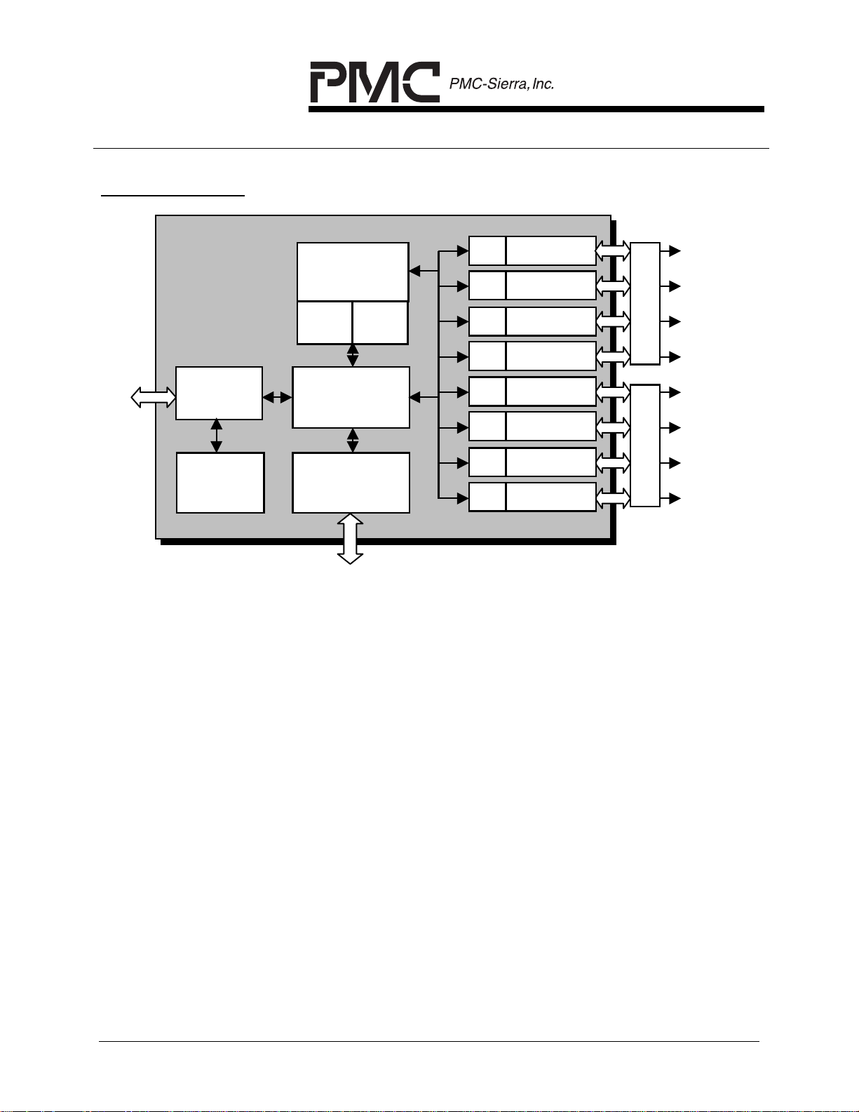
BLOCK DIAGRAM
10BaseT MAC
50 MHz
Embedded
Processor
FIFO
FIFO
10BaseT MAC
10BaseT
10BaseT
PCI Bus
Interface
I
Cache
Multi-Channel
DMA
D
Cache
FIFO
FIFO
FIFO
10BaseT MAC
10BaseT MAC
10BaseT MAC
Quad Ethernet
Interface Adapter
10BaseT
10BaseT
10BaseT
Controller
10BaseT MAC
FIFO
PCI Expansion Bus
Expansion
Registers
External
Memory
Interface
FIFO
FIFO
10BaseT MAC
10BaseT MAC
EDO DRAM / EPROM
Quad Ethernet
Interface Adapter
10BaseT
10BaseT
10BaseT
PROPRIETARY AND CONFIDENTIAL TO PMC-SIERRA, INC., AND PMC-SIERRA, INC. CUSTOMERS ONLY 7

ELAN 8X10
DATA SHEET
PMC-970109 ISSUE 3 8 PORT ETHERNET SWITCH
PM3350 ELAN 8 X10
DESCRIPTION
The PM3350 is a low-cost, highly integrated, stand-alone, single-chip switching device
for Ethernet/IEEE 802.3 switching and bridging applications. The device supports all
processing required for switching Ethernet/IEEE 802.3 packets between eight
independent half-duplex 10 Mbit/s ports. In addition, a switch built around the ELAN
8x10 can be expanded simply by connecting up to 7 additional devices to the on-chip
1 Gbit/s expansion port. Switch configuration and management can be performed either
remotely (in-band), via the on-chip SNMP MIB, agent and integrated TCP/UDP/IP
stack, or from a local CPU interfaced to the expansion port. The ELAN 8x10 also
collects per-port and per-host RMON statistics at wire rates on all ports. The ELAN
8x10 chip contains all the required elements of a high-performance Ethernet switch:
MAC-layer interfaces, buffer FIFOs, a high-speed DMA engine for fast packet transfers,
a local memory interface for up to 16 MB of external buffer memory, a compatible PCI
bus master and slave unit for modular expansion, and a switch processing unit that
implements the switching and bridging functions. The only additional components
required to create a complete 8-port switch are Ethernet Medium Access Unit (MAU)
devices, line transformers, a bank of external memory and a system clock.
The ELAN 8x10 device is implemented in high-density CMOS technology for low cost
and high performance. It is available in a 256-pin SBGA, and is ideally suited for
compact, low-cost desktop, workgroup and departmental Ethernet switching
applications.
PROPRIETARY AND CONFIDENTIAL TO PMC-SIERRA, INC., AND PMC-SIERRA, INC. CUSTOMERS ONLY 8

ELAN 8X10
DATA SHEET
PMC-970109 ISSUE 3 8 PORT ETHERNET SWITCH
PM3350 ELAN 8 X10
DEVICE DATA
Introduction
The PM3350 ELAN 8x10 offers a complete system-level solution, integrating all
required elements (except packet-buffer/address-table memory and transceiver logic) in
a single high-density VLSI chip. It is a true single-chip managed switch; all the required
functions, including address learning/aging, management, RMON-level statistics
collection, spanning tree support and self-configuration, are performed by the ELAN
8x10 without need for external CPUs or logic. In addition, the functions required for
expandability are also integrated into the device.
The ELAN 8x10 is built around a RISC CPU based Switch Processor core, coupled with
a multi-channel DMA controller, MAC-layer interface logic, FIFOs, a PCI-based
expansion port and a flexible memory controller.
Switch Processor
An on-chip Switch Processor is primarily responsible for performing the Ethernet / IEEE
802.3 packet switching functions, and can switch packets arriving simultaneously from
the eight 10BaseT ports and the expansion port at full wire rates using address tables
that it creates and maintains in external local memory. Store-and-forward switching is
performed, allowing the Switch Processor to detect CRC, length and alignment errors
and reject bad packets. The Switch Processor also supports IEEE 802.3
group/functional address handling. Address aging, topology change updates, and
statistics collection are performed by the Switch Processor as well.
The Switch Processor unit allows the device to support high-level capabilities. In
addition, it implements the full IEEE 802.1d spanning-tree transparent bridging protocol,
which allows the ELAN 8x10 to act as a eight-port expandable learning bridge,
performing learning, filtering and redirection at full speed. Finally, the Switch Processor
can host an SNMP agent for powerful remote switch configuration and diagnostic
capabilities, allowing systems built around the ELAN 8x10 to be managed in-band using
standard management platforms. When additional switch devices are connected to the
ELAN 8x10 expansion port, the Switch Processors in all ELAN 8x10s intercommunicate
to transparently support a distributed SNMP MIB.
In host-based applications, the host CPU may bypass the on-chip SNMP agent to
communicate directly with the Switch Processor for configuration, control and
monitoring purposes.
Multichannel DMA Processor
The on-chip DMA Coprocessor contains eleven independent and concurrently operating
channels, one for each of the eight 10BaseT ports and three dedicated to the
PROPRIETARY AND CONFIDENTIAL TO PMC-SIERRA, INC., AND PMC-SIERRA, INC. CUSTOMERS ONLY 9

ELAN 8X10
DATA SHEET
PMC-970109 ISSUE 3 8 PORT ETHERNET SWITCH
PM3350 ELAN 8 X10
expansion port. The DMA Coprocessor operates under the control of the Switch
Processor unit to transfer packets and data at high speed between the 10BaseT ports,
the local memory and the expansion port. It also computes 32-bit IEEE Frame Check
Sequence (FCS) CRC remainders over the transferred data, allowing the Switch
Processor to filter packets with errors and generate CRCs for transmitted packets as
required.
Ethernet/IEEE 802.3 MAC Interfaces
Eight independent Ethernet/IEEE 802.3 MAC-layer interfaces are built into the ELAN
8x10 chip. These interfaces connect directly to external 10BaseT Medium Access Unit
(MAU) devices via the industry-standard 7-wire serial interface, and perform most of the
MAC-layer processing tasks required for CSMA/CD networks. In addition, each MAC
interface contains a 32-byte FIFO buffer that enhances throughput and minimizes
latency issues.
The signaling protocol used on the 7-wire serial interfaces supported by the ELAN 8x10
chip follows that required by the Advanced Micro Devices, Inc (AMD) Am7990 LANCE
device.
Expansion Port
A 32-bit parity-checked expansion port is provided to allow systems using the ELAN
8x10 to be expanded transparently from 8 to 64 ports. The expansion port supports a
peak throughput of 1 Gbit/s, and requires only a single external PAL or similar device
(to serve as a bus arbiter). Packets received on an ELAN 8x10 MAC port that are
destined for an external ELAN 8x10 are transferred over the expansion bus prior to
transmission on the designated destination port. Broadcast and multicast packets are
handled using a two-level replication scheme, in which the broadcast/multicast packet is
first transferred to all of the external ELAN 8x10s, after which it is transmitted out the
required destination ports without any further use of the expansion bus. In addition,
ELAN 8x10s interconnected via the expansion port exchange information to maintain
the distributed MIB.
Local Memory Controller
An external local memory is used for holding configuration information, MAC address
tables and statistics tables, node management data, packet buffers, and host
communication queues (if a local host CPU is present). The ELAN 8x10 integrates a
memory controller that is capable of addressing and directly driving up to 16 Mbytes of
external memory, divided into four banks of 4 Mbytes each, with decoded selects for
each bank. Independent, software programmable access times may be set for each
bank, allowing a glueless interface to a mix of EDO DRAM, EEPROM, EPROM and
ROM in the same system. An external memory timing generator may also be used if
desired. The memory controller accepts simultaneous requests from the Switch
PROPRIETARY AND CONFIDENTIAL TO PMC-SIERRA, INC., AND PMC-SIERRA, INC. CUSTOMERS ONLY 10

ELAN 8X10
DATA SHEET
PMC-970109 ISSUE 3 8 PORT ETHERNET SWITCH
PM3350 ELAN 8 X10
Processor, the DMA processor, and the expansion port, and efficiently partitions the
100 Mbytes/s peak memory port bandwidth among them.
The ELAN 8x10 is capable of auto-configuring after power-up via an 8-bit EPROM or
EEPROM connected to the memory port. Parameters (such as the MAC address, IP
address, configuration options, etc.) may be placed in this EPROM or EEPROM, and
will be loaded automatically by the ELAN 8x10.
Clocking and Test
The ELAN 8x10 is implemented in fully-static CMOS technology, and is intended to
operate at a device clock frequency of 50 MHz (40 MHz for the expansion port bus).
The Switch Processor performs a comprehensive power on self test (POST), and can
report failure conditions and device status, if necessary, via an 8-bit LED interface
register connected to the local memory port.
PROPRIETARY AND CONFIDENTIAL TO PMC-SIERRA, INC., AND PMC-SIERRA, INC. CUSTOMERS ONLY 11
ELAN 8X10
DATA SHEET
PMC-970109 ISSUE 3 8 PORT ETHERNET SWITCH
PM3350 ELAN 8 X10
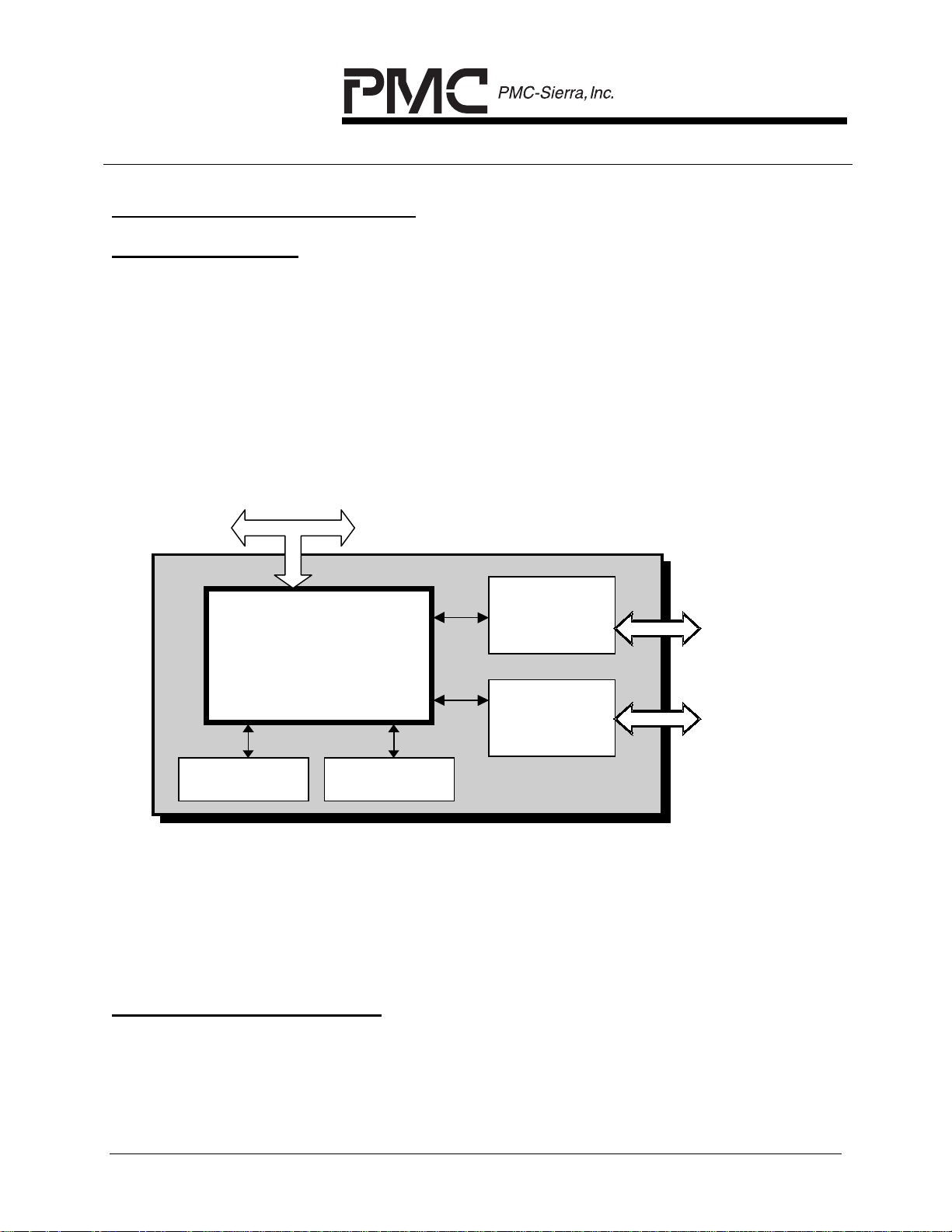
TYPICAL SYSTEM APPLICATIONS
Simple 8-Port Switch
The ELAN 8x10 chip can act as a stand-alone managed or unmanaged switching
device in low-cost, compact switch applications. Such a switch can be created from
ELAN 8x10 chips (one for every 8 ports), a bank of two 256k x 16-bit 60 nsec EDO
chips per ELAN 8x10 chip, a 32k x 8-bit EPROM or EEPROM for initialization and
configuration information, two LXT944 or similar quad Ethernet Interface Adapters, and
suitable passive components (filters, transformers, crystal oscillators, etc.) A block
diagram of a typical 8-port 10BaseT stackable switch is given below. The PCI
expansion bus allows multiple ELAN 8x10 switch assemblies to be easily stacked up to
a maximum of 64 10Mbit/s ports.
PCI Bus Expansion Bus
Quad
ELAN 8x10
PM3350
10BaseT
Interface
Quad
10BaseT
10BaseT
Ports 1-4
10BaseT
Ports 5-8
Interface
EDO DRAM
EEPROM
Managed 8-Port Ethernet Switch
The above system will operate as a fully managed system simply by replacing the 32k x
8-bit EEPROM with a 256k x 8-bit EPROM or EEPROM containing the SNMP agent,
support firmware, spanning tree, and TCP/IP stack.
Low-cost 10/100 Mbit/s Switch
The ELAN 8x10 chip can be part of a 10/100 switch using the ELAN 1x100 10/100
Mbit/s switch chip. Together they can form a workgroup or desktop switch supporting a
high-speed server or backbone port in low-cost, compact Ethernet switching hub
applications. Such a switch can be created from one or two PM3351 devices (one for
PROPRIETARY AND CONFIDENTIAL TO PMC-SIERRA, INC., AND PMC-SIERRA, INC. CUSTOMERS ONLY 12
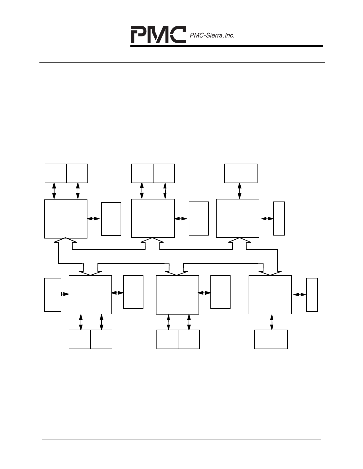
ELAN 8X10
SRAM
SRAM
DATA SHEET
PMC-970109 ISSUE 3 8 PORT ETHERNET SWITCH
PM3350 ELAN 8 X10
every 100 Mbit/s port required), 1 to 7 PM3350 chips (one for every eight 10 Mbit/s
ports required), a bank of memory per device (60 nsec EDO DRAM for each PM3350,
15 ns SRAM for each PM3351) for holding packet buffers and switching tables, a single
32k x 8-bit EEPROM device for configuration information, two LXT944 10BaseT
interface adapters per PM3350 chip, one LXT970 100 Mbit/s PHY device per PM3351,
and suitable passive components (filters, transformers, crystal oscillators, etc.) A block
diagram of a typical 32-port 10BaseT stackable switching hub with two 100 Mbit/s
server/backbone ports is given in the following diagram. The PCI expansion bus is used
seamlessly to stack the ELAN 8x10s and ELAN 1x100s.
8 x 10BaseT 10/100BaseT8 x 10BaseT
Quad
PHY
Quad
PHY
ELAN 8x10
8x10BaseT
PM3350
EEPROM
Quad
ELAN 8x10
8x10BaseT
PM3350
Quad
PHY
PHY
EDO
DRAM
Quad
PHY
Quad
PHY
ELAN 8x10
8x10BaseT
PM3350
PCI Backplane
ELAN 8x10
EDO
DRAM
8 x 10BaseT
PM3350
Quad
PHY
Quad
PHY
EDO
DRAM
10/100
PHY
ELAN 1x100
1x10/100
BaseT
PM3351
EDO
DRAM
ELAN 1x100
1x10/100
BaseT
PM3351
10/100
PHY
8 x 10BaseT 8 x 10BaseT
10/100BaseT
Expandable 10/100 Mbit/s Ethernet Switch
PROPRIETARY AND CONFIDENTIAL TO PMC-SIERRA, INC., AND PMC-SIERRA, INC. CUSTOMERS ONLY 13

ELAN 8X10
DATA SHEET
PMC-970109 ISSUE 3 8 PORT ETHERNET SWITCH
PM3350 ELAN 8 X10
PRIMARY FEATURES AND BENEFITS
Wire-speed Packet switching
Each ELAN 8x10 chip offers 8 separate Ethernet ports all capable of accepting and
processing packets simultaneously at wire rates (ranging from 14,880 packets/sec per
port with a packet length of 64 bytes to 813 packets/sec per port with 1518 byte
packets), immediately multiplying the aggregate bandwidth of the target network by a
factor of eight. In addition, the low cost and compact size permitted by the single-chip
ELAN 8x10 solution makes micro-segmentation highly feasible, allowing even more
improvement in bandwidth.
Combined Input- and Output-buffered switch
The ELAN 8x10 implements a hybrid input-buffered/output-queued switching algorithm
which minimizes packet loss, allows packet buffers to be allocated on a demand basis,
and permits limits to be established to prevent any one port from consuming all system
buffer memory. Buffer limits are configured on a per-port basis. Packet storage is
allocated within the external memory by the ELAN 8x10 from a central pool using an
on-demand method, employing linked lists of small, fixed-length buffers to hold variable
sized packets in order to maximize memory utilization.
Modular design
Multiple ELAN 8x10 chips interconnect seamlessly, allowing transparent expansion of
switching hubs from 8 to 64 ports without significant redesign. The 1 Gbit/s expansion
port bandwidth ensures that network capacity grows linearly as more ELAN 8x10 chips
are added (up to the maximum number of supported ports).
Advanced switching features
The ELAN 8x10 directly implements backpressure flow control (as a user-selectable
option), with configurable thresholds and limits, to minimize packet loss in heavily
loaded networks. Backpressure is performed by jamming, or colliding with, incoming
packets on an individual port when the port has run out of buffer space; all other ports
continue to run normally, with no head-of-line blocking effects. The ELAN 8x10 also
implements per-packet lifetime control to ensure that transmit queues are flushed
properly in the event of bottlenecks at the output ports. Address aging is handled onchip, as is purging of the address table in the event of a network reconfiguration.
Broadcast storm rate limiting is implemented (with configurable rate limits) to reduce the
effects of high broadcast rates on the traffic flowing through the switch.
PROPRIETARY AND CONFIDENTIAL TO PMC-SIERRA, INC., AND PMC-SIERRA, INC. CUSTOMERS ONLY 14

ELAN 8X10
DATA SHEET
PMC-970109 ISSUE 3 8 PORT ETHERNET SWITCH
PM3350 ELAN 8 X10
Spanning tree bridging capabilities
The ELAN 8x10 optionally implements the 802.1d spanning tree protocol, allowing it to
interoperate with IEEE-standard transparent bridges. The spanning tree protocol is
supported by the on-chip Switch Processor unit, and does not require an external CPU
for implementation.
Management and monitoring support
The ELAN 8x10 maintains full RMON port and host statistics for all ports and all learned
MAC addresses at wire rates. These statistics may be retrieved either in-band (via
SNMP agent) or out-of-band (via the expansion bus).
The ELAN 8x10 implements an optional on-chip SNMP agent on top of an integral
UDP/IP protocol stack, supporting SNMP and the RFC1493 bridge MIB. When multiple
ELAN 8x10 chips are present in a system, they may be configured to intercommunicate
and create a distributed MIB in a transparent manner. Alternatively, the system vendor
may elect to disable the SNMP agent and access the ELAN 8x10 statistics and
configuration variables directly from the expansion port.
Status codes may be displayed on a set of LEDs (Light Emitting Diodes) during self-test
and operation at the system implementer's discretion. These status codes are output to
a register mapped into the ELAN 8x10 memory data bus at a specific address location.
Device failure during self-test, or specific operating conditions, may be displayed using
front-panel LEDs connected to the register.
Autoconfiguration via Local PROM/EEPROM
The ELAN 8x10 will automatically self-configure upon power-up using user-defined
parameters supplied in an external EPROM or EEPROM. The EPROM/ EEPROM may
be connected to the memory bus and mapped to any address range; the ELAN 8x10
will automatically locate the EPROM or EEPROM and load the configuration
parameters from it. The ELAN 8x10 also contains hardware that enables it to write to
standard 3.3-volt EEPROM devices, thus permitting configuration information to be
changed dynamically.
PROPRIETARY AND CONFIDENTIAL TO PMC-SIERRA, INC., AND PMC-SIERRA, INC. CUSTOMERS ONLY 15
ELAN 8X10
DATA SHEET
PMC-970109 ISSUE 3 8 PORT ETHERNET SWITCH
PM3350 ELAN 8 X10
PIN DIAGRAM
The ELAN 8x10 is packaged in a 256-pin cavity-down SBGA, with 188 signal pins and
associated VDD (supply) and VSS (ground) pins.
256-Pin SBGA Pin Diagram
20 19 18 17 16 15 14 13 12 11
VSS VSS VSS
A
VSS VDD VDD MRAS_
B
VSS VDD VDD MWEN_1_
C
MRDY_ MRD_ MWEN_2_ VDD MWEN_0_
D
MCS_3_ MCS_2_ MCS_0_ MWEN_3_
E
MDATA_31MDATA_27MDATA_24MDATA_2
0
MDATA_28MDATA_25MDATA_21MDATA_17MDATA_15MDATA_1
MDATA_30MDATA_26MDATA_23MDATA_19MDATA_16MDATA_1
MDATA_2
9
MDATA_22MDATA_18MDATA_1
VDD
MDATA_14MDATA_1
VSS
0
1
2
3
MADDR_2 MADDR_1 MADDR_0 MCS_1_
F
MADDR_6 MADDR_5 MADDR_3 VDD
G
MADDR_1
H
J
K
MADDR_15MADDR_16MADDR_17MADDR_1
L
MADDR_1
M
N
TXD_7 TCLK_7 CD_6 VDD
P
RCLK_6 RXD_6 TEN_6 COL_5
R
TXD_6 TCLK_6 CD_5 TEN_5
T
RCLK_5 RXD_5 TXD_5 VDD COL_4 RXD_4 VDD RXD_3 CD_2 VDD
U
V
W
MADDR_8 MADDR_7 MADDR_4
0
MADDR_12MADDR_1
VSS
MADDR_13MADDR_1
VSS
COL_7 CD_7 RXD_7
9
VSS RCLK_7 TEN_7 COL_6
VSS VDD VDD TCLK_5 LBK TCLK_4 RCLK_3 TCLK_3 RXD_2 TCLK_2
VSS VDD VDD CD_4 TEN_4 COL_3 TEN_3 COL_2 TEN_2 TXD_2
MADDR_9
1
4
VDD
8
256 BGA
BOTTOM VIEW
VSS VSS VSS RCLK_4 TXD_4 CD_3 TXD_3 RCLK_2 VSS VSS
Y
20 19 18 17 16 15 14 13 12 11
PROPRIETARY AND CONFIDENTIAL TO PMC-SIERRA, INC., AND PMC-SIERRA, INC. CUSTOMERS ONLY 16

ELAN 8X10
DATA SHEET
PMC-970109 ISSUE 3 8 PORT ETHERNET SWITCH
PM3350 ELAN 8 X10
10987654321
VSS VSS MDATA_5 MDATA_1 DBG_2 PC_3 PC_7 VSS VSS VSS
MDATA_8 MDATA_7 MDATA_3 MDATA_0 DBG_1 PC_4 PC_8 VDD VDD VSS
MDATA_9 MDATA_6 MDATA_2 MINTR_ DBG_0 PC_6 PC_10 VDD VDD VSS
VDD MDATA_4 MGWE_ VDD PC_5 PC_9 VDD N/C N/C ERST_
N/C TST_ RST_ GNT_
INT_ REQ_ AD_31 AD_30
VDD AD_29 AD_27 AD_26
AD_28 AD_25 CBE_3_ VSS
AD_24 VDD5 IDEL_ AD_23
AD_22 AD_21 AD_20 AD_19
VDD AD_18 AD_17 VSS
IRDY_ CBE_2_ AD_16 VSS
SERR_ DEVSEL_ TRDY_ FRAME_
256 BGA
VDD PAR PERR_ STOP_
A
B
C
D
E
F
G
H
J
K
L
M
N
P
BOTTOM VIEW
COL_1 TXD_1 RCLK_0 VDD AD_2 AD_6 VDD PCI_CLK AD_8 AD_9
MCLK RXD_1 TCLK_1 RXD_0 TCLK_0 AD_3 CBE_0_ VDD VDD VSS
SYSCLK RCLK_1 TEN_1 CD_0 TXD_0 AD_1 AD_5 VDD VDD VSS
CLK20 CD_1 VSS COL_0 TEN_0 AD_0 AD_4 VSS VSS VSS
AD_11 AD_14 AD_15 CBE_1_
AD_7 AD_10 AD_12 AD_13
R
T
U
V
W
Y
10987654321
PROPRIETARY AND CONFIDENTIAL TO PMC-SIERRA, INC., AND PMC-SIERRA, INC. CUSTOMERS ONLY 17
ELAN 8X10
DATA SHEET
PMC-970109 ISSUE 3 8 PORT ETHERNET SWITCH
PM3350 ELAN 8 X10
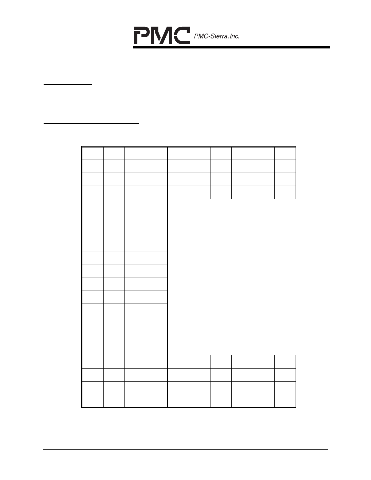
PIN DESCRIPTION
PIN SIGNAL PIN SIGNAL PIN SIGNAL
D1 ERST_ R3 AD_14 W12 TEN_2
E3 TST_ T1 AD_13 V12 RXD_2
F4 INT_ T2 AD_12 Y13 RCLK_2
E2 RST_ R4 AD_11 U12 CD_2
E1 GNT_ T3 AD_10 W13 COL_2
F3 REQ_ U1 AD_9 V13 TCLK_3
F2 AD_31 U2 AD_8 Y14 TXD_3
F1 AD_30 T4 AD_7 W14 TEN_3
G3 AD_29 U3 PCI_CLK U13 RXD_3
H4 AD_28 V4 CBE_0_ V14 RCLK_3
G2 AD_27 U5 AD_6 Y15 CD_3
G1 AD_26 W4 AD_5 W15 COL_3
H3 AD_25 Y4 AD_4 V15 TCLK_4
J4 AD_24 V5 AD_3 Y16 TXD_4
H2 CBE_3_ U6 AD_2 W16 TEN_4
J3 VDD5 W5 AD_1 U15 RXD_4
J2 IDSEL_ Y5 AD_0 V16 LBK
J1 AD_23 V6 TCLK_0 Y17 RCLK_4
K4 AD_22 W6 TXD_0 W17 CD_4
K3 AD_21 Y6 TEN_0 U16 COL_4
K2 AD_20 V7 RXD_0 V17 TCLK_5
K1 AD_19 U8 RCLK_0 U18 TXD_5
L3 AD_18 W7 CD_0 T17 TEN_5
L2 AD_17 Y7 COL_0 U19 RXD_5
M2 AD_16 V8 TCLK_1 U20 RCLK_5
M3 CBE_2_ U9 TXD_1 T18 CD_5
N1 FRAME_ W8 TEN_1 R17 COL_5
M4 IRDY_ V9 RXD_1 T19 TCLK_6
N2 TRDY_ W9 RCLK_1 T20 TXD_6
N3 DEVSEL_ Y9 CD_1 R18 TEN_6
P1 STOP_ U10 COL_1 R19 RXD_6
P2 PERR_ V10 MCLK R20 RCLK_6
N4 SERR_ W10 SYSCLK P18 CD_6
P3 PAR Y10 CLK20 N17 COL_6
R1 CBE_1_ V11 TCLK_2 P19 TCLK_7
R2 AD_15 W11 TXD_2 P20 TXD_7
PROPRIETARY AND CONFIDENTIAL TO PMC-SIERRA, INC., AND PMC-SIERRA, INC. CUSTOMERS ONLY 18
ELAN 8X10
DATA SHEET
PMC-970109 ISSUE 3 8 PORT ETHERNET SWITCH
PM3350 ELAN 8 X10
PIN SIGNAL PIN SIGNAL PIN SIGNAL
N18 TEN_7 F17 MCS_1_ D11 MDATA_13
M17 RXD_7 E18 MCS_0_ C11 MDATA_12
N19 RCLK_7 D20 MRDY_ B11 MDATA_11
M18 CD_7 D19 MRD_ A11 MDATA_10
M19 COL_7 E17 MWEN_3_ C10 MDATA_9
M20 MADDR_19 D18 MWEN_2_ B10 MDATA_8
L17 MADDR_18 C17 MWEN_1_ B9 MDATA_7
L18 MADDR_17 D16 MWEN_0_ C9 MDATA_6
L19 MADDR_16 B17 MRAS_ A8 MDATA_5
L20 MADDR_15 A17 MDATA_31 D9 MDATA_4
K18 MADDR_14 C16 MDATA_30 B8 MDATA_3
K19 MADDR_13 D15 MDATA_29 C8 MDATA_2
J19 MADDR_12 B16 MDATA_28 A7 MDATA_1
J18 MADDR_11 A16 MDATA_27 B7 MDATA_0
H20 MADDR_10 C15 MDATA_26 D8 MGWE_
J17 MADDR_9 B15 MDATA_25 C7 MINTR_
H19 MADDR_8 A15 MDATA_24 A6 DBG_2
H18 MADDR_7 C14 MDATA_23 B6 DBG_1
G20 MADDR_6 D13 MDATA_22 C6 DBG_0
G19 MADDR_5 B14 MDATA_21 A5 PC_3
H17 MADDR_4 A14 MDATA_20 B5 PC_4
G18 MADDR_3 C13 MDATA_19 D6 PC_5
F20 MADDR_2 D12 MDATA_18 C5 PC_6
F19 MADDR_1 B13 MDATA_17 A4 PC_7
F18 MADDR_0 C12 MDATA_16 B4 PC_8
E20 MCS_3_ B12 MDATA_15 D5 PC_9
E19 MCS_2_ A12 MDATA_14 C4 PC_10
D3 N/C E4 N/C D2 N/C
PROPRIETARY AND CONFIDENTIAL TO PMC-SIERRA, INC., AND PMC-SIERRA, INC. CUSTOMERS ONLY 19
ELAN 8X10
DATA SHEET
PMC-970109 ISSUE 3 8 PORT ETHERNET SWITCH
PM3350 ELAN 8 X10
Pin Signal Pin Signal
B2 VDD A1 VSS
B3 A2
B18 A3
B19 A9
C2 A10
C3 A13
C18 A18
C19 A19
D4 A20
D7 B1
D10 B20
D14 C1
D17 C20
G4 H1
G17 J20
K17 K20
L4 L1
P4 M1
P17 N20
U4 V1
U7 V20
U11 W1
U14 W20
U17 Y1
V2 Y2
V3 Y3
V18 Y8
V19 Y11
W2 Y12
W3 Y18
W18 Y19
W19 Y20
All VDD and VSS lines
be connected to supply and ground respectively. Standard
must
decoupling practices should be followed for proper device operation.
PROPRIETARY AND CONFIDENTIAL TO PMC-SIERRA, INC., AND PMC-SIERRA, INC. CUSTOMERS ONLY 20
ELAN 8X10
DATA SHEET
PMC-970109 ISSUE 3 8 PORT ETHERNET SWITCH
PM3350 ELAN 8 X10
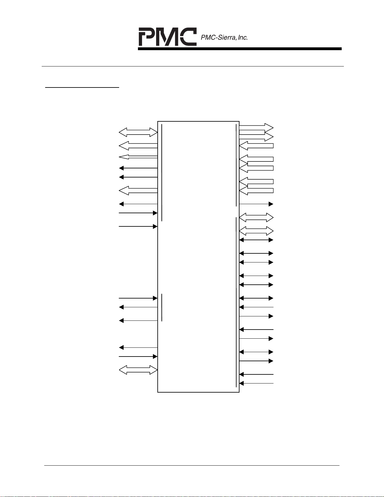
Functional Grouping
The following diagram shows the functional grouping of the ELAN 8x10 signal pins.
MDATA[31:0]
MADDR[19:0]
MCS_[3:0]
MRAS_
MRD_
MWE_[3:0]
MGWE_
MRDY_
MINTR
SYSCLK
MCLK
CLK20
Local
Memory
Interface
PM3350
8-Port
Ethernet
Switch
Clocking
8 x
MAU
PCI
Expansion
Bus
Interface
TXD[7:0]
TEN[7:0]
TCLK[7:0
RXD[7:0]
RCLK[7:0]
CD[7:0]
COL[7:0
LBK
AD[31:0]
CBE_[3:0]
PAR
FRAME_
TRDY_
IRDY_
STOP_
DEVSEL_
IDSEL
REQ_
GNT_
ERST_
TST_
DBG[2:0]
PROPRIETARY AND CONFIDENTIAL TO PMC-SIERRA, INC., AND PMC-SIERRA, INC. CUSTOMERS ONLY 21
INT_
PERR_
SERR_
PCI_CLK
RST_

ELAN 8X10
DATA SHEET
PMC-970109 ISSUE 3 8 PORT ETHERNET SWITCH
PM3350 ELAN 8 X10
PCI Expansion Bus Interface
Signal Name Size Type Description
AD[31:0] 32 I/O
CBE_[3:0] 4 I/O
PAR 1 I/O
FRAME_ 1 I/O
IRDY_ 1 I/O
TRDY_ 1 I/O
STOP_ 1 I/O
DEVSEL_ 1 I/O
IDSEL 1 I
REQ_ 1 O
GNT_ 1 I
INT_ 1 OD
PERR_ 1 I/O
SERR_ 1 OD
PCI_CLK 1 I
Multiplexed PCI address/data bus, used by an external bus master (e.g., a PCI
host) or the ELAN 8x10 to transfer addresses or data.
Command/Byte-Enable lines. These lines supply a command (during PCI address
phases) or byte enables (during data phases) for each bus transaction.
Address/data/command parity, supplies the even parity computed over the
AD[31:0] and CBE_[3:0] lines during valid data phases; it is sampled (when the
ELAN 8x10 is acting as a target) or driven (when the ELAN 8x10 acts as an
initiator) one clock edge after the respective data phase.
Bus transaction delimiter (framing signal); a HIGH-to-LOW transition on this signal
indicates that a new transaction is beginning (with an address phase); a LOW-toHIGH transition indicates that the next valid data phase will end the currently
ongoing transaction.
Transaction Initiator (master) ready, used by the transaction initiator or bus master
to indicate that it is ready for a data transfer. A valid data phase ends with data
transfer when both IRDY_ and TRDY_ are sampled asserted on the same clock
edge.
Transaction Target ready, used by the transaction target or bus slave to indicate
that it is ready for a data transfer. A valid data phase ends with data transfer when
both IRDY_ and TRDY_ are sampled asserted on the same clock edge.
Transaction termination request, driven by the current target or slave to abort,
disconnect or retry the current transfer.
Device select acknowledge: driven by a target to indicate to the initiator that the
address placed on the AD[31:0] lines (together with the command on the
CBE_[3:0] lines) has been decoded and accepted as a valid reference to the
target's address space. Once asserted, it is held asserted until FRAME_ is
de-asserted; otherwise, it indicates (in conjunction with STOP_ and TRDY_) a
target-abort.
Device identification (slot) select. Assertion of IDSEL signals the ELAN 8x10 that it
is being selected for a configuration space access.
Bus request (to bus arbiter), asserted by the ELAN 8x10 to request control of the
PCI bus.
Bus grant (from bus arbiter); this indicates to the ELAN 8x10 that it has been
granted control of the PCI bus, and may begin driving the address/data and control
lines after the current transaction has ended (indicated by FRAME_, IRDY_ and
TRDY_ all de-asserted simultaneously).
Open Drain Interrupt request. This pin signals an interrupt request to an external
PCI host system. The INT_ pin should be tied to the INTA* line on the PCI bus.
Bus parity error signal, asserted by the ELAN 8x10 as a bus slave, or sampled by
the ELAN 8x10 as a bus master, to indicate a parity error on the AD[31:0] and
CBE_[3:0] lines.
Open Drain System error, used by the ELAN 8x10 to indicate a system error, or a
parity error on the AD[31:0] and CBE_[3:0] lines during an address phase.
PCI bus clock; supplies the PCI bus clock signal to the ELAN 8x10.
PROPRIETARY AND CONFIDENTIAL TO PMC-SIERRA, INC., AND PMC-SIERRA, INC. CUSTOMERS ONLY 22

ELAN 8X10
DATA SHEET
PMC-970109 ISSUE 3 8 PORT ETHERNET SWITCH
PM3350 ELAN 8 X10
RST_ 1 I
PCI bus reset (system reset). Performs a hardware reset of the ELAN 8x10 and
associated peripherals when asserted. The RST_ input uses a Schmitt trigger to
accommodate slow rise and fall times, allowing a simple RC network to be used to
provide power-on reset capability.
MAU Interface Pins
Signal Name Size Type Description
TXD[7:0] 8 O
TEN[7:0] 8 O
TCLK[7:0] 8 I
RXD[7:0] 8 I
RCLK[7:0] 8 I
CD[7:0] 8 I
Transmit data outputs (to 8 MAUs). The TXD lines are used to carry outgoing
data bytes to the Medium Access Units (MAUs). Each bit of the bus is
connected to the serial transmit data input of a separate MAU device. The
TXD[7:0] lines are synchronous to the TCLK[7:0] lines (TXD[0] to TCLK[0], and
so on). Data are driven on to the TXD[7:0] lines after the rising edge of the
corresponding TCLK[7:0] input, and may be sampled on the next rising edge of
the latter.
Transmit enables. The data carried on the TXD[7:0] lines is only valid when the
TEN[7:0] lines are active. This also indicates to the MAU devices that the ELAN
8x10 is acquiring the medium. Each of the TEN[7:0] lines should be connected
to a separate MAU device. The TEN[7:0] outputs are asserted or de-asserted on
the rising edge of the corresponding TCLK[7:0] input, and may be sampled on
the next rising edge of the latter.
Transmit clocks; these inputs provide the synchronization references for the
TXD[7:0] and TEN[7:0] lines. TCLK[7:0] should be driven with a 10 MHz transmit
data clock reference by the external MAU devices (each MAU device should
drive a separate line of the TCLK[7:0] bus). Each of the TCLK[7:0] lines may be
driven completely asynchronously to all the others. The rising edges of the
TCLK[7:0] signals are used as timing references. The TCLK[7:0] inputs are
Schmitt-triggered for improved resistance to slow rise and fall times.
Receive data inputs (from 8 MAUs). The RXD lines transfer incoming serial
received data from the external MAU devices to the ELAN 8x10. Each bit of the
bus is connected to the serial receive data output of a separate MAU device.
The RXD[7:0] lines are sampled synchronously by the ELAN 8x10 at the rising
edges of the clocks supplied on the RCLK[7:0] inputs (RXD[0] to RCLK[0], and
so on).
Receive clocks; should be driven by the external MAU devices with the receive
clock references recovered from the incoming serial receive data. The
RCLK[7:0] inputs need not be driven with a continuous clock reference;
however, they must be running whenever the CD[7:0] inputs are asserted, and
must continue running for at least five clock cycles after the CD[7:0] inputs
transition LOW in order to permit the internal MAC logic to function properly.
The RCLK[7:0] inputs are Schmitt-triggered for improved resistance to slow rise
and fall times.
Receive carrier detect signals. These carrier detect inputs should be driven with
the carrier detect (i.e., data being received from the medium) signals generated
by the eight external MAU devices, and are sampled synchronously to the rising
edges of the clocks input on the RCLK[7:0] lines and the TCLK[7:0] lines to
implement the CSMA/CD algorithm. The data presented on RXD[7:0] are only
sampled when the corresponding CD[7:0] lines are asserted HIGH. (If not all of
the eight ELAN 8x10 MAC ports are connected to external MAU devices, the CD
inputs for to the missing MAU devices should be tied LOW.)
PROPRIETARY AND CONFIDENTIAL TO PMC-SIERRA, INC., AND PMC-SIERRA, INC. CUSTOMERS ONLY 23
ELAN 8X10
DATA SHEET
PMC-970109 ISSUE 3 8 PORT ETHERNET SWITCH
PM3350 ELAN 8 X10
COL[7:0] 8 I
LBK 1 O
Receive collision detect signals. These inputs pass the collision detect and SQE
test signals generated by the external MAU devices to the ELAN 8x10. They are
sampled synchronously to the TCLK[7:0] clock references (COL[0] corresponds
to TCLK[0], and so on), and should be asserted by the MAU devices to indicate
collisions on the medium as well as to signal a successful SQE test after
transmit. If not all of the 8 collision signal inputs are connected to external MAU
devices, the unused inputs should be tied LOW.
MAU loopback mode select (all 8 ports). This pin can be left as a no-connect
or wired to the loopback mode input of an attached PHY device. The loopback
mode feature on the PM3350 is not operational. Hence, this pin has no implied
functionality.
Local Memory Interface
Signal Name Size Type Description
MDATA[31:0] 32 I/O
MADDR[19:0] 20 O
MCS_[3:0] 4 O
MRAS_ 1 O
Memory data bus. MDATA[31:0] carries the data driven to the external local
memory by the ELAN 8x10 during local memory writes, and the data sent back
to the ELAN 8x10 by the memory devices during local memory reads. In
addition, configuration information is latched from the MDATA[31:0] lines
during ELAN 8x10 reset and loaded into an internal configuration register;
either pullup-pulldown resistors or tri-state buffers (enabled by the RST
drive configuration data on to the MDATA[31:0] lines during reset.
All MDATA[31:0] pins have internal pullups.
Memory address bus; supplies a word-aligned address to the external memory
devices (i.e., address bits 22 through 2 of the 24-bit byte address generated by
the internal ELAN 8x10 logic), and thus selects a single 32-bit word to be read
or written. Up to 4 MB of memory may be directly addressed in each bank
using these address lines. In addition, the lower 11 bits of MADDR[19:0] (i.e.,
MADDR[10:0]) carry a multiplexed row/column address when DRAM accesses
are being made, with the row address being presented when MRAS_
and the column address being presented when it is low. Multiplexing for 8-, 9-,
10- and 11-bit column addresses is supported. Up to 4 MB of memory may be
addressed in each bank when multiplexing is enabled for that bank (i.e., by
configuring the bank for DRAM accesses).
Memory bank chip selects. The MCS_[3:0] outputs select one of four memory
banks; each bank is 4 megabytes in size. They are decoded directly from the
most significant 2 bits (bits 23 and 22) of the 24-bit physical byte address
generated by the internal ELAN 8x10 logic, and are synchronous to MEMCLK.
When driving DRAM memory devices other than 2-CAS DRAMs, the
MCS_[3:0] signals function as the Column Address Strobe (CAS) signals to the
memories.
DRAM Row Address Strobe output; supplies the Row Address Strobe (RAS)
signal to one or more external DRAM banks. It is asserted to latch the row
address supplied on the MADDR lines into the DRAM array, and allow the
column address to be output one cycle later. It may be tied directly to the RAS*
inputs of standard asynchronous DRAM devices.
*
input)
is high
PROPRIETARY AND CONFIDENTIAL TO PMC-SIERRA, INC., AND PMC-SIERRA, INC. CUSTOMERS ONLY 24
ELAN 8X10
DATA SHEET
PMC-970109 ISSUE 3 8 PORT ETHERNET SWITCH
PM3350 ELAN 8 X10
MRD_ 1 O
MWE_[3:0] 4 O
MGWE_ 1 O
MRDY_ 1 I
MINTR_ 1 I
Memory read enable. This output signals the external memory banks that a
read is being performed and data should be output on the MDATA[31:0] lines
from the specified address. The MRD_ output may be tied to the OE* inputs of
standard memory devices.
Memory write enables, used by the ELAN 8x10 to enable the data presented
on individual byte lanes of MDATA[31:0] to be individually written to memory.
MWE_[0] corresponds to MDATA[7:0], MWE_[1] corresponds to MDATA[15:8],
and so on. When using 2-CAS asynchronous DRAM devices, the MWE_[3:0]
outputs should be connected to the memory CAS* inputs; otherwise, the
MWE_[3:0] outputs should be connected to the appropriate byte write enables.
Global memory write enable. This signal is used to signal that a write access
is occurring, and should be connected to the WE* inputs of dual CAS
asynchronous DRAM devices.
Memory ready input. If an external memory timing generator is used, it can be
connected to the MRDY_ input to force the ELAN 8x10 to insert wait states into
memory accesses. If the MRDY_
the MADDR[15:0], MCS_[3:0], MRD_
values (as well as MDATA[31:0] for memory writes).
The MRDY* input is only sampled by the ELAN 8x10 when performing an
SRAM-type access; it is ignored for all other memory types. If an external
memory timing generator is not used, the MRDY
Local interrupt input. The MINTR_ may be used to provide an interrupt input to
the ELAN 8x10 in special applications. If the MINTR_ input is not used, it
should be tied HIGH.
line is de-asserted, the ELAN 8x10 will hold
and MWR_[3:0] lines at their present
_
line should be tied LOW.
Clock Inputs and Outputs
Signal Name Size Type Description
SYSCLK 1 I
MCLK 1 O
CLK20 1 O
50 MHz master device clock input, This should be driven by a 50 MHz
symmetrical clock source with a duty cycle between 40% and 60%. It is re-timed
and driven out on the MEMCLK line, and is also used in the internal device
logic.
50 MHz clock output derived from SYSCLK; supplies the re-timed 50 MHz clock
(input on the SYSCLK pin) to external devices.
20 MHz clock output (for use by MAU devices). The 50 MHz input clock is
internally divided by 2.5 and output as an asymmetrical 20 MHz clock reference
on the CLK20 output; this clock may be used as an input to external MAU
devices.
PROPRIETARY AND CONFIDENTIAL TO PMC-SIERRA, INC., AND PMC-SIERRA, INC. CUSTOMERS ONLY 25
ELAN 8X10
DATA SHEET
PMC-970109 ISSUE 3 8 PORT ETHERNET SWITCH
PM3350 ELAN 8 X10
Miscellaneous Inputs and Outputs
Signal Name Size Type Description
VDD5 1 I
TST_ 1 I
ERST_ 1 OD
DBG[2:0] 3 I/O
PC[10:3] 8 O
The 5 volt bias pin must be connected to 5.0 volts for the input and bi-directional
pins to be 5 volt tolerant. This pin may be tied to VDD provided the maximum
static signal level is below VDD + 0.3V.
During power-up, the voltage on the VDD5 pin must be kept equal to or greater
then the voltage on all input pins to avoid damage to the device. In addition, the
voltage on the VDD5 pin is to be kept greater than or equal to the voltage on the
VDD pins.
Test select signal used for production testing. It must be tied high for correct
operation.
Open-drain external reset output. The ERST_ pin is driven low by the ELAN
8x10 to reset other components in the system. This output is asserted for a preset duration (10 milliseconds) upon the detection of a falling edge on the RST_
input, or when the ELAN 8x10 senses a condition requiring a system hardware
reset. It is an open-drain output, and should be pulled up using a 2.2k resistor.
The ERST_ output may be tied directly to the RST_ input to implement a
debounce function in pushbutton reset applications. (Note that the ERST_
output should be left unconnected in host-based applications where the ELAN
8x10 must not be allowed to reset the host CPU.)
PMC hardware debug pins. These pins are used for hardware debug and
should not be used. These pins should be implemented as no-connects.
PMC hardware debug pins. Program counter selected outputs. These pins are
used for hardware debug and should not be used. These pins should be
implemented as no-connects.
Notes on Pin Description:
1. All inputs and bi-directionals present minimal capacitive loading and operate at TTL
logic levels.
2. All digital outputs and bi-directionals have 2 mA D.C. drive capability.
3. Pins MDATA[31:0], MINTR_,RST_, GNT_, TST_ and DBG[2:0] have internal pullup resistors.
PROPRIETARY AND CONFIDENTIAL TO PMC-SIERRA, INC., AND PMC-SIERRA, INC. CUSTOMERS ONLY 26
ELAN 8X10
DATA SHEET
PMC-970109 ISSUE 3 8 PORT ETHERNET SWITCH
PM3350 ELAN 8 X10
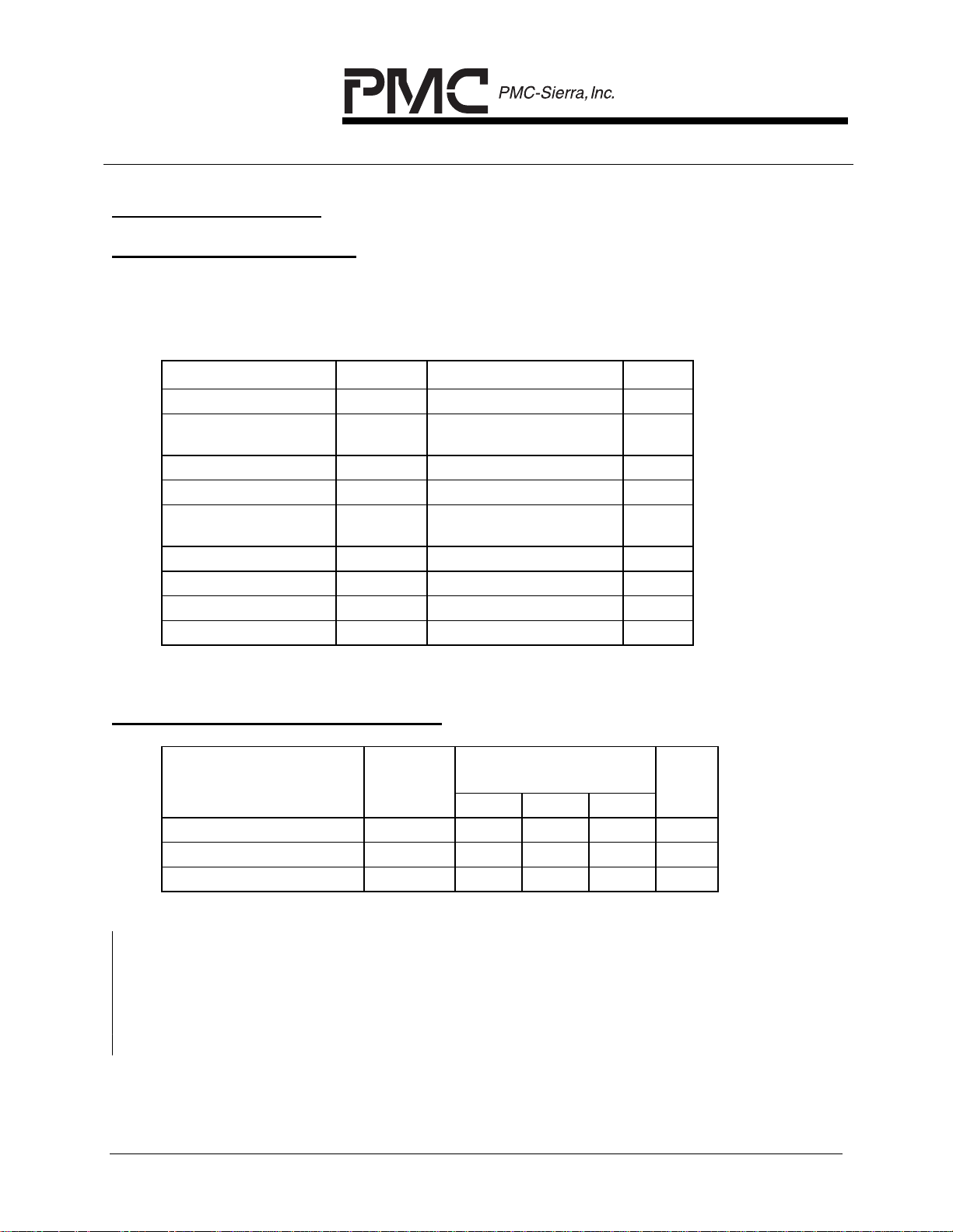
DC CHARACTERISTICS
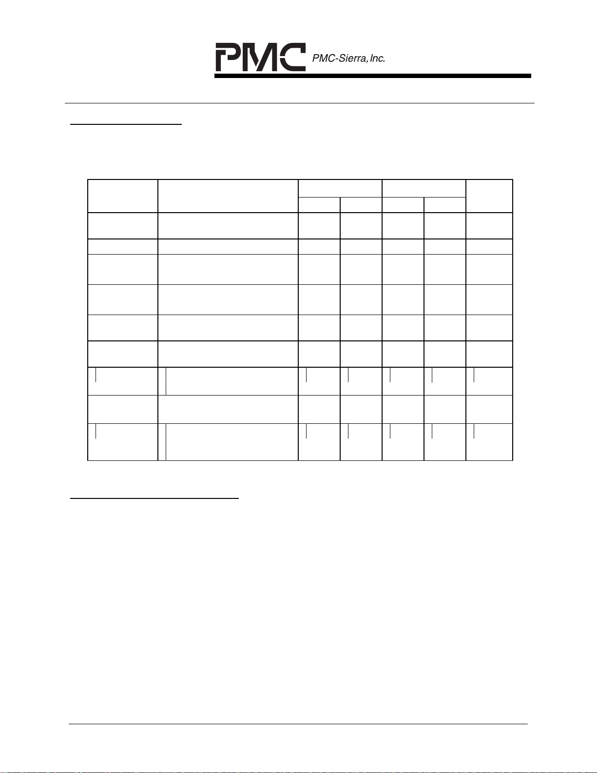
Absolute Maximum Ratings
Maximum rating are the worst case limits that the device can withstand without
sustaining permanent damage. They are not indicative of normal mode operation
conditions.
Parameter Symbol Value Units
Supply Voltage Vdd -0.3 to +5.0. Vdc
VDD5 pin voltage with
respect to Vss
Input Voltage Vin VDD5 +0.3 Vdc
Input Current Iin +/-10 mAdc
Static Discharge
Voltage
Latch-Up Current ±100 mA
Lead Temperature +220 °C
Storage Temperature Tst -45 to +125 °C
Junction Temperature Tj +125 °C
Vbias Minimum: VDD – 0.3V
Maximum: 5.5V
±1000 V
Vdc
Recommended Operating Conditions
Parameter Symbol Value Unit
s
Min Nom Max
Supply Voltage Vdd +3.13 +3.30 +3.47 Vdc
VDD5 pin voltage Vbias +4.75 +5.0 +5.25 Vdc
Operating Ambient Temp. Ta 0 +70 °C
NOTE: the PM3350 has been characterized over the industrial temperature range (Ta =
-40°C to +85°C). All DC and AC parametrics met the limits presented in the following
tables. In addition the package thermal characteristics of the 256-pin SBGA and power
consumption of the device are such that the device can be operated without any forced
air (i.e. still air) over the full industrial temperature range.
PROPRIETARY AND CONFIDENTIAL TO PMC-SIERRA, INC., AND PMC-SIERRA, INC. CUSTOMERS ONLY 27
ELAN 8X10
DATA SHEET
PMC-970109 ISSUE 3 8 PORT ETHERNET SWITCH
PM3350 ELAN 8 X10
D.C. Characteristics
DC characteristics are specified over recommended operating conditions (TA = 0°C to
+70°C, VDD = 3.3 V ±5%).
Parameter Description TTL I/Os PCI I/Os Units
Min Max Min Max
Vih Input High Voltage 2.0 VDD +
0.5
Vil Input Low Voltage -0.5 0.8 -0.5 0.8 Vdc
Voh Output High Voltage (VDD =
min, IOH = 2 mA, Note 2)
2.4 Vdd 2.4 Vdd Vdc
2.0 VDD +
0.5
Vdc
Vol Output Low Voltage (VDD =
min, IOL = -2 mA, Note 2)
Iil Input Low Leakage Current,
Note 3
Iih Input High Leakage Current,
Note 3
Iilpu Input Low Current (Pull ups,
VIL = GND, Notes 1)
Iihpu Input High Current (Pull ups,
VIH = VDD, Notes 1)
Iddop Supply Current, VDD = 3.47V,
Outputs Unloaded, SYSCLK =
50MHz
0 0.4 0 0.4 Vdc
-10 10 -10 10 µA
-10 10 -10 10 µA
+100 +20 µA
-10 +10 µA
450 mA
Notes on D.C. Characteristics:
1. Input pin or bi-directional pin with internal pull-up resistor.
2. Output pin or bi-directional pins. Voh not measured on open drain ouputs
3. Negative currents flow into the device (sinking), positive currents flow out of the
device (sourcing).
PROPRIETARY AND CONFIDENTIAL TO PMC-SIERRA, INC., AND PMC-SIERRA, INC. CUSTOMERS ONLY 28
 Loading...