

Page 1

PMC
FEATURES
PRELIMINARY
Pm29F004
4 Megabit (512K X 8) 5.0 Volt-only CMOS Flash Memory
• Single Power Supply Operation
- 5.0 V ± 10% Read/Program/Erase
• High Performance Read
- 70/90 ns access time
• Memory Blocks Architecture
- One 16 Kbytes top or bottom Boot Block with
software lockout
- Two 8 Kbytes Parameter Blocks
- One 96 Kbytes Main Block
- Three 128 Kbytes Main Blocks
• Automatic Block Erase and Byte Program
- Typical 12 µs/byte programming
- Typical 50 ms block or chip erase
• Hardware Data Protection
• Data# Polling and Toggle Bit Features
• Low Power Consumption
- Typical 15 mA active read current
- Typical 40 mA program/erase current
- Typical 0.1 µA CMOS standby current
• High Product Endurance
- Guarantee 10,000 program/erase cycles
- Typical 50,000 program/erase cycles
- Minimum 10 years data retention
• Industrial Standard Pin-out and Packaging
- 32-pin Plastic DIP
- 32-pin PLCC
• Manufactured on 0.30 µm process
GENERAL DESCRIPTION
The Pm29F004 is a 4 Megabit, 5 Volt-only Flash Memory organized as 524,288 bytes of 8 bits each. This
device is designed to use a 5.0 Volt power supply to perform in-system programming, 12.0 Volt VPP power supply
for program and erase operation is not required. The device can be programmed in standard EPROM programmers as well.
The 4 Megabit memory array is divided into seven blocks of one 16 Kbytes, two 8 Kbytes, one 96 Kbytes,
and three 128 Kbytes for BIOS and parameters storage. The seven blocks allow users to flexibly make chip erase
or block erase operation. The block erase feature allows a particular block to be erased and reprogrammed
without affecting the data in other blocks. After the device performed chip erase or block erase operation, it can
be reprogrammed on a byte-by-byte basis.
The device has a standard microprocessor interface as well as JEDEC single-power-supply Flash compatible
pin-out and command set. The program operation of Pm29F004 is executed by issuing the program command
code into command register. The internal control logic automatically handles the programming voltage ramp-up
and timing. The erase operation of Pm29F004 is executed by issuing the chip erase or block erase command
code into command register. The internal control logic automatically handles the erase voltage ramp-up and
timing. The preprogramming on the array which has not been programmed is not required before the erase
operation. The device also features Data# Polling and Toggle Bit function, the end of program or erase operation
can be detected by Data# Polling of I/O7 or Toggle Bit of I/O6.
The device has an optional 16 Kbytes top or bottom boot block with a software lockout feature for data
security. The boot block can be used to store user secure code. When the lockout feature is enabled, the boot
block is permanently protected from being reprogrammed.
The Pm29F004 is manufactured on PMC’s advanced 0.30 µm, P-FLASH™, nonvolatile memory process.
The device is packaged in a 32-pin DIP and PLCC with access time of 70 and 90 ns.
Programmable Microelectronics Corp. Issue Date: November, 2000 Rev:1. 0
1
Page 2
PMC
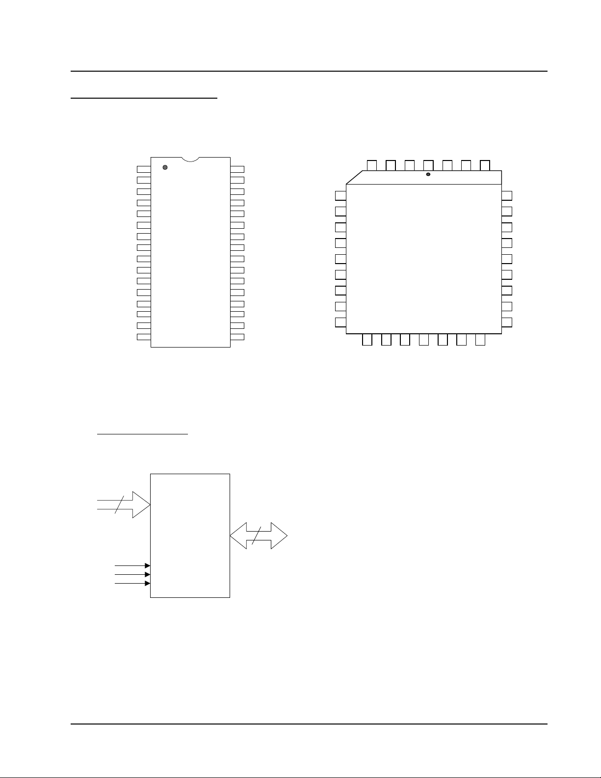
CONNECTION DIAGRAMS
A18
A16
A15
A12
A7
A6
A5
A4
A3
A2
A1
A0
I/O0
I/O1
I/O2
GND
1
2
3
4
5
6
7
8
9
10
11
12
13
14
15
16
32
31
30
29
28
27
26
25
24
23
22
21
20
19
18
17
CC
V
WE#
A17
A14
A13
A8
A9
A11
OE#
A10
CE#
I/O7
I/O6
I/O5
I/O4
I/O3
A7
A6
A5
A4
A3
A2
A1
A0
I/O0
5
6
7
8
9
10
11
12
13
14
A12
Pm29F004 Preliminary
CC
V
19
WE#
20
A18
1234323130
18
1716
15
A15
A16
A17
29
28
27
26
25
24
23
22
21
A14
A13
A8
A9
A11
OE#
A10
CE#
I/O7
32-Pin PDIP
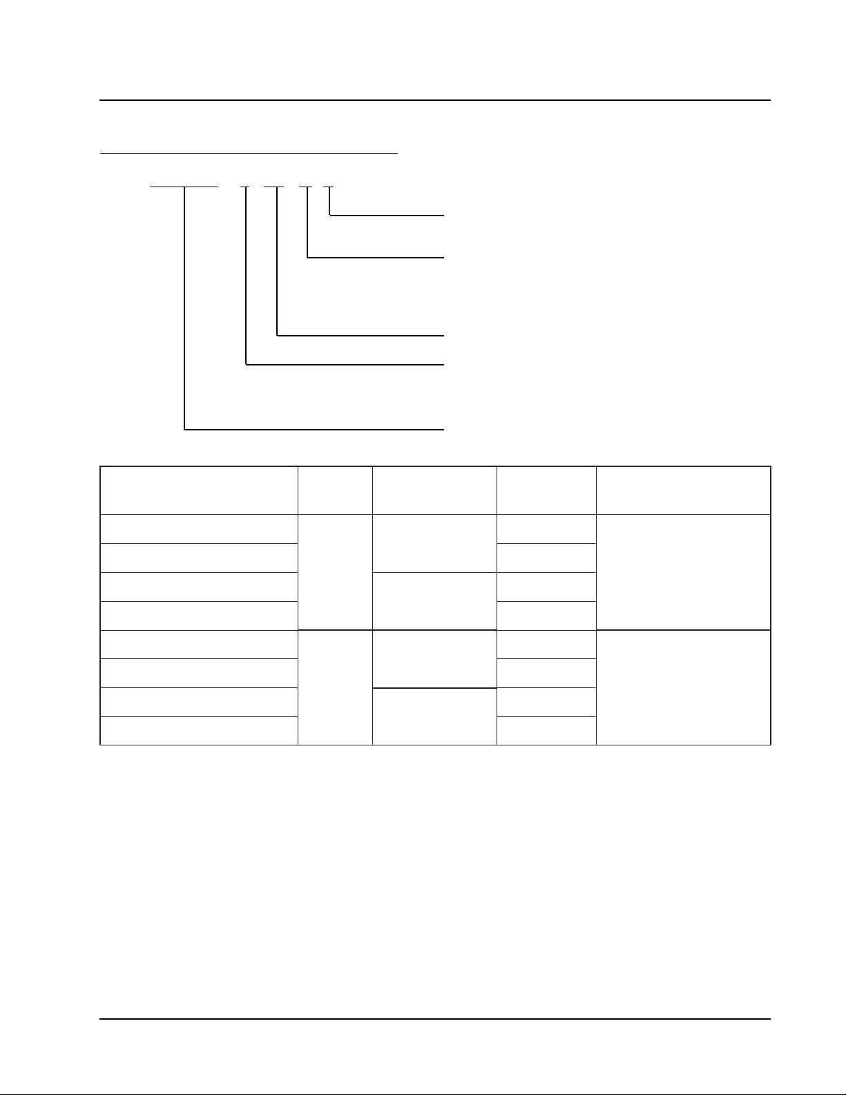
LOGIC SYMBOL
19
A0-A18
CE#
OE#
WE#
I/O0-I/O7
I/O1
I/O2
GND
I/O3
I/O4
I/O5
I/O6
32-Pin PLCC
8
Programmable Microelectronics Corp.
Issue Date: November, 2000 Rev: 1.0
2
Page 3
PMC
PRODUCT ORDERING INFORMATION
Pm29F004 T -70 P C
Pm29F004 Preliminary
Temperature Range
C = Commercial (0°C to +70°C)
Package Type
P = 32-pin Plastic DIP (32P)
J = 32-pin Plastic J-Leaded Chip Carrier (32J)
Speed Option
Boot Block Location
T = Top Boot Block
B = Bottom Boot Block
PMC Device Number
t
rebmuNtraP
CJ07-T400F92mP
CP07-T400F92mP
CJ07-B400F92mP
CP07-B400F92mP
CJ09-T400F92mP
CP09-T400F92mP
CJ09-B400F92mP
CP09-B400F92mP
CCA
)sn(
07
09
tooB
noitacoL
poT
mottoB
poT
mottoB
egakcaP
J23
P23
J23
P23
J23
P23
J23
P23
erutarepmeT
egnaR
laicremmoC
)C°07+otC°0(
laicremmoC
)C°07+otC°0(
Programmable Microelectronics Corp.
Issue Date: November, 2000 Rev: 1.0
3
Page 4
PMC
PIN DESCRIPTIONS
LOBMYSEPYTNOITPIRCSED
Pm29F004 Preliminary
81A-0ATUPNI
#ECTUPNI
#EWTUPNI
#EOTUPNI
7O/I-0O/I
V
CC
DNGdnuorG
.retsigerdnammocdnasesserddayromemroF:stupnIsserddA
.elcycetirwagniruddehctalyllanretnierasesserddA
seirtiucriclanretnis'ecivedehtsetavitcawol#EC:elbanEpihC
dnaecivedehtstcelesedhgih#EC.noitarepoecivedrof
.noitpmusnocrewopehtecuderotedomybdnatsotnisehctiws
.elbatscitsiretcarahcCDotreferesaelP
si#EW.noitarepoetirwrofecivedehtetavitcA:elbanEetirW
.wolevitca
daeragnirudsreffubatads'ecivedehtlortnoC:elbanEtuptuO
.wolevitcasi#EO.elcyc
,noitarepomargorpgnirudatadyarrastupnI:stuptuO/stupnIataD
gniruddehctalyllanretnisiataD.evitcaera#EWdna#ECnehw
/TUPNI
TUPTUO
.delbasiderastuptuo
ylppuSrewoPeciveD
,evitcaera#EOdna#ECnehW.selcycmargorpdnaetirweht
.edocecivedroedocrerutcafunam,atadyarrasdnestuptuoeht
ehtrodetcelesedsipihcehtnehwetats-irtottaolfsnipatadehT
CNnoitcennoCoN
Programmable Microelectronics Corp.
Issue Date: November, 2000 Rev: 1.0
4
Page 5
PMC
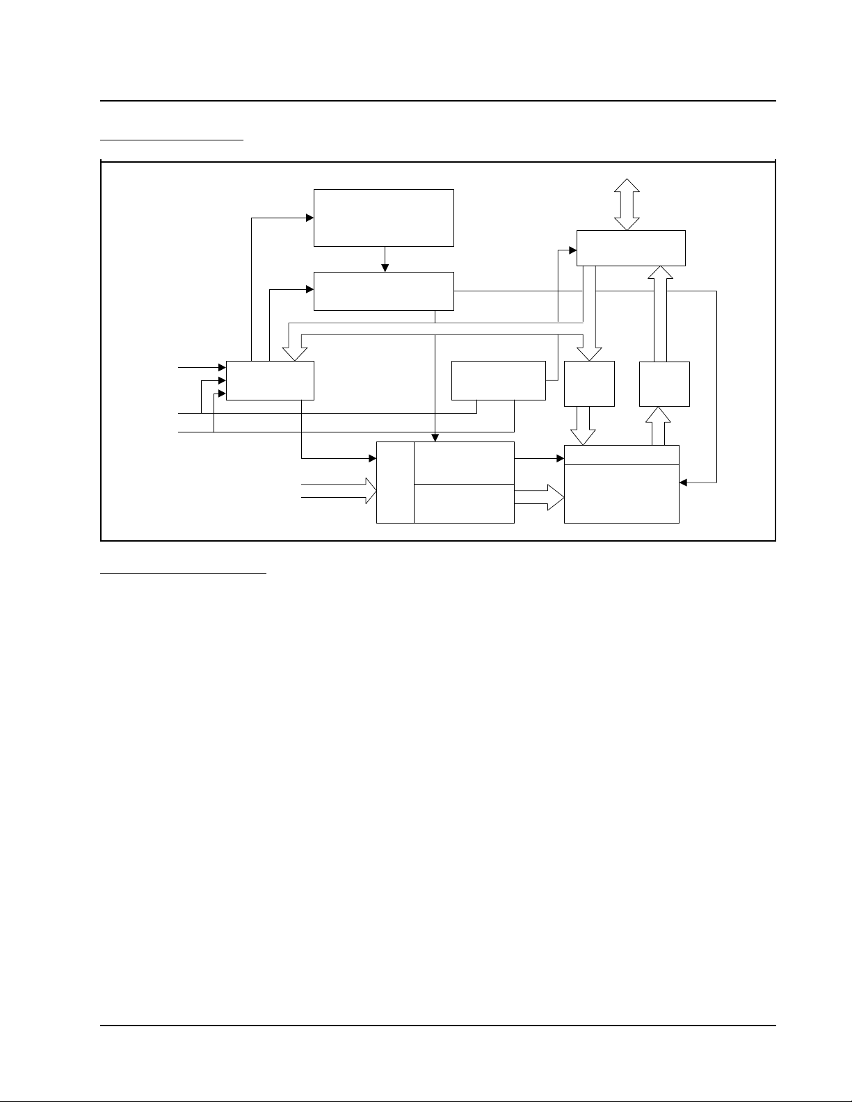
BLOCK DIAGRAM
Pm29F004 Preliminary
ERASE/PROGRAM
VOLTAGE
GENERATOR
HIGH VOLTAGE
SWITCH
WE#
CE#
OE#
COMMAND
REGISTER
A0-A18
LATCH
ADDRESS
DEVICE OPERATION
READ OPERATION
The access of Pm29F004 is similar as that of
EPROM. To obtain data at the outputs, three control
functions must be satisfied:
• CE# is the chip enable and should be pulled low
( VIL ).
• OE# is the output enable and should be pulled
low ( VIL).
• WE# is the write enable and should remains high
( V
).
IH
BOOT BLOCK LOCKOUT
The device has a software lockout feature to prevent the data in the boot block from being erased or
reprogrammed. The boot block can be located at the
top or bottom of the address location. The block size is
16 Kbytes. Once the lockout feature is enable, the boot
block can not be erased or reprogrammed. Data in the
main memory block can still be updated through the
regular programming method. The boot block lockout
feature can be turned on by issuing a six-bus-cycle command sequence. Please refer to Table 4 and Chart 4.
I/O0-I/O7
I/O BUFFERS
CE,OE LOGIC
Y-DECODER
X-DECODER
BOOT BLOCK LOCKOUT DETECTION
The state of the Boot Block lockout can be detected by software product identification entry. After
entry, selects Boot Block address with A0 = “0” and A1
= “1” and then read I/O0. A data of “0” means the lockout feature is disabled and the Boot Block can be erased
or programmed. A data of “1” means the lockout feature is enabled and the Boot Block is protected. Product identification exit must be executed before the device returns to read mode.
PRODUCT IDENTIFICATION
The product identification mode can be used to identify
the device and the manufacturer by hardware or software operation. The hardware operation mode is activated by applying a 12.0 Volt on A9 pin, typically used
by an external programmer to select the right programming algorithm for the device. For detail, please see
Bus Operation Modes in Table 3. The software operation mode is activated by three-bus-cycle command.
Please see Software Command Definition in Table 4.
DATA
LATCH
Y-GATING
MEMORY
ARRAY
SENSE
AMP
Programmable Microelectronics Corp.
Issue Date: November, 2000 Rev: 1.0
5
Page 6

PMC
DEVICE OPERATION (CONTINUED)
Pm29F004 Preliminary
BYTE PROGRAMMING
The programming is a four-bus-cycle operation
and the data is programmed into the device (to a logical
“0”) on a byte-by-byte basis. Please see Software Command Definition in Table 4. A program operation is activated by writing the three-byte command sequence
followed by one byte of data into the device. The address are latched on the falling edge of WE# or CE#
whichever occurs later, and the data is latched on the
rising edge of WE# or CE#, whichever occurs first. The
internal control logic automatically handles the internal
programming voltages and timing.
A data “0” can not be programmed back to a “1”.
Only erase operation can convert “0”s to “1”s. The Data#
Polling of I/O7 or Toggle Bit of I/O6 can be used to detect when the programming operation is completed.
CHIP ERASE
The entire memory array can be erased through
a chip erase operation. Pre-programs the device is not
required prior to chip erase operation. Chip erase starts
after a six-bus-cycle chip erase command sequence.
All commands will be ignored once the chip erase
operation has started. The device will return back to
read mode after the completion of chip erase. When
the boot block lockout feature is enabled, the boot block
will not be erased during a chip erase operation. Only
the parameter blocks and the main blocks will be erased.
BLOCK ERASE
The memory array is organized into seven blocks:
one 16 Kbytes boot block, two 8 Kbytes parameter
blocks, one 96 Kbytes and three 128 Kbytes main
blocks. A block erase operation allows to erase any
individual block. Pre-programs the block is not required
prior to block erase operation. If the boot block lockout
feature is enable, the block erase command attempts
to erase the boot block will be ignored. The block erase
command is similar to chip erase command except for
the last bus cycle command where the block addresses
are used to select the block for erasure and the input
data to the I/Os is 30h. Each block erase operation
erases one block. Block erase and chip erase are both
internally controlled and timed.
I/O7 DATA# POLLING
The Pm29F004 provides Data# Polling feature to
indicate the process or the completion of a program or
erase cycle. During a program cycle, an attempt to read
the device will result in the complement of the last loaded
data on I/O7. Once the program cycle is completed,
the true data of the last loaded data is valid on all outputs. During a block or chip erase operation, an attempt
to read the device will result a “0” on I/O7. After the
erase cycle is completed, an attempt to read the device
will result a “1” on I/O7.
I/O6 TOGGLE BIT
The Pm29F004 also provides Toggle Bit feature
as a method to detect the process or the end of a program or erase cycle. During a program or erase operation, an attempt to read data from the device will result
in I/O6 toggling between “1” and “0”. When the program
or erase operation is complete, I/O6 will stop toggling
and valid data will be read. Toggle bit may be accessed
at any time during a program or erase cycle.
HARDWARE DATA PROTECTION
Hardware data protection protects the device from
unintentional erase or program operation. It is performed
in the following ways: (a) VCC sense: if VCC is below 3.8
V (typical), the program function is inhibited. (b) Write
inhibit: holding any of the signal OE# low, CE# high or
WE# high inhibits a write cycle. (c) Noise filter: pulses
of less than 20 ns (typical) on the WE# or CE# inputs
will not initiate a write cycle.
Programmable Microelectronics Corp.
Issue Date: November, 2000 Rev: 1.0
6
Page 7
PMC
MEMORY BLOCKS AND ADDRESSES
Table 1. Top Boot Block Address Table (Pm29F004T)
kcolBeziSkcolBegnaRsserddA
4kcolBniaMsetybK821hFFFF1-h00000
3kcolBniaMsetybK821hFFFF3-h00002
2kcolBniaMsetybK821hFFFF5-h00004
1kcolBniaMsetybK69hFFF77-h00006
2kcolBretemaraPsetybK8hFFF97-h00087
1kcolBretemaraPsetybK8hFFFB7-h000A7
kcolBtooBsetybK61hFFFF7-h000C7
Pm29F004 Preliminary
Table 2. Bottom Boot Block Address Table ( Pm29F004B)
kcolBeziSkcolBegnaRsserddA
kcolBtooBsetybK61hFFF30-h00000
1kcolBretemaraPsetybK8hFFF50-h00040
2kcolBretemaraPsetybK8hFFF70-h00060
1kcolBniaMsetybK69hFFFF1-h00080
2kcolBniaMsetybK821hFFFF3-h00002
3kcolBniaMsetybK821hFFFF5-h00004
4kcolBniaMsetybK821hFFFF7-h00006
Programmable Microelectronics Corp.
Issue Date: November, 2000 Rev: 1.0
7
Page 8

PMC
OPERATING MODES
edoM#EC#EO#EWSSERDDAO/I
Pm29F004 Preliminary
Table 3. Bus Operation Modes
daeRV
etirWV
ybdnatSV
LI
LI
HI
elbasiDtuptuOXV
noitacifitnedItcudorP
erawdraH
V
LI
V
LI
V
HI
XX X ZhgiH
HI
V
LI
Notes:
1. X can be VIL, VIH or addresses.
2. VH = 12.0 V ± 0.5 V.
3. Manufacturer Code: 9Dh;
Device Code: 1Eh (top boot), 2Eh (bottom boot)
V
HI
V
LI
)1(
X
XD
XX ZhgiH
=81A-2AV=9A,X
V=1A
V
HI
LI
V=1A
LI
V=0A,
LI
V=0A,
HI
)2(
,
H
)2(
V=9A,X=81A-2A
,
H
D
TUO
NI
)3(
edoCrerutcafunaM
)3(
edoCeciveD
Programmable Microelectronics Corp.
Issue Date: November, 2000 Rev: 1.0
8
Page 9

PMC
COMMAND DEFINITION
Pm29F004 Preliminary
Table 4. Software Command Definition
dnammoC
ecneuqeS
suB
elcyC
daeR1DrddA
esarEpihC6hAAh555h55hAA2h08h555hAAh555h55hAA2h01h555
esarEkcolB6hAAh555h55hAA2h08h555hAAh555h55hAA2AB
etyB
margorP
kcolBtooB
)3,2(
tuokcoL
4hAAh555h55hAA2h0Ah555DrddA
6hAAh555h55hAA2h08h555hAAh555h55hAA2h04h555
kcolBtooB
tuokcoL
)3(
noitceteD
tcudorP
DIrerutcafunaM
eciveDtcudorP
)tooBpoT(DI
eciveDtcudorP
3hAAh555h55hAA2h09h555
3hAAh555h55hAA2h09h555hD9h00X
3hAAh555h55hAA2h09h555hE1h10X
3hAAh555h55hAA2h09h555hE2h10X
)tooBmottoB(DI
suBts1
elcyC
ataDrddA
TUO
suBdn2
elcyC
ataDrddA
suBdr3
elcyC
ataDrddA
AB
AB
suBht4
elcyC
ataDrddA
NI
)4(
)4(
)5(
h00
)5(
h10
suBht5
eclyC
ataDrddA
suBht6
elcyC
ataDrddA
)1(
h03
DItcudorP
)6(
tixE
DItcudorP
)6(
tixE
3hAAh555h55hAA2h0Fh555
1h0FhXXX
Notes:
1. BA = Block address of the block to be erased.
2. When the boot block lockout feature is enabled, the boot block will not be erased when a chip erase
command or a block erase command for boot block erasure is issued. Once the boot block is not
protected, the boot block will be erased when a chip erase command or a block erase command for
boot block erasure is issued.
3. After completion of the boot block lockout enable or detection command, the Product ID Exit command must be issued to return to standard read mode.
4. BA = Block address of the boot block;
For top boot block location, A0 = “0”, A1 = “1”, and A14-A18 = “1” where A2-A13 = Don’t Care;
For bottom boot block location, A0 = “0”, A1 = “1”, and A14-A18 = “0” where A2-A13 = Don’t Care.
5. I/O0 = “1” means boot block lockout is enabled, I/O0 = “0” means boot block lockout is disabled.
6. Either one of the Product ID Exit command can be used.
Programmable Microelectronics Corp.
Issue Date: November, 2000 Rev: 1.0
9
Page 10

PMC
DEVICE OPERATIONS FLOWCHARTS
AUTOMATIC PROGRAMMING
Pm29F004 Preliminary
Start
Load Data AAh
to
Address 555H
Load Data 55h
to
Address 2AAh
Address
Increment
No
Load Data A0h
to
Address 555h
Load Program
Data to
Program Address
I/O7 = Data?
or
I/O6 Stop Toggle?
Yes
Last Address?
Yes
Programming
Completed
No
Programmable Microelectronics Corp.
Chart 1. Automatic Programming Flowchart
Issue Date: November, 2000 Rev: 1.0
10
Page 11

PMC
DEVICE OPERATIONS FLOWCHARTS (CONTINUED)
AUTOMATIC ERASE
Start
Write Chip
or Block
Erase Command
Data = FFh?
or
No
I/O6 Stop Toggle?
Yes
Erasure
Completed
Pm29F004 Preliminary
CHIP ERASE COMMAND
Load Data AAh
to
Address 555h
Load Data 55h
to
Address 2AAh
Load Data 80h
to
Address 555h
Load Data AAh
to
Address 555h
Load Data 55h
to
Address 2AAh
Load Data 10h
to
Address 555h
(3)
BLOCK ERASE COMMAND
Load Data AAh
to
Address 555h
Load Data 55h
to
Address 2AAh
Load Data 80h
to
Address 555h
Load Data AAh
to
Address 555h
Notes:
1. Please see Software Command
Definition in Table 1 and Table
2 for block addresses.
Load Data 55h
to
Address 2AAh
2. Only erase one block per each
block erase cycle.
3. When the boot block lockout
feature has been enabled, the
Load Data 30h
to
Block Address
(1,2,3)
boot block will not be erased.
Programmable Microelectronics Corp.
Chart 2. Automatic Erase Flowchart
Issue Date: November, 2000 Rev: 1.0
11
Page 12

PMC
DEVICE OPERATIONS FLOWCHARTS (CONTINUED)
Pm29F004 Preliminary
SOFTWARE PRODUCT IDENTIFICATION ENTRY
Load Data AAh
to
Address 555h
Load Data 55h
to
Address 2AAh
Load Data 90h
to
Address 555h
Enter Product
Identification
Mode
(1,2)
SOFTWARE PRODUCT IDENTIFICATION EXIT
Load Data AAh
to
Address 555h
Load Data 55h
to
Address 2AAh
Load Data F0h
to
Address 555h
Exit Product
Identification
Mode
(3)
Notes:
1. Manufacturer Code is read when A0-A18 = XX00h, where X = Don’t Care;
Device Code is read when A0-A18 = XX01h.
or
Load Data F0h
to
Address XXXh
Exit Product
Identification
Mode
(3)
2. Manufacturer Code = 9Dh;
Device Code = 1Eh (top boot device);
Device Code = 2Eh (bottom boot device).
3. The device returns to standard read operation.
Chart 3. Software Product Identification Entry/Exit Flowchart
Programmable Microelectronics Corp.
Issue Date: November, 2000 Rev: 1.0
12
Page 13

PMC
DEVICE OPERATIONS FLOWCHARTS (CONTINUED)
Pm29F004 Preliminary
BOOT BLOCK LOCKOUT ENABLE
Load Data AAh
to
Address 555h
Load Data 55h
to
Address 2AAh
Load Data 80h
to
Address 555h
Load Data AAh
to
Address 555h
Load Data 55h
to
Address 2AAh
(1,2)
Notes:
1. Please call manufacturer for the command code to
disable the boot block lockout.
2. After excuting the boot block lockout command, the
Product ID Exit command must be issued to return
to standard read mode.
Load Data 40h
to
Address 555h
Pause 500 ms
Boot Block
Lockout Enabled
Chart 4. Boot Block Lockout Enable Flowchart
Programmable Microelectronics Corp.
Issue Date: November, 2000 Rev: 1.0
13
Page 14

PMC
Pm29F004 Preliminary
ABSOLUTE MAXIMUM RATINGS
saiBrednUerutarepmeT 56-
erutarepmeTegarotS 56-
)2(
V
CC
(1)
)2(
nip9AtpecxesniPllAnodnuorGottcepseRhtiwegatloVtupnI
)3(
nip9AnodnuorGottcepseRhtiwegatloVtupnI
dnuorGottcepseRhtiwegatloVtuptuOllA VotV5.0-
O
O
CC
Notes:
1. Stresses under those listed in “Absolute Maximum Ratings” may cause permanent
damage to the device. This is a stress rating only. The functional operation of the device
or any other conditions under those indicated in the operational sections of this specification is not implied. Exposure to absolute maximum rating condition for extended periods
may affected device reliability.
2. Maximum DC voltage on input or I/O pins are +6.25 V. During voltage transitioning period,
input or I/O pins may overshoot to VCC + 2.0 V for a period of time up to 20 ns. Minimum
DC voltage on input or I/O pins are -0.5 V. During voltage transitioning period, input or I/O
pins may undershoot GND to -2.0 V for a period of time up to 20 ns.
O
521+otC
C
O
521+otC
C
V52.6+otV5.0V0.31+otV5.0-
V6.0+
V52.6+otV5.0-
3. Maximum DC voltage on A9 pin is +13.0 V. During voltage transitioning period, A9 pin
may overshoot to +14.0 V for a period of time up to 20 ns. Minimum DC voltage on A9 pin
is -0.5 V. During voltage transitioning period, A9 pin may undershoot GND to -2.0 V for a
period of time up to 20 ns.
DC AND AC OPERATING RANGE
rebmuNtraP 400F92mP
erutarepmeTgnitarepO 0
ylppuSrewoPccV V5.5-V5.4
o
o
07otC
C
Programmable Microelectronics Corp.
Issue Date: November, 2000 Rev: 1.0
14
Page 15

PMC
DC CHARACTERISTICS
lobmySretemaraPnoitidnoCniMpyTxaMstinU
Pm29F004 Preliminary
I
IL
I
OL
I
1BS
I
2BS
I
1CC
I
2CC
V
LI
V
HI
V
LO
V
HO
V
CC
V
CC
V
CC
)1(
V
CC
tnerruCdaoLtupnIV
NI
tnerruCegakaeLtuptuOV
SOMCtnerruCybdnatSV=#EO,#EC
LTTtnerruCybdnatSV=#EC
tnerruCdaeRevitcAI;zHM5=f
tnerruCesarE/margorP 0406Am
egatloVwoLtupnI5.0-8.0V
egatloVhgiHtupnI0.2V
egatloVwoLtuptuOI
egatloVhgiHtuptuOI
LO
HO
Note: 1. Characterized but not 100% tested.
AC CHARACTERISTICS
O/I
= − V,Am5.2
VotV0=
V,
CC
VotV0=
CC
CC
Vot
HI
CC
TUO
V,Am21=
CC
V=
CC
V,
CC
xamCC
V=
xamCC
V5.0±1.05Aµ
2.03Am
Am0=5103Am
V=
nimCC
V=
CC
nimCC
4.2V
1Aµ
1Aµ
5.0+V
CC
54.0V
READ OPERATIONS CHARACTERISTICS
lobmySretemaraP
t
CR
t
CCA
t
EC
t
EO
t
FD
t
HO
t
SCV
Programmable Microelectronics Corp.
V
CC
emiTelcyCdaeR0709sn
yaleDtuptuOotsserddA0709sn
yaleDtuptuOot#EC0709sn
yaleDtuptuOot#EO5304sn
ZhgiHtuptuOot#EOro#EC052003sn
ro#EC,#EOmorfdloHtuptuO
emiTpu-teS0505sµ
07-400F92mP09-400F92mP
stinU
niMxaMniMxaM
tsrifderuccorevehcihw,sserddA
00 sn
Issue Date: November, 2000 Rev: 1.0
15
Page 16

PMC
AC CHARACTERISTICS (CONTINUED)
READ OPERATIONS AC WAVEFORMS
t
Pm29F004 Preliminary
RC
ADDRESS
CE#
OE#
ADDRESS VALID
t
ACC
t
CE
t
OE
WE#
t
OH
OUTPUT
VALID
OUTPUT
V
CC
t
VCS
HIGH Z
OUTPUT TEST LOAD INPUT TEST WAVEFORMS
AND MEASUREMENT LEVEL
5.0 V
1.8 K
OUTPUT PIN
3.0 V
Input
0.0 V
1.5 V
t
DF
AC
Measurement
Level
1.3 K
100 pF
PIN CAPACITANCE ( f = 1 MHz, T = 25°C )
pyTxaMstinUsnoitidnoC
C
NI
C
TUO
46 FpV
821FpV
Note: These parameters are characterized and are not 100% tested.
Programmable Microelectronics Corp.
Issue Date: November, 2000 Rev: 1.0
16
V0=
NI
V0=
TUO
Page 17

PMC
g
AC CHARACTERISTICS (CONTINUED)
WRITE (PROGRAM/ERASE) OPERATIONS CHARACTERISTICS
lobmySretemaraP
niMxaMniMxaM
Pm29F004 Preliminary
07-400F92mP09-400F92mP
stinU
t
CW
t
SA
t
HA
t
SC
t
HC
t
SW
t
HW
t
SD
t
HD
t
PW
t
HPW
t
PB
t
CE
t
SCV
V
CC
emiTelcyCetirW0709sn
emiTpu-teSsserddA00sn
emiTdloHsserddA5405sn
emiTpu-teS#EC00sn
emiTdloH#EC00sn
emiTpu-teS#EW00sn
emiTdloH#EW00sn
emiTpu-teSataD0354sn
emiTdloHataD00sn
htdiWesluPetirW5354sn
hgiHhtdiWesluPetirW0202sn
emiTgnimmargorPetyB0505sµ
emiTelcyCesarEkcolBropihC001001sm
emiTpu-teS0505sµ
PROGRAM OPERATIONS AC WAVEFORMS - WE# CONTROLLED
ram Cycle
Pro
OE#
t
t
VCS
CE#
t
CS
WE#
t
AS
A0 - A17
DATA IN
V
CC
Programmable Microelectronics Corp.
555 555 ADDRESS2AA
t
WC
t
AH
CH
t
WP
t
DS
AA 55 A0
t
WPH
t
DH
Issue Date: November, 2000 Rev: 1.0
17
INPUT
DATA
t
BP
VALID
DATA
Page 18

PMC
AC CHARACTERISTICS (CONTINUED)
PROGRAM OPERATIONS AC WAVEFORMS - CE# CONTROLLED
Program Cycle
OE#
t
WH
WE#
t
VCS
Pm29F004 Preliminary
t
WS
t
WP
CE#
t
AH
555 555 ADDRESS2AA
t
WC
t
DS
AA 55 A0
A0 - A17
DATA IN
V
CC
t
AS
CHIP ERASE OPERATIONS AC WAVEFORMS
OE#
t
VCS
CE#
t
WPH
t
DH
INPUT
DATA
t
BP
VALID
DATA
WE#
t
AS
AO - A17
555 2AA 555 555 2AA
t
WC
DATA IN
V
CC
Programmable Microelectronics Corp.
t
DS
t
DH
t
WPH
t
WP
t
AH
AA 55 55 1080 AA
Issue Date: November, 2000 Rev: 1.0
18
555
t
EC
Page 19

PMC
AC CHARACTERISTICS (CONTINUED)
BLOCK ERASE OPERATIONS AC WAVEFORMS
OE#
t
VCS
CE#
Pm29F004 Preliminary
t
WP
WE#
t
AO - A17
DATA IN
V
CC
AS
t
AH
555 2AA 555 555 2AA
t
WC
AA 55 55 3080 AA
PROGRAM/ERASE PERFORMANCE
retemaraPtinUniMpyTxaMskrameR
emiTesarEkcolBsm05001
t
DS
t
DH
t
WPH
BLOCK
ADDRESS
t
EC
dnammocesaregnitirwmorF
noitelpmocesareot
emiTesarEpihCsm05001
emiTgnimmargorPetyB
µs
2105
ecnarudnEesarE/margorPselcyC000,01000,05
Note: These parameters are characterized and are not 100% tested.
Programmable Microelectronics Corp.
Issue Date: November, 2000 Rev: 1.0
19
dnammocesaregnitirwmorF
noitelpmocesareot
elcyc-ruoffoemitehtsedulcxE
noitucexednammocmargorp
Page 20

PMC
AC CHARACTERISTICS (CONTINUED)
TOGGLE BIT AC WAVEFORMS
WE#
t
OEH
CE#
Pm29F004 Preliminary
OE#
t
I/O6
Note: Toggling either CE#, OE# or both OE# and CE# will operate Toggle Bit.
DATA# POLLING AC WAVEFORMS
WE#
CE#
OE#
t
CH
t
OEH
OE
TOGGLE
t
OE
t
DF
t
OH
TOGGLEDATA
t
CE
STOP
TOGGLING
VALID
DATA
t
DF
I/O7
Note: Toggling either CE#, OE# or both OE# and CE# will operate Data# Polling.
Programmable Microelectronics Corp.
VALID DATAI/O7#
t
OH
Issue Date: November, 2000 Rev: 1.0
20
Page 21

PMC
PACKAGE TYPE INFORMATION
32P
32-Pin Plastic DIP Dimensions in Inches (Millimeters)
1.640(41.7)
1.680(42.7)
1732
Pm29F004 Preliminary
.600(15.24)
.625(15.88)
.537(13.64)
.557(14.05)
Pin 1 I.D.
.120(3.05)
.160(4.07)
.040(1.02)
.065(1.65)
.005(.127)
MIN
.090(2.29)
.110(2.79)
16
.014(.36)
.022(.56)
.146(3.71)
.162(4.11)
SEATING PLANE
.015(.38) MIN
0°
10°
32J
32-Pin Plastic Leaded Chip Carrier Dimensions in Inches (Millimeters)
.485(12.32)
.495(12.51)
.447(11.35)
.453(11.51)
.009
.015
.008(0.20)
.013(0.33)
.625(15.88)
.665(16.89)
.585(14.86)
.595(15.11)
Pin 1 I.D.
.547(13.89)
.553(14.05)
.026(.66)
.032(.81)
TOP VIEW SIDE VIEW
Programmable Microelectronics Corp.
SEATING
.050 REF.
.123(3.12)
.140(3.56)
PLANE
025(.635)X30°
.076(1.93)
.095(2.41)
.400
REF.
.510(12.95)
.013(.33)
.021(.53)
Issue Date: November, 2000 Rev: 1.0
21
.530(13.46)
 Loading...