

Page 1

PEX 8648-AA RDK
Hardware Reference Manual
Version 1.2
December 2010
Website: www.plxtech.com
Technical Support: www.plxtech.com/support
Copyright © 2010 by PLX Technology, Inc. All Rights Reserved – Version 1.2
December 6, 2010
Page 2

© 2010 PLX Technology, Inc. All Rights Reserved.
PLX Technology, Inc. retains the right to make changes to this product at any time, without notice. Products may
have minor variations to this publication, known as errata. PLX assumes no liability whatsoever, including
infringement of any patent or copyright, for sale and use of PLX products.
PLX Technology and the PLX logo are registered trademarks and ExpressLane is a trademark of
PLX Technology, Inc.
Other brands and names are the property of their respective owners.
Document Number: 8648-AA RDK-HRM-1.2
Page 3

Contents
Preface ...................................................................................................................................................................... iv
Notice ..................................................................................................................................................................... iv
About This Manual ................................................................................................................................................. iv
Revision History...................................................................................................................................................... iv
1 General Information ............................................................................................................................................. 1
1.1 PEX 8648 Switch Features ............................................................................................................................ 2
1.2 PEX 8648 RDK Base Board Features ........................................................................................................... 2
2 System Architecture ............................................................................................................................................. 3
3 Hardware Architecture ......................................................................................................................................... 5
3.1 PCI Express Port Configuration ..................................................................................................................... 5
3.2 Non-Transparent Operation ......................................................................................................................... 12
3.3 PCI Express Hot-Plug Circuitry ................................................................................................................... 12
3.4 Reference Clock Circuitry ............................................................................................................................ 14
3.5 Port Configuration and Status LED Indicators ............................................................................................. 16
3.5.1 PORT STATUS LED Indicators ............................................................................................................ 17
3.5.2 UP PORT LED Indicators...................................................................................................................... 17
3.5.3 NT PORT LED Indicators ...................................................................................................................... 17
3.6 Hardware Strapping Balls ............................................................................................................................ 18
3.7 Power Circuitry ............................................................................................................................................ 20
3.8 Reset Circuitry ............................................................................................................................................. 21
3.9 Serial EEPROM Interface (U2) .................................................................................................................... 21
3.10 JTAG Interface (JP7) ................................................................................................................................... 22
3.11 I2C Interface (JP8 and JP9) ......................................................................................................................... 22
3.12 Device-Specific Sideband Signals ............................................................................................................... 23
3.12.1 FATAL_ERR# (TPV22, DS1) ....................................................................................................... ......... 23
3.12.2 PEX_INTA# (TPV21, DS2) ................................................................................................................... 23
3.12.3 PEX_NT_RESET# (TPV49) .................................................................................................................. 23
4 Base Board Mechanicals/Component Placement ............................................................................................. 24
4.1 Monitoring Point, LED Indicator, and Control Summary ............................................................................. 25
4.1.1 Monitoring Points .................................................................................................................................. 25
4.1.2 LED Indicators ....................................................................................................................................... 26
4.1.3 Controls ................................................................................................................................................. 27
4.2 Board Layout Information ............................................................................................................................ 28
4.2.1 Trace Routing Design Rules ................................................................................................................. 28
4.2.2 Power De-Coupling ............................................................................................................................... 28
4.2.3 PCB Layer Stackup ............................................................................................................................... 30
5 References ......................................................................................................................................................... 31
6 Bill of Materials & Schematics ............................................................................................................................ 32
PEX 8648-AA RDK Hardware Reference Manual, Version 1.2
Copyright © 2010 by PLX Technology, Inc. All rights reserved ii
Page 4

Figures
Figure 1. PEX 8648 RDK Base Board Component Layout ....................................................................................... 1
Figure 2. PEX 8648 RDK Being Used in a PC .......................................................................................................... 3
Figure 3. PEX 8648 RDK Base Board Component Layout ....................................................................................... 4
Figure 4. Station 0, x4 UP and x4x4x4 DOWN ......................................................................................................... 7
Figure 5. Station 0, x16 UP ....................................................................................................................................... 7
Figure 6. Station 0, x8 UP and x8 DOWN (Factory Default) ..................................................................................... 8
Figure 7. Station 0, x8 UP and x4x4 DOWN ............................................................................................................. 8
Figure 8. Station 0, x8 UP and x8 NT ........................................................................................................................ 9
Figure 9. Station 0, x4 UP, x4 NT, and x4x4 DOWN ................................................................................................. 9
Figure 10. Station 1, x4x4x4x4 DOWN .................................................................................................................... 10
Figure 11. Station 1, x16 DOWN ............................................................................................................................. 10
Figure 12. Station 1, x8x8 DOWN (Factory Default) ............................................................................................... 11
Figure 13. Station 1, x8x4x4 DOWN ....................................................................................................................... 11
Figure 14. PEX 8648 RDK Base Board PCI Express Hot-Plug Circuitry ................................................................ 13
Figure 15. PEX 8648 RDK Base Board Reference Clock Circuitry ......................................................................... 15
Figure 16. PEX 8648 RDK Base Board Port Configuration and Status LED Indicators ......................................... 16
Figure 17. PEX 8648 RDK Base Board Hardware Strapping DIP Switches – SW1, SW11,
SW4, SW5, SW9, SW6, SW2, and SW10, Default Settings ..................................................................... 18
Figure 18. PEX 8648 RDK Base Board Power Circuitry ......................................................................................... 20
Figure 19. JTAG Header (Top View) ....................................................................................................................... 22
Figure 20. I2C Headers (Top View) ......................................................................................................................... 22
Figure 21. TPV21, TPV22, DS1, and DS2 Placement on PEX 8648 RDK Base Board ......................................... 23
Figure 22. PEX 8648 RDK Base Board Mechanical Outline ................................................................................... 24
Figure 23. PEX 8648 RDK Base Board Dimensions ............................................................................................... 24
Figure 24. De-Coupling Capacitor Footprints .......................................................................................................... 28
Figure 25. PEX 8648 RDK Base Board Power Ball and Perimeter De-Coupling Capacitor Footprints
(Reverse Screen) ...................................................................................................................................... 29
Figure 26. PEX 8648 RDK Base Board External PCB Layer Stackup Report ........................................................ 30
Tables
Table 1. PEX 8648 RDK Base Board Port Configurations ........................................................................................ 6
Table 2. PEX 8648 Switch Port Status LED On/Off Patterns, by State .................................................................. 17
Table 3. PEX 8648 RDK Base Board Hardware Strapping DIP Switches – SW1, SW11,
SW4, SW5, SW9, SW6, SW2, and SW10 ................................................................................................ 19
Table 4. PEX 8648 RDK Base Board Monitoring Points ......................................................................................... 25
Table 5. PEX 8648 RDK Base Board LED Indicators ............................................................................................. 26
Table 6. PEX 8648 RDK Base Board Controls ....................................................................................................... 27
PEX 8648-AA RDK Hardware Reference Manual, Version 1.2
Copyright © 2010 by PLX Technology, Inc. All rights reserved iii
Page 5
Preface
Notice
This manual contains PLX Confidential and Proprietary information. The contents of this manual may not be
copied nor duplicated in any form, in whole or in part, without prior written consent from PLX Technology, Inc.
PLX provides the information and data included in this manual for your benefit, but it is not possible to entirely
verify and test all the information, in all circumstances, particularly information relating to non-PLX manufactured
products. PLX makes neither warranty nor representation relating to the quality, content, or adequacy of this
information. The information in this manual is subject to change without notice. Although every effort has been
made to ensure the accuracy of this manual, PLX shall not be liable for any errors, or incidental or co nsequential
damages in connection with the furnishing, performance, or use of this manual or examples herein. PLX assumes
no responsibility for damage or loss resulting from the use of this manual, for loss or claims by third parties, which
may arise through the use of the PEX 8648 RDK, or for any damage or loss caused by deletion of data as a result
of malfunction or repair.
About This Manual
This Hardware Reference Manual describes the PLX PEX 8648 Rapid Development Kit (PEX 8648 RDK), from a
hardware perspective. It contains a description of all major functional circuit blocks on the PEX 8648 RDK base
board, and serves as a reference for creating software for this product. This manual also includes a complete Bill
of Materials and Schematics.
Revision History
Date Version Comments
March 2008 1.0
November 2008 1.1 Minor update.
December 2010 1.2
Initial release. Supports Board Revision 100, which includes
the PEX 8648 switch, Silicon Revision AA.
Updated the schematic and BOM to reflect the new 360K ohm R170
resistor.
PEX 8648-AA RDK Hardware Reference Manual, Version 1.2
Copyright © 2010 by PLX Technology, Inc. All rights reserved iv
Page 6
1 General Information
The PLX PEX 8648 RDK is a Rapid Development Kit based upon PLX Technology’s ExpressLane™ PEX 8648, a
48-Lane, 12-Port, 3-Station PCI Express Gen 2 switch. The PEX 8648 RDK provides a complete hardware and
software development platform to facilitate getting designs up and running quickly, lowering ri sk and reducing
time-to-market. The PEX 8648 RDK consists of a base board containing three PEX 8648 hardware modules, an
adapter board that plugs into the Host system, four mini-SAS cables and a SATA cable (used to connect the
adapter board to the base board), and a Software Development Kit (SDK). The SDK is downloadable from the
PLX web site, at www.plxtech.com/products/sdk
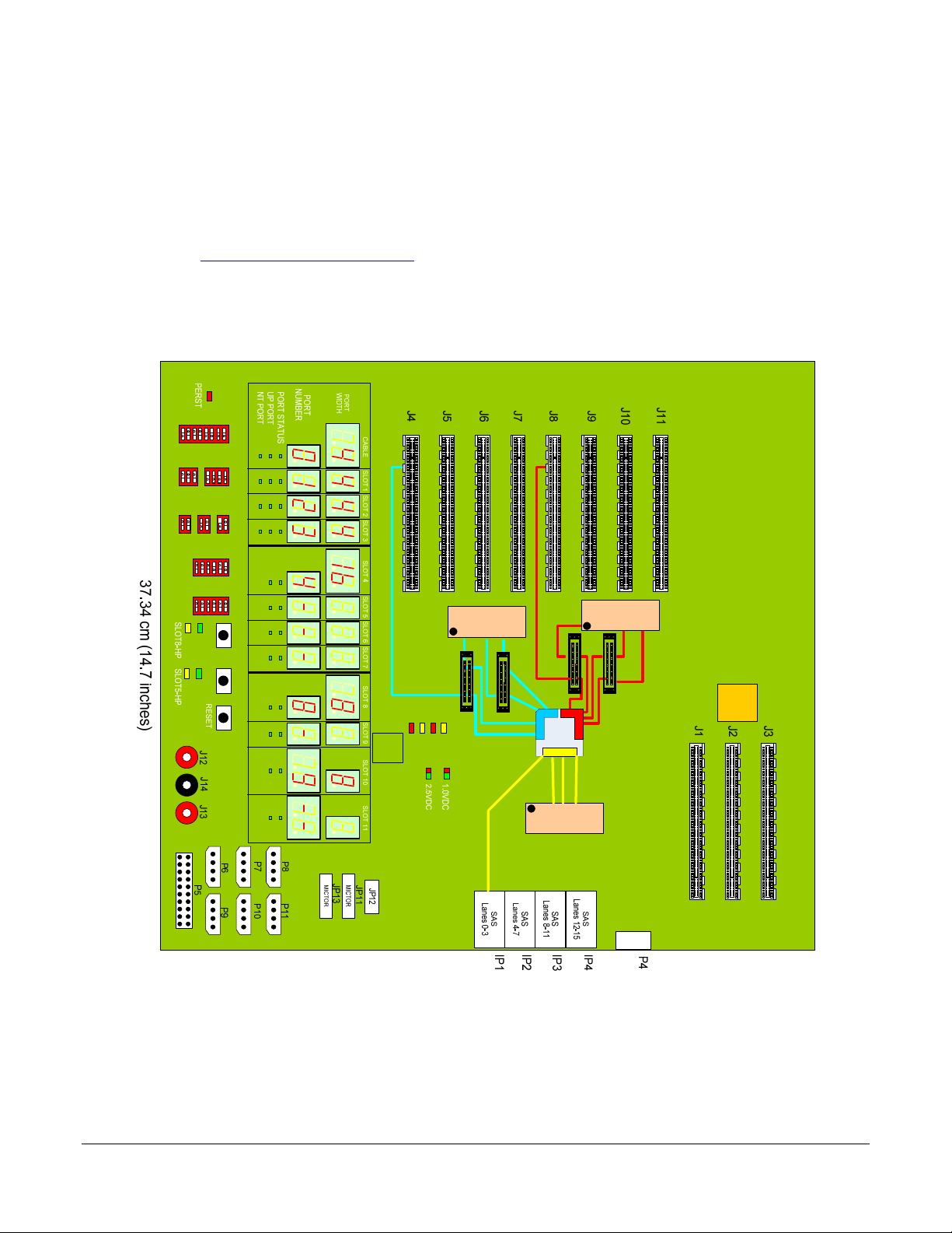
This manual primarily focuses on the PEX 8648 RDK base board, and its use with other parts provided a s part of
the RDK. Figure 1 provides a component-side view of the PEX 8648 RDK base board.
OPEN
OPEN
OPEN
OPEN
OPEN
OPEN
.
37.34 cm (14.7 inches)
OPEN
OPEN
P2
Configuration Module
32
31
PEX8648
27 x 27
U11
16
015
Configuration Module
P1
P3
Configuration Module
47
SATA
RefClk
1:12
Fanout
Figure 1. PEX 8648 RDK Base Board Component Layout
Note: In Figure 1 and other figures in this manual that represent the base board, the Port-related LEDs indicate a
sample Port configuration. The figures do not show which LEDs are turned ON/OFF to match the indicated Port
width and Port Numbers.
PEX 8648-AA RDK Hardware Reference Manual, Version 1.2
Copyright © 2010 by PLX Technology, Inc. All rights reserved 1
Page 7

1.1 PEX 8648 Switch Features
48-Lane, 12-Port, 3-Station PCI Express Gen 2 switch
Standard 676-ball Flip Chip Plastic BGA (FCBGA) package (27 x 27 mm
480 GT/s aggregate bandwidth (5.0 GT/s/Lane x 48 SerDes Lanes x 2 (full duplex))
Non-blocking Crossbar Switch interface supports TLP band width capacity of each x16 Link
Out-of-band communication/initialization interfaces (serial EEPROM and I
2,048-byte Maximum Payload Size
Performance tuning
Choice of width (number of Lanes) per unique Link/Port – x4, x8, or x16
Allows any Port to be designated as the upstream Port (Port 0 is recommended)
Configuration with Strapping balls, serial EEPROM, or I
2
C
Lane reversal
Polarity reversal
Quality of Service (QoS) with one Virtual Channel (VC0) and eight Traffic Classes (TC[7:0])
Non-Transparent Bridging (NTB)
2
) with Heat Spreader
2
C)
Read Pacing (intelligent bandwidth allocation)
Dual Cast
INTA# (PEX_INTA#) and FATAL ERROR (FATAL_ERR#) (Conventional PCI SERR# equivalent) ball
support
Compliant to the following specifications:
PCI Local Bus Specification, Revision 3.0
PCI Bus Power Management Interface Specification, Revision 1.2
PCI to PCI Bridge Architecture Specification, Revision 1.2
PCI Express Base Specification, Revision 2.0
PCI Express Card Electromechanical Specification, Revision 2.0
The I
2
C-Bus Specification, Version 2.1
1.2 PEX 8648 RDK Base Board Features
PLX PEX 8648 PCI Express Gen 2 switch in a 676-ball FCBGA package.
11 downstream PCI Express slot connectors. Hardware configuration is determi ned
by plug-in Configuration modules.
DIP switches, for hardware configuration of the PEX 8648 switch.
Transparent or Non-Transparent (NT) switch support.
Two Hot-Plug-controllable slots – one through a Parallel Hot-Plug Controller interface, and one through
the Serial Hot-Plug Controller interface.
Socketable serial EEPROM.
2
I
C interface, to read and write registers.
Manual pushbutton PERST#.
LED indicators for visual inspection of Port configuration and status.
PEX 8648-AA RDK Hardware Reference Manual, Version 1.2
Copyright © 2010 by PLX Technology, Inc. All rights reserved 2
Page 8
2 System Architecture
The PEX 8648 RDK is a PLX Rapid Development Kit primarily intended for use by PLX customers for silicon
evaluation and design reference for PEX 8648 switches in the 27 x 27 mm
2
package. The PEX 8648 RDK
consists of three main hardware components:
Base board, which is meant to lay on a benchtop and houses the PEX 8648 switch
PCI Express slot-to-cable adapter board, which is meant to plug into a PC platform for the upstream Port
connection
Cable assembly, which connects the base board to the adapter board
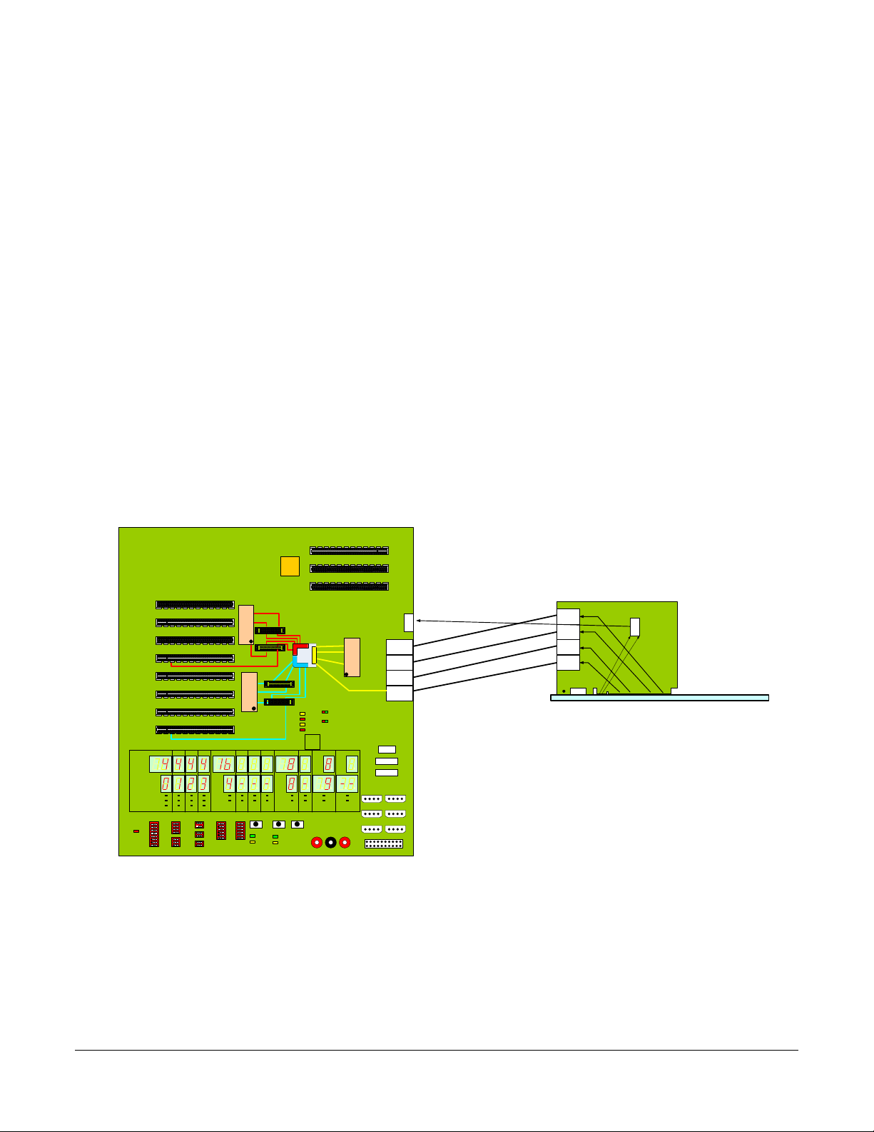
Figure 2 provides a diagram of the PEX 8648 RDK, being used in a PC. Figure 3 represents the placement of
major component blocks on the PEX 8648 RDK base board.
The PEX 8648 RDK base board is similar to a motherboard in form factor. The base board is meant to lay on a
benchtop, and provides 11 PCI Express slots for add-in boards. Board power is supplied by an external ATX
supply (P5). The PEX 8648 RDK base board supports up to 12 Ports (one upstream and 11 downstream). By
default, the upstream Port is Port 0 and the NT Port is Port 1. All available Port width combinations are possible
with the PEX 8648 RDK, by means of Configuration modules that enable versatile routing of the Lanes from the
PEX 8648 switch to the PCI Express connectors. Controls are provided, to support Hot-Plug capability for Port 5
(Parallel Hot-Plug) and Port 8 (Serial Hot-Plug). On-board LED indicators display various configuration and status
information. The power distribution system for the PEX 8648 RDK is such that accurate current draw
measurements can be made, as well as supplying various PEX 8648 RDK base board supply voltages from an
external source, for the purposes of voltage margining.
RDK Base Board
J3
1:12
J2
RefClk
Fanout
J1
J11
J10
J9
37.34 cm (14.7 inches)
J8
J7
J6
J5
J4
CABLE SLOT 1 SLOT 2 SLOT 3 SLOT 4 SLOT 5 SLOT 6 SLOT 7 SLOT 8 SLOT 9 SLOT 10 SLOT 11
PORT
WIDTH
PORT
NUMBER
PORT STATUS
UP PORT
NT PORT
OPEN
OPEN
PERST
OPEN
OPEN
OPEN
OPEN
P3
Configuration Module
P2
Configuration Module
OPEN
OPEN
SLOT8-HP SLOT5-HP
RESET
47
32
31
PEX8648
P1
27 X 27
015
16
Configuration Module
1.0VDC
2.5VDC
U11
P8
P7
P6
J14
J13
J12
JP11
MICTOR
JP13
MICTOR
P5
JP12
SAS
Lanes 12-15
SAS
Lanes 8-11
SAS
Lanes 4-7
SAS
Lanes 0-3
P11
P10
P9
P4
SATA
IP4
IP3
IP2
IP1
37.34 cm (14.7 inches)
Adapter
Lanes 12-15
SAS
Lanes 8-11
SAS
Lanes 4-7
SAS
Lanes 0-3
SAS
SATA
PERST#
REFCLK
Host
Motherboard
Figure 2. PEX 8648 RDK Being Used in a PC
PEX 8648-AA RDK Hardware Reference Manual, Version 1.2
Copyright © 2010 by PLX Technology, Inc. All rights reserved 3
Page 9
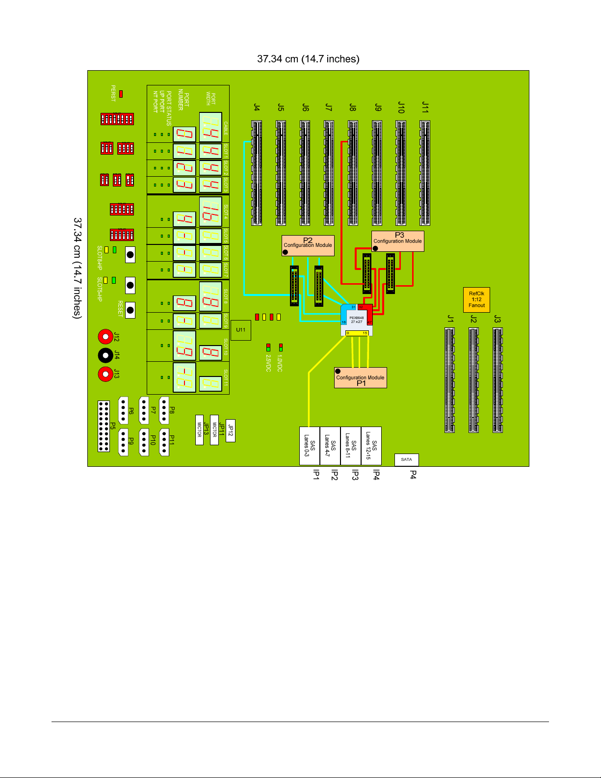
Figure 3. PEX 8648 RDK Base Board Component Layout
PEX 8648-AA RDK Hardware Reference Manual, Version 1.2
Copyright © 2010 by PLX Technology, Inc. All rights reserved 4
Page 10

3 Hardware Architecture
3.1 PCI Express Port Configuration
The PEX 8648 is a 48-Lane, 12-Port, 3-Station non-blocking PCI Express Gen 2 switch that supports Transparent
and NT modes of operation. The footprint for the PEX 8648 switch is laid out so that a heat sink can be attached
to the switch, or a high-speed BGA test socket can be loaded onto the PEX 8648 RDK base board.
The PEX 8648 RDK base board fixes the upstream Port at Port 0 and the NT Port at Port 1, by default. The
upstream Port connects to the Host through four mini-SAS cables that carry four Lanes each, and a serial ATA
cable that provides RefClk and PERST#. This is a significantly less-expensive and less-bulky solution than using
a PCI Express cable. On the Host side, the mini-SAS cables pass through the PC’s bulkhead and attach to the
PEX 8648 RDK adapter board, which plugs into one of the PC’s PCI Express slots, allowing the computer lid to
be closed.
The PEX 8648 RDK adapter board has a x16 male edge connector, to support Port 0 as a x16 Port. If the adapter
board is to be plugged into a smaller slot, a small Catalyst-style adapter must be used, which raises the adapter
board by 18 mm (0.7 inches). This makes the upper-most mini-SAS connector inaccessible, which is acceptable,
because this connector carries Lanes 12 through 15, which would not be used. Also, there is sufficient clearance
for the computer lid to close. Each Station has four possible Port configurations – x4x4x4x4, x16, x8x8, and
x8x4x4. The lowest four Lanes of Station 0 (Lanes 0 through 3) route directly to the lowest four Lanes of the SAS
connectors, the lowest four Lanes of Station 1 (Lanes 16 through 19) route directly to the lowest four Lanes of
Slot 4, and the lowest four Lanes of Station 2 (Lanes 32 through 35) route directly to the lowest four Lanes of
Slot 8. The remaining 12 Lanes of each Station route to a Configuration module. These modules map the Lanes
to the remaining mini-SAS and/or PCI Express connectors, as needed, to obtain the desired Port configuration.
Table 1 describes how to set up the various Port configuration options for each Station.
Note: The possibilities for Station 0 are more complex, because it houses the upstream Port and NT Port.
The Configuration modules consist of a 10 x 40 ball board-to-board, high-speed connector, with one-half of the
connectors mounted on the PEX 8648 RDK base board, and its mate mounted on a small 2-layer PCB that
performs the re-mapping. There are no other components. There are four different Configuration modul es, one for
each possible Station configuration. Each module’s functionality is clearly labeled, and a 3-pin interface on each
module communicates its function to the CPLD glue logic.
The PCI Express Lanes for Station 1 and Station 2, from the PEX 8648 switch to the Configuration modules, have
soft touch midbus probe headers, for monitoring PCI Express traffic. Refer to the Agilent Soft Touch Midbus
Probe User’s Guide, for further details regarding the headers.
PEX 8648-AA RDK Hardware Reference Manual, Version 1.2
Copyright © 2010 by PLX Technology, Inc. All rights reserved 5
Page 11
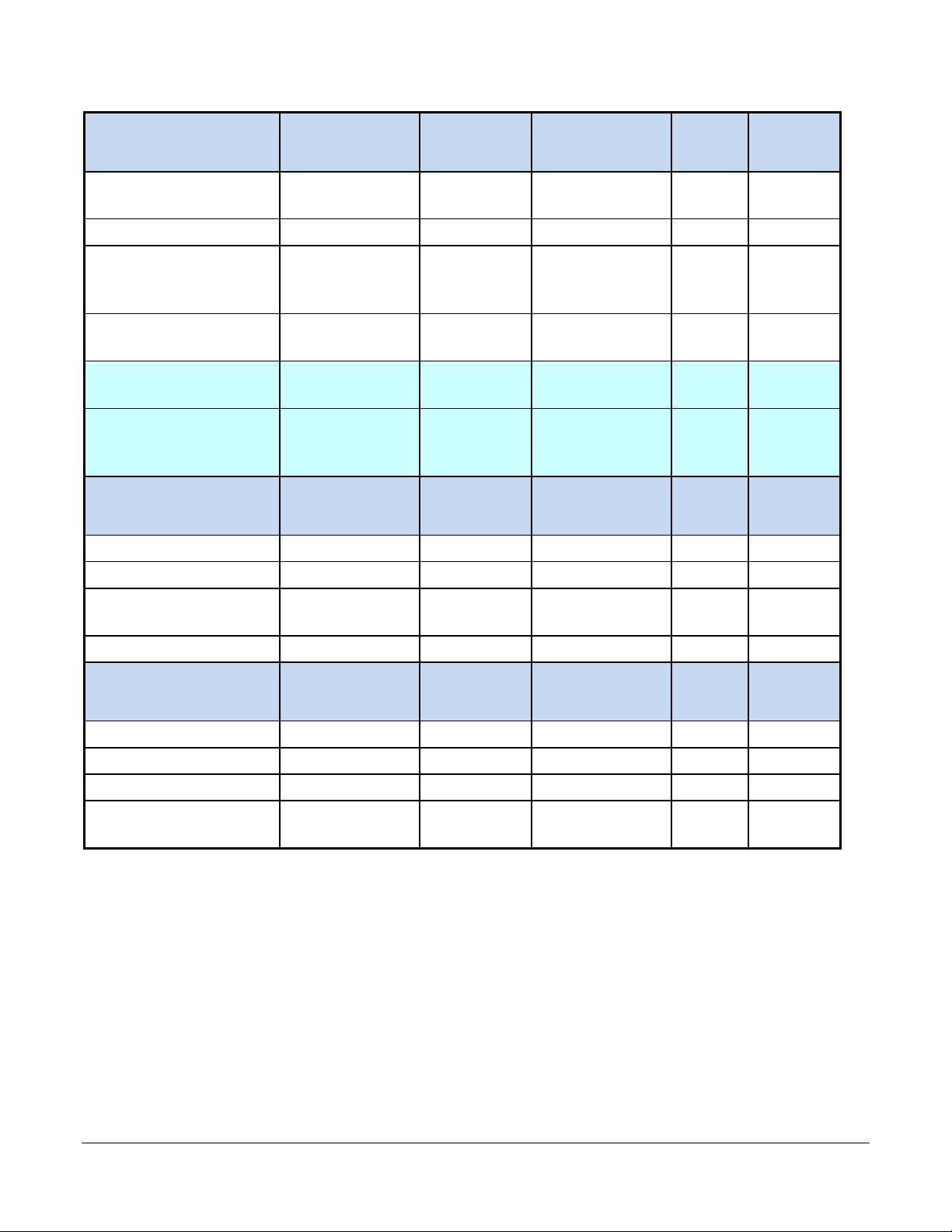
Table 1. PEX 8648 RDK Base Board Port Configurations
Station 0
Port Configuration
x4 UP
x4x4x4 DOWN
x16 UP x16 LH (IP1, IP2, IP3, IP4) H Figure 5
x8 UP
x8 DOWN
(Factory Default)
x8 UP
x4x4 DOWN
x8 UP
x8 NT
x4 UP
x4 NT
x4x4 DOWN
Station 1
Port Configuration
x4x4x4x4 DOWN x4x4x4x4 LL J4, J5, J6, J7 Figure 10
x16 DOWN x16 LH J4 Figure 11
Configuration
Module Installed
(P1)
x4x4x4x4 LL (IP1), J1, J2, J3 H Figure 4
x8x8 HL (IP1, IP2), J2 H Figure 6
x8x4x4 HH (IP1, IP2), J2, J3 H Figure 7
x16 HL (IP1, IP2), IP3, IP4 L Figure 8
x8x4x4 LL (IP1), IP2, J2, J3 L Figure 9
Configuration
Module Installed
(P2)
SW2[2 – 1]
Setting
SW2[4 – 3]
Setting
Connectors
Used
Connectors Used – Refer to
SW1[6]
Setting
Refer to
x8x8 DOWN
(Factory Default)
x8x4x4 DOWN x8x4x4 HH J4, J6, J7 Figure 13
Station 2
Port Configuration
x4x4x4x4 DOWN x4x4x4x4 LL J8, J9, J10, J11
x16 DOWN x16 LH J8
x8x8 DOWN x8x8 HL J8, J10
x8x4x4 DOWN
(Factory Default)
x8x8 HL J4, J6 Figure 12
Configuration
Module Installed
(P3)
x8x4x4 HH J8, J10, J11
SW2[6 – 5]
Setting
Connectors Used – –
Note: In Table 1, parenthesis around the IP components are used to indicate the connectors that comprise the
upstream Port.
PEX 8648-AA RDK Hardware Reference Manual, Version 1.2
Copyright © 2010 by PLX Technology, Inc. All rights reserved 6
Page 12
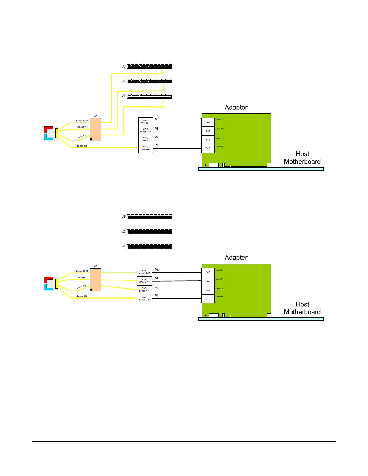
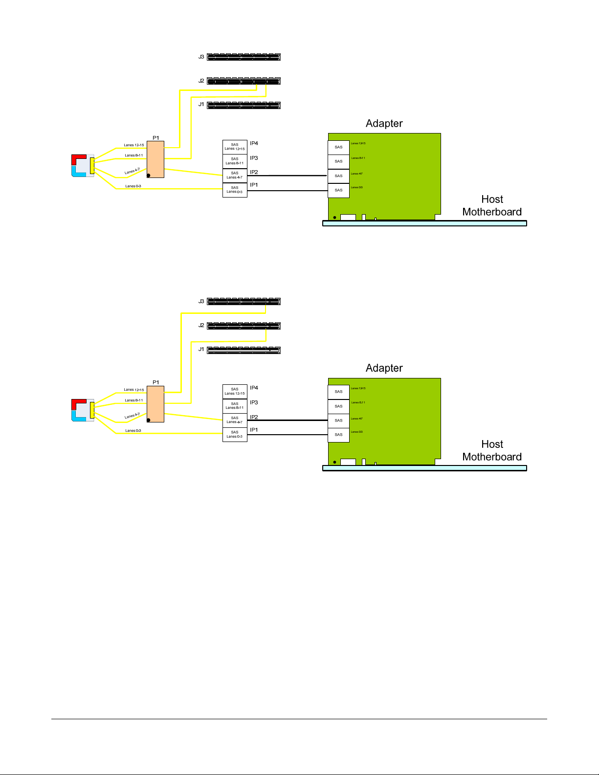
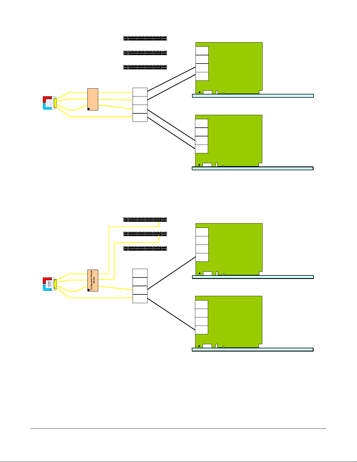
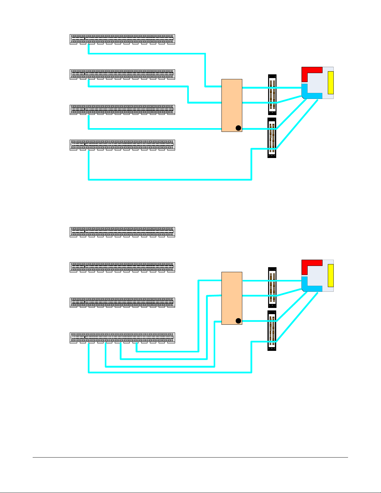
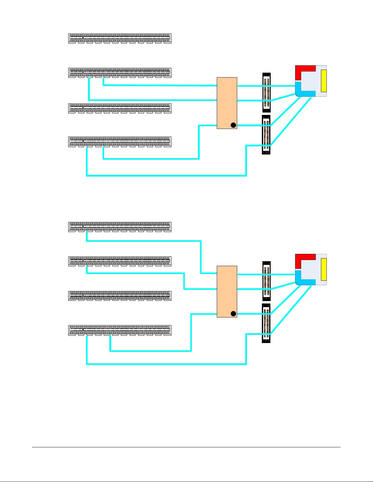
Figure 4 through Figure 13 illustrate the hardwire routing arrangement for each configuration. The routing for
Station 2 is the same as for Station 1, except that it uses J8 through J11 and Lanes 32 through 47 of the
PEX 8648 switch.
47
32
31
27 x 27
PEX8648
015
16
x4x4x4x4
Configuration Module
Figure 4. Station 0, x4 UP and x4x4x4 DOWN
47
32
31
27 x 27
PEX8648
015
16
x16
Configuration Module
Figure 5. Station 0, x16 UP
PEX 8648-AA RDK Hardware Reference Manual, Version 1.2
Copyright © 2010 by PLX Technology, Inc. All rights reserved 7
Page 13
47
32
31
27 x 27
PEX8648
015
16
x8x8
Configuration Module
Figure 6. Station 0, x8 UP and x8 DOWN (Factory Default)
47
32
31
27 x 27
PEX8648
015
16
x8x4x4
Configuration Module
Figure 7. Station 0, x8 UP and x4x4 DOWN
PEX 8648-AA RDK Hardware Reference Manual, Version 1.2
Copyright © 2010 by PLX Technology, Inc. All rights reserved 8
Page 14
Note: Station 0 must be configured
as x8x8, but the Configuration
Module used must be x16.
Lanes 12-15
47
32
31
27 x 27
PEX8648
015
16
Lanes 8-11
s
e
n
a
L
Lanes 0-3
7
-
4
J3
J2
J1
P1
x16
Configuration Module
SAS
Lanes 12-15
SAS
Lanes 8-11
SAS
Lanes 4-7
SAS
Lanes 0-3
IP4
IP3
IP2
IP1
SAS
SAS
SAS
SAS
SAS
SAS
SAS
SAS
Adapter
Lanes 12-15
Lanes 8-11
Lanes 4-7
Lanes 0-3
NT
Motherboard
Adapter
Lanes 12-15
Lanes 8-11
Lanes 4-7
Lanes 0-3
Host
Motherboard
Figure 8. Station 0, x8 UP and x8 NT
Note: Station 0 must be configured
as x4x4x4x4, but the Configuration
Module used must be x8x4x4.
P1
Lanes 12-15
Lanes 8-11
7
-
4
s
e
n
a
L
Lanes 0-3
J3
J2
J1
IP4
SAS
Lanes 12-15
IP3
SAS
Lanes 8-11
IP2
SAS
Lanes 4-7
IP1
SAS
Lanes 0-3
SAS
SAS
SAS
SAS
SAS
SAS
SAS
SAS
Adapter
Lanes 12-15
Lanes 8-11
Lanes 4-7
Lanes 0-3
Adapter
Lanes 12-15
Lanes 8-11
Lanes 4-7
Lanes 0-3
Figure 9. Station 0, x4 UP, x4 NT, and x4x4 DOWN
NT
Motherboard
Host
Motherboard
PEX 8648-AA RDK Hardware Reference Manual, Version 1.2
Copyright © 2010 by PLX Technology, Inc. All rights reserved 9
Page 15
J7
J6
J5
J4
J7
P2
x4x4x4x4
Configuration Module
Figure 10. Station 1, x4x4x4x4 DOWN
47
32
31
27 x 27
PEX8648
015
16
J6
J5
J4
P2
Configuration Module
Figure 11. Station 1, x16 DOWN
x16
47
32
31
27 x 27
PEX8648
015
16
PEX 8648-AA RDK Hardware Reference Manual, Version 1.2
Copyright © 2010 by PLX Technology, Inc. All rights reserved 10
Page 16
J7
J6
J5
J4
J7
P2
x8x8
Configuration Module
Figure 12. Station 1, x8x8 DOWN (Factory Default)
47
32
31
27 x 27
PEX8648
015
16
J6
J5
J4
P2
x8x4x4
Configuration Module
Figure 13. Station 1, x8x4x4 DOWN
47
32
31
27 x 27
PEX8648
015
16
PEX 8648-AA RDK Hardware Reference Manual, Version 1.2
Copyright © 2010 by PLX Technology, Inc. All rights reserved 11
Page 17

3.2 Non-Transparent Operation
Only the Station 0 Ports – Ports 0, 1, 2, and 3 – support NT mode. By default, the NT Port is assigned to Port 1,
by way of DIP switch SW1. To use the NT function, however, DIP switch SW1 must be used to Set the PEX 8648
switch’s Strapping balls so that the switch is in NT mode. Mini-SAS connectors are used to connect to the Host on
the NT Port, by way of cables.
For further details regarding the various hardware configurations for NT mode, refer to Section 3.1, “PCI Express
Port Configuration.”
For further details regarding DIP switch SW1, refer to Table 3, “PEX 8648 RDK Base Board Hardware Strapping
DIP Switches – SW1, SW11, SW4, SW5, SW9, SW6, SW2, and SW10.”
For details regarding the PEX_NT_RESET# sideband signal, refer to Section 3.12.3, “PEX_NT_RESET#
(TPV49).”
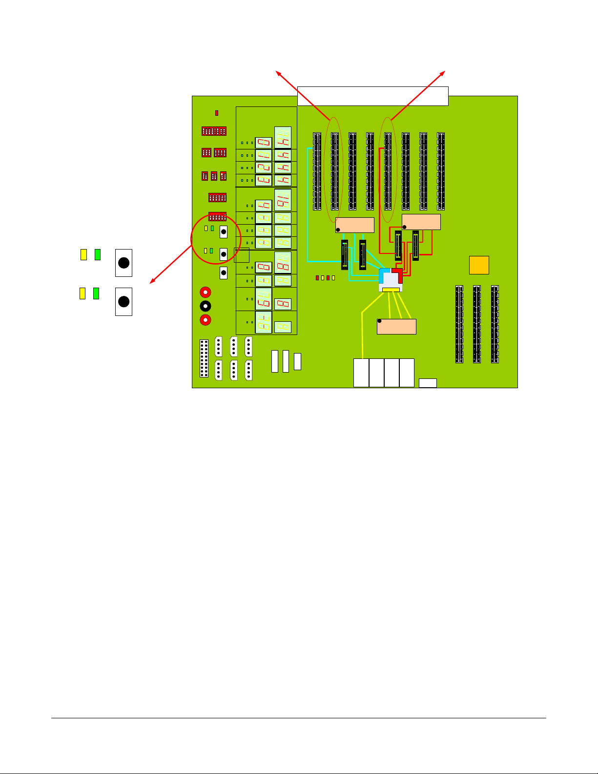
3.3 PCI Express Hot-Plug Circuitry
The PEX 8648 switch supports Hot-Plug on three downstream Ports, by way of dedicated 10-signal Parallel HotPlug interfaces. In addition, a serial I
2
C interface, in conjunction with an external I/O Expander IC, can be used to
support Hot-Plug on any Port. The PEX 8648 RDK base board has external Hot-Plug circuitry that supports
Parallel Hot-Plug to Slot 5, and Serial Hot-Plug to Slot 8.
The PEX 8648 RDK base board supports Parallel Hot-Plug, only on Port 5 of Station 1, routed to Slot 5, and only
when Station 1 is configured as x4x4x4x4. To support Parallel Hot-Plug, Slot 5 has a dual-voltage Hot-Plug
Controller chip associated with it (U15), which controls power to this slot. If Port 5 is the upstream Port, the
Strapping signals that Set the upstream Port are used to bypass the Hot-Plug circuitry for Slot 5.
Note: Other Port configurations that include Port 5 – x8x8 or x8x4x4 – do not support Hot-Plug. In this case,
Port 5 routes to Slot 6, which does not include Hot-Plug circuitry.
2
The PEX 8648 RDK base board supports Serial Hot-Plug on Port 8 of Station 2 (U18). A serial I
C interface, with
an external I/O Expander IC (U17), supports Serial Hot-Plug functionality on this slot. Because Port 8 is the
primary slot on Station 2, Port configuration of Station 2 does not matter. Port 8 is always Hot-Plug-capable.
Figure 14 illustrates the PEX 8648 RDK base board PCI Express Hot-Plug circuitry.
PEX 8648-AA RDK Hardware Reference Manual, Version 1.2
Copyright © 2010 by PLX Technology, Inc. All rights reserved 12
Page 18
PORT 5 –
PARALLEL HOT PLUG
PORT 8 –
SERIAL HOT PLUG
PWR LED
ATN LED
ATN BUTTON
SLOT8-HP SLOT5-HP
J6
P2
Configuration Module
Lanes 0-3
SAS
IP1
Bracket
J7
16
Configuration Module
Lanes 4-7
SAS
IP2
J8
32
31
PEX8648
27 x 27
47
015
P1
Lanes 8-11
SAS
IP3
J10
J9
P3
Configuration Module
Lanes 12-15
SAS
SATA
IP4
J11
RefClk
1:12
Fanout
J1
J2
J3
P4
PERST
OPEN
OPEN
OPEN
OPEN
OPEN
OPEN
OPEN
OPEN
SLOT8-HP SLOT5-HP
RESET
J12 J13
J14
P6
P5
P9
NUMBER
UP PORT
NT PORT
PORT STATUS
U11
P7
P10
WIDTH
PORT
PORT
P8
JP13
MICTOR
MICTOR
P11
J4
J5
CABLE SLOT 1 SLOT 2 SLOT 3
SLOT 4
SLOT 5
SLOT 6
SLOT 7 SLOT 8 SLOT 9 SLOT 10 SLOT 11
JP11
JP12
Figure 14. PEX 8648 RDK Base Board PCI Express Hot-Plug Circuitry
PEX 8648-AA RDK Hardware Reference Manual, Version 1.2
Copyright © 2010 by PLX Technology, Inc. All rights reserved 13
Page 19

3.4 Reference Clock Circuitry
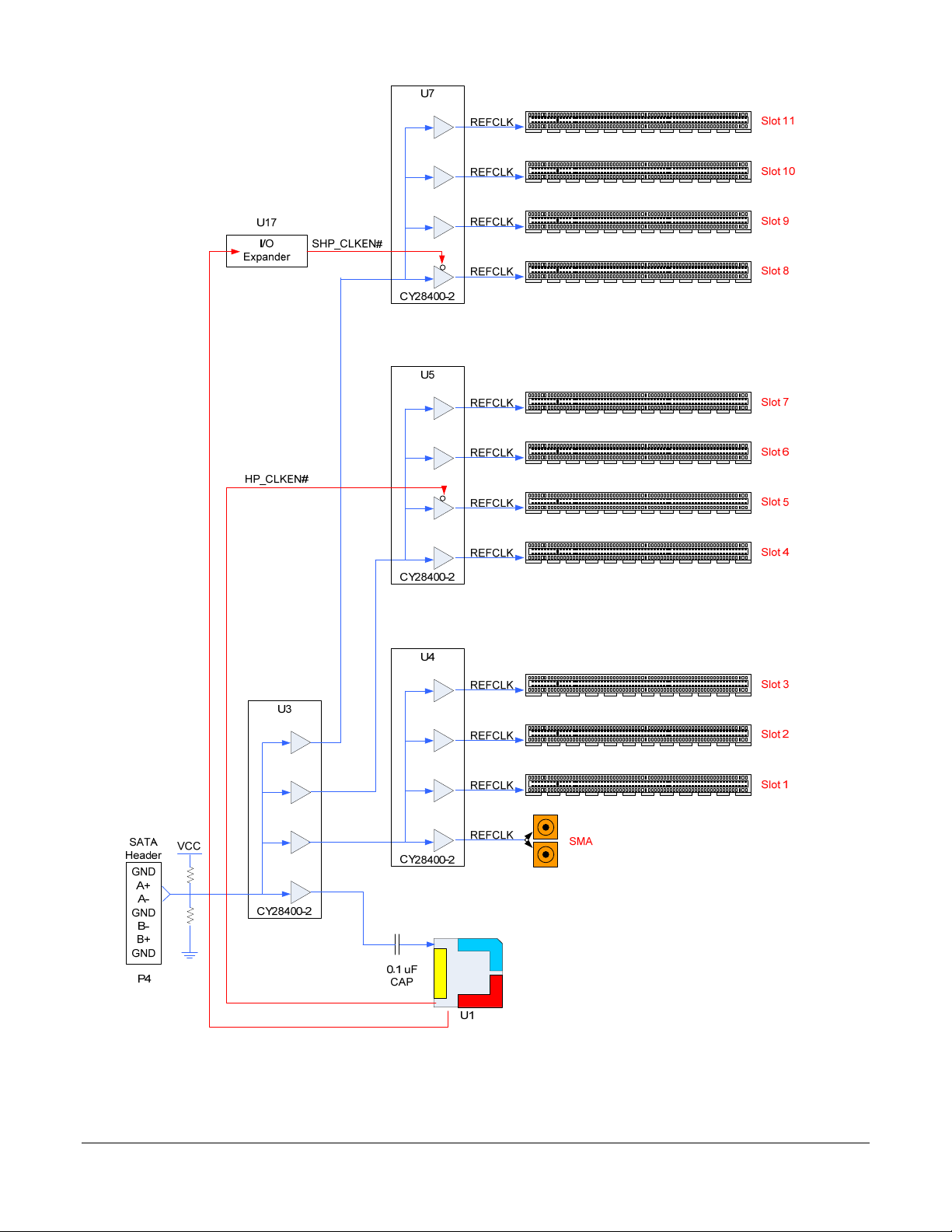
The differential PCI Express RefClk is brought onto the PEX 8648 RDK base board from the Host PC, by way of
the PEX 8648 RDK adapter board and a Serial ATA cable connection. It is used to drive a dual-level set of 1:4
Fan-Out buffers (U3, U4, U5, and U7) to provide a 1:12 Clock Fan-Out buffer. One of these clocks connects to the
PEX 8648 switch and is always enabled. The other 11 clocks connect to the 11 PCI Express slot connectors.
Except for Slot 5 and Slot 8, these RefClks are always enabled. Slot 5 is the downstream connection selected to
demonstrate Hot-Plug capability using the Parallel Hot-Plug interface. Therefore, by default, Slot 5 is enabled by
the PEX 8648 switch’s Parallel Hot-Plug Controller for Port 5. Slot 8 is the downstream connection selected to
demonstrate Hot-Plug capability using the Serial Hot-Plug Controller and an external I/O Expander IC. Figure 15
illustrates the PEX 8648 RDK base board’s Reference Clock circuitry.
PEX 8648-AA RDK Hardware Reference Manual, Version 1.2
Copyright © 2010 by PLX Technology, Inc. All rights reserved 14
Page 20
16
015
PEX8648
27 x 27
31
32
47
Figure 15. PEX 8648 RDK Base Board Reference Clock Circuitry
PEX 8648-AA RDK Hardware Reference Manual, Version 1.2
Copyright © 2010 by PLX Technology, Inc. All rights reserved 15
Page 21
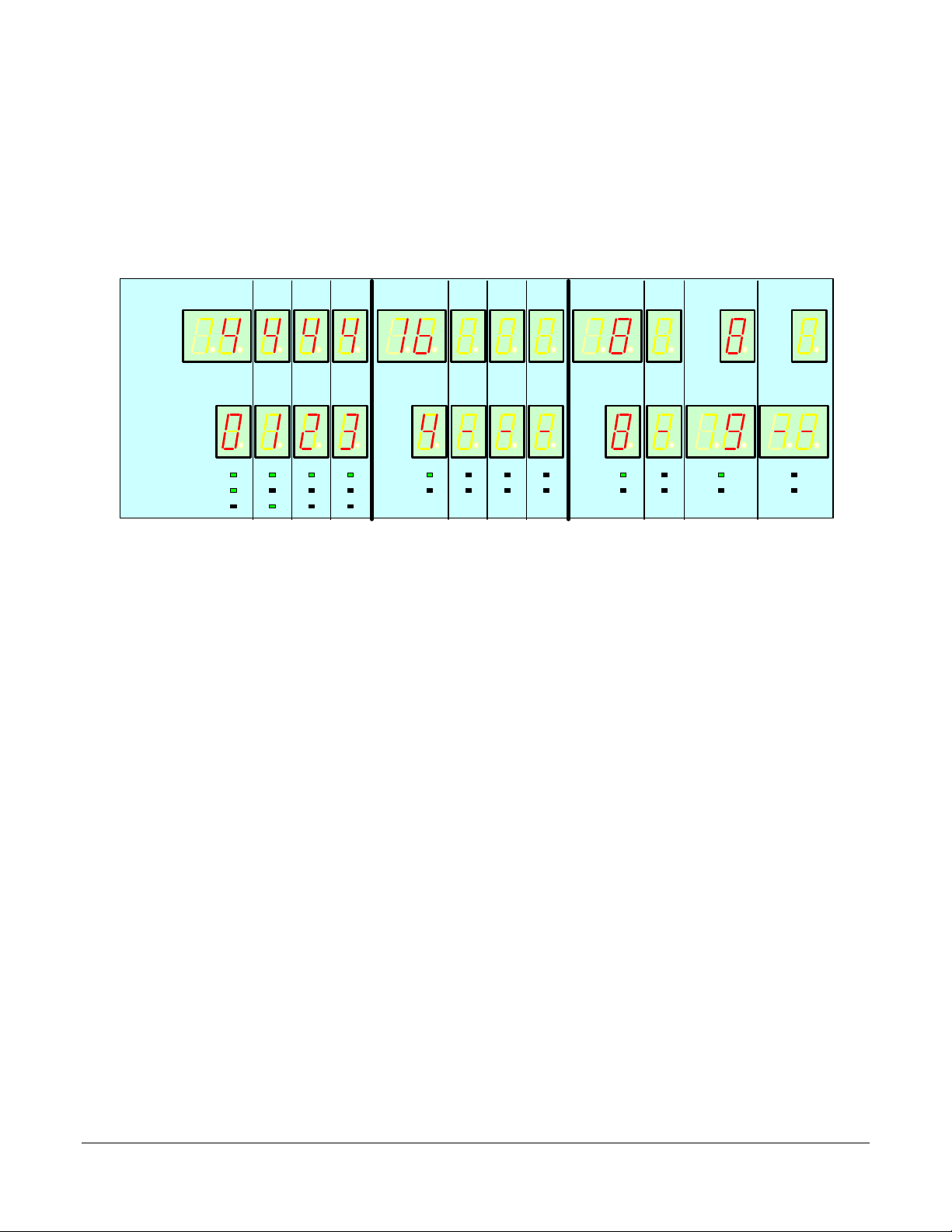
3.5 Port Configuration and Status LED Indicators
The PEX 8648 RDK base board includes several LED indicators, to indicate the board’s Port configuration and
status. (Refer to Figure 16.)
The Strapping switches instruct the PEX 8648 switch how to configure its Ports, which Port is to be the upstream
Port, and which Port (if any) is to be the NT Port. An on-board CPLD provides glue logic, which decodes the
Strapping switch settings. The on-board Configuration modules determine the PEX 8648 RDK base board’s
hardwired width and Port Number associated with the cable and each PCI Express slot. These are indicat ed by
the 7-segment PORT WIDTH and PORT NUMBER LED indicators.
PORT
WIDTH
PORT
NUMBER
PORT STATUS
UP PORT
NT PORT
DS5 DS8 DS11 DS14
DS33 DS36 DS39 DS42
DS30
DS47
DS19
DS31 DS32
DS45 DS46 DS48
DS17 DS18 DS20
DS29
DS6
SLOT 4
DS9
DS12
DS15
SLOT 6
SLOT 5
DS34 DS37 DS40 DS43
DS49 DS50 DS52
DS21 DS22 DS24
SLOT 7 SLOT 8 SLOT 9SLOT 3SLOT 2SLOT 1CABLE SLOT 10 SLOT 11
DS51
DS23
DS7 DS10
DS35 DS38 DS41 DS44
DS53 DS54 DS56
DS25 DS26 DS28
Figure 16. PEX 8648 RDK Base Board Port Configuration and Status LED Indicators
DS55
DS27
DS13
DS16
PEX 8648-AA RDK Hardware Reference Manual, Version 1.2
Copyright © 2010 by PLX Technology, Inc. All rights reserved 16
Page 22
3.5.1 PORT STATUS LED Indicators
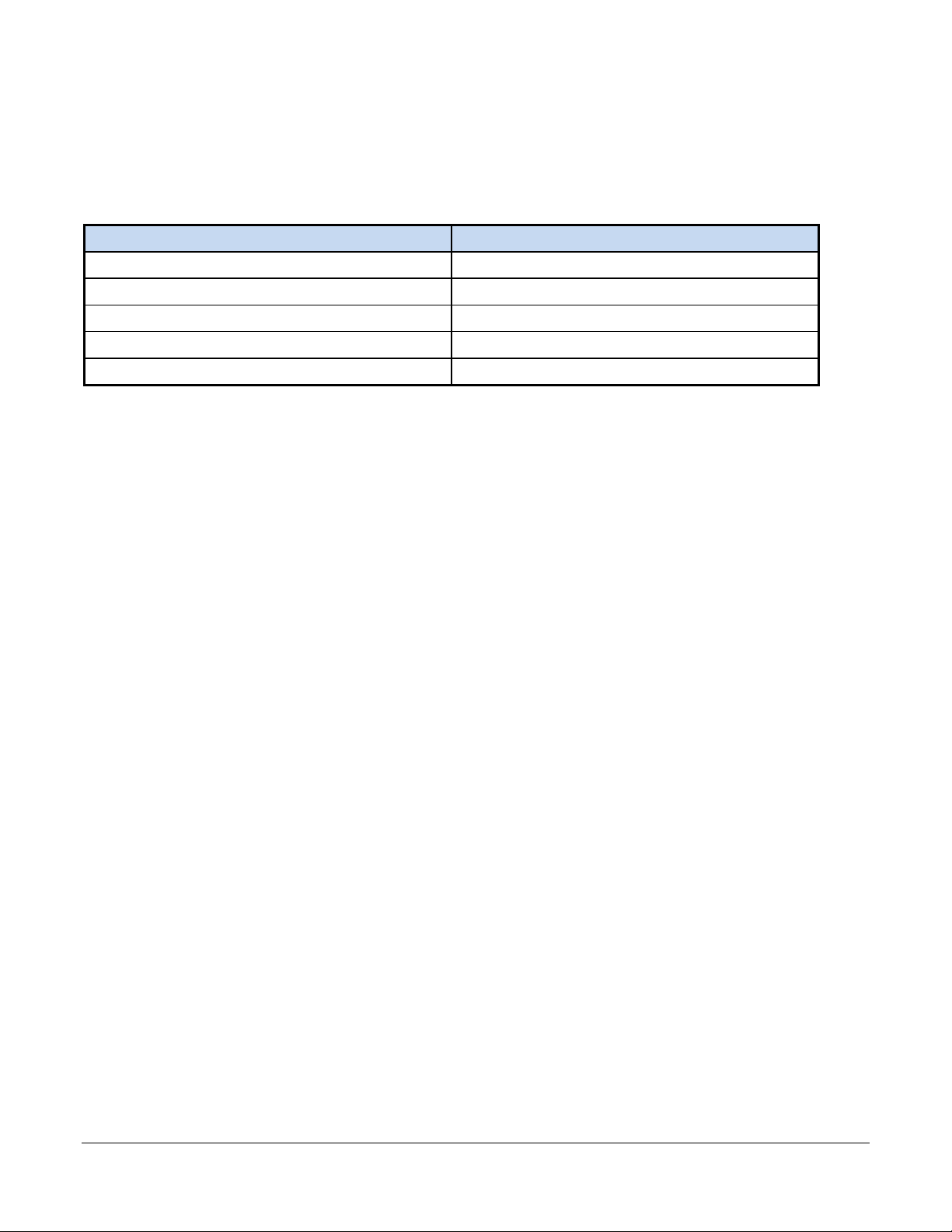
The PORT STATUS indicators (refer to Figure 16) are green LEDs that are driven by the PEX 8648 switch’s
PEX_PORT_GOOD[11:0]# balls. Table 2 describes the relationship of the LED On/Off patterns as they relate to
Port status.
Table 2. PEX 8648 Switch Port Status LED On/Off Patterns, by State
State LED Pattern
Link is down Off
Link is up, 5 GT/s, all Lanes are up On
Link is up, 5 GT/s, reduced Lanes are up Blinking, 0.5 seconds On, 0.5 secon ds Off
Link is up, 2.5 GT/s, all Lanes are up Blinking, 1.5 seconds On, 0.5 seconds Off
Link is up, 2.5 GT/s, reduced Lanes are up Blinking, 0.5 seconds On, 1.5 seconds Off
3.5.2 UP PORT LED Indicators
The upstream Port (UP PORT) indicators (refer to Figure 1 6) are green LEDs that indicate which Port is assigned
as the upstream Port. By default, Port 0 is the assigned upstream Port on the PEX 8648 RDK base board.
3.5.3 NT PORT LED Indicators
The NT PORT indicators (refer to Figure 16) are green LEDs that indicate which Port is assigned as the NT Port.
Only Station 0 Ports – Ports 0, 1, 2, or 3 – can be assigned as the NT Port. By default, Port 1 is the assigned
NT Port on the PEX 8648 RDK base board.
PEX 8648-AA RDK Hardware Reference Manual, Version 1.2
Copyright © 2010 by PLX Technology, Inc. All rights reserved 17
Page 23
3.6 Hardware Strapping Balls
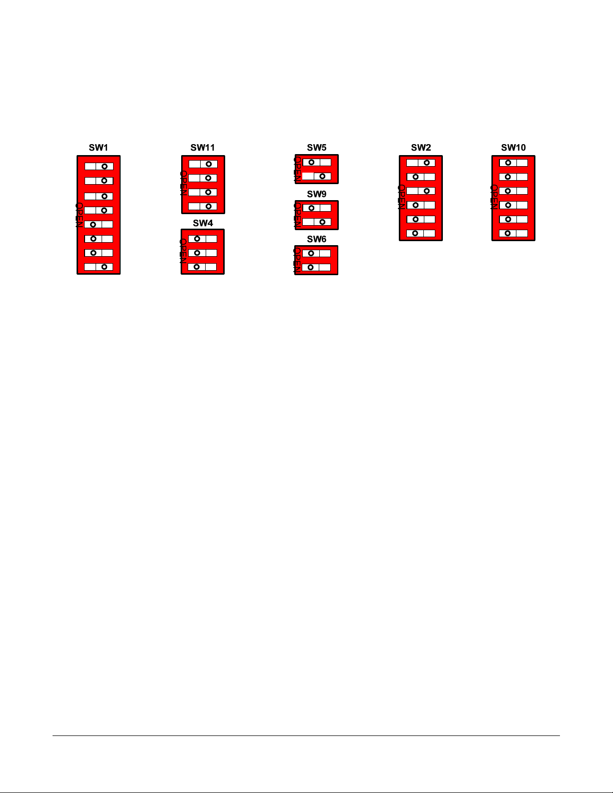
The PEX 8648 switch has several Strapping balls that provide the capability to perform various types of hardware
initialization, without the use of software. These Strapping balls are brought out to a bank of eight DIP switches on
the PEX 8648 RDK base board – SW1, SW11, SW4, SW5, SW9, SW6, SW2, and SW10. (Refer to Figure 17.)
Table 3 defines each DIP switch and its default settings.
Figure 17. PEX 8648 RDK Base Board Hardware Strapping DIP Switches – SW1, SW11,
SW4, SW5, SW9, SW6, SW2, and SW10, Default Settings
PEX 8648-AA RDK Hardware Reference Manual, Version 1.2
Copyright © 2010 by PLX Technology, Inc. All rights reserved 18
Page 24
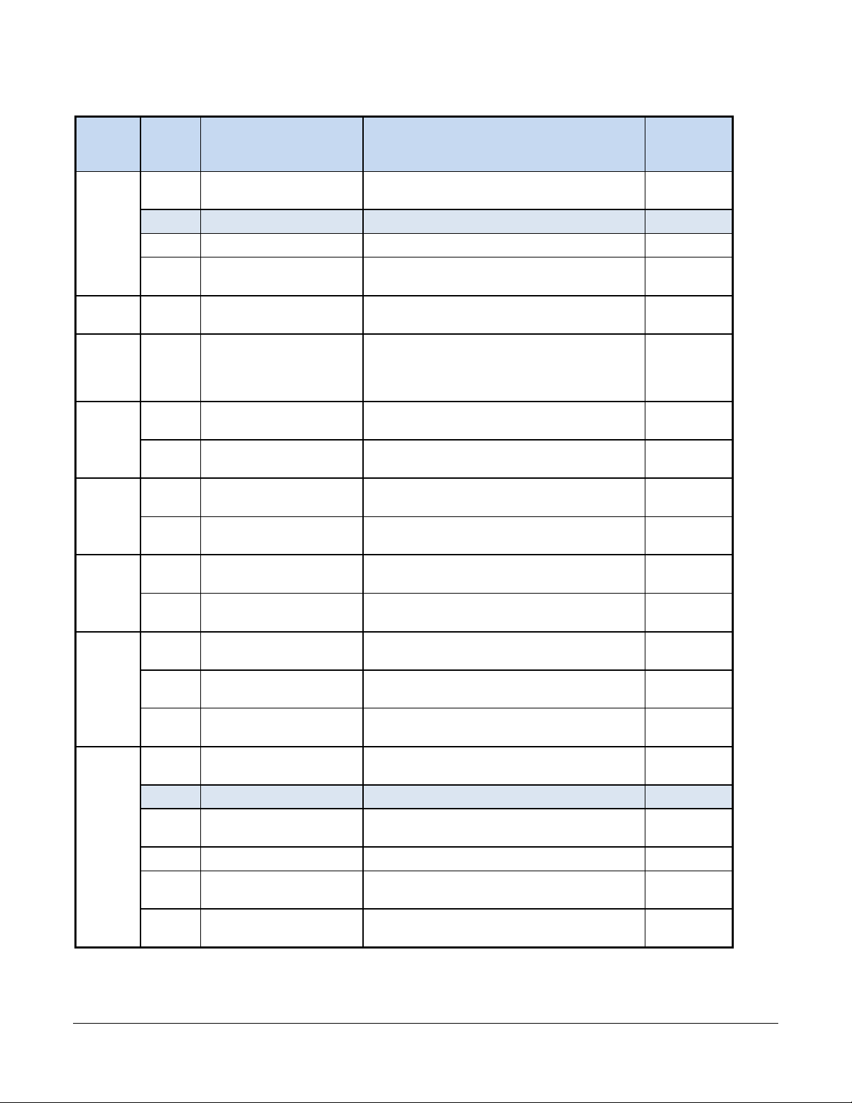
Table 3. PEX 8648 RDK Base Board Hardware Strapping DIP Switches – SW1, SW11,
SW4, SW5, SW9, SW6, SW2, and SW10
DIP
Switch
SW1
SW11
SW4
SW5
SW9
Base Board
Switch Switch Strap Signal Description
Default
Setting
4 – 1 UP-PORTSEL[3:0] Determines which Port is the upstream Port.
0000b
(Port 0)
5 No t used Don’t Care
6 NT-ENABLE# Enables (Low) or disables (High) NT mode. 1
8 – 7 NT-PORTSEL[1:0] Determines which Port is the upstream NT Port.
4 – 1 SHP-SLOT[3:0]
3 – 1 I2C-ADDR[2:0]
1 HP-ENABLE
2 HP-MRL-B#
1 SHP-ENABLE
2 SHP-MRL#
Determines which Port has Serial HotPlug control.
2
In combination with the I
C Configuration
register Slave Address field (offset 294h[6:3]),
determines the PEX 8648 switch’s
2
C Slave address.
I
Enables Hot-Plug capability to Port 5,
using Parallel Hot-Plug interface B.
Simulates the MRL# signal for Parallel Hot-Plug
capability to Port 5.
Enables Hot-Plug capability to Port 8, using the
Serial Hot-Plug interface.
Simulates the MRL# signal for Serial Hot-Plug
capability to Port 8.
01b
(Port 1)
0000b
(Port 8)
111b
1
0
1
0
SW6
SW2
SW10
1 ONBOARD-10V-ON
2 ONBOARD-25V-ON
2 – 1 STN0-PORTCFG[1:0]
4 – 3 STN1-PORTCFG[1:0]
6 – 5 STN2-PORTCFG[1:0]
1 PLL-BYPASS#
Enables the on-board 1.0 VDC voltage
generator to the PEX 8648 switch.
Enables the on-board 2.5 VDC voltage
generator to the PEX 8648 switch.
Determines the PEX 8648 switch Station 0
Port configuration. Default is x8x8.
Determines the PEX 8648 switch Station 1
Port configuration. Default is x8x8.
Determines the PEX 8648 switch Station 2
Port configuration. Default is x8x4x4.
Selects PLL_BYPASS function, to aid with
in-factory testing.
1
1
10b
10b
11b
1
2 No t used Don’t Care
3 FAST-BRINGUP#
Selects FAST_BRINGUP function, to aid with
in-factory testing.
1
4 12-PORT-MODE Factory Test Only. 1
5 SERDES-MODE-EN#
6 PROBE-MODE#
Selects SERDES_MODE function, to aid with
in-factory testing.
Selects PROBE_MODE function, to aid with
in-factory testing.
1
1
PEX 8648-AA RDK Hardware Reference Manual, Version 1.2
Copyright © 2010 by PLX Technology, Inc. All rights reserved 19
Page 25
3.7 Power Circuitry
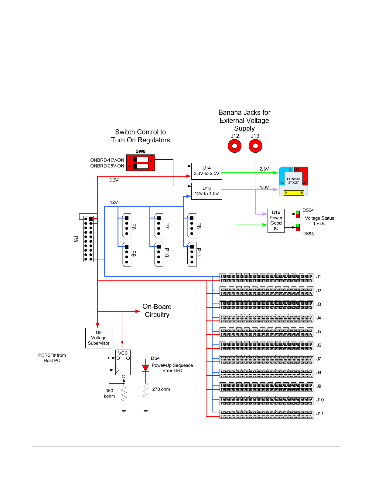
The PEX 8648 RDK base board is a benchtop board, meant to receive 3.3 VDC and 12 VDC from one or more
external ATX benchtop supplies. Figure 18 illustrates the PEX 8648 RDK base board power circuitry.
Note: The user must power-up the PEX 8648 RDK base board before powering up the Host computer, so that
enumeration will see the PEX 8648 switch and any downstream devices. A circuit detects the power-up sequence
between the PEX 8648 RDK base board and Host computer, and turns On a red LED (DS4) if an incorrect
sequence occurs. An incorrect sequence is detected by monitoring PERST# from the Host com puter, and a
“voltage good” signal from a voltage supervisor IC (U8), which monitors board power.
Figure 18. PEX 8648 RDK Base Board Power Circuitry
PEX 8648-AA RDK Hardware Reference Manual, Version 1.2
Copyright © 2010 by PLX Technology, Inc. All rights reserved 20
Page 26

Dedicated power rails supply the two voltages (2.5V and 1.0V) to the PEX 8648 switch, and only the PEX 8648
switch. This allows accurate current draw measurements when operating in various Po rt configurations and traffic
levels. In the default configuration, each of these power rails is driven by on-board voltage regulators – U13
generates 1.0V from 12 VDC, and U14 generates 2.5V from 3.3 VDC. For the purposes of current draw
measurements or voltage margining, an external supply can be used to supply 1.0V and 2.5V, using two banana
jacks (J13 and J12, respectively). In this case, the on-board regulators are turned Off by DIP switch SW6. Bicolor
red/green LED indicators are used with each of these power rails, to indicate that each voltage is within 10% of
nominal.
Power to the PCI Express slot connectors is also supplied by one or more external ATX benchtop supplies. +3.3
VDC to these connectors is on one power rail, and +12 VDC to these connectors is on another. Full board loading
of 75W add-in boards is supported. This requires 33A for +3.3 VDC, and 60.5A for +12 VDC. +3.3 VDC is
provided by the 20-pin main connector (P5). +12 VDC is obtained from six 4-pin peripheral connectors (P6
through P11).
Note: Load resistors are attached to the 3.3 , 5, and 12 VDC ATX power rails, to ensure that if the
PEX 8648 RDK base board is lightly loaded, the ATX supply used will still be able to regulate its voltages.
Power to Slot 5 is controlled by a dual-voltage, Hot-Plug Controller chip (U15), which is controlled by the
PEX 8648 switch’s Port 5 Hot-Plug interface. If Port 5 is the upstream Port, the Strapping signals that Set the
upstream Port are used to always keep this dual-voltage controller chip turned On.
Power to Slot 8 is also controlled by a dual-voltage, Hot-Plug Controller chip (U18), which is controlled by the
PEX 8648 switch’s Serial Hot-Plug interface. If Port 8 is the upstream Port, the Strapping signals that Set the
upstream Port are used to always keep this dual-voltage controller chip turned On.
3.8 Reset Circuitry
The PEX 8648 RDK base board accepts a PERST# from the Host computer, using a SATA cable connection. The
signal is ORed with a manual Reset circuit. This ORed signal connects to the PEX 8648 switch’s PEX_PERST#
Input ball, and the downstream slots’ PERST# connector pins. However, in the case where Slot 5 or Slot 8 is not
an upstream slot, PERST# to these slots is controlled by their respective Hot-Plug interfaces.
The manual Reset circuit consists of a voltage supervisor chip (U8), and pushbutton switch (SW3 ) to Reset input
of that chip. The voltage supervisor monitors 3.3 VDC and Reset input. If the Reset input is Low, or the supply rail
is out of range, the Reset output is held asserted. When both conditions no longer exist, the Reset output deasserts after a programmable Reset Timeout period (128.6 ms, by default).
3.9 Serial EEPROM Interface (U2)
The PEX 8648 RDK base board includes a socketable serial EEPROM (Mill-Max AT25128A) (U2). The serial
EEPROM contents can be used to initialize the PEX 8648 switch, after power-on reset.
PEX 8648-AA RDK Hardware Reference Manual, Version 1.2
Copyright © 2010 by PLX Technology, Inc. All rights reserved 21
Page 27
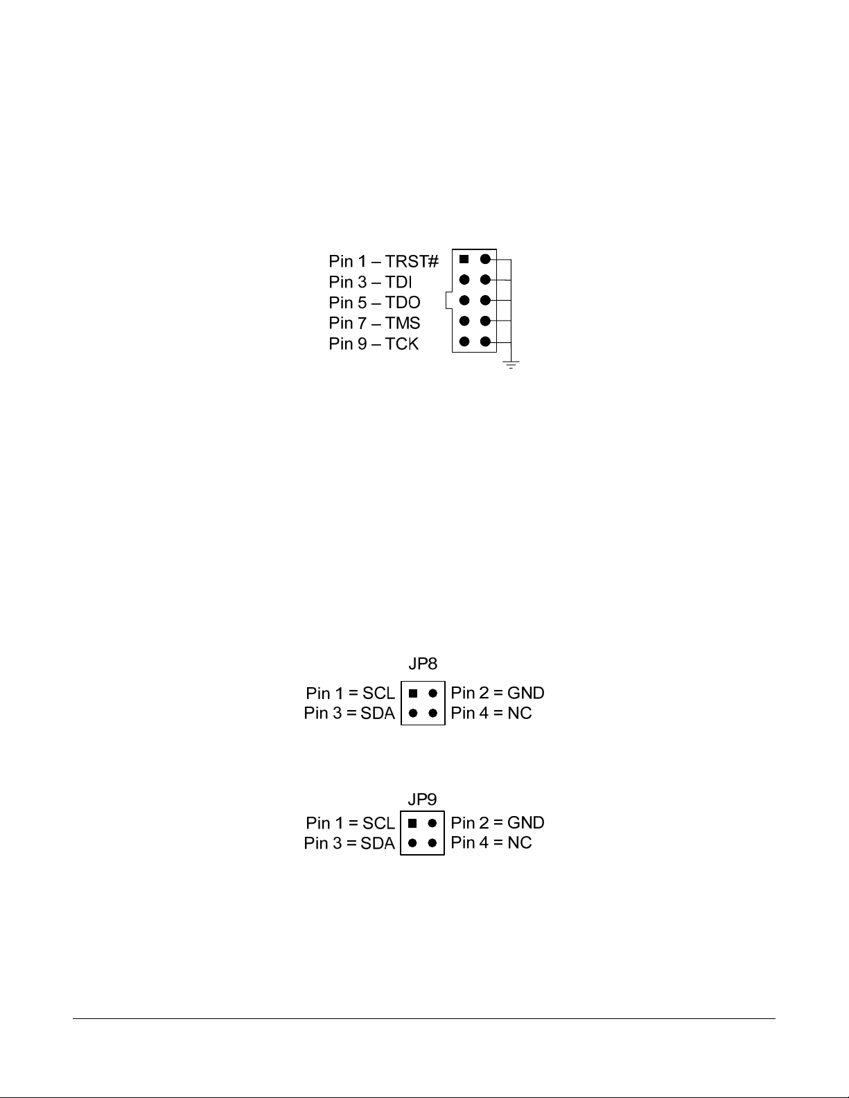
3.10 JTAG Interface (JP7)
The PEX 8648 RDK base board includes a dedicated 2x5 JTAG header (JP7) to the PEX 8648 switch. (Refer to
Figure 19.) The 10-pin connector is designed to allow a direct interface to third-party JTAG TAP Controllers, such
as the Corelis USB-1149.1/E Controller. The header provides connections for TCK, TDI, TDO, TMS, TRST#, and
GND.
There is no “standard” JTAG header pin arrangement; therefore, JTAG header type and pin assignments a re
arbitrary. The header and pin assignment chosen for the PEX 8648 RDK base board is compatible with the
Corelis JTAG single TAP cable (AS00790050-A0).
Figure 19. JTAG Header (Top View)
3.11 I2C Interface (JP8 and JP9)
The PEX 8648 RDK base board includes a two-wire, I2C-compatible Slave mode interface, with 3-bit addressing.
Through this out-of-band Channel, users can read, write, and configure the PEX 8648 switch’s internal registers,
run internal output Probe mode, monitor Error Counters, and monitor other PEX 8648 switch statuses. The
PEX 8648 RDK base board provides two 2x2 pin headers (JP8 and JP9), which interface to the PEX 8648
switch’s I
There is no “standard” I
(Refer to Figure 20.) The lower three bits of the I
2
C Port, to allow chaining of multiple boards.
2
C header pin arrangement; therefore, I2C header type and pin assignments are arbitrary.
2
C Slave address selection is determined by a DIP switch setting
(SW4[3:1]).
2
Figure 20. I
C Headers (Top View)
PEX 8648-AA RDK Hardware Reference Manual, Version 1.2
Copyright © 2010 by PLX Technology, Inc. All rights reserved 22
Page 28
3.12 Device-Specific Sideband Signals
The PEX 8648 switch has three device-specific sideband signals – FATAL_ERR#, PEX_INTA#, and
PEX_NT_RESET#.
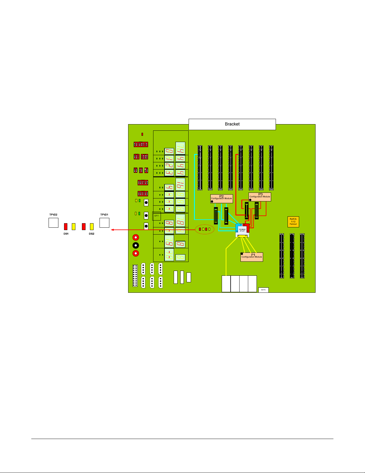
3.12.1 FATAL_ERR# (TPV22, DS1)
FATAL_ERR# (Conventional PCI SERR# equivalent) output is used to indicate when the PEX 8648 switch
detects a Fatal, Unrecoverable error. This signal is brought out to labeled test point pad TPV22 on the
PEX 8648 RDK base board, so that the FATAL_ERR# signal ball can be accessed. The FATAL_ERR# signal
also drives a red LED indicator, DS1. (Refer to Figure 21 for TPV22 and DS1 locations.)
SLOT8-HP SLOT5-HP
PERST
RESET
J12 J13
J14
P6
P5
P9
P7
P10
NT PORT
UP PORT
NUMBER
PORT STATUS
WIDTH
PORT
PORT
P8
JP13
MICTOR
P11
J4
CABLE SLOT 1 SLOT 2 SLOT 3
SLOT 4
SLOT 5
SLOT 6
SLOT 7 SLOT 8 SLOT 9 SLOT 10 SLOT 11
MICTOR
JP11
JP12
J6
J7
J5
J8
Lanes 8-11
Lanes 4-7
Lanes 0-3
SAS
SAS
IP1
IP2
J10
J9
Lanes 12-15
SAS
IP3
J11
J1
J2
J3
SAS
IP4
P4
Figure 21. TPV21, TPV22, DS1, and DS2 Placement on PEX 8648 RDK Base Board
3.12.2 PEX_INTA# (TPV21, DS2)
PEX_INTA# output is used for Conventional PCI INTA# signal compatibility. This signal is brought out to labeled
test point pad TPV21 on the PEX 8648 RDK base board, so that the PEX_INTA# signal ball can be accessed.
The PEX_INTA# signal also drives a yellow LED indicator, DS2. (Refer to Figure 21 for TPV21 and DS2
locations.)
3.12.3 PEX_NT_RESET# (TPV49)
PEX_NT_RESET# output is used to signal the reception of a Hot Reset from the NT Port Link Interface to the
NT Port Virtual Interface. This signal is brought out to labeled test point pad TPV49 on the PEX 8648 RDK base
board, so that the PEX_NT_RESET# signal ball can be accessed.
PEX 8648-AA RDK Hardware Reference Manual, Version 1.2
Copyright © 2010 by PLX Technology, Inc. All rights reserved 23
Page 29
4 Base Board Mechanicals/Component Placement
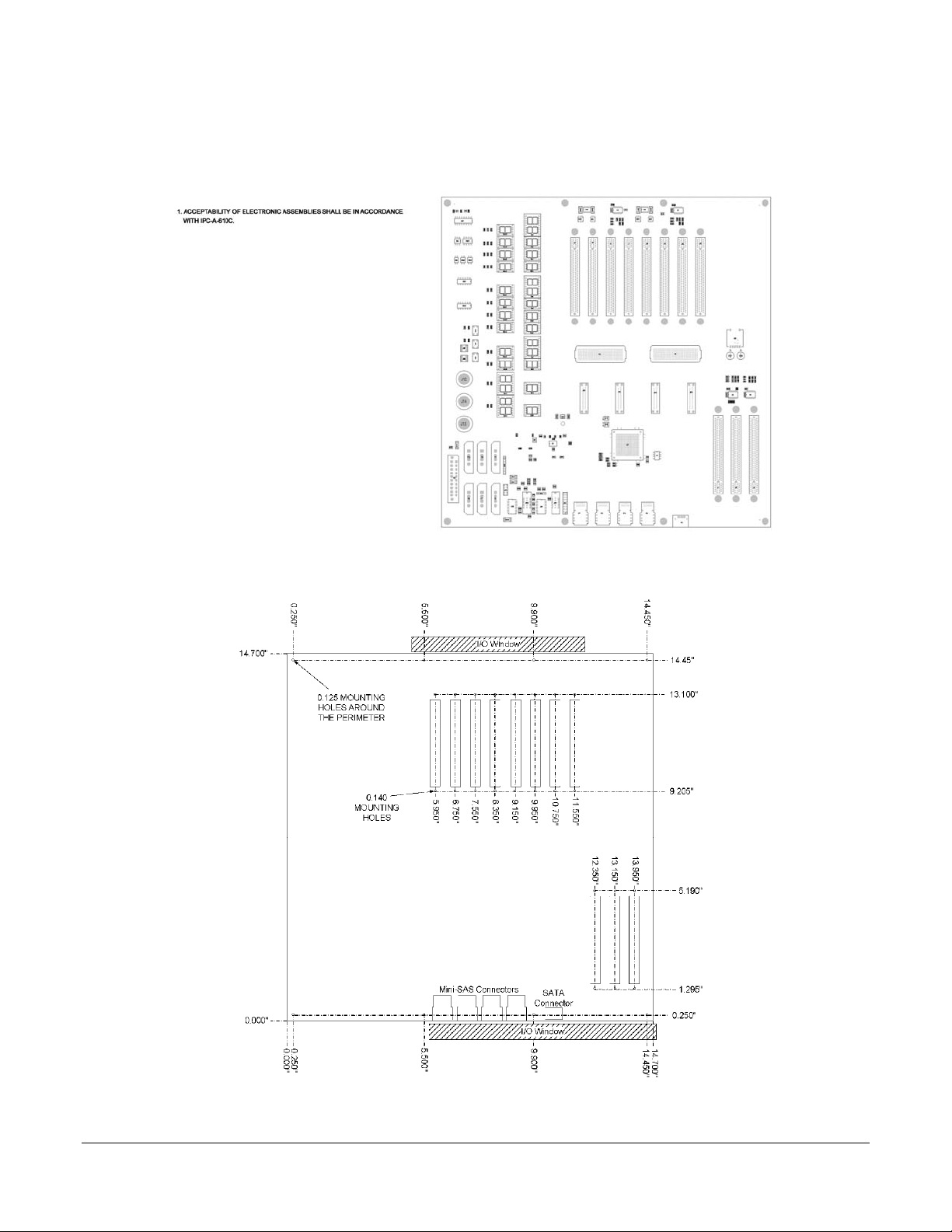
Figure 22 illustrates the PEX 8648 RDK base board and component placement. Figure 23 illustrates the
PEX 8648 RDK base board dimensions.
Figure 22. PEX 8648 RDK Base Board Mechanical Outline
Figure 23. PEX 8648 RDK Base Board Dimensions
PEX 8648-AA RDK Hardware Reference Manual, Version 1.2
Copyright © 2010 by PLX Technology, Inc. All rights reserved 24
Page 30
4.1 Monitoring Point, LED Indicator, and Control Summary
This section summarizes the PEX 8648 RDK base board interfaces that are used for monitoring, indicating, and
controlling PEX 8648 switch performance.
4.1.1 Monitoring Points
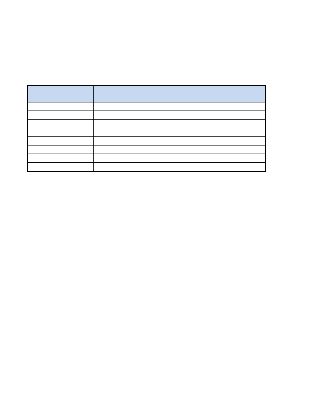
Table 4 lists the functions of all monitoring points available for use on the PEX 8648 RDK base board.
Table 4. PEX 8648 RDK Base Board Monitoring Points
Reference Designator Description
J12 2.5 VDC to the PEX 8648 switch.
J13 1.0 VDC to the PEX 8648 switch.
J14 Ground.
J15 and J16 Reference Clock.
TPV19 and TPV18 Ccathode and Anode of thermal diode within the PEX 8648 switch.
TPV21 PEX_INTA# from the PEX 8648 switch.
TPV22 FATAL_ERR# from the PEX 8648 switch.
TPV49 PEX_NT_RESET# to the PEX 8648 switch.
PEX 8648-AA RDK Hardware Reference Manual, Version 1.2
Copyright © 2010 by PLX Technology, Inc. All rights reserved 25
Page 31
4.1.2 LED Indicators
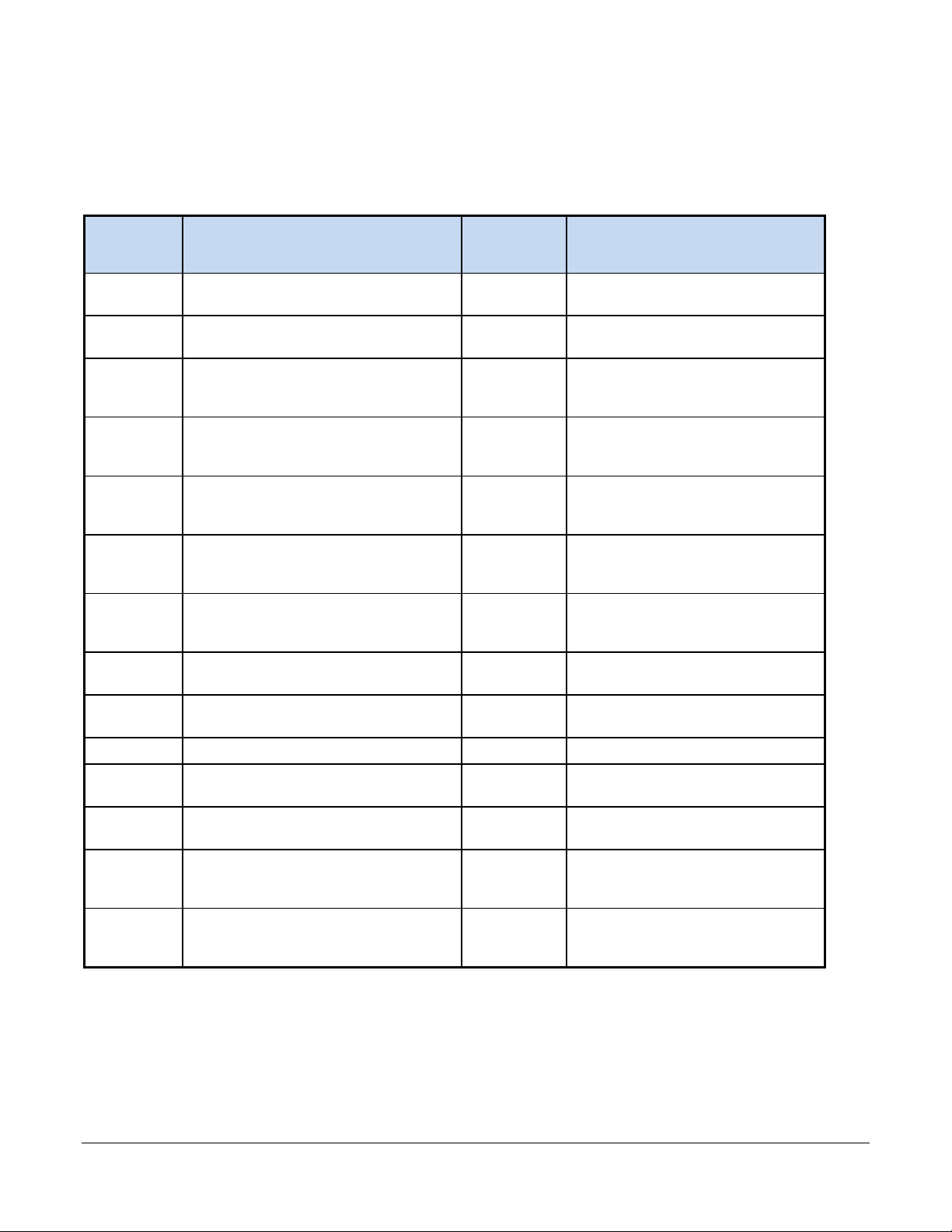
Table 5 lists the functions of all LED indicators available for use on the PEX 8648 RDK base board. Additional
information for the Port-related LED indicators is provided in Section 3.5, “Port Configuration and Status LED
Indicators.”
Table 5. PEX 8648 RDK Base Board LED Indicators
Reference
Designator
DS1 FATAL_ERR#
DS2 PEX_INTA#
DS3 PERST#_PCIe_SWITCH
DS4 POWER_UP_SEQUENCE_INCORRECT
DS28 –
DS17
DS32 –
DS29
DS56 –
DS45
DS58 HP_ATNLED_B#
Signal Color Description
UP_PORT[11:0]
NT_PORT[3:0]
PRT_STATUS[11:0]
Red
Yellow
Red
Red
Green
Green
Green
Yellow
Indicates that FATAL_ERR# is being
driven by the PEX 8648 switch.
Indicates that INTA# is being driven
by the PEX 8648 switch.
Indicates that PERST#, to the
PEX 8648 switch and downstream
slots, is asserted.
Indicates that the PEX 8648 RDK base
board was not powered up before the
Host CPU.
Indicates which Port is the
upstream Port, for Ports 11
through 0, respectively.
Indicates which Port is the
upstream NT Port, for Ports 3
through 0, respectively.
Indicates whether the Port is
active/configured for use, for Ports 11
through 0, respectively.
Attention LED for Parallel Hot-Plug
slot, J5.
DS59 HP_PWRLED_B#
DS60 SHP_PWRLED#
DS61 SHP_ATNLED#
DS62 INTERLOCK
DS63 2.5VDC_POWR_GOOD
DS64 1.0VDC_POWR_GOOD
PEX 8648-AA RDK Hardware Reference Manual, Version 1.2
Copyright © 2010 by PLX Technology, Inc. All rights reserved 26
Green
Green
Yellow
Yellow
Red/Green
Red/Green
Power LED for Parallel Hot-Plug
slot, J5.
Power LED for Serial Hot-Plug slot, J8.
Attention LED for Serial Hot-Plug
slot, J8.
INTERLOCK LED for Serial Hot-Plug
slot, J8.
Green when 2.5 VDC to the PEX 8648
switch is present and within 10% of
nominal; otherwise, red.
Green when 1.0 VDC to the PEX 8648
switch is present and within 5% of
nominal; otherwise, red.
Page 32
4.1.3 Controls
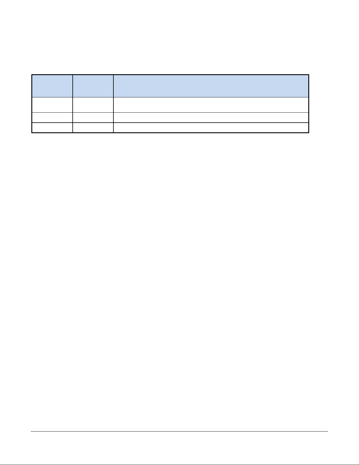
For a detailed description of the Strapping ball DIP switches, refer to Section 3.6, “Hardware Strapping Balls.” The
remaining controls are three pushbutton switches, defined in Table 6.
Table 6. PEX 8648 RDK Base Board Controls
Reference
Designator
SW3 RESET Initiates a manual PERST# to the PEX 8648 switch and all downstream slots.
SW7 SLOT5-HP Initiates a Hot-Plug event for Slot 5, the Parallel Hot-Plug slot.
SW8 SLOT8-HP Initiates a Hot-Plug event for Slot 8, the Serial Hot-Plug slot .
Pushbutton
Name
Description
PEX 8648-AA RDK Hardware Reference Manual, Version 1.2
Copyright © 2010 by PLX Technology, Inc. All rights reserved 27
Page 33
4.2 Board Layout Information
4.2.1 Trace Routing Design Rules
Impedance of the PCI Express differential pairs is 91 ohms ±5%. The differential pairs are routed as edgecoupled stripline pairs.
4.2.2 Power De-Coupling
Power de-coupling is provided by two means – plane capacitance provided by the PCB layer stackup and discrete
de-coupling capacitors. Plane capacitance filters noise above approximately 100 MHz. The footprints for the
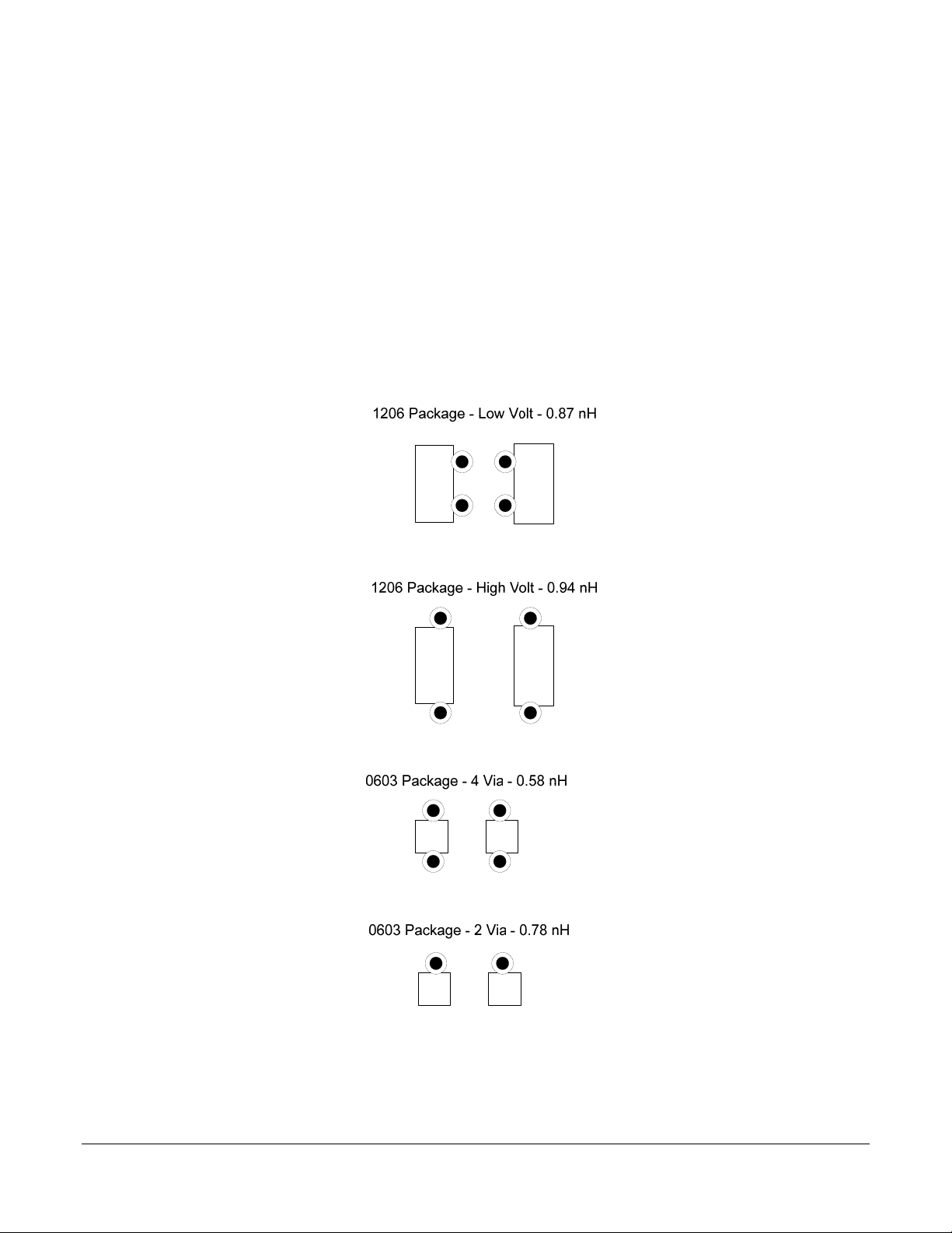
discrete de-coupling capacitors are designed such that the inductance between the pad and pl ane is reduced by
careful via placement. (Refer to Figure 24.)
The PEX 8648 switch power balls are individually de-coupled by 0201-size, 1,000-pF capacitors, with larger-value
capacitors providing additional de-coupling around the perimeter of the package. (Refer to Figure 25.)
Figure 24. De-Coupling Capacitor Footprints
PEX 8648-AA RDK Hardware Reference Manual, Version 1.2
Copyright © 2010 by PLX Technology, Inc. All rights reserved 28
Page 34
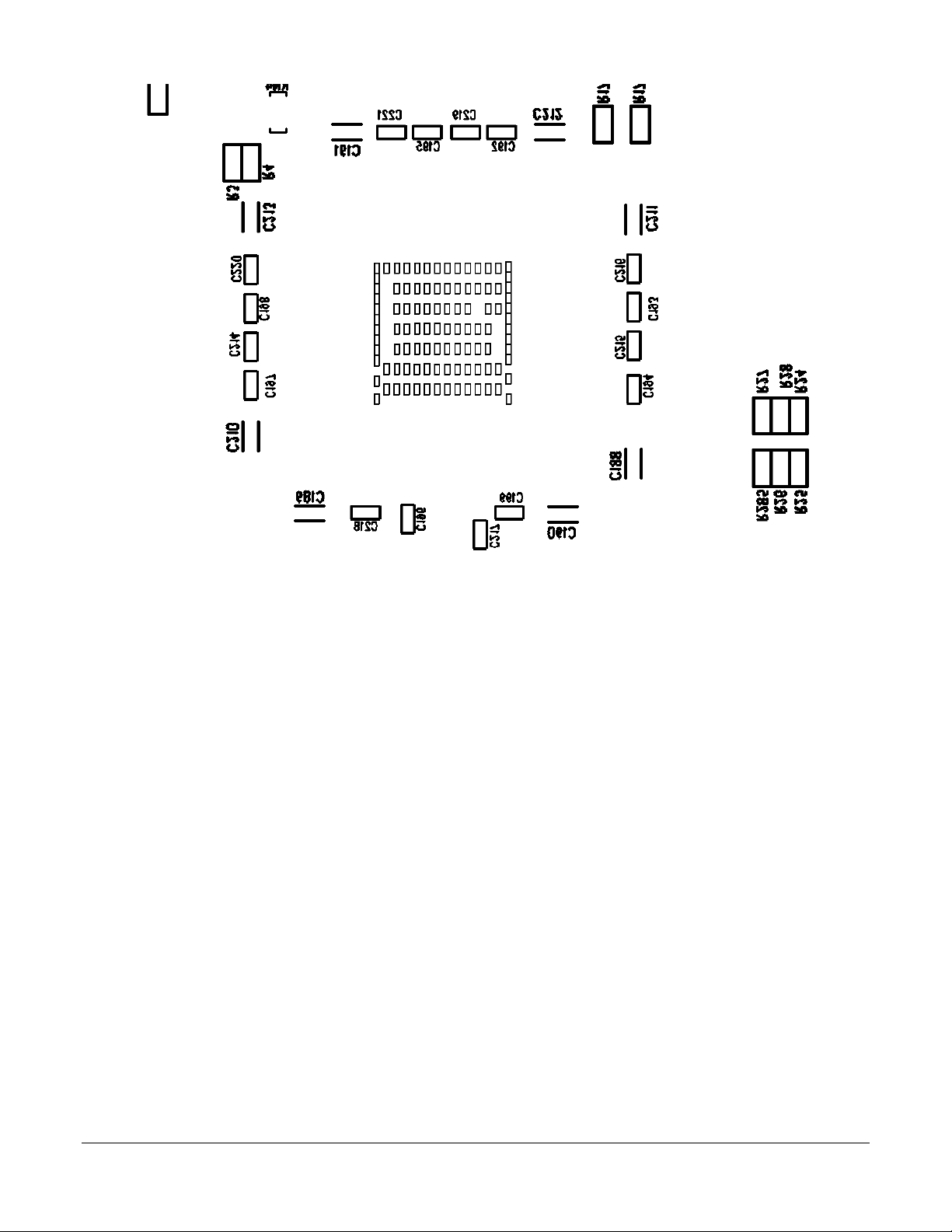
Figure 25. PEX 8648 RDK Base Board Power Ball and Perimeter De-Coupling Capacitor Footprints
(Reverse Screen)
PEX 8648-AA RDK Hardware Reference Manual, Version 1.2
Copyright © 2010 by PLX Technology, Inc. All rights reserved 29
Page 35
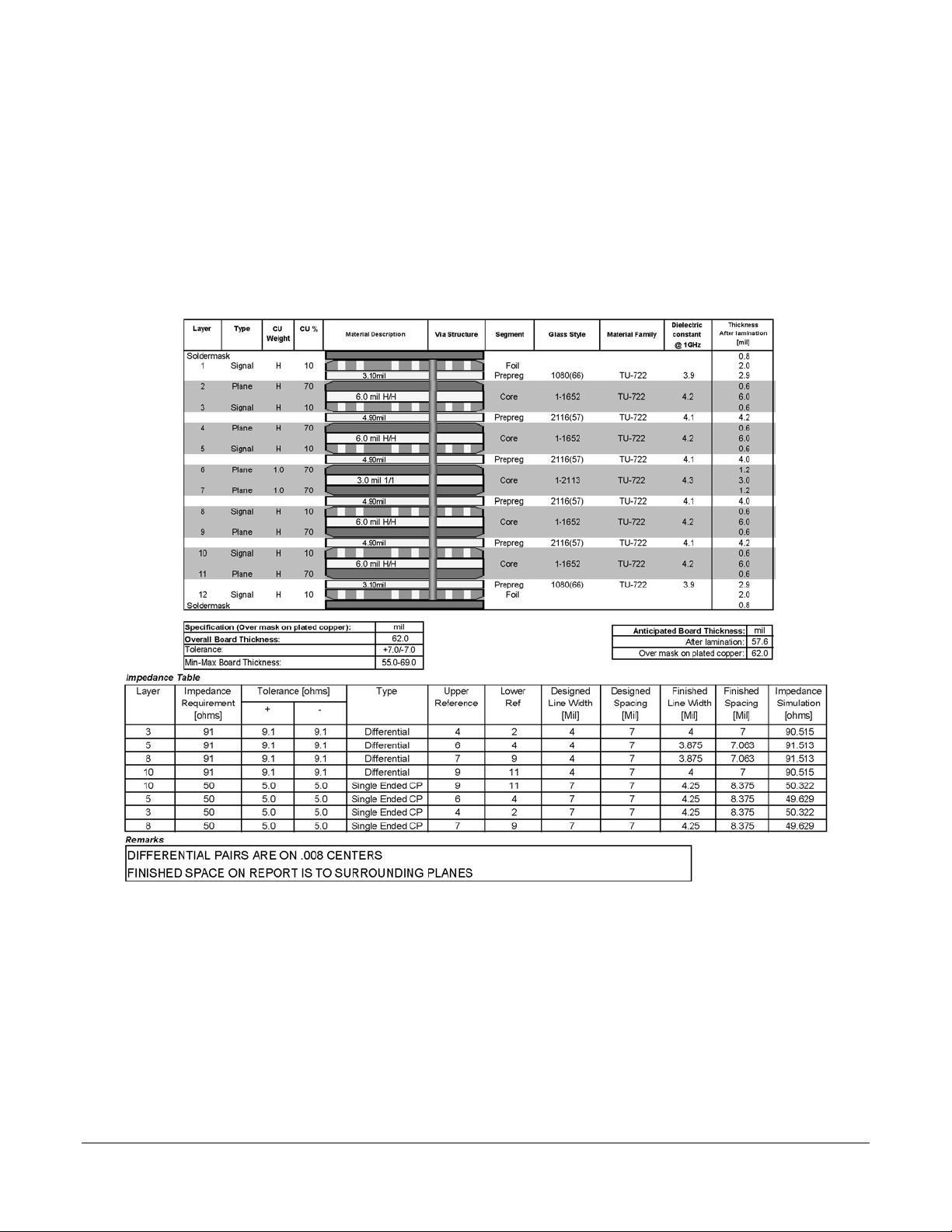
4.2.3 PCB Layer Stackup
The PEX 8648 RDK base board is a 12-layer, 62-mil thick PCB. (Refer to Figure 26.) This stackup includes six
routing layers, three ground planes, and three power planes. The target signal impedance for all routing layers is
50 ohms ±5% single-ended impedance, and 91 ohms ±5% differential.
This PCB layer stackup was chosen for the following reasons:
Power/ground plane arrangement provides capacitance to filter noise above 100 MHz from the sup ply
voltages
Differential pair routing layers and plane layers arrangement provides shielding for the PCI Express
signals
Figure 26. PEX 8648 RDK Base Board External PCB Layer Stackup Report
PEX 8648-AA RDK Hardware Reference Manual, Version 1.2
Copyright © 2010 by PLX Technology, Inc. All rights reserved 30
Page 36

5 References
The following is a list of documentation to provide further details.
PLX Technology, Inc.
870 W Maude Avenue, Sunnyvale, CA 94085 USA
Tel: 800 759-3735 (domestic only) or 408 774-9060, Fax: 408 774-2169, www.plxtech.com
PEX 8648-AA Data Book, Version 0.92 or higher
PCI Special Interest Group (PCI-SIG)
3855 SW 153rd Drive, Beaverton, OR 97006 USA
Tel: 503 619-0569, Fax: 503 644-6708, www.pcisig.com
PCI Local Bus Specification, Revision 3.0
PCI Bus Power Management Interface Specification, Revision 1.2
PCI to PCI Bridge Architecture Specification, Revision 1.2
PCI Express Base Specification, Revision 2.0
PCI Express Card Electromechanical Specification, Revision 2.0
Agilent Technologies, Inc.
5301 Stevens Creek Boulevard, Santa Clara , CA 95051 USA
Tel: 877 424-4536 (domestic only) or 408 345-8886, Fax: 408 345-8474, www.agilent.com
Soft Touch Midbus Probe User’s Guide
NXP Semiconductors
www.standardics.nxp.com
The I2C-Bus Specification, Version 2.1
, April, 2007
PEX 8648-AA RDK Hardware Reference Manual, Version 1.2
Copyright © 2010 by PLX Technology, Inc. All rights reserved 31
Page 37
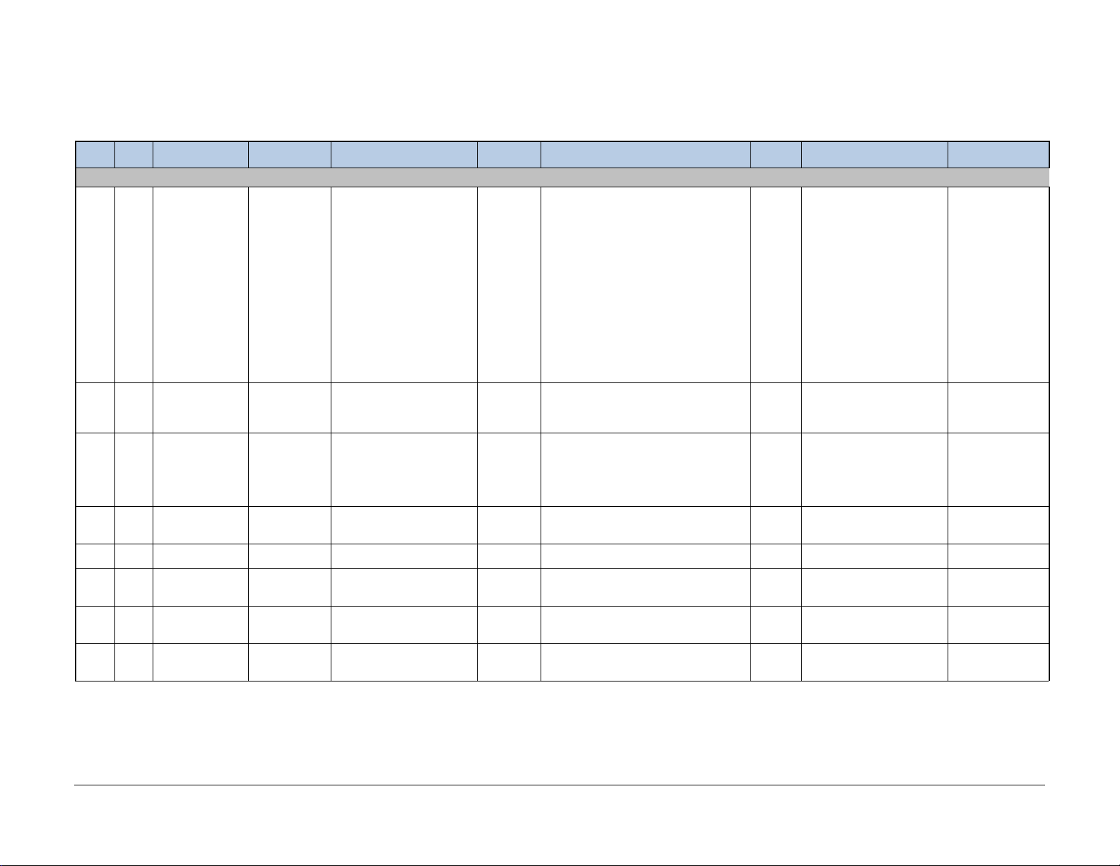
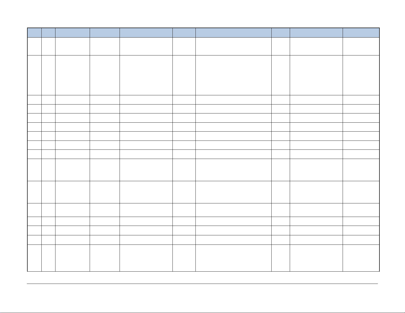
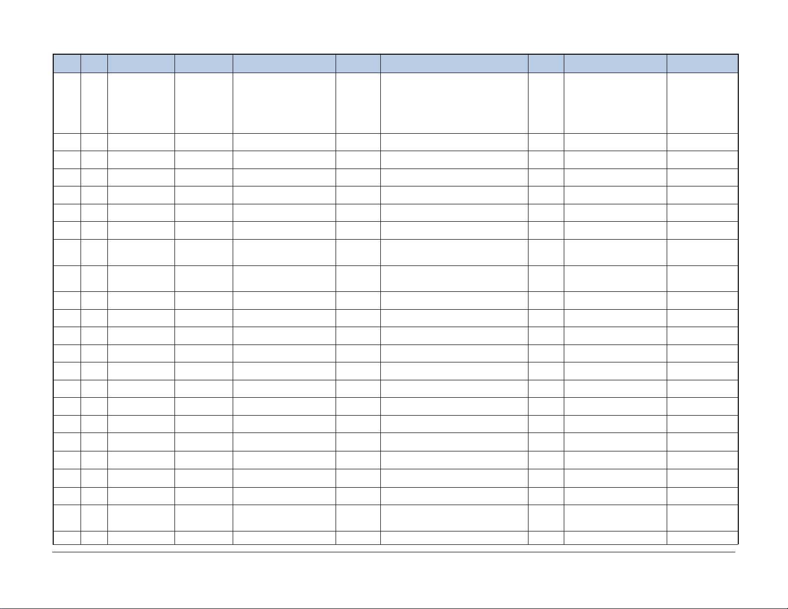
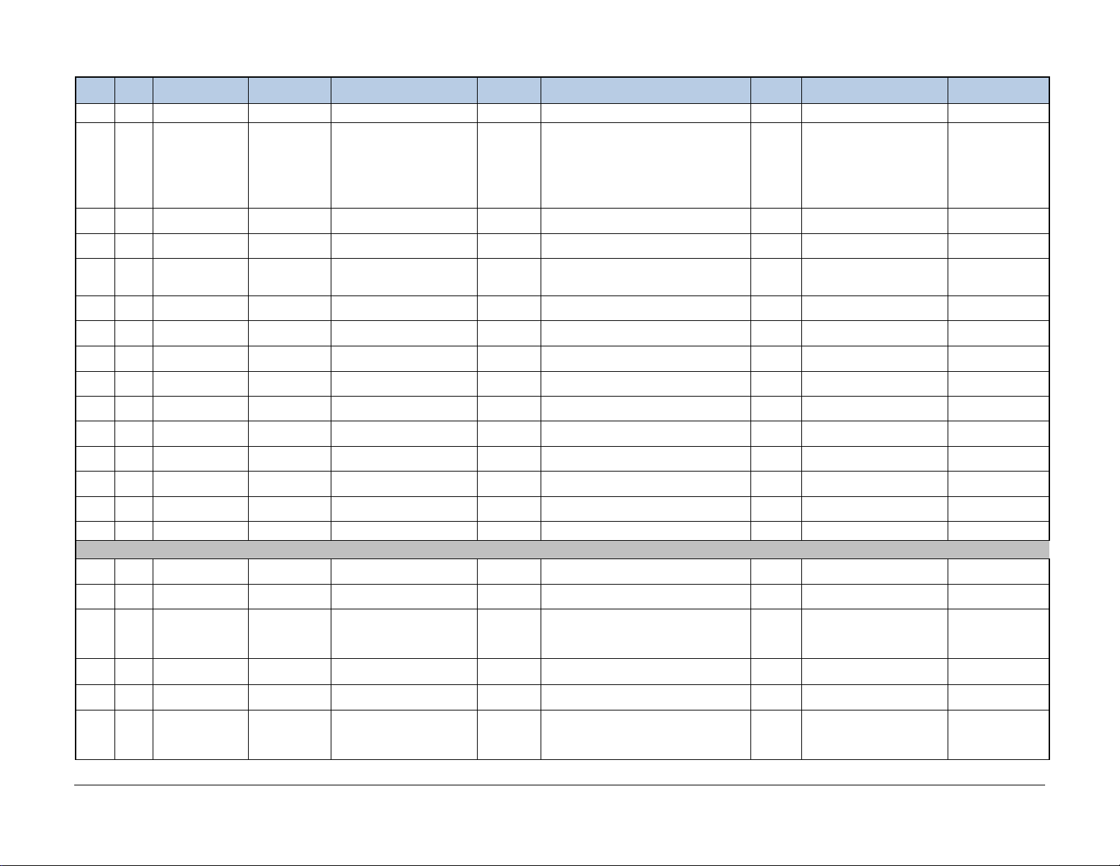
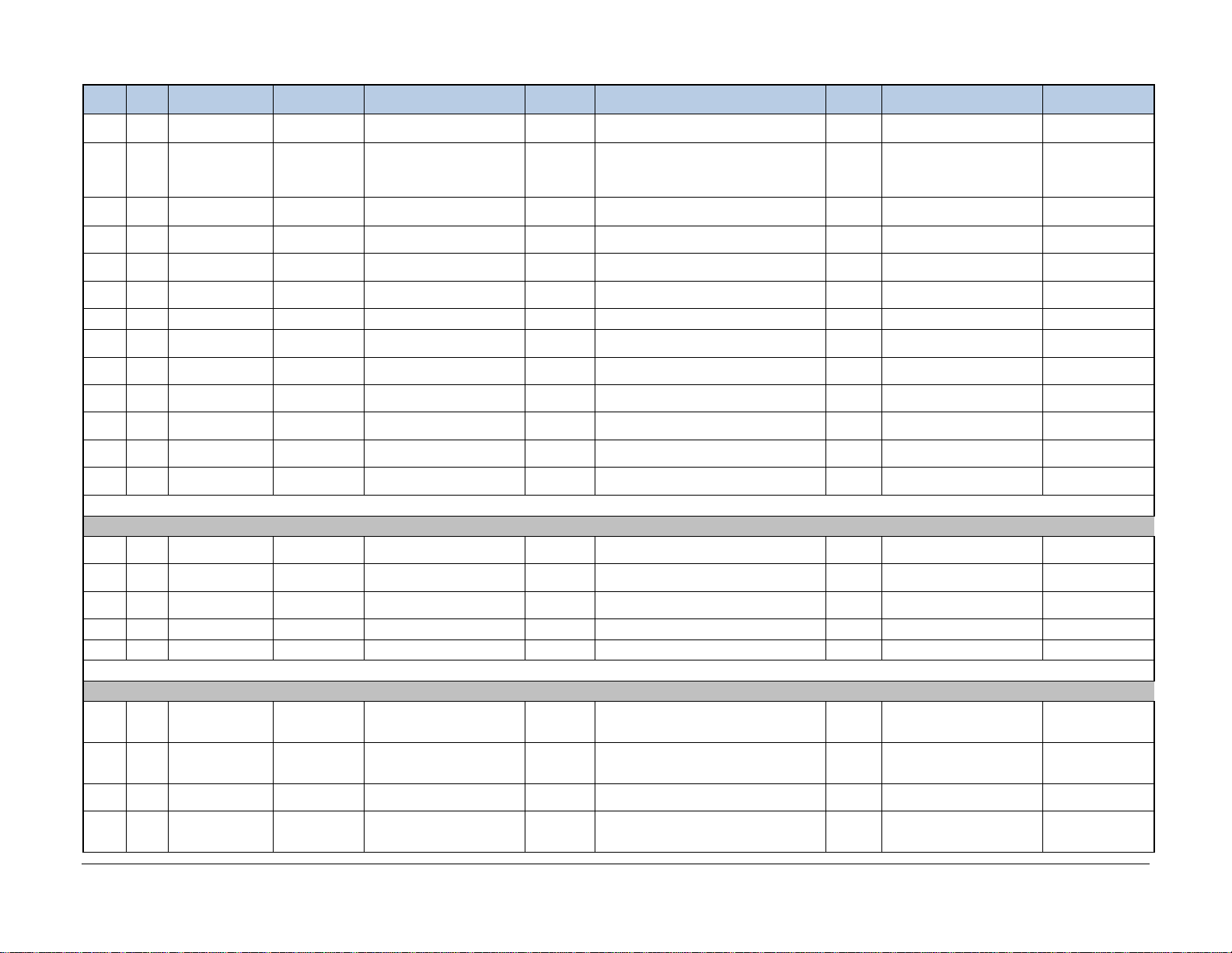
6 Bill of Materials & Schematics
This section replicates the PEX 8648 RDK base board Bill of Materials and provides a copy of the base board Schematics.
Item Qty Manufacturer
SURFACE MOUNT COMPONENTS
1 108 Kemet
2 22 AVX
3 32 Panasonic
4 5 Panasonic
5 2 Panasonic
6 9 Kemet
7 2 Kemet
8 16 Kemet
Manufacturer
Part #
C0402C104K
8PACTU
TAJC226K02
0R
ECJ-
0EB1C103K
ECJ-
3YB1C106M
ECJ-
1VB1H473K
C0603C105K
8PACTU
C1206C226K
9PACTU
C0603C104K
4RACTU
Description
CAP .10UF 10V CERAMIC
X5R 0402
CAP TANTALUM 22UF
20V 10% SMD
CAP .01UF 16V CERAMIC
0402 SMD
CAP 10UF 16V CERAMIC
X5R 1206 LOVOLT
FOOTPRINT
CAP .047UF 50V
CERAMIC X7R 0603
CAP CERAMIC 1.0UF 10V
X5R 0603, 2 VIA
CAP 22UF 6.3V CER X5R
SMD 1206 LOVOLT
FOOTPRINT
CAP .10UF 16V CERAMIC
X7R 0603
Package
Type
SMT,
0402
EIA size
C
SMT,
0402
SMT,
1206,
LoVolt
SMT,
0603
SMT,
0603,
2via
SMT,
1206,
LoVolt
SMT,
0603
Component
Designator(s)
C1, C2, C3, C4, C5, C6, C7, C8, C9,
C10, C11, C12, C13, C14, C15, C16,
C17, C18, C19, C20, C21, C22, C23,
C24, C25, C26, C27, C28, C29, C30,
C31, C32, C33, C34, C35, C36, C37,
C38, C39, C40, C41, C42, C43, C44,
C45, C46, C47, C48, C49, C50, C51,
C52, C53, C54, C55, C56, C57, C58,
C59, C60, C61, C62, C63, C64, C65,
C66, C67, C68, C69, C70, C71, C72,
C73, C74, C75, C76, C77, C78, C79,
C80, C81, C82, C83, C84, C85, C86,
C87, C88, C89, C90, C91, C92, C93,
C94, C95, C96, C124, C125, C126,
C132, C138, C144, C227, C232, C233,
C234, C236, C237
C97, C98, C99, C100, C101, C102,
C103, C104, C105, C106, C107, C108,
C109, C110, C111, C112, C113, C114,
C115, C116, C117, C118
C119, C120, C121, C122, C127, C128,
C129, C130, C133, C134, C135, C136,
C139, C140, C141, C142, C192, C193,
C194, C195, C196, C197, C198, C199,
C214, C215, C216, C217, C218, C219,
C220, C221
C123, C131, C137, C143, C148
C145, C222
C149, C188, C189, C190, C191, C210,
C211, C212, C213
C150, C151
C152, C153, C154, C155, C158, C159,
C162, C164, C223, C224, C225, C226,
C228, C229, C230, C231
Distrib
utor
Digi-
Key
Digi-
Key
Digi-
Key
Digi-
Key
Digi-
Key
Digi-
Key
Digi-
Key
Digi-
Key
PCC103BQCT-ND 0.01uF
Distributor
Part #
399-3027-1-ND 0.1uF
478-1711-1-ND 22uF
PCC2227CT-ND 10uF
PCC2286CT-ND 0.047uF
399-3118-1-ND 1uF
399-3229-1-ND 22uF
399-1096-1-ND 0.1uF
Part
PEX 8648-AA RDK Hardware Reference Manual, Version 1.2
Copyright © 2010 by PLX Technology, Inc. All rights reserved 32
Page 38
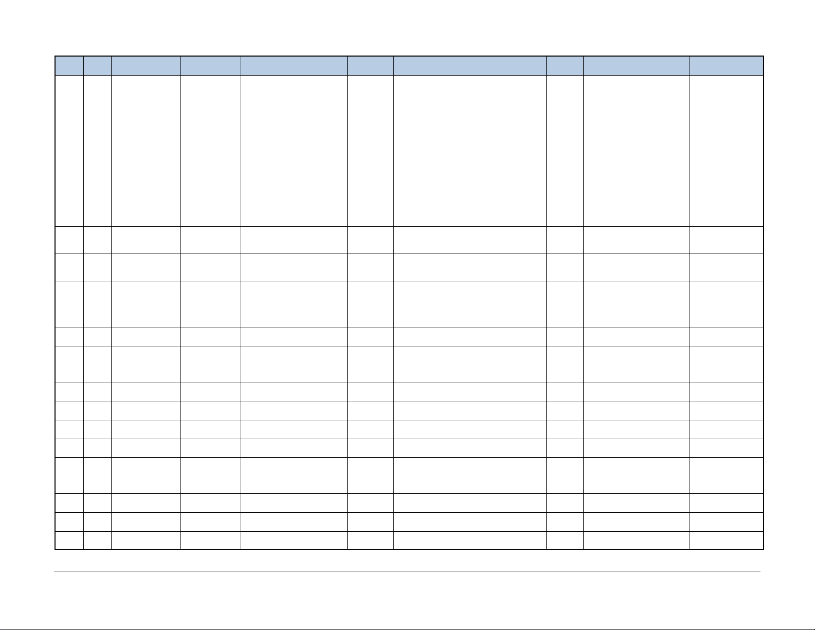
Item Qty Manufacturer
9 101 Panasonic
10 3 Lumex
11 4 Lumex
12 30 Lumex
13 2 Panasonic
14 4 Molex 757830036
15 2 Amp 767054-1
16 2
17 3 FCI 74221
18 1 Molex 47080-4001
19 29
20 4
21 6 CTS 742C083512J
22 6 Panasonic
Johnson/Emerso
n
ON
Semiconductor
International
Rectifier
Manufacturer
Part #
ECJ-
ZEB1E102K
SML-
LXT0805SR
W-TR
SML-
LXT0805YW-
TR
SML-
LXT0805GW-
TR
LNJ107W5PRW LED, RED/GREEN HI BRT
142-0711-201
MMBT3904LT1 NPN, GPSS, MMBT3904,
IRF7470
ERJ-
3EKF1431V
Description
CAP 1000PF 25V
CERAMIC X7R 0201
LED THIN660NM SUPRED
DIFF0805SMD
LED THIN 585NM YEL
DIFF 0805 SMD
LED THIN 565NM GRN
DIFF 0805 SMD
S TYPE SMD, If=10mA
Connector, right angle with
shell 0.8mm pitch for mini-
SAS,4x 26 CKT internal
cable,
CONN, 38-pin MICTOR,
RECPT, STRAIGHT
CONNECTOR, SMA, SMT,
STRAIGHT, 50 OHM
Header, BGA, 10x40,
receptacle
CONNECTOR, SATA,
right-angle
SOT23
MOSFET, N-CHAN, 10A,
Rds=13 mohm
RESNET, MF, 5.1 KOHM
NIL 5%, ISOLATED
RES 1.43K OHM 1/10W
1% 0603 SMD
Package
Type
SMT,
0201
SMT,
0805
SMT,
0805
SMT,
0805
DS63, DS64
shell TH,
SMT 26-
pin
connector
JP11, JP13
SMT_SM
A
P1, P2, P3 CM_10x40
P4 SATA header
SO8 Q31, Q32, Q33, Q34 IRF7470
742-CTS-
RN-8
SMT,
0603
C156, C157, C160, C161, C163, C166,
C168, C169, C170, C172, C173, C174,
C175, C176, C177, C178, C179, C180,
C181, C182, C183, C185, C186, C187,
C200, C201, C202, C203, C205, C206,
C207, C208, C310, C311, C312, C313,
C314, C315, C316, C317, C318, C319,
C320, C321, C322, C323, C324, C325,
C326, C327, C328, C330, C331, C332,
C333, C334, C335, C336, C337, C338,
C339, C340, C350, C352, C354, C356,
C358, C360, C362, C364, C366, C369,
C370, C371, C372, C373, C374, C375,
C376, C377, C378, C379, C380, C381,
C382, C383, C384, C385, C386, C387,
C388, C389, C390, C391, C392, C393,
C394, C395, C396, C397, C398
DS17, DS18, DS19, DS20, DS21, DS22,
DS23, DS24, DS25, DS26, DS27, DS28,
DS29, DS30, DS31, DS32, DS45, DS46,
DS47, DS48, DS49, DS50, DS51, DS52,
DS53, DS54, DS55, DS56, DS59, DS60
Q1, Q2, Q3, Q4, Q5, Q6, Q7, Q8, Q9,
Q10, Q11, Q12, Q13, Q14, Q15, Q16,
Q17, Q18, Q19, Q20, Q21, Q22, Q23,
Q24, Q25, Q26, Q27, Q28, Q29
RN1, RN2, RN3, RN4, RN5, RN7
Component
Designator(s)
DS1, DS3, DS4
DS2, DS58, DS61, DS62
IP1, IP2, IP3, IP4
J15, J16 Mouser 530-142-0711-201 SMT_SMA
R1, R2, R3, R4, R175, R176
Distrib
utor
Digi-
Key
Digi-
Key
Digi-
Key
Digi-
Key
Digi-
Key
MMBT3904LT1
Digi-
Key
Digi-
Key
Distributor
Part #
PCC2130CT-ND 1000pF
67-1555-1-ND Red
67-1554-1-ND Yellow
67-1553-1-ND Green
P526CT-ND LED_BI
I_PASS_26CKT_
75783_0036
MICTOR 38
RECEPT
742C083512JCT-ND 5.1K
P1.43KHCT-ND 1.43K
Part
PEX 8648-AA RDK Hardware Reference Manual, Version 1.2
Copyright © 2010 by PLX Technology, Inc. All rights reserved 33
Page 39
Item Qty Manufacturer
23 22 Yageo
24 55 Panasonic
25 6 Panasonic
26 1 Panasonic
27 5 Panasonic
28 8 Panasonic
29 2 Panasonic
30 4 Panasonic
31 4 Yageo
32 32 Panasonic
33 32 Panasonic
34 14 Yageo
35 4 Panasonic
36 2 CTS 742C163221J
37 1 Panasonic
38 31 Panasonic
Manufacturer
Part #
9C06031A0R
00JLHFT
ERJ-
3GEYJ512V
ERJ-
3GEYJ102V
ERJ-
3GEYJ152V
ERJ-
3GEYJ103V
ERJ-
3GEYJ512V
ERJ-
3EKF2261V
ERJ-
3GEYJ391V
9C08052A0R
00JLHFT
ERJ-
1GEF33R2C
ERJ-
1GEF49R9C
9C06031A0R
00JLHFT
ERJ-
3EKF4750V
ERJ-
3GEYJ330V
ERJ-
2GEJ512X
Description
RES 0.0 OHM 1/10W 5%
0603 SMD
RES 5.1K OHM 1/10W 5%
0603 SMD
RES 1.0K OHM 1/10W 5%
0603 SMD
RES 1.5K OHM 1/10W 5%
0603 SMD
RES 10K OHM 1/10W 5%
0603 SMD
RES, Shunt Select
Footprint, 0603
RES 2.26K OHM 1/10W
1% 0603 SMD
RES 390 OHM 1/10W 5%
0603 SMD
RES 0.0 OHM 1/8W 5%
0805 SMD
RES 33.2 OHM 1/20W 1%
0201 SMD
RES 49.9 OHM 1/20W 1%
0201 SMD
RES, Shunt Select
Footprint, 0603
RES 475 OHM 1/16W 1%
0603 SMD
RES ARRAY 220 OHM
16TRM 8RES SMD
RES, CF, 33 OHM, 1/16W,
5%, 0603 SMD
RES 5.1K OHM 1/16W 5%
0402 SMD
Package
Type
SMT,
0603
SMT,
0603
SMT,
0603
SMT,
0603
SMT,
0603
SMT,
0603-2
SMT,
0603
SMT,
0603
SMT,
0805
SMT,
0201
SMT,
0201
SMT,
0603-2
SMT,
0603
R171, R172
SMT,
0603
SMT,
0402
R7, R8, R9, R10, R12, R13, R14, R16,
R17, R18, R19, R25, R26, R27, R28,
R46, R250, R272, R280, R282, R283,
R11, R57, R64, R67, R69, R73, R75,
R86, R91, R94, R97, R100, R102, R117,
R120, R122, R127, R129, R145, R148,
R150, R154, R156, R162, R163, R165,
R166, R167, R168, R174, R177, R178,
R179, R239, R240, R241, R249, R254,
R258, R259, R260, R261, R262, R263,
R264, R265, R266, R267, R269, R277,
R278, R281, R285, R302, R303
R20, R21, R22, R62, R63, R304
R29, R31, R34, R39, R40, R41, R44,
R51, R52, R59, R66, R68, R77, R78,
R82, R83, R87, R88, R93, R95, R104,
R105, R109, R110, R113, R114, R119,
R121, R131, R132, R136, R137, R140,
R143, R144, R147, R149, R158, R159
R53, R54, R60, R61, R72, R74, R79,
R80, R84, R85, R89, R90, R99, R101,
R106, R107, R111, R112, R115, R116,
R125, R128, R133, R134, R138, R139,
R141, R142, R153, R155, R160, R161
R30, R32, R65, R70, R71, R92, R96,
R98, R118, R123, R126, R146, R151,
R181, R182, R183, R184, R185, R186,
R187, R188, R189, R190, R191, R192,
R193, R194, R195, R212, R213, R214,
R215, R216, R217, R218, R219, R220,
R221, R222, R223, R224, R225, R253,
Component
Designator(s)
R24, R33, R35, R55, R56
R42, R43
R48, R49, R164, R169
R50, R81, R108, R135
R76, R103, R130, R157
R284
R23
R45
R152
R173
R276
Distrib
utor
Digi-
Key
Digi-
Key
Digi-
Key
Digi-
Key
Digi-
Key
Digi-
Key
Digi-
Key
Digi-
Key
Digi-
Key
Digi-
Key
Digi-
Key
Digi-
Key
Digi-
Key
Digi-
Key
Digi-
Key
Digi-
Key
Distributor
Part #
311-0.0GCT-ND 0
P5.1KGCT-ND 5.1K
P1.0KGCT-ND 1.0K
P1.5KGCT-ND 1.5K
P10KGCT-ND 10K
P5.1KGCT-ND 5.1K Shunt
P2.26KHCT-ND 2.26K
P390GCT-ND 390
311-0.0ACT-ND 0
P33.2ABCT-ND 33.2
P49.9ABCT-ND 49.9
311-0.0GCT-ND 0 Shunt
P475HCT-ND 475
742C163221JCT-ND 220
P33GCT-ND 33
P5.1KJCT-ND 5.1K
Part
PEX 8648-AA RDK Hardware Reference Manual, Version 1.2
Copyright © 2010 by PLX Technology, Inc. All rights reserved 34
Page 40
Item Qty Manufacturer
39 37 Panasonic
40 1 Panasonic
41 1 Panasonic
42 1 Panasonic
43 2 Panasonic
44 4 TTelectronics
45 4 Panasonic
46 2 CTS 741X083472J
47 1 CTS 741X163472J
48 4 Panasonic
49 2 Panasonic
50 2 Panasonic
51 1 Panasonic
52 1 Panasonic
53 1 Panasonic
54 1 Panasonic
55 1 Panasonic
56 3 Omron B3S-1002
57 1 PLX
58 4 SpectraLinear CY28400-2
59 2 Fairchild
60 1 Maxim
61 1 Fairchild NC7SZ08M5 IC, AND Gate, SOT2 3-5 U9 NC7SZ08
Manufacturer
Part #
ERJ-
3GEYJ151V
ERJ-
3GEYJ333V
ERJ-
3GEYJ273V
ERJ-
3EKF4001V
ERJ-
3EKF1001V
LR2512-01-
R020-F
ERJ-
3EKF2001V
ERJ-
3EKF3481V
ERJ-
3EKF2802V
ERJ-
3EKF4991V
ERJ-
3EKF6811V
ERJ-
3EKF1501V
ERJ-
3EKF1212V
ERJ-
3EKF1432V
ERJ-
3EKF4531V
PEX8648-
AA50BC F
NC7SZ04M5
X
MAX6412UK2
9-T
Description
RES 150 OHM 1/10W 5%
0603 SMD
RES 33K OHM 1/10W 5%
0603 SMD
RES 27K OHM 1/10W 5%
0603 SMD
RES 4.00K OHM 1/10W
1% 0603 SMD
RES 1.00K OHM 1/10W
1% 0603 SMD
Res. 2W, 0.02 ohm 1%
RES 2.00K OHM 1/10W
1% 0603 SMD
RES ARRAY 4.7KOHM
8TERM 4RES SMD
RES ARRAY 4.7KOHM
8TERM 8RES SMD
RES 3.48K OHM 1/10W
1% 0603 SMD
RES 28.0K OHM 1/10W
1% 0603 SMD
RES 4.99K OHM 1/10W
1% 0603 SMD
RES 6.81K OHM 1/10W
1% 0603 SMD
RES 1.50K OHM 1/10W
1% 0603 SMD
RES 12.1K OHM 1/10W
1% 0603 SMD
RES 14.3K OHM 1/10W
1% 0603 SMD
RES 4.53K OHM 1/10W
1% 0603 SMD
SWITCH TACT 6MM SMD
MOM 230GF
IC, PCI Express Switch,
Gen 2, 48 Lane
IC, 1:4 100MHz Differential
Clock Fanout
IC, NOT GATE SOT23-5 U6, U16 NC7SZ04M5X
IC, Reset controller, 2.9V
threshold, Adj. reset
timeout
Package
Type
SMT,
0603
SMT,
0603
SMT,
0603
SMT,
0603
SMT,
0603
SMT,
2512
SMT,
0603
741X-
CTS-RN-
8
741X-
CTS-RN-
16
SMT,
0603
SMT,
0603
SMT,
0603
SMT,
0603
SMT,
0603
SMT,
0603
SMT,
0603
SMT,
0603
SW3, SW7, SW8
FCBGA67
6
U3, U4, U5, U7 CY28400-2
SOT23-5 U8 MAX6412
R196, R197, R198, R199, R200, R201,
R202, R203, R204, R205, R206, R207,
R208, R209, R210, R211, R226, R227,
R228, R229, R230, R231, R232, R233,
R234, R235, R236, R237, R251, R252,
R256, R274, R275, R279, R299, R300,
Component
Designator(s)
R301
R238
R242
R243
R244, R312
R245, R248, R270, R271 Mouser 66-LR2512-01-R040-F 0.02
R246, R247, R268, R273
R255, R286
R257
R291, R293, R296, R298
R292, R297
R294, R295
R308
R309
R310
R311
R313
U1
Distrib
utor
Digi-
Key
Digi-
Key
Digi-
Key
Digi-
Key
Digi-
Key
Digi-
Key
Digi-
Key
Digi-
Key
Digi-
Key
Digi-
Key
Digi-
Key
Digi-
Key
Digi-
Key
Digi-
Key
Digi-
Key
Digi-
Key
Digi-
Key
Distributor
Part #
P150GCT-ND 150
P33KGCT-ND 33K
P27KGCT-ND 27K
P4.00KHCT-ND 4.00K
P1.00KHCT-ND 1.00K
P2.00KHCT-ND 2.00K
741X083472JCT-ND 4.7K
741X163472JCT-ND 4.7K
P3.48KHCT-ND 3.48K
P28.0KHCT-ND 28.0K
P4.99KHCT-ND 4.99K
P6.81KHCT-ND 6.81K
P1.50KHCT-ND 1.50K
P12.1KHCT-ND 12.1K
P14.3KHCT-ND 14.3K
P4.53KHCT-ND 4.53K
SW416-ND B3S-1002
Part
PEX8648PBGA676
PEX 8648-AA RDK Hardware Reference Manual, Version 1.2
Copyright © 2010 by PLX Technology, Inc. All rights reserved 35
Page 41
Item Qty Manufacturer
62 1 Fairchild NC7SZ74K8X
63 1 Lattice
64 1 Ecliptek
65 1 Belfuse
66 1 Maxim MAX8556ETE
67 2 TI TPS2311IPW
68 1 Maxim
69 1 Intersil ISL6132IR
70 2 TI
71 1 Fairchild
72 2 Panasonic
73 2 Panasonic
74 1 Panasonic
THROUGH HOLE COMPONENTS
100 2 Vishay
101 5 Lumex LDD-A516RI
102 19 Lumex LDS-A516RI
103 1 Amp 103308-1
104 2 3M 929710-10-02
105 1 3M 929400-01-36
Manufacturer
Part #
X Tpd=15nsec, 24mA
ispXPLD
5256MX
EMK23G2H-
1.000M
S7AH-
08E1A00
MAX7311AU
G
SN74CB3Q16
244
NC7SZ00M5
X
ERJ-
1TYJ101U
ERJ-
1TYJ201U
ERJ-
3EKF3603V
94SP187X00
16EBP
Description
IC, D-FLOP, PSET and
CLR
IC, CPLD U11
Osc, 1.000MHz, 3.3V,
100ppm
IC, Non-iso DC/DC
converter, 12V-to-1V @ 8A
IC, V-REG, 4 A, ADJ,
Enable, POK
IC, DUAL HOT SWAP
CONTROLLER
IC, 2-WIRE, 16-BIT IO
EXPANDER
IC, MULTI-VOLTAGE
SUPERVISOR
IC, Bus Switch, 16-Bit SSOP48 U20, U21 SN74CB3Q16244
IC, NAND Gate,
Tpd=15nsec, 24mA
RES 100 OHM 1W 5%
2512 SMD
RES 200 OHM 1W 5%
2512 SMD
RES 360K OHM 1/10W 1%
CAP, Oscon, 180uF, 16V E case C146, C147 180uF
LED 7-SEG .56 DUAL S-
RED CA DIR
LED 7-SEG .56 SNGL S-
RED CA DIR
CONN HEADER LOPRO
STR 10POS 15AU
CONN HEADER .100
DUAL STR 4POS
HEADER, Lattice
Programming, 1x8
VERTICAL, .1in THRU-
HOLE
Package
Type
8-Lead
US8,
JEDEC
MO-187,
Variation
CA 3.1
mm Wide
EMK23 U12 1.000MHz
SMT, 7-
pin
Belfuse
Thin
QFN16
TSSOP20 U15, U18 TPS2311
TSSOP24 U17 MAX7311AUG
L24.4x4 U19 ISL6132
SOT23-5 U22 NC7SZ00
SMT,
2512
SMT,
2512
SMT,
0603
DS5, DS6, DS7, DS41, DS44
DS8, DS9, DS10, DS11, DS12, DS13,
0.1" 2x5 JP7
0.1" 2x2 JP8, JP9
JP10
DS14, DS15, DS16, DS33, DS34, DS35,
DS36, DS37, DS38, DS39, DS40, DS42,
Component
Designator(s)
U10 NC7SZ74
U13 S7AH-08E1A00
U14 MAX8556
R314, R316
R315, R317
R170
DS43
Distrib
utor
Digi-
Key
Digi-
Key
Digi-
Key
Digi-
Key
Digi-
Key
Digi-
Key
Digi-
Key
Digi-
Key
Distributor
Part #
PT100XCT-ND 100
PT200XCT-ND 200
P360KHCT-ND
67-1461-ND Red
67-1475-ND Red
A26267-ND JTAG Header
929710-10-02-ND HEADER 2X2
929400-01-36-ND Lattice JTAG
Part
ispXPLD 5256MX
256fpBGA
PEX 8648-AA RDK Hardware Reference Manual, Version 1.2
Copyright © 2010 by PLX Technology, Inc. All rights reserved 36
Page 42
Item Qty Manufacturer
106 1 3M 929710-10-10
107 1 3M 929400-01-36
108 11 Molex 87715-3302
109 2
110 1
111 1 Molex 39-29-9202
112 6 Molex 15-24-4449 Header, HD 4-pin, straight P6, P7, P8, P9, P10, P11 Arrow IDE4_HEADER
113 1 ITT SDA08H1BD
114 2 ITT SDA06H1BD
115 1 ITT SDA03H1BD
116 3 ITT SDA02H1BD
117 1 ITT SDA04H1BD
118 1 Mill-Max
MANUALLY INSERTED COMPONENTS
200 1 Atmel
201 2 PLX Technology 91-0091-00-A
202 1 PLX Technology 91-0092-00-A
MISCELLANEOUS COMPONENTS
300
301 1
302 1 PLX Technology
303 9 3M Bumpon SJ5009BK
1
Concord
Electronics
Concord
Electronics
PLX Technology
Advanced
Thermal
Solutions
Manufacturer
Part #
09-9127-1-
0212
09-9127-1-
0210
210-93-308-
41-001000
AT25128A-
10PI-2.7
90-0082-100-
A
ATS-54270D-
C2-R0
91-0083-001-
A
Description
CONN HEADER LOPRO
STR 20POS 15AU
HEADER, NVM
Programming, 1x4
VERTICAL, .1in THRU-
HOLE
PCI Express x16 Through-
hole connector
Banana Jack, Insulated,
Red
Banana Jack, Insulated,
Black
Header, ATX, 20 position,
ST dual-row
SWITCH DIP TOP SLIDE
EXT 8POS
SWITCH DIP TOP SLIDE
EXT 6POS
SWITCH DIP TOP SLIDE
EXT 3POS
SWITCH DIP TOP SLIDE
EXT 2POS
SWITCH DIP TOP SLIDE
EXT 4POS
Socket, EEPROM, DIP8,
Thru-hole
IC SRL EE 128K 2.7V 8DIP DIP8 U2
CONFIGURATION
MODULE, x8x8
CONFIGURATION
MODULE, x8x8x4
PCIe 48 LANE SWITCH
RDK PCB, BASEBOARD,
GEN2, Rev 100
HEAT SINK 27MM x 27MM
x 9.5MM
RDK x16 Cable Adapter
3M Bumpon, Black, .40" x
.88", PCB feet
Package
Type
0.1" 2x10 JP12
SIP4 JP14
TH, 164-
pin
BANANA J12, J13 banana_jac k
BANANA J14 banana_jack
ATX20_S
T
DIP16 SW1
DIP12 SW2, SW10
DIP6 SW4
DIP4 SW5, SW6, SW9
DIP8 SW11
DIP8 U2
J1, J2, J3, J4, J5, J6, J7, J8, J9, J10, J11
P1, P2
P3
U1
Component
Designator(s)
P5
Distrib
utor
Digi-
Key
Digi-
Key
Newar
k
Digi-
Key
Digi-
Key
Digi-
Key
Digi-
Key
Digi-
Key
Digi-
Key
Digi-
Key
Digi-
Key
The
Olande
r
Distributor
Part #
929710-10-10-ND
929400-01-36-ND 1x4 HEADER
ATX_20 ST
CKN6091-ND SW DIP-8
CKN6079-ND SW DIP-6
CKN6061-ND SW DIP-3
CKN6055-ND SW DIP-2
CKN6067-ND SW DIP-4
ED60000-ND AT25128A
AT25128A-10PI-2.7-ND AT25128A
ATS1201-ND
SJ5009BK
Part
PRB MODE
INPUT HEADER
PCI_EXP_X16_F
EMALE_CONN
PEX 8648-AA RDK Hardware Reference Manual, Version 1.2
Copyright © 2010 by PLX Technology, Inc. All rights reserved 37
Page 43
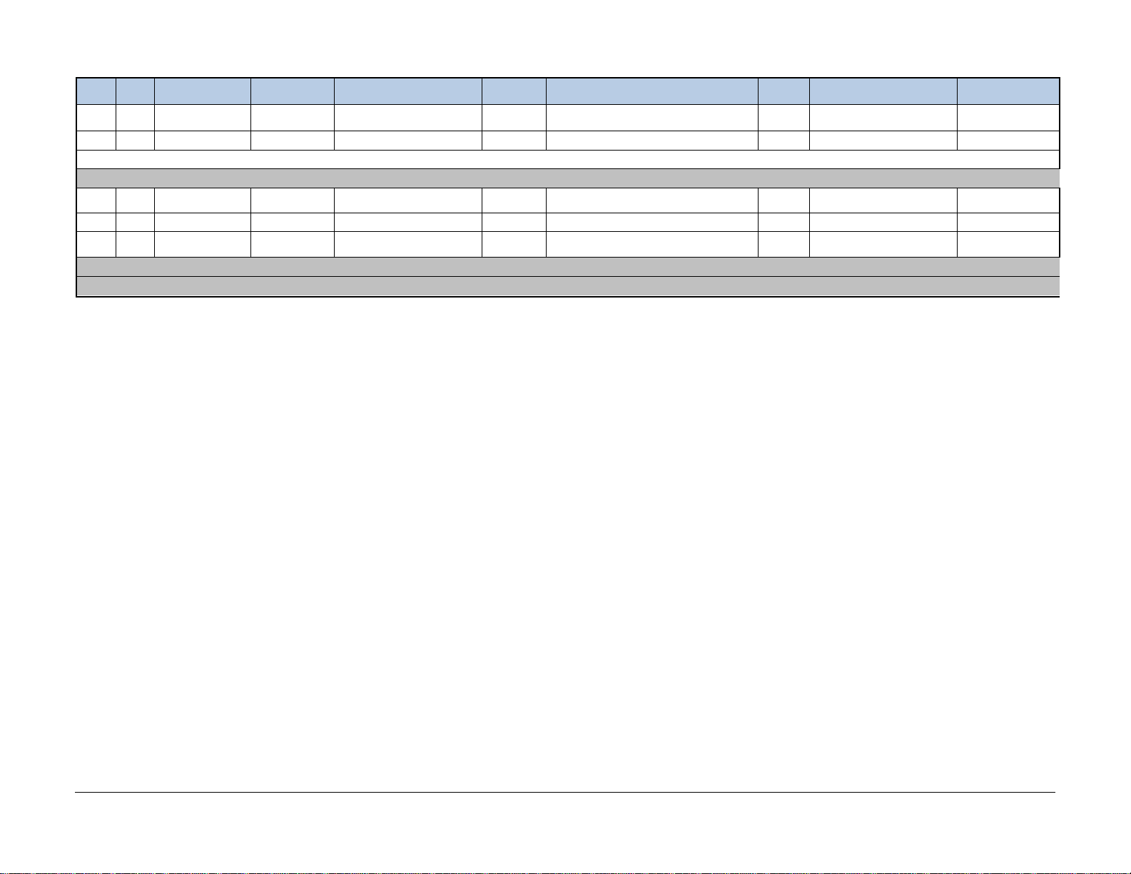
Item Qty Manufacturer
PARTS THAT SHOULD NOT BE ASSEMBLED
400 2 Yageo
401 4 JP3, JP4, JP5, JP6 Midbus LAI
402 4 Panasonic
PLX Part # 93-0082-100-A
Product Name: PEX 8648-AA RDK
Manufacturer
Part #
9C06031A0R
00JLHFT
ERJ-
3GEYJ330V
Description
RES 0.0 OHM 1/10W 5%
0603 SMD
RES, CF, 33 OHM, 1/16W,
5%, 0603 SMD
Package
Type
SMT,
0603
SMT,
0603
Component
Designator(s)
R124, R180
R287, R288, R289, R290
Distrib
utor
Compa
ny
Digi-
Key
Digi-
Key
Distributor
Part #
311-0.0GCT-ND NL
P33GCT-ND 33
Part
PEX 8648-AA RDK Hardware Reference Manual, Version 1.2
Copyright © 2010 by PLX Technology, Inc. All rights reserved 38
Page 44
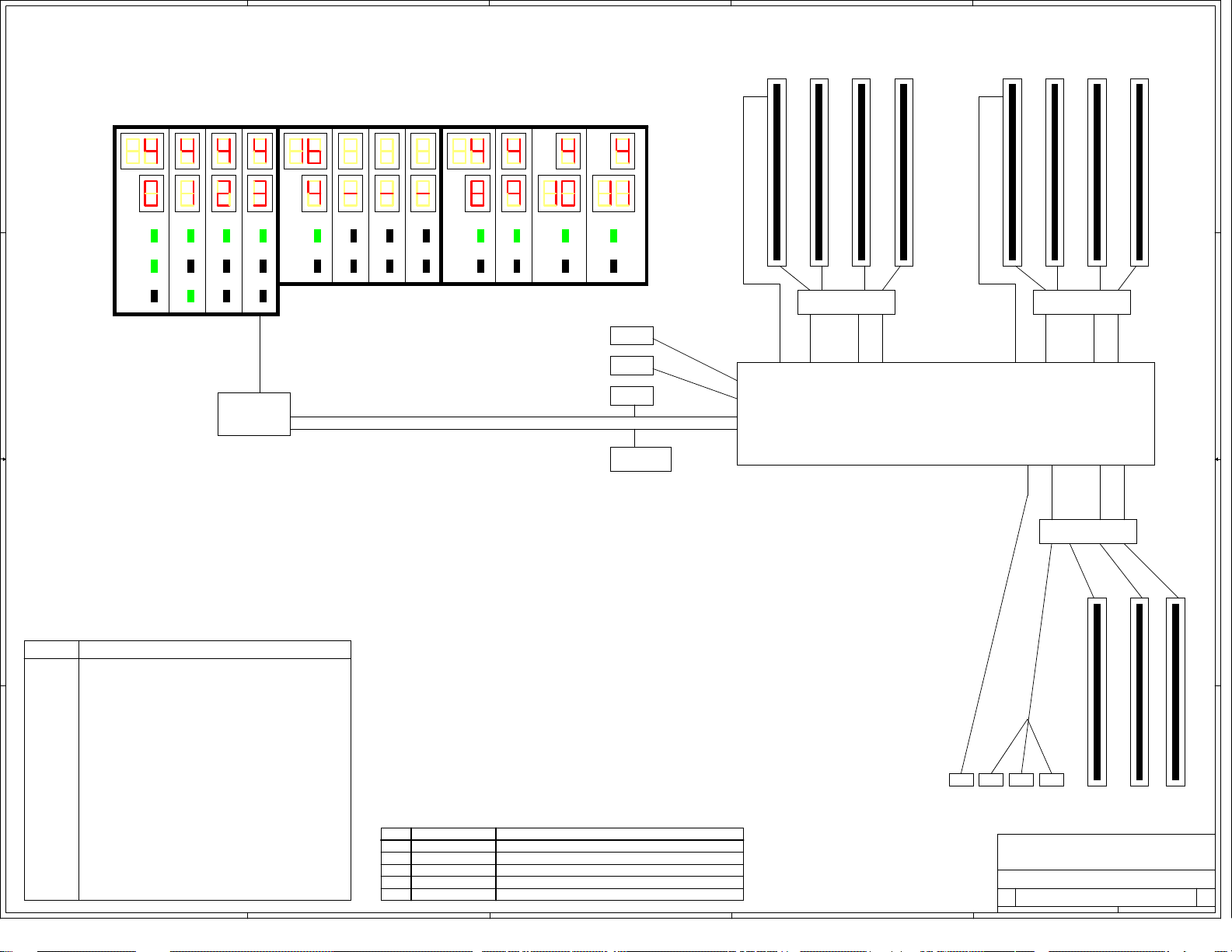
5
4
3
2
1
PORT CONFIGURATION AND STATUS INDICATORS
NOTE: THESE INDICATORS REFLECT THE BOARD CONFIGURATION AS DEFINED BY THE SWITCH SETTINGS AND THE
CONFIGURATION MODULES INSTALLED. THEY DO NOT NECESSARILY REFLECT THE PEX8648 CONFIGURATION.
CABLE
SLOT1
SLOT2
D D
SLOT3
PORT WIDTH
PORT NUMBER
PORT STATUS
SLOT4
SLOT5
SLOT6
SLOT7
SLOT8
SLOT9
SLOT10
SLOT11
SLOT4 SLOT5 SLOT6 SLOT7 SLOT8 SLOT9 SLOT10 SLOT11
UPSTREAM PORT
NT PORT
C C
EEPROM
CONFIG MODULE - P2 CONFIG MODULE - P3
x8 x4x4x12 x8 x4x4x12x4 x4
JTAG
I2C
CPLD
GLUE LOGIC
STRAPPING
SWITCHES
PEX 8648
CONFIG MODULE - P1
B B
x4x4x12x4 x8
Schematic Table of Contents
Sheet # Title
1 Functional Block Diagram
2 Board Layout Information
3 Station 0 Interface
4 Station 1 Interface
5 Station 2 Interface
6 Config Module 0
7 Config Modules 1 and 2
8 Station 0 Connectors
9 Station 1 Connectors
10 Station 2 Connectors
11 PCIe SWITCH INTERFACE
12 PCIe SWITCH POWER
A A
13 REFCLK Fanout 1
14 REFCLK Fanout 2
15 Switches
16 CPLD Glue Logic
17 MICTOR Connectors
18 Port Width Indicators
19 Port Status Indicators
20 Hot Plug
21 Power
5
Revision History
Rev. # Date Reason for Revision
January 10, 2008
100
February 8, 2008 Station 0 routing changed. Some footprints corrected.
101 6/4/2010 Modified the name of 8648 symbol
102 11/16/2010 Changed R170 to 360 K ohm resistor
4
First board build000
3
2
mSAS mSAS mSAS mSAS
SLOT1 SLOT2 SLOT3
PLX Technology, Inc.
PLX Technology, Inc.
PLX Technology, Inc.
870 W. Maude Avenue
870 W. Maude Avenue
870 W. Maude Avenue
Sunnyvale, CA 94085
Sunnyvale, CA 94085
Sunnyvale, CA 94085
www.plxtech.com
www.plxtech.com
Title
Title
Title
PEX8648 RDK - Functional Block Diagram
PEX8648 RDK - Functional Block Diagram
PEX8648 RDK - Functional Block Diagram
Size Document Number Rev
Size Document Number Rev
Size Document Number Rev
C
C
C
91-0082-100-A 102
91-0082-100-A 102
91-0082-100-A 102
Date: Sheet
Date: Sheet
Date: Sheet
www.plxtech.com
1
121Tuesday, November 16, 2010
121Tuesday, November 16, 2010
121Tuesday, November 16, 2010
of
of
of
Page 45
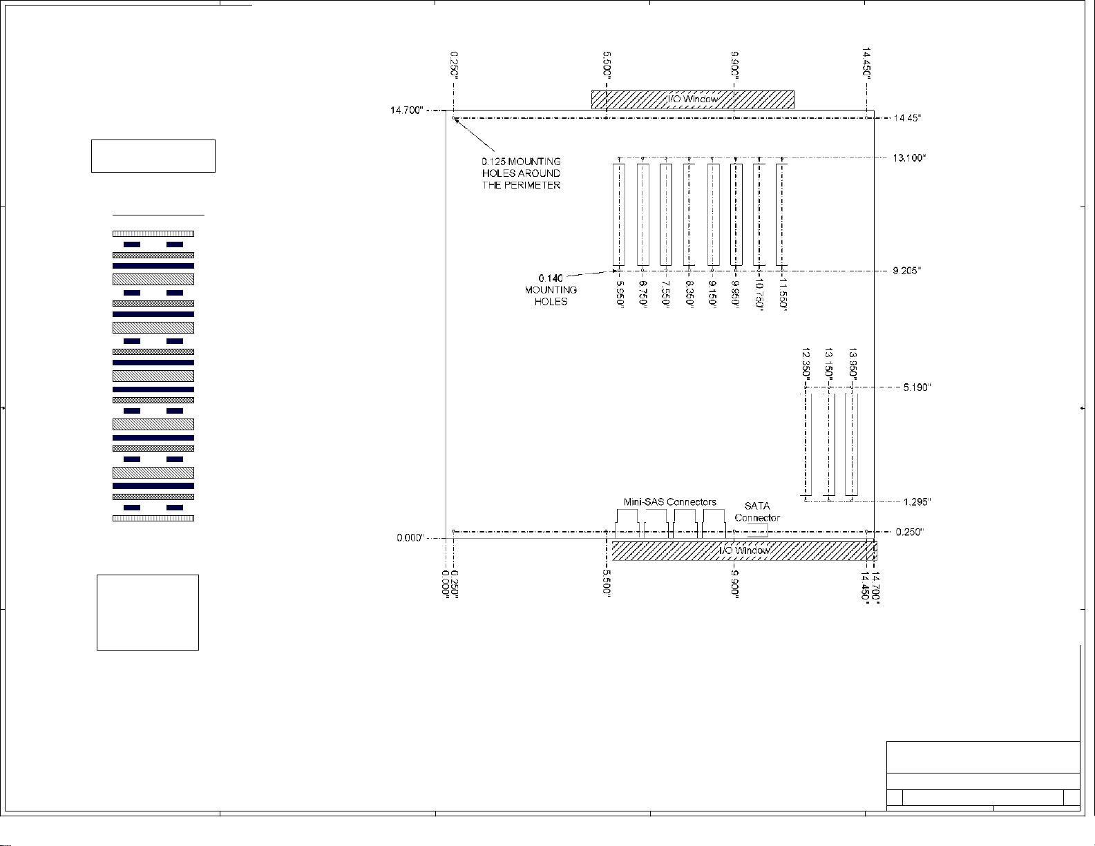
5
D D
4
3
2
1
Board
Thickness
= 62 mils
LAYER STACKUP
L1, SIGNAL 1, 2.0 mil
L2, GND1, 0.6 mil
L3, SIGNAL 2, 0.6 mil
C C
L4, POWER1, 0.6 mil
L5, SIGNAL 3, 0.6 mil
L6, POWER2, 1.2 mil
L7, GND2, 1.2 mil
L8, SIGNAL 4, 0.6 mil
L9, POWER3, 0.6 mil
L10, SIGNAL 5, 0.6 mil
L11, GND3, 0.6 mil
L12, SIGNAL 6, 2.0 mil
B B
SOLDERMASK, 0.8 mil
PREPREG, Er=3.9, 2.9 mil
CORE, Er=4.2, 6.0 mil
PREPREG, Er=4.1, 4.2 mil
CORE, Er=4.2, 6.0 mil
PREPREG, Er=4.1, 4.0 mil
CORE, Er=4.3, 3.0 mil
PREPREG, Er=4.1, 4.0 mil
CORE, Er=4.2, 6.0 mil
PREPREG, Er=4.1, 4.2 mil
CORE, Er=4.2, 6.0 mil
PREPREG, Er=3.9, 2.9 mil
SOLDERMASK, 0.8 mil
INNER
TRACES
Cu = 0.50 oz
DIFF Trace Zo = 91 ohm
WIDTH = 4.0 mil
SPACING = 7.0 mil
SINGLE Trace Zo = 50 ohm
WIDTH = 7.0 mil
NL = No Load
A A
PLX Technology, Inc.
PLX Technology, Inc.
PLX Technology, Inc.
870 W. Maude Avenue
870 W. Maude Avenue
870 W. Maude Avenue
Sunnyvale, CA 94085
Sunnyvale, CA 94085
Sunnyvale, CA 94085
www.plxtech.com
www.plxtech.com
Title
Title
Title
PEX8648 RDK - Board Layout Information
PEX8648 RDK - Board Layout Information
PEX8648 RDK - Board Layout Information
Size Document Number Rev
Size Document Number Rev
Size Document Number Rev
C
C
C
91-0082-100-A 102
91-0082-100-A 102
91-0082-100-A 102
Date: Sheet
Date: Sheet
5
4
3
2
Date: Sheet
www.plxtech.com
1
221Tuesday, November 16, 2010
221Tuesday, November 16, 2010
221Tuesday, November 16, 2010
of
of
of
Page 46
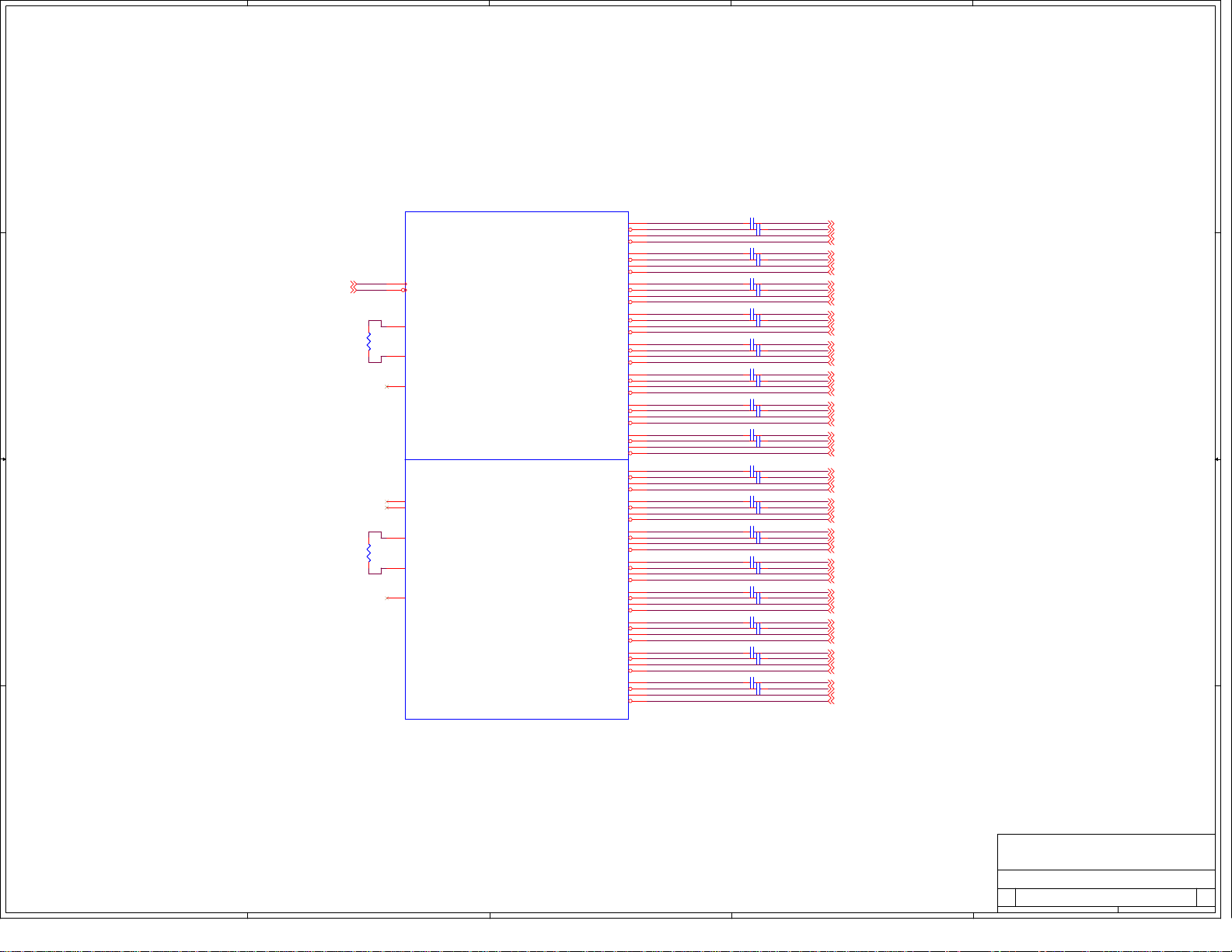
5
D D
Deneb_REFCLKp{13}
Deneb_REFCLKn{13}
C C
B B
R1
R1
1.43K
1.43K
1%
1%
R2
R2
1.43K
1.43K
1%
1%
4
U1A
U1A
PEX 8648
PEX 8648
AE9
PEX_REFCLKp
AF9
PEX_REFCLKn
AC9
REXT_A0
AB9
REXT_B0
AA9
NC
Station 0
Station 0
AE18
NC
AF18
NC
AC18
REXT_A1
AB18
REXT_B1
AA18
NC
PEX8648
PEX8648
3
PEX_PETp[0]
PEX_PETn[0]
PEX_PERp[0]
PEX_PERn[0]
PEX_PETp[1]
PEX_PETn[1]
PEX_PERp[1]
PEX_PERn[1]
PEX_PETp[2]
PEX_PETn[2]
PEX_PERp[2]
PEX_PERn[2]
PEX_PETp[3]
PEX_PETn[3]
PEX_PERp[3]
PEX_PERn[3]
PEX_PETp[4]
PEX_PETn[4]
PEX_PERp[4]
PEX_PERn[4]
PEX_PETp[5]
PEX_PETn[5]
PEX_PERp[5]
PEX_PERn[5]
PEX_PETp[6]
PEX_PETn[6]
PEX_PERp[6]
PEX_PERn[6]
PEX_PETp[7]
PEX_PETn[7]
PEX_PERp[7]
PEX_PERn[7]
PEX_PETp[8]
PEX_PETn[8]
PEX_PERp[8]
PEX_PERn[8]
PEX_PETp[9]
PEX_PETn[9]
PEX_PERp[9]
PEX_PERn[9]
PEX_PETp[10]
PEX_PETn[10]
PEX_PERp[10]
PEX_PERn[10]
PEX_PETp[11]
PEX_PETn[11]
PEX_PERp[11]
PEX_PERn[11]
PEX_PETp[12]
PEX_PETn[12]
PEX_PERp[12]
PEX_PERn[12]
PEX_PETp[13]
PEX_PETn[13]
PEX_PERp[13]
PEX_PERn[13]
PEX_PETp[14]
PEX_PETn[14]
PEX_PERp[14]
PEX_PERn[14]
PEX_PETp[15]
PEX_PETn[15]
PEX_PERp[15]
PEX_PERn[15]
AE5
AF5
AB5
AC5
AE6
AF6
AB6
AC6
AE7
AF7
AB7
AC7
AE8
AF8
AB8
AC8
AE10
AF10
AB10
AC10
AE11
AF11
AB11
AC11
AE12
AF12
AB12
AC12
AE13
AF13
AB13
AC13
AE14
AF14
AB14
AC14
AE15
AF15
AB15
AC15
AE16
AF16
AB16
AC16
AE17
AF17
AB17
AC17
AE19
AF19
AB19
AC19
AE20
AF20
AB20
AC20
AE21
AF21
AB21
AC21
AE22
AF22
AB22
AC22
PEX_Tx0_C_p
PEX_Tx0_C_n
PEX_Tx1_C_p
PEX_Tx1_C_n
PEX_Tx2_C_p
PEX_Tx2_C_n
PEX_Tx3_C_p
PEX_Tx3_C_n
PEX_Tx4_C_p
PEX_Tx4_C_n
PEX_Tx5_C_p
PEX_Tx5_C_n
PEX_Tx6_C_p
PEX_Tx6_C_n
PEX_Tx7_C_p
PEX_Tx7_C_n
PEX_Tx8_C_p
PEX_Tx8_C_n
PEX_Tx9_C_p
PEX_Tx9_C_n
PEX_Tx10_C_p
PEX_Tx10_C_n
PEX_Tx11_C_p
PEX_Tx11_C_n
PEX_Tx12_C_p
PEX_Tx12_C_n
PEX_Tx13_C_p
PEX_Tx13_C_n
PEX_Tx14_C_p
PEX_Tx14_C_n
PEX_Tx15_C_p
PEX_Tx15_C_n
2
C10.1uF C10.1uF
C20.1uF C20.1uF
C30.1uF C30.1uF
C40.1uF C40.1uF
C50.1uF C50.1uF
C60.1uF C60.1uF
C70.1uF C70.1uF
C80.1uF C80.1uF
C90.1uF C90.1uF
C100.1uF C100.1uF
C110.1uF C110.1uF
C120.1uF C120.1uF
C130.1uF C130.1uF
C140.1uF C140.1uF
C150.1uF C150.1uF
C160.1uF C160.1uF
C170.1uF C170.1uF
C180.1uF C180.1uF
C190.1uF C190.1uF
C200.1uF C200.1uF
C210.1uF C210.1uF
C220.1uF C220.1uF
C230.1uF C230.1uF
C240.1uF C240.1uF
C250.1uF C250.1uF
C260.1uF C260.1uF
C270.1uF C270.1uF
C280.1uF C280.1uF
C290.1uF C290.1uF
C300.1uF C300.1uF
C310.1uF C310.1uF
C320.1uF C320.1uF
PEX_Tx0_p {8}
PEX_Tx0_n {8}
PEX_Rx0_p {8}
PEX_Rx0_n {8}
PEX_Tx1_p {8}
PEX_Tx1_n {8}
PEX_Rx1_p {8}
PEX_Rx1_n {8}
PEX_Tx2_p {8}
PEX_Tx2_n {8}
PEX_Rx2_p {8}
PEX_Rx2_n {8}
PEX_Tx3_p {8}
PEX_Tx3_n {8}
PEX_Rx3_p {8}
PEX_Rx3_n {8}
PEX_Tx4_p {6}
PEX_Tx4_n {6}
PEX_Rx4_p {6}
PEX_Rx4_n {6}
PEX_Tx5_p {6}
PEX_Tx5_n {6}
PEX_Rx5_p {6}
PEX_Rx5_n {6}
PEX_Tx6_p {6}
PEX_Tx6_n {6}
PEX_Rx6_p {6}
PEX_Rx6_n {6}
PEX_Tx7_p {6}
PEX_Tx7_n {6}
PEX_Rx7_p {6}
PEX_Rx7_n {6}
PEX_Tx8_p {6}
PEX_Tx8_n {6}
PEX_Rx8_p {6}
PEX_Rx8_n {6}
PEX_Tx9_p {6}
PEX_Tx9_n {6}
PEX_Rx9_p {6}
PEX_Rx9_n {6}
PEX_Tx10_p {6}
PEX_Tx10_n {6}
PEX_Rx10_p {6}
PEX_Rx10_n {6}
PEX_Tx11_p {6}
PEX_Tx11_n {6}
PEX_Rx11_p {6}
PEX_Rx11_n {6}
PEX_Tx12_p {6}
PEX_Tx12_n {6}
PEX_Rx12_p {6}
PEX_Rx12_n {6}
PEX_Tx13_p {6}
PEX_Tx13_n {6}
PEX_Rx13_p {6}
PEX_Rx13_n {6}
PEX_Tx14_p {6}
PEX_Tx14_n {6}
PEX_Rx14_p {6}
PEX_Rx14_n {6}
PEX_Tx15_p {6}
PEX_Tx15_n {6}
PEX_Rx15_p {6}
PEX_Rx15_n {6}
1
A A
PLX Technology, Inc.
PLX Technology, Inc.
PLX Technology, Inc.
870 W. Maude Avenue
870 W. Maude Avenue
870 W. Maude Avenue
Sunnyvale, CA 94085
Sunnyvale, CA 94085
Sunnyvale, CA 94085
www.plxtech.com
www.plxtech.com
Title
Title
Title
PEX8648 RDK - Station 0 Interface
PEX8648 RDK - Station 0 Interface
PEX8648 RDK - Station 0 Interface
Size Document Number Rev
Size Document Number Rev
Size Document Number Rev
C
C
C
91-0082-100-A 102
91-0082-100-A 102
91-0082-100-A 102
Date: Sheet
Date: Sheet
5
4
3
2
Date: Sheet
www.plxtech.com
1
321Tuesday, November 16, 2010
321Tuesday, November 16, 2010
321Tuesday, November 16, 2010
of
of
of
Page 47
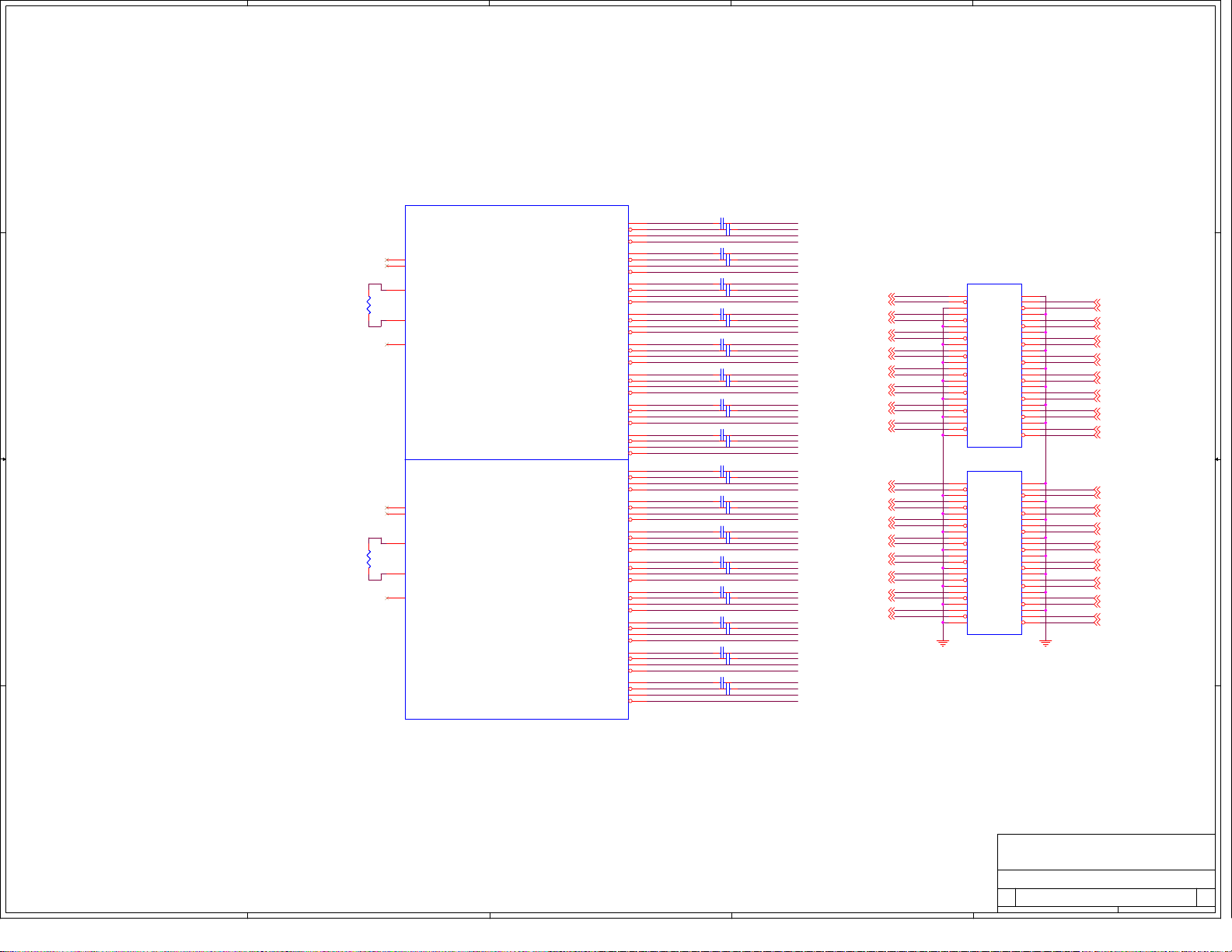
5
D D
C C
B B
R3
R3
1.43K
1.43K
1%
1%
R4
R4
1.43K
1.43K
1%
1%
4
U1B
U1B
PEX 8648
N2
NC
N1
NC
N4
REXT_A2
N5
REXT_B2
N6
NC
B9
NC
A9
NC
D9
REXT_A3
E9
REXT_B3
F9
NC
PEX8648
PEX8648
PEX 8648
Station 1
Station 1
3
PEX_PETp[16]
PEX_PETn[16]
PEX_PERp[16]
PEX_PERn[16]
PEX_PETp[17]
PEX_PETn[17]
PEX_PERp[17]
PEX_PERn[17]
PEX_PETp[18]
PEX_PETn[18]
PEX_PERp[18]
PEX_PERn[18]
PEX_PETp[19]
PEX_PETn[19]
PEX_PERp[19]
PEX_PERn[19]
PEX_PETp[20]
PEX_PETn[20]
PEX_PERp[20]
PEX_PERn[20]
PEX_PETp[21]
PEX_PETn[21]
PEX_PERp[21]
PEX_PERn[21]
PEX_PETp[22]
PEX_PETn[22]
PEX_PERp[22]
PEX_PERn[22]
PEX_PETp[23]
PEX_PETn[23]
PEX_PERp[23]
PEX_PERn[23]
PEX_PETp[24]
PEX_PETn[24]
PEX_PERp[24]
PEX_PERn[24]
PEX_PETp[25]
PEX_PETn[25]
PEX_PERp[25]
PEX_PERn[25]
PEX_PETp[26]
PEX_PETn[26]
PEX_PERp[26]
PEX_PERn[26]
PEX_PETp[27]
PEX_PETn[27]
PEX_PERp[27]
PEX_PERn[27]
PEX_PETp[28]
PEX_PETn[28]
PEX_PERp[28]
PEX_PERn[28]
PEX_PETp[29]
PEX_PETn[29]
PEX_PERp[29]
PEX_PERn[29]
PEX_PETp[30]
PEX_PETn[30]
PEX_PERp[30]
PEX_PERn[30]
PEX_PETp[31]
PEX_PETn[31]
PEX_PERp[31]
PEX_PERn[31]
Deneb_Txp__C_16
U2
Deneb_Txn__C_16
U1
U5
U4
Deneb_Txp_C_17
T2
Deneb_Txn_C_17
T1
T5
T4
Deneb_Txp_C_18
R2
Deneb_Txn_C_18
R1
R5
R4
Deneb_Txp_C_19
P2
Deneb_Txn_C_19
P1
P5
P4
Deneb_Txp_C_20
M2
Deneb_Txn_C_20
M1
M5
M4
Deneb_Txp_C_21
L2
Deneb_Txn_C_21 Deneb_Txn_21
L1
L5
L4
Deneb_Txp_C_22
K2
Deneb_Txn_C_22
K1
K5
K4
Deneb_Txp_C_23
J2
Deneb_Txn_C_23
J1
J5
J4
Deneb_Txp_C_24
B5
Deneb_Txn_C_24
A5
E5
D5
Deneb_Txp_C_25
B6
Deneb_Txn_C_25
A6
E6
D6
Deneb_Txp_C_26
B7
Deneb_Txn_C_26
A7
E7
D7
Deneb_Txp_C_27
B8
Deneb_Txn_C_27
A8
E8
D8
Deneb_Txp_C_28
B10
Deneb_Txn_C_28
A10
E10
D10
Deneb_Txp_C_29
B11
Deneb_Txn_C_29 Deneb_Txn_29
A11
E11
D11
Deneb_Txp_C_30
B12
Deneb_Txn_C_30
A12
E12
D12
Deneb_Txp_C_31
B13
Deneb_Txn_C_31
A13
E13
D13
C330.1uF C330.1uF
C370.1uF C370.1uF
C340.1uF C340.1uF
C380.1uF C380.1uF
C350.1uF C350.1uF
C360.1uF C360.1uF
C390.1uF C390.1uF
C400.1uF C400.1uF
C410.1uF C410.1uF
C420.1uF C420.1uF
C430.1uF C430.1uF
C440.1uF C440.1uF
C450.1uF C450.1uF
C460.1uF C460.1uF
C470.1uF C470.1uF
C480.1uF C480.1uF
C490.1uF C490.1uF
C500.1uF C500.1uF
C510.1uF C510.1uF
C520.1uF C520.1uF
C530.1uF C530.1uF
C540.1uF C540.1uF
C550.1uF C550.1uF
C560.1uF C560.1uF
C570.1uF C570.1uF
C580.1uF C580.1uF
C590.1uF C590.1uF
C600.1uF C600.1uF
C610.1uF C610.1uF
C620.1uF C620.1uF
C630.1uF C630.1uF
C640.1uF C640.1uF
Deneb_Txp_16
Deneb_Txn_16
Deneb_Rxp_16
Deneb_Rxn_16
Deneb_Txp_17
Deneb_Txn_17
Deneb_Rxp_17
Deneb_Rxn_17
Deneb_Txp_18
Deneb_Txn_18
Deneb_Rxp_18
Deneb_Rxn_18
Deneb_Txp_19
Deneb_Txn_19
Deneb_Rxp_19
Deneb_Rxn_19
Deneb_Txp_20
Deneb_Txn_20
Deneb_Rxp_20
Deneb_Rxn_20
Deneb_Txp_21
Deneb_Rxp_21
Deneb_Rxn_21
Deneb_Txp_22
Deneb_Txn_22
Deneb_Rxp_22
Deneb_Rxn_22
Deneb_Txp_23
Deneb_Txn_23
Deneb_Rxp_23
Deneb_Rxn_23
Deneb_Txp_24
Deneb_Txn_24
Deneb_Rxp_24
Deneb_Rxn_24
Deneb_Txp_25
Deneb_Txn_25
Deneb_Rxp_25
Deneb_Rxn_25
Deneb_Txp_26
Deneb_Txn_26
Deneb_Rxp_26
Deneb_Rxn_26
Deneb_Txp_27
Deneb_Txn_27
Deneb_Rxp_27
Deneb_Rxn_27
Deneb_Txp_28
Deneb_Txn_28
Deneb_Rxp_28
Deneb_Rxn_28
Deneb_Txp_29
Deneb_Rxp_29
Deneb_Rxn_29
Deneb_Txp_30
Deneb_Txn_30
Deneb_Rxp_30
Deneb_Rxn_30
Deneb_Txp_31
Deneb_Txn_31
Deneb_Rxp_31
Deneb_Rxn_31
2
Midbus Soft Touch
Probe Footprints
JP3
Deneb_Txp_16{9}
Deneb_Txn_16{9}
Deneb_Txp_17{9}
Deneb_Txn_17{9}
Deneb_Txp_18{9}
Deneb_Txn_18{9}
Deneb_Txp_19{9}
Deneb_Txn_19{9}
Deneb_Txp_20{7}
Deneb_Txn_20{7}
Deneb_Txp_21{7}
Deneb_Txn_21{7}
Deneb_Txp_22{7}
Deneb_Txn_22{7}
Deneb_Txp_23{7}
Deneb_Txn_23{7}
Deneb_Txp_24{7}
Deneb_Txn_24{7}
Deneb_Txp_25{7}
Deneb_Txn_25{7}
Deneb_Txp_26{7}
Deneb_Txn_26{7}
Deneb_Txp_27{7}
Deneb_Txn_27{7}
Deneb_Txp_28{7}
Deneb_Txn_28{7}
Deneb_Txp_29{7}
Deneb_Txn_29{7}
Deneb_Txp_30{7}
Deneb_Txn_30{7}
Deneb_Txp_31{7}
Deneb_Txn_31{7}
Deneb_Txp_16
Deneb_Txn_16
Deneb_Txp_17
Deneb_Txn_17
Deneb_Txp_18
Deneb_Txn_18
Deneb_Txp_19
Deneb_Txn_19
Deneb_Txp_20
Deneb_Txn_20
Deneb_Txp_21
Deneb_Txn_21
Deneb_Txp_22
Deneb_Txn_22
Deneb_Txp_23
Deneb_Txn_23
Deneb_Txp_24
Deneb_Txn_24
Deneb_Txp_25
Deneb_Txn_25
Deneb_Txp_26
Deneb_Txn_26
Deneb_Txp_27
Deneb_Txn_27
Deneb_Txp_28
Deneb_Txn_28
Deneb_Txp_29
Deneb_Txn_29
Deneb_Txp_30
Deneb_Txn_30
Deneb_Txp_31
Deneb_Txn_31
JP3
1
TX0+
TX0-3RX0+
5
GND
7
TX1+
9
TX1-
11
GND
13
TX2+
15
TX2-
17
GND
19
TX3+
21
TX3-
23
GND
25
TX4+
27
TX4-
29
GND
31
TX5+
33
TX5-
35
GND
37
TX6+
39
TX6-
41
GND
43
TX7+
45
TX7-
47
GND
Midbus LAI
Midbus LAI
JP4
JP4
1
TX0+
TX0-3RX0+
5
GND
7
TX1+
9
TX1-
11
GND
13
TX2+
15
TX2-
17
GND
19
TX3+
21
TX3-
23
GND
25
TX4+
27
TX4-
29
GND
31
TX5+
33
TX5-
35
GND
37
TX6+
39
TX6-
41
GND
43
TX7+
45
TX7-
47
GND
Midbus LAI
Midbus LAI
RX1+
RX2+
RX3+
RX4+
RX5+
RX6+
RX7+
RX1+
RX2+
RX3+
RX4+
RX5+
RX6+
RX7+
2
GND
4
6
RX0-
8
GND
10
12
RX1-
14
GND
16
18
RX2-
20
GND
22
24
RX3-
26
GND
28
30
RX4-
32
GND
34
36
RX5-
38
GND
40
42
RX6-
44
GND
46
48
RX7-
2
GND
4
6
RX0-
8
GND
10
12
RX1-
14
GND
16
18
RX2-
20
GND
22
24
RX3-
26
GND
28
30
RX4-
32
GND
34
36
RX5-
38
GND
40
42
RX6-
44
GND
46
48
RX7-
Deneb_Rxp_16
Deneb_Rxn_16
Deneb_Rxp_17
Deneb_Rxn_17
Deneb_Rxp_18
Deneb_Rxn_18
Deneb_Rxp_19
Deneb_Rxn_19
Deneb_Rxp_20
Deneb_Rxn_20
Deneb_Rxp_21
Deneb_Rxn_21
Deneb_Rxp_22
Deneb_Rxn_22
Deneb_Rxp_23
Deneb_Rxn_23
Deneb_Rxp_24
Deneb_Rxn_24
Deneb_Rxp_25
Deneb_Rxn_25
Deneb_Rxp_26
Deneb_Rxn_26
Deneb_Rxp_27
Deneb_Rxn_27
Deneb_Rxp_28
Deneb_Rxn_28
Deneb_Rxp_29
Deneb_Rxn_29
Deneb_Rxp_30
Deneb_Rxn_30
Deneb_Rxp_31
Deneb_Rxn_31
1
Deneb_Rxp_16 {9}
Deneb_Rxn_16 {9}
Deneb_Rxp_17 {9}
Deneb_Rxn_17 {9}
Deneb_Rxp_18 {9}
Deneb_Rxn_18 {9}
Deneb_Rxp_19 {9}
Deneb_Rxn_19 {9}
Deneb_Rxp_20 {7}
Deneb_Rxn_20 {7}
Deneb_Rxp_21 {7}
Deneb_Rxn_21 {7}
Deneb_Rxp_22 {7}
Deneb_Rxn_22 {7}
Deneb_Rxp_23 {7}
Deneb_Rxn_23 {7}
Deneb_Rxp_24 {7}
Deneb_Rxn_24 {7}
Deneb_Rxp_25 {7}
Deneb_Rxn_25 {7}
Deneb_Rxp_26 {7}
Deneb_Rxn_26 {7}
Deneb_Rxp_27 {7}
Deneb_Rxn_27 {7}
Deneb_Rxp_28 {7}
Deneb_Rxn_28 {7}
Deneb_Rxp_29 {7}
Deneb_Rxn_29 {7}
Deneb_Rxp_30 {7}
Deneb_Rxn_30 {7}
Deneb_Rxp_31 {7}
Deneb_Rxn_31 {7}
A A
PLX Technology, Inc.
PLX Technology, Inc.
PLX Technology, Inc.
870 W. Maude Avenue
870 W. Maude Avenue
870 W. Maude Avenue
Sunnyvale, CA 94085
Sunnyvale, CA 94085
Sunnyvale, CA 94085
www.plxtech.com
www.plxtech.com
Title
Title
Title
PEX8648 RDK - Station 1 INTERFACE
PEX8648 RDK - Station 1 INTERFACE
PEX8648 RDK - Station 1 INTERFACE
Size Document Number Rev
Size Document Number Rev
Size Document Number Rev
C
C
C
91-0082-100-A 102
91-0082-100-A 102
91-0082-100-A 102
Date: Sheet
Date: Sheet
5
4
3
2
Date: Sheet
www.plxtech.com
1
421Tuesday, November 16, 2010
421Tuesday, November 16, 2010
421Tuesday, November 16, 2010
of
of
of
Page 48
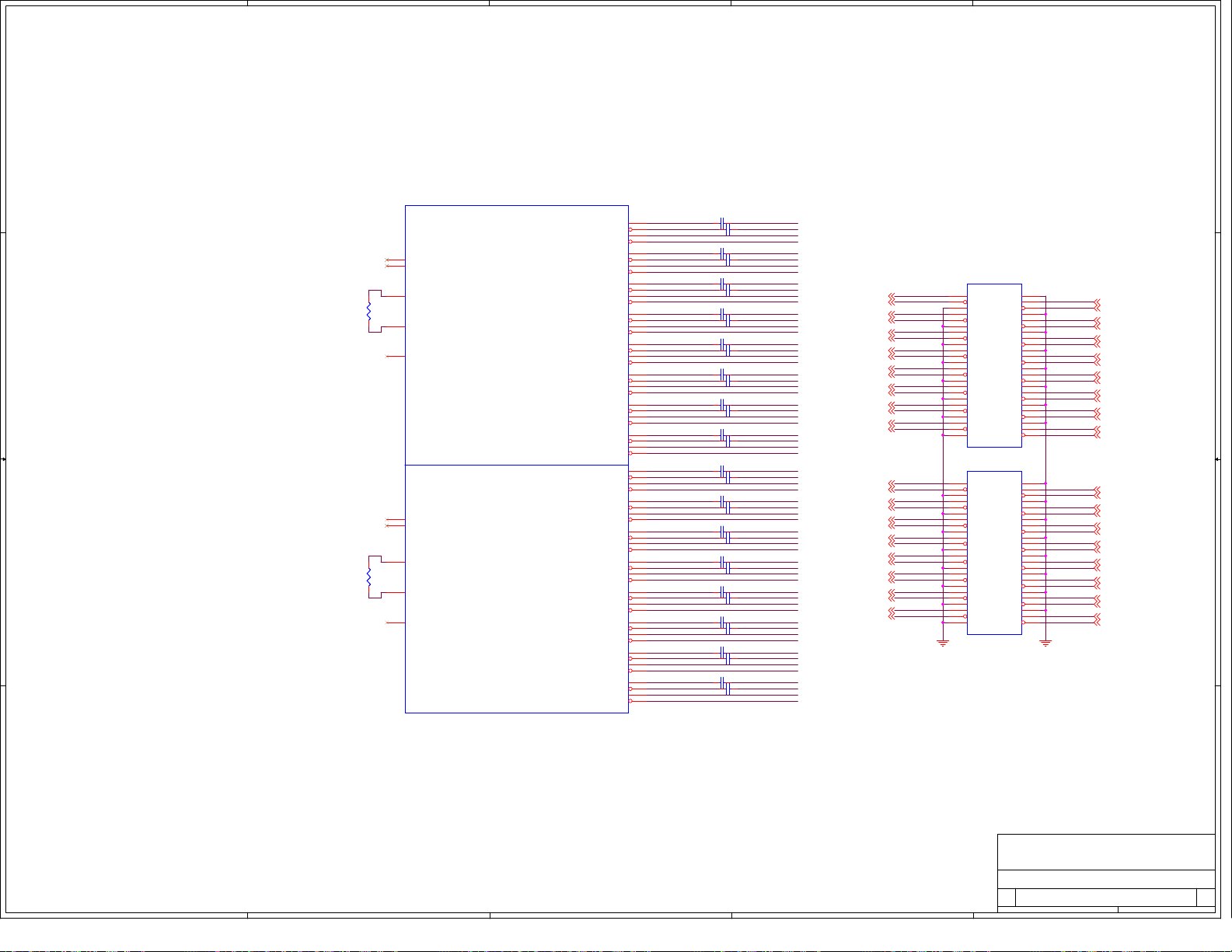
5
D D
C C
B B
R176
R176
1.43K
1.43K
1%
1%
R175
R175
1.43K
1.43K
1%
1%
4
U1C
U1C
N25
NC
N26
NC
N23
REXT_A4
N22
REXT_B4
N21
NC
B18
NC
A18
NC
D18
REXT_A5
E18
REXT_B5
F18
NC
PEX8648
PEX8648
PEX 8648
PEX 8648
Station 2
Station 2
3
PEX_PETp[32]
PEX_PETn[32]
PEX_PERp[32]
PEX_PERn[32]
PEX_PETp[33]
PEX_PETn[33]
PEX_PERp[33]
PEX_PERn[33]
PEX_PETp[34]
PEX_PETn[34]
PEX_PERp[34]
PEX_PERn[34]
PEX_PETp[35]
PEX_PETn[35]
PEX_PERp[35]
PEX_PERn[35]
PEX_PETp[36]
PEX_PETn[36]
PEX_PERp[36]
PEX_PERn[36]
PEX_PETp[37]
PEX_PETn[37]
PEX_PERp[37]
PEX_PERn[37]
PEX_PETp[38]
PEX_PETn[38]
PEX_PERp[38]
PEX_PERn[38]
PEX_PETp[39]
PEX_PETn[39]
PEX_PERp[39]
PEX_PERn[39]
PEX_PETp[40]
PEX_PETn[40]
PEX_PERp[40]
PEX_PERn[40]
PEX_PETp[41]
PEX_PETn[41]
PEX_PERp[41]
PEX_PERn[41]
PEX_PETp[42]
PEX_PETn[42]
PEX_PERp[42]
PEX_PERn[42]
PEX_PETp[43]
PEX_PETn[43]
PEX_PERp[43]
PEX_PERn[43]
PEX_PETp[44]
PEX_PETn[44]
PEX_PERp[44]
PEX_PERn[44]
PEX_PETp[45]
PEX_PETn[45]
PEX_PERp[45]
PEX_PERn[45]
PEX_PETp[46]
PEX_PETn[46]
PEX_PERp[46]
PEX_PERn[46]
PEX_PETp[47]
PEX_PETn[47]
PEX_PERp[47]
PEX_PERn[47]
Deneb_Txp_C_32
U25
Deneb_Txn_C_32
U26
U22
U23
Deneb_Txp_C_33
T25
Deneb_Txn_C_33
T26
T22
T23
Deneb_Txp_C_34
R25
Deneb_Txn_C_34
R26
R22
R23
Deneb_Txp_C_35
P25
Deneb_Txn_C_35
P26
P22
P23
Deneb_Txp_C_36
M25
Deneb_Txn_C_36
M26
M22
M23
Deneb_Txp_C_37
L25
Deneb_Txn_C_37 Deneb_Txn_37
L26
L22
L23
Deneb_Txp_C_38
K25
Deneb_Txn_C_38
K26
K22
K23
Deneb_Txp_C_39
J25
Deneb_Txn_C_39
J26
J22
J23
Deneb_Txp_C_40
B22
Deneb_Txn_C_40
A22
E22
D22
Deneb_Txp_C_41
B21
Deneb_Txn_C_41
A21
E21
D21
Deneb_Txp_C_42
B20
Deneb_Txn_C_42
A20
E20
D20
Deneb_Txp_C_43
B19
Deneb_Txn_C_43
A19
E19
D19
Deneb_Txp_C_44
B17
Deneb_Txn_C_44
A17
E17
D17
Deneb_Txp_C_45
B16
Deneb_Txn_C_45 Deneb_Txn_45
A16
E16
D16
Deneb_Txp_C_46
B15
Deneb_Txn_C_46
A15
E15
D15
Deneb_Txp_C_47
B14
Deneb_Txn_C_47
A14
E14
D14
C660.1uF C660.1uF
C670.1uF C670.1uF
C680.1uF C680.1uF
C690.1uF C690.1uF
C700.1uF C700.1uF
C710.1uF C710.1uF
C720.1uF C720.1uF
C650.1uF C650.1uF
C730.1uF C730.1uF
C740.1uF C740.1uF
C750.1uF C750.1uF
C760.1uF C760.1uF
C770.1uF C770.1uF
C780.1uF C780.1uF
C790.1uF C790.1uF
C800.1uF C800.1uF
C810.1uF C810.1uF
C820.1uF C820.1uF
C840.1uF C840.1uF
C830.1uF C830.1uF
C850.1uF C850.1uF
C860.1uF C860.1uF
C870.1uF C870.1uF
C880.1uF C880.1uF
C890.1uF C890.1uF
C900.1uF C900.1uF
C910.1uF C910.1uF
C920.1uF C920.1uF
C930.1uF C930.1uF
C940.1uF C940.1uF
C950.1uF C950.1uF
C960.1uF C960.1uF
Deneb_Txp_32
Deneb_Txn_32
Deneb_Rxp_32
Deneb_Rxn_32
Deneb_Txp_33
Deneb_Txn_33
Deneb_Rxp_33
Deneb_Rxn_33
Deneb_Txp_34
Deneb_Txn_34
Deneb_Rxp_34
Deneb_Rxn_34
Deneb_Txp_35
Deneb_Txn_35
Deneb_Rxp_35
Deneb_Rxn_35
Deneb_Txp_36
Deneb_Txn_36
Deneb_Rxp_36
Deneb_Rxn_36
Deneb_Txp_37
Deneb_Rxp_37
Deneb_Rxn_37
Deneb_Txp_38
Deneb_Txn_38
Deneb_Rxp_38
Deneb_Rxn_38
Deneb_Txp_39
Deneb_Txn_39
Deneb_Rxp_39
Deneb_Rxn_39
Deneb_Txp_40
Deneb_Txn_40
Deneb_Rxp_40
Deneb_Rxn_40
Deneb_Txp_41
Deneb_Txn_41
Deneb_Rxp_41
Deneb_Rxn_41
Deneb_Txp_42
Deneb_Txn_42
Deneb_Rxp_42
Deneb_Rxn_42
Deneb_Txp_43
Deneb_Txn_43
Deneb_Rxp_43
Deneb_Rxn_43
Deneb_Txp_44
Deneb_Txn_44
Deneb_Rxp_44
Deneb_Rxn_44
Deneb_Txp_45
Deneb_Rxp_45
Deneb_Rxn_45
Deneb_Txp_46
Deneb_Txn_46
Deneb_Rxp_46
Deneb_Rxn_46
Deneb_Txp_47
Deneb_Txn_47
Deneb_Rxp_47
Deneb_Rxn_47
2
Midbus Soft Touch
Probe Footprints
JP5
Deneb_Txp_32{10}
Deneb_Txn_32{10}
Deneb_Txp_33{10}
Deneb_Txn_33{10}
Deneb_Txp_34{10}
Deneb_Txn_34{10}
Deneb_Txp_35{10}
Deneb_Txn_35{10}
Deneb_Txp_36{7}
Deneb_Txn_36{7}
Deneb_Txp_37{7}
Deneb_Txn_37{7}
Deneb_Txp_38{7}
Deneb_Txn_38{7}
Deneb_Txp_39{7}
Deneb_Txn_39{7}
Deneb_Txp_40{7}
Deneb_Txn_40{7}
Deneb_Txp_41{7}
Deneb_Txn_41{7}
Deneb_Txp_42{7}
Deneb_Txn_42{7}
Deneb_Txp_43{7}
Deneb_Txn_43{7}
Deneb_Txp_44{7}
Deneb_Txn_44{7}
Deneb_Txp_45{7}
Deneb_Txn_45{7}
Deneb_Txp_46{7}
Deneb_Txn_46{7}
Deneb_Txp_47{7}
Deneb_Txn_47{7}
Deneb_Txp_32
Deneb_Txn_32
Deneb_Txp_33
Deneb_Txn_33
Deneb_Txp_34
Deneb_Txn_34
Deneb_Txp_35
Deneb_Txn_35
Deneb_Txp_36
Deneb_Txn_36
Deneb_Txp_37
Deneb_Txn_37
Deneb_Txp_38
Deneb_Txn_38
Deneb_Txp_39
Deneb_Txn_39
Deneb_Txp_40
Deneb_Txn_40
Deneb_Txp_41
Deneb_Txn_41
Deneb_Txp_42
Deneb_Txn_42
Deneb_Txp_43
Deneb_Txn_43
Deneb_Txp_44
Deneb_Txn_44
Deneb_Txp_45
Deneb_Txn_45
Deneb_Txp_46
Deneb_Txn_46
Deneb_Txp_47
Deneb_Txn_47
JP5
1
TX0+
TX0-3RX0+
5
GND
7
TX1+
9
TX1-
11
GND
13
TX2+
15
TX2-
17
GND
19
TX3+
21
TX3-
23
GND
25
TX4+
27
TX4-
29
GND
31
TX5+
33
TX5-
35
GND
37
TX6+
39
TX6-
41
GND
43
TX7+
45
TX7-
47
GND
Midbus LAI
Midbus LAI
JP6
JP6
1
TX0+
TX0-3RX0+
5
GND
7
TX1+
9
TX1-
11
GND
13
TX2+
15
TX2-
17
GND
19
TX3+
21
TX3-
23
GND
25
TX4+
27
TX4-
29
GND
31
TX5+
33
TX5-
35
GND
37
TX6+
39
TX6-
41
GND
43
TX7+
45
TX7-
47
GND
Midbus LAI
Midbus LAI
RX1+
RX2+
RX3+
RX4+
RX5+
RX6+
RX7+
RX1+
RX2+
RX3+
RX4+
RX5+
RX6+
RX7+
2
GND
4
6
RX0-
8
GND
10
12
RX1-
14
GND
16
18
RX2-
20
GND
22
24
RX3-
26
GND
28
30
RX4-
32
GND
34
36
RX5-
38
GND
40
42
RX6-
44
GND
46
48
RX7-
2
GND
4
6
RX0-
8
GND
10
12
RX1-
14
GND
16
18
RX2-
20
GND
22
24
RX3-
26
GND
28
30
RX4-
32
GND
34
36
RX5-
38
GND
40
42
RX6-
44
GND
46
48
RX7-
Deneb_Rxp_32
Deneb_Rxn_32
Deneb_Rxp_33
Deneb_Rxn_33
Deneb_Rxp_34
Deneb_Rxn_34
Deneb_Rxp_35
Deneb_Rxn_35
Deneb_Rxp_36
Deneb_Rxn_36
Deneb_Rxp_37
Deneb_Rxn_37
Deneb_Rxp_38
Deneb_Rxn_38
Deneb_Rxp_39
Deneb_Rxn_39
Deneb_Rxp_40
Deneb_Rxn_40
Deneb_Rxp_41
Deneb_Rxn_41
Deneb_Rxp_42
Deneb_Rxn_42
Deneb_Rxp_43
Deneb_Rxn_43
Deneb_Rxp_44
Deneb_Rxn_44
Deneb_Rxp_45
Deneb_Rxn_45
Deneb_Rxp_46
Deneb_Rxn_46
Deneb_Rxp_47
Deneb_Rxn_47
1
Deneb_Rxp_32 {10}
Deneb_Rxn_32 {10}
Deneb_Rxp_33 {10}
Deneb_Rxn_33 {10}
Deneb_Rxp_34 {10}
Deneb_Rxn_34 {10}
Deneb_Rxp_35 {10}
Deneb_Rxn_35 {10}
Deneb_Rxp_36 {7}
Deneb_Rxn_36 {7}
Deneb_Rxp_37 {7}
Deneb_Rxn_37 {7}
Deneb_Rxp_38 {7}
Deneb_Rxn_38 {7}
Deneb_Rxp_39 {7}
Deneb_Rxn_39 {7}
Deneb_Rxp_40 {7}
Deneb_Rxn_40 {7}
Deneb_Rxp_41 {7}
Deneb_Rxn_41 {7}
Deneb_Rxp_42 {7}
Deneb_Rxn_42 {7}
Deneb_Rxp_43 {7}
Deneb_Rxn_43 {7}
Deneb_Rxp_44 {7}
Deneb_Rxn_44 {7}
Deneb_Rxp_45 {7}
Deneb_Rxn_45 {7}
Deneb_Rxp_46 {7}
Deneb_Rxn_46 {7}
Deneb_Rxp_47 {7}
Deneb_Rxn_47 {7}
A A
PLX Technology, Inc.
PLX Technology, Inc.
PLX Technology, Inc.
870 W. Maude Avenue
870 W. Maude Avenue
870 W. Maude Avenue
Sunnyvale, CA 94085
Sunnyvale, CA 94085
Sunnyvale, CA 94085
www.plxtech.com
www.plxtech.com
Title
Title
Title
PEX8648 RDK - Station 2 Interface
PEX8648 RDK - Station 2 Interface
PEX8648 RDK - Station 2 Interface
Size Document Number Rev
Size Document Number Rev
Size Document Number Rev
C
C
C
91-0082-100-A 102
91-0082-100-A 102
91-0082-100-A 102
Date: Sheet
Date: Sheet
5
4
3
2
Date: Sheet
www.plxtech.com
1
521Tuesday, November 16, 2010
521Tuesday, November 16, 2010
521Tuesday, November 16, 2010
of
of
of
Page 49
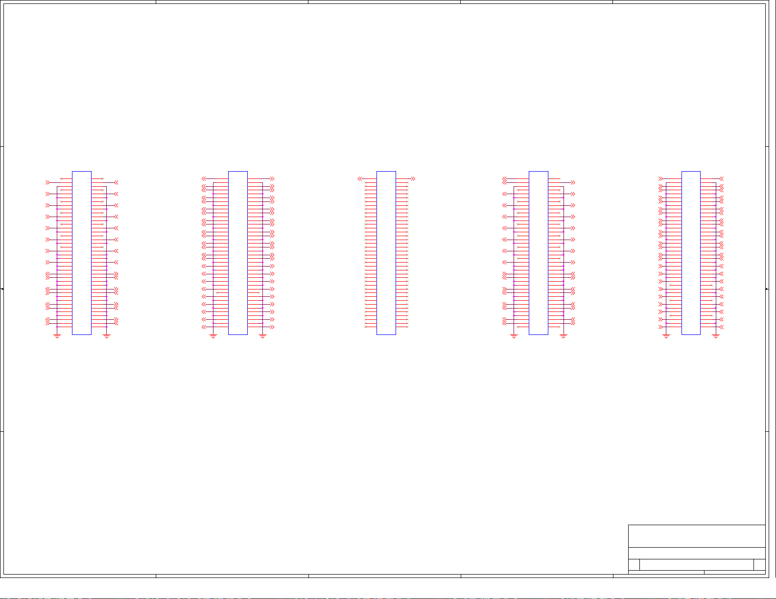
5
D D
4
3
2
1
CONFIGURATION MODULE 0
P1C
P1B
P1A
P1A
A1
B1
A1
B1
A2
PEX_Tx4_n{3}
PEX_Tx5_n{3}
PEX_Tx6_n{3}
PEX_Tx7_n{3}
C C
PEX_Tx8_n{3}
PEX_Tx9_n{3}
PEX_Tx10_n{3}
PEX_Tx11_n{3}
Slot2_Tx4_n{8}
PEX_Tx12_n{3}
Slot2_Tx5_n{8}
PEX_Tx13_n{3}
Slot2_Tx6_n{8}
PEX_Tx14_n{3}
Slot2_Tx7_n{8}
PEX_Tx15_n{3}
A10
A11
A12
A13
A14
A15
A16
A17
A18
A19
A20
A21
A22
A23
A24
A25
A26
A27
A28
A29
A30
A31
A32
A33
A34
A35
A36
A37
A38
A39
A40
A3
A4
A5
A6
A7
A8
A9
A2
A3
A4
A5
A6
A7
A8
A9
A10
A11
A12
A13
A14
A15
A16
A17
A18
A19
A20
A21
A22
A23
A24
A25
A26
A27
A28
A29
A30
A31
A32
A33
A34
A35
A36
A37
A38
A39
A40
CM_10x40
CM_10x40
B2
B2
B3
B4
B5
B6
B7
B8
B9
B10
B11
B12
B13
B14
B15
B16
B17
B18
B19
B20
B21
B22
B23
B24
B25
B26
B27
B28
B29
B30
B31
B32
B33
B34
B35
B36
B37
B38
B39
B40
PEX_Tx4_p {3}
B3
B4
B5
PEX_Tx5_p {3}
B6
B7
B8
PEX_Tx6_p {3}
B9
B10
B11
PEX_Tx7_p {3}
B12
B13
B14
PEX_Tx8_p {3}
B15
B16
B17
PEX_Tx9_p {3}
B18
B19
B20
PEX_Tx10_p {3}
B21
B22
B23
PEX_Tx11_p {3}
B24
B25
B26
Slot2_Tx4_p {8}
B27
PEX_Tx12_p {3}
B28
B29
B30
Slot2_Tx5_p {8}
B31
PEX_Tx13_p {3}
B32
B33
B34
Slot2_Tx6_p {8}
B35
PEX_Tx14_p {3}
B36
B37
B38
Slot2_Tx7_p {8}
B39
PEX_Tx15_p {3}
B40
SAS1_Tx0_n{8}
Slot1_Tx0_n{8}
SAS1_Tx1_n{8}
Slot1_Tx1_n{8}
SAS1_Tx2_n{8}
Slot1_Tx2_n{8}
SAS1_Tx3_n{8}
Slot1_Tx3_n{8}
SAS2_Tx0_n{8}
Slot2_Tx0_n{8}
SAS2_Tx1_n{8}
Slot2_Tx1_n{8}
SAS2_Tx2_n{8}
Slot2_Tx2_n{8}
SAS2_Tx3_n{8}
Slot2_Tx3_n{8}
SAS3_Tx0_n{8}
Slot3_Tx0_n{8}
SAS3_Tx1_n{8}
Slot3_Tx1_n{8}
SAS3_Tx2_n{8}
Slot3_Tx2_n{8}
SAS3_Tx3_n{8}
Slot3_Tx3_n{8}
P1B
C1
D1
C1
D1
C2
C2
D2
C3
C3
D3
C4
C4
D4
C5
C5
D5
C6
C6
D6
C7
C7
D7
C8
C8
D8
C9
C9
D9
C10
C10
D10
C11
C11
D11
C12
C12
D12
C13
C13
D13
C14
C14
D14
C15
C15
D15
C16
C16
D16
C17
C17
D17
C18
C18
D18
C19
C19
D19
C20
C20
D20
C21
C21
D21
C22
C22
D22
C23
C23
D23
C24
C24
D24
C25
C25
D25
C26
C26
D26
C27
C27
D27
C28
C28
D28
C29
C29
D29
C30
C30
D30
C31
C31
D31
C32
C32
D32
C33
C33
D33
C34
C34
D34
C35
C35
D35
C36
C36
D36
C37
C37
D37
C38
C38
D38
C39
C39
D39
C40
C40
D40
CM_10x40
CM_10x40
SAS1_Tx0_p {8}
D2
D3
Slot1_Tx0_p {8}
D4
SAS1_Tx1_p {8}
D5
D6
Slot1_Tx1_p {8}
D7
SAS1_Tx2_p {8}
D8
D9
Slot1_Tx2_p {8}
D10
SAS1_Tx3_p {8}
D11
D12
Slot1_Tx3_p {8}
D13
SAS2_Tx0_p {8}
D14
D15
Slot2_Tx0_p {8}
D16
SAS2_Tx1_p {8}
D17
D18
Slot2_Tx1_p {8}
D19
SAS2_Tx2_p {8}
D20
D21
Slot2_Tx2_p {8}
D22
SAS2_Tx3_p {8}
D23
D24
Slot2_Tx3_p {8}
D25
D26
SAS3_Tx0_p {8}
D27
D28
Slot3_Tx0_p {8}
D29
D30
SAS3_Tx1_p {8}
D31
D32
Slot3_Tx1_p {8}
D33
D34
SAS3_Tx2_p {8}
D35
D36
Slot3_Tx2_p {8}
D37
D38
SAS3_Tx3_p {8}
D39
D40
Slot3_Tx3_p {8}
P1C
E1
F1
E1
F1
E2
F2
E2
F2
E3
F3
E3
F3
E4
F4
E4
F4
E5
F5
E5
F5
E6
F6
E6
F6
E7
F7
E7
F7
E8
F8
E8
F8
E9
F9
E9
F9
E10
E11
E12
E13
E14
E15
E16
E17
E18
E19
E20
E21
E22
E23
E24
E25
E26
E27
E28
E29
E30
E31
E32
E33
E34
E35
E36
E37
E38
E39
E40
E10
E11
E12
E13
E14
E15
E16
E17
E18
E19
E20
E21
E22
E23
E24
E25
E26
E27
E28
E29
E30
E31
E32
E33
E34
E35
E36
E37
E38
E39
E40
CM_10x40
CM_10x40
F10
F10
F11
F11
F12
F12
F13
F13
F14
F14
F15
F15
F16
F16
F17
F17
F18
F18
F19
F19
F20
F20
F21
F21
F22
F22
F23
F23
F24
F24
F25
F25
F26
F26
F27
F27
F28
F28
F29
F29
F30
F30
F31
F31
F32
F32
F33
F33
F34
F34
F35
F35
F36
F36
F37
F37
F38
F38
F39
F39
F40
F40
MOD_0_PRSNT#{16}ST0_PRT_CONFIG1{16} ST0_PRT_CONFIG0 {16}
PEX_Rx4_p{3}
PEX_Rx5_p{3}
PEX_Rx6_p{3}
PEX_Rx7_p{3}
PEX_Rx8_p{3}
PEX_Rx9_p{3}
PEX_Rx10_p{3}
PEX_Rx11_p{3}
Slot2_Rx4_p{8}
PEX_Rx12_p{3}
Slot2_Rx5_p{8}
PEX_Rx13_p{3}
Slot2_Rx6_p{8}
PEX_Rx14_p{3}
Slot2_Rx7_p{8}
PEX_Rx15_p{3}
G10
G11
G12
G13
G14
G15
G16
G17
G18
G19
G20
G21
G22
G23
G24
G25
G26
G27
G28
G29
G30
G31
G32
G33
G34
G35
G36
G37
G38
G39
G40
G1
G2
G3
G4
G5
G6
G7
G8
G9
P1D
P1D
G1
G2
G3
G4
G5
G6
G7
G8
G9
G10
G11
G12
G13
G14
G15
G16
G17
G18
G19
G20
G21
G22
G23
G24
G25
G26
G27
G28
G29
G30
G31
G32
G33
G34
G35
G36
G37
G38
G39
G40
CM_10x40
CM_10x40
H1
H1
H2
H2
H3
H4
H5
H6
H7
H8
H9
H10
H11
H12
H13
H14
H15
H16
H17
H18
H19
H20
H21
H22
H23
H24
H25
H26
H27
H28
H29
H30
H31
H32
H33
H34
H35
H36
H37
H38
H39
H40
PEX_Rx4_n {3}
H3
H4
H5
PEX_Rx5_n {3}
H6
H7
H8
PEX_Rx6_n {3}
H9
H10
H11
PEX_Rx7_n {3}
H12
H13
H14
PEX_Rx8_n {3}
H15
H16
H17
PEX_Rx9_n {3}
H18
H19
H20
PEX_Rx10_n {3}
H21
H22
H23
PEX_Rx11_n {3}
H24
H25
H26
Slot2_Rx4_n {8}
H27
PEX_Rx12_n {3}
H28
H29
H30
Slot2_Rx5_n {8}
H31
PEX_Rx13_n {3}
H32
H33
H34
Slot2_Rx6_n {8}
H35
PEX_Rx14_n {3}
H36
H37
H38
Slot2_Rx7_n {8}
H39
PEX_Rx15_n {3}
H40
SAS1_Rx0_p{8}
Slot1_Rx0_p{8}
SAS1_Rx1_p{8}
Slot1_Rx1_p{8}
SAS1_Rx2_p{8}
Slot1_Rx2_p{8}
SAS1_Rx3_p{8}
Slot1_Rx3_p{8}
SAS2_Rx0_p{8}
Slot2_Rx0_p{8}
SAS2_Rx1_p{8}
Slot2_Rx1_p{8}
SAS2_Rx2_p{8}
Slot2_Rx2_p{8}
SAS2_Rx3_p{8}
Slot2_Rx3_p{8}
SAS3_Rx0_p{8}
Slot3_Rx0_p{8}
SAS3_Rx1_p{8}
Slot3_Rx1_p{8}
SAS3_Rx2_p{8}
Slot3_Rx2_p{8}
SAS3_Rx3_p{8}
Slot3_Rx3_p{8}
I10
I11
I12
I13
I14
I15
I16
I17
I18
I19
I20
I21
I22
I23
I24
I25
I26
I27
I28
I29
I30
I31
I32
I33
I34
I35
I36
I37
I38
I39
I40
I1
I2
I3
I4
I5
I6
I7
I8
I9
P1E
P1E
I1
I2
I3
I4
I5
I6
I7
I8
I9
I10
I11
I12
I13
I14
I15
I16
I17
I18
I19
I20
I21
I22
I23
I24
I25
I26
I27
I28
I29
I30
I31
I32
I33
I34
I35
I36
I37
I38
I39
I40
CM_10x40
CM_10x40
J1
SAS1_Rx0_n {8}
J1
J2
J2
J3
Slot1_Rx0_n {8}
J3
J4
SAS1_Rx1_n {8}
J4
J5
J5
J6
Slot1_Rx1_n {8}
J6
J7
SAS1_Rx2_n {8}
J7
J8
J8
J9
Slot1_Rx2_n {8}
J9
J10
J11
J12
J13
J14
J15
J16
J17
J18
J19
J20
J21
J22
J23
J24
J25
J26
J27
J28
J29
J30
J31
J32
J33
J34
J35
J36
J37
J38
J39
J40
SAS1_Rx3_n {8}
Slot1_Rx3_n {8}
SAS2_Rx0_n {8}
Slot2_Rx0_n {8}
SAS2_Rx1_n {8}
Slot2_Rx1_n {8}
SAS2_Rx2_n {8}
Slot2_Rx2_n {8}
SAS2_Rx3_n {8}
Slot2_Rx3_n {8}
SAS3_Rx0_n {8}
Slot3_Rx0_n {8}
SAS3_Rx1_n {8}
Slot3_Rx1_n {8}
SAS3_Rx2_n {8}
Slot3_Rx2_n {8}
SAS3_Rx3_n {8}
Slot3_Rx3_n {8}
J10
J11
J12
J13
J14
J15
J16
J17
J18
J19
J20
J21
J22
J23
J24
J25
J26
J27
J28
J29
J30
J31
J32
J33
J34
J35
J36
J37
J38
J39
J40
B B
A A
PLX Technology, Inc.
PLX Technology, Inc.
PLX Technology, Inc.
870 W. Maude Avenue
870 W. Maude Avenue
870 W. Maude Avenue
Sunnyvale, CA 94085
Sunnyvale, CA 94085
Sunnyvale, CA 94085
www.plxtech.com
www.plxtech.com
Title
Title
Title
PEX8648 RDK - Configuration Module 0
PEX8648 RDK - Configuration Module 0
PEX8648 RDK - Configuration Module 0
Size Document Number Rev
Size Document Number Rev
Size Document Number Rev
C
C
C
91-0082-100-A 102
91-0082-100-A 102
91-0082-100-A 102
Date: Sheet
Date: Sheet
5
4
3
2
Date: Sheet
www.plxtech.com
1
621Tuesday, November 16, 2010
621Tuesday, November 16, 2010
621Tuesday, November 16, 2010
of
of
of
Page 50
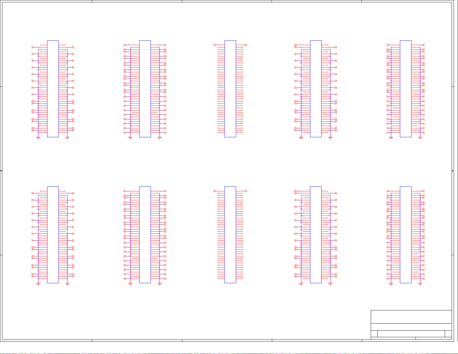
5
4
3
2
1
CONFIGURATION MODULE 1
P2D
P2B
P2A
P2A
A1
D D
Deneb_Txp_20{4}
Deneb_Txp_21{4}
Deneb_Txp_22{4}
Deneb_Txp_23{4}
Deneb_Txp_24{4}
Deneb_Txp_25{4}
Deneb_Txp_26{4}
Deneb_Txp_27{4}
Slot6_Txp_4{9}
Deneb_Txp_28{4}
Slot6_Txp_5{9}
Deneb_Txp_29{4}
Slot6_Txp_6{9}
Deneb_Txp_30{4}
Slot6_Txp_7{9}
C C
Deneb_Txp_31{4}
A10
A11
A12
A13
A14
A15
A16
A17
A18
A19
A20
A21
A22
A23
A24
A25
A26
A27
A28
A29
A30
A31
A32
A33
A34
A35
A36
A37
A38
A39
A40
A2
A3
A4
A5
A6
A7
A8
A9
A1
A2
A3
A4
A5
A6
A7
A8
A9
A10
A11
A12
A13
A14
A15
A16
A17
A18
A19
A20
A21
A22
A23
A24
A25
A26
A27
A28
A29
A30
A31
A32
A33
A34
A35
A36
A37
A38
A39
A40
CM_10x40
CM_10x40
B1
B1
B2
B2
B3
B4
B5
B6
B7
B8
B9
B10
B11
B12
B13
B14
B15
B16
B17
B18
B19
B20
B21
B22
B23
B24
B25
B26
B27
B28
B29
B30
B31
B32
B33
B34
B35
B36
B37
B38
B39
B40
Deneb_Txn_20 {4}
B3
B4
B5
Deneb_Txn_21 {4}
B6
B7
B8
Deneb_Txn_22 {4}
B9
B10
B11
Deneb_Txn_23 {4}
B12
B13
B14
Deneb_Txn_24 {4}
B15
B16
B17
Deneb_Txn_25 {4}
B18
B19
B20
Deneb_Txn_26 {4}
B21
B22
B23
Deneb_Txn_27 {4}
B24
B25
B26
Slot6_Txn_4 {9}
B27
Deneb_Txn_28 {4}
B28
B29
B30
Slot6_Txn_5 {9}
B31
Deneb_Txn_29 {4}
B32
B33
B34
Slot6_Txn_6 {9}
B35
Deneb_Txn_30 {4}
B36
B37
B38
Slot6_Txn_7 {9}
B39
Deneb_Txn_31 {4}
B40
Slot4_Txp_4{9}
Slot5_Txp_0{9}
Slot4_Txp_5{9}
Slot5_Txp_1{9}
Slot4_Txp_6{9}
Slot5_Txp_2{9}
Slot4_Txp_7{9}
Slot5_Txp_3{9}
Slot4_Txp_8{9}
Slot6_Txp_0{9}
Slot4_Txp_9{9}
Slot6_Txp_1{9}
Slot4_Txp_10{9}
Slot6_Txp_2{9}
Slot4_Txp_11{9}
Slot6_Txp_3{9}
Slot4_Txp_12{9}
Slot7_Txp_0{9}
Slot4_Txp_13{9}
Slot7_Txp_1{9}
Slot4_Txp_14{9}
Slot7_Txp_2{9}
Slot4_Txp_15{9}
Slot7_Txp_3{9}
P2B
C1
D1
C1
D1
C2
C2
D2
C3
C3
D3
C4
C4
D4
C5
C5
D5
C6
C6
D6
C7
C7
D7
C8
C8
D8
C9
C9
D9
C10
C10
D10
C11
C11
D11
C12
C12
D12
C13
C13
D13
C14
C14
D14
C15
C15
D15
C16
C16
D16
C17
C17
D17
C18
C18
D18
C19
C19
D19
C20
C20
D20
C21
C21
D21
C22
C22
D22
C23
C23
D23
C24
C24
D24
C25
C25
D25
C26
C26
D26
C27
C27
D27
C28
C28
D28
C29
C29
D29
C30
C30
D30
C31
C31
D31
C32
C32
D32
C33
C33
D33
C34
C34
D34
C35
C35
D35
C36
C36
D36
C37
C37
D37
C38
C38
D38
C39
C39
D39
C40
C40
D40
CM_10x40
CM_10x40
Slot4_Txn_4 {9}
D2
D3
Slot5_Txn_0 {9}
D4
Slot4_Txn_5 {9}
D5
D6
Slot5_Txn_1 {9}
D7
Slot4_Txn_6 {9}
D8
D9
Slot5_Txn_2 {9}
D10
Slot4_Txn_7 {9}
D11
D12
Slot5_Txn_3 {9}
D13
Slot4_Txn_8 {9}
D14
D15
Slot6_Txn_0 {9}
D16
Slot4_Txn_9 {9}
D17
D18
Slot6_Txn_1 {9}
D19
Slot4_Txn_10 {9}
D20
D21
Slot6_Txn_2 {9}
D22
Slot4_Txn_11 {9}
D23
D24
Slot6_Txn_3 {9}
D25
D26
Slot4_Txn_12 {9}
D27
D28
Slot7_Txn_0 {9}
D29
D30
Slot4_Txn_13 {9}
D31
D32
Slot7_Txn_1 {9}
D33
D34
Slot4_Txn_14 {9}
D35
D36
Slot7_Txn_2 {9}
D37
D38
Slot4_Txn_15 {9}
D39
D40
Slot7_Txn_3 {9}
ST1_PRT_CONFIG1{16} ST1_PRT_CONFIG0 {16}
E10
E11
E12
E13
E14
E15
E16
E17
E18
E19
E20
E21
E22
E23
E24
E25
E26
E27
E28
E29
E30
E31
E32
E33
E34
E35
E36
E37
E38
E39
E40
E1
E2
E3
E4
E5
E6
E7
E8
E9
P2C
P2C
E1
E2
E3
E4
E5
E6
E7
E8
E9
E10
E11
E12
E13
E14
E15
E16
E17
E18
E19
E20
E21
E22
E23
E24
E25
E26
E27
E28
E29
E30
E31
E32
E33
E34
E35
E36
E37
E38
E39
E40
CM_10x40
CM_10x40
F1
F1
F2
F2
F3
F3
F4
F4
F5
F5
F6
F6
F7
F7
F8
F8
F9
F9
F10
F10
F11
F11
F12
F12
F13
F13
F14
F14
F15
F15
F16
F16
F17
F17
F18
F18
F19
F19
F20
F20
F21
F21
F22
F22
F23
F23
F24
F24
F25
F25
F26
F26
F27
F27
F28
F28
F29
F29
F30
F30
F31
F31
F32
F32
F33
F33
F34
F34
F35
F35
F36
F36
F37
F37
F38
F38
F39
F39
F40
F40
MOD_1_PRSNT#{16}
Deneb_Rxn_20{4}
Deneb_Rxn_21{4}
Deneb_Rxn_22{4}
Deneb_Rxn_23{4}
Deneb_Rxn_24{4}
Deneb_Rxn_25{4}
Deneb_Rxn_26{4}
Deneb_Rxn_27{4}
Slot6_Rxn_4{9}
Deneb_Rxn_28{4}
Slot6_Rxn_5{9}
Deneb_Rxn_29{4}
Slot6_Rxn_6{9}
Deneb_Rxn_30{4}
Slot6_Rxn_7{9}
Deneb_Rxn_31{4}
P2D
G1
H1
G1
H1
G2
H2
G2
H2
G3
G3
H3
G4
G4
H4
G5
G5
H5
G6
G6
H6
G7
G7
H7
G8
G8
H8
G9
G9
H9
G10
G10
H10
G11
G11
H11
G12
G12
H12
G13
G13
H13
G14
G14
H14
G15
G15
H15
G16
G16
H16
G17
G17
H17
G18
G18
H18
G19
G19
H19
G20
G20
H20
G21
G21
H21
G22
G22
H22
G23
G23
H23
G24
G24
H24
G25
G25
H25
G26
G26
H26
G27
G27
H27
G28
G28
H28
G29
G29
H29
G30
G30
H30
G31
G31
H31
G32
G32
H32
G33
G33
H33
G34
G34
H34
G35
G35
H35
G36
G36
H36
G37
G37
H37
G38
G38
H38
G39
G39
H39
G40
G40
H40
CM_10x40
CM_10x40
Deneb_Rxp_20 {4}
H3
H4
H5
Deneb_Rxp_21 {4}
H6
H7
H8
Deneb_Rxp_22 {4}
H9
H10
H11
Deneb_Rxp_23 {4}
H12
H13
H14
Deneb_Rxp_24 {4}
H15
H16
H17
Deneb_Rxp_25 {4}
H18
H19
H20
Deneb_Rxp_26 {4}
H21
H22
H23
Deneb_Rxp_27 {4}
H24
H25
H26
Slot6_Rxp_4 {9}
H27
Deneb_Rxp_28 {4}
H28
H29
H30
Slot6_Rxp_5 {9}
H31
Deneb_Rxp_29 {4}
H32
H33
H34
Slot6_Rxp_6 {9}
H35
Deneb_Rxp_30 {4}
H36
H37
H38
Slot6_Rxp_7 {9}
H39
Deneb_Rxp_31 {4}
H40
Slot4_Rxn_4{9}
Slot5_Rxn_0{9}
Slot4_Rxn_5{9}
Slot5_Rxn_1{9}
Slot4_Rxn_6{9}
Slot5_Rxn_2{9}
Slot4_Rxn_7{9}
Slot5_Rxn_3{9}
Slot4_Rxn_8{9}
Slot6_Rxn_0{9}
Slot4_Rxn_9{9}
Slot6_Rxn_1{9}
Slot4_Rxn_10{9}
Slot6_Rxn_2{9}
Slot4_Rxn_11{9}
Slot6_Rxn_3{9}
Slot4_Rxn_12{9}
Slot7_Rxn_0{9}
Slot4_Rxn_13{9}
Slot7_Rxn_1{9}
Slot4_Rxn_14{9}
Slot7_Rxn_2{9}
Slot4_Rxn_15{9}
Slot7_Rxn_3{9}
I10
I11
I12
I13
I14
I15
I16
I17
I18
I19
I20
I21
I22
I23
I24
I25
I26
I27
I28
I29
I30
I31
I32
I33
I34
I35
I36
I37
I38
I39
I40
I1
I2
I3
I4
I5
I6
I7
I8
I9
P2E
P2E
I1
I2
I3
I4
I5
I6
I7
I8
I9
I10
I11
I12
I13
I14
I15
I16
I17
I18
I19
I20
I21
I22
I23
I24
I25
I26
I27
I28
I29
I30
I31
I32
I33
I34
I35
I36
I37
I38
I39
I40
CM_10x40
CM_10x40
J1
Slot4_Rxp_4 {9}
J1
J2
J2
J3
Slot5_Rxp_0 {9}
J3
J4
Slot4_Rxp_5 {9}
J4
J5
J5
J6
Slot5_Rxp_1 {9}
J6
J7
Slot4_Rxp_6 {9}
J7
J8
J8
J9
Slot5_Rxp_2 {9}
J9
J10
J11
J12
J13
J14
J15
J16
J17
J18
J19
J20
J21
J22
J23
J24
J25
J26
J27
J28
J29
J30
J31
J32
J33
J34
J35
J36
J37
J38
J39
J40
Slot4_Rxp_7 {9}
Slot5_Rxp_3 {9}
Slot4_Rxp_8 {9}
Slot6_Rxp_0 {9}
Slot4_Rxp_9 {9}
Slot6_Rxp_1 {9}
Slot4_Rxp_10 {9}
Slot6_Rxp_2 {9}
Slot4_Rxp_11 {9}
Slot6_Rxp_3 {9}
Slot4_Rxp_12 {9}
Slot7_Rxp_0 {9}
Slot4_Rxp_13 {9}
Slot7_Rxp_1 {9}
Slot4_Rxp_14 {9}
Slot7_Rxp_2 {9}
Slot4_Rxp_15 {9}
Slot7_Rxp_3 {9}
J10
J11
J12
J13
J14
J15
J16
J17
J18
J19
J20
J21
J22
J23
J24
J25
J26
J27
J28
J29
J30
J31
J32
J33
J34
J35
J36
J37
J38
J39
J40
CONFIGURATION MODULE 2
P3C
E10
E11
E12
E13
E14
E15
E16
E17
E18
E19
E20
E21
E22
E23
E24
E25
E26
E27
E28
E29
E30
E31
E32
E33
E34
E35
E36
E37
E38
E39
E40
E1
E2
E3
E4
E5
E6
E7
E8
E9
P3C
E1
E2
E3
E4
E5
E6
E7
E8
E9
E10
E11
E12
E13
E14
E15
E16
E17
E18
E19
E20
E21
E22
E23
E24
E25
E26
E27
E28
E29
E30
E31
E32
E33
E34
E35
E36
E37
E38
E39
E40
CM_10x40
CM_10x40
3
F1
F1
F2
F2
F3
F3
F4
F4
F5
F5
F6
F6
F7
F7
F8
F8
F9
F9
F10
F10
F11
F11
F12
F12
F13
F13
F14
F14
F15
F15
F16
F16
F17
F17
F18
F18
F19
F19
F20
F20
F21
F21
F22
F22
F23
F23
F24
F24
F25
F25
F26
F26
F27
F27
F28
F28
F29
F29
F30
F30
F31
F31
F32
F32
F33
F33
F34
F34
F35
F35
F36
F36
F37
F37
F38
F38
F39
F39
F40
F40
MOD_2_PRSNT#{16}
Deneb_Rxn_36{5}
Deneb_Rxn_37{5}
Deneb_Rxn_38{5}
Deneb_Rxn_39{5}
Deneb_Rxn_40{5}
Deneb_Rxn_41{5}
Deneb_Rxn_42{5}
Deneb_Rxn_43{5}
Slot10_Rxn_4{10}
Deneb_Rxn_44{5}
Slot10_Rxn_5{10}
Deneb_Rxn_45{5}
Slot10_Rxn_6{10}
Deneb_Rxn_46{5}
Slot10_Rxn_7{10}
Deneb_Rxn_47{5}
P3A
P3A
A1
B1
A1
B1
A2
B2
Deneb_Txp_36{5}
Deneb_Txp_37{5}
Deneb_Txp_38{5}
Deneb_Txp_39{5}
B B
Deneb_Txp_40{5}
Deneb_Txp_41{5}
Deneb_Txp_42{5}
Deneb_Txp_43{5}
Slot10_Txp_4{10}
Deneb_Txp_44{5}
Slot10_Txp_5{10}
Deneb_Txp_45{5}
Slot10_Txp_6{10}
Deneb_Txp_46{5}
Slot10_Txp_7{10}
Deneb_Txp_47{5}
A A
A10
A11
A12
A13
A14
A15
A16
A17
A18
A19
A20
A21
A22
A23
A24
A25
A26
A27
A28
A29
A30
A31
A32
A33
A34
A35
A36
A37
A38
A39
A40
A3
A4
A5
A6
A7
A8
A9
A2
A3
A4
A5
A6
A7
A8
A9
A10
A11
A12
A13
A14
A15
A16
A17
A18
A19
A20
A21
A22
A23
A24
A25
A26
A27
A28
A29
A30
A31
A32
A33
A34
A35
A36
A37
A38
A39
A40
CM_10x40
CM_10x40
5
B2
B3
B4
B5
B6
B7
B8
B9
B10
B11
B12
B13
B14
B15
B16
B17
B18
B19
B20
B21
B22
B23
B24
B25
B26
B27
B28
B29
B30
B31
B32
B33
B34
B35
B36
B37
B38
B39
B40
B3
B4
B5
B6
B7
B8
B9
B10
B11
B12
B13
B14
B15
B16
B17
B18
B19
B20
B21
B22
B23
B24
B25
B26
B27
B28
B29
B30
B31
B32
B33
B34
B35
B36
B37
B38
B39
B40
Deneb_Txn_36 {5}
Deneb_Txn_37 {5}
Deneb_Txn_38 {5}
Deneb_Txn_39 {5}
Deneb_Txn_40 {5}
Deneb_Txn_41 {5}
Deneb_Txn_42 {5}
Deneb_Txn_43 {5}
Slot10_Txn_4 {10}
Deneb_Txn_44 {5}
Slot10_Txn_5 {10}
Deneb_Txn_45 {5}
Slot10_Txn_6 {10}
Deneb_Txn_46 {5}
Slot10_Txn_7 {10}
Deneb_Txn_47 {5}
Slot8_Txp_4{10}
Slot9_Txp_0{10}
Slot8_Txp_5{10}
Slot9_Txp_1{10}
Slot8_Txp_6{10}
Slot9_Txp_2{10}
Slot8_Txp_7{10}
Slot9_Txp_3{10}
Slot8_Txp_8{10}
Slot10_Txp_0{10}
Slot8_Txp_9{10}
Slot10_Txp_1{10}
Slot8_Txp_10{10}
Slot10_Txp_2{10}
Slot8_Txp_11{10}
Slot10_Txp_3{10}
Slot8_Txp_12{10}
Slot11_Txp_0{10}
Slot8_Txp_13{10}
Slot11_Txp_1{10}
Slot8_Txp_14{10}
Slot11_Txp_2{10}
Slot8_Txp_15{10}
Slot11_Txp_3{10}
P3B
P3B
C1
D1
D2
D3
D4
D5
D6
D7
D8
D9
D10
D11
D12
D13
D14
D15
D16
D17
D18
D19
D20
D21
D22
D23
D24
D25
D26
D27
D28
D29
D30
D31
D32
D33
D34
D35
D36
D37
D38
D39
D40
Slot8_Txn_4 {10}
Slot9_Txn_0 {10}
Slot8_Txn_5 {10}
Slot9_Txn_1 {10}
Slot8_Txn_6 {10}
Slot9_Txn_2 {10}
Slot8_Txn_7 {10}
Slot9_Txn_3 {10}
Slot8_Txn_8 {10}
Slot10_Txn_0 {10}
Slot8_Txn_9 {10}
Slot10_Txn_1 {10}
Slot8_Txn_10 {10}
Slot10_Txn_2 {10}
Slot8_Txn_11 {10}
Slot10_Txn_3 {10}
Slot8_Txn_12 {10}
Slot11_Txn_0 {10}
Slot8_Txn_13 {10}
Slot11_Txn_1 {10}
Slot8_Txn_14 {10}
Slot11_Txn_2 {10}
Slot8_Txn_15 {10}
Slot11_Txn_3 {10}
C1
D1
C2
C2
D2
C3
C3
D3
C4
C4
D4
C5
C5
D5
C6
C6
D6
C7
C7
D7
C8
C8
D8
C9
C9
D9
C10
C10
D10
C11
C11
D11
C12
C12
D12
C13
C13
D13
C14
C14
D14
C15
C15
D15
C16
C16
D16
C17
C17
D17
C18
C18
D18
C19
C19
D19
C20
C20
D20
C21
C21
D21
C22
C22
D22
C23
C23
D23
C24
C24
D24
C25
C25
D25
C26
C26
D26
C27
C27
D27
C28
C28
D28
C29
C29
D29
C30
C30
D30
C31
C31
D31
C32
C32
D32
C33
C33
D33
C34
C34
D34
C35
C35
D35
C36
C36
D36
C37
C37
D37
C38
C38
D38
C39
C39
D39
C40
C40
D40
CM_10x40
CM_10x40
4
ST2_PRT_CONFIG1{16} ST2_PRT_CONFIG0 {16}
P3D
P3D
G1
H1
G1
H1
G2
H2
G2
H2
G3
G3
H3
G4
G4
H4
G5
G5
H5
G6
G6
H6
G7
G7
H7
G8
G8
H8
G9
G9
H9
G10
G10
H10
G11
G11
H11
G12
G12
H12
G13
G13
H13
G14
G14
H14
G15
G15
H15
G16
G16
H16
G17
G17
H17
G18
G18
H18
G19
G19
H19
G20
G20
H20
G21
G21
H21
G22
G22
H22
G23
G23
H23
G24
G24
H24
G25
G25
H25
G26
G26
H26
G27
G27
H27
G28
G28
H28
G29
G29
H29
G30
G30
H30
G31
G31
H31
G32
G32
H32
G33
G33
H33
G34
G34
H34
G35
G35
H35
G36
G36
H36
G37
G37
H37
G38
G38
H38
G39
G39
H39
G40
G40
H40
CM_10x40
CM_10x40
2
Deneb_Rxp_36 {5}
H3
H4
H5
Deneb_Rxp_37 {5}
H6
H7
H8
Deneb_Rxp_38 {5}
H9
H10
H11
Deneb_Rxp_39 {5}
H12
H13
H14
Deneb_Rxp_40 {5}
H15
H16
H17
Deneb_Rxp_41 {5}
H18
H19
H20
Deneb_Rxp_42 {5}
H21
H22
H23
Deneb_Rxp_43 {5}
H24
H25
H26
Slot10_Rxp_4 {10}
H27
Deneb_Rxp_44 {5}
H28
H29
H30
Slot10_Rxp_5 {10}
H31
Deneb_Rxp_45 {5}
H32
H33
H34
Slot10_Rxp_6 {10}
H35
Deneb_Rxp_46 {5}
H36
H37
H38
Slot10_Rxp_7 {10}
H39
Deneb_Rxp_47 {5}
H40
Slot8_Rxn_4{10}
Slot9_Rxn_0{10}
Slot8_Rxn_5{10}
Slot9_Rxn_1{10}
Slot8_Rxn_6{10}
Slot9_Rxn_2{10}
Slot8_Rxn_7{10}
Slot9_Rxn_3{10}
Slot8_Rxn_8{10}
Slot10_Rxn_0{10}
Slot8_Rxn_9{10}
Slot10_Rxn_1{10}
Slot8_Rxn_10{10}
Slot10_Rxn_2{10}
Slot8_Rxn_11{10}
Slot10_Rxn_3{10}
Slot8_Rxn_12{10}
Slot11_Rxn_0{10}
Slot8_Rxn_13{10}
Slot11_Rxn_1{10}
Slot8_Rxn_14{10}
Slot11_Rxn_2{10}
Slot8_Rxn_15{10}
Slot11_Rxn_3{10}
Title
Title
Title
PEX8648 RDK - Configuration Modules 1 and 2
PEX8648 RDK - Configuration Modules 1 and 2
PEX8648 RDK - Configuration Modules 1 and 2
Size Document Number Rev
Size Document Number Rev
Size Document Number Rev
C
C
C
91-0082-100-A 102
91-0082-100-A 102
91-0082-100-A 102
Date: Sheet
Date: Sheet
Date: Sheet
P3E
P3E
I1
J1
I1
J1
I2
J2
I2
J2
I3
J3
I3
J3
I4
J4
I4
J4
I5
J5
I5
J5
I6
J6
I6
J6
I7
J7
I7
J7
I8
J8
I8
J8
I9
J9
I9
J9
I10
J10
I10
J10
I11
J11
I11
J11
I12
J12
I12
J12
I13
J13
I13
J13
I14
J14
I14
J14
I15
J15
I15
J15
I16
J16
I16
J16
I17
J17
I17
J17
I18
J18
I18
J18
I19
J19
I19
J19
I20
J20
I20
J20
I21
J21
I21
J21
I22
J22
I22
J22
I23
J23
I23
J23
I24
J24
I24
J24
I25
J25
I25
J25
I26
J26
I26
J26
I27
J27
I27
J27
I28
J28
I28
J28
I29
J29
I29
J29
I30
J30
I30
J30
I31
J31
I31
J31
I32
J32
I32
J32
I33
J33
I33
J33
I34
J34
I34
J34
I35
J35
I35
J35
I36
J36
I36
J36
I37
J37
I37
J37
I38
J38
I38
J38
I39
J39
I39
J39
I40
J40
I40
J40
CM_10x40
CM_10x40
PLX Technology, Inc.
PLX Technology, Inc.
PLX Technology, Inc.
870 W. Maude Avenue
870 W. Maude Avenue
870 W. Maude Avenue
Sunnyvale, CA 94085
Sunnyvale, CA 94085
Sunnyvale, CA 94085
www.plxtech.com
www.plxtech.com
www.plxtech.com
1
Slot8_Rxp_4 {10}
Slot9_Rxp_0 {10}
Slot8_Rxp_5 {10}
Slot9_Rxp_1 {10}
Slot8_Rxp_6 {10}
Slot9_Rxp_2 {10}
Slot8_Rxp_7 {10}
Slot9_Rxp_3 {10}
Slot8_Rxp_8 {10}
Slot10_Rxp_0 {10}
Slot8_Rxp_9 {10}
Slot10_Rxp_1 {10}
Slot8_Rxp_10 {10}
Slot10_Rxp_2 {10}
Slot8_Rxp_11 {10}
Slot10_Rxp_3 {10}
Slot8_Rxp_12 {10}
Slot11_Rxp_0 {10}
Slot8_Rxp_13 {10}
Slot11_Rxp_1 {10}
Slot8_Rxp_14 {10}
Slot11_Rxp_2 {10}
Slot8_Rxp_15 {10}
Slot11_Rxp_3 {10}
721Tuesday, November 16, 2010
721Tuesday, November 16, 2010
721Tuesday, November 16, 2010
of
of
of
Page 51
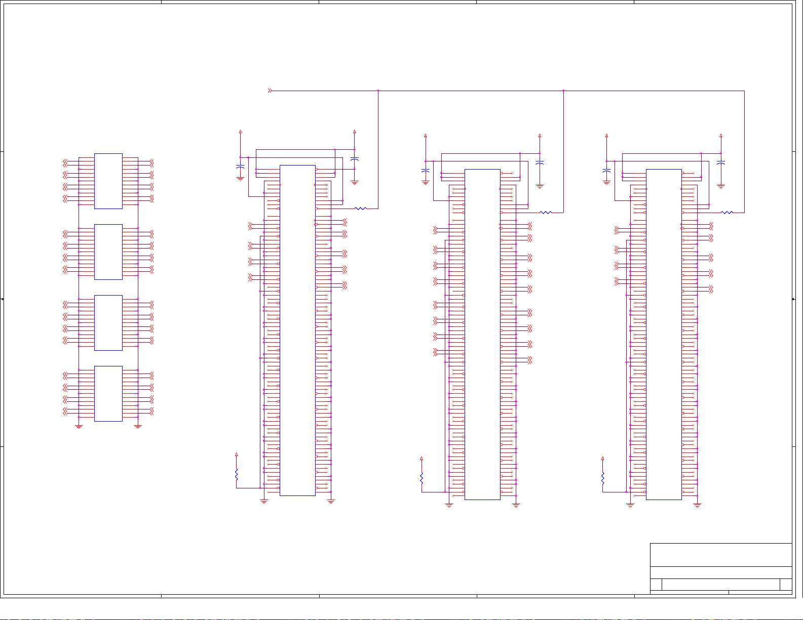
5
D D
4
PERST#_PCIe_SWITCH{9,10,11,15,16}
3
2
1
3.3V_BOARD
MINI SAS
SAS 0
IP1
IP1
B1
PEX_Rx0_p{3}
PEX_Rx0_n{3}
PEX_Rx1_p{3}
PEX_Rx1_n{3}
PEX_Rx2_p{3}
PEX_Rx2_n{3}
PEX_Rx3_p{3}
PEX_Rx3_n{3}
C C
B B
A A
SAS1_Rx0_p{6}
SAS1_Rx0_n{6}
SAS1_Rx1_p{6}
SAS1_Rx1_n{6}
SAS1_Rx2_p{6}
SAS1_Rx2_n{6}
SAS1_Rx3_p{6}
SAS1_Rx3_n{6}
SAS2_Rx0_p{6}
SAS2_Rx0_n{6}
SAS2_Rx1_p{6}
SAS2_Rx1_n{6}
SAS2_Rx2_p{6}
SAS2_Rx2_n{6}
SAS2_Rx3_p{6}
SAS2_Rx3_n{6}
SAS3_Rx0_p{6}
SAS3_Rx0_n{6}
SAS3_Rx1_p{6}
SAS3_Rx1_n{6}
SAS3_Rx2_p{6}
SAS3_Rx2_n{6}
SAS3_Rx3_p{6}
SAS3_Rx3_n{6}
B2
B3
B4
B5
B6
B7
B8
B9
B10
B11
B12
B13
B1
B2
B3
B4
B5
B6
B7
B8
B9
B10
B11
B12
B13
B1
B2
B3
B4
B5
B6
B7
B8
B9
B10
B11
B12
B13
B1
B2
B3
B4
B5
B6
B7
B8
B9
B10
B11
B12
B13
A1
GND
GND
A2
TX0+
RX0+
A3
TX0-
RX0-
A4
GND
GND
A5
TX1+
RX1+
A6
TX1-
RX1-
A7
GND
GND
A8
TX2+
RX2+
A9
TX2-
RX2-
A10
GND
GND
A11
TX3+
RX3+
A12
TX3-
RX3-
A13
GND
GND
I_PASS_26CKT_75783_0036
I_PASS_26CKT_75783_0036
SAS 1
IP2
IP2
A1
GND
GND
A2
TX0+
RX0+
A3
TX0-
RX0-
A4
GND
GND
A5
TX1+
RX1+
A6
TX1-
RX1-
A7
GND
GND
A8
TX2+
RX2+
A9
TX2-
RX2-
A10
GND
GND
A11
TX3+
RX3+
A12
TX3-
RX3-
A13
GND
GND
I_PASS_26CKT_75783_0036
I_PASS_26CKT_75783_0036
IP3
IP3
SAS 2
A1
GND
GND
A2
TX0+
RX0+
A3
TX0-
RX0-
A4
GND
GND
A5
TX1+
RX1+
A6
TX1-
RX1-
A7
GND
GND
A8
TX2+
RX2+
A9
TX2-
RX2-
A10
GND
GND
A11
TX3+
RX3+
A12
TX3-
RX3-
A13
GND
GND
I_PASS_26CKT_75783_0036
I_PASS_26CKT_75783_0036
SAS 3
IP4
IP4
A1
GND
GND
A2
TX0+
RX0+
A3
TX0-
RX0-
A4
GND
GND
A5
TX1+
RX1+
A6
TX1-
RX1-
A7
GND
GND
A8
TX2+
RX2+
A9
TX2-
RX2-
A10
GND
GND
A11
TX3+
RX3+
A12
TX3-
RX3-
A13
GND
GND
I_PASS_26CKT_75783_0036
I_PASS_26CKT_75783_0036
PEX_Tx0_p {3}
PEX_Tx0_n {3}
PEX_Tx1_p {3}
PEX_Tx1_n {3}
PEX_Tx2_p {3}
PEX_Tx2_n {3}
PEX_Tx3_p {3}
PEX_Tx3_n {3}
SAS1_Tx0_p {6}
SAS1_Tx0_n {6}
SAS1_Tx1_p {6}
SAS1_Tx1_n {6}
SAS1_Tx2_p {6}
SAS1_Tx2_n {6}
SAS1_Tx3_p {6}
SAS1_Tx3_n {6}
SAS2_Tx0_p {6}
SAS2_Tx0_n {6}
SAS2_Tx1_p {6}
SAS2_Tx1_n {6}
SAS2_Tx2_p {6}
SAS2_Tx2_n {6}
SAS2_Tx3_p {6}
SAS2_Tx3_n {6}
SAS3_Tx0_p {6}
SAS3_Tx0_n {6}
SAS3_Tx1_p {6}
SAS3_Tx1_n {6}
SAS3_Tx2_p {6}
SAS3_Tx2_n {6}
SAS3_Tx3_p {6}
SAS3_Tx3_n {6}
C98
C98
22uF
22uF
Slot1_Tx0_p{6}
Slot1_Tx0_n{6}
Slot1_Tx1_p{6}
Slot1_Tx1_n{6}
Slot1_Tx2_p{6}
Slot1_Tx2_n{6}
Slot1_Tx3_p{6}
Slot1_Tx3_n{6}
3.3V_BOARD
+
+
R258
R258
5.1K
5.1K
SLOT 1
J1
J1
B1
PRSNT1#
+12V
B2
B3
B4
B5
B6
B7
B8
B9
B10
B11
B12
B13
B14
B15
B16
B17
B18
B19
B20
B21
B22
B23
B24
B25
B26
B27
B28
B29
B30
B31
B32
B33
B34
B35
B36
B37
B38
B39
B40
B41
B42
B43
B44
B45
B46
B47
B48
B49
B50
B51
B52
B53
B54
B55
B56
B57
B58
B59
B60
B61
B62
B63
B64
B65
B66
B67
B68
B69
B70
B71
B72
B73
B74
B75
B76
B77
B78
B79
B80
B81
B82
PCI_EXP_X16_FEMALE_CONN
PCI_EXP_X16_FEMALE_CONN
+12V
+12V
GND
SMCLK
SMDAT
GND
+3.3V
TRST#
3.3VAUX
WAKE#
RSVD
GND
PETp0
PETn0
GND
PRSNT2#
GND
PETp1
PETn1
GND
GND
PETp2
PETn2
GND
GND
PETp3
PETn3
GND
RSVD
PRSNT2#
GND
PETp4
PETn4
GND
GND
PETp5
PETn5
GND
GND
PETp6
PETn6
GND
GND
PETp7
PETn7
GND
PRSNT2#
GND
PETp8
PETn8
GND
GND
PETp9
PETn9
GND
GND
PETp10
PETn10
GND
GND
PETp11
PETn11
GND
GND
PETp12
PETn12
GND
GND
PETp13
PETn13
GND
GND
PETp14
PETn14
GND
GND
PETp15
PETn15
GND
PRSNT2#
RSVD
+12V
+12V
GND
TCLK
+3.3V
+3.3V
PERST#
GND
REFCLK+
REFCLK-
GND
PERp0
PERn0
GND
RSVD
GND
PERp1
PERn1
GND
GND
PERp2
PERn2
GND
GND
PERp3
PERn3
GND
RSVD
RSVD
GND
PERp4
PERn4
GND
GND
PERp5
PERn5
GND
GND
PERp6
PERn6
GND
GND
PERp7
PERn7
GND
RSVD
GND
PERp8
PERn8
GND
GND
PERp9
PERn9
GND
GND
PERp10
PERn10
GND
GND
PERp11
PERn11
GND
GND
PERp12
PERn12
GND
GND
PERp13
PERn13
GND
GND
PERp14
PERn14
GND
GND
PERp15
PERn15
GND
TDI
TDO
TMS
A1
A2
A3
A4
A5
A6
A7
A8
A9
A10
A11
A12
A13
A14
A15
A16
A17
A18
A19
A20
A21
A22
A23
A24
A25
A26
A27
A28
A29
A30
A31
A32
A33
A34
A35
A36
A37
A38
A39
A40
A41
A42
A43
A44
A45
A46
A47
A48
A49
A50
A51
A52
A53
A54
A55
A56
A57
A58
A59
A60
A61
A62
A63
A64
A65
A66
A67
A68
A69
A70
A71
A72
A73
A74
A75
A76
A77
A78
A79
A80
A81
A82
12V_BOARD
+
C97
+
C97
22uF
22uF
R7 0R7 0
Slot1_REFCLKp {13}
Slot1_REFCLKn {13}
Slot1_Rx0_p {6}
Slot1_Rx0_n {6}
Slot1_Rx1_p {6}
Slot1_Rx1_n {6}
Slot1_Rx2_p {6}
Slot1_Rx2_n {6}
Slot1_Rx3_p {6}
Slot1_Rx3_n {6}
3.3V_BOARD 3.3V_BOARD
12V_BOARD 12V_BOARD
SLOT 2 SLOT 3
+
C99
+
J2
+
+
C101
C101
22uF
22uF
Slot2_Tx0_p{6}
Slot2_Tx0_n{6}
Slot2_Tx1_p{6}
Slot2_Tx1_n{6}
Slot2_Tx2_p{6}
Slot2_Tx2_n{6}
Slot2_Tx3_p{6}
Slot2_Tx3_n{6}
Slot2_Tx4_p{6}
Slot2_Tx4_n{6}
Slot2_Tx5_p{6}
Slot2_Tx5_n{6}
Slot2_Tx6_p{6}
Slot2_Tx6_n{6}
Slot2_Tx7_p{6}
Slot2_Tx7_n{6}
3.3V_BOARD 3.3V_BOARD
R259
R259
5.1K
5.1K
J2
B1
PRSNT1#
+12V
B2
B3
B4
B5
B6
B7
B8
B9
B10
B11
B12
B13
B14
B15
B16
B17
B18
B19
B20
B21
B22
B23
B24
B25
B26
B27
B28
B29
B30
B31
B32
B33
B34
B35
B36
B37
B38
B39
B40
B41
B42
B43
B44
B45
B46
B47
B48
B49
B50
B51
B52
B53
B54
B55
B56
B57
B58
B59
B60
B61
B62
B63
B64
B65
B66
B67
B68
B69
B70
B71
B72
B73
B74
B75
B76
B77
B78
B79
B80
B81
B82
PCI_EXP_X16_FEMALE_CONN
PCI_EXP_X16_FEMALE_CONN
+12V
+12V
GND
SMCLK
SMDAT
GND
+3.3V
TRST#
3.3VAUX
WAKE#
RSVD
GND
PETp0
PETn0
GND
PRSNT2#
GND
PETp1
PETn1
GND
GND
PETp2
PETn2
GND
GND
PETp3
PETn3
GND
RSVD
PRSNT2#
GND
PETp4
PETn4
GND
GND
PETp5
PETn5
GND
GND
PETp6
PETn6
GND
GND
PETp7
PETn7
GND
PRSNT2#
GND
PETp8
PETn8
GND
GND
PETp9
PETn9
GND
GND
PETp10
PETn10
GND
GND
PETp11
PETn11
GND
GND
PETp12
PETn12
GND
GND
PETp13
PETn13
GND
GND
PETp14
PETn14
GND
GND
PETp15
PETn15
GND
PRSNT2#
RSVD
TCLK
+3.3V
+3.3V
PERST#
REFCLK+
REFCLK-
PERp0
PERn0
RSVD
PERp1
PERn1
PERp2
PERn2
PERp3
PERn3
RSVD
RSVD
PERp4
PERn4
PERp5
PERn5
PERp6
PERn6
PERp7
PERn7
RSVD
PERp8
PERn8
PERp9
PERn9
PERp10
PERn10
PERp11
PERn11
PERp12
PERn12
PERp13
PERn13
PERp14
PERn14
PERp15
PERn15
+12V
+12V
GND
GND
GND
GND
GND
GND
GND
GND
GND
GND
GND
GND
GND
GND
GND
GND
GND
GND
GND
GND
GND
GND
GND
GND
GND
GND
GND
GND
GND
GND
GND
GND
GND
GND
TDI
TDO
TMS
A1
A2
A3
A4
A5
A6
A7
A8
A9
A10
A11
A12
A13
A14
A15
A16
A17
A18
A19
A20
A21
A22
A23
A24
A25
A26
A27
A28
A29
A30
A31
A32
A33
A34
A35
A36
A37
A38
A39
A40
A41
A42
A43
A44
A45
A46
A47
A48
A49
A50
A51
A52
A53
A54
A55
A56
A57
A58
A59
A60
A61
A62
A63
A64
A65
A66
A67
A68
A69
A70
A71
A72
A73
A74
A75
A76
A77
A78
A79
A80
A81
A82
C99
22uF
22uF
R8 0R8 0
Slot2_REFCLKp {13}
Slot2_REFCLKn {13}
Slot2_Rx0_p {6}
Slot2_Rx0_n {6}
Slot2_Rx1_p {6}
Slot2_Rx1_n {6}
Slot2_Rx2_p {6}
Slot2_Rx2_n {6}
Slot2_Rx3_p {6}
Slot2_Rx3_n {6}
Slot2_Rx4_p {6}
Slot2_Rx4_n {6}
Slot2_Rx5_p {6}
Slot2_Rx5_n {6}
Slot2_Rx6_p {6}
Slot2_Rx6_n {6}
Slot2_Rx7_p {6}
Slot2_Rx7_n {6}
C102
C102
22uF
22uF
Slot3_Tx0_p{6}
Slot3_Tx0_n{6}
Slot3_Tx1_p{6}
Slot3_Tx1_n{6}
Slot3_Tx2_p{6}
Slot3_Tx2_n{6}
Slot3_Tx3_p{6}
Slot3_Tx3_n{6}
+
C100
+
J3
+
+
R260
R260
5.1K
5.1K
J3
B1
PRSNT1#
+12V
B2
B3
B4
B5
B6
B7
B8
B9
B10
B11
B12
B13
B14
B15
B16
B17
B18
B19
B20
B21
B22
B23
B24
B25
B26
B27
B28
B29
B30
B31
B32
B33
B34
B35
B36
B37
B38
B39
B40
B41
B42
B43
B44
B45
B46
B47
B48
B49
B50
B51
B52
B53
B54
B55
B56
B57
B58
B59
B60
B61
B62
B63
B64
B65
B66
B67
B68
B69
B70
B71
B72
B73
B74
B75
B76
B77
B78
B79
B80
B81
B82
PCI_EXP_X16_FEMALE_CONN
PCI_EXP_X16_FEMALE_CONN
+12V
+12V
GND
SMCLK
SMDAT
GND
+3.3V
TRST#
3.3VAUX
WAKE#
RSVD
GND
PETp0
PETn0
GND
PRSNT2#
GND
PETp1
PETn1
GND
GND
PETp2
PETn2
GND
GND
PETp3
PETn3
GND
RSVD
PRSNT2#
GND
PETp4
PETn4
GND
GND
PETp5
PETn5
GND
GND
PETp6
PETn6
GND
GND
PETp7
PETn7
GND
PRSNT2#
GND
PETp8
PETn8
GND
GND
PETp9
PETn9
GND
GND
PETp10
PETn10
GND
GND
PETp11
PETn11
GND
GND
PETp12
PETn12
GND
GND
PETp13
PETn13
GND
GND
PETp14
PETn14
GND
GND
PETp15
PETn15
GND
PRSNT2#
RSVD
+12V
+12V
GND
TCLK
+3.3V
+3.3V
PERST#
GND
REFCLK+
REFCLK-
GND
PERp0
PERn0
GND
RSVD
GND
PERp1
PERn1
GND
GND
PERp2
PERn2
GND
GND
PERp3
PERn3
GND
RSVD
RSVD
GND
PERp4
PERn4
GND
GND
PERp5
PERn5
GND
GND
PERp6
PERn6
GND
GND
PERp7
PERn7
GND
RSVD
GND
PERp8
PERn8
GND
GND
PERp9
PERn9
GND
GND
PERp10
PERn10
GND
GND
PERp11
PERn11
GND
GND
PERp12
PERn12
GND
GND
PERp13
PERn13
GND
GND
PERp14
PERn14
GND
GND
PERp15
PERn15
GND
TDI
TDO
TMS
A1
A2
A3
A4
A5
A6
A7
A8
A9
A10
A11
A12
A13
A14
A15
A16
A17
A18
A19
A20
A21
A22
A23
A24
A25
A26
A27
A28
A29
A30
A31
A32
A33
A34
A35
A36
A37
A38
A39
A40
A41
A42
A43
A44
A45
A46
A47
A48
A49
A50
A51
A52
A53
A54
A55
A56
A57
A58
A59
A60
A61
A62
A63
A64
A65
A66
A67
A68
A69
A70
A71
A72
A73
A74
A75
A76
A77
A78
A79
A80
A81
A82
C100
22uF
22uF
R9 0R9 0
Slot3_REFCLKp {13}
Slot3_REFCLKn {13}
Slot3_Rx0_p {6}
Slot3_Rx0_n {6}
Slot3_Rx1_p {6}
Slot3_Rx1_n {6}
Slot3_Rx2_p {6}
Slot3_Rx2_n {6}
Slot3_Rx3_p {6}
Slot3_Rx3_n {6}
PLX Technology, Inc.
PLX Technology, Inc.
PLX Technology, Inc.
870 W. Maude Avenue
870 W. Maude Avenue
870 W. Maude Avenue
Sunnyvale, CA 94085
Sunnyvale, CA 94085
Sunnyvale, CA 94085
www.plxtech.com
www.plxtech.com
Title
Title
Title
PEX8648 RDK - Station 0 Connectors
PEX8648 RDK - Station 0 Connectors
PEX8648 RDK - Station 0 Connectors
Size Document Number Rev
Size Document Number Rev
Size Document Number Rev
C
C
C
91-0082-100-A 102
91-0082-100-A 102
91-0082-100-A 102
Date: Sheet
Date: Sheet
5
4
3
2
Date: Sheet
www.plxtech.com
1
821Tuesday, November 16, 2010
821Tuesday, November 16, 2010
821Tuesday, November 16, 2010
of
of
of
Page 52
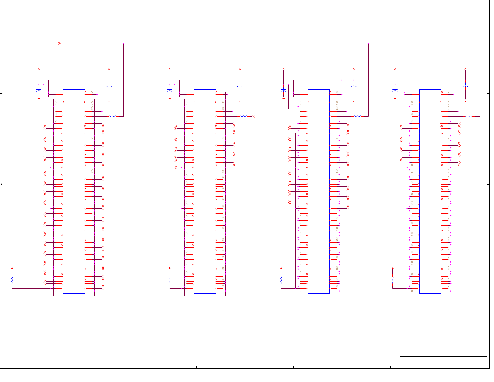
5
4
3
2
1
D D
PERST#_PCIe_SWITCH{8,10,11,15,16}
SLOT 5
3.3V_BOARD
SLOT 4
+
C103
+
J4
+
+
C107
C107
22uF
22uF
Deneb_Txp_16{4}
Deneb_Txn_16{4}
R263
R263
5.1K
5.1K
Deneb_Txp_17{4}
Deneb_Txn_17{4}
Deneb_Txp_18{4}
Deneb_Txn_18{4}
Deneb_Txp_19{4}
Deneb_Txn_19{4}
Slot4_Txp_4{7}
Slot4_Txn_4{7}
Slot4_Txp_5{7}
Slot4_Txn_5{7}
Slot4_Txp_6{7}
Slot4_Txn_6{7}
Slot4_Txp_7{7}
Slot4_Txn_7{7}
Slot4_Txp_8{7}
Slot4_Txn_8{7}
Slot4_Txp_9{7}
Slot4_Txn_9{7}
Slot4_Txp_10{7}
Slot4_Txn_10{7}
Slot4_Txp_11{7}
Slot4_Txn_11{7}
Slot4_Txp_12{7}
Slot4_Txn_12{7}
Slot4_Txp_13{7}
Slot4_Txn_13{7}
Slot4_Txp_14{7}
Slot4_Txn_14{7}
Slot4_Txp_15{7}
Slot4_Txn_15{7}
C C
B B
3.3V_BOARD
J4
B1
PRSNT1#
+12V
B2
B3
B4
B5
B6
B7
B8
B9
B10
B11
B12
B13
B14
B15
B16
B17
B18
B19
B20
B21
B22
B23
B24
B25
B26
B27
B28
B29
B30
B31
B32
B33
B34
B35
B36
B37
B38
B39
B40
B41
B42
B43
B44
B45
B46
B47
B48
B49
B50
B51
B52
B53
B54
B55
B56
B57
B58
B59
B60
B61
B62
B63
B64
B65
B66
B67
B68
B69
B70
B71
B72
B73
B74
B75
B76
B77
B78
B79
B80
B81
B82
PCI_EXP_X16_FEMALE_CONN
PCI_EXP_X16_FEMALE_CONN
+12V
+12V
GND
SMCLK
SMDAT
GND
+3.3V
TRST#
3.3VAUX
WAKE#
RSVD
GND
PETp0
PETn0
GND
PRSNT2#
GND
PETp1
PETn1
GND
GND
PETp2
PETn2
GND
GND
PETp3
PETn3
GND
RSVD
PRSNT2#
GND
PETp4
PETn4
GND
GND
PETp5
PETn5
GND
GND
PETp6
PETn6
GND
GND
PETp7
PETn7
GND
PRSNT2#
GND
PETp8
PETn8
GND
GND
PETp9
PETn9
GND
GND
PETp10
PETn10
GND
GND
PETp11
PETn11
GND
GND
PETp12
PETn12
GND
GND
PETp13
PETn13
GND
GND
PETp14
PETn14
GND
GND
PETp15
PETn15
GND
PRSNT2#
RSVD
TCLK
+3.3V
+3.3V
PERST#
REFCLK+
REFCLK-
PERp0
PERn0
RSVD
PERp1
PERn1
PERp2
PERn2
PERp3
PERn3
RSVD
RSVD
PERp4
PERn4
PERp5
PERn5
PERp6
PERn6
PERp7
PERn7
RSVD
PERp8
PERn8
PERp9
PERn9
PERp10
PERn10
PERp11
PERn11
PERp12
PERn12
PERp13
PERn13
PERp14
PERn14
PERp15
PERn15
+12V
+12V
GND
TDO
TMS
GND
GND
GND
GND
GND
GND
GND
GND
GND
GND
GND
GND
GND
GND
GND
GND
GND
GND
GND
GND
GND
GND
GND
GND
GND
GND
GND
GND
GND
GND
GND
GND
GND
TDI
A1
A2
A3
A4
A5
A6
A7
A8
A9
A10
A11
A12
A13
A14
A15
A16
A17
A18
A19
A20
A21
A22
A23
A24
A25
A26
A27
A28
A29
A30
A31
A32
A33
A34
A35
A36
A37
A38
A39
A40
A41
A42
A43
A44
A45
A46
A47
A48
A49
A50
A51
A52
A53
A54
A55
A56
A57
A58
A59
A60
A61
A62
A63
A64
A65
A66
A67
A68
A69
A70
A71
A72
A73
A74
A75
A76
A77
A78
A79
A80
A81
A82
C103
22uF
22uF
Slot4_REFCLKn {14} Slot6_REFCLKn {14}
Deneb_Rxp_16 {4}
Deneb_Rxn_16 {4}
Deneb_Rxp_17 {4}
Deneb_Rxn_17 {4}
Deneb_Rxp_18 {4}
Deneb_Rxn_18 {4}
Deneb_Rxp_19 {4}
Deneb_Rxn_19 {4}
Slot4_Rxp_4 {7}
Slot4_Rxn_4 {7}
Slot4_Rxp_5 {7}
Slot4_Rxn_5 {7}
Slot4_Rxp_6 {7}
Slot4_Rxn_6 {7}
Slot4_Rxp_7 {7}
Slot4_Rxn_7 {7}
Slot4_Rxp_8 {7}
Slot4_Rxn_8 {7}
Slot4_Rxp_9 {7}
Slot4_Rxn_9 {7}
Slot4_Rxp_10 {7}
Slot4_Rxn_10 {7}
Slot4_Rxp_11 {7}
Slot4_Rxn_11 {7}
Slot4_Rxp_12 {7}
Slot4_Rxn_12 {7}
Slot4_Rxp_13 {7}
Slot4_Rxn_13 {7}
Slot4_Rxp_14 {7}
Slot4_Rxn_14 {7}
Slot4_Rxp_15 {7}
Slot4_Rxn_15 {7}
3.3V_HOT_PLUG
PARALLEL HOT
12V_HOT_PLUG 3.3V_BOARD 12V_BOARD
PLUG CAPABLE
+
C104
+
J5
+
+
C108
C108
22uF
22uF
Slot5_Txp_0{7}
Slot5_Txn_0{7}
Slot5_Txp_1{7} Slot6_Txp_1{7}
Slot5_Txn_1{7} Slot6_Txn_1{7}
Slot5_Txp_2{7} Slot6_Txp_2{7}
Slot5_Txn_2{7} Slot6_Txn_2{7}
Slot5_Txp_3{7} Slot6_Txp_3{7}
Slot5_Txn_3{7} Slot6_Txn_3{7}
HP_PRSNT_B#{17}
3.3V_BOARD
R11
R11
5.1K
5.1K
J5
B1
PRSNT1#
+12V
B2
B3
B4
B5
B6
B7
B8
B9
B10
B11
B12
B13
B14
B15
B16
B17
B18
B19
B20
B21
B22
B23
B24
B25
B26
B27
B28
B29
B30
B31
B32
B33
B34
B35
B36
B37
B38
B39
B40
B41
B42
B43
B44
B45
B46
B47
B48
B49
B50
B51
B52
B53
B54
B55
B56
B57
B58
B59
B60
B61
B62
B63
B64
B65
B66
B67
B68
B69
B70
B71
B72
B73
B74
B75
B76
B77
B78
B79
B80
B81
B82
PCI_EXP_X16_FEMALE_CONN
PCI_EXP_X16_FEMALE_CONN
+12V
+12V
GND
SMCLK
SMDAT
GND
+3.3V
TRST#
3.3VAUX
WAKE#
RSVD
GND
PETp0
PETn0
GND
PRSNT2#
GND
PETp1
PETn1
GND
GND
PETp2
PETn2
GND
GND
PETp3
PETn3
GND
RSVD
PRSNT2#
GND
PETp4
PETn4
GND
GND
PETp5
PETn5
GND
GND
PETp6
PETn6
GND
GND
PETp7
PETn7
GND
PRSNT2#
GND
PETp8
PETn8
GND
GND
PETp9
PETn9
GND
GND
PETp10
PETn10
GND
GND
PETp11
PETn11
GND
GND
PETp12
PETn12
GND
GND
PETp13
PETn13
GND
GND
PETp14
PETn14
GND
GND
PETp15
PETn15
GND
PRSNT2#
RSVD
+12V
+12V
TCLK
+3.3V
+3.3V
PERST#
REFCLK+
REFCLK-
PERp0
PERn0
RSVD
PERp1
PERn1
PERp2
PERn2
PERp3
PERn3
RSVD
RSVD
PERp4
PERn4
PERp5
PERn5
PERp6
PERn6
PERp7
PERn7
RSVD
PERp8
PERn8
PERp9
PERn9
PERp10
PERn10
PERp11
PERn11
PERp12
PERn12
PERp13
PERn13
PERp14
PERn14
PERp15
PERn15
GND
TDI
TDO
TMS
GND
GND
GND
GND
GND
GND
GND
GND
GND
GND
GND
GND
GND
GND
GND
GND
GND
GND
GND
GND
GND
GND
GND
GND
GND
GND
GND
GND
GND
GND
GND
GND
GND
A1
A2
A3
A4
A5
A6
A7
A8
A9
A10
A11
A12
A13
A14
A15
A16
A17
A18
A19
A20
A21
A22
A23
A24
A25
A26
A27
A28
A29
A30
A31
A32
A33
A34
A35
A36
A37
A38
A39
A40
A41
A42
A43
A44
A45
A46
A47
A48
A49
A50
A51
A52
A53
A54
A55
A56
A57
A58
A59
A60
A61
A62
A63
A64
A65
A66
A67
A68
A69
A70
A71
A72
A73
A74
A75
A76
A77
A78
A79
A80
A81
A82
C104
22uF
22uF
R12 0R12 0R10 0R10 0 R14 0R14 0
Slot5_REFCLKp {14}
Slot5_REFCLKn {14}
Slot5_Rxp_0 {7}
Slot5_Rxn_0 {7}
Slot5_Rxp_1 {7}
Slot5_Rxn_1 {7}
Slot5_Rxp_2 {7}
Slot5_Rxp_3 {7}
Slot5_Rxn_3 {7}
HP_PERST# {16}
C109
C109
22uF
22uF
Slot6_Txp_0{7}
Slot6_Txn_0{7}
Slot6_Txp_4{7}
Slot6_Txn_4{7}
Slot6_Txp_5{7}
Slot6_Txn_5{7}
Slot6_Txp_6{7}
Slot6_Txn_6{7}
Slot6_Txp_7{7}
Slot6_Txn_7{7}
3.3V_BOARD
12V_BOARD12V_BOARD 3.3V_BOARD
SLOT 6 SLOT 7
+
C105
+
J6
+
+
R261
R261
5.1K
5.1K
J6
B1
PRSNT1#
+12V
B2
B3
B4
B5
B6
B7
B8
B9
B10
B11
B12
B13
B14
B15
B16
B17
B18
B19
B20
B21
B22
B23
B24
B25
B26
B27
B28
B29
B30
B31
B32
B33
B34
B35
B36
B37
B38
B39
B40
B41
B42
B43
B44
B45
B46
B47
B48
B49
B50
B51
B52
B53
B54
B55
B56
B57
B58
B59
B60
B61
B62
B63
B64
B65
B66
B67
B68
B69
B70
B71
B72
B73
B74
B75
B76
B77
B78
B79
B80
B81
B82
PCI_EXP_X16_FEMALE_CONN
PCI_EXP_X16_FEMALE_CONN
+12V
+12V
GND
SMCLK
SMDAT
GND
+3.3V
TRST#
3.3VAUX
WAKE#
RSVD
GND
PETp0
PETn0
GND
PRSNT2#
GND
PETp1
PETn1
GND
GND
PETp2
PETn2
GND
GND
PETp3
PETn3
GND
RSVD
PRSNT2#
GND
PETp4
PETn4
GND
GND
PETp5
PETn5
GND
GND
PETp6
PETn6
GND
GND
PETp7
PETn7
GND
PRSNT2#
GND
PETp8
PETn8
GND
GND
PETp9
PETn9
GND
GND
PETp10
PETn10
GND
GND
PETp11
PETn11
GND
GND
PETp12
PETn12
GND
GND
PETp13
PETn13
GND
GND
PETp14
PETn14
GND
GND
PETp15
PETn15
GND
PRSNT2#
RSVD
+12V
+12V
GND
TCLK
+3.3V
+3.3V
PERST#
GND
REFCLK+
REFCLK-
GND
PERp0
PERn0
GND
RSVD
GND
PERp1
PERn1
GND
GND
PERp2
PERn2
GND
GND
PERp3
PERn3
GND
RSVD
RSVD
GND
PERp4
PERn4
GND
GND
PERp5
PERn5
GND
GND
PERp6
PERn6
GND
GND
PERp7
PERn7
GND
RSVD
GND
PERp8
PERn8
GND
GND
PERp9
PERn9
GND
GND
PERp10
PERn10
GND
GND
PERp11
PERn11
GND
GND
PERp12
PERn12
GND
GND
PERp13
PERn13
GND
GND
PERp14
PERn14
GND
GND
PERp15
PERn15
GND
TDI
TDO
TMS
A1
A2
A3
A4
A5
A6
A7
A8
A9
A10
A11
A12
A13
A14
A15
A16
A17
A18
A19
A20
A21
A22
A23
A24
A25
A26
A27
A28
A29
A30
A31
A32
A33
A34
A35
A36
A37
A38
A39
A40
A41
A42
A43
A44
A45
A46
A47
A48
A49
A50
A51
A52
A53
A54
A55
A56
A57
A58
A59
A60
A61
A62
A63
A64
A65
A66
A67
A68
A69
A70
A71
A72
A73
A74
A75
A76
A77
A78
A79
A80
A81
A82
C105
22uF
22uF
R13 0R13 0
Slot6_REFCLKp {14}Slot4_REFCLKp {14}
Slot6_Rxp_0 {7}
Slot6_Rxn_0 {7}
Slot6_Rxp_1 {7}
Slot6_Rxn_1 {7}
Slot6_Rxp_2 {7}
Slot6_Rxn_2 {7}Slot5_Rxn_2 {7}
Slot6_Rxp_3 {7}
Slot6_Rxn_3 {7}
Slot6_Rxp_4 {7}
Slot6_Rxn_4 {7}
Slot6_Rxp_5 {7}
Slot6_Rxn_5 {7}
Slot6_Rxp_6 {7}
Slot6_Rxn_6 {7}
Slot6_Rxp_7 {7}
Slot6_Rxn_7 {7}
C110
C110
22uF
22uF
Slot7_Txp_0{7}
Slot7_Txn_0{7}
Slot7_Txp_1{7}
Slot7_Txn_1{7}
Slot7_Txp_2{7}
Slot7_Txn_2{7}
Slot7_Txp_3{7}
Slot7_Txn_3{7}
3.3V_BOARD
+
+
R262
R262
5.1K
5.1K
J7
J7
B1
PRSNT1#
+12V
B2
B3
B4
B5
B6
B7
B8
B9
B10
B11
B12
B13
B14
B15
B16
B17
B18
B19
B20
B21
B22
B23
B24
B25
B26
B27
B28
B29
B30
B31
B32
B33
B34
B35
B36
B37
B38
B39
B40
B41
B42
B43
B44
B45
B46
B47
B48
B49
B50
B51
B52
B53
B54
B55
B56
B57
B58
B59
B60
B61
B62
B63
B64
B65
B66
B67
B68
B69
B70
B71
B72
B73
B74
B75
B76
B77
B78
B79
B80
B81
B82
PCI_EXP_X16_FEMALE_CONN
PCI_EXP_X16_FEMALE_CONN
+12V
+12V
GND
SMCLK
SMDAT
GND
+3.3V
TRST#
3.3VAUX
WAKE#
RSVD
GND
PETp0
PETn0
GND
PRSNT2#
GND
PETp1
PETn1
GND
GND
PETp2
PETn2
GND
GND
PETp3
PETn3
GND
RSVD
PRSNT2#
GND
PETp4
PETn4
GND
GND
PETp5
PETn5
GND
GND
PETp6
PETn6
GND
GND
PETp7
PETn7
GND
PRSNT2#
GND
PETp8
PETn8
GND
GND
PETp9
PETn9
GND
GND
PETp10
PETn10
GND
GND
PETp11
PETn11
GND
GND
PETp12
PETn12
GND
GND
PETp13
PETn13
GND
GND
PETp14
PETn14
GND
GND
PETp15
PETn15
GND
PRSNT2#
RSVD
TCLK
+3.3V
+3.3V
PERST#
REFCLK+
REFCLK-
PERp0
PERn0
RSVD
PERp1
PERn1
PERp2
PERn2
PERp3
PERn3
RSVD
RSVD
PERp4
PERn4
PERp5
PERn5
PERp6
PERn6
PERp7
PERn7
RSVD
PERp8
PERn8
PERp9
PERn9
PERp10
PERn10
PERp11
PERn11
PERp12
PERn12
PERp13
PERn13
PERp14
PERn14
PERp15
PERn15
+12V
+12V
GND
TDO
TMS
GND
GND
GND
GND
GND
GND
GND
GND
GND
GND
GND
GND
GND
GND
GND
GND
GND
GND
GND
GND
GND
GND
GND
GND
GND
GND
GND
GND
GND
GND
GND
GND
GND
TDI
A1
A2
A3
A4
A5
A6
A7
A8
A9
A10
A11
A12
A13
A14
A15
A16
A17
A18
A19
A20
A21
A22
A23
A24
A25
A26
A27
A28
A29
A30
A31
A32
A33
A34
A35
A36
A37
A38
A39
A40
A41
A42
A43
A44
A45
A46
A47
A48
A49
A50
A51
A52
A53
A54
A55
A56
A57
A58
A59
A60
A61
A62
A63
A64
A65
A66
A67
A68
A69
A70
A71
A72
A73
A74
A75
A76
A77
A78
A79
A80
A81
A82
+
C106
+
C106
22uF
22uF
Slot7_REFCLKp {14}
Slot7_REFCLKn {14}
Slot7_Rxp_0 {7}
Slot7_Rxn_0 {7}
Slot7_Rxp_1 {7}
Slot7_Rxn_1 {7}
Slot7_Rxp_2 {7}
Slot7_Rxn_2 {7}
Slot7_Rxp_3 {7}
Slot7_Rxn_3 {7}
A A
PLX Technology, Inc.
PLX Technology, Inc.
PLX Technology, Inc.
870 W. Maude Avenue
870 W. Maude Avenue
870 W. Maude Avenue
Sunnyvale, CA 94085
Sunnyvale, CA 94085
Sunnyvale, CA 94085
www.plxtech.com
www.plxtech.com
Title
Title
Title
PEX8648 RDK - Station 1 Connectors
PEX8648 RDK - Station 1 Connectors
PEX8648 RDK - Station 1 Connectors
Size Document Number Rev
Size Document Number Rev
Size Document Number Rev
C
C
C
91-0082-100-A 102
91-0082-100-A 102
91-0082-100-A 102
Date: Sheet
Date: Sheet
5
4
3
2
Date: Sheet
www.plxtech.com
1
921Tuesday, November 16, 2010
921Tuesday, November 16, 2010
921Tuesday, November 16, 2010
of
of
of
Page 53
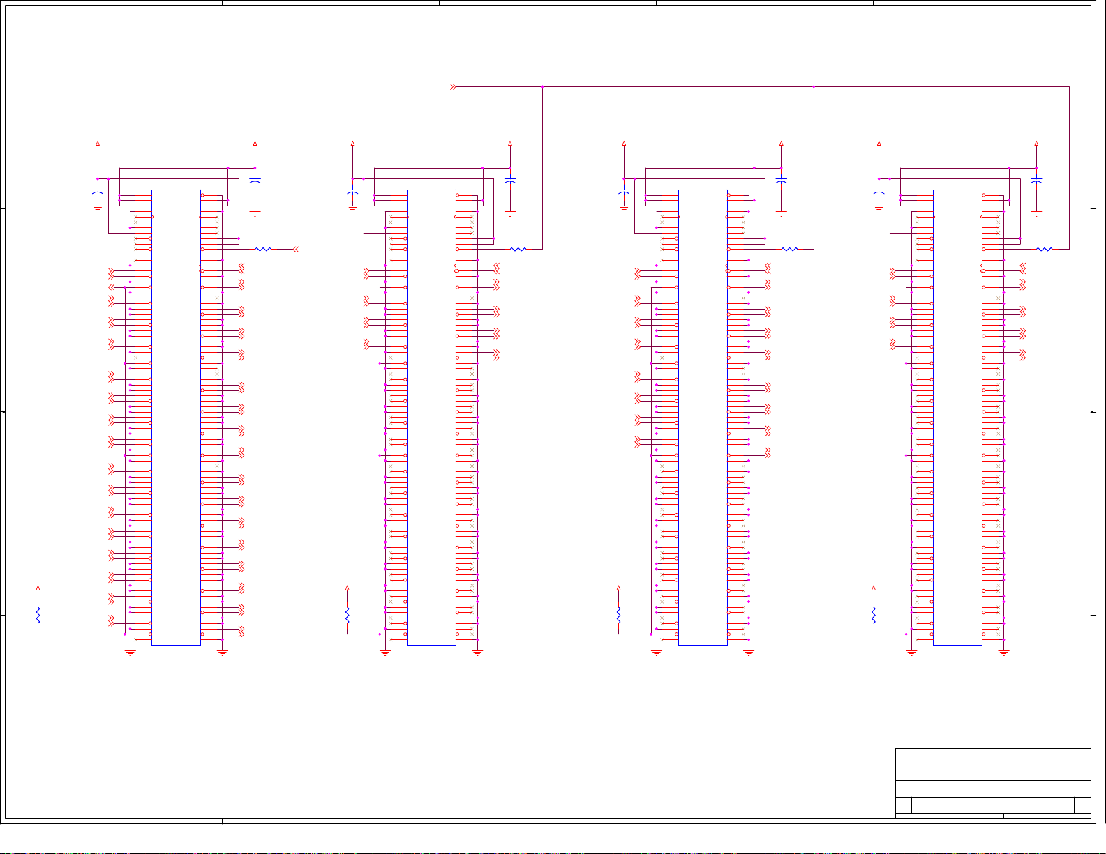
5
D D
4
PERST#_PCIe_SWITCH{8,9,11,15,16}
3
2
1
SLOT 8
SERIAL HOT
12V_SERIAL_HOT_PLUG3.3V_SERIAL_HOT_PLUG
PLUG CAPABLE
+
+
C111
J8
+
C115
+
C115
22uF
22uF
Deneb_Txp_32{5}
Deneb_Txn_32{5}
SHP_PRSNT#{20}
Deneb_Txp_33{5}
R267
R267
5.1K
5.1K
Deneb_Txn_33{5}
Deneb_Txp_34{5}
Deneb_Txn_34{5}
Deneb_Txp_35{5}
Deneb_Txn_35{5}
Slot8_Txp_4{7}
Slot8_Txn_4{7}
Slot8_Txp_5{7}
Slot8_Txn_5{7}
Slot8_Txp_6{7}
Slot8_Txn_6{7}
Slot8_Txp_7{7}
Slot8_Txn_7{7}
Slot8_Txp_8{7}
Slot8_Txn_8{7}
Slot8_Txp_9{7}
Slot8_Txn_9{7}
Slot8_Txp_10{7}
Slot8_Txn_10{7}
Slot8_Txp_11{7}
Slot8_Txn_11{7}
Slot8_Txp_12{7}
Slot8_Txn_12{7}
Slot8_Txp_13{7}
Slot8_Txn_13{7}
Slot8_Txp_14{7}
Slot8_Txn_14{7}
Slot8_Txp_15{7}
Slot8_Txn_15{7}
C C
B B
J8
B1
PRSNT1#
+12V
B2
B3
B4
B5
B6
B7
B8
B9
B10
B11
B12
B13
B14
B15
B16
B17
B18
B19
B20
B21
B22
B23
B24
B25
B26
B27
B28
B29
B30
B31
B32
B33
B34
B35
B36
B37
B38
B39
B40
B41
B42
B43
B44
B45
B46
B47
B48
B49
B50
B51
B52
B53
B54
B55
B56
B57
B58
B59
B60
B61
B62
B63
B64
B65
B66
B67
B68
B69
B70
B71
B72
B73
B74
B75
B76
B77
B78
B79
B80
B81
B82
PCI_EXP_X16_FEMALE_CONN
PCI_EXP_X16_FEMALE_CONN
+12V
+12V
GND
SMCLK
SMDAT
GND
+3.3V
TRST#
3.3VAUX
WAKE#
RSVD
GND
PETp0
PETn0
GND
PRSNT2#
GND
PETp1
PETn1
GND
GND
PETp2
PETn2
GND
GND
PETp3
PETn3
GND
RSVD
PRSNT2#
GND
PETp4
PETn4
GND
GND
PETp5
PETn5
GND
GND
PETp6
PETn6
GND
GND
PETp7
PETn7
GND
PRSNT2#
GND
PETp8
PETn8
GND
GND
PETp9
PETn9
GND
GND
PETp10
PETn10
GND
GND
PETp11
PETn11
GND
GND
PETp12
PETn12
GND
GND
PETp13
PETn13
GND
GND
PETp14
PETn14
GND
GND
PETp15
PETn15
GND
PRSNT2#
RSVD
+12V
+12V
GND
TCLK
+3.3V
+3.3V
PERST#
GND
REFCLK+
REFCLK-
GND
PERp0
PERn0
GND
RSVD
GND
PERp1
PERn1
GND
GND
PERp2
PERn2
GND
GND
PERp3
PERn3
GND
RSVD
RSVD
GND
PERp4
PERn4
GND
GND
PERp5
PERn5
GND
GND
PERp6
PERn6
GND
GND
PERp7
PERn7
GND
RSVD
GND
PERp8
PERn8
GND
GND
PERp9
PERn9
GND
GND
PERp10
PERn10
GND
GND
PERp11
PERn11
GND
GND
PERp12
PERn12
GND
GND
PERp13
PERn13
GND
GND
PERp14
PERn14
GND
GND
PERp15
PERn15
GND
TDI
TDO
TMS
A1
A2
A3
A4
A5
A6
A7
A8
A9
A10
A11
A12
A13
A14
A15
A16
A17
A18
A19
A20
A21
A22
A23
A24
A25
A26
A27
A28
A29
A30
A31
A32
A33
A34
A35
A36
A37
A38
A39
A40
A41
A42
A43
A44
A45
A46
A47
A48
A49
A50
A51
A52
A53
A54
A55
A56
A57
A58
A59
A60
A61
A62
A63
A64
A65
A66
A67
A68
A69
A70
A71
A72
A73
A74
A75
A76
A77
A78
A79
A80
A81
A82
C111
22uF
22uF
R18 0R18 0
Slot8_REFCLKp {14}
Slot8_REFCLKn {14}
Deneb_Rxp_32 {5}
Deneb_Rxn_32 {5}
Deneb_Rxp_33 {5}
Deneb_Rxn_33 {5}
Deneb_Rxp_34 {5}
Deneb_Rxn_34 {5}
Deneb_Rxp_35 {5}
Deneb_Rxn_35 {5}
Slot8_Rxp_4 {7}
Slot8_Rxn_4 {7}
Slot8_Rxp_5 {7}
Slot8_Rxn_5 {7}
Slot8_Rxp_6 {7}
Slot8_Rxn_6 {7}
Slot8_Rxp_7 {7}
Slot8_Rxn_7 {7}
Slot8_Rxp_8 {7}
Slot8_Rxn_8 {7}
Slot8_Rxp_9 {7}
Slot8_Rxn_9 {7}
Slot8_Rxp_10 {7}
Slot8_Rxn_10 {7}
Slot8_Rxp_11 {7}
Slot8_Rxn_11 {7}
Slot8_Rxp_12 {7}
Slot8_Rxn_12 {7}
Slot8_Rxp_13 {7}
Slot8_Rxn_13 {7}
Slot8_Rxp_14 {7}
Slot8_Rxn_14 {7}
Slot8_Rxp_15 {7}
Slot8_Rxn_15 {7}
SHP_PERST# {16}
3.3V_BOARD 12V_BOARD 12V_BOARD 12V_BOARD3.3V_BOARD 3.3V_BOARD
SLOT 9 SLOT 10 SLOT 11
+
+
C112
J9
+
C116
+
C116
22uF
22uF
Slot9_Txp_0{7}
Slot9_Txn_0{7}
Slot9_Txp_1{7}
Slot9_Txn_1{7}
Slot9_Txp_2{7}
Slot9_Txn_2{7}
Slot9_Txp_3{7}
Slot9_Txn_3{7}
R266
R266
5.1K
5.1K
J9
B1
PRSNT1#
+12V
B2
B3
B4
B5
B6
B7
B8
B9
B10
B11
B12
B13
B14
B15
B16
B17
B18
B19
B20
B21
B22
B23
B24
B25
B26
B27
B28
B29
B30
B31
B32
B33
B34
B35
B36
B37
B38
B39
B40
B41
B42
B43
B44
B45
B46
B47
B48
B49
B50
B51
B52
B53
B54
B55
B56
B57
B58
B59
B60
B61
B62
B63
B64
B65
B66
B67
B68
B69
B70
B71
B72
B73
B74
B75
B76
B77
B78
B79
B80
B81
B82
PCI_EXP_X16_FEMALE_CONN
PCI_EXP_X16_FEMALE_CONN
+12V
+12V
GND
SMCLK
SMDAT
GND
+3.3V
TRST#
3.3VAUX
WAKE#
RSVD
GND
PETp0
PETn0
GND
PRSNT2#
GND
PETp1
PETn1
GND
GND
PETp2
PETn2
GND
GND
PETp3
PETn3
GND
RSVD
PRSNT2#
GND
PETp4
PETn4
GND
GND
PETp5
PETn5
GND
GND
PETp6
PETn6
GND
GND
PETp7
PETn7
GND
PRSNT2#
GND
PETp8
PETn8
GND
GND
PETp9
PETn9
GND
GND
PETp10
PETn10
GND
GND
PETp11
PETn11
GND
GND
PETp12
PETn12
GND
GND
PETp13
PETn13
GND
GND
PETp14
PETn14
GND
GND
PETp15
PETn15
GND
PRSNT2#
RSVD
+12V
+12V
GND
TCLK
+3.3V
+3.3V
PERST#
GND
REFCLK+
REFCLK-
GND
PERp0
PERn0
GND
RSVD
GND
PERp1
PERn1
GND
GND
PERp2
PERn2
GND
GND
PERp3
PERn3
GND
RSVD
RSVD
GND
PERp4
PERn4
GND
GND
PERp5
PERn5
GND
GND
PERp6
PERn6
GND
GND
PERp7
PERn7
GND
RSVD
GND
PERp8
PERn8
GND
GND
PERp9
PERn9
GND
GND
PERp10
PERn10
GND
GND
PERp11
PERn11
GND
GND
PERp12
PERn12
GND
GND
PERp13
PERn13
GND
GND
PERp14
PERn14
GND
GND
PERp15
PERn15
GND
TDI
TDO
TMS
A1
A2
A3
A4
A5
A6
A7
A8
A9
A10
A11
A12
A13
A14
A15
A16
A17
A18
A19
A20
A21
A22
A23
A24
A25
A26
A27
A28
A29
A30
A31
A32
A33
A34
A35
A36
A37
A38
A39
A40
A41
A42
A43
A44
A45
A46
A47
A48
A49
A50
A51
A52
A53
A54
A55
A56
A57
A58
A59
A60
A61
A62
A63
A64
A65
A66
A67
A68
A69
A70
A71
A72
A73
A74
A75
A76
A77
A78
A79
A80
A81
A82
C112
22uF
22uF
Slot9_REFCLKp {14}
Slot9_REFCLKn {14}
Slot9_Rxp_0 {7}
Slot9_Rxn_0 {7}
Slot9_Rxp_1 {7}
Slot9_Rxn_1 {7}
Slot9_Rxp_2 {7}
Slot9_Rxn_2 {7}
Slot9_Rxp_3 {7}
Slot9_Rxn_3 {7}
J10
+
C117
+
C117
22uF
22uF
Slot10_Txp_0{7}
Slot10_Txn_0{7}
Slot10_Txp_1{7}
Slot10_Txn_1{7}
Slot10_Txp_2{7}
Slot10_Txn_2{7}
Slot10_Txp_3{7}
Slot10_Txn_3{7}
Slot10_Txp_4{7}
Slot10_Txn_4{7}
Slot10_Txp_5{7}
Slot10_Txn_5{7}
Slot10_Txp_6{7}
Slot10_Txn_6{7}
Slot10_Txp_7{7}
Slot10_Txn_7{7}
3.3V_BOARD 3.3V_BOARD3.3V_BOARD3.3V_BOARD
R264
R264
5.1K
5.1K
J10
B1
PRSNT1#
+12V
B2
B3
B4
B5
B6
B7
B8
B9
B10
B11
B12
B13
B14
B15
B16
B17
B18
B19
B20
B21
B22
B23
B24
B25
B26
B27
B28
B29
B30
B31
B32
B33
B34
B35
B36
B37
B38
B39
B40
B41
B42
B43
B44
B45
B46
B47
B48
B49
B50
B51
B52
B53
B54
B55
B56
B57
B58
B59
B60
B61
B62
B63
B64
B65
B66
B67
B68
B69
B70
B71
B72
B73
B74
B75
B76
B77
B78
B79
B80
B81
B82
PCI_EXP_X16_FEMALE_CONN
PCI_EXP_X16_FEMALE_CONN
+12V
+12V
GND
SMCLK
SMDAT
GND
+3.3V
TRST#
3.3VAUX
WAKE#
RSVD
GND
PETp0
PETn0
GND
PRSNT2#
GND
PETp1
PETn1
GND
GND
PETp2
PETn2
GND
GND
PETp3
PETn3
GND
RSVD
PRSNT2#
GND
PETp4
PETn4
GND
GND
PETp5
PETn5
GND
GND
PETp6
PETn6
GND
GND
PETp7
PETn7
GND
PRSNT2#
GND
PETp8
PETn8
GND
GND
PETp9
PETn9
GND
GND
PETp10
PETn10
GND
GND
PETp11
PETn11
GND
GND
PETp12
PETn12
GND
GND
PETp13
PETn13
GND
GND
PETp14
PETn14
GND
GND
PETp15
PETn15
GND
PRSNT2#
RSVD
TCLK
+3.3V
+3.3V
PERST#
REFCLK+
REFCLK-
PERp0
PERn0
RSVD
PERp1
PERn1
PERp2
PERn2
PERp3
PERn3
RSVD
RSVD
PERp4
PERn4
PERp5
PERn5
PERp6
PERn6
PERp7
PERn7
RSVD
PERp8
PERn8
PERp9
PERn9
PERp10
PERn10
PERp11
PERn11
PERp12
PERn12
PERp13
PERn13
PERp14
PERn14
PERp15
PERn15
+12V
+12V
GND
TDO
TMS
GND
GND
GND
GND
GND
GND
GND
GND
GND
GND
GND
GND
GND
GND
GND
GND
GND
GND
GND
GND
GND
GND
GND
GND
GND
GND
GND
GND
GND
GND
GND
GND
GND
TDI
A1
A2
A3
A4
A5
A6
A7
A8
A9
A10
A11
A12
A13
A14
A15
A16
A17
A18
A19
A20
A21
A22
A23
A24
A25
A26
A27
A28
A29
A30
A31
A32
A33
A34
A35
A36
A37
A38
A39
A40
A41
A42
A43
A44
A45
A46
A47
A48
A49
A50
A51
A52
A53
A54
A55
A56
A57
A58
A59
A60
A61
A62
A63
A64
A65
A66
A67
A68
A69
A70
A71
A72
A73
A74
A75
A76
A77
A78
A79
A80
A81
A82
+
+
C113
C113
22uF
22uF
R17 0R17 0R16 0R16 0
Slot10_REFCLKp {14}
Slot10_REFCLKn {14} Slot11_REFCLKn {14}
Slot10_Rxp_0 {7}
Slot10_Rxn_0 {7}
Slot10_Rxp_1 {7}
Slot10_Rxn_1 {7}
Slot10_Rxp_2 {7}
Slot10_Rxn_2 {7}
Slot10_Rxp_3 {7}
Slot10_Rxn_3 {7}
Slot10_Rxp_4 {7}
Slot10_Rxn_4 {7}
Slot10_Rxp_5 {7}
Slot10_Rxn_5 {7}
Slot10_Rxp_6 {7}
Slot10_Rxn_6 {7}
Slot10_Rxp_7 {7}
Slot10_Rxn_7 {7}
C118
C118
22uF
22uF
Slot11_Txp_0{7}
Slot11_Txn_0{7}
Slot11_Txp_1{7}
Slot11_Txn_1{7}
Slot11_Txp_2{7}
Slot11_Txn_2{7}
Slot11_Txp_3{7}
Slot11_Txn_3{7}
+
+
C114
J11
+
+
R265
R265
5.1K
5.1K
J11
B1
PRSNT1#
+12V
B2
B3
B4
B5
B6
B7
B8
B9
B10
B11
B12
B13
B14
B15
B16
B17
B18
B19
B20
B21
B22
B23
B24
B25
B26
B27
B28
B29
B30
B31
B32
B33
B34
B35
B36
B37
B38
B39
B40
B41
B42
B43
B44
B45
B46
B47
B48
B49
B50
B51
B52
B53
B54
B55
B56
B57
B58
B59
B60
B61
B62
B63
B64
B65
B66
B67
B68
B69
B70
B71
B72
B73
B74
B75
B76
B77
B78
B79
B80
B81
B82
PCI_EXP_X16_FEMALE_CONN
PCI_EXP_X16_FEMALE_CONN
+12V
+12V
GND
SMCLK
SMDAT
GND
+3.3V
TRST#
3.3VAUX
WAKE#
RSVD
GND
PETp0
PETn0
GND
PRSNT2#
GND
PETp1
PETn1
GND
GND
PETp2
PETn2
GND
GND
PETp3
PETn3
GND
RSVD
PRSNT2#
GND
PETp4
PETn4
GND
GND
PETp5
PETn5
GND
GND
PETp6
PETn6
GND
GND
PETp7
PETn7
GND
PRSNT2#
GND
PETp8
PETn8
GND
GND
PETp9
PETn9
GND
GND
PETp10
PETn10
GND
GND
PETp11
PETn11
GND
GND
PETp12
PETn12
GND
GND
PETp13
PETn13
GND
GND
PETp14
PETn14
GND
GND
PETp15
PETn15
GND
PRSNT2#
RSVD
TCLK
+3.3V
+3.3V
PERST#
REFCLK+
REFCLK-
PERp0
PERn0
RSVD
PERp1
PERn1
PERp2
PERn2
PERp3
PERn3
RSVD
RSVD
PERp4
PERn4
PERp5
PERn5
PERp6
PERn6
PERp7
PERn7
RSVD
PERp8
PERn8
PERp9
PERn9
PERp10
PERn10
PERp11
PERn11
PERp12
PERn12
PERp13
PERn13
PERp14
PERn14
PERp15
PERn15
+12V
+12V
GND
TDO
TMS
GND
GND
GND
GND
GND
GND
GND
GND
GND
GND
GND
GND
GND
GND
GND
GND
GND
GND
GND
GND
GND
GND
GND
GND
GND
GND
GND
GND
GND
GND
GND
GND
GND
TDI
A1
A2
A3
A4
A5
A6
A7
A8
A9
A10
A11
A12
A13
A14
A15
A16
A17
A18
A19
A20
A21
A22
A23
A24
A25
A26
A27
A28
A29
A30
A31
A32
A33
A34
A35
A36
A37
A38
A39
A40
A41
A42
A43
A44
A45
A46
A47
A48
A49
A50
A51
A52
A53
A54
A55
A56
A57
A58
A59
A60
A61
A62
A63
A64
A65
A66
A67
A68
A69
A70
A71
A72
A73
A74
A75
A76
A77
A78
A79
A80
A81
A82
C114
22uF
22uF
R19 0R19 0
Slot11_REFCLKp {14}
Slot11_Rxp_0 {7}
Slot11_Rxn_0 {7}
Slot11_Rxp_1 {7}
Slot11_Rxn_1 {7}
Slot11_Rxp_2 {7}
Slot11_Rxn_2 {7}
Slot11_Rxp_3 {7}
Slot11_Rxn_3 {7}
A A
PLX Technology, Inc.
PLX Technology, Inc.
PLX Technology, Inc.
870 W. Maude Avenue
870 W. Maude Avenue
870 W. Maude Avenue
Sunnyvale, CA 94085
Sunnyvale, CA 94085
Sunnyvale, CA 94085
www.plxtech.com
www.plxtech.com
Title
Title
Title
PEX8648 RDK - Station 2 Connectors
PEX8648 RDK - Station 2 Connectors
PEX8648 RDK - Station 2 Connectors
Size Document Number Rev
Size Document Number Rev
Size Document Number Rev
C
C
C
91-0082-100-A 102
91-0082-100-A 102
91-0082-100-A 102
Date: Sheet
Date: Sheet
5
4
3
2
Date: Sheet
www.plxtech.com
1
10 21Tuesday, November 16, 2010
10 21Tuesday, November 16, 2010
10 21Tuesday, November 16, 2010
of
of
of
Page 54
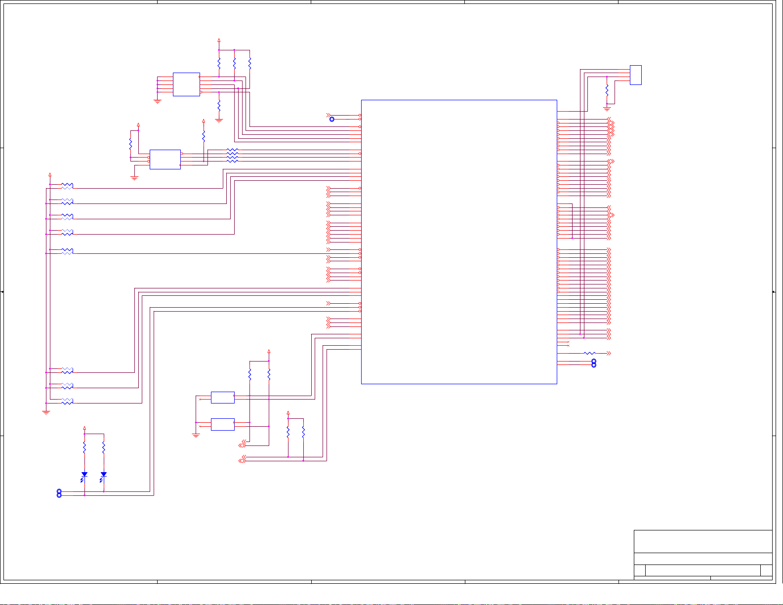
5
JP7
JP7
D D
3.3V_BOARD
R24
R24
10K
10K
3.3V_BOARD
5.1K
5.1K
R29
R29
3
12
R300R30
3
12
0
5.1K
5.1K
R31
R31
3
TPV21TPV21
TPV22TPV22
12
R320R32
3
12
0
5.1K
5.1K
R34
R34
3
12
R41
R41
3
12
5.1K
5.1K
R44
R44
3
12
5.1K
5.1K
R45
R45
3
12
5.1K
5.1K
3.3V_BOARD
R48
R48
R49
R49
390
390
390
390
21
21
DS2
DS1
DS1
Red
Red
DS2
Yellow
Yellow
PEX_INT#
FATAL_ERR#
C C
B B
A A
10
8
6
4
2
SERIAL EEPROM
SOCKET
U2
8
VCC
CS#
7
HOLD#
3
WP#
4
GND
SCK
AT25128AU2AT25128A
GND
GND
GND
GND
GND
JTAG Header
JTAG Header
3.3V_BOARD
1
5
SI
2
SO
6
TDO
TRST#
9
TCK
7
TMS
5
3
TDI
1
3.3V_BOARD
R211KR21
R201KR20
1K
1K
R23
R23
1.5K
1.5K
R285
R285
5.1K
5.1K
R25 0R25 0
R27 0R27 0
R26 0R26 0
R28 0R28 0
I2C HEADERS
JP8
JP8
2
SCL1GND
4
SDA3NC
HEADER 2X2
HEADER 2X2
JP9
JP9
2
SCL1GND
4
SDA3NC
HEADER 2X2
HEADER 2X2
I2C_SCL0{16}
I2C_SDA0{16}
I2C_SCL1{20}
I2C_SDA1{20}
4
R221KR22
1K
U1D
U1D
JTAG_TRST#
JTAG_TCK
JTAG_TMS
JTAG_TDI
JTAG_TDO
EE_SK
EE_CSn
EE_DI
EE_DO
R42
R42
2.26K
2.26K
1%
1%
STRAP_SERDES_MODE_EN#{15,17}
3.3V_BOARD
R43
R43
2.26K
2.26K
1%
1%
R33
R33
10K
10K
PERST#_PCIe_SWITCH{8,9,10,15,16}
STRAP_PLL_BYPASS#{15}
STRAP_FAST_BRINGUP#{15}
STRAP_12_PORT_MODE{15}
STRAP_PROBE_MODE#{15,17}
STRAP_DEBUG_SEL0{17}
STRAP_DEBUG_SEL1{17}
I2C_SCL0
I2C_SDA0
3.3V_BOARD
TPV49TPV49
NT_ENABLE{15,16}
NT_PORTSEL0{15,16}
NT_PORTSEL1{15,16}
UP_PORTSEL0{15,16}
UP_PORTSEL1{15,16}
UP_PORTSEL2{15,16}
UP_PORTSEL3{15,16}
STN0_PORTCFG0{15,16}
STN0_PORTCFG1{15,16}
STN1_PORTCFG0{15,16}
STN1_PORTCFG1{15,16}
STN2_PORTCFG0{15,16}
STN2_PORTCFG1{15,16}
SHPC_INT#{20}
I2C_ADDR0{15}
I2C_ADDR1{15}
I2C_ADDR2{15}
R35
R35
10K
10K
AD25
AD24
AF24
AC25
AE25
AC1
C2
B2
B1
C3
G5
E25
E26
G23
F26
Y6
AF2
AD4
W2
A3
A2
G6
G25
G24
G26
A24
C4
G1
C23
B24
Y26
H24
Y22
H3
W26
Y21
AF3
W6
W3
Y1
W1
B3
D1
C24
E2
F3
F2
G4
E3
3
PEX_PERST#
PEX_NT_RESET#
JTAG_TRST#
JTAG_TCK
JTAG_TMS
JTAG
JTAG
JTAG_TDI
JTAG_TDO
EE_SK
EE_CS#
EEPROM
EEPROM
EE_DI
EE_DO
STRAP_TESTMODE[0]
STRAP_TESTMODE[1]
STRAP_TESTMODE[2]
STRAP_TESTMODE[3]
STRAP_NT_ENABLE#
STRAP_NT_UPSTRM_PORTSEL[0]
STRAP_NT_UPSTRM_PORTSEL[1]
STRAP_UPSTRM_PORTSEL[0]
STRAP_UPSTRM_PORTSEL[1]
STRAP_UPSTRM_PORTSEL[2]
STRAP_UPSTRM_PORTSEL[3]
STRAP_STN0_PORTCFG[0]
STRAP_STN0_PORTCFG[1]
STRAP_STN1_PORTCFG[0]
STRAP_STN1_PORTCFG[1]
STRAP_STN2_PORTCFG[0]
STRAP_STN2_PORTCFG[1]
STRAP_PLL_BYPASS#
STRAP_RESERVED17#
STRAP_FAST_BRINGUP#
STRAP_RESERVED3
STRAP_SERDES_MODE_EN#
STRAP_PROBE_MODE#
STRAP_DEBUG_SEL[0]
STRAP_DEBUG_SEL[1]
STRAP_RESERVED0
STRAP_RESERVED1
STRAP_RESERVED2
SHPC_INT#
PEX_INTA#
FATAL_ERR#
I2C_ADDR[0]
I2C_ADDR[1]
I2C_ADDR[2]
I2C
I2C
I2C_SCL0
I2C_SDA0
I2C_SCL1
I2C_SDA1
PEX8648
PEX8648
PEX 8648
PEX 8648
Configuration Strap pins
Configuration Strap pins
Hot Plug
Hot Plug
Port Status and GPIO
Port Status and GPIO
Spare and Misc.
Spare and Misc.
2
STRAP_RESERVED16
HP_PWR_GOOD_A
HP_BUTTON_A#
HP_MRL_A#
HP_PRSNT_A#
HP_PWRFLT_A#
HP_PWRLED_A#
HP_ATNLED_A#
HP_CLKEN_A#
HP_PERST_A#
HP_PWREN_A
HP_PWR_GOOD_B
HP_BUTTON_B#
HP_MRL_B#
HP_PRSNT_B#
HP_PWRFLT_B#
HP_PWRLED_B#
HP_ATNLED_B#
HP_CLKEN_B#
HP_PERST_B#
HP_PWREN_B
HP_PWR_GOOD_C
HP_BUTTON_C#
HP_MRL_C#
HP_PRSNT_C#
HP_PWRFLT_C#
HP_PWRLED_C#
HP_ATNLED_C#
HP_CLKEN_C#
HP_PERST_C#
HP_PWREN_C
PEX_PORT_GOOD[0]#
PEX_PORT_GOOD[1]#
PEX_PORT_GOOD[2]#
PEX_PORT_GOOD[3]#
PEX_PORT_GOOD[4]#
PEX_PORT_GOOD[5]#
PEX_PORT_GOOD[6]#
PEX_PORT_GOOD[7]#
PEX_PORT_GOOD[8]#
PEX_PORT_GOOD[9]#
PEX_PORT_GOOD[10]#
PEX_PORT_GOOD[11]#
GPIO12
GPIO13
GPIO14
GPIO15
GPIO16
GPIO17
GPIO18
GPIO19
SPARE0
SPARE1
SPARE2
SPARE3
SPARE4
THERMAL_DIODEn
THERMAL_DIODEp
1
JP14
JP14
1
SP1
2
SP2
3
NVM
4
R3041KR304
1K
AE24
W21
Y24
AB26
AD26
AE26
Y23
AC26
AA24
AB25
W22
Y3
AB3
AB2
W5
AC3
AD2
AB1
AE1
AD1
AC2
F25
C25
G21
D25
B26
D26
B25
F24
G22
D24
D3
C1
Y4
Y2
G2
F1
G3
E1
W25
Y25
W24
AA25
C26
E24
AA26
W23
AE3
Y5
AE2
AD3
D2
AA3
AA2
AA1
AB24
R46 0R46 0
W4
NC
AC24
AF25
TPV19TPV19
TPV20TPV20
GND
1x4 HEADER
1x4 HEADER
PRB_HP_PWRGD_A {17}
PRB_HP_BUTTON_A# {17}
PRB_HP_MRL_A# {17}
PRB_HP_PRSNT_A# {17}
PRB_HP_PWRFLT_A# {17}
PRB_HP_PWRLED_A# {17}
PRB_HP_ATNLED_A# {17}
PRB_HP_CLKEN_A# {17}
PRB_HP_PERST_A# {17}
PRB_HP_PWREN_A {17}
PRB_HP_PWRGD_B {17}
PRB_HP_BUTTON_B# {17}
PRB_HP_MRL_B# {17}
PRB_HP_PRSNT_B# {17}
PRB_HP_PWRFLT_B# {17}
PRB_HP_PWRLED_B# {17}
PRB_HP_ATNLED_B# {17}
PRB_HP_CLKEN_B# {17}
PRB_HP_PERST_B# {17}
PRB_HP_PWREN_B {17}
PRB_HP_BUTTON_C# {17}
PRB_HP_MRL_C# {17}
PRB_HP_PRSNT_C# {17}
PRB_HP_PWRFLT_C# {17}
PRB_HP_PWRLED_C# {17}
PRB_HP_ATNLED_C# {17}
PRB_HP_CLKEN_C# {17}
PRB_HP_PERST_C# {17}
PRB_HP_PWREN_C {17}
PRB_PORT_GOOD0# {17}
PRB_PORT_GOOD1# {17}
PRB_PORT_GOOD2# {17}
PRB_PORT_GOOD3# {17}
PRB_PORT_GOOD4# {17}
PRB_PORT_GOOD5# {17}
PRB_PORT_GOOD6# {17}
PRB_PORT_GOOD7# {17}
PRB_PORT_GOOD8# {17}
PRB_PORT_GOOD9# {17}
PRB_PORT_GOOD10# {17}
PRB_PORT_GOOD11# {17}
PRB_GPIO0 {17}
PRB_GPIO1 {17}
PRB_GPIO2 {17}
PRB_GPIO3 {17}
PRB_GPIO4 {17}
PRB_GPIO5 {17}
PRB_GPIO6 {17}
PRB_GPIO7 {17}
PRB_SPARE0 {17}
PRB_SPARE1 {17}
PRB_SPARE2 {17}
PROCMON {17}
PLX Technology, Inc.
PLX Technology, Inc.
PLX Technology, Inc.
870 W. Maude Avenue
870 W. Maude Avenue
870 W. Maude Avenue
Sunnyvale, CA 94085
Sunnyvale, CA 94085
Sunnyvale, CA 94085
www.plxtech.com
www.plxtech.com
Title
Title
Title
PEX8648 RDK - Chip Interface
PEX8648 RDK - Chip Interface
PEX8648 RDK - Chip Interface
Size Document Number Rev
Size Document Number Rev
Size Document Number Rev
C
C
C
91-0082-100-A 102
91-0082-100-A 102
91-0082-100-A 102
Date: Sheet
Date: Sheet
5
4
3
2
Date: Sheet
www.plxtech.com
1
11 21Tuesday, November 16, 2010
11 21Tuesday, November 16, 2010
11 21Tuesday, November 16, 2010
of
of
of
Page 55
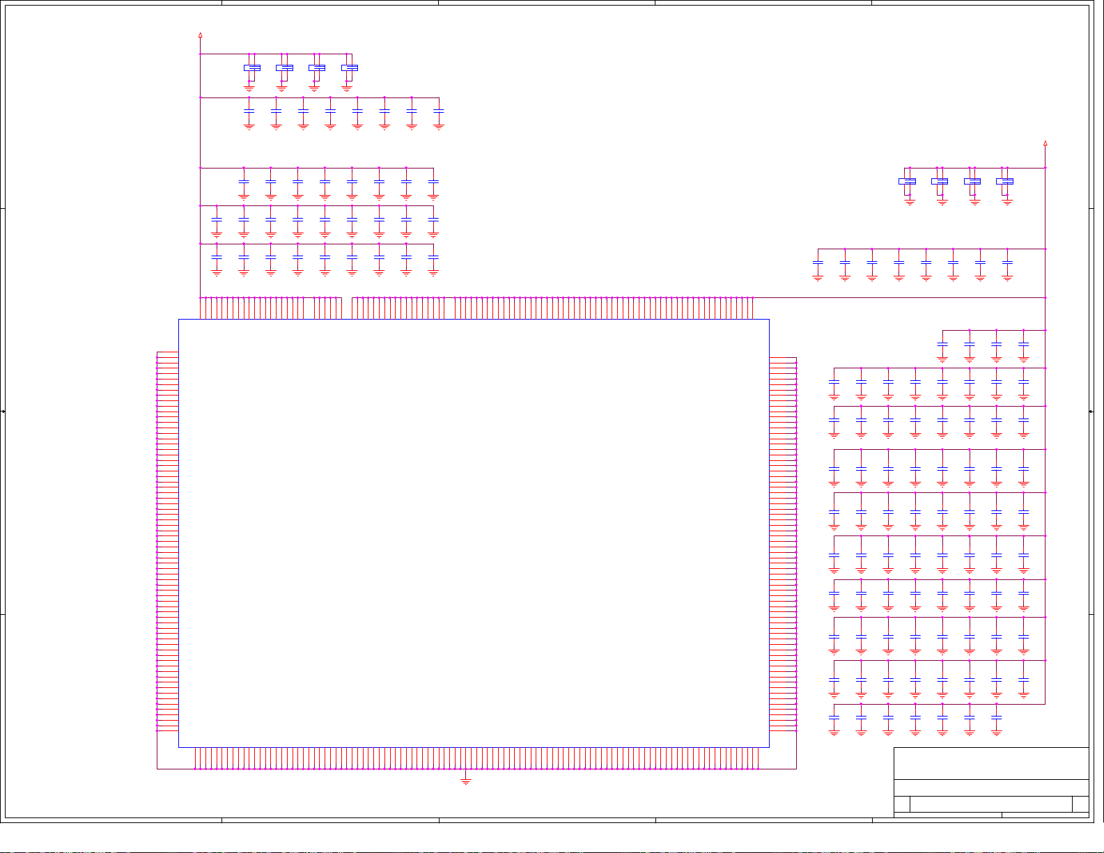
5
2.5V_PCIe_SWITCH
123
123
C210
C210
1uF
1uF
4
4
C214
C214
C215
VDD25
VSS
U10
J24
VDD25
VSS
C200
C200
1000pF
1000pF
C319
C319
1000pF
1000pF
C310
C310
1000pF
1000pF
V8
U17
VDD25
VSSK3VSS
K6
0.01uF
0.01uF
V18
V19
VDD25
VDD25V9VDD25
VSSK8VSSK9VSS
K11
C201
C201
1000pF
1000pF
C320
C320
1000pF
1000pF
C311
C311
1000pF
1000pF
VDD25
VDD25W7VDD25W8VDD25
VSS
K13
C215
0.01uF
0.01uF
K14
W19
VSS
K16
D D
C318
C318
1000pF
1000pF
C327
C327
1000pF
1000pF
U1E
A1
A4
A23
A25
A26
B4
B23
C5
C6
C7
C8
C9
C10
C11
C12
C13
C14
C15
C16
C17
C18
C19
C20
C21
C22
D4
D23
E4
E23
F4
F5
F6
F7
F8
F10
F11
F12
F13
F14
F15
F16
F17
F19
F20
F21
F22
F23
G8
G19
H1
H2
H4
H5
H6
H7
H9
H10
H11
H12
H13
H14
H15
H16
H17
H18
H20
H21
H22
H23
H25
H26
PEX8648
PEX8648
U1E
G20
H19
J18
K10
K17
VDD25G7VDD25
VDD25H8VDD25
VDD25J9VDD25
VDD25
VSS
VSS
VSS
VSS
VSS
VSS
VSS
VSS
VSS
VSS
VSS
VSS
VSS
VSS
VSS
VSS
VSS
VSS
VSS
VSS
VSS
VSS
VSS
VSS
VSS
VSS
VSS
VSS
VSS
VSS
VSS
VSS
VSS
VSS
VSS
VSS
VSS
VSS
VSS
VSS
VSS
VSS
VSS
VSS
VSS
VSS
VSS
VSS
VSS
VSS
VSS
VSS
VSS
VSS
VSS
VSS
VSS
VSS
VSS
VSS
VSS
VSS
VSS
VSS
VSS
VSS
VSS
VSS
VSS
VSS
VSS
VSSJ3VSSJ6VSSJ8VSS
VSS
VSS
VSS
VSS
J10
J12
J15
J17
J19
J21
C C
B B
A A
5
4
123
4
K12
K15
VDD25A
VSS
VSSL3VSSL6VSSL8VSS
C212
C212
1uF
1uF
N10
VDD25A
C203
C203
1000pF
1000pF
C322
C322
1000pF
1000pF
C313
C313
1000pF
1000pF
N17
VDD25A
VDD25A
L10
4
C217
C217
0.01uF
0.01uF
U12
L12
U15
VDD25A
VDD25A
VSS
VSS
L14
123
C213
C213
0402 Packages
1uF
1uF
L11
VDD10
VSS
L17
C218
C218
C205
C205
1000pF
1000pF
C323
C323
1000pF
1000pF
C314
C314
1000pF
1000pF
L13
VDD10
VSS
L19
0.01uF
0.01uF
L15
VDD10
VSS
L21
M12
M14
VDD10
VSS
L24
C219
C219
0.01uF
0.01uF
C206
C206
1000pF
1000pF
C324
C324
1000pF
1000pF
C315
C315
1000pF
1000pF
M16
N11
N13
VDD10
VDD10
VDD10
VSSM3VSSM6VSSM8VSS
M10
Placed Around the
Periphery.
C220
C220
C221
C221
0.01uF
0.01uF
0.01uF
0.01uF
C208
C208
C207
C207
1000pF
1000pF
1000pF
1000pF
C326
C326
C325
C325
1000pF
1000pF
1000pF
1000pF
C317
C317
C316
C316
1000pF
1000pF
1000pF
1000pF
N15
P12
P14
P16
R11
R13
R15
T12
T14
T16
G10
VDD10
VDD10
VDD10
VDD10
VDD10
VDD10
VDD10
VDD10
VDD10
VDD10
VDD10
VDD10AG9VDD10A
PEX 8648
PEX 8648
VSS
VSS
VSS
VSS
VSS
VSS
VSS
VSSN3VSSN8VSSN9VSS
VSS
N16
N12
M11
M13
M15
M17
N14
M19
M21
M24
0201 Packages
Placed near
the Power
Pins.
G15
G16
G17
G18
G11
G12
G13
G14
VDD10A
VDD10A
VDD10A
VDD10A
VDD10A
VDD10A
VDD10A
VSS
VSS
VSS
VSS
VSSP3VSSP6VSSP8VSS
P10
P11
N18
N19
N24
4
VSS
L16
C211
C211
1uF
1uF
C216
C216
0.01uF
0.01uF
C202
C202
1000pF
1000pF
C321
C321
1000pF
1000pF
C312
C312
1000pF
1000pF
W20
Y20
VDD25
VDD25Y7VDD25
VSS
VSS
VSS
VSS
K18
K19
K21
K24
VDD10A
VSS
P13
J11
J13
VDD10AJ7VDD10A
VSS
VSS
P15
P17
J14
VDD10A
VSS
P19
J16
VDD10A
VSS
P21
J20
VDD10A
VSS
P24
VDD10A
VSS
3
K20
L18
VDD10AK7VDD10A
VDD10AL7VDD10AL9VDD10A
VSSR3VSSR6VSSR8VSSR9VSS
R12
3
L20
VDD10A
VDD10AM7VDD10AM9VDD10A
VSS
VSS
R14
R16
2
0603 Packages Placed
Around the Periphery.
123
C188
C188
1uF
1uF
4
4
0402 Packages Placed
Around the Periphery.
C193
C193
C194
C168
C168
1000pF
1000pF
C185
C185
1000pF
1000pF
C187
C187
1000pF
1000pF
C330
C330
1000pF
1000pF
C356
C356
1000pF
1000pF
C350
C350
1000pF
1000pF
C376
C376
1000pF
1000pF
C384
C384
1000pF
1000pF
C392
C392
1000pF
1000pF
0.01uF
0.01uF
C169
C169
1000pF
1000pF
C156
C156
1000pF
1000pF
C182
C182
1000pF
1000pF
C331
C331
1000pF
1000pF
C358
C358
1000pF
1000pF
C369
C369
1000pF
1000pF
C377
C377
1000pF
1000pF
C385
C385
1000pF
1000pF
C393
C393
1000pF
1000pF
C194
0.01uF
0.01uF
C192
C192
0.01uF
0.01uF
M18
M20
N20
P18
P20
R10
R17
T18
T20
U20
V11
V13
V14
V16
Y10
Y11
Y12
Y13
Y14
Y15
Y16
Y17
R20
VDD10A
VDD10AN7VDD10A
VDD10AP7VDD10AP9VDD10A
VDD10A
VDD10AR7VDD10A
VDD10A
VDD10AT7VDD10AT9VDD10A
VDD10A
VDD10AU7VDD10A
VDD10A
VDD10A
VDD10A
VDD10A
VDD10A
VSS
VSS
VSS
VSS
VSST3VSST6VSST8VSS
VSS
VSS
VSS
VSS
VSS
VSS
VSS
VSSU3VSSU6VSSU8VSSU9VSS
T10
T11
T13
T15
T17
T19
T21
R18
R19
R21
R24
T24
VDD10AY9VDD10A
VSS
VSS
VSS
VSS
U11
U13
U14
U16
U18
U19
Y18
VDD10A
VDD10A
VDD10A
VDD10A
VDD10A
VDD10A
VDD10A
VDD10A
AF26
VSS
AF23
VSS
AF4
VSS
AF1
VSS
AE23
VSS
AE4
VSS
AD23
VSS
AD22
VSS
AD21
VSS
AD20
VSS
AD19
VSS
AD18
VSS
AD17
VSS
AD16
VSS
AD15
VSS
AD14
VSS
AD13
VSS
AD12
VSS
AD11
VSS
AD10
VSS
AD9
VSS
AD8
VSS
AD7
VSS
AD6
VSS
AD5
VSS
AC23
VSS
AC4
VSS
AB23
VSS
AB4
VSS
AA23
VSS
AA22
VSS
AA21
VSS
AA20
VSS
AA19
VSS
AA17
VSS
AA16
VSS
AA15
VSS
AA14
VSS
AA13
VSS
AA12
VSS
AA11
VSS
AA10
VSS
AA8
VSS
AA7
VSS
AA6
VSS
AA5
VSS
AA4
VSS
Y19
VSS
Y8
VSS
W18
VSS
W17
VSS
W16
VSS
W15
VSS
W14
VSS
W13
VSS
W12
VSS
W11
VSS
W10
VSS
W9
VSS
V26
VSS
V25
VSS
V24
VSS
V23
VSS
V22
VSS
V21
VSS
V20
VSS
V17
VSS
V15
VSS
V12
VSS
V10
VSS
VSS
VSS
U21
VSSV7VSSV6VSSV5VSSV4VSSV3VSS
VSS
VSS
V2
V1
U24
2
0201 Packages Placed
near the Power Pins.
C196
C196
C195
C195
0.01uF
0.01uF
0.01uF
0.01uF
C170
C170
C175
C175
1000pF
1000pF
1000pF
1000pF
C157
C157
C163
C163
1000pF
1000pF
1000pF
1000pF
C186
C186
C183
C183
1000pF
1000pF
1000pF
1000pF
C336
C336
C332
C332
1000pF
1000pF
1000pF
1000pF
C352
C352
C354
C354
1000pF
1000pF
1000pF
1000pF
C370
C370
C371
C371
1000pF
1000pF
1000pF
1000pF
C379
C379
C378
C378
1000pF
1000pF
1000pF
1000pF
C386
C386
C387
C387
1000pF
1000pF
1000pF
1000pF
C394
C394
C395
C395
1000pF
1000pF
1000pF
1000pF
Title
Title
Title
PEX8648 RDK - PCIe SWITCH POWER
PEX8648 RDK - PCIe SWITCH POWER
PEX8648 RDK - PCIe SWITCH POWER
Size Document Number Rev
Size Document Number Rev
Size Document Number Rev
C
C
C
91-0082-100-A 102
91-0082-100-A 102
91-0082-100-A 102
Date: Sheet
Date: Sheet
Date: Sheet
1
123
123
C190
C190
C189
C189
1uF
1uF
1uF
1uF
4
C197
C197
C198
C198
0.01uF
0.01uF
0.01uF
0.01uF
C176
C176
C177
C177
1000pF
1000pF
1000pF
1000pF
C174
C174
C172
C172
1000pF
1000pF
1000pF
1000pF
C161
C161
C160
C160
1000pF
1000pF
1000pF
1000pF
C333
C333
C328
C328
1000pF
1000pF
1000pF
1000pF
C337
C337
C338
C338
1000pF
1000pF
1000pF
1000pF
C360
C360
C362
C362
1000pF
1000pF
1000pF
1000pF
C373
C373
C372
C372
1000pF
1000pF
1000pF
1000pF
C380
C380
C381
C381
1000pF
1000pF
1000pF
1000pF
C388
C388
C389
C389
1000pF
1000pF
1000pF
1000pF
C396
C396
C397
C397
1000pF
1000pF
1000pF
1000pF
PLX Technology, Inc.
PLX Technology, Inc.
PLX Technology, Inc.
870 W. Maude Avenue
870 W. Maude Avenue
870 W. Maude Avenue
Sunnyvale, CA 94085
Sunnyvale, CA 94085
Sunnyvale, CA 94085
www.plxtech.com
www.plxtech.com
www.plxtech.com
1
4
C179
C179
1000pF
1000pF
C173
C173
1000pF
1000pF
C166
C166
1000pF
1000pF
C334
C334
1000pF
1000pF
C339
C339
1000pF
1000pF
C364
C364
1000pF
1000pF
C374
C374
1000pF
1000pF
C382
C382
1000pF
1000pF
C390
C390
1000pF
1000pF
C398
C398
1000pF
1000pF
123
C191
C191
1uF
1uF
C199
C199
0.01uF
0.01uF
1.0V_PCIe_SWITCH
C181
C181
1000pF
1000pF
C178
C178
1000pF
1000pF
C180
C180
1000pF
1000pF
C335
C335
1000pF
1000pF
C340
C340
1000pF
1000pF
C366
C366
1000pF
1000pF
C375
C375
1000pF
1000pF
C383
C383
1000pF
1000pF
C391
C391
1000pF
1000pF
12 21Tuesday, November 16, 2010
12 21Tuesday, November 16, 2010
12 21Tuesday, November 16, 2010
of
of
of
Page 56
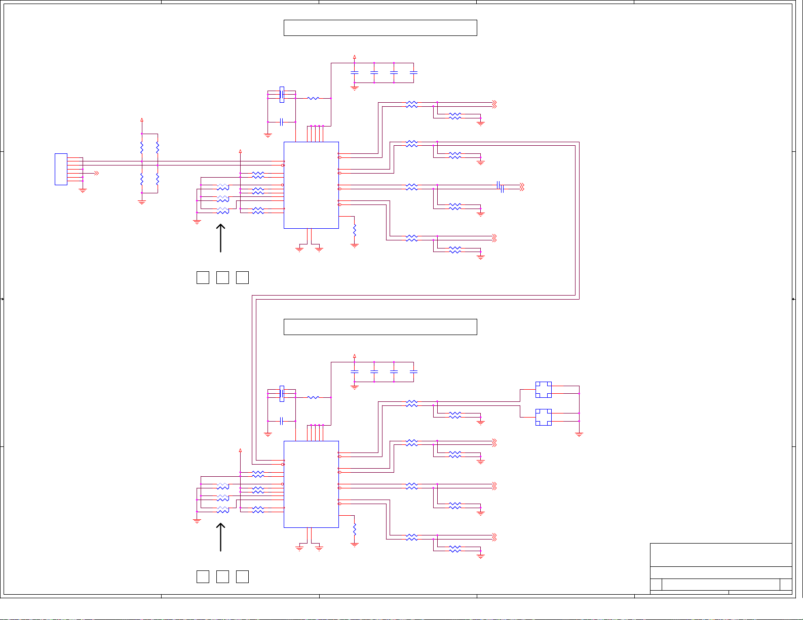
5
4
3
2
1
REFCLK FANOUT CIRCUIT TO PCIe SWITCH
A ferrite bead can
be used in place of
0-ohm resistor for
additional
filtering.
D D
3.3V_BOARD
R56
R56
R55
P4
P4
1
GND
2
A+
3
A-
4
GND
5
B-
B+
GND
SATA header
SATA header
C C
PERST# {15}
6
7
R55
10K
10K
10K
10K
R62
R62
1.0K
1.0K
REFCLK_INp
REFCLK_INn
R63
R63
1.0K
1.0K
These are custom 0603 resistor
footprints that have 3 pads.
3.3V_BOARD
R57 5.1KR57 5.1K
R64 5.1KR64 5.1K
R65
R65
12
3
3
3
R67 5.1KR67 5.1K
R69 5.1KR69 5.1K C1260.1uF C1260.1uF
R70
R70
0 Shunt
0 Shunt
12
R71
R71
0 Shunt
0 Shunt
R73 5.1KR73 5.1K
12
R75 5.1KR75 5.1K
0 Shunt
0 Shunt
CY28400-2U3CY28400-2
C123
C123
5
3 4
10uF
10uF
C124
C124
0.1uF
0.1uF
U3
2
3
8
21
17
16
15
12
25
13
14
6
R50 0R50 0
21
28
VDD_A
SRC_IN
SRC_IN#
OE_1
OE_6
HIGH_BW#
SRC_STP
PWRDWN
PLL/BYPASS#
OE_INV
SCLK
SDATA
VDD1VDD5VDD11VDD18VDD
VSS
VSS_A
4
27
2 1 3
3.3V_BOARD
C121
C121
C120
C120
C119
C119
0.01uF
0.01uF
0.01uF
0.01uF
24
ST1_RCLKp
6
DIFT1
ST1_RCLKn
7
DIFC1
ST0_RCLKp
9
DIFT2
ST0_RCLKn
10
DIFC2
20
DIFT5
19
DIFC5
ST2_RCLKp
23
DIFT6
ST2_RCLKn
22
DIFC6
26
IREF
R76
R76
475
475
1%
1%
C122
C122
0.01uF
0.01uF
0.01uF
0.01uF
R51, R52, R53, R54 SHOULD BE CLOSE TO U3 PINS 6 AND 7
R51 33.2 1%R51 33.2 1%
R52 33.2 1%R52 33.2 1%
R143, R59, R60, R61 SHOULD BE CLOSE TO U3 PINS 9 AND 10
R143 33.2 1%R143 33.2 1%
R59 33.2 1%R59 33.2 1%
R66, R68, R72, R74 SHOULD BE CLOSE TO U3 PINS 20 AND 19
R66 33.2 1%R66 33.2 1%
R68 33.2 1%R68 33.2 1%
R77 33.2 1%R77 33.2 1%
R78 33.2 1%R78 33.2 1%
R53 49.9 1%R53 49.9 1%
R54 49.9 1%R54 49.9 1%
R60 49.9 1%R60 49.9 1%
R61 49.9 1%R61 49.9 1%
Deneb_C_REFCLKpDNB_RCLKp
Deneb_C_REFCLKnDNB_RCLKn
R72 49.9 1%R72 49.9 1%
R74 49.9 1%R74 49.9 1%
R77, R78, R79, R80 SHOULD BE CLOSE TO U3 PINS 23 AND 22
R79 49.9 1%R79 49.9 1%
R80 49.9 1%R80 49.9 1%
Station1_REFCLKp {14}
Station1_REFCLKn {14}
Station0_REFCLKp
Station0_REFCLKn
C1250.1uF C1250.1uF
Deneb_REFCLKp {3}
Deneb_REFCLKn {3}
Station2_REFCLKp {14}
Station2_REFCLKn {14}
REFCLK FANOUT CIRCUIT TO STATION 0 SLOTS
A ferrite bead can
be used in place of
0-ohm resistor for
additional
filtering.
B B
3.3V_BOARD
R86 5.1KR86 5.1K
R91 5.1KR91 5.1K
R92
R92
12
R96
R96
0 Shunt
0 Shunt
R98
R98
0 Shunt
0 Shunt
0 Shunt
0 Shunt
12
12
R94 5.1KR94 5.1K
R97 5.1KR97 5.1K
R100 5.1KR100 5.1K
R102 5.1KR102 5.1K
3
3
3
A A
These are custom 0603 resistor
footprints that have 3 pads.
CY28400-2U4CY28400-2
C131
C131
5
3 4
10uF
10uF
C132
C132
0.1uF
0.1uF
U4
2
3
8
21
17
16
15
12
25
13
14
6
R81 0R81 0
21
28
VDD_A
SRC_IN
SRC_IN#
OE_1
OE_6
HIGH_BW#
SRC_STP
PWRDWN
PLL/BYPASS#
OE_INV
SCLK
SDATA
VDD1VDD5VDD11VDD18VDD
VSS
VSS_A
4
27
2 1 3
5
4
3.3V_BOARD
C128
C128
C127
C127
0.01uF
0.01uF
0.01uF
0.01uF
24
RCLKp
6
DIFT1
RCLKn
7
DIFC1
SLOT3_RCLKp
9
DIFT2
SLOT3_RCLKn
10
DIFC2
SLOT2_RCLKp
20
DIFT5
SLOT2_RCLKn
19
DIFC5
SLOT1_RCLKp
23
DIFT6
SLOT1_RCLKn
22
DIFC6
26
IREF
R103
R103
475
475
1%
1%
C130
C130
C129
C129
0.01uF
0.01uF
0.01uF
0.01uF
R82, R83, R84, R85 SHOULD BE CLOSE TO U4 PINS 6 AND 7
R82 33.2 1%R82 33.2 1%
R83 33.2 1%R83 33.2 1%
R87, R88, R89, R90 SHOULD BE CLOSE TO U4 PINS 9 AND 10
R87 33.2 1%R87 33.2 1%
R88 33.2 1%R88 33.2 1%
R93, R95, R99, R101 SHOULD BE CLOSE TO U4 PINS 20 AND 19
R93 33.2 1%R93 33.2 1%
R95 33.2 1%R95 33.2 1%
R104 33.2 1%R104 33.2 1%
R105 33.2 1%R105 33.2 1%
3
R84 49.9 1%R84 49.9 1%
R85 49.9 1%R85 49.9 1%
Slot3_REFCLKp {8}
R89 49.9 1%R89 49.9 1%
R90 49.9 1%R90 49.9 1%
R99 49.9 1%R99 49.9 1%
R101 49.9 1%R101 49.9 1%
R104, R105, R106 AND R107 SHOULD BE CLOSE TO U4 PINS 23 AND 22
R106 49.9 1%R106 49.9 1%
R107 49.9 1%R107 49.9 1%
Slot3_REFCLKn {8}
Slot2_REFCLKp {8}
Slot2_REFCLKn {8}
Slot1_REFCLKp {8}
Slot1_REFCLKn {8}
J15
J15
3
G
1
S
2
G
SMT_SMA
SMT_SMA
J16
J16
3
G
1
S
2
G
SMT_SMA
SMT_SMA
PLX Technology, Inc.
PLX Technology, Inc.
PLX Technology, Inc.
870 W. Maude Avenue
870 W. Maude Avenue
870 W. Maude Avenue
Sunnyvale, CA 94085
Sunnyvale, CA 94085
Sunnyvale, CA 94085
www.plxtech.com
www.plxtech.com
Title
Title
Title
PEX8648 RDK - REFCLK Fanout 1
PEX8648 RDK - REFCLK Fanout 1
PEX8648 RDK - REFCLK Fanout 1
Size Document Number Rev
Size Document Number Rev
Size Document Number Rev
C
C
C
91-0082-100-A 102
91-0082-100-A 102
91-0082-100-A 102
Date: Sheet
Date: Sheet
2
Date: Sheet
www.plxtech.com
1
13 21Tuesday, November 16, 2010
13 21Tuesday, November 16, 2010
13 21Tuesday, November 16, 2010
of
of
of
Page 57
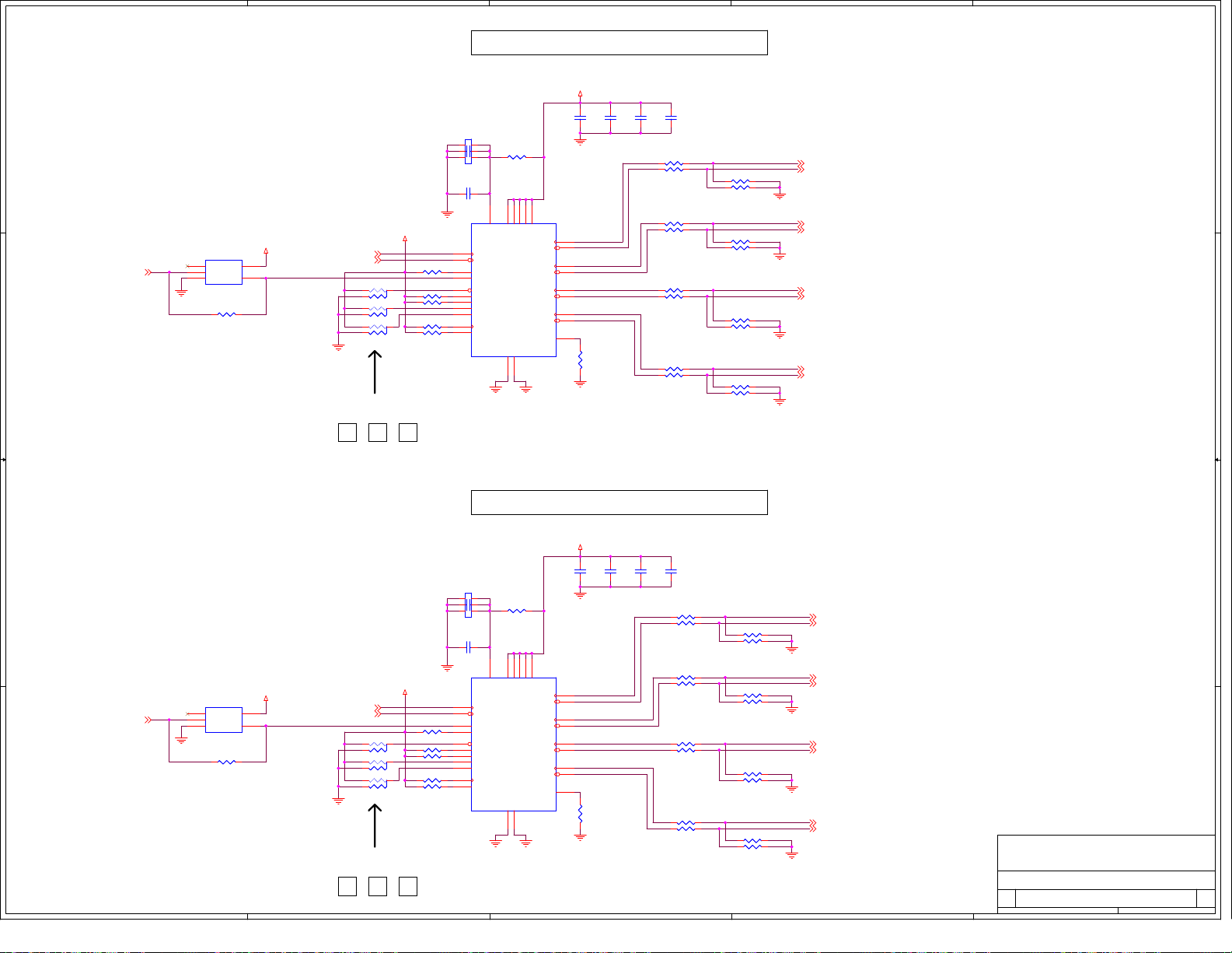
5
4
3
2
1
REFCLK FANOUT CIRCUIT TO STATION 1 SLOTS
A ferrite bead can
be used in place of
0-ohm resistor for
additional
filtering.
D D
3.3V_BOARD
U6
U6
1
HP_CLKEN#{16}
C C
2
NC
VCC
NOT
NOT
A
GND3Y
NC7SZ04M5X
NC7SZ04M5X
R124 NLR124 NL
5
4
Station1_REFCLKp{13}
Station1_REFCLKn{13}
These are custom 0603 resistor
footprints that have 3 pads.
3.3V_BOARD
R117 5.1KR117 5.1K
R118
R118
12
R123
R123
0 Shunt
0 Shunt
R126
R126
0 Shunt
0 Shunt
0 Shunt
0 Shunt
12
12
R120 5.1KR120 5.1K
R122 5.1KR122 5.1K
R127 5.1KR127 5.1K
R129 5.1KR129 5.1K
3
3
3
CY28400-2U5CY28400-2
C137
C137
5
3 4
10uF
10uF
C138
C138
0.1uF
0.1uF
U5
2
3
8
21
17
16
15
12
25
13
14
6
R108 0R108 0
21
28
VDD_A
SRC_IN
SRC_IN#
OE_1
OE_6
HIGH_BW#
SRC_STP
PWRDWN
PLL/BYPASS#
OE_INV
SCLK
SDATA
VDD1VDD5VDD11VDD18VDD
VSS
VSS_A
4
27
2 1 3
3.3V_BOARD
C134
C134
C133
C133
0.01uF
0.01uF
0.01uF
0.01uF
24
SLOT4_RCLKp
6
DIFT1
SLOT4_RCLKn
7
DIFC1
SLOT7_RCLKp
9
DIFT2
SLOT7_RCLKn
10
DIFC2
SLOT6_RCLKp
20
DIFT5
SLOT6_RCLKn
19
DIFC5
SLOT5_RCLKp
23
DIFT6
SLOT5_RCLKn
22
DIFC6
26
IREF
R130
R130
475
475
1%
1%
C136
C136
C135
C135
0.01uF
0.01uF
0.01uF
0.01uF
R109, R110, R111, R112 SHOULD BE CLOSE TO U5 PINS 6 AND 7
R109 33.2 1%R109 33.2 1%
R110 33.2 1%R110 33.2 1%
R113, R114, R115, R116 SHOULD BE CLOSE TO U5 PINS 9 AND 10
R113 33.2 1%R113 33.2 1%
R114 33.2 1%R114 33.2 1%
R119, R121, R125, R128 SHOULD BE CLOSE TO U5 PINS 20 AND 19
R119 33.2 1%R119 33.2 1%
R121 33.2 1%R121 33.2 1%
R131 33.2 1%R131 33.2 1%
R132 33.2 1%R132 33.2 1%
R111 49.9 1%R111 49.9 1%
R112 49.9 1%R112 49.9 1%
R115 49.9 1%R115 49.9 1%
R116 49.9 1%R116 49.9 1%
R125 49.9 1%R125 49.9 1%
R128 49.9 1%R128 49.9 1%
R131, R132, R133, R134 SHOULD BE CLOSE TO U5 PINS 23 AND 22
R133 49.9 1%R133 49.9 1%
R134 49.9 1%R134 49.9 1%
Slot4_REFCLKp {9}
Slot4_REFCLKn {9}
Slot7_REFCLKp {9}
Slot7_REFCLKn {9}
Slot6_REFCLKp {9}
Slot6_REFCLKn {9}
Slot5_REFCLKp {9}
Slot5_REFCLKn {9}
REFCLK FANOUT CIRCUIT TO STATION 2 SLOTS
A ferrite bead can
be used in place of
0-ohm resistor for
additional
filtering.
B B
3.3V_BOARD
U16
U16
1
SHP_CLKEN#{16}
A A
2
NC
VCC
NOT
NOT
A
GND3Y
NC7SZ04M5X
NC7SZ04M5X
R180 NLR180 NL
5
4
Station2_REFCLKp{13}
Station2_REFCLKn{13}
These are custom 0603 resistor
footprints that have 3 pads.
3.3V_BOARD
R145 5.1KR145 5.1K
R146
R146
12
R151
R151
0 Shunt
0 Shunt
R152
R152
0 Shunt
0 Shunt
0 Shunt
0 Shunt
12
12
R148 5.1KR148 5.1K
R150 5.1KR150 5.1K
R154 5.1KR154 5.1K
R156 5.1KR156 5.1K
3
3
3
CY28400-2U7CY28400-2
C143
C143
5
3 4
10uF
10uF
C144
C144
0.1uF
0.1uF
U7
2
3
8
21
17
16
15
12
25
13
14
6
R135 0R135 0
21
28
VDD_A
SRC_IN
SRC_IN#
OE_1
OE_6
HIGH_BW#
SRC_STP
PWRDWN
PLL/BYPASS#
OE_INV
SCLK
SDATA
VDD1VDD5VDD11VDD18VDD
VSS
VSS_A
4
27
2 1 3
5
4
3.3V_BOARD
C140
C140
C139
C139
0.01uF
0.01uF
0.01uF
0.01uF
24
SLOT8_RCLKp
6
DIFT1
SLOT8_RCLKn
7
DIFC1
SLOT11_RCLKp
9
DIFT2
SLOT11_RCLKn
10
DIFC2
SLOT10_RCLKp
20
DIFT5
SLOT10_RCLKn
19
DIFC5
SLOT9_RCLKp
23
DIFT6
SLOT9_RCLKn
22
DIFC6
26
IREF
R157
R157
475
475
1%
1%
3
C142
C142
C141
C141
0.01uF
0.01uF
0.01uF
0.01uF
R136, R137, R138, R139 SHOULD BE CLOSE TO U7 PINS 6 AND 7
R136 33.2 1%R136 33.2 1%
R137 33.2 1%R137 33.2 1%
R140, R144, R141, R142 SHOULD BE CLOSE TO U7 PINS 9 AND 10
R140 33.2 1%R140 33.2 1%
R144 33.2 1%R144 33.2 1%
R147, R149, R153, R155 SHOULD BE CLOSE TO U7 PINS 20 AND 19
R147 33.2 1%R147 33.2 1%
R149 33.2 1%R149 33.2 1%
R158 33.2 1%R158 33.2 1%
R159 33.2 1%R159 33.2 1%
R138 49.9 1%R138 49.9 1%
R139 49.9 1%R139 49.9 1%
R141 49.9 1%R141 49.9 1%
R142 49.9 1%R142 49.9 1%
R153 49.9 1%R153 49.9 1%
R155 49.9 1%R155 49.9 1%
R158, R159, R160, R161 SHOULD BE CLOSE TO U7 PINS 23 AND 22
R160 49.9 1%R160 49.9 1%
R161 49.9 1%R161 49.9 1%
Slot8_REFCLKp {10}
Slot8_REFCLKn {10}
Slot11_REFCLKp {10}
Slot11_REFCLKn {10}
Slot10_REFCLKp {10}
Slot10_REFCLKn {10}
Slot9_REFCLKp {10}
Slot9_REFCLKn {10}
2
PLX Technology, Inc.
PLX Technology, Inc.
PLX Technology, Inc.
870 W. Maude Avenue
870 W. Maude Avenue
870 W. Maude Avenue
Sunnyvale, CA 94085
Sunnyvale, CA 94085
Sunnyvale, CA 94085
www.plxtech.com
www.plxtech.com
Title
Title
Title
PEX8648 RDK - REFCLK Fanout 2
PEX8648 RDK - REFCLK Fanout 2
PEX8648 RDK - REFCLK Fanout 2
Size Document Number Rev
Size Document Number Rev
Size Document Number Rev
C
C
C
91-0082-100-A 102
91-0082-100-A 102
91-0082-100-A 102
Date: Sheet
Date: Sheet
Date: Sheet
www.plxtech.com
1
14 21Tuesday, November 16, 2010
14 21Tuesday, November 16, 2010
14 21Tuesday, November 16, 2010
of
of
of
Page 58
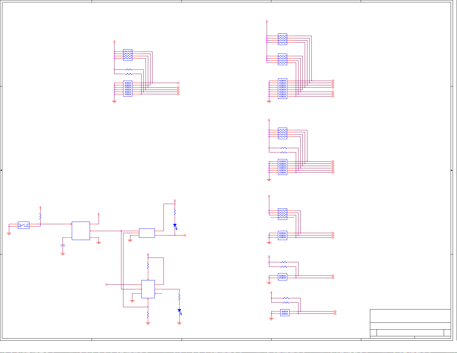
5
3.3V_BOARD
D D
Solderside
Componentside
C C
RN7
RN7
5.1K
5.1K
R178 5.1KR178 5.1K
R179 5.1KR179 5.1K
SW10
SW10
ON
ON
1
2
3
4
5
6
SW DIP-6
SW DIP-6
4
18
27
36
45
12
11
10
9
8
7
STRAP_PLL_BYPASS# {11}
STRAP_FAST_BRINGUP# {11}
STRAP_12_PORT_MODE {11}
STRAP_SERDES_MODE_EN# {11,17}
STRAP_PROBE_MODE# {11,17}
3
3.3V_BOARD
Solderside
RN1
RN1
18
27
36
45
5.1K
5.1K
RN2
RN2
18
27
36
45
5.1K
5.1K
SW1
SW1
ON
ON
1
16
2
15
3
14
4
13
5
12
6
11
7
10
8 9
SW DIP-8
SW DIP-8
Componentside
3.3V_BOARD
Solderside
RN3
RN3
18
27
36
45
5.1K
5.1K
R162 5.1KR162 5.1K
R163 5.1KR163 5.1K
SW2
SW2
ON
ON
1
12
2
11
3
10
4
9
5
8
6
7
SW DIP-6
SW DIP-6
Componentside
2
UP_PORTSEL0 {11,16}
UP_PORTSEL1 {11,16}
UP_PORTSEL2 {11,16}
UP_PORTSEL3 {11,16}
NT_ENABLE {11,16}
NT_PORTSEL0 {11,16}
NT_PORTSEL1 {11,16}
STN0_PORTCFG0 {11,16}
STN0_PORTCFG1 {11,16}
STN1_PORTCFG0 {11,16}
STN1_PORTCFG1 {11,16}
STN2_PORTCFG0 {11,16}
STN2_PORTCFG1 {11,16}
1
3.3V_BOARD
3.3V_BOARD
RESET#
5
1
2
3.3V_BOARD
PERST#{13}
PERST#_PWRGD
U9
U9
1
A
2
B
GND3Y
NC7SZ08
NC7SZ08
2
1
4
NC7SZ74
NC7SZ74
4
AND
AND
3.3V_BOARD
U10
U10
PRn
D
CK
CLRn
5
VCC
4
R167
R167
5.1K
5.1K
7
8
VCC
5
Q
Qn3GND
6
R170
R170
360K
360K
B B
SW3
SW3
1
2 3
B3S-1002
B3S-1002
A A
R165
R165
5.1K
5.1K
PERST#_MAN
4
C145
C145
0.047uF
0.047uF
5
U8
MR#3VCC
SRT4GND
MAX6412U8MAX6412
128.6 msec
R164
R164
390
390
21
DS3
DS3
Red
Red
PERST#_PCIe_SWITCH {8,9,10,11,16}
R169
R169
390
390
21
DS4
DS4
Red
Red
3
3.3V_BOARD
Solderside
1
2
3
Componentside
3.3V_BOARD
R166 5.1KR166 5.1K
R168 5.1KR168 5.1K
1
2
3.3V_BOARD
RN4
RN4
5.1K
5.1K
SW4
SW4
ON
ON
SW DIP-3
SW DIP-3
SW5
SW5
ON
ON
SW DIP-2
SW DIP-2
R278 5.1KR278 5.1K
R177 5.1KR177 5.1K
SW9
SW9
ON
ON
1
2
SW DIP-2
SW DIP-2
18
27
36
45
6
5
4
4
3
4
3
2
I2C_ADDR0 {11}
I2C_ADDR1 {11}
I2C_ADDR2 {11}
CPLD_HP_ENABLE {16}
HP_MRL_B# {17}
CPLD_SHP_ENABLE {16}
SHP_MRL# {20}
PLX Technology, Inc.
PLX Technology, Inc.
PLX Technology, Inc.
870 W. Maude Avenue
870 W. Maude Avenue
870 W. Maude Avenue
Sunnyvale, CA 94085
Sunnyvale, CA 94085
Sunnyvale, CA 94085
www.plxtech.com
www.plxtech.com
Title
Title
Title
PEX8648 RDK - Switches
PEX8648 RDK - Switches
PEX8648 RDK - Switches
Size Document Number Rev
Size Document Number Rev
Size Document Number Rev
C
C
C
91-0082-100-A 102
91-0082-100-A 102
91-0082-100-A 102
Date: Sheet
Date: Sheet
Date: Sheet
www.plxtech.com
1
15 21Tuesday, November 16, 2010
15 21Tuesday, November 16, 2010
15 21Tuesday, November 16, 2010
of
of
of
Page 59
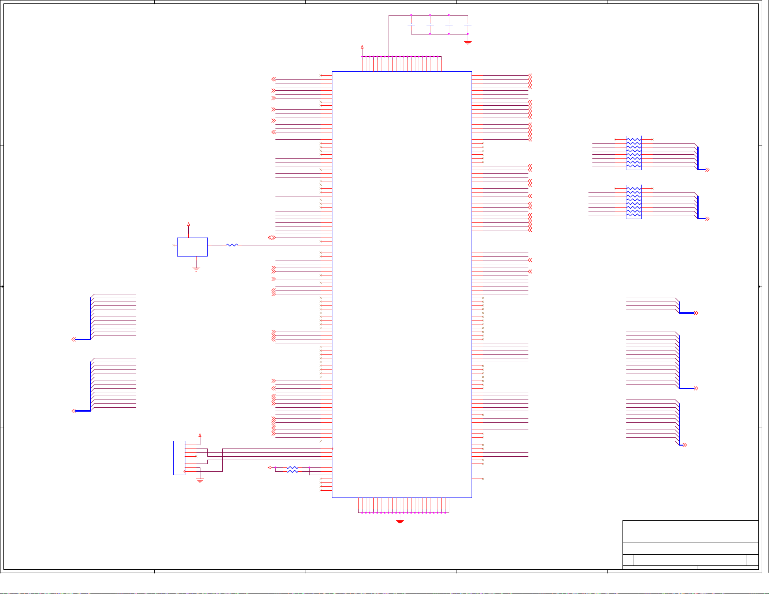
5
4
3.3V_BOARD
3
C164
C164
C162
C162
C159
C159
C158
C158
0.1uF
0.1uF
0.1uF
0.1uF
0.1uF
0.1uF
0.1uF
0.1uF
2
1
D13
F11
L11
VCCD4VCC
GNDK1GNDC3GND
C14
VCCF6VCC
GNDE5GND
E12
N13
VCCL6VCC
VCCN4VCC
GNDG7GNDG8GNDG9GND
G10
VCCO0A1VCCO0F7VCCO0G6VCCO1K6VCCO1L7VCCO1T1VCCO2
GNDH7GNDH8GNDH9GND
GNDJ7GNDJ8GNDJ9GND
H10
U11
U11
D D
C C
CPLD_UP_PORT11
CPLD_UP_PORT10
CPLD_UP_PORT9
CPLD_UP_PORT8
CPLD_UP_PORT7
CPLD_UP_PORT6
CPLD_UP_PORT5
CPLD_UP_PORT4
CPLD_UP_PORT3
CPLD_UP_PORT2
CPLD_UP_PORT1
CPLD_UP_PORT[11:0]{18}
B B
PRT_ID_DIG[13:0]{19}
A A
CPLD_UP_PORT0
PRT_ID_DIG13
PRT_ID_DIG12
PRT_ID_DIG11
PRT_ID_DIG10
PRT_ID_DIG9
PRT_ID_DIG8
PRT_ID_DIG7
PRT_ID_DIG6
PRT_ID_DIG5
PRT_ID_DIG4
PRT_ID_DIG3
PRT_ID_DIG2
PRT_ID_DIG1
PRT_ID_DIG0
Cut pin 5 of
header to form
mechanical key
U12
U12
1
OE
1.000MHz
1.000MHz
JP10
JP10
VCC
TDO
TDI
NC
TMS
GND
TCK
Lattice JTAG
Lattice JTAG
3.3V_BOARD
4
VCC
GND
2
3.3V_BOARD
1
2
3
4
6
7
8
3
OUT
HP_CLKEN#{14}
CPLD_HP_PWREN_B{17}
HP_PWRGD_B{20}
PERST#_PCIe_SWITCH{8,9,10,11,15}
CPLD_SHP_PERST#{20}
SHP_PWREN{20}
I2C_SDA0{11}
R17333R173
33
ST1_PRT_CONFIG0{7}
CPLD_PORT_GOOD5#{17}
CPLD_HP_PWRGD_B{17}
CPLD_PORT_GOOD1#{17}
CPLD_PORT_GOOD4#{17}
NT_PORTSEL1{11,15}
HP_PWREN_B{20}
ST0_PRT_CONFIG0{6}
HP_PERST#{9}
SHP_CLKEN#{14}
MOD_0_PRSNT#{6}
NT_PORTSEL0{11,15}
NT_ENABLE{11,15}
SHP_PERST#{10}
CPLD_PORT_GOOD7#{17}
ST0_PRT_CONFIG1{6}
CPLD_PORT_GOOD6#{17}
3.3V_BOARD
I2C_SCL0{11}
PRT_WIDTH_DIG9
PRT_WIDTH_DIG11
PRT_WIDTH_DIG10
PRT_WIDTH_DIG5
PRT_WIDTH_DIG3
PRT_WIDTH_DIG4
PRT_WIDTH_DIG7
PRT_WIDTH_DIG8
N31022341
CPLD_UP_PORT6
CPLD_UP_PORT5
PRT_WIDTH_DIG2
CPLD_PRT_STATUS4
CPLD_UP_PORT4
CPLD_PRT_STATUS5
N31022337
N31022342
N31022338
N31022336
N31022339
PRT_WIDTH_DIG1
PRT_WIDTH_DIG0
PRT_WIDTH_DIG6
N31022340
N38090049
N31024335
PRT_ID_DIG11
N31024343
CPLD_UP_PORT3
N32017686
N31024341
N31024339
R174 5.1KR174 5.1K
R241 5.1KR241 5.1K
B7
IO_109N_0
A7
IO_109P_0
D7
IO_110N_0
C7
IO_110P_0
B6
IO_111N_0
E7
IO_111P_0
E6
IO_112N_0
A6
IO_112P_0
A5
IO_113N/VREF0_0
A4
IO_113P_0
B5
IO_114N_0
A3
IO_114P_0
B4
IO_115N_0
B3
IO_115P_0
C5
IO_116N_0
C6
IO_116P_0
D5
IO_117N_0
D6
IO_117P_0
A2
NC
B2
NC
C4
NC
E4
NC
B1
IO_128N_0
C1
IO_128P_0
D3
IO_129N_0
C2
IO_129P_0
E3
IO_130N_0
D2
IO_130P_0
D1
NC
E1
NC
F4
NC
F5
NC
E2
IO_137N_0
F2
IO_137P/CLKOUT0_0
F1
IO_138N_0
G1
IO_138P_0
F3
IO_139N_0
G5
IO_139P_0
H5
IO_140N_0
G4
IO_140P/PLLRST0_0
G3
IO_141N_0
H3
IO_141P/PLLFBK0_0
G2
IO_156N_0
H1
IO_156P_0
J2
GCLK0N_0
H2
GCLK0P_0
K3
IO_0P/DATA0_1
J3
IO_0N/DATA1_1
J5
IO_1P/DATA2_1
J4
IO_1N/DATA3_1
L2
IO_2P/DATA4_1
M1
IO_2N/DATA5_1
K4
IO_3P/DATA6_1
L3
IO_3N/DATA7_1
K5
IO_4P/INITB_1
L5
IO_4N/CSB_1
N1
IO_5P/READ_1
M2
IO_5N/CCLK_1
P1
NC
M3
NC
L4
NC
N2
NC
P2
NC
R1
NC
R2
NC
T2
NC
T3
NC
N3
IO_13P_1
P4
IO_13N_1
N5
IO_14P_1
M6
IO_14N_1
T4
NC
T5
NC
R4
NC
N6
NC
R5
NC
P6
NC
M7
NC
T6
NC
R6
NC
T7
IO_21P_1
R7
IO_21N_1
N7
IO_22P_1
P7
IO_22N_1
T8
IO_23P_1
R8
IO_23N_1
M8
IO_24P_1
P8
IO_24N_1
N8
IO_25P_1
M9
IO_25N_1
N10
IO_26P_1
T9
IO_26N_1
T10
IO_27P_1
R9
IO_27N_1
P9
IO_28P_1
N9
IO_28N_1
L9
VREF1
J6
TCK
H6
TDI
K2
TDO
H4
TMS
R3
PROG_B
M4
DONE
L8
CFG0
J15
TOE
J11
RESETB
H11
GOE0
H13
GOE1
ispXPLD 5256MX 256fpBGA
ispXPLD 5256MX 256fpBGA
K11
L10
T16
A16
VCCO2
VCCO2
GNDK7GNDK8GNDK9GND
J10
J1
F10
G11
J16
VCCJ
VCCP
VCCO3
VCCO3
VCCO3
IO_33N/VREF2_2
IO_76P/PLLFBK1_3
IO_77N/PLLRST1_3
IO_80P/CLKOUT1_3
IO_104N/VREF3_3
GNDM5GND
K10
M12
IO_100N_3
IO_101N_3
IO_102N_3
IO_103N_3
IO_105N_3
IO_106N_3
IO_107N_3
IO_108N_3
GCLK3N_3
GCLK3P_3
GNDP3GNDP
K16
IO_29P_2
IO_29N_2
IO_30P_2
IO_30N_2
IO_31P_2
IO_31N_2
IO_32P_2
IO_32N_2
IO_33P_2
IO_34P_2
IO_34N_2
IO_35P_2
IO_35N_2
IO_36P_2
IO_36N_2
IO_37P_2
IO_37N_2
IO_51P_2
IO_51N_2
IO_52P_2
IO_52N_2
IO_53P_2
IO_53N_2
IO_55P_2
IO_55N_2
IO_56P_2
IO_56N_2
IO_57P_2
IO_57N_2
IO_58P_2
IO_58N_2
IO_59P_2
IO_59N_2
IO_60P_2
IO_60N_2
IO_61N_3
IO_61P_3
IO_76N_3
IO_77P_3
IO_78N_3
IO_78P_3
IO_79N_3
IO_79P_3
IO_80N_3
IO_91N_3
IO_91P_3
IO_92N_3
IO_92P_3
IO_93N_3
IO_93P_3
IO_100P_3
IO_101P_3
IO_102P_3
IO_103P_3
IO_104P_3
IO_105P_3
IO_106P_3
IO_107P_3
IO_108P_3
NC
NC
NC
NC
NC
NC
NC
NC
NC
NC
NC
NC
NC
NC
NC
NC
NC
NC
NC
NC
NC
NC
NC
NC
NC
NC
T11
T12
P10
R10
R11
M10
M11
T13
P11
T14
R12
R13
N11
T15
R14
N12
P12
R15
P13
P15
M13
P14
R16
P16
N15
N14
N16
M16
M14
M15
L13
L12
L15
L16
L14
K15
K14
K12
K13
J13
J14
J12
H14
G16
G15
F15
H12
G14
F16
E16
G13
G12
F14
E15
F12
F13
D16
D15
C16
B16
C15
B15
E14
D14
E13
A15
D12
B14
C13
A14
A13
B13
D11
B12
C12
E11
E10
A12
A11
B11
C11
B10
A10
C10
D10
C9
E9
D9
F9
A9
F8
E8
A8
B9
D8
B8
C8
H15
H16
L1
CPLD_PRT_STATUS6
N31024337
PRT_ID_DIG3
CPLD_UP_PORT2
PRT_ID_DIG4
CPLD_NT_PORT1
PRT_ID_DIG2
CPLD_PRT_STATUS2
CPLD_NT_PORT0
PRT_ID_DIG13
CPLD_NT_PORT3
CPLD_NT_PORT2
PRT_ID_DIG9
PRT_ID_DIG12
PRT_ID_DIG6
PRT_ID_DIG7
PRT_ID_DIG10
PRT_ID_DIG5
CPLD_UP_PORT0
PRT_ID_DIG8
CPLD_UP_PORT10
CPLD_UP_PORT1
CPLD_UP_PORT8
CPLD_UP_PORT7
CPLD_PRT_STATUS7
CPLD_PRT_STATUS8
CPLD_PRT_STATUS9
CPLD_UP_PORT9
PRT_ID_DIG0
PRT_ID_DIG1
CPLD_PRT_STATUS10
CPLD_PRT_STATUS3
CPLD_PRT_STATUS0
CPLD_PRT_STATUS1
CPLD_UP_PORT11
CPLD_PRT_STATUS11
PRT_WIDTH_DIG12
PRT_WIDTH_DIG13
PRT_WIDTH_DIG14
CPLD_HP_CLKEN_B# {17}
CPLD_PORT_GOOD11# {17}
STN2_PORTCFG0 {11,15}
STN2_PORTCFG1 {11,15}
CPLD_PORT_GOOD9# {17}
MOD_2_PRSNT# {7}
CPLD_PORT_GOOD3# {17}
STN1_PORTCFG1 {11,15}
CPLD_PORT_GOOD10# {17}
CPLD_HP_PERST_B# {17}
CPLD_PORT_GOOD8# {17}
CPLD_PORT_GOOD0# {17}
CPLD_SHP_CLKEN# {20}
CPLD_PORT_GOOD2# {17}
CPLD_SHP_PWREN {20}
STN1_PORTCFG0 {11,15}
STN0_PORTCFG0 {11,15}
STN0_PORTCFG1 {11,15}
UP_PORTSEL3 {11,15}
CPLD_HP_ENABLE {15}
CPLD_SHP_ENABLE {15}
UP_PORTSEL1 {11,15}
UP_PORTSEL2 {11,15}
ST2_PRT_CONFIG0 {7}
ST2_PRT_CONFIG1 {7}
ST1_PRT_CONFIG1 {7}
UP_PORTSEL0 {11,15}
MOD_1_PRSNT# {7}
N31022342
N31022338
N31022341
N31022339
N31022337
N31022336
N31022340
N32017686
N31024339
N38090049
N31024341
N31024337
N31024335
N31024343
R171
R171
1
16
2
15
3
14
4
13
5
12
6
11
7
10
8 9
220
220
R172
R172
1
16
2
15
3
14
4
13
5
12
6
11
7
10
8 9
220
220
CPLD_NT_PORT3
CPLD_NT_PORT2
CPLD_NT_PORT1
CPLD_NT_PORT0
PRT_WIDTH_DIG14
PRT_WIDTH_DIG13
PRT_WIDTH_DIG12
PRT_WIDTH_DIG11
PRT_WIDTH_DIG10
PRT_WIDTH_DIG9
PRT_WIDTH_DIG8
PRT_WIDTH_DIG7
PRT_WIDTH_DIG6
PRT_WIDTH_DIG5
PRT_WIDTH_DIG4
PRT_WIDTH_DIG3
PRT_WIDTH_DIG2
PRT_WIDTH_DIG1
PRT_WIDTH_DIG0
CPLD_PRT_STATUS11
CPLD_PRT_STATUS10
CPLD_PRT_STATUS9
CPLD_PRT_STATUS8
CPLD_PRT_STATUS7
CPLD_PRT_STATUS6
CPLD_PRT_STATUS5
CPLD_PRT_STATUS4
CPLD_PRT_STATUS3
CPLD_PRT_STATUS2
CPLD_PRT_STATUS1
CPLD_PRT_STATUS0
PRT_WIDTH_SEG6
PRT_WIDTH_SEG5
PRT_WIDTH_SEG4
PRT_WIDTH_SEG3
PRT_WIDTH_SEG2
PRT_WIDTH_SEG1
PRT_WIDTH_SEG0
PRT_ID_SEG6
PRT_ID_SEG5
PRT_ID_SEG4
PRT_ID_SEG3
PRT_ID_SEG2
PRT_ID_SEG1
PRT_ID_SEG0
PRT_WIDTH_SEG[6:0] {18}
PRT_ID_SEG[6:0] {19}
CPLD_NT_PORT[3:0] {18}
PRT_WIDTH_DIG[14:0] {18}
CPLD_PRT_STATUS[11:0] {19}
PLX Technology, Inc.
PLX Technology, Inc.
PLX Technology, Inc.
870 W. Maude Avenue
870 W. Maude Avenue
870 W. Maude Avenue
Sunnyvale, CA 94085
Sunnyvale, CA 94085
Sunnyvale, CA 94085
www.plxtech.com
www.plxtech.com
Title
Title
Title
PEX8648 RDK - CPLD Glue Logic
PEX8648 RDK - CPLD Glue Logic
PEX8648 RDK - CPLD Glue Logic
Size Document Number Rev
Size Document Number Rev
Size Document Number Rev
C
C
C
91-0082-100-A 102
91-0082-100-A 102
91-0082-100-A 102
Date: Sheet
Date: Sheet
5
4
3
2
Date: Sheet
www.plxtech.com
1
16 21Tuesday, November 16, 2010
16 21Tuesday, November 16, 2010
16 21Tuesday, November 16, 2010
of
of
of
Page 60
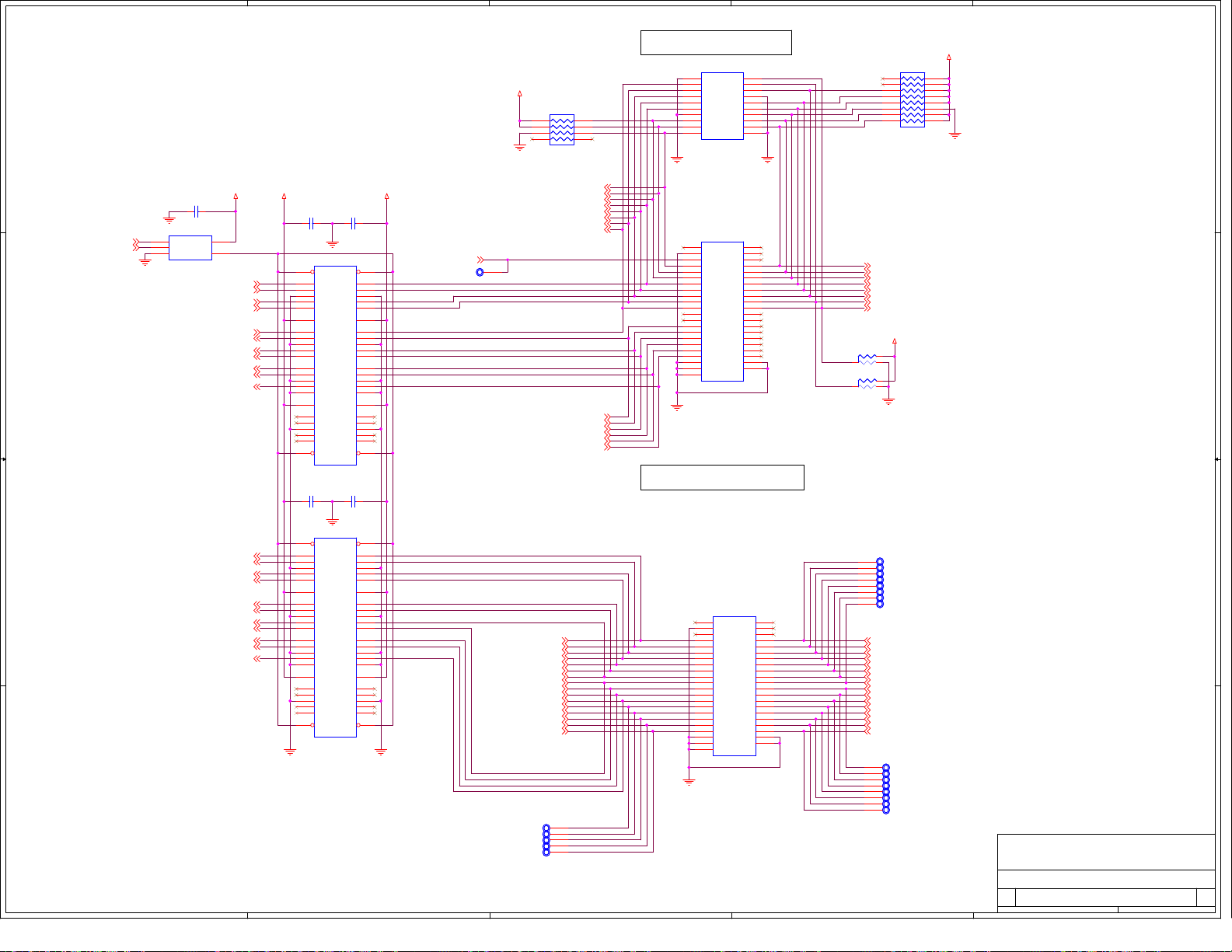
5
D D
4
Resistor array mounted
on component side
3.3V_BOARD
R255
R255
1 8
2 7
3 6
4 5
4.7K
4.7K
3
PROBE MODE INPUTS
JP12
JP12
2
GND12
3
5
PRB MODE INPUT HEADER
PRB MODE INPUT HEADER
3
5
77GND
9910
111112
GND1314
151516
171718
1919GND
4
4
6
6
8
10
12
14
16
18
20
2
Resistor array mounted
on component side
3.3V_BOARD
R257
R257
1
16
2
15
3
14
4
13
5
12
6
11
7
10
8 9
4.7K
4.7K
1
C234
C234
0.1uF
0.1uF
U22
U22
STRAP_SERDES_MODE_EN#{11,15}
STRAP_PROBE_MODE#{11,15}
C C
B B
A A
1
2
5
A
VCC
NAND
NAND
B
GND3Y
NC7SZ00
NC7SZ00
CPLD_HP_PWRGD_B{16}
CPLD_PORT_GOOD0#{16}
CPLD_PORT_GOOD1#{16}
CPLD_PORT_GOOD4#{16}
CPLD_PORT_GOOD5#{16}
CPLD_PORT_GOOD6#{16}
CPLD_PORT_GOOD7#{16}
CPLD_HP_CLKEN_B#{16}
CPLD_HP_PWREN_B{16}
CPLD_HP_PERST_B#{16}
CPLD_PORT_GOOD2#{16}
CPLD_PORT_GOOD3#{16}
CPLD_PORT_GOOD8#{16}
CPLD_PORT_GOOD9#{16}
CPLD_PORT_GOOD10#{16}
CPLD_PORT_GOOD11#{16}
5
4
HP_PWRFLT_B#{20}
HP_PRSNT_B#{9}
HP_BUTTON_B#{20}
HP_PWRLED_B#{20}
HP_ATNLED_B#{20}
3.3V_BOARD 3.3V_BOARD3.3V_BOARD
C233
C233
C232
C232
0.1uF
0.1uF
0.1uF
0.1uF
U21
U21
48
1OE#12OE#
HP_MRL_B#{15}
2
3
5
6
7
8
9
10
11
12
13
14
15
16
17
18
19
20
21
22
23
24
C236
C236
0.1uF
0.1uF
2
3
5
6
7
8
9
10
11
12
13
14
15
16
17
18
19
20
21
22
23
24
1B1
1A1
1B2
1A2
GND4GND
1B3
1A3
1B4
1A4
VCC
VCC
2B1
2A1
2B2
2A2
GND
GND
2B3
2A3
2B4
2A4
3B1
3A1
3B2
3A2
GND
GND
3B3
3A3
3B4
3A4
VCC
VCC
4B1
4A1
4B2
4A2
GND
GND
4B3
4A3
4B4
4A4
3OE#
4OE#
SN74CB3Q16244
SN74CB3Q16244
U20
U20
1OE#12OE#
1B1
1A1
1B2
1A2
GND4GND
1B3
1A3
1B4
1A4
VCC
VCC
2B1
2A1
2B2
2A2
GND
GND
2B3
2A3
2B4
2A4
3B1
3A1
3B2
3A2
GND
GND
3B3
3A3
3B4
3A4
VCC
VCC
4B1
4A1
4B2
4A2
GND
GND
4B3
4A3
4B4
4A4
3OE#
4OE#
SN74CB3Q16244
SN74CB3Q16244
C237
C237
0.1uF
0.1uF
47
46
45
44
43
42
41
40
39
38
37
36
35
34
33
32
31
30
29
28
27
26
25
48
47
46
45
44
43
42
41
40
39
38
37
36
35
34
33
32
31
30
29
28
27
26
25
4
PROCMON{11}
TPV27TPV27
PRB_HP_MRL_C#{11}
PRB_HP_PRSNT_C#{11}
PRB_HP_PWRFLT_C#{11}
PRB_HP_MRL_B#{11}
PRB_HP_PWRFLT_B#{11}
PRB_HP_PRSNT_B#{11}
PRB_HP_BUTTON_B#{11}
PRB_HP_PWRGD_B{11}
PRB_PORT_GOOD0#{11}
PRB_PORT_GOOD1#{11}
PRB_PORT_GOOD4#{11}
PRB_PORT_GOOD5#{11}
PRB_PORT_GOOD6#{11}
PRB_PORT_GOOD7#{11}
JP11
JP11
NC1NC
GND3NC
CLK/Q5CLK/Q
L3:77R1:7
L3:69R1:6
L3:511R1:5
L3:413R1:4
L3:315R1:3
L3:217R1:2
L3:119R1:1
L3:021R1:0
L2:723R0:7
L2:625R0:6
L2:527R0:5
L2:429R0:4
L2:331R0:3
33
L2:2
35
L2:1
37
L2:0
39
GND
41
GND
43
GND
MICTOR 38 RECEPT
MICTOR 38 RECEPT
2
4
6
8
10
12
14
16
18
20
22
24
26
28
30
32
34
R0:2
36
R0:1
38
R0:0
40
GND
42
GND
PRB_HP_BUTTON_C# {11}
PRB_HP_PWRGD_A {11}
PRB_HP_BUTTON_A# {11}
PRB_HP_PRSNT_A# {11}
PRB_HP_PWRFLT_A# {11}
PRB_HP_MRL_A# {11}
STRAP_DEBUG_SEL1 {11}
STRAP_DEBUG_SEL0 {11}
5.1K
5.1K
R39
R39
3
1 2
5.1K
5.1K
R40
R40
3
1 2
3.3V_BOARD
PROBE MODE OUTPUTS
TPV28TPV28
TPV29TPV29
TPV30TPV30
TPV31TPV31
TPV32TPV32
TPV33TPV33
TPV34TPV34
JP13
JP13
2
NC1NC
4
GND3NC
6
CLK/Q5CLK/Q
PRB_HP_CLKEN_B#{11}
PRB_HP_PWRLED_B#{11}
PRB_HP_PWREN_B{11}
PRB_HP_ATNLED_B#{11}
PRB_HP_PERST_B#{11}
PRB_PORT_GOOD2#{11}
PRB_PORT_GOOD3#{11}
PRB_PORT_GOOD8#{11}
PRB_PORT_GOOD9#{11}
PRB_PORT_GOOD10#{11}
PRB_PORT_GOOD11#{11}
PRB_HP_ATNLED_C#{11}
PRB_HP_PWREN_C{11}
PRB_HP_PWRLED_C#{11}
PRB_HP_PERST_C#{11}
PRB_HP_CLKEN_C#{11}
TPV44TPV44
TPV45TPV45
TPV46TPV46
TPV47TPV47
TPV48TPV48
3
33
35
37
39
41
43
L3:77R1:7
L3:69R1:6
L3:511R1:5
L3:413R1:4
L3:315R1:3
L3:217R1:2
L3:119R1:1
L3:021R1:0
L2:723R0:7
L2:625R0:6
L2:527R0:5
L2:429R0:4
L2:331R0:3
R0:2
L2:2
R0:1
L2:1
R0:0
L2:0
GND
GND
GND
GND
GND
MICTOR 38 RECEPT
MICTOR 38 RECEPT
8
10
12
14
16
18
20
22
24
26
28
30
32
34
36
38
40
42
TPV35TPV35
PRB_HP_CLKEN_A# {11}
PRB_HP_PWRLED_A# {11}
PRB_HP_PERST_A# {11}
PRB_HP_PWREN_A {11}
PRB_HP_ATNLED_A# {11}
PRB_GPIO2 {11}
PRB_GPIO3 {11}
PRB_GPIO4 {11}
PRB_GPIO5 {11}
PRB_GPIO6 {11}
PRB_GPIO7 {11}
PRB_SPARE1 {11}
PRB_SPARE2 {11}
PRB_GPIO0 {11}
PRB_GPIO1 {11}
PRB_SPARE0 {11}
2
TPV36TPV36
TPV37TPV37
TPV38TPV38
TPV39TPV39
TPV40TPV40
TPV41TPV41
TPV42TPV42
TPV43TPV43
PLX Technology, Inc.
PLX Technology, Inc.
PLX Technology, Inc.
870 W. Maude Avenue
870 W. Maude Avenue
870 W. Maude Avenue
Sunnyvale, CA 94085
Sunnyvale, CA 94085
Sunnyvale, CA 94085
www.plxtech.com
www.plxtech.com
Title
Title
Title
PEX8648 RDK - Probe Mode Interface
PEX8648 RDK - Probe Mode Interface
PEX8648 RDK - Probe Mode Interface
Size Document Number Rev
Size Document Number Rev
Size Document Number Rev
C
C
C
91-0082-100-A 102
91-0082-100-A 102
91-0082-100-A 102
Date: Sheet
Date: Sheet
Date: Sheet
www.plxtech.com
1
17 21Tuesday, November 16, 2010
17 21Tuesday, November 16, 2010
17 21Tuesday, November 16, 2010
of
of
of
Page 61
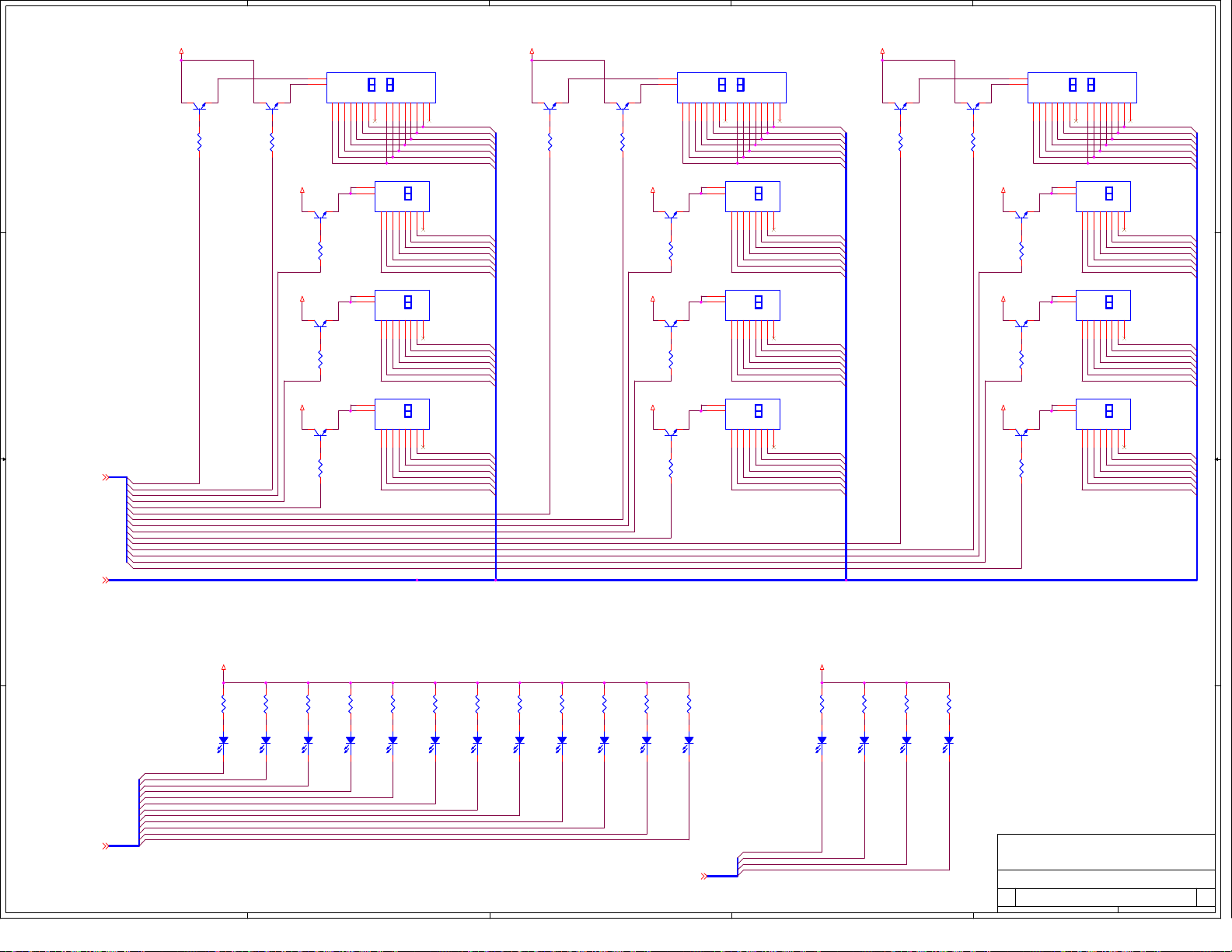
5
4
3
2
1
3.3V_BOARD 3.3V_BOARD 3.3V_BOARD
DS5 RedDS5 Red
14
ANODE1
13
3.3V_BOARD
Q7
Q7
3 2
3.3V_BOARD
Q10
Q10
3 2
3.3V_BOARD
Q13
Q13
3 2
ANODE2
A16B15C3D2E1F18G17DP
MMBT3904LT1
MMBT3904LT1
1
R187
R187
5.1K
5.1K
MMBT3904LT1
MMBT3904LT1
1
R190
R190
5.1K
5.1K
MMBT3904LT1
MMBT3904LT1
1
R193
R193
5.1K
5.1K
A11B10C8D6E5F12G7DP
4
DS8 RedDS8 Red
3
ANODE
8
ANODE
A7B6C4D2E1F9G10DP
DS11 RedDS11 Red
3
ANODE
8
ANODE
A7B6C4D2E1F9G10DP
DS14 RedDS14 Red
3
ANODE
8
ANODE
A7B6C4D2E1F9G10DP
9
PRT_WIDTH_SEG6
PRT_WIDTH_SEG5
PRT_WIDTH_SEG4
PRT_WIDTH_SEG3
PRT_WIDTH_SEG2
PRT_WIDTH_SEG1
PRT_WIDTH_SEG0
5
PRT_WIDTH_SEG6
PRT_WIDTH_SEG5
PRT_WIDTH_SEG4
PRT_WIDTH_SEG3
PRT_WIDTH_SEG2
PRT_WIDTH_SEG1
PRT_WIDTH_SEG0
5
PRT_WIDTH_SEG6
PRT_WIDTH_SEG5
PRT_WIDTH_SEG4
PRT_WIDTH_SEG3
PRT_WIDTH_SEG2
PRT_WIDTH_SEG1
PRT_WIDTH_SEG0
5
PRT_WIDTH_SEG6
PRT_WIDTH_SEG5
PRT_WIDTH_SEG4
PRT_WIDTH_SEG3
PRT_WIDTH_SEG2
PRT_WIDTH_SEG1
PRT_WIDTH_SEG0
Q3
Q3
3 2
1
MMBT3904LT1
MMBT3904LT1
R183
R183
5.1K
5.1K
Q4
Q4
3 2
1
MMBT3904LT1
MMBT3904LT1
R184
R184
5.1K
5.1K
Q2
Q1
Q1
3 2
MMBT3904LT1
MMBT3904LT1
D D
C C
PRT_WIDTH_DIG[14:0]{16}
B B
PRT_WIDTH_SEG[6:0]{16}
PRT_WIDTH_DIG0
PRT_WIDTH_DIG1
PRT_WIDTH_DIG2
PRT_WIDTH_DIG3
PRT_WIDTH_DIG4
PRT_WIDTH_DIG5
PRT_WIDTH_DIG6
PRT_WIDTH_DIG7
PRT_WIDTH_DIG8
PRT_WIDTH_DIG9
PRT_WIDTH_DIG10
PRT_WIDTH_DIG11
PRT_WIDTH_DIG12
PRT_WIDTH_DIG13
PRT_WIDTH_DIG14
1
R181
R181
5.1K
5.1K
Q2
3 2
1
MMBT3904LT1
MMBT3904LT1
R182
R182
5.1K
5.1K
DS6 RedDS6 Red
14
ANODE1
13
ANODE2
A16B15C3D2E1F18G17DP
3.3V_BOARD
Q8
Q8
3 2
MMBT3904LT1
MMBT3904LT1
1
R188
R188
5.1K
5.1K
3.3V_BOARD
Q11
Q11
3 2
MMBT3904LT1
MMBT3904LT1
1
R191
R191
5.1K
5.1K
3.3V_BOARD 3.3V_BOARD
Q14
Q14
3 2
MMBT3904LT1
MMBT3904LT1
1
R194
R194
5.1K
5.1K
A11B10C8D6E5F12G7DP
4
DS9 RedDS9 Red
3
ANODE
8
ANODE
A7B6C4D2E1F9G10DP
DS12 RedDS12 Red
3
ANODE
8
ANODE
A7B6C4D2E1F9G10DP
DS15 RedDS15 Red
3
ANODE
8
ANODE
A7B6C4D2E1F9G10DP
9
PRT_WIDTH_SEG6
PRT_WIDTH_SEG5
PRT_WIDTH_SEG4
PRT_WIDTH_SEG3
PRT_WIDTH_SEG2
PRT_WIDTH_SEG1
PRT_WIDTH_SEG0
5
PRT_WIDTH_SEG6
PRT_WIDTH_SEG5
PRT_WIDTH_SEG4
PRT_WIDTH_SEG3
PRT_WIDTH_SEG2
PRT_WIDTH_SEG1
PRT_WIDTH_SEG0
5
PRT_WIDTH_SEG6
PRT_WIDTH_SEG5
PRT_WIDTH_SEG4
PRT_WIDTH_SEG3
PRT_WIDTH_SEG2
PRT_WIDTH_SEG1
PRT_WIDTH_SEG0
5
PRT_WIDTH_SEG6
PRT_WIDTH_SEG5
PRT_WIDTH_SEG4
PRT_WIDTH_SEG3
PRT_WIDTH_SEG2
PRT_WIDTH_SEG1
PRT_WIDTH_SEG0
Q5
Q5
3 2
1
MMBT3904LT1
MMBT3904LT1
R185
R185
5.1K
5.1K
Q6
Q6
3 2
1
MMBT3904LT1
MMBT3904LT1
R186
R186
5.1K
5.1K
3.3V_BOARD
Q9
Q9
3 2
3.3V_BOARD
Q12
Q12
3 2
Q15
Q15
3 2
DS7 RedDS7 Red
14
ANODE1
13
ANODE2
A16B15C3D2E1F18G17DP
MMBT3904LT1
MMBT3904LT1
1
R189
R189
5.1K
5.1K
MMBT3904LT1
MMBT3904LT1
1
R192
R192
5.1K
5.1K
MMBT3904LT1
MMBT3904LT1
1
R195
R195
5.1K
5.1K
A11B10C8D6E5F12G7DP
4
DS10 RedDS10 Red
3
ANODE
8
ANODE
A7B6C4D2E1F9G10DP
DS13 RedDS13 Red
3
ANODE
8
ANODE
A7B6C4D2E1F9G10DP
DS16 RedDS16 Red
3
ANODE
8
ANODE
A7B6C4D2E1F9G10DP
9
PRT_WIDTH_SEG6
PRT_WIDTH_SEG5
PRT_WIDTH_SEG4
PRT_WIDTH_SEG3
PRT_WIDTH_SEG2
PRT_WIDTH_SEG1
PRT_WIDTH_SEG0
5
PRT_WIDTH_SEG6
PRT_WIDTH_SEG5
PRT_WIDTH_SEG4
PRT_WIDTH_SEG3
PRT_WIDTH_SEG2
PRT_WIDTH_SEG1
PRT_WIDTH_SEG0
5
PRT_WIDTH_SEG6
PRT_WIDTH_SEG5
PRT_WIDTH_SEG4
PRT_WIDTH_SEG3
PRT_WIDTH_SEG2
PRT_WIDTH_SEG1
PRT_WIDTH_SEG0
5
PRT_WIDTH_SEG6
PRT_WIDTH_SEG5
PRT_WIDTH_SEG4
PRT_WIDTH_SEG3
PRT_WIDTH_SEG2
PRT_WIDTH_SEG1
PRT_WIDTH_SEG0
3.3V_BOARD 3.3V_BOARD
R198
DS18
DS18
Green
Green
R197
R197
150
150
R198
R199
R199
150
150
150
150
21
21
DS19
DS19
Green
Green
DS20
DS20
Green
Green
21
DS21
DS21
Green
Green
R200
R200
150
150
R201
R201
150
150
21
21
DS22
DS22
Green
Green
R196
R196
150
150
21
21
DS17
DS17
Green
Green
CPLD_UP_PORT0
CPLD_UP_PORT1
CPLD_UP_PORT2
CPLD_UP_PORT3
CPLD_UP_PORT4
A A
CPLD_UP_PORT[11:0]{16}
CPLD_UP_PORT5
CPLD_UP_PORT6
CPLD_UP_PORT7
CPLD_UP_PORT8
CPLD_UP_PORT9
CPLD_UP_PORT10
CPLD_UP_PORT11
DS23
DS23
Green
Green
R202
R202
150
150
R203
R203
R204
R204
R205
150
150
21
21
DS24
DS24
DS25
DS25
Green
Green
Green
Green
R205
150
150
150
150
21
21
DS26
DS26
Green
Green
CPLD_NT_PORT[3:0]{16}
5
4
3
DS27
DS27
Green
Green
R206
R206
150
150
R207
R207
150
150
21
DS28
DS28
Green
Green
CPLD_NT_PORT0
CPLD_NT_PORT1
CPLD_NT_PORT2
CPLD_NT_PORT3
21
R208
R208
150
150
DS29
DS29
Green
Green
R209
R209
150
150
21
21
DS30
DS30
Green
Green
2
DS31
DS31
Green
Green
R210
R210
150
150
R211
R211
150
150
21
DS32
DS32
Green
Green
PLX Technology, Inc.
PLX Technology, Inc.
PLX Technology, Inc.
870 W. Maude Avenue
870 W. Maude Avenue
870 W. Maude Avenue
Sunnyvale, CA 94085
Sunnyvale, CA 94085
Sunnyvale, CA 94085
www.plxtech.com
www.plxtech.com
Title
Title
Title
PEX8648 RDK - Port Width Indicators
PEX8648 RDK - Port Width Indicators
PEX8648 RDK - Port Width Indicators
Size Document Number Rev
Size Document Number Rev
Size Document Number Rev
C
C
C
91-0082-100-A 102
91-0082-100-A 102
91-0082-100-A 102
Date: Sheet
Date: Sheet
Date: Sheet
www.plxtech.com
1
18 21Tuesday, November 16, 2010
18 21Tuesday, November 16, 2010
18 21Tuesday, November 16, 2010
of
of
of
Page 62
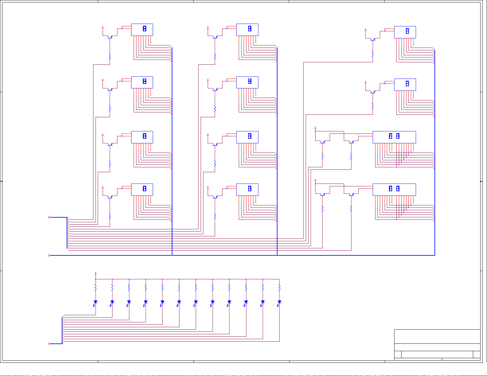
5
4
3
2
1
3.3V_BOARD 3.3V_BOARD
Q16
Q16
3 2
MMBT3904LT1
MMBT3904LT1
D D
1
R212
R212
5.1K
5.1K
3.3V_BOARD
Q19
Q19
3 2
MMBT3904LT1
MMBT3904LT1
1
R215
R215
5.1K
5.1K
3.3V_BOARD
C C
Q22
Q22
3 2
1
MMBT3904LT1
MMBT3904LT1
R220
R220
5.1K
5.1K
3.3V_BOARD
Q26
Q26
3 2
MMBT3904LT1
MMBT3904LT1
1
R224
R224
5.1K
PRT_ID_DIG[13:0]{16}
B B
PRT_ID_DIG0
PRT_ID_DIG1
PRT_ID_DIG2
PRT_ID_DIG3
PRT_ID_DIG4
PRT_ID_DIG5
PRT_ID_DIG6
PRT_ID_DIG7
PRT_ID_DIG8
PRT_ID_DIG9
PRT_ID_DIG10
PRT_ID_DIG11
PRT_ID_DIG12
PRT_ID_DIG13
5.1K
DS33 RedDS33 Red
3
ANODE
8
ANODE
A7B6C4D2E1F9G10DP
DS36 RedDS36 Red
3
ANODE
8
ANODE
A7B6C4D2E1F9G10DP
DS39 RedDS39 Red
3
ANODE
8
ANODE
A7B6C4D2E1F9G10DP
DS42 RedDS42 Red
3
ANODE
8
ANODE
A7B6C4D2E1F9G10DP
5
PRT_ID_SEG6
PRT_ID_SEG5
PRT_ID_SEG4
PRT_ID_SEG3
PRT_ID_SEG2
PRT_ID_SEG1
PRT_ID_SEG0
5
PRT_ID_SEG6
PRT_ID_SEG5
PRT_ID_SEG4
PRT_ID_SEG3
PRT_ID_SEG2
PRT_ID_SEG1
PRT_ID_SEG0
5
PRT_ID_SEG6
PRT_ID_SEG5
PRT_ID_SEG4
PRT_ID_SEG3
PRT_ID_SEG2
PRT_ID_SEG1
PRT_ID_SEG0
5
PRT_ID_SEG6
PRT_ID_SEG5
PRT_ID_SEG4
PRT_ID_SEG3
PRT_ID_SEG2
PRT_ID_SEG1
PRT_ID_SEG0
Q17
Q17
3 2
3.3V_BOARD
Q20
Q20
3 2
3.3V_BOARD
Q23
Q23
3 2
3.3V_BOARD
Q27
Q27
3 2
MMBT3904LT1
MMBT3904LT1
1
R213
R213
5.1K
5.1K
MMBT3904LT1
MMBT3904LT1
1
R216
R216
5.1K
5.1K
MMBT3904LT1
MMBT3904LT1
1
R221
R221
5.1K
5.1K
MMBT3904LT1
MMBT3904LT1
1
R225
R225
5.1K
5.1K
DS34 RedDS34 Red
3
ANODE
8
ANODE
A7B6C4D2E1F9G10DP
DS37 RedDS37 Red
3
ANODE
8
ANODE
A7B6C4D2E1F9G10DP
DS40 RedDS40 Red
3
ANODE
8
ANODE
A7B6C4D2E1F9G10DP
DS43 RedDS43 Red
3
ANODE
8
ANODE
A7B6C4D2E1F9G10DP
5
PRT_ID_SEG6
PRT_ID_SEG5
PRT_ID_SEG4
PRT_ID_SEG3
PRT_ID_SEG2
PRT_ID_SEG1
PRT_ID_SEG0
5
PRT_ID_SEG6
PRT_ID_SEG5
PRT_ID_SEG4
PRT_ID_SEG3
PRT_ID_SEG2
PRT_ID_SEG1
PRT_ID_SEG0
5
PRT_ID_SEG6
PRT_ID_SEG5
PRT_ID_SEG4
PRT_ID_SEG3
PRT_ID_SEG2
PRT_ID_SEG1
PRT_ID_SEG0
5
PRT_ID_SEG6
PRT_ID_SEG5
PRT_ID_SEG4
PRT_ID_SEG3
PRT_ID_SEG2
PRT_ID_SEG1
PRT_ID_SEG0
3.3V_BOARD
Q24
Q24
3 2
3.3V_BOARD
Q28
Q28
3 2
MMBT3904LT1
MMBT3904LT1
1
R218
R218
5.1K
5.1K
MMBT3904LT1
MMBT3904LT1
1
R222
R222
5.1K
5.1K
Q25
Q25
3 2
1
Q29
Q29
3 2
1
3.3V_BOARD
3.3V_BOARD
MMBT3904LT1
MMBT3904LT1
R219
R219
5.1K
5.1K
MMBT3904LT1
MMBT3904LT1
R223
R223
5.1K
5.1K
Q18
Q18
3 2
1
Q21
Q21
3 2
1
DS41 RedDS41 Red
14
ANODE1
13
ANODE2
DS44 RedDS44 Red
14
ANODE1
13
ANODE2
MMBT3904LT1
MMBT3904LT1
R214
R214
5.1K
5.1K
MMBT3904LT1
MMBT3904LT1
R217
R217
5.1K
5.1K
A16B15C3D2E1F18G17DP
A16B15C3D2E1F18G17DP
DS35 RedDS35 Red
3
ANODE
8
ANODE
A7B6C4D2E1F9G10DP
DS38 RedDS38 Red
3
ANODE
8
ANODE
A7B6C4D2E1F9G10DP
A11B10C8D6E5F12G7DP
4
A11B10C8D6E5F12G7DP
4
5
PRT_ID_SEG6
PRT_ID_SEG5
PRT_ID_SEG4
PRT_ID_SEG3
PRT_ID_SEG2
PRT_ID_SEG1
PRT_ID_SEG0
5
PRT_ID_SEG6
PRT_ID_SEG5
PRT_ID_SEG4
PRT_ID_SEG3
PRT_ID_SEG2
PRT_ID_SEG1
PRT_ID_SEG0
9
PRT_ID_SEG6
PRT_ID_SEG5
PRT_ID_SEG4
PRT_ID_SEG3
PRT_ID_SEG2
PRT_ID_SEG1
PRT_ID_SEG0
9
PRT_ID_SEG6
PRT_ID_SEG5
PRT_ID_SEG4
PRT_ID_SEG3
PRT_ID_SEG2
PRT_ID_SEG1
PRT_ID_SEG0
PRT_ID_SEG[6:0]{16}
3.3V_BOARD
R235
DS53
DS53
Green
Green
R234
R234
150
150
R235
R236
R236
R237
DS55
DS55
Green
Green
R237
150
150
150
150
21
DS56
DS56
Green
Green
PLX Technology, Inc.
PLX Technology, Inc.
PLX Technology, Inc.
870 W. Maude Avenue
870 W. Maude Avenue
870 W. Maude Avenue
Sunnyvale, CA 94085
Sunnyvale, CA 94085
Sunnyvale, CA 94085
www.plxtech.com
www.plxtech.com
Title
Title
Title
PEX8648 RDK - Port Status Indicators
PEX8648 RDK - Port Status Indicators
PEX8648 RDK - Port Status Indicators
Size Document Number Rev
Size Document Number Rev
Size Document Number Rev
C
C
C
91-0082-100-A 102
91-0082-100-A 102
91-0082-100-A 102
Date: Sheet
Date: Sheet
2
Date: Sheet
www.plxtech.com
1
19 21Tuesday, November 16, 2010
19 21Tuesday, November 16, 2010
19 21Tuesday, November 16, 2010
of
of
of
150
150
21
21
DS54
DS54
Green
Green
3
R229
DS47
DS47
Green
Green
R228
R228
150
150
R229
R230
R230
150
150
150
150
21
21
DS48
DS48
Green
Green
4
DS49
DS49
Green
Green
21
R226
R226
R227
R227
150
150
150
150
21
21
DS45
DS45
Green
Green
CPLD_PRT_STATUS0
5
CPLD_PRT_STATUS1
CPLD_PRT_STATUS2
CPLD_PRT_STATUS3
CPLD_PRT_STATUS4
CPLD_PRT_STATUS5
CPLD_PRT_STATUS6
CPLD_PRT_STATUS7
CPLD_PRT_STATUS8
CPLD_PRT_STATUS9
CPLD_PRT_STATUS10
CPLD_PRT_STATUS11
A A
CPLD_PRT_STATUS[11:0]{16}
DS46
DS46
Green
Green
21
DS50
DS50
Green
Green
R231
R231
150
150
R232
R232
R233
R233
150
150
150
150
21
21
DS51
DS51
Green
Green
DS52
DS52
Green
Green
21
Page 63
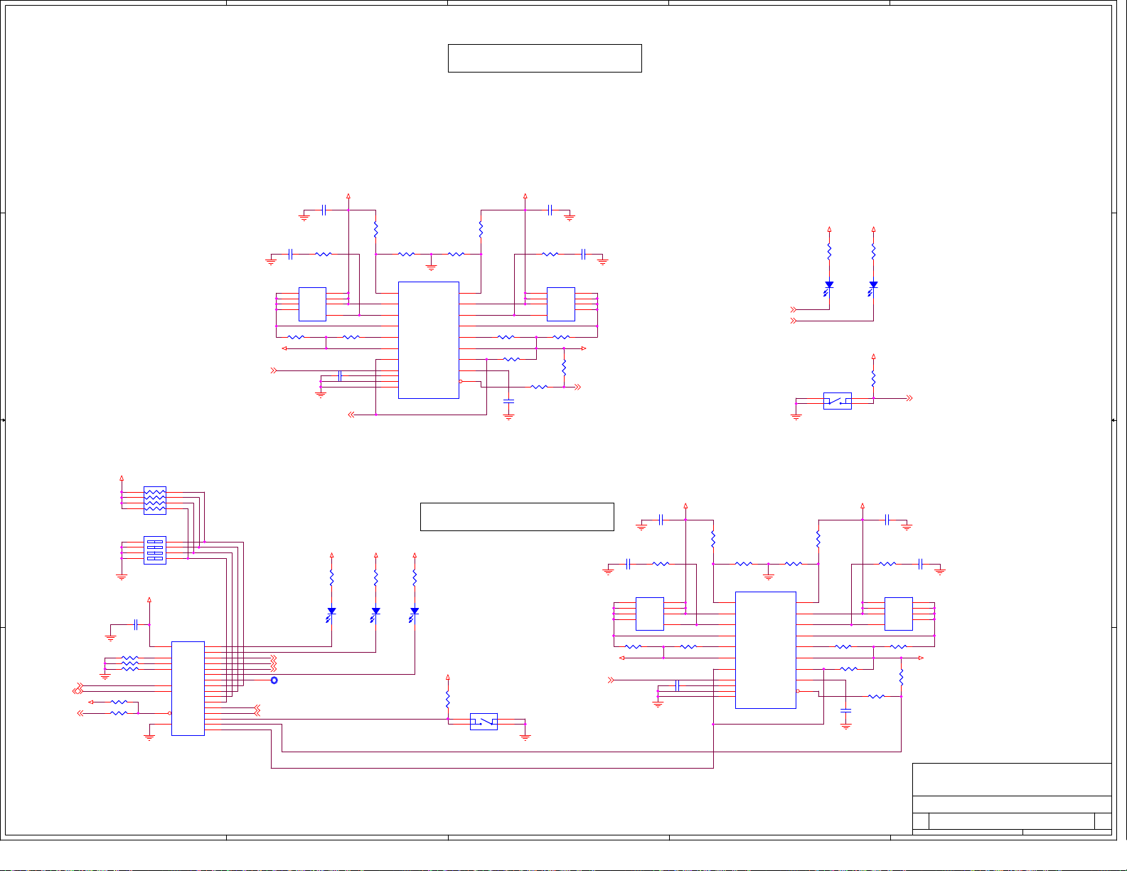
5
4
3
2
1
PARALLEL HOT PLUG TO PORT 5
D D
R276
R276
5.1K
5.1K
1%
1%
6
19
2
9
14
12
13
4
16
4
B3S-1002
B3S-1002
3.3V_HOT_PLUG12V_HOT_PLUG
R295
R295
4.99K
4.99K
1%
1%
R247 2.00K 1%R247 2.00K 1%
R254 5.1KR254 5.1K
R250 0R250 0
C155
C155
0.1uF
0.1uF
VDDHP_12V IS CURRENT
LIMITED TO 5 AMPS
SW8
SW8
1
23
C153
C153
0.1uF
0.1uF
C230
C230
R28733R287
33
0.1uF
0.1uF
Q32
Q32
1
D
S
2
D
S
3
D
S
D
4
G
IRF7470
IRF7470
R248 0.02 1%R248 0.02 1%
R249
R249
5.1K
5.1K
SHP_PWREN{16}
3
5
6
7
VDDHP_3.3V IS CURRENT
8
LIMITED TO 5 AMPS
3.3V_BOARD
HP_PWRFLT_B# {17}
R270 0.02 1%R270 0.02 1%
12V_BOARD
C229
C229
0.1uF
0.1uF
5
6
7
8
Q33
Q33
D
D
D
D
IRF7470
IRF7470
C223
C223
0.1uF
0.1uF
R29033R290
33
1
S
2
S
3
S
4
G
R268 2.00K 1%R268 2.00K 1%
3.3V_BOARD 3.3V_BOARD
R251
R251
150
150
21
DS58
DS58
Yellow
Yellow
HP_ATNLED_B#{17}
HP_PWRLED_B#{17}
SW7
SW7
1
2 3
B3S-1002
B3S-1002
3.3V_SERIAL_HOT_PLUG12V_SERIAL_HOT_PLUG
R294
IN2
1%
1%
6
19
2
9
14
12
13
4
16
R294
4.99K
4.99K
1%
1%
R273 2.00K 1%R273 2.00K 1%
R269 5.1KR269 5.1K
R292
R292
28.0K
28.0K
1%
1%
R293 3.48K
U18
U18
VSENSE1
DISCH1
GATE1
ISENSE1
ISET1
IN1
PWRGD1
ENABLE
VREG
DGND
AGND
TPS2311
TPS2311
1%
1%
R293 3.48K
VSENSE2
DISCH2
GATE2
ISENSE2
ISET2
PWRGD2
TIMER
FAULT#
2
R291 3.48K
R291 3.48K
7
20
1
10
15
11
17
18
C2260.1uF C2260.1uF
5
3
8
3.3V_BOARD
4
R272 0R272 0
C224
C224
0.1uF
0.1uF
R252
R252
150
150
21
DS59
DS59
Green
Green
R253
R253
5.1K
5.1K
HP_BUTTON_B# {17}
C225
C225
0.1uF
0.1uF
C228
C228
R28933R289
33
0.1uF
0.1uF
Q34
Q34
5
1
D
S
6
2
D
S
7
3
D
S
4
G
IRF7470
IRF7470
R271 0.02 1%R271 0.02 1%
VDDHP_3.3V IS CURRENT
8
D
LIMITED TO 5 AMPS
3.3V_BOARD
R277
R277
5.1K
5.1K
PLX Technology, Inc.
PLX Technology, Inc.
PLX Technology, Inc.
870 W. Maude Avenue
870 W. Maude Avenue
870 W. Maude Avenue
Sunnyvale, CA 94085
Sunnyvale, CA 94085
Sunnyvale, CA 94085
www.plxtech.com
www.plxtech.com
Title
Title
Title
PEX8648 RDK - Hot Plug
PEX8648 RDK - Hot Plug
PEX8648 RDK - Hot Plug
Size Document Number Rev
Size Document Number Rev
Size Document Number Rev
C
C
C
91-0082-100-A 102
91-0082-100-A 102
91-0082-100-A 102
Date: Sheet
Date: Sheet
Date: Sheet
www.plxtech.com
1
20 21Tuesday, November 16, 2010
20 21Tuesday, November 16, 2010
20 21Tuesday, November 16, 2010
of
of
of
C152
C152
0.1uF
0.1uF
C231
C231
R28833R288
33
0.1uF
0.1uF
Q31
Q31
5
1
D
S
6
2
D
S
7
3
D
VDDHP_12V IS CURRENT
SW11
SW11
RN5
RN5
5.1K
5.1K
LIMITED TO 5 AMPS
18
27
36
45
ON
ON
8
7
6
5
U17
U17
24
V+
21
AD0
2
AD1
3
AD2
22
SCL
23
SDA
1
INT#
12
GND
MAX7311AUG
MAX7311AUG
R245 0.02 1%R245 0.02 1%
12V_BOARD
HP_PWREN_B{16}
SLOT0
SLOT1
SLOT2
SLOT3
4
IO0
5
IO1
6
IO2
7
IO3
8
IO4
9
IO5
10
IO6
11
IO7
13
IO8
14
IO9
15
IO10
16
IO11
17
IO12
18
IO13
19
IO14
20
IO15
CPLD_SHP_PWREN {16}
CPLD_SHP_CLKEN# {16}
CPLD_SHP_PERST# {16}
TPV50TPV50
SHP_PRSNT# {10}
SHP_MRL# {15}
C C
Solderside
3.3V_BOARD
B B
1
2
3
4
SW DIP-4
SW DIP-4
3.3V_BOARD
C222
C222
0.047uF
0.047uF
R282 0R282 0
R283 0R283 0
R284 0R284 0
I2C_SCL1{11}
I2C_SDA1{11}
SHPC_INT#{11}
A A
3.3V_BOARD
R281 5.1KR281 5.1K
R280 0R280 0
5
8
D
IRF7470
IRF7470
HP_PWRGD_B{16}
SHP_PWRLED#
SHP_ATNLED#
SHP_PWRFLT#
SHP_PWRGD
S
4
G
R246 2.00K 1%R246 2.00K 1%
R275
R275
150
150
21
DS60
DS60
Green
Green
4
C1540.1uF C1540.1uF
INTERLOCK
SHP_BUTTON#
3.3V_BOARD3.3V_BOARD
21
R297
R297
28.0K
28.0K
1%
1%
R296 3.48K
R296 3.48K
U15
U15
7
VSENSE1
20
DISCH1
1
GATE1
10
ISENSE1
15
ISET1
11
IN1
17
PWRGD1
18
ENABLE
5
VREG
3
DGND
8
AGND
TPS2311
TPS2311
R274
R274
150
150
DS61
DS61
Yellow
Yellow
R298 3.48K
R298 3.48K
1%
1%
VSENSE2
DISCH2
GATE2
ISENSE2
ISET2
IN2
PWRGD2
TIMER
FAULT#
SERIAL HOT PLUG TO PORT 8
3.3V_BOARD
R279
R279
150
150
21
DS62
DS62
Yellow
Yellow
3.3V_BOARD
Page 64
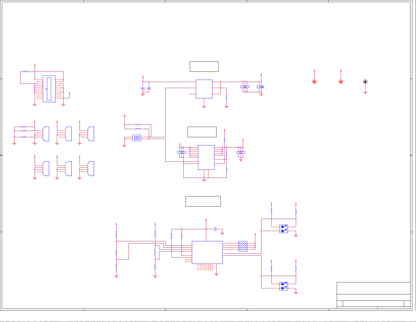
5
D D
4
3
2
1
3.3V_BOARD
R314 100R314 100
C C
R315 200R315 200
R317 200R317 200
R316 100R316 100
B B
A A
P6
P6
P9
P9
11
11
12
12
13
13
14
14
15
15
16
16
17
17
18
18
19
19
20
20
1
+12V
2
GND
3
GND
4
+5V
IDE4_HEADER
IDE4_HEADER
1
+12V
2
GND
3
GND
4
+5V
IDE4_HEADER
IDE4_HEADER
P5
ATX_20 STP5ATX_20 ST
1
1
2
2
3
3
4
4
5
5
6
6
12V_BOARD
7
7
8
8
9
9
10
10
3.3V_BOARD
12V_BOARD12V_BOARD12V_BOARD
P8
+12V
GND
GND
+5V
+12V
GND
GND
+5V
P8
1
+12V
2
GND
3
GND
4
+5V
IDE4_HEADER
IDE4_HEADER
12V_BOARD12V_BOARD12V_BOARD
P11
P11
1
+12V
2
GND
3
GND
4
+5V
IDE4_HEADER
IDE4_HEADER
R308
R308
6.81K
6.81K
1%
1%
R309
R309
1.50K
1.50K
1%
1%
R310
R310
12.1K
12.1K
1%
1%
P7
P7
P10
P10
1
2
3
4
IDE4_HEADER
IDE4_HEADER
1
2
3
4
IDE4_HEADER
IDE4_HEADER
12V_BOARD
C147
C147
180uF
180uF
Solderside
R239 5.1KR239 5.1K
R240 5.1KR240 5.1K
SW6
SW6
ON
ON
1
4
2
3
SW DIP-2
SW DIP-2
Componentside
+
+
+
+
C146
C146
180uF
180uF
An exposed pad on
the underside shall
be connected to
ground through
several vias.
2.5V_PCIe_SWITCH1.0V_PCIe_SWITCH
R311
R311
14.3K
14.3K
1.00K
1.00K
4.53K
4.53K
R312
R312
R313
R313
R302
R302
1%
1%
5.1K
5.1K
1%
1%
1%
1%
3.3V_BOARD
C150
C150
22uF
22uF
R303
R303
5.1K
5.1K
S7AH-08E1A00
S7AH-08E1A00
3.3V to 2.5V LINEAR
REGULATOR
1 53
2
4 6
PCIe SWITCH
VOLTAGE MONITORS
20
12
17
14
1
11
3
4
ISL6132
ISL6132
12V to 1.0V DC/DC
CONVERTER
U13
U13
Vin2Vout
1
On/Off
Trim
7
RS
NC
Gnd
3
U14
U14
1
IN
OUT
2
IN
OUT
3
IN
OUT
4
IN
OUT
5
IN
OUT
6
IN
16
EN
15
POK
NC
GND
EP
MAX8556
MAX8556
14
17
3.3V_BOARD
23
U19
U19
UVMON_1
OVMON_1
UVMON_2
OVMON_2
EN1
EN2
NC
NC
NC13NC15NC16NC18NC19NC21NC
NC
8
UVSTATUS_1
OVSTATUS_1
VDD
UVSTATUS_2
OVSTATUS_2
FB
0.1uF
0.1uF
C227
C227
22
4
5
6
11
10
9
8
7
13
12
PGOOD
PGOOD2
GND
10
8A Max
3.3V_BOARD
2
5
6
7
24
9
R242
R242
27K
27K
R243
R243
4.00K
4.00K
1%
1%
R244
R244
1.00K
1.00K
1%
1%
R238
R238
33K
33K
4 6
2.5V_PCIe_SWITCH
15 3
C151
C151
22uF
22uF
2
46
4.7K
4.7K
R286
R286
1 8
2 7
3 6
4 5
1.0V_PCIe_SWITCH
1 53
2
123
C148
C148
10uF
10uF
4
3.3A MAX
Limited by Power
Dissipation
3.3V_BOARD
C149
C149
1uF
1uF
3.3V_BOARD 3.3V_BOARD
R300
R300
150
150
DS64
DS64
43
Red
Red
2 1
Grn
Grn
3.3V_BOARD 3.3V_BOARD
R256
R256
150
150
2.5V_PCIe_SWITCH 1.0V_PCIe_SWITCH
banana_jack
banana_jack
J12
J12
R301
R301
150
150
R299
R299
150
150
banana_jack
banana_jack
J13
J13
J14
J14
banana_jack
banana_jack
DS63
Greater than
1.07 volt OR
Less than
0.95 volt is
out of range
5
4
Greater than
2.77 volt OR
Less than
2.27 volt is
out of range
3
DS63
Red
Red
2 1
Grn
Grn
43
Title
Title
Title
PEX8648 RDK - Power
PEX8648 RDK - Power
PEX8648 RDK - Power
Size Document Number Rev
Size Document Number Rev
Size Document Number Rev
C
C
C
91-0082-100-A 102
91-0082-100-A 102
91-0082-100-A 102
Date: Sheet
Date: Sheet
2
Date: Sheet
PLX Technology, Inc.
PLX Technology, Inc.
PLX Technology, Inc.
870 W. Maude Avenue
870 W. Maude Avenue
870 W. Maude Avenue
Sunnyvale, CA 94085
Sunnyvale, CA 94085
Sunnyvale, CA 94085
www.plxtech.com
www.plxtech.com
www.plxtech.com
21 21Tuesday, November 16, 2010
21 21Tuesday, November 16, 2010
1
21 21Tuesday, November 16, 2010
of
of
of
 Loading...