

Page 1

PEX 8505RDK
Hardware Reference Manual
Page 2

Page 3

PEX 8505RDK
Hardware Reference Manual
Version 1.1
October 2007
Website: http://www.plxtech.com
Support: http://www.plxtech.com/support
Phone: 408 774-9060
800 759-3735
Fax: 408 774-2169
Page 4

© 2007 PLX Technology, Inc. All rights reserved.
PLX Technology, Inc. retains the right to make changes to this product at any time, without notice. Products may
have minor variations to this publication, known as errata. PLX assumes no liability whatsoever, including
infringement of any patent or copyright, for sale and use of PLX products.
PLX Technology and the PLX logo are registered trademarks of PLX Technology, Inc.
Other brands and names are the property of their respective owners.
Order Number: PEX 8505-RDK-HRM-1.1
Printed in the USA, October 2007
Page 5
PREFACE
NOTICE
This document contains PLX Confidential and Proprietary information. The contents of this document may
not be copied nor duplicated in any form, in whole or in part, without prior written consent from PLX
Technology, Inc.
PLX provides the information and data included in this document for your benefit, but it is not possible to
entirely verify and test all the information, in all circumstances, particularly information relating to non-PLX
manufactured products. PLX makes neither warranty nor representation relating to the quality, content, or
adequacy of this information. The information in this document is subject to change without notice.
Although every effort has been made to ensure the accuracy of this manual, PLX shall not be liable for
any errors, incidental, or consequential damages in connection with the furnishing, performance, or use of
this manual or examples herein. PLX assumes no responsibility for damage or loss resulting from the use
of this manual, for loss or claims by third parties, which may arise through the use of the RDK, or for any
damage or loss caused by deletion of data as a result of malfunction or repair.
ABOUT THIS MANUAL
This document describes the PLX PEX 8505RDK, a Rapid Development Kit, from a hardware perspective.
It contains a description of all major functional circuit blocks on the board and also is a reference for the
creation of software for this product. This manual also includes complete schematics and bill of materials.
REVISION HISTORY
Date Version Comments
May 2007 0.90 Hardware Reference Manual initial release.
June 2007 1.0 Minor content update.
October
2007
1.1 Fixed note in schematic.
PEX 8505RDK Hardware Reference Manual v1.1
© 2007, PLX Technology, Inc. All rights reserved. i
Page 6

Page 7

CONTENTS
1. General Information ................................................................................................. 1
1.1 PEX 8505 Features .......................................................................................... 2
1.2 PEX 8505RDK Features................................................................................... 2
1.3 RDK Port Expansion Kit Features .................................................................... 2
1.3.1 RDK Port Expansion Kit Components ....................................................... 3
2. PEX 8505RDK Hardware Architecture .................................................................... 5
2.1 PEX 8505 PCI Express Switch ......................................................................... 6
2.2 PCI Express Card Edge P1 .............................................................................. 6
2.3 PCI Express Connector J1 ............................................................................... 6
2.4 Reference Clock Circuitry ................................................................................. 6
2.5 Reset Circuitry .................................................................................................. 7
2.6 Serial EEPROM................................................................................................ 7
2.7 I2C Interface ..................................................................................................... 7
2.8 Power Distribution ............................................................................................ 7
2.8.1 Power Generation/Conversion .................................................................. 7
2.8.2 Power Sequencing .................................................................................... 8
2.9 LED Indicators .................................................................................................. 8
3. On-Board Connectors, Switches, and Jumpers..................................................... 11
3.1 DIP Switches .................................................................................................. 11
3.1.1 Upstream Port Selection (SW1) .............................................................. 11
3.1.2 PEX 8505 I2C Address Selection (SW2)................................................. 11
3.2 Push-Button Switches..................................................................................... 12
3.2.1 Hot Plug Attention Button# (SW5) ........................................................... 12
3.2.2 Manual Reset# (SW6) ............................................................................. 12
3.3 EEPROM Enable Jumper (JP5) ..................................................................... 12
3.4 JTAG Header (JP1) ........................................................................................ 12
3.5 PCI Express Fatal Error Indication (D9).......................................................... 12
3.6 PEX INTA# (D19) ........................................................................................... 12
3.7 Slots J1 Power Fault Indication (D20) ............................................................ 13
4. Serial EEPROM Registers..................................................................................... 13
4.1 Serial EEPROM Contents............................................................................... 13
5. FAQ/Troubleshooting............................................................................................. 13
5.1 Frequently Asked Questions........................................................................... 13
6. Bill of Materials/ Schematics.................................................................................. 13
PEX 8505RDK Hardware Reference Manual v1.1
© 2007, PLX Technology, Inc. All rights reserved. iii
Page 8

FIGURES
FIGURE 1-1. PEX 8505RDK COMPONENT SIDE VIEW ...................................................................................... 1
F
IGURE 1-2. RDK PORT EXPANDER ................................................................................................................ 3
FIGURE 1-3. PCIE CABLE ADAPTER ................................................................................................................. 3
FIGURE 1-4. PCIE 1-METER X1 CABLE ............................................................................................................. 3
F
IGURE 2-1. PEX 8505RDK HARDWARE ARCHITECTURE................................................................................. 5
FIGURE 2-2. PEX 8505RDK REFERENCE CLOCK CIRCUIT ............................................................................... 6
FIGURE 2-3. I2C CONNECTOR ORIENTATION FOR AARDVARD I2C CONTROLLER ................................................ 7
F
IGURE 2-4. PEX 8505RDK POWER SUBSYSTEM............................................................................................ 8
FIGURE 3-1. SWITCH SW1 DEFAULT SETTINGS .............................................................................................. 11
F
IGURE 3-2. SWITCH SW2 DEFAULT SETTINGS .............................................................................................. 11
TABLES
TABLE 2-1. PEX 8505RDK LED INDICATOR DESCRIPTIONS ............................................................................. 8
ABLE 3-1. SWITCH SW1 DESCRIPTION......................................................................................................... 11
T
T
ABLE 3-2. SWITCH SW2 DESCRIPTION......................................................................................................... 12
T
ABLE 3-3. JUMPER JP2 SETTINGS................................................................................................................ 12
PEX 8505RDK Hardware Reference Manual v1.1
© 2007, PLX Technology, Inc. All rights reserved. iv
Page 9
1. General Information
The PLX PEX 8505RDK is a Rapid Development Kit based on the PEX 8505, a 5-lane, 5-port PCI
Express switch. The PEX 8505RDK provides a complete hardware and software development platform to
facilitate getting designs up and running quickly, lowering risk and reducing time-to-market.
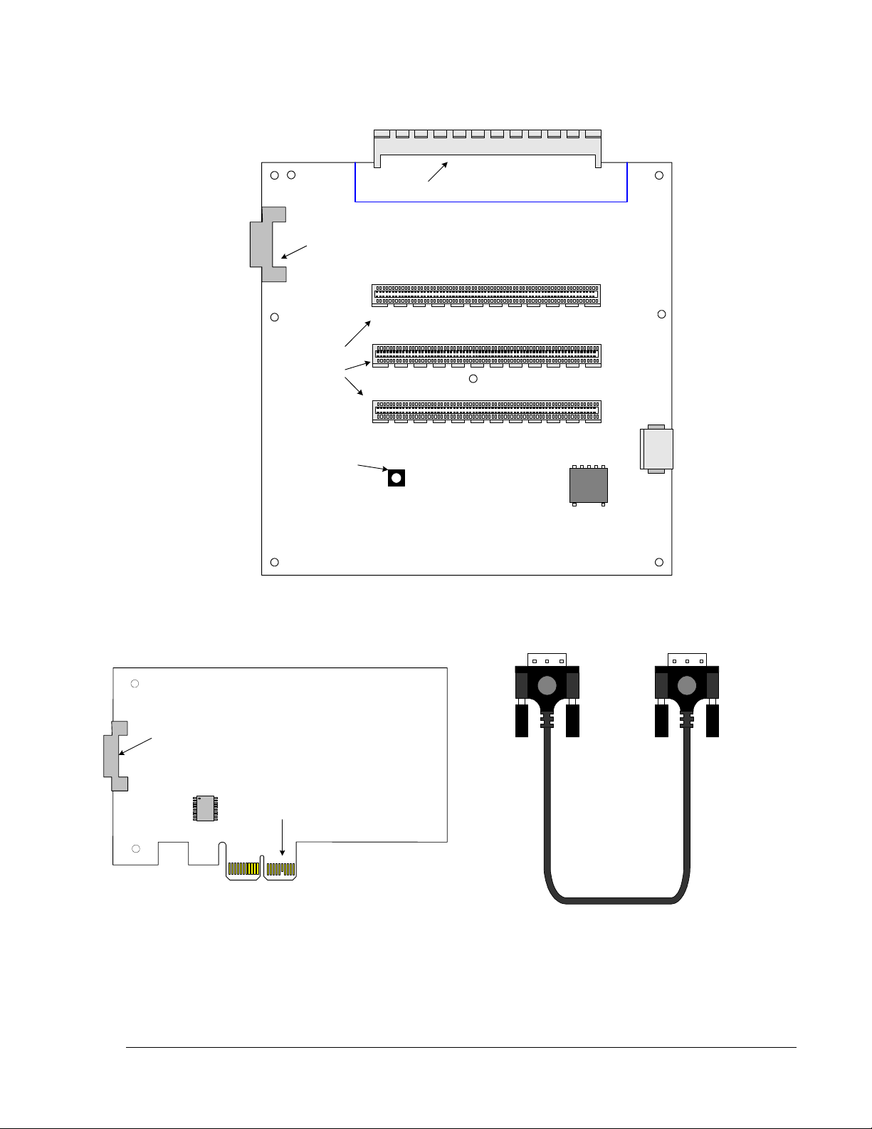
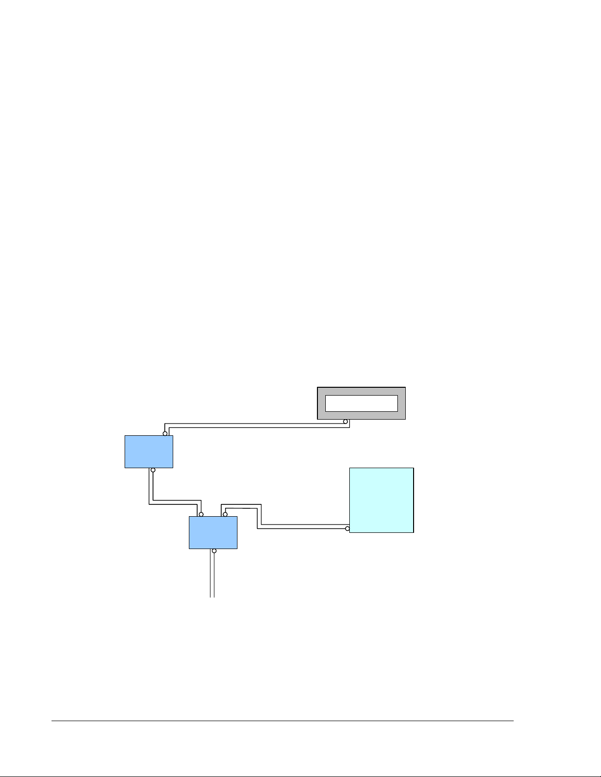
An RDK Port Expansion Kit is included, which is used to convert the PEX 8505RDK into a bench top
platform that supports the full 5-port/5-lane configuration. When mated to the RDK Port Expander, the
upstream port is connected to a PCI Express x1 Cable connector. The Expansion Kit includes a 1-meter
cable and adapter card, which allows the PEX 8505’s upstream port to connect to any standard PC. See
the RDK Port Expansion Kit Hardware Reference Manual for more details.
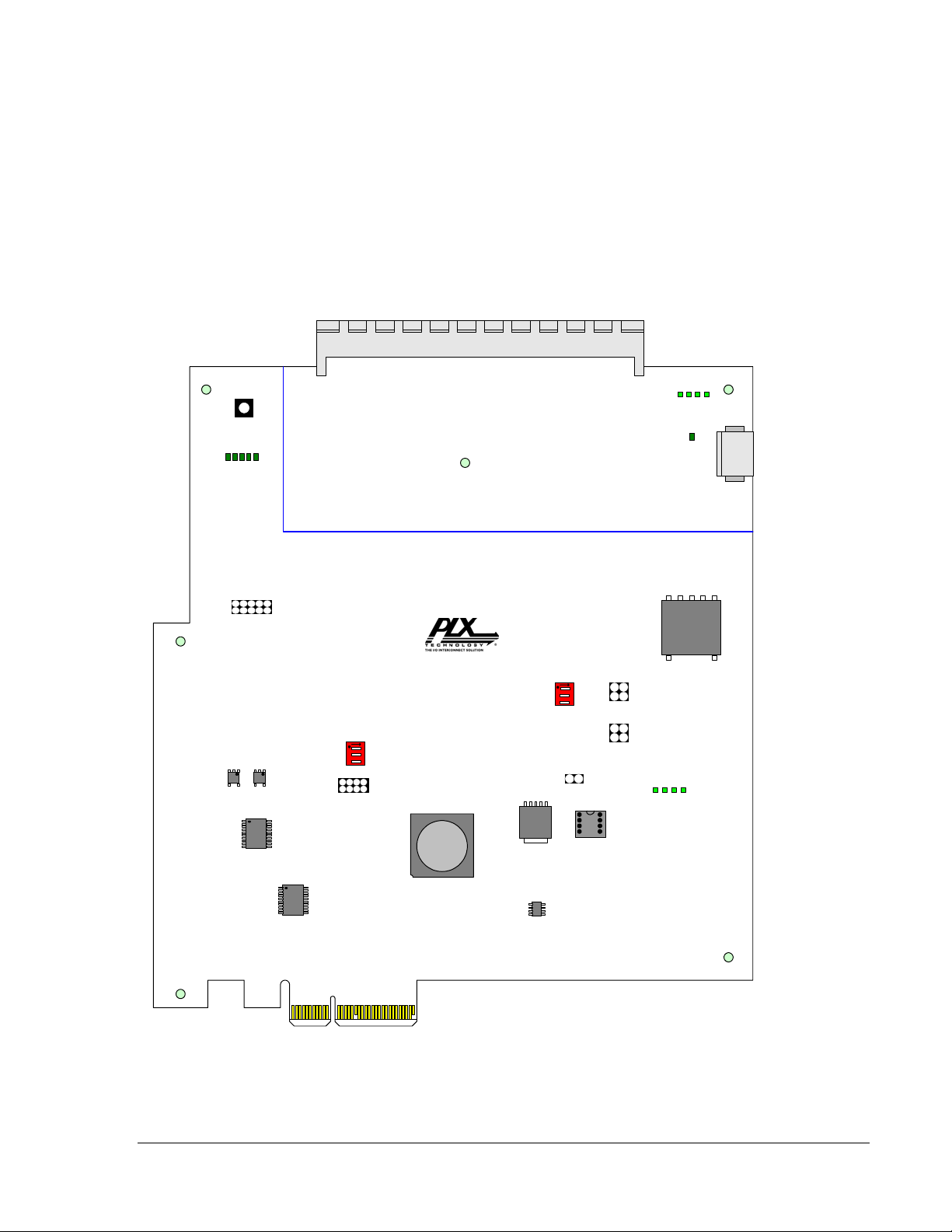
Manual PERST#
SW6
Main Board Power
Indicators
JTAG Header
Reset Circuitry
U8
Reference Clock Buffers
J1
JP1
U9
U10
P1
User Control DIP switch
SW1
JP2
U11
4 5 6 7
Lanes
Slots J1/J2/J3
Power Indicator
J5
Powered by J5
5V-3.3V DC/DC
converter
User Control DIP switch
SW2
U1
PEX
8505
A1
U13
3.3V-1V
Regulator
VTT Regulator
U14
U2
EEPROM
Socket
JP3
I2C
JP4
JP5
0 1 2 3
U12
Lanes
Figure 1-1. PEX 8505RDK Component Side View
PEX 8505RDK Hardware Reference Manual v1.1
© 2007, PLX Technology, Inc. All rights reserved. 1
Page 10

1.1 PEX 8505 Features
• 5-lane, 5-port (maximum) PCI Express switch
• PCI Express Base Specification revision 1.1 and PCI Standard Hot-Plug Controller and
Subsystem Specification, revision 1.0 compliance
• Five PCI Express lanes provide 25 Gbps aggregate bandwidth
• Cut-thru Packet latency of 210ns (x1 to x1)
• Non-blocking internal crossbar architecture supports full wire speed
• Out of band communication/initialization interfaces (Serial EEPROM and I2C)
• Maximum Payload Size up to 1024 bytes
• Performance tuning
• Up to 5-ports (Up to 4 possible port configurations)
• PCI Express Standard Hot Plug Controller for three ports
• Allows any port to be designated as upstream port
• Configuration with strapping pins and/or EEPROM
• Sideband INTA# (PEX_INTA#) and FATAL ERROR (FATAL_ERR#) signaling
• Lane reversal
1.2 PEX 8505RDK Features
• PLX PEX 8505 PCI Express switch in a 196-ball PBGA package
• Form factor based on PCI Express Card Electromechanical (CEM) Specification 1.1
• Four downstream PCI Express Slot connectors
• DIP switches for hardware configuration of PEX 8505 and on-board clock circuitry
• Support for Spread Spectrum Clocking (SSC).
• One Hot Plug controllable slot
• Socketable Serial EEPROM (3.3V)
• Standard 0.1” headers to connect up to I2C
• Manual push-button PERST# capability
• Lane Status indicator LEDs for visual inspection of link status
• Auxiliary ATX Hard disk connector for supporting additional power requirements for add-in cards
1.3 RDK Port Expansion Kit Features
• Provides a 4-lane/4-port breakout for PEX 8505 RDKs
• Upstream Connection via standard PCI Express x1cable
• Three downstream PCI Express Slot connectors
• Support for Spread Spectrum Clocking (SSC).
• Standard 0.1” headers to connect up to SM bus
• Manual push-button PERST# capability
• Auxiliary ATX Hard disk connector for supporting additional power requirements for add-in cards
PEX 8505RDK Hardware Reference Manual v1.1
2 © 2007, PLX Technology, Inc. All rights reserved.
Page 11
1.3.1 RDK Port Expansion Kit Components
J1
Cable Connector
(Upstream Port)
J3
RDK SLOT
PCI Express
J4
Downstream
Slots
J5
J6
Manual
PERST#
SW1
1
2
3
U4
J2
Figure 1-2. RDK Port Expander
J1
PCI Express x1
cable adapter
U3
PCI Express x1
Card Edge
Figure 1-3. PCIe Cable Adapter
Figure 1-4. PCIe 1-meter x1 cable
PEX 8505RDK Hardware Reference Manual v1.1
© 2007, PLX Technology, Inc. All rights reserved. 3
Page 12

Page 13
2. PEX 8505RDK Hardware Architecture
DIP
switch
8
RefClk
Buffer
RefClk
J1
x1
PCIe x1 Cable
x16 Connector
REFCLK
Buffer
x1
Port 4
PEX 8505
Port 0 Port 1 Port 2 Port 3
x4 Card Edge
x16 Connector
x1
x1
x1
J1
P1
J3
PEX 8505RDK
JTAG
connector
5
I2C
2
EEPROM
4
PERST#
Reset
Timer
RDK Port Expander
x16 Connector
J4
x16 Connector
J5
x16 Connector
J6
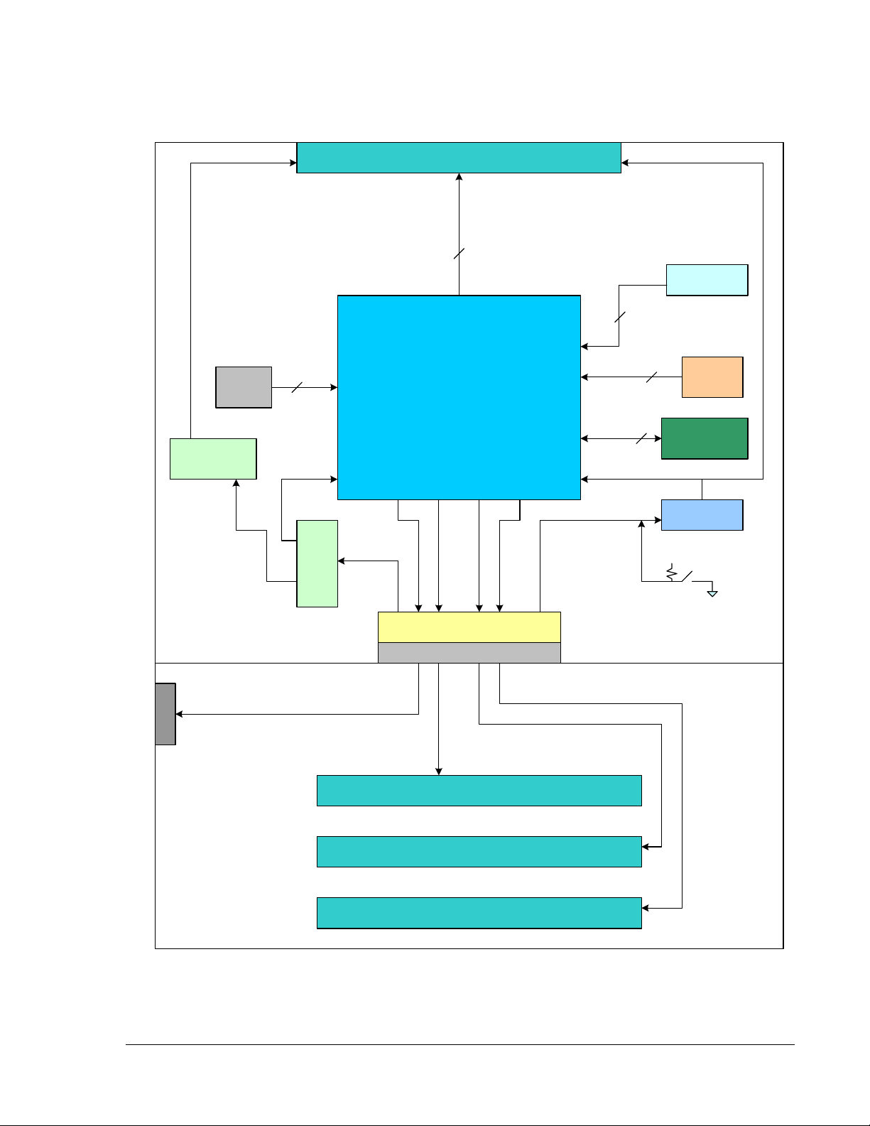
Figure 2-1. PEX 8505RDK Hardware Architecture
PEX 8505RDK Hardware Reference Manual v1.1
© 2007, PLX Technology, Inc. All rights reserved. 5
Page 14
2.1 PEX 8505 PCI Express Switch
The PEX 8505 is a 5-lane, 5-port (maximum) PCI Express switch, which can be configured using strap
pins or EEPROM. The RDK’s onboard PEX 8505 is set up as a 5-port switch, with one x1 upstream port
(Port 0) and four x1 downstream ports (Ports 1 - 4). Ports 0 - 3 connects to the card edge (P1), while Port
4 connects to x16-sized slot connectors (J1). The PEX 8509RDK plugs into an RDK Port expander which
breaks out four lanes connected to P1 into a PCI Expressx1 cable connector and three downstream slots.
2.2 PCI Express Card Edge P1
The RDK form factor is based on the PCI Express CEM 1.1 specification. The board can directly plug into
the RDK Port Expander, which in turn provides a break out of the lower four lanes. All four lanes from the
The default configuration of the PEX 8505RDK sets Port 0 to be the upstream port.
2.3 PCI Express Connector J1
Connector J1 is a straddle-mount (SMT), x16 PCI Express connector. Cards plugging into this slot will be
in-line with the RDK. Port 1 connects one lane (x1) to the lower four lanes of connector J1. The upper
fifteen lanes are unconnected. Power is provided to connector J1 from the ATX hard disk connector J5.
2.4 Reference Clock Circuitry
Two Cypress CY28400-2 1-to-4 PCI Express clock buffers (U10 and U11) provide on-board REFCLK
distribution to the PEX 8505 and the downstream slot (J1). The first CY28400-2 (U11) input is sourced by
the card edge P1. U11 provides two differential CML (current mode logic) clock outputs. One pair drives
the PEX 8505’s PEX_REFCLKP/N input. This pair is AC-coupled (C74 and C75). This is required to block
the DC information of the transmitter from the PEX 8505 clock receiver, which has on-chip biasing and
termination circuitry. The other pair drives the input of a second CY28400-2 (U10), which is used drive the
downstream slot.
RefClk
CY28400-2
CY28400-2
PEX 8505
PEX_REFCLK
Card-Edge
RefClk
Figure 2-2. PEX 8505RDK Reference Clock Circuit
PEX 8505RDK Hardware Reference Manual v1.1
6 © 2007, PLX Technology, Inc. All rights reserved.
Page 15
2.5 Reset Circuitry
The PEX 8505RDK reset circuitry includes a MAX6420 adjustable reset timer (U9) and manual reset
push-button switch (SW6). The reset timer accepts PERST# from the card edge (P1) and from SW6
(logical-OR via U8). The MAX6420 has the capability of adjusting the reset timeout period by changing
the value of C63 (0.001 µF ~= 3 ms).
2.6 Serial EEPROM
The PEX 8505RDK contains an 8-pin DIP socket for a serial EEPROM (U2). The board is populated with
a blank Atmel AT25080A 8-Kbit device. To use the serial EEPROM, place a shunt between pins 1 and 2
of JP2 (see section 3.4 for more details). The AT25080A device can directly interface to the PEX8505.
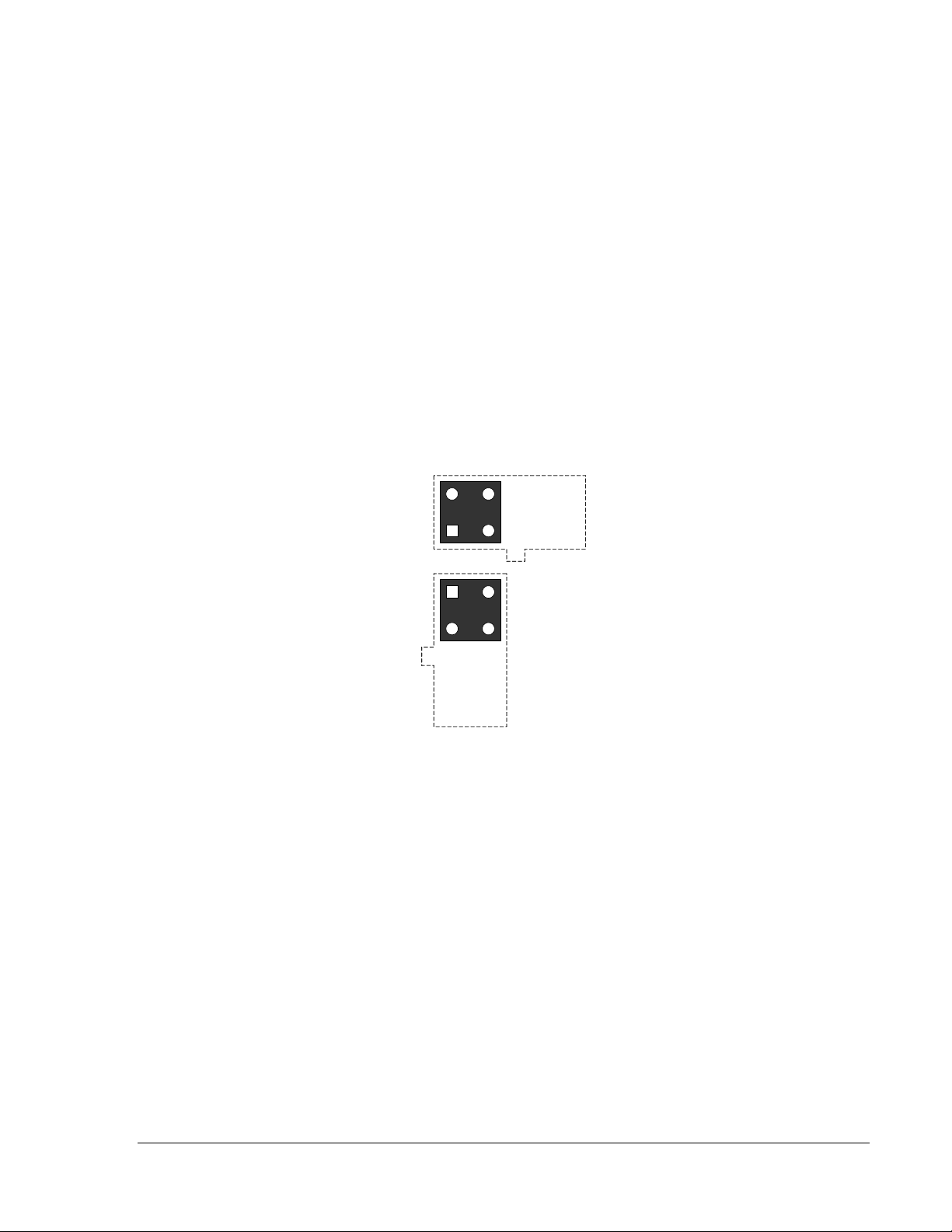
2.7 I2C Interface
The PEX 8505 implements an I2C slave interface, which allows an external I2C master to read and write
device registers through an out-of-band mechanism. The PEX 8505 I2C interface is accessible via a 7-bit
address, at data rates up to 400kbits/sec. The RDK provides two cascaded 2x2, 0.1” pitch headers (JP3
and JP4), which interface to the PEX 8505’s I2C port. This allows for cascading multiple RDKs together
using standard ribbon cable, or connecting various 3
Aardvark I2C controller.
2
1
1
3
JP3
JP4
rd
party I2C test equipment such as the Total Phase
4
3
2
4
Figure 2-3. I2C Connector Orientation for Aardvard I2C Controller
2.8 Power Distribution
2.8.1 Power Generation/Conversion
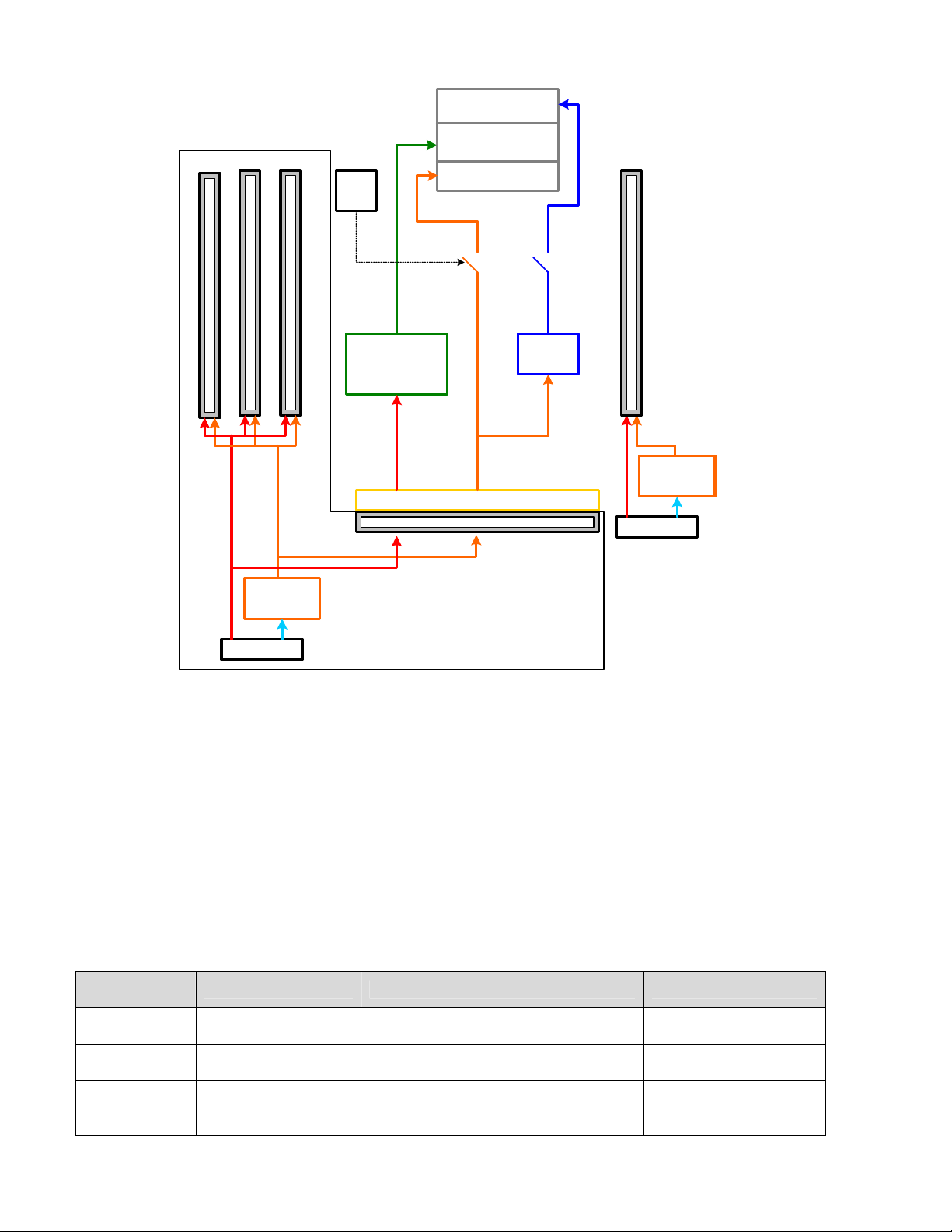
The PEX 8505RDK has two sources for DC power. The first source is the card edge connector (P1),
which gets it’s power from the RDK Port Expander. Card edge power is intended to power only RDK
board components. Slot J1 receives power via a 4-pin ATX hard disk connector (J5).
PEX8505 core and SerDes +1.0V supply is derived from the +3.3V rail through a Micrel MIC49150 LDO
regulator (U13). The PEX 8505’s +3.3V I/O supply receives power directly from the +3.3V card edge
power rail. The VTT supply for the PEX8505 PCI Express transmitters, is regulated from the +3.3V card
edge power via a Maxim MAX1806 adjustable LDO regulator (U14). The regulator output voltage is
normally set to +1.50V, but can be adjusted by changing the values of R98 and R102.
The ATX 4-pin connector provides +12V and +5V DC power. The +5V is converted down to +3.3V for slot
J1 through a Bel S7AH-08B330/-08E1A0 non-isolated DC/DC converter (U12). The +12V power rail is
used directly.
PEX 8505RDK Hardware Reference Manual v1.1
© 2007, PLX Technology, Inc. All rights reserved. 7
Page 16
PEX_VTT
PEX 8505
RDK Port Expander
Pwr
Seq.
VDD10/VDD10S/VDD10A
VDD33/VDD33A
PCI Express Connector
PCI Express Connector
PCI Express Connector
3.3V-to-1V
LDO Regulator
3.3V-to-
1.5V LDO
PCI Express Straddle Mount Connector
+12V
5V-to-3.3V
DC/DC
+5V
+3.3V
+12V
ATX HD Conn.
PCI Express Straddle Mount Connector
+3.3V
PCI Express Card Edge
+12V
+3.3V
5V-to-3.3V
DC/DC
ATX HD Conn.
+5V
Figure 2-4. PEX 8505RDK Power Subsystem
2.8.2 Power Sequencing
The PEX 8505 device requires that the 1.0V power rails are supplied before the 1.5V and 3.3V rails are
powered. This power sequencing is accomplished via three bipolar transistors (Q3, Q4, Q6), biasing
resistors and one power MOSFET (Q5).
2.9 LED Indicators
The PEX 8505RDK provides a number of LED indicators including power-on indication, PEX 8505 lane
status indication, and Hot Plug status indication. Table 2-1 provides a quick explanation of the various
board indicators.
Table 2-1. PEX 8505RDK LED Indicator descriptions
Indicator
Type
Board Power
indication
Slot J1 Power
Fault
J5 Power
indication
PEX 8505RDK Hardware Reference Manual v1.1
8 © 2007, PLX Technology, Inc. All rights reserved.
Locations LED On LED Off
D16, D15, D17, D18 1.0V, 1.5V, 12V, 3.3V power on
D14
D20
+12V or +3.3V power to slot J1 had
dropped below -15% on either supply.
ATX Hard disk connector is currently
supplying power
1.0V, 1.5V, 12V,
3.3V power off
+12V and +3.3V power
to slots J1 is good.
ATX hard disk
connector is not
supplying power
Page 17

Indicator
Type
PEX 8505 Port
0 Lane Status
PEX 8505 Port
1 Lane Status
PEX 8505 Port
2 Lane Status
PEX 8505 Port
3 Lane Status
PEX 8505 Port
4 Lane Status
PEX 8505
Fatal Error
Indication
PEX 8505
INTA#
Locations LED On LED Off
D1 Port 0 link is up
D4 Port 1 link is up
D5 Port 2 link is up
D8 Port 3 link is up
D2 Port 4 link is up
If LED is off, Port 0 link
is down
If LED is off, Port 1 link
is down
If LED is off, Port 2 link
is down
If LED is off, Port 3 link
is down
If LED is off, Port 4 link
is down
D9 PEX 8505 detected a fatal error. No fatal errors reported
D19
PEX 8505 has asserted sideband
interrupt
Interrupt is not asserted
PEX 8505RDK Hardware Reference Manual v1.1
© 2007, PLX Technology, Inc. All rights reserved. 9
Page 18

Page 19
3. On-Board Connectors, Switches, and Jumpers
3.1 DIP Switches
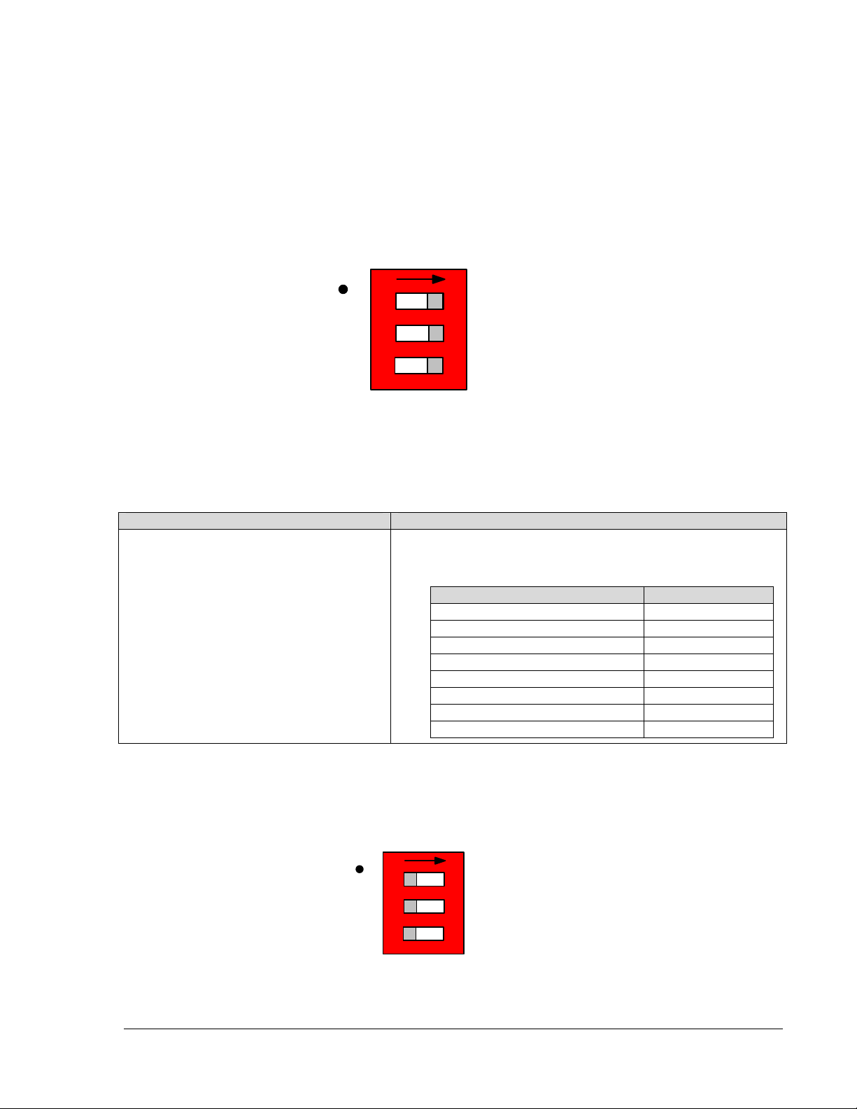
The PEX 8505RDK contains four user controllable DIP switches (SW1, SW2, SW3 and SW4) for
selecting various functionality. Each DIP switch position can be either ON (0b) or OFF (1b). The gray
squares in Figures 3-1 through 3-4 indicate which way the switch position is connected.
3.1.1 Upstream Port Selection (SW1)
HIGH
Figure 3-1. Switch SW1 Default Settings
SW1
ON
1
1
2
2
3
3
ON
UP_PORT0
UP_PORT1
UP_PORT2
LOW
Table 3-1. Switch SW1 Description
SW1 Functional Description Switch Position Settings
1: STRAP_UPSTRM_PORTSEL[0]
2: STRAP_UPSTRM_PORTSEL[1]
3: STRAP_UPSTRM_PORTSEL[2]
Bus Encodings [2:0] Upstream Port
STRAP_UPSTRM_PORTSEL [2:0]
Selects the PEX 8505 Upstream Port.
Default setting is 000b.
000b 0
001b 1
010b 2
011b 3
100b 4
101b 5
110b 6
111b 7
3.1.2 PEX 8505 I2C Address Selection (SW2)
Switch SW2 is used to select the lower three address bits of the PEX 8505’s I2C slave address.
HIGH
SW2
ON
1
1
2
2
3
3
ON
I2C_ADDR0
I2C_ADDR1
I2C_ADDR2
LOW
Figure 3-2. Switch SW2 Default Settings
PEX 8505RDK Hardware Reference Manual v1.1
© 2007, PLX Technology, Inc. All rights reserved. 11
Page 20
Table 3-2. Switch SW2 Description
SW2 Functional Description Switch Position Settings
1: I2C_ADDR[0]
2: I2C_ADDR[1]
3: I2C_ADDR[2]
Bus Encodings [1:0] PEX 8505 I2C Slave Address
000b 38h
PEX 8505 I2C Address bits[2:0].
Default setting is 111b.
001b 39h
010b 3Ah
011b 3Bh
100b 3Ch
101b 3Dh
110b 3Eh
111b 3Fh
3.2 Push-Button Switches
3.2.1 Hot Plug Attention Button# (SW5)
Switch SW5 provides a push-button switch control for the PEX 8505 Hot Plug Controller’s
HP_BUTTON[3]# input pin. The PEX 8505 contains internal debounce circuitry for this input.
3.2.2 Manual Reset# (SW6)
The PEX 8505 RDK provides a manual PERST# capability. Note that manual PERST# will only apply
warm reset to the PEX 8505, and slot J1.
3.3 EEPROM Enable Jumper (JP5)
JP5 is used to enable an EEPROM presence detection to the PEX 8505. Install a shunt between pins 1 2 to indicate a Serial EEPROM is present. Un-install the shunt to indicate a Serial EEPROM is not present.
Table 3-3. Jumper JP2 settings
JP5 Setting EEPROM Status
Shunt installed (Default) Serial EEPROM present
Shunt not installed Serial EEPROM not present
3.4 JTAG Header (JP1)
Header JP1 provides a direct connection to the PEX 8505 JTAG interface. The 10-pin connector is
designed to allow a direct interface to 3rd party JTAG controllers, such as the Corelis USB-1149.1/E
controller.
3.5 PCI Express Fatal Error Indication (D9)
The PEX 8505 provides an output status pin (FATAL_ERR#), which reports the event of a PCI Express
fatal error condition. The RDK connects this output to D9, which is lit when a fatal error is detected.
Examples of fatal error conditions are data link layer protocol errors, receiver overflow, malformed TLPs,
etc… The PCI Express Base specification provides a complete listing of fatal error conditions.
3.6 PEX INTA# (D19)
PEX 8505 provides a side-band interrupt pin for signaling various programmable events.
PEX 8505RDK Hardware Reference Manual v1.1
12 © 2007, PLX Technology, Inc. All rights reserved.
Page 21
3.7 Slots J1 Power Fault Indication (D20)
Slot J1 is power by the ATX 4-pin hard disk connector and a DC/DC converter (U12). No circuitry is
provided to current limit the power consumed by slot J1; however, a voltage supervisor is provided to
monitor under-voltage conditions on the +12V and +3.3V supply rails going to those slots. If either rail
drops below 15% of its nominal supply voltage, the power good signal from U3 is used to clear a D-flip
flop (U15), which will in turn light a red indicator LED (D14). Once the LED is lit, it remains lit until board
power is cycled.
4. Serial EEPROM Registers
4.1 Serial EEPROM Contents
The PEX 8505RDK is shipped with a programmed AT25080A EEPROM. PLX Technology provides the
necessary binary image files and software tools required to program the EEPROM. Install a jumper
between JP2 pins 1 and 2, before applying power to the RDK.
5. FAQ/Troubleshooting
5.1 Frequently Asked Questions
Q1) Does the PEX 8505RDK require that I use the RDK Port Expansion Kit.
A1) Yes. The PEX 8505RDK is required to plug into the RDK Port Expander in order to gain access to all
five ports/lanes.
Q2) What steps must I take to get my RDK working behind the RDK Port Expander?
A2) The RDK Port Expansion Kit has a separate Hardware Reference Manual, which provides of a list of
steps that should be taken prior to plugging the RDK into the RDK Port Expander.
Q3) Since the RDK Port Expansion Kit may use a different power than my host PC, is there a
power-up ordering requirement?
A2) Yes. The RDK Port Expander/PEX 8505RDK must have power applied before the PC is powered on.
This will ensure than the PC BIOS enumeration will see the PEX 8505 and it’s downstream components.
6. Bill of Materials/ Schematics
Item
SURFACE MOUNT COMPONENTS
PEX 8505RDK Hardware Reference Manual v1.1
© 2007, PLX Technology, Inc. All rights reserved. 13
Qty Man Man's Part # Des
#
1 1
2 1 Intersil ISL6536IB
3 0 TI
4 0 TI
PLX
Technology
PEX8505-
AA25BI
TPS2310IP
W
SN74LVC1
G3157DCK
IC, 5-lane, 5-port,
IC, Four Channel
PCI Express
switch
Supervisor
IC, Dual-power
Hot Plug
Controller
1-bit, SPDT
Analog switch
Package
Type
SMT,
196-pin
PBGA
SMT, 8-
pin SOIC
SMT, 20-
lead
TSSOP
SMT, 6-
pin SC-70
Comp Des(s)
U1
U3
Subcon.
Part #
Digikey
P/N: 296-
Page 22

Item
Qty Man Man's Part # Des
#
Package
Type
Comp Des(s)
Subcon.
Part #
R 14909-1-
ND
Digikey
P/N:
NC7S08M5
XCT-ND
Digikey
P/N: 576-
1227-ND
Digikey
P/N: 296-
13273-1-
ND
Digikey
P/N:
NC7S04M5
XCT-ND
See second
source for
alternatives
Digikey
P/N:
FDN359BN
CT-ND
5 1 Fairchild
6 1 Maxim
7 2 Cypress
8 1 Belfuse
9 1 Micrel
10 1 Maxim
11 1 TI
12 1 Fairchild
13 1 Adex
Fairchild
14 1
Semiconduct
or
NC7S08M5X IC, Tiny Logic 2-
input AND gate
MAX6420U
K29-T
CY28400O
XC-2
S7AH-
08E1A0
MIC49150
WR
MAX1806E
UA15
SN74LVC2
G74DCTR
IC, Reset
controller, Adj.
reset timeout
IC, 100MHz
Differential Clock
Buffer
Non-iso DC/DC
converter, 5V-to-
3.3V @ 8A
LDO Regulator,
1.5A, Adj output
LDO regulator,
500mA
adjustable
IC, Single
Positive Edge D
Flip flop
NC7S04M5X IC, Tiny Logic
Inverter
CONN-
PCIEXP-
16X-SM
FDN359BN
PCI Express x16
straddle-mount
connector
IC, N-Channel
MOSFET
SMT, 5-
pin SOT-
U8
23
SMT,
SOT23-5
SMT, 28-
pin SSOP
SMT, 7-
pin
U9
U10, U11
U12
SPAK-5 U13
SMT, 8-
pin uMax
SMT, 8-
pin SSOP
U14
U15
SMT, 5-
pin SOT-
U17
23
SMT,
164-pin
J1
SMT,
Super
Q5
SOT-3
Digikey
15 0
International
Rectifier
IRF7470
IC, N-Channel
MOSFET
SMT, 8-
pin, SO-8
P/N:
IRF7470-
ND
Digikey
P/N:
MMBT3904
LT1OSCT-
16 5
On
Semiconduct
or
MMBT3904
LT1
IC, Bipolar
Transistor
SMT,
SOT-23
Q3, Q4, Q6, Q7,
Q8
ND
17 0 Lumex
18 5 Lumex
19 2 Lumex
SML-
LXT0805Y
W-TR
SML-
LXT0805G
W-TR
SML-
LX0603IW-
TR
LED, Yellow
LED, Green
LED, Red
SMT,
0805
SMT,
0805
SMT,
0603
D15, D16, D17,
D18, D20
D9, D14
Digikey
P/N: 67-
1554-1-ND
Digikey
P/N: 67-
1553-1-ND
Digikey
P/N: 67-
1548-1-ND
20 6 Lumex SML- LED, Green SMT, D1, D2, D4, D5, Digikey
PEX 8505RDK Hardware Reference Manual v1.1
14 © 2007, PLX Technology, Inc. All rights reserved.
Page 23

Item
#
Qty Man Man's Part # Des
LX0603GW
-TR
Package
Type
Comp Des(s)
Subcon.
Part #
0603 D8, D19 P/N: 67-
1549-1-ND
21 0 ITTCANNON
22 2 ITTCANNON
SDA02H1S
KD
SDA03H1S
KD
23 1 Omron B3S1002
24 6 CTS
742C08351
2J
ERJ-
25 16 Panasonic
3GEY0R00
V
26 0 TTelectronics
LRF2512-
LF-R020-F
27 2 Panasonic
ERJ-
3GEYJ4R7
V
28 7 Panasonic
ERJ-
2GEJ330X
ERJ-
29 6 Panasonic
2RKF49R9
X
ERJ-
30 11 Panasonic
3GEYJ151
V
31 2 Panasonic
ERJ-
3EKF4750
V
32 4 Panasonic
ERJ-
3EKF1001
V
33 1 IRC
PFC-
W0805R-
03-1301-B
Dip Switch, 2-
pos, half pitch,
tape seal
Dip Switch, 3-
pos, half pitch,
tape seal
Switch, Push
Button
Chip Res. Array,
5.1K ohm, 4R
isolated
Res. 1/10W, zero
ohm 5%
Res. 2W, 0.02
ohm 1%
Res. 1/10W, 4.7
ohm 5%
Res. 1/16W, 33
ohm 5%
Res. 1/16W, 49.9
ohm 1%
Res. 1/10W, 150
ohm 5%
Res. 1/16W, 475
ohm 1%
Res. 1/16W, 1K
ohm 1%
Res. 1/10W,
1.30K ohm 1%
SMT
SMT SW1, SW2
SMT SW6
SW416-ND
RN1, RN2, RN3,
SMT
RN4, RN5, RN6
742C08351
R1, R2, R11,
R13, R14, R15,
SMT,
0603
R16, R17, R28,
R29, R46, R59,
R61, R102,
R119, R120
SMT,
2512
LF-R020-F
SMT,
0603
SMT,
0402
SMT,
0402
R62, R63
R18, R64, R65,
R68, R69, R80,
R83,
R66, R67, R71,
R73, R86, R87
P49.9LCT-
R3, R4, R6, R7,
SMT,
0603
R10, R25, R107,
R108, R109,
P150GCT-
R114, R122
SMT,
0603
SMT,
0603
SMT,
0805
R84, R85
R99, R105,
R113, R123
R96
PFC08C1.3
Digikey
P/N:
CKN1286-
ND
Digikey
P/N:
CKN1287-
ND
Digikey
P/N:
Digikey
P/N:
2JCT-ND
Digikey
P/N:
P0.0GCT-
ND
Mouser
P/N: 66-
LRF2512-
Digikey
P/N:
P4.7GCT-
ND
Digikey
P/N:
P33JCT-
ND
Digikey
P/N:
ND
Digikey
P/N:
ND
Digikey
P/N:
P475HCT-
ND
Digikey
P/N:
P1.00KHC
T-ND
Mouser:
66-
K-B
PEX 8505RDK Hardware Reference Manual v1.1
© 2007, PLX Technology, Inc. All rights reserved. 15
Page 24

Item
Qty Man Man's Part # Des
#
Package
Type
Comp Des(s)
Subcon.
Part #
34 0 Panasonic
35 3 Panasonic
36 1 Panasonic
37 18
Yageo
America
38 1 Panasonic
39 2 Panasonic
ERJ-
3EKF2001
V
ERJ-
3EKF2261
V
ERJ-
3EKF2741
V
9C06031A
5101FKHF
T
ERJ-
3EKF7681
V
ERJ-
3EKF8251
V
Res. 1/10W,
2.0K ohm, 1%
Res. 1/16W,
2.26K ohm 1%
Res. 1/16W,
2.74K ohm 1%
Res. 1/10W,
5.1K ohm 1%
Res. 1/16W,
7.68K ohm 1%
Res. 1/10W,
8.25K ohm 1%
SMT,
0603
SMT,
0603
SMT,
0603
SMT,
0603
SMT,
0603
SMT,
0603
R36, R37, R38
R117
R19, R20, R21,
R33, R35, R39,
R47, R49, R50,
R54, R58, R76,
R78, R94, R103,
R104, R106,
R121
R112
R100, R118
Digikey
P/N:
P2.00KHC
T-ND
Digikey
P/N:
P2.26KHC
T-ND
Digikey
P/N:
P2.74KHC
T-ND
Digikey
P/N: 331-
5.10KHCTND
Digikey
P/N:
P7.68KHC
T-ND
Digikey
P/N:
P8.25KHC
T-ND
40 4 Panasonic
41 2 Panasonic
42 1
Yaego
America
43 1 Panasonic
44 1 Littlefuse
45 1 Kemet
46 10 Kemet
ERJ-
3GEYJ103
V
ERJ-
3GEYJ513
V
9C06031A
7502FKHF
T
ERJ-
3GEYJ104
V
0429
007.WRM
C0603C10
2J5RACTU
C0402C10
3K3RACT
U
Res. 1/10W, 10K
ohm 5%
Res. 1/10W, 51K
ohm 5%
Res. 1/10W, 75K
ohm 1%
Res. 1/10W,
100K ohm 5%
Fuse, Very fast
acting, 7A
Cap. Ceramic,
0.001uF, X7R,
50V 5%
Cap. Ceramic,
0.01uF, X7R,
25V 10%
SMT,
0603
SMT,
0603
SMT,
0603
SMT,
0603
SMT,
1206
SMT,
0603
SMT,
0402
R12, R57, R110,
R115
R45, R60
R111
R101
F1
C63
C35, C36, C37,
C38, C64, C65,
C67, C68, C71,
Digikey
P/N:
P10KGCT-
ND
Digikey
P/N:
P51KGCT-
ND
Digikey
P/N: 311-
75.0KHCTND
Digikey
P/N:
P100KGCT
-ND
Digikey
P/N:
F1276CT-
ND
Digikey
P/N: 399-
1083-1-ND
Digikey
P/N: 399-
1278-1-ND
PEX 8505RDK Hardware Reference Manual v1.1
16 © 2007, PLX Technology, Inc. All rights reserved.
Page 25
Item
T
#
Qty Man Man's Part # Des
Package
Type
Comp Des(s)
C73
Subcon.
Part #
C74, C75, C89 Digikey
C39, C40, C41,
C42
47 3 Kemet
48 4
AVX
Corporation
C0603C10
3K5RACT
U
0402YC22
3KAT2A
Cap. Ceramic,
0.01uF, X7R,
50V 20%
Cap. Ceramic,
0.022uF, X7R,
16V 10%
SMT,
0603
SMT,
0402
C3, C4, C5, C6,
C7, C8, C9,
C10, C11, C12,
C13, C26, C27,
C28, C29, C31,
C32, C33, C34,
49 24 Kemet
C0402C10
4K8PACTU
Cap. Ceramic,
0.1uF, X5R, 10V
10%
SMT,
0402
C44, C45, C46,
C47, C48
C0603C10
50 3 Kemet
4K3RACT
U
ECJ-
51 2 Panasonic
1VB1C105
K
C0805C10
52 8 Kemet
5K4RACT
U
ECJ-
53 1 Panasonic
1VB0J106
M
ECJ-
54 12 Panasonic
3YB1C106
M
55 6
HROUGH-HOLE COMPONENTS
AVX
Corporation
100 0 Molex
101 1 Molex
TAJB226K
020R
87715-
3302
53113-
0410
102 1 AMP 103240-5
103 1 AMP 103185-2
104 2 AMP 103240-2
105 1 Samtec
106 1 Vishay
MANUALLY INSERTED COMPONENTS
ICA-308-S-
TT
94SP187X
0016EBP
Cap. Ceramic,
0.1uF, X7R, 25V
10%
Cap. Ceramic,
1uF, X5R, 16V
10%
Cap. Ceramic,
1uF, X7R, 16V
20%
Cap. Ceramic,
10uF, X5R, 6.3V
20%
Cap. MLCC ,
10uF, X5R, 16V
20%
Cap. Tantalum,
22uF, 20V 20%
PCI Express x16
Through-hole
connector
Connector, ATX
Hard Disk, 4-pin
Header, 2x5,
100mil
Header, 1x2,
100mil
Header, 2x2,
100mil
Socket, 8-pin
DIP, 300 mil
Cap. Oscon,
180uF, 16V
SMT,
0603
SMT,
0603
SMT,
0805
SMT,
0603
C62, C86, C92
C24, C25
C78,C80, C81,
C83, C84, C87,
C88, C91
C79
C20, C21, C22,
SMT,
1206
C23, C30, C43,
C66, C69, C70,
C72, C85, C90
SMT, B-
case
TH, 164-
pin
C1, C2, C49,
C51, C76, C82
100
TH, 4-pin J5 101
TH, 10-
pin
JP1 102
TH, 2-pin JP5 103
TH, 4-pin JP3, JP4 104
TH, 8-pin
DIP
U2 105
TH, 2-pin C77 106
200 1 Atmel AT25080A- SPI Serial 8-lead U2
P/N: 399-
1091-1-ND
Digikey
P/N: 478-
1118-1-ND
Digikey
P/N: 399-
3027-1-ND
Digikey
P/N: 399-
1281-1-ND
Digikey
P/N:
PCC2224C
T-ND
Digikey
P/N: 399-
1284-1-ND
Digikey
P/N:
PCC2395T
R-ND
Digikey
P/N:
PCC2227T
R-ND
Digikey
P/N: 478-
1683-1-ND
Digikey
PEX 8505RDK Hardware Reference Manual v1.1
© 2007, PLX Technology, Inc. All rights reserved. 17
Page 26

Item
Qty Man Man's Part # Des
#
Package
Type
Comp Des(s)
10PU-2.7 EEPROM PDIP P/N:
201 1
202 2
Keystone
Electronics
Building
Fasteners
9203
PMSSS
440 0025
PH
PCI bracket w/
two tabs
Phillips Panhead
screw, 4-40
thread, 0.25"
203 1 Amp/Tyco 382811-6 Jumpers JP5
MISCELLANEOUS COMPONENTS
300 1 PLX
PART THAT SHOULD NOT BE ASSEMBLED
4
Yageo
America
90-0072-
000-A
9C06031A
5101FKHF
T
ERJ-
10 Panasonic
3GEY0R00
V
ERJ-
1 Panasonic
3GEYJ103
V
1
2
1 AMP 103240-4
6 Kemet
6
AVX
Corporation
C0402C10
4K8PACTU
TAJB226K
020R
C0603C10
3 Kemet
4K3RACT
U
1 Kemet
C0603C10
2J5RACTU
ERJ-
6 Panasonic
3GEYJ151
V
ERJ-
1 Panasonic
3EKF1001
V
2 TTelectronics
LRF2512-
LF-R020-F
ERJ-
2 Panasonic
3EKF2001
V
PEX8509RDK
Bare Board rev
000
Res. 1/10W,
5.1K ohm 1%
Res. 1/10W, zero
ohm 5%
Res. 1/10W, 10K
ohm 5%
Resistor, Value
not specified
Resistor, Value
not specified
Header, 2x4,
100mil
Cap. Ceramic,
0.1uF, X5R, 10V
10%
Cap. Tantalum,
22uF, 20V 20%
Cap. Ceramic,
0.1uF, X7R, 25V
10%
Cap. Ceramic,
0.001uF, X7R,
50V 5%
Res. 1/10W, 150
ohm 5%
Res. 1/16W, 1K
ohm 1%
Res. 2W, 0.02
ohm 1%
Res. 1/10W,
2.0K ohm, 1%
SMT,
0603
R26, R27, R55,
R56
R22, R23, R24,
SMT,
0603
R30, R31, R32,
R34, R53, R92,
R93
SMT,
0603
SMT,
0805
SMT,
0603
R116
R95
R98, R124
TH, 8-pin JP2
SMT,
0402
SMT, B-
case
SMT,
0603
SMT,
0603
SMT,
0603
SMT,
0603
SMT,
2512
SMT,
0603
C14,C15, C16,
C17, C18, C19
C50, C52, C53,
C54, C55, C56
C57, C59, C60
C58
R5, R8, R9,
R41, R51, R52
R40
R42, R48
R43, R44
Subcon.
Part #
AT25080A-
10PU-2.7-
ND
Mouser
P/N: 534-
9203
Digikey
P/N: H703-
ND
Digikey
P/N:
A26227-ND
PEX 8505RDK Hardware Reference Manual v1.1
18 © 2007, PLX Technology, Inc. All rights reserved.
Page 27

Item
Qty Man Man's Part # Des
#
6 Panasonic
ERJ-
2GEJ330X
ERJ-
6 Panasonic
2RKF49R9
X
2 ITTCANNON
SDA02H1S
KD
1 Omron B3S1002
1 TI
TPS2310IP
W
SN74LVC1
3 TI
G3157DCK
R
3 Molex
2
International
Rectifier
87715-
3302
IRF7470
SML-
3 Lumex
LX0603GW
-TR
SML-
5 Lumex
LXT0805G
W-TR
SML-
1 Lumex
LXT0805Y
W-TR
Res. 1/16W, 33
ohm 5%
Res. 1/16W, 49.9
ohm 1%
Dip Switch, 2-
pos, half pitch,
tape seal
Switch, Push
Button
IC, Dual-power
Hot Plug
Controller
1-bit, SPDT
Analog switch
PCI Express x16
Through-hole
connector
IC, N-Channel
MOSFET
LED, Green
LED, Green
LED, Yellow
Package
Type
SMT,
0402
SMT,
0402
Comp Des(s)
R70, R72, R77,
R79, R88, R89
R74, R75, R81,
R82, R90, R91
SMT SW3, SW4
SMT SW5
SMT, 20-
lead
U4
TSSOP
SMT, 6-
pin SC-70
TH, 164-
pin
SMT, 8-
pin, SO-8
SMT,
0603
SMT,
0805
SMT,
0805
U5, U6, U7
J2, J3, J4
Q1, Q2
D3, D6, D7
D10, D11, D12
D13
SECOND SOURCE / ALTERNATIVE PARTS
TwinHunter TW-164PL
ST
Microelectron
STS12NH3
ics
Infineon
Tech.
SMBT3904
E6327
Littlefuse 0433 005
Molex
PLX Part #: 91-0076-001-A
Product Name: PEX8505RDK
87715-
0123
LL
PCI Express x16
straddle-mount
connector
IC, N-Channel
MOSFET
IC, Bipolar
Transistor
Fuse, Very fast
acting, 5A
PCI Express x16
Through-hole
connector
SMT,
164-pin
SMT, 8-
pin, SO-8
SMT,
SOT-23
SMT,
1206
TH, 164-
pin
Subcon.
Part #
Digikey
P/N:
SMBT3904I
NCT-ND
PEX 8505RDK Hardware Reference Manual v1.1
© 2007, PLX Technology, Inc. All rights reserved. 19
Page 28
5
D D
4
3
2
1
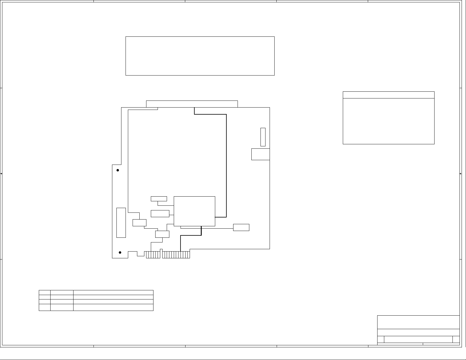
PEX 8505RDK
TABLE OF CONTENTS
Page 1: Functional Block Diagram
Port 4
C C
HD CONN.
5V-to-3.3V
DC/DC
Converter
Page 2: Board Layout Information
Page 3: PEX8505 PEX Interface
Page 4: PEX8505 Power, EEPROM, JTAG, Misc.
Page 5: PCI Express Slot Connectors 1
Page 6: PCI Express Slot Connectors 2
Page 7: Hot Plug Circuitry
Page 8: Clock and Reset
Page 9: Board Power
NOTE: NL INDICATES COMPONENT NOT LOADED
JTAG
DIP
B B
12V-to-1V DC/DC
Converter
CLK
BUF
SWITCHES
CLK
BUFFER
PEX8505
Port 0
Port 1 Port 2 Port 3
Four x1
Port 4
x1
EEPROM
Revision History
Rev# Date Changes from last revision
03/23/2007
000 Initial Revision
A A
10/1/2007001 Fixed note near U12
5
PLX Technology, Inc.
PLX Technology, Inc.
PLX Technology, Inc.
870 Maude Avenue
870 Maude Avenue
870 Maude Avenue
Sunnyvale, CA 94085
Sunnyvale, CA 94085
Sunnyvale, CA 94085
www.plxtech.com
www.plxtech.com
Title
Title
Title
Size Document Number Rev
Size Document Number Rev
Size Document Number Rev
C
C
C
91-0076-001-A 001
91-0076-001-A 001
91-0076-001-A 001
Date: Sheet
Date: Sheet
4
3
2
Date: Sheet
www.plxtech.com
PEX8505RDK - Functional Block Diagram
PEX8505RDK - Functional Block Diagram
PEX8505RDK - Functional Block Diagram
1
19Monday, October 01, 2007
19Monday, October 01, 2007
19Monday, October 01, 2007
of
of
of
Page 29
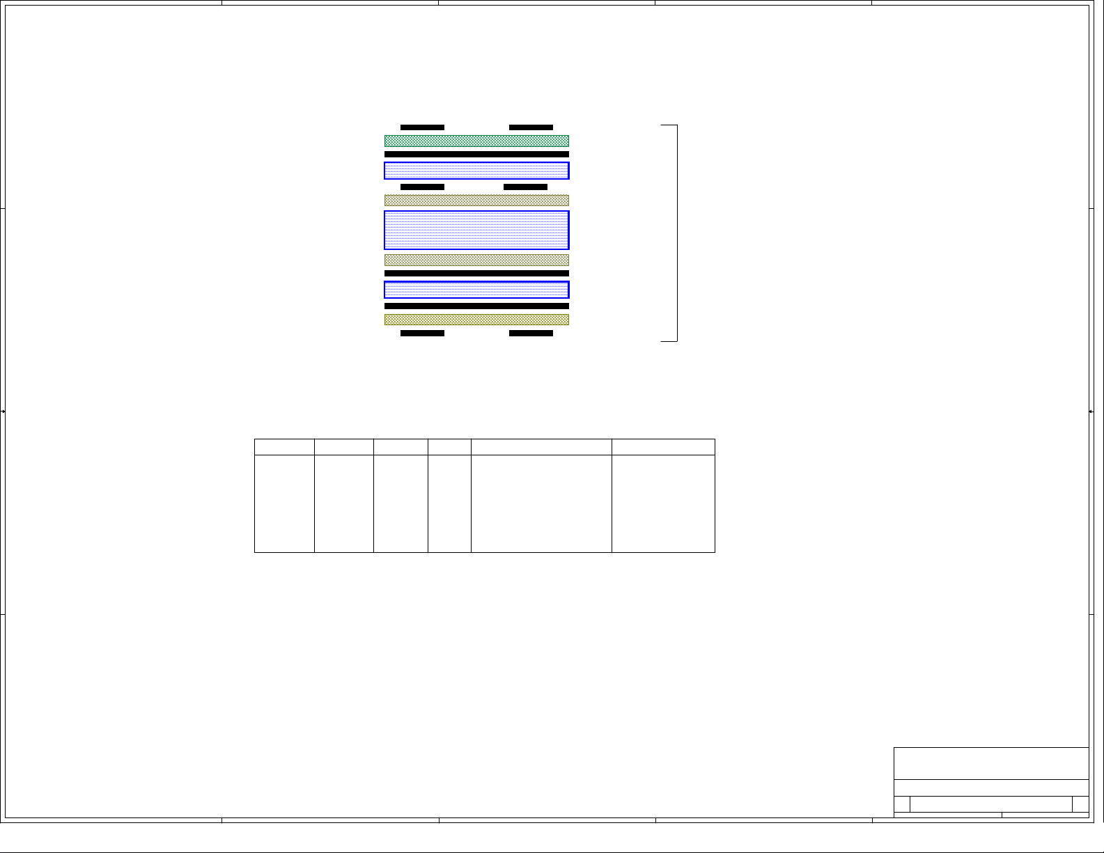
5
D D
L1, Signal 1, 0.5oz.
L2, GND, 0.5oz.
L3, Signal 2, 0.5oz.
4
3
2
1
Prepreg, 4mil
Laminate, 4mil
Prepreg, 6.5mil
Overall Board
Thickness
Laminate, 23mil
62mil
Prepreg, 6.5mil
L4, Power/GND 3, 0.5oz.
Laminate, 4mil
C C
L5, Split Power, 0.5oz.
Prepreg, 4mil
L6, Signal 3, 0.5oz.
0.004
0.004
0.0065
0.023
0.0065
0.004
0.004
Dielectric
Constant
4.3
4.3FR4
4.3
4.3
4.3
4.3
Layer#
1
2
3
4
5
6
Material
Thickness
FR4
FR4
FR4
B B
A A
5
FR4
FR4
FR4 4.3
4
Description
GROUND PLANE
SIGNAL
POWER/GROUND PLANE
SPLIT POWER PLANE
BOTTOM - SIGNAL + COMPONENTS
3
Weight/Thickness
1/2 oz, .0022TOP - SIGNAL + COMPONENTS
1/2 oz, .0007
1/2 oz, .0007
1/2 oz, .0007
1/2 oz, .0007
1/2 oz, .0022
PLX Technology, Inc.
PLX Technology, Inc.
PLX Technology, Inc.
870 Maude Avenue
870 Maude Avenue
870 Maude Avenue
Sunnyvale, CA 94085
Sunnyvale, CA 94085
Sunnyvale, CA 94085
www.plxtech.com
www.plxtech.com
Title
Title
Title
Size Document Number Rev
Size Document Number Rev
Size Document Number Rev
C
C
C
91-0076-001-A 001
91-0076-001-A 001
91-0076-001-A 001
Date: Sheet
Date: Sheet
2
Date: Sheet
www.plxtech.com
PEX8505RDK - Board Layout Information
PEX8505RDK - Board Layout Information
PEX8505RDK - Board Layout Information
1
29Monday, October 01, 2007
29Monday, October 01, 2007
29Monday, October 01, 2007
of
of
of
Page 30
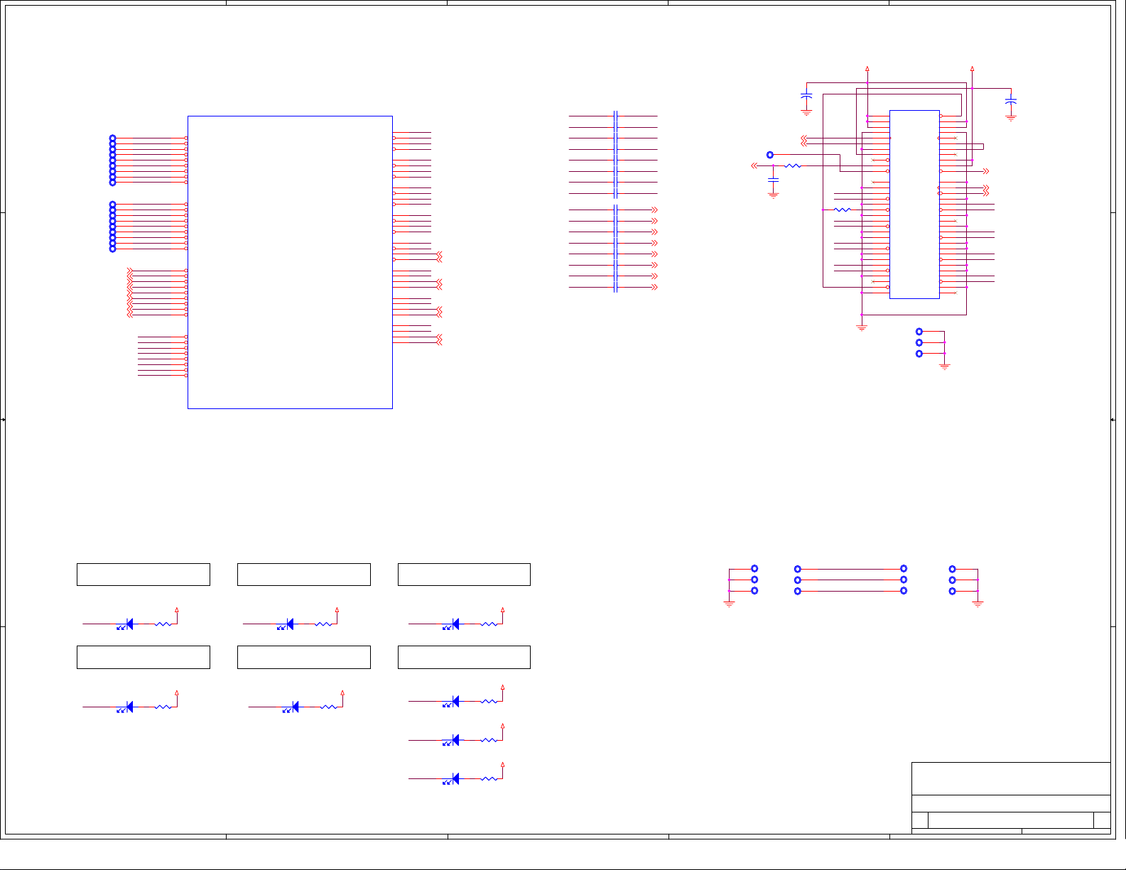
5
4
3
2
VDD_12V VDDEARLY_3.3V
1
+
+
C1
TPV6TPV6
0.1uF
0.1uF
C10
C10
C1
22uF
22uF
SMCLK{5,6,8}
SMDAT{5,6,8}
R1 NL, 0R1 NL, 0
WAKEN0
RP0
RN0
R2 0R2 0
RP1
RN1
RP2
RN2
RP3
RN3
P2
PCI_EXP_X4_CARD_EDGE_CONN
PCI_EXP_X4_CARD_EDGE_CONN
D D
C C
TPV1 - TPV19 SHOULD HAVE A
20-MIL FINISHED HOLE SIZE.
TPV2TPV2
TPV3TPV3
TPV4TPV4
TPV5TPV5
TPV7TPV7
TPV1TPV1
TPV8TPV8
TPV9TPV9
TPV10TPV10
TPV11TPV11
TPV12TPV12
TPV13TPV13
TPV14TPV14
TPV15TPV15
TPV16TPV16
TPV17TPV17
TPV18TPV18
TPV19TPV19
HP_BUTTONN3{7}
HP_PWRLEDN3{7}
HP_PRSTNN3{6}
HP_ATNLEDN3{7}
HP_PWRFLTN3{7}
HP_MRLN3{7}
HP_PWRENN3{7}
HP_PERSTN3{7}
HP_CLKENN3{7}
HP_BUTTONN1
HP_PWRLEDN1
HP_PRSTNN1
HP_ATNLEDN1
HP_PWRFLTN1
HP_MRLN1
HP_PWRENN1
HP_PERSTN1
HP_CLKENN1
HP_BUTTONN2
HP_PWRLEDN2
HP_PRSTNN2
HP_ATNLEDN2
HP_PWRFLTN2
HP_MRLN2
HP_PWRENN2
HP_PERSTN2
HP_CLKENN2
P4_LED0
P3_LED0
P2_LED0
P1_LED0
P0_LED3
P0_LED2
P0_LED1
P0_LED0
PEX 8505AA-PBGA196
PEX 8505AA-PBGA196
U1A
U1A
B2
HP_BUTTON[1]#
E1
HP_PWRLED[1]#
E2
HP_PRSNT[1]#
B1
HP_ATNLED[1]#
D2
HP_PWRFLT[1]#
C1
HP_MRL[1]#
D1
HP_PWREN[1]#
E3
HP_PERST[1]#
F2
HP_CLKEN[1]#
A8
HP_BUTTON[2]#
A3
HP_PWRLED[2]#
B5
HP_PRSNT[2]#
C9
HP_ATNLED[2]#
B7
HP_PWRFLT[2]#
B8
HP_MRL[2]#
C7
HP_PWREN[2]#
C5
HP_PERST[2]#
C4
HP_CLKEN[2]#
B13
HP_BUTTON[3]#
E13
HP_PWRLED[3]#
F11
HP_PRSNT[3]#
D11
HP_ATNLED[3]#
D12
HP_PWRFLT[3]#
B14
HP_MRL[3]#
C14
HP_PWREN[3]#
E12
HP_PERST[3]#
F12
HP_CLKEN[3]#
C13
GPO7#
D13
GPO6#
D3
GPO5#
C2
PEX_LANE_GOOD[4]#
B3
PEX_LANE_GOOD[3]#
B4
PEX_LANE_GOOD[2]#
A4
PEX_LANE_GOOD[1]#
B6
PEX_LANE_GOOD[0]#
PLX PEX 8505AA
PLX PEX 8505AA
-PBGA196
-PBGA196
PEX_PETp[0]
PEX_PETn[0]
PEX_PERp[0]
PEX_PERn[0]
PEX_PETp[1]
PEX_PETn[1]
PEX_PERp[1]
PEX_PERn[1]
PEX_PETp[2]
PEX_PETn[2]
PEX_PERp[2]
PEX_PERn[2]
PEX_PETp[3]
PEX_PETn[3]
PEX_PERp[3]
PEX_PERn[3]
PEX_PETp[4]
PEX_PETn[4]
PEX_PERp[4]
PEX_PERn[4]
TP0_0
N1
TN0_0
P1
M1
L1
P2
N2
N3
P3
N5
P5
P4
N4
P6
N6
N7
P7
P9
N9
N8
P8
N10
NC
P10
NC
P11
NC
N11
NC
P13
NC
N13
NC
N12
NC
P12
NC
N14
NC
P14
NC
L14
NC
K14
NC
RP0
RN0
TP1_0
TN1_0
RP1
RN1
TP2_0
TN2_0
RP2
RN2
TP3_0
TN3_0
RP3
RN3
TP4_0
TN4_0
TP5_0
TN5_0
TP6_0
TN6_0
TP7_0
TN7_0
PORT0
PORT1
PORT2
PORT3
PORT4
RP4 {5}
RN4 {5}
RP5 {5}
RN5 {5}
RP6 {6}
RN6 {6}
RP7 {6}
RN7 {6}
TP0_0
TN0_0
TP1_0
TN1_0
TP2_0
TN2_0
TP3_0
TN3_0
TP4_0
TN4_0
TP5_0
TN5_0
TP6_0
TN6_0
TP7_0
TN7_0
C3 0.1uFC3 0.1uF
C5 0.1uFC5 0.1uF
C4 0.1uFC4 0.1uF
C6 0.1uFC6 0.1uF
C7 0.1uFC7 0.1uF
C8 0.1uFC8 0.1uF
C9 0.1uFC9 0.1uF
C11 0.1uFC11 0.1uF
C12 0.1uFC12 0.1uF
C13 0.1uFC13 0.1uF
C14 NL, 0.1uFC14 NL, 0.1uF
C15 NL, 0.1uFC15 NL, 0.1uF
C16 NL, 0.1uFC16 NL, 0.1uF
C17 NL, 0.1uFC17 NL, 0.1uF
C18 NL, 0.1uFC18 NL, 0.1uF
C19 NL, 0.1uFC19 NL, 0.1uF
TP0
TN0
TP1
TN1
TP2
TN2
TP3
TN3
TP4 {5}
TN4 {5}
TP5 {5}
TN5 {5}
TP6 {6}
TN6 {6}
TP7 {6}
TN7 {6}
3.3AUX{5,6}
AC Coupling Capacitors
P1_PRSNT
P1
P1
B1
PRSNT1#
+12V
B2
+12V
B3
+12V
B4
GND
B5
B6
B7
B8
B9
B10
B11
B12
B13
B14
B15
B16
B17
B18
B19
B20
B21
B22
B23
B24
B25
B26
B27
B28
B29
B30
B31
B32
SMCLK
SMDAT
GND
+3.3V
TRST#
3.3VAUX
WAKE#
RSVD
GND
PETp0
PETn0
GND
PRSNT2#
GND
PETp1
PETn1
GND
GND
PETp2
PETn2
GND
GND
PETp3
PETn3
GND
RSVD
PRSNT2#
GND
GV1GV1
GV2GV2
GV3GV3
TCLK
+3.3V
+3.3V
PERST#
REFCLK+
REFCLK-
PERp0
PERn0
RSVD
PERp1
PERn1
PERp2
PERn2
PERp3
PERn3
RSVD
PLACE GV1-GV3 NEAR P1.
+12V
+12V
GND
GND
GND
GND
GND
GND
GND
GND
GND
GND
+
+
C2
C2
22uF
A1
A2
A3
A4
A5
A6
TDI
A7
TDO
A8
TMS
A9
A10
A11
A12
A13
A14
A15
A16
A17
A18
A19
A20
A21
A22
A23
A24
A25
A26
A27
A28
A29
A30
A31
A32
22uF
PERSTN0 {8}
REFCLKP {8}
REFCLKN {8}
TP0
TN0
TP1
TN1
TP2
TN2
TP3
TN3
B B
IMPEDANCE TEST TRACES
TPV20TPV20
PORT 0 LANE STATUS
INDICATOR
VDD_3.3V
P0_LED0
D1
GreenD1Green
R3
21
150R3150
PORT 1 LANE STATUS
INDICATOR
VDD_3.3V
D4
P0_LED1
GreenD4Green
A A
5
R6
21
150R6150
PORT 2 LANE STATUS
INDICATOR
VDD_3.3V
R7
21
150R7150
P0_LED2
D5
GreenD5Green
PORT 3 LANE STATUS
INDICATOR
VDD_3.3V
R10
R10
21
150
150
4
P0_LED3
D8
GreenD8Green
PORT 4 LANE STATUS
INDICATOR
VDD_3.3V
R4
21
150R4150
P1_LED0
D2
GreenD2Green
UNUSED GPIO
CONNECTIONS
VDD_3.3V
R5
21
NL, 150R5NL, 150
VDD_3.3V
R9
21
NL, 150R9NL, 150
VDD_3.3V
R8
21
NL, 150R8NL, 150
P3_LED0
P4_LED0
P2_LED0
D3
NL, GreenD3NL, Green
D7
NL, GreenD7NL, Green
D6
NL, GreenD6NL, Green
3
GV5GV5
TPV22TPV22
GV7GV7
GV9GV9
TPV24TPV24
IMPEDANCE TEST TRACES SHOULD BE 8" IN LENGTH.
GROUND VIAS SHOULD BE SPACED 0.1" FROM THE
CORRESPONDING TEST POINT VIA. TVP20-TVP27 AND
GV4-GV11 DIAMETERS ARE 30-MIL
2
TEST_LAYER1
TEST_LAYER3
TEST_LAYER6
GV4GV4
TPV21TPV21
TPV23TPV23
GV6GV6
TPV25TPV25
GV8GV8
PLX Technology, Inc.
PLX Technology, Inc.
PLX Technology, Inc.
870 Maude Avenue
870 Maude Avenue
870 Maude Avenue
Sunnyvale, CA 94085
Sunnyvale, CA 94085
Sunnyvale, CA 94085
www.plxtech.com
www.plxtech.com
Title
Title
Title
Size Document Number Rev
Size Document Number Rev
Size Document Number Rev
C
C
C
91-0076-001-A 001
91-0076-001-A 001
91-0076-001-A 001
Date: Sheet
Date: Sheet
Date: Sheet
www.plxtech.com
PEX8505RDK - PEX8505 PEX Interface
PEX8505RDK - PEX8505 PEX Interface
PEX8505RDK - PEX8505 PEX Interface
1
39Monday, October 01, 2007
39Monday, October 01, 2007
39Monday, October 01, 2007
of
of
of
Page 31
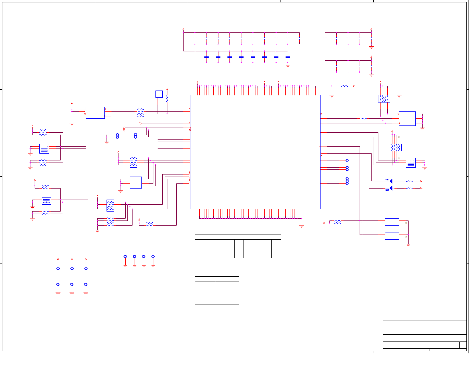
5
D D
4
C22
C21
C21
10uF
10uF
C35
C35
0.01uF
0.01uF
C22
10uF
10uF
C36
C36
0.01uF
0.01uF
C20
C20
10uF
10uF
C23
C23
10uF
10uF
C37
C37
0.01uF
0.01uF
3
C24
C24
1uF
1uF
C38
C38
0.01uF
0.01uF
C25
C25
1uF
1uF
C39
C39
0.022uF
0.022uF
C26
C26
0.1uF
0.1uF
C40
C40
0.022uF
0.022uF
C27
C27
0.1uF
0.1uF
C41
C41
0.022uF
0.022uF
C28
C28
0.1uF
0.1uF
C42
C42
0.022uF
0.022uF
C29
C29
0.1uF
0.1uF
2
VDD_VTTVDD_1.0V
C31
C31
C32
C32
C33
C30
C30
0.1uF
0.1uF
10uF
10uF
C43
C43
C44
C44
10uF
10uF
0.1uF
0.1uF
0.1uF
0.1uF
C45
C45
0.1uF
0.1uF
C33
0.1uF
0.1uF
C48
C48
0.1uF
0.1uF
C34
C34
0.1uF
0.1uF
C46
C46
0.1uF
0.1uF
VDD_3.3V
1
R1833 R1833
RN1
RN1
5.1K
5.1K
VDD_3.3V
123
45
678
JTAG_TDO_0
VDD_3.3V
RN2
RN2
5.1K
5.1K
I2C HEADERS
SCL1GND
SDA3NC
HEADER 2X2
HEADER 2X2
SCL1GND
SDA3NC
HEADER 2X2
HEADER 2X2
123
D9Red D9Red
D19Green D19Green
JP3
JP3
JP4
JP4
1
3
5
7
9
678
21
21
JP1
JP1
TRST#
TDI
TDO
TMS
TCK
JTAG
JTAG
45
6
5
4 3
SW SMT-3
SW SMT-3
2
4
2
4
2
GND
4
GND
6
GND
8
GND
10
GND
SW2
SW2
ON
ON
1
2
R25150 R25150
VDD_3.3V
R122150 R122150
VDD_3.3V
VDD_VTT VDD_3.3VVDD_1.0V
TPV30 - TPV31 SHOULD HAVE A 20-MIL
FINISHED HOLE.TPV28-TPV29 SHOULD HAVE A
30-MIL FINISHED HOLE.
VDD_3.3V
VDD_3.3V
R19 5.1KR19 5.1K
R20 5.1KR20 5.1K
C C
B B
R21 5.1KR21 5.1K
SW1
SW1
1
2
SW SMT-3
SW SMT-3
R22 NL, 0R22 NL, 0
R23 NL, 0R23 NL, 0
R24 NL, 0R24 NL, 0
VDD_3.3V
R26 NL, 5.1KR26 NL, 5.1K
R27 NL, 5.1KR27 NL, 5.1K
1
2
R28 0R28 0
R29 0R29 0
ON
ON
6
5
43
SW3
SW3
ON
ON
4
3
NL, SW SMT-2
NL, SW SMT-2
VOLTAGE MEASUREMENT POINTS
VDD_VTT VDD_3.3VVDD_1.0V
UP_PORT0
UP_PORT1
UP_PORT2
PORTCFG0
PORTCFG1
U2
U2
8
VCC
7
HOLD#
3
WP#
4
GND
EEPROM Socket
EEPROM Socket
VDD_3.3V
1
CS#
5
SI
2
SO
6
SCK
REFCLKP0{8}
REFCLKN0{8}
RN4
RN4
6
7
8
R30 NL, 0R30 NL, 0
R31 NL, 0R31 NL, 0
R32 NL, 0R32 NL, 0
R34 NL, 0R34 NL, 0
EECSN_0
EEDI_0
EEDO_0
EESK_0
TPV28TPV28
TPV29TPV29
VDD_3.3V
45
3
2
1
5.1K
5.1K
GROUND POST HOLES
GV12GV12
R14 0R14 0
R15 0R15 0
R16 0R16 0
R17 0R17 0
PERSTN{5,6,7,8,9}
TPV30TPV30
TPV31TPV31
RN3
RN3
6
7
8
JP2
JP2
1 2
3 4
5 6
7 8
HEADER 4X2
HEADER 4X2
GV13GV13
45
3
2
1
5.1K
5.1K
VDD_3.3V
R33 5.1KR33 5.1K
R35 5.1KR35 5.1K
GV14GV14
HDR, 1X2
HDR, 1X2
EEDO0
GV15GV15
JP5
JP5
VDD_3.3V
1
2
UP_PORT0
UP_PORT1
UP_PORT2
PORTCFG0
PORTCFG1
TESTMODE0
TESTMODE1
TESTMODE2
TESTMODE3
PLLBYPASSN
SERDESMODEN
DEBUGSEL0
DEBUGSEL1
R12
R12
10K
10K
EECSN
EEDI
EEDO
EESK
FASTBRGN
PROBEN
U1B
U1B
F14
EE_CS#
H12
EE_DI
G12
EE_DO
G13
EE_SK
G3
PEX_PERST#
J1
PEX_REFCLKp
J2
PEX_REFCLKn
A7
STRAP_UPSTRM_PORT_SEL[0]
A6
STRAP_UPSTRM_PORT_SEL[1]
C8
STRAP_UPSTRM_PORT_SEL[2]
F13
STRAP_PORTCFG[0]
E14
STRAP_PORTCFG[1]
C11
STRAP_TEST_MODE[0]
B11
STRAP_TEST_MODE[1]
A11
STRAP_TEST_MODE[2]
C12
STRAP_TEST_MODE[3]
F1
STRAP_PLL_BYPASS#
A2
STRAP_SERDES_MODE_EN#
G2
STRAP_FAST_BRINGUP#
G14
STRAP_PROBE_MODE#
A12
STRAP_DEBUG_SEL#[0]
A13
STRAP_DEBUG_SEL#[1]
PEX 8505AA-PBGA196
PEX 8505AA-PBGA196
M10
M12
L13
M4
L7
VDD10SM6VDD10SM8VDD10S
VDD10SM2VDD10S
VDD10S
EEPROM PORT
EEPROM PORT
VSS
VSSE6VSSE8VSS
A14
E10
VDD10S
PORT CONFIGURATION
PORT CONFIGURATION
TEST MODE SELECT
TEST MODE SELECT
VSSF5VSSF6VSSF7VSSF8VSSF9VSSG6VSSG7VSSG8VSSG9VSS
VDD10SK2VDD10SL3VDD10S
VSS
A1
STRAP_PORTCFG[1:0]
00b
01b
10b
H10
F10
E5
L5
L10
M14
VDD10
VDD10E9VDD10
VDD10E7VDD10G5VDD10J5VDD10K6VDD10
VDD10A
VDD10AJ3VDD10A
VDD10S
PLX PEX 8505AA
PLX PEX 8505AA
-PBGA196
-PBGA196
UP STREAM PORT SELECTS
UP STREAM PORT SELECTS
VSSH1VSSH2VSSH5VSSH6VSSH7VSSH8VSSH9VSSJ4VSSJ6VSSJ7VSSJ8VSSJ9VSS
G10
PEX 8505 PORT CONFIGURATION
Port 0 Port 1 Port 2 Port 3 Port 4
x1
x1 x1 x1 x1
x2
x1 x1
x2
x1 x1 x1 x1x2
L9
L11
K10
VDD10K8VDD10K4VDD10
VTT_PEX[0]L4VTT_PEX[1]L6VTT_PEX[2]
VTT_PEX[3]
VSSK1VSSK3VSSK5VSSK7VSS
VSS
J10
J14
D10
VDD33D9VDD33
VDD33D8VDD33D7VDD33D6VDD33D5VDD33
JTAG PORT
JTAG PORT
VSSM3VSSL8VSSM5VSSL2VSSM7VSSM9VSS
E11
VDD33E4VDD33
VDD33F4VDD33
I2C PORT
I2C PORT
THERMAL_DIODEn
THERMAL_DIODEp
VSS
M11
M13
D4
VSS
K9
K13
Port 5
G11
H4
H11
G4
VDD33
VDD33
VDD33
JTAG_TRST#
JTAG_TDI
JTAG_TDO
JTAG_TMS
JTAG_TCK
I2C_ADDR0
I2C_ADDR1
I2C_ADDR2
FATAL_ERR#
PEX_INTA#
NC_PROCMON
NC_SPARE0
NC_SPARE1
NC_SPARE2
VSSA_PLL
G1
J11
VDD33
I2C_SDA
I2C_SCL
VDD_3.3V
H3
VDD33A
VDD33A
B9
A9
A10
B10
C10
K11
K12
L12
H13
H14
J13
C3
F3
C6
A5
B12
D14
J12
R11 0R11 0
C47
C47
0.1uF
0.1uF
JTAG_TRSTN
JTAG_TDI
JTAG_TDO
JTAG_TMS
JTAG_TCK
I2C_ADDR0
I2C_ADDR1
I2C_ADDR2
I2C_SDA
I2C_SCL
FATAL_ERRN
PEX_INTAN
PROCMON
DIODE_N
DIODE_P
SPARE0
SPARE1
SPARE2
TPV32 - TPV37 SHOULD
HAVE A 20-MIL FINISHED
HOLE.
R36 2.26K 1%R36 2.26K 1%
2.26K 1%
2.26K 1%
R37
R37
TPV32TPV32
TPV33TPV33
TPV34TPV34
TPV35TPV35
TPV36TPV36
TPV37TPV37
VDD_3.3V
NOTE: RDK hardwired setting is 00b.
TPV38TPV38
TPV39TPV39
TPV40TPV40
GV17GV17
GV18GV18
GV16GV16
CLEARLY LABEL, AND PLACE CLOSE TO U1.
A A
TPV38-40 AND GV16-18 SHOULD
BE PLACED CLOSE TO U1.
FINISHED HOLE SIZE SHOULD BE
34-MIL
5
GV12-15 SHOULD BE 60-MIL PAD/34-MIL
FINISHED HOLE. PROVIDE SILKSCREEN
LABELS FOR THESE VIAS.
4
STRAP_UPSTREAM_PORT_SEL[2:0]
000b Port 0
001b
010b
011b
100b
Port 1
Port 2
Port 3
Port 4
NOTE: RDK default setting is 000b.
3
PLX Technology, Inc.
PLX Technology, Inc.
PLX Technology, Inc.
870 Maude Avenue
870 Maude Avenue
870 Maude Avenue
Sunnyvale, CA 94085
Sunnyvale, CA 94085
Sunnyvale, CA 94085
www.plxtech.com
www.plxtech.com
Title
Title
Title
Size Document Number Rev
Size Document Number Rev
Size Document Number Rev
C
C
C
91-0076-001-A 001
91-0076-001-A 001
91-0076-001-A 001
Date: Sheet
Date: Sheet
2
Date: Sheet
www.plxtech.com
PEX8505RDK - PEX8505 Power, Misc.
PEX8505RDK - PEX8505 Power, Misc.
PEX8505RDK - PEX8505 Power, Misc.
1
49Monday, October 01, 2007
49Monday, October 01, 2007
49Monday, October 01, 2007
of
of
of
Page 32
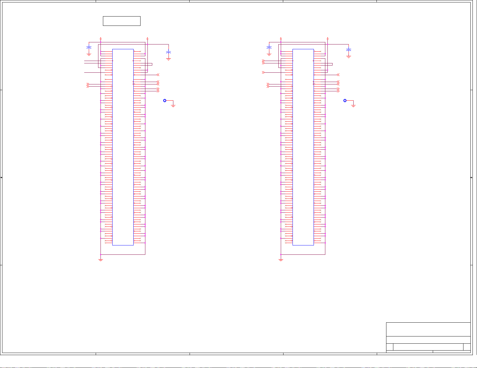
5
4
3
2
1
PORT 4 SLOT
CONNECTOR
VDDHD_12V VDDHD_3.3VVDDHD_12V VDDHD_3.3V
+
C50
+
SMCLK{3,6,8}
SMDAT{3,6,8}
3.3AUX{3,6}
NL, 22uF
NL, 22uF
C50
TP5{3}
TN5{3}
J2
J2
B1
+12V
B2
+12V
B3
+12V
B4
GND
B5
SMCLK
B6
SMDAT
B7
GND
B8
+3.3V
B9
TRST#
B10
3.3VAUX
B11
WAKE#
B12
RSVD
B13
GND
B14
PETp0
B15
PETn0
B16
GND
B17
PRSNT2#
B18
GND
B19
PETp1
B20
PETn1
B21
GND
B22
GND
B23
PETp2
B24
PETn2
B25
GND
B26
GND
B27
PETp3
B28
PETn3
B29
GND
B30
RSVD
B31
PRSNT2#
B32
GND
B33
PETp4
B34
PETn4
B35
GND
B36
GND
B37
PETp5
B38
PETn5
B39
GND
B40
GND
B41
PETp6
B42
PETn6
B43
GND
B44
GND
B45
PETp7
B46
PETn7
B47
GND
B48
PRSNT2#
B49
GND
B50
PETp8
B51
PETn8
B52
GND
B53
GND
B54
PETp9
B55
PETn9
B56
GND
B57
GND
B58
PETp10
B59
PETn10
B60
GND
B61
GND
B62
PETp11
B63
PETn11
B64
GND
B65
GND
B66
PETp12
B67
PETn12
B68
GND
B69
GND
B70
PETp13
B71
PETn13
B72
GND
B73
GND
B74
PETp14
B75
PETn14
B76
GND
B77
GND
B78
PETp15
B79
PETn15
B80
GND
B81
PRSNT2#
B82
RSVD
NL, PCI_EXP_X16_FEMALE_CONN
NL, PCI_EXP_X16_FEMALE_CONN
PRSNT1#
+12V
+12V
GND
TCLK
+3.3V
+3.3V
PERST#
GND
REFCLK+
REFCLK-
GND
PERp0
PERn0
GND
RSVD
GND
PERp1
PERn1
GND
GND
PERp2
PERn2
GND
GND
PERp3
PERn3
GND
RSVD
RSVD
GND
PERp4
PERn4
GND
GND
PERp5
PERn5
GND
GND
PERp6
PERn6
GND
GND
PERp7
PERn7
GND
RSVD
GND
PERp8
PERn8
GND
GND
PERp9
PERn9
GND
GND
PERp10
PERn10
GND
GND
PERp11
PERn11
GND
GND
PERp12
PERn12
GND
GND
PERp13
PERn13
GND
GND
PERp14
PERn14
GND
GND
PERp15
PERn15
GND
A1
A2
A3
A4
A5
A6
TDI
A7
TDO
A8
TMS
A9
A10
A11
A12
A13
A14
A15
A16
A17
A18
A19
A20
A21
A22
A23
A24
A25
A26
A27
A28
A29
A30
A31
A32
A33
A34
A35
A36
A37
A38
A39
A40
A41
A42
A43
A44
A45
A46
A47
A48
A49
A50
A51
A52
A53
A54
A55
A56
A57
A58
A59
A60
A61
A62
A63
A64
A65
A66
A67
A68
A69
A70
A71
A72
A73
A74
A75
A76
A77
A78
A79
A80
A81
A82
+
C52
+
C52
NL, 22uF
NL, 22uF
PERSTN {4,6,7,8,9}
REFCLKP2 {8}
RP5 {3}
RN5 {3}
GV20GV20GV19GV19
+
C49
+
D D
C C
B B
C49
22uF
22uF
SMCLK
SMDAT
3.3AUX
TP4{3}
TN4{3}
J1
J1
B1
+12V
B2
+12V
B3
+12V
B4
GND
B5
SMCLK
B6
SMDAT
B7
GND
B8
+3.3V
B9
TRST#
B10
3.3VAUX
B11
WAKE#
B12
RSVD
B13
GND
B14
PETp0
B15
PETn0
B16
GND
B17
PRSNT2#
B18
GND
B19
PETp1
B20
PETn1
B21
GND
B22
GND
B23
PETp2
B24
PETn2
B25
GND
B26
GND
B27
PETp3
B28
PETn3
B29
GND
B30
RSVD
B31
PRSNT2#
B32
GND
B33
PETp4
B34
PETn4
B35
GND
B36
GND
B37
PETp5
B38
PETn5
B39
GND
B40
GND
B41
PETp6
B42
PETn6
B43
GND
B44
GND
B45
PETp7
B46
PETn7
B47
GND
B48
PRSNT2#
B49
GND
B50
PETp8
B51
PETn8
B52
GND
B53
GND
B54
PETp9
B55
PETn9
B56
GND
B57
GND
B58
PETp10
B59
PETn10
B60
GND
B61
GND
B62
PETp11
B63
PETn11
B64
GND
B65
GND
B66
PETp12
B67
PETn12
B68
GND
B69
GND
B70
PETp13
B71
PETn13
B72
GND
B73
GND
B74
PETp14
B75
PETn14
B76
GND
B77
GND
B78
PETp15
B79
PETn15
B80
GND
B81
PRSNT2#
B82
RSVD
PCI_EXP_X16_STRADDLE_MNT_CONN
PCI_EXP_X16_STRADDLE_MNT_CONN
PRSNT1#
+12V
+12V
GND
TCLK
+3.3V
+3.3V
PERST#
GND
REFCLK+
REFCLK-
GND
PERp0
PERn0
GND
RSVD
GND
PERp1
PERn1
GND
GND
PERp2
PERn2
GND
GND
PERp3
PERn3
GND
RSVD
RSVD
GND
PERp4
PERn4
GND
GND
PERp5
PERn5
GND
GND
PERp6
PERn6
GND
GND
PERp7
PERn7
GND
RSVD
GND
PERp8
PERn8
GND
GND
PERp9
PERn9
GND
GND
PERp10
PERn10
GND
GND
PERp11
PERn11
GND
GND
PERp12
PERn12
GND
GND
PERp13
PERn13
GND
GND
PERp14
PERn14
GND
GND
PERp15
PERn15
GND
A1
A2
A3
A4
A5
A6
TDI
A7
TDO
A8
TMS
A9
A10
A11
A12
A13
A14
A15
A16
A17
A18
A19
A20
A21
A22
A23
A24
A25
A26
A27
A28
A29
A30
A31
A32
A33
A34
A35
A36
A37
A38
A39
A40
A41
A42
A43
A44
A45
A46
A47
A48
A49
A50
A51
A52
A53
A54
A55
A56
A57
A58
A59
A60
A61
A62
A63
A64
A65
A66
A67
A68
A69
A70
A71
A72
A73
A74
A75
A76
A77
A78
A79
A80
A81
A82
+
+
C51
C51
22uF
22uF
PERSTN {4,6,7,8,9}
REFCLKP1 {8}
REFCLKN1 {8} REFCLKN2 {8}
RP4 {3}
RN4 {3}
A A
PLX Technology, Inc.
PLX Technology, Inc.
PLX Technology, Inc.
870 Maude Avenue
870 Maude Avenue
870 Maude Avenue
Sunnyvale, CA 94085
Sunnyvale, CA 94085
Sunnyvale, CA 94085
www.plxtech.com
www.plxtech.com
Title
Title
Title
Size Document Number Rev
Size Document Number Rev
Size Document Number Rev
C
C
C
91-0076-001-A 001
91-0076-001-A 001
91-0076-001-A 001
Date: Sheet
Date: Sheet
5
4
3
2
Date: Sheet
www.plxtech.com
PEX8505RDK - PCI Express Slot Connectors 1
PEX8505RDK - PCI Express Slot Connectors 1
PEX8505RDK - PCI Express Slot Connectors 1
59Monday, October 01, 2007
59Monday, October 01, 2007
1
59Monday, October 01, 2007
of
of
of
Page 33
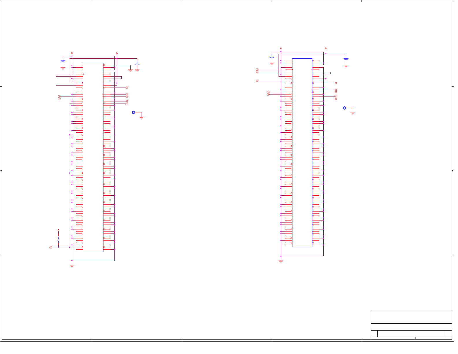
5
4
3
2
1
D D
VDDHP_12V VDDHP_3.3V
+
+
C54
C54
NL, 22uF
NL, 22uF
SMCLK
SMDAT
3.3AUX
TP6{3}
TN6{3}
C C
B B
VDD_3.3V
R39
R39
5.1K
5.1K
HP_PRSTNN3{3}
J4
J4
B1
PRSNT1#
+12V
B2
B3
B4
B5
B6
B7
B8
B9
B10
B11
B12
B13
B14
B15
B16
B17
B18
B19
B20
B21
B22
B23
B24
B25
B26
B27
B28
B29
B30
B31
B32
B33
B34
B35
B36
B37
B38
B39
B40
B41
B42
B43
B44
B45
B46
B47
B48
B49
B50
B51
B52
B53
B54
B55
B56
B57
B58
B59
B60
B61
B62
B63
B64
B65
B66
B67
B68
B69
B70
B71
B72
B73
B74
B75
B76
B77
B78
B79
B80
B81
B82
NL, PCI_EXP_X16_FEMALE_CONN
NL, PCI_EXP_X16_FEMALE_CONN
+12V
+12V
GND
SMCLK
SMDAT
GND
+3.3V
TRST#
3.3VAUX
WAKE#
RSVD
GND
PETp0
PETn0
GND
PRSNT2#
GND
PETp1
PETn1
GND
GND
PETp2
PETn2
GND
GND
PETp3
PETn3
GND
RSVD
PRSNT2#
GND
PETp4
PETn4
GND
GND
PETp5
PETn5
GND
GND
PETp6
PETn6
GND
GND
PETp7
PETn7
GND
PRSNT2#
GND
PETp8
PETn8
GND
GND
PETp9
PETn9
GND
GND
PETp10
PETn10
GND
GND
PETp11
PETn11
GND
GND
PETp12
PETn12
GND
GND
PETp13
PETn13
GND
GND
PETp14
PETn14
GND
GND
PETp15
PETn15
GND
PRSNT2#
RSVD
+12V
+12V
GND
TCLK
TDO
TMS
+3.3V
+3.3V
PERST#
GND
REFCLK+
REFCLK-
GND
PERp0
PERn0
GND
RSVD
GND
PERp1
PERn1
GND
GND
PERp2
PERn2
GND
GND
PERp3
PERn3
GND
RSVD
RSVD
GND
PERp4
PERn4
GND
GND
PERp5
PERn5
GND
GND
PERp6
PERn6
GND
GND
PERp7
PERn7
GND
RSVD
GND
PERp8
PERn8
GND
GND
PERp9
PERn9
GND
GND
PERp10
PERn10
GND
GND
PERp11
PERn11
GND
GND
PERp12
PERn12
GND
GND
PERp13
PERn13
GND
GND
PERp14
PERn14
GND
GND
PERp15
PERn15
GND
TDI
+
+
C55
PERSTN3 {7}
REFCLKP3 {8}
REFCLKN3 {8}
RP6 {3}
RN6 {3}
GV21GV21
C55
NL, 22uF
NL, 22uF
SMCLK{3,5,8}
SMDAT{3,5,8}
3.3AUX{3,5}
A1
A2
A3
A4
A5
A6
A7
A8
A9
A10
A11
A12
A13
A14
A15
A16
A17
A18
A19
A20
A21
A22
A23
A24
A25
A26
A27
A28
A29
A30
A31
A32
A33
A34
A35
A36
A37
A38
A39
A40
A41
A42
A43
A44
A45
A46
A47
A48
A49
A50
A51
A52
A53
A54
A55
A56
A57
A58
A59
A60
A61
A62
A63
A64
A65
A66
A67
A68
A69
A70
A71
A72
A73
A74
A75
A76
A77
A78
A79
A80
A81
A82
VDDHD_12V VDDHD_3.3V
+
C53
+
NL, 22uF
NL, 22uF
TP7{3}
TN7{3}
C53
J3
J3
B1
+12V
B2
+12V
B3
+12V
B4
GND
B5
SMCLK
B6
SMDAT
B7
GND
B8
+3.3V
B9
TRST#
B10
3.3VAUX
B11
WAKE#
B12
RSVD
B13
GND
B14
PETp0
B15
PETn0
B16
GND
B17
PRSNT2#
B18
GND
B19
PETp1
B20
PETn1
B21
GND
B22
GND
B23
PETp2
B24
PETn2
B25
GND
B26
GND
B27
PETp3
B28
PETn3
B29
GND
B30
RSVD
B31
PRSNT2#
B32
GND
B33
PETp4
B34
PETn4
B35
GND
B36
GND
B37
PETp5
B38
PETn5
B39
GND
B40
GND
B41
PETp6
B42
PETn6
B43
GND
B44
GND
B45
PETp7
B46
PETn7
B47
GND
B48
PRSNT2#
B49
GND
B50
PETp8
B51
PETn8
B52
GND
B53
GND
B54
PETp9
B55
PETn9
B56
GND
B57
GND
B58
PETp10
B59
PETn10
B60
GND
B61
GND
B62
PETp11
B63
PETn11
B64
GND
B65
GND
B66
PETp12
B67
PETn12
B68
GND
B69
GND
B70
PETp13
B71
PETn13
B72
GND
B73
GND
B74
PETp14
B75
PETn14
B76
GND
B77
GND
B78
PETp15
B79
PETn15
B80
GND
B81
PRSNT2#
B82
RSVD
NL, PCI_EXP_X16_FEMALE_CONN
NL, PCI_EXP_X16_FEMALE_CONN
PRSNT1#
TCLK
+3.3V
+3.3V
PERST#
REFCLK+
REFCLK-
PERp0
PERn0
RSVD
PERp1
PERn1
PERp2
PERn2
PERp3
PERn3
RSVD
RSVD
PERp4
PERn4
PERp5
PERn5
PERp6
PERn6
PERp7
PERn7
RSVD
PERp8
PERn8
PERp9
PERn9
PERp10
PERn10
PERp11
PERn11
PERp12
PERn12
PERp13
PERn13
PERp14
PERn14
PERp15
PERn15
+12V
+12V
GND
TDO
TMS
GND
GND
GND
GND
GND
GND
GND
GND
GND
GND
GND
GND
GND
GND
GND
GND
GND
GND
GND
GND
GND
GND
GND
GND
GND
GND
GND
GND
GND
GND
GND
GND
GND
+
C56
+
A1
A2
A3
A4
A5
A6
TDI
A7
A8
A9
A10
A11
A12
A13
A14
A15
A16
A17
A18
A19
A20
A21
A22
A23
A24
A25
A26
A27
A28
A29
A30
A31
A32
A33
A34
A35
A36
A37
A38
A39
A40
A41
A42
A43
A44
A45
A46
A47
A48
A49
A50
A51
A52
A53
A54
A55
A56
A57
A58
A59
A60
A61
A62
A63
A64
A65
A66
A67
A68
A69
A70
A71
A72
A73
A74
A75
A76
A77
A78
A79
A80
A81
A82
C56
NL, 22uF
NL, 22uF
PERSTN {4,5,7,8,9}
REFCLKP4 {8}
REFCLKN4 {8}
RP7 {3}
RN7 {3}
GV22GV22
A A
PLX Technology, Inc.
PLX Technology, Inc.
PLX Technology, Inc.
870 Maude Avenue
870 Maude Avenue
870 Maude Avenue
Sunnyvale, CA 94085
Sunnyvale, CA 94085
Sunnyvale, CA 94085
www.plxtech.com
www.plxtech.com
Title
Title
Title
Size Document Number Rev
Size Document Number Rev
Size Document Number Rev
C
C
C
91-0076-001-A 001
91-0076-001-A 001
91-0076-001-A 001
Date: Sheet
Date: Sheet
5
4
3
2
Date: Sheet
www.plxtech.com
PEX8505RDK - PCI Express Slot Connectors 2
PEX8505RDK - PCI Express Slot Connectors 2
PEX8505RDK - PCI Express Slot Connectors 2
69Monday, October 01, 2007
69Monday, October 01, 2007
1
69Monday, October 01, 2007
of
of
of
Page 34
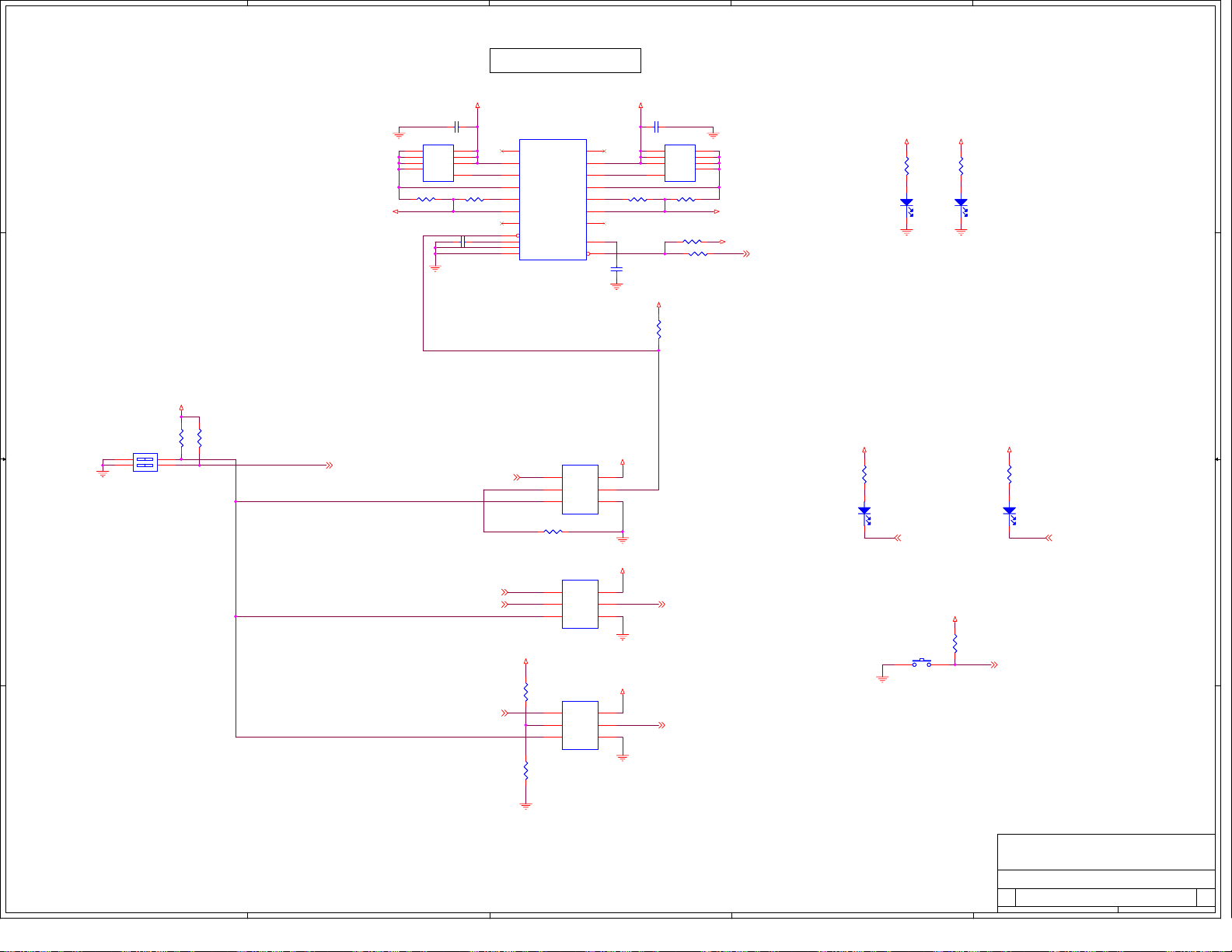
5
4
3
2
1
HOT PLUG CIRCUIT
VCC
GND
VCC
GND
VCC
GND
6
19
2
9
14
12
13
4
16
VDDHP_3.3V
3VSENSE
IS2
R44 NL, 2KR44 NL, 2K
TMR
HPFLTN
VDD_3.3V
5
PWREN
4
2
VDD_3.3V
5
4
2
VDD_3.3V
5
4
2
C58
C58
NL, 0.001uF
NL, 0.001uF
C60
C60
NL, 0.1uF
NL, 0.1uF
Q2NLQ2
1
S
2
S
3
S
4
G
R48 NLR48 NL
VDDEARLY_3.3V
R47
R47
5.1K
5.1K
CLKENN3 {8}
D
D
D
D
R45 51KR45 51K
R46 0R46 0
5
6
7
8
NL
VDDEARLY_3.3V
VDD_3.3V
HP_PWRFLTN3 {3}
PLACE D17 AND D18 NEAR J4.
VDDHP_3.3VVDDHP_12V
R41
21
VDD_3.3V
R54
R54
5.1K
5.1K
R41
NL, 150
NL, 150
D11
D11
NL, Green
NL, Green
R52
R52
NL, 150
NL, 150
21
HP_BUTTONN3 {3}
R40
R40
NL, 1K 1%
NL, 1K 1%
21
D10
D10
NL, Green
NL, Green
VDD_3.3V VDD_3.3V
R51
R51
NL, 150
NL, 150
21
D12
D12
NL, Green
NL, Green
HP_PWRLEDN3 {3} HP_ATNLEDN3 {3}
SW5
SW5
1 3
NL, SW PUSHBUTTON
NL, SW PUSHBUTTON
D13
D13
NL, Yellow
NL, Yellow
VDDHP_12V
C59
D D
VDD_12V
C C
VDD_3.3V
R50
R50
R49
R49
5.1K
5.1K
5.1K
5.1K
SW4
SW4
ON
ON
1
4
2
3
NL, SW SMT-2
NL, SW SMT-2
HP_SLOTCTL
B B
A A
HP_MRLN3 {3}
Q1NLQ1
5
D
6
D
7
D
8
D
NL
R42 NLR42 NL
C59
U4
NL, 0.1uF
NL, 0.1uF
1
S
2
S
3
S
4
G
12VSENSE
R43 NL,2KR43 NL,2K
C57
C57
NL, 0.1uF
NL, 0.1uF
HP_PWRENN3{3}
HP_PERSTN3{3}
PERSTN{4,5,6,8,9} PERSTN3 {6}
HP_CLKENN3{3}
U4
VSENSE17VSENSE2
DISCH120DISCH2
12VG 3VG
GATE11GATE2
ISENSE110ISENSE2
IS1
ISET115ISET2
11
VREG
IN1
PWRGD117PWRGD2
18
ENABLE#
5
VREG
3
DGND
8
AGND
VDD_3.3V
NL, TPS2310
NL, TPS2310
R53 NL, 0R53 NL, 0
R55
R55
NL, 5.1K
NL, 5.1K
R56
R56
NL, 5.1K
NL, 5.1K
IN2
TIMER
FAULT#
U5
U5
1
B2
B13A
6
S
NL, SN74LVC1G3157
NL, SN74LVC1G3157
U6
U6
1
B2
B13A
6
S
NL, SN74LVC1G3157
NL, SN74LVC1G3157
U7
U7
1
B2
B13A
6
S
NL, SN74LVC1G3157
NL, SN74LVC1G3157
PLX Technology, Inc.
PLX Technology, Inc.
PLX Technology, Inc.
870 Maude Avenue
870 Maude Avenue
870 Maude Avenue
Sunnyvale, CA 94085
Sunnyvale, CA 94085
Sunnyvale, CA 94085
www.plxtech.com
www.plxtech.com
Title
Title
Title
Size Document Number Rev
Size Document Number Rev
Size Document Number Rev
C
C
C
91-0076-001-A 001
91-0076-001-A 001
91-0076-001-A 001
Date: Sheet
Date: Sheet
5
4
3
2
Date: Sheet
www.plxtech.com
PEX8505RDK - Hot Plug Circuitry
PEX8505RDK - Hot Plug Circuitry
PEX8505RDK - Hot Plug Circuitry
1
79Monday, October 01, 2007
79Monday, October 01, 2007
79Monday, October 01, 2007
of
of
of
Page 35
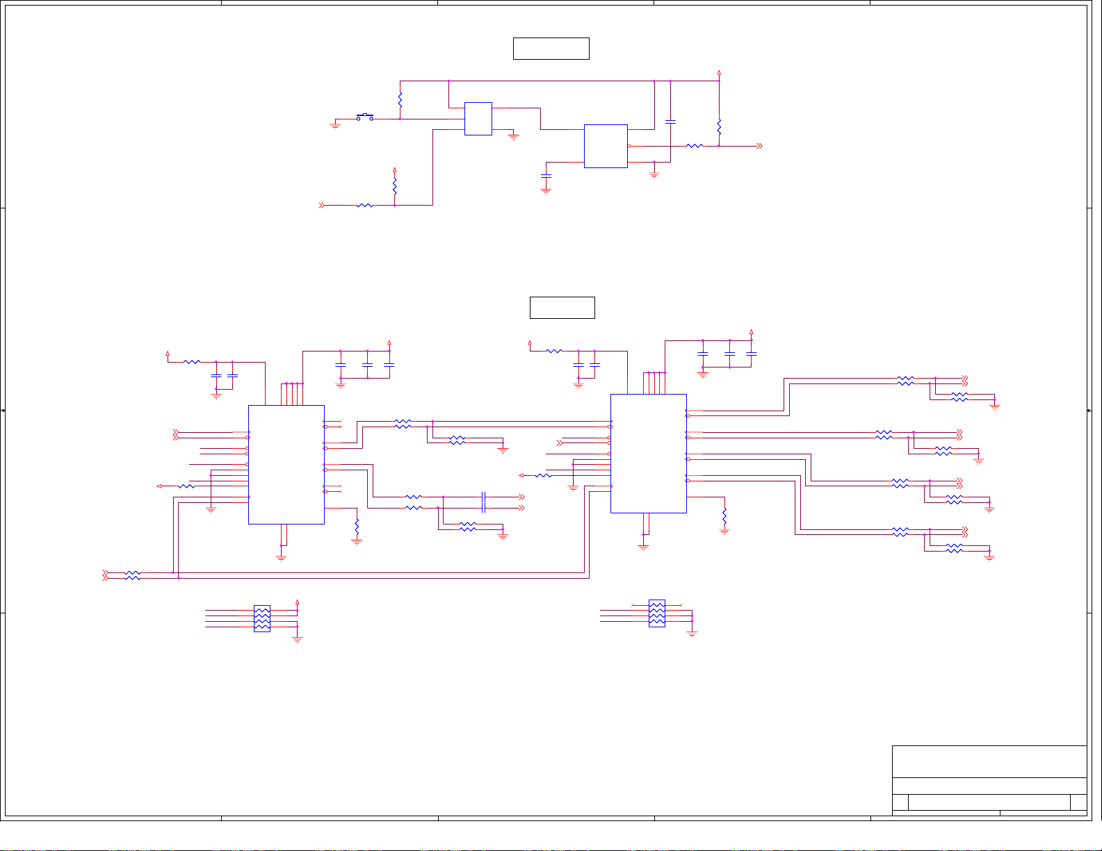
5
4
3
2
1
RESET
CIRCUIT
R57
R57
10K
10K
SW6
D D
PERSTN0{3}
SW6
1 3
SW PUSHBUTTON
SW PUSHBUTTON
R61 0R61 0
VDD_3.3V
MAN_PERSTN
R60
R60
51K
51K
PERST_INN
U8
5
4
VCC
Y
1
A
3
2
GND
B
NC7S08U8NC7S08
C63
C63
0.001uF
0.001uF
U9
RST_INN
RST IN3VCC
SRT
SRT4GND
MAX6420U9MAX6420
C63 IS USED TO SET THE RESET TIMEOUT
PERIOD FOR U9. A VALUE OF 0.001UF
RESULTS IS APPROXIMATELY 3MS. SEE
MANUFACTURER DATASHEET FOR DETAILS.
RESET#
5
PERSTN_0
1
2
C62
C62
0.1uF
0.1uF
R59 0R59 0
VDD_3.3V
R58
R58
5.1K
5.1K
PERSTN {4,5,6,7,9}
VDD_3.3VVDD_3.3V
CLKENN3{7}
R76 5.1KR76 5.1K
REFCLKP0 {4}
REFCLKN0 {4}
REFCLK
CIRCUIT
R62 4.7R62 4.7
C70
C70
10uF
10uF
HBW2
BP2
OE1_2
OEINV2
VDDA_2
C71
C71
0.01uF
0.01uF
U10
U10
2
3
8
21
17
16
15
12
25
13
14
CY28400-2
CY28400-2
OE1_2
HBW2
BP2
28
VDD_A
SRC_IN
SRC_IN#
OE_1
OE_6
HIGH_BW#
SRC_STP
PWRDWN
PLL/BYPASS#
OE_INV
SCLK
SDATA
VDD1VDD5VDD11VDD18VDD
VSS
VSS_A
4
27
RN6
RN6
6
7
8
VDD_3.3V
C65
C65
C64
C64
0.01uF
0.01uF
0.01uF
0.01uF
24
RCLKP1
6
DIFT1
RCLKN1
7
DIFC1
RCLKP2
9
DIFT2
RCLKN2
10
DIFC2
RCLKP4
20
DIFT5
RCLKN4
19
DIFC5
RCLKP3
23
DIFT6
RCLKN3
22
DIFC6
IREF2
26
IREF
45
3
2
1
5.1K
5.1K
R84
R84
475 1%
475 1%
C66
C66
10uF
10uF
R64,R65,R66,R67 SHOULD BE CLOSE TO U10 PINS 6 AND 7
R64 33R64 33
R65 33R65 33
R70 NL, 33R70 NL, 33
R72 NL, 33R72 NL, 33
R77 NL, 33R77 NL, 33
R79 NL, 33R79 NL, 33
R88 NL, 33R88 NL, 33
R89 NL, 33R89 NL, 33
R74 NL, 49.9, 1%R74 NL, 49.9, 1%
R75 NL, 49.9, 1%R75 NL, 49.9, 1%
REFCLKP1 {5}
REFCLKN1 {5}
R66 49.9, 1%R66 49.9, 1%
R67 49.9, 1%R67 49.9, 1%
REFCLKP2 {5}
REFCLKN2 {5}
REFCLKP4 {6}
REFCLKN4 {6}
R81 NL, 49.9, 1%R81 NL, 49.9, 1%
R82 NL, 49.9, 1%R82 NL, 49.9, 1%
REFCLKP3 {6}
REFCLKN3 {6}
R90 NL, 49.9, 1%R90 NL, 49.9, 1%
R91 NL, 49.9, 1%R91 NL, 49.9, 1%
C C
VDD_3.3V
R63 4.7R63 4.7
REFCLKP{3}
REFCLKN{3}
R78 5.1KR78 5.1K
VDD_3.3V
B B
R92 NL, 0R92 NL, 0
SMCLK{3,5,6}
R93 NL, 0R93 NL, 0
SMDAT{3,5,6}
SCLK_REFCLK
SDATA_REFCLK
HBW1
BP1
C72
C72
10uF
10uF
REFCLKP
REFCLKN
OE1_1
OE6_1
OE1_1
OE6_1
BP1
HBW1
OEINV1
CY28400-2
CY28400-2
VDDA_1
C73
C73
0.01uF
0.01uF
U11
U11
21
17
16
15
12
25
13
14
2
SRC_IN
3
SRC_IN#
8
OE_1
OE_6
HIGH_BW#
SRC_STP
PWRDWN
PLL/BYPASS#
OE_INV
SCLK
SDATA
6
7
8
C67
C67
C68
C68
0.01uF
0.01uF
0.01uF
0.01uF
28
24
VDD1VDD5VDD11VDD18VDD
VDD_A
VSS_A
27
RN5
RN5
45
3
2
1
5.1K
5.1K
VSS
4
VDD_3.3V
DIFT1
DIFC1
DIFT2
DIFC2
DIFT5
DIFC5
DIFT6
DIFC6
IREF
6
7
9
10
RCLKP_U1
20
RCLKN_U1
19
23
22
IREF1
26
C69
C69
10uF
10uF
R68,R69,R71,R73 SHOULD BE CLOSE TO U11 PINS 9 AND 10
RCLKP
R68 33R68 33
RCLKN
R85
R85
475 1%
475 1%
R69 33R69 33
R71 49.9, 1%R71 49.9, 1%
R73 49.9, 1%R73 49.9, 1%
RCLKP0_U1
RCLKN0_U1
R86 49.9, 1%R86 49.9, 1%
R87 49.9, 1%R87 49.9, 1%
C74 0.01uFC74 0.01uF
C75 0.01uFC75 0.01uF
R80 33R80 33
R83 33R83 33
PEX8505 PEX_REFCLK AC COUPLING
CAPACITORS (PLACE NEAR U1)
RCLKP0
RCLKN0
VDD_3.3V
A A
PLX Technology, Inc.
PLX Technology, Inc.
PLX Technology, Inc.
870 Maude Avenue
870 Maude Avenue
870 Maude Avenue
Sunnyvale, CA 94085
Sunnyvale, CA 94085
Sunnyvale, CA 94085
www.plxtech.com
www.plxtech.com
Title
Title
Title
Size Document Number Rev
Size Document Number Rev
Size Document Number Rev
C
C
C
91-0076-001-A 001
91-0076-001-A 001
91-0076-001-A 001
Date: Sheet
Date: Sheet
5
4
3
2
Date: Sheet
www.plxtech.com
PEX8505RDK - Clock and Reset
PEX8505RDK - Clock and Reset
PEX8505RDK - Clock and Reset
1
89Monday, October 01, 2007
89Monday, October 01, 2007
89Monday, October 01, 2007
of
of
of
Page 36
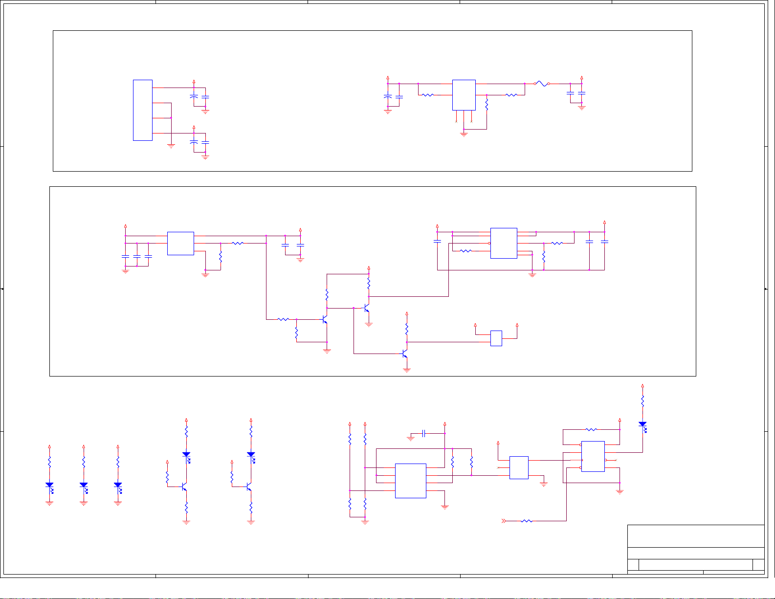
5
4
3
2
1
J1/J2/J3 SLOT POWER
ATX 4-PIN HARD
DISK CONNECTOR
D D
J5
+12VDC
COM
COM
+5VDC
53113-0410J553113-0410
1
2
3
4
VDDHD_12V
C76
C76
22uF
22uF
VDDHD_5V
C82
C82
22uF
22uF
C78
C78
+
+
1uF
1uF
+
+
C83
C83
1uF
1uF
1.0V REGULATOR VTT REGULATOR
C C
B B
VDDEARLY_3.3V
C87
C87
1uF
1uF
U13
U13
4
VIN
VOUT
2
ADJ
VBIAS
MIC49150
MIC49150
GND
C89
C89
C88
C88
0.01uF
0.01uF
1uF
1uF
U13 VOUT CAN RANGE FROM 2.8V TO 0.9V,
BY VARING R99 AND R100.
5
TRIM1V
1
3
NOTE: THE PCI EXPRESS CEM 1.1 SPEC DOES NOT
ALLOCATE ENOUGH POWER FOR ADD-IN CARDS TO
USE ON FANOUT SLOTS. J5 IS USED TO GENERATE
POWER FOR THE SLOT CONNECTORS J1, J2, AND
J3. THE +12V IS USED DIRECTLY, WHILE THE +5V IS
CONVERTED TO +3.3V VIA U12.
VDD_1.0V
C90
R99 1KR99 1K
R100
R100
8.25K 1%
8.25K 1%
C90
10uF
10uF
R105 1KR105 1K
R124NLR124
1V_ON
1V_ON
NL
VDDHD_5V
+
C77
+
C77
C81
C81
180uF
180uF
R94 5.1KR94 5.1K
1uF
1uF
PEX 8505 POWER
C91
C91
1uF
1uF
VDDEARLY_3.3V
R103
R103
5.1K
1
5.1K
Q3
Q3
MMBT3904LT1
MMBT3904LT1
2 3
BASE_OFF
SHDNVTT
VDD_12V
R106
R106
5.1K
5.1K
Q6
Q6
1
MMBT3904LT1
MMBT3904LT1
2 3
R104
R104
5.1K
5.1K
Q4
Q4
1
MMBT3904LT1
MMBT3904LT1
2 3
5V-TO-3.3V DC/DC CONVERTER
U12
S7AH-08E1A0
S7AH-08E1A0
VDDEARLY_3.3V
C84
C84
1uF
1uF
GATE33
1
U12
Vin2Vout
On/Off
Gnd
NC6NC
3
R101 100KR101 100K
VDD_3.3V
Trim
VDD33HD
4
R95 NLR95 NL
TRIM3V
5
R96
R96
1.30K, 1%
1.30K, 1%
7
R95 AND R96 CAN BE INSTALLED TO
ADJUST THE OUTPUT VOLTAGE OF U12. SEE
THE MANUFACTURERS DATASHEET FOR
DETAILS.
U14
U14
1
IN
2
IN
4
SHDN#
3
POK
THERM
MAX1806
MAX1806
PIN 9 IS A THERMAL PAD
UNDERNEATH U14.
Q5
2
S
3
D
1
G
N-MOSQ5N-MOS
8
OUT
7
OUT
6
SET
5
GND
9
VDDEARLY_3.3V
F1 7AF1 7A
SETVTT
R1020R102
0
VDDHD_3.3V
C79
C79
C80
C80
1uF
10uF
10uF
NL
1uF
VDD_VTT
C86
C86
C85
C85
0.1uF
0.1uF
10uF
R98NLR98
10uF
VDDEARLY_3.3V
R107
BOARD POWER ON INDICATOR LEDS
VDD_VTT
R118
R118
VDD_3.3V
R109
R109
150
150
21
D15
D15
Green
Green
Q8
Q8
1
MMBT3904LT1
MMBT3904LT1
2 3
R1200R120
0
4
75.0K 1%
75.0K 1%
R111
R111
R121
R121
5.1K
5.1K
R112
R112
7.68K 1%
7.68K 1%
VMON1
VMON4
R38
R38
2.26K 1%
2.26K 1%
PLACE U3, U15 AND U17 ON SOLDER SIDE.
3
VDD_3.3V
R108
R108
150
150
21
D16
D16
Green
Green
8.25K 1%
8.25K 1%
Q7
Q7
1
MMBT3904LT1
MMBT3904LT1
2 3
R1190R119
0
R113
R113
1K 1%
1K 1%
D17
D17
Green
Green
VDD_3.3VVDD_12V
2.74K 1%
2.74K 1%
VDD_1.0V
R117
R117
R114
R114
150
150
21
D18
D18
Green
Green
VDDHD_12V
R123
R123
1K 1%
1K 1%
21
A A
21
D20
D20
Green
Green
5
SLOT POWER FAULT INDICATOR
VDDEARLY_3.3VVDDHD_3.3VVDDHD_12V
C92 0.1uFC92 0.1uF
R115
U3
8
VDD
VMON1
7
PGD
VMON2
6
5
VMON3
VMON4
ISL6536U3ISL6536
EN
GND
R115
10K
10K
1
2
VMONEN
3
4
R116
R116
NL, 10K
NL, 10K
PGD
VDDEARLY_3.3V
PERSTN{4,5,6,7,8}
VDDEARLY_3.3V
R110 10KR110 10K
CLRN
U15
U15
6
PREN
2
1
7
U17
U17
NC7S04
NC7S04
R13 0R13 0
PFTL
4
Y
GND3A
2
5
VCC
1
NC
2
CLR#
VCC
D
CLK
GND
PRE#
SN74LVC2G74
SN74LVC2G74
8
5
Q
3
Q#
4
R107
150
150
21
PLACE D14 ON
D14
D14
COMPONENT SIDE OF
Red
Red
BOARD.
PFLT_Q
U3 MONITORS 12V AND 3.3V POWER GOING
TO J1, J2 AND J3. A FAULT ON EITHER
SUPPLY WILL CAUSE D14 TO LIGHT.
PLX Technology, Inc.
PLX Technology, Inc.
PLX Technology, Inc.
870 Maude Avenue
870 Maude Avenue
870 Maude Avenue
Sunnyvale, CA 94085
Sunnyvale, CA 94085
Sunnyvale, CA 94085
www.plxtech.com
www.plxtech.com
Title
Title
Title
Size Document Number Rev
Size Document Number Rev
Size Document Number Rev
C
C
C
91-0076-001-A 001
91-0076-001-A 001
91-0076-001-A 001
Date: Sheet
Date: Sheet
Date: Sheet
www.plxtech.com
PEX8505RDK - Board Power
PEX8505RDK - Board Power
PEX8505RDK - Board Power
1
99Monday, October 01, 2007
99Monday, October 01, 2007
99Monday, October 01, 2007
of
of
of
 Loading...