

PLL PL560-09OIL User Manual
查询PL560-09OIL供应商
PL560-xx VCXO Family
PRODUCT DESCRIPTION
PhaseLink’s Analog Frequency MultiplierTM (AFM) is
the industry’s first ‘Balanced Oscillator’ utilizing
analog multiplication of the fundamental frequency
(at double or quadruple frequency), combined with
an attenuation of the fundamental of the reference
crystal, without the use of a phase-locked loop
(PLL), in CMOS technology.
PhaseLink’s patent pending PL560-xx family of AFM
products can achieve up to 800 MHz output
frequency with little jitter or phase noise
deterioration. In addition, the low frequency input
crystal requirement makes the AFMs the most
affordable high-performance timing-source in the
market.
PL560-xx family of products utilize low-power CMOS
technology and are housed in GREEN/ RoHS
compliant 16-pin TSSOP, and 16-pin 3x3 QFN
packages.
Analog Frequency Multiplier
FEATURES
• Non-PLL frequency multiplication
• Input frequency from 30-200 MHz
• Output frequency from 60-800 MHz
• Low phase noise and jitter (equivalent to fundamental
crystal at the output frequency)
• Ultra-low jitter
o RMS phase jitter < 0.25 ps (12kHz-20MHz)
o RMS period jitter < 2.5 ps
• Low phase noise
o -142 dBc/Hz @100kHz offset from 155.52 MHz
o -150 dBc/Hz @10MHz offset from 155.52 MHz
• High linearity pull range (typ. 5%)
• +/- 120 PPM pullability VCXO
• Low input frequency eliminates the need for expensive
crystals
• Differential output levels (PECL, LVDS), or single-
ended CMOS
• Single 2.5V or 3.3V +/- 10% power supply
• Optional industrial temperature range (-40°C to +85° C)
• Available in 16-pin GREEN/RoHS com pliant TSSOP,
and 3x3 QFN
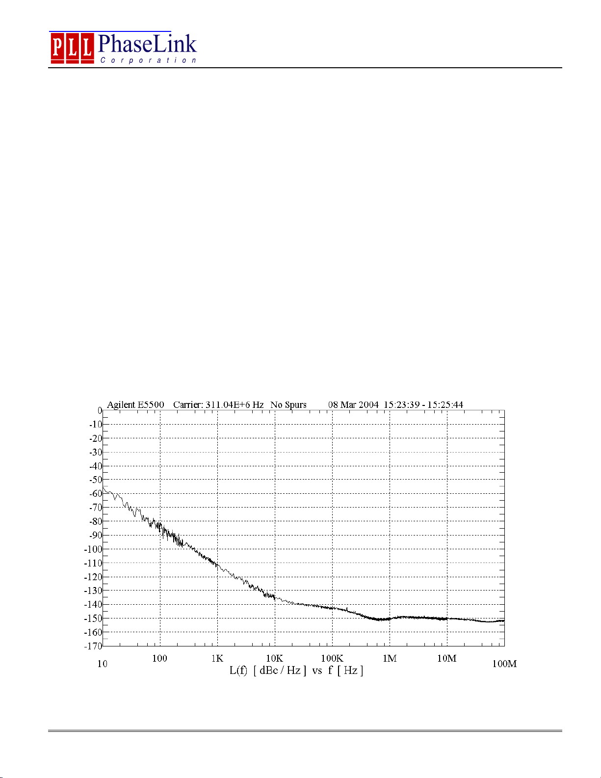
Figure 1: 2x AFM Phase Noise at 311.04MHz
47745 Fremont Blvd., Fremont, Cali fornia 94 53 8 TEL (51 0) 492-0990, FA X (510) 4 92 -0991 www .phaselink.com Rev. 02/09/07 Page 1
Analog Frequency Multiplier
PL560-xx VCXO F amily
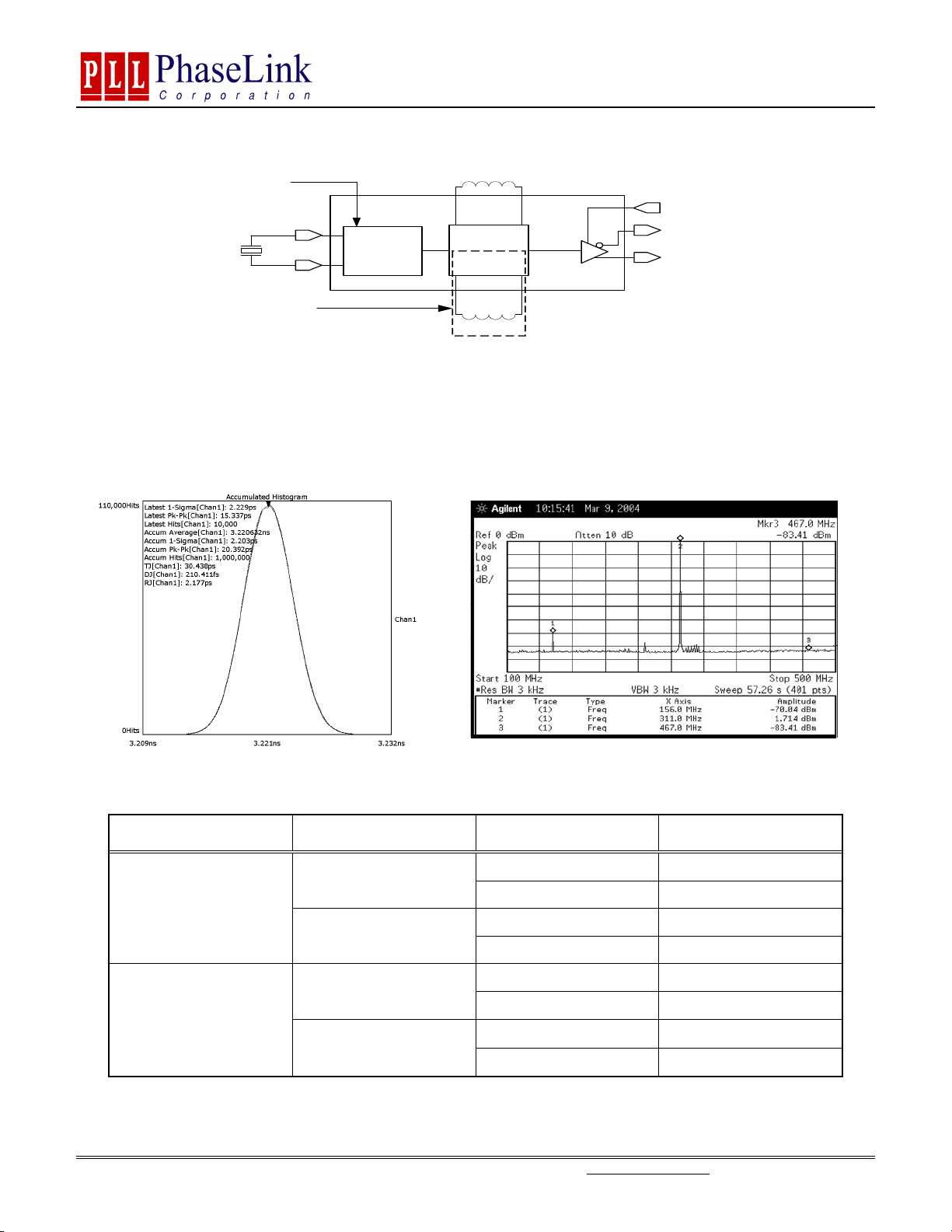
V C O N
X IN
O s c il la to r
A m plifi e r
X O U T
O n ly re q u ire d in x 4 d es ig n s
L 2 X
F re qu e nc y
X 2
F re qu e nc y
X 4
L 4 X
O E
Q B A R
Q
Figure 2: Block Diagra m of VC XO AFM
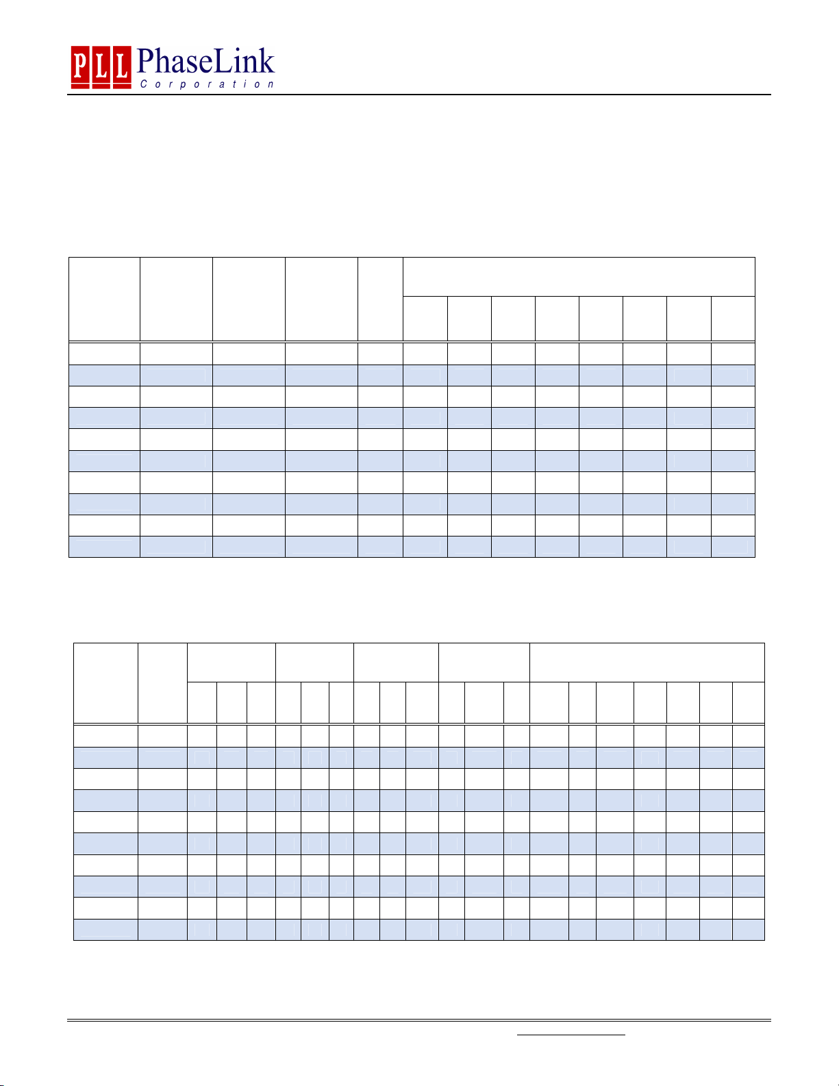
Figure 3 shows the period jitter histogram of the 2x Analog Frequency Multiplier at 311.04 MHz, while Figure 4 shows the very
low rejection levels of sub-harmonics that correspond to the exceptionally low jitter performance.
Figure 3: Period Jitter Histogram at 311.04 MHz Figure 4: Spectrum Analysis at 311.04 MHz
Analog Frequency Multiplier (2x) Analog Frequency Multiplier (2x)
with 155.52MHz crystal with sub-harmonics below –72 dBc
OE LOGIC SELECTION
OUTPUT OESEL OE Output State
0 (Default)
PECL
1
0 (Default)
LVDS or CMOS
1
OESEL and OE: Connect to VDD to set to “1”, conne ct to GND to set to “0”. Internally set to default thr ough pull-down / -up.
47745 Fremont Blvd., Fremont, CA 9 4538 TEL (51 0) 492-09 90, FAX (510) 4 92-0991 ww w.phaselink .com Rev.:02-09- 07 Page 2
0 (Default) Enabled
1 Tri-state
0 Tri-state
1 (Default) Enabled
0 Tri-state
1 (Default) Enabled
0 (Default) Enabled
1 Tri-state
Analog Frequency Multiplier
20MHz)
PL560-xx VCXO F amily
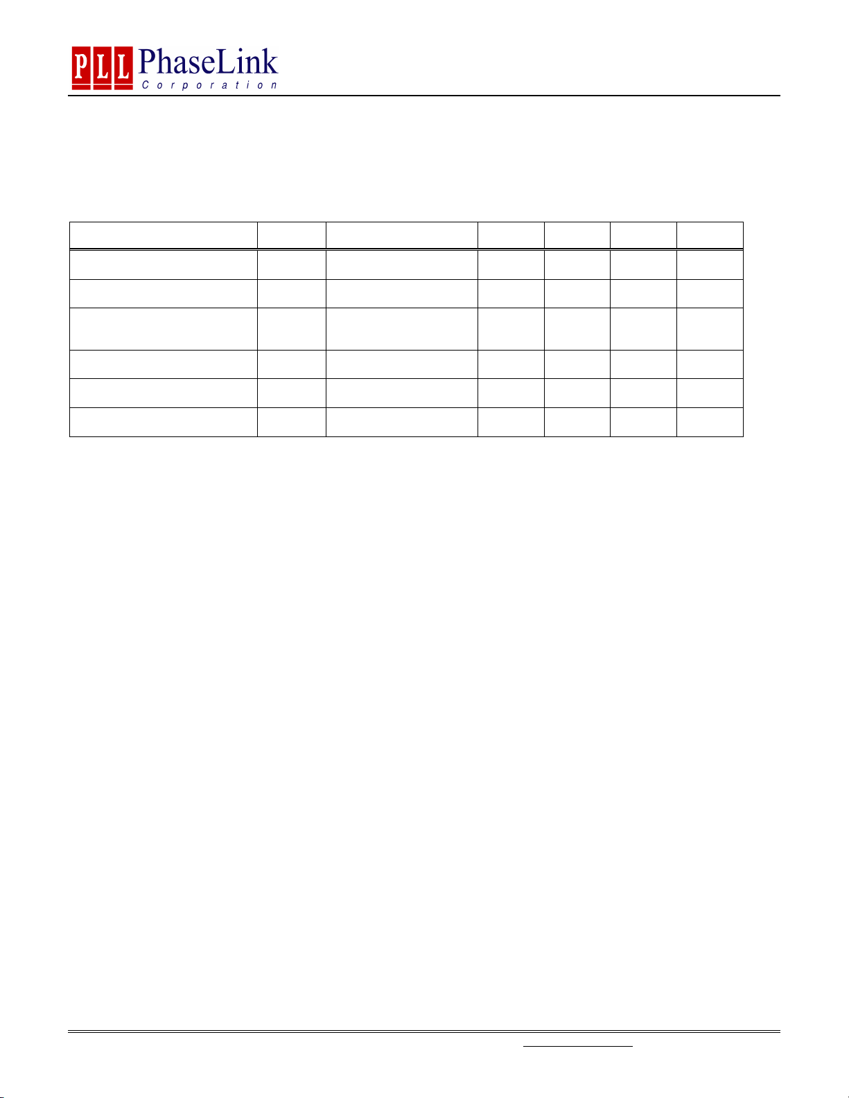
PRODUCT SELECTION GUIDE
FREQUENCY VERSUS PHASE NOISE PERFORMANCE
Part
Number
PL560-08
PL560-09
PL560-37
PL560-38
PL560-39
PL560-47
PL560-48
PL560-49
PL560-68
PL560-69
Input
Frequency
Range (MHz)
75 - 200 4 300 - 800 PECL 622.08 -55 -85 -110 -130 -137 -148 -150
75 - 200 4 300 - 800 LVDS 622.08 -55 -85 -110 -130 -137 -148 -150
30 - 80 4 120 - 320 CMOS 155.52 -50 -82 -110 -128 -142 -148 -150
30 - 80 4 120 - 320 PECL 155.52 -50 -82 -110 -128 -142 -148 -150
30 - 80 4 120 - 320 LVDS 155.52 -50 -82 -110 -128 -142 -148 -150
30 - 80 2 60 - 160 CMOS 155.52 -65 -95 -122 -138 -142 -148 -149
30 - 80 2 60 - 160 PECL 155.52 -65 -95 -122 -138 -142 -148 -149
30 - 80 2 60 - 160 LVDS 155.52 -65 -95 -122 -138 -142 -148 -149
75 - 200 2 150 - 400 PECL 311.04 -60 -85 -112 -135 -142 -150 -151
75 - 200 2 150 - 400 LVDS 311.04 -60 -85 -112 -135 -142 -150 -151
Analog
Frequency
Multiplication
Factor
Output
Frequency
Range (MHz)
Phase noise was measured using Agilent E5500.
Output
Type
Phase Noise at Frequency Offset From Carrier (dBc/Hz)
Carrier
Freq.
(MHz)
10 Hz 100 Hz 1 KHz
10
KHz
100
KHz
1 MHz
FREQUENCY VERSUS JITTER, AND SUB-HARMONIC PERFORM ANCE
RMS Period
Part
Number
PL560-08
PL560-09 622 4 6 25 30 6 0.09 622 -50 -50 -45 -47 -47 -55
PL560-37 155 2.5 3 18 20 3 0.25 155.52 -75 -62 -65 -75
PL560-38 155 2.5 3 18 20 3 0.25 155.52 -75 -62 -65 -75
PL560-39 155 2.5 3 18 20 3 0.25 155.52 -75 -62 -65 -75
PL560-47 155 2.5 3 18 20 3 0.25 155.52 -68 -68
PL560-48 155 2.5 3 18 20 3 0.25 155.52 -68 -68
PL560-49 155 2.5 3 18 20 3 0.27 155.52 -68 -68
PL560-68 311 2.5 3 18 20 3 0.18 311.04 -72 -85
PL560-69 311 2.5 3 18 20 3 0.18 311.04 -72 -85
Output.
Freq.
(MHz)
622 4 6 25 30 6 0.09 622 -50 -50 -45 -47 -47 -55
Jitter
(ps)
Min. Typ. Max. Min. Typ. Max. Min. Typ. Max. Min. Typ. Max.
Note: Wavecrest data 10, 000 hits. No filtering was used in jitter calculations .
Agilent 5500 wa s used for phase jitter mea suremen ts.
Spectral specif ications were obtained us ing Agilent E7401A.
Peak to Peak
Period Jitter
(ps)
RMS Accumulated
(L.T.) Jitter (ps)
RMS Phase Jitter
(12 KHz-
(ps)
Spectral Specifications / Sub-harmonic Content
Carrier
Freq.
(Fc)
(dBc), Frequency (MHz)
@
(Fc)
@
-50%
(Fc)
-25%
-75%
@
(Fc)
@
+25%
(Fc)
@
+50%
(Fc)
10
MHz
@
+75%
(Fc)
47745 Fremont Blvd., Fremont, CA 9 4538 TEL (51 0) 492-09 90, FAX (510) 4 92-0991 ww w.phaselink .com Rev.:02-09- 07 Page 3
Analog Frequency Multiplier
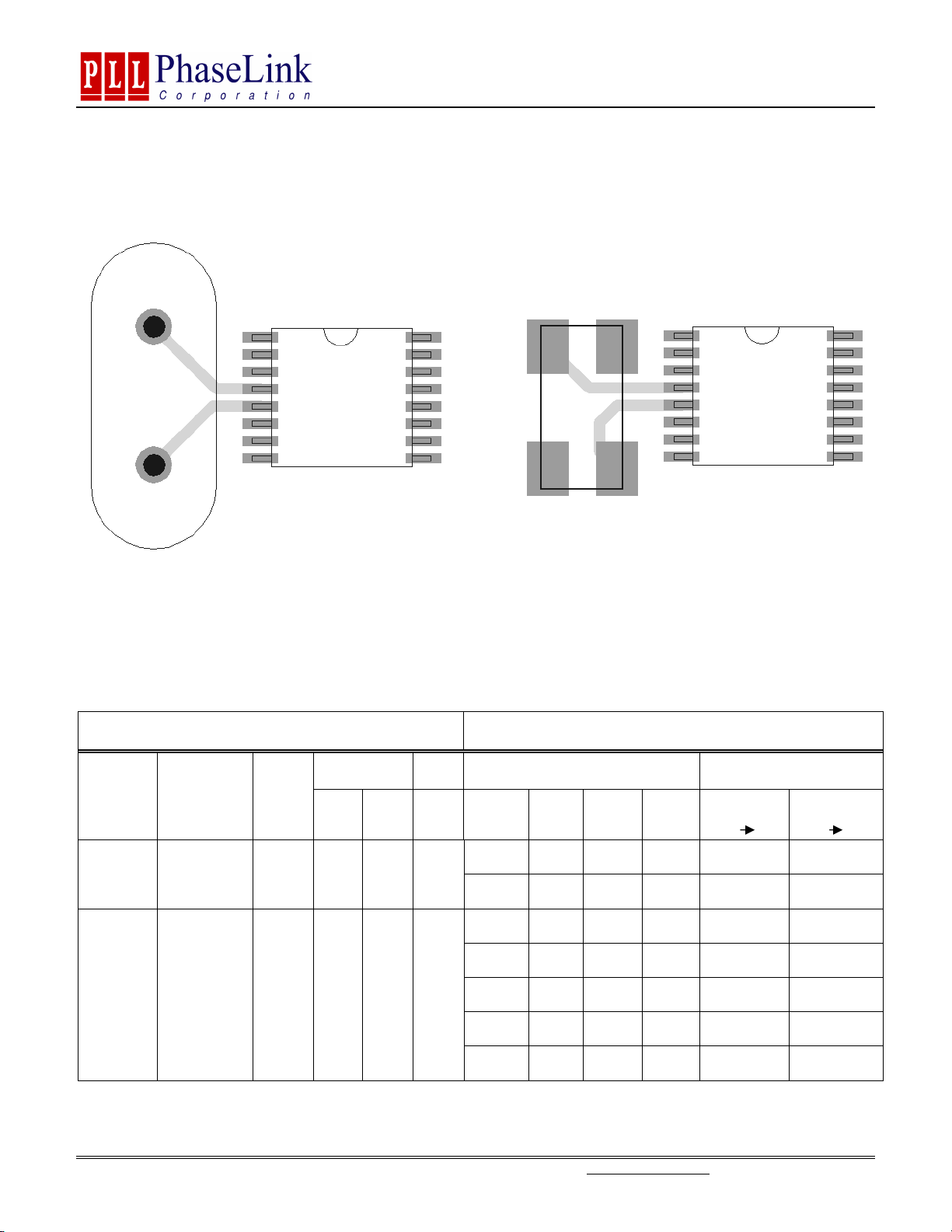
XTAL
XO UT ( Pi n # 5)
XO UT ( Pi n # 5)
PL560-xx VCXO F amily
CRYSTAL SPECIFIC ATIONS AND BOARD LAYOUT CONSIDERATIONS
BOARD LAYOUT CONSIDERATIONS
AFM IC
XI N (P in # 4)
XTAL
Ce ra mic
SM D
To minimize parasitic effects, and improve performance:
• Place the crystal as close as possible to the IC.
• Make the board traces that are connected to the crystal pins symmetrical.
• The board trace symmetry is important, as it reduces the negative parasitic effects to produce a clean frequency multiplication with
low jitter. Parasitic effects reduce frequency pulling of the VCXO and increase jitter.
AFM IC
XI N (P in # 4)
CRYSTAL SPECIFIC ATIONS & TUNING PERFORMANCE
CRYSTAL SPECIFICATIONS TUNING PERFORMANCE
PART
NUMBER
PL560-08/09
PL560-68/69
CRYSTAL
RESONATOR
FREQUENCY
(FXIN)
75~200MHz
MODE
Funda-
mental
PL56037/38/39
PL560-
30~80MHz
Funda-
mental
47/48/49
No te : No n sp ec ified p ar am et er s can be ch osen a s st andard valu es from cr ys ta l su ppliers.
CL ra tings lar ge r th an 5p F requ ir e a cr ys ta l frequency a dj us tm en t. Requ est de ta iled cryst al specif ic at ions from Pha se Link .
CL (xtal)
CONDI-
TIONS
At
VCON
=
1.65V
At
VCON
=
1.65V
TYP. Max.
5pF 30 Ω
5pF 30 Ω
ESR
(RE)
CRYSTAL TUNING (Typical)
CRYSTAL
FREQ
(MHz)
155.52 3.0pF 12.2fF 245 -145 ppm +108 ppm
155.52 1.8pF 5.7fF 316 -134 ppm +87 ppm
30.72 2.8pF 12.4fF 228 -167ppm +176 ppm
30.72 4.5pF 19.1fF 236 -163 ppm +167 ppm
38.88 5.1pF 20.9fF 242 -131 ppm +98 ppm
38.88 5.3pF 25.6fF 207 -157 ppm +141 ppm
77.76 2.0pF 6.7fF 305 -92 ppm +110 ppm
C0 C1 C0/C1
VC:
1.65V 0V
1.65V 3.4V
VC:
47745 Fremont Blvd., Fremont, CA 9 4538 TEL (51 0) 492-09 90, FAX (510) 4 92-0991 ww w.phaselink .com Rev.:02-09- 07 Page 4
Analog Frequency Multiplier
PL560-xx VCXO F amily
VOLTAGE CONTROL SPECIFICATION
PARAMETERS SYMBOL CONDITIONS MIN. TYP. MAX.
VCXO Stabilization Time T
VCXO T uning Ran ge
CLK Output Pullability
Linearity 5 10 %
VCON Input Impedance
VCON Modulation BW
From power valid 10 ms
VCXOSTB
XTAL C0 /C
VCON= 1.65V ± 1.65V
XTAL C0 /C
130
0V < VCON < 3.3V, -3dB 25 kHz
<300
1
<300
1
200 ppm
±100 ±120
ppm
UNITS
EXTERNAL COMPONENT VALUES
kΩ
INDUCTOR VALUE OPTIMIZATION
The required inductor value(s) for the best performance depends on the operating frequency, and the board
layout specifications. The listed values in this datasheet are based on the calculated parasitic values from
PhaseLink’s evaluation board design. These inductor values provide the user with a starting point to determine
the optimum inductor values. Additional fine-tuning may be required to determine the optimal solution.
To assist with the inductor value optimization, PhaseLink has developed the “AFM Tuning Assistant” software.
You can download this software from PhaseLink’s web site (www.phaselink.com). The software consists of two
worksheets. The first worksheet (named L2) is used to fine-tune the ‘L2’ inductor value, and the second
worksheet (named L4) is used for fine tuning of the ‘L4’ (used in 4x AFMs only) inductor value.
For those designs using PhaseLink’s recommended board layout, you can use the “AFM Tuning Assistant” to
determine the optimum values for the required inductors. This software is developed based on the parasitic
information from PhaseLink’s board layout and can be used to determine the required inductor and parallel
capacitor (see LWB1 and Cstray parameters) values. For those employing a different board layout in their
design, we recommend to use the parasitic information of their board layout to calculate the optimized inductor
values. Please use the following fine tuning procedure:
47745 Fremont Blvd., Fremont, CA 9 4538 TEL (51 0) 492-09 90, FAX (510) 4 92-0991 ww w.phaselink .com Rev.:02-09- 07 Page 5
 Loading...