

Page 1
CANAL PLUS TUNER
TS5
BCT-1510
BCT-1520
BCT-1530
THIS MANUAL IS APPLICABLE TO THE FOLLOWING MODEL(S) AND TYPE(S).
Type
NYXK/FR – – – AC230V
NYXK/FR1 – – – AC230V
NYXK/FR2 – – – AC230V
NYXK/FR3 – – – AC230V
NYXK/SP – – – AC230V
NYXK/IT – – – AC230V
NYWXKPL – – – AC230V
Model
TS5
BCT-1510 BCT-1520 BCT-1530
Power Requirement Remarks
ORDER NO.
ARP3079
CONTENTS
1. SAFETY INFORMATION
2. EXPLODED VIEWS AND PARTS LIST
3. SCHEMATIC DIAGRAM
4. PCB CONNECTION DIAGRAM
5. PCB PARTS LIST
PIONEER CORPORATION 4-1, Meguro 1-chome, Meguro-ku, Tokyo 153-8654, Japan
PIONEER ELECTRONICS SERVICE, INC. P.O. Box 1760, Long Beach, CA 90801-1760, U.S.A.
PIONEER EUROPE NV Haven 1087, Keetberglaan 1, 9120 Melsele, Belgium
PIONEER ELECTRONICS ASIACENTRE PTE. LTD. 253 Alexandra Road, #04-01, Singapore 159936
c
PIONEER CORPORATION 2000
...............................................
......................................
................
.......................................
..........................
28
34
2
4
8
6. ADJUSTMENT
7. GENERAL INFORMATION
7.1 IC
8. PANEL FACILITIES AND SPECIFICATIONS
.................................................................
....................................................
36
................................
T – ZZV SEPT. 2000 Printed in Japan
....
37
37
60
Page 2
TS5, BCT-1510, BCT-1520,
BCT-1530
1. SAFETY INFORMATION
This service manual is intended for qualified service technicians ; it is not meant for the casual do-ityourselfer. Qualified technicians have the necessary test equipment and tools, and have been trained
to properly and safely repair complex products such as those covered by this manual.
Improperly performed repairs can adversely affect the safety and reliability of the product and may
void the warranty. If you are not qualified to perform the repair of this product properly and safely, you
should not risk trying to do so and refer the repair to a qualified service technician.
WARNING
This product contains lead in solder and certain electrical parts contain chemicals which are known to the state of California to cause
cancer, birth defects or other reproductive harm.
Health & Safety Code Section 25249.6 – Proposition 65
NOTICE
(FOR CANADIAN MODEL ONLY)
Fuse symbols (fast operating fuse) and/or (slow operating fuse) on PCB indicate that replacement parts must
be of identical designation.
REMARQUE
(POUR MODÈLE CANADIEN SEULEMENT)
Les symboles de fusible (fusible de type rapide) et/ou (fusible de type lent) sur CCI indiquent que les pièces
de remplacement doivent avoir la même désignation.
(FOR USA MODEL ONLY)
1. SAFETY PRECAUTIONS
The following check should be performed for the
continued protection of the customer and service
technician.
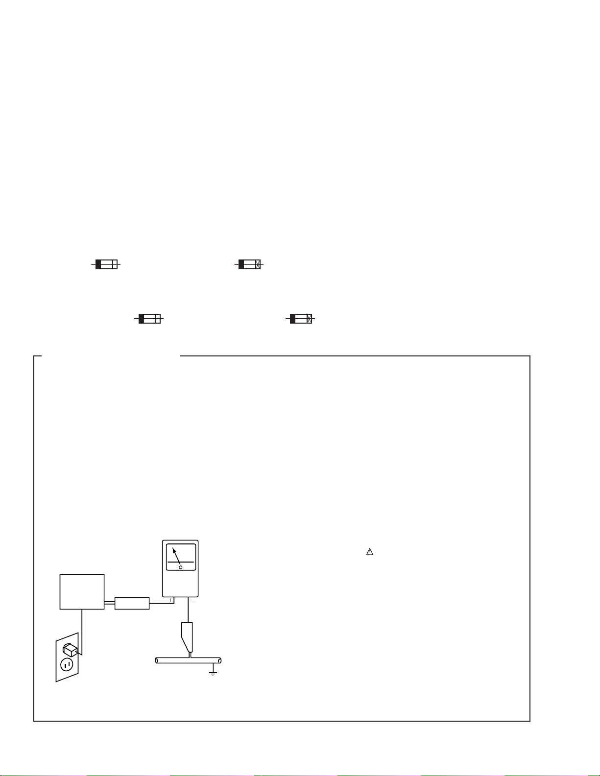
LEAKAGE CURRENT CHECK
Measure leakage current to a known earth ground (water
pipe, conduit, etc.) by connecting a leakage current tester
such as Simpson Model 229-2 or equivalent between the
earth ground and all exposed metal parts of the appliance
(input/output terminals, screwheads, metal overlays, control
shaft, etc.). Plug the AC line cord of the appliance directly
into a 120V AC 60Hz outlet and turn the AC power switch
on. Any current measured must not exceed 0.5mA.
Reading should
not be above
0.5mA
Earth
ground
Device
under
test
Also test with
plug reversed
(Using AC adapter
plug as required)
Leakage
current
tester
Test all
exposed metal
surfaces
ANY MEASUREMENTS NOT WITHIN THE LIMITS
OUTLINED ABOVE ARE INDICATIVE OF A POTENTIAL
SHOCK HAZARD AND MUST BE CORRECTED BEFORE
RETURNING THE APPLIANCE TO THE CUSTOMER.
2. PRODUCT SAFETY NOTICE
Many electrical and mechanical parts in the appliance
have special safety related characteristics. These are
often not evident from visual inspection nor the protection
afforded by them necessarily can be obtained by using
replacement components rated for voltage, wattage, etc.
Replacement parts which have these special safety
characteristics are identified in this Service Manual.
Electrical components having such features are identified
by marking with a
in this Service Manual.
The use of a substitute replacement component which does
not have the same safety characteristics as the PIONEER
recommended replacement one, shown in the parts list in
this Service Manual, may create shock, fire, or other hazards.
Product Safety is continuously under review and new
instructions are issued from time to time. For the latest
information, always consult the current PIONEER Service
Manual. A subscription to, or additional copies of, PIONEER
Service Manual may be obtained at a nominal charge from
PIONEER.
on the schematics and on the parts list
AC Leakage Test
2
Page 3

TS5, BCT-1510, BCT-1520,
BCT-1530
3
Page 4
TS5, BCT-1510, BCT-1520,
BCT-1530
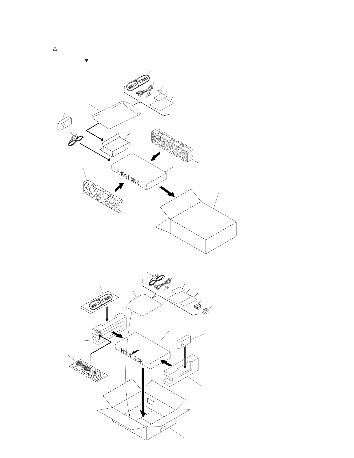
2. EXPLODED VIEWS AND PARTS LIST
NOTES:•Parts marked by "NSP" are generally unavailable because they are not in our Master Spare Parts List.
2.1 PACKING
TS5/NYXK/FR only
The mark found on some component parts indicates the importance of the safety factor of the part.
•
Therefore, when replacing, be sure to use parts of identical designation.
Screws adjacent to mark on the product are used for disassembly.
•
12
15
13
14
10
18
7
9
16
Except TS5/NYXK/FR
6
2
16(Except BCT-1520)
12
18
8
15
9
3
1
14(Except BCT-1530)
10
11(BCT-1530 only)
17(for BCT-1510)
17(for BCT-1530)
8
4
16 (BCT-1520 only)
1
7
5
4
Page 5

(1) PACKING PARTS LIST
Mark No. Description Part No.
1 Packing Case See Contrast Table(2)
2 Pulp Mold Pad F See Contrast Table(2)
3 Pulp Mold Pad R See Contrast Table(2)
4 Side Pad L See Contrast Table(2)
5 Side Pad R See Contrast Table(2)
6 Sub Packing Case See Contrast Table(2)
7 Remote Control Unit See Contrast Table(2)
8 Sheet AHG1153
9 Battery (R03) 2P VEM1018
10 Instruction Manual See Contrast Table(2)
11 Instruction Manual 2 See Contrast Table(2)
12 Scart Cable(1m:Black) See Contrast Table(2)
NSP 13 Sticker See Contrast Table(2)
NSP 14 Modem Approval Sheet See Contrast Table(2)
15 AC Power Cord (2m:Black) BDG1035
16 Modem Cable (10m:White) See Contrast Table(2)
NSP 17 Modem Adapter See Contrast Table(2)
NSP 18 Catalogue Bag BHG1047
TS5, BCT-1510, BCT-1520,
BCT-1530
(2) CONTRAST TABLE
TS5/NYXK/FR, TS5/NYXK/FR1, TS5/NYXK/FR2, TS5/NYXK/FR3, BCT-1510/NYXK/SP, BCT-1520/NYXK/IT and
BCT-1530/NYWXKPL are constructed the same except for the following:
.oNtraP
kraM.oNnoitpircseDdnalobmyS
TS5
/NYXK/FR
1 Packing Case BHD1489 BHD1369BHD1369 BHD1369 BHD1375 BHD1480 BHD1442
2 Pulp Mold Pad F
3
Pulp Mold Pad R
4 Side Pad L
5
Side Pad R
6
Sub Packing Case BHB1036
Remote Control Unit BXD1010 BXD1010 BXD1010 BXD10107BXD1016 BXD1018
10 Instruction Manual (French)
10 Instruction Manual (Spanish)
10 Instruction Manual (Italian)
Instruction Manual (Polish)
1110Instruction Manual 2 (Polish)
Scart Cable
12
NSP
13
Sticker BAX1271
14
NSP
NSP
Modem Approval Sheet BRM1034
16
Modem Cable BDH1014
Modem Adapter
17
BHX1028
BHX1029
Not used
Not used
BRC1030
Not used
Not used Not usedNot used Not used Not used
Not used Not used Not used Not used Not used Not used BRC1011
Not used
BDH1018 BDH1018 BDH1018 BDH1018
Not used Not used
TS5
/NYXK/FR1 /NYXK/FR2/NYXK/FR3
Not used
Not used
BHA1146
BHA1147
Not used
BRC1021
Not used Not used Not used
Not used Not used Not used Not used Not used BRC1012
BDH1027
Not used
BRM1034 BRM1034 BRM1034 BRM1035 BRM1036
BDH1014 BDH1014 BDH1014 BDH1015 BDH1015BDH1016
TS5 TS5
Not used
Not used
BHA1146
BHA1147
Not used
BRC1022
BDH1027
Not used
Not used
BCT-1510
/NYXK/SP
Not used
Not used
BHA1146
BHA1147
Not used
BRC1026
BDH1027
Not used
Not used Not used
Not used
Not used
BHA1146
BHA1147
Not used Not used
Not used Not used
BRC1004 Not used Not used
Not used Not used Not used
BKP1124
BCT-1520
/NYXK/IT
Not used
Not used
BHA1146
BHA1147
BRC1027
BCT-1530
/NYWXKPL
Not used
Not used
BHA1146
BHA1147
Not used
BXD1037
Not used
Not used
Not used
BKP1130
skrameR
5
Page 6
TS5, BCT-1510, BCT-1520,
BCT-1530
2.2 EXTERIOR SECTION
19
19
19
20
19
19
18
21
A
19
1
11
3
19
19
19
17
19
5
19
15
D
19
4
14
13
19
19
19
16
16
C
9
19
19
12
2
6
8
7
B
10
6
Page 7

(1) EXTERIOR SECTION PARTS LIST
Mark No. Description Part No.
1 MAIN ASSY(FRANCE) See Contrast Table (2)
2 FRONT ASSY BWE1102
3 CARD ASSY BWE1080
4 POWER ASSY BXF1139
5 Fuse (0109: T2.5AH250V) REK1102
6 Front Panel Assy See Contrast Table (2)
7 Plastic Base BMA1002
8 Chassis BNA1151
9 PCB Support AEC1215
10 21P FFC(J1) BDD1042
11 12P FFC(J2) BDD1022
12 Rear Panel Assy See Contrast Table (2)
NSP 13 Name Label See Contrast Table (2)
14 Washer Faced Nut BBN1005
15 Joint BMR1133
16 Hexagon Headed screw BBA1059
17 Barrier BEC1231
18 Bonnet Case See Contrast Table (2)
19 Screw BBZ30P080FZK
20 Heat Sink BNH1049
TS5, BCT-1510, BCT-1520,
BCT-1530
21 Serial No. Label See Contrast Table (2)
(2) CONTRAST TABLE
TS5/NYXK/FR, TS5/NYXK/FR1, TS5/NYXK/FR2, TS5/NYXK/FR3, BCT-1510/NYXK/SP, BCT-1520/NYXK/IT and
BCT-1530/NYWXKPL are constructed the same except for the following:
.oNtraP
kraM.oNnoitpircseDdnalobmyS
TS5
/NYXK/FR
1 MAIN ASSY BWE1103 BWE1103BWE1103 BWE1 103 BWE1115 BWE11 15 BWE1 1 10
6 Front Panel Assy
12
13 Name Label
NSP
18
21
Rear Panel Assy
Bonnet Case
Serial No. Label BAX1145 BAX1145 BAX1145 BAX1145 BAX1181 BAX1189
BWX1144
BWX1168
BAL1400
BNE1120
TS5
TS5 TS5
/NYXK/FR1 /NYXK/FR2/NYXK/FR3
BWX1144
BWX1168
BAL1414
BNE1120
BWX1144
BWX1168
BAL1415
BNE1120
BWX1144
BWX1168
BAL1416
BNE1120
BCT-1510
/NYXK/SP
BWX1145
BWX1169
BAL1401
BNE1120
BCT-1520
/NYXK/IT
BWX1191
BWX1170
BAL1402
BNE1122
BCT-1530
/NYWXKPL
BWX1146
BWX1171
BAL1403
BNE1120
BAX1250
skrameR
7
Page 8
1
D
TS5, BCT-1510, BCT-1520,
BCT-1530
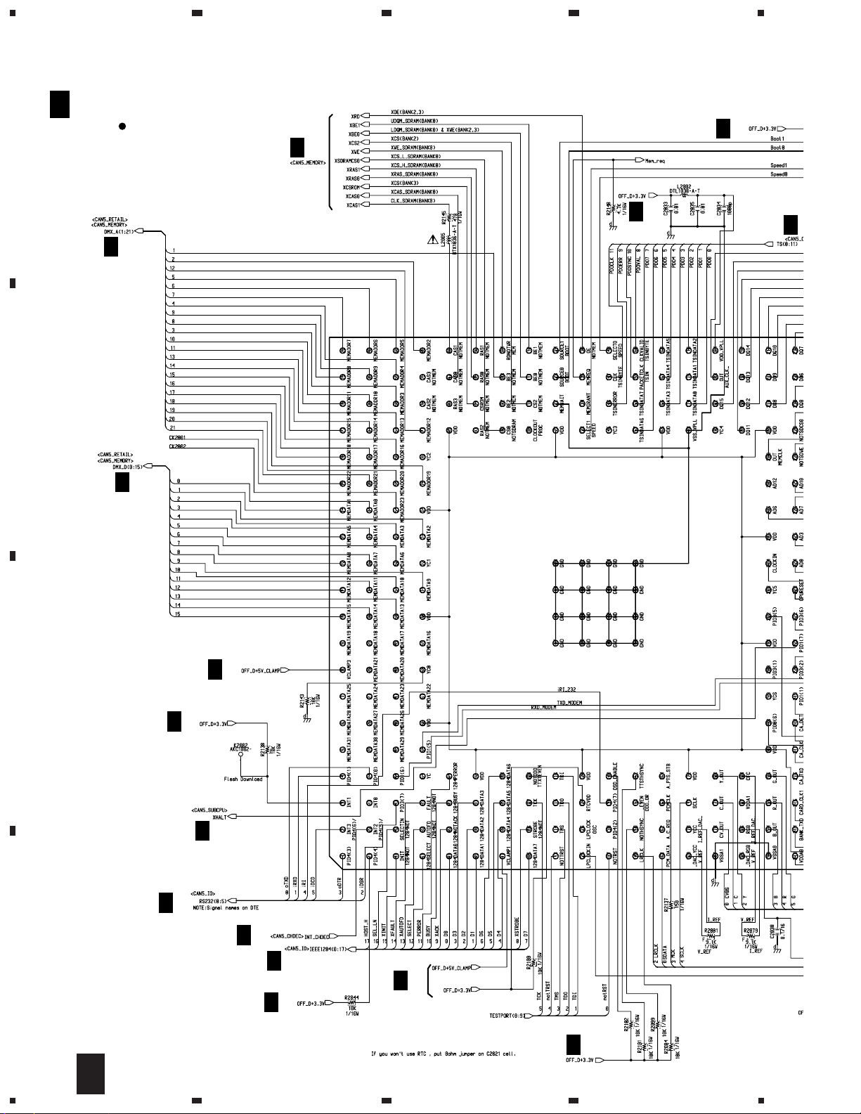
3. SCHEMATIC DIAGRAM
3.1 OVERALL WIRING DIAGRAM
A
23
4
CN4001-1
BKN1019
M1001
BXF1135
CN4001-2
BKN1019
B
(
A
A
1/7-
A
)
7/7
JA4001
BKB1017
MAIN ASSY
CN5005
BKP1123
CN5004
BKP1122
(TS5 : BWE1103)
(BCT-1510 : BWE1115)
(BCT-1520 : BWE1115)
(BCT-1530 : BWE1110)
CHDEC BLOCK : B1E1103
DMXCPU BLOCK : B2E1103
MEMORY BLOCK : B3E1103
ANALOG AV BLOCK : B4E1103
IO BLOCK : B5E1103
MODEM BLOCK : B6E1103
SUBPOWER BLOCK : B7E1103
C
CN2003
9604S-12C
B
D8001
BEL1037
FFC
BD
BDD1022
CN8503
9604S-12C
CARD ASSY
(BWE1080)
D
CN8502
BKP1141
CN8501
BKP1142
S8003 S8002
C
8
1234
S8006
S8001
S8004
S8005
Page 9
5
678
TS5, BCT-1510, BCT-1520,
BCT-1530
Note : When ordering service parts, be sure to refer to "EXPLODED VIEWS and P ARTS LIST" or "PCB P AR TS LIST".
A
CN5004
BKP1122
CN6001
BKP1137
T6001
BTX1035
GND
GND
GND
+3.3V
+3.3V
+3.3V
+5VReturn
+5V
+5V
GND
GND
–5V
AC_CLK
+12V
POW1
+24/19V
GND
+6V
+28V
BKP1120
CN7001
1
2
3
4
5
67
8
9
0
-=
~
!#
@
$
%
^
0209
0102
0109
REK1102
T2.5A/250V
1110
5110
6115
2170
1
7170
2
3
4
5
67
8
9
0
-=~
!#
@
$
%
^
POWER ASSY
D
(BXF1139)
5170
7180
B
C
8004
B
D8001
BEL1037
FFC CABLE
BDD1042
FRONT ASSY
(BWE1102)
M8001
BXX1026
5
D
9
6
7
8
Page 10
1
TS5, BCT-1510, BCT-1520,
BCT-1530
23
4
3.2 MAIN ASSY (1/7)
A
A
7/7
A
7/7
B
A 1/7
MAIN ASSY (1/7)
CHDEC BLOCK
(TS5 : BWE1103)
(BCT-1510 : BWE1115)
(BCT-1520 : BWE1115)
(BCT-1530 : BWE1110)
Regulator
A
A
7/7
7/7
DBS Front End
A+28V
C
Regulator
A
7/7
A
7/7
A
7/7
D
A
7/7
10
1/7
A
1234
Page 11
5
678
TS5, BCT-1510, BCT-1520,
BCT-1530
A
A
2/7
A
7/7
A
2/7
B
IC1004
TS5/BCT-1510/BCT-1520 : TDA8083H
BCT-1530 : TDA8083H/E
Domodulator and Decoder
A
C
7/7
D
1/7
A
5
6
7
8
11
Page 12
1
TS5, BCT-1510, BCT-1520,
BCT-1530
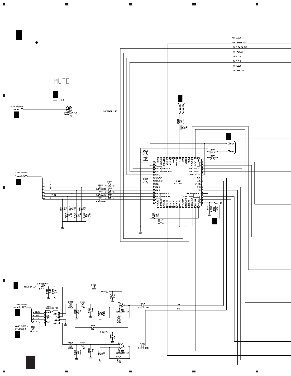
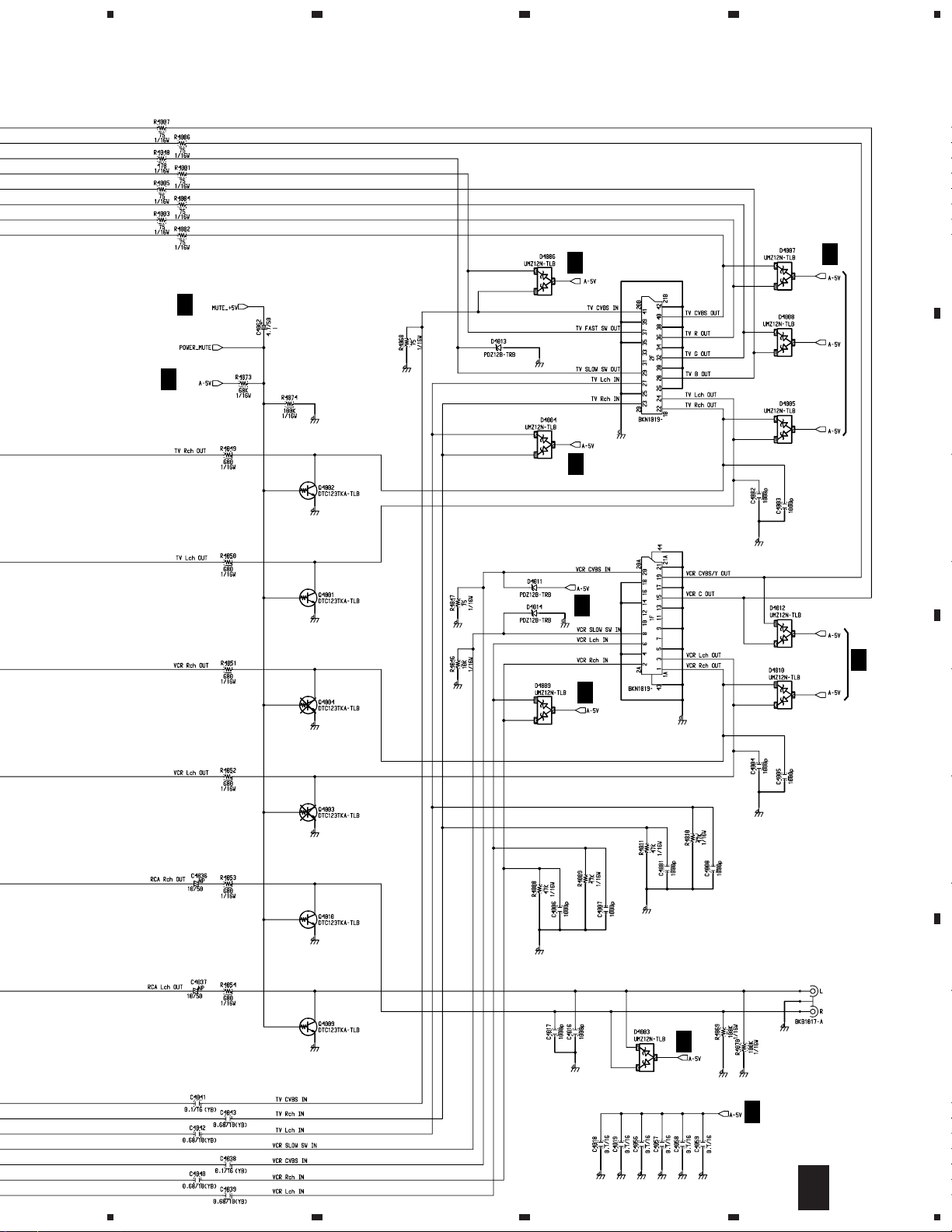
3.3 MAIN ASSY (2/7)
23
4
A 2/7
A
B
MAIN ASSY (2/7)
DMXCPU BLOCK
(TS5 : BWE1103)
(BCT-1510 : BWE1115)
(BCT-1520 : BWE1115)
(BCT-1530 : BWE1110)
A
3/7
A
3/7
A
3/7
A
7/7
IC2001
TS5/BCT-1510/BCT-1520 : STI5512AWE
BCT-1530 : STI5512AWE/E
A
7/7
A
1
Programmable Transport IC
A
7/7
C
A
7/7
A
7/7
A
6/7
A
1/7
A
A
5/7
7/7
A
7/7
A
7/7
D
12
2/7
A
1234
Page 13
7/7
A
1/7
5
678
TS5, BCT-1510, BCT-1520,
BCT-1530
A
B
A
A
3/7
7/7
A
3/7
A
7/7
A
7/7
A
7/7
Not used
A
A
7/7
7/7
A
7/7
A
6/7
A
1/7,4/7,7/7
A
7/7
A
4/7
A
7/7
A
7/7
A
7/7
A
A
C
7/7
7/7
CN8503
C
CN2003
A
7/7
A
4/7
A
7/7
2/7
A
5
6
7
8
13
D
Page 14
1
TS5, BCT-1510, BCT-1520,
BCT-1530
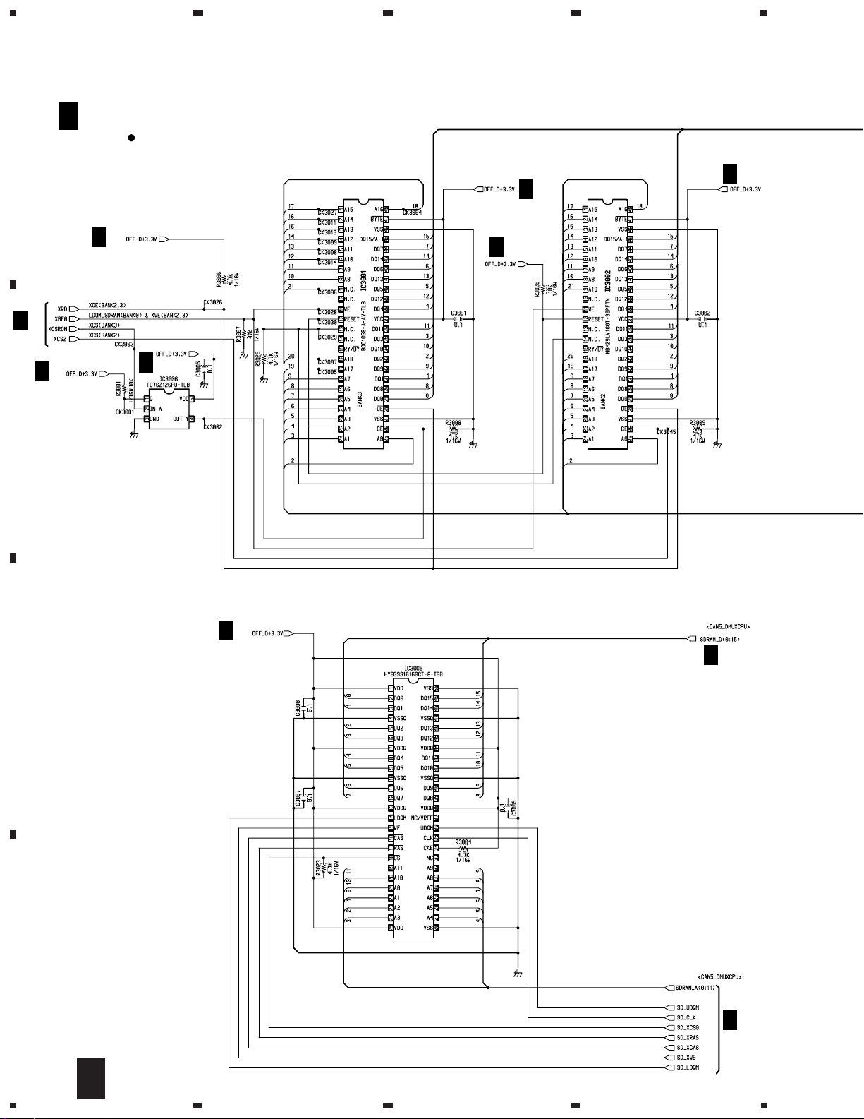
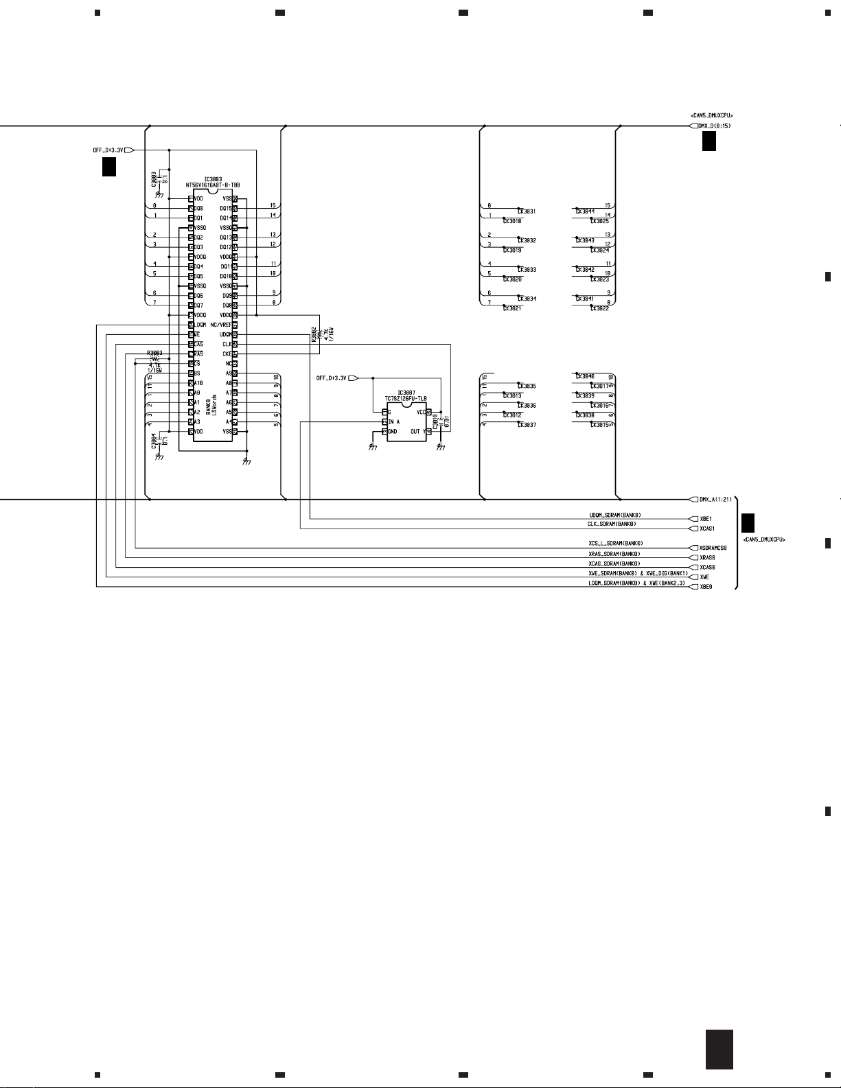
3.4 MAIN ASSY (3/7)
23
4
A 3/7
A
A
2/7
A
7/7
B
MAIN ASSY (3/7)
MEMORY BLOCK
(TS5 : BWE1103)
(BCT-1510 : BWE1115)
(BCT-1520 : BWE1115)
(BCT-1530 : BWE1110)
A
7/7
A
7/7
Flash Memory(8M)
(Boot/Data)
A
7/7
Flash Memory(16M)
(Application)
A
7/7
A
7/7
A
7/7
A
2/7
C
D
A
2/7
14
3/7
A
1234
Page 15
5
SDRAM (16M)
678
TS5, BCT-1510, BCT-1520,
BCT-1530
A
7/7
A
2/7
A
A
B
2/7
C
D
3/7
A
5
6
7
8
15
Page 16
1
TS5, BCT-1510, BCT-1520,
BCT-1530
3.5 MAIN ASSY (4/7)
MAIN ASSY (4/7)
ANALOG AV BLOCK
A
7/7
A
B
A 4/7
A
7/7
23
(TS5 : BWE1103)
(BCT-1510 : BWE1115)
(BCT-1520 : BWE1115)
(BCT-1530 : BWE1110)
A
2/7
4
A
7/7
A
2/7
AV Switch
A
7/7
C
A
7/7
A
2/7
D
A
7/7
16
4/7
A
1234
Page 17
A
A
7/7
7/7
5
678
TS5, BCT-1510, BCT-1520,
BCT-1530
A
A
A
7/7
CN4002-2
7/7
A
7/7
A
7/7
A
7/7
CN4002-1
A
B
7/7
C
Analog Audio Out
A
7/7
JA4001
A
4/7
8
D
17
A
7/7
5
6
7
Page 18
1
TS5, BCT-1510, BCT-1520,
BCT-1530
23
4
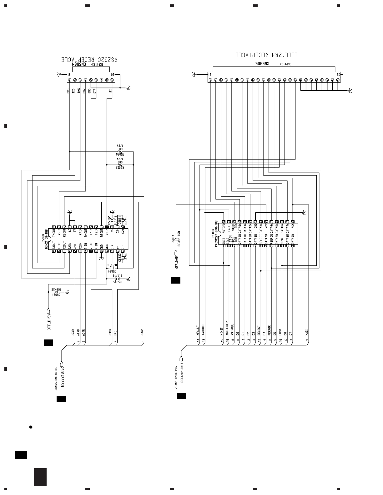
3.6 MAIN ASSY (5/7)
A
B
Serial I/F
Parallel I/F
RS-232C Driver
C
7/7
A
(BCT-1520 : BWE1115)
(BCT-1530 : BWE1110)
(BCT-1510 : BWE1115)
(TS5 : BWE1103)
2/7
A
MAIN ASSY (5/7)
D
IO BLOCK
7/7
A
2/7
A
Termination Network IC
A 5/7
18
5/7
A
1234
Page 19

1
234
TS5, BCT-1510, BCT-1520,
BCT-1530
A
B
C
D
19
1
2
3
4
Page 20

1
TS5, BCT-1510, BCT-1520,
BCT-1530
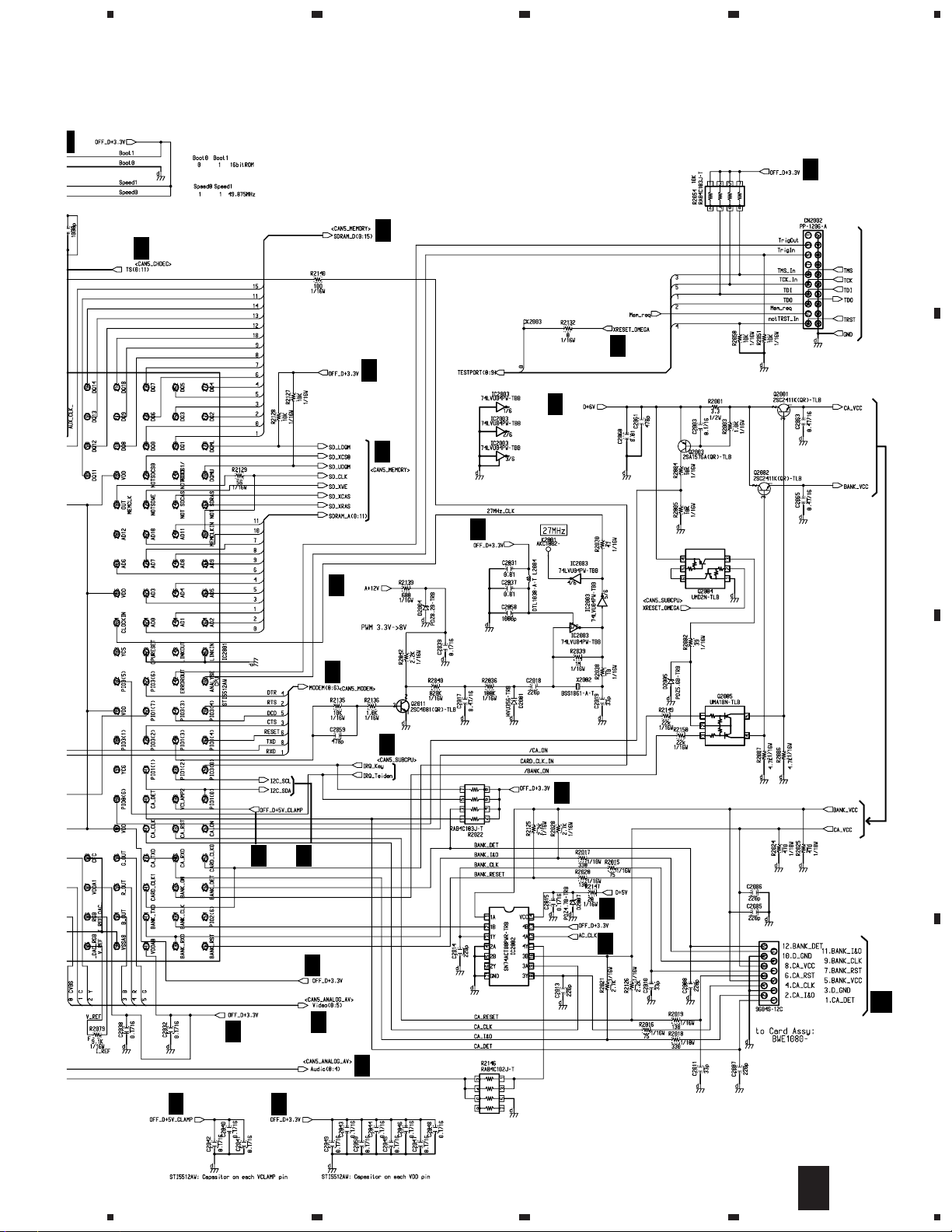
3.7 MAIN ASSY (6/7)
23
4
A 6/7
A
B
TS5 : AMC2442ACV(0.87)
BCT-1510/BCT-1520/BCT-1530 : AMC2442ACV(0.84)
MAIN ASSY (6/7)
MODEM BLOCK
(TS5 : BWE1103)
(BCT-1510 : BWE1115)
(BCT-1520 : BWE1115)
(BCT-1530 : BWE1110)
A
2/7
IC1006
A
7/7
A
7/7
IC1006
Modem Controller
A
7/7
C
D
20
6/7
A
1234
Page 21

5
Modem IC
678
TS5, BCT-1510, BCT-1520,
BCT-1530
A
B
A
7/7
C
Modular Jack
D
6/7
A
5
6
7
8
21
Page 22

1
TS5, BCT-1510, BCT-1520,
BCT-1530
3.8 MAIN ASSY (7/7)
23
4
A 7/7
A
B
MAIN ASSY (7/7)
SUBPOWER BLOCK
(TS5 : BWE1103)
(BCT-1510 : BWE1115)
(BCT-1520 : BWE1115)
(BCT-1530 : BWE1110)
EEPROM
A
2/7
A
4/7
A
1/7,2/7,3/7
R7043
10K
1/16W
D
0209
C
28
A
A
2/7
D
A
1/7
A
A
A
A
1/7
A
1/7
1/7,2/7
28
A
1/7
1/7,2/7,4/7
4/7
2/7,4/7
A
4/7
A
1/7
A
4/7,5/7,6/7
A
2/7
100K
1/16W
R7045
22
7/7
A
1234
Page 23

5
: The power supply is shown with the marked box.
678
A
2/7
TS5, BCT-1510, BCT-1520,
BCT-1530
A
Sub CPU
A
1/7
A
2/7
CN8001
B
B
C
Reset IC
D
7/7
A
5
6
7
8
23
Page 24

1
TS5, BCT-1510, BCT-1520,
BCT-1530
3.9 FRONT ASSY
A
B
23
4
C
D
FRONT ASSY (BWE1102)
B
24
B
1234
SWITCHES
S8001 : ↑ (UP)
S8002 : ← (LEFT)
S8003 : PERSO(MENU)
S8004 : → (RIGHT)
S8005 : ↓ (DOWN)
S8006 : VALIDER(ENTER)
CN7002
7/7
A
Page 25

1
3.10 CARD ASSY
234
CN2003
2/7
A
TS5, BCT-1510, BCT-1520,
BCT-1530
A
B
CARD ASSY (BWE1080)
C
1
C
D
C
2
3
4
25
Page 26

1
3
TS5, BCT-1510, BCT-1520,
BCT-1530
3.11 POWER ASSY
POWER ASSY (BXF1139)
D
A
0109
REK1102
0102
HCS0528
L
2
1
N
T 2.5A H 250V
F101
F102
F103
F104
0109
F114
23
F115 F116
1110
SDDF
13
24
56
3103
V
F118
F117
F119
3105
6108
680K
2108
33n
BZX79-C15
220n
2106
3106
470R
6109
43
5110
12
UF1922P4
BZX79-C15
S1NB80
6115
F105
F106
4
3180
100K
3181
100K
2110
15n
6180
3110
BAS216
4
100K
5170
CT283D3
68u
2121
2107
F130
F131
B
1K
3164
6142
BZX79-C15
C
6141
BAV21
BC847B
7141
7161
BC847B
3162
7163
BC857B
0107
220R
3163
22K
6135
BAS216
2140
3135
2145
BC847B
470n
33K
220p
7140
1M
3130
1M
3131
2135
BAS216
100n
6137
2171
10u
3124
47R
3136
3K3
100R
6123
BAS216
3123
1K
6136
BAV21
2146
330p
3140
3171
2K2
F107
F108
STP3NB60FP
0125
HEATSINK
1R5
3126
6150
BAV21
7125
3127
6111
5125
1R5
3147
100R
BYD33J
83R
2109
2127
6126
6127
6128
47p
2
220p
1N4004
1N4004
1N4004
8
7
2142
10n
3142
2K2
2164
10n
2141
470n
3141
100K
3150
1K8
2150
100n
2147
3148
2K2
220p
7170
TCDT1103G
Fuse 0109 (REK1102) : Only this part is supplied as a service part..
KA4
NOTE FOR FUSE REPLACEMENT
CAUTION
FOR CONTINUED PROTECTION AGAINST RISK OF FIRE.
REPLACE ONLY WITH SAME TYPE AND RATINGS ONLY.
2170
2n2
D
26
D
1234
Page 27

5
3110
6127
6128 6126
2127
2109
678
TS5, BCT-1510, BCT-1520,
BCT-1530
6180
BAS216
4
100K
2
220p 47p
1N4004
1N4004
1N4004
8
7
7170
CDT1103G
2170
5170
CT283D3
2n2
7180
TCDT1103G
7275
KA431LZTA
10
16
12
11
14
18
17
13
15
F222
F223
F220
F221
10K
3290
F234
BYW95C/20
BYW95C/20
BYV27-200
6210
BYV27-200
BYD33D
3273
1
3
2
100n
2290
6220
BYD33J
6252
6250
6202
6225
6230
SB340
100R
2275
33n
+5V Return
AC_CLK
2200
2250 2222
2205
2210
2223
2230
+8Va
3274
4K7
3275
10K
4.7
100u
22u
100u100u
220u
+8Va
220u
2m2
+5Va+8Va
3278
3277
3276
3221
680R
9251
+5Va
5200
22u
5220
100u
470R
4K7
4K7
F201 F202
BZX79-B27
6221
1N414B
6222
3202
BZX79
-B6V2
62046222
F209 F210
5210
3u3
F218
F217
6226
BZX79-C4V7
3230
+24V/19V
270R
+12V
BZX79-B5V6
+5V
F214
F213
2211
5230
2u2
47R
BC636
1K
3204
7205
BC847B
10u
-5V
F226
2231
7204
3205
F227
F233
2K2
F231
100u
0207
+6V
+3.3V
F245
F246
5208
3u3
3206
10K
F244
9208
Pow1
F205 F206
+5V Return
AC_CLK
+12V
+3.3V
+5V
-5V
F241
Pow1
+24V/19V
+6V
+28V
+18_23V
F230
F232
F242
A
B
TWG
0209
1
2
3
4
5
6
7
8
9
10
11
12
13
14
15
16
17
18
19
CN7001
7/7
A
C
D
D
5
6
7
8
27
Page 28

1
23
TS5, BCT-1510, BCT-1520,
BCT-1530
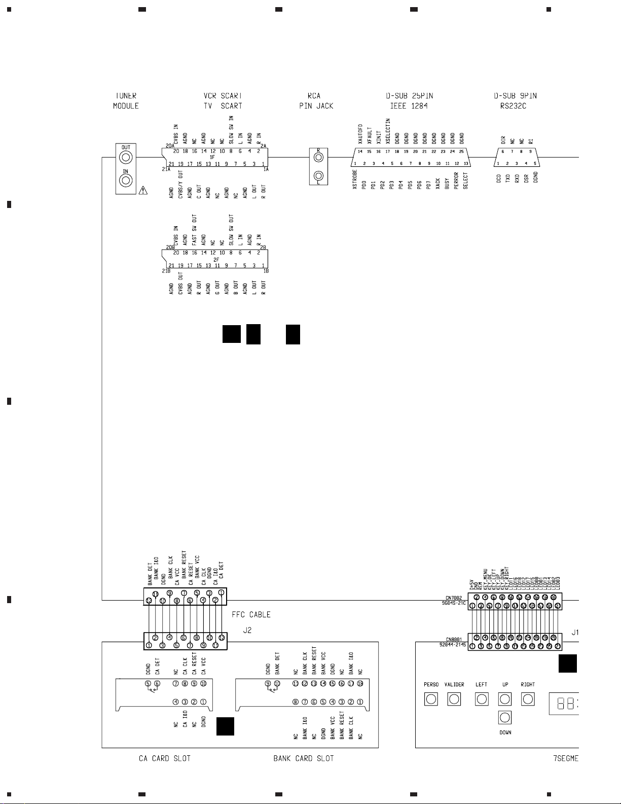
4. PCB CONNECTION DIAGRAM
4
4.1 FRONT ASSY
NOTE FOR PCB DIAGRAMS :
A
1. Part numbers in PCB diagrams match those in the schematic
diagrams.
2. A comparison between the main parts of PCB and schematic
diagrams is shown below.
Symbol In PCB
Diagrams
3. The parts mounted on this PCB include all necessary parts for
several destinations.
For further information for respective destinations, be sure to
check with the schematic diagram.
B
4. View point of PCB diagrams.
BCE
BCE
D
Connector
Symbol In Schematic
Diagrams
BCEBCE
BCE
BCE
DGGSS
DGS
Capacitor
Part Name
Transistor
Transistor
with resistor
Field effect
transistor
Resistor array
3-terminal
regulator
SIDE A
B
FRONT ASSY
SIDE A
P.C.Board
Chip Part
SIDE B
C
CN7002
A
D
(BNP1353-B)
28
B
1234
Page 29

1
4.2 CARD ASSY
234
TS5, BCT-1510, BCT-1520,
BCT-1530
A
C
CARD ASSY
SIDE A
B
(BNP1335-C)
CN2003
A
C
D
C
1
2
3
4
29
Page 30

1
MAIN ASSY
A
CN85
C
TUNER
MODULE
VCR SCART
TV SCART
Q1001 Q1011 Q4008 Q4007 Q4015
Q1008 Q4011 Q4004 Q4003 Q4002 Q4001
IC1003 IC4001 IC8001
IC1004 Q1009 Q2011 IC2003 IC2001
Q1006 Q1003 Q1004 Q1007 IC3005 Q2003 Q2005 IC3
Q1002 IC1001 Q2004 Q2002 Q2011 IC2002
TS5, BCT-1510, BCT-1520,
BCT-1530
4.3 MAIN ASSY
A
B
23
4
C
D
30
A
1234
Page 31

5
678
TS5, BCT-1510, BCT-1520,
BCT-1530
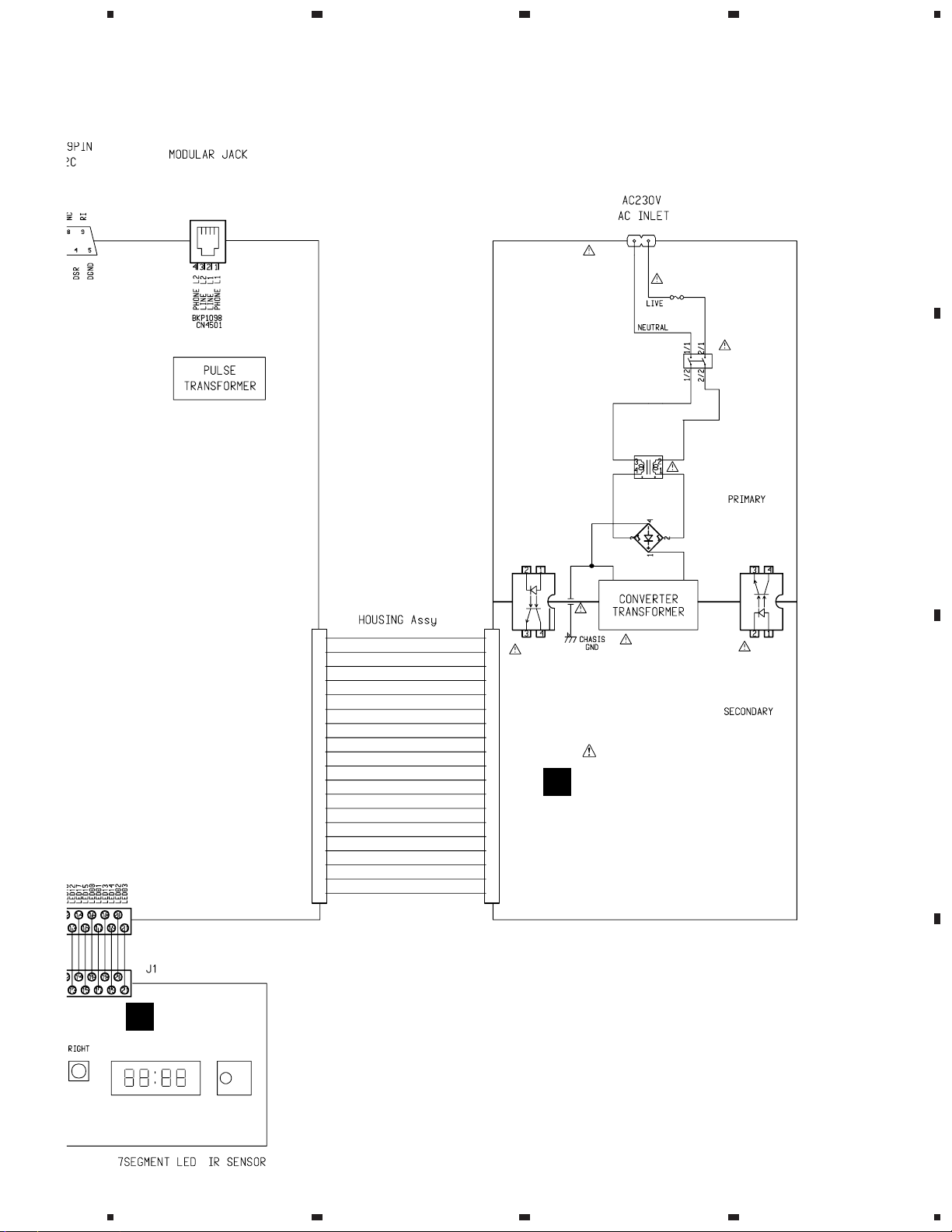
RCA
PIN JACK
D-SUB 25PIN
IEEE 1284
MODULAR
JACK
D-SUB 9PIN
RS232C
SIDE A
A
B
(BNP1354-D)
CN8503
C
IC5007 Q6007 Q6006
Q4009 Q4010 IC6002 IC6003 Q6002 IC6004 IC6001 IC6007 IC5006
IC8001 IC4003 IC4002 Q6001 Q6005 IC6006 IC6005 Q6003
IC3001 IC3002 IC7002 Q7010 IC7001 IC7003 Q7001
IC3006 IC3003 Q7003 Q7002 Q7005 Q7004
IC3007 Q7013 Q7016 Q7014 Q7011 Q7012
5
6
CN8001
B
0209
D
7
A
8
C
D
31
Page 32

1
TS5, BCT-1510, BCT-1520,
BCT-1530
23
4
A
B
A
MAIN ASSY
C
D
32
A
1234
Page 33

5
678
TS5, BCT-1510, BCT-1520,
BCT-1530
SIDE B
A
B
C
(BNP1354-D)
D
A
5
6
7
8
33
Page 34

TS5, BCT-1510, BCT-1520,
BCT-1530
5. PCB PARTS LIST
Mark No. Description Part No.
NOTES:•Parts marked by "NSP" are generally unavailable because they are not in our Master Spare Parts List.
CONTRAST OF PCB ASSEMBLIES
Mark Symbol and Description
The mark found on some component parts indicates the importance of the safety factor of the part.
•
Therefore, when replacing, be sure to use parts of identical designation.
When ordering resistors, first convert resistance values into code form as shown in the following examples.
•
Ex.1 When there are 2 effective digits (any digit apart from 0), such as 560 ohm and 47k ohm (tolerance is shown by J=5%,
and K=10%).
560 Ω→56 × 10
47k Ω→47 × 10
0.5 Ω→R50 ..................................................................................... RN2H
1 Ω→1R0 ..................................................................................... RS1P 1 R 0 K
Ex.2 When there are 3 effective digits (such as in high precision metal film resistors).
5.62k Ω→ 562 × 10
MAIN ASSY BWE1103 BWE1115 BWE1115 BWE1110
FRONT ASSY BWE1102 BWE1102 BWE1102 BWE1102
CARD ASSY BWE1080 BWE1080 BWE1080 BWE1080
POWER ASSY BXF1139 BXF1139 BXF1139 BXF1139
1
→ 561 ........................................................RD1/4PU 5 6 1 J
3
→ 473 ........................................................RD1/4PU 4 7 3 J
1
→ 5621 ...................................................... RN1/4PC 5 6 2 1 F
TS5 BCT-1510 BCT-1520 BCT-1530
NYXK/FR
NYXK/FR1
NYXK/FR2
NYXK/FR2
Mark No. Description Part No.
R 5 0
Part No.
NYXK/SP NYXK/IT NYWXKPL
K
Remarks
A
MAIN ASSY
BWE1103, BWE1115 and BWE1110 are constructed the same except for the following:
Mark
Symbol and Description
IC1004 TDA8083H TDA8083H TDA8083H/E
IC2001 STI5512AWE STI5512AWE STI5512AWE/E
IC6006
BWE1103 BWE1115 BWE1110
AMC2442ACV(0.87) AMC2442ACV(0.84) AMC2442ACV(0.84)
Part No.
MAIN ASSY IC3002 CONTRAST TABLE
IC3002 (16M FLASH Memory) is different according to the model types as the following tabel.
.oNtraP
kraMnoitpircseDdnalobmyS
IC3002 (16M FLASH Memory)
Mark No. Description Part No.
A
MAIN ASSY
TS5
/NYXK/FR
BGC1059-A-AV BGC1060-A-AV BGC1061-A-AV BGC1062-A-AV BGC1063-A-AV BGC1064-A-AV BGC1065-A-AV
SEMICONDUCTORS
IC6005 73K324BL-IH
IC2003 74LVU04PW
IC6006 AMC2442ACVF(0.87)
IC1003 BA05SFP
IC7002 CAT24WC16JI
IC4002 CS4335-KS
IC4001 CXA2161R
IC5006 HIN211CB
IC3005 HYB39S16160AT-10
IC1001 NJM317DL1
TS5
/NYXK/FR1 /NYXK/FR2/NYXK/FR3
TS5 TS5
Mark No. Description Part No.
IC4003 NJM4558MD
IC3003 NT56V1616A0T-8
IC5007 PACS1284-04Q
IC7001 PE5181A
IC7003 PST9124N
IC2002 SN74ACT08PWR
IC2001 STI5512MWD
IC3001 BGC1058-A-AV
IC3002 See IC3002 Contrast table
IC3006 TC7SZ126FU
IC1004 TDA8083H
IC6004 TL431CLP
IC6001 TLP127
IC6007 TLP181(GR)
BCT-1510
/NYXK/SP
BCT-1520
/NYXK/IT
Remarks
BCT-1530
/NYWXKPL
skrameR
34
Page 35

TS5, BCT-1510, BCT-1520,
BCT-1530
Mark No. Description Part No.
Q1002,Q2003,Q7001 2SA1576A
Q2001,Q2002 2SC2411K
Q1008,Q2011,Q6004,Q7013 2SC4081
Q6002 2SD1760
Q6001,Q7010 DTA124EUA
Q4015 DTA143EUA
Q7002-Q7005 DTB113ZK
Q4001,Q4002,Q4009,Q4010 DTC123TKA
Q1001,Q1003-Q1007,Q7012,Q7016 DTC124EUA
Q6005 DTC144TUA
Q7011 TPC8201
Q1011 TPC8301
Q2005 UMA10N
Q2004 UMD2N
Q7014 UMG1N
D1002,D5004,D7003 1SS355
D7004 DAP202U
D2001 HVU356
D4011,D4013,D4014 PDZ12B
D2007,D7005 PDZ4.7B
D2005 PDZ5.6B
D2004 PDZ8.2B
D6003 PTZ43A
D1004 RB160L-40
D1001,D2002,D2003 RB501V-40
D6004 RD4.3MW
D6001 S1ZB60-4072
VA6002
D4003-D4010,D4012 UMZ12N
2322 594 51516
COILS AND FILTERS
F6003 BTF1087
T6001 BTX1035
L1001,L4001 BTH1065
L2005 BTX1036
L2002,L2004 DTL1038
CAPACITORS
C6016 (470pF/AC250V) BCG1026
C7001 (0.047F/5.5V) BCH1072
C4022,C4023 CCSRCH101J50
C4028,C4029 CCSRCH181J50
C7002,C7003 CCSRCH220J50
C2005-C2008,C2013,C2014,C2018 CCSRCH221J50
C1010,C1011,C2010,C2011,C2019 CCSRCH330J50
C6006,C6007 CCSRCH390J50
C1009,C4031,C6011,C6013 CEAK100M50
C7004,C7019 CEAK101M10
C5001 CEAK101M25
C7018 CEAK221M10
C4053 CEAK221M25
C1008,C1012 CEAK470M16
C7014 CEAK471M10
C4036,C4037 CEANP100M50
C4051 CEAT100M50
C4010 CEAT470M16
C7021 CEAT470M50
C4062 CEAT4R7M50
C4039,C4040,C4042,C4043 CKSQYB684K10
C4060,C4061 CKSQYB684K10
C2034,C2058,C4001-C4008 CKSRYB102K50
C4016,C4017,C6002 CKSRYB102K50
C1002,C1006,C1007,C1013,C1014 CKSRYB103K50
Mark No. Description Part No.
C1016,C2031,C2033,C2035,C2037 CKSRYB103K50
C2060,C4011,C4024,C4025 CKSRYB103K50
C1019,C1024-C1026,C4038,C4041 CKSRYB104K16
C4044-C4049 CKSRYB104K16
C1032 CKSRYB153K50
C6008 CKSRYB273K16
C1001 CKSRYB332K50
C6012 CKSRYB333K25
C2059,C2061,C7007,C7008 CKSRYB471K50
C7016,C7017 CKSRYB473K16
C1017,C1018,C1020-C1023 CKSRYF104Z16
C1027-C1031,C2003,C2015,C2032 CKSRYF104Z16
C2038-C2050,C3001-C3005 CKSRYF104Z16
C3007-C3009,C4018-C4021,C4030 CKSRYF104Z16
C4050,C4052,C4056-C4059 CKSRYF104Z16
C5031-C5035,C6001,C6003-C6005 CKSRYF104Z16
C7005,C7006,C7009,C7011,C7013 CKSRYF104Z16
C7015,C7020,C7022 CKSRYF104Z16
C2063,C2065 CKSRYF224Z16
C1004,C1005,C2017 CKSRYF474Z16
RESISTORS
R5020,R5021 (680Ω/1/2W) BCN1046
R6017 (82Ω/1/2W) BCN1060
R6018 (47Ω/1/2W) BCN1063
R2146,R7001,R7013 RAB4C102J
R2022,R2054 RAB4C103J
R7015,R7016 RAB4C181J
R7002 RAB4C333J
R2001 RD1/2VM3R3J
R2017 RS1/10S331J
R1011,R1013,R1033 RS1/10S3601F
R2024,R2025,R7024,R7025,R7029 RS1/10S471J
R7042 RS1/10S681J
R2018 RS1/10S750J
R7026,R7027 RS1/10S821J
R1010 RS1/16S1200F
R1012 RS1/16S1202F
R4020-R4022,R4025,R4026 RS1/16S2000F
R2079,R2081 RS1/16S9101F
R1005,R1006 RS1/2S1R8J
Other Resistors RS1/16S J
OTHERS
M1001 DBS Front End BXF1135
CN2003 12P FFC Connector 9604S-12C
CN7002 21P FFC Connector 9604S-21C
JA4001 2P Pin Jack BKB1017
CN4002 SCART Connector BKN1019
CN7001 19P Plug BKP1120
CN5004 DSUB 9P Connector BKP1122
CN5005 DSUB 25P Connector BKP1123
CN6001 4P Modular Jack BKP1137
Ground Plate BNK1081
X1001 (4MHz) BSS1056
X2002 (27MHz) BSS1061
X7002 (32.768kHz) BSS1091
X7001 (8.0MHz) BSS1097
X6001 (11.0592MHz) BSS1099
KN6003-KN6006 Jumper Terminal PKX1001
35
Page 36

TS5, BCT-1510, BCT-1520,
BCT-1530
Mark No. Description Part No.
B
FRONT ASSY
SEMICONDUCTORS
D8001 BEL1037
SWITCHES AND RELAYS
S8001-S8006 ASG7013
RESISTORS
R8001 (27kΩ/1/4W) BCN1056
OTHERS
M8001 Remote Sensor Unit BXX1026
CN8001 21P FFC Connector 9607S-21F
C
CARD ASSY
CAPACITORS
C8501-C8504 CKCYF103Z50
RESISTORS
R8502 (100Ω/1/4W) BCN1057
OTHERS
CN8503 12P Connector 9604S-12F
CN8502 8Pin CARD Connector BKP1141
CN8501 16Pin CARD Connector BKP1142
D
Mark No. Description Part No.
POWER ASSY
This ASSY has no service part as a assy part.
Only the fuse(0109:REK1102) is the service part as
a set part. Refer to page 7.
6. ADJUSTMENT
There is no information to be shown in this chapter.
36
Page 37

TS5, BCT-1510, BCT-1520,
7. GENERAL INFORMATION
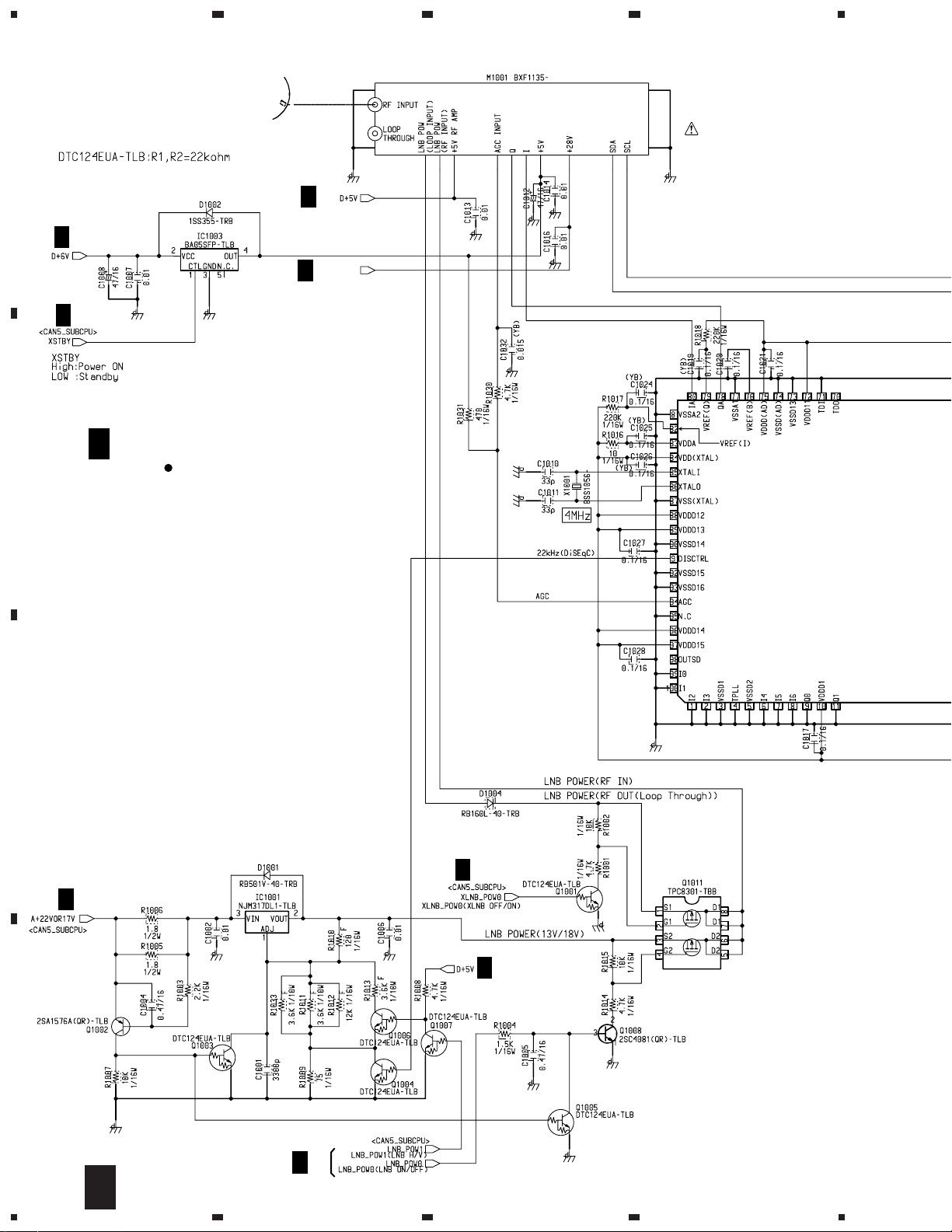
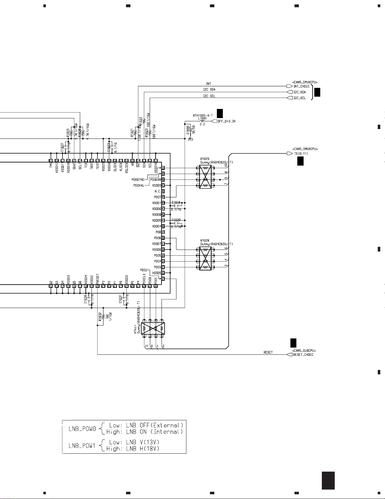
7.1 IC
¶ List of IC
TDA8083H STI5512MWD CXA2161R CS4335-KS 73K324BL-IH
AMC2442ACVF(0.87) PE5181A
TDA8083H (MAIN ASSY(1/7) : IC1004)
• Demodulator and Decoder
Block Diagram
•
• The information shown in the list is basic information and may not correspond exactly to that shown in the schematic diagrams.
BCT-1530
XTALO
XTALI
TRST
TMS
TCK
DLOCK
86
85
62
69
63
7071
RSLOCK
VLOCK
56
57
58
Lock
Detectors
oscillator
and PLL
SCAN TEST
BOUNDARY
PDOCLK
28
ENERGY DISPERSAL REMOVAL
REED-SOLOMON DECODER
SYNCHRONIZATION
FINE
AGC
CONTROL
PDO0
to PDO7
PDOSYNC
29, 30, 31
33, 34, 35
50
PDOERR
38, 45
48
DEINTERLEAVER
VITERBI DECODER
PHASE
DIGITAL
ROTATOR
FINE
AGC
PDOVAL
49
61
TEST
4
TPLL
PRESET
20
CARRIER
RECOVERY
(PHASE LOOP)
DTO
CONTROL
DISCTRL
91
DISEQC AND
TONE BURST
39
RESET
POWER-ON
POR
TDI TDO
P5 to P0
SDAT SCLT
A0
SDA SCL
21 to 24
26,27
64
65
55
52
53
I/O
DATA
EXPANDER
C TUNER
2
I
SWITCH
C-BUS
2
I
CONTROL
TDA8083
Interpolation
Anti-Aliasing filtering
MUX
99, 100,1
2, 6, 7, 8
I0 to I6
CLOCK
RECOVERY
Square Root Raised cosine
PHASE
DIGITAL
ROTATOR
ADC
80
AGC
COARSE
94
IA
VAGC
Interpolation
CARRIER
Anti-Aliasing filtering
Square Root Raised cosine
MUX
ADC
9, 11, 12, 13
78
14, 16, 17
QA
Q0 to Q6
RECOVERY
(AFC LOOP)
DTO
CONTROL
OUTSD
98
Σ∆ CONVERTER
GENERAL PURPOSE
INT
54
CONTROL
INTERRUPT
37
Page 38

TS5, BCT-1510, BCT-1520,
BCT-1530
Pin Function (1/3)
•
1
2
3
4
5
6
7
8
9
10
11
12
13
14
15
16
17
18
19
20
21
22
23
24
25
26
27
28
29
30
31
32
33
34
35
36
37
38
SYMBOLPIN
I2
I3
V
SSD1
TPLL
V
SSD2
I4
I5
I6
Q0
V
DDD1
Q1
Q2
Q3
Q4
V
SSD3
Q5
Q6
V
SSD4
V
DDD2
PRESET
P3
P2
P1
P0
V
DDD3
P5
P4
PDOCLK
PDO0
PDO1
PDO2
V
SSD5
PDO3
PDO4
PDO5
V
SSD6
V
SSD7
PDO6
I/O DESCRIPTION
I digital I-input bit 2 (ADC bypass)
I digital I-input bit 3 (ADC bypass)
− digital ground 1 (core and input periphery)
I test pin (normally connected to ground)
− digital ground 2 (core and input periphery)
I digital I-input bit 4 (ADC bypass)
I digital I-input bit 5 (ADC bypass)
I digital I-input bit 6 (ADC bypass - MSB)
I digital Q-input bit 0 (ADC bypass - LSB)
− digital supply voltage1 (core and input periphery)
I digital Q-input bit 1 (ADC bypass)
I digital Q-input bit 2 (ADC bypass)
I digital Q-input bit 3 (ADC bypass)
I digital Q-input bit 4 (ADC bypass)
− digital ground 3 (core and input periphery)
I digital Q-input bit 5 (ADC bypass)
I digital Q-input bit 6 (ADC bypass - MSB)
− digital ground 4 (output periphery)
− digital supply voltage 2 (core and input periphery)
I set device into default mode
I/O quasi-bidirectional I/O port (bit 3)
I/O quasi-bidirectional I/O port (bit 2)
I/O quasi-bidirectional I/O port (bit 1)
I/O quasi-bidirectional I/O port (bit 0)
− digital supply voltage 3 (output periphery)
I/O quasi-bidirectional I/O port (bit 5)
I/O quasi-bidirectional I/O port (bit 4)
O output clock for transport stream bytes
O parallel data output (bit 0) - Serial data output
O parallel data output (bit 1)
O parallel data output (bit 2)
− digital ground 5 (output periphery)
O parallel data output (bit 3)
O parallel data output (bit 4)
O parallel data output (bit 5)
− digital ground 6 (core and input periphery)
− digital ground 7 (core and input periphery)
O parallel data output (bit 6)
38
Page 39

Pin Function (2/3)
POR39 Ο Power-on Reset
V
DDD4
40 − digital supply voltage 4 (output periphery)
V
DDD5
41 − digital supply voltage 5 (core and input periphery)
V
SSD8
42 − digital ground 8 (core and input periphery)
V
DDD6
43 − digital supply voltage 6 (core and input periphery)
V
DDD7
44 − digital supply voltage 7 (output periphery)
PDO745 O parallel data output (bit 7)
n.c.46 − not connected
V
SSD9
47 − digital ground 9 (core and input periphery)
PDOERR48 O transport error indicator
PDOVAL49 O data valid indicator
PDOSYNC50 O transport packet synchronization signal
V
SSD10
51 − digital ground 10 (output periphery)
SCL52 I serial clock of I
2
C-bus
SDA53 I/O serial data of I
2
C-bus
INT54 O interrupt output (active LOW)
A055 I I
2
C hardware address
RSLOCK56 O Reed-Solomon lock indicator
VLOCK57 O Viterbi lock indicator
DLOCK58 O Demodulator lock indicator
V
DDD8
59 − digital supply voltage 8 (core and input periphery)
V
DDD9
60 − digital supply voltage 9 (core and input periphery)
TEST61 I test pin (normally connected to ground)
TRST62 I BST optional asynchronous reset (normally connected to ground)
TCK63 I BST dedicated test clock (normally connected to ground)
SCLT64 Ο serial clock of I
2
C-bus loop-through
SDAT65 I/O serial data of I
2
C-bus loop-through
V
DDD10
66 − digital supply voltage 10 (core and input periphery)
V
SSD11
67 − digital ground 11 (output periphery)
V
SSD12
68 − digital ground 12 (core and input periphery)
TMS69 I BST input control signal (normally connected to ground)
TDO70 O BST serial test data out
TDI71 I BST serial test data in (normally connected to ground)
V
DDD11
72 − digital supply voltage 11 (core and input periphery)
V
SSD13
73 − digital ground 13 (core and input periphery)
V
SSD(AD)
74 − digital ground A/D converter
V
DDD(AD)
75 − digital supply A/D converter
V
ref(B)
76 O bottom reference voltage for ADC
V
SSA1
77 − analog ground 1
QA78 I analog input Q
V
ref(Q)
79 O AGC decoupling - Q path
SYMBOL
PIN I/O DESCRIPTION
•
TS5, BCT-1510, BCT-1520,
BCT-1530
39
Page 40

TS5, BCT-1510, BCT-1520,
BCT-1530
Pin Function (3/3)
•
PIN
80
81
82
83
84
85
86
87
88
89
90
91
92
93
94
95
96
97
98
99
100
SYMBOL
IA
V
SSA2
V
ref(I)
V
DDA
V
DDXTAL
XTALI
XTALO
V
SSXTAL
V
DDD12
V
DDD13
V
SSD14
DiSCTRL
V
SSD15
V
SSD16
V
AGC
n.c.
V
DDD14
V
DDD15
OUTSD
I0
I1
I/O DESCRIPTION
I analog input I
− analog ground 2
O AGC decoupling - Ipath
− analog supply voltage
− supply voltage for crystal oscillator
I crystal oscillator input
O crystal oscillator output
− ground for crystal oscillator
− digital supply voltage 12 (core and input periphery)
− digital supply voltage 13 (core and input periphery)
− digital ground 14 (core and input periphery)
O 22 kHz / 44kHz output for dish control applications
− digital ground 15 (output periphery)
− digital ground 16 (core and input periphery)
O Tuner AGC output
− not connected
− digital supply voltage 14 (output periphery)
− digital supply voltage 15 (core and input periphery)
O Sigma Delta Output
I digital I-input bit 0 (ADC bypass - LSB)
I digital I-input bit 1 (ADC bypass)
Note
1. Pins I0 to I6, Q0 to Q6, SCL, SDA,
INT, SCLT, SDAT, V
and OUTSD are 5V tolerant.
AGC
2. The structure of I/O’s and the maximum output drive are specified in Section 12
40
Page 41

STI5512MWD (MAIN ASSY(2/7) : IC2001)
• Programmable Transport IC
Block Diagram
•
TS5, BCT-1510, BCT-1520,
BCT-1530
Block move
DMA
Programmable
transport
interface
IEEE 1394
link layer
interface
IEEE 1284
interface
Interrupt
controller
1 OS-L ink
2 UARTs
2 I2C
3 PWM
ST20
CPU
2 Kbytes
instruction
cache
and 2 Kbytes
data cache
4 Kbyte s
SRAM
EMI
MPEG
audio and
external
decoder I/ F
MPEG
video
decoder
Diagnostic
controller
and system
services
2 SmartCard
interfaces
(ASC)
PAL/NTSC/
SECAM
encoder
Teletext
interface
41
Page 42

TS5, BCT-1510, BCT-1520,
p
BCT-1530
Pin Function (1/5)
•
Signal names are prefixed by
Pin Number Function
VDD 13 Power supply
GND 16 Ground
VClamp1-3
VDDA0-1 2 Analog po wer supply for PAL/NTSC/SECAM encoder
VSSA0-1 2 Analog ground for PAL/NTSC/SECAM encoder
RTCVDD 1 Real time clock supply
VDD_VPLL 1 Analog po wer supply for video PLL
VSS_VPLL 1 Analog ground for video PLL
1. The VClamp pins are a power supply bus used to diode clamp the voltage on 5V tolerant digital input or output pins to.
The voltage on the di gital signal pin is then clamped to within VImax (5.5V) if the applied voltage is increased above 5V.
If the devi ce is to be interfaced to 3.3V logic signals only, then the VClamp pins can be connected to the STi 5512 3.3V VDD
power supply. However if any pin is to be interfaced to a 5V logic signal, then the VClamp pins m ust be connected to the 5V
power supply (the 5V l ogic device power sup ply). Note i n thi s case t he 5V power su pply m ust b e ca pable of s inking t he c lamp
current of transient signals above 5V .
In the latter case it is important to ensure the correct power supply ramp sequence. The VClamp power supply must be applied before or at the same time as the VDD 3.3V power supply. This is to ensure that during power supply power up and
power down, VClamp > VDD + 0.5V.
1
not
if they are active low; otherwise they are active high.
3 Power suppl y for clamp diodes
Table 1 Power supply pins
Pin In/Out Function
1
R_OUT
G_OUT
B_OUT2
C_OUT
CV_OUT
Y_OUT
1
1
1
1
1
I_REF_DAC_RGB
I_REF_DAC_YCC
V_REF_DAC_RGB
V_REF_DA C_YCC
1
1
1
1
out Red output
out Green output
out Blue output
out Chroma output
out Composite video output
out Luma output
in DAC current reference
in DAC current reference
in DAC volt age reference
in DAC volt age reference
OSD_ENABLE in/out OSD enable
notHSYNC in/out Horizontal sync
ODD_OR_EVEN in/out Vertical sync
YC0-7
2
output Digital YUV output
CFC input DENC color burst phase and frequency contro l.
This pin can be used in non-scart based Genlock applications.
If it is not used, this pin must
ground.
42
Table 2 Video out
ut interface pins
Page 43

TS5, BCT-1510, BCT-1520,
BCT-1530
Pin Function (2/5)
•
1. The digital encoder video outputs are analogue signals and are not 5V tolerant. The same applies to the video DAC
voltage and current reference pins.
2. The YC0 pin is tri-stated during reset and then sampled at the end of the reset to determine whether the EMI pins are in
STi5510 or STi5512 mode. If the YC0 pin is sampled high (i.e at VDD) then the STi5510 mode is selected for the EMI pins
and a low v alu e selec ts STi 5512 mode. In STi5512 mode t he address
and the strobe pins are tri-stated when the EMI bus is granted to an
down
resistors shou ld be fitted to the YC0 according to the functionality
be pulled high by an internal pull-up and will default the EMI pins to
Pin In/Out Function
SCLK/A_C_STB out Serial clock or AC-3 data strobe
PCM_DATA/A_C_DATA out PCM data out or AC-3 data out
PCMCLK in/out PCM clock
LRCLK/A-WORD_CLK out Left/right clock or AC-3 word clock
notA_C_REQ i n AC-3 data request
notA_PTS_STB in AC-3 audio PTS strobe
shift for bank 3 is dependent on the boot bank width
external DMA device. Ext ernal 10KΩ pull-up or
desir ed. If t his p in is lef t
STi5510 mode.
not
connected, the pin will
pull-
Table 3 AC-3/MPEG1 audio output interface pins
Pin In/Out Function
Interrupt0-1 in Interrupt
T able 4 External interrupt pins
Pin In/Out Function
ClockIn in System input clock - PLL or TimesOneMode
SpeedSelect0-1 in PLL speed selector
notRST in System reset
CPUAnalyse / TrigIn in Error anal ysis / External trigger input to DCU
CPUReset in Soft reset for analyzing from OS-Link
ErrorOut / TrigOut
1. This pin is tri-stated d uring res et and t hen sa mpled at t he end of the res et to det ermine whet her the O S-Li nk is act iv e an d
to determine th e function of the shared CPUAnalyse / TrigIn and the ErrorOut / TrigOut, as described in the
ices
chapter. If the ErrorOut pin is sampled high (i.e at VDD) then the DCU signals (TrigIn and TrigOut) are selected and a
low value indicates OS-Link signals (i.e. CPUAnalyse, ErrorOut) are to be used. External 10KΩ pull-up or pull-down resis-
tors should be fitted to the ErrorOut according to the functionality desired.
1
in/out, out Error indicator / Sig nal to trigger external debu g cir cui try (e.g. LSA)
T able 5 System services pins
System Serv-
43
Page 44

TS5, BCT-1510, BCT-1520,
BCT-1530
Pin Function (3/5)
•
Pin In/Out Function
MemAddr2-23 out Address bus
MemData0-31 in/out Data bus. MemData0 is the least significant bit (LSB) and MemData31 is the most
significan t bit (MSB).
MemRdnotWr out ReadnotWrite strobe
MemReq in Direct memory access request
MemGrant out Direct memory access granted
MemWait i n Memory cycle extender
notMemCAS0,2 out CAS strobes for SDRAM/DRAM in Banks 0 and 1
notMemCAS1 out CAS strobe for DRAM or SDRAM clock
notMemCAS3 out CAS strobe for DRAM or sub-bank chip select for bank 3
notMemRAS0 out RAS strobe for SDRAM/DRAM in Bank 0, chip select for Bank0 or
RAS strobe for lowest DRAM sub-bank in Bank0
notMemRAS1 out RAS strobe for highest DRAM sub-bank in Bank 0 or
SDRAM Chip select signal for highest sub-ba nk of Bank0
notMemRAS2 out RAS strobe for SDRAM/DRAM in bank 1, chip select f or Bank1 or
RAS strobe for lowest DRAM sub-bank in Bank1
notMemRAS3 out RAS strobe for highest DRAM sub-bank in Bank 1 or
SDRAM Chip select signal for Bank1
notMemCSROM out Chip select st robe for ROM in bank3.
notSDRAMCS0 out SDRAM Chip select signal for Bank0 or lowest sub-bank of Bank0
notMemOE out Output enable strobe - banks 0-3.
notMemBE0-3 out Byte enable strobes - banks 0-3.
notMemCS2 out Chip select strobe for me mo ry in bank 2.
BootSource0-1 in Boot from ROM or from link.
ProcClockOut out Processor clock.
T able 6 STi5512 External memory interface pi ns
Pin In/Out Function
AD0-12 out SDRAM address bus
DQ0-15 in/out SDRAM data bus (lower b yte)
notSDCS0 out SDRAM chip select for first SDRAM
notSDCS1/AD13 out SDRAM chip select for second SDRAM or AD13
notSDCAS out SDRAM CAS
notSDRAS out SDRAM RAS
notSDWE out SDRAM write enable
MEMCLKIN in SDRAM memory clock input
MEMCLKOUT out SDRAM memory clock out put
DQML out DQ mask enable (lower)
DQMU out DQ mask enable (upper)
T able 7 Shared SDRAM interface pins
44
Page 45

TS5, BCT-1510, BCT-1520,
BCT-1530
Pin Function (4/5)
•
Pin In/Out Function
LPClockIn
LPClockOsc
AUX_CLK_OUT out Auxiliary clock for general use
1
1
1. The low power clock pins are not 5V tolerant.
Pin I n/Out Function
PIO0[0-7] in/out Parallel input/output pin or alternative function (see
PIO1[0-7] in/out Parallel input/output pin or alternative function (see )
PIO2[0-7] in/out Parallel input/output pin or alternative function (see )
PIO3[0-7] in/out Parallel input/output pin or alternative function (see )
PIO4[0-7] in/out Parallel input/output pin or alternative function (see )
in Low power input clock
in/out Low power clock oscillator
8
T able
Low power controller and real time clock pins
IO pins
9P
Table
Table 15
Table 15
Table 15
Table 15
Table 15
)
Pin In/Out Function
LinkIn in Serial data input channel
LinkOut out Serial data outpu t channel
Table 10 OS-Link pins
Pin In/Out Function
TSInByteClk in Link IC byte clock
TSInByteClkValid in Li nk IC byte clock valid edge
TSInData0-7 in Link IC data
TSInError in Link IC pac ket error
TSInPac ketClk in Link IC pac ket strobe
Table 11 Transport stream input pins
Pin In/Out Function
TtxtEvennotOdd in Teletext even not odd vertical sync signal
TtxtHsync in The HSYNC signal input when the teletext interface is operating in the inpu t mode
T able 12 Teletext interface
45
Page 46

TS5, BCT-1510, BCT-1520,
BCT-1530
Pin Function (5/5)
•
The teletext clock and data inputs are shared PIO pins, as shown in Table 15 .
High speed data port pins have a dual function, and can be used either to interface to an external IEEE 1394 link layer
controller or provide an IEEE 1284 parallel port interface.
Pin In/Out Function
1284Data0-7 / AVData0-7 in/out IEEE 1284 port data or AV data
1284notSelectI n in IEEE 1284 port control signals or A V signals
1284notInit / AVPacketTag3 in
1284notFault / AVPacketTag2 out
1284notAutoFd / AVPacketTag1 in
1284Select / AVPacketTag0 out
1284PError / A VByteClkValid out, in/out
1284Busy / A VPacketClk out, in/out
1284notAck / AVByteClk out
1284notStrobe/AVPacketError in
T able 13 High-speed data port pins
Pin In/Out Function
TDI in Test data input
TDO out Test data output
TMS in Test mode select
TCK in Test clock
notTRST in Test logic reset
Table14TAP pins
PIO pins and alternative functions
To im prove flexibility and to allow the STi5 512 to fit into dif ferent set-top box application architectures, the input and
output signals from some of the peripherals are not directly connected to the pins of the device. Instead they are
assigned to the alternative function inputs and outputs of a PIO port bit. This scheme allows these pins to be configured
as general purpose PIO if the associated peripheral input or output is not required in that particular application.
Table 17 shows the assignmen t of the alternat ive functions to the PIO bits. Parentheses ( ) in the table indicate
suggested or possible pin usages as a PIO, not an alternative function connection.
Alternative function of PIO pins
Port
bit
PIO port 0 PIO port 1 PIO port 2 PIO port 3 PIO port 4
0 ASC0TxD or
Sc1DataOut
1 ASC0TRxD or
Sc1DataIn
2 Sc1ClkGenExtClk SSC0 SClk Sc0ClkGenExtClk SSC1 SClk TtxtClockIn
3 Sc1Clk PWMOut0 Sc0Cl k CaptureIn0 1284PeriphLogicH/ASC3 CTS
4 (Sc1RST) PWMOut1 (Sc0RST) CaptureIn1 1284HostLogicH/ASC3 RTS
5 (Sc1CmdVcc) ASC1TxD (Sc0CmdVcc) CaptureIn2 Interrupt2
6 (Sc1CmdVpp)
Sc1Dir
7 (Sc1Detect) PWMOut2 (Sc0Detect) 1284InnotOut TtxtData
46
SSC0 MTSR ASC2TxD or
Sc0DataOut
SSC0 MRST ASC2RxD or
Sc0DataIn
ASC1RxD (Sc0CmdVpp) Sc2Dir CompareOut2 In terrupt3
T able 15 Alternative function of PIO pins
SSC1 MTSR ASC3TxD
SSC1 MRST ASC3RxD
Page 47

CXA2161R (MAIN ASSY(4/7) : IC4001)
Video and Digital section
Note: All video outputs contain 75 Ω drivers, except Vout7.
+5V
0V
x2
x2
VOUT1 T.V BLUE
TV_FBLK
VOUT2 T.V GREEN
x2
x2
VOUT3 T.V RED / C
VOUT4 T.V CVBS / Y
x2
VOUT5 VCR CHROMA
x2
VOUT6 VCR CVBS / Y
Bias
FBLK_SW
VIDEO SWITCH1 (TV)
VIDEO SWITCH2 (VCR)
Mute
Typical Connection
RGB Gain Control
(+1,2,3dB)
MIX_SW
x2
VOUT7 (CVBS)
RF MOD
Sync
Detect
Tip
Tip
Tip
Tip
DC Restore / C Bias
C Bias
DC Restore / C Bias
DC Restore
DC Restore
DC Restore / Tip
DC Restore
TRAP
Output
disable &
Bi-direction
Control
Clamp Cntl
Output
disable
Output
disable
Output
disable
Output
disable
Output
disable
+5V/12V_VCCA
-5V_GNDA
+5V_DIG
+5V_VOUT
SDA
SCL
FNC_VCR
FNC_TV
3.3V or 5V
Fast Mode
Compatible
INTERRUPT
Monitor
0/6/12V
LOGIC
MIX_SW
MICRO
T.V.
VCR
+5V_VID
GND_VID
GND_DIG
AUD_BIAS
VID_BIAS
LOGIC
SYNC_ID
Interrupt
Control
+12V_DIG
Tip
C Bias
FBLK_IN1DIG 10
FBLK_IN2VCR 12
VIN1DIG BLUE 50
VIN2VCR BLUE 7
AUX CHROMA 1VIN13
VIN3DIG GREEN / CVBS 51
VIN4VCR GREEN 6
VIN5DIG RED / CHROMA 52
VIN6DIG CHROMA 53
VIN7VCR RED / CHROMA 5
VIN8DIG CVBS / LUMA 54
VIN9DIG CVBS / LUMA 55
VCR CVBS / LUMA 4VIN10
VIN11TV CVBS 3
VIN12AUX Y/CVBS 56
24
21
14
44
48
40
8
18
49
2
15
34
35
13
Typical Connection
T.V
VCR
47
9
46
45
44
41
39
38
37
11
36
33
0/6/12V
• AV Switch
Block Diagram(1/2)
•
TS5, BCT-1510, BCT-1520,
BCT-1530
47
Page 48

TS5, BCT-1510, BCT-1520,
BCT-1530
Block Diagram(2/2)
•
Audio section
MONO
To RF Modulator
32
6dB
Mono Switch
PHONO_R
31
6dB
Vol Bypass(Phono)
& MUTE
VOLUME CONTROL
RTV
26
6dB
Vol Bypass(T.V.)
Limiter
2.2Vrms
2dB
TV
ZCD
Limiter
2dB
LTV
25
6dB
R/L and Mono
2.2Vrms
PHONO_L
30
6dB
switching
Vol Bypass(T.V.)
Volume Control
Vol Bypass(Phono)
+6 to -56 dB
ROUT1
28
6dB
VCR
LOUT1
27
6dB
Output
Disable
SWITCH
MONO & R/L
48
AUDIO SWITCH1 (TV)
Overlay on/off
-16dB
-6/-3/0/+3dB
-6dB
-6/-11dB
Overlay on/off
-6dB
232017
RIN 1 (DIG)
RIN 4 (AUX)
RIN 2 (VCR)
RIN 3 (TV/OVERLAY)
-16dB
-6dB
-6dB
-6/-3/0/+3dB
2219164229
LIN 1 (DIG)
LIN 2 (VCR)
LIN 3 (TV/OVERLAY)
AUDIO SWITCH2 (VCR)
Mute
Bias
Tone mix
-6dB
LIN 4 (AUX)
Page 49

Pin Function (1/3)
•
TS5, BCT-1510, BCT-1520,
BCT-1530
Pin
Num
50
VIN_1
7
VIN_2
6
VIN_4
51 VIN_3
525VIN_5
VIN_7
Symbol
Pin
Voltage
(V)
2.4
2.4
2.35
2.4
3.0
Equivalent Circuit Description
VCC
6
51
52
5
7
50
VCC
VCC
150
150
20k
150
RGB signal inputs
RGB signal input
OR
CVBS signal input
RGB signal inputs
OR
Chrominance signal inputs
531VIN_6
VIN_13
54
VIN_8
55
VIN_9
4
VIN_10
3
VIN_11
56
VIN_12
47
VOUT_1
46
VOUT_2
45
VOUT_3
43
VOUT_4
39
VOUT_6
41 VOUT_5
3.0
2.35
0.4
0.4
54
55
56
53
VCC
150
VCC
150
VCC
20k
43
45
47
39
46
41
Chrominance signal inputs
CVBS / Luminance signal inputs
RGB / CVBS signal outputs
Chrominance signal output
1
VCC
3
4
12k
12k
49
Page 50

TS5, BCT-1510, BCT-1520,
BCT-1530
Pin Function (2/3)
•
Pin
Num
Symbol
Voltage
38 VOUT_7 0.4
49 VID_BIAS 0.9
37 TRAP 2.3
Pin
(V)
Equivalent Circuit Description
VCC
Typically
0.75mA
49
37
VCC
VCC
12k
40.8k
150
18.3k
200
38
VCC
2k
RF modulator signal output
Minimum load = 20k resistive
Internal reference bias for video circuits.
A capacitor is connected from this pin to
GND. Typically 100nF
Connects trap circuit for subcarrier
2 SYNC_ID 2.5
22
LIN_1
23
RIN_1
19
20
16
17
29
42
25
26
27
28
30
31
32
LIN_2
RIN_2
LIN_3
RIN_3
LIN_4
RIN_4
LTV
RTV
LOUT1
ROUT1
PHONO_L
PHONO_R
MONO
(Single)
(Dual)
(Single)
(Dual)
6.0
0.0
6.0
0.0
22
23
29
42
20k
16
17
19
20
2
VCC
VCC
VCC
150
60k
VCC/2
60k
25
26
27
28
30
31
32
Sync detect circuit time constant,
resistor and capacitor connection pin
Audio signal inputs
Audio signal outputs
18 AUD_BIAS
50
6.0
(Single)
0.0
(Dual)
18
VCC
40k
150
40k
VCC
Internal reference
bias for audio
circuits.
Capacitor
connected to GND.
(Typically 22µF)
Connected directly
to GND.
Page 51

Pin Function (3/3)
•
TS5, BCT-1510, BCT-1520,
BCT-1530
Pin
Num
Symbol
Pin
Voltage
(V)
1012FBLK_IN1
FBLK_IN2
9TV_FBLK -
13 FNC_VCR -
Equivalent Circuit Description
VCC
-
10
12
13
150
VCC
9
120k
Fast blanking signal inputs
Fast blanking signal output
SCART function pin 8 input / output to
VCR
VCC
11 FNC_TV -
33 LOGIC -
36 INTRUPT -
11
VCC
33
36
SCART function pin 8 outp ut to TV
Open collector logic outputs
Typically connect to +5V through 10k
resistor.
35 SCL I2C bus clock line
8k
I2C bus data line
34 SDA
34
-
35
14 +5 V_DIG Digital supply
44 +5V_VOUT Video output supply
48 +5V_VID
5.0
Video supply
15 +12V_DIG 12.0 Digital supply
21 -5V_GNDA -5.0 / 0.0 Audio supply / ground
24 +5V/12V_VCCA 5.0 / 12.0 Audio supply
8 GND_DIG 0.0 Digital ground
40 GND_VID 0.0 Video ground
51
Page 52

TS5, BCT-1510, BCT-1520,
BCT-1530
CS4335-KS (MAIN ASSY(4/7) : IC4002)
• DAC
BLOCK DIAGRAM
PIN DESCRIPTIONS
Power Supply Connections
VA - Analog Power, PIN 7
Analog supply. Nominally +5V.
AGND - Analog Ground, PIN 6
Analog ground reference.
Analog Outputs
AOUTL - Analog Left Cannel Output, PIN 8
Analog output for the left channel. Typically 3.5V Vpp for a full-scale input signal.
AOUTR - Analog Right Cannel Output, PIN 5
Analog output for the right channel. Typically 3.5V Vpp for a full-scale input signal.
Digital Inputs
MCLK - Master Clock Input, PIN 4
The frequency must be 256x, 384x or 512x the input sample rate in Base Rate Mode (BRM)
and either 128x or 192x the input sample rate in High Rate mode (HRM).
LRCK - Left/Right Clock, PIN 3
This input determine which channel is currently being input on the Audio Serial Data Input
pin, SDATA.
SDATA - Audio Serial Data Input, PIN 1
Two's complement MSB-first serial data is input on this pin. The data is clocked into the
CS4335 via internal or external SCLK and the channel is determined by LRCK.
DEM/SCLK - De-emphasis / External serial clock input, PIN 2
A dual-purpose input used for de-emphasis filter control or external serial clock input.
52
Page 53

73K324BL-IH (MAIN ASSY(6/7) : IC6005)
• Modem IC
Block Diagram
•
TXA1
18
TXA2
17
TS5, BCT-1510, BCT-1520,
BCT-1530
RXA
32
DTMF,
ANSWER,
TONE
CALLING
GUARD &
GENERATOR
FSK
MODULATOR
FILTER
EQUALIZER FILTER
QAM/
DPSK
MODULATOR
FIR
PULSE
SHAPER
2W/4W
HYBRID
ATTENUATOR
FILTER
A/D
SIGNAL
DIGITAL
FILTER
ANTI-ALIAS
PASS
BAND
FILTER
AGC
EQUALIZER
FIXED
RECEIVE
FUNCTIONS
PROCESSOR
GAIN
BOOST
DEMODULATOR
TONE
DETECTION
DI-BIT/
QUAD-BIT
ENCODER
SCRAMBLER
BUFFER
µP
BUS
8-BIT
27
DI-BIT/
INTERFACE
QUAD-BIT
DECODER
DEBUFFER DESCRAMBLER
SERIAL
INTERFACE
25
24
TXD
RXD
53
Page 54

TS5, BCT-1510, BCT-1520,
BCT-1530
Pin Function (1/3)
•
POWER
NAME PIN TYPE DESCRIPTION
GND 1 I System ground
VDD 16 I Power supply input, 5 V ±10% (73K324BL). Bypass with 0.1
and 22 µF capacitors to GND.
VREF 31 O An internally generated reference voltage. Bypass with 0.1 µF
capacitor to ground.
ISET 28 I Chip current reference. Sets bias current for op-amps. The
chip current is set by connecting this pin to VDD through a
2 MΩ resistor. ISET should be bypassed to GND with a
0.1 µF capacitor.
PARALLEL MICROPROCESSOR CONTROL INTERFACE MODE
ALE 13 I ADDRESS LATCH ENABLE: The falling edge of ALE latches
the address on AD0-AD2 and the chip select on &6.
AD0-AD7 5-12 I/O ADDRESS/DATA BUS: These bi-directional tri-state
multiplexed lines carry information to and from the internal
registers.
CS
CLK 2 O OUTPUT CLOCK: This pin is selectable under processor
INT
RD
RESET 30 I RESET: An active high signal on this pin will put the chip into
23 I CHIP SELECT: A low on this pin during the falling edge of
ALE allows a read cycle or a write cycle to occur. AD0-AD7
will not be driven and no registers will be written if CS
(latched) is not active. The state of CS is latched on the falling
edge of ALE.
control to be either the crystal frequency (for use as a
processor clock) or 16 times the data rate for use as a baud
rate clock in DPSK modes only. The pin defaults to the cr ystal
frequency on reset.
20 O INTERRUPT: This open drain output signal is used to inform
the processor that a detect flag has occurred. The processor
must then read the Detect Register to determine which detect
triggered the interrupt. INT will stay low until the processor
reads the detect register or does a full reset.
15 I READ: A low requests a read of the 73K324BL internal
registers. Data can not be output unless both RD and the
latched CS are active or low.
an inactive state. All Control Register bits (CR0, CR1, tone)
will be reset. The output of the CLK pin will be set to the
crystal frequency. An internal pull-down resistor permits
power-on-reset using a capacitor to VDD.
54
Page 55

Pin Function (2/3)
PARALLEL MICROPROCESSOR INTERFACE (continued)
NAME PIN TYPE DESCRIPTION
WR
14 I WRITE: A low on this informs the 73K324BL that data is
available on AD0-AD7 for writing into an internal register.
Data is latched on the rising edge of WR. No data is written
unless both WR and the latched CS are low.
SERIAL MICROPROCESSOR CONTROL INTERFACE MODE
NAME PIN TYPE DESCRIPTION
AD0-AD2 5-7 I REGISTER ADDRESS SELECTION: These lines carry
register addresses and should be valid during any read or
write operation.
DATA (AD7) 12 I/O SERIAL CONTROL DATA: Data for a read/write operation is
clocked in or out on the falling edge of the EXCLK pin. The
direction of data flow is controlled by the RD pin. RD low
outputs data. RD high inputs data.
RD
15 I READ: A low on this input infor ms the 73K324BL that data or
status information is being read by the processor. The falling
edge of the RD signal will initiate a read from the addressed
register. The RD signal must continue for eight falling edges
of EXCLK in order to read all eight bits of the referenced
register. Read data is provided LSB first. Data will not be
output unless the RD signal is active.
WR
14 I WRITE: A low on this input informs the 73K324BL that data
or status information has been shifted in through the DATA
pin and is available for writing to an internal register. The
normal procedure for a write is to shift in data LSB first on the
DATA pin for eight consecutive falling edges of EXCLK and
then to pulse WR low. Data is written on the rising edge of
WR.
NOTE: The serial control mode is provided by tying ALE high and CS low. In this configuration AD7 becomes
DATA and AD0, AD1 and AD2 become the register address.
•
TS5, BCT-1510, BCT-1520,
BCT-1530
55
Page 56

TS5, BCT-1510, BCT-1520,
BCT-1530
Pin Function (3/3)
•
DTE USER
NAME PIN TYPE DESCRIPTION
EXCLK 22 I EXTERNAL CLOCK: This signal is used in synchronous
transmission when the external timing option has been
selected. In the external timing mode the rising edge of
EXCLK is used to strobe synchronous DPSK transmit data
applied to on the TXD pin. Also used for serial control
interface.
RXCLK 26 O RECEIVE CLOCK: The falling edge of this clock output is
coincident with the transitions in the serial received data
output. The rising edge of RXCLK can be used to latch the
valid output data. RXCLK will be valid as long as a carrier is
present.
RXD 25 O RECEIVED DATA OUTPUT: Serial receive data is available
on this pin. The data is always valid on the rising edge of
RXCLK when in synchronous mode. RXD will output constant
marks if no carrier is detected.
TXCLK 21 O TRANSMIT CLOCK: This signal is used in synchronous
transmission to latch serial input data on the TXD pin. Data
must be provided so that valid data is available on the rising
edge of the TXCLK. The transmit clock is derived from
different sources depending upon the synchronization mode
selection. In internal mode the clock is generated internally. In
external mode TXCLK is phase locked to the EXCLK pin. In
slave mode TXCLK is phase locked to the RXCLK pin.
TXCLK is always active.
TXD 24 I TRANSMIT DATA INPUT: Serial data for transmission is
applied on this pin. In synchronous modes, the data must be
valid on the rising edge of the TXCLK clock. In asynchronous
modes (1200/600 bps or 300/1200 baud) no clocking is
necessary. DPSK data must be 1200/600 bps +1%, -2.5% or
+2.3%, -2.5 % in extended over speed mode.
.
ANALOG INTERFACE AND OSCILLATOR
NAME PIN TYPE DESCRIPTION
RXA 32 I Received modulated analog signal input from the telephone
line interface.
TXA1 / TXA 2 18 / 17 O (differential) Transmit Analog. These pins provide the analog
output signals to be transmitted to the telephone line. The
drivers will differentially drive the impedance of the line
transformer and the line matching resistor. An external hybrid
can also be built using TXA1 as a single ended transmit
signal.
XTL1 / XTL2 3 / 4 I These pins are for the internal crystal oscillator requiring a
11.0592 MHz parallel mode crystal. Load capacitors should
be connected from XTL1 and XTL2 to ground. XTL2 can also
be driven from an external clock.
OH
56
27 O OFF-HOOK RELAY DRIVER: This signal is an open drain
output capable of sinking 40 mA and is used for controlling a
relay. The output is the complement of the OH register bit in
the ID Register.
Page 57

AMC2442ACVF(0.87) (MAIN ASSY(6/7) : IC6006)
• Modem Controller
Pinouts/Blockdiagram
•
CS0
DTR
Pinouts
CS1
CS2
CS3
RESET
TXD
RXD
RXC
TXC
CTS
6
54321
7
8
9
10
11
AMC2442ACV
12
13
14
15
16
#
17
192021222324252627
RD
WR
RTSRDDCD
CLKo
CLKi
GND
VCC1
AD0
444342
#
SPKR
AD1
#
AD2
41
RLY
AD3
39
38
37
36
35
34
33
32
31
30
29
BS
TS5, BCT-1510, BCT-1520,
BCT-1530
AD4
AD5
AD6
AD7
VCC2
ALE
HOOK
CHECK
SENCE
BLOCK DIAGRAM
DCD
CTS
RTS
DTR
RXD
TXD
2
17
4
5
13
11
UART
20
Crystal
Oscillator
Autobaud
Detection
31
19
18
33
24
36-42
Check
Sence
Hook
Shunt
Sieze
Ring Det.
In Use
RD
WR
ALE
Spkr
AD0-7
CLKiCLKo
21
Command
Interpreter
V.42
Handler
29
30
CTR-21
DAA
Drivers
Modem
AFE
Drivers
Country
Specific
Routines
AMC2442A
6
7
CS0 CS1 CS2 CS3
9
8
57
Page 58

TS5, BCT-1510, BCT-1520,
BCT-1530
Pin Function
•
PIN NUMBER
Pin Name I/O TYPE Description
DCD2 Output DTE Data Carrier Detect output signal. Indicates modem has detected carrier.
RING3 Input Ring detector input. This pin assumes that a half wave opto coupler is used in the
telephone line DAA circuit in the frequency detection algorithm.
RTS4 Input DTE Ready To Send input signal. Used for hardware flow control.
DTR5 Input DTE Data Terminal Ready input signal. Used to enable modem device
CS06 Intput Country Selection bit 0 (Internal pull up)
CS17 Input Country Selection bit 1 (Internal pull up)
CS28 Input Country Selection bit 2 (Internal pull up)
CS39 Input Country Selection bit 3 (Internal pull up)
RESET10 Input Reset signal to the AMC2442A Controller. Active High.
TXD11 Input DTE Transmit Data Pin. All data communication from the DTE connects via this pin.
RXD13 Output DTE Receive Data Pin. All data communication to the DTE connects via this pin.
RXC14 Input Receiver Clock Input from AFE. Used in PSK, QAM and synchronous data mode.
TXC15 Input Transmitter Clock Input from AFE. Used in PSK, QAM and synchronous data mode.
Free16 I/O DO NOT CONNECT
CTS17 Output DTE Clear To Send output signal. Used for hardware flow control.
WR18 Output Write signal to AFE. Goes active low whenever the SMC wishes to write to the AFE
RD19 Output Read signal to AFE. Goes active low whenever the SMC wishes to read from the AFE
CLKo20 Output Buffered Clock output signal. Also used as a crystal drive signal when required.
CLKi21 Input Clock input signal. The SMC requires an 11.0592MHz signal on this pin.
GND22 Power Controller Ground connection
SPKR24 Output Speaker Enable drive
Free25 I/O DO NOT CONNECT
Free26 I/O DO NOT CONNECT
RLY27 Output DAA Line Seize relay control. Used if DPCO relay is used to share the telephone with a
standard telephone instrument.
BS28 Output DAA Bell Shunt control. Used during LD dialling to provide a low impedance loop.
SENSE29 Input Line-In-Use detection input.
CHECK30 Output Line-In-Use circuit drive pin.
HOOK31 Output DAA Hook switch control. Delayed from Seize to allow for a low cost opto coupler.
NC32 I/O DO NOT CONNECT
LATCH33 Output ALE signal to AFE. Goes active high to latch an address into the AFE
VCC235 Power Auxiliary power supply pin.
AD7->AD036->43 I/O Multiplex Address / Data bus connections to AFE.
VCC144 Power Main power supply pin.
NC1 I/O DO NOT CONNECT
NC12 I/O DO NOT CONNECT
NC23 I/O DO NOT CONNECT
NC34 I/O DO NOT CONNECT
58
Page 59

PE5181A (MAIN ASSY(7/7) : IC7001)
.oN Mark
Active
emaNniPO/InoitcnuFniP
1
P50
LED10 O Low Front LED, seg
P51
LED11 O Low Front LED, seg
P52
LED12 O Low Front LED, seg
P53
LED13 O Low Front LED, seg
P54
LED14 O Low Front LED, seg
P55
LED15 O Low Front LED, seg
P56
LED16 O Low Front LED, seg
P57
LED17 O Low Front LED, seg
P44
LED03 O Low Front LED, dig
P45
LED02 O Low Front LED, dig
P46
LED01 O Low Front LED, dig
P47
LED00 O Low Front LED, dig
P30
IRQ_TEIDEN O Low Power failure interruption (L output only at power failure)
P31
IRQ_KEY O Low
Low
Low
Any
Any
Low
Remote controller / key interruption
P35
× O
P34
× O
P36
× O
P21
× O
P20
× O
P22
× O
P24
P25
× O
P23
× O
P66
× O
P40
× O
P67
× O
P41
× O
P43
× O
P42
× O
P13
× I For AGC Reading
P72
× O
O Power_off Mute
SDA0
I2C_SDA O I2C_SDA Output
SCL0
I2C_SCL
SUB_MUTE
P17 I For production lineTEST
LowP12 I Front key inputKEY02, MENU
LowP11 I Front key inputKEY01, OK
HighINTP0 I Remote control inputREM
HighTI00 I Remote control inputREM
LowP73 O Stand-by signal (H output at full power)XSTBY
ToggleINTP1 I Power failuer detection clock (Both edge detectin)AC_CLK
AnyP02 O LNB inernal / external (H : internal, L : external)LNB_POW0
AnyP03 O LNB 18V / 13V (H : 18V, L : 13V)LNB_POW1
XRESET_OMEGA
LowP64 O STi5512 Reset
LowP10 I Front key inputKEY00, ←
P71 I Front key inputKEY, ↑
P74 I Front key inputKEY, ↓
P75 I Front key inputKEY, →
P16 I RC_MM Selection (H : Disabel, L : Enable)RC_MM
P14 I Power failure process completion flag (L : Complete, H : Normaly)XHALT
P15 I Remote control code selection (H : Philips, L : Pioneer)pioneer/philips
I
I2C_SCL Input
2
3
4
5
6
7
8
11
21
31
41
51
61
71
81
91
02
12
22
32
62
72
82
92
03
13
23
33
34
44
54
64
74
84
94
05
15
52
53
RESET_CHDEC
HighP65 O/I Link IC Reset
54
55
56
57
58
59
60
61
63
64
62
• Sub CPU
Pin Function
•
TS5, BCT-1510, BCT-1520,
BCT-1530
59
Page 60

TS5, BCT-1510, BCT-1520,
BCT-1530
8. PANEL FACILITIES AND SPECIFICATIONS
8.1 PANEL FACILITIES
Several functions keys
«
«
Movement on the
«
display
«
Reader for a subscriber
contract card
Connection of power
cord (Cord provided to
terminal)
«
Selection of
program
«
Reader for a bank debit
card
Access to PERSO
screen
Telephone line
connection jack
«
Volume
«
Validation of settings
PERITEL TV terminal
(PERITEL TV :
Application technology
such as playback and
recording video and TV
games other than TV
programs)
Display of program
number or time when
terminal is in standby
state
Power switch
Input terminal for satellite
antenna
60
Series and parallel
(option) computer
connection terminal
Audio output terminal for
connecting a stereo
system
PERITEL
video terminal
Parabola antenna output
terminal for an analog
satellite broadcast
receiver
Page 61

8.2 SPECIFICATIONS
RF
Moduration Method .....................................................QPSK
Symbol Rate ...........................................22, 27, 27.5Mbaud
Inner Code Rate.......................................... 1/2, 2/3, 3/4, 5/6
Error Correction ............................... Viterbi+Reed–solomon
Frequency Range .......................................950 to 2150MHz
Input Level ....................................................–65 to –25dBm
Max. Input Level...........................................................0dBm
Return Loss.......................................................... 8.0dB min.
Spurious Signal and
Local Oscillator Level ..................................–63dBm max.
LNB Power Supply................................. Ver. : 12.5V to 14V
Hor. : 17V to 19V
VIDEO
S/N ........................................................................55dB min.
Responce Flatness ............................ –2 ± 2.5dB at 4.7MHz
Differential Gain .................................................... 10% max.
Differential Phase................................................. 5deg max.
Chroma Delay .................................................±40nsec max.
Non Linearity ........................................................... 5% max.
TS5, BCT-1510, BCT-1520,
BCT-1530
AUDIO
S/N ........................................................................72dB min.
Responce flatness ............................ ±0.5dB at 20 to 20kHz
Channel Separation ..............................................50dB min.
DATA COMMUNICATION
Serial Interface....................................................... RS-232C
Parallel Interface ...................................................IEEE1284
Modem ............................................................................V23
IC Card...................................................................ISO-7816
GENERAL
Power Requirement ....................................... AC230V/50Hz
Power Consumption................................................ 18W typ.
Dimensions ............................... 380 (W) X 253 (D) X 71 (H)
Net Weight ................................................................... 2.3kg
61
 Loading...